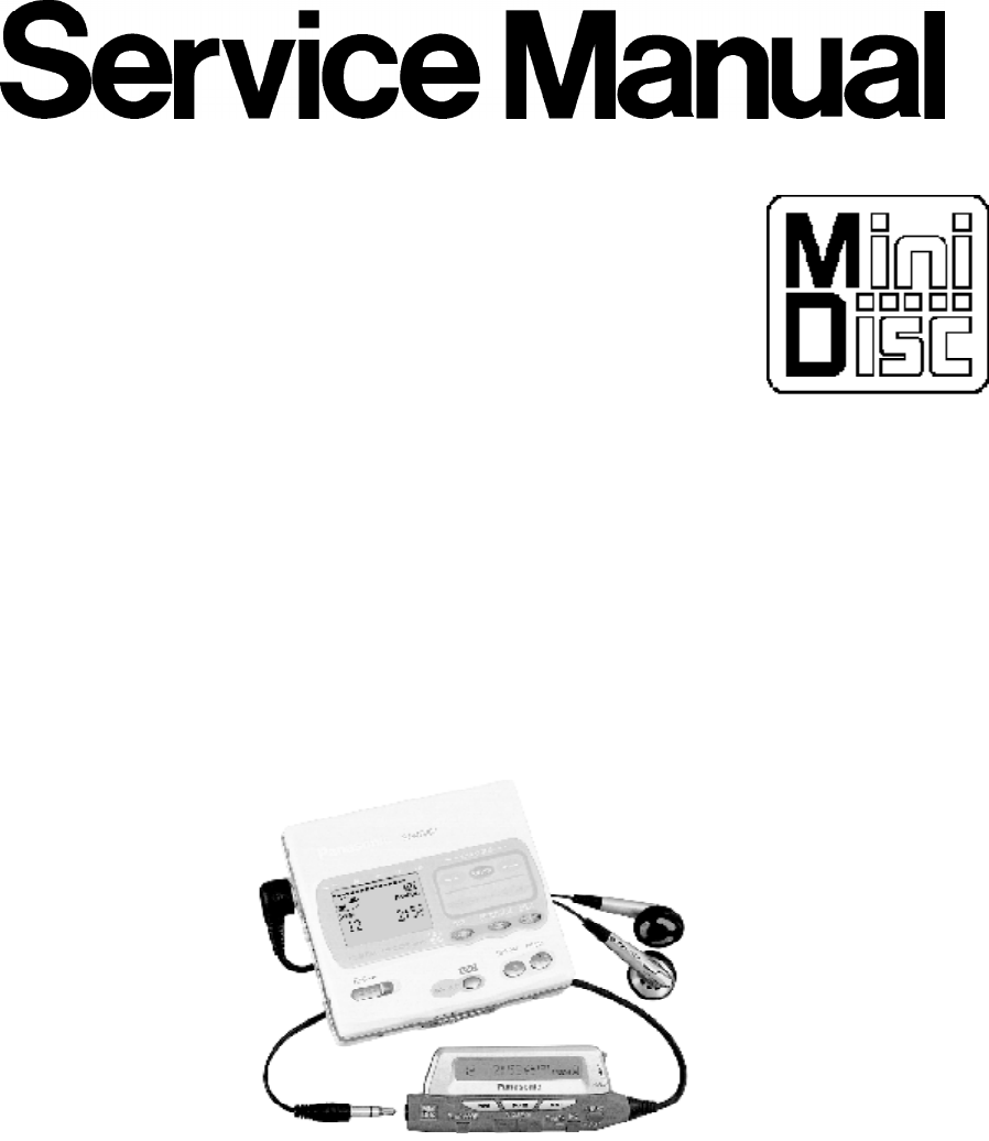
Service_manual Service Manual
User Manual: Service_manual MDCP: Panasonic SJ-MR200 Service Manual
Open the PDF directly: View PDF ![]() .
.
Page Count: 59
ORDER No.AD0009165C8
Portable MD Recorder
SJ-MR200
MD unit: RAE1630Z-M Mechanism Series
Colour
(S)...................Silver Type
(W)..................White Type
Areas
EB...................Great Britain.
EG...................Europe.
GH...................Hong Kong.
SPECIFICATIONS
Specifications
1

Audio
System: MiniDisc digital audio system
Laser: Semiconductor laser (=780 nm)
Sampling frequency: 44.1 kHz
Coding: Adaptive Transform Acoustic Coding
(ATRAC)
No. of channels: 2 (left and right, stereo)
1 (monaural)
Frequency response: 20 Hz-20 kHz (+0 dB, -6dB)
Wow and flutter: Below measurable limit
General
Input terminal
OPT/LINE IN jack
Impedance: 47k
Input level: SENS H: 178mV
SENS L: 500mV
MIC jack
Impedance: 600
Input level: 0.4mV
Output terminal
Output Jack: Phones, 22
Power output: 3.5 mW+3.5 mW
Power supply
Rechargeable battery: DC 1.2V
(included rechargeable battery)
Battery: DC 1.5V (One LR6, AA, UM-3 battery)
AC adaptor: DC 1.8V (included AC adaptor)
Dimensions (WxHxD)
Cabinet dimensions: 78.2x71.6x16.8
mm
incl.projecting parts: 79.9x73.6x18.6
mm
Weight: 120 g (with
battery)
94 g (without battery)
Play time
(When used in hold mode, at 25°C, on a flat, stable surface)
Battery type:Play timeRecord time
Rechargeable: About 15 hoursAbout 7 hours
Panasonic alkaline: About 21 hoursAbout 3 hours
Both together: About 38 hoursAbout 15 hours
Charger
Input: AC 220 V (GH) / AC220-230 V (EG) /
AC 230-240V (EB), 50/60 Hz 8W
Recharging time: About 3 hours
2
Notes:
- The play time may be less depending on the operating
conditions.
- Specifications are subject to charge without notice. Weight
and dimensions are approximate.
2000 Matsushita Electric Industrial Co., Ltd. All rights reserved.
Unauthorized copying and distribution is a violation of law.
1. Accessories
- Rechargeable battery with carrying case .............1pc.
(RFKFHFAZ01EM)
- External battery case...............................................1pc.
(RFA1537-S)
- Carrying case.........................................................1pc.
(RFC0056-K)
- Wired remote control.............................................1pc.
(N2QCBD000007)
- Stereo earphones..................................................1pc.
(RFEV335P-SA)
- Connection cable..................................................1pc.
(K2KA39B00001)
For EB area
- AC adaptor.............................................................1pc.
(RFEA003B-S)
For EG area
- AC adaptor.............................................................1pc.
(N0JCAD000001)
For GH area
- AC adaptor.............................................................1pc.
(RFEA004H-S)
2. Precation of Laser Diode
3
3. Operating Instructions
4. Handling Precautions for Traverse Deck
The laser diode in the traverse deck (optical pickup) may break down due to potential difference
caused by static electricity of clothes or human body.
So, be careful of electrostatic breakdown during repair of the traverse deck (optical pickup).
4.1. Handling the traverse deck (optical pickup)
1. The traverse deck (optical pickup) is an extremely high-precision
construction and must not be subjected to impact, excessive
4
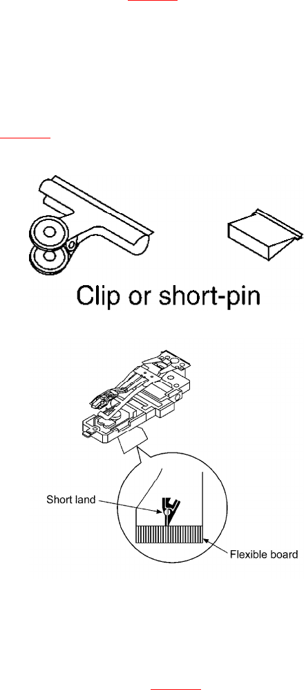
vibration, or other types of rough handling.
2. In order to prevent static electricity damage to the laser diode,
use a short pin or similar tool to short the optical pickup’s flexible
circuit boards after they have been disconnected from the main
circuit board. (as shown in Fig. 1 )
3. Handle the flexible circuit boards with care; excessive force could
cause them to be broken.
4. Do not turn the pre-set variable resistor (for adjustment of the
laser power); it has been adjusted at the factory.
(as shown in Fig. 2 )
Fig. 1
Fig. 2
4.2. Grounding for electrostatic breakdown prevention
1. Human body grounding
Use the anti-static wrist strap to discharge the static electricity
from your body. (as shown in Fig. 3 )
2. Work table grounding
Put a conductive material (sheet) or steel sheet on the area where
the traverse deck (optical pickup) is placed, and ground the sheet.
5

(as shown in Fig. 4 )
Caution
The static electricity of your clothes will not be grounded through
the wrist strap.
So, take care not to let your clothes touch the traverse deck (optical
pickup).
Fig. 3
Fig. 4
5. Operation Checks and Component Replacement
Procedures
- This section describes procedures for checking the operation of
the major printed circuit boards and replacing the main
components.
- For reassembly after operation checks or replacement, reverse the
respective procedures. Special reassembly procedures are
described only when required.
- After replacing the main components (optical pickup or traverse
motor, etc.) of mechanism unit block, change to the adjust mode,
and then perform the “ROM/RAM auto-adjustment”.
5.1. Checking for the main P.C.B.
6

- Check the main P.C.B. (A side) as shown below.
[Checking for the main P.C.B. (B side)]
- Each parts on main P.C.B. (B side) can not be checkesd directly,
however, for the checking of main component parts on P.C.B.,
refer to the “Checking procedures of main components parts on
the main P.C.B. (B side).
7
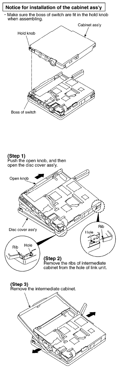
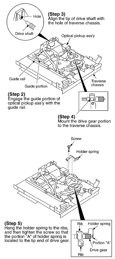
5.2. Replacement for the intermediate cabinet
- Follow the (Step 1) - (Step 3) of item 5.1.
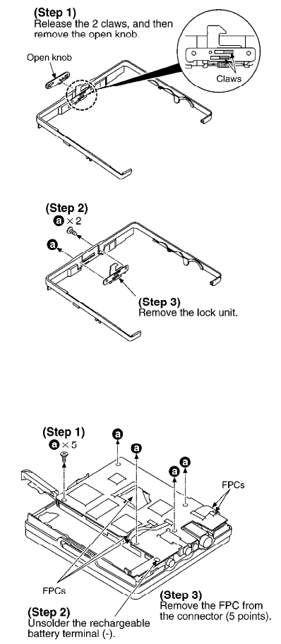
5.3. Replacement for the open knob and lock unit
- Follow the (Step 1) - (Step 3) of item 5.1.
8
- Follow the (Step 1) - (Step 3) of item 5.2.
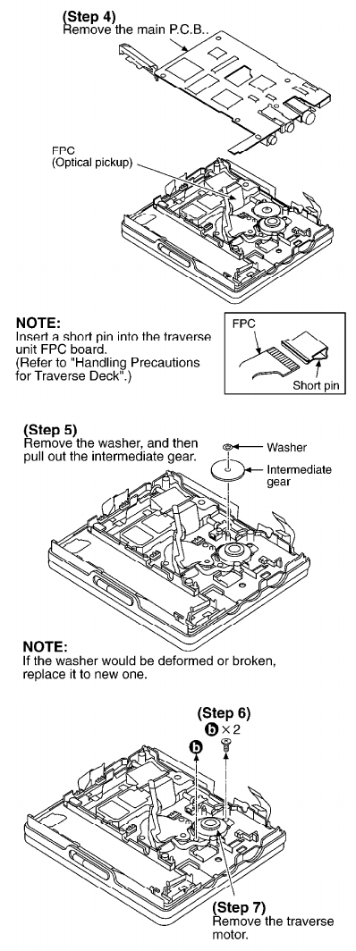
5.4. Replacement for the traverse motor
- Follow the (Step 1) - (Step 3) of item 5.1.
9
5.5. Replacement for the LCD
- Follow the (Step 1) - (Step 3) of item 5.1.
- Follow the (Step 1) - (Step 3) of item 5.2.
10
11
5.6. Replacement for the lift motor
- Follow the (Step 1) - (Step 3) of item 5.1.
- Follow the (Step 1) - (Step 3) of item 5.2.
- Follow the (Step 1) of item 5.5.
12
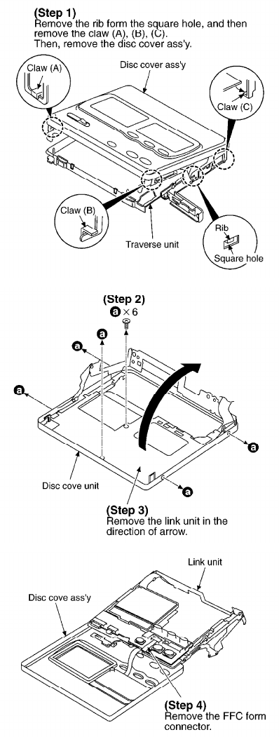
5.7. Replacement for the optical pickup
- Follow the (Step 1) - (Step 3) of item 5.1.
- Follow the (Step 1) - (Step 3) of item 5.2.
- Follow the (Step 1) - (Step 4) of item 5.4.
- Follow the (Step 1) of item 5.5.
13
14
15
6. Measurements and Adjsutments
Note:
After replacing the main components (optical pickup or traverse motor, etc.) of mechanism unit
block, change to the adjust mode, and then perform the “ROM/RAM auto-adjustment”.
6.1. Instruments to prepare
1. Playback-only disc (Test disc RFKV0006)
2. Commercially available recordable disc (fully recorded with
music) (magneto-optical disc)
3. Laser power meter (LE8010 or compatible meter)
16
4. Remote controller
6.2. Laser power adjustment, Playback-only disc/magneto-optical
disc automatic adjustment
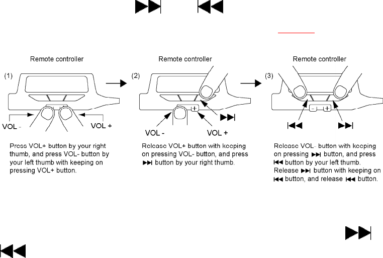
6.2.1. Enter the adjustment mode
1. Set the battery and connect the remote controller.
2. Turn off the power, and switch main unit’s HOLD switch off.
3. Press the VOL+, VOL-, , and buttons on the remote
controller within two seconds. (as shown in Fig. 5 )
Fig. 5
4. When the adjustment mode is activated, “ T1 EX ” will be
displayed on the LCD of remote controller. After “ T1 EX ” is
displayed, select the desired adjustment item with the button
or button of the remote controller. (If it is not displayed,
perform the procedures written above again.)
Adjustment mode
17

Adjustment mode Display
Laser power adjustment T1
Magneto-optical disc automatic adjustment T2
Playback-only disc automatic adjustment T3
EFM jitter meajurement T4
Record inspection T5
REC jitter meajurement T6
Magneto-optical disc automatic adjustment
value check
T7
Playback-only disc automatic adjustment value
check
T8
Error rate measurement (double velocity) T9
AD read result confirmation TA
ROM collection check sum TB
DRAM check TC
Reliability test TD
Tilt measurement (disc middle speed) TE
PWB inspection (audio test) TF
*In the display of T1 ~ TF shown above, you must adjust T1, T2 and TF. You must perform the
adjustment by observing the order T1 T2 T3.
6.2.2. Laser Power Adjustment
Adjust each laser power: read power for reading (play) and write power for writing (record).
6.2.2.1. Set the Unit to the Adjustment Mode
Cautions
About handling the optical pickup and the magnetic head.
- The optical pickup and the magnetic head are structured precisely;
therefore, they are very fragile. Be careful not to touch them with
the edge of the laser power meter. Do not touch the lens.
- The sensor of the laser power meter is a very fine part. Be careful
not to touch it to the optical pickup lens.
- Do not loosen or remove the magnetic head installing screw.
- The focus point of the laser reaches to 356°F. Therefore, avoid
adjusting using laser power for a long time because the sensor of
the laser power meter may be burned.
- Do not allow the write power to even momentarily reach or exceed
5 mW. Doing so will result in damage to the optical pickup.
- Do not set the unit to the laser power adjustment mode with the
MD loaded. Doing so may result in damage to the MD.
- Laser diode in the optical pickup may be destroyed by the
18
staticelectricity generated in your clothes or body. Be especially
careful with the static electricity.
6.2.2.2. Adjustment Procedure
1. Have “ T1 EX ” indicated on display, and move the optical pickup
to the most inside (only when a MD cartridge type laser power
meter is used).
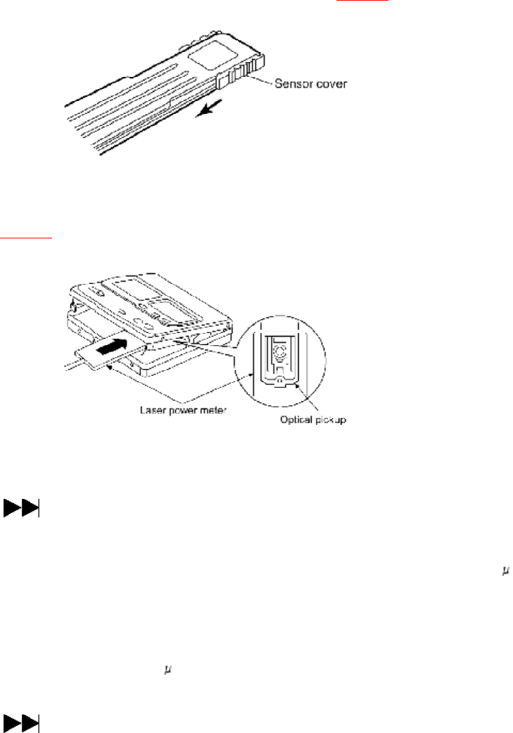
2. Uncover the laser power meter. (as shown in Fig. 6 )
Fig. 6
3. Locate the sensor of the laser power meter at a position above
the optical pickup (horizontally at a level of the disc position). (as
shown in Fig. 7 )
Fig. 7
4. Press the PLAY key of the remote controller (“ T1 EX ” changes to
“ LD ” of the LCD).
5. Press the key of the remote controller (“ LD ” changes to “ LP
” of the LCD).
6. Perform the read power adjustment. Set the light power at 600 W
±10% by using VOL+ and VOL- key of the remote controller.
Caution:
Proceeding on to the subsequent adjustment procedure with the
read power exceeding 600 W±10% will result in damage to the
optical pickup.
7. Press the key of the remote controller (“ LP ” changes to “
19
RLDA ” in the LCD).
Specified range (read power): 600 W±10% or lower
8. Perfome the light power adjustment. Set the light power at
4.55mW by using VOL+ and VOL- key of the remote controller. If
at this time the amperage between TP405 and TP406 (laser
current) is 70mA or higher, it is conceivable that theoptical pickup
is defective.
Specified range (light power): 4.5mW
Caution:
Do not allow the write power to even momentarily reach or exceed
5 mW. Doing so will result in damage to the optical pickup.
9. Press the key of the remote controller (“ RLDA ” changes to “
LP ” on the LDC. At this time, the data is written to EEPROM.).
10. Press the PLAY key on the remote controller (“ LP ” changes to “
T1 EX ” on the LCD.).
11. Remove the laser power meter. Laser power adjustment is
finished.
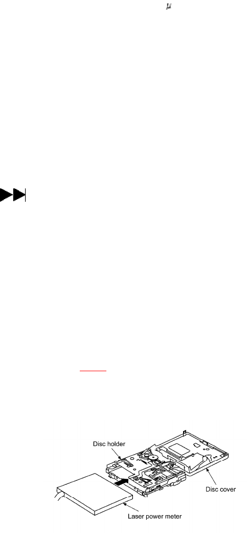
[REFERENCE]
For use of MD cartridge type laser power meter: / We recommend you to use a stick type laser
power meter for laser power adjustment of this set. / But if available is a MD cartridge type
only, arrange the set as shown in Fig. 9 , and from the state of “6.2.1. Enter the adjustment
mode”, start the laser power adjustment. / (As for the method of disassembly, refer to “5.
Operation checks and main component replacementprocedures”.)
Fig. 8
6.2.3. Magneto-optical disc automatically adjustment
1. Have “ T2 EX ” indicated on display, and move the optical pickup
to around the center (only when a MD cartridge type laser power
meter is used).
20
2. Set the full-recorded magneto-optical disc with the prevention
erase situation.
3. Press the PLAY key of the remote controller (“ T2 EX ” changes to
“ 1AADJ ” on the LCD, adjustment is started.).
4. If it has been finished normally, “ 1ADDJ ” changes to “ 1AOK ”
on LCD. If it is abnormally, it changes to “ 1ANG ”.
5. Press the PLAY key (“ 1AOK ” or “ 1ANG ” changes to “ T2 EX ”,
magneto-optical disc adjusment is finished.).
Note:
If it is displayed “ 0ANG ”, check the “Troubleshooting Procedures” in the order.
6.2.4. Playback-only disc automatically adjustment
1. Have “ T3 EX ” indicated on display, and move the optical pickup
to around center (only when a MD cartridge type laser power
meter is used).
2. Set the playback-only disc.
3. Press the PLAY key of the remote controller (“ T1 EX ” changes to
“ 00ADJ ” (or “ 10ADJ ”) on the LCD, adjusment is started.).
4. If it has been finished normally, “ 0AADJ ” (or “ 10ADJ ”) changes
to “ 00OK ” (or “ 10OK ”) on LCD. If it is abnormally, it changes to
“ 00NG ” (or “ 10NG ”).
5. Press the PLAY key [“ 00OK ” (or “ 10OK ”) or “ 00NG ” (or “ 10NG
”) changes to “ T3 EX ”, playback-only discadjustment is
finished.]
Note:
If it is displayed “ 00NG ” (or “ 10NG ”), check the “Troubleshooting Procedures” in the order.
6.2.5. How to get out the adjustment mode
Remove the battery when you finish the adjustment mode.
6.3. Checking the main unit's keys
1. Set the battery and connect the remote controller.
2. Turn off the power. Then, with the main unit’s HOLD switch at
21
OFF, press the VOL+, VOL-, , and buttonson the remote
controller within two seconds. (as shown in Fig. 5 )
3. When entering the main unit’s key check mode, “ KEY EX ” will be
displayed on the LCD of main unit and “ T KEX ” will be displayed
on the LCD of remote controller. (If it is notdisplayed, perform the
procedures written above again.)
4. Confirm the display of LCD by pressing any keys on the main unit.
There is no order to press the keys.
Mian unit’s keys LCD display positions and letters
HOLD OFF 1st. 2nd. letters are AA
REC PAUSE 3rd. 4th. letters are BB
EDIT 5th. 6th. letters are CC
STOP 7th. 8th. letters are DD
PLAY 9th. 10th. letters are EE
5. Remote controller’s LCD lights “ T ” and main unit’s LCD
lights all when you can detect all keys.
6. Perform below voltage check about the keys come under if you
cannot detect the key.
Main unit’s keys Check points ON OFF
HOLD IC501 55pin 0V 2.4V
REC PAUSE IC501 49pin 0V 2.4V
EDIT IC501 3pin 1.94V 2.4V
STOP IC501 3pin 0V 2.4V
PLAY IC501 48pin 0V 2.4V
7. When the keys are ready for detection, press the PLAY key of the
remote control.
8. Pressing each key mounted to the main body, make sure of
displayed three letters (4th ~ 6th letters) on the right side of the
remote control. / Keys to be pressed are not in order. / When the
3 keys apportioned to the respective letters asshown below are all
OK, “ 0 ” is displayed.
22

Display position Main unit’s keys
4th. letter DISPLAY, PLAYMODE, EQ
5th. letter Flat pad lower rank 3 key
6th. letter Flat pad upper rank 3 key
9. Upon detection of all keys, “ 000 ” is shown on the right side of
LCD of the remote control.
10. Perform below voltage check about the keys come under if you
cannot detect the key.
Main unit’s keys Check points ON OFF
DISPLAY IC501 3pin 1.45V 2.4V
PLAYMODE IC501 3pin 0.44V 2.4V
EQ IC501 3pin 1.0V 2.4V
Flat pad (*1) IC501 6~8pin 2.4V 0V
11. Remove the battery when you exit from this mode.
Note:
Refer to “Printed Circuit Board and Wiring Connection Diagram” for the test points.
7. Troubleshooting Guide
23

24
25

26
27
28
29
30
31
8. Checking Procedures of Main Components Parts
on the Main P.C.B. (B side)
As it cannot meajure the mechanism side of MAIN P.C.B. directly, refer to the table shown
below for the criterion in the time of repairing or checking.
32
Circuit
No.
Part No. Function Symptom Check point Result and
measure
IC304C0DBAGZ00006
DC-DC
converter / 3.5V
/ Power IC for
magnetic head
driver control
Recording is
impracticable.
Confirm the
voltage of IC403
(pin 14) or (TP137)
Confirm the
voltage of IC501
(pin 74)
If voltage at
TP137
normal and
voltage
IC501 is
unusual,
IC501 and
switch
periphery.
If voltage at
TP137
unusual,
replace
IC401 C0GBE000003 Optical head lift
motor drive
Recording is
impracticable.
Magnetic head
fails to descend.
Confirm the
motor drive wave
form of TP144 ~ 147
(CN402 pins 1 ~ 4)
If drive
wave
normal, check
FPC
condition of
solder
around lift
motor,
nothing
unusual
found, replace
the
motor.
If drive
wave
unusual,
check
supplyvoltage
of
and peripheral
solder,
and if nothing
unusual
found, replace
IC401.
IC701 AN7635SH-E1 MIC/LINE AMP Optical input
permits recording,
but line input does
not.
MIC recording is
impracticable.
Make sure of
IC601 (pins 2, 3)
input wave form
(during MIC/LINE
input time).
If input
wave
IC601 is
unusual,
supply voltage
of
and peripheral
solder,
and if nothing
unusual
found, replace
IC701.
If input
wave
IC601 is
normal,
checkIC601
and
perihperal
circuit.
9. Display of Self-Diagnostic Function
This model is equipped with a self-diagnosis function and shows, when necessary, the
following indication in the LCD section of the set.
“F17”---This indication appears when the Down switch fails to turn ON since the magnetic head
33

fails to move up/down normally (Due to trouble of the magnetic head or trouble of the magnetic
head up/down motor)or the magnetic head P.C.B. is out of position or a foreign matter has
mixed in or for some other reason.
In such a case, check the peripheral parts of the magnetic head, repair or replace defective
parts with normal ones.
10. Schematic Diagram Notes
10.1. Schemtic Diagram Notes
This schematic diagram may be modified at any time with the development of new technology.
Notes:
S1
:Magnetic head up switch (M.HEAD UP)
S501
:Open det. switch (OPEN )
S502
:Hold swithc in “OFF” position. (HOLD )
S503
:PROTECT det. switch
S801
:Play / record / pause / operation on /
character type button ( , CHARA)
S802
:Recording pause / operation on switch
(REC )
S803
:Stop / operation off / edit cancel button ( ,
OPR OFF)
S804
:Play and record mode / character delete
button (MODE, DELETE)
S805
:Tone / recording sensitivity / space button
(EQ / REC SENS, SPACE)
S806
:Display, capital / lower case button (DISP,
CAPS)
S807
:Changing edit mode, changing track mark
mode, completing edit button (EDIT, MARK
MODE)
- Indicated voltage values are the standard values for the unit
measured by the DC electronic circuit tester (high-impedance)
with the chassis taken as standard. Therefore, there may exist
some errors in the voltage values, depending on theinternal
impedance of the DC circuit tester.
No mark: MD STOP
( ): MD play [1kHz, L+R, 0dB]
Important safety notice:
34
Components identified by mark have special characteristics important for safety.
Furthermore, special parts which have purpose of fire-retardant (resistors), high-quality sound
(capacitors), low-noise (resistors), etc. are used. When replacing any of components, be sure to
use only manufacture's specified parts shown in theparts list.
Caution!
IC and LSI are sensitive to static electricity.
Secondary trouble can be prevented by taking care during repair.
Cover the parts boxes made of plastics with aluminum foil.
Ground the soldering iron.
Put a conductive mat on the work table.
Do not touch the legs of IC or LSI with the fingers directly.
Voltage and signal line
: Positive voltage line
: Playback signal line
: Recording signal “digital” line
: Recording signal “analog” line
: Mic signal line
10.2. Type Illustration of IC's, Transistors and Diodes
11. Schematic Diagram
12. Printed Circuit Board Diagram
13. Block Diagram
14. Wiring Connection Diagram
15. Terminal Function of IC's
15.1. IC1 (AN8772FHKEBV) : RF AMP
35

Pin
No.
Mark I/O
Division
Function
1 CENVD I D signal det. capacitor
input terminal
2 LDO O Laser amp output terminal
3APCPD I Photo diode light quantity
det. input terminal
4 LD IN I Laser amp reverse input
terminal
5APC REF I APC amp reference voltage
input terminal
6TEMP IN I Temperature sensor amp
input terminal
7TEMP O Temperature sensor amp
output terminal
8ADIP O ADIP signal output terminal
9TOFS I Tracking error offset
adjustment terminal
10 TBAL I Tracking ballance
adjustment input terminal
11 TE O Tracking error signal
output terminal
12 CRS IN I Track cross input terminal
13 TGAIN I Tracking gain adjustment
input terminal
14 LNP O Lens position signal
output terminal
15 AB GAIN I APP compensation signal
gain adjustment terminal
16 FE O Focus error signal output
terminal
17 AS GAIN I AS gain adjustment input
terminal
18 FBAL I Focus ballance adjustment
input terminal
19 AS/
MON3T
OAS/3TMON signal output
terminal
20 CEA I 3T envelope det. capacitor
connection terminal
(Connected to power
supply through capacitor)
21 BDO/ /
TRCRS
O BDO/Track cross signal
output terminal
36

Pin
No.
Mark I/O
Division
Function
22 CBD O O BDO detection capacitor
connection terminal
(Connected to GND
through capacitor)
23 OFT O O Off track detection signal
output terminal
24 GND — GND terminal
25 OFT IN I Off track detection signal
input terminal
26 V CC I Power supply terminal (+
3V)
27 NRFDET/
/ OFTR
ONRFDET/off track signal
output terminal
28 NRFLD I Serial command latch
signal input terminal
29 RF DATA I Serial command data
signal input terminal
30 RFCK I Serial command clock
input terminal
31 NRFSTBY I Standby control signal
input terminal
32 OUT RF O EFM signal output terminal
33 CRF
AGC
— RFAGC capacitor
connection terminal
(Connected to GND
through capacitor)
34 EQ IN I EQ input terminal
35 ARFO O RF amp. output terminal
36 SVREF I Reference voltage input
terminal
37 VREF I Reference voltage input
terminal
38 RF1 I RF1 signal input terminal
39 RF2 I RF2 signal input terminal
40 F1 I F1 signal input terminal
41 F2 I F2 signal input terminal
42 CLPF1 I APP compensation LPF
capacitor input terminal
43 EQADJ — RF equalizer adjustment
resistor connection
terminal (Connected to
power supply through
resistor)
37

Pin
No.
Mark I/O
Division
Function
44 /
~ /
47
A / ~ / D I Main beam A~D signal
input terminal
48 CENVC I Beam E signal detection
capacitor input terminal
15.2. IC101 (M66616RB2) : ATRAC ENCORDER/DECORDER, SERVO
SIGNAL PROCESSOR
Pin
No.
Mark I/O
Division
Function
1ADIP I ADIP FM signal input
terminal
2 LNP I Lens position signal input
terminal
3 FE I Focus error signal input
terminal
4TE I Tracking error signal input
terminal
5AS I AS signal input terminal
6 DRMONI I Drive voltage monitor input
terminal
7 BAT I Battery power supply
terminal
8AMONI — Servo analog monitor
signal output (Not used,
open)
9 VREFI I Reference voltage input
terminal
10 TOFS O Tracking off-set
adjustment output terminal
11 FBAL O Focus balance adjustment
output terminal
12 TBAL O Tracking balance
adjustment output terminal
13 TGAIN O TE error gain adjustment
output terminal
14 ASGAIN O Main beam amp gain
adjustment output terminal
15 ABGAIN O APP adjustment output
terminal
16 AV DD 1 I Power supply terminal
17 AV SS 1 — GND terminal
38

Pin
No.
Mark I/O
Division
Function
18 TRDP O Tracking drive (+) PWM
signal output terminal
19 TRDM O Tracking drive (-) PWM
signal output terminal
20 FODP O Focus drive (+) PWM signal
ouutput terminal
21 FODM O Focus drive (-) PWM signal/
focus, tracking ON/OFF
signal output terminal
22 SPDP O Spindle drive (+) PWM
signal output terminal
23 DIR O Spindle drive (-) PWM
signal output terminal
24 DV DD 0 I Power supply terminal
25 FG I FG input terminal
26 STPO0 O Stepper drive signal 0
output terminal
27 STPO1 O Stepper drive signal 1
output terminal
28 IV DD 0 I Power supply terminal for I/
O pad
29 DV ss 0 — GND terminal
30 RAD12 O DRAM address output
terminal (Not used, open)
31 RAD11
32 /
~42
RAD10 /
~RAD0
O DRAM address output
terminal
43 /
~ /
46
RDT3 /
~ / RDT0
I/O DRAM data input/output
terminal
47 NRAS O DRAM row address strobe
output terminal
48 NCAS O DRAM culum address
strobe output terminal
49 NWE O DRAM write enable output
terminal
50 NRST I Reset signal input terminal
51 SELAD I MSP/MDA,I/F address
select input terminal (“H”
Address)
52 SSCK I MSP/MDA,I/F clock input
terminal
53 SSDW I MSP/MDA,I/F write data
input terminal
39

Pin
No.
Mark I/O
Division
Function
54 SSDR O MSP/MDA,I/F read data
output terminal
55 MDISY O Leader synchronous signal
output
56 SCTSY O ADIP synchronous noise
output terminal
57 SGSYNC O Frame synchronous signal
output terminal
58 DV DD 1 I Power supply terminal
59 IV DD 1 — Power supply terminal for I/
O pad
60 DV ss 1 — GND terminal
61 FS384 O 384 Fs output terminal
62 SCL O Bit clock output terminal
63 SWS O Word clock output terminal
64 SDAP O Audio data output terminal
65 SDAR I Audio data input terminal
66 STPI1 I Stepper status 1 input
terminal
67 STPI2 I Stepper status 2 input
terminal
68 STPI0 I Stepper status 0 input
terminal
69 STPO2 O Stepper drive signal 2
output terminal
70 RX1 I Digital audio interface
signal 1 input terminal
71 NRECP I Amp. Play/Rec switching
signal input terminal
72 NREFM O EFM modulation inverted
output
73 REFM O EFM modulation inverted
output terminal
74 MONI3 O Monitor signal output (Not
used)
75 MONI2 O Monitor signal output (Not
used)
76 MONI1 O Monitor signal output (Not
used)
77 MONI0 O Monitor signal output (Not
used)
78 TS3 — Not used, connected to
GND
40

Pin
No.
Mark I/O
Division
Function
79 TS2 — Not used, connected to
GND
80 TS1 — Not used, connected to
GND
81 TS0 — Not used, connected to
GND
82 EXSYSCK I External system clock
input terminal (Not used,
connected to GND)
83 DV DD 2 I Power supply terminal
84 XI I Crystal oscillator input
terminal (F=16.9344MHz)
85 XO O Crystal oscillator output
terminal (F=16.9344MHz)
86 VDss2 — GND terminal
87 RFDAT O RF serial data output
terminal
88 RFCK O RF serial clock output
terminal
89 NRFLD O RF serial load output
terminal
90 TRCRS I Track cross input terminal
91 OFTR I Off-track signal input
terminal
92 APCD O Laser power PWM output
terminal
93 EXEFMCK I External FM clock input
terminal (Not used,
connected to GND through
registor)
94 PEFM1 O EFM loop filter output
terminal
95 EFMIREF I EFM PLL reference current
input terminal
96 EFMPLLF O EFM PLL filter output
terminal
97 PEFMS I EFM signal input terminal
98 AV DD 0 I Power supply terminal
99 AVss0 — GND terminal
100 TEFSEL — Tracking error signal
output terminal
15.3. IC402 (BD6605KVT) : FOCUS/TRACKING COIL, TRAVERSE
41

MOTOR DRIVE, SPINDLE MOTOR DRIVE, ROTARY DETECTOR
Pin
No.
Mark I/O
Division
Function
1 SPWIN I Roter position detect
comparater(W) input
terminal
2 SPCOM I Spindle motor coil center
input terminal
3 EXTCLK I Not used, open
4 C1P — Charge pump capacitor 1(+)
connect terminal
5 C1M — Charge pump capacitor 1(-)
connect terminal
6 C2P — Charge pump capacitor 2(+)
connect terminal
7 C2M — Charge pump capacitor 2(-)
connect terminal
8 VG O Charge pump output
terminal
9 SLVM1 I Power supply terminal
10 SLUOUT O Stepping motor (U) output
terminal
11 SLPG1 — GND termial
12 SLVOUT O Stepping motor (V) output
terminal
13 SLVM2 I Power supply terminal
14 SLWOUT O Stepping motor (W) output
terminal
15 SLPG2 — GND terminal
16 SLCOM I Step motor coil center
input terminal
17 BEMFW O Step detect comparater (W)
output terminal
18 BEMFV O Step detect comparater (V)
output terminal
19 BEMFU O Step detect comparater (U)
output terminal
20 S3 I Stepping decorder 3 input
terminal
21 S2 I Stepping decorder 2 input
terminal
22 S1 I Stepping decorder 1 input
terminal
23 SGND — GND terminal
42

Pin
No.
Mark I/O
Division
Function
24 ASGND — GND terminal
25 STHB I H1, H2 bridge mute input
terminal
26 STALL I Standby input terminal
27 PW1VM I Power supply terminal
28 PW1OUT O Hlaf bridge 1 output
terminal / (Not used, open)
29 PWPG — GND terminal
30 PW2OUT O Half bridge 2 output
terminal
31 PW2VM I Power supply terminal
32 PWIN2 I Half bridge input terminal
33 PWIN1 — GND terminal
34 IN 2R I H bridge 2 reverse input
terminal
35 IN 2F I H bridge 2 forward input
terminal
36 IN 1R I H bridge 1 reverse input
terminal
37 IN 1F I H bridge 1 forward input
terminal
38 H2 PG2 — GND terminal
39 H2 R
OUT
O H bridge 2 reverse output
terminal
40 H2 VM I Power supply terminal
41 H2 F
OUT
O H bridge 2 forward output
terminal
42 H2 PG1 — GND terminal
43 H1 PG2 — GND terminal
44 H1 R
OUT
O H bridge 1 reverse output
terminal
45 H1 VM I Power supply terminal
46 H1 F
OUT
O H bridge 1 forward output
terminal
47 H1 PG1 — GND terminal
48 CST — Connected to GND through
capacitor
49 CSL1 I Slope capacitor connection
terminal (Connected to
GND through capacitor)
50 CSL2
51 FG O Speed pulse output
terminal
43

Pin
No.
Mark I/O
Division
Function
52 BRK- I Brake comparater- input
terminal
53 BRK+ I Brake comparater+ input
terminal
54 V CC 2 I Power supply terminal
55 V CC 1 I Power supply terminal
56 SP VM1 I Half bridge 1 input terminal
57 SP U
OUT
O Spindle motor coil (U)
output terminal
58 SP PG1 — GND terminal
59 SP V
OUT
O Spindle motor coil (V)
output terminal
60 SP VM2 I Half bridge input terminal
61 SP W
OUT
O Spindle motor coil (W)
output terminal
62 SP PG2 — GND terminal
63 SP U IN I Roter position detect
comparater (U) input
terminal
64 SP V IN I Roter position detect
comparater (V) input
terminal
15.4. IC501 (MN101C32GAD) : SYSTEM CONTROL
Pin
No.
Mark I/O
Division
Function
1 VREF- I Reference voltage input
terminal
2 REM
KEY
I Remote cont. key input
terminal
3 KEY IN1 I Unit key1 input terminal
4TEMP I Temperature sensor input
terminal
5 BATT1 I Battery voltage det. input
terminal
6 FP IN1 I Flat pad 1 input terminal
7 FP IN2 I Flat pad 2 input terminal
8 FP IN3 I Flat pad 3 input terminal
9AN7 — Connected to power supply
10 VREF+ I Reference voltage input
terminal
11 V DD I Power supply terminal
44

Pin
No.
Mark I/O
Division
Function
12 OSC2 I System clock input
terminal (f=10.02MHz)
13 OSC1 O System clock output
terminal (f=10.02MHz)
14 VSS — GND terminal
15 XI I Sub clock input terminal
(Not used, connected to
GND)
16 XO O Sub clock output terminal
(Not used, open)
17 MMOD — Memory mode select input
terminal (Connected to
GND)
18 REM
DATA
OLCD driver data output
terminal
19 LINK
RXD
I Link serial input terminal
20 NC O Not used
21 SSDW O MSP/MDA interface writing
data output terminal
22 SSDR I MSP/MDA interface reading
data input terminal
23 SSCLK O MSP/MDA interface data
forward clock output
terminal
24 BUZZER O Buzzer output trminal
25 RST I Reset signal input terminal
26 SELAD O MSP/MDA interface
address signal output
terminal
27 ATRAC
CNT
OATRAC contorl output
terminal (“H”:NORMAL, “L”
:HiFi)
28 LCD STB O LCD driver strobe signal
output terminal
29 REC
SENSE
O REC sensitivity select
output terminal
30 MONO/
ST
O REC amp monaural/stereo
select terminal
31 WAKEUP I Micro computer wake up
signal input terminal
32 MDISY I Leader synchronize signal
from IC101 input terminal
45

Pin
No.
Mark I/O
Division
Function
33 SCTSY I ADIP/sub A synchronize
signal from IC101 input
terminal
34 CFSYNC I MDA synchronize signal
from IC101 input trminal
(11.6ms pulse)
35 OPENSW I Disc cover open/close
switch det. input terminal
(“H”:open, “L”:close)
36 LCD
DATA
OLCD driver data output
terminal
37 — — Connected to GND
38 LCD CK I LCD driver clock input
terminal
39 DEBUG O Micro computer debug
output terminal (Not used,
open)
40 DOCTOR O Doctor mode input terminal
41 NC — Not used, open
42 CHARGE1 O Recharging control output
terminal
43 NRECP O Track jump det. output
terminal
44 EEPCS O EEPROM chip select
output terminal
45 EEPCK O EEPROM clock output
terminal
46 EEPDATA0 OEEPROM data output
terminal
47 EEPDATAI IEEPROM data input
terminal
48 PLAY
KEY
I PLAY/PAUSE KEY input
terminal
49 REC
KEY
I REC/PAUSE KEY input
terminal
50 DC IN
WAKEUP
I DC IN wake up input
terminal
51 REG I Area selection input
terminal
52 MHEAD
UP
IMagnetic head down input
terminal
53 PROTECT I Erase prevention switch
input terminal
46

Pin
No.
Mark I/O
Division
Function
54 JITTER
OK
I Connected to power
supply through resistor
55 HOLD
SW
I HOLD switch input
terminal (“H”:OFF, “L”:ON)
56 DCINDET I DC IN det. input terminal
57 MIC DET I Mic det. input terminal
58 INSEL I INPUT select det. input
terminal
59 FPOUT1
/ JOGA
O Flat pad A output terminal
60 FPOUT2
/ JOGB
O Flat pad B output terminal
61 MIC/LINE O MIC/LINE select output
terminal
62 LOAD0 O Magnetic head movement
control 0 output terminal
63 LOAD1 O Magnetic head movement
control 1 output terminal
64 HFON1 I HF module ON 1 input
terminal
65 MUTEA O Analog mute A output
terminal
66 MUTEB O Analog mute B output
terminal
67 NRFSTBY O RF amp standby output
terminal
68 ADC OFF O ADC OFF output terminal
69 LOW
BST
O VMS select output terminal
70 DEO O DE enphasis output
terminal
71 DAC OFF O DAC off output terminal
72 RECCNT2 OREC control 2 output
terminal
73 RFCNT O RF power supply control
output terminal
74 RECCNT1 OREC control 1 output
terminal
75 PWRCNT O Power supply control
output terminal
76 EL ON I EL display control input
terminal
47
Pin
No.
Mark I/O
Division
Function
77 PC O 4ch driver standby output
terminal
78 STBY2 O FD/TR coil power supply
control output terminal
79 NC — Not used, open
80 MSP
RST
OMSP reset output terminal
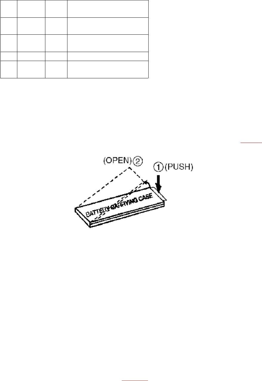
16. Caution in Use of Rechargeable Battery Ass'y
- Take Rechargeable Battery Ass’y out of Battery Carrying Case and
use it.
- Be sure to carry Rechargeable Battery Carrying Case. If not, it may
either heat or ignite by shorting with a metal. (as shown in Fig. 9 )
Fig. 9
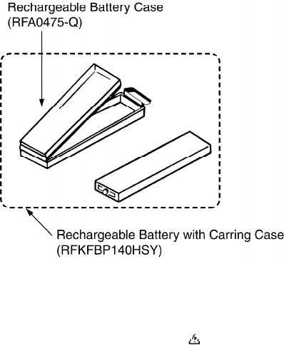
17. Supply of Rechargeable Battery Ass'y as
Replacement Parts
Please take note of the following points relating to Battery Carrying Case to be used for
protection of Rechargeable Battery Ass’y from shorting. Replacement Parts:
- Rechargeable Battery Ass’y (RFKFBP140HSY) supplied will be
provided with Battery Carrying Case (RFA0475-Q).
- No replacement parts will be supplied for Rechargeable Battry
Ass’y without Battery Carrying Case.
- Replacement parts will be supplied for Battery Carrying Case
(RFA0475-Q) without Rechargeable Battery Ass’y.
- To your customers, delivery Rechargeable Battery Ass’y together
with Battery Carrying Case to prevent shorting accidents that may
occur when Rechargeable Battery Ass’y is carried about Battery
Carrying Case. (as shown in Fig. 10 )
Fig. 10
48
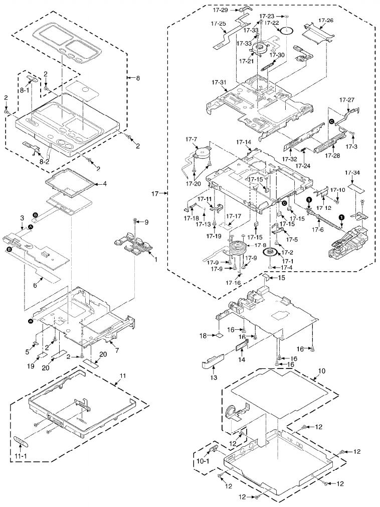
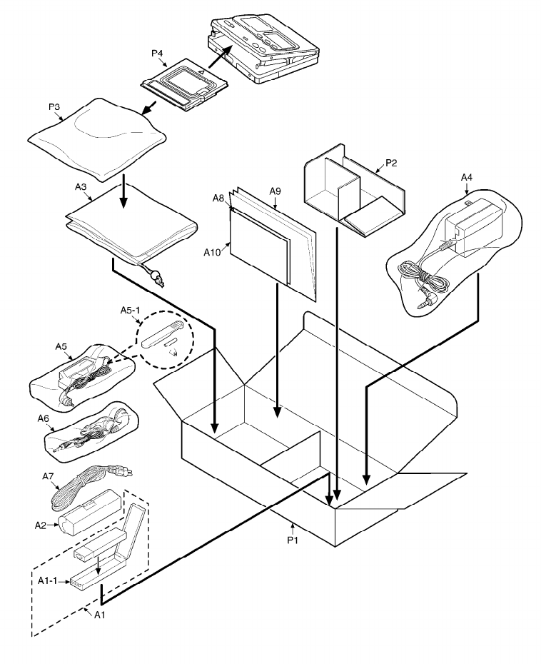
18. Replacement Parts List
Notes:
*Important safety notice: / Components identified by mark have special characteristics
important for safety. / Funrthermore, special parts which have purposes of fire-retardant
(resistors), high-quality sound (capacitors),low-noise (resistors), etc. are used. / When
replacing any of components, be sure to use only manufacture’s specified parts shown in the
parts list. / *Warning: This product uses a laser diode. Refer to caution statements.
*ACHTUNG:Die lasereinheit nicht zerlegen.Die lasereinheit darf nur gegen einc vom hersteller
spezifizierte einheit ausgetauscht werden.
*Capacity values are in microfarads (uF) unless specified otherwise, P=Pico-farads (pF) F=
Farads (F) / *Resistance values are in ohms, unless specified otherwise, 1K=1,000 (OHM), 1M=
1,000K (OHM)
*The marking <RTL> indicates that the Retention Time is limited for this item. After the
discontinuation of this assembly in production, the item will continue to be available for a
specific period of time. The retentionperiod of availability is dependant on the type of assembly ,
and in accordance with the laws governing part and product retention. After the end of this
period, the assembly will no longer be available.
*"<IA>" “<IB>” marks in Remarks indicate languages of instruction manuals.
[<IA>:English/Spanish/French/German/Netherlands/Swedish/Italian/Danish, <IB>:English/
Chinese]
49

Ref. No. Part No. Part Name & Description Pcs Remarks
1RGU1915-S1 OPERATION BUTTON 1 (S)
1 RGU1915-D2 OPERATION BUTTON 1 (W)
2 RHQ0083-S SCREW 6
3RJB2280A OPERATION FPC 1
4RMN0613 LCD HOLDER 1
5RMQ0916 TAPE 1
6RMZ0533 INSULATING SHEET 1
7RXM0072 LINK UNIT 1
8RYF0560-S DISC COVER 1 (S)
8 RYF0560-W DISC COVER 1 (W)
8-1 RGV0266-S REC KNOB 1
8-2 RMA1378 REC LEVER 1
9 XQN14+B2FC SCREW 1
10 RYK1030A-S CABINET ASS'Y 1 (EB)(EG)
10 RYK1030B-S CABINET ASS'Y 1 (GH-S)
10 RYK1030B-W CABINET ASS'Y 1 (GH-W)
10-1 RGV0265-S2 HOLD KNOB 1
11 RYK1031-S1 INTERMEDIATE CABINET 1
11-1 RGV0264-S OPEN KNOB 1
12 RHD14076-S SCREW 6
13 RKK0140-S RECHARGEABLE BATT.COVER 1 (S)
13 RKK0140-W RECHARGEABLE BATT.COVER 1 (W)
14 REJ0150 R.BATT.TERMINAL(+) 1
15 RMX0186 JACK SHEET 1
16 RHD14067 SCREW 5
17 RAE1630Z-M MECHANISM UNIT 1
17-1 RDG0481 INTERMEDIATE GEAR 1
17-2 RHD14078 SCREW 1
17-3 RHD14080 SCREW 1
17-4 RHW11011 WASHER 1
17-5 RMC0409 SPRING 1
17-6 RXJ0028 DRIVE SHAFT 1
17-7 BRL1A1CWC TRAVERSE MOTOR 1
17-8 BTL2A1CRD SPRING MOTOR 1
17-9 RHD14067 SCREW 3
17-10 RHD14082 SCREW 1
17-11 RJC99040 R.BATT.TERMINAL(-) 1
17-12 RMA1364 HOLDER ANGEL 1
17-13 RMB0655-2 DETECT LEVER SPRING 1
17-14 RMK0463 TRAVERSE CHASSIS 1
17-15 RMX0156-1 STOPPER RUBBER 4
17-16 RMX0162 SPACER 1
17-17 RMZ0535 INSULATING SHEET 1
17-18 RXA0183 DETECTION LEVER UNIT 1
17-19 XQN14+B2FC SCREW 1
17-20 XQN14+C12FZ SCREW 2
17-21 BRL1A1CWD LIFT MOTOR 1
17-22 RDG0482 REDUCTION GEAR 1
17-23 RHW06001 WASHER 1
17-24 RMB0650 EJECT SPRING 1
17-25 RMC0232 DRIVE ROD 1
17-26 RML0586-1 LIFTER 1
17-27 RML0587 LINK 1
50

Ref. No. Part No. Part Name & Description Pcs Remarks
17-28 RMM0230 EJECT ROD A 1
17-29 RMQ0958-2 ARM 1
17-30 RXG0050 TRANSFER GEAR 1
17-31 RXK0318 HOLDER UNIT 1
17-32 RXM0071 EJECT ROD B 1
17-33 XQN14+A12FC SCREW 2
17-34 RMX0194 SHEET 1
18 RMX0190 SPACER 1
19 RMG0534-K SHEET 1
20 RMX0187 HOLDER SPACER 2
A1 RFKFHFAZ01EM RECHARGEABLE BATT.ASS'Y 1
A1-1 RFA0475-Q RECHARGEABLE BATT.CASE 1
A2 RFA1537-S EXTERNAL BATTERY CASE 1
A3 RFC0056-K CARRYING CASE 1
A4 N0JCAD000001 AC ADAPTOR 1 (EG)
A4 RFEA003B-S AC ADAPTOR 1 (EB)
A4 RFEA004H-S AC ADAPTOR 1 (GH)
A5 N2QCBD000007 WIRED REMOTE CONTROL 1
A5-1 RYQ0312-H REMOCON.CLIP 1
A6 RFEV335P-SA STEREO EARPHONES 1 L0BAB0000118
A7 K2KA39B00001 LINE CABLE 1
A8 RQA0117 WARRANTY CARD 1 (EB)(EG)
A9 RQT5606-E INSTRUCTION MANUAL 1 (EB)(EG)<IA>
A9 RQT5607-G INSTRUCTION MANUAL 1 (GH)<IB>
A10 RQCB0169 SERVICE CENTER LIST 1
C1 ECUE1H221KBQ 50V 220P 1 F1G1H221A402
C2,C3 ECUVNA224KBV 10V 0.22U 2 F1H1A224A028
C5,C6 RCST0GZ106RG 4V 10U 2 F3E0G106A002
C7 ECUENA104KBQ 10V 0.1U 1 F1G1A104A014
C8 ECUE1C153KBQ 16V 0.015U 1 F1G1C153A044
C10 ECUE1H181KBQ 50V 180P 1
C14 ECUVNA224KBV 10V 0.22U 1 F1H1A224A028
C15 ECUVNJ105KBV 63V 1U 1 F1H0J105A002
C16 ECUE1H181KBQ 50V 180P 1
C17 ECUE1C223KBQ 16V 0.022U 1 F1G1C223A044
C18 ECUE1H101KBQ 50V 100P 1
C19-21 ECUE1H102KBQ 50V 1000P 3 F1G1H102A457
C22 ECUE1E682KBQ 25V 6800P 1
C23 ECUENA393KBQ 10V 0.039U 1 F1G1A393A014
C24 ECUE1E332KBQ 25V 3300P 1 F1G1E3320001
C27 ECUENA104KBQ 10V 0.1U 1 F1G1A104A014
C28 ECUE1E332KBQ 25V 3300P 1 F1G1E3320001
C29-32 ECUE1H102KBQ 50V 1000P 4 F1G1H102A457
C33 ECUVNA224KBV 10V 0.22U 1 F1H1A224A028
C34 ECUE1C103KBQ 16V 0.01U 1
C35 ECUE1C123KBQ 16V 0.012U 1 F1G1C1230001
C36,37 ECUV1C823KBV 16V 0.082U 2
C38 ECUENA104KBQ 10V 0.1U 1 F1G1A104A014
C39 RCST0GZ106RG 4V 10U 1 F3E0G106A002
C40 ECUE1H102KBQ 50V 1000P 1 F1G1H102A457
C41 ECUE1C183KBQ 16V 0.018U 1
51

Ref. No. Part No. Part Name & Description Pcs Remarks
C42 ECUV0J474KBV 6.3V 0.47U 1 F1H0J474A002
C44 ECUE1E332KBQ 25V 3300P 1 F1G1E3320001
C101 RCST0GZ106RG 4V 10U 1 F3E0G106A002
C102 ECUENA104KBQ 10V 0.1U 1 F1G1A104A014
C104 ECUE1H102KBQ 50V 1000P 1 F1G1H102A457
C105 ECUE1C103KBQ 16V 0.01U 1
C107 RCST0GZ106RG 4V 10U 1 F3E0G106A002
C108 ECUENA104KBQ 10V 0.1U 1 F1G1A104A014
C109 RCST0GZ106RG 4V 10U 1 F3E0G106A002
C111 ECUENA104KBQ 10V 0.1U 1 F1G1A104A014
C112,13 ECUE1H100DCQ 50V 10P 2 F1G1H100A420
C115 ECUE1C123KBQ 16V 0.012U 1 F1G1C1230001
C116 ECUE1H221KBQ 50V 220P 1 F1G1H221A402
C117 ECUENA473KBQ 10V 0.047U 1 F1G1A473A014
C118 ECUENA104KBQ 10V 0.1U 1 F1G1A104A014
C201 ECUENA104KBQ 10V 0.1U 1 F1G1A104A014
C202 RCST0GZ475RG 4V 4.7U 1 F3E0G475A002
C203 ECUVNJ105KBV 63V 1U 1 F1H0J105A002
C204 RCST0GZ475RG 4V 4.7U 1 F3E0G475A002
C205 RCST0GZ106RG 4V 10U 1 F3E0G106A002
C206 ECUV0J334KBV 16V 0.33U 1
C207 RCST0GZ475RG 4V 4.7U 1 F3E0G475A002
C208 ECUV0J334KBV 16V 0.33U 1
C209 ECUENA104KBQ 10V 0.1U 1 F1G1A104A014
C210 RCST0GZ106RG 4V 10U 1 F3E0G106A002
C211-13 ECUENA104KBQ 10V 0.1U 3 F1G1A104A014
C214,15 RCST0EX227RE 2.5V 220U 2 F3G0E2270001
C218 ECUE1H101KBQ 50V 100P 1
C219,20 ECUE1H102KBQ 50V 1000P 2 F1G1H102A457
C221 ECUENA104KBQ 10V 0.1U 1 F1G1A104A014
C301 RCST0JX107RG 6.3V 100U 1 F3G0J1070002
C303 RCST0EX227RE 2.5V 220U 1 F3G0E2270001
C305 RCST0GZ226RG 4V 22U 1 F3E0G226A002
C306 ECUENA104KBQ 10V 0.1U 1 F1G1A104A014
C307 RCST0EC397RE 2.5V 390U 1 F3H0J397A012
C308 ECUENA104KBQ 10V 0.1U 1 F1G1A104A014
C309 ECUE1C103KBQ 16V 0.01U 1
C310 ECUENA104KBQ 10V 0.1U 1 F1G1A104A014
C312 ECUENA104KBQ 10V 0.1U 1 F1G1A104A014
C313 ECUE1C103KBQ 16V 0.01U 1
C315 ECUENA104KBQ 10V 0.1U 1 F1G1A104A014
C316 ECUVNJ105KBV 63V 1U 1 F1H0J105A002
C317 ECUVNJ475MBN 63V 4.7U 1 F1J0J4750002
C318 ECUENA104KBQ 10V 0.1U 1 F1G1A104A014
C401 ECUVNA224KBV 10V 0.22U 1 F1H1A224A028
C402 ECUENA473KBQ 10V 0.047U 1 F1G1A473A014
C403 ECUVNA224KBV 10V 0.22U 1 F1H1A224A028
C404 ECUVNC104KBV 16V 0.1U 1
C405 RCST0GZ226RG 4V 22U 1 F3E0G226A002
C407 RCST0GZ106RG 4V 10U 1 F3E0G106A002
C408-11 ECUENA104KBQ 10V 0.1U 4 F1G1A104A014
C416-18 ECUE1H222KBQ 50V 2200P 3 F1G1H222A457
C423 RCST0GZ226RG 4V 22U 1 F3E0G226A002
C424 ECUVNJ105KBV 63V 1U 1 F1H0J105A002
52

Ref. No. Part No. Part Name & Description Pcs Remarks
C425,26 ECUENC273KBQ 16V 0.027U 2 F1G1C273A004
C427 ECUV0J334KBV 16V 0.33U 1
C432-35 ECUE1C103KBQ 16V 0.01U 4
C441 RCST0GZ106RG 4V 10U 1 F3E0G106A002
C442 ECUENA104KBQ 10V 0.1U 1 F1G1A104A014
C443 ECUENA473KBQ 10V 0.047U 1 F1G1A473A014
C444 ECUENA104KBQ 10V 0.1U 1 F1G1A104A014
C445 ECUE1H150JCQ 50V 15P 1
C501 ECUE1H101KBQ 50V 100P 1
C502 ECUENA104KBQ 10V 0.1U 1 F1G1A104A014
C503 ECUE1C103KBQ 16V 0.01U 1
C504 ECUE1H102KBQ 50V 1000P 1 F1G1H102A457
C505 RCST0GZ226RG 4V 22U 1 F3E0G226A002
C506 ECUENA104KBQ 10V 0.1U 1 F1G1A104A014
C507 ECUE1C103KBQ 16V 0.01U 1
C508 ECUV0J474KBV 6.3V 0.47U 1 F1H0J474A002
C509 ECUE1C103KBQ 16V 0.01U 1
C511,12 ECUE1H270JCQ 50V 27P 2 F1G1H270A422
C516 ECUVNJ105KBV 63V 1U 1 F1H0J105A002
C601 ECUE1H470JCQ 50V 47P 1 F1G1H470A422
C606,07 ECUE1E121KBQ 25V 120P 2
C608 RCST0GZ106RG 4V 10U 1 F3E0G106A002
C609 ECUENA104KBQ 10V 0.1U 1 F1G1A104A014
C610 RCST0GZ475RG 4V 4.7U 1 F3E0G475A002
C611 ECUENA104KBQ 10V 0.1U 1 F1G1A104A014
C614,15 ECUVNJ105KBV 63V 1U 2 F1H0J105A002
C701 ECUENA104KBQ 10V 0.1U 1 F1G1A104A014
C702,03 ECUE1C103KBQ 16V 0.01U 2
C704 ECUVNA224KBV 10V 0.22U 1 F1H1A224A028
C705 RCST0GZ106RG 4V 10U 1 F3E0G106A002
C706 ECUVNA224KBV 10V 0.22U 1 F1H1A224A028
C707 RCST0GZ106RG 4V 10U 1 F3E0G106A002
C708,09 RCST0GZ335RE 4V 3.3V 2 F3E0G335A001
C710,11 ECUVNA224KBV 10V 0.22U 2 F1H1A224A028
C712 RCST0GZ335RE 4V 3.3V 1 F3E0G335A001
C713 RCST0GY106RG 4V 10U 1 F3F0G1060003
C714 RCST0GY226RG 4V 22U 1 F3F0G2260002
C715 RCST0GZ226RG 4V 22U 1 F3E0G226A002
C716 ECUENA104KBQ 10V 0.1U 1 F1G1A104A014
C717 RCST0GZ225RG 4V 2.2U 1 F3E0G225A002
C718 RCST0GY106RG 4V 10U 1 F3F0G1060003
C720 ECUENA104KBQ 10V 0.1U 1 F1G1A104A014
C801 ECUENC333KBQ 16V 0.033U 1 F1G1C333A004
C802 ECUE1E472KBQ 25V 4700P 1 F1G1E4720004
C803 ECUE1C103KBQ 16V 0.01U 1
CN1 K1MN26B00047 CONNECTOR(26P) 1
CN2 K1MN06B00069 CONNECTOR(6P) 1
CN3 K1MN04B00034 CONNECTOR(4P) 1
CN402 K1MN10B00064 CONNECTOR(10P) 1
CN403,04 K1MN04B00034 CONNECTOR(4P) 2
CN701 K1MN13B00043 CONNECTOR(13P) 1
CP801 K1MN13B00042 CONNECTOR(13P) 1
CP802 K1MN07B00049 CONNECTOR(7P) 1
53

Ref. No. Part No. Part Name & Description Pcs Remarks
CP803 K1MN05B00042 CONNECTOR(5P) 1
D1 MA2S111TX DIODE 1 MA2S11100L
D301 MA133TX DIODE 1 MA3S13300L
D303-05 B0JCMC000006 DIODE 3
D401,02 ZHCS1006TA DIODE 2 B0JCLG000001
D403,04 MA133TX DIODE 2 MA3S13300L
D501,02 MA741WATX DIODE 2 MA3J741D0L
IC1 AN8772FHKEBV IC 1
IC101 MN66616RB2 IC 1
IC102 MNA7400CWA1T IC 1
IC201 TA2131FL IC 1
IC301 NJU7015RTE1 IC 1 C0ABHA000012
IC302 C0DBAFZ00016 IC 1
IC303 XC6367A151MR IC 1 C0DBAFZ00012
IC304 C0DBAGZ00006 IC 1
IC401 C0GBE0000003 IC 1
IC402 BD6605KVT IC 1 C1BB00000481
IC403 C0JBAB000373 IC 1
IC404 B1MBBDA00002 IC 1
IC405 B1MBBLA00001 IC 1
IC501 MN101C32GAD IC 1
IC502 AK93C45BH-L IC 1 C3EBCG000028
IC503 C0EBC0000032 IC 1
IC601 C0FBZH000011 IC 1
IC701 AN7635SH-E1 IC 1
JK201 K2HC106D0001 JACK,HEADPHONES 1
JK301 RJJ43K10-H JACK,DC IN 1 K2EA2B000003
JK701 RJJ38TW01-H JACK,OPT/LINE IN 1 B3MBZ0000002
JK702 RJJ34R01-1H JACK,MIC 1 K2HC103E0012
L1 RLQP100MT-W COIL 1 G1C100M00016
L101 RLQP100MT-W COIL 1 G1C100M00016
L103,04 ERJ8GEY0R00V COIL 2
L201,02 RLBV601V-W COIL 2 J0JCC0000059
L203 ERJ8GEY0R00V COIL 1
L301 G1A220E00006 COIL 1
L302 G1A100F00002 COIL 1
L303 ELJEA470KF COIL 1
L305 RLM9Z006T-D COIL 1
L402 ERJ8GEY0R00V COIL 1
L407 ELJEA470KF COIL 1
L501 RLQP100MT-W COIL 1 G1C100M00016
L701-03 RLBV601V-W COIL 3 J0JCC0000059
L705,06 J0JAC0000009 COIL 2
LCD801 L5DCADC00008 LCD 1
P1 RPK1473 PACKING CASE 1 (S)
P1 RPK1528 PACKING CASE 1 (W)
P2 RPQ0991 PAD 1
54

Ref. No. Part No. Part Name & Description Pcs Remarks
P3 RPF0257-1 PROTECTION BAG 1
P4 RPQ1004-1 TRANSPORT SPACER 1
PCB1 REP3036A-M REC.HEAD P.C.B. 1 (RTL)
PCB2 REP3038B-M MAIN P.C.B. 1 (RTL)
PCB3 REP3039A-S OPERATION P.C.B. 1 (RTL)
Q1 2SB1295-6-TB TRANSISTOR 1 B1ADKB000001
Q2 2SB1462STX TRANSISTOR 1 2SB14620SL
Q202 2SB1295-6-TB TRANSISTOR 1 B1ADKB000001
Q203 B1ABDF000001 TRANSISTOR 1
Q301 B1ABDF000001 TRANSISTOR 1
Q302 XP151A12A2MR TRANSISTOR 1 B1DFBC000002
Q303 XP4601TX TRANSISTOR 1 XP0460100L
Q304 XP161A1355PR TRANSISTOR 1 B1DFDC000003
Q305 XP152A12C0MR TRANSISTOR 1 B1DHAC000002
Q306,07 XP151A13A0MR TRANSISTOR 2 B1DFBC000003
Q308 2SB1462STX TRANSISTOR 1 2SB14620SL
Q309 XP151A13A0MR TRANSISTOR 1 B1DFBC000003
Q310 DTC144TETL TRANSISTOR 1 B1GBCFNA0001
Q311 2SD1979TX TRANSISTOR 1 2SD1979
Q312,13 XP152A12C0MR TRANSISTOR 2 B1DHAC000002
Q314 DTC144EETL TRANSISTOR 1 B1GBCFNN0001
Q315 XP152A12C0MR TRANSISTOR 1 B1DHAC000002
Q401 DTC144EETL TRANSISTOR 1 B1GBCFNN0001
Q701 XP4601TX TRANSISTOR 1 XP0460100L
Q703 UMG2NTR TRANSISTOR 1 B1GFCFNN0010
Q705 B1ABDF000001 TRANSISTOR 1
R1 ERJ2GEJ472X 1/4W 4.7K 1 ERJ2RMJ472X
R2 ERJ2GEJ272X 1/4W 2.7K 1 ERJ2RMJ272X
R5 ERJ2GEJ103X 1/4W 10K 1 ERJ2RMJ103X
R10 ERJ2GEJ1R0X 1/4W 1 1 ERJ2RMJ1R0X
R11 EXB24V103JX 1/4W 10K 1
R14 ERJ2GEJ471X 1/4W 470 1 ERJ2RMJ471X
R15 ERJ2GEJ473X 1/4W 47K 1 ERJ2RMJ473X
R16 ERJ2GEJ222X 1/4W 2.2K 1 ERJ2RMJ222X
R18 ERJ2GEJ474X 1/4W 470K 1 ERJ2RMJ474X
R20 EXB24V104JX 1/16W 100K 1
R21 ERJ2GEJ223X 1/4W 22K 1 ERJ2RMJ223X
R22 ERJ2GEJ102X 1/4W 1K 1 ERJ2RMJ102X
R23 ERJ2GEJ473X 1/4W 47K 1 ERJ2RMJ473X
R24 EXB24V272JX 1/16W 2.7K 1
R25 ERJ2GEJ563X 1/4W 56K 1
R29 ERJ2GEJ333X 1/4W 33K 1 ERJ2RMJ333X
R30 EXB24V473JX 1/16W 47K 1
R32 EXB24V473JX 1/16W 47K 1
R34 ERJ2GEJ223X 1/4W 22K 1 ERJ2RMJ223X
R35 ERJ2GEJ473X 1/4W 47K 1 ERJ2RMJ473X
R107 ERJ2GEJ105X 1/4W 1M 1 D0GA105JA001
R108 ERJ2GEJ223X 1/4W 22K 1 ERJ2RMJ223X
R110 ERJ2GEJ333X 1/4W 33K 1 ERJ2RMJ333X
R111 ERJ2GEJ682X 1/4W 6.8K 1 ERJ2RMJ682X
R113 ERJ2GEJ102X 1/4W 1K 1 ERJ2RMJ102X
55

Ref. No. Part No. Part Name & Description Pcs Remarks
R114 ERJ2GEJ473X 1/4W 47K 1 ERJ2RMJ473X
R201 ERJ2GEJ104X 1/4W 100K 1 ERJ2RMJ104X
R202 ERJ2GEJ221X 1/4W 220 1 ERJ2RMJ221X
R203 ERJ2GEJ102X 1/4W 1K 1 ERJ2RMJ102X
R204 EXB24V225JX 1/16W 2.2M 1
R205 ERJ2GEJ222X 1/4W 2.2K 1 ERJ2RMJ222X
R206 EXB24V100JX 1/16W 10 1
R207 ERJ2GEJ471X 1/4W 470 1 ERJ2RMJ471X
R208 ERJ2GED273X 1/4W 27K 1 ERJ2RHD273X
R209 EXB28V103JX 1/32W 10K 1
R211 EXB24V332JX 1/16W 3.3K 1
R212,13 ERJ2GEJ221X 1/4W 220 2 ERJ2RMJ221X
R301 EXB24V334JX 1/16W 330K 1
R302 EXB24V104JX 1/16W 100K 1
R303 ERJ2RHD223X 1/4W 22K 1
R304 ERJ2GEJ103X 1/4W 10K 1 ERJ2RMJ103X
R305 ERJ2GEJ474X 1/4W 470K 1 ERJ2RMJ474X
R306 ERJ2GEJ103X 1/4W 10K 1 ERJ2RMJ103X
R308 EXB24V474JX 1/16W 470K 1
R309 ERJ2GEJ394X 1/4W 390K 1 ERJ2RMJ394X
R310 ERJ2GED563X 1/4W 56K 1
R311 ERJ2GED683X 1/4W 68K 1 ERJ2RHD683X
R312 ERJ2GED105X 1/4W 1M 1 ERJ2RKD105X
R313 EXB24V104JX 1/16W 100K 1
R314 ERJ2GEJ154X 1/4W 150K 1 ERJ2RMJ154X
R315 ERJ2GED104X 1/4W 100K 1 D0HA104ZA002
R316 ERJ2GEJ104X 1/4W 100K 1 ERJ2RMJ104X
R317 ERJ6RSJR10V 1/10W 0.1 1
R318 ERJ2GED105X 1/4W 1M 1 ERJ2RKD105X
R320 ERJ2GEJ474X 1/4W 470K 1 ERJ2RMJ474X
R321 ERJ2GEJ394X 1/4W 390K 1 ERJ2RMJ394X
R322 ERJ2GEJ225X 1/4W 2.2M 1 ERJ2RMJ225X
R323 ERJ2GED105X 1/4W 1M 1 ERJ2RKD105X
R324,25 ERJ2GEJ474X 1/4W 470K 2 ERJ2RMJ474X
R326 ERJ2GEJ221X 1/4W 220 1 ERJ2RMJ221X
R327 ERJ2GEJ474X 1/4W 470K 1 ERJ2RMJ474X
R401 ERJ2GEJ6R8X 1/4W 6.8 1
R402 ERJ2GEJ103X 1/4W 10K 1 ERJ2RMJ103X
R403 EXB24V473JX 1/16W 47K 1
R406 EXB24V473JX 1/16W 47K 1
R408 ERJ2GEJ472X 1/4W 4.7K 1 ERJ2RMJ472X
R410 ERJ2GEJ153X 1/4W 15K 1 ERJ2RMJ153X
R411 ERJ2GEJ682X 1/4W 6.8K 1 ERJ2RMJ682X
R412 ERJ2GEJ182X 1/4W 1.8K 1 ERJ2RMJ182X
R413 ERJ2GEJ471X 1/4W 470 1 ERJ2RMJ471X
R414 ERJ2GEJ102X 1/4W 1K 1 ERJ2RMJ102X
R501 ERJ2GEJ473X 1/4W 47K 1 ERJ2RMJ473X
R502 ERJ2GEJ103X 1/4W 10K 1 ERJ2RMJ103X
R504 EXB28V334JX 1/32W 330K 1
R506 ERJ2GEJ103X 1/4W 10K 1 ERJ2RMJ103X
R507 EXB28V224JX 1/32W 220K 1
R509 ERJ2GEJ223X 1/4W 22K 1 ERJ2RMJ223X
R513 EXB28V334JX 1/32W 330K 1
R516 ERJ2GEJ221X 1/4W 220 1 ERJ2RMJ221X
56

Ref. No. Part No. Part Name & Description Pcs Remarks
R518 EXB28V104JX 1/32W 100K 1
R602 ERJ2GEJ5R6X 1/4W 5.6 1 ERJ2RMJ5R6X
R603 EXB24V123JX 1/16W 12K 1
R604 ERJ2GEJ470X 1/4W 47 1 ERJ2RMJ470X
R605 EXB28V470JX 1/32W 47 1
R701 ERJ2GEJ102X 1/4W 1K 1 ERJ2RMJ102X
R702 ERJ2GEJ103X 1/4W 10K 1 ERJ2RMJ103X
R703 EXB24V104JX 1/16W 100K 1
R704 EXB24V333JX 1/16W 33K 1
R705 EXB24V102JX 1/16W 1K 1
R706 EXB24V471JX 1/16W 470 1
R707 ERJ2GEJ394X 1/4W 390K 1 ERJ2RMJ394X
R708 EXB24V104JX 1/16W 100K 1
R709 ERJ2GEJ473X 1/4W 47K 1 ERJ2RMJ473X
R710 ERJ2GEJ470X 1/4W 47 1 ERJ2RMJ470X
R712 ERJ2GEJ104X 1/4W 100K 1 ERJ2RMJ104X
R713 ERJ2GEJ101X 1/4W 100 1 ERJ2RMJ101X
R714 ERJ2GEJ473X 1/4W 47K 1 ERJ2RMJ473X
R715 ERJ2GEJ155X 1/4W 1.5M 1
R716 EXB24V103JX 1/4W 10K 1
R717 EXB24V223JX 1/4W 22K 1
R801 ERJ3GEYJ222V 1/16W 2.2K 1
R802 ERJ3GEYJ472V 1/16W 4.7K 1 D0GB472JA002
R803 ERJ3GEYJ822V 1/16W 8.2K 1 D0GB822JA002
R804 ERJ3GEYJ273V 1/16W 27K 1 D0GB273JA002
R807 ERJ2GEJ473X 1/4W 47K 1 ERJ2RMJ473X
R808 ERJ2GEJ563X 1/4W 56K 1
RX103 ERJ2GEJ103X 1/4W 10K 1 ERJ2RMJ103X
RX503 ERJ2GEJ334X 1/4W 330K 1 ERJ2RMJ334X
S1 ABC1111P SW,MAGNETIC HEAD 1 K0L1BA000050
S501 RSH1A039-A SW,OPEN DET. 1 K0L1BA000037
S502 K0D112A00114 SW,HOLD 1
S503 RSH1A039-A SW,PROTECT 1 K0L1BA000037
S801 RSG0051-P SW,PLAY/PAUSE,CHARA 1
S802 K0F111A00335 SW,REC 1
S803-07 RSG0051-P SW,PUSH 5
TH1 RRSP33J103CW THERMISTOR 1 D4CC11730001
TH401 RRSP33J103CW THERMISTOR 1 D4CC11730001
X101 H0J169500013 OSCILLATOR 1
X501 H2C100500005 OSCILLATOR 1
Z301 RJH9209-1 BATT.CASE CONNECT.TERMINA 1 K4BC02E00005
19. Cabinet Parts Location
57
20. Packaging
58
Printed in Japan (H000900000) SW/HH
59
