SG6848x1 Datasheet. Www.s Manuals.com. R1.3 System General
User Manual: Marking of electronic components, SMD Codes AA, AA**, AA***, AA-, AA-**, AA-***, AA=***, AAA, AAA***, AAC, AAD, AAE, AAE**, AAF, AAFI, AAG, AAH**, AAHC, AAHO, AAI**, AAIK, AAJ**, AAJ***, AAJF*, AAJI, AAJJ, AAL***, AAM***, AAN***, AANC, AAP, AAQ, AAR, AAS, AASQ, AASR, AAT***, AATJ, AATK, AATL, AATM, AAU, AAU**, AAW, AAX, Aa. Datasheets 2N7002T, 2SD1757K, 74AHC1G00GW, AME8804AEEY, BCW60A, BCX51, BD48E23G, BD48K23G, BL3406B-1.0V, BL9641, LR9641, MAX1736EUT41-T, MAX1736EUT42-T, MAX2644, MAX4335EXT-T, MAX4336EXT
Open the PDF directly: View PDF ![]() .
.
Page Count: 16
Product Specification
Low-cost Green-Mode PWM Controller for Flyback Converters SG6848x1
© System General Corp. - 1 - www.sg.com.tw
Version 1.3(IAO33.0002.B4) Jan. 27, 2006
FEATURES
Green-mode PWM Controller
Low Start-up Current (5uA)
Low Operating Current (3mA)
Programmable PWM Frequency
Peak-current-mode Operation
Leading-edge Blanking
Built-in Synchronized Slope Compensation
Cycle-by-cycle Current Limiting
Constant Output Power Limit
Gate Output Voltage Clamped at 15V
Small SOT-26 Package Available
APPLICATIONS
General-purpose switching mode power supplies and
flyback power converters, such as
Battery chargers
Power adapters
Open-frame SMPS
Replacements for linear transformers and RCC
5V standby power for PC power supply.
DESCRIPTION
This highly integrated PWM controller provides
several special enhancements designed to meet the low
standby-power needs of low-power SMPS. To
minimize standby power consumption, the proprietary
green-mode function provides off-time modulation to
continuously decrease PWM frequency under light-load
conditions. This green-mode function enables the power
supply to easily meet even the strictest power
conservation requirements.
The BiCMOS fabrication process enables reducing
the start-up current to 5uA, and the operating current to
3mA. As a result, a large start-up resistance can be used.
Built-in synchronized slope compensation ensures the
stability of peak-current-mode control. Proprietary
internal compensation provides a constant output power
limit over a universal AC input range (90VAC to
264VAC). Cycle-by-cycle current limiting ensures safe
operation during short-circuits.
To protect the external power MOSFET from being
damaged by supply over voltage, the SG6848x1’s output
driver is clamped at 15V. The SG6848x1’s controllers can
be used to improve the performance and reduce the
production cost of power supplies. The SG6848x1 is the
best choice for replacing linear and RCC power supplies.
It is available in DIP-8 and SOT-26 packages.
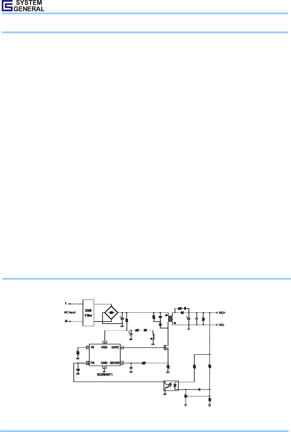
TYPICAL APPLICATION
Product Specification
Low-cost Green-Mode PWM Controller for Flyback Converters SG6848x1
© System General Corp. - 2 - www.sg.com.tw
Version 1.3(IAO33.0002.B4) Jan. 27, 2006
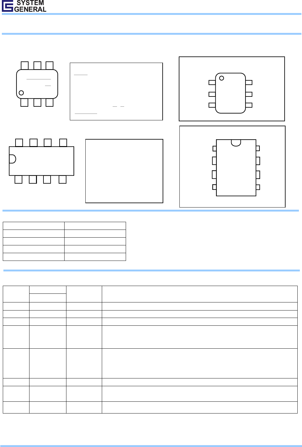
MARKING DIAGRAMS PIN CONFIGURATION
ORDERING INFORMATION
Part Number Package
SG6848T1 SOT-26
SG6848D1 DIP-8
SG6848TZ1 SOT-26 (Lead Free)
SG6848DZ1 DIP-8 (Lead Free)
PIN DESCRIPTIONS
Pin No.
Name DIP-8 / (SOT-26) Type Function
GATE 1 / (6) Driver Output The totem-pole output driver for driving the power MOSFET.
VDD 2 / (5) Supply Power supply.
NC 3 No connection.
SENSE 4 / (4) Analog Input
Current sense. This pin senses the voltage across a resistor for peak-current-mode
control. If the voltage reaches the internal threshold, PWM output is disabled. This
activates cycle-by-cycle current limiting.
RI 5 / (3) Analog
Input/Output
A resistor connected from the RI pin to GND pin will generate a constant current source
for the controller. This current is used to determine PWM frequency. Increasing the
resistance will reduce PWM frequency. A 95kΩ resistor results in a 70kHz PWM
frequency.
NC 6 No connection.
FB 7 / (2) Analog Input Feedback. The FB pin accepts the output voltage regulation signal. It provides feedback
to the internal PWM comparator to adjust the duty cycle.
GND 8 / (1) Supply Ground.
1
2
34
5
6
SOT-26
GND
FB
RI
GATE
VDD
SENSE
DIP-8
RI
N
C
FB
GND
SENSE
N
C
VDD
GATE
4
3
2
1
5
6
7
8
XXX:AAH =SG6848T1
XXX:AAH =SG6848TZ1
M: Mask Version
W: Week code A~Z=W1~W26
A~Z=W27~W52
:Lead free package
D: D = DIP
P : Z = Lead Free
Null = Regular Package
M: Mask Version
XXXXXX: Wafer Lot
YY: Year; WW: Week
V: Assembl
y
Location
8
1
SG6848DP1
MXXXXXXYYWWV
1
XXXMW
Product Specification
Low-cost Green-Mode PWM Controller for Flyback Converters SG6848x1
© System General Corp. - 3 - www.sg.com.tw
Version 1.3(IAO33.0002.B4) Jan. 27, 2006
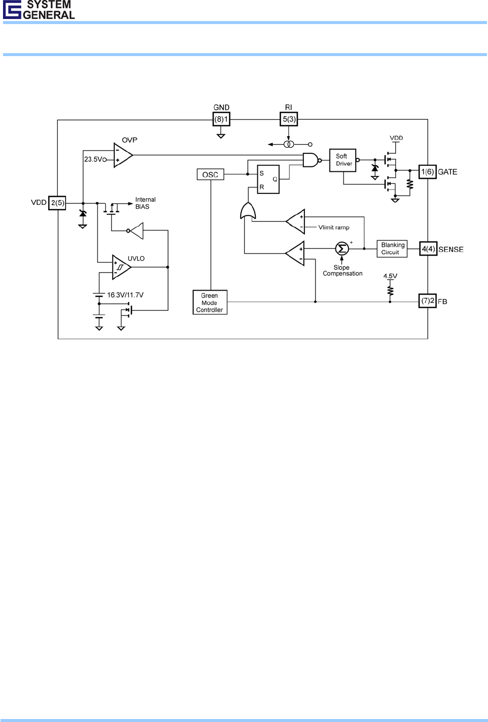
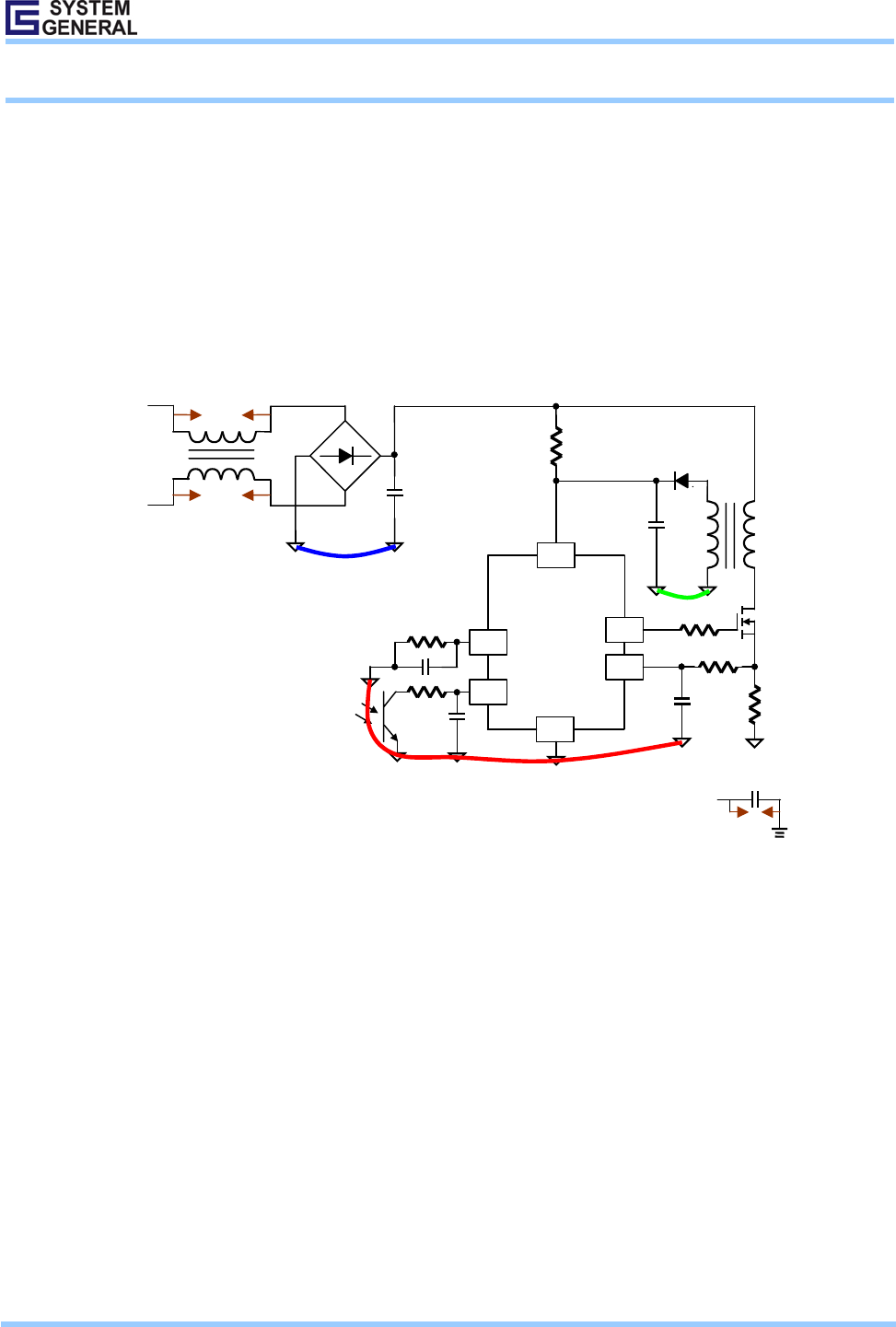
BLOCK DIAGRAM
Product Specification
Low-cost Green-Mode PWM Controller for Flyback Converters SG6848x1
© System General Corp. - 4 - www.sg.com.tw
Version 1.3(IAO33.0002.B4) Jan. 27, 2006
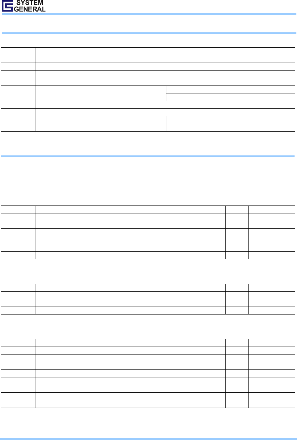
ABSOLUTE MAXIMUM RATINGS
Symbol Parameter Value Unit
VDD DC Supply Voltage 25 V
VFB Input Voltage to FB Pin -0.3 to 6 V V
VSENSE Input Voltage to Sense Pin -0.3 to 6V V
PD Power Dissipation 300 mW
SOT-26 208.4 °C/W
RθJA Thermal Resistance (Junction to Air) DIP-8 82.5 °C/W
TJ Operating Junction Temperature -40 to +125 °C
TSTG Storage Temperature Range -55 to +150 °C
Pb free 260(+5/-0)
TR Peak Reflow Temperature Pb 230(+5/-0)
°C
* All voltage values, except differential voltages, are given with respect to GND pin.
* Stresses beyond those listed under "absolute maximum ratings" may cause permanent damage to the device.
RECOMMENDED OPERATING JUNCTION TEMPERATURE: -30°C ~ 105°C*
*For proper operation
ELECTRICAL CHARACTERISTICS (VDD=15V, TA = 25°C, unless noted)
VDD Section
Symbol Parameter Test Condition Min. Typ. Max. Unit
VOP Continuously Operating Voltage 20 V
VTH(ON) Start-up Threshold Voltage 15.3 16.3 17.3 V
VDD(MIN) Min. Operating Voltage 10.9 11.7 12.5 V
IDD ST Start-up Current 5 30 uA
IDD OP Operating Supply Current GATE = 1nF 3 5 mA
VDD-OVP Over Voltage Protection 22 23.5 25 V
Feedback Input Section
Symbol Parameter Test Condition Min. Typ. Max. Unit
ZFB Input Impedance 2 kΩ
IOZ Zero-duty-cycle Input Current 1.3 2.0 mA
VOP Open Loop Voltage 4.5 V
Oscillator Section
Symbol Parameter Test Condition Min. Typ. Max. Unit
FOSC PWM Frequency RI = 95kΩ 65 70 75 kHz
FOSC-GREEN Green-mode Min. Frequency RI = 95kΩ 15 kHz
FDY Frequency Variation versus VDD Deviation VDD = 14 to 20V 2 %
FDT Frequency Variation versus Temp. Deviation TA = -30 to 105 ℃ 2 %
IN Green-mode Start Threshold FB Input Current 1 mA
IG Green-mode Min. Freq. FB Input Current 1.16 mA
SG Green-mode Modulation Slope RI = 95kΩ 300 Hz/uA
RI RI pin resistance 66.5 150 kΩ

Product Specification
Low-cost Green-Mode PWM Controller for Flyback Converters SG6848x1
© System General Corp. - 5 - www.sg.com.tw
Version 1.3(IAO33.0002.B4) Jan. 27, 2006
Current Sense Section
Symbol Parameter Test Condition Min. Typ. Max. Unit
ZCS Input Impedance 10 kΩ
TPD Delay to Output 100 nsec
VTH,FLT Current Limit Flatten Threshold Voltage 0.96 V
VTH,VALLEY Current Limit Valley Threshold Voltage 0.81 V
DCSAW Duty Cycle of SAW Limit 45 %
Gate Section
Symbol Parameter Test Condition Min. Typ. Max. Unit
DC (MAX) Maximum Duty Cycle 70 75 80 %
DC (MIN) Minimum Duty Cycle 0 %
BNK Leading-edge Blanking Time 200 nsec
VOL Output Voltage Low Sink current = 20mA 1.5 V
VOH Output Voltage High Source current = 20mA 8 V
TR Rising Time GATE = 1nF 250 nsec
TF Falling Time GATE = 1nF 80 nsec
VCLAMP Output Clamp Voltage VDD = 20V 15 17 V
Product Specification
Low-cost Green-Mode PWM Controller for Flyback Converters SG6848x1
© System General Corp. - 6 - www.sg.com.tw
Version 1.3(IAO33.0002.B4) Jan. 27, 2006
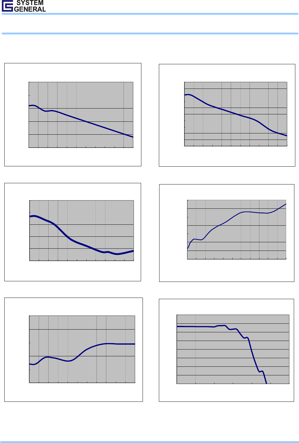
TYPICAL CHARACTERISTICS
Start-up Threshold Voltage vs Temperature
16
16.2
16.4
16.6
16.8
17
-40 -25 -10 5 20 35 50 65 80 95 110 125
Temperature (℃)
VTH(ON) (V)
Start-up Current vs Temperature
0.000
2.000
4.000
6.000
8.000
10.000
-40 -25 -10 5 20 35 50 65 80 95 110 125
Temperature (℃)
IDD ST (uA)
Green-mode min. Frequency vs Temperature
14.0
14.2
14.4
14.6
14.8
15.0
-40 -25 -10 5 20 35 50 65 80 95 110 125
Temperature (℃)
FOSC-GREEN (kHz)
Min. Operating Voltage vs Temperature
10
10.1
10.2
10.3
10.4
10.5
10.6
10.7
10.8
10.9
11
-40 -25 -10 5 20 35 50 65 80 95 110 125
Temperature (℃)
VDD(MIN) (V)
PWM Frequency vs Temperature
64.600
64.700
64.800
64.900
65.000
65.100
65.200
65.300
-40 -25 -10 5 20 35 50 65 80 95 110 125
Temperature (℃)
FOSC (kHz)
PWM Frequency vs. FB
0
10
20
30
40
50
60
70
80
0.6 0.7 0.8 0.9 1 1.1 1.2
FB(mA)
FOSC (kHz)
Product Specification
Low-cost Green-Mode PWM Controller for Flyback Converters SG6848x1
© System General Corp. - 7 - www.sg.com.tw
Version 1.3(IAO33.0002.B4) Jan. 27, 2006
OPERATION DESCRIPTION
The SG6848x1 devices integrate many useful
functions into one controller for low-power switching
mode power supplies. The following descriptions
highlight some of the features of the SG6848D1.
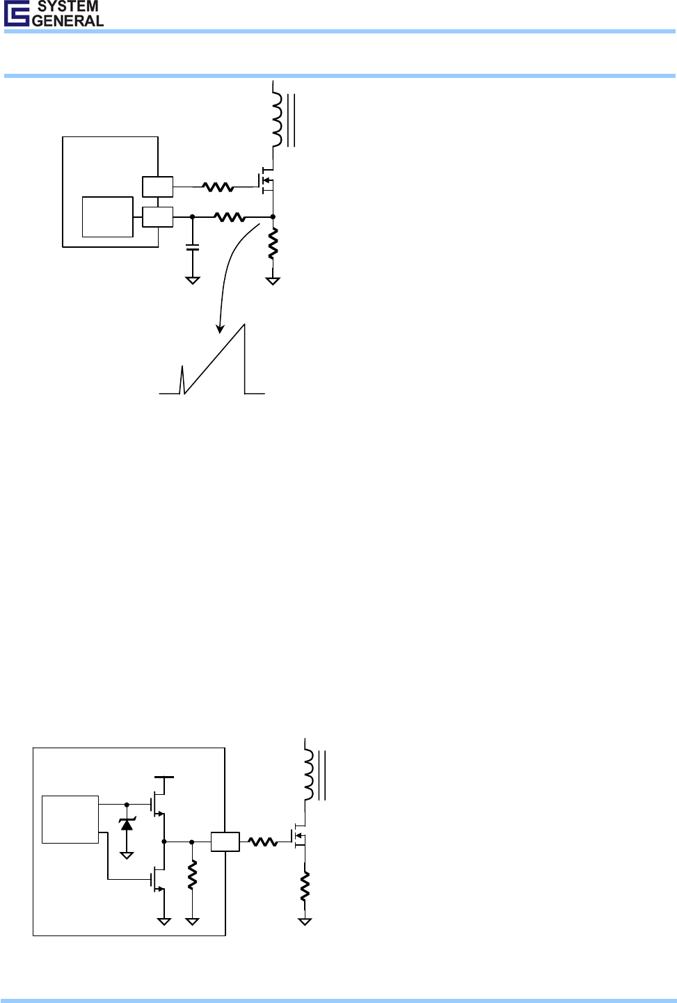
Start-up Circuitry
When the power is turned on, the input rectified
voltage, Vdc, charges the hold-up capacitor C1 via a
start-up resistor RIN. As the voltage of VDD pin reaches
the start threshold voltage VTH(ON), the SG6848x1
activates the entire power supply.
VDD
GND
SG6848D1
Vdc
IDDST
C1
RIN
TD_ON
VTH(ON)
D1
Figure 1. Power Circuit
The maximum power-on delay time is determined as
follows,
−⋅−= ⋅
−
1
)(
_
1)( CR
T
INDDSTdcONTH
IN
OND
eRIVV (1)
where
IDDST is the start-up current of SG6848x1;
TD_ON is the power-on delay time of the power
supply.
Due to the low start-up current, a large RIN such as
1.5Mohm can be used. Also with a hold-up capacitor of
10uF/50V, the power-on delay TD_ON is less than 2.8S for
90VAC input.
The FB input
This pin is designed for feedback control and to
activate the green-mode function. Figure 2 is a typical
feedback circuit mainly consisting of a shunt regulator
and an opto-coupler. R1 and R2 form a voltage divider for
the output voltage regulation. R3 and C1 are adjusted for
control-loop compensation. A small-value RC filter (e.g.
RFB= 47ohm, CFB= 1nF) placed from the FB pin to GND
can increase stability. The maximum source current on the
FB pin is 2mA. The phototransistor must be capable of
sinking this current to pull the FB level down at no load.
Thus, the value of the biasing resistor Rb is determined as
follows,
mAK
Rb
VVV ZDo 2≥⋅
−
−
(2)
where VD is the drop voltage of a photodiode, about 1.2V;
VZ is the minimum operating voltage of the shunt
regulator. Typical value is 2.5V;
K is the current transfer rate (CTR) of the opto-coupler.
For an output voltage Vo=5V, with CTR=100%, the
maximum value of Rb is 650ohm.
FB
VO
Rb
R1
C1
R2
R3
RFB
CFB
Figure 2. Feedback circuit.
Product Specification
Low-cost Green-Mode PWM Controller for Flyback Converters SG6848x1
© System General Corp. - 8 - www.sg.com.tw
Version 1.3(IAO33.0002.B4) Jan. 27, 2006
Oscillator & Green Mode Operation
One external resistor, RIi, connected between RI and
GND pins is used to program the PWM frequency of the
SG6848x1. The approximated formula is:
)Kohm(R
)KHz(F
I
OSC
6650
= (3)
The recommended FOSC is from 50 to 100KHz.
RI
GND
SG6848D1
RI C I
Figure 3. Setting PWM frequency
The patented green-mode function provides off-time
modulation to reduce the PWM frequency at light-load
and no-load conditions. The sink current of the FB pin
determines the green mode operation as shown in Figure 4.
At light load, the sink current of the FB pin will increase.
When the sink current is larger than 1mA, the PWM
frequency decreases in order to reduce the power
consumption of the power supply at light-load and in
no-load conditions.
For lightning surge tests, a small capacitor (not over
50pF) connected from the RI pin to GND is recommended.
This added capacitor also improves stability, especially at
light load and high input line voltage conditions.
Figure 4. PWM frequency vs. FB current.
Built-in Slope Compensation
A flyback converter can be operated in either
discontinuous current mode (DCM) or continuous current
mode (CCM). There are many advantages to operating the
converter in CCM. With the same output power, a
converter in CCM exhibits smaller peak inductor currents
than one in DCM. Therefore, a small-sized transformer
and a low-rated MOSFET can be applied. On the
secondary side of the transformer, the rms output current
of DCM can be up to twice that of CCM. Larger wire
gauge and output capacitors with larger ripple current
ratings are required. DCM operation also results in higher
output voltage spikes. A large LC filter must also be
added. Therefore, a flyback converter in CCM achieves
better performance with lower component cost.
Despite the above advantages of operating in CCM,
there is one concern–stability. Operating in CCM, the
output power is proportional to the average inductor
current, while the peak current is controlled. This causes
the well-known sub-harmonic oscillation when the PWM
duty cycle exceeds 50%. Adding slope compensation
(reducing the current-loop gain) is an effective way to
prevent this oscillation. The SG6848x1 introduces a
synchronized positive-going ramp (VSLOPE) in every
switching cycle to stabilize the current loop. The sensed
voltage together with this slope compensation signal
(VSLOPE) is fed into the non-inverting input of the PWM
comparator. The resulting voltage is compared with the
FB signal to adjust the PWM duty cycle, such that the
output voltage is regulated. Therefore, users can use the
SG6848x1 to design a cost-effective, highly efficient and
compact sized flyback power supply operating in CCM
without adding any external components.
The positive ramp added is,
DVV SLSLOPE
⋅
=
(4)
where
VSL = 0.33V;
D = Duty cycle
OSC
F
5
OSC
F
F
B
)(kHzf
IN IG
Product Specification
Low-cost Green-Mode PWM Controller for Flyback Converters SG6848x1
© System General Corp. - 9 - www.sg.com.tw
Version 1.3(IAO33.0002.B4) Jan. 27, 2006
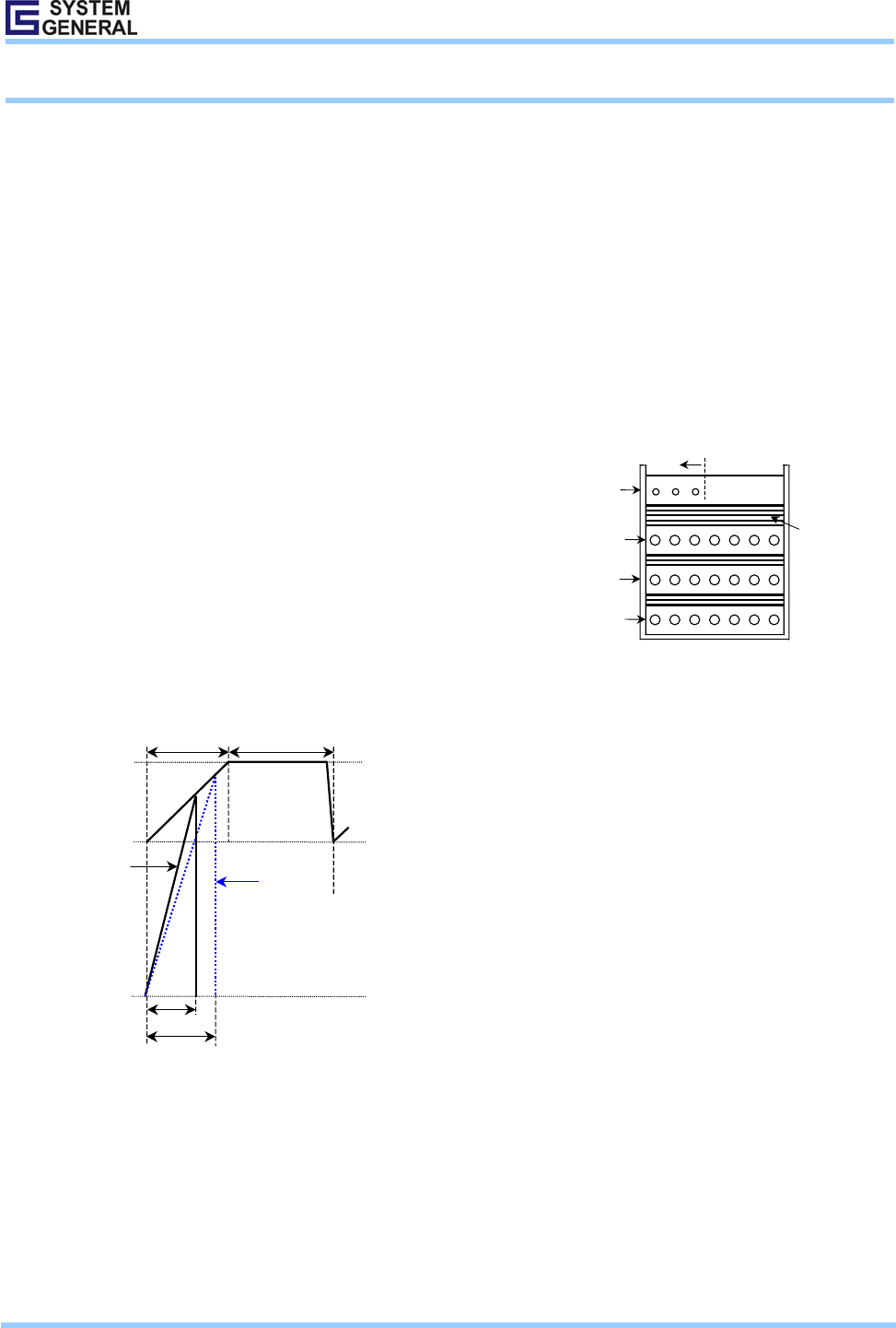
Constant Output Power Limit
The maximum output power of a flyback converter
can generally be determined from the current-sense
resistor RS. When the load increases, the peak inductor
current increases accordingly. When the output current
arrives at the protection value, the OCP comparator
dominates the current control loop. OCP occurs when the
current-sense voltage reaches the threshold value. The
output GATE driver is turned off after a small propagation
delay, td. The delay time results in unequal power-limit
level under universal input. In the SG6848x1, a saw-tooth
power-limiter is designed to solve the unequal
power-limit problem. As shown in Figure 5, the power
limiter is designed as a positive ramp signal and is fed to
the inverting input of the OCP comparator. This results in
a lower current limit at high-line inputs than at low-line
inputs. However, with fixed propagation delay, td, the
peak primary current would be the same for various line
input voltages. Therefore the maximum output power can
practically be limited to a constant value within a wide
input voltage range without adding any external circuitry.
T2
T1
High line
sense voltage Low line
sense voltage
ton VTH,FLT
VTH,VALLEY
toff
0
Figure 5. Constant power limit compensation
Short Circuit Protection
When the output of a flyback power supply is shorted,
the primary VDD will decrease due to the coupling
polarity between the aux winding and the secondary
winding of a transformer. When VDD drops below the
UVLO level of the SG6848x1, the power supply will
enter hiccup operation mode and hence limit the output
power. However, it is possible that the VDD voltage
remains higher than the UVLO level even if the output is
shorted. This happens when the coupling between the aux
and the primary winding is too good. Therefore, the
construction of the transformer becomes a dominant
factor. The recommended construction layout is to
increase the insulation thickness for the aux winding and
place the primary aux winding in one side of the bobbin.
For low output voltage applications, using a low dropout
voltage diode and a larger secondary winding also helps.
Primary main winding
Primary main winding
Secondary winding
Primary aux winding
Increased thickness
One side
Figure 6. Transformer construction
Leading-Edge Blanking
A voltage signal proportional to the MOSFET
current develops on the current-sensing resistor, RS. Each
time the MOSFET is turned on, a spike, which is induced
by the diode reverse recovery and by the output
capacitances of the MOSFET and diode, inevitably
appears on the sensed signal. Inside the SG6848x1, a
leading-edge blanking time of about 200 nsec. is
introduced to avoid premature termination of the
MOSFET by the spike. Therefore, only a small-value RC
filter (e.g. 100ohm + 470pF) is required between the
SENSE pin and RS. Still, a non-inductive resistor for the
RS is recommended.
Product Specification
Low-cost Green-Mode PWM Controller for Flyback Converters SG6848x1
© System General Corp. - 10 - www.sg.com.tw
Version 1.3(IAO33.0002.B4) Jan. 27, 2006
Gate
Sense
SG6848D1
Blanking
Circuit
Figure 7. Turn on spike
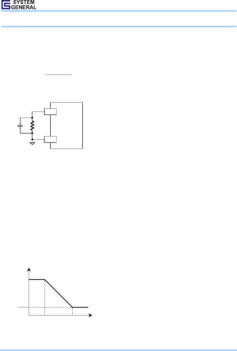
Gate Drive
The SG6848x1’s output stage is a fast totem pole
driver that can drive a MOSFET gate directly. It is also
equipped with a voltage clamping Zener diode to protect
the MOSFET from damage caused by undesirable
over-drive voltage. The output voltage is clamped at 15V.
An internal pull-down resistor is used to avoid a floating
state of the gate before startup. A gate drive resistor in the
range of 47 to 100ohm is recommended. This resistor
limits the peak gate drive current and provides damping to
prevent oscillations at the MOSFET gate terminal.
ON/OFF
Driver
VDD
15V
SG6848D1
Gate
Figure 8. Gate drive
Lab Note
Before reworking or soldering/de-soldering on the
power supply, it is suggested to discharge the primary
capacitors by an external bleeding resistor. Otherwise the
PWM IC may be destroyed by external high voltage
during soldering or de-soldering.
This device is sensitive to ESD discharge. To
improve the production yield, the production line should
be ESD protected in accordance to ANSI ESD S1.1, ESD
S1.4, ESD S7.1, ESD STM 12.1, and EOS/ESD S6.1.
Printed Circuit Board (PCB) Layout
High frequency switching current/voltage makes
PCB layout a very important design issue. Good PCB
layout minimizes excessive EMI and helps the power
supply survive during surge/ESD tests. Here, we give
some common guidelines:
In order to get better EMI performance and reduce
line frequency ripples, the output of the bridge rectifier
should be connected to capacitor C1 first, and then to the
switching circuits.
The high frequency current loop is in C1 –
Transformer – MOSFET – RS – C1. The area enclosed
by this current loop should be as small as possible. Keep
the traces (especially 4→1) short, direct, and wide. High
voltage traces related to the drain of the MOSFET and the
RCD snubber should be kept far way from control circuits
to prevent unnecessary interference. If a heatsink is used
for the MOSFET, it’s better to connect this heatsink to a
ground.
As indicated by 3, the ground of control circuits
should be connected first before any other circuitry.
As indicated by 2, the area enclosed by the
transformer aux winding, D1, and C2 should also be
kept small. Place C2 close to the SG6848x1 for good
decoupling.
Two suggestions for ground connections, with
different pro and cons, are offered.
Product Specification
Low-cost Green-Mode PWM Controller for Flyback Converters SG6848x1
© System General Corp. - 11 - www.sg.com.tw
Version 1.3(IAO33.0002.B4) Jan. 27, 2006
GND3→2→4→1: This should avoid common
impedance interference for the sense signal.
GND3→2→1→4: This should be better for ESD
tests, where the earth ground is not available on the power
supply. Regarding the ESD discharge path, the charges go
from secondary through the transformer’s stray
capacitance to GND2 first. Then the charge goes from
GND2 to GND1 and back to the mains. It should be noted
that control circuits should not be placed in the discharge
path. Point discharges for common choke can decrease the
high frequency impedance and help increase ESD
immunity.
Should a Y-cap between primary and secondary be
required, it is suggested to connect this Y-cap to the
positive terminal of C1 (Vdc). If this Y-cap is connected
to the primary GND, it should be connected to the
negative terminal of C1 (GND1) directly. The Point
discharge of this Y-cap also helps with ESD. However,
the distance between these two points should be at least
5mm according to safety requirements.
Sense
Gate
Vdc
VDD
RI
FB
GND
SG6848D1
C1
C2
RIN
CI
RI
CFB
RFB
Rg
Rf
RS
Cf
D1
3
2
1
4
Y-cap
5
Common mode
choke
Figure 9. Layout considerations
Product Specification
Low-cost Green-Mode PWM Controller for Flyback Converters SG6848x1
© System General Corp. - 12 - www.sg.com.tw
Version 1.3(IAO33.0002.B4) Jan. 27, 2006
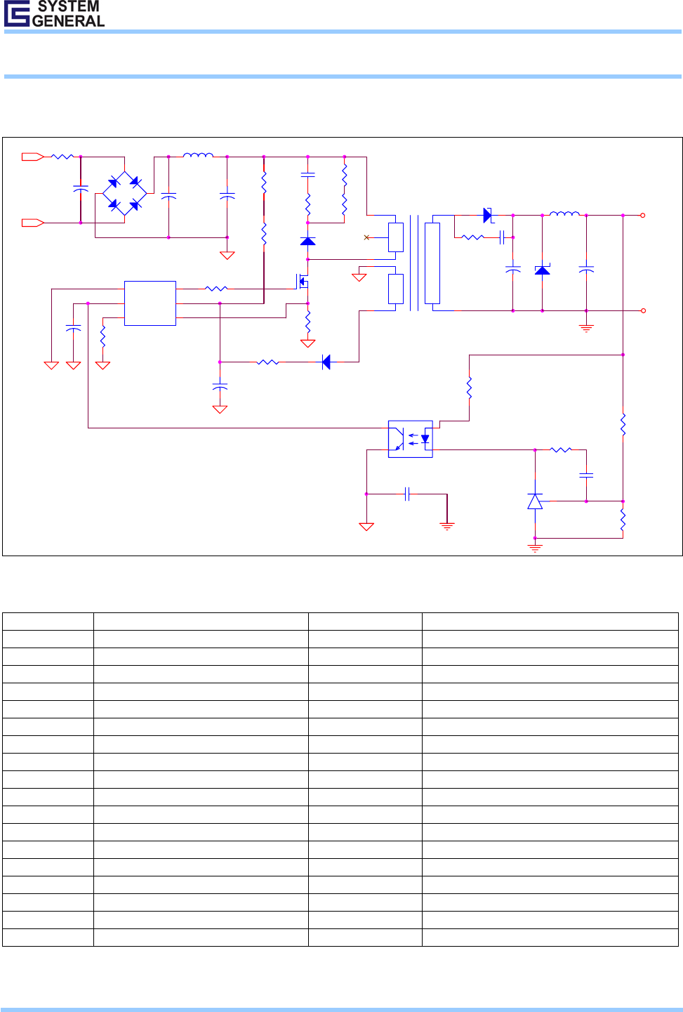
REFERENCE CIRCUIT
Circuit 5V/1A
VO
GND
R13
C10
R12
+
C9
U3
3
1
2
R1
D5
2 1
D1
2 1
R8
Q1
1
23
C3
U1
1
2
3 4
5
6
GND
FB
RI SENSE
VDD
GATE
+
C2
F1 L1
1 2
D4
2 1
R11
C1
R4
U2
1
2
4
3
CX1
R7
-+
BD1
1
4
3
2
R5 T1
8
5
7 3,4
1,210
9
L2
1 2
C6
R9
+
C4
R10
R6
R3
D2
21
+
C8
CY1
C7
R14
R2
L
N
BOM
Reference Component Reference Component
BD1 BD 1A/500V L2 10uH 6mm
CX1 (Optional) XC 0.1uF Q1 MOSFET 1A/600V
CY1 (Optional) YC 102P/400V (Y1) R1, R2 R 750KΩ 1206
C2 EC 10uF/400V 105℃ R4, R3 R 47KΩ 1206
C1 CC 103P/500V R5 R 47Ω 1206
C3 CC 102P/500V R6 R 4.7Ω 1206
C4 EC 10u/50V R7 R 100Ω 0805
C6 CC 472P 0805 R8 R 10Ω 1206
C7 (Optional) CC 102P/100V 1206 R10 (Optional) R 10Ω 1206
C8 EC 470u/10V 105℃ R9 R 100KΩ 0805
C9 EC 220u/10V 105℃ R11 R 100Ω 1/8W
C10 CC 222P 0805 R12 R 33KΩ 0805
D1 Diode FRI07 R13 R 33KΩ 1/8W
D2 Diode FR102 R14 R 4.7KΩ 0805
D4 Diode SB360 T1 EE-16
D5 (Optional) ZD 6.8V 0.5W U1 IC SG6848D1
F1 R 1Ω/0.5W U2 PC817
L1 20mH 6*8mm U3 TL431
Product Specification
Low-cost Green-Mode PWM Controller for Flyback Converters SG6848x1
© System General Corp. - 13 - www.sg.com.tw
Version 1.3(IAO33.0002.B4) Jan. 27, 2006
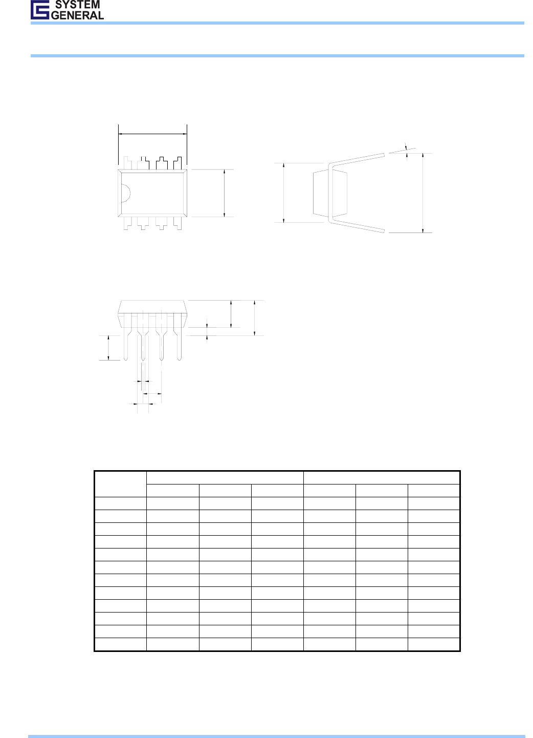
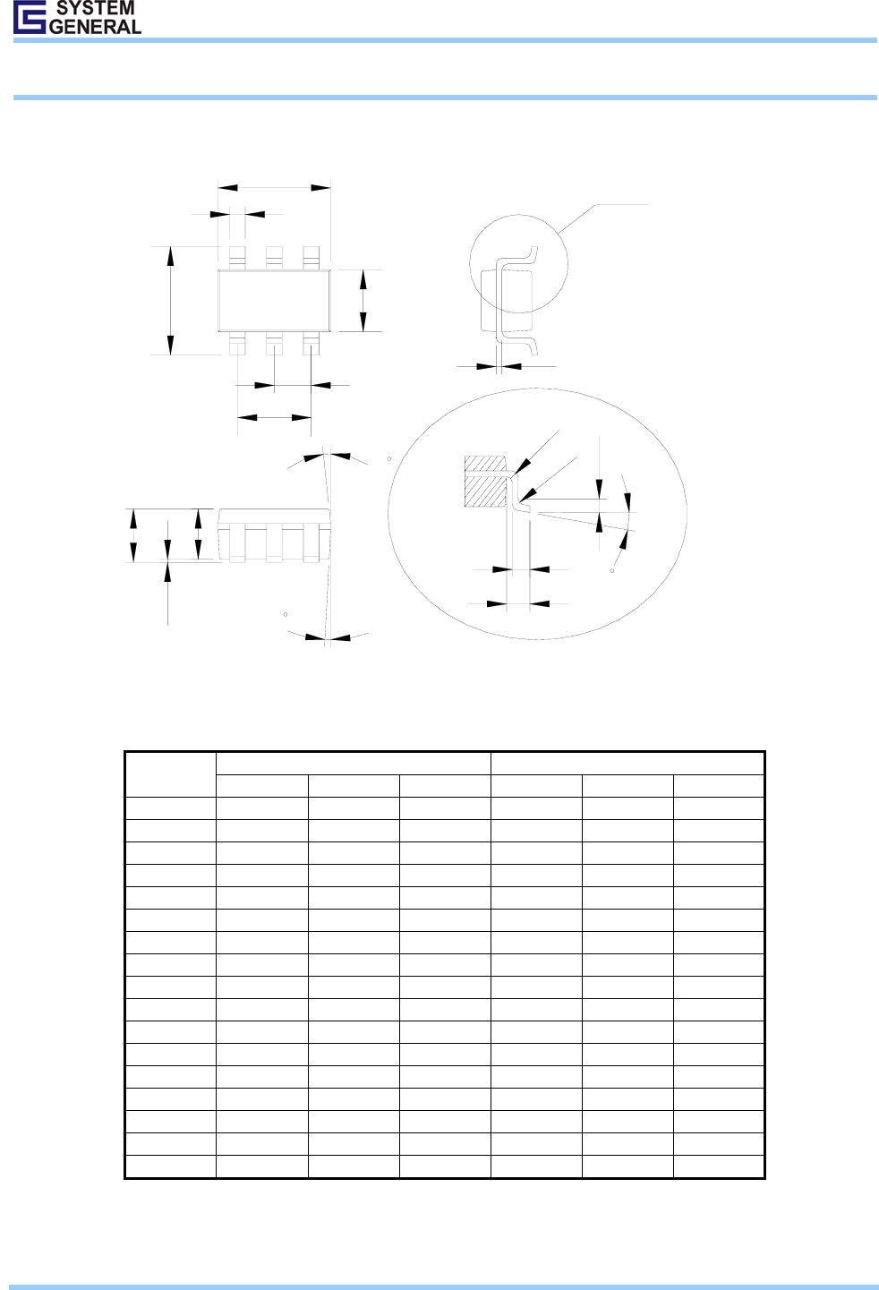
PACKAGE INFORMATION
8 PINS - DIP (D)
41
85
D
E1
EeB
A1
A2
A
b
b1
L
e
°
Θ
Dimensions
Millimeters Inches
Symbol Min. Typ. Max. Min. Typ. Max.
A 5.334 0.210
A1 0.381 0.015
A2 3.175 3.302 3.429 0.125 0.130 0.135
b 1.524 0.060
b1 0.457 0.018
D 9.017 9.271 10.160 0.355 0.365 0.400
E 7.620 0.300
E1 6.223 6.350 6.477 0.245 0.250 0.255
e 2.540 0.100
L 2.921 3.302 3.810 0.115 0.130 0.150
eB 8.509 9.017 9.525 0.335 0.355 0.375
θ˚ 0˚ 7˚ 15˚ 0˚ 7˚ 15˚
Product Specification
Low-cost Green-Mode PWM Controller for Flyback Converters SG6848x1
© System General Corp. - 14 - www.sg.com.tw
Version 1.3(IAO33.0002.B4) Jan. 27, 2006
6PINS - SOT (T)
13
64
E
e1
E1
e
D
b
A2
A1
A
θ
θ
R1
R
L2
L1
L
θ
Detail A
Detail A
c
1
1
Dimensions
Millimeters Inches
Symbol Min. Typ. Max. Min. Typ. Max.
A 1.45 0.057
A1 0.15 0.006
A2 0.90 1.15 1.30 0.036 0.045 0.051
b 0.30 0.50 0.011 0.020
c 0.08 0.22 0.003 0.009
D 2.90 0.114
E 2.80 0.110
E1 1.60 0.063
e 0.95 0.037
e1 1.90 0.075
L 0.30 0.45 0.60 0.020 0.018 0.024
L1 0.60 0.024
L2 0.25 0.010
R 0.10 0.004
R1 0.10 0.25 0.004 0.010
θ° 0° 4° 8° 0° 4° 8°
θ1° 5° 10° 15° 5° 10° 15°

Product Specification
Low-cost Green-Mode PWM Controller for Flyback Converters SG6848x1
© System General Corp. - 15 - www.sg.com.tw
Version 1.3(IAO33.0002.B4) Jan. 27, 2006
DISCLAIMERS
LIFE SUPPORT
System General’s products are not designed to be used as components in devices intended to support or sustain
human life. Use of System General’s products in components intended for surgical implant into the body, or other
applications in which failure of System General’s products could create a situation where personal death or injury may
occur, is not authorized without the express written approval of System General’s Chief Executive Officer. System
General will not be held liable for any damages or claims resulting from the use of its products in medical applications.
MILITARY
System General's products are not designed for use in military applications. Use of System General’s products in
military applications is not authorized without the express written approval of System General’s Chief Executive Officer.
System General will not be held liable for any damages or claims resulting from the use of its products in military
applications.
RIGHT TO MAKE CHANGES
System General reserves the right to change this document and/or this product without notice. Customers are advised
to consult their System General sales representative before ordering.