Si1304BDL Datasheet. Www.s Manuals.com. Vishay
User Manual: Marking of electronic components, SMD Codes KF, KF**, KF-, KF-***, KFJ, KFP, KFW, KFp, KFt, Kf. Datasheets BD49L26G, BZX84-A18, P6SMB7.5, PZU15B3, RP130Q531B, RT9198-35PV, Si1304BDL, TPSMB7.5.
Open the PDF directly: View PDF ![]() .
.
Page Count: 8
FEATURES
DTrenchFETr Power MOSFET
D100% Rg Tested RoHS
COMPLIANT
Si1304BDL
Vishay Siliconix
New Product
Document Number: 73480
S–52057—Rev. B, 03–Oct–05
www.vishay.com
1
N-Channel 30-V (D-S) MOSFET
PRODUCT SUMMARY
VDS (V) rDS(on) (W)ID (A)aQg (Typ)
30
0.270 @ VGS = 4.5 V 0.90
11
30
0.385 @ VGS = 2.5 V 0.75
1
.
1
Ordering Information: Si1304BDL–T1–E3
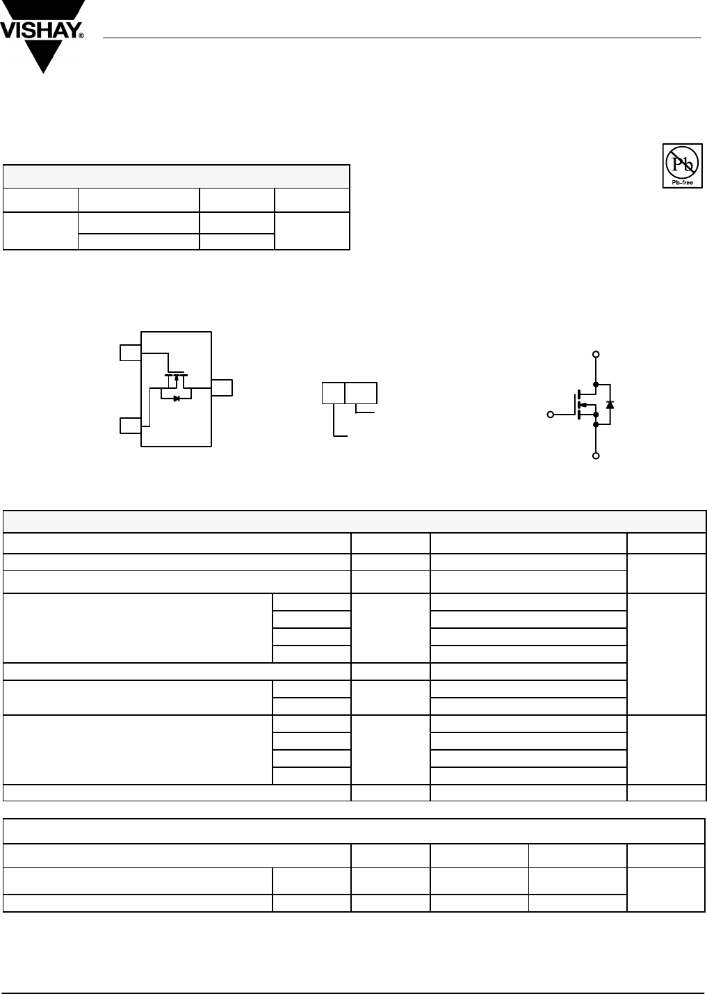
SC-70 (3-LEADS)
1
2
3
Top View
G
S
D
Marking Code
KF XX
Lot Traceability
and Date Code
Part # Code
YY
N-Channel MOSFET
G
D
S
ABSOLUTE MAXIMUM RATINGS (TA = 25_C UNLESS OTHERWISE NOTED)
Parameter Symbol Limit Unit
Drain-Source Voltage VDS 30
V
Gate-Source Voltage VGS "12
V
TC = 25_C0.90
Continuous Drain Current (T 150_C)
TC = 70_C
I
0.71
Continuous Drain Current (TJ = 150_C) TA = 25_CID0.85b, c
TA = 70_C0.68b, cA
Pulsed Drain Current IDM 4
Continuous Source Drain Diode Current
TC = 25_C
I
0.31
Continuous Source-Drain Diode Current TA = 25_CIS0.28b, c
TC = 25_C0.37
Maximum Power Dissipation
TC = 70_C
P
0.24
W
Maximum Power Dissipation TA = 25_CPD0.34b, cW
TA = 70_C0.22b, c
Operating Junction and Storage Temperature Range TJ, Tstg –55 to 150 _C
THERMAL RESISTANCE RATINGS
Parameter Symbol Typical Maximum Unit
Maximum Junction-to-Ambientb, dt p 5 sec RthJA 315 375
_
C/W
Maximum Junction-to-Foot (Drain) Steady State RthJF 285 340
_
C/W
Notes:
a. Based on TC = 25_C.
b. Surface mounted on 1” x 1” FR4 board.
c. t = 5 sec
d. Maximum under steady state conditions is 360 _C/W.
Si1304BDL
Vishay Siliconix New Product
www.vishay.com
2
Document Number: 73480
S–52057—Rev. B, 03–Oct–05
SPECIFICATIONS (TJ = 25_C UNLESS OTHERWISE NOTED)
Parameter Symbol Test Condition Min Typ Max Unit
Static
Drain-Source Breakdown Voltage VDS VGS = 0 V, ID = 250 mA30 V
VDS Temperature Coefficient DVDS/TJ
I= 250 mA
27.3
mV/_C
VGS(th) Temperature Coefficient DVGS(th)/TJ
ID = 250 mA3mV/_C
Gate-Source Threshold Voltage VGS(th) VDS = VGS, ID = 250 mA0.6 1.3 V
Gate-Source Leakage IGSS VDS = 0 V, VGS = "12 V "100 nA
Zero Gate Voltage Drain Current
I
VDS = 30 V, VGS = 0 V 1
A
Zero Gate Voltage Drain Current IDSS VDS = 30 V, VGS = 0 V, TJ = 70_C5mA
On-State Drain CurrentaID(on) VDS w 5 V, VGS = 4.5 V4 A
Drain
-
Source On
-
State Resistance
a
rDS(on)
VGS = 4.5 V, ID = 0.9 0.216 0.270
W
D
ra
i
n-
S
ource
O
n-
S
tate
R
es
i
stance
a
rDS(on) VGS =2.5 V, ID = 0.75 0.308 0.385
W
Forward Transconductanceagfs VDS = 15 V, ID = 0.9 2 S
Dynamicb
Input Capacitance Ciss 100
Output Capacitance Coss VDS = 15 V, VGS = 0 V, f = 1 MHz 30 pF
Reverse Transfer Capacitance Crss 20
p
Total Gate Charge
Q
VDS = 15 V, VGS = 4.5 V, ID = 0.9 1.8 2.7
Total Gate Charge Qg1.1 1.7
nC
Gate-Source Charge Qgs VDS = 15 V, VGS = 2.5 V, ID= 0.9 0.4 nC
Gate-Drain Charge Qgd 0.6
Gate Resistance Rgf = 1 MHz 1.5 2.3 W
Turn-On Delay Time td(on) 10 15
Rise Time trV
DD
= 15 V, R
L
= 22 W30 45
ns
Turn-Off Delay Time td(off)
VDD
=
15
V
,
RL
=
22
W
ID ^ 0.68 A, VGEN = 4.5 V, Rg = 1 W5 25 ns
Fall Time tf
g
10 15
Drain-Source Body Diode Characteristics
Continuous Source-Drain Diode Current ISTC = 25_C0.31
A
Pulse Diode Forward CurrentaISM 4A
Body Diode Voltage VSD IS = 0.28 A 0.8 1.2 V
Body Diode Reverse Recovery Time trr 50 75 ns
Body Diode Reverse Recovery Charge Qrr
I0 28 A di/dt 100 A/msT 25_C
105 160 nC
Reverse Recovery Fall Time ta
IF = 0.28 A, di/dt = 100 A/ms, TJ = 25_C34
ns
Reverse Recovery Rise Time tb16 ns
Notes
a. Pulse test; pulse width v 300 ms, duty cycle v 2%.
b. Guaranteed by design, not subject to production testing.
Stresses beyond those listed under “Absolute Maximum Ratings” may cause permanent damage to the device. These are stress ratings only, and functional operation
of the device at these or any other conditions beyond those indicated in the operational sections of the specifications is not implied. Exposure to absolute maximum
rating conditions for extended periods may affect device reliability.
Si1304BDL
Vishay Siliconix
New Product
Document Number: 73480
S–52057—Rev. B, 03–Oct–05
www.vishay.com
3
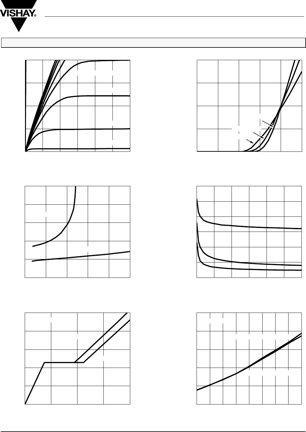
TYPICAL CHARACTERISTICS (25_C UNLESS NOTED)
0.0
0.5
1.0
1.5
2.0
0.0 0.5 1.0 1.5 2.0 2.5
0
1
2
3
4
0.0 0.5 1.0 1.5 2.0 2.5 3.0
VGS = 3 thru 5 V
Output Characteristics Transfer Characteristics curves vs. Temp
VDS – Drain-to-Source Voltage (V)
– Drain Current (A)ID
VGS – Gate-to-Source Voltage (V)
– Drain Current (A)ID
0.0
30.0
60.0
90.0
120.0
150.0
180.0
0.0 5.0 10.0 15.0 20.0 25.0 30.0
0.1
0.2
0.3
0.4
0.5
0.6
012345
0
1
2
3
4
5
0.0 0.5 1.0 1.5 2.0
0.5
0.8
1.1
1.4
1.7
2.0
–50 –25 0 25 50 75 100 125 150
Crss
ID = 0.91 A ID = 0.90 A
VGS = 2.5 V
Qg–Gate Charge
On-Resistance vs. Drain Current
– Gate-to-Source Voltage (V)
Qg – Total Gate Charge (nC)
VDS – Drain-Source Voltage (V)
C – Capacitance (pF)
VGS – On-Resistance (rDS(on) W)
ID – Drain Current (A)
Capacitance
On-Resistance vs. Junction Temperature
TJ – Junction Temperature (_C)
VGS = 4.5 V
Coss
Ciss
rDS(on) – On-Resistance
(Normalized)
VDS = 15 V
VGS = 2.5 V
VGS = 2.0 V
VGS = 1.5 V
TA = 25_C
TA = –55_C
VDS = 24 V
VGS = 4.5 V, ID = 0.9 A
VGS = 2.5 V, ID = 0.75 A
TA = 125_C
Si1304BDL
Vishay Siliconix New Product
www.vishay.com
4
Document Number: 73480
S–52057—Rev. B, 03–Oct–05
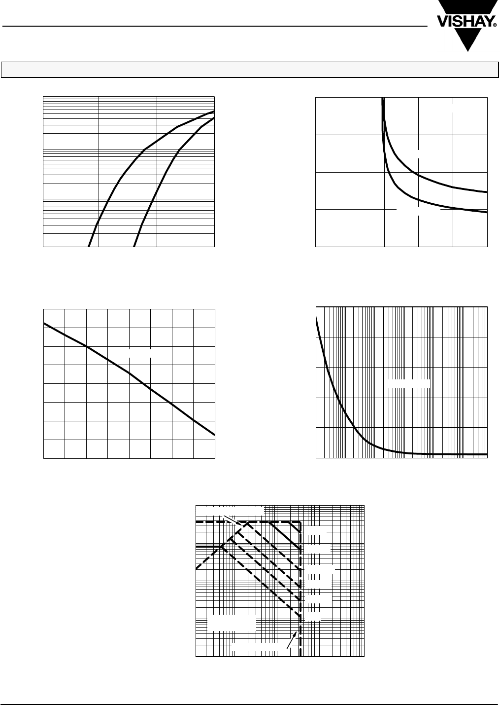
TYPICAL CHARACTERISTICS (25_C UNLESS NOTED)
TJ = 25_C
TJ = 150_C
Safe Operating Area
– Drain Current (A)ID
1 ms
TA = 25_C
Single Pulse
10 ms
100 ms
dc
VDS – Drain-to-Source Voltage (V)
*VGS u minimum VGS at which rDS(on) is specified
1 s
10 s
0.3 0.6 0.9 1.2
0.000
0.200
0.400
0.600
0.800
012345
ID = 0.9 A
Forward Diode Voltage vs. Temp rDS(on) vs VGS vs Temperature
– On-Resistance (rDS(on) W)
VSD – Source-to-Drain Voltage (V) VGS – Gate-to-Source Voltage (V)
– Source Current (A)IS
TA = 25_C
TA = 125_C
0.6
0.7
0.8
0.9
1.0
1.1
1.2
1.3
1.4
–50 –25 0 25 50 75 100 125 150
ID = 250 mA
Threshold Voltage
Variance (V)VGS(th)
TJ – Temperature (_C)
0.0
0.1
1.0
10.0
0
12
20
4
8
Power (W)
Single Pulse Power, Junction-to-Ambient
Time (sec)
16
1 100 6001010–1
10–3 10–2
0.001
0.01
0.1
1
10
0.1 110 100 1000
BVDSS Limited
*Limited by rDS(on)
TA = 25_C
Si1304BDL
Vishay Siliconix
New Product
Document Number: 73480
S–52057—Rev. B, 03–Oct–05
www.vishay.com
5
TYPICAL CHARACTERISTICS (25_C UNLESS NOTED)
0.0
0.2
0.4
0.6
0.8
1.0
1.2
0 25 50 75 100 125 150
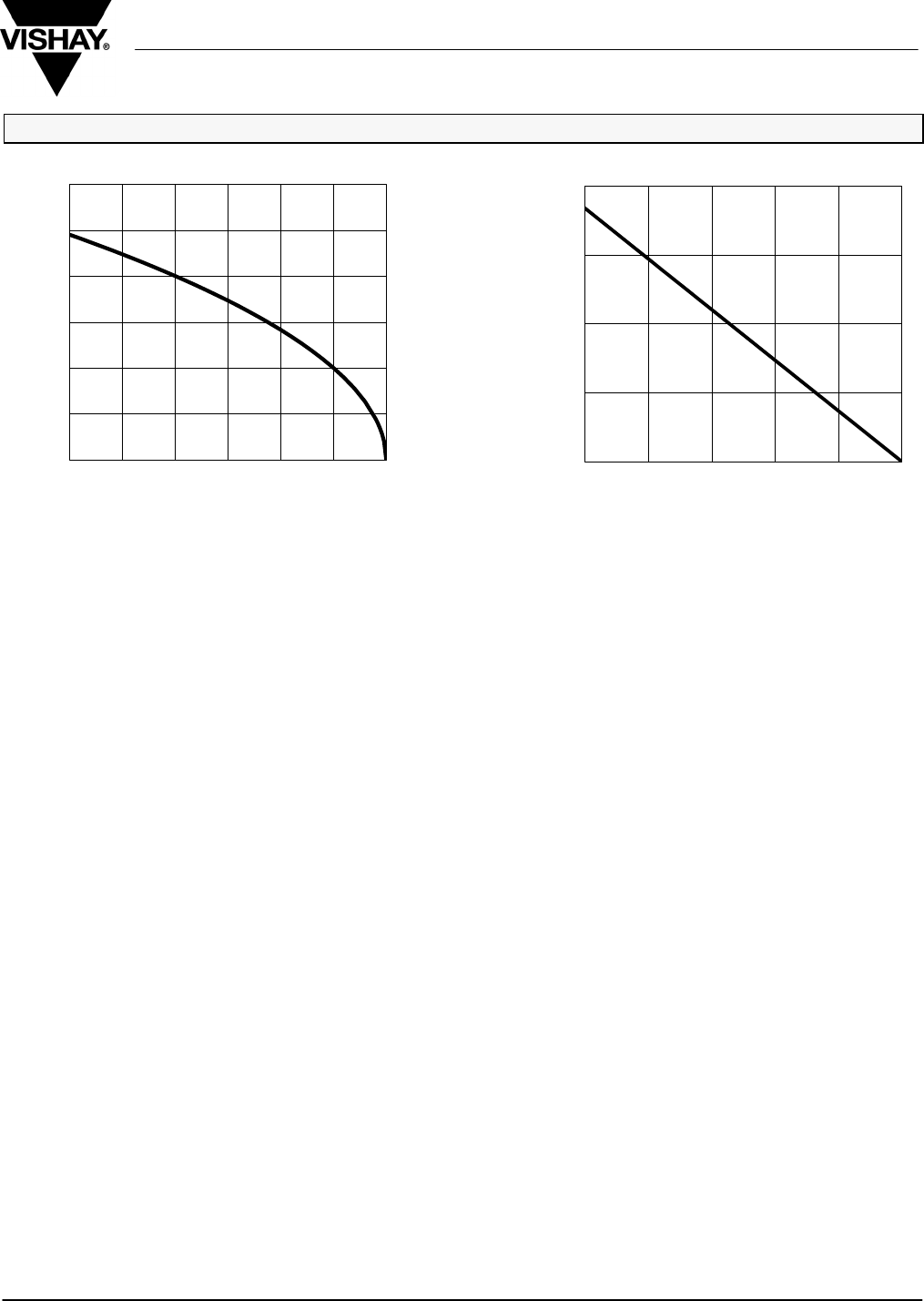
Current De-Rating*
ID – Drain Current (A)
TC – Case Temperature (_C)
*The power dissipation PD is based on TJ(max) = 150_C, using junction-to-case thermal resistance, and is more useful in settling the upper dissipation limit for
cases where additional heatsinking is used. It is used to determine the current rating, when this rating falls below the package limit.
0.0
0.1
0.2
0.3
0.4
25 50 75 100 125 150
Power, De-Rating
Case Temperature (_C)
Power Dissipation (W)
Si1304BDL
Vishay Siliconix New Product
www.vishay.com
6
Document Number: 73480
S–52057—Rev. B, 03–Oct–05
TYPICAL CHARACTERISTICS (25_C UNLESS NOTED)
10–3 10–2 1 10 60010–1
10–4 100
2
1
0.1
0.01
0.2
0.1
0.05
0.02
Single Pulse
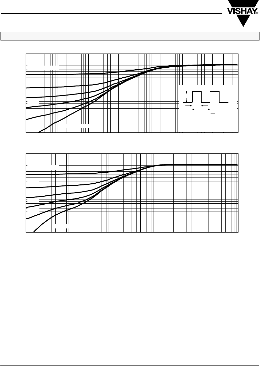
Duty Cycle = 0.5
Normalized Thermal Transient Impedance, Junction-to-Ambient
Square Wave Pulse Duration (sec)
Normalized Effective Transient
Thermal Impedance
1. Duty Cycle, D =
2. Per Unit Base = RthJA = 360_C/W
3. TJM – TA = PDMZthJA(t)
t1
t2
t1
t2
Notes:
4. Surface Mounted
PDM
10–3 10–2 11010–1
10–4
2
1
0.1
0.01
0.2
0.1
0.05
0.02
Single Pulse
Duty Cycle = 0.5
Normalized Thermal Transient Impedance, Junction-to-Foot
Square Wave Pulse Duration (sec)
Normalized Effective Transient
Thermal Impedance
Vishay Siliconix maintains worldwide manufacturing capability. Products may be manufactured at one of several qualified locations. Reliability data for Silicon Technology and
Package Reliability represent a composite of all qualified locations. For related documents such as package/tape drawings, part marking, and reliability data, see
http://www.vishay.com/ppg?73480.

Legal Disclaimer Notice
Vishay
Document Number: 91000 www.vishay.com
Revision: 08-Apr-05 1
Notice
Specifications of the products displayed herein are subject to change without notice. Vishay Intertechnology, Inc.,
or anyone on its behalf, assumes no responsibility or liability for any errors or inaccuracies.
Information contained herein is intended to provide a product description only. No license, express or implied, by
estoppel or otherwise, to any intellectual property rights is granted by this document. Except as provided in Vishay's
terms and conditions of sale for such products, Vishay assumes no liability whatsoever, and disclaims any express
or implied warranty, relating to sale and/or use of Vishay products including liability or warranties relating to fitness
for a particular purpose, merchantability, or infringement of any patent, copyright, or other intellectual property right.
The products shown herein are not designed for use in medical, life-saving, or life-sustaining applications.
Customers using or selling these products for use in such applications do so at their own risk and agree to fully
indemnify Vishay for any damages resulting from such improper use or sale.