Si2318DS Datasheet. Www.s Manuals.com. Vishay
User Manual: Marking of electronic components, SMD Codes C8, C8*, C8***, C8-**, C8-***, C84, C8=**, C8=***, C8A, C8B, C8C, C8D, C8E, C8F, C8G, C8H, C8J, C8K, C8L, C8M, C8N, C8P, C8Q, C8R, C8S, C8T, C8U, C8V, C8W, C8X, C8Y, C8Z. Datasheets BSS84, BZX585-B4V7, CMPZ5226B, CMPZ5227B, CMPZ5228B, CMPZ5229B, CMPZ5230B, CMPZ5231B, CMPZ5232B, CMPZ5233B, CMPZ5234B, CMPZ5235B, CMPZ5236B, CMPZ5237B, CMPZ5238B, CMPZ5239B, CMPZ5240B, CMPZ5241B, CMPZ5242B, CMPZ5243B, CMPZ5244B, CMPZ5245B, CMPZ5246B, CMPZ5247B, CMPZ5248B, CMPZ5249B, RT
Open the PDF directly: View PDF ![]() .
.
Page Count: 6
FEATURES
DTrenchFETr Power MOSFET
APPLICATIONS
DStepper Motors
DLoad Switch
Si2318DS
Vishay Siliconix
New Product
Document Number: 72322
S-31731—Rev. A, 18-Aug-03
www.vishay.com
1
N-Channel 40-V (D-S) MOSFET
PRODUCT SUMMARY
VDS (V) rDS(on) (W)ID (A)
40
0.045 @ VGS = 10 V 3.9
40 0.058 @ VGS = 4.5 V 3.5
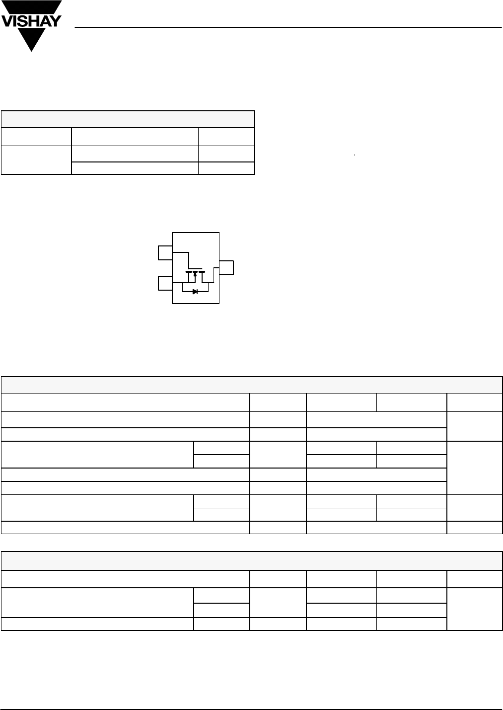
G
S
D
Top View
2
3
TO-236
(SOT-23)
1
*Marking Code
Si2318DS( C8)*
Ordering Information: Si2318DS-T1 (with Tape and Reel)
ABSOLUTE MAXIMUM RATINGS (TA = 25_C UNLESS OTHERWISE NOTED)
Parameter Symbol 5 sec Steady State Unit
Drain-Source Voltage VDS 40
V
Gate-Source Voltage VGS "20
V
Continuous Drain Current (TJ = 150
_
C)a, b
TA= 25_C
ID
3.9 3.0
Continuous Drain Current (TJ = 150_C)a,
b
TA= 70_CID3.1 2.4
A
Pulsed Drain CurrentbIDM 16 A
Continuous Source Current (Diode Conduction)a, bIS0.8
Power Dissipationa, b
TA= 25_C
PD
1.25 0.75
W
Power Dissipationa,
b
TA= 70_CPD0.8 0.48 W
Operating Junction and Storage Temperature Range TJ, Tstg -55 to 150 _C
THERMAL RESISTANCE RATINGS
Parameter Symbol Typical Maximum Unit
Mi J ti tAbit
a
t v 5 sec
R
75 100
Maximum Junction-to-Ambienta
Steady State RthJA 120 166 _C/W
Maximum Junction-to-Foot (drain) Steady State RthJF 40 50
C/W
Notes
a. Surface Mounted on 1” x 1” FR4 Board.
b. Pulse width limited by maximum junction temperature
Si2318DS
Vishay Siliconix New Product
www.vishay.com
2
Document Number: 72322
S-31731—Rev. A, 18-Aug-03
SPECIFICATIONS (TA = 25_C UNLESS OTHERWISE NOTED)
Limits
Parameter Symbol Test Conditions Min Typ Max Unit
Static
Drain-Source Breakdown Voltage V(BR)DSS VGS = 0 V, ID = 250 mA40
V
Gate-Threshold Voltage VGS(th) VDS = VGS, ID = 250 mA1 3 V
Gate-Body Leakage IGSS VDS = 0 V, VGS = "20 V "100 nA
Zero Gate Voltage Drain Current
IDSS
VDS = 32 V, VGS = 0 V 0.5
mA
Zero Gate Voltage Drain Current IDSS VDS = 32 V, VGS = 0 V, TJ = 55_C10 mA
On-State Drain CurrentaID(on) VDS w 4.5 V, VGS = 10 V 6 A
Drain Source On Resistancea
rDS( )
VGS = 10 V, ID = 3.9 A 0.036 0.045
W
Drain-Source On-ResistancearDS(on) VGS = 4.5 V, ID = 3.5 A 0.045 0.058 W
Forward Transconductanceagfs VDS = 10 V, ID = 3.9 A 11 S
Diode Forward Voltage VSD IS = 1.25 A, VGS = 0 V 0.8 1.2 V
Dynamicb
Total Gate Charge Qg10 15
Gate-Source Charge Qgs VDS = 20 V, VGS = 10 V, ID = 3.9 A 1.6 nC
Gate-Drain Charge Qgd
DS GS D
2.1
Gate Resistance Rg1.8 W
Input Capacitance Ciss 540
Output Capacitance Coss VDS = 20 V, VGS = 0 V, f = 1 MHz 80 pF
Reverse Transfer Capacitance Crss
DS GS
45
p
Switching
Turn-On Delay Time td(on) 5 10
Rise Time trV
DD
= 20 V, R
L
= 20 W12 20
ns
Turn-Off Delay Time td(off)
VDD = 20 V
,
RL = 20 W
ID ^ 1.0 A, VGEN = 10 V, RG = 6 W20 30 ns
Fall-Time tf15 25
Notes
a. Pulse test: PW v300 ms duty cycle v2%.
b. Guaranteed by design, not subject to production testing.
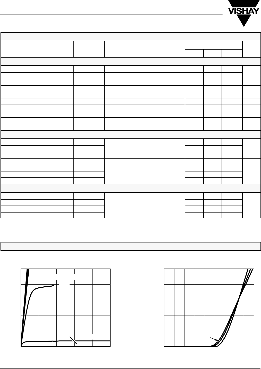
TYPICAL CHARACTERISTICS (25_C UNLESS NOTED)
0
4
8
12
16
20
0.0 0.5 1.0 1.5 2.0 2.5 3.0 3.5 4.0 4.5
0
4
8
12
16
20
0246810
VGS = 10 thru 5 V
TC = 125_C
-55_C
4 V
25_C
Output Characteristics Transfer Characteristics
VDS - Drain-to-Source Voltage (V)
- Drain Current (A)ID
VGS - Gate-to-Source Voltage (V)
- Drain Current (A)ID
3 V
1, 2 V
Si2318DS
Vishay Siliconix
New Product
Document Number: 72322
S-31731—Rev. A, 18-Aug-03
www.vishay.com
3
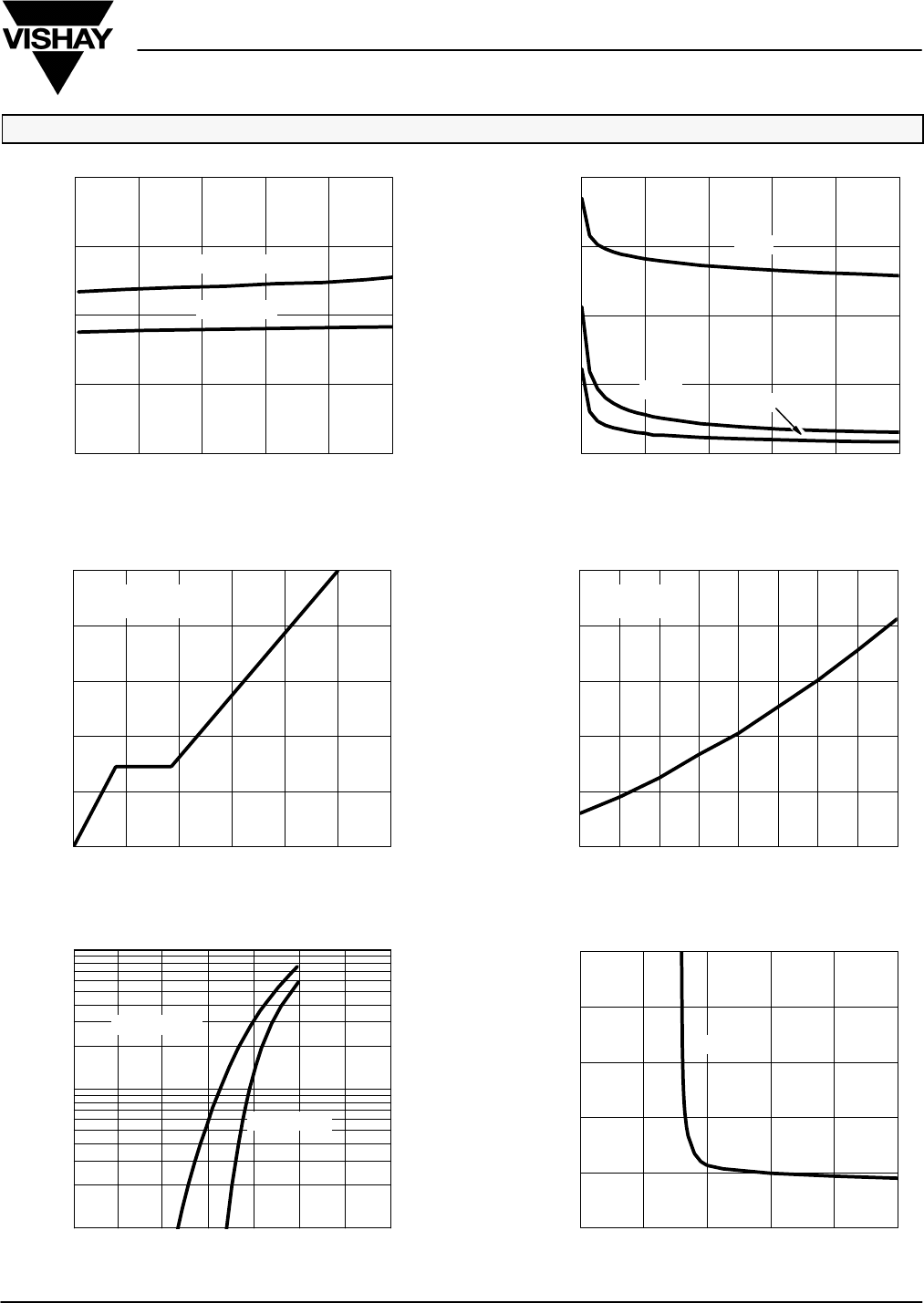
TYPICAL CHARACTERISTICS (25_C UNLESS NOTED)
- On-Resistance (rDS(on) W)
0
200
400
600
800
0 8 16 24 32 40
0.5
0.8
1.1
1.4
1.7
2.0
-50 -25 0 25 50 75 100 125 150
0
2
4
6
8
10
024681012
0.00
0.02
0.04
0.06
0.08
0 4 8 12 16 20
VDS - Drain-to-Source Voltage (V)
Coss
Ciss
VDS = 20 V
ID = 3.9 A
ID - Drain Current (A)
VGS = 10 V
ID = 3.9 A
Gate Charge
On-Resistance vs. Drain Current
- Gate-to-Source Voltage (V)
Qg - Total Gate Charge (nC)
C - Capacitance (pF)
VGS
Capacitance
On-Resistance vs. Junction Temperature
TJ - Junction Temperature (_C)
(Normalized)
- On-Resistance (rDS(on) W)
0.0 0.2 0.4 0.6 0.8 1.0 1.2 1.4
0.00
0.04
0.08
0.12
0.16
0.20
0246810
ID = 3.9 A
10
1
0.1
Source-Drain Diode Forward Voltage On-Resistance vs. Gate-to-Source Voltage
- On-Resistance (rDS(on) W)
VSD - Source-to-Drain Voltage (V) VGS - Gate-to-Source Voltage (V)
- Source Current (A)IS
TJ = 150_C
TJ = 25_C
VGS = 10 V
VGS = 4.5 V
Crss
Si2318DS
Vishay Siliconix New Product
www.vishay.com
4
Document Number: 72322
S-31731—Rev. A, 18-Aug-03
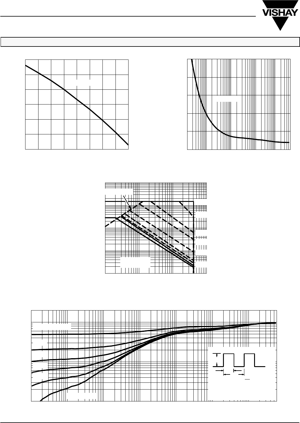
TYPICAL CHARACTERISTICS (25_C UNLESS NOTED)
10-3 10-2 1 10 60010-1
10-4 100
0.01
0
1
10
4
6
100 6000.1
Single Pulse Power
Time (sec)
2
8
Power (W)
-0.8
-0.6
-0.4
-0.2
-0.0
0.2
0.4
-50 -25 0 25 50 75 100 125 150
ID = 250 mA
2
1
0.1
0.01
0.2
0.1
0.05
0.02
Single Pulse
Duty Cycle = 0.5
Threshold Voltage
Variance (V)VGS(th)
TJ - Temperature (_C)
Normalized Thermal Transient Impedance, Junction-to-Ambient
Square Wave Pulse Duration (sec)
Normalized Effective Transient
Thermal Impedance
1. Duty Cycle, D =
2. Per Unit Base = RthJA = 166_C/W
3. TJM - T
A = PDMZthJA(t)
t1
t2
t1
t2
Notes:
4. Surface Mounted
PDM
10
TA = 25_C
- Drain Current (A)ID
Safe Operating Area, Junction-to-Case
VDS - Drain-to-Source Voltage (V)
100.0
1.0
0.1 1 10 100
0.01
10.0
0.1
Limited by rDS(on)
TA = 25_C
Single Pulse
10 ms
100 ms
10 ms
100 ms
1 ms
dc, 100 s, 10 s, 1 s

Legal Disclaimer Notice
Vishay
Document Number: 91000 www.vishay.com
Revision: 08-Apr-05 1
Notice
Specifications of the products displayed herein are subject to change without notice. Vishay Intertechnology, Inc.,
or anyone on its behalf, assumes no responsibility or liability for any errors or inaccuracies.
Information contained herein is intended to provide a product description only. No license, express or implied, by
estoppel or otherwise, to any intellectual property rights is granted by this document. Except as provided in Vishay's
terms and conditions of sale for such products, Vishay assumes no liability whatsoever, and disclaims any express
or implied warranty, relating to sale and/or use of Vishay products including liability or warranties relating to fitness
for a particular purpose, merchantability, or infringement of any patent, copyright, or other intellectual property right.
The products shown herein are not designed for use in medical, life-saving, or life-sustaining applications.
Customers using or selling these products for use in such applications do so at their own risk and agree to fully
indemnify Vishay for any damages resulting from such improper use or sale.

