TLV320AIC3256 Application Reference (Rev. A) Slau306a Guide
User Manual:
Open the PDF directly: View PDF ![]() .
.
Page Count: 155 [warning: Documents this large are best viewed by clicking the View PDF Link!]
- 1 TLV320AIC3256 Overview
- 2 TLV320AIC3256 Application
- 2.1 Terminal Descriptions
- 2.2 Analog Audio I/O
- 2.3 ADC
- 2.3.1 ADC Signal Routing
- 2.3.2 ADC Gain Setting
- 2.3.3 ADC Decimation Filtering and Signal Processing Overview
- 2.3.3.1 Signal Processing Blocks – Details
- 2.3.3.1.1 First-Order IIR, AGC, Filter A
- 2.3.3.1.2 5 Biquads, First-Order IIR, AGC, Filter A
- 2.3.3.1.3 25 Tap FIR, First-Order IIR, AGC, Filter A
- 2.3.3.1.4 First-Order IIR, AGC, Filter B
- 2.3.3.1.5 3 Biquads, First-Order IIR, AGC, Filter B
- 2.3.3.1.6 20 Tap FIR, First-Order IIR, AGC, Filter B
- 2.3.3.1.7 First-Order IIR, AGC, Filter C
- 2.3.3.1.8 5 Biquads, First-Order IIR, AGC, Filter C
- 2.3.3.1.9 25 Tap FIR, First-Order IIR, AGC, Filter C
- 2.3.3.1.10 User Programmable Filters
- 2.3.3.1.11 Decimation Filter
- 2.3.3.1.12 ADC Data Interface
- 2.3.3.2 ADC Special Functions
- 2.3.3.3 ADC Setup
- 2.3.3.1 Signal Processing Blocks – Details
- 2.4 DAC
- 2.4.1 Processing Blocks – Details
- 2.4.1.1 3 Biquads, Interpolation Filter A
- 2.4.1.2 6 Biquads, 1st order IIR, DRC, Interpolation Filter A or B
- 2.4.1.3 6 Biquads, 1st order IIR, Interpolation Filter A or B
- 2.4.1.4 IIR, Interpolation Filter B or C
- 2.4.1.5 4 Biquads, DRC, Interpolation Filter B
- 2.4.1.6 4 Biquads, Interpolation Filter B
- 2.4.1.7 4 Biquads, 1st order IIR, DRC, Interpolation Filter C
- 2.4.1.8 4 Biquads, 1st order IIR, Interpolation Filter C
- 2.4.1.9 2 Biquads, 3D, Interpolation Filter A
- 2.4.1.10 5 Biquads, DRC, 3D, Interpolation Filter A
- 2.4.1.11 5 Biquads, DRC, 3D, Beep Generator, Interpolation Filter A
- 2.4.2 User Programmable Filters
- 2.4.3 Interpolation Filters
- 2.4.4 DAC Gain Setting
- 2.4.5 DAC Special Functions
- 2.4.6 DAC Setup
- 2.4.1 Processing Blocks – Details
- 2.5 PowerTune
- 2.5.0.1 PowerTune Modes
- 2.5.0.2 ADC Power Consumption
- 2.5.0.2.1 ADC, Stereo, 48kHz, Highest Performance, DVdd = 1.8V, AVdd = 1.8V
- 2.5.0.2.2 ADC, Stereo, 48kHz, DVdd = 1.8V, AVdd = 1.8V
- 2.5.0.2.3 ADC, Stereo, 48kHz, Lowest Power Consumption
- 2.5.0.2.4 ADC, Mono, 48kHz, Highest Performance, DVdd = 1.8V, AVdd = 1.8V
- 2.5.0.2.5 ADC, Mono, 48kHz, DVdd = 1.8V, AVdd = 1.8V
- 2.5.0.2.6 ADC, Mono, 48 kHz, Lowest Power Consumption,
- 2.5.0.2.7 ADC, Stereo, 8kHz, Highest Performance, DVdd = 1.8V, AVdd = 1.8V
- 2.5.0.2.8 ADC, Stereo, 8kHz, DVdd = 1.8V, AVdd = 1.8V
- 2.5.0.2.9 ADC, Stereo, 8kHz, Lowest Power Consumption,
- 2.5.0.2.10 ADC, Mono, 8kHz, Highest Performance, DVdd = 1.8V, AVdd = 1.8V
- 2.5.0.2.11 ADC, Mono, 8kHz, DVdd = 1.8V, AVdd = 1.8V
- 2.5.0.2.12 ADC, Mono, 8kHz, Lowest Power Consumption
- 2.5.0.2.13 ADC, Stereo, 192kHz, Highest Performance, DVdd = 1.8V, AVdd = 1.8V
- 2.5.0.2.14 ADC, Stereo, 192kHz, Lowest Power Consumption
- 2.5.0.3 DAC Power Consumption
- 2.5.0.3.1 DAC, Stereo, 48kHz, Highest Performance, DVdd = 1.8V, AVdd = 1.8V
- 2.5.0.3.2 DAC, Stereo, 48kHz, Lowest Power Consumption
- 2.5.0.3.3 DAC, Mono, 48kHz, Highest Performance, DVdd = 1.8V, AVdd = 1.8V
- 2.5.0.3.4 DAC, Mono, 48kHz, Lowest Power Consumption
- 2.5.0.3.5 DAC, Stereo, 8kHz, Highest Performance, DVdd = 1.8V, AVdd = 1.8V
- 2.5.0.3.6 DAC, Stereo, 8kHz, Lowest Power Consumption
- 2.5.0.3.7 DAC, Mono, 8kHz, Highest Performance, DVdd = 1.8V, AVdd = 1.8V
- 2.5.0.3.8 DAC, Mono, 8kHz, Lowest Power Consumption
- 2.5.0.3.9 DAC, Stereo, 192kHz, DVdd = 1.8V, AVdd = 1.8V
- 2.5.0.3.10 DAC, Stereo, 192kHz, Lowest Power Consumption
- 2.6 Audio Digital I/O Interface
- 2.7 Clock Generation and PLL
- 2.8 Control Interfaces
- 2.9 Power Supply
- 2.10 Reference Voltage
- 2.11 Device Special Functions
- 2.12 miniDSP
- 3 Device Initialization
- 4 Example Setups
- 5 Register Map
- 5.1 Register Map Summary
- 5.2 Page 0 Registers
- 5.2.1 Page 0 / Register 0: Page Select Register - 0x00 / 0x00
- 5.2.2 Page 0 / Register 1: Software Reset Register - 0x00 / 0x01
- 5.2.3 Page 0 / Register 2: Reserved Register - 0x00 / 0x02
- 5.2.4 Page 0 / Register 3: Reserved Register - 0x00 / 0x03
- 5.2.5 Page 0 / Register 4: Clock Setting Register 1, Multiplexers - 0x00 / 0x04
- 5.2.6 Page 0 / Register 5: Clock Setting Register 2, PLL P&R Values - 0x00 / 0x05
- 5.2.7 Page 0 / Register 6: Clock Setting Register 3, PLL J Values - 0x00 / 0x06
- 5.2.8 Page 0 / Register 7: Clock Setting Register 4, PLL D Values (MSB) - 0x00 / 0x07
- 5.2.9 Page 0 / Register 8: Clock Setting Register 5, PLL D Values (LSB) - 0x00 / 0x08
- 5.2.10 Page 0 / Register 9-10: Reserved Register - 0x00 / 0x09-0x0A
- 5.2.11 Page 0 / Register 11: Clock Setting Register 6, NDAC Values - 0x00 / 0x0B
- 5.2.12 Page 0 / Register 12: Clock Setting Register 7, MDAC Values - 0x00 / 0x0C
- 5.2.13 Page 0 / Register 13: DAC OSR Setting Register 1, MSB Value - 0x00 / 0x0D
- 5.2.14 Page 0 / Register 14: DAC OSR Setting Register 2, LSB Value - 0x00 / 0x0E
- 5.2.15 Page 0 / Register 15: miniDSP_D Instruction Control Register 1 - 0x00 / 0x0F
- 5.2.16 Page 0 / Register 16: miniDSP_D Instruction Control Register 2 - 0x00 / 0x10
- 5.2.17 Page 0 / Register 17: miniDSP_D Interpolation Factor Setting Register - 0x00 / 0x11
- 5.2.18 Page 0 / Register 18: Clock Setting Register 8, NADC Values - 0x00 / 0x12
- 5.2.19 Page 0 / Register 19: Clock Setting Register 9, MADC Values - 0x00 / 0x13
- 5.2.20 Page 0 / Register 20: ADC Oversampling (AOSR) Register - 0x00 / 0x14
- 5.2.21 Page 0 / Register 21: miniDSP_A Instruction Control Register 1 - 0x00 / 0x15
- 5.2.22 Page 0 / Register 22: miniDSP_A Instruction Control Register 2 - 0x00 / 0x16
- 5.2.23 Page 0 / Register 23: miniDSP_A Decimation Factor Setting Register - 0x00 / 0x17
- 5.2.24 Page 0 / Register 24: Reserved Register - 0x00 / 0x18
- 5.2.25 Page 0 / Register 25: Clock Setting Register 10, Multiplexers - 0x00 / 0x19
- 5.2.26 Page 0 / Register 26: Clock Setting Register 11, CLKOUT M divider value - 0x00 / 0x1A
- 5.2.27 Page 0 / Register 27: Audio Interface Setting Register 1 - 0x00 / 0x1B
- 5.2.28 Page 0 / Register 28: Audio Interface Setting Register 2, Data offset setting - 0x00 / 0x1C
- 5.2.29 Page 0 / Register 29: Audio Interface Setting Register 3 - 0x00 / 0x1D
- 5.2.30 Page 0 / Register 30: Clock Setting Register 12, BCLK N Divider - 0x00 / 0x1E
- 5.2.31 Page 0 / Register 31: Audio Interface Setting Register 4, Secondary Audio Interface - 0x00 / 0x1F
- 5.2.32 Page 0 / Register 32: Audio Interface Setting Register 5 - 0x00 / 0x20
- 5.2.33 Page 0 / Register 33: Audio Interface Setting Register 6 - 0x00 / 0x21
- 5.2.34 Page 0 / Register 34: Digital Interface Misc. Setting Register - 0x00 / 0x22
- 5.2.35 Page 0 / Register 35: Reserved Register - 0x00 / 0x23
- 5.2.36 Page 0 / Register 36: ADC Flag Register - 0x00 / 0x24
- 5.2.37 Page 0 / Register 37: DAC Flag Register 1 - 0x00 / 0x25
- 5.2.38 Page 0 / Register 38: DAC Flag Register 2 - 0x00 / 0x26
- 5.2.39 Page 0 / Register 39-41: Reserved Register - 0x00 / 0x27-0x29
- 5.2.40 Page 0 / Register 42: Sticky Flag Register 1 - 0x00 / 0x2A
- 5.2.41 Page 0 / Register 43: Interrupt Flag Register 1 - 0x00 / 0x2B
- 5.2.42 Page 0 / Register 44: Sticky Flag Register 2 - 0x00 / 0x2C
- 5.2.43 Page 0 / Register 45: Sticky Flag Register 3 - 0x00 / 0x2D
- 5.2.44 Page 0 / Register 46: Interrupt Flag Register 2 - 0x00 / 0x2E
- 5.2.45 Page 0 / Register 47: Interrupt Flag Register 3 - 0x00 / 0x2F
- 5.2.46 Page 0 / Register 48: INT1 Interrupt Control Register - 0x00 / 0x30
- 5.2.47 Page 0 / Register 49: INT2 Interrupt Control Register - 0x00 / 0x31
- 5.2.48 Page 0 / Register 50-51: Reserved Register - 0x00 / 0x32-0x33
- 5.2.49 Page 0 / Register 52: GPIOorMFP5 Control Register - 0x00 / 0x34
- 5.2.50 Page 0 / Register 53: DOUT or MFP2 Function Control Register - 0x00 / 0x35
- 5.2.51 Page 0 / Register 54: DIN or MFP1 Function Control Register - 0x00 / 0x36
- 5.2.52 Page 0 / Register 55: MISO or MFP4 Function Control Register - 0x00 / 0x37
- 5.2.53 Page 0 / Register 56: SCLK or MFP3 Function Control Register - 0x00 / 0x38
- 5.2.54 Page 0 / Register 57-59: Reserved Registers - 0x00 / 0x39-0x3B
- 5.2.55 Page 0 / Register 60: DAC Signal Processing Block Control Register - 0x00 / 0x3C
- 5.2.56 Page 0 / Register 61: ADC Signal Processing Block Control Register - 0x00 / 0x3D
- 5.2.57 Page 0 / Register 62: miniDSP_A and miniDSP_D Configuration Register - 0x00 / 0x3E
- 5.2.58 Page 0 / Register 63: DAC Channel Setup Register 1 - 0x00 / 0x3F
- 5.2.59 Page 0 / Register 64: DAC Channel Setup Register 2 - 0x00 / 0x40
- 5.2.60 Page 0 / Register 65: Left DAC Channel Digital Volume Control Register - 0x00 / 0x41
- 5.2.61 Page 0 / Register 66: Right DAC Channel Digital Volume Control Register - 0x00 / 0x42
- 5.2.62 Page 0 / Register 67: Headset Detection Configuration Register - 0x00 / 0x43
- 5.2.63 Page 0 / Register 68: DRC Control Register 1 - 0x00 / 0x44
- 5.2.64 Page 0 / Register 69: DRC Control Register 2 - 0x00 / 0x45
- 5.2.65 Page 0 / Register 70: DRC Control Register 3 - 0x00 / 0x46
- 5.2.66 Page 0 / Register 71: Beep Generator Register 1 - 0x00 / 0x47
- 5.2.67 Page 0 / Register 72: Beep Generator Register 2 - 0x00 / 0x48
- 5.2.68 Page 0 / Register 73: Beep Generator Register 3 - 0x00 / 0x49
- 5.2.69 Page 0 / Register 74: Beep Generator Register 4 - 0x00 / 0x4A
- 5.2.70 Page 0 / Register 75: Beep Generator Register 5 - 0x00 / 0x4B
- 5.2.71 Page 0 / Register 76: Beep Generator Register 6 - 0x00 / 0x4C
- 5.2.72 Page 0 / Register 77: Beep Generator Register 7 - 0x00 / 0x4D
- 5.2.73 Page 0 / Register 78: Beep Generator Register 8 - 0x00 / 0x4E
- 5.2.74 Page 0 / Register 79: Beep Generator Register 9 - 0x00 / 0x4F
- 5.2.75 Page 0 / Register 80: Reserved Register - 0x00 / 0x50
- 5.2.76 Page 0 / Register 81: ADC Channel Setup Register - 0x00 / 0x51
- 5.2.77 Page 0 / Register 82: ADC Fine Gain Adjust Register - 0x00 / 0x52
- 5.2.78 Page 0 / Register 83: Left ADC Channel Volume Control Register - 0x00 / 0x53
- 5.2.79 Page 0 / Register 84: Right ADC Channel Volume Control Register - 0x00 / 0x54
- 5.2.80 Page 0 / Register 85: ADC Phase Adjust Register - 0x00 / 0x55
- 5.2.81 Page 0 / Register 86: Left Channel AGC Control Register 1 - 0x00 / 0x56
- 5.2.82 Page 0 / Register 87: Left Channel AGC Control Register 2 - 0x00 / 0x57
- 5.2.83 Page 0 / Register 88: Left Channel AGC Control Register 3 - 0x00 / 0x58
- 5.2.84 Page 0 / Register 89: Left Channel AGC Control Register 4 - 0x00 / 0x59
- 5.2.85 Page 0 / Register 90: Left Channel AGC Control Register 5 - 0x00 / 0x5A
- 5.2.86 Page 0 / Register 91: Left Channel AGC Control Register 6 - 0x00 / 0x5B
- 5.2.87 Page 0 / Register 92: Left Channel AGC Control Register 7 - 0x00 / 0x5C
- 5.2.88 Page 0 / Register 93: Left Channel AGC Control Register 8 - 0x00 / 0x5D
- 5.2.89 Page 0 / Register 94: Right Channel AGC Control Register 1 - 0x00 / 0x5E
- 5.2.90 Page 0 / Register 95: Right Channel AGC Control Register 2 - 0x00 / 0x5F
- 5.2.91 Page 0 / Register 96: Right Channel AGC Control Register 3 - 0x00 / 0x60
- 5.2.92 Page 0 / Register 97: Right Channel AGC Control Register 4 - 0x00 / 0x61
- 5.2.93 Page 0 / Register 98: Right Channel AGC Control Register 5 - 0x00 / 0x62
- 5.2.94 Page 0 / Register 99: Right Channel AGC Control Register 6 - 0x00 / 0x63
- 5.2.95 Page 0 / Register 100: Right Channel AGC Control Register 7 - 0x00 / 0x64
- 5.2.96 Page 0 / Register 101: Right Channel AGC Control Register 8 - 0x00 / 0x65
- 5.2.97 Page 0 / Register 102: DC Measurement Register 1 - 0x00 / 0x66
- 5.2.98 Page 0 / Register 103: DC Measurement Register 2 - 0x00 / 0x67
- 5.2.99 Page 0 / Register 104: Left Channel DC Measurement Output Register 1 - 0x00 / 0x68
- 5.2.100 Page 0 / Register 105: Left Channel DC Measurement Output Register 2 - 0x00 / 0x69
- 5.2.101 Page 0 / Register 106: Left Channel DC Measurement Output Register 3 - 0x00 / 0x6A
- 5.2.102 Page 0 / Register 107: Right Channel DC Measurement Output Register 1 - 0x00 / 0x6B
- 5.2.103 Page 0 / Register 108: Right Channel DC Measurement Output Register 2 - 0x00 / 0x6C
- 5.2.104 Page 0 / Register 109: Right Channel DC Measurement Output Register 3 - 0x00 / 0x6D
- 5.2.105 Page 0 / Register 110-127: Reserved Register - 0x00 / 0x6E-0x7F
- 5.3 Page 1 Registers
- 5.3.1 Page 1 / Register 0: Page Select Register - 0x01 / 0x00
- 5.3.2 Page 1 / Register 1: Power Configuration Register 1 - 0x01 / 0x01
- 5.3.3 Page 1 / Register 2: Power Configuration Register 2 - 0x01 / 0x02
- 5.3.4 Page 1 / Register 3: Playback Configuration Register 1 - 0x01 / 0x03
- 5.3.5 Page 1 / Register 4: Playback Configuration Register 2 - 0x01 / 0x04
- 5.3.6 Page 1 / Register 5-8: Reserved Register - 0x01 / 0x05-0x08
- 5.3.7 Page 1 / Register 9: Output Driver Power Control Register - 0x01 / 0x09
- 5.3.8 Page 1 / Register 10: Common Mode Control Register - 0x01 / 0x0A
- 5.3.9 Page 1 / Register 11: Over Current Protection Configuration Register - 0x01 / 0x0B
- 5.3.10 Page 1 / Register 12: HPL Routing Selection Register - 0x01 / 0x0C
- 5.3.11 Page 1 / Register 13: HPR Routing Selection Register - 0x01 / 0x0D
- 5.3.12 Page 1 / Register 14: LOL Routing Selection Register - 0x01 / 0x0E
- 5.3.13 Page 1 / Register 15: LOR Routing Selection Register - 0x01 / 0x0F
- 5.3.14 Page 1 / Register 16: HPL Driver Gain Setting Register - 0x01 / 0x10
- 5.3.15 Page 1 / Register 17: HPR Driver Gain Setting Register - 0x01 / 0x11
- 5.3.16 Page 1 / Register 18: LOL Driver Gain Setting Register - 0x01 / 0x12
- 5.3.17 Page 1 / Register 19: LOR Driver Gain Setting Register - 0x01 / 0x13
- 5.3.18 Page 1 / Register 20: Headphone Driver Startup Control Register - 0x01 / 0x14
- 5.3.19 Page 1 / Register 21: Reserved Register - 0x01 / 0x15
- 5.3.20 Page 1 / Register 22: IN1L to HPL Volume Control Register - 0x01 / 0x16
- 5.3.21 Page 1 / Register 23: IN1R to HPR Volume Control Register - 0x01 / 0x17
- 5.3.22 Page 1 / Register 24: Mixer Amplifier Left Volume Control Register - 0x01 / 0x18
- 5.3.23 Page 1 / Register 25: Mixer Amplifier Right Volume Control Register - 0x01 / 0x19
- 5.3.24 Page 1 / Register 26-50: Reserved Register - 0x01 / 0x1A-0x32
- 5.3.25 Page 1 / Register 51: MICBIAS Configuration Register - 0x01 / 0x33
- 5.3.26 Page 1 / Register 52: Left MICPGA Positive Terminal Input Routing Configuration Register - 0x01 / 0x34
- 5.3.27 Page 1 / Register 53: Reserved Register - 0x01 / 0x35
- 5.3.28 Page 1 / Register 54: Left MICPGA Negative Terminal Input Routing Configuration Register - 0x01 / 0x36
- 5.3.29 Page 1 / Register 55: Right MICPGA Positive Terminal Input Routing Configuration Register - 0x01 / 0x37
- 5.3.30 Page 1 / Register 56: Reserved Register - 0x01 / 0x38
- 5.3.31 Page 1 / Register 57: Right MICPGA Negative Terminal Input Routing Configuration Register - 0x01 / 0x39
- 5.3.32 Page 1 / Register 58: Floating Input Configuration Register - 0x01 / 0x3A
- 5.3.33 Page 1 / Register 59: Left MICPGA Volume Control Register - 0x01 / 0x3B
- 5.3.34 Page 1 / Register 60: Right MICPGA Volume Control Register - 0x01 / 0x3C
- 5.3.35 Page 1 / Register 61: ADC Power Tune Configuration Register - 0x01 / 0x3D
- 5.3.36 Page 1 / Register 62: ADC Analog Volume Control Flag Register - 0x01 / 0x3E
- 5.3.37 Page 1 / Register 63: DAC Analog Gain Control Flag Register - 0x01 / 0x3F
- 5.3.38 Page 1 / Register 64-70: Reserved Register - 0x01 / 0x40-0x46
- 5.3.39 Page 1 / Register 71: Analog Input Quick Charging Configuration Register - 0x01 / 0x47
- 5.3.40 Page 1 / Register 72-122: Reserved Register - 0x01 / 0x48-0x7A
- 5.3.41 Page 1 / Register 123: Reference Power-up Configuration Register - 0x01 / 0x7B
- 5.3.42 Page 1 / Register 124: Charge Pump Control Register - 0x01 / 0x7C
- 5.3.43 Page 1 / Register 125: Headphone Driver Configuration Register - 0x01 / 0x7D
- 5.3.44 Page 1 / Register 126-127: Reserved Register - 0x01 / 0x7E-0x7F
- 5.4 Page 8 Registers
- 5.5 Page 9-16 Registers
- 5.6 Page 26-34 Registers
- 5.7 Page 44 Registers
- 5.8 Page 45-52 Registers
- 5.9 Page 62-70 Registers
- 5.10 Page 80-114 Registers
- 5.11 Page 152-186 Registers
- 5.12 ADC Coefficients A+B
- 5.13 ADC Defaults
- 5.14 DAC Coefficients A+B
- 5.15 DAC Defaults
- 5.16 ADC miniDSP Instructions
- 5.17 DAC miniDSP Instructions

TLV320AIC3256 Application Reference Guide
Reference Guide
Literature Number: SLAU306A
January 2011–Revised January 2013

Chapter 1
SLAU306A–January 2011–Revised January 2013
TLV320AIC3256 Overview
•Chapter 1: Device Overview
•Chapter 2: TLV320AIC3256 Application
•Chapter 3: Device Initialization
•Chapter 4: Example Setups
•Chapter 5: Register Map and Descriptions
space
Features Applications
• Stereo Audio DAC with 100dB SNR • Portable Navigation Devices (PND)
• 5.0mW Stereo 48ksps DAC-to-Ground-Centered • Portable Media Player (PMP)
Headphone Playback • Mobile Handsets
• Stereo Audio ADC with 93dB SNR • Communication
• 5.2mW Stereo 48ksps ADC Record • Portable Computing
• PowerTune™ • Acoustic Echo Cancellation (AEC)
• Extensive Signal Processing Options • Active Noise Cancellation (ANC)
• Embedded miniDSP • Advanced DSP algorithms
• Six Single-Ended or 3 Fully-Differential Analog The TLV320AIC3256 (sometimes referred to as the
Inputs AIC3256) is a flexible, low-power, low-voltage
• Stereo Analog and Digital Microphone Inputs stereo audio codec with programmable inputs and
outputs, PowerTune capabilities, fully-
• Ground-Centered Stereo Headphone Outputs programmable miniDSP, fixed predefined and
• Stereo Line Outputs parameterizable signal processing blocks,
• Very Low-Noise PGA integrated PLL, and flexible digital interfaces.
• Low Power Analog Bypass Mode Extensive register-based control of power,
input/output channel configuration, gains, effects,
• Programmable Microphone Bias pin-multiplexing and clocks is included, allowing the
• Programmable PLL device to be precisely targeted to its application.
• 5mm x 5mm 40-pin QFN or 3.5mm x 3.3mm 42-
ball WCSP Package
2TLV320AIC3256 Overview SLAU306A–January 2011–Revised January 2013
Submit Documentation Feedback
Copyright © 2011–2013, Texas Instruments Incorporated
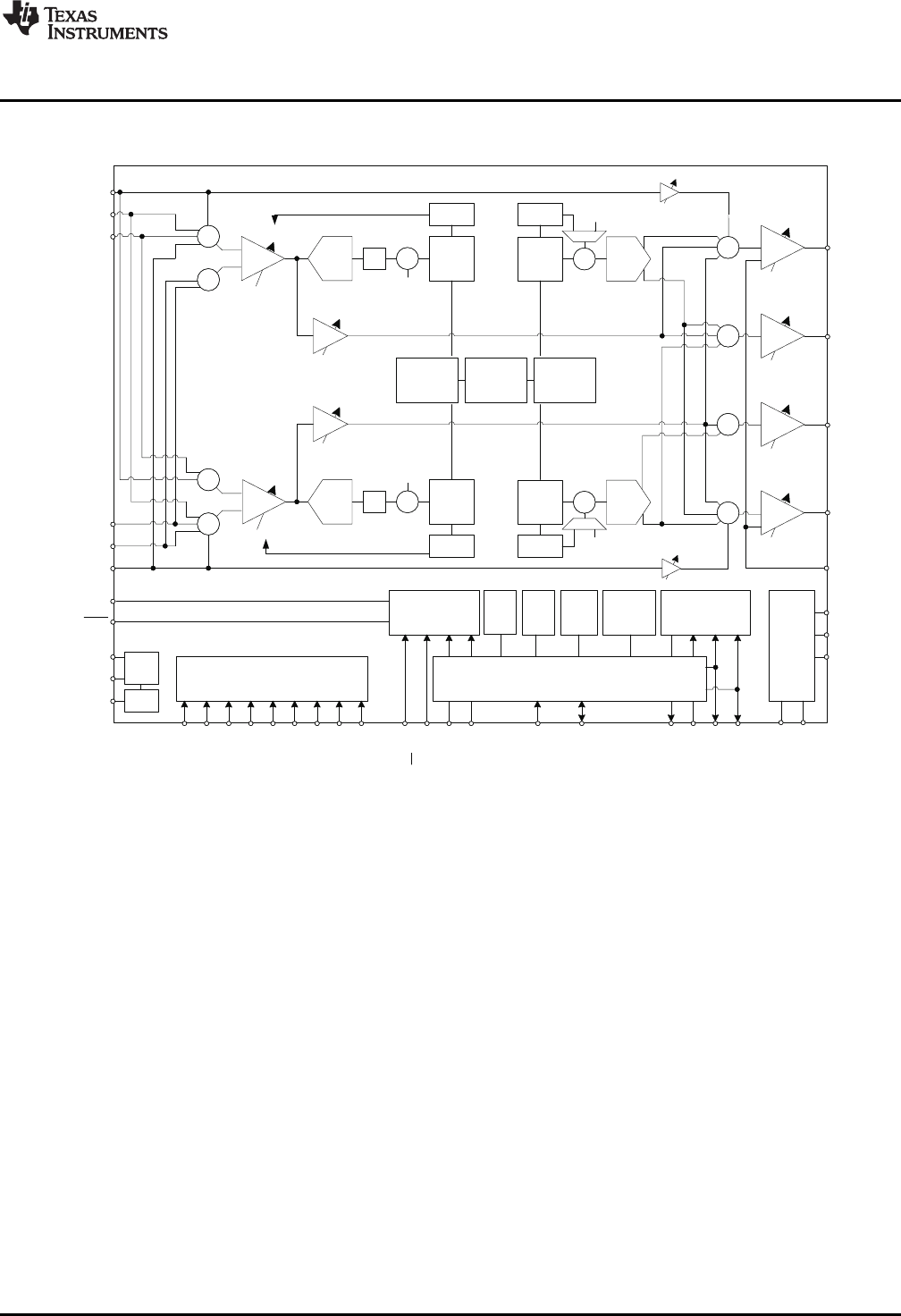
SPI_Select
IN1_R
IN2_R
IN3_R
IN3_L
IN2_L
IN1_L
Left
ADC
DRC
tpl
Left
DAC
AGC
*+
+
+
+
∗
ADC
Signal
Proc.
DAC
Signal
Proc.
Right
ADC
DRC
tpr Right
DAC
AGC
∗ ∗
ADC
Signal
Proc.
DAC
Signal
Proc.
+
+
+
+
Vol. Ctrl
Vol. Ctrl
Data
Interface
Gain Adj.
Gain Adj.
0…
+47.5 dB
0.5 dB steps
0…+47.5 dB
0.5 dB
steps
-6...+14dB
1dB steps
-6...+29dB
1dB steps
-6...+29dB
1dB steps
-6...+14dB
1dB steps
SPI / I2C
Control Block
Pin Muxing / Clock Routing
Sec.
I2S I/F
Primary
I2S Interface
Dig
Mic
Inter
rupt
PLL
Mic
Bias
Ref
MicBias
Ref
Supplies
DVdd
Vsys
IOVdd
Avss (GND)
DVss (GND)
IOVss (GND)
SDA/MOSI
MISO
SCLK
MCLK
GPIO
DOUT
DIN
BCLK
WCLK
miniDSP miniDSP
HPL
LOL
HPR
LOR
Reset
-30...0 dB
-30...0 dB
Charge
Pump
GND_Sense
MicDet
VNEG
Fly_N
DVSS_CP
Fly_P
DVDD_CP
DRVdd_HP
SCL/SS
GND
AVdd
www.ti.com
Description
1.1 Description
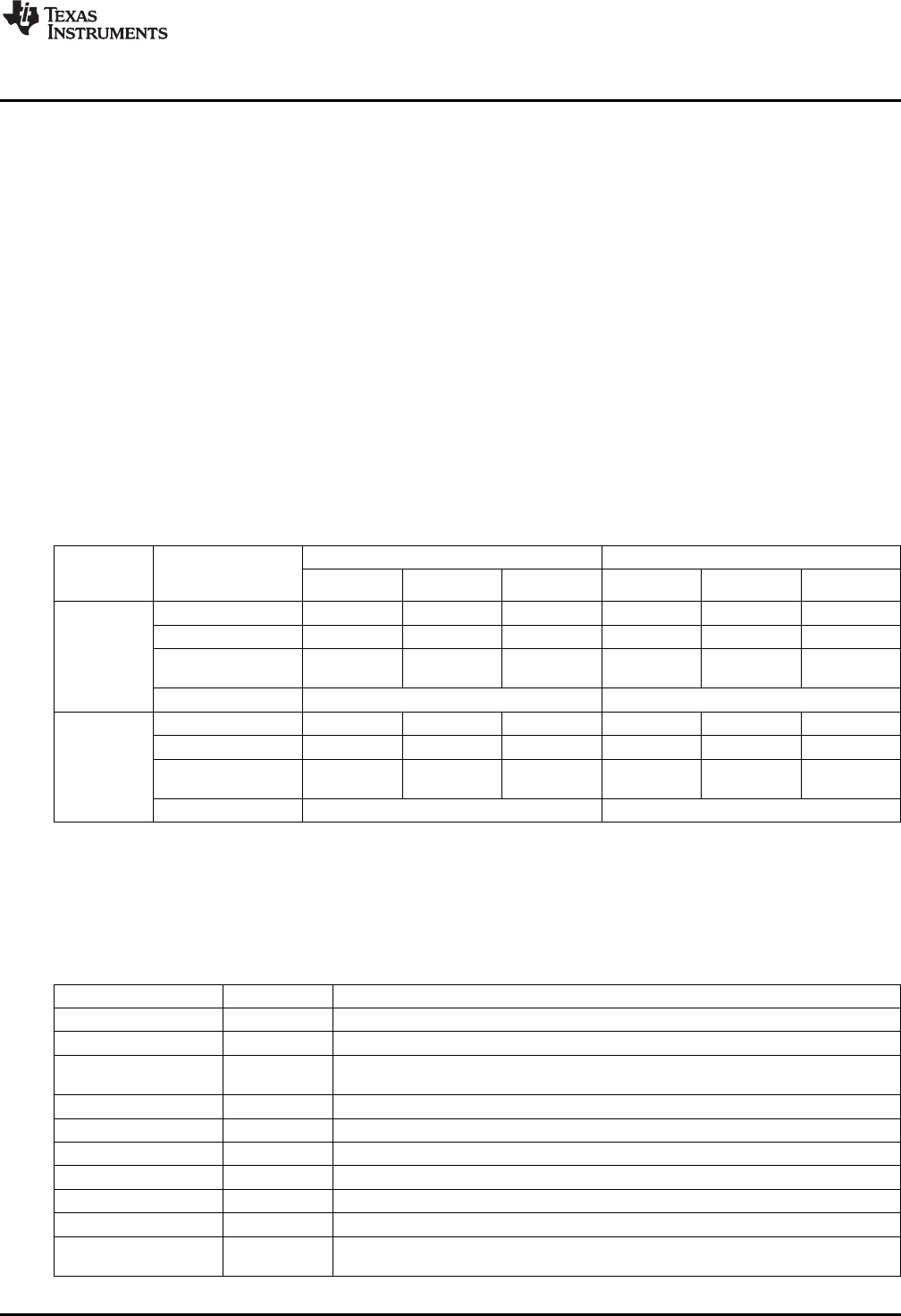
Figure 1-1. Simplified Block Diagram
The TLV320AIC3256 features two fully-programmable miniDSP cores that support application-specific
algorithms in the record and/or the playback path of the device. The miniDSP cores are fully software
controlled. Target miniDSP algorithms, such as active noise cancellation, acoustic echo cancellation or
advanced DSP filtering are loaded into the device after power-up.
Extensive register-based control of power, input/output channel configuration, gains, effects, pin-
multiplexing and clocks is included, allowing the device to precisely target its application. The device
operates from 8kHz mono voice playback to audio stereo 192kHz DAC playback; ideal for portable
battery-powered audio and telephony applications.
The record path of the TLV320AIC3256 ranges from 8kHz mono to 192kHz stereo recording, and contains
programmable input channel configurations covering single-ended and differential setups, as well as
floating or mixing input signals. A digitally-controlled stereo microphone preamplifier also integrates
microphone bias. Digital signal processing blocks can remove audible noise that may be introduced by
mechanical coupling, such as optical zooming in a digital camera.
The playback path offers signal-processing blocks for filtering and effects, and supports flexible mixing of
DAC and analog input signals as well as programmable volume controls. The playback path contains two
high-power output drivers that eliminate the need for ac coupling capacitors. A built in charge pump
generates the negative supply for the ground-centered high-power output drivers. The high-power outputs
can be configured in multiple ways, including stereo and mono BTL.
3
SLAU306A–January 2011–Revised January 2013 TLV320AIC3256 Overview
Submit Documentation Feedback Copyright © 2011–2013, Texas Instruments Incorporated
Typical Circuit Configuration
www.ti.com
The device can be programmed to various power-performance trade-offs. Mobile applications frequently
have multiple use cases requiring very low power operation while being used in a mobile environment.
When used in a docked environment power consumption typically is less of a concern, while minimizing
noise is important. The TLV320AIC3256 addresses both cases.
The device offers single supply operation from 1.5V-1.95V. Digital I/O voltages are supported in the range
of 1.1V-3.6V.
The required internal clock of the TLV320AIC3256 can be derived from multiple sources, including the
MCLK pin, the BCLK pin, the GPIO pin or the output of the internal PLL, where the input to the PLL again
can be derived from the MCLK pin, the BCLK or GPIO pins. Although using the PLL ensures the
availability of a suitable clock signal, it is not recommended for the lowest power settings. The PLL is
highly programmable and can accept available input clocks in the range of 512kHz to 50MHz.
The device is available in the 5mm × 5mm, 40-pin QFN or 3.5mm × 3.3mm 42-ball WCSP package.
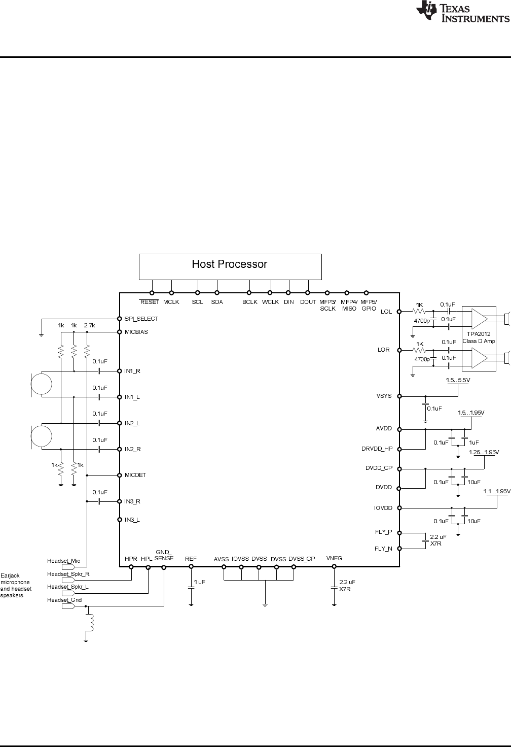
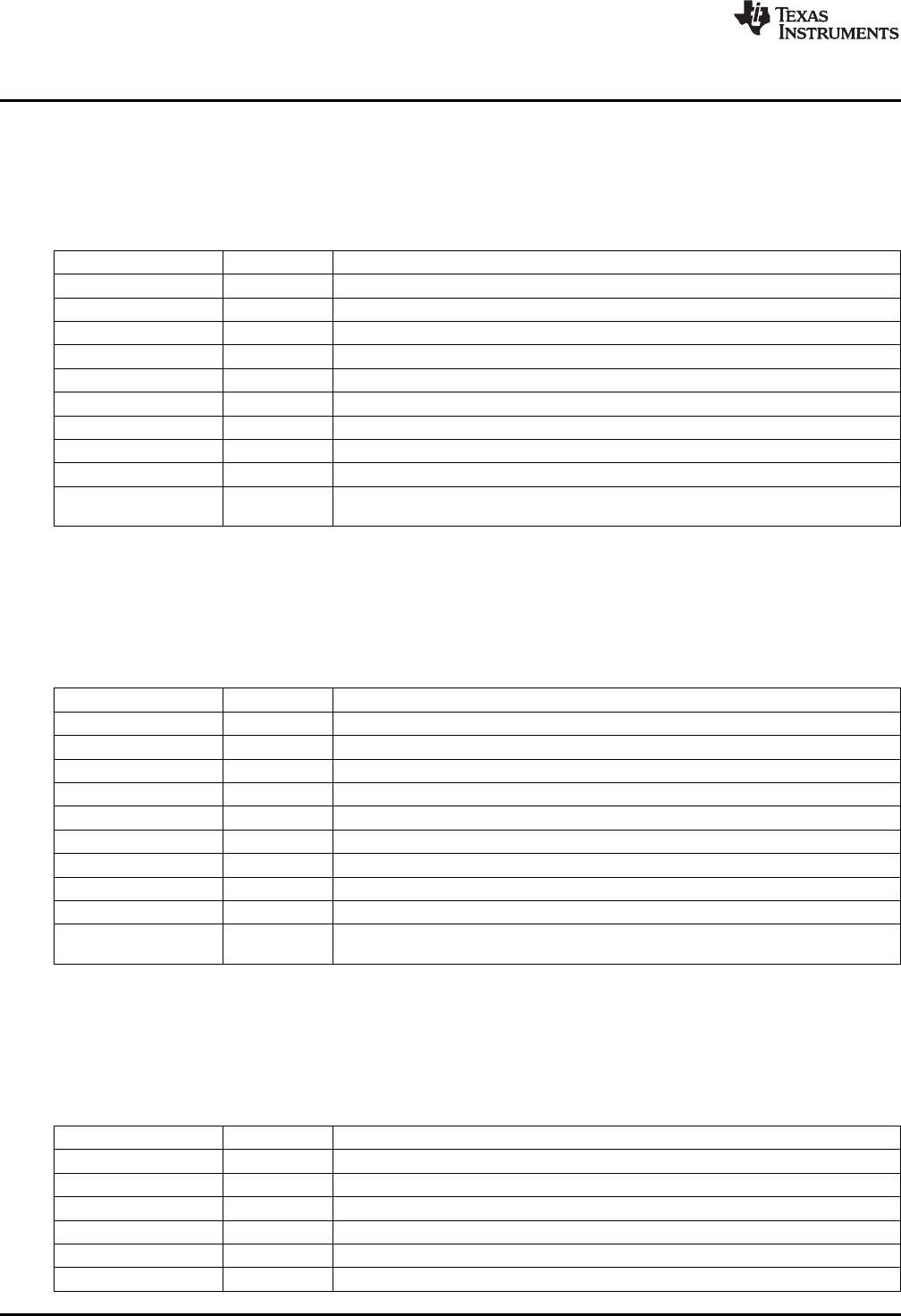
1.2 Typical Circuit Configuration
Figure 1-2. Typical Circuit Configuration
4TLV320AIC3256 Overview SLAU306A–January 2011–Revised January 2013
Submit Documentation Feedback
Copyright © 2011–2013, Texas Instruments Incorporated
Chapter 2
SLAU306A–January 2011–Revised January 2013
TLV320AIC3256 Application
2.1 Terminal Descriptions
2.1.1 Digital Pins
Only a small number of digital pins are dedicated to a single function; whenever possible, the digital pins
have a default function, and also can be reprogrammed to cover alternative functions for various
applications.
The fixed-function pins are Reset and the SPI_Select pin, which are HW control pins. Depending on the
state of SPI_Select, the two control-bus pins SCL/SS and SDA/MOSI are configured for either I2C or SPI
protocol.
Other digital IO pins can be configured for various functions via register control. An overview of available
functionality is given in Section 2.1.1.1.
2.1.1.1 Multifunction Pins
Table 2-1 shows the possible allocation of pins for specific functions. The PLL input, for example, can be
programmed to be any of 4 pins (MCLK, BCLK, DIN, GPIO).
Table 2-1. Multifunction Pin Assignments
1 2 3 4 5 6 7 8
Pin Function MCLK BCLK WCLK DIN DOUT DMDIN/ DMCLK/ GPIO
MFP1 MFP2 MFP3/ MFP4/ MFP5
SCLK MISO
APLL Input S(1) S(2) E S(3)
BCodec Clock Input S(1),D(4) S(2) S(3)
CI2S BCLK input S,D
DI2S BCLK output E(5)
EI2S WCLK input E, D
FI2S WCLK output E
GI2S ADC word clock input E E
HI2S ADC WCLK out E E
II2S DIN E, D
JI2S DOUT E, D
KGeneral Purpose Output I E
KGeneral Purpose Output II E
KGeneral Purpose Output III E
LGeneral Purpose Input I E
LGeneral Purpose Input II E
LGeneral Purpose Input III E
(1) S(1): The MCLK pin can drive the PLL and Codec Clock inputs simultaneously.
(2) S(2): The BCLK pin can drive the PLL and Codec Clock and audio interface bit clock inputs simultaneously.
(3) S(3): The GPIO/MFP5 pin can drive the PLL and Codec Clock inputs simultaneously.
(4) D: Default Function
(5) E: The pin is exclusively used for this function, no other function can be implemented with the same pin. (If GPIO/MFP5 has
been allocated for General Purpose Output, it cannot be used as the INT1 output at the same time.)
5
SLAU306A–January 2011–Revised January 2013 TLV320AIC3256 Application
Submit Documentation Feedback
Copyright © 2011–2013, Texas Instruments Incorporated
Terminal Descriptions
www.ti.com
Table 2-1. Multifunction Pin Assignments (continued)
1 2 3 4 5 6 7 8
Pin Function MCLK BCLK WCLK DIN DOUT DMDIN/ DMCLK/ GPIO
MFP1 MFP2 MFP3/ MFP4/ MFP5
SCLK MISO
MINT1 output E E E
NINT2 output E E E
QSecondary I2S BCLK input E E
RSecondary I2S WCLK in E E
SSecondary I2S DIN E E
TSecondary I2S DOUT E
USecondary I2S BCLK OUT E E E
VSecondary I2S WCLK OUT E E E
XAux Clock Output E E E
2.1.2 Analog Pins
Analog functions can also be configured to a large degree. For minimum power consumption, analog
blocks are powered down by default. The blocks can be powered up with fine granularity according to the
application needs.
6TLV320AIC3256 Application SLAU306A–January 2011–Revised January 2013
Submit Documentation Feedback
Copyright © 2011–2013, Texas Instruments Incorporated
www.ti.com
Terminal Descriptions
2.1.3 Register Settings for Multifunction Pins
To configure the settings seen in Table 2-1, please see the letter-number combination in Table 2-2 for the
appropriate registers to modify.
Please be aware that more settings may be necessary to obtain a full interface definition matching the
application requirement (see Page 0, Register 25 to 33).
Table 2-2. Multifunction Pin Register Configuration
Required Register
Description Required Register Setting Description Setting
Page 0, Register 4, Bits D3- Page 0, Register 53,Bits
A1 PLL Input on MCLK N5 INT2 output DOUT/MFP2
D2 = 00 D3-D1 = 101
Page 0, Register 4, Bits D3- INT2 output on Page 0, Register 55, Bits
A2 PLL Input on BCLK N7
D2 = 01 MISO/MFP4 D4-D1 = 0101
Page 0, Register 54, Bits
D2-D1 = 01 INT2 output on Page 0, Register 52, Bits
A4 PLL Input on DIN/MFP1 N8
Page 0, Register 4, Bits D3- GPIO/MFP5 D5-D2 = 0110
D2 = 11
Page 0, Register 52, Bits Page 0, Register 54, Bits
D5-D2 = 0001 Digital Microphone Data D2-D1 = 01
A8 PLL Input on GPIO/MFP5 O4
Page 0, Register 4, Bits D3- Input on DIN/MFP1 Page 0, Register 81, Bits
D2 = 10 D5-D4 = 10
Page 0, Register 56, Bits
Codec Clock Input on Page 0, Register 4, Bits D1- Digital Microphone Data D2-D1 = 01
B1 O6
MCLK D0 = 00 Input on SCLK/MFP3 Page 0, Register 81, Bits
D5-D4 = 01
Page 0, Register 52, Bits
Codec Clock Input on Page 0, Register 4, Bits D1- Digital Microphone Data D5-D2 = 0001
B2 O8
BCLK D0 = 01 Input on GPIO/MFP5 Page 0, Register 81, Bits
D5-D4 = 00
Page 0, Register 52, Bits
Codec Clock Input on D5-D2 = 0001 Digital Microphone Clock Page 0, Register 55, Bits
B8 P7
GPIO/MPF5 Page 0, Register 4, Bits D1- Output on MISO/MFP4 D4-D1 = 0111
D0 = 10
Page 0, Register 27, Bit D3 Digital Microphone Clock Page 0, Register 52, Bits
C2 I2S BCLK input on BCLK P8
= 0 Output on GPIO/MFP5 D5-D2 = 1010
Page 0, Register 56, Bits
Page 0, Register 27, Bit D3 Secondary I2S BCLK input D2-D1 = 01
D2 I2S BCLK output on BCLK Q6
= 1 on SCLK/MFP3 Page 0, Register 31, Bits
D6-D5 = 01
Page 0, Register 52, Bits
Page 0, Register 27, Bit D2 Secondary I2S BCLK input D5-D2 = 0001
E3 I2S WCLK input on WCLK Q8
= 0 on GPIO/MFP5 Page 0, Register 31, Bits
D6-D5 = 00
Page 0, Register 56, Bits
Page 0, Register 27, Bit D2 Secondary I2S WCLK in on D2-D1 = 01
F3 I2S WCLK output WCLK R6
= 1 SCLK/MFP3 Page 0, Register 31, Bits
D4-D3 = 01
Page 0, Register 56, Bits Page 0, Register 52, Bits
I2S ADC word clock input D2-D1 = 01 Secondary I2S WCLK in on D5-D2 = 0001
G6 R8
on SCLK/MFP3 Page 0, Register 31, Bits GPIO/MFP50 Page 0, Register 31, Bits
D2-D1 = 01 D4-D3 = 0
Page 0, Register 52, Bits Page 0, Register 56, Bits
I2S ADC word clock input D5-D2 = 0001 Secondary I2S DIN on D2-D1 = 01
G8 S6
on GPIO/MFP5 Page 0, Register 31, Bits SCLK/MFP3 Page 0, Register 31, Bit D0
D2-D1 = 00 = 1
7
SLAU306A–January 2011–Revised January 2013 TLV320AIC3256 Application
Submit Documentation Feedback
Copyright © 2011–2013, Texas Instruments Incorporated
Analog Audio I/O
www.ti.com
Table 2-2. Multifunction Pin Register Configuration (continued)
Required Register
Description Required Register Setting Description Setting
Page 0, Register 52, Bits
I2S ADC WCLK out on Page 0, Register 55, Bits Secondary I2S DIN on D5-D2 = 0001
H7 S8
MISO/MFP4 D4-D1 = 0110 GPIO/MFP5 Page 0, Register 31, Bit D0
= 0
I2S ADC WCLK out on Page 0, Register 52, Bits Secondary I2S DOUT on Page 0, Register 55, Bits
H8 T7
GPIO/MFP5 D5-D2 = 0111 MISO/MFP4 D4-D1 = 1000
Page 0, Register 54, Bits Secondary I2S BCLK OUT Page 0, Register 53, Bits
I4 I2S DIN on DIN/MFP1 U5
D2-D1 = 01 on DOUT/MFP2 D3-D1 = 110
I2S DOUT on Page 0, Register 53, Bits Secondary I2S BCLK OUT Page 0, Register 55, Bits
J5 U7
DOUT/MFP2 D3-D1 = 001 on MISO/MFP4 D4-D1 = 1001
General Purpose Out I on Page 0, Register 53, Bits Secondary I2S BCLK OUT Page 0, Register 52, Bits
K5 U8
DOUT/MFP2 D3-D1 = 010 on GPIO/MFP5 D5-D2 = 1000
General Purpose Out II Page 0, Register 55, Bits Secondary I2S WCLK OUT Page 0, Register 53, Bits
K7 V5
on MISO/MFP4 D4-D1 = 0010 on SCLK/MFP3 D3-D1 = 111
General Purpose Out III Page 0, Register 52, Bits Secondary I2S WCLK OUT Page 0, Register 55, Bits
K8 V7
on GPIO/MFP5 D5-D2 = 0011 on MISO/MFP4 D4-D1 = 1010
General Purpose In I on Page 0, Register 54, Bits Secondary I2S WCLK OUT Page 0, Register 52, Bits
L4 V8
DIN/MFP1 D2-D1 = 10 on GPIO/MFP5 D5-D2 = 1001
Page 0, Register 56, Bits
General Purpose In II on Page 0, Register 56, Bits Headset Detect Input on D2-D1 = 00
L6 W6
SCLK/MFP3 D2-D1 = 10 SCLK/MFP3 Page 0, Register 67, Bit D7
= 1
General Purpose In III on Page 0, Register 52, Bits Aux Clock Output on Page 0, Register 53, Bits
L8 X5
GPIO/MFP5 D5-D2 = 0010 DOUT/MFP2 D3-D1 = 011
INT1 output on Page 0, Register 53, Bits Aux Clock Output on Page 0, Register 55, Bits
M5 X7
DOUT/MFP2 D3-D1 = 100 MISO/MFP4 D4-D1 = 0011
INT1 output on Page 0, Register 55, Bits Aux Clock Output on Page 0, Register 52, Bits
M7 X8
MISO/MFP4 D4-D1 = 0100 GPIO/MFP5 D5-D2 = 0100
INT1 output on Page 0, Register 52, Bits
M8 GPIO/MFP5 D5-D2 = 0101
2.2 Analog Audio I/O
The analog IO path of the TLV320AIC3256 features a large set of options for signal conditioning as well
as signal routing:
• 6 analog inputs which can be mixed and-or multiplexed in single-ended and-or differential configuration
• 2 programmable gain amplifiers (PGA) with a range of 0 to +47.5dB
• 2 mixer amplifiers for analog bypass
• 2 low power analog bypass channels
• Mute function
• Channel-to-channel phase adjustment
• Fast charge of ac-coupling capacitors
• Anti thump
2.2.1 Analog Bypass
The TLV320AIC3256 offers two analog-bypass modes. In either of the modes, an analog input signal can
be routed from an analog input pin to an amplifier driving an analog output pin. Neither the ADC nor the
DAC resources are required for such operation.
In analog low-power bypass mode, line-level signals can be routed directly from the analog inputs IN1_L
to the left headphone amplifier (HPL) and IN1_R to HPR.
8TLV320AIC3256 Application SLAU306A–January 2011–Revised January 2013
Submit Documentation Feedback
Copyright © 2011–2013, Texas Instruments Incorporated
HPL
HPR
GND_SENSE
www.ti.com
Analog Audio I/O
2.2.2 ADC Bypass Using Mixer Amplifiers
In addition to the analog low-power bypass mode, another bypass mode uses the programmable gain
amplifiers of the input stage in conjunction with a mixer amplifier. With this mode, microphone-level signals
can be amplified and routed to the line or headphone outputs, fully bypassing the ADC and DAC.
To enable this mode, the mixer amplifiers are powered on via software command.
In analog low-power bypass mode, line-level signals can be routed directly from the analog inputs IN1L to
the left headphone amplifier (HPL) and IN1R to HPR. (Configured on Page 1, Register 12, Bit D2 for the
left channel and Page 1, Register 13, Bit D2 for the right channel.)
To use the mixer amplifiers, power them on via Page, Register 9, Bits D1-D0.
2.2.2.1 Analog Programmable Gain Amplifier (PGA)
The TLV320AIC3256 features a built-in low-noise PGA for boosting low-level signals, such as direct
microphone inputs, to full-scale to achieve high SNR. This PGA can provide a gain in the range of 0dB to
47.5dB for single-ended inputs or 6dB to 53.5dB for fully-differential inputs. See Section 2.3.2.1 for
information on setting gains for the entire input path.
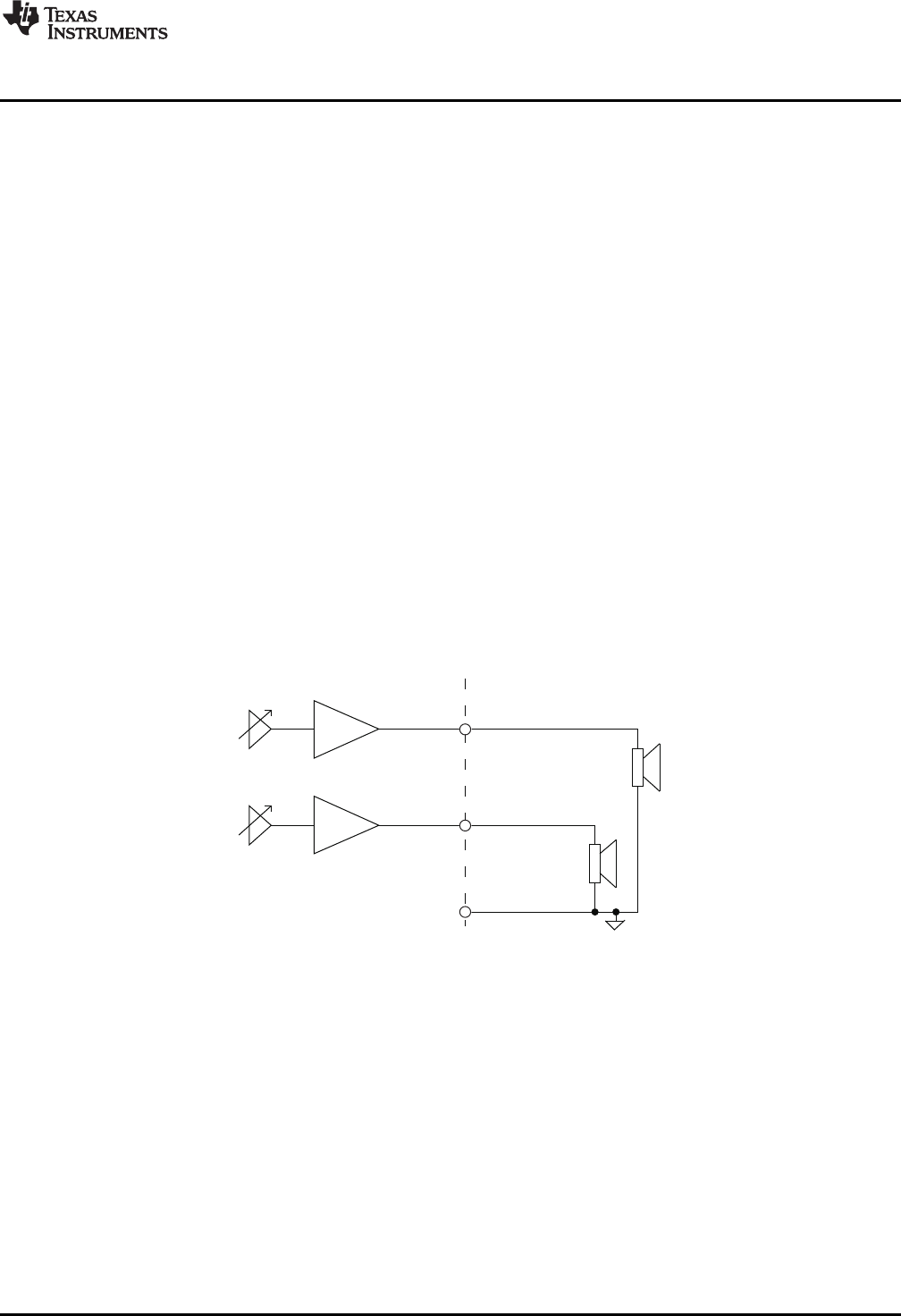
2.2.3 Headphone Output
The stereo headphone drivers on pins HPL and HPR can drive loads with impedances down to 16Ωin
single-ended DC-coupled headphone configurations. An integral charge pump generates the negative
supply required to operate the headphone drivers in dc-coupled mode, where the common mode of the
output signal is made equal to the ground of the headphone load using a ground-sense circuit. Operation
of headphone drivers in dc-coupled (ground centered mode) eliminates the need for large dc-blocking
capacitors.
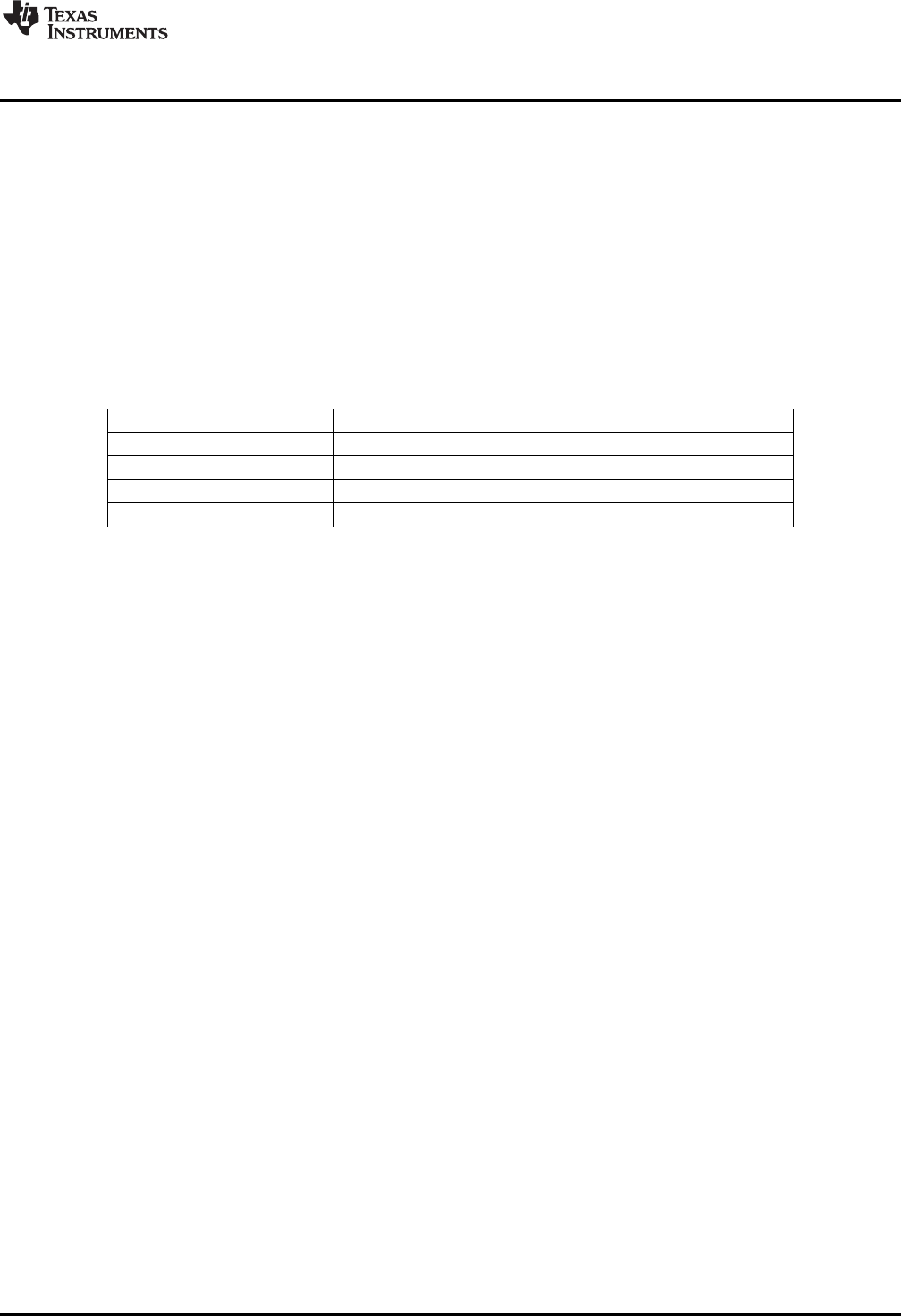
Figure 2-1. TLV320AIC3256 Ground-Centered Headphone Output
Alternatively the headphone amplifier can also be operated in a unipolar circuit configuration using DC
blocking capacitors.
2.2.3.1 Using the Headphone Amplifier
The headphone drivers are capable of driving a mixed combination of DAC signal, left and right ADC PGA
signal and line-bypass from analog input IN1L and IN1R by configuring Page 1, Reg 12 and Page 1, Reg
13 respectively. The ADC PGA signals can be attenuated up to 30dB before routing to headphone drivers
by configuring Page 1, Reg 24 and Page 1, Reg 25. The line-input signals can be attenuated up to 72dB
before routing by configuring Page 1, Reg 22 and 23. The level of the DAC signal can be controlled using
the digital volume control of the DAC in Page 0, Reg 65 and 66. To control the output-voltage swing of
headphone drivers, the digital volume control provides a range of –6.0dB to +14.0dB in steps of 1dB.
These can be configured by programming Page 1, Reg 16 and 17. These level controls are not meant to
be used as dynamic volume control, but more to set output levels during initial device configuration. (1)
(1) If the headphone amplifier must be placed into 'mute' from the –6.0dB setting, set the device at a gain of –5.0dB first, then place the
device into mute.
9
SLAU306A–January 2011–Revised January 2013 TLV320AIC3256 Application
Submit Documentation Feedback Copyright © 2011–2013, Texas Instruments Incorporated
-6...+14dB
1dB steps
-6...+14dB
1dB steps
HPL
HPR
Charge
Pump
GND_Sense
VNEG
Fly_N
Fly_P
DRVdd_HP
DVss_CP
DVdd_CP
2.2 uF
X7R
2.2 uF
X7R
1.8...1.95V
10 uF
Analog Audio I/O
www.ti.com
2.2.3.2 Ground-Centered Headphone Amplifier Configuration
Among the other advantages of the ground-centered connection is inherent freedom from turn-on
transients that can cause audible pops, sometimes at uncomfortable volumes.
2.2.3.2.1 Circuit Topology
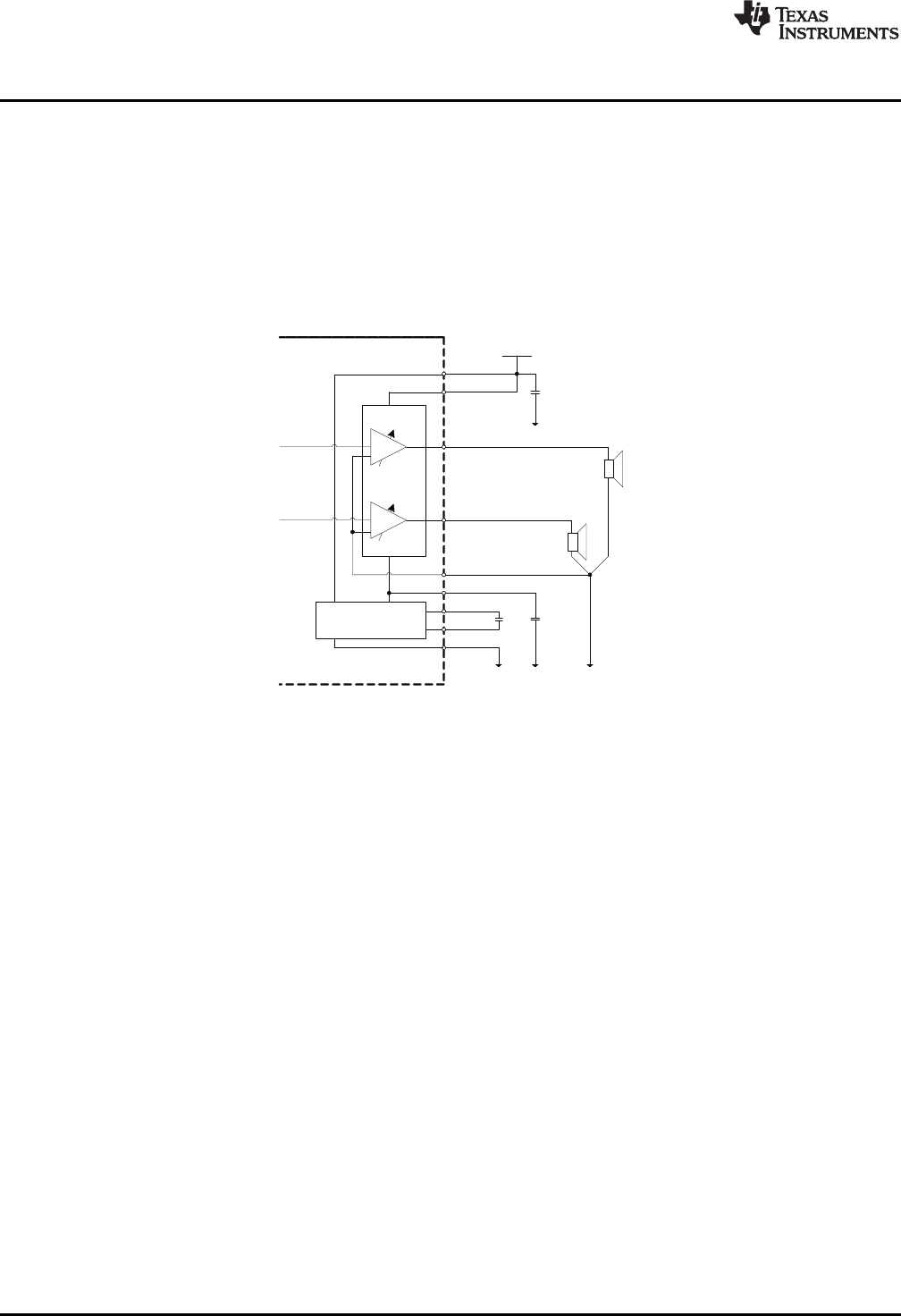
The power supply hook up scheme for the ground centered configuration is shown in Figure 2-2
DRVdd_HP pin supplies the positive side of the headphone amplifier. DVdd_CP pin supplies the charge
pump which in turn supplies the negative side of the headphone amplifier. Two capacitors are required for
the charge pump circuit to work. These capacitors should be X7R rated.
Figure 2-2.
2.2.3.2.2 Charge Pump Setup and Operation
The built in charge pump draws charge from the DVDD_CP supply, and by switching the external
capacitor between FLY_P and FLY_N, generates the negative voltage on VNEG pin. The charge-pump
circuit uses the principles of switched-capacitor charge conservation to generate the VNEG supply in a
very efficient fashion.
To turn on the charge pump circuit, program Page 1, Register 1, D1:0 to “10”. When the charge pump
circuit is disabled, VNEG acts as a ground terminal, allowing unipolar configuration of the headphone
amps. By default, the charge pump is disabled. The switching rate of the charge pump can be controlled
by Page 1, Register 124, D3:0. Because the charge pump can demand significant inrush currents from the
supply, it is important to have a capacitor connected in close proximity to the DVdd_CP and DVss_CP
pins of the device. At 500kHz clock rate this requires approximately a 10μF capacitor. The ESR and ESL
of the capacitor must be low to allow fast switching currents.
The ground-centered mode of operation is enabled by configuring Page 1, Reg 125, D4 after enabling the
charge-pump.
2.2.3.2.3 Output Power Optimization
The device can be optimized for a specific output-power range. The charge pump and the headphone
driver circuitry can be reduced in power so less overall power is consumed. The headphone driver power
can be programmed in Page 1, Register 125. The control of charge pump switching current is
programmed in Page 1, Register 124.
2.2.3.2.4 Offset Correction and Start-Up
The TLV320AIC3256 offers an offset-correction scheme that is based on calibration during power up. This
scheme minimizes the differences in DC voltage between GND_SENSE and HPL and HPR outputs.
10 TLV320AIC3256 Application SLAU306A–January 2011–Revised January 2013
Submit Documentation Feedback
Copyright © 2011–2013, Texas Instruments Incorporated
www.ti.com
Analog Audio I/O
The offset calibration happens after the headphones are powered up in ground-centered configuration. All
other headphone configurations like signal routings, gain settings and mute removal must be configured
before headphone powerup. Any change in these settings while the headphones are powered up may
result in additional offsets and are best avoided.
The offset-calibration block has a few programmable parameters that the user must control. The user can
either choose to calibrate the offset only for the selected input routing or all input configurations. The
calibration data is stored in internal memory until the next hardware reset or until AVdd power is removed.
Programming Page 1, Register 125, D(1:0) as “10” causes the offset to be calibrated for the selected input
mode. Programming Page 1, Register 125, D(1:1) as “11” causes the offset to be calibrated for all
possible configurations. All related blocks must be powered while doing offset correction.
Programming Page 1, Reg 125, D (1:0) as “00” (default) disables the offset correction block. While the
offset is being calibrated, no signal should be applied to the headphone amplifier. the DAC should be kept
muted and analog bypass routing should be kept at the highest attenuation. The user can read Page 1,
Register 2, D2 to poll if calibration is completed. D2 = ”1” indicates that calibration is completed.
2.2.3.2.5 Ground-Centered Headphone Setup
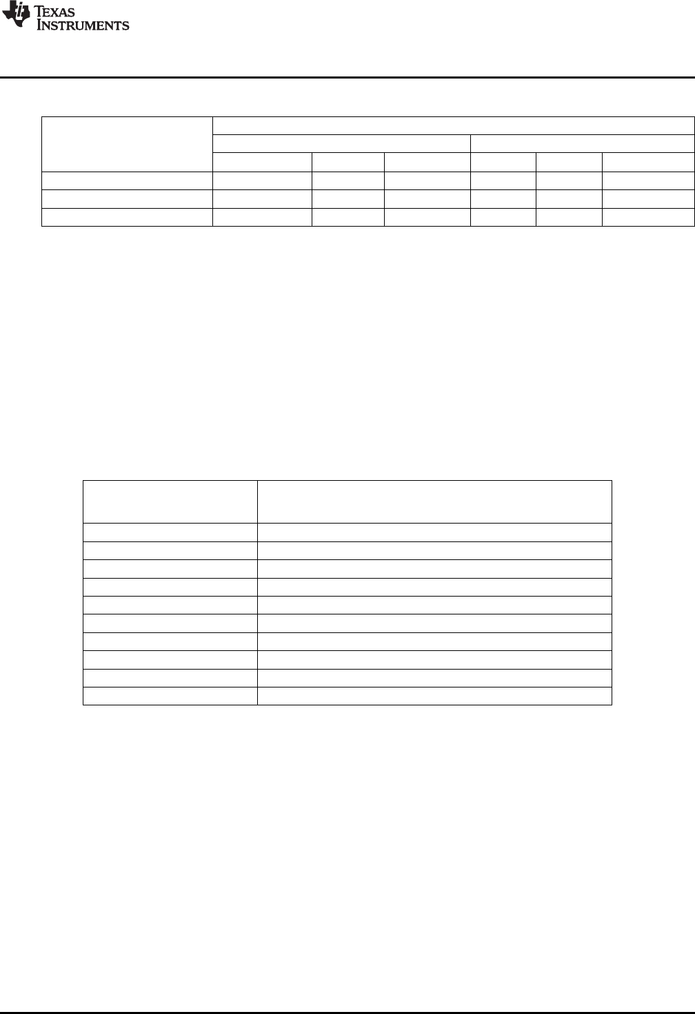
There are four practical device setups for ground-centered operation, shown in Table 2-3:
Table 2-3. Ground-Centered Headphone Setup Performance Options
Audio High Performance Low Power Consumption
Output 16Ω32Ω600Ω16Ω32Ω600Ω
Power
SNR 94.1dB 96.6dB 97.9dB 92.3dB 95.2dB 95.6dB
Output Power 26.2mW 23.4mW 19.7mW 19.3mW
High Idle Power 15.6mW 11.9mW
Consumption
High-Output, High-Performance Setup High-Output, Low-Power Setup
SNR 90.7dB 84.1dB 84.1dB 84.1dB
Output Power 10.5mW 5.3mW 5.1dB 2.6mW
Medium Idle Power 10.9mW 5.0mW
Consumption
Medium-Output, High-Performance Setup Medium-Output, Low-Power Setup
High Audio Output Power, High Performance Setup
This setup describe the register programming necessary to configure the device for a combination of high
audio output power and high performance. To achieve this combination the parameters must be
programmed to the values inTable 2-4.
Table 2-4. Setup A - High Audio Output Power, High Performance
Parameter Value Programming
CM 0.9 Page 1, Register 10, D6 = "0"
PTM PTM_P3 "Page 1, Register 3, D4:D2 = ""000""Page 1, Register 4, D4:D2 = ""000"""
1 to 6, 22, 23,
Processing Block Page 0, Register 60
24
DAC OSR 128 "Page 0, Register 13 = 0x00Page 0, Register 14 = 0x80"
DAC perf setting high "Page 1, Register 3, D5 = ""0""Page 1, Register 4, D5 = ""0"""
HP sizing 100 Page 1, Register 125, D3:D2 = "00"
CP sizing 100 Page 1, Register 124, D6:D4 = "000"
Gain 0 "Page 1, Register 16, D5:D0 = ""00 0000""Page 1, Register 17, D5:D0 = ""00 0000"""
DVdd 1.26 Apply 1.26 to 1.95V
AVdd,DRVdd_HP, 1.8 Apply 1.8 to 1.95V
DVdd_CP
11
SLAU306A–January 2011–Revised January 2013 TLV320AIC3256 Application
Submit Documentation Feedback
Copyright © 2011–2013, Texas Instruments Incorporated
Analog Audio I/O
www.ti.com
Medium Audio Output Power, High Performance Setup
This setup describe the register programming necessary to configure the device for a combination of
medium audio output power and high performance. To achieve this combination the parameters must be
programmed to the values inTable 2-5
Table 2-5. Setup B - Medium Audio Output Power, High Performance
Parameter Value Programming
CM 0.75 Page 1, Register 10, D6 = 1
PTM PTM_P2 "Page 1, Register 3, D4:D2 = ""001""Page 1, Register 4, D4:D2 = ""001"""
Processing Block 7 to 16 Page 0, Register 60
DAC OSR 64 "Page 0, Register 13 = 0x00Page 0, Register 14 = 0x40"
DAC perf setting low power "Page 1, Register 3, D5 = ""1""Page 1, Register 4, D5 = ""1"""
HP sizing 100 Page 1, Register 125, D3:D2 = "00"
CP sizing 100 Page 1, Register 124, D6:D4 = "000"
Gain 5 "Page 1, Register 16, D5:D0 = ""00 0101""Page 1, Register 17, D5:D0 = ""00 0101"""
DVdd 1.26 Apply 1.26 to 1.95V
AVdd,DRVdd_HP, 1.8 Apply 1.8 to 1.95V
DVdd_CP
High Audio Output Power, Low Power Consumption Setup
This setup describe the register programming necessary to configure the device for a combination of high
audio output power and low power consumption. To achieve this combination the parameters must be
programmed to the values inTable 2-6
Table 2-6. Setup C - High Audio Output Power, Low Power Consumption
Parameter Value Programming
CM 0.75 Page 1, Register 10, D6 = 1
PTM PTM_P2 "Page 1, Register 3, D4:D2 = ""001""Page 1, Register 4, D4:D2 = ""001"""
Processing Block 7 to 16 Page 0, Register 60
DAC OSR 64 "Page 0, Register 13 = 0x00Page 0, Register 14 = 0x40"
DAC perf setting high "Page 1, Register 3, D5 = ""0""Page 1, Register 4, D5 = ""0"""
HP sizing 100 Page 1, Register 125, D3:D2 = "00"
CP sizing 100 Page 1, Register 124, D6:D4 = "000"
Gain 5 "Page 1, Register 16, D5:D0 = ""00 0101""Page 1, Register 17, D5:D0 = ""00 0101"""
DVdd 1.26 Apply 1.26 to 1.95V
AVdd,DRVdd_HP, 1.5 Apply 1.5 to 1.95V
DVdd_CP
Medium Audio Output Power Setup, Lowest Power Consumption
This setup describe the register programming necessary to configure the device for a combination of
medium audio output power and lowest power consumption. To achieve this combination the parameters
must be programmed to the values inTable 2-7
Table 2-7. Setup D - Medium Audio Output Power Setup, Lowest Power Consumption
Parameter Value Programming
CM 0.75 Page 1, Register 10, D6 = 1
PTM PTM_P1 "Page 1, Register 3, D4:D2 = ""010""Page 1, Register 4, D4:D2 = ""010"""
Processing Block special Page 0, Register 60
DAC OSR 64 "Page 0, Register 13 = 0x00Page 0, Register 14 = 0x40"
DAC perf setting low power "Page 1, Register 3, D5 = ""1""Page 1, Register 4, D5 = ""1"""
HP sizing 25 Page 1, Register 125, D3:D2 = "11"
12 TLV320AIC3256 Application SLAU306A–January 2011–Revised January 2013
Submit Documentation Feedback
Copyright © 2011–2013, Texas Instruments Incorporated
-6...+14dB
1dB steps
-6...+14dB
1dB steps
HPL
HPR
Charge
Pump (disabled)
GND_Sense
VNEG
Fly_N
Fly_P
DRVdd_HP
DVss_CP
DVdd_CP
1.5...3.6V
DVdd
DVdd
www.ti.com
Analog Audio I/O
Table 2-7. Setup D - Medium Audio Output Power Setup, Lowest Power Consumption (continued)
Parameter Value Programming
CP sizing 12.5 Page 1, Register 124, D6:D4 = "001"
Gain 14 "Page 1, Register 16, D5:D0 = ""00 1110""Page 1, Register 17, D5:D0 = ""00 1110"""
DVdd 1.26 Apply 1.26 to 1.95V
AVdd,DRVdd_HP, 1.5 Apply 1.5 to 1.95V
DVdd_CP
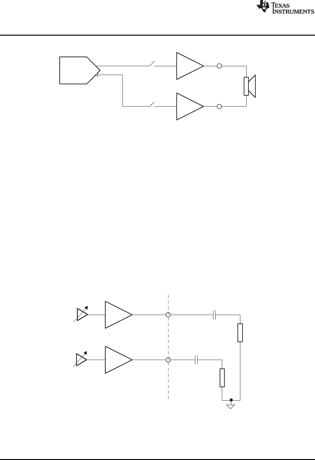
2.2.3.3 Stereo Unipolar Configuration
2.2.3.3.1 Circuit Topology
The power supply hook up scheme for the unipolar configuration is shown in Figure 2-3 DRVdd_HP pin
supplies the positive side of the headphone amplifier. The negative side is connected to ground potential
(VNEG). TI recommends connecting the DVdd_CP pin to DVdd, although the charge pump must not be
enabled while the device is connected in unipolar configuration.
Figure 2-3. Unipolar Stereo Headphone Circuit
The left and right DAC channels are routed to the corresponding left and right headphone amplifier. This
configuration is also used to drive line-level loads.
2.2.3.3.2 Unipolar Turn-On Transient (Pop) Reduction
The TLV320AIC3256 headphone drivers also support pop-free operation in unipolar, ac-coupled
configuration. Because the HPL and HPR are high-power drivers, pop can result due to sudden transient
changes in the output drivers if care is not taken. The most critical care is required while using the drivers
as stereo single-ended capacitively-coupled drivers as shown in Figure 2-3. The output drivers achieve
pop-free power-up by using slow power-up modes. Conceptually, the circuit during power-up can be
visualized as
13
SLAU306A–January 2011–Revised January 2013 TLV320AIC3256 Application
Submit Documentation Feedback Copyright © 2011–2013, Texas Instruments Incorporated
cm
popload
load
load V
RR
R
V´
+
=
Rload
Rpop
Cc
Output
Driver
PAD
Analog Audio I/O
www.ti.com
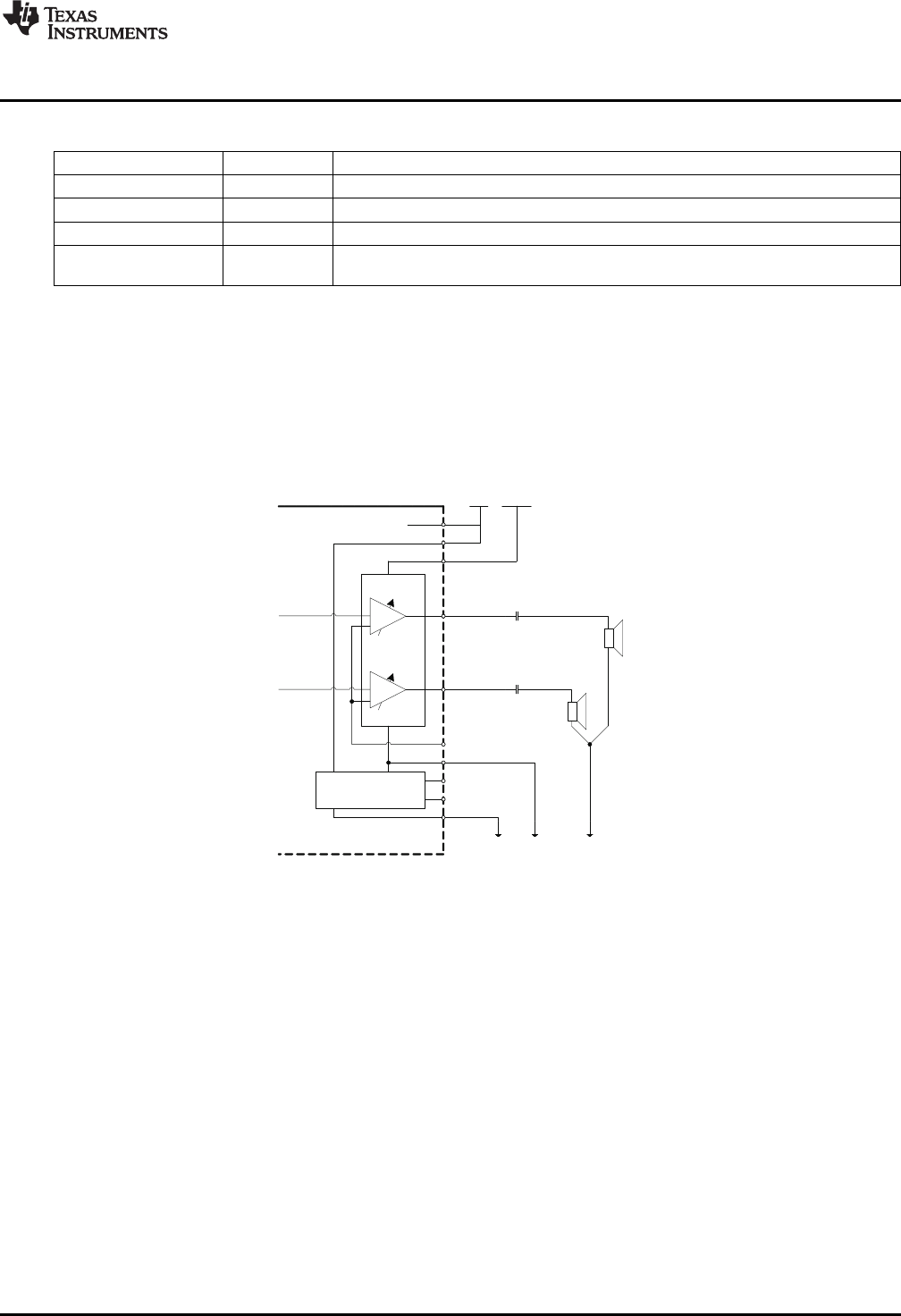
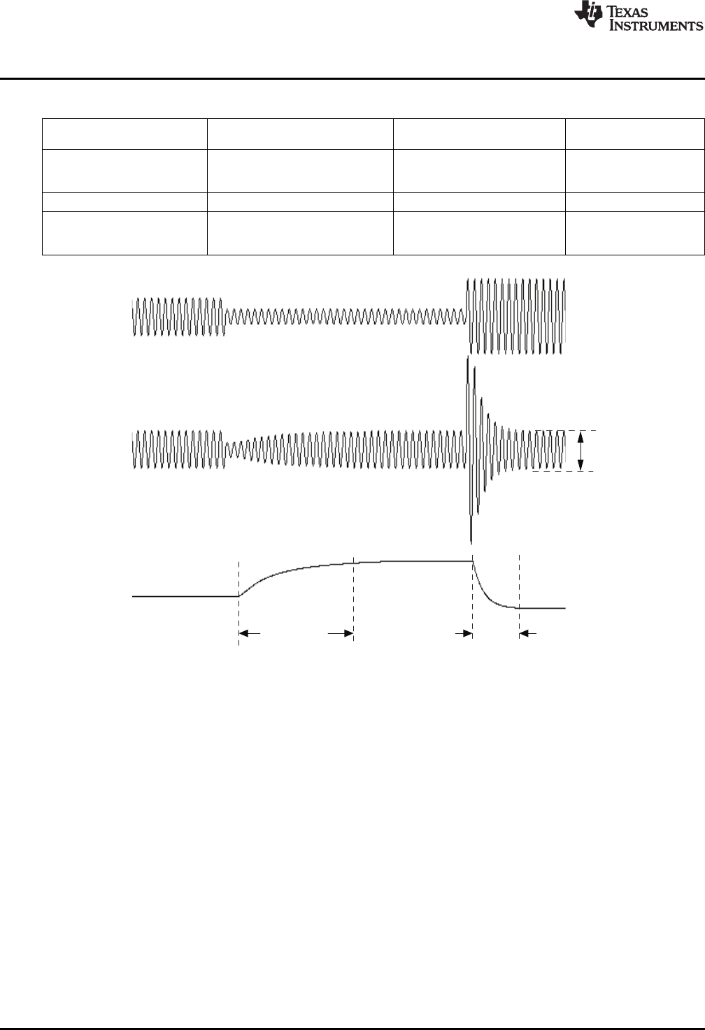
Figure 2-4. Conceptual Circuit for Pop-Free Power-up
Set the value of Rpop by writing register Page 1, Register 20, Bits D1-D0.
Table 2-8. Rpop Values
Page 1, Register 20, Bits D1-D0 Rpop Value
00 2 kΩ
01 6 kΩ
10 25 kΩ
To minimize audible artifacts, two parameters can be adjusted to match application requirements. The
voltage Vload across Rload at the beginning of slow charging should not be more than a few mV. At that time
the voltage across Rload can be determined as:
(1)
For a typical Rload of 32Ω, Rpop of 6 kΩor 25 kΩdelivers good results (see Table 2-8 for register settings).
According to the conceptual circuit in Figure 2-4, the voltage on PAD will exponentially settle to the output
common-mode voltage based on the value of Rpop and Cc. Thus, the output drivers must be in slow power-
up mode for time T, such that at the end of the slow power-on period, the voltage on Vpad is very close to
the common-mode voltage. The TLV320AIC3256 allows the time T to be adjusted to allow for a wide
range of Rload and Ccby programming Page 1, Register 20, Bits D5-D2. For the time adjustments, the
value of Ccis assumed to be 47μF. N = 5 is expected to yield good results.
Page 1, Register 20, Bits D5-D2 Slow Charging Time = N*Time – Constants (for Rpop and 47μF)
0000 N = 0
0001 N = 0.5
0010 N = 0.625
0011 N = 0.75
0100 N = 0.875
0101 N = 1.0
0110 N = 2.0
0111 N = 3.0
1000 N = 4.0
1001 N = 5.0
1010 N = 6.0
1011 N = 7.0
1100 N = 8.0
1101 N = 16 (Not valid for Rpop = 25kΩ)
1110 N = 24 (Not valid for Rpop = 25kΩ)
1111 N = 32 (Not valid for Rpop = 25kΩ)
14 TLV320AIC3256 Application SLAU306A–January 2011–Revised January 2013
Submit Documentation Feedback
Copyright © 2011–2013, Texas Instruments Incorporated
www.ti.com
Analog Audio I/O
Again, for example, for Rload = 32Ω, Cc= 47μF and common mode of 0.9V, the number of time constants
required for pop-free operation is 5 or 6. A higher or lower Ccvalue will require higher or lower value for N.
During the slow-charging period, no signal is routed to the output driver. Therefore, choosing a larger than
necessary value of N results in a delay from power-up to signal at output. At the same time, choosing N to
be smaller than the optimal value results in poor pop performance at power-up.
The signals being routed to headphone drivers (such as DAC and IN1) often have DC offsets due to less-
than-ideal processing. As a result, when these signals are routed to output drivers, the offset voltage
causes a pop. To improve the pop-performance in such situations, a feature is provided to soft-step the
DC-offset. At the beginning of the signal routing, a high-value attenuation can be applied which can be
progressively reduced in steps until the desired gain in the channel is reached. The time interval between
each of these gain changes can be controlled by programming Page 1, Register 20, Bits D7-D6. This gain
soft-stepping is applied only during the initial routing of the signal to the output driver and not during
subsequent gain changes.
Page 1, Register 20, Bits D7-D6 Soft-stepping Step Time During initial signal routing
00 0 ms (soft-stepping disabled)
01 50ms
10 100ms
11 200ms
The following sequence is recommended to achieve optimal pop performance at power-up:
1. Choose the value of Rpop, N (time constants) and soft-stepping step time for slow power-up.
2. Choose the configuration for output drivers, including common modes and output stage power
connections
3. Select the signals to be routed to headphones.
4. Power up the blocks driving signals into HPL and HPR, but keep HPL and HPR muted
5. Unmute HPL and HPR and set the desired gain setting.
6. Power on the HPL and HPR drivers.
7. Unmute the block driving signals to HPL and HPR after the Driver PGA flags are set to indicate
completion of soft-stepping after power-up. These flags can be read from Page 1, Register 63, Bits D7-
D6.
Configure the Headphone Output driver depop control registers before powering up the headphone; these
register contents must not be changed when the headphone drivers are powered up.
Before powering down the HPL and HPR drivers, it is recommended that software read back the flags in
Page 1, Register 63. For example. before powering down the HPL driver, ensure that bit D(7) = 1 and bit
D(3) = 1 if IN1L is routed to HPL and bit D(1) = 1 if the Left Mixer is routed to HPL. The output driver
should be powered down only after a steady-state power-up condition has been achieved. This steady
state power-up condition also must be satisfied for changing the HPL-R driver mute control in Page 1,
Register 16 and 17, Bits D7, for example. Mute and unmute the headphone drivers after the gain and
volume controls associated with routing to HPL and HPR finish soft-stepping.
In the differential configuration of HPL and HPR, when no coupling capacitor is used, the slow charging
method for pop-free performance need not be used. In the differential load configuration for HPL and
HPR, using the output driver MUTE feature is not recommended, because a pop may result.
During the power-down state, the headphone outputs are weakly pulled to ground using an approximately
50kΩresistor to ground, to maintain the output voltage on HPL and HPR pins.
15
SLAU306A–January 2011–Revised January 2013 TLV320AIC3256 Application
Submit Documentation Feedback Copyright © 2011–2013, Texas Instruments Incorporated
LOL
LOR
LEFT
DAC
HPL
HPR
LEFT_DACP
LEFT_DACM
Analog Audio I/O
www.ti.com
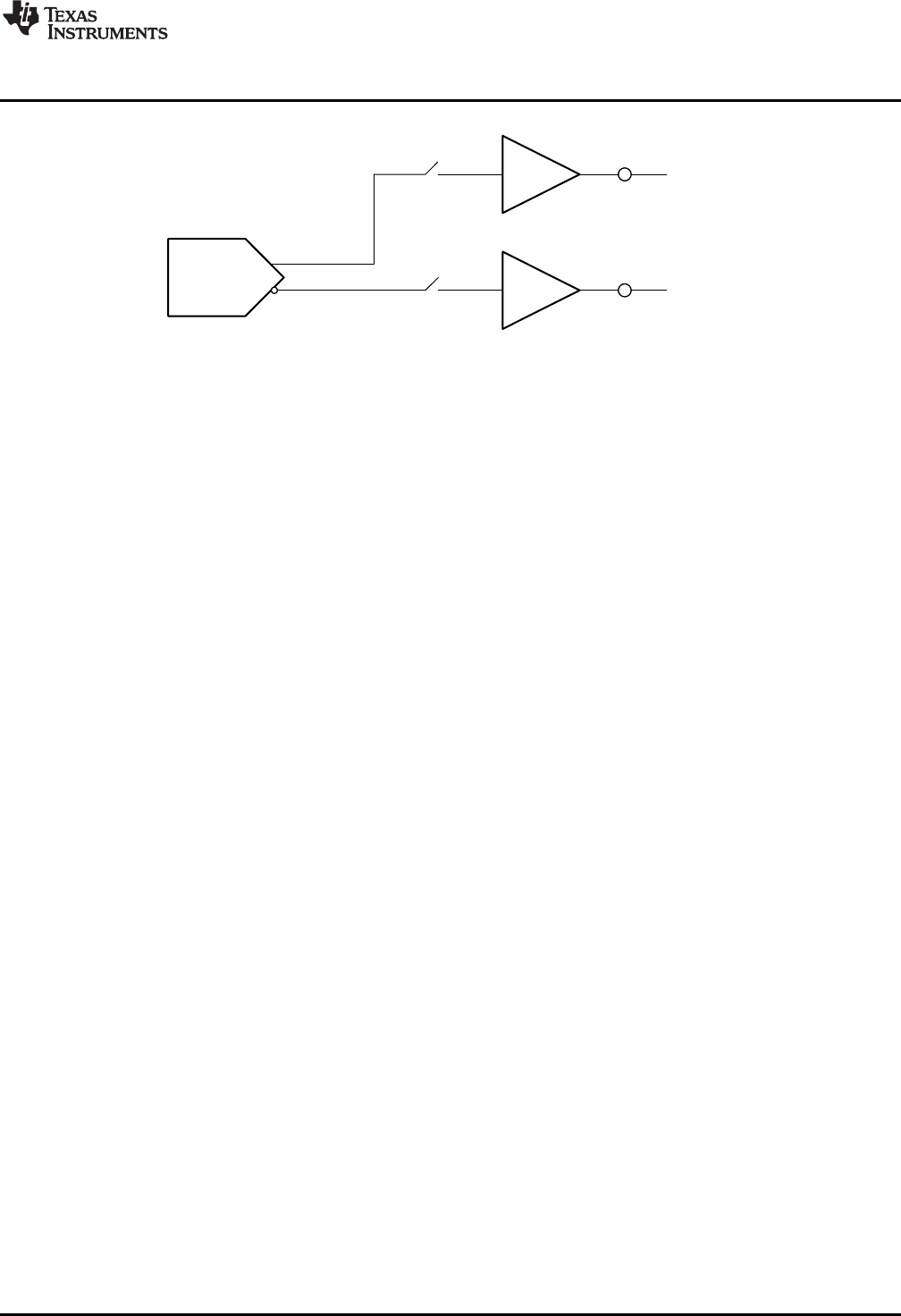
2.2.3.4 Mono Differential DAC to Mono Differential Headphone Output
Figure 2-5. Low Power Mono DAC to Differential Headphone
This configuration, available in unipolar configuration of the HP amplifier supplies, supports the routing of
the two differential outputs of the mono, left channel DAC to the headphone amplifiers in differential mode
(Page 1, Register 12, D3 = 1 and Page 1, Register 13, D4 = 1).
2.2.4 Line Outputs
The stereo line level drivers on LOL and LOR pins can drive a wide range of line level resistive
impedances in the range of 600Ωto 10kΩ. The output common modes of line level drivers can be
configured to equal either the analog input common-mode setting, or 1.65V. With output common-mode
setting of 1.65V and DRVdd_HP supply at 3.3V the line-level drivers can drive up to 1Vrms output signal.
The line-level drivers can drive out a mixed combination of DAC signal and attenuated ADC PGA signal.
Signal mixing is register-programmable.
2.2.4.1 Line Out Amplifier Configurations
Signal mixing can be configured by programming Page 1, Register 14 and 15. Additionally, the two line-
level drivers can be configured to act as a mono differential line level driver by routing the output of LOR
to LOL (Page 1, Register 14, D(0) = 1).
The output of DAC can be simultaneously played back to the stereo headphone drivers as well as stereo
line- level drivers. In such a case, the DAC signal at the headphone outputs and line outputs are out-of-
phase with respect to each other.
Figure 2-6. Stereo Single-Ended Line-out
16 TLV320AIC3256 Application SLAU306A–January 2011–Revised January 2013
Submit Documentation Feedback
Copyright © 2011–2013, Texas Instruments Incorporated
RIGHT
DAC AFIR
Output +
LOR
RIGHT_DACP
RIGHT_DACM
LOL
Output -
www.ti.com
ADC
Figure 2-7. Low Power Mono DAC to Differential Line-out
2.3 ADC
The TLV320AIC3256 includes a stereo audio ADC, which uses a delta-sigma modulator with a
programmable oversampling ratio, followed by a digital decimation filter. The ADC supports sampling rates
from 8kHz to 192kHz. In order to provide optimal system power management, the stereo recording path
can be powered up one channel at a time, to support the case where only mono record capability is
required.
The ADC path of the TLV320AIC3256 features a large set of options for signal conditioning as well as
signal routing:
• Two ADCs
• Six analog inputs which can be mixed and-or multiplexed in single-ended and-or differential
configuration
• Two programmable gain amplifiers (PGA) with a range of 0 to +47.5dB
• Two mixer amplifiers for analog bypass
• Two low power analog bypass channels
• Fine gain adjustment of digital channels with 0.1dB step size
• Digital volume control with a range of -12 to +20dB
• Mute function
In addition to the standard set of ADC features the TLV320AIC3256 also offers the following special
functions:
• Channel-to-channel phase adjustment
• Fast charge of ac-coupling capacitors
• Anti thump
• Adaptive filter mode
Because of the oversampling nature of the audio ADC and the integrated digital decimation filtering,
requirements for analog anti-aliasing filtering are very relaxed. The TLV320AIC3256 integrates a second
order analog anti-aliasing filter with 28-dB attenuation at 6MHz. This filter, combined with the digital
decimation filter, provides sufficient anti-aliasing filtering without requiring additional external components.
2.3.1 ADC Signal Routing
The TLV320AIC3256 includes six analog inputs which can be configured as either 3 stereo single-ended
pairs or 3 fully-differential pairs. These pins connect through series resistors and switches to the virtual
ground terminals of two fully-differential amplifiers (one per ADC-PGA channel). By turning on only one set
of switches per amplifier at a time, the inputs can be effectively multiplexed to each ADC PGA channel. By
turning on multiple sets of switches per amplifier at a time, audio sources can be mixed. The
TLV320AIC3256 supports the ability to mix up to four single-ended analog inputs or up to two fully-
differential analog inputs into each ADC PGA channel.
17
SLAU306A–January 2011–Revised January 2013 TLV320AIC3256 Application
Submit Documentation Feedback Copyright © 2011–2013, Texas Instruments Incorporated
Analog
Gain
Analog
In
Input
Selection
ADC
Filtering
Digital
Volume
Control
Digital
Gain
Adjust
0...47.5 dB
Step = 0.5 dB
0, -6, -12 dB -12...20 dB
Step = 0.5 dB
0…-0.4 dB
Step= 0.1 dB
Frequency
Response
and Gain
Fully
Programmable
Coefficients
Audio
Interface
ADC
PGA
ADC
www.ti.com
In most applications, high input impedance is desired for analog inputs. However, when used in
conjunction with high gain as in the case of microphone inputs, the higher input impedance results in
higher noise or lower dynamic range. The TLV320AIC3256 allows the user the flexibility of choosing the
input impedance from 10kΩ, 20kΩand 40kΩ. When multiple inputs are mixed together, by choosing
different input impedances, level adjustment can be achieved. For example, if one input is selected with
10kΩinput impedance and the second input is selected with 20kΩinput impedance, then the second input
is attenuated by half as compared to the first input. Note that this input level control is not intended to be a
volume control, but instead used occasionally for level setting.
Mixing of multiple inputs can easily lead to PGA outputs that exceed the range of the internal amplifiers,
resulting in saturation and clipping of the mixed output signal. Whenever mixing is being implemented, the
system designer is advised to take adequate precautions to avoid such a saturation from occurring. In
general, the mixed signal should not exceed 0dB.
Typically, voice or audio signal inputs are capacitively coupled to the device. Capacitive coupling allows
the device to independently set the common mode of the input signals to values chosen by the contents of
Page 1, Register 10, D(6) to either 0.9V or 0.75V. The correct value maximizes the dynamic range across
the entire analog-supply range. Failure to capacitively connect the input to the device can cause high
offset due to mismatch in source common-mode and device common-mode setting, and in extreme cases,
could also saturate the analog channel, causing distortion.
2.3.2 ADC Gain Setting
When the gain of the ADC Channel is kept at 0dB and the common mode set to 0.75V, a single-ended
input of 0.375VRMS results in a full-scale digital signal at the output of ADC channel. Similarly, when the
gain is kept at 0dB, and common mode is set to 0.9V, a single-ended input of 0.5VRMS results in a full-
scale digital signal at the output of the ADC channel. However various block functions control the gain
through the channel. The gain applied by the PGA is described in Table 2-9. Additionally, the digital
volume control adjusts the gain through the channel as described in Section 2.3.2.2. A finer level of gain is
controlled by fine gain control as described in Section 2.3.2.2.1. The decimation filters A, B and C along
with the delta-sigma modulator contribute to a DC gain of 1.0 through the channel.
2.3.2.1 Analog Programmable Gain Amplifier (PGA)
The TLV320AIC3256 features a built-in low-noise PGA for boosting low-level signals, such as direct
microphone inputs, to full-scale to achieve high SNR. This PGA provides a gain in the range of 0dB to
47.5dB for single-ended inputs or 6dB to 53.5dB for fully-differential inputs (gain calculated w.r.t. input
impedance setting of 10kΩ, 20kΩinput impedance will result in 6dB lower and 40kΩwill result in 12dB
lower gain). The user can control the gain by writing to Page 1, Register 59 and Page 1, Register 60. In
the AGC mode, this gain is optionally automatically controlled by the built-in hardware AGC.
Table 2-9. Analog PGA versus Input Configuration
Page 1, EFFECTIVE GAIN APPLIED BY PGA
Register 59, D(6:0) SINGLE-ENDED DIFFERENTIAL
Page 1, RIN = 10kΩRIN = 20kΩRIN = 40kΩRIN = 10kΩRIN = 20kΩRIN = 40kΩ
Register 60, D(6:0)
000 0000 0dB –6dB -12dB 6.0dB 0dB –6.0dB
000 0001 0.5dB –5.5dB –11.5dB 6.5dB 0.5dB -5.5dB
000 0010 1.0dB –5.0dB –11.0dB 7.0dB 7.5dB –5.0dB
18 TLV320AIC3256 Application SLAU306A–January 2011–Revised January 2013
Submit Documentation Feedback
Copyright © 2011–2013, Texas Instruments Incorporated
www.ti.com
ADC
Table 2-9. Analog PGA versus Input Configuration (continued)
Page 1, EFFECTIVE GAIN APPLIED BY PGA
Register 59, D(6:0) SINGLE-ENDED DIFFERENTIAL
Page 1, RIN = 10kΩRIN = 20kΩRIN = 40kΩRIN = 10kΩRIN = 20kΩRIN = 40kΩ
Register 60, D(6:0)
… … … … … … …
101 1110 47.0dB 41.0dB 35.0dB 53.0dB 47.0dB 41.0dB
101 1111 47.5dB 41.5dB 35.5dB 53.5dB 47.5dB 41.5dB
The gain changes are implemented with an internal soft-stepping algorithm that only changes the actual
volume level by one 0.5dB step every one or two ADC output samples, depending on the register value
(see registers Page 0, Reg 81, D(1:0)). This soft-stepping smooths volume control changes with no
audible artifacts. On reset, the PGA gain defaults to a mute condition, and at power down, the PGA soft-
steps the volume to mute before shutting down. A read-only flag Page 0, Reg 36, D(7) and D(3) is set
whenever the gain applied by the PGA equals the desired value set by the register. The soft-stepping
control can also be disabled by programming Page 0, Reg 81, D(1:0).
2.3.2.2 Digital Volume Control
The TLV320AIC3256 also has a digital volume-control block with a range from -12dB to +20dB in steps of
0.5dB. The system controls the volume by programming Page 0, Register 83 and 84 respectively for left
and right channels.
Table 2-10. Digital Volume Control for ADC
Desired Gain Left or Right Channel
dB Page 1, Register 83 or 84 (respectively),
D(6:0)
–12.0 110 1000
–11.5 110 1001
–11.0 110 1010
..
–0.5 111 1111
0.0 000 0000 (Default)
+0.5 000 0001
..
+19.5 010 0111
+20.0 010 1000
During volume control changes, using the soft-stepping feature avoids audible artifacts. The soft-stepping
rate can be set to either 1 or 2 gain steps per sample. Soft-stepping can also be entirely disabled. This
soft-stepping is configured via Page 1, Register 81, D(1:0), and is common to the soft-stepping control for
the analog PGA. During power-down of an ADC channel, this volume control soft-steps down to –12.0dB
before powering down. Due to the soft-stepping control, soon after changing the volume control setting or
powering down the ADC channel, the actual applied gain may be different from the one programmed
through the control register. The TLV320AIC3256 gives feedback to the user, through read-only flags
Page 1, Reg 36, D(7) for Left Channel and Page 1, Reg 36, D(3) for the right channel.
2.3.2.2.1 Fine Digital Gain Adjustment
Additionally, the gain in each of the channels is finely adjustable in steps of 0.1dB. This granularity is
useful when trying to match the gain between channels. By programming Page 0, Register 82 the gain
can be adjusted from 0dB to -0.4dB in steps of 0.1dB. This feature, in combination with the regular digital
volume control, allows the gains through the left and right channels be matched in the range of -0.5dB to
+0.5dB with a resolution of 0.1dB.
19
SLAU306A–January 2011–Revised January 2013 TLV320AIC3256 Application
Submit Documentation Feedback Copyright © 2011–2013, Texas Instruments Incorporated

ADC
www.ti.com
2.3.2.3 AGC
The TLV320AIC3256 includes Automatic Gain Control (AGC) for ADC recording. AGC can be used to
maintain a nominally-constant output level when recording speech. As opposed to manually setting the
PGA gain, in the AGC mode, the circuitry automatically adjusts the PGA gain as the input signal becomes
overly loud or very weak, such as when a person speaking into a microphone moves closer or farther from
the microphone. The AGC algorithm has several programmable parameters, including target gain, attack
and decay time constants, noise threshold, and max PGA applicable, that allow the algorithm to be fine
tuned for any particular application. The algorithm uses the absolute average of the signal (which is the
average of the absolute value of the signal) as a measure of the nominal amplitude of the output signal.
Since the gain can be changed at the sample interval time, the AGC algorithm operates at the ADC
sample rate.
1. Target Level represents the nominal output level at which the AGC attempts to hold the ADC output
signal level. The TLV320AIC3256 allows programming of eight different target levels, which can be
programmed from –5.5dB to –24dB relative to a full-scale signal. Since the TLV320AIC3256 reacts to
the signal absolute average and not to peak levels, it is recommended that the target level be set with
enough margin to avoid clipping at the occurrence of loud sounds.
2. Attack Time defines how quickly the AGC circuitry reduces the PGA gain when the output signal level
exceeds the target level due to increase in input signal level. Wide range of attack time
programmability is supported in terms of number of samples (number of ADC sample frequency clock
cycles).
3. Decay Time defines how quickly the PGA gain is increased when the output signal level falls below
the target level due to reduction in input signal level. Wide range of decay time programmability is
supported in terms of number of samples.
4. Gain Hysteresis is the hysteresis applied to the required gain calculated by the AGC function while
changing its mode of operation from attack to decay or vice-versa. For example, while attacking the
input signal, if the current applied gain by the AGC is xdB, and suddenly because of the input level
going down, the new calculated required gain is ydB, then this gain is applied, provided that yis
greater than xby the value set in Gain Hysteresis. This feature avoids the condition where the AGC
function fluctuates between a very narrow band of gains leading to audible artifacts. The Gain
Hysteresis can be adjusted or disabled by the user.
5. Noise threshold defines the level below which if the input signal level falls, the AGC considers it as
silence, and thus brings down the gain to 0dB in steps of 0.5dB every fSand sets the noise threshold
flag. The gain stays at 0dB unless the input speech signal average rises above the noise threshold
setting. This noise-gating ensures that noise is not 'gained up' in the absence of speech. Noise
threshold level in the AGC algorithm is programmable from -30dB to -90dB of full-scale. When AGC
Noise Threshold is set to –70dB, –80dB, or –90dB, the microphone input Max PGA applicable setting
must be greater than or equal to 11.5dB, 21.5dB, or 31.5dB respectively. This operation includes
hysteresis and debounce to avoid the AGC gain from cycling between high gain and 0dB when signals
are near the noise threshold level. The noise (or silence) detection feature can be entirely disabled by
the user.
6. Max PGA applicable allows the designer to restrict the maximum gain applied by the AGC. This
feature limits PGA gain in situations where environmental noise is greater than the programmed noise
threshold. Microphone input Max PGA is programmable from 0dB to 58dB in steps of 0.5dB.
7. Hysteresis, as the name suggests, defines a window around the Noise Threshold which must be
exceeded to either detect that the recorded signal is indeed noise or signal. If initially the energy of the
recorded signal is greater than the Noise Threshold, then the AGC recognizes it as noise only when
the energy of the recorded signal falls below the Noise Threshold by a value given by Hysteresis.
Similarly, after the recorded signal is recognized as noise, for the AGC to recognize it as a signal, its
energy must exceed the Noise Threshold by a value given by the Hysteresis setting. In order to
prevent the AGC from jumping between noise and signal states, (which can happen when the energy
of recorded signal is very close to the Noise threshold) a non-zero hysteresis value should be chosen.
The Hysteresis feature can also be disabled.
8. Debounce Time (Noise and Signal) defines the hysteresis in time domain for noise detection. The
AGC continuously calculates the energy of the recorded signal. If the calculated energy is less than the
set Noise Threshold, then the AGC does not increase the input gain to achieve the Target Level.
However, to handle audible artifacts which can occur when the energy of the input signal is very close
to the Noise Threshold, the AGC checks if the energy of the recorded signal is less than the Noise
20 TLV320AIC3256 Application SLAU306A–January 2011–Revised January 2013
Submit Documentation Feedback
Copyright © 2011–2013, Texas Instruments Incorporated

1
1
23
1
10
zD2
zNN
)z(H -
-
-
+
=
www.ti.com
ADC
Threshold for a time greater than the Noise Debounce Time. Similarly the AGC starts increasing the
input-signal gain to reach the Target Level when the calculated energy of the input signal is greater
than the Noise Threshold. Again, to avoid audible artifacts when the input-signal energy is very close
to Noise Threshold, the energy of the input signal needs to continuously exceed the Noise Threshold
value for the Signal Debounce Time. If the debounce times are kept very small, then audible artifacts
can result by rapid enabling and disabling the AGC function. At the same time, if the Debounce time is
kept too large, then the AGC may take time to respond to changes in levels of input signals with
respect to Noise Threshold. Both noise and signal debounce time can be disabled.
9. The AGC Noise Threshold Flag is a read-only flag indicating that the input signal has levels lower
than the Noise Threshold, and thus is detected as noise (or silence). In such a condition the AGC
applies a gain of 0dB.
10. Gain Applied by AGC is the gain applied by the AGC to the recorded signal in a read-only register to
provide real-time feedback to the system. This value, along with the Target Setting, can be used to
detect the input signal level. In a steady state situation
Target Level (dB ) = Gain Applied by AGC (dB) + Input Signal Level (dB)
When the AGC noise threshold flag is set, then the status of gain applied by AGC should be ignored.
11. The AGC Saturation Flag is a read-only flag indicating that the ADC output signal has not reached its
Target Level. However, the AGC is unable to increase the gain further because the required gain is
higher than the Maximum Allowed PGA gain. Such a situation can happen when the input signal has
very low energy and the Noise Threshold is also set very low. When the AGC noise threshold flag is
set, the status of the AGC saturation flag should be ignored.
12. The ADC Saturation Flag is a read-only flag indicating an overflow condition in the ADC channel. On
overflow, the signal is clipped and distortion results. This condition typically happens when the AGC
Target Level is kept very high and the energy in the input signal increases faster than the Attack Time.
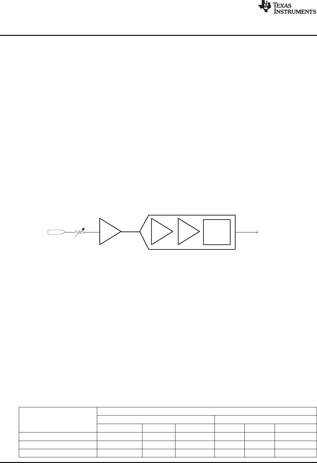
13. An AGC low-pass filter detects the average level of the input signal. This average level is compared
to the programmed detection levels in the AGC to provide the correct functionality. This low pass filter
is in the form of a first-order IIR filter. Three 8-bit registers form the 24-bit digital coefficient as shown
on the register map. A total of 9 registers are programmed to form the 3 IIR coefficients. The transfer
function of the filter implemented for signal level detection is given by
(2)
Where:
Coefficient N0 can be programmed by writing into Page 8, Register 12, 13 and 14.
Coefficient N1 can be programmed by writing into Page 8, Register 16, 17 and 18.
Coefficient D1 can be programmed by writing into Page 8, Register 20, 21 and 22.
N0, N1 and D1 are 24-bit 2’s complement numbers and their default values implement a low-pass
filter with cut-off at 0.002735*ADC_FS.
See Table 2-11 for various AGC programming options. AGC can be used only if analog microphone
input is routed to the ADC channel.
Table 2-11. AGC Parameter Settings
Function Control Register Control Register Bit
Left ADC Right ADC
AGC enable Page 0, Register 86 Page 0,Register 94 D(7)
Target Level Page 0, Register 86 Page 0, Register 94 D(6:4)
Gain Hysteresis Page 0, Register 86 Page 0, Register 94 D(1:0)
Hysteresis Page 0, Register 87 Page 0, Register 95 D(7:6)
Noise threshold Page 0, Register 87 Page 0, Register 95 D(5:1)
Max PGA applicable Page 0, Register 88 Page 0, Register 96 D(6:0)
Time constants (attack time) Page 0, Register 89 Page 0, Register 97 D(7:0)
Time constants(decay time) Page 0, Register 90 Page 0, Register 98 D(7:0)
Debounce time (Noise) Page 0, Register 91 Page 0, Register 99 D(4:0)
Debounce time (Signal) Page 0, Register 92 Page 0, Register 100 D(3:0)
Gain applied by AGC Page 0, Register 93 Page 0, Register 101 D(7:0) (Read Only)
21
SLAU306A–January 2011–Revised January 2013 TLV320AIC3256 Application
Submit Documentation Feedback
Copyright © 2011–2013, Texas Instruments Incorporated
DecayTime
Target
Level
Input
Signal
Output
Signal
AGC
Gain
Attack
Time
ADC
www.ti.com
Table 2-11. AGC Parameter Settings (continued)
Function Control Register Control Register Bit
Left ADC Right ADC
AGC Noise Threshold Flag Page 0, Register 45 (sticky flag), Page 0, Register 45 (sticky flag), D(6:5) (Read Only)
Page 0, Register 47 (non-sticky Page 0, Register 47 (non-sticky
flag) flag)
AGC Saturation flag Page 0, Register 36 (sticky flag) Page 0, Register 36 (sticky flag) D(5), D(1) (Read Only)
ADC Saturation flag Page 0, Register 42 (sticky flag), Page 0, Register 42 (sticky flag), D(3:2) (Read Only)
Page 0, Register 43 (non-sticky Page 0, Register 43 (non-sticky
flag) flag)
Figure 2-8. AGC Characteristics
2.3.3 ADC Decimation Filtering and Signal Processing Overview
The TLV320AIC3256 ADC channel includes a built-in digital decimation filter to process the oversampled
data from the to generate digital data at Nyquist sampling rate with high dynamic range. The decimation
filter can be chosen from three different types, depending on the required frequency response, group
delay and sampling rate.
ADC Processing Blocks
The TLV320AIC3256 offers a range of processing blocks which implement various signal processing
capabilities along with decimation filtering. These processing blocks give users the choice of how much
and what type of signal processing they may use and which decimation filter is applied.
The choice between these processing blocks is part of the PowerTune strategy to balance power
conservation and signal-processing flexibility. Less signal-processing capability reduces the power
consumed by the device. Table 2-12 gives an overview of the available processing blocks and their
properties. The Resource Class Column (RC) gives an approximate indication of power consumption.
The signal processing blocks available are:
• First-order IIR
• Scalable number of biquad filters
22 TLV320AIC3256 Application SLAU306A–January 2011–Revised January 2013
Submit Documentation Feedback
Copyright © 2011–2013, Texas Instruments Incorporated
To Audio
Interface
1stOrder
IIR
´
AGC
Gain
Compen-
sation
AGC
To Analog PGA
Filter A
From Delta-Sigma
Modulator
From Digital Vol. Ctrl
www.ti.com
ADC
• Variable-tap FIR filter
The processing blocks are tuned for common cases and can achieve high anti-alias filtering or low group
delay in combination with various signal processing effects such as audio effects and frequency shaping.
The available first order IIR, BiQuad and FIR filters have fully user-programmable coefficients. The
Resource Class Column (RC) gives an approximate indication of power consumption.
Table 2-12. ADC Processing Blocks
Processing Channel Decimation 1st Order Number FIR Required Resource
Blocks Filter IIR BiQuads AOSR Value Class
Available
PRB_R1(1) Stereo A Yes 0 No 128,64 6
PRB_R2 Stereo A Yes 5 No 128,64 8
PRB_R3 Stereo A Yes 0 25-Tap 128,64 8
PRB_R4 Right A Yes 0 No 128,64 3
PRB_R5 Right A Yes 5 No 128,64 4
PRB_R6 Right A Yes 0 25-Tap 128,64 4
PRB_R7 Stereo B Yes 0 No 64 3
PRB_R8 Stereo B Yes 3 No 64 4
PRB_R9 Stereo B Yes 0 20-Tap 64 4
PRB_R10 Right B Yes 0 No 64 2
PRB_R11 Right B Yes 3 No 64 2
PRB_R12 Right B Yes 0 20-Tap 64 2
PRB_R13 Stereo C Yes 0 No 32 3
PRB_R14 Stereo C Yes 5 No 32 4
PRB_R15 Stereo C Yes 0 25-Tap 32 4
PRB_R16 Right C Yes 0 No 32 2
PRB_R17 Right C Yes 5 No 32 2
PRB_R18 Right C Yes 0 25-Tap 32 2
(1) Default
2.3.3.1 Signal Processing Blocks – Details
2.3.3.1.1 First-Order IIR, AGC, Filter A
Figure 2-9. Signal Chain for PRB_R1 and PRB_R4
23
SLAU306A–January 2011–Revised January 2013 TLV320AIC3256 Application
Submit Documentation Feedback Copyright © 2011–2013, Texas Instruments Incorporated
1stOrder
IIR
AGC
Gain
Compen-
sation
AGC
Filter B HC
HB
HA
From Delta-Sigma
Modulator
To Analog PGA
To Audio
Interface
´
From Digital Vol. Ctrl
To Audio
Interface
1st Order
IIR
AGC
Gain
Compen-
sation
AGC
Filter B
To Audio
Interface
To Analog PGA
From Delta-Sigma
Modulator
´
From Digital Vol. Ctrl
1st Order
IIR
AGC
Gain
Compen-
sation
AGC
Filter A 25-Tap FIR
From Delta-Sigma
Modulator
To Analog PGA
To Audio
Interface
´
From Digital Vol. Ctrl
1stOrder
IIR
AGC
Gain
Compen-
sation
AGC
Filter A HE
HD
HC
HB
HA
To Audio
Interface
To Analog PGA
From Delta-Sigma
Modulator
´
From Digital Vol. Ctrl
ADC
www.ti.com
2.3.3.1.2 5 Biquads, First-Order IIR, AGC, Filter A
Figure 2-10. Signal Chain PRB_R2 and PRB_R5
2.3.3.1.3 25 Tap FIR, First-Order IIR, AGC, Filter A
Figure 2-11. Signal Chain for PRB_R3 and PRB_R6
2.3.3.1.4 First-Order IIR, AGC, Filter B
Figure 2-12. Signal Chain for PRB_R7 and PRB_R10
2.3.3.1.5 3 Biquads, First-Order IIR, AGC, Filter B
Figure 2-13. Signal Chain for PRB_R8 and PRB_R11
24 TLV320AIC3256 Application SLAU306A–January 2011–Revised January 2013
Submit Documentation Feedback
Copyright © 2011–2013, Texas Instruments Incorporated
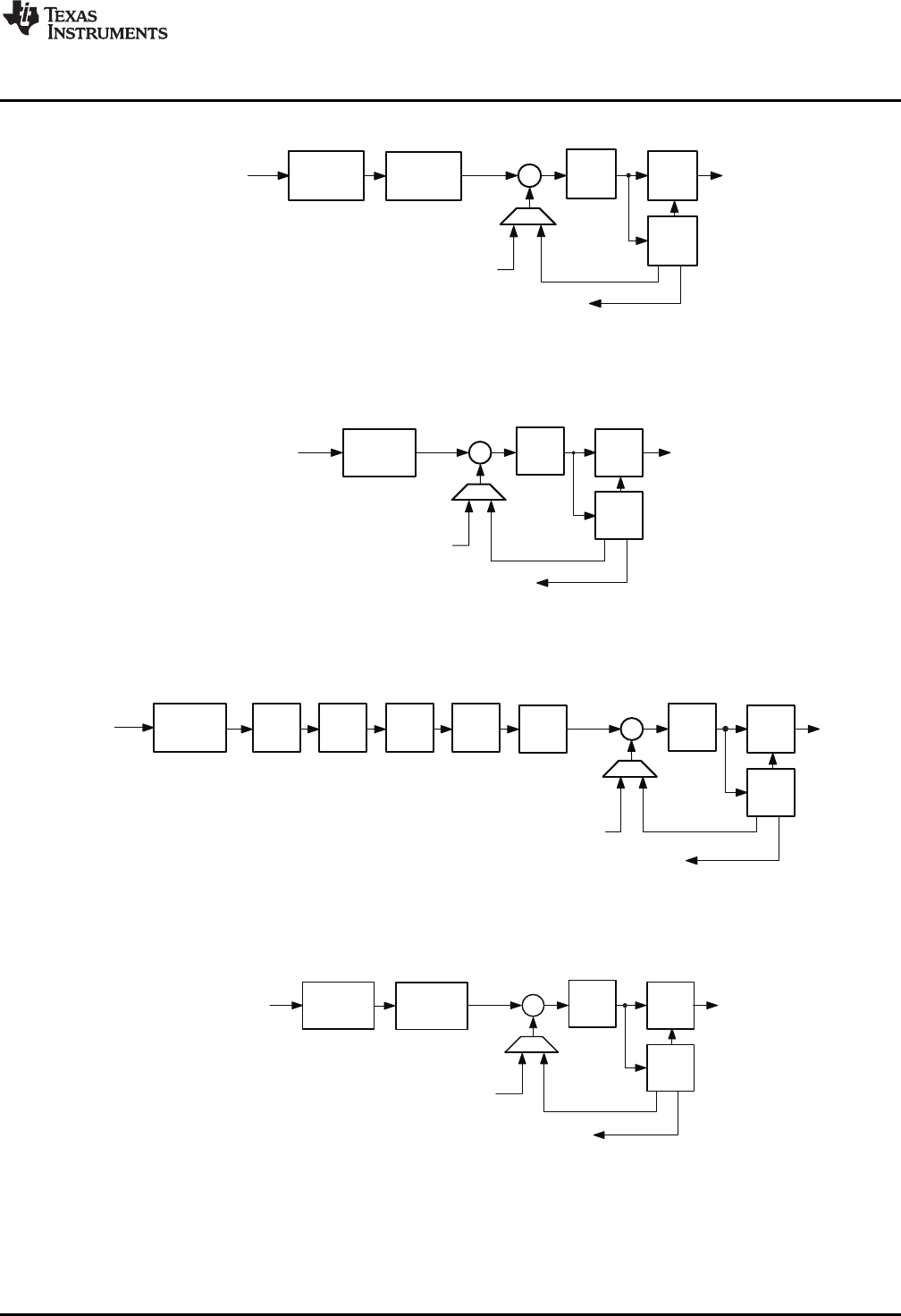
1st Order
IIR
AGC
Gain
Compen
sation
AGC
Filter C 25-Tap FIR
From Delta-Sigma
Modulator
From Digital Vol. Ctrl
To Analog PGA
To Audio
Interface
´
1st Order
IIR
AGC
Gain
Compen-
sation
AGC
Filter C HE
HD
HC
HB
HA
From Delta-Sigma
Modulator
From Digital Vol. Ctrl
To Analog PGA
To Audio
Interface
´
1st Order
IIR
AGC
Gain
Compen-
sation
AGC
Filter C
From Delta-Sigma
Modulator
From Digital Vol. Ctrl
To Analog PGA
To Audio
Interface
´
1st Order
IIR
AGC
Gain
Compen-
sation
AGC
Filter B 20-Tap FIR
From Delta-Sigma
Modulator
To Analog PGA
To Audio
Interface
´
From Digital Vol. Ctrl
www.ti.com
ADC
2.3.3.1.6 20 Tap FIR, First-Order IIR, AGC, Filter B
Figure 2-14. Signal Chain for PRB_R9 and PRB_R12
2.3.3.1.7 First-Order IIR, AGC, Filter C
Figure 2-15. Signal Chain for PRB_R13 and PRB_R16
2.3.3.1.8 5 Biquads, First-Order IIR, AGC, Filter C
Figure 2-16. Signal Chain for PRB_R14 and PRB_R17
2.3.3.1.9 25 Tap FIR, First-Order IIR, AGC, Filter C
Figure 2-17. Signal for PRB_R15 and PRB_R18
25
SLAU306A–January 2011–Revised January 2013 TLV320AIC3256 Application
Submit Documentation Feedback Copyright © 2011–2013, Texas Instruments Incorporated
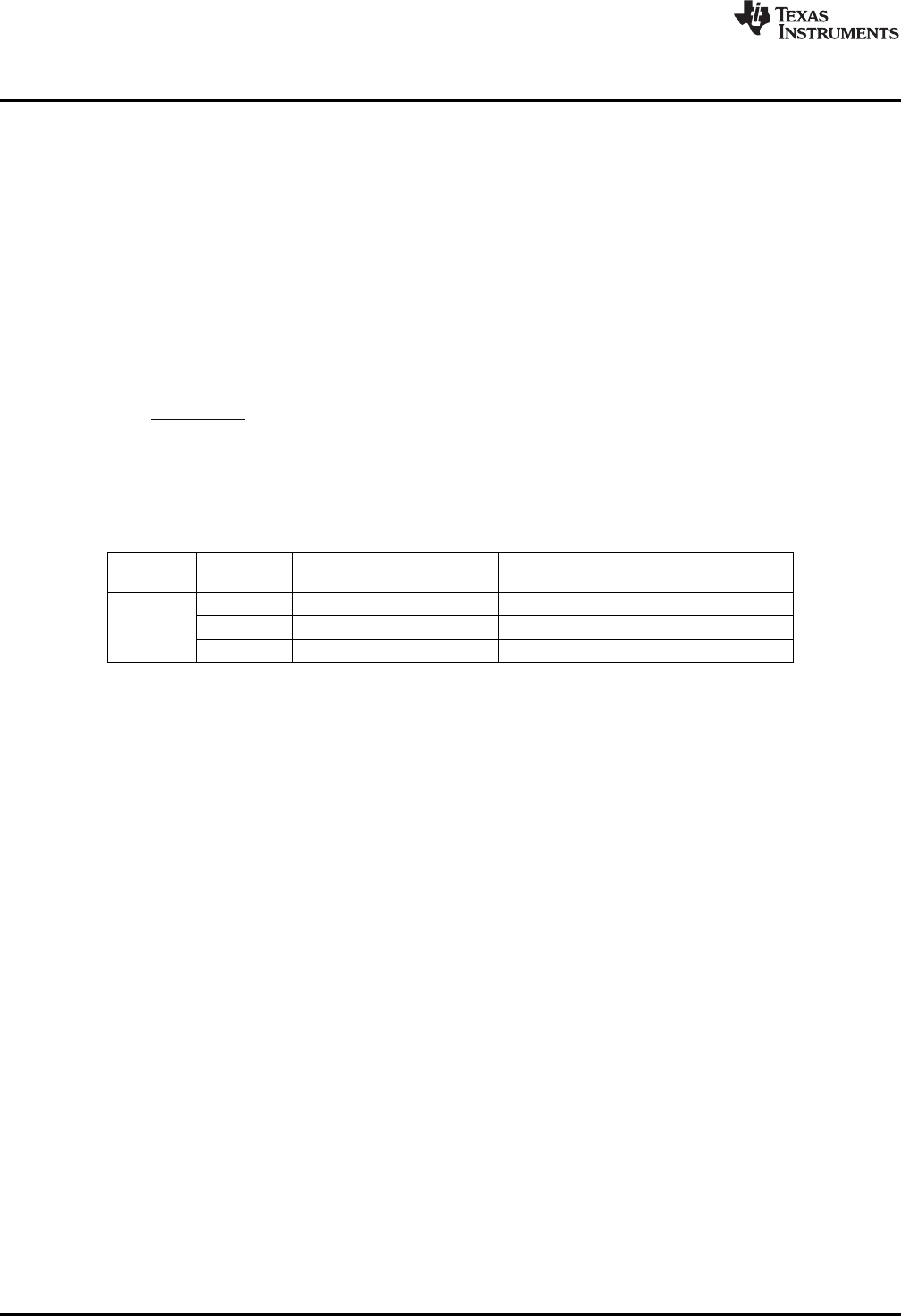
1
1
23
1
10
zD2
zNN
)z(H -
-
-
+
=
ADC
www.ti.com
2.3.3.1.10 User Programmable Filters
Depending on the selected processing block, different types and orders of digital filtering are available. A
first order IIR filter is always available, and is useful to efficiently filter out possible DC components of the
signal. Up to 5 biquad sections, or alternatively up to 25-tap FIR filters are available for specific processing
blocks. The coefficients of the available filters are arranged as sequentially indexed coefficients in two
banks. If adaptive filtering is chosen, the coefficient banks can be switched during operation without
disruption. For more details on adaptive filtering see Section 2.3.3.2.7 below.
The coefficients of these filters are each 24-bits wide, in two's-complement and occupy 3 consecutive 8-bit
registers in the register space. For default values please see Section 5.13.
2.3.3.1.10.1 First-Order IIR Section
The transfer function for the first order IIR Filter is given by
(3)
The frequency response for the first-order IIR Section with default coefficients is flat at a gain of 0dB.
Details on ADC coefficient default values are given in Section 5.13.
Table 2-13. ADC 1st order IIR Filter Coefficients
Filter FIlter ADC Coefficient Left ADC Coefficient Right Channel
Coefficient Channel
N0 C4 (Pg 8,Reg 24,25,26) C36 (Pg 9,Reg 32,33,34)
First Order N1 C5 (Pg 8,Reg 28,29,30) C37 (Pg 9,Reg 36,37,38)
IIR D1 C6 (Pg 8,Reg 32,33,34) C39 (Pg 9,Reg 40,41,42)
26 TLV320AIC3256 Application SLAU306A–January 2011–Revised January 2013
Submit Documentation Feedback
Copyright © 2011–2013, Texas Instruments Incorporated
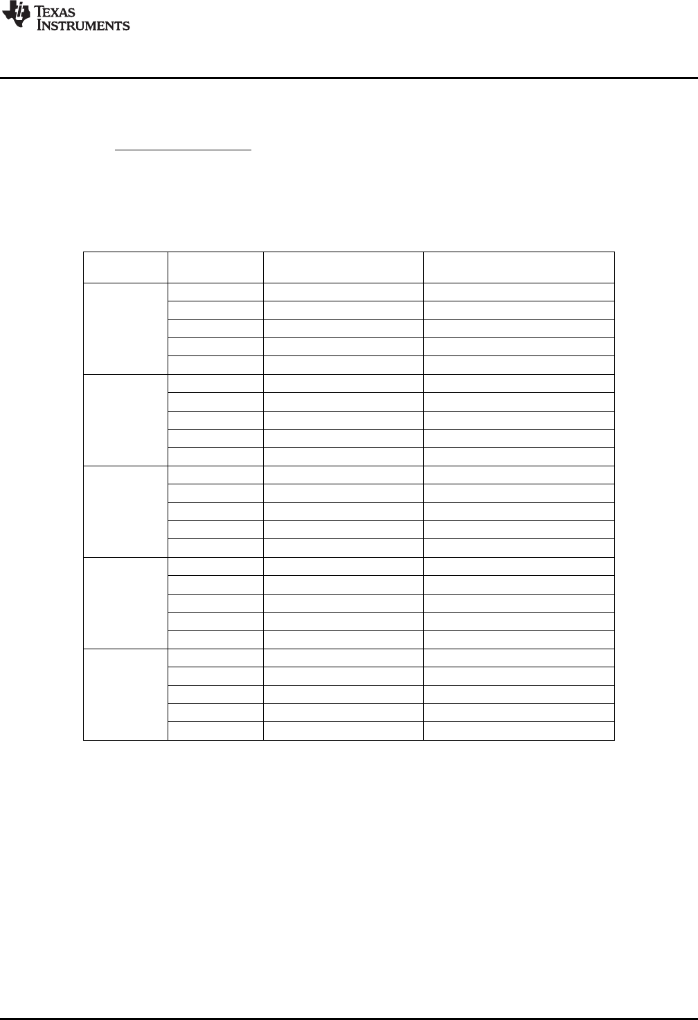
2
2
1
1
23
2
2
1
10
zDzD*22
zNzN*2N
)z(H --
--
--
++
=
www.ti.com
ADC
2.3.3.1.10.2 Biquad Section
The transfer function of each of the Biquad Filters is given by
(4)
The frequency response for each of the biquad section with default coefficients is flat at a gain of 0dB.
Details on ADC coefficient default values are given in Section 5.13.
Table 2-14. ADC Biquad Filter Coefficients
Filter FIlter ADC Coefficient Left ADC Coefficient Right Channel
Coefficient Channel
BIQUAD A N0 C7 (Pg 8, Reg 36,37,38) C39 (Pg 9, Reg 44,45,46)
N1 C8 (Pg 8, Reg 40,41,42) C40 (Pg 9, Reg 48,49,50)
N2 C9 (Pg 8, Reg 44,45,46) C41 (Pg 9, Reg 52,53,54)
D1 C10 (Pg 8, Reg 48,49,50) C42 (Pg 9, Reg 56,57,58)
D2 C11 (Pg 8, Reg 52,53,54) C43 (Pg 9, Reg 60,61,62)
BIQUAD B N0 C12 (Pg 8, Reg 56,57,58) C44 (Pg 9, Reg 64,65,66)
N1 C13 (Pg 8, Reg 60,61,62) C45 (Pg 9, Reg 68,69,70)
N2 C14 (Pg 8, Reg 64,65,66) C46 (Pg 9, Reg 72,73,74)
D1 C15 (Pg 8, Reg 68,69,70) C47 (Pg 9, Reg 76,77,78)
D2 C16 (Pg 8, Reg 72,73,74) C48 (Pg 9, Reg 80,81,82)
BIQUAD C N0 C17 (Pg 8, Reg 76,77,78) C49 (Pg 9, Reg 84,85,86)
N1 C18 (Pg 8, Reg 80,81,82) C50 (Pg 9, Reg 88,89,90)
N2 C19 (Pg 8, Reg 84,85,86) C51 (Pg 9, Reg 92,93,94)
D1 C20 (Pg 8, Reg 88,89,90) C52 (Pg 9, Reg 96,97,98)
D2 C21 (Pg 8, Reg 92,93,94) C53 (Pg 9, Reg 100,101,102)
BIQUAD D N0 C22 (Pg 8, Reg 96,97,98) C54 (Pg 9, Reg 104,105,106)
N1 C23 (Pg 8, Reg 100,101,102) C55 (Pg 9, Reg 108,109,110)
N2 C24 (Pg 8, Reg 104,105,106) C56 (Pg 9, Reg 112,113,114)
D1 C25 (Pg 8, Reg 108,109,110) C57 (Pg 9, Reg 116,117,118)
D2 C26 (Pg 8, Reg 112,113,114) C58 (Pg 9, Reg 120,121,122)
BIQUAD E N0 C27 (Pg 8, Reg 116,117,118) C59 (Pg 9, Reg 124,125,126)
N1 C28 (Pg 8, Reg 120,121,122) C60 (Pg 10, Reg 8,9,10)
N2 C29 (Pg 8, Reg 124,125,126) C61 (Pg 10, Reg 12,13,14)
D1 C30 (Pg 9, Reg 8,9,10) C62 (Pg 10, Reg 16,17,18)
D2 C31 (Pg 9, Reg 12,13,14) C63 (Pg 10, Reg 20,21,22)
27
SLAU306A–January 2011–Revised January 2013 TLV320AIC3256 Application
Submit Documentation Feedback Copyright © 2011–2013, Texas Instruments Incorporated
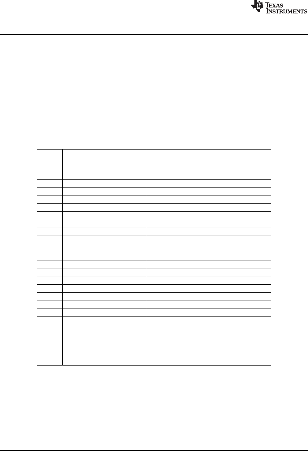
PRB_R12andPRB_R9for,19M
PRB_R18andPRB_R15PRB_R6,PRB_R3,for,24M
zFir)z(H
M
0n
n
n
=
=
=å
=
-
ADC
www.ti.com
2.3.3.1.10.3 FIR Section
Six of the available ADC processing blocks offer FIR filters for signal processing. PRB_R9 and PRB_R12
feature a 20-tap FIR filter while the processing blocks PRB_R3, PRB_R6, PRB_R15 and PRB_R18
feature a 25-tap FIR filter.
(5)
The coefficients of the FIR filters are 24-bit 2’s complement format and correspond to the ADC coefficient
space as listed below. There is no default transfer function for the FIR filter. When the FIR filter gets used
all applicable coefficients must be programmed.
Table 2-15. ADC FIR Filter Coefficients
Filter FIlter Coefficient Left ADC Filter Coefficient Right ADC Channel
Channel
Fir0 C7 (Pg 8, Reg 36,37,38) C39 (Pg 9, Reg 44,45,46)
Fir1 C8 (Pg 8, Reg 40,41,42) C40 (Pg 9, Reg 48,49,50)
Fir2 C9 (Pg 8, Reg 44,45,46) C41 (Pg 9, Reg 52,53,54)
Fir3 C10 (Pg 8, Reg 48,49,50) C42 (Pg 9, Reg 56,57,58)
Fir4 C11 (Pg 8, Reg 52,53,54) C43 (Pg 9, Reg 60,61,62)
Fir5 C12 (Pg 8, Reg 56,57,58) C44 (Pg 9, Reg 64,65,66)
Fir6 C13 (Pg 8, Reg 60,61,62) C45 (Pg 9, Reg 68,69,70)
Fir7 C14 (Pg 8, Reg 64,65,66) C46 (Pg 9, Reg 72,73,74)
Fir8 C15 (Pg 8, Reg 68,69,70) C47 (Pg 9, Reg 76,77,78)
Fir9 C16 (Pg 8, Reg 72,73,74) C48 (Pg 9, Reg 80,81,82)
Fir10 C17 (Pg 8, Reg 76,77,78) C49 (Pg 9, Reg 84,85,86)
Fir11 C18 (Pg 8, Reg 80,81,82) C50 (Pg 9, Reg 88,89,90)
Fir12 C19 (Pg 8, Reg 84,85,86) C51 (Pg 9, Reg 92,93,94)
Fir13 C20 (Pg 8, Reg 88,89,90) C52 (Pg 9, Reg 96,97,98)
Fir14 C21 (Pg 8, Reg 92,93,94) C53 (Pg 9, Reg 100,101,102)
Fir15 C22 (Pg 8, Reg 96,97,98) C54 (Pg 9, Reg 104,105,106)
Fir16 C23 (Pg 8, Reg 100,101,102) C55 (Pg 9, Reg 108,109,110)
Fir17 C24 (Pg 8, Reg 104,105,106) C56 (Pg 9, Reg 112,113,114)
Fir18 C25 (Pg 8, Reg 108,109,110) C57 (Pg 9, Reg 116,117,118)
Fir19 C26 (Pg 8, Reg 112,113,114) C58 (Pg 9, Reg 120,121,122)
Fir20 C27 (Pg 8, Reg 116,117,118) C59 (Pg 9, Reg 124,125,126)
Fir21 C28 (Pg 8, Reg 120,121,122) C60 (Pg 10, Reg 8,9,10)
Fir22 C29 (Pg 8, Reg 124,125,126) C61 (Pg 10, Reg 12,13,14)
Fir23 C30 (Pg 9, Reg 8,9,10) C62 (Pg 10, Reg 16,17,18)
Fir24 C31 (Pg 9, Reg 12,13,14) C63 (Pg 10, Reg 20,21,22)
28 TLV320AIC3256 Application SLAU306A–January 2011–Revised January 2013
Submit Documentation Feedback
Copyright © 2011–2013, Texas Instruments Incorporated
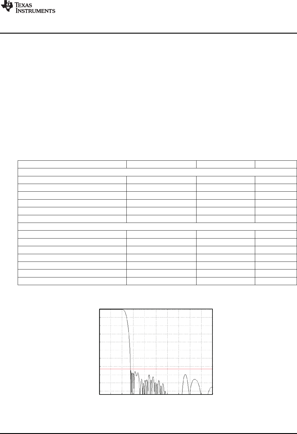
0
–10
–20
–30
–40
–50
–60
–70
–80
–90
–100
0.0 0.2 0.4 0.6 0.8 1.0 1.2 1.4 1.6 1.8 2.0
FrequencyNormalizedtofS
Magnitude – dB
ADCChannelResponseforDecimationFilter A
(Redlinecorrespondsto –73dB)
G013
www.ti.com
ADC
2.3.3.1.11 Decimation Filter
The TLV320AIC3256 offers 3 different types of decimation filters. The integrated digital decimation filter
removes high-frequency content and down samples the audio data from an initial sampling rate of AOSR *
fSto the final output sampling rate of fS. The decimation filtering is achieved using a higher-order CIC filter
followed by linear-phase FIR filters. The decimation filter cannot be chosen by itself, it is implicitly set
through the chosen processing block.
The following subsections describe the properties of the available filters A, B and C.
2.3.3.1.11.1 Decimation Filter A
This filter is intended for use at sampling rates up to 48kHz. When configuring this filter, the oversampling
ratio of the ADC can either be 128 or 64. For highest performance the oversampling ratio must be set to
128. Please also see the PowerTune chapter for details on performance and power in dependency of
AOSR.
Filter A can also be used for 96kHz at an AOSR of 64.
Table 2-16. ADC Decimation Filter A, Specification
Parameter Condition Value (Typical) Units
AOSR = 128
Filter Gain Pass Band 0…0.39fS0.062 dB
Filter Gain Stop Band 0.55…64fS–73 dB
Filter Group Delay 17 / fSSec.
Pass Band Ripple, 8 ksps 0…0.39fS0.062 dB
Pass Band Ripple, 44.1 ksps 0…0.39fS0.05 dB
Pass Band Ripple, 48 ksps 0…0.39fS0.05 dB
AOSR = 64
Filter Gain Pass Band 0…0.39fS0.062 dB
Filter Gain Stop Band 0.55…32fS–73 dB
Filter Group Delay 17 / fSSec.
Pass Band Ripple, 8 ksps 0…0.39fS0.062 dB
Pass Band Ripple, 44.1 ksps 0…0.39fS0.05 dB
Pass Band Ripple, 48 ksps 0…0.39fS0.05 dB
Pass Band Ripple, 96 ksps 0…20kHz 0.1 dB
Figure 2-18. ADC Decimation Filter A, Frequency Response
29
SLAU306A–January 2011–Revised January 2013 TLV320AIC3256 Application
Submit Documentation Feedback Copyright © 2011–2013, Texas Instruments Incorporated
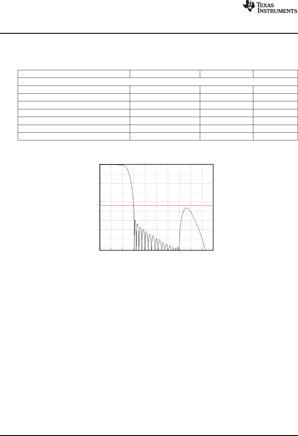
0
–10
–20
–30
–40
–50
–60
–70
–80
–90
0.0 0.2 0.4 0.6 0.8 1.0 1.2 1.4 1.6 1.8 2.0
FrequencyNormalizedtofS
Magnitude – dB
ADCChannelResponseforDecimationFilterB
(Redlinecorrespondsto –44dB)
G014
ADC
www.ti.com
2.3.3.1.11.2 Decimation Filter B
Filter B is intended to support sampling rates up to 96kHz at a oversampling ratio of 64.
Table 2-17. ADC Decimation Filter B, Specifications
Parameter Condition Value (Typical) Units
AOSR = 64
Filter Gain Pass Band 0…0.39fS±0.077 dB
Filter Gain Stop Band 0.60…32fS–46 dB
Filter Group Delay 11 / fSSec.
Pass Band Ripple, 8 ksps 0…0.39fS0.076 dB
Pass Band Ripple, 44.1 ksps 0…0.39fS0.06 dB
Pass Band Ripple, 48 ksps 0…0.39fS0.06 dB
Pass Band Ripple, 96 ksps 0…20kHz 0.11 dB
Figure 2-19. ADC Decimation Filter B, Frequency Response
30 TLV320AIC3256 Application SLAU306A–January 2011–Revised January 2013
Submit Documentation Feedback
Copyright © 2011–2013, Texas Instruments Incorporated
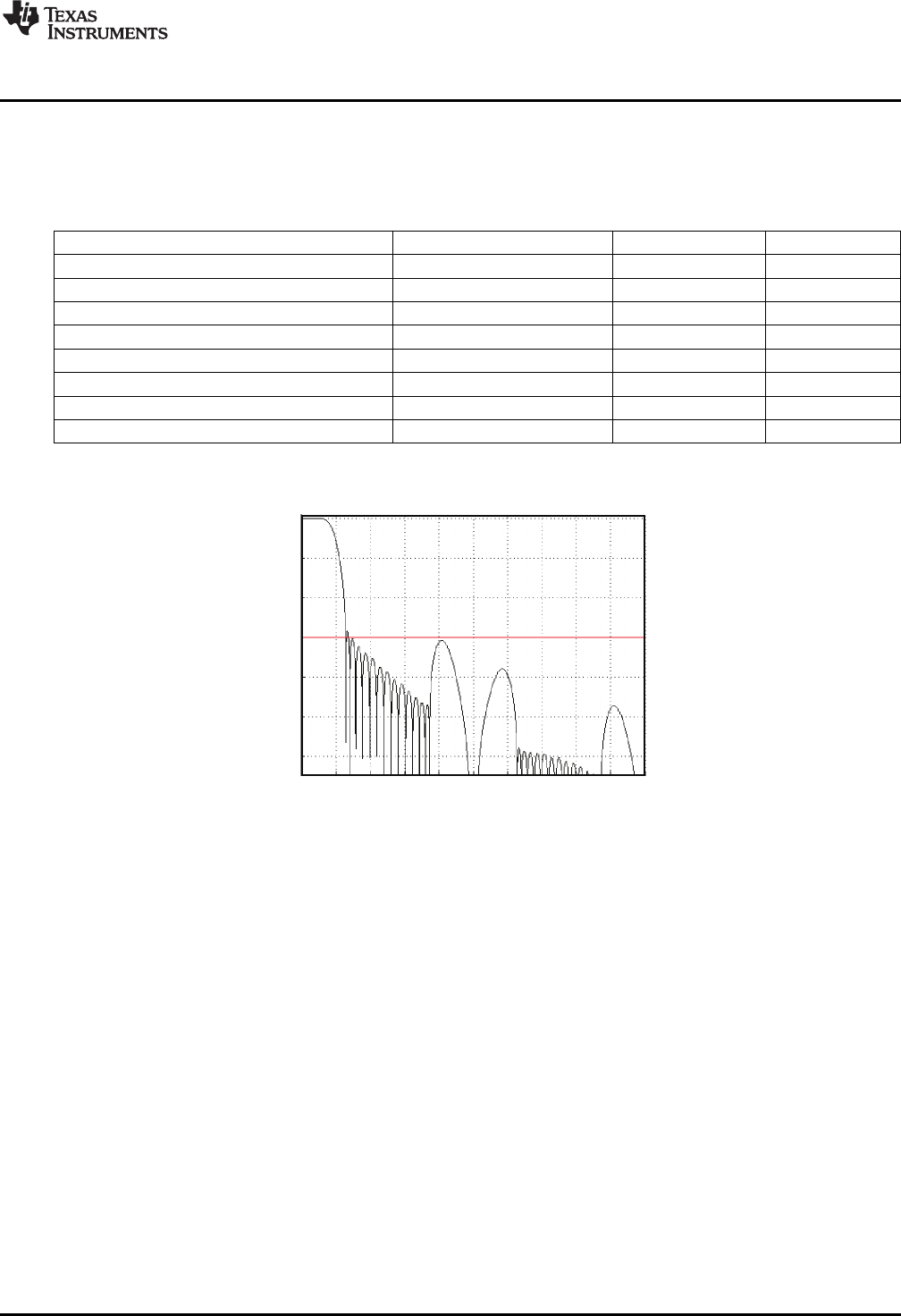
ADCChannelResponseforDecimationFilterC
(Redlinecorrespondsto –60dB)
0
–20
–40
–60
–100
–80
–120
0.0 0.2 0.4 0.6 0.8 1.0 1.2 1.4 1.6 1.8 2.0
FrequencyNormalizedtofS
Magnitude – dB
G015
www.ti.com
ADC
2.3.3.1.11.3 Decimation Filter C
Filter type C along with AOSR of 32 is specially designed for 192ksps operation for the ADC. The pass
band which extends up to 0.11 * fS( corresponds to 21kHz), is suited for audio applications.
Table 2-18. ADC Decimation Filter C, Specifications
Parameter Condition Value (Typical) Units
Filter Gain from 0 to 0.11fS0…0.11fS±0.033 dB
Filter Gain from 0.28 to 16fS0.28…16fS–60 dB
Filter Group Delay 11 / fSSec.
Pass Band Ripple, 8 ksps 0…0.11fS0.033 dB
Pass Band Ripple, 44.1 ksps 0…0.11fS0.033 dB
Pass Band Ripple, 48 ksps 0…0.11fS0.032 dB
Pass Band Ripple, 96 ksps 0…0.11fS0.032 dB
Pass Band Ripple, 192 ksps 0…20kHz 0.086 dB
Figure 2-20. ADC Decimation Filter C, Frequency Response
2.3.3.1.12 ADC Data Interface
The decimation filter and signal processing block in the ADC channel passes 32-bit data words to the
audio serial interface once every cycle of fS,ADC. During each cycle of fS,ADC, a pair of data words (for
left and right channel) are passed. The audio serial interface rounds the data to the required word length
of the interface before converting to serial data as per the different modes for audio serial interface.
31
SLAU306A–January 2011–Revised January 2013 TLV320AIC3256 Application
Submit Documentation Feedback Copyright © 2011–2013, Texas Instruments Incorporated
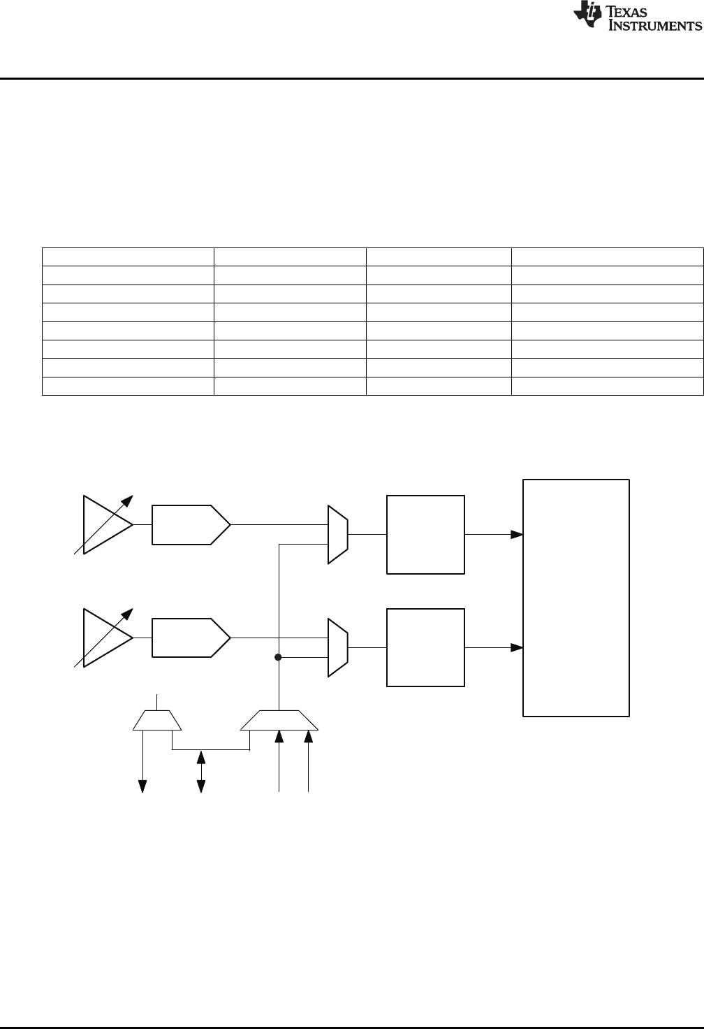
LEFT ADC
CICFILTER
RIGHT ADC
CICFILTER
Signal
Processing
Blocks
GPIOMISO DIN SCLK
Σ-Δ
Σ-Δ
ADC_MOD_CLK
DIG_MIC_IN
ADC
www.ti.com
2.3.3.2 ADC Special Functions
2.3.3.2.1 Microphone Bias
The built-in low noise Microphone Bias amplifier for electret-condenser microphones supports up to 3mA
of load current to support multiple microphones. The bias amplifier provides a combination of high PSRR,
low noise and programmable bias voltages to allow the user to fine tune the biasing to specific
microphone combinations. The bias amplifier operates from AVDD.
Table 2-19. MICBIAS Voltage Control
Page 1, Reg 51, D(5:4) Page 1, Reg 10, D6 Page 1, Reg 51, D(3) MICBIAS Voltage (without load)
00 0 X 1.25V
00 1 X 1.0V
01 0 X 1.7V
01 1 X 1.4V
10 0 1 2.5V
10 1 1 2.1V
11 X 0 AVdd
2.3.3.2.2 Digital Microphone Function
In addition to supporting analog microphones, the TLV320AIC3256 also interfaces to digital microphones.
Figure 2-21. Digital Microphone in TLV320AIC3256
The TLV320AIC3256 outputs internal clock ADC_MOD_CLK on GPIO pin (Page 0, Register 51, D(5:2)) or
MISO pin (Page 0, Register 55, D(4:1)). This clock can be connected to the external digital microphone
device. The single-bit output of the external digital microphone device can be connected to GPIO, DIN or
SCLK pins. Internally the TLV320AIC3256 latches the steady value of data on the rising edge of
ADC_MOD_CLK for the Left ADC channel, and the steady value of data on falling edge for the Right ADC
channel.
32 TLV320AIC3256 Application SLAU306A–January 2011–Revised January 2013
Submit Documentation Feedback
Copyright © 2011–2013, Texas Instruments Incorporated
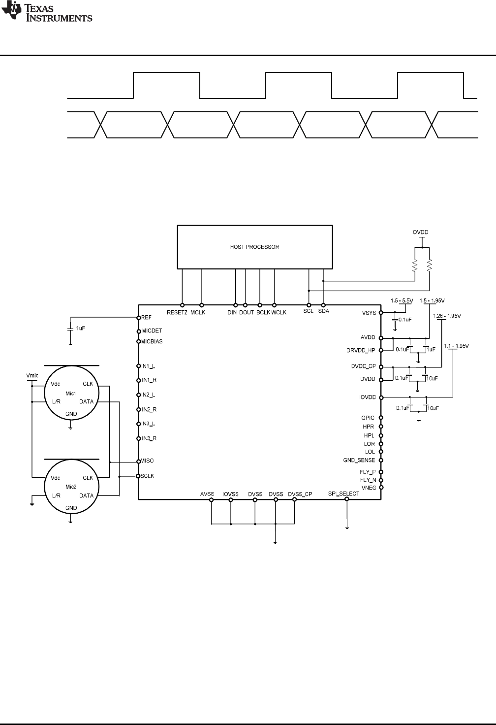
LEFT RIGHT LEFT RIGHT LEFT RIGHT
ADC_MOD_CLK
DIG_MIC_IN
www.ti.com
ADC
Figure 2-22. Timing Diagram for Digital Microphone Interface
The digital-microphone mode can be selectively enabled for only-left, only-right, or stereo channels. When
the digital microphone mode is enabled, the analog section of the ADC can be powered down and
bypassed for power efficiency. The AOSR value for the ADC channel must be configured to select the
desired decimation ratio to be achieved based on the external digital microphone properties.
Figure 2-23. Typical Digital Microphone External Circuitry
33
SLAU306A–January 2011–Revised January 2013 TLV320AIC3256 Application
Submit Documentation Feedback Copyright © 2011–2013, Texas Instruments Incorporated
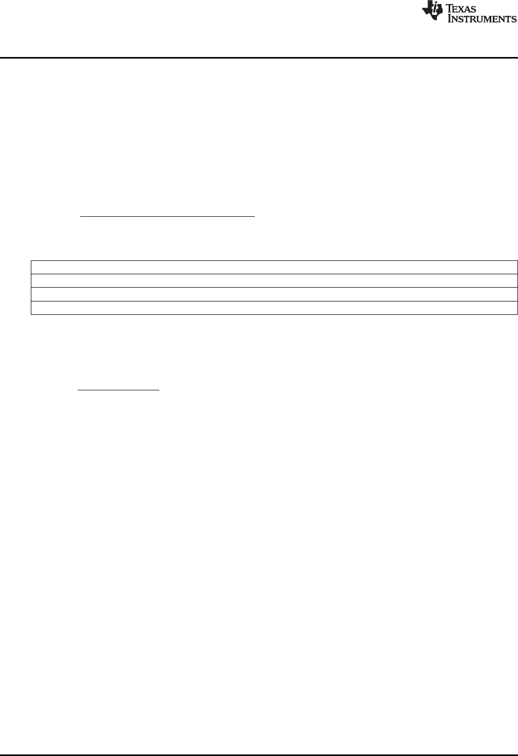
FS_ADC*AOSR
)7(Delay
tpl =
)tt(OUT_ADC_LEFT)t(COMP_PHASE_ADC_LEFT pl
-=
( )
FS_ADC*AOSR
k*AOSR*)5:6(Delay)0:4(Delay
tf
pr
+
=
)tt(OUT_ADC_RIGHT)t(COMP_PHASE_ADC_RIGHT pr
-=
ADC
www.ti.com
2.3.3.2.3 Channel-to-Channel Phase Adjustment
The TLV320AIC3256 has a built-in feature to fine-adjust the phase between the stereo ADC record
signals. The phase compensation is particularly helpful in applications such as adjusting delays when
using dual microphones for noise cancellation. This delay is controlled in fine amounts in the following
fashion.
Delay(7:0) = Page 0, Register 85, D(7:0)
Where
(6)
where
(7)
Where kfis a function of the decimation filter:
Decimation Filter Type kf
A 0.25
B 0.5
C 1
and
(8)
Where
(9)
34 TLV320AIC3256 Application SLAU306A–January 2011–Revised January 2013
Submit Documentation Feedback
Copyright © 2011–2013, Texas Instruments Incorporated
www.ti.com
ADC
2.3.3.2.4 DC Measurement
The TLV320AIC3256 supports a highly flexible DC measurement feature using the high resolution
oversampling and noise-shaping ADC. This mode can be used when the particular ADC channel is not
used for the voice or audio-record function. This mode can be enabled by programming Page 0, Register
102, D(7:6). The converted data is 24-bits, using 2.22 numbering format. The value of the converted data
for the left-channel ADC can be read back from Page 0, Register 104-106 and for the right-channel ADC
from Page 0, Register 107-109. Before reading back the converted data, Page 0, Register 103, D(6) must
be programmed to latch the converted data into the read-back register. After the converted data is read
back, Page 0, Register 103, D(6) must be reset to 0 immediately. In DC measurement mode, two
measurement methods are supported.
Mode A
In DC-measurement mode A, a variable-length averaging filter is used. The length of the averaging filter
D, can be programmed from 1 to 20 by programming Page 0, Register 102, D(4:0). To choose mode A,
Page 0, Register 102, D(5) must be programmed to 0.
Mode B
To choose mode B Page 0, Register 102, D(5) must be programmed to 1. In DC-measurement mode B, a
first-order IIR filter is used. The coefficients of this filter are determined by D, Page 0, Register 102,
D(4:0). The nature of the filter is given in the table below
Table 2-20. DC Measurement Bandwidth Settings
D: Page 0, Reg 102 , D(4:0) –3 dB BW (kHz) –0.5 dB BW (kHz)
1 688.44 236.5
2 275.97 96.334
3 127.4 44.579
4 61.505 21.532
5 30.248 10.59
6 15.004 5.253
7 7.472 2.616
8 3.729 1.305
9 1.862 652
10 931 326
11 465 163
12 232.6 81.5
13 116.3 40.7
14 58.1 20.3
15 29.1 10.2
16 14.54 5.09
17 7.25 2.54
18 3.63 1.27
19 1.8 0.635
20 0.908 0.3165
35
SLAU306A–January 2011–Revised January 2013 TLV320AIC3256 Application
Submit Documentation Feedback Copyright © 2011–2013, Texas Instruments Incorporated

ADC
www.ti.com
By programming Page 0, Reg 103, D(5) to ‘1’, the averaging filter is periodically reset after 2Rnumber of
ADC_MOD_CLK, where R is programmed in Page 0, Reg 103, D(4:0). When Page 0, Reg 103, D(5) is set
to 1 then the value of D should be less than the value of R. When Page 0, Reg 103, D(5) is programmed
as 0 the averaging filter is never reset.
2.3.3.2.5 Fast Charging AC Capacitors
The value of the coupling capacitor must be so chosen that the high-pass filter formed by the coupling
capacitor and the input impedance do not affect the signal content. At power-up, before proper recording
can begin, this coupling capacitor must be charged up to the common-mode voltage. To enable quick
charging, the TLV320AIC3256 has modes to speed up the charging of the coupling capacitor. These
modes are controlled through Page 1, Register 71, D(5:0).
2.3.3.2.6 Anti Thump
For normal voice or audio recording, the analog input pins of the TLV320AIC3256, must be AC-coupled to
isolate the DC-common mode voltage of the driving circuit from the common-mode voltage of the
TLV320AIC3256.
When the analog inputs are not selected for any routing, the input pins are tri-stated and the voltage on
the pins is undefined. When the unselected inputs are selected for any routing, the input pins must charge
from the undefined voltage to the input common-mode voltage. This charging signal can cause audible
artifacts. In order to avoid such artifacts the TLV320AIC3256 also incorporates anti-thump circuitry to allow
connection of unused inputs to the common-mode level. This feature is disabled by default, and can be
enabled by writing the appropriate value into Page 1, Register 58, D(7:2). The use of this feature in
combination with the PTM_R1 setting in Page 0, Register 61 when the ADC channel is powered down
causes the additional current consumption of 700μA from AVdd and 125μA from DVdd in the sleep mode.
36 TLV320AIC3256 Application SLAU306A–January 2011–Revised January 2013
Submit Documentation Feedback
Copyright © 2011–2013, Texas Instruments Incorporated
www.ti.com
ADC
2.3.3.2.7 Adaptive Filtering
After the ADC is running, the filter coefficients are locked and cannot be accessed for read or write.
However the TLV320AIC3256 offers an adaptive filter mode as well. Setting Register Page 8,Reg 1, D(2)
= 1 turns on double buffering of the coefficients. In this mode filter coefficients can be updated through the
host and activated without stopping and restarting the ADC, enabling advanced adaptive filtering
applications.
To support double buffering, all coefficients are stored in two buffers (Buffer A and B). When the ADC is
running and adaptive filtering mode is turned on, setting the control bit Page 8, Reg 1,D(0) = 1 switches
the coefficient buffers at the next start of a sampling period. The bit reverts to 0 after the switch occurs. At
the same time, the flag Page 8, Reg 1, D(1) toggles.
The flag in Page 8, Reg 1, D(1) indicates which of the two buffers is actually in use.
Page 8, Reg 1, D(1) = 0: Buffer A is in use by the ADC engine, D(1) = 1: Buffer B is in use.
While the device is running, coefficient updates are always made to the buffer not in use by the ADC,
regardless to which buffer the coefficients have been written
ADC running Flag, Page 8, Reg 1, D(1) Coefficient Buffer in use Writing to Will update
No 0 None C4, Buffer A C4, Buffer A
No 0 None C4, Buffer B C4, Buffer B
Yes 0 Buffer A C4, Buffer A C4, Buffer B
Yes 0 Buffer A C4, Buffer B C4, Buffer B
Yes 1 Buffer B C4, Buffer A C4, Buffer A
Yes 1 Buffer B C4, Buffer B C4, Buffer A
37
SLAU306A–January 2011–Revised January 2013 TLV320AIC3256 Application
Submit Documentation Feedback Copyright © 2011–2013, Texas Instruments Incorporated

ADC
www.ti.com
2.3.3.3 ADC Setup
The following discussion is intended to guide a system designer through the steps necessary to configure
the TLV320AIC3256 ADC.
Step 1
The system clock source (master clock) and the targeted ADC sampling frequency must be identified.
The oversampling ratio (OSR) of the TLV320AIC3256 must be configured to match the properties of the
digital microphone.
Based on the identified filter type and the required signal processing capabilities the appropriate
processing block can be determined from the list of available processing blocks (PRB_R1 to PRB_R18)
(See Table 2-12).
Based on the available master clock, the chosen OSR and the targeted sampling rate, the clock divider
values NADC and MADC can be determined. If necessary the internal PLL will add a large degree of
flexibility.
In summary, Codec_Clkin which is either derived directly from the system clock source or from the internal
PLL, divided by MADC, NADC and AOSR, must be equal to the ADC sampling rate ADC_or fS. The
codec_clkin clock signal is shared with the DAC clock generation block.
CODEC_CLKIN = NADC * MADC * AOSR * ADC_FS
To a large degree NADC and MADC can be chosen independently in the range of 1 to 128. In general
NADC should be as large as possible as long as the following condition can still be met:
MADC * AOSR / 32 ≥RC
RC is a function of the chosen processing block, and is listed in Table 2-12.
The common mode setting of the device is determined by the available analog power supply and the
desired PowerTune mode; this common mode setting is shared across ADC, DAC (input common mode)
and analog bypass path.
At this point the following device specific parameters are known:
PRB_Rx, AOSR, NADC, MADC, common mode setting
Additionally if the PLL is used the PLL parameters P, J, D and R are determined as well.
Step 2
Setting up the device via register programming:
The following list gives a sequence of items that must be executed between powering up the device and
reading data from the device:
Define starting point: Set register page to 0
Initiate SW Reset
Program Clock Settings Program PLL clock dividers P,J,D,R (if PLL is necessary)
Power up PLL (if PLL is necessary)
Program and power up NADC
Program and power up MADC
Program OSR value
Program the processing block to be used
At this point, at the latest, the analog power supply must be applied to the device
38 TLV320AIC3256 Application SLAU306A–January 2011–Revised January 2013
Submit Documentation Feedback
Copyright © 2011–2013, Texas Instruments Incorporated

www.ti.com
DAC
Program Analog Blocks Set register Page to 1
Disable coarse AVdd generation
Enable Master Analog Power Control
Program Common Mode voltage
Program PowerTune (PTM) mode
Program MicPGA startup delay
Program Reference fast charging
Routing of inputs and common mode to ADC input
Unmute analog PGAs and set analog gain
Power Up ADC Set register Page to 0
Power up ADC Channels
Unmute digital volume control
A detailed example can be found in Chapter 4.
2.4 DAC
The TLV320AIC3256 includes a stereo audio DAC supporting data rates from 8kHz to 192kHz. Each
channel of the stereo audio DAC consists of a signal-processing engine with fixed processing blocks, a
programmable miniDSP, a digital interpolation filter, multi-bit digital delta-sigma modulator, and an analog
reconstruction filter. The DAC is designed to provide enhanced performance at low sampling rates through
increased oversampling and image filtering, thereby keeping quantization noise generated within the delta-
sigma modulator and signal images strongly suppressed within the audio band to beyond 20kHz. To
handle multiple input rates and optimize power dissipation and performance, the TLV320AIC3256 allows
the system designer to program the oversampling rates over a wide range from 1 to 1024. The system
designer can choose higher oversampling ratios for lower input data rates and lower oversampling ratios
for higher input data rates.
The TLV320AIC3256 DAC channel includes a built-in digital interpolation filter to generate oversampled
data for the sigma-delta modulator. The interpolation filter can be chosen from three different types
depending on required frequency response, group delay and sampling rate.
The DAC path of the TLV320AIC3256 features many options for signal conditioning and signal routing:
• 2 headphone amplifiers
– Ground-centered, bipolar operation or unipolar operation
– Usable in single-ended or differential mode
– Analog volume setting with a range of -6 to +14dB
• 2 line-out amplifiers
– Usable in single-ended or differential mode
– Analog volume setting with a range of -6 to +29dB
• Digital volume control with a range of -63.5 to +24dB
• Mute function
• Dynamic range compression (DRC)
In addition to the standard set of DAC features the TLV320AIC3256 also offers the following special
features:
• Built in sine wave generation (beep generator)
• Digital auto mute
• Adaptive filter mode
The TLV320AIC3256 implements signal processing capabilities and interpolation filtering via processing
blocks. These fixed processing blocks give users the choice of how much and what type of signal
processing they may use and which interpolation filter is applied.
39
SLAU306A–January 2011–Revised January 2013 TLV320AIC3256 Application
Submit Documentation Feedback Copyright © 2011–2013, Texas Instruments Incorporated
DAC
www.ti.com
The choice between these processing blocks is part of the PowerTune strategy balancing power
conservation and signal processing flexibility. Less signal processing capability will result in less power
consumed by the device. Table 2-21 gives an overview over all available processing blocks of the DAC
channel and their properties. The Resource Class Column (RC) gives an approximate indication of power
consumption.
The signal processing blocks available are:
• First-order IIR
• Scalable number of biquad filters
• 3D – Effect
• Beep Generator
The processing blocks are tuned for typical cases and can achieve high image rejection or low group
delay in combination with various signal processing effects such as audio effects and frequency shaping.
The available first-order IIR and biquad filters have fully user-programmable coefficients. The Resource
Class Column (RC) gives an approximate indication of power consumption.
Table 2-21. Overview – DAC Predefined Processing Blocks
Processing Interpolation Channel 1st Order Num. of DRC 3D Beep Resource
Block No. Filter IIR Available Biquads Generator Class
PRB_P1(1) A Stereo No 3 No No No 8
PRB_P2 A Stereo Yes 6 Yes No No 12
PRB_P3 A Stereo Yes 6 No No No 10
PRB_P4 A Left No 3 No No No 4
PRB_P5 A Left Yes 6 Yes No No 6
PRB_P6 A Left Yes 6 No No No 6
PRB_P7 B Stereo Yes 0 No No No 6
PRB_P8 B Stereo No 4 Yes No No 8
PRB_P9 B Stereo No 4 No No No 8
PRB_P10 B Stereo Yes 6 Yes No No 10
PRB_P11 B Stereo Yes 6 No No No 8
PRB_P12 B Left Yes 0 No No No 3
PRB_P13 B Left No 4 Yes No No 4
PRB_P14 B Left No 4 No No No 4
PRB_P15 B Left Yes 6 Yes No No 6
PRB_P16 B Left Yes 6 No No No 4
PRB_P17 C Stereo Yes 0 No No No 3
PRB_P18 C Stereo Yes 4 Yes No No 6
PRB_P19 C Stereo Yes 4 No No No 4
PRB_P20 C Left Yes 0 No No No 2
PRB_P21 C Left Yes 4 Yes No No 3
PRB_P22 C Left Yes 4 No No No 2
PRB_P23 A Stereo No 2 No Yes No 8
PRB_P24 A Stereo Yes 5 Yes Yes No 12
PRB_P25 A Stereo Yes 5 Yes Yes Yes 12
(1) Default
40 TLV320AIC3256 Application SLAU306A–January 2011–Revised January 2013
Submit Documentation Feedback
Copyright © 2011–2013, Texas Instruments Incorporated
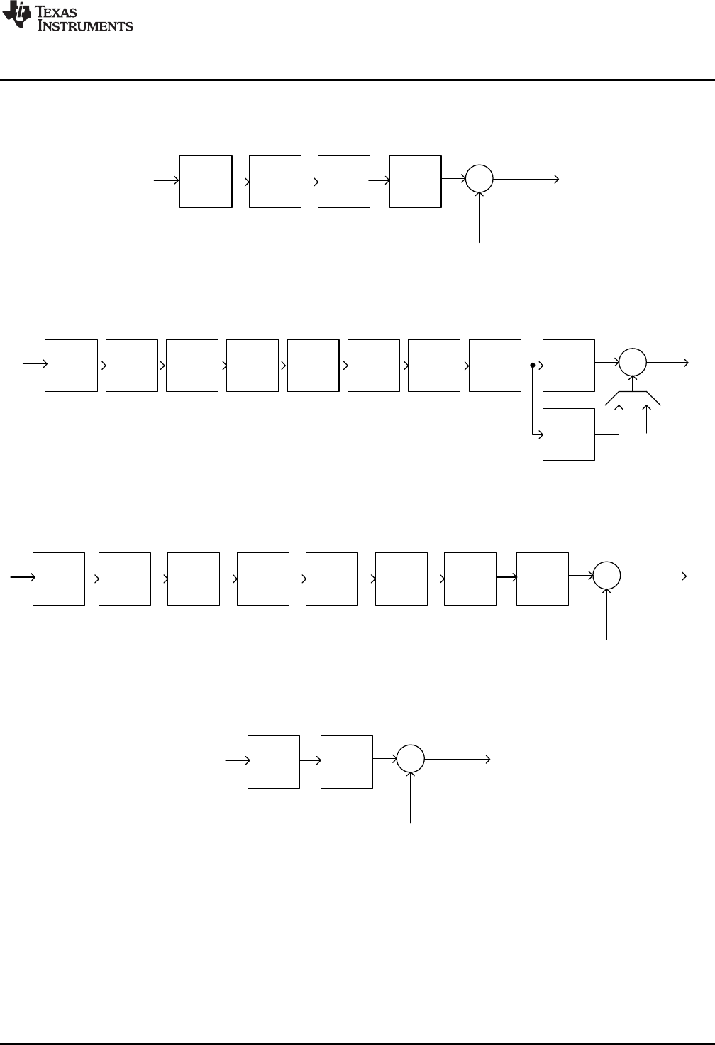
Interp.
Filter
B or C
*
IIR to
modulator
Digital
Volume
Ctrl
from
interface
Interp.
Filter
A or B
*
BiQuad
F
BiQuad
E
BiQuad
D
BiQuad
C
BiQuad
B
BiQuad
A
IIR to
modulator
Digital
Volume
Ctrl
Interp.
Filter
A or B
*
DRC
HPF
BiQuad
F
BiQuad
E
BiQuad
D
BiQuad
C
BiQuad
B
BiQuad
A
IIR to
modulator
Digital
Volume
Ctrl
from
interface
Interp.
Filter A
*
BiQuad
C
BiQuad
B
BiQuad
Ato
modulator
Digital
Volume
Ctrl
from
interface
www.ti.com
DAC
2.4.1 Processing Blocks – Details
2.4.1.1 3 Biquads, Interpolation Filter A
Figure 2-24. Signal Chain for PRB_P1 and PRB_P4
2.4.1.2 6 Biquads, 1st order IIR, DRC, Interpolation Filter A or B
Figure 2-25. Signal Chain for PRB_P2, PRB_P5, PRB_P10 and PRB_P15
2.4.1.3 6 Biquads, 1st order IIR, Interpolation Filter A or B
Figure 2-26. Signal Chain for PRB_P3, PRB_P6, PRB_P11 and PRB_P16
2.4.1.4 IIR, Interpolation Filter B or C
Figure 2-27. Signal Chain for PRB_P7, PRB_P12, PRB_P17 and PRB_P20
41
SLAU306A–January 2011–Revised January 2013 TLV320AIC3256 Application
Submit Documentation Feedback Copyright © 2011–2013, Texas Instruments Incorporated
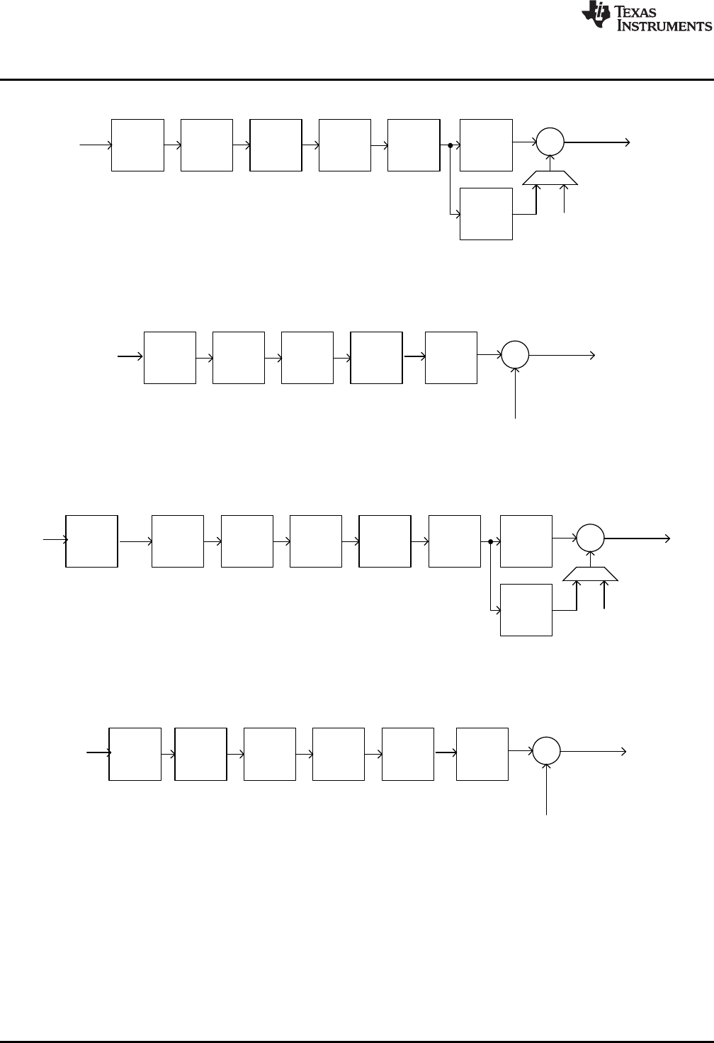
Interp.
Filter C
*
BiQuad
D
BiQuad
C
BiQuad
B
BiQuad
A
IIR to
modulator
Digital
Volume
Ctrl
from
interface
Interp.
Filter C
*
DRC
HPF
IIR to
modulator
Digital
Volume
Ctrl
BiQuad
D
BiQuad
C
BiQuad
B
BiQuad
A
from
interface
Interp.
Filter B
*
BiQuad
D
BiQuad
C
BiQuad
B
BiQuad
Ato
modulator
Digital
Volume
Ctrl
from
interface
Interp.
Filter B
*
DRC
HPF to
modulator
Digital
Volume
Ctrl
BiQuad
D
BiQuad
C
BiQuad
B
BiQuad
A
from
interface
DAC
www.ti.com
2.4.1.5 4 Biquads, DRC, Interpolation Filter B
Figure 2-28. Signal Chain for PRB_P8 and PRB_P13
2.4.1.6 4 Biquads, Interpolation Filter B
Figure 2-29. Signal Chain for PRB_P9 and PRB_P14
2.4.1.7 4 Biquads, 1st order IIR, DRC, Interpolation Filter C
Figure 2-30. Signal Chain for PRB_P18 and PRB_P21
2.4.1.8 4 Biquads, 1st order IIR, Interpolation Filter C
Figure 2-31. Signal Chain for PRB_P19 and PRB_P22
42 TLV320AIC3256 Application SLAU306A–January 2011–Revised January 2013
Submit Documentation Feedback
Copyright © 2011–2013, Texas Instruments Incorporated
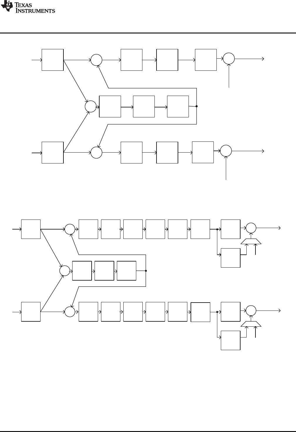
BiQuad
AL
Interp.
Filter A *
DRC
BiQuad
FL
BiQuad
EL
BiQuad
AR
IIR
left
3D
PGA
+
+
Interp.
Filter A *
DRC
BiQuad
FR
BiQuad
ER
BiQuad
DR
BiQuad
CR
BiQuad
BR
IIR
right +
+
-
+
-
+
+
from
left
channel
interface
to
modulator
to
modulator
Digital
Volume
Ctrl
Digital
Volume
Ctrl
from
right
channel
interface
BiQuad
BL
BiQuad
CL
BiQuad
DL
HPF
HPF
BiQuad
A
L
Interp.
Filter A
*
BiQuad
A
R
IIR
left
3D
PGA
+
+
BiQuad
C
R
BiQuad
B
R
IIR
right
+
+
-
+
-
+
+
from
left
channel
interface
to
modulator
Digital
Volume
Ctrl
from
right
channel
interface
BiQuad
B
L
BiQuad
C
L
Interp.
Filter A
*
to
modulator
Digital
Volume
Ctrl
www.ti.com
DAC
2.4.1.9 2 Biquads, 3D, Interpolation Filter A
Figure 2-32. Signal Chain for PRB_P23
2.4.1.10 5 Biquads, DRC, 3D, Interpolation Filter A
Figure 2-33. Signal Chain for PRB_P24
43
SLAU306A–January 2011–Revised January 2013 TLV320AIC3256 Application
Submit Documentation Feedback Copyright © 2011–2013, Texas Instruments Incorporated
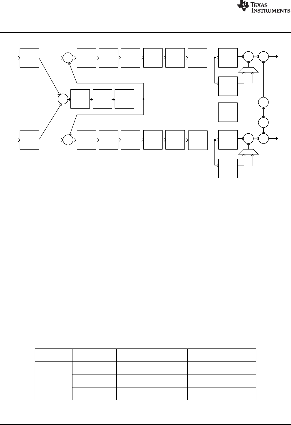
1
1
23
1
10
zD2
zNN
)z(H -
-
-
+
=
BiQuad
A
L
Interp.
Filter A *+
DRC
HPF
BiQuad
F
L
BiQuad
E
L
BiQuad
A
R
IIR
left
3D
PGA
+
+
Interp.
Filter A *+
DRC
*
Beep
Gen.
BiQuad
F
R
BiQuad
E
R
BiQuad
D
R
BiQuad
C
R
BiQuad
B
R
IIR
right +
+
-
+
-
+
+
from
left
channel
interface
to
modulator
to
modulator
Digital
Volume
Ctrl
Digital
Volume
Ctrl
Beep
Volume
Ctrl
from
right
channel
interface
BiQuad
B
L
BiQuad
C
L
BiQuad
D
L
*
HPF
DAC
www.ti.com
2.4.1.11 5 Biquads, DRC, 3D, Beep Generator, Interpolation Filter A
Figure 2-34. Signal Chain for PRB_P25
2.4.2 User Programmable Filters
Depending on the selected processing block, different types and orders of digital filtering are available. Up
to 6 biquad sections are available for specific processing blocks.
The coefficients of the available filters are arranged as sequentially-indexed coefficients in two banks. If
adaptive filtering is chosen, the coefficient banks can be switched on-the-fly. For more details on adaptive
filtering please see Section 2.4.5.3.
The coefficients of these filters are each 24-bits wide, in two's-complement and occupy 3 consecutive 8-bit
registers in the register space. For default values please see the default values tables in the Register Map
section.
2.4.2.1 First Order IIR Section
The IIR is of first-order and its transfer function is given by
(10)
The frequency response for the first order IIR Section with default coefficients is flat. Details on DAC
coefficient default values are given in Section 5.15.
Table 2-22. DAC IIR Filter Coefficients
Filter Filter Coefficient ADC Coefficient Left Channel ADC Coefficient Right
Channel
First order IIR N0 C65 (Page 46, Registers C68 (Page 46, Registers
28,29,30) 40,41,42)
N1 C66 (Page 46, Registers C69 (Page 46, Registers
32,33,34) 44,45,46)
D1 C67 (Page 46, Registers V70 (Page 46, Registers
36,37,38) 48,49,50)
44 TLV320AIC3256 Application SLAU306A–January 2011–Revised January 2013
Submit Documentation Feedback
Copyright © 2011–2013, Texas Instruments Incorporated
2
2
1
1
23
2
2
1
10
zDzD*22
zNzN*2N
)z(H --
--
--
++
=
www.ti.com
DAC
2.4.2.2 Biquad Section
The transfer function of each of the Biquad Filters is given by
(11)
The frequency response for each biquad section with default coefficients is flat at a gain of 0dB. Details on
DAC coefficient default values are given in Section 5.15.
Table 2-23. DAC Biquad Filter Coefficients
Filter Coefficient Left DAC Channel Right DAC Channel
BIQUAD A N0 C1 (Page 44, Registers 12,13,14) C33 (Page 45, Registers 20,21,22)
N1 C2 (Page 44, Registers 16,17,18) C34 (Page 45, Registers 24,25,26)
N2 C3 (Page 44, Registers 20,21,22) C35 (Page 45, Registers 28,29,30)
D1 C4 (Page 44, Registers 24,25,26) C36 (Page 45, Registers 32,33,34)
D2 C5 (Page 44, Registers 28,29,30) C37 (Page 45, Registers 36,37,38)
BIQUAD B N0 C6 (Page 44, Registers 32,33,34) C38 (Page 45, Registers 40,41,42)
N1 C7 (Page 44, Registers 36,37,38) C39 (Page 45, Registers 44,45,46)
N2 C8 (Page 44, Registers 40,41,42) C40 (Page 45, Registers 48,49,50)
D1 C9 (Page 44, Registers 44,45,46) C41 (Page 45, Registers 52,53,54)
D2 C10 (Page 44, Registers 48,49,50) C42 (Page 45, Registers 56,57,58)
BIQUAD C N0 C11 (Page 44, Registers 52,53,54) C43 (Page 45, Registers 60,61,62)
N1 C12 (Page 44, Registers 56,57,58) C44 (Page 45, Registers 64,65,66)
N2 C13 (Page 44, Registers 60,61,62) C45 (Page 45, Registers 68,69,70)
D1 C14 (Page 44, Registers 64,65,66) C46 (Page 45, Registers 72,73,74)
D2 C15 (Page 44, Registers 68,69,70) C47 (Page 45, Registers 76,77,78)
BIQUAD D N0 C16 (Page 44, Registers 72,73,74) C48 (Page 45, Registers 80,81,82)
N1 C17 (Page 44, Registers 76,77,78) C49 (Page 45, Registers 84,85,86)
N2 C18 (Page 44, Registers 80,81,82) C50 (Page 45, Registers 88,89,90)
D1 C19 (Page 44, Registers 84,85,86) C51 (Page 45, Registers 92,93,94)
D2 C20 (Page 44, Registers 88,89,90) C52 (Page 45, Registers 96,97,98)
BIQUAD E N0 C21 (Page 44, Registers 92,93,94) C53 (Page 45, Registers 100,101,102)
N1 C22 (Page 44, Registers 96,97,98) C54 (Page 45, Registers 104,105,106)
N2 C23 (Page 44, Registers 100,101,102) C55 (Page 45, Registers 108,109,110)
D1 C24 (Page 44, Registers 104,105,106) C56 (Page 45, Registers 112,113,114)
D2 C25 (Page 44, Registers 108,109,110) C57 (Page 45, Registers 116,117,118)
BIQUAD F N0 C26 (Page 44, Registers 112,113,114) C58 (Page 45, Registers 120,121,122)
N1 C27 (Page 44, Registers 116,117,118) C59 (Page 45, Registers 124,125,126)
N2 C28 (Page 44, Registers 120,121,122) C60 (Page 46, Registers 8,9,10)
D1 C29 (Page 44, Registers 124,125,126) C61 (Page 46, Registers 12,13,14)
D2 C30 (Page 45, Registers 8,9,10) C62 (Page 46, Registers 16,17,18)
2.4.2.2.1 3D-PGA
The 3D-PGA attenuation block as used in the processing blocks PRB_P23, PRB_P24 and PRB_P25 can
be programmed in the range of -1.0 to +1.0. A value of -1.0 corresponds to 0x7FFFFF in DAC coefficient
C32 (Page 45, Register 16,17 and 18). A value of 1.0 corresponds to 0x800000 in coefficient C32.
45
SLAU306A–January 2011–Revised January 2013 TLV320AIC3256 Application
Submit Documentation Feedback Copyright © 2011–2013, Texas Instruments Incorporated
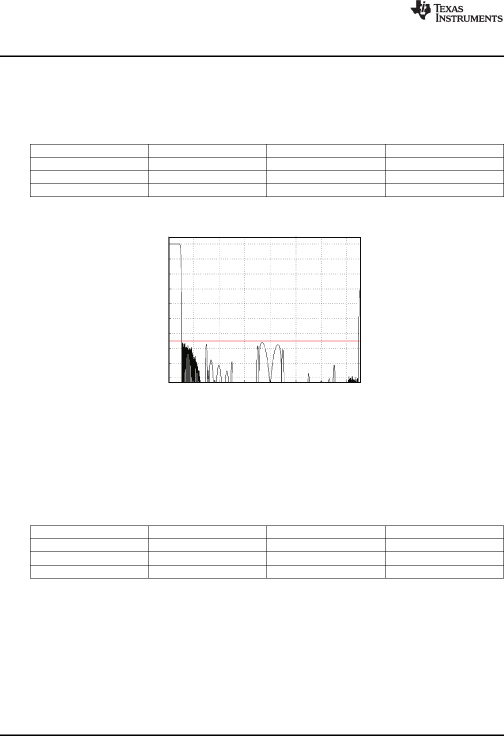
0
–10
–20
–30
–40
–50
–60
–70
–80
–90
1 2 3 4 5 6 7
FrequencyNormalizedtofS
Magnitude – dB
DACChannelResponseforInterpolationFilter A
(Redlinecorrespondsto –65dB)
G016
DAC
www.ti.com
2.4.3 Interpolation Filters
2.4.3.1 Interpolation Filter A
Filter A is designed for an fSup to 48ksps with a flat passband of 0kHz–20kHz.
Table 2-24. DAC Interpolation Filter A, Specification
Parameter Condition Value (Typical) Units
Filter Gain Pass Band 0 … 0.45fS±0.015 dB
Filter Gain Stop Band 0.55… 7.455fS–65 dB
Filter Group Delay 21 / fSs
Figure 2-35. DAC Interpolation Filter A, Frequency Response
2.4.3.2 Interpolation Filter B
Filter B is specifically designed for an fSof above 96ksps. Thus, the flat pass-band region easily covers
the required audio band of 0-20kHz.
Table 2-25. DAC Interpolation Filter B, Specification
Parameter Condition Value (Typical) Units
Filter Gain Pass Band 0 … 0.45fS±0.015 dB
Filter Gain Stop Band 0.55… 3.45fS–58 dB
Filter Group Delay 18 / fSs
46 TLV320AIC3256 Application SLAU306A–January 2011–Revised January 2013
Submit Documentation Feedback
Copyright © 2011–2013, Texas Instruments Incorporated
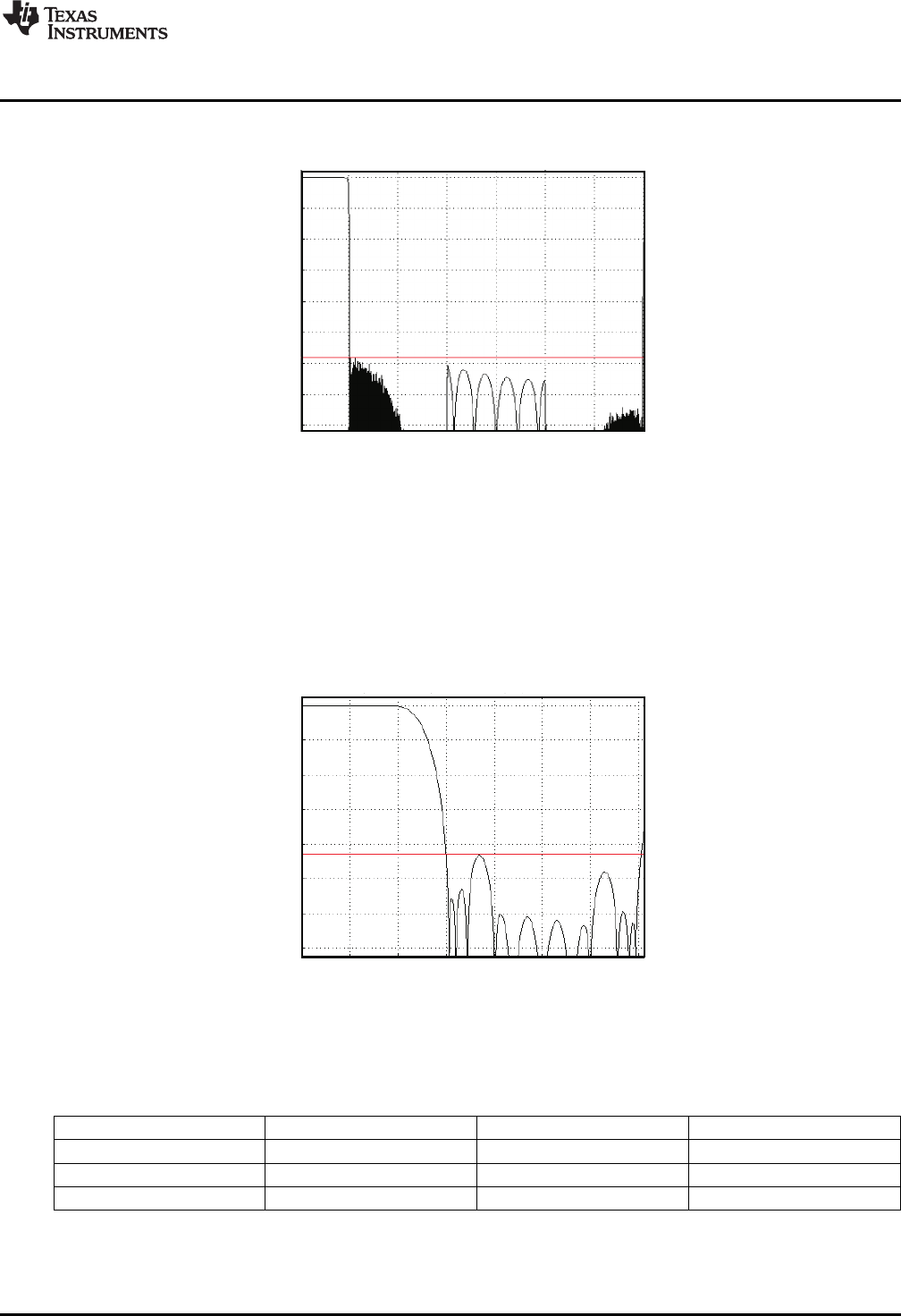
DACChannelResponseforInterpolationFilterC
(Redlinecorrespondsto –43dB)
0
–10
–20
–30
–40
–50
–60
–70
0.0 0.2 0.4 0.6 0.8 1.0 1.4
FrequencyNormalizedtofS
Magnitude – dB
G018
1.2
0
–10
–20
–30
–40
–50
–60
–70
–80
0.5 1.0 1.5 2.0 2.5 3.0 3.5
FrequencyNormalizedtofS
Magnitude – dB
G017
DACChannelResponseforInterpolationFilterB
(Redlinecorrespondsto –58dB)
www.ti.com
DAC
Figure 2-36. Channel Interpolation Filter B, Frequency Response
2.4.3.3 Interpolation Filter C
Filter C is specifically designed for the 192ksps mode. The pass band extends up to 0.40 * fS(corresponds
to 80kHz), more than sufficient for audio applications.
Figure 2-37. DAC Interpolation Filter C, Frequency Response
Table 2-26. DAC Interpolation Filter C, Specification
Parameter Condition Value (Typical) Units
Filter Gain Pass Band 0 … 0.35fS±0.03 dB
Filter Gain Stop Band 0.60… 1.4fS–43 dB
Filter Group Delay 13 / fSs
47
SLAU306A–January 2011–Revised January 2013 TLV320AIC3256 Application
Submit Documentation Feedback
Copyright © 2011–2013, Texas Instruments Incorporated
DAC
www.ti.com
2.4.4 DAC Gain Setting
2.4.4.1 PowerTune Modes
As part of the PowerTune strategy, the analog properties of the DAC are adjusted. As a consequence, the
full-scale signal swing achieved at the headphone and line outputs must be adjusted.
Please see Table 2-27 for the proper gain compensation values across the different combinations.
Table 2-27. DAC Gain versus. PowerTune Modes
DAC PowerTune PowerTune Mode Headphone or Line-out Gain
Mode Control
Page 1,Register 3 or CM = 0.75V, Gain for 375mVRMS output CM = 0.9V, Gain for 500mVRMS output
4, D(4:2) swing at 0dB full scale input swing at 0dB full scale input
000 PTM_P3, PTM_P4 0 0
001 PTM_P2 4 4
010 PTM_P1 14 14
2.4.4.2 Digital Volume Control
The TLV320AIC3256 signal processing blocks incorporate a digital volume control block that can control
the volume of the playback signal from +24dB to –63.5dB in steps of 0.5dB. These can be controlled by
writing to Page 0, Register 65 and 66. The volume control of left and right channels by default can be
controlled independently, however by programming Page 0, Reg 64, D(1:0), they can be made
interdependent. The volume changes are soft-stepped in steps of 0.5dB to avoid audible artifacts during
gain change. The rate of soft-stepping can be controlled by programming Page 0, Reg 63, D(1:0) to either
one step per frame (DAC_FS) or one step per 2 frames. The soft-stepping feature can also be entirely
disabled. During soft-stepping the value of the actual applied gain would differ from the programmed gain
in register. The TLV320AIC3256 gives a feedback to the user in form of register readable flag to indicate
that soft-stepping is currently in progress. The flags for left and right channels can be read back by
reading Page 0, Reg 38, Bits D4 and D0 respectively. A value of 0 in these flags indicates a soft-stepping
operation in progress, and a value of 1 indicates that soft-stepping has completed. A soft-stepping
operation comes into effect during
(a) power-up, when the volume control soft-steps from –63.5dB to programmed gain value,
(b) volume change by user when DAC is powered up, and
(c) power-down, when the volume control block soft-steps to –63.5dB before powering down the channel.
2.4.4.3 Dynamic Range Compression
Typical music signals are characterized by crest factors, the ratio of peak signal power to average signal
power, of 12dB or more. To avoid audible distortion due to clipping of peak signals, the gain of the DAC
channel must be adjusted to prevent hard clipping of peak signals. As a result, during nominal periods, the
applied gain is low, causing the perception that the signal is not loud enough. To overcome this problem,
the DRC in the TLV320AIC3256 continuously monitors the output of the DAC Digital Volume control to
detect its power level w.r.t. 0dBFS. When the power level is low, it increases the input signal gain to make
it sound louder. At the same time, if a peaking signal is detected, it autonomously reduces the applied
gain to avoid hard clipping. The resulting sound can be more pleasing to the ear as well as sounding
louder during nominal periods.
The DRC functionality in the TLV320AIC3256 is implemented by a combination of Processing Blocks in
the DAC channel as described in Section 2.4.1.
The DRC can be disabled by writing into Page 0, Reg 68, D(6:5).
The DRC typically works on the filtered version of the input signal. The input signals have no audio
information at DC and extremely low frequencies; however they can significantly influence the energy
estimation function in DRC. Also most of the information about signal energy is concentrated in the low
frequency region of the input signal.
48 TLV320AIC3256 Application SLAU306A–January 2011–Revised January 2013
Submit Documentation Feedback
Copyright © 2011–2013, Texas Instruments Incorporated
1
1
23
1
10
LPF zD2
zNN
)z(H -
-
-
+
=
1
1
23
1
10
HPF zD2
zNN
)z(H -
-
-
+
=
www.ti.com
DAC
In order to estimate the energy of the input signal, the signal is first fed to the DRC high-pass filter and
then to the DRC low-pass filter. These filters are implemented as first-order IIR filters given by
(12)
(13)
The coefficients for these filters are 24-bits wide in two’s-complement and are user programmable through
register write as given in Table 2-28, and coefficient default values are summarized in Section 5.15.
Table 2-28. DRC HPF and LPF Coefficients
Coefficient Location
HPF N0 C71 Page 46, Register 52 to 55
HPF N1 C72 Page 46, Register 56 to 59
HPF D1 C73 Page 46, Register 60 to 63
LPF N0 C74 Page 46, Register 64 to 67
LPF N1 C75 Page 46, Register 68 to 71
LPF D1 C76 Page 46, Register 72 to 75
The default values of these coefficients implement a high-pass filter with a cut-off at 0.00166 * DAC_FS,
and a low-pass filter with a cutoff at 0.00033 * DAC_FS.
The output of the DRC high-pass filter is fed to the Processing Block selected for the DAC Channel. The
absolute value of the DRC-LPF filter is used for energy estimation within the DRC.
The gain in the DAC Digital Volume Control is controlled by Page 0, Register 65 and 66. When the DRC is
enabled, the applied gain is a function of the Digital Volume Control register setting and the output of the
DRC.
The DRC parameters are described in sections that follow.
2.4.4.3.1 DRC Threshold
The DRC Threshold represents the level of the DAC playback signal at which the gain compression
becomes active. The output of the digital volume control in the DAC is compared with the set threshold.
The threshold value is programmable by writing to register Page 0, Register 68, D(4:2). The Threshold
value can be adjusted between –3dBFS to –24dBFS in steps of 3dB. Keeping the DRC Threshold value
too high may not leave enough time for the DRC block to detect peaking signals, and can cause
excessive distortion at the outputs. Keeping the DRC Threshold value too low can limit the perceived
loudness of the output signal.
The recommended DRC-Threshold value is –24dB.
When the output signal exceeds the set DRC Threshold, the interrupt flag bits at Page 0, Register 44,
D(3:2) are updated. These flag bits are 'sticky' in nature, and are reset only after they are read back by the
user. The non-sticky versions of the interrupt flags are also available at Page 0, Register 46, D(3:2).
2.4.4.3.2 DRC Hysteresis
DRC Hysteresis is programmable by writing to Page 0, Register 68, D(1:0) with values between 0dB and
3dB in steps of 1dB. DRC Hysteresis is a programmable window around the programmed DRC Threshold
that must be exceeded for a disabled DRC to become enabled, or an enabled DRC to become disabled.
For example, if the DRC Threshold is set to –12dBFS and DRC Hysteresis is set to 3dB, then if the gain
compressions in the DRC is inactive, the output of the DAC Digital Volume Control must exceed –9dBFS
before gain compression due to the DRC is activated. Similarly, when the gain compression in the DRC is
49
SLAU306A–January 2011–Revised January 2013 TLV320AIC3256 Application
Submit Documentation Feedback Copyright © 2011–2013, Texas Instruments Incorporated

DAC
www.ti.com
active, the output of the DAC Digital Volume Control must fall below –15dBFS for gain compression in the
DRC to be deactivated. The DRC Hysteresis feature prevents the rapid activation and de-activation of
gain compression in the DRC in cases when the output of DAC Digital Volume Control rapidly fluctuates in
a narrow region around the programmed DRC Threshold. Programming the DRC Hysteresis as 0dB
disables the hysteresis action.
Recommended Value of DRC Hysteresis is 3dB.
2.4.4.3.3 DRC Hold
The DRC Hold function slows the start of decay for a specified period of time in response to a decrease in
energy level. To minimize audible artifacts, it is recommended to set the DRC Hold time to 0 through
programming Page 0, Register 69, D(6:3) = 0000.
2.4.4.3.4 DRC Attack Rate
When the output of the DAC Digital Volume Control exceeds the programmed DRC Threshold, the gain
applied in the DAC Digital Volume Control is progressively reduced to avoid the signal from saturating the
channel. This process of reducing the applied gain is called Attack. To avoid audible artifacts, the gain is
reduced slowly with a rate equaling the Attack Rate programmable via Page 0, Register 70, D(7:4). Attack
Rates can be programmed from 4dB gain change per sample period (1 / DAC_FS) to 1.2207e-5dB gain
change per sample period.
Attack Rates should be programmed such that before the output of the DAC Digital Volume control can
clip, the input signal should be sufficiently attenuated. High Attack Rates can cause audible artifacts, and
too-slow Attack Rates may not prevent the input signal from clipping.
The recommended DRC Attack Rate value is 1.9531e-4 dB per sample period.
2.4.4.3.5 DRC Decay Rate
When the DRC detects a reduction in output signal swing beyond the programmed DRC Threshold, the
DRC enters a Decay state, where the applied gain in Digital Volume Control is gradually increased to
programmed values. To avoid audible artifacts, the gain is slowly increased with a rate equal to the Decay
Rate programmed through Page 0, Register 70, D(3:0). The Decay Rates can be programmed from
1.5625e-3dB per sample period to 4.7683e-7dB per sample period. If the Decay Rates are programmed
too high, then sudden gain changes can cause audible artifacts. However, if it is programmed too slow,
then the output may be perceived as too low for a long time after the peak signal has passed.
The recommended Value of DRC Decay Rate is 2.4414e-5 dB per sample period.
2.4.4.3.6 Example Setup for DRC
• PGA Gain = 12dB
• Threshold = -24dB
• Hysteresis = 3dB
• Hold time = 0ms
• Attack Rate = 1.9531e-4 dB per sample period
• Decay Rate = 2.4414e-5 dB per sample period
Script
w 30 00 00 #Go to Page 0
w 30 41 18 #DAC => 12 db gain left
w 30 42 18 #DAC => 12 db gain right
w 30 44 7F #DAC => DRC Enabled for both channels, Threshold = -24 db, Hysteresis = 3 dB
w 30 45 00 #DRC Hold = 0 ms, Rate of Changes of Gain = 0.5 dB/Fs'
w 30 46 B6 #Attack Rate = 1.9531e-4 dB/Frame , DRC Decay Rate =2.4414e-5 dB/Frame
w 30 00 2E #Go to Page 46
w 30 34 7F AB 00 00 80 55 00 00 7F 56 00 00 #DRC HPF
w 30 40 00 11 00 00 00 11 00 00 7F DE 00 00 #DRC LPF
50 TLV320AIC3256 Application SLAU306A–January 2011–Revised January 2013
Submit Documentation Feedback
Copyright © 2011–2013, Texas Instruments Incorporated

www.ti.com
DAC
2.4.5 DAC Special Functions
2.4.5.1 Beep Generation
A special function has also been included in the processing block PRB_P25 for generating a digital sine-
wave signal that is sent to the DAC. This signal is intended for generating key-click sounds for user
feedback. A default value for the sine-wave frequency, sine burst length, and signal magnitude is kept in
the Tone Generator Registers Page 0, Registers 71 through 79. The sine wave generator is very flexible,
and is completely register programmable via 9 registers of 8 bits each to provide many different sounds.
Two registers are used for programming the 16-bit, two's-complement, sine-wave coefficient (Page 0,
Registers 76 and 77). Two other registers program the 16-bit, two's-complement, cosine-wave coefficient
(Page 0, Registers 78 and 79). This coefficient resolution allows virtually any frequency of sine wave in the
audio band to be generated up to DAC_FS / 2.
Three registers are used to control the length of the sine burst waveform which are located on Page 0,
Registers 73, 74, and 75. The resolution (bit) in the registers of the sine burst length is one sample time,
so this allows great control on the overall time of the sine burst waveform. This 24-bit length timer
supports 16,777,215 sample times. (For example if DAC_FS is set at 48kHz, and the registers combined
value equals 96000d (01770h), then the sine burst would last exactly two seconds.)
Separate registers independently control the Left sine-wave volume and the Right sine-wave volume. The
6-bit digital volume control allows level control of 0dB to –63dB in one-dB steps. The left-channel volume
is controlled by writing to Page 0, Register 71, D(5:0). The right-channel volume is controlled by Page 0,
Register 72, D(5:0). A master volume control for the left and right channel of the beep generator can be
set up using Page 0, Register 72, D(7:6). The default volume control setting is 0dB, the tone generator
maximum-output level.
To play back the sine wave, the DAC must be configured with regards to clock setup and routing. The sine
wave starts by setting the Beep Generator Enable Bit (Page 1, Register 71, D(7) = 1). After the sine wave
has played for its predefined time period this bit automatically resets back to 0. While the sine wave is
playing, the parameters of the beep generator cannot be changed. To stop the sine wave before the
predefined time period expires, set the Beep Generator Enable Bit to 0.
2.4.5.2 Digital Auto Mute
The TLV320AIC3256 also incorporates a special feature where the DAC channel is auto-muted when a
continuous stream of DC-input is detected. By default, this feature is disabled, and is enabled by writing a
non-zero value into Page 0, Register 64, D(6:4). This non-zero value controls the duration of the
continuous stream of DC-input before the auto-mute feature takes effect. This feature is especially helpful
for eliminating high-frequency noise power from being delivered into the load during silent periods of
speech or music.
2.4.5.3 Adaptive Filtering
When the DAC is running, the user-programmable filter coefficients are locked and cannot be accessed
for either read or write.
However the TLV320AIC3256 offers an adaptive filter mode as well. Setting Register Page 44, Reg 1, Bit
D(2) = 1 turns on double buffering of the coefficients. In this mode, filter coefficients can be updated
through the host, and activated without stopping and restarting the DAC. This enables advanced adaptive
filtering applications.
In the double-buffering scheme, all coefficients are stored in two buffers (Buffers A and B). When the DAC
is running and adaptive filtering mode is turned on, setting the control bit Page 44, Register 1, D(0) = 1
switches the coefficient buffers at the next start of a sampling period. This bit resets back to 0 after the
switch occurs. At the same time, the flag (Page 44, Reg 1, D(1)) toggles.
The flag in Page 44, Register 1, D(1) indicates which of the two buffers is actually in use.
Page 44, Register 1, D(1) = 0: Buffer A is in use by the DAC engine, Bit D(1) = 1: Buffer B is in use.
While the device is running, coefficient updates are always made to the buffer not in use by the DAC,
regardless to which buffer the coefficients have been written.
51
SLAU306A–January 2011–Revised January 2013 TLV320AIC3256 Application
Submit Documentation Feedback Copyright © 2011–2013, Texas Instruments Incorporated

DAC
www.ti.com
DAC running Page 44, Reg 1, Bit D1 Coefficient Buffer in use Writing to Will update
No 0 None C1, Buffer A C1, Buffer A
No 0 None C1, Buffer B C1, Buffer B
Yes 0 Buffer A C1, Buffer A C1, Buffer B
Yes 0 Buffer A C1, Buffer B C1, Buffer B
Yes 1 Buffer B C1, Buffer A C1, Buffer A
Yes 1 Buffer B C1, Buffer B C1, Buffer A
The user programmable coefficients C1 to C70 are defined on Pages 44, 45 and 46 for Buffer A and
Pages 62, 63 and 64 for Buffer B.
2.4.6 DAC Setup
This section lists the steps necessary to configure the TLV320AIC3256 DAC.
Step 1
Determine the system clock source (master clock) and the targeted DAC sampling frequency.
Choose the targeted performance. This drives the choice of the decimation filter type (A, B or C) and
DOSR value.
Use Filter A for 48kHz high-performance operation; DOSR must be a multiple of 8.
Use Filter B for up to 96kHz operations; DOSR must be a multiple of 4.
Use Filter C for up to 192kHz operations; DOSR must be a multiple of 2.
In all cases the DOSR range is limited by the following condition:
2.8MHz < DOSR * DAC_FS < 6.2MHz
Based on the identified filter type and the required signal processing capabilities, the appropriate
processing block is determined from the list of available processing blocks (PRB_P1 to PRB_P25).
Based on the available master clock, the chosen DOSR and the targeted sampling rate, the clock divider
values NDAC and MDAC are calculated. If necessary, the internal PLL can add a large degree of
flexibility.
In summary, codec_clkin (derived directly from the system clock source or from the internal PLL) divided
by MDAC, NDAC and DOSR must be equal to the DAC sampling rate DAC_FS. The codec_clkin clock
signal is shared with the ADC clock generation block.
CODEC_CLKIN = NDAC * MDAC * DOSR * DAC_FS
To a large degree, NDAC and MDAC can be chosen independently in the range of 1 to 128. In general,
NDAC should be as large as possible as long as the following condition can still be met:
MDAC * DOSR / 32 ≥RC
RC is a function of the chosen processing block and is listed in Table 2-21.
The common-mode voltage setting of the device is determined by the available analog power supply and
the desired PowerTune mode. This common-mode (input common-mode) value is common across the
ADC, DAC and analog bypass path. The output common-mode setting is determined by the available
analog power supplies (AVDD and DRVdd_HP) and the desired output-signal swing.
At this point the following device specific parameters are known:
PRB_Px, DOSR, NDAC, MDAC, input and output common-mode values
If the PLL is used, the PLL parameters P, J, D and R are determined as well.
52 TLV320AIC3256 Application SLAU306A–January 2011–Revised January 2013
Submit Documentation Feedback
Copyright © 2011–2013, Texas Instruments Incorporated

www.ti.com
PowerTune
Step 2
Setting up the device via register programming:
The following list gives a sequence of items that must be executed in the time between powering the
device up and reading data from the device:
Define starting point: Set register page to 0
Initiate SW Reset
Program Clock Settings Program PLL clock dividers P,J,D,R (if PLL is necessary)
Power up PLL (if PLL is necessary)
Program and power up NDAC
Program and power up MDAC
Program OSR value
Program I2S word length if required (for example, 20bit)
Program the processing block to be used
At this point, at the latest, the analog power supply must be applied to the device
Program Analog Blocks Set register Page to 1
Disable coarse AVDD generation
Enable Master Analog Power Control
Program Common Mode voltage
Program PowerTune (PTM) mode
Program Reference fast charging
Program Headphone specific depop settings (in case of headphone driver
used)
Program routing of DAC output to the output amplifier (headphone or line
out)
Unmute and set gain of output driver
Power up output driver
Apply waiting time determined by the de-pop settings and the soft-stepping settings of the driver
gain or poll Page 1 , Register 63
Power Up DAC Set register Page to 0
Power up DAC Channels
Unmute digital volume control
A detailed example can be found in the Example Setups section.
2.5 PowerTune
The TLV320AIC3256 features PowerTune, a mechanism to balance power-versus-performance trade-offs
at the time of device configuration. The device can be tuned to minimize power dissipation, to maximize
performance, or to an operating point between the two extremes to best fit the application.
2.5.0.1 PowerTune Modes
NOTE: The PowerTune Modes described in this section are only used for unipolar headphone
output circuit topology. For a description of setups used with ground-centered output
topology, see Section 2.2.3.2.5.
2.5.0.1.1 ADC – Programming PTM_R1 to PTM_R4
The device powers up with PTM_R4 (highest performance) set as default. This mode always works across
all combinations of common-mode voltage, chosen processing block, or chosen oversampling ratio. If the
application can make use of a lower-power configuration please see the ADC and DAC power
consumption chapters below for valid combination of PowerTune modes and other device parameters.
53
SLAU306A–January 2011–Revised January 2013 TLV320AIC3256 Application
Submit Documentation Feedback Copyright © 2011–2013, Texas Instruments Incorporated
PowerTune
www.ti.com
The ADC configuration of the PowerTune mode affects right and left channels simultaneously.
PTM_R1 PTM_R2 PTM_R3 PTM_R4
Pg 1, Reg 61, D(7:0) 0xFF 0xB6 0x64 0x00
2.5.0.1.2 DAC - Programming PTM_P1 to PTM_P4
On the playback side, the performance is determined by a combination of register settings and the audio
data word length applied. For the highest performance setting (PTM_P4), an audio-data word length of 20
bits is required, while for the modes PTM_P1 to PTM_P3 a word length of 16 bits is sufficient.
PTM_P1 PTM_P2 PTM_P3 PTM_P4
Pg 1, Reg 3, D(4:2) 0x2 0x1 0x0 0x0
Pg 1, Reg 4, D(4:2) 0x2 0x1 0x0 0x0
Audio Data word length 16 bits 16 bits 16 bits 20 or more bits
Pg 0, Reg 27, D(5:4) 0x0 0x0 0x0 0x1, 0x2, 0x3
2.5.0.1.3 Processing Blocks
The choice of processing blocks, PRB_P1 to PRB_P25 for playback and PRB_R1 to PRB_R18 for
recording, also influences the power consumption. In fact, the numerous processing blocks have been
implemented to offer a choice between power-optimization and configurations with more signal-processing
resources.
2.5.0.2 ADC Power Consumption
The tables in this section give recommendations for various PowerTune modes. Typical performance and
power-consumption values are listed. PowerTune modes that are not supported are marked with an ‘X’.
All measurements were taken with the PLL turned off and the ADC configured for single-ended input. The
values given in the tables are intended as target-performance levels, not device specifications. For device
specifications, see the TLV320AIC3256 data sheet, SLOS630.
54 TLV320AIC3256 Application SLAU306A–January 2011–Revised January 2013
Submit Documentation Feedback
Copyright © 2011–2013, Texas Instruments Incorporated
www.ti.com
PowerTune
2.5.0.2.1 ADC, Stereo, 48kHz, Highest Performance, DVdd = 1.8V, AVdd = 1.8V
AOSR = 128, Processing Block = PRB_R1 (Decimation Filter A)
Device Common Mode Setting = 0.75V Device Common Mode Setting = 0.9V
PTM_R1 PTM_R2 PTM_R3 PTM_R4 PTM_R1 PTM_R2 PTM_R3 PTM_R4 UNIT
0dB full scale X 375 375 375 X 500 500 500 mVRMS
Max. allowed input level w.r.t. X –12 0 0 X –12 0 0 dB full
0dB full scale scale
Effective SNR w.r.t. X 78.3 90.6 90.5 X 80.3 92.8 92.7 dB
max. allowed input level
Power consumption X 10.7 12.8 16.6 X 10.7 12.8 16.6 mW
Alternative processing blocks:
Processing Block Filter Est. Power Change (mW)
PRB_R2 A +1.4
PRB_R3 A +1.4
2.5.0.2.2 ADC, Stereo, 48kHz, DVdd = 1.8V, AVdd = 1.8V
AOSR = 64, Processing Block = PRB_R7 (Decimation Filter B)
Device Common Mode Setting = 0.75V Device Common Mode Setting = 0.9V
PTM_R1 PTM_R2 PTM_R3 PTM_R4 PTM_R1 PTM_R2 PTM_R3 PTM_R4 UNIT
0dB full scale 375 X 375 X X X 500 X mVRMS
Max. allowed input level w.r.t. –2 X 0 X X X 0 X dB full
0dB full scale scale
Effective SNR w.r.t. 85.9 X 88.0 X X X 90.2 X dB
max. allowed input level
Power consumption 7.6 X 10.4 X X X 10.4 X mW
Alternative processing blocks:
Processing Block Filter Est. Power Change (mW)
PRB_R8 B +0.7
PRB_R9 B +0.7
PRB_R1 A +2.0
PRB_R2 A +3.4
PRB_R3 A +3.4
55
SLAU306A–January 2011–Revised January 2013 TLV320AIC3256 Application
Submit Documentation Feedback Copyright © 2011–2013, Texas Instruments Incorporated
PowerTune
www.ti.com
2.5.0.2.3 ADC, Stereo, 48kHz, Lowest Power Consumption
AOSR = 64, Processing Block = PRB_R7 (Decimation Filter B), DVdd = 1.26V
PTM_R1 PTM_R3 UNIT
CM = 0.75V CM = 0.9V
AVdd=1.5V AVdd=1.8V
0dB full scale 375 500 mVRMS
Max. allowed input level w.r.t. 0dB –2 0 dB full scale
full scale
Effective SNR w.r.t. max. allowed 85.9 90.3 dB
input level
Power consumption 5.2 8.9 mW
Alternative processing blocks:
Processing Block Filter Est. Power Change (mW)
PRB_R8 B + 0.3
PRB_R9 B + 0.3
PRB_R1 A + 1.0
PRB_R2 A + 1.6
PRB_R3 A + 1.6
2.5.0.2.4 ADC, Mono, 48kHz, Highest Performance, DVdd = 1.8V, AVdd = 1.8V
AOSR = 128, Processing Block = PRB_R4 (Decimation Filter A)
Device Common Mode Setting = 0.75V Device Common Mode Setting = 0.9V
PTM_R1 PTM_R2 PTM_R3 PTM_R4 PTM_R1 PTM_R2 PTM_R3 PTM_R4 UNIT
0dB full scale X 375 375 375 X 500 500 500 mVRMS
Max. allowed input level w.r.t. X –12 0 0 X –12 0 0 dB full
0dB full scale scale
Effective SNR w.r.t. X 78.4 90.7 90.5 X 80.4 92.8 92.6 dB
max. allowed input level
Power consumption X 6.5 7.7 9.9 X 6.5 7.7 9.9 mW
Alternative processing blocks:
Processing Block Filter Est. Power Change (mW)
PRB_R5 A +0.7
PRB_R6 A +0.7
56 TLV320AIC3256 Application SLAU306A–January 2011–Revised January 2013
Submit Documentation Feedback
Copyright © 2011–2013, Texas Instruments Incorporated
www.ti.com
PowerTune
2.5.0.2.5 ADC, Mono, 48kHz, DVdd = 1.8V, AVdd = 1.8V
AOSR = 64, Processing Block = PRB_R11 (Decimation Filter B)
Device Common Mode Setting = 0.75V Device Common Mode Setting = 0.9V
PTM_R1 PTM_R2 PTM_R3 PTM_R4 PTM_R1 PTM_R2 PTM_R3 PTM_R4 UNIT
0dB full scale 375 X 375 X X X 500 X mVRMS
Max. allowed input level w.r.t. –2 X 0 X X X 0 X dB full
0dB full scale scale
Effective SNR w.r.t. 86.0 X 88.1 X X X 90.3 X dB
max. allowed input level
Power consumption 5.0 X 6.6 X X X 6.6 X mW
Alternative processing blocks:
Processing Block Filter Est. Power Change (mW)
PRB_R10 B 0
PRB_R12 B 0
PRB_R4 A +0.7
PRB_R5 A +1.4
PRB_R6 A +1.4
2.5.0.2.6 ADC, Mono, 48 kHz, Lowest Power Consumption,
AOSR = 64, Processing Block = PRB_R11 (Decimation Filter B), DVdd = 1.26V
PTM_R1 PTM_R3 UNIT
CM = 0.75V CM = 0.9V
AVdd=1.5V AVdd=1.8V
0dB full scale 375 500 mVRMS
Max. allowed input level w.r.t. –2 0 dB full scale
0dB full scale
Effective SNR w.r.t. 85.9 90.3 dB
max. allowed input level
Power consumption 3.3 5.5 mW
Alternative processing blocks:
Processing Block Filter Est. Power Change (mW)
PRB_R10 B 0
PRB_R12 B 0
PRB_R4 A +0.3
PRB_R5 A +0.7
PRB_R6 A +0.7
57
SLAU306A–January 2011–Revised January 2013 TLV320AIC3256 Application
Submit Documentation Feedback Copyright © 2011–2013, Texas Instruments Incorporated
PowerTune
www.ti.com
2.5.0.2.7 ADC, Stereo, 8kHz, Highest Performance, DVdd = 1.8V, AVdd = 1.8V
AOSR = 128, Processing Block = PRB_R1 (Decimation Filter A)
Device Common Mode Setting = 0.75V Device Common Mode Setting = 0.9V
PTM_R1 PTM_R2 PTM_R3 PTM_R4 PTM_R1 PTM_R2 PTM_R3 PTM_R4 UNIT
0dB full scale 375 X X X 500 X X X mVRMS
Max. allowed input level w.r.t. 0 X X X 0 X X X dB full
0dB full scale scale
Effective SNR w.r.t. 89.5 X X X 92.6 X X X dB
max. allowed input level
Power consumption 5.7 X X X 5.7 X X X mW
Alternative processing blocks:
Processing Block Filter Est. Power Change (mW)
PRB_R2 A +0.2
PRB_R3 A +0.2
2.5.0.2.8 ADC, Stereo, 8kHz, DVdd = 1.8V, AVdd = 1.8V
AOSR = 64, Processing Block = PRB_R7 (Decimation Filter B)
Device Common Mode Setting = 0.75V Device Common Mode Setting = 0.9V
PTM_R1 PTM_R2 PTM_R3 PTM_R4 PTM_R1 PTM_R2 PTM_R3 PTM_R4 UNIT
0dB full scale 375 X X X 500 X X X mVRMS
Max. allowed input level w.r.t. 0 X X X 0 X X X dB full
0dB full scale scale
Effective SNR w.r.t. 87.3 X X X 89.4 X X X dB
max. allowed input level
Power consumption 5.3 X X X 5.3 X X X mW
Alternative processing blocks:
Processing Block Filter Est. Power Change (mW)
PRB_R8 B + 0.1
PRB_R9 B + 0.1
PRB_R1 A + 0.3
PRB_R2 A +0.6
PRB_R3 A + 0.6
58 TLV320AIC3256 Application SLAU306A–January 2011–Revised January 2013
Submit Documentation Feedback
Copyright © 2011–2013, Texas Instruments Incorporated
www.ti.com
PowerTune
2.5.0.2.9 ADC, Stereo, 8kHz, Lowest Power Consumption,
AOSR = 64, Processing Block = PRB_R7 (Decimation Filter B), PowerTune Mode = PTM_R1, DVdd =
1.26
CM = 0.75V CM = 0.9V UNIT
AVdd=1.5V AVdd=1.8V
0dB full scale 375 500 mVRMS
Max. allowed input level w.r.t. 0 0 dB full scale
0dB full scale
Effective SNR w.r.t. 87.2 89.4 dB
max. allowed input level
Power consumption 4.1 4.9 mW
Alternative processing blocks:
Processing Block Filter Est. Power Change (mW)
PRB_R8 B + 0.1
PRB_R9 B + 0.1
PRB_R1 A + 0.2
PRB_R2 A + 0.3
PRB_R3 A + 0.3
2.5.0.2.10 ADC, Mono, 8kHz, Highest Performance, DVdd = 1.8V, AVdd = 1.8V
AOSR = 128, Processing Block = PRB_R4 (Decimation Filter A)
Device Common Mode Setting = 0.75V Device Common Mode Setting = 0.9V
PTM_R1 PTM_R2 PTM_R3 PTM_R4 PTM_R1 PTM_R2 PTM_R3 PTM_R4 UNIT
0dB full scale 375 X X X 500 X X X mVRMS
Max. allowed input level w.r.t. 0 X X X 0 X X X dB full
0dB full scale scale
Effective SNR w.r.t. max. 90.5 X X X 92.7 X X X dB
allowed input level
Power consumption 3.5 X X X 3.5 X X X mW
Alternative processing blocks:
Processing Block Filter Est. Power Change (mW)
PRB_R5 A +0.1
PRB_R6 A +0.1
59
SLAU306A–January 2011–Revised January 2013 TLV320AIC3256 Application
Submit Documentation Feedback Copyright © 2011–2013, Texas Instruments Incorporated
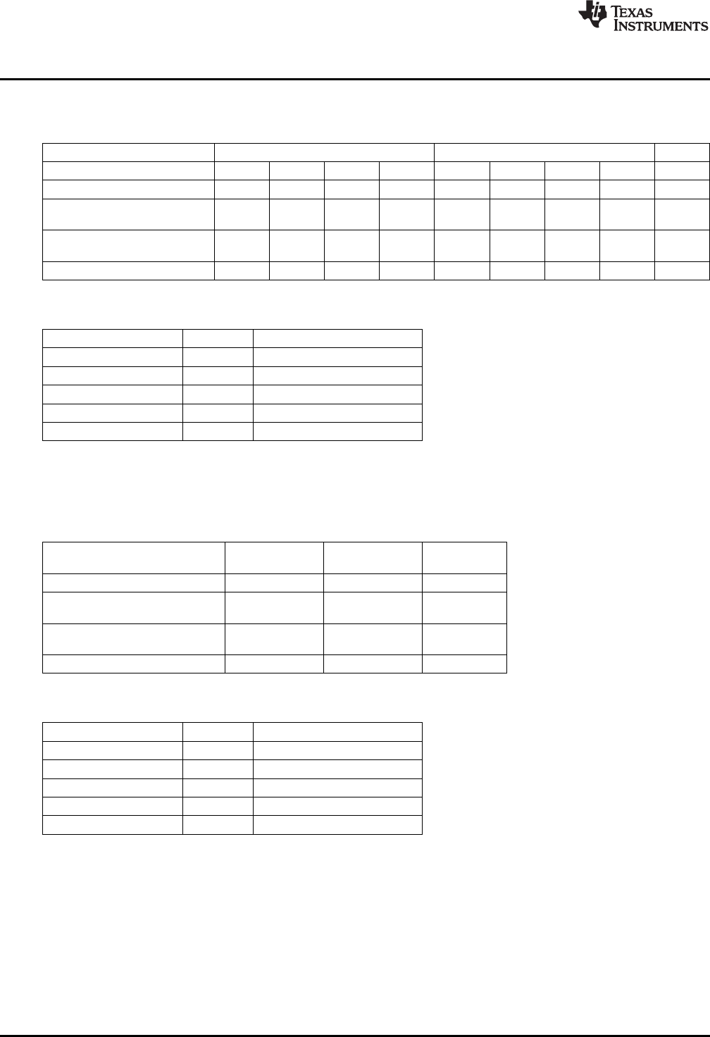
PowerTune
www.ti.com
2.5.0.2.11 ADC, Mono, 8kHz, DVdd = 1.8V, AVdd = 1.8V
AOSR = 64, Processing Block = PRB_R11 (Decimation Filter B)
Device Common Mode Setting = 0.75V Device Common Mode Setting = 0.9V
PTM_R1 PTM_R2 PTM_R3 PTM_R4 PTM_R1 PTM_R2 PTM_R3 PTM_R4 UNIT
0dB full scale 375 X X X 500 X X X mVRMS
Max. allowed input level w.r.t. 0 X X X 0 X X X dB full
0dB full scale scale
Effective SNR w.r.t. 87.3 X X X 89.4 X X X dB
max. allowed input level
Power consumption 3.3 X X X 3.3 X X X mW
Alternative processing blocks:
Processing Block Filter Est. Power Change (mW)
PRB_R10 B 0
PRB_R12 B 0
PRB_R4 A +0.1
PRB_R5 A +0.2
PRB_R6 A +0.2
2.5.0.2.12 ADC, Mono, 8kHz, Lowest Power Consumption
AOSR = 64, Processing Block = PRB_R11 (Decimation Filter B), PowerTune Mode = PTM_R1, DVdd =
1.26V
CM = 0.75V CM = 0.9V UNIT
AVdd=1.5V AVdd=1.8V
0dB full scale 375 500 mVRMS
Max. allowed input level w.r.t. 0 0 dB full scale
0dB full scale
Effective SNR w.r.t. 87.3 89.4 dB
max. allowed input level
Power consumption 2.5 3.0 mW
Alternative processing blocks:
Processing Block Filter Est. Power Change (mW)
PRB_R10 B 0
PRB_R12 B 0
PRB_R4 A +0.1
PRB_R5 A +0.1
PRB_R6 A +0.1
60 TLV320AIC3256 Application SLAU306A–January 2011–Revised January 2013
Submit Documentation Feedback
Copyright © 2011–2013, Texas Instruments Incorporated
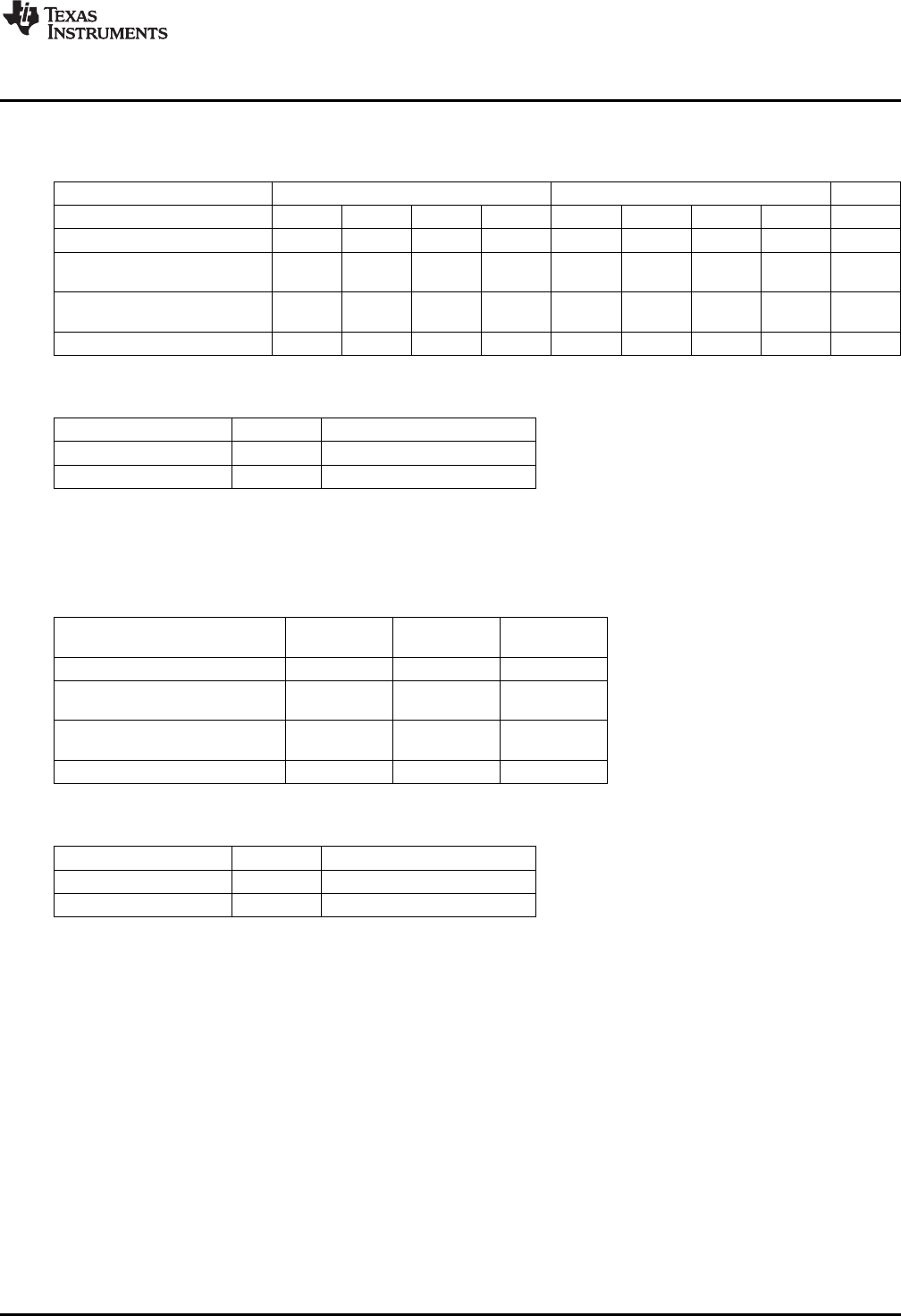
www.ti.com
PowerTune
2.5.0.2.13 ADC, Stereo, 192kHz, Highest Performance, DVdd = 1.8V, AVdd = 1.8V
AOSR = 32, Processing Block = PRB_R14 (Decimation Filter C)
Device Common Mode Setting = 0.75V Device Common Mode Setting = 0.9V
PTM_R1 PTM_R2 PTM_R3 PTM_R4 PTM_R1 PTM_R2 PTM_R3 PTM_R4 UNIT
0dB full scale X X 375 375 X X 500 500 mVRMS
Max. allowed input level w.r.t. X X 0 0 X X 0 0 dB full
0dB full scale scale
Effective SNR w.r.t. X X 90.7 90.5 X X 93.0 92.9 dB
max. allowed input level
Power consumption X X 18.6 22.3 X X 18.7 22.4 mW
Alternative processing blocks:
Processing Block Filter Est. Power Change (mW)
PRB_R13 C –2.7
PRB_R15 C 0
2.5.0.2.14 ADC, Stereo, 192kHz, Lowest Power Consumption
AOSR = 32, Processing Block = PRB_R14 (Decimation Filter C), PowerTune Mode = PTM_R3, DVdd =
1.26V
CM = 0.75V CM = 0.9V UNIT
AVdd=1.5V AVdd=1.8V
0dB full scale 375 500 mVRMS
Max. allowed input level w.r.t. 0 0 dB full scale
0dB full scale
Effective SNR w.r.t. 90.6 92.5 dB
max. allowed input level
Power consumption 11.7 10.9 mW
Alternative processing blocks:
Processing Block Filter Est. Power Change (mW)
PRB_R13 C – 1.3
PRB_R15 C 0
61
SLAU306A–January 2011–Revised January 2013 TLV320AIC3256 Application
Submit Documentation Feedback Copyright © 2011–2013, Texas Instruments Incorporated
PowerTune
www.ti.com
2.5.0.3 DAC Power Consumption
The tables in this section give recommendations for various DAC PowerTune modes. Typical performance
and power-consumption numbers are listed. PowerTune modes which are not supported are marked with
an ‘X’. Headphone load is assumed to be 600Ω.
All measurements were taken with the PLL turned off, no signal is present, and the DAC modulator is fully
running. The values given in the tables are intended as target-performance levels, not device
specifications. For device specifications, see the TLV320AIC3256 data sheet, SLOS630.
2.5.0.3.1 DAC, Stereo, 48kHz, Highest Performance, DVdd = 1.8V, AVdd = 1.8V
DOSR = 128, Processing Block = PRB_P8 (Interpolation Filter B)
Device Common Mode Setting = 0.75V Device Common Mode Setting = 0.9V
PTM_P1 PTM_P2 PTM_P3 PTM_P4 PTM_P1 PTM_P2 PTM_P3 PTM_P4 UNIT
0dB full scale(1) 75 225 375 375 100 300 500 500 mVRMS
HP out Effective SNR w.r.t. 87.9 86.8 98.4 98.4 83.2 96.8 100.1 100.1 dB
0dB full scale
Power consumption 9.3 9.8 10.2 10.5 9.4 10.1 10.7 10.7 mW
Line out Effective SNR w.r.t. 88.7 96.2 99.1 99.1 90.9 98.3 101.3 101.3 dB
0dB full scale
Power consumption 8.4 9.0 9.3 9.5 8.5 9.1 9.9 9.9 mW
(1) Reduced 0dB full-scale swing can be compensated by applying appropriate gain in the output drivers see Section 2.4.4.1.
Alternative processing blocks:
Processing Block Filter Est. Power Change (mW)
PRB_P1 A 0
PRB_P2 A +3.1
PRB_P3 A +1.6
PRB_P7 B –1.6
PRB_P9 B 0
PRB_P10 B +1.6
PRB_P11 B –0.8
PRB_P23 A 0
PRB_P24 A +3.1
PRB_P25 A +3.1
62 TLV320AIC3256 Application SLAU306A–January 2011–Revised January 2013
Submit Documentation Feedback
Copyright © 2011–2013, Texas Instruments Incorporated
www.ti.com
PowerTune
2.5.0.3.2 DAC, Stereo, 48kHz, Lowest Power Consumption
DOSR = 64, Interpolation Filter B, DVdd = 1.26V
CM = 0.75V CM = 0.9V CM = 0.75V UNIT
AVdd=1.5V AVdd=1.8V AVdd=1.5V
PRB_P8 PRB_P8 PRB_P7
PTM_P1 PTM_P1 PTM_P4
0dB full scale(1) 75 100 375 mVRMS
HP out Effective SNR w.r.t. 0dB full scale 88.1 88.2 98.5 dB
Power consumption 4.7 5.5 5.0 mW
Line out Effective SNR w.r.t. 0dB full scale 88.8 91.0 99.1 dB
Power consumption 4.1 4.6 4.3 mW
(1) Reduced 0dB full-scale swing can be compensated by applying appropriate gain in the output drivers see Section 2.4.4.1.
Alternative processing blocks:
Processing Block Filter Est. Power Change (mW) (1)
PRB_P1 A 0
PRB_P2 A +1.5
PRB_P3 A +0.8
PRB_P7 B –0.8
PRB_P9 B 0
PRB_P10 B +0.8
PRB_P11 B 0
PRB_P23 A 0
PRB_P24 A +1.5
PRB_P25 A +1.5
(1) Estimated power change is w.r.t. PRB_P8.
2.5.0.3.3 DAC, Mono, 48kHz, Highest Performance, DVdd = 1.8V, AVdd = 1.8V
DOSR = 128, Processing Block = PRB_P13 (Interpolation Filter B)
Device Common Mode Setting = 0.75V Device Common Mode Setting = 0.9V
PTM_P1 PTM_P2 PTM_P3 PTM_P4 PTM_P1 PTM_P2 PTM_P3 PTM_P4 UNIT
0dB full scale(1) 75 225 375 375 100 300 500 500 mVRMS
HP out Effective SNR w.r.t. 88.0 87.7 98.5 98.5 80.1 96.8 100.1 100.1 dB
0dB full scale
Power consumption 6.1 6.5 6.6 6.7 6.2 6.6 6.9 7.1 mW
Line out Effective SNR w.r.t. 88.7 96.2 99.2 99.1 91.0 98.3 101.2 101.3 dB
0dB full scale
Power consumption 5.8 5.9 6.1 6.3 5.6 6.0 6.3 6.6 mW
(1) Reduced 0dB full-scale swing can be compensated by applying appropriate gain in the output drivers see Section 2.4.4.1.
Alternative processing blocks:
Processing Block Filter Est. Power Change(mW)
PRB_P4 A 0
PRB_P5 A +1.6
PRB_P6 A +1.6
PRB_P12 B –0.8
PRB_P14 B 0
PRB_P15 B +1.6
63
SLAU306A–January 2011–Revised January 2013 TLV320AIC3256 Application
Submit Documentation Feedback
Copyright © 2011–2013, Texas Instruments Incorporated
PowerTune
www.ti.com
Processing Block Filter Est. Power Change(mW)
PRB_P16 B 0
2.5.0.3.4 DAC, Mono, 48kHz, Lowest Power Consumption
DOSR = 64, Processing Block = PRB_P13 (Interpolation Filter B), PowerTune Mode = PTM_P1, DVdd =
1.26V
CM = 0.75V CM = 0.9V UNIT
AVdd=1.5V AVdd=1.8V
0dB full scale(1) 75 100 mVRMS
HP out Effective SNR w.r.t. 0dB full scale 88.5 87.8 dB
Power consumption 3.0 3.4 mW
Line out Effective SNR w.r.t. 0dB full scale 88.7 91.0 dB
Power consumption 2.6 3.0 mW
(1) Reduced 0dB full-scale swing can be compensated by applying appropriate gain in the output drivers see Section 2.4.4.1.
Alternative processing blocks:
Processing Block Filter Est. Power Change (mW)
PRB_P4 A 0
PRB_P5 A +0.8
PRB_P6 A +0.8
PRB_P12 B –0.4
PRB_P14 B 0
PRB_P15 B +0.8
PRB_P16 B 0
2.5.0.3.5 DAC, Stereo, 8kHz, Highest Performance, DVdd = 1.8V, AVdd = 1.8V
DOSR = 768, Processing Block = PRB_P7 (Interpolation Filter B)
Device Common Mode Setting = 0.75V Device Common Mode Setting = 0.9V
PTM_P1 PTM_P2 PTM_P3 PTM_P4 PTM_P1 PTM_P2 PTM_P3 PTM_P4 UNIT
0dB full scale 75 X X X 100 X X X mVRMS
HP out Effective SNR w.r.t. 88.1 X X X 81.2 X X X dB
0dB full scale(1)
Power consumption 6.3 X X X 6.3 X X X mW
Line out Effective SNR w.r.t. 88.7 X X X 91.0 X X X dB
0dB full scale
Power consumption 5.4 X X X 5.6 X X X mW
(1) Reduced 0dB full-scale swing can be compensated by applying appropriate gain in the output drivers see Section 2.4.4.1.
Alternative processing blocks:
Processing Block Filter Est. Power Change (mW)
PRB_P1 A +0.3
PRB_P2 A +0.8
PRB_P3 A +0.5
PRB_P8 B +0.3
PRB_P9 B +0.3
PRB_P10 B +0.5
PRB_P11 B +0.3
64 TLV320AIC3256 Application SLAU306A–January 2011–Revised January 2013
Submit Documentation Feedback
Copyright © 2011–2013, Texas Instruments Incorporated
www.ti.com
PowerTune
Processing Block Filter Est. Power Change (mW)
PRB_P23 A +0.3
PRB_P24 A +0.8
PRB_P25 A +0.8
2.5.0.3.6 DAC, Stereo, 8kHz, Lowest Power Consumption
DOSR = 384, Processing Block = PRB_P7 (Interpolation Filter B), PowerTune Mode = PTM_P1, DVdd =
1.26V
CM = 0.75V CM = 0.9V UNIT
AVdd=1.5V AVdd=1.8V
0dB full scale(1) 75 100 mVRMS
HP out Effective SNR w.r.t. 0dB full scale 88.3 89.3 dB
Power consumption 3.3 4.0 mW
Line out Effective SNR w.r.t. 0dB full scale 88.8 91.1 dB
Power consumption 2.6 3.1 mW
(1) Reduced 0dB full-scale swing can be compensated by applying appropriate gain in the output drivers see Section 2.4.4.1.
Alternative processing blocks:
Processing Block Filter Est. Power Change (mW)
PRB_P1 A +0.1
PRB_P2 A +0.4
PRB_P3 A +0.3
PRB_P8 B +0.1
PRB_P9 B +0.1
PRB_P10 B +0.3
PRB_P11 B +0.1
PRB_P23 A +0.1
PRB_P24 A +0.4
PRB_P25 A +0.4
2.5.0.3.7 DAC, Mono, 8kHz, Highest Performance, DVdd = 1.8V, AVdd = 1.8V
DOSR = 768, Processing Block = PRB_P4 (Interpolation Filter A)
Device Common Mode Setting = 0.75V Device Common Mode Setting = 0.9V
PTM_P1 PTM_P2 PTM_P3 PTM_P4 PTM_P1 PTM_P2 PTM_P3 PTM_P4 UNIT
0dB full scale(1) 75 X X X 100 X X X mVRMS
HP out Effective SNR w.r.t. 88.0 X X X 82.3 X X X dB
0dB full scale
Power consumption 4.4 X X X 4.5 X X X mW
Line out Effective SNR w.r.t. 88.7 X X X 91.0 X X X dB
0dB full scale
Power consumption 4.0 X X X 4.0 X X X mW
(1) Reduced 0dB full-scale swing can be compensated by applying appropriate gain in the output drivers see Section 2.4.4.1.
Alternative processing blocks:
65
SLAU306A–January 2011–Revised January 2013 TLV320AIC3256 Application
Submit Documentation Feedback Copyright © 2011–2013, Texas Instruments Incorporated
PowerTune
www.ti.com
Processing Block Filter Est. Power Change (mW)
PRB_P5 A +0.3
PRB_P6 A +0.3
PRB_P12 B –0.1
PRB_P13 B 0
PRB_P14 B 0
PRB_P15 B +0.3
PRB_P16 B 0
2.5.0.3.8 DAC, Mono, 8kHz, Lowest Power Consumption
DOSR = 384, Processing Block = PRB_P4 (Interpolation Filter A), PowerTune Mode = PTM_P1, DVdd =
1.26V
CM = 0.75V CM = 0.9V UNIT
AVdd=1.5V AVdd=1.8V
0dB full scale(1) 75 100 mVRMS
HP out Effective SNR w.r.t. 88.6 88.0 dB
0dB full scale
Power consumption 2.2 2.7 mW
Line out Effective SNR w.r.t. 88.7 91.0 dB
0dB full scale
Power consumption 1.9 2.3 mW
(1) Reduced 0dB full-scale swing can be compensated by applying appropriate gain in the output drivers see Section 2.4.4.1.
Alternative processing blocks:
Processing Block Filter Est. Power Change (mW)
PRB_P5 A +0.1
PRB_P6 A +0.1
PRB_P12 B –0.1
PRB_P13 B 0
PRB_P14 B 0
PRB_P15 B +0.1
PRB_P16 B 0
2.5.0.3.9 DAC, Stereo, 192kHz, DVdd = 1.8V, AVdd = 1.8V
DOSR = 32, Processing Block = PRB_P17 (Interpolation Filter C)
Device Common Mode Setting = 0.75V Device Common Mode Setting = 0.9V
PTM_P1 PTM_P2 PTM_P3 PTM_P4 PTM_P1 PTM_P2 PTM_P3 PTM_P4 UNIT
0dB full scale(1) X X X 375 X X X 500 mVRMS
HP out Effective SNR w.r.t. X X X 98.5 X X X 100.0 dB
0dB full scale
Power consumption X X X 9.3 X X X 9.8 mW
Line out Effective SNR w.r.t. X X X 99.1 X X X 101.2 dB
0dB full scale
Power consumption X X X 8.5 X X X 8.9 mW
(1) Reduced 0dB full-scale swing can be compensated by applying appropriate gain in the output drivers see Section 2.4.4.1.
66 TLV320AIC3256 Application SLAU306A–January 2011–Revised January 2013
Submit Documentation Feedback
Copyright © 2011–2013, Texas Instruments Incorporated

Audio Digital I/O Interface
www.ti.com
2.5.0.3.10 DAC, Stereo, 192kHz, Lowest Power Consumption
DOSR = 16, Processing Block = PRB_R17 (Interpolation Filter C), PowerTune Mode = PTM_P4, DVdd =
1.26V
CM = 0.75V CM = 0.9V UNIT
AVdd=1.5V AVdd=1.8V
0dB full scale(1) 375 500 mVRMS
HP out Effective SNR w.r.t. 98.5 100.4 dB
0dB full scale
Power consumption 5.1 6.2 mW
Line out Effective SNR w.r.t. 99.1 101.1 dB
0dB full scale
Power consumption 4.4 5.4 mW
(1) Reduced 0dB full-scale swing can be compensated by applying appropriate gain in the output drivers see Section 2.4.4.1.
Alternative processing blocks:
Processing Block Filter Est. Power Change (mW)
PRB_P18 C +4.5
PRB_P19 C +1.5
2.6 Audio Digital I/O Interface
Audio data flows between the host processor and the TLV320AIC3256 on the digital audio data serial
interface, or audio bus. This very flexible bus includes left or right-justified data options, support for I2S or
PCM protocols, programmable data length options, a TDM mode for multichannel operation, very flexible
master-slave configurability for each bus clock line, and the ability to communicate with multiple devices
within a system directly.
The audio bus of the TLV320AIC3256 can be configured for left or right-justified, I2S, DSP, or TDM modes
of operation, where communication with standard PCM interfaces is supported within the TDM mode.
These modes are all MSB-first, with data width programmable as 16, 20, 24, or 32 bits by configuring
Page 0, Register 27, D(5:4). In addition, the word clock and bit clock can be independently configured in
either Master or Slave mode, for flexible connectivity to a wide variety of processors. The word clock is
used to define the beginning of a frame, and may be programmed as either a pulse or a square-wave
signal. The frequency of this clock corresponds to the maximum of the selected ADC and DAC sampling
frequencies.
The bit clock is used to clock in and clock out the digital audio data across the serial bus. When in Master
mode, this signal can be programmed to generate variable clock pulses by controlling the bit-clock divider
in Page 0, Register 30. The number of bit-clock pulses in a frame may need adjustment to accommodate
various word lengths, and to support the case when multiple TLV320AIC3256s may share the same audio
bus.
The TLV320AIC3256 also includes a feature to offset the position of start of data transfer with respect to
the word-clock. Control the offset in terms of number of bit-clocks by programming Page 0, Register 28.
The TLV320AIC3256 also has the feature to invert the polarity of the bit-clock used to transfer the audio
data as compared to the default clock polarity used. This feature can be used independently of the mode
of audio interface chosen. Page 0, Register 29, D(3) configures bit clock polarity.
The TLV320AIC3256 further includes programmability (Page 0, Register 27, D(0)) to place the DOUT line
into a hi-Z (3-state) condition during all bit clocks when valid data is not being sent. By combining this
capability with the ability to program at what bit clock in a frame the audio data begins, time-division
multiplexing (TDM) can be accomplished, enabling the use of multiple codecs on a single audio serial data
bus. When the audio serial data bus is powered down while configured in master mode, the pins
associated with the interface are put into a hi-Z output condition.
68 TLV320AIC3256 Application SLAU306A–January 2011–Revised January 2013
Submit Documentation Feedback
Copyright © 2011–2013, Texas Instruments Incorporated
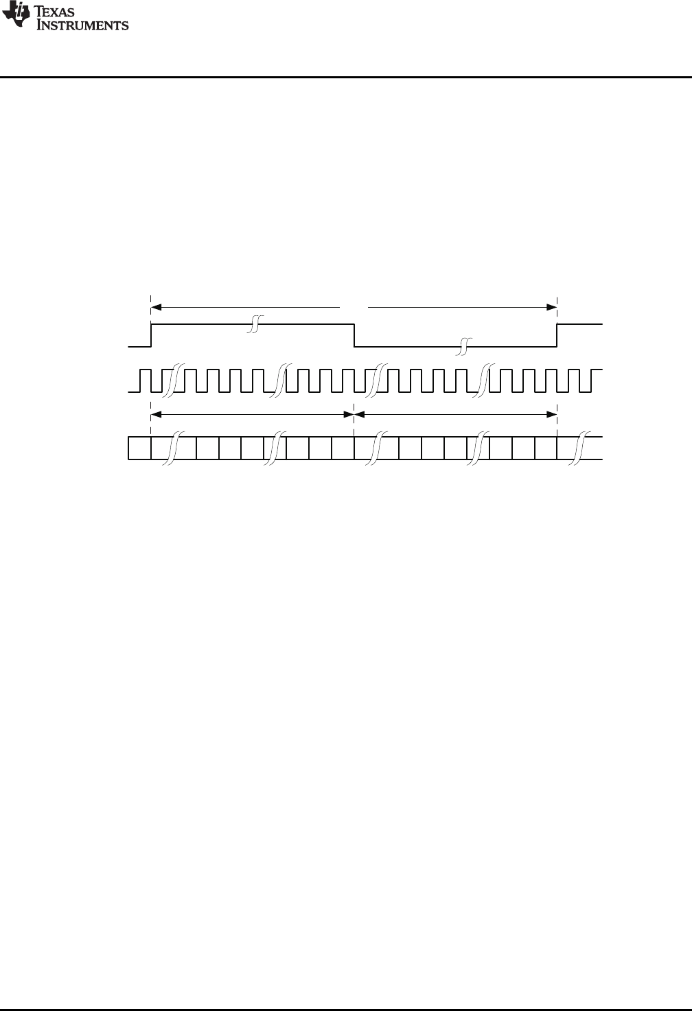
BCLK
WCLK
DIN/
DOUT n-1 n-2 1 00 n-1 n-2 1 0
LSBMSB
LeftChannel RightChannel
n-3 2 2n-3
LSBMSB
1/fs
www.ti.com
Audio Digital I/O Interface
By default when the word-clocks and bit-clocks are generated by the TLV320AIC3256, these clocks are
active only when the codec (ADC, DAC or both) are powered up within the device. This intermittent clock
operation reduces power consumption. However, it also supports a feature when both the word clocks and
bit-clocks can be active even when the codec in the device is powered down. This continuous clock
feature is useful when using the TDM mode with multiple codecs on the same bus, or when word-clock or
bit-clocks are used in the system as general-purpose clocks.
2.6.1 Right Justified Mode
The Audio Interface of the TLV320AIC3256 can be put into Right Justified Mode by programming Page 0,
Register 27, D(7:6) = 10b. In right-justified mode, the LSB of the left channel is valid on the rising edge of
the bit clock preceding the falling edge of the word clock. Similarly, the LSB of the right channel is valid on
the rising edge of the bit clock preceding the rising edge of the word clock.
Figure 2-38. Timing Diagram for Right-Justified Mode
For Right-Justified mode, the number of bit-clocks per frame should be greater than twice the
programmed word-length of the data.
69
SLAU306A–January 2011–Revised January 2013 TLV320AIC3256 Application
Submit Documentation Feedback Copyright © 2011–2013, Texas Instruments Incorporated
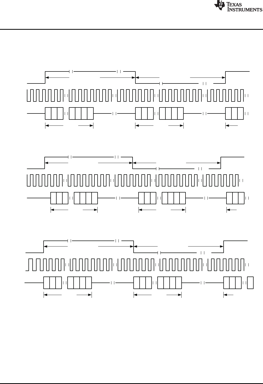
LD(n) LD(n+1)
WORD
CLOCK
BIT
CLOCK
DATA 3
N
-
1
N
-
2
N
-
3
2 1 0
3
N
-
1
N
-
2
N
-
3
2 1 0
3
N
-
1
N
-
2
N
-
3
RD(n)
LEFT CHANNEL RIGHT CHANNEL
LD(n)=n'thsampleofleftchanneldata RD(n)=n'thsampleofrightchanneldata
LD(n) LD(n+1)
WORD
CLOCK
BIT
CLOCK
DATA -
1
-
2
-
3
2 1 03 -
1
-
2
-
3
2 1 03 -
1
-
2
N N N N N N N N N
-
3
RD(n)
LEFT CHANNEL RIGHT CHANNEL
LD(n)=n'thsampleofleftchanneldata RD(n)=n'thsampleofrightchanneldata
LD(n) LD(n+1)
WORD
CLOCK
BIT
CLOCK
DATA -
1
-
2
-
3
2 1 03 -
1
-
2
-
3
2 1 03 -
1
-
2
N N N N N N N N N
-
3
RD(n)
LEFT CHANNEL RIGHT CHANNEL
LD(n)=n'thsampleofleftchanneldata RD(n)=n'thsampleofrightchanneldata
Audio Digital I/O Interface
www.ti.com
2.6.2 Left Justified Mode
The Audio Interface of the TLV320AIC3256 can be put into Left Justified Mode by programming Page 0,
Register 27, D(7:6) = 11b. In left-justified mode, the MSB of the right channel is valid on the rising edge of
the bit clock following the falling edge of the word clock. Similarly the MSB of the left channel is valid on
the rising edge of the bit clock following the rising edge of the word clock.
Figure 2-39. Timing Diagram for Left-Justified Mode
Figure 2-40. Timing Diagram for Left-Justified Mode with Offset = 1
Figure 2-41. Timing Diagram for Left-Justified Mode with Offset = 0 and inverted bit clock
For Left-Justified mode, the number of bit-clocks per frame should be greater than twice the programmed
word-length of the data. Also, the programmed offset value should be less than the number of bit-clocks
per frame by at least the programmed word-length of the data.
70 TLV320AIC3256 Application SLAU306A–January 2011–Revised January 2013
Submit Documentation Feedback
Copyright © 2011–2013, Texas Instruments Incorporated
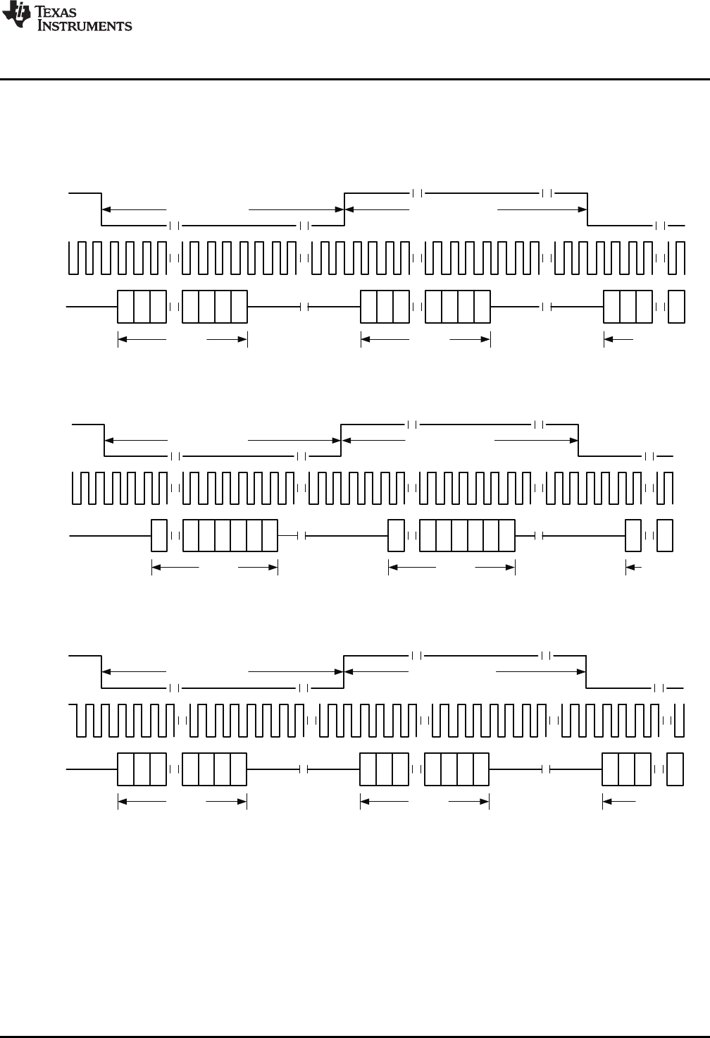
LD(n) LD(n+1)
WORD
CLOCK
BIT
CLOCK
DATA -
1
-
2
-
3
2 1 03 -
1
-
2
-
3
2 1 03 -
1
-
2
N N N N N N N N N
-
3
3
RD(n)
LEFT CHANNEL RIGHT CHANNEL
LD(n) = n'th sample of left channel data RD(n) = n'th sample of right channel data
LD(n) LD (n+1)
WORD
CLOCK
BIT
CLOCK
DATA -
1
4 3 25 1 0 -
1
4 3 25 1 0
N N N
-
1
5
RD(n)
LEFT CHANNEL RIGHT CHANNEL
LD(n) = n'th sample of left channel data RD(n) = n'th sample of right channel data
LD(n) LD(n+1)
WORD
CLOCK
BIT
CLOCK
DATA -
1
-
2
-
3
2 1 03 -
1
-
2
-
3
2 1 03 -
1
-
2
N N N N N N N N N
-
3
3
RD(n)
LEFT CHANNEL RIGHT CHANNEL
LD(n)=n'thsampleofleftchanneldata RD(n)=n'thsampleofrightchanneldata
www.ti.com
Audio Digital I/O Interface
2.6.3 I2S Mode
The Audio Interface of the TLV320AIC3256 can be put into I2S Mode by programming Page 0, Register
27, D(7:6) = to 00b. In I2S mode, the MSB of the left channel is valid on the second rising edge of the bit
clock after the falling edge of the word clock. Similarly the MSB of the right channel is valid on the second
rising edge of the bit clock after the rising edge of the word clock.
Figure 2-42. Timing Diagram for I2S Mode
Figure 2-43. Timing Diagram for I2S Mode with offset = 2
Figure 2-44. Timing Diagram for I2S Mode with offset = 0 and bit clock invert
For I2S mode, the number of bit-clocks per channel should be greater than or equal to the programmed
word-length of the data. Also the programmed offset value should be less than the number of bit-clocks
per frame by at least the programmed word-length of the data.
71
SLAU306A–January 2011–Revised January 2013 TLV320AIC3256 Application
Submit Documentation Feedback Copyright © 2011–2013, Texas Instruments Incorporated
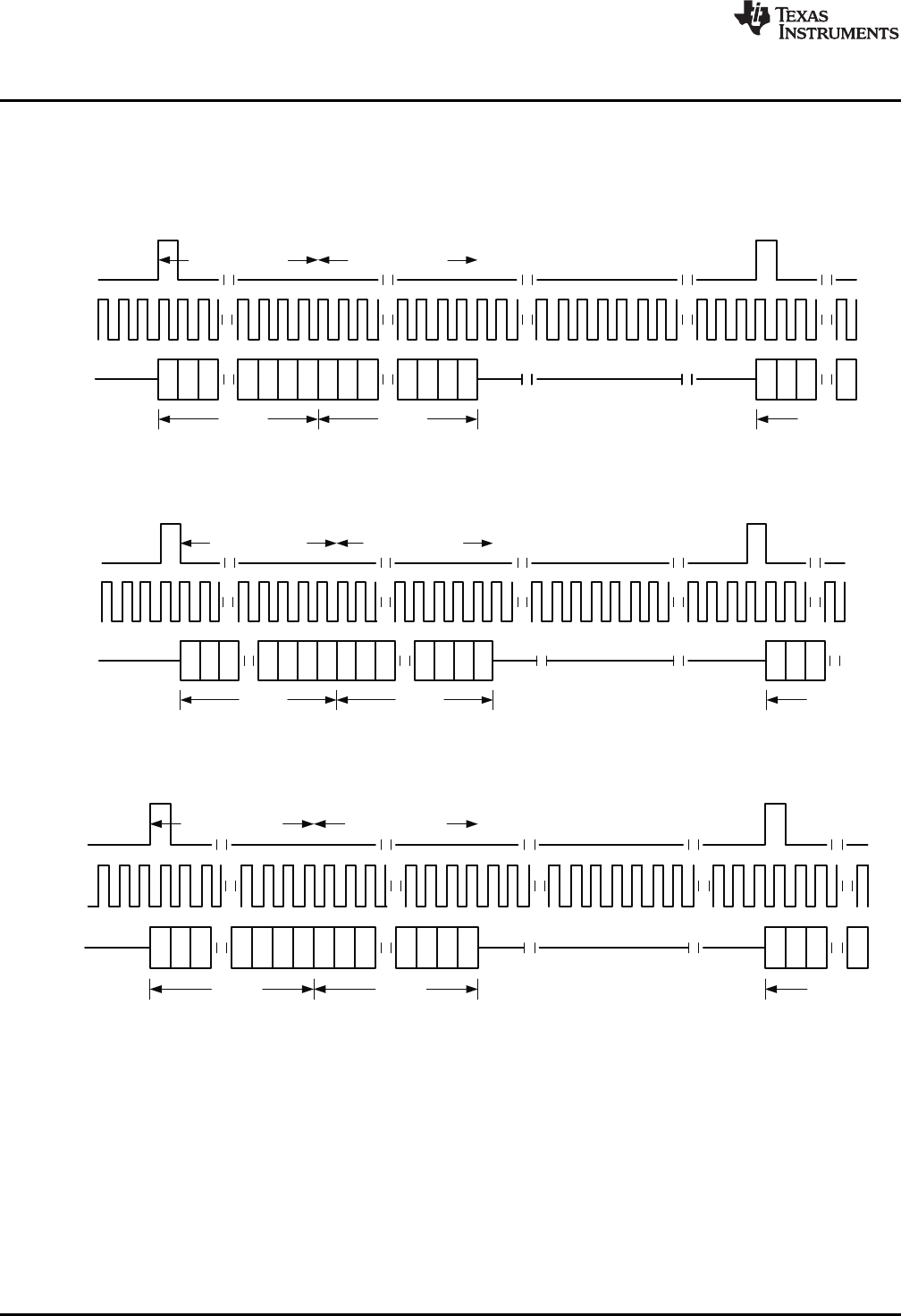
LD(n) LD(n+1)
BIT
CLOCK
DATA
N
-
1
N
-
2
N
-
3
2 1 0
3N
-
1
N
-
2
N
-
3
03 2 1 N
-
1
N
-
2
N
-
3
3
RD(n)
WORD
CLOCK LEFT CHANNEL RIGHT CHANNEL
LD(n) LD(n+1)
BIT
CLOCK
DATA -
1
-
2
-
3
2 1 03 -
1
-
2
-
3
03 2 1 -
1
-
2
N N N N N N N N N
-
3
RD(n)
WORD
CLOCK LEFT CHANNEL RIGHT CHANNEL
LD(n)=n'thsampleofleftchanneldata RD(n)=n'thsampleofrightchanneldata
LD(n) LD (n+1)
BIT
CLOCK
DATA -
1
-
2
-
3
2 1 03 -
1
-
2
-
3
03 2 1 -
1
-
2
N N N N N N N N N
-
3
3
RD(n)
WORD
CLOCK LEFT CHANNEL RIGHT CHANNEL
LD(n)=n'thsampleofleftchanneldata RD(n)=n'thsampleofrightchanneldata
Audio Digital I/O Interface
www.ti.com
2.6.4 DSP Mode
The Audio Interface of the TLV320AIC3256 can be put into DSP Mode by programming Page 0, Register
27, D(7:6) = 01b. In DSP mode, the rising edge of the word clock starts the data transfer with the left
channel data first and immediately followed by the right channel data. Each data bit is valid on the falling
edge of the bit clock.
Figure 2-45. Timing Diagram for DSP Mode
Figure 2-46. Timing Diagram for DSP Mode with offset = 1
Figure 2-47. Timing Diagram for DSP Mode with offset = 0 and bit clock inverted
For DSP mode, the number of bit-clocks per frame should be greater than twice the programmed word-
length of the data. Also the programmed offset value should be less than the number of bit-clocks per
frame by at least the programmed word-length of the data.
72 TLV320AIC3256 Application SLAU306A–January 2011–Revised January 2013
Submit Documentation Feedback
Copyright © 2011–2013, Texas Instruments Incorporated
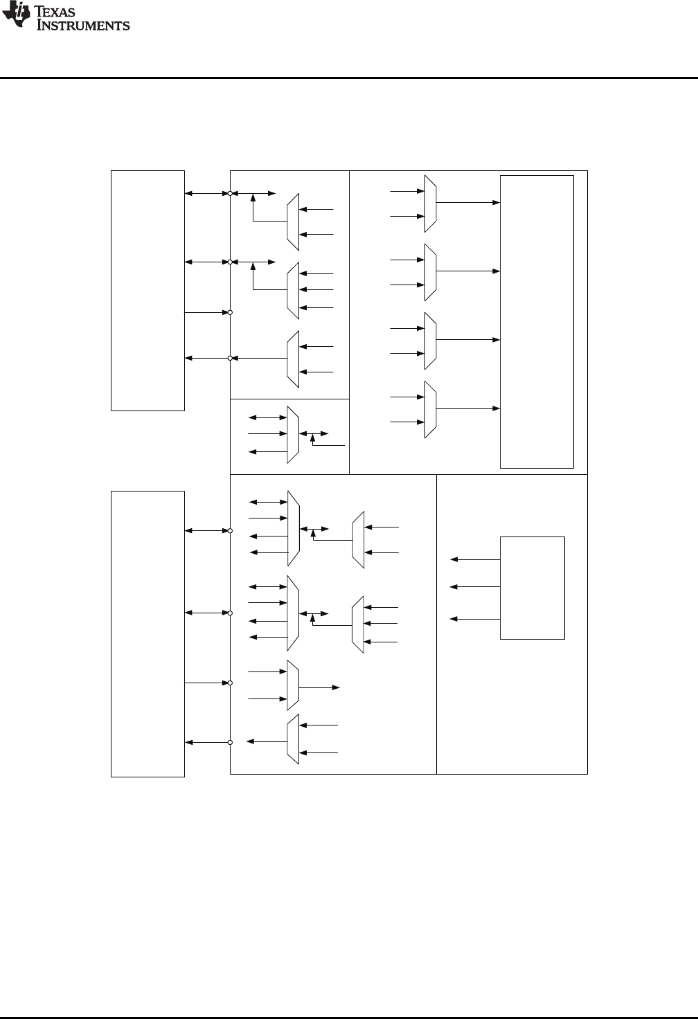
BCLK
WCLK
DOUT
DOUT_int
S_DIN
BCLK
DIN
WCLK
DIN
DOUT
Primary
Audio
Processor
S_WCLK
DAC_FS
ADC_FS
S_BCLK
BCLK_OUT
BCLK
S_BCLK
WCLK
S_WCLK
DIN
S_DIN
WCLK
ADC_WCLK
Audio
Digital
Serial
Interface
BCLK_INT
DAC_WCLK_INT
ADC_WCLK_INT
DIN_INT
GPIO
SCLK
MISO
S_BCLK
DOUT
BCLK
BCLK_OUT
GPIO
SCLK
MISO
S_WCLK
DOUT
WCLK
DAC_FS
ADC_FS
GPIO
SCLK
S_DIN
DOUT_int
DIN
MISO
(S_DOUT)
Clock
Generation
BCLK_OUT
DAC_FS
ADC_FS
WCLK
DIN
DOUT
Secondary
Audio
Processor
BCLK
GPIO
SCLK
MISO
ADC_FS
ADC_WCLK
BCLK2
WCLK2
www.ti.com
Audio Digital I/O Interface
2.6.5 Secondary I2S
The audio serial interface on the TLV320AIC3256 has an extensive IO control to allow communication
with two independent processors for audio data. Each processor can communicate with the device one at
a time. This feature is enabled by register programming of the various pin selections.
Figure 2-48. Audio Serial Interface Multiplexing
The secondary audio interface uses multifunction pins. For an overview on multifunction pins please see
Section 2.1.1.1.Figure 2-48 illustrates possible audio interface routing. The multifunction pins SCLK and
MISO are only available in I2C communication mode.
This multiplexing capability allows the TLV320AIC3256 to communicate with two separate devices with
independent I2S or PCM busses, one at a time.
73
SLAU306A–January 2011–Revised January 2013 TLV320AIC3256 Application
Submit Documentation Feedback Copyright © 2011–2013, Texas Instruments Incorporated
MDACNDAC
CLKIN_CODEC
CLK_MOD_DAC
´
=
DOSRMDACNDAC
CLKIN_CODEC
´´
fS
_DAC =
MADCNADC
CLKIN_CODEC
CLK_MOD_ADC
´
=
AOSRMADCNADC
CLKIN_CODEC
fS
_ADC
´´
=
Clock Generation and PLL
www.ti.com
2.7 Clock Generation and PLL
The TLV320AIC3256 supports a wide range of options for generating clocks for the ADC and DAC
sections as well as interface and other control blocks. The clocks for ADC and DAC require a source
reference clock. This clock can be provided on variety of device pins such as MCLK, BCLK or GPI pins.
The CODEC_CLKIN can then be routed through highly-flexible clock dividers to generate the various
clocks required for ADC, DAC and the miniDSP sections. In the event that the desired audio or miniDSP
clocks cannot be generated from the reference clocks on MCLK BCLK or GPIO, the TLV320AIC3256 also
provides the option of using the on-chip PLL which supports a wide range of fractional multiplication
values to generate the required clocks. Starting from CODEC_CLKIN the TLV320AIC3256 provides
several programmable clock dividers to help achieve a variety of sampling rates for ADC, DAC and clocks
for the miniDSP.
To minimize power consumption, the system ideally provides a master clock that is a suitable integer
multiple of the desired sampling frequencies. In such cases, internal dividers can be programmed to set
up the required internal clock signals at very low power consumption. For cases where such master clocks
are not available, the built-in PLL can be used to generate a clock signal that serves as an internal master
clock. In fact, this master clock can also be routed to an output pin and may be used elsewhere in the
system. The clock system is flexible enough that it even allows the internal clocks to be derived directly
from an external clock source, while the PLL is used to generate some other clock that is only used
outside the TLV320AIC3256.
Figure 2-49. Clock Distribution Tree
(14)
(15)
(16)
(17)
Table 2-29. CODEC CLKIN Clock Dividers
Divider Bits
NDAC Page 0, Register 11, D(6:0)
MDAC Page 0, Register 12, D(6:0)
DOSR Page 0, Register 13, D(1:0) + Page 0, Register 14, D(7:0)
NADC Page 0, Register 18, D(6:0)
MADC Page 0, Register 19, D(6:0)
AOSR Page 0, Register 20, D(7:0)
The DAC Modulator is clocked by DAC_MOD_CLK. For proper power-up of the DAC Channel, these
clocks must be enabled by configuring the NDAC and MDAC clock dividers ( Page 0,Register 11, D(7) = 1
and Page 0, Register 12, D(7) = 1). When the DAC channel is powered down, the device internally
initiates a power-down sequence for proper shut-down. During this shut-down sequence, the NDAC and
MDAC dividers must not be powered down, or else a proper low power shut-down may not take place.
The user can read the power-status flag in Page 0, Register 37, D(7) and Page 0, Register 37, D(3).
When both flags indicate power-down, the MDAC divider may be powered down, followed by the NDAC
divider.
74 TLV320AIC3256 Application SLAU306A–January 2011–Revised January 2013
Submit Documentation Feedback
Copyright © 2011–2013, Texas Instruments Incorporated
÷N
BCLK
DAC_CLK
ADC_MOD_CLK
DAC_MOD_CLK
ADC_CLK
BDIV_CLKIN
N=1,2,...,127,128
www.ti.com
Clock Generation and PLL
The is clocked by ADC_MOD_CLK. For proper power-up of the ADC Channel, these clocks are enabled
by the NADC and MADC clock dividers (Page 0,Register 18, D(7) = 1 and Page 0, Register 19, D(7) = 1).
When the ADC channel is powered down, the device internally initiates a power-down sequence for
proper shut-down. During this shut-down sequence, the NADC and MADC dividers must not be powered
down, or else a proper low power shut-down may not take place. The user can read the power-status flag
in Page 0, Register 36, D(6) and Page 0, Register 36, D(2). When both flags indicate power-down, the
MADC divider may be powered down, followed by NADC divider.
When ADC_CLK is derived from the NDAC divider output, the NDAC must be kept powered up till the
power-down status flags for ADC do not indicate power-down. When the input to the AOSR clock divider
is derived from DAC_MOD_CLK, then MDAC must be powered up when ADC_FS is needed ( such as
when WCLK is generated by TLV320AIC3256 or AGC is enabled) and can be powered down only after
the ADC power-down flags indicate power-down status.
In general, all the root clock dividers should be powered down only after the child clock dividers have been
powered down for proper operation.
The TLV320AIC3256 also has options for routing some of the internal clocks to the output pins of the
device to be used as general purpose clocks in the system. The feature is shown in Figure 2-50.
Figure 2-50. BCLK Output Options
In the mode when TLV320AIC3256 is configured to drive the BCLK pin (Page 0, Register 27, D(3) = ’1’) it
can be driven as divided value of BDIV_CLKIN. The division value can be programmed in Page 0,
Register 30, D(6:0) from 1 to 128. The BDIV_CLKIN can itself be configured to be one of DAC_CLK,
DAC_MOD_CLK, ADC_CLK or ADC_MOD_CLK by configuring the BDIV_CLKIN mux in Page 0, Register
29, D(1:0). Additionally a general purpose clock can be driven out on either GPIO, DOUT or MISO pin.
This clock can be a divided-down version of CDIV_CLKIN. The value of this clock divider can be
programmed from 1 to 128 by writing to Page 0, Register 26, D(6:0). The CDIV_CLKIN can itself be
programmed as one of the clocks among the list shown in Figure 2-51. This configuration is available by
programming the mux in Page 0, Register 25, D(2:0).
75
SLAU306A–January 2011–Revised January 2013 TLV320AIC3256 Application
Submit Documentation Feedback Copyright © 2011–2013, Texas Instruments Incorporated
÷M
CLKOUT
CDIV_CLKIN
MCLK BCLK DIN
GPIO MISO DOUT
PLL_CLK
DAC_CLK ADC_CLK
DAC_MOD_CLK ADC_MOD_CLK
M=1,2,...,127,128
Clock Generation and PLL
www.ti.com
Figure 2-51. General Purpose Clock Output Options
Table 2-30. Maximum TLV320AIC3256 Clock Frequencies
DVdd ≥1.26V DVdd ≥1.65V
CODEC_CLKIN 50MHz 137MHz when NDAC is even, NADC is even
112MHz when NDAC is even, NADC is odd
110MHz when NDAC is odd, NADC is even
110MHz when NDAC is odd, NADC is odd
ADC_CLK 25MHz 55.296MHz
ADC_miniDSP_CLK 20MHz 55.296MHz
51.0MHz if AGC is on
ADC_MOD_CLK 6.758MHz 6.758MHz
ADC_FS 0.192MHz 0.192MHz
DAC_CLK 25MHz 55.296MHz
DAC_miniDSP_CLK 20MHz 55.296MHz
DAC_MOD_CLK 6.758MHz 6.758MHz
4.2MHz when Class-D Mode Headphone
is used
DAC_FS 0.192MHz 0.192MHz
BDIV_CLKIN 25MHz 55.296MHz
CDIV_CLKIN 50MHz 112MHz when M is odd
137MHz when M is even
2.7.1 PLL
The TLV320AIC3256 has an on-chip PLL to generate the clock frequency for the audio ADC, DAC, and
Digital Signal Processing blocks. The programmability of the PLL allows operation from a wide variety of
clocks that may be available in the system.
76 TLV320AIC3256 Application SLAU306A–January 2011–Revised January 2013
Submit Documentation Feedback
Copyright © 2011–2013, Texas Instruments Incorporated
MHz20
P
CLKIN_PLL
MHz10 ££
MHz20
P
CLKIN_PLL
kHz512 ££
PLL _ CLKIN R J.D
PLL _ CLK P
´ ´
=
www.ti.com
Clock Generation and PLL
The PLL input supports clocks varying from 512kHz to 20MHz and is register programmable to enable
generation of required sampling rates with fine resolution. The PLL can be turned on by writing to Page 0,
Register 5, D(7). When the PLL is enabled, the PLL output clock PLL_CLK is given by the following
equation:
(18)
R=1,2,3,4
J = 1, 2, 3, 4,… 63, and D = 0, 1, 2, 3, 4, … 9999
P = 1, 2, 3, 4, … 8
R, J, D, and P are register programmable.
The PLL can be programmed via Page 0, Registers 5-8. The PLL can be turned on via Page 0, Register
5, D(7). The variable P can be programmed via Page 0, Register 5, D(6:4). The default register value for P
is 1, and for J is 4. The variable R can be programmed via Page 0, Register 5, D(3:0). The default register
value for R is 1. The variable J can be programmed via Page 0, Register 6, D(5:0). The variable D is 12-
bits, programmed into two registers. The MSB portion can be programmed via Page 0, Register 7, D(5:0),
and the LSB portion is programmed via Page 0, Register 8, D(7:0). The default register value for D is 0.
When the PLL is enabled the following conditions must be satisfied
• When the PLL is enabled and D = 0, the following conditions must be satisfied for PLL_CLKIN:
(19)
• When the PLL is enabled and D ≠0, the following conditions must be satisfied for PLL_CLKIN:
(20)
In the TLV320AIC3256 the PLL_CLK supports a wide range of output clock, based on register settings
and power-supply conditions.
Table 2-31. PLL_CLK Frequency Range
AVdd PLL Mode Min PLL_CLK Max PLL_CLK
Page 0, Reg 4, D6 frequency (MHz) frequency (MHz)
≥1.5V 0 80 103
1 95 110
≥1.65V 0 80 118
1 92 123
≥1.80V 0 80 132
1 92 137
The PLL can be powered up independently from the ADC and DAC blocks, and can also be used as a
general purpose PLL by routing its output to the GPIO output. After powering up the PLL, PLL_CLK is
available typically after 10ms. The PLL output frequency is controlled by J.D and R dividers
PLL Divider Bits
J Page 0, Register 6, D(5:0)
D Page 0, Register 7, D(5:0) and Page 0, Register 8, D(7:0)
R Page 0, Register 5, D(3:0)
The D-divider value is 14-bits wide and is controlled by 2 registers. For proper update of the D-divider
value, Page 0, Register 7 must be programmed first followed immediately by Page 0, Register 8. Unless
the write to Page 0, Register 8 is completed, the new value of D will not take effect.
The clocks for codec and various signal processing blocks, CODEC_CLKIN can be generated from MCLK
input, BCLK input, GPIO input or PLL_CLK (Page 0, Register 4, D(1:0)).
77
SLAU306A–January 2011–Revised January 2013 TLV320AIC3256 Application
Submit Documentation Feedback Copyright © 2011–2013, Texas Instruments Incorporated
Control Interfaces
www.ti.com
If the CODEC_CLKIN is derived from the PLL, then the PLL must be powered up first and powered down
last.
Table 2-32 lists several example cases of typical MCLK rates and how to program the PLL to achieve a
sample rate fSof either 44.1kHz or 48kHz.
Table 2-32. PLL Example Configurations
fS= 44.1kHz
MCLK (MHz) PLLP PLLR PLLJ PLLD MADC NADC AOSR MDAC NDAC DOSR
2.8224 1 3 10 0 3 5 128 3 5 128
5.6448 1 3 5 0 3 5 128 3 5 128
12 1 1 7 560 3 5 128 3 5 128
13 1 2 4 2336 13 3 64 4 6 104
16 1 1 5 2920 3 5 128 3 5 128
19.2 1 1 4 4100 3 5 128 3 5 128
48 4 1 7 560 3 5 128 3 5 128
fS= 48kHz
2.048 1 3 14 0 2 7 128 7 2 128
3.072 1 4 7 0 2 7 128 7 2 128
4.096 1 3 7 0 2 7 128 7 2 128
6.144 1 2 7 0 2 7 128 7 2 128
8.192 1 4 3 0 2 8 128 4 4 128
12 1 1 7 1680 2 7 128 7 2 128
16 1 1 5 3760 2 7 128 7 2 128
19.2 1 1 4 4800 2 7 128 7 2 128
48 4 1 7 1680 2 7 128 7 2 128
2.8 Control Interfaces
The TLV320AIC3256 control interface supports SPI or I2C communication protocols, with the protocol
selectable using the SPI_SELECT pin. For SPI, SPI_SELECT should be tied high; for I2C, SPI_SELECT
should be tied low. Changing the state of SPI_SELECT during device operation is not recommended.
2.8.1 I2C Control Mode
The TLV320AIC3256 supports the I2C control protocol, and will respond to the I2C address of 0011000.
I2C is a two-wire, open-drain interface supporting multiple devices and masters on a single bus. Devices
on the I2C bus only drive the bus lines LOW by connecting them to ground; they never drive the bus lines
HIGH. Instead, the bus wires are pulled HIGH by pullup resistors, so the bus wires are HIGH when no
device is driving them LOW. This circuit prevents two devices from conflicting; if two devices drive the bus
simultaneously, there is no driver contention.
Communication on the I2C bus always takes place between two devices, one acting as the master and the
other acting as the slave. Both masters and slaves can read and write, but slaves can only do so under
the direction of the master. Some I2C devices can act as masters or slaves, but the TLV320AIC3256 can
only act as a slave device.
An I2C bus consists of two lines, SDA and SCL. SDA carries data, and the SCL signal provides the clock.
All data is transmitted across the I2C bus in groups of eight bits. To send a bit on the I2C bus, the SDA line
is driven to the appropriate level while SCL is LOW (a LOW on SDA indicates the bit is zero, while a HIGH
indicates the bit is one).
Once the SDA line has settled, the SCL line is brought HIGH, then LOW. This pulse on the SCL line
clocks the SDA bit into the receiver’s shift register.
The I2C bus is bidirectional: the SDA line is used both for transmitting and receiving data. When a master
reads from a slave, the slave drives the data line; when a master sends to a slave, the master drives the
data line.
78 TLV320AIC3256 Application SLAU306A–January 2011–Revised January 2013
Submit Documentation Feedback
Copyright © 2011–2013, Texas Instruments Incorporated
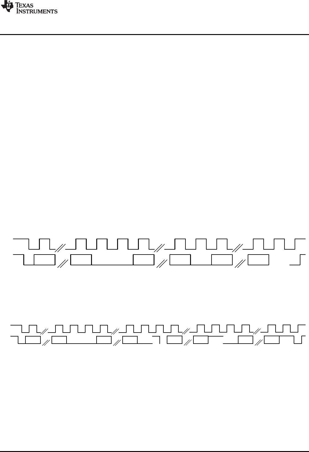
Start
(M)
7-bitDevice Address
(M)
Write
(M)
Slave
Ack
(S)
8-bitRegister Address
(M)
Slave
Ack
(S)
SDA
SCL
7-bitDevice Address
(M)
Read
(M)
Slave
Ack
(S)
DA(6) DA(0) RA(7) RA(0) DA(6) DA(0) D(7) D(0)
8-bitRegisterData
(S)
Stop
(M)
Master
No Ack
(M)
Repeat
Start
(M)
(M)=>SDA ControlledbyMaster
(S)=>SDA ControlledbySlave
DA(6) DA(0) RA(7) RA(0) D(7) D(0)
Start
(M)
7-bitDevice Address
(M)
Write
(M)
Slave
Ack
(S)
8-bitRegister Address
(M)
Slave
Ack
(S)
8-bitRegisterData
(M)
Stop
(M)
Slave
Ack
(S)
SDA
SCL
(M)=>SDA ControlledbyMaster
(S)=>SDA ControlledbySlave
www.ti.com
Control Interfaces
Most of the time the bus is idle, no communication is taking place, and both lines are HIGH. When
communication is taking place, the bus is active. Only master devices can start communication on the bus.
Normally, the data line is only allowed to change state while the clock line is LOW. If the data line changes
state while the clock line is HIGH, it is either a START condition or its counterpart, a STOP condition. A
START condition is when the clock line is HIGH and the data line goes from HIGH to LOW. A STOP
condition is when the clock line is HIGH and the data line goes from LOW to HIGH.
After the master issues a START condition, it sends a byte that selects the slave device for
communication. This byte is called the address byte. Each device on an I2C bus has a unique 7-bit
address to which it responds. (Slaves can also have 10-bit addresses; see the I2C specification for
details.) The master sends an address in the address byte, together with a bit that indicates whether it
wishes to read from or write to the slave device.
Every byte transmitted on the I2C bus, whether it is address or data, is acknowledged with an
acknowledge bit. When a master has finished sending a byte (eight data bits) to a slave, it stops driving
SDA and waits for the slave to acknowledge the byte. The slave acknowledges the byte by pulling SDA
LOW. The master then sends a clock pulse to clock the acknowledge bit. Similarly, when a master has
finished reading a byte, it pulls SDA LOW to acknowledge this to the slave. The master then sends a clock
pulse to clock the bit. (Remember that the master always drives the clock line.)
A not-acknowledge is performed by simply leaving SDA HIGH during an acknowledge cycle. If a device is
not present on the bus, and the master attempts to address it, it will receive a not−acknowledge because
no device is present at that address to pull the line LOW.
When a master has finished communicating with a slave, it may issue a STOP condition. When a STOP
condition is issued, the bus becomes idle again. A master may also issue another START condition. When
a START condition is issued while the bus is active, it is called a repeated START condition.
The TLV320AIC3256 can also respond to and acknowledge a General Call, which consists of the master
issuing a command with a slave address byte of 00H. This feature is disabled by default, but can be
enabled via Page 0, Register 34, Bit D(5).
Figure 2-52. I2C Write
Figure 2-53. I2C Read
In the case of an I2C register write, if the master does not issue a STOP condition, then the device enters
auto-increment mode. So in the next eight clocks, the data on SDA is treated as data for the next
incremental register.
Similarly, in the case of an I2C register read, after the device has sent out the 8-bit data from the
addressed register, if the master issues a ACKNOWLEDGE, the slave takes over control of SDA bus and
transmit for the next 8 clocks the data of the next incremental register.
79
SLAU306A–January 2011–Revised January 2013 TLV320AIC3256 Application
Submit Documentation Feedback Copyright © 2011–2013, Texas Instruments Incorporated
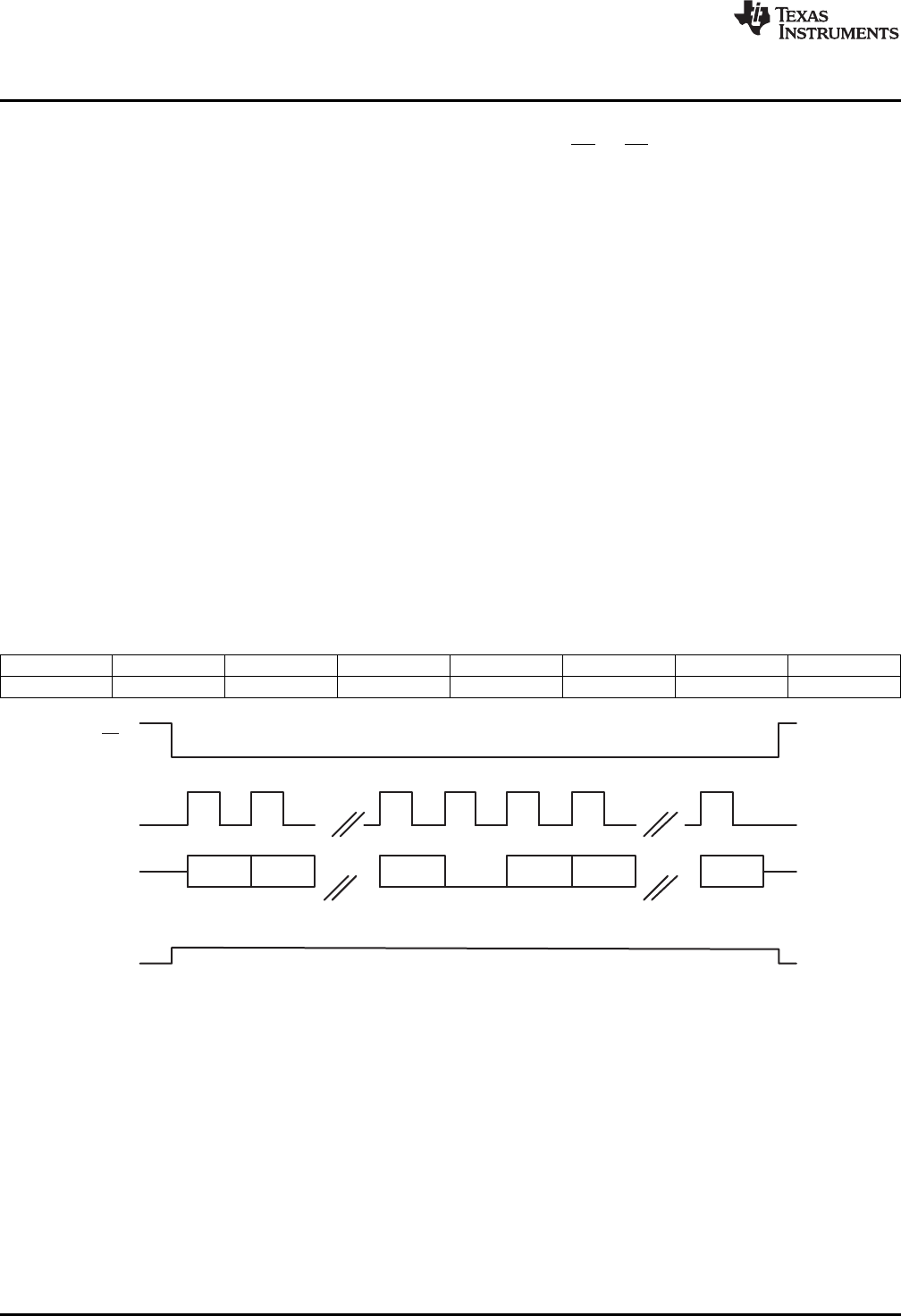
RA(6) RA(5) RA(0) D(7) D(6) D(0)
7-bitRegister Address Write 8-bitRegisterData
SS
SCLK
MOSI
MISO
Hi-Z Hi-Z
Hi-Z Hi-Z
Control Interfaces
www.ti.com
2.8.2 SPI Digital Interface
In the SPI control mode, the TLV320AIC3256 uses the pins SCL/SS as SS, SCLK as SCLK, MISO as
MISO, SDA/MOSI as MOSI; a standard SPI port with clock polarity setting of 0 (typical microprocessor
SPI control bit CPOL = 0). The SPI port allows full-duplex, synchronous, serial communication between a
host processor (the master) and peripheral devices (slaves). The SPI master (in this case, the host
processor) generates the synchronizing clock (driven onto SCLK) and initiates transmissions. The SPI
slave devices (such as the TLV320AIC3256) depend on a master to start and synchronize transmissions.
A transmission begins when initiated by an SPI master. The byte from the SPI master begins shifting in on
the slave MOSI pin under the control of the master serial clock (driven onto SCLK). As the byte shifts in
on the MOSI pin, a byte shifts out on the MISO pin to the master shift register.
The TLV320AIC3256 interface is designed so that with a clock-phase bit setting of 1 (typical
microprocessor SPI control bit CPHA = 1), the master begins driving its MOSI pin and the slave begins
driving its MISO pin on the first serial clock edge. The SSZ pin can remain low between transmissions;
however, the TLV320AIC3256 only interprets the first 8 bits transmitted after the falling edge of SSZ as a
command byte, and the next 8 bits as a data byte only if writing to a register. Reserved register bits
should be written to their default values. The TLV320AIC3256 is entirely controlled by registers. Reading
and writing these registers is accomplished by an 8-bit command sent to the MOSI pin of the part prior to
the data for that register. The command is structured as shown in Table 2-33. The first 7 bits specify the
register address which is being written or read, from 0 to 127 (decimal). The command word ends with an
R/W bit, which specifies the direction of data flow on the serial bus. In the case of a register write, the R/W
bit should be set to 0. A second byte of data is sent to the MOSI pin and contains the data to be written to
the register. Reading of registers is accomplished in similar fashion. The 8-bit command word sends the 7-
bit register address, followed by R/W bit = 1 to signify a register read is occurring. The 8-bit register data
is then clocked out of the part on the MISO pin during the second 8 SCLK clocks in the frame.
Table 2-33. SPI Command Word
Bit 7 Bit 6 Bit 5 Bit 4 Bit 3 Bit 2 Bit 1 Bit 0
ADDR(6) ADDR(5) ADDR(4) ADDR(3) ADDR(2) ADDR(1) ADDR(0) R/WZ
Figure 2-54. SPI Timing Diagram for Register Write
80 TLV320AIC3256 Application SLAU306A–January 2011–Revised January 2013
Submit Documentation Feedback
Copyright © 2011–2013, Texas Instruments Incorporated
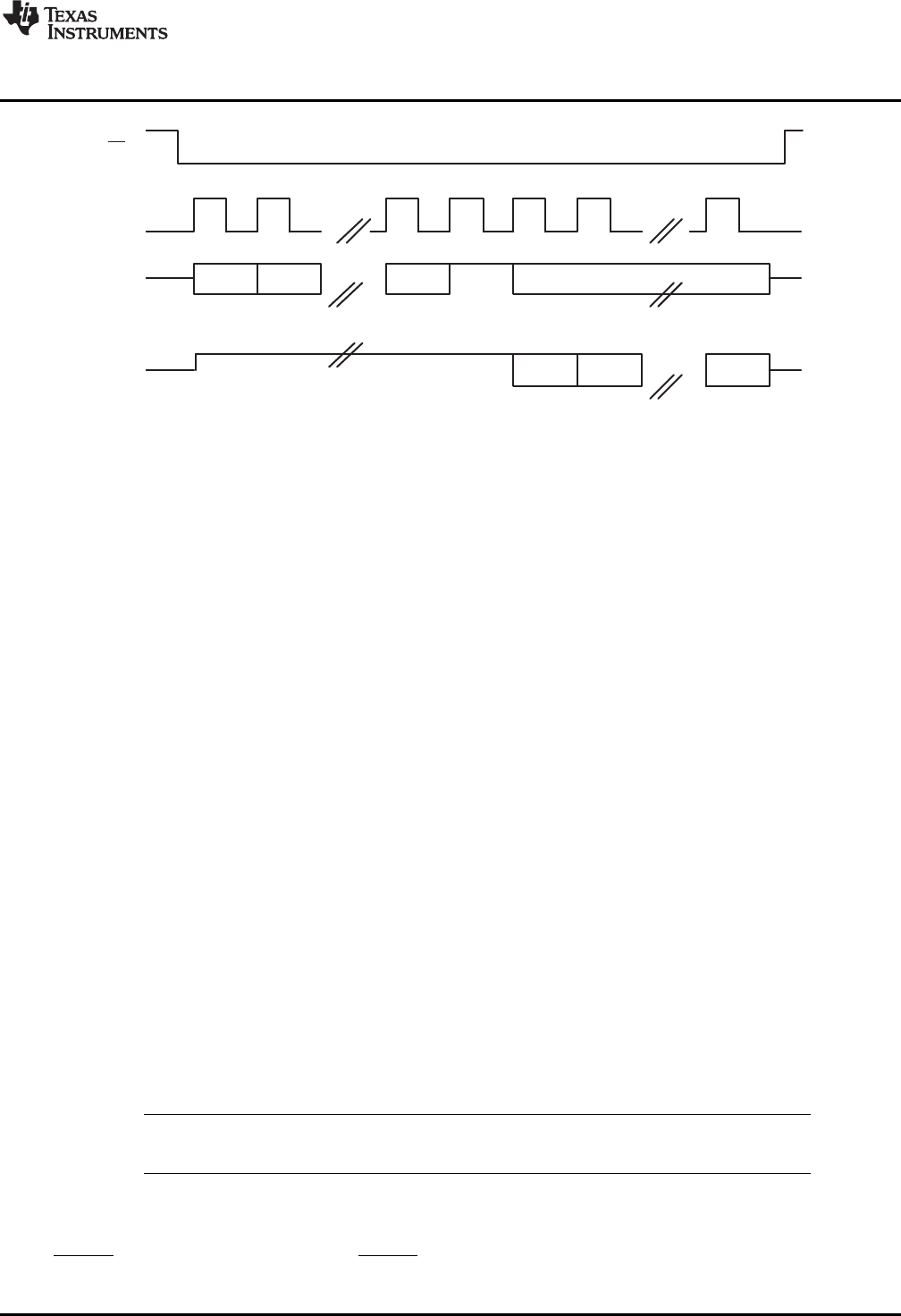
RA(6) RA(5) RA(0) Don’tCare
7-bitRegister Address Read 8-bitRegisterData
SS
SCLK
MOSI
MISO
Hi-Z Hi-Z
D(7) D(6) D(0)
Hi-Z Hi-Z
www.ti.com
Power Supply
Figure 2-55. SPI Timing Diagram for Register Read
2.9 Power Supply
The device has an integrated charge pump. In ground-centered headphone configuration, all supplies can
be conveniently supplied from a single 1.5V to 1.95V rail. The device has separate power domains for
digital IO, digital core, analog core, charge-pump input and headphone drive, all of which can be
connected together and be supplied from one source. For improved power efficiency, the digital core
voltage can range from 1.26V to 1.95V. The IO voltage can be supplied in the range of 1.1V to 3.6V.
The device power supply Vsys can be supplied in the range of 1.5V to 5.5V. Vsys must always be greater
than or equal to AVdd and DVdd voltages.
The TLV320AIC3256 has a total of six power-supply connections.
•Vsys - The Vsys supply biases the device. The voltage on Vsys can range from 1.5V to 5.5V, but must
always be greater than the voltage on AVdd and DVdd pins.
•IOVdd - The IOVdd pin supplies the digital IO cells of the device. The voltage of IOVdd can range from
1.1 to 3.6V and is determined by the digital IO voltage of the rest of the system.
•DVdd - This pin supplies the digital core of the device. Lower DVdd voltages cause lower power
dissipation. If efficient switched-mode power supplies are used in the system, system power can be
optimized using low DVdd voltages. the full clock range is supported with DVdd in the range of 1.65 to
1.95V. Also, operation with DVdd down to 1.26V is possible. (See Table 2-30)
•DVdd_CP - The internal charge pump is supplied through this pin.
•AVdd - This pin supplies the analog core of the device. The analog core voltage (AVdd) should be in
the range of 1.5 to 1.95V for specified performance. For AVdd voltages above 1.8V, the internal
common mode voltage can be set to 0.9V (Page 1 / Register 10, D(6)=0, default) resulting in
500mVrms full-scale voltage internally. For AVdd voltages below 1.8V, the internal common mode
voltage should be set to 0.75V (Page 1 / Register 10, D(6)=1), resulting in 375mVrms internal full scale
voltage.
•DRVdd_HP - This pin supplies the headphone amplifier stage. In ground centered configuration
theDRVdd_HP voltage should be in the range of 1.5 to 1.95V. In unipolar configuration the voltage
should be in the range of 1.5 to 3.6V.
NOTE: At powerup, AVdd is weakly connected to DVdd. This coarse AVdd generation must be
turned off by writing Page 1 / Register 1, D(3) = 1 at the time AVdd is applied.
2.9.0.1 Single Supply Operation
When all the power supplies to the TLV320AIC3256 are not at steady state, the hardware reset pin,
RESET, must be kept pulled low. The RESET pin must only be pulled high after all the power supplies to
the device stabilize at steady state.
81
SLAU306A–January 2011–Revised January 2013 TLV320AIC3256 Application
Submit Documentation Feedback Copyright © 2011–2013, Texas Instruments Incorporated
s
g
s
m
1 3
Micbias
m
s
g
s
MICBIAS
HPR
HPL
MICDET
Micpga
Reference Voltage
www.ti.com
Using the TLV320AIC3256 in its primary headphone configuration, the ground centered configuration, all
supply pins can be connected together and supplied from a single 1.5V to 1.95V supply. For highest
analog performance this voltage rail must be free from excessive voltage ripple.
2.9.0.2 Other Supply Options - Power Up Sequence
The digital supply operates as low as 1.26V for lowest power consumption. In this case, the DVdd voltage
must be supplied separately from the remaining supplies, and must be powered up and stable before
powering up the remaining power rail of 1.5 to 1.95V.
To supply the power pins from independent supplies, the powerup sequence is: Vsys, IOVdd, DVdd,
DVdd_CP, AVdd and then DRVdd_HP. Multiple domains may be powered up at the same time.
2.10 Reference Voltage
All data converters require a DC reference voltage. The TLV320AIC3256 achieves its low-noise
performance by internally generating a low-noise reference voltage. This reference voltage is generated
using a band-gap circuit with a good PSRR performance. This reference voltage must be filtered
externally using a minimum 1μF capacitor connected from the REF pin to analog ground (AVSS).
To achieve low power consumption, this reference block is powered down when all analog blocks inside
the device are powered down. In this condition, the REF pin is 3-stated. On powerup of any analog block,
the reference block also powers up and the REF pin settles to its steady-state voltage after the settling
time (a function of the decoupling capacitor on the REF pin). This time is approximately 1 second when
using a 1μF decoupling capacitor. In the event that a faster power-up is required, the reference block can
be kept powered up (even when no other analog block is powered up) by programming Page 1, Register
123, D(2) = 1. However, in this case, an additional 125μA of current from AVDD is consumed. Additionally,
to achieve a faster powerup, a fast-charge option is also provided where the charging time can be
controlled between 40ms and 120ms by programming Page 1, Register 123, D(1:0). By default, the fast
charge option is disabled.
2.11 Device Special Functions
2.11.1 Headset Detection
The TLV320AIC3256 includes extensive capability to monitor a headphone, microphone, or headset jack,
to determine if a plug has been inserted into the jack, and then determine what type of headset is wired to
the plug. The device also includes the capability to detect a button press, even, for example, when starting
calls on mobile phones with headsets. This feature is available while using I2C protocol for control
interface. The figure shows the circuit configuration to enable this feature.
Figure 2-56. Jack Connections for Headset Detection
82 TLV320AIC3256 Application SLAU306A–January 2011–Revised January 2013
Submit Documentation Feedback
Copyright © 2011–2013, Texas Instruments Incorporated
www.ti.com
Device Special Functions
This feature is enabled by programming Page 0, Register 67, D(1). In order to avoid false detections due
to mechanical vibrations in headset jacks or microphone buttons, a debounce function is provided for
glitch rejection. For the case of headset insertion, a debounce function with a range of 32ms - 512ms is
provided. This function can be programmed via Page 0, Register 67, D(4:2). For improved button-press
detection, the debounce function has a range of 8ms to 32ms by programming Page 0, Register 67,
D(1:0).
The TLV320AIC3256 also provides feedback to user when a button press, or a headset insertion or
removal event is detected through register readable flags as well as an interrupt on the IO pins. The value
in Page 0, Register 46, D(5:4) provides the instantaneous state of button press and headset insertion.
Page 0, Register 44, D(5) is a sticky (latched) flag that is set when the button-press event is detected.
Page 0, Register 44, D(4) is a sticky flag which is set when the headset insertion or removal event is
detected. These sticky flags are set by the event occurrence, and are reset only when read, requiring the
software to poll Page 0, Register 44. To avoid polling and the associated overhead, the TLV320AIC3256
also provides an interrupt feature where the events can trigger the INT1 and-or INT2 interrupts. These
interrupt events can be routed to one of the digital output pins. Please see Section 2.11.2 for details.
The TLV320AIC3256 not only detects a headset insertion event, but also is able to distinguish between
the different headsets inserted such as stereo headphones or cellular headphones. After the headset-
detection event, the user can read Page 0, Register 67, D(6:5) to determine the type of headset inserted.
Table 2-34. Headset Detection Block Registers
Register Description
Page 0, Register 67, D(1) Headset Detection Enable or Disable
Page 0, Register 67, D(4:2) Debounce Programmability for Headset Detection
Page 0, Register 67, D(1:0) Debounce Programmability for Button Press
Page 0, Register 44, D(5) Sticky Flag for Button Press Event
Page 0, Register 44, D(4) Sticky Flag for Headset Insertion or Removal Event
Page 0, Register 46, D(5) Status Flag for Button Press Event
Page 0, Register 46, D(4) Status Flag for Headset Insertion and Removal
Page 0, Register 67, D(6:5) Flags for type of Headset Detected
The headset detection block requires AVdd to be powered and Master Analog Power control in Page 1,
Register 2, D(3) to be enabled. The headset detection feature in the TLV320AIC3256 is achieved with a
very low power overhead, requiring less than 20μA of additional current from the AVdd supply.
2.11.2 Interrupts
Some specific events in the TLV320AIC3256 which may require host processor intervention, can be used
to trigger interrupts to the host processor. INterrupt use avoids polling the status-flag registers
continuously. The TLV320AIC3256 has two defined interrupts; INT1 and INT2 that can be configured by
programming Page 0, Register 48 and 49. A user can configure the interrupts INT1 and INT2 to be
triggered by one or many events such as
• Headset Detection
• Button Press
• DAC DRC Signal exceeding Threshold
• Over-current condition in headphones
• Data Overflow in ADC and DAC Processing Blocks and Filters
Each of these INT1 and INT2 interrupts can be routed to output pins like GPIO, DOUT and MISO by
configuring the respective output control registers in Page 0, Register 52, 53 and 55. These interrupt
signals can either be configured as a single pulse or a series of pulses by programming Page 0, Register
48, D(0) and Page 0, Register 49, D(0). If the user configures the interrupts as a series of pulses, the
events will trigger the start of pulses that will stop when the flag registers in Page 0, Register 42, 44 and
45 are read by the user to determine the cause of the interrupt.
83
SLAU306A–January 2011–Revised January 2013 TLV320AIC3256 Application
Submit Documentation Feedback Copyright © 2011–2013, Texas Instruments Incorporated

miniDSP
www.ti.com
2.12 miniDSP
The TLV320AIC3256 features two miniDSP cores. The first miniDSP core is tightly coupled to the ADC,
the second miniDSP core is tightly coupled to the DAC. The fully programmable algorithms for the
miniDSP must be loaded into the device after power up. The miniDSPs have direct access to the digital
stereo audio stream on the ADC and on the DAC side, offering the possibility for advanced, very-low
group delay DSP algorithms. Each miniDSP can run up to 1152 instructions on every audio sample at a
48kHz sample rate. The two cores can run fully synchronized and can exchange data. Typical algorithms
for the TLV320AIC3256 miniDSPs are active noise cancellation, acoustic echo cancellation or advanced
DSP sound enhancement algorithms.
2.12.1 Software
Software development for the TLV320AIC3256 is supported through TI's comprehensive PurePath Studio
Development Environment; a powerful, easy-to-use tool designed specifically to simplify software
development on the TLV320AIC3256 miniDSP audio platform. The Graphical Development Environment
consists of a library of common audio functions that can be dragged-and-dropped into an audio signal flow
and graphically connected together. The DSP code can then be assembled from the graphical signal flow
with the click of a mouse.
Please visit the TLV320AIC3256 product folder on www.ti.com to learn more about PurePath Studio and
the latest status on available, ready-to-use DSP algorithms.
84 TLV320AIC3256 Application SLAU306A–January 2011–Revised January 2013
Submit Documentation Feedback
Copyright © 2011–2013, Texas Instruments Incorporated

Chapter 3
SLAU306A–January 2011–Revised January 2013
Device Initialization
The requirements of the application circuit determine device setup details such as clock generation, power
sources, references voltage,and special functions that may add value to the end application. Example
device setups are described in the final section.
Topic ........................................................................................................................... Page
3.1 Reset ............................................................................................................... 86
3.2 Device Startup Lockout Times ............................................................................ 86
3.3 Analog and Reference Startup ............................................................................ 86
3.4 PLL Startup ...................................................................................................... 86
3.5 Setting Device Common Mode Voltage ................................................................ 86
85
SLAU306A–January 2011–Revised January 2013 Device Initialization
Submit Documentation Feedback Copyright © 2011–2013, Texas Instruments Incorporated

Reset
www.ti.com
3.1 Reset
The TLV320AIC3256 internal logic must be initialized to a known condition for proper device function. To
initialize the device to the default operation condition, the hardware reset pin (RESET) must be pulled low
for at least 10ns. For this initialization to work, both the IOVDD and DVDD supplies must be powered up.
While the TLV320AIC3256 supplies are powering up, pull the RESET pin low. To allow hardware reset
control independent of system power supply, drive the RESET pin through a GPIO terminal from the host
processor. While the device requires a hardware reset after the power supplies are powered up,
subsequently the device can be reset via software reset. Writing ‘1’ into Page 0, Register 1, D(0) resets
the device. After a device reset, all registers are initialized with default values as listed in the Register Map
section.
3.2 Device Startup Lockout Times
After the TLV320AIC3256 initializes through hardware reset at power-up or software reset, the internal
registers initialize to default values. This initialization takes place within 1ms after pulling the RESET
signal high. During this initialization phase, no register-read or register-write operation should be
performed on ADC or DAC coefficient buffers. Also, no block within the codec should be powered up
during the initialization phase.
3.3 Analog and Reference Startup
The TLV320AIC3256 uses an external REF pin for decoupling the reference voltage used for the data
converters and other analog blocks. The REF pin requires a minimum 1µF decoupling capacitor from REF
to AVSS. In order for any analog block to be powered up, the Analog Reference block must be powered up.
By default, the Analog Reference block is implicitly powered up when any analog block is powered up, or
it can be powered up independently. Detailed descriptions of Analog Reference including fast power-up
options are provided in Section 2.10. During the time that the reference block is not completely powered
up, subsequent requests for powering up analog blocks (such as the PLL) are queued, and executed after
the reference power up is complete.
3.4 PLL Startup
When the PLL is powered up, a startup delay of approximately 10ms is involved after the power up
command of the PLL and before the clocks are available to the codec. This delay provides stable
operation of PLL and clock-divider logic.
3.5 Setting Device Common Mode Voltage
The TLV320AIC3256 allows the user to set the common mode voltage for analog inputs to 0.75V or 0.9V
by programming Page 1, Register 10, D(6). The input common-mode voltage of 0.9V works best when the
analog supply voltage is centered around 1.8V or above, and offers the highest possible performance. For
analog supply voltages below 1.8V, a common mode voltage of 0.75V must be used.
Table 3-1. Input Common Mode voltage and Input Signal Swing
Input Common Mode AVdd (V) Channel Gain (dB) Single-Ended Input Differential Input
Voltage (V) Swing for 0dBFS Swing for 0dBFS
output signal (VRMS) output signal (VRMS)
0.75 >1.5 –2 0.375 0.75
0.90 1.8 … 1.95 0 0.5 1.0
The choice of input common mode of 0.75V allows the use of PowerTune mode PTM_R1 which results in
significantly lower power dissipation. (see Section 2.5.0.1) An input common-mode voltage of 0.9V allows
the user to maximize the signal swings and SNR.
NOTE: The input common mode setting is common for ADC record, DAC playback and Analog
Bypass path
86 Device Initialization SLAU306A–January 2011–Revised January 2013
Submit Documentation Feedback
Copyright © 2011–2013, Texas Instruments Incorporated

Chapter 4
SLAU306A–January 2011–Revised January 2013
Example Setups
The following example setups can be taken directly for the TLV320AIC3256 EVM setup.
The # marks a comment line, w marks an I2C write command followed by the device address, the I2C
register address and the value.
4.1 Stereo DAC Playback with 48ksps Sample Rate, GCHP
4.1.1 Setup A - High Audio Output Power, High Performance
##### Setup A - High Audio Output Power, High Performance #######
################# Software Reset ###############################
w 30 00 00 # Select Page 0
w 30 01 01 # Software Reset
d 1 # Delay 1 millisecond
##### Power and Analog Configuration ###########################
w 30 00 01 # Select Page 1
w 30 01 08 # Disable weak AVDD to DVDD connection
w 30 02 00 # Enable Master Analog Power Control
w 30 7b 01 # REF charging time = 40ms
w 30 7c 06 # 8/8 CP Sizing (Setup A), Div = 6, 333kHz
w 30 01 0a # CP powered, source = int 8MHz OSC
w 30 0a 00 # Full chip CM = 0.9V (Setup A)
w 30 03 00 # PTM_P3, High Performance (Setup A)
w 30 04 00 # PTM_P3, High Performance (Setup A)
####### Clock and Interface Configuration ######################
# --------------------------------------------------------------
# MCLK = 11.2896 MHz, BLCK = 2.8224 MHz, WCLK = 44.1 kHz (slave)
# --------------------------------------------------------------
w 30 00 00 # Select Page 0
w 30 0b 81 # NDAC = 1
w 30 0c 82 # MDAC = 2 (Setup A)
w 30 0D 00 80 # DOSR = 128 (Setup A)
####### Signal Processing Settings##############################
w 30 00 00 # Select Page 0
w 30 3c 01 # Set the DAC Mode to PRB_P1 (Setup A)
######## Output Channel Configuration###########################
w 30 00 01 # Select Page 1
w 30 0c 08 # Route LDAC to HPL
w 30 0d 08 # Route RDAC to HPR
w 30 00 00 # Select Page 0
w 30 3f d6 # Power up LDAC/RDAC
w 30 00 01 # Select Page 1
w 30 7d 13 # GCHP Mode, OC for all, HP Sizing (Setup A)
w 30 10 00 # Unmute HPL driver, 0dB Gain (Setup A)
w 30 11 00 # Unmute HPR driver, 0dB Gain (Setup A)
w 30 09 30 # Power up HPL/HPR drivers
f 30 02 xxxxx1xx # Wait for offset correction to finish
w 30 00 00 # Select Page 0
w 30 40 00 # Unmute LDAC/RDAC
87
SLAU306A–January 2011–Revised January 2013 Example Setups
Submit Documentation Feedback Copyright © 2011–2013, Texas Instruments Incorporated

Stereo DAC Playback with 48ksps Sample Rate, GCHP
www.ti.com
4.1.2 Setup B - Medium Audio Output Power, High Performance
#### Setup B - Medium Audio Output Power, High Performance######
########## Software Reset ####################################
w 30 00 00 # Select Page 0
w 30 01 01 # Software Reset
d 1 # Delay 1 millisecond
########### Power and Analog Configuration #####################
w 30 00 01 # Select Page 1
w 30 01 08 # Disable weak AVDD to DVDD connection
w 30 02 00 # Enable Master Analog Power Control
w 30 7b 01 # REF charging time = 40ms
w 30 7c 06 # 8/8 CP Sizing (Setup B), Div = 6, 333kHz
w 30 01 0a # CP powered, source = int 8MHz OSC
w 30 0a 40 # Full chip CM = 0.75V (Setup B)
w 30 03 24 # PTM_P2, Low Power (Setup B)
w 30 04 24 # PTM_P2, Low Power (Setup B)
############ Clock and Interface Configuration #################
# --------------------------------------------------------------
# MCLK = 11.2896 MHz, BLCK = 2.8224 MHz, WCLK = 44.1 kHz (slave)
################################################################
w 30 00 00 # Select Page 0
w 30 0b 81 # NDAC = 1
w 30 0c 84 # MDAC = 4 (Setup B)
w 30 0D 00 40 # DOSR = 64 (Setup B)
############ Signal Processing Settings #######################
w 30 00 00 # Select Page 0
w 30 3c 08 # Set the DAC Mode to PRB_P8 (Setup B)
##################### Output Channel Configuration #############
w 30 00 01 # Select Page 1
w 30 0c 08 # Route LDAC to HPL
w 30 0d 08 # Route RDAC to HPR
w 30 00 00 # Select Page 0
w 30 3f d6 # Power up LDAC/RDAC
w 30 00 01 # Select Page 1
w 30 7d 13 # GCHP Mode, OC for all, HP Sizing (Setup B)
w 30 10 05 # Unmute HPL driver, 5dB Gain (Setup B)
w 30 11 05 # Unmute HPR driver, 5dB Gain (Setup B)
w 30 09 30 # Power up HPL/HPR drivers
f 30 02 xxxxx1xx # Wait for offset correction to finish
w 30 00 00 # Select Page 0
w 30 40 00 # Unmute LDAC/RDAC
88 Example Setups SLAU306A–January 2011–Revised January 2013
Submit Documentation Feedback
Copyright © 2011–2013, Texas Instruments Incorporated

www.ti.com
Stereo DAC Playback with 48ksps Sample Rate, GCHP
4.1.3 Setup C - High Audio Output Power, Low Power Consumption
##### Setup C - High Audio Output Power, Low Power Consumption #######
############### Software Reset #####################
w 30 00 00 # Select Page 0
w 30 01 01 # Software Reset
d 1 # Delay 1 millisecond
############ Power and Analog Configuration ####################
w 30 00 01 # Select Page 1
w 30 01 08 # Disable weak AVDD to DVDD connection
w 30 02 00 # Enable Master Analog Power Control
w 30 7b 01 # REF charging time = 40ms
w 30 7c 06 # 8/8 CP Sizing (Setup C), Div = 6, 333kHz
w 30 01 0a # CP powered, source = int 8MHz OSC
w 30 0a 40 # Full chip CM = 0.75V (Setup C)
w 30 03 04 # PTM_P2, High Performance (Setup C)
w 30 04 04 # PTM_P2, High Performance (Setup C)
######## Clock and Interface Configuration #####################
# --------------------------------------------------------------
# MCLK = 11.2896 MHz, BLCK = 2.8224 MHz, WCLK = 44.1 kHz (slave)
################################################################
w 30 00 00 # Select Page 0
w 30 0b 81 # NDAC = 1
w 30 0c 84 # MDAC = 4 (Setup C)
w 30 0D 00 40 # DOSR = 64 (Setup C)
############ Signal Processing Settings ########################
w 30 00 00 # Select Page 0
w 30 3c 08 # Set the DAC Mode to PRB_P8 (Setup C)
############ Output Channel Configuration ######################
w 30 00 01 # Select Page 1
w 30 0c 08 # Route LDAC to HPL
w 30 0d 08 # Route RDAC to HPR
w 30 00 00 # Select Page 0
w 30 3f d6 # Power up LDAC/RDAC
w 30 00 01 # Select Page 1
w 30 7d 13 # GCHP Mode, OC for all, HP Sizing (Setup C)
w 30 10 05 # Unmute HPL driver, 5dB Gain (Setup C)
w 30 11 05 # Unmute HPR driver, 5dB Gain (Setup C)
w 30 09 30 # Power up HPL/HPR drivers
f 30 02 xxxxx1xx # Wait for offset correction to finish
w 30 00 00 # Select Page 0
w 30 40 00 # Unmute LDAC/RDAC
89
SLAU306A–January 2011–Revised January 2013 Example Setups
Submit Documentation Feedback Copyright © 2011–2013, Texas Instruments Incorporated

Stereo DAC Playback with 48ksps Sample Rate, GCHP
www.ti.com
4.1.4 Setup D - Medium Audio Output Power, Lowest Power Consumption
#
# Setup D - Medium Audio Output Power, Lowest Power Consumption
############# Software Reset #################################
w 30 00 00 # Select Page 0
w 30 01 01 # Software Reset
d 1 # Delay 1 millisecond
############# MINIDSP CODE STARTS #############
w 30 00 2c
w 30 08 18 dd c0 00 18 dd c0 00 18 dd c0 00 06 62 06 00 d5 2c 93 00
w 30 00 98
w 30 08 30 00 01 00 38 08 02 00 d8 0c 04 00 38 10 06 00 08 00 00 00
> 18 00 03 00 08 04 07 00 20 00 05 00 30 00 08 00 38 08 09 00 d8 0c
> 0b 00 38 10 0d 00 00 00 00 00 18 04 03 00 58 00 00 00 20 00 0c 00
> 58 04 07 00 20 00 00 00 30 10 04 00 20 00 07 00 d8 0c 05 00 d8 04
> 01 00 00 00 00 00 18 00 03 00 30 10 0b 00 20 00 03 00 d8 0c 0c 00
> d8 04 08 00 00 00 00 00 18 04 03 00
w 30 00 99
w 30 08 00 00 00 00 20 00 0a 00
############# MINIDSP CODE ENDS ###############
########### Power and Analog Configuration ################
w 30 00 01 # Select Page 1
w 30 01 08 # Disable weak AVDD to DVDD connection
w 30 02 00 # Enable Master Analog Power Control
w 30 7b 01 # REF charging time = 40ms
w 30 7c 16 # 1/8 CP Sizing (Setup D), Div = 6, 333kHz
w 30 01 0a # CP powered, source = int 8MHz OSC
w 30 0a 40 # Full chip CM = 0.75V (Setup D)
w 30 03 28 # PTM_P1, Low Power (Setup D)
w 30 04 28 # PTM_P1, Low Power (Setup D)
########### Clock and Interface Configuration #################
# --------------------------------------------------------------
# MCLK = 11.2896 MHz, BLCK = 2.8224 MHz, WCLK = 44.1 kHz (slave)
################################################################
w 30 00 00 # Select Page 0
w 30 0b 84 # NDAC = 4 (Setup D)
w 30 0c 81 # MDAC = 1 (Setup D)
w 30 0D 00 40 # DOSR = 64 (Setup D)
########### Signal Processing Settings #####################
w 30 00 00 # Select Page 0
w 30 11 02 # Interpolation factor = 2
w 30 0f 00 20 # IDAC = 32
w 30 3c 00 # Set in miniDSP_D mode (Setup D)
###### Output Channel Configuration ############################
w 30 00 01 # Select Page 1
w 30 0c 08 # Route LDAC to HPL
w 30 0d 08 # Route RDAC to HPR
w 30 00 00 # Select Page 0
w 30 41 F8 F8 # LDAC/RDAC Gain = -4dB
w 30 3f d6 # Power up LDAC/RDAC
w 30 00 01 # Select Page 1
w 30 7d 1F # GCHP Mode, OC for all, HP Sizing (Setup D)
w 30 10 0E # Unmute HPL driver, 14dB Gain (Setup D)
w 30 11 0E # Unmute HPR driver, 14dB Gain (Setup D)
w 30 09 30 # Power up HPL/HPR drivers
f 30 02 xxxxx1xx # Wait for offset correction to finish
w 30 00 00 # Select Page 0
w 30 40 00 # Unmute LDAC/RDAC
90 Example Setups SLAU306A–January 2011–Revised January 2013
Submit Documentation Feedback
Copyright © 2011–2013, Texas Instruments Incorporated

www.ti.com
Stereo ADC with 48ksps Sample Rate and High Performance
4.2 Stereo ADC with 48ksps Sample Rate and High Performance
Assumption AVdd = 1.8V, DVdd = 1.8V MCLK = 12.288MHz Default settings used. PLL Disabled I2S
Interface with 16bit Word Length. AOSR 128 PRB_R1 PTM_R4
w 30 00 00 # Initialize to Page 0
w 30 01 01 # S/W Reset to initialize all registers
w 30 12 81 # Power up NADC divider with value 1
w 30 13 82 # Power up MADC divider with value 2
w 30 14 80 # Program OSR for ADC to 128
w 30 3d 01 # Select ADC PRB_R1
w 30 00 01 # Select Page 1
w 30 01 08 # Disable Internal Crude AVdd in presence of external AVdd supply
w 30 02 00 # Enable Master Analog Power Control
w 30 0a 00 # Set the input common mode to 0.9V
w 30 3d 00 # Select ADC PTM_R4
w 30 47 32 # Set MicPGA startup delay to 3.1ms
w 30 7b 01 # Set the REF charging time to 40ms
w 30 34 80 # Route IN1L to LEFT_P with 20K input impedance
w 30 36 80 # Route Common Mode to LEFT_M with impedance of 20K
w 30 37 80 # Route IN1R to RIGHT_P with input impedance of 20K
w 30 39 80 # Route Common Mode to RIGHT_M with impedance of 20K
# Unmute Left MICPGA, Gain selection of 6dB to make channel gain 0dB
w 30 3b 0c # Register of 6dB with input impedance of 20K => Channel Gain of 0dB
# Unmute Right MICPGA, Gain selection of 6dB to make channel gain 0dB
w 30 3c 0c # Register of 6dB with input impedance of 20K => Channel Gain of 0dB
w 30 00 00 # Select Page 0
w 30 51 c0 # Power up Left and Right ADC Channels
w 30 52 00 # Unmute Left and Right ADC Digital Volume Control
4.3 Stereo ADC with 48ksps Sample Rate and Low Power
Assumption AVdd = 1.8V, DVdd = 1.8V, MCLK = 12.288MHz, Default settings used, PLL Disabled,
I2S Interface with 16bit Word Length.
w 30 00 00 # Initialize to Page 0
w 30 01 01 # S/W Reset to initialize all registers
w 30 12 81 # Power up NADC divider with value 1
w 30 13 84 # Power up MADC divider with value 4
w 30 14 40 # Program OSR for ADC to 64
w 30 3d 07 # Select ADC PRB_R7
w 30 00 01 # Select Page 1
w 30 01 08 # Disable Internal Crude AVdd in presence of external AVdd supply
w 30 02 00 # Enable Master Analog Power Control
w 30 0a 40 # Set the input common mode to 0.75V
w 30 3d ff # Select ADC PTM_R1
w 30 47 32 # Set MicPGA startup delay to 3.1ms
w 30 7b 01 # Set the REF charging time to 40ms
w 30 34 80 # Route IN1L to LEFT_P with 20K input impedance
w 30 36 80 # Route Common Mode to LEFT_M with impedance of 20K
w 30 37 80 # Route IN1R to RIGHT_P with input impedance of 20K
w 30 39 80 # Route Common Mode to RIGHT_M with impedance of 20K
# Unmute Left MICPGA, Gain selection of 6dB to make channel gain 0dB
w 30 3b 0c # Register of 6dB with input impedance of 20K => Channel Gain of 0dB
# Unmute Right MICPGA, Gain selection of 6dB to make channel gain 0dB
w 30 3c 0c # Register of 6dB with input impedance of 20K => Channel Gain of 0dB
w 30 00 00 # Select Page 0
w 30 51 c0 # Power up Left and Right ADC Channels
w 30 52 00 # Unmute Left and Right ADC Digital Volume Control
91
SLAU306A–January 2011–Revised January 2013 Example Setups
Submit Documentation Feedback Copyright © 2011–2013, Texas Instruments Incorporated

Chapter 5
SLAU306A–January 2011–Revised January 2013
Register Map
The TLV320AIC3256 contains 108 pages of 8-bit registers, each page can contain up to 128 registers.
The register pages are divided up based on functional blocks for this device. Page 0 is the default home
page after hardware reset.
Topic ........................................................................................................................... Page
5.1 Register Map Summary ...................................................................................... 93
5.2 Page 0 Registers ............................................................................................... 96
5.3 Page 1 Registers ............................................................................................. 125
5.4 Page 8 Registers ............................................................................................. 142
5.5 Page 9-16 Registers ......................................................................................... 142
5.6 Page 26-34 Registers ....................................................................................... 143
5.7 Page 44 Registers ............................................................................................ 143
5.8 Page 45-52 Registers ....................................................................................... 144
5.9 Page 62-70 Registers ....................................................................................... 144
5.10 Page 80-114 Registers ...................................................................................... 145
5.11 Page 152-186 Registers .................................................................................... 145
5.12 ADC Coefficients A+B ...................................................................................... 145
5.13 ADC Defaults .................................................................................................. 147
5.14 DAC Coefficients A+B ...................................................................................... 148
5.15 DAC Defaults .................................................................................................. 149
5.16 ADC miniDSP Instructions ................................................................................ 150
5.17 DAC miniDSP Instructions ................................................................................ 152
92 Register Map SLAU306A–January 2011–Revised January 2013
Submit Documentation Feedback
Copyright © 2011–2013, Texas Instruments Incorporated
www.ti.com
Register Map Summary
5.1 Register Map Summary
Table 5-1. Summary of Register Map
Decimal Hex DESCRIPTION
PAGE NO. REG. NO. PAGE NO. REG. NO.
0 0 0x00 0x00 Page Select Register
0 1 0x00 0x01 Software Reset Register
0 2 0x00 0x02 Reserved Register
0 3 0x00 0x03 Reserved Register
0 4 0x00 0x04 Clock Setting Register 1, Multiplexers
0 5 0x00 0x05 Clock Setting Register 2, PLL P&R Values
0 6 0x00 0x06 Clock Setting Register 3, PLL J Values
0 7 0x00 0x07 Clock Setting Register 4, PLL D Values (MSB)
0 8 0x00 0x08 Clock Setting Register 5, PLL D Values (LSB)
0 9-10 0x00 0x09-0x0A Reserved Register
0 11 0x00 0x0B Clock Setting Register 6, NDAC Values
0 12 0x00 0x0C Clock Setting Register 7, MDAC Values
0 13 0x00 0x0D DAC OSR Setting Register 1, MSB Value
0 14 0x00 0x0E DAC OSR Setting Register 2, LSB Value
0 15 0x00 0x0F miniDSP_D Instruction Control Register 1
0 16 0x00 0x10 miniDSP_D Instruction Control Register 2
0 17 0x00 0x11 miniDSP_D Interpolation Factor Setting Register
0 18 0x00 0x12 Clock Setting Register 8, NADC Values
0 19 0x00 0x13 Clock Setting Register 9, MADC Values
0 20 0x00 0x14 ADC Oversampling (AOSR) Register
0 21 0x00 0x15 miniDSP_A Instruction Control Register 1
0 22 0x00 0x16 miniDSP_A Instruction Control Register 2
0 23 0x00 0x17 miniDSP_A Decimation Factor Setting Register
0 24 0x00 0x18 Reserved Register
0 25 0x00 0x19 Clock Setting Register 10, Multiplexers
0 26 0x00 0x1A Clock Setting Register 11, CLKOUT M divider value
0 27 0x00 0x1B Audio Interface Setting Register 1
0 28 0x00 0x1C Audio Interface Setting Register 2, Data offset setting
0 29 0x00 0x1D Audio Interface Setting Register 3
0 30 0x00 0x1E Clock Setting Register 12, BCLK N Divider
0 31 0x00 0x1F Audio Interface Setting Register 4, Secondary Audio Interface
0 32 0x00 0x20 Audio Interface Setting Register 5
0 33 0x00 0x21 Audio Interface Setting Register 6
0 34 0x00 0x22 Digital Interface Misc. Setting Register
0 35 0x00 0x23 Reserved Register
0 36 0x00 0x24 ADC Flag Register
0 37 0x00 0x25 DAC Flag Register 1
0 38 0x00 0x26 DAC Flag Register 2
0 39-41 0x00 0x27-0x29 Reserved Register
0 42 0x00 0x2A Sticky Flag Register 1
0 43 0x00 0x2B Interrupt Flag Register 1
0 44 0x00 0x2C Sticky Flag Register 2
0 45 0x00 0x2D Sticky Flag Register 3
0 46 0x00 0x2E Interrupt Flag Register 2
0 47 0x00 0x2F Interrupt Flag Register 3
93
SLAU306A–January 2011–Revised January 2013 Register Map
Submit Documentation Feedback
Copyright © 2011–2013, Texas Instruments Incorporated

Register Map Summary
www.ti.com
Table 5-1. Summary of Register Map (continued)
Decimal Hex DESCRIPTION
PAGE NO. REG. NO. PAGE NO. REG. NO.
0 48 0x00 0x30 INT1 Interrupt Control Register
0 49 0x00 0x31 INT2 Interrupt Control Register
0 50-51 0x00 0x32-0x33 Reserved Register
0 52 0x00 0x34 GPIO/MFP5 Control Register
0 53 0x00 0x35 DOUT/MFP2 Function Control Register
0 54 0x00 0x36 DIN/MFP1 Function Control Register
0 55 0x00 0x37 MISO/MFP4 Function Control Register
0 56 0x00 0x38 SCLK/MFP3 Function Control Register
0 57-59 0x00 0x39-0x3B Reserved Registers
0 60 0x00 0x3C DAC Signal Processing Block Control Register
0 61 0x00 0x3D ADC Signal Processing Block Control Register
0 62 0x00 0x3E miniDSP_A and miniDSP_D Configuration Register
0 63 0x00 0x3F DAC Channel Setup Register 1
0 64 0x00 0x40 DAC Channel Setup Register 2
0 65 0x00 0x41 Left DAC Channel Digital Volume Control Register
0 66 0x00 0x42 Right DAC Channel Digital Volume Control Register
0 67 0x00 0x43 Headset Detection Configuration Register
0 68 0x00 0x44 DRC Control Register 1
0 69 0x00 0x45 DRC Control Register 2
0 70 0x00 0x46 DRC Control Register 3
0 71 0x00 0x47 Beep Generator Register 1
0 72 0x00 0x48 Beep Generator Register 2
0 73 0x00 0x49 Beep Generator Register 3
0 74 0x00 0x4A Beep Generator Register 4
0 75 0x00 0x4B Beep Generator Register 5
0 76 0x00 0x4C Beep Generator Register 6
0 77 0x00 0x4D Beep Generator Register 7
0 78 0x00 0x4E Beep Generator Register 8
0 79 0x00 0x4F Beep Generator Register 9
0 80 0x00 0x50 Reserved Register
0 81 0x00 0x51 ADC Channel Setup Register
0 82 0x00 0x52 ADC Fine Gain Adjust Register
0 83 0x00 0x53 Left ADC Channel Volume Control Register
0 84 0x00 0x54 Right ADC Channel Volume Control Register
0 85 0x00 0x55 ADC Phase Adjust Register
0 86 0x00 0x56 Left Channel AGC Control Register 1
0 87 0x00 0x57 Left Channel AGC Control Register 2
0 88 0x00 0x58 Left Channel AGC Control Register 3
0 89 0x00 0x59 Left Channel AGC Control Register 4
0 90 0x00 0x5A Left Channel AGC Control Register 5
0 91 0x00 0x5B Left Channel AGC Control Register 6
0 92 0x00 0x5C Left Channel AGC Control Register 7
0 93 0x00 0x5D Left Channel AGC Control Register 8
0 94 0x00 0x5E Right Channel AGC Control Register 1
0 95 0x00 0x5F Right Channel AGC Control Register 2
0 96 0x00 0x60 Right Channel AGC Control Register 3
94 Register Map SLAU306A–January 2011–Revised January 2013
Submit Documentation Feedback
Copyright © 2011–2013, Texas Instruments Incorporated
www.ti.com
Register Map Summary
Table 5-1. Summary of Register Map (continued)
Decimal Hex DESCRIPTION
PAGE NO. REG. NO. PAGE NO. REG. NO.
0 97 0x00 0x61 Right Channel AGC Control Register 4
0 98 0x00 0x62 Right Channel AGC Control Register 5
0 99 0x00 0x63 Right Channel AGC Control Register 6
0 100 0x00 0x64 Right Channel AGC Control Register 7
0 101 0x00 0x65 Right Channel AGC Control Register 8
0 102 0x00 0x66 DC Measurement Register 1
0 103 0x00 0x67 DC Measurement Register 2
0 104 0x00 0x68 Left Channel DC Measurement Output Register 1
0 105 0x00 0x69 Left Channel DC Measurement Output Register 2
0 106 0x00 0x6A Left Channel DC Measurement Output Register 3
0 107 0x00 0x6B Right Channel DC Measurement Output Register 1
0 108 0x00 0x6C Right Channel DC Measurement Output Register 2
0 109 0x00 0x6D Right Channel DC Measurement Output Register 3
0 110-127 0x00 0x6E-0x7F Reserved Register
1 0 0x01 0x00 Page Select Register
1 1 0x01 0x01 Power Configuration Register 1
1 2 0x01 0x02 Power Configuration Register 2
1 3 0x01 0x03 Playback Configuration Register 1
1 4 0x01 0x04 Playback Configuration Register 2
1 5-8 0x01 0x05-0x08 Reserved Register
1 9 0x01 0x09 Output Driver Power Control Register
1 10 0x01 0x0A Common Mode Control Register
1 11 0x01 0x0B Over Current Protection Configuration Register
1 12 0x01 0x0C HPL Routing Selection Register
1 13 0x01 0x0D HPR Routing Selection Register
1 14 0x01 0x0E LOL Routing Selection Register
1 15 0x01 0x0F LOR Routing Selection Register
1 16 0x01 0x10 HPL Driver Gain Setting Register
1 17 0x01 0x11 HPR Driver Gain Setting Register
1 18 0x01 0x12 LOL Driver Gain Setting Register
1 19 0x01 0x13 LOR Driver Gain Setting Register
1 20 0x01 0x14 Headphone Driver Startup Control Register
1 21 0x01 0x15 Reserved Register
1 22 0x01 0x16 IN1L to HPL Volume Control Register
1 23 0x01 0x17 IN1R to HPR Volume Control Register
1 24 0x01 0x18 Mixer Amplifier Left Volume Control Register
1 25 0x01 0x19 Mixer Amplifier Right Volume Control Register
1 26-50 0x01 0x1A-0x32 Reserved Register
1 51 0x01 0x33 MICBIAS Configuration Register
1 52 0x01 0x34 Left MICPGA Positive Terminal Input Routing Configuration Register
1 53 0x01 0x35 Reserved Register
1 54 0x01 0x36 Left MICPGA Negative Terminal Input Routing Configuration Register
1 55 0x01 0x37 Right MICPGA Positive Terminal Input Routing Configuration Register
1 56 0x01 0x38 Reserved Register
1 57 0x01 0x39 Right MICPGA Negative Terminal Input Routing Configuration Register
1 58 0x01 0x3A Floating Input Configuration Register
95
SLAU306A–January 2011–Revised January 2013 Register Map
Submit Documentation Feedback
Copyright © 2011–2013, Texas Instruments Incorporated
Page 0 Registers
www.ti.com
Table 5-1. Summary of Register Map (continued)
Decimal Hex DESCRIPTION
PAGE NO. REG. NO. PAGE NO. REG. NO.
1 59 0x01 0x3B Left MICPGA Volume Control Register
1 60 0x01 0x3C Right MICPGA Volume Control Register
1 61 0x01 0x3D ADC Power Tune Configuration Register
1 62 0x01 0x3E ADC Analog Volume Control Flag Register
1 63 0x01 0x3F DAC Analog Gain Control Flag Register
1 64-70 0x01 0x40-0x46 Reserved Register
1 71 0x01 0x47 Analog Input Quick Charging Configuration Register
1 72-122 0x01 0x48-0x7A Reserved Register
1 123 0x01 0x7B Reference Power-up Configuration Register
1 124 0x01 0x7C Charge Pump Control Register
1 125 0x01 0x7D Headphone Driver Configuration Register
1 126-127 0x01 0x7E-0x7F Reserved Register
8 0 0x08 0x00 Page Select Register
8 1 0x08 0x01 ADC Adaptive Filter Configuration Register
8 2-7 0x08 0x02-0x07 Reserved
8 8-127 0x08 0x08-0x7F ADC Coefficients Buffer-A C(0:29)
9-16 0 0x09-0x10 0x00 Page Select Register
9-16 1-7 0x09-0x10 0x01-0x07 Reserved
9-16 8-127 0x09-0x10 0x08-0x7F ADC Coefficients Buffer-A C(30:255)
26-34 0 0x1A-0x22 0x00 Page Select Register
26-34 1-7 0x1A-0x22 0x01-0x07 Reserved.
26-34 8-127 0x1A-0x22 0x08-0x7F ADC Coefficients Buffer-B C(0:255)
44 0 0x2C 0x00 Page Select Register
44 1 0x2C 0x01 DAC Adaptive Filter Configuration Register
44 2-7 0x2C 0x02-0x07 Reserved
44 8-127 0x2C 0x08-0x7F DAC Coefficients Buffer-A C(0:29)
45-52 0 0x2D-0x34 0x00 Page Select Register
45-52 1-7 0x2D-0x34 0x01-0x07 Reserved.
45-52 8-127 0x2D-0x34 0x08-0x7F DAC Coefficients Buffer-A C(30:255)
62-70 0 0x3E-0x46 0x00 Page Select Register
62-70 1-7 0x3E-0x46 0x01-0x07 Reserved.
62-70 8-127 0x3E-0x46 0x08-0x7F DAC Coefficients Buffer-B C(0:255)
80-114 0 0x50-0x72 0x00 Page Select Register
80-114 1-7 0x50-0x72 0x01-0x07 Reserved.
80-114 8-127 0x50-0x72 0x08-0x7F miniDSP_A Instructions
152-186 0 0x98-0xBA 0x00 Page Select Register
152-186 1-7 0x98-0xBA 0x01-0x07 Reserved.
152-186 8-127 0x98-0xBA 0x08-0x7F miniDSP_D Instructions
5.2 Page 0 Registers
5.2.1 Page 0 / Register 0: Page Select Register - 0x00 / 0x00
READ/ RESET
BIT DESCRIPTION
WRITE VALUE
D7-D0 R/W 0000 0000 Page Select Register
0-255: Selects the Register Page for next read or write command.
Refer Table "Summary of Memory Map" for details.
96 Register Map SLAU306A–January 2011–Revised January 2013
Submit Documentation Feedback
Copyright © 2011–2013, Texas Instruments Incorporated

www.ti.com
Page 0 Registers
5.2.2 Page 0 / Register 1: Software Reset Register - 0x00 / 0x01
READ/ RESET
BIT DESCRIPTION
WRITE VALUE
D7-D1 R 0000 000 Reserved, Write only default values
D0 W 0 Self clearing software reset bit
0: Don't care
1: Self clearing software reset
5.2.3 Page 0 / Register 2: Reserved Register - 0x00 / 0x02
READ/ RESET
BIT DESCRIPTION
WRITE VALUE
D7-D0 R 0XXX 0XXX Reserved, Write only default values
5.2.4 Page 0 / Register 3: Reserved Register - 0x00 / 0x03
READ/ RESET
BIT DESCRIPTION
WRITE VALUE
D7-D0 R 0000 0000 Reserved, Write only default values to this register
5.2.5 Page 0 / Register 4: Clock Setting Register 1, Multiplexers - 0x00 / 0x04
READ/ RESET
BIT DESCRIPTION
WRITE VALUE
D7 R 0 Reserved, Write only default values
D6 R/W 0 Select PLL Range
0: Low PLL Clock Range
1: High PLL Clock Range
D5-D4 R 00 Reserved, Write only default values
D3-D2 R/W 00 Select PLL Input Clock
00: MCLK pin is input to PLL
01: BCLK pin is input to PLL
10: GPIO pin is input to PLL
11: DIN pin is input to PLL
D1-D0 R/W 00 Select CODEC_CLKIN
00: MCLK pin is CODEC_CLKIN
01: BCLK pin is CODEC_CLKIN
10: GPIO pin is CODEC_CLKIN
11: PLL Clock is CODEC_CLKIN
5.2.6 Page 0 / Register 5: Clock Setting Register 2, PLL P&R Values - 0x00 / 0x05
READ/ RESET
BIT DESCRIPTION
WRITE VALUE
D7 R/W 0 PLL Power Up
0: PLL is powered down
1: PLL is powered up
D6-D4 R/W 001 PLL divider P Value
000: P=8
001: P=1
010: P=2
…
110: P=6
111: P=7
D3-D0 R/W 0001 PLL divider R Value
000: Reserved, do not use
001: R=1
010: R=2
011: R=3
100: R=4
101…111: Reserved, do not use
97
SLAU306A–January 2011–Revised January 2013 Register Map
Submit Documentation Feedback Copyright © 2011–2013, Texas Instruments Incorporated
Page 0 Registers
www.ti.com
5.2.7 Page 0 / Register 6: Clock Setting Register 3, PLL J Values - 0x00 / 0x06
READ/ RESET
BIT DESCRIPTION
WRITE VALUE
D7-D6 R 00 Reserved. Write only default values
D5-D0 R/W 00 0100 PLL divider J value
00 0000…00 0011: Do not use
00 0100: J=4
00 0101: J=5
…
11 1110: J=62
11 1111: J=63
5.2.8 Page 0 / Register 7: Clock Setting Register 4, PLL D Values (MSB) - 0x00 / 0x07
READ/ RESET
BIT DESCRIPTION
WRITE VALUE
D7-D6 R 00 Reserved. Write only default values
D5-D0 R/W 00 0000 PLL divider D value (MSB)
PLL divider D value(MSB) & PLL divider D value(LSB)
00 0000 0000 0000: D=0000
00 0000 0000 0001: D=0001
…
10 0111 0000 1110: D=9998
10 0111 0000 1111: D=9999
10 0111 0001 0000…11 1111 1111 1111: Do not use
Note: This register will be updated only when the Page-0, Reg-8 is written immediately after Page-
0, Reg-7
5.2.9 Page 0 / Register 8: Clock Setting Register 5, PLL D Values (LSB) - 0x00 / 0x08
READ/ RESET
BIT DESCRIPTION
WRITE VALUE
D7-D0 R/W 0000 0000 PLL divider D value (LSB)
PLL divider D value(MSB) & PLL divider D value(LSB)
00 0000 0000 0000: D=0000
00 0000 0000 0001: D=0001
…
10 0111 0000 1110: D=9998
10 0111 0000 1111: D=9999
10 0111 0001 0000…11 1111 1111 1111: Do not use
Note: Page-0, Reg-8 should be written immediately after Page-0, Reg-7
5.2.10 Page 0 / Register 9-10: Reserved Register - 0x00 / 0x09-0x0A
READ/ RESET
BIT DESCRIPTION
WRITE VALUE
D7-D0 R 0000 0000 Reserved, Write only default values.
5.2.11 Page 0 / Register 11: Clock Setting Register 6, NDAC Values - 0x00 / 0x0B
READ/ RESET
BIT DESCRIPTION
WRITE VALUE
D7 R/W 0 NDAC Divider Power Control
0: NDAC divider powered down
1: NDAC divider powered up
D6-D0 R/W 000 0001 NDAC Value
000 0000: NDAC=128
000 0001: NDAC=1
000 0010: NDAC=2
…
111 1110: NDAC=126
111 1111: NDAC=127
Note: Please check the clock frequency requirements in the Overview section
98 Register Map SLAU306A–January 2011–Revised January 2013
Submit Documentation Feedback
Copyright © 2011–2013, Texas Instruments Incorporated

www.ti.com
Page 0 Registers
5.2.12 Page 0 / Register 12: Clock Setting Register 7, MDAC Values - 0x00 / 0x0C
READ/ RESET
BIT DESCRIPTION
WRITE VALUE
D7 R/W 0 MDAC Divider Power Control
0: MDAC divider powered down
1: MDAC divider powered up
D6-D0 R/W 000 0001 MDAC Value
000 0000: MDAC=128
000 0001: MDAC=1
000 0010: MDAC=2
…
111 1110: MDAC=126
111 1111: MDAC=127
Note: Please check the clock frequency requirements in the Overview section
5.2.13 Page 0 / Register 13: DAC OSR Setting Register 1, MSB Value - 0x00 / 0x0D
READ/ RESET
BIT DESCRIPTION
WRITE VALUE
D7-D2 R 0000 00 Reserved. Write only default values
D1-D0 R/W 00 DAC OSR (DOSR) Setting
DAC OSR(MSB) & DAC OSR(LSB)
00 0000 0000: DOSR=1024
00 0000 0001: DOSR=1
00 0000 0010: DOSR=2
…
11 1111 1110: DOSR=1022
11 1111 1111: DOSR=1023
Note: This register is updated when Page-0, Reg-14 is written to immediately after Page-0, Reg-13
5.2.14 Page 0 / Register 14: DAC OSR Setting Register 2, LSB Value - 0x00 / 0x0E
READ/ RESET
BIT DESCRIPTION
WRITE VALUE
D7-D0 R/W 1000 0000 DAC OSR (DOSR) Setting
DAC OSR(MSB) & DAC OSR(LSB)
00 0000 0000: DOSR=1024
00 0000 0001: DOSR=1
00 0000 0010: DOSR=2
…
11 1111 1110: DOSR=1022
11 1111 1111: DOSR=1023
Note: This register should be written immediately after Page-0, Reg-13
5.2.15 Page 0 / Register 15: miniDSP_D Instruction Control Register 1 - 0x00 / 0x0F
READ/ RESET
BIT DESCRIPTION
WRITE VALUE
D7 R 0 Reserved. Write only default values
D6-D0 R/W 000 0010 miniDSP_D IDAC (14:8) setting. Use when miniDSP_D is in use for signal processing (page 0,Reg
60)
miniDSP_D IDAC(14:0)
000 0000 0000 0000: miniDSP_D IDAC = 32768
000 0000 0000 0001: miniDSP_D IDAC = 1
000 0000 0000 0010: miniDSP_D IDAC = 2
…
…
111 1111 1111 1110: miniDSP_D IDAC = 32766
111 1111 1111 1111: miniDSP_D IDAC = 32767
Note: IDAC should be a integral multiple of INTERP ( Page-0, Reg-17, D3-D0 )
Note: Page-0, Reg-15 takes effect after programming Page-0, Reg-16 in the immediate next
control command
99
SLAU306A–January 2011–Revised January 2013 Register Map
Submit Documentation Feedback Copyright © 2011–2013, Texas Instruments Incorporated
Page 0 Registers
www.ti.com
5.2.16 Page 0 / Register 16: miniDSP_D Instruction Control Register 2 - 0x00 / 0x10
READ/ RESET
BIT DESCRIPTION
WRITE VALUE
D7-D0 R/W 0000 0000 miniDSP_D IDAC (7:0) setting. Use when miniDSP_D is in use for signal processing (page 0,Reg
60)
miniDSP_D IDAC(14:0)
000 0000 0000 0000: miniDSP_D IDAC = 32768
000 0000 0000 0001: miniDSP_D IDAC = 1
000 0000 0000 0010: miniDSP_D IDAC = 2
…
…
111 1111 1111 1110: miniDSP_D IDAC = 32766
111 1111 1111 1111: miniDSP_D IDAC = 32767
Note: IDAC should be a integral multiple of INTERP ( Page-0, Reg-17, D3-D0 )
Note: Page-0, Reg-16 should be programmed immediately after Page-0, Reg-15
5.2.17 Page 0 / Register 17: miniDSP_D Interpolation Factor Setting Register - 0x00 / 0x11
READ/ RESET
BIT DESCRIPTION
WRITE VALUE
D7-D4 R 0000 Reserved. Write only default values
D3-D0 R/W 1000 miniDSP_D interpolation factor setting.
Used when miniDSP_D is in use for signal processing (page 0,Reg 60)
0000 : Interpolation factor in miniDSP_D(INTERP) = 16
0001: Interpolation factor in miniDSP_D(INTERP)= 1
0010: Interpolation factor in miniDSP_D(INTERP) = 2
…
1110: Interpolation factor in miniDSP_D(INTERP) = 14
1111: Interpolation factor in miniDSP_D(INTERP) = 15
5.2.18 Page 0 / Register 18: Clock Setting Register 8, NADC Values - 0x00 / 0x12
READ/ RESET
BIT DESCRIPTION
WRITE VALUE
D7 R/W 0 NADC Clock Divider Power Control
0: NADC divider powered down, ADC_CLK is same as DAC_CLK
1: NADC divider powered up
D6-D0 R/W 000 0001 NADC Value
000 0000: NADC=128
000 0001: NADC=1
…
111 1110: NADC=126
111 1111: NADC=127
Note: Please check the clock frequency requirements in the application overview section
5.2.19 Page 0 / Register 19: Clock Setting Register 9, MADC Values - 0x00 / 0x13
READ/ RESET
BIT DESCRIPTION
WRITE VALUE
D7 R/W 0 MADC Clock Divider Power Control
0: MADC divider powered down, ADC_MOD_CLK is same as DAC_MOD_CLK
1: MADC divider powered up
D6-D0 R/W 000 0001 MADC Value
000 0000: MADC=128
000 0001: MADC=1
…
111 1110: MADC=126
111 1111: MADC=127
Note: Please check the clock frequency requirements in the application overview section
100 Register Map SLAU306A–January 2011–Revised January 2013
Submit Documentation Feedback
Copyright © 2011–2013, Texas Instruments Incorporated
www.ti.com
Page 0 Registers
5.2.20 Page 0 / Register 20: ADC Oversampling (AOSR) Register - 0x00 / 0x14
READ/ RESET
BIT DESCRIPTION
WRITE VALUE
D7-D0 R/W 1000 0000 ADC Oversampling Value
0000 0000: ADC AOSR = 256
0000 0001: ADC AOSR = 1
0000 0010: ADC AOSR = 2
...
0010 0000: ADC AOSR=32 (Use with PRB_R13 to PRB_R18, ADC Filter Type C)
...
0100 0000: AOSR=64 (Use with PRB_R1 to PRB_R12, ADC Filter Type A or B)
...
1000 0000: AOSR=128 (Use with PRB_R1 to PRB_R6, ADC Filter Type A)
...
1111 1110: ADC AOSR = 254
1111 1111: ADC AOSR = 255
Note: If miniDSP_A will be used for ADC signal processing (Pg 0, Reg 61) AOSR should be an
integral multiple of ADC DECIM factor.
5.2.21 Page 0 / Register 21: miniDSP_A Instruction Control Register 1 - 0x00 / 0x15
READ/ RESET
BIT DESCRIPTION
WRITE VALUE
D7 R 0 Reserved. Write only default values
D6-D0 R/W 000 0001 miniDSP_A IADC (14:8) setting. Use when miniDSP_A is in use for signal processing (page 0,Reg
61)
miniDSP_A IADC(14:0)
000 0000 0000 0000: miniDSP_A IADC = 32768
000 0000 0000 0001: miniDSP_A IADC = 1
000 0000 0000 0010: miniDSP_A IADC = 2
…
000 0001 0000 0000: miniDSP_A IADC = 256 (Reset Value)
…
111 1111 1111 1110: miniDSP_A IADC = 32766
111 1111 1111 1111: miniDSP_A IADC = 32767
Note: IADC should be a integral multiple of DECIM ( Page-0, Reg-23, D3-D0 )
Note: Page-0, Reg-21 (MSBs) takes effect after programming Page-0, Reg-22 (LSBs) in the
immediate next control command
5.2.22 Page 0 / Register 22: miniDSP_A Instruction Control Register 2 - 0x00 / 0x16
READ/ RESET
BIT DESCRIPTION
WRITE VALUE
D7-D0 R/W 0000 0000 miniDSP_A IADC (7:0) setting. Use when miniDSP_A is in use for signal processing (page 0,Reg
61)
miniDSP_A IADC(14:0)
000 0000 0000 0000: miniDSP_A IADC = 32768
000 0000 0000 0001: miniDSP_A IADC = 1
000 0000 0000 0010: miniDSP_A IADC = 2
…
000 0001 0000 0000: miniDSP_A IADC = 256 (Reset Value)
…
111 1111 1111 1110: miniDSP_A IADC = 32766
111 1111 1111 1111: miniDSP_A IADC = 32767
Note: IADC should be a integral multiple of DECIM ( Page-0, Reg-23, D3-D0 ) LSB
Note: Page-0, Reg-21 (MSBs) takes effect after programming Page-0, Reg-22 (LSBs) in the
immediate next control command
5.2.23 Page 0 / Register 23: miniDSP_A Decimation Factor Setting Register - 0x00 / 0x17
READ/ RESET
BIT DESCRIPTION
WRITE VALUE
D7-D4 R 0000 Reserved. Write only default values
101
SLAU306A–January 2011–Revised January 2013 Register Map
Submit Documentation Feedback Copyright © 2011–2013, Texas Instruments Incorporated
Page 0 Registers
www.ti.com
Page 0 / Register 23: miniDSP_A Decimation Factor Setting Register - 0x00 / 0x17 (continued)
READ/ RESET
BIT DESCRIPTION
WRITE VALUE
D3-D0 R/W 0100 miniDSP_A Decimation factor setting. Use when miniDSP_A is in use for signal processing (page
0,Reg 61)
0000: Decimation factor in miniDSP_A = 16
0001: Decimation factor in miniDSP_A = 1
0010: Decimation factor in miniDSP_A = 2
…
1110: Decimation factor in miniDSP_A = 14
1111: Decimation factor in miniDSP_A = 15
5.2.24 Page 0 / Register 24: Reserved Register - 0x00 / 0x18
READ/ RESET
BIT DESCRIPTION
WRITE VALUE
D7-D0 R 0000 0000 Reserved. Write only default values
5.2.25 Page 0 / Register 25: Clock Setting Register 10, Multiplexers - 0x00 / 0x19
READ/ RESET
BIT DESCRIPTION
WRITE VALUE
D7-D3 R 0000 0 Reserved. Write only default values
D2-D0 R/W 000 CDIV_CLKIN Clock Selection
000: CDIV_CLKIN= MCLK
001: CDIV_CLKIN= BCLK
010: CDIV_CLKIN=DIN
011: CDIV_CLKIN=PLL_CLK
100: CDIV_CLKIN=DAC_CLK
101: CDIV_CLKIN=DAC_MOD_CLK
110: CDIV_CLKIN=ADC_CLK
111: CDIV_CLKIN=ADC_MOD_CLK
5.2.26 Page 0 / Register 26: Clock Setting Register 11, CLKOUT M divider value - 0x00 / 0x1A
READ/ RESET
BIT DESCRIPTION
WRITE VALUE
D7 R/W 0 CLKOUT M divider power control
0: CLKOUT M divider powered down
1: CLKOUT M divider powered up
D6-D0 R/W 000 0001 CLKOUT M divider value
000 0000: CLKOUT M divider = 128
000 0001: CLKOUT M divider = 1
000 0010: CLKOUT M divider = 2
…
111 1110: CLKOUT M divider = 126
111 1111: CLKOUT M divider = 127
Note: Please check the clock frequency requirements in the application overview section
5.2.27 Page 0 / Register 27: Audio Interface Setting Register 1 - 0x00 / 0x1B
READ/ RESET
BIT DESCRIPTION
WRITE VALUE
D7-D6 R/W 00 Audio Interface Selection
00: Audio Interface = I2S
01: Audio Interface = DSP
10: Audio Interface = RJF
11: Audio Interface = LJF
D5-D4 R/W 00 Audio Data Word length
00: Data Word length = 16 bits
01: Data Word length = 20 bits
10: Data Word length = 24 bits
11: Data Word length = 32 bits
D3 R/W 0 BCLK Direction Control
0: BCLK is input to the device
1: BCLK is output from the device
102 Register Map SLAU306A–January 2011–Revised January 2013
Submit Documentation Feedback
Copyright © 2011–2013, Texas Instruments Incorporated
www.ti.com
Page 0 Registers
Page 0 / Register 27: Audio Interface Setting Register 1 - 0x00 / 0x1B (continued)
READ/ RESET
BIT DESCRIPTION
WRITE VALUE
D2 R/W 0 WCLK Direction Control
0: WCLK is input to the device
1: WCLK is output from the device
D1 R 0 Reserved. Write only default values
D0 R/W 0 DOUT High Impendance Output Control
0: DOUT will not be high impedance while Audio Interface is active
1: DOUT will be high impedance after data has been transferred
5.2.28 Page 0 / Register 28: Audio Interface Setting Register 2, Data offset setting - 0x00 /
0x1C
READ/ RESET
BIT DESCRIPTION
WRITE VALUE
D7-D0 R/W 0000 0000 Data Offset Value
0000 0000: Data Offset = 0 BCLK's
0000 0001: Data Offset = 1 BCLK's
…
1111 1110: Data Offset = 254 BCLK's
1111 1111: Data Offset = 255 BCLK's
5.2.29 Page 0 / Register 29: Audio Interface Setting Register 3 - 0x00 / 0x1D
READ/ RESET
BIT DESCRIPTION
WRITE VALUE
D7-D6 R/W 00 Reserved. Write only default values
D5 R/W 0 Loopback control
0: No Loopback
1: Audio Data in is routed to Audio Data out (applicable when WCLK is configured as input that is
Page 0, Register 27, D2 = '0')
D4 R/W 0 Loopback control
0: No Loopback
1: Stereo ADC output is routed to Stereo DAC input
D3 R/W 0 Audio Bit Clock Polarity Control
0: Default Bit Clock polarity
1: Bit Clock is inverted w.r.t. default polarity
D2 R/W 0 Primary BCLK and Primary WCLK Power control
0: Priamry BCLK and Primary WCLK buffers are powered down when the codec is powered down
1: Primary BCLK and Primary WCLK buffers are powered up when they are used in clock
generation even when the codec is powered down
D1-D0 R/W 00 BDIV_CLKIN Multiplexer Control
00: BDIV_CLKIN = DAC_CLK
01: BDIV_CLKIN = DAC_MOD_CLK
10: BDIV_CLKIN = ADC_CLK
11: BDIV_CLKIN = ADC_MOD_CLK
5.2.30 Page 0 / Register 30: Clock Setting Register 12, BCLK N Divider - 0x00 / 0x1E
READ/ RESET
BIT DESCRIPTION
WRITE VALUE
D7 R/W 0 BCLK N Divider Power Control
0: BCLK N divider powered down
1: BCLK N divider powered up
D6-D0 R/W 000 0001 BCLK N Divider value
0000 0000: BCLK N divider = 128
0000 0001: BCLK N divider = 1
…
1111 1110: BCLK N divider = 126
1111 1111: BCLK N divider = 127
5.2.31 Page 0 / Register 31: Audio Interface Setting Register 4, Secondary Audio Interface -
103
SLAU306A–January 2011–Revised January 2013 Register Map
Submit Documentation Feedback Copyright © 2011–2013, Texas Instruments Incorporated
Page 0 Registers
www.ti.com
0x00 / 0x1F
READ/ RESET
BIT DESCRIPTION
WRITE VALUE
D7 R 0 Reserved. Write only default values
D6-D5 R/W 00 Secondary Bit Clock Multiplexer
00: Secondary Bit Clock = GPIO
01: Secondary Bit Clock = SCLK
10: Secondary Bit Clock = MISO
11: Secondary Bit Clock = DOUT
D4-D3 R/W 00 Secondary Word Clock Multiplexer
00: Secondary Word Clock = GPIO
01: Secondary Word Clock = SCLK
10: Secondary Word Clock = MISO
11: Secondary Word Clock = DOUT
D2-D1 R/W 00 ADC Word Clock Multiplexer
00: ADC Word Clock = GPIO
01: ADC Word Clock = SCLK
10: ADC Word Clock = MISO
11: Do not use
D0 R/W 0 Secondary Data Input Multiplexer
0: Secondary Data Input = GPIO
1: Secondary Data Input = SCLK
5.2.32 Page 0 / Register 32: Audio Interface Setting Register 5 - 0x00 / 0x20
READ/ RESET
BIT DESCRIPTION
WRITE VALUE
D7-D4 R 0000 Reserved. Write only default values
D3 R/W 0 Primary or Secondary Bit Clock Control
0: Primary Bit Clock(BCLK) is used for Audio Interface and Clocking
1: Secondary Bit Clock is used for Audio Interface and Clocking
D2 R/W 0 Primary or Secondary Word Clock Control
0: Primary Word Clock(WCLK) is used for Audio Interface
1: Secondary Word Clock is used for Audio Interface
D1 R/W 0 ADC Word Clock Control
0: ADC Word Clock is same as DAC Word Clock
1: ADC Word Clock is Secondary ADC Word Clock
D0 R/W 0 Audio Data In Control
0: DIN is used for Audio Data In
1: Secondary Data In is used for Audio Data In
5.2.33 Page 0 / Register 33: Audio Interface Setting Register 6 - 0x00 / 0x21
READ/ RESET
BIT DESCRIPTION
WRITE VALUE
D7 R/W 0 BCLK Output Control
0: BCLK Output = Generated Primary Bit Clock
1: BCLK Output = Secondary Bit Clock Input
D6 R/W 0 Secondary Bit Clock Output Control
0: Secondary Bit Clock = BCLK input
1: Secondary Bit Clock = Generated Primary Bit Clock
D5-D4 R/W 00 WCLK Output Control
00: WCLK Output = Generated DAC_FS
01: WCLK Output = Generated ADC_FS
10: WCLK Output = Secondary Word Clock Input
11: Reserved. Do not use
D3-D2 R/W 00 Secondary Word Clock Output Control
00: Secondary Word Clock output = WCLK input
01: Secondary Word Clock output = Generated DAC_FS
10: Secondary Word Clock output = Generated ADC_FS
11: Reserved. Do not use
D1 R/W 0 Primary Data Out output control
0: DOUT output = Data Output from Serial Interface
1: DOUT output = Secondary Data Input (Loopback)
104 Register Map SLAU306A–January 2011–Revised January 2013
Submit Documentation Feedback
Copyright © 2011–2013, Texas Instruments Incorporated
www.ti.com
Page 0 Registers
Page 0 / Register 33: Audio Interface Setting Register 6 - 0x00 / 0x21 (continued)
READ/ RESET
BIT DESCRIPTION
WRITE VALUE
D0 R/W 0 Secondary Data Out output control
0: Secondary Data Output = DIN input (Loopback)
1: Secondary Data Output = Data output from Serial Interface
5.2.34 Page 0 / Register 34: Digital Interface Misc. Setting Register - 0x00 / 0x22
READ/ RESET
BIT DESCRIPTION
WRITE VALUE
D7 R 0 Reserved. Write only default values
D6 R 0 Reserved. Write only default values
D5 R/W 0 I2C General Call Address Configuration
0: I2C General Call Address will be ignored
1: I2C General Call Address accepted
D4-D0 R 0 0000 Reserved. Write only default values
5.2.35 Page 0 / Register 35: Reserved Register - 0x00 / 0x23
READ/ RESET
BIT DESCRIPTION
WRITE VALUE
D7-D0 R 0000 0000 Reserved. Write only default value
5.2.36 Page 0 / Register 36: ADC Flag Register - 0x00 / 0x24
READ/ RESET
BIT DESCRIPTION
WRITE VALUE
D7 R 0 Left ADC PGA Status Flag
0: Gain Applied in Left ADC PGA is not equal to Programmed Gain in Control Register
1: Gain Applied in Left ADC PGA is equal to Programmed Gain in Control Register
D6 R 0 Left ADC Power Status Flag
0: Left ADC Powered Down
1: Left ADC Powered Up
D5 R 0 Left AGC Gain Status. This sticky flag will self clear on reading
0: Gain in Left AGC is not saturated
1: Gain in Left ADC is equal to maximum allowed gain in Left AGC
D4 R 0 Reserved. Write only default values
D3 R 0 Right ADC PGA Status Flag
0: Gain Applied in Right ADC PGA is not equal to Programmed Gain in Control Register
1: Gain Applied in Right ADC PGA is equal to Programmed Gain in Control Register
D2 R 0 Right ADC Power Status Flag
0: Right ADC Powered Down
1: Right ADC Powered Up
D1 R 0 Right AGC Gain Status. This sticky flag will self clear on reading
0: Gain in Right AGC is not saturated
1: Gain in Right ADC is equal to maximum allowed gain in Right AGC
D0 R 0 Reserved. Write only default values
5.2.37 Page 0 / Register 37: DAC Flag Register 1 - 0x00 / 0x25
READ/ RESET
BIT DESCRIPTION
WRITE VALUE
D7 R 0 Left DAC Power Status Flag
0: Left DAC Powered Down
1: Left DAC Powered Up
D6 R 0 Left Line Output Driver(LOL) Power Status Flag
0: LOL Powered Down
1: LOL Powered Up
D5 R 0 Left Headphone Driver (HPL) Power Status Flag
0: HPL Powered Down
1: HPL Powered Up
105
SLAU306A–January 2011–Revised January 2013 Register Map
Submit Documentation Feedback Copyright © 2011–2013, Texas Instruments Incorporated
Page 0 Registers
www.ti.com
Page 0 / Register 37: DAC Flag Register 1 - 0x00 / 0x25 (continued)
READ/ RESET
BIT DESCRIPTION
WRITE VALUE
D4 R 0 Reserved. Write only default values
D3 R 0 Right DAC Power Status Flag
0: Right DAC Powered Down
1: Right DAC Powered Up
D2 R 0 Right Line Output Driver(LOR) Power Status Flag
0: LOR Powered Down
1: LOR Powered Up
D1 R 0 Right Headphone Driver (HPR) Power Status Flag
0: HPR Powered Down
1: HPR Powered Up
D0 R 0 Reserved. Write only default values
5.2.38 Page 0 / Register 38: DAC Flag Register 2 - 0x00 / 0x26
READ/ RESET
BIT DESCRIPTION
WRITE VALUE
D7-D5 R 000 Reserved. Write only default values
D4 R 0 Left DAC PGA Status Flag
0: Gain applied in Left DAC PGA is not equal to Gain programmed in Control Register
1: Gain applied in Left DAC PGA is equal to Gain programmed in Control Register
D3-D1 R 000 Reserved. Write only default values
D0 R 0 Right DAC PGA Status Flag
0: Gain applied in Right DAC PGA is not equal to Gain programmed in Control Register
1: Gain applied in Right DAC PGA is equal to Gain programmed in Control Register
5.2.39 Page 0 / Register 39-41: Reserved Register - 0x00 / 0x27-0x29
READ/ RESET
BIT DESCRIPTION
WRITE VALUE
D7-D0 R 0000 0000 Reserved. Write only default values
5.2.40 Page 0 / Register 42: Sticky Flag Register 1 - 0x00 / 0x2A
READ/ RESET
BIT DESCRIPTION
WRITE VALUE
D7 R 0 Left DAC Overflow Status. This sticky flag will self clear on read
0: No overflow in Left DAC
1: Overflow has happened in Left DAC since last read of this register
D6 R 0 Right DAC Overflow Status. This sticky flag will self clear on read
0: No overflow in Right DAC
1: Overflow has happened in Right DAC since last read of this register
D5 R 0 miniDSP_D Barrel Shifter Output Overflow Sticky Flag. Flag is reset on register reading
D4 R 0 Reserved. Write only default values
D3 R 0 Left ADC Overflow Status. This sticky flag will self clear on read
0: No overflow in Left ADC
1: Overflow has happened in Left ADC since last read of this register
D2 R 0 Right ADC Overflow Status. This sticky flag will self clear on read
0: No overflow in Right ADC
1: Overflow has happened in Right ADC since last read of this register
D1 R 0 miniDSP_A Barrel Shifter Output Overflow Sticky Flag. Flag is reset on register reading
D0 R 0 Reserved. Write only default values
106 Register Map SLAU306A–January 2011–Revised January 2013
Submit Documentation Feedback
Copyright © 2011–2013, Texas Instruments Incorporated
www.ti.com
Page 0 Registers
5.2.41 Page 0 / Register 43: Interrupt Flag Register 1 - 0x00 / 0x2B
READ/ RESET
BIT DESCRIPTION
WRITE VALUE
D7 R 0 Left DAC Overflow Status.
0: No overflow in Left DAC
1: Overflow condition is present in Left ADC at the time of reading the register
D6 R 0 Right DAC Overflow Status.
0: No overflow in Right DAC
1: Overflow condition is present in Right DAC at the time of reading the register
D5 R 0 miniDSP_D Barrel Shifter Output Overflow Flag. Overflow condition is present at the time of
reading the register
D4 R 0 Reserved. Write only default values
D3 R 0 Left ADC Overflow Status.
0: No overflow in Left ADC
1: Overflow condition is present in Left ADC at the time of reading the register
D2 R 0 Right ADC Overflow Status.
0: No overflow in Right ADC
1: Overflow condition is present in Right ADC at the time of reading the register
D1 R 0 miniDSP_A Barrel Shifter Output Overflow Flag. Overflow condition is present at the time of
reading the register
D0 R 0 Reserved. Write only default values
5.2.42 Page 0 / Register 44: Sticky Flag Register 2 - 0x00 / 0x2C
READ/ RESET
BIT DESCRIPTION
WRITE VALUE
D7 R 0 HPL Over Current Detect Flag
0: Over Current not detected on HPL
1: Over Current detected on HPL (will be cleared when the register is read)
D6 R 0 HPR Over Current Detect Flag
0: Over Current not detected on HPR
1: Over Current detected on HPR (will be cleared when the register is read)
D5 R 0 Headset Button Press
0: Button Press not detected
1: Button Press detected (will be cleared when the register is read)
D4 R 0 Headset InsertionorRemoval Detect Flag
0: InsertionorRemoval event not detected
1: InsertionorRemoval event detected (will be cleared when the register is read)
D3 R 0 Left Channel DRC, Signal Threshold Flag
0: Signal Power is below Signal Threshold
1: Signal Power exceeded Signal Threshold (will be cleared when the register is read)
D2 R 0 Right Channel DRC, Signal Threshold Flag
0: Signal Power is below Signal Threshold
1: Signal Power exceeded Signal Threshold (will be cleared when the register is read)
D1 R 0 miniDSP_D Standard Interrupt Port Output. This is a sticky bit
D0 R 0 miniDSP_D Auxilliary Interrupt Port Output. This is a sticky bit
5.2.43 Page 0 / Register 45: Sticky Flag Register 3 - 0x00 / 0x2D
READ/ RESET
BIT DESCRIPTION
WRITE VALUE
D7 R 0 Reserved. Write only default values
D6 R 0 Left AGC Noise Threshold Flag
0: Signal Power is greater than Noise Threshold
1: Signal Power was lower than Noise Threshold (will be cleared when the register is read)
D5 R 0 Right AGC Noise Threshold Flag
0: Signal Power is greater than Noise Threshold
1: Signal Power was lower than Noise Threshold (will be cleared when the register is read)
D4 R 0 miniDSP_A Standard Interrupt Port Output. This is a sticky bit
D3 R 0 miniDSP_A Auxilliary Interrupt Port Output. This is a sticky bit
107
SLAU306A–January 2011–Revised January 2013 Register Map
Submit Documentation Feedback Copyright © 2011–2013, Texas Instruments Incorporated
Page 0 Registers
www.ti.com
Page 0 / Register 45: Sticky Flag Register 3 - 0x00 / 0x2D (continued)
READ/ RESET
BIT DESCRIPTION
WRITE VALUE
D2 R 0 Left ADC DC Measurement Data Available Flag
0: Data not available
1: Data available (will be cleared when the register is read)
D1 R 0 Right ADC DC Measurement Data Available Flag
0: Data not available
1: Data available (will be cleared when the register is read)
D0 R 0 Reserved. Write only default values
5.2.44 Page 0 / Register 46: Interrupt Flag Register 2 - 0x00 / 0x2E
READ/ RESET
BIT DESCRIPTION
WRITE VALUE
D7 R 0 HPL Over Current Detect Flag
0: Over Current not detected on HPL
1: Over Current detected on HPL
D6 R 0 HPR Over Current Detect Flag
0: Over Current not detected on HPR
1: Over Current detected on HPR
D5 R 0 Headset Button Press
0: Button Press not detected
1: Button Press detected
D4 R 0 Headset Insertion or Removal Detect Flag
0: Headset removal detected
1: Headset insertion detected
D3 R 0 Left Channel DRC, Signal Threshold Flag
0: Signal Power is below Signal Threshold
1: Signal Power exceeded Signal Threshold
D2 R 0 Right Channel DRC, Signal Threshold Flag
0: Signal Power is below Signal Threshold
1: Signal Power exceeded Signal Threshold
D1 R 0 miniDSP_D Standard Interrupt Port Output.
This bit shows the instantaneous value of miniDSP interrupt port at the time of reading the register
D0 R 0 miniDSP_D Auxilliary Interrupt Port Output.
This bit shows the instantaneous value of miniDSP interrupt port at the time of reading the register
5.2.45 Page 0 / Register 47: Interrupt Flag Register 3 - 0x00 / 0x2F
READ/ RESET
BIT DESCRIPTION
WRITE VALUE
D7 R 0 Reserved. Write only default values
D6 R 0 Left AGC Noise Threshold Flag
0: Signal Power is greater than Noise Threshold
1: Signal Power was lower than Noise Threshold
D5 R 0 Right AGC Noise Threshold Flag
0: Signal Power is greater than Noise Threshold
1: Signal Power was lower than Noise Threshold
D4 R 0 miniDSP_A Standard Interrupt Port Output.
This bit shows the instantaneous value of the interrupt port at the time of reading the register
D3 R 0 miniDSP_A Auxilliary Interrupt Port Output.
This bit shows the instantaneous value of the interrupt port at the time of reading the register
D2 R 0 Left ADC DC Measurement Data Available Flag
0: Data not available
1: Data available
D1 R 0 Right ADC DC Measurement Data Available Flag
0: Data not available
1: Data available
D0 R 0 Reserved. Write only default values
108 Register Map SLAU306A–January 2011–Revised January 2013
Submit Documentation Feedback
Copyright © 2011–2013, Texas Instruments Incorporated
www.ti.com
Page 0 Registers
5.2.46 Page 0 / Register 48: INT1 Interrupt Control Register - 0x00 / 0x30
READ/ RESET
BIT DESCRIPTION
WRITE VALUE
D7 R/W 0 INT1 Interrupt for Headset Insertion Event
0: Headset Insertion event will not generate a INT1 interrupt
1: Headset Insertion even will generate a INT1 interrupt
D6 R/W 0 INT1 Interrupt for Button Press Event
0: Button Press event will not generate a INT1 interrupt
1: Button Press event will generate a INT1 interrupt
D5 R/W 0 INT1 Interrupt for DAC DRC Signal Threshold
0: DAC DRC Signal Power exceeding Signal Threshold will not generate a INT1 interrupt
1: DAC DRC Signal Power exceeding Signal Threshold for either of Left or Right Channel will
generate a INT1 interrupt.
Read Page-0, Register-44 to distinguish between Left or Right Channel
D4 R/W 0 INT1 Interrupt for AGC Noise Interrupt
0: Noise level detected by AGC will not generate a INT1 interrupt
1: Noise level detected by either off Left or Right Channel AGC will generate a INT1 interrupt.
Read Page-0, Register-45 to distinguish between Left or Right Channel
D3 R/W 0 INT1 Interrupt for Over Current Condition
0: Headphone Over Current condition will not generate a INT1 interrupt.
1: Headphone Over Current condition on either off Left or Right Channels will generate a INT1
interrupt.
Read Page-0, Register-44 to distinguish between HPL and HPR
D2 R/W 0 INT1 Interrupt for overflow event
0: miniDSP_A or miniDSP_D generated interrupt does not result in a INT1 interrupt
1: miniDSP_A or miniDSP_D generated interrupt will result in a INT1 interrupt.
Read Page-0, Register-42 to distinguish between miniDSP_A or miniDSP_D interrupt
D1 R/W 0 INT1 Interrupt for DC Measurement
0: DC Measurement data available will not generate INT1 interrupt
1: DC Measurement data available will generate INT1 interrupt
D0 R/W 0 INT1 pulse control
0: INT1 is active high interrupt of 1 pulse of approx. 2ms duration
1: INT1 is active high interrupt of multiple pulses, each of duration 2ms. To stop the pulse train,
read Page-0, Reg-42d, 44d or 45d
5.2.47 Page 0 / Register 49: INT2 Interrupt Control Register - 0x00 / 0x31
READ/ RESET
BIT DESCRIPTION
WRITE VALUE
D7 R/W 0 INT2 Interrupt for Headset Insertion Event
0: Headset Insertion event will not generate a INT2 interrupt
1: Headset Insertion even will generate a INT2 interrupt
D6 R/W 0 INT2 Interrupt for Button Press Event
0: Button Press event will not generate a INT2 interrupt
1: Button Press event will generate a INT2 interrupt
D5 R/W 0 INT2 Interrupt for DAC DRC Signal Threshold
0: DAC DRC Signal Power exceeding Signal Threshold will not generate a INT2 interrupt
1: DAC DRC Signal Power exceeding Signal Threshold for either of Left or Right Channel will
generate a INT2 interrupt.
Read Page-0, Register-44 to distinguish between Left or Right Channel
D4 R/W 0 INT2 Interrupt for AGC Noise Interrupt
0: Noise level detected by AGC will not generate a INT2 interrupt
1: Noise level detected by either off Left or Right Channel AGC will generate a INT2 interrupt.
Read Page-0, Register-45 to distinguish between Left or Right Channel
D3 R/W 0 INT2 Interrupt for Over Current Condition
0: Headphone Over Current condition will not generate a INT2 interrupt.
1: Headphone Over Current condition on either off Left or Right Channels will generate a INT2
interrupt.
Read Page-0, Register-44 to distinguish between HPL and HPR
D2 R/W 0 INT2 Interrupt for overflow event
0: miniDSP_A or miniDSP_D generated interrupt will not result in a INT2 interrupt
1: miniDSP_A or miniDSP_D generated interrupt will result in a INT2 interrupt.
Read Page-0, Register-42 to distinguish between miniDSP_A or miniDSP_D interrupt
109
SLAU306A–January 2011–Revised January 2013 Register Map
Submit Documentation Feedback Copyright © 2011–2013, Texas Instruments Incorporated
Page 0 Registers
www.ti.com
Page 0 / Register 49: INT2 Interrupt Control Register - 0x00 / 0x31 (continued)
READ/ RESET
BIT DESCRIPTION
WRITE VALUE
D1 R/W 0 INT2 Interrupt for DC Measurement
0: DC Measurement data available will not generate INT2 interrupt
1: DC Measurement data available will generate INT2 interrupt
D0 R/W 0 INT2 pulse control
0: INT2 is active high interrupt of 1 pulse of approx. 2ms duration
1: INT2 is active high interrupt of multiple pulses, each of duration 2ms. To stop the pulse train,
read Page-0, Reg-42d, 44d and 45d
5.2.48 Page 0 / Register 50-51: Reserved Register - 0x00 / 0x32-0x33
READ/ RESET
BIT DESCRIPTION
WRITE VALUE
D7-D0 R 0000 0000 Reserved. Write only default values
5.2.49 Page 0 / Register 52: GPIOorMFP5 Control Register - 0x00 / 0x34
READ/ RESET
BIT DESCRIPTION
WRITE VALUE
D7-D6 R 00 Reserved. Write only default values
D5-D2 R/W 0000 GPIO Control
0000: GPIO inputandoutput disabled.
0001: GPIO input is used for secondary audio interface, digital microphone input or clock input.
Configure other registers to choose the functionality of GPIO input
0010: GPIO is general purpose input
0011: GPIO is general purpose output
0100: GPIO output is CLKOUT
0101: GPIO output is INT1
0110: GPIO output is INT2
0111: GPIO output is ADC_WCLK for Audio Interface
1000: GPIO output is secondary bit-clock for Audio Interface
1001: GPIO output is secondary word-clock for Audio Interface
1010: GPIO output is clock for digital microphone
1011-1111: Reserved. Do not use.
D1 R X GPIO Input Pin state, used along with GPIO as general purpose input
D0 R/W 0 GPIO as general purpose output control
0: GPIO pin is driven to '0' in general purpose output mode
1: GPIO pin is driven to '1' in general purpose output mode
5.2.50 Page 0 / Register 53: DOUT or MFP2 Function Control Register - 0x00 / 0x35
READ/ RESET
BIT DESCRIPTION
WRITE VALUE
D7-D5 R 000 Reserved. Write only default values
D4 R/W 1 DOUT Bus Keeper Control
0: DOUT Bus Keeper Enabled
1: DOUT Bus Keeper Disabled
D3-D1 R/W 001 DOUT MUX Control
000: DOUT disabled
001: DOUT is Primary DOUT
010: DOUT is General Purpose Output
011: DOUT is CLKOUT
100: DOUT is INT1
101: DOUT is INT2
110: DOUT is Secondary BCLK
111: DOUT is Secondary WCLK
D0 R/W 0 DOUT as General Purpose Output
0: DOUT General Purpose Output is '0'
1: DOUT General Purpose Output is '1'
110 Register Map SLAU306A–January 2011–Revised January 2013
Submit Documentation Feedback
Copyright © 2011–2013, Texas Instruments Incorporated
www.ti.com
Page 0 Registers
5.2.51 Page 0 / Register 54: DIN or MFP1 Function Control Register - 0x00 / 0x36
READ/ RESET
BIT DESCRIPTION
WRITE VALUE
D7-D3 R 0 0000 Reserved. Write only reserved values
D2-D1 R/W 01 DIN function control
00: DIN pin is disabled
01: DIN is enabled for Primary Data Input or Digital Microphone Input or General Purpose Clock
input
10: DIN is used as General Purpose Input
11: Reserved. Do not use
D0 R X Value of DIN input pin. To be used when for General Purpose Input
5.2.52 Page 0 / Register 55: MISO or MFP4 Function Control Register - 0x00 / 0x37
READ/ RESET
BIT DESCRIPTION
WRITE VALUE
D7-D5 R 000 Reserved. Write only default values
D4-D1 R/W 0001 MISO function control
0000: MISO buffer disabled
0001: MISO is used for data output in SPI interface, is disabled for I2C interface
0010: MISO is General Purpose Output
0011: MISO is CLKOUT output
0100: MISO is INT1 output
0101: MISO is INT2 output
0110: MISO is ADC Word Clock output
0111: MISO is clock output for Digital Microphone
1000: MISO is Secondary Data Output for Audio Interface
1001: MISO is Secondary Bit Clock for Audio Interface
1010: MISO is Secondary Word Clock for Audio Interface
1011-1111: Reserved. Do not use
D0 R/W 0 Value to be driven on MISO pin when used as General Purpose Output
5.2.53 Page 0 / Register 56: SCLK or MFP3 Function Control Register - 0x00 / 0x38
READ/ RESET
BIT DESCRIPTION
WRITE VALUE
D7-D3 R 0 0000 Reserved. Write only default values
D2-D1 R/W 01 SCLK function control
00: SCLK pin is disabled
01: SCLK pin is enabled for SPI clock in SPI Interface mode or when in I2C Interface enabled for
Secondary Data Input or Secondary Bit Clock Input or Secondary Word Clock or Secondary ADC
Word Clock or Digital Microphone Input
10: SCLK is enabled as General Purpose Input
11: Reserved. Do not use
D0 R X Value of SCLK input pin when used as General Purpose Input
5.2.54 Page 0 / Register 57-59: Reserved Registers - 0x00 / 0x39-0x3B
READ/ RESET
BIT DESCRIPTION
WRITE VALUE
D7-D0 R 0000 0000 Reserved. Write only default values
5.2.55 Page 0 / Register 60: DAC Signal Processing Block Control Register - 0x00 / 0x3C
READ/ RESET
BIT DESCRIPTION
WRITE VALUE
D7 R/W 0 0: miniDSP_A and miniDSP_D are independently powered up
1: miniDSP_A and miniDSP_D are powered up together. Useful when there is data transfer
between miniDSP_A and miniDSP_D
D6 R/W 0 miniDSP_D Power Configuration
0: miniDSP_D is powered down with DAC Channel Power Down
1: miniDSP_D is powered up if ADC Channel is powered up
D5 R 0 Reserved. Write only default values
111
SLAU306A–January 2011–Revised January 2013 Register Map
Submit Documentation Feedback Copyright © 2011–2013, Texas Instruments Incorporated
Page 0 Registers
www.ti.com
Page 0 / Register 60: DAC Signal Processing Block Control Register - 0x00 / 0x3C (continued)
READ/ RESET
BIT DESCRIPTION
WRITE VALUE
D4-D0 R/W 0 0001 0 0000: The miniDSP_D will be used for signal processing
0 0001: DAC Signal Processing Block PRB_P1
0 0010: DAC Signal Processing Block PRB_P2
0 0011: DAC Signal Processing Block PRB_P3
0 0100: DAC Signal Processing Block PRB_P4
…
1 1000: DAC Signal Processing Block PRB_P24
1 1001: DAC Signal Processing Block PRB_P25
1 1010-1 1111: Reserved. Do not use
5.2.56 Page 0 / Register 61: ADC Signal Processing Block Control Register - 0x00 / 0x3D
READ/ RESET
BIT DESCRIPTION
WRITE VALUE
D7-D5 R 000 Reserved. Write only default values
D4-D0 R/W 0 0001 0 0000: The miniDSP_A will be used for signal processing
0 0001: ADC Singal Processing Block PRB_R1
0 0010: ADC Signal Processing Block PRB_R2
0 0011: ADC Signal Processing Block PRB_R3
0 0100: ADC Signal Processing Block PRB_R4
…
1 0001: ADC Signal Processing Block PRB_R17
1 0010: ADC Signal Processing Block PRB_R18
1 0010-1 1111: Reserved. Do not use
5.2.57 Page 0 / Register 62: miniDSP_A and miniDSP_D Configuration Register - 0x00 / 0x3E
READ/ RESET
BIT DESCRIPTION
WRITE VALUE
D7 R 0 Reserved. Write only default values
D6 R/W 0 miniDSP_A Auxilliary Control Bit-A. Used for conditional instruction like JMP.
D5 R/W 0 miniDSP_A Auxilliary Control Bit-B. Used for conditional instruction like JMP.
D4 R/W 0 0: Reset miniDSP_A instruction counter at the start of new frame.
1: Do not reset miniDSP_A instruction counter at the start of new frame. If miniDSP_A is used for
Signal Processing
D3 R 0 Reserved. Write only default values
D2 R/W 0 miniDSP_D Auxilliary Control Bit-A. Used for conditional instruction like JMP.
D1 R/W 0 miniDSP_D Auxilliary Control Bit-B. Used for conditional instruction like JMP.
D0 R/W 0 0: Reset miniDSP_D instruction counter at the start of new frame.
1: Do not reset miniDSP_D instruction counter at the start of new frame. If miniDSP_D is used for
Signal Processing
5.2.58 Page 0 / Register 63: DAC Channel Setup Register 1 - 0x00 / 0x3F
READ/ RESET
BIT DESCRIPTION
WRITE VALUE
D7 R/W 0 Left DAC Channel Power Control
0: Left DAC Channel Powered Down
1: Left DAC Channel Powered Up
D6 R/W 0 Right DAC Channel Power Control
0: Right DAC Channel Powered Down
1: Right DAC Channel Powered Up
D5-D4 R/W 01 Left DAC Data path Control
00: Left DAC data is disabled
01: Left DAC data Left Channel Audio Interface Data
10: Left DAC data is Right Channel Audio Interface Data
11: Left DAC data is Mono Mix of Left and Right Channel Audio Interface Data
112 Register Map SLAU306A–January 2011–Revised January 2013
Submit Documentation Feedback
Copyright © 2011–2013, Texas Instruments Incorporated
www.ti.com
Page 0 Registers
Page 0 / Register 63: DAC Channel Setup Register 1 - 0x00 / 0x3F (continued)
READ/ RESET
BIT DESCRIPTION
WRITE VALUE
D3-D2 R/W 01 Right DAC Data path Control
00: Right DAC data is disabled
01: Right DAC data Right Channel Audio Interface Data
10: Right DAC data is Left Channel Audio Interface Data
11: Right DAC data is Mono Mix of Left and Right Channel Audio Interface Data
D1-D0 R/W 00 DAC Channel Volume Control's Soft-Step control
00: Soft-Stepping is 1 step per 1 DAC Word Clock
01: Soft-Stepping is 1 step per 2 DAC Word Clocks
10: Soft-Stepping is disabled
11: Reserved. Do not use
5.2.59 Page 0 / Register 64: DAC Channel Setup Register 2 - 0x00 / 0x40
READ/ RESET
BIT DESCRIPTION
WRITE VALUE
D7 R/W 0 Right Modulator Output Control
0: When Right DAC Channel is powered down, the data is zero.
1: When Right DAC Channel is powered down, the data is inverted version of Left DAC Modulator
Output. Can be used when differential mono output is used
D6-D4 R/W 000 DAC Auto Mute Control
000: Auto Mute disabled
001: DAC is auto muted if input data is DC for more than 100 consecutive inputs
010: DAC is auto muted if input data is DC for more than 200 consecutive inputs
011: DAC is auto muted if input data is DC for more than 400 consecutive inputs
100: DAC is auto muted if input data is DC for more than 800 consecutive inputs
101: DAC is auto muted if input data is DC for more than 1600 consecutive inputs
110: DAC is auto muted if input data is DC for more than 3200 consecutive inputs
111: DAC is auto muted if input data is DC for more than 6400 consecutive inputs
D3 R/W 1 Left DAC Channel Mute Control
0: Left DAC Channel not muted
1: Left DAC Channel muted
D2 R/W 1 Right DAC Channel Mute Control
0: Right DAC Channel not muted
1: Right DAC Channel muted
D1-D0 R/W 00 DAC Master Volume Control
00: Left and Right Channel have independent volume control
01: Left Channel Volume is controlled by Right Channel Volume Control setting
10: Right Channel Volume is controlled by Left Channel Volume Control setting
11: Reserved. Do not use
5.2.60 Page 0 / Register 65: Left DAC Channel Digital Volume Control Register - 0x00 / 0x41
READ/ RESET
BIT DESCRIPTION
WRITE VALUE
D7-D0 R/W 0000 0000 Left DAC Channel Digital Volume Control Setting
0111 1111-0011 0001: Reserved. Do not use
0011 0000: Digital Volume Control = +24dB
0010 1111: Digital Volume Control = +23.5dB
…
0000 0001: Digital Volume Control = +0.5dB
0000 0000: Digital Volume Control = 0.0dB
1111 1111: Digital Volume Control = -0.5dB
...
1000 0010: Digital Volume Control = -63dB
1000 0001: Digital Volume Control = -63.5dB
1000 0000: Reserved. Do not use
113
SLAU306A–January 2011–Revised January 2013 Register Map
Submit Documentation Feedback Copyright © 2011–2013, Texas Instruments Incorporated
Page 0 Registers
www.ti.com
5.2.61 Page 0 / Register 66: Right DAC Channel Digital Volume Control Register - 0x00 / 0x42
READ/ RESET
BIT DESCRIPTION
WRITE VALUE
D7-D0 R/W 0000 0000 Right DAC Channel Digital Volume Control Setting
0111 1111-0011 0001: Reserved. Do not use
0011 0000: Digital Volume Control = +24dB
0010 1111: Digital Volume Control = +23.5dB
…
0000 0001: Digital Volume Control = +0.5dB
0000 0000: Digital Volume Control = 0.0dB
1111 1111: Digital Volume Control = -0.5dB
...
1000 0010: Digital Volume Control = -63dB
1000 0001: Digital Volume Control = -63.5dB
1000 0000: Reserved. Do not use
5.2.62 Page 0 / Register 67: Headset Detection Configuration Register - 0x00 / 0x43
READ/ RESET
BIT DESCRIPTION
WRITE VALUE
D7 R/W 0 0: Headset Detection Disabled
1: Headset Detection Enabled
D6-D5 R 00 Headset Type Flag
00: Headset not detected
01: Stereo Headset detected
10: Reserved
11: Stereo + Cellular Headset detected
D4-D2 R/W 000 Headset Detection Debounce Programmability
000: Debounce Time = 16ms
001: Debounce Time = 32ms
010: Debounce Time = 64ms
011: Debounce Time = 128ms
100: Debounce Time = 256ms
101: Debounce Time = 512ms
110-111: Reserved. Do not use
Note: All times are typical values
D1-D0 R/W 00 Headset Button Press Debounce Programmability
00: Debounce disabled
01: Debounce Time = 8ms
10: Debounce Time = 16ms
11: Debounce Time = 32ms
Note: All times are typical values
5.2.63 Page 0 / Register 68: DRC Control Register 1 - 0x00 / 0x44
READ/ RESET
BIT DESCRIPTION
WRITE VALUE
D7 R 0 Reserved. Write only default values
D6 R/W 1 DRC Enable Control
0: Left Channel DRC disabled
1: Left Channel DRC enabled
Note: DRC only active if a PRB_Px has been selected that supports DRC
D5 R/W 1 DRC Enable Control
0: Right Channel DRC disabled
1: Right Channel DRC enabled
Note: DRC only active if a PRB_Px has been selected that supports DRC
D4-D2 R/W 011 DRC Threshold control
000: DRC Threshold = -3dBFS
001: DRC Threshold = -6dBFS
010: DRC Threshold = -9dBFS
011: DRC Threshold = -12dBFS
100: DRC Threshold = -15dBFS
101: DRC Threshold = -18dBFS
110: DRC Threshold = -21dBFS
111: DRC Threshold = -24dBFS
114 Register Map SLAU306A–January 2011–Revised January 2013
Submit Documentation Feedback
Copyright © 2011–2013, Texas Instruments Incorporated
www.ti.com
Page 0 Registers
Page 0 / Register 68: DRC Control Register 1 - 0x00 / 0x44 (continued)
READ/ RESET
BIT DESCRIPTION
WRITE VALUE
D1-D0 R/W 11 DRC Hysteresis Control
00: DRC Hysteresis = 0dB
01: DRC Hysteresis = 1dB
10: DRC Hysteresis = 2dB
11: DRC Hysteresis = 3dB
5.2.64 Page 0 / Register 69: DRC Control Register 2 - 0x00 / 0x45
READ/ RESET
BIT DESCRIPTION
WRITE VALUE
D7 R 0 Reserved. Write only default values.
D6-D3 R/W 0111 DRC Hold Programmability
0000: DRC Hold Disabled
0001: DRC Hold Time = 32 DAC Word Clocks
0010: DRC Hold Time = 64 DAC Word Clocks
0011: DRC Hold Time = 128 DAC Word Clocks
0100: DRC Hold Time = 256 DAC Word Clocks
0101: DRC Hold Time = 512 DAC Word Clocks
...
1110: DRC Hold Time = 4*32768 DAC Word Clocks
1111: DRC Hold Time = 5*32768 DAC Word Clocks
D2-D0 R/W 000 Reserved. Write only default values
5.2.65 Page 0 / Register 70: DRC Control Register 3 - 0x00 / 0x46
READ/ RESET
BIT DESCRIPTION
WRITE VALUE
D7-D4 R/W 0000 DRC Attack Rate control
0000: DRC Attack Rate = 4.0dB per DAC Word Clock
0001: DRC Attack Rate = 2.0dB per DAC Word Clock
0010: DRC Attack Rae = 1.0dB per DAC Word Clock
…
1110: DRC Attack Rate = 2.4414e-4dB per DAC Word Clock
1111: DRC Attack Rate = 1.2207e-4dB per DAC Word Clock
D3-D0 R/W 0000 DRC Decay Rate control
0000: DRC Decay Rate = 1.5625e-2dB per DAC Word Clock
0001: DRC Decay Rate = 7.8125e-3dB per DAC Word Clock
0010: DRC Decay Rae = 3.9062e-3dB per DAC Word Clock
…
1110: DRC Decay Rate = 9.5367e-7dB per DAC Word Clock
1111: DRC Decay Rate = 4.7683e-7dB per DAC Word Clock
5.2.66 Page 0 / Register 71: Beep Generator Register 1 - 0x00 / 0x47
READ/ RESET
BIT DESCRIPTION
WRITE VALUE
D7 R/W 0 0: Beep Generator Disabled
1: Beep Generator Enabled. This bit will self clear after the beep has been generated.
D6 R 0 Reserved. Write only default values
D5-D0 R/W 00 0000 Left Channel Beep Volume Control
00 0000: Left Channel Beep Volume = 0dB
00 0001: Left Channel Beep Volume = -1dB
…
11 1110: Left Channel Beep Volume = -62dB
11 1111: Left Channel Beep Volume = -63dB
115
SLAU306A–January 2011–Revised January 2013 Register Map
Submit Documentation Feedback Copyright © 2011–2013, Texas Instruments Incorporated
Page 0 Registers
www.ti.com
5.2.67 Page 0 / Register 72: Beep Generator Register 2 - 0x00 / 0x48
READ/ RESET
BIT DESCRIPTION
WRITE VALUE
D7-D6 R/W 00 Beep Generator Master Volume Control Setting
00: Left and Right Channels have independent Volume Settings
01: Left Channel Beep Volume is the same as programmed for Right Channel
10: Right Channel Beep Volume is the same as programmed for Left Channel
11: Reserved. Do not use
D5-D0 R 00 0000 Right Channel Beep Volume Control
00 0000: Right Channel Beep Volume = 0dB
00 0001: Right Channel Beep Volume = -1dB
…
11 1110: Right Channel Beep Volume = -62dB
11 1111: Right Channel Beep Volume = -63dB
5.2.68 Page 0 / Register 73: Beep Generator Register 3 - 0x00 / 0x49
READ/ RESET
BIT DESCRIPTION
WRITE VALUE
D7-D0 R/W 0000 0000 Programmed value is Beep Sample Length(23:16)
5.2.69 Page 0 / Register 74: Beep Generator Register 4 - 0x00 / 0x4A
READ/ RESET
BIT DESCRIPTION
WRITE VALUE
D7-D0 R/W 0000 0000 Programmed value is Beep Sample Length(15:8)
5.2.70 Page 0 / Register 75: Beep Generator Register 5 - 0x00 / 0x4B
READ/ RESET
BIT DESCRIPTION
WRITE VALUE
D7-D0 R/W 1110 1110 Programmed value is Beep Sample Length(7:0)
5.2.71 Page 0 / Register 76: Beep Generator Register 6 - 0x00 / 0x4C
READ/ RESET
BIT DESCRIPTION
WRITE VALUE
D7-D0 R/W 0001 0000 Programmed Value is Beep Sin(x)(15:8), where
Sin(x) = sin(2*pi*Fin/Fs), where Fin is desired beep frequency and Fs is
DAC sample rate
5.2.72 Page 0 / Register 77: Beep Generator Register 7 - 0x00 / 0x4D
READ/ RESET
BIT DESCRIPTION
WRITE VALUE
D7-D0 R/W 1101 1000 Programmed Value is Beep Sin(x)(7:0), where
Sin(x) = sin(2*pi*Fin/Fs), where Fin is desired beep frequency and Fs is
DAC sample rate
5.2.73 Page 0 / Register 78: Beep Generator Register 8 - 0x00 / 0x4E
READ/ RESET
BIT DESCRIPTION
WRITE VALUE
D7-D0 R/W 0111 1110 Programmed Value is Beep Cos(x)(15:8), where
Cos(x) = cos(2*pi*Fin/Fs), where Fin is desired beep frequency and Fs is
DAC sample rate
5.2.74 Page 0 / Register 79: Beep Generator Register 9 - 0x00 / 0x4F
READ/ RESET
BIT DESCRIPTION
WRITE VALUE
D7-D0 R/W 1110 0011 Programmed Value is Beep Cos(x)(7:0), where
Cos(x) = cos(2*π*Fin/Fs), where Fin is desired beep frequency and Fs is
DAC sample rate
116 Register Map SLAU306A–January 2011–Revised January 2013
Submit Documentation Feedback
Copyright © 2011–2013, Texas Instruments Incorporated
www.ti.com
Page 0 Registers
5.2.75 Page 0 / Register 80: Reserved Register - 0x00 / 0x50
READ/ RESET
BIT DESCRIPTION
WRITE VALUE
D7-D0 R 0000 0000 Reserved. Write only default values
5.2.76 Page 0 / Register 81: ADC Channel Setup Register - 0x00 / 0x51
READ/ RESET
BIT DESCRIPTION
WRITE VALUE
D7 R/W 0 Left Channel ADC Power Control
0: Left Channel ADC is powered down
1: Left Channel ADC is powered up
D6 R/W 0 Right Channel ADC Power Control
0: Right Channel ADC is powered down
1: Right Channel ADC is powered up
D5-D4 R/W 00 Digital Microphone Input Configuration
00: GPIO serves as Digital Microphone Input
01: SCLK serves as Digital Microphone Input
10: DIN serves as Digital Microphone Input
11: Reserved. Do not use
D3 R/W 0 Left Channel Digital Microphone Power Control
0: Left Channel ADC not configured for Digital Microphone
1: Left Channel ADC configured for Digital Microphone
D2 R/W 0 Right Channel Digital Microphone Power Control
0: Right Channel ADC not configured for Digital Microphone
1: Right Channel ADC configured for Digital Microphone
D1-D0 R/W 00 ADC Volume Control Soft-Stepping Control
00: ADC Volume Control changes by 1 gain step per ADC Word Clock
01: ADC Volume Control changes by 1 gain step per two ADC Word Clocks
10: ADC Volume Control Soft-Stepping disabled
11: Reserved. Do not use
5.2.77 Page 0 / Register 82: ADC Fine Gain Adjust Register - 0x00 / 0x52
READ/ RESET
BIT DESCRIPTION
WRITE VALUE
D7 R/W 1 Left ADC Channel Mute Control
0: Left ADC Channel Un-muted
1: Left ADC Channel Muted
D6-D4 R/W 000 Left ADC Channel Fine Gain Adjust
000: Left ADC Channel Fine Gain = 0dB
111: Left ADC Channel Fine Gain = -0.1dB
110: Left ADC Channel Fine Gain = -0.2dB
101: Left ADC Channel Fine Gain = -0.3dB
100: Left ADC Channel Fine Gain = -0.4dB
001-011: Reserved. Do not use
D3 R/W 1 Right ADC Channel Mute Control
0: Right ADC Channel Un-muted
1: Right ADC Channel Muted
D2-D0 R/W 000 Right ADC Channel Fine Gain Adjust
000: Right ADC Channel Fine Gain = 0dB
111: Right ADC Channel Fine Gain = -0.1dB
110: Right ADC Channel Fine Gain = -0.2dB
101: Right ADC Channel Fine Gain = -0.3dB
100: Right ADC Channel Fine Gain = -0.4dB
001-011: Reserved. Do not use
5.2.78 Page 0 / Register 83: Left ADC Channel Volume Control Register - 0x00 / 0x53
READ/ RESET
BIT DESCRIPTION
WRITE VALUE
D7 R 0 Reserved. Write only default values
117
SLAU306A–January 2011–Revised January 2013 Register Map
Submit Documentation Feedback Copyright © 2011–2013, Texas Instruments Incorporated
Page 0 Registers
www.ti.com
Page 0 / Register 83: Left ADC Channel Volume Control Register - 0x00 / 0x53 (continued)
READ/ RESET
BIT DESCRIPTION
WRITE VALUE
D6-D0 R/W 000 0000 Left ADC Channel Volume Control
100 0000-110 0111: Reserved. Do not use
110 1000: Left ADC Channel Volume = -12dB
110 1001: Left ADC Channel Volume = -11.5dB
110 1010: Left ADC Channel Volume = -11.0dB
…
111 1111: Left ADC Channel Volume = -0.5dB
000 0000: Left ADC Channel Volume = 0.0dB
000 0001: Left ADC Channel Volume = 0.5dB
...
010 0110: Left ADC Channel Volume = 19.0dB
010 0111: Left ADC Channel Volume = 19.5dB
010 1000: Left ADC Channel Volume = 20.0dB
010 1001-111 1111: Reserved. Do not use
5.2.79 Page 0 / Register 84: Right ADC Channel Volume Control Register - 0x00 / 0x54
READ/ RESET
BIT DESCRIPTION
WRITE VALUE
D7 R 0 Reserved. Write only default values
D6-D0 R/W 000 0000 Right ADC Channel Volume Control
100 0000-110 0111: Reserved. Do not use
110 1000: Right ADC Channel Volume = -12dB
110 1001: Right ADC Channel Volume = -11.5dB
110 1010: Right ADC Channel Volume = -11.0dB
…
111 1111: Right ADC Channel Volume = -0.5dB
000 0000: Right ADC Channel Volume = 0.0dB
000 0001: Right ADC Channel Volume = 0.5dB
...
010 0110: Right ADC Channel Volume = 19.0dB
010 0111: Right ADC Channel Volume = 19.5dB
010 1000: Right ADC Channel Volume = 20.0dB
010 1001-111 1111: Reserved. Do not use
5.2.80 Page 0 / Register 85: ADC Phase Adjust Register - 0x00 / 0x55
READ/ RESET
BIT DESCRIPTION
WRITE VALUE
D7-D0 R/W 0000 0000 ADC Phase Compensation Control
1000 0000-1111 1111: Left ADC Channel Data is delayed with respect to Right ADC Channel
Data. For details of delayed amount please refer to the description of Phase Compensation in the
Overview section.
0000 0000: Left and Right ADC Channel data are not delayed with respect to each other
0000 0001-0111 1111: Right ADC Channel Data is delayed with respect to Left ADC Channel
Data. For details of delayed amount please refer to the description of Phase Compensation in the
Overview section.
5.2.81 Page 0 / Register 86: Left Channel AGC Control Register 1 - 0x00 / 0x56
READ/ RESET
BIT DESCRIPTION
WRITE VALUE
D7 R/W 0 0: Left Channel AGC Disabled
1: Left Channel AGC Enabled
D6-D4 R/W 000 Left Channel AGC Target Level Setting
000: Left Channel AGC Target Level = -5.5dBFS
001: Left Channel AGC Target Level = -8.0dBFS
010: Left Channel AGC Target Level = -10.0dBFS
011: Left Channel AGC Target Level = -12.0dBFS
100: Left Channel AGC Target Level = -14.0dBFS
101: Left Channel AGC Target Level = -17.0dBFS
110: Left Channel AGC Target Level = -20.0dBFS
111: Left Channel AGC Target Level = -24.0dBFS
D3-D2 R 00 Reserved. Write only default values
118 Register Map SLAU306A–January 2011–Revised January 2013
Submit Documentation Feedback
Copyright © 2011–2013, Texas Instruments Incorporated

www.ti.com
Page 0 Registers
Page 0 / Register 86: Left Channel AGC Control Register 1 - 0x00 / 0x56 (continued)
READ/ RESET
BIT DESCRIPTION
WRITE VALUE
D1-D0 R/W 00 Left Channel AGC Gain Hysteresis Control
00: Left Channel AGC Gain Hysteresis is disabled
01: Left Channel AGC Gain Hysteresis is ±0.5dB
10: Left Channel AGC Gain Hysteresis is ±1.0dB
11: Left Channel AGC Gain Hysteresis is ±1.5dB
5.2.82 Page 0 / Register 87: Left Channel AGC Control Register 2 - 0x00 / 0x57
READ/ RESET
BIT DESCRIPTION
WRITE VALUE
D7-D6 R/W 00 Left Channel AGC Hysteresis Setting
00: Left Channel AGC Hysteresis is 1.0dB
01: Left Channel AGC Hysteresis is 2.0dB
10: Left Channel AGC Hysteresis is 4.0dB
11: Left Channel AGC Hysteresis is disabled
D5-D1 R/W 0 0000 Left Channel AGC Noise Threshold
0 0000: Left Channel AGC Noise Gate disabled
0 0001: Left Channel AGC Noise Threshold is -30dB
0 0010: Left Channel AGC Noise Threshold is -32dB
0 0011: Left Channel AGC Noise Threshold is -34dB
…
1 1101: Left Channel AGC Noise Threshold is -86dB
1 1110: Left Channel AGC Noise Threshold is -88dB
1 1111: Left Channel AGC Noise Threshold is -90dB
D0 R 0 Reserved. Write only default values
5.2.83 Page 0 / Register 88: Left Channel AGC Control Register 3 - 0x00 / 0x58
READ/ RESET
BIT DESCRIPTION
WRITE VALUE
D7 R 0 Reserved. Write only default values
D6-D0 R/W 111 1111 Left Channel AGC Maximum Gain Setting
000 0000: Left Channel AGC Maximum Gain = 0.0dB
000 0001: Left Channel AGC Maximum Gain = 0.5dB
000 0010: Left Channel AGC Maximum Gain = 1.0dB
…
111 0011: Left Channel AGC Maximum Gain = 57.5dB
111 0100: Left Channel AGC Maximum Gain = 58.0dB
111 0101-111 1111: not recommended for usage, Left Channel AGC Maximum Gain = 58.0dB
5.2.84 Page 0 / Register 89: Left Channel AGC Control Register 4 - 0x00 / 0x59
READ/ RESET
BIT DESCRIPTION
WRITE VALUE
D7-D3 R/W 0 0000 Left Channel AGC Attack Time Setting
0 0000: Left Channel AGC Attack Time = 1*32 ADC Word Clocks
0 0001: Left Channel AGC Attack Time = 3*32 ADC Word Clocks
0 0010: Left Channel AGC Attack Time = 5*32 ADC Word Clocks
…
1 1101: Left Channel AGC Attack Time = 59*32 ADC Word Clocks
1 1110: Left Channel AGC Attack Time = 61*32 ADC Word Clocks
1 1111: Left Channel AGC Attack Time = 63*32 ADC Word Clocks
D2-D0 R/W 000 Left Channel AGC Attack Time Scale Factor Setting
000: Scale Factor = 1
001: Scale Factor = 2
010: Scale Factor = 4
…
101: Scale Factor = 32
110: Scale Factor = 64
111: Scale Factor = 128
119
SLAU306A–January 2011–Revised January 2013 Register Map
Submit Documentation Feedback Copyright © 2011–2013, Texas Instruments Incorporated
Page 0 Registers
www.ti.com
5.2.85 Page 0 / Register 90: Left Channel AGC Control Register 5 - 0x00 / 0x5A
READ/ RESET
BIT DESCRIPTION
WRITE VALUE
D7-D3 R/W 0 0000 Left Channel AGC Decay Time Setting
0 0000: Left Channel AGC Decay Time = 1*512 ADC Word Clocks
0 0001: Left Channel AGC Decay Time = 3*512 ADC Word Clocks
0 0010: Left Channel AGC Decay Time = 5*512 ADC Word Clocks
…
1 1101: Left Channel AGC Decay Time = 59*512 ADC Word Clocks
1 1110: Left Channel AGC Decay Time = 61*512 ADC Word Clocks
1 1111: Left Channel AGC Decay Time = 63*512 ADC Word Clocks
D2-D0 R/W 000 Left Channel AGC Decay Time Scale Factor Setting
000: Scale Factor = 1
001: Scale Factor = 2
010: Scale Factor = 4
…
101: Scale Factor = 32
110: Scale Factor = 64
111: Scale Factor = 128
5.2.86 Page 0 / Register 91: Left Channel AGC Control Register 6 - 0x00 / 0x5B
READ/ RESET
BIT DESCRIPTION
WRITE VALUE
D7-D5 R 000 Reserved. Write only default values
D4-D0 R/W 0 0000 Left Channel AGC Noise Debounce Time Setting
0 0001: Left Channel AGC Noise Debounce Time = 0
0 0010: Left Channel AGC Noise Debounce Time = 4 ADC Word Clocks
0 0011: Left Channel AGC Noise Debounce Time = 8 ADC Word Clocks
…
0 1010: Left Channel AGC Noise Debounce Time = 2048 ADC Word Clocks
0 1011: Left Channel AGC Noise Debounce Time = 4096 ADC Word Clocks
0 1100: Left Channel AGC Noise Debounce Time = 2*4096 ADC Word Clocks
0 1101: Left Channel AGC Noise Debounce Time = 3*4096 ADC Word Clocks
...
1 1101: Left Channel AGC Noise Debounce Time = 19*4096 ADC Word Clocks
1 1110: Left Channel AGC Noise Debounce Time = 20*4096 ADC Word Clocks
1 1111: Left Channel AGC Noise Debounce Time = 21*4096 ADC Word Clocks
5.2.87 Page 0 / Register 92: Left Channel AGC Control Register 7 - 0x00 / 0x5C
READ/ RESET
BIT DESCRIPTION
WRITE VALUE
D7-D4 R 0000 Reserved. Write only default values
D3-D0 R/W 0000 Left Channel AGC Signal Debounce Time Setting
0001: Left Channel AGC Signal Debounce Time = 0
0010: Left Channel AGC Signal Debounce Time = 4 ADC Word Clocks
0011: Left Channel AGC Signal Debounce Time = 8 ADC Word Clocks
…
1001: Left Channel AGC Signal Debounce Time = 1024 ADC Word Clocks
1010: Left Channel AGC Signal Debounce Time = 2048 ADC Word Clocks
1011: Left Channel AGC Signal Debounce Time = 2*2048 ADC Word Clocks
1100: Left Channel AGC Signal Debounce Time = 3*2048 ADC Word Clocks
1101: Left Channel AGC Signal Debounce Time = 4*2048 ADC Word Clocks
1110: Left Channel AGC Signal Debounce Time = 5*2048 ADC Word Clocks
1111: Left Channel AGC Signal Debounce Time = 6*2048 ADC Word Clocks
120 Register Map SLAU306A–January 2011–Revised January 2013
Submit Documentation Feedback
Copyright © 2011–2013, Texas Instruments Incorporated

www.ti.com
Page 0 Registers
5.2.88 Page 0 / Register 93: Left Channel AGC Control Register 8 - 0x00 / 0x5D
READ/ RESET
BIT DESCRIPTION
WRITE VALUE
D7-D0 R 0000 0000 Left Channel AGC Gain Flag
1110 1000: Left Channel AGC Gain = -12.0dB
1110 1001: Left Channel AGC Gain = -11.5dB
1110 1010: Left Channel AGC Gain = -11.0dB
…
0000 0000: Left Channel AGC Gain = 0.0dB
…
0111 0010: Left Channel AGC Gain = 57.0dB
0111 0011: Left Channel AGC Gain = 57.5dB
0111 0100: Left Channel AGC Gain = 58.0dB
5.2.89 Page 0 / Register 94: Right Channel AGC Control Register 1 - 0x00 / 0x5E
READ/ RESET
BIT DESCRIPTION
WRITE VALUE
D7 R/W 0 0: Right Channel AGC Disabled
1: Right Channel AGC Enabled
D6-D4 R/W 000 Right Channel AGC Target Level Setting
000: Right Channel AGC Target Level = -5.5dBFS
001: Right Channel AGC Target Level = -8.0dBFS
010: Right Channel AGC Target Level = -10.0dBFS
011: Right Channel AGC Target Level = -12.0dBFS
100: Right Channel AGC Target Level = -14.0dBFS
101: Right Channel AGC Target Level = -17.0dBFS
110: Right Channel AGC Target Level = -20.0dBFS
111: Right Channel AGC Target Level = -24.0dBFS
D3-D2 R 00 Reserved. Write only default values
D1-D0 R/W 00 Right Channel AGC Gain Hysteresis Control
00: Right Channel AGC Gain Hysteresis is disabled
01: Right Channel AGC Gain Hysteresis is ±0.5dB
10: Right Channel AGC Gain Hysteresis is ±1.0dB
11: Right Channel AGC Gain Hysteresis is ±1.5dB
5.2.90 Page 0 / Register 95: Right Channel AGC Control Register 2 - 0x00 / 0x5F
READ/ RESET
BIT DESCRIPTION
WRITE VALUE
D7-D6 R/W 00 Right Channel AGC Hysteresis Setting
00: Right Channel AGC Hysteresis is 1.0dB
01: Right Channel AGC Hysteresis is 2.0dB
10: Right Channel AGC Hysteresis is 4.0dB
11: Right Channel AGC Hysteresis is disabled
D5-D1 R/W 0 0000 Right Channel AGC Noise Threshold
0 0000: Right Channel AGC Noise Gate disabled
0 0001: Right Channel AGC Noise Threshold is -30dB
0 0010: Right Channel AGC Noise Threshold is -32dB
0 0011: Right Channel AGC Noise Threshold is -34dB
…
1 1101: Right Channel AGC Noise Threshold is -86dB
1 1110: Right Channel AGC Noise Threshold is -88dB
1 1111: Right Channel AGC Noise Threshold is -90dB
D0 R 0 Reserved. Write only default values
5.2.91 Page 0 / Register 96: Right Channel AGC Control Register 3 - 0x00 / 0x60
READ/ RESET
BIT DESCRIPTION
WRITE VALUE
D7 R 0 Reserved. Write only default values
121
SLAU306A–January 2011–Revised January 2013 Register Map
Submit Documentation Feedback Copyright © 2011–2013, Texas Instruments Incorporated
Page 0 Registers
www.ti.com
Page 0 / Register 96: Right Channel AGC Control Register 3 - 0x00 / 0x60 (continued)
READ/ RESET
BIT DESCRIPTION
WRITE VALUE
D6-D0 R/W 111 1111 Right Channel AGC Maximum Gain Setting
000 0000: Right Channel AGC Maximum Gain = 0.0dB
000 0001: Right Channel AGC Maximum Gain = 0.5dB
000 0010: Right Channel AGC Maximum Gain = 1.0dB
…
111 0011: Right Channel AGC Maximum Gain = 57.5dB
111 0100: Right Channel AGC Maximum Gain = 58.0dB
111 0101-111 1111: not recommended for usage, Right Channel AGC Maximum Gain = 58.0dB
5.2.92 Page 0 / Register 97: Right Channel AGC Control Register 4 - 0x00 / 0x61
READ/ RESET
BIT DESCRIPTION
WRITE VALUE
D7-D3 R/W 0 0000 Right Channel AGC Attack Time Setting
0 0000: Right Channel AGC Attack Time = 1*32 ADC Word Clocks
0 0001: Right Channel AGC Attack Time = 3*32 ADC Word Clocks
0 0010: Right Channel AGC Attack Time = 5*32 ADC Word Clocks
…
1 1101: Right Channel AGC Attack Time = 59*32 ADC Word Clocks
1 1110: Right Channel AGC Attack Time = 61*32 ADC Word Clocks
1 1111: Right Channel AGC Attack Time = 63*32 ADC Word Clocks
D2-D0 R/W 000 Right Channel AGC Attack Time Scale Factor Setting
000: Scale Factor = 1
001: Scale Factor = 2
010: Scale Factor = 4
…
101: Scale Factor = 32
110: Scale Factor = 64
111: Scale Factor = 128
5.2.93 Page 0 / Register 98: Right Channel AGC Control Register 5 - 0x00 / 0x62
READ/ RESET
BIT DESCRIPTION
WRITE VALUE
D7-D3 R/W 0 0000 Right Channel AGC Decay Time Setting
0 0000: Right Channel AGC Decay Time = 1*512 ADC Word Clocks
0 0001: Right Channel AGC Decay Time = 3*512 ADC Word Clocks
0 0010: Right Channel AGC Decay Time = 5*512 ADC Word Clocks
…
1 1101: Right Channel AGC Decay Time = 59*512 ADC Word Clocks
1 1110: Right Channel AGC Decay Time = 61*512 ADC Word Clocks
1 1111: Right Channel AGC Decay Time = 63*512 ADC Word Clocks
D2-D0 R/W 000 Right Channel AGC Decay Time Scale Factor Setting
000: Scale Factor = 1
001: Scale Factor = 2
010: Scale Factor = 4
…
101: Scale Factor = 32
110: Scale Factor = 64
111: Scale Factor = 128
5.2.94 Page 0 / Register 99: Right Channel AGC Control Register 6 - 0x00 / 0x63
READ/ RESET
BIT DESCRIPTION
WRITE VALUE
D7-D5 R 000 Reserved. Write only default values
122 Register Map SLAU306A–January 2011–Revised January 2013
Submit Documentation Feedback
Copyright © 2011–2013, Texas Instruments Incorporated
www.ti.com
Page 0 Registers
Page 0 / Register 99: Right Channel AGC Control Register 6 - 0x00 / 0x63 (continued)
READ/ RESET
BIT DESCRIPTION
WRITE VALUE
D4-D0 R/W 0 0000 Right Channel AGC Noise Debounce Time Setting
0 0001: Right Channel AGC Noise Debounce Time = 0
0 0010: Right Channel AGC Noise Debounce Time = 4 ADC Word Clocks
0 0011: Right Channel AGC Noise Debounce Time = 8 ADC Word Clocks
…
0 1010: Right Channel AGC Noise Debounce Time = 2048 ADC Word Clocks
0 1011: Right Channel AGC Noise Debounce Time = 4096 ADC Word Clocks
0 1100: Right Channel AGC Noise Debounce Time = 2*4096 ADC Word Clocks
0 1101: Right Channel AGC Noise Debounce Time = 3*4096 ADC Word Clocks
...
1 1101: Right Channel AGC Noise Debounce Time = 19*4096 ADC Word Clocks
1 1110: Right Channel AGC Noise Debounce Time = 20*4096 ADC Word Clocks
1 1111: Right Channel AGC Noise Debounce Time = 21*4096 ADC Word Clocks
5.2.95 Page 0 / Register 100: Right Channel AGC Control Register 7 - 0x00 / 0x64
READ/ RESET
BIT DESCRIPTION
WRITE VALUE
D7-D4 R 0000 Reserved. Write only default values
D3-D0 R/W 0000 Right Channel AGC Signal Debounce Time Setting
0001: Right Channel AGC Signal Debounce Time = 0
0010: Right Channel AGC Signal Debounce Time = 4 ADC Word Clocks
0011: Right Channel AGC Signal Debounce Time = 8 ADC Word Clocks
…
1001: Right Channel AGC Signal Debounce Time = 1024 ADC Word Clocks
1010: Right Channel AGC Signal Debounce Time = 2048 ADC Word Clocks
1011: Right Channel AGC Signal Debounce Time = 2*2048 ADC Word Clocks
1100: Right Channel AGC Signal Debounce Time = 3*2048 ADC Word Clocks
1101: Right Channel AGC Signal Debounce Time = 4*2048 ADC Word Clocks
1110: Right Channel AGC Signal Debounce Time = 5*2048 ADC Word Clocks
1111: Right Channel AGC Signal Debounce Time = 6*2048 ADC Word Clocks
5.2.96 Page 0 / Register 101: Right Channel AGC Control Register 8 - 0x00 / 0x65
READ/ RESET
BIT DESCRIPTION
WRITE VALUE
D7-D0 R 0000 0000 Right Channel AGC Gain Flag
1110 1000: Right Channel AGC Gain = -12.0dB
1110 1001: Right Channel AGC Gain = -11.5dB
1110 1010: Right Channel AGC Gain = -11.0dB
…
0000 0000: Right Channel AGC Gain = 0.0dB
…
0111 0010: Right Channel AGC Gain = 57.0dB
0111 0011: Right Channel AGC Gain = 57.5dB
0111 0100: Right Channel AGC Gain = 58.0dB
5.2.97 Page 0 / Register 102: DC Measurement Register 1 - 0x00 / 0x66
READ/ RESET
BIT DESCRIPTION
WRITE VALUE
D7 R/W 0 0: DC Measurement Mode disabled for Left ADC Channel
1: DC Measurement Mode enabled for Left ADC Channel
D6 R/W 0 0: DC Measurement Mode disabled for Right ADC Channel
1: DC Measurement Mode enabled for Right ADC Channel
D5 R/W 0 0: DC Measurement is done using 1st order moving average filter with averaging of 2^D
1: DC Measurement is done with 1sr order Low-pass IIR filter with coefficients as a function of D
123
SLAU306A–January 2011–Revised January 2013 Register Map
Submit Documentation Feedback Copyright © 2011–2013, Texas Instruments Incorporated
Page 0 Registers
www.ti.com
Page 0 / Register 102: DC Measurement Register 1 - 0x00 / 0x66 (continued)
READ/ RESET
BIT DESCRIPTION
WRITE VALUE
D4-D0 R/W 0 0000 DC Measurement D setting
0 0000: Reserved. Do not use
0 0001: DC Measurement D parameter = 1
0 0010: DC Measurement D parameter = 2
..
1 0011: DC Measurement D parameter = 19
1 0100: DC Measurement D parameter = 20
1 0101-1 1111: Reserved. Do not use
5.2.98 Page 0 / Register 103: DC Measurement Register 2 - 0x00 / 0x67
READ/ RESET
BIT DESCRIPTION
WRITE VALUE
D7 R 0 Reserved. Write only default values
D6 R/W 0 0: Left and Right Channel DC measurement result update enabled
1: Left and Right Channel DC measurement result update disabled that is new results will be
updated while old results are being read
D5 R/W 0 0: For IIR based DC measurement, measurement value is the instantaneous output of IIR filter
1: For IIR based DC measurement, the measurement value is updated before periodic clearing of
IIR filter
D4-D0 R/W 0 0000 IIR based DC Measurement, averaging time setting
0 0000: Infinite average is used
0 0001: Averaging time is 2^1 ADC Modulator clocks
0 0010: Averaging time is 2^2 ADC Modulator clocks
…
1 0011: Averaging time is 2^19 ADC Modulator clocks
1 0100: Averaging time is 2^20 ADC Modulator clocks
1 0101-1 1111: Reserved. Do not use
5.2.99 Page 0 / Register 104: Left Channel DC Measurement Output Register 1 - 0x00 / 0x68
READ/ RESET
BIT DESCRIPTION
WRITE VALUE
D7-D0 R 0000 0000 Left Channel DC Measurement Output (23:16)
5.2.100 Page 0 / Register 105: Left Channel DC Measurement Output Register 2 - 0x00 / 0x69
READ/ RESET
BIT DESCRIPTION
WRITE VALUE
D7-D0 R 0000 0000 Left Channel DC Measurement Output (15:8)
5.2.101 Page 0 / Register 106: Left Channel DC Measurement Output Register 3 - 0x00 / 0x6A
READ/ RESET
BIT DESCRIPTION
WRITE VALUE
D7-D0 R 0000 0000 Left Channel DC Measurement Output (7:0)
5.2.102 Page 0 / Register 107: Right Channel DC Measurement Output Register 1 - 0x00 / 0x6B
READ/ RESET
BIT DESCRIPTION
WRITE VALUE
D7-D0 R 0000 0000 Right Channel DC Measurement Output (23:16)
5.2.103 Page 0 / Register 108: Right Channel DC Measurement Output Register 2 - 0x00 / 0x6C
READ/ RESET
BIT DESCRIPTION
WRITE VALUE
D7-D0 R 0000 0000 Right Channel DC Measurement Output (15:8)
124 Register Map SLAU306A–January 2011–Revised January 2013
Submit Documentation Feedback
Copyright © 2011–2013, Texas Instruments Incorporated
www.ti.com
Page 1 Registers
5.2.104 Page 0 / Register 109: Right Channel DC Measurement Output Register 3 - 0x00 / 0x6D
READ/ RESET
BIT DESCRIPTION
WRITE VALUE
D7-D0 R 0000 0000 Right Channel DC Measurement Output (7:0)
5.2.105 Page 0 / Register 110-127: Reserved Register - 0x00 / 0x6E-0x7F
READ/ RESET
BIT DESCRIPTION
WRITE VALUE
D7-D0 R 0000 0000 Reserved. Write only default values
5.3 Page 1 Registers
5.3.1 Page 1 / Register 0: Page Select Register - 0x01 / 0x00
READ/ RESET
BIT DESCRIPTION
WRITE VALUE
D7-D0 R/W 0000 0000 Page Select Register
0-255: Selects the Register Page for next read or write command.
Refer Table "Summary of Memory Map" for details.
5.3.2 Page 1 / Register 1: Power Configuration Register 1 - 0x01 / 0x01
READ/ RESET
BIT DESCRIPTION
WRITE VALUE
D7-D4 R 0000 Reserved. Write only default values
D3 R/W 0 0: AVDD will be weakly connected to DVDD.
Use while AVDD is not externally powered
1: Disabled weak connection of AVDD with DVDD
D2 R/W 0 Reserved. Write only default values
D1-D0 R/W 00 Charge Pump Conrol and Configuration
00: Power Down Charge Pump
01: Reserved. Do not use.
10: Power Up Charge Pump with Internal Oscillator Clock (nom. 8MHz)
11: Reserved. Do not use.
5.3.3 Page 1 / Register 2: Power Configuration Register 2 - 0x01 / 0x02
READ/ RESET
BIT DESCRIPTION
WRITE VALUE
D7-D6 R/W 00 Reserved. Write only default values
D5-D4 R/W 00 Reserved. Write only default values
D3 R/W 1 Analog Block Power Control
0: Analog Blocks Enabled
1: Analog Blocks Disabled
D2 R 0 Headphone Driver Powerup Flag
This flag is conditional to Page 1 , Register 10 D2
For Page 1 , Register 10 D2 = 1 it shows the status of HPL else the status of HPR
0: The Headphone Driver is powered down or not yet completely powered up
1: The Headphone Driver is completely powered up.
D1 R 0 Reserved.
D0 R/W 0 Reserved. Write only default values
5.3.4 Page 1 / Register 3: Playback Configuration Register 1 - 0x01 / 0x03
READ/ RESET
BIT DESCRIPTION
WRITE VALUE
D7-D6 R/W 00 Reserved. Write only default values
D5 R/W 0 Left DAC performance mode selection
0: Left DAC is enabled in high performance mode
1: Left DAC is enabled in normal mode
125
SLAU306A–January 2011–Revised January 2013 Register Map
Submit Documentation Feedback Copyright © 2011–2013, Texas Instruments Incorporated
Page 1 Registers
www.ti.com
Page 1 / Register 3: Playback Configuration Register 1 - 0x01 / 0x03 (continued)
READ/ RESET
BIT DESCRIPTION
WRITE VALUE
D4-D2 R/W 000 Left DAC PTM Control
000: Left DAC in mode PTM_P3, PTM_P4
001: Left DAC in mode PTM_P2
010: Left DAC in mode PTM_P1
011-111: Reserved. Do not use
D1-D0 R 00 Reserved. Write only default values
5.3.5 Page 1 / Register 4: Playback Configuration Register 2 - 0x01 / 0x04
READ/ RESET
BIT DESCRIPTION
WRITE VALUE
D7-D6 R/W 00 Reserved. Write only default values
D5 R/W 0 Right DAC performance mode selection
0: Right DAC is enabled in high performance mode
1: Right DAC is enabled in normal mode
D4-D2 R/W 000 Right DAC PTM Control
000: Right DAC in mode PTM_P3, PTM_P4
001: Right DAC in mode PTM_P2
010: Right DAC in mode PTM_P1
011-111: Reserved. Do not use
D1-D0 R 00 Reserved. Write only default values
5.3.6 Page 1 / Register 5-8: Reserved Register - 0x01 / 0x05-0x08
READ/ RESET
BIT DESCRIPTION
WRITE VALUE
D7-D0 R 0000 0000 Reserved. Write only default values
5.3.7 Page 1 / Register 9: Output Driver Power Control Register - 0x01 / 0x09
READ/ RESET
BIT DESCRIPTION
WRITE VALUE
D7-D6 R 00 Reserved. Write only default value
D5 R/W 0 0: HPL is powered down
1: HPL is powered up
D4 R/W 0 0: HPR is powered down
1: HPR is powered up
D3 R/W 0 0: LOL is powered down
1: LOL is powered up
D2 R/W 0 0: LOR is powered down
1: LOR is powered up
D1 R/W 0 0: Left Mixer Amplifier(MAL) is powered down
1: Left Mixer Amplifier(MAL) is powered up
D0 R/W 0 0: Right Mixer Amplifier(MAR) is powered down
1: Right Mixer Amplifier(MAR) is powered up
5.3.8 Page 1 / Register 10: Common Mode Control Register - 0x01 / 0x0A
READ/ RESET
BIT DESCRIPTION
WRITE VALUE
D7 R 0 Reserved. Write only default value.
D6 R/W 0 0: Full Chip Common Mode is 0.9V
1: Full Chip Common Mode is 0.75V
D5-D4 R/W 00 00: Output Common Mode for HPL & HPR is same as full-chip common mode
01: Output Common Mode for HPL & HPR is 1.25V
10: Output Common Mode for HPL & HPR is 1.5V
11: Output Common Mode for HPL & HPR is 1.65V if D6=0, 1.5V if D6=1
126 Register Map SLAU306A–January 2011–Revised January 2013
Submit Documentation Feedback
Copyright © 2011–2013, Texas Instruments Incorporated
www.ti.com
Page 1 Registers
Page 1 / Register 10: Common Mode Control Register - 0x01 / 0x0A (continued)
READ/ RESET
BIT DESCRIPTION
WRITE VALUE
D3 R/W 0 0: Output Common Mode for LOL & LOR is same as full-chip common mode
1: Output Common Mode for LOL & LOR is 1.65V and output is powered by DRVDD_HP.
DRVDD_HP supply should be >3.3V & VNEG connected to AVSS.
D2 R/W 0 Ground Centered Headphone Flag Channel Selection
Page 1 , Register 2 D2 will show status according to the following selection:
0: Flag shows HPR status
1: Flag shows HPL status
D1-D0 R/W 00 GND SENSE Configuration
00: Enable GND_SENSE for ground centered mode of operation.
01: Do not use
10: Disable GND_SENSE for ground centered mode of operation
11: Do not use
5.3.9 Page 1 / Register 11: Over Current Protection Configuration Register - 0x01 / 0x0B
READ/ RESET
BIT DESCRIPTION
WRITE VALUE
D7-D5 R 000 Reserved. Write only default values
D4 R/W 1 Reserved, Do not write '0'
D3-D1 R/W 000 000: No debounce is used for Over Current detection
001: Over Current detection is debounced by 8ms
010: Over Current detection is debounce by 16ms
011: Over Current detection is debounced by 32ms
100: Over Current detection is debounced by 64ms
101: Over Current detection is debounced by 128ms
110: Over Current detection is debounced by 256ms
111: Over Current detection is debounced by 512ms
D0 R/W 0 0: Output current will be limited if over current condition is detected
1: Output driver will be powered down if over current condition is detected
5.3.10 Page 1 / Register 12: HPL Routing Selection Register - 0x01 / 0x0C
READ/ RESET
BIT DESCRIPTION
WRITE VALUE
D7-D4 R 0000 Reserved. Write only default values
D3 R/W 0 0: Left Channel DAC reconstruction filter's positive terminal is not routed to HPL
1: Left Channel DAC reconstruction filter's positive terminal is routed to HPL
D2 R/W 0 0: IN1L is not routed to HPL
1: IN1L is routed to HPL
D1 R/W 0 0: MAL output is not routed to HPL
1: MAL output is routed to HPL
D0 R/W 0 0: MAR output is not routed to HPL
1: MAR output is routed to HPL
5.3.11 Page 1 / Register 13: HPR Routing Selection Register - 0x01 / 0x0D
READ/ RESET
BIT DESCRIPTION
WRITE VALUE
D7-D5 R 000 Reserved. Write only default values
D4 R/W 0 0: Left Channel DAC reconstruction filter's negative terminal is not routed to HPR
1: Left Channel DAC reconstruction filter's negative terminal is routed to HPR
D3 R/W 0 0: Right Channel DAC reconstruction filter's positive terminal is not routed to HPR
1: Right Channel DAC reconstruction filter's positive terminal is routed to HPR
D2 R/W 0 0: IN1R is not routed to HPR
1: IN1R is routed to HPR
D1 R/W 0 0: MAR output is not routed to HPR
1: MAR output is routed to HPR
D0 R/W 0 Reserved. Write only default values
127
SLAU306A–January 2011–Revised January 2013 Register Map
Submit Documentation Feedback Copyright © 2011–2013, Texas Instruments Incorporated
Page 1 Registers
www.ti.com
5.3.12 Page 1 / Register 14: LOL Routing Selection Register - 0x01 / 0x0E
READ/ RESET
BIT DESCRIPTION
WRITE VALUE
D7-D5 R 000 Reserved. Write only default values
D4 R/W 0 0: Right Channel DAC reconstruction filter's negative terminal is not routed to LOL
1: Right Channel DAC reconstruction filter's negative terminal is routed to LOL
D3 R/W 0 0: Left Channel DAC reconstruction filter output is not routed to LOL
1: Left Channel DAC reconstruction filter output is routed to LOL
D2 R 0 Reserved. Write only default value.
D1 R/W 0 0: MAL output is not routed to LOL
1: MAL output is routed to LOL
D0 R/W 0 0: LOR output is not routed to LOL
1: LOR output is routed to LOL(use when LOL&LOR output is powered by AVDD)
5.3.13 Page 1 / Register 15: LOR Routing Selection Register - 0x01 / 0x0F
READ/ RESET
BIT DESCRIPTION
WRITE VALUE
D7-D4 R 0000 Reserved. Write only default values
D3 R/W 0 0: Right Channel DAC reconstruction filter output is not routed to LOR
1: Right Channel DAC reconstruction filter output is routed to LOR
D2 R 0 Reserved. Write only default value.
D1 R/W 0 0: MAR output is not routed to LOR
1: MAR output is routed to LOR
D0 R 0 Reserved. Write only default value.
5.3.14 Page 1 / Register 16: HPL Driver Gain Setting Register - 0x01 / 0x10
READ/ RESET
BIT DESCRIPTION
WRITE VALUE
D7 R 0 Reserved. Write only default value.
D6 R/W 1 0: HPL driver is not muted
1: HPL driver is muted
D5-D0 R/W 00 0000 10 0000-11 1001: Reserved. Do not use
11 1010: HPL driver gain is -6dB
(Note: It is not possible to mute HPR while programmed to -6dB)
11 1011: HPL driver gain is -5dB
11 1100: HPL driver gain is -4dB
…
00 0000: HPL driver gain is 0dB
...
00 1110: HPL driver gain is 14dB
00 1111-01 1111: Reserved. Do not use
5.3.15 Page 1 / Register 17: HPR Driver Gain Setting Register - 0x01 / 0x11
READ/ RESET
BIT DESCRIPTION
WRITE VALUE
D7 R 0 Reserved. Write only default value.
D6 R/W 1 0: HPR driver is not muted
1: HPR driver is muted
D5-D0 R/W 00 0000 10 0000-11 1001: Reserved. Do not use
11 1010: HPR driver gain is -6dB
(Note: It is not possible to mute HPR while programmed to -6dB)
11 1011: HPR driver gain is -5dB
11 1100: HPR driver gain is -4dB
…
00 0000: HPR driver gain is 0dB
...
00 1110: HPR driver gain is 14dB
00 1111-01 1111: Reserved. Do not use
128 Register Map SLAU306A–January 2011–Revised January 2013
Submit Documentation Feedback
Copyright © 2011–2013, Texas Instruments Incorporated

www.ti.com
Page 1 Registers
5.3.16 Page 1 / Register 18: LOL Driver Gain Setting Register - 0x01 / 0x12
READ/ RESET
BIT DESCRIPTION
WRITE VALUE
D7 R 0 Reserved. Write only default value.
D6 R/W 1 0: LOL driver is not muted
1: LOL driver is muted
D5-D0 R/W 00 0000 10 0000-11 1001: Reserved. Do not use
11 1010: LOL driver gain is -6dB
11 1011: LOL driver gain is -5dB
11 1100: LOL driver gain is -4dB
…
00 0000: LOL driver gain is 0dB
...
01 1011: LOL driver gain is 27dB
01 1100: LOL driver gain is 28dB
01 1101: LOL driver gain is 29dB
01 1110-01 1111: Reserved. Do not use
5.3.17 Page 1 / Register 19: LOR Driver Gain Setting Register - 0x01 / 0x13
READ/ RESET
BIT DESCRIPTION
WRITE VALUE
D7 R 0 Reserved. Write only default value.
D6 R/W 1 0: LOR driver is not muted
1: LOR driver is muted
D5-D0 R/W 00 0000 10 0000-11 1001: Reserved. Do not use
11 1010: LOR driver gain is -6dB
11 1011: LOR driver gain is -5dB
11 1100: LOR driver gain is -4dB
…
00 0000: LOR driver gain is 0dB
...
01 1011: LOR driver gain is 27dB
01 1100: LOR driver gain is 28dB
01 1101: LOR driver gain is 29dB
01 1110-01 1111: Reserved. Do not use
5.3.18 Page 1 / Register 20: Headphone Driver Startup Control Register - 0x01 / 0x14
READ/ RESET
BIT DESCRIPTION
WRITE VALUE
D7-D6 R/W 00 00: Soft routing step time is 0ms
01: Soft routing step time is 50ms
10: Soft routing step time is 100ms
11: Soft routing step time is 200ms
D5-D2 R/W 0000 0000: Slow power up of headphone amp's is disabled
0001: Headphone amps power up slowly in 0.5 time constants
0010: Headphone amps power up slowly in 0.625 time constants
0011; Headphone amps power up slowly in 0.725 time constants
0100: Headphone amps power up slowly in 0.875 time constants
0101: Headphone amps power up slowly in 1.0 time constants
0110: Headphone amps power up slowly in 2.0 time constants
0111: Headphone amps power up slowly in 3.0 time constants
1000: Headphone amps power up slowly in 4.0 time constants
1001: Headphone amps power up slowly in 5.0 time constants
1010: Headphone amps power up slowly in 6.0 time constants
1011: Headphone amps power up slowly in 7.0 time constants
1100: Headphone amps power up slowly in 8.0 time constants
1101: Headphone amps power up slowly in 16.0 time constants ( do not use for Rchg=25K)
1110: Headphone amps power up slowly in 24.0 time constants (do not use for Rchg=25K)
1111: Headphone amps power up slowly in 32.0 time constants (do not use for Rchg=25K)
Note: Time constants assume 47uF decoupling cap
D1-D0 R/W 00 00: Headphone amps power up time is determined with 25K resistance
01: Headphone amps power up time is determined with 6K resistance
10: Headphone amps power up time is determined with 2K resistance
11: Reserved. Do not use
129
SLAU306A–January 2011–Revised January 2013 Register Map
Submit Documentation Feedback Copyright © 2011–2013, Texas Instruments Incorporated

Page 1 Registers
www.ti.com
5.3.19 Page 1 / Register 21: Reserved Register - 0x01 / 0x15
READ/ RESET
BIT DESCRIPTION
WRITE VALUE
D7-D0 R 0000 0000 Reserved. Write only default values
5.3.20 Page 1 / Register 22: IN1L to HPL Volume Control Register - 0x01 / 0x16
READ/ RESET
BIT DESCRIPTION
WRITE VALUE
D7 R 0 Reserved. Write only default value.
130 Register Map SLAU306A–January 2011–Revised January 2013
Submit Documentation Feedback
Copyright © 2011–2013, Texas Instruments Incorporated

www.ti.com
Page 1 Registers
Page 1 / Register 22: IN1L to HPL Volume Control Register - 0x01 / 0x16 (continued)
READ/ RESET
BIT DESCRIPTION
WRITE VALUE
D6-D0 R/W 000 0000 IN1R to HPR Volume Control
000 0000: Volume Control = 0.0dB
000 0001: Volume Control = -0.5dB
000 0010: Volume Control = -1.0dB
000 0011: Volume Control = -1.5dB
000 0100: Volume Control = -2.0dB
000 0101: Volume Control = -2.5dB
000 0110: Volume Control = -3.0dB
000 0111: Volume Control = -3.5dB
000 1000: Volume Control = -4.0dB
000 1001: Volume Control = -4.5dB
000 1010: Volume Control = -5.0dB
000 1011: Volume Control = -5.5dB
000 1100: Volume Control = -6.0dB
000 1101: Volume Control = -6.5dB
000 1110: Volume Control = -7.0dB
000 1111: Volume Control = -7.5dB
001 0000: Volume Control = -8.0dB
001 0001: Volume Control = -8.5dB
001 0010: Volume Control = -9.0dB
001 0011: Volume Control = -9.5dB
001 0100: Volume Control = -10.0dB
001 0101: Volume Control = -10.5dB
001 0110: Volume Control = -11.0dB
001 0111: Volume Control = -11.5dB
001 1000: Volume Control = -12.0dB
001 1001: Volume Control = -12.5dB
001 1010: Volume Control = -13.0dB
001 1011: Volume Control = -13.5dB
001 1100: Volume Control = -14.0dB
001 1101: Volume Control = -14.5dB
001 1110: Volume Control = -15.0dB
001 1111: Volume Control = -15.5dB
010 0000: Volume Control = -16.0dB
010 0001: Volume Control = -16.5dB
010 0010: Volume Control = -17.1dB
010 0011: Volume Control = -17.5dB
010 0100: Volume Control = -18.1dB
010 0101: Volume Control = -18.6dB
010 0110: Volume Control = -19.1dB
010 0111: Volume Control = -19.6dB
010 1000: Volume Control = -20.1dB
010 1001: Volume Control = -20.6dB
010 1010: Volume Control = -21.1dB
010 1011: Volume Control = -21.6dB
010 1100: Volume Control = -22.1dB
010 1101: Volume Control = -22.6dB
010 1110: Volume Control = -23.1dB
010 1111: Volume Control = -23.6dB
011 0000: Volume Control = -24.1dB
011 0001: Volume Control = -24.6dB
011 0010: Volume Control = -25.1dB
011 0011: Volume Control = -25.6dB
011 0100: Volume Control = -26.1dB
011 0101: Volume Control = -26.6dB
011 0110: Volume Control = -27.1dB
011 0111: Volume Control = -27.6dB
011 1000: Volume Control = -28.1dB
011 1001: Volume Control = -28.6dB
011 1010: Volume Control = -29.1dB
011 1011: Volume Control = -29.6dB
011 1100: Volume Control = -30.1dB
011 1101: Volume Control = -30.6dB
011 1110: Volume Control = -31.1dB
011 1111: Volume Control = -31.6dB
100 0000: Volume Control = -32.1dB
100 0001:Volume Control = -32.6dB
100 0010: Volume Control = -33.1dB
131
SLAU306A–January 2011–Revised January 2013 Register Map
Submit Documentation Feedback Copyright © 2011–2013, Texas Instruments Incorporated

Page 1 Registers
www.ti.com
Page 1 / Register 22: IN1L to HPL Volume Control Register - 0x01 / 0x16 (continued)
READ/ RESET
BIT DESCRIPTION
WRITE VALUE
100 0011: Volume Control = -33.6dB
100 0100: Volume Control = -34.1dB
100 0101: Volume Control = -34.6dB
100 0110: Volume Control = -35.2dB
100 0111: Volume Control = -35.7dB
100 1000: Volume Control = -36.2dB
100 1001: Volume Control = -36.7dB
100 1010: Volume Control = -37.2dB
100 1011:Volume Control = -37.7dB
100 1100: Volume Control = -38.2dB
100 1101: Volume Control = -38.7dB
100 1110: Volume Control = -39.2dB
100 1111: Volume Control = -39.7dB
101 0000: Volume Control = -40.2dB
101 0001: Volume Control = -40.7dB
101 0010: Volume Control = -41.2dB
101 0011: Volume Control = -41.7dB
101 0100: Volume Control = -42.1dB
101 0101: Volume Control = -42.7dB
101 0110: Volume Control = -43.2dB
101 0111: Volume Control = -43.8dB
101 1000: Volume Control = -44.3dB
101 1001: Volume Control = -44.8dB
101 1010: Volume Control = -45.2dB
101 1011: Volume Control = -45.8dB
101 1100: Volume Control = -46.2dB
101 1101: Volume Control = -46.7dB
101 1110: Volume Control = -47.4dB
101 1111: Volume Control = -47.9dB
110 0000: Volume Control = -48.2dB
110 0001: Volume Control = -48.7dB
110 0010: Volume Control = -49.3dB
110 0011: Volume Control = -50.0dB
110 0100: Volume Control = -50.3dB
110 0101: Volume Control = -51.0dB
110 0110: Volume Control = -51.4dB
110 0111: Volume Control = -51.8dB
110 1000: Volume Control = -52.3dB
110 1001: Volume Control = -52.7dB
110 1010: Volume Control = -53.7dB
110 1011: Volume Control = -54.2dB
110 1100: Volume Control = -55.4dB
110 1101: Volume Control = -56.7dB
110 1110: Volume Control = -58.3dB
110 1111: Volume Control = -60.2dB
111 0000: Volume Control = -62.7dB
111 0001: Volume Control = -64.3dB
111 0010: Volume Control = -66.2dB
111 0011: Volume Control = -68.7dB
111 0100: Volume Control = -72.3dB
111 0101: Volume Control = MUTE
111 0110-111 1111: Reserved. Do not use
5.3.21 Page 1 / Register 23: IN1R to HPR Volume Control Register - 0x01 / 0x17
READ/ RESET
BIT DESCRIPTION
WRITE VALUE
D7 R 0 Reserved. Write only default value
132 Register Map SLAU306A–January 2011–Revised January 2013
Submit Documentation Feedback
Copyright © 2011–2013, Texas Instruments Incorporated

www.ti.com
Page 1 Registers
Page 1 / Register 23: IN1R to HPR Volume Control Register - 0x01 / 0x17 (continued)
READ/ RESET
BIT DESCRIPTION
WRITE VALUE
D6-D0 R/W 000 0000 IN1R to HPR Volume Control
000 0000: Volume Control = 0.0dB
000 0001: Volume Control = -0.5dB
000 0010: Volume Control = -1.0dB
000 0011: Volume Control = -1.5dB
000 0100: Volume Control = -2.0dB
000 0101: Volume Control = -2.5dB
000 0110: Volume Control = -3.0dB
000 0111: Volume Control = -3.5dB
000 1000: Volume Control = -4.0dB
000 1001: Volume Control = -4.5dB
000 1010: Volume Control = -5.0dB
000 1011: Volume Control = -5.5dB
000 1100: Volume Control = -6.0dB
000 1101: Volume Control = -6.5dB
000 1110: Volume Control = -7.0dB
000 1111: Volume Control = -7.5dB
001 0000: Volume Control = -8.0dB
001 0001: Volume Control = -8.5dB
001 0010: Volume Control = -9.0dB
001 0011: Volume Control = -9.5dB
001 0100: Volume Control = -10.0dB
001 0101: Volume Control = -10.5dB
001 0110: Volume Control = -11.0dB
001 0111: Volume Control = -11.5dB
001 1000: Volume Control = -12.0dB
001 1001: Volume Control = -12.5dB
001 1010: Volume Control = -13.0dB
001 1011: Volume Control = -13.5dB
001 1100: Volume Control = -14.0dB
001 1101: Volume Control = -14.5dB
001 1110: Volume Control = -15.0dB
001 1111: Volume Control = -15.5dB
010 0000: Volume Control = -16.0dB
010 0001: Volume Control = -16.5dB
010 0010: Volume Control = -17.1dB
010 0011: Volume Control = -17.5dB
010 0100: Volume Control = -18.1dB
010 0101: Volume Control = -18.6dB
010 0110: Volume Control = -19.1dB
010 0111: Volume Control = -19.6dB
010 1000: Volume Control = -20.1dB
010 1001: Volume Control = -20.6dB
010 1010: Volume Control = -21.1dB
010 1011: Volume Control = -21.6dB
010 1100: Volume Control = -22.1dB
010 1101: Volume Control = -22.6dB
010 1110: Volume Control = -23.1dB
010 1111: Volume Control = -23.6dB
011 0000: Volume Control = -24.1dB
011 0001: Volume Control = -24.6dB
011 0010: Volume Control = -25.1dB
011 0011: Volume Control = -25.6dB
011 0100: Volume Control = -26.1dB
011 0101: Volume Control = -26.6dB
011 0110: Volume Control = -27.1dB
011 0111: Volume Control = -27.6dB
011 1000: Volume Control = -28.1dB
011 1001: Volume Control = -28.6dB
011 1010: Volume Control = -29.1dB
011 1011: Volume Control = -29.6dB
011 1100: Volume Control = -30.1dB
011 1101: Volume Control = -30.6dB
011 1110: Volume Control = -31.1dB
011 1111: Volume Control = -31.6dB
100 0000: Volume Control = -32.1dB
100 0001:Volume Control = -32.6dB
100 0010: Volume Control = -33.1dB
133
SLAU306A–January 2011–Revised January 2013 Register Map
Submit Documentation Feedback Copyright © 2011–2013, Texas Instruments Incorporated
Page 1 Registers
www.ti.com
Page 1 / Register 23: IN1R to HPR Volume Control Register - 0x01 / 0x17 (continued)
READ/ RESET
BIT DESCRIPTION
WRITE VALUE
100 0011: Volume Control = -33.6dB
100 0100: Volume Control = -34.1dB
100 0101: Volume Control = -34.6dB
100 0110: Volume Control = -35.2dB
100 0111: Volume Control = -35.7dB
100 1000: Volume Control = -36.2dB
100 1001: Volume Control = -36.7dB
100 1010: Volume Control = -37.2dB
100 1011:Volume Control = -37.7dB
100 1100: Volume Control = -38.2dB
100 1101: Volume Control = -38.7dB
100 1110: Volume Control = -39.2dB
100 1111: Volume Control = -39.7dB
101 0000: Volume Control = -40.2dB
101 0001: Volume Control = -40.7dB
101 0010: Volume Control = -41.2dB
101 0011: Volume Control = -41.7dB
101 0100: Volume Control = -42.1dB
101 0101: Volume Control = -42.7dB
101 0110: Volume Control = -43.2dB
101 0111: Volume Control = -43.8dB
101 1000: Volume Control = -44.3dB
101 1001: Volume Control = -44.8dB
101 1010: Volume Control = -45.2dB
101 1011: Volume Control = -45.8dB
101 1100: Volume Control = -46.2dB
101 1101: Volume Control = -46.7dB
101 1110: Volume Control = -47.4dB
101 1111: Volume Control = -47.9dB
110 0000: Volume Control = -48.2dB
110 0001: Volume Control = -48.7dB
110 0010: Volume Control = -49.3dB
110 0011: Volume Control = -50.0dB
110 0100: Volume Control = -50.3dB
110 0101: Volume Control = -51.0dB
110 0110: Volume Control = -51.4dB
110 0111: Volume Control = -51.8dB
110 1000: Volume Control = -52.3dB
110 1001: Volume Control = -52.7dB
110 1010: Volume Control = -53.7dB
110 1011: Volume Control = -54.2dB
110 1100: Volume Control = -55.4dB
110 1101: Volume Control = -56.7dB
110 1110: Volume Control = -58.3dB
110 1111: Volume Control = -60.2dB
111 0000: Volume Control = -62.7dB
111 0001: Volume Control = -64.3dB
111 0010: Volume Control = -66.2dB
111 0011: Volume Control = -68.7dB
111 0100: Volume Control = -72.3dB
111 0101: Volume Control = MUTE
111 0110-111 1111: Reserved. Do not use
5.3.22 Page 1 / Register 24: Mixer Amplifier Left Volume Control Register - 0x01 / 0x18
READ/ RESET
BIT DESCRIPTION
WRITE VALUE
D7-D6 R 00 Reserved. Write only default values
134 Register Map SLAU306A–January 2011–Revised January 2013
Submit Documentation Feedback
Copyright © 2011–2013, Texas Instruments Incorporated
www.ti.com
Page 1 Registers
Page 1 / Register 24: Mixer Amplifier Left Volume Control Register - 0x01 / 0x18 (continued)
READ/ RESET
BIT DESCRIPTION
WRITE VALUE
D5-D0 R/W 00 0000 Mixer Amplifier Left Volume Control
00 0000: Volume Control = 0.0dB
00 0001: Volume Control = -0.4dB
00 0010: Volume Control = -0.9dB
00 0011: Volume Control = -1.3dB
00 0100: Volume Control = -1.8dB
00 0101: Volume Control = -2.3dB
00 0110: Volume Control = -2.9dB
00 0111: Volume Control = -3.3dB
00 1000: Volume Control = -3.9dB
00 1001: Volume Control = -4.3dB
00 1010: Volume Control = -4.8dB
00 1011: Volume Control = -5.2dB
00 1100: Volume Control = -5.8dB
00 1101: Volume Control = -6.3dB
00 1110: Volume Control = -6.6dB
00 1111: Volume Control = -7.2dB
01 0000: Volume Control = -7.8dB
01 0001: Volume Control = -8.2dB
01 0010: Volume Control = -8.5dB
01 0011: Volume Control = -9.3dB
01 0100: Volume Control = -9.7dB
01 0101: Volume Control = -10.1dB
01 0110: Volume Control = -10.6dB
01 0111: Volume Control = -11.0dB
01 1000: Volume Control = -11.5dB
01 1001: Volume Control = -12.0dB
01 1010: Volume Control = -12.6dB
01 1011: Volume Control = -13.2dB
01 1100: Volume Control = -13.8dB
01 1101: Volume Control = -14.5dB
01 1110: Volume Control = -15.3dB
01 1111: Volume Control = -16.1dB
10 0000: Volume Control = -17.0dB
10 0001: Volume Control = -18.1dB
10 0010: Volume Control = -19.2dB
10 0011: Volume Control = -20.6dB
10 0100: Volume Control = -22.1dB
10 0101: Volume Control = -24.1dB
10 0110: Volume Control = -26.6dB
10 0111: Volume Control = -30.1dB
10 1000: Volume Control = MUTE
10 1001-11 1111: Reserved. Do no use
5.3.23 Page 1 / Register 25: Mixer Amplifier Right Volume Control Register - 0x01 / 0x19
READ/ RESET
BIT DESCRIPTION
WRITE VALUE
D7-D6 R 00 Reserved. Write only default values
135
SLAU306A–January 2011–Revised January 2013 Register Map
Submit Documentation Feedback Copyright © 2011–2013, Texas Instruments Incorporated
Page 1 Registers
www.ti.com
Page 1 / Register 25: Mixer Amplifier Right Volume Control Register - 0x01 / 0x19 (continued)
READ/ RESET
BIT DESCRIPTION
WRITE VALUE
D5-D0 R/W 00 0000 Mixer Amplifier Right Volume Control
00 0000: Volume Control = 0.0dB
00 0001: Volume Control = -0.4dB
00 0010: Volume Control = -0.9dB
00 0011: Volume Control = -1.3dB
00 0100: Volume Control = -1.8dB
00 0101: Volume Control = -2.3dB
00 0110: Volume Control = -2.9dB
00 0111: Volume Control = -3.3dB
00 1000: Volume Control = -3.9dB
00 1001: Volume Control = -4.3dB
00 1010: Volume Control = -4.8dB
00 1011: Volume Control = -5.2dB
00 1100: Volume Control = -5.8dB
00 1101: Volume Control = -6.3dB
00 1110: Volume Control = -6.6dB
00 1111: Volume Control = -7.2dB
01 0000: Volume Control = -7.8dB
01 0001: Volume Control = -8.2dB
01 0010: Volume Control = -8.5dB
01 0011: Volume Control = -9.3dB
01 0100: Volume Control = -9.7dB
01 0101: Volume Control = -10.1dB
01 0110: Volume Control = -10.6dB
01 0111: Volume Control = -11.0dB
01 1000: Volume Control = -11.5dB
01 1001: Volume Control = -12.0dB
01 1010: Volume Control = -12.6dB
01 1011: Volume Control = -13.2dB
01 1100: Volume Control = -13.8dB
01 1101: Volume Control = -14.5dB
01 1110: Volume Control = -15.3dB
01 1111: Volume Control = -16.1dB
10 0000: Volume Control = -17.0dB
10 0001: Volume Control = -18.1dB
10 0010: Volume Control = -19.2dB
10 0011: Volume Control = -20.6dB
10 0100: Volume Control = -22.1dB
10 0101: Volume Control = -24.1dB
10 0110: Volume Control = -26.6dB
10 0111: Volume Control = -30.1dB
10 1000: Volume Control = MUTE
10 1001-11 1111: Reserved. Do no use
5.3.24 Page 1 / Register 26-50: Reserved Register - 0x01 / 0x1A-0x32
READ/ RESET
BIT DESCRIPTION
WRITE VALUE
D7-D0 R 0000 0000 Reserved. Write only default values
5.3.25 Page 1 / Register 51: MICBIAS Configuration Register - 0x01 / 0x33
READ/ RESET
BIT DESCRIPTION
WRITE VALUE
D7 R 0 Reserved. Write only default value.
D6 R/W 0 0: MICBIAS powered down
1: MICBIAS powered up
D5-D4 R/W 00 MICBIAS Output Voltage Configuration
00: MICBIAS = 1.04V (CM=0.75V) or MICBIAS = 1.25V(CM=0.9V)
01: MICBIAS = 1.425V(CM=0.75V) or MICBIAS = 1.7V(CM=0.9V)
10: MICBIAS = 2.075V(CM=0.75V) or MICBIAS = 2.5V(CM=0.9V)
11: MICBIAS is switch to power supply
D3 R/W 0 0: MICBIAS voltage is generated from AVDD
1: MICBIAS voltage is generated from DRVdd_HP
D2-D0 R 000 Reserved. Write only default value.
136 Register Map SLAU306A–January 2011–Revised January 2013
Submit Documentation Feedback
Copyright © 2011–2013, Texas Instruments Incorporated
www.ti.com
Page 1 Registers
5.3.26 Page 1 / Register 52: Left MICPGA Positive Terminal Input Routing Configuration
Register - 0x01 / 0x34
READ/ RESET
BIT DESCRIPTION
WRITE VALUE
D7-D6 R/W 00 IN1L to Left MICPGA positive terminal selection
00: IN1L is not routed to Left MICPGA
01: IN1L is routed to Left MICPGA with 10K resistance
10: IN1L is routed to Left MICPGA with 20K resistance
11: IN1L is routed to Left MICPGA with 40K resistance
D5-D4 R/W 00 IN2L to Left MICPGA positive terminal selection
00: IN2L is not routed to Left MICPGA
01: IN2L is routed to Left MICPGA with 10K resistance
10: IN2L is routed to Left MICPGA with 20K resistance
11: IN2L is routed to Left MICPGA with 40K resistance
D3-D2 R/W 00 IN3L to Left MICPGA positive terminal selection
00: IN3L is not routed to Left MICPGA
01: IN3L is routed to Left MICPGA with 10K resistance
10: IN3L is routed to Left MICPGA with 20K resistance
11: IN3L is routed to Left MICPGA with 40K resistance
D1-D0 R/W 00 IN1R to Left MICPGA positive terminal selection
00: IN1R is not routed to Left MICPGA
01: IN1R is routed to Left MICPGA with 10K resistance
10: IN1R is routed to Left MICPGA with 20K resistance
11: IN1R is routed to Left MICPGA with 40K resistance
5.3.27 Page 1 / Register 53: Reserved Register - 0x01 / 0x35
READ/ RESET
BIT DESCRIPTION
WRITE VALUE
D7-D0 R 0000 0000 Reserved. Write only default values
5.3.28 Page 1 / Register 54: Left MICPGA Negative Terminal Input Routing Configuration
Register - 0x01 / 0x36
READ/ RESET
BIT DESCRIPTION
WRITE VALUE
D7-D6 R/W 00 CM to Left MICPGA (CM1L) positive terminal selection
00: CM is not routed to Left MICPGA
01: CM is routed to Left MICPGA via CM1L with 10K resistance
10: CM is routed to Left MICPGA via CM1L with 20K resistance
11: CM is routed to Left MICPGA via CM1L with 40K resistance
D5-D4 R/W 00 IN2R to Left MICPGA positive terminal selection
00: IN2R is not routed to Left MICPGA
01: IN2R is routed to Left MICPGA with 10K resistance
10: IN2R is routed to Left MICPGA with 20K resistance
11: IN2R is routed to Left MICPGA with 40K resistance
D3-D2 R/W 00 IN3R to Left MICPGA positive terminal selection
00: IN3R is not routed to Left MICPGA
01: IN3R is routed to Left MICPGA with 10K resistance
10: IN3R is routed to Left MICPGA with 20K resistance
11: IN3R is routed to Left MICPGA with 40K resistance
D1-D0 R/W 00 CM to Left MICPGA (CM2L) positive terminal selection
00: CM is not routed to Left MICPGA
01: CM is routed to Left MICPGA via CM2L with 10K resistance
10: CM is routed to Left MICPGA via CM2L with 20K resistance
11: CM is routed to Left MICPGA via CM2L with 40K resistance
5.3.29 Page 1 / Register 55: Right MICPGA Positive Terminal Input Routing Configuration
137
SLAU306A–January 2011–Revised January 2013 Register Map
Submit Documentation Feedback Copyright © 2011–2013, Texas Instruments Incorporated
Page 1 Registers
www.ti.com
Register - 0x01 / 0x37
READ/ RESET
BIT DESCRIPTION
WRITE VALUE
D7-D6 R/W 00 IN1R to Right MICPGA positive terminal selection
00: IN1R is not routed to Right MICPGA
01: IN1R is routed to Right MICPGA with 10K resistance
10: IN1R is routed to Right MICPGA with 20K resistance
11: IN1R is routed to Right MICPGA with 40K resistance
D5-D4 R/W 00 IN2R to Right MICPGA positive terminal selection
00: IN2R is not routed to Right MICPGA
01: IN2R is routed to Right MICPGA with 10K resistance
10: IN2R is routed to Right MICPGA with 20K resistance
11: IN2R is routed to Right MICPGA with 40K resistance
D3-D2 R/W 00 IN3R to Right MICPGA positive terminal selection
00: IN3R is not routed to Right MICPGA
01: IN3R is routed to Right MICPGA with 10K resistance
10: IN3R is routed to Right MICPGA with 20K resistance
11: IN3R is routed to Right MICPGA with 40K resistance
D1-D0 R/W 00 IN2L to Right MICPGA positive terminal selection
00: IN2L is not routed to Right MICPGA
01: IN2L is routed to Right MICPGA with 10K resistance
10: IN2L is routed to Right MICPGA with 20K resistance
11: IN2L is routed to Right MICPGA with 40K resistance
5.3.30 Page 1 / Register 56: Reserved Register - 0x01 / 0x38
READ/ RESET
BIT DESCRIPTION
WRITE VALUE
D7-D0 R 0000 0000 Reserved. Write only default values
5.3.31 Page 1 / Register 57: Right MICPGA Negative Terminal Input Routing Configuration
Register - 0x01 / 0x39
READ/ RESET
BIT DESCRIPTION
WRITE VALUE
D7-D6 R/W 00 CM to Right MICPGA (CM1R) positive terminal selection
00: CM is not routed to Right MICPGA
01: CM is routed to Right MICPGA via CM1R with 10K resistance
10: CM is routed to Right MICPGA via CM1R with 20K resistance
11: CM is routed to Right MICPGA via CM1R with 40K resistance
D5-D4 R/W 00 IN1L to Right MICPGA positive terminal selection
00: IN1L is not routed to Right MICPGA
01: IN1L is routed to Right MICPGA with 10K resistance
10: IN1L is routed to Right MICPGA with 20K resistance
11: IN1L is routed to Right MICPGA with 40K resistance
D3-D2 R/W 00 IN3L to Right MICPGA positive terminal selection
00: IN3L is not routed to Right MICPGA
01: IN3L is routed to Right MICPGA with 10K resistance
10: IN3L is routed to Right MICPGA with 20K resistance
11: IN3L is routed to Right MICPGA with 40K resistance
D1-D0 R/W 00 CM to Right MICPGA (CM2R) positive terminal selection
00: CM is not routed to Right MICPGA
01: CM is routed to Right MICPGA via CM2R with 10K resistance
10: CM is routed to Right MICPGA via CM2R with 20K resistance
11: CM is routed to Right MICPGA via CM2R with 40K resistance
5.3.32 Page 1 / Register 58: Floating Input Configuration Register - 0x01 / 0x3A
READ/ RESET
BIT DESCRIPTION
WRITE VALUE
D7 R/W 0 0: IN1L input is not weakly connected to common mode
1: IN1L input is weakly driven to common mode. Use when not routing IN1L to Left and Right
MICPGA and HPL
D6 R/W 0 0: IN1R input is not weakly connected to common mode
1: IN1R input is weakly driven to common mode. Use when not routing IN1L to Left and Right
MICPGA and HPR
138 Register Map SLAU306A–January 2011–Revised January 2013
Submit Documentation Feedback
Copyright © 2011–2013, Texas Instruments Incorporated
www.ti.com
Page 1 Registers
Page 1 / Register 58: Floating Input Configuration Register - 0x01 / 0x3A (continued)
READ/ RESET
BIT DESCRIPTION
WRITE VALUE
D5 R/W 0 0: IN2L input is not weakly connected to common mode
1: IN2L input is weakly driven to common mode. Use when not routing IN2L to Left and Right
MICPGA
D4 R/W 0 0: IN2R input is not weakly connected to common mode
1: IN2R input is weakly driven to common mode. Use when not routing IN2R to Left and Right
MICPGA
D3 R/W 0 0: IN3L input is not weakly connected to common mode
1: IN3L input is weakly driven to common mode. Use when not routing IN3L to Left and Right
MICPGA
D2 R/W 0 0: IN3R input is not weakly connected to common mode
1: IN3R input is weakly driven to common mode. Use when not routing IN3R to Left and Right
MICPGA
D1-D0 R 00 Reserved. Write only default values
5.3.33 Page 1 / Register 59: Left MICPGA Volume Control Register - 0x01 / 0x3B
READ/ RESET
BIT DESCRIPTION
WRITE VALUE
D7 R/W 1 0: Left MICPGA Gain is enabled
1: Left MICPGA Gain is set to 0dB
D6-D0 R/W 000 0000 Left MICPGA Volume Control
000 0000: Volume Control = 0.0dB
000 0001: Volume Control = 0.5dB
000 0010: Volume Control = 1.0dB
…
101 1101: Volume Control = 46.5dB
101 1110: Volume Control = 47.0dB
101 1111: Volume Control = 47.5dB
110 0000-111 1111: Reserved. Do not use
5.3.34 Page 1 / Register 60: Right MICPGA Volume Control Register - 0x01 / 0x3C
READ/ RESET
BIT DESCRIPTION
WRITE VALUE
D7 R/W 1 0: Right MICPGA Gain is enabled
1: Right MICPGA Gain is set to 0dB
D6-D0 R/W 000 0000 Right MICPGA Volume Control
000 0000: Volume Control = 0.0dB
000 0001: Volume Control = 0.5dB
000 0010: Volume Control = 1.0dB
…
101 1101: Volume Control = 46.5dB
101 1110: Volume Control = 47.0dB
101 1111: Volume Control = 47.5dB
110 0000-111 1111: Reserved. Do not use
5.3.35 Page 1 / Register 61: ADC Power Tune Configuration Register - 0x01 / 0x3D
READ/ RESET
BIT DESCRIPTION
WRITE VALUE
D7-D0 R/W 0000 0000 0000 0000: PTM_R4 (Default)
0110 0100: PTM_R3
1011 0110: PTM_R2
1111 1111: PTM_R1
5.3.36 Page 1 / Register 62: ADC Analog Volume Control Flag Register - 0x01 / 0x3E
READ/ RESET
BIT DESCRIPTION
WRITE VALUE
D7-D2 R 00 0000 Reserved. Write only default values
139
SLAU306A–January 2011–Revised January 2013 Register Map
Submit Documentation Feedback Copyright © 2011–2013, Texas Instruments Incorporated
Page 1 Registers
www.ti.com
Page 1 / Register 62: ADC Analog Volume Control Flag Register - 0x01 / 0x3E (continued)
READ/ RESET
BIT DESCRIPTION
WRITE VALUE
D1 R 0 Left Channel Analog Volume Control Flag
0: Applied Volume is not equal to Programmed Volume
1: Applied Volume is equal to Programmed Volume
D0 R 0 Right Channel Analog Volume Control Flag
0: Applied Volume is not equal to Programmed Volume
1: Applied Volume is equal to Programmed Volume
5.3.37 Page 1 / Register 63: DAC Analog Gain Control Flag Register - 0x01 / 0x3F
READ/ RESET
BIT DESCRIPTION
WRITE VALUE
D7 R 0 HPL Gain Flag
0: Applied Gain is not equal to Programmed Gain
1: Applied Gain is equal to Programmed Gain
D6 R 0 HPR Gain Flag
0: Applied Gain is not equal to Programmed Gain
1: Applied Gain is equal to Programmed Gain
D5 R 0 LOL Gain Flag
0: Applied Gain is not equal to Programmed Gain
1: Applied Gain is equal to Programmed Gain
D4 R 0 LOR Gain Flag
0: Applied Gain is not equal to Programmed Gain
1: Applied Gain is equal to Programmed Gain
D3 R 0 IN1L to HPL Bypass Volume Flag
0: Applied Volume is not equal to Programmed Volume
1: Applied Volume is equal to Programmed Volume
D2 R 0 IN1R to HPR Bypass Volume Flag
0: Applied Volume is not equal to Programmed Volume
1: Applied Volume is equal to Programmed Volume
D1 R 0 MAL Volume Flag
0: Applied Volume is not equal to Programmed Volume
1: Applied Volume is equal to Programmed Volume
D0 R 0 MAR Volume Flag
0: Applied Volume is not equal to Programmed Volume
1: Applied Volume is equal to Programmed Volume
5.3.38 Page 1 / Register 64-70: Reserved Register - 0x01 / 0x40-0x46
READ/ RESET
BIT DESCRIPTION
WRITE VALUE
D7-D0 R 0000 0000 Reserved. Write only default values
5.3.39 Page 1 / Register 71: Analog Input Quick Charging Configuration Register - 0x01 / 0x47
READ/ RESET
BIT DESCRIPTION
WRITE VALUE
D7-D6 R 00 Reserved. Write only default values
D5-D0 R/W 00 0000 Analog inputs power up time
00 0000: Default. Use one of the values give below
11 0001: Analog inputs power up time is 3.1 ms
11 0010: Analog inputs power up time is 6.4 ms
11 0011: Analog inputs power up time is 1.6 ms
Others: Do not use
5.3.40 Page 1 / Register 72-122: Reserved Register - 0x01 / 0x48-0x7A
READ/ RESET
BIT DESCRIPTION
WRITE VALUE
D7-D0 R 0000 0000 Reserved. Write only default values
140 Register Map SLAU306A–January 2011–Revised January 2013
Submit Documentation Feedback
Copyright © 2011–2013, Texas Instruments Incorporated
www.ti.com
Page 1 Registers
5.3.41 Page 1 / Register 123: Reference Power-up Configuration Register - 0x01 / 0x7B
READ/ RESET
BIT DESCRIPTION
WRITE VALUE
D7-D3 R 0 0000 Reserved. Write only default values
D2-D0 R/W 000 Reference Power Up configuration
000: Reference will power up slowly when analog blocks are powered up
001: Reference will power up in 40ms when analog blocks are powered up
010: Reference will power up in 80ms when analog blocks are powered up
011: Reference will power up in 120ms when analog blocks are powered up
100: Force power up of reference. Power up will be slow
101: Force power up of reference. Power up time will be 40ms
110: Force power up of reference. Power up time will be 80ms
111: Force power up of reference. Power up time will be 120ms
5.3.42 Page 1 / Register 124: Charge Pump Control Register - 0x01 / 0x7C
READ/ RESET
BIT DESCRIPTION
WRITE VALUE
D7 R/W 0 Reserved
D6-D4 R/W 000 Charge Pump Power Configuration
0: Charge Pump Configuration is for Peak Load Current
1: Charge Pump Configuration is for 1/8 x Peak Load Current
..
7: Charge Pump Configuration is for 7/8 x Peak Load Current
D3-D0 R/W 0000 Charge Pump Clock Divide Control
0: Clock Divide = 16 * 4 = 64
1: Clock Divide = 1 * 4 = 4
2: Clock Divide = 2 * 4 = 8
..
15: Clock Divide = 15 * 4 = 60
Note: To power up charge pump, please program Page 1 , Register 1
5.3.43 Page 1 / Register 125: Headphone Driver Configuration Register - 0x01 / 0x7D
READ/ RESET
BIT DESCRIPTION
WRITE VALUE
D7 R/W 0 Headphone amplifier compensation adjustment
For use with low capacitive loading at the headpone output (<100pF//10k)
D6-D5 R/W 00 HPL and HPR Master Gain Control in Ground Centered Mode
0: HPL and HPR have independent Gain Control in Ground Centered Mode
1: HPR Gain acts as Master Gain in Ground Centered Mode
2: HPL Gain acts as Master Gain in Ground Centered Mode
3: Reserved. Do not use
The use of D6:5=1 or 2 will lead to lower power consumption. For these power saving modes to
operate correctly the gains of HPL and HPR need to be programmed to the same values in Page
1 , Register 16 and Page 1 , Register 17
D4 R/W 0 0: Disable Ground Centered Mode for Headphone Drivers
1: Enable Ground Centered Mode for Headphone Drivers
The internal charge pump needs to be enabled if ground centered mode is enabled. Page 1,
Register 1 D1:0
D3-D2 R/W 00 Headphone Driver Power Configuration
0: Output Power Rating is 100%.
1: Output Power Rating is 75%
2: Output Power Rating is 50%
3: Output Power Ratign is 25%
D1-D0 R/W 00 DC Offset Correction Configuration for Ground Centered Mode of Headphone Driver
0: DC Offset Correction is disabled
1: Reserved.
2: DC Offset Correction is enabled for all signal routings which are enabled for HPL and HPR
3: DC Offset Correction for all possible signal routings for HPL and HPR
Note: Read status for HP amplifier from Page 1, Register 2
141
SLAU306A–January 2011–Revised January 2013 Register Map
Submit Documentation Feedback Copyright © 2011–2013, Texas Instruments Incorporated
Page 8 Registers
www.ti.com
5.3.44 Page 1 / Register 126-127: Reserved Register - 0x01 / 0x7E-0x7F
READ/ RESET
BIT DESCRIPTION
WRITE VALUE
D7-D0 R 0000 0000 Reserved. Write only default values
5.4 Page 8 Registers
5.4.1 Page 8 / Register 0: Page Select Register - 0x08 / 0x00
READ/ RESET
BIT DESCRIPTION
WRITE VALUE
D7-D0 R/W 0000 0000 Page Select Register
0-255: Selects the Register Page for next read or write command.
Refer Table "Summary of Memory Map" for details.
5.4.2 Page 8 / Register 1: ADC Adaptive Filter Configuration Register - 0x08 / 0x01
READ/ RESET
BIT DESCRIPTION
WRITE VALUE
D7-D3 R 0000 0 Reserved. Write only default values
D2 R/W 0 ADC Adaptive Filtering Control
0: Adaptive Filtering disabled for ADC
1: Adaptive Filtering enabled for ADC
D1 R 0 ADC Adaptive Filter Buffer Control Flag
0: In adaptive filter mode, ADC accesses ADC Coefficient Buffer-A and control interface accesses
ADC Coefficient Buffer-B
1: In adaptive filter mode, ADC accesses ADC Coefficient Buffer-B and control interface accesses
ADC Coefficient Buffer-A
D0 R/W 0 ADC Adaptive Filter Buffer Switch control
0: ADC Coefficient Buffers will not be switched at next frame boundary
1: ADC Coefficient Buffers will be switched at next frame boundary, if in adaptive filtering mode.
This will self clear on switching.
5.4.3 Page 8 / Register 2-7: Reserved - 0x08 / 0x02-0x07
READ/ RESET
BIT DESCRIPTION
WRITE VALUE
D7-D0 R 0000 0000 Reserved. Write only default values
5.4.4 Page 8 / Register 8-127: ADC Coefficients Buffer-A C(0:29) - 0x08 / 0x08-0x7F
READ/ RESET
BIT DESCRIPTION
WRITE VALUE
D7-D0 R/W xxxx xxxx 24-bit coefficients C0 through C29 of ADC Coefficient Buffer-A. Refer to Table "ADC Coefficient
Buffer A Map" for details
When Page-8, Reg-01d, D2='0' (Adaptive filtering disabled) the read write access to these registers
is allowed only when ADC channel is powered down
5.5 Page 9-16 Registers
5.5.1 Page 9-16 / Register 0: Page Select Register - 0x09-0x10 / 0x00
READ/ RESET
BIT DESCRIPTION
WRITE VALUE
D7-D0 R/W 0000 0000 Page Select Register
0-255: Selects the Register Page for next read or write command.
Refer Table "Summary of Memory Map" for details.
5.5.2 Page 9-16 / Register 1-7: Reserved - 0x09-0x10 / 0x01-0x07
READ/ RESET
BIT DESCRIPTION
WRITE VALUE
D7-D0 R 0000 0000 Reserved. Write only default values
142 Register Map SLAU306A–January 2011–Revised January 2013
Submit Documentation Feedback
Copyright © 2011–2013, Texas Instruments Incorporated
www.ti.com
Page 26-34 Registers
5.5.3 Page 9-16 / Register 8-127: ADC Coefficients Buffer-A C(30:255) - 0x09-0x10 / 0x08-0x7F
READ/ RESET
BIT DESCRIPTION
WRITE VALUE
D7-D0 R/W xxxx xxxx 24-bit coefficients ADC Coefficient Buffer-A. Refer to Table "ADC Coefficient Buffer A Map" for
details
When Page-8, Reg-01d, D2='0' (Adaptive filtering disabled) the read write access to these registers
is allowed only when ADC channel is powered down
5.6 Page 26-34 Registers
5.6.1 Page 26-34 / Register 0: Page Select Register - 0x1A-0x22 / 0x00
READ/ RESET
BIT DESCRIPTION
WRITE VALUE
D7-D0 R/W 0000 0000 Page Select Register
0-255: Selects the Register Page for next read or write command.
Refer Table "Summary of Memory Map" for details.
5.6.2 Page 26-34 / Register 1-7: Reserved. - 0x1A-0x22 / 0x01-0x07
READ/ RESET
BIT DESCRIPTION
WRITE VALUE
D7-D0 R 0000 0000 Reserved. Write only default values
5.6.3 Page 26-34 / Register 8-127: ADC Coefficients Buffer-B C(0:255) - 0x1A-0x22 / 0x08-0x7F
READ/ RESET
BIT DESCRIPTION
WRITE VALUE
D7-D0 R/W xxxx xxxx 24-bit coefficients of ADC Coefficient Buffer-B. Refer to Table "ADC Coefficient Buffer B Map" for
details
When Page-8, Reg-01d, D2='0' (Adaptive filtering disabled) the read write access to these registers
is allowed only when ADC channel is powered down
5.7 Page 44 Registers
5.7.1 Page 44 / Register 0: Page Select Register - 0x2C / 0x00
READ/ RESET
BIT DESCRIPTION
WRITE VALUE
D7-D0 R/W 0000 0000 Page Select Register
0-255: Selects the Register Page for next read or write command.
Refer Table "Summary of Memory Map" for details.
5.7.2 Page 44 / Register 1: DAC Adaptive Filter Configuration Register - 0x2C / 0x01
READ/ RESET
BIT DESCRIPTION
WRITE VALUE
D7-D3 R 0000 0 Reserved. Write only default values
D2 R/W 0 DAC Adaptive Filtering Control
0: Adaptive Filtering disabled for DAC
1: Adaptive Filtering enabled for DAC
D1 R 0 DAC Adaptive Filter Buffer Control Flag
0: In adaptive filter mode, DAC accesses DAC Coefficient Buffer-A and control interface accesses
DAC Coefficient Buffer-B
1: In adaptive filter mode, DAC accesses DAC Coefficient Buffer-B and control interface accesses
DAC Coefficient Buffer-A
D0 R/W 0 DAC Adaptive Filter Buffer Switch control
0: DAC Coefficient Buffers will not be switched at next frame boundary
1: DAC Coefficient Buffers will be switched at next frame boundary, if in adaptive filtering mode.
This will self clear on switching.
143
SLAU306A–January 2011–Revised January 2013 Register Map
Submit Documentation Feedback Copyright © 2011–2013, Texas Instruments Incorporated
Page 45-52 Registers
www.ti.com
5.7.3 Page 44 / Register 2-7: Reserved - 0x2C / 0x02-0x07
READ/ RESET
BIT DESCRIPTION
WRITE VALUE
D7-D0 R 0000 0000 Reserved. Write only default values
5.7.4 Page 44 / Register 8-127: DAC Coefficients Buffer-A C(0:29) - 0x2C / 0x08-0x7F
READ/ RESET
BIT DESCRIPTION
WRITE VALUE
D7-D0 R/W xxxx xxxx 24-bit coefficients C0 through C29 of DAC Coefficient Buffer-A. Refer to Table "DAC Coefficient
Buffer A Map" for details
When Page-44, Reg-01d, D2='0' (Adaptive filtering disabled) the read write access to these
registers is allowed only when DAC channel is powered down
5.8 Page 45-52 Registers
5.8.1 Page 45-52 / Register 0: Page Select Register - 0x2D-0x34 / 0x00
READ/ RESET
BIT DESCRIPTION
WRITE VALUE
D7-D0 R/W 0000 0000 Page Select Register
0-255: Selects the Register Page for next read or write command.
Refer Table "Summary of Memory Map" for details.
5.8.2 Page 45-52 / Register 1-7: Reserved. - 0x2D-0x34 / 0x01-0x07
READ/ RESET
BIT DESCRIPTION
WRITE VALUE
D7-D0 R 0000 0000 Reserved. Write only default values
5.8.3 Page 45-52 / Register 8-127: DAC Coefficients Buffer-A C(30:255) - 0x2D-0x34 / 0x08-
0x7F
READ/ RESET
BIT DESCRIPTION
WRITE VALUE
D7-D0 R/W xxxx xxxx 24-bit coefficients DAC Coefficient Buffer-A. Refer to Table "DAC Coefficient Buffer A Map" for
details
When Page-44, Reg-01d, D2='0' (Adaptive filtering disabled) the read write access to these
registers is allowed only when DAC channel is powered down
5.9 Page 62-70 Registers
5.9.1 Page 62-70 / Register 0: Page Select Register - 0x3E-0x46 / 0x00
READ/ RESET
BIT DESCRIPTION
WRITE VALUE
D7-D0 R/W 0000 0000 Page Select Register
0-255: Selects the Register Page for next read or write command.
Refer Table "Summary of Memory Map" for details.
5.9.2 Page 62-70 / Register 1-7: Reserved. - 0x3E-0x46 / 0x01-0x07
READ/ RESET
BIT DESCRIPTION
WRITE VALUE
D7-D0 R 0000 0000 Reserved. Write only default values
5.9.3 Page 62-70 / Register 8-127: DAC Coefficients Buffer-B C(0:255) - 0x3E-0x46 / 0x08-0x7F
READ/ RESET
BIT DESCRIPTION
WRITE VALUE
D7-D0 R/W xxxx xxxx 24-bit coefficients of DAC Coefficient Buffer-B. Refer to Table "DAC Coefficient Buffer B Map" for
details
When Page-44, Reg-01d, D2='0' (Adaptive filtering disabled) the read write access to these
registers is allowed only when DAC channel is powered down
144 Register Map SLAU306A–January 2011–Revised January 2013
Submit Documentation Feedback
Copyright © 2011–2013, Texas Instruments Incorporated
www.ti.com
Page 80-114 Registers
5.10 Page 80-114 Registers
5.10.1 Page 80-114 / Register 0: Page Select Register - 0x50-0x72 / 0x00
READ/ RESET
BIT DESCRIPTION
WRITE VALUE
D7-D0 R/W 0000 0000 Page Select Register
0-255: Selects the Register Page for next read or write command.
Refer Table "Summary of Memory Map" for details.
5.10.2 Page 80-114 / Register 1-7: Reserved. - 0x50-0x72 / 0x01-0x07
READ/ RESET
BIT DESCRIPTION
WRITE VALUE
D7-D0 R 0000 0000 Reserved. Write only default values
5.10.3 Page 80-114 / Register 8-127: miniDSP_A Instructions - 0x50-0x72 / 0x08-0x7F
READ/ RESET
BIT DESCRIPTION
WRITE VALUE
D7-D0 R/W xxxx xxxx 24 bit instructions for ADC miniDSP engine. For details refer to Table "ADC miniDSP Instruction
Map". These instructions control the operation of ADC miniDSP mode. When the fully
programmable miniDSP mode is enabled and ADC channel is powered up, the read and write
access to these registers is disabled.
5.11 Page 152-186 Registers
5.11.1 Page 152-186 / Register 0: Page Select Register - 0x98-0xBA / 0x00
READ/ RESET
BIT DESCRIPTION
WRITE VALUE
D7-D0 R/W 0000 0000 Page Select Register
0-255: Selects the Register Page for next read or write command.
Refer Table "Summary of Memory Map" for details.
5.11.2 Page 152-186 / Register 1-7: Reserved. - 0x98-0xBA / 0x01-0x07
READ/ RESET
BIT DESCRIPTION
WRITE VALUE
D7-D0 R 0000 0000 Reserved. Write only default values
5.11.3 Page 152-186 / Register 8-127: miniDSP_D Instructions - 0x98-0xBA / 0x08-0x7F
READ/ RESET
BIT DESCRIPTION
WRITE VALUE
D7-D0 R/W xxxx xxxx 24 bit instructions for DAC miniDSP engine. For details refer to Table "DAC miniDSP Instruction
Map". These instructions control the operation of DAC miniDSP mode. When the fully
programmable miniDSP mode is enabled and DAC channel is powered up, the read and write
access to these registers is disabled.
5.12 ADC Coefficients A+B
Table 5-2. ADC Coefficient Buffer-A Map
Coef No Page Base Register Base Register + 0 Base Register + 1 Base Register + 2 Base Register + 3
No
C0 8 8 Coef(23:16) Coef(15:8) Coef(7:0) Reserved.
C1 8 12 Coef(23:16) Coef(15:8) Coef(7:0) Reserved.
.. .. .. .. .. ..
C29 8 124 Coef(23:16) Coef(15:8) Coef(7:0) Reserved.
C30 9 8 Coef(23:16) Coef(15:8) Coef(7:0) Reserved.
.. .. .. .. .. ..
145
SLAU306A–January 2011–Revised January 2013 Register Map
Submit Documentation Feedback
Copyright © 2011–2013, Texas Instruments Incorporated
ADC Coefficients A+B
www.ti.com
Table 5-2. ADC Coefficient Buffer-A Map (continued)
Coef No Page Base Register Base Register + 0 Base Register + 1 Base Register + 2 Base Register + 3
No
C59 9 124 Coef(23:16) Coef(15:8) Coef(7:0) Reserved.
C60 10 8 Coef(23:16) Coef(15:8) Coef(7:0) Reserved.
.. .. .. .. .. ..
C89 10 124 Coef(23:16) Coef(15:8) Coef(7:0) Reserved.
C90 11 8 Coef(23:16) Coef(15:8) Coef(7:0) Reserved.
.. .. .. .. .. ..
C119 11 124 Coef(23:16) Coef(15:8) Coef(7:0) Reserved.
C120 12 8 Coef(23:16) Coef(15:8) Coef(7:0) Reserved.
.. .. .. .. .. ..
C149 12 124 Coef(23:16) Coef(15:8) Coef(7:0) Reserved.
C150 13 8 Coef(23:16) Coef(15:8) Coef(7:0) Reserved.
.. .. .. .. .. ..
C179 13 124 Coef(23:16) Coef(15:8) Coef(7:0) Reserved.
C180 14 8 Coef(23:16) Coef(15:8) Coef(7:0) Reserved.
.. .. .. .. .. ..
C209 14 124 Coef(23:16) Coef(15:8) Coef(7:0) Reserved.
C210 15 8 Coef(23:16) Coef(15:8) Coef(7:0) Reserved.
.. .. .. .. .. ..
C239 15 124 Coef(23:16) Coef(15:8) Coef(7:0) Reserved.
C240 16 8 Coef(23:16) Coef(15:8) Coef(7:0) Reserved.
.. .. .. .. .. ..
C255 16 68 Coef(23:16) Coef(15:8) Coef(7:0) Reserved.
Table 5-3. ADC Coefficient Buffer-B Map
Coef No Page No Base Base Register + 0 Base Register + 1 Base Register + 2 Base Register + 3
Register
C0 26 8 Coef(23:16) Coef(15:8) Coef(7:0) Reserved.
C1 26 12 Coef(23:16) Coef(15:8) Coef(7:0) Reserved.
.. .. .. .. .. ..
C29 26 124 Coef(23:16) Coef(15:8) Coef(7:0) Reserved.
C30 27 8 Coef(23:16) Coef(15:8) Coef(7:0) Reserved.
.. .. .. .. .. ..
C59 27 124 Coef(23:16) Coef(15:8) Coef(7:0) Reserved.
C60 28 8 Coef(23:16) Coef(15:8) Coef(7:0) Reserved.
.. .. .. .. .. ..
C89 28 124 Coef(23:16) Coef(15:8) Coef(7:0) Reserved.
C90 29 8 Coef(23:16) Coef(15:8) Coef(7:0) Reserved.
.. .. .. .. .. ..
C119 29 124 Coef(23:16) Coef(15:8) Coef(7:0) Reserved.
C120 30 8 Coef(23:16) Coef(15:8) Coef(7:0) Reserved.
.. .. .. .. .. ..
C149 30 124 Coef(23:16) Coef(15:8) Coef(7:0) Reserved.
C150 31 8 Coef(23:16) Coef(15:8) Coef(7:0) Reserved.
.. .. .. .. .. ..
C179 31 124 Coef(23:16) Coef(15:8) Coef(7:0) Reserved.
C180 32 8 Coef(23:16) Coef(15:8) Coef(7:0) Reserved.
146 Register Map SLAU306A–January 2011–Revised January 2013
Submit Documentation Feedback
Copyright © 2011–2013, Texas Instruments Incorporated
www.ti.com
ADC Defaults
Table 5-3. ADC Coefficient Buffer-B Map (continued)
Coef No Page No Base Base Register + 0 Base Register + 1 Base Register + 2 Base Register + 3
Register
.. .. .. .. .. ..
C209 32 124 Coef(23:16) Coef(15:8) Coef(7:0) Reserved.
C210 33 8 Coef(23:16) Coef(15:8) Coef(7:0) Reserved.
.. .. .. .. .. ..
C239 33 124 Coef(23:16) Coef(15:8) Coef(7:0) Reserved.
C240 34 8 Coef(23:16) Coef(15:8) Coef(7:0) Reserved.
.. .. .. .. .. ..
C255 34 68 Coef(23:16) Coef(15:8) Coef(7:0) Reserved.
5.13 ADC Defaults
Table 5-4. Default values of ADC Coefficients in
Buffers A and B
ADC Buffer-
A,B Default Value at reset
Coefficients
C0 00000000H
C1 01170000H
C2 01170000H
C3 7DD30000H
C4 7FFFFF00H
C5,C6 00000000H
C7 7FFFFF00H
C8,..,C11 00000000H
C12 7FFFFF00H
C13,..,C16 00000000H
C17 7FFFFF00H
C18,..,C21 00000000H
C22 7FFFFF00H
C23,..,C26 00000000H
C27 7FFFFF00H
C28,..,C35 00000000H
C36 7FFFFF00H
C37,C38 00000000H
C39 7FFFFF00H
C40,..,C43 00000000H
C44 7FFFFF00H
C45,..,C48 00000000H
C49 7FFFFF00H
C50,..,C53 00000000H
C54 7FFFFF00H
C55,..,C58 00000000H
C59 7FFFFF00H
C60,..,C255 00000000H
147
SLAU306A–January 2011–Revised January 2013 Register Map
Submit Documentation Feedback Copyright © 2011–2013, Texas Instruments Incorporated
DAC Coefficients A+B
www.ti.com
5.14 DAC Coefficients A+B
Table 5-5. DAC Coefficient Buffer-A Map
Coef No Page No Base Register Base Register + 0 Base Register + 1 Base Register + 2 Base Register + 3
C0 44 8 Coef(23:16) Coef(15:8) Coef(7:0) Reserved.
C1 44 12 Coef(23:16) Coef(15:8) Coef(7:0) Reserved.
.. .. .. .. .. ..
C29 44 124 Coef(23:16) Coef(15:8) Coef(7:0) Reserved.
C30 45 8 Coef(23:16) Coef(15:8) Coef(7:0) Reserved.
.. .. .. .. .. ..
C59 45 124 Coef(23:16) Coef(15:8) Coef(7:0) Reserved.
C60 46 8 Coef(23:16) Coef(15:8) Coef(7:0) Reserved.
.. .. .. .. .. ..
C89 46 124 Coef(23:16) Coef(15:8) Coef(7:0) Reserved.
C90 47 8 Coef(23:16) Coef(15:8) Coef(7:0) Reserved.
.. .. .. .. .. ..
C119 47 124 Coef(23:16) Coef(15:8) Coef(7:0) Reserved.
C120 48 8 Coef(23:16) Coef(15:8) Coef(7:0) Reserved.
.. .. .. .. .. ..
C149 48 124 Coef(23:16) Coef(15:8) Coef(7:0) Reserved.
C150 49 8 Coef(23:16) Coef(15:8) Coef(7:0) Reserved.
.. .. .. .. .. ..
C179 49 124 Coef(23:16) Coef(15:8) Coef(7:0) Reserved.
C180 50 8 Coef(23:16) Coef(15:8) Coef(7:0) Reserved.
.. .. .. .. .. ..
C209 50 124 Coef(23:16) Coef(15:8) Coef(7:0) Reserved.
C210 51 8 Coef(23:16) Coef(15:8) Coef(7:0) Reserved.
.. .. .. .. .. ..
C239 51 124 Coef(23:16) Coef(15:8) Coef(7:0) Reserved.
C240 52 8 Coef(23:16) Coef(15:8) Coef(7:0) Reserved.
.. .. .. .. .. ..
C255 52 68 Coef(23:16) Coef(15:8) Coef(7:0) Reserved.
Table 5-6. DAC Coefficient Buffer-B Map
Coef No Page No Base Register Base Register + 0 Base Register + 1 Base Register + 2 Base Register + 3
C0 62 8 Coef(23:16) Coef(15:8) Coef(7:0) Reserved.
C1 62 12 Coef(23:16) Coef(15:8) Coef(7:0) Reserved.
.. .. .. .. .. ..
C29 62 124 Coef(23:16) Coef(15:8) Coef(7:0) Reserved.
C30 63 8 Coef(23:16) Coef(15:8) Coef(7:0) Reserved.
.. .. .. .. .. ..
C59 63 124 Coef(23:16) Coef(15:8) Coef(7:0) Reserved.
C60 64 8 Coef(23:16) Coef(15:8) Coef(7:0) Reserved.
.. .. .. .. .. ..
C89 64 124 Coef(23:16) Coef(15:8) Coef(7:0) Reserved.
C90 65 8 Coef(23:16) Coef(15:8) Coef(7:0) Reserved.
.. .. .. .. .. ..
C119 65 124 Coef(23:16) Coef(15:8) Coef(7:0) Reserved.
C120 66 8 Coef(23:16) Coef(15:8) Coef(7:0) Reserved.
148 Register Map SLAU306A–January 2011–Revised January 2013
Submit Documentation Feedback
Copyright © 2011–2013, Texas Instruments Incorporated
www.ti.com
DAC Defaults
Table 5-6. DAC Coefficient Buffer-B Map (continued)
Coef No Page No Base Register Base Register + 0 Base Register + 1 Base Register + 2 Base Register + 3
.. .. .. .. .. ..
C149 66 124 Coef(23:16) Coef(15:8) Coef(7:0) Reserved.
C150 67 8 Coef(23:16) Coef(15:8) Coef(7:0) Reserved.
.. .. .. .. .. ..
C179 67 124 Coef(23:16) Coef(15:8) Coef(7:0) Reserved.
C180 68 8 Coef(23:16) Coef(15:8) Coef(7:0) Reserved.
.. .. .. .. .. ..
C209 68 124 Coef(23:16) Coef(15:8) Coef(7:0) Reserved.
C210 69 8 Coef(23:16) Coef(15:8) Coef(7:0) Reserved.
.. .. .. .. .. ..
C239 69 124 Coef(23:16) Coef(15:8) Coef(7:0) Reserved.
C240 70 8 Coef(23:16) Coef(15:8) Coef(7:0) Reserved.
.. .. .. .. .. ..
C255 70 68 Coef(23:16) Coef(15:8) Coef(7:0) Reserved.
5.15 DAC Defaults
Table 5-7. Default values of DAC Coefficients in Buffers A and B
DAC Buffer-A,B Coefficients Default Value at reset
C0 00000000H
C1 7FFFFF00H
C2,..,C5 00000000H
C6 7FFFFF00H
C7,..,C10 00000000H
C11 7FFFFF00H
C12,..,C15 00000000H
C16 7FFFFF00H
C17,..,C20 00000000H
C21 7FFFFF00H
C22,..,C25 00000000H
C26 7FFFFF00H
C27,..,C30 00000000H
C31,C32 00000000H
C33 7FFFFF00H
C34,..,C37 00000000H
C38 7FFFFF00H
C39,..,C42 00000000H
C43 7FFFFF00H
C44,..,C47 00000000H
C48 7FFFFF00H
C49,..,C52 00000000H
C53 7FFFFF00H
C54,..,C57 00000000H
C58 7FFFFF00H
C59,..,C64 00000000H
C65 7FFFFF00H
149
SLAU306A–January 2011–Revised January 2013 Register Map
Submit Documentation Feedback Copyright © 2011–2013, Texas Instruments Incorporated
ADC miniDSP Instructions
www.ti.com
Table 5-7. Default values of DAC Coefficients in Buffers A and B (continued)
DAC Buffer-A,B Coefficients Default Value at reset
C66,C67 00000000H
C68 7FFFFF00H
C69,C70 00000000H
C71 7FF70000H
C72 10090000H
C73 7FEF0000H
C74,C75 00110000H
C76 7FDE0000H
C77,..,C255 00000000H
5.16 ADC miniDSP Instructions
Table 5-8. ADC miniDSP Instruction Map
Coef No Page No Base Register Base Register + 0 Base Register + 1 Base Register + 2 Base Register + 3
I0 80 8 Instr(23:16) Instr(15:8) Instr(7:0) Reserved.
I1 80 12 Instr(23:16) Instr(15:8) Instr(7:0) Reserved.
.. .. .. .. .. ..
I29 80 124 Instr(23:16) Instr(15:8) Instr(7:0) Reserved.
I30 81 8 Instr(23:16) Instr(15:8) Instr(7:0) Reserved.
.. .. .. .. .. ..
I59 81 124 Instr(23:16) Instr(15:8) Instr(7:0) Reserved.
I60 82 8 Instr(23:16) Instr(15:8) Instr(7:0) Reserved.
.. .. .. .. .. ..
I89 82 124 Instr(23:16) Instr(15:8) Instr(7:0) Reserved.
I90 83 8 Instr(23:16) Instr(15:8) Instr(7:0) Reserved.
.. .. .. .. .. ..
I119 83 124 Instr(23:16) Instr(15:8) Instr(7:0) Reserved.
I120 84 8 Instr(23:16) Instr(15:8) Instr(7:0) Reserved.
.. .. .. .. .. ..
I149 84 124 Instr(23:16) Instr(15:8) Instr(7:0) Reserved.
I150 85 8 Instr(23:16) Instr(15:8) Instr(7:0) Reserved.
.. .. .. .. .. ..
I179 85 124 Instr(23:16) Instr(15:8) Instr(7:0) Reserved.
I180 86 8 Instr(23:16) Instr(15:8) Instr(7:0) Reserved.
.. .. .. .. .. ..
I209 86 124 Instr(23:16) Instr(15:8) Instr(7:0) Reserved.
I210 87 8 Instr(23:16) Instr(15:8) Instr(7:0) Reserved.
.. .. .. .. .. ..
I239 87 124 Instr(23:16) Instr(15:8) Instr(7:0) Reserved.
I240 88 8 Instr(23:16) Instr(15:8) Instr(7:0) Reserved.
.. .. .. .. .. ..
I269 88 124 Instr(23:16) Instr(15:8) Instr(7:0) Reserved.
I270 89 8 Instr(23:16) Instr(15:8) Instr(7:0) Reserved.
.. .. .. .. .. ..
I299 89 124 Instr(23:16) Instr(15:8) Instr(7:0) Reserved.
I300 90 8 Instr(23:16) Instr(15:8) Instr(7:0) Reserved.
150 Register Map SLAU306A–January 2011–Revised January 2013
Submit Documentation Feedback
Copyright © 2011–2013, Texas Instruments Incorporated

www.ti.com
ADC miniDSP Instructions
Table 5-8. ADC miniDSP Instruction Map (continued)
Coef No Page No Base Register Base Register + 0 Base Register + 1 Base Register + 2 Base Register + 3
.. .. .. .. .. ..
I329 90 124 Instr(23:16) Instr(15:8) Instr(7:0) Reserved.
I330 91 8 Instr(23:16) Instr(15:8) Instr(7:0) Reserved.
.. .. .. .. .. ..
I359 91 124 Instr(23:16) Instr(15:8) Instr(7:0) Reserved.
I360 92 8 Instr(23:16) Instr(15:8) Instr(7:0) Reserved.
.. .. .. .. .. ..
I389 92 124 Instr(23:16) Instr(15:8) Instr(7:0) Reserved.
I390 93 8 Instr(23:16) Instr(15:8) Instr(7:0) Reserved.
.. .. .. .. .. ..
I419 93 124 Instr(23:16) Instr(15:8) Instr(7:0) Reserved.
I420 94 8 Instr(23:16) Instr(15:8) Instr(7:0) Reserved.
.. .. .. .. .. ..
I449 94 124 Instr(23:16) Instr(15:8) Instr(7:0) Reserved.
I450 95 8 Instr(23:16) Instr(15:8) Instr(7:0) Reserved.
.. .. .. .. .. ..
I479 95 124 Instr(23:16) Instr(15:8) Instr(7:0) Reserved.
I480 96 8 Instr(23:16) Instr(15:8) Instr(7:0) Reserved.
.. .. .. .. .. ..
I509 96 124 Instr(23:16) Instr(15:8) Instr(7:0) Reserved.
I510 97 8 Instr(23:16) Instr(15:8) Instr(7:0) Reserved.
.. .. .. .. .. ..
I539 97 124 Instr(23:16) Instr(15:8) Instr(7:0) Reserved.
I540 98 8 Instr(23:16) Instr(15:8) Instr(7:0) Reserved.
.. .. .. .. .. ..
I569 98 124 Instr(23:16) Instr(15:8) Instr(7:0) Reserved.
I570 99 8 Instr(23:16) Instr(15:8) Instr(7:0) Reserved.
.. .. .. .. .. ..
I599 99 124 Instr(23:16) Instr(15:8) Instr(7:0) Reserved.
I600 100 8 Instr(23:16) Instr(15:8) Instr(7:0) Reserved.
.. .. .. .. .. ..
I629 100 124 Instr(23:16) Instr(15:8) Instr(7:0) Reserved.
I630 101 8 Instr(23:16) Instr(15:8) Instr(7:0) Reserved.
.. .. .. .. .. ..
I659 101 124 Instr(23:16) Instr(15:8) Instr(7:0) Reserved.
I660 102 8 Instr(23:16) Instr(15:8) Instr(7:0) Reserved.
.. .. .. .. .. ..
I689 102 124 Instr(23:16) Instr(15:8) Instr(7:0) Reserved.
I690 103 8 Instr(23:16) Instr(15:8) Instr(7:0) Reserved.
.. .. .. .. .. ..
I719 103 124 Instr(23:16) Instr(15:8) Instr(7:0) Reserved.
I720 104 8 Instr(23:16) Instr(15:8) Instr(7:0) Reserved.
.. .. .. .. .. ..
I749 104 124 Instr(23:16) Instr(15:8) Instr(7:0) Reserved.
I750 105 8 Instr(23:16) Instr(15:8) Instr(7:0) Reserved.
.. .. .. .. .. ..
I779 105 124 Instr(23:16) Instr(15:8) Instr(7:0) Reserved.
151
SLAU306A–January 2011–Revised January 2013 Register Map
Submit Documentation Feedback
Copyright © 2011–2013, Texas Instruments Incorporated
DAC miniDSP Instructions
www.ti.com
Table 5-8. ADC miniDSP Instruction Map (continued)
Coef No Page No Base Register Base Register + 0 Base Register + 1 Base Register + 2 Base Register + 3
I780 106 8 Instr(23:16) Instr(15:8) Instr(7:0) Reserved.
.. .. .. .. .. ..
I809 106 124 Instr(23:16) Instr(15:8) Instr(7:0) Reserved.
I810 107 8 Instr(23:16) Instr(15:8) Instr(7:0) Reserved.
.. .. .. .. .. ..
I839 107 124 Instr(23:16) Instr(15:8) Instr(7:0) Reserved.
I840 108 8 Instr(23:16) Instr(15:8) Instr(7:0) Reserved.
.. .. .. .. .. ..
I869 108 124 Instr(23:16) Instr(15:8) Instr(7:0) Reserved.
I870 109 8 Instr(23:16) Instr(15:8) Instr(7:0) Reserved.
.. .. .. .. .. ..
I899 109 124 Instr(23:16) Instr(15:8) Instr(7:0) Reserved.
I900 110 8 Instr(23:16) Instr(15:8) Instr(7:0) Reserved.
.. .. .. .. .. ..
I929 110 124 Instr(23:16) Instr(15:8) Instr(7:0) Reserved.
I930 111 8 Instr(23:16) Instr(15:8) Instr(7:0) Reserved.
.. .. .. .. .. ..
I959 111 124 Instr(23:16) Instr(15:8) Instr(7:0) Reserved.
I960 112 8 Instr(23:16) Instr(15:8) Instr(7:0) Reserved.
.. .. .. .. .. ..
I989 112 124 Instr(23:16) Instr(15:8) Instr(7:0) Reserved.
I990 113 8 Instr(23:16) Instr(15:8) Instr(7:0) Reserved.
.. .. .. .. .. ..
I1019 113 124 Instr(23:16) Instr(15:8) Instr(7:0) Reserved.
I1020 114 8 Instr(23:16) Instr(15:8) Instr(7:0) Reserved.
.. .. .. .. .. ..
I1023 114 20 Instr(23:16) Instr(15:8) Instr(7:0) Reserved.
5.17 DAC miniDSP Instructions
Table 5-9. DAC miniDSP Instruction Map
Coef No Page No Base Register Base Register + 0 Base Register + 1 Base Register + 2 Base Register + 3
I0 152 8 Instr(23:16) Instr(15:8) Instr(7:0) Reserved.
I1 152 12 Instr(23:16) Instr(15:8) Instr(7:0) Reserved.
.. .. .. .. ..
I29 152 124 Instr(23:16) Instr(15:8) Instr(7:0) Reserved.
I30 153 8 Instr(23:16) Instr(15:8) Instr(7:0) Reserved.
.. .. .. .. ..
I59 153 124 Instr(23:16) Instr(15:8) Instr(7:0) Reserved.
I60 154 8 Instr(23:16) Instr(15:8) Instr(7:0) Reserved.
.. .. .. .. ..
I89 154 124 Instr(23:16) Instr(15:8) Instr(7:0) Reserved.
I90 155 8 Instr(23:16) Instr(15:8) Instr(7:0) Reserved.
.. .. .. .. ..
I119 155 124 Instr(23:16) Instr(15:8) Instr(7:0) Reserved.
I120 156 8 Instr(23:16) Instr(15:8) Instr(7:0) Reserved.
152 Register Map SLAU306A–January 2011–Revised January 2013
Submit Documentation Feedback
Copyright © 2011–2013, Texas Instruments Incorporated

www.ti.com
DAC miniDSP Instructions
Table 5-9. DAC miniDSP Instruction Map (continued)
Coef No Page No Base Register Base Register + 0 Base Register + 1 Base Register + 2 Base Register + 3
.. .. .. .. ..
I149 156 124 Instr(23:16) Instr(15:8) Instr(7:0) Reserved.
I150 157 8 Instr(23:16) Instr(15:8) Instr(7:0) Reserved.
.. .. .. .. ..
I179 157 124 Instr(23:16) Instr(15:8) Instr(7:0) Reserved.
I180 158 8 Instr(23:16) Instr(15:8) Instr(7:0) Reserved.
.. .. .. .. ..
I209 158 124 Instr(23:16) Instr(15:8) Instr(7:0) Reserved.
I210 159 8 Instr(23:16) Instr(15:8) Instr(7:0) Reserved.
.. .. .. .. ..
I239 159 124 Instr(23:16) Instr(15:8) Instr(7:0) Reserved.
I240 160 8 Instr(23:16) Instr(15:8) Instr(7:0) Reserved.
.. .. .. .. ..
I269 160 124 Instr(23:16) Instr(15:8) Instr(7:0) Reserved.
I270 161 8 Instr(23:16) Instr(15:8) Instr(7:0) Reserved.
.. .. .. .. ..
I299 161 124 Instr(23:16) Instr(15:8) Instr(7:0) Reserved.
I300 162 8 Instr(23:16) Instr(15:8) Instr(7:0) Reserved.
.. .. .. .. ..
I329 162 124 Instr(23:16) Instr(15:8) Instr(7:0) Reserved.
I330 163 8 Instr(23:16) Instr(15:8) Instr(7:0) Reserved.
.. .. .. .. ..
I359 163 124 Instr(23:16) Instr(15:8) Instr(7:0) Reserved.
I360 164 8 Instr(23:16) Instr(15:8) Instr(7:0) Reserved.
.. .. .. .. ..
I389 164 124 Instr(23:16) Instr(15:8) Instr(7:0) Reserved.
I390 165 8 Instr(23:16) Instr(15:8) Instr(7:0) Reserved.
.. .. .. .. ..
I419 165 124 Instr(23:16) Instr(15:8) Instr(7:0) Reserved.
I420 166 8 Instr(23:16) Instr(15:8) Instr(7:0) Reserved.
.. .. .. .. ..
I449 166 124 Instr(23:16) Instr(15:8) Instr(7:0) Reserved.
I450 167 8 Instr(23:16) Instr(15:8) Instr(7:0) Reserved.
.. .. .. .. ..
I479 167 124 Instr(23:16) Instr(15:8) Instr(7:0) Reserved.
I480 168 8 Instr(23:16) Instr(15:8) Instr(7:0) Reserved.
.. .. .. .. ..
I509 168 124 Instr(23:16) Instr(15:8) Instr(7:0) Reserved.
I510 169 8 Instr(23:16) Instr(15:8) Instr(7:0) Reserved.
.. .. .. .. ..
I539 169 124 Instr(23:16) Instr(15:8) Instr(7:0) Reserved.
I540 170 8 Instr(23:16) Instr(15:8) Instr(7:0) Reserved.
.. .. .. .. ..
I569 170 124 Instr(23:16) Instr(15:8) Instr(7:0) Reserved.
I570 171 8 Instr(23:16) Instr(15:8) Instr(7:0) Reserved.
.. .. .. .. ..
I599 171 124 Instr(23:16) Instr(15:8) Instr(7:0) Reserved.
153
SLAU306A–January 2011–Revised January 2013 Register Map
Submit Documentation Feedback
Copyright © 2011–2013, Texas Instruments Incorporated

DAC miniDSP Instructions
www.ti.com
Table 5-9. DAC miniDSP Instruction Map (continued)
Coef No Page No Base Register Base Register + 0 Base Register + 1 Base Register + 2 Base Register + 3
I600 172 8 Instr(23:16) Instr(15:8) Instr(7:0) Reserved.
.. .. .. .. ..
I629 172 124 Instr(23:16) Instr(15:8) Instr(7:0) Reserved.
I630 173 8 Instr(23:16) Instr(15:8) Instr(7:0) Reserved.
.. .. .. .. ..
I659 173 124 Instr(23:16) Instr(15:8) Instr(7:0) Reserved.
I660 174 8 Instr(23:16) Instr(15:8) Instr(7:0) Reserved.
.. .. .. .. ..
I689 174 124 Instr(23:16) Instr(15:8) Instr(7:0) Reserved.
I690 175 8 Instr(23:16) Instr(15:8) Instr(7:0) Reserved.
.. .. .. .. ..
I719 175 124 Instr(23:16) Instr(15:8) Instr(7:0) Reserved.
I720 176 8 Instr(23:16) Instr(15:8) Instr(7:0) Reserved.
.. .. .. .. ..
I749 176 124 Instr(23:16) Instr(15:8) Instr(7:0) Reserved.
I750 177 8 Instr(23:16) Instr(15:8) Instr(7:0) Reserved.
.. .. .. .. ..
I779 177 124 Instr(23:16) Instr(15:8) Instr(7:0) Reserved.
I780 178 8 Instr(23:16) Instr(15:8) Instr(7:0) Reserved.
.. .. .. .. ..
I809 178 124 Instr(23:16) Instr(15:8) Instr(7:0) Reserved.
I810 179 8 Instr(23:16) Instr(15:8) Instr(7:0) Reserved.
.. .. .. .. ..
I839 179 124 Instr(23:16) Instr(15:8) Instr(7:0) Reserved.
I840 180 8 Instr(23:16) Instr(15:8) Instr(7:0) Reserved.
.. .. .. .. ..
I869 180 124 Instr(23:16) Instr(15:8) Instr(7:0) Reserved.
I870 181 8 Instr(23:16) Instr(15:8) Instr(7:0) Reserved.
.. .. .. .. ..
I899 181 124 Instr(23:16) Instr(15:8) Instr(7:0) Reserved.
I900 182 8 Instr(23:16) Instr(15:8) Instr(7:0) Reserved.
.. .. .. .. ..
I929 182 124 Instr(23:16) Instr(15:8) Instr(7:0) Reserved.
I930 183 8 Instr(23:16) Instr(15:8) Instr(7:0) Reserved.
.. .. .. .. ..
I959 183 124 Instr(23:16) Instr(15:8) Instr(7:0) Reserved.
I960 184 8 Instr(23:16) Instr(15:8) Instr(7:0) Reserved.
.. .. .. .. ..
I989 184 124 Instr(23:16) Instr(15:8) Instr(7:0) Reserved.
I990 185 8 Instr(23:16) Instr(15:8) Instr(7:0) Reserved.
.. .. .. .. ..
I1019 185 124 Instr(23:16) Instr(15:8) Instr(7:0) Reserved.
I1020 186 8 Instr(23:16) Instr(15:8) Instr(7:0) Reserved.
.. .. .. .. ..
I1023 186 20 Instr(23:16) Instr(15:8) Instr(7:0) Reserved.
154 Register Map SLAU306A–January 2011–Revised January 2013
Submit Documentation Feedback
Copyright © 2011–2013, Texas Instruments Incorporated

IMPORTANT NOTICE
Texas Instruments Incorporated and its subsidiaries (TI) reserve the right to make corrections, enhancements, improvements and other
changes to its semiconductor products and services per JESD46, latest issue, and to discontinue any product or service per JESD48, latest
issue. Buyers should obtain the latest relevant information before placing orders and should verify that such information is current and
complete. All semiconductor products (also referred to herein as “components”) are sold subject to TI’s terms and conditions of sale
supplied at the time of order acknowledgment.
TI warrants performance of its components to the specifications applicable at the time of sale, in accordance with the warranty in TI’s terms
and conditions of sale of semiconductor products. Testing and other quality control techniques are used to the extent TI deems necessary
to support this warranty. Except where mandated by applicable law, testing of all parameters of each component is not necessarily
performed.
TI assumes no liability for applications assistance or the design of Buyers’ products. Buyers are responsible for their products and
applications using TI components. To minimize the risks associated with Buyers’ products and applications, Buyers should provide
adequate design and operating safeguards.
TI does not warrant or represent that any license, either express or implied, is granted under any patent right, copyright, mask work right, or
other intellectual property right relating to any combination, machine, or process in which TI components or services are used. Information
published by TI regarding third-party products or services does not constitute a license to use such products or services or a warranty or
endorsement thereof. Use of such information may require a license from a third party under the patents or other intellectual property of the
third party, or a license from TI under the patents or other intellectual property of TI.
Reproduction of significant portions of TI information in TI data books or data sheets is permissible only if reproduction is without alteration
and is accompanied by all associated warranties, conditions, limitations, and notices. TI is not responsible or liable for such altered
documentation. Information of third parties may be subject to additional restrictions.
Resale of TI components or services with statements different from or beyond the parameters stated by TI for that component or service
voids all express and any implied warranties for the associated TI component or service and is an unfair and deceptive business practice.
TI is not responsible or liable for any such statements.
Buyer acknowledges and agrees that it is solely responsible for compliance with all legal, regulatory and safety-related requirements
concerning its products, and any use of TI components in its applications, notwithstanding any applications-related information or support
that may be provided by TI. Buyer represents and agrees that it has all the necessary expertise to create and implement safeguards which
anticipate dangerous consequences of failures, monitor failures and their consequences, lessen the likelihood of failures that might cause
harm and take appropriate remedial actions. Buyer will fully indemnify TI and its representatives against any damages arising out of the use
of any TI components in safety-critical applications.
In some cases, TI components may be promoted specifically to facilitate safety-related applications. With such components, TI’s goal is to
help enable customers to design and create their own end-product solutions that meet applicable functional safety standards and
requirements. Nonetheless, such components are subject to these terms.
No TI components are authorized for use in FDA Class III (or similar life-critical medical equipment) unless authorized officers of the parties
have executed a special agreement specifically governing such use.
Only those TI components which TI has specifically designated as military grade or “enhanced plastic” are designed and intended for use in
military/aerospace applications or environments. Buyer acknowledges and agrees that any military or aerospace use of TI components
which have not been so designated is solely at the Buyer's risk, and that Buyer is solely responsible for compliance with all legal and
regulatory requirements in connection with such use.
TI has specifically designated certain components as meeting ISO/TS16949 requirements, mainly for automotive use. In any case of use of
non-designated products, TI will not be responsible for any failure to meet ISO/TS16949.
Products Applications
Audio www.ti.com/audio Automotive and Transportation www.ti.com/automotive
Amplifiers amplifier.ti.com Communications and Telecom www.ti.com/communications
Data Converters dataconverter.ti.com Computers and Peripherals www.ti.com/computers
DLP® Products www.dlp.com Consumer Electronics www.ti.com/consumer-apps
DSP dsp.ti.com Energy and Lighting www.ti.com/energy
Clocks and Timers www.ti.com/clocks Industrial www.ti.com/industrial
Interface interface.ti.com Medical www.ti.com/medical
Logic logic.ti.com Security www.ti.com/security
Power Mgmt power.ti.com Space, Avionics and Defense www.ti.com/space-avionics-defense
Microcontrollers microcontroller.ti.com Video and Imaging www.ti.com/video
RFID www.ti-rfid.com
OMAP Applications Processors www.ti.com/omap TI E2E Community e2e.ti.com
Wireless Connectivity www.ti.com/wirelessconnectivity
Mailing Address: Texas Instruments, Post Office Box 655303, Dallas, Texas 75265
Copyright © 2013, Texas Instruments Incorporated
