Sn7002 Infineon
User Manual: Marking of electronic components, SMD Codes SS, SS12, SS14, sSG, sSN. Datasheets 2SC2405, 2SC3929, BSS138, BZX84J-B39, RP130K501A, SN7002, SN7002N, SN7002W, SS12T3 , SS14T3 .
Open the PDF directly: View PDF ![]() .
.
Page Count: 7
Data Sheet 1 05.99
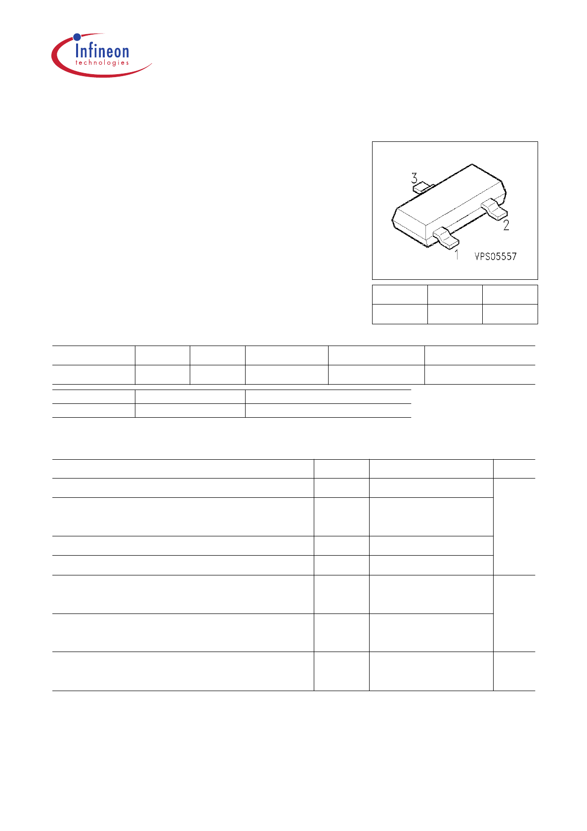
SIPMOS ® Small-Signal Transistor
• N channel
• Enhancement mode
• Logic Level
• V
GS(th) = 0.8...2.0V
Pin 1 Pin 2 Pin 3
G S D
Type
V
DS
I
D
R
DS(on) Package Marking
SN 7002 60 V 0.19 A 5
Ω
SOT-23 sSG
Type Ordering Code Tape and Reel Information
SN 7002 Q67000-S063 E6327
Maximum Ratings
Parameter Symbol Values Unit
Drain source voltage
V
DS 60 V
Drain-gate voltage
R
GS = 20 k
Ω
V
DGR
60
Gate source voltage
V
GS
±
20
ESD Sensitivity (HBM) as per MIL-STD 883 Class 1
Continuous drain current
T
A = 25 ˚C
I
D
0.19
A
DC drain current, pulsed
T
A = 25 ˚C
I
Dpuls
0.76
Power dissipation
T
A = 25 ˚C
P
tot
0.36
W
SN 7002
SN 7002
Data Sheet 2 05.99
Maximum Ratings
Parameter Symbol Values Unit
Chip or operating temperature
T
j -55 ... + 150 ˚C
Storage temperature
T
stg -55 ... + 150
Thermal resistance, chip to ambient air
R
thJA
≤
350 K/W
Therminal resistance, chip-substrate- reverse side 1)
R
thJSR
≤
285
DIN humidity category, DIN 40 040 E
IEC climatic category, DIN IEC 68-1 55 / 150 / 56
1) For package mounted on aluminium 15 mm x 16.7 mm x 0.7 mm
Electrical Characteristics, at
T
j = 25˚C, unless otherwise specified
Parameter Symbol Values Unit
min. typ. max.
Static Characteristics
Drain- source breakdown voltage
V
GS = 0 V,
I
D = 0.25 mA,
T
j = 25 ˚C
V
(BR)DSS
60 - -
V
Gate threshold voltage
V
GS=
V
DS,
I
D = 1 mA
V
GS(th)
0.8 1.4 2
Zero gate voltage drain current
V
DS = 60 V,
V
GS = 0 V,
T
j = 25 ˚C
V
DS = 60 V,
V
GS = 0 V,
T
j = 125 ˚C
I
DSS
-
-
-
0.1
5
1
µA
Gate-source leakage current
V
GS = 20 V,
V
DS = 0 V
I
GSS
- 1 10
nA
Drain-Source on-state resistance
V
GS = 10 V,
I
D = 0.5 A
V
GS = 4.5 V,
I
D = 0.05 A
R
DS(on)
-
-
3
2
7.5
5
Ω
SN 7002
Data Sheet 3 05.99
Electrical Characteristics, at
T
j = 25˚C, unless otherwise specified
Parameter Symbol Values Unit
min. typ. max.
Dynamic Characteristics
Transconductance
V
DS
≥
2 *
I
D *
R
DS(on)max,
I
D = 0.2 A
g
fs
0.1 0.2 -
S
Input capacitance
V
GS = 0 V,
V
DS = 25 V,
f
= 1 MHz
C
iss
- 60 80
pF
Output capacitance
V
GS = 0 V,
V
DS = 25 V,
f
= 1 MHz
C
oss
- 15 25
Reverse transfer capacitance
V
GS = 0 V,
V
DS = 25 V,
f
= 1 MHz
C
rss
- 15 25
Turn-on delay time
V
DD = 30 V,
V
GS = 10 V,
I
D = 0.29 A
R
GS = 50
Ω
t
d(on)
- 5 8
ns
Rise time
V
DD = 30 V,
V
GS = 10 V,
I
D = 0.29 A
R
GS = 50
Ω
t
r
- 5 8
Turn-off delay time
V
DD = 30 V,
V
GS = 10 V,
I
D = 0.29 A
R
GS = 50
Ω
t
d(off)
- 12 16
Fall time
V
DD = 30 V,
V
GS = 10 V,
I
D = 0.29 A
R
GS = 50
Ω
t
f
- 13 17
SN 7002
Data Sheet 4 05.99
Electrical Characteristics, at
T
j = 25˚C, unless otherwise specified
Parameter Symbol Values Unit
min. typ. max.
Reverse Diode
Inverse diode continuous forward current
T
A = 25 ˚C
I
S
- - 0.19
A
Inverse diode direct current,pulsed
T
A = 25 ˚C
I
SM
- - 0.76
Inverse diode forward voltage
V
GS = 0 V,
I
F = 0.5 A,
T
j = 25 ˚C
V
SD
- 1 1.2
V
SN 7002
Data Sheet 5 05.99
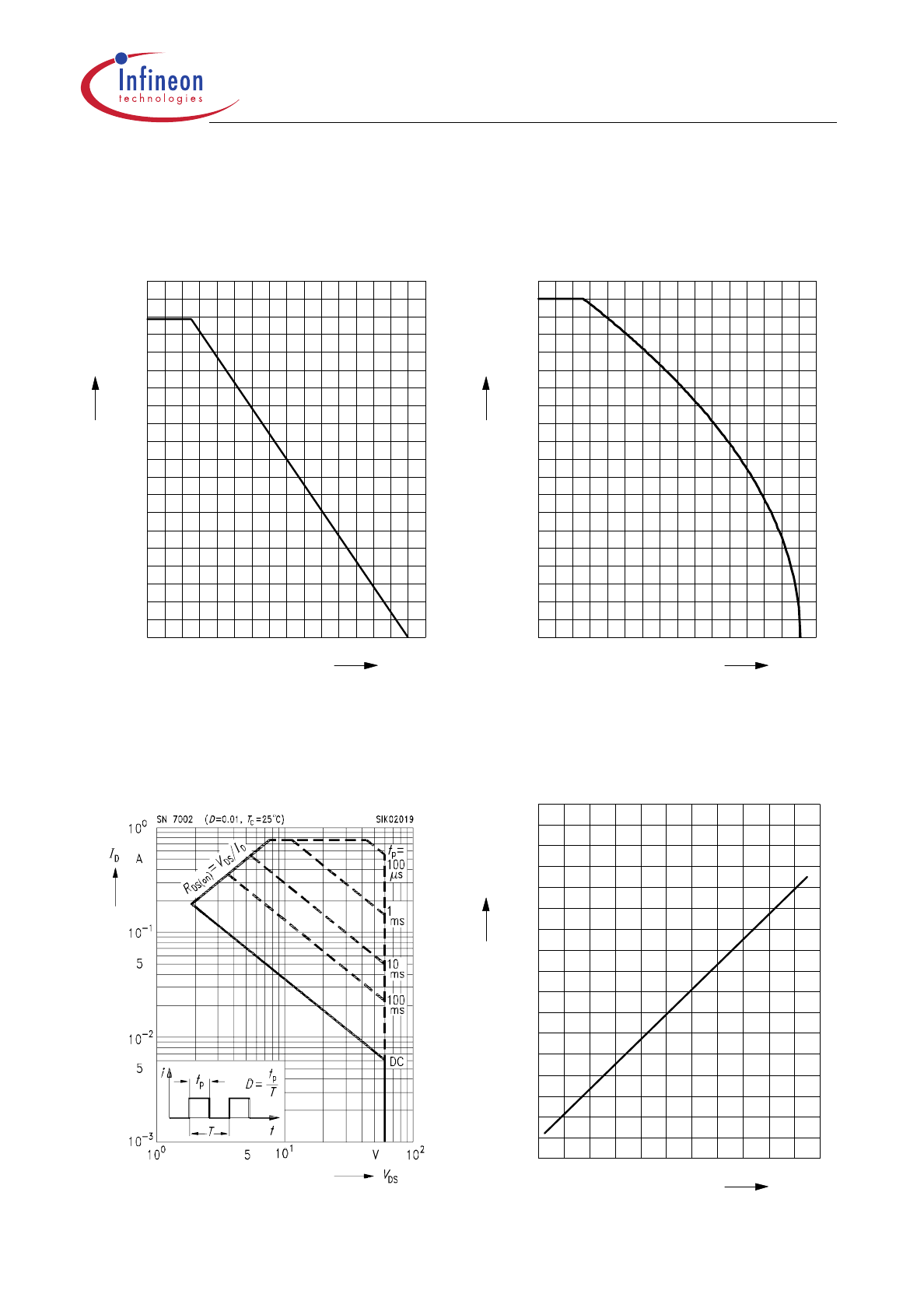
Power dissipation
P
tot =
ƒ
(
T
A)
020 40 60 80 100 120 ˚C 160
T
A
0.00
0.04
0.08
0.12
0.16
0.20
0.24
0.28
0.32
W
0.40
P
tot
Drain current
I
D =
ƒ
(
T
A)
parameter:
V
GS
≥
10 V
020 40 60 80 100 120 ˚C 160
T
A
0.00
0.02
0.04
0.06
0.08
0.10
0.12
0.14
0.16
A
0.20
I
D
Safe operating area
I
D=f(
V
DS)
parameter :
D
= 0.01,
T
C=25˚C
Drain-source breakdown voltage
V
(BR)DSS =
ƒ
(
T
j)
-60 -20 20 60 100 ˚C 160
T
j
54
56
58
60
62
64
66
68
V
71
V
(BR)DSS
SN 7002
Data Sheet 6 05.99
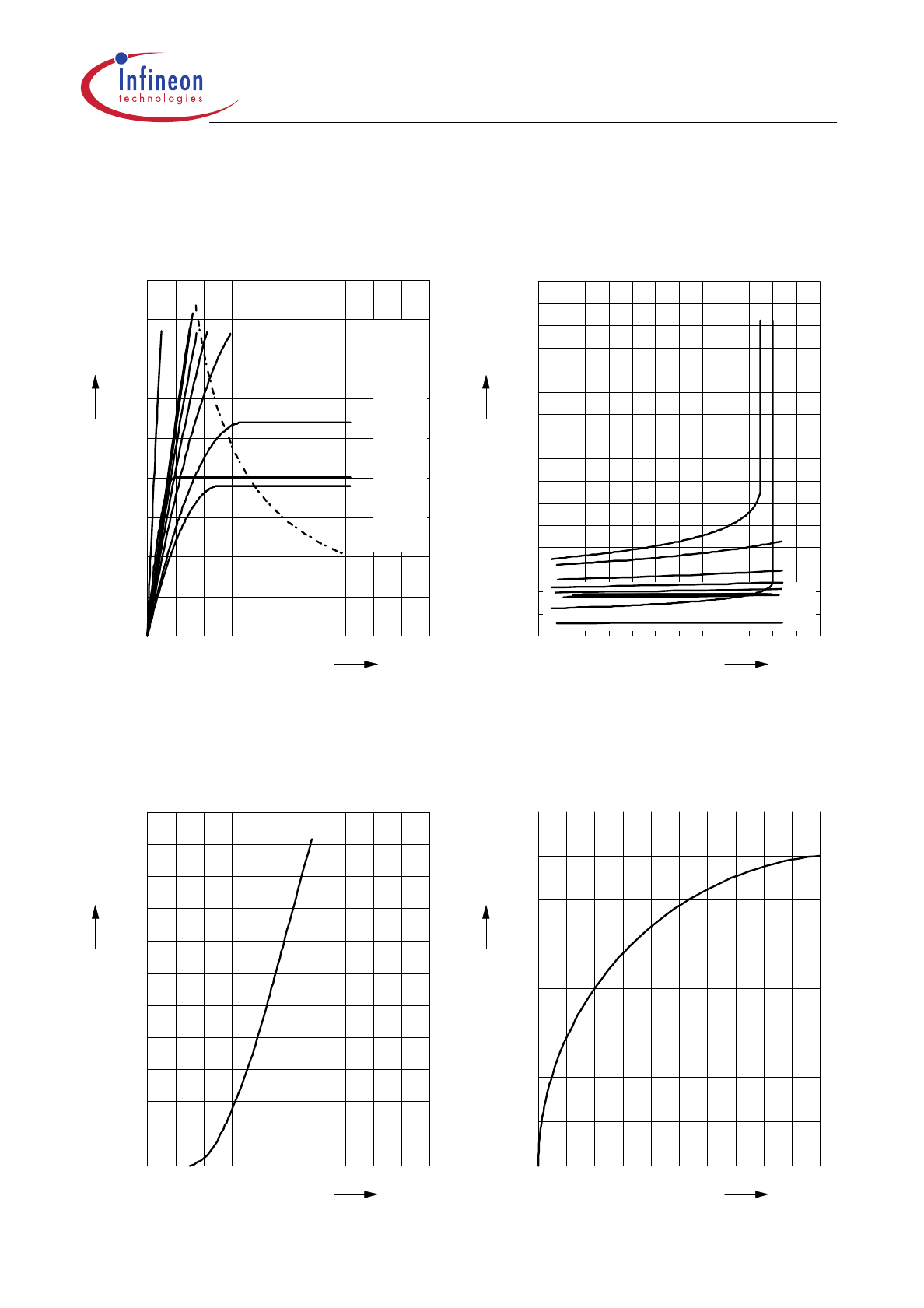
Typ. output characteristics
I
D =
ƒ(
V
DS)
parameter:
t
p = 80 µs ,
T
j = 25 ˚C
0.0 0.5 1.0 1.5 2.0 2.5 3.0 3.5 4.0 V5.0
V
DS
0.00
0.05
0.10
0.15
0.20
0.25
0.30
0.35
A
0.45
I
D
V
GS [V]
a
a 2.0
b
b 2.5
c
c 3.0
d
d 3.5
e
e 4.0
f
f 4.5
g
g 5.0
h
h 6.0
i
i 7.0
j
j 8.0
k
k 9.0
l
P
tot = 0W
l 10.0
Typ. drain-source on-resistance
R
DS (on) =
ƒ(
I
D)
parameter:
t
p = 80 µs,
T
j = 25 ˚C
0.00 0.04 0.08 0.12 0.16 A0.24
I
D
0
2
4
6
8
10
12
Ω
16
R
DS (on)
V
GS [V] =
a
a
2.0 b
b
2.5
c
c
3.0
d
d
3.5
e
e
4.0
f
f
4.5
g
g
5.0
h
h
6.0
i
i
7.0
j
j
8.0
kk
9.0
ll
10.0
Typ. transfer characteristics
I
D
= f
(
V
GS)
parameter:
t
p = 80 µs
0 1 2 3 4 5 6 7 8 V 10
V
GS
0.0
0.1
0.2
0.3
0.4
0.5
0.6
0.7
0.8
0.9
A
1.1
I
D
Typ. forward transconductance
g
fs =
f
(
I
D)
parameter:
t
p = 80 µs,
0.0 0.1 0.2 0.3 0.4 0.5 0.6 0.7 0.8 A1.0
I
D
0.00
0.05
0.10
0.15
0.20
0.25
0.30
S
0.40
g
fs
SN 7002
Data Sheet 7 05.99
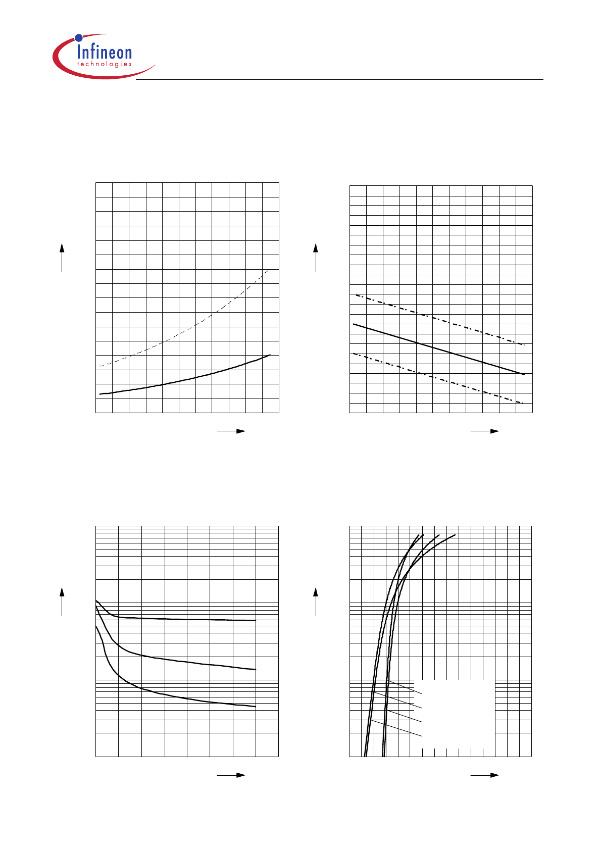
Drain-source on-resistance
R
DS (on) =
ƒ
(
T
j)
parameter:
I
D = 0.5 A,
V
GS = 10 V
-60 -20 20 60 100 ˚C 160
T
j
0
2
4
6
8
10
12
Ω
16
R
DS (on)
typ
98%
Gate threshold voltage
V
GS (th) =
ƒ
(
T
j)
parameter:
V
GS =
V
DS,
I
D = 1 mA
0.0
0.4
0.8
1.2
1.6
2.0
2.4
2.8
3.2
3.6
4.0
V
4.6
V
GS(th)
-60 -20 20 60 100 ˚C 160
T
j
2%
typ
98%
Typ. capacitances
C
=
f
(
V
DS)
parameter:
V
GS=0V,
f
= 1 MHz
0 5 10 15 20 25 30 V40
V
DS
0
10
1
10
2
10
3
10
pF
C
C
rss
C
oss
C
iss
Forward characteristics of reverse diode
I
F =
ƒ
(
V
SD)
parameter:
T
j
, t
p = 80 µs
-3
10
-2
10
-1
10
0
10
A
I
F
0.0 0.4 0.8 1.2 1.6 2.0 2.4 V3.0
V
SD
T
j = 25 ˚C typ
T
j = 25 ˚C (98%)
T
j = 150 ˚C typ
T
j = 150 ˚C (98%)
