MDS PC2 Sony_MDS PC2_service_manual Sony Service Manual
User Manual: sony_MDS-PC2_service_manual
Open the PDF directly: View PDF ![]() .
.
Page Count: 62
- ÿþ�C�O�V�E�R
- ÿþ�S�E�L�F�-�D�I�A�G�N�O�S�I�S� �F�U�N�C�T�I�O�N
- ÿþ� �S�E�R�V�I�C�I�N�G� �N�O�T�E
- ÿþ�G�E�N�E�R�A�L
- ÿþ� �D�I�S�A�S�S�E�M�B�L�Y
- ÿþ� �T�E�S�T� �M�O�D�E
- ÿþ� �E�L�E�C�T�R�I�C�A�L� �A�D�J�U�S�T�M�E�N�T�S
- ÿþ� �D�I�A�G�R�A�M�S
- ÿþ� �E�X�P�L�O�D�E�D� �V�I�E�W�S
- ÿþ�E�L�E�C�T�R�I�C�A�L� �P�A�R�T�S� �L�I�S�T

1
MICROFILM
MDS-PC2
SPECIFICATIONS
SERVICE MANUAL
MINIDISC DECK
Model Name Using Similar Mechanism MDS-S40
MD Mechanism Type MDM-5A
Optical Pick-up Type KMS-260B/J1N
US Model
Canadian Model
AEP Model
UK Model
E Model
— Continued on next page —
2
SELF-DIAGNOSIS FUNCTION
The self-diagnosis function consists of error codes for customers which are displayed automatically when errors occur, and error codes which
show the error history in the test mode during servicing. For details on how to view error codes for the customer, refer to the following box
in the instruction manual. For details on how to check error codes during servicing, refer to the following “Procedure for using the Self-
Diagnosis Function (Error History Display Mode)”.
Procedure for using the Self-Diagnosis Function (Error History Display Mode).
Note:
Perform the self-diagnosis function in the “error history display mode” in the test mode. The following describes the least required proce-
dure. Be careful not to enter other modes by mistake. If you set other modes accidentally, press the p “PROGRAM” button to exit the mode.
1. While pressing the INPUT button and p button, connect the power plug to the outlet, and release the INPUT button and p button.
2. Press the + button and when “[Service]” is displayed, press the ^ “PROGRAM” button.
3. Press the + button and display “ERR DP MODE”.
4. Pressing the ^ “PROGRAM” button sets the error history mode and displays “total rec”.
5. Select the contents to be displayed or executed using the + button.
6. Pressing the r “PROGRAM” button will display or execute the contents selected.
7. Pressing the r “PROGRAM” button another time returns to step 4.
8. Pressing the p “PROGRAM” button displays “ERROR DP MODE” and exits the error history mode.
9. To exit the test mode, press the 6 “1” button. The unit sets into the STANDBY state, the disc is ejected, and the test mode ends.
*Note:
As this unit has only a few buttons, one button is assigned with several functions in the test mode.
Press the INPUT button to switch the functions.
Each time the INPUT button is pressed, the display switches in the following order; “PROGRAM” n “1” n blank n “PROGRAM”
The functions of each button change with the display.
For simplicity, operations of the INPUT button will not be described here.
Instead, symbols are added to the names of buttons. Press the INPUT button as required to switch the display.
Example) p “PROGRAM” : Display “PROGRAM” and press the p button. p “1” : Display “1” and press the p button.

3
Displays the recording time.
Displayed as “rππππππh”.
The displayed time is the total time the laser is set to the high power state.
This is about 1/4 of the actual recording time.
The time is displayed in decimal digits from 0h to 65535h.
Displays the play time.
Displayed as “pππππππh”. The time displayed is the total actual play time. Pauses are not counted.
The time is displayed in decimal digits from 0h to 65535h.
Displays the total number of retries during recording and number of retry errors during play.
Displayed as “rππ pππ”.
“r” indicates the retries during recording while “p” indicates the retry errors during play.
The number of retries and retry errors are displayed in hexadecimal digits from 00 to FF.
Displays the total number of errors.
Displayed as “total ππ”.
The number of errors is displayed in hexadecimal digits from 00 to FF.
Displays the 10 latest errors.
Displayed as “0π E@@”.
π indicates the history number. The smaller the number, the more recent is the error. (00 is the latest).
@@ indicates the error code.
Refer to the following table for the details. The error history can be switched by pressing the + button.
Mode which erases the “retry err”, “total err”, and “err history” histories.
When returning the unit to the customer after completing repairs, perform this to erase the past error history,
After pressing the r “PROGRAM” button and “er refresh?” is displayed, press the ^ “PROGRAM” button
to erase the history.
“Complete!” will be displayed momentarily.
Be sure to check the following when this mode has been executed.
• The data has been erased.
• The mechanism operates normally when recording and play are performed.
Mode which erases the “total rec” and “total play” histories.
These histories serve as approximate indications of when to replace the optical pickup.
If the optical pickup has been replaced, perform this operation and erase the history.
After pressing the ^ “PROGRAM” button and “tm refresh?” is displayed, press the r “PROGRAM” button
to erase the history.
“Complete!” will be displayed momentarily.
Be sure to check the following when this mode has been executed.
• The data has been erased.
• The mechanism operates normally when recording and play are performed.
ITEMS OF ERROR HISTORY MODE ITEMS AND CONTENTS
Selecting the Test Mode
Display
total rec
total play
retry err
total err
err history
er refresh
tm refresh
Details of History
No error
Read error. PTOC cannot be read
(DISC ejected)
TOC error. UTOC error
(DISC not ejected)
Loading error
Address cannot be read (Servo has deviated)
Table of Error Codes
Error Code
E00
E01
E02
E03
E04
E05
E06
E07
E08
E09
E0A
FOK has deviated
Cannot focus (Servo has deviated)
Recording retry
Recording retry error
Playback retry error
(Access error)
Play retry error (C2 error)
Details of Error Error Code Details of Error

4
CAUTION
Use of controls or adjustments or performance of procedures
other than those specified herein may result in hazardous ra-
diation exposure.
Notes on chip component replacement
• Never reuse a disconnected chip component.
• Notice that the minus side of a tantalum capacitor may be
damaged by heat.
Flexible Circuit Board Repairing
• Keep the temperature of soldering iron around 270˚C
during repairing.
• Do not touch the soldering iron on the same conductor of the
circuit board (within 3 times).
• Be careful not to apply force on the conductor when soldering
or unsoldering.
Laser component in this product is capable of emitting radiation
exceeding the limit for Class 1.
This appliance is classified as
a CLASS 1 LASER product.
The CLASS 1 LASER PROD-
UCT MARKING is located on
the rear exterior.
This caution
label is located
inside the unit.
CAUTION
Danger of explosion if battery is incorrectly replaced.
Replace only with the same or equivalent type recommended by
the equipment manufacturer.
Discard used batteries according to manufacture’s instructions.
ADVARSEL!
Lithiumbatteri - Eksplosionsfare ved fejlagtig håndtering.
Udskiftning må kun ske med batteri af samme fabrikat og type.
Levér det brugte batteri tilbage til leverandøren.
ADVARSEL
Eksplosjonsfare ved feilakting skifte av batteri.
Benytt samme batteritype eller en tilsvarende type anbefalt av
apparatfabrikanten.
Brukte batterier katterier kasseres i henhold til fabrikantens
VARNIG
Explosionsfara vid felaktigt batteribyte.
Använd samma batterityp eller en likvärdig typ som rekommenderas
av apparattillverkaren.
Kassera använt batteri enligt gällande föreakrifter.
VAROITUS
Parist voi räjähtää, jos se on virheellisesti asennettu.
Vaihda paristo ainoastaan laitevalmistajan suosittelemaan tyyppiin.
Hävitä käytetty paristo valmistajan ohjeiden mukaisesti.
SAFETY-RELATED COMPONENT WARNING !!
COMPONENTS IDENTIFIED BY MARK ! OR DOTTED LINE
WITH MARK ! ON THE SCHEMATIC DIAGRAMS AND IN
THE PARTS LIST ARE CRITICAL TO SAFE OPERATION.
REPLACE THESE COMPONENTS WITH SONY PARTS
WHOSE PART NUMBERS APPEAR AS SHOWN IN THIS
MANUAL OR IN SUPPLEMENTS PUBLISHED BY SONY.
PARTS No. MODEL
MODEL IDENTIFICATION
— MODEL NUMBER LABEL —
4-220-576-0πUS model
4-220-577-0πCanadian model
4-220-578-0πAEP, UK model
4-220-579-0πSingapore model
ATTENTION AU COMPOSANT AYANT RAPPORT
À LA SÉCURITÉ!!
LES COMPOSANTS IDENTIFIÉS PAR UNE MARQUE ! SUR
LES DIAGRAMMES SCHÉMATIQUES ET LA LISTE DES
PIÈCES SONT CRITIQUES POUR LA SÉCURITÉ DE
FONCTIONNEMENT. NE REMPLACER CES COMPOSANTS
QUE PAR DES PIÈCES SONY DONT LES NUMÉROS
SONT DONNÉS DANS CE MANUEL OU DANS LES
SUPPLÉMENTS PUBLIÉS PAR SONY.
Parts No.
5
TABLE OF CONTENTS
1. SERVICING NOTE .......................................................... 6
2. GENERAL ........................................................................ 12
3. DISASSEMBLY
3-1. Case and Front Panel .......................................................... 14
3-2. MD Mechanism .................................................................. 14
3-3. Slider (CAM) ...................................................................... 15
3-4. Base Unit (MBU-5A) BD Board ........................................ 15
3-5. SW Board and Loading Motor (M103) .............................. 16
4. TEST MODE ..................................................................... 17
5. ELECTRICAL ADJUSTMENTS ............................... 22
6. DIAGRAMS
6-1. Circuit Boards Location ...................................................... 31
6-2. Block Diagrams
• BD Section ....................................................................... 33
• Main Section .................................................................... 34
6-3. Printed Wiring Board – BD Section –................................. 36
6-4. Schematic Diagram – BD (1/2) Section –........................... 37
6-5. Schematic Diagram – BD (2/2) Section –........................... 38
6-6. Schematic Diagram – Main (1/2) Section –........................ 39
6-7. Schematic Diagram – Main (2/2) Section –........................ 40
6-8. Printed Wiring Board – Main Section –.............................. 41
6-9. Schematic Diagram – Panel Section – ................................ 42
6-10. Printed Wiring Board – Panel Section –............................ 43
6-11. Schematic Diagram – Power Section – ............................. 44
6-12. Printed Wiring Board – Power Section – .......................... 45
6-13. Schematic Diagram – BD Switch Section – ..................... 46
6-14. Printed Wiring Board – BD Switch Section –................... 46
6-15. IC Block Diagrams ........................................................... 46
6-15. IC Pin Functions ............................................................... 49
7. EXPLODED VIEWS
7-1. Cabinet Section ................................................................... 53
7-2. Mechanism Section (MDM-5A) ......................................... 54
7-3. Base Unit Section (MBU-5A)............................................. 55
8. ELECTRICAL PARTS LIST ........................................ 56
SAFETY CHECK-OUT
After correcting the original service problem, perform the follow-
ing safety checks before releasing the set to the customer:
Check the antenna terminals, metal trim, “metallized” knobs, screws,
and all other exposed metal parts for AC leakage. Check leakage as
described below.
LEAKAGE
The AC leakage from any exposed metal part to earth Ground and
from all exposed metal parts to any exposed metal part having a
return to chassis, must not exceed 0.5 mA (500 microampers). Leak-
age current can be measured by any one of three methods.
1. A commercial leakage tester, such as the Simpson 229 or RCA
WT-540A. Follow the manufacturers’ instructions to use these
instruments.
2. A battery-operated AC milliammeter. The Data Precision 245
digital multimeter is suitable for this job.
3. Measuring the voltage drop across a resistor by means of a VOM
or battery-operated AC voltmeter. The “limit” indication is 0.75
V, so analog meters must have an accurate low-voltage scale.
The Simpson 250 and Sanwa SH-63Trd are examples of a pas-
sive VOM that is suitable. Nearly all battery operated digital
multimeters that have a 2V AC range are suitable. (See Fig. A)
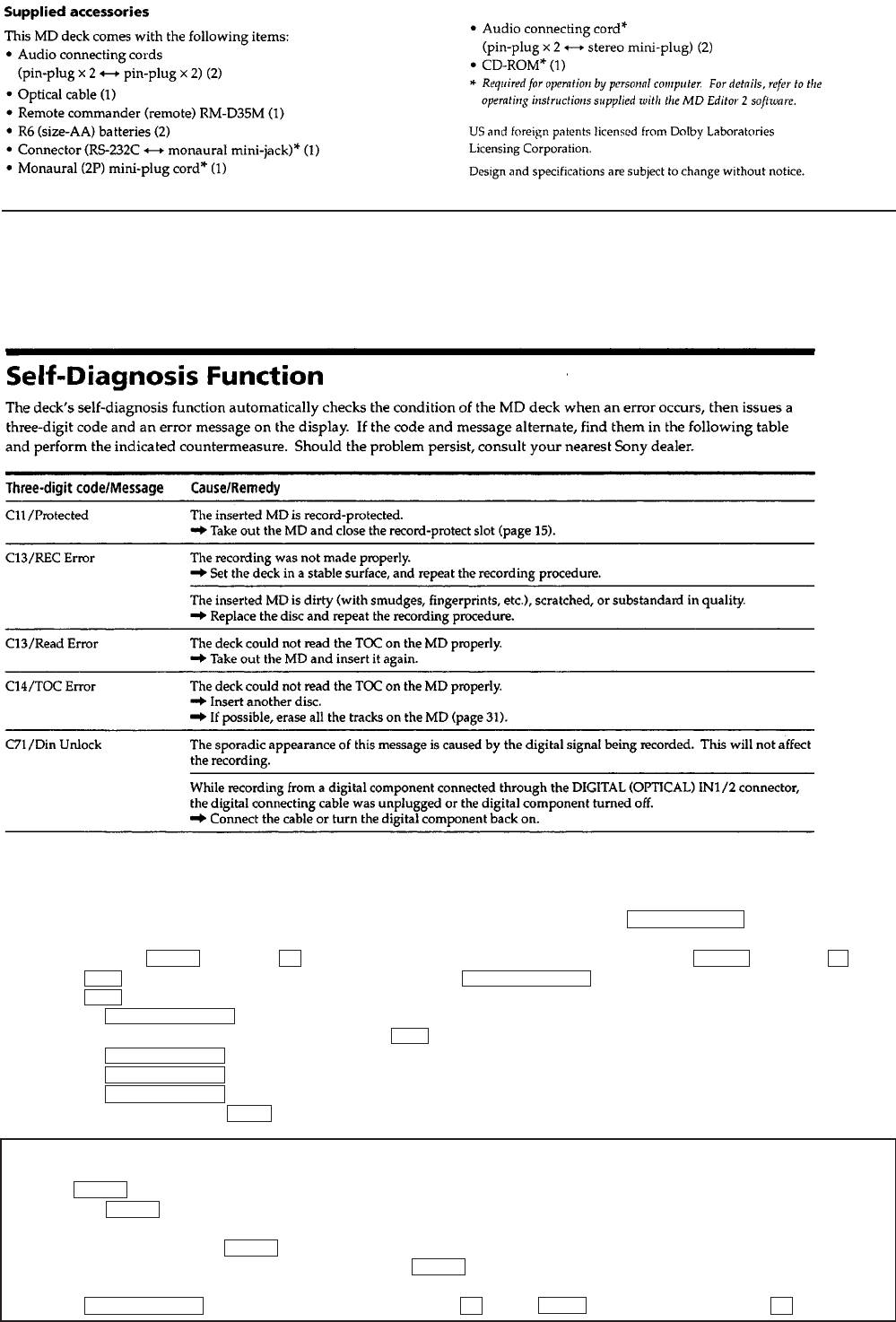
Fig. A. Using an AC voltmeter to check AC leakage.
AC
voltmeter
(0.75V)
1.5k
Ω
0.15
µ
F
Earth Ground
To Exposed Metal
Parts on Set
6
SECTION 1
SERVICING NOTE
JIG FOR CHECKING BD BOARD WAVEFORM
The special jig (J-2501-149-A) is useful for checking the waveform of the BD board. The names of terminals and the checking items to be
performed are shown as follows.
GND : Ground
I+3V : For measuring IOP (Check the deterioration of the optical pick-up laser)
IOP : For measuring IOP (Check the deterioration of the optical pick-up laser)
TEO : TRK error signal (Traverse adjustment)
VC : Reference level for checking the signal
RF : RF signal (Check jitter)
RF
VC
TEO For MDM-
3
For MDM-5
IOP
I+3V
VC
RF
TEO
IOP
I+3V
GND
VC
RF
TEO
IOP
I+3V
GND
1
5
1
6
CN110
RF
5P connector
6P connecto
r
VC
TEO
IOP
I+3V
GND
Mechanism deck

7
IOP DATA RECORDING AND DISPLAY WHEN OPTICAL PICK-UP AND NON-VOLATILE MEMORY (IC171 OF
BD BOARD) ARE REPLACED
The IOP value labeled on the optical pick-up can be recorded in the non-volatile memory. By recording the value, it will eliminate the need
to look at the value on the label of the optical pick-up. When replacing the optical pick-up or non-volatile memory (IC171 of BD board),
record the IOP value on the optical pick-up according to the following procedure.
Record Precedure:
1. While pressing the INPUT button and p button, connect the power plug to the outlet, and release the INPUT button and p button.
2. Press the + button to display “[Service]”, and press the ^ “PROGRAM” button.
3. Press the + button to display “lop.Write”, and press the ^ “PROGRAM” button.
4. The display becomes “Ref=@@@.@” (@ is an arbitrary number) and the numbers which can be changed will blink.
5. Input the IOP value written on the optical pick-up.
To select the number : Press the + button.
To select the digit : Press the r “PROGRAM” button.
6. When the ^ “PROGRAM” button is pressed, the display becomes “Measu=@@@.@” (@ is an arbitrary number).
7. As the adjustment results are recorded for the 6 value. Leave it as it is and press the ^ “PROGRAM” button.
8. “Complete!” will be displayed momentarily. The value will be recorded in the non-volatile memory and the display will become “Iop
Write”.
9. Press the 6 “1” button to complete. “Standby” will be displayed.
Display Precedure:
1. While pressing the INPUT button and p button, connect the power plug to the outlet, and release the INPUT button and p button.
2. Press the + button to display “[Service]”, and press the ^ “PROGRAM” button.
3. Press the + button to display “lop.Read”, and press the ^ “PROGRAM” button.
4. “@@.@/##.#” is displayed and the recorded contents are displayed.
@@.@ : indicates the Iop value labeled on the pick-up.
##.# : indicates the Iop value after adjustment
5. To end, press the r “PROGRAM” button or p “PROGRAM” button to display “Iop Read”. Then press the 6 “1” buttun.
*Note:
As this unit has only a few buttons, one button is assigned with several functions in the test mode.
Press the INPUT button to switch the functions.
Each time the INPUT button is pressed, the display switches in the following order; “PROGRAM” n “1” n blank n “PROGRAM”
The functions of each button change with the display.
For simplicity, operations of the INPUT button will not be described here.
Instead, symbols are added to the names of buttons. Press the INPUT button as required to switch the display.
Example) p “PROGRAM” : Display “PROGRAM” and press the p button. p “1” : Display “1” and press the p button.

8
CHECKS PRIOR TO PARTS REPLACEMENT AND ADJUSTMENTS
Before performing repairs, perform the following checks to determine the faulty locations up to a certain extent.
Details of the procedures are described in “5 Electrical Adjustments”.
Note:
The criteria for determination above is intended merely to determine if satisfactory or not, and does not serve as the specified value for
adjustments.
When performing adjustments, use the specified values for adjustments.
• 0.9 mW power
Specified value : 0.84 to 0.92 mW
• 7.0 mW power
Specified value : 6.8 to 7.2 mW
lop (at 7mW)
• Labeled on the optical pickup
Iop value ± 10mA
• Traverse waveform
Specified value : Below 10% offset
• Error rate check
Specified value : For points a, b, and c
C1 error : Below 220
AD error : Below 2
• Error rate check
Specified value:
a.When using test disc (MDW-74/AU-1)
C1 error : Below 80
AD error : Below 2
b.When using check disc (TDYS-1)
C1 error : Below 50
• CPLAY error rate check
Specified value:
C1 error : Below 80
AD error : Below 2
• Unsatisfactory if displayed as T=@@ (##) [NG”
NG
(@@, ## are both arbitrary numbers)
Laser power check
(5-6-2 : See page 37)
Traverse check
(5-6-3 : See page 37)
Focus bias check
(5-6-4 : See page 38)
C PLAY check
(5-6-5 : See page 38)
Self-recording/playback
check
(REC/PLAY)
(5-6-6 : See page 38)
TEMP check
(Temperature
compensation
offset check)
(5-6-1 : See page 37)
Criteria for Determination
(Unsatisfactory if specified value is not satisfied)
• Clean the optical pick-up
• Adjust again
• Replace the optical pick-up
• Replace the optical pick-up
• Replace the optical pick-up
• Replace the optical pick-up
• Replace the optical pick-up
If always unsatisfactory:
• Replace the overwrite head
• Check for disconnection of the circuits around the
overwrite head
If occasionally unsatisfactory:
• Check if the overwrite head is distorted
• Check the mechanism around the sled
• Check for disconnection of the circuits around D101
(BD board)
• Check the signals around IC101, IC121, CN102,
CN103 (BD board)
Measure if unsatisfactory:
9
Back up board
FLUORESCENT DISPLAY TUBE ALL LIGHTING AND KEY CHECK MODE
In this mode, the fluorescent display tube check and key check can be performed.
Procedure:
1. While pressing the INPUT button and r (REC) button, insert the power plug into the outlet.”
2. The fluorescent display tube displays “FL ALL 10n Key” momentarily and lights up completely.”
3. The display goes off partially each time a button is pressed.
4. When all buttons are pressed, “Push INPUT” is displayed.
5. When the INPUT button is pressed, the fluorescent display tube displays “Seg Chk” momentarily and lights up partially.
6. When the INPUT button is pressed, it displays “Rmk Chk” momentarily followed by “Push Rmc Key”.
If not using a remote commander, end there and disconnect the power plug from the outlet. If using a remote commander, press any
button.”
7. The check is completed when “Chk End!”is displayed. Press the I/u button to end.”
FORCED RESET
The system microprocessor can be reset in the following procedure.
Use these procedure when the unit cannot be operated normally due to the overrunning of the microprocessor, etc.
The line output level and PHONES output level can be varied in the range from 0 dB to -40 dB using the remote commander of this unit.
When forced reset is executed, these levels will be set to the initial value of -20 dB.
Procedure :
1. Disconnect the power plug from the outlet.
2. Remove the BACK UP board.
3. Insert the power plug into the outlet.
4. Mount the back up board.
5. Press the I/u button. When “Initialize” is displayed, it means that forced reset has been executed.
[POWER BOARD] (Component Side)

10
Fig. 1 Reading the Test Mode Display
(During recording and stop)
RTs@@c##c**
Fluorescent display tube display
@@ : Cause of retry
## : Number of retries
** : Number of retry errors
Fig. 2 Reading the Test Mode Display
(During playback)
@@####**$$
Fluorescent display tube display
@@ : Parts No. (name of area named on TOC)
## : Cluster
** : Sector
$$ : Track mode (Track information such as copyright infor-
mation of each part)
Reading the Retry Cause Display
RETRY CAUSE DISPLAY MODE
• In this test mode, the causes for retry of the unit during recording can be displayed on the fluorescent indicator tube. During playback, the
“track mode” for obtaining track information will be set.
This is useful for locating the faulty part of the unit.
• The following will be displayed :
During recording and stop : Retry cause, number of retries, and number of retry errors.
During playback : Information such as type of disc played, part played, copyright.
These are displayed in hexadecimal.
Precedure:
1. Load a recordable disc whose contents can be erased into the unit.
2. For discs with no disc name, set the name display using the remote commander. (The time display is set after some time. Leave as it is if
desired.)
3. Press the p button immediately. Wait for about 10 seconds while pressing the button. (The AMS knob can be pressed instead of the YES
button for the same results.)
4. The fluorescent display tube displays “RTs@@c##e**”.
5. Press the r button to start recording. Then press the ^ button and start recording.
6. To check the “track mode”, press the ^ button to start play.
7. To exit the test mode, press the 1/u button. If the test mode cannot be exited, refer to “Forced Reset” on page 8.
} Address (Physical address on disc)
Hexadecimal
Bit
Binary
Higher Bits Lower Bits
84218421
b7 b6 b5 b4 b3 b2 b1 b0
00000001
00000010
00000100
00001000
00010000
00100000
01000000
10000000
When track jump (shock) is detected
When ADER was counted more than five times
continuously
When ADIP address is not continuous
When DIN unlock is detected
When not in focus
When ABCD signal level exceeds the specified range
When CLV is unlocked
When access operation is not performed normally
Hexa-
decimal
shock
ader5
Discontinuous address
DIN unlock
FCS incorrect
IVR rec error
CLV unlock
Access fault
Cause of Retry Occurring conditions
01
02
04
08
10
20
40
80
Reading the Display:
Convert the hexadecimal display into binary display. If more than two causes, they will be added.
Example
When 42 is displayed:
Higher bit : 4 = 0100 n b6
Lower bit : 2 = 0010 n b1
In this case, the retry cause is combined of “CLV unlock” and “ader5”.
When A2 is displayed:
Higher bit : A = 1010 n b7+b5
Lower bit : 2 = 0010 n b2
The retry cause in this case is combined of “access fault”, “IVR rec error”, and “ader5”.
11
Reading the Display:
Convert the hexadecimal display into binary display. If more than two causes, they will be added.
Example When 84 is displayed:
Higher bit : 8 = 1000 n b7
Lower bit : 4 = 0100 n b2
In this case, as b2 and b7 are 1 and others are 0, it can be determined that the retry cause is combined of “emphasis OFF”, “monaural”,
“original”, “copyright exists”, and “write allowed”.
Example When 07 is displayed:
Higher bit : 0 = 1000 n All 0
Lower bit : 7 = 0111 n b0+b1+b2
In this case, as b0, b1, and b2 are 1 and others are 0, it can be determined that the retry cause is combined of “emphasis ON”, “stereo”,
“original”, “copyright exists”, and “write prohibited”.
Hexadecimal
n
Binary Conversion Table
Hexadecimal Binary Hexadecimal Binary
0
1
2
3
4
5
6
7
8
9
A
B
C
D
E
F
0000
0001
0010
0011
0100
0101
0110
0111
1000
1001
1010
1011
1100
1101
1110
1111
Hexadecimal
Bit
Binary
Higher Bits Lower Bits
84218421
b7 b6 b5 b4 b3 b2 b1 b0
00000001
00000010
00000100
00001000
00010000
00100000
01000000
10000000
Hexa-
decimal
Details
01
02
04
08
10
20
40
80
Emphasis OFF
Monaural
This is 2-bit display. Normally 01.
01:Normal audio. Others:Invalid
Audio (Normal)
Original
Copyright
Write prohibited
When 0 When 1
Emphasis ON
Stereo
Invalid
Digital copy
No copyright
Write allowed
Reading the Track Mode Display
12
This section is extracted from
instruction manual.
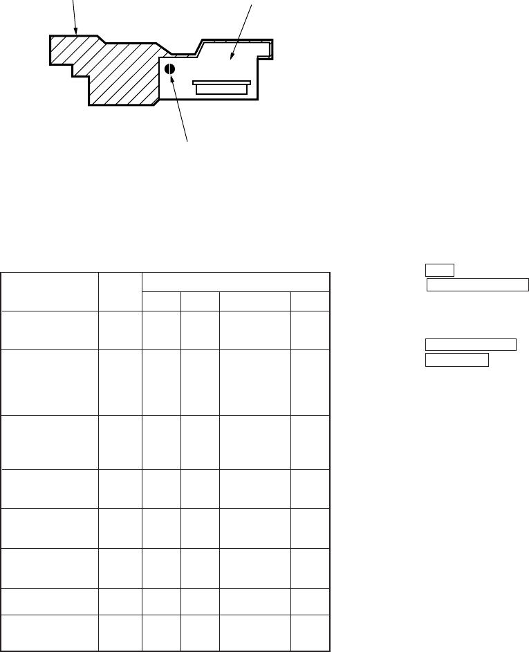
Location of Parts and Controls
SECTION 2
GENERAL
Front Panel
24
6
7
89
1011
135
13
SECTION 3
DISASSEMBLY
Note: Follow the disassembly procedure in the numerical order given.
3-1. CASE AND FRONT PANEL
3-2. MD MECHANISM
8
Front panel
(Take not of two claws)
9
Flat type wire
(CN701)
1
Two screw
s
(Flat head)
2
Two screws
(Flat head)
3
Case
4
Two screws
(BTT M3)
6
Screw
(M2 x 6.0)
7
Screw
(M2 x 6.0)
5
Screw
(BTT M3)
Claw
Claw
8
Two step screws
7
Main board
6
Screw
(BVTP 3 x 8)
5
Screw
(BVTP 3 x 8)
1
Connector 8P
(CN503)
2
Flat type wir
e
(CN412)
3
Flat type wire
(CN501)
4
Flat type wire
(CN421)
9
Two step screws
0
MD mechanism

14
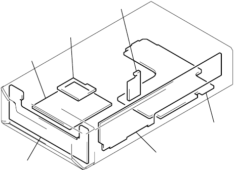
3-4. BASE UNIT (MBU-5A) AND BD BOARD
3-3. SLIDER (CAM)
6
Slider (Cam)
2
Bracket (Guide L)
5
Bracket (Guide R)
3
Leaf spring
1
Two screws
(BTP 2.6 x 6)
4
Two screws
(BTP 2.6 x 6)
Set the shaft of Lever (O/C) to
be at the position in the figure.
Set the shaft of Cam gear to
be at the position in the figure.
• Note for Installation of Slider (Cam)
4
Screw (M1.7 x 4)
1
Three screws
(BTP2.6 x 6)
3
Remove the solder (Five position)
2
Base unit (MBU-5A)
6
Flexible board
(CN101)
5
Flexible board
(CN104)
7
BD board

15
3-5. SW BOARD AND LOADING MOTOR (M103)
5
Three screws
(BTP2.6 x 6)
4
Loading motor (M103
)
6
SW board
2
Gear B
3
Two screws
(PWH 1.7 x 3)
1
Screw (PTPWH M2.6 x 6)
16
SECTION 4
TEST MODE
4-1. PRECAUTIONS FOR USE OF TEST MODE
• As loading related operations will be performed regardless of the test mode operations being performed, be sure to check that the disc is
stopped before setting and removing it.
Even if the 6 (EJECT) button is pressed while the disc is rotating during continuous playback, continuous recording, etc., the disc will not
stop rotating.
Therefore, it will be ejected while rotating.
Be sure to press the 6 (EJECT) button after pressing the p “PROGRAM” button and the rotation of disc is stopped.
4-1-1. Recording laser emission mode and operating buttons
• Continuous recording mode (CREC MODE)
• Laser power check mode (LDPWR CHECK)
• Laser power adjustment mode (LDPWR ADJUST)
• Traverse (MO) check (EF MO CHECK)
• Traverse (MO) adjustment (EF MO ADJUST)
• When pressing the r (REC) button.
4-2. SETTING THE TEST MODE
The following are two methods of entering the test mode.
Procedure 1: While pressing the INPUT button and p button, connect the power plug to an outlet, and release the INPUT button and p
button.
When the test mode is set, “[Check]” will be displayed. Rotating the INPUT button switches between the following four
groups; ···Nn Check Nn Adjust Nn Service Nn Develop Nn ···.
Procedure 2: While pressing the INPUT button, connect the power plug to the outlet and release the INPUT button.
When the test mode is set, “TEMP CHECK” will be displayed. By setting the test mode using this procedure, only the “Check”
group of procedure 1 can be executed.
4-3. EXITING THE TEST MODE
Press the p “1” button. The disc is ejected when loaded, and “Standby” display blinks, and the STANDBY state is set.
4-4. BASIC OPERATIONS OF THE TEST MODE
All operations are performed using the = , + button, ^ “PROGRAM” button, and p “PROGRAM” button.
The functions of these buttons are as follows.
Function name
= , + button
^ “PROGRAM” button
p “PROGRAM” button
Function
Changes parameters and modes
Proceeds onto the next step. Finalizes input.
Returns to previous step. Stops operations.
TIME
REPEAT
PLAY MODE
DISPLAY
SCROLL
*Note:
As this unit has only a few buttons, one button is assigned with several functions in the test mode.”
Press the INPUT button to switch the functions.
Each time the INPUT button is pressed, the display switches in the following order;”
“PROGRAM” n “1” n blank n “PROGRAM”
The functions of each button change with the display.
Buttons and Corresponding Functions
Buttons Function when
nothing displayed Function when “PROGRAM”
is displayed Function when “1” is displayed
1/u
6 (EJECT)
^
=
+
p (STOP)
r (REC)
CLEAR
ENTER/YES
0 (FR)
) (FF)
EDIT/NO
PUSH (AMS)
1/u
6 (EJECT)
^
= (AMS)
+ (AMS)
p (STOP)
r (REC)

17
4-5. SELECTING THE TEST MODE
There are 27 types of test modes as shown below. The groups can be switched by pressing the = and = buttons. After selecting the
group to be used, press the ^ “PROGRAM” button. After setting a certain group, pressing the = and = buttons switches between
these modes.
Refer to “Group” in the table for details selected.
All items used for servicing can be treated using group S. So be carefully not to enter other groups by mistake.
Display
TEMP CHECK
LDPWR CHECK
EF MO CHECK
EF CD CHECK
FBIAS CHECK
S curve CHECK
VERIFY MODE
DETRK CHECK
TEMP ADJUST
LDPWR ADJUST
EF MO ADJUST
EF CD ADJUST
FBIAS ADJUST
EEP MODE
MANUAL CMD
SVDATA READ
ERR DP MODE
SLED MOVE
Inpossible
ADJ CLEAR
AG Set (MO)
AG Set (CD)
Iop Read
Iop Write
INFORMATION
CPLAY MODE
CREC MODE
Contents
Temperature compensation offset check
Laser power check
Traverse (MO) check
Traverse (CD) check
Focus bias check
S letter check
Non-volatile memory check
Detrack check
Temperature compensation offset adjustment
Laser power adjustment
Traverse (MO) adjustment
Traverse (CD) adjustment
Focus bias adjustment
Non-volatile memory control
Command transmission
Status display
Error history display, clear
Sled check
No function
Initialization of non-volatile memory of adjustment value
Auto gain output level adjustment (MO)
Auto gain output level adjustment (CD)
IOP data display
IOP data write
Microprocessing version display
Continuous play mode
Continuous recording mode
Mark
(X)
(X)
(X)
(X) (!)
(X)
(X)
(X)
(X)
Group (*)
CS
CS
CS
CS
CS
C
C
C
AS
AS
AS
AS
AS
D
D
D
S
D
D
AS
AS
AS
CS
AS
CS
CASD
CASD
Group (*)
C: Check
S: Service
A: Adjust
D: Develop
• For details of each adjustment mode, refer to “5. Electrical Adjustments”.
For details of “ERR DP MODE”, refer to “Self-Diagnosis Function” on page 2.
• If a different mode has been selected by mistake, press the p “PROGRAM” button to exit that mode.
• Modes with (X) in the Mark column are not used for servicing and therefore are not described in detail. If these modes are set accidentally,
press the p “PROGRAM” button to exit the mode immediately. Be especially careful not to set the modes with (!) as they will overwrite
the non-volatile memory and reset it, and as a result, the unit will not operate normally.
18
4-5-1. Operating the Continuous Playback Mode
1. Entering the continuous playback mode
1Set the disc in the unit. (Whichever recordable discs or discs for playback only are available.)
2Press the + button and display “CPLAY MODE”.
3Press the ^ “PROGRAM” button to change the display to “CPLAY MID”.
4When access completes, the display changes to “C1 = AD = ”.
Note : The numbers “ ” displayed show you error rates and ADER.
2. Changing the parts to be played back
1Press the ^ “PROGRAM” button during continuous playback to change the display as below.
When pressed another time, the parts to be played back can be moved.
2When access completes, the display changes to “C1 = AD = ”.
Note : The numbers “ ” displayed show you error rates and ADER.
3. Ending the continuous playback mode
1Press the p “PROGRAM” button. The display will change to “CPLAY MODE”.
2Press the 6 (EJECT) button to remove the disc.
Note : The playback start addresses for IN, MID, and OUT are as follows.
IN 40h cluster
MID 300h cluster
OUT 700h cluster
4-5-2. Operating the Continuous Recording Mode (Use only when performing self-recording/palyback check.)
1. Entering the continuous recording mode
1Set a recordable disc in the unit.
2Press the + button and display “CREC MODE”.
3Press the ^ “PROGRAM” button to change the display to “CREC MID”.
4When access completes, the display changes to “CREC ( )” and REC lights up.
Note : The numbers “ ” displayed shows you the recording position addresses.
2. Changing the parts to be recorded
1When the + “PROGRAM” button is pressed during continuous recording, the display changes as below.
When pressed another time, the parts to be recorded can be changed. REC goes off.
2When access completes, the display changes to “CREC ( ” and REC lights up.
Note : The numbers “ ” displayed shows you the recording position addresses.
3. Ending the continuous recording mode
1Press the p “PROGRAM” button. The display changes to “CREC MODE” and REC goes off.
2Press the 6 (EJECT) button to remove the disc.
Note 1 : The recording start addresses for IN, MID, and OUT are as follows.
IN 40h cluster
MID 300h cluster
OUT 700h cluster
Note 2 :The p “PROGRAM” button can be used to stop recording anytime.
Note 3 :Do not perform continuous recording for long periods of time above 5 minutes.
Note 4 :During continuous recording, be careful not to apply vibration.
4-5-3. Non-Volatile Memory Mode (EEP MODE)
This mode reads and writes the contents of the non-volatile memory.
It is not used in servicing. If set accidentally, press the p “PROGRAM” button immediately to exit it.
“CPLAY MID” n “CPLAY OUT” n “CPLAY IN”
“REC MID” n “REC OUT” n “REC IN”

19
4-6. FUNCTIONS OF OTHER BUTTONS
Contents
Sets continuous playback when pressed in the STOP state. When pressed during continuous playback, the tracking servo turns
ON/OFF.
Stops continuous playback and continuous recording.
The sled moves to the outer circumference only when this is pressed.
The sled moves to the inner circumference only when this is pressed.
Switches between the pit and groove modes when pressed.
Switches the spindle servo mode (CLV S ˜ CLV A).
Switches the displayed contents each time the button is pressed
Ejects the disc
Exits the test mode
Function
^
p
+ “PROGRAM” *
= “PROGRAM” *
r “1” *
^ “1” *
p “1”
6 (EJECT)
6 “1” *
*Note:
As this unit has only a few buttons, one button is assigned with several functions in the test mode.”
Press the INPUT button to switch the functions.
Each time the INPUT button is pressed, the display switches in the following order;”
“PROGRAM” n “1” n blank n “PROGRAM”
The functions of each button change with the display.
Mode display
Error rate display
Address display
Auto gain display (Not used in servicing)
Detrack check display (Not used in servicing)
IVR display (Not used in servicing)
4-7. TEST MODE DISPLAYS
Each time the p “1” button is pressed, the display changes in the following order.
1. Mode display
Displays “TEMP ADJUST”, “CPLAYMODE”, etc.
2. Error rate display
Displays the error rate in the following way.
C1 = AD =
C1 = Indicates the C1 error.
AD = Indicates ADER.
3. Address display
The address is displayed as follows. (MO:recordable disc, CD:playback only disc)
Pressing the r “1” button switches between the groove display and pit display.
h = s = (MO pit and CD)
h = a = (MO groove)
h = Indicates the header address.
s = Indicates the SUBQ address.
a = Indicates the ADIP address.
Note : “–” is displayed when servo is not imposed.
4. Auto gain display (Not used in servicing)
The auto gain is displayed as follows.
AG = / [ ]
5. Detrack check display (Not used in servicing)
The detrack is displayed as follows.
ADR =
6. IVR display (Not used in servicing)
The IVR is displayed as follows.
[ ][ ][

20
(
P
REC
SYNC
L.SYNC
OVER
B
A-
TRACK
DISC
SLEEP
MONO
When Off
Contents
Display When Lit
During continuous playback (CLV: ON)
Tracking servo OFF
Recording mode ON
CLV low speed mode
ABCD adjustment completed
Tracking offset cancel ON
Tracking auto gain OK
Focus auto gain OK
Pit
High reflection
CLV S
CLV LOCK
MEANINGS OF OTHER DISPLAYS
STOP (CLV: OFF)
Tracking servo ON
Recording mode OFF
CLV normal mode
Tracking offset cancel OFF
Groove
Low reflection
CLV A
CLV UNLOCK
21
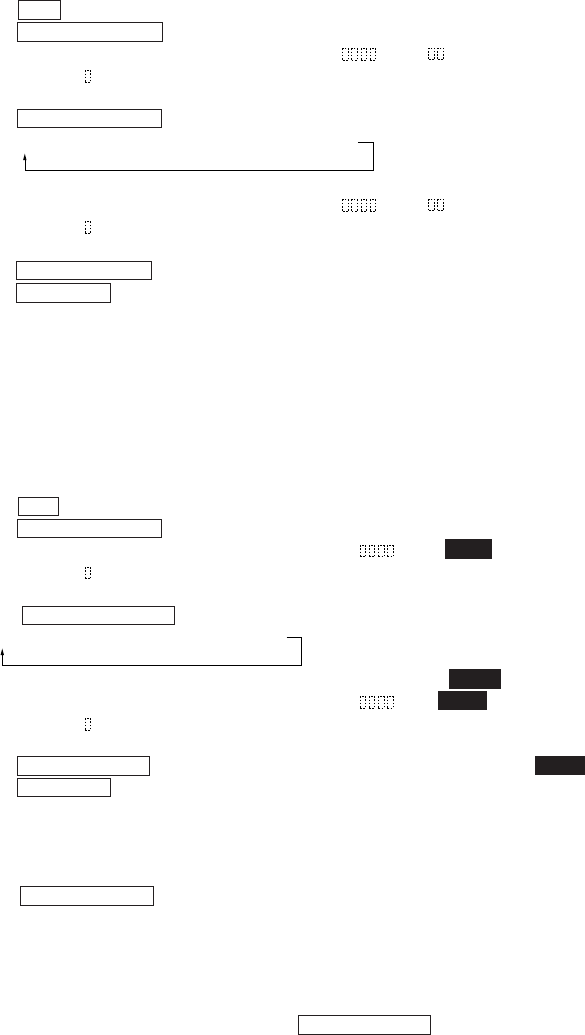
5-1. PARTS REPLACEMENT AND ADJUSTMENT
• Check and adjust the MDM and MBU as follows.
The procedure changes according to the part replaced
SECTION 5
ELECTRICAL ADJUSTMENTS
• Abbreviation
OP : Optical pick-up
OWH: Overwrite head
• Temperature compensation offset check
• Laser power check
• Traverse check
• Focus bias check
• C PLAY check
• Self-recording/playback check
Parts Replacement and Repair
NG
Has the OWH been replaced?
NO
OK
NO
NO
NO
Has OP, IC171, IC101, or
IC121 been replaced?
YES
YES
Initial setting of the adjustment value
Has OP or IC171 been replaced?
YES
IOP information recording
(IOP value labeled on OP)
Has IC171 or D101
been replaced?
YES
Temperature compensation offset adjustment
• Laser power adjustment
• Traverse adjustment
• Focus bias adjustment
• Error rate adjustment
• Focus bias check
• Auto gain adjustment
Check the sleding and spindle
mechanisms.
Other causes can be suspected.
22
5-2. PRECAUTIONS FOR CHECKING LASER DIODE
EMISSINON
To check the emission of the laser diode during adjustments, never
view directly from the top as this may lose your eye-sight.
5-3. PRECAUTIONS FOR USE OF OPTICAL PICK-
UP (KMS-260A)
As the laser diode in the optical pick-up is easily damaged by static
electricity, solder the laser tap of the flexible board when using it.
Before disconnecting the connector, desolder first. Before connect-
ing the connector, be careful not to remove the solder. Also take
adequate measures to prevent damage by static electricity. Handle
the flexible board with care as it breaks easily.
Optical pick-up flexible board
5-4. PRECAUTIONS FOR ADJUSTMENTS
1) When replacing the following parts, perform the adjustments
and checks with ¬ in the order shown in the following table.
Optical
Pick-up
BD Board
IC101, IC121
D101
IC171
¬G¬¬
pick-up flexible board
laser tap
1.Initial setting of
adjustment value
2.Recording of IOP
information
(Value written in
the pick-up)
3.Temperature
compensation
offset adjustment
4.Laser power
adjustment
5.Traverse
adjustment
6.Focus bias
adjustment
7.Error rate check
8.Auto gain output
level adjustment
IC192
G
¬G¬GG
¬¬GGG
¬G¬¬¬
¬G¬¬G
¬G¬¬G
¬G¬¬G
¬G¬¬G
2) Set the test mode when performing adjustments.
After completing the adjustments, exit the test mode.
Perform the adjustments and checks in “group S” of the test mode.
3) Perform the adjustments to be needed in the order shown.
4) Use the following tools and measuring devices.
• Check Disc (MD) TDYS-1
(Parts No. 4-963-646-01)
• Test Disk (MDW-74/AU-1) (Parts No. 8-892-341-41)
• Laser power meter LPM-8001 (Parts No. J-2501-046-A)
orMD Laser power meter 8010S (Parts No. J-2501-145-A)
• Oscilloscope (Measure after performing CAL of prove.)
• Digital voltmeter
• Thermometer
• Jig for checking BD board waveform
(Parts No. : J-2501-149-A)
5) When observing several signals on the oscilloscope, etc.,
make sure that VC and ground do not connect inside the oscillo-
scope.
(VC and ground will become short-circuited.)
6) Using the above jig enables the waveform to be checked without
the need to solder.
(Refer to Servicing Note on page 6.)
7) As the disc used will affect the adjustment results, make sure
that no dusts nor fingerprints are attached to it.
Note:
When performing laser power checks and adjustment (electrical
adjustment), use of the new MD laser power meter 8010S (J-2501-
145-A) instead of the conventional laser power meter is convenient.
It sharply reduces the time and trouble to set the laser power meter
sensor onto the objective lens of the optical pick-up.
5-5. CREATING CONTINUOUSLY RECORDED DISC
* This disc is used in focus bias adjustment and error rate check.
The following describes how to create a continuous recording disc.
1. Insert a disc (blank disc) commercially available.
2. Press the + button and display “CREC MODE”.
3. Press the ^ “PROGRAM” button again to display “CREC
MID”.
Display “CREC (0300)” and start to recording.
4. Complete recording within 5 minutes.
5. Press the p “PROGRAM” button and stop recording .
6. Press the 6 (EJECT) button and remove the disc.
The above has been how to create a continuous recorded data for
the focus bias adjustment and error rate check.
Note : Be careful not to apply vibration during continuous record-
ing.
23
5-6. CHECKS PRIOR TO REPAIRS
These checks are performed before replacing parts according to
“approximate specifications” to determine the faulty locations. For
details, refer to “Checks Prior to Parts Replacement and
Adjustments” (See page 8).
5-6-1. Temperature Compensation Offset Check
When performing adjustments, set the internal temperature and room
temperature to 22 to 28°C.
Checking Procedure:
1. Press the + button to display “TEMP CHECK”.
2. Press the ^ “PROGRAM” button.
3. “T=@@(##) [OK]” should be displayed. If “T=@@ (##) [NG]”
is displayed, it means that the results are bad.
(@@ indicates the current value set, and ## indicates the value
written in the non-volatile memory.)
5-6-2. Laser Power Check
Before checking, check the IOP value of the optical pick-up.
(Refer to 5-8. Recording and Displaying IOP Information.)
Connection :
Checking Procedure:
1. Set the laser power meter on the objective lens of the optical
pick-up. (When it cannot be set properly, press the = “PRO-
GRAM” button or + “PROGRAM” button to move the
optical pick-up.)
Connect the digital volt meter to CN110 pin 5 (I+3V) and
CN110 pin 4 (IOP).
2. Then, press the + button and display “LDPWR CHECK” .
3. Press the ^ “PROGRAM” button once and display “0.9
mW*** $ ”. Check that the reading of the laser power meter
become 0.84 to 0.92 mW. (*** means IOP value)
4. Press the ^ “PROGRAM” button once more and display
“7.0 mW*** $ ”. Check that the reading the laser power meter
and digital volt meter satisfy the specified value.
Specified Value :
Laser power meter reading : 7.0 ± 0.2 mW
Digital voltmeter reading : Optical pick-up displayed value ± 10%
(Optical pick-up label)
5. Press the p “PROGRAM” button and display “LDPWR
CHECK” and stop the laser emission.
(The p “PROGRAM” button is effective at all times to stop
the laser emission.)
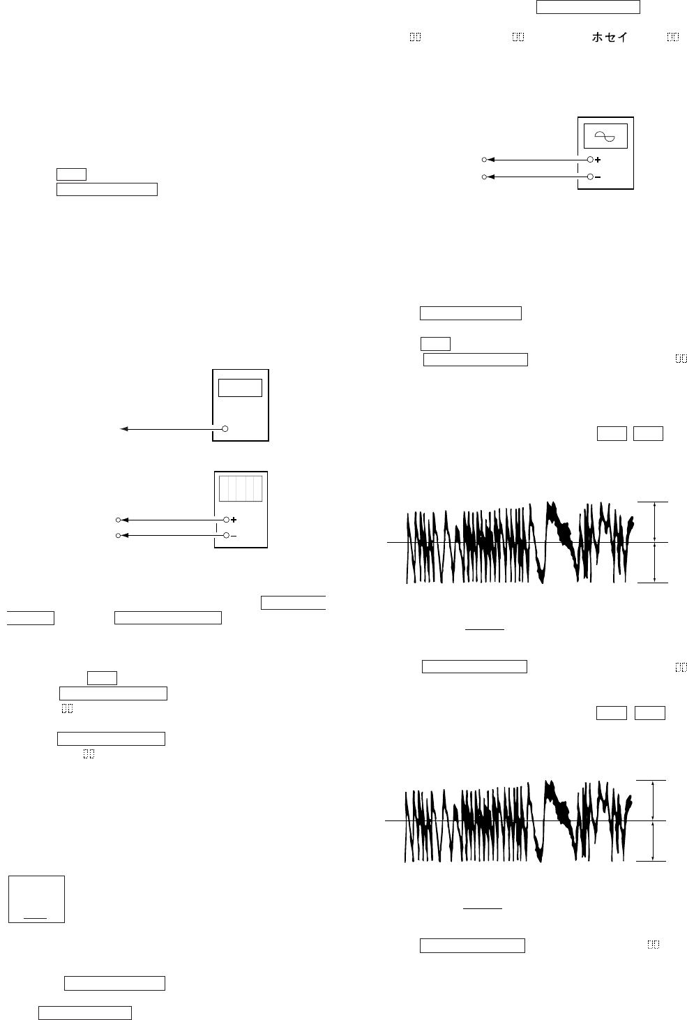
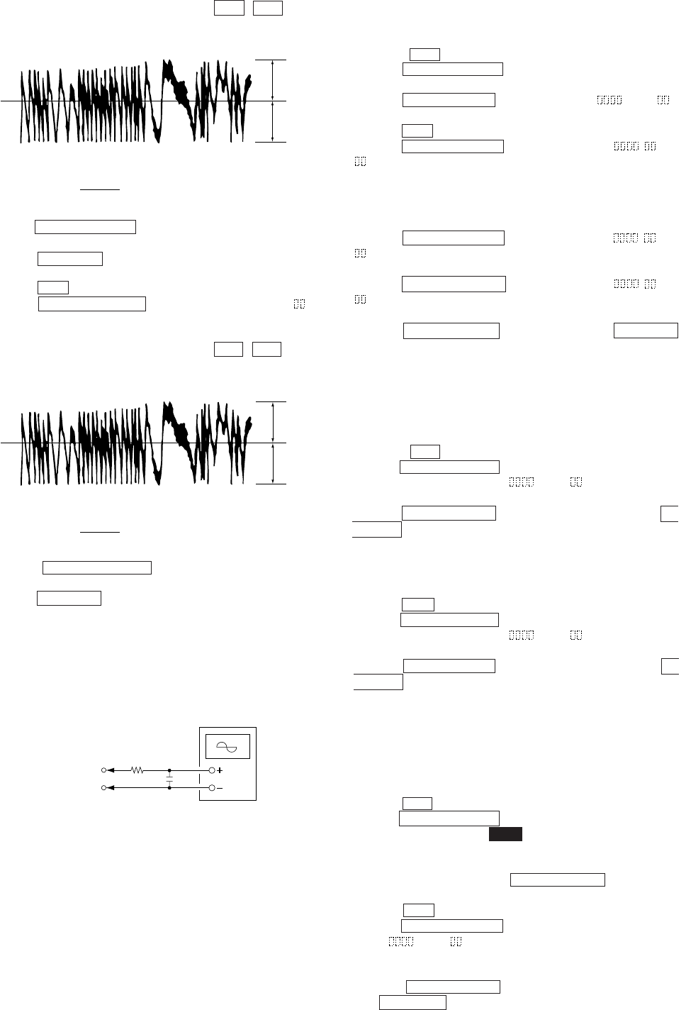
5-6-3. Traverse Check
Connection :
Checking Procedure:
1. Connect an oscilloscope to CN110 pin 3 (TE) and CN110 pin
1 (VC) of the BD board.
2. Load a disc (any available on the market). (Refer to Note 1.)
3. Press the + “PROGRAM” button and move the optical pick-
up outside the pit.
4. Press the + button and display “EF MO CHECK”.
5. Press the ^ “PROGRAM” button and display “EFB =
MO-R”.
(Laser power READ power/Focus servo ON/tracking servo OFF/
spindle (S) servo ON)
6. Observe the waveform of the oscilloscope, and check that the
specified value is satisfied. Do not press the = , + but-
tons.
(Read power traverse checking)
(Traverse Waveform)
7. Press the ^ “PROGRAM” button and display “EFB =
MO-W”.
8. Observe the waveform of the oscilloscope, and check that the
specified value is satisfied. Do not press the = , + but-
tons..
(Write power traverse checking)
(Traverse Waveform)
9. Press the ^ “PROGRAM” button display “EFB = MO-
P”.
Then, the optical pick-up moves to the pit area automatically
and servo is imposed.
Note 1: After step 4, each time the ^ “PROGRAM” button is
pressed, the display will be switched between “0.7 mW***
$ ”, “6.2 mW*** $ ”, and “WP *** $ ”.
Nothing needs to be performed here.
Laser power
meter
Optical pick-up
objective lens
Digital volt mete
r
BD board
CN110 pin
5
(I+3V)
CN110 pin
4
(IOP)
V : 0.5 V/div
H : 10 ms/div
Input : DC mod
e
Oscilloscope
BD board
CN110 pin
3
(TE)
CN110 pin
1
(VC)
VC
A
B
Specified value : Below 10% offset value
Offset value (%) = X 100
I
A – B
I
2 (A + B)
VC
A
B
Specified value : Below 10% offset value
Offset value (%) = X 100
I
A – B
I
2 (A + B)
KMS260A
27X40
B0825
N
Iop = 82.5 mA in this case
Iop (mA) = Digital voltmeter reading (mV)/1 (
Ω
)
(For details of the method for checking
this value, refer to “5-8. Recording and
Displaying IOP Information”.)
24
5-6-4. Focus Bias Check
Change the focus bias and check the focus tolerance amount.
Checking Procedure :
1. Load a test disk (MDW-74/AU-1).
2. Rotate the + button and display “CPLAY MODE”.
3. Press the ^ “PROGRAM” button twice and display “CPLAY
MID”.
4. Press the p “PROGRAM” button when “C1 = AD = ”
is displayed.
5. Press the + button and display “FBIAS CHECK”.
6. Press the ^ “PROGRAM” button and display “ / c =
”.
The first four digits indicate the C1 error rate, the two digits
after “/” indicate ADER, and the 2 digits after “c =” indicate the
focus bias value.
Check that the C1 error is below 220 and ADER is below 2.
7. Press the ^ “PROGRAM” button and display “ / b =
”.
Check that the C1 error is below 220 and ADER is below 2.
8. Press the ^ “PROGRAM” button and display “ / a =
”.
Check that the C1 error is below 220 and ADER is below 2.
9. Press the p “PROGRAM” button, next press the 6 (EJECT)
button, and remove the test disc.
5-6-5. C PLAY Checking
MO Error Rate Check
Checking Procedure :
1. Press a test disk (MDW-74/AU-1).
2. Rotate the + button knob and display “CPLAY MODE” .
3. Press the ^ “PROGRAM” button and display “CPLAY MID”.
4. The display changes to “C1 = AD = ”.
5. If the C1 error rate is below 80, check that ADER is below 2.
6. Press the p “PROGRAM” button, stop playback, press the 6
(EJECT) button, and test disc.
CD Error Rate Check
Checking Procedure :
1. Load a check disc (MD) TDYS-1.
2. Press the + button knob and display “CPLAY MODE”.
3. Press the ^ “PROGRAM” button and display “CPLAY MID”.
4. The display changes to “C1 = AD = ”.
5. Check that the C1 error rate is below 50.
6. Press the p “PROGRAM” button, stop playback, press the 6
(EJECT) button, and the test disc.
5-6-6. Self-Recording/playback Check
Prepare a continuous recording disc using the unit to be repaired
and check the error rate.
Checking Procedure :
1. Insert a recordable disc (blank disc) into the unit.
2. Press the + button knob to display “CREC MODE”.
3. Press the ^ “PROGRAM” button to display the “CREC MID”.
4. When recording starts, “ REC ” is displayed, this becomes
“CREC (@@@@)" (@@@@ is the address), and recording
starts.
5. About 1 minute later, press the p “PROGRAM” button to stop
continuous recording.
6. Press the = button to display “C PLAY MODE”.
7. Press the ^ “PROGRAM” button to display “C PLAY MID”.
8. “C1 = AD = ” will be displayed.
9. Check that the C1 error becomes below 80 and the AD error
below 2.
10. Press the p “PROGRAM” button to stop playback, and press
the 6 (EJECT) button and remove the disc.
10. Observe the waveform of the oscilloscope, and check that the
specified value is satisfied. Do not press the = , + but-
tons.
(Traverse Waveform)
11. Press the ^ “PROGRAM” button display “EF MO CHECK”
The disc stops rotating automatically.
12. Press the 6 (EJECT) button and remove the disc.
13. Load the check disc (MD) TDYS-1.
14. Press the + button and display “EF CD CHECK”.
15. Press the ^ “PROGRAM” button and display “EFB =
CD”. Servo is imposed automatically.
16. Observe the waveform of the oscilloscope, and check that the
specified value is satisfied. Do not press the = , + but-
tons.
(Traverse Waveform)
17. Press the ^ “PROGRAM” button and display “EF CD
CHECK”.
18. Press the 6 (EJECT) button and remove the check disc (MD)
TDYS-1.
Note 1 : MO reading data will be erased during if a recorded disc is
used in this adjustment.
Note 2 : If the traverse waveform is not clear, connect the oscillo-
scope as shown in the following figure so that it can be
seen more clearly.
VC
A
B
Specified value : Below 10% offset value
Offset value (%) = X 100
I
A – B
I
2 (A + B)
VC
A
B
Specified value : Below 10% offset value
Offset value (%) = X 100
I
A – B
I
2 (A + B)
330 k
Ω
Oscilloscop
e
10pF
BD board
CN110 pin
3
(TE)
CN110 pin
1
(VC)

25
5-7. INITIAL SETTING OF ADJUSTMENT VALUE
Note:
Mode which sets the adjustment results recorded in the non-volatile
memory to the initial setting value. However the results of the
temperature compensation offset adjustment will not change to the
initial setting value.
If initial setting is performed, perform all adjustments again
excluding the temperature compensation offset adjustment.
For details of the initial setting, refer to “5-4. Precautions on
Adjustments” and execute the initial setting before the adjustment
as required.
Setting Procedure :
1. Press the + button to display “ADJ CLEAR”.
2. Press the ^ “PROGRAM” button. “Complete!” will be dis-
played momentarily and initial setting will be executed, after
which “ADJ CLEAR” will be displayed.
5-8. RECORDING AND DISPLAYING THE IOP
INFORMATION
The IOP data can be recorded in the non-volatile memory. The IOP
value on the label of the optical pickup and the IOP value after the
adjustment will be recorded. Recording these data eliminates the
need to read the label on the optical pick-up.
Recording Procedure :
1. While pressing the INPUT button and p button, connect the
power plug to the outlet, and release the INPUT button and p
button.
2. Press the + button to display “[Service]”, and press the ^
“PROGRAM” button.
3. Rotate the + button to display “Iop.Write”, and press the
^ “PROGRAM” button.
4. The display becomes Ref=@@@.@ (@ is an arbitrary number)
and the numbers which can be changed will blink.
5. Input the IOP value written on the optical pick-up.
To select the number : Press the = , + buttons.
To select the digit : Press the r “PROGRAM” knob
6. When the ^ “PROGRAM” button is pressed, the display
becomes “Measu=@@@.@” (@ is an arbitrary number).
7. As the adjustment results are recorded for the 6 value. Leave it
as it is and press the ^ “PROGRAM” button.
8. “Complete!” will be displayed momentarily. The value will be
recorded in the non-volatile memory and the display will become
“Iop Write”.
Display Procedure :
1. Press the + button to display “Iop.Read”.
2. “@@.@/##.#” is displayed and the recorded contents are
displayed.
@@.@ indicates the Iop value labeled on the pick-up.
##.# indicates the Iop value after adjustment
3. To end, press the r “PROGRAM” button or p “PROGRAM”
button to display “Iop Read”.
5-9. TEMPERATURE COMPENSATION OFFSET
ADJUTMENT
Save the temperature data at that time in the non-volatile memory
as 25 ˚C reference data.
Note :
1. Usually, do not perform this adjustment.
2. Perform this adjustment in an ambient temperature of 22 ˚C to
28 ˚C. Perform it immediately after the power is turned on when
the internal temperature of the unit is the same as the ambient
temperature of 22 ˚C to 28 ˚C.
3. When D101 has been replaced, perform this adjustment after
the temperature of this part has become the ambient tempera-
ture.
Adjusting Procedure :
1. Press the + button and display “TEMP ADJUST”.
2. Press the ^ “PROGRAM” button and select the “TEMP
ADJUST” mode.
3. “TEMP = [OK]” and the current temperature data will be
displayed.
4. To save the data, press the ^ “PROGRAM” button.
When not saving the data, press the p “PROGRAM” button.
5. When the ^ “PROGRAM” button is pressed, “TEMP =
SAVE” will be displayed and turned back to “TEMP ADJUST”
display then. When the p “PROGRAM” button is pressed,
“TEMP ADJUST” will be displayed immediatelly.
Specified Value :
The “TEMP = ” should be within “E0 - EF”, “F0 - FF”, “00 -
0F”, “10 - 1F” and “20 - 2F”.
5-10. LASER POWER ADJUSTMENT
Check the IOP value of the optical pick-up before adjustments.
(Refer to 5-8. Recording and Displaying IOP Information.)
Connection :
Adjusting Procedure :
1. Set the laser power meter on the objective lens of the optical
pick-up. (When it cannot be set properly, press the = “PRO-
GRAM” button or + “PROGRAM” button to move the
optical pick-up.)
Connect the digital volt meter to CN110 pin 5 (I+3V) and
CN110 pin 4 (IOP).
2. Press the + button and display “LDPWR ADJUST”.
(Laser power : For adjustment)
3. Press the ^ “PROGRAM” button once and display “LD 0.9
mW $ ”.
4. Press the = , + buttons so that the reading of the laser
power meter becomes 0.85 to 0.91 mW. Press the ^ “PRO-
GRAM” button after setting the range knob of the laser power
meter, and save the adjustment results. (“LD SAVE $ ” will
be displayed for a moment.)
5. Then “LD 7.0 mW $ ” will be displayed.
Laser power
meter
Optical pick-up
objective lens
Digital volt mete
r
BD board
CN110 pin
5
(I+3V)
CN110 pin
4
(IOP)
26
6. Press the = , + buttons so that the reading of the laser
power meter becomes 6.9 to 7.1 mW, press the ^ “PRO-
GRAM” button and save it.
Note : Do not perform the emission with 7.0 mW more than 15
seconds continuously.
7. Then, press the + button and display “PWR CHECK”.
8. Press the ^ “PROGRAM” button once and display “0.9
mW*** $ ”. Check that the reading of the laser power meter
become 0.85 to 0.91 mW. (*** means IOP value)
9. Press the ^ “PROGRAM” button once more and display
“7.0 mW*** $ ”. Check that the reading the laser power meter
and digital volt meter satisfy the specified value.
Note down the digital voltmeter reading value.
Specified Value :
Laser power meter reading : 7.0 ± 0.1 mW
Digital voltmeter reading : Optical pick-up displayed value ± 10%
(Optical pick-up label)
10. Press the p “PROGRAM” button and display “LDPWR
CHECK” and stop the laser emission.
(The p “PROGRAM” button is effective at all times to stop
the laser emission.)
11. Press the + button to display “Iop.Write”.
12. Press the ^ “PROGRAM” button. When the display be-
comes Ref=@@@.@ (@ is an arbitrary number), press the ^
“PROGRAM” button to display “Measu=@@@.@” (@ is an
arbitrary number).
13. The numbers which can be changed will blink. Input the Iop
value noted down at step 9.
To select the number : Press the = , + buttons.
To select the digit : Press the r “PROGRAM” buttan
14. When the ^ “PROGRAM” button is pressed, “Complete!”
will be displayed momentarily. The value will be recorded in
the non-volatile memory and the display will become “Iop
Write”.
Note 1: After step 4, each time the ^ “PROGRAM” button is
pressed, the display will be switched between “0.7 mW***
$ ”, “6.2 mW*** $ ”, and “ WP *** $ ”.
Nothing needs to be performed here.
5-11. TRAVERSE ADJUSTMENT
Connection :
Adjusting Procedure :
1. Connect an oscilloscope to CN110 pin 3 (TE) and CN110 pin
1 (VC) of the BD board.
2. Load a disc (any available on the market). (Refer to Note 1.)
3. Press the + “PROGRAM” button and move the optical pick-
up outside the pit.
4. Press the + button and display “EF MO ADJUST”.
5. Press the + button and display “EFB = MO-R”.
(Laser power READ power/Focus servo ON/tracking servo OFF/
spindle (S) servo ON)
6. Press the + button so that the waveform of the oscilloscope
becomes the specified value.
(When the = , + buttons is pressed, the of “EFB= ”
changes and the waveform changes.) In this adjustment, wave-
form varies at intervals of approx. 2%. Adjust the waveform so
that the specified value is satisfied as much as possible.
(Read power traverse adjustment)
(Traverse Waveform)
7. Press the ^ “PROGRAM” button and save the result of ad-
justment to the non-volatile memory (“EFB = SAVE” will be
displayed for a moment. Then “EFB = MO-W” will be dis-
played).
8. Press the = , + buttons so that the waveform of the
oscilloscope becomes the specified value.
(When the = , + buttons is pressed, the of “EFB- ”
changes and the waveform changes.) In this adjustment, wave-
form varies at intervals of approx. 2%. Adjust the waveform so
that the specified value is satisfied as much as possible.
(Write power traverse adjustment)
(Traverse Waveform)
9. Press the ^ “PROGRAM” button, and save the adjustment
results in the non-volatile memory. (“EFB = SAVE” will be
displayed for a moment.)
10. “EFB = MO-P”. will be displayed.
The optical pick-up moves to the pit area automatically and servo
is imposed.
V : 0.5 V/div
H : 10 ms/div
Input : DC mod
e
Oscilloscope
BD board
CN110 pin
3
(TE)
CN110 pin
1
(VC)
VC
A
B
Specification A = B
VC
A
B
Specification A = B
KMS260A
27X40
B0825
N
Iop = 82.5 mA in this case
Iop (mA) = Digital voltmeter reading (mV)/1 (
Ω
)
(For details of the method for checking
this value, refer to “5-8. Recording and
Displaying IOP Information”.)

27
11. Press the = , + buttons until the waveform of the oscil-
loscope moves closer to the specified value.
In this adjustment, waveform varies at intervals of approx. 2%.
Adjust the waveform so that the specified value is satisfied as
much as possible.
(Traverse Waveform)
12. Press the ^ “PROGRAM” button, and save the adjustment
results in the non-volatile memory. (“EFB = SAVE” will be
displayed for a moment.)
Next “EF MO ADJUST” is displayed. The disc stops rotating
automatically.
13. Press the 6 (EJECT) button and remove the disc.
14. Load the check disc (MD) TDYS-1.
15. Press + button and display “EF CD ADJUST”.
16. Press the ^ “PROGRAM” button and display “EFB =
CD”. Servo is imposed automatically.
17. Press the = , + buttons so that the waveform of the
oscilloscope moves closer to the specified value.
In this adjustment, waveform varies at intervals of approx. 2%.
Adjust the waveform so that the specified value is satisfied as
much as possible.
(Traverse Waveform)
18. Press the ^ “PROGRAM” button, display “EFB = SAVE”
for a moment and save the adjustment results in the non-vola-
tile memory.
Next “EF CD ADJUST” will be displayed.
19. Press the 6 (EJECT) button and remove the check disc (MD)
TDYS-1.
Note 1 : MO reading data will be erased during if a recorded disc is
used in this adjustment.
Note 2 : If the traverse waveform is not clear, connect the oscillo-
scope as shown in the following figure so that it can be
seen more clearly.
5-12. FOCUS BIAS ADJUSTMENT
Adjusting Procedure :
1. Load a test disk (MDW-74/AU-1).
2. Press the + button and display “CPLAY MODE”.
3. Press the ^ “PROGRAM” button and display “CPLAY MID”.
4. Press the p “PROGRAM” button when “C1 = AD = ”
is displayed.
5. Press the + button and display “FBIAS ADJUST”.
6. Press the p “PROGRAM” button and display “ / a =
”.
The first four digits indicate the C1 error rate, the two digits
after “/” indicate ADER, and the 2 digits after [a =] indicate the
focus bias value.
7. Press the + button and find the focus bias value at which the
C1 error rate becomes about 200 (Refer to Note 2).
8. Press the ^ “PROGRAM” button and display “ / b =
”.
9. Press the = button direction and find the focus bias value at
which the C1 error rate becomes about 200.
10. Press the ^ “PROGRAM” button and display “ / c =
”.
11. Check that the C1 error rate is below 50 and ADER is 00. Then
press the ^ “PROGRAM” button.
12. If the “( )” in “ - - ( )” is above 20, press the p
“PROGRAM” button.
If below 20, press the p “PROGRAM” button and repeat the
adjustment from step 2.
13. Press the 6 (EJECT) button to remove the test disc.
Note 1 : The relation between the C1 error and focus bias is as
shown in the following figure. Find points a and b in the
following figure using the above adjustment. The focal
point position C is automatically calculated from points a
and b.
Note 2 : As the C1 error rate changes, perform the adjustment us-
ing the average vale.
VC
A
B
Specification A = B
VC
A
B
Specification A = B
330 k
Ω
Oscilloscop
e
10pF
BD board
CN110 pin
3
(TE)
CN110 pin
1
(VC)
C1 error
about
200
bc a Focus bias value
(F. BIAS)
28
5-13. ERROR RATE CHECK
5-13-1. CD Error Rate Check
Checking Procedure :
1. Load a check disc (MD) TDYS-1.
2. Press the + button and display “CPLAY MODE”.
3. Press the ^ “PROGRAM” button twice and display “CPLAY
MID”.
4. The display changes to “C1 = AD = ”.
5. Check that the C1 error rate is below 20.
6. Press the p “PROGRAM” button, stop playback, press the 6
(EJECT) button, and remove the test disc.
5-13-2. MO Error Rate Check
Checking Procedure :
1. Load a test disc (MDW-74/AU-1).
2. Press the + button and display “CPLAY MODE”.
3. Press the ^ “PROGRAM” button and display “CPLAY MID”.
4. The display changes to “C = AD = ”.
5. If the C1 error rate is below 50, check that ADER is 00.
6. Press the p “PROGRAM” button, stop playback, press the 6
(EJECT) button, and remove the test disc.
5-14. FOCUS BIAS CHECK
Change the focus bias and check the focus tolerance amount.
Checking Procedure :
1. Load a test disc (MDW-74/AU-1).
2. Press the + button and display “CPLAY MODE”.
3. Press the ^ “PROGRAM” button twice and display “CPLAY
MID”.
4. Press the p “PROGRAM” button when “C1 = AD = ”
is displayed.
5. Press the + button and display “FBIAS CHECK”.
6. Press the ^ “PROGRAM” button and display “ / c =
”.
The first four digits indicate the C1 error rate, the two digits
after “/” indicate ADER, and the 2 digits after “c =” indicate the
focus bias value.
Check that the C1 error is below 50 and ADER is below 2.
7. Press the ^ “PROGRAM” button and display “ / b =
”.
Check that the C1 error is below 220 and ADER is below 2.
8. Press the ^ “PROGRAM” button and display “ / a =
”.
Check that the C1 error is below 220 and ADER is below 2
9. Press the p “PROGRAM” button, next press the 6 (EJECT)
button, and remove the continuously recorded disc.
Note 1 : If the C1 error and ADER are above other than the speci-
fied value at points a (step 8. in the above) or b (step 7. in
the above), the focus bias adjustment may not have been
carried out properly. Adjust perform the beginning again.
5-15. AUTO GAIN CONTROL OUTPUT LEVEL
ADJUSTMENT
Be sure to perform this adjustment when the pickup is replaced.
If the adjustment results becomes “Adjust NG!”, the pickup may be
faulty or the servo system circuits may be abnormal.
5-15-1. CD Auto Gain Control Output Level Adjustment
Adjusting Procedure :
1. Insert the check disc (MD) TDYS-1.
2. Press the + button to display “AG Set (CD)”.
3. When the ^ “PROGRAM” button is pressed, the adjustment
will be performed automatically.
“Complete!!” will then be displayed momentarily when the value
is recorded in the non-volatile memory, after which the display
changes to “AG Set (CD)”.
4. Press the 6 (EJECT) button to remove the disc.
5-15-2. MO Auto Gain Control Output Level Adjustment
Adjusting Procedure :
1. Insert the reference disc (MDW-74/AU-1) for recording.
2. Press the + button to display “AG Set (MO)”.
3. When the ^ “PROGRAM” button is pressed, the adjustment
will be performed automatically.
“Complete!!” will then be displayed momentarily when the value
is recorded in the non-volatile memory, after which the display
changes to “AG Set (MO)”.
4. Press the 6 (EJECT) button to remove the disc.
29
NOTE:
It is useful to use the jig. for checking the waveform. (Refer to Ser-
vicing Note on page 6.)
5-15. ADJUSTING POINTS AND CONNECTING POINTS
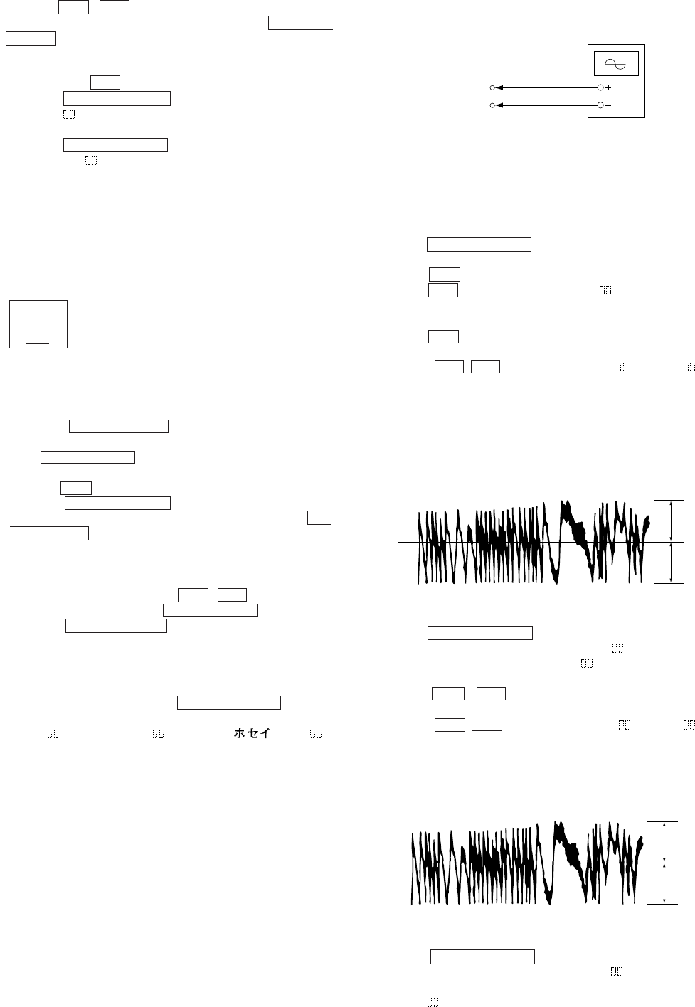
[BD BOARD] (SIDE A)
[BD BOARD] (SIDE B)
CN110
NOTE
D101
I+3V
IOP
TE
VC
GND
IC171
IC121
IC101
IC192
CN101
RF
30
SECTION 6
DIAGRAMS
6-1. CIRCUIT BOARDS LOCATION
Back up board
SW board
BD board
Panel board
Main board
Power boar
d
31 31
MDS-PC2
6-2. BLOCK DIAGRAM – BD SECTION –
HR901
OVER WRITE
HEAD
HEAD
DRIVE
Q181,182 3
6
1
2
FILTER
PCO
FILI
FILO
CLTV
PLL
EFM,
ACIRC,
ENCODER/
DECODER
RF AGC & EQ
AGCI
RFO
MORFI
MORFO
RF AMP
1
2BPF P-P
AT
AMP BPF
ADAGC VC
ANALOG
MUX
27
16
17
18
SERIAL
PARALLEL
DECODER
VICONV
20
2522 23
4
5
6
7
8
9
IV AMP
IV AMP
E-F
BALANCE
14
15
3
VCC
VC
D101
12
11
10
LASER ON
SW
Q101
PD
APC
Q162,163
HF
MODULE
HF MODULE
SW
IC103,Q102-104
TRACKING
COIL
FOCUS
COIL 10
12 DRIVER
21 DRIVER
23
27 DRIVER
25
6
8DRIVER
16
TFDR
PSB XRST
SLED/SPINDLE MOTOR DRIVE
FOCUS/TRACKING COIL DRIVE
IC152
09
M
M
M102
SLED MOTOR
M101
SPINDLE MOTOR
DETECTOR
F
IJ
C
D
B
A
E
VC
LD
PD
ILCC
15 14
ATRAC
ENCODER/
DECODER
SAMPLING
RATE
CONVERTER
DTRF
CKRF
XLRF
FOCNT
79
82
81
80
93 94 95 10
SPRD
SPFD
FG IN
XRST
SPINDLE
SERVO
ADIP
DEMODULATOR/
DECODER
78 ADFG
A/D
CONVERTER
SERVO
DSP
APC
PWM
GENERATOR
21
26
25
20
SUBCODE
PROCESSOR
11
12
MONITOR
CONTROL
4
3
2
1
3
CPU
I/F
AUTO
SEQUENCER
16
27
28
7
5
6
8
9
73512FS
M
M103
LOADING MOTOR
BCK
LRCK
BUFFER IC123
DRAM
IC124
SQSY
DQSY
MNT3
MNT2
MNT1
MNT0
SENS
SRDT
SCLK
SWDT
XLAT
DIN1
19
DIN0
ADDT
DADT
DOUT
91928586898883
13
RECP
APCREF
FFDR
FRDR
TFDR
TRDR
SFDR
SRDR
FOCNT
XLAT
SCLK
SWDT
CSLED
SE
TE 26
28
32
30
ADFG
ADIN
ADFM
29
31
34 66
68
75
74
FE
VC
TE
SE
33 67
36
37
35
64
63
65
AUX
BOTM
PEAK
ABCD
FE
AUX1
BOTM
PEAK
ABCD
38
RF 57 RFI
59
60
61
62
ABCD
AMP
FOCUS
ERROR
AMP
I
J
A
B
C
D
E
F
VC CVB
TEMP
AMP
TEMPR
TEMPI
APC
APCREF
EQADJ
3TADJ
WBLADJ
TRACKING
ERROR
AMP
OPTICAL PICK-UP BLOCK
(KMS-260A/J1N)
48 47 46 40
RF AMP
IC101
EFMO
TX
XINIT
CLOCK
GENERATOR
14
15
18
19
29
30
3
4
SPFD
SPRD
SFDR
SRDR
TRDR
FRDR
FFDR
OVER WRITE HEAD DRIVE
IC181
OSCI
XBCK
LRCK
VC
VC
PEAK
&
BOTTOM
TRK–
TRK+
FSC+
FSC–
SLED+
SLED–
SPDL+
SPDL–
DIGITAL SERVO SIGNAL PROCESSOR, DIGITAL SIGNAL PROCESSOR
EFM/ACIRC ENCODER/DECODER, SHOCK-PROOF MEMORY CONTROLLER,
ATRAC ENCODER/DECODER
IC121
DIN0
DIN1
SCTX
XINIT
ADDT
DADT
DOUT
SQSY
DQSY
MNT3
MNT2
MNT1
MNT0
SENS
SRDT
SCLK
SWDT
XLAT CH
LDON
WRPWR
MOD
6
5SDA
SDA
SCLSCL
LIMIT-IN
REFLECT
PROTECT
CHACK IN SW
PACK OUT SW
PLAY-P SW
REC P SW
EEP ROM
IC171
LOAD-IN
LOAD-OUT
DIG-RST
DETECT SW
S101, S102,
S601-604
100
49 • 48 • 50 • 51 34 31 • 36 40 • 45
D0 D3 A00 A09
47
46
3
4
17
16
1
2
18
19
6
9
11
15
5
XWE
XRAS
XCAS
XOE
DQ1
DQ4
•
•
•
•
A0
A9
44
43
20 XWE
XRAS
XCAS
XOE
•
SHOCK
RESISTANT
MEMORY
CONTROLLER
8
•
11 10
•
13
9
•
12
4
5
DIGITAL
AUDIO
I/F
MAIN
SECTION
(Page 32)
• SIGNAL PATH
:PB
:REC
:PB (Digital out)
:REC (Digital in)
32 32
MDS-PC2
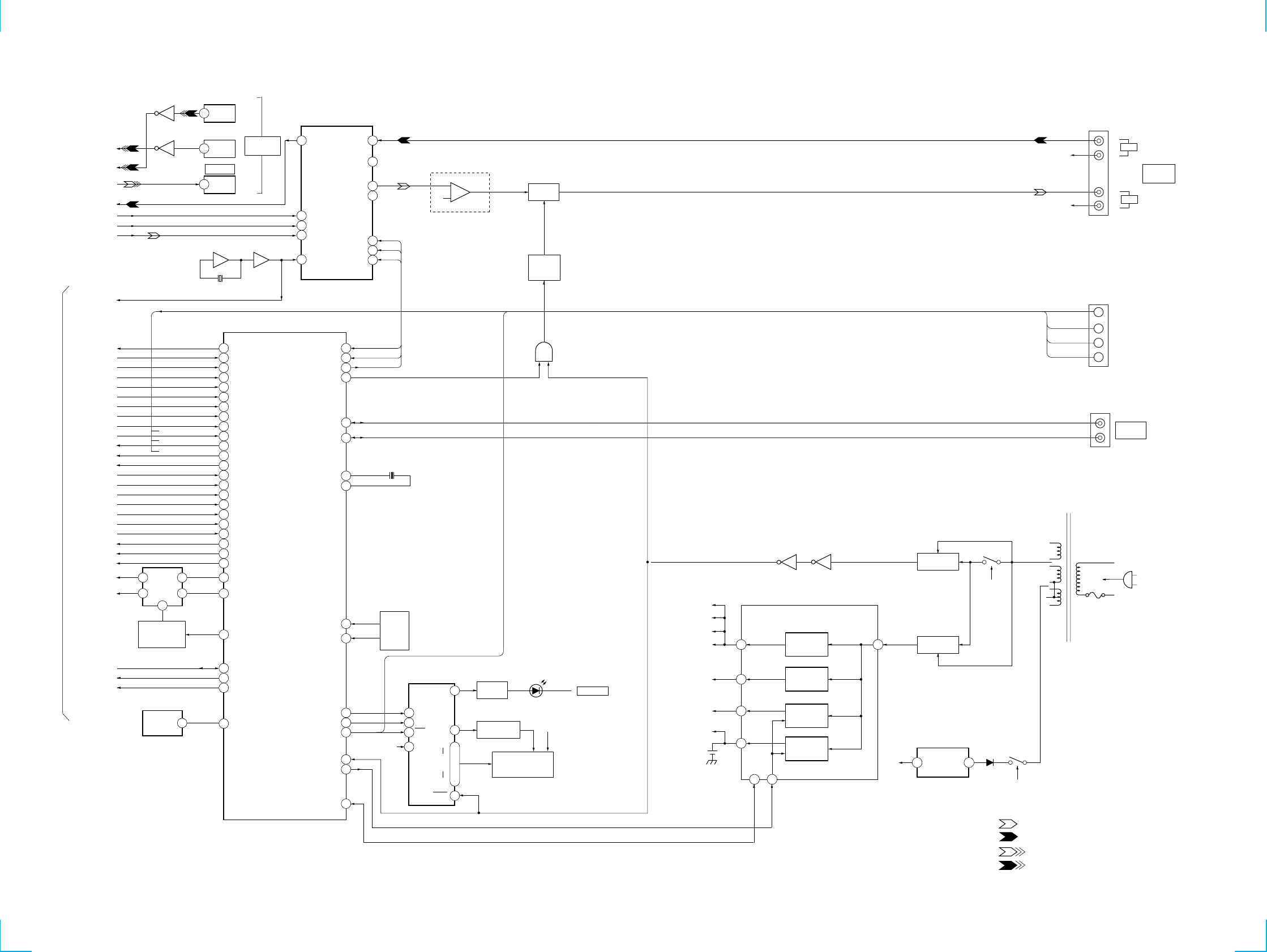
– MAIN SECTION –
1
RM
5
23
80
17
16
18
12
19
4
2
26
14
13
24
15
74
66
18
71
78
72
31
33
32
69
77
75
53
51
68
70
59
60
54
76
67
65
56
55
73
79
47
30
28
49
15
13
12
35
97
19
34
37
50
3
10
DIN0
DIN1
DOUT
ADDT
BCK
LRCK
DADT
512FS
SCTX
XINT
SQSY
DQSY
MNT3
RXDI
CLKI
TXDI
MNT2
MNT1
MNT0
SENS
SRDT
SCLK
SWDT
XLATCH
LIMIT-IN
REFLECT
PROTECT
CHACKIN SW
PACK-OUT SW
PB P SW
REC-P SW
LD ON
WRPWR
MOD
LOAD-IN
LOAD OUT
SIRCS
RECEIVER
IC781
SDA
SCL
DIG-RST
SCTX L3-CLOCK
L3-DATA
L3-MODE
MUTE
XOUT
XIN
S.RST
KEY0
FLDATA
FLCLK
FLCS RTSI
STB
P.DOWN
XINT
SQSY
DQSY
MNT3(S-LOCK)
MNT2(X-BUSY)
MNT1(SHOCK)
MNT0(F-OK)
SENS
SRDT
SCLK
SWDT
XLATCH
LIMIT-IN
REFLECT
PROTECT
CHACKIN
PACK-OUT
PB-P
REC-P
LDON
WR PWR
MOD
LD-IN
LD OUT
LD-LOVO
SDA
SCL
DIG-RST
6RMC
11
3
4
52
36
95KEY1
63
61
56
62
1
52
60
5
I
51
LD-LOVO
9
10
2
4
7
X513
10MHz
LD LOW
SWITCH
Q441
LED SW
Q751
RECTIFIER
D411,412
RECTIFIER
D431,432
MUTE
Q191
8
7
5
4
MUTE
DRIVE
Q390
GRID DRIVE
Q767
FL701
FLUORESCENT
INDICATOR TUBE
STANDBY
FL
DRIVER
IC761
IC611
IC601
A/D,D/A CONVERTER
IC301
LINE AMP
IC381, 382
IC601
IC351 IC351
SYSTEM CONTROL
IC501
3IC621
1IC661
DATAO VINL1
VINR1 R-CH
R-CH
VOUTL
VOUTR
L3MODE
L3CLK
L3DATA
BCK
WS
DATAI
SYSCLK
56
IC601
INVERTER
98
3 1
J101
R-CH
R-CH
AC
IN
–32V –32V REG
IC421
+
–
D390
D391
-32V
DAT
P1
AC
G13
S1
S35
G1
G12
RST
CLK
CS
VFL
X351
22.5792MHz
BD SECTION
LOADING
MOTER
DRIVE
IC441
D751
MATRIX
SWITCH
J101
TXDI
RTSI
CLKI
RXDI
09
6BACK UP
4+5V REG
5+3.3V REG
1 3
+5V REG
12 2 D421
BT451
LITHIUM
BATTERY
BACK+3.3V
ANA+5V
SYS+3.3V
M5V
D5V
H5V
LOADING 5V
S RESET
RY911
ANA+5V
ANA+5V
RY912
SWITCHING REG
IC 411
J801
CONTROL
A1
II
45
7
A1-OUT
A1-IN
POWER
TRANSFORMER
• SIGNAL PATH
:PB
:REC
:PB (Digital out)
:REC (Digital in)
OPT OUT
OPT IN 2
DIGITAL
(OPTICAL)
OPT IN 1
IN
L
R
L
R
OUT
LINE
(ANALOG)
(Page 31)

33 33
MDS-PC2
– MAIN SECTION –
IC701 !£ (XOUT)
IC201 !™ (SYSCLK)
IC201 !¶ (LRCK1)
IC201 !§ (BCK)
– PANEL SECTION –
IC901 %• (OSCO)
3.4Vp-p
2.822MHz
3.0Vp-p
22.581MHz
3.9Vp-p
2.4MHz
3.2Vp-p
10MHz
3.8Vp-p
44.1kHz
WAVEFORMS
1
IC101 1, 2 (I, J) (PLAY mode)
– BD (1/2) SECTION –
2
3
IC101 4 (A) (PLAY mode)
IC101 8, 9 (E, F) (PLAY mode)
0.46Vp-p
0.1Vp-p
0.06Vp-p
– BD (2/2) SECTION –
4
5
6
7
8
IC121 !§ (OSCI)
IC121 @¶ (LRCK)
IC121 @• (XBCK)
IC121 @ª (FS256)
IC121 (º (FS4)
3.1Vp-p
22.581MHz
3.2Vp-p
44.1kHz
3.8Vp-p
2.822MHz
3.2Vp-p
176.4kHz
3.8Vp-p
11.29MHz
1
1
2
3
4
Note on Schematic Diagram:
Note:
• All capacitors are in µF unless otherwise noted. pF: µµF
50 WV or less are not indicated except for electrolytics
and tantalums.
• All resistors are in Ω and 1/4 W or less unless otherwise
specified.
•¢: internal component.
•C: panel designation.
Note on Printed Wiring Boards:
Note:
•X: parts extracted from the component side.
•Y: parts extracted from the conductor side.
•p: parts mounted on the conductor side.
•®: Through hole.
•b: Pattern from the side which enables seeing.
(The other layers' patterns are not indicated.)
•U: B+ Line.
•V: B– Line.
•H: adjustment for repair.
no mark : STOP
( ) : Play the test disk (TDYS-1)
< > : REC
∗: Can not be measured.
• Voltages are taken with a VOM (Input impedance 10 MΩ).
Voltage variations may be noted due to normal produc-
tion tolerances.
• Waveforms are taken with a oscilloscope.
Voltage variations may be noted due to normal produc-
tion tolerances.
• Signal path.
E: PB
: REC
p: PB (digital out)
l: REC (digital in)
Note:
The components identi-
fied by mark ! or dotted
line with mark ! are criti-
cal for safety.
Replace only with part
number specified.
Note:
Les composants identifiés par
une marque ! sont critiques
pour la sécurité.
Ne les remplacer que par une
piéce portant le numéro
spécifié.
Caution:
Pattern face side: Parts on the pattern face side seen from the
(Side B) pattern face are indicated.
Parts face side: Parts on the parts face side seen from the
(Side A) parts face are indicated.
Q
C
EB
CEB
• Indication of transistor
These are omitted
These are omitted
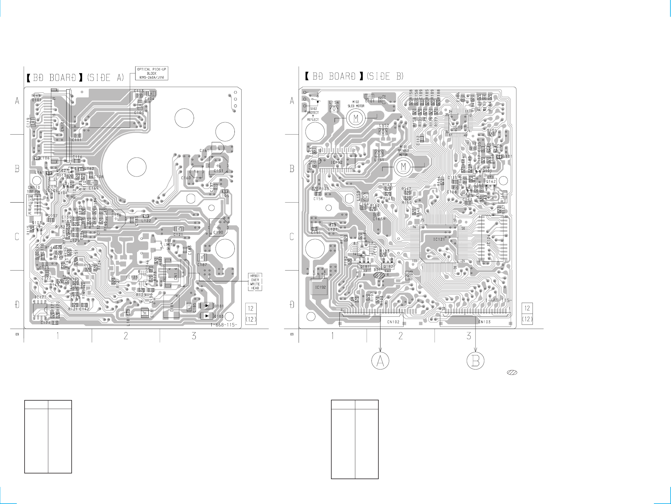
34 34
MDS-PC2
6-3. PRINTED WIRING BOARD – BD SECTION –
• See page 30 for Circuit Boards Location.
D101 A-1
D181 D-3
D183 D-3
IC103 B-1
IC123 D-2
IC171 D-1
Q102 B-1
Q103 B-1
Q104 B-1
• SEMICONDUCTOR
LOCATION
Ref. No. Location
IC101 A-3
IC121 C-3
IC124 C-3
IC152 B-1
IC181 C-1
IC192 D-1
Q101 B-3
Q162 B-3
Q163 B-3
Q181 C-1
Q182 C-2
• SEMICONDUCTOR
LOCATION
Ref. No. Location
: SOLDER BRIDGE
(Page 43) (Page 39)

35 35
MDS-PC2
6-4. SCHEMATIC DIAGRAM – BD (1/2) SECTION –
• See page 33 for Waveform.
• See page 45 for IC Block Diagrams.
• See page 48 for IC Pin Function.
(Page 36) (Page 36) (Page 36) (Page 36) (Page 36) (Page 36) (Page 36)

36 36
MDS-PC2
6-5. SCHEMATIC DIAGRAM – BD (2/2) SECTION –
• See page 33 for Waveform.
• See page 34 for Printed Wiring Board.
(Page 35) (Page 35) (Page 35) (Page 35) (Page 35) (Page 35) (Page 35)
(Page 37)
(Page 42)
BA033FP-E2
MAIN BOARD
(1/2)
POWER BOARD

37 37
MDS-PC2
6-6. SCHEMATIC DIAGRAM – MAIN (1/2) SECTION –
• See page 33 for Waveform.
• See page 39 for Printed Wiring Board.
(Page 44)
(Page 36)
(Page 42)
(Page 38)
(Page 38)
(Page 38)
(Page 38)
SW BOARD
BD BOARD
(2/2)
POWER
BOARD
• See page 51 for IC Pin Function.

38 38
MDS-PC2
6-7. SCHEMATIC DIAGRAM – MAIN (2/2) SECTION –
• See page 33 for Waveform.
• See page 47 for IC Block Diagrams.
(Page
37)
(Page
37)
(Page
37)
(Page
37)
(Page 40)
PANEL
BOARD
IN
L
R
L
R
OUT
LINE
(ANALOG)
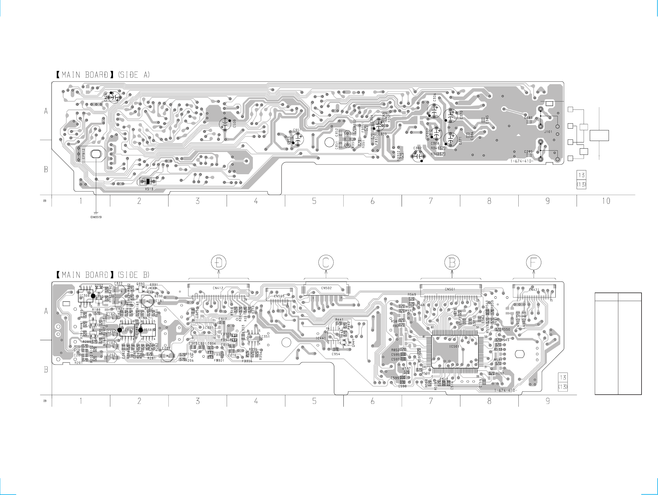
39 39
MDS-PC2
6-8. PRINTED WIRING BOARD – MAIN SECTION –
• See page 30 for Circuit Boards Location.
IN
OUT
L
L
R
R
LINE
(ANALOG)
• SEMICONDUCTOR
LOCATION
D390 A-2
D391 A-2
IC301 A-3
IC308 A-1
IC351 A-4
IC381 A-2
IC382 A-2
IC441 A-5
IC501 B-7
Q191 A-1
Q192 A-1
Q291 A-1
Q292 A-1
Q390 A-2
Q441 B-6
Ref. No. Location
(Page 43) (Page 44) (Page 34) (Page 41)
POWER
BOARD
BD SWITCH
BOARD BD BOARD
PANEL
BOARD

40 40
MDS-PC2
6-9. SCHEMATIC DIAGRAM – PANEL SECTION –
• See page 33 for Waveform.
(Page 38)
MAIN
BOARD
(2/2)

41 41
MDS-PC2
6-10. PRINTED WIRING BOARD – PANEL SECTION –
• See page 30 for Circuit Boards Location.
(Page 39)
MAIN BOARD

42 42
MDS-PC2
6-11. SCHEMATIC DIAGRAM – POWER SECTION –
(Page 37)
(Page 36)
BD BOARD
(2/2)
MAIN
BOARD
(1/2)
IN 1 IN 2
OUT
DIGITAL
(OPTICAL)
RESET

43 43
MDS-PC2
6-12. PRINTED WIRING BOARD – POWER SECTION –
• See page 30 for Circuit Boards Location.
• SEMICONDUCTOR
LOCATION
D431 C-2
D432 C-2
D433 C-2
D466 B-2
D467 B-2
D801 E-1
IC601 C-1
Ref. No. Location
• SEMICONDUCTOR
LOCATION
D411 C-4
D412 C-3
D421 C-2
D422 C-1
D451 B-2
D452 B-2
D461 B-4
D462 B-4
D911 B-4
D912 C-2
Ref. No. Location
IC411 B-2
IC421 C-1
IC611 C-5
IC621 B-5
IC661 D-5
Q801 E-5
Ref. No. Location
(Page 39)
MAIN BOARD
IN 1
IN 2
OUT
DIGITAL
(OPTICAL)
CONTROL
A1 II
(Page 34)
BD BOARD
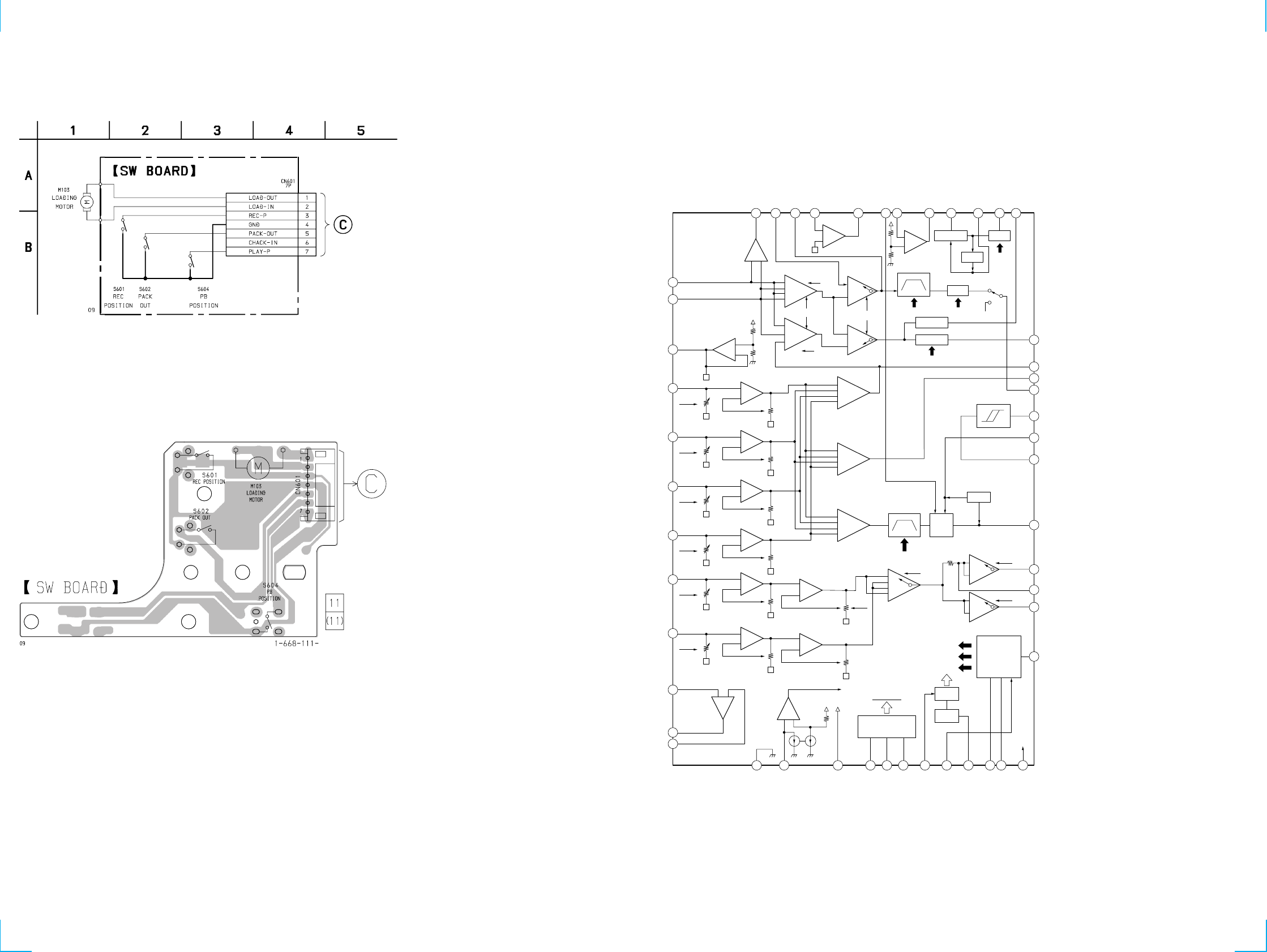
44 44
MDS-PC2
6-13. SCHEMATIC DIAGRAM – BD SWITCH SECTION –
6-14. PRINTED WIRING BOARD – BD SWITCH SECTION –
• See page 30 for Circuit Boards Location.
(Page 37)
MAIN BOARD
(1/2)
6-15. IC BLOCK DIAGRAM
• BD section
IC101 CXA2523AR
–1
–2
+
–
IVR BB
+
–
IVR AA
+
–
IVR CC
+
–
IVR DD
+
–
IVR +
–
EE EE'
EFB TESW
PTGR
48
MORFO
47
MORFI
46
RFO
45
OPN
44
OPO
43
ADDC
42
COMPP
41
COMPO
40
AGCI
39
RF AGC
38
RF
37
PEAK
36 BOTM
35 ABCD
34 FE
33 AUX
32 ADFG
31 ADAGC
30 ADIN
29 ADFM
28 SE
27 CSLED
26 TE
25 WBLADJ
24
VCC
23
3TADJ
22
EQADJ
21
VREF
20
F0CNT
19
XSTBY
18
XLAT
17
SCLK
16
SWDT
15
TEMPR
14
TEMPI
13
GND
12APCREF
11APC
10PD
9F
8E
7D
6C
5B
4A
3VC
VI CONV
BGR
VREF
SCRI - PARA
DECODE
+
–
+
–
AUXSW
COMMAND
+
–
IVR
GSW IV
+
–
FF
FBAL
FF'
TG
SEA
–
+
–
+
–1
–2
TG
TEA
WBL
3T
EQ
–
–
+
+
+
+
–
–
+
+
+
+
DET
ADIP
AGC
WBL
BPF22
BPFC
ABCDA
FEA
WBL
ATA
–
+
CVB
+
–
RFA1
–
–
–
–
1
2
–
–
–
1
2
GRVA
CFST
RFA2
GRV
HLPT
PTGR
–2
–1
–1
–2
BOTTOM
PEAK
RF AGC EQ
EQ
DET
P-P
WBL
3T WBL TEMP
PBH
–
+
USROP
+
–USRC
3T
BPF3T
PEAK3T
1I
2J
(Page 39)
MAIN BOARD

45
100
99 98 97 96 95 94 93
EFMO
DVSS
TEST3
TEST2
TEST1
TEST0
SPFD
SPRD
92
SFDR
91
SRDR
90
FS4
89
FRDR
88
FFDR
87
DVDD
86
TFDR
85
TRDR
84
LDDR
83
APCREF
82
DTRF
81
CKRF
80
XLRF
79
F0CNT
78
ADFG
77
APC
76
DCHG
75 TE
74 SE
73 AVSS
72 ADRB
71 ADRT
70 AVDD
69 ADIO
62 CLTV
61 FILO
60 FILI
59 PCO
57 RFI
58 AVSS
56 BIAS
55 AVDD
54 ASYI
53 ASYO
52 MVCI
51 D3
68 VC
67 AUX1
66 FE
65 ABCD
64 BOTM
63 PEAK
50
D2
49
D0
48
D1
47
XWE
46
XRAS
45
A09
44
XCAS
43
XOE
42
DVSS
41
A11
40
A08
39
A07
38
A06
37
A05
36
A04
35
A10
34
A00
33
A01
32
A02
31
A03
30
DVDD
28
XBCK
29
FS256
26
DADT
27
LRCK
24
XBCKI
25
ADDT
23
LRCKI
22
DATAI
21
DOUT
20
DIN1
19
DIN0
18
XTSL
17
OSCO
16
OSCI
15
TX
14
XINT
13
RECP
12
DQSY
11
SQSY
10
XRST
9
SENS
8
SRDT
7
XLAT
6
SCLK
5
SWDT
4
MNT3
3
MNT2
2
MNT1
1
MNT0
PWM
GENERATOR
AUTO
SEQUENCER
SERVO
DSP
CPU I/F
MONITOR
CONTROL
SPINDLE
SERVO
EACH
BLOCK
EACH
BLOCK
DIGITAL
AUDIO
I/F
SAMPLING
RATE
CONVERTER
CLOCK
GENERATOR
SUBCODE
PROCESSOR
EACH
BLOCK
A/D
CONVERTER
ANALOG
MUX
EFM/ACIRC
ENCODER/
DECODER
APC
PLL
SHOCK RESISTANT
MEMORY CONTROLLER
ATRAC
ENCODER/DECODER
DRAM
ADIP
DEMODULATOR/
DECODER
COMP
ADDRESS/DATA BUS A00 - A11, D0 - D3
IC121 CXD2654R
32 31 30 29 28 27 26 25 24 23 22 21 20 19 18 17
1 2 3 4 5 6 7 8 9 10 11 12 13 14 15 16
GND
VG
IN4R
IN4F
VM4
OUT4F
PGND4
OUT4R
VM34
OUT3R
PGND3
OUT3F
VM3
IN3F
IN3R
PSB
CAPA–
CAPA+
IN2R
IN2F
VM2
OUT2F
PGND2
OUT2R
VM12
OUT1R
PGND1
OUT1F
VM1
IN1F
IN1R
V
DD
CHARGE
PUMP.
OSC
INTERFACE AMP
INTERFACE AMP
AMP INTERFACE
PREDRIVEPREDRIVE
PREDRIVEPREDRIVE
AMP
INTERFACE
AMPAMPAMP
V
DD
PSB
AMP
IC152 BH6511FS-E2
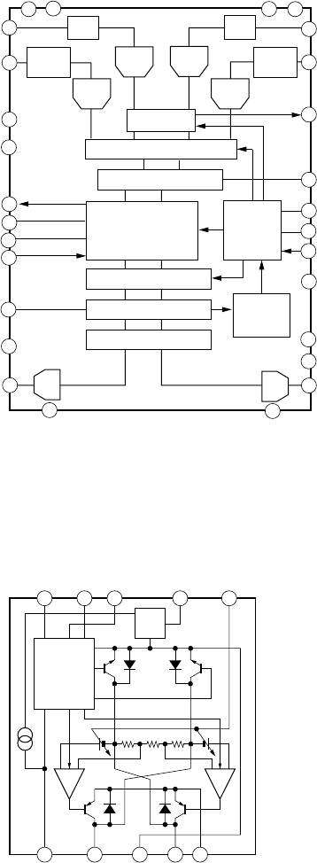
46
• MAIN section
3
4
5
6
2
8
7
1
VADCN
VADCP
VINL2 PGA PGA
0DB/6DB
SWITCH
NOISE SHAPER
INTERPOLATION FILTER
DSP FEATURES
PRAK
DETECTOR
L3-BUS
INTERFACE
DECIMATION FILTER
DIGITAL
INTERFACE
DIGITAL MIXER
DIGITAL AGC
ADC1L
ADC2L ADC2R
ADC1R
DAC
DAC
0DB/6DB
SWITCH
VSS(AD)
VDD(AD)
VINL1
VDDD
VSSD
18
16
19
17
26
25 27
24
13
15
14
9
22
10
11
23
28
12
20
21
DATAO
BCK
WS
DATAI
QMUTE
VREF
VOUTL
V
DD(DAC)
VSS(DAC)
VOUTR
TEST2
TEST1
SYSCLK
L3DATA
L3MODE
L3CLOCK
OVERFLOW
AGCSTAT
VINR1
VINR2
IC301 UDA1341TS/N2
1
LOGIC
PREDRIVER
VREF
2 3 45
10 9 8 7 6
IN2 IN1 VM VREF VCONT
VCC OUT2 GND OUT1 VS
IC441 LB1830M

47
6-16. IC PIN FUNCTIONS
• IC101 RF Amplifier (CXA2523AR) (BD board)
Pin No. Pin Name I/O Function
I
J
VC
A to F
PD
APC
APCREF
GND
TEMPI
TEMPR
SWDT
SCLK
XLAT
XSTBY
F0CNT
VREF
EQADJ
3TADJ
Vcc
WBLADJ
TE
CSLED
SE
ADFM
ADIN
ADAGC
ADFG
AUX
FE
ABCD
BOTM
PEAK
RF
RFAGC
AGCI
COMPO
COMPP
ADDC
OPO
OPN
RFO
MORFI
MORFO
I
I
O
I
I
O
I
—
I
O
I
I
I
I
I
O
I/O
I/O
—
I/O
O
—
O
O
I
—
O
O
O
O
O
O
O
—
I
O
I
I/O
O
I
O
I
O
I-V converted RF signal I input
I-V converted RF signal J input
Middle point voltage (+1.5V) generation output
Signal input from the optical pick-up detector
Light amount monitor input
Laser APC output
Reference voltage input for setting laser power
Ground
Temperature sensor connection
Reference voltage output for the temperature sensor
Serial data input from the CXD2650R or CXD2652AR
Serial clock input from the CXD2650R or CXD2652AR
Latch signal input from the CXD2650R or CXD2652AR “L”: Latch
Stand by signal input “L”: Stand by
Center frequency control voltage input of BPF22, BPF3T, EQ from the CXD2650R or
CXD2652AR
Reference voltage output (Not used)
Center frequency setting pin for the internal circuit EQ
Center frequency setting pin for the internal circuit BPF3T
+3V power supply
Center frequency setting pin for the internal circuit BPF22
Tracking error signal output to the CXD2650R or CXD2652AR
External capacitor connection pin for the sled error signal LPF
Sled error signal output to the CXD2650R or CXD2652AR
FM signal output of ADIP
ADIP signal comparator input ADFM is connected with AC coupling
External capacitor connection pin for AGC of ADIP
ADIP duplex signal output to the CXD2650R or CXD2652AR
I3 signal/temperature signal output to the CXD2650R or CXD2652AR
(Switching with a serial command)
Focus error signal output to the CXD2650R or CXD2652AR
Light amount signal output to the CXD2650R or CXD2652AR
RF/ABCD bottom hold signal output to the CXD2650R or CXD2652AR
RF/ABCD peak hold signal output to the CXD2650R or CXD2652AR
RF equalizer output to the CXD2650R or CXD2652AR
External capacitor connection pin for the RF AGC circuit
Input to the RF AGC circuit The RF amplifier output is input with AC coupling
User comparator output (Not used)
User comparator input (Fixed at “L”)
External capacitor pin for cutting the low band of the ADIP amplifier
User operation amplifier output (Not used)
User operation amplifier inversion input (Fixed at “L”)
RF amplifier output
Groove RF signal is input with AC coupling
Groove RF signal output
1
2
3
4 to 9
10
11
12
13
14
15
16
17
18
19
20
21
22
23
24
25
26
27
28
29
30
31
32
33
34
35
36
37
38
39
40
41
42
43
44
45
46
47
48
• Abbreviation
APC: Auto Power Control
AGC: Auto Gain Control

48
1
2
3
4
5
6
7
8
9
10
11
12
13
14
15
16
17
18
19
20
21
22
23
24
25
26
27
28
29
30
31 to 34
35
36 to 40
41
42
43
44
45
46
47
• IC121 Digital Signal Processor, Digital Servo Signal Processor, EFM/ACIRC Encoder/Decoder,
Shock-proof Memory Controller, ATRAC Encoder/Decoder, 2M Bit DRAM (CXD2654R) (BD board)
Function
Pin No. Pin Name I/O
MNT0 (FOK)
MNT1 (SHCK)
MNT2 (XBUSY)
MNT3 (SLOC)
SWDT
SCLK
XLAT
SRDT
SENS
XRST
SQSY
DQSY
RECP
XINT
TX
OSCI
OSCO
XTSL
DIN0
DIN1
DOUT
DADTI
LRCKI
XBCKI
ADDT
DADT
LRCK
XBCK
FS256
DVDD
A03 to A00
A10
A04 to A08
A11
DVSS
XOE
XCAS
A09
XRAS
XWE
O
O
O
O
I
I (S)
I (S)
O (3)
O (3)
I (S)
O
O
I
O
I
I
O
I
I
I
O
I
I
I
I
O
O
O
O
—
O
O
O
O
—
O
O
O
O
O
FOK signal output to the system control (monitor output)
“H” is output when focus is on
Track jump detection signal output to the system control (monitor output)
Monitor 2 output to the system control (monitor output)
Monitor 3 output to the system control (monitor output)
Writing data signal input from the system control
Serial clock signal input from the system control
Serial latch signal input from the system control
Reading data signal output to the system control
Internal status (SENSE) output to the system control
Reset signal input from the system control “L”: Reset
Subcode Q sync (SCOR) output to the system control
“L” is output every 13.3 msec. Almost all, “H” is output
Digital In U-bit CD format or MD format subcode Q sync (SCOR) output to the system
control
Laser power switching input from the system control “H”: Recording, “L”: Playback
Interrupt status output to the system control
Recording data output enable input from the system control
System clock input (512Fs=22.5792 MHz)
System clock output (512Fs=22.5792 MHz) (Not used)
System clock frequency setting “L”: 45.1584 MHz, “H”: 22.5792 MHz (Fixed at “H”)
Digital audio input (Optical input)
Digital audio input (Optical input)
Digital audio output (Optical output)
Serial data input
LR clock input “H” : Lch, “L” : R ch
Serial data clock input
Data input from the A/D converter
Data output to the D/A converter
LR clock output for the A/D and D/A converter (44.1 kHz)
Bit clock output to the A/D and D/A converter (2.8224 MHz)
11.2896 MHz clock output (Not used)
+3V power supply (Digital)
DRAM address output
DRAM address output (Not used)
DRAM address output
DRAM address output (Not used)
Ground (Digital)
Output enable output for DRAM
CAS signal output for DRAM
Address output for DRAM
RAS signal output for DRAM
Write enable signal output for DRAM (Used : CXD2652AR, Not used : CXD2650R)
* I (S) stands for Schmidt input, I (A) for analog input, O (3) for 3-state output, and O (A) for analog output in the column I/O

49
Function
Pin No. Pin Name I/O
48
49
50, 51
52
53
54
55
56
57
58
59
60
61
62
63
64
65
66
67
68
69
70
71
72
73
74
75
76
77
78
79
80
81
82
83
84
85
D1
D0
D2, D3
MVCI
ASYO
ASYI
AVDD
BIAS
RFI
AVSS
PCO
FILI
FILO
CLTV
PEAK
BOTM
ABCD
FE
AUX1
VC
ADIO
AVDD
ADRT
ADRB
AVSS
SE
TE
DCHG
APC
ADFG
F0CNT
XLRF
CKRF
DTRF
APCREF
TEST0
TRDR
Data input/output for DRAM
Clock input from an external VCO (Fixed at “L”)
Playback EFM duplex signal output
Playback EFM comparator slice level input
+3V power supply (Analog)
Playback EFM comparator bias current input
Playback EFM RF signal input
Ground (Analog)
Phase comparison output for the recording/playback EFM master PLL
Filter input for the recording/playback EFM master PLL
Filter output for the recording/playback EFM master PLL
Internal VCO control voltage input for the recording/playback EFM master PLL
Light amount signal peak hold input from the CXA2523R
Light amount signal bottom hold input from the CXA2523R
Light amount signal input from the CXA2523R
Focus error signal input from the CXA2523R
Auxiliary A/D input
Middle point voltage (+1.5V) input from the CXA2523R
Monitor output of the A/D converter input signal (Not used)
+3V power supply (Analog)
A/D converter operational range upper limit voltage input (Fixed at “H”)
A/D converter operational range lower limit voltage input (Fixed at “L”)
Ground (Analog)
Sled error signal input from the CXA2523R
Tracking error signal input from the CXA2523R
Connected to +3V power supply
Error signal input for the laser digital APC (Fixed at “L”)
ADIP duplex FM signal input from the CXA2523R (22.05 ± 1 kHz)
Filter f0 control output to the CXA2523R
Control latch output to the CXA2523R
Control clock output to the CXA2523R
Control data output to the CXA2523R
Reference PWM output for the laser APC
PWM output for the laser digital APC (Not used)
Tracking servo drive PWM output (–)
I/O
I/O
I/O
I (S)
O
I (A)
—
I (A)
I (A)
—
O (3)
I (A)
O (A)
I (A)
I (A)
I (A)
I (A)
I (A)
I (A)
I (A)
O (A)
—
I (A)
I (A)
—
I (A)
I (A)
I (A)
I (A)
I (S)
O
O
O
O
O
O
O
• Abbreviation
EFM: Eight to Fourteen Modulation
PLL : Phase Locked Loop
VCO: Voltage Controlled Oscillator

50
Function
Pin No. Pin Name I/O
86
87
88
89
90
91
92
93
94
95
96 to 98
99
100
TFDR
DVDD
FFDR
FRDR
FS4
SRDR
SFDR
SPRD
SPFD
FGIN
TEST1 to TEST3
DVSS
EFMO
O
—
O
O
O
O
O
O
O
I (S)
I
—
O
Tracking servo drive PWM output (+)
+3V power supply (Digital)
Focus servo drive PWM output (+)
Focus servo drive PWM output (–)
176.4 kHz clock signal output (X’tal) (Not used)
Sled servo drive PWM output (–)
Sled servo drive PWM output (+)
Spindle servo drive PWM output (–)
Spindle servo drive PWM output (+)
Test input (Fixed at “L”)
Ground (Digital)
EFM output when recording
• Abbreviation
EFM: Eight to Fourteen Modulation

51
1, 2
3
4
5
6
7
8
9
10
11
12
13
14
15
16
17
18
19
20
21
22
23
24 to 27
28
29
30
31
32
33
34
35
36
37
38 to 41
42, 43
44
45
46
47
48
49
50
51
52
53
54
55
56
57, 58
59
Pin No. Pin Name I/O Function
• IC501 System Control (M30620MC-406FP) (MAIN board)
O
O
O
I
I
I
I
—
O
O
I
O
—
I
—
I
I
I
O
O
—
I
O
O
O
O
O
I
O
O
O
O
O
O
I
O
O
O
O
O
O
O
I
I
I
I
O
O
O
I
Not used (Fixed at “L”)
C1 error rate voltage output (Fixed at “L”) (Not used)
AD error rate voltage output (Fixed at “L”) (Not used)
ADIP sync or subcode Q sync input from CXD2654R
Remote controls
A1 Control input (Fixed at “L”)
Data bus changed input (Fixed at “L”)
Ground
Not used (Fixed at “L”)
Not used (Fixed at “L”)
System rest input
Main clock output (7.0MHz)
Ground
Main clock input (7.0MHz)
+3.3V power supply
(Fixed at “H”)
Digital in sync input
Power down detection input “L”: Power down
Not used
Not used
Not used
Interrupt status input from CXD2654R
Not used
Serial clock signal output to IC301
Not used
Serial data signal input to IC301
Writing data signal output to the serial bus
Reading data signal input from the serial bus
Clock signal output to the serial bus
Chip select signal output to the display driver
Serial data signal output to the display driver
Not used (Fixed at “L”)
Serial clock signal output to the display driver
Not used
Not used
Not used
A1 output
Not used
Serial mode signal output to IC301
Not used Reset: “L”
DA line out muting output Mute: “L”
Strobe signal output to the power supply circuit Power supply ON: “H”, stand by: “L”
Detection input from the chucking-in switch “L”: Chucking
Not used (Fixed at “L”)
Detection input from the loading out switch. Loaded out position: “L”, Others: “H”
Loading motor control input
Loading motor control output
Loading motor voltage control output Low voltage: “H”
Not used (Fixed at “L”)
Detection signal input from the recording position detection switch
NC
C1ER
ADER
SQSY
RMC
A1 IN
BYTE
CNVSS
XIN-T
XOUT-T
S.RST
XOUT
GND
XIN
+3.3V
NMI
DQSY
P.DOWN
KEYBOARD CLK
KEYBOARD DATA
BEEP OUT
XINIT
NC
L3 CLOCK
NC
LC DATA
SWDT
SRDT
SCLK
FLCS
FLDATA
NC
FLCLK
NC
JOG1, JOG0
NC
A1 OUT
NC
L3 MODE
DA.RST
MUTE
STB
CHACK IN
NC
PACK-OUT
LDIN
LDOUT
LD-LOW
NC
REC-P

52
Pin No. Pin Name I/O Function
60
61
62
63
64
65
66
67
68
69
70
71
72
73
74
75
76
77
78
79
80
81
82
83
84
85
86
87
88
89
90
91
92
93
94
95
96
97
98
99
100
PB-P
REC/PB
+3.3V
NC
GND
SDA
MNT3 (SLOCK)
WR PWR
PROTECT
REFLECT
LDON
SENS
NMT1 (SHOCK)
DIG-RST
MNT2 (XBUSY)
XLATCH
MOD
LIMIT-IN
MNT0 (FOK)
SCL
SCTX
CLKSET0
CLKSET1
LED0
LED1
OPT DEL
OPT SEL
MODE SEL 0
MODE SEL 1
REC
BEEP SW
NC
NC
KEY 3
KEY 2
KEY 1
AVSS
KEY0
VREF
+3.3V
MONO/ST
I
O
—
O
—
I/O
I
O
I
I
O
I
I
O
I
O
O
I
I
O
O
I
I
O
O
O
O
I
O
O
O
I
I
I
I
I
—
I
—
—
I
Detection signal input from the playback position detection switch
Not used Write: “H”
+3.3V power supply
Not used (Fixed at “L”)
Ground
Data signal input/output pin with the backup memory
In the state of spindle servo lock from the CXD2564R
Write power ON/OFF output
Recording-protection claw detection input from the protection detection switch
Protect: “H”
Disk reflection rate detection input from the reflect detection switch
Disk with low reflection rate: “H”
Laser ON/OFF control output “H”: Laser ON
Internal status (SENSE) input from the CXD2654R
Track jump signal input from the CXD2654R
Digital rest signal output to the CXD2654R and motor driver Reset: “L”
In the state of executive command from the CXD2654R
Latch signal output to the serial bus
Laser modulation switching signal output
Detection input from the limit switch
Sled limit-In: “L”
Focus OK signal input from the CXD26504R
“H” is input when focus is on
Clock signal output to the backup memory
Writing data transmission timing output to the CXD2654R
Shared with the magnetic head ON/OFF output
Clock destination select pin US, Canadian: “L”, Except US, Canadian :“H”
Clock destination select pin US, Canadian: “H”, Except US, Canadian :“L”
Not used
Beep switch
Not used
Key input pin (A/D input)
Ground (Analog)
Key input pin (A/D input)
A/D reference voltage (Fixed at “H”)
+3.3V power supply
Monaural, stereo change input Monaural: “L”
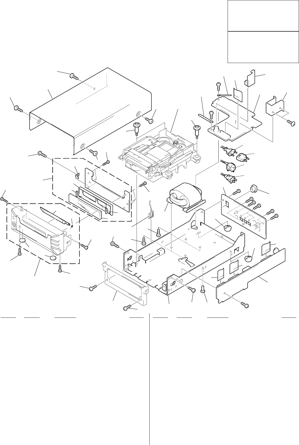
53
3
2
7
7
2
1
9
26
26
4
FL701 T901
5
6
5
5
12
11
11
5
MDM-5A
not supplied
not supplied
not supplied
not supplied not supplied
#1
#1
#1
#1
#1
#1
#1
#1
#
7
#1
not supplied
7
7
10
11
11
8
7
722
14
16
7
18 25
24
13
15
12
20
21
(AEP,SP)
21
(UK)
13
(SP)
21
(US,CND)
19
17
23
23
22
SECTION 7
EXPLODED VIEWS
7-1. CABINET SECTION
NOTE:
• Items marked “*” are not stocked since they are
seldom required for routine service. Some delay
should be anticipated when ordering these items.
• The mechanical parts with no reference number in
the exploded views are not supplied.
• Hardware (# mark) list and accessories and pack-
ing materials are given in the last of this parts list.
Ref. No. Part No. Description Remark Ref. No. Part No. Description Remark
The components identified by
mark ! or dotted line with mark
! are critical for safety.
Replace only with part number
specified.
Les composants identifiés par une
marque ! sont critiques pour la
sécurité.
Ne les remplacer que par une
piéce portant le numéro spécifié.
16 1-791-160-11 WIRE(FLAT TYPE) (23 CORE)(180mm)
17 1-791-158-11 WIRE(FLAT TYPE) (23 CORE)(90mm)
18 1-791-159-11 WIRE(FLAT TYPE) (21 CORE)
19 4-220-570-11 PANEL, BACK
20 3-703-244-00 BUSHING (2104), CORD
!21 1-696-586-21 CORD, POWER (UK)
!21 1-751-275-11 CORD, POWER (AEP,SP)
!21 1-783-531-31 CORD, POWER (US,CND)
22 3-703-249-01 SCREW, S TIGHT, +PTTWH 3X6
23 4-965-822-01 FOOT
24 A-4724-780-A POWER BOARD, COMPLETE (US,CND)
24 A-4724-784-A POWER BOARD, COMPLETE (AEP,UK,SP)
25 1-674-897-11 BACK UP BOARD
*26 4-949-935-51 CUSHION (FL)
FL701 1-517-907-11 INDICATOR TUBE, FLUORESCENT
!T901 1-433-910-11 TRANSFORMER, POWER (US,CND)
!T901 1-433-911-11 TRANSFORMER, POWER (AEP,UK,SP)
1 X-4951-678-1 PANEL ASSY, FRONT
2 4-220-561-01 FOOT
3 4-216-729-31 LID(CARTRIDGE)
4 4-976-593-01 SPRING (LID), TORSION
5 3-348-383-01 SCREW(M2X6.0), +B TAPPING
6 X-4951-680-1 CHASSIS ASSY
7 3-703-599-01 SCREW, +BTT (M3) S TITE
8 A-4724-778-A PANEL BOARD, COMPLETE (US,CND)
8 A-4724-786-A PANEL BOARD, COMPLETE (AEP,UK,SP)
9 4-220-557-01 HOLDER (FL)
10 4-220-569-01 CASE
11 4-976-827-21 SCREW, FLAT HEAD
12 4-999-839-01 SCREW (+BVTTWH M3), STEP
13 1-569-008-21 ADAPTOR, CONVERSION 2P (SP)
14 A-4724-776-A MAIN BOARD, COMPLETE (US,CND)
14 A-4724-782-A MAIN BOARD, COMPLETE (AEP,UK,SP)
15 1-791-161-11 WIRE(FLAT TYPE) (15 CORE)
• Abbreviation
CND : Canadian model
SP : Singapore model
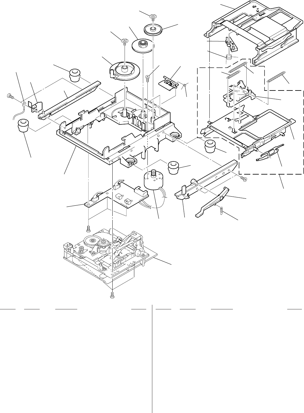
54
7-2. MECHANISM SECTION (MDM-5A)
Ref. No. Part No. Description Remark Ref. No. Part No. Description Remark
515 4-996-227-01 LEVER (HEAD)
516 4-996-229-01 SPRING (HEAD LEVER), TORSION
517 4-996-212-01 LEVER (LIMITTER)
518 4-996-213-01 SPRING (LIMITTER), TORSION
519 4-996-214-01 SPRING (SLIDER), TENSION
520 4-996-216-01 SPRING (HOLDER), TENSION
521 4-210-396-01 SPRING (LOCK), TENSION
522 X-4951-631-1 SLIDER ASSY
*523 X-4949-245-7 HOLDER ASSY
*524 4-996-211-01 SLIDER (CAM)
525 4-998-763-01 SPRING (SHUTTER), LEAF
526 A-4680-417-A HOLDER COMPLETE ASSY
M103 X-4949-264-1 MOTOR ASSY, LOADING
*501 1-668-111-11 SW BOARD
*502 4-996-217-01 CHASSIS
503 4-996-223-01 INSULATOR (F)
*504 4-996-218-01 BRACKET (GUIDE R)
505 4-996-277-01 SPRING (O/C), TENSION
506 4-996-226-01 LEVER (O/C)
507 4-999-347-01 INSULATOR (R)
*508 4-996-225-01 BRACKET (GUIDE L)
509 4-988-466-21 SPRING (ELECTROSTATIC), LEAF
510 4-996-219-01 GEAR (CAM GEAR)
511 4-996-220-01 GEAR (A)
512 4-996-221-01 GEAR (B)
513 4-933-134-01 SCREW (+PTPWH M2.6X6)
514 4-996-224-01 SCREW (1.7X3), +PWH
#2
M103
#2
#2
not supplied
#3
MBU-5A
501
502
503 503
504 505
506
507
507
508
509
510
511 512
513
513
514 515
516
517
518
519
520
521
522
523
525
526
524

55
7-3. BASE UNIT SECTION (MBU-5A)
Ref. No. Part No. Description Remark Ref. No. Part No. Description Remark
565 4-996-261-01 GEAR (SL-B)
566 4-996-264-01 SPRING (SHAFT), LEAF
567 4-996-265-01 SHAFT, MAIN
568 4-996-256-01 SL(BASE)
569 4-996-257-01 RACK (SL)
570 4-996-263-01 SPRING (CLV), TORSION
571 4-988-560-01 SCREW (+P 1.7X6)
572 4-211-036-01 SCREW (1.7X2.5), +PWH
HR901 1-500-502-11 HEAD, OVER LIGHT
M101 A-4672-475-A MOTOR ASSY, SPINDLE
M102 A-4672-474-A MOTOR ASSY, SLED
S102 1-762-148-21 SWITCH, PUSH (2 KEY)
*551 A-4699-893-A BD BOARD, COMPLETE
552 3-372-761-01 SCREW (M1.7), TAPPING
*553 4-996-267-01 BASE (BU-D)
*554 4-996-255-01 BASE (BU-C)
555 4-900-590-01 SCREW, PRECISION SMALL
556 4-996-258-01 SPRING, COMPRESSION
557 4-996-262-01 GEAR (SL-C)
558 1-667-954-11 FLEXIBLE BOARD
*559 4-210-664-01 BASE (BU-A)
!560 A-4672-541-A OPTICAL PICK-UP KMS-260B/J1N
*561 4-996-252-01 CHASSIS, BU
*562 4-996-254-01 BASE (BU-B)
563 4-967-688-11 MAGNET, ABSORPTION
564 4-996-260-01 GEAR (SL-A)
Les composants identifiés par une
marque ! sont critiques pour la sécurité.
Ne les remplacer que par une piéce
portant le numéro spécifié.
The components identified by mark !
or dotted line with mark ! are critical
for safety.
Replace only with part number specified.
not supplied
not supplied
#4
#4
HR901
#4
#4
#4
#4
#5
#5
#6
551
552
552
553
554
S102
M101
552
557
558
559
560
561
562
563
572
570
564
565
566
567
568
569
556
555
571
M102

56
SECTION 8
ELECTRICAL PARTS LIST
Note:
Ref. No. Part No. Description Remark Ref. No. Part No. Description Remark
• SEMICONDUCTORS
In each case, u: µ , for example:
uA...: µ A..., uPA...: µ PA..., uPB...: µ PB...,
uPC...: µ PC..., uPD...: µ PD...
• CAPACITORS
uF : µ F
• COILS
uH : µ H
• Abbreviation
CND : Canadian model
SP : Singapore model
• Due to standardization, replacements in the parts list
may be different from the parts specified in the
diagrams or the components used on the set.
• -XX, -X mean standardized parts, so they may have
some difference from the original one.
• Items marked “*” are not stocked since they are
seldom required for routine service. Some delay
should be anticipated when ordering these items.
• RESISTORS
All resistors are in ohms
METAL: Metal-film resistor
METAL OXIDE: Metal Oxide-film resistor
F : nonflammable
When indicating parts by reference
number, please include the board
name.
BD
BACK UP
1-674-897-11 BACK UP BOARD
************
< BATTERY >
BT451 1-528-887-11 BATTERY, LITHIUM SECONDARY
< CONNECTOR >
*CN452 1-569-499-11 PIN, CONNECTOR 3P
**************************************************************
*A-4699-893-A BD BOARD, COMPLETE
*****************
< CAPACITOR >
C101 1-125-822-11 TANTALUM 10uF 20% 10V
C102 1-163-038-91 CERAMIC CHIP 0.1uF 25V
C103 1-125-822-11 TANTALUM 10uF 20% 10V
C104 1-125-822-11 TANTALUM 10uF 20% 10V
C105 1-163-021-91 CERAMIC CHIP 0.01uF 10% 50V
C106 1-163-275-11 CERAMIC CHIP 0.001uF 5% 50V
C107 1-163-038-91 CERAMIC CHIP 0.1uF 25V
C108 1-163-038-91 CERAMIC CHIP 0.1uF 25V
C109 1-163-037-11 CERAMIC CHIP 0.022uF 10% 25V
C111 1-164-344-11 CERAMIC CHIP 0.068uF 10% 25V
C112 1-163-017-00 CERAMIC CHIP 0.0047uF 5% 50V
C113 1-109-982-11 CERAMIC CHIP 1uF 10% 10V
C115 1-164-489-11 CERAMIC CHIP 0.22uF 10% 16V
C116 1-163-037-11 CERAMIC CHIP 0.022uF 10% 25V
C117 1-163-809-11 CERAMIC CHIP 0.047uF 10% 25V
C118 1-163-038-91 CERAMIC CHIP 0.1uF 25V
C119 1-125-822-11 TANTALUM 10uF 20% 10V
C121 1-125-822-11 TANTALUM 10uF 20% 10V
C122 1-163-021-91 CERAMIC CHIP 0.01uF 10% 50V
C123 1-163-038-91 CERAMIC CHIP 0.1uF 25V
C124 1-163-038-91 CERAMIC CHIP 0.1uF 25V
C127 1-163-038-91 CERAMIC CHIP 0.1uF 25V
C128 1-163-021-91 CERAMIC CHIP 0.01uF 10% 50V
C129 1-107-823-11 CERAMIC CHIP 0.47uF 10% 16V
C130 1-163-251-11 CERAMIC CHIP 100PF 5% 50V
C131 1-163-023-00 CERAMIC CHIP 0.015uF 5% 50V
C132 1-107-823-11 CERAMIC CHIP 0.47uF 10% 16V
C133 1-163-017-00 CERAMIC CHIP 0.0047uF 5% 50V
C134 1-163-038-91 CERAMIC CHIP 0.1uF 25V
C135 1-163-038-91 CERAMIC CHIP 0.1uF 25V
C136 1-126-206-11 ELECT CHIP 100uF 20% 6.3V
C142 1-163-251-11 CERAMIC CHIP 100PF 5% 50V
C143 1-163-251-11 CERAMIC CHIP 100PF 5% 50V
C144 1-163-251-11 CERAMIC CHIP 100PF 5% 50V
C146 1-163-038-91 CERAMIC CHIP 0.1uF 25V
C151 1-126-206-11 ELECT CHIP 100uF 20% 6.3V
C152 1-163-038-91 CERAMIC CHIP 0.1uF 25V
C153 1-163-021-91 CERAMIC CHIP 0.01uF 10% 50V
C156 1-163-038-91 CERAMIC CHIP 0.1uF 25V
C158 1-163-019-00 CERAMIC CHIP 0.0068uF 10% 50V
C160 1-104-601-11 ELECT CHIP 10uF 20% 10V
C161 1-104-601-11 ELECT CHIP 10uF 20% 10V
C163 1-163-021-91 CERAMIC CHIP 0.01uF 10% 50V
C164 1-163-021-91 CERAMIC CHIP 0.01uF 10% 50V
C167 1-163-038-91 CERAMIC CHIP 0.1uF 25V
C168 1-163-038-91 CERAMIC CHIP 0.1uF 25V
C169 1-125-822-11 TANTALUM 10uF 20% 10V
C171 1-163-038-91 CERAMIC CHIP 0.1uF 25V
C181 1-104-913-11 TANTAL. CHIP 10uF 20% 16V
C183 1-163-038-91 CERAMIC CHIP 0.1uF 25V
C184 1-117-970-11 ELECT CHIP 22uF 20% 10V
C185 1-164-611-11 CERAMIC CHIP 0.001uF 10% 500V
C187 1-104-913-11 TANTAL. CHIP 10uF 20% 16V
C188 1-163-021-91 CERAMIC CHIP 0.01uF 10% 50V
C189 1-163-989-11 CERAMIC CHIP 0.033uF 10% 25V
C190 1-126-206-11 ELECT CHIP 100uF 20% 6.3V
C191 1-163-038-91 CERAMIC CHIP 0.1uF 25V
C196 1-163-038-91 CERAMIC CHIP 0.1uF 25V
C197 1-163-038-91 CERAMIC CHIP 0.1uF 25V
< CONNECTOR >
CN101 1-569-479-21 CONNECTOR, FPC 21P
CN102 1-784-833-21 CONNECTOR,FFC(LIF(NON-ZIF))21P
CN103 1-784-834-21 CONNECTOR,FFC(LIF(NON-ZIF))23P
CN104 1-770-687-11 CONNECTOR, FFC/FPC 4P
CN110 1-695-440-21 PIN, CONNECTOR (PC BOARD) 6P
< DIODE >
D101 8-719-988-61 DIODE 1SS355TE-17
D181 8-719-046-86 DIODE F1J6TP
D183 8-719-046-86 DIODE F1J6TP
< IC >
IC101 8-752-080-95 IC CXA2523AR
IC103 8-729-903-10 TRANSISTOR FMW1-T-148
IC121 8-752-389-44 IC CXD2654R
IC123 8-759-096-87 IC TC7WU04FU(TE12R)
IC124 8-759-498-44 IC MSM51V4400-70TS-K
The components identified by
mark ! or dotted line with mark
! are critical for safety.
Replace only with part number
specified.
Les composants identifiés par une
marque ! sont critiques pour la
sécurité.
Ne les remplacer que par une
piéce portant le numéro spécifié.

57
Ref. No. Part No. Description Remark Ref. No. Part No. Description Remark
IC152 8-759-430-25 IC BH6511FS-E2
IC171 8-759-487-04 IC BR24C02F-E2
IC181 8-759-481-17 IC MC74ACT08DTR2
IC192 8-759-460-72 IC BA033FP-E2
< COIL >
L101 1-414-813-11 FERRITE 0uH
L102 1-414-813-11 FERRITE 0uH
L103 1-414-813-11 FERRITE 0uH
L105 1-414-813-11 FERRITE 0uH
L106 1-414-813-11 FERRITE 0uH
L121 1-414-813-11 FERRITE 0uH
L122 1-414-813-11 FERRITE 0uH
L151 1-412-029-11 INDUCTOR CHIP 10uH
L152 1-412-029-11 INDUCTOR CHIP 10uH
L153 1-412-032-11 INDUCTOR CHIP 100uH
L154 1-412-032-11 INDUCTOR CHIP 100uH
L161 1-414-813-11 FERRITE 0uH
L162 1-414-813-11 FERRITE 0uH
L181 1-216-295-91 SHORT 0
< TRANSISTOR >
Q101 8-729-403-35 TRANSISTOR UN5113
Q102 8-729-026-53 TRANSISTOR 2SA1576A-T106-QR
Q103 8-729-402-93 TRANSISTOR UN5214
Q104 8-729-402-93 TRANSISTOR UN5214
Q162 8-729-101-07 TRANSISTOR 2SB798-DL
Q163 8-729-403-35 TRANSISTOR UN5113
Q181 8-729-018-75 TRANSISTOR 2SJ278MYTR
Q182 8-729-017-65 TRANSISTOR 2SK1764KYTR
< RESISTOR >
R103 1-216-049-91 RES,CHIP 1K 5% 1/10W
R104 1-216-073-00 METAL CHIP 10K 5% 1/10W
R105 1-216-065-91 RES,CHIP 4.7K 5% 1/10W
R106 1-216-133-00 METAL CHIP 3.3M 5% 1/10W
R107 1-216-113-00 METAL CHIP 470K 5% 1/10W
R109 1-216-295-91 SHORT 0
R110 1-216-073-00 METAL CHIP 10K 5% 1/10W
R111 1-216-295-91 SHORT 0
R112 1-216-089-91 RES,CHIP 47K 5% 1/10W
R113 1-216-049-91 RES,CHIP 1K 5% 1/10W
R115 1-216-049-91 RES,CHIP 1K 5% 1/10W
R117 1-216-113-00 METAL CHIP 470K 5% 1/10W
R120 1-216-025-91 RES,CHIP 100 5% 1/10W
R121 1-216-097-91 RES,CHIP 100K 5% 1/10W
R123 1-216-295-91 SHORT 0
R124 1-216-025-91 RES,CHIP 100 5% 1/10W
R125 1-216-025-91 RES,CHIP 100 5% 1/10W
R127 1-216-025-91 RES,CHIP 100 5% 1/10W
R129 1-216-295-91 SHORT 0
R130 1-216-295-91 SHORT 0
R131 1-216-073-00 METAL CHIP 10K 5% 1/10W
R132 1-216-097-91 RES,CHIP 100K 5% 1/10W
R133 1-216-117-00 METAL CHIP 680K 5% 1/10W
R134 1-216-049-91 RES,CHIP 1K 5% 1/10W
R135 1-216-061-00 METAL CHIP 3.3K 5% 1/10W
R136 1-216-049-91 RES,CHIP 1K 5% 1/10W
R137 1-216-295-91 SHORT 0
R140 1-216-029-00 METAL CHIP 150 5% 1/10W
R142 1-216-073-00 METAL CHIP 10K 5% 1/10W
R143 1-216-073-00 METAL CHIP 10K 5% 1/10W
R144 1-216-025-91 RES,CHIP 100 5% 1/10W
R145 1-216-073-00 METAL CHIP 10K 5% 1/10W
R146 1-216-037-00 METAL CHIP 330 5% 1/10W
R147 1-216-025-91 RES,CHIP 100 5% 1/10W
R148 1-216-045-00 METAL CHIP 680 5% 1/10W
R149 1-216-073-00 METAL CHIP 10K 5% 1/10W
R150 1-216-295-91 SHORT 0
R151 1-216-073-00 METAL CHIP 10K 5% 1/10W
R152 1-216-073-00 METAL CHIP 10K 5% 1/10W
R158 1-216-097-91 RES,CHIP 100K 5% 1/10W
R159 1-216-097-91 RES,CHIP 100K 5% 1/10W
R160 1-216-295-91 SHORT 0
R161 1-216-057-00 METAL CHIP 2.2K 5% 1/10W
R162 1-216-057-00 METAL CHIP 2.2K 5% 1/10W
R163 1-216-057-00 METAL CHIP 2.2K 5% 1/10W
R164 1-216-045-00 METAL CHIP 680 5% 1/10W
R165 1-216-097-91 RES,CHIP 100K 5% 1/10W
R167 1-216-065-91 RES,CHIP 4.7K 5% 1/10W
R169 1-219-724-11 METAL CHIP 1 1% 1/4W
R170 1-216-073-00 METAL CHIP 10K 5% 1/10W
R171 1-216-073-00 METAL CHIP 10K 5% 1/10W
R173 1-216-121-91 RES,CHIP 1M 5% 1/10W
R175 1-216-065-91 RES,CHIP 4.7K 5% 1/10W
R177 1-216-061-00 METAL CHIP 3.3K 5% 1/10W
R179 1-216-085-00 METAL CHIP 33K 5% 1/10W
R180 1-216-073-00 METAL CHIP 10K 5% 1/10W
R182 1-216-089-91 RES,CHIP 47K 5% 1/10W
R183 1-216-089-91 RES,CHIP 47K 5% 1/10W
R184 1-216-073-00 METAL CHIP 10K 5% 1/10W
R185 1-216-081-00 METAL CHIP 22K 5% 1/10W
R186 1-216-089-91 RES,CHIP 47K 5% 1/10W
R188 1-216-073-00 METAL CHIP 10K 5% 1/10W
R189 1-216-073-00 METAL CHIP 10K 5% 1/10W
R190 1-216-073-00 METAL CHIP 10K 5% 1/10W
R195 1-216-073-00 METAL CHIP 10K 5% 1/10W
R196 1-216-295-91 SHORT 0
R197 1-216-295-91 SHORT 0
R198 1-216-286-00 RES,CHIP 4.7M 5% 1/8W
R198 1-216-296-91 SHORT 0
< SWITCH >
S101 1-762-596-21 SWITCH, PUSH (1 KEY)(LIMIT SW)
**************************************************************
A-4724-776-A MAIN BOARD, COMPLETE (US,CND)
********************
A-4724-782-A MAIN BOARD, COMPLETE (AEP,UK,SP)
********************
< CAPACITOR >
C101 1-163-005-11 CERAMIC CHIP 470PF 10% 50V
BD MAIN

58
Ref. No. Part No. Description Remark Ref. No. Part No. Description Remark
C102 1-124-779-00 ELECT CHIP 10uF 20% 16V
C181 1-126-395-11 ELECT 22uF 20% 16V
C182 1-163-017-00 CERAMIC CHIP 0.0047uF 5% 50V
C183 1-163-009-11 CERAMIC CHIP 0.001uF 10% 50V
C184 1-126-603-11 ELECT CHIP 4.7uF 20% 35V
C185 1-163-117-00 CERAMIC CHIP 100PF 5% 50V
C201 1-163-005-11 CERAMIC CHIP 470PF 10% 50V
C202 1-124-779-00 ELECT CHIP 10uF 20% 16V
C281 1-126-395-11 ELECT 22uF 20% 16V
C282 1-163-017-00 CERAMIC CHIP 0.0047uF 5% 50V
C283 1-163-009-11 CERAMIC CHIP 0.001uF 10% 50V
C284 1-126-603-11 ELECT CHIP 4.7uF 20% 35V
C285 1-163-117-00 CERAMIC CHIP 100PF 5% 50V
C300 1-126-177-11 ELECT 100uF 20% 10V
C301 1-163-038-91 CERAMIC CHIP 0.1uF 25V
C302 1-126-177-11 ELECT 100uF 20% 10V
C303 1-163-038-91 CERAMIC CHIP 0.1uF 25V
C304 1-163-038-91 CERAMIC CHIP 0.1uF 25V
C305 1-163-038-91 CERAMIC CHIP 0.1uF 25V
C306 1-126-934-11 ELECT 220uF 20% 10V
C307 1-163-038-91 CERAMIC CHIP 0.1uF 25V
C308 1-126-177-11 ELECT 100uF 20% 10V
C315 1-163-009-11 CERAMIC CHIP 0.001uF 10% 50V
C316 1-163-009-11 CERAMIC CHIP 0.001uF 10% 50V
C317 1-163-117-00 CERAMIC CHIP 100PF 5% 50V
C321 1-124-779-00 ELECT CHIP 10uF 20% 16V
C322 1-124-779-00 ELECT CHIP 10uF 20% 16V
C351 1-163-233-11 CERAMIC CHIP 18PF 5% 50V
C352 1-163-234-11 CERAMIC CHIP 20PF 5% 50V
C353 1-163-038-91 CERAMIC CHIP 0.1uF 25V
C354 1-163-038-91 CERAMIC CHIP 0.1uF 25V
C370 1-126-933-11 ELECT 100uF 20% 16V
C371 1-126-933-11 ELECT 100uF 20% 16V
C385 1-163-038-91 CERAMIC CHIP 0.1uF 25V
C386 1-163-038-91 CERAMIC CHIP 0.1uF 25V
C426 1-128-551-11 ELECT 22uF 20% 35V
C500 1-131-347-00 TANTALUM 1uF 10% 35V
C512 1-163-038-91 CERAMIC CHIP 0.1uF 25V
C516 1-163-038-91 CERAMIC CHIP 0.1uF 25V
C519 1-163-009-11 CERAMIC CHIP 0.001uF 10% 50V
C562 1-163-038-91 CERAMIC CHIP 0.1uF 25V
C571 1-163-117-00 CERAMIC CHIP 100PF 5% 50V
C572 1-163-117-00 CERAMIC CHIP 100PF 5% 50V
C595 1-163-009-11 CERAMIC CHIP 0.001uF 10% 50V
C597 1-163-009-11 CERAMIC CHIP 0.001uF 10% 50V
C598 1-163-038-91 CERAMIC CHIP 0.1uF 25V
C599 1-163-038-91 CERAMIC CHIP 0.1uF 25V
C951 1-104-664-11 ELECT 47uF 20% 10V
C953 1-163-038-91 CERAMIC CHIP 0.1uF 25V
C954 1-163-038-91 CERAMIC CHIP 0.1uF 25V
< CONNECTOR >
CN412 1-784-834-21 CONNECTOR,FFC(LIF(NON-ZIF))23P
CN421 1-793-448-11 CONNECTOR, FFC 15P
CN501 1-784-834-21 CONNECTOR,FFC(LIF(NON-ZIF))23P
CN502 1-770-215-11 PIN, CONNECTOR (PC BOARD) 7P
CN503 1-784-860-21 CONNECTOR, FFC(LIF(NON-ZIF))8P
< DIODE >
D390 8-719-016-74 DIODE 1SS352-TPH3
D391 8-719-016-74 DIODE 1SS352-TPH3
< GROUND TERMINAL >
EP911 1-537-771-21 TERMINAL BOARD, GROUND
EP912 1-537-771-21 TERMINAL BOARD, GROUND
< FERRITE BEAD >
FB301 1-414-235-22 INDUCTOR CHIP 0UH
FB302 1-414-235-22 INDUCTOR CHIP 0UH
FB303 1-414-235-22 INDUCTOR CHIP 0UH
FB306 1-414-235-22 INDUCTOR CHIP 0UH
FB307 1-414-235-22 INDUCTOR CHIP 0UH
FB351 1-414-235-22 INDUCTOR CHIP 0UH
FB352 1-414-235-22 INDUCTOR CHIP 0UH
FB356 1-414-235-22 INDUCTOR CHIP 0UH
< IC >
IC301 8-759-553-65 IC UDA1341TS
IC308 8-759-636-55 IC M5218AFP-T1
IC351 8-759-242-70 IC TC7WU04F-TE12L
IC381 8-759-636-55 IC M5218AFP-T1
IC382 8-759-636-55 IC M5218AFP-T1
IC441 8-759-481-19 IC LB1830M-S-TE-L
IC501 8-759-599-90 IC M30620MC-406FP
< JACK >
J101 1-793-344-11 JACK, PIN 4P
< COIL >
L450 1-216-296-91 SHORT 0
L451 1-216-296-91 SHORT 0
< TRANSISTOR >
Q191 8-729-046-97 TRANSISTOR 2SD1938(F)-T(TX).SO
Q192 8-729-046-97 TRANSISTOR 2SD1938(F)-T(TX).SO
Q291 8-729-046-97 TRANSISTOR 2SD1938(F)-T(TX).SO
Q292 8-729-046-97 TRANSISTOR 2SD1938(F)-T(TX).SO
Q390 8-729-424-08 TRANSISTOR UN2111-TX
Q441 8-729-421-22 TRANSISTOR UN2211-TX
< RESISTOR >
R82 1-216-097-91 RES,CHIP 100K 5% 1/10W
R101 1-216-049-91 RES,CHIP 1K 5% 1/10W
R102 1-216-097-91 RES,CHIP 100K 5% 1/10W
R106 1-216-075-00 METAL CHIP 12K 5% 1/10W
R181 1-216-073-00 METAL CHIP 10K 5% 1/10W
R182 1-216-073-00 METAL CHIP 10K 5% 1/10W
R183 1-216-080-00 METAL CHIP 20K 5% 1/10W
R184 1-216-683-11 METAL CHIP 22K 0.5% 1/10W
R185 1-216-041-00 METAL CHIP 470 5% 1/10W
R186 1-216-041-00 METAL CHIP 470 5% 1/10W
R187 1-216-089-91 RES,CHIP 47K 5% 1/10W
R188 1-216-045-00 METAL CHIP 680 5% 1/10W
MAIN

59
Ref. No. Part No. Description Remark Ref. No. Part No. Description Remark
PANEL
R189 1-216-037-00 METAL CHIP 330 5% 1/10W
R191 1-216-057-00 METAL CHIP 2.2K 5% 1/10W
R192 1-216-057-00 METAL CHIP 2.2K 5% 1/10W
R201 1-216-049-91 RES,CHIP 1K 5% 1/10W
R202 1-216-097-91 RES,CHIP 100K 5% 1/10W
R206 1-216-075-00 METAL CHIP 12K 5% 1/10W
R281 1-216-073-00 METAL CHIP 10K 5% 1/10W
R282 1-216-073-00 METAL CHIP 10K 5% 1/10W
R283 1-216-080-00 METAL CHIP 20K 5% 1/10W
R284 1-216-683-11 METAL CHIP 22K 0.5% 1/10W
R285 1-216-041-00 METAL CHIP 470 5% 1/10W
R286 1-216-041-00 METAL CHIP 470 5% 1/10W
R287 1-216-089-91 RES,CHIP 47K 5% 1/10W
R288 1-216-045-00 METAL CHIP 680 5% 1/10W
R289 1-216-037-00 METAL CHIP 330 5% 1/10W
R291 1-216-057-00 METAL CHIP 2.2K 5% 1/10W
R292 1-216-057-00 METAL CHIP 2.2K 5% 1/10W
R311 1-216-025-91 RES,CHIP 100 5% 1/10W
R312 1-216-025-91 RES,CHIP 100 5% 1/10W
R313 1-216-025-91 RES,CHIP 100 5% 1/10W
R314 1-216-025-91 RES,CHIP 100 5% 1/10W
R339 1-216-295-91 SHORT 0
R341 1-216-295-91 SHORT 0
R342 1-216-295-91 SHORT 0
R351 1-216-121-91 RES,CHIP 1M 5% 1/10W
R352 1-216-041-00 METAL CHIP 470 5% 1/10W
R355 1-216-029-00 METAL CHIP 150 5% 1/10W
R356 1-216-031-00 METAL CHIP 180 5% 1/10W
R357 1-216-296-91 SHORT 0
R391 1-216-097-91 RES,CHIP 100K 5% 1/10W
R392 1-216-101-00 METAL CHIP 150K 5% 1/10W
R441 1-216-057-00 METAL CHIP 2.2K 5% 1/10W
R442 1-216-053-00 METAL CHIP 1.5K 5% 1/10W
R443 1-216-055-00 METAL CHIP 1.8K 5% 1/10W
R500 1-216-073-00 METAL CHIP 10K 5% 1/10W
R508 1-216-025-91 RES,CHIP 100 5% 1/10W
R509 1-216-073-00 METAL CHIP 10K 5% 1/10W
R530 1-216-065-91 RES,CHIP 4.7K 5% 1/10W
R531 1-216-073-00 METAL CHIP 10K 5% 1/10W
R533 1-216-073-00 METAL CHIP 10K 5% 1/10W
R549 1-216-025-91 RES,CHIP 100 5% 1/10W
R550 1-216-073-00 METAL CHIP 10K 5% 1/10W
R551 1-216-073-00 METAL CHIP 10K 5% 1/10W
R553 1-216-073-00 METAL CHIP 10K 5% 1/10W
R559 1-216-073-00 METAL CHIP 10K 5% 1/10W
R560 1-216-073-00 METAL CHIP 10K 5% 1/10W
R568 1-216-073-00 METAL CHIP 10K 5% 1/10W
R569 1-216-073-00 METAL CHIP 10K 5% 1/10W
R573 1-216-073-00 METAL CHIP 10K 5% 1/10W
R575 1-216-073-00 METAL CHIP 10K 5% 1/10W
R577 1-216-073-00 METAL CHIP 10K 5% 1/10W
R581 1-216-097-91 RES,CHIP 100K 5% 1/10W
R595 1-216-073-00 METAL CHIP 10K 5% 1/10W
R597 1-216-073-00 METAL CHIP 10K 5% 1/10W
R852 1-216-097-91 RES,CHIP 100K 5% 1/10W
< VIBRATOR >
X351 1-579-314-11 VIBRATOR, CRYSTAL (22.5792MHz)
X513 1-781-174-21 VIBRATOR, CERAMIC (10MHz)
**************************************************************
A-4724-778-A PANEL BOARD, COMPLETE (US,CND)
*********************
A-4724-786-A PANEL BOARD, COMPLETE (AEP,UK,SP)
*********************
4-220-557-01 HOLDER (FL)
*4-949-935-51 CUSHION (FL)
7-685-647-79 SCREW +BVTP 3X10 TYPE2 IT-3
< CAPACITOR >
C411 1-126-939-11 ELECT 10000uF 20% 16V
C412 1-126-964-11 ELECT 10uF 20% 50V
C414 1-163-038-91 CERAMIC CHIP 0.1uF 25V
C415 1-126-916-11 ELECT 1000uF 20% 6.3V
C416 1-163-038-91 CERAMIC CHIP 0.1uF 25V
C417 1-104-664-11 ELECT 47uF 20% 10V
C418 1-163-038-91 CERAMIC CHIP 0.1uF 25V
C419 1-126-964-11 ELECT 10uF 20% 50V
C420 1-126-926-11 ELECT 1000uF 20% 10V
C421 1-163-021-91 CERAMIC CHIP 0.01uF 10% 50V
C423 1-126-968-11 ELECT 100uF 20% 50V
C424 1-163-038-91 CERAMIC CHIP 0.1uF 25V
C425 1-126-967-11 ELECT 47uF 20% 50V
C427 1-163-038-91 CERAMIC CHIP 0.1uF 25V
C428 1-163-038-91 CERAMIC CHIP 0.1uF 25V
C431 1-126-966-11 ELECT 33uF 20% 16V
C432 1-126-964-11 ELECT 10uF 20% 50V
C461 1-126-935-11 ELECT 470uF 20% 16V
C466 1-126-935-11 ELECT 470uF 20% 16V
C601 1-163-021-91 CERAMIC CHIP 0.01uF 10% 50V
C611 1-163-038-91 CERAMIC CHIP 0.1uF 25V
C612 1-126-205-11 ELECT CHIP 47uF 20% 6.3V
C613 1-163-021-91 CERAMIC CHIP 0.01uF 10% 50V
C621 1-163-038-91 CERAMIC CHIP 0.1uF 25V
C623 1-163-021-91 CERAMIC CHIP 0.01uF 10% 50V
C661 1-163-038-91 CERAMIC CHIP 0.1uF 25V
C662 1-126-205-11 ELECT CHIP 47uF 20% 6.3V
C802 1-163-038-91 CERAMIC CHIP 0.1uF 25V
!C901 1-113-924-11 CERAMIC 0.0047uF 20% 250V
!C902 1-113-924-11 CERAMIC 0.0047uF 20% 250V
C911 1-163-038-91 CERAMIC CHIP 0.1uF 25V
C912 1-163-038-91 CERAMIC CHIP 0.1uF 25V
C913 1-163-038-91 CERAMIC CHIP 0.1uF 25V
< CONNECTOR >
*CN401 1-564-509-11 PLUG, CONNECTOR 6P
CN411 1-778-692-11 CONNECTOR, FFC/FPC 21P
CN414 1-770-651-11 CONNECTOR, FFC/FPC 23P
CN451 1-569-490-11 SOCKET, CONNECTOR 3P
*CN901 1-580-230-11 PIN, CONNECTOR (PC BOARD) 2P
*CN902 1-566-693-11 PIN, CONNECTOR 2P
MAIN
Les composants identifiés par une
marque ! sont critiques pour la sécurité.
Ne les remplacer que par une piéce
portant le numéro spécifié.
The components identified by mark !
or dotted line with mark ! are critical
for safety.
Replace only with part number specified.

60
Ref. No. Part No. Description Remark Ref. No. Part No. Description Remark
< DIODE >
D411 8-719-210-39 DIODE EC10QS04-TE12L5
D412 8-719-210-39 DIODE EC10QS04-TE12L5
D421 8-719-210-33 DIODE EC10DS2TE12R
D422 8-719-422-31 DIODE MA8047-M-TX
D431 8-719-210-33 DIODE EC10DS2TE12R
D432 8-719-210-33 DIODE EC10DS2TE12R
D433 8-719-016-74 DIODE 1SS352-TPH3
D451 8-719-016-74 DIODE 1SS352-TPH3
D452 8-719-313-73 DIODE SFPB-52V
D461 8-719-210-39 DIODE EC10QS04-TE12L5
D462 8-719-210-39 DIODE EC10QS04-TE12L5
D466 8-719-210-39 DIODE EC10QS04-TE12L5
D467 8-719-210-39 DIODE EC10QS04-TE12L5
D801 8-719-016-74 DIODE 1SS352-TPH3
D911 8-719-016-74 DIODE 1SS352-TPH3
D912 8-719-016-74 DIODE 1SS352-TPH3
< FLUORESCENT >
FL701 1-517-907-11 INDICATOR TUBE, FLUORESCENT
< IC >
IC411 8-759-525-48 IC LA5632
IC421 8-759-633-42 IC M5293L
IC601 8-759-269-92 IC SN74HCU04ANSR
IC611 8-749-012-70 IC GP1F38R
IC621 8-749-012-70 IC GP1F38R
IC661 8-749-012-69 IC GP1F38T
< JACK >
J801 1-779-655-21 JACK (SMALL TYPE) (2 GANG)
< JUMPER RESISTOR >
JW401 1-216-296-91 SHORT 0
< COIL >
L611 1-412-784-41 INDUCTOR 4.7uH
L661 1-412-784-41 INDUCTOR 4.7uH
!L901 1-424-485-11 FILTER, LINE
< TRANSISTOR >
Q801 8-729-620-05 TRANSISTOR 2SC2603TP-EF
< RESISTOR >
R411 1-216-073-00 METAL CHIP 10K 5% 1/10W
R412 1-216-097-91 RES,CHIP 100K 5% 1/10W
R413 1-216-049-91 RES,CHIP 1K 5% 1/10W
R420 1-216-099-00 METAL CHIP 120K 5% 1/10W
R422 1-216-097-91 RES,CHIP 100K 5% 1/10W
R423 1-216-033-00 METAL CHIP 220 5% 1/10W
R424 1-216-033-00 METAL CHIP 220 5% 1/10W
R431 1-216-025-91 RES,CHIP 100 5% 1/10W
R432 1-216-047-91 RES,CHIP 820 5% 1/10W
R433 1-216-035-00 METAL CHIP 270 5% 1/10W
R434 1-216-081-00 METAL CHIP 22K 5% 1/10W
R435 1-216-091-00 METAL CHIP 56K 5% 1/10W
R436 1-216-109-00 METAL CHIP 330K 5% 1/10W
R437 1-216-049-91 RES,CHIP 1K 5% 1/10W
R451 1-216-033-00 METAL CHIP 220 5% 1/10W
R613 1-216-113-00 METAL CHIP 470K 5% 1/10W
R614 1-216-089-91 RES,CHIP 47K 5% 1/10W
R623 1-216-113-00 METAL CHIP 470K 5% 1/10W
R624 1-216-089-91 RES,CHIP 47K 5% 1/10W
R801 1-216-067-00 METAL CHIP 5.6K 5% 1/10W
R802 1-216-295-91 SHORT 0
R803 1-216-065-91 RES,CHIP 4.7K 5% 1/10W
R804 1-216-073-00 METAL CHIP 10K 5% 1/10W
R805 1-216-001-00 METAL CHIP 10 5% 1/10W
R806 1-216-025-91 RES,CHIP 100 5% 1/10W
R912 1-216-296-91 SHORT 0
< RELAY >
RY911 1-755-300-11 RELAY
RY912 1-755-300-11 RELAY
< SWITCH >
S401 1-571-839-11 SWITCH, KEY BOARD (RESET)
**************************************************************
A-4724-780-A POWER BOARD, COMPLETE (US,CND)
*********************
A-4724-784-A POWER BOARD, COMPLETE (AEP,UK,SP)
*********************
< CAPACITOR >
C760 1-163-038-91 CERAMIC CHIP 0.1uF 25V
C761 1-163-009-11 CERAMIC CHIP 0.001uF 10% 50V
C762 1-163-009-11 CERAMIC CHIP 0.001uF 10% 50V
C763 1-163-009-11 CERAMIC CHIP 0.001uF 10% 50V
C764 1-163-038-91 CERAMIC CHIP 0.1uF 25V
C765 1-124-778-00 ELECT CHIP 22uF 20% 6.3V
C766 1-163-038-91 CERAMIC CHIP 0.1uF 25V
C769 1-163-109-00 CERAMIC CHIP 47PF 5% 50V
C781 1-126-206-11 ELECT CHIP 100uF 20% 6.3V
C782 1-163-021-91 CERAMIC CHIP 0.01uF 10% 50V
< CONNECTOR >
CN701 1-793-448-11 CONNECTOR, FFC 15P
< DIODE >
D751 8-719-051-89 DIODE SML-010VT-T87 (STANDBY)
< IC >
IC761 8-759-426-98 IC MSM9202-02GS-K
IC781 8-749-013-92 IC GP1UC7X
< JACK >
J751 1-793-439-11 JACK (SMALL TYPE)
POWERPANEL
Les composants identifiés par une
marque ! sont critiques pour la sécurité.
Ne les remplacer que par une piéce
portant le numéro spécifié.
The components identified by mark !
or dotted line with mark ! are critical
for safety.
Replace only with part number specified.

61
Ref. No. Part No. Description Remark Ref. No. Part No. Description Remark
< COIL >
L751 1-216-296-91 SHORT 0
L752 1-216-296-91 SHORT 0
L753 1-216-296-91 SHORT 0
< TRANSISTOR >
Q751 8-729-424-08 TRANSISTOR UN2111-TX
Q767 8-729-424-67 TRANSISTOR UN2216-TX
< RESISTOR >
R322 1-216-166-00 RES,CHIP 47 5% 1/8W
R323 1-216-166-00 RES,CHIP 47 5% 1/8W
R324 1-216-166-00 RES,CHIP 47 5% 1/8W
R325 1-216-166-00 RES,CHIP 47 5% 1/8W
R702 1-216-057-00 METAL CHIP 2.2K 5% 1/10W
R703 1-216-061-00 METAL CHIP 3.3K 5% 1/10W
R704 1-216-065-91 RES,CHIP 4.7K 5% 1/10W
R705 1-216-073-00 METAL CHIP 10K 5% 1/10W
R706 1-216-085-00 METAL CHIP 33K 5% 1/10W
R722 1-216-057-00 METAL CHIP 2.2K 5% 1/10W
R751 1-216-001-00 METAL CHIP 10 5% 1/10W
R752 1-216-001-00 METAL CHIP 10 5% 1/10W
R753 1-216-033-00 METAL CHIP 220 5% 1/10W
R760 1-216-025-91 RES,CHIP 100 5% 1/10W
R761 1-216-025-91 RES,CHIP 100 5% 1/10W
R762 1-216-025-91 RES,CHIP 100 5% 1/10W
R763 1-216-025-91 RES,CHIP 100 5% 1/10W
R767 1-216-097-91 RES,CHIP 100K 5% 1/10W
R769 1-216-061-00 METAL CHIP 3.3K 5% 1/10W
R781 1-216-017-91 RES,CHIP 47 5% 1/10W
R782 1-216-025-91 RES,CHIP 100 5% 1/10W
< SWITCH >
S701 1-762-400-11 SWITCH (r)
S702 1-762-400-11 SWITCH (p)
S703 1-762-400-11 SWITCH (+)
S704 1-762-400-11 SWITCH (=)
S705 1-762-400-11 SWITCH (^)
S706 1-762-400-11 SWITCH (§)
S721 1-762-400-11 SWITCH (INPUT)
S722 1-762-400-11 SWITCH (1/u)
**************************************************************
*1-668-111-11 SW BOARD
*******
< CONNECTOR >
*CN601 1-506-486-11 PIN, CONNECTOR 7P
< SWITCH >
S601 1-572-126-21 SWITCH, PUSH (1 KEY)(REC POSITION)
S602 1-572-126-21 SWITCH, PUSH (1 KEY)(PACK OUT)
S604 1-771-264-11 SWITCH, PUSH(DETECTION)(1 KEY)
(PB POSITION)
**************************************************************
MISCELLANEOUS
*************
15 1-791-161-11 WIRE (FLAT TYPE) (15 CORE)
16 1-791-160-11 WIRE (FLAT TYPE) (23 CORE)(180mm)
17 1-791-158-11 WIRE (FLAT TYPE) (23 CORE)(90mm)
18 1-791-159-11 WIRE (FLAT TYPE) (21 CORE)
!21 1-696-586-21 CORD, POWER (UK)
!21 1-751-275-11 CORD, POWER (AEP,SP)
!21 1-783-531-11 CORD, POWER (US,CND)
27 1-569-008-21 ADAPTOR, CONVERSION 2P (SP)
558 1-667-954-11 FLEXIBLE BOARD
!560 A-4672-541-A OPTICAL PICK-UP KMS-260B/J1N
FL701 1-517-907-11 INDICATOR TUBE, FLUORESCENT
HR901 1-500-502-11 HEAD, OVER LIGHT
M101 A-4672-475-A MOTOR ASSY, SPINDLE
M102 A-4672-474-A MOTOR ASSY, SLED
M103 X-4949-264-1 MOTOR ASSY, LOADING
S102 1-762-148-21 SWITCH, PUSH (2 KEY)
!T901 1-433-910-11 TRANSFORMER, POWER (US,CND)
!T901 1-433-911-11 TRANSFORMER, POWER (AEP,UK,SP)
**************************************************************
ACCESSORIES & PACKING MATERIALS
*******************************
1-418-541-11 REMOTE COMMANDER (RM-D35)
1-558-271-11 CORD, CONNECTION (AUDIO 108cm)
1-574-264-11 CORD, OPTICAL PLUG (600mm)
1-777-172-11 CORD, CONNECTION (CONTROL A1II 100cm)(CND)
1-783-106-11 CORD, CONNECTION (MINI-PLUG 105cm)
3-866-796-11 MANUAL, INSTRUCTION (ENGLISH,FRENCH)
3-866-796-21 MANUAL, INSTRUCTION
(GERMAN,NETHER LAND,SWEDISH,ITALIAN)(AEP)
3-866-796-31 MANUAL, INSTRUCTION
(SPANISH,PORTUGUESE,CHINESE)(AEP,SP)
3-866-797-11 MANUAL, INSTRUCTION (ENGLISH,FRENCH)
3-866-797-21 MANUAL, INSTRUCTION
(GERMAN,NETHER LAND,SWEDISH,ITALIAN)(AEP)
3-866-797-31 MANUAL, INSTRUCTION
(SPANISH,PORTUGUESE,CHINESE)(AEP,SP)
4-981-643-31 LID, BATTERY (for RM-D35)
A-4680-289-A CORD, CONNECTION (CAV-50C)(US,CND)
A-4406-082-A CORD, CONNECTION (EXCEPT US, CND)
**************************************************************
**********
HARDWARE LIST
**********
#1 7-685-646-79 SCREW +BVTP 3X8 TYPE2 N-S
#2 7-685-133-19 SCREW (DIA. 2.6) (IT3B)
#3 7-685-533-19 SCREW +BTP 2.6X6 TYPE2 N-S
#4 7-621-772-20 SCREW +B 2X5
#5 7-621-772-40 SCREW +B 2X8
#6 7-627-852-08 SCREW,PRECISION +P 1.7X2.5
#7 7-685-647-79 SCREW +BVTP 3X10 TYPE2 IT-3
POWER SW
Les composants identifiés par une
marque ! sont critiques pour la sécurité.
Ne les remplacer que par une piéce
portant le numéro spécifié.
The components identified by mark !
or dotted line with mark ! are critical
for safety.
Replace only with part number specified.
62
Sony Corporation
Home Audio Company
9-928-916-11
(SP) 99F0986-1
Printed in Japan © 1999. 6
Published by Quality Assurance Dept.
MDS-PC2
