Getting Started With STM32F10xxx Hardware Development Stm32 Guide
User Manual:
Open the PDF directly: View PDF ![]() .
.
Page Count: 28
- 1 Power supplies
- 2 Clocks
- 3 Boot configuration
- 4 Debug management
- 5 Recommendations
- 6 Reference design
- 7 Revision history

November 2011 Doc ID 13675 Rev 7 1/28
AN2586
Application note
Getting started with STM32F10xxx hardware development
Introduction
This application note is intended for system designers who require a hardware
implementation overview of the development board features such as the power supply, the
clock management, the reset control, the boot mode settings and the debug management. It
shows how to use the low-density value line, low-density, medium-density value line,
medium-density, high-density, XL-density and connectivity line STM32F10xxx product
families and describes the minimum hardware resources required to develop an
STM32F10xxx application.
Detailed reference design schematics are also contained in this document with descriptions
of the main components, interfaces and modes.
Glossary
●Low-density value line devices are STM32F100xx microcontrollers where the Flash
memory density ranges between 16 and 32 Kbytes.
●Low-density devices are STM32F101xx, STM32F102xx and STM32F103xx
microcontrollers where the Flash memory density ranges between 16 and 32 Kbytes.
●Medium-density value line devices are STM32F100xx microcontrollers where the
Flash memory density ranges between 64 and 128 Kbytes.
●Medium-density devices are STM32F100xx, STM32F101xx, STM32F102xx and
STM32F103xx microcontrollers where the Flash memory density ranges between 64
and 128 Kbytes.
●High-density value line devices are STM32F100xx microcontrollers where the Flash
memory density ranges between 256 and 512 Kbytes.
●High-density devices are STM32F101xx and STM32F103xx microcontrollers where
the Flash memory density ranges between 256 and 512 Kbytes.
●XL-density devices are STM32F101xx and STM32F103xx microcontrollers where the
Flash memory density ranges between 768 Kbytes and 1 Mbyte.
●Connectivity line devices are STM32F105xx and STM32F107xx microcontrollers.
www.st.com

Contents AN2586
2/28 Doc ID 13675 Rev 7
Contents
1 Power supplies . . . . . . . . . . . . . . . . . . . . . . . . . . . . . . . . . . . . . . . . . . . . . 6
1.1 Introduction . . . . . . . . . . . . . . . . . . . . . . . . . . . . . . . . . . . . . . . . . . . . . . . . 6
1.1.1 Independent A/D converter supply and reference voltage . . . . . . . . . . . . 6
1.1.2 Battery backup . . . . . . . . . . . . . . . . . . . . . . . . . . . . . . . . . . . . . . . . . . . . . 7
1.1.3 Voltage regulator . . . . . . . . . . . . . . . . . . . . . . . . . . . . . . . . . . . . . . . . . . . 7
1.2 Power supply schemes . . . . . . . . . . . . . . . . . . . . . . . . . . . . . . . . . . . . . . . . 7
1.3 Reset and power supply supervisor . . . . . . . . . . . . . . . . . . . . . . . . . . . . . . 8
1.3.1 Power on reset (POR) / power down reset (PDR) . . . . . . . . . . . . . . . . . . 8
1.3.2 Programmable voltage detector (PVD) . . . . . . . . . . . . . . . . . . . . . . . . . . 9
1.3.3 System reset . . . . . . . . . . . . . . . . . . . . . . . . . . . . . . . . . . . . . . . . . . . . . . 9
2 Clocks . . . . . . . . . . . . . . . . . . . . . . . . . . . . . . . . . . . . . . . . . . . . . . . . . . . . 11
2.1 HSE OSC clock . . . . . . . . . . . . . . . . . . . . . . . . . . . . . . . . . . . . . . . . . . . . 11
2.1.1 External source (HSE bypass) . . . . . . . . . . . . . . . . . . . . . . . . . . . . . . . . 12
2.1.2 External crystal/ceramic resonator (HSE crystal) . . . . . . . . . . . . . . . . . 12
2.2 LSE OSC clock . . . . . . . . . . . . . . . . . . . . . . . . . . . . . . . . . . . . . . . . . . . . . 13
2.2.1 External source (LSE bypass) . . . . . . . . . . . . . . . . . . . . . . . . . . . . . . . . 13
2.2.2 External crystal/ceramic resonator (LSE crystal) . . . . . . . . . . . . . . . . . . 13
2.3 Clock security system (CSS) . . . . . . . . . . . . . . . . . . . . . . . . . . . . . . . . . . 14
3 Boot configuration . . . . . . . . . . . . . . . . . . . . . . . . . . . . . . . . . . . . . . . . . 15
3.1 Boot mode selection . . . . . . . . . . . . . . . . . . . . . . . . . . . . . . . . . . . . . . . . . 15
3.2 Boot pin connection . . . . . . . . . . . . . . . . . . . . . . . . . . . . . . . . . . . . . . . . . 15
3.3 Embedded boot loader mode . . . . . . . . . . . . . . . . . . . . . . . . . . . . . . . . . . 16
4 Debug management . . . . . . . . . . . . . . . . . . . . . . . . . . . . . . . . . . . . . . . . 17
4.1 Introduction . . . . . . . . . . . . . . . . . . . . . . . . . . . . . . . . . . . . . . . . . . . . . . . 17
4.2 SWJ debug port (serial wire and JTAG) . . . . . . . . . . . . . . . . . . . . . . . . . . 17
4.3 Pinout and debug port pins . . . . . . . . . . . . . . . . . . . . . . . . . . . . . . . . . . . 17
4.3.1 SWJ debug port pins . . . . . . . . . . . . . . . . . . . . . . . . . . . . . . . . . . . . . . . 17
4.3.2 Flexible SWJ-DP pin assignment . . . . . . . . . . . . . . . . . . . . . . . . . . . . . . 18
4.3.3 Internal pull-up and pull-down resistors on JTAG pins . . . . . . . . . . . . . . 19
4.3.4 SWJ debug port connection with standard JTAG connector . . . . . . . . . 19

AN2586 Contents
Doc ID 13675 Rev 7 3/28
5 Recommendations . . . . . . . . . . . . . . . . . . . . . . . . . . . . . . . . . . . . . . . . . 20
5.1 Printed circuit board . . . . . . . . . . . . . . . . . . . . . . . . . . . . . . . . . . . . . . . . . 20
5.2 Component position . . . . . . . . . . . . . . . . . . . . . . . . . . . . . . . . . . . . . . . . . 20
5.3 Ground and power supply (VSS, VDD) . . . . . . . . . . . . . . . . . . . . . . . . . . . 20
5.4 Decoupling . . . . . . . . . . . . . . . . . . . . . . . . . . . . . . . . . . . . . . . . . . . . . . . . 20
5.5 Other signals . . . . . . . . . . . . . . . . . . . . . . . . . . . . . . . . . . . . . . . . . . . . . . 21
5.6 Unused I/Os and features . . . . . . . . . . . . . . . . . . . . . . . . . . . . . . . . . . . . 21
6 Reference design . . . . . . . . . . . . . . . . . . . . . . . . . . . . . . . . . . . . . . . . . . 22
6.1 Description . . . . . . . . . . . . . . . . . . . . . . . . . . . . . . . . . . . . . . . . . . . . . . . . 22
6.1.1 Clock . . . . . . . . . . . . . . . . . . . . . . . . . . . . . . . . . . . . . . . . . . . . . . . . . . . 22
6.1.2 Reset . . . . . . . . . . . . . . . . . . . . . . . . . . . . . . . . . . . . . . . . . . . . . . . . . . . 22
6.1.3 Boot mode . . . . . . . . . . . . . . . . . . . . . . . . . . . . . . . . . . . . . . . . . . . . . . . 22
6.1.4 SWJ interface . . . . . . . . . . . . . . . . . . . . . . . . . . . . . . . . . . . . . . . . . . . . . 22
6.1.5 Power supply . . . . . . . . . . . . . . . . . . . . . . . . . . . . . . . . . . . . . . . . . . . . . 22
6.2 Component references . . . . . . . . . . . . . . . . . . . . . . . . . . . . . . . . . . . . . . . 23
7 Revision history . . . . . . . . . . . . . . . . . . . . . . . . . . . . . . . . . . . . . . . . . . . 27

List of tables AN2586
4/28 Doc ID 13675 Rev 7
List of tables
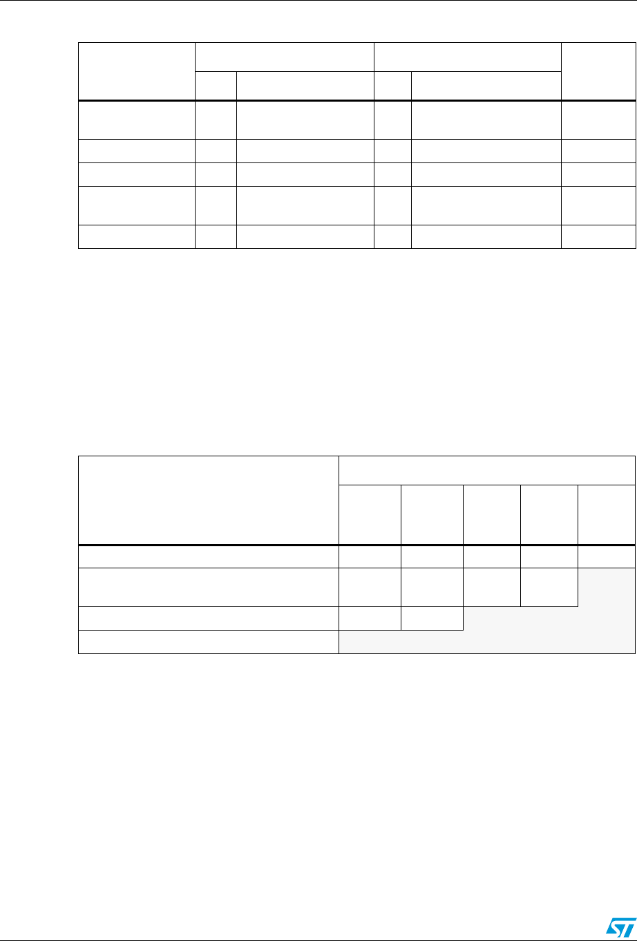
Table 1. Boot modes. . . . . . . . . . . . . . . . . . . . . . . . . . . . . . . . . . . . . . . . . . . . . . . . . . . . . . . . . . . . . 15
Table 2. Debug port pin assignment. . . . . . . . . . . . . . . . . . . . . . . . . . . . . . . . . . . . . . . . . . . . . . . . . 18
Table 3. SWJ I/O pin availability . . . . . . . . . . . . . . . . . . . . . . . . . . . . . . . . . . . . . . . . . . . . . . . . . . . . 18
Table 4. Mandatory components . . . . . . . . . . . . . . . . . . . . . . . . . . . . . . . . . . . . . . . . . . . . . . . . . . . 23
Table 5. Optional components . . . . . . . . . . . . . . . . . . . . . . . . . . . . . . . . . . . . . . . . . . . . . . . . . . . . . 23
Table 6. Reference connection for all packages. . . . . . . . . . . . . . . . . . . . . . . . . . . . . . . . . . . . . . . . 25
Table 7. Document revision history . . . . . . . . . . . . . . . . . . . . . . . . . . . . . . . . . . . . . . . . . . . . . . . . . 27

AN2586 List of figures
Doc ID 13675 Rev 7 5/28
List of figures
Figure 1. Power supply overview . . . . . . . . . . . . . . . . . . . . . . . . . . . . . . . . . . . . . . . . . . . . . . . . . . . . . 6
Figure 2. Power supply scheme. . . . . . . . . . . . . . . . . . . . . . . . . . . . . . . . . . . . . . . . . . . . . . . . . . . . . . 8
Figure 3. Power on reset/power down reset waveform . . . . . . . . . . . . . . . . . . . . . . . . . . . . . . . . . . . . 8
Figure 4. PVD thresholds. . . . . . . . . . . . . . . . . . . . . . . . . . . . . . . . . . . . . . . . . . . . . . . . . . . . . . . . . . . 9
Figure 5. Reset circuit . . . . . . . . . . . . . . . . . . . . . . . . . . . . . . . . . . . . . . . . . . . . . . . . . . . . . . . . . . . . 10
Figure 6. External clock . . . . . . . . . . . . . . . . . . . . . . . . . . . . . . . . . . . . . . . . . . . . . . . . . . . . . . . . . . . 11
Figure 7. Crystal/ceramic resonators . . . . . . . . . . . . . . . . . . . . . . . . . . . . . . . . . . . . . . . . . . . . . . . . . 11
Figure 8. External clock . . . . . . . . . . . . . . . . . . . . . . . . . . . . . . . . . . . . . . . . . . . . . . . . . . . . . . . . . . . 13
Figure 9. Crystal/ceramic resonators . . . . . . . . . . . . . . . . . . . . . . . . . . . . . . . . . . . . . . . . . . . . . . . . . 13
Figure 10. Boot mode selection implementation example . . . . . . . . . . . . . . . . . . . . . . . . . . . . . . . . . . 15
Figure 11. Host-to-board connection . . . . . . . . . . . . . . . . . . . . . . . . . . . . . . . . . . . . . . . . . . . . . . . . . . 17
Figure 12. JTAG connector implementation . . . . . . . . . . . . . . . . . . . . . . . . . . . . . . . . . . . . . . . . . . . . 19
Figure 13. Typical layout for VDD/VSS pair . . . . . . . . . . . . . . . . . . . . . . . . . . . . . . . . . . . . . . . . . . . . . 21
Figure 14. STM32F103ZE(T6) microcontroller reference schematic. . . . . . . . . . . . . . . . . . . . . . . . . . 24
Power supplies AN2586
6/28 Doc ID 13675 Rev 7
1 Power supplies
1.1 Introduction
The device requires a 2.0 V to 3.6 V operating voltage supply (VDD). An embedded regulator
is used to supply the internal 1.8 V digital power.
The real-time clock (RTC) and backup registers can be powered from the VBAT voltage when
the main VDD supply is powered off.
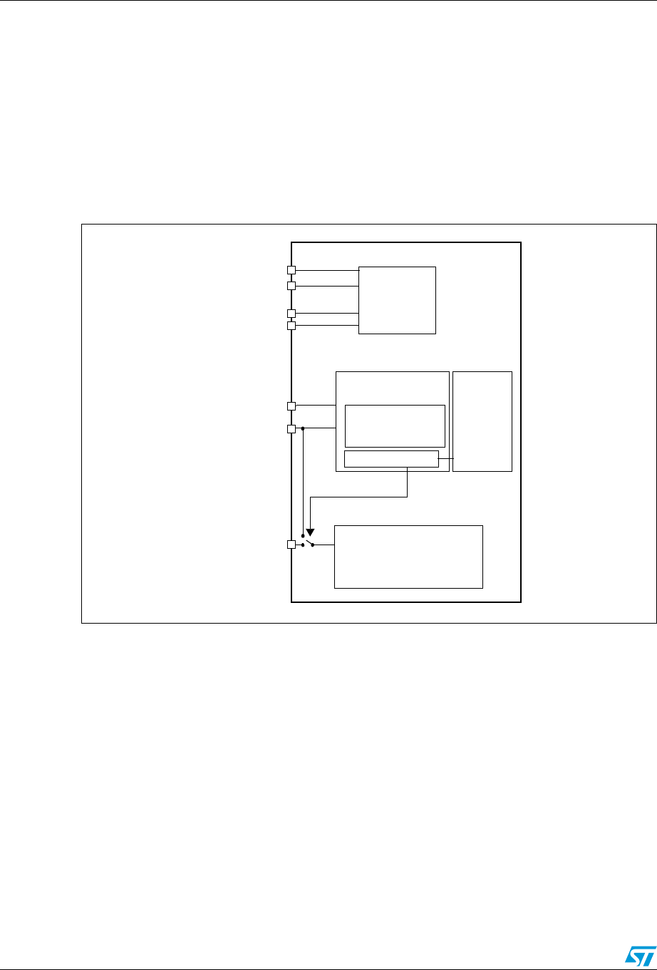
Figure 1. Power supply overview
Note: VDDA and VSSA must be connected to VDD and VSS, respectively.
1.1.1 Independent A/D converter supply and reference voltage
To improve conversion accuracy, the ADC has an independent power supply that can be
filtered separately, and shielded from noise on the PCB.
●the ADC voltage supply input is available on a separate VDDA pin
●an isolated supply ground connection is provided on the VSSA pin
When available (depending on package), VREF– must be tied to VSSA.
On 100-pin and 144-pin packages
To ensure a better accuracy on low-voltage inputs, the user can connect a separate external
reference voltage ADC input on VREF+. The voltage on VREF+ may range from 2.4 V to
VDDA.
A/D converter
V
DD
V
SS
I/O Ring
BKP registers
Temp. sensor
Reset block
Standby circuitry
PLL
(Wakeup logic,
IWDG)
RTC
Voltage regulator
Core
memories'
digital
peripherals
Low voltage detector
(V
SSA
) V
REF–
V
DDA
domain
V
DD
domain 1.8 V domain
Backup domain
LSE crystal 32 KHz oscillator
RCC BDCR register
ai14863
(from 2.4 V up to V
DDA
) V
REF+
(V
DD
) V
DDA
(V
SS
) V
SSA
(V
DD
) V
BAT

AN2586 Power supplies
Doc ID 13675 Rev 7 7/28
On packages with 64 pins or less
The VREF+ and VREF- pins are not available, they are internally connected to the ADC
voltage supply (VDDA) and ground (VSSA).
1.1.2 Battery backup
To retain the content of the Backup registers when VDD is turned off, the VBAT pin can be
connected to an optional standby voltage supplied by a battery or another source.
The VBAT pin also powers the RTC unit, allowing the RTC to operate even when the main
digital supply (VDD) is turned off. The switch to the VBAT supply is controlled by the power
down reset (PDR) circuitry embedded in the Reset block.
If no external battery is used in the application, it is highly recommended to connect VBAT
externally to VDD.
1.1.3 Voltage regulator
The voltage regulator is always enabled after reset. It works in three different modes
depending on the application modes.
●in Run mode, the regulator supplies full power to the 1.8 V domain (core, memories and
digital peripherals)
●in Stop mode, the regulator supplies low power to the 1.8 V domain, preserving the
contents of the registers and SRAM
●in Standby mode, the regulator is powered off. The contents of the registers and SRAM
are lost except for those concerned with the Standby circuitry and the Backup domain.
1.2 Power supply schemes
The circuit is powered by a stabilized power supply, VDD.
●Caution:
– If the ADC is used, the VDD range is limited to 2.4 V to 3.6 V
– If the ADC is not used, the VDD range is 2.0 V to 3.6 V
●The VDD pins must be connected to VDD with external decoupling capacitors (one
100 nF Ceramic capacitor for each VDD pin + one Tantalum or Ceramic capacitor (min.
4.7 µF typ.10 µF).
●The VBAT pin can be connected to the external battery (1.8 V < VBAT < 3.6 V). If no
external battery is used, it is recommended to connect this pin to VDD with a 100 nF
external ceramic decoupling capacitor.
●The VDDA pin must be connected to two external decoupling capacitors (100 nF
Ceramic + 1 µF Tantalum or Ceramic).
●The VREF+ pin can be connected to the VDDA external power supply. If a separate,
external reference voltage is applied on VREF+, a 100 nF and a 1 µF capacitors must be
connected on this pin. In all cases, VREF+ must be kept between 2.4 V and VDDA.
●Additional precautions can be taken to filter analog noise:
–V
DDA can be connected to VDD through a ferrite bead.
–The V
REF+ pin can be connected to VDDA through a resistor (typ. 47 Ω).
Power supplies AN2586
8/28 Doc ID 13675 Rev 7
Figure 2. Power supply scheme
1. Optional. If a separate, external reference voltage is connected on VREF+, the two capacitors (100 nF and
1 µF) must be connected.
2. VREF+ is either connected to VDDA or to VREF.
3. N is the number of VDD and VSS inputs.
1.3 Reset and power supply supervisor
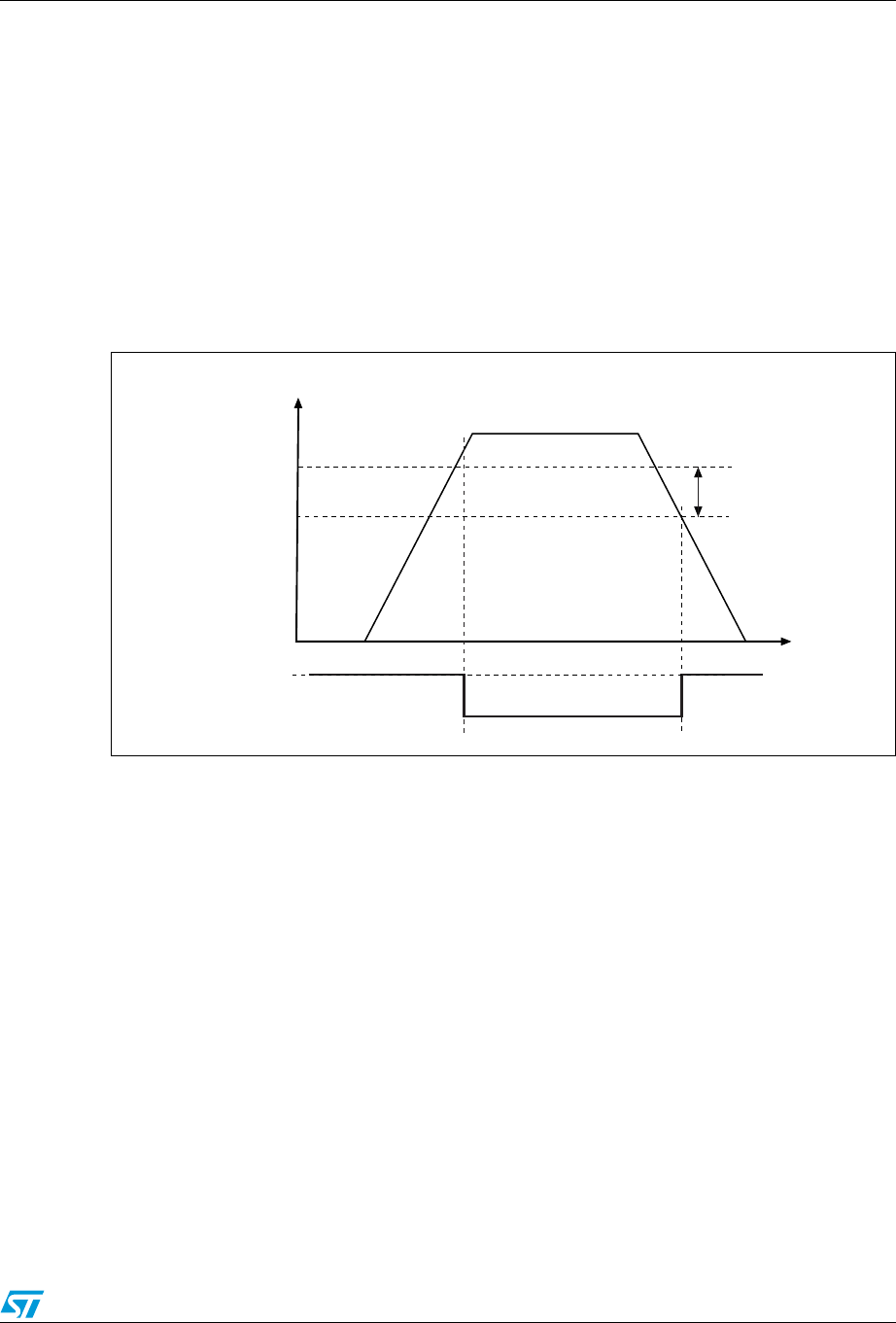
1.3.1 Power on reset (POR) / power down reset (PDR)
The device has an integrated POR/PDR circuitry that allows proper operation starting from
2V.
The device remains in the Reset mode as long as VDD is below a specified threshold,
VPOR/PDR, without the need for an external reset circuit. For more details concerning the
power on/power down reset threshold, refer to the electrical characteristics in the low-
density, medium-density, high-density, XL-density, and connectivity line STM32F10xxx
datasheets.
Figure 3. Power on reset/power down reset waveform
VBAT
STM32F10xxx
N × 100 nF
VDD
+ 1 × 10 µF
100 nF + 1 µF
100 nF + 1 µF
(note 1)
Battery
VBAT VREF+
VDDA
VSSA
VREF–
VDD 1/2/3/.../N
VSS 1/2/3/.../N
VREF
VDD
ai14865b
VDD
POR
PDR
40 mV
hysteresis
Temporization
tRSTTEMPO
RESET
ai14364
AN2586 Power supplies
Doc ID 13675 Rev 7 9/28
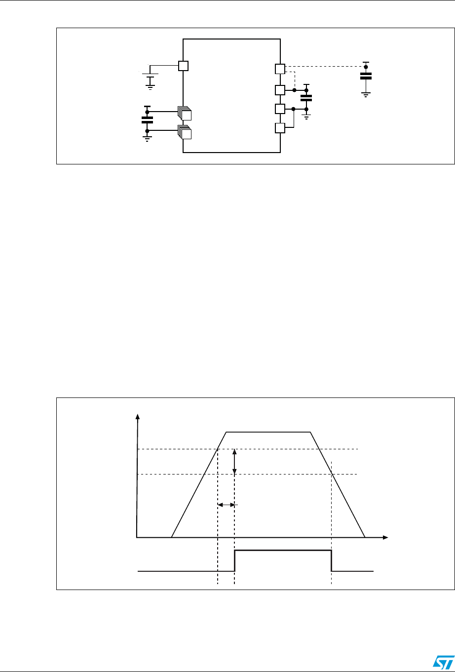
1.3.2 Programmable voltage detector (PVD)
You can use the PVD to monitor the VDD power supply by comparing it to a threshold
selected by the PLS[2:0] bits in the Power control register (PWR_CR).
The PVD is enabled by setting the PVDE bit.
A PVDO flag is available, in the Power control/status register (PWR_CSR), to indicate
whether VDD is higher or lower than the PVD threshold. This event is internally connected to
EXTI Line16 and can generate an interrupt if enabled through the EXTI registers. The PVD
output interrupt can be generated when VDD drops below the PVD threshold and/or when
VDD rises above the PVD threshold depending on the EXTI Line16 rising/falling edge
configuration. As an example the service routine can perform emergency shutdown tasks.
Figure 4. PVD thresholds
1.3.3 System reset
A system reset sets all registers to their reset values except for the reset flags in the clock
controller CSR register and the registers in the Backup domain (see Figure 1).
A system reset is generated when one of the following events occurs:
1. A low level on the NRST pin (external reset)
2. window watchdog end-of-count condition (WWDG reset)
3. Independent watchdog end-of-count condition (IWDG reset)
4. A software reset (SW reset)
5. Low-power management reset
The reset source can be identified by checking the reset flags in the Control/Status register,
RCC_CSR.
VDD
100 mV
hysteresis
PVD threshold
PVD output
ai14365
Power supplies AN2586
10/28 Doc ID 13675 Rev 7
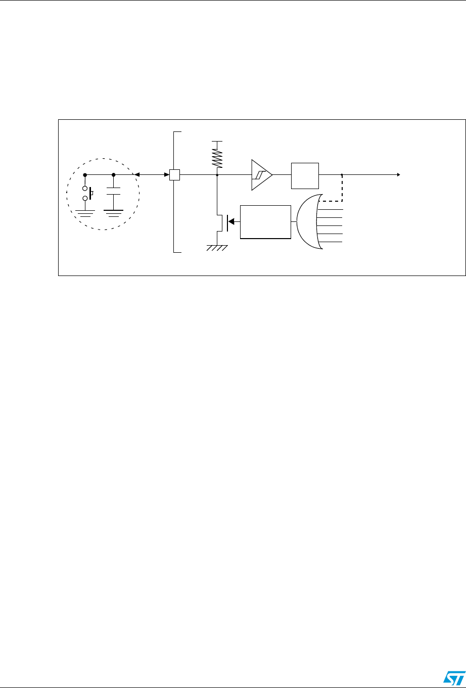
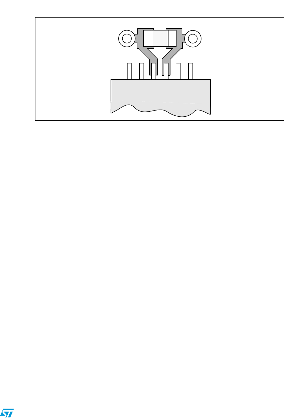
The STM32F1xx does not require an external reset circuit to power-up correctly. Only a pull-
down capacitor is recommended to improve EMS performance by protecting the device
against parasitic resets. See Figure 5.
Charging and discharging a pull-down capacitor through an internal resistor increases the
device power consumption. The capacitor recommended value (100 nF) can be reduced to
10 nF to limit this power consumption;
Figure 5. Reset circuit
205
6$$6$$!
77$'RESET
)7$'RESET
0ULSE
GENERATOR 0OWERRESET
MINS
3YSTEMRESET
&ILTER
3OFTWARERESET
,OWPOWERMANAGEMENTRESET
&
%XTERNAL
RESETCIRCUIT
.234
AIC
AN2586 Clocks
Doc ID 13675 Rev 7 11/28
2 Clocks
Three different clock sources can be used to drive the system clock (SYSCLK):
●HSI oscillator clock (high-speed internal clock signal)
●HSE oscillator clock (high-speed external clock signal)
●PLL clock
The devices have two secondary clock sources:
●40 kHz low-speed internal RC (LSI RC) that drives the independent watchdog and,
optionally, the RTC used for Auto-wakeup from the Stop/Standby modes.
●32.768 kHz low-speed external crystal (LSE crystal) that optionally drives the real-time
clock (RTCCLK)
Each clock source can be switched on or off independently when it is not used, to optimize
the power consumption.
Refer to the STM32F10xxx or STM32F100xx reference manual (RM0008 or RM0041,
respectively) for a description of the clock tree:
●RM0008 for STM32F101xx, STM32F102xx, STM32F103xx and STM32F105xx/107xx
microcontrollers
●RM0041 for STM32F100xx value line microcontrollers
2.1 HSE OSC clock
The high-speed external clock signal (HSE) can be generated from two possible clock
sources:
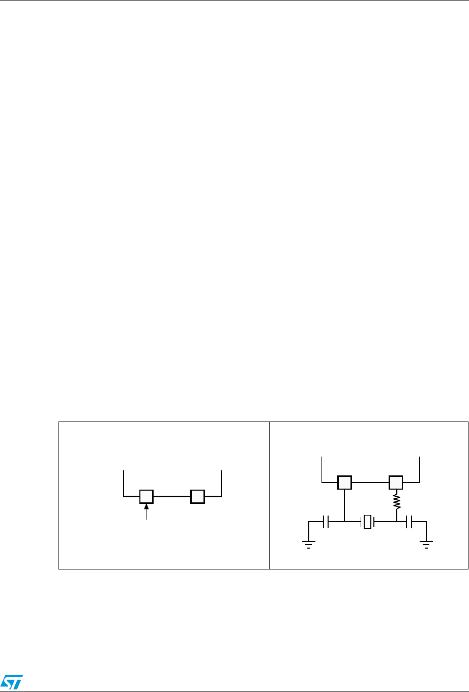
●HSE external crystal/ceramic resonator (see Figure 7)
●HSE user external clock (see Figure 6)
1. The value of REXT depends on the crystal characteristics. Typical value is in the range of 5 to 6 RS
(resonator series resistance).
2. Load capacitance CL has the following formula: CL = CL1 x CL2 / (CL1 + CL2) + Cstray where: Cstray is the pin
capacitance and board or trace PCB-related capacitance. Typically, it is between 2 pF and 7 pF. Please
refer to Section 5: Recommendations on page 20 to minimize its value.
Figure 6. External clock Figure 7. Crystal/ceramic resonators
OSC_OUTOSC_IN
External source
(Hi-Z)
ai14369
Hardware configuration
OSC_OUTOSC_IN
ai14370
STM32F10xxx
R
EXT(1)
C
L1
C
L2
Hardware configuration

Clocks AN2586
12/28 Doc ID 13675 Rev 7
2.1.1 External source (HSE bypass)
In this mode, an external clock source must be provided. It can have a frequency of up to:
●24 MHz for STM32F100xx value line devices
●25 MHz for STM32F101xx, STM32F102xx and STM32F103xx devices
●50 MHz for connectivity line devices
The external clock signal (square, sine or triangle) with a duty cycle of about 50%, has to
drive the OSC_IN pin while the OSC_OUT pin must be left in the high impedance state (see
Figure 7 and Figure 6).
2.1.2 External crystal/ceramic resonator (HSE crystal)
The external oscillator frequency ranges from:
●4 to 16 MHz on STM32F101xx, STM32F102xx and STM32F103xx devices
●4 to 24 MHz for STM32F100xx value line devices
●3 to 25 MHz on connectivity line devices
The external oscillator has the advantage of producing a very accurate rate on the main
clock. The associated hardware configuration is shown in Figure 7.
The resonator and the load capacitors have to be connected as close as possible to the
oscillator pins in order to minimize output distortion and startup stabilization time. The load
capacitance values must be adjusted according to the selected oscillator.
For CL1 and CL2 it is recommended to use high-quality ceramic capacitors in the 5 pF-to-
25 pF range (typ.), designed for high-frequency applications and selected to meet the
requirements of the crystal or resonator. CL1 and CL2, are usually the same value. The
crystal manufacturer typically specifies a load capacitance that is the series combination of
CL1 and CL2. The PCB and MCU pin capacitances must be included when sizing CL1 and
CL2 (10 pF can be used as a rough estimate of the combined pin and board capacitance).
Refer to the electrical characteristics sections in the datasheet of your product for more
details.
AN2586 Clocks
Doc ID 13675 Rev 7 13/28
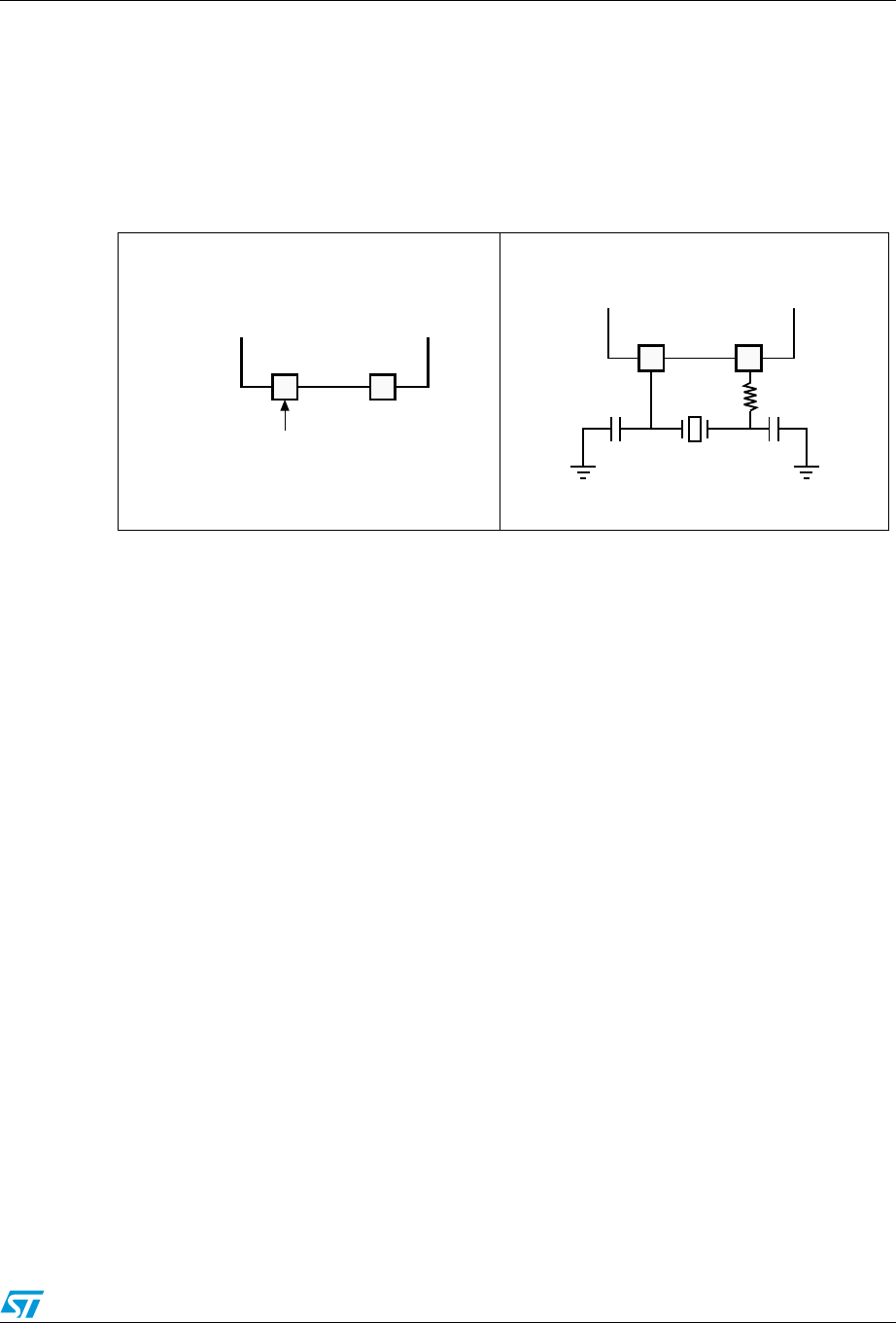
2.2 LSE OSC clock
The low-speed external clock signal (LSE) can be generated from two possible clock
sources:
●LSE external crystal/ceramic resonator (see Figure 9)
●LSE user external clock (see Figure 8)
Note: 1 “External clock” figure:
To avoid exceeding the maximum value of CL1 and CL2 (15 pF) it is strongly recommended
to use a resonator with a load capacitance CL
≤
7 pF. Never use a resonator with a load
capacitance of 12.5 pF
2“External clock” and “crystal/ceramic resonators” figures:
OSC32_IN and OSC_OUT pins can be used also as GPIO, but it is recommended not to
use them as both RTC and GPIO pins in the same application
3“Crystal/ceramic resonators” figure:
The value of REXT depends on the crystal characteristics. A 0
Ω
resistor would work but
would not be optimal. Typical value is in the range of 5 to 6 RS (resonator series resistance).
To fine tune RS value refer to AN2867 - Oscillator design guide for ST microcontrollers.
2.2.1 External source (LSE bypass)
In this mode, an external clock source must be provided. It can have a frequency of up to
1 MHz. The external clock signal (square, sine or triangle) with a duty cycle of about 50%
has to drive the OSC32_IN pin while the OSC32_OUT pin must be left high impedance (see
Figure 9 and Figure 8).
2.2.2 External crystal/ceramic resonator (LSE crystal)
The LSE crystal is a 32.768 kHz low-speed external crystal or ceramic resonator. It has the
advantage of providing a low-power, but highly accurate clock source to the real-time clock
peripheral (RTC) for clock/calendar or other timing functions.
The resonator and the load capacitors have to be connected as close as possible to the
oscillator pins in order to minimize output distortion and startup stabilization time. The load
capacitance values must be adjusted according to the selected oscillator.
Figure 8. External clock Figure 9. Crystal/ceramic resonators
OSC32_OUTOSC32_IN
External source
(Hi-Z)
ai14371
Hardware configuration
OSC32_OUTOSC32_IN
ai14372c
STM32F10xxx
CL1 CL2
Hardware configuration
REXT(3)

Clocks AN2586
14/28 Doc ID 13675 Rev 7
2.3 Clock security system (CSS)
The clock security system can be activated by software. In this case, the clock detector is
enabled after the HSE oscillator startup delay, and disabled when this oscillator is stopped.
●If a failure is detected on the HSE oscillator clock, the oscillator is automatically
disabled. A clock failure event is sent to the break input of the TIM1 advanced control
timer and an interrupt is generated to inform the software about the failure (clock
security system interrupt CSSI), allowing the MCU to perform rescue operations. The
CSSI is linked to the Cortex™-M3 NMI (non-maskable interrupt) exception vector.
●If the HSE oscillator is used directly or indirectly as the system clock (indirectly means
that it is used as the PLL input clock, and the PLL clock is used as the system clock), a
detected failure causes a switch of the system clock to the HSI oscillator and the
disabling of the external HSE oscillator. If the HSE oscillator clock (divided or not) is the
clock entry of the PLL used as system clock when the failure occurs, the PLL is
disabled too.
For details, see the STM32F10xxx (RM0008) and STM32F100xx (RM0041) reference
manuals available from the STMicroelectronics website www.st.com.
AN2586 Boot configuration
Doc ID 13675 Rev 7 15/28
3 Boot configuration
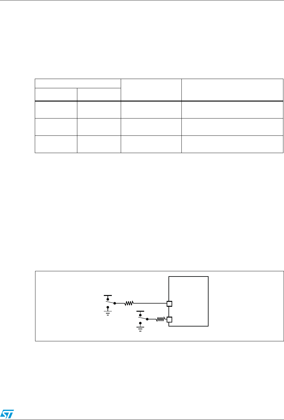
3.1 Boot mode selection
In the STM32F10xxx, three different boot modes can be selected by means of the
BOOT[1:0] pins as shown in Ta bl e 1 .
The values on the BOOT pins are latched on the 4th rising edge of SYSCLK after a reset. It
is up to the user to set the BOOT1 and BOOT0 pins after reset to select the required boot
mode.
The BOOT pins are also resampled when exiting the Standby mode. Consequently, they
must be kept in the required Boot mode configuration in the Standby mode. After this startup
delay has elapsed, the CPU fetches the top-of-stack value from address 0x0000 0000, and
starts code execution from the boot memory starting from 0x0000 0004.
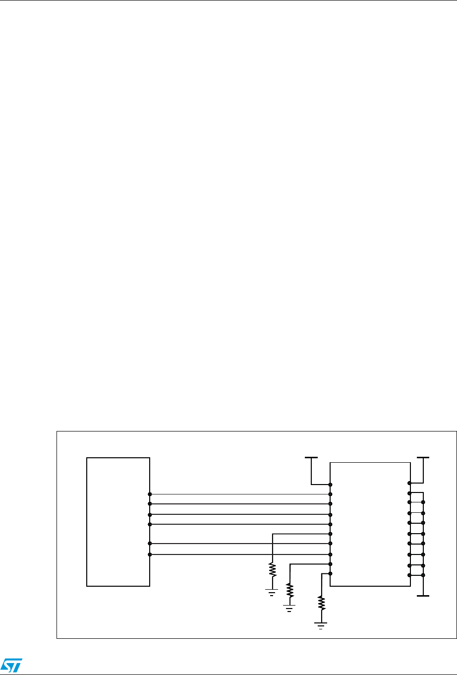
3.2 Boot pin connection
Figure 10 shows the external connection required to select the boot memory of the
STM32F10xxx.
Figure 10. Boot mode selection implementation example
1. Resistor values are given only as a typical example.
Table 1. Boot modes
BOOT mode selection pins
Boot mode Aliasing
BOOT1 BOOT0
x 0 Main Flash memory Main Flash memory is selected as boot
space
0 1 System memory System memory is selected as boot
space
1 1 Embedded SRAM Embedded SRAM is selected as boot
space
ai14373
V
DD
STM32F10xxx
BOOT0
BOOT1
V
DD
10 kΩ
10 kΩ

Boot configuration AN2586
16/28 Doc ID 13675 Rev 7
3.3 Embedded boot loader mode
The Embedded boot loader mode is used to reprogram the Flash memory using one of the
available serial interfaces:
●In low-density, low-density value line, medium-density, medium-density value line, and
high-density devices, the boot loader is activated through the USART1 interface. For
further details please refer to AN2606.
●In XL-density devices, the boot loader is activated through the USART1 or USART2
(remapped) interface. For further details please refer to AN2606.
●In connectivity line devices the boot loader can be activated through one of the
following interfaces: USART1, USART2 (remapped), CAN2 (remapped) or USB OTG
FS in Device mode (DFU: device firmware upgrade).
The USART peripheral operates with the internal 8 MHz oscillator (HSI). The CAN and
USB OTG FS, however, can only function if an external 8 MHz, 14.7456 MHz or 25
MHz clock (HSE) is present. For further details, please refer to AN2662.
This embedded boot loader is located in the System memory and is programmed by ST
during production.
AN2586 Debug management
Doc ID 13675 Rev 7 17/28
4 Debug management
4.1 Introduction
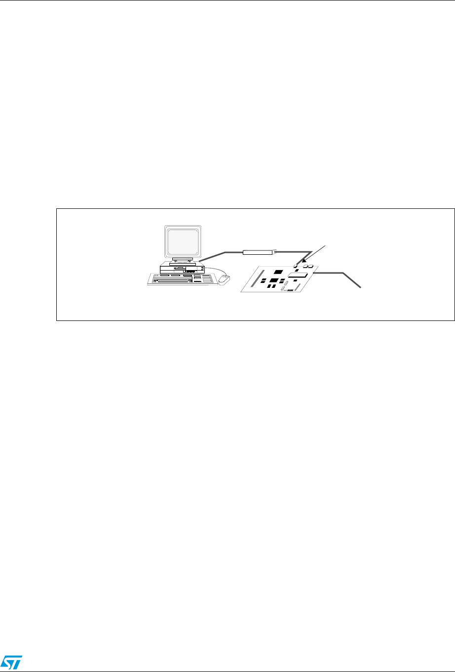
The Host/Target interface is the hardware equipment that connects the host to the
application board. This interface is made of three components: a hardware debug tool, a
JTAG or SW connector and a cable connecting the host to the debug tool.
Figure 11 shows the connection of the host to the evaluation board (STM3210B-EVAL,
STM3210C-EVAL, STM32100B-EVAL or STM3210E-EVAL).
The Value line evaluation board (STM32100B-EVAL or STM32100E-EVAL) embeds the
debug tools (ST-LINK). Consequently, it can be directly connected to the PC through a USB
cable.
Figure 11. Host-to-board connection
4.2 SWJ debug port (serial wire and JTAG)
The STM32F10xxx core integrates the serial wire / JTAG debug port (SWJ-DP). It is an
ARM® standard CoreSight™ debug port that combines a JTAG-DP (5-pin) interface and a
SW-DP (2-pin) interface.
●The JTAG debug port (JTAG-DP) provides a 5-pin standard JTAG interface to the AHP-
AP port
●The serial wire debug port (SW-DP) provides a 2-pin (clock + data) interface to the
AHP-AP port
In the SWJ-DP, the two JTAG pins of the SW-DP are multiplexed with some of the five JTAG
pins of the JTAG-DP.
4.3 Pinout and debug port pins
The STM32F10xxx MCU is offered in various packages with different numbers of available
pins. As a result, some functionality related to the pin availability may differ from one
package to another.
4.3.1 SWJ debug port pins
Five pins are used as outputs for the SWJ-DP as alternate functions of general-purpose
I/Os (GPIOs). These pins, shown in Ta bl e 2 , are available on all packages.
%VALUATIONBOARD
(OST0# 0OWERSUPPLY
*4!'37CONNECTOR
$EBUGTOOL
AIB
Debug management AN2586
18/28 Doc ID 13675 Rev 7
4.3.2 Flexible SWJ-DP pin assignment
After reset (SYSRESETn or PORESETn), all five pins used for the SWJ-DP are assigned as
dedicated pins immediately usable by the debugger host (note that the trace outputs are not
assigned except if explicitly programmed by the debugger host).
However, the STM32F10xxx MCU implements a register to disable some part or all of the
SWJ-DP port, and so releases the associated pins for general-purpose I/Os usage. This
register is mapped on an APB bridge connected to the Cortex™-M3 system bus. This
register is programmed by the user software program and not by the debugger host.
Ta bl e 3 shows the different possibilities to release some pins.
For more details, see the STM32F10xxx (RM0008) and STM32F100xx (RM0041) reference
manuals, available from the STMicroelectronics website www.st.com.
Table 2. Debug port pin assignment
SWJ-DP pin name
JTAG debug port SW debug port Pin
assignment
Type Description Type Debug assignment
JTMS/SWDIO I JTAG test mode
selection I/O Serial wire data
input/output PA 1 3
JTCK/SWCLK I JTAG test clock I Serial wire clock PA14
JTDI I JTAG test data input - - PA15
JTDO/TRACESWO O JTAG test data output - TRACESWO if async trace
is enabled PB3
JNTRST I JTAG test nReset - - PB4
Table 3. SWJ I/O pin availability
Available Debug ports
SWJ I/O pin assigned
PA13 /
JTMS/
SWDIO
PA14 /
JTCK/
SWCLK
PA15 /
JTDI
PB3 /
JTDO
PB4/
JNTRST
Full SWJ (JTAG-DP + SW-DP) - reset state X X X X X
Full SWJ (JTAG-DP + SW-DP) but without
JNTRST XXXX
JTAG-DP disabled and SW-DP enabled X X
JTAG-DP disabled and SW-DP disabled Released
AN2586 Debug management
Doc ID 13675 Rev 7 19/28
4.3.3 Internal pull-up and pull-down resistors on JTAG pins
The JTAG input pins must not be floating since they are directly connected to flip-flops to
control the debug mode features. Special care must be taken with the SWCLK/TCK pin that
is directly connected to the clock of some of these flip-flops.
To avoid any uncontrolled I/O levels, the STM32F10xxx embeds internal pull-up and pull-
down resistors on JTAG input pins:
●JNTRST: Internal pull-up
●JTDI: Internal pull-up
●JTMS/SWDIO: Internal pull-up
●TCK/SWCLK: Internal pull-down
Once a JTAG I/O is released by the user software, the GPIO controller takes control again.
The reset states of the GPIO control registers put the I/Os in the equivalent state:
●JNTRST: Input pull-up
●JTDI: Input pull-up
●JTMS/SWDIO: Input pull-up
●JTCK/SWCLK: Input pull-down
●JTDO: Input floating
The software can then use these I/Os as standard GPIOs.
Note: The JTAG IEEE standard recommends to add pull-up resistors on TDI, TMS and nTRST but
there is no special recommendation for TCK. However, for the STM32F10xxx, an integrated
pull-down resistor is used for JTCK.
Having embedded pull-up and pull-down resistors removes the need to add external
resistors.
4.3.4 SWJ debug port connection with standard JTAG connector
Figure 12 shows the connection between the STM32F10xxx and a standard JTAG
connector.
Figure 12. JTAG connector implementation
ai14376
V
DD
V
DD
STM32F10xxx
nJTRST
JTDI
JSTM/SWDIO
JTCK/SWCLK
JTDO
nRSTIN
(1) VTREF
(3) nTRST
(5) TDI
(7) TMS
(9) TCK
(11) RTCK
(13)TDO
(15) nSRST
(17) DBGRQ
(19) DBGACK
10 kΩ
10 kΩ
10 kΩV
SS
(2)
(4)
(6)
(8)
(10)
(12)
(14)
(16)
(18)
(20)
Connector 2 × 10
JTAG connector CN9

Recommendations AN2586
20/28 Doc ID 13675 Rev 7
5 Recommendations
5.1 Printed circuit board
For technical reasons, it is best to use a multilayer printed circuit board (PCB) with a
separate layer dedicated to ground (VSS) and another dedicated to the VDD supply. This
provides good decoupling and a good shielding effect. For many applications, economical
reasons prohibit the use of this type of board. In this case, the major requirement is to
ensure a good structure for ground and for the power supply.
5.2 Component position
A preliminary layout of the PCB must separate the different circuits according to their EMI
contribution in order to reduce cross-coupling on the PCB, that is noisy, high-current circuits,
low-voltage circuits, and digital components.
5.3 Ground and power supply (VSS, VDD)
Every block (noisy, low-level sensitive, digital, etc.) should be grounded individually and all
ground returns should be to a single point. Loops must be avoided or have a minimum area.
The power supply should be implemented close to the ground line to minimize the area of
the supply loop. This is due to the fact that the supply loop acts as an antenna, and is
therefore the main transmitter and receiver of EMI. All component-free PCB areas must be
filled with additional grounding to create a kind of shielding (especially when using single-
layer PCBs).
5.4 Decoupling
All power supply and ground pins must be properly connected to the power supplies. These
connections, including pads, tracks and vias should have as low an impedance as possible.
This is typically achieved with thick track widths and, preferably, the use of dedicated power
supply planes in multilayer PCBs.
In addition, each power supply pair should be decoupled with filtering ceramic capacitors C
(100 nF) and a chemical capacitor C of about 10 µF connected in parallel on the
STM32F10xxx device. These capacitors need to be placed as close as possible to, or below,
the appropriate pins on the underside of the PCB. Typical values are 10 nF to 100 nF, but
exact values depend on the application needs. Figure 13 shows the typical layout of such a
VDD/VSS pair.
AN2586 Recommendations
Doc ID 13675 Rev 7 21/28
Figure 13. Typical layout for VDD/VSS pair
5.5 Other signals
When designing an application, the EMC performance can be improved by closely studying:
●Signals for which a temporary disturbance affects the running process permanently
(the case of interrupts and handshaking strobe signals, and not the case for LED
commands).
For these signals, a surrounding ground trace, shorter lengths and the absence of
noisy and sensitive traces nearby (crosstalk effect) improve EMC performance.
For digital signals, the best possible electrical margin must be reached for the two
logical states and slow Schmitt triggers are recommended to eliminate parasitic states.
●Noisy signals (clock, etc.)
●Sensitive signals (high impedance, etc.)
5.6 Unused I/Os and features
All microcontrollers are designed for a variety of applications and often a particular
application does not use 100% of the MCU resources.
To increase EMC performance, unused clocks, counters or I/Os, should not be left free, e.g.
I/Os should be set to “0” or “1”(pull-up or pull-down to the unused I/O pins.) and unused
features should be “frozen” or disabled.
Via to VSS
Via to VDD
Cap.
VDD VSS
STM32F10xxx

Reference design AN2586
22/28 Doc ID 13675 Rev 7
6 Reference design
6.1 Description
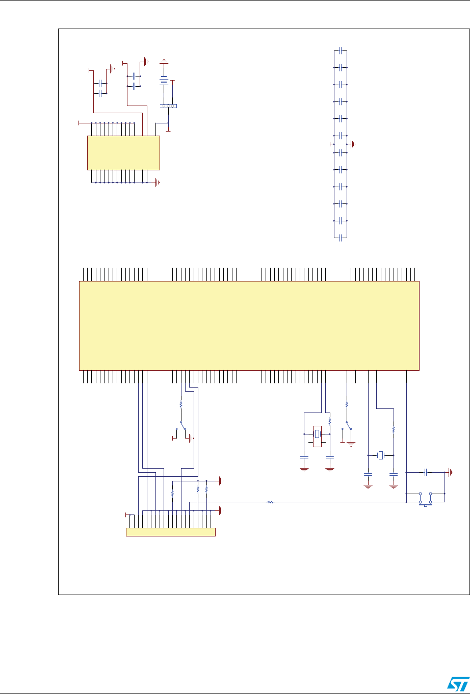
The reference design shown in Figure 14, is based on the STM32F103ZE(T6), a highly
integrated microcontroller running at 72 MHz, that combines the new Cortex™-M3 32-bit
RISC CPU core with 512 Kbytes of embedded Flash memory and up to 64 Kbytes of high-
speed SRAM.
This reference design can be tailored to any other STM32F10xxx device with different
package, using the pins correspondence given in Table 6: Reference connection for all
packages.
6.1.1 Clock
Two clock sources are used for the microcontroller:
●LSE: X1– 32.768 kHz crystal for the embedded RTC
●HSE: X2– 8 MHz crystal for the STM32F10xxx microcontroller
Refer to Section 2: Clocks on page 11.
6.1.2 Reset
The reset signal in Figure 14 is active low. The reset sources include:
●Reset button (B1)
●Debugging tools via the connector CN1
Refer to Section 1.3: Reset and power supply supervisor on page 8.
6.1.3 Boot mode
The boot option is configured by setting switches SW2 (Boot 0) and SW1 (Boot 1). Refer to
Section 3: Boot configuration on page 15.
Note: In low-power mode (more specially in Standby mode) the boot mode is mandatory to be
able to connect to tools (the device should boot from the SRAM).
6.1.4 SWJ interface
The reference design shows the connection between the STM32F10xxx and a standard
JTAG connector. Refer to Section 4: Debug management on page 17.
Note: It is recommended to connect the reset pins so as to be able to reset the application from
the tools.
6.1.5 Power supply
Refer to Section 1: Power supplies on page 6.
AN2586 Reference design
Doc ID 13675 Rev 7 23/28
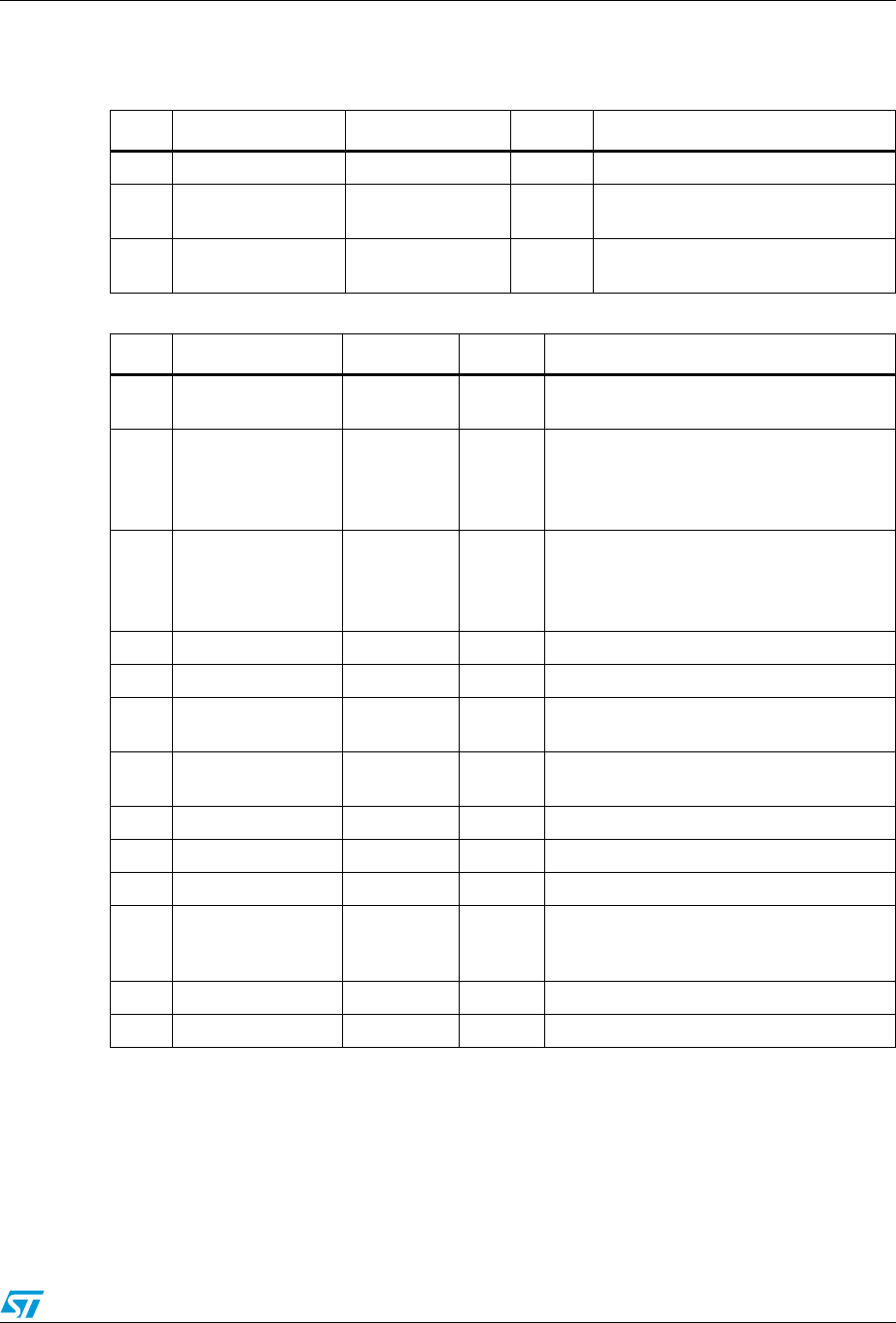
6.2 Component references
Table 4. Mandatory components
Id Components name Reference Quantity Comments
1 Microcontroller STM32F103ZE(T6) 1 144-pin package
2 Capacitors 100 nF 11 Ceramic capacitors (decoupling
capacitors)
3 Capacitor 10 µF 1 Ceramic capacitor (decoupling
capacitor)
Table 5. Optional components
Id Components name Reference Quantity Comments
1Resistor 10 kΩ5Pull-up and pull-down for JTAG and Boot
mode.
2Resistor 390 Ω1
Used for HSE: the value depends on the
crystal characteristics.
This resistor value is given only as a typical
example.
3Resistor 0 Ω1
Used for LSE: the value depends on the
crystal characteristics.
This resistor value is given only as a typical
example.
4 Capacitor 100 nF 3 Ceramic capacitor
5 Capacitor 1µF 2 Used for VDDA and VREF.
6 Capacitor 10 pF 2 Used for LSE: the value depends on the
crystal characteristics.
7 Capacitor 20 pF 2 Used for HSE: the value depends on the
crystal characteristics.
8 Quartz 8 MHz 1 Used for HSE
9 Quartz 32 kHz 1 Used for LSE
10 JTAG connector HE10 1
11 Battery 3V3 1
If no external battery is used in the
application, it is recommended to connect
VBAT externally to VDD
12 Switch 3V3 2 Used to select the correct boot mode.
13 Push-button B1 1
Reference design AN2586
24/28 Doc ID 13675 Rev 7
Figure 14. STM32F103ZE(T6) microcontroller reference schematic
1. If no external battery is used in the application, it is recommended to connect VBAT externally to VDD.
2. To be able to reset the device from the tools this resistor has to be kept.
MCU
1
2
3
4
5
6
7
8
9
10
11
12
13
14
15
16
17
18
19
20
CN1
JTAG VDD
R2 10K
R310K
R1 10K
JTAG connector
Decoupling Capacitor
1
43
2
B1
C5
100nF
C4
20pF
C3
20pF
X2
8MHz
R6
390
R7 10K
VDD 2
3
1SW2
RESET#
OSC_IN
OSC_OUT
C8
100nF
C9
100nF
C10
100nF
C7
100nF
VDD
C11
100nF
4 1
32
X1
32K
C2
10pF
C1
10pF
BT1
CR1220 holder
VBAT 3
2
1
JP1
VDD
MCU Supply
R4 10K
VDD
2
3
1SW1
C12
100nF
R9 0
PE2 1
PF2 12
OSC_IN
23
PA0-WKUP
34
PC5
45
PG0 56
PE10 63
PE11 64
PE32
PE4 3
PE5 4
PE6 5
PC13-ANTI _TAMP
7
PC14-OSC32_IN
8
PC15-OSC32_OUT
9
PF0 10
PF1 11
PF313
PF4 14
PF5 15
PF6 18
PF7 19
PF820
PF9 21
PF1 0 22
OSC_OUT
24
NRST
25
PC0
26
PC1
27
PC2
28
PC3
29
PA1
35
PA2
36
PA3
37
PA4
40
PA5
41
PA6
42
PA7
43
PC4
44
PB0
46
PB1
47
PB2-BOOT1
48
PF1 1 49
PF1 2 50
PF1 353
PF1 4 54
PF1 5 55
PG1 57
PE7 58
PE859
PE9 60
PE12 65
PB15
76
PG2 87
PC8
98
PA14
109
PG11 126
PG12 127
PG13128
PE1 366
PE14 67
PE15 68
PB10
69
PB11
70
PB12
73
PB1 3
74
PB14
75
PD877
PD9 78
PD10 79
PD11 80
PD12 81
PD1382
PD14 85
PD15 86
PG388
PG4 89
PG5 90
PG6 91
PG7 92
PG893
PC6
96
PC7
97
PC9
99
PA8
100
PA9
101
PA10
102
PA11
103
PA12
104
PA13
105
NC
106
PA15
110
PC10
111
PC11
112
PC12
113
PD0 114
PD1 115
PD2 116
PD3117
PD4 118
PD5 119
PD6 122
PD7 123
PG9 124
PG10 125
PG14 129
PB7
137
BOOT0
138
PB8
139
PB9
140
PE0 141
PE1 142
PG15 132
PB3
133
PB4
134
PB5
135
PB6
136
U1A
STM32F103ZET6
VDD_7 62
VBAT 6
VSS_5
16
VDD_5 17
VSSA
30VREF-
31VREF+ 32
VDDA 33
VSS_4
38
VDD_4 39
VSS_6
51 VDD_6 52
VSS_7
61
VSS_10
120
VSS_1
71
VDD_1 72
VSS_8
83
VDD_884
VSS_9
94
VDD_9 95
VSS_2
107
VDD_2 108
VDD_10 121
VSS_3
143
VDD_3144
VSS_11
130
VDD_11 131
U1B
STM32F103ZET6
VDD
Default setting: 2<->3
C13
100nF
C14
100nF
C15
100nF
C16
100nF
C17
10µF
C6
100nF
MCU
Boot Mode
LSE
HSE
Boot Mode
OSC_IN
OSC_OUT
Boot 0
Boot 1
Reset
R8
0
1)
2)
100nF 1µF
Ai148767c
VDD
100nF 1µF
VDD
AN2586 Reference design
Doc ID 13675 Rev 7 25/28
Table 6. Reference connection for all packages
Pin name
Pin numbers for LQFP packages Pin numbers for
BGA packages
Pin numbers for
VFQFPN package
144 pins 100 pins 64 pins 48 pins 144 pins 100 pins 36 pins
OSC_IN 23 12 5 5 D1 C1 2
OSC_OUT 24 13 6 6 E1 D1 3
PC15-
OSC32_OUT 9944C1B1 -
PC14-
OSC32_IN 8 8 3 3 B1 A1 -
BOOT0 138 94 60 44 D5 D5 35
PB2-BOOT1 48 37 28 20 J5 G5 17
NRST 25 14 7 7 F1 E1 4
PA13 105 72 46 34 A12 A10 25
PA14 109 76 49 37 A11 A9 28
PA15 110 77 50 38 A10 A8 29
PB4 134 90 56 40 A6 A6 31
PB3 133 89 55 39 A7 A7 30
VSS_1 71 49 31 23 H7 E7 18
VSS_2 107 74 47 35 G9 E6 26
VSS_3 143 99 63 47 E5 E5 36
VSS_4 38 27 18 - G4 E4 -
VSS_5 16 10 - - D2 C2 -
VSS_6 51 - - - H5 - -
VSS_7 61 - - - H6 - -
VSS_8 83 - - - G8 - -
VSS_9 94 - - - G10 - -
VSS_10 120 - - - E7 - -
VSS_11 130 - - - E6 -
VDD_1 72 50 32 24 G7 F7 19
VDD_2 108 75 48 36 F9 27
VDD_3 144 100 64 48 F5 F5 1
VDD_4 39 28 19 - F4 F4 -
VDD_5 17 11 - - D3 D2 -
VDD_6 52 - - - G5 - -
VDD_7 62 - - - G6 - -
VDD_8 84 - - - F8 - -

Reference design AN2586
26/28 Doc ID 13675 Rev 7
VDD_9 95 - - - F10 - -
VDD_10 121 - - - F7 - -
VDD_11 131 - - - F6 - -
VREF+ 32 21 - - L1 J1 -
VREF- 31 20 - - K1 H1 -
VSSA 30 19 12 8 J1 G1 -
VDDA 33 22 13 9 M1 K1 -
VBAT 6611C2B2 -
Table 6. Reference connection for all packages (continued)
Pin name
Pin numbers for LQFP packages Pin numbers for
BGA packages
Pin numbers for
VFQFPN package
144 pins 100 pins 64 pins 48 pins 144 pins 100 pins 36 pins

AN2586 Revision history
Doc ID 13675 Rev 7 27/28
7 Revision history
Table 7. Document revision history
Date Revision Changes
12-Jul-2007 1 Initial release.
23-May-2008 2
Application note also applicable to High-density devices.
Figure 1: Power supply overview, Figure 2: Power supply scheme
and Figure 6: Clock overview updated.
Low-speed internal RC frequency modified in Section 2: Clocks on
page 11. VREF+ voltage range modified.
Table 6: Reference connection for all packages on page 25 added.
Small text changes.
23-Jun-2009 3
Connectivity line STM32F10xxx and Section : Glossary added.
Section 1.2: Power supply schemes and Figure 2: Power supply
scheme updated.
Figure 5: Reset circuit updated. Figure 6 Clock overview removed in
Section 2: Clocks. Note 1 added Note 3 updated below Figure 8:
External clock. Section 2.1.1: External source (HSE bypass) and
Section 2.1.2: External crystal/ceramic resonator (HSE crystal)
updated.
Section 2.3 Clock-out capability section removed.
Section 3.1: Boot mode selection and Section 3.3: Embedded boot
loader mode updated.
When no external battery is used, it is recommended to externally
connect the VBAT pin to VDD.
PA14 updated in Table 7: Document revision history.
Small text changes.
STM3210C-EVAL evaluation board added in Section 4.
01-Mar-2010 4
This application note also applies to STM32F100xx low- and
medium-density value line products:
– low- and medium-density value line devices added to Introduction
on page 1
–Section 2.1.1: External source (HSE bypass) and Section 2.1.2:
External crystal/ceramic resonator (HSE crystal) updated
– reference to value line’s evaluation board added to Section 4.1:
Introduction
Table 5: Reset circuit updated.
19-Oct-2010 5 Modified Section 2.2.1: External source (LSE bypass)
Updated for high-density value line devices.
14-Apr-2011 6
Updated VDDA and VREF schematics in Figure 14:
STM32F103ZE(T6) microcontroller reference schematic on page 24
and Table 5: Optional components.
18-Nov-2011 7 Updated to include XL-density devices.

AN2586
28/28 Doc ID 13675 Rev 7
Please Read Carefully:
Information in this document is provided solely in connection with ST products. STMicroelectronics NV and its subsidiaries (“ST”) reserve the
right to make changes, corrections, modifications or improvements, to this document, and the products and services described herein at any
time, without notice.
All ST products are sold pursuant to ST’s terms and conditions of sale.
Purchasers are solely responsible for the choice, selection and use of the ST products and services described herein, and ST assumes no
liability whatsoever relating to the choice, selection or use of the ST products and services described herein.
No license, express or implied, by estoppel or otherwise, to any intellectual property rights is granted under this document. If any part of this
document refers to any third party products or services it shall not be deemed a license grant by ST for the use of such third party products
or services, or any intellectual property contained therein or considered as a warranty covering the use in any manner whatsoever of such
third party products or services or any intellectual property contained therein.
UNLESS OTHERWISE SET FORTH IN ST’S TERMS AND CONDITIONS OF SALE ST DISCLAIMS ANY EXPRESS OR IMPLIED
WARRANTY WITH RESPECT TO THE USE AND/OR SALE OF ST PRODUCTS INCLUDING WITHOUT LIMITATION IMPLIED
WARRANTIES OF MERCHANTABILITY, FITNESS FOR A PARTICULAR PURPOSE (AND THEIR EQUIVALENTS UNDER THE LAWS
OF ANY JURISDICTION), OR INFRINGEMENT OF ANY PATENT, COPYRIGHT OR OTHER INTELLECTUAL PROPERTY RIGHT.
UNLESS EXPRESSLY APPROVED IN WRITING BY TWO AUTHORIZED ST REPRESENTATIVES, ST PRODUCTS ARE NOT
RECOMMENDED, AUTHORIZED OR WARRANTED FOR USE IN MILITARY, AIR CRAFT, SPACE, LIFE SAVING, OR LIFE SUSTAINING
APPLICATIONS, NOR IN PRODUCTS OR SYSTEMS WHERE FAILURE OR MALFUNCTION MAY RESULT IN PERSONAL INJURY,
DEATH, OR SEVERE PROPERTY OR ENVIRONMENTAL DAMAGE. ST PRODUCTS WHICH ARE NOT SPECIFIED AS "AUTOMOTIVE
GRADE" MAY ONLY BE USED IN AUTOMOTIVE APPLICATIONS AT USER’S OWN RISK.
Resale of ST products with provisions different from the statements and/or technical features set forth in this document shall immediately void
any warranty granted by ST for the ST product or service described herein and shall not create or extend in any manner whatsoever, any
liability of ST.
ST and the ST logo are trademarks or registered trademarks of ST in various countries.
Information in this document supersedes and replaces all information previously supplied.
The ST logo is a registered trademark of STMicroelectronics. All other names are the property of their respective owners.
© 2011 STMicroelectronics - All rights reserved
STMicroelectronics group of companies
Australia - Belgium - Brazil - Canada - China - Czech Republic - Finland - France - Germany - Hong Kong - India - Israel - Italy - Japan -
Malaysia - Malta - Morocco - Philippines - Singapore - Spain - Sweden - Switzerland - United Kingdom - United States of America
www.st.com
