STM32F410 Advanced ARM® Based 32 Bit MCUs Stm32f4 Reference Manual
User Manual:
Open the PDF directly: View PDF ![]() .
.
Page Count: 766 [warning: Documents this large are best viewed by clicking the View PDF Link!]
- 1 Documentation conventions
- 2 System and memory overview
- 3 Embedded Flash memory interface
- 3.1 Introduction
- 3.2 Main features
- 3.3 Embedded Flash memory
- 3.4 Read interface
- 3.5 Erase and program operations
- 3.6 Option bytes
- 3.7 One-time programmable bytes
- 3.8 Flash interface registers
- 4 Power controller (PWR)
- 4.1 Power supplies
- 4.2 Power supply supervisor
- 4.3 Low-power modes
- Entering low-power mode
- Exiting low-power mode
- Table 14. Low-power mode summary
- 4.3.1 Optimizing PLL VCO frequency
- 4.3.2 Slowing down system clocks
- 4.3.3 Peripheral clock gating
- 4.3.4 Flash memory in low-power mode for code execution from RAM
- 4.3.5 Sleep mode
- 4.3.6 Batch acquisition mode
- 4.3.7 Stop mode
- 4.3.8 Standby mode
- 4.3.9 Programming the RTC alternate functions to wake up the device from the Stop and Standby modes
- 4.4 Power control registers
- 4.5 PWR register map
- 5 Reset and clock control (RCC)
- 5.1 Reset
- 5.2 Clocks
- 5.3 RCC registers
- 5.3.1 RCC clock control register (RCC_CR)
- 5.3.2 RCC PLL configuration register (RCC_PLLCFGR)
- 5.3.3 RCC clock configuration register (RCC_CFGR)
- 5.3.4 RCC clock interrupt register (RCC_CIR)
- 5.3.5 RCC AHB1 peripheral reset register (RCC_AHB1RSTR)
- 5.3.6 RCC APB1 peripheral reset register for (RCC_APB1RSTR)
- 5.3.7 RCC APB2 peripheral reset register (RCC_APB2RSTR)
- 5.3.8 RCC AHB1 peripheral clock enable register (RCC_AHB1ENR)
- 5.3.9 RCC APB1 peripheral clock enable register (RCC_APB1ENR)
- 5.3.10 RCC APB2 peripheral clock enable register (RCC_APB2ENR)
- 5.3.11 RCC AHB1 peripheral clock enable in low power mode register (RCC_AHB1LPENR)
- 5.3.12 RCC APB1 peripheral clock enable in low power mode register (RCC_APB1LPENR)
- 5.3.13 RCC APB2 peripheral clock enabled in low power mode register (RCC_APB2LPENR)
- 5.3.14 RCC Backup domain control register (RCC_BDCR)
- 5.3.15 RCC clock control & status register (RCC_CSR)
- 5.3.16 RCC spread spectrum clock generation register (RCC_SSCGR)
- 5.3.17 RCC Dedicated Clocks Configuration Register (RCC_DCKCFGR)
- 5.3.18 RCC dedicated Clocks Configuration Register 2 (RCC_DCKCFGR2)
- 5.3.19 RCC register map
- 6 General-purpose I/Os (GPIO)
- 6.1 GPIO introduction
- 6.2 GPIO main features
- 6.3 GPIO functional description
- Table 24. Port bit configuration table (continued)
- 6.3.1 General-purpose I/O (GPIO)
- 6.3.2 I/O pin multiplexer and mapping
- 6.3.3 I/O port control registers
- 6.3.4 I/O port data registers
- 6.3.5 I/O data bitwise handling
- 6.3.6 GPIO locking mechanism
- 6.3.7 I/O alternate function input/output
- 6.3.8 External interrupt/wakeup lines
- 6.3.9 Input configuration
- 6.3.10 Output configuration
- 6.3.11 Alternate function configuration
- 6.3.12 Analog configuration
- 6.3.13 Using the OSC32_IN/OSC32_OUT pins as GPIO PC14/PC15 port pins
- 6.3.14 Using the OSC_IN/OSC_OUT pins as GPIO PH0/PH1 port pins
- 6.3.15 Selection of RTC additional functions
- 6.4 GPIO registers
- 6.4.1 GPIO port mode register (GPIOx_MODER) (x = A..C and H)
- 6.4.2 GPIO port output type register (GPIOx_OTYPER) (x = A..C and H)
- 6.4.3 GPIO port output speed register (GPIOx_OSPEEDR) (x = A..C and H)
- 6.4.4 GPIO port pull-up/pull-down register (GPIOx_PUPDR) (x = A..C and H)
- 6.4.5 GPIO port input data register (GPIOx_IDR) (x = A..C and H)
- 6.4.6 GPIO port output data register (GPIOx_ODR) (x = A..C and H)
- 6.4.7 GPIO port bit set/reset register (GPIOx_BSRR) (x = A..C and H)
- 6.4.8 GPIO port configuration lock register (GPIOx_LCKR) (x = A..C and H)
- 6.4.9 GPIO alternate function low register (GPIOx_AFRL) (x = A..C and H)
- 6.4.10 GPIO alternate function high register (GPIOx_AFRH) (x = A..C and H)
- 6.4.11 GPIO register map
- 7 System configuration controller (SYSCFG)
- 7.1 I/O compensation cell
- 7.2 SYSCFG registers
- 7.2.1 SYSCFG memory remap register (SYSCFG_MEMRMP)
- 7.2.2 SYSCFG peripheral mode configuration register (SYSCFG_PMC)
- 7.2.3 SYSCFG external interrupt configuration register 1 (SYSCFG_EXTICR1)
- 7.2.4 SYSCFG external interrupt configuration register 2 (SYSCFG_EXTICR2)
- 7.2.5 SYSCFG external interrupt configuration register 3 (SYSCFG_EXTICR3)
- 7.2.6 SYSCFG external interrupt configuration register 4 (SYSCFG_EXTICR4)
- 7.2.7 SYSCFG configuration register 2 (SYSCFG_CFGR2)
- 7.2.8 Compensation cell control register (SYSCFG_CMPCR)
- 7.2.9 Compensation cell control register (SYSCFG_CFGR)
- 7.2.10 SYSCFG register map
- 8 Direct memory access controller (DMA)
- 8.1 DMA introduction
- 8.2 DMA main features
- 8.3 DMA functional description
- 8.3.1 General description
- 8.3.2 DMA transactions
- 8.3.3 Channel selection
- 8.3.4 Arbiter
- 8.3.5 DMA streams
- 8.3.6 Source, destination and transfer modes
- 8.3.7 Pointer incrementation
- 8.3.8 Circular mode
- 8.3.9 Double buffer mode
- 8.3.10 Programmable data width, packing/unpacking, endianness
- 8.3.11 Single and burst transfers
- 8.3.12 FIFO
- 8.3.13 DMA transfer completion
- 8.3.14 DMA transfer suspension
- 8.3.15 Flow controller
- 8.3.16 Summary of the possible DMA configurations
- 8.3.17 Stream configuration procedure
- 8.3.18 Error management
- 8.4 DMA interrupts
- 8.5 DMA registers
- 8.5.1 DMA low interrupt status register (DMA_LISR)
- 8.5.2 DMA high interrupt status register (DMA_HISR)
- 8.5.3 DMA low interrupt flag clear register (DMA_LIFCR)
- 8.5.4 DMA high interrupt flag clear register (DMA_HIFCR)
- 8.5.5 DMA stream x configuration register (DMA_SxCR) (x = 0..7)
- 8.5.6 DMA stream x number of data register (DMA_SxNDTR) (x = 0..7)
- 8.5.7 DMA stream x peripheral address register (DMA_SxPAR) (x = 0..7)
- 8.5.8 DMA stream x memory 0 address register (DMA_SxM0AR) (x = 0..7)
- 8.5.9 DMA stream x memory 1 address register (DMA_SxM1AR) (x = 0..7)
- 8.5.10 DMA stream x FIFO control register (DMA_SxFCR) (x = 0..7)
- 8.5.11 DMA register map
- 9 Interrupts and events
- 9.1 Nested vectored interrupt controller (NVIC)
- 9.2 External interrupt/event controller (EXTI)
- 9.3 EXTI registers
- 10 CRC calculation unit
- 11 Analog-to-digital converter (ADC)
- 11.1 ADC introduction
- 11.2 ADC main features
- 11.3 ADC functional description
- 11.4 Data alignment
- 11.5 Channel-wise programmable sampling time
- 11.6 Conversion on external trigger and trigger polarity
- 11.7 Fast conversion mode
- 11.8 Data management
- 11.9 Temperature sensor
- 11.10 Battery charge monitoring
- 11.11 ADC interrupts
- 11.12 ADC registers
- 11.12.1 ADC status register (ADC_SR)
- 11.12.2 ADC control register 1 (ADC_CR1)
- 11.12.3 ADC control register 2 (ADC_CR2)
- 11.12.4 ADC sample time register 1 (ADC_SMPR1)
- 11.12.5 ADC sample time register 2 (ADC_SMPR2)
- 11.12.6 ADC injected channel data offset register x (ADC_JOFRx) (x=1..4)
- 11.12.7 ADC watchdog higher threshold register (ADC_HTR)
- 11.12.8 ADC watchdog lower threshold register (ADC_LTR)
- 11.12.9 ADC regular sequence register 1 (ADC_SQR1)
- 11.12.10 ADC regular sequence register 2 (ADC_SQR2)
- 11.12.11 ADC regular sequence register 3 (ADC_SQR3)
- 11.12.12 ADC injected sequence register (ADC_JSQR)
- 11.12.13 ADC injected data register x (ADC_JDRx) (x= 1..4)
- 11.12.14 ADC regular data register (ADC_DR)
- 11.12.15 ADC Common status register (ADC_CSR)
- 11.12.16 ADC common control register (ADC_CCR)
- 11.12.17 ADC register map
- 12 Digital-to-analog converter (DAC)
- 12.1 Introduction
- 12.2 DAC main features
- 12.3 DAC output buffer enable
- 12.4 DAC channel enable
- 12.5 Single mode functional description
- 12.6 Noise generation
- 12.7 Triangle-wave generation
- 12.8 DMA request
- 12.9 DAC registers
- 12.9.1 DAC control register (DAC_CR)
- 12.9.2 DAC software trigger register (DAC_SWTRIGR)
- 12.9.3 DAC channel1 12-bit right-aligned data holding register (DAC_DHR12R1)
- 12.9.4 DAC channel1 12-bit left-aligned data holding register (DAC_DHR12L1)
- 12.9.5 DAC channel1 8-bit right-aligned data holding register (DAC_DHR8R1)
- 12.9.6 DAC channel1 data output register (DAC_DOR1)
- 12.9.7 DAC status register (DAC_SR)
- 12.9.8 DAC register map
- 13 Random number generator (RNG)
- 14 Advanced-control timers (TIM1)
- 14.1 TIM1 introduction
- 14.2 TIM1 main features
- 14.3 TIM1 functional description
- 14.3.1 Time-base unit
- 14.3.2 Counter modes
- 14.3.3 Repetition counter
- 14.3.4 Clock selection
- 14.3.5 Capture/compare channels
- 14.3.6 Input capture mode
- 14.3.7 PWM input mode
- 14.3.8 Forced output mode
- 14.3.9 Output compare mode
- 14.3.10 PWM mode
- 14.3.11 Complementary outputs and dead-time insertion
- 14.3.12 Using the break function
- 14.3.13 Clearing the OCxREF signal on an external event
- 14.3.14 6-step PWM generation
- 14.3.15 One-pulse mode
- 14.3.16 Encoder interface mode
- 14.3.17 Timer input XOR function
- 14.3.18 Interfacing with Hall sensors
- 14.3.19 TIMx and external trigger synchronization
- 14.3.20 Debug mode
- 14.4 TIM1 registers
- 14.4.1 TIM1 control register 1 (TIMx_CR1)
- 14.4.2 TIM1 control register 2 (TIMx_CR2)
- 14.4.3 TIM1 slave mode control register (TIMx_SMCR)
- 14.4.4 TIM1 DMA/interrupt enable register (TIMx_DIER)
- 14.4.5 TIM1 status register (TIMx_SR)
- 14.4.6 TIM1 event generation register (TIMx_EGR)
- 14.4.7 TIM1 capture/compare mode register 1 (TIMx_CCMR1)
- 14.4.8 TIM1 capture/compare mode register 2 (TIMx_CCMR2)
- 14.4.9 TIM1 capture/compare enable register (TIMx_CCER)
- 14.4.10 TIM1 counter (TIMx_CNT)
- 14.4.11 TIM1 prescaler (TIMx_PSC)
- 14.4.12 TIM1 auto-reload register (TIMx_ARR)
- 14.4.13 TIM1 repetition counter register (TIMx_RCR)
- 14.4.14 TIM1 capture/compare register 1 (TIMx_CCR1)
- 14.4.15 TIM1 capture/compare register 2 (TIMx_CCR2)
- 14.4.16 TIM1 capture/compare register 3 (TIMx_CCR3)
- 14.4.17 TIM1 capture/compare register 4 (TIMx_CCR4)
- 14.4.18 TIM1 break and dead-time register (TIMx_BDTR)
- 14.4.19 TIM1 DMA control register (TIMx_DCR)
- 14.4.20 TIM1 DMA address for full transfer (TIMx_DMAR)
- 14.4.21 TIM1 register map
- 15 General-purpose timers (TIM5)
- 15.1 TIM5 introduction
- 15.2 TIM5 main features
- 15.3 TIM5 functional description
- 15.3.1 Time-base unit
- 15.3.2 Counter modes
- 15.3.3 Clock selection
- 15.3.4 Capture/compare channels
- 15.3.5 Input capture mode
- 15.3.6 PWM input mode
- 15.3.7 Forced output mode
- 15.3.8 Output compare mode
- 15.3.9 PWM mode
- 15.3.10 One-pulse mode
- 15.3.11 Encoder interface mode
- 15.3.12 Timer input XOR function
- 15.3.13 Timers and external trigger synchronization
- 15.3.14 Debug mode
- 15.4 TIM5 registers
- 15.4.1 TIMx control register 1 (TIMx_CR1)
- 15.4.2 TIMx control register 2 (TIMx_CR2)
- 15.4.3 TIMx slave mode control register (TIMx_SMCR)
- 15.4.4 TIMx DMA/Interrupt enable register (TIMx_DIER)
- 15.4.5 TIMx status register (TIMx_SR)
- 15.4.6 TIMx event generation register (TIMx_EGR)
- 15.4.7 TIMx capture/compare mode register 1 (TIMx_CCMR1)
- 15.4.8 TIMx capture/compare mode register 2 (TIMx_CCMR2)
- 15.4.9 TIMx capture/compare enable register (TIMx_CCER)
- 15.4.10 TIMx counter (TIMx_CNT)
- 15.4.11 TIMx prescaler (TIMx_PSC)
- 15.4.12 TIMx auto-reload register (TIMx_ARR)
- 15.4.13 TIMx capture/compare register 1 (TIMx_CCR1)
- 15.4.14 TIMx capture/compare register 2 (TIMx_CCR2)
- 15.4.15 TIMx capture/compare register 3 (TIMx_CCR3)
- 15.4.16 TIMx capture/compare register 4 (TIMx_CCR4)
- 15.4.17 TIMx DMA control register (TIMx_DCR)
- 15.4.18 TIMx DMA address for full transfer (TIMx_DMAR)
- 15.4.19 TIM5 option register (TIM5_OR)
- 15.4.20 TIMx register map
- 16 General-purpose timers (TIM9 and TIM11)
- 16.1 TIM9 and TIM11 introduction
- 16.2 TIM9 and TIM11 main features
- 16.3 TIM9 and TIM11 functional description
- 16.3.1 Time-base unit
- 16.3.2 Counter modes
- 16.3.3 Clock selection
- 16.3.4 Capture/compare channels
- 16.3.5 Input capture mode
- 16.3.6 PWM input mode (only for TIM9)
- 16.3.7 Forced output mode
- 16.3.8 Output compare mode
- 16.3.9 PWM mode
- 16.3.10 One-pulse mode
- 16.3.11 TIM9 external trigger synchronization
- 16.3.12 Debug mode
- 16.4 TIM9 registers
- 16.4.1 TIM9 control register 1 (TIMx_CR1)
- 16.4.2 TIM9 slave mode control register (TIMx_SMCR)
- 16.4.3 TIM9 Interrupt enable register (TIMx_DIER)
- 16.4.4 TIM9 status register (TIMx_SR)
- 16.4.5 TIM9 event generation register (TIMx_EGR)
- 16.4.6 TIM9 capture/compare mode register 1 (TIMx_CCMR1)
- 16.4.7 TIM9 capture/compare enable register (TIMx_CCER)
- 16.4.8 TIM9 counter (TIMx_CNT)
- 16.4.9 TIM9 prescaler (TIMx_PSC)
- 16.4.10 TIM9 auto-reload register (TIMx_ARR)
- 16.4.11 TIM9 capture/compare register 1 (TIMx_CCR1)
- 16.4.12 TIM9 capture/compare register 2 (TIMx_CCR2)
- 16.4.13 TIM9 register map
- 16.5 TIM11 registers
- 16.5.1 TIM11 control register 1 (TIMx_CR1)
- 16.5.2 TIM11 Interrupt enable register (TIMx_DIER)
- 16.5.3 TIM11 status register (TIMx_SR)
- 16.5.4 TIM11 event generation register (TIMx_EGR)
- 16.5.5 TIM11 capture/compare mode register 1 (TIMx_CCMR1)
- 16.5.6 TIM11 capture/compare enable register (TIMx_CCER)
- 16.5.7 TIM11 counter (TIMx_CNT)
- 16.5.8 TIM11 prescaler (TIMx_PSC)
- 16.5.9 TIM11 auto-reload register (TIMx_ARR)
- 16.5.10 TIM11 capture/compare register 1 (TIMx_CCR1)
- 16.5.11 TIM11 option register 1 (TIM11_OR)
- 16.5.12 TIM11 register map
- 17 Basic timers (TIM6)
- 17.1 Introduction
- 17.2 TIM6 main features
- 17.3 TIM6 functional description
- 17.4 TIM6 registers
- 17.4.1 TIM6 control register 1 (TIMx_CR1)
- 17.4.2 TIM6 control register 2 (TIMx_CR2)
- 17.4.3 TIM6 DMA/Interrupt enable register (TIMx_DIER)
- 17.4.4 TIM6 status register (TIMx_SR)
- 17.4.5 TIM6 event generation register (TIMx_EGR)
- 17.4.6 TIM6 counter (TIMx_CNT)
- 17.4.7 TIM6 prescaler (TIMx_PSC)
- 17.4.8 TIM6 auto-reload register (TIMx_ARR)
- 17.4.9 TIM6 register map
- 18 Low-power timer (LPTIM)
- 18.1 Introduction
- 18.2 LPTIM main features
- 18.3 LPTIM implementation
- 18.4 LPTIM functional description
- 18.4.1 LPTIM block diagram
- 18.4.2 LP Timer input1 multiplexing
- 18.4.3 LPTIM reset and clocks
- 18.4.4 Glitch filter
- 18.4.5 Prescaler
- 18.4.6 Trigger multiplexer
- 18.4.7 Operating mode
- 18.4.8 Timeout function
- 18.4.9 Waveform generation
- 18.4.10 Register update
- 18.4.11 Counter mode
- 18.4.12 Timer enable
- 18.4.13 Encoder mode
- 18.5 LPTIM interrupts
- 18.6 LPTIM registers
- 18.6.1 LPTIM interrupt and status register (LPTIMx_ISR)
- 18.6.2 LPTIM interrupt clear register (LPTIMx_ICR)
- 18.6.3 LPTIM interrupt enable register (LPTIMx_IER)
- 18.6.4 LPTIM configuration register (LPTIMx_CFGR)
- 18.6.5 LPTIM control register (LPTIMx_CR)
- 18.6.6 LPTIM compare register (LPTIMx_CMP)
- 18.6.7 LPTIM autoreload register (LPTIMx_ARR)
- 18.6.8 LPTIM counter register (LPTIMx_CNT)
- 18.6.9 LPTIM1 option register (LPTIM1_OR)
- 18.6.10 LPTIM register map
- 19 Window watchdog (WWDG)
- 20 Independent watchdog (IWDG)
- 21 Real-time clock (RTC)
- 21.1 Introduction
- 21.2 RTC main features
- 21.3 RTC functional description
- 21.3.1 Clock and prescalers
- 21.3.2 Real-time clock and calendar
- 21.3.3 Programmable alarms
- 21.3.4 Periodic auto-wakeup
- 21.3.5 RTC initialization and configuration
- 21.3.6 Reading the calendar
- 21.3.7 Resetting the RTC
- 21.3.8 RTC synchronization
- 21.3.9 RTC reference clock detection
- 21.3.10 RTC coarse digital calibration
- 21.3.11 RTC smooth digital calibration
- 21.3.12 Timestamp function
- 21.3.13 Tamper detection
- 21.3.14 Calibration clock output
- 21.3.15 Alarm output
- 21.4 RTC and low power modes
- 21.5 RTC interrupts
- 21.6 RTC registers
- 21.6.1 RTC time register (RTC_TR)
- 21.6.2 RTC date register (RTC_DR)
- 21.6.3 RTC control register (RTC_CR)
- 21.6.4 RTC initialization and status register (RTC_ISR)
- 21.6.5 RTC prescaler register (RTC_PRER)
- 21.6.6 RTC wakeup timer register (RTC_WUTR)
- 21.6.7 RTC calibration register (RTC_CALIBR)
- 21.6.8 RTC alarm A register (RTC_ALRMAR)
- 21.6.9 RTC alarm B register (RTC_ALRMBR)
- 21.6.10 RTC write protection register (RTC_WPR)
- 21.6.11 RTC sub second register (RTC_SSR)
- 21.6.12 RTC shift control register (RTC_SHIFTR)
- 21.6.13 RTC time stamp time register (RTC_TSTR)
- 21.6.14 RTC time stamp date register (RTC_TSDR)
- 21.6.15 RTC timestamp sub second register (RTC_TSSSR)
- 21.6.16 RTC calibration register (RTC_CALR)
- 21.6.17 RTC tamper and alternate function configuration register (RTC_TAFCR)
- 21.6.18 RTC alarm A sub second register (RTC_ALRMASSR)
- 21.6.19 RTC alarm B sub second register (RTC_ALRMBSSR)
- 21.6.20 RTC backup registers (RTC_BKPxR)
- 21.6.21 RTC register map
- 22 Fast-mode Plus Inter-integrated circuit (FMPI2C) interface
- 22.1 Introduction
- 22.2 FMPI2C main features
- 22.3 FMPI2C implementation
- 22.4 FMPI2C functional description
- 22.4.1 FMPI2C block diagram
- 22.4.2 FMPI2C clock requirements
- 22.4.3 Mode selection
- 22.4.4 FMPI2C initialization
- 22.4.5 Software reset
- 22.4.6 Data transfer
- 22.4.7 FMPI2C slave mode
- 22.4.8 FMPI2C master mode
- 22.4.9 FMPI2C_TIMINGR register configuration examples
- 22.4.10 SMBus specific features
- 22.4.11 SMBus initialization
- 22.4.12 SMBus: FMPI2C_TIMEOUTR register configuration examples
- 22.4.13 SMBus slave mode
- 22.4.14 Error conditions
- 22.4.15 DMA requests
- 22.4.16 Debug mode
- 22.5 FMPI2C low-power modes
- 22.6 FMPI2C interrupts
- 22.7 FMPI2C registers
- 22.7.1 Control register 1 (FMPI2C_CR1)
- 22.7.2 Control register 2 (FMPI2C_CR2)
- 22.7.3 Own address 1 register (FMPI2C_OAR1)
- 22.7.4 Own address 2 register (FMPI2C_OAR2)
- 22.7.5 Timing register (FMPI2C_TIMINGR)
- 22.7.6 Timeout register (FMPI2C_TIMEOUTR)
- 22.7.7 Interrupt and status register (FMPI2C_ISR)
- 22.7.8 Interrupt clear register (FMPI2C_ICR)
- 22.7.9 PEC register (FMPI2C_PECR)
- 22.7.10 Receive data register (FMPI2C_RXDR)
- 22.7.11 Transmit data register (FMPI2C_TXDR)
- 22.7.12 FMPI2C register map
- 23 Inter-integrated circuit (I2C) interface
- 23.1 I2C introduction
- 23.2 I2C main features
- 23.3 I2C functional description
- 23.4 I2C interrupts
- 23.5 I2C debug mode
- 23.6 I2C registers
- 23.6.1 I2C Control register 1 (I2C_CR1)
- 23.6.2 I2C Control register 2 (I2C_CR2)
- 23.6.3 I2C Own address register 1 (I2C_OAR1)
- 23.6.4 I2C Own address register 2 (I2C_OAR2)
- 23.6.5 I2C Data register (I2C_DR)
- 23.6.6 I2C Status register 1 (I2C_SR1)
- 23.6.7 I2C Status register 2 (I2C_SR2)
- 23.6.8 I2C Clock control register (I2C_CCR)
- 23.6.9 I2C TRISE register (I2C_TRISE)
- 23.6.10 I2C FLTR register (I2C_FLTR)
- 23.6.11 I2C register map
- 24 Universal synchronous asynchronous receiver transmitter (USART)
- 24.1 USART introduction
- 24.2 USART main features
- 24.3 USART implementation
- 24.4 USART functional description
- 24.4.1 USART character description
- 24.4.2 Transmitter
- 24.4.3 Receiver
- 24.4.4 Fractional baud rate generation
- How to derive USARTDIV from USART_BRR register values when OVER8=0
- How to derive USARTDIV from USART_BRR register values when OVER8=1
- Table 98. Error calculation for programmed baud rates at fPCLK = 8 MHz or fPCLK = 12 MHz, oversampling by 16
- Table 99. Error calculation for programmed baud rates at fPCLK = 8 MHz or fPCLK = 12 MHz, oversampling by 8 (continued)
- Table 100. Error calculation for programmed baud rates at fPCLK = 16 MHz or fPCLK = 24 MHz, oversampling by 16
- Table 101. Error calculation for programmed baud rates at fPCLK = 16 MHz or fPCLK = 24 MHz, oversampling by 8
- Table 102. Error calculation for programmed baud rates at fPCLK = 8 MHz or fPCLK = 16 MHz, oversampling by 16 (continued)
- Table 103. Error calculation for programmed baud rates at fPCLK = 8 MHz or fPCLK = 16 MHz, oversampling by 8
- Table 104. Error calculation for programmed baud rates at fPCLK = 30 MHz or fPCLK = 60 MHz, oversampling by 16
- Table 105. Error calculation for programmed baud rates at fPCLK = 30 MHz or fPCLK = 60 MHz, oversampling by 8 (continued)
- Table 106. Error calculation for programmed baud rates at fPCLK = 42 MHz or fPCLK = 84 Hz, oversampling by 16 (continued)
- Table 107. Error calculation for programmed baud rates at fPCLK = 42 MHz or fPCLK = 84 MHz, oversampling by 8 (continued)
- 24.4.5 USART receiver tolerance to clock deviation
- 24.4.6 Multiprocessor communication
- 24.4.7 Parity control
- 24.4.8 LIN (local interconnection network) mode
- 24.4.9 USART synchronous mode
- 24.4.10 Single-wire half-duplex communication
- 24.4.11 Smartcard
- 24.4.12 IrDA SIR ENDEC block
- 24.4.13 Continuous communication using DMA
- 24.4.14 Hardware flow control
- 24.5 USART interrupts
- 24.6 USART registers
- 25 Serial peripheral interface/ inter-IC sound (SPI/I2S)
- 25.1 Introduction
- 25.2 SPI/I2S implementation
- 25.3 SPI functional description
- 25.3.1 General description
- 25.3.2 Communications between one master and one slave
- 25.3.3 Standard multi-slave communication
- 25.3.4 Multi-master communication
- 25.3.5 Slave select (NSS) pin management
- 25.3.6 Communication formats
- 25.3.7 SPI configuration
- 25.3.8 Procedure for enabling SPI
- 25.3.9 Data transmission and reception procedures
- 25.3.10 Procedure for disabling the SPI
- 25.3.11 Communication using DMA (direct memory addressing)
- 25.3.12 SPI status flags
- 25.3.13 SPI error flags
- 25.4 SPI special features
- 25.5 SPI interrupts
- 25.6 I2S functional description
- 25.7 SPI and I2S registers
- 25.7.1 SPI control register 1 (SPI_CR1) (not used in I2S mode)
- 25.7.2 SPI control register 2 (SPI_CR2)
- 25.7.3 SPI status register (SPI_SR)
- 25.7.4 SPI data register (SPI_DR)
- 25.7.5 SPI CRC polynomial register (SPI_CRCPR) (not used in I2S mode)
- 25.7.6 SPI RX CRC register (SPI_RXCRCR) (not used in I2S mode)
- 25.7.7 SPI TX CRC register (SPI_TXCRCR) (not used in I2S mode)
- 25.7.8 SPI_I2S configuration register (SPI_I2SCFGR)
- 25.7.9 SPI_I2S prescaler register (SPI_I2SPR)
- 25.7.10 SPI register map
- 26 Debug support (DBG)
- 26.1 Overview
- 26.2 Reference ARM® documentation
- 26.3 SWJ debug port (serial wire and JTAG)
- 26.4 Pinout and debug port pins
- 26.5 JTAG TAP connection
- 26.6 ID codes and locking mechanism
- 26.7 JTAG debug port
- 26.8 SW debug port
- 26.9 AHB-AP (AHB access port) - valid for both JTAG-DP and SW-DP
- 26.10 Core debug
- 26.11 Capability of the debugger host to connect under system reset
- 26.12 FPB (Flash patch breakpoint)
- 26.13 DWT (data watchpoint trigger)
- 26.14 ITM (instrumentation trace macrocell)
- 26.15 ETM (Embedded trace macrocell)
- 26.16 MCU debug component (DBGMCU)
- 26.17 TPIU (trace port interface unit)
- 26.17.1 Introduction
- 26.17.2 TRACE pin assignment
- 26.17.3 TPUI formatter
- 26.17.4 TPUI frame synchronization packets
- 26.17.5 Transmission of the synchronization frame packet
- 26.17.6 Synchronous mode
- 26.17.7 Asynchronous mode
- 26.17.8 TRACECLKIN connection
- 26.17.9 TPIU registers
- 26.17.10 Example of configuration
- 26.18 DBG register map
- 27 Device electronic signature
- 28 Revision history

October 2015 DocID027812 Rev 2 1/766
1
RM0401
Reference manual
STM32F410 advanced ARM®-based 32-bit MCUs
Introduction
This reference manual targets application developers. It provides complete information on
how to use the memory and the peripherals of the STM32F410 microcontrollers.
The STM32F410 is a line of microcontrollers with different memory sizes, packages and
peripherals.
For ordering information, mechanical and electrical device characteristics refer to the
datasheets.
For information on the ARM Cortex®-M4 with FPU core, refer to the Cortex®-M4 with FPU
Technical Reference Manual.
Related documents
Available from STMicroelectronics web site (http://www.st.com):
•STM32F410 datasheet
For information on the ARM-M4 core with FPU, refer to the STM32F3xx/F4xxx Cortex®-
M4 with FPU-M4 programming manual (PM0214).
www.st.com

Contents RM0401
2/766 DocID027812 Rev 2
Contents
1 Documentation conventions . . . . . . . . . . . . . . . . . . . . . . . . . . . . . . . . . 33
1.1 List of abbreviations for registers . . . . . . . . . . . . . . . . . . . . . . . . . . . . . . . 33
1.2 Glossary . . . . . . . . . . . . . . . . . . . . . . . . . . . . . . . . . . . . . . . . . . . . . . . . . . 34
1.3 Peripheral availability . . . . . . . . . . . . . . . . . . . . . . . . . . . . . . . . . . . . . . . . 34
2 System and memory overview . . . . . . . . . . . . . . . . . . . . . . . . . . . . . . . . 35
2.1 System architecture . . . . . . . . . . . . . . . . . . . . . . . . . . . . . . . . . . . . . . . . . 35
2.1.1 I-bus . . . . . . . . . . . . . . . . . . . . . . . . . . . . . . . . . . . . . . . . . . . . . . . . . . . . 36
2.1.2 D-bus . . . . . . . . . . . . . . . . . . . . . . . . . . . . . . . . . . . . . . . . . . . . . . . . . . . 36
2.1.3 S-bus . . . . . . . . . . . . . . . . . . . . . . . . . . . . . . . . . . . . . . . . . . . . . . . . . . . 36
2.1.4 DMA memory bus . . . . . . . . . . . . . . . . . . . . . . . . . . . . . . . . . . . . . . . . . 36
2.1.5 DMA peripheral bus . . . . . . . . . . . . . . . . . . . . . . . . . . . . . . . . . . . . . . . . 36
2.1.6 BusMatrix . . . . . . . . . . . . . . . . . . . . . . . . . . . . . . . . . . . . . . . . . . . . . . . . 36
2.1.7 AHB/APB bridges (APB) . . . . . . . . . . . . . . . . . . . . . . . . . . . . . . . . . . . . 36
2.2 Memory organization . . . . . . . . . . . . . . . . . . . . . . . . . . . . . . . . . . . . . . . . 37
2.2.1 Introduction . . . . . . . . . . . . . . . . . . . . . . . . . . . . . . . . . . . . . . . . . . . . . . 37
2.2.2 Memory map and register boundary addresses . . . . . . . . . . . . . . . . . . 38
2.3 Embedded SRAM . . . . . . . . . . . . . . . . . . . . . . . . . . . . . . . . . . . . . . . . . . . 40
2.4 Flash memory overview . . . . . . . . . . . . . . . . . . . . . . . . . . . . . . . . . . . . . . 41
2.5 Bit banding . . . . . . . . . . . . . . . . . . . . . . . . . . . . . . . . . . . . . . . . . . . . . . . . 41
2.6 Boot configuration . . . . . . . . . . . . . . . . . . . . . . . . . . . . . . . . . . . . . . . . . . 42
3 Embedded Flash memory interface . . . . . . . . . . . . . . . . . . . . . . . . . . . . 44
3.1 Introduction . . . . . . . . . . . . . . . . . . . . . . . . . . . . . . . . . . . . . . . . . . . . . . . 44
3.2 Main features . . . . . . . . . . . . . . . . . . . . . . . . . . . . . . . . . . . . . . . . . . . . . . 44
3.3 Embedded Flash memory . . . . . . . . . . . . . . . . . . . . . . . . . . . . . . . . . . . . 45
3.4 Read interface . . . . . . . . . . . . . . . . . . . . . . . . . . . . . . . . . . . . . . . . . . . . . 46
3.4.1 Relation between CPU clock frequency and Flash memory read time . 46
3.4.2 Adaptive real-time memory accelerator (ART Accelerator™) . . . . . . . . 47
3.5 Erase and program operations . . . . . . . . . . . . . . . . . . . . . . . . . . . . . . . . . 49
3.5.1 Unlocking the Flash control register . . . . . . . . . . . . . . . . . . . . . . . . . . . 49
3.5.2 Program/erase parallelism . . . . . . . . . . . . . . . . . . . . . . . . . . . . . . . . . . . 50
3.5.3 Erase . . . . . . . . . . . . . . . . . . . . . . . . . . . . . . . . . . . . . . . . . . . . . . . . . . . 50

DocID027812 Rev 2 3/766
RM0401 Contents
23
3.5.4 Programming . . . . . . . . . . . . . . . . . . . . . . . . . . . . . . . . . . . . . . . . . . . . . 51
3.5.5 Interrupts . . . . . . . . . . . . . . . . . . . . . . . . . . . . . . . . . . . . . . . . . . . . . . . . 52
3.6 Option bytes . . . . . . . . . . . . . . . . . . . . . . . . . . . . . . . . . . . . . . . . . . . . . . . 52
3.6.1 Description of user option bytes . . . . . . . . . . . . . . . . . . . . . . . . . . . . . . 52
3.6.2 Programming user option bytes . . . . . . . . . . . . . . . . . . . . . . . . . . . . . . . 54
3.6.3 Read protection (RDP) . . . . . . . . . . . . . . . . . . . . . . . . . . . . . . . . . . . . . 54
3.6.4 Write protections . . . . . . . . . . . . . . . . . . . . . . . . . . . . . . . . . . . . . . . . . . 56
3.6.5 Proprietary code readout protection (PCROP) . . . . . . . . . . . . . . . . . . . 57
3.7 One-time programmable bytes . . . . . . . . . . . . . . . . . . . . . . . . . . . . . . . . . 59
3.8 Flash interface registers . . . . . . . . . . . . . . . . . . . . . . . . . . . . . . . . . . . . . . 60
3.8.1 Flash access control register (FLASH_ACR) . . . . . . . . . . . . . . . . . . . . 60
3.8.2 Flash key register (FLASH_KEYR) . . . . . . . . . . . . . . . . . . . . . . . . . . . . 61
3.8.3 Flash option key register (FLASH_OPTKEYR) . . . . . . . . . . . . . . . . . . . 61
3.8.4 Flash status register (FLASH_SR) . . . . . . . . . . . . . . . . . . . . . . . . . . . . 62
3.8.5 Flash control register (FLASH_CR) . . . . . . . . . . . . . . . . . . . . . . . . . . . . 63
3.8.6 Flash option control register (FLASH_OPTCR) . . . . . . . . . . . . . . . . . . . 64
3.8.7 Flash interface register map . . . . . . . . . . . . . . . . . . . . . . . . . . . . . . . . . 67
4 Power controller (PWR) . . . . . . . . . . . . . . . . . . . . . . . . . . . . . . . . . . . . . 68
4.1 Power supplies . . . . . . . . . . . . . . . . . . . . . . . . . . . . . . . . . . . . . . . . . . . . . 68
4.1.1 Independent A/D converter supply and reference voltage . . . . . . . . . . . 69
4.1.2 Battery backup domain . . . . . . . . . . . . . . . . . . . . . . . . . . . . . . . . . . . . . 69
4.1.3 Voltage regulator . . . . . . . . . . . . . . . . . . . . . . . . . . . . . . . . . . . . . . . . . . 70
4.2 Power supply supervisor . . . . . . . . . . . . . . . . . . . . . . . . . . . . . . . . . . . . . 71
4.2.1 Power-on reset (POR)/power-down reset (PDR) . . . . . . . . . . . . . . . . . . 71
4.2.2 Brownout reset (BOR) . . . . . . . . . . . . . . . . . . . . . . . . . . . . . . . . . . . . . . 72
4.2.3 Programmable voltage detector (PVD) . . . . . . . . . . . . . . . . . . . . . . . . . 73
4.3 Low-power modes . . . . . . . . . . . . . . . . . . . . . . . . . . . . . . . . . . . . . . . . . . 73
4.3.1 Optimizing PLL VCO frequency . . . . . . . . . . . . . . . . . . . . . . . . . . . . . . . 75
4.3.2 Slowing down system clocks . . . . . . . . . . . . . . . . . . . . . . . . . . . . . . . . . 75
4.3.3 Peripheral clock gating . . . . . . . . . . . . . . . . . . . . . . . . . . . . . . . . . . . . . 75
4.3.4 Flash memory in low-power mode for code execution from RAM . . . . . 76
4.3.5 Sleep mode . . . . . . . . . . . . . . . . . . . . . . . . . . . . . . . . . . . . . . . . . . . . . . 76
4.3.6 Batch acquisition mode . . . . . . . . . . . . . . . . . . . . . . . . . . . . . . . . . . . . . 77
4.3.7 Stop mode . . . . . . . . . . . . . . . . . . . . . . . . . . . . . . . . . . . . . . . . . . . . . . . 78
4.3.8 Standby mode . . . . . . . . . . . . . . . . . . . . . . . . . . . . . . . . . . . . . . . . . . . . 81

Contents RM0401
4/766 DocID027812 Rev 2
4.3.9 Programming the RTC alternate functions to wake up the device from
the Stop and Standby modes . . . . . . . . . . . . . . . . . . . . . . . . . . . . . . . . . 82
4.4 Power control registers . . . . . . . . . . . . . . . . . . . . . . . . . . . . . . . . . . . . . . . 85
4.4.1 PWR power control register (PWR_CR) . . . . . . . . . . . . . . . . . . . . . . . . 85
4.4.2 PWR power control/status register (PWR_CSR) . . . . . . . . . . . . . . . . . . 87
4.5 PWR register map . . . . . . . . . . . . . . . . . . . . . . . . . . . . . . . . . . . . . . . . . . 89
5 Reset and clock control (RCC) . . . . . . . . . . . . . . . . . . . . . . . . . . . . . . . . 90
5.1 Reset . . . . . . . . . . . . . . . . . . . . . . . . . . . . . . . . . . . . . . . . . . . . . . . . . . . . 90
5.1.1 System reset . . . . . . . . . . . . . . . . . . . . . . . . . . . . . . . . . . . . . . . . . . . . . 90
5.1.2 Power reset . . . . . . . . . . . . . . . . . . . . . . . . . . . . . . . . . . . . . . . . . . . . . . 91
5.1.3 Backup domain reset . . . . . . . . . . . . . . . . . . . . . . . . . . . . . . . . . . . . . . . 92
5.2 Clocks . . . . . . . . . . . . . . . . . . . . . . . . . . . . . . . . . . . . . . . . . . . . . . . . . . . . 92
5.2.1 HSE clock . . . . . . . . . . . . . . . . . . . . . . . . . . . . . . . . . . . . . . . . . . . . . . . 95
5.2.2 HSI clock . . . . . . . . . . . . . . . . . . . . . . . . . . . . . . . . . . . . . . . . . . . . . . . . 96
5.2.3 PLL configuration . . . . . . . . . . . . . . . . . . . . . . . . . . . . . . . . . . . . . . . . . . 96
5.2.4 LSE clock . . . . . . . . . . . . . . . . . . . . . . . . . . . . . . . . . . . . . . . . . . . . . . . . 96
5.2.5 LSI clock . . . . . . . . . . . . . . . . . . . . . . . . . . . . . . . . . . . . . . . . . . . . . . . . 97
5.2.6 System clock (SYSCLK) selection . . . . . . . . . . . . . . . . . . . . . . . . . . . . . 97
5.2.7 Clock security system (CSS) . . . . . . . . . . . . . . . . . . . . . . . . . . . . . . . . . 97
5.2.8 RTC/AWU clock . . . . . . . . . . . . . . . . . . . . . . . . . . . . . . . . . . . . . . . . . . . 98
5.2.9 Watchdog clock . . . . . . . . . . . . . . . . . . . . . . . . . . . . . . . . . . . . . . . . . . . 98
5.2.10 Clock-out capability . . . . . . . . . . . . . . . . . . . . . . . . . . . . . . . . . . . . . . . . 99
5.2.11 Internal/external clock measurement using TIM5/TIM11 . . . . . . . . . . . . 99
5.3 RCC registers . . . . . . . . . . . . . . . . . . . . . . . . . . . . . . . . . . . . . . . . . . . . . 101
5.3.1 RCC clock control register (RCC_CR) . . . . . . . . . . . . . . . . . . . . . . . . . 101
5.3.2 RCC PLL configuration register (RCC_PLLCFGR) . . . . . . . . . . . . . . . 103
5.3.3 RCC clock configuration register (RCC_CFGR) . . . . . . . . . . . . . . . . . 105
5.3.4 RCC clock interrupt register (RCC_CIR) . . . . . . . . . . . . . . . . . . . . . . . 108
5.3.5 RCC AHB1 peripheral reset register (RCC_AHB1RSTR) . . . . . . . . . . 110
5.3.6 RCC APB1 peripheral reset register for (RCC_APB1RSTR) . . . . . . . 111
5.3.7 RCC APB2 peripheral reset register (RCC_APB2RSTR) . . . . . . . . . . 113
5.3.8 RCC AHB1 peripheral clock enable register (RCC_AHB1ENR) . . . . . 115
5.3.9 RCC APB1 peripheral clock enable register (RCC_APB1ENR) . . . . . 116
5.3.10 RCC APB2 peripheral clock enable register
(RCC_APB2ENR) . . . . . . . . . . . . . . . . . . . . . . . . . . . . . . . . . . . . . . . . 118

DocID027812 Rev 2 5/766
RM0401 Contents
23
5.3.11 RCC AHB1 peripheral clock enable in low power mode register
(RCC_AHB1LPENR) . . . . . . . . . . . . . . . . . . . . . . . . . . . . . . . . . . . . . . 120
5.3.12 RCC APB1 peripheral clock enable in low power mode register
(RCC_APB1LPENR) . . . . . . . . . . . . . . . . . . . . . . . . . . . . . . . . . . . . . . 122
5.3.13 RCC APB2 peripheral clock enabled in low power mode register
(RCC_APB2LPENR) . . . . . . . . . . . . . . . . . . . . . . . . . . . . . . . . . . . . . . 124
5.3.14 RCC Backup domain control register (RCC_BDCR) . . . . . . . . . . . . . . 126
5.3.15 RCC clock control & status register (RCC_CSR) . . . . . . . . . . . . . . . . 127
5.3.16 RCC spread spectrum clock generation register (RCC_SSCGR) . . . . 129
5.3.17 RCC Dedicated Clocks Configuration Register (RCC_DCKCFGR) . . 130
5.3.18 RCC dedicated Clocks Configuration Register 2 (RCC_DCKCFGR2) 131
5.3.19 RCC register map . . . . . . . . . . . . . . . . . . . . . . . . . . . . . . . . . . . . . . . . 132
6 General-purpose I/Os (GPIO) . . . . . . . . . . . . . . . . . . . . . . . . . . . . . . . . 134
6.1 GPIO introduction . . . . . . . . . . . . . . . . . . . . . . . . . . . . . . . . . . . . . . . . . . 134
6.2 GPIO main features . . . . . . . . . . . . . . . . . . . . . . . . . . . . . . . . . . . . . . . . 134
6.3 GPIO functional description . . . . . . . . . . . . . . . . . . . . . . . . . . . . . . . . . . 134
6.3.1 General-purpose I/O (GPIO) . . . . . . . . . . . . . . . . . . . . . . . . . . . . . . . . 136
6.3.2 I/O pin multiplexer and mapping . . . . . . . . . . . . . . . . . . . . . . . . . . . . . 137
6.3.3 I/O port control registers . . . . . . . . . . . . . . . . . . . . . . . . . . . . . . . . . . . 139
6.3.4 I/O port data registers . . . . . . . . . . . . . . . . . . . . . . . . . . . . . . . . . . . . . 140
6.3.5 I/O data bitwise handling . . . . . . . . . . . . . . . . . . . . . . . . . . . . . . . . . . . 140
6.3.6 GPIO locking mechanism . . . . . . . . . . . . . . . . . . . . . . . . . . . . . . . . . . 140
6.3.7 I/O alternate function input/output . . . . . . . . . . . . . . . . . . . . . . . . . . . . 141
6.3.8 External interrupt/wakeup lines . . . . . . . . . . . . . . . . . . . . . . . . . . . . . . 141
6.3.9 Input configuration . . . . . . . . . . . . . . . . . . . . . . . . . . . . . . . . . . . . . . . . 141
6.3.10 Output configuration . . . . . . . . . . . . . . . . . . . . . . . . . . . . . . . . . . . . . . 142
6.3.11 Alternate function configuration . . . . . . . . . . . . . . . . . . . . . . . . . . . . . . 142
6.3.12 Analog configuration . . . . . . . . . . . . . . . . . . . . . . . . . . . . . . . . . . . . . . 143
6.3.13 Using the OSC32_IN/OSC32_OUT pins as GPIO PC14/PC15
port pins . . . . . . . . . . . . . . . . . . . . . . . . . . . . . . . . . . . . . . . . . . . . . . . . 144
6.3.14 Using the OSC_IN/OSC_OUT pins as GPIO PH0/PH1 port pins . . . . 144
6.3.15 Selection of RTC additional functions . . . . . . . . . . . . . . . . . . . . . . . . . 144
6.4 GPIO registers . . . . . . . . . . . . . . . . . . . . . . . . . . . . . . . . . . . . . . . . . . . . 146
6.4.1 GPIO port mode register (GPIOx_MODER) (x = A..C and H) . . . . . . . 146
6.4.2 GPIO port output type register (GPIOx_OTYPER)
(x = A..C and H) . . . . . . . . . . . . . . . . . . . . . . . . . . . . . . . . . . . . . . . . . . 146

Contents RM0401
6/766 DocID027812 Rev 2
6.4.3 GPIO port output speed register (GPIOx_OSPEEDR)
(x = A..C and H) . . . . . . . . . . . . . . . . . . . . . . . . . . . . . . . . . . . . . . . . . . 147
6.4.4 GPIO port pull-up/pull-down register (GPIOx_PUPDR)
(x = A..C and H) . . . . . . . . . . . . . . . . . . . . . . . . . . . . . . . . . . . . . . . . . . 147
6.4.5 GPIO port input data register (GPIOx_IDR) (x = A..C and H) . . . . . . . 148
6.4.6 GPIO port output data register (GPIOx_ODR) (x = A..C and H) . . . . . 148
6.4.7 GPIO port bit set/reset register (GPIOx_BSRR) (x = A..C and H) . . . . 149
6.4.8 GPIO port configuration lock register (GPIOx_LCKR)
(x = A..C and H) . . . . . . . . . . . . . . . . . . . . . . . . . . . . . . . . . . . . . . . . . . 149
6.4.9 GPIO alternate function low register (GPIOx_AFRL) (x = A..C and H) 150
6.4.10 GPIO alternate function high register (GPIOx_AFRH)
(x = A..C and H) . . . . . . . . . . . . . . . . . . . . . . . . . . . . . . . . . . . . . . . . . . 151
6.4.11 GPIO register map . . . . . . . . . . . . . . . . . . . . . . . . . . . . . . . . . . . . . . . . 151
7 System configuration controller (SYSCFG) . . . . . . . . . . . . . . . . . . . . 154
7.1 I/O compensation cell . . . . . . . . . . . . . . . . . . . . . . . . . . . . . . . . . . . . . . . 154
7.2 SYSCFG registers . . . . . . . . . . . . . . . . . . . . . . . . . . . . . . . . . . . . . . . . . 154
7.2.1 SYSCFG memory remap register (SYSCFG_MEMRMP) . . . . . . . . . . 154
7.2.2 SYSCFG peripheral mode configuration register (SYSCFG_PMC) . . 155
7.2.3 SYSCFG external interrupt configuration register 1
(SYSCFG_EXTICR1) . . . . . . . . . . . . . . . . . . . . . . . . . . . . . . . . . . . . . 156
7.2.4 SYSCFG external interrupt configuration register 2
(SYSCFG_EXTICR2) . . . . . . . . . . . . . . . . . . . . . . . . . . . . . . . . . . . . . 156
7.2.5 SYSCFG external interrupt configuration register 3
(SYSCFG_EXTICR3) . . . . . . . . . . . . . . . . . . . . . . . . . . . . . . . . . . . . . 157
7.2.6 SYSCFG external interrupt configuration register 4
(SYSCFG_EXTICR4) . . . . . . . . . . . . . . . . . . . . . . . . . . . . . . . . . . . . . 157
7.2.7 SYSCFG configuration register 2 (SYSCFG_CFGR2) . . . . . . . . . . . . 158
7.2.8 Compensation cell control register (SYSCFG_CMPCR) . . . . . . . . . . . 158
7.2.9 Compensation cell control register (SYSCFG_CFGR) . . . . . . . . . . . . 159
7.2.10 SYSCFG register map . . . . . . . . . . . . . . . . . . . . . . . . . . . . . . . . . . . . . 160
8 Direct memory access controller (DMA) . . . . . . . . . . . . . . . . . . . . . . . 161
8.1 DMA introduction . . . . . . . . . . . . . . . . . . . . . . . . . . . . . . . . . . . . . . . . . . 161
8.2 DMA main features . . . . . . . . . . . . . . . . . . . . . . . . . . . . . . . . . . . . . . . . . 161
8.3 DMA functional description . . . . . . . . . . . . . . . . . . . . . . . . . . . . . . . . . . . 163
8.3.1 General description . . . . . . . . . . . . . . . . . . . . . . . . . . . . . . . . . . . . . . . 163
8.3.2 DMA transactions . . . . . . . . . . . . . . . . . . . . . . . . . . . . . . . . . . . . . . . . 164
8.3.3 Channel selection . . . . . . . . . . . . . . . . . . . . . . . . . . . . . . . . . . . . . . . . 165

DocID027812 Rev 2 7/766
RM0401 Contents
23
8.3.4 Arbiter . . . . . . . . . . . . . . . . . . . . . . . . . . . . . . . . . . . . . . . . . . . . . . . . . 166
8.3.5 DMA streams . . . . . . . . . . . . . . . . . . . . . . . . . . . . . . . . . . . . . . . . . . . . 166
8.3.6 Source, destination and transfer modes . . . . . . . . . . . . . . . . . . . . . . . 167
8.3.7 Pointer incrementation . . . . . . . . . . . . . . . . . . . . . . . . . . . . . . . . . . . . . 170
8.3.8 Circular mode . . . . . . . . . . . . . . . . . . . . . . . . . . . . . . . . . . . . . . . . . . . 171
8.3.9 Double buffer mode . . . . . . . . . . . . . . . . . . . . . . . . . . . . . . . . . . . . . . . 171
8.3.10 Programmable data width, packing/unpacking, endianness . . . . . . . . 172
8.3.11 Single and burst transfers . . . . . . . . . . . . . . . . . . . . . . . . . . . . . . . . . . 174
8.3.12 FIFO . . . . . . . . . . . . . . . . . . . . . . . . . . . . . . . . . . . . . . . . . . . . . . . . . . . 174
8.3.13 DMA transfer completion . . . . . . . . . . . . . . . . . . . . . . . . . . . . . . . . . . . 177
8.3.14 DMA transfer suspension . . . . . . . . . . . . . . . . . . . . . . . . . . . . . . . . . . 178
8.3.15 Flow controller . . . . . . . . . . . . . . . . . . . . . . . . . . . . . . . . . . . . . . . . . . . 178
8.3.16 Summary of the possible DMA configurations . . . . . . . . . . . . . . . . . . . 179
8.3.17 Stream configuration procedure . . . . . . . . . . . . . . . . . . . . . . . . . . . . . . 180
8.3.18 Error management . . . . . . . . . . . . . . . . . . . . . . . . . . . . . . . . . . . . . . . . 181
8.4 DMA interrupts . . . . . . . . . . . . . . . . . . . . . . . . . . . . . . . . . . . . . . . . . . . . 182
8.5 DMA registers . . . . . . . . . . . . . . . . . . . . . . . . . . . . . . . . . . . . . . . . . . . . . 182
8.5.1 DMA low interrupt status register (DMA_LISR) . . . . . . . . . . . . . . . . . . 182
8.5.2 DMA high interrupt status register (DMA_HISR) . . . . . . . . . . . . . . . . . 183
8.5.3 DMA low interrupt flag clear register (DMA_LIFCR) . . . . . . . . . . . . . . 184
8.5.4 DMA high interrupt flag clear register (DMA_HIFCR) . . . . . . . . . . . . . 185
8.5.5 DMA stream x configuration register (DMA_SxCR) (x = 0..7) . . . . . . . 186
8.5.6 DMA stream x number of data register (DMA_SxNDTR) (x = 0..7) . . . 189
8.5.7 DMA stream x peripheral address register (DMA_SxPAR) (x = 0..7) . 190
8.5.8 DMA stream x memory 0 address register (DMA_SxM0AR) (x = 0..7) 190
8.5.9 DMA stream x memory 1 address register (DMA_SxM1AR) (x = 0..7) 190
8.5.10 DMA stream x FIFO control register (DMA_SxFCR) (x = 0..7) . . . . . . 191
8.5.11 DMA register map . . . . . . . . . . . . . . . . . . . . . . . . . . . . . . . . . . . . . . . . 193
9 Interrupts and events . . . . . . . . . . . . . . . . . . . . . . . . . . . . . . . . . . . . . . 197
9.1 Nested vectored interrupt controller (NVIC) . . . . . . . . . . . . . . . . . . . . . . 197
9.1.1 NVIC features . . . . . . . . . . . . . . . . . . . . . . . . . . . . . . . . . . . . . . . . . . . 197
9.1.2 SysTick calibration value register . . . . . . . . . . . . . . . . . . . . . . . . . . . . 197
9.1.3 Interrupt and exception vectors . . . . . . . . . . . . . . . . . . . . . . . . . . . . . . 197
9.2 External interrupt/event controller (EXTI) . . . . . . . . . . . . . . . . . . . . . . . . 197
9.2.1 EXTI main features . . . . . . . . . . . . . . . . . . . . . . . . . . . . . . . . . . . . . . . 201
9.2.2 EXTI block diagram . . . . . . . . . . . . . . . . . . . . . . . . . . . . . . . . . . . . . . . 202

Contents RM0401
8/766 DocID027812 Rev 2
9.2.3 Wakeup event management . . . . . . . . . . . . . . . . . . . . . . . . . . . . . . . . 202
9.2.4 Functional description . . . . . . . . . . . . . . . . . . . . . . . . . . . . . . . . . . . . . 202
9.2.5 External interrupt/event line mapping . . . . . . . . . . . . . . . . . . . . . . . . . 204
9.3 EXTI registers . . . . . . . . . . . . . . . . . . . . . . . . . . . . . . . . . . . . . . . . . . . . . 205
9.3.1 Interrupt mask register (EXTI_IMR) . . . . . . . . . . . . . . . . . . . . . . . . . . . 205
9.3.2 Event mask register (EXTI_EMR) . . . . . . . . . . . . . . . . . . . . . . . . . . . . 205
9.3.3 Rising trigger selection register (EXTI_RTSR) . . . . . . . . . . . . . . . . . . 206
9.3.4 Falling trigger selection register (EXTI_FTSR) . . . . . . . . . . . . . . . . . . 207
9.3.5 Software interrupt event register (EXTI_SWIER) . . . . . . . . . . . . . . . . 207
9.3.6 Pending register (EXTI_PR) . . . . . . . . . . . . . . . . . . . . . . . . . . . . . . . . 208
9.3.7 EXTI register map . . . . . . . . . . . . . . . . . . . . . . . . . . . . . . . . . . . . . . . . 209
10 CRC calculation unit . . . . . . . . . . . . . . . . . . . . . . . . . . . . . . . . . . . . . . . 210
10.1 CRC introduction . . . . . . . . . . . . . . . . . . . . . . . . . . . . . . . . . . . . . . . . . . 210
10.2 CRC main features . . . . . . . . . . . . . . . . . . . . . . . . . . . . . . . . . . . . . . . . . 210
10.3 CRC functional description . . . . . . . . . . . . . . . . . . . . . . . . . . . . . . . . . . . 210
10.4 CRC registers . . . . . . . . . . . . . . . . . . . . . . . . . . . . . . . . . . . . . . . . . . . . . .211
10.4.1 Data register (CRC_DR) . . . . . . . . . . . . . . . . . . . . . . . . . . . . . . . . . . . 211
10.4.2 Independent data register (CRC_IDR) . . . . . . . . . . . . . . . . . . . . . . . . 212
10.4.3 Control register (CRC_CR) . . . . . . . . . . . . . . . . . . . . . . . . . . . . . . . . . 212
10.4.4 CRC register map . . . . . . . . . . . . . . . . . . . . . . . . . . . . . . . . . . . . . . . . 213
11 Analog-to-digital converter (ADC) . . . . . . . . . . . . . . . . . . . . . . . . . . . . 214
11.1 ADC introduction . . . . . . . . . . . . . . . . . . . . . . . . . . . . . . . . . . . . . . . . . . 214
11.2 ADC main features . . . . . . . . . . . . . . . . . . . . . . . . . . . . . . . . . . . . . . . . . 214
11.3 ADC functional description . . . . . . . . . . . . . . . . . . . . . . . . . . . . . . . . . . . 214
11.3.1 ADC on-off control . . . . . . . . . . . . . . . . . . . . . . . . . . . . . . . . . . . . . . . . 216
11.3.2 ADC clock . . . . . . . . . . . . . . . . . . . . . . . . . . . . . . . . . . . . . . . . . . . . . . 216
11.3.3 Channel selection . . . . . . . . . . . . . . . . . . . . . . . . . . . . . . . . . . . . . . . . 216
11.3.4 Single conversion mode . . . . . . . . . . . . . . . . . . . . . . . . . . . . . . . . . . . 217
11.3.5 Continuous conversion mode . . . . . . . . . . . . . . . . . . . . . . . . . . . . . . . 217
11.3.6 Timing diagram . . . . . . . . . . . . . . . . . . . . . . . . . . . . . . . . . . . . . . . . . . 218
11.3.7 Analog watchdog . . . . . . . . . . . . . . . . . . . . . . . . . . . . . . . . . . . . . . . . . 218
11.3.8 Scan mode . . . . . . . . . . . . . . . . . . . . . . . . . . . . . . . . . . . . . . . . . . . . . . 219
11.3.9 Injected channel management . . . . . . . . . . . . . . . . . . . . . . . . . . . . . . . 220
11.3.10 Discontinuous mode . . . . . . . . . . . . . . . . . . . . . . . . . . . . . . . . . . . . . . 221

DocID027812 Rev 2 9/766
RM0401 Contents
23
11.4 Data alignment . . . . . . . . . . . . . . . . . . . . . . . . . . . . . . . . . . . . . . . . . . . . 222
11.5 Channel-wise programmable sampling time . . . . . . . . . . . . . . . . . . . . . 223
11.6 Conversion on external trigger and trigger polarity . . . . . . . . . . . . . . . . 223
11.7 Fast conversion mode . . . . . . . . . . . . . . . . . . . . . . . . . . . . . . . . . . . . . . 225
11.8 Data management . . . . . . . . . . . . . . . . . . . . . . . . . . . . . . . . . . . . . . . . . 225
11.8.1 Using the DMA . . . . . . . . . . . . . . . . . . . . . . . . . . . . . . . . . . . . . . . . . . . 225
11.8.2 Managing a sequence of conversions without using the DMA . . . . . . 226
11.8.3 Conversions without DMA and without overrun detection . . . . . . . . . . 226
11.9 Temperature sensor . . . . . . . . . . . . . . . . . . . . . . . . . . . . . . . . . . . . . . . . 226
11.10 Battery charge monitoring . . . . . . . . . . . . . . . . . . . . . . . . . . . . . . . . . . . 228
11.11 ADC interrupts . . . . . . . . . . . . . . . . . . . . . . . . . . . . . . . . . . . . . . . . . . . . 228
11.12 ADC registers . . . . . . . . . . . . . . . . . . . . . . . . . . . . . . . . . . . . . . . . . . . . . 229
11.12.1 ADC status register (ADC_SR) . . . . . . . . . . . . . . . . . . . . . . . . . . . . . . 229
11.12.2 ADC control register 1 (ADC_CR1) . . . . . . . . . . . . . . . . . . . . . . . . . . . 230
11.12.3 ADC control register 2 (ADC_CR2) . . . . . . . . . . . . . . . . . . . . . . . . . . . 232
11.12.4 ADC sample time register 1 (ADC_SMPR1) . . . . . . . . . . . . . . . . . . . . 233
11.12.5 ADC sample time register 2 (ADC_SMPR2) . . . . . . . . . . . . . . . . . . . . 234
11.12.6 ADC injected channel data offset register x (ADC_JOFRx) (x=1..4) . . 235
11.12.7 ADC watchdog higher threshold register (ADC_HTR) . . . . . . . . . . . . . 235
11.12.8 ADC watchdog lower threshold register (ADC_LTR) . . . . . . . . . . . . . . 235
11.12.9 ADC regular sequence register 1 (ADC_SQR1) . . . . . . . . . . . . . . . . . 236
11.12.10 ADC regular sequence register 2 (ADC_SQR2) . . . . . . . . . . . . . . . . . 236
11.12.11 ADC regular sequence register 3 (ADC_SQR3) . . . . . . . . . . . . . . . . . 237
11.12.12 ADC injected sequence register (ADC_JSQR) . . . . . . . . . . . . . . . . . . 238
11.12.13 ADC injected data register x (ADC_JDRx) (x= 1..4) . . . . . . . . . . . . . . 238
11.12.14 ADC regular data register (ADC_DR) . . . . . . . . . . . . . . . . . . . . . . . . . 239
11.12.15 ADC Common status register (ADC_CSR) . . . . . . . . . . . . . . . . . . . . . 239
11.12.16 ADC common control register (ADC_CCR) . . . . . . . . . . . . . . . . . . . . . 240
11.12.17 ADC register map . . . . . . . . . . . . . . . . . . . . . . . . . . . . . . . . . . . . . . . . 241
12 Digital-to-analog converter (DAC) . . . . . . . . . . . . . . . . . . . . . . . . . . . . 243
12.1 Introduction . . . . . . . . . . . . . . . . . . . . . . . . . . . . . . . . . . . . . . . . . . . . . . 243
12.2 DAC main features . . . . . . . . . . . . . . . . . . . . . . . . . . . . . . . . . . . . . . . . . 243
12.3 DAC output buffer enable . . . . . . . . . . . . . . . . . . . . . . . . . . . . . . . . . . . . 244
12.4 DAC channel enable . . . . . . . . . . . . . . . . . . . . . . . . . . . . . . . . . . . . . . . 245
12.5 Single mode functional description . . . . . . . . . . . . . . . . . . . . . . . . . . . . . 245

Contents RM0401
10/766 DocID027812 Rev 2
12.5.1 DAC data format . . . . . . . . . . . . . . . . . . . . . . . . . . . . . . . . . . . . . . . . . 245
12.5.2 DAC channel conversion . . . . . . . . . . . . . . . . . . . . . . . . . . . . . . . . . . . 245
12.5.3 DAC output voltage . . . . . . . . . . . . . . . . . . . . . . . . . . . . . . . . . . . . . . . 247
12.5.4 DAC trigger selection . . . . . . . . . . . . . . . . . . . . . . . . . . . . . . . . . . . . . . 247
12.6 Noise generation . . . . . . . . . . . . . . . . . . . . . . . . . . . . . . . . . . . . . . . . . . 248
12.7 Triangle-wave generation . . . . . . . . . . . . . . . . . . . . . . . . . . . . . . . . . . . 249
12.8 DMA request . . . . . . . . . . . . . . . . . . . . . . . . . . . . . . . . . . . . . . . . . . . . . 250
12.9 DAC registers . . . . . . . . . . . . . . . . . . . . . . . . . . . . . . . . . . . . . . . . . . . . . 251
12.9.1 DAC control register (DAC_CR) . . . . . . . . . . . . . . . . . . . . . . . . . . . . . 251
12.9.2 DAC software trigger register (DAC_SWTRIGR) . . . . . . . . . . . . . . . . . 253
12.9.3 DAC channel1 12-bit right-aligned data holding register
(DAC_DHR12R1) . . . . . . . . . . . . . . . . . . . . . . . . . . . . . . . . . . . . . . . . 253
12.9.4 DAC channel1 12-bit left-aligned data holding register
(DAC_DHR12L1) . . . . . . . . . . . . . . . . . . . . . . . . . . . . . . . . . . . . . . . . . 254
12.9.5 DAC channel1 8-bit right-aligned data holding register
(DAC_DHR8R1) . . . . . . . . . . . . . . . . . . . . . . . . . . . . . . . . . . . . . . . . . 254
12.9.6 DAC channel1 data output register (DAC_DOR1) . . . . . . . . . . . . . . . . 254
12.9.7 DAC status register (DAC_SR) . . . . . . . . . . . . . . . . . . . . . . . . . . . . . . 255
12.9.8 DAC register map . . . . . . . . . . . . . . . . . . . . . . . . . . . . . . . . . . . . . . . . 256
13 Random number generator (RNG) . . . . . . . . . . . . . . . . . . . . . . . . . . . . 257
13.1 Introduction . . . . . . . . . . . . . . . . . . . . . . . . . . . . . . . . . . . . . . . . . . . . . . 257
13.2 RNG main features . . . . . . . . . . . . . . . . . . . . . . . . . . . . . . . . . . . . . . . . . 257
13.3 RNG functional description . . . . . . . . . . . . . . . . . . . . . . . . . . . . . . . . . . . 257
13.3.1 Operation . . . . . . . . . . . . . . . . . . . . . . . . . . . . . . . . . . . . . . . . . . . . . . . 258
13.3.2 Error management . . . . . . . . . . . . . . . . . . . . . . . . . . . . . . . . . . . . . . . . 258
13.4 RNG registers . . . . . . . . . . . . . . . . . . . . . . . . . . . . . . . . . . . . . . . . . . . . . 259
13.4.1 RNG control register (RNG_CR) . . . . . . . . . . . . . . . . . . . . . . . . . . . . . 259
13.4.2 RNG status register (RNG_SR) . . . . . . . . . . . . . . . . . . . . . . . . . . . . . . 259
13.4.3 RNG data register (RNG_DR) . . . . . . . . . . . . . . . . . . . . . . . . . . . . . . . 260
13.4.4 RNG register map . . . . . . . . . . . . . . . . . . . . . . . . . . . . . . . . . . . . . . . . 261
14 Advanced-control timers (TIM1) . . . . . . . . . . . . . . . . . . . . . . . . . . . . . 262
14.1 TIM1 introduction . . . . . . . . . . . . . . . . . . . . . . . . . . . . . . . . . . . . . . . . . . 262
14.2 TIM1 main features . . . . . . . . . . . . . . . . . . . . . . . . . . . . . . . . . . . . . . . . 262
14.3 TIM1 functional description . . . . . . . . . . . . . . . . . . . . . . . . . . . . . . . . . . 264
14.3.1 Time-base unit . . . . . . . . . . . . . . . . . . . . . . . . . . . . . . . . . . . . . . . . . . . 264

DocID027812 Rev 2 11/766
RM0401 Contents
23
14.3.2 Counter modes . . . . . . . . . . . . . . . . . . . . . . . . . . . . . . . . . . . . . . . . . . 266
14.3.3 Repetition counter . . . . . . . . . . . . . . . . . . . . . . . . . . . . . . . . . . . . . . . . 275
14.3.4 Clock selection . . . . . . . . . . . . . . . . . . . . . . . . . . . . . . . . . . . . . . . . . . . 277
14.3.5 Capture/compare channels . . . . . . . . . . . . . . . . . . . . . . . . . . . . . . . . . 280
14.3.6 Input capture mode . . . . . . . . . . . . . . . . . . . . . . . . . . . . . . . . . . . . . . . 283
14.3.7 PWM input mode . . . . . . . . . . . . . . . . . . . . . . . . . . . . . . . . . . . . . . . . . 284
14.3.8 Forced output mode . . . . . . . . . . . . . . . . . . . . . . . . . . . . . . . . . . . . . . . 284
14.3.9 Output compare mode . . . . . . . . . . . . . . . . . . . . . . . . . . . . . . . . . . . . . 285
14.3.10 PWM mode . . . . . . . . . . . . . . . . . . . . . . . . . . . . . . . . . . . . . . . . . . . . . 286
14.3.11 Complementary outputs and dead-time insertion . . . . . . . . . . . . . . . . 289
14.3.12 Using the break function . . . . . . . . . . . . . . . . . . . . . . . . . . . . . . . . . . . 291
14.3.13 Clearing the OCxREF signal on an external event . . . . . . . . . . . . . . . 294
14.3.14 6-step PWM generation . . . . . . . . . . . . . . . . . . . . . . . . . . . . . . . . . . . . 295
14.3.15 One-pulse mode . . . . . . . . . . . . . . . . . . . . . . . . . . . . . . . . . . . . . . . . . 296
14.3.16 Encoder interface mode . . . . . . . . . . . . . . . . . . . . . . . . . . . . . . . . . . . . 297
14.3.17 Timer input XOR function . . . . . . . . . . . . . . . . . . . . . . . . . . . . . . . . . . . 300
14.3.18 Interfacing with Hall sensors . . . . . . . . . . . . . . . . . . . . . . . . . . . . . . . . 300
14.3.19 TIMx and external trigger synchronization . . . . . . . . . . . . . . . . . . . . . . 302
14.3.20 Debug mode . . . . . . . . . . . . . . . . . . . . . . . . . . . . . . . . . . . . . . . . . . . . 305
14.4 TIM1 registers . . . . . . . . . . . . . . . . . . . . . . . . . . . . . . . . . . . . . . . . . . . . 306
14.4.1 TIM1 control register 1 (TIMx_CR1) . . . . . . . . . . . . . . . . . . . . . . . . . . 306
14.4.2 TIM1 control register 2 (TIMx_CR2) . . . . . . . . . . . . . . . . . . . . . . . . . . 307
14.4.3 TIM1 slave mode control register (TIMx_SMCR) . . . . . . . . . . . . . . . . 310
14.4.4 TIM1 DMA/interrupt enable register (TIMx_DIER) . . . . . . . . . . . . . . . . 312
14.4.5 TIM1 status register (TIMx_SR) . . . . . . . . . . . . . . . . . . . . . . . . . . . . . . 314
14.4.6 TIM1 event generation register (TIMx_EGR) . . . . . . . . . . . . . . . . . . . . 315
14.4.7 TIM1 capture/compare mode register 1 (TIMx_CCMR1) . . . . . . . . . . . 317
14.4.8 TIM1 capture/compare mode register 2 (TIMx_CCMR2) . . . . . . . . . . . 321
14.4.9 TIM1 capture/compare enable register (TIMx_CCER) . . . . . . . . . . . . 322
14.4.10 TIM1 counter (TIMx_CNT) . . . . . . . . . . . . . . . . . . . . . . . . . . . . . . . . . . 326
14.4.11 TIM1 prescaler (TIMx_PSC) . . . . . . . . . . . . . . . . . . . . . . . . . . . . . . . . 326
14.4.12 TIM1 auto-reload register (TIMx_ARR) . . . . . . . . . . . . . . . . . . . . . . . . 326
14.4.13 TIM1 repetition counter register (TIMx_RCR) . . . . . . . . . . . . . . . . . . . 327
14.4.14 TIM1 capture/compare register 1 (TIMx_CCR1) . . . . . . . . . . . . . . . . . 327
14.4.15 TIM1 capture/compare register 2 (TIMx_CCR2) . . . . . . . . . . . . . . . . . 328
14.4.16 TIM1 capture/compare register 3 (TIMx_CCR3) . . . . . . . . . . . . . . . . . 328
14.4.17 TIM1 capture/compare register 4 (TIMx_CCR4) . . . . . . . . . . . . . . . . . 329

Contents RM0401
12/766 DocID027812 Rev 2
14.4.18 TIM1 break and dead-time register (TIMx_BDTR) . . . . . . . . . . . . . . . 329
14.4.19 TIM1 DMA control register (TIMx_DCR) . . . . . . . . . . . . . . . . . . . . . . . 331
14.4.20 TIM1 DMA address for full transfer (TIMx_DMAR) . . . . . . . . . . . . . . . 332
14.4.21 TIM1 register map . . . . . . . . . . . . . . . . . . . . . . . . . . . . . . . . . . . . . . . . 333
15 General-purpose timers (TIM5) . . . . . . . . . . . . . . . . . . . . . . . . . . . . . . 335
15.1 TIM5 introduction . . . . . . . . . . . . . . . . . . . . . . . . . . . . . . . . . . . . . . . . . . 335
15.2 TIM5 main features . . . . . . . . . . . . . . . . . . . . . . . . . . . . . . . . . . . . . . . . 335
15.3 TIM5 functional description . . . . . . . . . . . . . . . . . . . . . . . . . . . . . . . . . . 336
15.3.1 Time-base unit . . . . . . . . . . . . . . . . . . . . . . . . . . . . . . . . . . . . . . . . . . . 336
15.3.2 Counter modes . . . . . . . . . . . . . . . . . . . . . . . . . . . . . . . . . . . . . . . . . . 338
15.3.3 Clock selection . . . . . . . . . . . . . . . . . . . . . . . . . . . . . . . . . . . . . . . . . . . 346
15.3.4 Capture/compare channels . . . . . . . . . . . . . . . . . . . . . . . . . . . . . . . . . 348
15.3.5 Input capture mode . . . . . . . . . . . . . . . . . . . . . . . . . . . . . . . . . . . . . . . 350
15.3.6 PWM input mode . . . . . . . . . . . . . . . . . . . . . . . . . . . . . . . . . . . . . . . . . 351
15.3.7 Forced output mode . . . . . . . . . . . . . . . . . . . . . . . . . . . . . . . . . . . . . . . 352
15.3.8 Output compare mode . . . . . . . . . . . . . . . . . . . . . . . . . . . . . . . . . . . . . 353
15.3.9 PWM mode . . . . . . . . . . . . . . . . . . . . . . . . . . . . . . . . . . . . . . . . . . . . . 354
15.3.10 One-pulse mode . . . . . . . . . . . . . . . . . . . . . . . . . . . . . . . . . . . . . . . . . 357
15.3.11 Encoder interface mode . . . . . . . . . . . . . . . . . . . . . . . . . . . . . . . . . . . . 358
15.3.12 Timer input XOR function . . . . . . . . . . . . . . . . . . . . . . . . . . . . . . . . . . . 361
15.3.13 Timers and external trigger synchronization . . . . . . . . . . . . . . . . . . . . 361
15.3.14 Debug mode . . . . . . . . . . . . . . . . . . . . . . . . . . . . . . . . . . . . . . . . . . . . 363
15.4 TIM5 registers . . . . . . . . . . . . . . . . . . . . . . . . . . . . . . . . . . . . . . . . . . . . 364
15.4.1 TIMx control register 1 (TIMx_CR1) . . . . . . . . . . . . . . . . . . . . . . . . . . 364
15.4.2 TIMx control register 2 (TIMx_CR2) . . . . . . . . . . . . . . . . . . . . . . . . . . 366
15.4.3 TIMx slave mode control register (TIMx_SMCR) . . . . . . . . . . . . . . . . . 367
15.4.4 TIMx DMA/Interrupt enable register (TIMx_DIER) . . . . . . . . . . . . . . . . 368
15.4.5 TIMx status register (TIMx_SR) . . . . . . . . . . . . . . . . . . . . . . . . . . . . . . 369
15.4.6 TIMx event generation register (TIMx_EGR) . . . . . . . . . . . . . . . . . . . . 371
15.4.7 TIMx capture/compare mode register 1 (TIMx_CCMR1) . . . . . . . . . . . 372
15.4.8 TIMx capture/compare mode register 2 (TIMx_CCMR2) . . . . . . . . . . . 375
15.4.9 TIMx capture/compare enable register (TIMx_CCER) . . . . . . . . . . . . . 376
15.4.10 TIMx counter (TIMx_CNT) . . . . . . . . . . . . . . . . . . . . . . . . . . . . . . . . . . 378
15.4.11 TIMx prescaler (TIMx_PSC) . . . . . . . . . . . . . . . . . . . . . . . . . . . . . . . . 378
15.4.12 TIMx auto-reload register (TIMx_ARR) . . . . . . . . . . . . . . . . . . . . . . . . 378
15.4.13 TIMx capture/compare register 1 (TIMx_CCR1) . . . . . . . . . . . . . . . . . 379

DocID027812 Rev 2 13/766
RM0401 Contents
23
15.4.14 TIMx capture/compare register 2 (TIMx_CCR2) . . . . . . . . . . . . . . . . . 379
15.4.15 TIMx capture/compare register 3 (TIMx_CCR3) . . . . . . . . . . . . . . . . . 379
15.4.16 TIMx capture/compare register 4 (TIMx_CCR4) . . . . . . . . . . . . . . . . . 380
15.4.17 TIMx DMA control register (TIMx_DCR) . . . . . . . . . . . . . . . . . . . . . . . 380
15.4.18 TIMx DMA address for full transfer (TIMx_DMAR) . . . . . . . . . . . . . . . 381
15.4.19 TIM5 option register (TIM5_OR) . . . . . . . . . . . . . . . . . . . . . . . . . . . . . 382
15.4.20 TIMx register map . . . . . . . . . . . . . . . . . . . . . . . . . . . . . . . . . . . . . . . . 383
16 General-purpose timers (TIM9 and TIM11) . . . . . . . . . . . . . . . . . . . . . 385
16.1 TIM9 and TIM11 introduction . . . . . . . . . . . . . . . . . . . . . . . . . . . . . . . . . 385
16.2 TIM9 and TIM11 main features . . . . . . . . . . . . . . . . . . . . . . . . . . . . . . . 385
16.2.1 TIM9 main features . . . . . . . . . . . . . . . . . . . . . . . . . . . . . . . . . . . . . . . 385
16.2.2 TIM11 main features . . . . . . . . . . . . . . . . . . . . . . . . . . . . . . . . . . . . . . 386
16.3 TIM9 and TIM11 functional description . . . . . . . . . . . . . . . . . . . . . . . . . 388
16.3.1 Time-base unit . . . . . . . . . . . . . . . . . . . . . . . . . . . . . . . . . . . . . . . . . . . 388
16.3.2 Counter modes . . . . . . . . . . . . . . . . . . . . . . . . . . . . . . . . . . . . . . . . . . 390
16.3.3 Clock selection . . . . . . . . . . . . . . . . . . . . . . . . . . . . . . . . . . . . . . . . . . . 393
16.3.4 Capture/compare channels . . . . . . . . . . . . . . . . . . . . . . . . . . . . . . . . . 395
16.3.5 Input capture mode . . . . . . . . . . . . . . . . . . . . . . . . . . . . . . . . . . . . . . . 396
16.3.6 PWM input mode (only for TIM9) . . . . . . . . . . . . . . . . . . . . . . . . . . . . . 397
16.3.7 Forced output mode . . . . . . . . . . . . . . . . . . . . . . . . . . . . . . . . . . . . . . . 398
16.3.8 Output compare mode . . . . . . . . . . . . . . . . . . . . . . . . . . . . . . . . . . . . . 399
16.3.9 PWM mode . . . . . . . . . . . . . . . . . . . . . . . . . . . . . . . . . . . . . . . . . . . . . 400
16.3.10 One-pulse mode . . . . . . . . . . . . . . . . . . . . . . . . . . . . . . . . . . . . . . . . . 401
16.3.11 TIM9 external trigger synchronization . . . . . . . . . . . . . . . . . . . . . . . . . 403
16.3.12 Debug mode . . . . . . . . . . . . . . . . . . . . . . . . . . . . . . . . . . . . . . . . . . . . 406
16.4 TIM9 registers . . . . . . . . . . . . . . . . . . . . . . . . . . . . . . . . . . . . . . . . . . . . 406
16.4.1 TIM9 control register 1 (TIMx_CR1) . . . . . . . . . . . . . . . . . . . . . . . . . . 406
16.4.2 TIM9 slave mode control register (TIMx_SMCR) . . . . . . . . . . . . . . . . 408
16.4.3 TIM9 Interrupt enable register (TIMx_DIER) . . . . . . . . . . . . . . . . . . . . 409
16.4.4 TIM9 status register (TIMx_SR) . . . . . . . . . . . . . . . . . . . . . . . . . . . . . . 410
16.4.5 TIM9 event generation register (TIMx_EGR) . . . . . . . . . . . . . . . . . . . . 412
16.4.6 TIM9 capture/compare mode register 1 (TIMx_CCMR1) . . . . . . . . . . . 413
16.4.7 TIM9 capture/compare enable register (TIMx_CCER) . . . . . . . . . . . . 416
16.4.8 TIM9 counter (TIMx_CNT) . . . . . . . . . . . . . . . . . . . . . . . . . . . . . . . . . . 417
16.4.9 TIM9 prescaler (TIMx_PSC) . . . . . . . . . . . . . . . . . . . . . . . . . . . . . . . . 417
16.4.10 TIM9 auto-reload register (TIMx_ARR) . . . . . . . . . . . . . . . . . . . . . . . . 417

Contents RM0401
14/766 DocID027812 Rev 2
16.4.11 TIM9 capture/compare register 1 (TIMx_CCR1) . . . . . . . . . . . . . . . . . 417
16.4.12 TIM9 capture/compare register 2 (TIMx_CCR2) . . . . . . . . . . . . . . . . . 418
16.4.13 TIM9 register map . . . . . . . . . . . . . . . . . . . . . . . . . . . . . . . . . . . . . . . . 418
16.5 TIM11 registers . . . . . . . . . . . . . . . . . . . . . . . . . . . . . . . . . . . . . . . . . . . . 420
16.5.1 TIM11 control register 1 (TIMx_CR1) . . . . . . . . . . . . . . . . . . . . . . . . . . 420
16.5.2 TIM11 Interrupt enable register (TIMx_DIER) . . . . . . . . . . . . . . . . . . . 421
16.5.3 TIM11 status register (TIMx_SR) . . . . . . . . . . . . . . . . . . . . . . . . . . . . . 421
16.5.4 TIM11 event generation register (TIMx_EGR) . . . . . . . . . . . . . . . . . . . 422
16.5.5 TIM11 capture/compare mode register 1
(TIMx_CCMR1) . . . . . . . . . . . . . . . . . . . . . . . . . . . . . . . . . . . . . . . . . . 423
16.5.6 TIM11 capture/compare enable register
(TIMx_CCER) . . . . . . . . . . . . . . . . . . . . . . . . . . . . . . . . . . . . . . . . . . . 426
16.5.7 TIM11 counter (TIMx_CNT) . . . . . . . . . . . . . . . . . . . . . . . . . . . . . . . . . 427
16.5.8 TIM11 prescaler (TIMx_PSC) . . . . . . . . . . . . . . . . . . . . . . . . . . . . . . . 427
16.5.9 TIM11 auto-reload register (TIMx_ARR) . . . . . . . . . . . . . . . . . . . . . . . 427
16.5.10 TIM11 capture/compare register 1 (TIMx_CCR1) . . . . . . . . . . . . . . . . 428
16.5.11 TIM11 option register 1 (TIM11_OR) . . . . . . . . . . . . . . . . . . . . . . . . . . 428
16.5.12 TIM11 register map . . . . . . . . . . . . . . . . . . . . . . . . . . . . . . . . . . . . . . . 429
17 Basic timers (TIM6) . . . . . . . . . . . . . . . . . . . . . . . . . . . . . . . . . . . . . . . . 431
17.1 Introduction . . . . . . . . . . . . . . . . . . . . . . . . . . . . . . . . . . . . . . . . . . . . . . 431
17.2 TIM6 main features . . . . . . . . . . . . . . . . . . . . . . . . . . . . . . . . . . . . . . . . 431
17.3 TIM6 functional description . . . . . . . . . . . . . . . . . . . . . . . . . . . . . . . . . . 432
17.3.1 Time-base unit . . . . . . . . . . . . . . . . . . . . . . . . . . . . . . . . . . . . . . . . . . . 432
17.3.2 Counting mode . . . . . . . . . . . . . . . . . . . . . . . . . . . . . . . . . . . . . . . . . . 434
17.3.3 Clock source . . . . . . . . . . . . . . . . . . . . . . . . . . . . . . . . . . . . . . . . . . . . 437
17.3.4 Debug mode . . . . . . . . . . . . . . . . . . . . . . . . . . . . . . . . . . . . . . . . . . . . 438
17.4 TIM6 registers . . . . . . . . . . . . . . . . . . . . . . . . . . . . . . . . . . . . . . . . . . . . 439
17.4.1 TIM6 control register 1 (TIMx_CR1) . . . . . . . . . . . . . . . . . . . . . . . . . . 439
17.4.2 TIM6 control register 2 (TIMx_CR2) . . . . . . . . . . . . . . . . . . . . . . . . . . 440
17.4.3 TIM6 DMA/Interrupt enable register (TIMx_DIER) . . . . . . . . . . . . . . . 440
17.4.4 TIM6 status register (TIMx_SR) . . . . . . . . . . . . . . . . . . . . . . . . . . . . . . 441
17.4.5 TIM6 event generation register (TIMx_EGR) . . . . . . . . . . . . . . . . . . . . 441
17.4.6 TIM6 counter (TIMx_CNT) . . . . . . . . . . . . . . . . . . . . . . . . . . . . . . . . . . 441
17.4.7 TIM6 prescaler (TIMx_PSC) . . . . . . . . . . . . . . . . . . . . . . . . . . . . . . . . 442
17.4.8 TIM6 auto-reload register (TIMx_ARR) . . . . . . . . . . . . . . . . . . . . . . . . 442
17.4.9 TIM6 register map . . . . . . . . . . . . . . . . . . . . . . . . . . . . . . . . . . . . . . . . 443

DocID027812 Rev 2 15/766
RM0401 Contents
23
18 Low-power timer (LPTIM) . . . . . . . . . . . . . . . . . . . . . . . . . . . . . . . . . . . 444
18.1 Introduction . . . . . . . . . . . . . . . . . . . . . . . . . . . . . . . . . . . . . . . . . . . . . . 444
18.2 LPTIM main features . . . . . . . . . . . . . . . . . . . . . . . . . . . . . . . . . . . . . . . 444
18.3 LPTIM implementation . . . . . . . . . . . . . . . . . . . . . . . . . . . . . . . . . . . . . . 444
18.4 LPTIM functional description . . . . . . . . . . . . . . . . . . . . . . . . . . . . . . . . . 445
18.4.1 LPTIM block diagram . . . . . . . . . . . . . . . . . . . . . . . . . . . . . . . . . . . . . . 445
18.4.2 LP Timer input1 multiplexing . . . . . . . . . . . . . . . . . . . . . . . . . . . . . . . . 445
18.4.3 LPTIM reset and clocks . . . . . . . . . . . . . . . . . . . . . . . . . . . . . . . . . . . . 445
18.4.4 Glitch filter . . . . . . . . . . . . . . . . . . . . . . . . . . . . . . . . . . . . . . . . . . . . . . 446
18.4.5 Prescaler . . . . . . . . . . . . . . . . . . . . . . . . . . . . . . . . . . . . . . . . . . . . . . . 447
18.4.6 Trigger multiplexer . . . . . . . . . . . . . . . . . . . . . . . . . . . . . . . . . . . . . . . . 447
18.4.7 Operating mode . . . . . . . . . . . . . . . . . . . . . . . . . . . . . . . . . . . . . . . . . . 448
18.4.8 Timeout function . . . . . . . . . . . . . . . . . . . . . . . . . . . . . . . . . . . . . . . . . 449
18.4.9 Waveform generation . . . . . . . . . . . . . . . . . . . . . . . . . . . . . . . . . . . . . . 450
18.4.10 Register update . . . . . . . . . . . . . . . . . . . . . . . . . . . . . . . . . . . . . . . . . . 451
18.4.11 Counter mode . . . . . . . . . . . . . . . . . . . . . . . . . . . . . . . . . . . . . . . . . . . 452
18.4.12 Timer enable . . . . . . . . . . . . . . . . . . . . . . . . . . . . . . . . . . . . . . . . . . . . 452
18.4.13 Encoder mode . . . . . . . . . . . . . . . . . . . . . . . . . . . . . . . . . . . . . . . . . . . 452
18.5 LPTIM interrupts . . . . . . . . . . . . . . . . . . . . . . . . . . . . . . . . . . . . . . . . . . . 454
18.6 LPTIM registers . . . . . . . . . . . . . . . . . . . . . . . . . . . . . . . . . . . . . . . . . . . 455
18.6.1 LPTIM interrupt and status register (LPTIMx_ISR) . . . . . . . . . . . . . . . 455
18.6.2 LPTIM interrupt clear register (LPTIMx_ICR) . . . . . . . . . . . . . . . . . . . 456
18.6.3 LPTIM interrupt enable register (LPTIMx_IER) . . . . . . . . . . . . . . . . . . 457
18.6.4 LPTIM configuration register (LPTIMx_CFGR) . . . . . . . . . . . . . . . . . . 458
18.6.5 LPTIM control register (LPTIMx_CR) . . . . . . . . . . . . . . . . . . . . . . . . . 461
18.6.6 LPTIM compare register (LPTIMx_CMP) . . . . . . . . . . . . . . . . . . . . . . . 462
18.6.7 LPTIM autoreload register (LPTIMx_ARR) . . . . . . . . . . . . . . . . . . . . . 462
18.6.8 LPTIM counter register (LPTIMx_CNT) . . . . . . . . . . . . . . . . . . . . . . . . 463
18.6.9 LPTIM1 option register (LPTIM1_OR) . . . . . . . . . . . . . . . . . . . . . . . . . 463
18.6.10 LPTIM register map . . . . . . . . . . . . . . . . . . . . . . . . . . . . . . . . . . . . . . . 464
19 Window watchdog (WWDG) . . . . . . . . . . . . . . . . . . . . . . . . . . . . . . . . . 465
19.1 WWDG introduction . . . . . . . . . . . . . . . . . . . . . . . . . . . . . . . . . . . . . . . . 465
19.2 WWDG main features . . . . . . . . . . . . . . . . . . . . . . . . . . . . . . . . . . . . . . 465
19.3 WWDG functional description . . . . . . . . . . . . . . . . . . . . . . . . . . . . . . . . 465
19.4 How to program the watchdog timeout . . . . . . . . . . . . . . . . . . . . . . . . . . 467

Contents RM0401
16/766 DocID027812 Rev 2
19.5 Debug mode . . . . . . . . . . . . . . . . . . . . . . . . . . . . . . . . . . . . . . . . . . . . . . 468
19.6 WWDG registers . . . . . . . . . . . . . . . . . . . . . . . . . . . . . . . . . . . . . . . . . . 469
19.6.1 Control register (WWDG_CR) . . . . . . . . . . . . . . . . . . . . . . . . . . . . . . . 469
19.6.2 Configuration register (WWDG_CFR) . . . . . . . . . . . . . . . . . . . . . . . . . 470
19.6.3 Status register (WWDG_SR) . . . . . . . . . . . . . . . . . . . . . . . . . . . . . . . . 470
19.6.4 WWDG register map . . . . . . . . . . . . . . . . . . . . . . . . . . . . . . . . . . . . . . 471
20 Independent watchdog (IWDG) . . . . . . . . . . . . . . . . . . . . . . . . . . . . . . 472
20.1 IWDG introduction . . . . . . . . . . . . . . . . . . . . . . . . . . . . . . . . . . . . . . . . . 472
20.2 IWDG main features . . . . . . . . . . . . . . . . . . . . . . . . . . . . . . . . . . . . . . . . 472
20.3 IWDG functional description . . . . . . . . . . . . . . . . . . . . . . . . . . . . . . . . . . 472
20.3.1 Hardware watchdog . . . . . . . . . . . . . . . . . . . . . . . . . . . . . . . . . . . . . . . 472
20.3.2 Register access protection . . . . . . . . . . . . . . . . . . . . . . . . . . . . . . . . . 472
20.3.3 Debug mode . . . . . . . . . . . . . . . . . . . . . . . . . . . . . . . . . . . . . . . . . . . . 473
20.4 IWDG registers . . . . . . . . . . . . . . . . . . . . . . . . . . . . . . . . . . . . . . . . . . . . 473
20.4.1 Key register (IWDG_KR) . . . . . . . . . . . . . . . . . . . . . . . . . . . . . . . . . . . 473
20.4.2 Prescaler register (IWDG_PR) . . . . . . . . . . . . . . . . . . . . . . . . . . . . . . 475
20.4.3 Reload register (IWDG_RLR) . . . . . . . . . . . . . . . . . . . . . . . . . . . . . . . 476
20.4.4 Status register (IWDG_SR) . . . . . . . . . . . . . . . . . . . . . . . . . . . . . . . . . 476
20.4.5 IWDG register map . . . . . . . . . . . . . . . . . . . . . . . . . . . . . . . . . . . . . . . 478
21 Real-time clock (RTC) . . . . . . . . . . . . . . . . . . . . . . . . . . . . . . . . . . . . . . 479
21.1 Introduction . . . . . . . . . . . . . . . . . . . . . . . . . . . . . . . . . . . . . . . . . . . . . . 479
21.2 RTC main features . . . . . . . . . . . . . . . . . . . . . . . . . . . . . . . . . . . . . . . . . 479
21.3 RTC functional description . . . . . . . . . . . . . . . . . . . . . . . . . . . . . . . . . . . 481
21.3.1 Clock and prescalers . . . . . . . . . . . . . . . . . . . . . . . . . . . . . . . . . . . . . . 481
21.3.2 Real-time clock and calendar . . . . . . . . . . . . . . . . . . . . . . . . . . . . . . . 481
21.3.3 Programmable alarms . . . . . . . . . . . . . . . . . . . . . . . . . . . . . . . . . . . . . 482
21.3.4 Periodic auto-wakeup . . . . . . . . . . . . . . . . . . . . . . . . . . . . . . . . . . . . . 482
21.3.5 RTC initialization and configuration . . . . . . . . . . . . . . . . . . . . . . . . . . . 483
21.3.6 Reading the calendar . . . . . . . . . . . . . . . . . . . . . . . . . . . . . . . . . . . . . . 485
21.3.7 Resetting the RTC . . . . . . . . . . . . . . . . . . . . . . . . . . . . . . . . . . . . . . . . 486
21.3.8 RTC synchronization . . . . . . . . . . . . . . . . . . . . . . . . . . . . . . . . . . . . . . 486
21.3.9 RTC reference clock detection . . . . . . . . . . . . . . . . . . . . . . . . . . . . . . 487
21.3.10 RTC coarse digital calibration . . . . . . . . . . . . . . . . . . . . . . . . . . . . . . . 487
21.3.11 RTC smooth digital calibration . . . . . . . . . . . . . . . . . . . . . . . . . . . . . . . 488

DocID027812 Rev 2 17/766
RM0401 Contents
23
21.3.12 Timestamp function . . . . . . . . . . . . . . . . . . . . . . . . . . . . . . . . . . . . . . . 490
21.3.13 Tamper detection . . . . . . . . . . . . . . . . . . . . . . . . . . . . . . . . . . . . . . . . . 491
21.3.14 Calibration clock output . . . . . . . . . . . . . . . . . . . . . . . . . . . . . . . . . . . . 492
21.3.15 Alarm output . . . . . . . . . . . . . . . . . . . . . . . . . . . . . . . . . . . . . . . . . . . . 493
21.4 RTC and low power modes . . . . . . . . . . . . . . . . . . . . . . . . . . . . . . . . . . 493
21.5 RTC interrupts . . . . . . . . . . . . . . . . . . . . . . . . . . . . . . . . . . . . . . . . . . . . 494
21.6 RTC registers . . . . . . . . . . . . . . . . . . . . . . . . . . . . . . . . . . . . . . . . . . . . . 495
21.6.1 RTC time register (RTC_TR) . . . . . . . . . . . . . . . . . . . . . . . . . . . . . . . . 495
21.6.2 RTC date register (RTC_DR) . . . . . . . . . . . . . . . . . . . . . . . . . . . . . . . . 496
21.6.3 RTC control register (RTC_CR) . . . . . . . . . . . . . . . . . . . . . . . . . . . . . . 497
21.6.4 RTC initialization and status register (RTC_ISR) . . . . . . . . . . . . . . . . . 499
21.6.5 RTC prescaler register (RTC_PRER) . . . . . . . . . . . . . . . . . . . . . . . . . 501
21.6.6 RTC wakeup timer register (RTC_WUTR) . . . . . . . . . . . . . . . . . . . . . . 502
21.6.7 RTC calibration register (RTC_CALIBR) . . . . . . . . . . . . . . . . . . . . . . . 503
21.6.8 RTC alarm A register (RTC_ALRMAR) . . . . . . . . . . . . . . . . . . . . . . . . 503
21.6.9 RTC alarm B register (RTC_ALRMBR) . . . . . . . . . . . . . . . . . . . . . . . . 504
21.6.10 RTC write protection register (RTC_WPR) . . . . . . . . . . . . . . . . . . . . . 505
21.6.11 RTC sub second register (RTC_SSR) . . . . . . . . . . . . . . . . . . . . . . . . . 506
21.6.12 RTC shift control register (RTC_SHIFTR) . . . . . . . . . . . . . . . . . . . . . . 507
21.6.13 RTC time stamp time register (RTC_TSTR) . . . . . . . . . . . . . . . . . . . . 508
21.6.14 RTC time stamp date register (RTC_TSDR) . . . . . . . . . . . . . . . . . . . . 508
21.6.15 RTC timestamp sub second register (RTC_TSSSR) . . . . . . . . . . . . . . 509
21.6.16 RTC calibration register (RTC_CALR) . . . . . . . . . . . . . . . . . . . . . . . . . 509
21.6.17 RTC tamper and alternate function configuration register
(RTC_TAFCR) . . . . . . . . . . . . . . . . . . . . . . . . . . . . . . . . . . . . . . . . . . . 511
21.6.18 RTC alarm A sub second register (RTC_ALRMASSR) . . . . . . . . . . . . 513
21.6.19 RTC alarm B sub second register (RTC_ALRMBSSR) . . . . . . . . . . . . 514
21.6.20 RTC backup registers (RTC_BKPxR) . . . . . . . . . . . . . . . . . . . . . . . . . 515
21.6.21 RTC register map . . . . . . . . . . . . . . . . . . . . . . . . . . . . . . . . . . . . . . . . 515
22 Fast-mode Plus Inter-integrated circuit (FMPI2C) interface . . . . . . . 518
22.1 Introduction . . . . . . . . . . . . . . . . . . . . . . . . . . . . . . . . . . . . . . . . . . . . . . 518
22.2 FMPI2C main features . . . . . . . . . . . . . . . . . . . . . . . . . . . . . . . . . . . . . . 518
22.3 FMPI2C implementation . . . . . . . . . . . . . . . . . . . . . . . . . . . . . . . . . . . . . 519
22.4 FMPI2C functional description . . . . . . . . . . . . . . . . . . . . . . . . . . . . . . . . 519
22.4.1 FMPI2C block diagram . . . . . . . . . . . . . . . . . . . . . . . . . . . . . . . . . . . . 520
22.4.2 FMPI2C clock requirements . . . . . . . . . . . . . . . . . . . . . . . . . . . . . . . . 521

Contents RM0401
18/766 DocID027812 Rev 2
22.4.3 Mode selection . . . . . . . . . . . . . . . . . . . . . . . . . . . . . . . . . . . . . . . . . . . 521
22.4.4 FMPI2C initialization . . . . . . . . . . . . . . . . . . . . . . . . . . . . . . . . . . . . . . 523
22.4.5 Software reset . . . . . . . . . . . . . . . . . . . . . . . . . . . . . . . . . . . . . . . . . . . 528
22.4.6 Data transfer . . . . . . . . . . . . . . . . . . . . . . . . . . . . . . . . . . . . . . . . . . . . 529
22.4.7 FMPI2C slave mode . . . . . . . . . . . . . . . . . . . . . . . . . . . . . . . . . . . . . . 531
22.4.8 FMPI2C master mode . . . . . . . . . . . . . . . . . . . . . . . . . . . . . . . . . . . . . 540
22.4.9 FMPI2C_TIMINGR register configuration examples . . . . . . . . . . . . . . 552
22.4.10 SMBus specific features . . . . . . . . . . . . . . . . . . . . . . . . . . . . . . . . . . . 552
22.4.11 SMBus initialization . . . . . . . . . . . . . . . . . . . . . . . . . . . . . . . . . . . . . . . 555
22.4.12 SMBus: FMPI2C_TIMEOUTR register configuration examples . . . . . 557
22.4.13 SMBus slave mode . . . . . . . . . . . . . . . . . . . . . . . . . . . . . . . . . . . . . . . 557
22.4.14 Error conditions . . . . . . . . . . . . . . . . . . . . . . . . . . . . . . . . . . . . . . . . . . 564
22.4.15 DMA requests . . . . . . . . . . . . . . . . . . . . . . . . . . . . . . . . . . . . . . . . . . . 566
22.4.16 Debug mode . . . . . . . . . . . . . . . . . . . . . . . . . . . . . . . . . . . . . . . . . . . . 567
22.5 FMPI2C low-power modes . . . . . . . . . . . . . . . . . . . . . . . . . . . . . . . . . . . 567
22.6 FMPI2C interrupts . . . . . . . . . . . . . . . . . . . . . . . . . . . . . . . . . . . . . . . . . 568
22.7 FMPI2C registers . . . . . . . . . . . . . . . . . . . . . . . . . . . . . . . . . . . . . . . . . . 569
22.7.1 Control register 1 (FMPI2C_CR1) . . . . . . . . . . . . . . . . . . . . . . . . . . . . 569
22.7.2 Control register 2 (FMPI2C_CR2) . . . . . . . . . . . . . . . . . . . . . . . . . . . . 573
22.7.3 Own address 1 register (FMPI2C_OAR1) . . . . . . . . . . . . . . . . . . . . . . 576
22.7.4 Own address 2 register (FMPI2C_OAR2) . . . . . . . . . . . . . . . . . . . . . . 577
22.7.5 Timing register (FMPI2C_TIMINGR) . . . . . . . . . . . . . . . . . . . . . . . . . . 578
22.7.6 Timeout register (FMPI2C_TIMEOUTR) . . . . . . . . . . . . . . . . . . . . . . . 579
22.7.7 Interrupt and status register (FMPI2C_ISR) . . . . . . . . . . . . . . . . . . . . 580
22.7.8 Interrupt clear register (FMPI2C_ICR) . . . . . . . . . . . . . . . . . . . . . . . . . 582
22.7.9 PEC register (FMPI2C_PECR) . . . . . . . . . . . . . . . . . . . . . . . . . . . . . . 583
22.7.10 Receive data register (FMPI2C_RXDR) . . . . . . . . . . . . . . . . . . . . . . . 584
22.7.11 Transmit data register (FMPI2C_TXDR) . . . . . . . . . . . . . . . . . . . . . . . 584
22.7.12 FMPI2C register map . . . . . . . . . . . . . . . . . . . . . . . . . . . . . . . . . . . . . . 585
23 Inter-integrated circuit (I2C) interface . . . . . . . . . . . . . . . . . . . . . . . . . 587
23.1 I2C introduction . . . . . . . . . . . . . . . . . . . . . . . . . . . . . . . . . . . . . . . . . . . . 587
23.2 I2C main features . . . . . . . . . . . . . . . . . . . . . . . . . . . . . . . . . . . . . . . . . . 588
23.3 I2C functional description . . . . . . . . . . . . . . . . . . . . . . . . . . . . . . . . . . . . 589
23.3.1 Mode selection . . . . . . . . . . . . . . . . . . . . . . . . . . . . . . . . . . . . . . . . . . . 589
23.3.2 I2C slave mode . . . . . . . . . . . . . . . . . . . . . . . . . . . . . . . . . . . . . . . . . . 590

DocID027812 Rev 2 19/766
RM0401 Contents
23
23.3.3 I2C master mode . . . . . . . . . . . . . . . . . . . . . . . . . . . . . . . . . . . . . . . . . 593
23.3.4 Error conditions . . . . . . . . . . . . . . . . . . . . . . . . . . . . . . . . . . . . . . . . . . 599
23.3.5 Programmable noise filter . . . . . . . . . . . . . . . . . . . . . . . . . . . . . . . . . . 600
23.3.6 SDA/SCL line control . . . . . . . . . . . . . . . . . . . . . . . . . . . . . . . . . . . . . . 601
23.3.7 SMBus . . . . . . . . . . . . . . . . . . . . . . . . . . . . . . . . . . . . . . . . . . . . . . . . . 601
23.3.8 DMA requests . . . . . . . . . . . . . . . . . . . . . . . . . . . . . . . . . . . . . . . . . . . 604
23.3.9 Packet error checking . . . . . . . . . . . . . . . . . . . . . . . . . . . . . . . . . . . . . 605
23.4 I2C interrupts . . . . . . . . . . . . . . . . . . . . . . . . . . . . . . . . . . . . . . . . . . . . . 606
23.5 I2C debug mode . . . . . . . . . . . . . . . . . . . . . . . . . . . . . . . . . . . . . . . . . . . 608
23.6 I2C registers . . . . . . . . . . . . . . . . . . . . . . . . . . . . . . . . . . . . . . . . . . . . . . 608
23.6.1 I2C Control register 1 (I2C_CR1) . . . . . . . . . . . . . . . . . . . . . . . . . . . . . 608
23.6.2 I2C Control register 2 (I2C_CR2) . . . . . . . . . . . . . . . . . . . . . . . . . . . . . 610
23.6.3 I2C Own address register 1 (I2C_OAR1) . . . . . . . . . . . . . . . . . . . . . . . 612
23.6.4 I2C Own address register 2 (I2C_OAR2) . . . . . . . . . . . . . . . . . . . . . . . 612
23.6.5 I2C Data register (I2C_DR) . . . . . . . . . . . . . . . . . . . . . . . . . . . . . . . . . 613
23.6.6 I2C Status register 1 (I2C_SR1) . . . . . . . . . . . . . . . . . . . . . . . . . . . . . . 613
23.6.7 I2C Status register 2 (I2C_SR2) . . . . . . . . . . . . . . . . . . . . . . . . . . . . . . 617
23.6.8 I2C Clock control register (I2C_CCR) . . . . . . . . . . . . . . . . . . . . . . . . . 618
23.6.9 I2C TRISE register (I2C_TRISE) . . . . . . . . . . . . . . . . . . . . . . . . . . . . . 619
23.6.10 I2C FLTR register (I2C_FLTR) . . . . . . . . . . . . . . . . . . . . . . . . . . . . . . . 620
23.6.11 I2C register map . . . . . . . . . . . . . . . . . . . . . . . . . . . . . . . . . . . . . . . . . 621
24 Universal synchronous asynchronous receiver
transmitter (USART) . . . . . . . . . . . . . . . . . . . . . . . . . . . . . . . . . . . . . . . 622
24.1 USART introduction . . . . . . . . . . . . . . . . . . . . . . . . . . . . . . . . . . . . . . . . 622
24.2 USART main features . . . . . . . . . . . . . . . . . . . . . . . . . . . . . . . . . . . . . . 623
24.3 USART implementation . . . . . . . . . . . . . . . . . . . . . . . . . . . . . . . . . . . . . 624
24.4 USART functional description . . . . . . . . . . . . . . . . . . . . . . . . . . . . . . . . 624
24.4.1 USART character description . . . . . . . . . . . . . . . . . . . . . . . . . . . . . . . 627
24.4.2 Transmitter . . . . . . . . . . . . . . . . . . . . . . . . . . . . . . . . . . . . . . . . . . . . . . 628
24.4.3 Receiver . . . . . . . . . . . . . . . . . . . . . . . . . . . . . . . . . . . . . . . . . . . . . . . . 631
24.4.4 Fractional baud rate generation . . . . . . . . . . . . . . . . . . . . . . . . . . . . . . 636
24.4.5 USART receiver tolerance to clock deviation . . . . . . . . . . . . . . . . . . . . 645
24.4.6 Multiprocessor communication . . . . . . . . . . . . . . . . . . . . . . . . . . . . . . 646
24.4.7 Parity control . . . . . . . . . . . . . . . . . . . . . . . . . . . . . . . . . . . . . . . . . . . . 648
24.4.8 LIN (local interconnection network) mode . . . . . . . . . . . . . . . . . . . . . . 649

Contents RM0401
20/766 DocID027812 Rev 2
24.4.9 USART synchronous mode . . . . . . . . . . . . . . . . . . . . . . . . . . . . . . . . . 651
24.4.10 Single-wire half-duplex communication . . . . . . . . . . . . . . . . . . . . . . . . 653
24.4.11 Smartcard . . . . . . . . . . . . . . . . . . . . . . . . . . . . . . . . . . . . . . . . . . . . . . 654
24.4.12 IrDA SIR ENDEC block . . . . . . . . . . . . . . . . . . . . . . . . . . . . . . . . . . . . 656
24.4.13 Continuous communication using DMA . . . . . . . . . . . . . . . . . . . . . . . . 658
24.4.14 Hardware flow control . . . . . . . . . . . . . . . . . . . . . . . . . . . . . . . . . . . . . 660
24.5 USART interrupts . . . . . . . . . . . . . . . . . . . . . . . . . . . . . . . . . . . . . . . . . . 662
24.6 USART registers . . . . . . . . . . . . . . . . . . . . . . . . . . . . . . . . . . . . . . . . . . 663
24.6.1 Status register (USART_SR) . . . . . . . . . . . . . . . . . . . . . . . . . . . . . . . . 663
24.6.2 Data register (USART_DR) . . . . . . . . . . . . . . . . . . . . . . . . . . . . . . . . . 665
24.6.3 Baud rate register (USART_BRR) . . . . . . . . . . . . . . . . . . . . . . . . . . . . 666
24.6.4 Control register 1 (USART_CR1) . . . . . . . . . . . . . . . . . . . . . . . . . . . . . 667
24.6.5 Control register 2 (USART_CR2) . . . . . . . . . . . . . . . . . . . . . . . . . . . . . 669
24.6.6 Control register 3 (USART_CR3) . . . . . . . . . . . . . . . . . . . . . . . . . . . . . 670
24.6.7 Guard time and prescaler register (USART_GTPR) . . . . . . . . . . . . . . 673
24.6.8 USART register map . . . . . . . . . . . . . . . . . . . . . . . . . . . . . . . . . . . . . . 674
25 Serial peripheral interface/ inter-IC sound (SPI/I2S) . . . . . . . . . . . . . 675
25.1 Introduction . . . . . . . . . . . . . . . . . . . . . . . . . . . . . . . . . . . . . . . . . . . . . . 675
25.1.1 SPI main features . . . . . . . . . . . . . . . . . . . . . . . . . . . . . . . . . . . . . . . . 676
25.1.2 SPI extended features . . . . . . . . . . . . . . . . . . . . . . . . . . . . . . . . . . . . . 677
25.1.3 I2S features . . . . . . . . . . . . . . . . . . . . . . . . . . . . . . . . . . . . . . . . . . . . . 677
25.2 SPI/I2S implementation . . . . . . . . . . . . . . . . . . . . . . . . . . . . . . . . . . . . . 678
25.3 SPI functional description . . . . . . . . . . . . . . . . . . . . . . . . . . . . . . . . . . . . 679
25.3.1 General description . . . . . . . . . . . . . . . . . . . . . . . . . . . . . . . . . . . . . . . 679
25.3.2 Communications between one master and one slave . . . . . . . . . . . . . 680
25.3.3 Standard multi-slave communication . . . . . . . . . . . . . . . . . . . . . . . . . . 682
25.3.4 Multi-master communication . . . . . . . . . . . . . . . . . . . . . . . . . . . . . . . . 683
25.3.5 Slave select (NSS) pin management . . . . . . . . . . . . . . . . . . . . . . . . . . 684
25.3.6 Communication formats . . . . . . . . . . . . . . . . . . . . . . . . . . . . . . . . . . . . 686
25.3.7 SPI configuration . . . . . . . . . . . . . . . . . . . . . . . . . . . . . . . . . . . . . . . . . 688
25.3.8 Procedure for enabling SPI . . . . . . . . . . . . . . . . . . . . . . . . . . . . . . . . . 688
25.3.9 Data transmission and reception procedures . . . . . . . . . . . . . . . . . . . 689
25.3.10 Procedure for disabling the SPI . . . . . . . . . . . . . . . . . . . . . . . . . . . . . . 691
25.3.11 Communication using DMA (direct memory addressing) . . . . . . . . . . 692
25.3.12 SPI status flags . . . . . . . . . . . . . . . . . . . . . . . . . . . . . . . . . . . . . . . . . . 694
25.3.13 SPI error flags . . . . . . . . . . . . . . . . . . . . . . . . . . . . . . . . . . . . . . . . . . . 694

DocID027812 Rev 2 21/766
RM0401 Contents
23
25.4 SPI special features . . . . . . . . . . . . . . . . . . . . . . . . . . . . . . . . . . . . . . . . 695
25.4.1 TI mode . . . . . . . . . . . . . . . . . . . . . . . . . . . . . . . . . . . . . . . . . . . . . . . . 695
25.4.2 CRC calculation . . . . . . . . . . . . . . . . . . . . . . . . . . . . . . . . . . . . . . . . . . 696
25.5 SPI interrupts . . . . . . . . . . . . . . . . . . . . . . . . . . . . . . . . . . . . . . . . . . . . . 698
25.6 I2S functional description . . . . . . . . . . . . . . . . . . . . . . . . . . . . . . . . . . . . 699
25.6.1 I2S general description . . . . . . . . . . . . . . . . . . . . . . . . . . . . . . . . . . . . 699
25.6.2 Supported audio protocols . . . . . . . . . . . . . . . . . . . . . . . . . . . . . . . . . . 700
25.6.3 Clock generator . . . . . . . . . . . . . . . . . . . . . . . . . . . . . . . . . . . . . . . . . . 707
25.6.4 I2S master mode . . . . . . . . . . . . . . . . . . . . . . . . . . . . . . . . . . . . . . . . . 709
25.6.5 I2S slave mode . . . . . . . . . . . . . . . . . . . . . . . . . . . . . . . . . . . . . . . . . . 711
25.6.6 I2S status flags . . . . . . . . . . . . . . . . . . . . . . . . . . . . . . . . . . . . . . . . . . . 713
25.6.7 I2S error flags . . . . . . . . . . . . . . . . . . . . . . . . . . . . . . . . . . . . . . . . . . . . 714
25.6.8 I2S interrupts . . . . . . . . . . . . . . . . . . . . . . . . . . . . . . . . . . . . . . . . . . . . 714
25.6.9 DMA features . . . . . . . . . . . . . . . . . . . . . . . . . . . . . . . . . . . . . . . . . . . . 715
25.7 SPI and I2S registers . . . . . . . . . . . . . . . . . . . . . . . . . . . . . . . . . . . . . . . 716
25.7.1 SPI control register 1 (SPI_CR1) (not used in I2S mode) . . . . . . . . . . 716
25.7.2 SPI control register 2 (SPI_CR2) . . . . . . . . . . . . . . . . . . . . . . . . . . . . . 718
25.7.3 SPI status register (SPI_SR) . . . . . . . . . . . . . . . . . . . . . . . . . . . . . . . . 719
25.7.4 SPI data register (SPI_DR) . . . . . . . . . . . . . . . . . . . . . . . . . . . . . . . . . 721
25.7.5 SPI CRC polynomial register (SPI_CRCPR) (not used in I2S
mode) . . . . . . . . . . . . . . . . . . . . . . . . . . . . . . . . . . . . . . . . . . . . . . . . . . 721
25.7.6 SPI RX CRC register (SPI_RXCRCR) (not used in I2S mode) . . . . . . 722
25.7.7 SPI TX CRC register (SPI_TXCRCR) (not used in I2S mode) . . . . . . 722
25.7.8 SPI_I2S configuration register (SPI_I2SCFGR) . . . . . . . . . . . . . . . . . . 723
25.7.9 SPI_I2S prescaler register (SPI_I2SPR) . . . . . . . . . . . . . . . . . . . . . . . 724
25.7.10 SPI register map . . . . . . . . . . . . . . . . . . . . . . . . . . . . . . . . . . . . . . . . . 726
26 Debug support (DBG) . . . . . . . . . . . . . . . . . . . . . . . . . . . . . . . . . . . . . . 727
26.1 Overview . . . . . . . . . . . . . . . . . . . . . . . . . . . . . . . . . . . . . . . . . . . . . . . . 727
26.2 Reference ARM® documentation . . . . . . . . . . . . . . . . . . . . . . . . . . . . . . 728
26.3 SWJ debug port (serial wire and JTAG) . . . . . . . . . . . . . . . . . . . . . . . . . 728
26.3.1 Mechanism to select the JTAG-DP or the SW-DP . . . . . . . . . . . . . . . . 729
26.4 Pinout and debug port pins . . . . . . . . . . . . . . . . . . . . . . . . . . . . . . . . . . 729
26.4.1 SWJ debug port pins . . . . . . . . . . . . . . . . . . . . . . . . . . . . . . . . . . . . . . 730
26.4.2 Flexible SWJ-DP pin assignment . . . . . . . . . . . . . . . . . . . . . . . . . . . . 730
26.4.3 Internal pull-up and pull-down on JTAG pins . . . . . . . . . . . . . . . . . . . . 731
26.4.4 Using serial wire and releasing the unused debug pins as GPIOs . . . 732

Contents RM0401
22/766 DocID027812 Rev 2
26.5 JTAG TAP connection . . . . . . . . . . . . . . . . . . . . . . . . . . . . . . . . . . . . . . 732
26.6 ID codes and locking mechanism . . . . . . . . . . . . . . . . . . . . . . . . . . . . . . 734
26.6.1 MCU device ID code . . . . . . . . . . . . . . . . . . . . . . . . . . . . . . . . . . . . . . 734
26.6.2 Boundary scan TAP . . . . . . . . . . . . . . . . . . . . . . . . . . . . . . . . . . . . . . . 734
26.6.3 Cortex®-M4 with FPU TAP . . . . . . . . . . . . . . . . . . . . . . . . . . . . . . . . . . 734
26.6.4 Cortex®-M4 with FPU JEDEC-106 ID code . . . . . . . . . . . . . . . . . . . . . 735
26.7 JTAG debug port . . . . . . . . . . . . . . . . . . . . . . . . . . . . . . . . . . . . . . . . . . 735
26.8 SW debug port . . . . . . . . . . . . . . . . . . . . . . . . . . . . . . . . . . . . . . . . . . . . 737
26.8.1 SW protocol introduction . . . . . . . . . . . . . . . . . . . . . . . . . . . . . . . . . . . 737
26.8.2 SW protocol sequence . . . . . . . . . . . . . . . . . . . . . . . . . . . . . . . . . . . . . 737
26.8.3 SW-DP state machine (reset, idle states, ID code) . . . . . . . . . . . . . . . 738
26.8.4 DP and AP read/write accesses . . . . . . . . . . . . . . . . . . . . . . . . . . . . . 738
26.8.5 SW-DP registers . . . . . . . . . . . . . . . . . . . . . . . . . . . . . . . . . . . . . . . . . 739
26.8.6 SW-AP registers . . . . . . . . . . . . . . . . . . . . . . . . . . . . . . . . . . . . . . . . . 740
26.9 AHB-AP (AHB access port) - valid for both JTAG-DP
and SW-DP . . . . . . . . . . . . . . . . . . . . . . . . . . . . . . . . . . . . . . . . . . . . . . 740
26.10 Core debug . . . . . . . . . . . . . . . . . . . . . . . . . . . . . . . . . . . . . . . . . . . . . . 741
26.11 Capability of the debugger host to connect under system reset . . . . . . 742
26.12 FPB (Flash patch breakpoint) . . . . . . . . . . . . . . . . . . . . . . . . . . . . . . . . . 742
26.13 DWT (data watchpoint trigger) . . . . . . . . . . . . . . . . . . . . . . . . . . . . . . . . 743
26.14 ITM (instrumentation trace macrocell) . . . . . . . . . . . . . . . . . . . . . . . . . . 743
26.14.1 General description . . . . . . . . . . . . . . . . . . . . . . . . . . . . . . . . . . . . . . . 743
26.14.2 Time stamp packets, synchronization and overflow packets . . . . . . . . 743
26.15 ETM (Embedded trace macrocell) . . . . . . . . . . . . . . . . . . . . . . . . . . . . . 745
26.15.1 General description . . . . . . . . . . . . . . . . . . . . . . . . . . . . . . . . . . . . . . . 745
26.15.2 Signal protocol, packet types . . . . . . . . . . . . . . . . . . . . . . . . . . . . . . . . 745
26.15.3 Main ETM registers . . . . . . . . . . . . . . . . . . . . . . . . . . . . . . . . . . . . . . . 745
26.15.4 Configuration example . . . . . . . . . . . . . . . . . . . . . . . . . . . . . . . . . . . . . 746
26.16 MCU debug component (DBGMCU) . . . . . . . . . . . . . . . . . . . . . . . . . . . 746
26.16.1 Debug support for low-power modes . . . . . . . . . . . . . . . . . . . . . . . . . . 746
26.16.2 Debug support for timers, watchdog and I2C . . . . . . . . . . . . . . . . . . . . 747
26.16.3 Debug MCU configuration register . . . . . . . . . . . . . . . . . . . . . . . . . . . 747
26.16.4 Debug MCU APB1 freeze register (DBGMCU_APB1_FZ) . . . . . . . . . 748
26.16.5 Debug MCU APB2 Freeze register (DBGMCU_APB2_FZ) . . . . . . . . . 750
26.17 TPIU (trace port interface unit) . . . . . . . . . . . . . . . . . . . . . . . . . . . . . . . . 751
26.17.1 Introduction . . . . . . . . . . . . . . . . . . . . . . . . . . . . . . . . . . . . . . . . . . . . . 751

DocID027812 Rev 2 23/766
RM0401 Contents
23
26.17.2 TRACE pin assignment . . . . . . . . . . . . . . . . . . . . . . . . . . . . . . . . . . . . 752
26.17.3 TPUI formatter . . . . . . . . . . . . . . . . . . . . . . . . . . . . . . . . . . . . . . . . . . . 753
26.17.4 TPUI frame synchronization packets . . . . . . . . . . . . . . . . . . . . . . . . . . 754
26.17.5 Transmission of the synchronization frame packet . . . . . . . . . . . . . . . 754
26.17.6 Synchronous mode . . . . . . . . . . . . . . . . . . . . . . . . . . . . . . . . . . . . . . . 754
26.17.7 Asynchronous mode . . . . . . . . . . . . . . . . . . . . . . . . . . . . . . . . . . . . . . 755
26.17.8 TRACECLKIN connection . . . . . . . . . . . . . . . . . . . . . . . . . . . . . . . . . . 755
26.17.9 TPIU registers . . . . . . . . . . . . . . . . . . . . . . . . . . . . . . . . . . . . . . . . . . . 755
26.17.10 Example of configuration . . . . . . . . . . . . . . . . . . . . . . . . . . . . . . . . . . . 756
26.18 DBG register map . . . . . . . . . . . . . . . . . . . . . . . . . . . . . . . . . . . . . . . . . . 757
27 Device electronic signature . . . . . . . . . . . . . . . . . . . . . . . . . . . . . . . . . 758
27.1 Unique device ID register (96 bits) . . . . . . . . . . . . . . . . . . . . . . . . . . . . . 758
27.2 Flash size . . . . . . . . . . . . . . . . . . . . . . . . . . . . . . . . . . . . . . . . . . . . . . . . 759
27.3 Package data register . . . . . . . . . . . . . . . . . . . . . . . . . . . . . . . . . . . . . . 759
28 Revision history . . . . . . . . . . . . . . . . . . . . . . . . . . . . . . . . . . . . . . . . . . 765

List of tables RM0401
24/766 DocID027812 Rev 2
List of tables
Table 1. Register boundary addresses . . . . . . . . . . . . . . . . . . . . . . . . . . . . . . . . . . . . . . . . . . . . . . . 38
Table 2. Boot modes. . . . . . . . . . . . . . . . . . . . . . . . . . . . . . . . . . . . . . . . . . . . . . . . . . . . . . . . . . . . . 42
Table 3. Embedded bootloader interfaces . . . . . . . . . . . . . . . . . . . . . . . . . . . . . . . . . . . . . . . . . . . . 42
Table 4. Memory mapping vs. Boot mode/physical remap in STM32F410 . . . . . . . . . . . . . . . . . . . 43
Table 5. Flash module organization . . . . . . . . . . . . . . . . . . . . . . . . . . . . . . . . . . . . . . . . . . . . . . . . . 45
Table 6. Number of wait states according to CPU clock (HCLK) frequency . . . . . . . . . . . . . . . . . . . 46
Table 7. Program/erase parallelism . . . . . . . . . . . . . . . . . . . . . . . . . . . . . . . . . . . . . . . . . . . . . . . . . 50
Table 8. Flash interrupt request . . . . . . . . . . . . . . . . . . . . . . . . . . . . . . . . . . . . . . . . . . . . . . . . . . . . 52
Table 9. Option byte organization. . . . . . . . . . . . . . . . . . . . . . . . . . . . . . . . . . . . . . . . . . . . . . . . . . . 52
Table 10. Description of the option bytes . . . . . . . . . . . . . . . . . . . . . . . . . . . . . . . . . . . . . . . . . . . . . . 53
Table 11. Access versus read protection level . . . . . . . . . . . . . . . . . . . . . . . . . . . . . . . . . . . . . . . . . . 56
Table 12. OTP area organization . . . . . . . . . . . . . . . . . . . . . . . . . . . . . . . . . . . . . . . . . . . . . . . . . . . . 59
Table 13. Flash register map and reset values. . . . . . . . . . . . . . . . . . . . . . . . . . . . . . . . . . . . . . . . . . 67
Table 14. Low-power mode summary . . . . . . . . . . . . . . . . . . . . . . . . . . . . . . . . . . . . . . . . . . . . . . . . 75
Table 15. Sleep-now entry and exit . . . . . . . . . . . . . . . . . . . . . . . . . . . . . . . . . . . . . . . . . . . . . . . . . . 76
Table 16. Sleep-on-exit entry and exit . . . . . . . . . . . . . . . . . . . . . . . . . . . . . . . . . . . . . . . . . . . . . . . . 77
Table 17. BAM-now entry and exit . . . . . . . . . . . . . . . . . . . . . . . . . . . . . . . . . . . . . . . . . . . . . . . . . . . 78
Table 18. BAM-on-exit entry and exit . . . . . . . . . . . . . . . . . . . . . . . . . . . . . . . . . . . . . . . . . . . . . . . . . 78
Table 19. Stop operating modes. . . . . . . . . . . . . . . . . . . . . . . . . . . . . . . . . . . . . . . . . . . . . . . . . . . . . 79
Table 20. Stop mode entry and exit . . . . . . . . . . . . . . . . . . . . . . . . . . . . . . . . . . . . . . . . . . . . . . . . . . 80
Table 21. Standby mode entry and exit . . . . . . . . . . . . . . . . . . . . . . . . . . . . . . . . . . . . . . . . . . . . . . . 82
Table 22. PWR - register map and reset values . . . . . . . . . . . . . . . . . . . . . . . . . . . . . . . . . . . . . . . . . 89
Table 23. RCC register map and reset values . . . . . . . . . . . . . . . . . . . . . . . . . . . . . . . . . . . . . . . . . 132
Table 24. Port bit configuration table . . . . . . . . . . . . . . . . . . . . . . . . . . . . . . . . . . . . . . . . . . . . . . . . 135
Table 25. Flexible SWJ-DP pin assignment . . . . . . . . . . . . . . . . . . . . . . . . . . . . . . . . . . . . . . . . . . . 138
Table 26. RTC additional functions. . . . . . . . . . . . . . . . . . . . . . . . . . . . . . . . . . . . . . . . . . . . . . . . . . 144
Table 27. GPIO register map and reset values . . . . . . . . . . . . . . . . . . . . . . . . . . . . . . . . . . . . . . . . 151
Table 28. SYSCFG register map and reset values. . . . . . . . . . . . . . . . . . . . . . . . . . . . . . . . . . . . . . 160
Table 29. DMA1 request mapping . . . . . . . . . . . . . . . . . . . . . . . . . . . . . . . . . . . . . . . . . . . . . . . . . . 165
Table 30. DMA2 request mapping . . . . . . . . . . . . . . . . . . . . . . . . . . . . . . . . . . . . . . . . . . . . . . . . . . 166
Table 31. Source and destination address . . . . . . . . . . . . . . . . . . . . . . . . . . . . . . . . . . . . . . . . . . . . 167
Table 32. Source and destination address registers in double buffer mode (DBM=1) . . . . . . . . . . . 172
Table 33. Packing/unpacking & endian behavior (bit PINC = MINC = 1) . . . . . . . . . . . . . . . . . . . . . 173
Table 34. Restriction on NDT versus PSIZE and MSIZE . . . . . . . . . . . . . . . . . . . . . . . . . . . . . . . . . 173
Table 35. FIFO threshold configurations . . . . . . . . . . . . . . . . . . . . . . . . . . . . . . . . . . . . . . . . . . . . . 175
Table 36. Possible DMA configurations . . . . . . . . . . . . . . . . . . . . . . . . . . . . . . . . . . . . . . . . . . . . . . 179
Table 37. DMA interrupt requests . . . . . . . . . . . . . . . . . . . . . . . . . . . . . . . . . . . . . . . . . . . . . . . . . . . 182
Table 38. DMA register map and reset values . . . . . . . . . . . . . . . . . . . . . . . . . . . . . . . . . . . . . . . . . 193
Table 39. Vector table. . . . . . . . . . . . . . . . . . . . . . . . . . . . . . . . . . . . . . . . . . . . . . . . . . . . . . . . . . . . 197
Table 40. External interrupt/event controller register map and reset values. . . . . . . . . . . . . . . . . . . 209
Table 41. CRC calculation unit register map and reset values. . . . . . . . . . . . . . . . . . . . . . . . . . . . . 213
Table 42. ADC pins. . . . . . . . . . . . . . . . . . . . . . . . . . . . . . . . . . . . . . . . . . . . . . . . . . . . . . . . . . . . . . 216
Table 43. Analog watchdog channel selection . . . . . . . . . . . . . . . . . . . . . . . . . . . . . . . . . . . . . . . . . 219
Table 44. Configuring the trigger polarity . . . . . . . . . . . . . . . . . . . . . . . . . . . . . . . . . . . . . . . . . . . . . 223
Table 45. External trigger for regular channels. . . . . . . . . . . . . . . . . . . . . . . . . . . . . . . . . . . . . . . . . 224
Table 46. External trigger for injected channels . . . . . . . . . . . . . . . . . . . . . . . . . . . . . . . . . . . . . . . . 224
Table 47. ADC interrupts . . . . . . . . . . . . . . . . . . . . . . . . . . . . . . . . . . . . . . . . . . . . . . . . . . . . . . . . . 228
Table 48. ADC global register map. . . . . . . . . . . . . . . . . . . . . . . . . . . . . . . . . . . . . . . . . . . . . . . . . . 241

DocID027812 Rev 2 25/766
RM0401 List of tables
26
Table 49. ADC register map and reset values . . . . . . . . . . . . . . . . . . . . . . . . . . . . . . . . . . . . . . . . . 241
Table 50. ADC register map and reset values (common ADC registers) . . . . . . . . . . . . . . . . . . . . . 242
Table 51. DAC pins. . . . . . . . . . . . . . . . . . . . . . . . . . . . . . . . . . . . . . . . . . . . . . . . . . . . . . . . . . . . . . 244
Table 52. External triggers . . . . . . . . . . . . . . . . . . . . . . . . . . . . . . . . . . . . . . . . . . . . . . . . . . . . . . . . 247
Table 53. DAC register map and reset values . . . . . . . . . . . . . . . . . . . . . . . . . . . . . . . . . . . . . . . . . 256
Table 54. RNG register map and reset map . . . . . . . . . . . . . . . . . . . . . . . . . . . . . . . . . . . . . . . . . . . 261
Table 55. Counting direction versus encoder signals . . . . . . . . . . . . . . . . . . . . . . . . . . . . . . . . . . . . 298
Table 56. TIMx Internal trigger connection . . . . . . . . . . . . . . . . . . . . . . . . . . . . . . . . . . . . . . . . . . . . 312
Table 57. Output control bits for complementary OCx and OCxN channels
with break feature . . . . . . . . . . . . . . . . . . . . . . . . . . . . . . . . . . . . . . . . . . . . . . . . . . . . . . 325
Table 58. TIM1 register map and reset values . . . . . . . . . . . . . . . . . . . . . . . . . . . . . . . . . . . . . . . . . 333
Table 59. Counting direction versus encoder signals . . . . . . . . . . . . . . . . . . . . . . . . . . . . . . . . . . . . 359
Table 60. TIMx internal trigger connection . . . . . . . . . . . . . . . . . . . . . . . . . . . . . . . . . . . . . . . . . . . . 368
Table 61. Output control bit for standard OCx channels. . . . . . . . . . . . . . . . . . . . . . . . . . . . . . . . . . 377
Table 62. TIM5 register map and reset values . . . . . . . . . . . . . . . . . . . . . . . . . . . . . . . . . . . . . . . . . 383
Table 63. TIMx internal trigger connection . . . . . . . . . . . . . . . . . . . . . . . . . . . . . . . . . . . . . . . . . . . . 409
Table 64. Output control bit for standard OCx channels. . . . . . . . . . . . . . . . . . . . . . . . . . . . . . . . . . 417
Table 65. TIM9 register map and reset values . . . . . . . . . . . . . . . . . . . . . . . . . . . . . . . . . . . . . . . . . 418
Table 66. Output control bit for standard OCx channels. . . . . . . . . . . . . . . . . . . . . . . . . . . . . . . . . . 426
Table 67. TIM11 register map and reset values . . . . . . . . . . . . . . . . . . . . . . . . . . . . . . . . . . . . . . . . 429
Table 68. TIM6 register map and reset values . . . . . . . . . . . . . . . . . . . . . . . . . . . . . . . . . . . . . . . . . 443
Table 69. STM32F410 LPTIM features . . . . . . . . . . . . . . . . . . . . . . . . . . . . . . . . . . . . . . . . . . . . . . 444
Table 70. Prescaler division ratios . . . . . . . . . . . . . . . . . . . . . . . . . . . . . . . . . . . . . . . . . . . . . . . . . . 447
Table 71. Encoder counting scenarios . . . . . . . . . . . . . . . . . . . . . . . . . . . . . . . . . . . . . . . . . . . . . . . 453
Table 72. LPTIM external trigger connection . . . . . . . . . . . . . . . . . . . . . . . . . . . . . . . . . . . . . . . . . . 460
Table 73. LPTIM register map and reset values. . . . . . . . . . . . . . . . . . . . . . . . . . . . . . . . . . . . . . . . 464
Table 74. WWDG register map and reset values . . . . . . . . . . . . . . . . . . . . . . . . . . . . . . . . . . . . . . . 471
Table 75. Min/max IWDG timeout period at 32 kHz (LSI). . . . . . . . . . . . . . . . . . . . . . . . . . . . . . . . . 473
Table 76. IWDG register map and reset values . . . . . . . . . . . . . . . . . . . . . . . . . . . . . . . . . . . . . . . . 478
Table 77. Effect of low power modes on RTC . . . . . . . . . . . . . . . . . . . . . . . . . . . . . . . . . . . . . . . . . 493
Table 78. Interrupt control bits . . . . . . . . . . . . . . . . . . . . . . . . . . . . . . . . . . . . . . . . . . . . . . . . . . . . . 494
Table 79. RTC register map and reset values . . . . . . . . . . . . . . . . . . . . . . . . . . . . . . . . . . . . . . . . . 515
Table 80. STM32F410 FMPI2C implementation . . . . . . . . . . . . . . . . . . . . . . . . . . . . . . . . . . . . . . . 519
Table 81. I2C-SMBUS specification data setup and hold times . . . . . . . . . . . . . . . . . . . . . . . . . . . . 527
Table 82. FMPI2C configuration table . . . . . . . . . . . . . . . . . . . . . . . . . . . . . . . . . . . . . . . . . . . . . . . 531
Table 83. I2C-SMBUS specification clock timings . . . . . . . . . . . . . . . . . . . . . . . . . . . . . . . . . . . . . . 541
Table 84. SMBus timeout specifications. . . . . . . . . . . . . . . . . . . . . . . . . . . . . . . . . . . . . . . . . . . . . . 554
Table 85. SMBUS with PEC configuration . . . . . . . . . . . . . . . . . . . . . . . . . . . . . . . . . . . . . . . . . . . . 555
Table 86. Examples of TIMEOUTA settings for various FMPI2CCLK frequencies
(max tTIMEOUT = 25 ms) . . . . . . . . . . . . . . . . . . . . . . . . . . . . . . . . . . . . . . . . . . . . . . . . . . 557
Table 87. Examples of TIMEOUTB settings for various FMPI2CCLK frequencies. . . . . . . . . . . . . . 557
Table 88. Examples of TIMEOUTA settings for various FMPI2CCLK frequencies
(max tIDLE = 50 µs) . . . . . . . . . . . . . . . . . . . . . . . . . . . . . . . . . . . . . . . . . . . . . . . . . . . . . . 557
Table 89. low-power modes . . . . . . . . . . . . . . . . . . . . . . . . . . . . . . . . . . . . . . . . . . . . . . . . . . . . . . . 567
Table 90. FMPI2C Interrupt requests . . . . . . . . . . . . . . . . . . . . . . . . . . . . . . . . . . . . . . . . . . . . . . . . 568
Table 91. FMPI2C register map and reset values . . . . . . . . . . . . . . . . . . . . . . . . . . . . . . . . . . . . . . 585
Table 92. Maximum DNF[3:0] value to be compliant with Thd:dat(max) . . . . . . . . . . . . . . . . . . . . . 600
Table 93. SMBus vs. I2C . . . . . . . . . . . . . . . . . . . . . . . . . . . . . . . . . . . . . . . . . . . . . . . . . . . . . . . . . 602
Table 94. I2C Interrupt requests . . . . . . . . . . . . . . . . . . . . . . . . . . . . . . . . . . . . . . . . . . . . . . . . . . . . 606
Table 95. I2C register map and reset values . . . . . . . . . . . . . . . . . . . . . . . . . . . . . . . . . . . . . . . . . . 621
Table 96. USART features . . . . . . . . . . . . . . . . . . . . . . . . . . . . . . . . . . . . . . . . . . . . . . . . . . . . . . . . 624
Table 97. Noise detection from sampled data . . . . . . . . . . . . . . . . . . . . . . . . . . . . . . . . . . . . . . . . . 634

List of tables RM0401
26/766 DocID027812 Rev 2
Table 98. Error calculation for programmed baud rates at fPCLK = 8 MHz or fPCLK = 12 MHz,
oversampling by 16. . . . . . . . . . . . . . . . . . . . . . . . . . . . . . . . . . . . . . . . . . . . . . . . . . . . . . 638
Table 99. Error calculation for programmed baud rates at fPCLK = 8 MHz or fPCLK = 12 MHz,
oversampling by 8. . . . . . . . . . . . . . . . . . . . . . . . . . . . . . . . . . . . . . . . . . . . . . . . . . . . . . . 638
Table 100. Error calculation for programmed baud rates at fPCLK = 16 MHz or fPCLK = 24 MHz,
oversampling by 16. . . . . . . . . . . . . . . . . . . . . . . . . . . . . . . . . . . . . . . . . . . . . . . . . . . . . . 639
Table 101. Error calculation for programmed baud rates at fPCLK = 16 MHz or fPCLK = 24 MHz,
oversampling by 8. . . . . . . . . . . . . . . . . . . . . . . . . . . . . . . . . . . . . . . . . . . . . . . . . . . . . . . 640
Table 102. Error calculation for programmed baud rates at fPCLK = 8 MHz or fPCLK = 16 MHz,
oversampling by 16. . . . . . . . . . . . . . . . . . . . . . . . . . . . . . . . . . . . . . . . . . . . . . . . . . . . . . 640
Table 103. Error calculation for programmed baud rates at fPCLK = 8 MHz or fPCLK = 16 MHz,
oversampling by 8. . . . . . . . . . . . . . . . . . . . . . . . . . . . . . . . . . . . . . . . . . . . . . . . . . . . . . . 641
Table 104. Error calculation for programmed baud rates at fPCLK = 30 MHz or fPCLK = 60 MHz,
oversampling by 16. . . . . . . . . . . . . . . . . . . . . . . . . . . . . . . . . . . . . . . . . . . . . . . . . . . . . . 642
Table 105. Error calculation for programmed baud rates at fPCLK = 30 MHz or fPCLK = 60 MHz,
oversampling by 8 . . . . . . . . . . . . . . . . . . . . . . . . . . . . . . . . . . . . . . . . . . . . . . . . . . . . . . 642
Table 106. Error calculation for programmed baud rates at fPCLK = 42 MHz or fPCLK = 84 Hz,
oversampling by 16. . . . . . . . . . . . . . . . . . . . . . . . . . . . . . . . . . . . . . . . . . . . . . . . . . . . . . 643
Table 107. Error calculation for programmed baud rates at fPCLK = 42 MHz or fPCLK = 84 MHz,
oversampling by 8. . . . . . . . . . . . . . . . . . . . . . . . . . . . . . . . . . . . . . . . . . . . . . . . . . . . . . . 644
Table 108. USART receiver tolerance when DIV fraction is 0 . . . . . . . . . . . . . . . . . . . . . . . . . . . . . . 646
Table 109. USART receiver tolerance when DIV_Fraction is different from 0 . . . . . . . . . . . . . . . . . . 646
Table 110. Frame formats . . . . . . . . . . . . . . . . . . . . . . . . . . . . . . . . . . . . . . . . . . . . . . . . . . . . . . . . . 648
Table 111. USART interrupt requests. . . . . . . . . . . . . . . . . . . . . . . . . . . . . . . . . . . . . . . . . . . . . . . . . 662
Table 112. USART register map and reset values . . . . . . . . . . . . . . . . . . . . . . . . . . . . . . . . . . . . . . . 674
Table 113. STM32F410 SPI implementation . . . . . . . . . . . . . . . . . . . . . . . . . . . . . . . . . . . . . . . . . . . 678
Table 114. SPI interrupt requests . . . . . . . . . . . . . . . . . . . . . . . . . . . . . . . . . . . . . . . . . . . . . . . . . . . . 698
Table 115. Audio-frequency precision using standard 8 MHz HSE . . . . . . . . . . . . . . . . . . . . . . . . . . 708
Table 116. I2S interrupt requests . . . . . . . . . . . . . . . . . . . . . . . . . . . . . . . . . . . . . . . . . . . . . . . . . . . . 714
Table 117. SPI register map and reset values . . . . . . . . . . . . . . . . . . . . . . . . . . . . . . . . . . . . . . . . . . 726
Table 118. SWJ debug port pins . . . . . . . . . . . . . . . . . . . . . . . . . . . . . . . . . . . . . . . . . . . . . . . . . . . . 730
Table 119. Flexible SWJ-DP pin assignment . . . . . . . . . . . . . . . . . . . . . . . . . . . . . . . . . . . . . . . . . . . 730
Table 120. JTAG debug port data registers . . . . . . . . . . . . . . . . . . . . . . . . . . . . . . . . . . . . . . . . . . . . 735
Table 121. 32-bit debug port registers addressed through the shifted value A[3:2] . . . . . . . . . . . . . . 736
Table 122. Packet request (8-bits) . . . . . . . . . . . . . . . . . . . . . . . . . . . . . . . . . . . . . . . . . . . . . . . . . . . 737
Table 123. ACK response (3 bits). . . . . . . . . . . . . . . . . . . . . . . . . . . . . . . . . . . . . . . . . . . . . . . . . . . . 738
Table 124. DATA transfer (33 bits) . . . . . . . . . . . . . . . . . . . . . . . . . . . . . . . . . . . . . . . . . . . . . . . . . . . 738
Table 125. SW-DP registers . . . . . . . . . . . . . . . . . . . . . . . . . . . . . . . . . . . . . . . . . . . . . . . . . . . . . . . . 739
Table 126. Cortex®-M4 with FPU AHB-AP registers . . . . . . . . . . . . . . . . . . . . . . . . . . . . . . . . . . . . . 740
Table 127. Core debug registers . . . . . . . . . . . . . . . . . . . . . . . . . . . . . . . . . . . . . . . . . . . . . . . . . . . . 741
Table 128. Main ITM registers . . . . . . . . . . . . . . . . . . . . . . . . . . . . . . . . . . . . . . . . . . . . . . . . . . . . . . 744
Table 129. Main ETM registers. . . . . . . . . . . . . . . . . . . . . . . . . . . . . . . . . . . . . . . . . . . . . . . . . . . . . . 745
Table 130. Asynchronous TRACE pin assignment. . . . . . . . . . . . . . . . . . . . . . . . . . . . . . . . . . . . . . . 752
Table 131. Synchronous TRACE pin assignment . . . . . . . . . . . . . . . . . . . . . . . . . . . . . . . . . . . . . . . 752
Table 132. Flexible TRACE pin assignment . . . . . . . . . . . . . . . . . . . . . . . . . . . . . . . . . . . . . . . . . . . . 753
Table 133. Important TPIU registers. . . . . . . . . . . . . . . . . . . . . . . . . . . . . . . . . . . . . . . . . . . . . . . . . . 755
Table 134. DBG register map and reset values . . . . . . . . . . . . . . . . . . . . . . . . . . . . . . . . . . . . . . . . . 757
Table 135. Document revision history . . . . . . . . . . . . . . . . . . . . . . . . . . . . . . . . . . . . . . . . . . . . . . . . 765

DocID027812 Rev 2 27/766
RM0401 List of figures
32
List of figures
Figure 1. System architecture . . . . . . . . . . . . . . . . . . . . . . . . . . . . . . . . . . . . . . . . . . . . . . . . . . . . . . 35
Figure 2. Memory map . . . . . . . . . . . . . . . . . . . . . . . . . . . . . . . . . . . . . . . . . . . . . . . . . . . . . . . . . . . . 37
Figure 3. Flash memory interface connection inside system architecture . . . . . . . . . . . . . . . . . . . . . 44
Figure 4. Sequential 32-bit instruction execution . . . . . . . . . . . . . . . . . . . . . . . . . . . . . . . . . . . . . . . . 48
Figure 5. RDP levels . . . . . . . . . . . . . . . . . . . . . . . . . . . . . . . . . . . . . . . . . . . . . . . . . . . . . . . . . . . . . 56
Figure 6. PCROP levels. . . . . . . . . . . . . . . . . . . . . . . . . . . . . . . . . . . . . . . . . . . . . . . . . . . . . . . . . . . 58
Figure 7. Power supply overview . . . . . . . . . . . . . . . . . . . . . . . . . . . . . . . . . . . . . . . . . . . . . . . . . . . . 68
Figure 8. Power-on reset/power-down reset waveform . . . . . . . . . . . . . . . . . . . . . . . . . . . . . . . . . . . 71
Figure 9. BOR thresholds . . . . . . . . . . . . . . . . . . . . . . . . . . . . . . . . . . . . . . . . . . . . . . . . . . . . . . . . . 72
Figure 10. PVD thresholds. . . . . . . . . . . . . . . . . . . . . . . . . . . . . . . . . . . . . . . . . . . . . . . . . . . . . . . . . . 73
Figure 11. Simplified diagram of the reset circuit . . . . . . . . . . . . . . . . . . . . . . . . . . . . . . . . . . . . . . . . . 91
Figure 12. Clock tree . . . . . . . . . . . . . . . . . . . . . . . . . . . . . . . . . . . . . . . . . . . . . . . . . . . . . . . . . . . . . . 93
Figure 13. HSE/ LSE clock sources . . . . . . . . . . . . . . . . . . . . . . . . . . . . . . . . . . . . . . . . . . . . . . . . . . . 95
Figure 14. Frequency measurement with TIM5 in Input capture mode . . . . . . . . . . . . . . . . . . . . . . . 100
Figure 15. Frequency measurement with TIM11 in Input capture mode . . . . . . . . . . . . . . . . . . . . . . 100
Figure 16. Basic structure of a five-volt tolerant I/O port bit . . . . . . . . . . . . . . . . . . . . . . . . . . . . . . . . 135
Figure 17. Selecting an alternate function . . . . . . . . . . . . . . . . . . . . . . . . . . . . . . . . . . . . . . . . . . . . . 139
Figure 18. Input floating/pull up/pull down configurations . . . . . . . . . . . . . . . . . . . . . . . . . . . . . . . . . 141
Figure 19. Output configuration . . . . . . . . . . . . . . . . . . . . . . . . . . . . . . . . . . . . . . . . . . . . . . . . . . . . . 142
Figure 20. Alternate function configuration . . . . . . . . . . . . . . . . . . . . . . . . . . . . . . . . . . . . . . . . . . . . 143
Figure 21. High impedance-analog configuration . . . . . . . . . . . . . . . . . . . . . . . . . . . . . . . . . . . . . . . 143
Figure 22. DMA block diagram . . . . . . . . . . . . . . . . . . . . . . . . . . . . . . . . . . . . . . . . . . . . . . . . . . . . . 163
Figure 23. System implementation of the two DMA controllers . . . . . . . . . . . . . . . . . . . . . . . . . . . . 164
Figure 24. Channel selection . . . . . . . . . . . . . . . . . . . . . . . . . . . . . . . . . . . . . . . . . . . . . . . . . . . . . . 165
Figure 25. Peripheral-to-memory mode . . . . . . . . . . . . . . . . . . . . . . . . . . . . . . . . . . . . . . . . . . . . . . . 168
Figure 26. Memory-to-peripheral mode . . . . . . . . . . . . . . . . . . . . . . . . . . . . . . . . . . . . . . . . . . . . . . . 169
Figure 27. Memory-to-memory mode . . . . . . . . . . . . . . . . . . . . . . . . . . . . . . . . . . . . . . . . . . . . . . . . 170
Figure 28. FIFO structure. . . . . . . . . . . . . . . . . . . . . . . . . . . . . . . . . . . . . . . . . . . . . . . . . . . . . . . . . . 175
Figure 29. External interrupt/event controller block diagram . . . . . . . . . . . . . . . . . . . . . . . . . . . . . . . 202
Figure 30. External interrupt/event GPIO mapping . . . . . . . . . . . . . . . . . . . . . . . . . . . . . . . . . . . . . . 204
Figure 31. CRC calculation unit block diagram . . . . . . . . . . . . . . . . . . . . . . . . . . . . . . . . . . . . . . . . . 210
Figure 32. Single ADC block diagram . . . . . . . . . . . . . . . . . . . . . . . . . . . . . . . . . . . . . . . . . . . . . . . 215
Figure 33. Timing diagram . . . . . . . . . . . . . . . . . . . . . . . . . . . . . . . . . . . . . . . . . . . . . . . . . . . . . . . . 218
Figure 34. Analog watchdog’s guarded area . . . . . . . . . . . . . . . . . . . . . . . . . . . . . . . . . . . . . . . . . . . 219
Figure 35. Injected conversion latency . . . . . . . . . . . . . . . . . . . . . . . . . . . . . . . . . . . . . . . . . . . . . . . 220
Figure 36. Right alignment of 12-bit data . . . . . . . . . . . . . . . . . . . . . . . . . . . . . . . . . . . . . . . . . . . . . . 222
Figure 37. Left alignment of 12-bit data . . . . . . . . . . . . . . . . . . . . . . . . . . . . . . . . . . . . . . . . . . . . . . . 222
Figure 38. Left alignment of 6-bit data . . . . . . . . . . . . . . . . . . . . . . . . . . . . . . . . . . . . . . . . . . . . . . . . 222
Figure 39. Temperature sensor and VREFINT channel block diagram . . . . . . . . . . . . . . . . . . . . . . 227
Figure 40. DAC channel block diagram . . . . . . . . . . . . . . . . . . . . . . . . . . . . . . . . . . . . . . . . . . . . . . . 244
Figure 41. Data registers in single DAC channel mode . . . . . . . . . . . . . . . . . . . . . . . . . . . . . . . . . . . 245
Figure 42. Timing diagram for conversion with trigger disabled TEN = 0 . . . . . . . . . . . . . . . . . . . . . 246
Figure 43. DAC LFSR register calculation algorithm . . . . . . . . . . . . . . . . . . . . . . . . . . . . . . . . . . . . . 248
Figure 44. DAC conversion (SW trigger enabled) with LFSR wave generation. . . . . . . . . . . . . . . . . 248
Figure 45. DAC triangle wave generation . . . . . . . . . . . . . . . . . . . . . . . . . . . . . . . . . . . . . . . . . . . . . 249
Figure 46. DAC conversion (SW trigger enabled) with triangle wave generation . . . . . . . . . . . . . . . 249
Figure 47. Block diagram . . . . . . . . . . . . . . . . . . . . . . . . . . . . . . . . . . . . . . . . . . . . . . . . . . . . . . . . . . 257
Figure 48. Advanced-control timer block diagram . . . . . . . . . . . . . . . . . . . . . . . . . . . . . . . . . . . . . . . 263

List of figures RM0401
28/766 DocID027812 Rev 2
Figure 49. Counter timing diagram with prescaler division change from 1 to 2 . . . . . . . . . . . . . . . . . 265
Figure 50. Counter timing diagram with prescaler division change from 1 to 4 . . . . . . . . . . . . . . . . . 265
Figure 51. Counter timing diagram, internal clock divided by 1 . . . . . . . . . . . . . . . . . . . . . . . . . . . . . 266
Figure 52. Counter timing diagram, internal clock divided by 2 . . . . . . . . . . . . . . . . . . . . . . . . . . . . . 267
Figure 53. Counter timing diagram, internal clock divided by 4 . . . . . . . . . . . . . . . . . . . . . . . . . . . . . 267
Figure 54. Counter timing diagram, internal clock divided by N. . . . . . . . . . . . . . . . . . . . . . . . . . . . . 267
Figure 55. Counter timing diagram, update event when ARPE=0
(TIMx_ARR not preloaded). . . . . . . . . . . . . . . . . . . . . . . . . . . . . . . . . . . . . . . . . . . . . . . . 268
Figure 56. Counter timing diagram, update event when ARPE=1
(TIMx_ARR preloaded) . . . . . . . . . . . . . . . . . . . . . . . . . . . . . . . . . . . . . . . . . . . . . . . . . . . 268
Figure 57. Counter timing diagram, internal clock divided by 1 . . . . . . . . . . . . . . . . . . . . . . . . . . . . . 270
Figure 58. Counter timing diagram, internal clock divided by 2 . . . . . . . . . . . . . . . . . . . . . . . . . . . . . 270
Figure 59. Counter timing diagram, internal clock divided by 4 . . . . . . . . . . . . . . . . . . . . . . . . . . . . . 271
Figure 60. Counter timing diagram, internal clock divided by N. . . . . . . . . . . . . . . . . . . . . . . . . . . . . 271
Figure 61. Counter timing diagram, update event when repetition counter is not used . . . . . . . . . . . 272
Figure 62. Counter timing diagram, internal clock divided by 1, TIMx_ARR = 0x6 . . . . . . . . . . . . . . 273
Figure 63. Counter timing diagram, internal clock divided by 2 . . . . . . . . . . . . . . . . . . . . . . . . . . . . . 273
Figure 64. Counter timing diagram, internal clock divided by 4, TIMx_ARR=0x36 . . . . . . . . . . . . . . 274
Figure 65. Counter timing diagram, internal clock divided by N. . . . . . . . . . . . . . . . . . . . . . . . . . . . . 274
Figure 66. Counter timing diagram, update event with ARPE=1 (counter underflow) . . . . . . . . . . . . 275
Figure 67. Counter timing diagram, update event with ARPE=1 (counter overflow) . . . . . . . . . . . . . 275
Figure 68. Update rate examples depending on mode and TIMx_RCR register settings . . . . . . . . . 276
Figure 69. Control circuit in normal mode, internal clock divided by 1. . . . . . . . . . . . . . . . . . . . . . . . 277
Figure 70. TI2 external clock connection example. . . . . . . . . . . . . . . . . . . . . . . . . . . . . . . . . . . . . . . 278
Figure 71. Control circuit in external clock mode 1 . . . . . . . . . . . . . . . . . . . . . . . . . . . . . . . . . . . . . . 279
Figure 72. External trigger input block . . . . . . . . . . . . . . . . . . . . . . . . . . . . . . . . . . . . . . . . . . . . . . . . 279
Figure 73. Control circuit in external clock mode 2 . . . . . . . . . . . . . . . . . . . . . . . . . . . . . . . . . . . . . . 280
Figure 74. Capture/compare channel (example: channel 1 input stage) . . . . . . . . . . . . . . . . . . . . . . 281
Figure 75. Capture/compare channel 1 main circuit . . . . . . . . . . . . . . . . . . . . . . . . . . . . . . . . . . . . . 281
Figure 76. Output stage of capture/compare channel (channels 1 to 3) . . . . . . . . . . . . . . . . . . . . . . 282
Figure 77. Output stage of capture/compare channel (channel 4). . . . . . . . . . . . . . . . . . . . . . . . . . . 282
Figure 78. PWM input mode timing . . . . . . . . . . . . . . . . . . . . . . . . . . . . . . . . . . . . . . . . . . . . . . . . . . 284
Figure 79. Output compare mode, toggle on OC1. . . . . . . . . . . . . . . . . . . . . . . . . . . . . . . . . . . . . . . 286
Figure 80. Edge-aligned PWM waveforms (ARR=8) . . . . . . . . . . . . . . . . . . . . . . . . . . . . . . . . . . . . . 287
Figure 81. Center-aligned PWM waveforms (ARR=8) . . . . . . . . . . . . . . . . . . . . . . . . . . . . . . . . . . . . 288
Figure 82. Complementary output with dead-time insertion. . . . . . . . . . . . . . . . . . . . . . . . . . . . . . . . 290
Figure 83. Dead-time waveforms with delay greater than the negative pulse. . . . . . . . . . . . . . . . . . 290
Figure 84. Dead-time waveforms with delay greater than the positive pulse. . . . . . . . . . . . . . . . . . . 290
Figure 85. Output behavior in response to a break.. . . . . . . . . . . . . . . . . . . . . . . . . . . . . . . . . . . . . . 293
Figure 86. Clearing TIMx OCxREF . . . . . . . . . . . . . . . . . . . . . . . . . . . . . . . . . . . . . . . . . . . . . . . . . . 294
Figure 87. 6-step generation, COM example (OSSR=1) . . . . . . . . . . . . . . . . . . . . . . . . . . . . . . . . . . 295
Figure 88. Example of one pulse mode. . . . . . . . . . . . . . . . . . . . . . . . . . . . . . . . . . . . . . . . . . . . . . . 296
Figure 89. Example of counter operation in encoder interface mode. . . . . . . . . . . . . . . . . . . . . . . . . 299
Figure 90. Example of encoder interface mode with TI1FP1 polarity inverted. . . . . . . . . . . . . . . . . . 299
Figure 91. Example of hall sensor interface. . . . . . . . . . . . . . . . . . . . . . . . . . . . . . . . . . . . . . . . . . . . 301
Figure 92. Control circuit in reset mode . . . . . . . . . . . . . . . . . . . . . . . . . . . . . . . . . . . . . . . . . . . . . . . 302
Figure 93. Control circuit in gated mode . . . . . . . . . . . . . . . . . . . . . . . . . . . . . . . . . . . . . . . . . . . . . . 303
Figure 94. Control circuit in trigger mode . . . . . . . . . . . . . . . . . . . . . . . . . . . . . . . . . . . . . . . . . . . . . . 304
Figure 95. Control circuit in external clock mode 2 + trigger mode . . . . . . . . . . . . . . . . . . . . . . . . . . 305
Figure 96. General-purpose timer block diagram . . . . . . . . . . . . . . . . . . . . . . . . . . . . . . . . . . . . . . . 336
Figure 97. Counter timing diagram with prescaler division change from 1 to 2 . . . . . . . . . . . . . . . . . 337
Figure 98. Counter timing diagram with prescaler division change from 1 to 4 . . . . . . . . . . . . . . . . . 338

DocID027812 Rev 2 29/766
RM0401 List of figures
32
Figure 99. Counter timing diagram, internal clock divided by 1 . . . . . . . . . . . . . . . . . . . . . . . . . . . . . 339
Figure 100. Counter timing diagram, internal clock divided by 2 . . . . . . . . . . . . . . . . . . . . . . . . . . . . . 339
Figure 101. Counter timing diagram, internal clock divided by 4 . . . . . . . . . . . . . . . . . . . . . . . . . . . . . 339
Figure 102. Counter timing diagram, internal clock divided by N. . . . . . . . . . . . . . . . . . . . . . . . . . . . . 340
Figure 103. Counter timing diagram, Update event when ARPE=0 (TIMx_ARR not preloaded). . . . . 340
Figure 104. Counter timing diagram, Update event when ARPE=1 (TIMx_ARR preloaded). . . . . . . . 341
Figure 105. Counter timing diagram, internal clock divided by 1 . . . . . . . . . . . . . . . . . . . . . . . . . . . . . 342
Figure 106. Counter timing diagram, internal clock divided by 2 . . . . . . . . . . . . . . . . . . . . . . . . . . . . . 342
Figure 107. Counter timing diagram, internal clock divided by 4 . . . . . . . . . . . . . . . . . . . . . . . . . . . . . 342
Figure 108. Counter timing diagram, internal clock divided by N. . . . . . . . . . . . . . . . . . . . . . . . . . . . . 343
Figure 109. Counter timing diagram, Update event . . . . . . . . . . . . . . . . . . . . . . . . . . . . . . . . . . . . . . . 343
Figure 110. Counter timing diagram, internal clock divided by 1, TIMx_ARR=0x6 . . . . . . . . . . . . . . . 344
Figure 111. Counter timing diagram, internal clock divided by 2 . . . . . . . . . . . . . . . . . . . . . . . . . . . . . 345
Figure 112. Counter timing diagram, internal clock divided by 4, TIMx_ARR=0x36 . . . . . . . . . . . . . . 345
Figure 113. Counter timing diagram, internal clock divided by N. . . . . . . . . . . . . . . . . . . . . . . . . . . . . 345
Figure 114. Counter timing diagram, Update event with ARPE=1 (counter underflow). . . . . . . . . . . . 346
Figure 115. Counter timing diagram, Update event with ARPE=1 (counter overflow) . . . . . . . . . . . . . 346
Figure 116. Control circuit in normal mode, internal clock divided by 1 . . . . . . . . . . . . . . . . . . . . . . . . 347
Figure 117. TI2 external clock connection example. . . . . . . . . . . . . . . . . . . . . . . . . . . . . . . . . . . . . . . 347
Figure 118. Control circuit in external clock mode 1 . . . . . . . . . . . . . . . . . . . . . . . . . . . . . . . . . . . . . . 348
Figure 119. Capture/compare channel (example: channel 1 input stage) . . . . . . . . . . . . . . . . . . . . . . 349
Figure 120. Capture/compare channel 1 main circuit . . . . . . . . . . . . . . . . . . . . . . . . . . . . . . . . . . . . . 349
Figure 121. Output stage of capture/compare channel (channel 1). . . . . . . . . . . . . . . . . . . . . . . . . . . 350
Figure 122. PWM input mode timing . . . . . . . . . . . . . . . . . . . . . . . . . . . . . . . . . . . . . . . . . . . . . . . . . . 352
Figure 123. Output compare mode, toggle on OC1 . . . . . . . . . . . . . . . . . . . . . . . . . . . . . . . . . . . . . . . 354
Figure 124. Edge-aligned PWM waveforms (ARR=8) . . . . . . . . . . . . . . . . . . . . . . . . . . . . . . . . . . . . . 355
Figure 125. Center-aligned PWM waveforms (ARR=8) . . . . . . . . . . . . . . . . . . . . . . . . . . . . . . . . . . . . 356
Figure 126. Example of one-pulse mode . . . . . . . . . . . . . . . . . . . . . . . . . . . . . . . . . . . . . . . . . . . . . . . 357
Figure 127. Example of counter operation in encoder interface mode . . . . . . . . . . . . . . . . . . . . . . . . 360
Figure 128. Example of encoder interface mode with TI1FP1 polarity inverted . . . . . . . . . . . . . . . . . 360
Figure 129. Control circuit in reset mode . . . . . . . . . . . . . . . . . . . . . . . . . . . . . . . . . . . . . . . . . . . . . . . 361
Figure 130. Control circuit in gated mode . . . . . . . . . . . . . . . . . . . . . . . . . . . . . . . . . . . . . . . . . . . . . . 362
Figure 131. Control circuit in trigger mode. . . . . . . . . . . . . . . . . . . . . . . . . . . . . . . . . . . . . . . . . . . . . . 363
Figure 132. General-purpose timer block diagram (TIM9) . . . . . . . . . . . . . . . . . . . . . . . . . . . . . . . . . 386
Figure 133. General-purpose timer block diagram (TIM11) . . . . . . . . . . . . . . . . . . . . . . . . . . . . . . . . 387
Figure 134. Counter timing diagram with prescaler division change from 1 to 2 . . . . . . . . . . . . . . . . . 389
Figure 135. Counter timing diagram with prescaler division change from 1 to 4 . . . . . . . . . . . . . . . . . 389
Figure 136. Counter timing diagram, internal clock divided by 1 . . . . . . . . . . . . . . . . . . . . . . . . . . . . . 390
Figure 137. Counter timing diagram, internal clock divided by 2 . . . . . . . . . . . . . . . . . . . . . . . . . . . . . 391
Figure 138. Counter timing diagram, internal clock divided by 4 . . . . . . . . . . . . . . . . . . . . . . . . . . . . . 391
Figure 139. Counter timing diagram, internal clock divided by N. . . . . . . . . . . . . . . . . . . . . . . . . . . . . 391
Figure 140. Counter timing diagram, update event when ARPE=0
(TIMx_ARR not preloaded) . . . . . . . . . . . . . . . . . . . . . . . . . . . . . . . . . . . . . . . . . . . . . . . 392
Figure 141. Counter timing diagram, update event when ARPE=1
(TIMx_ARR preloaded) . . . . . . . . . . . . . . . . . . . . . . . . . . . . . . . . . . . . . . . . . . . . . . . . . . 392
Figure 142. Control circuit in normal mode, internal clock divided by 1 . . . . . . . . . . . . . . . . . . . . . . . . 393
Figure 143. TI2 external clock connection example. . . . . . . . . . . . . . . . . . . . . . . . . . . . . . . . . . . . . . . 394
Figure 144. Control circuit in external clock mode 1 . . . . . . . . . . . . . . . . . . . . . . . . . . . . . . . . . . . . . . 394
Figure 145. Capture/compare channel (example: channel 1 input stage) . . . . . . . . . . . . . . . . . . . . . . 395
Figure 146. Capture/compare channel 1 main circuit . . . . . . . . . . . . . . . . . . . . . . . . . . . . . . . . . . . . . 396
Figure 147. Output stage of capture/compare channel (channel 1). . . . . . . . . . . . . . . . . . . . . . . . . . . 396
Figure 148. PWM input mode timing . . . . . . . . . . . . . . . . . . . . . . . . . . . . . . . . . . . . . . . . . . . . . . . . . . 398

List of figures RM0401
30/766 DocID027812 Rev 2
Figure 149. Output compare mode, toggle on OC1. . . . . . . . . . . . . . . . . . . . . . . . . . . . . . . . . . . . . . . 400
Figure 150. Edge-aligned PWM waveforms (ARR=8) . . . . . . . . . . . . . . . . . . . . . . . . . . . . . . . . . . . . . 401
Figure 151. Example of one pulse mode. . . . . . . . . . . . . . . . . . . . . . . . . . . . . . . . . . . . . . . . . . . . . . . 402
Figure 152. Control circuit in reset mode . . . . . . . . . . . . . . . . . . . . . . . . . . . . . . . . . . . . . . . . . . . . . . . 404
Figure 153. Control circuit in gated mode . . . . . . . . . . . . . . . . . . . . . . . . . . . . . . . . . . . . . . . . . . . . . . 405
Figure 154. Control circuit in trigger mode. . . . . . . . . . . . . . . . . . . . . . . . . . . . . . . . . . . . . . . . . . . . . . 405
Figure 155. Basic timer block diagram. . . . . . . . . . . . . . . . . . . . . . . . . . . . . . . . . . . . . . . . . . . . . . . . . 431
Figure 156. Counter timing diagram with prescaler division change from 1 to 2 . . . . . . . . . . . . . . . . . 433
Figure 157. Counter timing diagram with prescaler division change from 1 to 4 . . . . . . . . . . . . . . . . . 433
Figure 158. Counter timing diagram, internal clock divided by 1 . . . . . . . . . . . . . . . . . . . . . . . . . . . . . 434
Figure 159. Counter timing diagram, internal clock divided by 2 . . . . . . . . . . . . . . . . . . . . . . . . . . . . . 435
Figure 160. Counter timing diagram, internal clock divided by 4 . . . . . . . . . . . . . . . . . . . . . . . . . . . . . 435
Figure 161. Counter timing diagram, internal clock divided by N. . . . . . . . . . . . . . . . . . . . . . . . . . . . . 436
Figure 162. Counter timing diagram, update event when ARPE = 0 (TIMx_ARR not
preloaded). . . . . . . . . . . . . . . . . . . . . . . . . . . . . . . . . . . . . . . . . . . . . . . . . . . . . . . . . . . . . 436
Figure 163. Counter timing diagram, update event when ARPE=1 (TIMx_ARR
preloaded). . . . . . . . . . . . . . . . . . . . . . . . . . . . . . . . . . . . . . . . . . . . . . . . . . . . . . . . . . . . . 437
Figure 164. Control circuit in normal mode, internal clock divided by 1 . . . . . . . . . . . . . . . . . . . . . . . . 438
Figure 165. Low-power timer block diagram . . . . . . . . . . . . . . . . . . . . . . . . . . . . . . . . . . . . . . . . . . . . 445
Figure 166. Glitch filter timing diagram . . . . . . . . . . . . . . . . . . . . . . . . . . . . . . . . . . . . . . . . . . . . . . . . 446
Figure 167. LPTIM output waveform, Single counting mode configuration . . . . . . . . . . . . . . . . . . . . . 448
Figure 168. LPTIM output waveform, Single counting mode configuration
and Set-once mode activated (WAVE bit is set) . . . . . . . . . . . . . . . . . . . . . . . . . . . . . . . . 448
Figure 169. LPTIM output waveform, Continuous counting mode configuration . . . . . . . . . . . . . . . . . 449
Figure 170. Waveform generation . . . . . . . . . . . . . . . . . . . . . . . . . . . . . . . . . . . . . . . . . . . . . . . . . . . . 451
Figure 171. Encoder mode counting sequence . . . . . . . . . . . . . . . . . . . . . . . . . . . . . . . . . . . . . . . . . . 454
Figure 172. Watchdog block diagram . . . . . . . . . . . . . . . . . . . . . . . . . . . . . . . . . . . . . . . . . . . . . . . . . 466
Figure 173. Window watchdog timing diagram . . . . . . . . . . . . . . . . . . . . . . . . . . . . . . . . . . . . . . . . . . 467
Figure 174. Independent watchdog block diagram . . . . . . . . . . . . . . . . . . . . . . . . . . . . . . . . . . . . . . . 473
Figure 175. RTC block diagram . . . . . . . . . . . . . . . . . . . . . . . . . . . . . . . . . . . . . . . . . . . . . . . . . . . . . 480
Figure 176. FMPI2C block diagram . . . . . . . . . . . . . . . . . . . . . . . . . . . . . . . . . . . . . . . . . . . . . . . . . . . 520
Figure 177. I2C bus protocol . . . . . . . . . . . . . . . . . . . . . . . . . . . . . . . . . . . . . . . . . . . . . . . . . . . . . . . . 522
Figure 178. Setup and hold timings . . . . . . . . . . . . . . . . . . . . . . . . . . . . . . . . . . . . . . . . . . . . . . . . . . . 524
Figure 179. FMPI2C initialization flowchart . . . . . . . . . . . . . . . . . . . . . . . . . . . . . . . . . . . . . . . . . . . . . 528
Figure 180. Data reception . . . . . . . . . . . . . . . . . . . . . . . . . . . . . . . . . . . . . . . . . . . . . . . . . . . . . . . . . 529
Figure 181. Data transmission . . . . . . . . . . . . . . . . . . . . . . . . . . . . . . . . . . . . . . . . . . . . . . . . . . . . . . . 530
Figure 182. Slave initialization flowchart . . . . . . . . . . . . . . . . . . . . . . . . . . . . . . . . . . . . . . . . . . . . . . . 533
Figure 183. Transfer sequence flowchart for FMPI2C slave transmitter, NOSTRETCH=0 . . . . . . . . . 535
Figure 184. Transfer sequence flowchart for FMPI2C slave transmitter, NOSTRETCH=1 . . . . . . . . . 536
Figure 185. Transfer bus diagrams for FMPI2C slave transmitter . . . . . . . . . . . . . . . . . . . . . . . . . . . 537
Figure 186. Transfer sequence flowchart for slave receiver with NOSTRETCH=0 . . . . . . . . . . . . . . . 538
Figure 187. Transfer sequence flowchart for slave receiver with NOSTRETCH=1 . . . . . . . . . . . . . . . 539
Figure 188. Transfer bus diagrams for FMPI2C slave receiver . . . . . . . . . . . . . . . . . . . . . . . . . . . . . . 539
Figure 189. Master clock generation . . . . . . . . . . . . . . . . . . . . . . . . . . . . . . . . . . . . . . . . . . . . . . . . . . 541
Figure 190. Master initialization flowchart . . . . . . . . . . . . . . . . . . . . . . . . . . . . . . . . . . . . . . . . . . . . . . 543
Figure 191. 10-bit address read access with HEAD10R=0 . . . . . . . . . . . . . . . . . . . . . . . . . . . . . . . . . 543
Figure 192. 10-bit address read access with HEAD10R=1 . . . . . . . . . . . . . . . . . . . . . . . . . . . . . . . . . 544
Figure 193. Transfer sequence flowchart for FMPI2C master transmitter for N≤255 bytes. . . . . . . . . 545
Figure 194. Transfer sequence flowchart for FMPI2C master transmitter for N>255 bytes. . . . . . . . . 546
Figure 195. Transfer bus diagrams for FMPI2C master transmitter. . . . . . . . . . . . . . . . . . . . . . . . . . . 547
Figure 196. Transfer sequence flowchart for FMPI2C master receiver for N≤255 bytes . . . . . . . . . . . 549
Figure 197. Transfer sequence flowchart for FMPI2C master receiver for N >255 bytes . . . . . . . . . . 550

DocID027812 Rev 2 31/766
RM0401 List of figures
32
Figure 198. Transfer bus diagrams for FMPI2C master receiver. . . . . . . . . . . . . . . . . . . . . . . . . . . . . 551
Figure 199. Timeout intervals for tLOW:SEXT, tLOW:MEXT. . . . . . . . . . . . . . . . . . . . . . . . . . . . . . . . . . . . 554
Figure 200. Transfer sequence flowchart for SMBus slave transmitter N bytes + PEC. . . . . . . . . . . . 558
Figure 201. Transfer bus diagrams for SMBus slave transmitter (SBC=1) . . . . . . . . . . . . . . . . . . . . . 558
Figure 202. Transfer sequence flowchart for SMBus slave receiver N Bytes + PEC . . . . . . . . . . . . . 560
Figure 203. Bus transfer diagrams for SMBus slave receiver (SBC=1) . . . . . . . . . . . . . . . . . . . . . . . 561
Figure 204. Bus transfer diagrams for SMBus master transmitter. . . . . . . . . . . . . . . . . . . . . . . . . . . . 562
Figure 205. Bus transfer diagrams for SMBus master receiver . . . . . . . . . . . . . . . . . . . . . . . . . . . . . . 564
Figure 206. FMPI2C interrupt mapping diagram . . . . . . . . . . . . . . . . . . . . . . . . . . . . . . . . . . . . . . . . . 569
Figure 207. I2C bus protocol . . . . . . . . . . . . . . . . . . . . . . . . . . . . . . . . . . . . . . . . . . . . . . . . . . . . . . . . 589
Figure 208. I2C block diagram . . . . . . . . . . . . . . . . . . . . . . . . . . . . . . . . . . . . . . . . . . . . . . . . . . . . . . . 590
Figure 209. Transfer sequence diagram for slave transmitter . . . . . . . . . . . . . . . . . . . . . . . . . . . . . . . 592
Figure 210. Transfer sequence diagram for slave receiver . . . . . . . . . . . . . . . . . . . . . . . . . . . . . . . . . 593
Figure 211. Transfer sequence diagram for master transmitter. . . . . . . . . . . . . . . . . . . . . . . . . . . . . . 596
Figure 212. Transfer sequence diagram for master receiver . . . . . . . . . . . . . . . . . . . . . . . . . . . . . . . 598
Figure 213. I2C interrupt mapping diagram . . . . . . . . . . . . . . . . . . . . . . . . . . . . . . . . . . . . . . . . . . . . 607
Figure 214. USART block diagram . . . . . . . . . . . . . . . . . . . . . . . . . . . . . . . . . . . . . . . . . . . . . . . . . . . 626
Figure 215. Word length programming . . . . . . . . . . . . . . . . . . . . . . . . . . . . . . . . . . . . . . . . . . . . . . . . 627
Figure 216. Configurable stop bits . . . . . . . . . . . . . . . . . . . . . . . . . . . . . . . . . . . . . . . . . . . . . . . . . . . . 629
Figure 217. TC/TXE behavior when transmitting . . . . . . . . . . . . . . . . . . . . . . . . . . . . . . . . . . . . . . . . . 630
Figure 218. Start bit detection when oversampling by 16 or 8. . . . . . . . . . . . . . . . . . . . . . . . . . . . . . . 631
Figure 219. Data sampling when oversampling by 16 . . . . . . . . . . . . . . . . . . . . . . . . . . . . . . . . . . . . . 634
Figure 220. Data sampling when oversampling by 8 . . . . . . . . . . . . . . . . . . . . . . . . . . . . . . . . . . . . . . 634
Figure 221. Mute mode using Idle line detection . . . . . . . . . . . . . . . . . . . . . . . . . . . . . . . . . . . . . . . . . 647
Figure 222. Mute mode using address mark detection . . . . . . . . . . . . . . . . . . . . . . . . . . . . . . . . . . . . 647
Figure 223. Break detection in LIN mode (11-bit break length - LBDL bit is set) . . . . . . . . . . . . . . . . . 650
Figure 224. Break detection in LIN mode vs. Framing error detection. . . . . . . . . . . . . . . . . . . . . . . . . 651
Figure 225. USART example of synchronous transmission. . . . . . . . . . . . . . . . . . . . . . . . . . . . . . . . . 652
Figure 226. USART data clock timing diagram (M=0) . . . . . . . . . . . . . . . . . . . . . . . . . . . . . . . . . . . . . 652
Figure 227. USART data clock timing diagram (M=1) . . . . . . . . . . . . . . . . . . . . . . . . . . . . . . . . . . . . . 653
Figure 228. RX data setup/hold time . . . . . . . . . . . . . . . . . . . . . . . . . . . . . . . . . . . . . . . . . . . . . . . . . . 653
Figure 229. ISO 7816-3 asynchronous protocol . . . . . . . . . . . . . . . . . . . . . . . . . . . . . . . . . . . . . . . . . 654
Figure 230. Parity error detection using the 1.5 stop bits . . . . . . . . . . . . . . . . . . . . . . . . . . . . . . . . . . 655
Figure 231. IrDA SIR ENDEC- block diagram . . . . . . . . . . . . . . . . . . . . . . . . . . . . . . . . . . . . . . . . . . . 657
Figure 232. IrDA data modulation (3/16) -Normal mode . . . . . . . . . . . . . . . . . . . . . . . . . . . . . . . . . . . 657
Figure 233. Transmission using DMA . . . . . . . . . . . . . . . . . . . . . . . . . . . . . . . . . . . . . . . . . . . . . . . . . 659
Figure 234. Reception using DMA . . . . . . . . . . . . . . . . . . . . . . . . . . . . . . . . . . . . . . . . . . . . . . . . . . . . 660
Figure 235. Hardware flow control between 2 USARTs . . . . . . . . . . . . . . . . . . . . . . . . . . . . . . . . . . . 660
Figure 236. RTS flow control . . . . . . . . . . . . . . . . . . . . . . . . . . . . . . . . . . . . . . . . . . . . . . . . . . . . . . . . 661
Figure 237. CTS flow control . . . . . . . . . . . . . . . . . . . . . . . . . . . . . . . . . . . . . . . . . . . . . . . . . . . . . . . . 661
Figure 238. USART interrupt mapping diagram . . . . . . . . . . . . . . . . . . . . . . . . . . . . . . . . . . . . . . . . . 663
Figure 239. SPI block diagram. . . . . . . . . . . . . . . . . . . . . . . . . . . . . . . . . . . . . . . . . . . . . . . . . . . . . . . 679
Figure 240. Full-duplex single master/ single slave application. . . . . . . . . . . . . . . . . . . . . . . . . . . . . . 680
Figure 241. Half-duplex single master/ single slave application . . . . . . . . . . . . . . . . . . . . . . . . . . . . . 681
Figure 242. Simplex single master/single slave application (master in transmit-only/
slave in receive-only mode) . . . . . . . . . . . . . . . . . . . . . . . . . . . . . . . . . . . . . . . . . . . . . . . 682
Figure 243. Master and three independent slaves. . . . . . . . . . . . . . . . . . . . . . . . . . . . . . . . . . . . . . . . 683
Figure 244. Multi-master application . . . . . . . . . . . . . . . . . . . . . . . . . . . . . . . . . . . . . . . . . . . . . . . . . . 684
Figure 245. Hardware/software slave select management . . . . . . . . . . . . . . . . . . . . . . . . . . . . . . . . . 685
Figure 246. Data clock timing diagram . . . . . . . . . . . . . . . . . . . . . . . . . . . . . . . . . . . . . . . . . . . . . . . . 687
Figure 247. TXE/RXNE/BSY behavior in master / full-duplex mode (BIDIMODE=0,
RXONLY=0) in the case of continuous transfers . . . . . . . . . . . . . . . . . . . . . . . . . . . . . . . 690

List of figures RM0401
32/766 DocID027812 Rev 2
Figure 248. TXE/RXNE/BSY behavior in slave / full-duplex mode (BIDIMODE=0,
RXONLY=0) in the case of continuous transfers . . . . . . . . . . . . . . . . . . . . . . . . . . . . . . . 691
Figure 249. Transmission using DMA . . . . . . . . . . . . . . . . . . . . . . . . . . . . . . . . . . . . . . . . . . . . . . . . . 693
Figure 250. Reception using DMA . . . . . . . . . . . . . . . . . . . . . . . . . . . . . . . . . . . . . . . . . . . . . . . . . . . . 693
Figure 251. TI mode transfer . . . . . . . . . . . . . . . . . . . . . . . . . . . . . . . . . . . . . . . . . . . . . . . . . . . . . . . . 696
Figure 252. I2S block diagram . . . . . . . . . . . . . . . . . . . . . . . . . . . . . . . . . . . . . . . . . . . . . . . . . . . . . . 699
Figure 253. I2S Philips protocol waveforms (16/32-bit full accuracy, CPOL = 0). . . . . . . . . . . . . . . . . 701
Figure 254. I2S Philips standard waveforms (24-bit frame with CPOL = 0) . . . . . . . . . . . . . . . . . . . . . 701
Figure 255. Transmitting 0x8EAA33 . . . . . . . . . . . . . . . . . . . . . . . . . . . . . . . . . . . . . . . . . . . . . . . . . . 702
Figure 256. Receiving 0x8EAA33 . . . . . . . . . . . . . . . . . . . . . . . . . . . . . . . . . . . . . . . . . . . . . . . . . . . . 702
Figure 257. I2S Philips standard (16-bit extended to 32-bit packet frame with CPOL = 0) . . . . . . . . . 702
Figure 258. Example of 16-bit data frame extended to 32-bit channel frame . . . . . . . . . . . . . . . . . . . 702
Figure 259. MSB Justified 16-bit or 32-bit full-accuracy length with CPOL = 0 . . . . . . . . . . . . . . . . . . 703
Figure 260. MSB justified 24-bit frame length with CPOL = 0 . . . . . . . . . . . . . . . . . . . . . . . . . . . . . . . 703
Figure 261. MSB justified 16-bit extended to 32-bit packet frame with CPOL = 0 . . . . . . . . . . . . . . . . 704
Figure 262. LSB justified 16-bit or 32-bit full-accuracy with CPOL = 0 . . . . . . . . . . . . . . . . . . . . . . . . 704
Figure 263. LSB justified 24-bit frame length with CPOL = 0. . . . . . . . . . . . . . . . . . . . . . . . . . . . . . . . 704
Figure 264. Operations required to transmit 0x3478AE. . . . . . . . . . . . . . . . . . . . . . . . . . . . . . . . . . . . 705
Figure 265. Operations required to receive 0x3478AE . . . . . . . . . . . . . . . . . . . . . . . . . . . . . . . . . . . . 705
Figure 266. LSB justified 16-bit extended to 32-bit packet frame with CPOL = 0 . . . . . . . . . . . . . . . . 705
Figure 267. Example of 16-bit data frame extended to 32-bit channel frame . . . . . . . . . . . . . . . . . . . 706
Figure 268. PCM standard waveforms (16-bit) . . . . . . . . . . . . . . . . . . . . . . . . . . . . . . . . . . . . . . . . . . 706
Figure 269. PCM standard waveforms (16-bit extended to 32-bit packet frame). . . . . . . . . . . . . . . . . 706
Figure 270. Audio sampling frequency definition . . . . . . . . . . . . . . . . . . . . . . . . . . . . . . . . . . . . . . . . . 707
Figure 271. I2S clock generator architecture . . . . . . . . . . . . . . . . . . . . . . . . . . . . . . . . . . . . . . . . . . . . 707
Figure 272. Block diagram of STM32 MCU and Cortex®-M4 with FPU-level
debug support. . . . . . . . . . . . . . . . . . . . . . . . . . . . . . . . . . . . . . . . . . . . . . . . . . . . . . . . . . 727
Figure 273. SWJ debug port . . . . . . . . . . . . . . . . . . . . . . . . . . . . . . . . . . . . . . . . . . . . . . . . . . . . . . . . 729
Figure 274. JTAG TAP connections . . . . . . . . . . . . . . . . . . . . . . . . . . . . . . . . . . . . . . . . . . . . . . . . . . 733
Figure 275. TPIU block diagram . . . . . . . . . . . . . . . . . . . . . . . . . . . . . . . . . . . . . . . . . . . . . . . . . . . . . 751

DocID027812 Rev 2 33/766
RM0401 Documentation conventions
34
1 Documentation conventions
1.1 List of abbreviations for registers
The following abbreviations are used in register descriptions:
read/write (rw) Software can read and write to these bits.
read-only (r) Software can only read these bits.
write-only (w) Software can only write to this bit. Reading the bit returns the reset value.
read/clear
(rc_w1)
Software can read as well as clear this bit by writing 1. Writing ‘0’ has no
effect on the bit value.
read/clear
(rc_w0)
Software can read as well as clear this bit by writing 0. Writing ‘1’ has no
effect on the bit value.
read/clear by
read (rc_r)
Software can read this bit. Reading this bit automatically clears it to ‘0’.
Writing ‘0’ has no effect on the bit value.
read/set (rs) Software can read as well as set this bit. Writing ‘0’ has no effect on the bit
value.
Reserved (Res.) Reserved bit, must be kept at reset value.

Documentation conventions RM0401
34/766 DocID027812 Rev 2
1.2 Glossary
This section gives a brief definition of acronyms and abbreviations used in this document:
•The CPU core integrates two debug ports:
–JTAG debug port (JTAG-DP) provides a 5-pin standard interface based on the
Joint Test Action Group (JTAG) protocol.
– SWD debug port (SWD-DP) provides a 2-pin (clock and data) interface based on
the Serial Wire Debug (SWD) protocol.
For both the JTAG and SWD protocols, please refer to the Cortex®-M4 with FPU
Technical Reference Manual.
•Word: data of 32-bit length.
•Half-word: data of 16-bit length.
•Byte: data of 8-bit length.
•IAP (in-application programming): IAP is the ability to re-program the Flash memory
of a microcontroller while the user program is running.
•ICP (in-circuit programming): ICP is the ability to program the Flash memory of a
microcontroller using the JTAG protocol, the SWD protocol or the bootloader while the
device is mounted on the user application board.
•I-Code: this bus connects the Instruction bus of the CPU core to the Flash instruction
•interface. Prefetch is performed on this bus.
•D-Code: this bus connects the D-Code bus (literal load and debug access) of the CPU
•to the Flash data interface.
•Option bytes: product configuration bits stored in the Flash memory.
•OBL: option byte loader.
•AHB: advanced high-performance bus.
•CPU: refers to the Cortex®-M4 with FPU core.
1.3 Peripheral availability
For peripheral availability and number across all sales types, please refer to the particular
device datasheet.
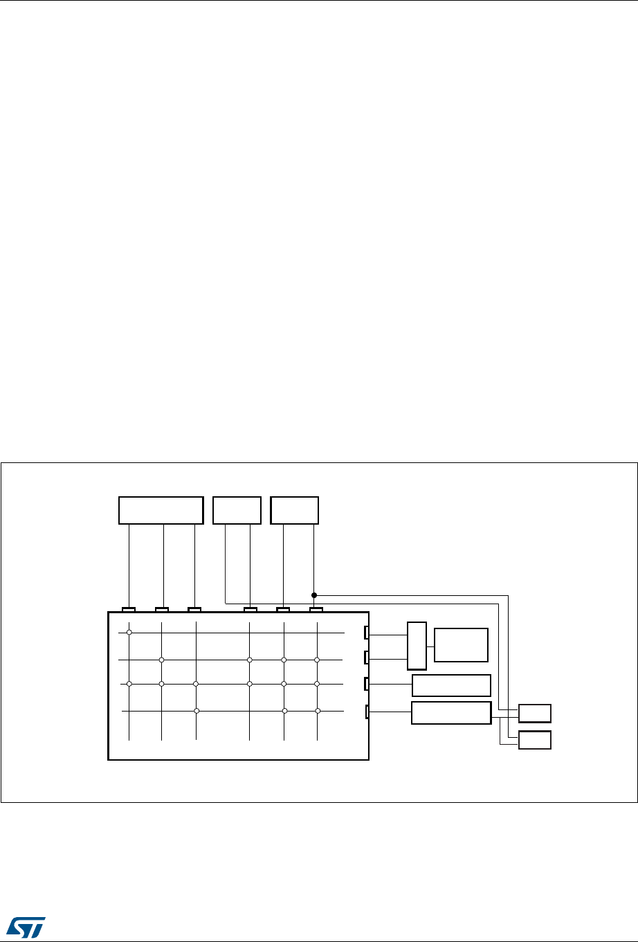
DocID027812 Rev 2 35/766
RM0401 System and memory overview
36
2 System and memory overview
2.1 System architecture
In STM32F410, the main system consists of 32-bit multilayer AHB bus matrix that
interconnects:
•Six masters:
–C
ortex
®-M4 with FPU core I-bus, D-bus and S-bus
– DMA1 memory bus
– DMA2 memory bus
– DMA2 peripheral bus
•Five slaves:
– Internal Flash memory ICode bus
– Internal Flash memory DCode bus
– Main internal SRAM
– AHB1 peripherals including AHB to APB bridges and APB peripherals
– AHB2 peripherals
The bus matrix provides access from a master to a slave, enabling concurrent access and
efficient operation even when several high-speed peripherals work simultaneously. This
architecture is shown in Figure 1.
Figure 1. System architecture
1. The Flash memory size is 512 Kbytes or 128 Mbytes while SRAM1 size is 256 Kbytes.
06Y9
$50
&RUWH[0
*3
'0$
*3
'0$
%XVPDWUL[6
6 6 6 6 6 6
,&2'(
'&2'(
$&&(/
)ODVK
.%
65$0
.E\WHV
0
0
0
,EXV
'EXV
6EXV
'0$B3,
'0$B0(0
'0$B0(0
'0$B3
0 $+%
SHULSK $3%
$3%

System and memory overview RM0401
36/766 DocID027812 Rev 2
2.1.1 I-bus
This bus connects the Instruction bus of the Cortex®-M4 with FPU core to the BusMatrix.
This bus is used by the core to fetch instructions. The target of this bus is a memory
containing code (internal Flash memory/SRAM1).
2.1.2 D-bus
This bus connects the databus of the Cortex®-M4 with FPU to the BusMatrix. This bus is
used by the core for literal load and debug access. The target of this bus is a memory
containing code or data (internal Flash memory/SRAM1).
2.1.3 S-bus
This bus connects the system bus of the Cortex®-M4 with FPU core to a BusMatrix. This
bus is used to access data located in a peripheral or in SRAM1. Instructions may also be
fetch on this bus (less efficient than ICode). The targets of this bus are the internal SRAM1,
the AHB1 peripherals including the APB peripherals, and the AHB2 peripherals.
2.1.4 DMA memory bus
This bus connects the DMA memory bus master interface to the BusMatrix. It is used by the
DMA to perform transfer to/from memories. The targets of this bus are data memories:
internal Flash memory, internal SRAM1 and additionally for S4 the AHB1/AHB2 peripherals
including the APB peripherals.
2.1.5 DMA peripheral bus
This bus connects the DMA peripheral master bus interface to the BusMatrix. This bus is
used by the DMA to access AHB peripherals or to perform memory-to-memory transfers.
The targets of this bus are the AHB and APB peripherals plus data memories: Flash
memory and internal SRAM1.
2.1.6 BusMatrix
The BusMatrix manages the access arbitration between masters. The arbitration uses a
round-robin algorithm.
2.1.7 AHB/APB bridges (APB)
The two AHB/APB bridges, APB1 and APB2, provide full synchronous connections between
the AHB and the two APB buses, allowing flexible selection of the peripheral frequency.
Refer to the device datasheets for more details on APB1 and APB2 maximum frequencies,
and to Table 1 for the address mapping of AHB and APB peripherals.
After each device reset, all peripheral clocks are disabled (except for the SRAM and Flash
memory interface). Before using a peripheral you have to enable its clock in the
RCC_AHBxENR or RCC_APBxENR register.
Note: When a 16- or an 8-bit access is performed on an APB register, the access is transformed
into a 32-bit access: the bridge duplicates the 16- or 8-bit data to feed the 32-bit vector.
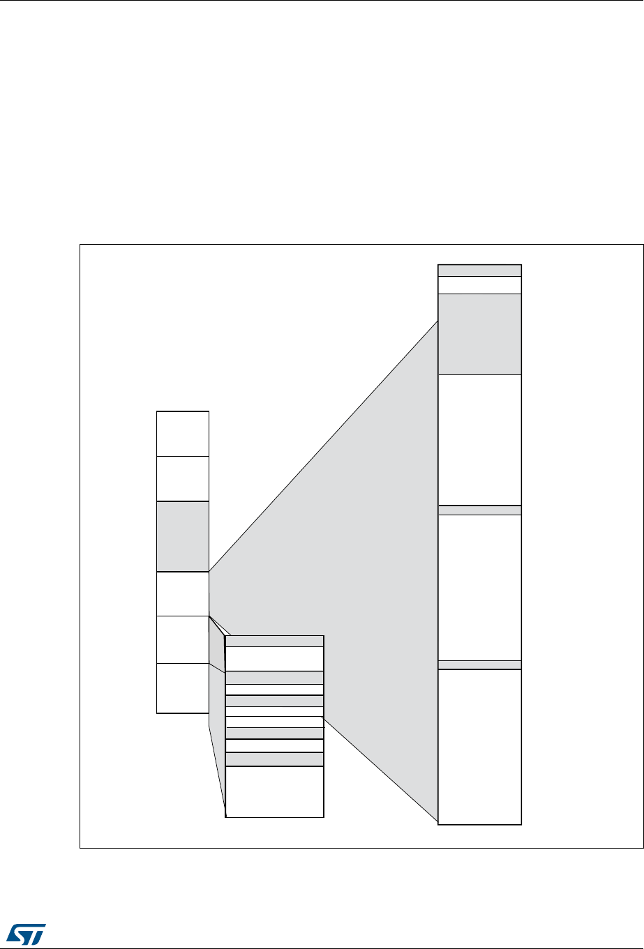
DocID027812 Rev 2 37/766
RM0401
43
2.2 Memory organization
2.2.1 Introduction
Program memory, data memory, registers and I/O ports are organized within the same linear
4-Gbyte address space.
The bytes are coded in memory in Little Endian format. The lowest numbered byte in a word
is considered the word’s least significant byte and the highest numbered byte the most
significant.
The addressable memory space is divided into 8 main blocks, of 512 Mbyte each.
Figure 2. Memory map
All the memory areas that are not allocated to on-chip memories and peripherals are
considered “Reserved”. For the detailed mapping of available memory and register areas,
06Y9
0E\WH
EORFN
&RUWH[0V
LQWHUQDO
SHULSKHUDOV
0E\WH
EORFN
1RWXVHG
0E\WH
EORFN
3HULSKHUDOV
0E\WH
EORFN
65$0
[
[)))))))
[
[)))))))
[
[)))))))
[
[&
[')))))))
[(
[))))))))
0E\WH
EORFN
&RGH
[[)))))))
[
5HVHUYHG
[))
[[))))
[
[')))))))
5HVHUYHG
65$0.%DOLDVHG
E\ELWEDQGLQJ [[)))
$3%
$3%
[))
[[))))
5HVHUYHG
[
[))
$+%
)ODVKPHPRU\
[[))())))
[)))&[)))&
[[))))
[[))))))
[[))))
5HVHUYHG
5HVHUYHG
$OLDVHGWR)ODVK
V\VWHPPHPRU\RU
65$0GHSHQGLQJRQ
WKH%227SLQV
6\VWHPPHPRU\
[)))&[)))))))
[)))$[)))%)))
[)))[)))))
2SWLRQE\WHV
[
&RUWH[0LQWHUQDO
SHULSKHUDOV [([()))))
5HVHUYHG [([))))))))
5HVHUYHG
[%)))))))
5HVHUYHG
5HVHUYHG
5HVHUYHG
273DUHDORFN [)))[)))$)
RM0401
38/766 DocID027812 Rev 2
please refer to the Memory map and register boundary addresses chapter and peripheral
chapters.
2.2.2 Memory map and register boundary addresses
See the datasheet corresponding to your device for a comprehensive diagram of the
memory map.
The following table gives the boundary addresses of the peripherals available in the
devices.
Table 1. Register boundary addresses
Bus Boundary address Peripheral
0xE010 0000 - 0xFFFF FFFF Reserved
Cortex®-M4 0xE000 0000 - 0xE00F FFFF Cortex-M4 internal peripherals
0x5000 0000 - 0xDFFF FFFF Reserved
AHB1
0x4008 0400 - 0x4FFF FFFF Reserved
0x4008 0000 - 0x4008 03FF RNG
0x4002 6800 - 0x4007 FFFF Reserved
0x4002 6400 - 0x4002 67FF DMA2
0x4002 6000 - 0x4002 63FF DMA1
0x4002 5000 - 0x4002 4FFF Reserved
0x4002 3C00 - 0x4002 3FFF Flash interface register
0x4002 3800 - 0x4002 3BFF RCC
0x4002 3400 - 0x4002 37FF Reserved
0x4002 3000 - 0x4002 33FF CRC
0x4002 2800 - 0x4002 2FFF Reserved
0x4002 2400 - 0x4002 27FF LPTIM1
0x4002 2000 - 0x4002 23FF Reserved
0x4002 1C00 - 0x4002 1FFF GPIOH
0x4002 0C00 - 0x4002 1BFF Reserved
0x4002 0800 - 0x4002 0BFF GPIOC
0x4002 0400 - 0x4002 07FF GPIOB
0x4002 0000 - 0x4002 03FF GPIOA

DocID027812 Rev 2 39/766
RM0401
43
APB2
0x4001 5400- 0x4001 FFFF Reserved
0x4001 5000 - 0x4001 53FF SPI5/I2S5
0x4001 4C00- 0x4001 4FFF Reserved
0x4001 4800 - 0x4001 4BFF TIM11
0x4001 4400 - 0x4001 47FF Reserved
0x4001 4000 - 0x4001 43FF TIM9
0x4001 3C00 - 0x4001 3FFF EXTI
0x4001 3800 - 0x4001 3BFF SYSCFG
0x4001 3400 - 0x4001 37FF Reserved
0x4001 3000 - 0x4001 33FF SPI1/I2S1
0x4001 2400 - 0x4001 2FF Reserved
0x4001 2000 - 0x4001 23FF ADC1
0x4001 1800 - 0x4001 1FFF Reserved
0x4001 1400 - 0x4001 17FF USART6
0x4001 1000 - 0x4001 13FF USART1
0x4001 0400 - 0x4001 0FFF Reserved
0x4001 0000 - 0x4001 03FF TIM1
Table 1. Register boundary addresses (continued)
Bus Boundary address Peripheral
RM0401
40/766 DocID027812 Rev 2
2.3 Embedded SRAM
STM32F410 devices feature 32 Kbytes of system SRAM.
The embedded SRAM can be accessed as bytes, half-words (16 bits) or full words (32 bits).
Read and write operations are performed at CPU speed with 0 wait state.
The CPU can access the embedded SRAM1, through the System Bus or through the I-
Code/D-Code buses when boot from SRAM is selected or when physical remap is selected
(Section 7.2.1: SYSCFG memory remap register (SYSCFG_MEMRMP) in the SYSCFG
controller). To get the max performance on SRAM execution, physical remap should be
selected (boot or software selection).
APB1
0x4000 7800 - 0x4000 FFFF Reserved
0x4000 7400 - 0x4000 77FF DAC
0x4000 7000 - 0x4000 73FF PWR
0x4000 6400 - 0x4000 6FFF Reserved
0x4000 6000 - 0x4000 63FF I2C4 FM+
0x4000 5C00 - 0x4000 5FFF Reserved
0x4000 5800 - 0x4000 5BFF I2C2
0x4000 5400 - 0x4000 57FF I2C1
0x4000 4800 - 0x4000 53FF Reserved
0x4000 4400 - 0x4000 47FF USART2
0x4000 3C00 - 0x4000 43FF Reserved
0x4000 3800 - 0x4000 3BFF SPI2 / I2S2
0x4000 3400 - 0x4000 37FF Reserved
0x4000 3000 - 0x4000 33FF IWDG
0x4000 2C00 - 0x4000 2FFF WWDG
0x4000 2800 - 0x4000 2BFF RTC & BKP Registers
0x4000 1400 - 0x4000 27FF Reserved
0x4000 1000 - 0x4000 13FF TIM6
0x4000 0C00 - 0x4000 0FFF TIM5
0x4000 0000 - 0x4000 0BFF Reserved
Table 1. Register boundary addresses (continued)
Bus Boundary address Peripheral

DocID027812 Rev 2 41/766
RM0401
43
2.4 Flash memory overview
The Flash memory interface manages CPU AHB I-Code and D-Code accesses to the Flash
memory. It implements the erase and program Flash memory operations and the read and
write protection mechanisms. It accelerates code execution with a system of instruction
prefetch and cache lines.
The Flash memory is organized as follows:
•A main memory block divided into sectors.
•System memory from which the device boots in System memory boot mode
•512 OTP (one-time programmable) bytes for user data.
•Option bytes to configure read and write protection, BOR level, watchdog
software/hardware and reset when the device is in Standby or Stop mode.
Refer to Section 3: Embedded Flash memory interface for more details.
2.5 Bit banding
The Cortex®-M4 with FPU memory map includes two bit-band regions. These regions map
each word in an alias region of memory to a bit in a bit-band region of memory. Writing to a
word in the alias region has the same effect as a read-modify-write operation on the
targeted bit in the bit-band region.
In the STM32F410 devices both the peripheral registers and the SRAM1 are mapped to a
bit-band region, so that single bit-band write and read operations are allowed. The
operations are only available for Cortex®-M4 with FPU accesses, and not from other bus
masters (e.g. DMA).
A mapping formula shows how to reference each word in the alias region to a corresponding
bit in the bit-band region. The mapping formula is:
bit_word_addr = bit_band_base + (byte_offset x 32) + (bit_number × 4)
where:
–bit_word_addr is the address of the word in the alias memory region that maps to
the targeted bit
–bit_band_base is the starting address of the alias region
–byte_offset is the number of the byte in the bit-band region that contains the
targeted bit
–bit_number is the bit position (0-7) of the targeted bit
Example
The following example shows how to map bit 2 of the byte located at SRAM1 address
0x20000300 to the alias region:
0x22006008 = 0x22000000 + (0x300*32) + (2*4)
Writing to address 0x22006008 has the same effect as a read-modify-write operation on bit
2 of the byte at SRAM1 address 0x20000300.
Reading address 0x22006008 returns the value (0x01 or 0x00) of bit 2 of the byte at SRAM1
address 0x20000300 (0x01: bit set; 0x00: bit reset).
For more information on bit-banding, please refer to the Cortex®-M4 with FPU programming
manual (see Related documents on page 1Related documents on page 1).
RM0401
42/766 DocID027812 Rev 2
2.6 Boot configuration
Due to its fixed memory map, the code area starts from address 0x0000 0000 (accessed
through the ICode/DCode buses) while the data area (SRAM) starts from address
0x2000 0000 (accessed through the system bus). The Cortex®-M4 with FPU CPU always
fetches the reset vector on the ICode bus, which implies to have the boot space available
only in the code area (typically, Flash memory). STM32F4xx microcontrollers implement a
special mechanism to be able to boot from other memories (like the internal SRAM).
In the STM32F410, three different boot modes can be selected through the BOOT[1:0] pins
as shown in Table 2.
The values on the BOOT pins are latched on the 4th rising edge of SYSCLK after a reset. It
is up to the user to set the BOOT1 and BOOT0 pins after reset to select the required boot
mode.
BOOT0 is a dedicated pin while BOOT1 is shared with a GPIO pin. Once BOOT1 has been
sampled, the corresponding GPIO pin is free and can be used for other purposes.
The BOOT pins are also resampled when the device exits the Standby mode. Consequently,
they must be kept in the required Boot mode configuration when the device is in the Standby
mode. After this startup delay is over, the CPU fetches the top-of-stack value from address
0x0000 0000, then starts code execution from the boot memory starting from 0x0000 0004.
Note: When the device boots from SRAM, in the application initialization code, you have to
relocate the vector table in SRAM using the NVIC exception table and the offset register.
Embedded bootloader
The embedded bootloader mode is used to reprogram the Flash memory using interfaces
that depend on the package (refer to Table 3):
The USART peripherals operate at the internal 16 MHz oscillator (HSI) frequency.
Table 2. Boot modes
Boot mode selection pins
Boot mode Aliasing
BOOT1 BOOT0
x 0 Main Flash memory Main Flash memory is selected as the boot space
0 1 System memory System memory is selected as the boot space
1 1 Embedded SRAM Embedded SRAM is selected as the boot space
Table 3. Embedded bootloader interfaces
Package USART1 USART2 I2C1 I2C2 I2C4 FM+ SPI1 SPI3
WLCSP36 X
PA2/PA3 PB6/PB7
X PB10/PB3 PA15/PA5
/PB4/PB5 X
UFQFPN48
PA9/PA10
X
PB14/PB15 PA4/PA5/
PA6/PA7
X
LQFP64 PB10/PB11 PB12/PB13
/PC2/PC3
DocID027812 Rev 2 43/766
RM0401
43
The embedded bootloader code is located in system memory. It is programmed by ST
during production. For additional information, refer to application note AN2606.
Physical remap in STM32F410
Once the boot pins are selected, the application software can modify the memory
accessible in the code area (in this way the code can be executed through the ICode bus in
place of the System bus). This modification is performed by programming the Section 7.2.1:
SYSCFG memory remap register (SYSCFG_MEMRMP) in the SYSCFG controller.
The following memories can thus be remapped:
•Main Flash memory
•System memory
•Embedded SRAM
Table 4. Memory mapping vs. Boot mode/physical remap in STM32F410
Addresses Boot/Remap in main
Flash memory
Boot/Remap in
embedded SRAM
Boot/Remap in
System memory
0x2000 0000 - 0x2002 7FFF SRAM (32 KB) SRAM (32KB) SRAM (32KB)
0x1FFF 0000 - 0x1FFF 77FF System memory System memory System memory
0x0802 0000 - 0x1FFE FFFF Reserved Reserved Reserved
0x0800 0000 - 0x0801 FFFF Flash memory Flash memory Flash memory
0x0400 000 - 0x07FF FFFF Reserved Reserved Reserved
0x0000 0000 - 0x0001 FFFF(1)
1. Even when aliased in the boot memory space, the related memory is still accessible at its original memory
space.
Flash (128 KB) Aliased SRAM1 (32 KB)
Aliased
System memory
(30 KB) Aliased
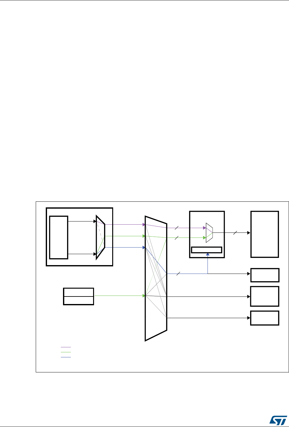
Embedded Flash memory interface RM0401
44/766 DocID027812 Rev 2
3 Embedded Flash memory interface
3.1 Introduction
The Flash memory interface manages CPU AHB I-Code and D-Code accesses to the Flash
memory. It implements the erase and program Flash memory operations and the read and
write protection mechanisms.
The Flash memory interface accelerates code execution with a system of instruction
prefetch and cache lines.
3.2 Main features
•Flash memory read operations
•Flash memory program/erase operations
•Read / write protections
•Prefetch on I-Code
•64 cache lines of 128 bits on I-Code
•8 cache lines of 128 bits on D-Code
Figure 3 shows the Flash memory interface connection inside the system architecture.
Figure 3. Flash memory interface connection inside system architecture
&RUWH[
FRUH
'0$
'0$
'FRGHEXV
,&RGHEXV
&RUWH[0ZLWK)38
,&RGH
'&RGH
6EXV
$+%
SHULSK
)ODVK
PHPRU\
)ODVKLQWHUIDFH
65$0DQG
([WHUQDO
PHPRULHV
$+%
SHULSK
)/,7)UHJLVWHUV
$+%
ELW
LQVWUXFWLRQ
EXV
$FFHVVWRLQVWUXFWLRQLQ)ODVKPHPRU\
$FFHVVWRGDWDDQGOLWHUDOSRROLQ)ODVKPHPRU\
)/,7)UHJLVWHUDFFHVV
069
$+%
ELW
GDWDEXV
$+%
ELW
V\VWHPEXV
)ODVK
PHPRU\
EXV
ELWV
DocID027812 Rev 2 45/766
RM0401 Embedded Flash memory interface
67
3.3 Embedded Flash memory
The Flash memory has the following main features:
•Capacity up to 128 Kbytes
•128 bits wide data read
•Byte, half-word, word and double word write
•Sector and mass erase
•Memory organization
The Flash memory is organized as follows:
– A main memory block divided into 4 sectors of 16 Kbytes plus 1 sector of
64 Kbytes.
– System memory from which the device boots in System memory boot mode
– 512 OTP (one-time programmable) bytes for user data
The OTP area contains 16 additional bytes used to lock the corresponding OTP
data block.
– Option bytes to configure read and write protection, BOR level, watchdog
software/hardware and reset when the device is in Standby or Stop mode.
•Low-power modes (for details refer to the Power control (PWR) section of the reference
manual)
Table 5. Flash module organization
Block Name Block base addresses Size
Main memory
Sector 0 0x0800 0000 - 0x0800 3FFF 16 Kbytes
Sector 1 0x0800 4000 - 0x0800 7FFF 16 Kbytes
Sector 2 0x0800 8000 - 0x0800 BFFF 16 Kbytes
Sector 3 0x0800 C000 - 0x0800 FFFF 16 Kbytes
Sector 4 0x0800 1000 - 0x0801 FFFF 64 Kbytes
System memory 0x1FFF 0000 - 0x1FFF 77FF 30 Kbytes
OTP area 0x1FFF 7800 - 0x1FFF 7A0F 528 bytes
Option bytes 0x1FFF C000 - 0x1FFF C00F 16 bytes
Embedded Flash memory interface RM0401
46/766 DocID027812 Rev 2
3.4 Read interface
3.4.1 Relation between CPU clock frequency and Flash memory read time
To correctly read data from Flash memory, the number of wait states (LATENCY) must be
correctly programmed in the Flash access control register (FLASH_ACR) according to the
frequency of the CPU clock (HCLK) and the supply voltage of the device.
The prefetch buffer must be disabled when the supply voltage is below 2.1 V. The
correspondence between wait states and CPU clock frequency is given inTable 6:
•When VOS[1:0] = 0x01, the maximum value of fHCLK = 64 MHz.
•When VOS[1:0] = 0x10, the maximum value of fHCLK = 84 MHz.
•When VOS[1:0] = 0x11, the maximum value of fHCLK = 100 MHz.
After reset, the CPU clock frequency is 16 MHz and 0 wait state (WS) is configured in the
FLASH_ACR register.
It is highly recommended to use the following software sequences to tune the number of
wait states needed to access the Flash memory with the CPU frequency.
Increasing the CPU frequency
1. Program the new number of wait states to the LATENCY bits in the FLASH_ACR
register
2. Check that the new number of wait states is taken into account to access the Flash
memory by reading the FLASH_ACR register
3. Modify the CPU clock source by writing the SW bits in the RCC_CFGR register
4. If needed, modify the CPU clock prescaler by writing the HPRE bits in RCC_CFGR
5. Check that the new CPU clock source or/and the new CPU clock prescaler value is/are
taken into account by reading the clock source status (SWS bits) or/and the AHB
prescaler value (HPRE bits), respectively, in the RCC_CFGR register.
Table 6. Number of wait states according to CPU clock (HCLK) frequency
Wait states (WS)
(LATENCY)
HCLK (MHz)
Voltage range
2.7 V - 3.6 V
Voltage range
2.4 V - 2.7 V
Voltage range
2.1 V - 2.4 V
Voltage range
1.7 V - 2.1 V
0 WS (1 CPU cycle) 0 < HCLK≤ 30 0 < HCLK ≤ 24 0 < HCLK ≤ 18 0 < HCLK ≤ 16
1 WS (2 CPU cycles) 30 < HCLK ≤ 64 24 < HCLK ≤ 48 18 < HCLK ≤ 36 16 <HCLK ≤ 32
2 WS (3 CPU cycles) 64 < HCLK ≤ 90 48 < HCLK ≤ 72 36 < HCLK ≤ 54 32 < HCLK ≤ 48
3 WS (4 CPU cycles) 90 < HCLK ≤ 100 72 < HCLK ≤ 96 54 < HCLK ≤ 72 48 < HCLK ≤ 64
4 WS (5 CPU cycles) - 96 < HCLK ≤ 100 72 < HCLK ≤ 90 64 < HCLK ≤ 80
5 WS (6 CPU cycles) - - 90 < HCLK ≤ 100 80 < HCLK ≤ 96
6 WS (7 CPU cycles) - - - 96 < HCLK ≤ 100

DocID027812 Rev 2 47/766
RM0401 Embedded Flash memory interface
67
Decreasing the CPU frequency
1. Modify the CPU clock source by writing the SW bits in the RCC_CFGR register
2. If needed, modify the CPU clock prescaler by writing the HPRE bits in RCC_CFGR
3. Check that the new CPU clock source or/and the new CPU clock prescaler value is/are
taken into account by reading the clock source status (SWS bits) or/and the AHB
prescaler value (HPRE bits), respectively, in the RCC_CFGR register
4. Program the new number of wait states to the LATENCY bits in FLASH_ACR
5. Check that the new number of wait states is used to access the Flash memory by
reading the FLASH_ACR register
Note: A change in CPU clock configuration or wait state (WS) configuration may not be effective
straight away. To make sure that the current CPU clock frequency is the one you have
configured, you can check the AHB prescaler factor and clock source status values. To
make sure that the number of WS you have programmed is effective, you can read the
FLASH_ACR register.
3.4.2 Adaptive real-time memory accelerator (ART Accelerator™)
The proprietary Adaptive real-time (ART) memory accelerator is optimized for STM32
industry-standard ARM® Cortex®-M4 with FPU processors. It balances the inherent
performance advantage of the ARM® Cortex®-M4 with FPU over Flash memory
technologies, which normally requires the processor to wait for the Flash memory at higher
operating frequencies.
To release the processor full performance, the accelerator implements an instruction
prefetch queue and branch cache which increases program execution speed from the 128-
bit Flash memory. Based on CoreMark benchmark, the performance achieved thanks to the
ART accelerator is equivalent to 0 wait state program execution from Flash memory at a
CPU frequency up to 100 MHz.
Instruction prefetch
Each Flash memory read operation provides 128 bits from either four instructions of 32 bits
or 8 instructions of 16 bits according to the program launched. So, in case of sequential
code, at least four CPU cycles are needed to execute the previous read instruction line.
Prefetch on the I-Code bus can be used to read the next sequential instruction line from the
Flash memory while the current instruction line is being requested by the CPU. Prefetch is
enabled by setting the PRFTEN bit in the FLASH_ACR register. This feature is useful if at
least one wait state is needed to access the Flash memory.
Figure 4 shows the execution of sequential 32-bit instructions with and without prefetch
when 3 WSs are needed to access the Flash memory.
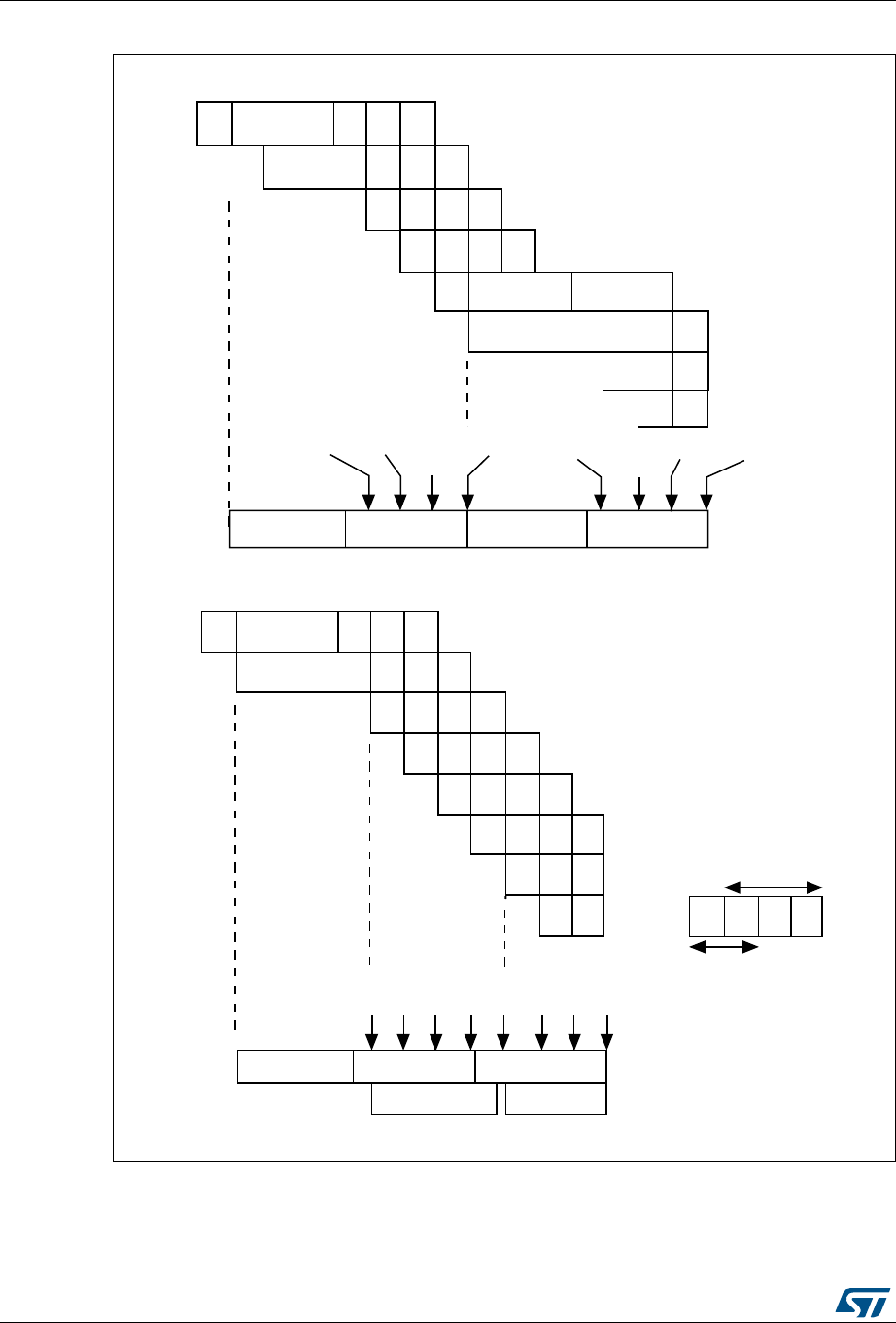
Embedded Flash memory interface RM0401
48/766 DocID027812 Rev 2
Figure 4. Sequential 32-bit instruction execution
When the code is not sequential (branch), the instruction may not be present in the currently
used instruction line or in the prefetched instruction line. In this case (miss), the penalty in
terms of number of cycles is at least equal to the number of wait states.
&
&
&
&
$
$
$
$
%
%
%
%
&
&
&
&
$
$
$
%
%
2EADINS 'IVESINS 2EADINS 'IVESINS
INS
FETCH
INS
FETCH
INS
FETCH
INS
FETCH
INS
FETCH
INS
FETCH
INS
FETCH
INS
FETCH
7!)4
7!)4
$%
&
&
&
&
$
$
$
%
%
&
&
&
&
$
$
$
%
%
7AITDATA
%
2EADINS 'IVESINS 'IVESINS
2EADINS 2EADINS
INS INS
FETCH
INS INS
7ITHOUTPREFETCH
7ITHPREFETCH
&$%
#ORTEX-PIPELINE
!("PROTOCOL
ADDRESSREQUESTED
&&ETCHSTAGE
$$ECODESTAGE
%%XECUTESTAGE
INS
FETCH
INS
FETCH
INS
FETCH FETCH FETCH FETCH
INS
FETCH
-36

DocID027812 Rev 2 49/766
RM0401 Embedded Flash memory interface
67
Instruction cache memory
To limit the time lost due to jumps, it is possible to retain 64 lines of 128 bits in an instruction
cache memory. This feature can be enabled by setting the instruction cache enable (ICEN)
bit in the FLASH_ACR register. Each time a miss occurs (requested data not present in the
currently used instruction line, in the prefetched instruction line or in the instruction cache
memory), the line read is copied into the instruction cache memory. If some data contained
in the instruction cache memory are requested by the CPU, they are provided without
inserting any delay. Once all the instruction cache memory lines have been filled, the LRU
(least recently used) policy is used to determine the line to replace in the instruction memory
cache. This feature is particularly useful in case of code containing loops.
Data management
Literal pools are fetched from Flash memory through the D-Code bus during the execution
stage of the CPU pipeline. The CPU pipeline is consequently stalled until the requested
literal pool is provided. To limit the time lost due to literal pools, accesses through the AHB
databus D-Code have priority over accesses through the AHB instruction bus I-Code.
If some literal pools are frequently used, the data cache memory can be enabled by setting
the data cache enable (DCEN) bit in the FLASH_ACR register. This feature works like the
instruction cache memory, but the retained data size is limited to 8 rows of 128 bits.
Note: Data in user configuration sector are not cacheable.
3.5 Erase and program operations
For any Flash memory program operation (erase or program), the CPU clock frequency
(HCLK) must be at least 1 MHz. The contents of the Flash memory are not guaranteed if a
device reset occurs during a Flash memory operation.
Any attempt to read the Flash memory on STM32F4xx while it is being written or erased,
causes the bus to stall. Read operations are processed correctly once the program
operation has completed. This means that code or data fetches cannot be performed while
a write/erase operation is ongoing.
3.5.1 Unlocking the Flash control register
After reset, write is not allowed in the Flash control register (FLASH_CR) to protect the
Flash memory against possible unwanted operations due, for example, to electric
disturbances. The following sequence is used to unlock this register:
1. Write KEY1 = 0x45670123 in the Flash key register (FLASH_KEYR)
2. Write KEY2 = 0xCDEF89AB in the Flash key register (FLASH_KEYR)
Any wrong sequence will return a bus error and lock up the FLASH_CR register until the
next reset.
The FLASH_CR register can be locked again by software by setting the LOCK bit in the
FLASH_CR register.
Note: The FLASH_CR register is not accessible in write mode when the BSY bit in the FLASH_SR
register is set. Any attempt to write to it with the BSY bit set will cause the AHB bus to stall
until the BSY bit is cleared.

Embedded Flash memory interface RM0401
50/766 DocID027812 Rev 2
3.5.2 Program/erase parallelism
The Parallelism size is configured through the PSIZE field in the FLASH_CR register. It
represents the number of bytes to be programmed each time a write operation occurs to the
Flash memory. PSIZE is limited by the supply voltage and by whether the external VPP
supply is used or not. It must therefore be correctly configured in the FLASH_CR register
before any programming/erasing operation.
A Flash memory erase operation can only be performed by sector or for the whole Flash
memory (mass erase). The erase time depends on PSIZE programmed value. For more
details on the erase time, refer to the electrical characteristics section of the device
datasheet.
Table 7 provides the correct PSIZE values.
Note: Any program or erase operation started with inconsistent program parallelism/voltage range
settings may lead to unpredicted results. Even if a subsequent read operation indicates that
the logical value was effectively written to the memory, this value may not be retained.
To use VPP
, an external high-voltage supply (between 8 and 9 V) must be applied to the VPP
pad. The external supply must be able to sustain this voltage range even if the DC
consumption exceeds 10 mA. It is advised to limit the use of VPP to initial programming on
the factory line. The VPP supply must not be applied for more than an hour, otherwise the
Flash memory might be damaged.
3.5.3 Erase
The Flash memory erase operation can be performed at sector level or on the whole Flash
memory (Mass Erase). Mass Erase does not affect the OTP sector or the configuration
sector.
Sector Erase
To erase a sector, follow the procedure below:
1. Check that no Flash memory operation is ongoing by checking the BSY bit in the
FLASH_SR register
2. Set the SER bit and select the sector out of the 5 sectors in the main memory block you
wish to erase (SNB) in the FLASH_CR register
3. Set the STRT bit in the FLASH_CR register
4. Wait for the BSY bit to be cleared
Table 7. Program/erase parallelism
Voltage range 2.7 - 3.6 V
with External VPP
Voltage range
2.7 - 3.6 V
Voltage range
2.4 - 2.7 V
Voltage range
2.1 - 2.4 V
Voltage range
1.7 V - 2.1 V
Parallelism size x64 x32 x16 x8
PSIZE(1:0)11100100

DocID027812 Rev 2 51/766
RM0401 Embedded Flash memory interface
67
Mass Erase
To perform Mass Erase, the following sequence is recommended:
1. Check that no Flash memory operation is ongoing by checking the BSY bit in the
FLASH_SR register
2. Set the MER bit in the FLASH_CR register
3. Set the STRT bit in the FLASH_CR register
4. Wait for the BSY bit to be cleared
Note: If MERx and SER bits are both set in the FLASH_CR register, mass erase is performed.
If both MERx and SER bits are reset and the STRT bit is set, an unpredictable behavior may
occur without generating any error flag. This condition should be forbidden.
3.5.4 Programming
Standard programming
The Flash memory programming sequence is as follows:
1. Check that no main Flash memory operation is ongoing by checking the BSY bit in the
FLASH_SR register.
2. Set the PG bit in the FLASH_CR register
3. Perform the data write operation(s) to the desired memory address (inside main
memory block or OTP area):
– Byte access in case of x8 parallelism
– Half-word access in case of x16 parallelism
– Word access in case of x32 parallelism
– Double word access in case of x64 parallelism
4. Wait for the BSY bit to be cleared.
Note: Successive write operations are possible without the need of an erase operation when
changing bits from ‘1’ to ‘0’. Writing ‘1’ requires a Flash memory erase operation.
If an erase and a program operation are requested simultaneously, the erase operation is
performed first.
Programming errors
It is not allowed to program data to the Flash memory that would cross the 128-bit row
boundary. In such a case, the write operation is not performed and a program alignment
error flag (PGAERR) is set in the FLASH_SR register.
The write access type (byte, half-word, word or double word) must correspond to the type of
parallelism chosen (x8, x16, x32 or x64). If not, the write operation is not performed and a
program parallelism error flag (PGPERR) is set in the FLASH_SR register.
If the standard programming sequence is not respected (for example, if there is an attempt
to write to a Flash memory address when the PG bit is not set), the operation is aborted and
a program sequence error flag (PGSERR) is set in the FLASH_SR register.
Embedded Flash memory interface RM0401
52/766 DocID027812 Rev 2
Programming and caches
If a Flash memory write access concerns some data in the data cache, the Flash write
access modifies the data in the Flash memory and the data in the cache.
If an erase operation in Flash memory also concerns data in the data or instruction cache,
you have to make sure that these data are rewritten before they are accessed during code
execution. If this cannot be done safely, it is recommended to flush the caches by setting the
DCRST and ICRST bits in the FLASH_CR register.
Note: The I/D cache should be flushed only when it is disabled (I/DCEN = 0).
3.5.5 Interrupts
Setting the end of operation interrupt enable bit (EOPIE) in the FLASH_CR register enables
interrupt generation when an erase or program operation ends, that is when the busy bit
(BSY) in the FLASH_SR register is cleared (operation completed, correctly or not). In this
case, the end of operation (EOP) bit in the FLASH_SR register is set.
If an error occurs during a program, an erase, or a read operation request, one of the
following error flags is set in the FLASH_SR register:
•PGAERR, PGPERR, PGSERR (Program error flags)
•WRPERR (Protection error flag)
In this case, if the error interrupt enable bit (ERRIE) is set in the FLASH_CR register, an
interrupt is generated and the operation error bit (OPERR) is set in the FLASH_SR register.
Note: If several successive errors are detected (for example, in case of DMA transfer to the Flash
memory), the error flags cannot be cleared until the end of the successive write requests.
3.6 Option bytes
3.6.1 Description of user option bytes
The option bytes are configured by the end user depending on the application requirements.
Table 9 shows the organization of these bytes inside the user configuration sector.
Table 8. Flash interrupt request
Interrupt event Event flag Enable control bit
End of operation EOP EOPIE
Write protection error WRPERR ERRIE
Programming error PGAERR, PGPERR, PGSERR ERRIE
Table 9. Option byte organization
Address [63:16] [15:0]
0x1FFF C0000 Reserved ROP & user option bytes (RDP & USER)
0x1FFF C008 Reserved Write protection nWRP bits for sectors 0 to 4

DocID027812 Rev 2 53/766
RM0401 Embedded Flash memory interface
67
Table 10. Description of the option bytes
Option bytes (word, address 0x1FFF C000)
RDP: Read protection option byte.
The read protection is used to protect the software code stored in Flash memory.
Bits 15:8
0xAA: Level 0, no protection
0xCC: Level 2, chip protection (debug and boot from RAM features disabled)
Others: Level 1, read protection of memories (debug features limited)
USER: User option byte
This byte is used to configure the following features:
– Select the watchdog event: Hardware or software
– Reset event when entering the Stop mode
– Reset event when entering the Standby mode
Bit 7
nRST_STDBY
0: Reset generated when entering the Standby mode
1: No reset generated
Bit 6
nRST_STOP
0: Reset generated when entering the Stop mode
1: No reset generated
Bit 5
WDG_SW
0: Hardware independent watchdog
1: Software independent watchdog
Bit 4 0x1: Not used
Bits 3:2
BOR_LEV: BOR reset Level
These bits contain the supply level threshold that activates/releases the reset.
They can be written to program a new BOR level value into Flash memory.
00: BOR Level 3 (VBOR3), brownout threshold level 3
01: BOR Level 2 (VBOR2), brownout threshold level 2
10: BOR Level 1 (VBOR1), brownout threshold level 1
11: BOR off, POR/PDR reset threshold level is applied
Note: For full details on BOR characteristics, refer to the “Electrical characteristics”
section of the product datasheet.
Bits 1:0 0x1: Not used
Option bytes (word, address 0x1FFF C008)
Bit 15
SPRMOD: Selection of Protection Mode of nWPRi bits
0: nWPRi bits used for sector i write protection (Default)
1: nWPRi bits used for sector i PCROP protection (Sector)
Bits 14:5 Reserved

Embedded Flash memory interface RM0401
54/766 DocID027812 Rev 2
3.6.2 Programming user option bytes
To run any operation on this sector, the option lock bit (OPTLOCK) in the Flash option
control register (FLASH_OPTCR) must be cleared. To be allowed to clear this bit, you have
to perform the following sequence:
1. Write OPTKEY1 = 0x0819 2A3B in the Flash option key register (FLASH_OPTKEYR)
2. Write OPTKEY2 = 0x4C5D 6E7F in the Flash option key register (FLASH_OPTKEYR)
The user option bytes can be protected against unwanted erase/program operations by
setting the OPTLOCK bit by software.
Modifying user option bytes
To modify the user option value, follow the sequence below:
1. Check that no Flash memory operation is ongoing by checking the BSY bit in the
FLASH_SR register
2. Write the desired option value in the FLASH_OPTCR register.
3. Set the option start bit (OPTSTRT) in the FLASH_OPTCR register
4. Wait for the BSY bit to be cleared.
Note: The value of an option is automatically modified by first erasing the user configuration sector
and then programming all the option bytes with the values contained in the FLASH_OPTCR
register.
3.6.3 Read protection (RDP)
The user area in the Flash memory can be protected against read operations by an
entrusted code. Three read protection levels are defined:
•Level 0: no read protection
When the read protection level is set to Level 0 by writing 0xAA into the read protection
option byte (RDP), all read/write operations (if no write protection is set) from/to the
nWRP: Flash memory write protection option bytes
Section 0 to 4 can be write protected
Bits 4:0
nWRPi
If SPRMOD is reset (default value) :
0: Write protection active on sector i.
1: Write protection not active on sector i.
If SPRMOD is set (active):
0: PCROP protection not active on sector i.
1: PCROP protection active on sector i.
Table 10. Description of the option bytes (continued)

DocID027812 Rev 2 55/766
RM0401 Embedded Flash memory interface
67
Flash memory are possible in all boot configurations (Flash user boot, debug or boot
from RAM).
•Level 1: read protection enabled
It is the default read protection level after option byte erase. The read protection Level
1 is activated by writing any value (except for 0xAA and 0xCC used to set Level 0 and
Level 2, respectively) into the RDP option byte. When the read protection Level 1 is set:
– No access (read, erase, program) to Flash memory can be performed while the
debug feature is connected or while booting from RAM or system memory
bootloader. A bus error is generated in case of read request.
– When booting from Flash memory, accesses (read, erase, program) to Flash
memory from user code are allowed.
When Level 1 is active, programming the protection option byte (RDP) to Level 0
causes the Flash memory to be mass-erased. As a result the user code area is cleared
before the read protection is removed. The mass erase only erases the user code area.
The other option bytes including write protections remain unchanged from before the
mass-erase operation. The OTP area is not affected by mass erase and remains
unchanged. Mass erase is performed only when Level 1 is active and Level 0
requested. When the protection level is increased (0->1, 1->2, 0->2) there is no mass
erase.
•Level 2: debug/chip read protection disabled
The read protection Level 2 is activated by writing 0xCC to the RDP option byte. When
the read protection Level 2 is set:
– All protections provided by Level 1 are active.
– Booting from RAM or system memory bootloader is no more allowed.
– JTAG, SWV (single-wire viewer), ETM, and boundary scan are disabled.
– User option bytes can no longer be changed.
– When booting from Flash memory, accesses (read, erase and program) to Flash
memory from user code are allowed.
Memory read protection Level 2 is an irreversible operation. When Level 2 is activated,
the level of protection cannot be decreased to Level 0 or Level 1.
Note: The JTAG port is permanently disabled when Level 2 is active (acting as a JTAG fuse). As a
consequence, boundary scan cannot be performed. STMicroelectronics is not able to
perform analysis on defective parts on which the Level 2 protection has been set.
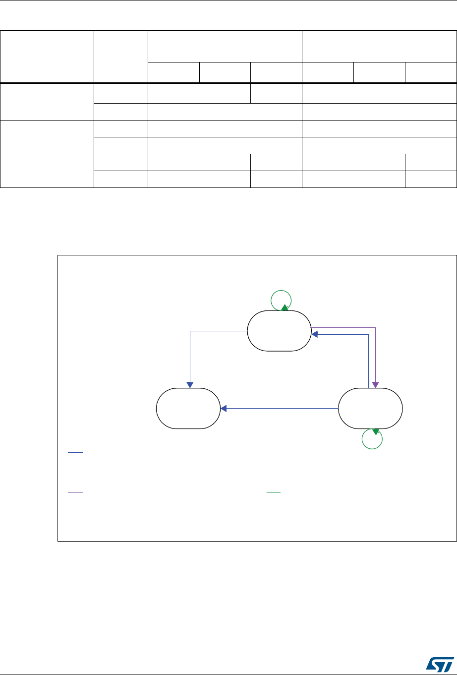
Embedded Flash memory interface RM0401
56/766 DocID027812 Rev 2
--
Figure 5 shows how to go from one RDP level to another.
Figure 5. RDP levels
3.6.4 Write protections
Up to 5 user sectors in Flash memory can be protected against unwanted write operations
due to loss of program counter contexts. When the non-write protection nWRPi bit (0 ≤ i ≤ 4)
in the FLASH_OPTCR registers is low, the corresponding sector cannot be erased or
programmed. Consequently, a mass erase cannot be performed if one of the sectors is
write-protected.
Table 11. Access versus read protection level
Memory area Protection
Level
Debug features, Boot from RAM or
from System memory bootloader Booting from Flash memory
Read Write Erase Read Write Erase
Main Flash Memory
Level 1 NO NO(1) YES
Level 2 NO YES
Option Bytes
Level 1 YES YES
Level 2 NO NO
OTP
Level 1 NO NA YES NA
Level 2 NO NA YES NA
1. The main Flash memory is only erased when the RDP changes from level 1 to 0. The OTP area remains unchanged.
,EVEL
LEVE,LEVE,
H!!0$2H##0$2
2$0!!H
2$0##H
DEFAULT
/PTIONSWRITE2$0LEVELINCREASEINCLUDES
/PTIONSERASE
.EWOPTIONSPROGRAM
/PTIONSWRITE2$0LEVELDECREASEINCLUDES
-ASSERASE
/PTIONSERASE
.EWOPTIONSPROGRAM
/PTIONSWRITE2$0LEVELIDENTICALINCLUDES
/PTIONSERASE
.EWOPTIONSPROGRAM
2$0!!H
/THERSOPTIONSMODIFIED
2$0!!H##H
/THERSOPTIONSMODIFIED
7RITEOPTIONS
INCLUDING
2$0!!H
7RITEOPTIONS
INCLUDING
2$0##H
7RITEOPTIONS
INCLUDING
2$0##H
7RITEOPTIONSINCLUDING
2$0##H!!H
AI

DocID027812 Rev 2 57/766
RM0401 Embedded Flash memory interface
67
If an erase/program operation to a write-protected part of the Flash memory is attempted
(sector protected by write protection bit, OTP part locked or part of the Flash memory that
can never be written like the ICP), the write protection error flag (WRPERR) is set in the
FLASH_SR register.
Note: When the memory read protection level is selected (RDP level = 1), it is not possible to
program or erase Flash memory sector i if the CPU debug features are connected (JTAG or
single wire) or boot code is being executed from RAM, even if nWRPi = 1.
Write protection error flag
If an erase/program operation to a write protected area of the Flash memory is performed,
the Write Protection Error flag (WRPERR) is set in the FLASH_SR register.
If an erase operation is requested, the WRPERR bit is set when:
•Mass, sector erase are configured (MER or MER/MER1 and SER = 1)
•A sector erase is requested and the Sector Number SNB field is not valid
•A mass erase is requested while at least one of the user sector is write protected by
option bit (MER or MER/MER1 = 1 and nWRPi = 0 with 0 ≤ i ≤ 4 bits in the
FLASH_OPTCRx register
•A sector erase is requested on a write protected sector. (SER = 1, SNB = i and
nWRPi = 0 with 0 ≤ i ≤ 4 bits in the FLASH_OPTCRx register)
•The Flash memory is readout protected and an intrusion is detected.
If a program operation is requested, the WRPERR bit is set when:
•A write operation is performed on system memory or on the reserved part of the user
specific sector.
•A write operation is performed to the user configuration sector
•A write operation is performed on a sector write protected by option bit.
•A write operation is requested on an OTP area which is already locked
•The Flash memory is read protected and an intrusion is detected.
3.6.5 Proprietary code readout protection (PCROP)
Flash memory user sectors (0 to 4) can be protected against D-bus read accesses by using
the proprietary readout protection (PCROP).
The PCROP protection is selected as follows, through the SPRMOD option bit in the
FLASH_CR register:
•SPRMOD = 0: nWRPi control the write protection of respective user sectors
•SPRMOD = 1: nWRPi control the read and write protection (PCROP) of respective
user sectors.
When a sector is readout protected (PCROP mode activated), it can only be accessed for
code fetch through ICODE Bus on Flash interface:
•Any read access performed through the D-bus triggers a RDERR flag error.
•Any program/erase operation on a PCROPed sector triggers a WRPERR flag error.
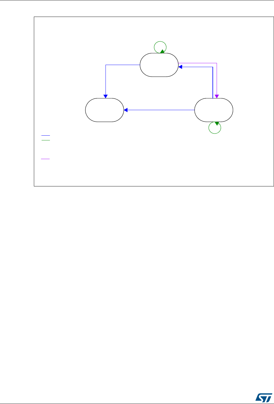
Embedded Flash memory interface RM0401
58/766 DocID027812 Rev 2
Figure 6. PCROP levels
The deactivation of the SPRMOD and/or the unprotection of PCROPed user sectors can
only occur when, at the same time, the RDP level changes from 1 to 0. If this condition is not
respected, the user option byte modification is canceled and the write error WRPERR flag is
set. The modification of the users option bytes (BOR_LEV, RST_STDBY, ..) is allowed since
none of the active nWRPi bits is reset and SPRMOD is kept active.
Note: The active value of nWRPi bits is inverted when PCROP mode is active (SPRMOD =1).
,EVEL
,EVEL
2$0X##
2$0X!!
2$0X##
DEFAULT
5SEROPTIONSECTORERASE
0ROGRAMNEWOPTIONS
'LOBALMASSERASE
5SEROPTIONSECTIONERASE
0ROGRAMNEWOPTIONS
7RITEOPTIONS
30-/$ACTIVE
ANDVALIDN720I
.ORESTRICTIONON
7RITEOPTIONS
7RITEOPTIONS
30-/$ACTIVE
ANDVALIDN720I
,EVEL
2$0X!!
7RITEOPTIONS
30-/$ACTIVE
ANDVALIDN720I
7RITEOPTIONS
30-/$ACTIVE
ANDVALIDN720I 7RITEOPTIONS
30-/$ACTIVE
ANDVALIDN720I
6ALIDN720IMEANSTHATNONEOFTHEN720BITSSETCANBERESETTRANSITIONFROMTO
-36

DocID027812 Rev 2 59/766
RM0401 Embedded Flash memory interface
67
3.7 One-time programmable bytes
Table 12 shows the organization of the one-time programmable (OTP) part of the OTP area.
The OTP area is divided into 16 OTP data blocks of 32 bytes and one lock OTP block of 16
bytes. The OTP data and lock blocks cannot be erased. The lock block contains 16 bytes
LOCKBi (0 ≤ i ≤ 15) to lock the corresponding OTP data block (blocks 0 to 15). Each OTP
data block can be programmed until the value 0x00 is programmed in the corresponding
OTP lock byte. The lock bytes must only contain 0x00 and 0xFF values, otherwise the OTP
bytes might not be taken into account correctly.
Table 12. OTP area organization
Block [128:96] [95:64] [63:32] [31:0] Address byte 0
0
OTP0 OTP0 OTP0 OTP0 0x1FFF 7800
OTP0 OTP0 OTP0 OTP0 0x1FFF 7810
1
OTP1 OTP1 OTP1 OTP1 0x1FFF 7820
OTP1 OTP1 OTP1 OTP1 0x1FFF 7830
.
.
.
.
.
.
.
.
.
15
OTP15 OTP15 OTP15 OTP15 0x1FFF 79E0
OTP15 OTP15 OTP15 OTP15 0x1FFF 79F0
Lock block LOCKB15 ...
LOCKB12
LOCKB11 ...
LOCKB8
LOCKB7 ...
LOCKB4
LOCKB3 ...
LOCKB0 0x1FFF 7A00

Embedded Flash memory interface RM0401
60/766 DocID027812 Rev 2
3.8 Flash interface registers
3.8.1 Flash access control register (FLASH_ACR)
The Flash access control register is used to enable/disable the acceleration features and
control the Flash memory access time according to CPU frequency.
Address offset: 0x00
Reset value: 0x0000 0000
Access: no wait state, word, half-word and byte access
31 30 29 28 27 26 25 24 23 22 21 20 19 18 17 16
Res. Res. Res. Res. Res. Res. Res. Res. Res. Res. Res. Res. Res. Res. Res. Res.
15 14 13 12 11 10 9 8 7 6 5 4 3 2 1 0
Res. Res. Res. DCRST ICRST DCEN ICEN PRFTEN Res. Res. Res. Res. LATENCY
rwwrwrw rw rwrwrwrw
Bits 31:13 Reserved, must be kept cleared.
Bit 12 DCRST: Data cache reset
0: Data cache is not reset
1: Data cache is reset
This bit can be written only when the D cache is disabled.
Bit 11 ICRST: Instruction cache reset
0: Instruction cache is not reset
1: Instruction cache is reset
This bit can be written only when the I cache is disabled.
Bit 10 DCEN: Data cache enable
0: Data cache is disabled
1: Data cache is enabled
Bit 9 ICEN: Instruction cache enable
0: Instruction cache is disabled
1: Instruction cache is enabled
Bit 8 PRFTEN: Prefetch enable
0: Prefetch is disabled
1: Prefetch is enabled
Bits 7:4 Reserved, must be kept cleared.
Bits 3:0 LATENCY: Latency
These bits represent the ratio of the CPU clock period to the Flash memory access time.
0000: Zero wait state
0001: One wait state
0010: Two wait states
-
-
-
1110: Fourteen wait states
1111: Fifteen wait states

DocID027812 Rev 2 61/766
RM0401 Embedded Flash memory interface
67
3.8.2 Flash key register (FLASH_KEYR)
The Flash key register is used to allow access to the Flash control register and so, to allow
program and erase operations.
Address offset: 0x04
Reset value: 0x0000 0000
Access: no wait state, word access
3.8.3 Flash option key register (FLASH_OPTKEYR)
The Flash option key register is used to allow program and erase operations in the user
configuration sector.
Address offset: 0x08
Reset value: 0x0000 0000
Access: no wait state, word access
31 30 29 28 27 26 25 24 23 22 21 20 19 18 17 16
KEY[31:16]
wwwwww w w w w w w w w w w
1514131211109876543210
KEY[15:0]
wwwwww w w w w w w w w w w
Bits 31:0 FKEYR: FPEC key
The following values must be programmed consecutively to unlock the FLASH_CR register
and allow programming/erasing it:
a) KEY1 = 0x45670123
b) KEY2 = 0xCDEF89AB
31 30 29 28 27 26 25 24 23 22 21 20 19 18 17 16
OPTKEYR[31:16
wwwwww w w w w w ww w w w
15 14 13 12 11 10 9 8 7 6 5 4 3 2 1 0
OPTKEYR[15:0]
wwwwww w w w w w ww w w w
Bits 31:0 OPTKEYR: Option byte key
The following values must be programmed consecutively to unlock the FLASH_OPTCR
register and allow programming it:
a) OPTKEY1 = 0x08192A3B
b) OPTKEY2 = 0x4C5D6E7F

Embedded Flash memory interface RM0401
62/766 DocID027812 Rev 2
3.8.4 Flash status register (FLASH_SR)
The Flash status register gives information on ongoing program and erase operations.
Address offset: 0x0C
Reset value: 0x0000 0000
Access: no wait state, word, half-word and byte access
31 30 29 28 27 26 25 24 23 22 21 20 19 18 17 16
Res. Res. Res. Res. Res. Res. Res. Res. Res. Res. Res. Res. Res. Res. Res. BSY
r
15 14 13 12 11 10 9 8 7 6 5 4 3 2 1 0
Res. Res. Res. Res. Res. Res. Res. RDERR PGSERR PGPERR PGAERR WRPERR Res. Res. OPERR EOP
rw rc_w1 rc_w1 rc_w1 rc_w1 rc_w1 rc_w1
Bits 31:17 Reserved, must be kept cleared.
Bit 16 BSY: Busy
This bit indicates that a Flash memory operation is in progress. It is set at the beginning of a
Flash memory operation and cleared when the operation finishes or an error occurs.
0: no Flash memory operation ongoing
1: Flash memory operation ongoing
Bits 15:9 Reserved, must be kept cleared.
Bit 8 RDERR: Read Protection Error (PCROP)
Set by hardware when an address to be read through the Dbus belongs to a read protected
part of the flash.
Reset by writing 1.
Bit 7 PGSERR: Programming sequence error
Set by hardware when a write access to the Flash memory is performed by the code while
the control register has not been correctly configured.
Cleared by writing 1.
Bit 6 PGPERR: Programming parallelism error
Set by hardware when the size of the access (byte, half-word, word, double word) during the
program sequence does not correspond to the parallelism configuration PSIZE (x8, x16,
x32, x64).
Cleared by writing 1.
Bit 5 PGAERR: Programming alignment error
Set by hardware when the data to program cannot be contained in the same 128-bit Flash
memory row.
Cleared by writing 1.
Bit 4 WRPERR: Write protection error
Set by hardware when an address to be erased/programmed belongs to a write-protected
part of the Flash memory.
Cleared by writing 1.

DocID027812 Rev 2 63/766
RM0401 Embedded Flash memory interface
67
3.8.5 Flash control register (FLASH_CR)
The Flash control register is used to configure and start Flash memory operations.
Address offset: 0x10
Reset value: 0x8000 0000
Access: no wait state when no Flash memory operation is ongoing, word, half-word and
byte access.
Bits 3:2 Reserved, must be kept cleared.
Bit 1 OPERR: Operation error
Set by hardware when a flash operation (programming / erase /read) request is detected and
can not be run because of parallelism, alignment, or write protection error. This bit is set only
if error interrupts are enabled (ERRIE = 1).
Bit 0 EOP: End of operation
Set by hardware when one or more Flash memory operations (program/erase) has/have
completed successfully. It is set only if the end of operation interrupts are enabled (EOPIE =
1).
Cleared by writing a 1.
31 30 29 28 27 26 25 24 23 22 21 20 19 18 17 16
LOCK Res. Res. Res. Res. Res. ERRIE EOPIE Res. Res. Res. Res. Res. Res. Res. STRT
rs rw rw rs
15 14 13 12 11 10 9 8 7 6 5 4 3 2 1 0
Res. Res. Res. Res. Res. Res. PSIZE[1:0] Res. SNB[3:0] MER SER PG
rw rw rw rw rw rw rw rw rw
Bit 31 LOCK: Lock
Write to 1 only. When it is set, this bit indicates that the FLASH_CR register is locked. It is
cleared by hardware after detecting the unlock sequence.
In the event of an unsuccessful unlock operation, this bit remains set until the next reset.
Bits 30:26 Reserved, must be kept cleared.
Bit 25 ERRIE: Error interrupt enable
This bit enables the interrupt generation when the OPERR bit in the FLASH_SR register is
set to 1.
0: Error interrupt generation disabled
1: Error interrupt generation enabled
Bit 24 EOPIE: End of operation interrupt enable
This bit enables the interrupt generation when the EOP bit in the FLASH_SR register goes
to 1.
0: Interrupt generation disabled
1: Interrupt generation enabled
Bits 23:17 Reserved, must be kept cleared.
Bit 16 STRT: Start
This bit triggers an erase operation when set. It is set only by software and cleared when the
BSY bit is cleared.
Bits 15:10 Reserved, must be kept cleared.

Embedded Flash memory interface RM0401
64/766 DocID027812 Rev 2
3.8.6 Flash option control register (FLASH_OPTCR)
The FLASH_OPTCR register is used to modify the user option bytes.
Address offset: 0x14
Reset value: 0x0FFF FFED. The option bits are loaded with values from Flash memory at
reset release.
Access: no wait state when no Flash memory operation is ongoing, word, half-word and
byte access.
Bits 9:8 PSIZE: Program size
These bits select the program parallelism.
00 program x8
01 program x16
10 program x32
11 program x64
Bit 7 Reserved, must be kept cleared.
Bits 6:3 SNB: Sector number
These bits select the sector to erase.
0000 sector 0
0001 sector 1
0010 sector 2
0011 sector 3
0100 sector 4
0101: not allowed
...
1011 not allowed
1100 user specific sector
1101 user configuration sector
1110 not allowed
1111 not allowed
Bit 2 MER: Mass Erase
Erase activated for all user sectors.
Bit 1 SER: Sector Erase
Sector Erase activated.
Bit 0 PG: Programming
Flash programming activated.
31 30 29 28 27 26 25 24 23 22 21 20 19 18 17 16
SPR
MOD Res. Res. Res. Res. Res. Res. Res. Res. Res. Res. nWRP[4:0]
rw rw rw rw rw rw
15 14 13 12 11 10 9 8 7 6 5 4 3 2 1 0
RDP[7:0] nRST_
STDBY
nRST_
STOP
WDG_S
WRes. BOR_LEV OPTST
RT
OPTLO
CK
rw rw rw rw rw rw rw rw rw rw rw rw rw rs rs

DocID027812 Rev 2 65/766
RM0401 Embedded Flash memory interface
67
Bit 31 SPRMOD: Selection of Protection Mode of nWPRi bits
0: PCROP disabled, nWPRi bits used for Write Protection on sector i
1: PCROP enabled, nWPRi bits used for PCROP Protection on sector i
Bits 30:21 Reserved, must be kept cleared.
Bits 20:16 nWRP[4:0]: Not write protect
These bits contain the value of the write-protection option bytes of sectors after reset. They
can be written to program a new write protect value into Flash memory.
0: Write protection active on selected sector
1: Write protection not active on selected sector
These bits contain the value of the write-protection and read-protection (PCROP) option
bytes for sectors 0 to 5 after reset. They can be written to program a new write-protect or
PCROP value into Flash memory.
If SPRMOD is reset:
0: Write protection active on sector i
1: Write protection not active on sector i
If SPRMOD is set:
0: PCROP protection not active on sector i
1: PCROP protection active on sector i
Bits 15:8 RDP: Read protect
These bits contain the value of the read-protection option level after reset. They can be
written to program a new read protection value into Flash memory.
0xAA: Level 0, read protection not active
0xCC: Level 2, chip read protection active
Others: Level 1, read protection of memories active
Bits 7:5 USER: User option bytes
These bits contain the value of the user option byte after reset. They can be written to
program a new user option byte value into Flash memory.
Bit 7: nRST_STDBY
Bit 6: nRST_STOP
Bit 5: WDG_SW
Note: When changing the WDG mode from hardware to software or from software to
hardware, a system reset is required to make the change effective.
Bit 4 Reserved, must be kept cleared. Always read as “0”.

Embedded Flash memory interface RM0401
66/766 DocID027812 Rev 2
Bits 3:2 BOR_LEV: BOR reset Level
These bits contain the supply level threshold that activates/releases the reset. They can be
written to program a new BOR level. By default, BOR is off. When the supply voltage (VDD)
drops below the selected BOR level, a device reset is generated.
00: BOR Level 3 (VBOR3), brownout threshold level 3
01: BOR Level 2 (VBOR2), brownout threshold level 2
10: BOR Level 1 (VBOR1), brownout threshold level 1
11: BOR off, POR/PDR reset threshold level is applied
Note: For full details about BOR characteristics, refer to the “Electrical characteristics” section
in the device datasheet.
Bit 1 OPTSTRT: Option start
This bit triggers a user option operation when set. It is set only by software and cleared when
the BSY bit is cleared.
Bit 0 OPTLOCK: Option lock
Write to 1 only. When this bit is set, it indicates that the FLASH_OPTCR register is locked.
This bit is cleared by hardware after detecting the unlock sequence.
In the event of an unsuccessful unlock operation, this bit remains set until the next reset.

DocID027812 Rev 2 67/766
RM0401 Embedded Flash memory interface
67
3.8.7 Flash interface register map
Table 13. Flash register map and reset values
Offset Register
31
30
29
28
27
26
25
24
23
22
21
20
19
18
17
16
15
14
13
12
11
10
9
8
7
6
5
4
3
2
1
0
0x00
FLASH_ACR
Res.
Res.
Res.
Res.
Res.
Res.
Res.
Res.
Res.
Res.
Res.
Res.
Res.
Res.
Res.
Res.
Res.
Res.
Res.
DCRST
ICRST
DCEN
ICEN
PRFTEN
Res.
Res.
Res.
Res.
LATENCY
Reset value 00000 0 0 0 0
0x04
FLASH_KEYR KEY[31:16] KEY[15:0]
Reset value 00000000000000000000000000000 0 0 0
0x08
FLASH_
OPTKEYR OPTKEYR[31:16] OPTKEYR[15:0]
Reset value 00000000000000000000000000000 0 0 0
0x0C
FLASH_SR
Res.
Res.
Res.
Res.
Res.
Res.
Res.
Res.
Res.
Res.
Res.
Res.
Res.
Res.
Res.
BSY
Res.
Res.
Res.
Res.
Res.
Res.
Res.
RDERR
PGSERR
PGPERR
PGAERR
WRPERR
Res.
Res.
OPERR
EOP
Reset value 0 00000 0 0
0x10
FLASH_CR
LOCK
Res.
Res.
Res.
Res.
Res.
ERRIE
EOPIE
Res.
Res.
Res.
Res.
Res.
Res.
Res.
STRT
Res.
Res.
Res.
Res.
Res.
Res.
PSIZE[1:0]
Res.
SNB[3:0]
MER
SER
PG
Reset value 1 00 0 00 00000 0 0
0x14
FLASH_OPTCR
SPRMOD
Res.
Res.
Res.
Res.
Res.
Res.
Res.
Res.
Res.
Res.
nWRP[4:0] RDP[7:0]
nRST_STDBY
nRST_STOP
WDG_SW
Res.
BOR_LEV
OPTSTRT
OPTLOCK
Reset value 0 1111110101010111 1 1 0 1
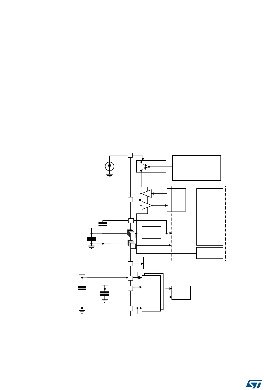
Power controller (PWR) RM0401
68/766 DocID027812 Rev 2
4 Power controller (PWR)
4.1 Power supplies
There are two main power supply schemes:
•VDD = 1.7 to 3.6 V: external power supply for I/Os with the internal regulator disabled,
provided externally through VDD pins. Requires the use of an external power supply
supervisor connected to the VDD and PDR_ON pins.
•VDD = 1.8 to 3.6 V: external power supply for I/Os and the internal regulator (when
enabled), provided externally through VDD pins.
The real-time clock (RTC), and the RTC backup registers can be powered from the VBAT
voltage when the main VDD supply is powered off.
Note: Depending on the operating power supply range, some peripheral may be used with limited
functionality and performance. For more details refer to section "General operating
conditions" in the datasheet.
Figure 7. Power supply overview
1. VDDA and VSSA must be connected to VDD and VSS, respectively.
06Y9
ĂĐŬƵƉĐŝƌĐƵŝƚƌLJ
;K^ϯϮ<͕Zd͕
tĂŬĞƵƉůŽŐŝĐ
ĂĐŬƵƉƌĞŐŝƐƚĞƌƐͿ ͕
<ĞƌŶĞůůŽŐŝĐ
;Wh͕ĚŝŐŝƚĂů
ΘZDͿ
ŶĂůŽŐ͗
ZƐ ͕
W>> ͕͘͘
WŽǁĞƌ
ƐǁŝƚĐŚ
sd
'W/KƐ
Khd
/E
ϰп ϭ ϬϬŶ&
нϭпϰ͘ϳђ&
sdс
ϭ ͘ϲϱƚŽϯ͘ϲs
sŽůƚĂŐĞ
ƌĞŐƵůĂƚŽƌ
s
>ĞǀĞůƐŚŝĨƚĞƌ
/K
>ŽŐŝĐ
s
ϭϬϬŶ&
нϭђ&
&ůĂƐŚŵĞŵŽƌLJ
sWͺϭ
ϭdžϰ͘ϳђ&
WZͺKE
ZĞƐĞƚ
ĐŽŶƚƌŽůůĞƌ
s
ϭ ͬϮ ͬ͘͘͘ ϰ
s^^
ϭ ͬϮ ͬ͘͘͘ ϰ
s
s^^
sZ&
ϭϬϬŶ&
нϭђ&

DocID027812 Rev 2 69/766
RM0401 Power controller (PWR)
89
4.1.1 Independent A/D converter supply and reference voltage
To improve conversion accuracy, the ADC has an independent power supply which can be
separately filtered and shielded from noise on the PCB.
•The ADC voltage supply input is available on a separate VDDA pin.
•An isolated supply ground connection is provided on pin VSSA.
To ensure a better accuracy of low voltage inputs, the user can connect a separate external
reference voltage ADC input on VREF
. The voltage on VREF ranges from 1.7 V to VDDA.
4.1.2 Battery backup domain
Backup domain description
To retain the content of the RTC backup registers and supply the RTC when VDD is turned
off, VBAT pin can be connected to an optional standby voltage supplied by a battery or by
another source.
To allow the RTC to operate even when the main digital supply (VDD) is turned off, the VBAT
pin powers the following blocks:
•The RTC
•The LSE oscillator
•PC13 to PC15 I/Os
The switch to the VBAT supply is controlled by the power-down reset embedded in the Reset
block.
Warning: During tRSTTEMPO (temporization at VDD startup) or after a PDR
is detected, the power switch between VBAT and VDD remains
connected to VBAT
.
During the startup phase, if VDD is established in less than
tRSTTEMPO (Refer to the datasheet for the value of tRSTTEMPO)
and VDD > VBAT + 0.6 V, a current may be injected into VBAT
through an internal diode connected between VDD and the
power switch (VBAT).
If the power supply/battery connected to the VBAT pin cannot
support this current injection, it is strongly recommended to
connect an external low-drop diode between this power
supply and the VBAT pin.
If no external battery is used in the application, it is recommended to connect the VBAT pin to
VDD with a 100 nF external decoupling ceramic capacitor in parallel.
When the backup domain is supplied by VDD (analog switch connected to VDD), the
following functions are available:
•PC14 and PC15 can be used as either GPIO or LSE pins
•PC13 can be used as a GPIO or additional functions can be configured (refer to
Table 26: RTC additional functions for more details about this pin configuration)
Note: Due to the fact that the switch only sinks a limited amount of current (3 mA), the use of
PC13 to PC15 GPIOs in output mode is restricted: the speed has to be limited to 2 MHz with

Power controller (PWR) RM0401
70/766 DocID027812 Rev 2
a maximum load of 30 pF and these I/Os must not be used as a current source (e.g. to drive
an LED).
When the backup domain is supplied by VBAT (analog switch connected to VBAT because
VDD is not present), the following functions are available:
•PC14 and PC15 can be used as LSE pins only
•PC13 can be used as the RTC additional function pin (refer to Table 26: RTC additional
functions for more details about this pin configuration)
Backup domain access
After reset, the backup domain (RTC registers, and RTC backup register) is protected
against possible unwanted write accesses. To enable access to the backup domain,
proceed as follows:
•Access to the RTC and RTC backup registers
1. Enable the power interface clock by setting the PWREN bits in the RCC_APB1ENR
register (see Section 5.3.9: RCC APB1 peripheral clock enable register
(RCC_APB1ENR))
2. Set the DBP bit in the Section 4.4.1 to enable access to the backup domain
3. Select the RTC clock source: see Section 5.2.8: RTC/AWU clock
4. Enable the RTC clock by programming the RTCEN [15] bit in the Section 5.3.14: RCC
Backup domain control register (RCC_BDCR)
RTC and RTC backup registers
The real-time clock (RTC) is an independent BCD timer/counter. The RTC provides a time-
of-day clock/calendar, two programmable alarm interrupts, and a periodic programmable
wakeup flag with interrupt capability. The RTC contains 20 backup data registers (80 bytes)
which are reset when a tamper detection event occurs. For more details refer to Section 21:
Real-time clock (RTC).
4.1.3 Voltage regulator
An embedded linear voltage regulator supplies all the digital circuitries except for the backup
domain and the Standby circuitry. The regulator output voltage is around 1.2 V.
This voltage regulator requires one capacitor to be connected to the dedicated pin, VCAP_1.
When activated by software, the voltage regulator is always enabled after Reset. It works in
three different modes depending on the application modes.
•In Run mode, the regulator supplies full power to the 1.2 V domain (core, memories
and digital peripherals). In this mode, the regulator output voltage (around 1.2 V) can
be scaled by software to different voltage values:
Scale 1, scale 2, or scale 3 can be configured through the VOS[1:0] bits of the
PWR_CR register. After reset the VOS register is set to scale 2. When the PLL is
OFF, the voltage regulator is set to scale 3 independently of the VOS register
content. The VOS register content is only taken into account once the PLL is
activated and the HSI or HSE is selected as clock source.
The voltage scaling allows optimizing the power consumption when the device is
clocked below the maximum system frequency.
•In Stop mode, the main regulator or the low-power regulator supplies low power to the
1.2 V domain, thus preserving the content of registers and internal SRAM. The voltage
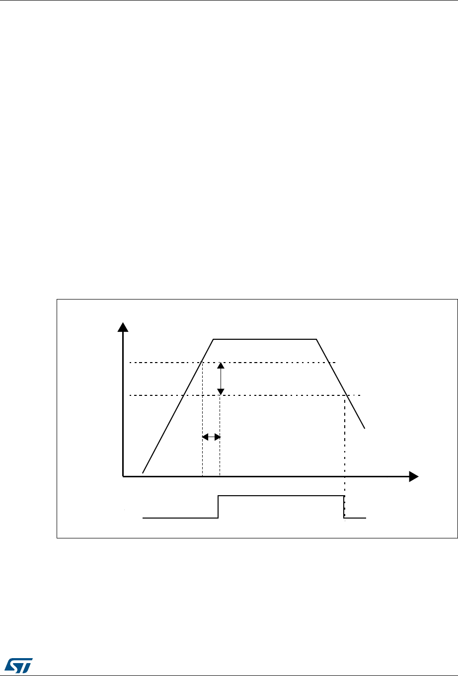
DocID027812 Rev 2 71/766
RM0401 Power controller (PWR)
89
regulator can be put either in main regulator mode (MR) or in low-power mode (LPR).
The programmed voltage scale remains the same during Stop mode:
Voltage scale 3 is automatically selected when the microcontroller enters Stop
mode (see Section 4.4.1: PWR power control register (PWR_CR)).
•In Standby mode, the regulator is powered down. The content of the registers and
SRAM are lost except for the Standby circuitry and the backup domain.
Note: For more details, refer to the voltage regulator section in the datasheet.
4.2 Power supply supervisor
4.2.1 Power-on reset (POR)/power-down reset (PDR)
The device has an integrated POR/PDR circuitry that allows proper operation starting
from 1.8 V.
To use the device below 1.8 V, the internal power supervisor must be switched off using the
PDR_ON pin (please refer to section Power supply supervisor of the datasheet). The device
remains in Reset mode when VDD/VDDA is below a specified threshold, VPOR/PDR, without
the need for an external reset circuit. For more details concerning the power on/power-down
reset threshold, refer to the electrical characteristics of the datasheet.
Figure 8. Power-on reset/power-down reset waveform
6$$6$$!
M6
HYSTERESIS
0$2
0$2
-36
2ESET
4EMPORIZATION
T2344%-0/
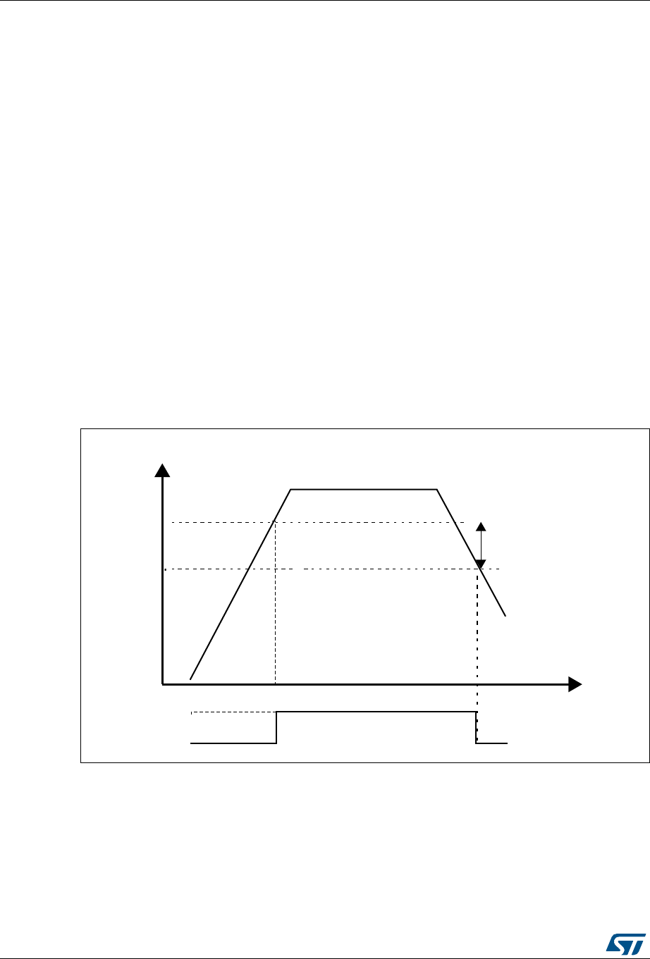
Power controller (PWR) RM0401
72/766 DocID027812 Rev 2
4.2.2 Brownout reset (BOR)
During power on, the Brownout reset (BOR) keeps the device under reset until the supply
voltage reaches the specified VBOR threshold.
VBOR is configured through device option bytes. By default, BOR is off. 3 programmable
VBOR threshold levels can be selected:
•BOR Level 3 (VBOR3). Brownout threshold level 3.
•BOR Level 2 (VBOR2). Brownout threshold level 2.
•BOR Level 1 (VBOR1). Brownout threshold level 1.
Note: For full details about BOR characteristics, refer to the "Electrical characteristics" section in
the device datasheet.
When the supply voltage (VDD) drops below the selected VBOR threshold, a device reset is
generated.
The BOR can be disabled by programming the device option bytes. In this case, the
power-on and power-down is then monitored by the POR/ PDR or by an external power
supervisor if the PDR is switched off through the PDR_ON pin (see Section 4.2.1: Power-on
reset (POR)/power-down reset (PDR)).
The BOR threshold hysteresis is ~100 mV (between the rising and the falling edge of the
supply voltage).
Figure 9. BOR thresholds
-36
6$$6$$!
M6
HYSTERESIS
"/2THRESHOLD
2ESET
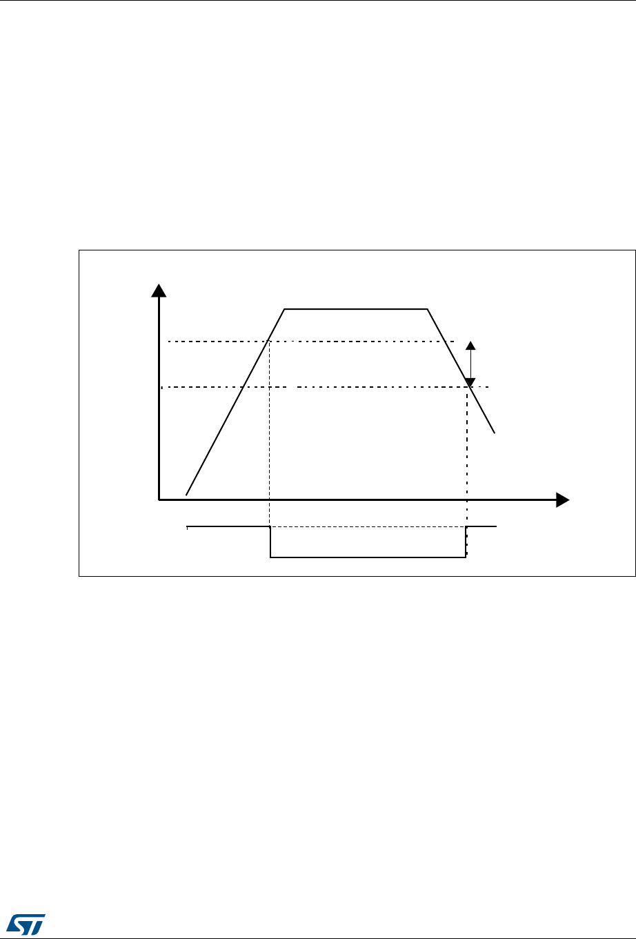
DocID027812 Rev 2 73/766
RM0401 Power controller (PWR)
89
4.2.3 Programmable voltage detector (PVD)
You can use the PVD to monitor the VDD power supply by comparing it to a threshold
selected by the PLS[2:0] bits in the PWR power control register (PWR_CR)
The PVD is enabled by setting the PVDE bit.
A PVDO flag is available, in the PWR power control/status register (PWR_CSR), to indicate
if VDD is higher or lower than the PVD threshold. This event is internally connected to the
EXTI line16 and can generate an interrupt if enabled through the EXTI registers. The PVD
output interrupt can be generated when VDD drops below the PVD threshold and/or when
VDD rises above the PVD threshold depending on EXTI line16 rising/falling edge
configuration. As an example the service routine could perform emergency shutdown tasks.
Figure 10. PVD thresholds
4.3 Low-power modes
By default, the microcontroller is in Run mode after a system or a power-on reset. In Run
mode the CPU is clocked by HCLK and the program code is executed. Several low-power
modes are available to save power when the CPU does not need to be kept running, for
example when waiting for an external event. It is up to the user to select the mode that gives
the best compromise between low-power consumption, short startup time and available
wakeup sources.
The devices feature four low-power modes:
•Sleep mode: Cortex®-M4 with FPU core is stopped, peripherals are kept running.
•Stop mode: all clocks are stopped.
•Standby mode: 1.2 V domain is powered off.
•Batch acquisition mode (BAM): the devices are in Sleep mode, the Flash memory is off,
needed peripheral are kept running, data transfer are still possible through DMA.
069
9''
P9
K\VWHUHVLV
39'WKUHVKROG
39'RXWSXW

Power controller (PWR) RM0401
74/766 DocID027812 Rev 2
In addition, the power consumption in Run mode can be reduced by one of the following
means:
•Optimizing PLL VCO frequency (see Section 4.3.1: Optimizing PLL VCO frequency)
•Slowing down the system clocks (see Section 4.3.2: Slowing down system clocks)
•Gating the clocks to the APBx and AHBx peripherals when they are unused (see
Section 4.3.3: Peripheral clock gating)
•Configuring the Flash memory in low-power mode (Stop or Deep-power down) to
execute code from RAM (see Section 4.3.4: Flash memory in low-power mode for code
execution from RAM).
Entering low-power mode
Low-power modes are entered by the MCU by executing the WFI (Wait For Interrupt), or
WFE (Wait for Event) instructions, or when the SLEEPONEXIT bit in the Cortex®-M4 with
FPU System Control register is set on Return from ISR.
Entering low-power mode through WFI or WFE is executed only is no interrupt or no event is
pending.
Exiting low-power mode
The MCU exits from Sleep and Stop modes low-power mode depending on the way the low-
power mode was entered:
•If the WFI instruction or Return from ISR was used to enter the low-power mode, any
peripheral interrupt acknowledged by the NVIC can wake up the device.
•If the WFE instruction is used to enter the low-power mode, the MCU exits the low-
power mode as soon as an event occurs. The wakeup event can be generated either
by:
– NVIC IRQ interrupt:
When SEVONPEND = 0 in the Cortex®-M4 with FPU System Control register: by
enabling an interrupt in the peripheral control register and in the NVIC. When the
MCU resumes from WFE, the peripheral interrupt pending bit and the NVIC
peripheral IRQ channel pending bit (in the NVIC interrupt clear pending register)
have to be cleared. Only NVIC interrupts with sufficient priority will wakeup and
interrupt the MCU.
When SEVONPEND = 1 in the Cortex®-M4 with FPU System Control register: by
enabling an interrupt in the peripheral control register and optionally in the NVIC.
When the MCU resumes from WFE, the peripheral interrupt pending bit and when
enabled the NVIC peripheral IRQ channel pending bit (in the NVIC interrupt clear
pending register) have to be cleared. All NVIC interrupts will wakeup the MCU,
even the disabled ones.Only enabled NVIC interrupts with sufficient priority will
wakeup and interrupt the MCU.
–Event
This is done by configuring a EXTI line in event mode. When the CPU resumes
from WFE, it is not necessary to clear the EXTI peripheral interrupt pending bit or
the NVIC IRQ channel pending bit as the pending bits corresponding to the event
line is not set. It may be necessary to clear the interrupt flag in the peripheral.
The MCU exits from Standby low-power mode through an external reset (NRST pin), an
IWDG reset, a rising edge on one of the enabled WKUPx pins or a RTC event occurs (see
Figure 368: RTC block diagram).

DocID027812 Rev 2 75/766
RM0401 Power controller (PWR)
89
After waking up from Standby mode, program execution restarts in the same way as after a
Reset (boot pin sampling, option bytes loading, reset vector is fetched, etc.).
Only enabled NVIC interrupts with sufficient priority will wakeup and interrupt the MCU.
4.3.1 Optimizing PLL VCO frequency
When the devices operate in a mode where one or more PLL is used, the power
consumption can be optimized by avoiding to run the VCO at higher frequency than needed
(refer to the datasheet).
4.3.2 Slowing down system clocks
In Run mode the speed of the system clocks (SYSCLK, HCLK, PCLK1, PCLK2) can be
reduced by programming the prescaler registers. These prescalers can also be used to slow
down peripherals before entering Sleep mode.
For more details refer to Section 5.3.3: RCC clock configuration register (RCC_CFGR).
4.3.3 Peripheral clock gating
In Run mode, the HCLKx and PCLKx for individual peripherals and memories can be
stopped at any time to reduce power consumption.
To further reduce power consumption in Sleep mode the peripheral clocks can be disabled
prior to executing the WFI or WFE instructions.
Peripheral clock gating is controlled by the AHB1 peripheral clock enable register
(RCC_AHB1ENR), AHB2 peripheral clock enable register (RCC_AHB2ENR) (see
Table 14. Low-power mode summary
Mode name Entry Wakeup Effect on 1.2 V
domain clocks
Effect on
VDD
domain
clocks
Voltage regulator
Sleep and
BAM(1)
(Sleep now or
Sleep-on-
exit)
WFI or Return
from ISR Any interrupt CPU CLK OFF
no effect on other
clocks or analog
clock sources
None ON
WFE Wakeup event
Stop
SLEEPDEEP bit
+ WFI, Return
from ISR or WFE
Any EXTI line (configured
in the EXTI registers,
internal and external lines)
All 1.2 V domain
clocks OFF
HSI and
HSE
oscillator
s OFF
Main regulator or
Low-Power
regulator (depends
on PWR power
control register
(PWR_CR)
Standby
PDDS bit +
SLEEPDEEP bit
+ WFI, Return
from ISR or WFE
WKUP pin rising edge,
RTC alarm (Alarm A or
Alarm B), RTC Wakeup
event, RTC tamper
events, RTC time stamp
event, external reset in
NRST pin, IWDG reset
OFF
1. Refer to Section 4.3.6: Batch acquisition mode for specific BAM entry and exit requirements.

Power controller (PWR) RM0401
76/766 DocID027812 Rev 2
Section 5.3.8: RCC AHB1 peripheral clock enable register (RCC_AHB1ENR)).
Disabling the peripherals clocks in Sleep mode can be performed automatically by resetting
the corresponding bit in RCC_AHBxLPENR and RCC_APBxLPENR registers.
4.3.4 Flash memory in low-power mode for code execution from RAM
For applications where the code is executed from RAM, the Flash memory can be put in two
possible low-power mode.
•Stop mode
•Deep-power down mode
Putting the Flash memory in Deep-power down mode allows to achieve the best power
consumption. However the Flash memory wakeup time is the slowest (refer to the
Electrical characteristics section of the datasheet).
From Run mode, the Flash memory can be configured anytime by software to enter any of
these low-power mode.
From Sleep mode, setting the Flash memory low-power down mode must be done before
entering Sleep mode.
The Flash memory wakeup time has to be handled by software counter.
4.3.5 Sleep mode
Entering Sleep mode
The Sleep mode is entered according to Section : Entering low-power mode, when the
SLEEPDEEP bit in the Cortex®-M4 with FPU System Control register is cleared.
Refer to Table 15 and Table 16 for details on how to enter Sleep mode.
Exiting Sleep mode
The Sleep mode is exited according to Section : Exiting low-power mode.
Refer to Table 15 and Table 16 for more details on how to exit Sleep mode.
Table 15. Sleep-now entry and exit
Sleep-now mode Description
Mode entry
WFI (Wait for Interrupt) or WFE (Wait for Event) while:
– SLEEPDEEP = 0
– No interrupt (for WFI) or event (for WFE) is pending
Refer to the Cortex®-M4 with FPU System Control register.
On Return from ISR while:
– SLEEPDEEP = 0 and
– SLEEPONEXIT = 1
– No interrupt is pending
Refer to the Cortex®-M4 with FPU System Control register.

DocID027812 Rev 2 77/766
RM0401 Power controller (PWR)
89
4.3.6 Batch acquisition mode
Entering BAM
The BAM is entered according to Section : Entering low-power mode, when the
SLEEPDEEP bit in the Cortex®-M4 with FPU System Control register is cleared.
Refer to Table 17 and Table 18 for details on how to enter Sleep mode.
Before entering Sleep mode, the Flash memory must be configured by software to operate
in the required low- power mode. If data need to be transferred from peripheral to RAM
during BAM, the DMA must be enabled before entering Sleep mode.
Exiting BAM
The BAM is exited according to Section : Exiting low-power mode.
Refer to Table 17 and Table 18 for more details on how to exit Sleep mode.
After waking up from BAM, the Flash memory must first to be waked up if code execution
restarts from Flash memory.
This wakeup time must be managed by software running from the internal SRAM.
Mode exit
If WFI or Return from ISR was used for entry:
Interrupt: Refer to Table 39: Vector table
If WFE was used for entry and SEVONPEND = 0
Wakeup event: Refer to Section 9.2.3: Wakeup event management
f WFE was used for entry and SEVONPEND = 1
Interrupt even when disabled in NVIC: refer to Table 39: Vector table or
Wakeup event (see Section 9.2.3: Wakeup event management).
Wakeup latency None
Table 16. Sleep-on-exit entry and exit
Sleep-on-exit Description
Mode entry
WFI (Wait for Interrupt) or WFE (Wait for Event) while:
– SLEEPDEEP = 0
– No interrupt (for WFI) or event (for WFE) is pending
Refer to the Cortex®-M4 with FPU System Control register.
On Return from ISR while:
– SLEEPDEEP = 0 and
– SLEEPONEXIT = 1
– No interrupt is pending
Refer to the Cortex®-M4 with FPU System Control register.
Mode exit Interrupt: refer to Table 39: Vector table
Wakeup latency None
Table 15. Sleep-now entry and exit (continued)
Sleep-now mode Description

Power controller (PWR) RM0401
78/766 DocID027812 Rev 2
4.3.7 Stop mode
The Stop mode is based on the Cortex®-M4 with FPU deepsleep mode combined with
peripheral clock gating. The voltage regulator can be configured either in normal or low-
power mode. In Stop mode, all clocks in the 1.2 V domain are stopped, the PLLs, the HSI
and the HSE RC oscillators are disabled. Internal SRAM and register contents are
preserved.
Some settings in the PWR_CR register allow to further reduce the power consumption.
When the Flash memory is in power-down mode, an additional startup delay is incurred
when waking up from Stop mode (see Table 19: Stop operating modes and Section 4.4.1:
PWR power control register (PWR_CR)).
Table 17. BAM-now entry and exit
Sleep-now mode Description
Mode entry
Set the Flash memory in low-power mode:
– FISSR/FMSSR and FPDS bits of the PWR_CR register
WFI (Wait for Interrupt) or WFE (Wait for Event) while:
– SLEEPDEEP = 0 and
– SLEEPONEXIT = 0
Refer to the Cortex®-M4 with FPU System Control register.
Mode exit
If WFI was used for entry:
Interrupt: Refer to Table 39: Vector table
If WFE was used for entry
Wakeup event: Refer to Section 9.2.3: Wakeup event management
If Flash memory wakeup time is needed, FISSR/FMSSR bits of PWR_CR
register must be set
Wakeup latency
None if code executed from RAM
Low-power mode Flash memory wakeup time, before restarting code
execution from Flash memory (refer to the Flash memory wakeup time in
the Electrical characteristics section of the datasheet).
Table 18. BAM-on-exit entry and exit
Sleep-on-exit Description
Mode entry
Set the Flash memory in low-power mode:
– FISSR/FMSSR and FPDS bits of the PWR_CR register
WFI (wait for interrupt) while:
– SLEEPDEEP = 0 and
– SLEEPONEXIT = 1
Refer to the Cortex®-M4 with FPU System Control register.
Mode exit
Interrupt: refer to Table 39: Vector table
If Flash memory wakeup time is needed, FISSR/FMSSR bits of PWR_CR
register must be set
Wakeup latency
None when code executed from internal SRAM
Low-power mode Flash memory wakeup time, before restarting code
execution from Flash memory (refer to the Flash memory wakeup time in
the Electrical characteristics section of the datasheet).

DocID027812 Rev 2 79/766
RM0401 Power controller (PWR)
89
When the code is executed from internal SRAM and the Flash memory is configured in low-
power mode before entering Stop mode, the Flash memory stays in low-power mode after
waking up from Stop. In this case, only the HSI RC clock startup time and the regulator
wakeup time apply.
Entering Stop mode
The Stop mode is entered according to Section : Entering low-power mode, when the
SLEEPDEEP bit in the Cortex®-M4 with FPU System Control register is set.
Refer to Table 20 for details on how to enter the Stop mode.
To further reduce power consumption in Stop mode, the internal voltage regulator can be put
in low-power mode. This is configured by the LPDS bit of the PWR power control register
(PWR_CR).
If Flash memory programming is ongoing, the Stop mode entry is delayed until the memory
access is finished.
If an access to the APB domain is ongoing, The Stop mode entry is delayed until the APB
access is finished.
The following features can be selected by programming individual control bits before
entering Stop mode:
•Independent watchdog (IWDG): the IWDG is started by writing to its Key register or by
hardware option. Once started it cannot be stopped except by a Reset. See
Table 19. Stop operating modes
Stop mode MRLV bit LPLV bit FPDS bit LPDS bit Wakeup latency
STOP MR 0 - 0 0 HSI RC startup time
STOP MRFPD 0 - 1 0
HSI RC startup time +
Flash wakeup time from Deep Power
Down mode
STOP LP0001 HSI RC startup time +
regulator wakeup time from LP mode
STOP LPFPD - 0 1 1
HSI RC startup time +
Flash wakeup time from Deep Power
Down mode +
regulator wakeup time from LP mode
STOP MRLV 1 - - 0
HSI RC startup time +
Flash wakeup time from Deep Power
Down mode +
Main regulator from low voltage mode
STOP LPLV-1-1
HSI RC startup time +
Flash wakeup time from Deep Power
Down mode +
regulator wakeup time from Low
Voltage LP mode

Power controller (PWR) RM0401
80/766 DocID027812 Rev 2
Section 20.3 in Section 20: Independent watchdog (IWDG).
•Real-time clock (RTC): this is configured by the RTCEN bit in the Section 5.3.14: RCC
Backup domain control register (RCC_BDCR)
•Internal RC oscillator (LSI RC): this is configured by the LSION bit in the
Section 5.3.15: RCC clock control & status register (RCC_CSR).
•External 32.768 kHz oscillator (LSE OSC): this is configured by the LSEON bit in the
Section 5.3.14: RCC Backup domain control register (RCC_BDCR).
The ADC can also consume power during the Stop mode, unless it is disabled before
entering it. To disable it, the ADON bit in the ADC_CR2 register must be written to 0.
Note: If the application needs to disable the external clock before entering Stop mode, the HSEON
bit must first be disabled and the system clock switched to HSI.
Otherwise, if the HSEON bit is kept enabled while the external clock (external oscillator) can
be removed before entering stop mode, the clock security system (CSS) feature must be
enabled to detect any external oscillator failure and avoid a malfunction behavior when
entering stop mode.
Exiting Stop mode
The Stop mode is exited according to Section : Exiting low-power mode.
Refer to Table 20 for more details on how to exit Stop mode.
When exiting Stop mode by issuing an interrupt or a wakeup event, the HSI RC oscillator is
selected as system clock.
When the voltage regulator operates in low-power mode, an additional startup delay is
incurred when waking up from Stop mode. By keeping the internal regulator ON during Stop
mode, the consumption is higher although the startup time is reduced.
If the code is executed from internal SRAM while the Flash memory in low-power mode, the
Stop wakeup time is reduced since the code execution restarts from SRAM which is directly
available when the clocks are stable.
Table 20. Stop mode entry and exit
Stop mode Description
Mode entry
WFI (Wait for Interrupt) or WFE (Wait for Event) while:
– SLEEPDEEP bit is set in Cortex®-M4 with FPU System Control register
– PDDS bit is cleared in Power Control register (PWR_CR)
– Select the voltage regulator mode by configuring LPDS bit in PWR_CR
– No interrupt (for WFI) or event (for WFE) is pending
On Return from ISR:
– SLEEPDEEP bit is set in Cortex®-M4 with FPU System Control register
– SLEEPONEXIT = 1
– PDDS bit is cleared in Power Control register (PWR_CR)
– No interrupt is pending
Note: To enter Stop mode, all EXTI Line pending bits (in Pending register
(EXTI_PR)), all peripheral interrupts pending bits, the RTC Alarm
(Alarm A and Alarm B), RTC wakeup, RTC tamper, and RTC time
stamp flags, must be reset. Otherwise, the Stop mode entry
procedure is ignored and program execution continues.

DocID027812 Rev 2 81/766
RM0401 Power controller (PWR)
89
4.3.8 Standby mode
The Standby mode allows to achieve the lowest power consumption. It is based on the
Cortex®-M4 with FPU deepsleep mode, with the voltage regulator disabled. The 1.2 V
domain is consequently powered off. The PLLs, the HSI oscillator and the HSE oscillator are
also switched off. SRAM and register contents are lost except for registers in the backup
domain (RTC registers and RTC backup register), and Standby circuitry (see Figure 7).
Entering Standby mode
The Standby mode is entered according to Section : Entering low-power mode, when the
SLEEPDEEP bit in the Cortex®-M4 with FPU System Control register is set.
Refer to Table 21 for more details on how to enter Standby mode.
In Standby mode, the following features can be selected by programming individual control
bits:
•Independent watchdog (IWDG): the IWDG is started by writing to its Key register or by
hardware option. Once started it cannot be stopped except by a reset. See
Section 20.3 in Section 20: Independent watchdog (IWDG).
•Real-time clock (RTC): this is configured by the RTCEN bit in the backup domain
control register (RCC_BDCR)
•Internal RC oscillator (LSI RC): this is configured by the LSION bit in the Control/status
register (RCC_CSR).
•External 32.768 kHz oscillator (LSE OSC): this is configured by the LSEON bit in the
backup domain control register (RCC_BDCR)
Exiting Standby mode
The Standby mode is exited according to Section : Exiting low-power mode. The SBF status
flag in PWR_CR (see Section 4.4.2: PWR power control/status register (PWR_CSR))
indicates that the MCU was in Standby mode. All registers are reset after wakeup from
Standby except for PWR_CR.
Refer to Table 21 for more details on how to exit Standby mode.
Mode exit
If WFI or Return from ISR was used for entry:
Any EXTI lines configured in Interrupt mode (the corresponding EXTI
Interrupt vector must be enabled in the NVIC). The interrupt source can
be external interrupts or peripherals with wakeup capability. Refer to
Table 39: Vector table.
If WFE was used for entry and SEVONPEND = 0
Any EXTI lines configured in event mode. Refer to Section 9.2.3:
Wakeup event management.
If WFE was used for entry and SEVONPEND = 1:
– Any EXTI lines configured in Interrupt mode (even if the corresponding
EXTI Interrupt vector is disabled in the NVIC). The interrupt source can
be an external interrupt or a peripheral with wakeup capability. Refer to v.
– Wakeup event: refer to Section 9.2.3: Wakeup event management.
Wakeup latency Refer to Table 19: Stop operating modes
Table 20. Stop mode entry and exit (continued)
Stop mode Description

Power controller (PWR) RM0401
82/766 DocID027812 Rev 2
I/O states in Standby mode
In Standby mode, all I/O pins are high impedance except for:
•Reset pad (still available)
•RTC_AF1 pin (PC13) if configured for tamper, time stamp, RTC Alarm out, or RTC
clock calibration out
•WKUP1 pin (PA0), WKUP2 pin (PC0) and WKUP3 pin (PC1) if enabled
Debug mode
By default, the debug connection is lost if the application puts the MCU in Stop or Standby
mode while the debug features are used. This is due to the fact that the Cortex®-M4 with
FPU core is no longer clocked.
However, by setting some configuration bits in the DBGMCU_CR register, the software can
be debugged even when using the low-power modes extensively. For more details, refer to
Section 26.16.1: Debug support for low-power modes.
4.3.9 Programming the RTC alternate functions to wake up the device from
the Stop and Standby modes
The MCU can be woken up from a low-power mode by an RTC alternate function.
The RTC alternate functions are the RTC alarms (Alarm A and Alarm B), RTC wakeup, RTC
tamper event detection and RTC time stamp event detection.
These RTC alternate functions can wake up the system from the Stop and Standby low-
power modes.
Table 21. Standby mode entry and exit
Standby mode Description
Mode entry
WFI (Wait for Interrupt) or WFE (Wait for Event) while:
– SLEEPDEEP is set in Cortex®-M4 with FPU System Control register
– PDDS bit is set in Power Control register (PWR_CR)
– CWUF bit is cleared in Power Control register (PWR_CR)
– the RTC flag corresponding to the chosen wakeup source (RTC Alarm A,
RTC Alarm B, RTC wakeup, Tamper or Timestamp flags) is cleared
– No interrupt (for WFI) or event (for WFE) is pending
On return from ISR while:
– SLEEPDEEP bit is set in Cortex®-M4 with FPU System Control register
and
– SLEEPONEXIT = 1 and
– PDDS bit is set in Power Control register (PWR_CR) and
– WUF bit is cleared in Power Control/Status register (PWR_SR)
– The RTC flag corresponding to the chosen wakeup source (RTC Alarm
A, RTC Alarm B, RTC wakeup, Tamper or Timestamp flags) is cleared
– No interrupt is pending
Mode exit WKUP pin rising edge, RTC alarm (Alarm A and Alarm B), RTC wakeup,
tamper event, time stamp event, external reset in NRST pin, IWDG reset.
Wakeup latency Reset phase.

DocID027812 Rev 2 83/766
RM0401 Power controller (PWR)
89
The system can also wake up from low-power modes without depending on an external
interrupt (Auto-wakeup mode), by using the RTC alarm or the RTC wakeup events.
The RTC provides a programmable time base for waking up from the Stop or Standby mode
at regular intervals.
For this purpose, two of the three alternate RTC clock sources can be selected by
programming the RTCSEL[1:0] bits in the Section 5.3.14: RCC Backup domain control
register (RCC_BDCR):
•Low-power 32.768 kHz external crystal oscillator (LSE OSC)
This clock source provides a precise time base with a very low-power consumption
(additional consumption of less than 1 µA under typical conditions)
•Low-power internal RC oscillator (LSI RC)
This clock source has the advantage of saving the cost of the 32.768 kHz crystal. This
internal RC oscillator is designed to use minimum power.
RTC alternate functions to wake up the device from the Stop mode
•To wake up the device from the Stop mode with an RTC alarm event, it is necessary to:
a) Configure the EXTI Line 17 to be sensitive to rising edges (Interrupt or Event
modes)
b) Enable the RTC Alarm Interrupt in the RTC_CR register
c) Configure the RTC to generate the RTC alarm
•To wake up the device from the Stop mode with an RTC tamper or time stamp event, it
is necessary to:
a) Configure the EXTI Line 21 to be sensitive to rising edges (Interrupt or Event
modes)
b) Enable the RTC time stamp Interrupt in the RTC_CR register or the RTC tamper
interrupt in the RTC_TAFCR register
c) Configure the RTC to detect the tamper or time stamp event
•To wake up the device from the Stop mode with an RTC wakeup event, it is necessary
to:
a) Configure the EXTI Line 22 to be sensitive to rising edges (Interrupt or Event
modes)
b) Enable the RTC wakeup interrupt in the RTC_CR register
c) Configure the RTC to generate the RTC Wakeup event
RTC alternate functions to wake up the device from the Standby mode
•To wake up the device from the Standby mode with an RTC alarm event, it is necessary
to:
a) Enable the RTC alarm interrupt in the RTC_CR register
b) Configure the RTC to generate the RTC alarm
•To wake up the device from the Standby mode with an RTC tamper or time stamp
event, it is necessary to:
a) Enable the RTC time stamp interrupt in the RTC_CR register or the RTC tamper
interrupt in the RTC_TAFCR register
b) Configure the RTC to detect the tamper or time stamp event

Power controller (PWR) RM0401
84/766 DocID027812 Rev 2
•To wake up the device from the Standby mode with an RTC wakeup event, it is
necessary to:
a) Enable the RTC wakeup interrupt in the RTC_CR register
b) Configure the RTC to generate the RTC wakeup event
Safe RTC alternate function wakeup flag clearing sequence
If the selected RTC alternate function is set before the PWR wakeup flag (WUTF) is cleared,
it will not be detected on the next event as detection is made once on the rising edge.
To avoid bouncing on the pins onto which the RTC alternate functions are mapped, and exit
correctly from the Stop and Standby modes, it is recommended to follow the sequence
below before entering the Standby mode:
•When using RTC alarm to wake up the device from the low-power modes:
a) Disable the RTC alarm interrupt (ALRAIE or ALRBIE bits in the RTC_CR register)
b) Clear the RTC alarm (ALRAF/ALRBF) flag
c) Clear the PWR Wakeup (WUF) flag
d) Enable the RTC alarm interrupt
e) Re-enter the low-power mode
•When using RTC wakeup to wake up the device from the low-power modes:
a) Disable the RTC Wakeup interrupt (WUTIE bit in the RTC_CR register)
b) Clear the RTC Wakeup (WUTF) flag
c) Clear the PWR Wakeup (WUF) flag
d) Enable the RTC Wakeup interrupt
e) Re-enter the low-power mode
•When using RTC tamper to wake up the device from the low-power modes:
a) Disable the RTC tamper interrupt (TAMPIE bit in the RTC_TAFCR register)
b) Clear the Tamper (TAMP1F/TSF) flag
c) Clear the PWR Wakeup (WUF) flag
d) Enable the RTC tamper interrupt
e) Re-enter the low-power mode
•When using RTC time stamp to wake up the device from the low-power modes:
a) Disable the RTC time stamp interrupt (TSIE bit in RTC_CR)
b) Clear the RTC time stamp (TSF) flag
c) Clear the PWR Wakeup (WUF) flag
d) Enable the RTC TimeStamp interrupt
e) Re-enter the low-power mode

DocID027812 Rev 2 85/766
RM0401 Power controller (PWR)
89
4.4 Power control registers
4.4.1 PWR power control register (PWR_CR)
Address offset: 0x00
Reset value: 0x0000 8000 (reset by wakeup from Standby mode)
31 30 29 28 27 26 25 24 23 22 21 20 19 18 17 16
Res. Res. Res. Res. Res. Res. Res. Res. Res. Res. FISSR FMSSR Res. Res. Res. Res.
rw rw
1514131211109876543210
VOS ADCDC1 Res. MRLV
DS
LPLV
DS FPDS DBP PLS[2:0] PVDE CSBF CWUF PDDS LPDS
rw rw rw rw rw rw rw rw rw rw rw w w rw rw
Bits 31:22 Reserved, must be kept at reset value.
Bit 21 FISSR: Flash Interface Stop while System Run
0: Flash Interface clock run (Default value).
1: Flash Interface clock off.
Note: This bit could not be set while executing with the Flash itself. It should be done with
specific routine executed from RAM.
Bit 20 FMSSR: Flash Memory Sleep System Run.
0: Flash standard mode (Default value)
1: Flash forced to be in STOP or Deep-power down mode (depending of FPDS value bit) by
hardware.
Note: This bit could not be set while executing with the Flash itself. It should be done with
specific routine executed from RAM.
Bits 19:16 Reserved, must be kept at reset value.
Bits 15:14 VOS[1:0]: Regulator voltage scaling output selection
These bits control the main internal voltage regulator output voltage to achieve a trade-off
between performance and power consumption when the device does not operate at the
maximum frequency (refer to the corresponding datasheet for more details).
These bits can be modified only when the PLL is OFF. The new value programmed is active
only when the PLL is ON. When the PLL is OFF, the voltage regulator is set to scale 3
independently of the VOS register content.
00: Reserved (Scale 3 mode selected)
01: Scale 3 mode <= 64 MHz
10: Scale 2 mode (reset value) <= 84 MHz
11: Scale 1 mode <= 100 MHz
Bit 13 ADCDC1:
0: No effect.
1: Refer to AN4073 for details on how to use this bit.
Note: This bit can only be set when operating at supply voltage range 2.7 to 3.6V and when
the Prefetch is OFF.

Power controller (PWR) RM0401
86/766 DocID027812 Rev 2
Bit 12 Reserved, must be kept at reset value.
Bit 11 MRLVDS: Main regulator Low Voltage in Deep Sleep
0: Main regulator in Voltage scale 3 when the device is in Stop mode.
1: Main regulator in Low Voltage and Flash memory in Deep Sleep mode when the device is
in Stop mode.
Bit 10 LPLVDS: Low-power regulator Low Voltage in Deep Sleep
0: Low-power regulator on if LPDS bit is set when the device is in Stop mode.
1: Low-power regulator in Low Voltage and Flash memory in Deep Sleep mode if LPDS bit is
set when device is in Stop mode.
Bit 9 FPDS: Flash power-down in Stop mode
When set, the Flash memory enters power-down mode when the device enters Stop mode.
This allows to achieve a lower consumption in stop mode but a longer restart time.
0: Flash memory not in power-down when the device is in Stop mode
1: Flash memory in power-down when the device is in Stop mode
Bit 8 DBP: Disable backup domain write protection
In reset state, the RCC_BDCR register, the RTC registers (including the backup registers), and
the BRE bit of the PWR_CSR register, are protected against parasitic write access. This bit
must be set to enable write access to these registers.
0: Access to RTC and RTC Backup registers.
1: Access to RTC and RTC Backup registers.
Bits 7:5 PLS[2:0]: PVD level selection
These bits are written by software to select the voltage threshold detected by the Power
Voltage Detector
000: 2.2 V
001: 2.3 V
010: 2.4 V
011: 2.5 V
100: 2.6 V
101: 2.7 V
110: 2.8 V
111: 2.9 V
Note: Refer to the electrical characteristics of the datasheet for more details.
Bit 4 PVDE: Power voltage detector enable
This bit is set and cleared by software.
0: PVD disabled
1: PVD enabled
Bit 3 CSBF: Clear standby flag
This bit is always read as 0.
0: No effect.
1: Clear the SBF Standby Flag (write).

DocID027812 Rev 2 87/766
RM0401 Power controller (PWR)
89
4.4.2 PWR power control/status register (PWR_CSR)
Address offset: 0x04
Reset value: 0x0000 0000 (not reset by wakeup from Standby mode)
Additional APB cycles are needed to read this register versus a standard APB read.
Bit 2 CWUF: Clear wakeup flag
This bit is always read as 0.
0: No effect.
1: Clear the WUF Wakeup Flag after 2 System clock cycles.
Bit 1 PDDS: Power-down deepsleep
This bit is set and cleared by software. It works together with the LPDS bit.
0: Enter Stop mode when the CPU enters deepsleep. The regulator status depends on the
LPDS bit.
1: Enter Standby mode when the CPU enters deepsleep.
Bit 0 LPDS: Low-power deepsleep
This bit is set and cleared by software. It works together with the PDDS bit.
0: Voltage regulator on during Stop mode.
1: Low-power Voltage regulator on during Stop mode.
31 30 29 28 27 26 25 24 23 22 21 20 19 18 17 16
Res. Res. Res. Res. Res. Res. Res. Res. Res. Res. Res. Res. Res. Res. Res. Res.
1514131211109876543210
Res. VOS
RDY Res. Res. Res. Res. BRE EWUP
1
EWUP
2
EWUP
3Res. Res. BRR PVDO SBF WUF
r rwrwrwrw r r r r
Bits 31:15 Reserved, must be kept at reset value.
Bit 14 VOSRDY: Regulator voltage scaling output selection ready bit
0: Not ready
1: Ready
Bits 13:10 Reserved, must be kept at reset value.
Bit 9 BRE: Backup regulator enable
When set, the Backup regulator (used to maintain the backup domain content) is enabled. If
BRE is reset, the backup regulator is switched off. Once set, the application must wait that
the Backup Regulator Ready flag (BRR) is set to indicate that the data written into the
backup registers will be maintained in the Standby and VBAT modes.
0: Backup regulator disabled
1: Backup regulator enabled
Note: This bit is not reset when the device wakes up from Standby mode, by a system reset,
or by a power reset.

Power controller (PWR) RM0401
88/766 DocID027812 Rev 2
Bit 8 EWUP1: Enable WKUP1 pin (PA0)
This bit is set and cleared by software.
0: WKUP1 pin is used for general purpose I/O. An event on the WKUP1 pin does not
wakeup the device from Standby mode.
1: WKUP1 pin is used for wakeup from Standby mode and forced in input pull down
configuration (rising edge on WKUP1 pin wakes up the system from Standby mode).
Note: This bit is reset by a system reset.
Bit 7 EWUP2: Enable WKUP2 pin (PC0)
This bit is set and cleared by software.
0: WKUP2 pin is used for general purpose I/O. An event on the WKUP2 pin does not
wakeup the device from Standby mode.
1: WKUP2 pin is used for wakeup from Standby mode and forced in input pull down
configuration (rising edge on WKUP2 pin wakes up the system from Standby mode).
Note: This bit is reset by a system reset.
Bit 6 EWUP3: Enable WKUP3 pin (PC1)
This bit is set and cleared by software.
0: WKUP3 pin is used for general purpose I/O. An event on the WKUP3 pin does not
wakeup the device from Standby mode.
1: WKUP3 pin is used for wakeup from Standby mode and forced in input pull down
configuration (rising edge on WKUP3 pin wakes up the system from Standby mode).
Note: This bit is reset by a system reset.
Bits 5:4 Reserved, must be kept at reset value.
Bit 3 BRR: Backup regulator ready
Set by hardware to indicate that the Backup Regulator is ready.
0: Backup Regulator not ready
1: Backup Regulator ready
Note: This bit is not reset when the device wakes up from Standby mode or by a system reset
or power reset.
Bit 2 PVDO: PVD output
This bit is set and cleared by hardware. It is valid only if PVD is enabled by the PVDE bit.
0: VDD is higher than the PVD threshold selected with the PLS[2:0] bits.
1: VDD is lower than the PVD threshold selected with the PLS[2:0] bits.
Note: The PVD is stopped by Standby mode. For this reason, this bit is equal to 0 after
Standby or reset until the PVDE bit is set.
Bit 1 SBF: Standby flag
This bit is set by hardware and cleared only by a POR/PDR (power-on reset/power-down
reset) or by setting the CSBF bit in the PWR_CR register.
0: Device has not been in Standby mode
1: Device has been in Standby mode
Bit 0 WUF: Wakeup flag
This bit is set by hardware and cleared either by a system reset or by setting the CWUF bit in
the PWR_CR register.
0: No wakeup event occurred
1: A wakeup event was received from the WKUP pin or from the RTC alarm (Alarm A or
Alarm B), RTC Tamper event, RTC TimeStamp event or RTC Wakeup).
Note: An additional wakeup event is detected if the WKUP pin is enabled (by setting the
EWUP bit) when the WKUP pin level is already high.

DocID027812 Rev 2 89/766
RM0401 Power controller (PWR)
89
4.5 PWR register map
The following table summarizes the PWR registers.
Refer to Section 2.2.2 on page 38 for the register boundary addresses.
Table 22. PWR - register map and reset values
Offset Register
31
30
29
28
27
26
25
24
23
22
21
20
19
18
17
16
15
14
13
12
11
10
9
8
7
6
5
4
3
2
1
0
0x000 PWR_CR
Res.
Res.
Res.
Res.
Res.
Res.
Res.
Res.
Res.
Res.
FISSR
FMSSR
Res.
Res.
Res.
Res.
VOS[1:0]
ADCDC1
Res.
MRLVDS
LPLVDS
FPDS
DBP
PLS[2:0]
PVDE
CSBF
CWUF
PDDS
LPDS
Reset value 00 110 000000000000
0x004 PWR_CSR
Res.
Res.
Res.
Res.
Res.
Res.
Res.
Res.
Res.
Res.
Res.
Res.
Res.
Res.
Res.
Res.
Res.
VOSRDY
Res.
Res.
Res.
Res.
BRE
EWUP1
EWUP2
EWUP3
Res.
Res.
BRR
PVDO
SBF
WUF
Reset value 0 0 0 0 0 0 0 0 0

Reset and clock control (RCC) RM0401
90/766 DocID027812 Rev 2
5 Reset and clock control (RCC)
5.1 Reset
There are three types of reset, defined as system Reset, power Reset and backup domain
Reset.
5.1.1 System reset
A system reset sets all registers to their reset values except the reset flags in the clock
controller CSR register and the registers in the Backup domain.
A system reset is generated when one of the following events occurs:
1. A low level on the NRST pin (external reset)
2. Window watchdog end of count condition (WWDG reset)
3. Independent watchdog end of count condition (IWDG reset)
4. A software reset (SW reset) (see Software reset)
5. Low-power management reset (see Low-power management reset)
Software reset
The reset source can be identified by checking the reset flags in the RCC clock control &
status register (RCC_CSR).
The SYSRESETREQ bit in Cortex®-M4 with FPU Application Interrupt and Reset Control
Register must be set to force a software reset on the device. Refer to the Cortex®-M4 with
FPU technical reference manual for more details.
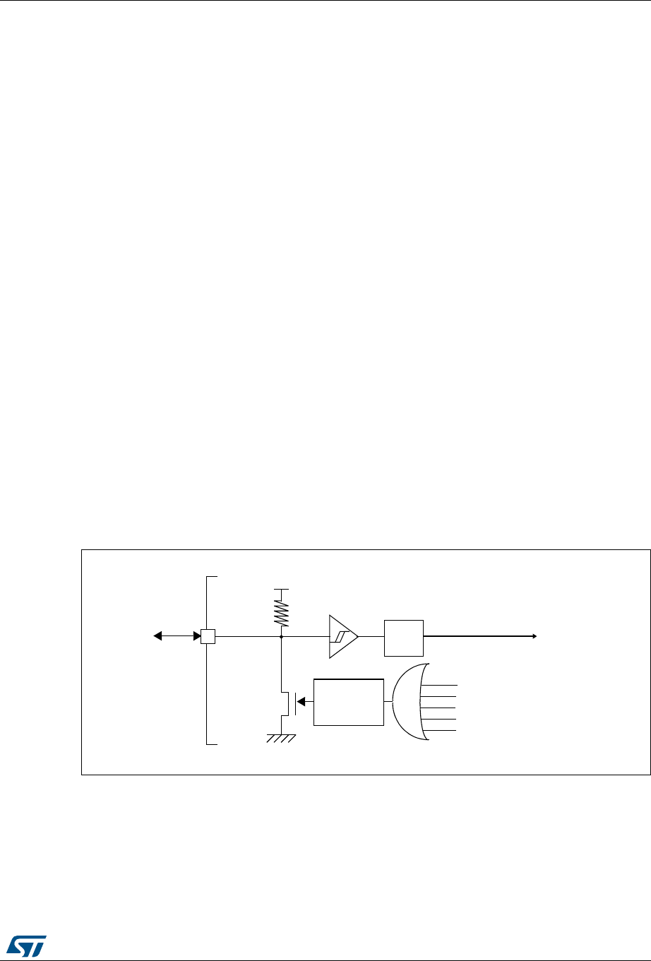
DocID027812 Rev 2 91/766
RM0401 Reset and clock control (RCC)
133
Low-power management reset
There are two ways of generating a low-power management reset:
1. Reset generated when entering the Standby mode:
This type of reset is enabled by resetting the nRST_STDBY bit in the user option bytes.
In this case, whenever a Standby mode entry sequence is successfully executed, the
device is reset instead of entering the Standby mode.
2. Reset when entering the Stop mode:
This type of reset is enabled by resetting the nRST_STOP bit in the user option bytes.
In this case, whenever a Stop mode entry sequence is successfully executed, the
device is reset instead of entering the Stop mode.
For further information on the user option bytes, refer to the STM32F410 Flash
programming manual available from your ST sales office.
5.1.2 Power reset
A power reset is generated when one of the following events occurs:
1. Power-on/power-down reset (POR/PDR reset) or brownout (BOR) reset
2. When exiting the Standby mode
A power reset sets all registers to their reset values except the Backup domain.
These sources act on the NRST pin and it is always kept low during the delay phase. The
RESET service routine vector is fixed at address 0x0000_0004 in the memory map.
The system reset signal provided to the device is output on the NRST pin. The pulse
generator guarantees a minimum reset pulse duration of 20 µs for each internal reset
source. In case of an external reset, the reset pulse is generated while the NRST pin is
asserted low.
Figure 11. Simplified diagram of the reset circuit
1567
538
9''9''$
::'*UHVHW
,:'*UHVHW
3XOVH
JHQHUDWRU 3RZHUUHVHW
([WHUQDO
UHVHW
PLQV
6\VWHPUHVHW
)LOWHU
6RIWZDUHUHVHW
/RZSRZHUPDQDJHPHQWUHVHW
DLF

Reset and clock control (RCC) RM0401
92/766 DocID027812 Rev 2
5.1.3 Backup domain reset
The backup domain reset sets all RTC registers and the RCC_BDCR register to their reset
values.
A backup domain reset is generated when one of the following events occurs:
1. Software reset, triggered by setting the BDRST bit in the RCC Backup domain control
register (RCC_BDCR).
2. VDD or VBAT power on, if both supplies have previously been powered off.
5.2 Clocks
Three different clock sources can be used to drive the system clock (SYSCLK):
•HSI oscillator clock
•HSE oscillator clock
•PLL (PLL) clock
The devices have the two following secondary clock sources:
•32 kHz low-speed internal RC (LSI RC) which drives the independent watchdog and,
optionally, the RTC used for Auto-wakeup from the Stop/Standby mode.
•32.768 kHz low-speed external crystal (LSE crystal) which optionally drives the RTC
clock (RTCCLK)
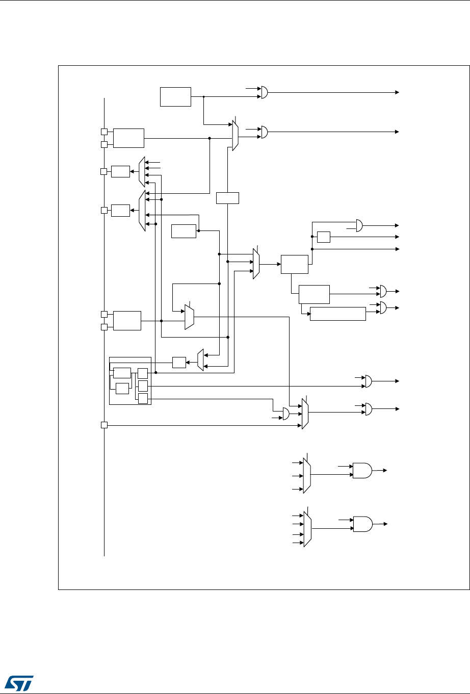
DocID027812 Rev 2 93/766
RM0401 Reset and clock control (RCC)
133
Each clock source can be switched on or off independently when it is not used, to optimize
power consumption.
Figure 12. Clock tree
1. For full details about the internal and external clock source characteristics, refer to the Electrical
characteristics section in the device datasheet.
06Y9
$+%
35(6&
LI$3%[SUHVF [
HOVH[
/6(
)&/.&RUWH[
IUHHUXQQLQJFORFN
$3%[FORFNV
$3%[
WLPHUFORFNV
51*
0&2
3HULSKHUDO
FORFNHQDEOH
0&2
26&B287
/6(26&
N+]
/6,5&
N+]
WR
LQGHSHQGHQW
ZDWFKGRJ
/6(
/6,
WR57&
57&&/.
57&6(/>@
,:'*&/.
26&B,1
26&B287
3//&/.
+6,
+6,
+6(
6:
6<6&/.
0+]
PD[
+&/.
WR$+%EXVFRUH
0HPRU\DQG'0$
0+]PD[
WR&RUWH[6\VWHPWLPHU
&ORFN
(QDEOH
51*
FORFNHQDEOH
$3%[
35(6&
:DWFKGRJ
HQDEOH
57&
HQDEOH
WR
6<6&/.
+6(B57&
+6(
,6B&.,1
26&B,1
3HULSKHUDO
FORFNHQDEOH
3//
[1
3
4
5
9&2
0
0+]
+6,5&
WR
WR
0+]
+6(26&
,6BFN
3//&/.B5
(QDEOHGLI63,,663,,6
RU63,,6DUHHQDEOHG
,665&
,6BFN ,6FORFN
,6BFN
HQDEOH
+6,
6<6&/.
&.B$3%
'&.&)*5
,&)0FORFN
,&BFNB
HQDEOH
/6,
+6,
&.B$3%B7,0
'&.&)*5
/37,0FORFN
/37,0BFNB
HQDEOH
/6(
3//65&

Reset and clock control (RCC) RM0401
94/766 DocID027812 Rev 2
The clock controller provides a high degree of flexibility to the application in the choice of the
external crystal or the oscillator to run the core and peripherals at the highest frequency
and, guarantee the appropriate frequency for peripherals that need a specific clock like
RNG, I2S and low-power timer.
Several prescalers are used to configure the AHB frequency, the high-speed APB (APB2)
and the low-speed APB (APB1) domains. The maximum frequency of the AHB domain is
100 MHz. The maximum allowed frequency of the high-speed APB2 domain is 100 MHz.
The maximum allowed frequency of the low-speed APB1 domain is 50 MHz
All peripheral clocks are derived from the system clock (SYSCLK) except for:
•The low-power timer clock which is derived either from the low-speed internal or low-
speed external oscillator (LSI/LSE), from the high-speed internal (HSI) or from the
system clock.
•The RNG and I2S clocks which come from a specific PLL output.
To achieve high-quality audio performance, the I2S clock can be derived either from the
PLL or from an external clock mapped on the I2S_CKIN pin. For more information
about I2S clock frequency and precision, refer to Section 25.6.3: Clock generator.
The RCC feeds the external clock of the Cortex System Timer (SysTick) with the AHB clock
(HCLK) divided by 8. The SysTick can work either with this clock or with the Cortex clock
(HCLK), configurable in the SysTick control and status register.
The timer clock frequencies are automatically set by hardware. There are two cases:
1. If the APB prescaler is 1, the timer clock frequencies are set to the same frequency as
that of the APB domain to which the timers are connected.
2. Otherwise, they are set to twice (×2) the frequency of the APB domain to which the
timers are connected.
The timer clock frequencies are automatically set by hardware. There are two cases
depending on the value of TIMPRE bit in RCC_DCKCFGR register:
•If TIMPRE bit is reset:
If the APB prescaler is configured to a division factor of 1, the timer clock frequencies
(TIMxCLK) are set to HCLK. Otherwise, the timer clock frequencies are twice the
frequency of the APB domain to which the timers are connected: TIMxCLK = 2xPCLKx.
•If TIMPRE bit is set:
If the APB prescaler is configured to a division factor of 1 or 2, the timer clock
frequencies (TIMxCLK) are set to HCLK. Otherwise, the timer clock frequencies is four
times the frequency of the APB domain to which the timers are connected: TIMxCLK =
4xPCLKx.
FCLK acts as Cortex®-M4 with FPU free-running clock. For more details, refer to the
Cortex®-M4 with FPU technical reference manual.
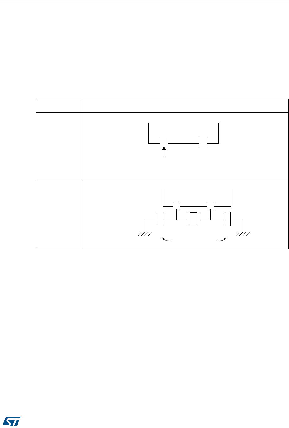
DocID027812 Rev 2 95/766
RM0401 Reset and clock control (RCC)
133
5.2.1 HSE clock
The high speed external clock signal (HSE) can be generated from two possible clock
sources:
•HSE external crystal/ceramic resonator
•HSE external user clock
The resonator and the load capacitors have to be placed as close as possible to the
oscillator pins in order to minimize output distortion and startup stabilization time. The
loading capacitance values must be adjusted according to the selected oscillator.
External source (HSE bypass)
In this mode, an external clock source must be provided. You select this mode by setting the
HSEBYP and HSEON bits in the RCC clock control register (RCC_CR). The external clock
signal (square, sinus or triangle) with ~50% duty cycle has to drive the OSC_IN pin while the
OSC_OUT pin should be left HI-Z. See Figure 13.
External crystal/ceramic resonator (HSE crystal)
The HSE has the advantage of producing a very accurate rate on the main clock.
The associated hardware configuration is shown in Figure 13. Refer to the electrical
characteristics section of the datasheet for more details.
The HSERDY flag in the RCC clock control register (RCC_CR) indicates if the high-speed
external oscillator is stable or not. At startup, the clock is not released until this bit is set by
hardware. An interrupt can be generated if enabled in the RCC clock interrupt register
(RCC_CIR).
The HSE Crystal can be switched on and off using the HSEON bit in the RCC clock control
register (RCC_CR).
Figure 13. HSE/ LSE clock sources
Hardware configuration
External clock
Crystal/ceramic
resonators
OSC_OUT
External
source
(HI-Z)
OSC_IN OSC_OUT
Load
capacitors
CL2
CL1

Reset and clock control (RCC) RM0401
96/766 DocID027812 Rev 2
5.2.2 HSI clock
The HSI clock signal is generated from an internal 16 MHz RC oscillator and can be used
directly as a system clock, or used as PLL input.
The HSI RC oscillator has the advantage of providing a clock source at low cost (no external
components). It also has a faster startup time than the HSE crystal oscillator however, even
with calibration the frequency is less accurate than an external crystal oscillator or ceramic
resonator.
Calibration
RC oscillator frequencies can vary from one chip to another due to manufacturing process
variations, this is why each device is factory calibrated by ST for 1% accuracy at TA= 25 °C.
After reset, the factory calibration value is loaded in the HSICAL[7:0] bits in the RCC clock
control register (RCC_CR).
If the application is subject to voltage or temperature variations this may affect the RC
oscillator speed. You can trim the HSI frequency in the application using the HSITRIM[4:0]
bits in the RCC clock control register (RCC_CR).
The HSIRDY flag in the RCC clock control register (RCC_CR) indicates if the HSI RC is
stable or not. At startup, the HSI RC output clock is not released until this bit is set by
hardware.
The HSI RC can be switched on and off using the HSION bit in the RCC clock control
register (RCC_CR).
The HSI signal can also be used as a backup source (Auxiliary clock) if the HSE crystal
oscillator fails. Refer to Section 5.2.7: Clock security system (CSS) on page 97.
5.2.3 PLL configuration
The STM32F410 devices feature one PLL. The PLL (PLL) is clocked by the HSE or HSI
oscillator and features three different output clocks:
•The first output is used to generate the high speed system clock (up to 100 MHz)
•The second output is used to generate the RNG clock.
•The third output is used to generate an accurate clock to achieve high-quality audio
performance on the I2S interface.
Since the PLL configuration parameters cannot be changed once the PLL is enabled, it is
recommended to configure the PLL before enabling it (selection of the HSI or HSE oscillator
as PLL clock source, and configuration of division factors M, P, Q, R and multiplication factor
N).
The PLL is disabled by hardware when entering Stop and Standby modes, or when an HSE
failure occurs when HSE or PLL (clocked by HSE) are used as system clock. The PLL can
be configured through RCC PLL configuration register (RCC_PLLCFGR).
5.2.4 LSE clock
The LSE clock is generated using a 32.768kHz low speed external crystal or ceramic
resonator. It has the advantage providing a low-power but highly accurate clock source to
the real-time clock peripheral (RTC) for clock/calendar or other timing functions.

DocID027812 Rev 2 97/766
RM0401 Reset and clock control (RCC)
133
The LSE oscillator is switched on and off using the LSEON bit in RCC Backup domain
control register (RCC_BDCR).
The LSERDY flag in the RCC Backup domain control register (RCC_BDCR) indicates if the
LSE crystal is stable or not. At startup, the LSE crystal output clock signal is not released
until this bit is set by hardware. An interrupt can be generated if enabled in the RCC clock
interrupt register (RCC_CIR).
External source (LSE bypass)
In this mode, an external clock source must be provided. It must have a frequency up to
1 MHz. You select this mode by setting the LSEBYP and LSEON bits in the RCC Backup
domain control register (RCC_BDCR). The external clock signal (square, sinus or triangle)
with ~50% duty cycle has to drive the OSC32_IN pin while the OSC32_OUT pin should be
left HI-Z. See Figure 13.
5.2.5 LSI clock
The LSI RC acts as an low-power clock source that can be kept running in Stop and
Standby mode for the independent watchdog (IWDG) and Auto-wakeup unit (AWU). The
clock frequency is around 32 kHz. For more details, refer to the electrical characteristics
section of the datasheets.
The LSI RC can be switched on and off using the LSION bit in the RCC clock control &
status register (RCC_CSR).
The LSIRDY flag in the RCC clock control & status register (RCC_CSR) indicates if the low-
speed internal oscillator is stable or not. At startup, the clock is not released until this bit is
set by hardware. An interrupt can be generated if enabled in the RCC clock interrupt register
(RCC_CIR).
5.2.6 System clock (SYSCLK) selection
After a system reset, the HSI oscillator is selected as the system clock. When a clock source
is used directly or through PLL as the system clock, it is not possible to stop it.
A switch from one clock source to another occurs only if the target clock source is ready
(clock stable after startup delay or PLL locked). If a clock source that is not yet ready is
selected, the switch occurs when the clock source is ready. Status bits in the RCC clock
control register (RCC_CR) indicate which clock(s) is (are) ready and which clock is currently
used as the system clock.
5.2.7 Clock security system (CSS)
The clock security system can be activated by software. In this case, the clock detector is
enabled after the HSE oscillator startup delay, and disabled when this oscillator is stopped.
If a failure is detected on the HSE clock, this oscillator is automatically disabled, a clock
failure event is sent to the break inputs of advanced-control timer TIM1, and an interrupt is
generated to inform the software about the failure (clock security system interrupt CSSI),
allowing the MCU to perform rescue operations. The CSSI is linked to the Cortex®-M4 with
FPU NMI (non-maskable interrupt) exception vector.
Note: When the CSS is enabled, if the HSE clock happens to fail, the CSS generates an interrupt,
which causes the automatic generation of an NMI. The NMI is executed indefinitely unless
the CSS interrupt pending bit is cleared. As a consequence, the application has to clear the

Reset and clock control (RCC) RM0401
98/766 DocID027812 Rev 2
CSS interrupt in the NMI ISR by setting the CSSC bit in the Clock interrupt register
(RCC_CIR).
If the HSE oscillator is used directly or indirectly as the system clock (indirectly meaning that
it is directly used as PLL input clock, and that PLL clock is the system clock) and a failure is
detected, then the system clock switches to the HSI oscillator and the HSE oscillator is
disabled.
If the HSE oscillator clock was the clock source of PLL used as the system clock when the
failure occurred, PLL is also disabled.
5.2.8 RTC/AWU clock
Once the RTCCLK clock source has been selected, the only possible way of modifying the
selection is to reset the power domain.
The RTCCLK clock source can be either the HSE 1 MHz (HSE divided by a programmable
prescaler), the LSE or the LSI clock. This is selected by programming the RTCSEL[1:0] bits
in the RCC Backup domain control register (RCC_BDCR) and the RTCPRE[4:0] bits in RCC
clock configuration register (RCC_CFGR). This selection cannot be modified without
resetting the Backup domain.
If the LSE is selected as the RTC clock, the RTC will work normally if the backup or the
system supply disappears. If the LSI is selected as the AWU clock, the AWU state is not
guaranteed if the system supply disappears. If the HSE oscillator divided by a value
between 2 and 31 is used as the RTC clock, the RTC state is not guaranteed if the backup
or the system supply disappears.
The LSE clock is in the Backup domain, whereas the HSE and LSI clocks are not. As a
consequence:
•If LSE is selected as the RTC clock:
–The RTC continues to work even if the VDD supply is switched off, provided the
VBAT supply is maintained.
•If LSI is selected as the Auto-wakeup unit (AWU) clock:
– The AWU state is not guaranteed if the VDD supply is powered off. Refer to
Section 5.2.5: LSI clock on page 97 for more details on LSI calibration.
•If the HSE clock is used as the RTC clock:
– The RTC state is not guaranteed if the VDD supply is powered off or if the internal
voltage regulator is powered off (removing power from the 1.2 V domain).
Note: To read the RTC calendar register when the APB1 clock frequency is less than seven times
the RTC clock frequency (fAPB1 < 7xfRTCLCK), the software must read the calendar time and
date registers twice. The data are correct if the second read access to RTC_TR gives the
same result than the first one. Otherwise a third read access must be performed.
5.2.9 Watchdog clock
If the independent watchdog (IWDG) is started by either hardware option or software
access, the LSI oscillator is forced ON and cannot be disabled. After the LSI oscillator
temporization, the clock is provided to the IWDG.

DocID027812 Rev 2 99/766
RM0401 Reset and clock control (RCC)
133
5.2.10 Clock-out capability
Two microcontroller clock output (MCO) pins are available:
•MCO1
You can output four different clock sources onto the MCO1 pin (PA8) using the
configurable prescaler (from 1 to 5):
–HSI clock
– LSE clock
– HSE clock
– PLL clock
The desired clock source is selected using the MCO1PRE[2:0] and MCO1[1:0] bits in
the RCC clock configuration register (RCC_CFGR).
•MCO2
You can output four different clock sources onto the MCO2 pin (PC9) using the
configurable prescaler (from 1 to 5):
– System clock (SYSCLK)
– I2S clock (I2S gated clock)
– HSE clock
– PLL clock
The desired clock source is selected using the MCO2PRE[2:0] and MCO2 bits in the
RCC clock configuration register (RCC_CFGR).
For the different MCO pins, the corresponding GPIO port has to be programmed in alternate
function mode.
The selected clock to output onto MCO must not exceed 100 MHz (the maximum I/O
speed).
5.2.11 Internal/external clock measurement using TIM5/TIM11
It is possible to indirectly measure the frequencies of all on-board clock source generators
by means of the input capture of TIM5 channel4 and TIM11 channel1 as shown in Figure 14
and Figure 15.
Internal/external clock measurement using TIM5 channel4
TIM5 has an input multiplexer which allows choosing whether the input capture is triggered
by the I/O or by an internal clock. This selection is performed through the TI4_RMP [1:0] bits
in the TIM5_OR register.
The primary purpose of having the LSE connected to the channel4 input capture is to be
able to precisely measure the HSI (this requires to have the HSI used as the system clock
source). The number of HSI clock counts between consecutive edges of the LSE signal
provides a measurement of the internal clock period. Taking advantage of the high precision
of LSE crystals (typically a few tens of ppm) we can determine the internal clock frequency
with the same resolution, and trim the source to compensate for manufacturing-process
and/or temperature- and voltage-related frequency deviations.
The HSI oscillator has dedicated, user-accessible calibration bits for this purpose.
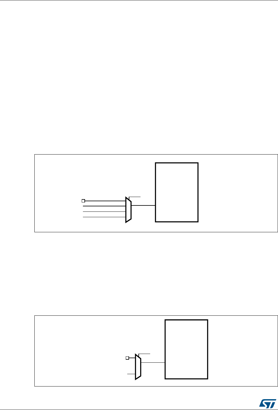
Reset and clock control (RCC) RM0401
100/766 DocID027812 Rev 2
The basic concept consists in providing a relative measurement (e.g. HSI/LSE ratio): the
precision is therefore tightly linked to the ratio between the two clock sources. The greater
the ratio, the better the measurement.
It is also possible to measure the LSI frequency: this is useful for applications that do not
have a crystal. The ultralow-power LSI oscillator has a large manufacturing process
deviation: by measuring it versus the HSI clock source, it is possible to determine its
frequency with the precision of the HSI. The measured value can be used to have more
accurate RTC time base timeouts (when LSI is used as the RTC clock source) and/or an
IWDG timeout with an acceptable accuracy.
Use the following procedure to measure the LSI frequency:
1. Enable the TIM5 timer and configure channel4 in Input capture mode.
2. Set the TI4_RMP bits in the TIM5_OR register to 0x01 to connect the LSI clock
internally to TIM5 channel4 input capture for calibration purposes.
3. Measure the LSI clock frequency using the TIM5 capture/compare 4 event or interrupt.
4. Use the measured LSI frequency to update the prescaler of the RTC depending on the
desired time base and/or to compute the IWDG timeout.
Figure 14. Frequency measurement with TIM5 in Input capture mode
Internal/external clock measurement using TIM11 channel1
TIM11 has an input multiplexer which allows choosing whether the input capture is triggered
by the I/O or by an internal clock. This selection is performed through TI1_RMP [1:0] bits in
the TIM11_OR register. The HSE_RTC clock (HSE divided by a programmable prescaler) is
connected to channel 1 input capture to have a rough indication of the external crystal
frequency. This requires that the HSI is the system clock source. This can be useful for
instance to ensure compliance with the IEC 60730/IEC 61335 standards which require to be
able to determine harmonic or subharmonic frequencies (–50/+100% deviations).
Figure 15. Frequency measurement with TIM11 in Input capture mode
4)-
4)
4)?2-0;=
'0)/
24#?7AKE5P?)4
,3%
,3)
AI6
4)-
4)
4)?2-0;=
'0)/
(3%?24#-(Z
AI

DocID027812 Rev 2 101/766
RM0401 Reset and clock control (RCC)
133
5.3 RCC registers
Refer to Section 1.1: List of abbreviations for registers for a list of abbreviations used in
register descriptions.
5.3.1 RCC clock control register (RCC_CR)
Address offset: 0x00
Reset value: 0x0000 XX81 where X is undefined.
Access: no wait state, word, half-word and byte access
31 30 29 28 27 26 25 24 23 22 21 20 19 18 17 16
Res. Res. Res. Res. Res. Res. PLLRDY PLLON Res. Res. Res. Res. CSS
ON
HSE
BYP
HSE
RDY HSE ON
rrw rwrwrrw
15 14 13 12 11 10 9 8 7 6 5 4 3 2 1 0
HSICAL[7:0] HSITRIM[4:0] Res. HSI
RDY HSION
rrrrrr r rrwrwrwrwrw rrw
Bits 31:26 Reserved, must be kept at reset value.
Bit 25 PLLRDY: Main PLL (PLL) clock ready flag
Set by hardware to indicate that PLL is locked.
0: PLL unlocked
1: PLL locked
Bit 24 PLLON: Main PLL (PLL) enable
Set and cleared by software to enable PLL.
Cleared by hardware when entering Stop or Standby mode. This bit cannot be reset if PLL
clock is used as the system clock.
0: PLL OFF
1: PLL ON
Bits 23:20 Reserved, must be kept at reset value.
Bit 19 CSSON: Clock security system enable
Set and cleared by software to enable the clock security system. When CSSON is set, the
clock detector is enabled by hardware when the HSE oscillator is ready, and disabled by
hardware if an oscillator failure is detected.
0: Clock security system OFF (Clock detector OFF)
1: Clock security system ON (Clock detector ON if HSE oscillator is stable, OFF if not)
Bit 18 HSEBYP: HSE clock bypass
Set and cleared by software to bypass the oscillator with an external clock. The external
clock must be enabled with the HSEON bit, to be used by the device.
The HSEBYP bit can be written only if the HSE oscillator is disabled.
0: HSE oscillator not bypassed
1: HSE oscillator bypassed with an external clock
Bit 17 HSERDY: HSE clock ready flag
Set by hardware to indicate that the HSE oscillator is stable. After the HSEON bit is cleared,
HSERDY goes low after 6 HSE oscillator clock cycles.
0: HSE oscillator not ready
1: HSE oscillator ready

Reset and clock control (RCC) RM0401
102/766 DocID027812 Rev 2
Bit 16 HSEON: HSE clock enable
Set and cleared by software.
Cleared by hardware to stop the HSE oscillator when entering Stop or Standby mode. This
bit cannot be reset if the HSE oscillator is used directly or indirectly as the system clock.
0: HSE oscillator OFF
1: HSE oscillator ON
Bits 15:8 HSICAL[7:0]: Internal high-speed clock calibration
These bits are initialized automatically at startup.
Bits 7:3 HSITRIM[4:0]: Internal high-speed clock trimming
These bits provide an additional user-programmable trimming value that is added to the
HSICAL[7:0] bits. It can be programmed to adjust to variations in voltage and temperature
that influence the frequency of the internal HSI RC.
Bit 2 Reserved, must be kept at reset value.
Bit 1 HSIRDY: Internal high-speed clock ready flag
Set by hardware to indicate that the HSI oscillator is stable. After the HSION bit is cleared,
HSIRDY goes low after 6 HSI clock cycles.
0: HSI oscillator not ready
1: HSI oscillator ready
Bit 0 HSION: Internal high-speed clock enable
Set and cleared by software.
Set by hardware to force the HSI oscillator ON when leaving the Stop or Standby mode or in
case of a failure of the HSE oscillator used directly or indirectly as the system clock. This bit
cannot be cleared if the HSI is used directly or indirectly as the system clock.
0: HSI oscillator OFF
1: HSI oscillator ON

DocID027812 Rev 2 103/766
RM0401 Reset and clock control (RCC)
133
5.3.2 RCC PLL configuration register (RCC_PLLCFGR)
Address offset: 0x04
Reset value: 0x7F00 3010
Access: no wait state, word, half-word and byte access.
This register is used to configure the PLL clock outputs according to the formulas:
•f(VCO clock) = f(PLL clock input) × (PLLN / PLLM)
•f(PLL general clock output) = f(VCO clock) / PLLP
•f(I2S, System) = f(VCO clock) / PLLR
31 30 29 28 27 26 25 24 23 22 21 20 19 18 17 16
Res. PLLR3 PLLR2 PLLR1 PLLQ3 PLLQ2 PLLQ1 PLLQ0 Reserv
ed
PLLSRC Res. Res. Res. Res. PLLP1 PLLP0
rw rw rw rw rw rw rw rw rw rw
15 14 13 12 11 10 9 8 7 6 5 4 3 2 1 0
Res. PLLN PLLM5 PLLM4 PLLM3 PLLM2 PLLM1 PLLM0
rw rw rw rw rw rw rw rw rw rw rw rw rw rw rw
Bit 31 Reserved, must be kept at reset value.
Bits 30:28 PLLR: PLL division factor for I2S and System clocks
Set and cleared by software to control the clock frequency. These bits should be written only
if PLL is disabled.
clock frequency = VCO frequency / PLLR with 2 ≤ PLLR ≤ 7
000: PLL = 0, wrong configuration
001: PLL = 1, wrong configuration
010: PLL = 2
...
111: PLL = 7
Bits 27:24 PLLQ: Main PLL (PLL) division factor for random number generator clocks
Set and cleared by software to control the frequency of the random number generator clock.
These bits should be written only if PLL is disabled.
0000: PLLQ = 0, wrong configuration
0001: PLLQ = 1, wrong configuration
0010: PLLQ = 2
0011: PLLQ = 3
0100: PLLQ = 4
...
1111: PLLQ = 15
Bit 23 Reserved, must be kept at reset value.
Bit 22 PLLSRC: Main PLL(PLL) entry clock source
Set and cleared by software to select PLL clock source. This bit can be written only when
the PLL is disabled.
0: HSI clock selected as PLL clock entry
1: HSE oscillator clock selected as PLL clock entry
Bits 21:18 Reserved, must be kept at reset value.

Reset and clock control (RCC) RM0401
104/766 DocID027812 Rev 2
Bits 17:16 PLLP: Main PLL (PLL) division factor for main system clock
Set and cleared by software to control the frequency of the general PLL output clock. These
bits can be written only if PLL is disabled.
Caution: The software has to set these bits correctly not to exceed 100 MHz on this domain.
PLL output clock frequency = VCO frequency / PLLP with PLLP = 2, 4, 6, or 8
00: PLLP = 2
01: PLLP = 4
10: PLLP = 6
11: PLLP = 8
Bit 15 Reserved, must be kept at reset value.
Bits 14:6 PLLN: Main PLL (PLL) multiplication factor for VCO
Set and cleared by software to control the multiplication factor of the VCO. These bits can
be written only when PLL is disabled. Only half-word and word accesses are allowed to
write these bits.
Caution: The software has to set these bits correctly to ensure that the VCO output
frequency is between 100 and 432 MHz. (check also Section 5.3.17: RCC
Dedicated Clocks Configuration Register (RCC_DCKCFGR))
VCO output frequency = VCO input frequency × PLLN with 50 ≤ PLLN ≤ 432
000000000: PLLN = 0, wrong configuration
000000001: PLLN = 1, wrong configuration
...
000110010: PLLN = 50
...
001100011: PLLN = 99
001100100: PLLN = 100
...
110110000: PLLN = 432
110110001: PLLN = 433, wrong configuration
...
111111111: PLLN = 511, wrong configuration
Note: Multiplication factors possible for VCO input frequency higher than 1 MHz but care
must be taken to fulfill the minimum VCO output frequency as specified above.
Bits 5:0 PLLM: Division factor for the main PLL (PLL) input clock
Set and cleared by software to divide the PLL input clock before the VCO. These bits can be
written only when the PLL is disabled.
Caution: The software has to set these bits correctly to ensure that the VCO input frequency
ranges from 1 to 2 MHz. It is recommended to select a frequency of 2 MHz to limit
PLL jitter.
VCO input frequency = PLL input clock frequency / PLLM with 2 ≤ PLLM ≤ 63
000000: PLLM = 0, wrong configuration
000001: PLLM = 1, wrong configuration
000010: PLLM = 2
000011: PLLM = 3
000100: PLLM = 4
...
111110: PLLM = 62
111111: PLLM = 63

DocID027812 Rev 2 105/766
RM0401 Reset and clock control (RCC)
133
5.3.3 RCC clock configuration register (RCC_CFGR)
Address offset: 0x08
Reset value: 0x0000 0000
Access: 0 ≤ wait state ≤ 2, word, half-word and byte access
1 or 2 wait states inserted only if the access occurs during a clock source switch.
31 30 29 28 27 26 25 24 23 22 21 20 19 18 17 16
MCO2 MCO2 PRE[2:0] MCO1 PRE[2:0] Res. MCO1 RTCPRE[4:0]
rw rw rw rw rw rw rw rw rw rw rw rw rw
15 14 13 12 11 10 9 8 7 6 5 4 3 2 1 0
PPRE2[2:0] PPRE1[2:0] MCO2
EN
MCO1
EN HPRE[3:0] SWS1 SWS0 SW1 SW0
rw rw rw rw rw rw rw rw rw rw rw rw r r rw rw
Bits 31:30 MCO2[1:0]: Microcontroller clock output 2
Set and cleared by software. Clock source selection may generate glitches on MCO2. It is
highly recommended to configure these bits only after reset before enabling the external
oscillators and the PLLs.
00: System clock (SYSCLK) selected
01: Main PLL clock (I2S)
10: HSE oscillator clock selected
11: PLL clock selected
Bits 29:27 MCO2PRE: MCO2 prescaler
Set and cleared by software to configure the prescaler of the MCO2. Modification of this
prescaler may generate glitches on MCO2. It is highly recommended to change this
prescaler only after reset before enabling the external oscillators and the PLLs.
0xx: no division
100: division by 2
101: division by 3
110: division by 4
111: division by 5
Bits 26:24 MCO1PRE: MCO1 prescaler
Set and cleared by software to configure the prescaler of the MCO1. Modification of this
prescaler may generate glitches on MCO1. It is highly recommended to change this
prescaler only after reset before enabling the external oscillators and the PLL.
0xx: no division
100: division by 2
101: division by 3
110: division by 4
111: division by 5
Bit 23 Reserved, must be kept at reset value.

Reset and clock control (RCC) RM0401
106/766 DocID027812 Rev 2
Bits 22:21 MCO1: Microcontroller clock output 1
Set and cleared by software. Clock source selection may generate glitches on MCO1. It is
highly recommended to configure these bits only after reset before enabling the external
oscillators and PLL.
00: HSI clock selected
01: LSE oscillator selected
10: HSE oscillator clock selected
11: PLL clock selected
Bits 20:16 RTCPRE: HSE division factor for RTC clock
Set and cleared by software to divide the HSE clock input clock to generate a 1 MHz clock for
RTC.
Caution: The software has to set these bits correctly to ensure that the clock supplied to the
RTC is 1 MHz. These bits must be configured if needed before selecting the RTC
clock source.
00000: no clock
00001: no clock
00010: HSE/2
00011: HSE/3
00100: HSE/4
...
11110: HSE/30
11111: HSE/31
Bits 15:13 PPRE2: APB high-speed prescaler (APB2)
Set and cleared by software to control APB high-speed clock division factor.
Caution: The software has to set these bits correctly not to exceed 100 MHz on this domain.
The clocks are divided with the new prescaler factor from 1 to 16 AHB cycles after
PPRE2 write.
0xx: AHB clock not divided
100: AHB clock divided by 2
101: AHB clock divided by 4
110: AHB clock divided by 8
111: AHB clock divided by 16
Bits 12:10 PPRE1: APB Low speed prescaler (APB1)
Set and cleared by software to control APB low-speed clock division factor.
Caution: The software has to set these bits correctly not to exceed 50 MHz on this domain.
The clocks are divided with the new prescaler factor from 1 to 16 AHB cycles after
PPRE1 write.
0xx: AHB clock not divided
100: AHB clock divided by 2
101: AHB clock divided by 4
110: AHB clock divided by 8
111: AHB clock divided by 16
Bit 9 MCO2EN: MCO2 output enable
0: MCO2 output disabled
1: MCO2 output enabled
Bit 8 MCO1EN: MCO1 output enable
0: MCO1 output disabled
1: MCO1 output enabled

DocID027812 Rev 2 107/766
RM0401 Reset and clock control (RCC)
133
Bits 7:4 HPRE: AHB prescaler
Set and cleared by software to control AHB clock division factor.
Caution: The clocks are divided with the new prescaler factor from 1 to 16 AHB cycles after
HPRE write.
Caution: The AHB clock frequency must be at least 25 MHz when the Ethernet is used.
0xxx: system clock not divided
1000: system clock divided by 2
1001: system clock divided by 4
1010: system clock divided by 8
1011: system clock divided by 16
1100: system clock divided by 64
1101: system clock divided by 128
1110: system clock divided by 256
1111: system clock divided by 512
Bits 3:2 SWS: System clock switch status
Set and cleared by hardware to indicate which clock source is used as the system clock.
00: HSI oscillator used as the system clock
01: HSE oscillator used as the system clock
10: PLL used as the system clock
11: not applicable
Bits 1:0 SW: System clock switch
Set and cleared by software to select the system clock source.
Set by hardware to force the HSI selection when leaving the Stop or Standby mode or in case
of failure of the HSE oscillator used directly or indirectly as the system clock.
00: HSI oscillator selected as system clock
01: HSE oscillator selected as system clock
10: PLL selected as system clock
11: not allowed

Reset and clock control (RCC) RM0401
108/766 DocID027812 Rev 2
5.3.4 RCC clock interrupt register (RCC_CIR)
Address offset: 0x0C
Reset value: 0x0000 0000
Access: no wait state, word, half-word and byte access
31 30 29 28 27 26 25 24 23 22 21 20 19 18 17 16
Reserved
CSSC Res. Res. PLL
RDYC
HSE
RDYC
HSI
RDYC
LSE
RDYC
LSI
RDYC
wwwwww
15 14 13 12 11 10 9 8 7 6 5 4 3 2 1 0
Res. Res. Res. PLL
RDYIE
HSE
RDYIE
HSI
RDYIE
LSE
RDYIE
LSI
RDYIE CSSF Res. Res. PLL
RDYF
HSE
RDYF
HSI
RDYF
LSE
RDYF
LSI
RDYF
rw rw rw rw rw r r r r r r
Bits 31:24 Reserved, must be kept at reset value.
Bit 23 CSSC: Clock security system interrupt clear
This bit is set by software to clear the CSSF flag.
0: No effect
1: Clear CSSF flag
Bits 22:21 Reserved, must be kept at reset value.
Bit 20 PLLRDYC: Main PLL(PLL) ready interrupt clear
This bit is set by software to clear the PLLRDYF flag.
0: No effect
1: PLLRDYF cleared
Bit 19 HSERDYC: HSE ready interrupt clear
This bit is set by software to clear the HSERDYF flag.
0: No effect
1: HSERDYF cleared
Bit 18 HSIRDYC: HSI ready interrupt clear
This bit is set software to clear the HSIRDYF flag.
0: No effect
1: HSIRDYF cleared
Bit 17 LSERDYC: LSE ready interrupt clear
This bit is set by software to clear the LSERDYF flag.
0: No effect
1: LSERDYF cleared
Bit 16 LSIRDYC: LSI ready interrupt clear
This bit is set by software to clear the LSIRDYF flag.
0: No effect
1: LSIRDYF cleared
Bits 15:13 Reserved, must be kept at reset value.

DocID027812 Rev 2 109/766
RM0401 Reset and clock control (RCC)
133
Bit 12 PLLRDYIE: Main PLL (PLL) ready interrupt enable
Set and cleared by software to enable/disable interrupt caused by PLL lock.
0: PLL lock interrupt disabled
1: PLL lock interrupt enabled
Bit 11 HSERDYIE: HSE ready interrupt enable
Set and cleared by software to enable/disable interrupt caused by the HSE oscillator
stabilization.
0: HSE ready interrupt disabled
1: HSE ready interrupt enabled
Bit 10 HSIRDYIE: HSI ready interrupt enable
Set and cleared by software to enable/disable interrupt caused by the HSI oscillator
stabilization.
0: HSI ready interrupt disabled
1: HSI ready interrupt enabled
Bit 9 LSERDYIE: LSE ready interrupt enable
Set and cleared by software to enable/disable interrupt caused by the LSE oscillator
stabilization.
0: LSE ready interrupt disabled
1: LSE ready interrupt enabled
Bit 8 LSIRDYIE: LSI ready interrupt enable
Set and cleared by software to enable/disable interrupt caused by LSI oscillator
stabilization.
0: LSI ready interrupt disabled
1: LSI ready interrupt enabled
Bit 7 CSSF: Clock security system interrupt flag
Set by hardware when a failure is detected in the HSE oscillator.
Cleared by software setting the CSSC bit.
0: No clock security interrupt caused by HSE clock failure
1: Clock security interrupt caused by HSE clock failure
Bits 6:5 Reserved, must be kept at reset value.
Bit 4 PLLRDYF: Main PLL (PLL) ready interrupt flag
Set by hardware when PLL locks and PLLRDYDIE is set.
Cleared by software setting the PLLRDYC bit.
0: No clock ready interrupt caused by PLL lock
1: Clock ready interrupt caused by PLL lock
Bit 3 HSERDYF: HSE ready interrupt flag
Set by hardware when External High Speed clock becomes stable and HSERDYDIE is set.
Cleared by software setting the HSERDYC bit.
0: No clock ready interrupt caused by the HSE oscillator
1: Clock ready interrupt caused by the HSE oscillator
Bit 2 HSIRDYF: HSI ready interrupt flag
Set by hardware when the Internal High Speed clock becomes stable and HSIRDYDIE is
set.
Cleared by software setting the HSIRDYC bit.
0: No clock ready interrupt caused by the HSI oscillator
1: Clock ready interrupt caused by the HSI oscillator

Reset and clock control (RCC) RM0401
110/766 DocID027812 Rev 2
5.3.5 RCC AHB1 peripheral reset register (RCC_AHB1RSTR)
Address offset: 0x10
Reset value: 0x0000 0000
Access: no wait state, word, half-word and byte access.
Bit 1 LSERDYF: LSE ready interrupt flag
Set by hardware when the External Low Speed clock becomes stable and LSERDYDIE is
set.
Cleared by software setting the LSERDYC bit.
0: No clock ready interrupt caused by the LSE oscillator
1: Clock ready interrupt caused by the LSE oscillator
Bit 0 LSIRDYF: LSI ready interrupt flag
Set by hardware when the internal low speed clock becomes stable and LSIRDYDIE is set.
Cleared by software setting the LSIRDYC bit.
0: No clock ready interrupt caused by the LSI oscillator
1: Clock ready interrupt caused by the LSI oscillator
31 30 29 28 27 26 25 24 23 22 21 20 19 18 17 16
RNG
RST Res. Res. Res. Res. Res. Res. Res. Res. DMA2
RST
DMA1
RST Res. Res. Res. Res. Res.
rw rw rw
15 14 13 12 11 10 9 8 7 6 5 4 3 2 1 0
Res. Res. Res. CRCRST Res. Res. Res. Res. GPIOH
RST Res. Res. Res. Res. GPIOC
RST
GPIOB
RST
GPIOA
RST
rw rw rw rw rw
Bit 31 RNGRST: RNG reset
Set and cleared by software.
0: does not reset RNG
1: resets RNG
Bits 30:23 Reserved, must be kept at reset value.
Bit 22 DMA2RST: DMA2 reset
Set and cleared by software.
0: does not reset DMA2
1: resets DMA2
Bit 21 DMA1RST: DMA1 reset
Set and cleared by software.
0: does not reset DMA1
1: resets DMA1
Bits 20:13 Reserved, must be kept at reset value.
Bit 12 CRCRST: CRC reset
Set and cleared by software.
0: does not reset CRC
1: resets CRC
Bits 11:8 Reserved, must be kept at reset value.

DocID027812 Rev 2 111/766
RM0401 Reset and clock control (RCC)
133
5.3.6 RCC APB1 peripheral reset register for (RCC_APB1RSTR)
Address offset: 0x20
Reset value: 0x0000 0000
Access: no wait state, word, half-word and byte access.
Bit 7 GPIOHRST: IO port H reset
Set and cleared by software.
0: does not reset IO port H
1: resets IO port H
Bits 6:3 Reserved, must be kept at reset value.
Bit 2 GPIOCRST: IO port C reset
Set and cleared by software.
0: does not reset IO port C
1: resets IO port C
Bit 1 GPIOBRST: IO port B reset
Set and cleared by software.
0: does not reset IO port B
1:resets IO port B
Bit 0 GPIOARST: IO port A reset
Set and cleared by software.
0: does not reset IO port A
1: resets IO port A
31 30 29 28 27 26 25 24 23 22 21 20 19 18 17 16
Res. Res. DAC
RST
PWR
RST Res. Res. Res. I2C4
RST Res. I2C2
RST
I2C1
RST Res. Res. Res. USART2
RST Res.
rw rw rw rw rw rw
151413121110987654321Res.
Res. SPI2
RST Res. Res. WWDG
RST Res. LPTIM1
RST Res. Res. Res. Res. TIM6
RST
TIM5
RST Res. Res. Res.
rw rw rw rw rw
Bits 31:30 Reserved, must be kept at reset value.
Bit 29 DACRST: DAC reset
Set and cleared by software.
0: does not reset the DAC interface
1: resets the DAC interface
Bit 28 PWRRST: Power interface reset
Set and cleared by software.
0: does not reset the power interface
1: resets the power interface
Bits 27:25 Reserved, must be kept at reset value.

Reset and clock control (RCC) RM0401
112/766 DocID027812 Rev 2
Bit 24 I2C4RST: I2C4 reset
Set and cleared by software.
0: does not reset I2C4
1: resets I2C4
Bit 23 Reserved, must be kept at reset value.
Bit 22 I2C2RST: I2C2 reset
Set and cleared by software.
0: does not reset I2C2
1: resets I2C2
Bit 21 I2C1RST: I2C1 reset
Set and cleared by software.
0: does not reset I2C1
1: resets I2C1
Bits 20:18 Reserved, must be kept at reset value.
Bit 17 USART2RST: USART2 reset
Set and cleared by software.
0: does not reset USART2
1: resets USART2
Bits 16:15 Reserved, must be kept at reset value.
Bit 14 SPI2RST: SPI2 reset
Set and cleared by software.
0: does not reset SPI2
1: resets SPI2
Bits 13:12 Reserved, must be kept at reset value.
Bit 11 WWDGRST: Window watchdog reset
Set and cleared by software.
0: does not reset the window watchdog
1: resets the window watchdog
Bit 10 Reserved, must be kept at reset value.
Bit 9 LPTIM1RST: LPTIM1 reset
Set and cleared by software.
0: does not reset LPTIM1
1: resets LPTIM1
Bits 8:5 Reserved, must be kept at reset value.
Bit 4 TIM6RST: TIM6 reset
Set and cleared by software.
0: does not reset TIM6
1: resets TIM6
Bit 3 TIM5RST: TIM5 reset
Set and cleared by software.
0: does not reset TIM5
1: resets TIM5
Bits 2:0 Reserved, must be kept at reset value.

DocID027812 Rev 2 113/766
RM0401 Reset and clock control (RCC)
133
5.3.7 RCC APB2 peripheral reset register (RCC_APB2RSTR)
Address offset: 0x24
Reset value: 0x0000 0000
Access: no wait state, word, half-word and byte access.
31 30 29 28 27 26 25 24 23 22 21 20 19 18 17 16
Res. Res. Res. Res. Res. Res. Res. Res. Res. Res. Res. SPI5
RST Res. TIM11
RST Res. TIM9
RST
rw rw rw
15 14 13 12 11 10 9 8 7 6 5 4 3 2 1 0
Res. SYSCFG
RST Res. SPI1
RST Res. Res. Res. ADC1
RST Res. Res. USART6
RST
USART1
RST Res. Res. Res. TIM1
RST
rw rw rw rw rw rw
Bits 31:21 Reserved, must be kept at reset value.
Bit 20 SPI5RST: SPI5RST
This bit is set and cleared by software.
0: does not reset SPI5
1: resets SPI5
Bit 19 Reserved, must be kept at reset value.
Bit 18 TIM11RST: TIM11 reset
Set and cleared by software.
0: does not reset TIM11
1: resets TIM11
Bit 17 Reserved, must be kept at reset value.
Bit 16 TIM9RST: TIM9 reset
Set and cleared by software.
0: does not reset TIM9
1: resets TIM9
Bit 15 Reserved, must be kept at reset value.
Bit 14 SYSCFGRST: System configuration controller reset
Set and cleared by software.
0: does not reset the System configuration controller
1: resets the System configuration controller
Bit 13 Reserved, must be kept at reset value.
Bit 12 SPI1RST: SPI1 reset
Set and cleared by software.
0: does not reset SPI1
1: resets SPI1
Bit 11 Reserved, must be kept at reset value.
Bits 10:9 Reserved, must be kept at reset value.
Bit 8 ADC1RST: ADC interface reset
Set and cleared by software.
0: does not reset the ADC interface
1: resets the ADC interface

Reset and clock control (RCC) RM0401
114/766 DocID027812 Rev 2
Bits 7:6 Reserved, must be kept at reset value.
Bit 5 USART6RST: USART6 reset
Set and cleared by software.
0: does not reset USART6
1: resets USART6
Bit 4 USART1RST: USART1 reset
Set and cleared by software.
0: does not reset USART1
1: resets USART1
Bits 3:1 Reserved, must be kept at reset value.
Bit 0 TIM1RST: TIM1 reset
Set and cleared by software.
0: does not reset TIM1
1: resets TIM1

DocID027812 Rev 2 115/766
RM0401 Reset and clock control (RCC)
133
5.3.8 RCC AHB1 peripheral clock enable register (RCC_AHB1ENR)
Address offset: 0x30
Reset value: 0x0000 0000
Access: no wait state, word, half-word and byte access.
31 30 29 28 27 26 25 24 23 22 21 20 19 18 17 16
RNGEN Res. Res. Res. Res. Res. Res. Res. Res. DMA2EN DMA1EN Res. Res. Res. Res. Res.
rw rw rw
15 14 13 12 11 10 9 8 7 6 5 4 3 2 1 0
Res. Res. Res. CRCEN Res. Res. Res. Res. GPIOH
EN Res. Res. Res. Res. GPIOC
EN
GPIOB
EN
GPIOA
EN
rw rw rw rw rw
Bit 31 RNGEN: RNG clock enable
Set and cleared by software.
0: RNG clock disabled
1: RNG clock enabled
Bits 30:23 Reserved, must be kept at reset value.
Bit 22 DMA2EN: DMA2 clock enable
Set and cleared by software.
0: DMA2 clock disabled
1: DMA2 clock enabled
Bit 21 DMA1EN: DMA1 clock enable
Set and cleared by software.
0: DMA1 clock disabled
1: DMA1 clock enabled
Bits 20:13 Reserved, must be kept at reset value.
Bit 12 CRCEN: CRC clock enable
Set and cleared by software.
0: CRC clock disabled
1: CRC clock enabled
Bits 11:8 Reserved, must be kept at reset value.
Bit 7 GPIOHEN: IO port H clock enable
Set and reset by software.
0: IO port H clock disabled
1: IO port H clock enabled
Bits 6:3 Reserved, must be kept at reset value.
Bit 2 GPIOCEN: IO port C clock enable
Set and cleared by software.
0: IO port C clock disabled
1: IO port C clock enabled
Bit 1 GPIOBEN: IO port B clock enable
Set and cleared by software.
0: IO port B clock disabled
1: IO port B clock enabled

Reset and clock control (RCC) RM0401
116/766 DocID027812 Rev 2
5.3.9 RCC APB1 peripheral clock enable register (RCC_APB1ENR)
Address offset: 0x40
Reset value: 0x0000 0000
Access: no wait state, word, half-word and byte access.
Bit 0 GPIOAEN: IO port A clock enable
Set and cleared by software.
0: IO port A clock disabled
1: IO port A clock enabled
31 30 29 28 27 26 25 24 23 22 21 20 19 18 17 16
Res. Res. DAC
EN
PWR
EN Res. Res. Res. I2C4
EN Res. I2C2
EN
I2C1
EN Res. Res. Res. USART2
EN Res.
rw rw rw rw rw rw
15 14 13 12 11 10 9 8 7 6 5 4 3 2 1 0
SPI3
EN
SPI2
EN Res. Res. WWDG
EN
RTCAPB
EN
LPTIM1
EN Res. Res. Res. Res. TIM6
EN
TIM5
EN Res. Res. Res.
rw rw rw rw rw rw rw
Bits 31:30 Reserved, must be kept at reset value.
Bit 29 DACEB: DAC interface clock enable
Set and cleared by software.
0: DAC interface clock disabled
1: DAC interface clock enable
Bit 28 PWREN: Power interface clock enable
Set and cleared by software.
0: Power interface clock disabled
1: Power interface clock enable
Bits 27:25 Reserved, must be kept at reset value.
Bit 24 I2C4EN: I2C4 clock enable
Set and cleared by software.
0: I2C4 clock disabled
1: I2C4 clock enabled
Bit 23 Reserved, must be kept at reset value.
Bit 22 I2C2EN: I2C2 clock enable
Set and cleared by software.
0: I2C2 clock disabled
1: I2C2 clock enabled
Bit 21 I2C1EN: I2C1 clock enable
Set and cleared by software.
0: I2C1 clock disabled
1: I2C1 clock enabled
Bits 20:18 Reserved, must be kept at reset value.

DocID027812 Rev 2 117/766
RM0401 Reset and clock control (RCC)
133
Bit 17 USART2EN: USART2 clock enable
Set and cleared by software.
0: USART2 clock disabled
1: USART2 clock enabled
Bits 16:15 Reserved, must be kept at reset value.
Bit 14 SPI2EN: SPI2 clock enable
Set and cleared by software.
0: SPI2 clock disabled
1: SPI2 clock enabled
Bits 13:12 Reserved, must be kept at reset value.
Bit 11 WWDGEN: Window watchdog clock enable
Set and cleared by software.
0: Window watchdog clock disabled
1: Window watchdog clock enabled
Bit 10 RTCAPBEN: RTC APB clock enable
Set and cleared by software.
0: RTC clock disabled
1: RTC clock enabled
Bit 9 LPTIM1EN: LPTIM1 clock enable
Set and cleared by software.
0: LPTIM1 clock disabled
1: LPTIM1 clock enabled
Bits 8:3 Reserved, must be kept at reset value.
Bit 4 TIM6EN: TIM6 clock enable
Set and cleared by software.
0: TIM6 clock disabled
1: TIM5 clock enabled
Bit 3 TIM5EN: TIM5 clock enable
Set and cleared by software.
0: TIM5 clock disabled
1: TIM5 clock enabled
Bits 2:0 Reserved, must be kept at reset value.

Reset and clock control (RCC) RM0401
118/766 DocID027812 Rev 2
5.3.10 RCC APB2 peripheral clock enable register
(RCC_APB2ENR)
Address offset: 0x44
Reset value: 0x0000 0000
Access: no wait state, word, half-word and byte access.
31 30 29 28 27 26 25 24 23 22 21 20 19 18 17 16
Res. Res. Res. Res. Res. Res. Res. Res. Res. Res. Res. SPI5EN Res. TIM11
EN Res. TIM9
EN
rw rw rw
15 14 13 12 11 10 9 8 7 6 5 4 3 2 1 0
EXTIEN SYSCF
G EN Res. SPI1
EN Res. Res. Res. ADC1
EN Res. Res. USART6
EN
USART1
EN Res. Res. Res. TIM1
EN
rw rw rw rw rw rw rw
Bits 31:21 Reserved, must be kept at reset value.
Bit 20 SPI5EN:SPI5 clock enable
This bit is set and cleared by software
0: SPI5 clock disabled
1: SPI5 clock enabled
Bit 19 Reserved, must be kept at reset value.
Bit 18 TIM11EN: TIM11 clock enable
Set and cleared by software.
0: TIM11 clock disabled
1: TIM11 clock enabled
Bit 17 Reserved, must be kept at reset value.
Bit 16 TIM9EN: TIM9 clock enable
Set and cleared by software.
0: TIM9 clock disabled
1: TIM9 clock enabled
Bit 16 EXTIEN: System controller and external interrupt clock enable
Set and cleared by software.
0: EXTI clock disabled
1: EXTI clock enabled
Bit 14 SYSCFGEN: System configuration controller clock enable
Set and cleared by software.
0: System configuration controller clock disabled
1: System configuration controller clock enabled
Bit 13 Reserved, must be kept at reset value.
Bit 12 SPI1EN: SPI1 clock enable
Set and cleared by software.
0: SPI1 clock disabled
1: SPI1 clock enabled
Bits 11:9 Reserved, must be kept at reset value.

DocID027812 Rev 2 119/766
RM0401 Reset and clock control (RCC)
133
Bit 8 ADC1EN: ADC1 clock enable
Set and cleared by software.
0: ADC1 clock disabled
1: ADC1 clock disabled
Bits 7:6 Reserved, must be kept at reset value.
Bit 5 USART6EN: USART6 clock enable
Set and cleared by software.
0: USART6 clock disabled
1: USART6 clock enabled
Bit 4 USART1EN: USART1 clock enable
Set and cleared by software.
0: USART1 clock disabled
1: USART1 clock enabled
Bits 3:1 Reserved, must be kept at reset value.
Bit 0 TIM1EN: TIM1 clock enable
Set and cleared by software.
0: TIM1 clock disabled
1: TIM1 clock enabled

Reset and clock control (RCC) RM0401
120/766 DocID027812 Rev 2
5.3.11 RCC AHB1 peripheral clock enable in low power mode register
(RCC_AHB1LPENR)
Address offset: 0x50
Reset value: 0x0061 900F
Access: no wait state, word, half-word and byte access.
31 30 29 28 27 26 25 24 23 22 21 20 19 18 17 16
RNG
LPEN Res. Res. Res. Res. Res. Res. Res. Res. DMA2
LPEN
DMA1
LPEN Res. Res. Res. Res. SRAM1
LPEN
rw rw rw rw
15 14 13 12 11 10 9 8 7 6 5 4 3 2 1 0
FLITF
LPEN Res. Res. CRC
LPEN Res. Res. Res. Res. GPIOH
LPEN Res. Res. Res. Res. GPIOC
LPEN
GPIOB
LPEN
GPIOA
LPEN
rw rw rw rw rw rw
Bit 31 RNGPEN: RNG clock enable during Sleep mode
Set and cleared by software.
0: RNG clock disabled during Sleep mode
1: RNG clock enabled during Sleep mode
Bits 30:23 Reserved, must be kept at reset value.
Bit 22 DMA2LPEN: DMA2 clock enable during Sleep mode
Set and cleared by software.
0: DMA2 clock disabled during Sleep mode
1: DMA2 clock enabled during Sleep mode
Bit 21 DMA1LPEN: DMA1 clock enable during Sleep mode
Set and cleared by software.
0: DMA1 clock disabled during Sleep mode
1: DMA1 clock enabled during Sleep mode
Bits 20:17 Reserved, must be kept at reset value.
Bit 16 SRAM1LPEN: SRAM1interface clock enable during Sleep mode
Set and cleared by software.
0: SRAM1 interface clock disabled during Sleep mode
1: SRAM1 interface clock enabled during Sleep mode
Bit 15 FLITFLPEN: Flash interface clock enable during Sleep mode
Set and cleared by software.
0: Flash interface clock disabled during Sleep mode
1: Flash interface clock enabled during Sleep mode
Bits 14:13 Reserved, must be kept at reset value.
Bit 12 CRCLPEN: CRC clock enable during Sleep mode
Set and cleared by software.
0: CRC clock disabled during Sleep mode
1: CRC clock enabled during Sleep mode
Bits 11:8 Reserved, must be kept at reset value.

DocID027812 Rev 2 121/766
RM0401 Reset and clock control (RCC)
133
Bit 7 GPIOHLPEN: IO port H clock enable during sleep mode
Set and reset by software.
0: IO port H clock disabled during sleep mode
1: IO port H clock enabled during sleep mode
Bits 6:3 Reserved, must be kept at reset value.
Bit 2 GPIOCLPEN: IO port C clock enable during Sleep mode
Set and cleared by software.
0: IO port C clock disabled during Sleep mode
1: IO port C clock enabled during Sleep mode
Bit 1 GPIOBLPEN: IO port B clock enable during Sleep mode
Set and cleared by software.
0: IO port B clock disabled during Sleep mode
1: IO port B clock enabled during Sleep mode
Bit 0 GPIOALPEN: IO port A clock enable during sleep mode
Set and cleared by software.
0: IO port A clock disabled during Sleep mode
1: IO port A clock enabled during Sleep mode

Reset and clock control (RCC) RM0401
122/766 DocID027812 Rev 2
5.3.12 RCC APB1 peripheral clock enable in low power mode register
(RCC_APB1LPENR)
Address offset: 0x60
Reset value: 0x10E2 C80F
Access: no wait state, word, half-word and byte access.
31 30 29 28 27 26 25 24 23 22 21 20 19 18 17 16
Res. Res. DAC
LPEN
PWR
LPEN Res. Res. Res. I2C4
LPEN Res. I2C2
LPEN
I2C1
LPEN Res. Res. Res. USART2
LPEN Res.
rw rw rw rw rw rw
15 14 13 12 11 10 9 8 7 6 5 4 3 2 1 0
Res. SPI2
LPEN Res. Res. WWDG
LPEN
RTCAPB
LPEN
LPTIM1
LPEN Res. Res. Res. Res. TIM6
LPEN
TIM5
LPEN Res. Res. Res.
rw rw rw rw rw rw
Bits 31:30 Reserved, must be kept at reset value.
Bit 29 DACLPEN: DAC interface clock enable during Sleep mode
Set and cleared by software.
0: DAC interface clock disabled during Sleep mode
1: DAC interface clock enabled during Sleep mode
Bit 28 PWRLPEN: Power interface clock enable during Sleep mode
Set and cleared by software.
0: Power interface clock disabled during Sleep mode
1: Power interface clock enabled during Sleep mode
Bits 27:25 Reserved, must be kept at reset value.
Bit 24 I2C4LPEN: I2C4 clock enable during Sleep mode
Set and cleared by software.
0: I2C4 clock disabled during Sleep mode
1: I2C4 clock enabled during Sleep mode
Bit 23 Reserved, must be kept at reset value.
Bit 22 I2C2LPEN: I2C2 clock enable during Sleep mode
Set and cleared by software.
0: I2C2 clock disabled during Sleep mode
1: I2C2 clock enabled during Sleep mode
Bit 21 I2C1LPEN: I2C1 clock enable during Sleep mode
Set and cleared by software.
0: I2C1 clock disabled during Sleep mode
1: I2C1 clock enabled during Sleep mode
Bits 20:18 Reserved, must be kept at reset value.
Bit 17 USART2LPEN: USART2 clock enable during Sleep mode
Set and cleared by software.
0: USART2 clock disabled during Sleep mode
1: USART2 clock enabled during Sleep mode
Bits 16:15 Reserved, must be kept at reset value.

DocID027812 Rev 2 123/766
RM0401 Reset and clock control (RCC)
133
Bit 14 SPI2LPEN: SPI2 clock enable during Sleep mode
Set and cleared by software.
0: SPI2 clock disabled during Sleep mode
1: SPI2 clock enabled during Sleep mode
Bits 13:12 Reserved, must be kept at reset value.
Bit 11 WWDGLPEN: Window watchdog clock enable during Sleep mode
Set and cleared by software.
0: Window watchdog clock disabled during sleep mode
1: Window watchdog clock enabled during sleep mode
Bit 10 RTCAPBLPEN: RTC APB clock enable during Sleep mode
Set and cleared by software.
0: RTC watchdog clock disabled during sleep mode
1: RTC watchdog clock enabled during sleep mode
Bit 9 LPTIM1LPEN: LPTIM1 clock enable during Sleep mode
Set and cleared by software.
0: LPTIM1 clock disabled during sleep mode
1: LPTIM1 clock enabled during sleep mode
Bits 8:5 Reserved, must be kept at reset value.
Bit 4 TIM6LPEN: TIM6 clock enable during Sleep mode
Set and cleared by software.
0: TIM6 clock disabled during Sleep mode
1: TIM6 clock enabled during Sleep mode
Bit 3 TIM5LPEN: TIM5 clock enable during Sleep mode
Set and cleared by software.
0: TIM5 clock disabled during Sleep mode
1: TIM5 clock enabled during Sleep mode
Bits 2:0 Reserved, must be kept at reset value.

Reset and clock control (RCC) RM0401
124/766 DocID027812 Rev 2
5.3.13 RCC APB2 peripheral clock enabled in low power mode register
(RCC_APB2LPENR)
Address offset: 0x64
Reset value: 0x0007 7930
Access: no wait state, word, half-word and byte access.
31 30 29 28 27 26 25 24 23 22 21 20 19 18 17 16
Res. Res. Res. Res. Res. Res. Res. Res. Res. Res. Res. SPI5
LPEN Res. TIM11
LPEN Res. TIM9
LPEN
rw rw rw
15 14 13 12 11 10 9 8 7 6 5 4 3 2 1 0
EXTI
LPEN
SYSC
FG
LPEN
Res. SPI1
LPEN Res. Res. Res. ADC1
LPEN Res. Res. USART6
LPEN
USART1
LPEN Res. Res. Res. TIM1
LPEN
rw rw rw rw rw rw rw
Bits 31:21 Reserved, must be kept at reset value.
Bit 20 SPI5LPEN: SPI5 clock enable during Sleep mode
This bit is set and cleared by software
0: SPI5 clock disabled during Sleep mode
1: SPI5 clock enabled during Sleep mode
Bit 19 Reserved, must be kept at reset value.
Bit 18 TIM11LPEN: TIM11 clock enable during Sleep mode
Set and cleared by software.
0: TIM11 clock disabled during Sleep mode
1: TIM11 clock enabled during Sleep mode
Bit 17 Reserved, must be kept at reset value.
Bit 16 TIM9LPEN: TIM9 clock enable during sleep mode
Set and cleared by software.
0: TIM9 clock disabled during Sleep mode
1: TIM9 clock enabled during Sleep mode
Bit 15 EXTILPEN: System controller and external interrupt clock enable during sleep mode
Set and cleared by software.
0: EXTI clock disabled during Sleep mode
1: EXTI clock enabled during Sleep mode
Bit 14 SYSCFGLPEN: System configuration controller clock enable during Sleep mode
Set and cleared by software.
0: System configuration controller clock disabled during Sleep mode
1: System configuration controller clock enabled during Sleep mode
Bit 13 Reserved, must be kept at reset value.
Bit 12 SPI1LPEN: SPI1 clock enable during Sleep mode
Set and cleared by software.
0: SPI1 clock disabled during Sleep mode
1: SPI1 clock enabled during Sleep mode
Bits 11:9 Reserved, must be kept at reset value.

DocID027812 Rev 2 125/766
RM0401 Reset and clock control (RCC)
133
Bit 8 ADC1LPEN: ADC1 clock enable during Sleep mode
Set and cleared by software.
0: ADC1 clock disabled during Sleep mode
1: ADC1 clock disabled during Sleep mode
Bits 7:6 Reserved, must be kept at reset value.
Bit 5 USART6LPEN: USART6 clock enable during Sleep mode
Set and cleared by software.
0: USART6 clock disabled during Sleep mode
1: USART6 clock enabled during Sleep mode
Bit 4 USART1LPEN: USART1 clock enable during Sleep mode
Set and cleared by software.
0: USART1 clock disabled during Sleep mode
1: USART1 clock enabled during Sleep mode
Bits 3:1 Reserved, must be kept at reset value.
Bit 0 TIM1LPEN: TIM1 clock enable during Sleep mode
Set and cleared by software.
0: TIM1 clock disabled during Sleep mode
1: TIM1 clock enabled during Sleep mode

Reset and clock control (RCC) RM0401
126/766 DocID027812 Rev 2
5.3.14 RCC Backup domain control register (RCC_BDCR)
Address offset: 0x70
Reset value: 0x0000 0000, reset by Backup domain reset.
Access: 0 ≤ wait state ≤ 3, word, half-word and byte access
Wait states are inserted in case of successive accesses to this register.
The LSEON, LSEBYP, RTCSEL and RTCEN bits in the RCC Backup domain control
register (RCC_BDCR) are in the Backup domain. As a result, after Reset, these bits are
write-protected and the DBP bit in the PWR power control register (PWR_CR) has to be set
before these can be modified. Refer to Section 5.1.2 on page 118 for further information.
These bits are only reset after a Backup domain Reset (see Section 5.1.3: Backup domain
reset). Any internal or external Reset will not have any effect on these bits.
31 30 29 28 27 26 25 24 23 22 21 20 19 18 17 16
Res. Res. Res. Res. Res. Res. Res. Res. Res. Res. Res. Res. Res. Res. Res. BDRST
rw
15 14 13 12 11 10 9 8 7 6 5 4 3 2 1 0
RTCEN Res. Res. Res. Res. Res. RTCSEL[1:0] Res. Res. Res. Res. LSEMO
D
LSEBYP LSERDY LSEON
rw rw rw rw r rw
Bits 31:17 Reserved, must be kept at reset value.
Bit 16 BDRST: Backup domain software reset
Set and cleared by software.
0: Reset not activated
1: Resets the entire Backup domain
Bit 15 RTCEN: RTC clock enable
Set and cleared by software.
0: RTC clock disabled
1: RTC clock enabled
Bits 14:10 Reserved, must be kept at reset value.
Bits 9:8 RTCSEL[1:0]: RTC clock source selection
Set by software to select the clock source for the RTC. Once the RTC clock source has been
selected, it cannot be changed anymore unless the Backup domain is reset. The BDRST bit
can be used to reset them.
00: No clock
01: LSE oscillator clock used as the RTC clock
10: LSI oscillator clock used as the RTC clock
11: HSE oscillator clock divided by a programmable prescaler (selection through the
RTCPRE[4:0] bits in the RCC clock configuration register (RCC_CFGR)) used as the RTC
clock
Bits 7:4 Reserved, must be kept at reset value.
Bit 3 LSEMOD: External low-speed oscillator bypass
Set and reset by software to select crystal mode for low speed oscillator. Two power modes
are available.
0: LSE oscillator “low power” mode selection
1: LSE oscillator “high drive” mode selection

DocID027812 Rev 2 127/766
RM0401 Reset and clock control (RCC)
133
5.3.15 RCC clock control & status register (RCC_CSR)
Address offset: 0x74
Reset value: 0x0E00 0000, reset by system reset, except reset flags by power reset only.
Access: 0 ≤ wait state ≤ 3, word, half-word and byte access
Wait states are inserted in case of successive accesses to this register.
Bit 2 LSEBYP: External low-speed oscillator bypass
Set and cleared by software to bypass oscillator in debug mode. This bit can be written only
when the LSE clock is disabled.
0: LSE oscillator not bypassed
1: LSE oscillator bypassed
Bit 1 LSERDY: External low-speed oscillator ready
Set and cleared by hardware to indicate when the external 32 kHz oscillator is stable. After
the LSEON bit is cleared, LSERDY goes low after 6 external low-speed oscillator clock
cycles.
0: LSE clock not ready
1: LSE clock ready
Bit 0 LSEON: External low-speed oscillator enable
Set and cleared by software.
0: LSE clock OFF
1: LSE clock ON
31 30 29 28 27 26 25 24 23 22 21 20 19 18 17 16
LPWR
RSTF
WWDG
RSTF
IWDG
RSTF
SFT
RSTF
POR
RSTF
PIN
RSTF
BORRS
TF RMVF Res. Res. Res. Res. Res. Res. Res. Res.
rrrrrr rrt_w
15 14 13 12 11 10 9 8 7 6 5 4 3 2 1 0
Res. Res. Res. Res. Res. Res. Res. Res. Res. Res. Res. Res. Res. Res. LSIRDY LSION
rrw
Bit 31 LPWRRSTF: Low-power reset flag
Set by hardware when a Low-power management reset occurs.
Cleared by writing to the RMVF bit.
0: No Low-power management reset occurred
1: Low-power management reset occurred
For further information on Low-power management reset, refer to Low-power management
reset.
Bit 30 WWDGRSTF: Window watchdog reset flag
Set by hardware when a window watchdog reset occurs.
Cleared by writing to the RMVF bit.
0: No window watchdog reset occurred
1: Window watchdog reset occurred
Bit 29 IWDGRSTF: Independent watchdog reset flag
Set by hardware when an independent watchdog reset from VDD domain occurs.
Cleared by writing to the RMVF bit.
0: No watchdog reset occurred
1: Watchdog reset occurred

Reset and clock control (RCC) RM0401
128/766 DocID027812 Rev 2
Bit 28 SFTRSTF: Software reset flag
Set by hardware when a software reset occurs.
Cleared by writing to the RMVF bit.
0: No software reset occurred
1: Software reset occurred
Bit 27 PORRSTF: POR/PDR reset flag
Set by hardware when a POR/PDR reset occurs.
Cleared by writing to the RMVF bit.
0: No POR/PDR reset occurred
1: POR/PDR reset occurred
Bit 26 PINRSTF: PIN reset flag
Set by hardware when a reset from the NRST pin occurs.
Cleared by writing to the RMVF bit.
0: No reset from NRST pin occurred
1: Reset from NRST pin occurred
Bit 25 BORRSTF: BOR reset flag
Cleared by software by writing the RMVF bit.
Set by hardware when a POR/PDR or BOR reset occurs.
0: No POR/PDR or BOR reset occurred
1: POR/PDR or BOR reset occurred
Bit 24 RMVF: Remove reset flag
Set by software to clear the reset flags.
0: No effect
1: Clear the reset flags
Bits 23:2 Reserved, must be kept at reset value.
Bit 1 LSIRDY: Internal low-speed oscillator ready
Set and cleared by hardware to indicate when the internal RC 40 kHz oscillator is stable.
After the LSION bit is cleared, LSIRDY goes low after 3 LSI clock cycles.
0: LSI RC oscillator not ready
1: LSI RC oscillator ready
Bit 0 LSION: Internal low-speed oscillator enable
Set and cleared by software.
0: LSI RC oscillator OFF
1: LSI RC oscillator ON
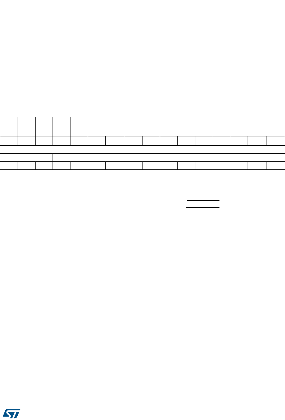
DocID027812 Rev 2 129/766
RM0401 Reset and clock control (RCC)
133
5.3.16 RCC spread spectrum clock generation register (RCC_SSCGR)
Address offset: 0x80
Reset value: 0x0000 0000
Access: no wait state, word, half-word and byte access.
The spread spectrum clock generation is available only for the main PLL.
The RCC_SSCGR register must be written either before the main PLL is enabled or after
the main PLL disabled.
Note: For full details about PLL spread spectrum clock generation (SSCG) characteristics, refer to
the “Electrical characteristics” section in your device datasheet.
31 30 29 28 27 26 25 24 23 22 21 20 19 18 17 16
SSCG
EN
SPR
EAD
SEL
Res. Res. INCSTEP
rw rw rw rw rw rw rw rw rw rw rw rw rw
1514131211109 8 765432 1 0
INCSTEP MODPER
rw rw rw rw rw rw rw rw rw rw rw rw rw rw rw rw
Bit 31 SSCGEN: Spread spectrum modulation enable
Set and cleared by software.
0: Spread spectrum modulation DISABLE. (To write after clearing CR[24]=PLLON bit)
1: Spread spectrum modulation ENABLE. (To write before setting CR[24]=PLLON bit)
Bit 30 SPREADSEL: Spread Select
Set and cleared by software.
To write before to set CR[24]=PLLON bit.
0: Center spread
1: Down spread
Bits 29:28 Reserved, must be kept at reset value.
Bits 27:13 INCSTEP: Incrementation step
Set and cleared by software. To write before setting CR[24]=PLLON bit.
Configuration input for modulation profile amplitude.
Bits 12:0 MODPER: Modulation period
Set and cleared by software. To write before setting CR[24]=PLLON bit.
Configuration input for modulation profile period.

Reset and clock control (RCC) RM0401
130/766 DocID027812 Rev 2
5.3.17 RCC Dedicated Clocks Configuration Register (RCC_DCKCFGR)
Address offset: 0x8C
Reset value: 0x0000 0000
Access: no wait state, word, half-word and byte access.
31 30 29 28 27 26 25 24 23 22 21 20 19 18 17 16
Res. Res. Res. Res. Res. I2SSCR TIMPRE Res. Res. Res. Res. Res. Res. Res. Res.
rw rw rw
15 14 13 12 11 10 9 8 7 6 5 4 3 2 1 0
Res. Res. Res. Res. Res. Res. Res. Res. Res. Res. Res. Res. Res. Res. Res. Res.
Bits 31:27 Reserved, must be kept at reset value.
Bits 26:25 I2SSRC: I2S APB clock source selection
Set and reset by software to configure the frequency of the I2S clock. These bits must be
written when the PLL is disabled.
00: I2S clock frequency = fPPLCLK_R
01: I2S clock frequency = Alternate function input frequency
1x: I2S clock frequency = HSI/HSE depending on PLLRC (bit 22 of RCC_PLLCFGR
register)
Bit 24 TIMPRE: Timers clocks prescalers selection
Set and reset by software to control the clock frequency of all the timers connected to APB1
and APB2 domain.
0: If the APB prescaler (PPRE1, PPRE2 in the RCC_CFGR register) is configured to a
division factor of 1, TIMxCLK = HCKL. Otherwise, the timer clock frequencies are set to
twice to the frequency of the APB domain to which the timers are connected:
TIMxCLK = 2xPCLKx.
1:If the APB prescaler (PPRE1, PPRE2 in the RCC_CFGR register) is configured to a
division factor of 1 or 2, TIMxCLK = HCKL. Otherwise, the timer clock frequencies are set to
four times to the frequency of the APB domain to which the timers are connected:
TIMxCLK = 4xPCLKx.
Bits 23: 0 Reserved, must be kept at reset value.

DocID027812 Rev 2 131/766
RM0401 Reset and clock control (RCC)
133
5.3.18 RCC dedicated Clocks Configuration Register 2 (RCC_DCKCFGR2)
Address offset: 0x94
Reset value: 0x0000 0000
Access: no wait state, word, half-word and byte access.
31 30 29 28 27 26 25 24 23 22 21 20 19 18 17 16
LPTIM1SEL Res. Res. Res. Res. Res. Res. I2C4SEL Res. Res. Res. Res. Res. Res.
rw rw rw rw
15 14 13 12 11 10 9 8 7 6 5 4 3 2 1 0
Res. Res. Res. Res. Res. Res. Res. Res. Res. Res. Res. Res. Res. Res. Res. Res.
Bits 31:30 LPTIMSEL: LPTIM1 kernel clock source selection
Set and reset by software to select the LPTIM1 clock source.
00: LPTIM1 clock = APB clock
01: LPTIM1 clock = HSI clock
10: LPTIM1 clock = LSI clock
11: LPTIM1 clock = LSE clock
Bits 29:24 Reserved, must be kept at reset value.
Bits 23:22 I2C4SEL: I2C4 kernel clock source selection
Set and reset by software to select the I2C4 clock source.
00 and 11: I2C4 clock = APB clock
01: I2C4 clock = system clock
10: I2C4 clock = HSI clock
Bits 21: 0 Reserved, must be kept at reset value.

Reset and clock control (RCC) RM0401
132/766 DocID027812 Rev 2
5.3.19 RCC register map
Table 23 gives the register map and reset values
Table 23. RCC register map and reset values
Addr.
offset
Register
name
31
30
29
28
27
26
25
24
23
22
21
20
19
18
17
16
15
14
13
12
11
10
9
8
7
6
5
4
3
2
1
0
0x00 RCC_CR
Res.
Res.
Res.
Res.
Res.
Res.
PLL RDY
PLL ON
Res.
Res.
Res.
Res.
CSSON
HSEBYP
HSERDY
HSEON
HSICAL 7
HSICAL 6
HSICAL 5
HSICAL 4
HSICAL 3
HSICAL 2
HSICAL 1
HSICAL 0
HSITRIM 4
HSITRIM 3
HSITRIM 2
HSITRIM 1
HSITRIM 0
Res.
HSIRDY
HSION
0x04 RCC_
PLLCFGR
PLLR3
PLLR2
PLLR1
PLLQ 3
PLLQ 2
PLLQ 1
PLLQ 0
Res.
PLLSRC
Res.
Res.
Res.
Res.
PLLP 1
PLLP 0
Res.
PLLN 8
PLLN 7
PLLN 6
PLLN 5
PLLN 4
PLLN 3
PLLN 2
PLLN 1
PLLN 0
PLLM 5
PLLM 4
PLLM 3
PLLM 2
PLLM 1
PLLM 0
0x08 RCC_CFGR
MCO2 1
MCO2 0
MCO2PRE2
MCO2PRE1
MCO2PRE0
MCO1PRE2
MCO1PRE1
MCO1PRE0
Res.
MCO1 1
MCO1 0
RTCPRE 4
RTCPRE 3
RTCPRE 2
RTCPRE 1
RTCPRE 0
PPRE2 2
PPRE2 1
PPRE2 0
PPRE1 2
PPRE1 1
PPRE1 0
MCO2EN
MCO1EN
HPRE 3
HPRE 2
HPRE 1
HPRE 0
SWS 1
SWS 0
SW 1
SW 0
0x0C RCC_CIR
Res.
Res.
Res.
Res.
Res.
Res.
Res.
Res.
CSSC
Res.
Res.
PLLRDYC
HSERDYC
HSIRDYC
LSERDYC
LSIRDYC
Res.
Res.
Res.
PLLRDYIE
HSERDYIE
HSIRDYIE
LSERDYIE
LSIRDYIE
CSSF
Res.
Res.
PLLRDYF
HSERDYF
HSIRDYF
LSERDYF
LSIRDYF
0x10 RCC_
AHB1RSTR
RNGRST
Res.
Res.
Res.
Res.
Res.
Res.
Res.
Res.
DMA2RST
DMA1RST
Res.
Res.
Res.
Res.
Res.
Res.
Res.
Res.
CRCRST
Res.
Res.
Res.
Res.
GPIOHRST
Res.
Res.
Res.
Res.
GPIOCRST
GPIOBRST
GPIOARST
0x14 to
0x1C Reserved
0x20 RCC_
APB1RSTR
Res.
Res.
DACRST
PWRRST
Res.
Res.
Res.
I2C4RST.
Res.
I2C2RST
I2C1RST
Res.
Res.
Res.
USART2RST
Res.
Res.
SPI2RST
Res.
Res.
WWDGRST
Res.
LPTIM1RST
Res.
Res.
Res.
Res.
TIM6RST
TIM5RST
Res.
Res.
Res.
0x24 RCC_
APB2RSTR
Res.
Res.
Res.
Res.
Res.
Res.
Res.
Res.
Res.
Res.
Res.
SPI5RST
Res.
TIM11RST
Res.
TIM9RST
Res.
SYSCFGRST
Res.
SPI1RST
Res.
Res.
Res.
ADC1RST
Res.
USART6RST
USART1RST
Res.
Res.
Res.
TIM1RST
0x28 to
0x2C Reserved
0x30 RCC_
AHB1ENR
RNGEN
Res.
Res.
Res.
Res.
Res.
Res.
Res.
Res.
DMA2EN
DMA1EN
Res.
Res.
Res.
Res.
Res.
Res.
Res.
Res.
CRCEN
Res.
Res.
Res.
Res.
GPIOHEN
Res.
Res.
Res.
Res.
GPIOCEN
GPIOBEN
GPIOAEN
0x34 to
0x3C Reserved
0x40 RCC_
APB1ENR
Res.
Res.
DACEN
PWREN
Res.
Res.
Res.
I2C4EN
Res.
I2C2EN
I2C1EN
Res.
Res.
Res.
USART2EN
Res.
Res.
SPI2EN
Res.
Res.
WWDGEN
RTCAPBEN.
LPTIM1EN
Res.
Res.
Res.
Res.
TIM6EN
TIM5EN
Res.
Res.
Res.
0x44 RCC_
APB2ENR
Res.
Res.
Res.
Res.
Res.
Res.
Res.
Res.
Res.
Res.
Res.
SPI5EN
Res.
TIM11EN
Res.
TIM9EN
EXTIEN
SYSCFGEN
Res.
SPI1EN
Res.
Res.
Res.
ADC1EN
Res.
Res.
USART6EN
USART1EN
Res.
Res.
Res.
TIM1EN
0x48 to
0x4C Reserved
DocID027812 Rev 2 133/766
RM0401 Reset and clock control (RCC)
133
Refer to Section 2.2.2 on page 38 for the register boundary addresses.
0x50 RCC_AHB1L
PENR
RNGLPEM
Res.
Res.
Res.
Res.
Res.
Res.
Res.
Res.
DMA2LPEN
DMA1LPEN
Res.
Res.
Res.
Res.
SRAM1LPEN
FLITFLPEN
Res.
Res.
CRCLPEN
Res.
Res.
Res.
Res.
GPIOHLPEN
Res.
Res.
Res.
Res.
GPIOCLPEN
GPIOBLPEN
GPIOALPEN
0x54 to
0x5C Reserved
0x60 RCC_APB1L
PENR
Res.
Res.
DACLPEM.
PWRLPEN
Res.
Res.
Res.
I2C4LPEN.
Res.
I2C2LPEN
I2C1LPEN
Res.
Res.
Res.
USART2LPEN
Res.
Res.
SPI2LPEN
Res.
Res.
WWDGLPEN
RTCAPBLPEN
LPTIM1LPEM
Res.
Res.
Res.
Res.
TIM6LPEN.
TIM5LPEN
Res.
Res.
Res.
0x64 RCC_APB2L
PENR
Res.
Res.
Res.
Res.
Res.
Res.
Res.
Res.
Res.
Res.
Res.
SPI5LPEN
Res.
TIM11LPEN
Res.
TIM9LPEN.
EXTILPEN.
SYSCFGLPEN
Res.
SPI1LPEN.
Res.
Res.
Res.
ADC1LPEN
Res.
Res.
USART6LPEN
USART1LPEN
Res.
Res.
Res.
TIM1LPEN
0x68 to
0x6C Reserved
0x70 RCC_BDCR
Res.
Res.
Res.
Res.
Res.
Res.
Res.
Res.
Res.
Res.
Res.
Res.
Res.
Res.
Res.
BDRST
RTCEN
Res.
Res.
Res.
Res.
Res.
RTCSEL 1
RTCSEL 0
Res.
Res.
Res.
Res.
LSEMOD
LSEBYP
LSERDY
LSEON
0x74 RCC_CSR
LPWRRSTF
WWDGRSTF
WDGRSTF
SFTRSTF
PORRSTF
PADRSTF
BORRSTF
RMVF
Res.
Res.
Res.
Res.
Res.
Res.
Res.
Res.
Res.
Res.
Res.
Res.
Res.
Res.
Res.
Res.
Res.
Res.
Res.
Res.
Res.
Res.
LSIRDY
LSION
0x78 to
0x7C Reserved
0x80 RCC_SSCGR
SSCGEN
SPREADSEL
Res.
Res.
INCSTEP MODPER
0x84 to
0x88 Reserved
0x8C RCC_
DCKCFGR
Res.
Res.
Res.
Res.
Res.
I2SSCR
TIMPRE
Res.
Res.
Res.
Res.
Res.
Res.
Res.
Res.
Res.
Res.
Res.
Res.
Res.
Res.
Res.
Res.
Res.
Res.
Res.
Res.
Res.
Res.
Res.
Res.
0x90 Reserved
0x94 RCC_
DCKCFGR2
LPTIM1SEL
Res.
Res.
Res.
Res.
Res.
Res.
I2C4SEL
Res.
Res.
Res.
Res.
Res.
Res.
Res.
Res.
Res.
Res.
Res.
Res.
Res.
Res.
Res.
Res.
Res.
Res.
Res.
Res.
Res.
Res.
Table 23. RCC register map and reset values (continued)
Addr.
offset
Register
name
31
30
29
28
27
26
25
24
23
22
21
20
19
18
17
16
15
14
13
12
11
10
9
8
7
6
5
4
3
2
1
0

General-purpose I/Os (GPIO) RM0401
134/766 DocID027812 Rev 2
6 General-purpose I/Os (GPIO)
6.1 GPIO introduction
Each general-purpose I/O port has four 32-bit configuration registers (GPIOx_MODER,
GPIOx_OTYPER, GPIOx_OSPEEDR and GPIOx_PUPDR), two 32-bit data registers
(GPIOx_IDR and GPIOx_ODR), a 32-bit set/reset register (GPIOx_BSRR), a 32-bit locking
register (GPIOx_LCKR) and two 32-bit alternate function selection register (GPIOx_AFRH
and GPIOx_AFRL).
6.2 GPIO main features
•Up to 16 I/Os under control
•Output states: push-pull or open drain + pull-up/down
•Output data from output data register (GPIOx_ODR) or peripheral (alternate function
output)
•Speed selection for each I/O
•Input states: floating, pull-up/down, analog
•Input data to input data register (GPIOx_IDR) or peripheral (alternate function input)
•Bit set and reset register (GPIOx_BSRR) for bitwise write access to GPIOx_ODR
•Locking mechanism (GPIOx_LCKR) provided to freeze the I/O configuration
•Analog function
•Alternate function input/output selection registers (at most 16 AFs per I/O)
•Fast toggle capable of changing every two clock cycles
•Highly flexible pin multiplexing allows the use of I/O pins as GPIOs or as one of several
peripheral functions
6.3 GPIO functional description
Subject to the specific hardware characteristics of each I/O port listed in the datasheet, each
port bit of the general-purpose I/O (GPIO) ports can be individually configured by software in
several modes:
•Input floating
•Input pull-up
•Input-pull-down
•Analog
•Output open-drain with pull-up or pull-down capability
•Output push-pull with pull-up or pull-down capability
•Alternate function push-pull with pull-up or pull-down capability
•Alternate function open-drain with pull-up or pull-down capability
Each I/O port bit is freely programmable, however the I/O port registers have to be
accessed as 32-bit words, half-words or bytes. The purpose of the GPIOx_BSRR register is
to allow atomic read/modify accesses to any of the GPIO registers. In this way, there is no
risk of an IRQ occurring between the read and the modify access.
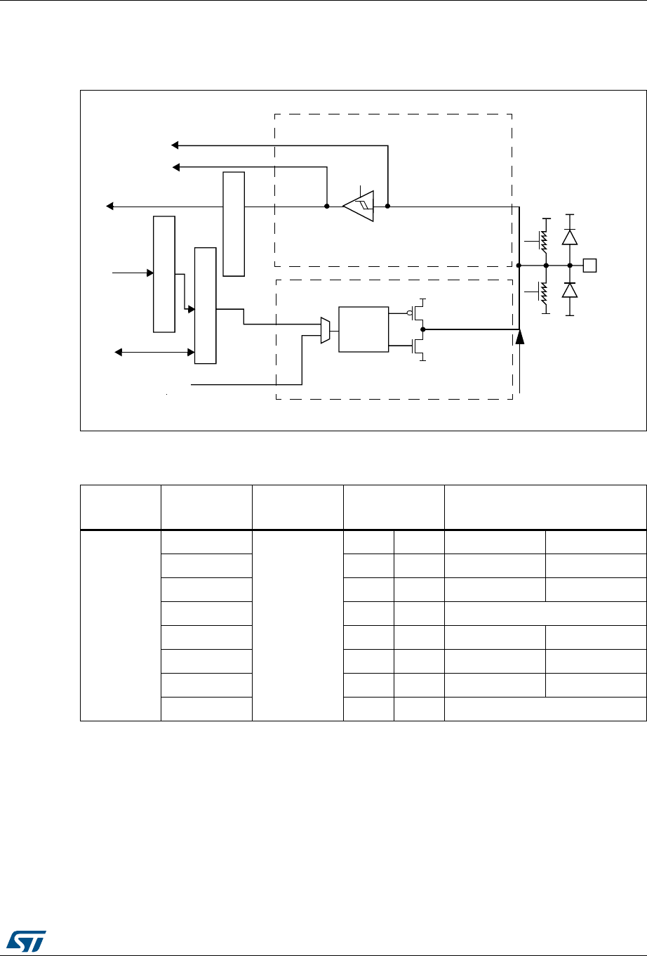
DocID027812 Rev 2 135/766
RM0401 General-purpose I/Os (GPIO)
153
Figure 16 shows the basic structure of a 5 V tolerant I/O port bit. Table 27 gives the possible
port bit configurations.
Figure 16. Basic structure of a five-volt tolerant I/O port bit
1. VDD_FT is a potential specific to five-volt tolerant I/Os and different from VDD.
Table 24. Port bit configuration table(1)
MODER(i)
[1:0] OTYPER(i) OSPEEDR(i)
[B:A]
PUPDR(i)
[1:0] I/O configuration
01
0
SPEED
[B:A]
0 0 GP output PP
0 0 1 GP output PP + PU
0 1 0 GP output PP + PD
0 1 1 Reserved
1 0 0 GP output OD
1 0 1 GP output OD + PU
1 1 0 GP output OD + PD
1 1 1 Reserved (GP output OD)
!LTERNATEFUNCTIONOUTPUT
!LTERNATEFUNCTIONINPUT
0USHPULL
OPENDRAINOR
DISABLED
/UTPUTDATAREGISTER
2EADWRITE
&ROMONCHIP
PERIPHERAL
4OONCHIP
PERIPHERAL
/UTPUT
CONTROL
!NALOG
ONOFF 0ULL
0ULL
ONOFF
)/PIN
6$$
6$$
633
633
44,3CHMITT
TRIGGER
633
6$$?&4
0ROTECTION
DIODE
0ROTECTION
DIODE
ONOFF
)NPUTDRIVER
/UTPUTDRIVER
DOWN
UP
0-/3
.-/3
2EAD
"ITSETRESETREGISTERS
7RITE
!NALOG
)NPUTDATAREGISTER
AIB
General-purpose I/Os (GPIO) RM0401
136/766 DocID027812 Rev 2
6.3.1 General-purpose I/O (GPIO)
During and just after reset, the alternate functions are not active and the I/O ports are
configured in input floating mode.
The debug pins are in AF pull-up/pull-down after reset:
•PA15: JTDI in pull-up
•PA14: JTCK/SWCLK in pull-down
•PA13: JTMS/SWDAT in pull-up
•PB4: NJTRST in pull-up
•PB3: JTDO in floating state
When the pin is configured as output, the value written to the output data register
(GPIOx_ODR) is output on the I/O pin. It is possible to use the output driver in push-pull
mode or open-drain mode (only the N-MOS is activated when 0 is output).
The input data register (GPIOx_IDR) captures the data present on the I/O pin at every AHB1
clock cycle.
All GPIO pins have weak internal pull-up and pull-down resistors, which can be activated or
not depending on the value in the GPIOx_PUPDR register.
10
0
SPEED
[B:A]
0 0 AF PP
0 0 1 AF PP + PU
0 1 0 AF PP + PD
0 1 1 Reserved
100AFOD
101AFOD + PU
110AFOD + PD
1 1 1 Reserved
00
x x x 0 0 Input Floating
x x x 0 1 Input PU
x x x 1 0 Input PD
x x x 1 1 Reserved (input floating)
11
x x x 0 0 Input/output Analog
xxx01
Reservedxxx10
xxx11
1. GP = general-purpose, PP = push-pull, PU = pull-up, PD = pull-down, OD = open-drain, AF = alternate
function.
Table 24. Port bit configuration table(1) (continued)
MODER(i)
[1:0] OTYPER(i) OSPEEDR(i)
[B:A]
PUPDR(i)
[1:0] I/O configuration

DocID027812 Rev 2 137/766
RM0401 General-purpose I/Os (GPIO)
153
6.3.2 I/O pin multiplexer and mapping
The microcontroller I/O pins are connected to onboard peripherals/modules through a
multiplexer that allows only one peripherals alternate function (AF) connected to an I/O pin
at a time. In this way, there can be no conflict between peripherals sharing the same I/O pin.
Each I/O pin has a multiplexer with sixteen alternate function inputs (AF0 to AF15) that can
be configured through the GPIOx_AFRL (for pin 0 to 7) and GPIOx_AFRH (for pin 8 to 15)
registers:
•After reset all I/Os are connected to the system’s alternate function 0 (AF0)
•The peripherals’ alternate functions are mapped from AF1 to AF13
•Cortex®-M4 with FPU EVENTOUT is mapped on AF15
This structure is shown in Figure 17 below.
In addition to this flexible I/O multiplexing architecture, each peripheral has alternate
functions mapped onto different I/O pins to optimize the number of peripherals available in
smaller packages.
To use an I/O in a given configuration, proceed as follows:
•System function
Connect the I/O to AF0 and configure it depending on the function used:
– JTAG/SWD, after each device reset these pins are assigned as dedicated pins
immediately usable by the debugger host (not controlled by the GPIO controller)
– RTC_REFIN: this pin should be configured in Input floating mode
– MCO1 and MCO2: these pins have to be configured in alternate function mode.
Note: You can disable some or all of the JTAG/SWD pins and so release the associated pins for
GPIO usage.
For more details please refer to Section 5.2.10: Clock-out capability.

General-purpose I/Os (GPIO) RM0401
138/766 DocID027812 Rev 2
•GPIO
Configure the desired I/O as output or input in the GPIOx_MODER register.
•Peripheral alternate function
For the ADC configure the desired I/O as analog in the GPIOx_MODER register.
For other peripherals:
– Configure the desired I/O as an alternate function in the GPIOx_MODER register
– Select the type, pull-up/pull-down and output speed via the GPIOx_OTYPER,
GPIOx_PUPDR and GPIOx_OSPEEDER registers, respectively
– Connect the I/O to the desired AFx in the GPIOx_AFRL or GPIOx_AFRH register
•EVENTOUT
Configure the I/O pin used to output the Cortex®-M4 with FPU EVENTOUT signal by
connecting it to AF15
Please refer to the “Alternate function mapping” table in the datasheets for the detailed
mapping of the system and peripherals’ alternate function I/O pins.
Table 25. Flexible SWJ-DP pin assignment
Available debug ports
SWJ I/O pin assigned
PA13 /
JTMS/
SWDIO
PA14 /
JTCK/
SWCLK
PA15 /
JTDI
PB3 /
JTDO
PB4/
NJTRST
Full SWJ (JTAG-DP + SW-DP) - Reset state X X X X X
Full SWJ (JTAG-DP + SW-DP) but without
NJTRST XXXX
JTAG-DP Disabled and SW-DP Enabled X X
JTAG-DP Disabled and SW-DP Disabled Released
DocID027812 Rev 2 139/766
RM0401 General-purpose I/Os (GPIO)
153
Figure 17. Selecting an alternate function
1. Configured in FS.
6.3.3 I/O port control registers
Each of the GPIOs has four 32-bit memory-mapped control registers (GPIOx_MODER,
GPIOx_OTYPER, GPIOx_OSPEEDR, GPIOx_PUPDR) to configure up to 16 I/Os.
The GPIOx_MODER register is used to select the I/O direction (input, output, AF, analog).
The GPIOx_OTYPER and GPIOx_OSPEEDR registers are used to select the output type
(push-pull or open-drain) and speed (the I/O speed pins are directly connected to the
corresponding GPIOx_OSPEEDR register bits whatever the I/O direction). The
GPIOx_PUPDR register is used to select the pull-up/pull-down whatever the I/O direction.
06Y9
)RUSLQVWRWKH*3,2[B$)5/>@UHJLVWHUVHOHFWVWKHGHGLFDWHGDOWHUQDWHIXQFWLRQ
$)V\VWHP
$)7,0/37,0
$)7,0
$)7,0
$),&
$)63,
$)63,
$)86$57
$)86$57
$),&
$)
$)
$)
$)
$)
$)(9(17287
3LQ[[
$)5/>@
)RUSLQVWRWKH*3,2[B$)5+>@UHJLVWHUVHOHFWVWKHGHGLFDWHGDOWHUQDWHIXQFWLRQ
3LQ[[
$)5+>@
$)V\VWHP
$)7,0/37,0
$)7,0
$)7,0
$),&
$)63,
$)63,
$)86$57
$)86$57
$),&
$)
$)
$)
$)
$)
$)(9(17287

General-purpose I/Os (GPIO) RM0401
140/766 DocID027812 Rev 2
6.3.4 I/O port data registers
Each GPIO has two 16-bit memory-mapped data registers: input and output data registers
(GPIOx_IDR and GPIOx_ODR). GPIOx_ODR stores the data to be output, it is read/write
accessible. The data input through the I/O are stored into the input data register
(GPIOx_IDR), a read-only register.
See Section 6.4.5: GPIO port input data register (GPIOx_IDR) (x = A..C and H) and
Section 6.4.6: GPIO port output data register (GPIOx_ODR) (x = A..C and H) for the register
descriptions.
6.3.5 I/O data bitwise handling
The bit set reset register (GPIOx_BSRR) is a 32-bit register which allows the application to
set and reset each individual bit in the output data register (GPIOx_ODR). The bit set reset
register has twice the size of GPIOx_ODR.
To each bit in GPIOx_ODR, correspond two control bits in GPIOx_BSRR: BSRR(i) and
BSRR(i+SIZE). When written to 1, bit BSRR(i) sets the corresponding ODR(i) bit. When
written to 1, bit BSRR(i+SIZE) resets the ODR(i) corresponding bit.
Writing any bit to 0 in GPIOx_BSRR does not have any effect on the corresponding bit in
GPIOx_ODR. If there is an attempt to both set and reset a bit in GPIOx_BSRR, the set
action takes priority.
Using the GPIOx_BSRR register to change the values of individual bits in GPIOx_ODR is a
“one-shot” effect that does not lock the GPIOx_ODR bits. The GPIOx_ODR bits can always
be accessed directly. The GPIOx_BSRR register provides a way of performing atomic
bitwise handling.
There is no need for the software to disable interrupts when programming the GPIOx_ODR
at bit level: it is possible to modify one or more bits in a single atomic AHB1 write access.
6.3.6 GPIO locking mechanism
It is possible to freeze the GPIO control registers by applying a specific write sequence to
the GPIOx_LCKR register. The frozen registers are GPIOx_MODER, GPIOx_OTYPER,
GPIOx_OSPEEDR, GPIOx_PUPDR, GPIOx_AFRL and GPIOx_AFRH.
To write the GPIOx_LCKR register, a specific write / read sequence has to be applied. When
the right LOCK sequence is applied to bit 16 in this register, the value of LCKR[15:0] is used
to lock the configuration of the I/Os (during the write sequence the LCKR[15:0] value must
be the same). When the LOCK sequence has been applied to a port bit, the value of the port
bit can no longer be modified until the next MCU or peripheral reset. Each GPIOx_LCKR bit
freezes the corresponding bit in the control registers (GPIOx_MODER, GPIOx_OTYPER,
GPIOx_OSPEEDR, GPIOx_PUPDR, GPIOx_AFRL and GPIOx_AFRH).
The LOCK sequence (refer to Section 6.4.8: GPIO port configuration lock register
(GPIOx_LCKR) (x = A..C and H)) can only be performed using a word (32-bit long) access
to the GPIOx_LCKR register due to the fact that GPIOx_LCKR bit 16 has to be set at the
same time as the [15:0] bits.
For more details please refer to LCKR register description in Section 6.4.8: GPIO port
configuration lock register (GPIOx_LCKR) (x = A..C and H).
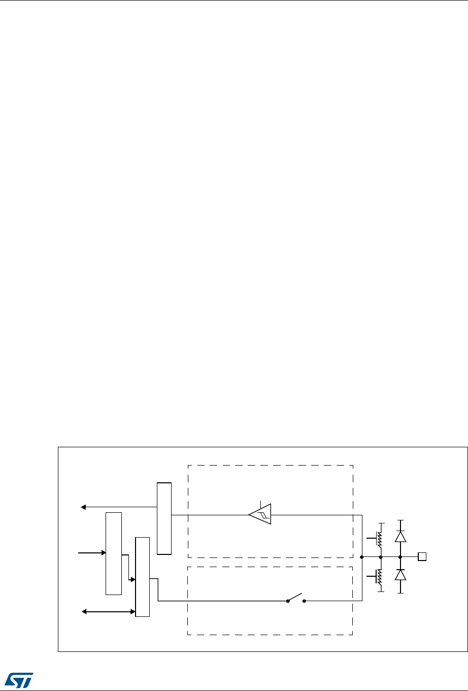
DocID027812 Rev 2 141/766
RM0401 General-purpose I/Os (GPIO)
153
6.3.7 I/O alternate function input/output
Two registers are provided to select one out of the sixteen alternate function inputs/outputs
available for each I/O. With these registers, you can connect an alternate function to some
other pin as required by your application.
This means that a number of possible peripheral functions are multiplexed on each GPIO
using the GPIOx_AFRL and GPIOx_AFRH alternate function registers. The application can
thus select any one of the possible functions for each I/O. The AF selection signal being
common to the alternate function input and alternate function output, a single channel is
selected for the alternate function input/output of one I/O.
To know which functions are multiplexed on each GPIO pin, refer to the datasheets.
Note: The application is allowed to select one of the possible peripheral functions for each I/O at a
time.
6.3.8 External interrupt/wakeup lines
All ports have external interrupt capability. To use external interrupt lines, the port must be
configured in input mode, refer to Section 12.2: External interrupt/event controller (EXTI)
and Section 12.2.3: Wakeup event management.
6.3.9 Input configuration
When the I/O port is programmed as Input:
•the output buffer is disabled
•the Schmitt trigger input is activated
•the pull-up and pull-down resistors are activated depending on the value in the
GPIOx_PUPDR register
•The data present on the I/O pin are sampled into the input data register every AHB1
clock cycle
•A read access to the input data register provides the I/O State
Figure 18 shows the input configuration of the I/O port bit.
Figure 18. Input floating/pull up/pull down configurations
ONOFF
PULL
PULL
ONOFF
)/PIN
6$$
633
44,3CHMITT
TRIGGER
633
6$$
PROTECTION
DIODE
PROTECTION
DIODE
ON
INPUTDRIVER
OUTPUTDRIVER
DOWN
UP
)NPUTDATAREGISTER
/UTPUTDATAREGISTER
2EADWRITE
2EAD
"ITSETRESETREGISTERS
7RITE
AIB
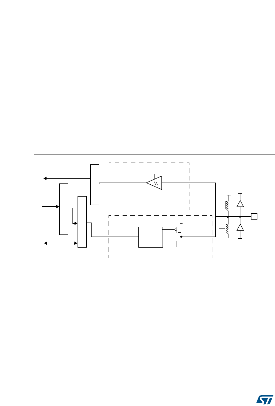
General-purpose I/Os (GPIO) RM0401
142/766 DocID027812 Rev 2
6.3.10 Output configuration
When the I/O port is programmed as output:
•The output buffer is enabled:
–Open drain mode: A “0” in the Output register activates the N-MOS whereas a “1”
in the Output register leaves the port in Hi-Z (the P-MOS is never activated)
– Push-pull mode: A “0” in the Output register activates the N-MOS whereas a “1” in
the Output register activates the P-MOS
•The Schmitt trigger input is activated
•The weak pull-up and pull-down resistors are activated or not depending on the value
in the GPIOx_PUPDR register
•The data present on the I/O pin are sampled into the input data register every AHB1
clock cycle
•A read access to the input data register gets the I/O state
•A read access to the output data register gets the last written value
Figure 19 shows the output configuration of the I/O port bit.
Figure 19. Output configuration
6.3.11 Alternate function configuration
When the I/O port is programmed as alternate function:
•The output buffer can be configured as open-drain or push-pull
•The output buffer is driven by the signal coming from the peripheral (transmitter enable
and data)
•The Schmitt trigger input is activated
•The weak pull-up and pull-down resistors are activated or not depending on the value
in the GPIOx_PUPDR register
•The data present on the I/O pin are sampled into the input data register every AHB1
clock cycle
•A read access to the input data register gets the I/O state
Figure 20 shows the Alternate function configuration of the I/O port bit.
0USHPULLOR
/PENDRAIN
/UTPUT
CONTROL
6
$$
6
33
44,3CHMITT
TRIGGER
ON
)NPUTDRIVER
/UTPUTDRIVER
0-/3
.-/3
)NPUTDATAREGISTER
/UTPUTDATAREGISTER
2EADWRITE
2EAD
"ITSETRESETREGISTERS
7RITE
ONOFF
PULL
PULL
ONOFF
6
$$
6
33
6
33
6
$$
PROTECTION
DIODE
PROTECTION
DIODE
DOWN
UP
)/PIN
AIB
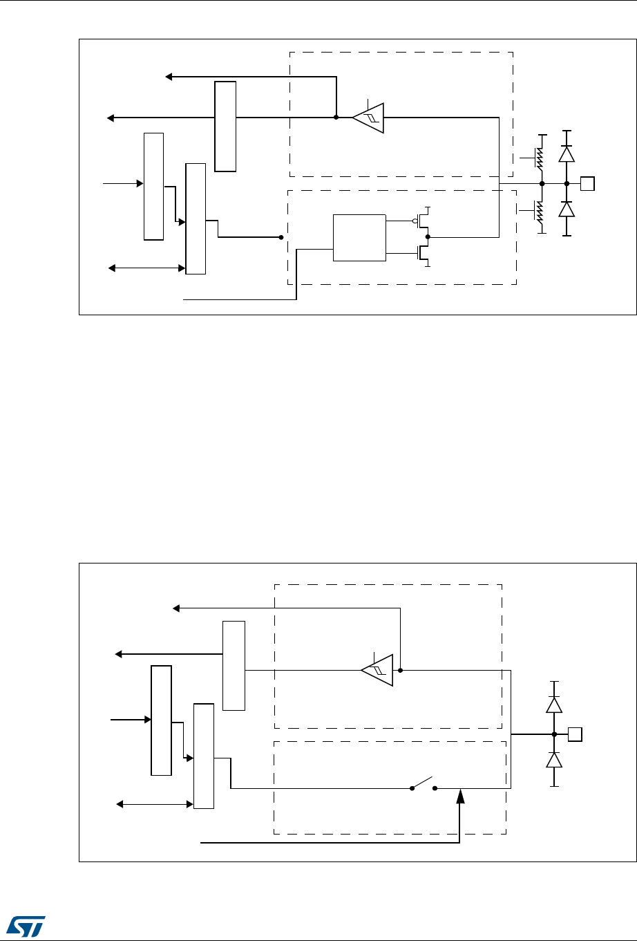
DocID027812 Rev 2 143/766
RM0401 General-purpose I/Os (GPIO)
153
Figure 20. Alternate function configuration
6.3.12 Analog configuration
When the I/O port is programmed as analog configuration:
•The output buffer is disabled
•The Schmitt trigger input is deactivated, providing zero consumption for every analog
value of the I/O pin. The output of the Schmitt trigger is forced to a constant value (0).
•The weak pull-up and pull-down resistors are disabled
•Read access to the input data register gets the value “0”
Note: In the analog configuration, the I/O pins cannot be 5 Volt tolerant.
Figure 21 shows the high-impedance, analog-input configuration of the I/O port bit.
Figure 21. High impedance-analog configuration
!LTERNATEFUNCTIONOUTPUT
!LTERNATEFUNCTIONINPUT
PUSHPULLOR
OPENDRAIN
&ROMONCHIP
PERIPHERAL
4OONCHIP
PERIPHERAL
/UTPUT
CONTROL
6$$
633
44,3CHMITT
TRIGGER
ON
)NPUTDRIVER
/UTPUTDRIVER
0-/3
.-/3
)NPUTDATAREGISTER
/UTPUTDATAREGISTER
2EADWRITE
2EAD
"ITSETRESETREGISTERS
7RITE
ONOFF
ONOFF
6$$
633 633
6$$
PROTECTION
DIODE
PROTECTION
DIODE
0ULL
0ULL
)/PIN
DOWN
UP
AIB
&ROMONCHIP
PERIPHERAL
4OONCHIP
PERIPHERAL
!NALOG
TRIGGER
OFF
)NPUTDRIVER
)NPUTDATAREGISTER
/UTPUTDATAREGISTER
2EADWRITE
2EAD
"ITSETRESETREGISTERS
7RITE
!NALOG
6
33
6
$$
PROTECTION
DIODE
PROTECTION
DIODE
)/PIN
AI
44,3CHMITT

General-purpose I/Os (GPIO) RM0401
144/766 DocID027812 Rev 2
6.3.13 Using the OSC32_IN/OSC32_OUT pins as GPIO PC14/PC15
port pins
The LSE oscillator pins OSC32_IN and OSC32_OUT can be used as general-purpose
PC14 and PC15 I/Os, respectively, when the LSE oscillator is off. The PC14 and PC15 I/Os
are only configured as LSE oscillator pins OSC32_IN and OSC32_OUT when the LSE
oscillator is ON. This is done by setting the LSEON bit in the RCC_BDCR register. The LSE
has priority over the GPIO function.
Note: The PC14/PC15 GPIO functionality is lost when the 1.2 V domain is powered off (by the
device entering the standby mode) or when the backup domain is supplied by VBAT (VDD no
more supplied). In this case the I/Os are set in analog input mode.
6.3.14 Using the OSC_IN/OSC_OUT pins as GPIO PH0/PH1 port pins
The HSE oscillator pins OSC_IN/OSC_OUT can be used as general-purpose PH0/PH1
I/Os, respectively, when the HSE oscillator is OFF. (after reset, the HSE oscillator is off). The
PH0/PH1 I/Os are only configured as OSC_IN/OSC_OUT HSE oscillator pins when the
HSE oscillator is ON. This is done by setting the HSEON bit in the RCC_CR register. The
HSE has priority over the GPIO function.
6.3.15 Selection of RTC additional functions
The devices feature one GPIO pin, RTC_AF1 (PC13), that can be used for the detection to
a tamper event, a time stamp event, an RTC_ALARM or an RTC_CALIB:
•RTC_ALARM output: this output can be RTC Alarm A, RTC Alarm B or RTC Wakeup
depending on the value of OSEL[1:0] bits in the RTC_CR register
•RTC_CALIB output: this feature is enabled by setting the COE[23] in the RTC_CR
register
•RTC_TAMP1: tamper event detection
•RTC_TS: time stamp event detection
The selection of the corresponding pin is performed through the RTC_TAFCR register as
follows:
•TAMP1INSEL is used to select which pin is used as the RTC_TAMP1 tamper input
•TSINSEL is used to select which pin is used as the RTC_TS time stamp input
•ALARMOUTTYPE is used to select whether the RTC_ALARM is output in push-pull or
open-drain mode
The output mechanism follows the priority order listed in Table 26.
Table 26. RTC additional functions(1)
Pin
configuration
and function
RTC_ALARM
enabled
RTC_CALIB
enabled
Tamper
enabled
Time
stamp
enabled
TAMP1INSEL
TAMPER1
pin selection
TSINSEL
TIMESTAMP
pin
selection
ALARMOUTTYPE
RTC_ALARM
configuration
Alarm out
output OD 1Don’t care
Don’t
care
Don’t
care Don’t care Don’t care 0
Alarm out
output PP 1Don’t care
Don’t
care
Don’t
care Don’t care Don’t care 1

DocID027812 Rev 2 145/766
RM0401 General-purpose I/Os (GPIO)
153
Calibration
out output PP 01
Don’t
care
Don’t
care Don’t care Don’t care Don’t care
TAMPER1
input floating 0 0 1 0 0 Don’t care Don’t care
TIMESTAMP
and
TAMPER1
input floating
0 0 1 1 0 0 Don’t care
TIMESTAMP
input floating 0 0 0 1 Don’t care 0 Don’t care
Standard
GPIO 0 0 0 0 Don’t care Don’t care Don’t care
1. OD: open drain; PP: push-pull.
Table 26. RTC additional functions(1) (continued)
Pin
configuration
and function
RTC_ALARM
enabled
RTC_CALIB
enabled
Tamper
enabled
Time
stamp
enabled
TAMP1INSEL
TAMPER1
pin selection
TSINSEL
TIMESTAMP
pin
selection
ALARMOUTTYPE
RTC_ALARM
configuration
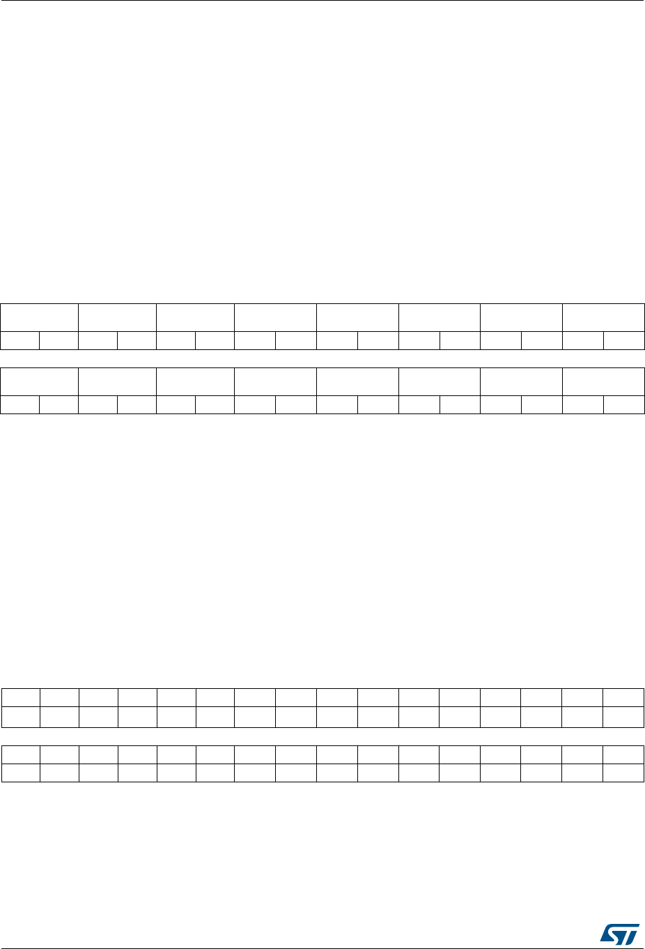
General-purpose I/Os (GPIO) RM0401
146/766 DocID027812 Rev 2
6.4 GPIO registers
This section gives a detailed description of the GPIO registers.
For a summary of register bits, register address offsets and reset values, refer to Table 27.
The GPIO registers can be accessed by byte (8 bits), half-words (16 bits) or words (32 bits).
6.4.1 GPIO port mode register (GPIOx_MODER) (x = A..C and H)
Address offset: 0x00
Reset values:
•0x0C00 0000 for port A
•0x0000 0280 for port B
•0x0000 0000 for other ports
6.4.2 GPIO port output type register (GPIOx_OTYPER)
(x = A..C and H)
Address offset: 0x04
Reset value: 0x0000 0000
31 30 29 28 27 26 25 24 23 22 21 20 19 18 17 16
MODER15[1:0] MODER14[1:0] MODER13[1:0] MODER12[1:0] MODER11[1:0] MODER10[1:0] MODER9[1:0] MODER8[1:0]
rw rw rw rw rw rw rw rw rw rw rw rw rw rw rw rw
1514131211109876543210
MODER7[1:0] MODER6[1:0] MODER5[1:0] MODER4[1:0] MODER3[1:0] MODER2[1:0] MODER1[1:0] MODER0[1:0]
rw rw rw rw rw rw rw rw rw rw rw rw rw rw rw rw
Bits 2y:2y+1 MODERy[1:0]: Port x configuration bits (y = 0..15)
These bits are written by software to configure the I/O direction mode.
00: Input (reset state)
01: General purpose output mode
10: Alternate function mode
11: Analog mode
31 30 29 28 27 26 25 24 23 22 21 20 19 18 17 16
Res. Res. Res. Res. Res. Res. Res. Res. Res. Res. Res. Res. Res. Res. Res. Res.
1514131211109876543210
OT15 OT14 OT13 OT12 OT11 OT10 OT9 OT8 OT7 OT6 OT5 OT4 OT3 OT2 OT1 OT0
rw rw rw rw rw rw rw rw rw rw rw rw rw rw rw rw
Bits 31:16 Reserved, must be kept at reset value.
Bits 15:0 OTy: Port x configuration bits (y = 0..15)
These bits are written by software to configure the output type of the I/O port.
0: Output push-pull (reset state)
1: Output open-drain

DocID027812 Rev 2 147/766
RM0401 General-purpose I/Os (GPIO)
153
6.4.3 GPIO port output speed register (GPIOx_OSPEEDR)
(x = A..C and H)
Address offset: 0x08
Reset values:
•0x0C00 0000 for port A
•0x0000 00C0 for port B
•0x0000 0000 for other ports
6.4.4 GPIO port pull-up/pull-down register (GPIOx_PUPDR)
(x = A..C and H)
Address offset: 0x0C
Reset values:
•0x6400 0000 for port A
•0x0000 0100 for port B
•0x0000 0000 for other ports
31 30 29 28 27 26 25 24 23 22 21 20 19 18 17 16
OSPEEDR15
[1:0]
OSPEEDR14
[1:0]
OSPEEDR13
[1:0]
OSPEEDR12
[1:0]
OSPEEDR11
[1:0]
OSPEEDR10
[1:0]
OSPEEDR9
[1:0]
OSPEEDR8
[1:0]
rw rw rw rw rw rw rw rw rw rw rw rw rw rw rw rw
15 14 13 12 11 10 9 8 7 6 5 4 3 2 1 0
OSPEEDR7[1:0] OSPEEDR6[1:0] OSPEEDR5[1:0] OSPEEDR4[1:0] OSPEEDR3[1:0] OSPEEDR2[1:0] OSPEEDR1
[1:0]
OSPEEDR0
1:0]
rw rw rw rw rw rw rw rw rw rw rw rw rw rw rw rw
Bits 2y:2y+1 OSPEEDRy[1:0]: Port x configuration bits (y = 0..15)
These bits are written by software to configure the I/O output speed.
00: Low speed
01: Medium speed
10: High speed
11: Very high speed
Note: Refer to the product datasheets for the values of OSPEEDRy bits versus VDD
range and external load.
31 30 29 28 27 26 25 24 23 22 21 20 19 18 17 16
PUPDR15[1:0] PUPDR14[1:0] PUPDR13[1:0] PUPDR12[1:0] PUPDR11[1:0] PUPDR10[1:0] PUPDR9[1:0] PUPDR8[1:0]
rw rw rw rw rw rw rw rw rw rw rw rw rw rw rw rw
1514131211109876543210
PUPDR7[1:0] PUPDR6[1:0] PUPDR5[1:0] PUPDR4[1:0] PUPDR3[1:0] PUPDR2[1:0] PUPDR1[1:0] PUPDR0[1:0]
rw rw rw rw rw rw rw rw rw rw rw rw rw rw rw rw

General-purpose I/Os (GPIO) RM0401
148/766 DocID027812 Rev 2
6.4.5 GPIO port input data register (GPIOx_IDR) (x = A..C and H)
Address offset: 0x10
Reset value: 0x0000 XXXX (where X means undefined)
6.4.6 GPIO port output data register (GPIOx_ODR) (x = A..C and H)
Address offset: 0x14
Reset value: 0x0000 0000
Bits 2y:2y+1 PUPDRy[1:0]: Port x configuration bits (y = 0..15)
These bits are written by software to configure the I/O pull-up or pull-down
00: No pull-up, pull-down
01: Pull-up
10: Pull-down
11: Reserved
31 30 29 28 27 26 25 24 23 22 21 20 19 18 17 16
Res. Res. Res. Res. Res. Res. Res. Res. Res. Res. Res. Res. Res. Res. Res. Res.
1514131211109876543210
IDR15 IDR14 IDR13 IDR12 IDR11 IDR10 IDR9 IDR8 IDR7 IDR6 IDR5 IDR4 IDR3 IDR2 IDR1 IDR0
rrrrrr r r r r rrrrrr
Bits 31:16 Reserved, must be kept at reset value.
Bits 15:0 IDRy: Port input data (y = 0..15)
These bits are read-only and can be accessed in word mode only. They contain the input
value of the corresponding I/O port.
31 30 29 28 27 26 25 24 23 22 21 20 19 18 17 16
Res. Res. Res. Res. Res. Res. Res. Res. Res. Res. Res. Res. Res. Res. Res. Res.
1514131211109876543210
ODR15 ODR14 ODR13 ODR12 ODR11 ODR10 ODR9 ODR8 ODR7 ODR6 ODR5 ODR4 ODR3 ODR2 ODR1 ODR0
rw rw rw rw rw rw rw rw rw rw rw rw rw rw rw rw
Bits 31:16 Reserved, must be kept at reset value.
Bits 15:0 ODRy: Port output data (y = 0..15)
These bits can be read and written by software.
Note: For atomic bit set/reset, the ODR bits can be individually set and reset by writing to the
GPIOx_BSRR register (x = A..C and H).

DocID027812 Rev 2 149/766
RM0401 General-purpose I/Os (GPIO)
153
6.4.7 GPIO port bit set/reset register (GPIOx_BSRR) (x = A..C and H)
Address offset: 0x18
Reset value: 0x0000 0000
6.4.8 GPIO port configuration lock register (GPIOx_LCKR)
(x = A..C and H)
This register is used to lock the configuration of the port bits when a correct write sequence
is applied to bit 16 (LCKK). The value of bits [15:0] is used to lock the configuration of the
GPIO. During the write sequence, the value of LCKR[15:0] must not change. When the
LOCK sequence has been applied on a port bit, the value of this port bit can no longer be
modified until the next MCU or peripheral reset.
Note: A specific write sequence is used to write to the GPIOx_LCKR register. Only word access
(32-bit long) is allowed during this write sequence.
Each lock bit freezes a specific configuration register (control and alternate function
registers).
Address offset: 0x1C
Reset value: 0x0000 0000
Access: 32-bit word only, read/write register
31 30 29 28 27 26 25 24 23 22 21 20 19 18 17 16
BR15 BR14 BR13 BR12 BR11 BR10 BR9 BR8 BR7 BR6 BR5 BR4 BR3 BR2 BR1 BR0
wwwwwwwwwwwwwwww
1514131211109876543210
BS15 BS14 BS13 BS12 BS11 BS10 BS9 BS8 BS7 BS6 BS5 BS4 BS3 BS2 BS1 BS0
wwwwwwwwwwwwwwww
Bits 31:16 BRy: Port x reset bit y (y = 0..15)
These bits are write-only and can be accessed in word, half-word or byte mode. A read to
these bits returns the value 0x0000.
0: No action on the corresponding ODRx bit
1: Resets the corresponding ODRx bit
Note: If both BSx and BRx are set, BSx has priority.
Bits 15:0 BSy: Port x set bit y (y= 0..15)
These bits are write-only and can be accessed in word, half-word or byte mode. A read to
these bits returns the value 0x0000.
0: No action on the corresponding ODRx bit
1: Sets the corresponding ODRx bit
31 30 29 28 27 26 25 24 23 22 21 20 19 18 17 16
Res. Res. Res. Res. Res. Res. Res. Res. Res. Res. Res. Res. Res. Res. Res. LCKK
rw
15 14 13 12 11 10 9 8 7 6 5 4 3 2 1 0
LCK15 LCK14 LCK13 LCK12 LCK11 LCK10 LCK9 LCK8 LCK7 LCK6 LCK5 LCK4 LCK3 LCK2 LCK1 LCK0
rw rw rw rw rw rw rw rw rw rw rw rw rw rw rw rw

General-purpose I/Os (GPIO) RM0401
150/766 DocID027812 Rev 2
6.4.9 GPIO alternate function low register (GPIOx_AFRL) (x = A..C and H)
Address offset: 0x20
Reset value: 0x0000 0000
Bits 31:17 Reserved, must be kept at reset value.
Bit 16 LCKK[16]: Lock key
This bit can be read any time. It can only be modified using the lock key write sequence.
0: Port configuration lock key not active
1: Port configuration lock key active. The GPIOx_LCKR register is locked until an MCU reset
or a peripheral reset occurs.
LOCK key write sequence:
WR LCKR[16] = ‘1’ + LCKR[15:0]
WR LCKR[16] = ‘0’ + LCKR[15:0]
WR LCKR[16] = ‘1’ + LCKR[15:0]
RD LCKR
RD LCKR[16] = ‘1’ (this read operation is optional but it confirms that the lock is active)
Note: During the LOCK key write sequence, the value of LCK[15:0] must not change.
Any error in the lock sequence aborts the lock.
After the first lock sequence on any bit of the port, any read access on the LCKK bit will
return ‘1’ until the next CPU reset.
Bits 15:0 LCKy: Port x lock bit y (y= 0..15)
These bits are read/write but can only be written when the LCKK bit is ‘0.
0: Port configuration not locked
1: Port configuration locked
31 30 29 28 27 26 25 24 23 22 21 20 19 18 17 16
AFRL7[3:0] AFRL6[3:0] AFRL5[3:0] AFRL4[3:0]
rw rw rw rw rw rw rw rw rw rw rw rw rw rw rw rw
1514131211109876543210
AFRL3[3:0] AFRL2[3:0] AFRL1[3:0] AFRL0[3:0]
rw rw rw rw rw rw rw rw rw rw rw rw rw rw rw rw
Bits 31:0 AFRLy: Alternate function selection for port x bit y (y = 0..7)
These bits are written by software to configure alternate function I/Os
AFRLy selection:
0000: AF0
0001: AF1
0010: AF2
0011: AF3
0100: AF4
0101: AF5
0110: AF6
0111: AF7
1000: AF8
1001: AF9
1010: AF10
1011: AF11
1100: AF12
1101: AF13
1110: AF14
1111: AF15
DocID027812 Rev 2 151/766
RM0401 General-purpose I/Os (GPIO)
153
6.4.10 GPIO alternate function high register (GPIOx_AFRH)
(x = A..C and H)
Address offset: 0x24
Reset value: 0x0000 0000
6.4.11 GPIO register map
The following table gives the GPIO register map and the reset values.
31 30 29 28 27 26 25 24 23 22 21 20 19 18 17 16
AFRH15[3:0] AFRH14[3:0] AFRH13[3:0] AFRH12[3:0]
rw rw rw rw rw rw rw rw rw rw rw rw rw rw rw rw
1514131211109876543210
AFRH11[3:0] AFRH10[3:0] AFRH9[3:0] AFRH8[3:0]
rw rw rw rw rw rw rw rw rw rw rw rw rw rw rw rw
Bits 31:0 AFRHy: Alternate function selection for port x bit y (y = 8..15)
These bits are written by software to configure alternate function I/Os
AFRHy selection:
0000: AF0
0001: AF1
0010: AF2
0011: AF3
0100: AF4
0101: AF5
0110: AF6
0111: AF7
1000: AF8
1001: AF9
1010: AF10
1011: AF11
1100: AF12
1101: AF13
1110: AF14
1111: AF15
Table 27. GPIO register map and reset values
Offset Register
31
30
29
28
27
26
25
24
23
22
21
20
19
18
17
16
15
14
13
12
11
10
9
8
7
6
5
4
3
2
1
0
0x00
GPIOA_
MODER
MODER15[1:0]
MODER14[1:0]
MODER13[1:0]
MODER12[1:0]
MODER11[1:0]
MODER10[1:0]
MODER9[1:0]
MODER8[1:0]
MODER7[1:0]
MODER6[1:0]
MODER5[1:0]
MODER4[1:0]
MODER3[1:0]
MODER2[1:0]
MODER1[1:0]
MODER0[1:0]
Reset value 00000 00000000000000000000000000
0x00
GPIOB_
MODER
MODER15[1:0]
MODER14[1:0]
MODER13[1:0]
MODER12[1:0]
MODER11[1:0]
MODER10[1:0]
MODER9[1:0]
MODER8[1:0]
MODER7[1:0]
MODER6[1:0]
MODER5[1:0]
MODER4[1:0]
MODER3[1:0]
MODER2[1:0]
MODER1[1:0]
MODER0[1:0]
Reset value 00000000000000000000001010000000
0x00
GPIOx_MODER
(where x = C
and H)
MODER15[1:0]
MODER14[1:0]
MODER13[1:0]
MODER12[1:0]
MODER11[1:0]
MODER10[1:0]
MODER9[1:0]
MODER8[1:0]
MODER7[1:0]
MODER6[1:0]
MODER5[1:0]
MODER4[1:0]
MODER3[1:0]
MODER2[1:0]
MODER1[1:0]
MODER0[1:0]
Reset value 00000000000000000000000000000000

General-purpose I/Os (GPIO) RM0401
152/766 DocID027812 Rev 2
0x04
GPIOx_
OTYPER
(where x = A..C
and H)
Res.
Res.
Res.
Res.
Res.
Res.
Res.
Res.
Res.
Res.
Res.
Res.
Res.
Res.
Res.
Res.
OT15
OT14
OT13
OT12
OT11
OT10
OT9
OT8
OT7
OT6
OT5
OT4
OT3
OT2
OT1
OT0
Reset value 0000000000000000
0x08
GPIOx_
OSPEEDER
(where x = A..C
and H)
OSPEEDR15[1:0]
OSPEEDR14[1:0]
OSPEEDR13[1:0]
OSPEEDR12[1:0]
OSPEEDR11[1:0]
OSPEEDR10[1:0]
OSPEEDR9[1:0]
OSPEEDR8[1:0]
OSPEEDR7[1:0]
OSPEEDR6[1:0]
OSPEEDR5[1:0]
OSPEEDR4[1:0]
OSPEEDR3[1:0]
OSPEEDR2[1:0]
OSPEEDR1[1:0]
OSPEEDR0[1:0]
Reset value 00000000000000000000000000000000
0x08
GPIOA_
OSPEEDER
OSPEEDR15[1:0]
OSPEEDR14[1:0]
OSPEEDR13[1:0]
OSPEEDR12[1:0]
OSPEEDR11[1:0]
OSPEEDR10[1:0]
OSPEEDR9[1:0]
OSPEEDR8[1:0]
OSPEEDR7[1:0]
OSPEEDR6[1:0]
OSPEEDR5[1:0]
OSPEEDR4[1:0]
OSPEEDR3[1:0]
OSPEEDR2[1:0]
OSPEEDR1[1:0]
OSPEEDR0[1:0]
Reset value 00001100000000000000000000000000
0x08
GPIOB_
OSPEEDER
OSPEEDR15[1:0]
OSPEEDR14[1:0]
OSPEEDR13[1:0]
OSPEEDR12[1:0]
OSPEEDR11[1:0]
OSPEEDR10[1:0]
OSPEEDR9[1:0]
OSPEEDR8[1:0]
OSPEEDR7[1:0]
OSPEEDR6[1:0]
OSPEEDR5[1:0]
OSPEEDR4[1:0]
OSPEEDR3[1:0]
OSPEEDR2[1:0]
OSPEEDR1[1:0]
OSPEEDR0[1:0]
Reset value 00000000000000000000000011000000
0x0C GPIOA_PUPDR
PUPDR15[1:0]
PUPDR14[1:0]
PUPDR13[1:0]
PUPDR12[1:0]
PUPDR11[1:0]
PUPDR10[1:0]
PUPDR9[1:0]
PUPDR8[1:0]
PUPDR7[1:0]
PUPDR6[1:0]
PUPDR5[1:0]
PUPDR4[1:0]
PUPDR3[1:0]
PUPDR2[1:0]
PUPDR1[1:0]
PUPDR0[1:0]
Reset value 01100100000000000000000000000000
0x0C GPIOB_PUPDR
PUPDR15[1:0]
PUPDR14[1:0]
PUPDR13[1:0]
PUPDR12[1:0]
PUPDR11[1:0]
PUPDR10[1:0]
PUPDR9[1:0]
PUPDR8[1:0]
PUPDR7[1:0]
PUPDR6[1:0]
PUPDR5[1:0]
PUPDR4[1:0]
PUPDR3[1:0]
PUPDR2[1:0]
PUPDR1[1:0]
PUPDR0[1:0]
Reset value 00000000000000000000000100000000
0x0C
GPIOx_PUPDR
(where x = A..C
and H)
PUPDR15[1:0]
PUPDR14[1:0]
PUPDR13[1:0]
PUPDR12[1:0]
PUPDR11[1:0]
PUPDR10[1:0]
PUPDR9[1:0]
PUPDR8[1:0]
PUPDR7[1:0]
PUPDR6[1:0]
PUPDR5[1:0]
PUPDR4[1:0]
PUPDR3[1:0]
PUPDR2[1:0]
PUPDR1[1:0]
PUPDR0[1:0]
Reset value 00000000000000000000000000000000
0x10
GPIOx_IDR
(where x =A..C
and H)
Res.
Res.
Res.
Res.
Res.
Res.
Res.
Res.
Res.
Res.
Res.
Res.
Res.
Res.
Res.
Res.
IDR15
IDR14
IDR13
IDR12
IDR11
IDR10
IDR9
IDR8
IDR7
IDR6
IDR5
IDR4
IDR3
IDR2
IDR1
IDR0
Reset value xxxxxxxxxxxxxxxx
0x14
GPIOx_ODR
(where x =A..C
and H)
Res.
Res.
Res.
Res.
Res.
Res.
Res.
Res.
Res.
Res.
Res.
Res.
Res.
Res.
Res.
Res.
ODR15
ODR14
ODR13
ODR12
ODR11
ODR10
ODR9
ODR8
ODR7
ODR6
ODR5
ODR4
ODR3
ODR2
ODR1
ODR0
Reset value 0000000000000000
0x18
GPIOx_BSRR
(where x =A..C
and H)
BR15
BR14
BR13
BR12
BR11
BR10
BR9
BR8
BR7
BR6
BR5
BR4
BR3
BR2
BR1
BR0
BS15
BS14
BS13
BS12
BS11
BS10
BS9
BS8
BS7
BS6
BS5
BS4
BS3
BS2
BS1
BS0
Reset value 00000000000000000000000000000000
Table 27. GPIO register map and reset values (continued)
Offset Register
31
30
29
28
27
26
25
24
23
22
21
20
19
18
17
16
15
14
13
12
11
10
9
8
7
6
5
4
3
2
1
0

DocID027812 Rev 2 153/766
RM0401 General-purpose I/Os (GPIO)
153
Refer to Section 2.2.2 on page 38 for the register boundary addresses.
0x1C
GPIOx_LCKR
(where x =A..C
and H)
Res.
Res.
Res.
Res.
Res.
Res.
Res.
Res.
Res.
Res.
Res.
Res.
Res.
Res.
Res.
LCKK
LCK15
LCK14
LCK13
LCK12
LCK11
LCK10
LCK9
LCK8
LCK7
LCK6
LCK5
LCK4
LCK3
LCK2
LCK1
LCK0
Reset value 00000000000000000
0x20
GPIOx_AFRL
(where x =A..C
and H)
AFRL7[3:0] AFRL6[3:0] AFRL5[3:0] AFRL4[3:0] AFRL3[3:0] AFRL2[3:0] AFRL1[3:0] AFRL0[3:0]
Reset value 00000000000000000000000000000000
0x24
GPIOx_AFRH
(where x =A..C
and H)
AFRH15[3:0] AFRH14[3:0] AFRH13[3:0] AFRH12[3:0] AFRH11[3:0] AFRH10[3:0] AFRH9[3:0] AFRH8[3:0]
Reset value 00000000000000000000000000000000
Table 27. GPIO register map and reset values (continued)
Offset Register
31
30
29
28
27
26
25
24
23
22
21
20
19
18
17
16
15
14
13
12
11
10
9
8
7
6
5
4
3
2
1
0

System configuration controller (SYSCFG) RM0401
154/766 DocID027812 Rev 2
7 System configuration controller (SYSCFG)
The system configuration controller is mainly used to remap the memory accessible in the
code area and manage the external interrupt line connection to the GPIOs.
7.1 I/O compensation cell
By default the I/O compensation cell is not used. However when the I/O output buffer speed
is configured in 50 MHz or 100 MHz mode, it is recommended to use the compensation cell
for slew rate control on I/O tf(IO)out)/tr(IO)out commutation to reduce the I/O noise on power
supply.
When the compensation cell is enabled, a READY flag is set to indicate that the
compensation cell is ready and can be used. The I/O compensation cell can be used only
when the supply voltage ranges from 2.4 to 3.6 V.
7.2 SYSCFG registers
7.2.1 SYSCFG memory remap register (SYSCFG_MEMRMP)
This register is used for specific configurations on memory remap:
•Two bits are used to configure the type of memory accessible at address 0x0000 0000.
These bits are used to select the physical remap by software and so, bypass the BOOT
pins.
•After reset these bits take the value selected by the BOOT pins. When booting from
main Flash memory with BOOT0 pin set to 0, this register takes the value 0x00.
In remap mode, the CPU can access the external memory via ICode bus instead of System
bus which boosts up the performance.
Address offset: 0x00
Reset value: 0x0000 000X (X is the memory mode selected by the BOOT pins)
)
31 30 29 28 27 26 25 24 23 22 21 20 19 18 17 16
Res. Res. Res. Res. Res. Res. Res. Res. Res. Res. Res. Res. Res. Res. Res. Res.
1514131211109876543210
Res. Res. Res. Res. Res. Res. Res. Res. Res. Res. Res. Res. Res. Res. MEM_MODE
rw rw

DocID027812 Rev 2 155/766
RM0401 System configuration controller (SYSCFG)
160
7.2.2 SYSCFG peripheral mode configuration register (SYSCFG_PMC)
Address offset: 0x04
Reset value: 0x0000 0000
Bits 31:2 Reserved, must be kept at reset value.
Bits 1:0 MEM_MODE: Memory mapping selection
Set and cleared by software. This bit controls the memory internal mapping at
address 0x0000 0000. After reset these bits take the value selected by the Boot
pins.
00: Main Flash memory mapped at 0x0000 0000
01: System Flash memory mapped at 0x0000 0000
10: reserved
11: Embedded SRAM mapped at 0x0000 0000
Note: Refer to Figure 2: Memory map for details about the memory mapping at
address 0x0000 0000.
31 30 29 28 27 26 25 24 23 22 21 20 19 18 17 16
Res. Res. Res. Res. Res. Res. Res. Res. Res. Res. Res. Res. Res. Res. Res. ADC1D
C2
rw
15 14 13 12 11 10 9 8 7 6 5 4 3 2 1 0
Res. Res. Res. Res. Res. Res. Res. Res. Res. Res. Res. Res. Res. Res. Res. Res.
Res. Res. Res. Res. Res. Res. Res. Res. Res. Res. Res. Res. Res. Res. Res. Res.
Bits 31:17 Reserved, must be kept at reset value.
Bit 16 ADC1DC2:
0: No effect.
1: Refer to AN4073 on how to use this bit
Note: These bits can be set only if the following conditions are met:
- ADC clock higher or equal to 30 MHz.
- Only one ADC1DC2 bit must be selected if ADC conversions do not start
at the same time and the sampling times differ.
- These bits must not be set when the ADCDC1 bit is set in PWR_CR
register.
Bits 15:0 Reserved, must be kept at reset value.
System configuration controller (SYSCFG) RM0401
156/766 DocID027812 Rev 2
7.2.3 SYSCFG external interrupt configuration register 1
(SYSCFG_EXTICR1)
Address offset: 0x08
Reset value: 0x0000 0000
7.2.4 SYSCFG external interrupt configuration register 2
(SYSCFG_EXTICR2)
Address offset: 0x0C
Reset value: 0x0000 0000
31 30 29 28 27 26 25 24 23 22 21 20 19 18 17 16
Res. Res. Res. Res. Res. Res. Res. Res. Res. Res. Res. Res. Res. Res. Res. Res.
1514131211109876543210
EXTI3[3:0] EXTI2[3:0] EXTI1[3:0] EXTI0[3:0]
rw rw rw rw rw rw rw rw rw rw rw rw rw rw rw rw
Bits 31:16 Reserved, must be kept at reset value.
Bits 15:0 EXTIx[3:0]: EXTI x configuration (x = 0 to 3)
These bits are written by software to select the source input for the EXTIx
external interrupt.
0000: PA[x] pin
0001: PB[x] pin
0010: PC[x] pin
0111: PH[x] pin
Other configurations: reserved
31 30 29 28 27 26 25 24 23 22 21 20 19 18 17 16
Res. Res. Res. Res. Res. Res. Res. Res. Res. Res. Res. Res. Res. Res. Res. Res.
1514131211109876543210
EXTI7[3:0] EXTI6[3:0] EXTI5[3:0] EXTI4[3:0]
rw rw rw rw rw rw rw rw rw rw rw rw rw rw rw rw
Bits 31:16 Reserved, must be kept at reset value.
Bits 15:0 EXTIx[3:0]: EXTI x configuration (x = 4 to 7)
These bits are written by software to select the source input for the EXTIx
external interrupt.
0000: PA[x] pin
0001: PB[x] pin
0010: PC[x] pin
0111: PH[x] pin
Other configurations: reserved
DocID027812 Rev 2 157/766
RM0401 System configuration controller (SYSCFG)
160
7.2.5 SYSCFG external interrupt configuration register 3
(SYSCFG_EXTICR3)
Address offset: 0x10
Reset value: 0x0000 0000
7.2.6 SYSCFG external interrupt configuration register 4
(SYSCFG_EXTICR4)
Address offset: 0x14
Reset value: 0x0000 0000
31 30 29 28 27 26 25 24 23 22 21 20 19 18 17 16
Res. Res. Res. Res. Res. Res. Res. Res. Res. Res. Res. Res. Res. Res. Res. Res.
1514131211109876543210
EXTI11[3:0] EXTI10[3:0] EXTI9[3:0] EXTI8[3:0]
rw rw rw rw rw rw rw rw rw rw rw rw rw rw rw rw
Bits 31:16 Reserved, must be kept at reset value.
Bits 15:0 EXTIx[3:0]: EXTI x configuration (x = 8 to 11)
These bits are written by software to select the source input for the EXTIx external
interrupt.
0000: PA[x] pin
0001: PB[x] pin
0010: PC[x] pin
0101: Reserved
0110: Reserved
0111: PH[x] pin
Other configurations: reserved
31 30 29 28 27 26 25 24 23 22 21 20 19 18 17 16
Res. Res. Res. Res. Res. Res. Res. Res. Res. Res. Res. Res. Res. Res. Res. Res.
15 14 13 12 11 10 9 8 7 6 5 4 3 2 1 0
EXTI15[3:0] EXTI14[3:0] EXTI13[3:0] EXTI12[3:0]
rw rw rw rw rw rw rw rw rw rw rw rw rw rw rw rw
Bits 31:16 Reserved, must be kept at reset value.
Bits 15:0 EXTIx[3:0]: EXTI x configuration (x = 12 to 15)
These bits are written by software to select the source input for the EXTIx external
interrupt.
0000: PA[x] pin
0001: PB[x] pin
0010: PC[x] pin
0101: Reserved
0110: Reserved
0111: PH[x] pin

System configuration controller (SYSCFG) RM0401
158/766 DocID027812 Rev 2
7.2.7 SYSCFG configuration register 2 (SYSCFG_CFGR2)
Address offset: 0x1C
Reset value: 0x0000 0000
7.2.8 Compensation cell control register (SYSCFG_CMPCR)
Address offset: 0x20
Reset value: 0x0000 0000
31 30 29 28 27 26 25 24 23 22 21 20 19 18 17 16
Res. Res. Res. Res. Res. Res. Res. Res. Res. Res. Res. Res. Res. Res. Res. Res.
Res. Res. Res. Res. Res. Res. Res. Res. Res. Res. Res. Res. Res. Res. Res. Res.
1514131211109 8 7 654321 0
Res. Res. Res. Res. Res. Res. Res. Res. Res. Res. Res. Res. Res. PVDL Res. CLL
rw rw
Bits 31:3 Reserved, must be kept at reset value.
Bit 8 PVDL: PVD lock
This bit is set by software. It can be cleared only by a system reset. It enables and
locks the PVD connection to TIM1 Break input. It also locks (write protection) the
PVDE and PVDS[2:0] bits of PWR_CR register.
0: PVD interrupt not connected to TIM1 Break input. PVDE and PVDS[2:0] can be
read and modified
1: PVD interrupt connected to TIM1 Break input. PVDE and PVDS[2:0] are read-only
Bit 1 Reserved, must be kept at reset value.
Bit 0 CLL: core lockup lock
This bit is set and cleared by software. It enables and locks the LOCKUP (Hardfault)
output of the Cortex-M4 core with TIM1 Break input.
0: Cortex-M4 LOCKUP output not connected to TIM1 Break input
1: Cortex-M4 LOCKUP output connected to TIM1 Break input
31 30 29 28 27 26 25 24 23 22 21 20 19 18 17 16
Res. Res. Res. Res. Res. Res. Res. Res. Res. Res. Res. Res. Res. Res. Res. Res.
Res. Res. Res. Res. Res. Res. Res. Res. Res. Res. Res. Res. Res. Res. Res. Res.
1514131211109 8 7 654321 0
Res. Res. Res. Res. Res. Res. Res. READY Res. Res. Res. Res. Res. Res. Res. CMP_PD
rrw

DocID027812 Rev 2 159/766
RM0401 System configuration controller (SYSCFG)
160
7.2.9 Compensation cell control register (SYSCFG_CFGR)
Address offset: 0x2C
Reset value: 0x0000 0000
Bits 31:9 Reserved, must be kept at reset value.
Bit 8 READY: Compensation cell ready flag
0: I/O compensation cell not ready
1: O compensation cell ready
Bits 7:2 Reserved, must be kept at reset value.
Bit 0 CMP_PD: Compensation cell power-down
0: I/O compensation cell power-down mode
1: I/O compensation cell enabled
31 30 29 28 27 26 25 24 23 22 21 20 19 18 17 16
Res. Res. Res. Res. Res. Res. Res. Res. Res. Res. Res. Res. Res. Res. Res. Res.
Res. Res. Res. Res. Res. Res. Res. Res. Res. Res. Res. Res. Res. Res. Res. Res.
1514131211109 8 7 65432 1 0
Res. Res. Res. Res. Res. Res. Res. Res. Res. Res. Res. Res. Res. Res. FMPI2C4
_SDA
FMPI2C4_
SCL
rw rw
Bits 31:2 Reserved, must be kept at reset value.
Bit 1 FMPI2C4_SDA
Set and cleared by software. When this bit is set, it forces FM+ drive capability on
FMPI2C4_SDA pin selected through GPIO port mode register and GPIO alternate
function selection bits.
Bit 0 FMPI2C4_SCL
Set and cleared by software. When this bit is set, it forces FM+ drive capability on
FMPI2C4_SCL pin selected through GPIO port mode register and GPIO alternate
function selection bits.
System configuration controller (SYSCFG) RM0401
160/766 DocID027812 Rev 2
7.2.10 SYSCFG register map
The following table gives the SYSCFG register map and the reset values.
Refer to Section 2.2.2 on page 38 for the register boundary addresses.
Table 28. SYSCFG register map and reset values
Offset Register
31
30
29
28
27
26
25
24
23
22
21
20
19
18
17
16
15
14
13
12
11
10
9
8
7
6
5
4
3
2
1
0
0x00
SYSCFG_
MEMRMP
Res.
Res.
Res.
Res.
Res.
Res.
Res.
Res.
Res.
Res.
Res.
Res.
Res.
Res.
Res.
Res.
Res.
Res.
Res.
Res.
Res.
Res.
Res.
Res.
Res.
Res.
Res.
Res.
Res.
Res.
MEM_MODE
Reset value xx
0x04 SYSCFG_PMC
Res.
Res.
Res.
Res.
Res.
Res.
Res.
Res.
Res.
Res.
Res.
Res.
Res.
Res.
Res.
ADC1DC2
Res.
Res.
Res.
Res.
Res.
Res.
Res.
Res.
Res.
Res.
Res.
Res.
Res.
Res.
Res.
Res.
Reset value 0
0x08 SYSCFG_EXTICR1
Res.
Res.
Res.
Res.
Res.
Res.
Res.
Res.
Res.
Res.
Res.
Res.
Res.
Res.
Res.
Res.
EXTI3[3:0] EXTI2[3:0] EXTI1[3:0] EXTI0[3:0]
Reset value 0000000000000000
0x0C SYSCFG_EXTICR2
Res.
Res.
Res.
Res.
Res.
Res.
Res.
Res.
Res.
Res.
Res.
Res.
Res.
Res.
Res.
Res.
EXTI7[3:0] EXTI6[3:0] EXTI5[3:0] EXTI4[3:0]
Reset value 0000000000000000
0x10 SYSCFG_EXTICR3
Res.
Res.
Res.
Res.
Res.
Res.
Res.
Res.
Res.
Res.
Res.
Res.
Res.
Res.
Res.
Res.
EXTI11[3:0] EXTI10[3:0] EXTI9[3:0] EXTI8[3:0]
Reset value 0000000000000000
0x14 SYSCFG_EXTICR4
Res.
Res.
Res.
Res.
Res.
Res.
Res.
Res.
Res.
Res.
Res.
Res.
Res.
Res.
Res.
Res.
EXTI15[3:0] EXTI14[3:0] EXTI13[3:0] EXTI12[3:0]
Reset value 0000000000000000
0x1C SYSCFG_CFGR2
Res.
Res.
Res.
Res.
Res.
Res.
Res.
Res.
Res.
Res.
Res.
Res.
Res.
Res.
Res.
Res.
Res.
Res.
Res.
Res.
Res.
Res.
Res.
Res.
Res.
Res.
Res.
Res.
Res.
PVDL
Res.
CLL
Reset value 00
0x20 SYSCFG_CMPCR
Res.
Res.
Res.
Res.
Res.
Res.
Res.
Res.
Res.
Res.
Res.
Res.
Res.
Res.
Res.
Res.
Res.
Res.
Res.
Res.
Res.
Res.
Res.
Res.
READY
Res.
Res.
Res.
Res.
Res.
Res.
CMP_PD
Reset value 00
0x24 SYSCFG_CFGR
Res.
Res.
Res.
Res.
Res.
Res.
Res.
Res.
Res.
Res.
Res.
Res.
Res.
Res.
Res.
Res.
Res.
Res.
Res.
Res.
Res.
Res.
Res.
Res.
Res.
Res.
Res.
Res.
Res.
Res.
FMPI2C4_SDA
FMPI2C4_SCL
Reset value 00

DocID027812 Rev 2 161/766
RM0401 Direct memory access controller (DMA)
196
8 Direct memory access controller (DMA)
8.1 DMA introduction
Direct memory access (DMA) is used in order to provide high-speed data transfer between
peripherals and memory and between memory and memory. Data can be quickly moved by
DMA without any CPU action. This keeps CPU resources free for other operations.
The DMA controller combines a powerful dual AHB master bus architecture with
independent FIFO to optimize the bandwidth of the system, based on a complex bus matrix
architecture.
The two DMA controllers have 16 streams in total (8 for each controller), each dedicated to
managing memory access requests from one or more peripherals. Each stream can have
up to 8 channels (requests) in total. And each has an arbiter for handling the priority
between DMA requests.
8.2 DMA main features
The main DMA features are:
•Dual AHB master bus architecture, one dedicated to memory accesses and one
dedicated to peripheral accesses
•AHB slave programming interface supporting only 32-bit accesses
•8 streams for each DMA controller, up to 8 channels (requests) per stream
•Four-word depth 32 first-in, first-out memory buffers (FIFOs) per stream, that can be
used in FIFO mode or direct mode:
– FIFO mode: with threshold level software selectable between 1/4, 1/2 or 3/4 of the
FIFO size
– Direct mode
Each DMA request immediately initiates a transfer from/to the memory. When it is
configured in direct mode (FIFO disabled), to transfer data in memory-to-
peripheral mode, the DMA preloads only one data from the memory to the internal
FIFO to ensure an immediate data transfer as soon as a DMA request is triggered
by a peripheral.
•Each stream can be configured by hardware to be:
– a regular channel that supports peripheral-to-memory, memory-to-peripheral and
memory-to-memory transfers
– a double buffer channel that also supports double buffering on the memory side
•Each of the 8 streams are connected to dedicated hardware DMA channels (requests)
•Priorities between DMA stream requests are software-programmable (4 levels
consisting of very high, high, medium, low) or hardware in case of equality (request 0
has priority over request 1, etc.)

Direct memory access controller (DMA) RM0401
162/766 DocID027812 Rev 2
•Each stream also supports software trigger for memory-to-memory transfers (only
available for the DMA2 controller)
•Each stream request can be selected among up to 8 possible channel requests. This
selection is software-configurable and allows several peripherals to initiate DMA
requests
•The number of data items to be transferred can be managed either by the DMA
controller or by the peripheral:
– DMA flow controller: the number of data items to be transferred is software-
programmable from 1 to 65535
– Peripheral flow controller: the number of data items to be transferred is unknown
and controlled by the source or the destination peripheral that signals the end of
the transfer by hardware
•Independent source and destination transfer width (byte, half-word, word): when the
data widths of the source and destination are not equal, the DMA automatically
packs/unpacks the necessary transfers to optimize the bandwidth. This feature is only
available in FIFO mode
•Incrementing or nonincrementing addressing for source and destination
•Supports incremental burst transfers of 4, 8 or 16 beats. The size of the burst is
software-configurable, usually equal to half the FIFO size of the peripheral
•Each stream supports circular buffer management
•5 event flags (DMA Half Transfer, DMA Transfer complete, DMA Transfer Error, DMA
FIFO Error, Direct Mode Error) logically ORed together in a single interrupt request for
each stream
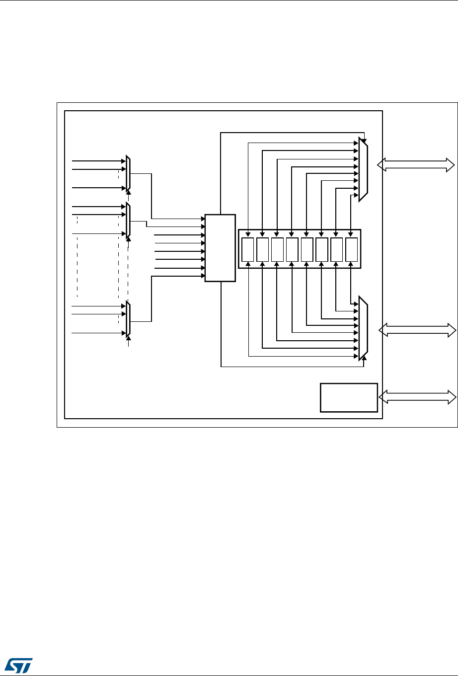
DocID027812 Rev 2 163/766
RM0401 Direct memory access controller (DMA)
196
8.3 DMA functional description
8.3.1 General description
Figure 22 shows the block diagram of a DMA.
Figure 22. DMA block diagram
The DMA controller performs direct memory transfer: as an AHB master, it can take the
control of the AHB bus matrix to initiate AHB transactions.
It can carry out the following transactions:
•peripheral-to-memory
•memory-to-peripheral
•memory-to-memory
The DMA controller provides two AHB master ports: the AHB memory port, intended to be
connected to memories and the AHB peripheral port, intended to be connected to
peripherals. However, to allow memory-to-memory transfers, the AHB peripheral port must
also have access to the memories.
The AHB slave port is used to program the DMA controller (it supports only 32-bit
accesses).
See Figure 23 for the implementation of the system of two DMA controllers.
!("MASTER
-EMORYPORT
&)&/
!("MASTER
0ERIPHERALPORT
342%!-
&)&/ 342%!-
342%!-
342%!-
&)&/ 342%!-342%!-
&)&/ 342%!-
342%!-
2%1?342%!-
2%1?342?#(
2%1?342?#(
$-!CONTROLLER
&)&/ 342%!-342%!-
&)&/ 342%!-342%!-
&)&/ 342%!-342%!-
&)&/ 342%!-342%!-
!RBITER
2%1?342%!-
2%1?342%!-
2%1?342%!-
2%1?342%!-
2%1?342%!-
2%1?342%!-
2%1?342%!-
2%1?342?#(
2%1?342?#(
2%1?342?#(
2%1?342?#(
2%1?342?#(
2%1?342?#(
2%1?342?#(
!("SLAVE
PROGRAMMING
INTERFACE
0ROGRAMMINGPORT
#HANNEL
SELECTION
AIB
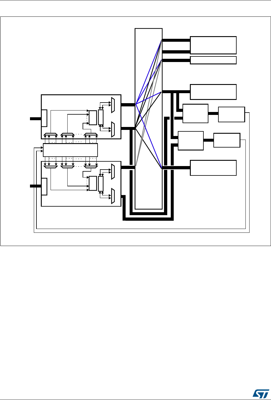
Direct memory access controller (DMA) RM0401
164/766 DocID027812 Rev 2
Figure 23. System implementation of the two DMA controllers
1. The DMA1 controller AHB peripheral port is not connected to the bus matrix like in the case of the DMA2 controller, thus
only DMA2 streams are able to perform memory-to-memory transfers.
8.3.2 DMA transactions
A DMA transaction consists of a sequence of a given number of data transfers. The number
of data items to be transferred and their width (8-bit, 16-bit or 32-bit) are software-
programmable.
Each DMA transfer consists of three operations:
•A loading from the peripheral data register or a location in memory, addressed through
the DMA_SxPAR or DMA_SxM0AR register
•A storage of the data loaded to the peripheral data register or a location in memory
addressed through the DMA_SxPAR or DMA_SxM0AR register
•A post-decrement of the DMA_SxNDTR register, which contains the number of
transactions that still have to be performed
After an event, the peripheral sends a request signal to the DMA controller. The DMA
controller serves the request depending on the channel priorities. As soon as the DMA
069
'0$FRQWUROOHU
$+%SHULSK
$UELWHU
$+%PHPRU\
),)2
'0$FRQWUROOHU
$+%PHPRU\
%XV0DWUL[
$+%PXOWLOD\HU
$UELWHU
$+%SHULSK
0$33,1*
),)2
)ODVK
PHPRU\
65$0
$+%SHULSKHUDOV
$+%$3%
EULGJH
GXDO$+%
$3% $3%
$+%$3%
EULGJH
GXDO$+%
$3% $3%
SHULSKHUDOV
$+%VODYH
$+%VODYH
SRUWSRUWSRUWSRUW
'0$UHTXHVW
SHULSKHUDOV
$+%SHULSKHUDOV
7R$+%
SHULSKHUDOV
7R$+%
SHULSKHUDOV
'&2'(
,&2'(
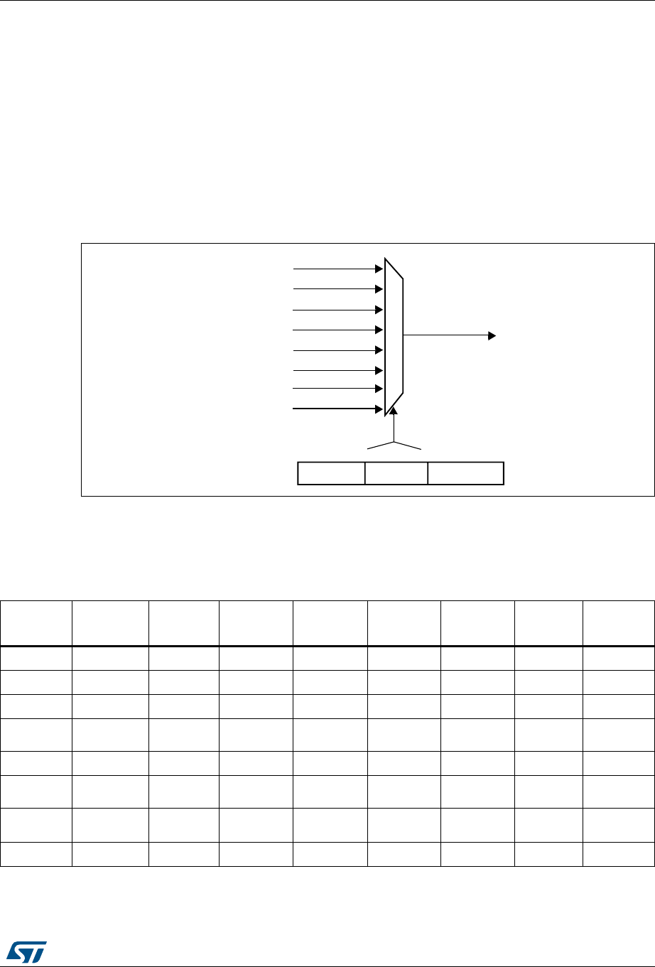
DocID027812 Rev 2 165/766
RM0401 Direct memory access controller (DMA)
196
controller accesses the peripheral, an Acknowledge signal is sent to the peripheral by the
DMA controller. The peripheral releases its request as soon as it gets the Acknowledge
signal from the DMA controller. Once the request has been deasserted by the peripheral,
the DMA controller releases the Acknowledge signal. If there are more requests, the
peripheral can initiate the next transaction.
8.3.3 Channel selection
Each stream is associated with a DMA request that can be selected out of 8 possible
channel requests. The selection is controlled by the CHSEL[2:0] bits in the DMA_SxCR
register.
Figure 24. Channel selection
The 8 requests from the peripherals (TIM, ADC, SPI, I2C, etc.) are independently connected
to each channel and their connection depends on the product implementation.
Table 29 and Table 30 give examples of DMA request mappings.
2%1?342%!-X
2%1?342X?#(
2%1?342X?#(
2%1?342X?#(
2%1?342X?#(
2%1?342X?#(
2%1?342X?#(
2%1?342X?#(
2%1?342X?#(
#(3%,;=
$-!?3X#2
AIB
Table 29. DMA1 request mapping
Peripheral
requests Stream 0 Stream 1 Stream 2 Stream 3 Stream 4 Stream 5 Stream 6 Stream 7
Channel 0 - I2C1_TX - SPI2_RX SPI2_TX - - -
Channel 1 I2C1_RX - - I2C4_RX - I2C1_RX I2C1_TX I2C1_TX
Channel 2 - I2C4_TX - - - - - -
Channel 3 ------
--
Channel 4 - - - - - USART2_RX USART2_TX I2C4_TX
Channel 5 --
------
Channel 6 TIM5_CH3
TIM5_UP
TIM5_CH4
TIM5_TRIG TIM5_CH1 TIM5_CH4
TIM5_TRIG TIM5_CH2 - TIM5_UP USART2_RX
Channel 7 I2C4_RX TIM6_UP I2C2_RX I2C2_RX - DAC1 - I2C2_TX

Direct memory access controller (DMA) RM0401
166/766 DocID027812 Rev 2
8.3.4 Arbiter
An arbiter manages the 8 DMA stream requests based on their priority for each of the two
AHB master ports (memory and peripheral ports) and launches the peripheral/memory
access sequences.
Priorities are managed in two stages:
•Software: each stream priority can be configured in the DMA_SxCR register. There are
four levels:
–Very high priority
– High priority
– Medium priority
– Low priority
•Hardware: If two requests have the same software priority level, the stream with the
lower number takes priority over the stream with the higher number. For example,
Stream 2 takes priority over Stream 4.
8.3.5 DMA streams
Each of the 8 DMA controller streams provides a unidirectional transfer link between a
source and a destination.
Each stream can be configured to perform:
•Regular type transactions: memory-to-peripherals, peripherals-to-memory or memory-
to-memory transfers
•Double-buffer type transactions: double buffer transfers using two memory pointers for
the memory (while the DMA is reading/writing from/to a buffer, the application can
write/read to/from the other buffer).
The amount of data to be transferred (up to 65535) is programmable and related to the
source width of the peripheral that requests the DMA transfer connected to the peripheral
AHB port. The register that contains the amount of data items to be transferred is
decremented after each transaction.
Table 30. DMA2 request mapping
Peripheral
requests Stream 0 Stream 1 Stream 2 Stream 3 Stream 4 Stream 5 Stream 6 Stream 7
Channel 0 ADC1 - - - ADC1 -
TIM1_CH1
TIM1_CH2
TIM1_CH3
-
Channel 1 --------
Channel 2 - - SPI1_TX SPI5_RX SPI5_TX - - -
Channel 3 SPI1_RX - SPI1_RX SPI1_TX - SPI1_TX - -
Channel 4 - - USART1_RX - - USART1_RX - USART1_TX
Channel 5 - USART6_RX USART6_RX - - SPI5_TX USART6_TX USART6_TX
Channel 6 TIM1_TRIG TIM1_CH1 TIM1_CH2 TIM1_CH1
TIM1_CH4
TIM1_TRIG
TIM1_COM
TIM1_UP TIM1_CH3 -
Channel 7 - - - - - SPI5_RX SPI5_TX -

DocID027812 Rev 2 167/766
RM0401 Direct memory access controller (DMA)
196
8.3.6 Source, destination and transfer modes
Both source and destination transfers can address peripherals and memories in the entire
4 GB area, at addresses comprised between 0x0000 0000 and 0xFFFF FFFF.
The direction is configured using the DIR[1:0] bits in the DMA_SxCR register and offers
three possibilities: memory-to-peripheral, peripheral-to-memory or memory-to-memory
transfers. Table 31 describes the corresponding source and destination addresses.
When the data width (programmed in the PSIZE or MSIZE bits in the DMA_SxCR register)
is a half-word or a word, respectively, the peripheral or memory address written into the
DMA_SxPAR or DMA_SxM0AR/M1AR registers has to be aligned on a word or half-word
address boundary, respectively.
Peripheral-to-memory mode
Figure 25 describes this mode.
When this mode is enabled (by setting the bit EN in the DMA_SxCR register), each time a
peripheral request occurs, the stream initiates a transfer from the source to fill the FIFO.
When the threshold level of the FIFO is reached, the contents of the FIFO are drained and
stored into the destination.
The transfer stops once the DMA_SxNDTR register reaches zero, when the peripheral
requests the end of transfers (in case of a peripheral flow controller) or when the EN bit in
the DMA_SxCR register is cleared by software.
In direct mode (when the DMDIS value in the DMA_SxFCR register is ‘0’), the threshold
level of the FIFO is not used: after each single data transfer from the peripheral to the FIFO,
the corresponding data are immediately drained and stored into the destination.
The stream has access to the AHB source or destination port only if the arbitration of the
corresponding stream is won. This arbitration is performed using the priority defined for
each stream using the PL[1:0] bits in the DMA_SxCR register.
Table 31. Source and destination address
Bits DIR[1:0] of the
DMA_SxCR register Direction Source address Destination address
00 Peripheral-to-memory DMA_SxPAR DMA_SxM0AR
01 Memory-to-peripheral DMA_SxM0AR DMA_SxPAR
10 Memory-to-memory DMA_SxPAR DMA_SxM0AR
11 Reserved - -
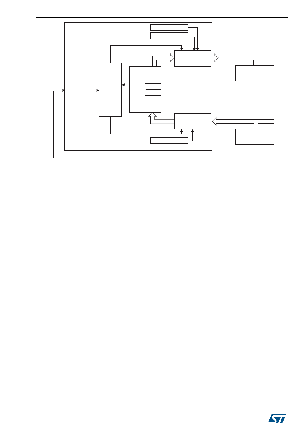
Direct memory access controller (DMA) RM0401
168/766 DocID027812 Rev 2
Figure 25. Peripheral-to-memory mode
1. For double-buffer mode.
Memory-to-peripheral mode
Figure 26 describes this mode.
When this mode is enabled (by setting the EN bit in the DMA_SxCR register), the stream
immediately initiates transfers from the source to entirely fill the FIFO.
Each time a peripheral request occurs, the contents of the FIFO are drained and stored into
the destination. When the level of the FIFO is lower than or equal to the predefined
threshold level, the FIFO is fully reloaded with data from the memory.
The transfer stops once the DMA_SxNDTR register reaches zero, when the peripheral
requests the end of transfers (in case of a peripheral flow controller) or when the EN bit in
the DMA_SxCR register is cleared by software.
In direct mode (when the DMDIS value in the DMA_SxFCR register is '0'), the threshold
level of the FIFO is not used. Once the stream is enabled, the DMA preloads the first data to
transfer into an internal FIFO. As soon as the peripheral requests a data transfer, the DMA
transfers the preloaded value into the configured destination. It then reloads again the
empty internal FIFO with the next data to be transfer. The preloaded data size corresponds
to the value of the PSIZE bitfield in the DMA_SxCR register.
The stream has access to the AHB source or destination port only if the arbitration of the
corresponding stream is won. This arbitration is performed using the priority defined for
each stream using the PL[1:0] bits in the DMA_SxCR register.
-EMORYBUS
0ERIPHERALBUS
2%1?342%!-X !RBITER
$-!?3X-!2
&)&/
!("MEMORY
PORT
!("PERIPHERAL
PORT
$-!?3X0!2
&)&/
LEVEL
$-!CONTROLLER $-!?3X-!2
DESTINATION
SOURCE
PERIPHERAL
-EMORY
0ERIPHERAL$-!REQUEST
AI
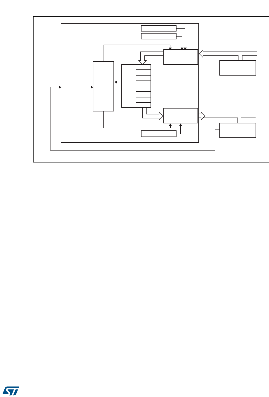
DocID027812 Rev 2 169/766
RM0401 Direct memory access controller (DMA)
196
Figure 26. Memory-to-peripheral mode
1. For double-buffer mode.
Memory-to-memory mode
The DMA channels can also work without being triggered by a request from a peripheral.
This is the memory-to-memory mode, described in Figure 27.
When the stream is enabled by setting the Enable bit (EN) in the DMA_SxCR register, the
stream immediately starts to fill the FIFO up to the threshold level. When the threshold level
is reached, the FIFO contents are drained and stored into the destination.
The transfer stops once the DMA_SxNDTR register reaches zero or when the EN bit in the
DMA_SxCR register is cleared by software.
The stream has access to the AHB source or destination port only if the arbitration of the
corresponding stream is won. This arbitration is performed using the priority defined for
each stream using the PL[1:0] bits in the DMA_SxCR register.
Note: When memory-to-memory mode is used, the Circular and direct modes are not allowed.
Only the DMA2 controller is able to perform memory-to-memory transfers.
0ERIPHERALBUS
-EMORYBUS
2%1?342%!-X !RBITER
$-!?3X-!2
&)&/
!("MEMORY
PORT
!("PERIPHERAL
PORT
$-!?3X0!2
&)&/
LEVEL
$-!CONTROLLER $-!?3X-!2
SOURCE
DESTINATION
0ERIPHERAL
-EMORY
0ERIPHERAL$-!REQUEST
AI
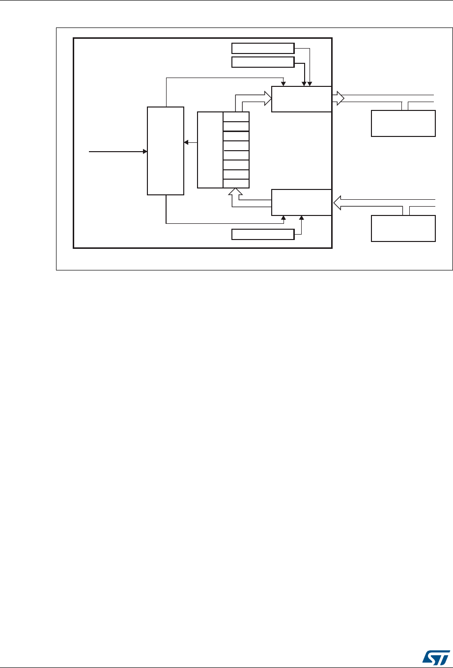
Direct memory access controller (DMA) RM0401
170/766 DocID027812 Rev 2
Figure 27. Memory-to-memory mode
1. For double-buffer mode.
8.3.7 Pointer incrementation
Peripheral and memory pointers can optionally be automatically post-incremented or kept
constant after each transfer depending on the PINC and MINC bits in the DMA_SxCR
register.
Disabling the Increment mode is useful when the peripheral source or destination data are
accessed through a single register.
If the Increment mode is enabled, the address of the next transfer will be the address of the
previous one incremented by 1 (for bytes), 2 (for half-words) or 4 (for words) depending on
the data width programmed in the PSIZE or MSIZE bits in the DMA_SxCR register.
In order to optimize the packing operation, it is possible to fix the increment offset size for
the peripheral address whatever the size of the data transferred on the AHB peripheral port.
The PINCOS bit in the DMA_SxCR register is used to align the increment offset size with
the data size on the peripheral AHB port, or on a 32-bit address (the address is then
incremented by 4). The PINCOS bit has an impact on the AHB peripheral port only.
If PINCOS bit is set, the address of the next transfer is the address of the previous one
incremented by 4 (automatically aligned on a 32-bit address) whatever the PSIZE value.
The AHB memory port, however, is not impacted by this operation.
-EMORYBUS
0ERIPHERALBUS
3TREAMENABLE
!RBITER
$-!?3X-!2
&)&/
!("MEMORY
PORT
!("PERIPHERAL
PORT
$-!?3X0!2
&)&/
LEVEL
$-!CONTROLLER $-!?3X-!2
DESTINATION
SOURCE
-EMORY
-EMORY
&)&/
AI

DocID027812 Rev 2 171/766
RM0401 Direct memory access controller (DMA)
196
8.3.8 Circular mode
The Circular mode is available to handle circular buffers and continuous data flows (e.g.
ADC scan mode). This feature can be enabled using the CIRC bit in the DMA_SxCR
register.
When the circular mode is activated, the number of data items to be transferred is
automatically reloaded with the initial value programmed during the stream configuration
phase, and the DMA requests continue to be served.
Note: In the circular mode, it is mandatory to respect the following rule in case of a burst mode
configured for memory:
DMA_SxNDTR = Multiple of ((Mburst beat) × (Msize)/(Psize)), where:
– (Mburst beat) = 4, 8 or 16 (depending on the MBURST bits in the DMA_SxCR
register)
– ((Msize)/(Psize)) = 1, 2, 4, 1/2 or 1/4 (Msize and Psize represent the MSIZE and
PSIZE bits in the DMA_SxCR register. They are byte dependent)
– DMA_SxNDTR = Number of data items to transfer on the AHB peripheral port
For example: Mburst beat = 8 (INCR8), MSIZE = ‘00’ (byte) and PSIZE = ‘01’ (half-word), in
this case: DMA_SxNDTR must be a multiple of (8 × 1/2 = 4).
If this formula is not respected, the DMA behavior and data integrity are not guaranteed.
NDTR must also be a multiple of the Peripheral burst size multiplied by the peripheral data
size, otherwise this could result in a bad DMA behavior.
8.3.9 Double buffer mode
This mode is available for all the DMA1 and DMA2 streams.
The Double buffer mode is enabled by setting the DBM bit in the DMA_SxCR register.
A double-buffer stream works as a regular (single buffer) stream with the difference that it
has two memory pointers. When the Double buffer mode is enabled, the Circular mode is
automatically enabled (CIRC bit in DMA_SxCR is don’t care) and at each end of transaction,
the memory pointers are swapped.
In this mode, the DMA controller swaps from one memory target to another at each end of
transaction. This allows the software to process one memory area while the second memory
area is being filled/used by the DMA transfer. The double-buffer stream can work in both
directions (the memory can be either the source or the destination) as described in
Table 32: Source and destination address registers in double buffer mode (DBM=1).
Note: In Double buffer mode, it is possible to update the base address for the AHB memory port
on-the-fly (DMA_SxM0AR or DMA_SxM1AR) when the stream is enabled, by respecting the
following conditions:
•
When the CT bit is ‘0’ in the DMA_SxCR register, the DMA_SxM1AR register can be
written. Attempting to write to this register while CT = '1' sets an error flag (TEIF) and
the stream is automatically disabled.
•
When the CT bit is ‘1’ in the DMA_SxCR register, the DMA_SxM0AR register can be
written. Attempting to write to this register while CT = '0', sets an error flag (TEIF) and
the stream is automatically disabled.
To avoid any error condition, it is advised to change the base address as soon as the TCIF
flag is asserted because, at this point, the targeted memory must have changed from

Direct memory access controller (DMA) RM0401
172/766 DocID027812 Rev 2
memory 0 to 1 (or from 1 to 0) depending on the value of CT in the DMA_SxCR register in
accordance with one of the two above conditions.
For all the other modes (except the Double buffer mode), the memory address registers are
write-protected as soon as the stream is enabled.
8.3.10 Programmable data width, packing/unpacking, endianness
The number of data items to be transferred has to be programmed into DMA_SxNDTR
(number of data items to transfer bit, NDT) before enabling the stream (except when the
flow controller is the peripheral, PFCTRL bit in DMA_SxCR is set).
When using the internal FIFO, the data widths of the source and destination data are
programmable through the PSIZE and MSIZE bits in the DMA_SxCR register (can be 8-,
16- or 32-bit).
When PSIZE and MSIZE are not equal:
•The data width of the number of data items to transfer, configured in the DMA_SxNDTR
register is equal to the width of the peripheral bus (configured by the PSIZE bits in the
DMA_SxCR register). For instance, in case of peripheral-to-memory, memory-to-
peripheral or memory-to-memory transfers and if the PSIZE[1:0] bits are configured for
half-word, the number of bytes to be transferred is equal to 2 × NDT.
•The DMA controller only copes with little-endian addressing for both source and
destination. This is described in Table 33: Packing/unpacking & endian behavior (bit
PINC = MINC = 1).
This packing/unpacking procedure may present a risk of data corruption when the operation
is interrupted before the data are completely packed/unpacked. So, to ensure data
coherence, the stream may be configured to generate burst transfers: in this case, each
group of transfers belonging to a burst are indivisible (refer to Section 8.3.11: Single and
burst transfers).
In direct mode (DMDIS = 0 in the DMA_SxFCR register), the packing/unpacking of data is
not possible. In this case, it is not allowed to have different source and destination transfer
data widths: both are equal and defined by the PSIZE bits in the DMA_SxCR MSIZE bits are
don’t care).
Table 32. Source and destination address registers in double buffer mode (DBM=1)
Bits DIR[1:0] of the
DMA_SxCR register Direction Source address Destination address
00 Peripheral-to-memory DMA_SxPAR DMA_SxM0AR / DMA_SxM1AR
01 Memory-to-peripheral DMA_SxM0AR / DMA_SxM1AR DMA_SxPAR
10 Not allowed(1)
11 Reserved - -
1. When the Double buffer mode is enabled, the Circular mode is automatically enabled. Since the memory-to-memory mode
is not compatible with the Circular mode, when the Double buffer mode is enabled, it is not allowed to configure the
memory-to-memory mode.

DocID027812 Rev 2 173/766
RM0401 Direct memory access controller (DMA)
196
Note: Peripheral port may be the source or the destination (it could also be the memory source in
the case of memory-to-memory transfer).
PSIZE, MSIZE and NDT[15:0] have to be configured so as to ensure that the last transfer
will not be incomplete. This can occur when the data width of the peripheral port (PSIZE
bits) is lower than the data width of the memory port (MSIZE bits). This constraint is
summarized in Table 34.
Table 33. Packing/unpacking & endian behavior (bit PINC = MINC = 1)
AHB
memory
port
width
AHB
peripheral
port
width
Number
of data
items to
transfer
(NDT)
Memory
transfer
number
Memory port
address / byte
lane
Peripheral
transfer
number
Peripheral port address / byte lane
PINCOS = 1 PINCOS = 0
884
1
2
3
4
0x0 / B0[7:0]
0x1 / B1[7:0]
0x2 / B2[7:0]
0x3 / B3[7:0]
1
2
3
4
0x0 / B0[7:0]
0x4 / B1[7:0]
0x8 / B2[7:0]
0xC / B3[7:0]
0x0 / B0[7:0]
0x1 / B1[7:0]
0x2 / B2[7:0]
0x3 / B3[7:0]
8162
1
2
3
4
0x0 / B0[7:0]
0x1 / B1[7:0]
0x2 / B2[7:0]
0x3 / B3[7:0]
1
2
0x0 / B1|B0[15:0]
0x4 / B3|B2[15:0]
0x0 / B1|B0[15:0]
0x2 / B3|B2[15:0]
8321
1
2
3
4
0x0 / B0[7:0]
0x1 / B1[7:0]
0x2 / B2[7:0]
0x3 / B3[7:0]
10x0 /
B3|B2|B1|B0[31:0]
0x0 /
B3|B2|B1|B0[31:0]
16 8 4
1
2
0x0 / B1|B0[15:0]
0x2 / B3|B2[15:0]
1
2
3
4
0x0 / B0[7:0]
0x4 / B1[7:0]
0x8 / B2[7:0]
0xC / B3[7:0]
0x0 / B0[7:0]
0x1 / B1[7:0]
0x2 / B2[7:0]
0x3 / B3[7:0]
16 16 2
1
2
0x0 / B1|B0[15:0]
0x2 / B1|B0[15:0]
1
2
0x0 / B1|B0[15:0]
0x4 / B3|B2[15:0]
0x0 / B1|B0[15:0]
0x2 / B3|B2[15:0]
16 32 1 1
2
0x0 / B1|B0[15:0]
0x2 / B3|B2[15:0]
10x0 /
B3|B2|B1|B0[31:0]
0x0 /
B3|B2|B1|B0[31:0]
32 8 4
10x0 / B3|B2|B1|B0[31:0]
1
2
3
4
0x0 / B0[7:0]
0x4 / B1[7:0]
0x8 / B2[7:0]
0xC / B3[7:0]
0x0 / B0[7:0]
0x1 / B1[7:0]
0x2 / B2[7:0]
0x3 / B3[7:0]
32 16 2 10x0 /B3|B2|B1|B0[31:0] 1
2
0x0 / B1|B0[15:0]
0x4 / B3|B2[15:0]
0x0 / B1|B0[15:0]
0x2 / B3|B2[15:0]
32 32 1 1 0x0 /B3|B2|B1|B0 [31:0] 1 0x0 /B3|B2|B1|B0
[31:0]
0x0 /
B3|B2|B1|B0[31:0]
Table 34. Restriction on NDT versus PSIZE and MSIZE
PSIZE[1:0] of DMA_SxCR MSIZE[1:0] of DMA_SxCR NDT[15:0] of DMA_SxNDTR
00 (8-bit) 01 (16-bit) must be a multiple of 2
00 (8-bit) 10 (32-bit) must be a multiple of 4
01 (16-bit) 10 (32-bit) must be a multiple of 2

Direct memory access controller (DMA) RM0401
174/766 DocID027812 Rev 2
8.3.11 Single and burst transfers
The DMA controller can generate single transfers or incremental burst transfers of 4, 8 or 16
beats.
The size of the burst is configured by software independently for the two AHB ports by using
the MBURST[1:0] and PBURST[1:0] bits in the DMA_SxCR register.
The burst size indicates the number of beats in the burst, not the number of bytes
transferred.
To ensure data coherence, each group of transfers that form a burst are indivisible: AHB
transfers are locked and the arbiter of the AHB bus matrix does not degrant the DMA master
during the sequence of the burst transfer.
Depending on the single or burst configuration, each DMA request initiates a different
number of transfers on the AHB peripheral port:
•When the AHB peripheral port is configured for single transfers, each DMA request
generates a data transfer of a byte, half-word or word depending on the PSIZE[1:0] bits
in the DMA_SxCR register
•When the AHB peripheral port is configured for burst transfers, each DMA request
generates 4,8 or 16 beats of byte, half word or word transfers depending on the
PBURST[1:0] and PSIZE[1:0] bits in the DMA_SxCR register.
The same as above has to be considered for the AHB memory port considering the
MBURST and MSIZE bits.
In direct mode, the stream can only generate single transfers and the MBURST[1:0] and
PBURST[1:0] bits are forced by hardware.
The address pointers (DMA_SxPAR or DMA_SxM0AR registers) must be chosen so as to
ensure that all transfers within a burst block are aligned on the address boundary equal to
the size of the transfer.
The burst configuration has to be selected in order to respect the AHB protocol, where
bursts must not cross the 1 KB address boundary because the minimum address space that
can be allocated to a single slave is 1 KB. This means that the 1 KB address boundary
should not be crossed by a burst block transfer, otherwise an AHB error would be
generated, that is not reported by the DMA registers.
8.3.12 FIFO
FIFO structure
The FIFO is used to temporarily store data coming from the source before transmitting them
to the destination.
Each stream has an independent 4-word FIFO and the threshold level is software-
configurable between 1/4, 1/2, 3/4 or full.
To enable the use of the FIFO threshold level, the direct mode must be disabled by setting
the DMDIS bit in the DMA_SxFCR register.
The structure of the FIFO differs depending on the source and destination data widths, and
is described in Figure 28: FIFO structure.
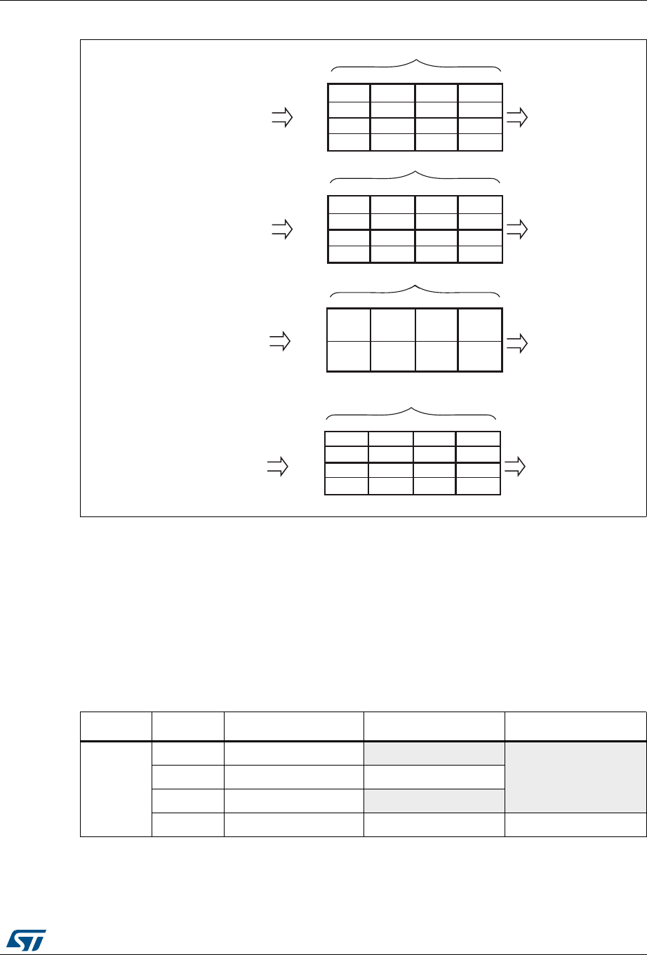
DocID027812 Rev 2 175/766
RM0401 Direct memory access controller (DMA)
196
Figure 28. FIFO structure
FIFO threshold and burst configuration
Caution is required when choosing the FIFO threshold (bits FTH[1:0] of the DMA_SxFCR
register) and the size of the memory burst (MBURST[1:0] of the DMA_SxCR register): The
content pointed by the FIFO threshold must exactly match an integer number of memory
burst transfers. If this is not in the case, a FIFO error (flag FEIFx of the DMA_HISR or
DMA_LISR register) will be generated when the stream is enabled, then the stream will be
automatically disabled. The allowed and forbidden configurations are described in Table 35.
The forbidden configurations are highlighted in gray in the table.
Table 35. FIFO threshold configurations
MSIZE FIFO level MBURST = INCR4 MBURST = INCR8 MBURST = INCR16
Byte
1/4 1 burst of 4 beats forbidden
forbidden1/2 2 bursts of 4 beats 1 burst of 8 beats
3/4 3 bursts of 4 beats forbidden
Full 4 bursts of 4 beats 2 bursts of 8 beats 1 burst of 16 beats
3OURCEBYTE
WORDS
BYTELANE
BYTELANE
BYTELANE
BYTELANE
&ULL%MPTY
"
"
"
"
"
"
"
"
"
"
"
"
"
"
"
"
$ESTINATIONWORD
3OURCEBYTE $ESTINATIONHALFWORD
WORDS
BYTELANE
BYTELANE
BYTELANE
BYTELANE
&ULL%MPTY
"
"
"
"
"
"
"
"
"
"
"
"
"
"
"
"
7777
(
(
(
(
(
(
(
(
3OURCEHALFWORD $ESTINATIONWORD
WORDS
BYTELANE
BYTELANE
BYTELANE
BYTELANE
&ULL%MPTY
(
7777
(
(
(
(
(
(
(
""""""""""""""""
""""""""""""""""
((((((((
((((((((
7777
7777
3OURCEHALFWORD
WORDS
BYTELANE
BYTELANE
BYTELANE
BYTELANE
&ULL%MPTY
$ESTINATIONBYTE
((((((((
"
"
"
"
"
"
"
"
"
"
"
"
"
"
"
"
(
(
(
(
(
(
(
(
""""""""
""""""""
AI

Direct memory access controller (DMA) RM0401
176/766 DocID027812 Rev 2
In all cases, the burst size multiplied by the data size must not exceed the FIFO size (data
size can be: 1 (byte), 2 (half-word) or 4 (word)).
Incomplete Burst transfer at the end of a DMA transfer may happen if one of the following
conditions occurs:
•For the AHB peripheral port configuration: the total number of data items (set in the
DMA_SxNDTR register) is not a multiple of the burst size multiplied by the data size
•For the AHB memory port configuration: the number of remaining data items in the
FIFO to be transferred to the memory is not a multiple of the burst size multiplied by the
data size
In such cases, the remaining data to be transferred will be managed in single mode by the
DMA, even if a burst transaction was requested during the DMA stream configuration.
Note: When burst transfers are requested on the peripheral AHB port and the FIFO is used
(DMDIS = 1 in the DMA_SxCR register), it is mandatory to respect the following rule to
avoid permanent underrun or overrun conditions, depending on the DMA stream direction:
If (PBURST × PSIZE) = FIFO_SIZE (4 words), FIFO_Threshold = 3/4 is forbidden with
PSIZE = 1, 2 or 4 and PBURST = 4, 8 or 16.
This rule ensures that enough FIFO space at a time will be free to serve the request from
the peripheral.
FIFO flush
The FIFO can be flushed when the stream is disabled by resetting the EN bit in the
DMA_SxCR register and when the stream is configured to manage peripheral-to-memory or
memory-to-memory transfers: If some data are still present in the FIFO when the stream is
disabled, the DMA controller continues transferring the remaining data to the destination
(even though stream is effectively disabled). When this flush is completed, the transfer
complete status bit (TCIFx) in the DMA_LISR or DMA_HISR register is set.
The remaining data counter DMA_SxNDTR keeps the value in this case to indicate how
many data items are currently available in the destination memory.
Note that during the FIFO flush operation, if the number of remaining data items in the FIFO
to be transferred to memory (in bytes) is less than the memory data width (for example 2
bytes in FIFO while MSIZE is configured to word), data will be sent with the data width set in
the MSIZE bit in the DMA_SxCR register. This means that memory will be written with an
Half-word
1/4 forbidden
forbidden
forbidden
1/2 1 burst of 4 beats
3/4 forbidden
Full 2 bursts of 4 beats 1 burst of 8 beats
Word
1/4
forbidden
forbidden
1/2
3/4
Full 1 burst of 4 beats
Table 35. FIFO threshold configurations (continued)
MSIZE FIFO level MBURST = INCR4 MBURST = INCR8 MBURST = INCR16

DocID027812 Rev 2 177/766
RM0401 Direct memory access controller (DMA)
196
undesired value. The software may read the DMA_SxNDTR register to determine the
memory area that contains the good data (start address and last address).
If the number of remaining data items in the FIFO is lower than a burst size (if the MBURST
bits in DMA_SxCR register are set to configure the stream to manage burst on the AHB
memory port), single transactions will be generated to complete the FIFO flush.
Direct mode
By default, the FIFO operates in direct mode (DMDIS bit in the DMA_SxFCR is reset) and
the FIFO threshold level is not used. This mode is useful when the system requires an
immediate and single transfer to or from the memory after each DMA request.
When the DMA is configured in direct mode (FIFO disabled), to transfer data in memory-to-
peripheral mode, the DMA preloads one data from the memory to the internal FIFO to
ensure an immediate data transfer as soon as a DMA request is triggered by a peripheral.
To avoid saturating the FIFO, it is recommended to configure the corresponding stream with
a high priority.
This mode is restricted to transfers where:
•The source and destination transfer widths are equal and both defined by the
PSIZE[1:0] bits in DMA_SxCR (MSIZE[1:0] bits are don’t care)
•Burst transfers are not possible (PBURST[1:0] and MBURST[1:0] bits in DMA_SxCR
are don’t care)
Direct mode must not be used when implementing memory-to-memory transfers.
8.3.13 DMA transfer completion
Different events can generate an end of transfer by setting the TCIFx bit in the DMA_LISR
or DMA_HISR status register:
•In DMA flow controller mode:
–The DMA_SxNDTR counter has reached zero in the memory-to-peripheral mode
– The stream is disabled before the end of transfer (by clearing the EN bit in the
DMA_SxCR register) and (when transfers are peripheral-to-memory or memory-
to-memory) all the remaining data have been flushed from the FIFO into the
memory
•In Peripheral flow controller mode:
– The last external burst or single request has been generated from the peripheral
and (when the DMA is operating in peripheral-to-memory mode) the remaining
data have been transferred from the FIFO into the memory
– The stream is disabled by software, and (when the DMA is operating in peripheral-
to-memory mode) the remaining data have been transferred from the FIFO into
the memory
Note: The transfer completion is dependent on the remaining data in FIFO to be transferred into
memory only in the case of peripheral-to-memory mode. This condition is not applicable in
memory-to-peripheral mode.
If the stream is configured in noncircular mode, after the end of the transfer (that is when the
number of data to be transferred reaches zero), the DMA is stopped (EN bit in DMA_SxCR
register is cleared by Hardware) and no DMA request is served unless the software
reprograms the stream and re-enables it (by setting the EN bit in the DMA_SxCR register).

Direct memory access controller (DMA) RM0401
178/766 DocID027812 Rev 2
8.3.14 DMA transfer suspension
At any time, a DMA transfer can be suspended to be restarted later on or to be definitively
disabled before the end of the DMA transfer.
There are two cases:
•The stream disables the transfer with no later-on restart from the point where it was
stopped. There is no particular action to do, except to clear the EN bit in the
DMA_SxCR register to disable the stream. The stream may take time to be disabled
(ongoing transfer is completed first). The transfer complete interrupt flag (TCIF in the
DMA_LISR or DMA_HISR register) is set in order to indicate the end of transfer. The
value of the EN bit in DMA_SxCR is now ‘0’ to confirm the stream interruption. The
DMA_SxNDTR register contains the number of remaining data items at the moment
when the stream was stopped so that the software can determine how many data items
have been transferred before the stream was interrupted.
•The stream suspends the transfer before the number of remaining data items to be
transferred in the DMA_SxNDTR register reaches 0. The aim is to restart the transfer
later by re-enabling the stream. In order to restart from the point where the transfer was
stopped, the software has to read the DMA_SxNDTR register after disabling the stream
by writing the EN bit in DMA_SxCR register (and then checking that it is at ‘0’) to know
the number of data items already collected. Then:
– The peripheral and/or memory addresses have to be updated in order to adjust
the address pointers
– The SxNDTR register has to be updated with the remaining number of data items
to be transferred (the value read when the stream was disabled)
– The stream may then be re-enabled to restart the transfer from the point it was
stopped
Note: Note that a Transfer complete interrupt flag (TCIF in DMA_LISR or DMA_HISR) is set to
indicate the end of transfer due to the stream interruption.
8.3.15 Flow controller
The entity that controls the number of data to be transferred is known as the flow controller.
This flow controller is configured independently for each stream using the PFCTRL bit in the
DMA_SxCR register.
The flow controller can be:
•The DMA controller: in this case, the number of data items to be transferred is
programmed by software into the DMA_SxNDTR register before the DMA stream is
enabled.
•The peripheral source or destination: this is the case when the number of data items to
be transferred is unknown. The peripheral indicates by hardware to the DMA controller
when the last data are being transferred. This feature is only supported for peripherals
which are able to signal the end of the transfer, that is:
When the peripheral flow controller is used for a given stream, the value written into the
DMA_SxNDTR has no effect on the DMA transfer. Actually, whatever the value written, it will
be forced by hardware to 0xFFFF as soon as the stream is enabled, to respect the following
schemes:
•Anticipated stream interruption: EN bit in DMA_SxCR register is reset to 0 by the
software to stop the stream before the last data hardware signal (single or burst) is sent
by the peripheral. In such a case, the stream is switched off and the FIFO flush is

DocID027812 Rev 2 179/766
RM0401 Direct memory access controller (DMA)
196
triggered in the case of a peripheral-to-memory DMA transfer. The TCIFx flag of the
corresponding stream is set in the status register to indicate the DMA completion. To
know the number of data items transferred during the DMA transfer, read the
DMA_SxNDTR register and apply the following formula:
– Number_of_data_transferred = 0xFFFF – DMA_SxNDTR
•Normal stream interruption due to the reception of a last data hardware signal: the
stream is automatically interrupted when the peripheral requests the last transfer
(single or burst) and when this transfer is complete. the TCIFx flag of the corresponding
stream is set in the status register to indicate the DMA transfer completion. To know the
number of data items transferred, read the DMA_SxNDTR register and apply the same
formula as above.
•The DMA_SxNDTR register reaches 0: the TCIFx flag of the corresponding stream is
set in the status register to indicate the forced DMA transfer completion. The stream is
automatically switched off even though the last data hardware signal (single or burst)
has not been yet asserted. The already transferred data will not be lost. This means
that a maximum of 65535 data items can be managed by the DMA in a single
transaction, even in peripheral flow control mode.
Note: When configured in memory-to-memory mode, the DMA is always the flow controller and
the PFCTRL bit is forced to 0 by hardware.
The Circular mode is forbidden in the peripheral flow controller mode.
8.3.16 Summary of the possible DMA configurations
Table 36 summarizes the different possible DMA configurations. The forbidden
configurations are highlighted in gray in the table.
Table 36. Possible DMA configurations
DMA transfer
mode Source Destination Flow
controller
Circular
mode
Transfer
type
Direct
mode
Double
buffer mode
Peripheral-to-
memory
AHB
peripheral port
AHB
memory port
DMA possible
single possible
possible
burst forbidden
Peripheral forbidden
single possible
forbidden
burst forbidden
Memory-to-
peripheral
AHB
memory port
AHB
peripheral port
DMA possible
single possible
possible
burst forbidden
Peripheral forbidden
single possible
forbidden
burst forbidden
Memory-to-
memory
AHB
peripheral port
AHB
memory port DMA only forbidden
single
forbidden forbidden
burst

Direct memory access controller (DMA) RM0401
180/766 DocID027812 Rev 2
8.3.17 Stream configuration procedure
The following sequence should be followed to configure a DMA stream x (where x is the
stream number):
1. If the stream is enabled, disable it by resetting the EN bit in the DMA_SxCR register,
then read this bit in order to confirm that there is no ongoing stream operation. Writing
this bit to 0 is not immediately effective since it is actually written to 0 once all the
current transfers have finished. When the EN bit is read as 0, this means that the
stream is ready to be configured. It is therefore necessary to wait for the EN bit to be
cleared before starting any stream configuration. All the stream dedicated bits set in the
status register (DMA_LISR and DMA_HISR) from the previous data block DMA
transfer should be cleared before the stream can be re-enabled.
2. Set the peripheral port register address in the DMA_SxPAR register. The data will be
moved from/ to this address to/ from the peripheral port after the peripheral event.
3. Set the memory address in the DMA_SxMA0R register (and in the DMA_SxMA1R
register in the case of a double buffer mode). The data will be written to or read from
this memory after the peripheral event.
4. Configure the total number of data items to be transferred in the DMA_SxNDTR
register. After each peripheral event or each beat of the burst, this value is
decremented.
5. Select the DMA channel (request) using CHSEL[2:0] in the DMA_SxCR register.
6. If the peripheral is intended to be the flow controller and if it supports this feature, set
the PFCTRL bit in the DMA_SxCR register.
7. Configure the stream priority using the PL[1:0] bits in the DMA_SxCR register.
8. Configure the FIFO usage (enable or disable, threshold in transmission and reception)
9. Configure the data transfer direction, peripheral and memory incremented/fixed mode,
single or burst transactions, peripheral and memory data widths, Circular mode,
Double buffer mode and interrupts after half and/or full transfer, and/or errors in the
DMA_SxCR register.
10. Activate the stream by setting the EN bit in the DMA_SxCR register.
As soon as the stream is enabled, it can serve any DMA request from the peripheral
connected to the stream.
Once half the data have been transferred on the AHB destination port, the half-transfer flag
(HTIF) is set and an interrupt is generated if the half-transfer interrupt enable bit (HTIE) is
set. At the end of the transfer, the transfer complete flag (TCIF) is set and an interrupt is
generated if the transfer complete interrupt enable bit (TCIE) is set.
Warning: To switch off a peripheral connected to a DMA stream
request, it is mandatory to, first, switch off the DMA stream to
which the peripheral is connected, then to wait for EN bit = 0.
Only then can the peripheral be safely disabled.

DocID027812 Rev 2 181/766
RM0401 Direct memory access controller (DMA)
196
8.3.18 Error management
The DMA controller can detect the following errors:
•Transfer error: the transfer error interrupt flag (TEIFx) is set when:
– A bus error occurs during a DMA read or a write access
– A write access is requested by software on a memory address register in Double
buffer mode whereas the stream is enabled and the current target memory is the
one impacted by the write into the memory address register (refer to Section 8.3.9:
Double buffer mode)
•FIFO error: the FIFO error interrupt flag (FEIFx) is set if:
– A FIFO underrun condition is detected
– A FIFO overrun condition is detected (no detection in memory-to-memory mode
because requests and transfers are internally managed by the DMA)
– The stream is enabled while the FIFO threshold level is not compatible with the
size of the memory burst (refer to Table 35: FIFO threshold configurations)
•Direct mode error: the direct mode error interrupt flag (DMEIFx) can only be set in the
peripheral-to-memory mode while operating in direct mode and when the MINC bit in
the DMA_SxCR register is cleared. This flag is set when a DMA request occurs while
the previous data have not yet been fully transferred into the memory (because the
memory bus was not granted). In this case, the flag indicates that 2 data items were be
transferred successively to the same destination address, which could be an issue if
the destination is not able to manage this situation
In direct mode, the FIFO error flag can also be set under the following conditions:
•In the peripheral-to-memory mode, the FIFO can be saturated (overrun) if the memory
bus is not granted for several peripheral requests
•In the memory-to-peripheral mode, an underrun condition may occur if the memory bus
has not been granted before a peripheral request occurs
If the TEIFx or the FEIFx flag is set due to incompatibility between burst size and FIFO
threshold level, the faulty stream is automatically disabled through a hardware clear of its
EN bit in the corresponding stream configuration register (DMA_SxCR).
If the DMEIFx or the FEIFx flag is set due to an overrun or underrun condition, the faulty
stream is not automatically disabled and it is up to the software to disable or not the stream
by resetting the EN bit in the DMA_SxCR register. This is because there is no data loss
when this kind of errors occur.
When the stream's error interrupt flag (TEIF, FEIF, DMEIF) in the DMA_LISR or DMA_HISR
register is set, an interrupt is generated if the corresponding interrupt enable bit (TEIE,
FEIE, DMIE) in the DMA_SxCR or DMA_SxFCR register is set.
Note: When a FIFO overrun or underrun condition occurs, the data are not lost because the
peripheral request is not acknowledged by the stream until the overrun or underrun
condition is cleared. If this acknowledge takes too much time, the peripheral itself may
detect an overrun or underrun condition of its internal buffer and data might be lost.
Direct memory access controller (DMA) RM0401
182/766 DocID027812 Rev 2
8.4 DMA interrupts
For each DMA stream, an interrupt can be produced on the following events:
•Half-transfer reached
•Transfer complete
•Transfer error
•Fifo error (overrun, underrun or FIFO level error)
•Direct mode error
Separate interrupt enable control bits are available for flexibility as shown in Table 37.
Note: Before setting an Enable control bit to ‘1’, the corresponding event flag should be cleared,
otherwise an interrupt is immediately generated.
8.5 DMA registers
The DMA registers have to be accessed by words (32 bits).
8.5.1 DMA low interrupt status register (DMA_LISR)
Address offset: 0x00
Reset value: 0x0000 0000
Table 37. DMA interrupt requests
Interrupt event Event flag Enable control bit
Half-transfer HTIF HTIE
Transfer complete TCIF TCIE
Transfer error TEIF TEIE
FIFO overrun/underrun FEIF FEIE
Direct mode error DMEIF DMEIE
31 30 29 28 27 26 25 24 23 22 21 20 19 18 17 16
Res. Res. Res. Res. TCIF3 HTIF3 TEIF3 DMEIF3 Res. FEIF3 TCIF2 HTIF2 TEIF2 DMEIF2 Res. FEIF2
r r r r r r r r r r r r r r
15 14 13 12 11 10 9 8 7 6 5 4 3 2 1 0
Res. Res. Res. Res. TCIF1 HTIF1 TEIF1 DMEIF1 Res. FEIF1 TCIF0 HTIF0 TEIF0 DMEIF0 Res. FEIF0
r r r r r r r r r r r r r r
Bits 31:28, 15:12 Reserved, must be kept at reset value.
Bits 27, 21, 11, 5 TCIFx: Stream x transfer complete interrupt flag (x = 3..0)
This bit is set by hardware. It is cleared by software writing 1 to the corresponding bit in the
DMA_LIFCR register.
0: No transfer complete event on stream x
1: A transfer complete event occurred on stream x

DocID027812 Rev 2 183/766
RM0401 Direct memory access controller (DMA)
196
8.5.2 DMA high interrupt status register (DMA_HISR)
Address offset: 0x04
Reset value: 0x0000 0000
Bits 26, 20, 10, 4 HTIFx: Stream x half transfer interrupt flag (x=3..0)
This bit is set by hardware. It is cleared by software writing 1 to the corresponding bit in the
DMA_LIFCR register.
0: No half transfer event on stream x
1: A half transfer event occurred on stream x
Bits 25, 19, 9, 3 TEIFx: Stream x transfer error interrupt flag (x=3..0)
This bit is set by hardware. It is cleared by software writing 1 to the corresponding bit in the
DMA_LIFCR register.
0: No transfer error on stream x
1: A transfer error occurred on stream x
Bits 24, 18, 8, 2 DMEIFx: Stream x direct mode error interrupt flag (x=3..0)
This bit is set by hardware. It is cleared by software writing 1 to the corresponding bit in the
DMA_LIFCR register.
0: No Direct Mode Error on stream x
1: A Direct Mode Error occurred on stream x
Bits 23, 17, 7, 1 Reserved, must be kept at reset value.
Bits 22, 16, 6, 0 FEIFx: Stream x FIFO error interrupt flag (x=3..0)
This bit is set by hardware. It is cleared by software writing 1 to the corresponding bit in the
DMA_LIFCR register.
0: No FIFO Error event on stream x
1: A FIFO Error event occurred on stream x
31 30 29 28 27 26 25 24 23 22 21 20 19 18 17 16
Res. Res. Res. Res. TCIF7 HTIF7 TEIF7 DMEIF7 Res. FEIF7 TCIF6 HTIF6 TEIF6 DMEIF6 Res. FEIF6
rr r r r r r r r r
15 14 13 12 11 10 9 8 7 6 5 4 3 2 1 0
Res. Res. Res. Res. TCIF5 HTIF5 TEIF5 DMEIF5 Res. FEIF5 TCIF4 HTIF4 TEIF4 DMEIF4 Res. FEIF4
rr r r r r r r r r
Bits 31:28, 15:12 Reserved, must be kept at reset value.
Bits 27, 21, 11, 5 TCIFx: Stream x transfer complete interrupt flag (x=7..4)
This bit is set by hardware. It is cleared by software writing 1 to the corresponding bit in the
DMA_HIFCR register.
0: No transfer complete event on stream x
1: A transfer complete event occurred on stream x
Bits 26, 20, 10, 4 HTIFx: Stream x half transfer interrupt flag (x=7..4)
This bit is set by hardware. It is cleared by software writing 1 to the corresponding bit in the
DMA_HIFCR register.
0: No half transfer event on stream x
1: A half transfer event occurred on stream x

Direct memory access controller (DMA) RM0401
184/766 DocID027812 Rev 2
8.5.3 DMA low interrupt flag clear register (DMA_LIFCR)
Address offset: 0x08
Reset value: 0x0000 0000
Bits 25, 19, 9, 3 TEIFx: Stream x transfer error interrupt flag (x=7..4)
This bit is set by hardware. It is cleared by software writing 1 to the corresponding bit in the
DMA_HIFCR register.
0: No transfer error on stream x
1: A transfer error occurred on stream x
Bits 24, 18, 8, 2 DMEIFx: Stream x direct mode error interrupt flag (x=7..4)
This bit is set by hardware. It is cleared by software writing 1 to the corresponding bit in the
DMA_HIFCR register.
0: No Direct mode error on stream x
1: A Direct mode error occurred on stream x
Bits 23, 17, 7, 1 Reserved, must be kept at reset value.
Bits 22, 16, 6, 0 FEIFx: Stream x FIFO error interrupt flag (x=7..4)
This bit is set by hardware. It is cleared by software writing 1 to the corresponding bit in the
DMA_HIFCR register.
0: No FIFO error event on stream x
1: A FIFO error event occurred on stream x
31 30 29 28 27 26 25 24 23 22 21 20 19 18 17 16
Res. Res. Res. Res. CTCIF3 CHTIF3 CTEIF3 CDMEIF3 Res. CFEIF3 CTCIF2 CHTIF2 CTEIF2 CDMEIF2 Res. CFEIF2
w w w w w w w w w w
15 14 13 12 11 10 9 8 7 6 5 4 3 2 1 0
Res. Res. Res. Res. CTCIF1 CHTIF1 CTEIF1 CDMEIF1 Res. CFEIF1 CTCIF0 CHTIF0 CTEIF0 CDMEIF0 Res. CFEIF0
w w w w w w w w w w
Bits 31:28, 15:12 Reserved, must be kept at reset value.
Bits 27, 21, 11, 5 CTCIFx: Stream x clear transfer complete interrupt flag (x = 3..0)
Writing 1 to this bit clears the corresponding TCIFx flag in the DMA_LISR register
Bits 26, 20, 10, 4 CHTIFx: Stream x clear half transfer interrupt flag (x = 3..0)
Writing 1 to this bit clears the corresponding HTIFx flag in the DMA_LISR register
Bits 25, 19, 9, 3 CTEIFx: Stream x clear transfer error interrupt flag (x = 3..0)
Writing 1 to this bit clears the corresponding TEIFx flag in the DMA_LISR register
Bits 24, 18, 8, 2 CDMEIFx: Stream x clear direct mode error interrupt flag (x = 3..0)
Writing 1 to this bit clears the corresponding DMEIFx flag in the DMA_LISR register
Bits 23, 17, 7, 1 Reserved, must be kept at reset value.
Bits 22, 16, 6, 0 CFEIFx: Stream x clear FIFO error interrupt flag (x = 3..0)
Writing 1 to this bit clears the corresponding CFEIFx flag in the DMA_LISR register

DocID027812 Rev 2 185/766
RM0401 Direct memory access controller (DMA)
196
8.5.4 DMA high interrupt flag clear register (DMA_HIFCR)
Address offset: 0x0C
Reset value: 0x0000 0000
31 30 29 28 27 26 25 24 23 22 21 20 19 18 17 16
Res. Res. Res. Res. CTCIF7 CHTIF7 CTEIF7 CDMEIF7 Res. CFEIF7 CTCIF6 CHTIF6 CTEIF6 CDMEIF6 Res. CFEIF6
w w w w w w w w w w
15 14 13 12 11 10 9 8 7 6 5 4 3 2 1 0
Res. Res. Res. Res. CTCIF5 CHTIF5 CTEIF5 CDMEIF5 Res. CFEIF5 CTCIF4 CHTIF4 CTEIF4 CDMEIF4 Res. CFEIF4
w w w w w w w w w w
Bits 31:28, 15:12 Reserved, must be kept at reset value.
Bits 27, 21, 11, 5 CTCIFx: Stream x clear transfer complete interrupt flag (x = 7..4)
Writing 1 to this bit clears the corresponding TCIFx flag in the DMA_HISR register
Bits 26, 20, 10, 4 CHTIFx: Stream x clear half transfer interrupt flag (x = 7..4)
Writing 1 to this bit clears the corresponding HTIFx flag in the DMA_HISR register
Bits 25, 19, 9, 3 CTEIFx: Stream x clear transfer error interrupt flag (x = 7..4)
Writing 1 to this bit clears the corresponding TEIFx flag in the DMA_HISR register
Bits 24, 18, 8, 2 CDMEIFx: Stream x clear direct mode error interrupt flag (x = 7..4)
Writing 1 to this bit clears the corresponding DMEIFx flag in the DMA_HISR register
Bits 23, 17, 7, 1 Reserved, must be kept at reset value.
Bits 22, 16, 6, 0 CFEIFx: Stream x clear FIFO error interrupt flag (x = 7..4)
Writing 1 to this bit clears the corresponding CFEIFx flag in the DMA_HISR register

Direct memory access controller (DMA) RM0401
186/766 DocID027812 Rev 2
8.5.5 DMA stream x configuration register (DMA_SxCR) (x = 0..7)
This register is used to configure the concerned stream.
Address offset: 0x10 + 0x18 × stream number
Reset value: 0x0000 0000
31 30 29 28 27 26 25 24 23 22 21 20 19 18 17 16
Res. Res. Res. Res. CHSEL[2:0] MBURST [1:0] PBURST[1:0] Res. CT DBM or
reserved PL[1:0]
rw rw rw rw rw rw rw rw rw or r rw rw
15 14 13 12 11 10 9 8 7 6 5 4 3 2 1 0
PINCOS MSIZE[1:0] PSIZE[1:0] MINC PINC CIRC DIR[1:0] PFCTRL TCIE HTIE TEIE DMEIE EN
rw rw rw rw rw rw rw rw rw rw rw rw rw rw rw rw
Bits 31:28 Reserved, must be kept at reset value.
Bits 27:25 CHSEL[2:0]: Channel selection
These bits are set and cleared by software.
000: channel 0 selected
001: channel 1 selected
010: channel 2 selected
011: channel 3 selected
100: channel 4 selected
101: channel 5 selected
110: channel 6 selected
111: channel 7 selected
These bits are protected and can be written only if EN is ‘0’
Bits 24:23 MBURST: Memory burst transfer configuration
These bits are set and cleared by software.
00: single transfer
01: INCR4 (incremental burst of 4 beats)
10: INCR8 (incremental burst of 8 beats)
11: INCR16 (incremental burst of 16 beats)
These bits are protected and can be written only if EN is ‘0’
In direct mode, these bits are forced to 0x0 by hardware as soon as bit EN= '1'.
Bits 22:21 PBURST[1:0]: Peripheral burst transfer configuration
These bits are set and cleared by software.
00: single transfer
01: INCR4 (incremental burst of 4 beats)
10: INCR8 (incremental burst of 8 beats)
11: INCR16 (incremental burst of 16 beats)
These bits are protected and can be written only if EN is ‘0’
In direct mode, these bits are forced to 0x0 by hardware.
Bit 20 Reserved, must be kept at reset value.
Bit 19 CT: Current target (only in double buffer mode)
This bits is set and cleared by hardware. It can also be written by software.
0: The current target memory is Memory 0 (addressed by the DMA_SxM0AR pointer)
1: The current target memory is Memory 1 (addressed by the DMA_SxM1AR pointer)
This bit can be written only if EN is ‘0’ to indicate the target memory area of the first transfer.
Once the stream is enabled, this bit operates as a status flag indicating which memory area
is the current target.

DocID027812 Rev 2 187/766
RM0401 Direct memory access controller (DMA)
196
Bit 18 DBM: Double buffer mode
This bits is set and cleared by software.
0: No buffer switching at the end of transfer
1: Memory target switched at the end of the DMA transfer
This bit is protected and can be written only if EN is ‘0’.
Bits 17:16 PL[1:0]: Priority level
These bits are set and cleared by software.
00: Low
01: Medium
10: High
11: Very high
These bits are protected and can be written only if EN is ‘0’.
Bit 15 PINCOS: Peripheral increment offset size
This bit is set and cleared by software
0: The offset size for the peripheral address calculation is linked to the PSIZE
1: The offset size for the peripheral address calculation is fixed to 4 (32-bit alignment).
This bit has no meaning if bit PINC = '0'.
This bit is protected and can be written only if EN = '0'.
This bit is forced low by hardware when the stream is enabled (bit EN = '1') if the direct
mode is selected or if PBURST are different from “00”.
Bits 14:13 MSIZE[1:0]: Memory data size
These bits are set and cleared by software.
00: byte (8-bit)
01: half-word (16-bit)
10: word (32-bit)
11: reserved
These bits are protected and can be written only if EN is ‘0’.
In direct mode, MSIZE is forced by hardware to the same value as PSIZE as soon as bit EN
= '1'.
Bits 12:11 PSIZE[1:0]: Peripheral data size
These bits are set and cleared by software.
00: Byte (8-bit)
01: Half-word (16-bit)
10: Word (32-bit)
11: reserved
These bits are protected and can be written only if EN is ‘0’
Bit 10 MINC: Memory increment mode
This bit is set and cleared by software.
0: Memory address pointer is fixed
1: Memory address pointer is incremented after each data transfer (increment is done
according to MSIZE)
This bit is protected and can be written only if EN is ‘0’.
Bit 9 PINC: Peripheral increment mode
This bit is set and cleared by software.
0: Peripheral address pointer is fixed
1: Peripheral address pointer is incremented after each data transfer (increment is done
according to PSIZE)
This bit is protected and can be written only if EN is ‘0’.

Direct memory access controller (DMA) RM0401
188/766 DocID027812 Rev 2
Bit 8 CIRC: Circular mode
This bit is set and cleared by software and can be cleared by hardware.
0: Circular mode disabled
1: Circular mode enabled
When the peripheral is the flow controller (bit PFCTRL=1) and the stream is enabled (bit
EN=1), then this bit is automatically forced by hardware to 0.
It is automatically forced by hardware to 1 if the DBM bit is set, as soon as the stream is
enabled (bit EN ='1').
Bits 7:6 DIR[1:0]: Data transfer direction
These bits are set and cleared by software.
00: Peripheral-to-memory
01: Memory-to-peripheral
10: Memory-to-memory
11: reserved
These bits are protected and can be written only if EN is ‘0’.
Bit 5 PFCTRL: Peripheral flow controller
This bit is set and cleared by software.
0: The DMA is the flow controller
1: The peripheral is the flow controller
This bit is protected and can be written only if EN is ‘0’.
When the memory-to-memory mode is selected (bits DIR[1:0]=10), then this bit is
automatically forced to 0 by hardware.
Bit 4 TCIE: Transfer complete interrupt enable
This bit is set and cleared by software.
0: TC interrupt disabled
1: TC interrupt enabled
Bit 3 HTIE: Half transfer interrupt enable
This bit is set and cleared by software.
0: HT interrupt disabled
1: HT interrupt enabled
Bit 2 TEIE: Transfer error interrupt enable
This bit is set and cleared by software.
0: TE interrupt disabled
1: TE interrupt enabled
Bit 1 DMEIE: Direct mode error interrupt enable
This bit is set and cleared by software.
0: DME interrupt disabled
1: DME interrupt enabled

DocID027812 Rev 2 189/766
RM0401 Direct memory access controller (DMA)
196
8.5.6 DMA stream x number of data register (DMA_SxNDTR) (x = 0..7)
Address offset: 0x14 + 0x18 × stream number
Reset value: 0x0000 0000
Bit 0 EN: Stream enable / flag stream ready when read low
This bit is set and cleared by software.
0: Stream disabled
1: Stream enabled
This bit may be cleared by hardware:
– on a DMA end of transfer (stream ready to be configured)
– if a transfer error occurs on the AHB master buses
– when the FIFO threshold on memory AHB port is not compatible with the size of the
burst
When this bit is read as 0, the software is allowed to program the Configuration and FIFO
bits registers. It is forbidden to write these registers when the EN bit is read as 1.
Note: Before setting EN bit to '1' to start a new transfer, the event flags corresponding to the
stream in DMA_LISR or DMA_HISR register must be cleared.
31 30 29 28 27 26 25 24 23 22 21 20 19 18 17 16
Res. Res. Res. Res. Res. Res. Res. Res. Res. Res. Res. Res. Res. Res. Res. Res.
1514131211109876543210
NDT[15:0]
rw rw rw rw rw rw rw rw rw rw rw rw rw rw rw rw
Bits 31:16 Reserved, must be kept at reset value.
Bits 15:0 NDT[15:0]: Number of data items to transfer
Number of data items to be transferred (0 up to 65535). This register can be written only
when the stream is disabled. When the stream is enabled, this register is read-only,
indicating the remaining data items to be transmitted. This register decrements after each
DMA transfer.
Once the transfer has completed, this register can either stay at zero (when the stream is in
normal mode) or be reloaded automatically with the previously programmed value in the
following cases:
– when the stream is configured in Circular mode.
– when the stream is enabled again by setting EN bit to '1'
If the value of this register is zero, no transaction can be served even if the stream is
enabled.
Direct memory access controller (DMA) RM0401
190/766 DocID027812 Rev 2
8.5.7 DMA stream x peripheral address register (DMA_SxPAR) (x = 0..7)
Address offset: 0x18 + 0x18 × stream number
Reset value: 0x0000 0000
8.5.8 DMA stream x memory 0 address register (DMA_SxM0AR) (x = 0..7)
Address offset: 0x1C + 0x18 × stream number
Reset value: 0x0000 0000
8.5.9 DMA stream x memory 1 address register (DMA_SxM1AR) (x = 0..7)
Address offset: 0x20 + 0x18 × stream number
Reset value: 0x0000 0000
31 30 29 28 27 26 25 24 23 22 21 20 19 18 17 16
PAR[31:16]
rw rw rw rw rw rw rw rw rw rw rw rw rw rw rw rw
1514131211109876543210
PAR[15:0]
rw rw rw rw rw rw rw rw rw rw rw rw rw rw rw rw
Bits 31:0 PAR[31:0]: Peripheral address
Base address of the peripheral data register from/to which the data will be read/written.
These bits are write-protected and can be written only when bit EN = '0' in the DMA_SxCR register.
31 30 29 28 27 26 25 24 23 22 21 20 19 18 17 16
M0A[31:16]
rw rw rw rw rw rw rw rw rw rw rw rw rw rw rw rw
1514131211109876543210
M0A[15:0]
rw rw rw rw rw rw rw rw rw rw rw rw rw rw rw rw
Bits 31:0 M0A[31:0]: Memory 0 address
Base address of Memory area 0 from/to which the data will be read/written.
These bits are write-protected. They can be written only if:
– the stream is disabled (bit EN= '0' in the DMA_SxCR register) or
– the stream is enabled (EN=’1’ in DMA_SxCR register) and bit CT = '1' in the
DMA_SxCR register (in Double buffer mode).
31 30 29 28 27 26 25 24 23 22 21 20 19 18 17 16
M1A[31:16]
rw rw rw rw rw rw rw rw rw rw rw rw rw rw rw rw
1514131211109876543210
M1A[15:0]
rw rw rw rw rw rw rw rw rw rw rw rw rw rw rw rw

DocID027812 Rev 2 191/766
RM0401 Direct memory access controller (DMA)
196
8.5.10 DMA stream x FIFO control register (DMA_SxFCR) (x = 0..7)
Address offset: 0x24 + 0x24 × stream number
Reset value: 0x0000 0021
Bits 31:0 M1A[31:0]: Memory 1 address (used in case of Double buffer mode)
Base address of Memory area 1 from/to which the data will be read/written.
This register is used only for the Double buffer mode.
These bits are write-protected. They can be written only if:
– the stream is disabled (bit EN= '0' in the DMA_SxCR register) or
– the stream is enabled (EN=’1’ in DMA_SxCR register) and bit CT = '0' in the
DMA_SxCR register.
31 30 29 28 27 26 25 24 23 22 21 20 19 18 17 16
Res. Res. Res. Res. Res. Res. Res. Res. Res. Res. Res. Res. Res. Res. Res. Res.
15 14 13 12 11 10 9 8 7 6 5 4 3 2 1 0
Res. Res. Res. Res. Res. Res. Res. Res. FEIE Res. FS[2:0] DMDIS FTH[1:0]
rw r r r rw rw rw
Bits 31:8 Reserved, must be kept at reset value.
Bit 7 FEIE: FIFO error interrupt enable
This bit is set and cleared by software.
0: FE interrupt disabled
1: FE interrupt enabled
Bit 6 Reserved, must be kept at reset value.

Direct memory access controller (DMA) RM0401
192/766 DocID027812 Rev 2
Bits 5:3 FS[2:0]: FIFO status
These bits are read-only.
000: 0 < fifo_level < 1/4
001: 1/4 ≤ fifo_level < 1/2
010: 1/2 ≤ fifo_level < 3/4
011: 3/4 ≤ fifo_level < full
100: FIFO is empty
101: FIFO is full
others: no meaning
These bits are not relevant in the direct mode (DMDIS bit is zero).
Bit 2 DMDIS: Direct mode disable
This bit is set and cleared by software. It can be set by hardware.
0: Direct mode enabled
1: Direct mode disabled
This bit is protected and can be written only if EN is ‘0’.
This bit is set by hardware if the memory-to-memory mode is selected (DIR bit in
DMA_SxCR are “10”) and the EN bit in the DMA_SxCR register is ‘1’ because the direct
mode is not allowed in the memory-to-memory configuration.
Bits 1:0 FTH[1:0]: FIFO threshold selection
These bits are set and cleared by software.
00: 1/4 full FIFO
01: 1/2 full FIFO
10: 3/4 full FIFO
11: full FIFO
These bits are not used in the direct mode when the DMIS value is zero.
These bits are protected and can be written only if EN is ‘0’.
DocID027812 Rev 2 193/766
RM0401 Direct memory access controller (DMA)
196
8.5.11 DMA register map
Table 38 summarizes the DMA registers.
Table 38. DMA register map and reset values
Offset Register
31
30
29
28
27
26
25
24
23
22
21
20
19
18
17
16
15
14
13
12
11
10
9
8
7
6
5
4
3
2
1
0
0x0000 DMA_LISR
Res.
Res.
Res.
Res.
TCIF3
HTIF3
TEIF3
DMEIF3
Res.
FEIF3
TCIF2
HTIF2
TEIF2
DMEIF2
Res.
FEIF2
Res.
Res.
Res.
Res.
TCIF1
HTIF1
TEIF1
DMEIF1
Res.
FEIF1
TCIF0
HTIF0
TEIF0
DMEIF0
Reserved
FEIF0
Reset value 0 0 0 0 0 0 0 0 0 0 0 0 0 0 0 0 0 0 0 0
0x0004
DMA_HISR
Res
Res
Res
Res
TCIF7
HTIF7
TEIF7
DMEIF7
Res
FEIF7
TCIF6
HTIF6
TEIF6
DMEIF6
Res
FEIF6
Res
Res
Res
Res
TCIF5
HTIF5
TEIF5
DMEIF5
Res
FEIF5
TCIF4
HTIF4
TEIF4
DMEIF4
Reserved
FEIF4
Reset value 0 0 0 0 0 0 0 0 0 0 0 0 0 0 0 0 0 0 0 0
0x0008
DMA_LIFCR
Res
Res
Res
Res
CTCIF3
CHTIF3
TEIF3
CDMEIF3
Reserved
CFEIF3
CTCIF2
CHTIF2
CTEIF2
CDMEIF2
Res
CFEIF2
Res
Res
Res
Res
CTCIF1
CHTIF1
CTEIF1
CDMEIF1
Res
CFEIF1
CTCIF0
CHTIF0
CTEIF0
CDMEIF0
Reserved
CFEIF0
Reset value 0 0 0 0 0 0 0 0 0 0 0 0 0 0 0 0 0 0 0 0
0x000C
DMA_HIFCR
Res
Res
Res
Res
CTCIF7
CHTIF7
CTEIF7
CDMEIF7
Reserved
CFEIF7
CTCIF6
CHTIF6
CTEIF6
CDMEIF6
Res
CFEIF6
Res
Res
Res
Res
CTCIF5
CHTIF5
CTEIF5
CDMEIF5
Res
CFEIF5
CTCIF4
CHTIF4
CTEIF4
CDMEIF4
Reserved
CFEIF4
Reset value
Res
Res
Res
Res
0 0 0 0 0 0 0 0 0
Res
0 0 0 0 0 0 0 0 0 0 0
0x0010
DMA_S0CR
Res
Res
Res
Res
CHSEL[2:0]
MBURST[1:0]
PBURST[1:0]
Res
CT
DBM
PL[1:0]
PINCOS
MSIZE[1:0]
PSIZE[1:0]
MINC
PINC
CIRC
DIR[1:0]
PFCTRL
TCIE
HTIE
TEIE
DMEIE
EN
Reset value 0 0 0 0 0 0 0 0 0 0 0 0 0 0 0 0 0 0 0 0 0 0 0 0 0 0 0
0x0014
DMA_S0NDTR
Res
Res
Res
Res
Res
Res
Res
Res
Res
Res
Res
Res
Res
Res
Res
Res
NDT[15:.]
Reset value 0000000000000000
0x0018 DMA_S0PAR PA[31:0]
Reset value 0 0 0 0 0 0 0 0 0 0 0 0 0 0 0 0 0 0 0 0 0 0 0 0 0 0 0 0 0 0 0 0
0x001C DMA_S0M0AR M0A[31:0]
Reset value 0 0 0 0 0 0 0 0 0 0 0 0 0 0 0 0 0 0 0 0 0 0 0 0 0 0 0 0 0 0 0 0
0x0020 DMA_S0M1AR M1A[31:0]
Reset value 0 0 0 0 0 0 0 0 0 0 0 0 0 0 0 0 0 0 0 0 0 0 0 0 0 0 0 0 0 0 0 0
0x0024
DMA_S0FCR
Res
Res
Res
Res
Res
Res
Res
Res
Res
Res
Res
Res
Res
Res
Res
Res
Res
Res
Res
Res
Res
Res
Res
Res
FEIE
Res
FS[2:0]
DMDIS
FTH
[1:0]
Reset value 0 1 0 0 0 0 1
0x0028
DMA_S1CR
Res
Res
Res
Res
CHSEL[2:0]
MBURST[1:]
PBURST[1:0]
Res
CT
DBM
PL[1:0]
PINCOS
MSIZE[1:0]
PSIZE[1:0]
MINC
PINC
CIRC
DIR[1:0]
PFCTRL
TCIE
HTIE
TEIE
DMEIE
EN
Reset value 0 0 0 0 0 0 0 0 0 0 0 0 0 0 0 0 0 0 0 0 0 0 0 0 0 0 0
0x002C
DMA_S1NDTR
Res
Res
Res
Res
Res
Res
Res
Res
Res
Res
Res
Res
Res
Res
Res
Res
NDT[15:.]
Reset value 0000000000000000
Direct memory access controller (DMA) RM0401
194/766 DocID027812 Rev 2
0x0030 DMA_S1PAR PA[31:0]
Reset value 0 0 0 0 0 0 0 0 0 0 0 0 0 0 0 0 0 0 0 0 0 0 0 0 0 0 0 0 0 0 0 0
0x0034 DMA_S1M0ARM0A[31:0]
Reset value 0 0 0 0 0 0 0 0 0 0 0 0 0 0 0 0 0 0 0 0 0 0 0 0 0 0 0 0 0 0 0 0
0x0038 DMA_S1M1AR M1A[31:0]
Reset value 0 0 0 0 0 0 0 0 0 0 0 0 0 0 0 0 0 0 0 0 0 0 0 0 0 0 0 0 0 0 0 0
0x003C
DMA_S1FCR
Res
Res
Res
Res
Res
Res
Res
Res
Res
Res
Res
Res
Res
Res
Res
Res
Res
Res
Res
Res
Res
Res
Res
Res
FEIE
Res
FS[2:0]
DMDIS
FTH
[1:0]
Reset value 0 1 0 0 0 0 1
0x0040
DMA_S2CR
Res
Res
Res
Res
CHSEL[2:0]
MBURST[1:0]
PBURST[1:0]
Res
CT
DBM
PL[1:0]
PINCOS
MSIZE[1:0]
PSIZE[1:0]
MINC
PINC
CIRC
DIR
[1:0]
PFCTRL
TCIE
HTIE
TEIE
DMEIE
EN
Reset value 0 0 0 0 0 0 0 0 0 0 0 0 0 0 0 0 0 0 0 0 0 0 0 0 0 0 0
0x0044
DMA_S2NDTR
Res
Res
Res
Res
Res
Res
Res
Res
Res
Res
Res
Res
Res
Res
Res
Res
NDT[15:.]
Reset value 0000000000000000
0x0048 DMA_S2PAR PA[31:0]
Reset value 0 0 0 0 0 0 0 0 0 0 0 0 0 0 0 0 0 0 0 0 0 0 0 0 0 0 0 0 0 0 0 0
0x004C DMA_S2M0AR M0A[31:0]
Reset value 0 0 0 0 0 0 0 0 0 0 0 0 0 0 0 0 0 0 0 0 0 0 0 0 0 0 0 0 0 0 0 0
0x0050 DMA_S2M1AR M1A[31:0]
Reset value 0 0 0 0 0 0 0 0 0 0 0 0 0 0 0 0 0 0 0 0 0 0 0 0 0 0 0 0 0 0 0 0
0x0054
DMA_S2FCR
Res
Res
Res
Res
Res
Res
Res
Res
Res
Res
Res
Res
Res
Res
Res
Res
Res
Res
Res
Res
Res
Res
Res
Res
FEIE
Res
FS[2:0]
DMDIS
FTH
[1:0]
Reset value 0 1 0 0 0 0 1
0x0058
DMA_S3CR
Res
Res
Res
Res
CHSEL[2:0]
MBURST[1:0]
PBURST[1:0]
Res
CT
DBM
PL[1:0]
PINCOS
MSIZE[1:0]
PSIZE[1:0]
MINC
PINC
CIRC
DIR[1:0]
PFCTRL
TCIE
HTIE
TEIE
DMEIE
EN
Reset value 0 0 0 0 0 0 0 0 0 0 0 0 0 0 0 0 0 0 0 0 0 0 0 0 0 0 0
0x005C
DMA_S3NDTR
Res
Res
Res
Res
Res
Res
Res
Res
Res
Res
Res
Res
Res
Res
Res
Res
NDT[15:.]
Reset value 0000000000000000
0x0060 DMA_S3PAR PA[31:0]
Reset value 0 0 0 0 0 0 0 0 0 0 0 0 0 0 0 0 0 0 0 0 0 0 0 0 0 0 0 0 0 0 0 0
0x0064 DMA_S3M0AR M0A[31:0]
Reset value 0 0 0 0 0 0 0 0 0 0 0 0 0 0 0 0 0 0 0 0 0 0 0 0 0 0 0 0 0 0 0 0
Table 38. DMA register map and reset values (continued)
Offset Register
31
30
29
28
27
26
25
24
23
22
21
20
19
18
17
16
15
14
13
12
11
10
9
8
7
6
5
4
3
2
1
0
DocID027812 Rev 2 195/766
RM0401 Direct memory access controller (DMA)
196
0x0068 DMA_S3M1AR M1A[31:0]
Reset value 0 0 0 0 0 0 0 0 0 0 0 0 0 0 0 0 0 0 0 0 0 0 0 0 0 0 0 0 0 0 0 0
0x006C
DMA_S3FCR
Res
Res
Res
Res
Res
Res
Res
Res
Res
Res
Res
Res
Res
Res
Res
Res
Res
Res
Res
Res
Res
Res
Res
Res
FEIE
Res
FS[2:0]
DMDIS
FTH
[1:0]
Reset value 0 1 0 0 0 0 1
0x0070
DMA_S4CR
Res
Res
Res
Res
CHSEL[2:0]
MBURST[1:0]
PBURST[1:0]
Res
CT
DBM
PL[1:0]
PINCOS
MSIZE[1:0]
PSIZE[1:0]
MINC
PINC
CIRC
DIR
[1:0]
PFCTRL
TCIE
HTIE
TEIE
DMEIE
EN
Reset value 0 0 0 0 0 0 0 0 0 0 0 0 0 0 0 0 0 0 0 0 0 0 0 0 0 0 0
0x0074
DMA_S4NDTR
Res
Res
Res
Res
Res
Res
Res
Res
Res
Res
Res
Res
Res
Res
Res
Res
NDT[15:.]
Reset value 0000000000000000
0x0078 DMA_S4PAR PA[31:0]
Reset value 0 0 0 0 0 0 0 0 0 0 0 0 0 0 0 0 0 0 0 0 0 0 0 0 0 0 0 0 0 0 0 0
0x007C DMA_S4M0AR M0A[31:0]
Reset value 0 0 0 0 0 0 0 0 0 0 0 0 0 0 0 0 0 0 0 0 0 0 0 0 0 0 0 0 0 0 0 0
0x0080 DMA_S4M1AR M1A[31:0]
Reset value 0 0 0 0 0 0 0 0 0 0 0 0 0 0 0 0 0 0 0 0 0 0 0 0 0 0 0 0 0 0 0 0
0x0084
DMA_S4FCR
Res
Res
Res
Res
Res
Res
Res
Res
Res
Res
Res
Res
Res
Res
Res
Res
Res
Res
Res
Res
Res
Res
Res
Res
FEIE
Res
FS[2:0]
DMDIS
FTH
[1:0]
Reset value 0 1 0 0 0 0 1
0x0088
DMA_S5CR
Res
Res
Res
Res
CHSEL[2:0]
MBURST[1:0]
PBURST[1:0]
Res
CT
DBM
PL[1:0]
PINCOS
MSIZE[1:0]
PSIZE[1:0]
MINC
PINC
CIRC
DIR[1:0]
PFCTRL
TCIE
HTIE
TEIE
DMEIE
EN
Reset value 0 0 0 0 0 0 0 0 0 0 0 0 0 0 0 0 0 0 0 0 0 0 0 0 0 0 0
0x008C
DMA_S5NDTR
Res
Res
Res
Res
Res
Res
Res
Res
Res
Res
Res
Res
Res
Res
Res
Res
NDT[15:.]
Reset value 0000000000000000
0x0090 DMA_S5PAR PA[31:0]
Reset value 0 0 0 0 0 0 0 0 0 0 0 0 0 0 0 0 0 0 0 0 0 0 0 0 0 0 0 0 0 0 0 0
0x0094 DMA_S5M0AR M0A[31:0]
Reset value 0 0 0 0 0 0 0 0 0 0 0 0 0 0 0 0 0 0 0 0 0 0 0 0 0 0 0 0 0 0 0 0
0x0098 DMA_S5M1AR M1A[31:0]
Reset value 0 0 0 0 0 0 0 0 0 0 0 0 0 0 0 0 0 0 0 0 0 0 0 0 0 0 0 0 0 0 0 0
0x009C
DMA_S5FCR
Res
Res
Res
Res
Res
Res
Res
Res
Res
Res
Res
Res
Res
Res
Res
Res
Res
Res
Res
Res
Res
Res
Res
Res
FEIE
Res
FS[2:0]
DMDIS
FTH
[1:0]
Reset value 0 1 0 0 0 0 1
0x00A0
DMA_S6CR
Res
Res
Res
Res
CHSEL[2:0]
MBURST[1:0]
PBURST[1:0]
Res
CT
DBM
PL[1:0]
PINCOS
MSIZE[1:0]
PSIZE[1:0]
MINC
PINC
CIRC
DIR[1:0]
PFCTRL
TCIE
HTIE
TEIE
DMEIE
EN
Reset value 0 0 0 0 0 0 0 0 0 0 0 0 0 0 0 0 0 0 0 0 0 0 0 0 0 0 0
0x00A4
DMA_S6NDTR
Res
Res
Res
Res
Res
Res
Res
Res
Res
Res
Res
Res
Res
Res
Res
Res
NDT[15:.]
Reset value 0000000000000000
0x00A8 DMA_S6PAR PA[31:0]
Reset value 0 0 0 0 0 0 0 0 0 0 0 0 0 0 0 0 0 0 0 0 0 0 0 0 0 0 0 0 0 0 0 0
Table 38. DMA register map and reset values (continued)
Offset Register
31
30
29
28
27
26
25
24
23
22
21
20
19
18
17
16
15
14
13
12
11
10
9
8
7
6
5
4
3
2
1
0
Direct memory access controller (DMA) RM0401
196/766 DocID027812 Rev 2
Refer to Section 2.2.2 on page 38 for the register boundary addresses.
0x00AC DMA_S6M0AR M0A[31:0]
Reset value 0 0 0 0 0 0 0 0 0 0 0 0 0 0 0 0 0 0 0 0 0 0 0 0 0 0 0 0 0 0 0 0
0x00B0 DMA_S6M1AR M1A[31:0]
Reset value 0 0 0 0 0 0 0 0 0 0 0 0 0 0 0 0 0 0 0 0 0 0 0 0 0 0 0 0 0 0 0 0
0x00B4
DMA_S6FCR
Res
Res
Res
Res
Res
Res
Res
Res
Res
Res
Res
Res
Res
Res
Res
Res
Res
Res
Res
Res
Res
Res
Res
Res
FEIE
Res
FS[2:0]
DMDIS
FTH
[1:0]
Reset value 0 1 0 0 0 0 1
0x00B8
DMA_S7CR
Res
Res
Res
Res
CHSEL[2:0]
MBURST[1:0]
PBURST[1:0]
Res
CT
DBM
PL[1:0]
PINCOS
MSIZE[1:0]
PSIZE[1:0]
MINC
PINC
CIRC
DIR[1:0]
PFCTRL
TCIE
HTIE
TEIE
DMEIE
EN
Reset value 0 0 0 0 0 0 0 0 0 0 0 0 0 0 0 0 0 0 0 0 0 0 0 0 0 0
0x00BC
DMA_S7NDTR
Res
Res
Res
Res
Res
Res
Res
Res
Res
Res
Res
Res
Res
Res
Res
Res
NDT[15:.]
Reset value 0000000000000000
0x00C0 DMA_S7PAR PA[31:0]
Reset value 0 0 0 0 0 0 0 0 0 0 0 0 0 0 0 0 0 0 0 0 0 0 0 0 0 0 0 0 0 0 0 0
0x00C4 DMA_S7M0AR M0A[31:0]
Reset value 0 0 0 0 0 0 0 0 0 0 0 0 0 0 0 0 0 0 0 0 0 0 0 0 0 0 0 0 0 0 0 0
0x00C8 DMA_S7M1AR M1A[31:0]
Reset value 0 0 0 0 0 0 0 0 0 0 0 0 0 0 0 0 0 0 0 0 0 0 0 0 0 0 0 0 0 0 0 0
0x00CC
DMA_S7FCR
Res
Res
Res
Res
Res
Res
Res
Res
Res
Res
Res
Res
Res
Res
Res
Res
Res
Res
Res
Res
Res
Res
Res
Res
FEIE
Res
FS[2:0]
DMDIS
FTH
[1:0]
Reset value 0 1 0 0 0 0 1
Table 38. DMA register map and reset values (continued)
Offset Register
31
30
29
28
27
26
25
24
23
22
21
20
19
18
17
16
15
14
13
12
11
10
9
8
7
6
5
4
3
2
1
0

DocID027812 Rev 2 197/766
RM0401 Interrupts and events
209
9 Interrupts and events
9.1 Nested vectored interrupt controller (NVIC)
9.1.1 NVIC features
The nested vector interrupt controller NVIC includes the following features:
•52 maskable interrupt channels (not including the 16 interrupt lines of Cortex®-M4 with
FPU)
•16 programmable priority levels (4 bits of interrupt priority are used)
•low-latency exception and interrupt handling
•power management control
•implementation of system control registers
The NVIC and the processor core interface are closely coupled, which enables low latency
interrupt processing and efficient processing of late arriving interrupts.
All interrupts including the core exceptions are managed by the NVIC. For more information
on exceptions and NVIC programming, refer to programming manual PM0214.
9.1.2 SysTick calibration value register
The SysTick calibration value is fixed to 12500, which gives a reference time base of 1 ms
with the SysTick clock set to 12.5 MHz (HCLK/8, with HCLK set to 100 MHz).
9.1.3 Interrupt and exception vectors
Refer to Table 39: Vector table.
9.2 External interrupt/event controller (EXTI)
The external interrupt/event controller consists of up to 23 edge detectors for generating
event/interrupt requests. Each input line can be independently configured to select the type
(interrupt or event) and the corresponding trigger event (rising or falling or both). Each line
can also masked independently. A pending register maintains the status line of the interrupt
requests.
Table 39. Vector table
Position
Priority
Type of
priority Acronym Description Address
- - - Reserved 0x0000 0000
-3 fixed Reset Reset 0x0000 0004

Interrupts and events RM0401
198/766 DocID027812 Rev 2
-2 fixed NMI Non maskable interrupt, Clock Security
System 0x0000 0008
-1 fixed HardFault All class of fault 0x0000 000C
0 settable MemManage Memory management 0x0000 0010
1 settable BusFault Prefetch fault, memory access fault 0x0000 0014
2settable UsageFault Undefined instruction or illegal state 0x0000 0018
- - - Reserved 0x0000 001C -
0x0000 002B
3settable SVCall System Service call via SWI instruction 0x0000 002C
4settable Debug Monitor Debug Monitor 0x0000 0030
- - Reserved 0x0000 0034
5settable PendSV Pendable request for system service 0x0000 0038
6settable Systick System tick timer 0x0000 003C
0 7 settable WWDG Window Watchdog interrupt 0x0000 0040
1 8 settable PVD PVD through EXTI line detection interrupt 0x0000 0044
2 9 settable EXTI21 / TAMP_STAMP
EXTI Line 21 interrupt /
Tamper and TimeStamp interrupts through
the EXTI line
0x0000 0048
3 10 settable EXTI22 / RTC_WKUP
EXTI Line 22 interrupt /
RTC Wakeup interrupt through the EXTI
line
0x0000 004C
4 11 settable FLASH Flash memory global interrupt 0x0000 0050
5 12 settable RCC RCC global interrupt 0x0000 0054
6 13 settable EXTI0 EXTI Line0 interrupt 0x0000 0058
7 14 settable EXTI1 EXTI Line1 interrupt 0x0000 005C
8 15 settable EXTI2 EXTI Line2 interrupt 0x0000 0060
9 16 settable EXTI3 EXTI Line3 interrupt 0x0000 0064
10 17 settable EXTI4 EXTI Line4 interrupt 0x0000 0068
11 18 settable DMA1_Stream0 DMA1 Stream0 global interrupt 0x0000 006C
12 19 settable DMA1_Stream1 DMA1 Stream1 global interrupt 0x0000 0070
13 20 settable DMA1_Stream2 DMA1 Stream2 global interrupt 0x0000 0074
14 21 settable DMA1_Stream3 DMA1 Stream3 global interrupt 0x0000 0078
Table 39. Vector table (continued)
Position
Priority
Type of
priority Acronym Description Address

DocID027812 Rev 2 199/766
RM0401 Interrupts and events
209
15 22 settable DMA1_Stream4 DMA1 Stream4 global interrupt 0x0000 007C
16 23 settable DMA1_Stream5 DMA1 Stream5 global interrupt 0x0000 0080
17 24 settable DMA1_Stream6 DMA1 Stream6 global interrupt 0x0000 0084
18 25 settable ADC ADC1 global interrupts 0x0000 0088
19 to
22 - - - Reserved 0x0000 008C to
0x0000 0098
23 30 settable EXTI9_5 EXTI Line[9:5] interrupts 0x0000 009C
24 31 settable TIM1_BRK_TIM9 TIM1 Break interrupt and TIM9 global
interrupt 0x0000 00A0
25 32 settable TIM1_UP TIM1 Update interrupt 0x0000 00A4
26 33 settable TIM1_TRG_COM_TIM11 TIM1 Trigger and Commutation interrupts
and TIM11 global interrupt 0x0000 00A8
27 34 settable TIM1_CC TIM1 Capture Compare interrupt 0x0000 00AC
28 to
30 - - - Reserved 0x0000 00B0 to
0x0000 00B8
31 38 settable I2C1_EV I2C1 event interrupt 0x0000 00BC
32 39 settable I2C1_ER I2C1 error interrupt 0x0000 00C0
33 40 settable I2C2_EV I2C2 event interrupt 0x0000 00C4
34 41 settable I2C2_ER I2C2 error interrupt 0x0000 00C8
35 42 settable SPI1 SPI1 global interrupt 0x0000 00CC
36 43 settable SPI2 SPI2 global interrupt 0x0000 00D0
37 44 settable USART1 USART1 global interrupt 0x0000 00D4
38 45 settable USART2 USART2 global interrupt 0x0000 00D8
39 - - - Reserved 0x0000 00DC
40 47 settable EXTI15_10 EXTI Line[15:10] interrupts 0x0000 00E0
41 48 settable EXTI17 / RTC_Alarm EXTI Line 17 interrupt / RTC Alarms (A and
B) through EXTI line interrupt 0x0000 00E4
42 to
46 - - - Reserved 0x0000 00E8 to
0x0000 00F8
47 54 settable DMA1_Stream7 DMA1 Stream7 global interrupt 0x0000 00FC
48 to
49 -- -Reserved 0x0000 0100 to
0x0000 0104
50 57 settable TIM5 TIM5 global interrupt 0x0000 0108
Table 39. Vector table (continued)
Position
Priority
Type of
priority Acronym Description Address

Interrupts and events RM0401
200/766 DocID027812 Rev 2
51 to
53 -- -Reserved 0x0000 010C to
0x0000 0114
54 61 settable TIM6_DAC TIM6 global interrupt,
DAC1 underrun error interrupt 0x0000 0118
55 - - - Reserved 0x0000 011C
56 63 settable DMA2_Stream0 DMA2 Stream0 global interrupt 0x0000 0120
57 64 settable DMA2_Stream1 DMA2 Stream1 global interrupt 0x0000 0124
58 65 settable DMA2_Stream2 DMA2 Stream2 global interrupt 0x0000 0128
59 66 settable DMA2_Stream3 DMA2 Stream3 global interrupt 0x0000 012C
60 67 settable DMA2_Stream4 DMA2 Stream4 global interrupt 0x0000 0130
61 - - - Reserved 0x0000 0134
62 69 settable EXTI19 EXTI Line 19 interrupt 0x0000 0138
63 to
67 - - - Reserved 0x0000 013C to
0x0000 014C
68 75 settable DMA2_Stream5 DMA2 Stream5 global interrupt 0x0000 0150
69 76 settable DMA2_Stream6 DMA2 Stream6 global interrupt 0x0000 0154
70 77 settable DMA2_Stream7 DMA2 Stream7 global interrupt 0x0000 0158
71 78 settable USART6 USART6 global interrupt 0x0000 015C
72 to
75 - - - Reserved 0x0000 0160 to
0x0000 016C
76 83 settable EXTI20 EXTI Line 20 interrupt 0x0000 0170
77 to
79 - - - Reserved 0x0000 0174 to
0x0000 017C
80 87 settable RNG RNG global interrupt 0x0000 0180
81 88 Settable FPU FPU global interrupt 0x0000 0184
82 to
84 - - - Reserved 0x0000 0188 to
0x0000 0190
85 92 settable SPI5 SPI 5 global interrupt 0x0000 0194
86
to 94 - - - Reserved 0x0000 0198
to 0x0000 01B8
95 102 settable I2C4_EV I2C4 event interrupt 0x0000 01C0
Table 39. Vector table (continued)
Position
Priority
Type of
priority Acronym Description Address

DocID027812 Rev 2 201/766
RM0401 Interrupts and events
209
9.2.1 EXTI main features
The main features of the EXTI controller are the following:
•independent trigger and mask on each interrupt/event line
•dedicated status bit for each interrupt line
•generation of up to 23 software event/interrupt requests
•detection of external signals with a pulse width lower than the APB2 clock period. Refer
to the electrical characteristics section of the datasheets for details on this parameter.
96 103 settable I2C4_ER I2C4 error interrupt 0x0000 01C4
97 103 settable LPTIM1/EXTI23 LPTIM1 global interrupt or EXTI Line 23
interrupt 0x0000 01C8
Table 39. Vector table (continued)
Position
Priority
Type of
priority Acronym Description Address
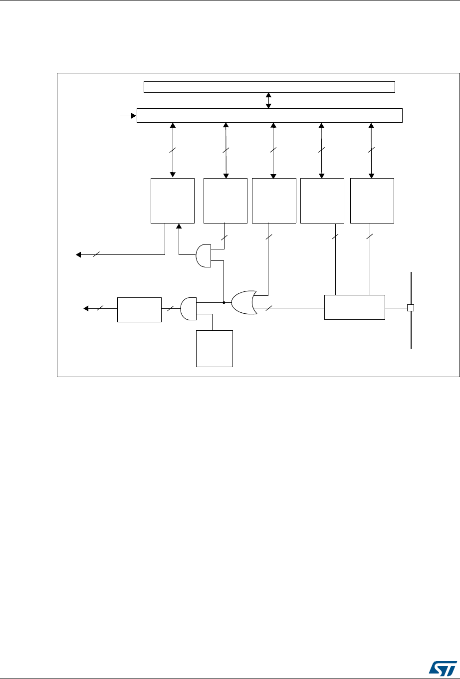
Interrupts and events RM0401
202/766 DocID027812 Rev 2
9.2.2 EXTI block diagram
Figure 29 shows the block diagram.
Figure 29. External interrupt/event controller block diagram
9.2.3 Wakeup event management
The STM32F4xx are able to handle external or internal events in order to wake up the core
(WFE). The wakeup event can be generated either by:
•enabling an interrupt in the peripheral control register but not in the NVIC, and enabling
the SEVONPEND bit in the Cortex®-M4 with FPU System Control register. When the
MCU resumes from WFE, the peripheral interrupt pending bit and the peripheral NVIC
IRQ channel pending bit (in the NVIC interrupt clear pending register) have to be
cleared.
•or configuring an external or internal EXTI line in event mode. When the CPU resumes
from WFE, it is not necessary to clear the peripheral interrupt pending bit or the NVIC
IRQ channel pending bit as the pending bit corresponding to the event line is not set.
To use an external line as a wakeup event, refer to Section 9.2.4: Functional description.
9.2.4 Functional description
To generate the interrupt, the interrupt line should be configured and enabled. This is done
by programming the two trigger registers with the desired edge detection and by enabling
the interrupt request by writing a ‘1’ to the corresponding bit in the interrupt mask register.
When the selected edge occurs on the external interrupt line, an interrupt request is
3HULSKHUDOLQWHUIDFH
(GJHGHWHFW
FLUFXLW
$0%$$3%EXV
3&/.
7R19,&LQWHUUXSW
FRQWUROOHU
6RIWZDUH
LQWHUUXSW
HYHQW
UHJLVWHU
5LVLQJ
WULJJHU
VHOHFWLRQ
UHJLVWHU
(YHQW
PDVN
UHJLVWHU
3XOVH
JHQHUDWRU
,QSXW
OLQH
3HQGLQJ
UHTXHVW
UHJLVWHU
069
,QWHUUXSW
PDVN
UHJLVWHU
)DOOLQJ
WULJJHU
VHOHFWLRQ
UHJLVWHU

DocID027812 Rev 2 203/766
RM0401 Interrupts and events
209
generated. The pending bit corresponding to the interrupt line is also set. This request is
reset by writing a ‘1’ in the pending register.
To generate the event, the event line should be configured and enabled. This is done by
programming the two trigger registers with the desired edge detection and by enabling the
event request by writing a ‘1’ to the corresponding bit in the event mask register. When the
selected edge occurs on the event line, an event pulse is generated. The pending bit
corresponding to the event line is not set.
An interrupt/event request can also be generated by software by writing a ‘1’ in the software
interrupt/event register.
Hardware interrupt selection
To configure the 23 lines as interrupt sources, use the following procedure:
•Configure the mask bits of the 23 interrupt lines (EXTI_IMR)
•Configure the Trigger selection bits of the interrupt lines (EXTI_RTSR and EXTI_FTSR)
•Configure the enable and mask bits that control the NVIC IRQ channel mapped to the
external interrupt controller (EXTI) so that an interrupt coming from one of the 23 lines
can be correctly acknowledged.
Hardware event selection
To configure the 23 lines as event sources, use the following procedure:
•Configure the mask bits of the 23 event lines (EXTI_EMR)
•Configure the Trigger selection bits of the event lines (EXTI_RTSR and EXTI_FTSR)
Software interrupt/event selection
The 23 lines can be configured as software interrupt/event lines. The following is the
procedure to generate a software interrupt.
•Configure the mask bits of the 23 interrupt/event lines (EXTI_IMR, EXTI_EMR)
•Set the required bit in the software interrupt register (EXTI_SWIER)
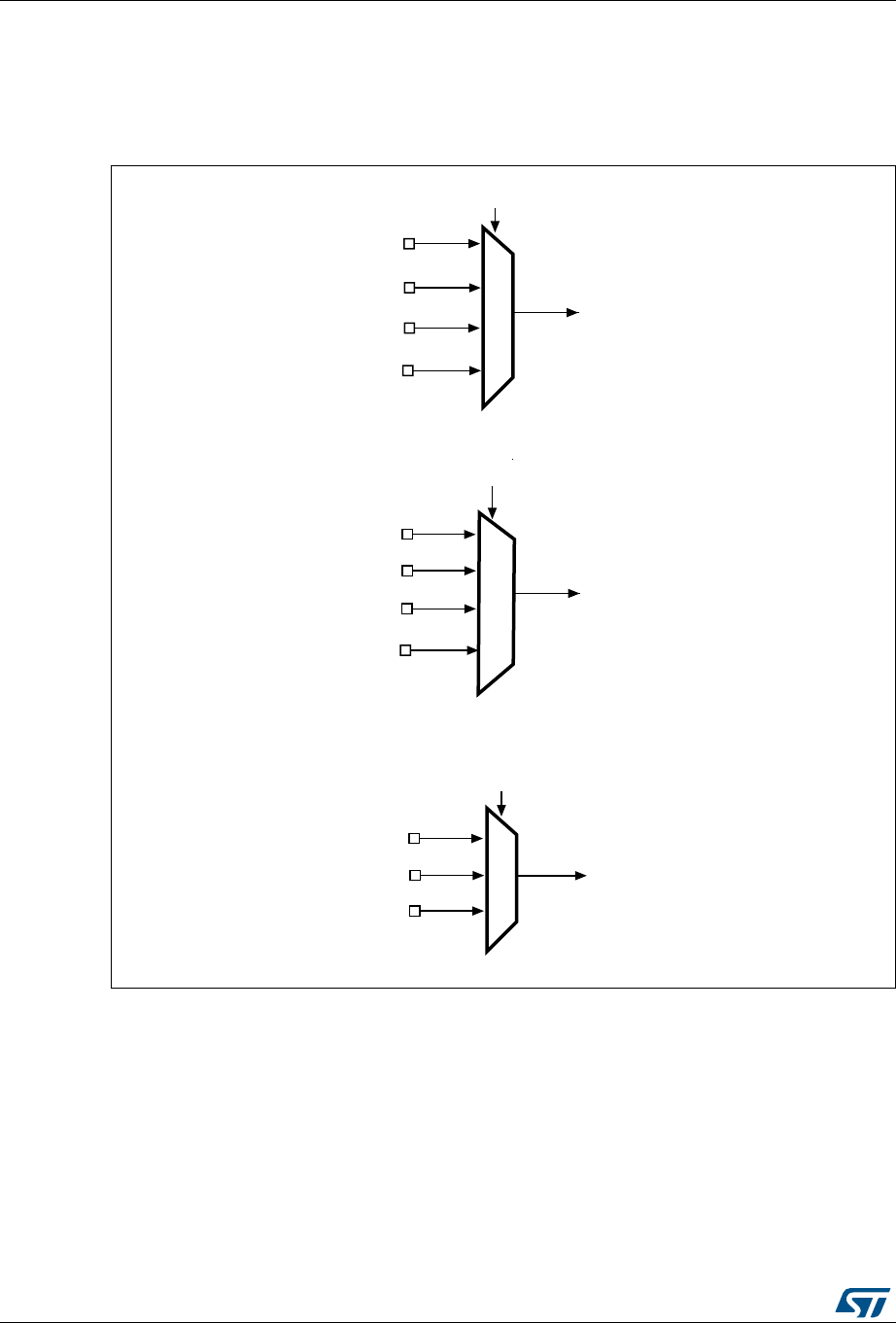
Interrupts and events RM0401
204/766 DocID027812 Rev 2
9.2.5 External interrupt/event line mapping
Up to 50 GPIOs are connected to the 16 external interrupt/event lines in the following
manner:
Figure 30. External interrupt/event GPIO mapping
The five other EXTI lines are connected as follows:
•EXTI line 16 is connected to the PVD output
•EXTI line 17 is connected to the RTC Alarm event
•EXTI line 21 is connected to the RTC Tamper and TimeStamp events
•EXTI line 22 is connected to the RTC Wakeup event
•EXTI line 23 is connected to the LPTIM1 asynchronous interrupt
3$
3%
3&
3$
3%
3&
3$
3%
3&
(;7,
(;7,
(;7,
(;7,>@ELWVLQWKH6<6&)*B(;7,&5UHJLVWHU
(;7,>@ELWVLQWKH6<6&)*B(;7,&5UHJLVWHU
(;7,>@ELWVLQWKH6<6&)*B(;7,&5UHJLVWHU
069
3+
3+

DocID027812 Rev 2 205/766
RM0401 Interrupts and events
209
9.3 EXTI registers
Refer to Section 1.1: List of abbreviations for registers for a list of abbreviations used in
register descriptions.
9.3.1 Interrupt mask register (EXTI_IMR)
Address offset: 0x00
Reset value: 0x0000 0000
9.3.2 Event mask register (EXTI_EMR)
Address offset: 0x04
Reset value: 0x0000 0000
31 30 29 28 27 26 25 24 23 22 21 20 19 18 17 16
Res. Res. Res. Res. Res. Res. Res. Res. Res. MR22 MR21 Res. Res. MR18 MR17 MR16
rw rw rw rw rw
15 14 13 12 11 10 9 8 7 6 5 4 3 2 1 0
MR15 MR14 MR13 MR12 MR11 MR10 MR9 MR8 MR7 MR6 MR5 MR4 MR3 MR2 MR1 MR0
rw rw rw rw rw rw rw rw rw rw rw rw rw rw rw rw
Bits 31:23 Reserved, must be kept at reset value.
Bits 22:21 MRx: Interrupt mask on line x
0: Interrupt request from line x is masked
1: Interrupt request from line x is not masked
Bits 20-19 Reserved, must be kept at reset value.
Bits 18:0 MRx: Interrupt mask on line x
0: Interrupt request from line x is masked
1: Interrupt request from line x is not masked
31 30 29 28 27 26 25 24 23 22 21 20 19 18 17 16
Res. Res. Res. Res. Res. Res. Res. Res. Res. MR22 MR21 Res. Res. MR18 MR17 MR16
rw rw rw rw rw
15 14 13 12 11 10 9 8 7 6 5 4 3 2 1 0
MR15 MR14 MR13 MR12 MR11 MR10 MR9 MR8 MR7 MR6 MR5 MR4 MR3 MR2 MR1 MR0
rw rw rw rw rw rw rw rw rw rw rw rw rw rw rw rw

Interrupts and events RM0401
206/766 DocID027812 Rev 2
9.3.3 Rising trigger selection register (EXTI_RTSR)
Address offset: 0x08
Reset value: 0x0000 0000
Note: The external wakeup lines are edge triggered, no glitch must be generated on these lines.
If a rising edge occurs on the external interrupt line while writing to the EXTI_RTSR register,
the pending bit is be set.
Rising and falling edge triggers can be set for the same interrupt line. In this configuration,
both generate a trigger condition.
Bits 31:23 Reserved, must be kept at reset value.
Bits 22:21 MRx: Event mask on line x
0: Event request from line x is masked
1: Event request from line x is not masked
Bits 20-19 Reserved, must be kept at reset value.
Bits 18:0 MRx: Event mask on line x
0: Event request from line x is masked
1: Event request from line x is not masked
31 30 29 28 27 26 25 24 23 22 21 20 19 18 17 16
Res. Res. Res. Res. Res. Res. Res. Res. Res. TR22 TR21 Res. Res. TR18 TR17 TR16
rw rw rw rw rw
1514131211109 8 765432 1 0
TR15 TR14 TR13 TR12 TR11 TR10 TR9 TR8 TR7 TR6 TR5 TR4 TR3 TR2 TR1 TR0
rw rw rw rw rw rw rw rw rw rw rw rw rw rw rw rw
Bits 31:23 Reserved, must be kept at reset value.
Bits 22:21 TRx: Rising trigger event configuration bit of line x
0: Rising trigger disabled (for Event and Interrupt) for input line
1: Rising trigger enabled (for Event and Interrupt) for input line
Bits 20:19 Reserved, must be kept at reset value.
Bits 18-0 TRx: Rising trigger event configuration bit of line x
0: Rising trigger disabled (for Event and Interrupt) for input line
1: Rising trigger enabled (for Event and Interrupt) for input line

DocID027812 Rev 2 207/766
RM0401 Interrupts and events
209
9.3.4 Falling trigger selection register (EXTI_FTSR)
Address offset: 0x0C
Reset value: 0x0000 0000
Note: The external wakeup lines are edge triggered, no glitch must be generated on these lines.
If a falling edge occurs on the external interrupt line while writing to the EXTI_FTSR register,
the pending bit is not set.
Rising and falling edge triggers can be set for the same interrupt line. In this configuration,
both generate a trigger condition.
9.3.5 Software interrupt event register (EXTI_SWIER)
Address offset: 0x10
Reset value: 0x0000 0000
31 30 29 28 27 26 25 24 23 22 21 20 19 18 17 16
Res. Res. Res. Res. Res. Res. Res. Res. Res. TR22 TR21 Res. Res. TR18 TR17 TR16
rw rw rw rw rw
1514131211109 8 765432 1 0
TR15 TR14 TR13 TR12 TR11 TR10 TR9 TR8 TR7 TR6 TR5 TR4 TR3 TR2 TR1 TR0
rw rw rw rw rw rw rw rw rw rw rw rw rw rw rw rw
Bits 31:23 Reserved, must be kept at reset value.
Bits 22:21 TRx: Falling trigger event configuration bit of line x
0: Falling trigger disabled (for Event and Interrupt) for input line
1: Falling trigger enabled (for Event and Interrupt) for input line.
Bits 20:19 Reserved, must be kept at reset value.
Bits 18:0 TRx: Falling trigger event configuration bit of line x
0: Falling trigger disabled (for Event and Interrupt) for input line
1: Falling trigger enabled (for Event and Interrupt) for input line.
31 30 29 28 27 26 25 24 23 22 21 20 19 18 17 16
Res. Res. Res. Res. Res. Res. Res. Res. Res. SWIER
22
SWIER
21 Res. Res. SWIER
18
SWIER
17
SWIER
16
rw rw rw rw rw
1514131211109 8 765432 1 0
SWIER
15
SWIER
14
SWIER
13
SWIER
12
SWIER
11
SWIER
10
SWIER
9
SWIER
8
SWIER
7
SWIER
6
SWIER
5
SWIER
4
SWIER
3
SWIER
2
SWIER
1
SWIER
0
rw rw rw rw rw rw rw rw rw rw rw rw rw rw rw rw

Interrupts and events RM0401
208/766 DocID027812 Rev 2
9.3.6 Pending register (EXTI_PR)
Address offset: 0x14
Reset value: undefined
Bits 31:23 Reserved, must be kept at reset value.
Bits 22:21 SWIERx: Software Interrupt on line x
If interrupt are enabled on line x in the EXTI_IMR register, writing '1' to SWIERx bit when it is
set at '0' sets the corresponding pending bit in the EXTI_PR register, thus resulting in an
interrupt request generation.
This bit is cleared by clearing the corresponding bit in EXTI_PR (by writing a 1 to the bit).
Bits 20:19 Reserved, must be kept at reset value.
Bits 18:0 SWIERx: Software Interrupt on line x
If interrupt are enabled on line x in the EXTI_IMR register, writing '1' to SWIERx bit when it is
set at '0' sets the corresponding pending bit in the EXTI_PR register, thus resulting in an
interrupt request generation.
This bit is cleared by clearing the corresponding bit in EXTI_PR (by writing a 1 to the bit).
31 30 29 28 27 26 25 24 23 22 21 20 19 18 17 16
Res. Res. Res. Res. Res. Res. Res. Res. Res. PR22 PR21 Res. Res. PR18 PR17 PR16
rc_w1 rc_w1 rc_w1 rc_w1 rc_w1
1514131211109 8 765432 1 0
PR15 PR14 PR13 PR12 PR11 PR10 PR9 PR8 PR7 PR6 PR5 PR4 PR3 PR2 PR1 PR0
rc_w1 rc_w1 rc_w1 rc_w1 rc_w1 rc_w1 rc_w1 rc_w1 rc_w1 rc_w1 rc_w1 rc_w1 rc_w1 rc_w1 rc_w1 rc_w1
Bits 31:23 Reserved, must be kept at reset value.
Bits 22:21 PRx: Pending bit
0: No trigger request occurred
1: selected trigger request occurred
This bit is set when the selected edge event arrives on the external interrupt line.
This bit is cleared by programming it to ‘1’.
Bits 20:19 Reserved, must be kept at reset value.
Bits 18:0 PRx: Pending bit
0: No trigger request occurred
1: selected trigger request occurred
This bit is set when the selected edge event arrives on the external interrupt line.
This bit is cleared by programming it to ‘1’.
DocID027812 Rev 2 209/766
RM0401 Interrupts and events
209
9.3.7 EXTI register map
Table 40 gives the EXTI register map and the reset values.
Refer to Section 2.2.2 on page 38 for the register boundary addresses.
Table 40. External interrupt/event controller register map and reset values
Offset Register
31
30
29
28
27
26
25
24
23
22
21
20
19
18
17
16
15
14
13
12
11
10
9
8
7
6
5
4
3
2
1
0
0x00 EXTI_IMR
Res.
Res.
Res.
Res.
Res.
Res.
Res.
Res.
Res.
MR
[22:21]
Res.
Res.
MR[18:0]
Reset value 0 0 0000000000000000000
0x04 EXTI_EMR
Res.
Res.
Res.
Res.
Res.
Res.
Res.
Res.
Res.
MR
[22:21]
Res.
Res.
MR[18:0]
Reset value 0 0 0000000000000000000
0x08 EXTI_RTSR
Res.
Res.
Res.
Res.
Res.
Res.
Res.
Res.
Res.
TR
[22:21]
Res.
Res.
TR[18:0]
Reset value 0 0 0000000000000000000
0x0C
EXTI_FTSR
Res.
Res.
Res.
Res.
Res.
Res.
Res.
Res.
Res.
TR
[22:21]
Res.
Res.
TR[18:0]
Reset value 0 0 0000000000000000000
0x10
EXTI_SWIER
Res.
Res.
Res.
Res.
Res.
Res.
Res.
Res.
Res.
SWIER
[22:21]
Res.
Res.
SWIER[18:0]
Reset value 0 0 0000000000000000000
0x14
EXTI_PR
Res.
Res.
Res.
Res.
Res.
Res.
Res.
Res.
Res.
PR
[22:21]
Res.
Res.
PR[18:0]
Reset value 0 0 0000000000000000000
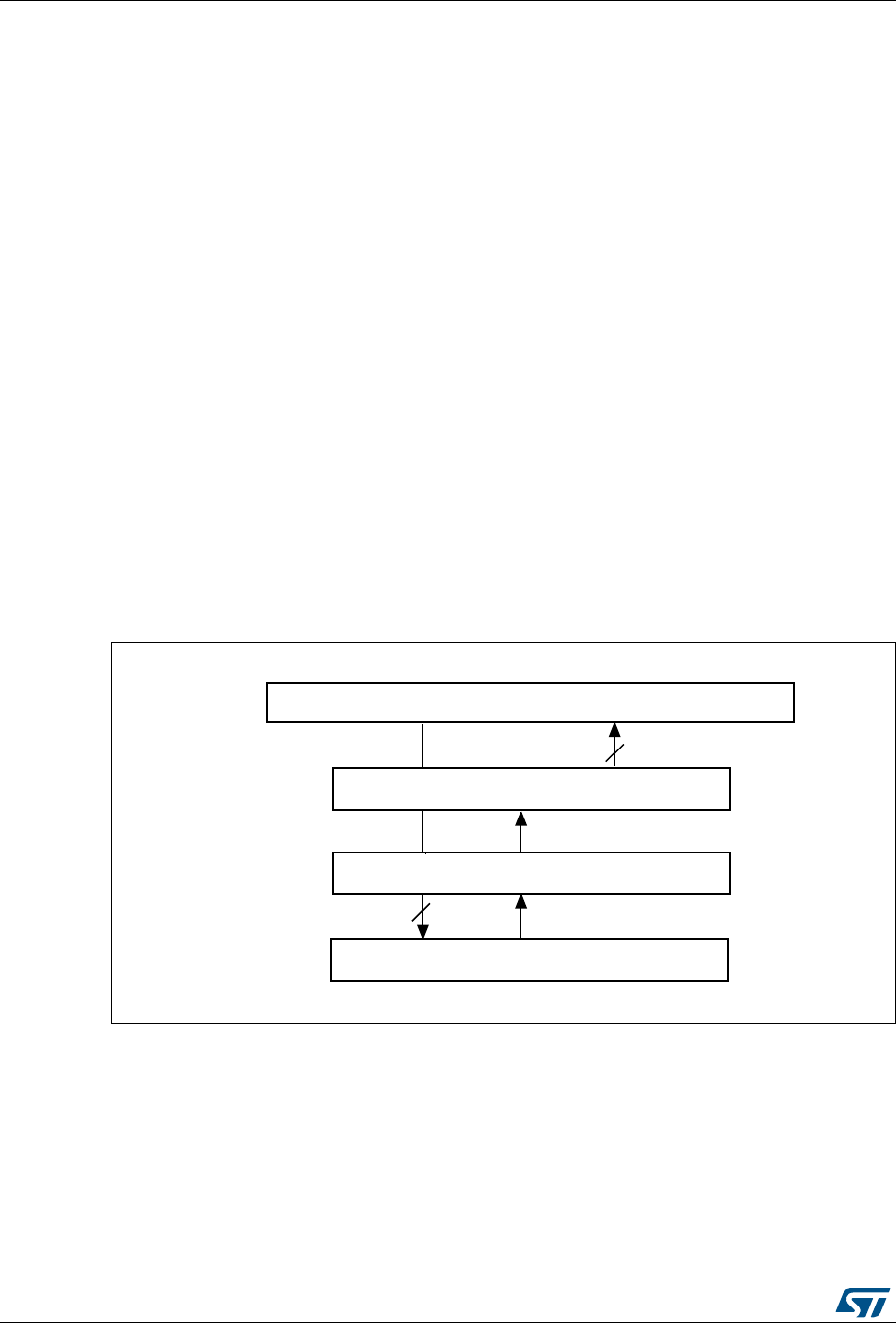
CRC calculation unit RM0401
210/766 DocID027812 Rev 2
10 CRC calculation unit
10.1 CRC introduction
The CRC (cyclic redundancy check) calculation unit is used to get a CRC code from a 32-bit
data word and a fixed generator polynomial.
Among other applications, CRC-based techniques are used to verify data transmission or
storage integrity. In the scope of the EN/IEC 60335-1 standard, they offer a way of verifying
the Flash memory integrity. The CRC calculation unit helps compute a signature of the
software during runtime, to be compared with a reference signature generated at link-time
and stored at a given memory location.
10.2 CRC main features
•Uses CRC-32 (Ethernet) polynomial: 0x4C11DB7
–X
32 + X26 + X23 + X22 + X16 + X12 + X11 + X10 +X8 + X7 + X5 + X4 + X2+ X +1
•Single input/output 32-bit data register
•CRC computation done in 4 AHB clock cycles (HCLK)
•General-purpose 8-bit register (can be used for temporary storage)
The block diagram is shown in Figure 31.
Figure 31. CRC calculation unit block diagram
10.3 CRC functional description
The CRC calculation unit mainly consists of a single 32-bit data register, which:
•is used as an input register to enter new data in the CRC calculator (when writing into
the register)
•holds the result of the previous CRC calculation (when reading the register)
$+%EXV
ELWUHDGDFFHVV
'DWDUHJLVWHURXWSXW
&5&FRPSXWDWLRQSRO\QRPLDO[&'%
ELWZULWHDFFHVV
'DWDUHJLVWHULQSXW
DL

DocID027812 Rev 2 211/766
RM0401 CRC calculation unit
213
Each write operation into the data register creates a combination of the previous CRC value
and the new one (CRC computation is done on the whole 32-bit data word, and not byte per
byte).
The write operation is stalled until the end of the CRC computation, thus allowing back-to-
back write accesses or consecutive write and read accesses.
The CRC calculator can be reset to 0xFFFF FFFF with the RESET control bit in the
CRC_CR register. This operation does not affect the contents of the CRC_IDR register.
10.4 CRC registers
The CRC calculation unit contains two data registers and a control register.The peripheral
The CRC registers have to be accessed by words (32 bits).
10.4.1 Data register (CRC_DR)
Address offset: 0x00
Reset value: 0xFFFF FFFF
31 30 29 28 27 26 25 24 23 22 21 20 19 18 17 16
DR [31:16]
rw rw rw rw rw rw rw rw rw rw rw rw rw rw rw rw
15 14 13 12 11 10 9 8 7 6 5 4 3 2 1 0
DR [15:0]
rw rw rw rw rw rw rw rw rw rw rw rw rw rw rw rw
Bits 31:0 Data register bits
Used as an input register when writing new data into the CRC calculator.
Holds the previous CRC calculation result when it is read.

CRC calculation unit RM0401
212/766 DocID027812 Rev 2
10.4.2 Independent data register (CRC_IDR)
Address offset: 0x04
Reset value: 0x0000 0000
10.4.3 Control register (CRC_CR)
Address offset: 0x08
Reset value: 0x0000 0000
31 30 29 28 27 26 25 24 23 22 21 20 19 18 17 16
Res. Res. Res. Res. Res. Res. Res. Res. Res. Res. Res. Res. Res. Res. Res. Res.
15 14 13 12 11 10 9876543210
Res. Res. Res. Res. Res. Res. Res. Res. IDR[7:0]
rw rw rw rw rw rw rw rw
Bits 31:8 Reserved, must be kept at reset value.
Bits 7:0 General-purpose 8-bit data register bits
Can be used as a temporary storage location for one byte.
This register is not affected by CRC resets generated by the RESET bit in the CRC_CR
register.
31 30 29 28 27 26 25 24 23 22 21 20 19 18 17 16
Res. Res. Res. Res. Res. Res. Res. Res. Res. Res. Res. Res. Res. Res. Res. Res.
15 14 13 12 11 10 9 8 7 6 5 4 3 2 1 0
Res. Res. Res. Res. Res. Res. Res. Res. Res. Res. Res. Res. Res. Res. Res. RESET
w
Bits 31:1 Reserved, must be kept at reset value.
Bit 0 RESET bit
Resets the CRC calculation unit and sets the data register to 0xFFFF FFFF.
This bit can only be set, it is automatically cleared by hardware.

DocID027812 Rev 2 213/766
RM0401 CRC calculation unit
213
10.4.4 CRC register map
Table 41. CRC calculation unit register map and reset values
Offset Register
31
30
29
28
27
26
25
24
23
22
21
20
19
18
17
16
15
14
13
12
11
10
9
8
7
6
5
4
3
2
1
0
0x00
CRC_DR Data register
Reset value 0xFFFF FFFF
0x04
CRC_IDR
Res.
Res.
Res.
Res.
Res.
Res.
Res.
Res.
Res.
Res.
Res.
Res.
Res.
Res.
Res.
Res.
Res.
Res.
Res.
Res.
Res.
Res.
Res.
Res.
Independent data register
Reset value 0x0000
0x08
CRC_CR
Res.
Res.
Res.
Res.
Res.
Res.
Res.
Res.
Res.
Res.
Res.
Res.
Res.
Res.
Res.
Res.
Res.
Res.
Res.
Res.
Res.
Res.
Res.
Res.
Res.
Res.
Res.
Res.
Res.
Res.
Res.
RESET
Reset value 0

Analog-to-digital converter (ADC) RM0401
214/766 DocID027812 Rev 2
11 Analog-to-digital converter (ADC)
11.1 ADC introduction
The 12-bit ADC is a successive approximation analog-to-digital converter. It has up to 19
multiplexed channels allowing it to measure signals from 16 external sources, two internal
sources, and the VBAT channel. The A/D conversion of the channels can be performed in
single, continuous, scan or discontinuous mode. The result of the ADC is stored into a left-
or right-aligned 16-bit data register.
The analog watchdog feature allows the application to detect if the input voltage goes
beyond the user-defined, higher or lower thresholds.
11.2 ADC main features
•12-bit, 10-bit, 8-bit or 6-bit configurable resolution
•Interrupt generation at the end of conversion, end of injected conversion, and in case of
analog watchdog or overrun events
•Single and continuous conversion modes
•Scan mode for automatic conversion of channel 0 to channel ‘n’
•Data alignment with in-built data coherency
•Channel-wise programmable sampling time
•External trigger option with configurable polarity for both regular and injected
conversions
•Discontinuous mode
•Configurable delay between conversions in Dual/Triple interleaved mode
•ADC supply requirements: 2.4 V to 3.6 V at full speed and down to 1.8 V at slower
speed
•ADC input range: VSSA ≤ VIN ≤ VREF+
•DMA request generation during regular channel conversion
Figure 32 shows the block diagram of the ADC.
11.3 ADC functional description
Figure 32 shows a single ADC block diagram and Table 42 gives the ADC pin description.
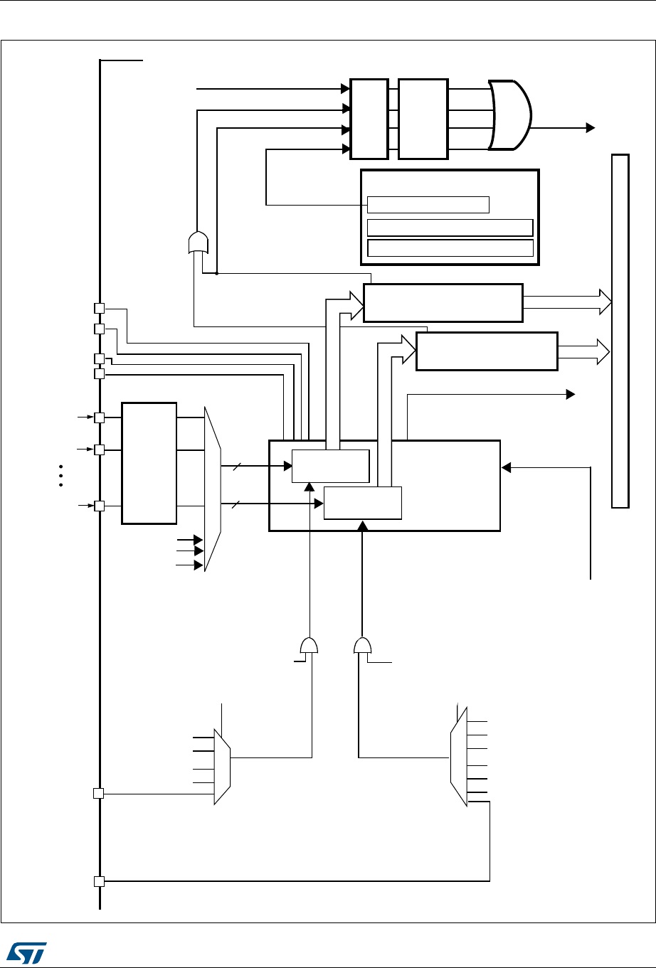
DocID027812 Rev 2 215/766
RM0401 Analog-to-digital converter (ADC)
242
Figure 32. Single ADC block diagram
$'&[B,1
$'&[B,1
$QDORJ WR GLJLWDO
FRQYHUWHU
$'&[B,1
$QDORJ
PX[
$'&&/.
$'&,QWHUUXSWWR19,&
*3,2
SRUWV
$QDORJZDWFKGRJ
$GGUHVVGDWDEXV
/RZHUWKUHVKROGELWV
&RPSDUHUHVXOW
+LJKHUWKUHVKROGELWV
)ODJV HQDEOHELWV
(2&
$:'
$QDORJZDWFKGRJHYHQW
9''$
966$
95()
95()
,QWHUUXSW
(;7,B
)URP$'&SUHVFDOHU
ELWV
(QGRIFRQYHUVLRQ
FKDQQHOV
,QMHFWHG
FKDQQHOV
(QGRILQMHFWHGFRQYHUVLRQ -(2&
(2&,(
$:',(
-(2&,(
XSWR
XSWR
5HJXODUGDWDUHJLVWHU
[ELWV
,QMHFWHGGDWDUHJLVWHUV
5HJXODU
6WDUWWULJJHU
UHJXODUJURXS
(;76(/>@ELWV
(;7(1
(;7,B
7,0B75*2
6WDUWWULJJHU
LQMHFWHGJURXS
-(;76(/>@ELWV
7,0B&+
-(;7(1 >@ELWV
>@ELWV
'0$UHTXHVW
7HPSVHQVRU
95(),17
295295,(
'0$RYHUUXQ
9%$7
7,0B&+
7,0B75*2
7,0B&+
7,0B&+
7,0B&+
7,0B&+
7,0B&+
7,0B&+
069

Analog-to-digital converter (ADC) RM0401
216/766 DocID027812 Rev 2
11.3.1 ADC on-off control
The ADC is powered on by setting the ADON bit in the ADC_CR2 register. When the ADON
bit is set for the first time, it wakes up the ADC from the Power-down mode.
Conversion starts when either the SWSTART or the JSWSTART bit is set.
You can stop conversion and put the ADC in power down mode by clearing the ADON bit. In
this mode the ADC consumes almost no power (only a few µA).
11.3.2 ADC clock
The ADC features two clock schemes:
•Clock for the analog circuitry: ADCCLK
This clock is generated from the APB2 clock divided by a programmable prescaler that
allows the ADC to work at fPCLK2/2, /4, /6 or /8. Refer to the datasheets for the
maximum value of ADCCLK.
•Clock for the digital interface (used for registers read/write access)
This clock is equal to the APB2 clock. The digital interface clock can be
enabled/disabled individually for each ADC through the RCC APB2 peripheral clock
enable register (RCC_APB2ENR).
11.3.3 Channel selection
There are 16 multiplexed channels. It is possible to organize the conversions in two groups:
regular and injected. A group consists of a sequence of conversions that can be done on
any channel and in any order. For instance, it is possible to implement the conversion
sequence in the following order: ADC_IN3, ADC_IN8, ADC_IN2, ADC_IN2, ADC_IN0,
ADC_IN2, ADC_IN2, ADC_IN15.
•A regular group is composed of up to 16 conversions. The regular channels and their
order in the conversion sequence must be selected in the ADC_SQRx registers. The
total number of conversions in the regular group must be written in the L[3:0] bits in the
ADC_SQR1 register.
•An injected group is composed of up to 4 conversions. The injected channels and
their order in the conversion sequence must be selected in the ADC_JSQR register.
Table 42. ADC pins
Name Signal type Remarks
VREF+
Input, analog reference
positive
The higher/positive reference voltage for the ADC,
1.8 V ≤ VREF+ ≤ VDDA
VDDA Input, analog supply
Analog power supply equal to VDD and
2.4 V ≤ VDDA ≤ VDD (3.6 V) for full speed
1.8 V ≤ VDDA ≤ VDD (3.6 V) for reduced speed
VREF–
Input, analog reference
negative
The lower/negative reference voltage for the ADC,
VREF– = VSSA
VSSA
Input, analog supply
ground Ground for analog power supply equal to VSS
ADCx_IN[15:0] Analog input signals 16 analog input channels

DocID027812 Rev 2 217/766
RM0401 Analog-to-digital converter (ADC)
242
The total number of conversions in the injected group must be written in the L[1:0] bits
in the ADC_JSQR register.
If the ADC_SQRx or ADC_JSQR registers are modified during a conversion, the current
conversion is reset and a new start pulse is sent to the ADC to convert the newly chosen
group.
Temperature sensor, VREFINT and VBAT internal channels
•The temperature sensor is internally connected to ADC1_IN18 and ADC1_IN16
channels which is shared with VBAT. Only one conversion, temperature sensor or
VBAT, must be selected at a time. When the temperature sensor and VBAT conversion
are set simultaneously, only the VBAT conversion is performed.
The internal reference voltage VREFINT is connected to ADC1_IN17.
The VBAT channel is connected to ADC1_IN18 and ADC1_IN16 channels. It can also be
converted as an injected or regular channel.
11.3.4 Single conversion mode
In Single conversion mode the ADC does one conversion. This mode is started with the
CONT bit at 0 by either:
•setting the SWSTART bit in the ADC_CR2 register (for a regular channel only)
•setting the JSWSTART bit (for an injected channel)
•external trigger (for a regular or injected channel)
Once the conversion of the selected channel is complete:
•If a regular channel was converted:
–The converted data are stored into the 16-bit ADC_DR register
– The EOC (end of conversion) flag is set
– An interrupt is generated if the EOCIE bit is set
•If an injected channel was converted:
– The converted data are stored into the 16-bit ADC_JDR1 register
– The JEOC (end of conversion injected) flag is set
– An interrupt is generated if the JEOCIE bit is set
Then the ADC stops.
11.3.5 Continuous conversion mode
In continuous conversion mode, the ADC starts a new conversion as soon as it finishes one.
This mode is started with the CONT bit at 1 either by external trigger or by setting the
SWSTRT bit in the ADC_CR2 register (for regular channels only).
After each conversion:
•If a regular group of channels was converted:
–The last converted data are stored into the 16-bit ADC_DR register
– The EOC (end of conversion) flag is set
– An interrupt is generated if the EOCIE bit is set
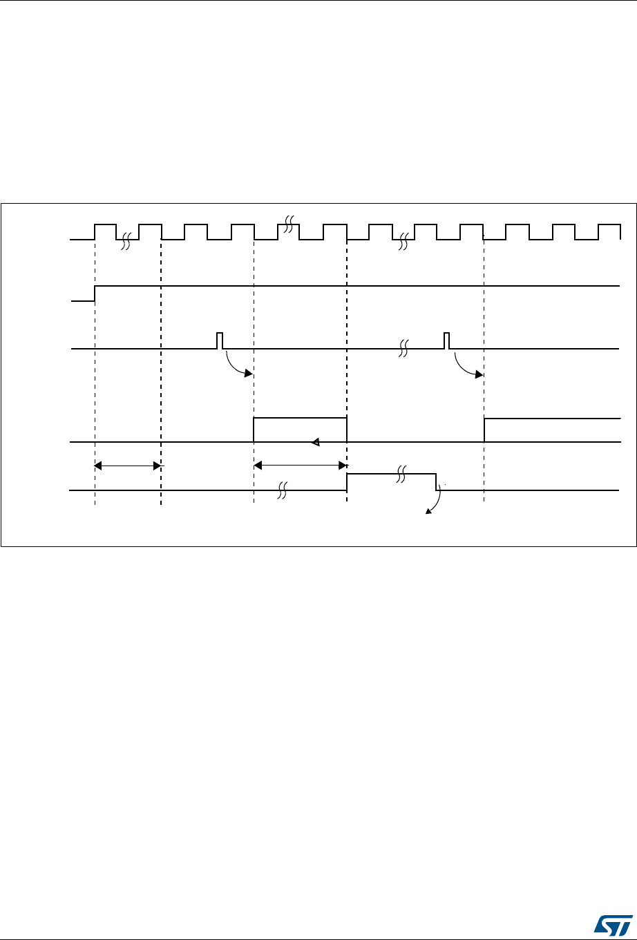
Analog-to-digital converter (ADC) RM0401
218/766 DocID027812 Rev 2
Note: Injected channels cannot be converted continuously. The only exception is when an injected
channel is configured to be converted automatically after regular channels in continuous
mode (using JAUTO bit), refer to Auto-injection section).
11.3.6 Timing diagram
As shown in Figure 33, the ADC needs a stabilization time of tSTAB before it starts
converting accurately. After the start of the ADC conversion and after 15 clock cycles, the
EOC flag is set and the 16-bit ADC data register contains the result of the conversion.
Figure 33. Timing diagram
11.3.7 Analog watchdog
The AWD analog watchdog status bit is set if the analog voltage converted by the ADC is
below a lower threshold or above a higher threshold. These thresholds are programmed in
the 12 least significant bits of the ADC_HTR and ADC_LTR 16-bit registers. An interrupt can
be enabled by using the AWDIE bit in the ADC_CR1 register.
The threshold value is independent of the alignment selected by the ALIGN bit in the
ADC_CR2 register. The analog voltage is compared to the lower and higher thresholds
before alignment.
Table 43 shows how the ADC_CR1 register should be configured to enable the analog
watchdog on one or more channels.
!$#?#,+
%/#
.EXT!$#CONVERSION
!$#CONVERSION
#ONVERSIONTIME
T34!"
!$#
3OFTWARECLEARSTHE%/#BIT
TOTALCONVTIME
3TARTSTCONVERSION 3TARTNEXTCONVERSION
AIB
!$/.
3734!24
*3734!24
DocID027812 Rev 2 219/766
RM0401 Analog-to-digital converter (ADC)
242
Figure 34. Analog watchdog’s guarded area
11.3.8 Scan mode
This mode is used to scan a group of analog channels.
The Scan mode is selected by setting the SCAN bit in the ADC_CR1 register. Once this bit
has been set, the ADC scans all the channels selected in the ADC_SQRx registers (for
regular channels) or in the ADC_JSQR register (for injected channels). A single conversion
is performed for each channel of the group. After each end of conversion, the next channel
in the group is converted automatically. If the CONT bit is set, regular channel conversion
does not stop at the last selected channel in the group but continues again from the first
selected channel.
If the DMA bit is set, the direct memory access (DMA) controller is used to transfer the data
converted from the regular group of channels (stored in the ADC_DR register) to SRAM
after each regular channel conversion.
The EOC bit is set in the ADC_SR register:
•At the end of each regular group sequence if the EOCS bit is cleared to 0
•At the end of each regular channel conversion if the EOCS bit is set to 1
The data converted from an injected channel are always stored into the ADC_JDRx
registers.
Table 43. Analog watchdog channel selection
Channels guarded by the analog
watchdog
ADC_CR1 register control bits (x = don’t care)
AWDSGL bit AWDEN bit JAWDEN bit
None x 0 0
All injected channels 0 0 1
All regular channels 0 1 0
All regular and injected channels 0 1 1
Single(1) injected channel
1. Selected by the AWDCH[4:0] bits
101
Single(1) regular channel 1 1 0
Single (1) regular or injected channel 1 1 1
DL
$QDORJYROWDJH
+LJKHUWKUHVKROG
/RZHUWKUHVKROG
*XDUGHGDUHD
+75
/75
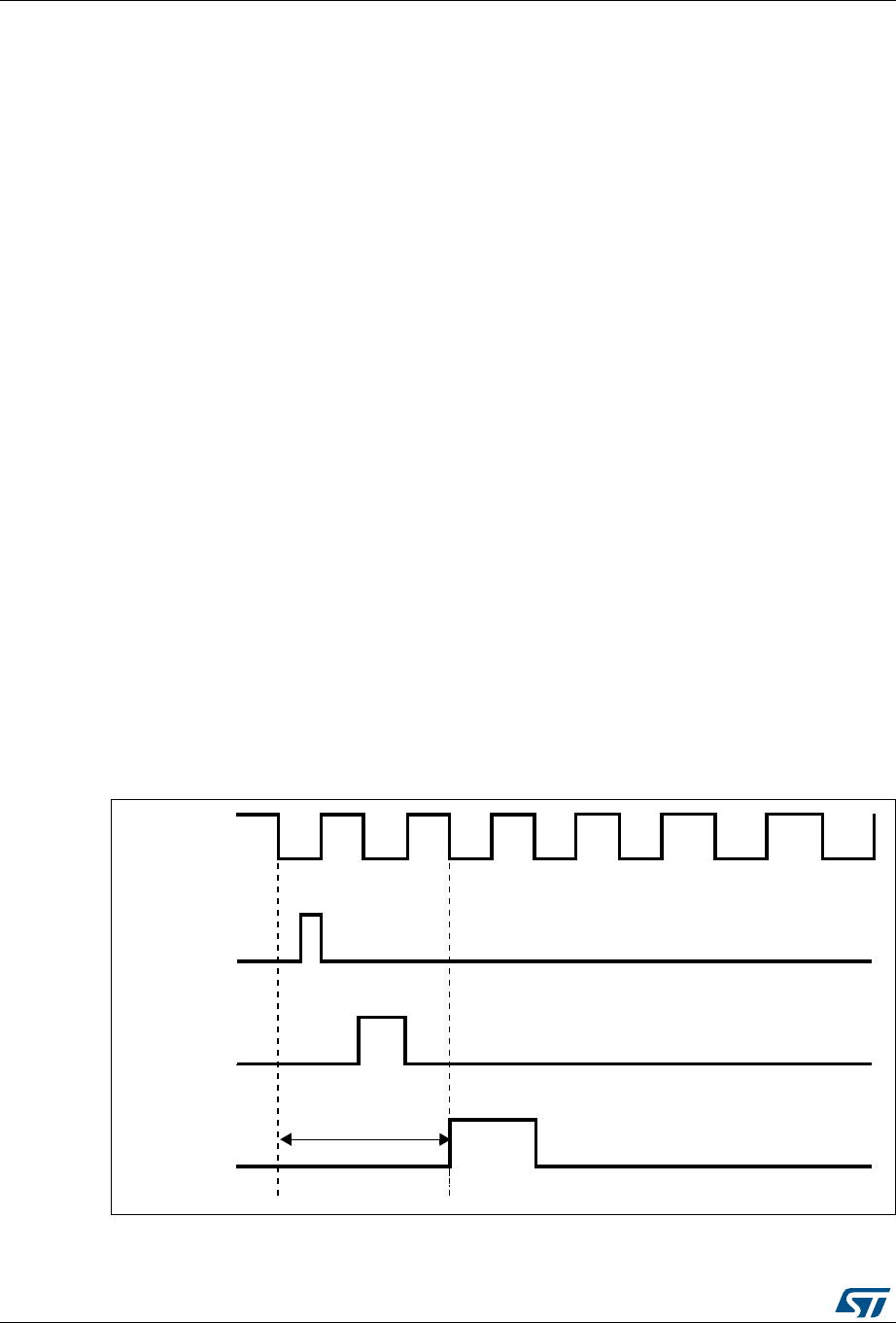
Analog-to-digital converter (ADC) RM0401
220/766 DocID027812 Rev 2
11.3.9 Injected channel management
Triggered injection
To use triggered injection, the JAUTO bit must be cleared in the ADC_CR1 register.
1. Start the conversion of a group of regular channels either by external trigger or by
setting the SWSTART bit in the ADC_CR2 register.
2. If an external injected trigger occurs or if the JSWSTART bit is set during the
conversion of a regular group of channels, the current conversion is reset and the
injected channel sequence switches to Scan-once mode.
3. Then, the regular conversion of the regular group of channels is resumed from the last
interrupted regular conversion.
If a regular event occurs during an injected conversion, the injected conversion is not
interrupted but the regular sequence is executed at the end of the injected sequence.
Figure 35 shows the corresponding timing diagram.
Note: When using triggered injection, one must ensure that the interval between trigger events is
longer than the injection sequence. For instance, if the sequence length is 30 ADC clock
cycles (that is two conversions with a sampling time of 3 clock periods), the minimum
interval between triggers must be 31 ADC clock cycles.
Auto-injection
If the JAUTO bit is set, then the channels in the injected group are automatically converted
after the regular group of channels. This can be used to convert a sequence of up to 20
conversions programmed in the ADC_SQRx and ADC_JSQR registers.
In this mode, external trigger on injected channels must be disabled.
If the CONT bit is also set in addition to the JAUTO bit, regular channels followed by injected
channels are continuously converted.
Note: It is not possible to use both the auto-injected and discontinuous modes simultaneously.
Figure 35. Injected conversion latency
1. The maximum latency value can be found in the electrical characteristics of the STM32F410 datasheets.
!$##,+
)NJECTIONEVENT
2ESET!$#
3/# MAXLATENCY
AI

DocID027812 Rev 2 221/766
RM0401 Analog-to-digital converter (ADC)
242
11.3.10 Discontinuous mode
Regular group
This mode is enabled by setting the DISCEN bit in the ADC_CR1 register. It can be used to
convert a short sequence of n conversions (n ≤ 8) that is part of the sequence of
conversions selected in the ADC_SQRx registers. The value of n is specified by writing to
the DISCNUM[2:0] bits in the ADC_CR1 register.
When an external trigger occurs, it starts the next n conversions selected in the ADC_SQRx
registers until all the conversions in the sequence are done. The total sequence length is
defined by the L[3:0] bits in the ADC_SQR1 register.
Example:
•n = 3, channels to be converted = 0, 1, 2, 3, 6, 7, 9, 10
•1st trigger: sequence converted 0, 1, 2. An EOC event is generated at each
conversion.
•2nd trigger: sequence converted 3, 6, 7. An EOC event is generated at each
conversion
•3rd trigger: sequence converted 9, 10.An EOC event is generated at each conversion
•4th trigger: sequence converted 0, 1, 2. An EOC event is generated at each conversion
Note: When a regular group is converted in discontinuous mode, no rollover occurs.
When all subgroups are converted, the next trigger starts the conversion of the first
subgroup. In the example above, the 4th trigger reconverts the channels 0, 1 and 2 in the
1st subgroup.
Injected group
This mode is enabled by setting the JDISCEN bit in the ADC_CR1 register. It can be used to
convert the sequence selected in the ADC_JSQR register, channel by channel, after an
external trigger event.
When an external trigger occurs, it starts the next channel conversions selected in the
ADC_JSQR registers until all the conversions in the sequence are done. The total sequence
length is defined by the JL[1:0] bits in the ADC_JSQR register.
Example:
n = 1, channels to be converted = 1, 2, 3
1st trigger: channel 1 converted
2nd trigger: channel 2 converted
3rd trigger: channel 3 converted and JEOC event generated
4th trigger: channel 1
Note: When all injected channels are converted, the next trigger starts the conversion of the first
injected channel. In the example above, the 4th trigger reconverts the 1st injected channel
1.
It is not possible to use both the auto-injected and discontinuous modes simultaneously.
Discontinuous mode must not be set for regular and injected groups at the same time.
Discontinuous mode must be enabled only for the conversion of one group.
Analog-to-digital converter (ADC) RM0401
222/766 DocID027812 Rev 2
11.4 Data alignment
The ALIGN bit in the ADC_CR2 register selects the alignment of the data stored after
conversion. Data can be right- or left-aligned as shown in Figure 36 and Figure 37.
The converted data value from the injected group of channels is decreased by the user-
defined offset written in the ADC_JOFRx registers so the result can be a negative value.
The SEXT bit represents the extended sign value.
For channels in a regular group, no offset is subtracted so only twelve bits are significant.
Figure 36. Right alignment of 12-bit data
Figure 37. Left alignment of 12-bit data
Special case: when left-aligned, the data are aligned on a half-word basis except when the
resolution is set to 6-bit. in that case, the data are aligned on a byte basis as shown in
Figure 38.
Figure 38. Left alignment of 6-bit data
$$$ $ $ $ $ $ $ $$$3%843%843%843%84
$$
$$
)NJECTEDGROUP
2EGULARGROUP
$ $ $ $ $ $ $ $
AI
$$
$ $ $ $ $ $$$$$3%84
)NJECTEDGROUP
2EGULARGROUP
AI
$ $ $ $ $ $ $ $ $ $ $ $
$$
3%843%843%843%843%843%84
)NJECTEDGROUP
2EGULARGROUP
AI
$ $ $ $ $ $
3%843%84 $ $ $ $ 3%84

DocID027812 Rev 2 223/766
RM0401 Analog-to-digital converter (ADC)
242
11.5 Channel-wise programmable sampling time
The ADC samples the input voltage for a number of ADCCLK cycles that can be modified
using the SMP[2:0] bits in the ADC_SMPR1 and ADC_SMPR2 registers. Each channel can
be sampled with a different sampling time.
The total conversion time is calculated as follows:
Tconv = Sampling time + 12 cycles
Example:
With ADCCLK = 30 MHz and sampling time = 3 cycles:
Tconv = 3 + 12 = 15 cycles = 0.5 µs with APB2 at 60 MHz
11.6 Conversion on external trigger and trigger polarity
Conversion can be triggered by an external event (e.g. timer capture, EXTI line). If the
EXTEN[1:0] control bits (for a regular conversion) or JEXTEN[1:0] bits (for an injected
conversion) are different from “0b00”, then external events are able to trigger a conversion
with the selected polarity. Table 44 provides the correspondence between the EXTEN[1:0]
and JEXTEN[1:0] values and the trigger polarity.
Note: The polarity of the external trigger can be changed on the fly.
The EXTSEL[3:0] and JEXTSEL[3:0] control bits are used to select which out of 16 possible
events can trigger conversion for the regular and injected groups.
Table 45 gives the possible external trigger for regular conversion.
Table 44. Configuring the trigger polarity
Source EXTEN[1:0] / JEXTEN[1:0]
Trigger detection disabled 00
Detection on the rising edge 01
Detection on the falling edge 10
Detection on both the rising and falling edges 11
Analog-to-digital converter (ADC) RM0401
224/766 DocID027812 Rev 2
Table 46 gives the possible external trigger for injected conversion.
Software source trigger events can be generated by setting SWSTART (for regular
conversion) or JSWSTART (for injected conversion) in ADC_CR2.
A regular group conversion can be interrupted by an injected trigger.
Note: The trigger selection can be changed on the fly. However, when the selection changes,
there is a time frame of 1 APB clock cycle during which the trigger detection is disabled.
This is to avoid spurious detection during transitions.
Table 45. External trigger for regular channels
Source Type EXTSEL[3:0]
TIM1_CH1 event
Internal signal from on-chip
timers
0000
TIM1_CH2 event 0001
TIM1_CH3 event 0010
TIM5_CH1 event 1010
TIM5_CH2 event 1011
TIM5_CH3 event 1100
Not used 1101
Not used 1110
EXTI line11 External pin 1111
Table 46. External trigger for injected channels
Source Connection type JEXTSEL[3:0]
TIM1_CH4 event
Internal signal from on-chip
timers
0000
TIM1_TRGO event 0001
TIM5_CH4 event 1010
TIM5_TRGO event 1011
Not used 1100
Not used 1101
Not used 1110
EXTI line15 External pin 1111

DocID027812 Rev 2 225/766
RM0401 Analog-to-digital converter (ADC)
242
11.7 Fast conversion mode
It is possible to perform faster conversion by reducing the ADC resolution. The RES bits are
used to select the number of bits available in the data register. The minimum conversion
time for each resolution is then as follows:
•12 bits: 3 + 12 = 15 ADCCLK cycles
•10 bits: 3 + 10 = 13 ADCCLK cycles
•8 bits: 3 + 8 = 11 ADCCLK cycles
•6 bits: 3 + 6 = 9 ADCCLK cycles
11.8 Data management
11.8.1 Using the DMA
Since converted regular channel values are stored into a unique data register, it is useful to
use DMA for conversion of more than one regular channel. This avoids the loss of the data
already stored in the ADC_DR register.
When the DMA mode is enabled (DMA bit set to 1 in the ADC_CR2 register), after each
conversion of a regular channel, a DMA request is generated. This allows the transfer of the
converted data from the ADC_DR register to the destination location selected by the
software.
Despite this, if data are lost (overrun), the OVR bit in the ADC_SR register is set and an
interrupt is generated (if the OVRIE enable bit is set). DMA transfers are then disabled and
DMA requests are no longer accepted. In this case, if a DMA request is made, the regular
conversion in progress is aborted and further regular triggers are ignored. It is then
necessary to clear the OVR flag and the DMAEN bit in the used DMA stream, and to re-
initialize both the DMA and the ADC to have the wanted converted channel data transferred
to the right memory location. Only then can the conversion be resumed and the data
transfer, enabled again. Injected channel conversions are not impacted by overrun errors.
When OVR = 1 in DMA mode, the DMA requests are blocked after the last valid data have
been transferred, which means that all the data transferred to the RAM can be considered
as valid.
At the end of the last DMA transfer (number of transfers configured in the DMA controller’s
DMA_SxNTR register):
•No new DMA request is issued to the DMA controller if the DDS bit is cleared to 0 in the
ADC_CR2 register (this avoids generating an overrun error). However the DMA bit is
not cleared by hardware. It must be written to 0, then to 1 to start a new transfer.
•Requests can continue to be generated if the DDS bit is set to 1. This allows
configuring the DMA in double-buffer circular mode.
To recover the ADC from OVR state when the DMA is used, follow the steps below:
1. Reinitialize the DMA (adjust destination address and NDTR counter)
2. Clear the ADC OVR bit in ADC_SR register
3. Trigger the ADC to start the conversion.

Analog-to-digital converter (ADC) RM0401
226/766 DocID027812 Rev 2
11.8.2 Managing a sequence of conversions without using the DMA
If the conversions are slow enough, the conversion sequence can be handled by the
software. In this case the EOCS bit must be set in the ADC_CR2 register for the EOC status
bit to be set at the end of each conversion, and not only at the end of the sequence. When
EOCS = 1, overrun detection is automatically enabled. Thus, each time a conversion is
complete, EOC is set and the ADC_DR register can be read. The overrun management is
the same as when the DMA is used.
To recover the ADC from OVR state when the EOCS is set, follow the steps below:
1. Clear the ADC OVR bit in ADC_SR register
2. Trigger the ADC to start the conversion.
11.8.3 Conversions without DMA and without overrun detection
It may be useful to let the ADC convert one or more channels without reading the data each
time (if there is an analog watchdog for instance). For that, the DMA must be disabled
(DMA = 0) and the EOC bit must be set at the end of a sequence only (EOCS = 0). In this
configuration, overrun detection is disabled.
11.9 Temperature sensor
The temperature sensor can be used to measure the ambient temperature (TA) of the
device.
Figure 39 shows the block diagram of the temperature sensor.
When not in use, the sensor can be put in power down mode.
Note: The TSVREFE bit must be set to enable the conversion of both internal channels: the
ADC1_IN18 or ADC1_IN16 (temperature sensor) and the ADC1_IN17 (VREFINT).
Main features
•Supported temperature range: –40 to 125 °C
•Precision: ±1.5 °C
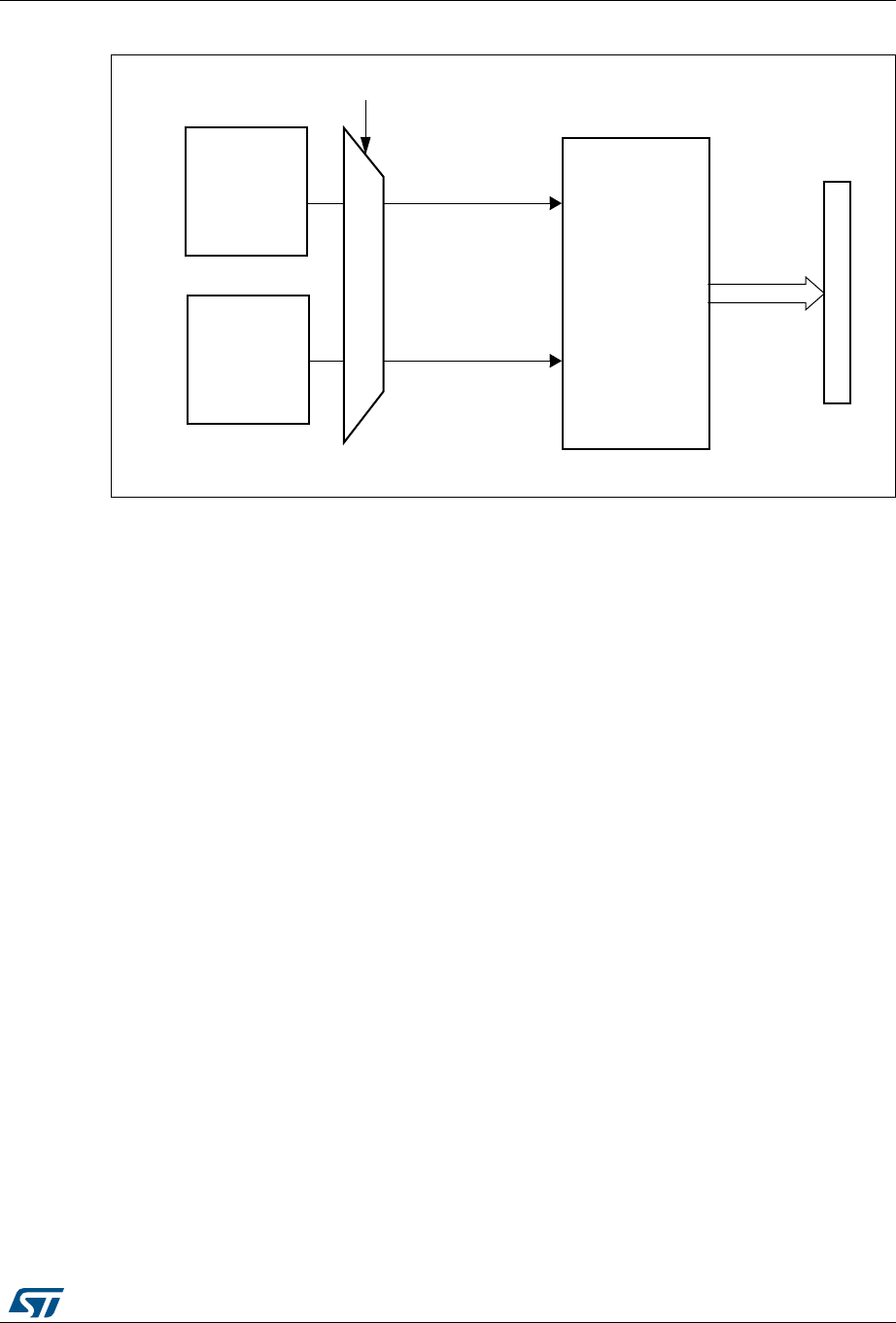
DocID027812 Rev 2 227/766
RM0401 Analog-to-digital converter (ADC)
242
Figure 39. Temperature sensor and VREFINT channel block diagram
1. VSENSE is input to ADC1_IN18 and ADC1_IN16.
Reading the temperature
To use the sensor:
3. Select ADC1_IN18 input channel.
4. Select a sampling time greater than the minimum sampling time specified in the
datasheet.
5. Set the TSVREFE bit in the ADC_CCR register to wake up the temperature sensor
from power down mode
6. Start the ADC conversion by setting the SWSTART bit (or by external trigger)
7. Read the resulting VSENSE data in the ADC data register
8. Calculate the temperature using the following formula:
Temperature (in °C) = {(VSENSE – V25) / Avg_Slope} + 25
Where:
–V
25 = VSENSE value for 25° C
– Avg_Slope = average slope of the temperature vs. VSENSE curve (given in mV/°C
or µV/°C)
Refer to the datasheet electrical characteristics section for the actual values of V25 and
Avg_Slope.
Note: The sensor has a startup time after waking from power down mode before it can output
VSENSE at the correct level. The ADC also has a startup time after power-on, so to minimize
the delay, the ADON and TSVREFE bits should be set at the same time.
The temperature sensor output voltage changes linearly with temperature. The offset of this
linear function depends on each chip due to process variation (up to 45 °C from one chip to
another).
-36
4EMPERATURE
SENSOR
63%.3%
4362%&%CONTROLBIT
!$#
!DDRESSDATABUS
62%&).4
!$#?).
!$#?).
)NTERNAL
POWERBLOCK !$#?).
CONVERTEDDATA
Analog-to-digital converter (ADC) RM0401
228/766 DocID027812 Rev 2
The internal temperature sensor is more suited for applications that detect temperature
variations instead of absolute temperatures. If accurate temperature reading is required, an
external temperature sensor should be used.
11.10 Battery charge monitoring
The VBATE bit in the ADC_CCR register is used to switch to the battery voltage. As the
VBAT voltage could be higher than VDDA, to ensure the correct operation of the ADC, the
VBAT pin is internally connected to a bridge divider.
When the VBATE is set, the bridge is automatically enabled to connect:
•VBAT/4 to the ADC1_IN18 and ADC1_IN16 input channels
Note: The VBAT and temperature sensor are connected to the same ADC internal channels
(ADC1_IN18 and ADC1_IN16). Only one conversion, either temperature sensor or VBAT,
must be selected at a time. When both conversion are enabled simultaneously, only the
VBAT conversion is performed.
11.11 ADC interrupts
An interrupt can be produced on the end of conversion for regular and injected groups,
when the analog watchdog status bit is set and when the overrun status bit is set. Separate
interrupt enable bits are available for flexibility.
Two other flags are present in the ADC_SR register, but there is no interrupt associated with
them:
•JSTRT (Start of conversion for channels of an injected group)
•STRT (Start of conversion for channels of a regular group)
Table 47. ADC interrupts
Interrupt event Event flag Enable control bit
End of conversion of a regular group EOC EOCIE
End of conversion of an injected group JEOC JEOCIE
Analog watchdog status bit is set AWD AWDIE
Overrun OVR OVRIE

DocID027812 Rev 2 229/766
RM0401 Analog-to-digital converter (ADC)
242
11.12 ADC registers
Refer to Section 1.1 on page 33 for a list of abbreviations used in register descriptions.
The peripheral registers must be written at word level (32 bits). Read accesses can be done
by bytes (8 bits), half-words (16 bits) or words (32 bits).
11.12.1 ADC status register (ADC_SR)
Address offset: 0x00
Reset value: 0x0000 0000
31 30 29 28 27 26 25 24 23 22 21 20 19 18 17 16
Res. Res. Res. Res. Res. Res. Res. Res. Res. Res. Res. Res. Res. Res. Res. Res.
15 14 13 12 11 10 9 8 7 6 5 4 3 2 1 0
Res. Res. Res. Res. Res. Res. Res. Res. Res. Res. OVR STRT JSTRT JEOC EOC AWD
rc_w0 rc_w0 rc_w0 rc_w0 rc_w0 rc_w0
Bits 31:6 Reserved, must be kept at reset value.
Bit 5 OVR: Overrun
This bit is set by hardware when data are lost (either in single mode or in dual/triple mode). It
is cleared by software. Overrun detection is enabled only when DMA = 1 or EOCS = 1.
0: No overrun occurred
1: Overrun has occurred
Bit 4 STRT: Regular channel start flag
This bit is set by hardware when regular channel conversion starts. It is cleared by software.
0: No regular channel conversion started
1: Regular channel conversion has started
Bit 3 JSTRT: Injected channel start flag
This bit is set by hardware when injected group conversion starts. It is cleared by software.
0: No injected group conversion started
1: Injected group conversion has started
Bit 2 JEOC: Injected channel end of conversion
This bit is set by hardware at the end of the conversion of all injected channels in the group.
It is cleared by software.
0: Conversion is not complete
1: Conversion complete
Bit 1 EOC: Regular channel end of conversion
This bit is set by hardware at the end of the conversion of a regular group of channels. It is
cleared by software or by reading the ADC_DR register.
0: Conversion not complete (EOCS=0), or sequence of conversions not complete (EOCS=1)
1: Conversion complete (EOCS=0), or sequence of conversions complete (EOCS=1)
Bit 0 AWD: Analog watchdog flag
This bit is set by hardware when the converted voltage crosses the values programmed in
the ADC_LTR and ADC_HTR registers. It is cleared by software.
0: No analog watchdog event occurred
1: Analog watchdog event occurred

Analog-to-digital converter (ADC) RM0401
230/766 DocID027812 Rev 2
11.12.2 ADC control register 1 (ADC_CR1)
Address offset: 0x04
Reset value: 0x0000 0000
31 30 29 28 27 26 25 24 23 22 21 20 19 18 17 16
Res. Res. Res. Res. Res. OVRIE RES AWDEN JAWDEN Res. Res. Res. Res. Res. Res.
rw rw rw rw rw
15 14 13 12 11 10 9 8 7 6 5 4 3 2 1 0
DISCNUM[2:0] JDISCEN DISCEN JAUTO AWDSGL SCAN JEOCIE AWDIE EOCIE AWDCH[4:0]
rw rw rw rw rw rw rw rw rw rw rw rw rw rw rw rw
Bits 31:27 Reserved, must be kept at reset value.
Bit 26 OVRIE: Overrun interrupt enable
This bit is set and cleared by software to enable/disable the Overrun interrupt.
0: Overrun interrupt disabled
1: Overrun interrupt enabled. An interrupt is generated when the OVR bit is set.
Bits 25:24 RES[1:0]: Resolution
These bits are written by software to select the resolution of the conversion.
00: 12-bit (minimum 15 ADCCLK cycles)
01: 10-bit (minimum 13 ADCCLK cycles)
10: 8-bit (minimum 11 ADCCLK cycles)
11: 6-bit (minimum 9 ADCCLK cycles)
Bit 23 AWDEN: Analog watchdog enable on regular channels
This bit is set and cleared by software.
0: Analog watchdog disabled on regular channels
1: Analog watchdog enabled on regular channels
Bit 22 JAWDEN: Analog watchdog enable on injected channels
This bit is set and cleared by software.
0: Analog watchdog disabled on injected channels
1: Analog watchdog enabled on injected channels
Bits 21:16 Reserved, must be kept at reset value.
Bits 15:13 DISCNUM[2:0]: Discontinuous mode channel count
These bits are written by software to define the number of regular channels to be converted
in discontinuous mode, after receiving an external trigger.
000: 1 channel
001: 2 channels
...
111: 8 channels
Bit 12 JDISCEN: Discontinuous mode on injected channels
This bit is set and cleared by software to enable/disable discontinuous mode on the injected
channels of a group.
0: Discontinuous mode on injected channels disabled
1: Discontinuous mode on injected channels enabled

DocID027812 Rev 2 231/766
RM0401 Analog-to-digital converter (ADC)
242
Bit 11 DISCEN: Discontinuous mode on regular channels
This bit is set and cleared by software to enable/disable Discontinuous mode on regular
channels.
0: Discontinuous mode on regular channels disabled
1: Discontinuous mode on regular channels enabled
Bit 10 JAUTO: Automatic injected group conversion
This bit is set and cleared by software to enable/disable automatic injected group conversion
after regular group conversion.
0: Automatic injected group conversion disabled
1: Automatic injected group conversion enabled
Bit 9 AWDSGL: Enable the watchdog on a single channel in scan mode
This bit is set and cleared by software to enable/disable the analog watchdog on the channel
identified by the AWDCH[4:0] bits.
0: Analog watchdog enabled on all channels
1: Analog watchdog enabled on a single channel
Bit 8 SCAN: Scan mode
This bit is set and cleared by software to enable/disable the Scan mode. In Scan mode, the
inputs selected through the ADC_SQRx or ADC_JSQRx registers are converted.
0: Scan mode disabled
1: Scan mode enabled
Note: An EOC interrupt is generated if the EOCIE bit is set:
– At the end of each regular group sequence if the EOCS bit is cleared to 0
– At the end of each regular channel conversion if the EOCS bit is set to 1
Note: A JEOC interrupt is generated only on the end of conversion of the last channel if the
JEOCIE bit is set.
Bit 7 JEOCIE: Interrupt enable for injected channels
This bit is set and cleared by software to enable/disable the end of conversion interrupt for
injected channels.
0: JEOC interrupt disabled
1: JEOC interrupt enabled. An interrupt is generated when the JEOC bit is set.
Bit 6 AWDIE: Analog watchdog interrupt enable
This bit is set and cleared by software to enable/disable the analog watchdog interrupt.
0: Analog watchdog interrupt disabled
1: Analog watchdog interrupt enabled
Bit 5 EOCIE: Interrupt enable for EOC
This bit is set and cleared by software to enable/disable the end of conversion interrupt.
0: EOC interrupt disabled
1: EOC interrupt enabled. An interrupt is generated when the EOC bit is set.
Bits 4:0 AWDCH[4:0]: Analog watchdog channel select bits
These bits are set and cleared by software. They select the input channel to be guarded by
the analog watchdog.
Note: 00000: ADC analog input Channel0
00001: ADC analog input Channel1
...
01111: ADC analog input Channel15
10000: ADC analog input Channel16
10001: ADC analog input Channel17
10010: ADC analog input Channel18
Other values reserved

Analog-to-digital converter (ADC) RM0401
232/766 DocID027812 Rev 2
11.12.3 ADC control register 2 (ADC_CR2)
Address offset: 0x08
Reset value: 0x0000 0000
31 30 29 28 27 26 25 24 23 22 21 20 19 18 17 16
Res. SWSTART EXTEN EXTSEL[3:0] Res. JSWSTART JEXTEN JEXTSEL[3:0]
rw rw rw rw rw rw rw rw rw rw rw rw rw rw
15 14 13121110987 6 543210
Res. Res. Res. Res. ALIGN EOCS DDS DMA Res. Res. Res. Res. Res. Res. CONT ADON
rw rw rw rw rw rw
Bit 31 Reserved, must be kept at reset value.
Bit 30 SWSTART: Start conversion of regular channels
This bit is set by software to start conversion and cleared by hardware as soon as the
conversion starts.
0: Reset state
1: Starts conversion of regular channels
Note: This bit can be set only when ADON = 1 otherwise no conversion is launched.
Bits 29:28 EXTEN: External trigger enable for regular channels
These bits are set and cleared by software to select the external trigger polarity and enable
the trigger of a regular group.
00: Trigger detection disabled
01: Trigger detection on the rising edge
10: Trigger detection on the falling edge
11: Trigger detection on both the rising and falling edges
Bits 27:24 EXTSEL[3:0]: External event select for regular group
These bits select the external event used to trigger the start of conversion of a regular group:
0000: Timer 1 CC1 event
0001: Timer 1 CC2 event
0010: Timer 1 CC3 event
1010: Timer 5 CC1 event
1011: Timer 5 CC2 event
1100: Timer 5 CC3 event
1111: EXTI line 11
Other configurations: reserved
Bit 23 Reserved, must be kept at reset value.
Bit 22 JSWSTART: Start conversion of injected channels
This bit is set by software and cleared by hardware as soon as the conversion starts.
0: Reset state
1: Starts conversion of injected channels
Note: This bit can be set only when ADON = 1 otherwise no conversion is launched.
Bits 21:20 JEXTEN: External trigger enable for injected channels
These bits are set and cleared by software to select the external trigger polarity and enable
the trigger of an injected group.
00: Trigger detection disabled
01: Trigger detection on the rising edge
10: Trigger detection on the falling edge
11: Trigger detection on both the rising and falling edges

DocID027812 Rev 2 233/766
RM0401 Analog-to-digital converter (ADC)
242
11.12.4 ADC sample time register 1 (ADC_SMPR1)
Address offset: 0x0C
Reset value: 0x0000 0000
Bits 19:16 JEXTSEL[3:0]: External event select for injected group
These bits select the external event used to trigger the start of conversion of an injected
group.
0000: Timer 1 CC4 event
0001: Timer 1 TRGO event
1010: Timer 5 CC4 event
1011: Timer 5 TRGO event
1111: EXTI line15
Other configurations: reserved
Bits 15:12 Reserved, must be kept at reset value.
Bit 11 ALIGN: Data alignment
This bit is set and cleared by software. Refer to Figure 36 and Figure 37.
0: Right alignment
1: Left alignment
Bit 10 EOCS: End of conversion selection
This bit is set and cleared by software.
0: The EOC bit is set at the end of each sequence of regular conversions. Overrun detection
is enabled only if DMA=1.
1: The EOC bit is set at the end of each regular conversion. Overrun detection is enabled.
Bit 9 DDS: DMA disable selection (for single ADC mode)
This bit is set and cleared by software.
0: No new DMA request is issued after the last transfer (as configured in the DMA controller)
1: DMA requests are issued as long as data are converted and DMA=1
Bit 8 DMA: Direct memory access mode (for single ADC mode)
This bit is set and cleared by software. Refer to the DMA controller chapter for more details.
0: DMA mode disabled
1: DMA mode enabled
Bits 7:2 Reserved, must be kept at reset value.
Bit 1 CONT: Continuous conversion
This bit is set and cleared by software. If it is set, conversion takes place continuously until it
is cleared.
0: Single conversion mode
1: Continuous conversion mode
Bit 0 ADON: A/D Converter ON / OFF
This bit is set and cleared by software.
Note: 0: Disable ADC conversion and go to power down mode
1: Enable ADC
31 30 29 28 27 26 25 24 23 22 21 20 19 18 17 16
Res. Res. Res. Res. Res. SMP18[2:0] SMP17[2:0] SMP16[2:0] SMP15[2:1]
rw rw rw rw rw rw rw rw rw rw rw
Analog-to-digital converter (ADC) RM0401
234/766 DocID027812 Rev 2
11.12.5 ADC sample time register 2 (ADC_SMPR2)
Address offset: 0x10
Reset value: 0x0000 0000
15 14 13 12 11 10 9 8 7 6 5 4 3 2 1 0
SMP15_0 SMP14[2:0] SMP13[2:0] SMP12[2:0] SMP11[2:0] SMP10[2:0]
rw rw rw rw rw rw rw rw rw rw rw rw rw rw rw rw
Bits 31: 27 Reserved, must be kept at reset value.
Bits 26:0 SMPx[2:0]: Channel x sampling time selection
These bits are written by software to select the sampling time individually for each channel.
During sampling cycles, the channel selection bits must remain unchanged.
Note: 000: 3 cycles
001: 15 cycles
010: 28 cycles
011: 56 cycles
100: 84 cycles
101: 112 cycles
110: 144 cycles
111: 480 cycles
31 30 29 28 27 26 25 24 23 22 21 20 19 18 17 16
Res. Res. SMP9[2:0] SMP8[2:0] SMP7[2:0] SMP6[2:0] SMP5[2:1]
rw rw rw rw rw rw rw rw rw rw rw rw rw rw
1514131211109876543210
SMP5_0 SMP4[2:0] SMP3[2:0] SMP2[2:0] SMP1[2:0] SMP0[2:0]
rw rw rw rw rw rw rw rw rw rw rw rw rw rw rw rw
Bits 31:30 Reserved, must be kept at reset value.
Bits 29:0 SMPx[2:0]: Channel x sampling time selection
These bits are written by software to select the sampling time individually for each channel.
During sample cycles, the channel selection bits must remain unchanged.
Note: 000: 3 cycles
001: 15 cycles
010: 28 cycles
011: 56 cycles
100: 84 cycles
101: 112 cycles
110: 144 cycles
111: 480 cycles
DocID027812 Rev 2 235/766
RM0401 Analog-to-digital converter (ADC)
242
11.12.6 ADC injected channel data offset register x (ADC_JOFRx) (x=1..4)
Address offset: 0x14-0x20
Reset value: 0x0000 0000
11.12.7 ADC watchdog higher threshold register (ADC_HTR)
Address offset: 0x24
Reset value: 0x0000 0FFF
11.12.8 ADC watchdog lower threshold register (ADC_LTR)
Address offset: 0x28
Reset value: 0x0000 0000
31 30 29 28 27 26 25 24 23 22 21 20 19 18 17 16
Res. Res. Res. Res. Res. Res. Res. Res. Res. Res. Res. Res. Res. Res. Res. Res.
15 14 13 12 11 10 9 8 7 6 5 4 3 2 1 0
Res. Res. Res. Res. JOFFSETx[11:0]
rw rw rw rw rw rw rw rw rw rw rw rw
Bits 31:12 Reserved, must be kept at reset value.
Bits 11:0 JOFFSETx[11:0]: Data offset for injected channel x
These bits are written by software to define the offset to be subtracted from the raw
converted data when converting injected channels. The conversion result can be read from
in the ADC_JDRx registers.
31 30 29 28 27 26 25 24 23 22 21 20 19 18 17 16
Res. Res. Res. Res. Res. Res. Res. Res. Res. Res. Res. Res. Res. Res. Res. Res.
15 14 13 12 11 10 9 8 7 6 5 4 3 2 1 0
Res. Res. Res. Res. HT[11:0]
rw rw rw rw rw rw rw rw rw rw rw rw
Bits 31:12 Reserved, must be kept at reset value.
Bits 11:0 HT[11:0]: Analog watchdog higher threshold
These bits are written by software to define the higher threshold for the analog watchdog.
31 30 29 28 27 26 25 24 23 22 21 20 19 18 17 16
Res. Res. Res. Res. Res. Res. Res. Res. Res. Res. Res. Res. Res. Res. Res. Res.
15 14 13 12 11 10 9 8 7 6 5 4 3 2 1 0
Res. Res. Res. Res. LT[11:0]
rw rw rw rw rw rw rw rw rw rw rw rw
Analog-to-digital converter (ADC) RM0401
236/766 DocID027812 Rev 2
11.12.9 ADC regular sequence register 1 (ADC_SQR1)
Address offset: 0x2C
Reset value: 0x0000 0000
11.12.10 ADC regular sequence register 2 (ADC_SQR2)
Address offset: 0x30
Reset value: 0x0000 0000
Bits 31:12 Reserved, must be kept at reset value.
Bits 11:0 LT[11:0]: Analog watchdog lower threshold
These bits are written by software to define the lower threshold for the analog watchdog.
31 30 29 28 27 26 25 24 23 22 21 20 19 18 17 16
Res. Res. Res. Res. Res. Res. Res. Res. L[3:0] SQ16[4:1]
rw rw rw rw rw rw rw rw
15 14 13 12 11 10 9 8 7 6 5 4 3 2 1 0
SQ16_0 SQ15[4:0] SQ14[4:0] SQ13[4:0]
rw rw rw rw rw rw rw rw rw rw rw rw rw rw rw rw
Bits 31:24 Reserved, must be kept at reset value.
Bits 23:20 L[3:0]: Regular channel sequence length
These bits are written by software to define the total number of conversions in the regular
channel conversion sequence.
0000: 1 conversion
0001: 2 conversions
...
1111: 16 conversions
Bits 19:15 SQ16[4:0]: 16th conversion in regular sequence
These bits are written by software with the channel number (0..18) assigned as the 16th in
the conversion sequence.
Bits 14:10 SQ15[4:0]: 15th conversion in regular sequence
Bits 9:5 SQ14[4:0]: 14th conversion in regular sequence
Bits 4:0 SQ13[4:0]: 13th conversion in regular sequence
31 30 29 28 27 26 25 24 23 22 21 20 19 18 17 16
Res. Res. SQ12[4:0] SQ11[4:0] SQ10[4:1]
rw rw rw rw rw rw rw rw rw rw rw rw rw rw
1514131211109876543210
SQ10_0 SQ9[4:0] SQ8[4:0] SQ7[4:0]
rw rw rw rw rw rw rw rw rw rw rw rw rw rw rw rw

DocID027812 Rev 2 237/766
RM0401 Analog-to-digital converter (ADC)
242
11.12.11 ADC regular sequence register 3 (ADC_SQR3)
Address offset: 0x34
Reset value: 0x0000 0000
Bits 31:30 Reserved, must be kept at reset value.
Bits 29:26 SQ12[4:0]: 12th conversion in regular sequence
These bits are written by software with the channel number (0..18) assigned as the 12th in
the sequence to be converted.
Bits 24:20 SQ11[4:0]: 11th conversion in regular sequence
Bits 19:15 SQ10[4:0]: 10th conversion in regular sequence
Bits 14:10 SQ9[4:0]: 9th conversion in regular sequence
Bits 9:5 SQ8[4:0]: 8th conversion in regular sequence
Bits 4:0 SQ7[4:0]: 7th conversion in regular sequence
31 30 29 28 27 26 25 24 23 22 21 20 19 18 17 16
Res. Res. SQ6[4:0] SQ5[4:0] SQ4[4:1]
rw rw rw rw rw rw rw rw rw rw rw rw rw rw
15 14 13 12 11 10 9 8 7 6 5 4 3 2 1 0
SQ4_0 SQ3[4:0] SQ2[4:0] SQ1[4:0]
rw rw rw rw rw rw rw rw rw rw rw rw rw rw rw rw
Bits 31:30 Reserved, must be kept at reset value.
Bits 29:25 SQ6[4:0]: 6th conversion in regular sequence
These bits are written by software with the channel number (0..18) assigned as the 6th in the
sequence to be converted.
Bits 24:20 SQ5[4:0]: 5th conversion in regular sequence
Bits 19:15 SQ4[4:0]: 4th conversion in regular sequence
Bits 14:10 SQ3[4:0]: 3rd conversion in regular sequence
Bits 9:5 SQ2[4:0]: 2nd conversion in regular sequence
Bits 4:0 SQ1[4:0]: 1st conversion in regular sequence

Analog-to-digital converter (ADC) RM0401
238/766 DocID027812 Rev 2
11.12.12 ADC injected sequence register (ADC_JSQR)
Address offset: 0x38
Reset value: 0x0000 0000
Note: When JL[1:0]=3 (4 injected conversions in the sequencer), the ADC converts the channels
in the following order: JSQ1[4:0], JSQ2[4:0], JSQ3[4:0], and JSQ4[4:0].
When JL=2 (3 injected conversions in the sequencer), the ADC converts the channels in the
following order: JSQ2[4:0], JSQ3[4:0], and JSQ4[4:0].
When JL=1 (2 injected conversions in the sequencer), the ADC converts the channels in
starting from JSQ3[4:0], and then JSQ4[4:0].
When JL=0 (1 injected conversion in the sequencer), the ADC converts only JSQ4[4:0]
channel.
11.12.13 ADC injected data register x (ADC_JDRx) (x= 1..4)
Address offset: 0x3C - 0x48
Reset value: 0x0000 0000
31 30 29 28 27 26 25 24 23 22 21 20 19 18 17 16
Res. Res. Res. Res. Res. Res. Res. Res. Res. Res. JL[1:0] JSQ4[4:1]
rw rw rw rw rw rw
15 14 13 12 11 10 9 8 7 6 5 4 3 2 1 0
JSQ4[0] JSQ3[4:0] JSQ2[4:0] JSQ1[4:0]
rw rw rw rw rw rw rw rw rw rw rw rw rw rw rw rw
Bits 31:22 Reserved, must be kept at reset value.
Bits 21:20 JL[1:0]: Injected sequence length
These bits are written by software to define the total number of conversions in the injected
channel conversion sequence.
00: 1 conversion
01: 2 conversions
10: 3 conversions
11: 4 conversions
Bits 19:15 JSQ4[4:0]: 4th conversion in injected sequence (when JL[1:0]=3, see note below)
These bits are written by software with the channel number (0..18) assigned as the 4th in the
sequence to be converted.
Bits 14:10 JSQ3[4:0]: 3rd conversion in injected sequence (when JL[1:0]=3, see note below)
Bits 9:5 JSQ2[4:0]: 2nd conversion in injected sequence (when JL[1:0]=3, see note below)
Bits 4:0 JSQ1[4:0]: 1st conversion in injected sequence (when JL[1:0]=3, see note below)
31 30 29 28 27 26 25 24 23 22 21 20 19 18 17 16
Res. Res. Res. Res. Res. Res. Res. Res. Res. Res. Res. Res. Res. Res. Res. Res.
15 14 13 12 11 10 9 8 7 6 5 4 3 2 1 0
JDATA[15:0]
rrrrrrrrrrrrrrrr

DocID027812 Rev 2 239/766
RM0401 Analog-to-digital converter (ADC)
242
11.12.14 ADC regular data register (ADC_DR)
Address offset: 0x4C
Reset value: 0x0000 0000
11.12.15 ADC Common status register (ADC_CSR)
Address offset: 0x00 (this offset address is relative to ADC1 base address + 0x300)
Reset value: 0x0000 0000
This register provides an image of the status bits of ADC1. Nevertheless it is read-only and
does not allow to clear the different status bits. Instead each status bit must be cleared by
writing it to 0 in the corresponding ADC_SR register.
Bits 31:16 Reserved, must be kept at reset value.
Bits 15:0 JDATA[15:0]: Injected data
These bits are read-only. They contain the conversion result from injected channel x. The
data are left -or right-aligned as shown in Figure 36 and Figure 37.
31 30 29 28 27 26 25 24 23 22 21 20 19 18 17 16
Res. Res. Res. Res. Res. Res. Res. Res. Res. Res. Res. Res. Res. Res. Res. Res.
15 14 13 12 11 10 9 8 7 6 5 4 3 2 1 0
DATA[15:0]
rrrrrrrrrrrrrrrr
Bits 31:16 Reserved, must be kept at reset value.
Bits 15:0 DATA[15:0]: Regular data
These bits are read-only. They contain the conversion result from the regular
channels. The data are left- or right-aligned as shown in Figure 36 and
Figure 37.
31 30 29 28 27 26 25 24 23 22 21 20 19 18 17 16
Res. Res. Res. Res. Res. Res. Res. Res. Res. Res. Res. Res. Res. Res. Res. Res.
15 14 13 12 11 10 9 8 7 6 5 4 3 2 1 0
Res. Res. Res. Res. Res. Res. Res. Res. Res. Res. OVR1 STRT1 JSTRT1 JEOC 1 EOC1 AWD1
rrrrrr
Bits 31:6 Reserved, must be kept at reset value.
Bit 5 OVR1: Overrun flag of ADC1
This bit is a copy of the OVR bit in the ADC1_SR register.
Bit 4 STRT1: Regular channel Start flag of ADC1
This bit is a copy of the STRT bit in the ADC1_SR register.
Bit 3 JSTRT1: Injected channel Start flag of ADC1
This bit is a copy of the JSTRT bit in the ADC1_SR register.

Analog-to-digital converter (ADC) RM0401
240/766 DocID027812 Rev 2
11.12.16 ADC common control register (ADC_CCR)
Address offset: 0x04 (this offset address is relative to ADC1 base address + 0x300)
Reset value: 0x0000 0000
Bit 2 JEOC1: Injected channel end of conversion of ADC1
This bit is a copy of the JEOC bit in the ADC1_SR register.
Bit 1 EOC1: End of conversion of ADC1
This bit is a copy of the EOC bit in the ADC1_SR register.
Bit 0 AWD1: Analog watchdog flag of ADC1
This bit is a copy of the AWD bit in the ADC1_SR register.
31 30 29 28 27 26 25 24 23 22 21 20 19 18 17 16
Res. Res. Res. Res. Res. Res. Res. Res. TSVREFE VBATE Res. Res. Res. Res. ADCPRE
rw rw rw rw
15 14 13 12 11 10 9 8 7 6 5 4 3 2 1 0
Res. Res. Res. Res. Res. Res. Res. Res. Res. Res. Res. Res. Res. Res. Res. Res.
Bits 31:24 Reserved, must be kept at reset value.
Bit 23 TSVREFE: Temperature sensor and VREFINT enable
This bit is set and cleared by software to enable/disable the temperature sensor and the
VREFINT channel.
0: Temperature sensor and VREFINT channel disabled
1: Temperature sensor and VREFINT channel enabled
Note: VBATE must be disabled when TSVREFE is set. If both bits are set, only the VBAT
conversion is performed.
Bit 22 VBATE: VBAT enable
This bit is set and cleared by software to enable/disable the VBAT channel.
0: VBAT channel disabled
1: VBAT channel enabled
Bits 21:18 Reserved, must be kept at reset value.
Bits 17:16 ADCPRE: ADC prescaler
Set and cleared by software to select the frequency of the clock to the ADC. The clock is
common for all the ADCs.
Note: 00: PCLK2 divided by 2
01: PCLK2 divided by 4
10: PCLK2 divided by 6
11: PCLK2 divided by 8
Bits 15:0 Reserved, must be kept at reset value.
DocID027812 Rev 2 241/766
RM0401 Analog-to-digital converter (ADC)
242
11.12.17 ADC register map
The following table summarizes the ADC registers.
Table 48. ADC global register map
Offset Register
0x000 - 0x04C ADC1
0x050 - 0x2FC Reserved
0x300 - 0x308 Common registers
Table 49. ADC register map and reset values
Offset Register
31
30
29
28
27
26
25
24
23
22
21
20
19
18
17
16
15
14
13
12
11
10
9
8
7
6
5
4
3
2
1
0
0x00 ADC_SR
Res.
Res.
Res.
Res.
Res.
Res.
Res.
Res.
Res.
Res.
Res.
Res.
Res.
Res.
Res.
Res.
Res.
Res.
Res.
Res.
Res.
Res.
Res.
Res.
Res.
Res.
OVR
STRT
JSTRT
JEOC
EOC
AWD
Reset value 000000
0x04
ADC_CR1
Res.
Res.
Res.
Res.
Res.
OVRIE
RES[1:0]
AWDEN
JAWDEN
Res.
Res.
Res.
Res.
Res.
Res.
DISC
NUM [2:0]
JDISCEN
DISCEN
JAUTO
AWD SGL
SCAN
JEOCIE
AWDIE
EOCIE
AWDCH[4:0]
Reset value 00000 0000000000000000
0x08 ADC_CR2
Res.
SWSTART
EXTEN[1:0]
EXTSEL [3:0]
Res.
JSWSTART
JEXTEN[1:0]
JEXTSEL
[3:0]
Res.
Res.
Res.
Res.
ALIGN
EOCS
DDS
DMA
Res.
Res.
Res.
Res.
Res.
Res.
CONT
ADON
Reset value 0000000 0000000 00 0 00
0x0C ADC_SMPR1 Sample time bits SMPx_x
Reset value 00000000000000000000000000000000
0x10 ADC_SMPR2 Sample time bits SMPx_x
Reset value 00000000000000000000000000000000
0x14 ADC_JOFR1
Res.
Res.
Res.
Res.
Res.
Res.
Res.
Res.
Res.
Res.
Res.
Res.
Res.
Res.
Res.
Res.
Res.
Res.
Res.
Res.
JOFFSET1[11:0]
Reset value 000000000000
0x18 ADC_JOFR2
Res.
Res.
Res.
Res.
Res.
Res.
Res.
Res.
Res.
Res.
Res.
Res.
Res.
Res.
Res.
Res.
Res.
Res.
Res.
Res.
JOFFSET2[11:0]
Reset value 000000000000
0x1C ADC_JOFR3
Res.
Res.
Res.
Res.
Res.
Res.
Res.
Res.
Res.
Res.
Res.
Res.
Res.
Res.
Res.
Res.
Res.
Res.
Res.
Res.
JOFFSET3[11:0]
Reset value 000000000000
0x20 ADC_JOFR4
Res.
Res.
Res.
Res.
Res.
Res.
Res.
Res.
Res.
Res.
Res.
Res.
Res.
Res.
Res.
Res.
Res.
Res.
Res.
Res.
JOFFSET4[11:0]
Reset value 000000000000
0x24 ADC_HTR
Res.
Res.
Res.
Res.
Res.
Res.
Res.
Res.
Res.
Res.
Res.
Res.
Res.
Res.
Res.
Res.
Res.
Res.
Res.
Res.
HT[11:0]
Reset value 111111111111
0x28 ADC_LTR
Res.
Res.
Res.
Res.
Res.
Res.
Res.
Res.
Res.
Res.
Res.
Res.
Res.
Res.
Res.
Res.
Res.
Res.
Res.
Res.
LT[11:0]
Reset value 000000000000
0x2C ADC_SQR1
Res.
Res.
Res.
Res.
Res.
Res.
Res.
Res.
L[3:0] Regular channel sequence SQx_x bits
Reset value 000000000000000000000000
0x30 ADC_SQR2
Res.
Res.
Regular channel sequence SQx_x bits
Reset value 000000000000000000000000000000
Analog-to-digital converter (ADC) RM0401
242/766 DocID027812 Rev 2
Refer to Section 2.2.2 on page 38 for the register boundary addresses.
0x34 ADC_SQR3
Res.
Res.
Regular channel sequence SQx_x bits
Reset value 000000000000000000000000000000
0x38 ADC_JSQR
Res.
Res.
Res.
Res.
Res.
Res.
Res.
Res.
Res.
Res.
JL[1:0] Injected channel sequence JSQx_x bits
Reset value 0000000000000000000000
0x3C ADC_JDR1
Res.
Res.
Res.
Res.
Res.
Res.
Res.
Res.
Res.
Res.
Res.
Res.
Res.
Res.
Res.
Res.
JDATA[15:0]
Reset value 0000000000000000
0x40 ADC_JDR2
Res.
Res.
Res.
Res.
Res.
Res.
Res.
Res.
Res.
Res.
Res.
Res.
Res.
Res.
Res.
Res.
JDATA[15:0]
Reset value 0000000000000000
0x44 ADC_JDR3
Res.
Res.
Res.
Res.
Res.
Res.
Res.
Res.
Res.
Res.
Res.
Res.
Res.
Res.
Res.
Res.
JDATA[15:0]
Reset value 0000000000000000
0x48 ADC_JDR4
Res.
Res.
Res.
Res.
Res.
Res.
Res.
Res.
Res.
Res.
Res.
Res.
Res.
Res.
Res.
Res.
JDATA[15:0]
Reset value 0000000000000000
0x4C
ADC_DR
Res.
Res.
Res.
Res.
Res.
Res.
Res.
Res.
Res.
Res.
Res.
Res.
Res.
Res.
Res.
Res.
Regular DATA[15:0]
Reset value 0000000000000000
Table 49. ADC register map and reset values (continued)
Offset Register
31
30
29
28
27
26
25
24
23
22
21
20
19
18
17
16
15
14
13
12
11
10
9
8
7
6
5
4
3
2
1
0
Table 50. ADC register map and reset values (common ADC registers)
Offset Register
31
30
29
28
27
26
25
24
23
22
21
20
19
18
17
16
15
14
13
12
11
10
9
8
7
6
5
4
3
2
1
0
0x00 ADC_CSR
Res.
Res.
Res.
Res.
Res.
Res.
Res.
Res.
Res.
Res.
Res.
Res.
Res.
Res.
Res.
Res.
Res.
Res.
Res.
Res.
Res.
Res.
Res.
Res.
Res.
Res.
OVR
STRT
JSTRT
JEOC
EOC
AWD
Reset value 000000
0x04 ADC_CCR
Res.
Res.
Res.
Res.
Res.
Res.
Res.
Res.
TSVREFE.
VBATE
Res.
Res.
Res.
Res.
ADCPRE[1:0]
Res.
Res.
Res.
Res.
Res.
Res.
Res.
Res.
Res.
Res.
Res.
Res.
Res.
Res.
Res.
Res.
Reset value 00

DocID027812 Rev 2 243/868
RM0401 Digital-to-analog converter (DAC)
256
12 Digital-to-analog converter (DAC)
12.1 Introduction
The DAC module is a 12-bit, voltage output digital-to-analog converter. The DAC can be
configured in 8- or 12-bit mode and may be used in conjunction with the DMA controller. In
12-bit mode, the data could be left- or right-aligned. An input reference voltage, VREF+
(shared with ADC), is available. The output can optionally be buffered for higher current
drive.
12.2 DAC main features
•One DAC converter
•Left or right data alignment in 12-bit mode
•Synchronized update capability
•Noise-wave generation
•Triangular-wave generation
•DMA capability
•DMA underrun error detection
•External triggers for conversion
•Input voltage reference, VREF+
Figure 40 shows the block diagram of a DAC channel and Table 51 gives the pin
description.
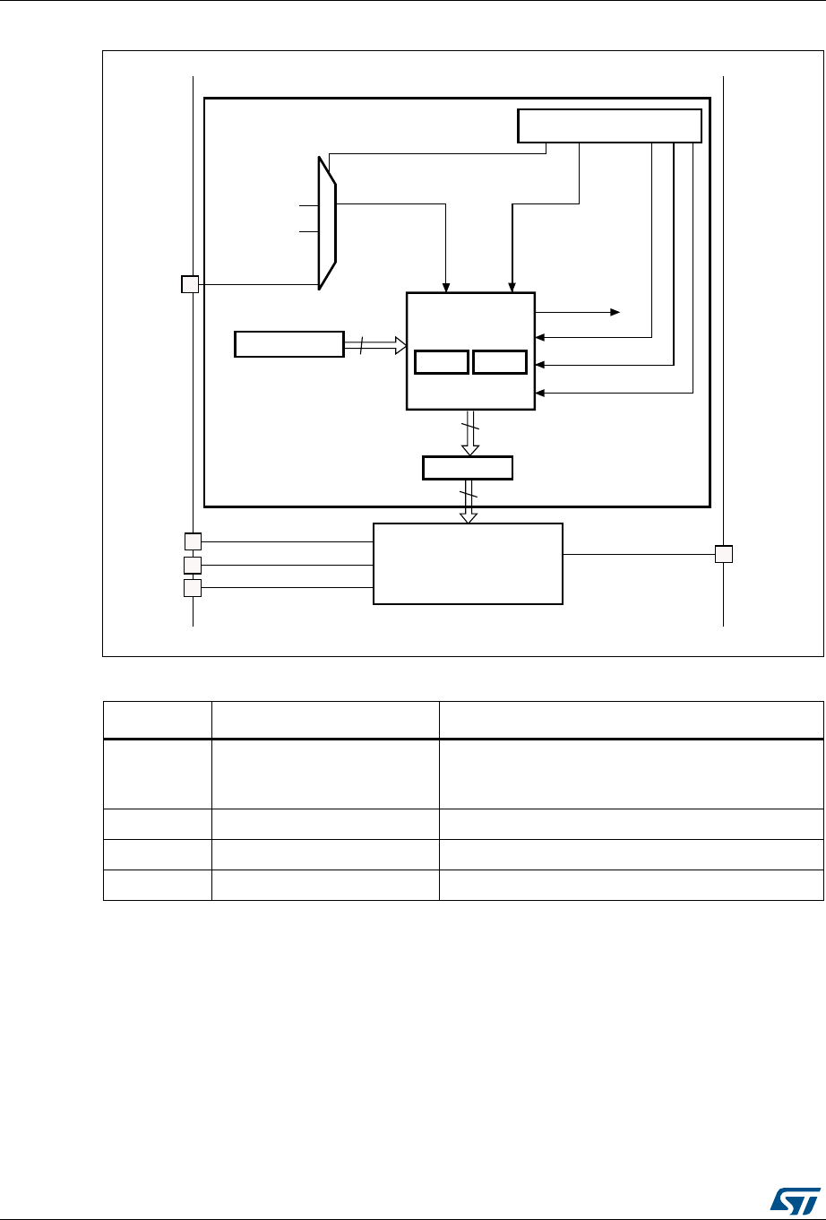
Digital-to-analog converter (DAC) RM0401
244/868 DocID027812 Rev 2
Figure 40. DAC channel block diagram
Note: Once DAC_Channelx is enabled, the corresponding GPIO pin (PA5) is automatically
connected to the analog converter output (DAC1_OUT). In order to avoid parasitic
consumption, the PA5 pin should first be configured to analog (AIN).
12.3 DAC output buffer enable
The DAC integrates one output buffer that can be used to reduce the output impedance on
DAC1_OUT1 output, and to drive external loads directly without having to add an external
operational amplifier.
Table 51. DAC pins
Name Signal type Remarks
VREF+
Input, analog positive
reference
The higher/positive reference voltage for the DAC.
VDDA and VREF+ are connected together on the
package.
VDDA Input, analog supply Analog power supply
VSSA Input, analog supply ground Ground for analog power supply
DAC1_OUT Analog output signal DAC1 channel analog output
06Y9
95()
'$&B287
&RQWUROORJLF[
WULDQJOH[
'0$UHTXHVW[
76(/[>@ELWV
7,0B75*2
(;7,B
'0$(1[
7(1[
:$9(1[>@ELWV
6:75,*[
ELW
'$&FRQWUROUHJLVWHU
'+5[
/)65[
'25[
'LJLWDOWRDQDORJ
FRQYHUWHU[
7ULJJHUVHOHFWRU[
966$
9''$
ELW
0$03[>@ELWV
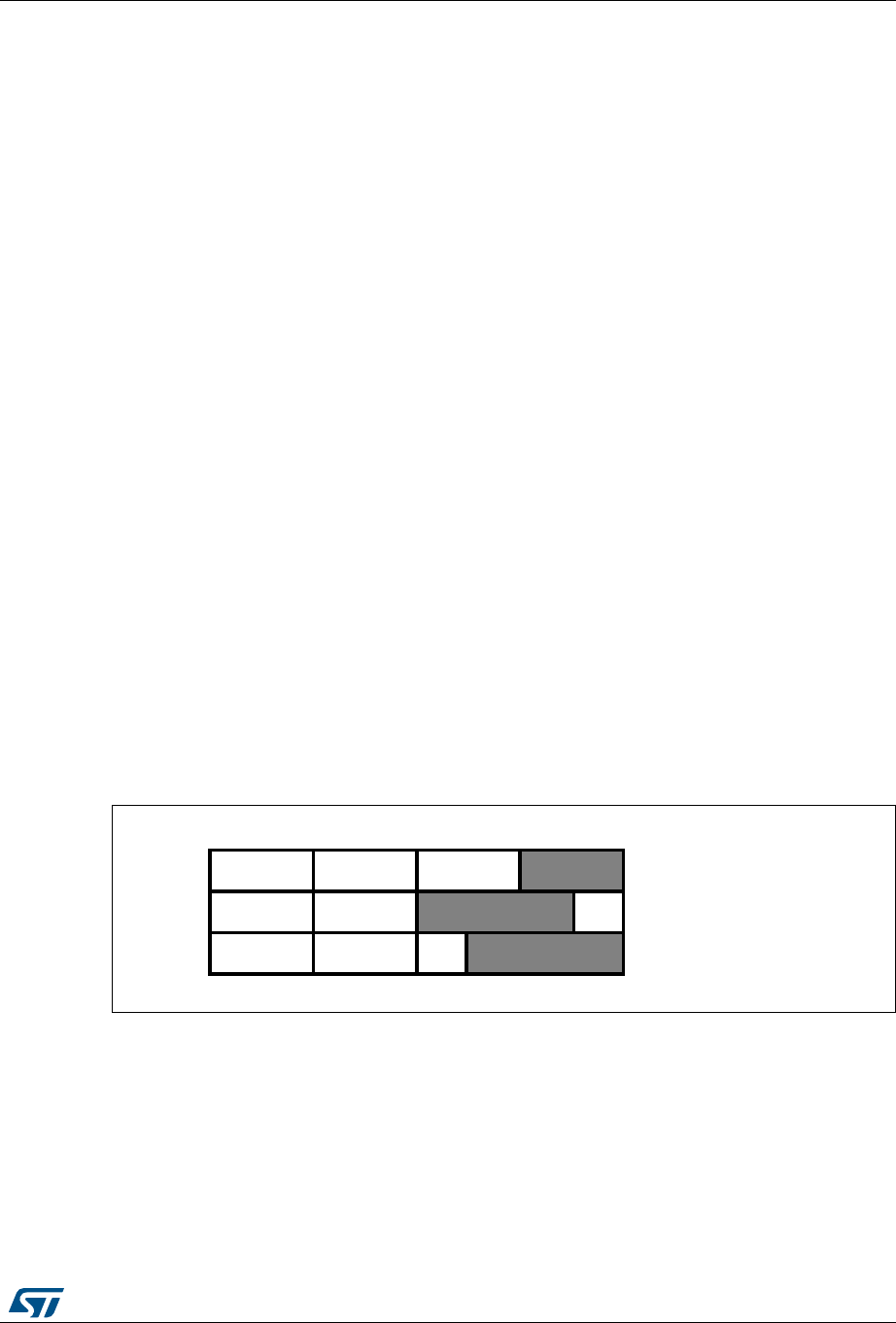
DocID027812 Rev 2 245/868
RM0401 Digital-to-analog converter (DAC)
256
The DAC channel output buffer can be enabled and disabled through the BOFF1 bit in the
DAC_CR register.
12.4 DAC channel enable
The DAC channel can be powered on by setting the EN1 bit in the DAC_CR register. The
DAC channel is then enabled after a startup time tWAKEUP
.
Note: The EN1 bit enables the analog DAC Channel macrocell only. The DAC Channel digital
interface is enabled even if the EN1 bit is reset.
12.5 Single mode functional description
12.5.1 DAC data format
Depending on the selected configuration mode, the data have to be written into the specified
register as described below:
•There are three possibilities:
– 8-bit right alignment: the software has to load data into the DAC_DHR8Rx [7:0]
bits (stored into the DHRx[11:4] bits)
– 12-bit left alignment: the software has to load data into the DAC_DHR12Lx [15:4]
bits (stored into the DHRx[11:0] bits)
– 12-bit right alignment: the software has to load data into the DAC_DHR12Rx [11:0]
bits (stored into the DHRx[11:0] bits)
Depending on the loaded DAC_DHRyyyx register, the data written by the user is shifted and
stored into the corresponding DHRx (data holding registerx, which are internal non-memory-
mapped registers). The DHRx register is then loaded into the DORx register either
automatically, by software trigger or by an external event trigger.
Figure 41. Data registers in single DAC channel mode
12.5.2 DAC channel conversion
The DAC_DORx cannot be written directly and any data transfer to the DAC channelx must
be performed by loading the DAC_DHRx register (write to DAC_DHR8Rx, DAC_DHR12Lx,
DAC_DHR12Rx).
Data stored in the DAC_DHRx register are automatically transferred to the DAC_DORx
register after one APB1 clock cycle, if no hardware trigger is selected (TENx bit in DAC_CR
register is reset). However, when a hardware trigger is selected (TENx bit in DAC_CR
register is set) and a trigger occurs, the transfer is performed three PCLK clock cycles later.
ELWULJKWDOLJQHG
ELWOHIWDOLJQHG
ELWULJKWDOLJQHG
DLE
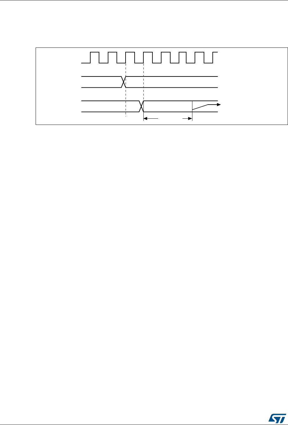
Digital-to-analog converter (DAC) RM0401
246/868 DocID027812 Rev 2
When DAC_DORx is loaded with the DAC_DHRx contents, the analog output voltage
becomes available after a time tSETTLING that depends on the power supply voltage and the
analog output load.
Figure 42. Timing diagram for conversion with trigger disabled TEN = 0
Independent trigger with single LFSR generation
To configure the DAC in this conversion mode (see Section 12.6: Noise generation), the
following sequence is required:
1. Set the DAC channel trigger enable bit TENx.
2. Configure the trigger source by setting TSELx[2:0] bits.
3. Configure the DAC channel WAVEx[1:0] bits as “01” and the same LFSR mask value in
the MAMPx[3:0] bits
4. Load the DAC channel data into the desired DAC_DHRx register (DHR12RD,
DHR12LD or DHR8RD).
When a DAC channelx trigger arrives, the LFSRx counter, with the same mask, is added to
the DHRx register and the sum is transferred into DAC_DORx (three APB clock cycles
later). Then the LFSRx counter is updated.
Independent trigger with single triangle generation
To configure the DAC in this conversion mode (see Section 12.7: Triangle-wave generation),
the following sequence is required:
1. Set the DAC channelx trigger enable TENx bits.
2. Configure the trigger source by setting TSELx[2:0] bits.
3. Configure the DAC channelx WAVEx[1:0] bits as “1x” and the same maximum
amplitude value in the MAMPx[3:0] bits
4. Load the DAC channelx data into the desired DAC_DHRx register. (DHR12RD,
DHR12LD or DHR8RD).
When a DAC channelx trigger arrives, the DAC channelx triangle counter, with the same
triangle amplitude, is added to the DHRx register and the sum is transferred into
DAC_DORx (three APB clock cycles later). The DAC channelx triangle counter is then
updated.
!0"?#,+
X!#
X!#
T3%44,).'
$(2
$/2
/UTPUTVOLTAGE
AVAILABLEON$!#?/54PIN
AIB
DocID027812 Rev 2 247/868
RM0401 Digital-to-analog converter (DAC)
256
12.5.3 DAC output voltage
Digital inputs are converted to output voltages on a linear conversion between 0 and VREF+.
The analog output voltages on each DAC channel pin are determined by the following
equation:
12.5.4 DAC trigger selection
If the TENx control bit is set, conversion can then be triggered by an external event (timer
counter, external interrupt line). The TSELx[2:0] control bits determine which possible
events will trigger conversion as shown in Table 52.
Each time a DAC interface detects a rising edge on the selected timer TRGO output, or on
the selected external interrupt line 9, the last data stored into the DAC_DHRx register are
transferred into the DAC_DORx register. The DAC_DORx register is updated three APB1
cycles after the trigger occurs.
If the software trigger is selected, the conversion starts once the SWTRIG bit is set.
SWTRIG is reset by hardware once the DAC_DORx register has been loaded with the
DAC_DHRx register contents.
Note: TSELx[2:0] bit cannot be changed when the ENx bit is set. When software trigger is
selected, the transfer from the DAC_DHRx register to the DAC_DORx register takes only
one APB1 clock cycle.
DACoutput VREF+
DOR
4096
--------------×=
Table 52. External triggers
Source Type TSEL[2:0]
TIM5 TRGO event Internal signal from on-chip
timers 011
EXTI line9 External pin 110
SWTRIG Software control bit 111
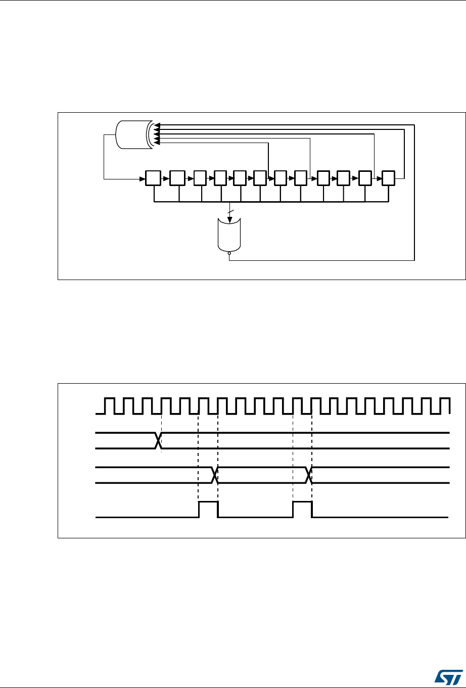
Digital-to-analog converter (DAC) RM0401
248/868 DocID027812 Rev 2
12.6 Noise generation
In order to generate a variable-amplitude pseudonoise, an LFSR (linear feedback shift
register) is available. DAC noise generation is selected by setting WAVEx[1:0] to “01”. The
preloaded value in LFSR is 0xAAA. This register is updated three APB clock cycles after
each trigger event, following a specific calculation algorithm.
Figure 43. DAC LFSR register calculation algorithm
The LFSR value, that may be masked partially or totally by means of the MAMPx[3:0] bits in
the DAC_CR register, is added up to the DAC_DHRx contents without overflow and this
value is then stored into the DAC_DORx register.
If LFSR is 0x0000, a ‘1 is injected into it (antilock-up mechanism).
It is possible to reset LFSR wave generation by resetting the WAVEx[1:0] bits.
Figure 44. DAC conversion (SW trigger enabled) with LFSR wave generation
Note: The DAC trigger must be enabled for noise generation by setting the TENx bit in the
DAC_CR register.
125
;
;
;
;
;
;25
DLF
$3%B&/.
[
[$$$
'+5
'25
DLE
['
6:75,*
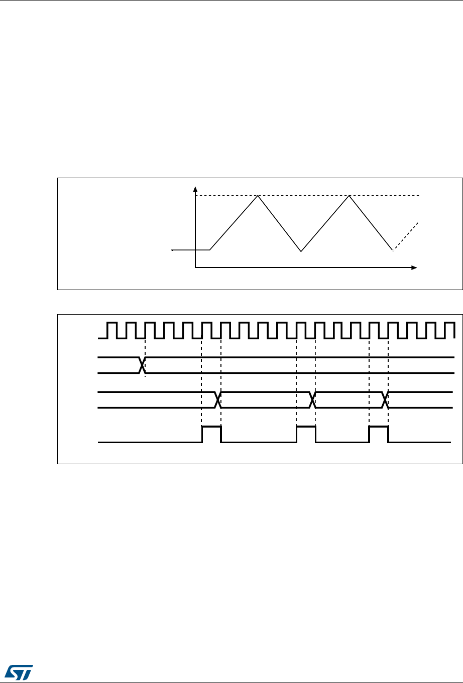
DocID027812 Rev 2 249/868
RM0401 Digital-to-analog converter (DAC)
256
12.7 Triangle-wave generation
It is possible to add a small-amplitude triangular waveform on a DC or slowly varying signal.
DAC triangle-wave generation is selected by setting WAVEx[1:0] to “10”. The amplitude is
configured through the MAMPx[3:0] bits in the DAC_CR register. An internal triangle counter
is incremented three APB clock cycles after each trigger event. The value of this counter is
then added to the DAC_DHRx register without overflow and the sum is stored into the
DAC_DORx register. The triangle counter is incremented as long as it is less than the
maximum amplitude defined by the MAMPx[3:0] bits. Once the configured amplitude is
reached, the counter is decremented down to 0, then incremented again and so on.
It is possible to reset triangle wave generation by resetting the WAVEx[1:0] bits.
Figure 45. DAC triangle wave generation
Figure 46. DAC conversion (SW trigger enabled) with triangle wave generation
Note: The DAC trigger must be enabled for triangle generation by setting the TENx bit in the
DAC_CR register.
The MAMPx[3:0] bits must be configured before enabling the DAC, otherwise they cannot
be changed.
-!-0X;=MAXAMPLITUDE
$!#?$(2XBASEVALUE
$!#?$(2XBASEVALUE
)NCREMENTATION
AIC
$ECREMENTATION
$3%B&/.
[$%(
[$%(
'+5
'25
DLE
[$%)
6:75,*
[$&

Digital-to-analog converter (DAC) RM0401
250/868 DocID027812 Rev 2
12.8 DMA request
The DAC channel has a DMA capability. One DMA channel is used to service DAC channel
DMA requests.
A DAC DMA request is generated when an external trigger (but not a software trigger)
occurs while the DMAENx bit is set. The value of the DAC_DHRx register is then transferred
to the DAC_DORx register.
DMA underrun
The DAC DMA request is not queued so that if a second external trigger arrives before the
acknowledgment for the first external trigger is received (first request), then no new request
is issued and the DMA channelx underrun flag DMAUDRx in the DAC_SR register is set,
reporting the error condition. DMA data transfers are then disabled and no further DMA
request is treated. The DAC channelx continues to convert old data.
The software should clear the DMAUDRx flag by writing “1”, clear the DMAEN bit of the
used DMA stream and re-initialize both DMA and DAC channelx to restart the transfer
correctly. The software should modify the DAC trigger conversion frequency or lighten the
DMA workload to avoid a new DMA. Finally, the DAC conversion can be resumed by
enabling both DMA data transfer and conversion trigger.
An interrupt is also generated if the corresponding DMAUDRIE1 bit in the DAC_CR register
is enabled.

DocID027812 Rev 2 251/868
RM0401 Digital-to-analog converter (DAC)
256
12.9 DAC registers
Refer to Section 1.1 on page 33 for a list of abbreviations used in register descriptions.
The peripheral registers have to be accessed by words (32-bit).
12.9.1 DAC control register (DAC_CR)
Address offset: 0x00
Reset value: 0x0000 0000
31 30 29 28 27 26 25 24 23 22 21 20 19 18 17 16
Res. Res. Res. Res. Res. Res. Res. Res. Res. Res.
151413121110987 6 543210
Res. Res. DMAU
DRIE1
DMA
EN1 MAMP1[3:0] WAVE1[1:0] TSEL1[2:0] TEN1 BOFF1 EN1
rw rw rw rw rw rw rw rw rw rw rw rw rw rw
Bits 31:14 Reserved, must be kept at reset value.
Bit 13 DMAUDRIE1: DAC channel1 DMA Underrun Interrupt enable
This bit is set and cleared by software.
0: DAC channel1 DMA Underrun Interrupt disabled
1: DAC channel1 DMA Underrun Interrupt enabled
Bit 12 DMAEN1: DAC channel1 DMA enable
This bit is set and cleared by software.
0: DAC channel1 DMA mode disabled
1: DAC channel1 DMA mode enabled
Bits 11:8 MAMP1[3:0]: DAC channel1 mask/amplitude selector
These bits are written by software to select mask in wave generation mode or amplitude in
triangle generation mode.
0000: Unmask bit0 of LFSR/ triangle amplitude equal to 1
0001: Unmask bits[1:0] of LFSR/ triangle amplitude equal to 3
0010: Unmask bits[2:0] of LFSR/ triangle amplitude equal to 7
0011: Unmask bits[3:0] of LFSR/ triangle amplitude equal to 15
0100: Unmask bits[4:0] of LFSR/ triangle amplitude equal to 31
0101: Unmask bits[5:0] of LFSR/ triangle amplitude equal to 63
0110: Unmask bits[6:0] of LFSR/ triangle amplitude equal to 127
0111: Unmask bits[7:0] of LFSR/ triangle amplitude equal to 255
1000: Unmask bits[8:0] of LFSR/ triangle amplitude equal to 511
1001: Unmask bits[9:0] of LFSR/ triangle amplitude equal to 1023
1010: Unmask bits[10:0] of LFSR/ triangle amplitude equal to 2047
≥ 1011: Unmask bits[11:0] of LFSR/ triangle amplitude equal to 4095
Bits 7:6 WAVE1[1:0]: DAC channel1 noise/triangle wave generation enable
These bits are set and cleared by software.
00: Wave generation disabled
01: Noise wave generation enabled
1x: Triangle wave generation enabled
Note: Only used if bit TEN1 = 1 (DAC channel1 trigger enabled).

Digital-to-analog converter (DAC) RM0401
252/868 DocID027812 Rev 2
Bits 5:3 TSEL1[2:0]: DAC channel1 trigger selection
These bits select the external event used to trigger DAC channel1.
011: TIM5 TRGO event
110: EXTI line9
111: Software trigger
Note: Only used if bit TEN1 = 1 (DAC channel1 trigger enabled).
Bit 2 TEN1: DAC channel1 trigger enable
This bit is set and cleared by software to enable/disable DAC channel1 trigger.
0: DAC channel1 trigger disabled and data written into the DAC_DHRx register are
transferred one APB1 clock cycle later to the DAC_DOR1 register
1: DAC channel1 trigger enabled and data from the DAC_DHRx register are transferred
three APB1 clock cycles later to the DAC_DOR1 register
Note: When software trigger is selected, the transfer from the DAC_DHRx register to the
DAC_DOR1 register takes only one APB1 clock cycle.
Bit 1 BOFF1: DAC channel1 output buffer disable
This bit is set and cleared by software to enable/disable DAC channel1 output buffer.
0: DAC channel1 output buffer enabled
1: DAC channel1 output buffer disabled
Bit 0 EN1: DAC channel1 enable
This bit is set and cleared by software to enable/disable DAC channel1.
0: DAC channel1 disabled
1: DAC channel1 enabled
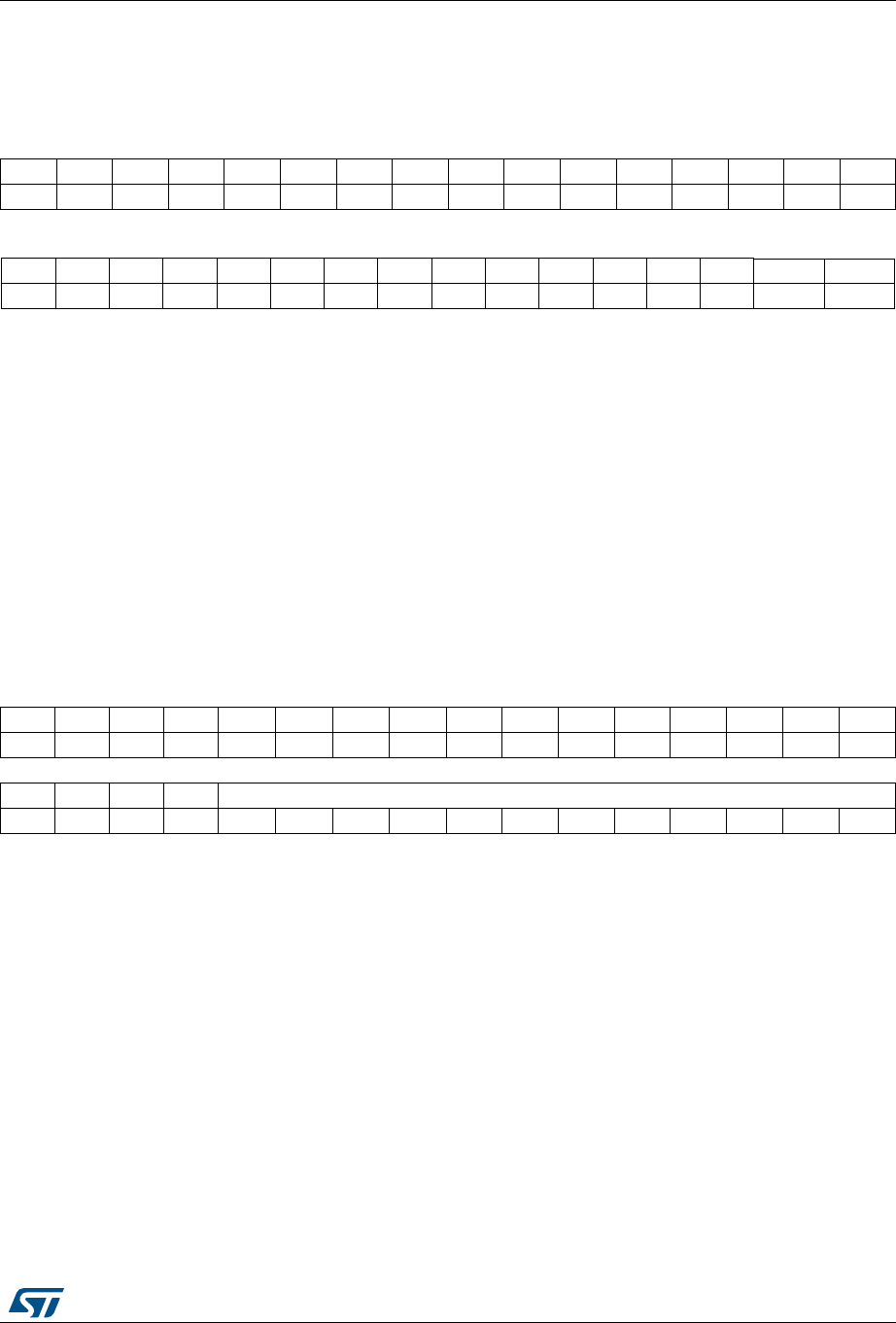
DocID027812 Rev 2 253/868
RM0401 Digital-to-analog converter (DAC)
256
12.9.2 DAC software trigger register (DAC_SWTRIGR)
Address offset: 0x04
Reset value: 0x0000 0000
12.9.3 DAC channel1 12-bit right-aligned data holding register
(DAC_DHR12R1)
Address offset: 0x08
Reset value: 0x0000 0000
31 30 29 28 27 26 25 24 23 22 21 20 19 18 17 16
Res. Res. Res. Res. Res. Res. Res. Res. Res. Res. Res. Res. Res. Res. Res. Res.
15 14 13 12 11 10 9 8 7 6 5 4 3 2 1 0
Res. Res. Res. Res. Res. Res. Res. Res. Res. Res. Res. Res. Res. Res. Res. SWTRIG1
w
Bits 31:1 Reserved, must be kept at reset value.
Bit 0 SWTRIG1: DAC channel1 software trigger
This bit is set and cleared by software to enable/disable the software trigger.
0: Software trigger disabled
1: Software trigger enabled
Note: This bit is cleared by hardware (one APB1 clock cycle later) once the DAC_DHR1
register value has been loaded into the DAC_DOR1 register.
31 30 29 28 27 26 25 24 23 22 21 20 19 18 17 16
Res. Res. Res. Res. Res. Res. Res. Res. Res. Res. Res. Res. Res. Res. Res. Res.
15 14 13 12 11 10 9 8 7 6 5 4 3 2 1 0
Res. Res. Res. Res. DACC1DHR[11:0]
rw rw rw rw rw rw rw rw rw rw rw rw
Bits 31:12 Reserved, must be kept at reset value.
Bits 11:0 DACC1DHR[11:0]: DAC channel1 12-bit right-aligned data
These bits are written by software which specifies 12-bit data for DAC channel1.

Digital-to-analog converter (DAC) RM0401
254/868 DocID027812 Rev 2
12.9.4 DAC channel1 12-bit left-aligned data holding register
(DAC_DHR12L1)
Address offset: 0x0C
Reset value: 0x0000 0000
12.9.5 DAC channel1 8-bit right-aligned data holding register
(DAC_DHR8R1)
Address offset: 0x10
Reset value: 0x0000 0000
12.9.6 DAC channel1 data output register (DAC_DOR1)
Address offset: 0x2C
Reset value: 0x0000 0000
31 30 29 28 27 26 25 24 23 22 21 20 19 18 17 16
Res. Res. Res. Res. Res. Res. Res. Res. Res. Res. Res. Res. Res. Res. Res. Res.
1514131211109876543210
DACC1DHR[11:0] v Res. Res. Res.
rw rw rw rw rw rw rw rw rw rw rw rw
Bits 31:16 Reserved, must be kept at reset value.
Bits 15:4 DACC1DHR[11:0]: DAC channel1 12-bit left-aligned data
These bits are written by software which specifies 12-bit data for DAC channel1.
Bits 3:0 Reserved, must be kept at reset value.
31 30 29 28 27 26 25 24 23 22 21 20 19 18 17 16
Res. Res. Res. Res. Res. Res. Res. Res. Res. Res. Res. Res. Res. Res. Res. Res.
15 14 13 12 11 10 9 8 7 6 5 4 3 2 1 0
Res. Res. Res. Res. Res. Res. Res. Res. DACC1DHR[7:0]
rw rw rw rw rw rw rw rw
Bits 31:8 Reserved, must be kept at reset value.
Bits 7:0 DACC1DHR[7:0]: DAC channel1 8-bit right-aligned data
These bits are written by software which specifies 8-bit data for DAC channel1.
31 30 29 28 27 26 25 24 23 22 21 20 19 18 17 16
Res. Res. Res. Res. Res. Res. Res. Res. Res. Res. Res. Res. Res. Res. Res. Res.
1514131211109876543210
Res. Res. Res. Res. DACC1DOR[11:0]
rrrrrrrrrrrr

DocID027812 Rev 2 255/868
RM0401 Digital-to-analog converter (DAC)
256
12.9.7 DAC status register (DAC_SR)
Address offset: 0x34
Reset value: 0x0000 0000
Bits 31:12 Reserved, must be kept at reset value.
Bits 11:0 DACC1DOR[11:0]: DAC channel1 data output
These bits are read-only, they contain data output for DAC channel1.
31 30 29 28 27 26 25 24 23 22 21 20 19 18 17 16
Res. Res. Res. Res. Res. Res. Res. Res. Res. Res. Res. Res. Res. Res. Res. Res.
1514 13 1211109876543210
Res. Res. DMAUDR1 Res. Res. Res. Res. Res. Res. Res. Res. Res. Res. Res. Res. Res.
rc_w1
Bits 31:14 Reserved, must be kept at reset value.
Bit 13 DMAUDR1: DAC channel1 DMA underrun flag
This bit is set by hardware and cleared by software (by writing it to 1).
0: No DMA underrun error condition occurred for DAC channel1
1: DMA underrun error condition occurred for DAC channel1 (the currently selected trigger is
driving DAC channel1 conversion at a frequency higher than the DMA service capability rate)
Bits 12:0 Reserved, must be kept at reset value.

Digital-to-analog converter (DAC) RM0401
256/868 DocID027812 Rev 2
12.9.8 DAC register map
Table 53 summarizes the DAC registers.
Refer to Section 2.2.2 on page 38 for the register boundary addresses.
Table 53. DAC register map and reset values
Offset Register
name
31
30
29
28
27
26
25
24
23
22
21
20
19
18
17
16
15
14
13
12
11
10
9
8
7
6
5
4
3
2
1
0
0x00
DAC_CR
Res.
Res.
Res.
Res.
Res.
Res.
Res.
Res.
Res.
Res.
Res.
Res.
DMAUDRIE1
DMAEN1
MAMP1[3:0].
WAVE1[1:0]
TSEL1[2:0]
TEN1
BOFF1
EN1
Reset value 00000000000000
0x04
DAC_
SWTRIGR
Res.
Res.
Res.
Res.
Res.
Res.
Res.
Res.
Res.
Res.
Res.
Res.
Res.
Res.
Res.
Res.
Res.
Res.
Res.
Res.
Res.
Res.
Res.
Res.
Res.
Res.
Res.
Res.
Res.
Res.
Res.
SWTRIG1
Reset value 0
0x08
DAC_
DHR12R1
Res.
Res.
Res.
Res.
Res.
Res.
Res.
Res.
Res.
Res.
Res.
Res.
Res.
Res.
Res.
Res.
Res.
Res.
Res.
Res.
DACC1DHR[11:0]
Reset value 000000000000
0x0C
DAC_
DHR12L1
Res.
Res.
Res.
Res.
Res.
Res.
Res.
Res.
Res.
Res.
Res.
Res.
Res.
Res.
Res.
Res.
DACC1DHR[11:0]
Res.
Res.
Res.
Res.
Reset value 000000000000
0x10
DAC_
DHR8R1
Res.
Res.
Res.
Res.
Res.
Res.
Res.
Res.
Res.
Res.
Res.
Res.
Res.
Res.
Res.
Res.
Res.
Res.
Res.
Res.
Res.
Res.
Res.
Res.
DACC1DHR[7:0]
Reset value 00000000
0x2C
DAC_DOR1
Res.
Res.
Res.
Res.
Res.
Res.
Res.
Res.
Res.
Res.
Res.
Res.
Res.
Res.
Res.
Res.
Res.
Res.
Res.
Res.
DACC1DOR[11:0]
Reset value 000000000000
0x34
DAC_SR
Res.
Res.
Res.
Res.
Res.
Res.
Res.
Res.
Res.
Res.
Res.
Res.
Res.
Res.
Res.
Res.
Res.
Res.
DMAUDR1
Res.
Res.
Res.
Res.
Res.
Res.
Res.
Res.
Res.
Res.
Res.
Res.
Res.
Reset value 0
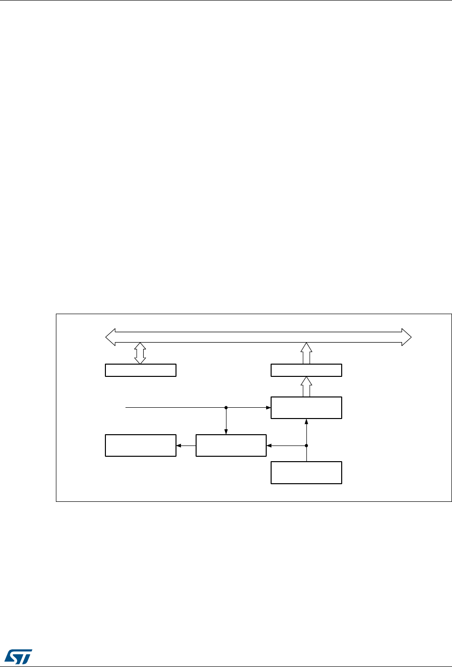
DocID027812 Rev 2 257/766
RM0401 Random number generator (RNG)
261
13 Random number generator (RNG)
13.1 Introduction
The RNG processor is a random number generator, based on a continuous analog noise,
that provides a random 32-bit value to the host when read.
The RNG passed the FIPS PUB 140-2 (2001 October 10) tests with a success ratio of 99%.
13.2 RNG main features
•It delivers 32-bit random numbers, produced by an analog generator
•40 periods of the RNG_CLK clock signal between two consecutive random numbers
•Monitoring of the RNG entropy to flag abnormal behavior (generation of stable values,
or of a stable sequence of values)
•It can be disabled to reduce power consumption
13.3 RNG functional description
Figure 47 shows the RNG block diagram.
Figure 47. Block diagram
1. For more details about RNG Clock (RNG_CLK) source, please refer to Section 5: Reset and clock control
(RCC).
The random number generator implements an analog circuit. This circuit generates seeds
that feed a linear feedback shift register (RNG_LFSR) in order to produce 32-bit random
numbers.
The analog circuit is made of several ring oscillators whose outputs are XORed to generate
the seeds. The RNG_LFSR is clocked by a dedicated clock (RNG_CLK) at a constant
frequency, so that the quality of the random number is independent of the HCLK frequency.
The contents of the RNG_LFSR are transferred into the data register (RNG_DR) when a
significant number of seeds have been introduced into the RNG_LFSR.
DLE
$QDORJVHHG
ELW$+%EXV
51*B'5
$QDORJVHHG
/)65
)HHGDOLQHDUIHHGEDFN
VKLIWUHJLVWHU
'DWDUHJLVWHU
&ORFNFKHFNHUDQG
IDXOWGHWHFWRU
51*B65
6WDWXVUHJLVWHU
51*B&/.
51*B&5
&RQWUROUHJLVWHU

Random number generator (RNG) RM0401
258/766 DocID027812 Rev 2
In parallel, the analog seed and the dedicated RNG_CLK clock are monitored. Status bits (in
the RNG_SR register) indicate when an abnormal sequence occurs on the seed or when
the frequency of the RNG_CLK clock is too low. An interrupt can be generated when an
error is detected.
13.3.1 Operation
To run the RNG, follow the steps below:
1. Enable the interrupt if needed (to do so, set the IE bit in the RNG_CR register). An
interrupt is generated when a random number is ready or when an error occurs.
2. Enable the random number generation by setting the RNGEN bit in the RNG_CR
register. This activates the analog part, the RNG_LFSR and the error detector.
3. At each interrupt, check that no error occurred (the SEIS and CEIS bits should be ‘0’ in
the RNG_SR register) and that a random number is ready (the DRDY bit is ‘1’ in the
RNG_SR register). The contents of the RNG_DR register can then be read.
As required by the FIPS PUB (Federal Information Processing Standard Publication) 140-2,
the first random number generated after setting the RNGEN bit should not be used, but
saved for comparison with the next generated random number. Each subsequent generated
random number has to be compared with the previously generated number. The test fails if
any two compared numbers are equal (continuous random number generator test).
13.3.2 Error management
If the CEIS bit is read as ‘1’ (clock error)
In the case of a clock, the RNG is no more able to generate random numbers because the
RNG_CLK clock is not correct. Check that the clock controller is correctly configured to
provide the RNG clock and clear the CEIS bit. The RNG can work when the CECS bit is ‘0’.
The clock error has no impact on the previously generated random numbers, and the
RNG_DR register contents can be used.
If the SEIS bit is read as ‘1’ (seed error)
In the case of a seed error, the generation of random numbers is interrupted for as long as
the SECS bit is ‘1’. If a number is available in the RNG_DR register, it must not be used
because it may not have enough entropy.
What you should do is clear the SEIS bit, then clear and set the RNGEN bit to reinitialize
and restart the RNG.
DocID027812 Rev 2 259/766
RM0401 Random number generator (RNG)
261
13.4 RNG registers
The RNG is associated with a control register, a data register and a status register. They
have to be accessed by words (32 bits).
13.4.1 RNG control register (RNG_CR)
Address offset: 0x00
Reset value: 0x0000 0000
13.4.2 RNG status register (RNG_SR)
Address offset: 0x04
Reset value: 0x0000 0000
31 30 29 28 27 26 25 24 23 22 21 20 19 18 17 16
Res. Res. Res. Res. Res. Res. Res. Res. Res. Res. Res. Res. Res. Res. Res. Res.
15 14 13 12 11 10 9 8 7 6 5 4 3 2 1 0
Res. Res. Res. Res. Res. Res. Res. Res. Res. Res. Res. Res. IE RNGEN Res. Res.
rw rw
Bits 31:4 Reserved, must be kept at reset value
Bit 3 IE: Interrupt enable
0: RNG Interrupt is disabled
1: RNG Interrupt is enabled. An interrupt is pending as soon as DRDY=1 or SEIS=1 or
CEIS=1 in the RNG_SR register.
Bit 2 RNGEN: Random number generator enable
0: Random number generator is disabled
1: random Number Generator is enabled.
Bits 1:0 Reserved, must be kept at reset value
31 30 29 28 27 26 25 24 23 22 21 20 19 18 17 16
Res. Res. Res. Res. Res. Res. Res. Res. Res. Res. Res. Res. Res. Res. Res. Res.
1514131211109876543210
Res. Res. Res. Res. Res. Res. Res. Res. Res. SEIS CEIS Res. Res. SECS CECS DRDY
rc_w0 rc_w0 r r r

Random number generator (RNG) RM0401
260/766 DocID027812 Rev 2
13.4.3 RNG data register (RNG_DR)
Address offset: 0x08
Reset value: 0x0000 0000
The RNG_DR register is a read-only register that delivers a 32-bit random value when read.
After being read, this register delivers a new random value after a maximum time of 40
periods of the RNG_CLK clock. The software must check that the DRDY bit is set before
reading the RNDATA value.
Bits 31:7 Reserved, must be kept at reset value
Bit 6 SEIS: Seed error interrupt status
This bit is set at the same time as SECS, it is cleared by writing it to 0.
0: No faulty sequence detected
1: One of the following faulty sequences has been detected:
– More than 64 consecutive bits at the same value (0 or 1)
– More than 32 consecutive alternations of 0 and 1 (0101010101...01)
An interrupt is pending if IE = 1 in the RNG_CR register.
Bit 5 CEIS: Clock error interrupt status
This bit is set at the same time as CECS, it is cleared by writing it to 0.
0: The RNG_CLK clock was correctly detected
1: The RNG_CLK was not correctly detected (fRNG_CLK< fHCLK/16)
An interrupt is pending if IE = 1 in the RNG_CR register.
Bits 4:3 Reserved, must be kept at reset value
Bit 2 SECS: Seed error current status
0: No faulty sequence has currently been detected. If the SEIS bit is set, this means that a
faulty sequence was detected and the situation has been recovered.
1: One of the following faulty sequences has been detected:
– More than 64 consecutive bits at the same value (0 or 1)
– More than 32 consecutive alternations of 0 and 1 (0101010101...01)
Bit 1 CECS: Clock error current status
0: The RNG_CLK clock has been correctly detected. If the CEIS bit is set, this means that a
clock error was detected and the situation has been recovered
1: The RNG_CLK was not correctly detected (fRNG_CLK< fHCLK/16).
Bit 0 DRDY: Data ready
0: The RNG_DR register is not yet valid, no random data is available
1: The RNG_DR register contains valid random data
Note: An interrupt is pending if IE = 1 in the RNG_CR register.
Once the RNG_DR register has been read, this bit returns to 0 until a new valid value is
computed.
31 30 29 28 27 26 25 24 23 22 21 20 19 18 17 16
RNDATA
rrrrrrrrrrrrrrrr
1514131211109876543210
RNDATA
rrrrrrrrrrrrrrrr
DocID027812 Rev 2 261/766
RM0401 Random number generator (RNG)
261
13.4.4 RNG register map
Table 54 gives the RNG register map and reset values.
Refer to Section 2.2.2 on page 38 for the register boundary addresses.
Bits 31:0 RNDATA: Random data
32-bit random data.
Table 54. RNG register map and reset map
Offset Register name
reset value
31
30
29
28
27
26
25
24
23
22
21
20
19
18
17
16
15
14
13
12
11
10
9
8
7
6
5
4
3
2
1
0
0x00
RNG_CR
Res.
Res.
Res.
Res.
Res.
Res.
Res.
Res.
Res.
Res.
Res.
Res.
Res.
Res.
Res.
Res.
Res.
Res.
Res.
Res.
Res.
Res.
Res.
Res.
Res.
Res.
Res.
Res.
IE
RNGEN
Res.
Res.
Reset value 00
0x04 RNG_SR
Res.
Res.
Res.
Res.
Res.
Res.
Res.
Res.
Res.
Res.
Res.
Res.
Res.
Res.
Res.
Res.
Res.
Res.
Res.
Res.
Res.
Res.
Res.
Res.
Res.
SEIS
CEIS
Res.
Res.
SECS
Res
Res
Reset value 00 0
0x08 RNG_DR RNDATA[31:0]
Reset value 00000000000000000000000000000000

Advanced-control timers (TIM1) RM0401
262/766 DocID027812 Rev 2
14 Advanced-control timers (TIM1)
14.1 TIM1 introduction
The advanced-control timer (TIM1) consists of a 16-bit auto-reload counter driven by a
programmable prescaler.
It may be used for a variety of purposes, including measuring the pulse length of input
signals (input capture) or generating output waveforms (output compare, PWM,
complementary PWM with dead-time insertion).
Pulse lengths and waveform periods can be modulated from a few microseconds to several
milliseconds using the timer prescaler and the RCC clock controller prescalers.
The advanced-control (TIM1) and general-purpose (TIMx) timers are completely
independent, and do not share any resources. They can be synchronized together as
described in Section .
14.2 TIM1 main features
TIM1 timer features include:
•16-bit up, down, up/down auto-reload counter.
•16-bit programmable prescaler allowing dividing (also “on the fly”) the counter clock
frequency either by any factor between 1 and 65536.
•Up to 4 independent channels for:
– Input Capture
– Output Compare
– PWM generation (Edge and Center-aligned Mode)
– One-pulse mode output
•Complementary outputs with programmable dead-time
•Synchronization circuit to control the timer with external signals and to interconnect
several timers together.
•Repetition counter to update the timer registers only after a given number of cycles of
the counter.
•Break input to put the timer’s output signals in reset state or in a known state.
•Interrupt/DMA generation on the following events:
– Update: counter overflow/underflow, counter initialization (by software or
internal/external trigger)
– Trigger event (counter start, stop, initialization or count by internal/external trigger)
– Input capture
– Output compare
– Break input
•Supports incremental (quadrature) encoder and hall-sensor circuitry for positioning
purposes
•Trigger input for external clock or cycle-by-cycle current management
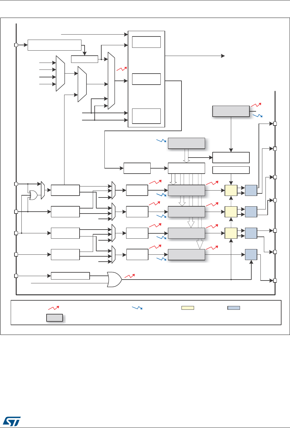
DocID027812 Rev 2 263/766
RM0401 Advanced-control timers (TIM1)
334
Figure 48. Advanced-control timer block diagram
069
,QWHUUXSW'0$RXWSXW (YHQW
5HJ 3UHORDGUHJLVWHUVWUDQVIHUUHGWRDFWLYHUHJLVWHUVRQ8HYHQWDFFRUGLQJWRFRQWUROELW
/HJHQG
3RODULW\VHOHFWLRQ
,QSXWILOWHU
(GJHGHWHFWRU
,QSXWILOWHU
(GJHGHWHFWRU
,QSXWILOWHU
(GJHGHWHFWRU
,QSXWILOWHU
(GJHGHWHFWRU
75&
75&
75&
75&
7,)3
7,)3
7,)3
7,)3
3UHVFDOHU
,&
,&
,&
,&
3UHVFDOHU
3UHVFDOHU
3UHVFDOHU
7,)3
7,)3
7,)3
7,)3
7,
7,
7,
7,
%5.
&ORFNIDLOXUHHYHQWIURPFORFNFRQWUROOHU
&66&ORFN6HFXULW\6\VWHP
,&36
,&36
,&36
,&36
%,
&DSWXUH&RPSDUH
5HJLVWHU
8
&DSWXUH&RPSDUH
5HJLVWHU
8
8
&DSWXUH&RPSDUH
5HJLVWHU
&DSWXUH&RPSDUH
5HJLVWHU
8
&&,
&&,
&&,
&&,
&&,
&&,
&&,
&&,
2&5()
2&5()
2&5()
2&5()
2&
2&1
2&
2&1
2&
2&1 2&
'7*>@UHJLVWHUV
&17
FRXQWHU
36&
SUHVFDOHU
&.B&17&.B36&
5HSHWLWLRQFRXQWHU
5(35HJLVWHU
8,
3RODULW\VHOHFWLRQ
(GJHGHWHFWRUDQG3UHVFDOHU
,QSXWILOWHU
7ULJJHU
FRQWUROOHU
6ODYHPRGH
FRQWUROOHU
(QFRGHU
LQWHUIDFH
5HVHW
(QDEOH
8S'RZQ
&RXQW
7RRWKHUWLPHUV
7R'$&DQG$'&
75*2
75*,
7*,
,QWHUQDOFORFN&.B,17
(75)
(753
(75
&.B7,0IURP5&&
7,)3
7,)3
7,0[B(757,0[B&+7,0[B&+7,0[B&+7,0[B&+7,0[B%.,1
7,0[B&+7,0[B&+17,0[B&+7,0[B&+1 7,0[B&+7,0[B&+ 7,0[B&+1
8
8
'7* 2XWSXWFRQWURO
$XWR5HORDG
5HJLVWHU
8
,75
,75
,75
,75
7,)B('

Advanced-control timers (TIM1) RM0401
264/766 DocID027812 Rev 2
14.3 TIM1 functional description
14.3.1 Time-base unit
The main block of the programmable advanced-control timer is a 16-bit counter with its
related auto-reload register. The counter can count up, down or both up and down. The
counter clock can be divided by a prescaler.
The counter, the auto-reload register and the prescaler register can be written or read by
software. This is true even when the counter is running.
The time-base unit includes:
•Counter register (TIMx_CNT)
•Prescaler register (TIMx_PSC)
•Auto-reload register (TIMx_ARR)
•Repetition counter register (TIMx_RCR)
The auto-reload register is preloaded. Writing to or reading from the auto-reload register
accesses the preload register. The content of the preload register are transferred into the
shadow register permanently or at each update event (UEV), depending on the auto-reload
preload enable bit (ARPE) in TIMx_CR1 register. The update event is sent when the counter
reaches the overflow (or underflow when downcounting) and if the UDIS bit equals 0 in the
TIMx_CR1 register. It can also be generated by software. The generation of the update
event is described in detailed for each configuration.
The counter is clocked by the prescaler output CK_CNT, which is enabled only when the
counter enable bit (CEN) in TIMx_CR1 register is set (refer also to the slave mode controller
description to get more details on counter enabling).
Note that the counter starts counting 1 clock cycle after setting the CEN bit in the TIMx_CR1
register.
Prescaler description
The prescaler can divide the counter clock frequency by any factor between 1 and 65536. It
is based on a 16-bit counter controlled through a 16-bit register (in the TIMx_PSC register).
It can be changed on the fly as this control register is buffered. The new prescaler ratio is
taken into account at the next update event.
Figure 49 and Figure 50 give some examples of the counter behavior when the prescaler
ratio is changed on the fly:
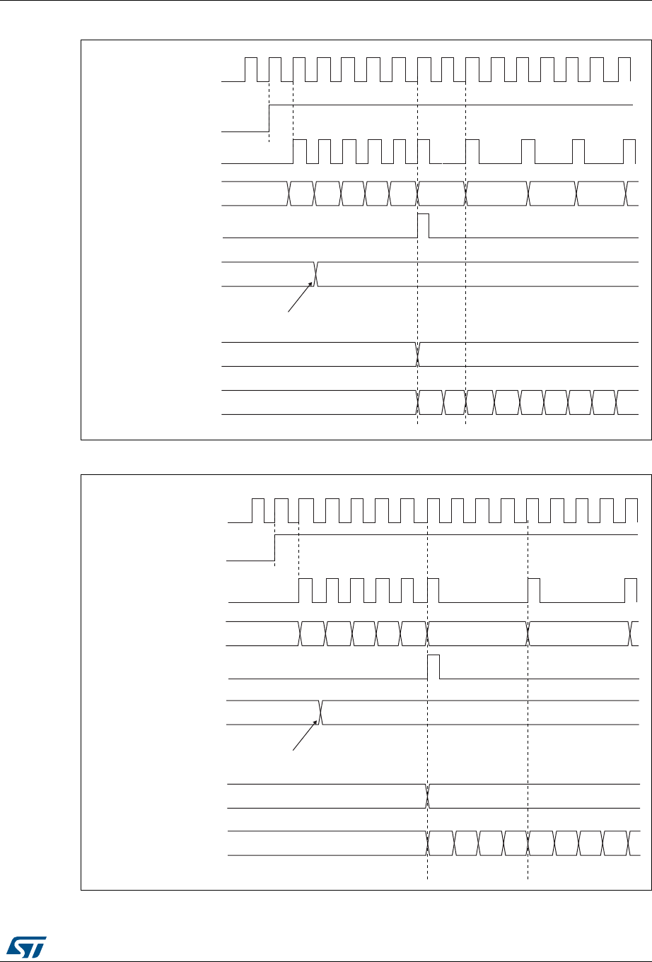
DocID027812 Rev 2 265/766
RM0401 Advanced-control timers (TIM1)
334
Figure 49. Counter timing diagram with prescaler division change from 1 to 2
Figure 50. Counter timing diagram with prescaler division change from 1 to 4
&.B36&
&(1
7LPHUFORFN &.B&17
&RXQWHUUHJLVWHU
8SGDWHHYHQW8(9
3UHVFDOHUFRQWUROUHJLVWHU
:ULWHDQHZYDOXHLQ7,0[B36&
3UHVFDOHUEXIIHU
3UHVFDOHUFRXQWHU
)$ )%) ) ) )&
069
069
&.B36&
&(1
7LPHUFORFN &.B&17
&RXQWHUUHJLVWHU
8SGDWHHYHQW8(9
3UHVFDOHUFRQWUROUHJLVWHU
:ULWHDQHZYDOXHLQ7,0[B36&
3UHVFDOHUEXIIHU
3UHVFDOHUFRXQWHU
)$ )%
) ) ) )&
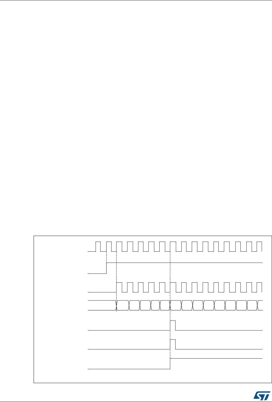
Advanced-control timers (TIM1) RM0401
266/766 DocID027812 Rev 2
14.3.2 Counter modes
Upcounting mode
In upcounting mode, the counter counts from 0 to the auto-reload value (content of the
TIMx_ARR register), then restarts from 0 and generates a counter overflow event.
If the repetition counter is used, the update event (UEV) is generated after upcounting is
repeated for the number of times programmed in the repetition counter register plus one
(TIMx_RCR+1). Else the update event is generated at each counter overflow.
Setting the UG bit in the TIMx_EGR register (by software or by using the slave mode
controller) also generates an update event.
The UEV event can be disabled by software by setting the UDIS bit in the TIMx_CR1
register. This is to avoid updating the shadow registers while writing new values in the
preload registers. Then no update event occurs until the UDIS bit has been written to 0.
However, the counter restarts from 0, as well as the counter of the prescaler (but the
prescale rate does not change). In addition, if the URS bit (update request selection) in
TIMx_CR1 register is set, setting the UG bit generates an update event UEV but without
setting the UIF flag (thus no interrupt or DMA request is sent). This is to avoid generating
both update and capture interrupts when clearing the counter on the capture event.
When an update event occurs, all the registers are updated and the update flag (UIF bit in
TIMx_SR register) is set (depending on the URS bit):
•The repetition counter is reloaded with the content of TIMx_RCR register,
•The auto-reload shadow register is updated with the preload value (TIMx_ARR),
•The buffer of the prescaler is reloaded with the preload value (content of the TIMx_PSC
register).
The following figures show some examples of the counter behavior for different clock
frequencies when TIMx_ARR=0x36.
Figure 51. Counter timing diagram, internal clock divided by 1
ϬϬ ϬϮ Ϭϯ Ϭϰ Ϭϱ Ϭϲ Ϭϳϯϯ ϯϰ ϯϱ ϯϲϯϭ
069
<ͺW^
EdͺE
dŝŵĞƌĐůŽĐŬс<ͺEd
ŽƵŶƚĞƌƌĞŐŝƐƚĞƌ
hƉĚĂƚĞĞǀĞŶƚ;hsͿ
ŽƵŶƚĞƌŽǀĞƌĨůŽǁ
hƉĚĂƚĞŝŶƚĞƌƌƵƉƚĨůĂŐ;h/&Ϳ
ϬϭϯϮ
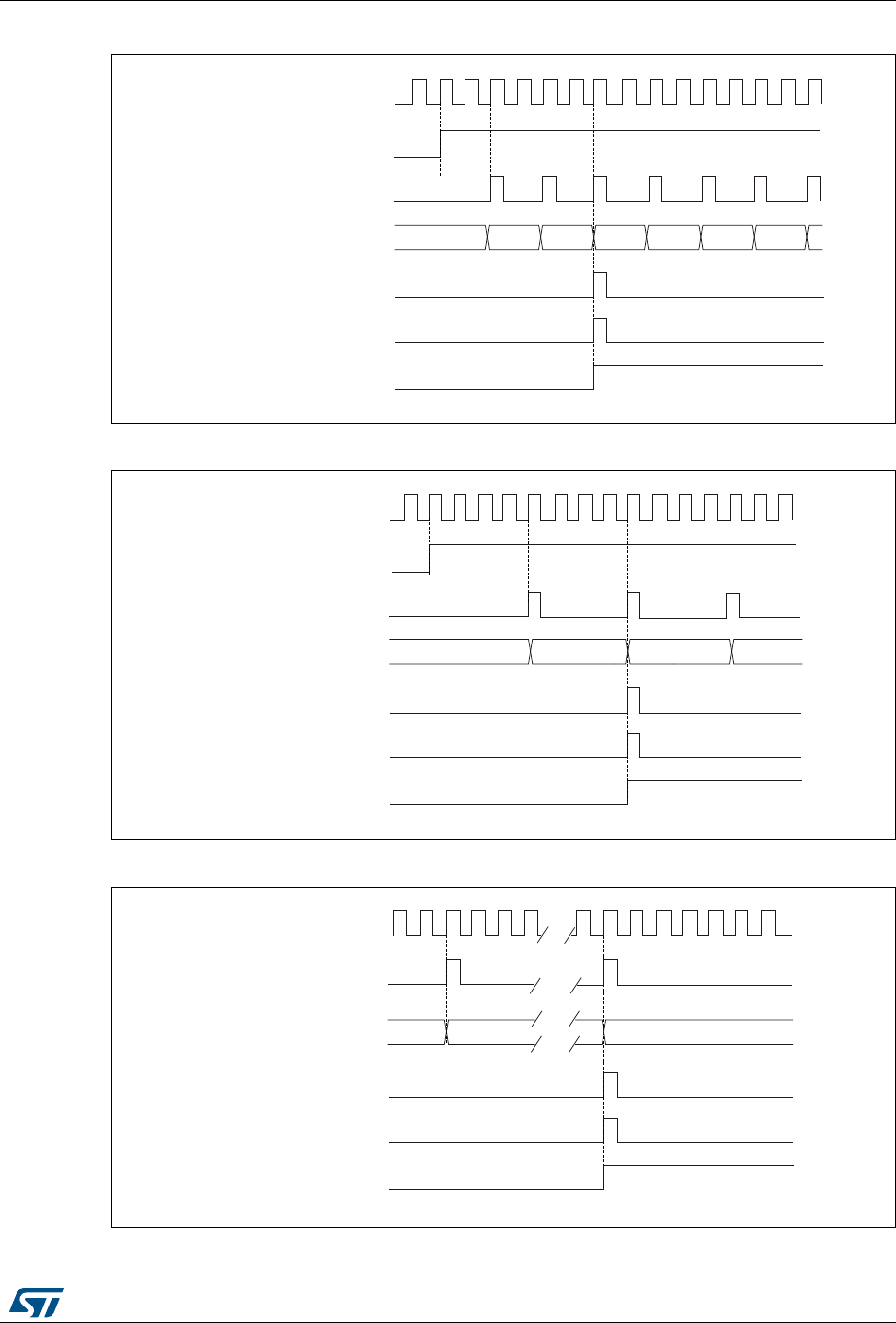
DocID027812 Rev 2 267/766
RM0401 Advanced-control timers (TIM1)
334
Figure 52. Counter timing diagram, internal clock divided by 2
Figure 53. Counter timing diagram, internal clock divided by 4
Figure 54. Counter timing diagram, internal clock divided by N
069
&.B36&
&17B(1
7LPHUFORFN &.B&17
&RXQWHUUHJLVWHU
8SGDWHHYHQW8(9
&RXQWHURYHUIORZ
8SGDWHLQWHUUXSWIODJ8,)
069
&.B36&
&17B(1
7LPHUFORFN &.B&17
&RXQWHUUHJLVWHU
8SGDWHHYHQW8(9
&RXQWHURYHUIORZ
8SGDWHLQWHUUXSWIODJ8,)
069
&.B36&
7LPHUFORFN &.B&17
&RXQWHUUHJLVWHU
8SGDWHHYHQW8(9
&RXQWHURYHUIORZ
8SGDWHLQWHUUXSWIODJ8,)
)
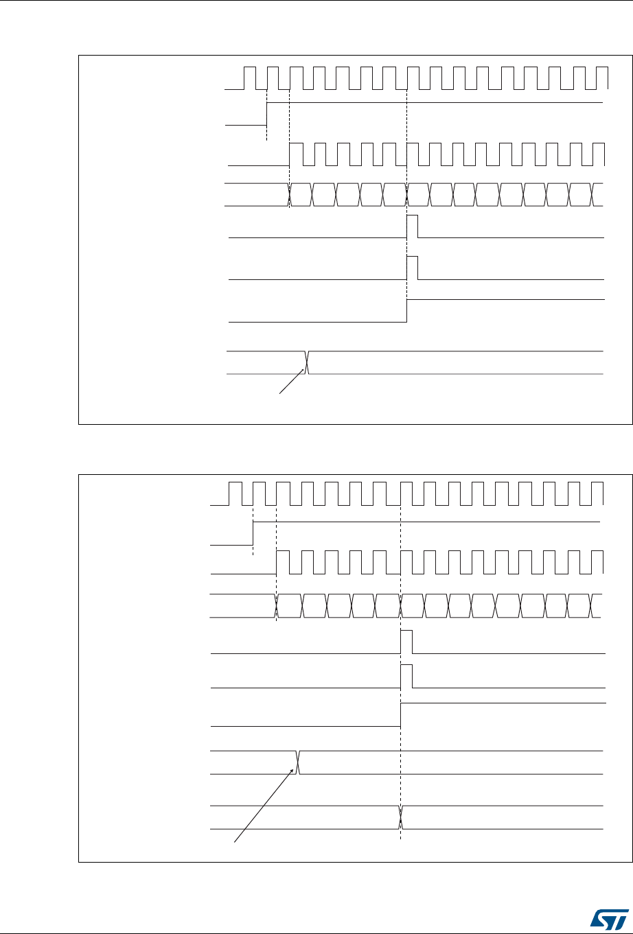
Advanced-control timers (TIM1) RM0401
268/766 DocID027812 Rev 2
Figure 55. Counter timing diagram, update event when ARPE=0
(TIMx_ARR not preloaded)
Figure 56. Counter timing diagram, update event when ARPE=1
(TIMx_ARR preloaded)
&& ϯϲ
069
<ͺW^
dŝŵĞƌĐůŽĐŬс<ͺEd
ŽƵŶƚĞƌƌĞŐŝƐƚĞƌ
hƉĚĂƚĞĞǀĞŶƚ;hsͿ
ŽƵŶƚĞƌŽǀĞƌĨůŽǁ
hƉĚĂƚĞŝŶƚĞƌƌƵƉƚĨůĂŐ;h/&Ϳ
ϬϬ ϬϮ Ϭϯ Ϭϰ Ϭϱ Ϭϲ ϬϳϯϮ ϯϯ ϯϰ ϯϱ ϯϲϯϭ Ϭϭ
E
ƵƚŽͲƌĞůŽĂĚƉƌĞůŽĂĚƌĞŐŝƐƚĞƌ
tƌŝƚĞĂŶĞǁǀĂůƵĞŝŶd/DdžͺZZ
069
)
&.B36&
7LPHUFORFN &.B&17
&RXQWHUUHJLVWHU
8SGDWHHYHQW8(9
&RXQWHURYHUIORZ
8SGDWHLQWHUUXSWIODJ
8,)
) ) ) ) ))
&(1
$XWRUHORDGSUHORDG
UHJLVWHU
:ULWHDQHZYDOXHLQ7,0[B$55
$XWRUHORDGVKDGRZ
UHJLVWHU )

DocID027812 Rev 2 269/766
RM0401 Advanced-control timers (TIM1)
334
Downcounting mode
In downcounting mode, the counter counts from the auto-reload value (content of the
TIMx_ARR register) down to 0, then restarts from the auto-reload value and generates a
counter underflow event.
If the repetition counter is used, the update event (UEV) is generated after downcounting is
repeated for the number of times programmed in the repetition counter register plus one
(TIMx_RCR+1). Else the update event is generated at each counter underflow.
Setting the UG bit in the TIMx_EGR register (by software or by using the slave mode
controller) also generates an update event.
The UEV update event can be disabled by software by setting the UDIS bit in TIMx_CR1
register. This is to avoid updating the shadow registers while writing new values in the
preload registers. Then no update event occurs until UDIS bit has been written to 0.
However, the counter restarts from the current auto-reload value, whereas the counter of the
prescaler restarts from 0 (but the prescale rate doesn’t change).
In addition, if the URS bit (update request selection) in TIMx_CR1 register is set, setting the
UG bit generates an update event UEV but without setting the UIF flag (thus no interrupt or
DMA request is sent). This is to avoid generating both update and capture interrupts when
clearing the counter on the capture event.
When an update event occurs, all the registers are updated and the update flag (UIF bit in
TIMx_SR register) is set (depending on the URS bit):
•The repetition counter is reloaded with the content of TIMx_RCR register
•The buffer of the prescaler is reloaded with the preload value (content of the TIMx_PSC
register)
•The auto-reload active register is updated with the preload value (content of the
TIMx_ARR register). Note that the auto-reload is updated before the counter is
reloaded, so that the next period is the expected one
The following figures show some examples of the counter behavior for different clock
frequencies when TIMx_ARR=0x36.
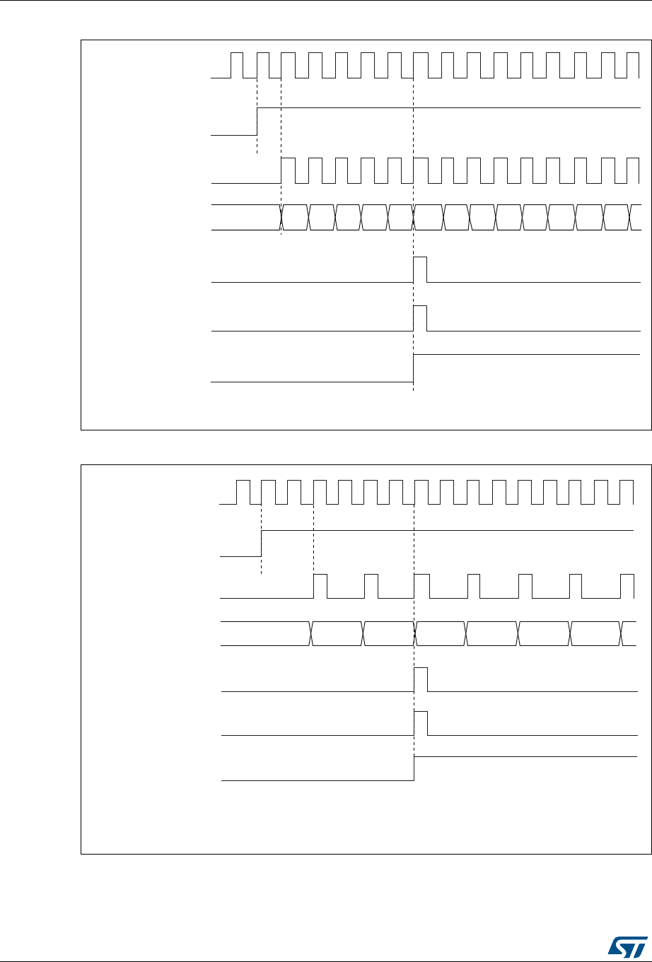
Advanced-control timers (TIM1) RM0401
270/766 DocID027812 Rev 2
Figure 57. Counter timing diagram, internal clock divided by 1
Figure 58. Counter timing diagram, internal clock divided by 2
)
069
&.B36&
&17B(1
7LPHUFORFN &.B&17
&RXQWHUUHJLVWHU
8SGDWHHYHQW8(9
&RXQWHUXQGHUIORZ
FQWBXGI
8SGDWHLQWHUUXSWIODJ
8,)
069
&.B36&
&17B(1
7LPHUFORFN &.B&17
&RXQWHUUHJLVWHU
8SGDWHHYHQW8(9
&RXQWHUXQGHUIORZ
8SGDWHLQWHUUXSWIODJ
8,)
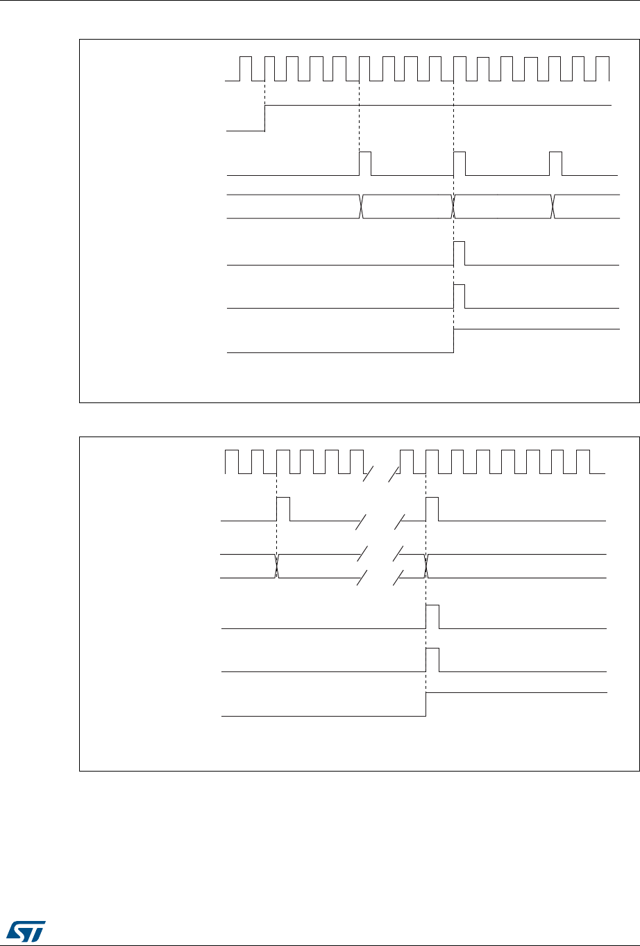
DocID027812 Rev 2 271/766
RM0401 Advanced-control timers (TIM1)
334
Figure 59. Counter timing diagram, internal clock divided by 4
Figure 60. Counter timing diagram, internal clock divided by N
069
&.B36&
7LPHUFORFN &.B&17
&RXQWHUUHJLVWHU
8SGDWHHYHQW8(9
&RXQWHUXQGHUIORZ
8SGDWHLQWHUUXSWIODJ
8,)
&17B(1
)
069
&.B36&
7LPHUFORFN &.B&17
&RXQWHUUHJLVWHU
8SGDWHHYHQW8(9
&RXQWHUXQGHUIORZ
8SGDWHLQWHUUXSWIODJ
8,)
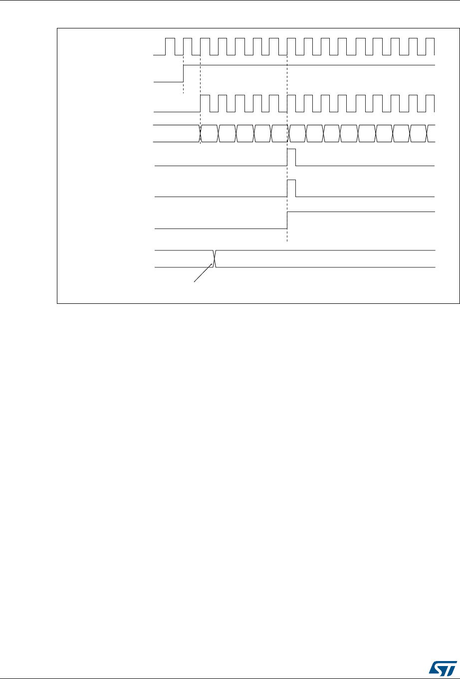
Advanced-control timers (TIM1) RM0401
272/766 DocID027812 Rev 2
Figure 61. Counter timing diagram, update event when repetition counter is not used
Center-aligned mode (up/down counting)
In center-aligned mode, the counter counts from 0 to the auto-reload value (content of the
TIMx_ARR register) – 1, generates a counter overflow event, then counts from the auto-
reload value down to 1 and generates a counter underflow event. Then it restarts counting
from 0.
Center-aligned mode is active when the CMS bits in TIMx_CR1 register are not equal to
'00'. The Output compare interrupt flag of channels configured in output is set when: the
counter counts down (Center aligned mode 1, CMS = "01"), the counter counts up (Center
aligned mode 2, CMS = "10") the counter counts up and down (Center aligned mode 3,
CMS = "11").
In this mode, the DIR direction bit in the TIMx_CR1 register cannot be written. It is updated
by hardware and gives the current direction of the counter.
The update event can be generated at each counter overflow and at each counter underflow
or by setting the UG bit in the TIMx_EGR register (by software or by using the slave mode
controller) also generates an update event. In this case, the counter restarts counting from
0, as well as the counter of the prescaler.
The UEV update event can be disabled by software by setting the UDIS bit in the TIMx_CR1
register. This is to avoid updating the shadow registers while writing new values in the
preload registers. Then no update event occurs until UDIS bit has been written to 0.
However, the counter continues counting up and down, based on the current auto-reload
value.
In addition, if the URS bit (update request selection) in TIMx_CR1 register is set, setting the
UG bit generates an UEV update event but without setting the UIF flag (thus no interrupt or
))
069
&.B36&
7LPHUFORFN &.B&17
&RXQWHUUHJLVWHU
8SGDWHHYHQW8(9
&RXQWHUXQGHUIORZ
8SGDWHLQWHUUXSWIODJ
8,)
)
&(1
$XWRUHORDGSUHORDG
UHJLVWHU
:ULWHDQHZYDOXHLQ7,0[B$55
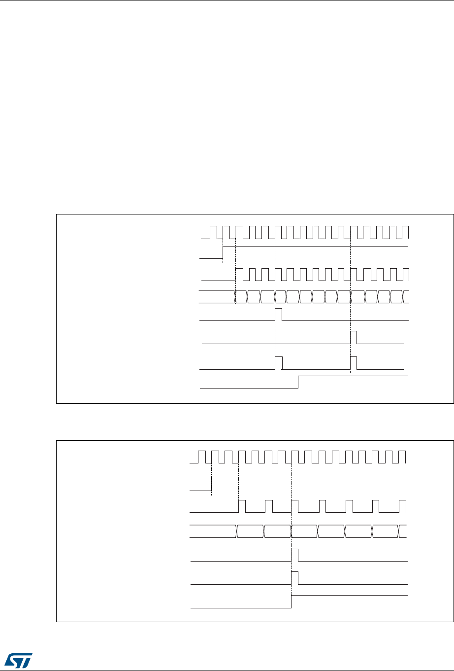
DocID027812 Rev 2 273/766
RM0401 Advanced-control timers (TIM1)
334
DMA request is sent). This is to avoid generating both update and capture interrupts when
clearing the counter on the capture event.
When an update event occurs, all the registers are updated and the update flag (UIF bit in
TIMx_SR register) is set (depending on the URS bit):
•The repetition counter is reloaded with the content of TIMx_RCR register
•The buffer of the prescaler is reloaded with the preload value (content of the TIMx_PSC
register)
•The auto-reload active register is updated with the preload value (content of the
TIMx_ARR register). Note that if the update source is a counter overflow, the auto-
reload is updated before the counter is reloaded, so that the next period is the expected
one (the counter is loaded with the new value).
The following figures show some examples of the counter behavior for different clock
frequencies.
Figure 62. Counter timing diagram, internal clock divided by 1, TIMx_ARR = 0x6
1. Here, center-aligned mode 1 is used (for more details refer to Section 14.4: TIM1 registers).
Figure 63. Counter timing diagram, internal clock divided by 2
069
&.B36&
7LPHUFORFN &.B&17
&RXQWHUUHJLVWHU
8SGDWHHYHQW8(9
&RXQWHURYHUIORZ
8SGDWHLQWHUUXSWIODJ8,)
&(1
&RXQWHUXQGHUIORZ
069
&.B36&
7LPHUFORFN &.B&17
&RXQWHUUHJLVWHU
8SGDWHHYHQW8(9
8SGDWHLQWHUUXSWIODJ8,)
&17B(1
&RXQWHUXQGHUIORZ
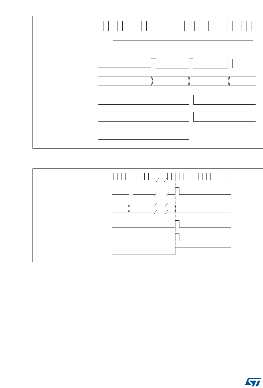
Advanced-control timers (TIM1) RM0401
274/766 DocID027812 Rev 2
Figure 64. Counter timing diagram, internal clock divided by 4, TIMx_ARR=0x36
1. Center-aligned mode 2 or 3 is used with an UIF on overflow.
Figure 65. Counter timing diagram, internal clock divided by N
069
&.B36&
7LPHUFORFN &.B&17
&RXQWHUUHJLVWHU
8SGDWHHYHQW8(9
&RXQWHURYHUIORZ
8SGDWHLQWHUUXSWIODJ8,)
&17B(1
069
&.B36&
7LPHUFORFN &.B&17
&RXQWHUUHJLVWHU
8SGDWHHYHQW8(9
8SGDWHLQWHUUXSWIODJ8,)
&RXQWHUXQGHUIORZ
)
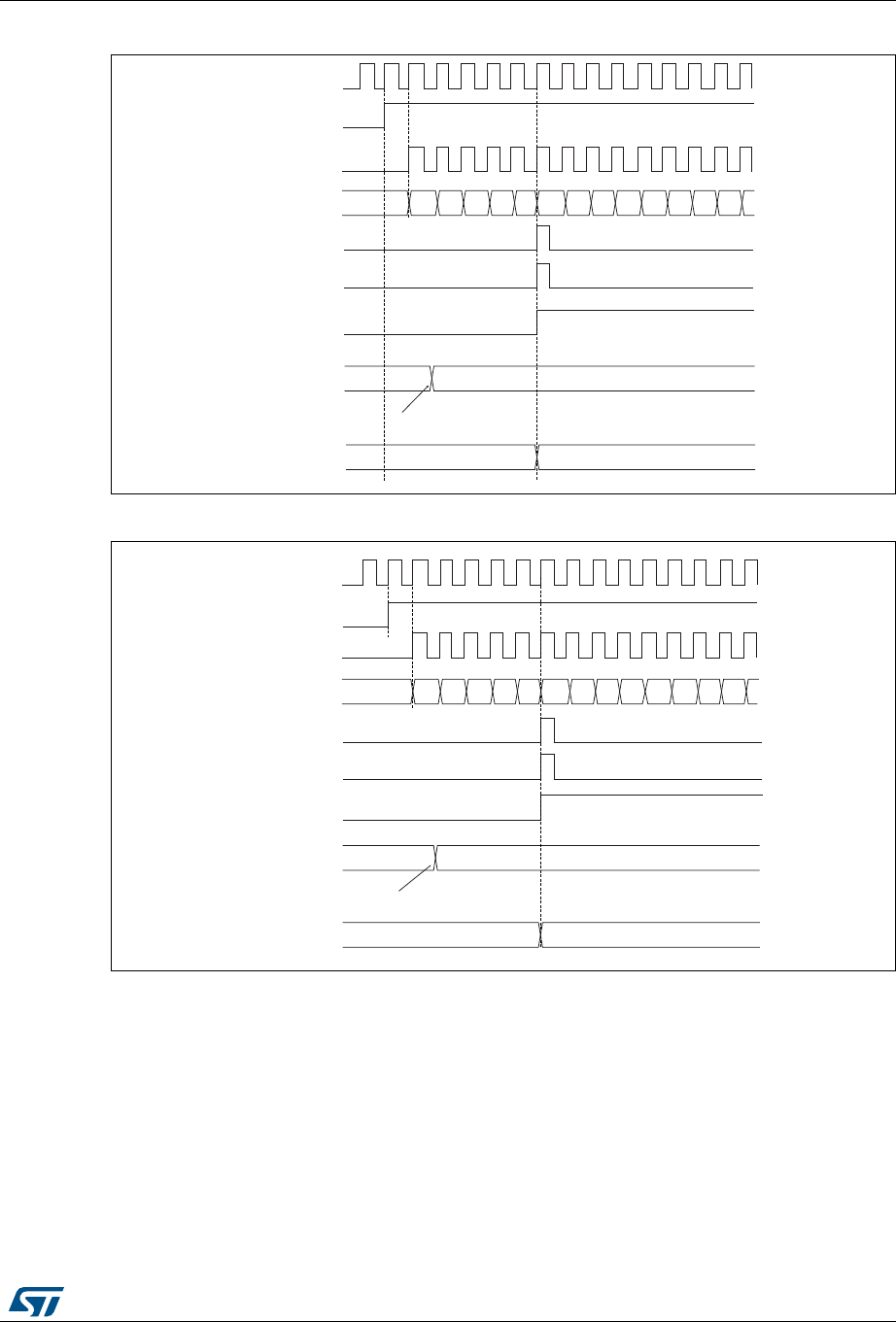
DocID027812 Rev 2 275/766
RM0401 Advanced-control timers (TIM1)
334
Figure 66. Counter timing diagram, update event with ARPE=1 (counter underflow)
Figure 67. Counter timing diagram, update event with ARPE=1 (counter overflow)
14.3.3 Repetition counter
Section 14.3.1: Time-base unit describes how the update event (UEV) is generated with
respect to the counter overflows/underflows. It is actually generated only when the repetition
counter has reached zero. This can be useful when generating PWM signals.
This means that data are transferred from the preload registers to the shadow registers
(TIMx_ARR auto-reload register, TIMx_PSC prescaler register, but also TIMx_CCRx
capture/compare registers in compare mode) every N+1 counter overflows or underflows,
where N is the value in the TIMx_RCR repetition counter register.
069
&.B36&
7LPHUFORFN &.B&17
&RXQWHUUHJLVWHU
8SGDWHHYHQW8(9
&RXQWHURYHUIORZ
8SGDWHLQWHUUXSWIODJ8,)
&(1
$XWRUHORDGSUHORDGUHJLVWHU
:ULWHDQHZYDOXHLQ7,0[B$55
$XWRUHORDGDFWLYHUHJLVWHU
)'
)'
069
)'
&.B36&
7LPHUFORFN &.B&17
&RXQWHUUHJLVWHU
8SGDWHHYHQW8(9
&RXQWHURYHUIORZ
8SGDWHLQWHUUXSWIODJ8,)
)) ) )$ )% )&)
&(1
$XWRUHORDGSUHORDGUHJLVWHU
:ULWHDQHZYDOXHLQ7,0[B$55
$XWRUHORDGDFWLYHUHJLVWHU )'
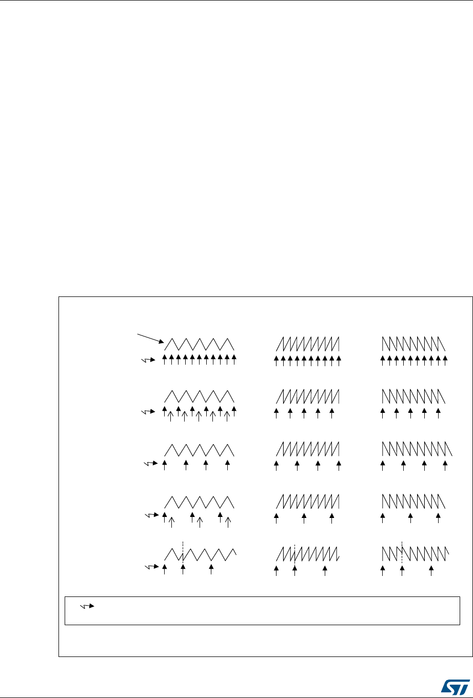
Advanced-control timers (TIM1) RM0401
276/766 DocID027812 Rev 2
The repetition counter is decremented:
•At each counter overflow in upcounting mode,
•At each counter underflow in downcounting mode,
•At each counter overflow and at each counter underflow in center-aligned mode.
Although this limits the maximum number of repetition to 128 PWM cycles, it makes it
possible to update the duty cycle twice per PWM period. When refreshing compare
registers only once per PWM period in center-aligned mode, maximum resolution is
2xTck, due to the symmetry of the pattern.
The repetition counter is an auto-reload type; the repetition rate is maintained as defined by
the TIMx_RCR register value (refer to Figure 68). When the update event is generated by
software (by setting the UG bit in TIMx_EGR register) or by hardware through the slave
mode controller, it occurs immediately whatever the value of the repetition counter is and the
repetition counter is reloaded with the content of the TIMx_RCR register.
In center-aligned mode, for odd values of RCR, the update event occurs either on the
overflow or on the underflow depending on when the RCR register was written and when
the counter was started. If the RCR was written before starting the counter, the UEV occurs
on the overflow. If the RCR was written after starting the counter, the UEV occurs on the
underflow. For example for RCR = 3, the UEV is generated on each 4th overflow or
underflow event depending on when RCR was written.
Figure 68. Update rate examples depending on mode and TIMx_RCR register settings
06Y9
8(9
8(9
8(9
8(9
8(9
&RXQWHUDOLJQHGPRGH (GJHDOLJQHGPRGH
8SFRXQWLQJ 'RZQFRXQWLQJ
E\6:E\6:E\6:
7,0[B5&5
DQG
UHV\QFKURQL]DWLRQ
7,0[B5&5
7,0[B5&5
7,0[B5&5
7,0[B5&5
&RXQWHU
7,0[B&17
8(9 8SGDWHHYHQW3UHORDGUHJLVWHUVWUDQVIHUUHGWRDFWLYHUHJLVWHUVDQGXSGDWHLQWHUUXSWJHQHUDWHG
8SGDWH(YHQWLIWKHUHSHWLWLRQFRXQWHUXQGHUIORZRFFXUVZKHQWKHFRXQWHULVHTXDOWRWKHDXWRUHORDGYDOXH
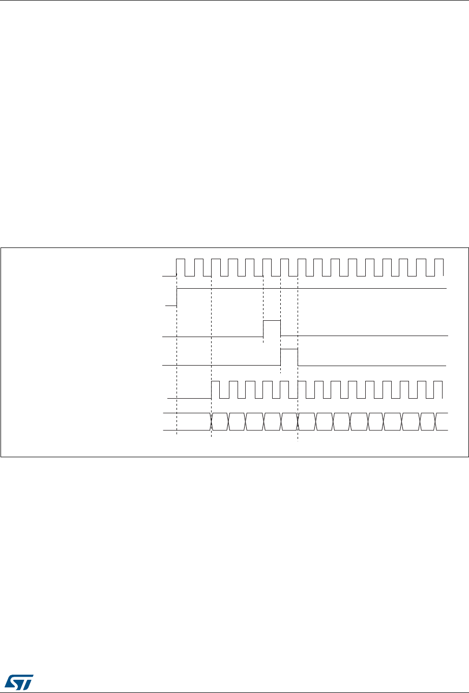
DocID027812 Rev 2 277/766
RM0401 Advanced-control timers (TIM1)
334
14.3.4 Clock selection
The counter clock can be provided by the following clock sources:
•Internal clock (CK_INT)
•External clock mode1: external input pin
•External clock mode2: external trigger input ETR
•Internal trigger inputs (ITRx): using one timer as prescaler for another timer
Internal clock source (CK_INT)
If the slave mode controller is disabled (SMS=000), then the CEN, DIR (in the TIMx_CR1
register) and UG bits (in the TIMx_EGR register) are actual control bits and can be changed
only by software (except UG which remains cleared automatically). As soon as the CEN bit
is written to 1, the prescaler is clocked by the internal clock CK_INT.
Figure 69 shows the behavior of the control circuit and the upcounter in normal mode,
without prescaler.
Figure 69. Control circuit in normal mode, internal clock divided by 1
External clock source mode 1
This mode is selected when SMS=111 in the TIMx_SMCR register. The counter can count at
each rising or falling edge on a selected input.
,QWHUQDOFORFN
&RXQWHUFORFN &.B&17 &.B36&
&RXQWHUUHJLVWHU
&(1 &17B(1
8*
&17B,1,7
069
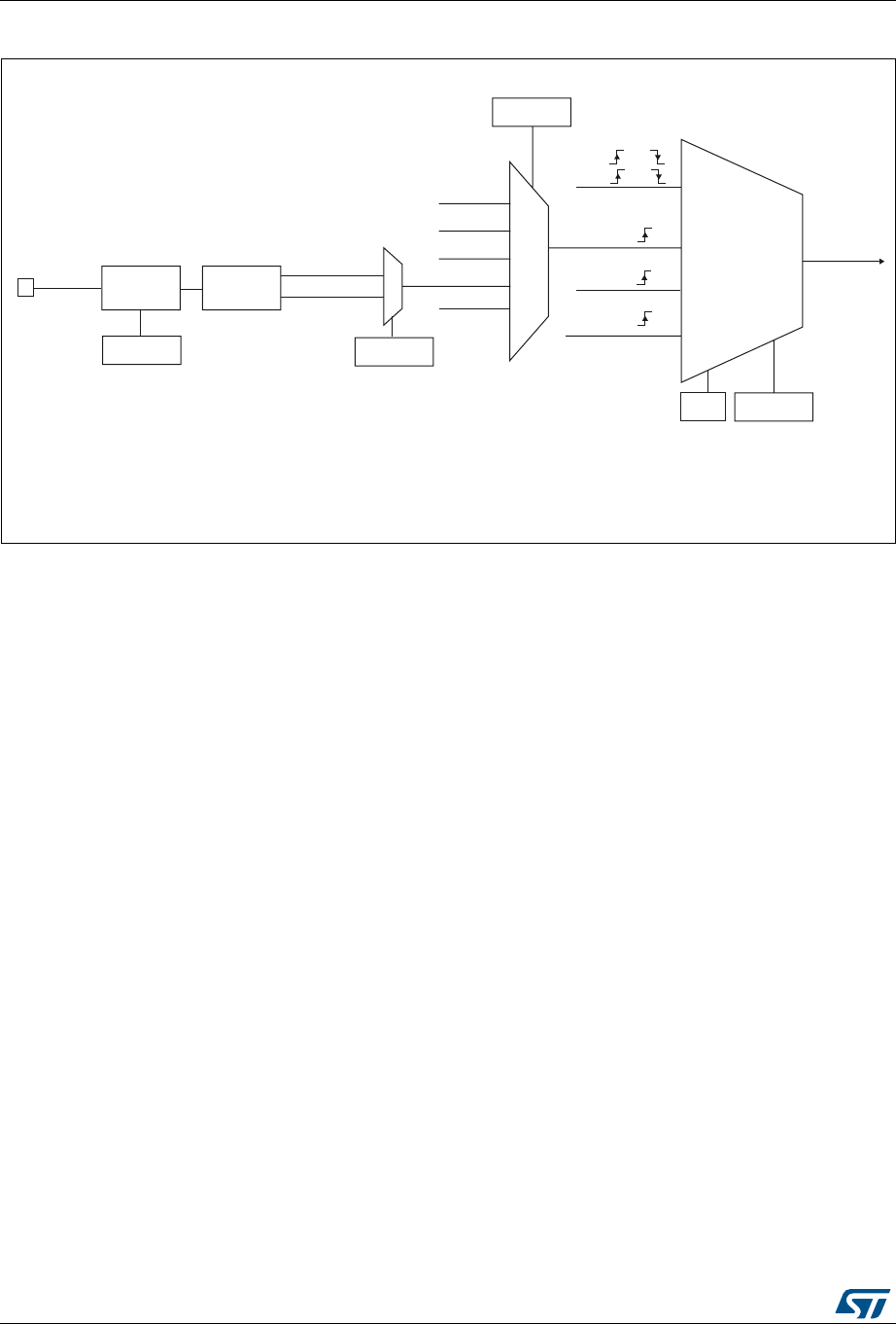
Advanced-control timers (TIM1) RM0401
278/766 DocID027812 Rev 2
Figure 70. TI2 external clock connection example
For example, to configure the upcounter to count in response to a rising edge on the TI2
input, use the following procedure:
1. Configure channel 2 to detect rising edges on the TI2 input by writing CC2S = ‘01’ in
the TIMx_CCMR1 register.
2. Configure the input filter duration by writing the IC2F[3:0] bits in the TIMx_CCMR1
register (if no filter is needed, keep IC2F=0000).
3. Select rising edge polarity by writing CC2P=0 and CC2NP=0 in the TIMx_CCER
register.
4. Configure the timer in external clock mode 1 by writing SMS=111 in the TIMx_SMCR
register.
5. Select TI2 as the trigger input source by writing TS=110 in the TIMx_SMCR register.
6. Enable the counter by writing CEN=1 in the TIMx_CR1 register.
Note: The capture prescaler is not used for triggering, so you don’t need to configure it.
When a rising edge occurs on TI2, the counter counts once and the TIF flag is set.
The delay between the rising edge on TI2 and the actual clock of the counter is due to the
resynchronization circuit on TI2 input.
([WHUQDOFORFN
PRGH
,QWHUQDOFORFN
PRGH
75*,
&.B,17
&.B36&
7,0[B60&5
606>@
,75[
7,B('
7,)3
7,)3
7,0[B60&5
76>@
7,
7,0[B&&(5
&&3
)LOWHU
,&)>@
7,0[B&&05
(GJH
GHWHFWRU
7,)B5LVLQJ
7,)B)DOOLQJ
[[
069
LQWHUQDOFORFN
7,) RU
7,) RU
RU
(QFRGHU
PRGH
(75)
([WHUQDOFORFN
PRGH
(75)
(&(
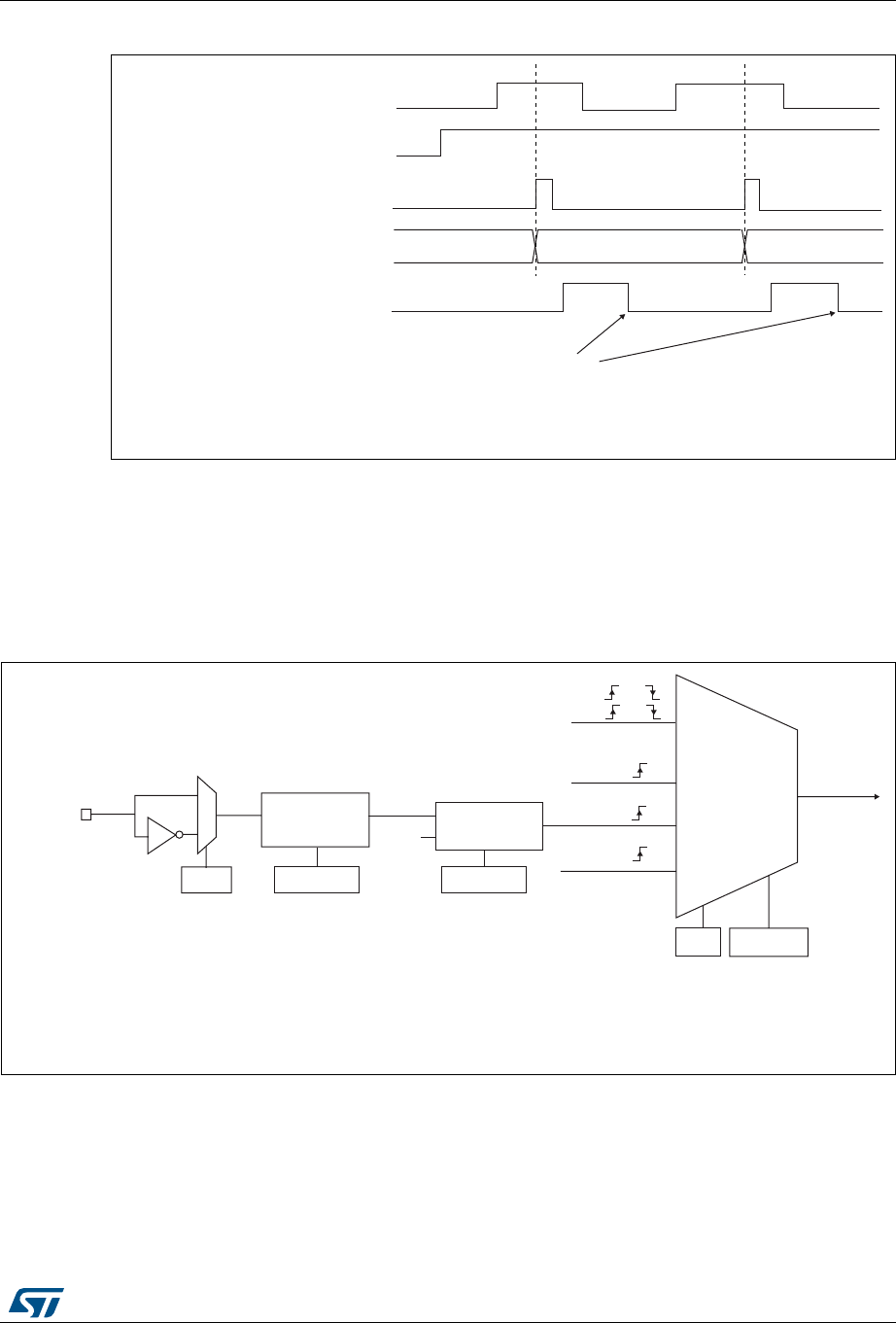
DocID027812 Rev 2 279/766
RM0401 Advanced-control timers (TIM1)
334
Figure 71. Control circuit in external clock mode 1
External clock source mode 2
This mode is selected by writing ECE=1 in the TIMx_SMCR register.
The counter can count at each rising or falling edge on the external trigger input ETR.
Figure 72 gives an overview of the external trigger input block.
Figure 72. External trigger input block
For example, to configure the upcounter to count each 2 rising edges on ETR, use the
following procedure:
&RXQWHUFORFN &.B&17 &.B36&
&RXQWHUUHJLVWHU
7,
&17B(1
7,)
:ULWH7,)
069
([WHUQDOFORFN
PRGH
,QWHUQDOFORFN
PRGH
75*,
&.B,17
&.B36&
7,0[B60&5
606>@
069
LQWHUQDOFORFN
7,) RU
7,) RU
RU
(QFRGHU
PRGH
([WHUQDOFORFN
PRGH
(75)
(&(
7,0[B60&5
(73
(75SLQ
(75
'LYLGHU
)LOWHU
GRZQFRXQWHU
I
(753
7,0[B60&5
(736>@
7,0[B60&5
(7)>@
'76
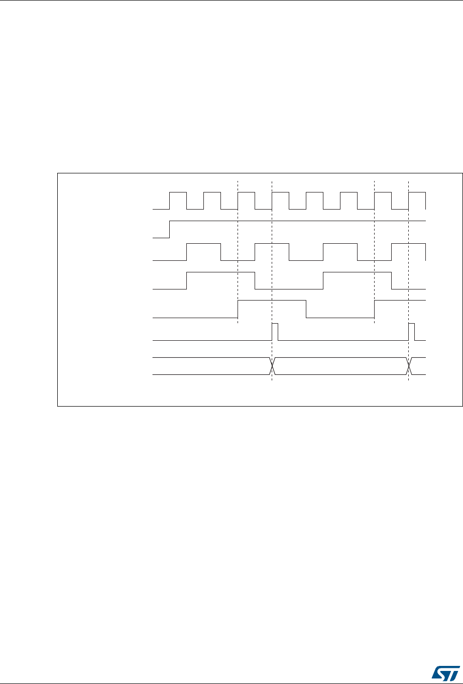
Advanced-control timers (TIM1) RM0401
280/766 DocID027812 Rev 2
1. As no filter is needed in this example, write ETF[3:0]=0000 in the TIMx_SMCR register.
2. Set the prescaler by writing ETPS[1:0]=01 in the TIMx_SMCR register
3. Select rising edge detection on the ETR pin by writing ETP=0 in the TIMx_SMCR
register
4. Enable external clock mode 2 by writing ECE=1 in the TIMx_SMCR register.
5. Enable the counter by writing CEN=1 in the TIMx_CR1 register.
The counter counts once each 2 ETR rising edges.
The delay between the rising edge on ETR and the actual clock of the counter is due to the
resynchronization circuit on the ETRP signal.
Figure 73. Control circuit in external clock mode 2
14.3.5 Capture/compare channels
Each Capture/Compare channel is built around a capture/compare register (including a
shadow register), a input stage for capture (with digital filter, multiplexing and prescaler) and
an output stage (with comparator and output control).
Figure 74 to Figure 77 give an overview of one Capture/Compare channel.
The input stage samples the corresponding TIx input to generate a filtered signal TIxF.
Then, an edge detector with polarity selection generates a signal (TIxFPx) which can be
used as trigger input by the slave mode controller or as the capture command. It is
prescaled before the capture register (ICxPS).
069
I&.B,17
&17B(1
(75
(753
(75)
&RXQWHUFORFN
&.B,17 &.B36&
&RXQWHUUHJLVWHU
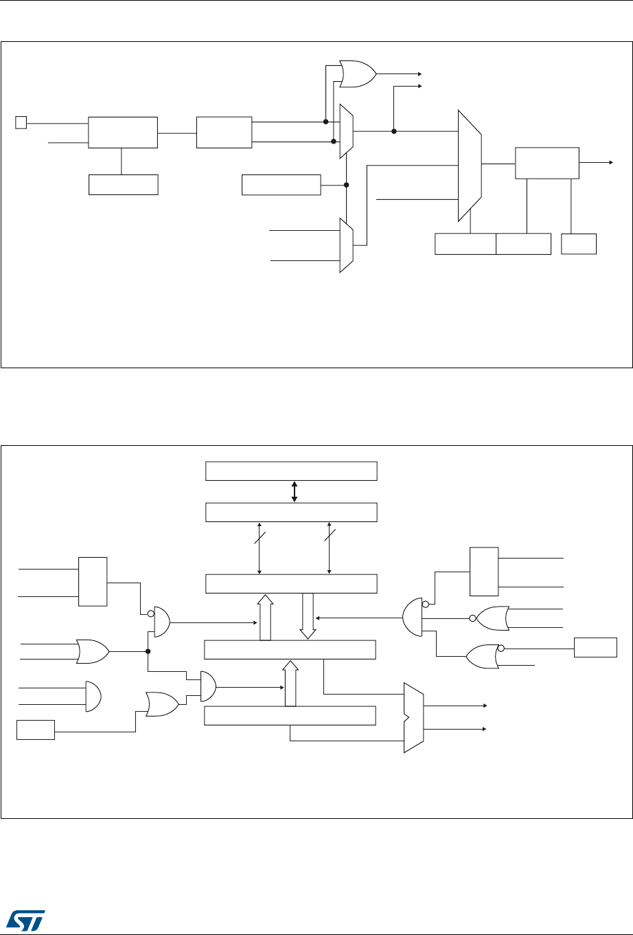
DocID027812 Rev 2 281/766
RM0401 Advanced-control timers (TIM1)
334
Figure 74. Capture/compare channel (example: channel 1 input stage)
The output stage generates an intermediate waveform which is then used for reference:
OCxRef (active high). The polarity acts at the end of the chain.
Figure 75. Capture/compare channel 1 main circuit
'LYLGHU
,&36>@
7,)B('
7RWKHVODYHPRGHFRQWUROOHU
7,)3
&&6>@
,&
7,)3
75&
IURPVODYHPRGH
FRQWUROOHU
,&36
069
7,
7,0[B&&(5
&&3&&13
)LOWHU
GRZQFRXQWHU
,&)>@
7,0[B&&05
(GJH
GHWHFWRU
7,)B5LVLQJ
7,)B)DOOLQJ
7,0[B&&05
7,0[B&&(5
7,)B5LVLQJ
IURPFKDQQHO
7,)B)DOOLQJ
IURPFKDQQHO
7,)
I
&&(
'76
&&(
&DSWXUHFRPSDUHVKDGRZUHJLVWHU
&RPSDUDWRU
&DSWXUHFRPSDUHSUHORDGUHJLVWHU
&RXQWHU
,&36
&&6>@
&&6>@
&DSWXUH
,QSXW
PRGH
6
5
5HDG&&5+
5HDG&&5/
UHDGBLQBSURJUHVV
FDSWXUHBWUDQVIHU &&6>@
&&6>@
6
5
ZULWH&&5+
ZULWH&&5/
ZULWHBLQBSURJUHVV
2XWSXW
PRGH
8(9
2&3(
IURPWLPH
EDVHXQLW
FRPSDUHBWUDQVIHU
$3%%XV
KLJK
ORZ
LIELW
0&8SHULSKHUDOLQWHUIDFH
7,0B&&05
2&3(
&17!&&5
&17 &&5
7,0B(*5
&&*
069
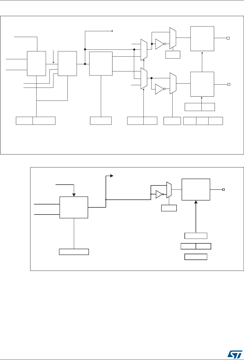
Advanced-control timers (TIM1) RM0401
282/766 DocID027812 Rev 2
Figure 76. Output stage of capture/compare channel (channels 1 to 3)
Figure 77. Output stage of capture/compare channel (channel 4)
The capture/compare block is made of one preload register and one shadow register. Write
and read always access the preload register.
In capture mode, captures are actually done in the shadow register, which is copied into the
preload register.
In compare mode, the content of the preload register is copied into the shadow register
which is compared to the counter.
069
2XWSXW
PRGH
FRQWUROOHU
&17!&&5
&17 &&5
7,0B&&05
2&0>@
2&5()
2&&(
'HDGWLPH
JHQHUDWRU
2&B'7
2&1B'7
'7*>@
7,0B%'75
µ
µ
&&(
7,0B&&(5
&&1(
&&3
7,0B&&(5
&&13
7,0B&&(5
2&
2XWSXW
HQDEOH
FLUFXLW
2&1
&&( 7,0B&&(5
&&1(
266,
7,0B%'75
02( 2665
[
[
2XWSXW
VHOHFWRU
2&[5()
2&5()&
7RWKHPDVWHUPRGH
FRQWUROOHU
2XWSXW
HQDEOH
FLUFXLW
2&5()
(75)
069
2XWSXW
PRGH
FRQWUROOHU
7,0B&&05
2&0>@
2&5()
&&3
7,0B&&(5
2&
7RWKHPDVWHU
PRGHFRQWUROOHU 2XWSXW
HQDEOH
FLUFXLW
(75
&17!&&5
&17!&&5
7,0B&&(5
7,0B%'75
7,0B&5
266,02(
&&(
2,6

DocID027812 Rev 2 283/766
RM0401 Advanced-control timers (TIM1)
334
14.3.6 Input capture mode
In Input capture mode, the Capture/Compare Registers (TIMx_CCRx) are used to latch the
value of the counter after a transition detected by the corresponding ICx signal. When a
capture occurs, the corresponding CCXIF flag (TIMx_SR register) is set and an interrupt or
a DMA request can be sent if they are enabled. If a capture occurs while the CCxIF flag was
already high, then the over-capture flag CCxOF (TIMx_SR register) is set. CCxIF can be
cleared by software by writing it to ‘0’ or by reading the captured data stored in the
TIMx_CCRx register. CCxOF is cleared when you write it to ‘0’.
The following example shows how to capture the counter value in TIMx_CCR1 when TI1
input rises. To do this, use the following procedure:
•Select the active input: TIMx_CCR1 must be linked to the TI1 input, so write the CC1S
bits to 01 in the TIMx_CCMR1 register. As soon as CC1S becomes different from 00,
the channel is configured in input and the TIMx_CCR1 register becomes read-only.
•Program the input filter duration you need with respect to the signal you connect to the
timer (by programming ICxF bits in the TIMx_CCMRx register if the input is a TIx input).
Let’s imagine that, when toggling, the input signal is not stable during at must 5 internal
clock cycles. We must program a filter duration longer than these 5 clock cycles. We
can validate a transition on TI1 when 8 consecutive samples with the new level have
been detected (sampled at fDTS frequency). Then write IC1F bits to 0011 in the
TIMx_CCMR1 register.
•Select the edge of the active transition on the TI1 channel by writing CC1P and CC1NP
bits to 0 in the TIMx_CCER register (rising edge in this case).
•Program the input prescaler. In our example, we wish the capture to be performed at
each valid transition, so the prescaler is disabled (write IC1PS bits to ‘00’ in the
TIMx_CCMR1 register).
•Enable capture from the counter into the capture register by setting the CC1E bit in the
TIMx_CCER register.
•If needed, enable the related interrupt request by setting the CC1IE bit in the
TIMx_DIER register, and/or the DMA request by setting the CC1DE bit in the
TIMx_DIER register.
When an input capture occurs:
•The TIMx_CCR1 register gets the value of the counter on the active transition.
•CC1IF flag is set (interrupt flag). CC1OF is also set if at least two consecutive captures
occurred whereas the flag was not cleared.
•An interrupt is generated depending on the CC1IE bit.
•A DMA request is generated depending on the CC1DE bit.
In order to handle the overcapture, it is recommended to read the data before the
overcapture flag. This is to avoid missing an overcapture which could happen after reading
the flag and before reading the data.
Note: IC interrupt and/or DMA requests can be generated by software by setting the
corresponding CCxG bit in the TIMx_EGR register.
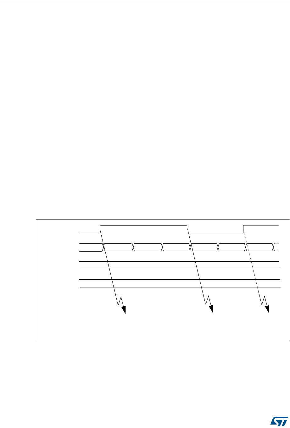
Advanced-control timers (TIM1) RM0401
284/766 DocID027812 Rev 2
14.3.7 PWM input mode
This mode is a particular case of input capture mode. The procedure is the same except:
•Two ICx signals are mapped on the same TIx input.
•These 2 ICx signals are active on edges with opposite polarity.
•One of the two TIxFP signals is selected as trigger input and the slave mode controller
is configured in reset mode.
For example, you can measure the period (in TIMx_CCR1 register) and the duty cycle (in
TIMx_CCR2 register) of the PWM applied on TI1 using the following procedure (depending
on CK_INT frequency and prescaler value):
•Select the active input for TIMx_CCR1: write the CC1S bits to 01 in the TIMx_CCMR1
register (TI1 selected).
•Select the active polarity for TI1FP1 (used both for capture in TIMx_CCR1 and counter
clear): write the CC1P and CC1NP bits to ‘0’ (active on rising edge).
•Select the active input for TIMx_CCR2: write the CC2S bits to 10 in the TIMx_CCMR1
register (TI1 selected).
•Select the active polarity for TI1FP2 (used for capture in TIMx_CCR2): write the CC2P
and CC2NP bits to ‘1’ (active on falling edge).
•Select the valid trigger input: write the TS bits to 101 in the TIMx_SMCR register
(TI1FP1 selected).
•Configure the slave mode controller in reset mode: write the SMS bits to 100 in the
TIMx_SMCR register.
•Enable the captures: write the CC1E and CC2E bits to ‘1’ in the TIMx_CCER register.
Figure 78. PWM input mode timing
14.3.8 Forced output mode
In output mode (CCxS bits = 00 in the TIMx_CCMRx register), each output compare signal
(OCxREF and then OCx/OCxN) can be forced to active or inactive level directly by software,
independently of any comparison between the output compare register and the counter.
TI1
TIMx_CNT 0000 0001 0002 0003 0004 00000004
TIMx_CCR1
TIMx_CCR2
0004
0002
IC1 capture
IC2 capture
reset counter
IC2 capture
pulse width
IC1 capture
period
measurementmeasurement
ai15413

DocID027812 Rev 2 285/766
RM0401 Advanced-control timers (TIM1)
334
To force an output compare signal (OCXREF/OCx) to its active level, you just need to write
101 in the OCxM bits in the corresponding TIMx_CCMRx register. Thus OCXREF is forced
high (OCxREF is always active high) and OCx get opposite value to CCxP polarity bit.
For example: CCxP=0 (OCx active high) => OCx is forced to high level.
The OCxREF signal can be forced low by writing the OCxM bits to 100 in the TIMx_CCMRx
register.
Anyway, the comparison between the TIMx_CCRx shadow register and the counter is still
performed and allows the flag to be set. Interrupt and DMA requests can be sent
accordingly. This is described in the output compare mode section below.
14.3.9 Output compare mode
This function is used to control an output waveform or indicating when a period of time has
elapsed.
When a match is found between the capture/compare register and the counter, the output
compare function:
•Assigns the corresponding output pin to a programmable value defined by the output
compare mode (OCxM bits in the TIMx_CCMRx register) and the output polarity (CCxP
bit in the TIMx_CCER register). The output pin can keep its level (OCXM=000), be set
active (OCxM=001), be set inactive (OCxM=010) or can toggle (OCxM=011) on match.
•Sets a flag in the interrupt status register (CCxIF bit in the TIMx_SR register).
•Generates an interrupt if the corresponding interrupt mask is set (CCXIE bit in the
TIMx_DIER register).
•Sends a DMA request if the corresponding enable bit is set (CCxDE bit in the
TIMx_DIER register, CCDS bit in the TIMx_CR2 register for the DMA request
selection).
The TIMx_CCRx registers can be programmed with or without preload registers using the
OCxPE bit in the TIMx_CCMRx register.
In output compare mode, the update event UEV has no effect on OCxREF and OCx output.
The timing resolution is one count of the counter. Output compare mode can also be used to
output a single pulse (in One Pulse mode).
Procedure:
1. Select the counter clock (internal, external, prescaler).
2. Write the desired data in the TIMx_ARR and TIMx_CCRx registers.
3. Set the CCxIE bit if an interrupt request is to be generated.
4. Select the output mode. For example:
– Write OCxM = 011 to toggle OCx output pin when CNT matches CCRx
– Write OCxPE = 0 to disable preload register
– Write CCxP = 0 to select active high polarity
– Write CCxE = 1 to enable the output
5. Enable the counter by setting the CEN bit in the TIMx_CR1 register.
The TIMx_CCRx register can be updated at any time by software to control the output
waveform, provided that the preload register is not enabled (OCxPE=’0’, else TIMx_CCRx
shadow register is updated only at the next update event UEV). An example is given in
Figure 79.

Advanced-control timers (TIM1) RM0401
286/766 DocID027812 Rev 2
Figure 79. Output compare mode, toggle on OC1.
14.3.10 PWM mode
Pulse Width Modulation mode allows you to generate a signal with a frequency determined
by the value of the TIMx_ARR register and a duty cycle determined by the value of the
TIMx_CCRx register.
The PWM mode can be selected independently on each channel (one PWM per OCx
output) by writing ‘110’ (PWM mode 1) or ‘111’ (PWM mode 2) in the OCxM bits in the
TIMx_CCMRx register. You must enable the corresponding preload register by setting the
OCxPE bit in the TIMx_CCMRx register, and eventually the auto-reload preload register (in
upcounting or center-aligned modes) by setting the ARPE bit in the TIMx_CR1 register.
As the preload registers are transferred to the shadow registers only when an update event
occurs, before starting the counter, you have to initialize all the registers by setting the UG
bit in the TIMx_EGR register.
OCx polarity is software programmable using the CCxP bit in the TIMx_CCER register. It
can be programmed as active high or active low. OCx output is enabled by a combination of
the CCxE, CCxNE, MOE, OSSI and OSSR bits (TIMx_CCER and TIMx_BDTR registers).
Refer to the TIMx_CCER register description for more details.
In PWM mode (1 or 2), TIMx_CNT and TIMx_CCRx are always compared to determine
whether TIMx_CCRx ≤ TIMx_CNT or TIMx_CNT ≤ TIMx_CCRx (depending on the direction
of the counter).
The timer is able to generate PWM in edge-aligned mode or center-aligned mode
depending on the CMS bits in the TIMx_CR1 register.
069
2&5() 2&
7,0B&17 % %
7,0B&&5 $
:ULWH%KLQWKH&&5UHJLVWHU
0DWFKGHWHFWHGRQ&&5
,QWHUUXSWJHQHUDWHGLIHQDEOHG
%
%
$
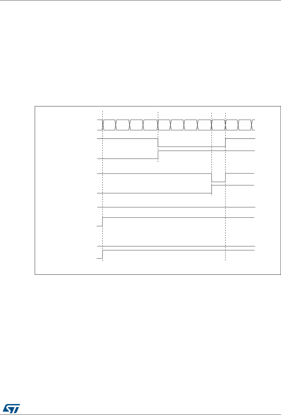
DocID027812 Rev 2 287/766
RM0401 Advanced-control timers (TIM1)
334
PWM edge-aligned mode
•Upcounting configuration
Upcounting is active when the DIR bit in the TIMx_CR1 register is low. Refer to
Upcounting mode.
In the following example, we consider PWM mode 1. The reference PWM signal
OCxREF is high as long as TIMx_CNT < TIMx_CCRx else it becomes low. If the
compare value in TIMx_CCRx is greater than the auto-reload value (in TIMx_ARR)
then OCxREF is held at ‘1’. If the compare value is 0 then OCxRef is held at ‘0’.
Figure 80 shows some edge-aligned PWM waveforms in an example where
TIMx_ARR=8.
Figure 80. Edge-aligned PWM waveforms (ARR=8)
•Downcounting configuration
Downcounting is active when DIR bit in TIMx_CR1 register is high. Refer to
Downcounting mode.
In PWM mode 1, the reference signal OCxRef is low as long as
TIMx_CNT > TIMx_CCRx else it becomes high. If the compare value in TIMx_CCRx is
greater than the auto-reload value in TIMx_ARR, then OCxREF is held at ‘1’. 0% PWM
is not possible in this mode.
PWM center-aligned mode
Center-aligned mode is active when the CMS bits in TIMx_CR1 register are different from
‘00’ (all the remaining configurations having the same effect on the OCxRef/OCx signals).
The compare flag is set when the counter counts up, when it counts down or both when it
counts up and down depending on the CMS bits configuration. The direction bit (DIR) in the
TIMx_CR1 register is updated by hardware and must not be changed by software. Refer to
Center-aligned mode (up/down counting).
069
&RXQWHUUHJLVWHU
µ
2&;5()
&&[,)
2&;5()
&&[,)
2&;5()
&&[,)
2&;5()
&&[,)
&&5[
&&5[
&&5[!
&&5[
µ
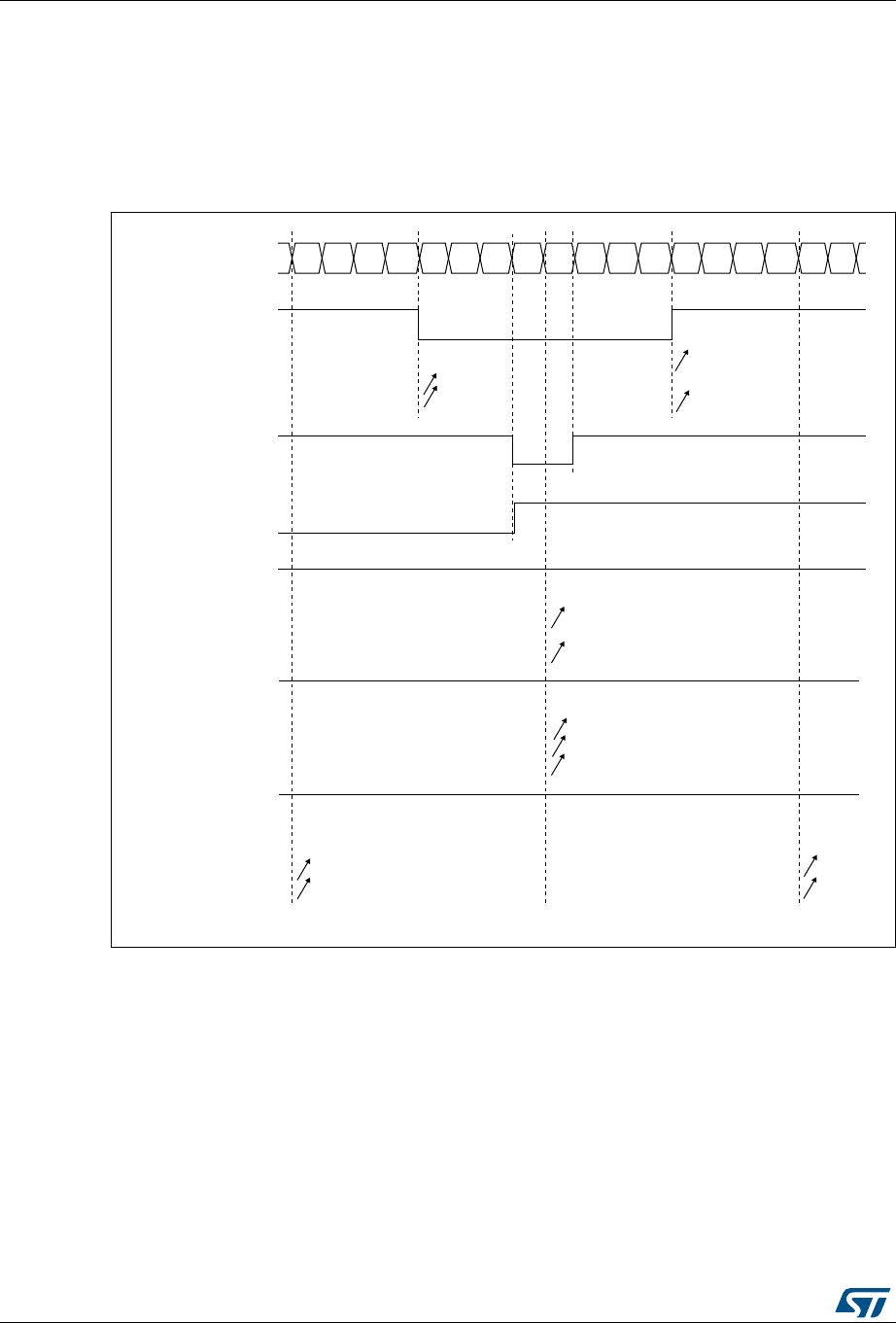
Advanced-control timers (TIM1) RM0401
288/766 DocID027812 Rev 2
Figure 81 shows some center-aligned PWM waveforms in an example where:
•TIMx_ARR=8,
•PWM mode is the PWM mode 1,
•The flag is set when the counter counts down corresponding to the center-aligned
mode 1 selected for CMS=01 in TIMx_CR1 register.
Figure 81. Center-aligned PWM waveforms (ARR=8)
Hints on using center-aligned mode:
•When starting in center-aligned mode, the current up-down configuration is used. It
means that the counter counts up or down depending on the value written in the DIR bit
&&[,)
&RXQWHUUHJLVWHU
&&5[
2&[5()
&06
&06
&06
&&[,)
&&5[
2&[5()
&06 RU
&&[,)
&&5[
2&[5()
&06
&06
&06
µ
&&[,)
&&5[!
2&[5()
&06
&06
&06
µ
&&[,)
&&5[
2&[5()
&06
&06
&06
µ
$,E

DocID027812 Rev 2 289/766
RM0401 Advanced-control timers (TIM1)
334
in the TIMx_CR1 register. Moreover, the DIR and CMS bits must not be changed at the
same time by the software.
•Writing to the counter while running in center-aligned mode is not recommended as it
can lead to unexpected results. In particular:
– The direction is not updated if you write a value in the counter that is greater than
the auto-reload value (TIMx_CNT>TIMx_ARR). For example, if the counter was
counting up, it continues to count up.
– The direction is updated if you write 0 or write the TIMx_ARR value in the counter
but no Update Event UEV is generated.
•The safest way to use center-aligned mode is to generate an update by software
(setting the UG bit in the TIMx_EGR register) just before starting the counter and not to
write the counter while it is running.
14.3.11 Complementary outputs and dead-time insertion
The advanced-control timers (TIM1) can output two complementary signals and manage the
switching-off and the switching-on instants of the outputs.
This time is generally known as dead-time and you have to adjust it depending on the
devices you have connected to the outputs and their characteristics (intrinsic delays of level-
shifters, delays due to power switches...)
You can select the polarity of the outputs (main output OCx or complementary OCxN)
independently for each output. This is done by writing to the CCxP and CCxNP bits in the
TIMx_CCER register.
The complementary signals OCx and OCxN are activated by a combination of several
control bits: the CCxE and CCxNE bits in the TIMx_CCER register and the MOE, OISx,
OISxN, OSSI and OSSR bits in the TIMx_BDTR and TIMx_CR2 registers. Refer to Table 57
for more details. In particular, the dead-time is activated when switching to the IDLE state
(MOE falling down to 0).
Dead-time insertion is enabled by setting both CCxE and CCxNE bits, and the MOE bit if the
break circuit is present. DTG[7:0] bits of the TIMx_BDTR register are used to control the
dead-time generation for all channels. From a reference waveform OCxREF, it generates 2
outputs OCx and OCxN. If OCx and OCxN are active high:
•The OCx output signal is the same as the reference signal except for the rising edge,
which is delayed relative to the reference rising edge.
•The OCxN output signal is the opposite of the reference signal except for the rising
edge, which is delayed relative to the reference falling edge.
If the delay is greater than the width of the active output (OCx or OCxN) then the
corresponding pulse is not generated.
The following figures show the relationships between the output signals of the dead-time
generator and the reference signal OCxREF. (we suppose CCxP=0, CCxNP=0, MOE=1,
CCxE=1 and CCxNE=1 in these examples).
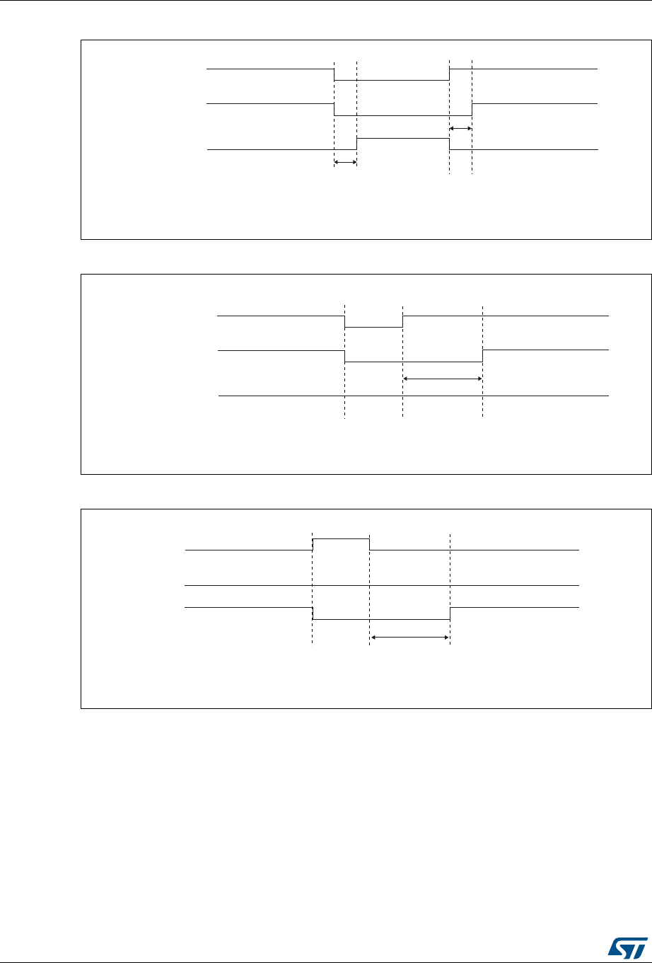
Advanced-control timers (TIM1) RM0401
290/766 DocID027812 Rev 2
Figure 82. Complementary output with dead-time insertion.
Figure 83. Dead-time waveforms with delay greater than the negative pulse.
Figure 84. Dead-time waveforms with delay greater than the positive pulse.
The dead-time delay is the same for each of the channels and is programmable with the
DTG bits in the TIMx_BDTR register. Refer to Section 14.4.18: TIM1 break and dead-time
register (TIMx_BDTR) for delay calculation.
Re-directing OCxREF to OCx or OCxN
In output mode (forced, output compare or PWM), OCxREF can be re-directed to the OCx
output or to OCxN output by configuring the CCxE and CCxNE bits in the TIMx_CCER
register.
This allows you to send a specific waveform (such as PWM or static active level) on one
output while the complementary remains at its inactive level. Other alternative possibilities
GHOD\
GHOD\
2&[5()
2&[
2&[1
069
069
GHOD\
2&[5()
2&[
2&[1
069
GHOD\
2&[5()
2&[
2&[1

DocID027812 Rev 2 291/766
RM0401 Advanced-control timers (TIM1)
334
are to have both outputs at inactive level or both outputs active and complementary with
dead-time.
Note: When only OCxN is enabled (CCxE=0, CCxNE=1), it is not complemented and becomes
active as soon as OCxREF is high. For example, if CCxNP=0 then OCxN=OCxRef. On the
other hand, when both OCx and OCxN are enabled (CCxE=CCxNE=1) OCx becomes
active when OCxREF is high whereas OCxN is complemented and becomes active when
OCxREF is low.
14.3.12 Using the break function
When using the break function, the output enable signals and inactive levels are modified
according to additional control bits (MOE, OSSI and OSSR bits in the TIMx_BDTR register,
OISx and OISxN bits in the TIMx_CR2 register). In any case, the OCx and OCxN outputs
cannot be set both to active level at a given time. Refer to Table 57 for more details.
The break source can be either the break input pin or a clock failure event, generated by the
Clock Security System (CSS), from the Reset Clock Controller. For further information on
the Clock Security System, refer to Section 6.2.7.
When exiting from reset, the break circuit is disabled and the MOE bit is low. You can enable
the break function by setting the BKE bit in the TIMx_BDTR register. The break input
polarity can be selected by configuring the BKP bit in the same register. BKE and BKP can
be modified at the same time. When the BKE and BKP bits are written, a delay of 1 APB
clock cycle is applied before the writing is effective. Consequently, it is necessary to wait 1
APB clock period to correctly read back the bit after the write operation.
Because MOE falling edge can be asynchronous, a resynchronization circuit has been
inserted between the actual signal (acting on the outputs) and the synchronous control bit
(accessed in the TIMx_BDTR register). It results in some delays between the asynchronous
and the synchronous signals. In particular, if you write MOE to 1 whereas it was low, you
must insert a delay (dummy instruction) before reading it correctly. This is because you write
the asynchronous signal and read the synchronous signal.
When a break occurs (selected level on the break input):
•The MOE bit is cleared asynchronously, putting the outputs in inactive state, idle state
or in reset state (selected by the OSSI bit). This feature functions even if the MCU
oscillator is off.
•Each output channel is driven with the level programmed in the OISx bit in the
TIMx_CR2 register as soon as MOE=0. If OSSI=0 then the timer releases the enable
output else the enable output remains high.
•When complementary outputs are used:
– The outputs are first put in reset state inactive state (depending on the polarity).
This is done asynchronously so that it works even if no clock is provided to the
timer.
– If the timer clock is still present, then the dead-time generator is reactivated in
order to drive the outputs with the level programmed in the OISx and OISxN bits
after a dead-time. Even in this case, OCx and OCxN cannot be driven to their

Advanced-control timers (TIM1) RM0401
292/766 DocID027812 Rev 2
active level together. Note that because of the resynchronization on MOE, the
dead-time duration is a bit longer than usual (around 2 ck_tim clock cycles).
– If OSSI=0 then the timer releases the enable outputs else the enable outputs
remain or become high as soon as one of the CCxE or CCxNE bits is high.
•The break status flag (BIF bit in the TIMx_SR register) is set. An interrupt can be
generated if the BIE bit in the TIMx_DIER register is set. A DMA request can be sent if
the BDE bit in the TIMx_DIER register is set.
•If the AOE bit in the TIMx_BDTR register is set, the MOE bit is automatically set again
at the next update event UEV. This can be used to perform a regulation, for instance.
Else, MOE remains low until you write it to ‘1’ again. In this case, it can be used for
security and you can connect the break input to an alarm from power drivers, thermal
sensors or any security components.
Note: The break inputs is acting on level. Thus, the MOE cannot be set while the break input is
active (neither automatically nor by software). In the meantime, the status flag BIF cannot
be cleared.
The break can be generated by the BRK input which has a programmable polarity and an
enable bit BKE in the TIMx_BDTR Register.
There are two solutions to generate a break:
•By using the BRK input which has a programmable polarity and an enable bit BKE in
the TIMx_BDTR register
•By software through the BG bit of the TIMx_EGR register.
In addition to the break input and the output management, a write protection has been
implemented inside the break circuit to safeguard the application. It allows you to freeze the
configuration of several parameters (dead-time duration, OCx/OCxN polarities and state
when disabled, OCxM configurations, break enable and polarity). You can choose from 3
levels of protection selected by the LOCK bits in the TIMx_BDTR register. Refer to
Section 14.4.18: TIM1 break and dead-time register (TIMx_BDTR). The LOCK bits can be
written only once after an MCU reset.
Figure 85 shows an example of behavior of the outputs in response to a break.
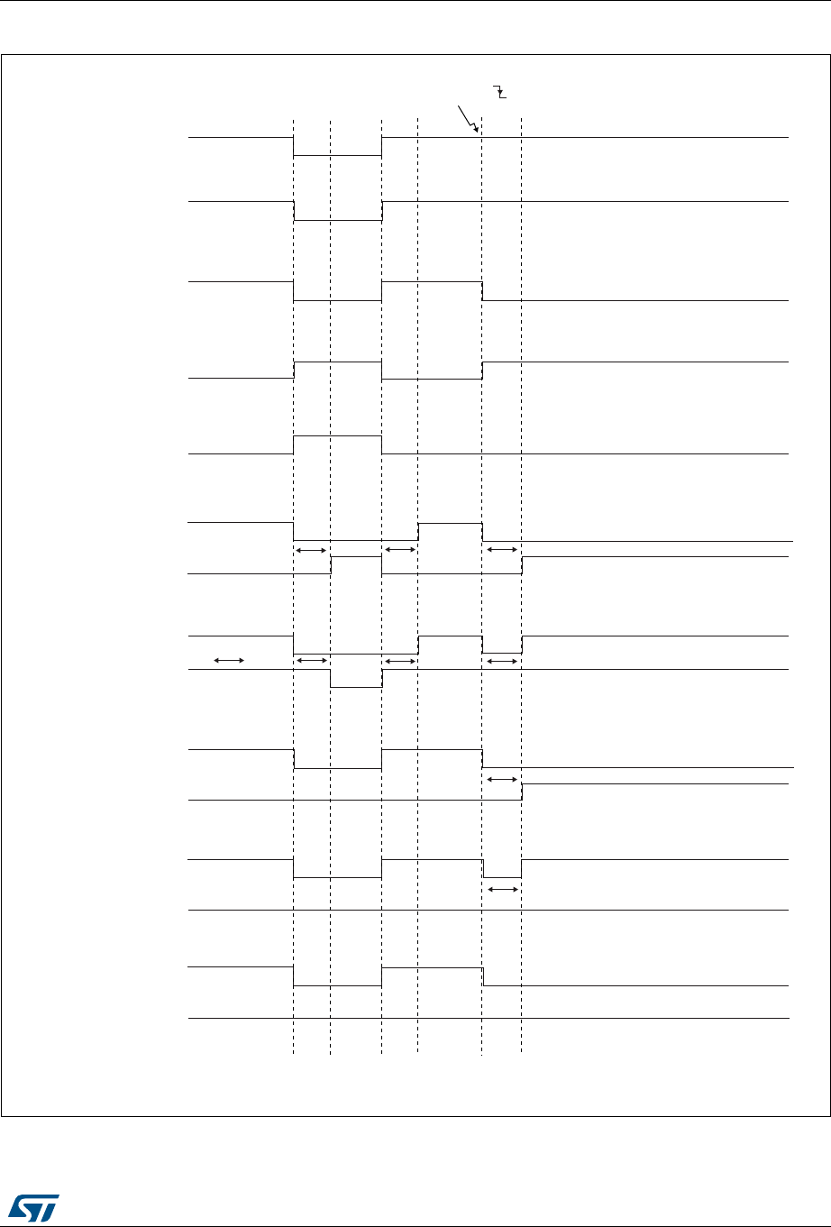
DocID027812 Rev 2 293/766
RM0401 Advanced-control timers (TIM1)
334
Figure 85. Output behavior in response to a break.
GHOD\ GHOD\ GHOD\
GHOD\ GHOD\ GHOD\
GHOD\
GHOD\
2&[5()
2&[
2&[1QRWLPSOHPHQWHG&&[3 2,6[
2&[
2&[1QRWLPSOHPHQWHG&&[3 2,6[
2&[
2&[1QRWLPSOHPHQWHG&&[3 2,6[
2&[
2&[1QRWLPSOHPHQWHG&&[3 2,6[
2&[
2&[1
&&[( &&[3 2,6[ &&[1( &&[13 2,6[1
2&[
2&[1
&&[( &&[3 2,6[ &&[1( &&[13 2,6[1
2&[
2&[1
&&[( &&[3 2,6[ &&[1( &&[13 2,6[1
2&[
2&[1
&&[( &&[3 2,6[ &&[1( &&[13 2,6[1
2&[
2&[1
&&[( &&[3 &&[1( &&[13 2,6[ 2,6[1 RU2,6[ 2,6[1
069
%5($.02(
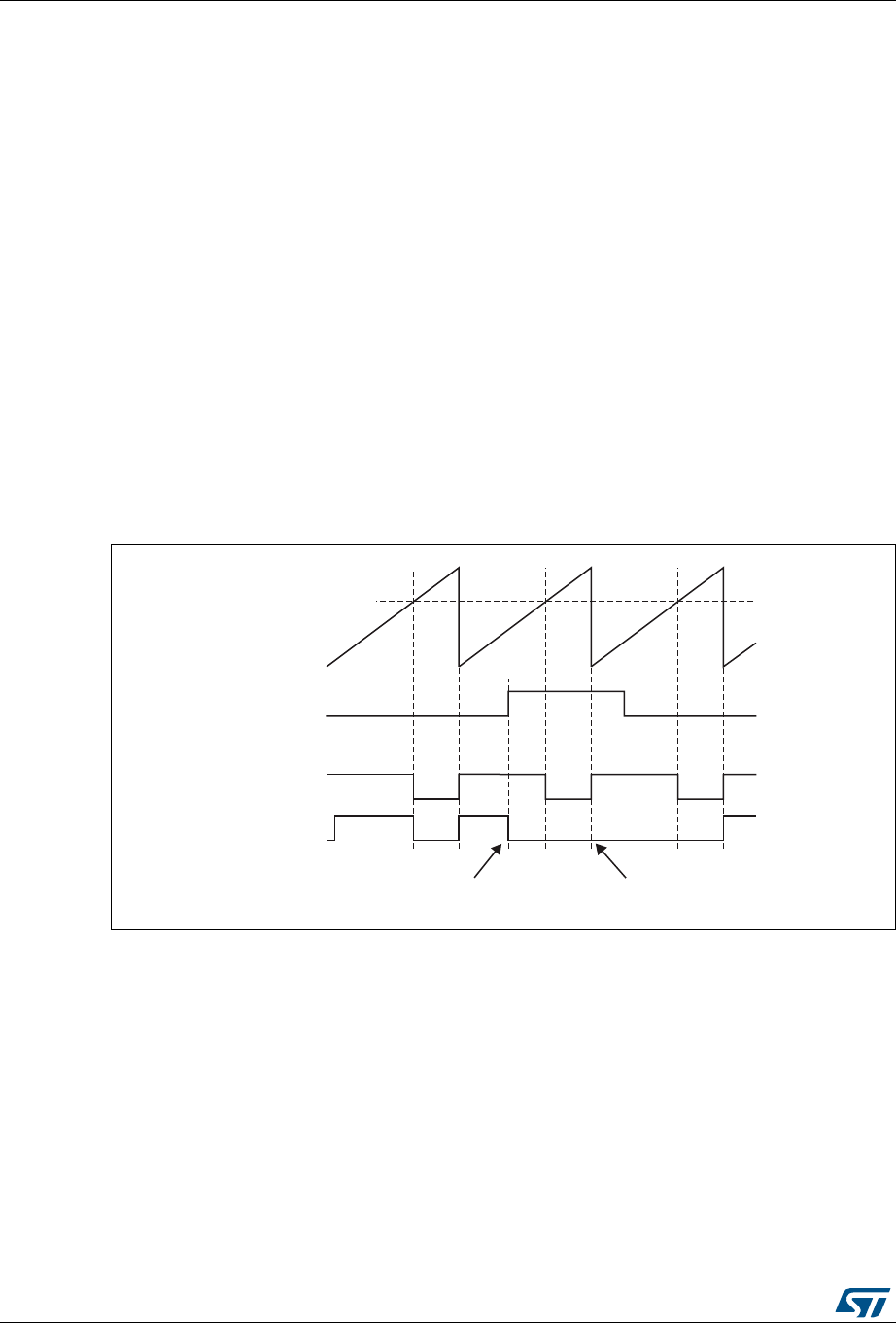
Advanced-control timers (TIM1) RM0401
294/766 DocID027812 Rev 2
14.3.13 Clearing the OCxREF signal on an external event
The OCxREF signal for a given channel can be driven Low by applying a High level to the
ETRF input (OCxCE enable bit of the corresponding TIMx_CCMRx register set to ‘1’). The
OCxREF signal remains Low until the next update event, UEV, occurs.
This function can only be used in output compare and PWM modes, and does not work in
forced mode.
For example, the ETR signal can be connected to the output of a comparator to be used for
current handling. In this case, the ETR must be configured as follow:
1. The External Trigger Prescaler should be kept off: bits ETPS[1:0] of the TIMx_SMCR
register set to ‘00’.
2. The external clock mode 2 must be disabled: bit ECE of the TIMx_SMCR register set to
‘0’.
3. The External Trigger Polarity (ETP) and the External Trigger Filter (ETF) can be
configured according to the user needs.
Figure 86 shows the behavior of the OCxREF signal when the ETRF Input becomes High,
for both values of the enable bit OCxCE. In this example, the timer TIMx is programmed in
PWM mode.
Figure 86. Clearing TIMx OCxREF
Note: In case of a PWM with a 100% duty cycle (if CCRx>ARR), then OCxREF is enabled again at
the next counter overflow.
06Y9
&&5[
&RXQWHU&17
(75)
2&[5()2&[&( µ
2&[5()2&[&( µ
(75)EHFRPHVKLJK (75)VWLOOKLJK
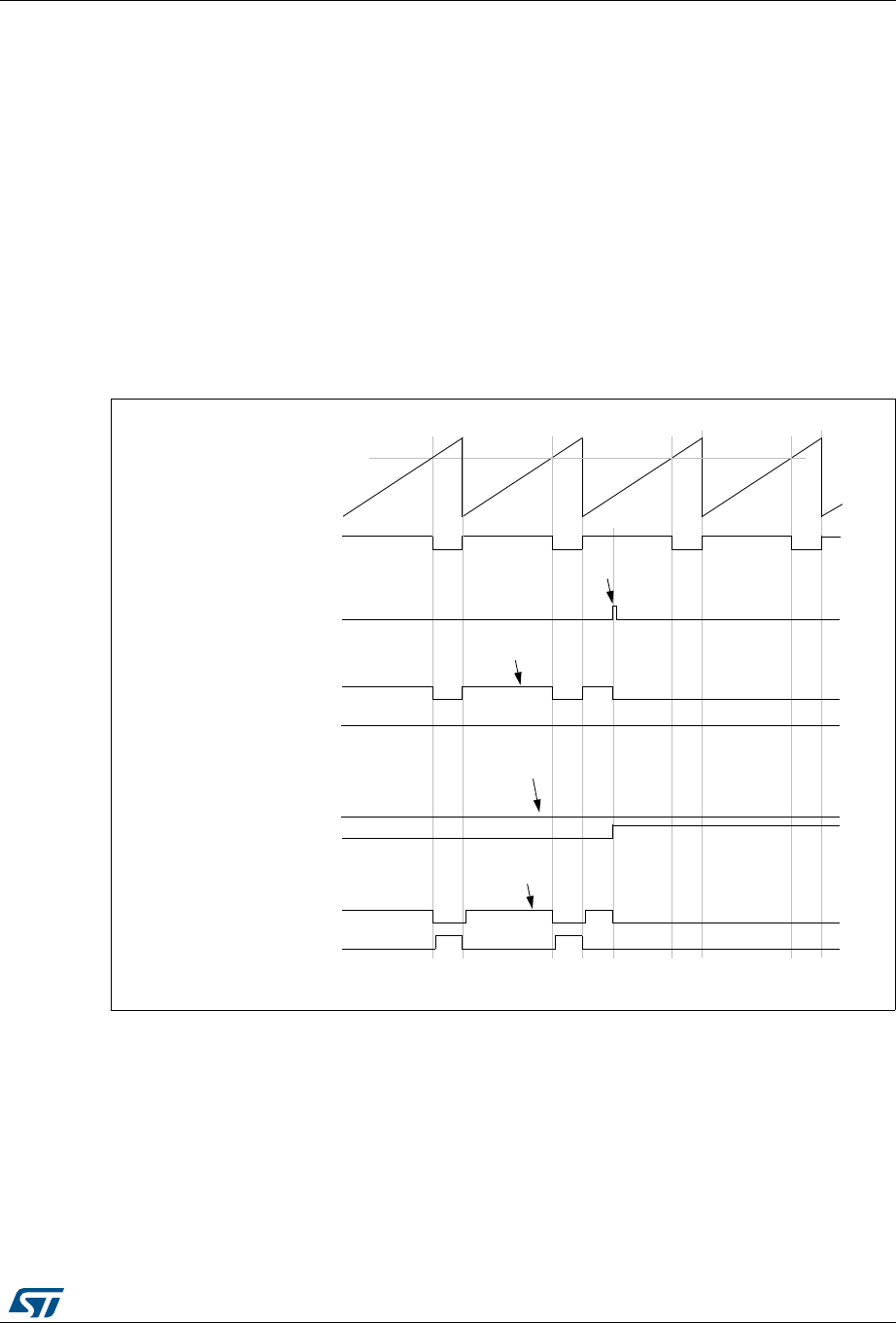
DocID027812 Rev 2 295/766
RM0401 Advanced-control timers (TIM1)
334
14.3.14 6-step PWM generation
When complementary outputs are used on a channel, preload bits are available on the
OCxM, CCxE and CCxNE bits. The preload bits are transferred to the shadow bits at the
COM commutation event. Thus you can program in advance the configuration for the next
step and change the configuration of all the channels at the same time. COM can be
generated by software by setting the COM bit in the TIMx_EGR register or by hardware (on
TRGI rising edge).
A flag is set when the COM event occurs (COMIF bit in the TIMx_SR register), which can
generate an interrupt (if the COMIE bit is set in the TIMx_DIER register) or a DMA request
(if the COMDE bit is set in the TIMx_DIER register).
Figure 87 describes the behavior of the OCx and OCxN outputs when a COM event occurs,
in 3 different examples of programmed configurations.
Figure 87. 6-step generation, COM example (OSSR=1)
(CCRx)
OCx
OCxN
Write COM to 1
counter (CNT)
OCxREF
COM event
CCxE=1
CCxNE=0
OCxM=100
OCx
OCxN
CCxE=0
CCxNE=1
OCxM=101
OCx
OCxN
CCxE=1
CCxNE=0
OCxM=100
Example 1
Example 2
Example 3
write OCxM to 100
CCxE=1
CCxNE=0
OCxM=100 (forced inactive)
CCxE=1
CCxNE=0
OCxM=100 (forced inactive)
Write CCxNE to 1
and OCxM to 101
write CCxNE to 0
and OCxM to 100
CCxE=1
CCxNE=0
OCxM=100 (forced inactive)
ai14910
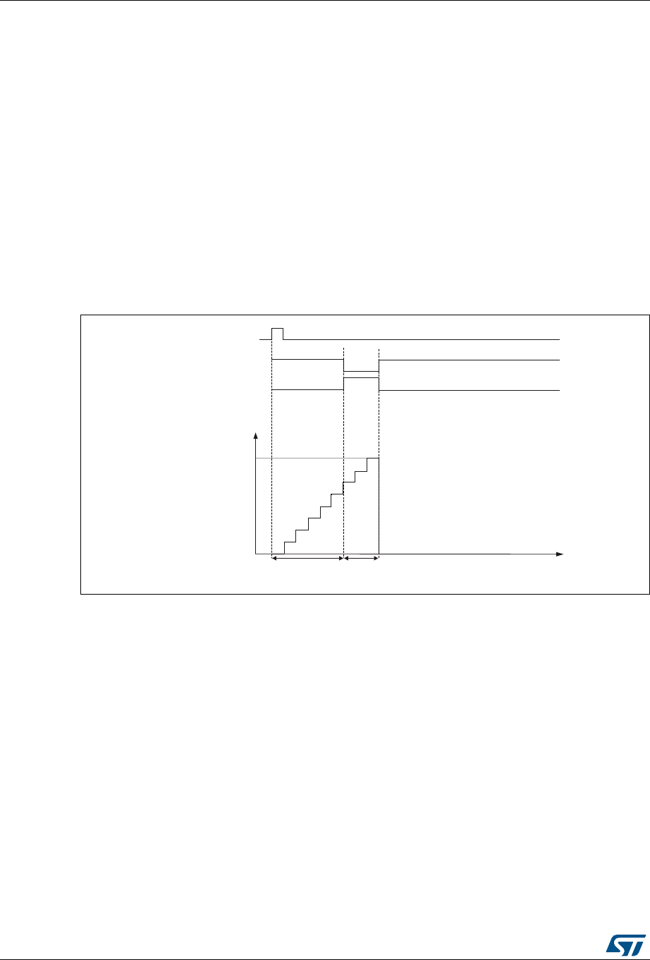
Advanced-control timers (TIM1) RM0401
296/766 DocID027812 Rev 2
14.3.15 One-pulse mode
One-pulse mode (OPM) is a particular case of the previous modes. It allows the counter to
be started in response to a stimulus and to generate a pulse with a programmable length
after a programmable delay.
Starting the counter can be controlled through the slave mode controller. Generating the
waveform can be done in output compare mode or PWM mode. You select One-pulse mode
by setting the OPM bit in the TIMx_CR1 register. This makes the counter stop automatically
at the next update event UEV.
A pulse can be correctly generated only if the compare value is different from the counter
initial value. Before starting (when the timer is waiting for the trigger), the configuration must
be:
•In upcounting: CNT < CCRx ≤ ARR (in particular, 0 < CCRx)
•In downcounting: CNT > CCRx
Figure 88. Example of one pulse mode.
For example you may want to generate a positive pulse on OC1 with a length of tPULSE and
after a delay of tDELAY as soon as a positive edge is detected on the TI2 input pin.
Let’s use TI2FP2 as trigger 1:
•Map TI2FP2 to TI2 by writing CC2S=’01’ in the TIMx_CCMR1 register.
•TI2FP2 must detect a rising edge, write CC2P=’0’ and CC2NP=’0’ in the TIMx_CCER
register.
•Configure TI2FP2 as trigger for the slave mode controller (TRGI) by writing TS=’110’ in
the TIMx_SMCR register.
•TI2FP2 is used to start the counter by writing SMS to ‘110’ in the TIMx_SMCR register
(trigger mode).
069
7,
2&5()
&RXQWHU
ƚ
7,0B$55
7,0B&&5
2&
ƚ>z ƚWh>^

DocID027812 Rev 2 297/766
RM0401 Advanced-control timers (TIM1)
334
The OPM waveform is defined by writing the compare registers (taking into account the
clock frequency and the counter prescaler).
•The tDELAY is defined by the value written in the TIMx_CCR1 register.
•The tPULSE is defined by the difference between the auto-reload value and the compare
value (TIMx_ARR - TIMx_CCR1).
•Let’s say you want to build a waveform with a transition from ‘0’ to ‘1’ when a compare
match occurs and a transition from ‘1’ to ‘0’ when the counter reaches the auto-reload
value. To do this you enable PWM mode 2 by writing OC1M=111 in the TIMx_CCMR1
register. You can optionally enable the preload registers by writing OC1PE=’1’ in the
TIMx_CCMR1 register and ARPE in the TIMx_CR1 register. In this case you have to
write the compare value in the TIMx_CCR1 register, the auto-reload value in the
TIMx_ARR register, generate an update by setting the UG bit and wait for external
trigger event on TI2. CC1P is written to ‘0’ in this example.
In our example, the DIR and CMS bits in the TIMx_CR1 register should be low.
You only want 1 pulse (Single mode), so you write '1 in the OPM bit in the TIMx_CR1
register to stop the counter at the next update event (when the counter rolls over from the
auto-reload value back to 0). When OPM bit in the TIMx_CR1 register is set to '0', so the
Repetitive Mode is selected.
Particular case: OCx fast enable:
In One-pulse mode, the edge detection on TIx input set the CEN bit which enables the
counter. Then the comparison between the counter and the compare value makes the
output toggle. But several clock cycles are needed for these operations and it limits the
minimum delay tDELAY min we can get.
If you want to output a waveform with the minimum delay, you can set the OCxFE bit in the
TIMx_CCMRx register. Then OCxRef (and OCx) are forced in response to the stimulus,
without taking in account the comparison. Its new level is the same as if a compare match
had occurred. OCxFE acts only if the channel is configured in PWM1 or PWM2 mode.
14.3.16 Encoder interface mode
To select Encoder Interface mode write SMS=‘001’ in the TIMx_SMCR register if the
counter is counting on TI2 edges only, SMS=’010’ if it is counting on TI1 edges only and
SMS=’011’ if it is counting on both TI1 and TI2 edges.
Select the TI1 and TI2 polarity by programming the CC1P and CC2P bits in the TIMx_CCER
register. When needed, you can program the input filter as well. CC1NP and CC2NP must
be kept low.
The two inputs TI1 and TI2 are used to interface to an incremental encoder. Refer to
Table 55. The counter is clocked by each valid transition on TI1FP1 or TI2FP2 (TI1 and TI2
after input filter and polarity selection, TI1FP1=TI1 if not filtered and not inverted,
TI2FP2=TI2 if not filtered and not inverted) assuming that it is enabled (CEN bit in
TIMx_CR1 register written to ‘1’). The sequence of transitions of the two inputs is evaluated
and generates count pulses as well as the direction signal. Depending on the sequence the
counter counts up or down, the DIR bit in the TIMx_CR1 register is modified by hardware
accordingly. The DIR bit is calculated at each transition on any input (TI1 or TI2), whatever
the counter is counting on TI1 only, TI2 only or both TI1 and TI2.
Encoder interface mode acts simply as an external clock with direction selection. This
means that the counter just counts continuously between 0 and the auto-reload value in the
TIMx_ARR register (0 to ARR or ARR down to 0 depending on the direction). So you must

Advanced-control timers (TIM1) RM0401
298/766 DocID027812 Rev 2
configure TIMx_ARR before starting. in the same way, the capture, compare, prescaler,
repetition counter, trigger output features continue to work as normal. Encoder mode and
External clock mode 2 are not compatible and must not be selected together.
In this mode, the counter is modified automatically following the speed and the direction of
the incremental encoder and its content, therefore, always represents the encoder’s
position. The count direction correspond to the rotation direction of the connected sensor.
The table summarizes the possible combinations, assuming TI1 and TI2 don’t switch at the
same time.
An external incremental encoder can be connected directly to the MCU without external
interface logic. However, comparators are normally be used to convert the encoder’s
differential outputs to digital signals. This greatly increases noise immunity. The third
encoder output which indicate the mechanical zero position, may be connected to an
external interrupt input and trigger a counter reset.
Figure 89 gives an example of counter operation, showing count signal generation and
direction control. It also shows how input jitter is compensated where both edges are
selected. This might occur if the sensor is positioned near to one of the switching points. For
this example we assume that the configuration is the following:
•CC1S=’01’ (TIMx_CCMR1 register, TI1FP1 mapped on TI1).
•CC2S=’01’ (TIMx_CCMR2 register, TI1FP2 mapped on TI2).
•CC1P=’0’, CC1NP=’0’, and IC1F = ‘0000’ (TIMx_CCER register, TI1FP1 non-inverted,
TI1FP1=TI1).
•CC2P=’0’, CC2NP=’0’, and IC2F = ‘0000’ (TIMx_CCER register, TI1FP2 non-inverted,
TI1FP2= TI2).
•SMS=’011’ (TIMx_SMCR register, both inputs are active on both rising and falling
edges).
•CEN=’1’ (TIMx_CR1 register, Counter enabled).
Table 55. Counting direction versus encoder signals
Active edge
Level on opposite signal
(TI1FP1 for TI2,
TI2FP2 for TI1)
TI1FP1 signal TI2FP2 signal
Rising Falling Rising Falling
Counting on
TI1 only
High Down Up No Count No Count
Low Up Down No Count No Count
Counting on
TI2 only
High No Count No Count Up Down
Low No Count No Count Down Up
Counting on
TI1 and TI2
High DownUp UpDown
Low Up Down Down Up
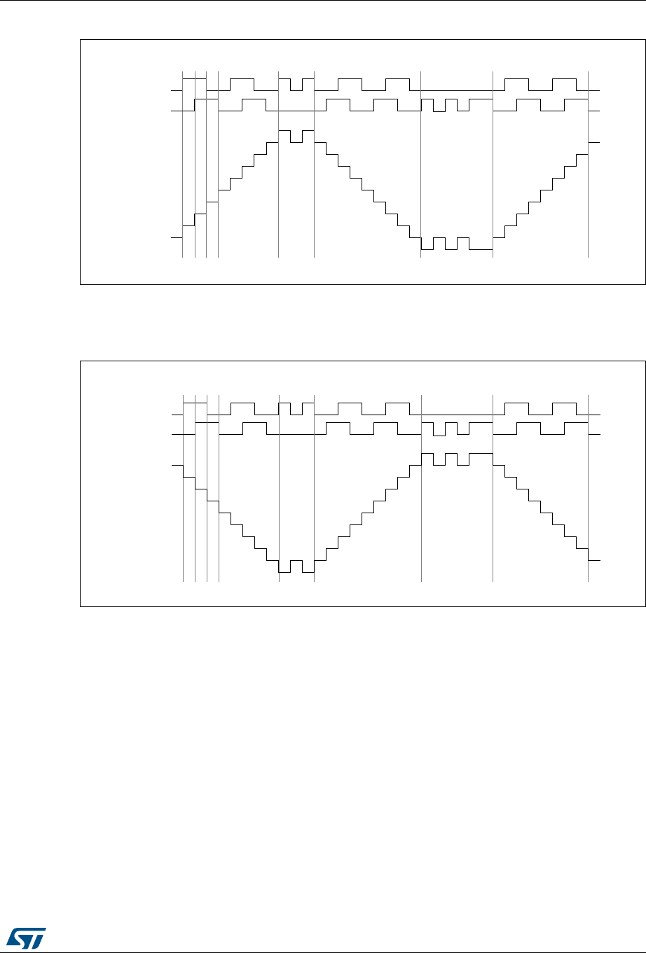
DocID027812 Rev 2 299/766
RM0401 Advanced-control timers (TIM1)
334
Figure 89. Example of counter operation in encoder interface mode.
Figure 90 gives an example of counter behavior when TI1FP1 polarity is inverted (same
configuration as above except CC1P=’1’).
Figure 90. Example of encoder interface mode with TI1FP1 polarity inverted.
The timer, when configured in Encoder Interface mode provides information on the sensor’s
current position. You can obtain dynamic information (speed, acceleration, deceleration) by
measuring the period between two encoder events using a second timer configured in
capture mode. The output of the encoder which indicates the mechanical zero can be used
for this purpose. Depending on the time between two events, the counter can also be read
at regular times. You can do this by latching the counter value into a third input capture
register if available (then the capture signal must be periodic and can be generated by
another timer). when available, it is also possible to read its value through a DMA request
generated by a real-time clock.
7,
EDFNZDUGMLWWHU MLWWHU
XS GRZQ XS
7,
&RXQWHU
IRUZDUG IRUZDUG
069
7,
EDFNZDUGMLWWHU MLWWHU
XSGRZQ
7,
&RXQWHU
IRUZDUG IRUZDUG
069
GRZQ

Advanced-control timers (TIM1) RM0401
300/766 DocID027812 Rev 2
14.3.17 Timer input XOR function
The TI1S bit in the TIMx_CR2 register allows the input filter of channel 1 to be connected to
the output of a XOR gate, combining the three input pins TIMx_CH1, TIMx_CH2 and
TIMx_CH3.
The XOR output can be used with all the timer input functions such as trigger or input
capture. An example of this feature used to interface Hall sensors is given in
Section 14.3.18 below.
14.3.18 Interfacing with Hall sensors
This is done using the advanced-control timers (TIM1 ) to generate PWM signals to drive
the motor and another timer TIMx (TIM5) referred to as “interfacing timer” in Figure 91. The
“interfacing timer” captures the 3 timer input pins (TIMx_CH1, TIMx_CH2, and TIMx_CH3)
connected through a XOR to the TI1 input channel (selected by setting the TI1S bit in the
TIMx_CR2 register).
The slave mode controller is configured in reset mode; the slave input is TI1F_ED. Thus,
each time one of the 3 inputs toggles, the counter restarts counting from 0. This creates a
time base triggered by any change on the Hall inputs.
On the “interfacing timer”, capture/compare channel 1 is configured in capture mode,
capture signal is TRC (see Figure 74). The captured value, which corresponds to the time
elapsed between 2 changes on the inputs, gives information about motor speed.
The “interfacing timer” can be used in output mode to generate a pulse which changes the
configuration of the channels of the advanced-control timer (TIM1 ) (by triggering a COM
event). The TIM1 timer is used to generate PWM signals to drive the motor. To do this, the
interfacing timer channel must be programmed so that a positive pulse is generated after a
programmed delay (in output compare or PWM mode). This pulse is sent to the advanced-
control timer (TIM1) through the TRGO output.
Example: you want to change the PWM configuration of your advanced-control timer TIM1
after a programmed delay each time a change occurs on the Hall inputs connected to one of
the TIMx timers.
•Configure 3 timer inputs ORed to the TI1 input channel by writing the TI1S bit in the
TIMx_CR2 register to ‘1’,
•Program the time base: write the TIMx_ARR to the max value (the counter must be
cleared by the TI1 change. Set the prescaler to get a maximum counter period longer
than the time between 2 changes on the sensors,
•Program channel 1 in capture mode (TRC selected): write the CC1S bits in the
TIMx_CCMR1 register to ‘11’. You can also program the digital filter if needed,
•Program channel 2 in PWM 2 mode with the desired delay: write the OC2M bits to ‘111’
and the CC2S bits to ‘00’ in the TIMx_CCMR1 register,
•Select OC2REF as trigger output on TRGO: write the MMS bits in the TIMx_CR2
register to ‘101’,
In the advanced-control timer TIM1, the right ITR input must be selected as trigger input, the
timer is programmed to generate PWM signals, the capture/compare control signals are
preloaded (CCPC=1 in the TIMx_CR2 register) and the COM event is controlled by the
trigger input (CCUS=1 in the TIMx_CR2 register). The PWM control bits (CCxE, OCxM) are
written after a COM event for the next step (this can be done in an interrupt subroutine
generated by the rising edge of OC2REF).
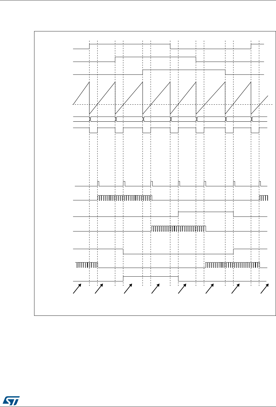
DocID027812 Rev 2 301/766
RM0401 Advanced-control timers (TIM1)
334
Figure 91 describes this example.
Figure 91. Example of hall sensor interface
DLE
&RXQWHU&17
75*2 2&5()
&&5
2&
2&1
&20
:ULWH&&[(&&[1(
7,+
7,+
7,+
&&5
2&
2&1
2&
2&1
&
DQG2&[0IRUQH[WVWHS
,QWHUIDFLQJWLPHU$GYDQFHGFRQWUROWLPHUV
&$ &$ & &$ &$%
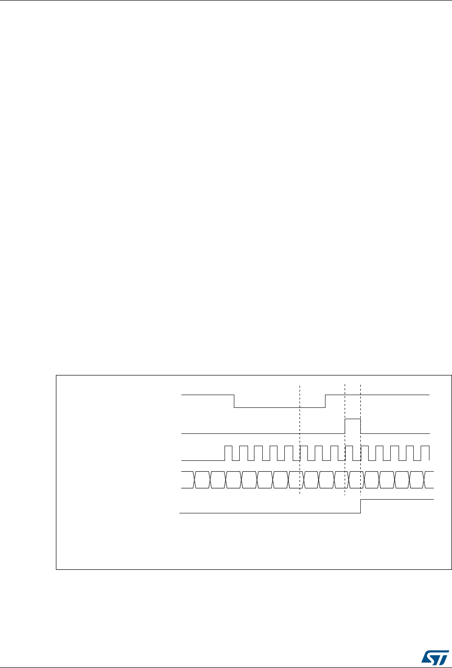
Advanced-control timers (TIM1) RM0401
302/766 DocID027812 Rev 2
14.3.19 TIMx and external trigger synchronization
The TIMx timer can be synchronized with an external trigger in several modes: Reset mode,
Gated mode and Trigger mode.
Slave mode: Reset mode
The counter and its prescaler can be reinitialized in response to an event on a trigger input.
Moreover, if the URS bit from the TIMx_CR1 register is low, an update event UEV is
generated. Then all the preloaded registers (TIMx_ARR, TIMx_CCRx) are updated.
In the following example, the upcounter is cleared in response to a rising edge on TI1 input:
•Configure the channel 1 to detect rising edges on TI1. Configure the input filter duration
(in this example, we don’t need any filter, so we keep IC1F=0000). The capture
prescaler is not used for triggering, so you don’t need to configure it. The CC1S bits
select the input capture source only, CC1S = 01 in the TIMx_CCMR1 register. Write
CC1P=0 and CC1NP=’0’ in TIMx_CCER register to validate the polarity (and detect
rising edges only).
•Configure the timer in reset mode by writing SMS=100 in TIMx_SMCR register. Select
TI1 as the input source by writing TS=101 in TIMx_SMCR register.
•Start the counter by writing CEN=1 in the TIMx_CR1 register.
The counter starts counting on the internal clock, then behaves normally until TI1 rising
edge. When TI1 rises, the counter is cleared and restarts from 0. In the meantime, the
trigger flag is set (TIF bit in the TIMx_SR register) and an interrupt request, or a DMA
request can be sent if enabled (depending on the TIE and TDE bits in TIMx_DIER register).
The following figure shows this behavior when the auto-reload register TIMx_ARR=0x36.
The delay between the rising edge on TI1 and the actual reset of the counter is due to the
resynchronization circuit on TI1 input.
Figure 92. Control circuit in reset mode
069
&RXQWHUFORFN FNBFQW FNBSVF
&RXQWHUUHJLVWHU
8*
7,
7,)
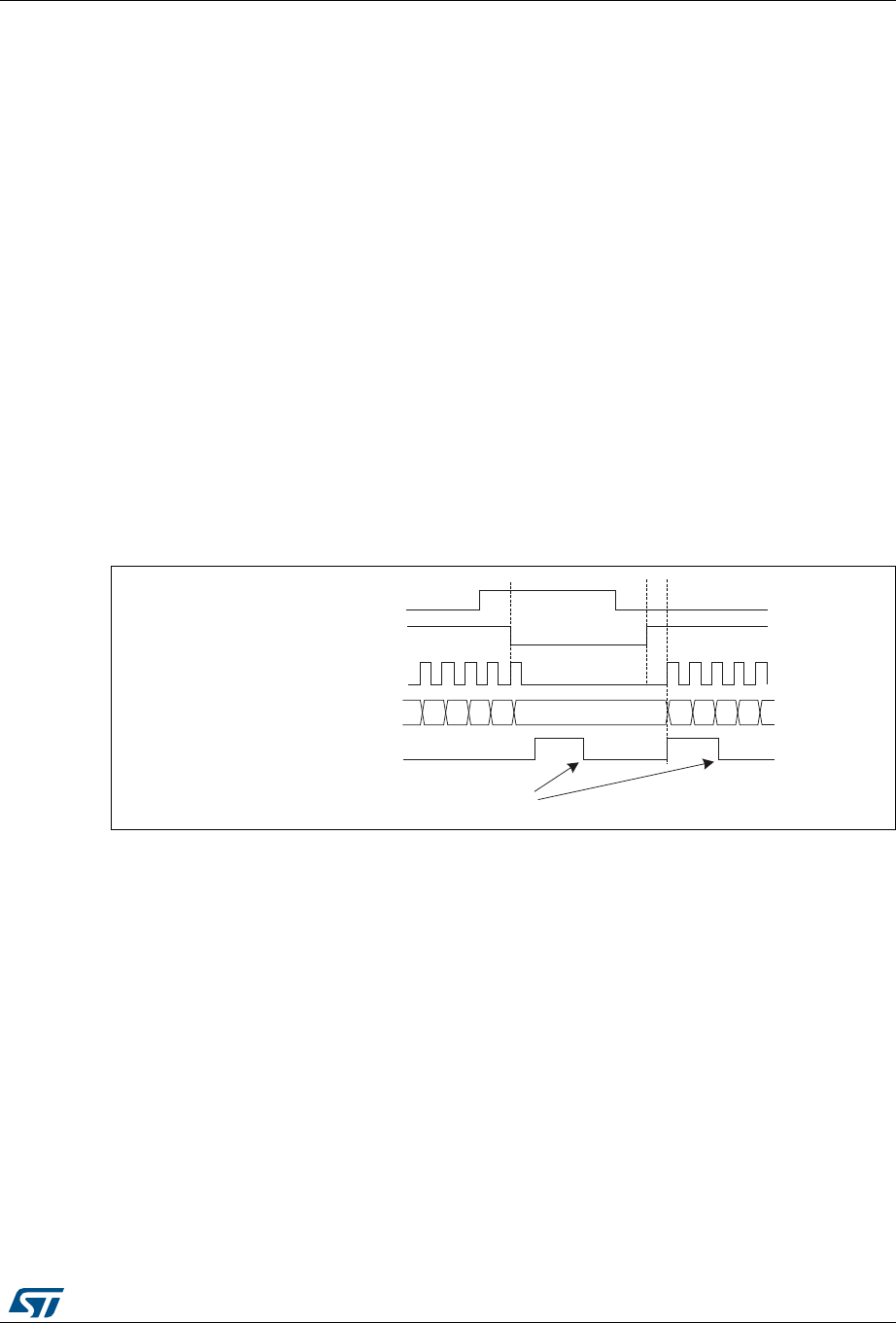
DocID027812 Rev 2 303/766
RM0401 Advanced-control timers (TIM1)
334
Slave mode: Gated mode
The counter can be enabled depending on the level of a selected input.
In the following example, the upcounter counts only when TI1 input is low:
•Configure the channel 1 to detect low levels on TI1. Configure the input filter duration
(in this example, we don’t need any filter, so we keep IC1F=0000). The capture
prescaler is not used for triggering, so you don’t need to configure it. The CC1S bits
select the input capture source only, CC1S=01 in TIMx_CCMR1 register. Write
CC1P=1 and CC1NP=’0’ in TIMx_CCER register to validate the polarity (and detect
low level only).
•Configure the timer in gated mode by writing SMS=101 in TIMx_SMCR register. Select
TI1 as the input source by writing TS=101 in TIMx_SMCR register.
•Enable the counter by writing CEN=1 in the TIMx_CR1 register (in gated mode, the
counter doesn’t start if CEN=0, whatever is the trigger input level).
The counter starts counting on the internal clock as long as TI1 is low and stops as soon as
TI1 becomes high. The TIF flag in the TIMx_SR register is set both when the counter starts
or stops.
The delay between the rising edge on TI1 and the actual stop of the counter is due to the
resynchronization circuit on TI1 input.
Figure 93. Control circuit in gated mode
069
7,
&17B(1
:ULWH7,)
&RXQWHUFORFN FNBFQW FNBSVF
&RXQWHUUHJLVWHU
7,)
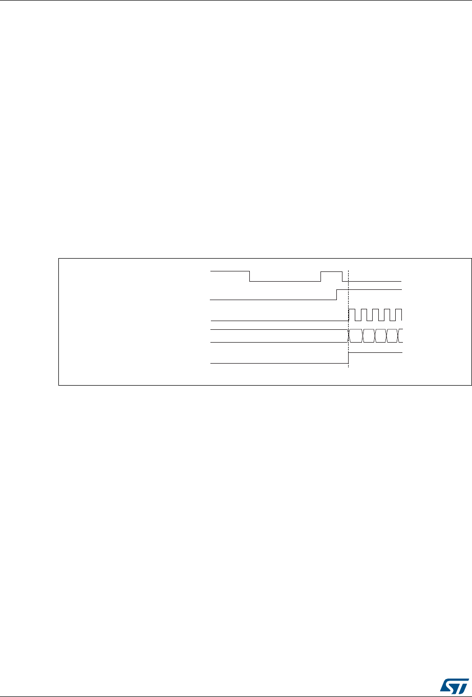
Advanced-control timers (TIM1) RM0401
304/766 DocID027812 Rev 2
Slave mode: Trigger mode
The counter can start in response to an event on a selected input.
In the following example, the upcounter starts in response to a rising edge on TI2 input:
•Configure the channel 2 to detect rising edges on TI2. Configure the input filter duration
(in this example, we don’t need any filter, so we keep IC2F=0000). The capture
prescaler is not used for triggering, so you don’t need to configure it. The CC2S bits are
configured to select the input capture source only, CC2S=01 in TIMx_CCMR1 register.
Write CC2P=1 and CC2NP=0 in TIMx_CCER register to validate the polarity (and
detect low level only).
•Configure the timer in trigger mode by writing SMS=110 in TIMx_SMCR register. Select
TI2 as the input source by writing TS=110 in TIMx_SMCR register.
When a rising edge occurs on TI2, the counter starts counting on the internal clock and the
TIF flag is set.
The delay between the rising edge on TI2 and the actual start of the counter is due to the
resynchronization circuit on TI2 input.
Figure 94. Control circuit in trigger mode
Slave mode: external clock mode 2 + trigger mode
The external clock mode 2 can be used in addition to another slave mode (except external
clock mode 1 and encoder mode). In this case, the ETR signal is used as external clock
input, and another input can be selected as trigger input (in reset mode, gated mode or
trigger mode). It is recommended not to select ETR as TRGI through the TS bits of
TIMx_SMCR register.
In the following example, the upcounter is incremented at each rising edge of the ETR
signal as soon as a rising edge of TI1 occurs:
1. Configure the external trigger input circuit by programming the TIMx_SMCR register as
follows:
– ETF = 0000: no filter
– ETPS = 00: prescaler disabled
– ETP = 0: detection of rising edges on ETR and ECE=1 to enable the external clock
mode 2.
069
7,
&17B(1
&RXQWHUFORFN FNBFQW FNBSVF
&RXQWHUUHJLVWHU
7,)
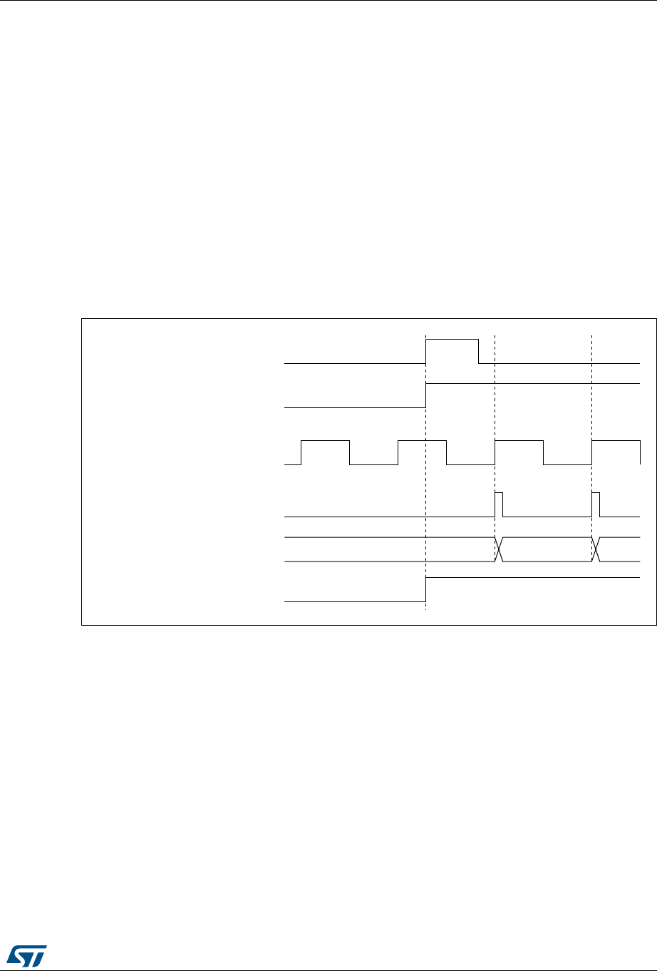
DocID027812 Rev 2 305/766
RM0401 Advanced-control timers (TIM1)
334
2. Configure the channel 1 as follows, to detect rising edges on TI:
– IC1F=0000: no filter.
– The capture prescaler is not used for triggering and does not need to be
configured.
– CC1S=01 in TIMx_CCMR1 register to select only the input capture source
– CC1P=0 and CC1NP=’0’ in TIMx_CCER register to validate the polarity (and
detect rising edge only).
3. Configure the timer in trigger mode by writing SMS=110 in TIMx_SMCR register. Select
TI1 as the input source by writing TS=101 in TIMx_SMCR register.
A rising edge on TI1 enables the counter and sets the TIF flag. The counter then counts on
ETR rising edges.
The delay between the rising edge of the ETR signal and the actual reset of the counter is
due to the resynchronization circuit on ETRP input.
Figure 95. Control circuit in external clock mode 2 + trigger mode
14.3.20 Debug mode
When the microcontroller enters debug mode (Cortex®-M4 with FPU core halted), the TIMx
counter either continues to work normally or stops, depending on DBG_TIMx_STOP
configuration bit in DBG module. For more details, refer to Section 26.16.2: Debug support
for timers, watchdog and I2C.
069
7,)
&RXQWHUUHJLVWHU
&RXQWHUFORFN &.B&17 &.B36&
(75
&(1&17B(1
7,

Advanced-control timers (TIM1) RM0401
306/766 DocID027812 Rev 2
14.4 TIM1 registers
Refer to Section 1.1: List of abbreviations for registers for a list of abbreviations used in
register descriptions.
The peripheral registers must be written by half-words (16 bits) or words (32 bits). Read
accesses can be done by bytes (8 bits), half-word (16 bits) or words (32 bits).
14.4.1 TIM1 control register 1 (TIMx_CR1)
Address offset: 0x00
Reset value: 0x0000
1514131211109876543210
Res. Res. Res. Res. Res. Res. CKD[1:0] ARPE CMS[1:0] DIR OPM URS UDIS CEN
rw rw rw rw rw rw rw rw rw rw
Bits 15:10 Reserved, must be kept at reset value.
Bits 9:8 CKD[1:0]: Clock division
This bit-field indicates the division ratio between the timer clock (CK_INT) frequency and the
dead-time and sampling clock (tDTS)used by the dead-time generators and the digital filters
(ETR, TIx),
00: tDTS=tCK_INT
01: tDTS=2*tCK_INT
10: tDTS=4*tCK_INT
11: Reserved, do not program this value
Bit 7 ARPE: Auto-reload preload enable
0: TIMx_ARR register is not buffered
1: TIMx_ARR register is buffered
Bits 6:5 CMS[1:0]: Center-aligned mode selection
00: Edge-aligned mode. The counter counts up or down depending on the direction bit
(DIR).
01: Center-aligned mode 1. The counter counts up and down alternatively. Output compare
interrupt flags of channels configured in output (CCxS=00 in TIMx_CCMRx register) are set
only when the counter is counting down.
10: Center-aligned mode 2. The counter counts up and down alternatively. Output compare
interrupt flags of channels configured in output (CCxS=00 in TIMx_CCMRx register) are set
only when the counter is counting up.
11: Center-aligned mode 3. The counter counts up and down alternatively. Output compare
interrupt flags of channels configured in output (CCxS=00 in TIMx_CCMRx register) are set
both when the counter is counting up or down.
Note: It is not allowed to switch from edge-aligned mode to center-aligned mode as long as
the counter is enabled (CEN=1)
Bit 4 DIR: Direction
0: Counter used as upcounter
1: Counter used as downcounter
Note: This bit is read only when the timer is configured in Center-aligned mode or Encoder
mode.

DocID027812 Rev 2 307/766
RM0401 Advanced-control timers (TIM1)
334
14.4.2 TIM1 control register 2 (TIMx_CR2)
Address offset: 0x04
Reset value: 0x0000
Bit 3 OPM: One pulse mode
0: Counter is not stopped at update event
1: Counter stops counting at the next update event (clearing the bit CEN)
Bit 2 URS: Update request source
This bit is set and cleared by software to select the UEV event sources.
0: Any of the following events generate an update interrupt or DMA request if enabled.
These events can be:
– Counter overflow/underflow
– Setting the UG bit
– Update generation through the slave mode controller
1: Only counter overflow/underflow generates an update interrupt or DMA request if
enabled.
Bit 1 UDIS: Update disable
This bit is set and cleared by software to enable/disable UEV event generation.
0: UEV enabled. The Update (UEV) event is generated by one of the following events:
– Counter overflow/underflow
– Setting the UG bit
– Update generation through the slave mode controller
Buffered registers are then loaded with their preload values.
1: UEV disabled. The Update event is not generated, shadow registers keep their value
(ARR, PSC, CCRx). However the counter and the prescaler are reinitialized if the UG bit is
set or if a hardware reset is received from the slave mode controller.
Bit 0 CEN: Counter enable
0: Counter disabled
1: Counter enabled
Note: External clock, gated mode and encoder mode can work only if the CEN bit has been
previously set by software. However trigger mode can set the CEN bit automatically by
hardware.
15 14 13 12 11 10 9876543210
Res. OIS4 OIS3N OIS3 OIS2N OIS2 OIS1N OIS1 TI1S MMS[2:0] CCDS CCUS Res. CCPC
rw rw rw rw rw rw rw rw rw rw rw rw rw rw
Bit 15 Reserved, must be kept at reset value.
Bit 14 OIS4: Output Idle state 4 (OC4 output)
refer to OIS1 bit
Bit 13 OIS3N: Output Idle state 3 (OC3N output)
refer to OIS1N bit
Bit 12 OIS3: Output Idle state 3 (OC3 output)
refer to OIS1 bit

Advanced-control timers (TIM1) RM0401
308/766 DocID027812 Rev 2
Bit 11 OIS2N: Output Idle state 2 (OC2N output)
refer to OIS1N bit
Bit 10 OIS2: Output Idle state 2 (OC2 output)
refer to OIS1 bit
Bit 9 OIS1N: Output Idle state 1 (OC1N output)
0: OC1N=0 after a dead-time when MOE=0
1: OC1N=1 after a dead-time when MOE=0
Note: This bit can not be modified as long as LOCK level 1, 2 or 3 has been programmed
(LOCK bits in TIMx_BDTR register).
Bit 8 OIS1: Output Idle state 1 (OC1 output)
0: OC1=0 (after a dead-time if OC1N is implemented) when MOE=0
1: OC1=1 (after a dead-time if OC1N is implemented) when MOE=0
Note: This bit can not be modified as long as LOCK level 1, 2 or 3 has been programmed
(LOCK bits in TIMx_BDTR register).
Bit 7 TI1S: TI1 selection
0: The TIMx_CH1 pin is connected to TI1 input
1: The TIMx_CH1, CH2 and CH3 pins are connected to the TI1 input (XOR combination)
Bits 6:4 MMS[2:0]: Master mode selection
These bits allow to select the information to be sent in master mode to slave timers for
synchronization (TRGO). The combination is as follows:
000: Reset - the UG bit from the TIMx_EGR register is used as trigger output (TRGO). If the
reset is generated by the trigger input (slave mode controller configured in reset mode) then
the signal on TRGO is delayed compared to the actual reset.
001: Enable - the Counter Enable signal CNT_EN is used as trigger output (TRGO). It is
useful to start several timers at the same time or to control a window in which a slave timer is
enable. The Counter Enable signal is generated by a logic OR between CEN control bit and
the trigger input when configured in gated mode. When the Counter Enable signal is
controlled by the trigger input, there is a delay on TRGO, except if the master/slave mode is
selected (see the MSM bit description in TIMx_SMCR register).
010: Update - The update event is selected as trigger output (TRGO). For instance a master
timer can then be used as a prescaler for a slave timer.
011: Compare Pulse - The trigger output send a positive pulse when the CC1IF flag is to be
set (even if it was already high), as soon as a capture or a compare match occurred.
(TRGO).
100: Compare - OC1REF signal is used as trigger output (TRGO)
101: Compare - OC2REF signal is used as trigger output (TRGO)
110: Compare - OC3REF signal is used as trigger output (TRGO)
111: Compare - OC4REF signal is used as trigger output (TRGO)
Bit 3 CCDS: Capture/compare DMA selection
0: CCx DMA request sent when CCx event occurs
1: CCx DMA requests sent when update event occurs

DocID027812 Rev 2 309/766
RM0401 Advanced-control timers (TIM1)
334
Bit 2 CCUS: Capture/compare control update selection
0: When capture/compare control bits are preloaded (CCPC=1), they are updated by setting
the COMG bit only
1: When capture/compare control bits are preloaded (CCPC=1), they are updated by setting
the COMG bit or when an rising edge occurs on TRGI
Note: This bit acts only on channels that have a complementary output.
Bit 1 Reserved, must be kept at reset value.
Bit 0 CCPC: Capture/compare preloaded control
0: CCxE, CCxNE and OCxM bits are not preloaded
1: CCxE, CCxNE and OCxM bits are preloaded, after having been written, they are updated
only when a commutation event (COM) occurs (COMG bit set or rising edge detected on
TRGI, depending on the CCUS bit).
Note: This bit acts only on channels that have a complementary output.

Advanced-control timers (TIM1) RM0401
310/766 DocID027812 Rev 2
14.4.3 TIM1 slave mode control register (TIMx_SMCR)
Address offset: 0x08
Reset value: 0x0000
15 14 13 12 11 10 9876543210
ETP ECE ETPS[1:0] ETF[3:0] MSM TS[2:0] Res. SMS[2:0]
rw rw rw rw rw rw rw rw rw rw rw rw rw rw rw
Bit 15 ETP: External trigger polarity
This bit selects whether ETR or ETR is used for trigger operations
0: ETR is non-inverted, active at high level or rising edge.
1: ETR is inverted, active at low level or falling edge.
Bit 14 ECE: External clock enable
This bit enables External clock mode 2.
0: External clock mode 2 disabled
1: External clock mode 2 enabled. The counter is clocked by any active edge on the ETRF
signal.
Note: 1: Setting the ECE bit has the same effect as selecting external clock mode 1 with
TRGI connected to ETRF (SMS=111 and TS=111).
2: It is possible to simultaneously use external clock mode 2 with the following slave
modes: reset mode, gated mode and trigger mode. Nevertheless, TRGI must not be
connected to ETRF in this case (TS bits must not be 111).
3: If external clock mode 1 and external clock mode 2 are enabled at the same time,
the external clock input is ETRF.
Bits 13:12 ETPS[1:0]: External trigger prescaler
External trigger signal ETRP frequency must be at most 1/4 of TIMxCLK frequency. A
prescaler can be enabled to reduce ETRP frequency. It is useful when inputting fast external
clocks.
00: Prescaler OFF
01: ETRP frequency divided by 2
10: ETRP frequency divided by 4
11: ETRP frequency divided by 8

DocID027812 Rev 2 311/766
RM0401 Advanced-control timers (TIM1)
334
Bits 11:8 ETF[3:0]: External trigger filter
This bit-field then defines the frequency used to sample ETRP signal and the length of the
digital filter applied to ETRP. The digital filter is made of an event counter in which N
consecutive events are needed to validate a transition on the output:
0000: No filter, sampling is done at fDTS
0001: fSAMPLING=fCK_INT
, N=2
0010: fSAMPLING=fCK_INT
, N=4
0011: fSAMPLING=fCK_INT
, N=8
0100: fSAMPLING=fDTS/2, N=6
0101: fSAMPLING=fDTS/2, N=8
0110: fSAMPLING=fDTS/4, N=6
0111: fSAMPLING=fDTS/4, N=8
1000: fSAMPLING=fDTS/8, N=6
1001: fSAMPLING=fDTS/8, N=8
1010: fSAMPLING=fDTS/16, N=5
1011: fSAMPLING=fDTS/16, N=6
1100: fSAMPLING=fDTS/16, N=8
1101: fSAMPLING=fDTS/32, N=5
1110: fSAMPLING=fDTS/32, N=6
1111: fSAMPLING=fDTS/32, N=8
Bit 7 MSM: Master/slave mode
0: No action
1: The effect of an event on the trigger input (TRGI) is delayed to allow a perfect
synchronization between the current timer and its slaves (through TRGO). It is useful if we
want to synchronize several timers on a single external event.
Bits 6:4 TS[2:0]: Trigger selection
This bit-field selects the trigger input to be used to synchronize the counter.
000: Internal Trigger 0 (ITR0)
001: Internal Trigger 1 (ITR1)
010: Internal Trigger 2 (ITR2)
011: Internal Trigger 3 (ITR3)
100: TI1 Edge Detector (TI1F_ED)
101: Filtered Timer Input 1 (TI1FP1)
110: Filtered Timer Input 2 (TI2FP2)
111: External Trigger input (ETRF)
See Table 56: TIMx Internal trigger connection for more details on ITRx meaning for each
Timer.
Note: These bits must be changed only when they are not used (e.g. when SMS=000) to
avoid wrong edge detections at the transition.
Bit 3 Reserved, must be kept at reset value.
Advanced-control timers (TIM1) RM0401
312/766 DocID027812 Rev 2
14.4.4 TIM1 DMA/interrupt enable register (TIMx_DIER)
Address offset: 0x0C
Reset value: 0x0000
Bits 2:0 SMS: Slave mode selection
When external signals are selected the active edge of the trigger signal (TRGI) is linked to
the polarity selected on the external input (see Input Control register and Control Register
description.
000: Slave mode disabled - if CEN = ‘1’ then the prescaler is clocked directly by the internal
clock.
001: Encoder mode 1 - Counter counts up/down on TI2FP2 edge depending on TI1FP1
level.
010: Encoder mode 2 - Counter counts up/down on TI1FP1 edge depending on TI2FP2
level.
011: Encoder mode 3 - Counter counts up/down on both TI1FP1 and TI2FP2 edges
depending on the level of the other input.
100: Reset Mode - Rising edge of the selected trigger input (TRGI) reinitializes the counter
and generates an update of the registers.
101: Gated Mode - The counter clock is enabled when the trigger input (TRGI) is high. The
counter stops (but is not reset) as soon as the trigger becomes low. Both start and stop of
the counter are controlled.
110: Trigger Mode - The counter starts at a rising edge of the trigger TRGI (but it is not
reset). Only the start of the counter is controlled.
111: External Clock Mode 1 - Rising edges of the selected trigger (TRGI) clock the counter.
Note: The gated mode must not be used if TI1F_ED is selected as the trigger input
(TS=’100’). Indeed, TI1F_ED outputs 1 pulse for each transition on TI1F, whereas the
gated mode checks the level of the trigger signal.
Table 56. TIMx Internal trigger connection
Slave TIM ITR0 (TS = 000) ITR1 (TS = 001) ITR2 (TS = 010) ITR3 (TS = 011)
TIM1 TIM5 Reserved Reserved Reserved
15 14 13 12 11 10 9 8 7 6 5 4 3 2 1 0
Res. TDE COMDE CC4DE CC3DE CC2DE CC1DE UDE BIE TIE COMIE CC4IE CC3IE CC2IE CC1IE UIE
rw rw rw rw rw rw rw rw rw rw rw rw rw rw rw
Bit 15 Reserved, must be kept at reset value.
Bit 14 TDE: Trigger DMA request enable
0: Trigger DMA request disabled
1: Trigger DMA request enabled
Bit 13 COMDE: COM DMA request enable
0: COM DMA request disabled
1: COM DMA request enabled
Bit 12 CC4DE: Capture/Compare 4 DMA request enable
0: CC4 DMA request disabled
1: CC4 DMA request enabled

DocID027812 Rev 2 313/766
RM0401 Advanced-control timers (TIM1)
334
Bit 11 CC3DE: Capture/Compare 3 DMA request enable
0: CC3 DMA request disabled
1: CC3 DMA request enabled
Bit 10 CC2DE: Capture/Compare 2 DMA request enable
0: CC2 DMA request disabled
1: CC2 DMA request enabled
Bit 9 CC1DE: Capture/Compare 1 DMA request enable
0: CC1 DMA request disabled
1: CC1 DMA request enabled
Bit 8 UDE: Update DMA request enable
0: Update DMA request disabled
1: Update DMA request enabled
Bit 7 BIE: Break interrupt enable
0: Break interrupt disabled
1: Break interrupt enabled
Bit 6 TIE: Trigger interrupt enable
0: Trigger interrupt disabled
1: Trigger interrupt enabled
Bit 5 COMIE: COM interrupt enable
0: COM interrupt disabled
1: COM interrupt enabled
Bit 4 CC4IE: Capture/Compare 4 interrupt enable
0: CC4 interrupt disabled
1: CC4 interrupt enabled
Bit 3 CC3IE: Capture/Compare 3 interrupt enable
0: CC3 interrupt disabled
1: CC3 interrupt enabled
Bit 2 CC2IE: Capture/Compare 2 interrupt enable
0: CC2 interrupt disabled
1: CC2 interrupt enabled
Bit 1 CC1IE: Capture/Compare 1 interrupt enable
0: CC1 interrupt disabled
1: CC1 interrupt enabled
Bit 0 UIE: Update interrupt enable
0: Update interrupt disabled
1: Update interrupt enabled

Advanced-control timers (TIM1) RM0401
314/766 DocID027812 Rev 2
14.4.5 TIM1 status register (TIMx_SR)
Address offset: 0x10
Reset value: 0x0000
151413121110 9876543210
Res. Res. Res. CC4OF CC3OF CC2OF CC1OF Res. BIF TIF COMIF CC4IF CC3IF CC2IF CC1IF UIF
rc_w0 rc_w0 rc_w0 rc_w0 rc_w0 rc_w0 rc_w0 rc_w0 rc_w0 rc_w0 rc_w0 rc_w0
Bits 15:13 Reserved, must be kept at reset value.
Bit 12 CC4OF: Capture/Compare 4 overcapture flag
refer to CC1OF description
Bit 11 CC3OF: Capture/Compare 3 overcapture flag
refer to CC1OF description
Bit 10 CC2OF: Capture/Compare 2 overcapture flag
refer to CC1OF description
Bit 9 CC1OF: Capture/Compare 1 overcapture flag
This flag is set by hardware only when the corresponding channel is configured in input
capture mode. It is cleared by software by writing it to ‘0’.
0: No overcapture has been detected.
1: The counter value has been captured in TIMx_CCR1 register while CC1IF flag was
already set
Bit 8 Reserved, must be kept at reset value.
Bit 7 BIF: Break interrupt flag
This flag is set by hardware as soon as the break input goes active. It can be cleared by
software if the break input is not active.
0: No break event occurred.
1: An active level has been detected on the break input.
Bit 6 TIF: Trigger interrupt flag
This flag is set by hardware on trigger event (active edge detected on TRGI input when the
slave mode controller is enabled in all modes but gated mode. It is set when the counter
starts or stops when gated mode is selected. It is cleared by software.
0: No trigger event occurred.
1: Trigger interrupt pending.
Bit 5 COMIF: COM interrupt flag
This flag is set by hardware on COM event (when Capture/compare Control bits - CCxE,
CCxNE, OCxM - have been updated). It is cleared by software.
0: No COM event occurred.
1: COM interrupt pending.
Bit 4 CC4IF: Capture/Compare 4 interrupt flag
refer to CC1IF description
Bit 3 CC3IF: Capture/Compare 3 interrupt flag
refer to CC1IF description

DocID027812 Rev 2 315/766
RM0401 Advanced-control timers (TIM1)
334
14.4.6 TIM1 event generation register (TIMx_EGR)
Address offset: 0x14
Reset value: 0x0000
Bit 2 CC2IF: Capture/Compare 2 interrupt flag
refer to CC1IF description
Bit 1 CC1IF: Capture/Compare 1 interrupt flag
If channel CC1 is configured as output:
This flag is set by hardware when the counter matches the compare value, with some
exception in center-aligned mode (refer to the CMS bits in the TIMx_CR1 register
description). It is cleared by software.
0: No match.
1: The content of the counter TIMx_CNT matches the content of the TIMx_CCR1 register.
When the contents of TIMx_CCR1 are greater than the contents of TIMx_ARR, the CC1IF
bit goes high on the counter overflow (in upcounting and up/down-counting modes) or
underflow (in downcounting mode)
If channel CC1 is configured as input:
This bit is set by hardware on a capture. It is cleared by software or by reading the
TIMx_CCR1 register.
0: No input capture occurred
1: The counter value has been captured in TIMx_CCR1 register (An edge has been
detected on IC1 which matches the selected polarity)
Bit 0 UIF: Update interrupt flag
This bit is set by hardware on an update event. It is cleared by software.
0: No update occurred.
1: Update interrupt pending. This bit is set by hardware when the registers are updated:
–At overflow or underflow regarding the repetition counter value (update if repetition
counter = 0) and if the UDIS=0 in the TIMx_CR1 register.
–When CNT is reinitialized by software using the UG bit in TIMx_EGR register, if URS=0
and UDIS=0 in the TIMx_CR1 register.
–When CNT is reinitialized by a trigger event (refer to Section 14.4.3: TIM1 slave mode
control register (TIMx_SMCR)), if URS=0 and UDIS=0 in the TIMx_CR1 register.
1514131211109876543210
Res. Res. Res. Res. Res. Res. Res. Res. BG TG COMG CC4G CC3G CC2G CC1G UG
wwwwwwww
Bits 15:8 Reserved, must be kept at reset value.
Bit 7 BG: Break generation
This bit is set by software in order to generate an event, it is automatically cleared by
hardware.
0: No action
1: A break event is generated. MOE bit is cleared and BIF flag is set. Related interrupt or
DMA transfer can occur if enabled.
Bit 6 TG: Trigger generation
This bit is set by software in order to generate an event, it is automatically cleared by
hardware.
0: No action
1: The TIF flag is set in TIMx_SR register. Related interrupt or DMA transfer can occur if
enabled.

Advanced-control timers (TIM1) RM0401
316/766 DocID027812 Rev 2
Bit 5 COMG: Capture/Compare control update generation
This bit can be set by software, it is automatically cleared by hardware
0: No action
1: When CCPC bit is set, it allows to update CCxE, CCxNE and OCxM bits
Note: This bit acts only on channels having a complementary output.
Bit 4 CC4G: Capture/Compare 4 generation
refer to CC1G description
Bit 3 CC3G: Capture/Compare 3 generation
refer to CC1G description
Bit 2 CC2G: Capture/Compare 2 generation
refer to CC1G description
Bit 1 CC1G: Capture/Compare 1 generation
This bit is set by software in order to generate an event, it is automatically cleared by
hardware.
0: No action
1: A capture/compare event is generated on channel 1:
If channel CC1 is configured as output:
CC1IF flag is set, Corresponding interrupt or DMA request is sent if enabled.
If channel CC1 is configured as input:
The current value of the counter is captured in TIMx_CCR1 register. The CC1IF flag is set,
the corresponding interrupt or DMA request is sent if enabled. The CC1OF flag is set if the
CC1IF flag was already high.
Bit 0 UG: Update generation
This bit can be set by software, it is automatically cleared by hardware.
0: No action
1: Reinitialize the counter and generates an update of the registers. Note that the prescaler
counter is cleared too (anyway the prescaler ratio is not affected). The counter is cleared if
the center-aligned mode is selected or if DIR=0 (upcounting), else it takes the auto-reload
value (TIMx_ARR) if DIR=1 (downcounting).

DocID027812 Rev 2 317/766
RM0401 Advanced-control timers (TIM1)
334
14.4.7 TIM1 capture/compare mode register 1 (TIMx_CCMR1)
Address offset: 0x18
Reset value: 0x0000
The channels can be used in input (capture mode) or in output (compare mode). The
direction of a channel is defined by configuring the corresponding CCxS bits. All the other
bits of this register have a different function in input and in output mode. For a given bit,
OCxx describes its function when the channel is configured in output, ICxx describes its
function when the channel is configured in input. So you must take care that the same bit
can have a different meaning for the input stage and for the output stage.
Output compare mode:
1514131211109876543210
OC2
CE OC2M[2:0] OC2
PE
OC2
FE CC2S[1:0]
OC1
CE OC1M[2:0] OC1
PE
OC1
FE CC1S[1:0]
IC2F[3:0] IC2PSC[1:0] IC1F[3:0] IC1PSC[1:0]
rw rw rw rw rw rw rw rw rw rw rw rw rw rw rw rw
Bit 15 OC2CE: Output Compare 2 clear enable
Bits 14:12 OC2M[2:0]: Output Compare 2 mode
Bit 11 OC2PE: Output Compare 2 preload enable
Bit 10 OC2FE: Output Compare 2 fast enable
Bits 9:8 CC2S[1:0]: Capture/Compare 2 selection
This bit-field defines the direction of the channel (input/output) as well as the used input.
00: CC2 channel is configured as output
01: CC2 channel is configured as input, IC2 is mapped on TI2
10: CC2 channel is configured as input, IC2 is mapped on TI1
11: CC2 channel is configured as input, IC2 is mapped on TRC. This mode is working only if
an internal trigger input is selected through the TS bit (TIMx_SMCR register)
Note: CC2S bits are writable only when the channel is OFF (CC2E = ‘0’ in TIMx_CCER).
Bit 7 OC1CE: Output Compare 1 clear enable
OC1CE: Output Compare 1 Clear Enable
0: OC1Ref is not affected by the ETRF Input
1: OC1Ref is cleared as soon as a High level is detected on ETRF input

Advanced-control timers (TIM1) RM0401
318/766 DocID027812 Rev 2
Bits 6:4 OC1M: Output Compare 1 mode
These bits define the behavior of the output reference signal OC1REF from which OC1 and
OC1N are derived. OC1REF is active high whereas OC1 and OC1N active level depends on
CC1P and CC1NP bits.
000: Frozen - The comparison between the output compare register TIMx_CCR1 and the
counter TIMx_CNT has no effect on the outputs.(this mode is used to generate a timing
base).
001: Set channel 1 to active level on match. OC1REF signal is forced high when the counter
TIMx_CNT matches the capture/compare register 1 (TIMx_CCR1).
010: Set channel 1 to inactive level on match. OC1REF signal is forced low when the counter
TIMx_CNT matches the capture/compare register 1 (TIMx_CCR1).
011: Toggle - OC1REF toggles when TIMx_CNT=TIMx_CCR1.
100: Force inactive level - OC1REF is forced low.
101: Force active level - OC1REF is forced high.
110: PWM mode 1 - In upcounting, channel 1 is active as long as TIMx_CNT<TIMx_CCR1
else inactive. In downcounting, channel 1 is inactive (OC1REF=‘0’) as long as
TIMx_CNT>TIMx_CCR1 else active (OC1REF=’1’).
111: PWM mode 2 - In upcounting, channel 1 is inactive as long as TIMx_CNT<TIMx_CCR1
else active. In downcounting, channel 1 is active as long as TIMx_CNT>TIMx_CCR1 else
inactive.
Note: 1: These bits can not be modified as long as LOCK level 3 has been programmed
(LOCK bits in TIMx_BDTR register) and CC1S=’00’ (the channel is configured in
output).
2: In PWM mode 1 or 2, the OCREF level changes only when the result of the
comparison changes or when the output compare mode switches from “frozen” mode to
“PWM” mode.
3: On channels having a complementary output, this bit field is preloaded. If the CCPC
bit is set in the TIMx_CR2 register then the OC1M active bits take the new value from
the preloaded bits only when a COM event is generated.

DocID027812 Rev 2 319/766
RM0401 Advanced-control timers (TIM1)
334
Input capture mode
Bit 3 OC1PE: Output Compare 1 preload enable
0: Preload register on TIMx_CCR1 disabled. TIMx_CCR1 can be written at anytime, the new
value is taken in account immediately.
1: Preload register on TIMx_CCR1 enabled. Read/Write operations access the preload
register. TIMx_CCR1 preload value is loaded in the active register at each update event.
Note: 1: These bits can not be modified as long as LOCK level 3 has been programmed
(LOCK bits in TIMx_BDTR register) and CC1S=’00’ (the channel is configured in
output).
2: The PWM mode can be used without validating the preload register only in one pulse
mode (OPM bit set in TIMx_CR1 register). Else the behavior is not guaranteed.
Bit 2 OC1FE: Output Compare 1 fast enable
This bit is used to accelerate the effect of an event on the trigger in input on the CC output.
0: CC1 behaves normally depending on counter and CCR1 values even when the trigger is
ON. The minimum delay to activate CC1 output when an edge occurs on the trigger input is 5
clock cycles.
1: An active edge on the trigger input acts like a compare match on CC1 output. Then, OC is
set to the compare level independently from the result of the comparison. Delay to sample
the trigger input and to activate CC1 output is reduced to 3 clock cycles. OCFE acts only if
the channel is configured in PWM1 or PWM2 mode.
Bits 1:0 CC1S: Capture/Compare 1 selection
This bit-field defines the direction of the channel (input/output) as well as the used input.
00: CC1 channel is configured as output
01: CC1 channel is configured as input, IC1 is mapped on TI1
10: CC1 channel is configured as input, IC1 is mapped on TI2
11: CC1 channel is configured as input, IC1 is mapped on TRC. This mode is working only if
an internal trigger input is selected through TS bit (TIMx_SMCR register)
Note: CC1S bits are writable only when the channel is OFF (CC1E = ‘0’ in TIMx_CCER).
Bits 15:12 IC2F: Input capture 2 filter
Bits 11:10 IC2PSC[1:0]: Input capture 2 prescaler
Bits 9:8 CC2S: Capture/Compare 2 selection
This bit-field defines the direction of the channel (input/output) as well as the used input.
00: CC2 channel is configured as output
01: CC2 channel is configured as input, IC2 is mapped on TI2
10: CC2 channel is configured as input, IC2 is mapped on TI1
11: CC2 channel is configured as input, IC2 is mapped on TRC. This mode is working only if an
internal trigger input is selected through TS bit (TIMx_SMCR register)
Note: CC2S bits are writable only when the channel is OFF (CC2E = ‘0’ in TIMx_CCER).

Advanced-control timers (TIM1) RM0401
320/766 DocID027812 Rev 2
14.4.8 TIM1 capture/compare mode register 2 (TIMx_CCMR2)
Address offset: 0x1C
Reset value: 0x0000
Refer to the above CCMR1 register description.
Bits 7:4 IC1F[3:0]: Input capture 1 filter
This bit-field defines the frequency used to sample TI1 input and the length of the digital filter applied
to TI1. The digital filter is made of an event counter in which N consecutive events are needed to
validate a transition on the output:
0000: No filter, sampling is done at fDTS
0001: fSAMPLING=fCK_INT
, N=2
0010: fSAMPLING=fCK_INT
, N=4
0011: fSAMPLING=fCK_INT
, N=8
0100: fSAMPLING=fDTS/2, N=6
0101: fSAMPLING=fDTS/2, N=8
0110: fSAMPLING=fDTS/4, N=6
0111: fSAMPLING=fDTS/4, N=8
1000: fSAMPLING=fDTS/8, N=6
1001: fSAMPLING=fDTS/8, N=8
1010: fSAMPLING=fDTS/16, N=5
1011: fSAMPLING=fDTS/16, N=6
1100: fSAMPLING=fDTS/16, N=8
1101: fSAMPLING=fDTS/32, N=5
1110: fSAMPLING=fDTS/32, N=6
1111: fSAMPLING=fDTS/32, N=8
Bits 3:2 IC1PSC: Input capture 1 prescaler
This bit-field defines the ratio of the prescaler acting on CC1 input (IC1).
The prescaler is reset as soon as CC1E=’0’ (TIMx_CCER register).
00: no prescaler, capture is done each time an edge is detected on the capture input
01: capture is done once every 2 events
10: capture is done once every 4 events
11: capture is done once every 8 events
Bits 1:0 CC1S: Capture/Compare 1 Selection
This bit-field defines the direction of the channel (input/output) as well as the used input.
00: CC1 channel is configured as output
01: CC1 channel is configured as input, IC1 is mapped on TI1
10: CC1 channel is configured as input, IC1 is mapped on TI2
11: CC1 channel is configured as input, IC1 is mapped on TRC. This mode is working only if an
internal trigger input is selected through TS bit (TIMx_SMCR register)
Note: CC1S bits are writable only when the channel is OFF (CC1E = ‘0’ in TIMx_CCER).
1514131211109876543210
OC4
CE OC4M[2:0] OC4
PE
OC4
FE CC4S[1:0]
OC3
CE. OC3M[2:0] OC3
PE
OC3
FE CC3S[1:0]
IC4F[3:0] IC4PSC[1:0] IC3F[3:0] IC3PSC[1:0]
rw rw rw rw rw rw rw rw rw rw rw rw rw rw rw rw

DocID027812 Rev 2 321/766
RM0401 Advanced-control timers (TIM1)
334
Output compare mode
Input capture mode
Bit 15 OC4CE: Output compare 4 clear enable
Bits 14:12 OC4M: Output compare 4 mode
Bit 11 OC4PE: Output compare 4 preload enable
Bit 10 OC4FE: Output compare 4 fast enable
Bits 9:8 CC4S: Capture/Compare 4 selection
This bit-field defines the direction of the channel (input/output) as well as the used input.
00: CC4 channel is configured as output
01: CC4 channel is configured as input, IC4 is mapped on TI4
10: CC4 channel is configured as input, IC4 is mapped on TI3
11: CC4 channel is configured as input, IC4 is mapped on TRC. This mode is working only if
an internal trigger input is selected through TS bit (TIMx_SMCR register)
Note: CC4S bits are writable only when the channel is OFF (CC4E = ‘0’ in TIMx_CCER).
Bit 7 OC3CE: Output compare 3 clear enable
Bits 6:4 OC3M: Output compare 3 mode
Bit 3 OC3PE: Output compare 3 preload enable
Bit 2 OC3FE: Output compare 3 fast enable
Bits 1:0 CC3S: Capture/Compare 3 selection
This bit-field defines the direction of the channel (input/output) as well as the used input.
00: CC3 channel is configured as output
01: CC3 channel is configured as input, IC3 is mapped on TI3
10: CC3 channel is configured as input, IC3 is mapped on TI4
11: CC3 channel is configured as input, IC3 is mapped on TRC. This mode is working only if
an internal trigger input is selected through TS bit (TIMx_SMCR register)
Note: CC3S bits are writable only when the channel is OFF (CC3E = ‘0’ in TIMx_CCER).
Bits 15:12 IC4F: Input capture 4 filter
Bits 11:10 IC4PSC: Input capture 4 prescaler
Bits 9:8 CC4S: Capture/Compare 4 selection
This bit-field defines the direction of the channel (input/output) as well as the used input.
00: CC4 channel is configured as output
01: CC4 channel is configured as input, IC4 is mapped on TI4
10: CC4 channel is configured as input, IC4 is mapped on TI3
11: CC4 channel is configured as input, IC4 is mapped on TRC. This mode is working only if
an internal trigger input is selected through TS bit (TIMx_SMCR register)
Note: CC4S bits are writable only when the channel is OFF (CC4E = ‘0’ in TIMx_CCER).

Advanced-control timers (TIM1) RM0401
322/766 DocID027812 Rev 2
14.4.9 TIM1 capture/compare enable register (TIMx_CCER)
Address offset: 0x20
Reset value: 0x0000
Bits 7:4 IC3F: Input capture 3 filter
Bits 3:2 IC3PSC: Input capture 3 prescaler
Bits 1:0 CC3S: Capture/compare 3 selection
This bit-field defines the direction of the channel (input/output) as well as the used input.
00: CC3 channel is configured as output
01: CC3 channel is configured as input, IC3 is mapped on TI3
10: CC3 channel is configured as input, IC3 is mapped on TI4
11: CC3 channel is configured as input, IC3 is mapped on TRC. This mode is working only if
an internal trigger input is selected through TS bit (TIMx_SMCR register)
Note: CC3S bits are writable only when the channel is OFF (CC3E = ‘0’ in TIMx_CCER).
15 14 13 12 11 10 9876543210
Res. Res. CC4P CC4E CC3NP CC3NE CC3P CC3E CC2NP CC2NE CC2P CC2E CC1NP CC1NE CC1P CC1E
rw rw rw rw rw rw rw rw rw rw rw rw rw rw
Bits 15:14 Reserved, must be kept at reset value.
Bit 13 CC4P: Capture/Compare 4 output polarity
refer to CC1P description
Bit 12 CC4E: Capture/Compare 4 output enable
refer to CC1E description
Bit 11 CC3NP: Capture/Compare 3 complementary output polarity
refer to CC1NP description
Bit 10 CC3NE: Capture/Compare 3 complementary output enable
refer to CC1NE description
Bit 9 CC3P: Capture/Compare 3 output polarity
refer to CC1P description
Bit 8 CC3E: Capture/Compare 3 output enable
refer to CC1E description
Bit 7 CC2NP: Capture/Compare 2 complementary output polarity
refer to CC1NP description
Bit 6 CC2NE: Capture/Compare 2 complementary output enable
refer to CC1NE description
Bit 5 CC2P: Capture/Compare 2 output polarity
refer to CC1P description
Bit 4 CC2E: Capture/Compare 2 output enable
refer to CC1E description

DocID027812 Rev 2 323/766
RM0401 Advanced-control timers (TIM1)
334
Bit 3 CC1NP: Capture/Compare 1 complementary output polarity
CC1 channel configured as output:
0: OC1N active high.
1: OC1N active low.
CC1 channel configured as input:
This bit is used in conjunction with CC1P to define the polarity of TI1FP1 and TI2FP1. Refer
to CC1P description.
Note: On channels having a complementary output, this bit is preloaded. If the CCPC bit is
set in the TIMx_CR2 register then the CC1NP active bit takes the new value from the
preloaded bit only when a Commutation event is generated.
Note: This bit is not writable as soon as LOCK level 2 or 3 has been programmed (LOCK bits
in TIMx_BDTR register) and CC1S=”00” (the channel is configured in output).
Bit 2 CC1NE: Capture/Compare 1 complementary output enable
0: Off - OC1N is not active. OC1N level is then function of MOE, OSSI, OSSR, OIS1, OIS1N
and CC1E bits.
1: On - OC1N signal is output on the corresponding output pin depending on MOE, OSSI,
OSSR, OIS1, OIS1N and CC1E bits.
Note: On channels having a complementary output, this bit is preloaded. If the CCPC bit is
set in the TIMx_CR2 register then the CC1NE active bit takes the new value from the
preloaded bit only when a Commutation event is generated.
Bit 1 CC1P: Capture/Compare 1 output polarity
CC1 channel configured as output:
0: OC1 active high
1: OC1 active low
CC1 channel configured as input:
CC1NP/CC1P bits select the active polarity of TI1FP1 and TI2FP1 for trigger or capture
operations.
00: non-inverted/rising edge
The circuit is sensitive to TIxFP1 rising edge (capture or trigger operations in reset, external
clock or trigger mode), TIxFP1 is not inverted (trigger operation in gated mode or encoder
mode).
01: inverted/falling edge
The circuit is sensitive to TIxFP1 falling edge (capture or trigger operations in reset, external
clock or trigger mode), TIxFP1 is inverted (trigger operation in gated mode or encoder
mode).
10: reserved, do not use this configuration.
11: non-inverted/both edges
The circuit is sensitive to both TIxFP1 rising and falling edges (capture or trigger operations
in reset, external clock or trigger mode), TIxFP1 is not inverted (trigger operation in gated
mode). This configuration must not be used in encoder mode.
Note: On channels having a complementary output, this bit is preloaded. If the CCPC bit is
set in the TIMx_CR2 register then the CC1P active bit takes the new value from the
preloaded bit only when a Commutation event is generated.
Note: This bit is not writable as soon as LOCK level 2 or 3 has been programmed (LOCK bits
in TIMx_BDTR register).

Advanced-control timers (TIM1) RM0401
324/766 DocID027812 Rev 2
Bit 0 CC1E: Capture/Compare 1 output enable
CC1 channel configured as output:
0: Off - OC1 is not active. OC1 level is then function of MOE, OSSI, OSSR, OIS1, OIS1N
and CC1NE bits.
1: On - OC1 signal is output on the corresponding output pin depending on MOE, OSSI,
OSSR, OIS1, OIS1N and CC1NE bits.
CC1 channel configured as input:
This bit determines if a capture of the counter value can actually be done into the input
capture/compare register 1 (TIMx_CCR1) or not.
0: Capture disabled.
1: Capture enabled.
Note: On channels having a complementary output, this bit is preloaded. If the CCPC bit is
set in the TIMx_CR2 register then the CC1E active bit takes the new value from the
preloaded bit only when a Commutation event is generated.
Table 57. Output control bits for complementary OCx and OCxN channels
with break feature
Control bits Output states(1)
MOE
bit
OSSI
bit
OSSR
bit
CCxE
bit
CCxNE
bit OCx output state OCxN output state
1X
0
0
0
Output Disabled (not driven by
the timer)
OCx=0, OCx_EN=0
Output Disabled (not driven by the timer)
OCxN=0, OCxN_EN=0
1
Output Disabled (not driven by
the timer)
OCx=0, OCx_EN=0
OCxREF + Polarity OCxN=OCxREF xor
CCxNP, OCxN_EN=1
1
0
OCxREF + Polarity
OCx=OCxREF xor CCxP,
OCx_EN=1
Output Disabled (not driven by the timer)
OCxN=0, OCxN_EN=0
1OCREF + Polarity + dead-time
OCx_EN=1
Complementary to OCREF (not
OCREF)
+ Polarity + dead-time
OCxN_EN=1
1
0
0
Output Disabled (not driven by
the timer)
OCx=CCxP, OCx_EN=0
Output Disabled (not driven by the timer)
OCxN=CCxNP, OCxN_EN=0
1
Off-State (output enabled with
inactive state)
OCx=CCxP, OCx_EN=1
OCxREF + Polarity
OCxN=OCxREF xor CCxNP,
OCxN_EN=1
1
0
OCxREF + Polarity
OCx=OCxREF xor CCxP,
OCx_EN=1
Off-State (output enabled with inactive
state)
OCxN=CCxNP, OCxN_EN=1
1OCREF + Polarity + dead-time
OCx_EN=1
Complementary to OCREF (not
OCREF) + Polarity + dead-time
OCxN_EN=1

DocID027812 Rev 2 325/766
RM0401 Advanced-control timers (TIM1)
334
Note: The state of the external I/O pins connected to the complementary OCx and OCxN channels
depends on the OCx and OCxN channel state and the GPIO registers.
14.4.10 TIM1 counter (TIMx_CNT)
Address offset: 0x24
Reset value: 0x0000
14.4.11 TIM1 prescaler (TIMx_PSC)
Address offset: 0x28
Reset value: 0x0000
0
0
X
00
Output Disabled (not driven by
the timer)
OCx=CCxP, OCx_EN=0
Output Disabled (not driven by the timer)
OCxN=CCxNP, OCxN_EN=0
1 Output Disabled (not driven by the timer)
Asynchronously: OCx=CCxP, OCx_EN=0, OCxN=CCxNP, OCxN_EN=0
Then if the clock is present: OCx=OISx and OCxN=OISxN after a dead-
time, assuming that OISx and OISxN do not correspond to OCX and
OCxN both in active state.
1
0
1
1
00
Output Disabled (not driven by
the timer)
OCx=CCxP, OCx_EN=0
Output Disabled (not driven by the timer)
OCxN=CCxNP, OCxN_EN=0
1 Off-State (output enabled with inactive state)
Asynchronously: OCx=CCxP, OCx_EN=1, OCxN=CCxNP, OCxN_EN=1
Then if the clock is present: OCx=OISx and OCxN=OISxN after a dead-
time, assuming that OISx and OISxN do not correspond to OCX and
OCxN both in active state
1
0
1
1. When both outputs of a channel are not used (CCxE = CCxNE = 0), the OISx, OISxN, CCxP and CCxNP bits must be kept
cleared.
Table 57. Output control bits for complementary OCx and OCxN channels
with break feature (continued)
Control bits Output states(1)
MOE
bit
OSSI
bit
OSSR
bit
CCxE
bit
CCxNE
bit OCx output state OCxN output state
15 14 13 12 11 10 9876543210
CNT[15:0]
rw rw rw rw rw rw rw rw rw rw rw rw rw rw rw rw
Bits 15:0 CNT[15:0]: Counter value
15 14 13 12 11 10 9876543210
PSC[15:0]
rw rw rw rw rw rw rw rw rw rw rw rw rw rw rw rw

Advanced-control timers (TIM1) RM0401
326/766 DocID027812 Rev 2
14.4.12 TIM1 auto-reload register (TIMx_ARR)
Address offset: 0x2C
Reset value: 0x0000
Bits 15:0 PSC[15:0]: Prescaler value
The counter clock frequency (CK_CNT) is equal to fCK_PSC / (PSC[15:0] + 1).
PSC contains the value to be loaded in the active prescaler register at each update event
(including when the counter is cleared through UG bit of TIMx_EGR register or through
trigger controller when configured in “reset mode”).
15 14 13 12 11 10 9876543210
ARR[15:0]
rw rw rw rw rw rw rw rw rw rw rw rw rw rw rw rw
Bits 15:0 ARR[15:0]: Auto-reload value
ARR is the value to be loaded in the actual auto-reload register.
Refer to Section 14.3.1: Time-base unit for more details about ARR update and behavior.
The counter is blocked while the auto-reload value is null.

DocID027812 Rev 2 327/766
RM0401 Advanced-control timers (TIM1)
334
14.4.13 TIM1 repetition counter register (TIMx_RCR)
Address offset: 0x30
Reset value: 0x0000
14.4.14 TIM1 capture/compare register 1 (TIMx_CCR1)
Address offset: 0x34
Reset value: 0x0000
15 14 13 12 11 10 9876543210
Res. Res. Res. Res. Res. Res. Res. Res. REP[7:0]
rw rw rw rw rw rw rw rw
Bits 15:8 Reserved, must be kept at reset value.
Bits 7:0 REP[7:0]: Repetition counter value
These bits allow the user to set-up the update rate of the compare registers (i.e. periodic
transfers from preload to active registers) when preload registers are enable, as well as the
update interrupt generation rate, if this interrupt is enable.
Each time the REP_CNT related downcounter reaches zero, an update event is generated
and it restarts counting from REP value. As REP_CNT is reloaded with REP value only at
the repetition update event U_RC, any write to the TIMx_RCR register is not taken in
account until the next repetition update event.
It means in PWM mode (REP+1) corresponds to:
– the number of PWM periods in edge-aligned mode
– the number of half PWM period in center-aligned mode.
15 14 13 12 11 10 9876543210
CCR1[15:0]
rw rw rw rw rw rw rw rw rw rw rw rw rw rw rw rw
Bits 15:0 CCR1[15:0]: Capture/Compare 1 value
If channel CC1 is configured as output:
CCR1 is the value to be loaded in the actual capture/compare 1 register (preload value).
It is loaded permanently if the preload feature is not selected in the TIMx_CCMR1 register
(bit OC1PE). Else the preload value is copied in the active capture/compare 1 register when
an update event occurs.
The active capture/compare register contains the value to be compared to the counter
TIMx_CNT and signaled on OC1 output.
If channel CC1 is configured as input:
CCR1 is the counter value transferred by the last input capture 1 event (IC1).

Advanced-control timers (TIM1) RM0401
328/766 DocID027812 Rev 2
14.4.15 TIM1 capture/compare register 2 (TIMx_CCR2)
Address offset: 0x38
Reset value: 0x0000
14.4.16 TIM1 capture/compare register 3 (TIMx_CCR3)
Address offset: 0x3C
Reset value: 0x0000
15 14 13 12 11 10 9876543210
CCR2[15:0]
rw rw rw rw rw rw rw rw rw rw rw rw rw rw rw rw
Bits 15:0 CCR2[15:0]: Capture/Compare 2 value
If channel CC2 is configured as output:
CCR2 is the value to be loaded in the actual capture/compare 2 register (preload value).
It is loaded permanently if the preload feature is not selected in the TIMx_CCMR2 register
(bit OC2PE). Else the preload value is copied in the active capture/compare 2 register when
an update event occurs.
The active capture/compare register contains the value to be compared to the counter
TIMx_CNT and signalled on OC2 output.
If channel CC2 is configured as input:
CCR2 is the counter value transferred by the last input capture 2 event (IC2).
15 14 13 12 11 10 9876543210
CCR3[15:0]
rw rw rw rw rw rw rw rw rw rw rw rw rw rw rw rw
Bits 15:0 CCR3[15:0]: Capture/Compare value
If channel CC3 is configured as output:
CCR3 is the value to be loaded in the actual capture/compare 3 register (preload value).
It is loaded permanently if the preload feature is not selected in the TIMx_CCMR3 register
(bit OC3PE). Else the preload value is copied in the active capture/compare 3 register when
an update event occurs.
The active capture/compare register contains the value to be compared to the counter
TIMx_CNT and signalled on OC3 output.
If channel CC3 is configured as input:
CCR3 is the counter value transferred by the last input capture 3 event (IC3).

DocID027812 Rev 2 329/766
RM0401 Advanced-control timers (TIM1)
334
14.4.17 TIM1 capture/compare register 4 (TIMx_CCR4)
Address offset: 0x40
Reset value: 0x0000
14.4.18 TIM1 break and dead-time register (TIMx_BDTR)
Address offset: 0x44
Reset value: 0x0000
Note: As the bits AOE, BKP, BKE, OSSI, OSSR and DTG[7:0] can be write-locked depending on
the LOCK configuration, it can be necessary to configure all of them during the first write
access to the TIMx_BDTR register.
15 14 13 12 11 10 9876543210
CCR4[15:0]
rw rw rw rw rw rw rw rw rw rw rw rw rw rw rw rw
Bits 15:0 CCR4[15:0]: Capture/Compare value
If channel CC4 is configured as output:
CCR4 is the value to be loaded in the actual capture/compare 4 register (preload value).
It is loaded permanently if the preload feature is not selected in the TIMx_CCMR4 register
(bit OC4PE). Else the preload value is copied in the active capture/compare 4 register when
an update event occurs.
The active capture/compare register contains the value to be compared to the counter
TIMx_CNT and signalled on OC4 output.
If channel CC4 is configured as input:
CCR4 is the counter value transferred by the last input capture 4 event (IC4).
15 14 13 12 11 10 9876543210
MOE AOE BKP BKE OSSR OSSI LOCK[1:0] DTG[7:0]
rw rw rw rw rw rw rw rw rw rw rw rw rw rw rw rw
Bit 15 MOE: Main output enable
This bit is cleared asynchronously by hardware as soon as the break input is active. It is set
by software or automatically depending on the AOE bit. It is acting only on the channels
which are configured in output.
0: OC and OCN outputs are disabled or forced to idle state.
1: OC and OCN outputs are enabled if their respective enable bits are set (CCxE, CCxNE in
TIMx_CCER register).
See OC/OCN enable description for more details (Section 14.4.9: TIM1 capture/compare
enable register (TIMx_CCER) on page 322).
Bit 14 AOE: Automatic output enable
0: MOE can be set only by software
1: MOE can be set by software or automatically at the next update event (if the break input is
not be active)
Note: This bit can not be modified as long as LOCK level 1 has been programmed (LOCK bits
in TIMx_BDTR register).

Advanced-control timers (TIM1) RM0401
330/766 DocID027812 Rev 2
Bit 13 BKP: Break polarity
0: Break input BRK is active low
1: Break input BRK is active high
Note: This bit can not be modified as long as LOCK level 1 has been programmed (LOCK bits
in TIMx_BDTR register).
Note: Any write operation to this bit takes a delay of 1 APB clock cycle to become effective.
Bit 12 BKE: Break enable
0: Break inputs (BRK and CSS clock failure event) disabled
1; Break inputs (BRK and CSS clock failure event) enabled
Note: This bit cannot be modified when LOCK level 1 has been programmed (LOCK bits in
TIMx_BDTR register).
Note: Any write operation to this bit takes a delay of 1 APB clock cycle to become effective.
Bit 11 OSSR: Off-state selection for Run mode
This bit is used when MOE=1 on channels having a complementary output which are
configured as outputs. OSSR is not implemented if no complementary output is implemented
in the timer.
See OC/OCN enable description for more details (Section 14.4.9: TIM1 capture/compare
enable register (TIMx_CCER) on page 322).
0: When inactive, OC/OCN outputs are disabled (OC/OCN enable output signal=0).
1: When inactive, OC/OCN outputs are enabled with their inactive level as soon as CCxE=1
or CCxNE=1. Then, OC/OCN enable output signal=1
Note: This bit can not be modified as soon as the LOCK level 2 has been programmed (LOCK
bits in TIMx_BDTR register).
Bit 10 OSSI: Off-state selection for Idle mode
This bit is used when MOE=0 on channels configured as outputs.
See OC/OCN enable description for more details (Section 14.4.9: TIM1 capture/compare
enable register (TIMx_CCER) on page 322).
0: When inactive, OC/OCN outputs are disabled (OC/OCN enable output signal=0).
1: When inactive, OC/OCN outputs are forced first with their idle level as soon as CCxE=1 or
CCxNE=1. OC/OCN enable output signal=1)
Note: This bit can not be modified as soon as the LOCK level 2 has been programmed (LOCK
bits in TIMx_BDTR register).
Bits 9:8 LOCK[1:0]: Lock configuration
These bits offer a write protection against software errors.
00: LOCK OFF - No bit is write protected.
01: LOCK Level 1 = DTG bits in TIMx_BDTR register, OISx and OISxN bits in TIMx_CR2
register and BKE/BKP/AOE bits in TIMx_BDTR register can no longer be written.
10: LOCK Level 2 = LOCK Level 1 + CC Polarity bits (CCxP/CCxNP bits in TIMx_CCER
register, as long as the related channel is configured in output through the CCxS bits) as well
as OSSR and OSSI bits can no longer be written.
11: LOCK Level 3 = LOCK Level 2 + CC Control bits (OCxM and OCxPE bits in
TIMx_CCMRx registers, as long as the related channel is configured in output through the
CCxS bits) can no longer be written.
Note: The LOCK bits can be written only once after the reset. Once the TIMx_BDTR register
has been written, their content is frozen until the next reset.

DocID027812 Rev 2 331/766
RM0401 Advanced-control timers (TIM1)
334
14.4.19 TIM1 DMA control register (TIMx_DCR)
Address offset: 0x48
Reset value: 0x0000
Bits 7:0 DTG[7:0]: Dead-time generator setup
This bit-field defines the duration of the dead-time inserted between the complementary
outputs. DT correspond to this duration.
DTG[7:5]=0xx => DT=DTG[7:0]x tdtg with tdtg=tDTS.
DTG[7:5]=10x => DT=(64+DTG[5:0])xtdtg with Tdtg=2xtDTS.
DTG[7:5]=110 => DT=(32+DTG[4:0])xtdtg with Tdtg=8xtDTS.
DTG[7:5]=111 => DT=(32+DTG[4:0])xtdtg with Tdtg=16xtDTS.
Example if TDTS=125ns (8MHz), dead-time possible values are:
0 to 15875 ns by 125 ns steps,
16 us to 31750 ns by 250 ns steps,
32 us to 63us by 1 us steps,
64 us to 126 us by 2 us steps
Note: This bit-field can not be modified as long as LOCK level 1, 2 or 3 has been programmed
(LOCK bits in TIMx_BDTR register).
15 14 13 12 11 10 9876543210
Res. Res. Res. DBL[4:0] Res. Res. Res. DBA[4:0]
rw rw rw rw rw rw rw rw rw rw
Bits 15:13 Reserved, must be kept at reset value.
Bits 12:8 DBL[4:0]: DMA burst length
This 5-bit vector defines the number of DMA transfers (the timer detects a burst transfer
when a read or a write access to the TIMx_DMAR register address is performed).
the TIMx_DMAR address)
00000: 1 transfer
00001: 2 transfers
00010: 3 transfers
...
10001: 18 transfers
Bits 7:5 Reserved, must be kept at reset value.
Bits 4:0 DBA[4:0]: DMA base address
This 5-bits vector defines the base-address for DMA transfers (when read/write access are
done through the TIMx_DMAR address). DBA is defined as an offset starting from the
address of the TIMx_CR1 register.
Example:
00000: TIMx_CR1,
00001: TIMx_CR2,
00010: TIMx_SMCR,
...
Example: Let us consider the following transfer: DBL = 7 transfers and DBA = TIMx_CR1. In
this case the transfer is done to/from 7 registers starting from the TIMx_CR1 address.

Advanced-control timers (TIM1) RM0401
332/766 DocID027812 Rev 2
14.4.20 TIM1 DMA address for full transfer (TIMx_DMAR)
Address offset: 0x4C
Reset value: 0x0000
Example of how to use the DMA burst feature
In this example the timer DMA burst feature is used to update the contents of the CCRx
registers (x = 2, 3, 4) with the DMA transferring half words into the CCRx registers.
This is done in the following steps:
1. Configure the corresponding DMA channel as follows:
– DMA channel peripheral address is the DMAR register address
– DMA channel memory address is the address of the buffer in the RAM containing
the data to be transferred by DMA into CCRx registers.
– Number of data to transfer = 3 (See note below).
– Circular mode disabled.
2. Configure the DCR register by configuring the DBA and DBL bit fields as follows:
DBL = 3 transfers, DBA = 0xE.
3. Enable the TIMx update DMA request (set the UDE bit in the DIER register).
4. Enable TIMx
5. Enable the DMA channel
Note: This example is for the case where every CCRx register to be updated once. If every CCRx
register is to be updated twice for example, the number of data to transfer should be 6. Let's
take the example of a buffer in the RAM containing data1, data2, data3, data4, data5 and
data6. The data is transferred to the CCRx registers as follows: on the first update DMA
request, data1 is transferred to CCR2, data2 is transferred to CCR3, data3 is transferred to
CCR4 and on the second update DMA request, data4 is transferred to CCR2, data5 is
transferred to CCR3 and data6 is transferred to CCR4.
15 14 13 12 11 10 9876543210
DMAB[15:0]
rw rw rw rw rw rw rw rw rw rw rw rw rw rw rw rw
Bits 15:0 DMAB[15:0]: DMA register for burst accesses
A read or write operation to the DMAR register accesses the register located at the address
(TIMx_CR1 address) + (DBA + DMA index) x 4
where TIMx_CR1 address is the address of the control register 1, DBA is the DMA base
address configured in TIMx_DCR register, DMA index is automatically controlled by the
DMA transfer, and ranges from 0 to DBL (DBL configured in TIMx_DCR).
DocID027812 Rev 2 333/766
RM0401 Advanced-control timers (TIM1)
334
14.4.21 TIM1 register map
TIM1 registers are mapped as 16-bit addressable registers as described in the table below:
Table 58. TIM1 register map and reset values
Offset Register
31
30
29
28
27
26
25
24
23
22
21
20
19
18
17
16
15
14
13
12
11
10
9
8
7
6
5
4
3
2
1
0
0x00 TIMx_CR1
Res.
Res.
Res.
Res.
Res.
Res.
Res.
Res.
Res.
Res.
Res.
Res.
Res.
Res.
Res.
Res.
Res.
Res.
Res.
Res.
Res.
CKD
[1:0]
ARPE
CMS
[1:0]
DIR
OPM
URS
UDIS
CEN
Reset value 0000000000
0x04 TIMx_CR2
Res.
Res.
Res.
Res.
Res.
Res.
Res.
Res.
Res.
Res.
Res.
Res.
Res.
Res.
Res.
Res.
Res.
OIS4
OIS3N
OIS3
OIS2N
OIS2
OIS1N
OIS1
TI1S
MMS[2:0]
CCDS
CCUS
Res.
CCPC
Reset value 0000000000000 0
0x08 TIMx_SMCR
Res.
Res.
Res.
Res.
Res.
Res.
Res.
Res.
Res.
Res.
Res.
Res.
Res.
Res.
Res.
Res.
ETP
ECE
ETPS
[1:0] ETF[3:0]
MSM
TS[2:0]
Res.
SMS[2:0]
Reset value 000000000000 000
0x0C TIMx_DIER
Res.
Res.
Res.
Res.
Res.
Res.
Res.
Res.
Res.
Res.
Res.
Res.
Res.
Res.
Res.
Res.
Res.
TDE
COMDE
CC4DE
CC3DE
CC2DE
CC1DE
UDE
BIE
TIE
COMIE
CC4IE
CC3IE
CC2IE
CC1IE
UIE
Reset value 000000000000000
0x10 TIMx_SR
Res.
Res.
Res.
Res.
Res.
Res.
Res.
Res.
Res.
Res.
Res.
Res.
Res.
Res.
Res.
Res.
Res.
Res.
Res.
CC4OF
CC3OF
CC2OF
CC1OF
Res.
BIF
TIF
COMIF
CC4IF
CC3IF
CC2IF
CC1IF
UIF
Reset value 0000 00000000
0x14 TIMx_EGR
Res.
Res.
Res.
Res.
Res.
Res.
Res.
Res.
Res.
Res.
Res.
Res.
Res.
Res.
Res.
Res.
Res.
Res.
Res.
Res.
Res.
Res.
Res.
Res.
BG
TG
COMG
CC4G
CC3G
CC2G
CC1G
UG
Reset value 00000000
0x18
TIMx_CCMR1
Output Compare
mode
Res.
Res.
Res.
Res.
Res.
Res.
Res.
Res.
Res.
Res.
Res.
Res.
Res.
Res.
Res.
Res.
OC2CE
OC2M
[2:0]
OC2PE
OC2FE
CC2S
[1:0]
OC1CE
OC1M
[2:0]
OC1PE
OC1FE
CC1S
[1:0]
Reset value 0000000000000000
TIMx_CCMR1
Input Capture
mode
Res.
Res.
Res.
Res.
Res.
Res.
Res.
Res.
Res.
Res.
Res.
Res.
Res.
Res.
Res.
Res.
IC2F[3:0]
IC2
PSC
[1:0]
CC2S
[1:0] IC1F[3:0]
IC1
PSC
[1:0]
CC1S
[1:0]
Reset value 0000000000000000
0x1C
TIMx_CCMR2
Output Compare
mode
Res.
Res.
Res.
Res.
Res.
Res.
Res.
Res.
Res.
Res.
Res.
Res.
Res.
Res.
Res.
Res.
O24CE
OC4M
[2:0]
OC4PE
OC4FE
CC4S
[1:0]
OC3CE
OC3M
[2:0]
OC3PE
OC3FE
CC3S
[1:0]
Reset value 0000000000000000
TIMx_CCMR2
Input Capture
mode
Res.
Res.
Res.
Res.
Res.
Res.
Res.
Res.
Res.
Res.
Res.
Res.
Res.
Res.
Res.
Res.
IC4F[3:0]
IC4
PSC
[1:0]
CC4S
[1:0] IC3F[3:0]
IC3
PSC
[1:0]
CC3S
[1:0]
Reset value 0000000000000000
0x20 TIMx_CCER
Res.
Res.
Res.
Res.
Res.
Res.
Res.
Res.
Res.
Res.
Res.
Res.
Res.
Res.
Res.
Res.
Res.
Res.
CC4P
CC4E
CC3NP
CC3NE
CC3P
CC3E
CC2NP
CC2NE
CC2P
CC2E
CC1NP
CC1NE
CC1P
CC1E
Reset value 00000000000000
0x24 TIMx_CNT
Res.
Res.
Res.
Res.
Res.
Res.
Res.
Res.
Res.
Res.
Res.
Res.
Res.
Res.
Res.
Res.
CNT[15:0]
Reset value 0000000000000000
0x28 TIMx_PSC
Res.
Res.
Res.
Res.
Res.
Res.
Res.
Res.
Res.
Res.
Res.
Res.
Res.
Res.
Res.
Res.
PSC[15:0]
Reset value 0000000000000000
0x2C TIMx_ARR
Res.
Res.
Res.
Res.
Res.
Res.
Res.
Res.
Res.
Res.
Res.
Res.
Res.
Res.
Res.
Res.
ARR[15:0]
Reset value 0000000000000000
0x30 TIMx_RCR
Res.
Res.
Res.
Res.
Res.
Res.
Res.
Res.
Res.
Res.
Res.
Res.
Res.
Res.
Res.
Res.
Res.
Res.
Res.
Res.
Res.
Res.
Res.
Res.
REP[7:0]
Reset value 00000000
Advanced-control timers (TIM1) RM0401
334/766 DocID027812 Rev 2
Refer to Section 2.2.2 on page 38 for the register boundary addresses.
0x34 TIMx_CCR1 CCR1[15:0]
Reset value 0000000000000000
0x38 TIMx_CCR2
Res.
Res.
Res.
Res.
Res.
Res.
Res.
Res.
Res.
Res.
Res.
Res.
Res.
Res.
Res.
Res.
CCR2[15:0]
Reset value 0000000000000000
0x3C TIMx_CCR3
Res.
Res.
Res.
Res.
Res.
Res.
Res.
Res.
Res.
Res.
Res.
Res.
Res.
Res.
Res.
Res.
CCR3[15:0]
Reset value 0000000000000000
0x40 TIMx_CCR4
Res.
Res.
Res.
Res.
Res.
Res.
Res.
Res.
Res.
Res.
Res.
Res.
Res.
Res.
Res.
Res.
CCR4[15:0]
Reset value 0000000000000000
0x44 TIMx_BDTR
Res.
Res.
Res.
Res.
Res.
Res.
Res.
Res.
Res.
Res.
Res.
Res.
Res.
Res.
Res.
Res.
MOE
AOE
BKP
BKE
OSSR
OSSI
LOCK
[1:0] DT[7:0]
Reset value 0000000000000000
0x48 TIMx_DCR
Res.
Res.
Res.
Res.
Res.
Res.
Res.
Res.
Res.
Res.
Res.
Res.
Res.
Res.
Res.
Res.
Res.
Res.
Res.
DBL[4:0]
Res.
Res.
Res.
DBA[4:0]
Reset value 00000 00000
0x4C TIMx_DMAR
Res.
Res.
Res.
Res.
Res.
Res.
Res.
Res.
Res.
Res.
Res.
Res.
Res.
Res.
Res.
Res.
DMAB[15:0]
Reset value 0000000000000000
Table 58. TIM1 register map and reset values (continued)
Offset Register
31
30
29
28
27
26
25
24
23
22
21
20
19
18
17
16
15
14
13
12
11
10
9
8
7
6
5
4
3
2
1
0

DocID027812 Rev 2 335/766
RM0401 General-purpose timers (TIM5)
384
15 General-purpose timers (TIM5)
15.1 TIM5 introduction
The general-purpose timer consists of a 32-bit auto-reload counter driven by a
programmable prescaler.
It can be used for a variety of purposes, including measuring the pulse lengths of input
signals (input capture) or generating output waveforms (output compare and PWM).
Pulse lengths and waveform periods can be modulated from a few microseconds to several
milliseconds using the timer prescaler and the RCC clock controller prescalers.
The timer is completely independent, and do not share any resources.
15.2 TIM5 main features
General-purpose TIMx timer features include:
•32-bit up, down, up/down auto-reload counter.
•16-bit programmable prescaler used to divide (also “on the fly”) the counter clock
frequency by any factor between 1 and 65536.
•Up to 4 independent channels for:
– Input capture
– Output compare
– PWM generation (Edge- and Center-aligned modes)
– One-pulse mode output
•Synchronization circuit to control the timer with external signals and to interconnect
several timers.
•Interrupt/DMA generation on the following events:
– Update: counter overflow/underflow, counter initialization (by software or
internal/external trigger)
– Trigger event (counter start, stop, initialization or count by internal/external trigger)
– Input capture
– Output compare
•Supports incremental (quadrature) encoder and hall-sensor circuitry for positioning
purposes
•Trigger input for external clock or cycle-by-cycle current management
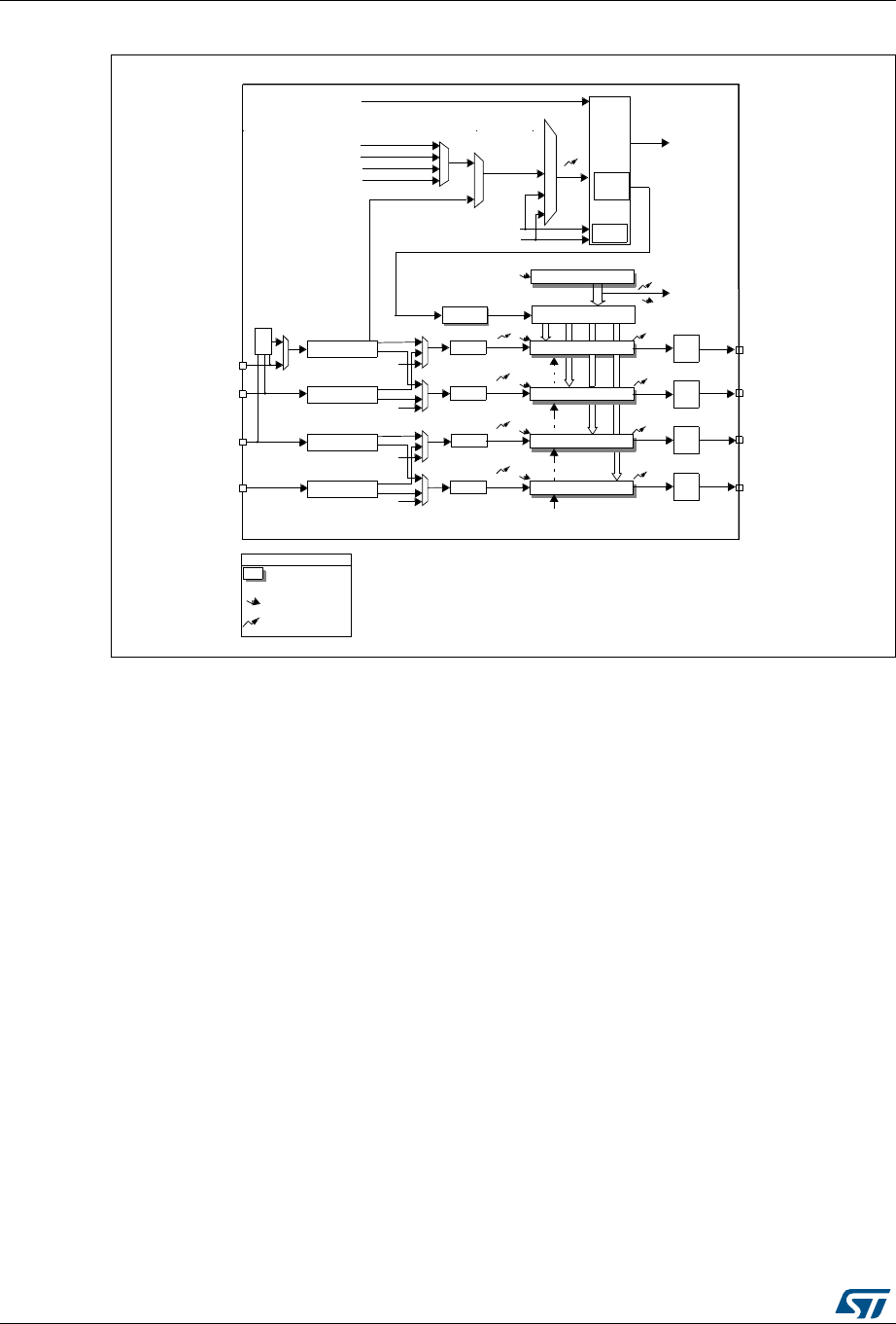
General-purpose timers (TIM5) RM0401
336/766 DocID027812 Rev 2
Figure 96. General-purpose timer block diagram
15.3 TIM5 functional description
15.3.1 Time-base unit
The main block of the programmable timer is a 32-bit counter with its related auto-reload
register. The counter can count up. The counter clock can be divided by a prescaler.
The counter, the auto-reload register and the prescaler register can be written or read by
software. This is true even when the counter is running.
The time-base unit includes:
•Counter Register (TIMx_CNT)
•Prescaler Register (TIMx_PSC):
•Auto-Reload Register (TIMx_ARR)
The auto-reload register is preloaded. Writing to or reading from the auto-reload register
accesses the preload register. The content of the preload register are transferred into the
shadow register permanently or at each update event (UEV), depending on the auto-reload
preload enable bit (ARPE) in TIMx_CR1 register. The update event is sent when the counter
reaches the overflow (or underflow when downcounting) and if the UDIS bit equals 0 in the
TIMx_CR1 register. It can also be generated by software. The generation of the update
event is described in detail for each configuration.
ƵƚŽ ƌĞůŽĂĚ ƌĞŐ ŝƐ ƚĞƌ
ĂƉƚƵ ƌĞͬĐŽŵ ƉĂƌĞ ϭ ƌĞŐ ŝƐ ƚĞ ƌ
ĂƉƚƵ ƌĞͬĐŽŵ ƉĂƌĞ Ϯ ƌĞŐ ŝƐ ƚĞ ƌ
h
h
h
ϭ /
Ϯ/
dƌŝŐŐĞ ƌ
ĐŽŶ ƚƌŽůůĞƌ
^ ƚŽƉ͕ Đ ůĞĂ ƌ Žƌ ƵƉͬĚŽǁŶ
d/ϭ&W ϭ
d/Ϯ&W Ϯ
/d Z Ϭ
/d Z ϭ
/d Z Ϯ
/d Z ϯ
dZ' /
ŶĐŽĚĞ ƌ
/ŶƚĞƌĨĂ Đ Ğ
ĂƉƚƵƌĞͬĐŽŵƉĂƌĞ ϯ ƌĞŐŝƐƚĞƌ
h
ϯ/
ŽƵƚƉƵƚ
ĐŽŶ ƚƌŽů
Kϭ
dZ'K
K ϭZ &
KϮZ &
Kϯ Z &
h
h/
ĂƉ ƚƵƌĞͬĐŽŵ ƉĂƌĞ ϰ ƌĞŐ ŝƐ ƚĞƌ
h
ϰ /
KϰZ &
W ƌĞƐĐĂ ůĞ ƌ
WƌĞƐĐĂ ůĞƌ
/ ϰW ^
/ ϯW ^
/ ϭ
/ Ϯ
W ƌĞƐĐĂ ůĞ ƌ
W ƌĞƐĐĂ ůĞ ƌ
/ŶƉƵ ƚ ĨŝůƚĞƌ Θ
ĞĚŐĞ ĚĞ ƚĞĐƚŽ ƌ
/ ϮW ^
/ ϭW ^
d/ϭ&Wϭ
KϮ
Kϯ
Kϰ
ZĞŐ
ĞǀĞŶƚ
EŽƚĞƐ͗
W ƌĞ ůŽĂ ĚƌĞŐ ŝƐ ƚĞƌƐ ƚƌĂŶ Ɛ ĨĞƌƌĞ Ě
ƚŽ Ă Đ ƚŝǀĞ ƌĞŐ ŝƐ ƚĞƌƐ ŽŶ h Ğ ǀĞ Ŷƚ
ĂĐĐŽƌĚŝŶŐ ƚŽ ĐŽŶƚƌŽů ďŝƚ
ŝŶƚĞƌƌƵƉƚΘ D Ž ƵƚƉƵƚ
d'/
dZ
dZ
/ ϯ
/ ϰ
/d Z
dZ
d/ϭ&ͺ
/ŶƉƵ ƚ ĨŝůƚĞƌ Θ
ĞĚŐĞ ĚĞ ƚĞĐƚŽ ƌ
/ŶƉƵ ƚ ĨŝůƚĞƌ Θ
ĞĚŐĞ ĚĞ ƚĞĐƚŽ ƌ
/ŶƉƵ ƚ ĨŝůƚĞƌ Θ
ĞĚŐĞ ĚĞ ƚĞĐƚŽ ƌ
ϭ /
Ϯ/
ϯ/
ϰ/
d/ϭ&WϮ
d/Ϯ&Wϭ
d/Ϯ&WϮ
d/ϯ&Wϯ
dZ
dZ
d/ϯ&Wϰ
d/ϰ&Wϯ
d/ϰ&Wϰ
d/ϰ
d/ϯ
d/ϭ
d/Ϯ
yKZ
d/Ddžͺ,ϭ
d /Ddžͺ ,
d /Ddžͺ ,
d /Ddžͺ ,
d /Ddžͺ ,
ƚŽ ŽƚŚĞƌ ƚŝŵĞƌƐ
W ƌĞƐĐĂůĞ ƌ Đ ŽƵŶƚĞ ƌ
нͬͲ
<ͺW^ W^ E d
<ͺEd
ĐŽŶ ƚƌŽůůĞƌ
ŵŽĚĞ
^ůĂǀĞ
dZ &
ƚŽ
ŽƵƚƉƵƚ
ĐŽŶ ƚƌŽů
ŽƵƚƉƵƚ
ĐŽŶ ƚƌŽů
ŽƵƚƉƵƚ
ĐŽŶ ƚƌŽů
06Y9
d/Ddžͺ,Ϯ
d/Ddžͺ,ϯ
d/Ddžͺ,ϰ
d/Ddžͺ><ĨƌŽŵZ
/ŶƚĞƌŶĂůůŽĐŬ;<ͺ/EdͿ
5HDGHQDEOHXS
FRXQW
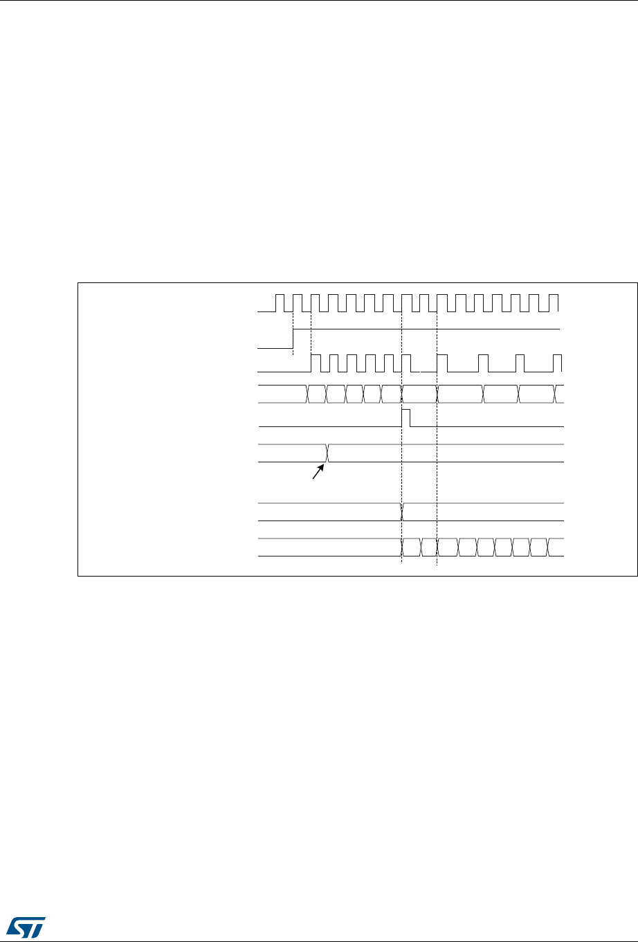
DocID027812 Rev 2 337/766
RM0401 General-purpose timers (TIM5)
384
The counter is clocked by the prescaler output CK_CNT, which is enabled only when the
counter enable bit (CEN) in TIMx_CR1 register is set (refer also to the slave mode controller
description to get more details on counter enabling).
Note that the actual counter enable signal CNT_EN is set 1 clock cycle after CEN.
Prescaler description
The prescaler can divide the counter clock frequency by any factor between 1 and 65536. It
is based on a 16-bit counter controlled through a 32-bit register (in the TIMx_PSC register).
It can be changed on the fly as this control register is buffered. The new prescaler ratio is
taken into account at the next update event.
Figure 97 and Figure 98 give some examples of the counter behavior when the prescaler
ratio is changed on the fly:
Figure 97. Counter timing diagram with prescaler division change from 1 to 2
069
&.B36&
&17B(1
7LPHUFORFN &.B&17
&RXQWHUUHJLVWHU
8SGDWHHYHQW8(9
3UHVFDOHUFRQWUROUHJLVWHU
:ULWHDQHZYDOXHLQ7,0[B36&
3UHVFDOHUEXIIHU
3UHVFDOHUFRXQWHU
)$ )%) ) ) )&
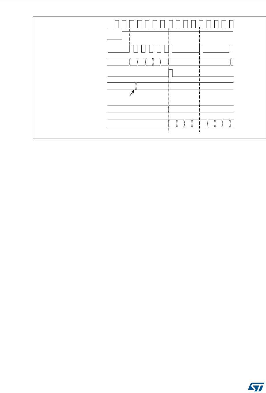
General-purpose timers (TIM5) RM0401
338/766 DocID027812 Rev 2
Figure 98. Counter timing diagram with prescaler division change from 1 to 4
15.3.2 Counter modes
Upcounting mode
In upcounting mode, the counter counts from 0 to the auto-reload value (content of the
TIMx_ARR register), then restarts from 0 and generates a counter overflow event.
An Update event can be generated at each counter overflow or by setting the UG bit in the
TIMx_EGR register (by software or by using the slave mode controller).
The UEV event can be disabled by software by setting the UDIS bit in TIMx_CR1 register.
This is to avoid updating the shadow registers while writing new values in the preload
registers. Then no update event occurs until the UDIS bit has been written to 0. However,
the counter restarts from 0, as well as the counter of the prescaler (but the prescale rate
does not change). In addition, if the URS bit (update request selection) in TIMx_CR1
register is set, setting the UG bit generates an update event UEV but without setting the UIF
flag (thus no interrupt or DMA request is sent). This is to avoid generating both update and
capture interrupts when clearing the counter on the capture event.
When an update event occurs, all the registers are updated and the update flag (UIF bit in
TIMx_SR register) is set (depending on the URS bit):
•The buffer of the prescaler is reloaded with the preload value (content of the TIMx_PSC
register)
•The auto-reload shadow register is updated with the preload value (TIMx_ARR)
The following figures show some examples of the counter behavior for different clock
frequencies when TIMx_ARR=0x36.
069
&.B36&
&17B(1
7LPHUFORFN &.B&17
&RXQWHUUHJLVWHU
8SGDWHHYHQW8(9
3UHVFDOHUFRQWUROUHJLVWHU
:ULWHDQHZYDOXHLQ7,0[B36&
3UHVFDOHUEXIIHU
3UHVFDOHUFRXQWHU
)$ )%) ) ) )&
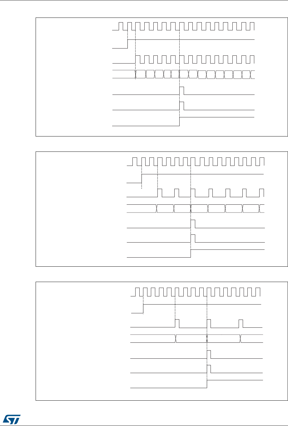
DocID027812 Rev 2 339/766
RM0401 General-purpose timers (TIM5)
384
Figure 99. Counter timing diagram, internal clock divided by 1
Figure 100. Counter timing diagram, internal clock divided by 2
Figure 101. Counter timing diagram, internal clock divided by 4
069
&.B,17
&17B(1
7LPHUFORFN &.B&17
&RXQWHUUHJLVWHU
8SGDWHHYHQW8(9
&RXQWHURYHUIORZ
8SGDWHLQWHUUXSWIODJ8,)
069
&.B,17
&17B(1
7LPHUFORFN &.B&17
&RXQWHUUHJLVWHU
8SGDWHHYHQW8(9
&RXQWHURYHUIORZ
8SGDWHLQWHUUXSWIODJ8,)
06Y9
&.B,17
7LPHUFORFN &.B&17
&RXQWHUUHJLVWHU
8SGDWHHYHQW8(9
&RXQWHURYHUIORZ
8SGDWHLQWHUUXSWIODJ8,)
&17B(1
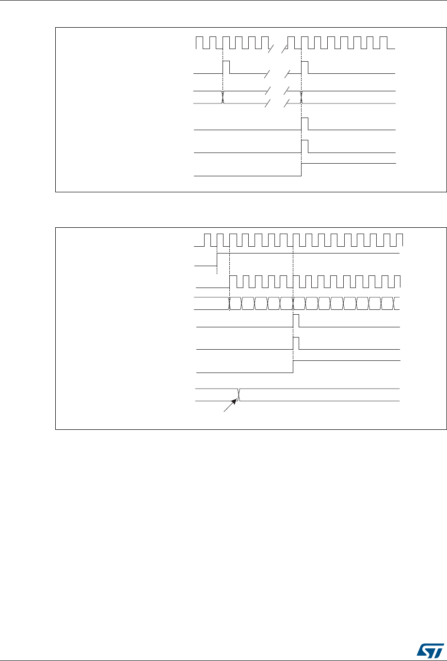
General-purpose timers (TIM5) RM0401
340/766 DocID027812 Rev 2
Figure 102. Counter timing diagram, internal clock divided by N
Figure 103. Counter timing diagram, Update event when ARPE=0 (TIMx_ARR not
preloaded)
06Y9
&.B,17
7LPHUFORFN &.B&17
&RXQWHUUHJLVWHU
8SGDWHHYHQW8(9
&RXQWHURYHUIORZ
8SGDWHLQWHUUXSWIODJ8,)
)
))
06Y9
&.B,17
7LPHUFORFN &.B&17
&RXQWHUUHJLVWHU
8SGDWHHYHQW8(9
&RXQWHURYHUIORZ
8SGDWHLQWHUUXSWIODJ8,)
&17B(1
$XWRUHORDGUHJLVWHU
:ULWHDQHZYDOXHLQ7,0[B$55
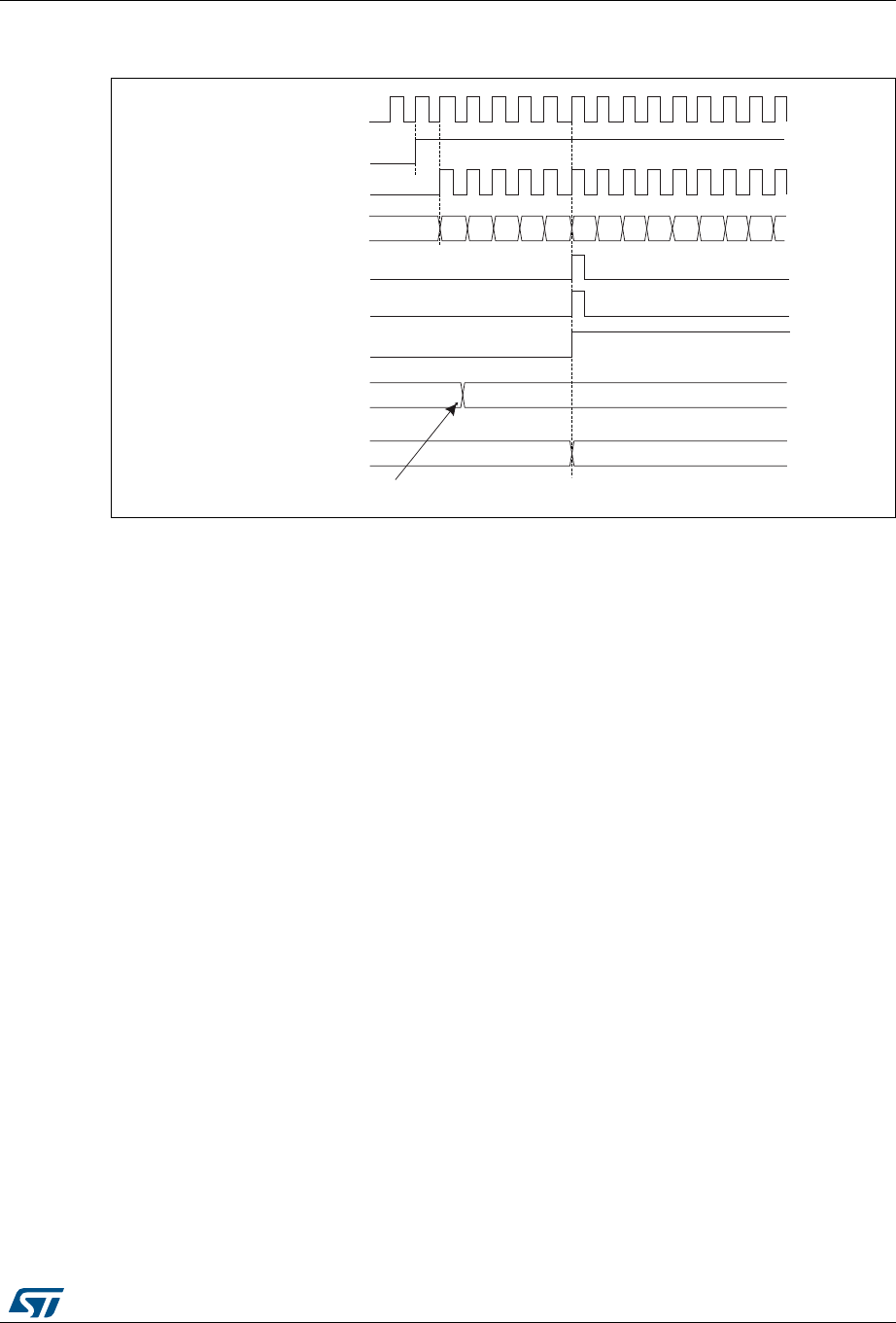
DocID027812 Rev 2 341/766
RM0401 General-purpose timers (TIM5)
384
Figure 104. Counter timing diagram, Update event when ARPE=1 (TIMx_ARR
preloaded)
Downcounting mode
In downcounting mode, the counter counts from the auto-reload value (content of the
TIMx_ARR register) down to 0, then restarts from the auto-reload value and generates a
counter underflow event.
An Update event can be generate at each counter underflow or by setting the UG bit in the
TIMx_EGR register (by software or by using the slave mode controller)
The UEV update event can be disabled by software by setting the UDIS bit in TIMx_CR1
register. This is to avoid updating the shadow registers while writing new values in the
preload registers. Then no update event occurs until UDIS bit has been written to 0.
However, the counter restarts from the current auto-reload value, whereas the counter of the
prescaler restarts from 0 (but the prescale rate doesn’t change).
In addition, if the URS bit (update request selection) in TIMx_CR1 register is set, setting the
UG bit generates an update event UEV but without setting the UIF flag (thus no interrupt or
DMA request is sent). This is to avoid generating both update and capture interrupts when
clearing the counter on the capture event.
When an update event occurs, all the registers are updated and the update flag (UIF bit in
TIMx_SR register) is set (depending on the URS bit):
•The buffer of the prescaler is reloaded with the preload value (content of the TIMx_PSC
register).
•The auto-reload active register is updated with the preload value (content of the
TIMx_ARR register). Note that the auto-reload is updated before the counter is
reloaded, so that the next period is the expected one.
The following figures show some examples of the counter behavior for different clock
frequencies when TIMx_ARR=0x36.
06Y9
)
&.B36&
7LPHUFORFN &.B&17
&RXQWHUUHJLVWHU
8SGDWHHYHQW8(9
&RXQWHURYHUIORZ
8SGDWHLQWHUUXSWIODJ8,)
) ) ) ) ))
&17B(1
$XWRUHORDGSUHORDGUHJLVWHU
:ULWHDQHZYDOXHLQ7,0[B$55
$XWRUHORDGVKDGRZUHJLVWHU )
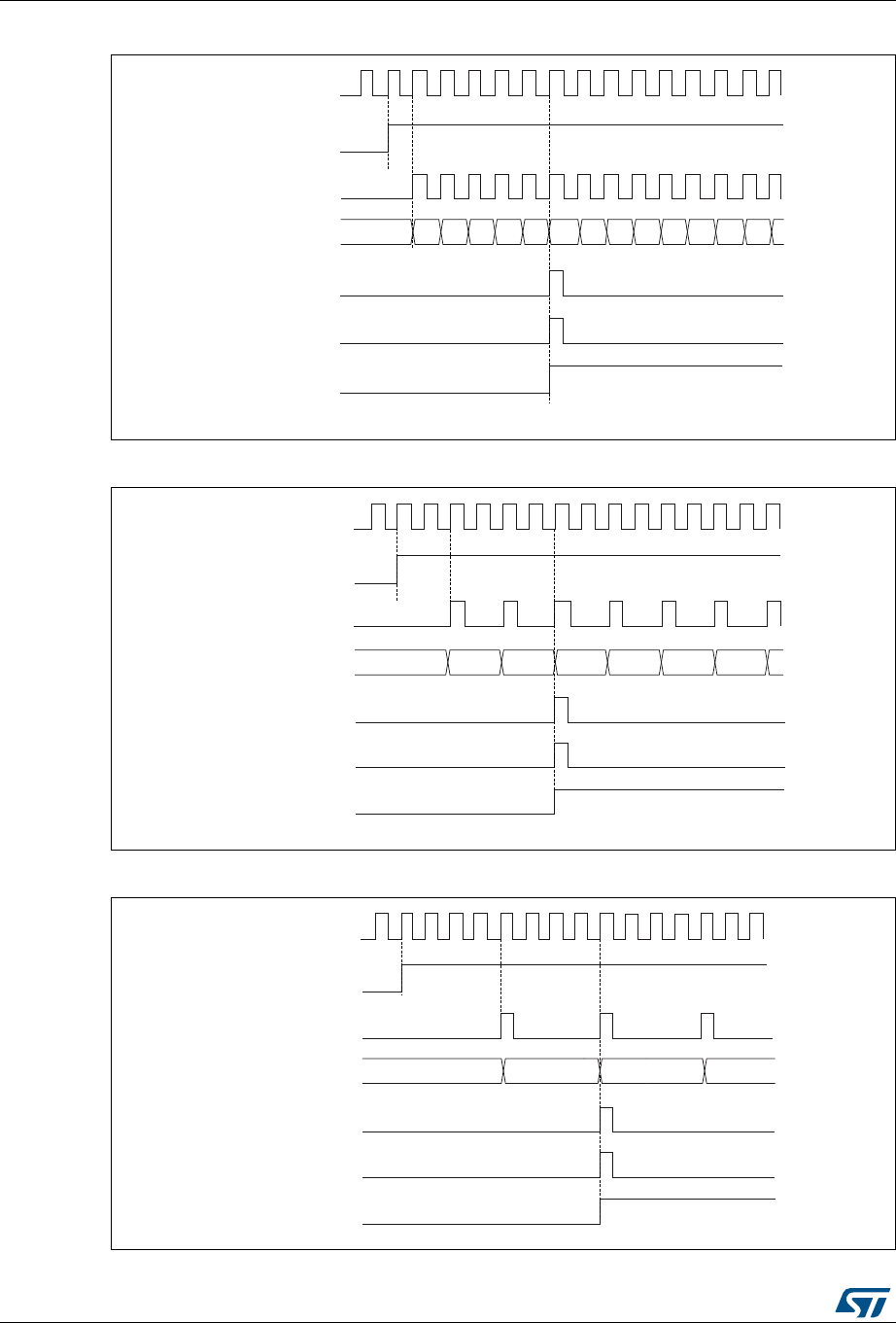
General-purpose timers (TIM5) RM0401
342/766 DocID027812 Rev 2
Figure 105. Counter timing diagram, internal clock divided by 1
Figure 106. Counter timing diagram, internal clock divided by 2
Figure 107. Counter timing diagram, internal clock divided by 4
)
06Y9
&.B,17
&17B(1
7LPHUFORFN &.B&17
&RXQWHUUHJLVWHU
8SGDWHHYHQW8(9
&RXQWHUXQGHUIORZFQWBXGI
8SGDWHLQWHUUXSWIODJ8,)
06Y9
&.B,17
&17B(1
7LPHUFORFN &.B&17
&RXQWHUUHJLVWHU
8SGDWHHYHQW8(9
&RXQWHUXQGHUIORZ
8SGDWHLQWHUUXSWIODJ8,)
06Y9
&.B,17
7LPHUFORFN &.B&17
&RXQWHUUHJLVWHU
8SGDWHHYHQW8(9
&RXQWHUXQGHUIORZ
8SGDWHLQWHUUXSWIODJ8,)
&17B(1
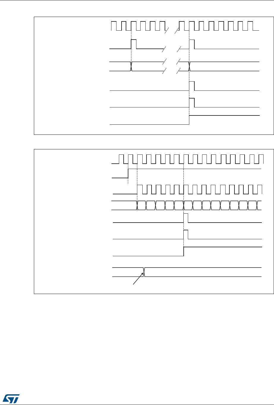
DocID027812 Rev 2 343/766
RM0401 General-purpose timers (TIM5)
384
Figure 108. Counter timing diagram, internal clock divided by N
Figure 109. Counter timing diagram, Update event
Center-aligned mode (up/down counting)
In center-aligned mode, the counter counts from 0 to the auto-reload value (content of the
TIMx_ARR register) – 1, generates a counter overflow event, then counts from the auto-
reload value down to 1 and generates a counter underflow event. Then it restarts counting
from 0.
Center-aligned mode is active when the CMS bits in TIMx_CR1 register are not equal to
'00'. The Output compare interrupt flag of channels configured in output is set when: the
counter counts down (Center aligned mode 1, CMS = "01"), the counter counts up (Center
aligned mode 2, CMS = "10") the counter counts up and down (Center aligned mode 3,
CMS = "11").
069
)
&.B,17
7LPHUFORFN &.B&17
&RXQWHUUHJLVWHU
8SGDWHHYHQW8(9
&RXQWHURYHUIORZ
8SGDWHLQWHUUXSWIODJ8,)
069
))
&.B,17
7LPHUFORFN &.B&17
&RXQWHUUHJLVWHU
8SGDWHHYHQW8(9
&RXQWHURYHUIORZ
8SGDWHLQWHUUXSWIODJ8,)
&17B(1
$XWRUHORDGSUHORDGUHJLVWHU
:ULWHDQHZYDOXHLQ7,0[B$55
)
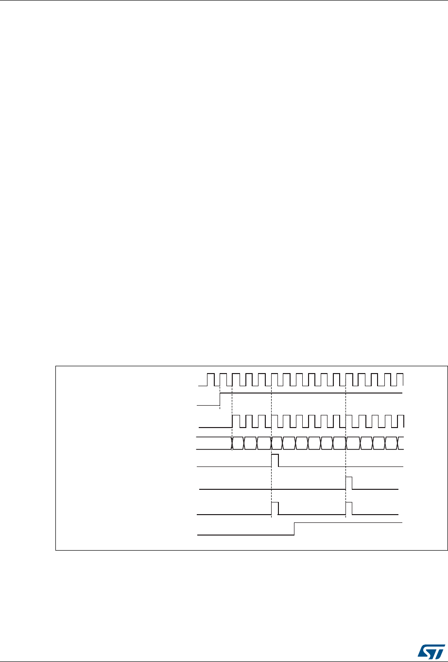
General-purpose timers (TIM5) RM0401
344/766 DocID027812 Rev 2
In this mode, the direction bit (DIR from TIMx_CR1 register) cannot be written. It is updated
by hardware and gives the current direction of the counter.
The update event can be generated at each counter overflow and at each counter underflow
or by setting the UG bit in the TIMx_EGR register (by software or by using the slave mode
controller) also generates an update event. In this case, the counter restarts counting from
0, as well as the counter of the prescaler.
The UEV update event can be disabled by software by setting the UDIS bit in TIMx_CR1
register. This is to avoid updating the shadow registers while writing new values in the
preload registers. Then no update event occurs until the UDIS bit has been written to 0.
However, the counter continues counting up and down, based on the current auto-reload
value.
In addition, if the URS bit (update request selection) in TIMx_CR1 register is set, setting the
UG bit generates an update event UEV but without setting the UIF flag (thus no interrupt or
DMA request is sent). This is to avoid generating both update and capture interrupt when
clearing the counter on the capture event.
When an update event occurs, all the registers are updated and the update flag (UIF bit in
TIMx_SR register) is set (depending on the URS bit):
•The buffer of the prescaler is reloaded with the preload value (content of the TIMx_PSC
register).
•The auto-reload active register is updated with the preload value (content of the
TIMx_ARR register). Note that if the update source is a counter overflow, the auto-
reload is updated before the counter is reloaded, so that the next period is the expected
one (the counter is loaded with the new value).
The following figures show some examples of the counter behavior for different clock
frequencies.
Figure 110. Counter timing diagram, internal clock divided by 1, TIMx_ARR=0x6
1. Here, center-aligned mode 1 is used (for more details refer to Section 15.4.1: TIMx control register 1 (TIMx_CR1)
on page 364).
069
&.B,17
7LPHUFORFN &.B&17
&RXQWHUUHJLVWHU
8SGDWHHYHQW8(9
&RXQWHURYHUIORZ
8SGDWHLQWHUUXSWIODJ8,)
&17B(1
&RXQWHUXQGHUIORZ
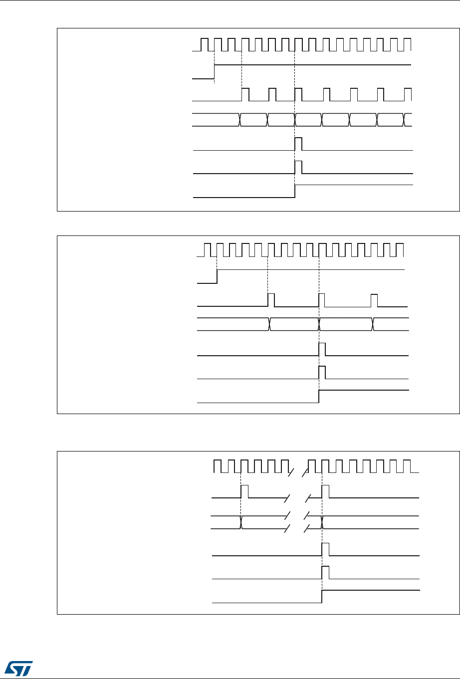
DocID027812 Rev 2 345/766
RM0401 General-purpose timers (TIM5)
384
Figure 111. Counter timing diagram, internal clock divided by 2
Figure 112. Counter timing diagram, internal clock divided by 4, TIMx_ARR=0x36
1. Center-aligned mode 2 or 3 is used with an UIF on overflow.
Figure 113. Counter timing diagram, internal clock divided by N
069
&.B,17
7LPHUFORFN &.B&17
&RXQWHUUHJLVWHU
8SGDWHHYHQW8(9
8SGDWHLQWHUUXSWIODJ8,)
&17B(1
&RXQWHUXQGHUIORZ
069
&.B,17
7LPHUFORFN &.B&17
&RXQWHUUHJLVWHU
8SGDWHHYHQW8(9
&RXQWHURYHUIORZFQWBRYI
8SGDWHLQWHUUXSWIODJ8,)
&17B(1
069
&.B,17
7LPHUFORFN &.B&17
&RXQWHUUHJLVWHU
8SGDWHHYHQW8(9
8SGDWHLQWHUUXSWIODJ8,)
&RXQWHUXQGHUIORZ
)
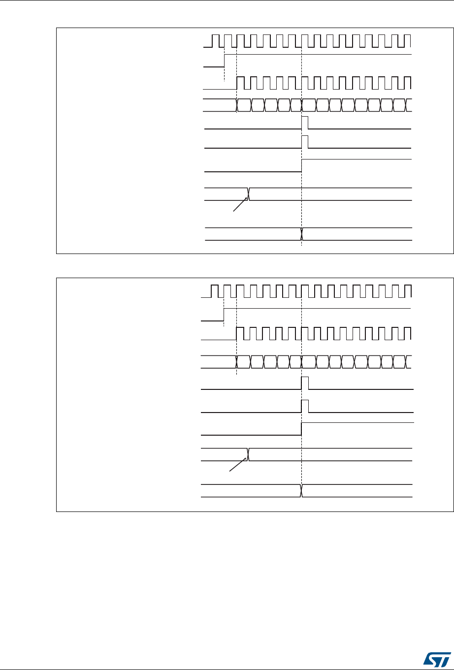
General-purpose timers (TIM5) RM0401
346/766 DocID027812 Rev 2
Figure 114. Counter timing diagram, Update event with ARPE=1 (counter underflow)
Figure 115. Counter timing diagram, Update event with ARPE=1 (counter overflow)
15.3.3 Clock selection
The counter clock can be provided by the following clock sources:
•Internal clock (CK_INT)
•External clock mode1: external input pin (TIx)
•Internal trigger inputs (ITRx): using one timer as prescaler for another timer.
069
)'
&.B,17
7LPHUFORFN &.B&17
&RXQWHUUHJLVWHU
8SGDWHHYHQW8(9
&RXQWHUXQGHUIORZ
8SGDWHLQWHUUXSWIODJ8,)
&17B(1
$XWRUHORDGSUHORDGUHJLVWHU
:ULWHDQHZYDOXHLQ7,0[B$55
)'
$XWRUHORDGDFWLYHUHJLVWHU
069
)'
&.B,17
7LPHUFORFN &.B&17
&RXQWHUUHJLVWHU
8SGDWHHYHQW8(9
&RXQWHURYHUIORZ
8SGDWHLQWHUUXSWIODJ8,)
)) ) )$ )% )&)
&17B(1
$XWRUHORDGSUHORDGUHJLVWHU
:ULWHDQHZYDOXHLQ7,0[B$55
$XWRUHORDGDFWLYHUHJLVWHU )'
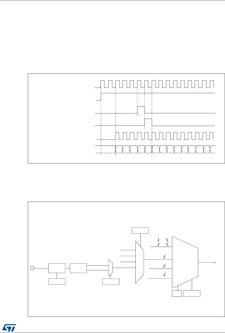
DocID027812 Rev 2 347/766
RM0401 General-purpose timers (TIM5)
384
Internal clock source (CK_INT)
If the slave mode controller is disabled (SMS=000 in the TIMx_SMCR register), then the
CEN, DIR (in the TIMx_CR1 register) and UG bits (in the TIMx_EGR register) are actual
control bits and can be changed only by software (except UG which remains cleared
automatically). As soon as the CEN bit is written to 1, the prescaler is clocked by the internal
clock CK_INT.
Figure 116 shows the behavior of the control circuit and the upcounter in normal mode,
without prescaler.
Figure 116. Control circuit in normal mode, internal clock divided by 1
External clock source mode 1
This mode is selected when SMS=111 in the TIMx_SMCR register. The counter can count at
each rising or falling edge on a selected input.
Figure 117. TI2 external clock connection example
,QWHUQDOFORFN
&RXQWHUFORFN &.B&17 &.B36&
&RXQWHUUHJLVWHU
&(1 &17B(1
8*
&17B,1,7
069
06Y9
([WHUQDOFORFN
PRGH
,QWHUQDOFORFN
PRGH
75*,
&.B,17
&.B36&
7,0[B60&5
606>@
,75[
7,B('
7,)3
7,)3
7,0[B60&5
76>@
7,
7,0[B&&(5
&&3
)LOWHU
,&)>@
7,0[B&&05
(GJH
GHWHFWRU
7,)B5LVLQJ
7,)B)DOOLQJ
[[
LQWHUQDOFORFN
7,) RU
7,) RU
RU
(QFRGHU
PRGH
([WHUQDOFORFN
PRGH
(75)
(&(
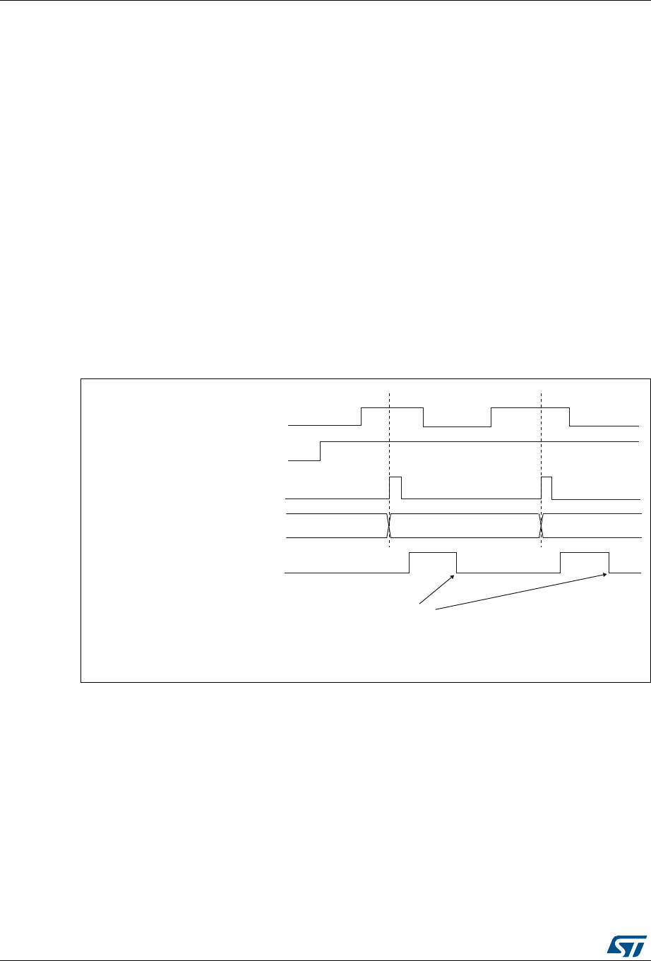
General-purpose timers (TIM5) RM0401
348/766 DocID027812 Rev 2
For example, to configure the upcounter to count in response to a rising edge on the TI2
input, use the following procedure:
1. Configure channel 2 to detect rising edges on the TI2 input by writing CC2S= ‘01 in the
TIMx_CCMR1 register.
2. Configure the input filter duration by writing the IC2F[3:0] bits in the TIMx_CCMR1
register (if no filter is needed, keep IC2F=0000).
Note: The capture prescaler is not used for triggering, so you don’t need to configure it.
3. Select rising edge polarity by writing CC2P=0 and CC2NP=0 in the TIMx_CCER
register.
4. Configure the timer in external clock mode 1 by writing SMS=111 in the TIMx_SMCR
register.
5. Select TI2 as the input source by writing TS=110 in the TIMx_SMCR register.
6. Enable the counter by writing CEN=1 in the TIMx_CR1 register.
When a rising edge occurs on TI2, the counter counts once and the TIF flag is set.
The delay between the rising edge on TI2 and the actual clock of the counter is due to the
resynchronization circuit on TI2 input.
Figure 118. Control circuit in external clock mode 1
15.3.4 Capture/compare channels
Each Capture/Compare channel is built around a capture/compare register (including a
shadow register), a input stage for capture (with digital filter, multiplexing and prescaler) and
an output stage (with comparator and output control).
The following figure gives an overview of one Capture/Compare channel.
The input stage samples the corresponding TIx input to generate a filtered signal TIxF.
Then, an edge detector with polarity selection generates a signal (TIxFPx) which can be
used as trigger input by the slave mode controller or as the capture command. It is
prescaled before the capture register (ICxPS).
&RXQWHUFORFN &.B&17 &.B36&
&RXQWHUUHJLVWHU
7,
&17B(1
7,)
:ULWH7,)
069
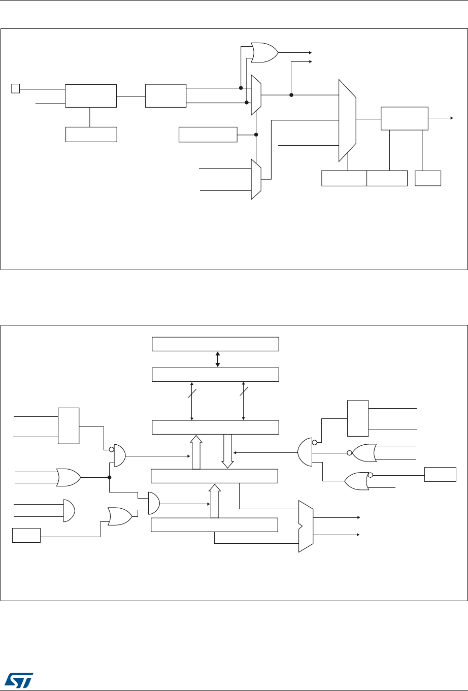
DocID027812 Rev 2 349/766
RM0401 General-purpose timers (TIM5)
384
Figure 119. Capture/compare channel (example: channel 1 input stage)
The output stage generates an intermediate waveform which is then used for reference:
OCxRef (active high). The polarity acts at the end of the chain.
Figure 120. Capture/compare channel 1 main circuit
'LYLGHU
,&36>@
7,)B('
7RWKHVODYHPRGHFRQWUROOHU
7,)3
&&6>@
,&
7,)3
75&
IURPVODYHPRGH
FRQWUROOHU
,&36
069
7,
7,0[B&&(5
&&3&&13
)LOWHU
GRZQFRXQWHU
,&)>@
7,0[B&&05
(GJH
GHWHFWRU
7,)B5LVLQJ
7,)B)DOOLQJ
7,0[B&&05
7,0[B&&(5
7,)B5LVLQJ
IURPFKDQQHO
7,)B)DOOLQJ
IURPFKDQQHO
7,)
I
&&(
'76
&&(
&DSWXUHFRPSDUHVKDGRZUHJLVWHU
&RPSDUDWRU
&DSWXUHFRPSDUHSUHORDGUHJLVWHU
&RXQWHU
,&36
&&6>@
&&6>@
&DSWXUH
,QSXW
PRGH
6
5
5HDG&&5+
5HDG&&5/
UHDGBLQBSURJUHVV
FDSWXUHBWUDQVIHU &&6>@
&&6>@
6
5
ZULWH&&5+
ZULWH&&5/
ZULWHBLQBSURJUHVV
2XWSXW
PRGH
8(9
2&3(
IURPWLPH
EDVHXQLW
FRPSDUHBWUDQVIHU
$3%%XV
KLJK
ORZ
LIELW
0&8SHULSKHUDOLQWHUIDFH
7,0[B&&05
2&3(
&17!&&5
&17 &&5
7,0[B(*5
&&*
069
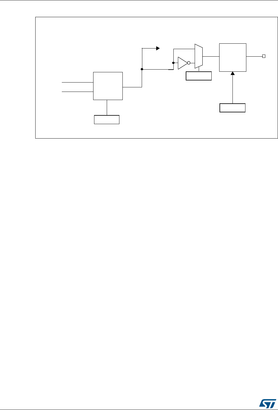
General-purpose timers (TIM5) RM0401
350/766 DocID027812 Rev 2
Figure 121. Output stage of capture/compare channel (channel 1)
The capture/compare block is made of one preload register and one shadow register. Write
and read always access the preload register.
In capture mode, captures are actually done in the shadow register, which is copied into the
preload register.
In compare mode, the content of the preload register is copied into the shadow register
which is compared to the counter.
15.3.5 Input capture mode
In Input capture mode, the Capture/Compare Registers (TIMx_CCRx) are used to latch the
value of the counter after a transition detected by the corresponding ICx signal. When a
capture occurs, the corresponding CCXIF flag (TIMx_SR register) is set and an interrupt or
a DMA request can be sent if they are enabled. If a capture occurs while the CCxIF flag was
already high, then the over-capture flag CCxOF (TIMx_SR register) is set. CCxIF can be
cleared by software by writing it to 0 or by reading the captured data stored in the
TIMx_CCRx register. CCxOF is cleared when you write it to 0.
The following example shows how to capture the counter value in TIMx_CCR1 when TI1
input rises. To do this, use the following procedure:
•Select the active input: TIMx_CCR1 must be linked to the TI1 input, so write the CC1S
bits to 01 in the TIMx_CCMR1 register. As soon as CC1S becomes different from 00,
the channel is configured in input and the TIMx_CCR1 register becomes read-only.
•Program the input filter duration you need with respect to the signal you connect to the
timer (by programming the ICxF bits in the TIMx_CCMRx register if the input is one of
the TIx inputs). Let’s imagine that, when toggling, the input signal is not stable during at
must 5 internal clock cycles. We must program a filter duration longer than these 5
clock cycles. We can validate a transition on TI1 when 8 consecutive samples with the
2XWSXWPRGH
7,0[B&17!7,0[B&&5
FRQWUROOHU
7,0[B&&05
2&0>@
RFUHI
7,0[B&&(5
2XWSXW
(QDEOH
&LUFXLW
2&
7,0[B&&(5
7RWKHPDVWHUPRGH
FRQWUROOHU
06Y9
&&3
&&(
7,0[B&17 7,0[B&&5

DocID027812 Rev 2 351/766
RM0401 General-purpose timers (TIM5)
384
new level have been detected (sampled at fDTS frequency). Then write IC1F bits to
0011 in the TIMx_CCMR1 register.
•Select the edge of the active transition on the TI1 channel by writing the CC1P and
CC1NP bits to 00 in the TIMx_CCER register (rising edge in this case).
•Program the input prescaler. In our example, we wish the capture to be performed at
each valid transition, so the prescaler is disabled (write IC1PS bits to 00 in the
TIMx_CCMR1 register).
•Enable capture from the counter into the capture register by setting the CC1E bit in the
TIMx_CCER register.
•If needed, enable the related interrupt request by setting the CC1IE bit in the
TIMx_DIER register, and/or the DMA request by setting the CC1DE bit in the
TIMx_DIER register.
When an input capture occurs:
•The TIMx_CCR1 register gets the value of the counter on the active transition.
•CC1IF flag is set (interrupt flag). CC1OF is also set if at least two consecutive captures
occurred whereas the flag was not cleared.
•An interrupt is generated depending on the CC1IE bit.
•A DMA request is generated depending on the CC1DE bit.
In order to handle the overcapture, it is recommended to read the data before the
overcapture flag. This is to avoid missing an overcapture which could happen after reading
the flag and before reading the data.
Note: IC interrupt and/or DMA requests can be generated by software by setting the
corresponding CCxG bit in the TIMx_EGR register.
15.3.6 PWM input mode
This mode is a particular case of input capture mode. The procedure is the same except:
•Two ICx signals are mapped on the same TIx input.
•These 2 ICx signals are active on edges with opposite polarity.
•One of the two TIxFP signals is selected as trigger input and the slave mode controller
is configured in reset mode.
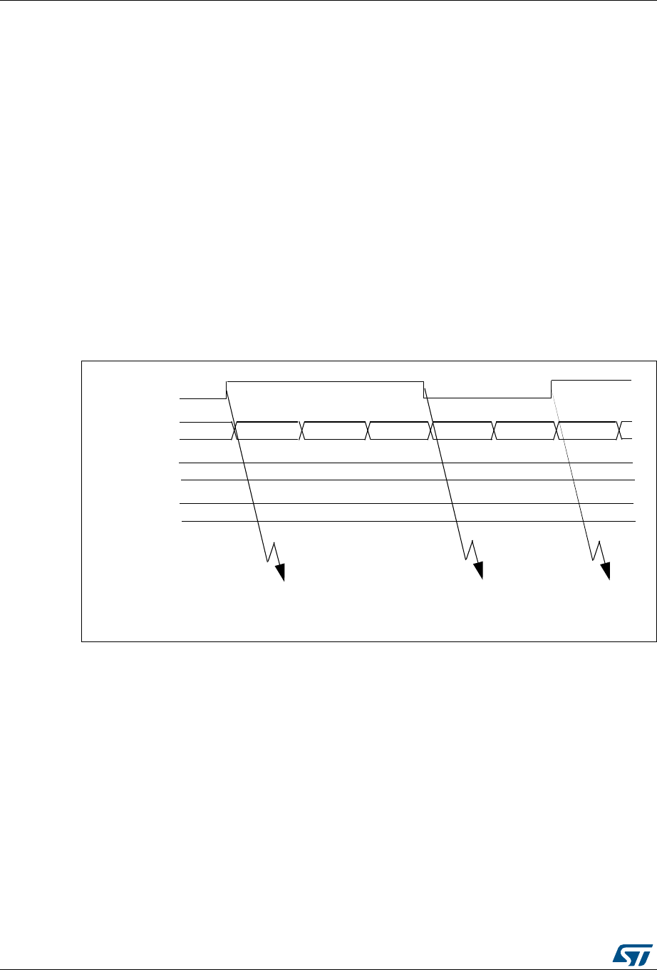
General-purpose timers (TIM5) RM0401
352/766 DocID027812 Rev 2
For example, you can measure the period (in TIMx_CCR1 register) and the duty cycle (in
TIMx_CCR2 register) of the PWM applied on TI1 using the following procedure (depending
on CK_INT frequency and prescaler value):
•Select the active input for TIMx_CCR1: write the CC1S bits to 01 in the TIMx_CCMR1
register (TI1 selected).
•Select the active polarity for TI1FP1 (used both for capture in TIMx_CCR1 and counter
clear): write the CC1P to ‘0’ and the CC1NP bit to ‘0’ (active on rising edge).
•Select the active input for TIMx_CCR2: write the CC2S bits to 10 in the TIMx_CCMR1
register (TI1 selected).
•Select the active polarity for TI1FP2 (used for capture in TIMx_CCR2): write the CC2P
bit to ‘1’ and the CC2NP bit to ’0’(active on falling edge).
•Select the valid trigger input: write the TS bits to 101 in the TIMx_SMCR register
(TI1FP1 selected).
•Configure the slave mode controller in reset mode: write the SMS bits to 100 in the
TIMx_SMCR register.
•Enable the captures: write the CC1E and CC2E bits to ‘1 in the TIMx_CCER register.
Figure 122. PWM input mode timing
15.3.7 Forced output mode
In output mode (CCxS bits = 00 in the TIMx_CCMRx register), each output compare signal
(OCxREF and then OCx) can be forced to active or inactive level directly by software,
independently of any comparison between the output compare register and the counter.
To force an output compare signal (ocxref/OCx) to its active level, you just need to write 101
in the OCxM bits in the corresponding TIMx_CCMRx register. Thus ocxref is forced high
(OCxREF is always active high) and OCx get opposite value to CCxP polarity bit.
e.g.: CCxP=0 (OCx active high) => OCx is forced to high level.
ocxref signal can be forced low by writing the OCxM bits to 100 in the TIMx_CCMRx
register.
TI1
TIMx_CNT 0000 0001 0002 0003 0004 00000004
TIMx_CCR1
TIMx_CCR2
0004
0002
IC1 capture
IC2 capture
reset counter
IC2 capture
pulse width
IC1 capture
period
measurementmeasurement
ai15413

DocID027812 Rev 2 353/766
RM0401 General-purpose timers (TIM5)
384
Anyway, the comparison between the TIMx_CCRx shadow register and the counter is still
performed and allows the flag to be set. Interrupt and DMA requests can be sent
accordingly. This is described in the Output Compare Mode section.
15.3.8 Output compare mode
This function is used to control an output waveform or indicating when a period of time has
elapsed.
When a match is found between the capture/compare register and the counter, the output
compare function:
•Assigns the corresponding output pin to a programmable value defined by the output
compare mode (OCxM bits in the TIMx_CCMRx register) and the output polarity (CCxP
bit in the TIMx_CCER register). The output pin can keep its level (OCXM=000), be set
active (OCxM=001), be set inactive (OCxM=010) or can toggle (OCxM=011) on match.
•Sets a flag in the interrupt status register (CCxIF bit in the TIMx_SR register).
•Generates an interrupt if the corresponding interrupt mask is set (CCXIE bit in the
TIMx_DIER register).
•Sends a DMA request if the corresponding enable bit is set (CCxDE bit in the
TIMx_DIER register, CCDS bit in the TIMx_CR2 register for the DMA request
selection).
The TIMx_CCRx registers can be programmed with or without preload registers using the
OCxPE bit in the TIMx_CCMRx register.
In output compare mode, the update event UEV has no effect on ocxref and OCx output.
The timing resolution is one count of the counter. Output compare mode can also be used to
output a single pulse (in One-pulse mode).
Procedure:
1. Select the counter clock (internal, external, prescaler).
2. Write the desired data in the TIMx_ARR and TIMx_CCRx registers.
3. Set the CCxIE and/or CCxDE bits if an interrupt and/or a DMA request is to be
generated.
4. Select the output mode. For example, you must write OCxM=011, OCxPE=0, CCxP=0
and CCxE=1 to toggle OCx output pin when CNT matches CCRx, CCRx preload is not
used, OCx is enabled and active high.
5. Enable the counter by setting the CEN bit in the TIMx_CR1 register.
The TIMx_CCRx register can be updated at any time by software to control the output
waveform, provided that the preload register is not enabled (OCxPE=0, else TIMx_CCRx
shadow register is updated only at the next update event UEV). An example is given in
Figure 123.

General-purpose timers (TIM5) RM0401
354/766 DocID027812 Rev 2
Figure 123. Output compare mode, toggle on OC1
15.3.9 PWM mode
Pulse width modulation mode allows you to generate a signal with a frequency determined
by the value of the TIMx_ARR register and a duty cycle determined by the value of the
TIMx_CCRx register.
The PWM mode can be selected independently on each channel (one PWM per OCx
output) by writing 110 (PWM mode 1) or ‘111 (PWM mode 2) in the OCxM bits in the
TIMx_CCMRx register. You must enable the corresponding preload register by setting the
OCxPE bit in the TIMx_CCMRx register, and eventually the auto-reload preload register by
setting the ARPE bit in the TIMx_CR1 register.
As the preload registers are transferred to the shadow registers only when an update event
occurs, before starting the counter, you have to initialize all the registers by setting the UG
bit in the TIMx_EGR register.
OCx polarity is software programmable using the CCxP bit in the TIMx_CCER register. It
can be programmed as active high or active low. OCx output is enabled by the CCxE bit in
the TIMx_CCER register. Refer to the TIMx_CCERx register description for more details.
In PWM mode (1 or 2), TIMx_CNT and TIMx_CCRx are always compared to determine
whether TIMx_CCRx≤ TIMx_CNT or TIMx_CNT≤ TIMx_CCRx (depending on the direction
of the counter). However, the OCREF signal is asserted only:
•When the result of the comparison changes, or
•When the output compare mode (OCxM bits in TIMx_CCMRx register) switches from
the “frozen” configuration (no comparison, OCxM=‘000) to one of the PWM modes
(OCxM=‘110 or ‘111).
This forces the PWM by software while the timer is running.
The timer is able to generate PWM in edge-aligned mode or center-aligned mode
depending on the CMS bits in the TIMx_CR1 register.
069
2&5() 2&
7,0[B&17 % %
7,0[B&&5 $
:ULWH%KLQWKH&&5UHJLVWHU
0DWFKGHWHFWHGRQ&&5
,QWHUUXSWJHQHUDWHGLIHQDEOHG
%
%
$
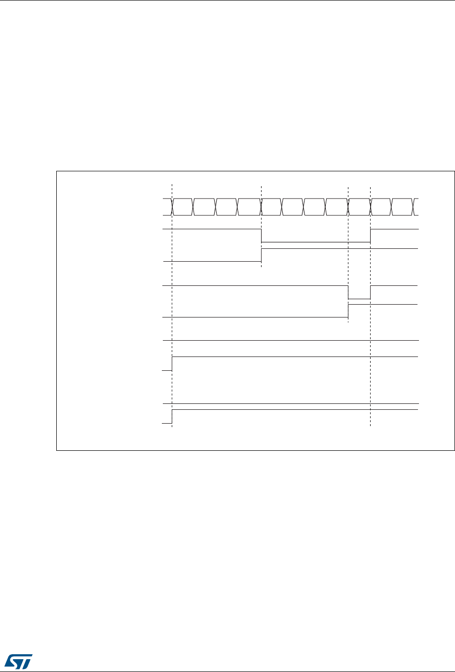
DocID027812 Rev 2 355/766
RM0401 General-purpose timers (TIM5)
384
PWM edge-aligned mode
Upcounting configuration
Upcounting is active when the DIR bit in the TIMx_CR1 register is low. Refer to Section :
Upcounting mode on page 338.
In the following example, we consider PWM mode 1. The reference PWM signal OCxREF is
high as long as TIMx_CNT <TIMx_CCRx else it becomes low. If the compare value in
TIMx_CCRx is greater than the auto-reload value (in TIMx_ARR) then OCxREF is held at ‘1.
If the compare value is 0 then OCxREF is held at ‘0. Figure 124 shows some edge-aligned
PWM waveforms in an example where TIMx_ARR=8.
Figure 124. Edge-aligned PWM waveforms (ARR=8)
Downcounting configuration
Downcounting is active when DIR bit in TIMx_CR1 register is high. Refer to Section :
Downcounting mode on page 341.
In PWM mode 1, the reference signal ocxref is low as long as TIMx_CNT>TIMx_CCRx else
it becomes high. If the compare value in TIMx_CCRx is greater than the auto-reload value in
TIMx_ARR, then ocxref is held at ‘1’. 0% PWM is not possible in this mode.
PWM center-aligned mode
Center-aligned mode is active when the CMS bits in TIMx_CR1 register are different from
‘00 (all the remaining configurations having the same effect on the ocxref/OCx signals). The
compare flag is set when the counter counts up, when it counts down or both when it counts
up and down depending on the CMS bits configuration. The direction bit (DIR) in the
TIMx_CR1 register is updated by hardware and must not be changed by software. Refer to
069
&RXQWHUUHJLVWHU
µ
2&;5()
&&[,)
2&;5()
&&[,)
2&;5()
&&[,)
2&;5()
&&[,)
&&5[
&&5[
&&5[!
&&5[
µ
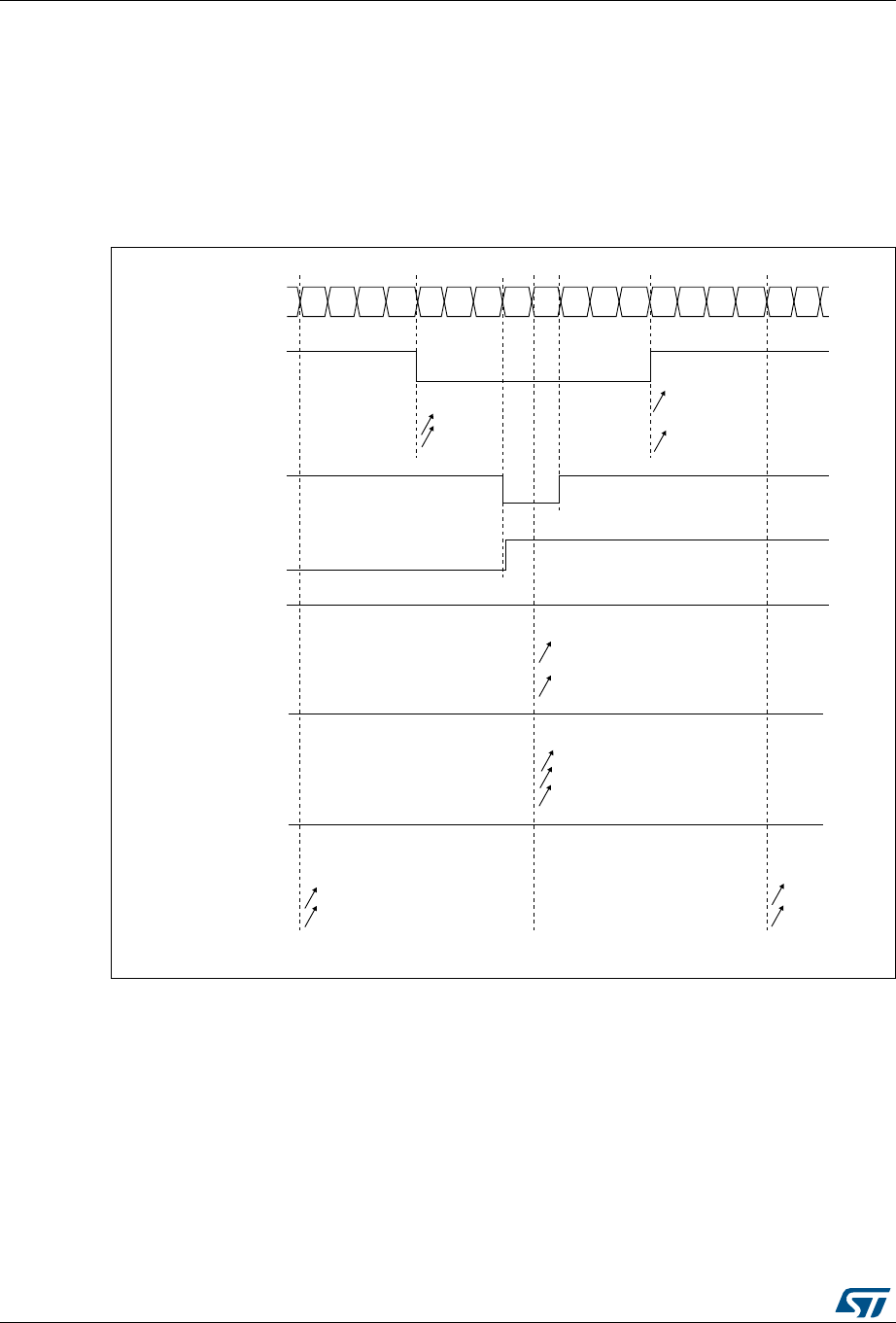
General-purpose timers (TIM5) RM0401
356/766 DocID027812 Rev 2
Section : Center-aligned mode (up/down counting) on page 343.
Figure 125 shows some center-aligned PWM waveforms in an example where:
•TIMx_ARR=8,
•PWM mode is the PWM mode 1,
•The flag is set when the counter counts down corresponding to the center-aligned
mode 1 selected for CMS=01 in TIMx_CR1 register.
Figure 125. Center-aligned PWM waveforms (ARR=8)
Hints on using center-aligned mode:
•When starting in center-aligned mode, the current up-down configuration is used. It
means that the counter counts up or down depending on the value written in the DIR bit
&&[,)
&RXQWHUUHJLVWHU
&&5[
2&[5()
&06
&06
&06
&&[,)
&&5[
2&[5()
&06 RU
&&[,)
&&5[
2&[5()
&06
&06
&06
µ
&&[,)
&&5[!
2&[5()
&06
&06
&06
µ
&&[,)
&&5[
2&[5()
&06
&06
&06
µ
$,E
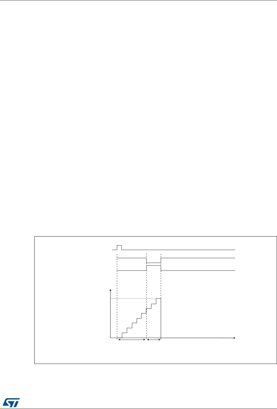
DocID027812 Rev 2 357/766
RM0401 General-purpose timers (TIM5)
384
in the TIMx_CR1 register. Moreover, the DIR and CMS bits must not be changed at the
same time by the software.
•Writing to the counter while running in center-aligned mode is not recommended as it
can lead to unexpected results. In particular:
– The direction is not updated if you write a value in the counter that is greater than
the auto-reload value (TIMx_CNT>TIMx_ARR). For example, if the counter was
counting up, it continues to count up.
– The direction is updated if you write 0 or write the TIMx_ARR value in the counter
but no Update Event UEV is generated.
•The safest way to use center-aligned mode is to generate an update by software
(setting the UG bit in the TIMx_EGR register) just before starting the counter and not to
write the counter while it is running.
15.3.10 One-pulse mode
One-pulse mode (OPM) is a particular case of the previous modes. It allows the counter to
be started in response to a stimulus and to generate a pulse with a programmable length
after a programmable delay.
Starting the counter can be controlled through the slave mode controller. Generating the
waveform can be done in output compare mode or PWM mode. You select One-pulse mode
by setting the OPM bit in the TIMx_CR1 register. This makes the counter stop automatically
at the next update event UEV.
A pulse can be correctly generated only if the compare value is different from the counter
initial value. Before starting (when the timer is waiting for the trigger), the configuration must
be:
•In upcounting: CNT<CCRx≤ ARR (in particular, 0<CCRx),
•In downcounting: CNT>CCRx.
Figure 126. Example of one-pulse mode
For example you may want to generate a positive pulse on OC1 with a length of tPULSE and
after a delay of tDELAY as soon as a positive edge is detected on the TI2 input pin.
069
7,
2&5()
&RXQWHU
W
7,0B$55
7,0B&&5
2&
W'(/$< W38/6(

General-purpose timers (TIM5) RM0401
358/766 DocID027812 Rev 2
Let’s use TI2FP2 as trigger 1:
•Map TI2FP2 on TI2 by writing CC2S=01 in the TIMx_CCMR1 register.
•TI2FP2 must detect a rising edge, write CC2P=0 and CC2NP=’0’ in the TIMx_CCER
register.
•Configure TI2FP2 as trigger for the slave mode controller (TRGI) by writing TS=110 in
the TIMx_SMCR register.
•TI2FP2 is used to start the counter by writing SMS to ‘110 in the TIMx_SMCR register
(trigger mode).
The OPM waveform is defined by writing the compare registers (taking into account the
clock frequency and the counter prescaler).
•The tDELAY is defined by the value written in the TIMx_CCR1 register.
•The tPULSE is defined by the difference between the auto-reload value and the compare
value (TIMx_ARR - TIMx_CCR + 1).
•Let’s say you want to build a waveform with a transition from ‘0 to ‘1 when a compare
match occurs and a transition from ‘1 to ‘0 when the counter reaches the auto-reload
value. To do this you enable PWM mode 2 by writing OC1M=111 in the TIMx_CCMR1
register. You can optionally enable the preload registers by writing OC1PE=1 in the
TIMx_CCMR1 register and ARPE in the TIMx_CR1 register. In this case you have to
write the compare value in the TIMx_CCR1 register, the auto-reload value in the
TIMx_ARR register, generate an update by setting the UG bit and wait for external
trigger event on TI2. CC1P is written to ‘0 in this example.
In our example, the DIR and CMS bits in the TIMx_CR1 register should be low.
You only want 1 pulse (Single mode), so you write '1 in the OPM bit in the TIMx_CR1
register to stop the counter at the next update event (when the counter rolls over from the
auto-reload value back to 0). When OPM bit in the TIMx_CR1 register is set to '0', so the
Repetitive Mode is selected.
Particular case: OCx fast enable:
In One-pulse mode, the edge detection on TIx input set the CEN bit which enables the
counter. Then the comparison between the counter and the compare value makes the
output toggle. But several clock cycles are needed for these operations and it limits the
minimum delay tDELAY min we can get.
If you want to output a waveform with the minimum delay, you can set the OCxFE bit in the
TIMx_CCMRx register. Then OCxRef (and OCx) is forced in response to the stimulus,
without taking in account the comparison. Its new level is the same as if a compare match
had occurred. OCxFE acts only if the channel is configured in PWM1 or PWM2 mode.
15.3.11 Encoder interface mode
To select Encoder Interface mode write SMS=‘001 in the TIMx_SMCR register if the counter
is counting on TI2 edges only, SMS=010 if it is counting on TI1 edges only and SMS=011 if
it is counting on both TI1 and TI2 edges.
Select the TI1 and TI2 polarity by programming the CC1P and CC2P bits in the TIMx_CCER
register. When needed, you can program the input filter as well.
The two inputs TI1 and TI2 are used to interface to an incremental encoder. Refer to
Table 59. The counter is clocked by each valid transition on TI1FP1 or TI2FP2 (TI1 and TI2
after input filter and polarity selection, TI1FP1=TI1 if not filtered and not inverted,
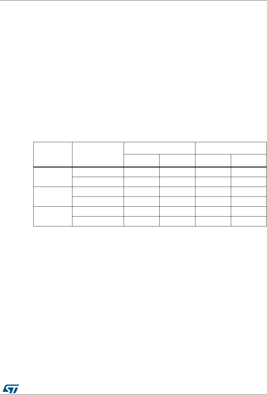
DocID027812 Rev 2 359/766
RM0401 General-purpose timers (TIM5)
384
TI2FP2=TI2 if not filtered and not inverted) assuming that it is enabled (CEN bit in
TIMx_CR1 register written to ‘1). The sequence of transitions of the two inputs is evaluated
and generates count pulses as well as the direction signal. Depending on the sequence the
counter counts up or down, the DIR bit in the TIMx_CR1 register is modified by hardware
accordingly. The DIR bit is calculated at each transition on any input (TI1 or TI2), whatever
the counter is counting on TI1 only, TI2 only or both TI1 and TI2.
Encoder interface mode acts simply as an external clock with direction selection. This
means that the counter just counts continuously between 0 and the auto-reload value in the
TIMx_ARR register (0 to ARR or ARR down to 0 depending on the direction). So you must
configure TIMx_ARR before starting. In the same way, the capture, compare, prescaler,
trigger output features continue to work as normal.
In this mode, the counter is modified automatically following the speed and the direction of
the incremental encoder and its content, therefore, always represents the encoder’s
position. The count direction correspond to the rotation direction of the connected sensor.
The table summarizes the possible combinations, assuming TI1 and TI2 don’t switch at the
same time.
An external incremental encoder can be connected directly to the MCU without external
interface logic. However, comparators are normally be used to convert the encoder’s
differential outputs to digital signals. This greatly increases noise immunity. The third
encoder output which indicate the mechanical zero position, may be connected to an
external interrupt input and trigger a counter reset.
Figure 127 gives an example of counter operation, showing count signal generation and
direction control. It also shows how input jitter is compensated where both edges are
selected. This might occur if the sensor is positioned near to one of the switching points. For
this example we assume that the configuration is the following:
•CC1S= ‘01’ (TIMx_CCMR1 register, TI1FP1 mapped on TI1)
•CC2S= ‘01’ (TIMx_CCMR2 register, TI2FP2 mapped on TI2)
•CC1P= ‘0’, CC1NP = ‘0’, IC1F =’0000’ (TIMx_CCER register, TI1FP1 noninverted,
TI1FP1=TI1)
•CC2P= ‘0’, CC2NP = ‘0’, IC2F =’0000’ (TIMx_CCER register, TI2FP2 noninverted,
TI2FP2=TI2)
•SMS= ‘011’ (TIMx_SMCR register, both inputs are active on both rising and falling
edges)
•CEN = 1 (TIMx_CR1 register, Counter is enabled)
Table 59. Counting direction versus encoder signals
Active edge
Level on opposite
signal (TI1FP1 for
TI2, TI2FP2 for TI1)
TI1FP1 signal TI2FP2 signal
Rising Falling Rising Falling
Counting on
TI1 only
High Down Up No Count No Count
Low Up Down No Count No Count
Counting on
TI2 only
High No Count No Count Up Down
Low No Count No Count Down Up
Counting on
TI1 and TI2
High Down Up Up Down
Low Up Down Down Up
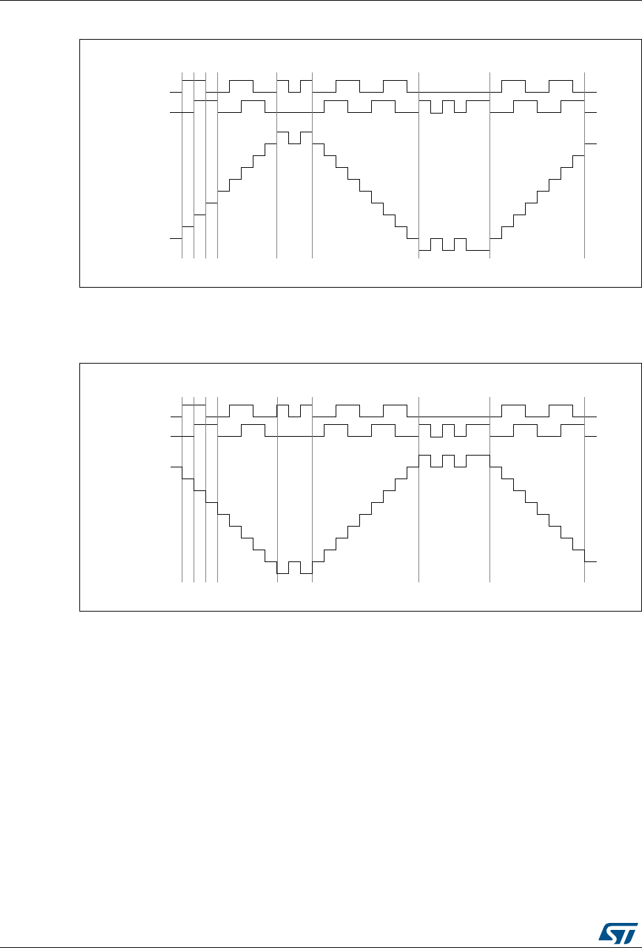
General-purpose timers (TIM5) RM0401
360/766 DocID027812 Rev 2
Figure 127. Example of counter operation in encoder interface mode
Figure 128 gives an example of counter behavior when TI1FP1 polarity is inverted (same
configuration as above except CC1P=1).
Figure 128. Example of encoder interface mode with TI1FP1 polarity inverted
The timer, when configured in Encoder Interface mode provides information on the sensor’s
current position. You can obtain dynamic information (speed, acceleration, deceleration) by
measuring the period between two encoder events using a second timer configured in
capture mode. The output of the encoder which indicates the mechanical zero can be used
for this purpose. Depending on the time between two events, the counter can also be read
at regular times. You can do this by latching the counter value into a third input capture
register if available (then the capture signal must be periodic and can be generated by
another timer). when available, it is also possible to read its value through a DMA request
generated by a Real-Time clock.
7,
EDFNZDUGMLWWHU MLWWHU
XS GRZQ XS
7,
&RXQWHU
IRUZDUG IRUZDUG
069
7,
EDFNZDUGMLWWHU MLWWHU
XSGRZQ
7,
&RXQWHU
IRUZDUG IRUZDUG
069
GRZQ

DocID027812 Rev 2 361/766
RM0401 General-purpose timers (TIM5)
384
15.3.12 Timer input XOR function
The TI1S bit in the TIM_CR2 register, allows the input filter of channel 1 to be connected to
the output of a XOR gate, combining the three input pins TIMx_CH1 to TIMx_CH3.
The XOR output can be used with all the timer input functions such as trigger or input
capture.
15.3.13 Timers and external trigger synchronization
The TIMx Timers can be synchronized with an external trigger in several modes: Reset
mode, Gated mode and Trigger mode.
Slave mode: Reset mode
The counter and its prescaler can be reinitialized in response to an event on a trigger input.
Moreover, if the URS bit from the TIMx_CR1 register is low, an update event UEV is
generated. Then all the preloaded registers (TIMx_ARR, TIMx_CCRx) are updated.
In the following example, the upcounter is cleared in response to a rising edge on TI1 input:
•Configure the channel 1 to detect rising edges on TI1. Configure the input filter duration
(in this example, we don’t need any filter, so we keep IC1F=0000). The capture
prescaler is not used for triggering, so you don’t need to configure it. The CC1S bits
select the input capture source only, CC1S = 01 in the TIMx_CCMR1 register. Write
CC1P=0 and CC1NP=0 in TIMx_CCER register to validate the polarity (and detect
rising edges only).
•Configure the timer in reset mode by writing SMS=100 in TIMx_SMCR register. Select
TI1 as the input source by writing TS=101 in TIMx_SMCR register.
•Start the counter by writing CEN=1 in the TIMx_CR1 register.
The counter starts counting on the internal clock, then behaves normally until TI1 rising
edge. When TI1 rises, the counter is cleared and restarts from 0. In the meantime, the
trigger flag is set (TIF bit in the TIMx_SR register) and an interrupt request, or a DMA
request can be sent if enabled (depending on the TIE and TDE bits in TIMx_DIER register).
The following figure shows this behavior when the auto-reload register TIMx_ARR=0x36.
The delay between the rising edge on TI1 and the actual reset of the counter is due to the
resynchronization circuit on TI1 input.
Figure 129. Control circuit in reset mode
069
&RXQWHUFORFN &.B&17 &.B36&
&RXQWHUUHJLVWHU
8*
7,
7,)
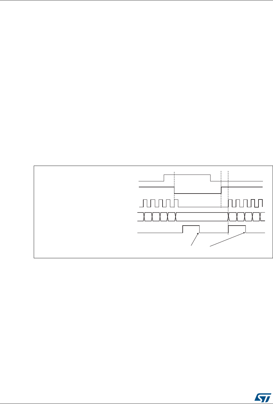
General-purpose timers (TIM5) RM0401
362/766 DocID027812 Rev 2
Slave mode: Gated mode
The counter can be enabled depending on the level of a selected input.
In the following example, the upcounter counts only when TI1 input is low:
•Configure the channel 1 to detect low levels on TI1. Configure the input filter duration
(in this example, we don’t need any filter, so we keep IC1F=0000). The capture
prescaler is not used for triggering, so you don’t need to configure it. The CC1S bits
select the input capture source only, CC1S=01 in TIMx_CCMR1 register. Write
CC1P=1 in TIMx_CCER register to validate the polarity (and detect low level only).
•Configure the timer in gated mode by writing SMS=101 in TIMx_SMCR register. Select
TI1 as the input source by writing TS=101 in TIMx_SMCR register.
•Enable the counter by writing CEN=1 in the TIMx_CR1 register (in gated mode, the
counter doesn’t start if CEN=0, whatever is the trigger input level).
The counter starts counting on the internal clock as long as TI1 is low and stops as soon as
TI1 becomes high. The TIF flag in the TIMx_SR register is set both when the counter starts
or stops.
The delay between the rising edge on TI1 and the actual stop of the counter is due to the
resynchronization circuit on TI1 input.
Figure 130. Control circuit in gated mode
1. The configuration “CCxP=CCxNP=1” (detection of both rising and falling edges) does not have any effect
in gated mode because gated mode acts on a level and not on an edge.
Slave mode: Trigger mode
The counter can start in response to an event on a selected input.
In the following example, the upcounter starts in response to a rising edge on TI2 input:
•Configure the channel 2 to detect rising edges on TI2. Configure the input filter duration
(in this example, we don’t need any filter, so we keep IC2F=0000). The capture
prescaler is not used for triggering, so you don’t need to configure it. CC2S bits are
selecting the input capture source only, CC2S=01 in TIMx_CCMR1 register. Write
CC2P=1 in TIMx_CCER register to validate the polarity (and detect low level only).
•Configure the timer in trigger mode by writing SMS=110 in TIMx_SMCR register. Select
TI2 as the input source by writing TS=110 in TIMx_SMCR register.
When a rising edge occurs on TI2, the counter starts counting on the internal clock and the
TIF flag is set.
069
&RXQWHUFORFN &.B&17 &.B36&
7,
&17B(1
:ULWH7,)
&RXQWHUUHJLVWHU
7,)

DocID027812 Rev 2 363/766
RM0401 General-purpose timers (TIM5)
384
The delay between the rising edge on TI2 and the actual start of the counter is due to the
resynchronization circuit on TI2 input.
Figure 131. Control circuit in trigger mode
15.3.14 Debug mode
When the microcontroller enters debug mode (Cortex®-M4 with FPU core - halted), the
TIMx counter either continues to work normally or stops, depending on DBG_TIMx_STOP
configuration bit in DBGMCU module. For more details, refer to Section 26.16.2: Debug
support for timers, watchdog and I2C.
069
7,
&17B(1
&RXQWHUUHJLVWHU
7,)
&RXQWHUFORFN &.B&17 &.B36&

General-purpose timers (TIM5) RM0401
364/766 DocID027812 Rev 2
15.4 TIM5 registers
Refer to Section 1.1 on page 33 for a list of abbreviations used in register descriptions.
The 32-bit peripheral registers have to be written by words (32 bits). All other peripheral
registers have to be written by half-words (16 bits) or words (32 bits). Read accesses can be
done by bytes (8 bits), half-words (16 bits) or words (32 bits).
15.4.1 TIMx control register 1 (TIMx_CR1)
Address offset: 0x00
Reset value: 0x0000
15 14 13 12 11 10 9876543210
Res. Res. Res. Res. Res. Res. CKD[1:0] ARPE CMS DIR OPM URS UDIS CEN
rw rw rw rw rw rw rw rw rw rw
Bits 15:10 Reserved, must be kept at reset value.
Bits 9:8 CKD: Clock division
This bit-field indicates the division ratio between the timer clock (CK_INT) frequency and
sampling clock used by the digital filters (TIx).
00: tDTS = tCK_INT
01: tDTS = 2 × tCK_INT
10: tDTS = 4 × tCK_INT
11: Reserved
Bit 7 ARPE: Auto-reload preload enable
0: TIMx_ARR register is not buffered
1: TIMx_ARR register is buffered
Bits 6:5 CMS: Center-aligned mode selection
00: Edge-aligned mode. The counter counts up or down depending on the direction bit
(DIR).
01: Center-aligned mode 1. The counter counts up and down alternatively. Output compare
interrupt flags of channels configured in output (CCxS=00 in TIMx_CCMRx register) are set
only when the counter is counting down.
10: Center-aligned mode 2. The counter counts up and down alternatively. Output compare
interrupt flags of channels configured in output (CCxS=00 in TIMx_CCMRx register) are set
only when the counter is counting up.
11: Center-aligned mode 3. The counter counts up and down alternatively. Output compare
interrupt flags of channels configured in output (CCxS=00 in TIMx_CCMRx register) are set
both when the counter is counting up or down.
Note: It is not allowed to switch from edge-aligned mode to center-aligned mode as long as
the counter is enabled (CEN=1)
Bit 4 DIR: Direction
0: Counter used as upcounter
1: Counter used as downcounter
Note: This bit is read only when the timer is configured in Center-aligned mode or Encoder
mode.
Bit 3 OPM: One-pulse mode
0: Counter is not stopped at update event
1: Counter stops counting at the next update event (clearing the bit CEN)

DocID027812 Rev 2 365/766
RM0401 General-purpose timers (TIM5)
384
Bit 2 URS: Update request source
This bit is set and cleared by software to select the UEV event sources.
0: Any of the following events generate an update interrupt or DMA request if enabled.
These events can be:
– Counter overflow/underflow
– Setting the UG bit
– Update generation through the slave mode controller
1: Only counter overflow/underflow generates an update interrupt or DMA request if
enabled.
Bit 1 UDIS: Update disable
This bit is set and cleared by software to enable/disable UEV event generation.
0: UEV enabled. The Update (UEV) event is generated by one of the following events:
– Counter overflow/underflow
– Setting the UG bit
– Update generation through the slave mode controller
Buffered registers are then loaded with their preload values.
1: UEV disabled. The Update event is not generated, shadow registers keep their value
(ARR, PSC, CCRx). However the counter and the prescaler are reinitialized if the UG bit is
set or if a hardware reset is received from the slave mode controller.
Bit 0 CEN: Counter enable
0: Counter disabled
1: Counter enabled
Note: External clock, gated mode and encoder mode can work only if the CEN bit has been
previously set by software. However trigger mode can set the CEN bit automatically by
hardware.
CEN is cleared automatically in one-pulse mode, when an update event occurs.

General-purpose timers (TIM5) RM0401
366/766 DocID027812 Rev 2
15.4.2 TIMx control register 2 (TIMx_CR2)
Address offset: 0x04
Reset value: 0x0000
15 14 13 12 11 10 9876543210
Res. Res. Res. Res. Res. Res. Res. Res. TI1S MMS[2:0] CCDS Res. Res. Res.
rw rw rw rw rw
Bits 15:8 Reserved, must be kept at reset value.
Bit 7 TI1S: TI1 selection
0: The TIMx_CH1 pin is connected to TI1 input
1: The TIMx_CH1, CH2 and CH3 pins are connected to the TI1 input (XOR combination)
Bits 6:4 MMS[2:0]: Master mode selection
These bits allow to select the information to be sent in master mode to slave timers for
synchronization (TRGO). The combination is as follows:
000: Reset - the UG bit from the TIMx_EGR register is used as trigger output (TRGO). If the
reset is generated by the trigger input (slave mode controller configured in reset mode) then
the signal on TRGO is delayed compared to the actual reset.
001: Enable - the Counter enable signal, CNT_EN, is used as trigger output (TRGO). It is
useful to start several timers at the same time or to control a window in which a slave timer is
enabled. The Counter Enable signal is generated by a logic OR between CEN control bit
and the trigger input when configured in gated mode.
When the Counter Enable signal is controlled by the trigger input, there is a delay on TRGO,
except if the master/slave mode is selected (see the MSM bit description in TIMx_SMCR
register).
010: Update - The update event is selected as trigger output (TRGO). For instance a master
timer can then be used as a prescaler for a slave timer.
011: Compare Pulse - The trigger output send a positive pulse when the CC1IF flag is to be
set (even if it was already high), as soon as a capture or a compare match occurred.
(TRGO)
100: Compare - OC1REF signal is used as trigger output (TRGO)
101: Compare - OC2REF signal is used as trigger output (TRGO)
110: Compare - OC3REF signal is used as trigger output (TRGO)
111: Compare - OC4REF signal is used as trigger output (TRGO)
Bit 3 CCDS: Capture/compare DMA selection
0: CCx DMA request sent when CCx event occurs
1: CCx DMA requests sent when update event occurs
Bits 2:0 Reserved, must be kept at reset value.

DocID027812 Rev 2 367/766
RM0401 General-purpose timers (TIM5)
384
15.4.3 TIMx slave mode control register (TIMx_SMCR)
Address offset: 0x08
Reset value: 0x0000
15 14 13 12 11 10 9876543210
Res. Res. Res. Res. Res. Res. Res. Res. MSM TS[2:0] Res. SMS[2:0]
rw rw rw rw rw rw rw
Bits 15:8 Reserved, must be kept at reset value.
Bit 7 MSM: Master/Slave mode
0: No action
1: The effect of an event on the trigger input (TRGI) is delayed to allow a perfect
synchronization between the current timer and its slaves (through TRGO). It is useful if we
want to synchronize several timers on a single external event.
Bits 6:4 TS: Trigger selection
This bit-field selects the trigger input to be used to synchronize the counter.
000: Internal Trigger 0 (ITR0)
001: Internal Trigger 1 (ITR1).
010: Internal Trigger 2 (ITR2).
011: Internal Trigger 3 (ITR3).
100: TI1 Edge Detector (TI1F_ED)
101: Filtered Timer Input 1 (TI1FP1)
110: Filtered Timer Input 2 (TI2FP2)
111: Reserved
See Table 60: TIMx internal trigger connection on page 368 for more details on ITRx
meaning for each Timer.
Note: These bits must be changed only when they are not used (e.g. when SMS=000) to
avoid wrong edge detections at the transition.
Bit 3 Reserved, must be kept at reset value.
Bits 2:0 SMS: Slave mode selection
When external signals are selected the active edge of the trigger signal (TRGI) is linked to
the polarity selected on the external input (see Input Control register and Control Register
description.
000: Slave mode disabled - if CEN = ‘1 then the prescaler is clocked directly by the internal
clock.
001: Encoder mode 1 - Counter counts up/down on TI2FP2 edge depending on TI1FP1
level.
010: Encoder mode 2 - Counter counts up/down on TI1FP1 edge depending on TI2FP2
level.
011: Encoder mode 3 - Counter counts up/down on both TI1FP1 and TI2FP2 edges
depending on the level of the other input.
100: Reset Mode - Rising edge of the selected trigger input (TRGI) reinitializes the counter
and generates an update of the registers.
101: Gated Mode - The counter clock is enabled when the trigger input (TRGI) is high. The
counter stops (but is not reset) as soon as the trigger becomes low. Both start and stop of
the counter are controlled.
110: Trigger Mode - The counter starts at a rising edge of the trigger TRGI (but it is not
reset). Only the start of the counter is controlled.
111: External Clock Mode 1 - Rising edges of the selected trigger (TRGI) clock the counter.
Note: The gated mode must not be used if TI1F_ED is selected as the trigger input (TS=100).
Indeed, TI1F_ED outputs 1 pulse for each transition on TI1F, whereas the gated mode
checks the level of the trigger signal.

General-purpose timers (TIM5) RM0401
368/766 DocID027812 Rev 2
15.4.4 TIMx DMA/Interrupt enable register (TIMx_DIER)
Address offset: 0x0C
Reset value: 0x0000
Table 60. TIMx internal trigger connection
Slave TIM ITR0 (TS = 000) ITR1 (TS = 001) ITR2 (TS = 010) ITR3 (TS = 011)
TIM5 Reserved LPTIM Reserved Reserved
15 14 13 12 11 10 9876543210
Res. TDE Res. CC4DE CC3DE CC2DE CC1DE UDE Res. TIE Res. CC4IE CC3IE CC2IE CC1IE UIE
rw rw rw rw rw rw rw rw rw rw rw rw
Bit 15 Reserved, must be kept at reset value.
Bit 14 TDE: Trigger DMA request enable
0: Trigger DMA request disabled.
1: Trigger DMA request enabled.
Bit 13 Reserved, always read as 0
Bit 12 CC4DE: Capture/Compare 4 DMA request enable
0: CC4 DMA request disabled.
1: CC4 DMA request enabled.
Bit 11 CC3DE: Capture/Compare 3 DMA request enable
0: CC3 DMA request disabled.
1: CC3 DMA request enabled.
Bit 10 CC2DE: Capture/Compare 2 DMA request enable
0: CC2 DMA request disabled.
1: CC2 DMA request enabled.
Bit 9 CC1DE: Capture/Compare 1 DMA request enable
0: CC1 DMA request disabled.
1: CC1 DMA request enabled.
Bit 8 UDE: Update DMA request enable
0: Update DMA request disabled.
1: Update DMA request enabled.
Bit 7 Reserved, must be kept at reset value.
Bit 6 TIE: Trigger interrupt enable
0: Trigger interrupt disabled.
1: Trigger interrupt enabled.
Bit 5 Reserved, must be kept at reset value.
Bit 4 CC4IE: Capture/Compare 4 interrupt enable
0: CC4 interrupt disabled.
1: CC4 interrupt enabled.
Bit 3 CC3IE: Capture/Compare 3 interrupt enable
0: CC3 interrupt disabled
1: CC3 interrupt enabled

DocID027812 Rev 2 369/766
RM0401 General-purpose timers (TIM5)
384
15.4.5 TIMx status register (TIMx_SR)
Address offset: 0x10
Reset value: 0x0000
Bit 2 CC2IE: Capture/Compare 2 interrupt enable
0: CC2 interrupt disabled
1: CC2 interrupt enabled
Bit 1 CC1IE: Capture/Compare 1 interrupt enable
0: CC1 interrupt disabled
1: CC1 interrupt enabled
Bit 0 UIE: Update interrupt enable
0: Update interrupt disabled
1: Update interrupt enabled
15 14 13 12 11 10 9876543210
Res. Res. Res. CC4OF CC3OF CC2OF CC1OF Res. Res. TIF Res. CC4IF CC3IF CC2IF CC1IF UIF
rc_w0 rc_w0 rc_w0 rc_w0 rc_w0 rc_w0 rc_w0 rc_w0 rc_w0 rc_w0
Bits 15:13 Reserved, must be kept at reset value.
Bit 12 CC4OF: Capture/Compare 4 overcapture flag
refer to CC1OF description
Bit 11 CC3OF: Capture/Compare 3 overcapture flag
refer to CC1OF description
Bit 10 CC2OF: Capture/compare 2 overcapture flag
refer to CC1OF description
Bit 9 CC1OF: Capture/Compare 1 overcapture flag
This flag is set by hardware only when the corresponding channel is configured in input
capture mode. It is cleared by software by writing it to ‘0.
0: No overcapture has been detected
1: The counter value has been captured in TIMx_CCR1 register while CC1IF flag was
already set
Bits 8:7 Reserved, must be kept at reset value.
Bit 6 TIF: Trigger interrupt flag
This flag is set by hardware on trigger event (active edge detected on TRGI input when the
slave mode controller is enabled in all modes but gated mode. It is set when the counter
starts or stops when gated mode is selected. It is cleared by software.
0: No trigger event occurred
1: Trigger interrupt pending
Bit 5 Reserved, must be kept at reset value.
Bit 4 CC4IF: Capture/Compare 4 interrupt flag
refer to CC1IF description
Bit 3 CC3IF: Capture/Compare 3 interrupt flag
refer to CC1IF description

General-purpose timers (TIM5) RM0401
370/766 DocID027812 Rev 2
Bit 2 CC2IF: Capture/Compare 2 interrupt flag
refer to CC1IF description
Bit 1 CC1IF: Capture/compare 1 interrupt flag
If channel CC1 is configured as output:
This flag is set by hardware when the counter matches the compare value, with some
exception in center-aligned mode (refer to the CMS bits in the TIMx_CR1 register
description). It is cleared by software.
0: No match
1: The content of the counter TIMx_CNT matches the content of the TIMx_CCR1 register.
When the contents of TIMx_CCR1 are greater than the contents of TIMx_ARR, the CC1IF bit
goes high on the counter overflow (in upcounting and up/down-counting modes) or underflow
(in downcounting mode)
If channel CC1 is configured as input:
This bit is set by hardware on a capture. It is cleared by software or by reading the
TIMx_CCR1 register.
0: No input capture occurred
1: The counter value has been captured in TIMx_CCR1 register (An edge has been detected
on IC1 which matches the selected polarity)
Bit 0 UIF: Update interrupt flag
″This bit is set by hardware on an update event. It is cleared by software.
0: No update occurred.
1: Update interrupt pending. This bit is set by hardware when the registers are updated:
″At overflow or underflow and if UDIS=0 in the TIMx_CR1 register.
″When CNT is reinitialized by software using the UG bit in TIMx_EGR register, if URS=0
and UDIS=0 in the TIMx_CR1 register.
When CNT is reinitialized by a trigger event (refer to the synchro control register description),
if URS=0 and UDIS=0 in the TIMx_CR1 register.

DocID027812 Rev 2 371/766
RM0401 General-purpose timers (TIM5)
384
15.4.6 TIMx event generation register (TIMx_EGR)
Address offset: 0x14
Reset value: 0x0000
15 14 13 12 11 10 9876543210
Res. Res. Res. Res. Res. Res. Res. Res. Res. TG Res. CC4G CC3G CC2G CC1G UG
w wwwww
Bits 15:7 Reserved, must be kept at reset value.
Bit 6 TG: Trigger generation
This bit is set by software in order to generate an event, it is automatically cleared by
hardware.
0: No action
1: The TIF flag is set in TIMx_SR register. Related interrupt or DMA transfer can occur if
enabled.
Bit 5 Reserved, must be kept at reset value.
Bit 4 CC4G: Capture/compare 4 generation
refer to CC1G description
Bit 3 CC3G: Capture/compare 3 generation
refer to CC1G description
Bit 2 CC2G: Capture/compare 2 generation
refer to CC1G description
Bit 1 CC1G: Capture/compare 1 generation
This bit is set by software in order to generate an event, it is automatically cleared by
hardware.
0: No action
1: A capture/compare event is generated on channel 1:
If channel CC1 is configured as output:
CC1IF flag is set, Corresponding interrupt or DMA request is sent if enabled.
If channel CC1 is configured as input:
The current value of the counter is captured in TIMx_CCR1 register. The CC1IF flag is set,
the corresponding interrupt or DMA request is sent if enabled. The CC1OF flag is set if the
CC1IF flag was already high.
Bit 0 UG: Update generation
This bit can be set by software, it is automatically cleared by hardware.
0: No action
1: Re-initialize the counter and generates an update of the registers. Note that the prescaler
counter is cleared too (anyway the prescaler ratio is not affected). The counter is cleared if
the center-aligned mode is selected or if DIR=0 (upcounting), else it takes the auto-reload
value (TIMx_ARR) if DIR=1 (downcounting).

General-purpose timers (TIM5) RM0401
372/766 DocID027812 Rev 2
15.4.7 TIMx capture/compare mode register 1 (TIMx_CCMR1)
Address offset: 0x18
Reset value: 0x0000
The channels can be used in input (capture mode) or in output (compare mode). The
direction of a channel is defined by configuring the corresponding CCxS bits. All the other
bits of this register have a different function in input and in output mode. For a given bit,
OCxx describes its function when the channel is configured in output, ICxx describes its
function when the channel is configured in input. So you must take care that the same bit
can have a different meaning for the input stage and for the output stage.
Output compare mode
15 14 13 12 11 10 9876543210
Res. OC2M[2:0] OC2PE OC2FE CC2S[1:0] Res. OC1M[2:0] OC1PE OC1FE CC1S[1:0]
IC2F[3:0] IC2PSC[1:0] IC1F[3:0] IC1PSC[1:0]
rw rw rw rw rw rw rw rw rw rw rw rw rw rw rw rw
Bit 15 Reserved, must be kept at reset value.
Bits 14:12 OC2M[2:0]: Output compare 2 mode
Bit 11 OC2PE: Output compare 2 preload enable
Bit 10 OC2FE: Output compare 2 fast enable
Bits 9:8 CC2S[1:0]: Capture/Compare 2 selection
This bit-field defines the direction of the channel (input/output) as well as the used input.
00: CC2 channel is configured as output
01: CC2 channel is configured as input, IC2 is mapped on TI2
10: CC2 channel is configured as input, IC2 is mapped on TI1
11: CC2 channel is configured as input, IC2 is mapped on TRC. This mode is working only if
an internal trigger input is selected through the TS bit (TIMx_SMCR register)
Note: CC2S bits are writable only when the channel is OFF (CC2E = 0 in TIMx_CCER).
Bit 7 Reserved, must be kept at reset value.

DocID027812 Rev 2 373/766
RM0401 General-purpose timers (TIM5)
384
Bits 6:4 OC1M: Output compare 1 mode
These bits define the behavior of the output reference signal OC1REF from which OC1 and
OC1N are derived. OC1REF is active high whereas OC1 and OC1N active level depends
on CC1P and CC1NP bits.
000: Frozen - The comparison between the output compare register TIMx_CCR1 and the
counter TIMx_CNT has no effect on the outputs.(this mode is used to generate a timing
base).
001: Set channel 1 to active level on match. OC1REF signal is forced high when the counter
TIMx_CNT matches the capture/compare register 1 (TIMx_CCR1).
010: Set channel 1 to inactive level on match. OC1REF signal is forced low when the
counter TIMx_CNT matches the capture/compare register 1 (TIMx_CCR1).
011: Toggle - OC1REF toggles when TIMx_CNT=TIMx_CCR1.
100: Force inactive level - OC1REF is forced low.
101: Force active level - OC1REF is forced high.
110: PWM mode 1 - In upcounting, channel 1 is active as long as TIMx_CNT<TIMx_CCR1
else inactive. In downcounting, channel 1 is inactive (OC1REF=‘0) as long as
TIMx_CNT>TIMx_CCR1 else active (OC1REF=1).
111: PWM mode 2 - In upcounting, channel 1 is inactive as long as TIMx_CNT<TIMx_CCR1
else active. In downcounting, channel 1 is active as long as TIMx_CNT>TIMx_CCR1 else
inactive.
Note: In PWM mode 1 or 2, the OCREF level changes only when the result of the
comparison changes or when the output compare mode switches from “frozen” mode
to “PWM” mode.
Bit 3 OC1PE: Output compare 1 preload enable
0: Preload register on TIMx_CCR1 disabled. TIMx_CCR1 can be written at anytime, the
new value is taken in account immediately.
1: Preload register on TIMx_CCR1 enabled. Read/Write operations access the preload
register. TIMx_CCR1 preload value is loaded in the active register at each update event.
Note: 1: These bits can not be modified as long as LOCK level 3 has been programmed
(LOCK bits in TIMx_BDTR register) and CC1S=00 (the channel is configured in
output).
2: The PWM mode can be used without validating the preload register only in one-
pulse mode (OPM bit set in TIMx_CR1 register). Else the behavior is not guaranteed.
Bit 2 OC1FE: Output compare 1 fast enable
This bit is used to accelerate the effect of an event on the trigger in input on the CC output.
0: CC1 behaves normally depending on counter and CCR1 values even when the trigger is
ON. The minimum delay to activate CC1 output when an edge occurs on the trigger input is
5 clock cycles.
1: An active edge on the trigger input acts like a compare match on CC1 output. Then, OC
is set to the compare level independently from the result of the comparison. Delay to sample
the trigger input and to activate CC1 output is reduced to 3 clock cycles. OCFE acts only if
the channel is configured in PWM1 or PWM2 mode.
Bits 1:0 CC1S: Capture/Compare 1 selection
This bit-field defines the direction of the channel (input/output) as well as the used input.
00: CC1 channel is configured as output.
01: CC1 channel is configured as input, IC1 is mapped on TI1.
10: CC1 channel is configured as input, IC1 is mapped on TI2.
11: CC1 channel is configured as input, IC1 is mapped on TRC. This mode is working only if
an internal trigger input is selected through TS bit (TIMx_SMCR register)
Note: CC1S bits are writable only when the channel is OFF (CC1E = 0 in TIMx_CCER).

General-purpose timers (TIM5) RM0401
374/766 DocID027812 Rev 2
Input capture mode
Bits 15:12 IC2F: Input capture 2 filter
Bits 11:10 IC2PSC[1:0]: Input capture 2 prescaler
Bits 9:8 CC2S: Capture/compare 2 selection
This bit-field defines the direction of the channel (input/output) as well as the used input.
00: CC2 channel is configured as output.
01: CC2 channel is configured as input, IC2 is mapped on TI2.
10: CC2 channel is configured as input, IC2 is mapped on TI1.
11: CC2 channel is configured as input, IC2 is mapped on TRC. This mode is working only if
an internal trigger input is selected through TS bit (TIMx_SMCR register)
Note: CC2S bits are writable only when the channel is OFF (CC2E = 0 in TIMx_CCER).
Bits 7:4 IC1F: Input capture 1 filter
This bit-field defines the frequency used to sample TI1 input and the length of the digital filter
applied to TI1. The digital filter is made of an event counter in which N events are needed to
validate a transition on the output:
0000: No filter, sampling is done at fDTS
0001: fSAMPLING=fCK_INT
, N=2
0010: fSAMPLING=fCK_INT
, N=4
0011: fSAMPLING=fCK_INT
, N=8
0100: fSAMPLING=fDTS/2, N=6
0101: fSAMPLING=fDTS/2, N=8
0110: fSAMPLING=fDTS/4, N=6
0111: fSAMPLING=fDTS/4, N=8
1000: fSAMPLING=fDTS/8, N=6
1001: fSAMPLING=fDTS/8, N=8
1010: fSAMPLING=fDTS/16, N=5
1011: fSAMPLING=fDTS/16, N=6
1100: fSAMPLING=fDTS/16, N=8
1101: fSAMPLING=fDTS/32, N=5
1110: fSAMPLING=fDTS/32, N=6
1111: fSAMPLING=fDTS/32, N=8
Bits 3:2 IC1PSC: Input capture 1 prescaler
This bit-field defines the ratio of the prescaler acting on CC1 input (IC1).
The prescaler is reset as soon as CC1E=0 (TIMx_CCER register).
00: no prescaler, capture is done each time an edge is detected on the capture input
01: capture is done once every 2 events
10: capture is done once every 4 events
11: capture is done once every 8 events
Bits 1:0 CC1S: Capture/Compare 1 selection
This bit-field defines the direction of the channel (input/output) as well as the used input.
00: CC1 channel is configured as output
01: CC1 channel is configured as input, IC1 is mapped on TI1
10: CC1 channel is configured as input, IC1 is mapped on TI2
11: CC1 channel is configured as input, IC1 is mapped on TRC. This mode is working only if
an internal trigger input is selected through TS bit (TIMx_SMCR register)
Note: CC1S bits are writable only when the channel is OFF (CC1E = 0 in TIMx_CCER).

DocID027812 Rev 2 375/766
RM0401 General-purpose timers (TIM5)
384
15.4.8 TIMx capture/compare mode register 2 (TIMx_CCMR2)
Address offset: 0x1C
Reset value: 0x0000
Refer to the above CCMR1 register description.
Output compare mode
15 14 13 12 11 10 9876543210
Res. OC4M[2:0] OC4PE OC4FE CC4S[1:0] Res. OC3M[2:0] OC3PE OC3FE CC3S[1:0]
IC4F[3:0] IC4PSC[1:0] IC3F[3:0] IC3PSC[1:0]
rw rw rw rw rw rw rw rw rw rw rw rw rw rw rw rw
Bit 15 Reserved, must be kept at reset value.
Bits 14:12 OC4M: Output compare 4 mode
Bit 11 OC4PE: Output compare 4 preload enable
Bit 10 OC4FE: Output compare 4 fast enable
Bits 9:8 CC4S: Capture/Compare 4 selection
This bit-field defines the direction of the channel (input/output) as well as the used input.
00: CC4 channel is configured as output
01: CC4 channel is configured as input, IC4 is mapped on TI4
10: CC4 channel is configured as input, IC4 is mapped on TI3
11: CC4 channel is configured as input, IC4 is mapped on TRC. This mode is working only if
an internal trigger input is selected through TS bit (TIMx_SMCR register)
Note: CC4S bits are writable only when the channel is OFF (CC4E = 0 in TIMx_CCER).
Bit 7 Reserved, must be kept at reset value.
Bits 6:4 OC3M: Output compare 3 mode
Bit 3 OC3PE: Output compare 3 preload enable
Bit 2 OC3FE: Output compare 3 fast enable
Bits 1:0 CC3S: Capture/Compare 3 selection
This bit-field defines the direction of the channel (input/output) as well as the used input.
00: CC3 channel is configured as output
01: CC3 channel is configured as input, IC3 is mapped on TI3
10: CC3 channel is configured as input, IC3 is mapped on TI4
11: CC3 channel is configured as input, IC3 is mapped on TRC. This mode is working only if
an internal trigger input is selected through TS bit (TIMx_SMCR register)
Note: CC3S bits are writable only when the channel is OFF (CC3E = 0 in TIMx_CCER).

General-purpose timers (TIM5) RM0401
376/766 DocID027812 Rev 2
Input capture mode
15.4.9 TIMx capture/compare enable register (TIMx_CCER)
Address offset: 0x20
Reset value: 0x0000
Bits 15:12 IC4F: Input capture 4 filter
Bits 11:10 IC4PSC: Input capture 4 prescaler
Bits 9:8 CC4S: Capture/Compare 4 selection
This bit-field defines the direction of the channel (input/output) as well as the used input.
00: CC4 channel is configured as output
01: CC4 channel is configured as input, IC4 is mapped on TI4
10: CC4 channel is configured as input, IC4 is mapped on TI3
11: CC4 channel is configured as input, IC4 is mapped on TRC. This mode is working only if
an internal trigger input is selected through TS bit (TIMx_SMCR register)
Note: CC4S bits are writable only when the channel is OFF (CC4E = 0 in TIMx_CCER).
Bits 7:4 IC3F: Input capture 3 filter
Bits 3:2 IC3PSC: Input capture 3 prescaler
Bits 1:0 CC3S: Capture/Compare 3 selection
This bit-field defines the direction of the channel (input/output) as well as the used input.
00: CC3 channel is configured as output
01: CC3 channel is configured as input, IC3 is mapped on TI3
10: CC3 channel is configured as input, IC3 is mapped on TI4
11: CC3 channel is configured as input, IC3 is mapped on TRC. This mode is working only if
an internal trigger input is selected through TS bit (TIMx_SMCR register)
Note: CC3S bits are writable only when the channel is OFF (CC3E = 0 in TIMx_CCER).
15 14 13 12 11 10 9876543210
CC4NP Res. CC4P CC4E CC3NP Res. CC3P CC3E CC2NP Res. CC2P CC2E CC1NP Res. CC1P CC1E
rw rw rw rw rw rw rw rw rw rw rw rw
Bit 15 CC4NP: Capture/Compare 4 output Polarity.
Refer to CC1NP description
Bit 14 Reserved, must be kept at reset value.
Bit 13 CC4P: Capture/Compare 4 output Polarity.
refer to CC1P description
Bit 12 CC4E: Capture/Compare 4 output enable.
refer to CC1E description
Bit 11 CC3NP: Capture/Compare 3 output Polarity.
refer to CC1NP description
Bit 10 Reserved, must be kept at reset value.
Bit 9 CC3P: Capture/Compare 3 output Polarity.
refer to CC1P description
Bit 8 CC3E: Capture/Compare 3 output enable.
refer to CC1E description

DocID027812 Rev 2 377/766
RM0401 General-purpose timers (TIM5)
384
Note: The state of the external IO pins connected to the standard OCx channels depends on the
OCx channel state and the GPIO registers.
Bit 7 CC2NP: Capture/Compare 2 output Polarity.
refer to CC1NP description
Bit 6 Reserved, must be kept at reset value.
Bit 5 CC2P: Capture/Compare 2 output Polarity.
refer to CC1P description
Bit 4 CC2E: Capture/Compare 2 output enable.
refer to CC1E description
Bit 3 CC1NP: Capture/Compare 1 output Polarity.
CC1 channel configured as output:
CC1NP must be kept cleared in this case.
CC1 channel configured as input:
This bit is used in conjunction with CC1P to define TI1FP1/TI2FP1 polarity. refer to CC1P
description.
Bit 2 Reserved, must be kept at reset value.
Bit 1 CC1P: Capture/Compare 1 output Polarity.
CC1 channel configured as output:
0: OC1 active high
1: OC1 active low
CC1 channel configured as input:
CC1NP/CC1P bits select TI1FP1 and TI2FP1 polarity for trigger or capture operations.
00: noninverted/rising edge
Circuit is sensitive to TIxFP1 rising edge (capture, trigger in reset, external clock or trigger
mode), TIxFP1 is not inverted (trigger in gated mode, encoder mode).
01: inverted/falling edge
Circuit is sensitive to TIxFP1 falling edge (capture, trigger in reset, external clock or trigger
mode), TIxFP1 is inverted (trigger in gated mode, encoder mode).
10: reserved, do not use this configuration.
11: noninverted/both edges
Circuit is sensitive to both TIxFP1 rising and falling edges (capture, trigger in reset, external
clock or trigger mode), TIxFP1 is not inverted (trigger in gated mode). This configuration
must not be used for encoder mode.
Bit 0 CC1E: Capture/Compare 1 output enable.
CC1 channel configured as output:
0: Off - OC1 is not active
1: On - OC1 signal is output on the corresponding output pin
CC1 channel configured as input:
This bit determines if a capture of the counter value can actually be done into the input
capture/compare register 1 (TIMx_CCR1) or not.
0: Capture disabled
1: Capture enabled
Table 61. Output control bit for standard OCx channels
CCxE bit OCx output state
0 Output Disabled (OCx=0, OCx_EN=0)
1 OCx=OCxREF + Polarity, OCx_EN=1
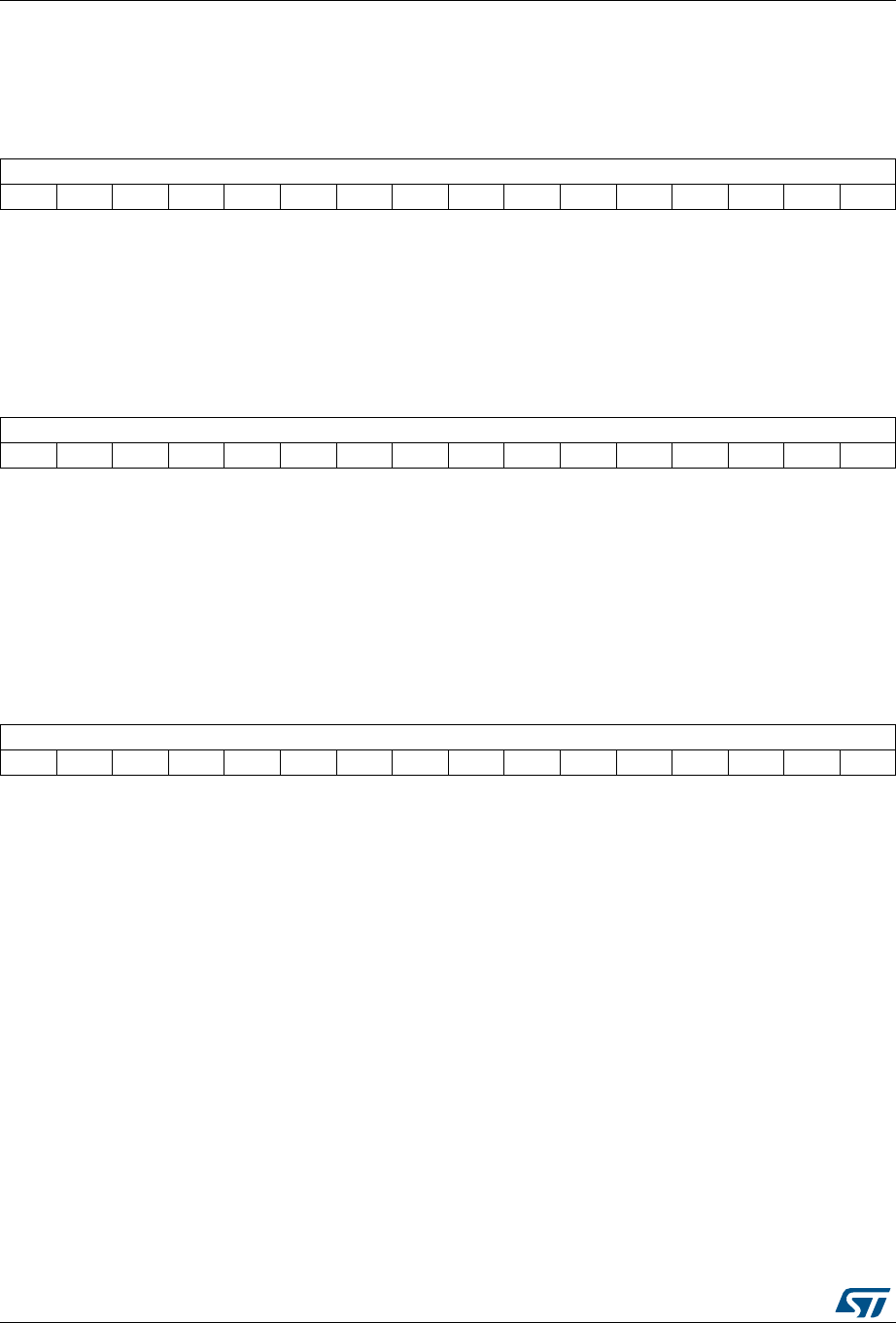
General-purpose timers (TIM5) RM0401
378/766 DocID027812 Rev 2
15.4.10 TIMx counter (TIMx_CNT)
Address offset: 0x24
Reset value: 0x0000
15.4.11 TIMx prescaler (TIMx_PSC)
Address offset: 0x28
Reset value: 0x0000
15.4.12 TIMx auto-reload register (TIMx_ARR)
Address offset: 0x2C
Reset value: 0x0000
15 14 13 12 11 10 9876543210
CNT[15:0]
rw rw rw rw rw rw rw rw rw rw rw rw rw rw rw rw
Bits 15:0 CNT[15:0]: Counter value
15 14 13 12 11 10 9876543210
PSC[15:0]
rw rw rw rw rw rw rw rw rw rw rw rw rw rw rw rw
Bits 15:0 PSC[15:0]: Prescaler value
The counter clock frequency CK_CNT is equal to fCK_PSC / (PSC[15:0] + 1).
PSC contains the value to be loaded in the active prescaler register at each update event.
15 14 13 12 11 10 9876543210
ARR[15:0]
rw rw rw rw rw rw rw rw rw rw rw rw rw rw rw rw
Bits 15:0 ARR[15:0]: Auto-reload value
ARR is the value to be loaded in the actual auto-reload register.
Refer to the Section 15.3.1: Time-base unit on page 336 for more details about ARR update
and behavior.
The counter is blocked while the auto-reload value is null.
DocID027812 Rev 2 379/766
RM0401 General-purpose timers (TIM5)
384
15.4.13 TIMx capture/compare register 1 (TIMx_CCR1)
Address offset: 0x34
Reset value: 0x0000 0000
15.4.14 TIMx capture/compare register 2 (TIMx_CCR2)
Address offset: 0x38
Reset value: 0x0000 0000
15.4.15 TIMx capture/compare register 3 (TIMx_CCR3)
Address offset: 0x3C
31 30 29 28 27 26 25 24 23 22 21 20 19 18 17 16
CCR1[31:16] (depending on timers)
rw rw rw rw rw rw rw rw rw rw rw rw rw rw rw rw
15 14 13 12 11 10 9876543210
CCR1[15:0]
rw rw rw rw rw rw rw rw rw rw rw rw rw rw rw rw
Bits 31:16 CCR1[31:16]: High Capture/Compare 1 value
Bits 15:0 CCR1[15:0]: Low Capture/Compare 1 value
If channel CC1 is configured as output:
CCR1 is the value to be loaded in the actual capture/compare 1 register (preload value).
It is loaded permanently if the preload feature is not selected in the TIMx_CCMR1 register
(bit OC1PE). Else the preload value is copied in the active capture/compare 1 register when
an update event occurs.
The active capture/compare register contains the value to be compared to the counter
TIMx_CNT and signaled on OC1 output.
If channel CC1is configured as input:
CCR1 is the counter value transferred by the last input capture 1 event (IC1).
31 30 29 28 27 26 25 24 23 22 21 20 19 18 17 16
CCR2[31:16] (depending on timers)
rw rw rw rw rw rw rw rw rw rw rw rw rw rw rw rw
15 14 13 12 11 10 9876543210
CCR2[15:0]
rw rw rw rw rw rw rw rw rw rw rw rw rw rw rw rw
Bits 31:16 CCR2[31:16]: High Capture/Compare 2 value.
Bits 15:0 CCR2[15:0]: Low Capture/Compare 2 value
If channel CC2 is configured as output:
CCR2 is the value to be loaded in the actual capture/compare 2 register (preload value).
It is loaded permanently if the preload feature is not selected in the TIMx_CCMR register (bit
OC2PE). Else the preload value is copied in the active capture/compare 2 register when an
update event occurs.
The active capture/compare register contains the value to be compared to the counter
TIMx_CNT and signalled on OC2 output.
If channel CC2 is configured as input:
CCR2 is the counter value transferred by the last input capture 2 event (IC2).

General-purpose timers (TIM5) RM0401
380/766 DocID027812 Rev 2
Reset value: 0x0000 0000
15.4.16 TIMx capture/compare register 4 (TIMx_CCR4)
Address offset: 0x40
Reset value: 0x0000 0000
15.4.17 TIMx DMA control register (TIMx_DCR)
Address offset: 0x48
31 30 29 28 27 26 25 24 23 22 21 20 19 18 17 16
CCR3[31:16] (depending on timers)
rw rw rw rw rw rw rw rw rw rw rw rw rw rw rw rw
15 14 13 12 11 10 9876543210
CCR3[15:0]
rw rw rw rw rw rw rw rw rw rw rw rw rw rw rw rw
Bits 31:16 CCR3[31:16]: High Capture/Compare 3 value.
Bits 15:0 CCR3[15:0]: Low Capture/Compare value
If channel CC3 is configured as output:
CCR3 is the value to be loaded in the actual capture/compare 3 register (preload value).
It is loaded permanently if the preload feature is not selected in the TIMx_CCMR register (bit
OC3PE). Else the preload value is copied in the active capture/compare 3 register when an
update event occurs.
The active capture/compare register contains the value to be compared to the counter
TIMx_CNT and signaled on OC3 output.
If channel CC3 is configured as input:
CCR3 is the counter value transferred by the last input capture 3 event (IC3).
31 30 29 28 27 26 25 24 23 22 21 20 19 18 17 16
CCR4[31:16] (depending on timers)
rw rw rw rw rw rw rw rw rw rw rw rw rw rw rw rw
15 14 13 12 11 10 9876543210
CCR4[15:0]
rw rw rw rw rw rw rw rw rw rw rw rw rw rw rw rw
Bits 31:16 CCR4[31:16]: High Capture/Compare 4 value
Bits 15:0 CCR4[15:0]: Low Capture/Compare value
1. if CC4 channel is configured as output (CC4S bits):
CCR4 is the value to be loaded in the actual capture/compare 4 register (preload value).
It is loaded permanently if the preload feature is not selected in the TIMx_CCMR register
(bit OC4PE). Else the preload value is copied in the active capture/compare 4 register
when an update event occurs.
The active capture/compare register contains the value to be compared to the counter
TIMx_CNT and signalled on OC4 output.
2. if CC4 channel is configured as input (CC4S bits in TIMx_CCMR4 register):
CCR4 is the counter value transferred by the last input capture 4 event (IC4).

DocID027812 Rev 2 381/766
RM0401 General-purpose timers (TIM5)
384
Reset value: 0x0000
15.4.18 TIMx DMA address for full transfer (TIMx_DMAR)
Address offset: 0x4C
Reset value: 0x0000
Example of how to use the DMA burst feature
In this example the timer DMA burst feature is used to update the contents of the CCRx
registers (x = 2, 3, 4) with the DMA transferring half words into the CCRx registers.
This is done in the following steps:
15 14 13 12 11 10 9876543210
Res. Res. Res. DBL[4:0] Res. Res. Res. DBA[4:0]
rw rw rw rw rw rw rw rw rw rw
Bits 15:13 Reserved, must be kept at reset value.
Bits 12:8 DBL[4:0]: DMA burst length
This 5-bit vector defines the number of DMA transfers (the timer recognizes a burst transfer
when a read or a write access is done to the TIMx_DMAR address).
00000: 1 transfer,
00001: 2 transfers,
00010: 3 transfers,
...
10001: 18 transfers.
Bits 7:5 Reserved, must be kept at reset value.
Bits 4:0 DBA[4:0]: DMA base address
This 5-bit vector defines the base-address for DMA transfers (when read/write access are
done through the TIMx_DMAR address). DBA is defined as an offset starting from the
address of the TIMx_CR1 register.
Example:
00000: TIMx_CR1,
00001: TIMx_CR2,
00010: TIMx_SMCR,
...
Example: Let us consider the following transfer: DBL = 7 transfers & DBA = TIMx_CR1. In this
case the transfer is done to/from 7 registers starting from the TIMx_CR1 address.
15 14 13 12 11 10 9876543210
DMAB[15:0]
rw rw rw rw rw rw rw rw rw rw rw rw rw rw rw rw
Bits 15:0 DMAB[15:0]: DMA register for burst accesses
A read or write operation to the DMAR register accesses the register located at the address
(TIMx_CR1 address) + (DBA + DMA index) x 4
where TIMx_CR1 address is the address of the control register 1, DBA is the DMA base
address configured in TIMx_DCR register, DMA index is automatically controlled by the
DMA transfer, and ranges from 0 to DBL (DBL configured in TIMx_DCR).

General-purpose timers (TIM5) RM0401
382/766 DocID027812 Rev 2
1. Configure the corresponding DMA channel as follows:
– DMA channel peripheral address is the DMAR register address
– DMA channel memory address is the address of the buffer in the RAM containing
the data to be transferred by DMA into CCRx registers.
– Number of data to transfer = 3 (See note below).
– Circular mode disabled.
2. Configure the DCR register by configuring the DBA and DBL bit fields as follows:
DBL = 3 transfers, DBA = 0xE.
3. Enable the TIMx update DMA request (set the UDE bit in the DIER register).
4. Enable TIMx
5. Enable the DMA channel
Note: This example is for the case where every CCRx register to be updated once. If every CCRx
register is to be updated twice for example, the number of data to transfer should be 6. Let's
take the example of a buffer in the RAM containing data1, data2, data3, data4, data5 and
data6. The data is transferred to the CCRx registers as follows: on the first update DMA
request, data1 is transferred to CCR2, data2 is transferred to CCR3, data3 is transferred to
CCR4 and on the second update DMA request, data4 is transferred to CCR2, data5 is
transferred to CCR3 and data6 is transferred to CCR4.
15.4.19 TIM5 option register (TIM5_OR)
Address offset: 0x50
Reset value: 0x0000
15 14 13 12 11 10 9876543210
Res. Res. Res. Res. Res. Res. Res. Res. TI4_RMP Res. Res. Res. Res. Res. Res.
rw rw
Bits 15:8 Reserved, must be kept at reset value.
Bits 7:6 TI4_RMP: Timer Input 4 remap
Set and cleared by software.
00: TIM5 Channel4 is connected to the GPIO: Refer to the Alternate function mapping table
in the datasheets.
01: the LSI internal clock is connected to the TIM5_CH4 input for calibration purposes
10: the LSE internal clock is connected to the TIM5_CH4 input for calibration purposes
11: the RTC wakeup interrupt is connected to TIM5_CH4 input for calibration purposes.
Wakeup interrupt should be enabled.
Bits 5:0 Reserved, must be kept at reset value.

DocID027812 Rev 2 383/766
RM0401 General-purpose timers (TIM5)
384
15.4.20 TIMx register map
TIMx registers are mapped as described in the table below:
Table 62. TIM5 register map and reset values
Offset Register
31
30
29
28
27
26
25
24
23
22
21
20
19
18
17
16
15
14
13
12
11
10
9
8
7
6
5
4
3
2
1
0
0x00
TIMx_CR1
Res.
Res.
Res.
Res.
Res.
Res.
Res.
Res.
Res.
Res.
Res.
Res.
Res.
Res.
Res.
Res.
Res.
Res.
Res.
Res.
Res.
Res.
CKD
[1:0]
ARPE
CMS
[1:0]
DIR
OPM
URS
UDIS
CEN
Reset value 0000000000
0x04
TIMx_CR2
Res.
Res.
Res.
Res.
Res.
Res.
Res.
Res.
Res.
Res.
Res.
Res.
Res.
Res.
Res.
Res.
Res.
Res.
Res.
Res.
Res.
Res.
Res.
Res.
TI1S
MMS[2:0]
CCDS
Res.
Res.
Res.
Reset value 00000
0x08
TIMx_SMCR
Res.
Res.
Res.
Res.
Res.
Res.
Res.
Res.
Res.
Res.
Res.
Res.
Res.
Res.
Res.
Res.
ETP
ECE
ETPS
[1:0] ETF[3:0]
MSM
TS[2:0]
Res.
SMS[2:0]
Reset value 000000000000 000
0x0C
TIMx_DIER
Res.
Res.
Res.
Res.
Res.
Res.
Res.
Res.
Res.
Res.
Res.
Res.
Res.
Res.
Res.
Res.
Res.
TDE
COMDE
CC4DE
CC3DE
CC2DE
CC1DE
UDE
Res.
TIE
Res.
CC4IE
CC3IE
CC2IE
CC1IE
UIE
Reset value 0000000 0 00000
0x10
TIMx_SR
Res.
Res.
Res.
Res.
Res.
Res.
Res.
Res.
Res.
Res.
Res.
Res.
Res.
Res.
Res.
Res.
Res.
Res.
Res.
CC4OF
CC3OF
CC2OF
CC1OF
Res.
Res.
TIF
Res.
CC4IF
CC3IF
CC2IF
CC1IF
UIF
Reset value 0000 0 00000
0x14
TIMx_EGR
Res.
Res.
Res.
Res.
Res.
Res.
Res.
Res.
Res.
Res.
Res.
Res.
Res.
Res.
Res.
Res.
Res.
Res.
Res.
Res.
Res.
Res.
Res.
Res.
Res.
TG
Res.
CC4G
CC3G
CC2G
CC1G
UG
Reset value 0 00000
0x18
TIMx_CCMR1
Output Compare
mode
Res.
Res.
Res.
Res.
Res.
Res.
Res.
Res.
Res.
Res.
Res.
Res.
Res.
Res.
Res.
Res.
Res.
OC2M
[2:0]
OC2PE
OC2FE
CC2S
[1:0]
Res.
OC1M
[2:0]
OC1PE
OC1FE
CC1S
[1:0]
Reset value 0000000 0000000
TIMx_CCMR1
Input Capture
mode
Res.
Res.
Res.
Res.
Res.
Res.
Res.
Res.
Res.
Res.
Res.
Res.
Res.
Res.
Res.
Res.
IC2F[3:0]
IC2
PSC
[1:0]
CC2S
[1:0] IC1F[3:0]
IC1
PSC
[1:0]
CC1S
[1:0]
Reset value 0000000000000000
0x1C
TIMx_CCMR2
Output Compare
mode
Res.
Res.
Res.
Res.
Res.
Res.
Res.
Res.
Res.
Res.
Res.
Res.
Res.
Res.
Res.
Res.
Res.
OC4M
[2:0]
OC4PE
OC4FE
CC4S
[1:0]
Res.
OC3M
[2:0]
OC3PE
OC3FE
CC3S
[1:0]
Reset value 0000000 0000000
TIMx_CCMR2
Input Capture
mode
Res.
Res.
Res.
Res.
Res.
Res.
Res.
Res.
Res.
Res.
Res.
Res.
Res.
Res.
Res.
Res.
IC4F[3:0]
IC4
PSC
[1:0]
CC4S
[1:0] IC3F[3:0]
IC3
PSC
[1:0]
CC3S
[1:0]
Reset value 0000000000000000
0x20
TIMx_CCER
Res.
Res.
Res.
Res.
Res.
Res.
Res.
Res.
Res.
Res.
Res.
Res.
Res.
Res.
Res.
Res.
CC4NP
Res.
CC4P
CC4E
CC3NP
Res.
CC3P
CC3E
CC2NP
Res.
CC2P
CC2E
CC1NP
Res.
CC1P
CC1E
Reset value 0 000 000 000 00
0x24
TIMx_CNT CNT[31:16] CNT[15:0]
Reset value 00000000000000000 0 0 0 000000000000

General-purpose timers (TIM5) RM0401
384/766 DocID027812 Rev 2
Refer to Section 2.2.2 on page 38 for the register boundary addresses.
0x28
TIMx_PSC
Res.
Res.
Res.
Res.
Res.
Res.
Res.
Res.
Res.
Res.
Res.
Res.
Res.
Res.
Res.
Res.
PSC[15:0]
Reset value 0000000000000000
0x2C
TIMx_ARR ARR[31:16] ARR[15:0]
Reset value 00000000000000000 0 0 0 000000000000
0x30 Reserved
Res.
Res.
Res.
Res.
Res.
Res.
Res.
Res.
Res.
Res.
Res.
Res.
Res.
Res.
Res.
Res.
Res.
Res.
Res.
Res.
Res.
Res.
Res.
Res.
Res.
Res.
Res.
Res.
Res.
Res.
Res.
Res.
0x34
TIMx_CCR1 CCR1[31:16] CCR1[15:0]
Reset value 00000000000000000 0 0 0 000000000000
0x38
TIMx_CCR2 CCR2[31:16] CCR2[15:0]
Reset value 00000000000000000 0 0 0 000000000000
0x3C
TIMx_CCR3 CCR3[31:16] CCR3[15:0]
Reset value 00000000000000000 0 0 0 000000000000
0x40
TIMx_CCR4 CCR4[31:16] CCR4[15:0]
Reset value 00000000000000000 0 0 0 000000000000
0x44 Reserved
Res.
Res.
Res.
Res.
Res.
Res.
Res.
Res.
Res.
Res.
Res.
Res.
Res.
Res.
Res.
Res.
Res.
Res.
Res.
Res.
Res.
Res.
Res.
Res.
Res.
Res.
Res.
Res.
Res.
Res.
Res.
Res.
0x48
TIMx_DCR
Res.
Res.
Res.
Res.
Res.
Res.
Res.
Res.
Res.
Res.
Res.
Res.
Res.
Res.
Res.
Res.
Res.
Res.
Res.
DBL[4:0]
Res.
Res.
Res.
DBA[4:0]
Reset value 00000 00000
0x4C
TIMx_DMAR
Res.
Res.
Res.
Res.
Res.
Res.
Res.
Res.
Res.
Res.
Res.
Res.
Res.
Res.
Res.
Res.
DMAB[15:0]
Reset value 0000000000000000
0x50
TIM5_OR
Res.
Res.
Res.
Res.
Res.
Res.
Res.
Res.
Res.
Res.
Res.
Res.
Res.
Res.
Res.
Res.
Res.
Res.
Res.
Res.
Res.
Res.
Res.
Res.
IT4_
RMP
Res.
Res.
Res.
Res.
Res.
Res.
Reset value 00
Table 62. TIM5 register map and reset values (continued)
Offset Register
31
30
29
28
27
26
25
24
23
22
21
20
19
18
17
16
15
14
13
12
11
10
9
8
7
6
5
4
3
2
1
0

DocID027812 Rev 2 385/766
RM0401 General-purpose timers (TIM9 and TIM11)
430
16 General-purpose timers (TIM9 and TIM11)
16.1 TIM9 and TIM11 introduction
The TIM9 and TIM11 general-purpose timers consist of a 16-bit auto-reload counter driven
by a programmable prescaler.
They may be used for a variety of purposes, including measuring the pulse lengths of input
signals (input capture) or generating output waveforms (output compare, PWM).
Pulse lengths and waveform periods can be modulated from a few microseconds to several
milliseconds using the timer prescaler and the RCC clock controller prescalers.
16.2 TIM9 and TIM11 main features
16.2.1 TIM9 main features
The features of the TIM9 general-purpose timer include:
•16-bit auto-reload upcounter
•16-bit programmable prescaler used to divide the counter clock frequency by any factor
between 1 and 65536 (can be changed “on the fly”)
•Up to 2 independent channels for:
– Input capture
– Output compare
– PWM generation (edge-aligned mode)
– One-pulse mode output
•Synchronization circuit to control the timer with external signals and to interconnect
several timers together
•Interrupt generation on the following events:
– Update: counter overflow, counter initialization (by software or internal trigger)
– Trigger event (counter start, stop, initialization or count by internal trigger)
– Input capture
– Output compare
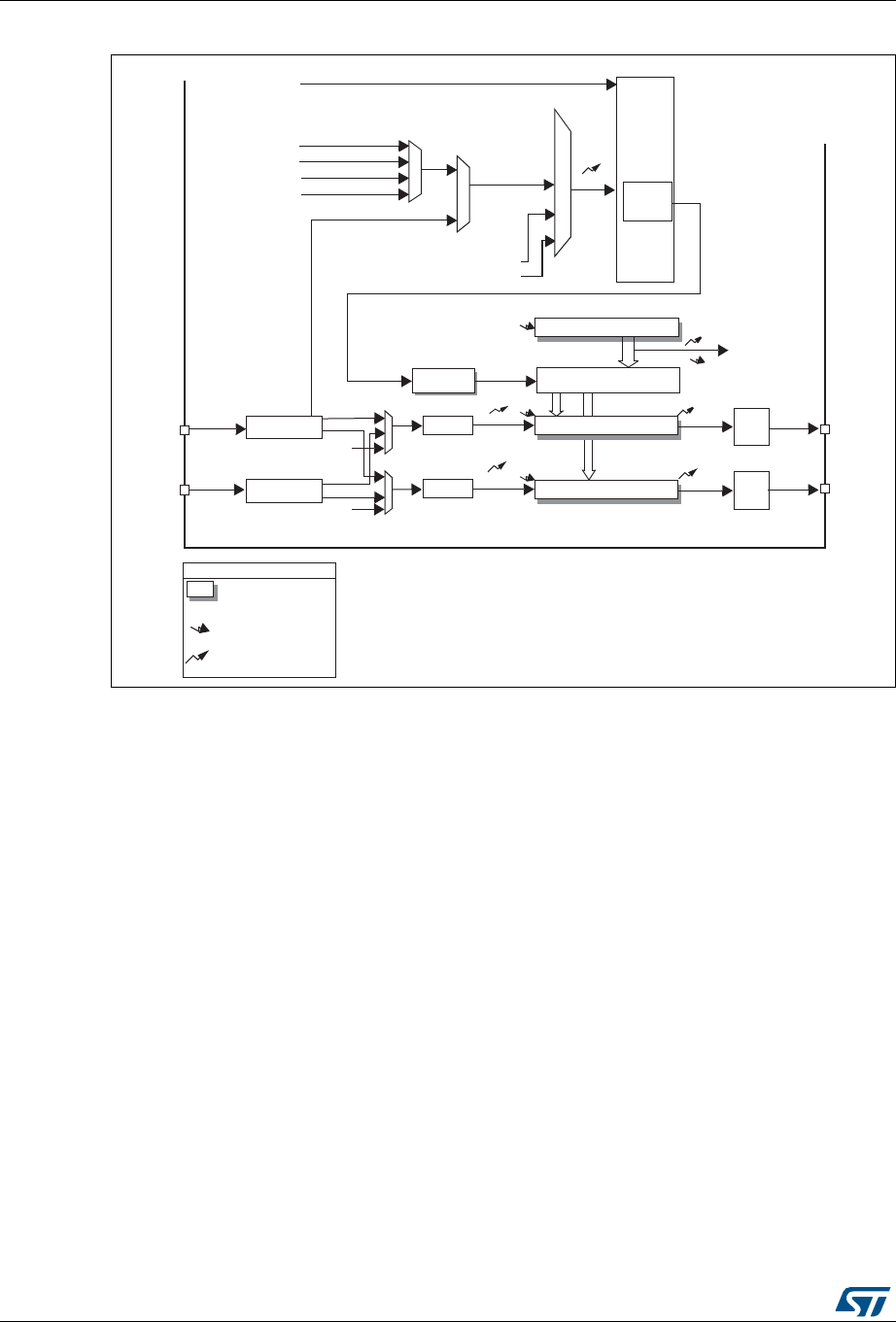
General-purpose timers (TIM9 and TIM11) RM0401
386/766 DocID027812 Rev 2
Figure 132. General-purpose timer block diagram (TIM9)
16.2.2 TIM11 main features
The features of general-purpose timer TIM11 include:
•16-bit auto-reload upcounter
•16-bit programmable prescaler used to divide the counter clock frequency by any factor
between 1 and 65536 (can be changed “on the fly”)
•independent channel for:
– Input capture
– Output compare
– PWM generation (edge-aligned mode)
– One-pulse mode output
•Interrupt generation on the following events:
– Update: counter overflow, counter initialization (by software)
– Input capture
– Output compare
Auto-reload register
Capture/Compare 1 register
Capture/Compare 2 register
U
U
U
CC1I
CC2I
Tr i g g e r
controller
Stop, Clear
TI1FP1
TI2FP2
ITR0
ITR1
ITR2
ITR3
TRGI
output
control
OC1
OC1REF
OC2REF
U
UI
Reset, Enable, Count
IC1
IC2
Prescaler
Prescaler
Input filter &
Edge detector
IC2PS
IC1PS
TI1FP1
output
control
OC2
Reg
event
Notes:
Preload registers transferred
to active registers on
U
event
according to control bit
interrupt
TGI
TRC
TRC
ITR
TRC
TI1F_ED
Input filter &
Edge detector
CC1I
CC2I
TI1FP2
TI2FP1
TI2FP2
TI1
TI2
TIMx_CH1
TIMx_CH2
TIMx_CH1
TIMx_CH2
Prescaler
COUNTER
+/-
CK_PSC
PSC CNT
CK_CNT
controller
mode
Slave
Internal clock (CK_INT)
ai17190
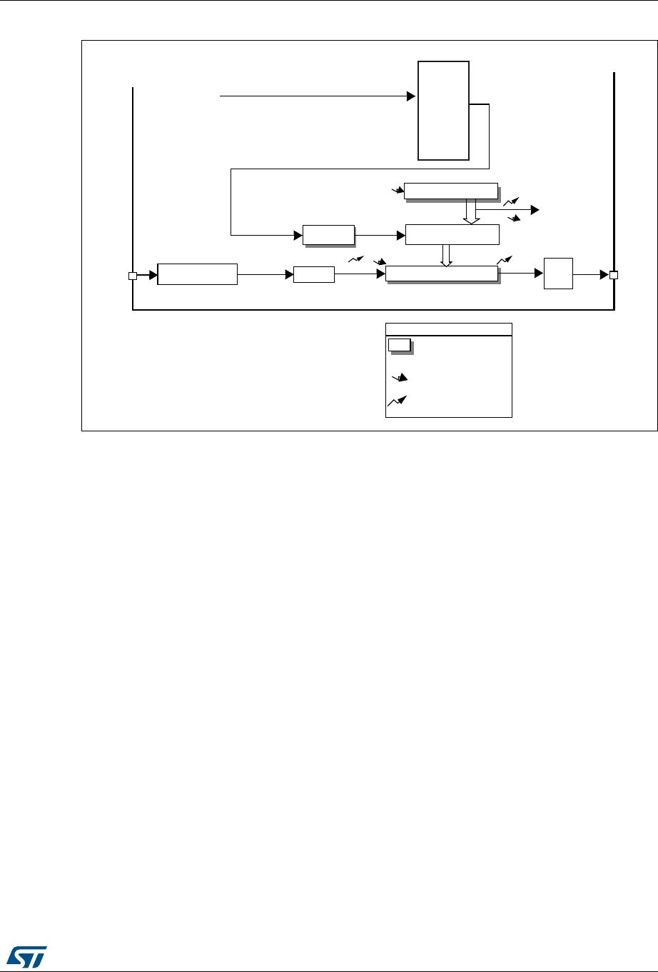
DocID027812 Rev 2 387/766
RM0401 General-purpose timers (TIM9 and TIM11)
430
Figure 133. General-purpose timer block diagram (TIM11)
!UTORELOADREGISTER
#APTURE#OMPAREREGISTER
5
5
##)
3TOP#LEAR
OUTPUT
CONTROL
/#
/#2%&
5
5)
)#
0RESCALER
)NPUTFILTER
EDGEDETECTOR
)#03
4)&0
2EG
EVENT
.OTES
0RELOADREGISTERSTRANSFERRED
TOACTIVEREGISTERSON5EVENT
ACCORDINGTOCONTROLBIT
INTERRUPT$-!OUTPUT
##)
4)
4)-X?#(
PRESCALER COUNTER
#+?03# 03# #.4
#+?#.4
)NTERNALCLOCK#+?).4
AIC
4RIGGER
#ONTROLLER
%NABLE
COUNTER
4)-X?#(

General-purpose timers (TIM9 and TIM11) RM0401
388/766 DocID027812 Rev 2
16.3 TIM9 and TIM11 functional description
16.3.1 Time-base unit
The main block of the timer is a 16-bit counter with its related auto-reload register. The
counters counts up.
The counter clock can be divided by a prescaler.
The counter, the auto-reload register and the prescaler register can be written or read by
software. This is true even when the counter is running.
The time-base unit includes:
•Counter register (TIMx_CNT)
•Prescaler register (TIMx_PSC)
•Auto-reload register (TIMx_ARR)
The auto-reload register is preloaded. Writing to or reading from the auto-reload register
accesses the preload register. The content of the preload register are transferred into the
shadow register permanently or at each update event (UEV), depending on the auto-reload
preload enable bit (ARPE) in TIMx_CR1 register. The update event is sent when the counter
reaches the overflow and if the UDIS bit equals 0 in the TIMx_CR1 register. It can also be
generated by software. The generation of the update event is described in details for each
configuration.
The counter is clocked by the prescaler output CK_CNT, which is enabled only when the
counter enable bit (CEN) in TIMx_CR1 register is set (refer also to the slave mode controller
description to get more details on counter enabling).
Note that the counter starts counting 1 clock cycle after setting the CEN bit in the TIMx_CR1
register.
Prescaler description
The prescaler can divide the counter clock frequency by any factor between 1 and 65536. It
is based on a 16-bit counter controlled through a 16-bit register (in the TIMx_PSC register).
It can be changed on the fly as this control register is buffered. The new prescaler ratio is
taken into account at the next update event.
Figure 134 and Figure 135 give some examples of the counter behavior when the prescaler
ratio is changed on the fly.
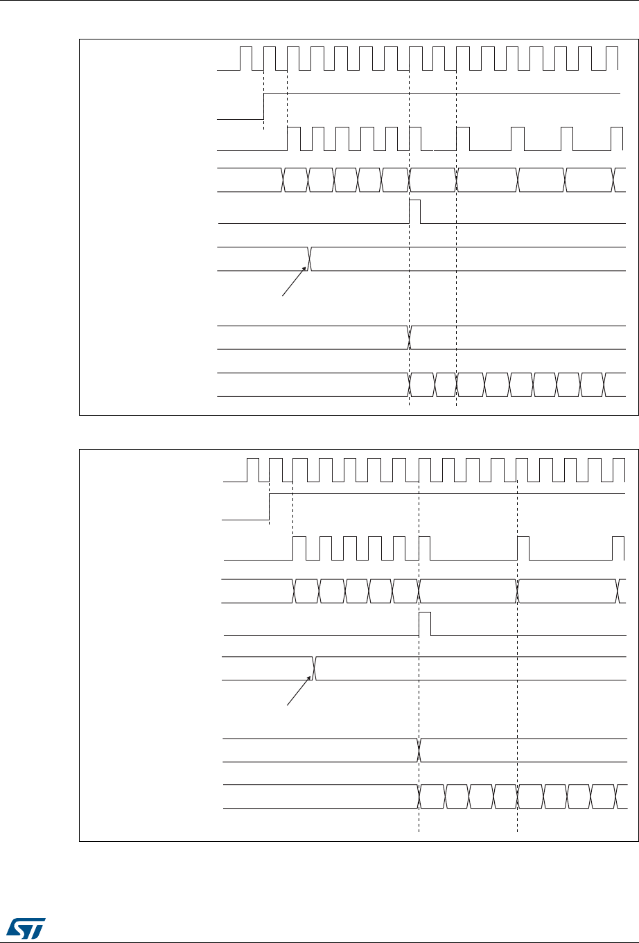
DocID027812 Rev 2 389/766
RM0401 General-purpose timers (TIM9 and TIM11)
430
Figure 134. Counter timing diagram with prescaler division change from 1 to 2
Figure 135. Counter timing diagram with prescaler division change from 1 to 4
&.B36&
&(1
7LPHUFORFN &.B&17
&RXQWHUUHJLVWHU
8SGDWHHYHQW8(9
3UHVFDOHUFRQWUROUHJLVWHU
:ULWHDQHZYDOXHLQ7,0[B36&
3UHVFDOHUEXIIHU
3UHVFDOHUFRXQWHU
)$ )%) ) ) )&
069
069
&.B36&
&(1
7LPHUFORFN &.B&17
&RXQWHUUHJLVWHU
8SGDWHHYHQW8(9
3UHVFDOHUFRQWUROUHJLVWHU
:ULWHDQHZYDOXHLQ7,0[B36&
3UHVFDOHUEXIIHU
3UHVFDOHUFRXQWHU
)$ )%
) ) ) )&
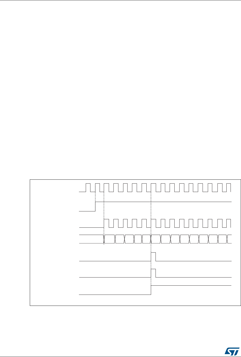
General-purpose timers (TIM9 and TIM11) RM0401
390/766 DocID027812 Rev 2
16.3.2 Counter modes
Upcounting mode
In upcounting mode, the counter counts from 0 to the auto-reload value (content of the
TIMx_ARR register), then restarts from 0 and generates a counter overflow event.
Setting the UG bit in the TIMx_EGR register (by software or by using the slave mode
controller on TIM9) also generates an update event.
The UEV event can be disabled by software by setting the UDIS bit in the TIMx_CR1
register. This is to avoid updating the shadow registers while writing new values in the
preload registers. Then no update event occurs until the UDIS bit has been written to 0.
However, the counter restarts from 0, as well as the counter of the prescaler (but the
prescale rate does not change). In addition, if the URS bit (update request selection) in
TIMx_CR1 register is set, setting the UG bit generates an update event UEV but without
setting the UIF flag (thus no interrupt is sent). This is to avoid generating both update and
capture interrupts when clearing the counter on the capture event.
When an update event occurs, all the registers are updated and the update flag (UIF bit in
TIMx_SR register) is set (depending on the URS bit):
•The auto-reload shadow register is updated with the preload value (TIMx_ARR),
•The buffer of the prescaler is reloaded with the preload value (content of the TIMx_PSC
register).
The following figures show some examples of the counter behavior for different clock
frequencies when TIMx_ARR=0x36.
Figure 136. Counter timing diagram, internal clock divided by 1
ϬϬ ϬϮ Ϭϯ Ϭϰ Ϭϱ Ϭϲ Ϭϳϯϯ ϯϰ ϯϱ ϯϲϯϭ
069
<ͺW^
EdͺE
dŝŵĞƌĐůŽĐŬс<ͺEd
ŽƵŶƚĞƌƌĞŐŝƐƚĞƌ
hƉĚĂƚĞĞǀĞŶƚ;hsͿ
ŽƵŶƚĞƌŽǀĞƌĨůŽǁ
hƉĚĂƚĞŝŶƚĞƌƌƵƉƚĨůĂŐ;h/&Ϳ
ϬϭϯϮ
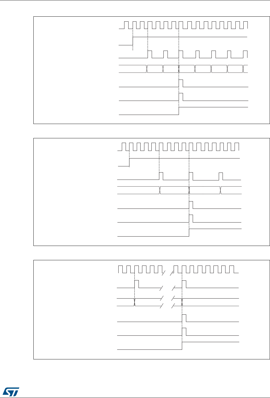
DocID027812 Rev 2 391/766
RM0401 General-purpose timers (TIM9 and TIM11)
430
Figure 137. Counter timing diagram, internal clock divided by 2
Figure 138. Counter timing diagram, internal clock divided by 4
Figure 139. Counter timing diagram, internal clock divided by N
069
&.B36&
&17B(1
7LPHUFORFN &.B&17
&RXQWHUUHJLVWHU
8SGDWHHYHQW8(9
&RXQWHURYHUIORZ
8SGDWHLQWHUUXSWIODJ8,)
069
&.B36&
&17B(1
7LPHUFORFN &.B&17
&RXQWHUUHJLVWHU
8SGDWHHYHQW8(9
&RXQWHURYHUIORZ
8SGDWHLQWHUUXSWIODJ8,)
069
&.B36&
7LPHUFORFN &.B&17
&RXQWHUUHJLVWHU
8SGDWHHYHQW8(9
&RXQWHURYHUIORZ
8SGDWHLQWHUUXSWIODJ8,)
)
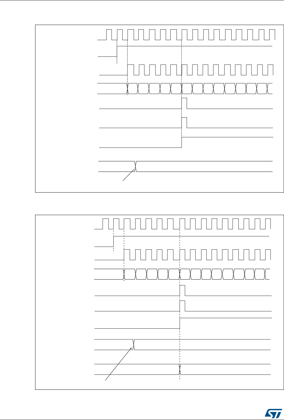
General-purpose timers (TIM9 and TIM11) RM0401
392/766 DocID027812 Rev 2
Figure 140. Counter timing diagram, update event when ARPE=0
(TIMx_ARR not preloaded)
Figure 141. Counter timing diagram, update event when ARPE=1
(TIMx_ARR preloaded)
&& ϯϲ
069
<ͺW^
dŝŵĞƌĐůŽĐŬс<ͺEd
ŽƵŶƚĞƌƌĞŐŝƐƚĞƌ
hƉĚĂƚĞĞǀĞŶƚ;hsͿ
ŽƵŶƚĞƌŽǀĞƌĨůŽǁ
hƉĚĂƚĞŝŶƚĞƌƌƵƉƚĨůĂŐ;h/&Ϳ
ϬϬ ϬϮ Ϭϯ Ϭϰ Ϭϱ Ϭϲ ϬϳϯϮ ϯϯ ϯϰ ϯϱ ϯϲϯϭ Ϭϭ
E
ƵƚŽͲƌĞůŽĂĚƉƌĞůŽĂĚƌĞŐŝƐƚĞƌ
tƌŝƚĞĂŶĞǁǀĂůƵĞŝŶd/DdžͺZZ
069
)
&.B36&
7LPHUFORFN &.B&17
&RXQWHUUHJLVWHU
8SGDWHHYHQW8(9
&RXQWHURYHUIORZ
8SGDWHLQWHUUXSWIODJ
8,)
) ) ) ) ))
&(1
$XWRUHORDGSUHORDG
UHJLVWHU
:ULWHDQHZYDOXHLQ7,0[B$55
$XWRUHORDGVKDGRZ
UHJLVWHU )
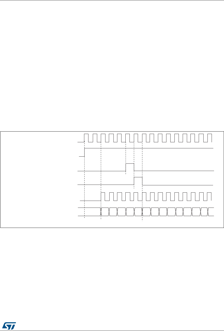
DocID027812 Rev 2 393/766
RM0401 General-purpose timers (TIM9 and TIM11)
430
16.3.3 Clock selection
The counter clock can be provided by the following clock sources:
•Internal clock (CK_INT)
•External clock mode1 (for TIM9): external input pin (TIx)
•Internal trigger inputs (ITRx) (for TIM9): connecting the trigger output from another
timer.
Internal clock source (CK_INT)
The internal clock source is the default clock source for TIM11.
For TIM9, the internal clock source is selected when the slave mode controller is disabled
(SMS=’000’). The CEN bit in the TIMx_CR1 register and the UG bit in the TIMx_EGR
register are then used as control bits and can be changed only by software (except for UG
which remains cleared). As soon as the CEN bit is programmed to 1, the prescaler is
clocked by the internal clock CK_INT.
Figure 142 shows the behavior of the control circuit and the upcounter in normal mode,
without prescaler.
Figure 142. Control circuit in normal mode, internal clock divided by 1
External clock source mode 1(TIM9)
This mode is selected when SMS=’111’ in the TIMx_SMCR register. The counter can count
at each rising or falling edge on a selected input.
,QWHUQDOFORFN
&RXQWHUFORFN &.B&17 &.B36&
&RXQWHUUHJLVWHU
&(1 &17B(1
8*
&17B,1,7
069
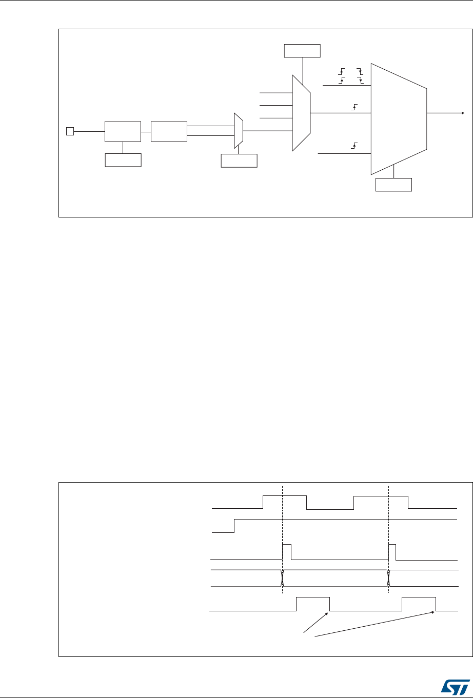
General-purpose timers (TIM9 and TIM11) RM0401
394/766 DocID027812 Rev 2
Figure 143. TI2 external clock connection example
For example, to configure the upcounter to count in response to a rising edge on the TI2
input, use the following procedure:
1. Configure channel 2 to detect rising edges on the TI2 input by writing CC2S = ‘01’ in
the TIMx_CCMR1 register.
2. Configure the input filter duration by writing the IC2F[3:0] bits in the TIMx_CCMR1
register (if no filter is needed, keep IC2F=’0000’).
3. Select the rising edge polarity by writing CC2P=’0’ and CC2NP=’0’ in the TIMx_CCER
register.
4. Configure the timer in external clock mode 1 by writing SMS=’111’ in the TIMx_SMCR
register.
5. Select TI2 as the trigger input source by writing TS=’110’ in the TIMx_SMCR register.
6. Enable the counter by writing CEN=’1’ in the TIMx_CR1 register.
Note: The capture prescaler is not used for triggering, so you don’t need to configure it.
When a rising edge occurs on TI2, the counter counts once and the TIF flag is set.
The delay between the rising edge on TI2 and the actual clock of the counter is due to the
resynchronization circuit on TI2 input.
Figure 144. Control circuit in external clock mode 1
([WHUQDOFORFN
PRGH
,QWHUQDOFORFN
PRGH
75*,
&.B,17
&.B36&
7,0[B60&5
606>@
,75[
7,B('
7,)3
7,)3
7,0[B60&5
76>@
7,
7,0[B&&(5
&&3
)LOWHU
,&)>@
7,0[B&&05
(GJH
GHWHFWRU
7,)B5LVLQJ
7,)B)DOOLQJ
[[
069
LQWHUQDOFORFN
7,) RU
7,) RU
RU
&RXQWHUFORFN &.B&17 &.B36&
&RXQWHUUHJLVWHU
7,
&17B(1
7,)
:ULWH7,) 069
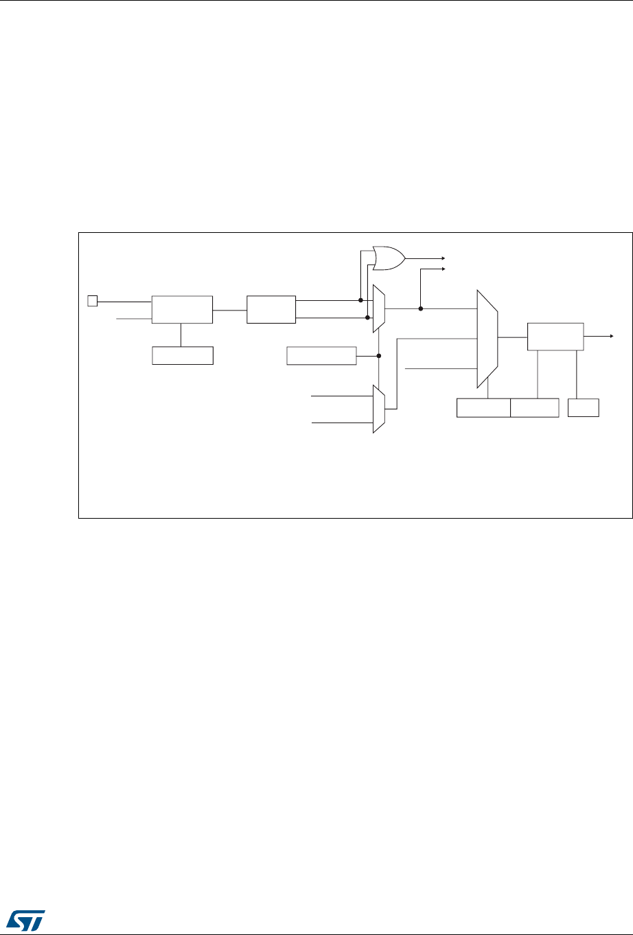
DocID027812 Rev 2 395/766
RM0401 General-purpose timers (TIM9 and TIM11)
430
16.3.4 Capture/compare channels
Each Capture/Compare channel is built around a capture/compare register (including a
shadow register), a input stage for capture (with digital filter, multiplexing and prescaler) and
an output stage (with comparator and output control).
Figure 145 to Figure 147 give an overview of one capture/compare channel.
The input stage samples the corresponding TIx input to generate a filtered signal TIxF.
Then, an edge detector with polarity selection generates a signal (TIxFPx) which can be
used as trigger input by the slave mode controller or as the capture command. It is
prescaled before the capture register (ICxPS).
Figure 145. Capture/compare channel (example: channel 1 input stage)
The output stage generates an intermediate waveform which is then used for reference:
OCxRef (active high). The polarity acts at the end of the chain.
'LYLGHU
,&36>@
7,)B('
7RWKHVODYHPRGHFRQWUROOHU
7,)3
&&6>@
,&
7,)3
75&
IURPVODYHPRGH
FRQWUROOHU
,&36
069
7,
7,0[B&&(5
&&3&&13
)LOWHU
GRZQFRXQWHU
,&)>@
7,0[B&&05
(GJH
GHWHFWRU
7,)B5LVLQJ
7,)B)DOOLQJ
7,0[B&&05
7,0[B&&(5
7,)B5LVLQJ
IURPFKDQQHO
7,)B)DOOLQJ
IURPFKDQQHO
7,)
I
&&(
'76
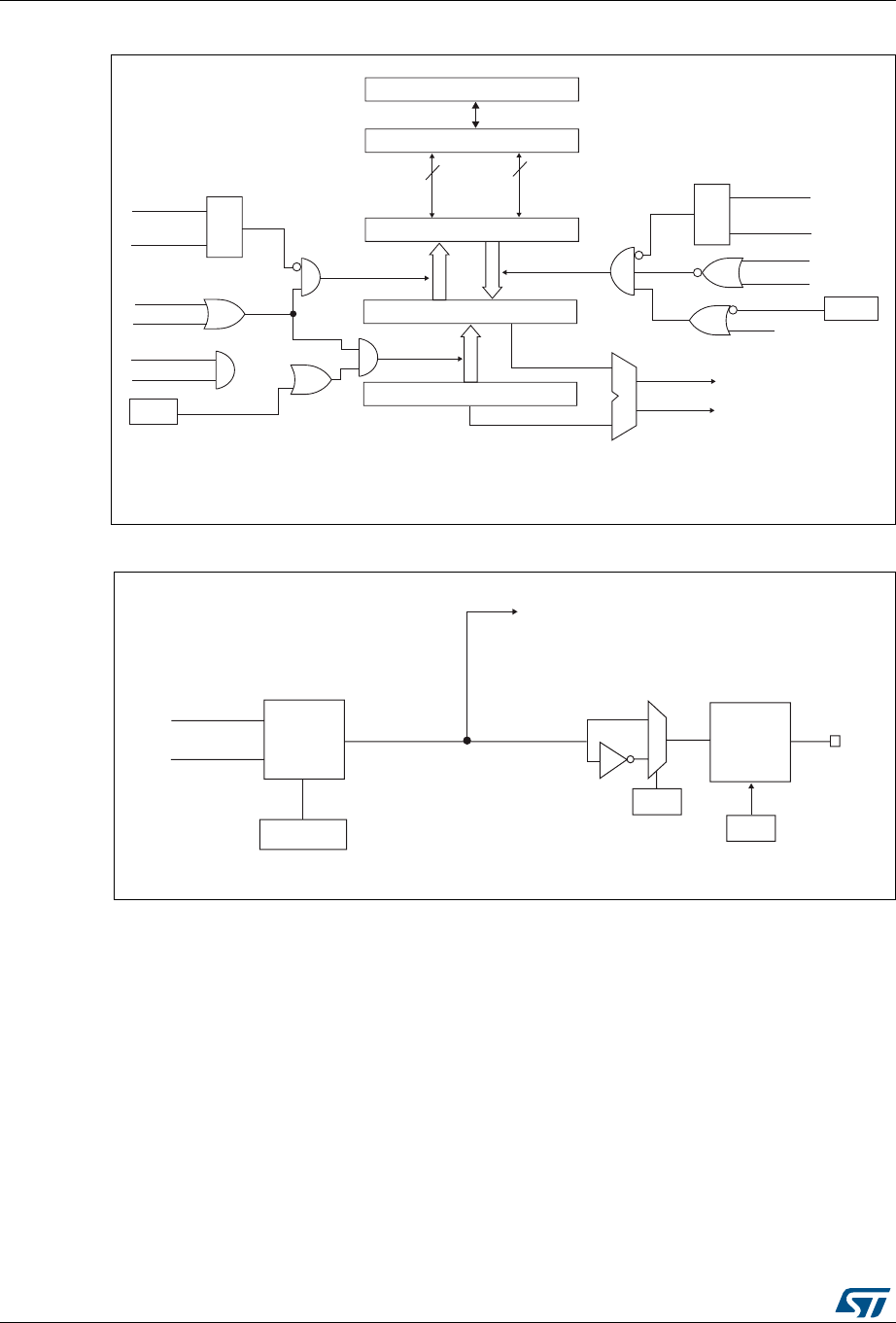
General-purpose timers (TIM9 and TIM11) RM0401
396/766 DocID027812 Rev 2
Figure 146. Capture/compare channel 1 main circuit
Figure 147. Output stage of capture/compare channel (channel 1)
The capture/compare block is made of one preload register and one shadow register. Write
and read always access the preload register.
In capture mode, captures are actually done in the shadow register, which is copied into the
preload register.
In compare mode, the content of the preload register is copied into the shadow register
which is compared to the counter.
16.3.5 Input capture mode
In Input capture mode, the Capture/Compare Registers (TIMx_CCRx) are used to latch the
value of the counter after a transition detected by the corresponding ICx signal. When a
capture occurs, the corresponding CCXIF flag (TIMx_SR register) is set and an interrupt or
a DMA request can be sent if they are enabled. If a capture occurs while the CCxIF flag was
already high, then the over-capture flag CCxOF (TIMx_SR register) is set. CCxIF can be
&&(
&DSWXUHFRPSDUHVKDGRZUHJLVWHU
&RPSDUDWRU
&DSWXUHFRPSDUHSUHORDGUHJLVWHU
&RXQWHU
,&36
&&6>@
&&6>@
&DSWXUH
,QSXW
PRGH
6
5
5HDG&&5+
5HDG&&5/
UHDGBLQBSURJUHVV
FDSWXUHBWUDQVIHU &&6>@
&&6>@
6
5
ZULWH&&5+
ZULWH&&5/
ZULWHBLQBSURJUHVV
2XWSXW
PRGH
8(9
2&3(
IURPWLPH
EDVHXQLW
FRPSDUHBWUDQVIHU
$3%%XV
KLJK
ORZ
LIELW
0&8SHULSKHUDOLQWHUIDFH
7,0B&&05
2&3(
&17!&&5
&17 &&5
7,0B(*5
&&*
069
DL
2XWSXW
PRGH
FRQWUROOHU
&17!&&5
&17 &&5
7,0[B&&05
2&0>@
&&3
7,0[B&&(5
2XWSXW
HQDEOH
FLUFXLW
2&
&&( 7,0[B&&(5
7RWKHPDVWHU
PRGHFRQWUROOHU
2&B5()

DocID027812 Rev 2 397/766
RM0401 General-purpose timers (TIM9 and TIM11)
430
cleared by software by writing it to ‘0’ or by reading the captured data stored in the
TIMx_CCRx register. CCxOF is cleared when you write it to ‘0’.
The following example shows how to capture the counter value in TIMx_CCR1 when TI1
input rises. To do this, use the following procedure:
1. Select the active input: TIMx_CCR1 must be linked to the TI1 input, so write the CC1S
bits to ‘01’ in the TIMx_CCMR1 register. As soon as CC1S becomes different from ‘00’,
the channel is configured in input mode and the TIMx_CCR1 register becomes read-
only.
2. Program the input filter duration you need with respect to the signal you connect to the
timer (by programming the ICxF bits in the TIMx_CCMRx register if the input is one of
the TIx inputs). Let’s imagine that, when toggling, the input signal is not stable during at
must 5 internal clock cycles. We must program a filter duration longer than these 5
clock cycles. We can validate a transition on TI1 when 8 consecutive samples with the
new level have been detected (sampled at fDTS frequency). Then write IC1F bits to
‘0011’ in the TIMx_CCMR1 register.
3. Select the edge of the active transition on the TI1 channel by programming CC1P and
CC1NP bits to ‘00’ in the TIMx_CCER register (rising edge in this case).
4. Program the input prescaler. In our example, we wish the capture to be performed at
each valid transition, so the prescaler is disabled (write IC1PS bits to ‘00’ in the
TIMx_CCMR1 register).
5. Enable capture from the counter into the capture register by setting the CC1E bit in the
TIMx_CCER register.
6. If needed, enable the related interrupt request by setting the CC1IE bit in the
TIMx_DIER register.
When an input capture occurs:
•The TIMx_CCR1 register gets the value of the counter on the active transition.
•CC1IF flag is set (interrupt flag). CC1OF is also set if at least two consecutive captures
occurred whereas the flag was not cleared.
•An interrupt is generated depending on the CC1IE bit.
In order to handle the overcapture, it is recommended to read the data before the
overcapture flag. This is to avoid missing an overcapture which could happen after reading
the flag and before reading the data.
Note: IC interrupt requests can be generated by software by setting the corresponding CCxG bit in
the TIMx_EGR register.
16.3.6 PWM input mode (only for TIM9)
This mode is a particular case of input capture mode. The procedure is the same except:
•Two ICx signals are mapped on the same TIx input.
•These 2 ICx signals are active on edges with opposite polarity.
•One of the two TIxFP signals is selected as trigger input and the slave mode controller
is configured in reset mode.
For example, you can measure the period (in TIMx_CCR1 register) and the duty cycle (in
TIMx_CCR2 register) of the PWM applied on TI1 using the following procedure (depending
on CK_INT frequency and prescaler value):
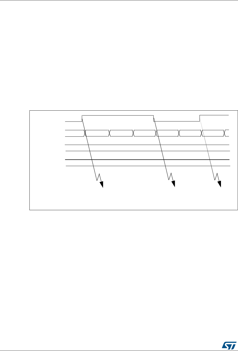
General-purpose timers (TIM9 and TIM11) RM0401
398/766 DocID027812 Rev 2
1. Select the active input for TIMx_CCR1: write the CC1S bits to ‘01’ in the TIMx_CCMR1
register (TI1 selected).
2. Select the active polarity for TI1FP1 (used both for capture in TIMx_CCR1 and counter
clear): program the CC1P and CC1NP bits to ‘00’ (active on rising edge).
3. Select the active input for TIMx_CCR2: write the CC2S bits to ‘10’ in the TIMx_CCMR1
register (TI1 selected).
4. Select the active polarity for TI1FP2 (used for capture in TIMx_CCR2): program the
CC2P and CC2NP bits to ‘11’ (active on falling edge).
5. Select the valid trigger input: write the TS bits to ‘101’ in the TIMx_SMCR register
(TI1FP1 selected).
6. Configure the slave mode controller in reset mode: write the SMS bits to ‘100’ in the
TIMx_SMCR register.
7. Enable the captures: write the CC1E and CC2E bits to ‘1’ in the TIMx_CCER register.
Figure 148. PWM input mode timing
1. The PWM input mode can be used only with the TIMx_CH1/TIMx_CH2 signals due to the fact that only
TI1FP1 and TI2FP2 are connected to the slave mode controller.
16.3.7 Forced output mode
In output mode (CCxS bits = ‘00’ in the TIMx_CCMRx register), each output compare signal
(OCxREF and then OCx) can be forced to active or inactive level directly by software,
independently of any comparison between the output compare register and the counter.
To force an output compare signal (OCXREF/OCx) to its active level, you just need to write
‘101’ in the OCxM bits in the corresponding TIMx_CCMRx register. Thus OCXREF is forced
high (OCxREF is always active high) and OCx get opposite value to CCxP polarity bit.
For example: CCxP=’0’ (OCx active high) => OCx is forced to high level.
The OCxREF signal can be forced low by writing the OCxM bits to ‘100’ in the
TIMx_CCMRx register.
Anyway, the comparison between the TIMx_CCRx shadow register and the counter is still
performed and allows the flag to be set. Interrupt requests can be sent accordingly. This is
described in the output compare mode section below.
TI1
TIMx_CNT 0000 0001 0002 0003 0004 00000004
TIMx_CCR1
TIMx_CCR2
0004
0002
IC1 capture
IC2 capture
reset counter
IC2 capture
pulse width
IC1 capture
period
measurementmeasurement
ai15413

DocID027812 Rev 2 399/766
RM0401 General-purpose timers (TIM9 and TIM11)
430
16.3.8 Output compare mode
This function is used to control an output waveform or indicating when a period of time has
elapsed.
When a match is found between the capture/compare register and the counter, the output
compare function:
1. Assigns the corresponding output pin to a programmable value defined by the output
compare mode (OCxM bits in the TIMx_CCMRx register) and the output polarity (CCxP
bit in the TIMx_CCER register). The output pin can keep its level (OCXM=’000’), be set
active (OCxM=’001’), be set inactive (OCxM=’010’) or can toggle (OCxM=’011’) on
match.
2. Sets a flag in the interrupt status register (CCxIF bit in the TIMx_SR register).
3. Generates an interrupt if the corresponding interrupt mask is set (CCXIE bit in the
TIMx_DIER register).
The TIMx_CCRx registers can be programmed with or without preload registers using the
OCxPE bit in the TIMx_CCMRx register.
In output compare mode, the update event UEV has no effect on OCxREF and OCx output.
The timing resolution is one count of the counter. Output compare mode can also be used to
output a single pulse (in One-pulse mode).
Procedure:
1. Select the counter clock (internal, external, prescaler).
2. Write the desired data in the TIMx_ARR and TIMx_CCRx registers.
3. Set the CCxIE bit if an interrupt request is to be generated.
4. Select the output mode. For example:
– Write OCxM = ‘011’ to toggle OCx output pin when CNT matches CCRx
– Write OCxPE = ‘0’ to disable preload register
– Write CCxP = ‘0’ to select active high polarity
– Write CCxE = ‘1’ to enable the output
5. Enable the counter by setting the CEN bit in the TIMx_CR1 register.
The TIMx_CCRx register can be updated at any time by software to control the output
waveform, provided that the preload register is not enabled (OCxPE=’0’, else TIMx_CCRx
shadow register is updated only at the next update event UEV). An example is given in
Figure 149.

General-purpose timers (TIM9 and TIM11) RM0401
400/766 DocID027812 Rev 2
Figure 149. Output compare mode, toggle on OC1.
16.3.9 PWM mode
Pulse Width Modulation mode allows you to generate a signal with a frequency determined
by the value of the TIMx_ARR register and a duty cycle determined by the value of the
TIMx_CCRx register.
The PWM mode can be selected independently on each channel (one PWM per OCx
output) by writing ‘110’ (PWM mode 1) or ‘111’ (PWM mode 2) in the OCxM bits in the
TIMx_CCMRx register. You must enable the corresponding preload register by setting the
OCxPE bit in the TIMx_CCMRx register, and eventually the auto-reload preload register (in
upcounting or center-aligned modes) by setting the ARPE bit in the TIMx_CR1 register.
As the preload registers are transferred to the shadow registers only when an update event
occurs, before starting the counter, you have to initialize all the registers by setting the UG
bit in the TIMx_EGR register.
The OCx polarity is software programmable using the CCxP bit in the TIMx_CCER register.
It can be programmed as active high or active low. The OCx output is enabled by the CCxE
bit in the TIMx_CCER register. Refer to the TIMx_CCERx register description for more
details.
In PWM mode (1 or 2), TIMx_CNT and TIMx_CCRx are always compared to determine
whether TIMx_CNT ≤ TIMx_CCRx.
The timer is able to generate PWM in edge-aligned mode only since the counter is
upcounting.
PWM edge-aligned mode
In the following example, we consider PWM mode 1. The reference PWM signal OCxREF is
high as long as TIMx_CNT < TIMx_CCRx else it becomes low. If the compare value in
TIMx_CCRx is greater than the auto-reload value (in TIMx_ARR) then OCxREF is held at
‘1’. If the compare value is 0 then OCxRef is held at ‘0’. Figure 150 shows some edge-
aligned PWM waveforms in an example where TIMx_ARR=8.
069
2&5() 2&
7,0B&17 % %
7,0B&&5 $
:ULWH%KLQWKH&&5UHJLVWHU
0DWFKGHWHFWHGRQ&&5
,QWHUUXSWJHQHUDWHGLIHQDEOHG
%
%
$
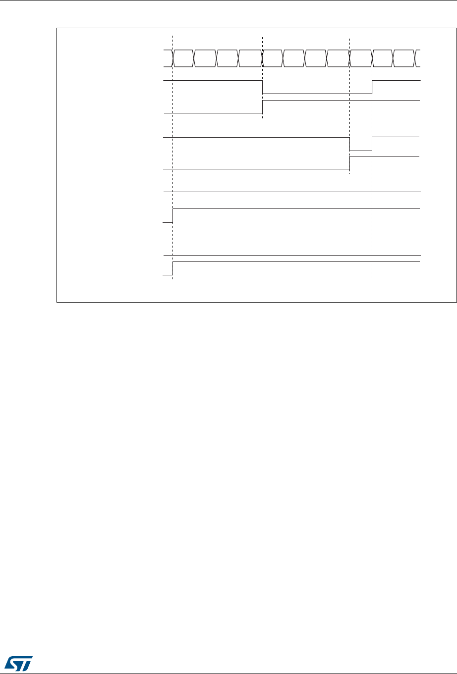
DocID027812 Rev 2 401/766
RM0401 General-purpose timers (TIM9 and TIM11)
430
Figure 150. Edge-aligned PWM waveforms (ARR=8)
16.3.10 One-pulse mode
One-pulse mode (OPM) is a particular case of the previous modes. It allows the counter to
be started in response to a stimulus and to generate a pulse with a programmable length
after a programmable delay.
Starting the counter can be controlled through the slave mode controller. Generating the
waveform can be done in output compare mode or PWM mode. You select One-pulse mode
by setting the OPM bit in the TIMx_CR1 register. This makes the counter stop automatically
at the next update event UEV.
A pulse can be correctly generated only if the compare value is different from the counter
initial value. Before starting (when the timer is waiting for the trigger), the configuration must
be as follows:
CNT < CCRx≤ ARR (in particular, 0 < CCRx)
069
&RXQWHUUHJLVWHU
µ
2&;5()
&&[,)
2&;5()
&&[,)
2&;5()
&&[,)
2&;5()
&&[,)
&&5[
&&5[
&&5[!
&&5[
µ
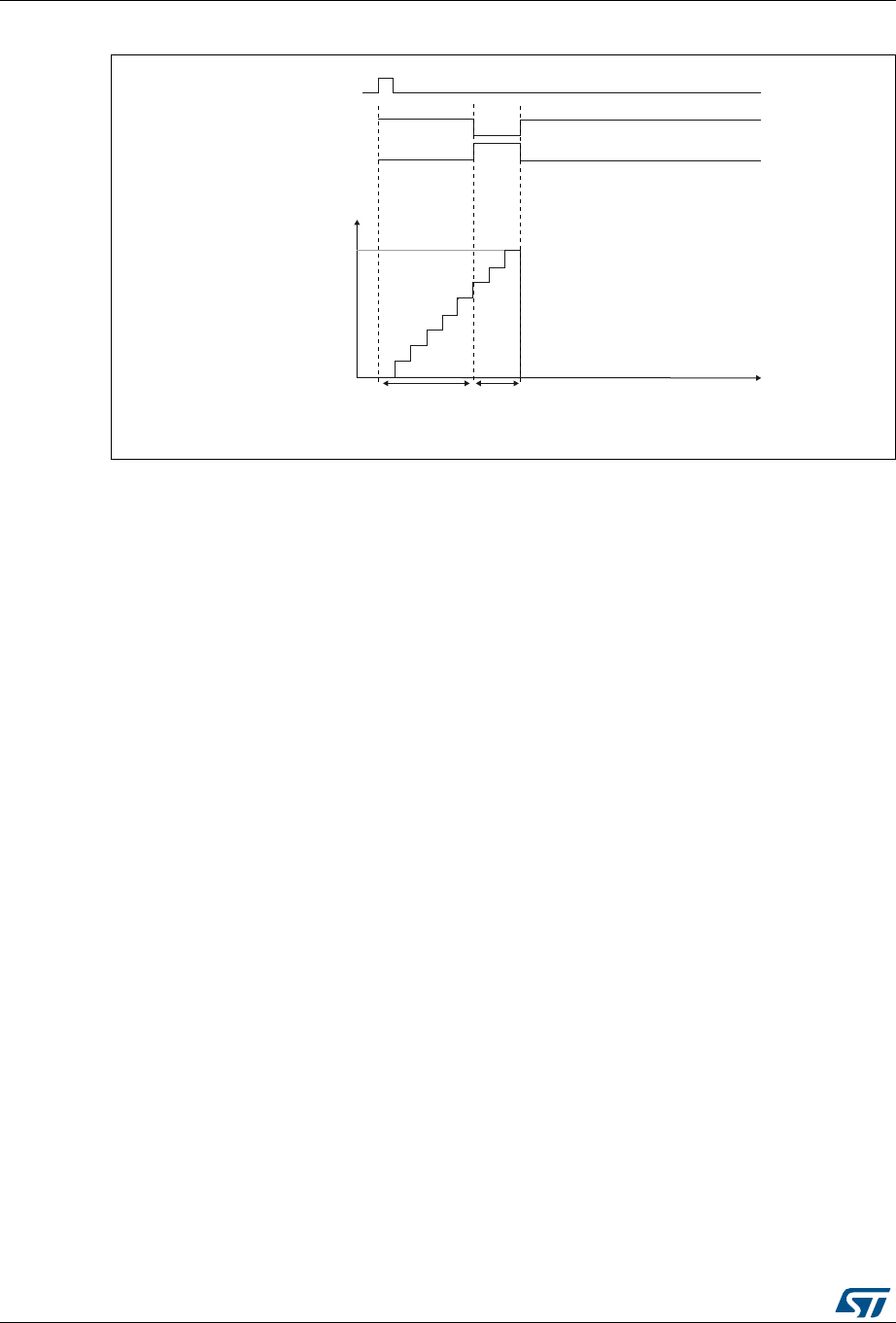
General-purpose timers (TIM9 and TIM11) RM0401
402/766 DocID027812 Rev 2
Figure 151. Example of one pulse mode.
For example you may want to generate a positive pulse on OC1 with a length of tPULSE and
after a delay of tDELAY as soon as a positive edge is detected on the TI2 input pin.
Use TI2FP2 as trigger 1:
1. Map TI2FP2 to TI2 by writing CC2S=’01’ in the TIMx_CCMR1 register.
2. TI2FP2 must detect a rising edge, write CC2P=’0’ and CC2NP = ‘0’ in the TIMx_CCER
register.
3. Configure TI2FP2 as trigger for the slave mode controller (TRGI) by writing TS=’110’ in
the TIMx_SMCR register.
4. TI2FP2 is used to start the counter by writing SMS to ‘110’ in the TIMx_SMCR register
(trigger mode).
The OPM waveform is defined by writing the compare registers (taking into account the
clock frequency and the counter prescaler).
•The tDELAY is defined by the value written in the TIMx_CCR1 register.
•The tPULSE is defined by the difference between the auto-reload value and the compare
value (TIMx_ARR - TIMx_CCR1).
•Let’s say you want to build a waveform with a transition from ‘0’ to ‘1’ when a compare
match occurs and a transition from ‘1’ to ‘0’ when the counter reaches the auto-reload
value. To do this you enable PWM mode 2 by writing OC1M=’111’ in the TIMx_CCMR1
register. You can optionally enable the preload registers by writing OC1PE=’1’ in the
TIMx_CCMR1 register and ARPE in the TIMx_CR1 register. In this case you have to
write the compare value in the TIMx_CCR1 register, the auto-reload value in the
TIMx_ARR register, generate an update by setting the UG bit and wait for external
trigger event on TI2. CC1P is written to ‘0’ in this example.
You only want 1 pulse (Single mode), so you write '1 in the OPM bit in the TIMx_CR1
register to stop the counter at the next update event (when the counter rolls over from the
auto-reload value back to 0). When OPM bit in the TIMx_CR1 register is set to '0', so the
Repetitive Mode is selected.
Particular case: OCx fast enable
069
7,
2&5()
&RXQWHU
W
7,0B$55
7,0B&&5
2&
W'(/$< W38/6(

DocID027812 Rev 2 403/766
RM0401 General-purpose timers (TIM9 and TIM11)
430
In One-pulse mode, the edge detection on TIx input set the CEN bit which enables the
counter. Then the comparison between the counter and the compare value makes the
output toggle. But several clock cycles are needed for these operations and it limits the
minimum delay tDELAY min we can get.
If you want to output a waveform with the minimum delay, you can set the OCxFE bit in the
TIMx_CCMRx register. Then OCxRef (and OCx) are forced in response to the stimulus,
without taking in account the comparison. Its new level is the same as if a compare match
had occurred. OCxFE acts only if the channel is configured in PWM1 or PWM2 mode.
16.3.11 TIM9 external trigger synchronization
The TIM9 timers can be synchronized with an external trigger in several modes: Reset
mode, Gated mode and Trigger mode.
Slave mode: Reset mode
The counter and its prescaler can be reinitialized in response to an event on a trigger input.
Moreover, if the URS bit from the TIMx_CR1 register is low, an update event UEV is
generated. Then all the preloaded registers (TIMx_ARR, TIMx_CCRx) are updated.
In the following example, the upcounter is cleared in response to a rising edge on TI1 input:
1. Configure the channel 1 to detect rising edges on TI1. Configure the input filter duration
(in this example, we don’t need any filter, so we keep IC1F=’0000’). The capture
prescaler is not used for triggering, so you don’t need to configure it. The CC1S bits
select the input capture source only, CC1S = ‘01’ in the TIMx_CCMR1 register.
Program CC1P and CC1NP to ‘00’ in TIMx_CCER register to validate the polarity (and
detect rising edges only).
2. Configure the timer in reset mode by writing SMS=’100’ in TIMx_SMCR register. Select
TI1 as the input source by writing TS=’101’ in TIMx_SMCR register.
3. Start the counter by writing CEN=’1’ in the TIMx_CR1 register.
The counter starts counting on the internal clock, then behaves normally until TI1 rising
edge. When TI1 rises, the counter is cleared and restarts from 0. In the meantime, the
trigger flag is set (TIF bit in the TIMx_SR register) and an interrupt request can be sent if
enabled (depending on the TIE bit in TIMx_DIER register).
The following figure shows this behavior when the auto-reload register TIMx_ARR=0x36.
The delay between the rising edge on TI1 and the actual reset of the counter is due to the
resynchronization circuit on TI1 input.

General-purpose timers (TIM9 and TIM11) RM0401
404/766 DocID027812 Rev 2
Figure 152. Control circuit in reset mode
Slave mode: Gated mode
The counter can be enabled depending on the level of a selected input.
In the following example, the upcounter counts only when TI1 input is low:
1. Configure the channel 1 to detect low levels on TI1. Configure the input filter duration
(in this example, we don’t need any filter, so we keep IC1F=’0000’). The capture
prescaler is not used for triggering, so you don’t need to configure it. The CC1S bits
select the input capture source only, CC1S=’01’ in TIMx_CCMR1 register. Program
CC1P=’1’ and CC1NP= ‘0’ in TIMx_CCER register to validate the polarity (and detect
low level only).
2. Configure the timer in gated mode by writing SMS=’101’ in TIMx_SMCR register.
Select TI1 as the input source by writing TS=’101’ in TIMx_SMCR register.
3. Enable the counter by writing CEN=’1’ in the TIMx_CR1 register (in gated mode, the
counter doesn’t start if CEN=’0’, whatever is the trigger input level).
The counter starts counting on the internal clock as long as TI1 is low and stops as soon as
TI1 becomes high. The TIF flag in the TIMx_SR register is set both when the counter starts
or stops.
The delay between the rising edge on TI1 and the actual stop of the counter is due to the
resynchronization circuit on TI1 input.
069
&RXQWHUFORFN FNBFQW FNBSVF
&RXQWHUUHJLVWHU
8*
7,
7,)
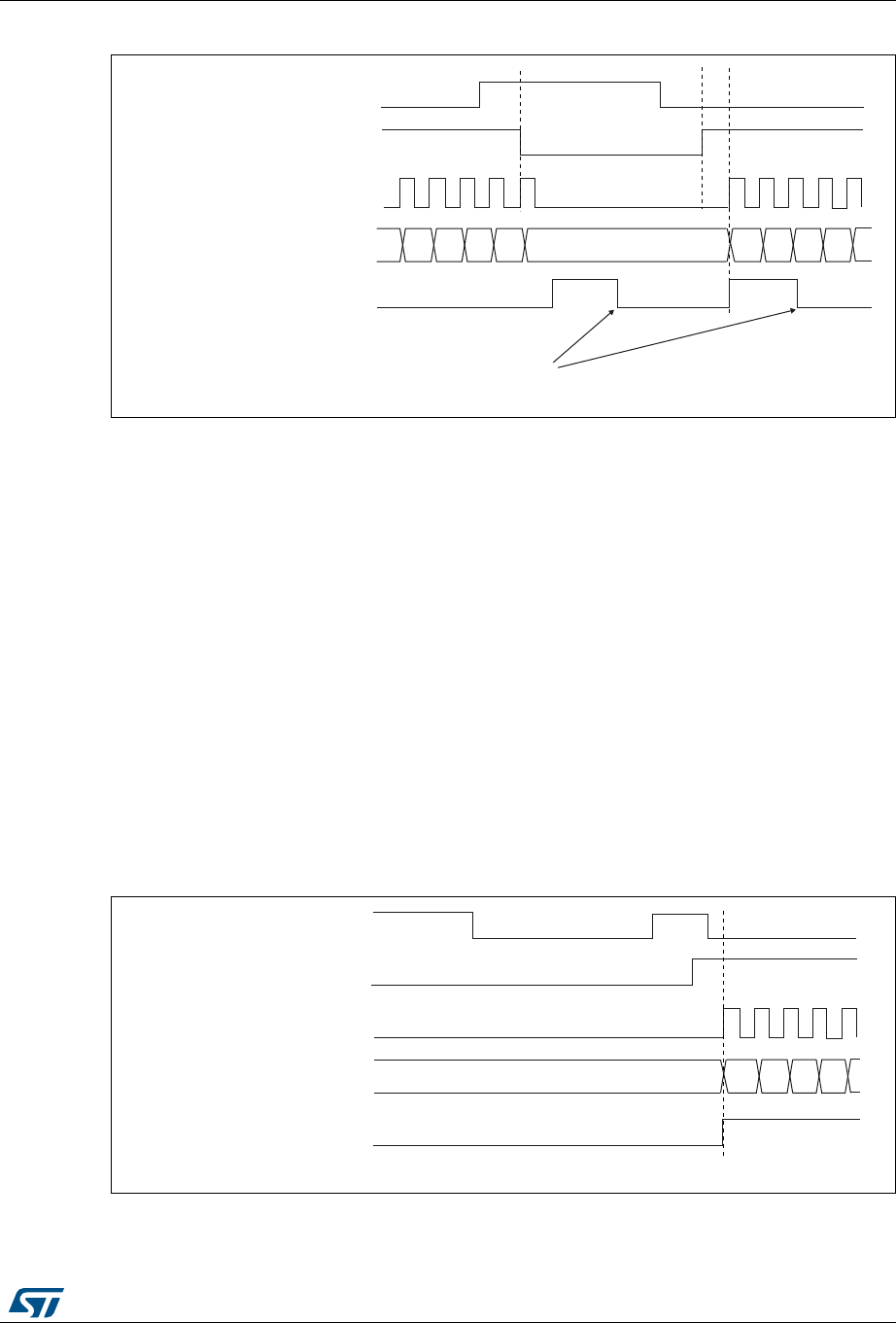
DocID027812 Rev 2 405/766
RM0401 General-purpose timers (TIM9 and TIM11)
430
Figure 153. Control circuit in gated mode
Slave mode: Trigger mode
The counter can start in response to an event on a selected input.
In the following example, the upcounter starts in response to a rising edge on TI2 input:
1. Configure the channel 2 to detect rising edges on TI2. Configure the input filter duration
(in this example, we don’t need any filter, so we keep IC2F=’0000’). The capture
prescaler is not used for triggering, so you don’t need to configure it. The CC2S bits are
configured to select the input capture source only, CC2S=’01’ in TIMx_CCMR1 register.
Program CC2P=’1’ and CC2NP=’0’ in TIMx_CCER register to validate the polarity (and
detect low level only).
2. Configure the timer in trigger mode by writing SMS=’110’ in TIMx_SMCR register.
Select TI2 as the input source by writing TS=’110’ in TIMx_SMCR register.
When a rising edge occurs on TI2, the counter starts counting on the internal clock and the
TIF flag is set.
The delay between the rising edge on TI2 and the actual start of the counter is due to the
resynchronization circuit on TI2 input.
Figure 154. Control circuit in trigger mode
069
7,
FQWBHQ
:ULWH7,)
&RXQWHUFORFN FNBFQW FNBSVF
&RXQWHUUHJLVWHU
7,)
069
7,
FQWBHQ
&RXQWHUFORFN FNBFQW FNBSVF
&RXQWHUUHJLVWHU
7,)

General-purpose timers (TIM9 and TIM11) RM0401
406/766 DocID027812 Rev 2
16.3.12 Debug mode
When the microcontroller enters debug mode (Cortex®-M4 with FPU core halted), the TIMx
counter either continues to work normally or stops, depending on DBG_TIMx_STOP
configuration bit in DBG module. For more details, refer to Section 26.16.2: Debug support
for timers, watchdog and I2C.
16.4 TIM9 registers
Refer to Section 1.1 on page 33 for a list of abbreviations used in register descriptions.
The peripheral registers have to be written by half-words (16 bits) or words (32 bits). Read
accesses can be done by bytes (8 bits), half-words (16 bits) or words (32 bits).
16.4.1 TIM9 control register 1 (TIMx_CR1)
Address offset: 0x00
Reset value: 0x0000
15 14 13 12 11 10 9876543210
Res. Res. Res. Res. Res. Res. CKD[1:0] ARPE Res. Res. Res. OPM URS UDIS CEN
rw rw rw rw rw rw rw
Bits 15:10 Reserved, must be kept at reset value.
Bits 9:8 CKD: Clock division
This bit-field indicates the division ratio between the timer clock (CK_INT) frequency and
sampling clock used by the digital filters (TIx),
00: tDTS = tCK_INT
01: tDTS = 2 × tCK_INT
10: tDTS = 4 × tCK_INT
11: Reserved
Bit 7 ARPE: Auto-reload preload enable
0: TIMx_ARR register is not buffered.
1: TIMx_ARR register is buffered.
Bits 6:4 Reserved, must be kept at reset value.
Bit 3 OPM: One-pulse mode
0: Counter is not stopped on the update event
1: Counter stops counting on the next update event (clearing the CEN bit).

DocID027812 Rev 2 407/766
RM0401 General-purpose timers (TIM9 and TIM11)
430
Bit 2 URS: Update request source
This bit is set and cleared by software to select the UEV event sources.
0: Any of the following events generates an update interrupt if enabled:
– Counter overflow
– Setting the UG bit
1: Only counter overflow generates an update interrupt if enabled.
Bit 1 UDIS: Update disable
This bit is set and cleared by software to enable/disable update event (UEV) generation.
0: UEV enabled. An UEV is generated by one of the following events:
– Counter overflow
– Setting the UG bit
Buffered registers are then loaded with their preload values.
1: UEV disabled. No UEV is generated, shadow registers keep their value (ARR, PSC,
CCRx). The counter and the prescaler are reinitialized if the UG bit is set.
Bit 0 CEN: Counter enable
0: Counter disabled
1: Counter enabled
CEN is cleared automatically in one-pulse mode, when an update event occurs.

General-purpose timers (TIM9 and TIM11) RM0401
408/766 DocID027812 Rev 2
16.4.2 TIM9 slave mode control register (TIMx_SMCR)
Address offset: 0x08
Reset value: 0x0000
1514131211109876543210
Res. Res. Res. Res. Res. Res. Res. Res. MSM TS[2:0] Res. SMS[2:0]
rw rw rw rw rw rw rw
Bits 15:8 Reserved, must be kept at reset value.
Bit 7 MSM: Master/Slave mode
0: No action
1: The effect of an event on the trigger input (TRGI) is delayed to allow a perfect
synchronization between the current timer and its slaves (through TRGO). It is useful in
order to synchronize several timers on a single external event.
Bits 6:4 TS: Trigger selection
This bitfield selects the trigger input to be used to synchronize the counter.
000: Internal Trigger 0 (ITR0)
001: Internal Trigger 1 (ITR1)
010: Internal Trigger 2 (ITR2)
011: Internal Trigger 3 (ITR3)
100: TI1 Edge Detector (TI1F_ED)
101: Filtered Timer Input 1 (TI1FP1)
110: Filtered Timer Input 2 (TI2FP2)
111: Reserved.
See Table 63: TIMx internal trigger connection on page 409 for more details on the meaning
of ITRx for each timer.
Note: These bits must be changed only when they are not used (e.g. when SMS=’000’) to
avoid wrong edge detections at the transition.
Bit 3 Reserved, must be kept at reset value.
Bits 2:0 SMS: Slave mode selection
When external signals are selected, the active edge of the trigger signal (TRGI) is linked to
the polarity selected on the external input (see Input control register and Control register
descriptions.
000: Slave mode disabled - if CEN = 1 then the prescaler is clocked directly by the internal
clock
001: Reserved
010: Reserved
011: Reserved
100: Reset mode - Rising edge of the selected trigger input (TRGI) reinitializes the counter
and generates an update of the registers
101: Gated mode - The counter clock is enabled when the trigger input (TRGI) is high. The
counter stops (but is not reset) as soon as the trigger becomes low. Counter starts and stops
are both controlled
110: Trigger mode - The counter starts on a rising edge of the trigger TRGI (but it is not
reset). Only the start of the counter is controlled
111: External clock mode 1 - Rising edges of the selected trigger (TRGI) clock the counter
Note: The Gated mode must not be used if TI1F_ED is selected as the trigger input
(TS=’100’). Indeed, TI1F_ED outputs 1 pulse for each transition on TI1F, whereas the
Gated mode checks the level of the trigger signal.

DocID027812 Rev 2 409/766
RM0401 General-purpose timers (TIM9 and TIM11)
430
16.4.3 TIM9 Interrupt enable register (TIMx_DIER)
Address offset: 0x0C
Reset value: 0x0000
Table 63. TIMx internal trigger connection
Slave TIM ITR0 (TS = ‘000’) ITR1 (TS = ‘001’) ITR2 (TS = ‘010’) ITR3 (TS = ‘011’)
TIM5 Reserved LPTIM Reserved Reserved
TIM9 Reserved LPTIM Reserved TIM11
15 14 13 12 11 10 9876543210
Res. Res. Res. Res. Res. Res. Res. Res. Res. TIE Res. Res. Res. CC2IE CC1IE UIE
rw rw rw rw
Bits 15:7 Reserved, must be kept at reset value.
Bit 6 TIE: Trigger interrupt enable
0: Trigger interrupt disabled.
1: Trigger interrupt enabled.
Bit 5:3 Reserved, must be kept at reset value.
Bit 2 CC2IE: Capture/Compare 2 interrupt enable
0: CC2 interrupt disabled.
1: CC2 interrupt enabled.
Bit 1 CC1IE: Capture/Compare 1 interrupt enable
0: CC1 interrupt disabled.
1: CC1 interrupt enabled.
Bit 0 UIE: Update interrupt enable
0: Update interrupt disabled.
1: Update interrupt enabled.

General-purpose timers (TIM9 and TIM11) RM0401
410/766 DocID027812 Rev 2
16.4.4 TIM9 status register (TIMx_SR)
Address offset: 0x10
Reset value: 0x0000
15 14 13 12 11 10 9876543210
Res. Res. Res. Res. Res. CC2OF CC1OF Res. Res. TIF Res. Res. Res. CC2IF CC1IF UIF
rc_w0 rc_w0 rc_w0 rc_w0 rc_w0 rc_w0
Bits 15:11 Reserved, must be kept at reset value.
Bit 10 CC2OF: Capture/compare 2 overcapture flag
refer to CC1OF description
Bit 9 CC1OF: Capture/Compare 1 overcapture flag
This flag is set by hardware only when the corresponding channel is configured in input
capture mode. It is cleared by software by writing it to ‘0’.
0: No overcapture has been detected.
1: The counter value has been captured in TIMx_CCR1 register while CC1IF flag was
already set
Bits 8:7 Reserved, must be kept at reset value.
Bit 6 TIF: Trigger interrupt flag
This flag is set by hardware on trigger event (active edge detected on TRGI input when the
slave mode controller is enabled in all modes but gated mode. It is set when the counter
starts or stops when gated mode is selected. It is cleared by software.
0: No trigger event occurred.
1: Trigger interrupt pending.
Bits 5:3 Reserved, must be kept at reset value.

DocID027812 Rev 2 411/766
RM0401 General-purpose timers (TIM9 and TIM11)
430
Bit 2 CC2IF: Capture/Compare 2 interrupt flag
refer to CC1IF description
Bit 1 CC1IF: Capture/compare 1 interrupt flag
If channel CC1 is configured as output:
This flag is set by hardware when the counter matches the compare value. It is cleared by
software.
0: No match.
1: The content of the counter TIMx_CNT matches the content of the TIMx_CCR1 register.
When the contents of TIMx_CCR1 are greater than the contents of TIMx_ARR, the CC1IF
bit goes high on the counter overflow.
If channel CC1 is configured as input:
This bit is set by hardware on a capture. It is cleared by software or by reading the
TIMx_CCR1 register.
0: No input capture occurred.
1: The counter value has been captured in TIMx_CCR1 register (an edge has been detected
on IC1 which matches the selected polarity).
Bit 0 UIF: Update interrupt flag
This bit is set by hardware on an update event. It is cleared by software.
0: No update occurred.
1: Update interrupt pending. This bit is set by hardware when the registers are updated:
– At overflow and if UDIS=’0’ in the TIMx_CR1 register.
– When CNT is reinitialized by software using the UG bit in TIMx_EGR register, if URS=’0’ and
UDIS=’0’ in the TIMx_CR1 register.
– When CNT is reinitialized by a trigger event (refer to the synchro control register
description), if URS=’0’ and UDIS=’0’ in the TIMx_CR1 register.

General-purpose timers (TIM9 and TIM11) RM0401
412/766 DocID027812 Rev 2
16.4.5 TIM9 event generation register (TIMx_EGR)
Address offset: 0x14
Reset value: 0x0000
15 14 13 12 11 10 9876543210
Res. Res. Res. Res. Res. Res. Res. Res. Res. TG Res. Res. Res. CC2G CC1G UG
w w w w
Bits 15:7 Reserved, must be kept at reset value.
Bit 6 TG: Trigger generation
This bit is set by software in order to generate an event, it is automatically cleared by
hardware.
0: No action
1: The TIF flag is set in the TIMx_SR register. Related interrupt can occur if enabled
Bits 5:3 Reserved, must be kept at reset value.
Bit 2 CC2G: Capture/compare 2 generation
refer to CC1G description
Bit 1 CC1G: Capture/compare 1 generation
This bit is set by software to generate an event, it is automatically cleared by hardware.
0: No action
1: A capture/compare event is generated on channel 1:
If channel CC1 is configured as output:
the CC1IF flag is set, the corresponding interrupt is sent if enabled.
If channel CC1 is configured as input:
The current counter value is captured in the TIMx_CCR1 register. The CC1IF flag is set, the
corresponding interrupt is sent if enabled. The CC1OF flag is set if the CC1IF flag was
already high.
Bit 0 UG: Update generation
This bit can be set by software, it is automatically cleared by hardware.
0: No action
1: Re-initializes the counter and generates an update of the registers. The prescaler counter
is also cleared and the prescaler ratio is not affected. The counter is cleared.

DocID027812 Rev 2 413/766
RM0401 General-purpose timers (TIM9 and TIM11)
430
16.4.6 TIM9 capture/compare mode register 1 (TIMx_CCMR1)
Address offset: 0x18
Reset value: 0x0000
The channels can be used in input (capture mode) or in output (compare mode). The
direction of a channel is defined by configuring the corresponding CCxS bits. All the other
bits in this register have different functions in input and output modes. For a given bit, OCxx
describes its function when the channel is configured in output mode, ICxx describes its
function when the channel is configured in input mode. So you must take care that the same
bit can have different meanings for the input stage and the output stage.
Output compare mode
15 14 13 12 11 10 9876543210
Res. OC2M[2:0] OC2PE OC2FE CC2S[1:0] Res. OC1M[2:0] OC1PE OC1FE CC1S[1:0]
IC2F[3:0] IC2PSC[1:0] IC1F[3:0] IC1PSC[1:0]
rw rw rw rw rw rw rw rw rw rw rw rw rw rw rw rw
Bit 15 Reserved, must be kept at reset value.
Bits 14:12 OC2M[2:0]: Output compare 2 mode
Bit 11 OC2PE: Output compare 2 preload enable
Bit 10 OC2FE: Output compare 2 fast enable
Bits 9:8 CC2S[1:0]: Capture/Compare 2 selection
This bitfield defines the direction of the channel (input/output) as well as the used input.
00: CC2 channel is configured as output
01: CC2 channel is configured as input, IC2 is mapped on TI2
10: CC2 channel is configured as input, IC2 is mapped on TI1
11: CC2 channel is configured as input, IC2 is mapped on TRC. This mode works only if an
internal trigger input is selected through the TS bit (TIMx_SMCR register
Note: The CC2S bits are writable only when the channel is OFF (CC2E = 0 in TIMx_CCER).
Bit 7 Reserved, must be kept at reset value.

General-purpose timers (TIM9 and TIM11) RM0401
414/766 DocID027812 Rev 2
Bits 6:4 OC1M: Output compare 1 mode
These bits define the behavior of the output reference signal OC1REF from which OC1 and
OC1N are derived. OC1REF is active high whereas the active levels of OC1 and OC1N
depend on the CC1P and CC1NP bits, respectively.
000: Frozen - The comparison between the output compare register TIMx_CCR1 and the
counter TIMx_CNT has no effect on the outputs.(this mode is used to generate a timing
base).
001: Set channel 1 to active level on match. The OC1REF signal is forced high when the
TIMx_CNT counter matches the capture/compare register 1 (TIMx_CCR1).
010: Set channel 1 to inactive level on match. The OC1REF signal is forced low when the
TIMx_CNT counter matches the capture/compare register 1 (TIMx_CCR1).
011: Toggle - OC1REF toggles when TIMx_CNT=TIMx_CCR1
100: Force inactive level - OC1REF is forced low
101: Force active level - OC1REF is forced high
110: PWM mode 1 - In upcounting, channel 1 is active as long as TIMx_CNT<TIMx_CCR1
else it is inactive. In downcounting, channel 1 is inactive (OC1REF=‘0) as long as
TIMx_CNT>TIMx_CCR1, else it is active (OC1REF=’1’)
111: PWM mode 2 - In upcounting, channel 1 is inactive as long as TIMx_CNT<TIMx_CCR1
else it is active. In downcounting, channel 1 is active as long as TIMx_CNT>TIMx_CCR1
else it is inactive.
Note: In PWM mode 1 or 2, the OCREF level changes only when the result of the
comparison changes or when the output compare mode switches from “frozen” mode
to “PWM” mode.
Bit 3 OC1PE: Output compare 1 preload enable
0: Preload register on TIMx_CCR1 disabled. TIMx_CCR1 can be written at anytime, the
new value is taken into account immediately
1: Preload register on TIMx_CCR1 enabled. Read/Write operations access the preload
register. TIMx_CCR1 preload value is loaded into the active register at each update event
Note: The PWM mode can be used without validating the preload register only in one-pulse
mode (OPM bit set in the TIMx_CR1 register). Else the behavior is not guaranteed.
Bit 2 OC1FE: Output compare 1 fast enable
This bit is used to accelerate the effect of an event on the trigger in input on the CC output.
0: CC1 behaves normally depending on the counter and CCR1 values even when the
trigger is ON. The minimum delay to activate the CC1 output when an edge occurs on the
trigger input is 5 clock cycles
1: An active edge on the trigger input acts like a compare match on the CC1 output. Then,
OC is set to the compare level independently of the result of the comparison. Delay to
sample the trigger input and to activate CC1 output is reduced to 3 clock cycles. OC1FE
acts only if the channel is configured in PWM1 or PWM2 mode.
Bits 1:0 CC1S: Capture/Compare 1 selection
This bitfield defines the direction of the channel (input/output) as well as the used input.
00: CC1 channel is configured as output
01: CC1 channel is configured as input, IC1 is mapped on TI1
10: CC1 channel is configured as input, IC1 is mapped on TI2
11: CC1 channel is configured as input, IC1 is mapped on TRC. This mode works only if an
internal trigger input is selected through the TS bit (TIMx_SMCR register)
Note: The CC1S bits are writable only when the channel is OFF (CC1E = 0 in TIMx_CCER).

DocID027812 Rev 2 415/766
RM0401 General-purpose timers (TIM9 and TIM11)
430
Input capture mode
Bits 15:12 IC2F: Input capture 2 filter
Bits 11:10 IC2PSC[1:0]: Input capture 2 prescaler
Bits 9:8 CC2S: Capture/compare 2 selection
This bitfield defines the direction of the channel (input/output) as well as the used input.
00: CC2 channel is configured as output
01: CC2 channel is configured as input, IC2 is mapped on TI2
10: CC2 channel is configured as input, IC2 is mapped on TI1
11: CC2 channel is configured as input, IC2 is mapped on TRC. This mode works only if an
internal trigger input is selected through the TS bit (TIMx_SMCR register)
Note: The CC2S bits are writable only when the channel is OFF (CC2E = 0 in TIMx_CCER).
Bits 7:4 IC1F: Input capture 1 filter
This bitfield defines the frequency used to sample the TI1 input and the length of the digital
filter applied to TI1. The digital filter is made of an event counter in which N consecutive
events are needed to validate a transition on the output:
0000: No filter, sampling is done at fDTS1000: fSAMPLING=fDTS/8, N=6
0001: fSAMPLING=fCK_INT
, N=21001: fSAMPLING=fDTS/8, N=8
0010: fSAMPLING=fCK_INT
, N=41010: fSAMPLING=fDTS/16, N=5
0011: fSAMPLING=fCK_INT
, N=8 1011: fSAMPLING=fDTS/16, N=6
0100: fSAMPLING=fDTS/2, N=61100: fSAMPLING=fDTS/16, N=8
0101: fSAMPLING=fDTS/2, N=81101: fSAMPLING=fDTS/32, N=5
0110: fSAMPLING=fDTS/4, N=61110: fSAMPLING=fDTS/32, N=6
0111: fSAMPLING=fDTS/4, N=81111: fSAMPLING=fDTS/32, N=8
Bits 3:2 IC1PSC: Input capture 1 prescaler
This bitfield defines the ratio of the prescaler acting on the CC1 input (IC1).
The prescaler is reset as soon as CC1E=’0’ (TIMx_CCER register).
00: no prescaler, capture is done each time an edge is detected on the capture input
01: capture is done once every 2 events
10: capture is done once every 4 events
11: capture is done once every 8 events
Bits 1:0 CC1S: Capture/Compare 1 selection
This bitfield defines the direction of the channel (input/output) as well as the used input.
00: CC1 channel is configured as output
01: CC1 channel is configured as input, IC1 is mapped on TI1
10: CC1 channel is configured as input, IC1 is mapped on TI2
11: CC1 channel is configured as input, IC1 is mapped on TRC. This mode is working only if
an internal trigger input is selected through TS bit (TIMx_SMCR register)
Note: The CC1S bits are writable only when the channel is OFF (CC1E = 0 in TIMx_CCER).

General-purpose timers (TIM9 and TIM11) RM0401
416/766 DocID027812 Rev 2
16.4.7 TIM9 capture/compare enable register (TIMx_CCER)
Address offset: 0x20
Reset value: 0x0000
15 14 13 12 11 10 9876543210
Res. Res. Res. Res. Res. Res. Res. Res. CC2NP Res. CC2P CC2E CC1NP Res. CC1P CC1E
rw rw rw rw rw rw
Bits 15:8 Reserved, must be kept at reset value.
Bit 7 CC2NP: Capture/Compare 2 output Polarity
refer to CC1NP description
Bits 6 Reserved, must be kept at reset value.
Bit 5 CC2P: Capture/Compare 2 output Polarity
refer to CC1P description
Bit 4 CC2E: Capture/Compare 2 output enable
refer to CC1E description
Bit 3 CC1NP: Capture/Compare 1 complementary output Polarity
CC1 channel configured as output: CC1NP must be kept cleared
CC1 channel configured as input: CC1NP is used in conjunction with CC1P to define
TI1FP1/TI2FP1 polarity (refer to CC1P description).
Bit 2 Reserved, must be kept at reset value.
Bit 1 CC1P: Capture/Compare 1 output Polarity.
CC1 channel configured as output:
0: OC1 active high.
1: OC1 active low.
CC1 channel configured as input:
CC1NP/CC1P bits select TI1FP1 and TI2FP1 polarity for trigger or capture operations.
00: noninverted/rising edge
Circuit is sensitive to TIxFP1 rising edge (capture, trigger in reset, external clock or trigger
mode), TIxFP1 is not inverted (trigger in gated mode, encoder mode).
01: inverted/falling edge
Circuit is sensitive to TIxFP1 falling edge (capture, trigger in reset, external clock or trigger
mode), TIxFP1 is inverted (trigger in gated mode, encoder mode).
10: reserved, do not use this configuration.
Note: 11: noninverted/both edges
Circuit is sensitive to both TIxFP1 rising and falling edges (capture, trigger in reset,
external clock or trigger mode), TIxFP1 is not inverted (trigger in gated mode). This
configuration must not be used for encoder mode.
Bit 0 CC1E: Capture/Compare 1 output enable.
CC1 channel configured as output:
0: Off - OC1 is not active.
1: On - OC1 signal is output on the corresponding output pin.
CC1 channel configured as input:
This bit determines if a capture of the counter value can actually be done into the input
capture/compare register 1 (TIMx_CCR1) or not.
0: Capture disabled.
1: Capture enabled.
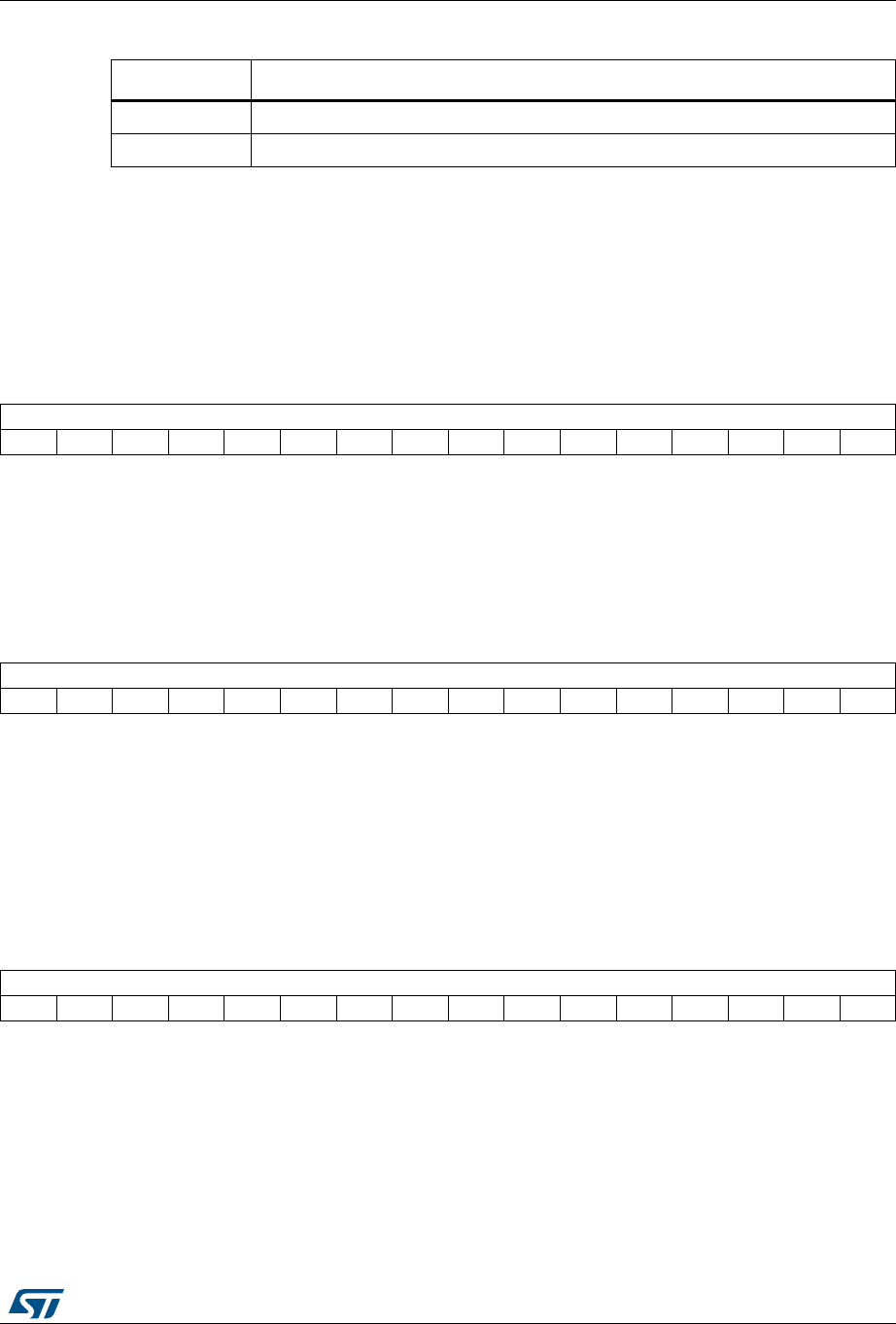
DocID027812 Rev 2 417/766
RM0401 General-purpose timers (TIM9 and TIM11)
430
Note: The states of the external I/O pins connected to the standard OCx channels depend on the
state of the OCx channel and on the GPIO registers.
16.4.8 TIM9 counter (TIMx_CNT)
Address offset: 0x24
Reset value: 0x0000 0000
16.4.9 TIM9 prescaler (TIMx_PSC)
Address offset: 0x28
Reset value: 0x0000
16.4.10 TIM9 auto-reload register (TIMx_ARR)
Address offset: 0x2C
Reset value: 0x0000
16.4.11 TIM9 capture/compare register 1 (TIMx_CCR1)
Address offset: 0x34
Table 64. Output control bit for standard OCx channels
CCxE bit OCx output state
0 Output disabled (OCx=’0’, OCx_EN=’0’)
1 OCx=OCxREF + Polarity, OCx_EN=’1’
15 14 13 12 11 10 9876543210
CNT[15:0]
rw rw rw rw rw rw rw rw rw rw rw rw rw rw rw rw
Bits 15:0 CNT[15:0]: Counter value
15 14 13 12 11 10 9876543210
PSC[15:0]
rw rw rw rw rw rw rw rw rw rw rw rw rw rw rw rw
Bits 15:0 PSC[15:0]: Prescaler value
The counter clock frequency CK_CNT is equal to fCK_PSC / (PSC[15:0] + 1).
PSC contains the value to be loaded into the active prescaler register at each update event.
15 14 13 12 11 10 9876543210
ARR[15:0]
rw rw rw rw rw rw rw rw rw rw rw rw rw rw rw rw
Bits 15:0 ARR[15:0]: Auto-reload value
ARR is the value to be loaded into the actual auto-reload register.
Refer to the Section 16.3.1: Time-base unit on page 388 for more details about ARR update
and behavior.
The counter is blocked while the auto-reload value is null.
General-purpose timers (TIM9 and TIM11) RM0401
418/766 DocID027812 Rev 2
Reset value: 0x0000
16.4.12 TIM9 capture/compare register 2 (TIMx_CCR2)
Address offset: 0x38
Reset value: 0x0000
16.4.13 TIM9 register map
TIM9 registers are mapped as 16-bit addressable registers as described below:
15 14 13 12 11 10 9876543210
CCR1[15:0]
rw rw rw rw rw rw rw rw rw rw rw rw rw rw rw rw
Bits 15:0 CCR1[15:0]: Capture/Compare 1 value
If channel CC1 is configured as output:
CCR1 is the value to be loaded into the actual capture/compare 1 register (preload value).
It is loaded permanently if the preload feature is not selected in the TIMx_CCMR1 register
(OC1PE bit). Else the preload value is copied into the active capture/compare 1 register
when an update event occurs.
The active capture/compare register contains the value to be compared to the TIMx_CNT
counter and signaled on the OC1 output.
If channel CC1is configured as input:
CCR1 is the counter value transferred by the last input capture 1 event (IC1).
15 14 13 12 11 10 9876543210
CCR2[15:0]
rw rw rw rw rw rw rw rw rw rw rw rw rw rw rw rw
Bits 15:0 CCR2[15:0]: Capture/Compare 2 value
If channel CC2 is configured as output:
CCR2 is the value to be loaded into the actual capture/compare 2 register (preload value).
It is loaded permanently if the preload feature is not selected in the TIMx_CCMR2 register
(OC2PE bit). Else the preload value is copied into the active capture/compare 2 register
when an update event occurs.
The active capture/compare register contains the value to be compared to the TIMx_CNT
counter and signalled on the OC2 output.
If channel CC2 is configured as input:
CCR2 is the counter value transferred by the last input capture 2 event (IC2).
Table 65. TIM9 register map and reset values
Offset Register
31
30
29
28
27
26
25
24
23
22
21
20
19
18
17
16
15
14
13
12
11
10
9
8
7
6
5
4
3
2
1
0
0x00
TIMx_CR1
Res.
Res.
Res.
Res.
Res.
Res.
Res.
Res.
Res.
Res.
Res.
Res.
Res.
Res.
Res.
Res.
Res.
Res.
Res.
Res.
Res.
Res.
CKD
[1:0]
ARPE
Res.
Res.
Res.
OPM
URS
UDIS
CEN
Reset value 000 0000
0x08
TIMx_SMCR
Res.
Res.
Res.
Res.
Res.
Res.
Res.
Res.
Res.
Res.
Res.
Res.
Res.
Res.
Res.
Res.
Res.
Res.
Res.
Res.
Res.
Res.
Res.
Res.
MSM
TS[2:0]
Res.
SMS[2:0]
Reset value 0000

DocID027812 Rev 2 419/766
RM0401 General-purpose timers (TIM9 and TIM11)
430
Refer to Section 2.2.2 on page 38 for the register boundary addresses.
0x0C
TIMx_DIER
Res.
Res.
Res.
Res.
Res.
Res.
Res.
Res.
Res.
Res.
Res.
Res.
Res.
Res.
Res.
Res.
Res.
Res.
Res.
Res.
Res.
Res.
Res.
Res.
Res.
TIE
Res.
Res.
Res.
CC2IE
CC1IE
UIE
Reset value 0000
0x10
TIMx_SR
Res.
Res.
Res.
Res.
Res.
Res.
Res.
Res.
Res.
Res.
Res.
Res.
Res.
Res.
Res.
Res.
Res.
Res.
Res.
Res.
Res.
CC2OF
CC1OF
Res.
Res.
TIF
Res.
Res.
Res.
CC2IF
CC1IF
UIF
Reset value 00 0 000
0x14
TIMx_EGR
Res.
Res.
Res.
Res.
Res.
Res.
Res.
Res.
Res.
Res.
Res.
Res.
Res.
Res.
Res.
Res.
Res.
Res.
Res.
Res.
Res.
Res.
Res.
Res.
Res.
TG
Res.
Res.
Res.
CC2G
CC1G
UG
Reset value 0000
0x18
TIMx_CCMR1
Output Compare
mode
Res.
Res.
Res.
Res.
Res.
Res.
Res.
Res.
Res.
Res.
Res.
Res.
Res.
Res.
Res.
Res.
Res.
OC2M
[2:0]
OC2PE
OC2FE
CC2S
[1:0]
Res.
OC1M
[2:0]
OC1PE
OC1FE
CC1
S
[1:0]
Reset value 0 0 0 0 0 0 0 0 0 0 0 0 0 0 0
TIMx_CCMR1
Input Capture
mode
Res.
Res.
Res.
Res.
Res.
Res.
Res.
Res.
Res.
Res.
Res.
Res.
Res.
Res.
Res.
Res.
IC2F[3:0]
IC2
PSC
[1:0]
CC2S
[1:0] IC1F[3:0]
IC1
PSC
[1:0]
CC1
S
[1:0]
Reset value 0 0 0 0 0 0 0 0 0 0 0 0 0 0 0 0
0x1C Reserved
Res.
Res.
Res.
Res.
Res.
Res.
Res.
Res.
Res.
Res.
Res.
Res.
Res.
Res.
Res.
Res.
Res.
Res.
Res.
Res.
Res.
Res.
Res.
Res.
Res.
Res.
Res.
Res.
Res.
Res.
Res.
Res.
0x20
TIMx_CCER
Res.
Res.
Res.
Res.
Res.
Res.
Res.
Res.
Res.
Res.
Res.
Res.
Res.
Res.
Res.
Res.
Res.
Res.
Res.
Res.
Res.
Res.
Res.
Res.
CC2NP
Res.
CC2P
CC2E
CC1NP
Res.
CC1P
CC1E
Reset value 000000
0x24
TIMx_CNT
Res.
Res.
Res.
Res.
Res.
Res.
Res.
Res.
Res.
Res.
Res.
Res.
Res.
Res.
Res.
Res.
CNT[15:0]
Reset value 0 0 0 0 0 0 0 0 0 0 0 0 0 0 0 0
0x28
TIMx_PSC
Res.
Res.
Res.
Res.
Res.
Res.
Res.
Res.
Res.
Res.
Res.
Res.
Res.
Res.
Res.
Res.
PSC[15:0]
Reset value 0 0 0 0 0 0 0 0 0 0 0 0 0 0 0 0
0x2C
TIMx_ARR
Res.
Res.
Res.
Res.
Res.
Res.
Res.
Res.
Res.
Res.
Res.
Res.
Res.
Res.
Res.
Res.
ARR[15:0]
Reset value 0 0 0 0 0 0 0 0 0 0 0 0 0 0 0 0
0x30 Reserved
Res.
Res.
Res.
Res.
Res.
Res.
Res.
Res.
Res.
Res.
Res.
Res.
Res.
Res.
Res.
Res.
Res.
Res.
Res.
Res.
Res.
Res.
Res.
Res.
Res.
Res.
Res.
Res.
Res.
Res.
Res.
Res.
0x34
TIMx_CCR1
Res.
Res.
Res.
Res.
Res.
Res.
Res.
Res.
Res.
Res.
Res.
Res.
Res.
Res.
Res.
Res.
CCR1[15:0]
Reset value 0 0 0 0 0 0 0 0 0 0 0 0 0 0 0 0
0x38
TIMx_CCR2
Res.
Res.
Res.
Res.
Res.
Res.
Res.
Res.
Res.
Res.
Res.
Res.
Res.
Res.
Res.
Res.
CCR2[15:0]
Reset value 0 0 0 0 0 0 0 0 0 0 0 0 0 0 0 0
0x3C to
0x4C Reserved
Res.
Res.
Res.
Res.
Res.
Res.
Res.
Res.
Res.
Res.
Res.
Res.
Res.
Res.
Res.
Res.
Res.
Res.
Res.
Res.
Res.
Res.
Res.
Res.
Res.
Res.
Res.
Res.
Res.
Res.
Res.
Res.
Table 65. TIM9 register map and reset values (continued)
Offset Register
31
30
29
28
27
26
25
24
23
22
21
20
19
18
17
16
15
14
13
12
11
10
9
8
7
6
5
4
3
2
1
0

General-purpose timers (TIM9 and TIM11) RM0401
420/766 DocID027812 Rev 2
16.5 TIM11 registers
The peripheral registers have to be written by half-words (16 bits) or words (32 bits). Read
accesses can be done by bytes (8 bits), half-words (16 bits) or words (32 bits).
16.5.1 TIM11 control register 1 (TIMx_CR1)
Address offset: 0x00
Reset value: 0x0000
15 14 13 12 11 10 9876543210
Res. Res. Res. Res. Res. Res. CKD[1:0] ARPE Res. Res. Res. Res. URS UDIS CEN
rw rw rw rw rw rw
Bits 15:10 Reserved, must be kept at reset value.
Bits 9:8 CKD: Clock division
This bit-field indicates the division ratio between the timer clock (CK_INT) frequency and
sampling clock used by the digital filters (TIx),
00: tDTS = tCK_INT
01: tDTS = 2 × tCK_INT
10: tDTS = 4 × tCK_INT
11: Reserved
Bit 7 ARPE: Auto-reload preload enable
0: TIMx_ARR register is not buffered
1: TIMx_ARR register is buffered
Bits 6:3 Reserved, must be kept at reset value.
Bit 2 URS: Update request source
This bit is set and cleared by software to select the update interrupt (UEV) sources.
0: Any of the following events generate an UEV if enabled:
– Counter overflow
– Setting the UG bit
1: Only counter overflow generates an UEV if enabled.
Bit 1 UDIS: Update disable
This bit is set and cleared by software to enable/disable update interrupt (UEV) event
generation.
0: UEV enabled. An UEV is generated by one of the following events:
– Counter overflow
– Setting the UG bit.
Buffered registers are then loaded with their preload values.
1: UEV disabled. No UEV is generated, shadow registers keep their value (ARR, PSC,
CCRx). The counter and the prescaler are reinitialized if the UG bit is set.
Bit 0 CEN: Counter enable
0: Counter disabled
1: Counter enabled

DocID027812 Rev 2 421/766
RM0401 General-purpose timers (TIM9 and TIM11)
430
16.5.2 TIM11 Interrupt enable register (TIMx_DIER)
Address offset: 0x0C
Reset value: 0x0000
16.5.3 TIM11 status register (TIMx_SR)
Address offset: 0x10
Reset value: 0x0000
15 14 13 12 11 10 9876543210
Res. Res. Res. Res. Res. Res. Res. Res. Res. Res. Res. Res. Res. Res. CC1IE UIE
rw rw
Bits 15:2 Reserved, must be kept at reset value.
Bit 1 CC1IE: Capture/Compare 1 interrupt enable
0: CC1 interrupt disabled
1: CC1 interrupt enabled
Bit 0 UIE: Update interrupt enable
0: Update interrupt disabled
1: Update interrupt enabled
15 14 13 12 11 10 9876543210
Res. Res. Res. Res. Res. Res. CC1OF Res. Res. Res. Res. Res. Res. Res. CC1IF UIF
rc_w0 rc_w0 rc_w0
Bits 15:10 Reserved, must be kept at reset value.
Bit 9 CC1OF: Capture/Compare 1 overcapture flag
This flag is set by hardware only when the corresponding channel is configured in input
capture mode. It is cleared by software by writing it to ‘0’.
0: No overcapture has been detected.
1: The counter value has been captured in TIMx_CCR1 register while CC1IF flag was
already set

General-purpose timers (TIM9 and TIM11) RM0401
422/766 DocID027812 Rev 2
16.5.4 TIM11 event generation register (TIMx_EGR)
Address offset: 0x14
Reset value: 0x0000
Bits 8:2 Reserved, must be kept at reset value.
Bit 1 CC1IF: Capture/compare 1 interrupt flag
If channel CC1 is configured as output:
This flag is set by hardware when the counter matches the compare value. It is cleared by
software.
0: No match.
1: The content of the counter TIMx_CNT matches the content of the TIMx_CCR1 register.
When the contents of TIMx_CCR1 are greater than the contents of TIMx_ARR, the CC1IF bit
goes high on the counter overflow.
If channel CC1 is configured as input:
This bit is set by hardware on a capture. It is cleared by software or by reading the
TIMx_CCR1 register.
0: No input capture occurred.
1: The counter value has been captured in TIMx_CCR1 register (an edge has been detected
on IC1 which matches the selected polarity).
Bit 0 UIF: Update interrupt flag
This bit is set by hardware on an update event. It is cleared by software.
0: No update occurred.
1: Update interrupt pending. This bit is set by hardware when the registers are updated:
– At overflow and if UDIS=’0’ in the TIMx_CR1 register.
– When CNT is reinitialized by software using the UG bit in TIMx_EGR register, if
URS=’0’ and UDIS=’0’ in the TIMx_CR1 register.
15 14 13 12 11 10 9876543210
Res. Res. Res. Res. Res. Res. Res. Res. Res. Res. Res. Res. Res. Res. CC1G UG
w w
Bits 15:2 Reserved, must be kept at reset value.
Bit 1 CC1G: Capture/compare 1 generation
This bit is set by software in order to generate an event, it is automatically cleared by
hardware.
0: No action
1: A capture/compare event is generated on channel 1:
If channel CC1 is configured as output:
CC1IF flag is set, Corresponding interrupt or is sent if enabled.
If channel CC1 is configured as input:
The current value of the counter is captured in TIMx_CCR1 register. The CC1IF flag is set,
the corresponding interrupt is sent if enabled. The CC1OF flag is set if the CC1IF flag was
already high.
Bit 0 UG: Update generation
This bit can be set by software, it is automatically cleared by hardware.
0: No action
1: Re-initialize the counter and generates an update of the registers. Note that the prescaler
counter is cleared too (anyway the prescaler ratio is not affected). The counter is cleared.

DocID027812 Rev 2 423/766
RM0401 General-purpose timers (TIM9 and TIM11)
430
16.5.5 TIM11 capture/compare mode register 1
(TIMx_CCMR1)
Address offset: 0x18
Reset value: 0x0000
The channels can be used in input (capture mode) or in output (compare mode). The
direction of a channel is defined by configuring the corresponding CCxS bits. All the other
bits of this register have a different function in input and in output mode. For a given bit,
OCxx describes its function when the channel is configured in output, ICxx describes its
function when the channel is configured in input. So you must take care that the same bit
can have a different meaning for the input stage and for the output stage.
15 14 13 12 11 10 9876543210
Res. Res. Res. Res. Res. Res. Res. Res. Res. OC1M[2:0] OC1PE OC1FE
CC1S[1:0]
Res. Res. Res. Res. Res. Res. Res. Res. IC1F[3:0] IC1PSC[1:0]
rw rw rw rw rw rw rw rw

General-purpose timers (TIM9 and TIM11) RM0401
424/766 DocID027812 Rev 2
Output compare mode
Bits 15:7 Reserved, must be kept at reset value.
Bits 6:4 OC1M: Output compare 1 mode
These bits define the behavior of the output reference signal OC1REF from which OC1 is
derived. OC1REF is active high whereas OC1 active level depends on CC1P bit.
000: Frozen. The comparison between the output compare register TIMx_CCR1 and the
counter TIMx_CNT has no effect on the outputs.
001: Set channel 1 to active level on match. OC1REF signal is forced high when the counter
TIMx_CNT matches the capture/compare register 1 (TIMx_CCR1).
010: Set channel 1 to inactive level on match. OC1REF signal is forced low when the
counter TIMx_CNT matches the capture/compare register 1 (TIMx_CCR1).
011: Toggle - OC1REF toggles when TIMx_CNT = TIMx_CCR1.
100: Force inactive level - OC1REF is forced low.
101: Force active level - OC1REF is forced high.
110: PWM mode 1 - Channel 1 is active as long as TIMx_CNT < TIMx_CCR1 else inactive.
111: PWM mode 2 - Channel 1 is inactive as long as TIMx_CNT < TIMx_CCR1 else active.
Note: In PWM mode 1 or 2, the OCREF level changes when the result of the comparison
changes or when the output compare mode switches from frozen to PWM mode.
Bit 3 OC1PE: Output compare 1 preload enable
0: Preload register on TIMx_CCR1 disabled. TIMx_CCR1 can be written at anytime, the
new value is taken in account immediately.
1: Preload register on TIMx_CCR1 enabled. Read/Write operations access the preload
register. TIMx_CCR1 preload value is loaded in the active register at each update event.
Note: The PWM mode can be used without validating the preload register only in one pulse
mode (OPM bit set in TIMx_CR1 register). Else the behavior is not guaranteed.
Bit 2 OC1FE: Output compare 1 fast enable
This bit is used to accelerate the effect of an event on the trigger in input on the CC output.
0: CC1 behaves normally depending on counter and CCR1 values even when the trigger is
ON. The minimum delay to activate CC1 output when an edge occurs on the trigger input is
5 clock cycles.
1: An active edge on the trigger input acts like a compare match on CC1 output. OC is then
set to the compare level independently of the result of the comparison. Delay to sample the
trigger input and to activate CC1 output is reduced to 3 clock cycles. OC1FE acts only if the
channel is configured in PWM1 or PWM2 mode.
Bits 1:0 CC1S: Capture/Compare 1 selection
This bit-field defines the direction of the channel (input/output) as well as the used input.
00: CC1 channel is configured as output.
01: CC1 channel is configured as input, IC1 is mapped on TI1.
10:
11:
Note: CC1S bits are writable only when the channel is OFF (CC1E = 0 in TIMx_CCER).

DocID027812 Rev 2 425/766
RM0401 General-purpose timers (TIM9 and TIM11)
430
Input capture mode
Bits 15:8 Reserved, must be kept at reset value.
Bits 7:4 IC1F: Input capture 1 filter
This bit-field defines the frequency used to sample TI1 input and the length of the digital filter
applied to TI1. The digital filter is made of an event counter in which N consecutive events
are needed to validate a transition on the output:
0000: No filter, sampling is done at fDTS1000: fSAMPLING=fDTS/8, N=6
0001: fSAMPLING=fCK_INT
, N=21001: fSAMPLING=fDTS/8, N=8
0010: fSAMPLING=fCK_INT
, N=41010: fSAMPLING=fDTS/16, N=5
0011: fSAMPLING=fCK_INT
, N=81011: fSAMPLING=fDTS/16, N=6
0100: fSAMPLING=fDTS/2, N=61100: fSAMPLING=fDTS/16, N=8
0101: fSAMPLING=fDTS/2, N=81101: fSAMPLING=fDTS/32, N=5
0110: fSAMPLING=fDTS/4, N=61110: fSAMPLING=fDTS/32, N=6
0111: fSAMPLING=fDTS/4, N=81111: fSAMPLING=fDTS/32, N=8
Bits 3:2 IC1PSC: Input capture 1 prescaler
This bit-field defines the ratio of the prescaler acting on CC1 input (IC1).
The prescaler is reset as soon as CC1E=’0’ (TIMx_CCER register).
00: no prescaler, capture is done each time an edge is detected on the capture input
01: capture is done once every 2 events
10: capture is done once every 4 events
11: capture is done once every 8 events
Bits 1:0 CC1S: Capture/Compare 1 selection
This bit-field defines the direction of the channel (input/output) as well as the used input.
00: CC1 channel is configured as output
01: CC1 channel is configured as input, IC1 is mapped on TI1
10: Reserved
11: Reserved
Note: CC1S bits are writable only when the channel is OFF (CC1E = 0 in TIMx_CCER).

General-purpose timers (TIM9 and TIM11) RM0401
426/766 DocID027812 Rev 2
16.5.6 TIM11 capture/compare enable register
(TIMx_CCER)
Address offset: 0x20
Reset value: 0x0000
Note: The state of the external I/O pins connected to the standard OCx channels depends on the
OCx channel state and the GPIO registers.
15 14 13 12 11 10 9876543210
Res. Res. Res. Res. Res. Res. Res. Res. Res. Res. Res. Res. CC1NP Res. CC1P CC1E
rw rw rw
Bits 15:4 Reserved, must be kept at reset value.
Bit 3 CC1NP: Capture/Compare 1 complementary output Polarity.
CC1 channel configured as output: CC1NP must be kept cleared.
CC1 channel configured as input: CC1NP bit is used in conjunction with CC1P to define
TI1FP1 polarity (refer to CC1P description).
Bit 2 Reserved, must be kept at reset value.
Bit 1 CC1P: Capture/Compare 1 output Polarity.
CC1 channel configured as output:
0: OC1 active high
1: OC1 active low
CC1 channel configured as input:
The CC1P bit selects TI1FP1 and TI2FP1 polarity for trigger or capture operations.
00: noninverted/rising edge
Circuit is sensitive to TI1FP1 rising edge (capture mode), TI1FP1 is not inverted.
01: inverted/falling edge
Circuit is sensitive to TI1FP1 falling edge (capture mode), TI1FP1 is inverted.
10: reserved, do not use this configuration.
11: noninverted/both edges
Circuit is sensitive to both TI1FP1 rising and falling edges (capture mode), TI1FP1 is not
inverted.
Bit 0 CC1E: Capture/Compare 1 output enable.
CC1 channel configured as output:
0: Off - OC1 is not active
1: On - OC1 signal is output on the corresponding output pin
CC1 channel configured as input:
This bit determines if a capture of the counter value can actually be done into the input
capture/compare register 1 (TIMx_CCR1) or not.
0: Capture disabled
1: Capture enabled
Table 66. Output control bit for standard OCx channels
CCxE bit OCx output state
0 Output Disabled (OCx=’0’, OCx_EN=’0’)
1 OCx=OCxREF + Polarity, OCx_EN=’1’

DocID027812 Rev 2 427/766
RM0401 General-purpose timers (TIM9 and TIM11)
430
16.5.7 TIM11 counter (TIMx_CNT)
Address offset: 0x24
Reset value: 0x0000
16.5.8 TIM11 prescaler (TIMx_PSC)
Address offset: 0x28
Reset value: 0x0000
16.5.9 TIM11 auto-reload register (TIMx_ARR)
Address offset: 0x2C
Reset value: 0x0000
15 14 13 12 11 10 9876543210
CNT[15:0]
rw rw rw rw rw rw rw rw rw rw rw rw rw rw rw rw
Bits 15:0 CNT[15:0]: Counter value
15 14 13 12 11 10 9876543210
PSC[15:0]
rw rw rw rw rw rw rw rw rw rw rw rw rw rw rw rw
Bits 15:0 PSC[15:0]: Prescaler value
The counter clock frequency CK_CNT is equal to fCK_PSC / (PSC[15:0] + 1).
PSC contains the value to be loaded in the active prescaler register at each update event.
15 14 13 12 11 10 9876543210
ARR[15:0]
rw rw rw rw rw rw rw rw rw rw rw rw rw rw rw rw
Bits 15:0 ARR[15:0]: Auto-reload value
ARR is the value to be loaded in the actual auto-reload register.
Refer to Section 16.3.1: Time-base unit on page 388 for more details about ARR update and
behavior.
The counter is blocked while the auto-reload value is null.

General-purpose timers (TIM9 and TIM11) RM0401
428/766 DocID027812 Rev 2
16.5.10 TIM11 capture/compare register 1 (TIMx_CCR1)
Address offset: 0x34
Reset value: 0x0000
16.5.11 TIM11 option register 1 (TIM11_OR)
Address offset: 0x50
Reset value: 0x0000
15 14 13 12 11 10 9876543210
CCR1[15:0]
rw rw rw rw rw rw rw rw rw rw rw rw rw rw rw rw
Bits 15:0 CCR1[15:0]: Capture/Compare 1 value
If channel CC1 is configured as output:
CCR1 is the value to be loaded in the actual capture/compare 1 register (preload value).
It is loaded permanently if the preload feature is not selected in the TIMx_CCMR1 register (bit
OC1PE). Else the preload value is copied in the active capture/compare 1 register when an
update event occurs.
The active capture/compare register contains the value to be compared to the counter
TIMx_CNT and signaled on OC1 output.
If channel CC1is configured as input:
CCR1 is the counter value transferred by the last input capture 1 event (IC1).
15 14 13 12 11 10 9876543210
Res. Res. Res. Res. Res. Res. Res. Res. Res. Res. Res. Res. Res. Res. TI1_RMP[1:0]
rw
Bits 15:2 Reserved, must be kept at reset value.
Bits 1:0 TI1_RMP[1:0]: TIM11 Input 1 remapping capability
Set and cleared by software.
00,01,11: TIM11 Channel1 is connected to the GPIO (refer to the Alternate function mapping
table in the datasheets).
10: HSE_RTC clock (HSE divided by programmable prescaler) is connected to the
TIM11_CH1 input for measurement purposes.

DocID027812 Rev 2 429/766
RM0401 General-purpose timers (TIM9 and TIM11)
430
16.5.12 TIM11 register map
TIMx registers are mapped as 16-bit addressable registers as described in the table below:
Table 67. TIM11 register map and reset values
Offset Register
31
30
29
28
27
26
25
24
23
22
21
20
19
18
17
16
15
14
13
12
11
10
9
8
7
6
5
4
3
2
1
0
0x00
TIMx_CR1
Res.
Res.
Res.
Res.
Res.
Res.
Res.
Res.
Res.
Res.
Res.
Res.
Res.
Res.
Res.
Res.
Res.
Res.
Res.
Res.
Res.
Res.
CKD
[1:0]
ARPE
Res.
Res.
Res.
Res.
URS
UDIS
CEN
Reset value 000 0 0 0
0x08
TIMx_SMCR
Res.
Res.
Res.
Res.
Res.
Res.
Res.
Res.
Res.
Res.
Res.
Res.
Res.
Res.
Res.
Res.
Res.
Res.
Res.
Res.
Res.
Res.
Res.
Res.
Res.
Res.
Res.
Res.
Res.
Res.
Res.
Res.
Reset value
0x0C
TIMx_DIER
Res.
Res.
Res.
Res.
Res.
Res.
Res.
Res.
Res.
Res.
Res.
Res.
Res.
Res.
Res.
Res.
Res.
Res.
Res.
Res.
Res.
Res.
Res.
Res.
Res.
Res.
Res.
Res.
Res.
Res.
CC1IE
UIE
Reset value 00
0x10
TIMx_SR
Res.
Res.
Res.
Res.
Res.
Res.
Res.
Res.
Res.
Res.
Res.
Res.
Res.
Res.
Res.
Res.
Res.
Res.
Res.
Res.
Res.
Res.
CC1OF
Res.
Res.
Res.
Res.
Res.
Res.
Res.
CC1IF
UIF
Reset value 000
0x14
TIMx_EGR
Res.
Res.
Res.
Res.
Res.
Res.
Res.
Res.
Res.
Res.
Res.
Res.
Res.
Res.
Res.
Res.
Res.
Res.
Res.
Res.
Res.
Res.
Res.
Res.
Res.
Res.
Res.
Res.
Res.
Res.
CC1G
UG
Reset value 00
0x18
TIMx_CCMR1
Output compare
mode
Res.
Res.
Res.
Res.
Res.
Res.
Res.
Res.
Res.
Res.
Res.
Res.
Res.
Res.
Res.
Res.
Res.
Res.
Res.
Res.
Res.
Res.
Res.
Res.
Res.
OC1M
[2:0]
OC1PE
OC1FE
CC1S
[1:0]
Reset value 00000 0 0
TIMx_CCMR1
Input capture
mode
Res.
Res.
Res.
Res.
Res.
Res.
Res.
Res.
Res.
Res.
Res.
Res.
Res.
Res.
Res.
Res.
Res.
Res.
Res.
Res.
Res.
Res.
Res.
Res.
IC1F[3:0]
IC1
PSC
[1:0]
CC1S
[1:0]
Reset value 000000 0 0
0x1C Reserved
Res.
Res.
Res.
Res.
Res.
Res.
Res.
Res.
Res.
Res.
Res.
Res.
Res.
Res.
Res.
Res.
Res.
Res.
Res.
Res.
Res.
Res.
Res.
Res.
Res.
Res.
Res.
Res.
Res.
Res.
Res.
Res.
0x20
TIMx_CCER
Res.
Res.
Res.
Res.
Res.
Res.
Res.
Res.
Res.
Res.
Res.
Res.
Res.
Res.
Res.
Res.
Res.
Res.
Res.
Res.
Res.
Res.
Res.
Res.
Res.
Res.
Res.
Res.
CC1NP
Res.
CC1P
CC1E
Reset value 000
0x24
TIMx_CNT
Res.
Res.
Res.
Res.
Res.
Res.
Res.
Res.
Res.
Res.
Res.
Res.
Res.
Res.
Res.
Res.
CNT[15:0]
Reset value 000000000000000 0
0x28
TIMx_PSC
Res.
Res.
Res.
Res.
Res.
Res.
Res.
Res.
Res.
Res.
Res.
Res.
Res.
Res.
Res.
Res.
PSC[15:0]
Reset value 000000000000000 0
0x2C
TIMx_ARR
Res.
Res.
Res.
Res.
Res.
Res.
Res.
Res.
Res.
Res.
Res.
Res.
Res.
Res.
Res.
Res.
ARR[15:0]
Reset value 000000000000000 0
0x30 Reserved
Res.
Res.
Res.
Res.
Res.
Res.
Res.
Res.
Res.
Res.
Res.
Res.
Res.
Res.
Res.
Res.
Res.
Res.
Res.
Res.
Res.
Res.
Res.
Res.
Res.
Res.
Res.
Res.
Res.
Res.
Res.
Res.

General-purpose timers (TIM9 and TIM11) RM0401
430/766 DocID027812 Rev 2
Refer to Section 2.2.2 on page 38 for the register boundary addresses.
0x34
TIMx_CCR1
Res.
Res.
Res.
Res.
Res.
Res.
Res.
Res.
Res.
Res.
Res.
Res.
Res.
Res.
Res.
Res.
CCR1[15:0]
Reset value 000000000000000 0
0x38 to
0x4C Reserved
Res.
Res.
Res.
Res.
Res.
Res.
Res.
Res.
Res.
Res.
Res.
Res.
Res.
Res.
Res.
Res.
Res.
Res.
Res.
Res.
Res.
Res.
Res.
Res.
Res.
Res.
Res.
Res.
Res.
Res.
Res.
Res.
0x50
TIMx_OR
Res.
Res.
Res.
Res.
Res.
Res.
Res.
Res.
Res.
Res.
Res.
Res.
Res.
Res.
Res.
Res.
Res.
Res.
Res.
Res.
Res.
Res.
Res.
Res.
Res.
Res.
Res.
Res.
Res.
Res.
TI1_RMP
Reset value 00
Table 67. TIM11 register map and reset values (continued)
Offset Register
31
30
29
28
27
26
25
24
23
22
21
20
19
18
17
16
15
14
13
12
11
10
9
8
7
6
5
4
3
2
1
0
DocID027812 Rev 2 431/766
RM0401 Basic timers (TIM6)
443
17 Basic timers (TIM6)
17.1 Introduction
The basic timer TIM6 consists of a 16-bit auto-reload counter driven by a programmable
prescaler.
IT can be used as generic timer for timebase generation but it is also specifically used to
drive the digital-to-analog converter (DAC). In fact, the timer is internally connected to the
DAC and is able to drive it through its trigger output.
The timers are completely independent, and do not share any resources.
They can be used as generic timers for timebase generation but they are also specifically
used to drive the digital-to-analog converter (DAC). In fact, the timers are internally
connected to the DAC and are able to drive it through their trigger outputs.
The timers are completely independent, and do not share any resources.
17.2 TIM6 main features
Basic timer (TIM6) features include:
•16-bit auto-reload upcounter
•16-bit programmable prescaler used to divide (also “on the fly”) the counter clock
frequency by any factor between 1 and 65536
•Synchronization circuit to trigger the DAC
•Interrupt/DMA generation on the update event: counter overflow
Figure 155. Basic timer block diagram
069
,QWHUQDOFORFN&.B,17
$XWRUHORDGUHJLVWHU
&17FRXQWHU
&.B36& &.B&17
6WRSFOHDURUXS
8,
8
8
1RWHV
5HJ 3UHORDGUHJLVWHUVWUDQVIHUUHG
WRDFWLYHUHJLVWHUVRQ8HYHQW
DFFRUGLQJWRFRQWUROELW
(YHQW
,QWHUUXSW'0$RXWSXW
36&
SUHVFDOHU
7ULJJHU
FRQWUROOHU
5HVHWHQDEOH&RXQW
7,0[&/.IURP5&&
75*2 WR'$&
&RQWURO

Basic timers (TIM6) RM0401
432/766 DocID027812 Rev 2
17.3 TIM6 functional description
17.3.1 Time-base unit
The main block of the programmable timer is a 16-bit upcounter with its related auto-reload
register. The counter clock can be divided by a prescaler.
The counter, the auto-reload register and the prescaler register can be written or read by
software. This is true even when the counter is running.
The time-base unit includes:
•Counter Register (TIMx_CNT)
•Prescaler Register (TIMx_PSC)
•Auto-Reload Register (TIMx_ARR)
The auto-reload register is preloaded. The preload register is accessed each time an
attempt is made to write or read the auto-reload register. The contents of the preload
register are transferred into the shadow register permanently or at each update event UEV,
depending on the auto-reload preload enable bit (ARPE) in the TIMx_CR1 register. The
update event is sent when the counter reaches the overflow value and if the UDIS bit equals
0 in the TIMx_CR1 register. It can also be generated by software. The generation of the
update event is described in detail for each configuration.
The counter is clocked by the prescaler output CK_CNT, which is enabled only when the
counter enable bit (CEN) in the TIMx_CR1 register is set.
Note that the actual counter enable signal CNT_EN is set 1 clock cycle after CEN.
Prescaler description
The prescaler can divide the counter clock frequency by any factor between 1 and 65536. It
is based on a 16-bit counter controlled through a 16-bit register (in the TIMx_PSC register).
It can be changed on the fly as the TIMx_PSC control register is buffered. The new
prescaler ratio is taken into account at the next update event.
Figure 156 and Figure 157 give some examples of the counter behavior when the prescaler
ratio is changed on the fly.
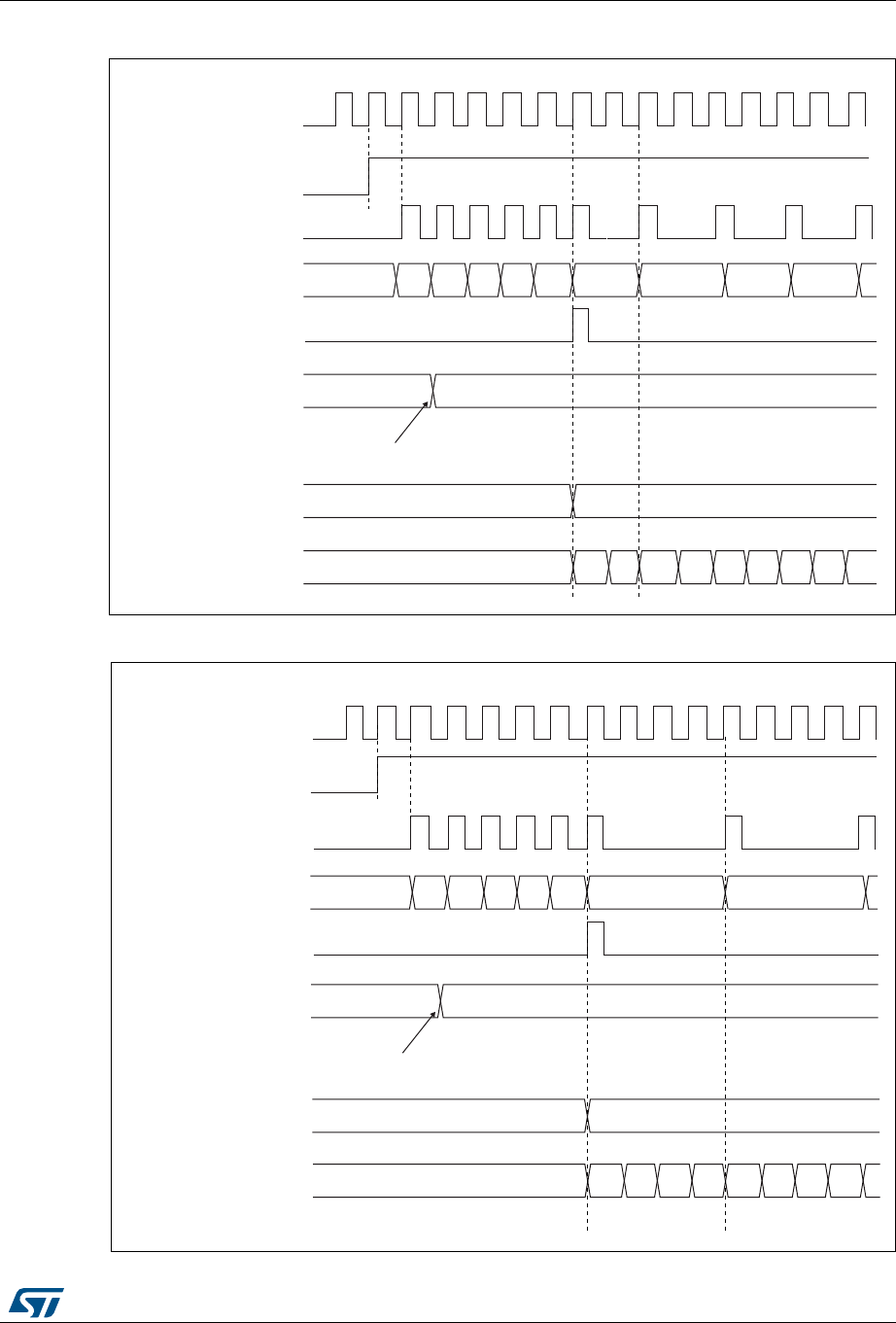
DocID027812 Rev 2 433/766
RM0401 Basic timers (TIM6)
443
Figure 156. Counter timing diagram with prescaler division change from 1 to 2
Figure 157. Counter timing diagram with prescaler division change from 1 to 4
&.B36&
&(1
7LPHUFORFN &.B&17
&RXQWHUUHJLVWHU
8SGDWHHYHQW8(9
3UHVFDOHUFRQWUROUHJLVWHU
:ULWHDQHZYDOXHLQ7,0[B36&
3UHVFDOHUEXIIHU
3UHVFDOHUFRXQWHU
)$ )%) ) ) )&
069
069
&.B36&
&(1
7LPHUFORFN &.B&17
&RXQWHUUHJLVWHU
8SGDWHHYHQW8(9
3UHVFDOHUFRQWUROUHJLVWHU
:ULWHDQHZYDOXHLQ7,0[B36&
3UHVFDOHUEXIIHU
3UHVFDOHUFRXQWHU
)$ )%
) ) ) )&
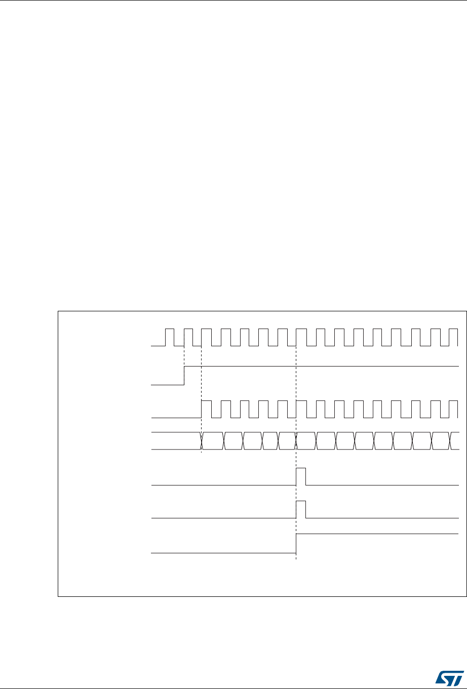
Basic timers (TIM6) RM0401
434/766 DocID027812 Rev 2
17.3.2 Counting mode
The counter counts from 0 to the auto-reload value (contents of the TIMx_ARR register),
then restarts from 0 and generates a counter overflow event.
An update event can be generate at each counter overflow or by setting the UG bit in the
TIMx_EGR register (by software or by using the slave mode controller).
The UEV event can be disabled by software by setting the UDIS bit in the TIMx_CR1
register. This avoids updating the shadow registers while writing new values into the preload
registers. In this way, no update event occurs until the UDIS bit has been written to 0,
however, the counter and the prescaler counter both restart from 0 (but the prescale rate
does not change). In addition, if the URS (update request selection) bit in the TIMx_CR1
register is set, setting the UG bit generates an update event UEV, but the UIF flag is not set
(so no interrupt or DMA request is sent).
When an update event occurs, all the registers are updated and the update flag (UIF bit in
the TIMx_SR register) is set (depending on the URS bit):
•The buffer of the prescaler is reloaded with the preload value (contents of the
TIMx_PSC register)
•The auto-reload shadow register is updated with the preload value (TIMx_ARR)
The following figures show some examples of the counter behavior for different clock
frequencies when TIMx_ARR = 0x36.
Figure 158. Counter timing diagram, internal clock divided by 1
069
&.B36&
&17B(1
7LPHUFORFN &.B&17
&RXQWHUUHJLVWHU
8SGDWHHYHQW8(9
&RXQWHURYHUIORZ
8SGDWHLQWHUUXSWIODJ
8,)
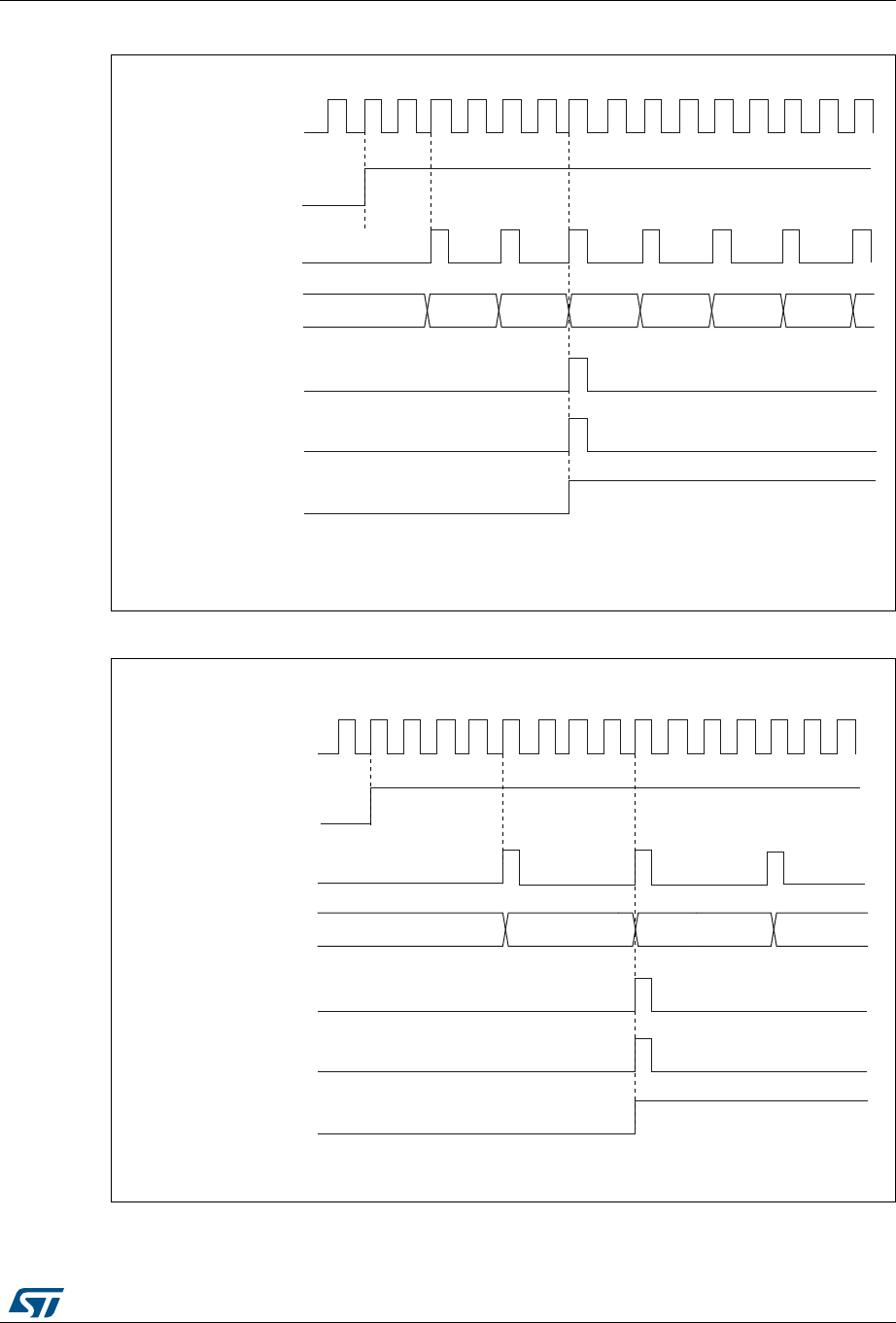
DocID027812 Rev 2 435/766
RM0401 Basic timers (TIM6)
443
Figure 159. Counter timing diagram, internal clock divided by 2
Figure 160. Counter timing diagram, internal clock divided by 4
069
&.B36&
&17B(1
7LPHUFORFN &.B&17
&RXQWHUUHJLVWHU
8SGDWHHYHQW8(9
&RXQWHURYHUIORZ
8SGDWHLQWHUUXSWIODJ
8,)
069
&.B36&
7LPHUFORFN &.B&17
&RXQWHUUHJLVWHU
8SGDWHHYHQW8(9
&RXQWHURYHUIORZ
8SGDWHLQWHUUXSWIODJ
8,)
&17B(1
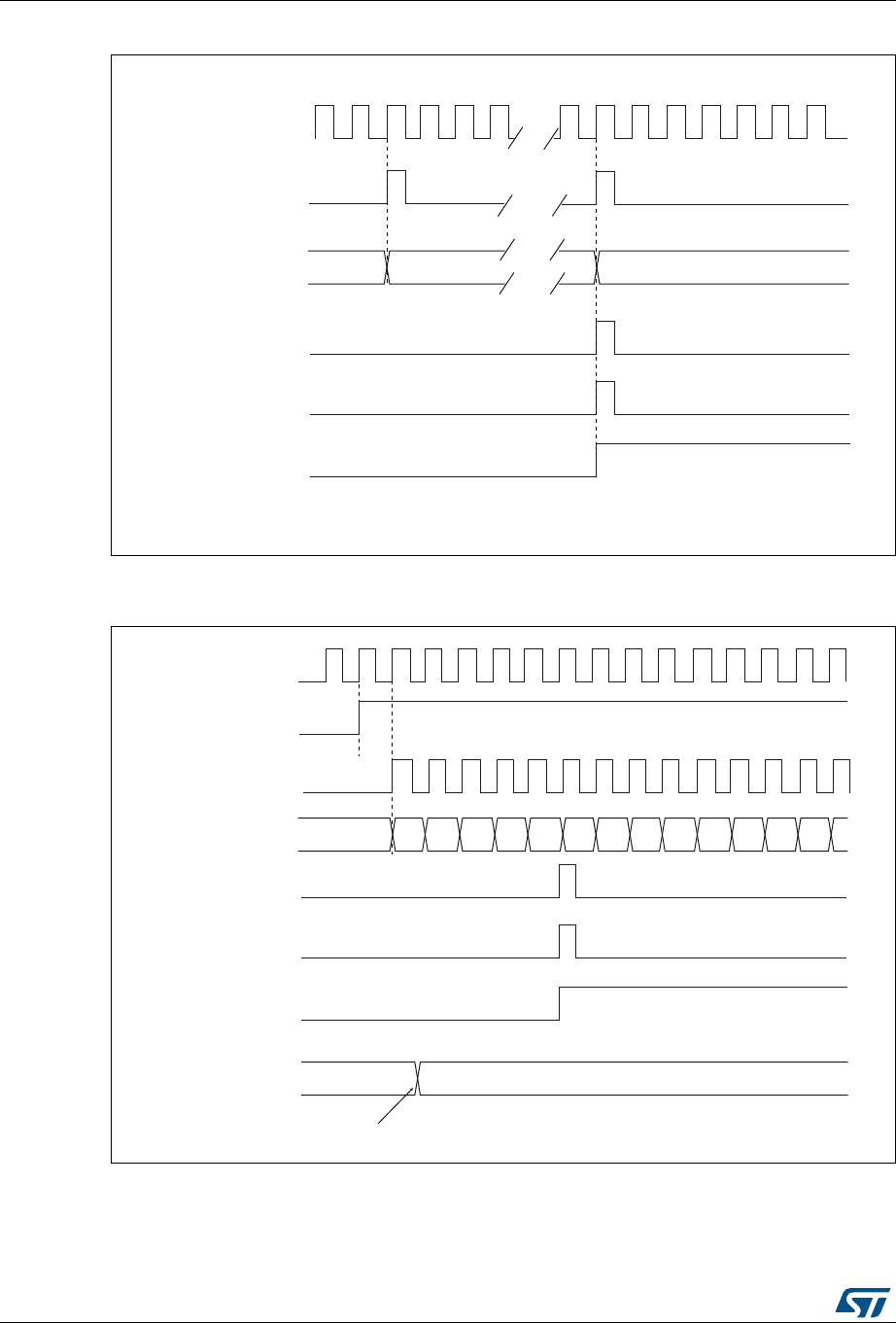
Basic timers (TIM6) RM0401
436/766 DocID027812 Rev 2
Figure 161. Counter timing diagram, internal clock divided by N
Figure 162. Counter timing diagram, update event when ARPE = 0 (TIMx_ARR not
preloaded)
)
069
&.B36&
7LPHUFORFN &.B&17
&RXQWHUUHJLVWHU
8SGDWHHYHQW8(9
&RXQWHURYHUIORZ
8SGDWHLQWHUUXSWIODJ
8,)
))
069
&.B36&
7LPHUFORFN &.B&17
&RXQWHUUHJLVWHU
8SGDWHHYHQW8(9
&RXQWHURYHUIORZ
8SGDWHLQWHUUXSWIODJ
8,)
&(1
$XWRUHORDGSUHORDG
UHJLVWHU
:ULWHDQHZYDOXHLQ7,0[B$55
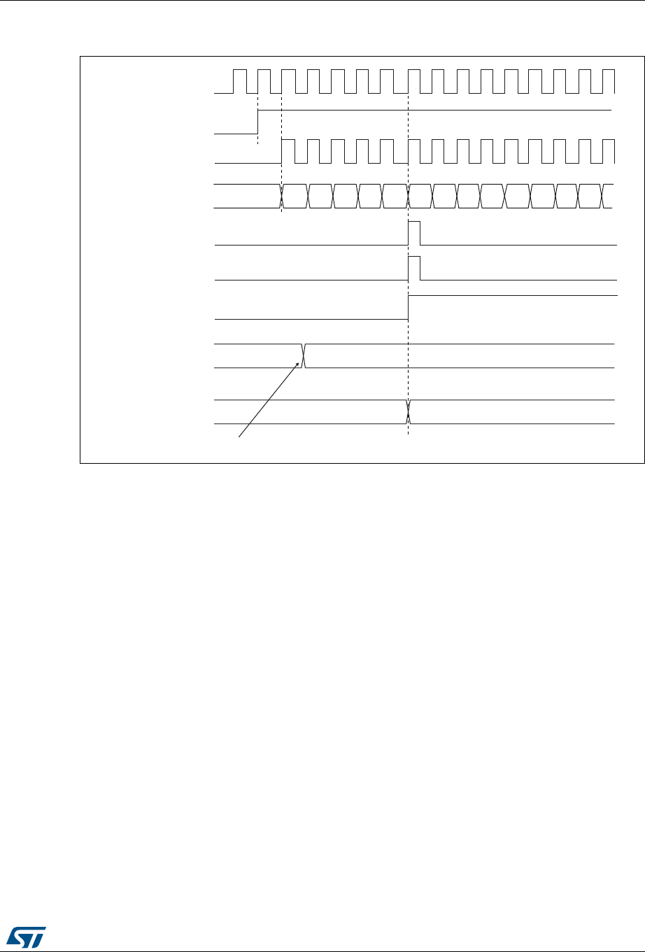
DocID027812 Rev 2 437/766
RM0401 Basic timers (TIM6)
443
Figure 163. Counter timing diagram, update event when ARPE=1 (TIMx_ARR
preloaded)
17.3.3 Clock source
The counter clock is provided by the Internal clock (CK_INT) source.
The CEN (in the TIMx_CR1 register) and UG bits (in the TIMx_EGR register) are actual
control bits and can be changed only by software (except for UG that remains cleared
automatically). As soon as the CEN bit is written to 1, the prescaler is clocked by the internal
clock CK_INT.
Figure 164 shows the behavior of the control circuit and the upcounter in normal mode,
without prescaler.
069
)
&.B36&
7LPHUFORFN &.B&17
&RXQWHUUHJLVWHU
8SGDWHHYHQW8(9
&RXQWHURYHUIORZ
8SGDWHLQWHUUXSWIODJ
8,)
) ) ) ) ))
&(1
$XWRUHORDGSUHORDG
UHJLVWHU
:ULWHDQHZYDOXHLQ7,0[B$55
$XWRUHORDGVKDGRZ
UHJLVWHU )
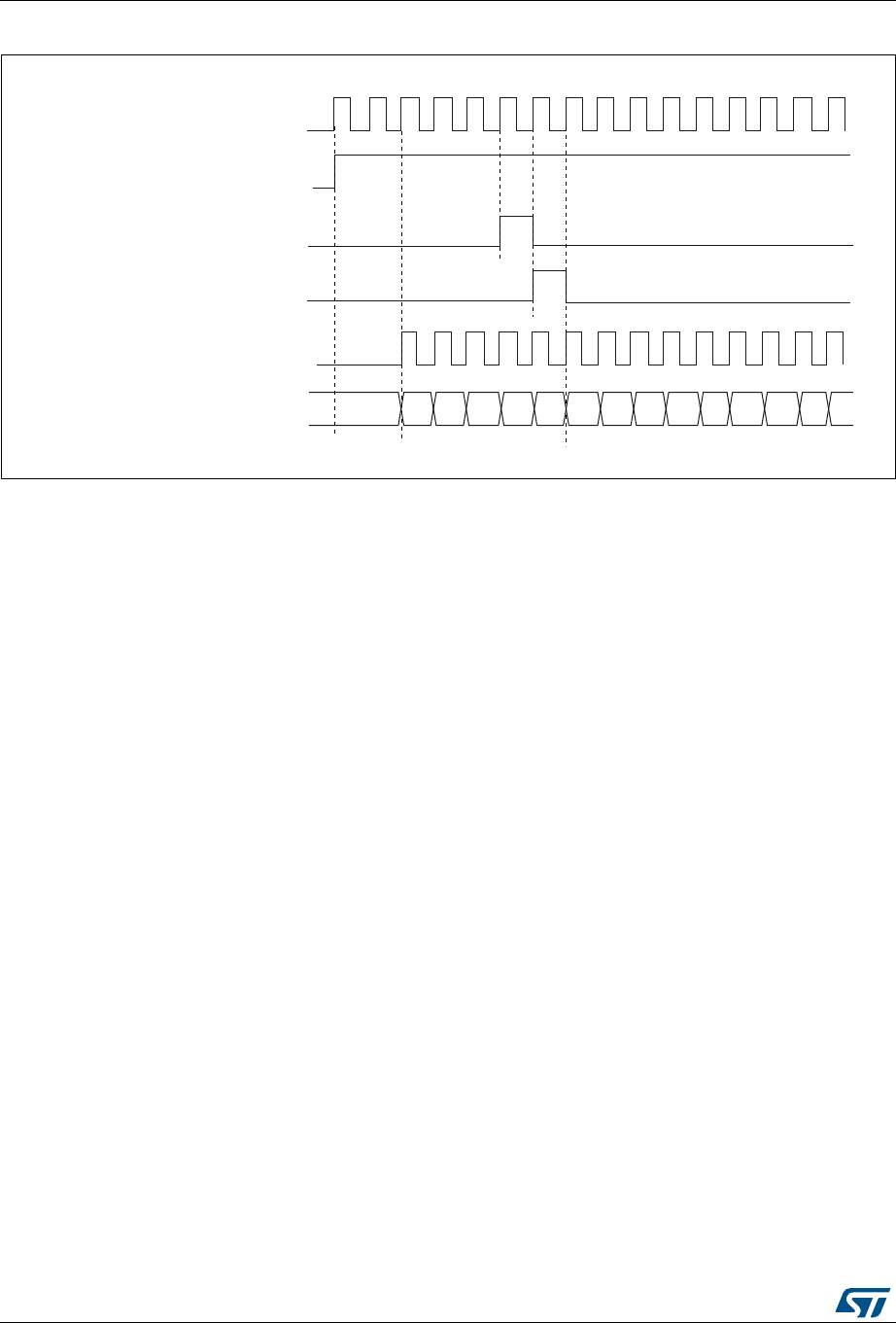
Basic timers (TIM6) RM0401
438/766 DocID027812 Rev 2
Figure 164. Control circuit in normal mode, internal clock divided by 1
17.3.4 Debug mode
When the microcontroller enters the debug mode (Cortex®-M4 with FPU core - halted), the
TIMx counter either continues to work normally or stops, depending on the
DBG_TIMx_STOP configuration bit in the DBG module. For more details, refer to
Section 26.16.2: Debug support for timers, watchdog and I2C.
,QWHUQDOFORFN
&RXQWHUFORFN &.B&17 &.B36&
&RXQWHUUHJLVWHU
&(1 &17B(1
8*
&17B,1,7
069

DocID027812 Rev 2 439/766
RM0401 Basic timers (TIM6)
443
17.4 TIM6 registers
Refer to Section 1.1: List of abbreviations for registers for a list of abbreviations used in
register descriptions.
The peripheral registers have to be written by half-words (16 bits) or words (32 bits). Read
accesses can be done by bytes (8 bits), half-words (16 bits) or words (32 bits).
17.4.1 TIM6 control register 1 (TIMx_CR1)
Address offset: 0x00
Reset value: 0x0000
15 14 13 12 11 10 9876543210
Res. Res. Res. Res. Res. Res. Res. Res. ARPE Res. Res. Res. OPM URS UDIS CEN
rw rw rw rw rw
Bits 15:8 Reserved, must be kept at reset value.
Bit 7 ARPE: Auto-reload preload enable
0: TIMx_ARR register is not buffered.
1: TIMx_ARR register is buffered.
Bits 6:4 Reserved, must be kept at reset value.
Bit 3 OPM: One-pulse mode
0: Counter is not stopped at update event
1: Counter stops counting at the next update event (clearing the CEN bit).
Bit 2 URS: Update request source
This bit is set and cleared by software to select the UEV event sources.
0: Any of the following events generates an update interrupt or DMA request if enabled.
These events can be:
– Counter overflow/underflow
– Setting the UG bit
– Update generation through the slave mode controller
1: Only counter overflow/underflow generates an update interrupt or DMA request if
enabled.
Bit 1 UDIS: Update disable
This bit is set and cleared by software to enable/disable UEV event generation.
0: UEV enabled. The Update (UEV) event is generated by one of the following events:
– Counter overflow/underflow
– Setting the UG bit
– Update generation through the slave mode controller
Buffered registers are then loaded with their preload values.
1: UEV disabled. The Update event is not generated, shadow registers keep their value
(ARR, PSC). However the counter and the prescaler are reinitialized if the UG bit is set or if
a hardware reset is received from the slave mode controller.
Bit 0 CEN: Counter enable
0: Counter disabled
1: Counter enabled
Note: Gated mode can work only if the CEN bit has been previously set by software.
However trigger mode can set the CEN bit automatically by hardware.
CEN is cleared automatically in one-pulse mode, when an update event occurs.

Basic timers (TIM6) RM0401
440/766 DocID027812 Rev 2
17.4.2 TIM6 control register 2 (TIMx_CR2)
Address offset: 0x04
Reset value: 0x0000
17.4.3 TIM6 DMA/Interrupt enable register (TIMx_DIER)
Address offset: 0x0C
Reset value: 0x0000
15 14 13 12 11 10 9876543210
Res. Res. Res. Res. Res. Res. Res. Res. Res. MMS[2:0] Res. Res. Res. Res.
rw rw rw
Bits 15:7 Reserved, must be kept at reset value.
Bits 6:4 MMS: Master mode selection
These bits are used to select the information to be sent in master mode to slave timers for
synchronization (TRGO). The combination is as follows:
000: Reset - the UG bit from the TIMx_EGR register is used as a trigger output (TRGO). If
reset is generated by the trigger input (slave mode controller configured in reset mode) then
the signal on TRGO is delayed compared to the actual reset.
001: Enable - the Counter enable signal, CNT_EN, is used as a trigger output (TRGO). It is
useful to start several timers at the same time or to control a window in which a slave timer
is enabled. The Counter Enable signal is generated by a logic OR between CEN control bit
and the trigger input when configured in gated mode.
When the Counter Enable signal is controlled by the trigger input, there is a delay on TRGO,
except if the master/slave mode is selected (see the MSM bit description in the TIMx_SMCR
register).
010: Update - The update event is selected as a trigger output (TRGO). For instance a
master timer can then be used as a prescaler for a slave timer.
Bits 3:0 Reserved, must be kept at reset value.
15 14 13 12 11 10 9876543210
Res. Res. Res. Res. Res. Res. Res. UDE Res. Res. Res. Res. Res. Res. Res. UIE
rw rw
Bit 15:9 Reserved, must be kept at reset value.
Bit 8 UDE: Update DMA request enable
0: Update DMA request disabled.
1: Update DMA request enabled.
Bit 7:1 Reserved, must be kept at reset value.
Bit 0 UIE: Update interrupt enable
0: Update interrupt disabled.
1: Update interrupt enabled.

DocID027812 Rev 2 441/766
RM0401 Basic timers (TIM6)
443
17.4.4 TIM6 status register (TIMx_SR)
Address offset: 0x10
Reset value: 0x0000
17.4.5 TIM6 event generation register (TIMx_EGR)
Address offset: 0x14
Reset value: 0x0000
17.4.6 TIM6 counter (TIMx_CNT)
Address offset: 0x24
Reset value: 0x0000
15 14 13 12 11 10 9876543210
Res. Res. Res. Res. Res. Res. Res. Res. Res. Res. Res. Res. Res. Res. Res. UIF
rc_w0
Bits 15:1 Reserved, must be kept at reset value.
Bit 0 UIF: Update interrupt flag
This bit is set by hardware on an update event. It is cleared by software.
0: No update occurred.
1: Update interrupt pending. This bit is set by hardware when the registers are updated:
– At overflow or underflow regarding the repetition counter value and if UDIS = 0 in the
TIMx_CR1 register.
– When CNT is reinitialized by software using the UG bit in the TIMx_EGR register, if URS = 0
and UDIS = 0 in the TIMx_CR1 register.
15 14 13 12 11 10 9876543210
Res. Res. Res. Res. Res. Res. Res. Res. Res. Res. Res. Res. Res. Res. Res. UG
w
Bits 15:1 Reserved, must be kept at reset value.
Bit 0 UG: Update generation
This bit can be set by software, it is automatically cleared by hardware.
0: No action.
1: Re-initializes the timer counter and generates an update of the registers. Note that the
prescaler counter is cleared too (but the prescaler ratio is not affected).
15 14 13 12 11 10 9876543210
CNT[15:0]
rw rw rw rw rw rw rw rw rw rw rw rw rw rw rw rw
Bits 15:0 CNT[15:0]: Counter value
Basic timers (TIM6) RM0401
442/766 DocID027812 Rev 2
17.4.7 TIM6 prescaler (TIMx_PSC)
Address offset: 0x28
Reset value: 0x0000
17.4.8 TIM6 auto-reload register (TIMx_ARR)
Address offset: 0x2C
Reset value: 0x0000
15 14 13 12 11 10 9876543210
PSC[15:0]
rw rw rw rw rw rw rw rw rw rw rw rw rw rw rw rw
Bits 15:0 PSC[15:0]: Prescaler value
The counter clock frequency CK_CNT is equal to fCK_PSC / (PSC[15:0] + 1).
PSC contains the value to be loaded into the active prescaler register at each update event.
15 14 13 12 11 10 9876543210
ARR[15:0]
rw rw rw rw rw rw rw rw rw rw rw rw rw rw rw rw
Bits 15:0 ARR[15:0]: Auto-reload value
ARR is the value to be loaded into the actual auto-reload register.
Refer to Section 17.3.1: Time-base unit on page 432 for more details about ARR update and
behavior.
The counter is blocked while the auto-reload value is null.

DocID027812 Rev 2 443/766
RM0401 Basic timers (TIM6)
443
17.4.9 TIM6 register map
TIMx registers are mapped as 16-bit addressable registers as described in the table below:
Refer to Section 2.2.2 on page 38 for the register boundary addresses.
Table 68. TIM6 register map and reset values
Offset Register
31
30
29
28
27
26
25
24
23
22
21
20
19
18
17
16
15
14
13
12
11
10
9
8
7
6
5
4
3
2
1
0
0x00
TIMx_CR1
Res.
Res.
Res.
Res.
Res.
Res.
Res.
Res.
Res.
Res.
Res.
Res.
Res.
Res.
Res.
Res.
Res.
Res.
Res.
Res.
Res.
Res.
Res.
Res.
ARPE
Res.
Res.
Res.
OPM
URS
UDIS
CEN
Reset value 00000
0x04
TIMx_CR2
Res.
Res.
Res.
Res.
Res.
Res.
Res.
Res.
Res.
Res.
Res.
Res.
Res.
Res.
Res.
Res.
Res.
Res.
Res.
Res.
Res.
Res.
Res.
Res.
Res.
MMS[2:0]
Res.
Res.
Res.
Res.
Reset value 000
0x08 Res.
0x0C
TIMx_DIER
Res.
Res.
Res.
Res.
Res.
Res.
Res.
Res.
Res.
Res.
Res.
Res.
Res.
Res.
Res.
Res.
Res.
Res.
Res.
Res.
Res.
Res.
Res.
UDE
Res.
Res.
Res.
Res.
Res.
Res.
Res.
UIE
Reset value 00
0x10
TIMx_SR
Res.
Res.
Res.
Res.
Res.
Res.
Res.
Res.
Res.
Res.
Res.
Res.
Res.
Res.
Res.
Res.
Res.
Res.
Res.
Res.
Res.
Res.
Res.
Res.
Res.
Res.
Res.
Res.
Res.
Res.
Res.
UIF
Reset value 0
0x14
TIMx_EGR
Res.
Res.
Res.
Res.
Res.
Res.
Res.
Res.
Res.
Res.
Res.
Res.
Res.
Res.
Res.
Res.
Res.
Res.
Res.
Res.
Res.
Res.
Res.
Res.
Res.
Res.
Res.
Res.
Res.
Res.
Res.
UG
Reset value 0
0x18 Res.
0x1C Res.
0x20 Res.
0x24
TIMx_CNT
Res.
Res.
Res.
Res.
Res.
Res.
Res.
Res.
Res.
Res.
Res.
Res.
Res.
Res.
Res.
Res.
CNT[15:0]
Reset value 0000000000 0 00000
0x28
TIMx_PSC
Res.
Res.
Res.
Res.
Res.
Res.
Res.
Res.
Res.
Res.
Res.
Res.
Res.
Res.
Res.
Res.
PSC[15:0]
Reset value 0000000000 0 00000
0x2C
TIMx_ARR
Res.
Res.
Res.
Res.
Res.
Res.
Res.
Res.
Res.
Res.
Res.
Res.
Res.
Res.
Res.
Res.
ARR[15:0]
Reset value 0000000000 0 00000

Low-power timer (LPTIM) RM0401
444/766 DocID027812 Rev 2
18 Low-power timer (LPTIM)
18.1 Introduction
The LPTIM is a 16-bit timer that benefits from the ultimate developments in power
consumption reduction. Thanks to its diversity of clock sources, the LPTIM is able to keep
running in all power modes except for Standby mode. Given its capability to run even with
no internal clock source, the LPTIM can be used as a “Pulse Counter” which can be useful
in some applications. Also, the LPTIM capability to wake up the system from low-power
modes, makes it suitable to realize “Timeout functions” with extremely low power
consumption.
The LPTIM introduces a flexible clock scheme that provides the needed functionalities and
performance, while minimizing the power consumption.
18.2 LPTIM main features
•16 bit upcounter
•3-bit prescaler with 8 possible dividing factor (1,2,4,8,16,32,64,128)
•Selectable clock
– Internal clock sources: LSE, LSI, HSI or APB clock
– External clock source over ULPTIM input (working with no LP oscillator running,
used by Pulse Counter application)
•16 bit ARR autoreload register
•16 bit compare register
•Continuous/one shot mode
•Selectable software/hardware input trigger
•Programmable Digital Glitch filter
•Configurable output: Pulse, PWM
•Configurable I/O polarity
•Encoder mode
18.3 LPTIM implementation
Table 69 describes LPTIM implementation on STM32F410 devices.
Table 69. STM32F410 LPTIM features
LPTIM modes/features(1)
1. X = supported.
LPTIM1
Encoder mode X
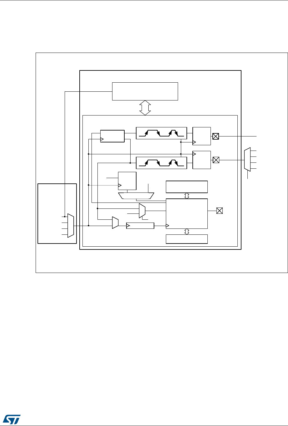
DocID027812 Rev 2 445/766
RM0401 Low-power timer (LPTIM)
464
18.4 LPTIM functional description
18.4.1 LPTIM block diagram
Figure 165. Low-power timer block diagram
18.4.2 LP Timer input1 multiplexing
Various inputs can be selected for LPTIM1 input 1 through the LPTMI option register
(LPTIM1_OR).
This input can either be connected to the pads selected by the LPTIM alternate function
(AF1) or directly connected internally to PA4, PB9 pad or to TIM6/DAC trigger.
In case of internal connection to PA4 or PB9, the selected alternate function for this pad
defines the peripheral to which the timer is connected.
PA4 and PB9 can also be configured as GPIO.
18.4.3 LPTIM reset and clocks
The LPTIM can be clocked using several clock sources. It can be clocked using an internal
clock signal which can be chosen among APB, LSI, LSE or HSI sources through the Clock
Tree controller (RCC). Also, the LPTIM can be clocked using an external clock signal
06Y9
5&&
/37,0
$3%B,7)
.HUQHO
VZ
WULJJHU
XSWRH[W
WULJJHU
&/.08;
+6,
/6,
/6(
$3%FORFN
ELWFRPSDUH
ELWFRXQWHU
ELW$55
2XW
3UHVFDOHU
0X[WULJJHU
*OLWFK
ILOWHU
*OLWFK
ILOWHU
,QSXW
(QFRGHU *OLWFK
ILOWHU
,QSXW
8SGRZQ
&2817
02'(
$)SDGLQSXW
3$SDG
3%SDG
7,0'$&WULJJHU
/37,0B25
$)SDGLQSXW
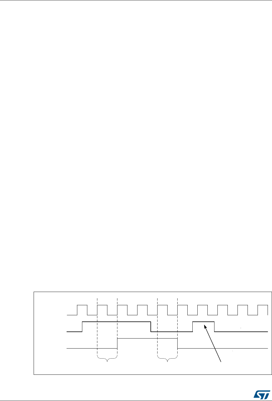
Low-power timer (LPTIM) RM0401
446/766 DocID027812 Rev 2
injected on its external Input1. When clocked with an external clock source, the LPTIM may
run in one of these two possible configurations:
•The first configuration is when the LPTIM is clocked by an external signal but in the
same time an internal clock signal is provided to the LPTIM either from APB or any
other embedded oscillator including LSE, LSI and HSI.
•The second configuration is when the LPTIM is solely clocked by an external clock
source through its external Input1. This configuration is the one used to realize Timeout
function or Pulse counter function when all the embedded oscillators are turned off
after entering a low-power mode.
Programming the CKSEL and COUNTMODE bits allows controlling whether the LPTIM will
use an external clock source or an internal one.
When configured to use an external clock source, the CKPOL bits are used to select the
external clock signal active edge. If both edges are configured to be active ones, an internal
clock signal should also be provided (first configuration). In this case, the internal clock
signal frequency should be at least four time higher than the external clock signal frequency.
18.4.4 Glitch filter
The LPTIM inputs, either external or internal, are protected with digital filters that prevent
any glitches and noise perturbations to propagate inside the LPTIM. This is in order to
prevent spurious counts or triggers.
Before activating the digital filters, an internal clock source should first be provided to the
LPTIM. This is necessary to guarantee the proper operation of the filters.
The digital filters are divided into two groups:
•The first group of digital filters protects the LPTIM external inputs. The digital filters
sensitivity is controlled by the CKFLT bits
•The second group of digital filters protects the LPTIM internal trigger inputs. The digital
filters sensitivity is controlled by the TRGFLT bits.
Note: The digital filters sensitivity is controlled by groups. It is not possible to configure each digital
filter sensitivity separately inside the same group.
The filter sensitivity acts on the number of consecutive equal samples that should be
detected on one of the LPTIM inputs to consider a signal level change as a valid transition.
Figure 166 shows an example of glitch filter behavior in case of a 2 consecutive samples
programmed.
Figure 166. Glitch filter timing diagram
069
&/.08;
,QSXW
)LOWHURXW
FRQVHFXWLYHVDPSOHV FRQVHFXWLYHVDPSOHV )LOWHUHG

DocID027812 Rev 2 447/766
RM0401 Low-power timer (LPTIM)
464
Note: In case no internal clock signal is provided, the digital filter must be deactivated by setting
the CKFLT and TRGFLT bits to ‘0’. In that case, an external analog filter may be used to
protect the LPTIM external inputs against glitches.
18.4.5 Prescaler
The LPTIM 16-bit counter is preceded by a configurable power-of-2 prescaler. The prescaler
division ratio is controlled by the PRESC[2:0] 3-bit field. The table below lists all the possible
division ratios:
18.4.6 Trigger multiplexer
The LPTIM counter may be started either by software or after the detection of an active
edge on one of the 8 trigger inputs.
TRIGEN[1:0] is used to determine the LPTIM trigger source:
•When TRIGEN[1:0] equals ‘00’, The LPTIM counter is started as soon as one of the
CNTSTRT or the SNGSTRT bits is set by software.
•The three remaining possible values for the TRIGEN[1:0] are used to configure the
active edge used by the trigger inputs. The LPTIM counter starts as soon as an active
edge is detected.
When TRIGEN[1:0] is different than ‘00’, TRIGSEL[2:0] is used to select which of the 8
trigger inputs is used to start the counter.
The external triggers are considered asynchronous signals for the LPTIM. So after a trigger
detection, a two-counter-clock period latency is needed before the timer starts running due
to the synchronization.
If a new trigger event occurs when the timer is already started it will be ignored (unless
timeout function is enabled).
Note: The timer must be enabled before setting the SNGSTRT/CNTSTRT bits. Any write on these
bits when the timer is disabled will be discarded by hardware.
Table 70. Prescaler division ratios
programming dividing factor
000 /1
001 /2
010 /4
011 /8
100 /16
101 /32
110 /64
111 /128
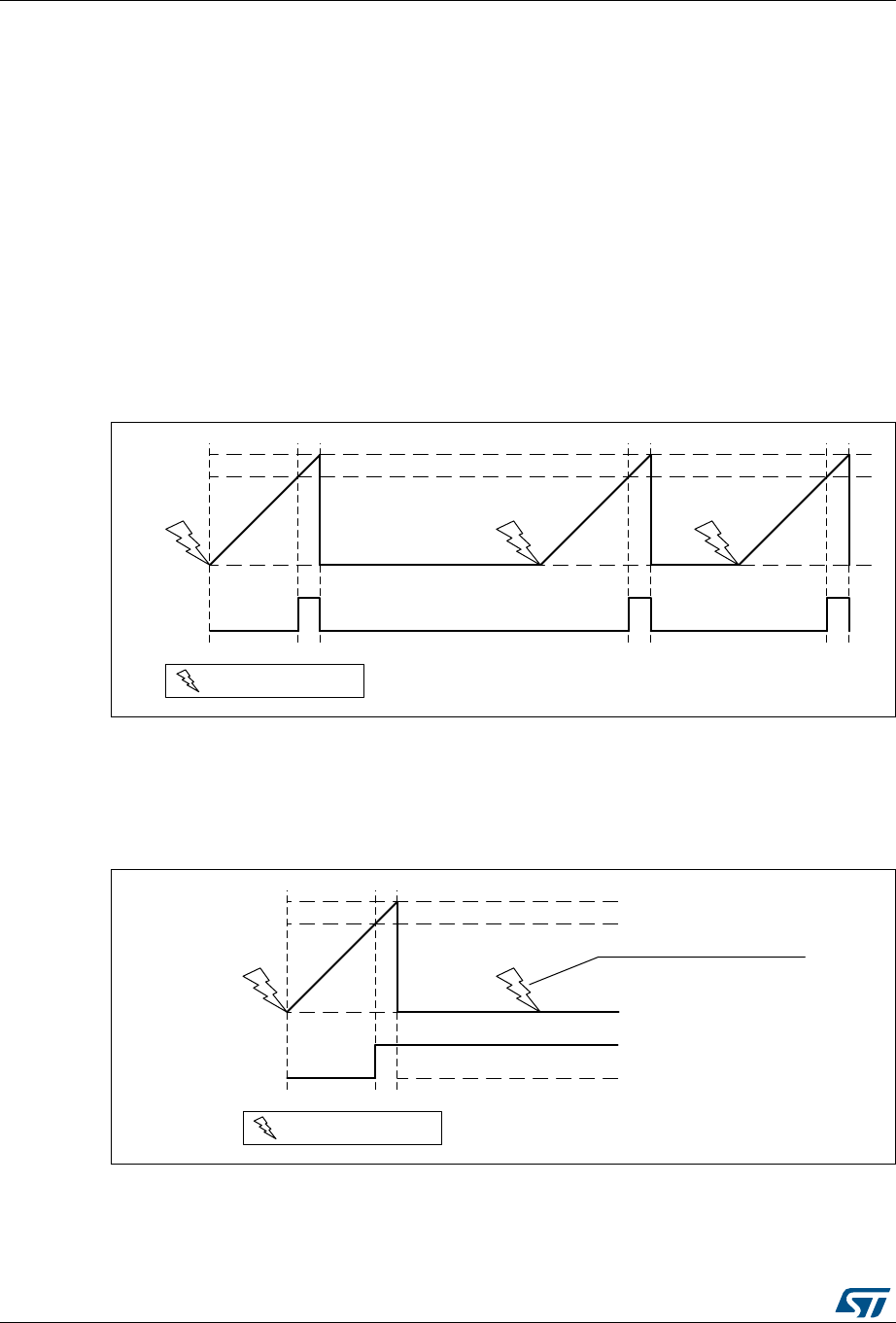
Low-power timer (LPTIM) RM0401
448/766 DocID027812 Rev 2
18.4.7 Operating mode
The LPTIM features two operating modes:
•The Continuous mode: the timer is free running, the timer is started from a trigger event
and never stops until the timer is disabled
•One shot mode: the timer is started from a trigger event and stops when reaching the
ARR value.
A new trigger event will re-start the timer. Any trigger event occurring after the counter starts
and before the counter reaches ARR will be discarded.
To enable the one shot counting, the SNGSTRT bit must be set.
In case an external trigger is selected, each external trigger event arriving after the
SNGSTRT bit is set, and after the counter register has stopped (contains zero value), will
start the counter for a new One-shot counting cycle as shown in Figure 167.
Figure 167. LPTIM output waveform, Single counting mode configuration
It should be noted that when the WAVE bit-field in the LPTIMx_CFGR register is set, the
Set-once mode is activated. In this case, the counter is only started once following the first
trigger, and any subsequent trigger event is discarded as shown in Figure 167.
Figure 168. LPTIM output waveform, Single counting mode configuration
and Set-once mode activated (WAVE bit is set)
In case of software start (TRIGEN[1:0] = ‘00’), the SNGSTRT setting will start the counter for
one shot counting.
To enable the continuous counting, the CNTSTRT bit must be set.
06Y9
3:0
&RPSDUH
$55
([WHUQDOWULJJHUHYHQW
06Y9
3:0
&RPSDUH
$55
'LVFDUGHGWULJJHU
([WHUQDOWULJJHUHYHQW
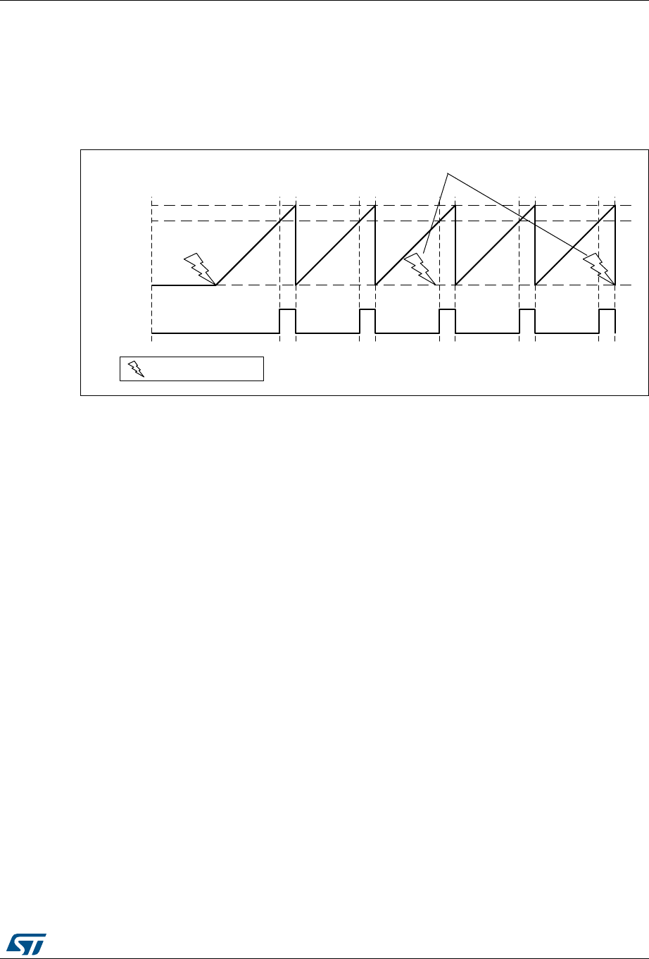
DocID027812 Rev 2 449/766
RM0401 Low-power timer (LPTIM)
464
In case an external trigger is selected, an external trigger event arriving after CNTSTRT is
set will start the counter for continuous counting. Any subsequent external trigger event will
be discarded as shown in Figure 169.
In case of software start (TRIGEN[1:0] = ‘00’), setting CNTSTRT will start the counter for
continuous counting.
Figure 169. LPTIM output waveform, Continuous counting mode configuration
SNGSTRT and CNTSTRT bits can only be set when the timer is enabled (The ENABLE bit
is set to ‘1’). It is possible to change “on the fly” from One Shot mode to Continuous mode.
If the Continuous mode was previously selected, setting SNGSTRT will switch the LPTIM to
the One Shot mode. The counter (if active) will stop as soon as it reaches ARR.
If the One Shot mode was previously selected, setting CNTSTRT will switch the LPTIM to
the Continuous mode. The counter (if active) will restart as soon as it reaches ARR.
18.4.8 Timeout function
The detection of an active edge on one selected trigger input can be used to reset the
LPTIM counter. This feature is controlled through the TIMOUT bit.
The first trigger event will start the timer, any successive trigger event will reset the counter
and the timer will restart.
A low-power timeout function can be realized. The timeout value corresponds to the
compare value; if no trigger occurs within the expected time frame, the MCU is waked-up by
the compare match event.
06Y9
3:0
&RPSDUH
$55
'LVFDUGHGWULJJHUV
([WHUQDOWULJJHUHYHQW

Low-power timer (LPTIM) RM0401
450/766 DocID027812 Rev 2
18.4.9 Waveform generation
Two 16-bit registers, the LPTIMx_ARR (autoreload register) and LPTIMx_CMP (Compare
register), are used to generate several different waveforms on LPTIM output
The timer can generate the following waveforms:
•The PWM mode: the LPTIM output is set as soon as a match occurs between the
LPTIMx_CMP and the LPTIMx_CNT registers. The LPTIM output is reset as soon as a
match occurs between the LPTIMx_ARR and the LPTIMx_CNT registers
•The One-pulse mode: the output waveform is similar to the one of the PWM mode for
the first pulse, then the output is permanently reset
•The Set-once mode: the output waveform is similar to the One-pulse mode except that
the output is kept to the last signal level (depends on the output configured polarity).
The above described modes require that the LPTIMx_ARR register value be strictly greater
than the LPTIMx_CMP register value.
The LPTIM output waveform can be configured through the WAVE bit as follow:
•Resetting the WAVE bit to ‘0’ forces the LPTIM to generate either a PWM waveform or
a One pulse waveform depending on which bit is set: CNTSTRT or SNGSTRT.
•Setting the WAVE bit to ‘1’ forces the LPTIM to generate a Set-once mode waveform.
The WAVPOL bit controls the LPTIM output polarity. The change takes effect immediately,
so the output default value will change immediately after the polarity is re-configured, even
before the timer is enabled.
Signals with frequencies up to the LPTIM clock frequency divided by 2 can be generated.
Figure 170 below shows the three possible waveforms that can be generated on the LPTIM
output. Also, it shows the effect of the polarity change using the WAVPOL bit.
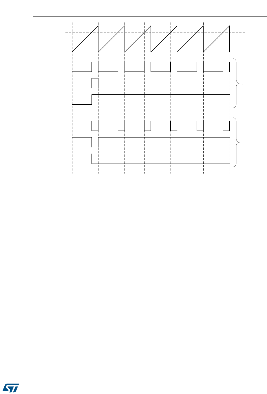
DocID027812 Rev 2 451/766
RM0401 Low-power timer (LPTIM)
464
Figure 170. Waveform generation
18.4.10 Register update
The LPTIMx_ARR register and LPTIMx_CMP register are updated immediately after the
APB bus write operation, or at the end of the current period if the timer is already started.
The PRELOAD bit controls how the LPTIMx_ARR and the LPTIMx_CMP registers are
updated:
•When the PRELOAD bit is reset to ‘0’, the LPTIMx_ARR and the LPTIMx_CMP
registers are immediately updated after any write access.
•When the PRELOAD bit is set to ‘1’, the LPTIMx_ARR and the LPTIMx_CMP registers
are updated at the end of the current period, if the timer has been already started.
The APB bus and the LPTIM use different clocks, so there is some latency between the
APB write and the moment when these values are available to the counter comparator.
Within this latency period, any additional write into these registers must be avoided.
The ARROK flag and the CMPOK flag in the LPTIMx_ISR register indicate when the write
operation is completed to respectively the LPTIMx_ARR register and the LPTIMx_CMP
register.
After a write to the LPTIMx_ARR register or the LPTIMx_CMP register, a new write
operation to the same register can only be performed when the previous write operation is
completed. Any successive write before respectively the ARROK flag or the CMPOK flag be
set, will lead to unpredictable results.
069
$55
&RPSDUH
3:0
2QHVKRW
6HWRQFH
3:0
2QHVKRW
6HWRQFH
3RO
3RO

Low-power timer (LPTIM) RM0401
452/766 DocID027812 Rev 2
18.4.11 Counter mode
The LPTIM counter can be used to count external events on the LPTIM Input1 or it can be
used to count internal clock cycles. The CKSEL and COUNTMODE bits control which
source will be used for updating the counter.
In case the LPTIM is configured to count external events on Input1, the counter can be
updated following a rising edge, falling edge or both edges depending on the value written
to the CKPOL[1:0] bits.
The count modes below can be selected, depending on CKSEL and COUNTMODE values:
•CKSEL = 0: the LPTIM is clocked by an internal clock source
– COUNTMODE = 0
When the LPTIM is configured to be clocked by an internal clock source and the
LPTIM counter is configured to be updated by active edges detected on the LPTIM
external Input1, the internal clock provided to the LPTIM must be not be prescaled
(PRESC[2:0] = ‘000’).
– COUNTMODE = 1
The LPTIM external Input1 is sampled with the internal clock provided to the
LPTIM. Consequently, in order not to miss any event, the frequency of the
changes on the external Input1 signal should never exceed the frequency of the
internal clock provided to the LPTIM.
•CKSEL = 1: the LPTIM is clocked by an external clock source
COUNTMODE value is don’t care.
In this configuration, the LPTIM has no need for an internal clock source (except if the
glitch filters are enabled). The signal injected on the LPTIM external Input1 is used as
system clock for the LPTIM. This configuration is suitable for operation modes where
no embedded oscillator is enabled.
For this configuration, the LPTIM counter can be updated either on rising edges or
falling edges of the input1 clock signal but not on both rising and falling edges.
Since the signal injected on the LPTIM external Input1 is also used to clock the LPTIM,
there is some initial latency (after the LPTIM is enabled) before the counter is
incremented. More precisely, the first five active edges on the LPTIM external Input1
(after LPTIM is enable) are lost.
18.4.12 Timer enable
The ENABLE bit located in the LPTIMx_CR register is used to enable/disable the LPTIM.
After setting the ENABLE bit, a delay of two counter clock is needed before the LPTIM is
actually enabled.
The LPTIMx_CFGR and LPTIMx_IER registers must be modified only when the LPTIM is
disabled.
18.4.13 Encoder mode
This mode allows handling signals from quadrature encoders used to detect angular
position of rotary elements. Encoder interface mode acts simply as an external clock with
direction selection. This means that the counter just counts continuously between 0 and the
auto-reload value programmed into the LPTIMx_ARR register (0 up to ARR or ARR down to
0 depending on the direction). Therefore you must configure LPTIMx_ARR before starting.
DocID027812 Rev 2 453/766
RM0401 Low-power timer (LPTIM)
464
From the two external input signals, Input1 and Input2, a clock signal is generated to clock
the LPTIM counter. The phase between those two signals determines the counting direction.
The Encoder mode is only available when the LPTIM is clocked by an internal clock source.
The signals frequency on both Input1 and Input2 inputs must not exceed the LPTIM internal
clock frequency divided by 4. This is mandatory in order to guarantee a proper operation of
the LPTIM.
Direction change is signalized by the two Down and Up flags in the LPTIMx_ISR register.
Also, an interrupt can be generated for both direction change events if enabled through the
LPTIMx_IER register.
To activate the Encoder mode the ENC bit has to be set to ‘1’. The LPTIM must first be
configured in Continuous mode.
When Encoder mode is active, the LPTIM counter is modified automatically following the
speed and the direction of the incremental encoder. Therefore, its content always
represents the encoder’s position. The count direction, signaled by the Up and Down flags,
correspond to the rotation direction of the connected sensor.
According to the edge sensitivity configured using the CKPOL[1:0] bits, different counting
scenarios are possible. The following table summarizes the possible combinations,
assuming that Input1 and Input2 do not switch at the same time.
The following figure shows a counting sequence for Encoder mode where both edges
sensitivity is configured.
Caution: In this mode the LPTIM must be clocked by an internal clock source, so the CKSEL bit must
be maintained to its reset value which is equal to ‘0’. Also, the prescaler division ratio must
be equal to its reset value which is 1 (PRESC[2:0] bits must be ‘000’).
Table 71. Encoder counting scenarios
Active edge
Level on opposite
signal (Input1 for
Input2, Input2 for
Input1)
Input1 signal Input2 signal
Rising Falling Rising Falling
Rising Edge
High Down No count Up No count
Low Up No count Down No count
Falling Edge
High No count Up No count Down
Low No count Down No count Up
Both Edges
High Down Up Up Down
Low Up Down Down Up
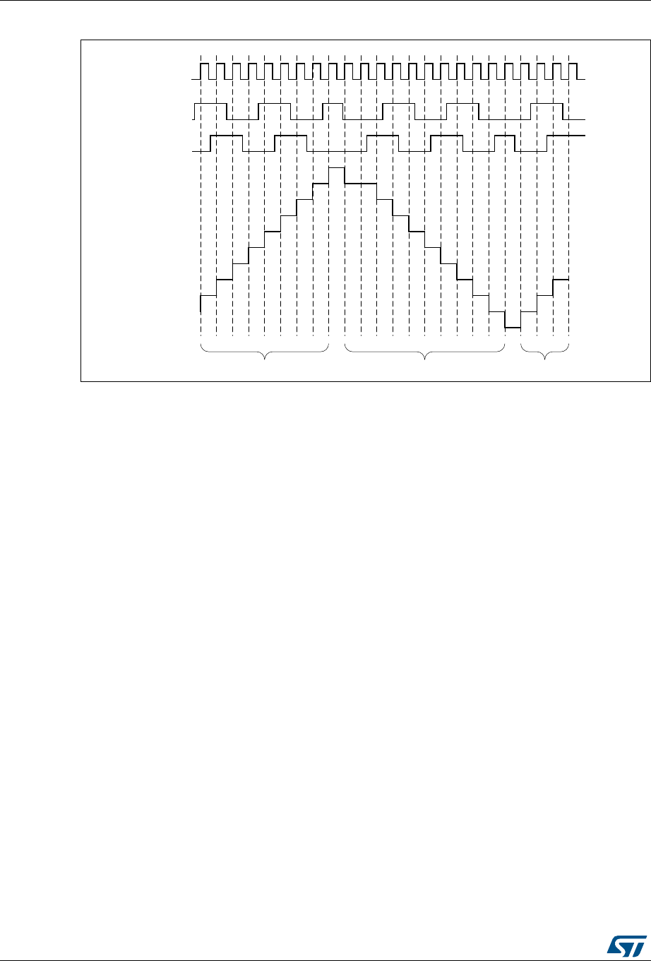
Low-power timer (LPTIM) RM0401
454/766 DocID027812 Rev 2
Figure 171. Encoder mode counting sequence
18.5 LPTIM interrupts
The following events generate an interrupt/wake-up event, if they are enabled through the
LPTIMx_IER register:
•Compare match
•Auto-reload match (whatever the direction if encoder mode)
•External trigger event
•Autoreload register write completed
•Compare register write completed
•Direction change (encoder mode), programmable (up / down / both).
Note: if any bit in the LPTIMx_IER register (Interrupt Enable Register) is set after that its
corresponding flag in the LPTIMx_ISR register (Status Register) is set, the interrupt is not
asserted
069
7
&RXQWHU
XS XSGRZQ
7

DocID027812 Rev 2 455/766
RM0401 Low-power timer (LPTIM)
464
18.6 LPTIM registers
18.6.1 LPTIM interrupt and status register (LPTIMx_ISR)
Address offset: 0x00
Reset value: 0x0000 0000
31 30 29 28 27 26 25 24 23 22 21 20 19 18 17 16
Res. Res. Res. Res. Res. Res. Res. Res. Res. Res. Res. Res. Res. Res. Res. Res.
15 14 13 12 11 10 9 8 7 6 5 4 3 2 1 0
Res. Res. Res. Res. Res. Res. Res. Res. Res. DOWN UP ARROK CMPOK EXTTRIG ARRM CMPM
r r r r r r r
Bits 31:7 Reserved, must be kept at reset value.
Bit 6 DOWN: Counter direction change up to down
In Encoder mode, DOWN bit is set by hardware to inform application that the counter direction has
changed from up to down.
Bit 5 UP: Counter direction change down to up
In Encoder mode, UP bit is set by hardware to inform application that the counter direction has
changed from down to up.
Bit 4 ARROK: Autoreload register update OK
ARROK is set by hardware to inform application that the APB bus write operation to the LPTIMx_ARR
register has been successfully completed. If so, a new one can be initiated.
Bit 3 CMPOK: Compare register update OK
CMPOK is set by hardware to inform application that the APB bus write operation to the LPTIMx_CMP
register has been successfully completed. If so, a new one can be initiated.
Bit 2 EXTTRIG: External trigger edge event
EXTTRIG is set by hardware to inform application that a valid edge on the selected external trigger
input has occurred. If the trigger is ignored because the timer has already started, then this flag is not
set.
Bit 1 ARRM: Autoreload match
ARRM is set by hardware to inform application that LPTIMx_CNT register’s value reached the
LPTIMx_ARR register’s value.
Bit 0 CMPM: Compare match
The CMPM bit is set by hardware to inform application that LPTIMx_CNT register value reached the
LPTIMx_CMP register’s value.

Low-power timer (LPTIM) RM0401
456/766 DocID027812 Rev 2
18.6.2 LPTIM interrupt clear register (LPTIMx_ICR)
Address offset: 0x04
Reset value: 0x0000 0000
31 30 29 28 27 26 25 24 23 22 21 20 19 18 17 16
Res. Res. Res. Res. Res. Res. Res. Res. Res. Res. Res. Res. Res. Res. Res. Res.
1514131211109876543210
Res. Res. Res. Res. Res. Res. Res. Res. Res. DOWN
CF UPCF ARRO
KCF
CMPO
KCF
EXTTR
IGCF
ARRM
CF
CMPM
CF
wwwwwww
Bits 31:7 Reserved, must be kept at reset value.
Bit 6 DOWNCF: Direction change to down Clear Flag
Writing 1 to this bit clear the DOWN flag in the LPT_ISR register
Bit 5 UPCF: Direction change to UP Clear Flag
Writing 1 to this bit clear the UP flag in the LPT_ISR register
Bit 4 ARROKCF: Autoreload register update OK Clear Flag
Writing 1 to this bit clears the ARROK flag in the LPT_ISR register
Bit 3 CMPOKCF: Compare register update OK Clear Flag
Writing 1 to this bit clears the CMPOK flag in the LPT_ISR register
Bit 2 EXTTRIGCF: External trigger valid edge Clear Flag
Writing 1 to this bit clears the EXTTRIG flag in the LPT_ISR register
Bit 1 ARRMCF: Autoreload match Clear Flag
Writing 1 to this bit clears the ARRM flag in the LPT_ISR register
Bit 0 CMPMCF: compare match Clear Flag
Writing 1 to this bit clears the CMP flag in the LPT_ISR register

DocID027812 Rev 2 457/766
RM0401 Low-power timer (LPTIM)
464
18.6.3 LPTIM interrupt enable register (LPTIMx_IER)
Address offset: 0x08
Reset value: 0x0000 0000
Caution: The LPTIMx_IER register must only be modified when the LPTIM is disabled (ENABLE bit is reset to ‘0’)
31 30 29 28 27 26 25 24 23 22 21 20 19 18 17 16
Res. Res. Res. Res. Res. Res. Res. Res. Res. Res. Res. Res. Res. Res. Res. Res.
1514131211109876543210
Res. Res. Res. Res. Res. Res. Res. Res. Res. DOWNI
EUPIE ARRO
KIE
CMPO
KIE
EXTTR
IGIE
ARRMI
E
CMPMI
E
rw rw rw rw rw rw rw
Bits 31:7 Reserved, must be kept at reset value.
Bit 6 DOWNIE: Direction change to down Interrupt Enable
0: DOWN interrupt disabled
1: DOWN interrupt enabled
Bit 5 UPIE: Direction change to UP Interrupt Enable
0: UP interrupt disabled
1: UP interrupt enabled
Bit 4 ARROKIE: Autoreload register update OK Interrupt Enable
0: ARROK interrupt disabled
1: ARROK interrupt enabled
Bit 3 CMPOKIE: Compare register update OK Interrupt Enable
0: CMPOK interrupt disabled
1: CMPOK interrupt enabled
Bit 2 EXTTRIGIE: External trigger valid edge Interrupt Enable
0: EXTTRIG interrupt disabled
1: EXTTRIG interrupt enabled
Bit 1 ARRMIE: Autoreload match Interrupt Enable
0: ARRM interrupt disabled
1: ARRM interrupt enabled
Bit 0 CMPMIE: Compare match Interrupt Enable
0: CMPM interrupt disabled
1: CMPM interrupt enabled

Low-power timer (LPTIM) RM0401
458/766 DocID027812 Rev 2
18.6.4 LPTIM configuration register (LPTIMx_CFGR)
Address offset: 0x0C
Reset value: 0x0000 0000
31 30 29 28 27 26 25 24 23 22 21 20 19 18 17 16
Res. Res. Res. Res. Res. Res. Res. ENC COUNT
MODE PRELOAD WAVPOL WAVE TIMOUT TRIGEN Res.
rw rw rw rw rw rw rw rw
15 14 13 12 11 10 9 8 7 6 5 4 3 2 1 0
TRIGSEL Res. PRESC Res. TRGFLT Res. CKFLT CKPOL CKSEL
rw rw rw rw rw rw rw rw rw rw rw rw rw
Bits 31:25 Reserved, must be kept at reset value.
Bit 24 ENC: Encoder mode enable
The ENC bit controls the Encoder mode
0: Encoder mode disabled
1: Encoder mode enabled
Bit 23 COUNTMODE: counter mode enabled
The COUNTMODE bit selects which clock source is used by the LPTIM to clock the counter:
0: the counter is incremented following each internal clock pulse
1: the counter is incremented following each valid clock pulse on the LPTIM external Input1
Bit 22 PRELOAD: Registers update mode
The PRELOAD bit controls the LPTIMx_ARR and the LPTIMx_CMP registers update modality
0: Registers are updated after each APB bus write access
1: Registers are updated at the end of the current LPTIM period
Bit 21 WAVPOL: Waveform shape polarity
The WAVEPOL bit controls the output polarity
0: The LPTIM output reflects the compare results between LPTIMx_ARR and LPTIMx_CMP
registers
1: The LPTIM output reflects the inverse of the compare results between LPTIMx_ARR and
LPTIMx_CMP registers
Bit 20 WAVE: Waveform shape
The WAVE bit controls the output shape
0: Deactivate Set-once mode, PWM / One Pulse waveform (depending on OPMODE bit)
1: Activate the Set-once mode
Bit 19 TIMOUT: Timeout enable
The TIMOUT bit controls the Timeout feature
0: a trigger event arriving when the timer is already started will be ignored
1: A trigger event arriving when the timer is already started will reset and restart the counter
Bits18:17 TRIGEN: Trigger enable and polarity
The TRIGEN bits controls whether the LPTIM counter is started by an external trigger or not. If the
external trigger option is selected, three configurations are possible for the trigger active edge:
00: sw trigger (counting start is initiated by software)
01: rising edge is the active edge
10: falling edge is the active edge
11: both edges are active edges
Bit 16 Reserved, must be kept at reset value.

DocID027812 Rev 2 459/766
RM0401 Low-power timer (LPTIM)
464
Bits 15:13 TRIGSEL: Trigger selector
The TRIGSEL bits select the trigger source that will serve as a trigger event for the LPTIM among the
below 8 available sources:
000: PB6 or PC3 input on AF1
001: RTC alarm A output signal
010: RTC alarm B output signal
011: RTC tamper output signal
100: TIM1 trigger output (0) output signal
101: TIM5 trigger output (3) output signal
Other configurations: reserved
Bit 12 Reserved, must be kept at reset value.
Bits 11:9 PRESC: Clock prescaler
The PRESC bits configure the prescaler division factor. It can be one among the following division
factors:
000: /1
001: /2
010: /4
011: /8
100: /16
101: /32
110: /64
111: /128
Bit 8 Reserved, must be kept at reset value.
Bits 7:6 TRGFLT: Configurable digital filter for trigger
The TRGFLT value sets the number of consecutive equal samples that should be detected when a
level change occurs on an internal trigger before it is considered as a valid level transition. An internal
clock source must be present to use this feature
00: any trigger active level change is considered as a valid trigger
01: trigger active level change must be stable for at least 2 clock periods before it is considered as
valid trigger.
10: trigger active level change must be stable for at least 4 clock periods before it is considered as
valid trigger.
11: trigger active level change must be stable for at least 8 clock periods before it is considered as
valid trigger.
Bit 5 Reserved, must be kept at reset value.

Low-power timer (LPTIM) RM0401
460/766 DocID027812 Rev 2
Caution: The LPTIMx_CFGR register must only be modified when the LPTIM is disabled (ENABLE
bit is reset to ‘0’).
Bits 4:3 CKFLT: Configurable digital filter for external clock
The CKFLT value sets the number of consecutive equal samples that should be detected when a level
change occurs on an external clock signal before it is considered as a valid level transition. An internal
clock source must be present to use this feature
00: any external clock signal level change is considered as a valid transition
01: external clock signal level change must be stable for at least 2 clock periods before it is
considered as valid transition.
10: external clock signal level change must be stable for at least 4 clock periods before it is
considered as valid transition.
11: external clock signal level change must be stable for at least 8 clock periods before it is
considered as valid transition.
Bits 2:1 CKPOL: Clock Polarity
If LPTIM is clocked by an external clock source:
When the LPTIM is clocked by an external clock source, CKPOL bits is used to configure the active
edge or edges used by the counter:
00: the rising edge is the active edge used for counting
01: the falling edge is the active edge used for counting
10: both edges are active edges. When both external clock signal’s edges are considered active
ones, the LPTIM must also be clocked by an internal clock source with a frequency equal to at
least four time the external clock frequency.
11: not allowed
If the LPTIM is configured in Encoder mode (ENC bit is set):
00: the encoder sub-mode 1 is active
01: the encoder sub-mode 2 is active
10: the encoder sub-mode 3 is active
Refer to Section 18.4.13: Encoder mode for more details about Encoder mode sub-modes.
Bit 0 CKSEL: Clock selector
The CKSEL bit selects which clock source the LPTIM will use:
0: LPTIM is clocked by internal clock source (APB clock or any of the embedded oscillators)
1: LPTIM is clocked by an external clock source through the LPTIM external Input1
Table 72. LPTIM external trigger connection
TRIGSEL External trigger
ext_trig0 GPIO
ext_trig1 RTC alarm A
ext_trig2 RTC alarm B
ext_trig3 RTC_TAMP input detection
ext_trig4 TIM1
ext_trig5 TIM5
ext_trig6 Not connected
ext_trig7 Not connected

DocID027812 Rev 2 461/766
RM0401 Low-power timer (LPTIM)
464
18.6.5 LPTIM control register (LPTIMx_CR)
Address offset: 0x10
Reset value: 0x0000 0000
31 30 29 28 27 26 25 24 23 22 21 20 19 18 17 16
Res. Res. Res. Res. Res. Res. Res. Res. Res. Res. Res. Res. Res. Res. Res. Res.
15 14 13 12 11 10 9876543210
Res. Res. Res. Res. Res. Res. Res. Res. Res. Res. Res. Res. Res. CNT
STRT
SNG
STRT
ENA
BLE
rw rw rw
Bits 31:3 Reserved, must be kept at reset value.
Bit 2 CNTSTRT: Timer start in Continuous mode
This bit is set by software and cleared by hardware.
In case of software start (TRIGEN[1:0] = ‘00’), setting this bit starts the LPTIM in Continuous mode.
If the software start is disabled (TRIGEN[1:0] different than ‘00’), setting this bit starts the timer in
Continuous mode as soon as an external trigger is detected.
If this bit is set when a single pulse mode counting is ongoing, then the timer will not stop at the next
match between the LPTIMx_ARR and LPTIMx_CNT registers and the LPTIM counter keeps
counting in Continuous mode.
This bit can be set only when the LPTIM is enabled. It will be automatically reset by hardware.
Bit 1 SNGSTRT: LPTIM start in Single mode
This bit is set by software and cleared by hardware.
In case of software start (TRIGEN[1:0] = ‘00’), setting this bit starts the LPTIM in single pulse mode.
If the software start is disabled (TRIGEN[1:0] different than ‘00’), setting this bit starts the LPTIM in
single pulse mode as soon as an external trigger is detected.
If this bit is set when the LPTIM is in continuous counting mode, then the LPTIM will stop at the
following match between LPTIMx_ARR and LPTIMx_CNT registers.
This bit can only be set when the LPTIM is enabled. It will be automatically reset by hardware.
Bit 0 ENABLE: LPTIM enable
The ENABLE bit is set and cleared by software.
0:LPTIM is disabled
1:LPTIM is enabled
Low-power timer (LPTIM) RM0401
462/766 DocID027812 Rev 2
18.6.6 LPTIM compare register (LPTIMx_CMP)
Address offset: 0x14
Reset value: 0x0000 0000
18.6.7 LPTIM autoreload register (LPTIMx_ARR)
Address offset: 0x18
Reset value: 0x0000 0001
31 30 29 28 27 26 25 24 23 22 21 20 19 18 17 16
Res. Res. Res. Res. Res. Res. Res. Res. Res. Res. Res. Res. Res. Res. Res. Res.
15 14 13 12 11 10 9 8 7 6 5 4 3 2 1 0
CMP[15:0]
rw
Bits 31:16 Reserved, must be kept at reset value.
Bits 15:0 CMP: Compare value
CMP is the compare value used by the LPTIM.
The LPTIMx_CMP register’s content must only be modified when the LPTIM is enabled (ENABLE bit
is set to ‘1’).
31 30 29 28 27 26 25 24 23 22 21 20 19 18 17 16
Res. Res. Res. Res. Res. Res. Res. Res. Res. Res. Res. Res. Res. Res. Res. Res.
15 14 13 12 11 10 9 8 7 6 5 4 3 2 1 0
ARR[15:0]
rw
Bits 31:16 Reserved, must be kept at reset value.
Bits 15:0 ARR: Auto reload value
ARR is the autoreload value for the LPTIM.
This value must be strictly greater than the CMP[15:0] value.
The LPTIMx_ARR register’s content must only be modified when the LPTIM is enabled (ENABLE bit
is set to ‘1’).

DocID027812 Rev 2 463/766
RM0401 Low-power timer (LPTIM)
464
18.6.8 LPTIM counter register (LPTIMx_CNT)
Address offset: 0x1C
Reset value: 0x0000 0000
18.6.9 LPTIM1 option register (LPTIM1_OR)
Address offset: 0x20
Reset value: 0x0000 0000
31 30 29 28 27 26 25 24 23 22 21 20 19 18 17 16
Res. Res. Res. Res. Res. Res. Res. Res. Res. Res. Res. Res. Res. Res. Res. Res.
15 14 13 12 11 10 9 8 7 6 5 4 3 2 1 0
CNT[15:0]
r
Bits 31:16 Reserved, must be kept at reset value.
Bits 15:0 CNT: Counter value
When the LPTIM is running with an asynchronous clock, reading the LPTIMx_CNT register may
return unreliable values. So in this case it is necessary to perform two consecutive read accesses
and verify that the two returned values are identical.
It should be noted that for a reliable LPTIM_CNT register read access, two consecutive read
accesses must be performed and compared. A read access can be considered reliable when the
values of the two consecutive read accesses are equal.
31 30 29 28 27 26 25 24 23 22 21 20 19 18 17 16
Res. Res. Res. Res. Res. Res. Res. Res. Res. Res. Res. Res. Res. Res. Res. Res.
15 14 13 12 11 10 9 8 7 6 5 4 3 2 1 0
Res. Res. Res. Res. Res. Res. Res. Res. Res. Res. Res. Res. Res. Res. OR_1 OR_0
rw rw
Bits 31:2 Reserved, must be kept at reset value.
Bits 1:0 OR_1/0: Low-power timer input 1 remap
These bits are set and cleared by software.
00: LPTIM1 input 1 connected to PB5 (AF1) or PC0 (AF1) for timer input
01: LPTIM1 input 1 is connected to PA4, the input signal depends on the alternate function that has
been selected for PA4
10: LPTIM1 input 1 is connected to PB9, the input signal depends on the alternate function that has
been selected for PB9
11: LPTIM1 input 1 is connected to TIM6/DAC trigger
Low-power timer (LPTIM) RM0401
464/766 DocID027812 Rev 2
18.6.10 LPTIM register map
The following table summarizes the LPTIM registers.
Refer to Section 2.2.2 on page 38 for the register boundary addresses.
Table 73. LPTIM register map and reset values
Offset Register
31
30
29
28
27
26
25
24
23
22
21
20
19
18
17
16
15
14
13
12
11
10
9
8
7
6
5
4
3
2
1
0
0x00
LPTIMx_ISR
Res.
Res.
Res.
Res.
Res.
Res.
Res.
Res.
Res.
Res.
Res.
Res.
Res.
Res.
Res.
Res.
Res.
Res.
Res.
Res.
Res.
Res.
Res.
Res.
Res.
DOWN
UP
ARROK
CMPOK
EXTTRIG
ARRM
CMPM
Reset value 0000000
0x04
LPTIMx_ICR
Res.
Res.
Res.
Res.
Res.
Res.
Res.
Res.
Res.
Res.
Res.
Res.
Res.
Res.
Res.
Res.
Res.
Res.
Res.
Res.
Res.
Res.
Res.
Res.
Res.
DOWNCF
UPCF
ARROKCF
CMPOKCF
EXTTRIGCF
ARRMCF
CMPMCF
Reset value 0000000
0x08
LPTIMx_IER
Res.
Res.
Res.
Res.
Res.
Res.
Res.
Res.
Res.
Res.
Res.
Res.
Res.
Res.
Res.
Res.
Res.
Res.
Res.
Res.
Res.
Res.
Res.
Res.
Res.
DOWNIE
UPIE
ARROKIE
CMPOKIE
EXTTRIGIE
ARRMIE
CMPMIE
Reset value 0000000
0x0C
LPTIMx_CFGR
Res.
Res.
Res.
Res.
Res.
Res.
Res.
ENC
COUNTMODE
PRELOAD
WAVPOL
WAVE
TIMOUT
TRIGEN
Res.
TRIGSEL
Res.
PRESC
Res.
TRGFLT
Res.
CKFLT
CKPOL
CKSEL
Reset value 00000000 000 000 00000000
0x10
LPTIMx_CR
Res.
Res.
Res.
Res.
Res.
Res.
Res.
Res.
Res.
Res.
Res.
Res.
Res.
Res.
Res.
Res.
Res.
Res.
Res.
Res.
Res.
Res.
Res.
Res.
Res.
Res.
Res.
Res.
Res.
CNTSTRT
SNGSTRT
ENABLE
Reset value 000
0x14
LPTIMx_CMP
Res.
Res.
Res.
Res.
Res.
Res.
Res.
Res.
Res.
Res.
Res.
Res.
Res.
Res.
Res.
Res.
CMP[15:0]
Reset value 0000000000000000
0x18
LPTIMx_ARR
Res.
Res.
Res.
Res.
Res.
Res.
Res.
Res.
Res.
Res.
Res.
Res.
Res.
Res.
Res.
Res.
ARR[15:0]
Reset value 0000000000000001
0x1C
LPTIMx_CNT
Res.
Res.
Res.
Res.
Res.
Res.
Res.
Res.
Res.
Res.
Res.
Res.
Res.
Res.
Res.
Res.
CNT[15:0]
Reset value 0000000000000000
0x20
LPTIMx_OR
Res.
Res.
Res.
Res.
Res.
Res.
Res.
Res.
Res.
Res.
Res.
Res.
Res.
Res.
Res.
Res.
Res.
Res.
Res.
Res.
Res.
Res.
Res.
Res.
Res.
Res.
Res.
Res.
Res.
Res.
OR_1
OR_0
Reset Value 00

DocID027812 Rev 2 465/766
RM0401 Window watchdog (WWDG)
471
19 Window watchdog (WWDG)
19.1 WWDG introduction
The window watchdog is used to detect the occurrence of a software fault, usually
generated by external interference or by unforeseen logical conditions, which causes the
application program to abandon its normal sequence. The watchdog circuit generates an
MCU reset on expiry of a programmed time period, unless the program refreshes the
contents of the downcounter before the T6 bit becomes cleared. An MCU reset is also
generated if the 7-bit downcounter value (in the control register) is refreshed before the
downcounter has reached the window register value. This implies that the counter must be
refreshed in a limited window.
19.2 WWDG main features
•Programmable free-running downcounter
•Conditional reset
– Reset (if watchdog activated) when the downcounter value becomes less than
0x40
– Reset (if watchdog activated) if the downcounter is reloaded outside the window
(see Figure 173)
•Early wakeup interrupt (EWI): triggered (if enabled and the watchdog activated) when
the downcounter is equal to 0x40.
19.3 WWDG functional description
If the watchdog is activated (the WDGA bit is set in the WWDG_CR register) and when the
7-bit downcounter (T[6:0] bits) rolls over from 0x40 to 0x3F (T6 becomes cleared), it initiates
a reset. If the software reloads the counter while the counter is greater than the value stored
in the window register, then a reset is generated.
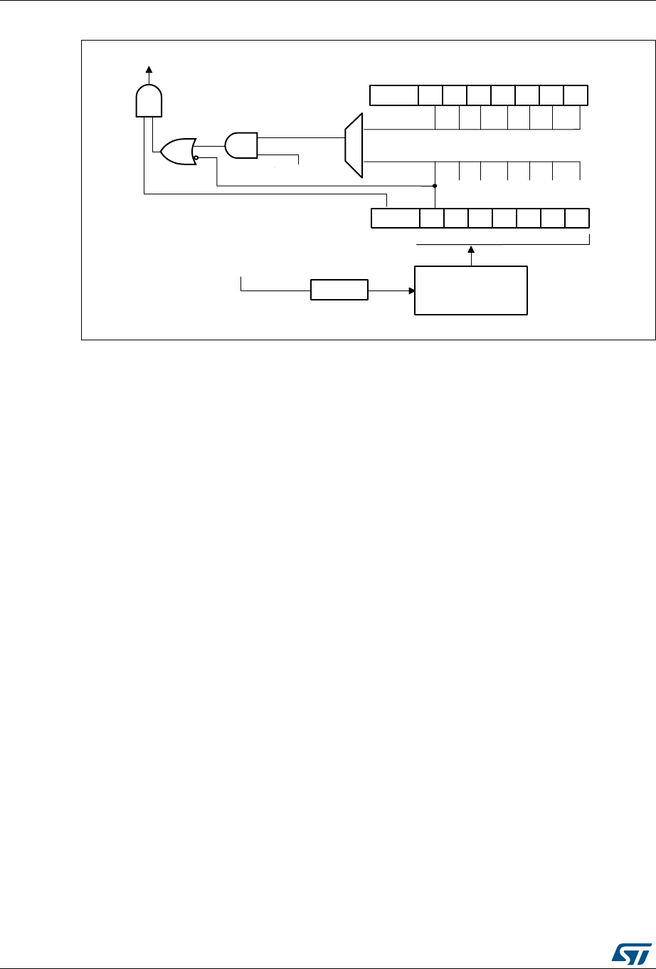
Window watchdog (WWDG) RM0401
466/766 DocID027812 Rev 2
Figure 172. Watchdog block diagram
The application program must write in the WWDG_CR register at regular intervals during
normal operation to prevent an MCU reset. This operation must occur only when the counter
value is lower than the window register value. The value to be stored in the WWDG_CR
register must be between 0xFF and 0xC0.
Enabling the watchdog
The watchdog is always disabled after a reset. It is enabled by setting the WDGA bit in the
WWDG_CR register, then it cannot be disabled again except by a reset.
Controlling the downcounter
This downcounter is free-running, counting down even if the watchdog is disabled. When
the watchdog is enabled, the T6 bit must be set to prevent generating an immediate reset.
The T[5:0] bits contain the number of increments which represents the time delay before the
watchdog produces a reset. The timing varies between a minimum and a maximum value
due to the unknown status of the prescaler when writing to the WWDG_CR register (see
Figure 173). The Configuration register (WWDG_CFR) contains the high limit of the window:
To prevent a reset, the downcounter must be reloaded when its value is lower than the
window register value and greater than 0x3F. Figure 173 describes the window watchdog
process.
Note: The T6 bit can be used to generate a software reset (the WDGA bit is set and the T6 bit is
cleared).
Advanced watchdog interrupt feature
The Early Wakeup Interrupt (EWI) can be used if specific safety operations or data logging
must be performed before the actual reset is generated. The EWI interrupt is enabled by
setting the EWI bit in the WWDG_CFR register. When the downcounter reaches the value
0x40, an EWI interrupt is generated and the corresponding interrupt service routine (ISR)
can be used to trigger specific actions (such as communications or data logging), before
resetting the device.
06Y9
5(6(7
ELWGRZQFRXQWHU&17
:DWFKGRJFRQILJXUDWLRQUHJLVWHU::'*B&)5
FRPSDUDWRU
7!:
ZKHQ
:ULWH::'*B&5
3&/.
IURP5&&FORFNFRQWUROOHU
:'*SUHVFDOHU
:'*7%
: ::::: :
:'*$ 7
:DWFKGRJFRQWUROUHJLVWHU::'*B&5
77777 7
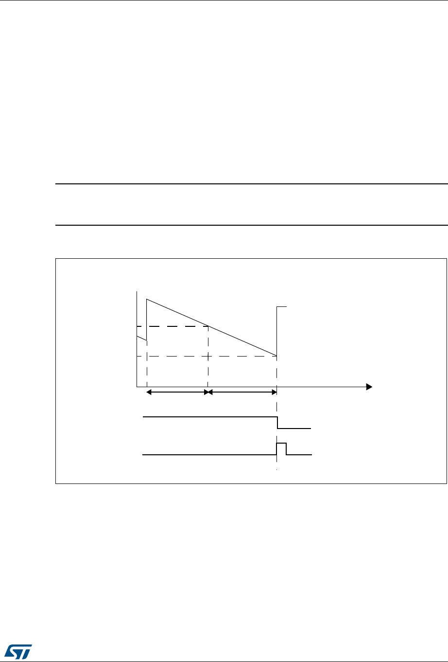
DocID027812 Rev 2 467/766
RM0401 Window watchdog (WWDG)
471
In some applications, the EWI interrupt can be used to manage a software system check
and/or system recovery/graceful degradation, without generating a WWDG reset. In this
case, the corresponding interrupt service routine (ISR) should reload the WWDG counter to
avoid the WWDG reset, then trigger the required actions.
The EWI interrupt is cleared by writing '0' to the EWIF bit in the WWDG_SR register.
Note: When the EWI interrupt cannot be served, e.g. due to a system lock in a higher priority task,
the WWDG reset will eventually be generated.
19.4 How to program the watchdog timeout
You can use the formula in Figure 173 to calculate the WWDG timeout.
Warning: When writing to the WWDG_CR register, always write 1 in the
T6 bit to avoid generating an immediate reset.
Figure 173. Window watchdog timing diagram
The formula to calculate the timeout value is given by:
where:
tWWDG: WWDG timeout
tPCLK1: APB1 clock period measured in ms
4096: value corresponding to internal divider
As an example, lets assume APB1 frequency is equal to 24 MHz, WDGTB[1:0] is set to 3
and T[5:0] is set to 63:
AIC
7;=
4;=#.4DOWNCOUNTER
2EFRESHNOTALLOWED
X&
2EFRESHALLOWED 4IME
4BIT
2%3%4
tWWDG tPCLK1 4096×2WDGTB[1:0]
×T5:0] 1+()×=ms()

Window watchdog (WWDG) RM0401
468/766 DocID027812 Rev 2
Refer to the table below for the minimum and maximum values of the tWWDG.
19.5 Debug mode
When the microcontroller enters debug mode (Cortex®-M4 with FPU core halted), the
WWDG counter either continues to work normally or stops, depending on
DBG_WWDG_STOP configuration bit in DBG module. For more details, refer to
Section 26.16.2: Debug support for timers, watchdog and I2C.
tWWDG 1 24000⁄4096×23
×63 1+()×21.85 ms==

DocID027812 Rev 2 469/766
RM0401 Window watchdog (WWDG)
471
19.6 WWDG registers
Refer to Section 1.1 on page 33 for a list of abbreviations used in register descriptions.
The peripheral registers have to be accessed by half-words (16 bits) or words (32 bits).
19.6.1 Control register (WWDG_CR)
Address offset: 0x00
Reset value: 0x0000 007F
31 30 29 28 27 26 25 24 23 22 21 20 19 18 17 16
Res. Res. Res. Res. Res. Res. Res. Res. Res. Res. Res. Res. Res. Res. Res. Res.
1514131211109876543210
Res. Res. Res. Res. Res. Res. Res. Res. WDGA T[6:0]
rs rw
Bits 31:8 Reserved, must be kept at reset value.
Bit 7 WDGA: Activation bit
This bit is set by software and only cleared by hardware after a reset. When WDGA = 1, the
watchdog can generate a reset.
0: Watchdog disabled
1: Watchdog enabled
Bits 6:0 T[6:0]: 7-bit counter (MSB to LSB)
These bits contain the value of the watchdog counter. It is decremented every (4096 x
2WDGTB[1:0]) PCLK1 cycles. A reset is produced when it rolls over from 0x40 to 0x3F (T6
becomes cleared).

Window watchdog (WWDG) RM0401
470/766 DocID027812 Rev 2
19.6.2 Configuration register (WWDG_CFR)
Address offset: 0x04
Reset value: 0x0000 007F
19.6.3 Status register (WWDG_SR)
Address offset: 0x08
Reset value: 0x0000 0000
31 30 29 28 27 26 25 24 23 22 21 20 19 18 17 16
Res. Res. Res. Res. Res. Res. Res. Res. Res. Res. Res. Res. Res. Res. Res. Res.
1514131211109876543210
Res. Res. Res. Res. Res. Res. EWI WDGTB[1:0] W[6:0]
rs rw rw
Bit 31:10 Reserved, must be kept at reset value.
Bit 9 EWI: Early wakeup interrupt
When set, an interrupt occurs whenever the counter reaches the value 0x40. This interrupt is
only cleared by hardware after a reset.
Bits 8:7 WDGTB[1:0]: Timer base
The time base of the prescaler can be modified as follows:
00: CK Counter Clock (PCLK1 div 4096) div 1
01: CK Counter Clock (PCLK1 div 4096) div 2
10: CK Counter Clock (PCLK1 div 4096) div 4
11: CK Counter Clock (PCLK1 div 4096) div 8
Bits 6:0 W[6:0]: 7-bit window value
These bits contain the window value to be compared to the downcounter.
31 30 29 28 27 26 25 24 23 22 21 20 19 18 17 16
Res. Res. Res. Res. Res. Res. Res. Res. Res. Res. Res. Res. Res. Res. Res. Res.
1514131211109876543210
Res. Res. Res. Res. Res. Res. Res. Res. Res. Res. Res. Res. Res. Res. Res. EWIF
rc_w0
Bits 31:1 Reserved, must be kept at reset value.
Bit 0 EWIF: Early wakeup interrupt flag
This bit is set by hardware when the counter has reached the value 0x40. It must be cleared
by software by writing ‘0’. A write of ‘1’ has no effect. This bit is also set if the interrupt is not
enabled.

DocID027812 Rev 2 471/766
RM0401 Window watchdog (WWDG)
471
19.6.4 WWDG register map
The following table gives the WWDG register map and reset values.
Refer to Section 2.2.2 on page 38 for the register boundary addresses.
Table 74. WWDG register map and reset values
Offset Register
31
30
29
28
27
26
25
24
23
22
21
20
19
18
17
16
15
14
13
12
11
10
9
8
7
6
5
4
3
2
1
0
0x00
WWDG_CR
Res.
Res.
Res.
Res.
Res.
Res.
Res.
Res.
Res.
Res.
Res.
Res.
Res.
Res.
Res.
Res.
Res.
Res.
Res.
Res.
Res.
Res.
Res.
Res.
WDGA
T[6:0]
Reset value 01111111
0x04
WWDG_CFR
Res.
Res.
Res.
Res.
Res.
Res.
Res.
Res.
Res.
Res.
Res.
Res.
Res.
Res.
Res.
Res.
Res.
Res.
Res.
Res.
Res.
Res.
EWI
WDGTB1
WDGTB0
W[6:0]
Reset value 0001111111
0x08
WWDG_SR
Res.
Res.
Res.
Res.
Res.
Res.
Res.
Res.
Res.
Res.
Res.
Res.
Res.
Res.
Res.
Res.
Res.
Res.
Res.
Res.
Res.
Res.
Res.
Res.
Res.
Res.
Res.
Res.
Res.
Res.
Res.
EWIF
Reset value 0

Independent watchdog (IWDG) RM0401
472/766 DocID027812 Rev 2
20 Independent watchdog (IWDG)
20.1 IWDG introduction
The devices have two embedded watchdog peripherals which offer a combination of high
safety level, timing accuracy and flexibility of use. Both watchdog peripherals (Independent
and Window) serve to detect and resolve malfunctions due to software failure, and to trigger
system reset or an interrupt (window watchdog only) when the counter reaches a given
timeout value.
The independent watchdog (IWDG) is clocked by its own dedicated low-speed clock (LSI)
and thus stays active even if the main clock fails. The window watchdog (WWDG) clock is
prescaled from the APB1 clock and has a configurable time-window that can be
programmed to detect abnormally late or early application behavior.
The IWDG is best suited to applications which require the watchdog to run as a totally
independent process outside the main application, but have lower timing accuracy
constraints. The WWDG is best suited to applications which require the watchdog to react
within an accurate timing window. For further information on the window watchdog, refer to
Section 19: Window watchdog (WWDG) on page 465.
20.2 IWDG main features
•Free-running downcounter
•clocked from an independent RC oscillator (can operate in Standby and Stop modes)
•Reset (if watchdog activated) when the downcounter value of 0x000 is reached
20.3 IWDG functional description
Figure 174 shows the functional blocks of the independent watchdog module.
When the independent watchdog is started by writing the value 0xCCCC in the Key register
(IWDG_KR), the counter starts counting down from the reset value of 0xFFF. When it
reaches the end of count value (0x000) a reset signal is generated (IWDG reset).
Whenever the key value 0xAAAA is written in the IWDG_KR register, the IWDG_RLR value
is reloaded in the counter and the watchdog reset is prevented.
20.3.1 Hardware watchdog
If the “Hardware watchdog” feature is enabled through the device option bits, the watchdog
is automatically enabled at power-on, and will generate a reset unless the Key register is
written by the software before the counter reaches end of count.
20.3.2 Register access protection
Write access to the IWDG_PR and IWDG_RLR registers is protected. To modify them, you
must first write the code 0x5555 in the IWDG_KR register. A write access to this register
with a different value will break the sequence and register access will be protected again.
This implies that it is the case of the reload operation (writing 0xAAAA).
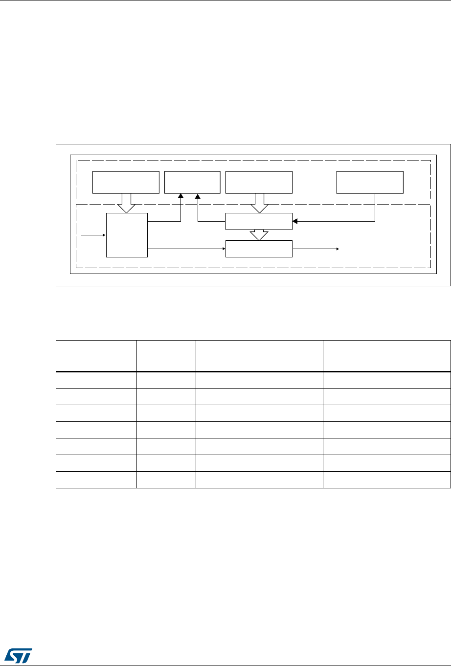
DocID027812 Rev 2 473/766
RM0401 Independent watchdog (IWDG)
478
A status register is available to indicate that an update of the prescaler or the down-counter
reload value is on going.
20.3.3 Debug mode
When the microcontroller enters debug mode (Cortex®-M4 with FPU core halted), the IWDG
counter either continues to work normally or stops, depending on DBG_IWDG_STOP
configuration bit in DBG module. For more details, refer to Section 26.16.2: Debug support
for timers, watchdog and I2C.
Figure 174. Independent watchdog block diagram
Note: The watchdog function is implemented in the VDD voltage domain that is still functional in
Stop and Standby modes.
20.4 IWDG registers
Refer to Section 1.1 on page 33 for a list of abbreviations used in register descriptions.
The peripheral registers have to be accessed by half-words (16 bits) or words (32 bits).
20.4.1 Key register (IWDG_KR)
Address offset: 0x00
)7$'RESET
PRESCALER
)7$'?02
0RESCALERREGISTER
)7$'?2,2
2ELOADREGISTER
BIT
,3)
K(Z
)7$'?+2
+EYREGISTER
#/2%
6$$VOLTAGEDOMAIN
)7$'?32
3TATUSREGISTER
-36
BITRELOADVALUE
BITDOWNCOUNTER
Table 75. Min/max IWDG timeout period at 32 kHz (LSI)(1)
1. These timings are given for a 32 kHz clock but the microcontroller internal RC frequency can vary. Please
refers to LSI oscillator characteristics table in device datasheet for from max and min values.
Prescaler divider PR[2:0] bits Min timeout (ms) RL[11:0]=
0x000
Max timeout (ms) RL[11:0]=
0xFFF
/4 0 0.125 512
/8 1 0.25 1024
/16 2 0.5 2048
/32 3 1 4096
/64 4 2 8192
/128 5 4 16384
/256 6 8 32768

Independent watchdog (IWDG) RM0401
474/766 DocID027812 Rev 2
Reset value: 0x0000 0000 (reset by Standby mode)
31 30 29 28 27 26 25 24 23 22 21 20 19 18 17 16
Res. Res. Res. Res. Res. Res. Res. Res. Res. Res. Res. Res. Res. Res. Res. Res.
15 14 13 12 11 10 9 8 7 6 5 4 3 2 1 0
KEY[15:0]
w w w w w w w w w w w w w w w w
Bits 31:16 Reserved, must be kept at reset value.
Bits 15:0 KEY[15:0]: Key value (write only, read 0000h)
These bits must be written by software at regular intervals with the key value AAAAh,
otherwise the watchdog generates a reset when the counter reaches 0.
Writing the key value 5555h to enable access to the IWDG_PR and IWDG_RLR registers
(see Section 20.3.2)
Writing the key value CCCCh starts the watchdog (except if the hardware watchdog option is
selected)

DocID027812 Rev 2 475/766
RM0401 Independent watchdog (IWDG)
478
20.4.2 Prescaler register (IWDG_PR)
Address offset: 0x04
Reset value: 0x0000 0000
31 30 29 28 27 26 25 24 23 22 21 20 19 18 17 16
Res. Res. Res. Res. Res. Res. Res. Res. Res. Res. Res. Res. Res. Res. Res. Res.
15 14 13 12 11 10 9 8 7 6 5 4 3 2 1 0
Res. Res. Res. Res. Res. Res. Res. Res. Res. Res. Res. Res. Res. PR[2:0]
rw rw rw
Bits 31:3 Reserved, must be kept at reset value.
Bits 2:0 PR[2:0]: Prescaler divider
These bits are write access protected seeSection 20.3.2. They are written by software to
select the prescaler divider feeding the counter clock. PVU bit of IWDG_SR must be reset in
order to be able to change the prescaler divider.
000: divider /4
001: divider /8
010: divider /16
011: divider /32
100: divider /64
101: divider /128
110: divider /256
111: divider /256
Note: Reading this register returns the prescaler value from the VDD voltage domain. This
value may not be up to date/valid if a write operation to this register is ongoing. For this
reason the value read from this register is valid only when the PVU bit in the IWDG_SR
register is reset.

Independent watchdog (IWDG) RM0401
476/766 DocID027812 Rev 2
20.4.3 Reload register (IWDG_RLR)
Address offset: 0x08
Reset value: 0x0000 0FFF (reset by Standby mode)
20.4.4 Status register (IWDG_SR)
Address offset: 0x0C
Reset value: 0x0000 0000 (not reset by Standby mode)
31 30 29 28 27 26 25 24 23 22 21 20 19 18 17 16
Res. Res. Res. Res. Res. Res. Res. Res. Res. Res. Res. Res. Res. Res. Res. Res.
15 14 13 12 11 10 9 8 7 6 5 4 3 2 1 0
Res. Res. Res. Res. RL[11:0]
rw rw rw rw rw rw rw rw rw rw rw rw
Bits 31:12 Reserved, must be kept at reset value.
Bits11:0 RL[11:0]: Watchdog counter reload value
These bits are write access protected see Section 20.3.2. They are written by software to
define the value to be loaded in the watchdog counter each time the value AAAAh is written
in the IWDG_KR register. The watchdog counter counts down from this value. The timeout
period is a function of this value and the clock prescaler. Refer to Table 75.
The RVU bit in the IWDG_SR register must be reset in order to be able to change the reload
value.
Note: Reading this register returns the reload value from the VDD voltage domain. This value
may not be up to date/valid if a write operation to this register is ongoing on this
register. For this reason the value read from this register is valid only when the RVU bit
in the IWDG_SR register is reset.
31 30 29 28 27 26 25 24 23 22 21 20 19 18 17 16
Res. Res. Res. Res. Res. Res. Res. Res. Res. Res. Res. Res. Res. Res. Res. Res.
15 14 13 12 11 10 9 8 7 6 5 4 3 2 1 0
Res. Res. Res. Res. Res. Res. Res. Res. Res. Res. Res. Res. Res. Res. RVU PVU
rr
Bits 31:2 Reserved, must be kept at reset value.
Bit 1 RVU: Watchdog counter reload value update
This bit is set by hardware to indicate that an update of the reload value is ongoing. It is reset
by hardware when the reload value update operation is completed in the VDD voltage domain
(takes up to 5 RC 40 kHz cycles).
Reload value can be updated only when RVU bit is reset.
Bit 0 PVU: Watchdog prescaler value update
This bit is set by hardware to indicate that an update of the prescaler value is ongoing. It is
reset by hardware when the prescaler update operation is completed in the VDD voltage
domain (takes up to 5 RC 40 kHz cycles).
Prescaler value can be updated only when PVU bit is reset.

DocID027812 Rev 2 477/766
RM0401 Independent watchdog (IWDG)
478
Note: If several reload values or prescaler values are used by application, it is mandatory to wait
until RVU bit is reset before changing the reload value and to wait until PVU bit is reset
before changing the prescaler value. However, after updating the prescaler and/or the
reload value it is not necessary to wait until RVU or PVU is reset before continuing code
execution (even in case of low-power mode entry, the write operation is taken into account
and will complete)

Independent watchdog (IWDG) RM0401
478/766 DocID027812 Rev 2
20.4.5 IWDG register map
The following table gives the IWDG register map and reset values.
Refer to Section 2.2.2 on page 38 for the register boundary addresses.
Table 76. IWDG register map and reset values
Offset Register
31
30
29
28
27
26
25
24
23
22
21
20
19
18
17
16
15
14
13
12
11
10
9
8
7
6
5
4
3
2
1
0
0x00
IWDG_KR
Res.
Res.
Res.
Res.
Res.
Res.
Res.
Res.
Res.
Res.
Res.
Res.
Res.
Res.
Res.
Res.
KEY[15:0]
Reset value 0000000000000000
0x04
IWDG_PR
Res.
Res.
Res.
Res.
Res.
Res.
Res.
Res.
Res.
Res.
Res.
Res.
Res.
Res.
Res.
Res.
Res.
Res.
Res.
Res.
Res.
Res.
Res.
Res.
Res.
Res.
Res.
Res.
Res.
PR[2:0]
Reset value 000
0x08
IWDG_RLR
Res.
Res.
Res.
Res.
Res.
Res.
Res.
Res.
Res.
Res.
Res.
Res.
Res.
Res.
Res.
Res.
Res.
Res.
Res.
Res.
RL[11:0]
Reset value 111111111111
0x0C
IWDG_SR
Res.
Res.
Res.
Res.
Res.
Res.
Res.
Res.
Res.
Res.
Res.
Res.
Res.
Res.
Res.
Res.
Res.
Res.
Res.
Res.
Res.
Res.
Res.
Res.
Res.
Res.
Res.
Res.
Res.
Res.
RVU
PVU
Reset value 00

DocID027812 Rev 2 479/766
RM0401 Real-time clock (RTC)
517
21 Real-time clock (RTC)
21.1 Introduction
The real-time clock (RTC) is an independent BCD timer/counter. The RTC provides a time-
of-day clock/calendar, two programmable alarm interrupts, and a periodic programmable
wakeup flag with interrupt capability. The RTC also includes an automatic wakeup unit to
manage low power modes.
Two 32-bit registers contain the seconds, minutes, hours (12- or 24-hour format), day (day
of week), date (day of month), month, and year, expressed in binary coded decimal format
(BCD). The sub-seconds value is also available in binary format.
Compensations for 28-, 29- (leap year), 30-, and 31-day months are performed
automatically. Daylight saving time compensation can also be performed.
Additional 32-bit registers contain the programmable alarm subseconds, seconds, minutes,
hours, day, and date.
A digital calibration feature is available to compensate for any deviation in crystal oscillator
accuracy.
After backup domain reset, all RTC registers are protected against possible parasitic write
accesses.
As long as the supply voltage remains in the operating range, the RTC never stops,
regardless of the device status (Run mode, low power mode or under reset).
21.2 RTC main features
The RTC unit main features are the following (see Figure 175: RTC block diagram):
•Calendar with subseconds, seconds, minutes, hours (12 or 24 format), day (day of
week), date (day of month), month, and year.
•Daylight saving compensation programmable by software.
•Two programmable alarms with interrupt function. The alarms can be triggered by any
combination of the calendar fields.
•Automatic wakeup unit generating a periodic flag that triggers an automatic wakeup
interrupt.
•Reference clock detection: a more precise second source clock (50 or 60 Hz) can be
used to enhance the calendar precision.
•Accurate synchronization with an external clock using the subsecond shift feature.
•Maskable interrupts/events:
–Alarm A
–Alarm B
– Wakeup interrupt
–Timestamp
– Tamper detection
•Digital calibration circuit (periodic counter correction)
– 5 ppm accuracy
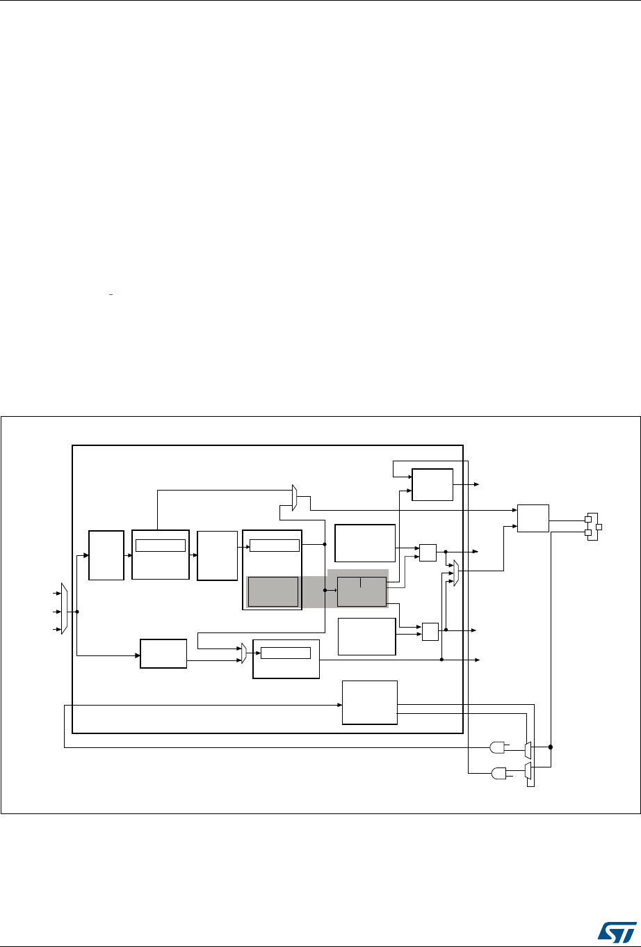
Real-time clock (RTC) RM0401
480/766 DocID027812 Rev 2
– 0.95 ppm accuracy, obtained in a calibration window of several seconds
•Timestamp function for event saving (1 event)
•Tamper detection:
– 2 tamper events with configurable filter and internal pull-up.
•20 backup registers (80 bytes). The backup registers are reset when a tamper
detection event occurs.
•Alternate function output (RTC_OUT) which selects one of the following two outputs:
– RTC_CALIB: 512 Hz or 1 Hz clock output (with an LSE frequency of 32.768 kHz).
This output is enabled by setting the COE bit in the RTC_CR register. It is routed
to the device RTC_AF1 function.
– RTC_ALARM (Alarm A, Alarm B or wakeup).
This output is selected by configuring the OSEL[1:0] bits in the RTC_CR register.
It is routed to the device RTC_AF1 function.
• RTC alternate function inputs:
– RTC_TS: timestamp event detection. It is routed to the device RTC_AF1.
– RTC_TAMP1: TAMPER1 event detection. It is routed to the device RTC_AF1.
– RTC_REFIN: reference clock input (usually the mains, 50 or 60 Hz).
Refer to Section 6.3.15: Selection of RTC additional functions.
Figure 175. RTC block diagram
06Y9
&NBDSUH
GHIDXOW+]
57&B&$/,%
+]
57&B:875
57&&/.
:87)
+6(B57&
0+]PD[
/6(
+]
/6,
6\QFKURQRXV
ELWSUHVFDOHU
GHIDXOW &DOHQGDU
3UHVFDOHU
ELWZDNHXS
DXWRUHORDGWLPHU
$ODUP$
57&B$/50$5
57&B$/50$665
UHJLVWHUV
$/5$)
57&B$/$50
57&B35 ( 5 57&B35(5
&RDUVH
FDOLEUDWLRQ
57&B&$/
,%5
$/5%)
7LPH
VWDPS
UHJLVWHUV
76)
2XWSXW
FRQWURO 57&B$)
57&B287
6PRRWK
&DOLEUDWLRQ
57&B&$/
5
+]
$ODUP%
57&B$/50%5
57&B$/50%665
UHJLVWHUV
:8&.6(/>@
%DFNXSDQG
57&WDPSHU
FRQWURO
UHJLVWHUV
57&B7$03
57&B76
7$03(
76(
6KDGRZ
5HJLVWHUV
57&B665
6KDGRZ
5HJLVWHUV
57&B75'5
FNBVSUH
GHIDXOW
+]
$V\QFKURQRXV
ELWSUHVFDOHU
GHIDXOW

DocID027812 Rev 2 481/766
RM0401 Real-time clock (RTC)
517
21.3 RTC functional description
21.3.1 Clock and prescalers
The RTC clock source (RTCCLK) is selected through the clock controller among the LSE
clock, the LSI oscillator clock, and the HSE clock. For more information on the RTC clock
source configuration, refer to Section 6: Reset and clock control (RCC).
A programmable prescaler stage generates a 1 Hz clock which is used to update the
calendar. To minimize power consumption, the prescaler is split into 2 programmable
prescalers (see Figure 175: RTC block diagram):
•A 7-bit asynchronous prescaler configured through the PREDIV_A bits of the
RTC_PRER register.
• A 15-bit synchronous prescaler configured through the PREDIV_S bits of the
RTC_PRER register.
Note: When both prescalers are used, it is recommended to configure the asynchronous prescaler
to a high value to minimize consumption.
The asynchronous prescaler division factor is set to 128, and the synchronous division
factor to 256, to obtain an internal clock frequency of 1 Hz (ck_spre) with an LSE frequency
of 32.768 kHz.
The minimum division factor is 1 and the maximum division factor is 222.
This corresponds to a maximum input frequency of around 4 MHz.
fck_apre is given by the following formula:
The ck_apre clock is used to clock the binary RTC_SSR subseconds downcounter. When it
reaches 0, RTC_SSR is reloaded with the content of PREDIV_S.
fck_spre is given by the following formula:
The ck_spre clock can be used either to update the calendar or as timebase for the 16-bit
wakeup auto-reload timer. To obtain short timeout periods, the 16-bit wakeup auto-reload
timer can also run with the RTCCLK divided by the programmable 4-bit asynchronous
prescaler (see Section 21.3.4: Periodic auto-wakeup for details).
21.3.2 Real-time clock and calendar
The RTC calendar time and date registers are accessed through shadow registers which
are synchronized with PCLK1 (APB1 clock). They can also be accessed directly in order to
avoid waiting for the synchronization duration.
•RTC_SSR for the subseconds
•RTC_TR for the time
•RTC_DR for the date
fCK_APRE
fRTCCLK
PREDIV_A 1+
---------------------------------------
=
fCK_SPRE
fRTCCLK
PREDIV_S 1+()PREDIV_A 1+()×
----------------------------------------------------------------------------------------------
=

Real-time clock (RTC) RM0401
482/766 DocID027812 Rev 2
Every two RTCCLK periods, the current calendar value is copied into the shadow registers,
and the RSF bit of RTC_ISR register is set (see Section 21.6.4). The copy is not performed
in Stop and Standby mode. When exiting these modes, the shadow registers are updated
after up to 2 RTCCLK periods.
When the application reads the calendar registers, it accesses the content of the shadow
registers.It is possible to make a direct access to the calendar registers by setting the
BYPSHAD control bit in the RTC_CR register. By default, this bit is cleared, and the user
accesses the shadow registers.
When reading the RTC_SSR, RTC_TR or RTC_DR registers in BYPSHAD=0 mode, the
frequency of the APB clock (fAPB) must be at least 7 times the frequency of the RTC clock
(fRTCCLK).
The shadow registers are reset by system reset.
21.3.3 Programmable alarms
The RTC unit provides two programmable alarms, Alarm A and Alarm B.
The programmable alarm functions are enabled through the ALRAIE and ALRBIE bits in the
RTC_CR register. The ALRAF and ALRBF flags are set to 1 if the calendar subseconds,
seconds, minutes, hours, date or day match the values programmed in the alarm registers
RTC_ALRMASSR/RTC_ALRMAR and RTC_ALRMBSSR/RTC_ALRMBR, respectively.
Each calendar field can be independently selected through the MSKx bits of the
RTC_ALRMAR and RTC_ALRMBR registers, and through the MASKSSx bits of the
RTC_ALRMASSR and RTC_ALRMBSSR registers. The alarm interrupts are enabled
through the ALRAIE and ALRBIE bits in the RTC_CR register.
Alarm A and Alarm B (if enabled by bits OSEL[1:0] in RTC_CR register) can be routed to the
RTC_ALARM output. RTC_ALARM polarity can be configured through bit POL in the
RTC_CR register.
Caution: If the seconds field is selected (MSK0 bit reset in RTC_ALRMAR or RTC_ALRMBR), the
synchronous prescaler division factor set in the RTC_PRER register must be at least 3 to
ensure correct behavior.
21.3.4 Periodic auto-wakeup
The periodic wakeup flag is generated by a 16-bit programmable auto-reload down-counter.
The wakeup timer range can be extended to 17 bits.
The wakeup function is enabled through the WUTE bit in the RTC_CR register.
The wakeup timer clock input can be:
•RTC clock (RTCCLK) divided by 2, 4, 8, or 16.
When RTCCLK is LSE(32.768 kHz), this allows to configure the wakeup interrupt
period from 122 µs to 32 s, with a resolution down to 61µs.
•ck_spre (usually 1 Hz internal clock)
When ck_spre frequency is 1Hz, this allows to achieve a wakeup time from 1 s to
around 36 hours with one-second resolution. This large programmable time range is
divided in 2 parts:
– from 1s to 18 hours when WUCKSEL [2:1] = 10
– and from around 18h to 36h when WUCKSEL[2:1] = 11. In this last case 216 is
added to the 16-bit counter current value.When the initialization sequence is

DocID027812 Rev 2 483/766
RM0401 Real-time clock (RTC)
517
complete (see Programming the wakeup timer on page 484), the timer starts
counting down.When the wakeup function is enabled, the down-counting remains
active in low power modes. In addition, when it reaches 0, the WUTF flag is set in
the RTC_ISR register, and the wakeup counter is automatically reloaded with its
reload value (RTC_WUTR register value).
The WUTF flag must then be cleared by software.
When the periodic wakeup interrupt is enabled by setting the WUTIE bit in the RTC_CR2
register, it can exit the device from low power modes.
The periodic wakeup flag can be routed to the RTC_ALARM output provided it has been
enabled through bits OSEL[1:0] of RTC_CR register. RTC_ALARM polarity can be
configured through the POL bit in the RTC_CR register.
System reset, as well as low power modes (Sleep, Stop and Standby) have no influence on
the wakeup timer.
21.3.5 RTC initialization and configuration
RTC register access
The RTC registers are 32-bit registers. The APB interface introduces 2 wait-states in RTC
register accesses except on read accesses to calendar shadow registers when
BYPSHAD=0.
RTC register write protection
After system reset, the RTC registers are protected against parasitic write access with the
DBP bit of the PWR power control register (PWR_CR). The DBP bit must be set to enable
RTC registers write access.
After backup domain reset, all the RTC registers are write-protected. Writing to the RTC
registers is enabled by writing a key into the Write Protection register, RTC_WPR.
The following steps are required to unlock the write protection on all the RTC registers
except for RTC_ISR[13:8], RTC_TAFCR, and RTC_BKPxR.
1. Write ‘0xCA’ into the RTC_WPR register.
2. Write ‘0x53’ into the RTC_WPR register.
Writing a wrong key reactivates the write protection.
The protection mechanism is not affected by system reset.
Calendar initialization and configuration
To program the initial time and date calendar values, including the time format and the
prescaler configuration, the following sequence is required:
1. Set INIT bit to 1 in the RTC_ISR register to enter initialization mode. In this mode, the
calendar counter is stopped and its value can be updated.
2. Poll INITF bit of in the RTC_ISR register. The initialization phase mode is entered when
INITF is set to 1. It takes from 1 to 2 RTCCLK clock cycles (due to clock
synchronization).
3. To generate a 1 Hz clock for the calendar counter, program first the synchronous
prescaler factor in RTC_PRER register, and then program the asynchronous prescaler

Real-time clock (RTC) RM0401
484/766 DocID027812 Rev 2
factor. Even if only one of the two fields needs to be changed, 2 separate write
accesses must be performed to the RTC_PRER register.
4. Load the initial time and date values in the shadow registers (RTC_TR and RTC_DR),
and configure the time format (12 or 24 hours) through the FMT bit in the RTC_CR
register.
5. Exit the initialization mode by clearing the INIT bit. The actual calendar counter value is
then automatically loaded and the counting restarts after 4 RTCCLK clock cycles.
When the initialization sequence is complete, the calendar starts counting.
Note: After a system reset, the application can read the INITS flag in the RTC_ISR register to
check if the calendar has been initialized or not. If this flag equals 0, the calendar has not
been initialized since the year field is set at its backup domain reset default value (0x00).
To read the calendar after initialization, the software must first check that the RSF flag is set
in the RTC_ISR register.
Daylight saving time
The daylight saving time management is performed through bits SUB1H, ADD1H, and BKP
of the RTC_CR register.
Using SUB1H or ADD1H, the software can subtract or add one hour to the calendar in one
single operation without going through the initialization procedure.
In addition, the software can use the BKP bit to memorize this operation.
Programming the alarm
A similar procedure must be followed to program or update the programmable alarm (Alarm
A or Alarm B):
1. Clear ALRAE or ALRBIE in RTC_CR to disable Alarm A or Alarm B.
2. Poll ALRAWF or ALRBWF in RTC_ISR until it is set to make sure the access to alarm
registers is allowed. This takes 1 to 2 RTCCLK clock cycles (due to clock
synchronization).
3. Program the Alarm A or Alarm B registers (RTC_ALRMASSR/RTC_ALRMAR or
RTC_ALRMBSSR/RTC_ALRMBR).
4. Set ALRAE or ALRBIE in the RTC_CR register to enable Alarm A or Alarm B again.
Note: Each change of the RTC_CR register is taken into account after 1 to 2 RTCCLK clock cycles
due to clock synchronization.
Programming the wakeup timer
The following sequence is required to configure or change the wakeup timer auto-reload
value (WUT[15:0] in RTC_WUTR):
1. Clear WUTE in RTC_CR to disable the wakeup timer.
2. Poll WUTWF until it is set in RTC_ISR to make sure the access to wakeup auto-reload
counter and to WUCKSEL[2:0] bits is allowed. It takes 1 to 2 RTCCLK clock cycles
(due to clock synchronization).
3. Program the wakeup auto-reload value WUT[15:0] and the wakeup clock selection
(WUCKSEL[2:0] bits in RTC_CR).Set WUTE in RTC_CR to enable the timer again.
The wakeup timer restarts down-counting. Due to clock synchronization, the WUTWF
bit is cleared up to 2 RTCCLK clocks cycles after WUTE is cleared.

DocID027812 Rev 2 485/766
RM0401 Real-time clock (RTC)
517
21.3.6 Reading the calendar
When BYPSHAD control bit is cleared in the RTC_CR register
To read the RTC calendar registers (RTC_SSR, RTC_TR and RTC_DR) properly, the APB1
clock frequency (fPCLK1) must be equal to or greater than seven times the fRTCCLK RTC
clock frequency. This ensures a secure behavior of the synchronization mechanism.
If the APB1 clock frequency is less than seven times the RTC clock frequency, the software
must read the calendar time and date registers twice. If the second read of the RTC_TR
gives the same result as the first read, this ensures that the data is correct. Otherwise a third
read access must be done. In any case the APB1 clock frequency must never be lower than
the RTC clock frequency.
The RSF bit is set in RTC_ISR register each time the calendar registers are copied into the
RTC_SSR, RTC_TR and RTC_DR shadow registers. The copy is performed every two
RTCCLK cycles. To ensure consistency between the 3 values, reading either RTC_SSR or
RTC_TR locks the values in the higher-order calendar shadow registers until RTC_DR is
read. In case the software makes read accesses to the calendar in a time interval smaller
than 2 RTCCLK periods: RSF must be cleared by software after the first calendar read, and
then the software must wait until RSF is set before reading again the RTC_SSR, RTC_TR
and RTC_DR registers.
After waking up from low power mode (Stop or Standby), RSF must be cleared by software.
The software must then wait until it is set again before reading the RTC_SSR, RTC_TR and
RTC_DR registers.
The RSF bit must be cleared after wakeup and not before entering low power mode.
Note: After a system reset, the software must wait until RSF is set before reading the RTC_SSR,
RTC_TR and RTC_DR registers. Indeed, a system reset resets the shadow registers to
their default values.
After an initialization (refer to Calendar initialization and configuration on page 483): the
software must wait until RSF is set before reading the RTC_SSR, RTC_TR and RTC_DR
registers.
After synchronization (refer to Section 21.3.8: RTC synchronization): the software must wait
until RSF is set before reading the RTC_SSR, RTC_TR and RTC_DR registers.
When the BYPSHAD control bit is set in the RTC_CR register (bypass shadow
registers)
Reading the calendar registers gives the values from the calendar counters directly, thus
eliminating the need to wait for the RSF bit to be set. This is especially useful after exiting
from low power modes (STOP or Standby), since the shadow registers are not updated
during these modes.
When the BYPSHAD bit is set to 1, the results of the different registers might not be
coherent with each other if an RTCCLK edge occurs between two read accesses to the
registers. Additionally, the value of one of the registers may be incorrect if an RTCCLK edge
occurs during the read operation. The software must read all the registers twice, and then
compare the results to confirm that the data is coherent and correct. Alternatively, the
software can just compare the two results of the least-significant calendar register.
Note: While BYPSHAD=1, instructions which read the calendar registers require one extra APB
cycle to complete.

Real-time clock (RTC) RM0401
486/766 DocID027812 Rev 2
21.3.7 Resetting the RTC
The calendar shadow registers (RTC_SSR, RTC_TR and RTC_DR) and some bits of the
RTC status register (RTC_ISR) are reset to their default values by all available system reset
sources.
On the contrary, the following registers are resetted to their default values by a backup
domain reset and are not affected by a system reset: the RTC current calendar registers,
the RTC control register (RTC_CR), the prescaler register (RTC_PRER), the RTC
calibration registers (RTC_CALIBR or RTC_CALR), the RTC shift register (RTC_SHIFTR),
the RTC timestamp registers (RTC_TSSSR, RTC_TSTR and RTC_TSDR), the RTC tamper
and alternate function configuration register (RTC_TAFCR), the RTC backup registers
(RTC_BKPxR), the wakeup timer register (RTC_WUTR), the Alarm A and Alarm B registers
(RTC_ALRMASSR/RTC_ALRMAR and RTC_ALRMBSSR/RTC_ALRMBR).
In addition, the RTC keeps on running under system reset if the reset source is different
from a backup domain reset. When a backup domain reset occurs, the RTC is stopped and
all the RTC registers are set to their reset values.
21.3.8 RTC synchronization
The RTC can be synchronized to a remote clock with a high degree of precision. After
reading the sub-second field (RTC_SSR or RTC_TSSSR), a calculation can be made of the
precise offset between the times being maintained by the remote clock and the RTC. The
RTC can then be adjusted to eliminate this offset by “shifting” its clock by a fraction of a
second using RTC_SHIFTR.
RTC_SSR contains the value of the synchronous prescaler’s counter. This allows one to
calculate the exact time being maintained by the RTC down to a resolution of
1 / (PREDIV_S + 1) seconds. As a consequence, the resolution can be improved by
increasing the synchronous prescaler value (PREDIV_S[14:0]. The maximum resolution
allowed (30.52 μs with a 32768 Hz clock) is obtained with PREDIV_S set to 0x7FFF.
However, increasing PREDIV_S means that PREDIV_A must be decreased in order to
maintain the synchronous prescaler’s output at 1 Hz. In this way, the frequency of the
asynchronous prescaler’s output increases, which may increase the RTC dynamic
consumption.
The RTC can be finely adjusted using the RTC shift control register (RTC_SHIFTR). Writing
to RTC_SHIFTR can shift (either delay or advance) the clock by up to a second with a
resolution of 1 / (PREDIV_S + 1) seconds. The shift operation consists of adding the
SUBFS[14:0] value to the synchronous prescaler counter SS[15:0]: this will delay the clock.
If at the same time the ADD1S bit is set, this results in adding one second and at the same
time subtracting a fraction of second, so this will advance the clock.
Caution: Before initiating a shift operation, the user must check that SS[15] = 0 in order to ensure that
no overflow will occur.
As soon as a shift operation is initiated by a write to the RTC_SHIFTR register, the SHPF
flag is set by hardware to indicate that a shift operation is pending. This bit is cleared by
hardware as soon as the shift operation has completed.
Caution: This synchronization feature is not compatible with the reference clock detection feature:
firmware must not write to RTC_SHIFTR when REFCKON=1.

DocID027812 Rev 2 487/766
RM0401 Real-time clock (RTC)
517
21.3.9 RTC reference clock detection
The RTC calendar update can be synchronized to a reference clock RTC_REFIN, usually
the mains (50 or 60 Hz). The RTC_REFIN reference clock should have a higher precision
than the 32.768 kHz LSE clock. When the RTC_REFIN detection is enabled (REFCKON bit
of RTC_CR set to 1), the calendar is still clocked by the LSE, and RTC_REFIN is used to
compensate for the imprecision of the calendar update frequency (1 Hz).
Each 1 Hz clock edge is compared to the nearest reference clock edge (if one is found
within a given time window). In most cases, the two clock edges are properly aligned. When
the 1 Hz clock becomes misaligned due to the imprecision of the LSE clock, the RTC shifts
the 1 Hz clock a bit so that future 1 Hz clock edges are aligned. Thanks to this mechanism,
the calendar becomes as precise as the reference clock.
The RTC detects if the reference clock source is present by using the 256 Hz clock
(ck_apre) generated from the 32.768 kHz quartz. The detection is performed during a time
window around each of the calendar updates (every 1 s). The window equals 7 ck_apre
periods when detecting the first reference clock edge. A smaller window of 3 ck_apre
periods is used for subsequent calendar updates.
Each time the reference clock is detected in the window, the asynchronous prescaler which
outputs the ck_apre clock is forced to reload. This has no effect when the reference clock
and the 1 Hz clock are aligned because the prescaler is being reloaded at the same
moment. When the clocks are not aligned, the reload shifts future 1 Hz clock edges a little
for them to be aligned with the reference clock.
If the reference clock halts (no reference clock edge occurred during the 3 ck_apre window),
the calendar is updated continuously based solely on the LSE clock. The RTC then waits for
the reference clock using a large 7 ck_apre period detection window centered on the
ck_spre edge.
When the reference clock detection is enabled, PREDIV_A and PREDIV_S must be set to
their default values:
•PREDIV_A = 0x007F
•PREDIV_S = 0x00FF
Note: The reference clock detection is not available in Standby mode.
Caution: The reference clock detection feature cannot be used in conjunction with the coarse digital
calibration: RTC_CALIBR must be kept at 0x0000 0000 when REFCKON=1.
21.3.10 RTC coarse digital calibration
Two digital calibration methods are available: coarse and smooth calibration. To perform
coarse calibration refer to Section 21.6.7: RTC calibration register (RTC_CALIBR).
The two calibration methods are not intended to be used together, the application must
select one of the two methods. Coarse calibration is provided for compatibly reasons. To
perform smooth calibration refer to Section 21.3.11: RTC smooth digital calibration and the
Section 21.6.16: RTC calibration register (RTC_CALR)
The coarse digital calibration can be used to compensate crystal inaccuracy by adding
(positive calibration) or masking (negative calibration) clock cycles at the output of the
asynchronous prescaler (ck_apre).
Positive and negative calibration are selected by setting the DCS bit in RTC_CALIBR
register to ‘0’ and ‘1’, respectively.

Real-time clock (RTC) RM0401
488/766 DocID027812 Rev 2
When positive calibration is enabled (DCS = ‘0’), 2 ck_apre cycles are added every minute
(around 15360 ck_apre cycles) for 2xDC minutes. This causes the calendar to be updated
sooner, thereby adjusting the effective RTC frequency to be a bit higher.
When negative calibration is enabled (DCS = ‘1’), 1 ck_apre cycle is removed every minute
(around 15360 ck_apre cycles) for 2xDC minutes. This causes the calendar to be updated
later, thereby adjusting the effective RTC frequency to be a bit lower.
DC is configured through bits DC[4:0] of RTC_CALIBR register. This number ranges from 0
to 31 corresponding to a time interval (2xDC) ranging from 0 to 62.
The coarse digital calibration can be configured only in initialization mode, and starts when
the INIT bit is cleared. The full calibration cycle lasts 64 minutes. The first 2xDC minutes of
the 64 -minute cycle are modified as just described.
Negative calibration can be performed with a resolution of about 2 ppm while positive
calibration can be performed with a resolution of about 4 ppm. The maximum calibration
ranges from −63 ppm to 126 ppm.
The calibration can be performed either on the LSE or on the HSE clock.
Caution: Digital calibration may not work correctly if PREDIV_A < 6.
Case of RTCCLK=32.768 kHz and PREDIV_A+1=128
The following description assumes that ck_apre frequency is 256 Hz obtained with an LSE
clock nominal frequency of 32.768 kHz, and PREDIV_A set to 127 (default value).
The ck_spre clock frequency is only modified during the first 2xDC minutes of the 64-minute
cycle. For example, when DC equals 1, only the first 2 minutes are modified. This means
that the first 2xDC minutes of each 64-minute cycle have, once per minute, one second
either shortened by 256 or lengthened by 128 RTCCLK cycles, given that each ck_apre
cycle represents 128 RTCCLK cycles (with PREDIV_A+1=128).
Therefore each calibration step has the effect of adding 512 or subtracting 256 oscillator
cycles for every 125829120 RTCCLK cycles (64min x 60 s/min x 32768 cycles/s). This is
equivalent to +4.069 ppm or-2.035 ppm per calibration step. As a result, the calibration
resolution is +10.5 or −5.27 seconds per month, and the total calibration ranges from +5.45
to − 2.72 minutes per month.
In order to measure the clock deviation, a 512 Hz clock is output for calibration.Refer to
Section 21.3.14: Calibration clock output.
21.3.11 RTC smooth digital calibration
RTC frequency can be digitally calibrated with a resolution of about 0.954 ppm with a range
from -487.1 ppm to +488.5 ppm. The correction of the frequency is performed using series
of small adjustments (adding and/or subtracting individual RTCCLK pulses). These
adjustments are fairly well distributed so that the RTC is well calibrated even when observed
over short durations of time.
The smooth digital calibration is performed during a cycle of about 220 RTCCLK pulses, or
32 seconds when the input frequency is 32768 Hz. This cycle is maintained by a 20-bit
counter, cal_cnt[19:0], clocked by RTCCLK.

DocID027812 Rev 2 489/766
RM0401 Real-time clock (RTC)
517
The smooth calibration register (RTC_CALR) specifies the number of RTCCLK clock cycles
to be masked during the 32-second cycle:
•Setting the bit CALM[0] to 1 causes exactly one pulse to be masked during the 32-
second cycle.
•Setting CALM[1] to 1 causes two additional cycles to be masked
•Setting CALM[2] to 1 causes four additional cycles to be masked
•and so on up to CALM[8] set to 1 which causes 256 clocks to be masked.
Note: CALM[8:0] (RTC_CALRx) specifies the number of RTCCLK pulses to be masked during the
32-second cycle. Setting the bit CALM[0] to ‘1’ causes exactly one pulse to be masked
during the 32-second cycle at the moment when cal_cnt[19:0] is 0x80000; CALM[1]=1
causes two other cycles to be masked (when cal_cnt is 0x40000 and 0xC0000); CALM[2]=1
causes four other cycles to be masked (cal_cnt = 0x20000/0x60000/0xA0000/ 0xE0000);
and so on up to CALM[8]=1 which causes 256 clocks to be masked (cal_cnt = 0xXX800).
While CALM allows the RTC frequency to be reduced by up to 487.1 ppm with fine
resolution, the bit CALP can be used to increase the frequency by 488.5 ppm. Setting CALP
to ‘1’ effectively inserts an extra RTCCLK pulse every 211 RTCCLK cycles, which means
that 512 clocks are added during every 32-second cycle.
Using CALM together with CALP, an offset ranging from -511 to +512 RTCCLK cycles can
be added during the 32-second cycle, which translates to a calibration range of -487.1 ppm
to +488.5 ppm with a resolution of about 0.954 ppm.
The formula to calculate the effective calibrated frequency (FCAL) given the input frequency
(FRTCCLK) is as follows:
FCAL = FRTCCLK x [1 + (CALP x 512 - CALM) / (220 + CALM - CALP x 512)]
Calibration when PREDIV_A<3
The CALP bit can not be set to 1 when the asynchronous prescaler value (PREDIV_A bits in
RTC_PRER register) is less than 3. If CALP was already set to 1 and PREDIV_A bits are
set to a value less than 3, CALP is ignored and the calibration operates as if CALP was
equal to 0.
To perform a calibration with PREDIV_A less than 3, the synchronous prescaler value
(PREDIV_S) should be reduced so that each second is accelerated by 8 RTCCLK clock
cycles, which is equivalent to adding 256 clock cycles every 32 seconds. As a result,
between 255 and 256 clock pulses (corresponding to a calibration range from 243.3 to
244.1 ppm) can effectively be added during each 32-second cycle using only the CALM bits.
With a nominal RTCCLK frequency of 32768 Hz, when PREDIV_A equals 1 (division factor
of 2), PREDIV_S should be set to 16379 rather than 16383 (4 less). The only other
interesting case is when PREDIV_A equals 0, PREDIV_S should be set to 32759 rather
than 32767 (8 less).
If PREDIV_S is reduced in this way, the formula given the effective frequency of the
calibrated input clock is as follows:
FCAL = FRTCCLK x [1 + (256 - CALM) / (220 + CALM - 256)]
In this case, CALM[7:0] equals 0x100 (the midpoint of the CALM range) is the correct
setting if RTCCLK is exactly 32768.00 Hz.

Real-time clock (RTC) RM0401
490/766 DocID027812 Rev 2
Verifying the RTC calibration
RTC precision is performed by measuring the precise frequency of RTCCLK and calculating
the correct CALM value and CALP values. An optional 1 Hz output is provided to allow
applications to measure and verify the RTC precision.
Measuring the precise frequency of the RTC over a limited interval can result in a
measurement error of up to 2 RTCCLK clock cycles over the measurement period,
depending on how the digital calibration cycle is aligned with the measurement period.
However, this measurement error can be eliminated if the measurement period is the same
length as the calibration cycle period. In this case, the only error observed is the error due to
the resolution of the digital calibration.
•By default, the calibration cycle period is 32 seconds.
Using this mode and measuring the accuracy of the 1 Hz output over exactly 32
seconds guarantees that the measure is within 0.477 ppm (0.5 RTCCLK cycles over 32
seconds, due to the limitation of the calibration resolution).
•CALW16 bit of the RTC_CALR register can be set to 1 to force a 16- second calibration
cycle period.
In this case, the RTC precision can be measured during 16 seconds with a maximum
error of 0.954 ppm (0.5 RTCCLK cycles over 16 seconds). However, since the
calibration resolution is reduced, the long term RTC precision is also reduced to 0.954
ppm: CALM[0] bit is stuck at 0 when CALW16 is set to 1.
•CALW8 bit of the RTC_CALR register can be set to 1 to force a 8- second calibration
cycle period.
In this case, the RTC precision can be measured during 8 seconds with a maximum
error of 1.907 ppm (0.5 RTCCLK cycles over 8s). The long term RTC precision is also
reduced to 1.907 ppm: CALM[1:0] bits are stuck at 00 when CALW8 is set to 1.
Re-calibration on-the-fly
The calibration register (RTC_CALR) can be updated on-the-fly while RTC_ISR/INITF=0, by
using the follow process:
1. Poll the RTC_ISR/RECALPF (re-calibration pending flag).
2. If it is set to 0, write a new value to RTC_CALR, if necessary. RECALPF is then
automatically set to 1
3. Within three ck_apre cycles after the write operation to RTC_CALR, the new calibration
settings take effect.
21.3.12 Timestamp function
Timestamp is enabled by setting the TSE bit of RTC_CR register to 1.
The calendar is saved in the timestamp registers (RTC_TSSSR, RTC_TSTR, RTC_TSDR)
when a timestamp event is detected on the pin to which the TIMESTAMP alternate function
is mapped. When a timestamp event occurs, the timestamp flag bit (TSF) in RTC_ISR
register is set.
By setting the TSIE bit in the RTC_CR register, an interrupt is generated when a timestamp
event occurs.

DocID027812 Rev 2 491/766
RM0401 Real-time clock (RTC)
517
If a new timestamp event is detected while the timestamp flag (TSF) is already set, the
timestamp overflow flag (TSOVF) flag is set and the timestamp registers (RTC_TSTR and
RTC_TSDR) maintain the results of the previous event.
Note: TSF is set 2 ck_apre cycles after the timestamp event occurs due to synchronization
process.
There is no delay in the setting of TSOVF. This means that if two timestamp events are
close together, TSOVF can be seen as '1' while TSF is still '0'. As a consequence, it is
recommended to poll TSOVF only after TSF has been set.
Caution: If a timestamp event occurs immediately after the TSF bit is supposed to be cleared, then
both TSF and TSOVF bits are set. To avoid masking a timestamp event occurring at the
same moment, the application must not write ‘0’ into TSF bit unless it has already read it to
‘1’.
Optionally, a tamper event can cause a timestamp to be recorded. See the description of the
TAMPTS control bit in Section 21.6.17: RTC tamper and alternate function configuration
register (RTC_TAFCR). If the timestamp event is on the same pin as a tamper event
configured in filtered mode (TAMPFLT set to a non-zero value), the timestamp on tamper
detection event mode must be selected by setting TAMPTS='1' in RTC_TAFCR register.
TIMESTAMP alternate function
The TIMESTAMP additional function is mapped to RTC_AF1.
21.3.13 Tamper detection
Two tamper detection inputs are available. They can be configured either for edge detection,
or for level detection with filtering.
RTC backup registers
The backup registers (RTC_BKPxR) are twenty 32-bit registers for storing 80 bytes of user
application data. They are implemented in the backup domain that remains powered-on by
VBAT when the VDD power is switched off. They are not reset by system reset or when the
device wakes up from Standby mode. They are reset by a backup domain reset
The backup registers are reset when a tamper detection event occurs (see Section 21.6.20:
RTC backup registers (RTC_BKPxR) and Tamper detection initialization on page 491.
Tamper detection initialization
Each tamper detection input is associated with the TAMP1F/TAMP2F flags in the RTC_ISR2
register. Each input can be enabled by setting the corresponding TAMP1E/TAMP2E bits to 1
in the RTC_TAFCR register.
A tamper detection event resets all backup registers (RTC_BKPxR).
By setting the TAMPIE bit in the RTC_TAFCR register, an interrupt is generated when a
tamper detection event occurs.
Timestamp on tamper event
With TAMPTS set to ‘1 , any tamper event causes a timestamp to occur. In this case, either
the TSF bit or the TSOVF bit are set in RTC_ISR, in the same manner as if a normal
timestamp event occurs. The affected tamper flag register (TAMP1F, TAMP2F) is set at the
same time that TSF or TSOVF is set.

Real-time clock (RTC) RM0401
492/766 DocID027812 Rev 2
Edge detection on tamper inputs
If the TAMPFLT bits are “00”, the TAMPER pins generate tamper detection events
(RTC_TAMP[2:1]) when either a rising edge is observed or an falling edge is observed
depending on the corresponding TAMPxTRG bit. The internal pull-up resistors on the
TAMPER inputs are deactivated when edge detection is selected.
Caution: To avoid losing tamper detection events, the signal used for edge detection is logically
ANDed with TAMPxE in order to detect a tamper detection event in case it occurs before the
TAMPERx pin is enabled.
•When TAMPxTRG = 0: if the TAMPERx alternate function is already high before
tamper detection is enabled (TAMPxE bit set to 1), a tamper event is detected as soon
as TAMPERx is enabled, even if there was no rising edge on TAMPERx after TAMPxE
was set.
•When TAMPxTRG = 1: if the TAMPERx alternate function is already low before tamper
detection is enabled, a tamper event is detected as soon as TAMPERx is enabled
(even if there was no falling edge on TAMPERx after TAMPxE was set.
After a tamper event has been detected and cleared, the TAMPERx alternate function
should be disabled and then re-enabled (TAMPxE set to 1) before re-programming the
backup registers (RTC_BKPxR). This prevents the application from writing to the backup
registers while the TAMPERx value still indicates a tamper detection. This is equivalent to a
level detection on the TAMPERx alternate function.
Note: Tamper detection is still active when VDD power is switched off. To avoid unwanted resetting
of the backup registers, the pin to which the TAMPER alternate function is mapped should
be externally tied to the correct level.
Level detection with filtering on tamper inputs
Level detection with filtering is performed by setting TAMPFLT to a non-zero value. A tamper
detection event is generated when either 2, 4, or 8 (depending on TAMPFLT) consecutive
samples are observed at the level designated by the TAMPxTRG bits
(TAMP1TRG/TAMP2TRG).
The TAMPER inputs are pre-charged through the I/O internal pull-up resistance before its
state is sampled, unless disabled by setting TAMPPUDIS to 1,The duration of the precharge
is determined by the TAMPPRCH bits, allowing for larger capacitances on the tamper
inputs.
The trade-off between tamper detection latency and power consumption through the pull-up
can be optimized by using TAMPFREQ to determine the frequency of the sampling for level
detection.
Note: Refer to the datasheets for the electrical characteristics of the pull-up resistors.
TAMPER alternate function detection
The TAMPER1 additional function is mapped to RTC_AF1 pin.
21.3.14 Calibration clock output
When the COE bit is set to 1 in the RTC_CR register, a reference clock is provided on the
RTC_CALIB device output. If the COSEL bit in the RTC_CR register is reset and
PREDIV_A = 0x7F, the RTC_CALIB frequency is fRTCCLK/64. This corresponds to a
calibration output at 512 Hz for an RTCCLK frequency at 32.768 kHz.

DocID027812 Rev 2 493/766
RM0401 Real-time clock (RTC)
517
The RTC_CALIB output is not impacted by the calibration value programmed in
RTC_CALIBR register. The RTC_CALIB duty cycle is irregular: there is a light jitter on falling
edges. It is therefore recommended to use rising edges.
If COSEL is set and “PREDIV_S+1” is a non-zero multiple of 256 (i.e: PREDIV_S[7:0] =
0xFF), the RTC_CALIB frequency is fRTCCLK/(256 * (PREDIV_A+1)). This corresponds to a
calibration output at 1 Hz for prescaler default values (PREDIV_A = Ox7F, PREDIV_S =
0xFF), with an RTCCLK frequency at 32.768 kHz.
Calibration alternate function output
When the COE bit in the RTC_CR register is set to 1, the calibration alternate function
(RTC_CALIB) is enabled on RTC_AF1.
Note: When RTC_CALIB or RTC_ALARM is selected, RTC_AF1 is automatically configured in
output alternate function.
21.3.15 Alarm output
Three functions can be selected on Alarm output: ALRAF, ALRBF and WUTF. These
functions reflect the contents of the corresponding flags in the RTC_ISR register.
The OSEL[1:0] control bits in the RTC_CR register are used to activate the alarm alternate
function output (RTC_ALARM) in RTC_AF1, and to select the function which is output on
RTC_ALARM.
The polarity of the output is determined by the POL control bit in RTC_CR so that the
opposite of the selected flag bit is output when POL is set to 1.
Alarm alternate function output
RTC_ALARM can be configured in output open drain or output push-pull using the control
bit ALARMOUTTYPE in the RTC_TAFCR register.
Note: Once RTC_ALARM is enabled, it has priority over RTC_CALIB (COE bit is don't care on
RTC_AF1).
When RTC_CALIB or RTC_ALARM is selected, RTC_AF1 is automatically configured in
output alternate function.
21.4 RTC and low power modes
Table 77. Effect of low power modes on RTC
Mode Description
Sleep No effect
RTC interrupts cause the device to exit the Sleep mode.
Stop
The RTC remains active when the RTC clock source is LSE or LSI. RTC alarm, RTC
tamper event, RTC time stamp event, and RTC Wakeup cause the device to exit the Stop
mode.
Standby
The RTC remains active when the RTC clock source is LSE or LSI. RTC alarm, RTC
tamper event, RTC time stamp event, and RTC Wakeup cause the device to exit the
Standby mode.
Real-time clock (RTC) RM0401
494/766 DocID027812 Rev 2
21.5 RTC interrupts
All RTC interrupts are connected to the EXTI controller.
To enable the RTC Alarm interrupt, the following sequence is required:
1. Configure and enable the EXTI Line 17 in interrupt mode and select the rising edge
sensitivity.
2. Configure and enable the RTC_Alarm IRQ channel in the NVIC.
3. Configure the RTC to generate RTC alarms (Alarm A or Alarm B).
To enable the RTC Wakeup interrupt, the following sequence is required:
1. Configure and enable the EXTI Line 22 in interrupt mode and select the rising edge
sensitivity.
2. Configure and enable the RTC_WKUP IRQ channel in the NVIC.
3. Configure the RTC to generate the RTC wakeup timer event.
To enable the RTC Tamper interrupt, the following sequence is required:
1. Configure and enable the EXTI Line 21 in interrupt mode and select the rising edge
sensitivity.
2. Configure and Enable the TAMP_STAMP IRQ channel in the NVIC.
3. Configure the RTC to detect the RTC tamper event.
To enable the RTC TimeStamp interrupt, the following sequence is required:
1. Configure and enable the EXTI Line 21 in interrupt mode and select the rising edge
sensitivity.
2. Configure and Enable the TAMP_STAMP IRQ channel in the NVIC.
3. Configure the RTC to detect the RTC timestamp event.
Table 78. Interrupt control bits
Interrupt event Event flag
Enable
control
bit
Exit the
Sleep
mode
Exit the
Stop
mode
Exit the
Standby
mode
Alarm A ALRAF ALRAIE yes yes(1)
1. Wakeup from STOP and Standby modes is possible only when the RTC clock source is LSE or LSI.
yes(1)
Alarm B ALRBF ALRBIE yes yes(1) yes(1)
Wakeup WUTF WUTIE yes yes(1) yes(1)
TimeStamp TSF TSIE yes yes(1) yes(1)
Tamper1 detection TAMP1F TAMPIE yes yes(1) yes(1)
Tamper2 detection(2)
2. If RTC_TAMPER2 pin is present. Refer to device datasheet pinout.
TAMP2F TAMPIE yes yes(1) yes(1)

DocID027812 Rev 2 495/766
RM0401 Real-time clock (RTC)
517
21.6 RTC registers
Refer to Section 1.1 on page 33 of this reference manual for a list of abbreviations used in
register descriptions.
The peripheral registers have to be accessed by words (32 bits).
21.6.1 RTC time register (RTC_TR)
The RTC_TR is the calendar time shadow register. This register must be written in
initialization mode only. Refer to Calendar initialization and configuration on page 483 and
Reading the calendar on page 485.
Address offset: 0x00
Backup domain reset value: 0x0000 0000
System reset: 0x0000 0000 when BYPSHAD = 0. Not affected when BYPSHAD = 1.
Note: This register is write protected. The write access procedure is described in RTC register
write protection on page 483.
31 30 29 28 27 26 25 24 23 22 21 20 19 18 17 16
Res. Res. Res. Res. Res. Res. Res. Res. Res. PM HT[1:0] HU[3:0]
rw rw rw rw rw rw rw
1514131211109876543210
Res. MNT[2:0] MNU[3:0] Res. ST[2:0] SU[3:0]
rw rw rw rw rw rw rw rw rw rw rw rw rw rw
Bits 31-24 Reserved, must be kept at reset value
Bit 23 Reserved, must be kept at reset value.
Bit 22 PM: AM/PM notation
0: AM or 24-hour format
1: PM
Bits 21:20 HT[1:0]: Hour tens in BCD format
Bits 19:16 HU[3:0]: Hour units in BCD format
Bit 15 Reserved, must be kept at reset value.
Bits 14:12 MNT[2:0]: Minute tens in BCD format
Bit 11:8 MNU[3:0]: Minute units in BCD format
Bit 7 Reserved, must be kept at reset value.
Bits 6:4 ST[2:0]: Second tens in BCD format
Bits 3:0 SU[3:0]: Second units in BCD format

Real-time clock (RTC) RM0401
496/766 DocID027812 Rev 2
21.6.2 RTC date register (RTC_DR)
The RTC_DR is the calendar date shadow register. This register must be written in
initialization mode only. Refer to Calendar initialization and configuration on page 483 and
Reading the calendar on page 485.
Address offset: 0x04
Backup domain reset value: 0x0000_2101
System reset: 0x0000 2101 when BYPSHAD = 0. Not affected when BYPSHAD = 1.
Note: This register is write protected. The write access procedure is described in RTC register
write protection on page 483.
31 30 29 28 27 26 25 24 23 22 21 20 19 18 17 16
Res. Res. Res. Res. Res. Res. Res. Res. YT[3:0] YU[3:0]
rw rw rw rw rw rw rw rw
1514131211109876543210
WDU[2:0] MT MU[3:0] Res. Res. DT[1:0] DU[3:0]
rw rw rw rw rw rw rw rw rw rw rw rw rw rw
Bits 31-24 Reserved, must be kept at reset value
Bits 23:20 YT[3:0]: Year tens in BCD format
Bits 19:16 YU[3:0]: Year units in BCD format
Bits 15:13 WDU[2:0]: Week day units
000: forbidden
001: Monday
...
111: Sunday
Bit 12 MT: Month tens in BCD format
Bits 11:8 MU: Month units in BCD format
Bits 7:6 Reserved, must be kept at reset value.
Bits 5:4 DT[1:0]: Date tens in BCD format
Bits 3:0 DU[3:0]: Date units in BCD format

DocID027812 Rev 2 497/766
RM0401 Real-time clock (RTC)
517
21.6.3 RTC control register (RTC_CR)
Address offset: 0x08
Backup domain reset value: 0x0000 0000
System reset: not affected
31 30 29 28 27 26 25 24 23 22 21 20 19 18 17 16
Res. Res. Res. Res. Res. Res. Res. Res. COE OSEL[1:0] POL COSEL BKP SUB1H ADD1H
rw rw rw rw rw rw w w
15 14 13 12 11 10 9 8 7 6 5 4 3 2 1 0
TSIE WUTIE ALRBIE ALRAIE TSE WUTE ALRBE ALRAE DCE FMT BYPSHAD REFCKON TSEDGE WUCKSEL[2:0]
rw rw rw rw rw rw rw rw rw rw rw rw rw rw rw rw
Bits 31:24 Reserved, must be kept at reset value.
Bit 23 COE: Calibration output enable
This bit enables the RTC_CALIB output
0: Calibration output disabled
1: Calibration output enabled
Bits 22:21 OSEL[1:0]: Output selection
These bits are used to select the flag to be routed to RTC_ALARM output
00: Output disabled
01: Alarm A output enabled
10:Alarm B output enabled
11: Wakeup output enabled
Bit 20 POL: Output polarity
This bit is used to configure the polarity of RTC_ALARM output
0: The pin is high when ALRAF/ALRBF/WUTF is asserted (depending on OSEL[1:0])
1: The pin is low when ALRAF/ALRBF/WUTF is asserted (depending on OSEL[1:0]).
Bit 19 COSEL: Calibration output selection
When COE=1, this bit selects which signal is output on RTC_CALIB.
0: Calibration output is 512 Hz
1: Calibration output is 1 Hz
These frequencies are valid for RTCCLK at 32.768 kHz and prescalers at their default
values (PREDIV_A=127 and PREDIV_S=255). Refer to Section 21.3.14: Calibration clock
output
Bit 18 BKP: Backup
This bit can be written by the user to memorize whether the daylight saving time change has
been performed or not.
Bit 17 SUB1H: Subtract 1 hour (winter time change)
When this bit is set outside initialization mode, 1 hour is subtracted to the calendar time if the
current hour is not 0. This bit is always read as 0.
Setting this bit has no effect when current hour is 0.
0: No effect
1: Subtracts 1 hour to the current time. This can be used for winter time change.

Real-time clock (RTC) RM0401
498/766 DocID027812 Rev 2
Bit 16 ADD1H: Add 1 hour (summer time change)
When this bit is set outside initialization mode, 1 hour is added to the calendar time. This bit
is always read as 0.
0: No effect
1: Adds 1 hour to the current time. This can be used for summer time change
Bit 15 TSIE: Timestamp interrupt enable
0: Timestamp Interrupt disable
1: Timestamp Interrupt enable
Bit 14 WUTIE: Wakeup timer interrupt enable
0: Wakeup timer interrupt disabled
1: Wakeup timer interrupt enabled
Bit 13 ALRBIE: Alarm B interrupt enable
0: Alarm B Interrupt disable
1: Alarm B Interrupt enable
Bit 12 ALRAIE: Alarm A interrupt enable
0: Alarm A interrupt disabled
1: Alarm A interrupt enabled
Bit 11 TSE: Time stamp enable
0: Time stamp disable
1: Time stamp enable
Bit 10 WUTE: Wakeup timer enable
0: Wakeup timer disabled
1: Wakeup timer enabled
Bit 9 ALRBE: Alarm B enable
0: Alarm B disabled
1: Alarm B enabled
Bit 8 ALRAE: Alarm A enable
0: Alarm A disabled
1: Alarm A enabled
Bit 7 DCE: Coarse digital calibration enable
0: Digital calibration disabled
1: Digital calibration enabled
PREDIV_A must be 6 or greater
Bit 6 FMT: Hour format
0: 24 hour/day format
1: AM/PM hour format
Bit 5 BYPSHAD: Bypass the shadow registers
0: Calendar values (when reading from RTC_SSR, RTC_TR, and RTC_DR) are taken from
the shadow registers, which are updated once every two RTCCLK cycles.
1: Calendar values (when reading from RTC_SSR, RTC_TR, and RTC_DR) are taken
directly from the calendar counters.
Note: If the frequency of the APB1 clock is less than seven times the frequency of RTCCLK,
BYPSHAD must be set to ‘1’.

DocID027812 Rev 2 499/766
RM0401 Real-time clock (RTC)
517
Note: WUT = Wakeup unit counter value. WUT = (0x0000 to 0xFFFF) + 0x10000 added when
WUCKSEL[2:1 = 11].
Bits 7, 6 and 4 of this register can be written in initialization mode only (RTC_ISR/INITF = 1).
Bits 2 to 0 of this register can be written only when RTC_CR WUTE bit = 0 and RTC_ISR
WUTWF bit = 1.
It is recommended not to change the hour during the calendar hour increment as it could
mask the incrementation of the calendar hour.
ADD1H and SUB1H changes are effective in the next second.
This register is write protected. The write access procedure is described in RTC register
write protection on page 483.
21.6.4 RTC initialization and status register (RTC_ISR)
Address offset: 0x0C
Backup domain reset value: 0x0000 0007
System reset value: Not affected except INIT, INITF and RSF which are cleared to 0.
Bit 4 REFCKON: Reference clock detection enable (50 or 60 Hz)
0: Reference clock detection disabled
1: Reference clock detection enabled
Note: PREDIV_S must be 0x00FF.
Bit 3 TSEDGE: Timestamp event active edge
0: TIMESTAMP rising edge generates a timestamp event
1: TIMESTAMP falling edge generates a timestamp event
TSE must be reset when TSEDGE is changed to avoid unwanted TSF setting
Bits 2:0 WUCKSEL[2:0]: Wakeup clock selection
000: RTC/16 clock is selected
001: RTC/8 clock is selected
010: RTC/4 clock is selected
011: RTC/2 clock is selected
10x: ck_spre (usually 1 Hz) clock is selected
11x: ck_spre (usually 1 Hz) clock is selected and 216 is added to the WUT counter value
(see note below)
31 30 29 28 27 26 25 24 23 22 21 20 19 18 17 16
Res. Res. Res. Res. Res. Res. Res. Res. Res. Res. Res. Res. Res. Res. Res. RECALPF
r
1514 13 121110 9 8 7654 3 2 1 0
Res. TAMP2F TAMP1F TSOVF TSF WUTF ALRBF ALRAF INIT INITF RSF INITS SHPF WUT WF ALRB WF ALRA WF
rc_w0 rc_w0 rc_w0 rc_w0 rc_w0 rc_w0 rc_w0 rw r rc_w0 r r r r r

Real-time clock (RTC) RM0401
500/766 DocID027812 Rev 2
Bits 31:17 Reserved, must be kept at reset value
Bit 16 RECALPF: Recalibration pending Flag
The RECALPF status flag is automatically set to ‘1’ when software writes to the RTC_CALR
register, indicating that the RTC_CALR register is blocked. When the new calibration
settings are taken into account, this bit returns to ‘0’. Refer to Section : Re-calibration on-the-
fly.
Bit 15 Reserved, must be kept at reset value.
Bit 14 TAMP2F: TAMPER2 detection flag
This flag is set by hardware when a tamper detection event is detected on tamper input 2.
It is cleared by software writing 0.
Bit 13 TAMP1F: Tamper detection flag
This flag is set by hardware when a tamper detection event is detected.
It is cleared by software writing 0.
Bit 12 TSOVF: Timestamp overflow flag
This flag is set by hardware when a timestamp event occurs while TSF is already set.
This flag is cleared by software by writing 0. It is recommended to check and then clear
TSOVF only after clearing the TSF bit. Otherwise, an overflow might not be noticed if a
timestamp event occurs immediately before the TSF bit is cleared.
Bit 11 TSF: Timestamp flag
This flag is set by hardware when a timestamp event occurs.
This flag is cleared by software by writing 0.
Bit 10 WUTF: Wakeup timer flag
This flag is set by hardware when the wakeup auto-reload counter reaches 0.
This flag is cleared by software by writing 0.
This flag must be cleared by software at least 1.5 RTCCLK periods before WUTF is set to 1
again.
Bit 9 ALRBF: Alarm B flag
This flag is set by hardware when the time/date registers (RTC_TR and RTC_DR) match the
Alarm B register (RTC_ALRMBR).
This flag is cleared by software by writing 0.
Bit 8 ALRAF: Alarm A flag
This flag is set by hardware when the time/date registers (RTC_TR and RTC_DR) match the
Alarm A register (RTC_ALRMAR).
This flag is cleared by software by writing 0.
Bit 7 INIT: Initialization mode
0: Free running mode
1: Initialization mode used to program time and date register (RTC_TR and RTC_DR), and
prescaler register (RTC_PRER). Counters are stopped and start counting from the new
value when INIT is reset.
Bit 6 INITF: Initialization flag
When this bit is set to 1, the RTC is in initialization state, and the time, date and prescaler
registers can be updated.
0: Calendar registers update is not allowed
1: Calendar registers update is allowed.

DocID027812 Rev 2 501/766
RM0401 Real-time clock (RTC)
517
Note: The ALRAF, ALRBF, WUTF and TSF bits are cleared 2 APB clock cycles after programming
them to 0.
This register is write protected (except for RTC_ISR[13:8] bits). The write access procedure
is described in RTC register write protection on page 483.
21.6.5 RTC prescaler register (RTC_PRER)
Address offset: 0x10
Backup domain reset value: 0x007F 00FF
System reset: not affected
Bit 5 RSF: Registers synchronization flag
This bit is set by hardware each time the calendar registers are copied into the shadow
registers (RTC_SSRx, RTC_TRx and RTC_DRx). This bit is cleared by hardware in
initialization mode, while a shift operation is pending (SHPF=1), or when in bypass shadow
register mode (BYPSHAD=1). This bit can also be cleared by software.
0: Calendar shadow registers not yet synchronized
1: Calendar shadow registers synchronized
Bit 4 INITS: Initialization status flag
This bit is set by hardware when the calendar year field is different from 0 (backup domain
reset value state).
0: Calendar has not been initialized
1: Calendar has been initialized
Bit 3 SHPF: Shift operation pending
0: No shift operation is pending
1: A shift operation is pending
This flag is set by hardware as soon as a shift operation is initiated by a write to the
RTC_SHIFTR. It is cleared by hardware when the corresponding shift operation has been
executed. Writing to SHPF has no effect.
Bit 2 WUTWF: Wakeup timer write flag
This bit is set by hardware up to 2 RTCCLK cycles after the WUTE bit has been set to 0 in
RTC_CR. It is cleared up to 2 RTCCLK cycles after the WUTE bit has been set to 1. The
wakeup timer values can be changed when WUTE bit is cleared and WUTWF is set.
0: Wakeup timer configuration update not allowed
1: Wakeup timer configuration update allowed
Bit 1 ALRBWF: Alarm B write flag
This bit is set by hardware when Alarm B values can be changed, after the ALRBIE bit has
been set to 0 in RTC_CR.
It is cleared by hardware in initialization mode.
0: Alarm B update not allowed
1: Alarm B update allowed.
Bit 0 ALRAWF: Alarm A write flag
This bit is set by hardware when Alarm A values can be changed, after the ALRAE bit has
been set to 0 in RTC_CR.
It is cleared by hardware in initialization mode.
0: Alarm A update not allowed
1: Alarm A update allowed
Real-time clock (RTC) RM0401
502/766 DocID027812 Rev 2
Note: This register must be written in initialization mode only. The initialization must be performed
in two separate write accesses. Refer to Calendar initialization and configuration on
page 483
This register is write protected. The write access procedure is described in RTC register
write protection on page 483.
21.6.6 RTC wakeup timer register (RTC_WUTR)
Address offset: 0x14
Backup domain reset value: 0x0000 FFFF
System reset: not affected
31 30 29 28 27 26 25 24 23 22 21 20 19 18 17 16
Res. Res. Res. Res. Res. Res. Res. Res. Res. PREDIV_A[6:0]
rw rw rw rw rw rw rw
1514131211109876543210
Res. PREDIV_S[14:0]
rw rw rw rw rw rw rw rw rw rw rw rw rw rw rw
Bits 31:23 Reserved, must be kept at reset value
Bits 22:16 PREDIV_A[6:0]: Asynchronous prescaler factor
This is the asynchronous division factor:
ck_apre frequency = RTCCLK frequency/(PREDIV_A+1)
Bit 15 Reserved, must be kept at reset value.
Bits 14:0 PREDIV_S[14:0]: Synchronous prescaler factor
This is the synchronous division factor:
ck_spre frequency = ck_apre frequency/(PREDIV_S+1)
31 30 29 28 27 26 25 24 23 22 21 20 19 18 17 16
Res. Res. Res. Res. Res. Res. Res. Res. Res. Res. Res. Res. Res. Res. Res. Res.
1514131211109876543210
WUT[15:0]
rw rw rw rw rw rw rw rw rw rw rw rw rw rw rw rw
Bits 31:16 Reserved, must be kept at reset value
Bits 15:0 WUT[15:0]: Wakeup auto-reload value bits
When the wakeup timer is enabled (WUTE set to 1), the WUTF flag is set every (WUT[15:0]
+ 1) ck_wut cycles. The ck_wut period is selected through WUCKSEL[2:0] bits of the
RTC_CR register
When WUCKSEL[2] = 1, the wakeup timer becomes 17-bits and WUCKSEL[1] effectively
becomes WUT[16] the most-significant bit to be reloaded into the timer.
Note: The first assertion of WUTF occurs (WUT+1) ck_wut cycles after WUTE is set. Setting
WUT[15:0] to 0x0000 with WUCKSEL[2:0] =011 (RTCCLK/2) is forbidden.

DocID027812 Rev 2 503/766
RM0401 Real-time clock (RTC)
517
Note: This register can be written only when WUTWF is set to 1 in RTC_ISR.
This register is write protected. The write access procedure is described in RTC register
write protection on page 483.
21.6.7 RTC calibration register (RTC_CALIBR)
Address offset: 0x18
Backup domain reset value: 0x0000 0000
System reset: not affected
Note: This register can be written in initialization mode only (RTC_ISR/INITF = ‘1’).
This register is write protected. The write access procedure is described in RTC register
write protection on page 483.
21.6.8 RTC alarm A register (RTC_ALRMAR)
Address offset: 0x1C
Backup domain reset value: 0x0000 0000
System reset: not affected
31 30 29 28 27 26 25 24 23 22 21 20 19 18 17 16
Res. Res. Res. Res. Res. Res. Res. Res. Res. Res. Res. Res. Res. Res. Res. Res.
15141312111098765432 1 0
Res. Res. Res. Res. Res. Res. Res. Res. DCS Res. Res. DC[4:0]
rw rw rw rw rw rw
Bits 31:8 Reserved, must be kept at reset value
Bit 7 DCS: Digital calibration sign
0: Positive calibration: calendar update frequency is increased
1: Negative calibration: calendar update frequency is decreased
Bits 6:5 Reserved, must be kept at reset value.
Bits 4:0 DC[4:0]: Digital calibration
DCS = 0 (positive calibration)
00000: + 0 ppm
00001: + 4 ppm (rounded value)
00010: + 8 ppm (rounded value)
..
11111: + 126 ppm (rounded value)
DCS = 1 (negative calibration)
00000: − 0 ppm
00001: − 2 ppm (rounded value)
00010: − 4 ppm (rounded value)
..
11111: − 63 ppm (rounded value)
Refer to Case of RTCCLK=32.768 kHz and PREDIV_A+1=128 on page 488 for the exact
step value.

Real-time clock (RTC) RM0401
504/766 DocID027812 Rev 2
Note: This register can be written only when ALRAWF is set to 1 in RTC_ISR, or in initialization
mode.
This register is write protected. The write access procedure is described in RTC register
write protection on page 483.
21.6.9 RTC alarm B register (RTC_ALRMBR)
Address offset: 0x20
Backup domain reset value: 0x0000 0000
System reset: not affected
31 30 29 28 27 26 25 24 23 22 21 20 19 18 17 16
MSK4 WDSEL DT[1:0] DU[3:0] MSK3 PM HT[1:0] HU[3:0]
rw rw rw rw rw rw rw rw rw rw rw rw rw rw rw rw
1514131211109876543210
MSK2 MNT[2:0] MNU[3:0] MSK1 ST[2:0] SU[3:0]
rw rw rw rw rw rw rw rw rw rw rw rw rw rw rw rw
Bit 31 MSK4: Alarm A date mask
0: Alarm A set if the date/day match
1: Date/day don’t care in Alarm A comparison
Bit 30 WDSEL: Week day selection
0: DU[3:0] represents the date units
1: DU[3:0] represents the week day. DT[1:0] is don’t care.
Bits 29:28 DT[1:0]: Date tens in BCD format.
Bits 27:24 DU[3:0]: Date units or day in BCD format.
Bit 23 MSK3: Alarm A hours mask
0: Alarm A set if the hours match
1: Hours don’t care in Alarm A comparison
Bit 22 PM: AM/PM notation
0: AM or 24-hour format
1: PM
Bits 21:20 HT[1:0]: Hour tens in BCD format.
Bits 19:16 HU[3:0]: Hour units in BCD format.
Bit 15 MSK2: Alarm A minutes mask
0: Alarm A set if the minutes match
1: Minutes don’t care in Alarm A comparison
Bits 14:12 MNT[2:0]: Minute tens in BCD format.
Bits 11:8 MNU[3:0]: Minute units in BCD format.
Bit 7 MSK1: Alarm A seconds mask
0: Alarm A set if the seconds match
1: Seconds don’t care in Alarm A comparison
Bits 6:4 ST[2:0]: Second tens in BCD format.
Bits 3:0 SU[3:0]: Second units in BCD format.

DocID027812 Rev 2 505/766
RM0401 Real-time clock (RTC)
517
Note: This register can be written only when ALRBWF is set to 1 in RTC_ISR, or in initialization
mode.
This register is write protected. The write access procedure is described in RTC register
write protection on page 483.
21.6.10 RTC write protection register (RTC_WPR)
Address offset: 0x24
Backup domain reset value: 0x0000 0000
31 30 29 28 27 26 25 24 23 22 21 20 19 18 17 16
MSK4 WDSEL DT[1:0] DU[3:0] MSK3 PM HT[1:0] HU[3:0]
rw rw rw rw rw rw rw rw rw rw rw rw rw rw rw rw
1514131211109876543210
MSK2 MNT[2:0] MNU[3:0] MSK1 ST[2:0] SU[3:0]
rw rw rw rw rw rw rw rw rw rw rw rw rw rw rw rw
Bit 31 MSK4: Alarm B date mask
0: Alarm B set if the date and day match
1: Date and day don’t care in Alarm B comparison
Bit 30 WDSEL: Week day selection
0: DU[3:0] represents the date units
1: DU[3:0] represents the week day. DT[1:0] is don’t care.
Bits 29:28 DT[1:0]: Date tens in BCD format
Bits 27:24 DU[3:0]: Date units or day in BCD format
Bit 23 MSK3: Alarm B hours mask
0: Alarm B set if the hours match
1: Hours don’t care in Alarm B comparison
Bit 22 PM: AM/PM notation
0: AM or 24-hour format
1: PM
Bits 21:20 HT[1:0]: Hour tens in BCD format
Bits 19:16 HU[3:0]: Hour units in BCD format
Bit 15 MSK2: Alarm B minutes mask
0: Alarm B set if the minutes match
1: Minutes don’t care in Alarm B comparison
Bits 14:12 MNT[2:0]: Minute tens in BCD format
Bits 11:8 MNU[3:0]: Minute units in BCD format
Bit 7 MSK1: Alarm B seconds mask
0: Alarm B set if the seconds match
1: Seconds don’t care in Alarm B comparison
Bits 6:4 ST[2:0]: Second tens in BCD format
Bits 3:0 SU[3:0]: Second units in BCD format
Real-time clock (RTC) RM0401
506/766 DocID027812 Rev 2
21.6.11 RTC sub second register (RTC_SSR)
Address offset: 0x28
Backup domain reset value: 0x0000 0000
System reset: 0x0000 0000 when BYPSHAD = 0. Not affected when BYPSHAD = 1.
31 30 29 28 27 26 25 24 23 22 21 20 19 18 17 16
Res. Res. Res. Res. Res. Res. Res. Res. Res. Res. Res. Res. Res. Res. Res. Res.
1514131211109876543210
Res. Res. Res. Res. Res. Res. Res. Res. KEY
wwwwwwww
Bits 31:8 Reserved, must be kept at reset value.
Bits 7:0 KEY: Write protection key
This byte is written by software.
Reading this byte always returns 0x00.
Refer to RTC register write protection for a description of how to unlock RTC register write
protection.
31 30 29 28 27 26 25 24 23 22 21 20 19 18 17 16
Res. Res. Res. Res. Res. Res. Res. Res. Res. Res. Res. Res. Res. Res. Res. Res.
rrrr rrrrrrrrrr r r
15 14 13 12 11 10 9 8 7 6 5 4 3 2 1 0
SS[15:0]
rrrr rrrrrrrrrr r r
Bits 31:16 Reserved, must be kept at reset value
Bits 15:0 SS: Sub second value
SS[15:0] is the value in the synchronous prescaler’s counter. The fraction of a second is
given by the formula below:
Second fraction = ( PREDIV_S - SS ) / ( PREDIV_S + 1 )
Note: SS can be larger than PREDIV_S only after a shift operation. In that case, the correct
time/date is one second less than as indicated by RTC_TR/RTC_DR.

DocID027812 Rev 2 507/766
RM0401 Real-time clock (RTC)
517
21.6.12 RTC shift control register (RTC_SHIFTR)
Address offset: 0x2C
Backup domain reset value: 0x0000 0000
System reset: not affected
Note: This register is write protected. The write access procedure is described in RTC register
write protection on page 483
31 30 29 28 27 26 25 24 23 22 21 20 19 18 17 16
ADD1S Res. Res. Res. Res. Res. Res. Res. Res. Res. Res. Res. Res. Res. Res. Res.
w
1514131211109876543210
Res. SUBFS[14:0]
wwwwwwwwwwwwwww
Bit 31 ADD1S: Add one second
0: No effect
1: Add one second to the clock/calendar
This bit is write only and is always read as zero. Writing to this bit has no effect when a shift
operation is pending (when SHPF=1, in RTC_ISR).
This function is intended to be used with SUBFS (see description below) in order to
effectively add a fraction of a second to the clock in an atomic operation.
Bits 30:15 Reserved, must be kept at reset value
Bits 14:0 SUBFS: Subtract a fraction of a second
These bits are write only and is always read as zero. Writing to this bit has no effect when a
shift operation is pending (when SHPF=1, in RTC_ISR).
The value which is written to SUBFS is added to the synchronous prescaler’s counter. Since
this counter counts down, this operation effectively subtracts from (delays) the clock by:
Delay (seconds) = SUBFS / ( PREDIV_S + 1 )
A fraction of a second can effectively be added to the clock (advancing the clock) when the
ADD1S function is used in conjunction with SUBFS, effectively advancing the clock by:
Advance (seconds) = ( 1 - ( SUBFS / ( PREDIV_S + 1 ) ) ) .
Note: Writing to SUBFS causes RSF to be cleared. Software can then wait until RSF=1 to be
sure that the shadow registers have been updated with the shifted time.
Refer to Section 21.3.8: RTC synchronization.
Real-time clock (RTC) RM0401
508/766 DocID027812 Rev 2
21.6.13 RTC time stamp time register (RTC_TSTR)
Address offset: 0x30
Backup domain reset value: 0x0000 0000
System reset: not affected
Note: The content of this register is valid only when TSF is set to 1 in RTC_ISR. It is cleared when
TSF bit is reset.
21.6.14 RTC time stamp date register (RTC_TSDR)
Address offset: 0x34
Backup domain reset value: 0x0000 0000
System reset: not affected
31 30 29 28 27 26 25 24 23 22 21 20 19 18 17 16
Res. Res. Res. Res. Res. Res. Res. Res. Res. PM HT[1:0] HU[3:0]
rrrrr r r
15 14 13 12 11 10 9 8 7 6 5 4 3 2 1 0
Res. MNT[2:0] MNU[3:0] Res. ST[2:0] SU[3:0]
rrr rrrr rrrrr r r
Bits 31:23 Reserved, must be kept at reset value.
Bit 22 PM: AM/PM notation
0: AM or 24-hour format
1: PM
Bits 21:20 HT[1:0]: Hour tens in BCD format.
Bits 19:16 HU[3:0]: Hour units in BCD format.
Bit 15 Reserved, must be kept at reset value.
Bits 14:12 MNT[2:0]: Minute tens in BCD format.
Bits 11:8 MNU[3:0]: Minute units in BCD format.
Bit 7 Reserved, must be kept at reset value.
Bits 6:4 ST[2:0]: Second tens in BCD format.
Bits 3:0 SU[3:0]: Second units in BCD format.
31 30 29 28 27 26 25 24 23 22 21 20 19 18 17 16
Res. Res. Res. Res. Res. Res. Res. Res. Res. Res. Res. Res. Res. Res. Res. Res.
1514131211109876543210
WDU[1:0] MT MU[3:0] Res. Res. DT[1:0] DU[3:0]
rrrrrrrr rrrrrr

DocID027812 Rev 2 509/766
RM0401 Real-time clock (RTC)
517
Note: The content of this register is valid only when TSF is set to 1 in RTC_ISR. It is cleared when
TSF bit is reset.
21.6.15 RTC timestamp sub second register (RTC_TSSSR)
Address offset: 0x38
Backup domain reset value: 0x0000 0000
System reset: not affected
Note: The content of this register is valid only when RTC_ISR/TSF is set. It is cleared when the
RTC_ISR/TSF bit is reset.
21.6.16 RTC calibration register (RTC_CALR)
Address offset: 0x3C
Backup domain reset value: 0x0000 0000
System reset: not affected
Bits 31:16 Reserved, must be kept at reset value.
Bits 15:13 WDU[1:0]: Week day units
Bit 12 MT: Month tens in BCD format
Bits 11:8 MU[3:0]: Month units in BCD format
Bits 7:6 Reserved, must be kept at reset value.
Bits 5:4 DT[1:0]: Date tens in BCD format
Bit 3:0 DU[3:0]: Date units in BCD format
31 30 29 28 27 26 25 24 23 22 21 20 19 18 17 16
Res. Res. Res. Res. Res. Res. Res. Res. Res. Res. Res. Res. Res. Res. Res. Res.
rrrrrrrrrrrrrrrr
1514131211109876543210
SS[15:0]
rrrrrrrrrrrrrrrr
Bits 31:16 Reserved
Bits 15:0 SS: Sub second value
SS[15:0] is the value of the synchronous prescaler’s counter when the timestamp event
occurred.
31 30 29 28 27 26 25 24 23 22 21 20 19 18 17 16
Res. Res. Res. Res. Res. Res. Res. Res. Res. Res. Res. Res. Res. Res. Res. Res.
rr r rrrrrrrrrrrrr
1514131211109876543210
CALP CALW8 CALW16 Res. Res. Res. Res. CALM[8:0]
rwrwrwrrrrrwrwrwrwrwrwrwrwrw

Real-time clock (RTC) RM0401
510/766 DocID027812 Rev 2
Note: This register is write protected. The write access procedure is described in RTC register
write protection on page 483
Bits 31:16 Reserved, must be kept at reset value
Bit 15 CALP: Increase frequency of RTC by 488.5 ppm
0: No RTCCLK pulses are added.
1: One RTCCLK pulse is effectively inserted every 211 pulses (frequency increased by
488.5 ppm).
This feature is intended to be used in conjunction with CALM, which lowers the frequency of
the calendar with a fine resolution. if the input frequency is 32768 Hz, the number of
RTCCLK pulses added during a 32-second window is calculated as follows: (512 * CALP) -
CALM.
Refer to Section 21.3.11: RTC smooth digital calibration.
Bit 14 CALW8: Use an 8-second calibration cycle period
When CALW8 is set to ‘1’, the 8-second calibration cycle period is selected.
CALM[1:0] are stuck at “00” when CALW8=’1’.
Refer to Section 21.3.11: RTC smooth digital calibration.
Bit 13 CALW16: Use a 16-second calibration cycle period
When CALW16 is set to ‘1’, the 16-second calibration cycle period is selected. This bit must
not be set to ‘1’ if CALW8=1.
Note: CALM[0] is stuck at ‘0’ when CALW16=’1’.
Refer to Section 21.3.11: RTC smooth digital calibration.
Bits 12:9 Reserved, must be kept at reset value
Bits 8:0 CALM[8:0]: Calibration minus
The frequency of the calendar is reduced by masking CALM out of 220 RTCCLK pulses (32
seconds if the input frequency is 32768 Hz). This decreases the frequency of the calendar
with a resolution of 0.9537 ppm.
To increase the frequency of the calendar, this feature should be used in conjunction with
CALP.
See Section 21.3.11: RTC smooth digital calibration on page 488.

DocID027812 Rev 2 511/766
RM0401 Real-time clock (RTC)
517
21.6.17 RTC tamper and alternate function configuration register
(RTC_TAFCR)
Address offset: 0x40
Backup domain reset value: 0x0000 0000
System reset: not affected
31 30 29 28 27 26 25 24 23 22 21 20 19 18 17 16
Res. Res. Res. Res. Res. Res. Res. Res. Res. Res. Res. Res. Res. ALARMOUT
TYPE
TSIN
SEL
TAMP1I
NSEL
rw rw rw
15 14 13 12 11 10 9 8 7 6 5 4 3 2 1 0
TAMP
PUDIS
TAMP
PRCH[1:0]
TAMP
FLT[1:0]
TAMP
FREQ[2:0] TAMPTS Res. Res. TAMP2
TRG TAMP2E TAMPIE TAMP1TRG TAMP1E
rw rw rw rw rw rw rw rw rw rw rw rw rw rw
Bits 31:19 Reserved, must be kept at reset value. Always read as 0.
Bit 18 ALARMOUTTYPE: RTC_ALARM output type
0: RTC_ALARM is an open-drain output
1: RTC_ALARM is a push-pull output
Bit 17 TSINSEL: TIMESTAMP mapping
0: RTC_AF1 used as TIMESTAMP
1: Reserved
Bit 16 TAMP1INSEL: TAMPER1 mapping
0: RTC_AF1 used as TAMPER1
1: Reserved
Note: TAMP1E must be reset when TAMP1INSEL is changed to avoid unwanted setting of
TAMP1F.
Bit 15 TAMPPUDIS: TAMPER pull-up disable
This bit determines if each of the tamper pins are pre-charged before each sample.
0: Precharge tamper pins before sampling (enable internal pull-up)
1: Disable precharge of tamper pins
Note:
Bits 14:13 TAMPPRCH[1:0]: Tamper precharge duration
These bit determines the duration of time during which the pull-up/is activated before each
sample. TAMPPRCH is valid for each of the tamper inputs.
0x0: 1 RTCCLK cycle
0x1: 2 RTCCLK cycles
0x2: 4 RTCCLK cycles
0x3: 8 RTCCLK cycles

Real-time clock (RTC) RM0401
512/766 DocID027812 Rev 2
Bits 12:11 TAMPFLT[1:0]: Tamper filter count
These bits determines the number of consecutive samples at the specified level
(TAMP*TRG) necessary to activate a Tamper event. TAMPFLT is valid for each of the tamper
inputs.
0x0: Tamper is activated on edge of tamper input transitions to the active level (no internal
pull-up on tamper input).
0x1: Tamper is activated after 2 consecutive samples at the active level.
0x2: Tamper is activated after 4 consecutive samples at the active level.
0x3: Tamper is activated after 8 consecutive samples at the active level.
Bits 10:8 TAMPFREQ[2:0]: Tamper sampling frequency
Determines the frequency at which each of the tamper inputs are sampled.
0x0: RTCCLK / 32768 (1 Hz when RTCCLK = 32768 Hz)
0x1: RTCCLK / 16384 (2 Hz when RTCCLK = 32768 Hz)
0x2: RTCCLK / 8192 (4 Hz when RTCCLK = 32768 Hz)
0x3: RTCCLK / 4096 (8 Hz when RTCCLK = 32768 Hz)
0x4: RTCCLK / 2048 (16 Hz when RTCCLK = 32768 Hz)
0x5: RTCCLK / 1024 (32 Hz when RTCCLK = 32768 Hz)
0x6: RTCCLK / 512 (64 Hz when RTCCLK = 32768 Hz)
0x7: RTCCLK / 256 (128 Hz when RTCCLK = 32768 Hz)
Bit 7 TAMPTS: Activate timestamp on tamper detection event
0: Tamper detection event does not cause a timestamp to be saved
1: Save timestamp on tamper detection event
TAMPTS is valid even if TSE=0 in the RTC_CR register.
Bits 6:5 Reserved. Always read as 0.
Bit 4 TAMP2TRG: Active level for tamper 2
if TAMPFLT != 00
0: TAMPER2 staying low triggers a tamper detection event.
1: TAMPER2 staying high triggers a tamper detection event.
if TAMPFLT = 00:
0: TAMPER2 rising edge triggers a tamper detection event.
1: TAMPER2 falling edge triggers a tamper detection event.
Bit 3 TAMP2E: Tamper 2 detection enable
0: Tamper 2 detection disabled
1: Tamper 2 detection enabled
Bit 2 TAMPIE: Tamper interrupt enable
0: Tamper interrupt disabled
1: Tamper interrupt enabled
DocID027812 Rev 2 513/766
RM0401 Real-time clock (RTC)
517
21.6.18 RTC alarm A sub second register (RTC_ALRMASSR)
Address offset: 0x44
Backup domain reset value: 0x0000 0000
System reset: not affected
Bit 1 TAMP1TRG: Active level for tamper 1
if TAMPFLT != 00:
0: TAMPER1 staying low triggers a tamper detection event.
1: TAMPER1 staying high triggers a tamper detection event.
if TAMPFLT = 00:
0: TAMPER1 rising edge triggers a tamper detection event.
1: TAMPER1 falling edge triggers a tamper detection event.
Caution: When TAMPFLT = 0, TAMP1E must be reset when TAMP1TRG is changed to avoid
spuriously setting TAMP1F.
Bit 0 TAMP1E: Tamper 1 detection enable
0: Tamper 1 detection disabled
1: Tamper 1 detection enabled
31 30 29 28 27 26 25 24 23 22 21 20 19 18 17 16
Res. Res. Res. Res. MASKSS[3:0] Res. Res. Res. Res. Res. Res. Res. Res.
rw rw rw rw
1514131211109876543210
Res. SS[14:0]
rw rw rw rw rw rw rw rw rw rw rw rw w rw rw
Bits 31:28 Reserved, must be kept at reset value
Bits 27:24 MASKSS[3:0]: Mask the most-significant bits starting at this bit
0: No comparison on sub seconds for Alarm A. The alarm is set when the seconds unit is
incremented (assuming that the rest of the fields match).
1: SS[14:1] are don’t care in Alarm A comparison. Only SS[0] is compared.
2: SS[14:2] are don’t care in Alarm A comparison. Only SS[1:0] are compared.
3: SS[14:3] are don’t care in Alarm A comparison. Only SS[2:0] are compared.
...
12: SS[14:12] are don’t care in Alarm A comparison. SS[11:0] are compared.
13: SS[14:13] are don’t care in Alarm A comparison. SS[12:0] are compared.
14: SS[14] is don’t care in Alarm A comparison. SS[13:0] are compared.
15: All 15 SS bits are compared and must match to activate alarm.
The overflow bits of the synchronous counter (bits 15) is never compared. This bit can be
different from 0 only after a shift operation.
Bits 23:15 Reserved, must be kept at reset value
Bits 14:0 SS[14:0]: Sub seconds value
This value is compared with the contents of the synchronous prescaler’s counter to
determine if Alarm A is to be activated. Only bits 0 up MASKSS-1 are compared.

Real-time clock (RTC) RM0401
514/766 DocID027812 Rev 2
Note: This register can be written only when ALRAE is reset in RTC_CR register, or in initialization
mode.
This register is write protected. The write access procedure is described in RTC register
write protection on page 483
21.6.19 RTC alarm B sub second register (RTC_ALRMBSSR)
Address offset: 0x48
Backup domain reset value: 0x0000 0000
System reset: not affected
Note: This register can be written only when ALRBIE is reset in RTC_CR register, or in
initialization mode.
This register is write protected.The write access procedure is described in Section : RTC
register write protection
31 30 29 28 27 26 25 24 23 22 21 20 19 18 17 16
Res. Res. Res. Res. MASKSS[3:0] Res. Res. Res. Res. Res. Res. Res. Res.
rrrrrwrwrwrwrrrrrrrr
1514131211109876543210
Res. SS[14:0]
r rwrwrwrwrwrwrwrwrwrwrwrw w rwrw
Bits 31:28 Reserved, must be kept at reset value
Bits 27:24 MASKSS[3:0]: Mask the most-significant bits starting at this bit
0x0: No comparison on sub seconds for Alarm B. The alarm is set when the seconds unit is
incremented (assuming that the rest of the fields match).
0x1: SS[14:1] are don’t care in Alarm B comparison. Only SS[0] is compared.
0x2: SS[14:2] are don’t care in Alarm B comparison. Only SS[1:0] are compared.
0x3: SS[14:3] are don’t care in Alarm B comparison. Only SS[2:0] are compared.
...
0xC: SS[14:12] are don’t care in Alarm B comparison. SS[11:0] are compared.
0xD: SS[14:13] are don’t care in Alarm B comparison. SS[12:0] are compared.
0xE: SS[14] is don’t care in Alarm B comparison. SS[13:0] are compared.
0xF: All 15 SS bits are compared and must match to activate alarm.
The overflow bits of the synchronous counter (bits 15) is never compared. This bit can be
different from 0 only after a shift operation.
Bits 23:15 Reserved, must be kept at reset value
Bits 14:0 SS[14:0]: Sub seconds value
This value is compared with the contents of the synchronous prescaler’s counter to
determine if Alarm B is to be activated. Only bits 0 up to MASKSS-1 are compared.
DocID027812 Rev 2 515/766
RM0401 Real-time clock (RTC)
517
21.6.20 RTC backup registers (RTC_BKPxR)
Address offset: 0x50 to 0x9C
Backup domain reset value: 0x0000 0000
System reset: not affected
21.6.21 RTC register map
31 30 29 28 27 26 25 24 23 22 21 20 19 18 17 16
BKP[31:16]
rw rw rw rw rw rw rw rw rw rw rw rw rw rw rw rw
1514131211109876543210
BKP[15:0]
rw rw rw rw rw rw rw rw rw rw rw rw rw w rw rw
Bits 31:0 BKP[31:0]
The application can write or read data to and from these registers.
They are powered-on by VBAT when VDD is switched off, so that they are not reset by
System reset, and their contents remain valid when the device operates in low-power mode.
This register is reset on a tamper detection event, as long as TAMPxF=1.
Table 79. RTC register map and reset values
Offset Register
31
30
29
28
27
26
25
24
23
22
21
20
19
18
17
16
15
14
13
12
11
10
9
8
7
6
5
4
3
2
1
0
0x00
RTC_TR
Res.
Res.
Res.
Res.
Res.
Res.
Res.
Res.
Res.
PM
HT
[1:0] HU[3:0]
Res.
MNT[2:0] MNU[3:0]
Res.
ST[2:0] SU[3:0]
Reset value 0 0 0 0 0 0 0 0 0 0 0 0 0 0 0 0 0 0 0 0 0
0x04
RTC_DR
Res.
Res.
Res.
Res.
Res.
Res.
Res.
Res.
YT[3:0] YU[3:0] WDU[2:0]
MT
MU[3:0]
Res.
Res.
DT
[1:0] DU[3:0]
Reset value 0 0 1 00001 0000 0 1
0x08
RTC_CR
Res.
Res.
Res.
Res.
Res.
Res.
Res.
Res.
COE
OSEL
[1:0]
POL
COSEL
BKP
SUB1H
ADD1H
TSIE
WUTIE
ALRBIE
ALRAIE
TSE
WUTE
ALRBE
ALRAE
DCE
FMT
BYPSHAD
REFCKON
TSEDGE
WCKSEL
[2:0]
Reset value 00 0000000 0 0 00000000000 0 0
0x0C
RTC_ISR
Res.
Res.
Res.
Res.
Res.
Res.
Res.
Res.
Res.
Res.
Res.
Res.
Res.
Res.
Res.
Res.
Res.
TAMP2F
TAMP1F
TSOVF
TSF
WUTF
ALRBF
ALRAF
INIT
INITF
RSF
INITS
SHPF
WUTWF
ALRBWF
ALRAWF
Reset value 0 000000000001 0 1
0x10
RTC_PRER
Res.
Res.
Res.
Res.
Res.
Res.
Res.
Res.
Res.
PREDIV_A[6:0]
Res.
PREDIV_S[14:0]
Reset value 1 1 1 1 1 1 1 0000000111111 1 1
0x14
RTC_WUTR
Res.
Res.
Res.
Res.
Res.
Res.
Res.
Res.
Res.
Res.
Res.
Res.
Res.
Res.
Res.
Res.
WUT[15:0]
Reset value 1 1 1 11111111111 1 1
Real-time clock (RTC) RM0401
516/766 DocID027812 Rev 2
0x18
RTC_CALIBR
Res.
Res.
Res.
Res.
Res.
Res.
Res.
Res.
Res.
Res.
Res.
Res.
Res.
Res.
Res.
Res.
Res.
Res.
Res.
Res.
Res.
Res.
Res.
Res.
DCS
Res.
Res.
DC[4:0]
Reset value 000000
0x1C
RTC_ALRMAR
MSK4
WDSEL
DT
[1:0] DU[3:0]
MSK3
PM
HT
[1:0] HU[3:0]
MSK2
MNT[2:0] MNU[3:0]
MSK1
ST[2:0] SU[3:0]
Reset value 00000 0 0 00 0 0 000000 0 000000000000 0 0
0x20
RTC_ALRMBR
MSK4
WDSEL
DT
[1:0] DU[3:0]
MSK3
PM
HT
[1:0] HU[3:0]
MSK2
MNT[2:0] MNU[3:0]
MSK2
ST[2:0] SU[3:0]
Reset value 00000 0 0 00 0 0 000000 0 000000000000 0 0
0x24
RTC_WPR
Res.
Res.
Res.
Res.
Res.
Res.
Res.
Res.
Res.
Res.
Res.
Res.
Res.
Res.
Res.
Res.
Res.
Res.
Res.
Res.
Res.
Res.
Res.
Res.
KEY[7:0]
Reset value 000000 0 0
0x28
RTC_SSR
Res.
Res.
Res.
Res.
Res.
Res.
Res.
Res.
Res.
Res.
Res.
Res.
Res.
Res.
Res.
Res.
SS[15:0]
Reset value 0 0 0 00000000000 0 0
0x2C
RTC_SHIFTR
ADD1S
Res.
Res.
Res.
Res.
Res.
Res.
Res.
Res.
Res.
Res.
Res.
Res.
Res.
Res.
Res.
Res.
SUBFS[14:0]
Reset value 0 0 00000000000000
0x30
RTC_TSTR
Res.
Res.
Res.
Res.
Res.
Res.
Res.
Res.
Res.
PM
HT[1:0]
HU[3:0]
Res.
MNT[2:0]
MNU[3:0]
Res.
ST[2:0] SU[3:0]
Reset value 0 0 0 0 0 0 0 0 0 0 0 0 0 0 0 0 0 0 0 0 0
0x38
RTC_TSSSR
Res.
Res.
Res.
Res.
Res.
Res.
Res.
Res.
Res.
Res.
Res.
Res.
Res.
Res.
Res.
Res.
SS[15:0]
Reset value 0 0 0 00000000000 0 0
0x3C
RTC_ CALR
Res.
Res.
Res.
Res.
Res.
Res.
Res.
Res.
Res.
Res.
Res.
Res.
Res.
Res.
Res.
Res.
CALP
CALW8
CALW16
Res.
Res.
Res.
Res.
CALM[8:0]
Reset value 0 0 0 00000000 0
0x40
RTC_TAFCR
Res.
Res.
Res.
Res.
Res.
Res.
Res.
Res.
Res.
Res.
Res.
Res.
Res.
ALARMOUTTYPE
TSINSEL
TAMP1INSEL
TAMPPUDIS
TAMPPRCH[1:0]
TAMPFLT[1:0]
TAMPFREQ[2:0]
TAMPTS
Res.
Res.
TAMP2TRG
TAMP2E
TAMPIE
TAMP1ETRG
TAMP1E
Reset value 0000 0 0 000000 000 0 0
0x44
RTC_
ALRMASSR
Res.
Res.
Res.
Res.
MASKSS[3:0]
Res.
Res.
Res.
Res.
Res.
Res.
Res.
Res.
Res.
SS[14:0]
Reset value 0 0 0 0 0 000000000000 0 0
0x48
RTC_
ALRMBSSR
Res.
Res.
Res.
Res.
MASKSS[3:0]
Res.
Res.
Res.
Res.
Res.
Res.
Res.
Res.
Res.
SS[14:0]
Reset value 0 0 0 0 0 000000000000 0 0
Table 79. RTC register map and reset values (continued)
Offset Register
31
30
29
28
27
26
25
24
23
22
21
20
19
18
17
16
15
14
13
12
11
10
9
8
7
6
5
4
3
2
1
0

DocID027812 Rev 2 517/766
RM0401 Real-time clock (RTC)
517
Refer to Section 2.2.2 on page 38 for the register boundary addresses.
Caution: In Table 79, the reset value is the value after a backup domain reset. The majority of the
registers are not affected by a system reset. For more information, please refer to
Section 21.3.7: Resetting the RTC.
0x50
to 0x9C
RTC_BKP0R BKP[31:0]
Reset value 00000 0 0 00 0 0 000000 0 000000000000 0 0
to
RTC_BKP19R BKP[31:0]
Reset value 00000 0 0 00 0 0 000000 0 000000000000 0 0
Table 79. RTC register map and reset values (continued)
Offset Register
31
30
29
28
27
26
25
24
23
22
21
20
19
18
17
16
15
14
13
12
11
10
9
8
7
6
5
4
3
2
1
0

Fast-mode Plus Inter-integrated circuit (FMPI2C) interface RM0401
518/766 DocID027812 Rev 2
22 Fast-mode Plus Inter-integrated circuit (FMPI2C)
interface
22.1 Introduction
The I2C (inter-integrated circuit) bus interface handles communications between the
microcontroller and the serial I2C bus. It provides multimaster capability, and controls all I2C
bus-specific sequencing, protocol, arbitration and timing. It supports Standard-mode (Sm),
Fast-mode (Fm) and Fast-mode Plus (Fm+).
It is also SMBus (system management bus) and PMBus (power management bus)
compatible.
DMA can be used to reduce CPU overload.
22.2 FMPI2C main features
•I2C bus specification rev03 compatibility:
– Slave and master modes
– Multimaster capability
– Standard-mode (up to 100 kHz)
– Fast-mode (up to 400 kHz)
– Fast-mode Plus (up to 1 MHz)
– 7-bit and 10-bit addressing mode
– Multiple 7-bit slave addresses (2 addresses, 1 with configurable mask)
– All 7-bit addresses acknowledge mode
– General call
– Programmable setup and hold times
– Easy to use event management
– Optional clock stretching
– Software reset
•1-byte buffer with DMA capability
•Programmable analog and digital noise filters
DocID027812 Rev 2 519/766
RM0401 Fast-mode Plus Inter-integrated circuit (FMPI2C) interface
586
The following additional features are also available depending on the product
implementation (see Section 22.3: FMPI2C implementation):
•SMBus specification rev 2.0 compatibility:
– Hardware PEC (Packet Error Checking) generation and verification with ACK
control
– Command and data acknowledge control
– Address resolution protocol (ARP) support
– Host and Device support
– SMBus alert
– Timeouts and idle condition detection
•PMBus rev 1.1 standard compatibility
•Independent clock: a choice of independent clock sources allowing the FMPI2C
communication speed to be independent from the PCLK reprogramming
22.3 FMPI2C implementation
This manual describes the full set of features implemented in FMPI2C1
22.4 FMPI2C functional description
In addition to receiving and transmitting data, this interface converts it from serial to parallel
format and vice versa. The interrupts are enabled or disabled by software. The interface is
connected to the I2C bus by a data pin (SDA) and by a clock pin (SCL). It can be connected
with a standard (up to 100 kHz), Fast-mode (up to 400 kHz) or Fast-mode Plus (up to
1 MHz) I2C bus.
This interface can also be connected to a SMBus with the data pin (SDA) and clock pin
(SCL).
If SMBus feature is supported: the additional optional SMBus Alert pin (SMBA) is also
available.
Table 80. STM32F410 FMPI2C implementation
I2C features(1)
1. X = supported.
I2C4
Independent clock X
SMBus X
Wakeup from Stop mode -
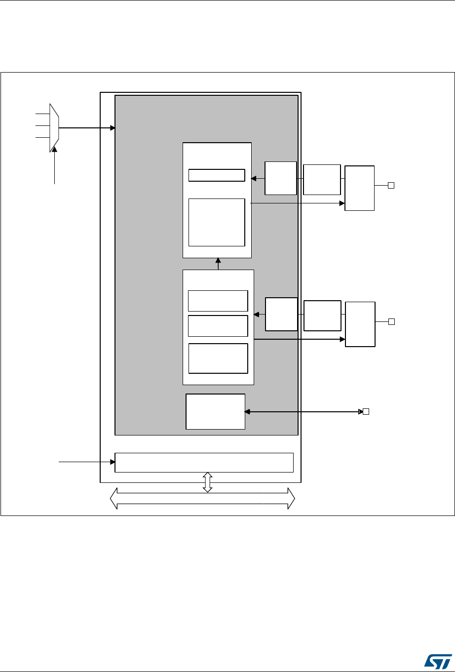
Fast-mode Plus Inter-integrated circuit (FMPI2C) interface RM0401
520/766 DocID027812 Rev 2
22.4.1 FMPI2C block diagram
The block diagram of the FMPI2C interface is shown in Figure 176.
Figure 176. FMPI2C block diagram
The FMPI2C is clocked by an independent clock source which allows to the FMPI2C to
operate independently from the PCLK frequency.
This independent clock source can be selected for either of the following clock sources:
•PCLK1: APB1 clock (default value)
•HSI: high speed internal oscillator
•SYSCLK: system clock
Refer to Section 5: Reset and clock control (RCC) for more details.
+6,
6<6&/.
5&&B)03,&[6(/
IURPUHVHWDQG
FORFN
FRQWUROOHU
)03,&&/.
60%86
3(&
JHQHUDWLRQ
FKHFN
6KLIWUHJLVWHU
'DWDFRQWURO
60%XV
7LPHRXW
FKHFN
&ORFNFRQWURO
0DVWHUFORFN
JHQHUDWLRQ
6ODYHFORFN
VWUHWFKLQJ
60%XV$OHUW
FRQWURO
VWDWXV
'LJLWDO
QRLVH
ILOWHU )03,&[B6&/
)03,&[B60%$
3&/. 5HJLVWHUV
$3%EXV
*3,2
ORJLF
$QDORJ
QRLVH
ILOWHU
'LJLWDO
QRLVH
ILOWHU )03,&[B6'$
*3,2
ORJLF
$QDORJ
QRLVH
ILOWHU
$3%
06Y9

DocID027812 Rev 2 521/766
RM0401 Fast-mode Plus Inter-integrated circuit (FMPI2C) interface
586
22.4.2 FMPI2C clock requirements
The FMPI2C kernel is clocked by FMPI2CCLK.
The FMPI2CCLK period tI2CCLK must respect the following conditions:
tI2CCLK < (tLOW - tfilters ) / 4 and tI2CCLK < tHIGH
with:
tLOW: SCL low time and tHIGH : SCL high time
tfilters: when enabled, sum of the delays brought by the analog filter and by the digital filter.
Analog filter delay is maximum 260 ns. Digital filter delay is DNF x tI2CCLK.
The PCLK clock period tPCLK must respect the following condition:
tPCLK < 4/3 tSCL
with tSCL: SCL period
Caution: When the FMPI2C kernel is clocked by PCLK. PCLK must respect the conditions for
tI2CCLK.
22.4.3 Mode selection
The interface can operate in one of the four following modes:
•Slave transmitter
•Slave receiver
•Master transmitter
•Master receiver
By default, it operates in slave mode. The interface automatically switches from slave to
master when it generates a START condition, and from master to slave if an arbitration loss
or a STOP generation occurs, allowing multimaster capability.
Communication flow
In Master mode, the FMPI2C interface initiates a data transfer and generates the clock
signal. A serial data transfer always begins with a START condition and ends with a STOP
condition. Both START and STOP conditions are generated in master mode by software.
In Slave mode, the interface is capable of recognizing its own addresses (7 or 10-bit), and
the General Call address. The General Call address detection can be enabled or disabled
by software. The reserved SMBus addresses can also be enabled by software.
Data and addresses are transferred as 8-bit bytes, MSB first. The first byte(s) following the
START condition contain the address (one in 7-bit mode, two in 10-bit mode). The address
is always transmitted in Master mode.
A 9th clock pulse follows the 8 clock cycles of a byte transfer, during which the receiver must
send an acknowledge bit to the transmitter. Refer to the following figure.
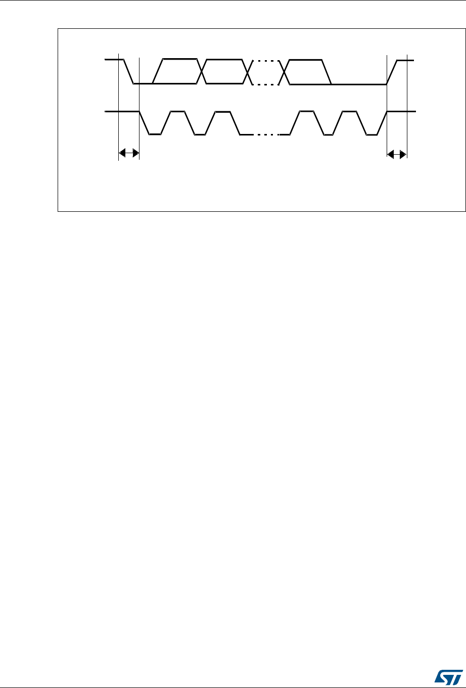
Fast-mode Plus Inter-integrated circuit (FMPI2C) interface RM0401
522/766 DocID027812 Rev 2
Figure 177. I2C bus protocol
Acknowledge can be enabled or disabled by software. The FMPI2C interface addresses can
be selected by software.
069
6'$
6&/
6WDUW
FRQGLWLRQ
6WRS
FRQGLWLRQ
06% $&.

DocID027812 Rev 2 523/766
RM0401 Fast-mode Plus Inter-integrated circuit (FMPI2C) interface
586
22.4.4 FMPI2C initialization
Enabling and disabling the peripheral
The FMPI2C peripheral clock must be configured and enabled in the clock controller (refer
to Section 5: Reset and clock control (RCC)).
Then the FMPI2C can be enabled by setting the PE bit in the FMPI2C_CR1 register.
When the FMPI2C is disabled (PE=0), the I2C performs a software reset. Refer to
Section 22.4.5: Software reset for more details.
Noise filters
Before enabling the FMPI2C peripheral by setting the PE bit in FMPI2C_CR1 register, the
user must configure the noise filters, if needed. By default, an analog noise filter is present
on the SDA and SCL inputs. This analog filter is compliant with the I2C specification which
requires the suppression of spikes with a pulse width up to 50 ns in Fast-mode and Fast-
mode Plus. The user can disable this analog filter by setting the ANFOFF bit, and/or select a
digital filter by configuring the DNF[3:0] bit in the FMPI2C_CR1 register.
When the digital filter is enabled, the level of the SCL or the SDA line is internally changed
only if it remains stable for more than DNF x FMPI2CCLK periods. This allows to suppress
spikes with a programmable length of 1 to 15 FMPI2CCLK periods.
Caution: Changing the filter configuration is not allowed when the FMPI2C is enabled.
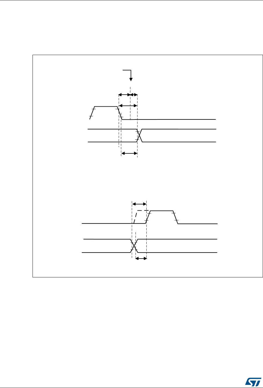
Fast-mode Plus Inter-integrated circuit (FMPI2C) interface RM0401
524/766 DocID027812 Rev 2
FMPI2C timings
The timings must be configured in order to guarantee a correct data hold and setup time,
used in master and slave modes. This is done by programming the PRESC[3:0],
SCLDEL[3:0] and SDADEL[3:0] bits in the FMPI2C_TIMINGR register.
Figure 178. Setup and hold timings
•When the SCL falling edge is internally detected, a delay is inserted before sending
SDA output. This delay is tSDADEL = SDADEL x tPRESC + tI2CCLK where tPRESC = (PRESC+1)
x tI2CCLK.
TSDADEL impacts the hold time tHD;DAT.
The total SDA output delay is:
tSYNC1 + {[SDADEL x (PRESC+1) + 1] x tI2CCLK }
06Y9
W6<1&
6&/IDOOLQJHGJHLQWHUQDO
GHWHFWLRQ
6'$'(/6&/VWUHWFKHGORZE\WKH,&
6'$RXWSXWGHOD\
6&/
6'$
d,K>d/D
W+''$7
6&/'(/
6&/VWUHWFKHGORZE\WKH,&
6&/
6'$
d^dhWd/D
W6867$
'DWDKROGWLPHLQFDVHRIWUDQVPLVVLRQWKHGDWDLVVHQWRQ6'$RXWSXWDIWHU
WKH6'$'(/GHOD\LILWLVDOUHDG\DYDLODEOHLQ,&B7;'5
'DWDVHWXSWLPHLQFDVHRIWUDQVPLVVLRQWKH6&/'(/FRXQWHUVWDUWV
ZKHQWKHGDWDLVVHQWRQ6'$RXWSXW

DocID027812 Rev 2 525/766
RM0401 Fast-mode Plus Inter-integrated circuit (FMPI2C) interface
586
tSYNC1 duration depends on these parameters:
– SCL falling slope
– When enabled, input delay brought by the analog filter: tAF(min) < tAF < tAF(max) ns.
– When enabled, input delay brought by the digital filter: tDNF = DNF x tI2CCLK
– Delay due to SCL synchronization to FMPI2CCLK clock (2 to 3 FMPI2CCLK
periods)
In order to bridge the undefined region of the SCL falling edge, the user must program
SDADEL in such a way that:
{tf (max) +tHD;DAT (min) -tAF(min) - [(DNF +3) x tI2CCLK]} / {(PRESC +1) x tI2CCLK } ≤ SDADEL
SDADEL ≤ {tHD;DAT (max) -tAF(max) - [(DNF+4) x tI2CCLK]} / {(PRESC +1) x tI2CCLK }
Note: tAF(min) / tAF(max) are part of the equation only when the analog filter is enabled. Refer to
device datasheet for tAF values.
The maximum tHD;DAT could be 3.45 µs, 0.9 µs and 0.45 µs for Standard-mode, Fast-mode
and Fast-mode Plus, but must be less than the maximum of tVD;DAT by a transition time.
This maximum must only be met if the device does not stretch the LOW period (tLOW) of the
SCL signal. If the clock stretches the SCL, the data must be valid by the set-up time before
it releases the clock.
The SDA rising edge is usually the worst case, so in this case the previous equation
becomes:
SDADEL ≤ {tVD;DAT (max) -tr (max) -260 ns - [(DNF+4) x tI2CCLK]} / {(PRESC +1) x tI2CCLK }.
Note: This condition can be violated when NOSTRETCH=0, because the device stretches SCL
low to guarantee the set-up time, according to the SCLDEL value.
Refer to Table 81: I2C-SMBUS specification data setup and hold times for tf, tr, tHD;DAT and
tVD;DAT standard values.
•After tSDADEL delay, or after sending SDA output in case the slave had to stretch the
clock because the data was not yet written in I2C_TXDR register, SCL line is kept at
low level during the setup time. This setup time is tSCLDEL = (SCLDEL+1) x tPRESC where
tPRESC = (PRESC+1) x tI2CCLK.
tSCLDEL impacts the setup time tSU;DAT .
In order to bridge the undefined region of the SDA transition (rising edge usually worst
case), the user must program SCLDEL in such a way that:
{[tr (max) + tSU;DAT (min)] / [(PRESC+1)] x tI2CCLK]} - 1 <= SCLDEL
Refer to Table 81: I2C-SMBUS specification data setup and hold times for tr and tSU;DAT
standard values.
The SDA and SCL transition time values to be used are the ones in the application. Using
the maximum values from the standard increases the constraints for the SDADEL and
SCLDEL calculation, but ensures the feature whatever the application.
Note: At every clock pulse, after SCL falling edge detection, the I2C master or slave stretches SCL
low during at least [(SDADEL+SCLDEL+1) x (PRESC+1) + 1] x tI2CCLK, in both transmission
and reception modes. In transmission mode, in case the data is not yet written in I2C_TXDR
when SDADEL counter is finished, the I2C keeps on stretching SCL low until the next data
is written. Then new data MSB is sent on SDA output, and SCLDEL counter starts,
continuing stretching SCL low to guarantee the data setup time.

Fast-mode Plus Inter-integrated circuit (FMPI2C) interface RM0401
526/766 DocID027812 Rev 2
If NOSTRETCH=1 in slave mode, the SCL is not stretched. Consequently the SDADEL
must be programmed in such a way to guarantee also a sufficient setup time.

DocID027812 Rev 2 527/766
RM0401 Fast-mode Plus Inter-integrated circuit (FMPI2C) interface
586
Additionally, in master mode, the SCL clock high and low levels must be configured by
programming the PRESC[3:0], SCLH[7:0] and SCLL[7:0] bits in the FMPI2C_TIMINGR
register.
•When the SCL falling edge is internally detected, a delay is inserted before releasing
the SCL output. This delay is tSCLL = (SCLL+1) x tPRESC where tPRESC = (PRESC+1) x
tI2CCLK.
tSCLL impacts the SCL low time tLOW .
•When the SCL rising edge is internally detected, a delay is inserted before forcing the
SCL output to low level. This delay is tSCLH = (SCLH+1) x tPRESC where tPRESC =
(PRESC+1) x tI2CCLK. tSCLH impacts the SCL high time tHIGH .
Refer to section : FMPI2C master initialization for more details.
Caution: Changing the timing configuration is not allowed when the FMPI2C is enabled.
The FMPI2C slave NOSTRETCH mode must also be configured before enabling the
peripheral. Refer to : FMPI2C slave initialization for more details.
Caution: Changing the NOSTRETCH configuration is not allowed when the FMPI2C is enabled.
Table 81. I2C-SMBUS specification data setup and hold times
Symbol Parameter
Standard-mode
(Sm)
Fast-mode
(Fm)
Fast-mode Plus
(Fm+) SMBUS
Unit
Min. Max Min. Max Min. Max Min. Max
tHD;DAT Data hold time 0-0-0 -0.3-
µs
tVD;DAT Data valid time - 3.45 - 0.9 - 0.45 - -
tSU;DAT Data setup time 250 - 100 50 250
ns
tr
Rise time of both
SDA and SCL
signals
- 1000 300 - 120 - 1000
tf
Fall time of both
SDA and SCL
signals
- 300 300 - 120 - 300
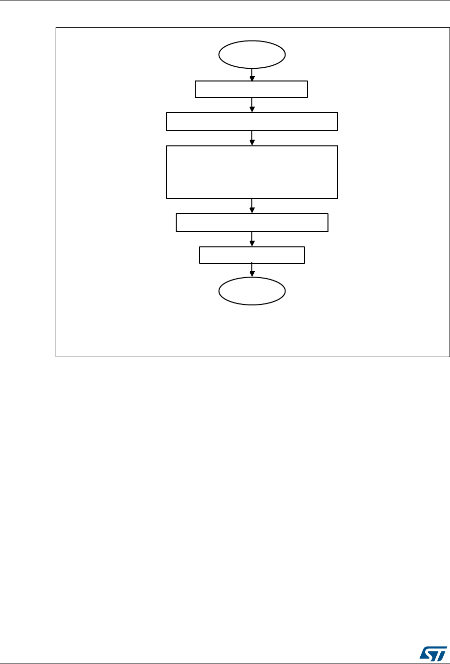
Fast-mode Plus Inter-integrated circuit (FMPI2C) interface RM0401
528/766 DocID027812 Rev 2
Figure 179. FMPI2C initialization flowchart
22.4.5 Software reset
A software reset can be performed by clearing the PE bit in the FMPI2C_CR1 register. In
that case FMPI2C lines SCL and SDA are released. Internal states machines are reset and
communication control bits, as well as status bits come back to their reset value. The
configuration registers are not impacted.
Here is the list of impacted register bits:
1. FMPI2C_CR2 register: START, STOP, NACK
2. FMPI2C_ISR register: BUSY, TXE, TXIS, RXNE, ADDR, NACKF, TCR, TC, STOPF,
BERR, ARLO, OVR
and in addition when the SMBus feature is supported:
1. FMPI2C_CR2 register: PECBYTE
2. FMPI2C_ISR register: PECERR, TIMEOUT, ALERT
PE must be kept low during at least 3 APB clock cycles in order to perform the software
reset. This is ensured by writing the following software sequence: - Write PE=0 - Check
PE=0 - Write PE=1.
D^ǀϯϱϵϲϮsϭ
&OHDU3(ELWLQ)03,&B&5
,QLWLDOVHWWLQJV
&RQILJXUH$1)2))DQG'1)>@LQ
)03,&B&5
&RQILJXUH35(6&>@
6'$'(/>@6&/'(/>@6&/+>@
6&//>@LQ)03,&B7,0,1*5
&RQILJXUH12675(7&+LQ)03,&B&5
6HW3(ELWLQ)03,&B&5
(QG
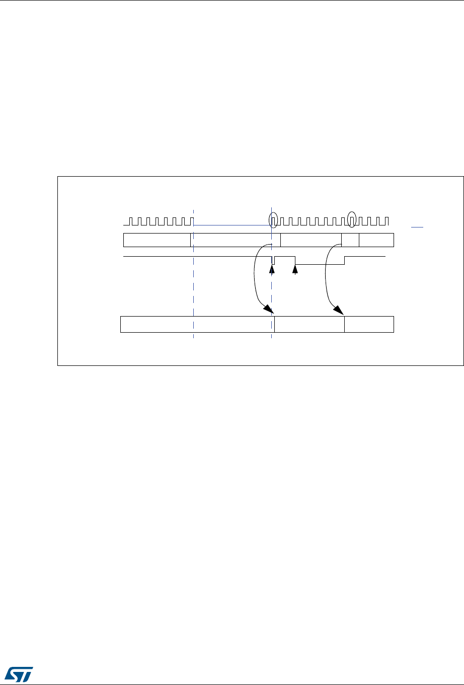
DocID027812 Rev 2 529/766
RM0401 Fast-mode Plus Inter-integrated circuit (FMPI2C) interface
586
22.4.6 Data transfer
The data transfer is managed through transmit and receive data registers and a shift
register.
Reception
The SDA input fills the shift register. After the 8th SCL pulse (when the complete data byte is
received), the shift register is copied into FMPI2C_RXDR register if it is empty (RXNE=0). If
RXNE=1, meaning that the previous received data byte has not yet been read, the SCL line
is stretched low until FMPI2C_RXDR is read. The stretch is inserted between the 8th and
9th SCL pulse (before the Acknowledge pulse).
Figure 180. Data reception
Transmission
If the FMPI2C_TXDR register is not empty (TXE=0), its content is copied into the shift
register after the 9th SCL pulse (the Acknowledge pulse). Then the shift register content is
shifted out on SDA line. If TXE=1, meaning that no data is written yet in FMPI2C_TXDR,
SCL line is stretched low until FMPI2C_TXDR is written. The stretch is done after the 9th
SCL pulse.
dždž
^ŚŝĨƚƌĞŐŝƐƚĞƌ ĚĂƚĂϭ
ĚĂƚĂϭ
dždž ĚĂƚĂϮ
ZyE
<ƉƵůƐĞ
ĚĂƚĂϬ ĚĂƚĂϮ
<ƉƵůƐĞ
dždž
&DW/ϮͺZyZ
ƌĚĚĂƚĂϭƌĚĚĂƚĂϬ
^>
ůĞŐĞŶĚ͗
^>
ƐƚƌĞƚĐŚ
D^ǀϯϱϵϳϲsϭ
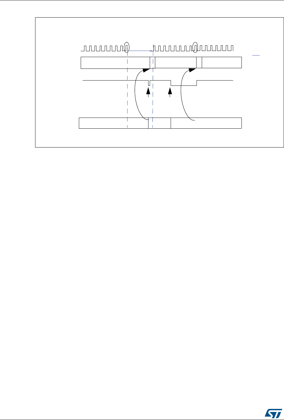
Fast-mode Plus Inter-integrated circuit (FMPI2C) interface RM0401
530/766 DocID027812 Rev 2
Figure 181. Data transmission
Hardware transfer management
The FMPI2C has a byte counter embedded in hardware in order to manage byte transfer
and to close the communication in various modes such as:
– NACK, STOP and ReSTART generation in master mode
– ACK control in slave receiver mode
– PEC generation/checking when SMBus feature is supported
The byte counter is always used in master mode. By default it is disabled in slave mode, but
it can be enabled by software by setting the SBC (Slave Byte Control) bit in the
FMPI2C_CR2 register.
The number of bytes to be transferred is programmed in the NBYTES[7:0] bit field in the
FMPI2C_CR2 register. If the number of bytes to be transferred (NBYTES) is greater than
255, or if a receiver wants to control the acknowledge value of a received data byte, the
reload mode must be selected by setting the RELOAD bit in the FMPI2C_CR2 register. In
this mode, TCR flag is set when the number of bytes programmed in NBYTES has been
transferred, and an interrupt is generated if TCIE is set. SCL is stretched as long as TCR
flag is set. TCR is cleared by software when NBYTES is written to a non-zero value.
When the NBYTES counter is reloaded with the last number of bytes, RELOAD bit must be
cleared.
When RELOAD=0 in master mode, the counter can be used in 2 modes:
•Automatic end mode (AUTOEND = ‘1’ in the FMPI2C_CR2 register). In this mode, the
master automatically sends a STOP condition once the number of bytes programmed
in the NBYTES[7:0] bit field has been transferred.
•Software end mode (AUTOEND = ‘0’ in the FMPI2C_CR2 register). In this mode,
software action is expected once the number of bytes programmed in the NBYTES[7:0]
bit field has been transferred; the TC flag is set and an interrupt is generated if the
TCIE bit is set. The SCL signal is stretched as long as the TC flag is set. The TC flag is
cleared by software when the START or STOP bit is set in the FMPI2C_CR2 register.
This mode must be used when the master wants to send a RESTART condition.
D^ǀϯϱϵϳϳsϭ
dždž
^ŚŝĨƚƌĞŐŝƐƚĞƌ
ĚĂƚĂϭ
ĚĂƚĂϭ
dždž
ĚĂƚĂϮ
dy
<ƉƵůƐĞ
ĚĂƚĂϬ ĚĂƚĂϮ
<ƉƵůƐĞ
dždž
&DW/ϮͺdyZ
ǁƌĚĂƚĂϭ ǁƌĚĂƚĂϮ
^> ůĞŐĞŶĚ͗
^>
ƐƚƌĞƚĐŚ

DocID027812 Rev 2 531/766
RM0401 Fast-mode Plus Inter-integrated circuit (FMPI2C) interface
586
Caution: The AUTOEND bit has no effect when the RELOAD bit is set.
22.4.7 FMPI2C slave mode
FMPI2C slave initialization
In order to work in slave mode, the user must enable at least one slave address. Two
registers FMPI2C_OAR1 and FMPI2C_OAR2 are available in order to program the slave
own addresses OA1 and OA2.
•OA1 can be configured either in 7-bit mode (by default) or in 10-bit addressing mode by
setting the OA1MODE bit in the FMPI2C_OAR1 register.
OA1 is enabled by setting the OA1EN bit in the FMPI2C_OAR1 register.
•If additional slave addresses are required, the 2nd slave address OA2 can be
configured. Up to 7 OA2 LSB can be masked by configuring the OA2MSK[2:0] bits in
the FMPI2C_OAR2 register. Therefore for OA2MSK configured from 1 to 6, only
OA2[7:2], OA2[7:3], OA2[7:4], OA2[7:5], OA2[7:6] or OA2[7] are compared with the
received address. As soon as OA2MSK is not equal to 0, the address comparator for
OA2 excludes the FMPI2C reserved addresses (0000 XXX and 1111 XXX), which are
not acknowledged. If OA2MSK=7, all received 7-bit addresses are acknowledged
(except reserved addresses). OA2 is always a 7-bit address.
These reserved addresses can be acknowledged if they are enabled by the specific
enable bit, if they are programmed in the FMPI2C_OAR1 or FMPI2C_OAR2 register
with OA2MSK=0.
OA2 is enabled by setting the OA2EN bit in the FMPI2C_OAR2 register.
•The General Call address is enabled by setting the GCEN bit in the FMPI2C_CR1
register.
When the FMPI2C is selected by one of its enabled addresses, the ADDR interrupt status
flag is set, and an interrupt is generated if the ADDRIE bit is set.
By default, the slave uses its clock stretching capability, which means that it stretches the
SCL signal at low level when needed, in order to perform software actions. If the master
does not support clock stretching, the FMPI2C must be configured with NOSTRETCH=1 in
the FMPI2C_CR1 register.
After receiving an ADDR interrupt, if several addresses are enabled the user must read the
ADDCODE[6:0] bits in the FMPI2C_ISR register in order to check which address matched.
DIR flag must also be checked in order to know the transfer direction.
Table 82. FMPI2C configuration table
Function SBC bit RELOAD bit AUTOEND bit
Master Tx/Rx NBYTES + STOP x 0 1
Master Tx/Rx + NBYTES + RESTART x 0 0
Slave Tx/Rx
all received bytes ACKed 0xx
Slave Rx with ACK control 1 1 x

Fast-mode Plus Inter-integrated circuit (FMPI2C) interface RM0401
532/766 DocID027812 Rev 2
Slave clock stretching (NOSTRETCH = 0)
In default mode, the FMPI2C slave stretches the SCL clock in the following situations:
•When the ADDR flag is set: the received address matches with one of the enabled
slave addresses. This stretch is released when the ADDR flag is cleared by software
setting the ADDRCF bit.
•In transmission, if the previous data transmission is completed and no new data is
written in FMPI2C_TXDR register, or if the first data byte is not written when the ADDR
flag is cleared (TXE=1). This stretch is released when the data is written to the
FMPI2C_TXDR register.
•In reception when the FMPI2C_RXDR register is not read yet and a new data reception
is completed. This stretch is released when FMPI2C_RXDR is read.
•When TCR = 1 in Slave Byte Control mode, reload mode (SBC=1 and RELOAD=1),
meaning that the last data byte has been transferred. This stretch is released when
then TCR is cleared by writing a non-zero value in the NBYTES[7:0] field.
•After SCL falling edge detection, the FMPI2C stretches SCL low during
[(SDADEL+SCLDEL+1) x (PRESC+1) + 1] x tI2CCLK.
Slave without clock stretching (NOSTRETCH = 1)
When NOSTRETCH = 1 in the FMPI2C_CR1 register, the FMPI2C slave does not stretch
the SCL signal.
•The SCL clock is not stretched while the ADDR flag is set.
•In transmission, the data must be written in the FMPI2C_TXDR register before the first
SCL pulse corresponding to its transfer occurs. If not, an underrun occurs, the OVR
flag is set in the FMPI2C_ISR register and an interrupt is generated if the ERRIE bit is
set in the FMPI2C_CR1 register. The OVR flag is also set when the first data
transmission starts and the STOPF bit is still set (has not been cleared). Therefore, if
the user clears the STOPF flag of the previous transfer only after writing the first data to
be transmitted in the next transfer, he ensures that the OVR status is provided, even for
the first data to be transmitted.
•In reception, the data must be read from the FMPI2C_RXDR register before the 9th
SCL pulse (ACK pulse) of the next data byte occurs. If not an overrun occurs, the OVR
flag is set in the FMPI2C_ISR register and an interrupt is generated if the ERRIE bit is
set in the FMPI2C_CR1 register.
Slave Byte Control Mode
In order to allow byte ACK control in slave reception mode, Slave Byte Control mode must
be enabled by setting the SBC bit in the FMPI2C_CR1 register. This is required to be
compliant with SMBus standards.
Reload mode must be selected in order to allow byte ACK control in slave reception mode
(RELOAD=1). To get control of each byte, NBYTES must be initialized to 0x1 in the ADDR
interrupt subroutine, and reloaded to 0x1 after each received byte. When the byte is
received, the TCR bit is set, stretching the SCL signal low between the 8th and 9th SCL
pulses. The user can read the data from the FMPI2C_RXDR register, and then decide to
acknowledge it or not by configuring the ACK bit in the FMPI2C_CR2 register. The SCL
stretch is released by programming NBYTES to a non-zero value: the acknowledge or not-
acknowledge is sent and next byte can be received.
NBYTES can be loaded with a value greater than 0x1, and in this case, the reception flow is
continuous during NBYTES data reception.
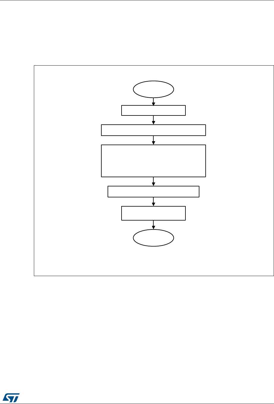
DocID027812 Rev 2 533/766
RM0401 Fast-mode Plus Inter-integrated circuit (FMPI2C) interface
586
Note: The SBC bit must be configured when the FMPI2C is disabled, or when the slave is not
addressed, or when ADDR=1.
The RELOAD bit value can be changed when ADDR=1, or when TCR=1.
Caution: Slave Byte Control mode is not compatible with NOSTRETCH mode. Setting SBC when
NOSTRETCH=1 is not allowed.
Figure 182. Slave initialization flowchart
Slave transmitter
A transmit interrupt status (TXIS) is generated when the FMPI2C_TXDR register becomes
empty. An interrupt is generated if the TXIE bit is set in the FMPI2C_CR1 register.
The TXIS bit is cleared when the FMPI2C_TXDR register is written with the next data byte
to be transmitted.
When a NACK is received, the NACKF bit is set in the FMPI2C_ISR register and an
interrupt is generated if the NACKIE bit is set in the FMPI2C_CR1 register. The slave
automatically releases the SCL and SDA lines in order to let the master perform a STOP or
a RESTART condition. The TXIS bit is not set when a NACK is received.
When a STOP is received and the STOPIE bit is set in the FMPI2C_CR1 register, the
STOPF flag is set in the FMPI2C_ISR register and an interrupt is generated. In most
applications, the SBC bit is usually programmed to ‘0’. In this case, If TXE = 0 when the
D^ǀϯϱϵϲϯsϭ
,QLWLDOVHWWLQJV
6ODYH
LQLWLDOL]DWLRQ
&OHDU^2$(12$(1`LQ)03,&B&5
&RQILJXUH^2$>@2$02'(2$(1
2$>@2$06.>@2$(1*&(1`
&RQILJXUH6%&LQ)03,&B&5
(QDEOHLQWHUUXSWVDQGRU
'0$LQ)03,&B&5
(QG
6%&PXVWEHVHWWRVXSSRUW60%XVIHDWXUHV

Fast-mode Plus Inter-integrated circuit (FMPI2C) interface RM0401
534/766 DocID027812 Rev 2
slave address is received (ADDR=1), the user can choose either to send the content of the
FMPI2C_TXDR register as the first data byte, or to flush the FMPI2C_TXDR register by
setting the TXE bit in order to program a new data byte.
In Slave Byte Control mode (SBC=1), the number of bytes to be transmitted must be
programmed in NBYTES in the address match interrupt subroutine (ADDR=1). In this case,
the number of TXIS events during the transfer corresponds to the value programmed in
NBYTES.
Caution: When NOSTRETCH=1, the SCL clock is not stretched while the ADDR flag is set, so the
user cannot flush the FMPI2C_TXDR register content in the ADDR subroutine, in order to
program the first data byte. The first data byte to be sent must be previously programmed in
the FMPI2C_TXDR register:
•This data can be the data written in the last TXIS event of the previous transmission
message.
•If this data byte is not the one to be sent, the FMPI2C_TXDR register can be flushed by
setting the TXE bit in order to program a new data byte. The STOPF bit must be
cleared only after these actions, in order to guarantee that they are executed before the
first data transmission starts, following the address acknowledge.
If STOPF is still set when the first data transmission starts, an underrun error will be
generated (the OVR flag is set).
If a TXIS event is needed, (Transmit Interrupt or Transmit DMA request), the user must
set the TXIS bit in addition to the TXE bit, in order to generate a TXIS event.
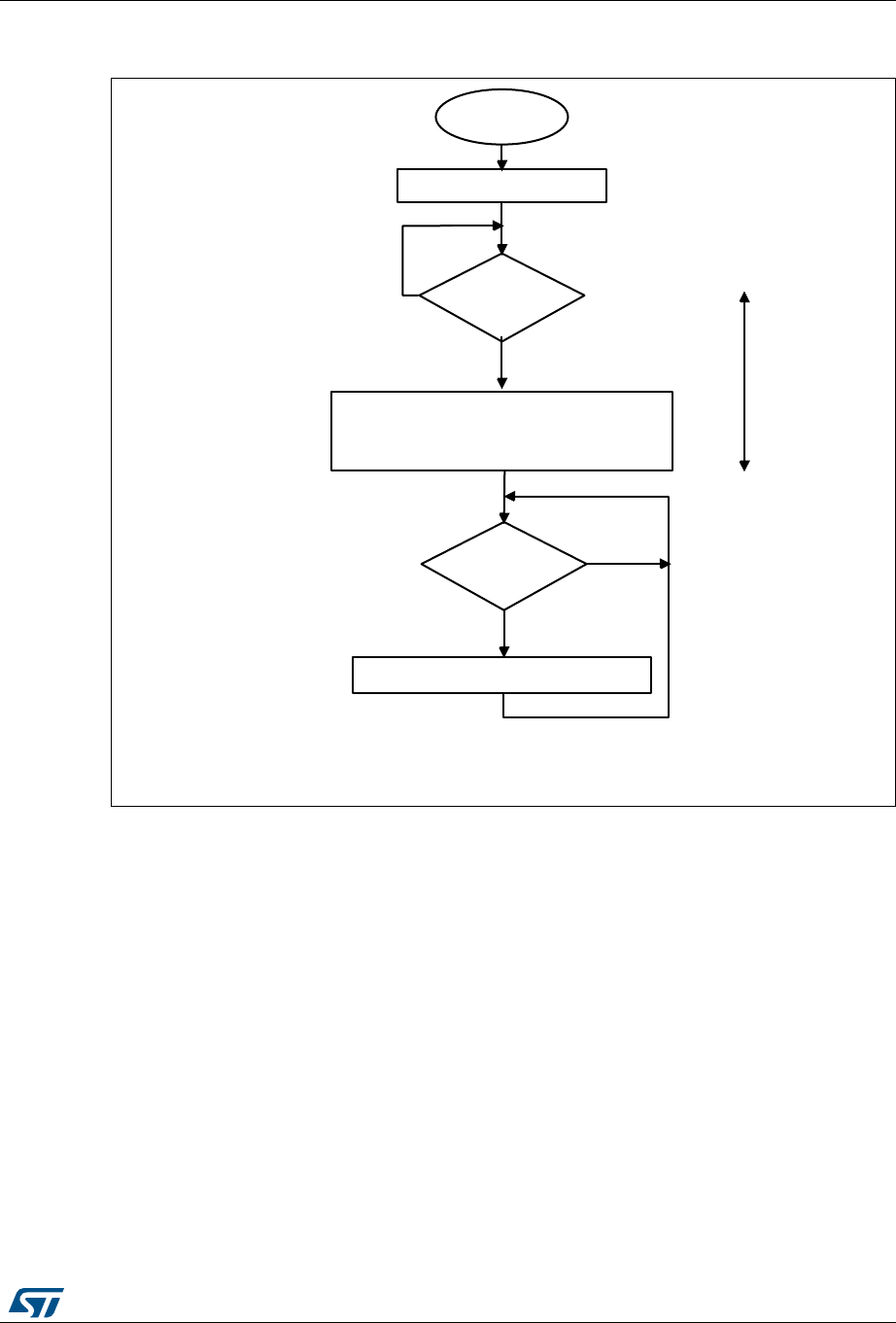
DocID027812 Rev 2 535/766
RM0401 Fast-mode Plus Inter-integrated circuit (FMPI2C) interface
586
Figure 183. Transfer sequence flowchart for FMPI2C slave transmitter,
NOSTRETCH=0
D^ǀϯϱϵϲϰsϭ
6ODYHLQLWLDOL]DWLRQ
6ODYH
WUDQVPLVVLRQ
5HDG$''&2'(DQG',5LQ)03,&B,65
2SWLRQDO6HW)03,&B,657;(
6HW)03,&B,&5$''5&)
:ULWH)03,&B7;'57;'$7$
)03,&B,65$''5
"
1R
<HV
)03,&B,657;,6
"
<HV
1R
6&/
VWUHWFKHG
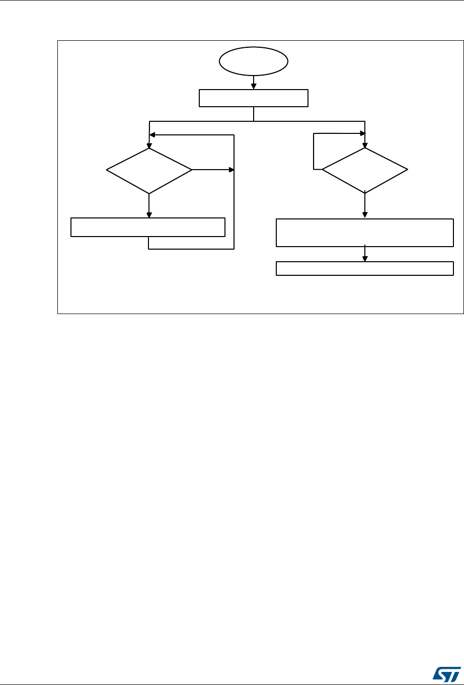
Fast-mode Plus Inter-integrated circuit (FMPI2C) interface RM0401
536/766 DocID027812 Rev 2
Figure 184. Transfer sequence flowchart for FMPI2C slave transmitter,
NOSTRETCH=1
D^ǀϯϱϵϲϱsϭ
6ODYHLQLWLDOL]DWLRQ
6ODYH
WUDQVPLVVLRQ
2SWLRQDO6HW)03,&B,657;(
DQG)03,&B,657;,6
:ULWH)03,&B7;'57;'$7$
)03,&B,656723)
"
1R
<HV
)03,&B,657;,6
"
<HV
1R
6HW)03,&B,&56723&)
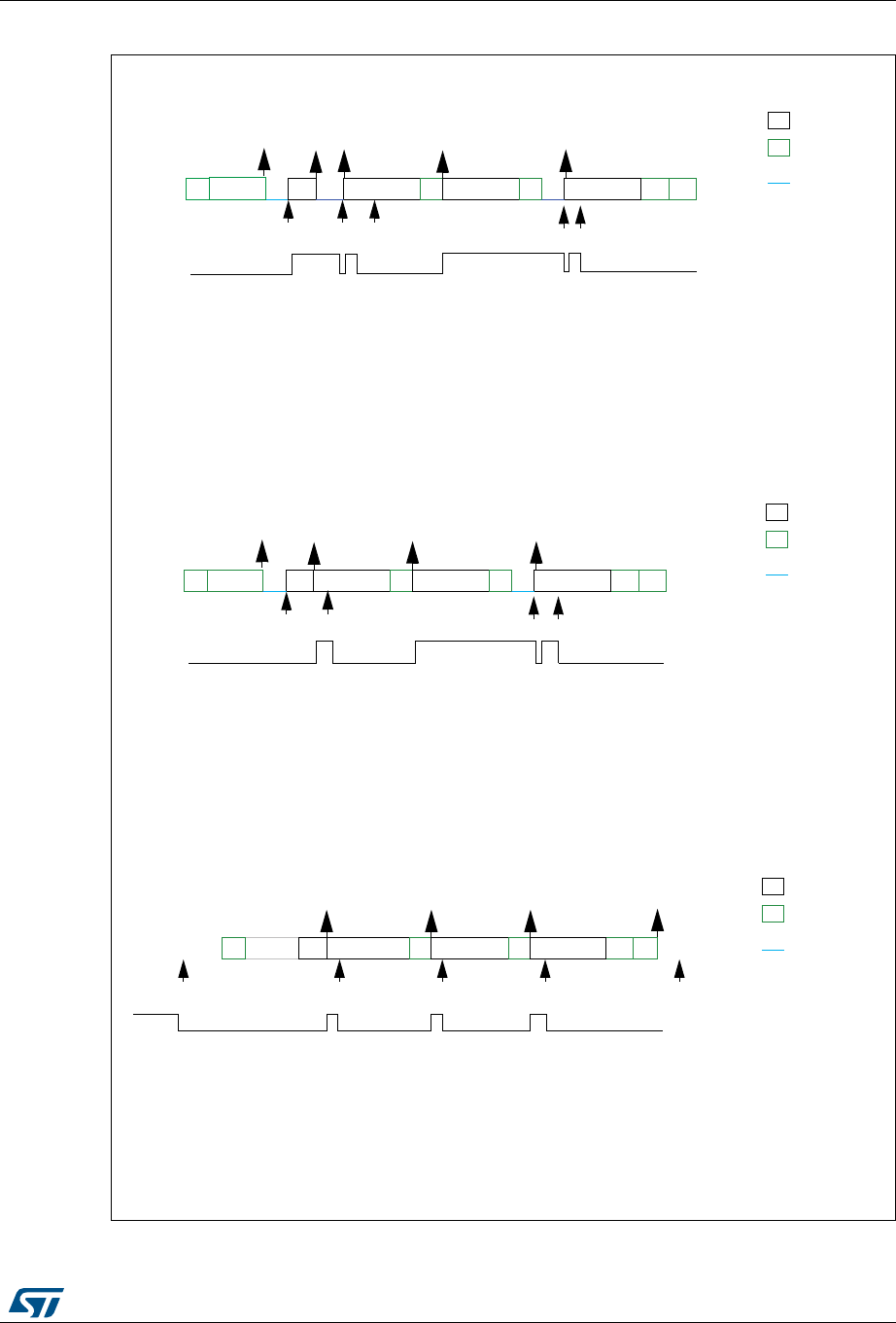
DocID027812 Rev 2 537/766
RM0401 Fast-mode Plus Inter-integrated circuit (FMPI2C) interface
586
Figure 185. Transfer bus diagrams for FMPI2C slave transmitter
069
([DPSOH)03,&VODYHWUDQVPLWWHUE\WHVZLWKVWGDWDIOXVKHG
12675(7&+
(9$''5,65FKHFN$''&2'(DQG',5VHW7;(VHW$''5&)
(97;,6,65ZUGDWD
(97;,6,65ZUGDWD
(97;,6,65ZUGDWD
(97;,6,65ZUGDWDQRWVHQW
$''5
$
7;,6
$
7;,6
1$
7;,6
7;(
3
OHJHQG
WUDQVPLVVLRQ
UHFHSWLRQ
6&/VWUHWFK
(9 (9 (9 (9
([DPSOH)03,&VODYHWUDQVPLWWHUE\WHV12675(7&+
(9ZUGDWD
(97;,6,65ZUGDWD
(97;,6,65ZUGDWD
(97;,6,65ZUGDWDQRWVHQW
(96723),65RSWLRQDOVHW7;(DQG7;,6VHW6723&)
$
7;,6 7;,6
7;(
OHJHQG
WUDQVPLVVLRQ
UHFHSWLRQ
6&/VWUHWFK
(9 (9 (9
7;,6
(9
6723)
(9
([DPSOH)03,&VODYHWUDQVPLWWHUE\WHVZLWKRXWVWGDWDIOXVK
12675(7&+
(9$''5,65FKHFN$''&2'(DQG',5VHW$''5&)
(97;,6,65ZUGDWD
(97;,6,65ZUGDWD
(97;,6,65ZUGDWDQRWVHQW
$''5 7;,6 7;,6 7;,6
7;(
OHJHQG
WUDQVPLVVLRQ
UHFHSWLRQ
6&/VWUHWFK
(9 (9 (9 (9
7;,6
(9
6 $GGUHVV GDWD $ GDWD GDWD$1$3
6 $GGUHVV $ GDWD $ GDWD $ GDWD 1$ 3
6$GGUHVV $ GDWD
GDWD
GDWD
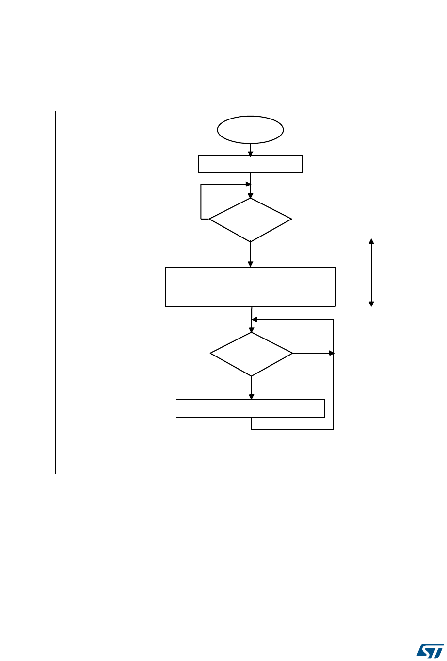
Fast-mode Plus Inter-integrated circuit (FMPI2C) interface RM0401
538/766 DocID027812 Rev 2
Slave receiver
RXNE is set in FMPI2C_ISR when the FMPI2C_RXDR is full, and generates an interrupt if
RXIE is set in FMPI2C_CR1. RXNE is cleared when FMPI2C_RXDR is read.
When a STOP is received and STOPIE is set in FMPI2C_CR1, STOPF is set in
FMPI2C_ISR and an interrupt is generated.
Figure 186. Transfer sequence flowchart for slave receiver with NOSTRETCH=0
D^ǀϯϱϵϲϲsϭ
6ODYHLQLWLDOL]DWLRQ
6ODYHUHFHSWLRQ
5HDG$''&2'(DQG',5LQ)03,&B,65
6HW)03,&B,&5$''5&)
:ULWH)03,&B5;'55;'$7$
)03,&B,65$''5
"
1R
<HV
)03,&B,655;1(
"
<HV
1R
6&/
VWUHWFKHG
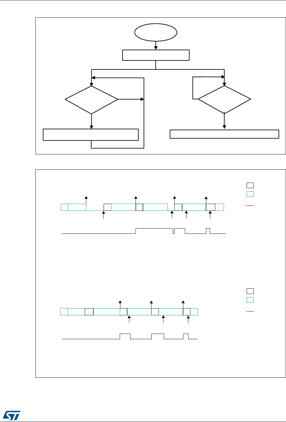
DocID027812 Rev 2 539/766
RM0401 Fast-mode Plus Inter-integrated circuit (FMPI2C) interface
586
Figure 187. Transfer sequence flowchart for slave receiver with NOSTRETCH=1
Figure 188. Transfer bus diagrams for FMPI2C slave receiver
D^ǀϯϱϵϲϳsϭ
6ODYHLQLWLDOL]DWLRQ
6ODYHUHFHSWLRQ
5HDG)03,&B5;'55;'$7$
)03,&B,656723)
"
1R
<HV
)03,&B,655;1(
"
<HV
1R
6HW)03,&B,&56723&)
069
(9$''5,65FKHFN$''&2'(DQG',5VHW$''5&)
(95;1(,65UGGDWD
(95;1(,65UGGDWD
(95;1(,65UGGDWD
$
$''5
$$
5;1(
$
5;1(
5;1(
OHJHQG
WUDQVPLVVLRQ
UHFHSWLRQ
6&/VWUHWFK
(9 (9 (9
(95;1(,65UGGDWD
(95;1(,65UGGDWD
(95;1(,65UGGDWD
(96723),65VHW6723&)
$
$$ $
5;1(
OHJHQG
WUDQVPLVVLRQ
UHFHSWLRQ
6&/VWUHWFK
5;1(
(9
([DPSOH)03,&VODYHUHFHLYHUE\WHV12675(7&+
4$GGUHVV GDWD GDWD GDWD 1
([DPSOH)03,&VODYHUHFHLYHUE\WHV12675(7&+
4$GGUHVV GDWD GDWD GDWD
(9
(9
(9
5;1( 5;1( 5;1(

Fast-mode Plus Inter-integrated circuit (FMPI2C) interface RM0401
540/766 DocID027812 Rev 2
22.4.8 FMPI2C master mode
FMPI2C master initialization
Before enabling the peripheral, the FMPI2C master clock must be configured by setting the
SCLH and SCLL bits in the FMPI2C_TIMINGR register.
A clock synchronization mechanism is implemented in order to support multi-master
environment and slave clock stretching.
In order to allow clock synchronization:
•The low level of the clock is counted using the SCLL counter, starting from the SCL low
level internal detection.
•The high level of the clock is counted using the SCLH counter, starting from the SCL
high level internal detection.
The FMPI2C detects its own SCL low level after a tSYNC1 delay depending on the SCL falling
edge, SCL input noise filters (analog + digital) and SCL synchronization to the I2CxCLK
clock. The FMPI2C releases SCL to high level once the SCLL counter reaches the value
programmed in the SCLL[7:0] bits in the FMPI2C_TIMINGR register.
The FMPI2C detects its own SCL high level after a tSYNC2 delay depending on the SCL rising
edge, SCL input noise filters (analog + digital) and SCL synchronization to I2CxCLK clock.
The FMPI2C ties SCL to low level once the SCLH counter is reached reaches the value
programmed in the SCLH[7:0] bits in the FMPI2C_TIMINGR register.
Consequently the master clock period is:
tSCL = tSYNC1 + tSYNC2 + {[(SCLH+1) + (SCLL+1)] x (PRESC+1) x tI2CCLK}
The duration of tSYNC1 depends on these parameters:
– SCL falling slope
– When enabled, input delay induced by the analog filter.
– When enabled, input delay induced by the digital filter: DNF x tI2CCLK
– Delay due to SCL synchronization with FMPI2CCLK clock (2 to 3 FMPI2CCLK
periods)
The duration of tSYNC2 depends on these parameters:
– SCL rising slope
– When enabled, input delay induced by the analog filter.
– When enabled, input delay induced by the digital filter: DNF x tI2CCLK
– Delay due to SCL synchronization with FMPI2CCLK clock (2 to 3 FMPI2CCLK
periods)
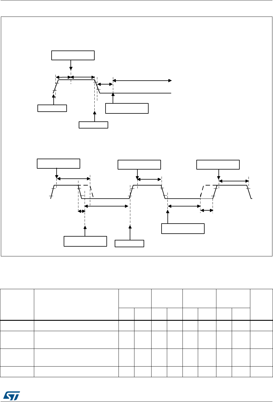
DocID027812 Rev 2 541/766
RM0401 Fast-mode Plus Inter-integrated circuit (FMPI2C) interface
586
Figure 189. Master clock generation
Caution: In order to be I2C or SMBus compliant, the master clock must respect the timings given
below:
069
W6<1&
6&/KLJKOHYHOGHWHFWHG
6&/+FRXQWHUVWDUWV
6&/+
6&/
6&/PDVWHUFORFNJHQHUDWLRQ
6&/UHOHDVHG 6&/ORZOHYHOGHWHFWHG
6&//FRXQWHUVWDUWV
6&/GULYHQORZ
6&//
W6<1&
6&/PDVWHUFORFNV\QFKURQL]DWLRQ
6&//
6&/GULYHQORZE\
DQRWKHUGHYLFH
6&/ORZOHYHOGHWHFWHG
6&//FRXQWHUVWDUWV 6&/UHOHDVHG
6&/+
6&/+
6&/KLJKOHYHOGHWHFWHG
6&/+FRXQWHUVWDUWV 6&/KLJKOHYHOGHWHFWHG
6&/+FRXQWHUVWDUWV
6&/ORZOHYHOGHWHFWHG
6&//FRXQWHUVWDUWV
6&//
6&/GULYHQORZE\
DQRWKHUGHYLFH
6&/+
6&/KLJKOHYHOGHWHFWHG
6&/+FRXQWHUVWDUWV
Table 83. I2C-SMBUS specification clock timings
Symbol Parameter
Standard-
mode (Sm)
Fast-mode
(Fm)
Fast-mode
Plus (Fm+) SMBUS
Unit
Min Max Min Max Min Max Min Max
fSCL SCL clock frequency 100 400 1000 100 kHz
tHD:STA
Hold time (repeated) START
condition 4.0 - 0.6 0.26 - 4.0 - µs
tSU:STA
Set-up time for a repeated
START condition 4.7 - 0.6 0.26 - 4.7 - µs
tSU:STO Set-up time for STOP condition 4.0 - 0.6 0.26 - 4.0 - µs

Fast-mode Plus Inter-integrated circuit (FMPI2C) interface RM0401
542/766 DocID027812 Rev 2
Note: SCLL is also used to generate the tBUF and tSU:STA timings.
SCLH is also used to generate the tHD:STA and tSU:STO timings.
Refer to Section 22.4.9: FMPI2C_TIMINGR register configuration examples for examples of
FMPI2C_TIMINGR settings vs. FMPI2CCLK frequency.
Master communication initialization (address phase)
In order to initiate the communication, the user must program the following parameters for
the addressed slave in the FMPI2C_CR2 register:
•Addressing mode (7-bit or 10-bit): ADD10
•Slave address to be sent: SADD[9:0]
•Transfer direction: RD_WRN
•In case of 10-bit address read: HEAD10R bit. HEAD10R must be configure to indicate
if the complete address sequence must be sent, or only the header in case of a
direction change.
•The number of bytes to be transferred: NBYTES[7:0]. If the number of bytes is equal to
or greater than 255 bytes, NBYTES[7:0] must initially be filled with 0xFF.
The user must then set the START bit in FMPI2C_CR2 register. Changing all the above bits
is not allowed when START bit is set.
Then the master automatically sends the START condition followed by the slave address as
soon as it detects that the bus is free (BUSY = 0) and after a delay of tBUF
.
In case of an arbitration loss, the master automatically switches back to slave mode and can
acknowledge its own address if it is addressed as a slave.
Note: The START bit is reset by hardware when the slave address has been sent on the bus,
whatever the received acknowledge value. The START bit is also reset by hardware if an
arbitration loss occurs. If the FMPI2C is addressed as a slave (ADDR=1) while the START
bit is set, the FMPI2C switches to slave mode and the START bit is cleared when the
ADDRCF bit is set.
Note: The same procedure is applied for a Repeated Start condition. In this case BUSY=1.
tBUF
Bus free time between a
STOP and START condition
4.7 - 1.3 0.5 - 4.7 - µs
tLOW Low period of the SCL clock 4.7 - 1.3 0.5 - 4.7 - µs
tHIGH Period of the SCL clock 4.0 - 0.6 0.26 - 4.0 50 µs
tr Rise time of both SDA and
SCL signals - 1000 - 300 120 - 1000 ns
tf
Fall time of both SDA and SCL
signals - 300 - 300 120 - 300 ns
Table 83. I2C-SMBUS specification clock timings (continued)
Symbol Parameter
Standard-
mode (Sm)
Fast-mode
(Fm)
Fast-mode
Plus (Fm+) SMBUS
Unit
Min Max Min Max Min Max Min Max
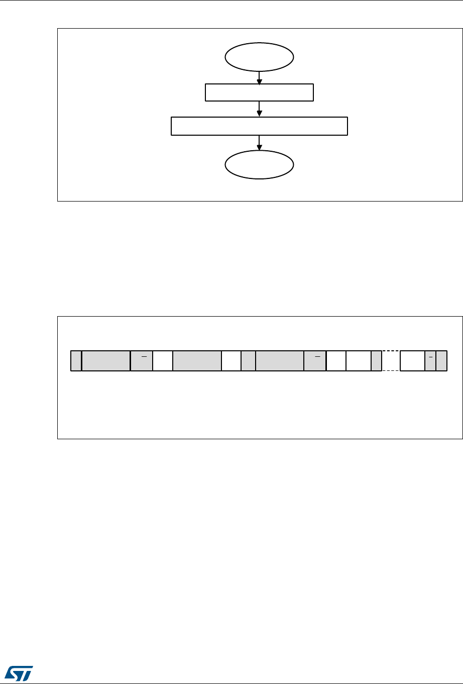
DocID027812 Rev 2 543/766
RM0401 Fast-mode Plus Inter-integrated circuit (FMPI2C) interface
586
Figure 190. Master initialization flowchart
Initialization of a master receiver addressing a 10-bit address slave
•If the slave address is in 10-bit format, the user can choose to send the complete read
sequence by clearing the HEAD10R bit in the FMPI2C_CR2 register. In this case the
master automatically sends the following complete sequence after the START bit is set:
(Re)Start + Slave address 10-bit header Write + Slave address 2nd byte + REStart +
Slave address 10-bit header Read
Figure 191. 10-bit address read access with HEAD10R=0
•If the master addresses a 10-bit address slave, transmits data to this slave and then
reads data from the same slave, a master transmission flow must be done first. Then a
repeated start is set with the 10 bit slave address configured with HEAD10R=1. In this
case the master sends this sequence: ReStart + Slave address 10-bit header Read
D^ǀϯϱϵϲϴsϭ
,QLWLDOVHWWLQJV
0DVWHU
LQLWLDOL]DWLRQ
(QDEOHLQWHUUXSWVDQGRU'0$LQ)03,&B&5
(QG
069
'$7$ $ 3$'$7$
6ODYHDGGUHVV
QGE\WH
6ODYHDGGUHVV
VWELWV
6U$$ 5:5:
6ODYHDGGUHVV
VWELWV
6 $
;;
;;
:ULWH 5HDG

Fast-mode Plus Inter-integrated circuit (FMPI2C) interface RM0401
544/766 DocID027812 Rev 2
Figure 192. 10-bit address read access with HEAD10R=1
Master transmitter
In the case of a write transfer, the TXIS flag is set after each byte transmission, after the 9th
SCL pulse when an ACK is received.
A TXIS event generates an interrupt if the TXIE bit is set in the FMPI2C_CR1 register. The
flag is cleared when the FMPI2C_TXDR register is written with the next data byte to be
transmitted.
The number of TXIS events during the transfer corresponds to the value programmed in
NBYTES[7:0]. If the total number of data bytes to be sent is greater than 255, reload mode
must be selected by setting the RELOAD bit in the FMPI2C_CR2 register. In this case,
when NBYTES data have been transferred, the TCR flag is set and the SCL line is stretched
low until NBYTES[7:0] is written to a non-zero value.
The TXIS flag is not set when a NACK is received.
•When RELOAD=0 and NBYTES data have been transferred:
– In automatic end mode (AUTOEND=1), a STOP is automatically sent.
– In software end mode (AUTOEND=0), the TC flag is set and the SCL line is
stretched low in order to perform software actions:
A RESTART condition can be requested by setting the START bit in the
FMPI2C_CR2 register with the proper slave address configuration, and number of
bytes to be transferred. Setting the START bit clears the TC flag and the START
condition is sent on the bus.
A STOP condition can be requested by setting the STOP bit in the FMPI2C_CR2
register. Setting the STOP bit clears the TC flag and the STOP condition is sent on
the bus.
•If a NACK is received: the TXIS flag is not set, and a STOP condition is automatically
sent after the NACK reception. the NACKF flag is set in the FMPI2C_ISR register, and
an interrupt is generated if the NACKIE bit is set.
069
'$7$'$7$
6ODYHDGGUHVV
QGE\WH
6ODYHDGGUHVV
VWELWV
6U
$$
5:
6ODYHDGGUHVV
VWELWV
6 $
;;
;;
:ULWH
5HDG
'$7$ $ 3$'$7$$
$$5:
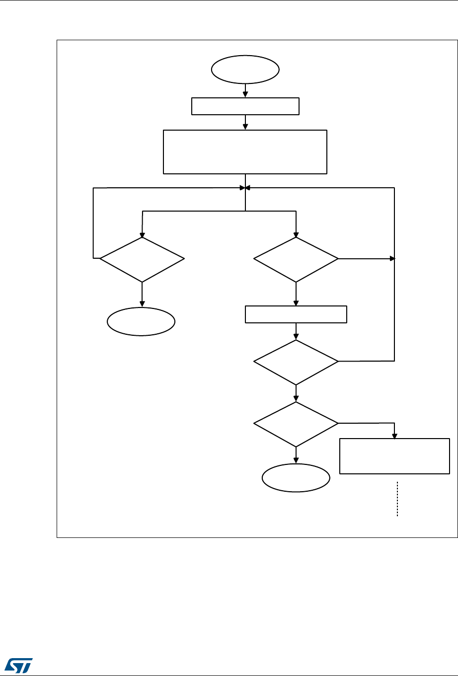
DocID027812 Rev 2 545/766
RM0401 Fast-mode Plus Inter-integrated circuit (FMPI2C) interface
586
Figure 193. Transfer sequence flowchart for FMPI2C master transmitter for N≤255
bytes
D^ǀϯϱϵϲϵsϭ
0DVWHULQLWLDOL]DWLRQ
0DVWHU
WUDQVPLVVLRQ
:ULWH)03,&B7;'5
)03,&B,657;,6
"
1R
<HV
)03,&B,651$&.)
"
<HV
1R
1%<7(6 1
$872(1' IRU5(67$57IRU6723
&RQILJXUHVODYHDGGUHVV
6HW)03,&B&567$57
(QG
1%<7(6
WUDQVPLWWHG"
)03,&B,657&
"
<HV
(QG
1R
<HV
1R 6HW)03,&B&567$57
ZLWKVODYHDGGHVV1%<7(6
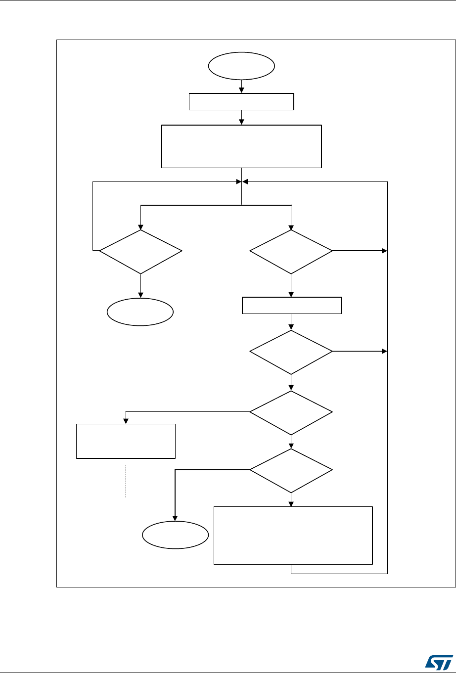
Fast-mode Plus Inter-integrated circuit (FMPI2C) interface RM0401
546/766 DocID027812 Rev 2
Figure 194. Transfer sequence flowchart for FMPI2C master transmitter for N>255
bytes
06Y9
0DVWHULQLWLDOL]DWLRQ
0DVWHU
WUDQVPLVVLRQ
:ULWH)03,&B7;'5
)03,&B,657;,6
"
1R
<HV
)03,&B,651$&.)
"
<HV
1R
1%<7(6 [))1 1
5(/2$'
&RQILJXUHVODYHDGGUHVV
6HW)03,&B&567$57
(QG
1%<7(6
WUDQVPLWWHG "
)03,&B,657&
"
<HV
(QG
1R
<HV
1R
6HW)03,&B&567$57
ZLWKVODYHDGGHVV
1%<7(6
)03,&B,657&5
"
<HV
,)1
1%<7(6 11 5(/2$'
$872(1' IRU5(67$57IRU6723
(/6(
1%<7(6 [))1 1
5(/2$'
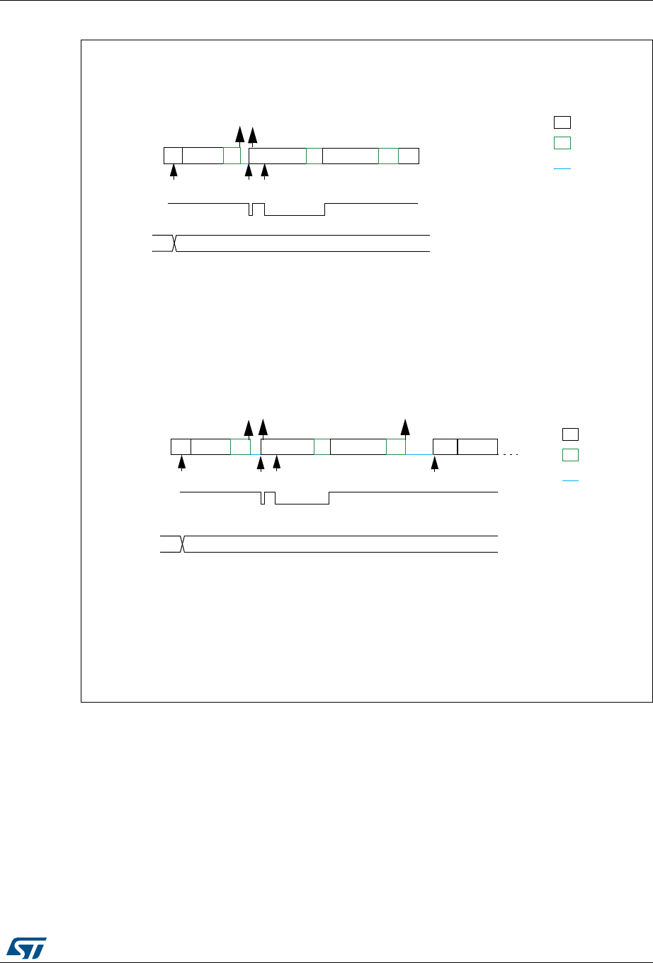
DocID027812 Rev 2 547/766
RM0401 Fast-mode Plus Inter-integrated circuit (FMPI2C) interface
586
Figure 195. Transfer bus diagrams for FMPI2C master transmitter
069
([DPSOH)03,&PDVWHUWUDQVPLWWHUE\WHVDXWRPDWLFHQGPRGH6723
,1,7SURJUDP6ODYHDGGUHVVSURJUDP1%<7(6 $872(1' VHW67$57
(97;,6,65ZUGDWD
(97;,6,65ZUGDWD
7;,67;,6
OHJHQG
WUDQVPLVVLRQ
UHFHSWLRQ
6&/VWUHWFK
(9 (9
[[
,1,7
([DPSOH)03,&PDVWHUWUDQVPLWWHUE\WHVVRIWZDUHHQGPRGH5(67$57
,1,7SURJUDP6ODYHDGGUHVVSURJUDP1%<7(6 $872(1' VHW67$57
(97;,6,65ZUGDWD
(97;,6,65ZUGDWD
(97&,65SURJUDP6ODYHDGGUHVVSURJUDP1%<7(6 1VHW67$57
7;,6 7;,6 OHJHQG
WUDQVPLVV
LRQ
UHFHSWLRQ
6&/VWUHW
FK
(9 (9
,1,7
7&
7;(
7;(
(9
1%<7(6
1%<7(6
[[
6 $GGUHVV $ GDWD $ GDWD 5H6 $GGUHVV$
6 $GGUHVV $ GDWD $ GDWD $3

Fast-mode Plus Inter-integrated circuit (FMPI2C) interface RM0401
548/766 DocID027812 Rev 2
Master receiver
In the case of a read transfer, the RXNE flag is set after each byte reception, after the 8th
SCL pulse. An RXNE event generates an interrupt if the RXIE bit is set in the FMPI2C_CR1
register. The flag is cleared when FMPI2C_RXDR is read.
If the total number of data bytes to be received is greater than 255, reload mode must be
selected by setting the RELOAD bit in the FMPI2C_CR2 register. In this case, when
NBYTES[7:0] data have been transferred, the TCR flag is set and the SCL line is stretched
low until NBYTES[7:0] is written to a non-zero value.
•When RELOAD=0 and NBYTES[7:0] data have been transferred:
–In automatic end mode (AUTOEND=1), a NACK and a STOP are automatically
sent after the last received byte.
– In software end mode (AUTOEND=0), a NACK is automatically sent after the last
received byte, the TC flag is set and the SCL line is stretched low in order to allow
software actions:
A RESTART condition can be requested by setting the START bit in the
FMPI2C_CR2 register with the proper slave address configuration, and number of
bytes to be transferred. Setting the START bit clears the TC flag and the START
condition, followed by slave address, are sent on the bus.
A STOP condition can be requested by setting the STOP bit in the FMPI2C_CR2
register. Setting the STOP bit clears the TC flag and the STOP condition is sent on
the bus.
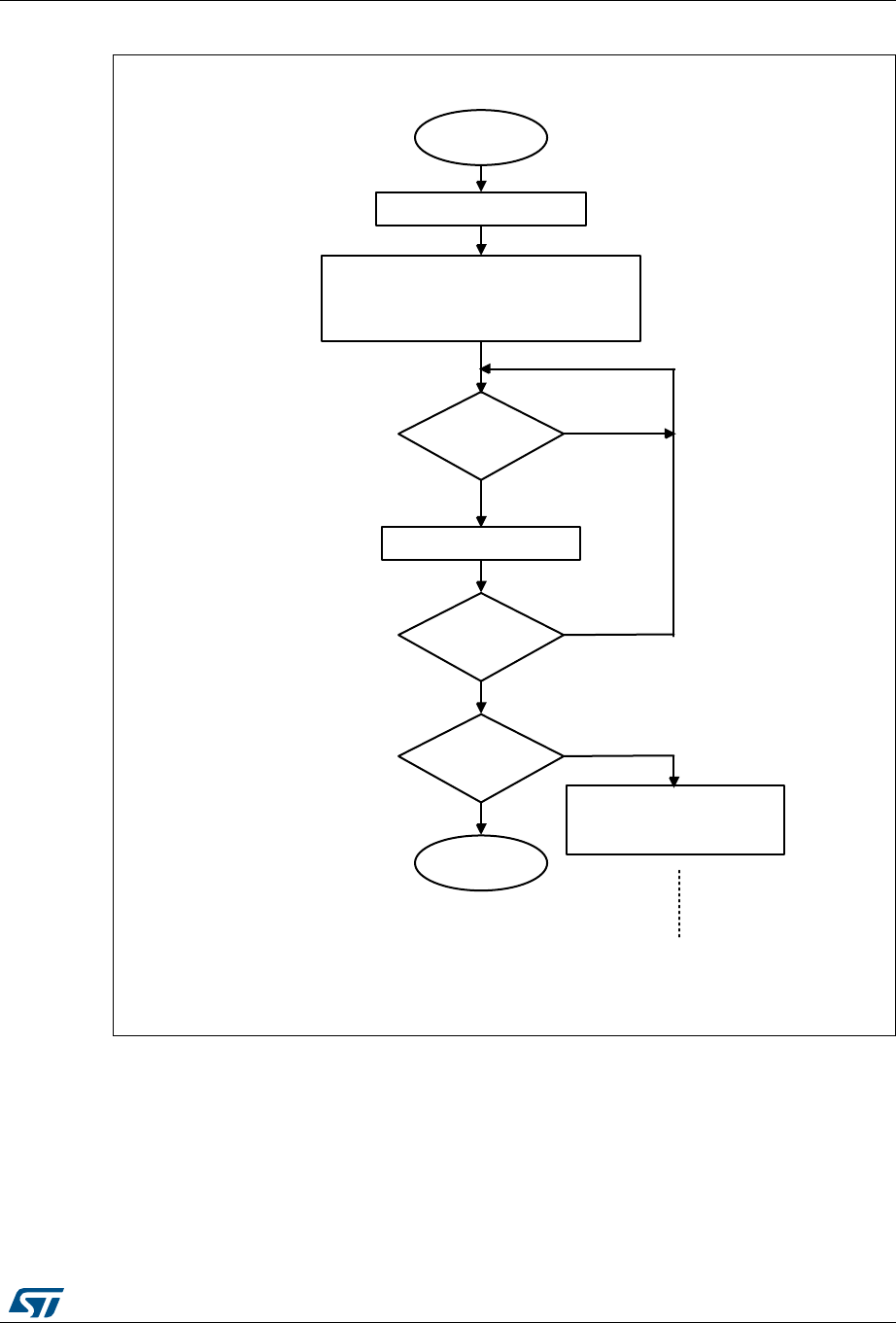
DocID027812 Rev 2 549/766
RM0401 Fast-mode Plus Inter-integrated circuit (FMPI2C) interface
586
Figure 196. Transfer sequence flowchart for FMPI2C master receiver for N≤255 bytes
D^ǀϯϱϵϳϭsϭ
0DVWHULQLWLDOL]DWLRQ
0DVWHUUHFHSWLRQ
5HDG)03,&B5;'5
)03,&B,655;1(
"
1R
<HV
1%<7(6 1
$872(1' IRU5(67$57IRU6723
&RQILJXUHVODYHDGGUHVV
6HW)03,&B&567$57
1%<7(6
UHFHLYHG"
)03,&B,657&
"
<HV
(QG
1R
<HV
1R 6HW)03,&B&567$57
ZLWKVODYHDGGHVV1%<7(6
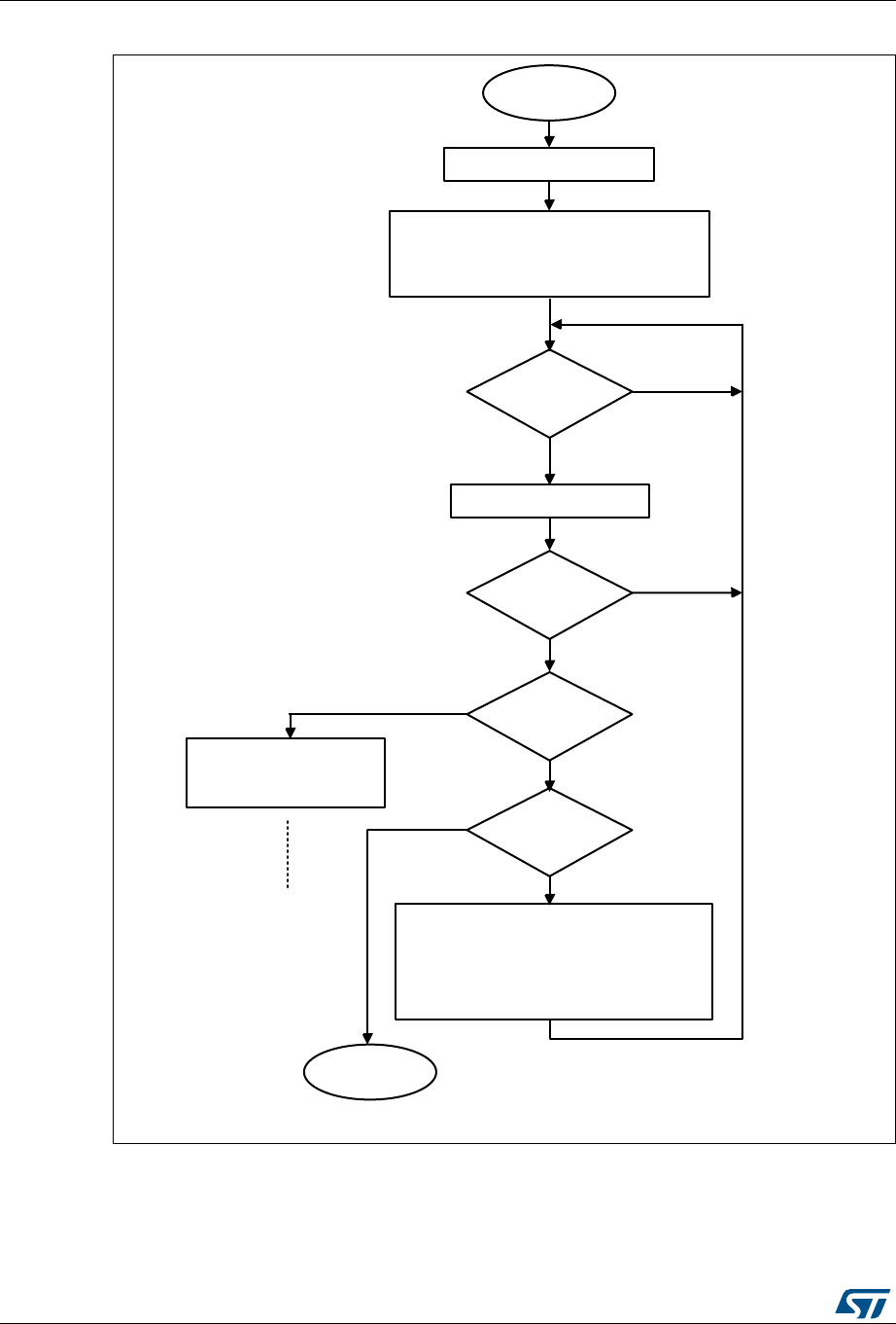
Fast-mode Plus Inter-integrated circuit (FMPI2C) interface RM0401
550/766 DocID027812 Rev 2
Figure 197. Transfer sequence flowchart for FMPI2C master receiver for N >255 bytes
D^ǀϯϱϵϳϮsϭ
0DVWHULQLWLDOL]DWLRQ
0DVWHUUHFHSWLRQ
5HDG)03,&B5;'5
)03,&B,655;1(
"
1R
<HV
1%<7(6 [))1 1
5(/2$'
&RQILJXUHVODYHDGGUHVV
6HW)03,&B&567$57
1%<7(6
UHFHLYHG"
)03,&B,657&
"
<HV
(QG
1R
<HV
1R
6HW)03,&B&567$57
ZLWKVODYHDGGHVV
1%<7(6
)03,&B,657&5
"
<HV
,)1
1%<7(6 11 5(/2$'
$872(1' IRU5(67$57IRU6723
(/6(
1%<7(6 [))1 1
5(/2$'
1R
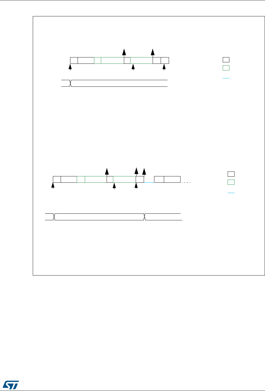
DocID027812 Rev 2 551/766
RM0401 Fast-mode Plus Inter-integrated circuit (FMPI2C) interface
586
Figure 198. Transfer bus diagrams for FMPI2C master receiver
069
([DPSOH)03,&PDVWHUUHFHLYHUE\WHVDXWRPDWLFHQGPRGH6723
,1,7SURJUDP6ODYHDGGUHVVSURJUDP1%<7(6 $872(1' VHW67$57
(95;1(,65UGGDWD
(95;1(,65UGGDWD
$
5;1( 5;1(
1%<7(6
OHJHQG
WUDQVPLVVLRQ
UHFHSWLRQ
6&/VWUHWFK
(9
[[
,1,7
([DPSOH)03,&PDVWHUUHFHLYHUE\WHVVRIWZDUHHQGPRGH5(67$57
,1,7SURJUDP6ODYHDGGUHVVSURJUDP1%<7(6 $872(1' VHW67$57
(95;1(,65UGGDWD
(95;1(,65UHDGGDWD
(97&,65SURJUDP6ODYHDGGUHVVSURJUDP1%<7(6 1VHW67$57
$
5;1( 5;1(
1%<7(6
OHJHQG
WUDQVPLVVLRQ
UHFHSWLRQ
6&/VWUHWFK
(9 (9
[[
,1,7
1
(9
7&
$GGUHVV6 $ GDWD GDWD 1$ 5H6 $GGUHVV
6 $GGUHVV $ GDWD GDWD 1$ 3

Fast-mode Plus Inter-integrated circuit (FMPI2C) interface RM0401
552/766 DocID027812 Rev 2
22.4.9 FMPI2C_TIMINGR register configuration examples
The tables below provide examples of how to program the FMPI2C_TIMINGR to obtain
timings compliant with the I2C specification. In order to get more accurate configuration
values, please refer to the application note: I2C timing configuration tool (AN4235) and the
associated software STSW-STM32126.
22.4.10 SMBus specific features
This section is relevant only when SMBus feature is supported. Please refer to Section 22.3:
FMPI2C implementation.
Introduction
The System Management Bus (SMBus) is a two-wire interface through which various
devices can communicate with each other and with the rest of the system. It is based on I2C
principles of operation. SMBus provides a control bus for system and power management
related tasks.
This peripheral is compatible with the SMBUS specification rev 2.0 (http://smbus.org).
The System Management Bus Specification refers to three types of devices.
•A slave is a device that receives or responds to a command.
•A master is a device that issues commands, generates the clocks and terminates the
transfer.
•A host is a specialized master that provides the main interface to the system’s CPU. A
host must be a master-slave and must support the SMBus host notify protocol. Only
one host is allowed in a system.
This peripheral can be configured as master or slave device, and also as a host.
SMBUS is based on I2C specification rev 2.1.
Bus protocols
There are eleven possible command protocols for any given device. A device may use any
or all of the eleven protocols to communicate. The protocols are Quick Command, Send
Byte, Receive Byte, Write Byte, Write Word, Read Byte, Read Word, Process Call, Block
Read, Block Write and Block Write-Block Read Process Call. These protocols should be
implemented by the user software.
For more details of these protocols, refer to SMBus specification version 2.0
(http://smbus.org).
Address resolution protocol (ARP)
SMBus slave address conflicts can be resolved by dynamically assigning a new unique
address to each slave device. In order to provide a mechanism to isolate each device for the
purpose of address assignment each device must implement a unique device identifier
(UDID). This 128-bit number is implemented by software.
This peripheral supports the Address Resolution Protocol (ARP). The SMBus Device
Default Address (0b1100 001) is enabled by setting SMBDEN bit in FMPI2C_CR1 register.
The ARP commands should be implemented by the user software.
Arbitration is also performed in slave mode for ARP support.

DocID027812 Rev 2 553/766
RM0401 Fast-mode Plus Inter-integrated circuit (FMPI2C) interface
586
For more details of the SMBus Address Resolution Protocol, refer to SMBus specification
version 2.0 (http://smbus.org).
Received Command and Data acknowledge control
A SMBus receiver must be able to NACK each received command or data. In order to allow
the ACK control in slave mode, the Slave Byte Control mode must be enabled by setting
SBC bit in FMPI2C_CR1 register. Refer to Slave Byte Control Mode on page 532 section for
more details.
Host Notify protocol
This peripheral supports the Host Notify protocol by setting the SMBHEN bit in the
FMPI2C_CR1 register. In this case the host will acknowledge the SMBus Host address
(0b0001 000).
When this protocol is used, the device acts as a master and the host as a slave.
SMBus alert
The SMBus ALERT optional signal is supported. A slave-only device can signal the host
through the SMBALERT# pin that it wants to talk. The host processes the interrupt and
simultaneously accesses all SMBALERT# devices through the Alert Response Address
(0b0001 100). Only the device(s) which pulled SMBALERT# low will acknowledge the Alert
Response Address.
When configured as a slave device(SMBHEN=0), the SMBA pin is pulled low by setting the
ALERTEN bit in the FMPI2C_CR1 register. The Alert Response Address is enabled at the
same time.
When configured as a host (SMBHEN=1), the ALERT flag is set in the FMPI2C_ISR register
when a falling edge is detected on the SMBA pin and ALERTEN=1. An interrupt is
generated if the ERRIE bit is set in the FMPI2C_CR1 register. When ALERTEN=0, the
ALERT line is considered high even if the external SMBA pin is low.
If the SMBus ALERT pin is not needed, the SMBA pin can be used as a standard GPIO if
ALERTEN=0.
Packet error checking
A packet error checking mechanism has been introduced in the SMBus specification to
improve reliability and communication robustness. Packet Error Checking is implemented
by appending a Packet Error Code (PEC) at the end of each message transfer. The PEC is
calculated by using the C(x) = x8 + x2 + x + 1 CRC-8 polynomial on all the message bytes
(including addresses and read/write bits).
The peripheral embeds a hardware PEC calculator and allows to send a Not Acknowledge
automatically when the received byte does not match with the hardware calculated PEC.
Timeouts
This peripheral embeds hardware timers in order to be compliant with the 3 timeouts defined
in SMBus specification version 2.0.
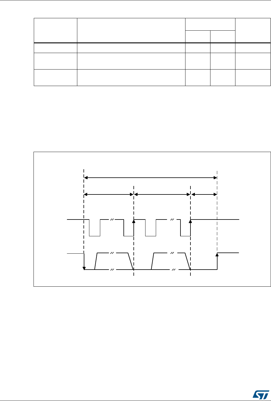
Fast-mode Plus Inter-integrated circuit (FMPI2C) interface RM0401
554/766 DocID027812 Rev 2
.
Figure 199. Timeout intervals for tLOW:SEXT
, tLOW:MEXT
.
Bus idle detection
A master can assume that the bus is free if it detects that the clock and data signals have
been high for tIDLE greater than tHIGH,MAX. (refer to Table 83: I2C-SMBUS specification clock
timings)
This timing parameter covers the condition where a master has been dynamically added to
the bus and may not have detected a state transition on the SMBCLK or SMBDAT lines. In
this case, the master must wait long enough to ensure that a transfer is not currently in
progress. The peripheral supports a hardware bus idle detection.
Table 84. SMBus timeout specifications
Symbol Parameter
Limits
Unit
Min Max
tTIMEOUT Detect clock low timeout 25 35 ms
tLOW:SEXT(1)
1. tLOW:SEXT is the cumulative time a given slave device is allowed to extend the clock cycles in one message
from the initial START to the STOP. It is possible that, another slave device or the master will also extend
the clock causing the combined clock low extend time to be greater than tLOW:SEXT
. Therefore, this
parameter is measured with the slave device as the sole target of a full-speed master.
Cumulative clock low extend time (slave
device) -25 ms
tLOW:MEXT(2)
2. tLOW:MEXT is the cumulative time a master device is allowed to extend its clock cycles within each byte of a
message as defined from START-to-ACK, ACK-to-ACK, or ACK-to-STOP. It is possible that a slave device
or another master will also extend the clock causing the combined clock low time to be greater than
tLOW:MEXT on a given byte. Therefore, this parameter is measured with a full speed slave device as the sole
target of the master.
Cumulative clock low extend time (master
device) -10 ms
069
6WDUW 6WRS
W/2:6(;7
W/2:0(;7 W/2:0(;7 W/2:0(;7
&ON$FN &ON$FN
60%&/.
60%'$7

DocID027812 Rev 2 555/766
RM0401 Fast-mode Plus Inter-integrated circuit (FMPI2C) interface
586
22.4.11 SMBus initialization
This section is relevant only when SMBus feature is supported. Please refer to Section 22.3:
FMPI2C implementation.
In addition to FMPI2C initialization, some other specific initialization must be done in order
to perform SMBus communication:
Received Command and Data Acknowledge control (Slave mode)
A SMBus receiver must be able to NACK each received command or data. In order to allow
ACK control in slave mode, the Slave Byte Control mode must be enabled by setting the
SBC bit in the FMPI2C_CR1 register. Refer to Slave Byte Control Mode on page 532 for
more details.
Specific address (Slave mode)
The specific SMBus addresses should be enabled if needed. Refer to Bus idle detection on
page 554 for more details.
•The SMBus Device Default address (0b1100 001) is enabled by setting the SMBDEN
bit in the FMPI2C_CR1 register.
•The SMBus Host address (0b0001 000) is enabled by setting the SMBHEN bit in the
FMPI2C_CR1 register.
•The Alert Response Address (0b0001100) is enabled by setting the ALERTEN bit in the
FMPI2C_CR1 register.
Packet error checking
PEC calculation is enabled by setting the PECEN bit in the FMPI2C_CR1 register. Then the
PEC transfer is managed with the help of a hardware byte counter: NBYTES[7:0] in the
FMPI2C_CR2 register. The PECEN bit must be configured before enabling the FMPI2C.
The PEC transfer is managed with the hardware byte counter, so the SBC bit must be set
when interfacing the SMBus in slave mode. The PEC is transferred after NBYTES-1 data
have been transferred when the PECBYTE bit is set and the RELOAD bit is cleared. If
RELOAD is set, PECBYTE has no effect.
Caution: Changing the PECEN configuration is not allowed when the FMPI2C is enabled.
Table 85. SMBUS with PEC configuration
Mode SBC
bit
RELOAD
bit
AUTOEND
bit
PECBYTE
bit
Master Tx/Rx NBYTES + PEC+ STOP x 0 1 1
Master Tx/Rx NBYTES + PEC + ReSTART x 0 0 1
Slave Tx/Rx with PEC 1 0 x 1

Fast-mode Plus Inter-integrated circuit (FMPI2C) interface RM0401
556/766 DocID027812 Rev 2
Timeout detection
The timeout detection is enabled by setting the TIMOUTEN and TEXTEN bits in the
FMPI2C_TIMEOUTR register. The timers must be programmed in such a way that they
detect a timeout before the maximum time given in the SMBus specification version 2.0.
•tTIMEOUT check
In order to enable the tTIMEOUT check, the 12-bit TIMEOUTA[11:0] bits must be
programmed with the timer reload value in order to check the tTIMEOUT parameter. The
TIDLE bit must be configured to ‘0’ in order to detect the SCL low level timeout.
Then the timer is enabled by setting the TIMOUTEN in the FMPI2C_TIMEOUTR
register.
If SCL is tied low for a time greater than (TIMEOUTA+1) x 2048 x tI2CCLK, the TIMEOUT
flag is set in the FMPI2C_ISR register.
Refer to Table 86: Examples of TIMEOUTA settings for various FMPI2CCLK
frequencies (max tTIMEOUT = 25 ms).
Caution: Changing the TIMEOUTA[11:0] bits and TIDLE bit configuration is not allowed when the
TIMEOUTEN bit is set.
•tLOW:SEXT and tLOW:MEXT check
Depending on if the peripheral is configured as a master or as a slave, The 12-bit
TIMEOUTB timer must be configured in order to check tLOW:SEXT for a slave and
tLOW:MEXT for a master. As the standard specifies only a maximum, the user can choose
the same value for the both.
Then the timer is enabled by setting the TEXTEN bit in the FMPI2C_TIMEOUTR
register.
If the SMBus peripheral performs a cumulative SCL stretch for a time greater than
(TIMEOUTB+1) x 2048 x tI2CCLK, and in the timeout interval described in Bus idle
detection on page 554 section, the TIMEOUT flag is set in the FMPI2C_ISR register.
Refer to Table 87: Examples of TIMEOUTB settings for various FMPI2CCLK
frequencies
Caution: Changing the TIMEOUTB configuration is not allowed when the TEXTEN bit is set.
Bus Idle detection
In order to enable the tIDLE check, the 12-bit TIMEOUTA[11:0] field must be programmed
with the timer reload value in order to obtain the tIDLE parameter. The TIDLE bit must be
configured to ‘1 in order to detect both SCL and SDA high level timeout.
Then the timer is enabled by setting the TIMOUTEN bit in the FMPI2C_TIMEOUTR register.
If both the SCL and SDA lines remain high for a time greater than (TIMEOUTA+1) x 4 x
tI2CCLK, the TIMEOUT flag is set in the FMPI2C_ISR register.
Refer to Table 88: Examples of TIMEOUTA settings for various FMPI2CCLK frequencies
(max tIDLE = 50 µs)
Caution: Changing the TIMEOUTA and TIDLE configuration is not allowed when the TIMEOUTEN is
set.
DocID027812 Rev 2 557/766
RM0401 Fast-mode Plus Inter-integrated circuit (FMPI2C) interface
586
22.4.12 SMBus: FMPI2C_TIMEOUTR register configuration examples
This section is relevant only when SMBus feature is supported. Please refer to Section 22.3:
FMPI2C implementation.
•Configuring the maximum duration of tTIMEOUT to 25 ms:
•Configuring the maximum duration of tLOW:SEXT and tLOW:MEXT to 8 ms:
•Configuring the maximum duration of tIDLE to 50 µs
22.4.13 SMBus slave mode
This section is relevant only when SMBus feature is supported. Please refer to Section 22.3:
FMPI2C implementation.
In addition to FMPI2C slave transfer management (refer to Section 22.4.7: FMPI2C slave
mode) some additional software flowcharts are provided to support SMBus.
SMBus Slave transmitter
When the IP is used in SMBus, SBC must be programmed to ‘1’ in order to allow the PEC
transmission at the end of the programmed number of data bytes. When the PECBYTE bit
is set, the number of bytes programmed in NBYTES[7:0] includes the PEC transmission. In
that case the total number of TXIS interrupts will be NBYTES-1 and the content of the
FMPI2C_PECR register is automatically transmitted if the master requests an extra byte
after the NBYTES-1 data transfer.
Table 86. Examples of TIMEOUTA settings for various FMPI2CCLK frequencies
(max tTIMEOUT = 25 ms)
fI2CCLK
TIMEOUTA[11:0]
bits
TIDLE
bit
TIMEOUTEN
bit tTIMEOUT
8 MHz 0x61 0 1 98 x 2048 x 125 ns = 25 ms
16 MHz 0xC3 0 1 196 x 2048 x 62.5 ns = 25 ms
Table 87. Examples of TIMEOUTB settings for various FMPI2CCLK frequencies
fI2CCLK
TIMEOUTB[11:0]
bits TEXTEN bit tLOW:EXT
8 MHz 0x1F 1 32 x 2048 x 125 ns = 8 ms
16 MHz 0x3F 1 64 x 2048 x 62.5 ns = 8 ms
Table 88. Examples of TIMEOUTA settings for various FMPI2CCLK frequencies
(max tIDLE = 50 µs)
fI2CCLK
TIMEOUTA[11:0]
bits TIDLE bit TIMEOUTEN
bit tTIDLE
8 MHz 0x63 1 1 100 x 4 x 125 ns = 50 µs
16 MHz 0xC7 1 1 200 x 4 x 62.5 ns = 50 µs
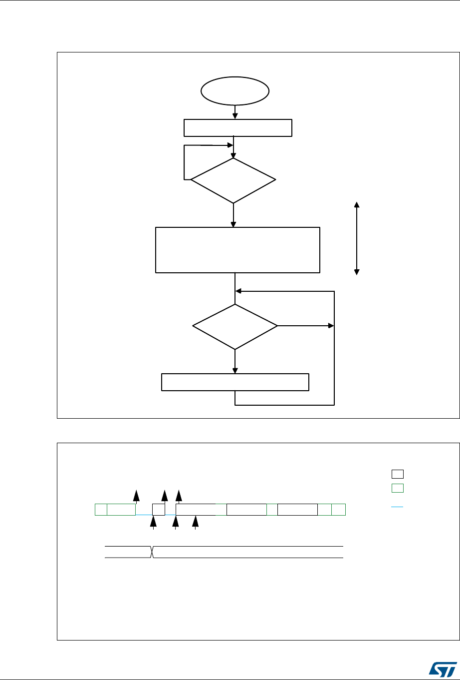
Fast-mode Plus Inter-integrated circuit (FMPI2C) interface RM0401
558/766 DocID027812 Rev 2
Caution: The PECBYTE bit has no effect when the RELOAD bit is set.
Figure 200. Transfer sequence flowchart for SMBus slave transmitter N bytes + PEC
Figure 201. Transfer bus diagrams for SMBus slave transmitter (SBC=1)
D^ǀϯϱϵϳϯsϭ
6ODYHLQLWLDOL]DWLRQ
60%XVVODYH
WUDQVPLVVLRQ
:ULWH)03,&B7;'57;'$7$
)03,&B,657;,6
"
1R
<HV
)03,&B,65$''5
"
<HV
1R
5HDG$''&2'(DQG',5LQ)03,&B,65
)03,&B&51%<7(6 1
3(&%<7(
6HW)03,&B,&5$''5&)
6&/
VWUHWFKHG
069
([DPSOH60%XVVODYHWUDQVPLWWHUE\WHV3(&
(9$''5,65FKHFN$''&2'(SURJUDP1%<7(6 VHW3(&%<7(VHW$''5&)
(97;,6,65ZUGDWD
(97;,6,65ZUGDWD
$''5
OHJHQG
WUDQVPLVVLRQ
UHFHSWLRQ
6&/VWUHWFK
(9 (9
7;,6 7;,6
(9
1%<7(6
6 $GGUHVV $ $GDWD GDWD 3(&$ 1$ 3

DocID027812 Rev 2 559/766
RM0401 Fast-mode Plus Inter-integrated circuit (FMPI2C) interface
586
SMBus Slave receiver
When the FMPI2C is used in SMBus mode, SBC must be programmed to ‘1’ in order to
allow the PEC checking at the end of the programmed number of data bytes. In order to
allow the ACK control of each byte, the reload mode must be selected (RELOAD=1). Refer
to Slave Byte Control Mode on page 532 for more details.
In order to check the PEC byte, the RELOAD bit must be cleared and the PECBYTE bit
must be set. In this case, after NBYTES-1 data have been received, the next received byte
is compared with the internal FMPI2C_PECR register content. A NACK is automatically
generated if the comparison does not match, and an ACK is automatically generated if the
comparison matches, whatever the ACK bit value. Once the PEC byte is received, it is
copied into the FMPI2C_RXDR register like any other data, and the RXNE flag is set.
In the case of a PEC mismatch, the PECERR flag is set and an interrupt is generated if the
ERRIE bit is set in the FMPI2C_CR1 register.
If no ACK software control is needed, the user can program PECBYTE=1 and, in the same
write operation, program NBYTES with the number of bytes to be received in a continuous
flow. After NBYTES-1 are received, the next received byte is checked as being the PEC.
Caution: The PECBYTE bit has no effect when the RELOAD bit is set.
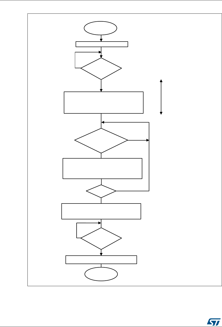
Fast-mode Plus Inter-integrated circuit (FMPI2C) interface RM0401
560/766 DocID027812 Rev 2
Figure 202. Transfer sequence flowchart for SMBus slave receiver N Bytes + PEC
D^ǀϯϱϵϳϰsϭ
6ODYHLQLWLDOL]DWLRQ
60%XVVODYH
UHFHSWLRQ
5HDG)03,&B5;'55;'$7$
)03,&B,655;1( "
)03,&B,657&5 "
1R
<HV
)03,&B,65$''5
"
<HV
1R
5HDG$''&2'(DQG',5LQ)03,&B,65
)03,&B&51%<7(6 5(/2$'
3(&%<7(
6HW)03,&B,&5$''5&)
6&/
VWUHWFKHG
5HDG)03,&B5;'55;'$7$
3URJUDP)03,&B&51$&.
)03,&B&51%<7(6
1 1
1 "
5HDG)03,&B5;'55;'$7$
3URJUDP5(/2$'
1$&. DQG1%<7(6
)03,&B,655;1(
"
1R
(QG
1R
<HV
<HV
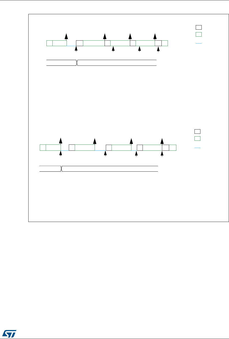
DocID027812 Rev 2 561/766
RM0401 Fast-mode Plus Inter-integrated circuit (FMPI2C) interface
586
Figure 203. Bus transfer diagrams for SMBus slave receiver (SBC=1)
This section is relevant only when SMBus feature is supported. Please refer to Section 22.3:
FMPI2C implementation.
In addition to FMPI2C master transfer management (refer to Section 22.4.8: FMPI2C
master mode) some additional software flowcharts are provided to support SMBus.
SMBus Master transmitter
When the SMBus master wants to transmit the PEC, the PECBYTE bit must be set and the
number of bytes must be programmed in the NBYTES[7:0] field, before setting the START
bit. In this case the total number of TXIS interrupts will be NBYTES-1. So if the PECBYTE
bit is set when NBYTES=0x1, the content of the FMPI2C_PECR register is automatically
transmitted.
If the SMBus master wants to send a STOP condition after the PEC, automatic end mode
should be selected (AUTOEND=1). In this case, the STOP condition automatically follows
the PEC transmission.
069
([DPSOH60%XVVODYHUHFHLYHUE\WHV3(&
$GGUHVV
6
(9$''5,65FKHFN$''&2'(DQG',5SURJUDP1%<7(6 3(&%<7( 5(/2$' VHW$''5&)
(95;1(,65UGGDWD
(95;1(,65UGGDWD
(95;1(,65UG3(&
$
GDWD
$
GDWD
$
5;1(
3(&
$
5;1(
3
OHJHQG
WUDQVPLVVLRQ
UHFHSWLRQ
6&/VWUHWFK
(9 (9 (9 (9
$''5
5;1(
1%<7(6
([DPSOH60%XVVODYHUHFHLYHUE\WHV3(&ZLWK$&.FRQWURO
5(/2$'
$GGUHVV
6
(9$''5,65FKHFN$''&2'(DQG',5SURJUDP1%<7(6 3(&%<7( 5(/2$' VHW$''5&)
(95;1(7&5,65UGGDWDSURJUDP1$&. DQG1%<7(6
(95;1(7&5,65UGGDWDSURJUDP1$&. 1%<7(6 DQG5(/2$'
(95;1(7&5,65UG3(&
$
$''5
GDWD
$
GDWD
$
5;1(7&5
3(&
$
5;1(7&5
3
OHJHQG
WUDQVPLVVLRQ
UHFHSWLRQ
6&/VWUHWFK
9(9(9(
5;1(
(9
1%<7(6
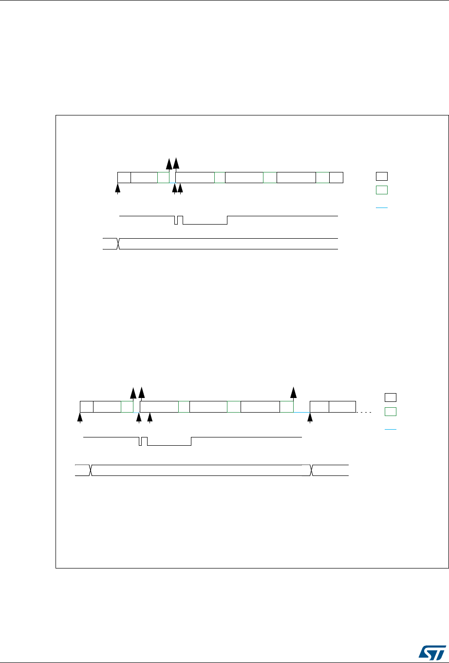
Fast-mode Plus Inter-integrated circuit (FMPI2C) interface RM0401
562/766 DocID027812 Rev 2
When the SMBus master wants to send a RESTART condition after the PEC, software
mode must be selected (AUTOEND=0). In this case, once NBYTES-1 have been
transmitted, the FMPI2C_PECR register content is transmitted and the TC flag is set after
the PEC transmission, stretching the SCL line low. The RESTART condition must be
programmed in the TC interrupt subroutine.
Caution: The PECBYTE bit has no effect when the RELOAD bit is set.
Figure 204. Bus transfer diagrams for SMBus master transmitter
SMBus Master receiver
When the SMBus master wants to receive the PEC followed by a STOP at the end of the
transfer, automatic end mode can be selected (AUTOEND=1). The PECBYTE bit must be
069
([DPSOH60%XVPDVWHUWUDQVPLWWHUE\WHV3(&DXWRPDWLFHQGPRGH6723
$GGUHVV
6
,1,7SURJUDP6ODYHDGGUHVVSURJUDP1%<7(6 $872(1' VHW3(&%<7(VHW67$57
(97;,6,65ZUGDWD
(97;,6,65ZUGDWD
$
GDWD
$
7;,6 7;,6
GDWD
$
1%<7(6
$
OHJHQG
WUDQVPLVVLRQ
UHFHSWLRQ
6&/VWUHWFK
(9
[[
,1,7
([DPSOH60%XVPDVWHUWUDQVPLWWHUE\WHV3(&VRIWZDUHHQGPRGH5(67$57
,1,7SURJUDP6ODYHDGGUHVVSURJUDP1%<7(6 $872(1' VHW3(&%<7(VHW67$57
(97;,6,65ZUGDWD
(97;,6,65ZUGDWD
(97&,65SURJUDP6ODYHDGGUHVVSURJUDP1%<7(6 1VHW67$57
1%<7(6
5VWDUW
OHJHQG
WUDQVPLVVLRQ
UHFHSWLRQ
6&/VWUHWFK
[[
$GGUHVV
1
3(&
3
(9
$
7;(
$GGUHVV
6
$
GDWD
$
7;,6 7;,6
GDWD
$
(9
,1,7
3(&
(9
7&
(9

DocID027812 Rev 2 563/766
RM0401 Fast-mode Plus Inter-integrated circuit (FMPI2C) interface
586
set and the slave address must be programmed, before setting the START bit. In this case,
after NBYTES-1 data have been received, the next received byte is automatically checked
versus the FMPI2C_PECR register content. A NACK response is given to the PEC byte,
followed by a STOP condition.
When the SMBus master receiver wants to receive the PEC byte followed by a RESTART
condition at the end of the transfer, software mode must be selected (AUTOEND=0). The
PECBYTE bit must be set and the slave address must be programmed, before setting the
START bit. In this case, after NBYTES-1 data have been received, the next received byte is
automatically checked versus the FMPI2C_PECR register content. The TC flag is set after
the PEC byte reception, stretching the SCL line low. The RESTART condition can be
programmed in the TC interrupt subroutine.
Caution: The PECBYTE bit has no effect when the RELOAD bit is set.
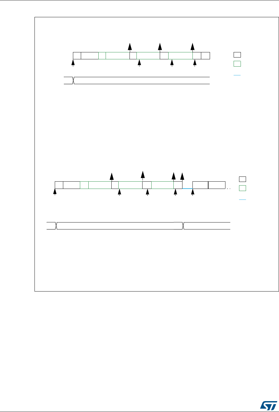
Fast-mode Plus Inter-integrated circuit (FMPI2C) interface RM0401
564/766 DocID027812 Rev 2
Figure 205. Bus transfer diagrams for SMBus master receiver
22.4.14 Error conditions
The following are the error conditions which may cause communication to fail.
Bus error (BERR)
A bus error is detected when a START or a STOP condition is detected and is not located
after a multiple of 9 SCL clock pulses. A START or a STOP condition is detected when a
SDA edge occurs while SCL is high.
The bus error flag is set only if the FMPI2C is involved in the transfer as master or
addressed slave (i.e not during the address phase in slave mode).
069
([DPSOH60%XVPDVWHUUHFHLYHUE\WHV3(&DXWRPDWLFHQGPRGH6723
$GGUHVV
6
,1,7SURJUDP6ODYHDGGUHVVSURJUDP1%<7(6 $872(1' VHW3(&%<7(VHW67$57
(95;1(,65UGGDWD
(95;1(,65UGGDWD
(95;1(,65UG3(&
$
GDWD
$
5;1( 5;1(
GDWD
$
1%<7(6
1$
OHJHQG
WUDQVPLVVLRQ
UHFHSWLRQ
6&/VWUHWFK
9(9(
[[
,1,7
([DPSOH60%XVPDVWHUUHFHLYHUE\WHV3(&VRIWZDUHHQGPRGH5(67$57
$GGUHVV
6
,1,7SURJUDP6ODYHDGGUHVVSURJUDP1%<7(6 $872(1' VHW3(&%<7(VHW67$57
(95;1(,65UGGDWD
(95;1(,65UGGDWD
(95;1(,65UHDG3(&
(97&,65SURJUDP6ODYHDGGUHVVSURJUDP1%<7(6 1VHW67$57
$
GDWD
$
5;1( 5;1(
GDWD
$
1%<7(6
5HVWDUW
OHJHQG
WUDQVPLVVLRQ
UHFHSWLRQ
6&/VWUHWFK
(9 (9
[[
,1,7
$GGUHVV
1
3(&
3
5;1(
(9
1$
3(&
5;1(
(9
7&
(9

DocID027812 Rev 2 565/766
RM0401 Fast-mode Plus Inter-integrated circuit (FMPI2C) interface
586
In case of a misplaced START or RESTART detection in slave mode, the FMPI2C enters
address recognition state like for a correct START condition.
When a bus error is detected, the BERR flag is set in the FMPI2C_ISR register, and an
interrupt is generated if the ERRIE bit is set in the FMPI2C_CR1 register.
Arbitration lost (ARLO)
An arbitration loss is detected when a high level is sent on the SDA line, but a low level is
sampled on the SCL rising edge.
•In master mode, arbitration loss is detected during the address phase, data phase and
data acknowledge phase. In this case, the SDA and SCL lines are released, the
START control bit is cleared by hardware and the master switches automatically to
slave mode.
•In slave mode, arbitration loss is detected during data phase and data acknowledge
phase. In this case, the transfer is stopped, and the SCL and SDA lines are released.
When an arbitration loss is detected, the ARLO flag is set in the FMPI2C_ISR register, and
an interrupt is generated if the ERRIE bit is set in the FMPI2C_CR1 register.
Overrun/underrun error (OVR)
An overrun or underrun error is detected in slave mode when NOSTRETCH=1 and:
•In reception when a new byte is received and the RXDR register has not been read yet.
The new received byte is lost, and a NACK is automatically sent as a response to the
new byte.
•In transmission:
– When STOPF=1 and the first data byte should be sent. The content of the
FMPI2C_TXDR register is sent if TXE=0, 0xFF if not.
– When a new byte should be sent and the FMPI2C_TXDR register has not been
written yet, 0xFF is sent.
When an overrun or underrun error is detected, the OVR flag is set in the FMPI2C_ISR
register, and an interrupt is generated if the ERRIE bit is set in the FMPI2C_CR1 register.
Packet Error Checking Error (PECERR)
This section is relevant only when the SMBus feature is supported. Please refer to
Section 22.3: FMPI2C implementation.
A PEC error is detected when the received PEC byte does not match with the
FMPI2C_PECR register content. A NACK is automatically sent after the wrong PEC
reception.
When a PEC error is detected, the PECERR flag is set in the FMPI2C_ISR register, and an
interrupt is generated if the ERRIE bit is set in the FMPI2C_CR1 register.

Fast-mode Plus Inter-integrated circuit (FMPI2C) interface RM0401
566/766 DocID027812 Rev 2
Timeout Error (TIMEOUT)
This section is relevant only when the SMBus feature is supported. Please refer to
Section 22.3: FMPI2C implementation.
A timeout error occurs for any of these conditions:
•TIDLE=0 and SCL remained low for the time defined in the TIMEOUTA[11:0] bits: this is
used to detect a SMBus timeout.
•TIDLE=1 and both SDA and SCL remained high for the time defined in the TIMEOUTA
[11:0] bits: this is used to detect a bus idle condition.
•Master cumulative clock low extend time reached the time defined in the
TIMEOUTB[11:0] bits (SMBus tLOW:MEXT parameter)
•Slave cumulative clock low extend time reached the time defined in TIMEOUTB[11:0]
bits (SMBus tLOW:SEXT parameter)
When a timeout violation is detected in master mode, a STOP condition is automatically
sent.
When a timeout violation is detected in slave mode, SDA and SCL lines are automatically
released.
When a timeout error is detected, the TIMEOUT flag is set in the FMPI2C_ISR register, and
an interrupt is generated if the ERRIE bit is set in the FMPI2C_CR1 register.
Alert (ALERT)
This section is relevant only when the SMBus feature is supported. Please refer to
Section 22.3: FMPI2C implementation.
The ALERT flag is set when the FMPI2C interface is configured as a Host (SMBHEN=1),
the alert pin detection is enabled (ALERTEN=1) and a falling edge is detected on the SMBA
pin. An interrupt is generated if the ERRIE bit is set in the FMPI2C_CR1 register.
22.4.15 DMA requests
Transmission using DMA
DMA (Direct Memory Access) can be enabled for transmission by setting the TXDMAEN bit
in the FMPI2C_CR1 register. Data is loaded from an SRAM area configured using the DMA
peripheral (see Section 8: Direct memory access controller (DMA) on page 161) to the
FMPI2C_TXDR register whenever the TXIS bit is set.
Only the data are transferred with DMA.
•In master mode: the initialization, the slave address, direction, number of bytes and
START bit are programmed by software (the transmitted slave address cannot be
transferred with DMA). When all data are transferred using DMA, the DMA must be
initialized before setting the START bit. The end of transfer is managed with the

DocID027812 Rev 2 567/766
RM0401 Fast-mode Plus Inter-integrated circuit (FMPI2C) interface
586
NBYTES counter. Refer to Master transmitter on page 544.
•In slave mode:
– With NOSTRETCH=0, when all data are transferred using DMA, the DMA must be
initialized before the address match event, or in ADDR interrupt subroutine, before
clearing ADDR.
– With NOSTRETCH=1, the DMA must be initialized before the address match
event.
•For instances supporting SMBus: the PEC transfer is managed with NBYTES counter.
Refer to SMBus Slave transmitter on page 557 and SMBus Master transmitter on
page 561.
Note: If DMA is used for transmission, the TXIE bit does not need to be enabled.
Reception using DMA
DMA (Direct Memory Access) can be enabled for reception by setting the RXDMAEN bit in
the FMPI2C_CR1 register. Data is loaded from the FMPI2C_RXDR register to an SRAM
area configured using the DMA peripheral (refer to Section 8: Direct memory access
controller (DMA)) whenever the RXNE bit is set. Only the data (including PEC) are
transferred with DMA.
•In master mode, the initialization, the slave address, direction, number of bytes and
START bit are programmed by software. When all data are transferred using DMA, the
DMA must be initialized before setting the START bit. The end of transfer is managed
with the NBYTES counter.
•In slave mode with NOSTRETCH=0, when all data are transferred using DMA, the
DMA must be initialized before the address match event, or in the ADDR interrupt
subroutine, before clearing the ADDR flag.
•If SMBus is supported (see Section 22.3: FMPI2C implementation): the PEC transfer is
managed with the NBYTES counter. Refer to SMBus Slave receiver on page 559 and
SMBus Master receiver on page 562.
Note: If DMA is used for reception, the RXIE bit does not need to be enabled.
22.4.16 Debug mode
When the microcontroller enters debug mode (core halted), the SMBus timeout either
continues to work normally or stops, depending on the DBG_I2Cx_ configuration bits in the
DBG module.
22.5 FMPI2C low-power modes
Table 89. low-power modes
Mode Description
Sleep No effect
FMPI2C interrupts cause the device to exit the Sleep mode.
Stop The FMPI2C registers content is kept.
Standby The FMPI2C peripheral is powered down and must be reinitialized after exiting Standby.

Fast-mode Plus Inter-integrated circuit (FMPI2C) interface RM0401
568/766 DocID027812 Rev 2
22.6 FMPI2C interrupts
The table below gives the list of FMPI2C interrupt requests.
Depending on the product implementation, all these interrupts events can either share the
same interrupt vector (FMPI2C global interrupt), or be grouped into 2 interrupt vectors
(FMPI2C event interrupt and FMPI2C error interrupt). Refer to for details.
In order to enable the FMPI2C interrupts, the following sequence is required:
1. Configure and enable the FMPI2C IRQ channel in the NVIC.
2. Configure the FMPI2C to generate interrupts.
Table 90. FMPI2C Interrupt requests
Interrupt event Event flag Event flag/Interrupt
clearing method
Interrupt enable
control bit
Receive buffer not empty RXNE Read FMPI2C_RXDR
register RXIE
Transmit buffer interrupt status TXIS Write FMPI2C_TXDR
register TXIE
Stop detection interrupt flag STOPF Write STOPCF=1 STOPIE
Transfer Complete Reload TCR Write FMPI2C_CR2
with NBYTES[7:0] ≠ 0
TCIE
Transfer complete TC Write START=1 or
STOP=1
Address matched ADDR Write ADDRCF=1 ADDRIE
NACK reception NACKF Write NACKCF=1 NACKIE
Bus error BERR Write BERRCF=1
ERRIE
Arbitration loss ARLO Write ARLOCF=1
Overrun/Underrun OVR Write OVRCF=1
PEC error PECERR Write PECERRCF=1
Timeout/tLOW error TIMEOUT Write TIMEOUTCF=1
SMBus Alert ALERT Write ALERTCF=1
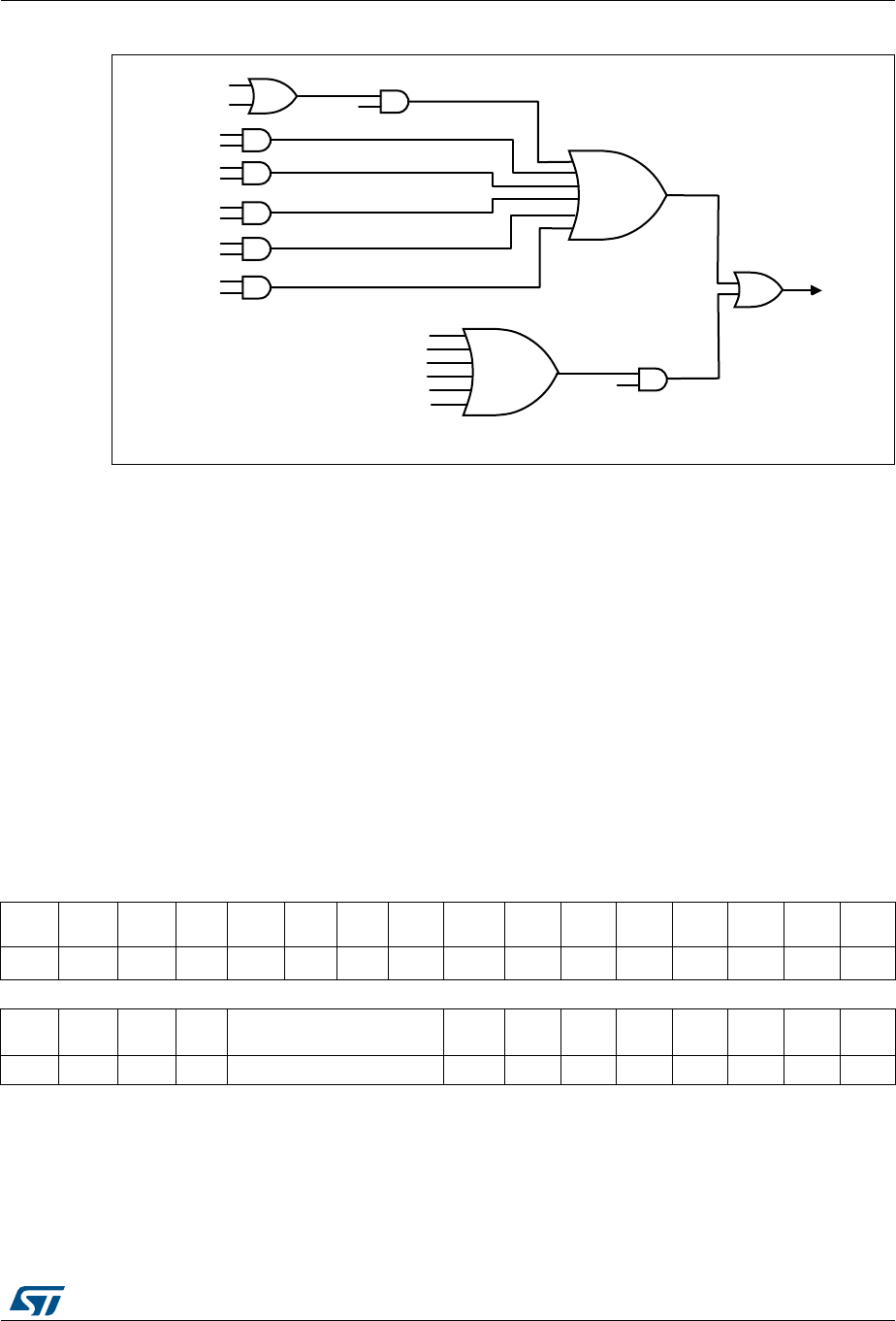
DocID027812 Rev 2 569/766
RM0401 Fast-mode Plus Inter-integrated circuit (FMPI2C) interface
586
Figure 206. FMPI2C interrupt mapping diagram
22.7 FMPI2C registers
Refer to Section 1.1 on page 33 for a list of abbreviations used in register descriptions.
The peripheral registers are accessed by words (32-bit).
22.7.1 Control register 1 (FMPI2C_CR1)
Address offset: 0x00
Reset value: 0x0000 0000
Access: No wait states, except if a write access occurs while a write access to this register is
ongoing. In this case, wait states are inserted in the second write access until the previous
one is completed. The latency of the second write access can be up to 2 x PCLK1 + 6 x
FMPI2CCLK.
069
7&5
7;,6
7;,(
5;1(
5;,(
6723)
6723,(
$''5
$''5,(
1$&.)
1$&.,(
,&JOREDOLQWHUUXSW
%(55
295
$5/2
7,0(287
$/(57
3(&(55
7&,(
(55,(
7&
,&HUURULQWHUUXSW
,&HYHQWLQWHUUXSW
31 30 29 28 27 26 25 24 23 22 21 20 19 18 17 16
Res. Res. Res. Res. Res. Res. Res. Res. PECEN ALERT
EN
SMBD
EN
SMBH
EN GCEN Res. NOSTR
ETCH SBC
rw rw rw rw rw rw rw
15141312111098 7 6543210
RXDMA
EN
TXDMA
EN Res. ANF
OFF DNF ERRIE TCIE STOP
IE
NACK
IE
ADDR
IE RXIE TXIE PE
rw rw rw rw rw rw rw rw rw rw rw rw
Bits 31:24 Reserved, must be kept at reset value.

Fast-mode Plus Inter-integrated circuit (FMPI2C) interface RM0401
570/766 DocID027812 Rev 2
Bit 23 PECEN: PEC enable
0: PEC calculation disabled
1: PEC calculation enabled
Note: If the SMBus feature is not supported, this bit is reserved and forced by hardware to ‘0’.
Please refer to Section 22.3: FMPI2C implementation.
Bit 22 ALERTEN: SMBus alert enable
Device mode (SMBHEN=0):
0: Releases SMBA pin high and Alert Response Address Header disabled: 0001100x
followed by NACK.
1: Drives SMBA pin low and Alert Response Address Header enables: 0001100x followed
by ACK.
Host mode (SMBHEN=1):
0: SMBus Alert pin (SMBA) not supported.
1: SMBus Alert pin (SMBA) supported.
Note: When ALERTEN=0, the SMBA pin can be used as a standard GPIO.
If the SMBus feature is not supported, this bit is reserved and forced by hardware to ‘0’.
Please refer to Section 22.3: FMPI2C implementation.
Bit 21 SMBDEN: SMBus Device Default address enable
0: Device default address disabled. Address 0b1100001x is NACKed.
1: Device default address enabled. Address 0b1100001x is ACKed.
Note: If the SMBus feature is not supported, this bit is reserved and forced by hardware to ‘0’.
Please refer to Section 22.3: FMPI2C implementation.
Bit 20 SMBHEN: SMBus Host address enable
0: Host address disabled. Address 0b0001000x is NACKed.
1: Host address enabled. Address 0b0001000x is ACKed.
Note: If the SMBus feature is not supported, this bit is reserved and forced by hardware to ‘0’.
Please refer to Section 22.3: FMPI2C implementation.
Bit 19 GCEN: General call enable
0: General call disabled. Address 0b00000000 is NACKed.
1: General call enabled. Address 0b00000000 is ACKed.
Bit 18 Reserved, must be kept at reset value.
Bit 17 NOSTRETCH: Clock stretching disable
This bit is used to disable clock stretching in slave mode. It must be kept cleared in master
mode.
0: Clock stretching enabled
1: Clock stretching disabled
Note: This bit can only be programmed when the I2C is disabled (PE = 0).
Bit 16 SBC: Slave byte control
This bit is used to enable hardware byte control in slave mode.
0: Slave byte control disabled
1: Slave byte control enabled
Bit 15 RXDMAEN: DMA reception requests enable
0: DMA mode disabled for reception
1: DMA mode enabled for reception
Bit 14 TXDMAEN: DMA transmission requests enable
0: DMA mode disabled for transmission
1: DMA mode enabled for transmission

DocID027812 Rev 2 571/766
RM0401 Fast-mode Plus Inter-integrated circuit (FMPI2C) interface
586
Bit 13 Reserved, must be kept at reset value.
Bit 12 ANFOFF: Analog noise filter OFF
0: Analog noise filter enabled
1: Analog noise filter disabled
Note: This bit can only be programmed when the FMPI2C is disabled (PE = 0).
Bits 11:8 DNF[3:0]: Digital noise filter
These bits are used to configure the digital noise filter on SDA and SCL input. The digital filter
will filter spikes with a length of up to DNF[3:0] * tI2CCLK
0000: Digital filter disabled
0001: Digital filter enabled and filtering capability up to 1 tI2CCLK
...
1111: digital filter enabled and filtering capability up to15 tI2CCLK
Note: If the analog filter is also enabled, the digital filter is added to the analog filter.
This filter can only be programmed when the FMPI2C is disabled (PE = 0).
Bit 7 ERRIE: Error interrupts enable
0: Error detection interrupts disabled
1: Error detection interrupts enabled
Note: Any of these errors generate an interrupt:
Arbitration Loss (ARLO)
Bus Error detection (BERR)
Overrun/Underrun (OVR)
Timeout detection (TIMEOUT)
PEC error detection (PECERR)
Alert pin event detection (ALERT)
Bit 6 TCIE: Transfer Complete interrupt enable
0: Transfer Complete interrupt disabled
1: Transfer Complete interrupt enabled
Note: Any of these events will generate an interrupt:
Transfer Complete (TC)
Transfer Complete Reload (TCR)
Bit 5 STOPIE: STOP detection Interrupt enable
0: Stop detection (STOPF) interrupt disabled
1: Stop detection (STOPF) interrupt enabled
Bit 4 NACKIE: Not acknowledge received Interrupt enable
0: Not acknowledge (NACKF) received interrupts disabled
1: Not acknowledge (NACKF) received interrupts enabled
Bit 3 ADDRIE: Address match Interrupt enable (slave only)
0: Address match (ADDR) interrupts disabled
1: Address match (ADDR) interrupts enabled
Bit 2 RXIE: RX Interrupt enable
0: Receive (RXNE) interrupt disabled
1: Receive (RXNE) interrupt enabled
Bit 1 TXIE: TX Interrupt enable
0: Transmit (TXIS) interrupt disabled
1: Transmit (TXIS) interrupt enabled

Fast-mode Plus Inter-integrated circuit (FMPI2C) interface RM0401
572/766 DocID027812 Rev 2
Bit 0 PE: Peripheral enable
0: Peripheral disable
1: Peripheral enable
Note: When PE=0, the FMPI2C SCL and SDA lines are released. Internal state machines
and status bits are put back to their reset value. When cleared, PE must be kept low for
at least 3 APB clock cycles.

DocID027812 Rev 2 573/766
RM0401 Fast-mode Plus Inter-integrated circuit (FMPI2C) interface
586
22.7.2 Control register 2 (FMPI2C_CR2)
Address offset: 0x04
Reset value: 0x0000 0000
Access: No wait states, except if a write access occurs while a write access to this register is
ongoing. In this case, wait states are inserted in the second write access until the previous
one is completed. The latency of the second write access can be up to 2 x PCLK1 + 6 x
FMPI2CCLK.
31 30 29 28 27 26 25 24 23 22 21 20 19 18 17 16
Res. Res. Res. Res. Res. PEC
BYTE
AUTO
END
RE
LOAD NBYTES[7:0]
rs rw rw rw
1514131211109876543210
NACK STOP START HEAD
10R ADD10 RD_W
RN SADD[9:0]
rs rs rs rw rw rw rw
Bits 31:27 Reserved, must be kept at reset value.
Bit 26 PECBYTE: Packet error checking byte
This bit is set by software, and cleared by hardware when the PEC is transferred, or when a
STOP condition or an Address matched is received, also when PE=0.
0: No PEC transfer.
1: PEC transmission/reception is requested
Note: Writing ‘0’ to this bit has no effect.
This bit has no effect when RELOAD is set.
This bit has no effect is slave mode when SBC=0.
If the SMBus feature is not supported, this bit is reserved and forced by hardware to ‘0’.
Please refer to Section 22.3: FMPI2C implementation.
Bit 25 AUTOEND: Automatic end mode (master mode)
This bit is set and cleared by software.
0: software end mode: TC flag is set when NBYTES data are transferred, stretching SCL low.
1: Automatic end mode: a STOP condition is automatically sent when NBYTES data are
transferred.
Note: This bit has no effect in slave mode or when the RELOAD bit is set.
Bit 24 RELOAD: NBYTES reload mode
This bit is set and cleared by software.
0: The transfer is completed after the NBYTES data transfer (STOP or RESTART will follow).
1: The transfer is not completed after the NBYTES data transfer (NBYTES will be reloaded).
TCR flag is set when NBYTES data are transferred, stretching SCL low.
Bits 23:16 NBYTES[7:0]: Number of bytes
The number of bytes to be transmitted/received is programmed there. This field is don’t care in
slave mode with SBC=0.
Note: Changing these bits when the START bit is set is not allowed.

Fast-mode Plus Inter-integrated circuit (FMPI2C) interface RM0401
574/766 DocID027812 Rev 2
Bit 15 NACK: NACK generation (slave mode)
The bit is set by software, cleared by hardware when the NACK is sent, or when a STOP
condition or an Address matched is received, or when PE=0.
0: an ACK is sent after current received byte.
1: a NACK is sent after current received byte.
Note: Writing ‘0’ to this bit has no effect.
This bit is used in slave mode only: in master receiver mode, NACK is automatically
generated after last byte preceding STOP or RESTART condition, whatever the NACK
bit value.
When an overrun occurs in slave receiver NOSTRETCH mode, a NACK is
automatically generated whatever the NACK bit value.
When hardware PEC checking is enabled (PECBYTE=1), the PEC acknowledge value
does not depend on the NACK value.
Bit 14 STOP: Stop generation (master mode)
The bit is set by software, cleared by hardware when a Stop condition is detected, or when PE
= 0.
In Master Mode:
0: No Stop generation.
1: Stop generation after current byte transfer.
Note: Writing ‘0’ to this bit has no effect.
Bit 13 START: Start generation
This bit is set by software, and cleared by hardware after the Start followed by the address
sequence is sent, by an arbitration loss, by a timeout error detection, or when PE = 0. It can
also be cleared by software by writing ‘1’ to the ADDRCF bit in the FMPI2C_ICR register.
0: No Start generation.
1: Restart/Start generation:
– If the FMPI2C is already in master mode with AUTOEND = 0, setting this bit generates a
Repeated Start condition when RELOAD=0, after the end of the NBYTES transfer.
– Otherwise setting this bit will generate a START condition once the bus is free.
Note: Writing ‘0’ to this bit has no effect.
The START bit can be set even if the bus is BUSY or FMPI2C is in slave mode.
This bit has no effect when RELOAD is set.
Bit 12 HEAD10R: 10-bit address header only read direction (master receiver mode)
0: The master sends the complete 10 bit slave address read sequence: Start + 2 bytes 10bit
address in write direction + Restart + 1st 7 bits of the 10 bit address in read direction.
1: The master only sends the 1st 7 bits of the 10 bit address, followed by Read direction.
Note: Changing this bit when the START bit is set is not allowed.
Bit 11 ADD10: 10-bit addressing mode (master mode)
0: The master operates in 7-bit addressing mode,
1: The master operates in 10-bit addressing mode
Note: Changing this bit when the START bit is set is not allowed.
Bit 10 RD_WRN: Transfer direction (master mode)
0: Master requests a write transfer.
1: Master requests a read transfer.
Note: Changing this bit when the START bit is set is not allowed.

DocID027812 Rev 2 575/766
RM0401 Fast-mode Plus Inter-integrated circuit (FMPI2C) interface
586
Bits 9:8 SADD[9:8]: Slave address bit 9:8 (master mode)
In 7-bit addressing mode (ADD10 = 0):
These bits are don’t care
In 10-bit addressing mode (ADD10 = 1):
These bits should be written with bits 9:8 of the slave address to be sent
Note: Changing these bits when the START bit is set is not allowed.
Bits 7:1 SADD[7:1]: Slave address bit 7:1 (master mode)
In 7-bit addressing mode (ADD10 = 0):
These bits should be written with the 7-bit slave address to be sent
In 10-bit addressing mode (ADD10 = 1):
These bits should be written with bits 7:1 of the slave address to be sent.
Note: Changing these bits when the START bit is set is not allowed.
Bit 0 SADD0: Slave address bit 0 (master mode)
In 7-bit addressing mode (ADD10 = 0):
This bit is don’t care
In 10-bit addressing mode (ADD10 = 1):
This bit should be written with bit 0 of the slave address to be sent
Note: Changing these bits when the START bit is set is not allowed.

Fast-mode Plus Inter-integrated circuit (FMPI2C) interface RM0401
576/766 DocID027812 Rev 2
22.7.3 Own address 1 register (FMPI2C_OAR1)
Address offset: 0x08
Reset value: 0x0000 0000
Access: No wait states, except if a write access occurs while a write access to this register is
ongoing. In this case, wait states are inserted in the second write access until the previous
one is completed. The latency of the second write access can be up to 2 x PCLK1 + 6 x
FMPI2CCLK.
31 30 29 28 27 26 25 24 23 22 21 20 19 18 17 16
Res. Res. Res. Res. Res. Res. Res. Res. Res. Res. Res. Res. Res. Res. Res. Res.
1514131211109876543210
OA1EN Res. Res. Res. Res. OA1
MODE OA1[9:8] OA1[7:1] OA1[0]
rw rw rw rw rw
Bits 31:16 Reserved, must be kept at reset value.
Bit 15 OA1EN: Own Address 1 enable
0: Own address 1 disabled. The received slave address OA1 is NACKed.
1: Own address 1 enabled. The received slave address OA1 is ACKed.
Bits 14:11 Reserved, must be kept at reset value.
Bit 10 OA1MODE Own Address 1 10-bit mode
0: Own address 1 is a 7-bit address.
1: Own address 1 is a 10-bit address.
Note: This bit can be written only when OA1EN=0.
Bits 9:8 OA1[9:8]: Interface address
7-bit addressing mode: don’t care
10-bit addressing mode: bits 9:8 of address
Note: These bits can be written only when OA1EN=0.
Bits 7:1 OA1[7:1]: Interface address
Bits 7:1 of address
Note: These bits can be written only when OA1EN=0.
Bit 0 OA1[0]: Interface address
7-bit addressing mode: don’t care
10-bit addressing mode: bit 0 of address
Note: This bit can be written only when OA1EN=0.

DocID027812 Rev 2 577/766
RM0401 Fast-mode Plus Inter-integrated circuit (FMPI2C) interface
586
22.7.4 Own address 2 register (FMPI2C_OAR2)
Address offset: 0x0C
Reset value: 0x0000 0000
Access: No wait states, except if a write access occurs while a write access to this register is
ongoing. In this case, wait states are inserted in the second write access until the previous
one is completed. The latency of the second write access can be up to 2 x PCLK1 + 6 x
FMPI2CCLK.
31 30 29 28 27 26 25 24 23 22 21 20 19 18 17 16
Res. Res. Res. Res. Res. Res. Res. Res. Res. Res. Res. Res. Res. Res. Res. Res.
15 14 13 12 11 10 9 8 7 6 5 4 3 2 1 0
OA2EN Res. Res. Res. Res. OA2MSK[2:0] OA2[7:1] Res.
rw rw rw
Bits 31:16 Reserved, must be kept at reset value.
Bit 15 OA2EN: Own Address 2 enable
0: Own address 2 disabled. The received slave address OA2 is NACKed.
1: Own address 2 enabled. The received slave address OA2 is ACKed.
Bits 14:11 Reserved, must be kept at reset value.
Bits 10:8 OA2MSK[2:0]: Own Address 2 masks
000: No mask
001: OA2[1] is masked and don’t care. Only OA2[7:2] are compared.
010: OA2[2:1] are masked and don’t care. Only OA2[7:3] are compared.
011: OA2[3:1] are masked and don’t care. Only OA2[7:4] are compared.
100: OA2[4:1] are masked and don’t care. Only OA2[7:5] are compared.
101: OA2[5:1] are masked and don’t care. Only OA2[7:6] are compared.
110: OA2[6:1] are masked and don’t care. Only OA2[7] is compared.
111: OA2[7:1] are masked and don’t care. No comparison is done, and all (except reserved)
7-bit received addresses are acknowledged.
Note: These bits can be written only when OA2EN=0.
As soon as OA2MSK is not equal to 0, the reserved FMPI2C addresses (0b0000xxx
and 0b1111xxx) are not acknowledged even if the comparison matches.
Bits 7:1 OA2[7:1]: Interface address
bits 7:1 of address
Note: These bits can be written only when OA2EN=0.
Bit 0 Reserved, must be kept at reset value.

Fast-mode Plus Inter-integrated circuit (FMPI2C) interface RM0401
578/766 DocID027812 Rev 2
22.7.5 Timing register (FMPI2C_TIMINGR)
Address offset: 0x10
Reset value: 0x0000 0000
Access: No wait states
Note: This register must be configured when the FMPI2C is disabled (PE = 0).
31 30 29 28 27 26 25 24 23 22 21 20 19 18 17 16
PRESC[3:0] Res. Res. Res. Res. SCLDEL[3:0] SDADEL[3:0]
rw rw rw
15141312111098 7 654321 0
SCLH[7:0] SCLL[7:0]
rw rw
Bits 31:28 PRESC[3:0]: Timing prescaler
This field is used to prescale FMPI2CCLK in order to generate the clock period tPRESC used for
data setup and hold counters (refer to FMPI2C timings on page 524) and for SCL high and low
level counters (refer to FMPI2C master initialization on page 540).
tPRESC = (PRESC+1) x tI2CCLK
Bits 27:24 Reserved, must be kept at reset value.
Bits 23:20 SCLDEL[3:0]: Data setup time
This field is used to generate a delay tSCLDEL between SDA edge and SCL rising edge. In
master mode and in slave mode with NOSTRETCH = 0, the SCL line is stretched low during
tSCLDEL.
tSCLDEL = (SCLDEL+1) x tPRESC
Note: tSCLDEL is used to generate tSU:DAT timing.
Bits 19:16 SDADEL[3:0]: Data hold time
This field is used to generate the delay tSDADEL between SCL falling edge and SDA edge. In
master mode and in slave mode with NOSTRETCH = 0, the SCL line is stretched low during
tSDADEL.
tSDADEL= SDADEL x tPRESC
Note: SDADEL is used to generate tHD:DAT timing.
Bits 15:8 SCLH[7:0]: SCL high period (master mode)
This field is used to generate the SCL high period in master mode.
tSCLH = (SCLH+1) x tPRESC
Note: SCLH is also used to generate tSU:STO and tHD:STA timing.
Bits 7:0 SCLL[7:0]: SCL low period (master mode)
This field is used to generate the SCL low period in master mode.
tSCLL = (SCLL+1) x tPRESC
Note: SCLL is also used to generate tBUF and tSU:STA timings.

DocID027812 Rev 2 579/766
RM0401 Fast-mode Plus Inter-integrated circuit (FMPI2C) interface
586
22.7.6 Timeout register (FMPI2C_TIMEOUTR)
Address offset: 0x14
Reset value: 0x0000 0000
Access: No wait states, except if a write access occurs while a write access to this register is
ongoing. In this case, wait states are inserted in the second write access until the previous
one is completed. The latency of the second write access can be up to 2 x PCLK1 + 6 x
FMPI2CCLK.
Note: If the SMBus feature is not supported, this register is reserved and forced by hardware to
“0x00000000”. Please refer to Section 22.3: FMPI2C implementation.
31 30 29 28 27 26 25 24 23 22 21 20 19 18 17 16
TEXTEN Res. Res. Res. TIMEOUTB [11:0]
rw rw
15 14 13 12 11109876543210
TIMOUTEN Res. Res. TIDLE TIMEOUTA [11:0]
rw rw rw
Bit 31 TEXTEN: Extended clock timeout enable
0: Extended clock timeout detection is disabled
1: Extended clock timeout detection is enabled. When a cumulative SCL stretch for more
than tLOW:EXT is done by the FMPI2C interface, a timeout error is detected (TIMEOUT=1).
Bits 30:28 Reserved, must be kept at reset value.
Bits 27:16 TIMEOUTB[11:0]: Bus timeout B
This field is used to configure the cumulative clock extension timeout:
In master mode, the master cumulative clock low extend time (tLOW:MEXT) is detected
In slave mode, the slave cumulative clock low extend time (tLOW:SEXT) is detected
tLOW:EXT= (TIMEOUTB+1) x 2048 x tI2CCLK
Note: These bits can be written only when TEXTEN=0.
Bit 15 TIMOUTEN: Clock timeout enable
0: SCL timeout detection is disabled
1: SCL timeout detection is enabled: when SCL is low for more than tTIMEOUT (TIDLE=0) or
high for more than tIDLE (TIDLE=1), a timeout error is detected (TIMEOUT=1).
Bits 14:13 Reserved, must be kept at reset value.
Bit 12 TIDLE: Idle clock timeout detection
0: TIMEOUTA is used to detect SCL low timeout
1: TIMEOUTA is used to detect both SCL and SDA high timeout (bus idle condition)
Note: This bit can be written only when TIMOUTEN=0.
Bits 11:0 TIMEOUTA[11:0]: Bus Timeout A
This field is used to configure:
– The SCL low timeout condition tTIMEOUT when TIDLE=0
tTIMEOUT= (TIMEOUTA+1) x 2048 x tI2CCLK
– The bus idle condition (both SCL and SDA high) when TIDLE=1
tIDLE= (TIMEOUTA+1) x 4 x tI2CCLK
Note: These bits can be written only when TIMOUTEN=0.

Fast-mode Plus Inter-integrated circuit (FMPI2C) interface RM0401
580/766 DocID027812 Rev 2
22.7.7 Interrupt and status register (FMPI2C_ISR)
Address offset: 0x18
Reset value: 0x0000 0001
Access: No wait states
31 30 29 28 27 26 25 24 23 22 21 20 19 18 17 16
Res. Res. Res. Res. Res. Res. Res. Res. ADDCODE[6:0] DIR
rr
1514131211109876543210
BUSY Res. ALERT TIME
OUT
PEC
ERR OVR ARLO BERR TCR TC STOPF NACKF ADDR RXNE TXIS TXE
r rrrrrrrrrrrrrsrs
Bits 31:24 Reserved, must be kept at reset value.
Bits 23:17 ADDCODE[6:0]: Address match code (Slave mode)
These bits are updated with the received address when an address match event occurs
(ADDR = 1).
In the case of a 10-bit address, ADDCODE provides the 10-bit header followed by the 2 MSBs
of the address.
Bit 16 DIR: Transfer direction (Slave mode)
This flag is updated when an address match event occurs (ADDR=1).
0: Write transfer, slave enters receiver mode.
1: Read transfer, slave enters transmitter mode.
Bit 15 BUSY: Bus busy
This flag indicates that a communication is in progress on the bus. It is set by hardware when a
START condition is detected. It is cleared by hardware when a Stop condition is detected, or
when PE=0.
Bit 14 Reserved, must be kept at reset value.
Bit 13 ALERT: SMBus alert
This flag is set by hardware when SMBHEN=1 (SMBus host configuration), ALERTEN=1 and
a SMBALERT event (falling edge) is detected on SMBA pin. It is cleared by software by setting
the ALERTCF bit.
Note: This bit is cleared by hardware when PE=0.
If the SMBus feature is not supported, this bit is reserved and forced by hardware to ‘0’.
Please refer to Section 22.3: FMPI2C implementation.
Bit 12 TIMEOUT: Timeout or tLOW detection flag
This flag is set by hardware when a timeout or extended clock timeout occurred. It is cleared
by software by setting the TIMEOUTCF bit.
Note: This bit is cleared by hardware when PE=0.
If the SMBus feature is not supported, this bit is reserved and forced by hardware to ‘0’.
Please refer to Section 22.3: FMPI2C implementation.

DocID027812 Rev 2 581/766
RM0401 Fast-mode Plus Inter-integrated circuit (FMPI2C) interface
586
Bit 11 PECERR: PEC Error in reception
This flag is set by hardware when the received PEC does not match with the PEC register
content. A NACK is automatically sent after the wrong PEC reception. It is cleared by software
by setting the PECCF bit.
Note: This bit is cleared by hardware when PE=0.
If the SMBus feature is not supported, this bit is reserved and forced by hardware to ‘0’.
Please refer to Section 22.3: FMPI2C implementation.
Bit 10 OVR: Overrun/Underrun (slave mode)
This flag is set by hardware in slave mode with NOSTRETCH=1, when an overrun/underrun
error occurs. It is cleared by software by setting the OVRCF bit.
Note: This bit is cleared by hardware when PE=0.
Bit 9 ARLO: Arbitration lost
This flag is set by hardware in case of arbitration loss. It is cleared by software by setting the
ARLOCF bit.
Note: This bit is cleared by hardware when PE=0.
Bit 8 BERR: Bus error
This flag is set by hardware when a misplaced Start or Stop condition is detected whereas the
peripheral is involved in the transfer. The flag is not set during the address phase in slave
mode. It is cleared by software by setting BERRCF bit.
Note: This bit is cleared by hardware when PE=0.
Bit 7 TCR: Transfer Complete Reload
This flag is set by hardware when RELOAD=1 and NBYTES data have been transferred. It is
cleared by software when NBYTES is written to a non-zero value.
Note: This bit is cleared by hardware when PE=0.
This flag is only for master mode, or for slave mode when the SBC bit is set.
Bit 6 TC: Transfer Complete (master mode)
This flag is set by hardware when RELOAD=0, AUTOEND=0 and NBYTES data have been
transferred. It is cleared by software when START bit or STOP bit is set.
Note: This bit is cleared by hardware when PE=0.
Bit 5 STOPF: Stop detection flag
This flag is set by hardware when a Stop condition is detected on the bus and the peripheral is
involved in this transfer:
– either as a master, provided that the STOP condition is generated by the peripheral.
– or as a slave, provided that the peripheral has been addressed previously during this
transfer.
It is cleared by software by setting the STOPCF bit.
Note: This bit is cleared by hardware when PE=0.
Bit 4 NACKF: Not Acknowledge received flag
This flag is set by hardware when a NACK is received after a byte transmission. It is cleared by
software by setting the NACKCF bit.
Note: This bit is cleared by hardware when PE=0.
Bit 3 ADDR: Address matched (slave mode)
This bit is set by hardware as soon as the received slave address matched with one of the
enabled slave addresses. It is cleared by software by setting ADDRCF bit.
Note: This bit is cleared by hardware when PE=0.

Fast-mode Plus Inter-integrated circuit (FMPI2C) interface RM0401
582/766 DocID027812 Rev 2
22.7.8 Interrupt clear register (FMPI2C_ICR)
Address offset: 0x1C
Reset value: 0x0000 0000
Access: No wait states
Bit 2 RXNE: Receive data register not empty (receivers)
This bit is set by hardware when the received data is copied into the FMPI2C_RXDR register,
and is ready to be read. It is cleared when FMPI2C_RXDR is read.
Note: This bit is cleared by hardware when PE=0.
Bit 1 TXIS: Transmit interrupt status (transmitters)
This bit is set by hardware when the FMPI2C_TXDR register is empty and the data to be
transmitted must be written in the FMPI2C_TXDR register. It is cleared when the next data to
be sent is written in the FMPI2C_TXDR register.
This bit can be written to ‘1’ by software when NOSTRETCH=1 only, in order to generate a
TXIS event (interrupt if TXIE=1 or DMA request if TXDMAEN=1).
Note: This bit is cleared by hardware when PE=0.
Bit 0 TXE: Transmit data register empty (transmitters)
This bit is set by hardware when the FMPI2C_TXDR register is empty. It is cleared when the
next data to be sent is written in the FMPI2C_TXDR register.
This bit can be written to ‘1’ by software in order to flush the transmit data register
FMPI2C_TXDR.
Note: This bit is set by hardware when PE=0.
31 30 29 28 27 26 25 24 23 22 21 20 19 18 17 16
Res. Res. Res. Res. Res. Res. Res. Res. Res. Res. Res. Res. Res. Res. Res. Res.
1514131211109876543210
Res. Res. ALERT
CF
TIM
OUTCF PECCF OVRCF ARLO
CF
BERR
CF Res. Res. STOP
CF
NACK
CF
ADDR
CF Res. Res. Res.
wwwwww www
Bits 31:14 Reserved, must be kept at reset value.
Bit 13 ALERTCF: Alert flag clear
Writing 1 to this bit clears the ALERT flag in the FMPI2C_ISR register.
Note: If the SMBus feature is not supported, this bit is reserved and forced by hardware to ‘0’.
Please refer to Section 22.3: FMPI2C implementation.
Bit 12 TIMOUTCF: Timeout detection flag clear
Writing 1 to this bit clears the TIMEOUT flag in the FMPI2C_ISR register.
Note: If the SMBus feature is not supported, this bit is reserved and forced by hardware to ‘0’.
Please refer to Section 22.3: FMPI2C implementation.
Bit 11 PECCF: PEC Error flag clear
Writing 1 to this bit clears the PECERR flag in the FMPI2C_ISR register.
Note: If the SMBus feature is not supported, this bit is reserved and forced by hardware to ‘0’.
Please refer to Section 22.3: FMPI2C implementation.

DocID027812 Rev 2 583/766
RM0401 Fast-mode Plus Inter-integrated circuit (FMPI2C) interface
586
22.7.9 PEC register (FMPI2C_PECR)
Address offset: 0x20
Reset value: 0x0000 0000
Access: No wait states
Note: If the SMBus feature is not supported, this register is reserved and forced by hardware to
“0x00000000”. Please refer to Section 22.3: FMPI2C implementation.
Bit 10 OVRCF: Overrun/Underrun flag clear
Writing 1 to this bit clears the OVR flag in the FMPI2C_ISR register.
Bit 9 ARLOCF: Arbitration Lost flag clear
Writing 1 to this bit clears the ARLO flag in the FMPI2C_ISR register.
Bit 8 BERRCF: Bus error flag clear
Writing 1 to this bit clears the BERRF flag in the FMPI2C_ISR register.
Bits 7:6 Reserved, must be kept at reset value.
Bit 5 STOPCF: Stop detection flag clear
Writing 1 to this bit clears the STOPF flag in the FMPI2C_ISR register.
Bit 4 NACKCF: Not Acknowledge flag clear
Writing 1 to this bit clears the ACKF flag in FMPI2C_ISR register.
Bit 3 ADDRCF: Address matched flag clear
Writing 1 to this bit clears the ADDR flag in the FMPI2C_ISR register. Writing 1 to this bit also
clears the START bit in the FMPI2C_CR2 register.
Bits 2:0 Reserved, must be kept at reset value.
31 30 29 28 27 26 25 24 23 22 21 20 19 18 17 16
Res. Res. Res. Res. Res. Res. Res. Res. Res. Res. Res. Res. Res. Res. Res. Res.
1514131211109876543210
Res. Res. Res. Res. Res. Res. Res. Res. PEC[7:0]
r
Bits 31:8 Reserved, must be kept at reset value.
Bits 7:0 PEC[7:0] Packet error checking register
This field contains the internal PEC when PECEN=1.
The PEC is cleared by hardware when PE=0.
Fast-mode Plus Inter-integrated circuit (FMPI2C) interface RM0401
584/766 DocID027812 Rev 2
22.7.10 Receive data register (FMPI2C_RXDR)
Address offset: 0x24
Reset value: 0x0000 0000
Access: No wait states
22.7.11 Transmit data register (FMPI2C_TXDR)
Address offset: 0x28
Reset value: 0x0000 0000
Access: No wait states
31 30 29 28 27 26 25 24 23 22 21 20 19 18 17 16
Res. Res. Res. Res. Res. Res. Res. Res. Res. Res. Res. Res. Res. Res. Res. Res.
1514131211109876543210
Res. Res. Res. Res. Res. Res. Res. Res. RXDATA[7:0]
r
Bits 31:8 Reserved, must be kept at reset value.
Bits 7:0 RXDATA[7:0] 8-bit receive data
Data byte received from the I2C bus.
31 30 29 28 27 26 25 24 23 22 21 20 19 18 17 16
Res. Res. Res. Res. Res. Res. Res. Res. Res. Res. Res. Res. Res. Res. Res. Res.
1514131211109876543210
Res. Res. Res. Res. Res. Res. Res. Res. TXDATA[7:0]
rw
Bits 31:8 Reserved, must be kept at reset value.
Bits 7:0 TXDATA[7:0] 8-bit transmit data
Data byte to be transmitted to the I2C bus.
Note: These bits can be written only when TXE=1.

DocID027812 Rev 2 585/766
RM0401 Fast-mode Plus Inter-integrated circuit (FMPI2C) interface
586
22.7.12 FMPI2C register map
The table below provides the FMPI2C register map and reset values.
Table 91. FMPI2C register map and reset values
Offset Register
31
30
29
28
27
26
25
24
23
22
21
20
19
18
17
16
15
14
13
12
11
10
9
8
7
6
5
4
3
2
1
0
0x0
FMPI2C_CR1
Res.
Res.
Res.
Res.
Res.
Res.
Res.
Res.
PECEN
ALERTEN
SMBDEN
SMBHEN
GCEN
Res
NOSTRETCH
SBC
RXDMAEN
TXDMAEN
Res.
ANFOFF
DNF[3:0]
ERRIE
TCIE
STOPIE
NACKIE
ADDRIE
RXIE
TXIE
PE
Reset value 00000 0000 0000000000000
0x4
FMPI2C_CR2
Res.
Res.
Res.
Res.
Res.
PECBYTE
AUTOEND
RELOAD
NBYTES[7:0]
NACK
STOP
START
HEAD10R
ADD10
RD_WRN
SADD[9:0]
Reset value 000000000000000000000000000
0x8
FMPI2C_OAR1
Res.
Res.
Res.
Res.
Res.
Res.
Res.
Res.
Res.
Res.
Res.
Res.
Res.
Res.
Res.
Res.
OA1EN
Res.
Res.
Res.
Res.
OA1MODE
OA1[9:0]
Reset value 0 00000000000
0xC
FMPI2C_OAR2
Res.
Res.
Res.
Res.
Res.
Res.
Res.
Res.
Res.
Res.
Res.
Res.
Res.
Res.
Res.
Res.
OA2EN
Res.
Res.
Res.
Res.
OA2MS
K [2:0] OA2[7:1]
Res.
Reset value 0 0000000000
0x10
FMPI2C_TIMING
RPRESC[3:0]
Res.
Res.
Res.
Res.
SCLDEL[3:0
]
SDADEL[3:
0] SCLH[7:0] SCLL[7:0]
Reset value 0000 000000000000000000000000
0x14
FMPI2C_
TIMEOUTR
TEXTEN
Res.
Res.
Res.
TIMEOUTB[11:0]
TIMOUTEN
Res.
TIDLE
TIMEOUTA[11:0]
Reset value 0 0000000000000 0000000000000
0x18
FMPI2C_ISR
Res.
Res.
Res.
Res.
Res.
Res.
Res.
Res.
ADDCODE[6:0]
DIR
BUSY
Res.
ALERT
TIMEOUT
PECERR
OVR
ARLO
BERR
TCR
TC
STOPF
NACKF
ADDR
RXNE
TXIS
TXE
Reset value 000000000 00000000000001
0x1C
FMPI2C_ICR
Res.
Res.
Res.
Res.
Res.
Res.
Res.
Res.
Res.
Res.
Res.
Res.
Res.
Res.
Res.
Res.
Res.
Res.
ALERTCF
TIMOUTCF
PECCF
OVRCF
ARLOCF
BERRCF
Res.
Res.
STOPCF
NACKCF
ADDRCF
Res.
Res.
Res.
Reset value 000000 000
0x20
FMPI2C_PECR
Res.
Res.
Res.
Res.
Res.
Res.
Res.
Res.
Res.
Res.
Res.
Res.
Res.
Res.
Res.
Res.
Res.
Res.
Res.
Res.
Res.
Res.
Res.
Res.
PEC[7:0]
Reset value 00000000
0x24
FMPI2C_RXDR
Res.
Res.
Res.
Res.
Res.
Res.
Res.
Res.
Res.
Res.
Res.
Res.
Res.
Res.
Res.
Res.
Res.
Res.
Res.
Res.
Res.
Res.
Res.
Res.
RXDATA[7:0]
Reset value 00000000

Fast-mode Plus Inter-integrated circuit (FMPI2C) interface RM0401
586/766 DocID027812 Rev 2
Refer to Section 2.2.2 on page 38 for the register boundary addresses.
0x28
FMPI2C_TXDR
Res.
Res.
Res.
Res.
Res.
Res.
Res.
Res.
Res.
Res.
Res.
Res.
Res.
Res.
Res.
Res.
Res.
Res.
Res.
Res.
Res.
Res.
Res.
Res.
TXDATA[7:0]
Reset value 00000000
Table 91. FMPI2C register map and reset values (continued)
Offset Register
31
30
29
28
27
26
25
24
23
22
21
20
19
18
17
16
15
14
13
12
11
10
9
8
7
6
5
4
3
2
1
0

DocID027812 Rev 2 587/766
RM0401 Inter-integrated circuit (I2C) interface
621
23 Inter-integrated circuit (I2C) interface
23.1 I2C introduction
I2C (inter-integrated circuit) bus Interface serves as an interface between the microcontroller
and the serial I2C bus. It provides multimaster capability, and controls all I2C bus-specific
sequencing, protocol, arbitration and timing. It supports the standard mode (Sm, up to 100
kHz) and Fm mode (Fm, up to 400 kHz).
It may be used for a variety of purposes, including CRC generation and verification, SMBus
(system management bus) and PMBus (power management bus).
Depending on specific device implementation DMA capability can be available for reduced
CPU overload.

Inter-integrated circuit (I2C) interface RM0401
588/766 DocID027812 Rev 2
23.2 I2C main features
•Parallel-bus/I2C protocol converter
•Multimaster capability: the same interface can act as Master or Slave
•I2C Master features:
– Clock generation
– Start and Stop generation
•I2C Slave features:
– Programmable I2C Address detection
– Dual Addressing Capability to acknowledge 2 slave addresses
– Stop bit detection
•Generation and detection of 7-bit/10-bit addressing and General Call
•Supports different communication speeds:
– Standard Speed (up to 100 kHz)
– Fast Speed (up to 400 kHz)
•Analog noise filter
•Programmable digital noise filter
•Status flags:
– Transmitter/Receiver mode flag
– End-of-Byte transmission flag
–I
2C busy flag
•Error flags:
– Arbitration lost condition for master mode
– Acknowledgment failure after address/ data transmission
– Detection of misplaced start or stop condition
– Overrun/Underrun if clock stretching is disabled
•2 Interrupt vectors:
– 1 Interrupt for successful address/ data communication
– 1 Interrupt for error condition
•Optional clock stretching
•1-byte buffer with DMA capability
•Configurable PEC (packet error checking) generation or verification:
– PEC value can be transmitted as last byte in Tx mode
– PEC error checking for last received byte
•SMBus 2.0 Compatibility:
– 25 ms clock low timeout delay
– 10 ms master cumulative clock low extend time
– 25 ms slave cumulative clock low extend time
– Hardware PEC generation/verification with ACK control
– Address Resolution Protocol (ARP) supported
•PMBus Compatibility
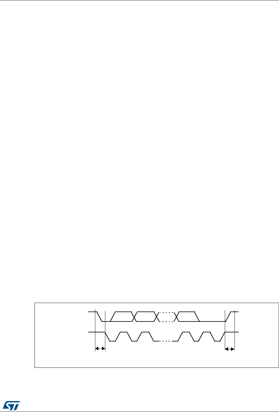
DocID027812 Rev 2 589/766
RM0401 Inter-integrated circuit (I2C) interface
621
Note: Some of the above features may not be available in certain products. The user should refer
to the product data sheet, to identify the specific features supported by the I2C interface
implementation.
23.3 I2C functional description
In addition to receiving and transmitting data, this interface converts it from serial to parallel
format and vice versa. The interrupts are enabled or disabled by software. The interface is
connected to the I2C bus by a data pin (SDA) and by a clock pin (SCL). It can be connected
with a standard (up to 100 kHz) or fast (up to 400 kHz) I2C bus.
23.3.1 Mode selection
The interface can operate in one of the four following modes:
•Slave transmitter
•Slave receiver
•Master transmitter
•Master receiver
By default, it operates in slave mode. The interface automatically switches from slave to
master, after it generates a START condition and from master to slave, if an arbitration loss
or a Stop generation occurs, allowing multimaster capability.
Communication flow
In Master mode, the I2C interface initiates a data transfer and generates the clock signal. A
serial data transfer always begins with a start condition and ends with a stop condition. Both
start and stop conditions are generated in master mode by software.
In Slave mode, the interface is capable of recognizing its own addresses (7 or 10-bit), and
the General Call address. The General Call address detection may be enabled or disabled
by software.
Data and addresses are transferred as 8-bit bytes, MSB first. The first byte(s) following the
start condition contain the address (one in 7-bit mode, two in 10-bit mode). The address is
always transmitted in Master mode.
A 9th clock pulse follows the 8 clock cycles of a byte transfer, during which the receiver must
send an acknowledge bit to the transmitter. Refer to Figure 207.
Figure 207. I2C bus protocol
Acknowledge may be enabled or disabled by software. The I2C interface addresses (dual
addressing 7-bit/ 10-bit and/or general call address) can be selected by software.
SCL
SDA
12 8 9
MSB ACK
Stop
Start
condition
condition
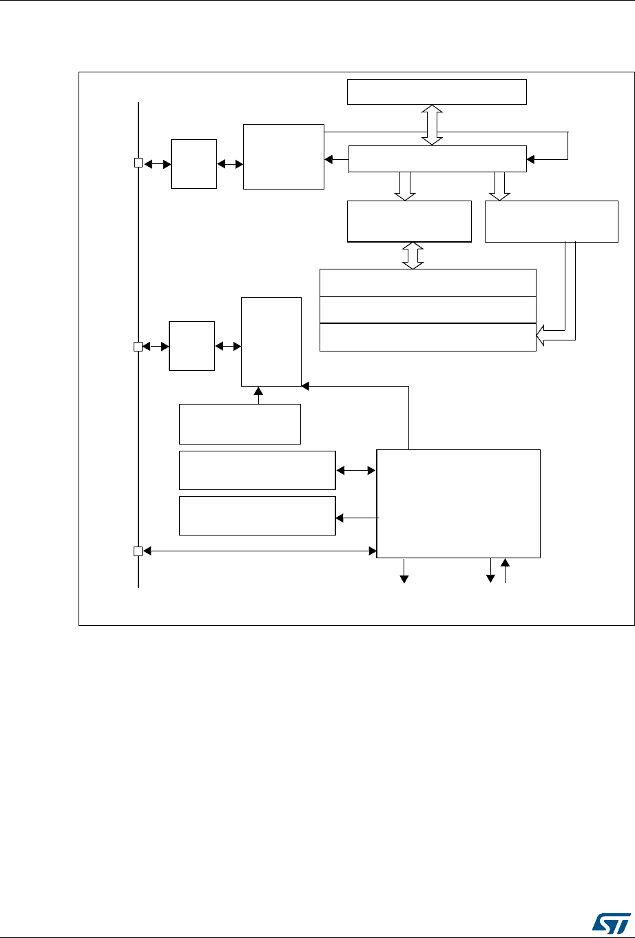
Inter-integrated circuit (I2C) interface RM0401
590/766 DocID027812 Rev 2
The block diagram of the I2C interface is shown in Figure 208.
Figure 208. I2C block diagram
1. SMBA is an optional signal in SMBus mode. This signal is not applicable if SMBus is disabled.
23.3.2 I2C slave mode
By default the I2C interface operates in Slave mode. To switch from default Slave mode to
Master mode a Start condition generation is needed.
The peripheral input clock must be programmed in the I2C_CR2 register in order to
generate correct timings. The peripheral input clock frequency must be at least:
•2 MHz in Sm mode
•4 MHz in Fm mode
As soon as a start condition is detected, the address is received from the SDA line and sent
to the shift register. Then it is compared with the address of the interface (OAR1) and with
OAR2 (if ENDUAL=1) or the General Call address (if ENGC = 1).
$ATASHIFTREGISTER
#OMPARATOR
/WNADDRESSREGISTER
#LOCKCONTROL
3TATUSREGISTERS
#ONTROLREGISTERS
#ONTROL
#LOCK
CONTROL
$ATA
CONTROL
3#,
LOGIC
$UALADDRESSREGISTER
$ATAREGISTER
0%#REGISTER
)NTERRUPTS
0%#CALCULATION
3-"!
3$!
2EGISTER##2
3232
#2#2
$-!REQUESTS!#+
-36
.OISE
FILTER
.OISE
FILTER

DocID027812 Rev 2 591/766
RM0401 Inter-integrated circuit (I2C) interface
621
Note: In 10-bit addressing mode, the comparison includes the header sequence (11110xx0),
where xx denotes the two most significant bits of the address.
Header or address not matched: the interface ignores it and waits for another Start
condition.
Header matched (10-bit mode only): the interface generates an acknowledge pulse if the
ACK bit is set and waits for the 8-bit slave address.
Address matched: the interface generates in sequence:
•An acknowledge pulse if the ACK bit is set
•The ADDR bit is set by hardware and an interrupt is generated if the ITEVFEN bit is
set.
•If ENDUAL=1, the software has to read the DUALF bit to check which slave address
has been acknowledged.
In 10-bit mode, after receiving the address sequence the slave is always in Receiver mode.
It will enter Transmitter mode on receiving a repeated Start condition followed by the header
sequence with matching address bits and the least significant bit set (11110xx1).
The TRA bit indicates whether the slave is in Receiver or Transmitter mode.
Slave transmitter
Following the address reception and after clearing ADDR, the slave sends bytes from the
DR register to the SDA line via the internal shift register.
The slave stretches SCL low until ADDR is cleared and DR filled with the data to be sent
(see Figure 209 Transfer sequencing EV1 EV3).
When the acknowledge pulse is received:
•The TxE bit is set by hardware with an interrupt if the ITEVFEN and the ITBUFEN bits
are set.
If TxE is set and some data were not written in the I2C_DR register before the end of the
next data transmission, the BTF bit is set and the interface waits until BTF is cleared by a
read to I2C_SR1 followed by a write to the I2C_DR register, stretching SCL low.
Inter-integrated circuit (I2C) interface RM0401
592/766 DocID027812 Rev 2
Figure 209. Transfer sequence diagram for slave transmitter
1. The EV1 and EV3_1 events stretch SCL low until the end of the corresponding software sequence.
2. The EV3 event stretches SCL low if the software sequence is not completed before the end of the next byte
transmission
Slave receiver
Following the address reception and after clearing ADDR, the slave receives bytes from the
SDA line into the DR register via the internal shift register. After each byte the interface
generates in sequence:
•An acknowledge pulse if the ACK bit is set
•The RxNE bit is set by hardware and an interrupt is generated if the ITEVFEN and
ITBUFEN bit is set.
If RxNE is set and the data in the DR register is not read before the end of the next data
reception, the BTF bit is set and the interface waits until BTF is cleared by a read from the
I2C_DR register, stretching SCL low (see Figure 210 Transfer sequencing).
ELWVODYHWUDQVPLWWHU
ELWVODYHWUDQVPLWWHU
6 $ GGUHVV $ 'DWD
(9 (9 (9
6U'DWD $
(9 (9B (9 (9 (9
DL9
'DWD$$
'DWD1 1$ 3
(9(9 (9
6 +HDGHU $ $GGUHVV $
(9
+HDGHU $ 'DWD1 1$ 3
/HJHQG 6 6WDUW6U 5HSHDWHG6WDUW3 6WRS$ $FNQRZOHGJH1$ 1RQDFNQRZOHGJH
(9[ (YHQWZLWKLQWHUUXSWLI,7(9)(1
(97[( VKLIWUHJLVWHUHPSW\GDWDUHJLVWHUHPSW\ZULWH'DWDLQ'5
(97[( VKLIWUHJLVWHUQRWHPSW\GDWDUHJLVWHUHPSW\FOHDUHGE\ZULWLQJ'5
(9$) $)LVFOHDUHGE\ZULWLQJµ¶LQ$)ELWRI65UHJLVWHU
$9$''5 FOHDUHGE\UHDGLQJ65IROORZHGE\UHDGLQJ65

DocID027812 Rev 2 593/766
RM0401 Inter-integrated circuit (I2C) interface
621
Figure 210. Transfer sequence diagram for slave receiver
1. The EV1 event stretches SCL low until the end of the corresponding software sequence.
2. The EV2 event stretches SCL low if the software sequence is not completed before the end of the next byte
reception.
3. After checking the SR1 register content, the user should perform the complete clearing sequence for each
flag found set.
Thus, for ADDR and STOPF flags, the following sequence is required inside the I2C interrupt routine:
READ SR1
if (ADDR == 1) {READ SR1; READ SR2}
if (STOPF == 1) {READ SR1; WRITE CR1}
The purpose is to make sure that both ADDR and STOPF flags are cleared if both are found set.
Closing slave communication
After the last data byte is transferred a Stop Condition is generated by the master. The
interface detects this condition and sets:
•The STOPF bit and generates an interrupt if the ITEVFEN bit is set.
The STOPF bit is cleared by a read of the SR1 register followed by a write to the CR1
register (see Figure 210: Transfer sequence diagram for slave receiver EV4).
23.3.3 I2C master mode
In Master mode, the I2C interface initiates a data transfer and generates the clock signal. A
serial data transfer always begins with a Start condition and ends with a Stop condition.
Master mode is selected as soon as the Start condition is generated on the bus with a
START bit.
The following is the required sequence in master mode.
•Program the peripheral input clock in I2C_CR2 Register in order to generate correct
timings
•Configure the clock control registers
•Configure the rise time register
•Program the I2C_CR1 register to enable the peripheral
•Set the START bit in the I2C_CR1 register to generate a Start condition
The peripheral input clock frequency must be at least:
•2 MHz in Sm mode
•4 MHz in Fm mode
ELWVODYHUHFHLYHU
ELWVODY HUHFHLYHU
/HJHQG 6 6WDUW6U 5HSHDWHG6WDUW3 6WRS$ $FNQRZOHGJH
(9[ (YHQWZLWKLQWHUUXSWLI,7(9)(1
(9$''5 FOHDUHGE\UHDGLQJ65IROORZHGE\UHDGLQJ65
(95[1( FOHDUHGE\UHDGLQJ'5UHJLVWHU
(96723) FOHDUHGE\UHDGLQJ65UHJLVWHUIROORZHGE\ZULWLQJWRWKH&5UHJLVWHU
$'DWD $ 'DWD1 $ 3
$$
'DWD1
DL9
6 $GGUHVV 'DWD $
(9 (9 (9 (9 (9
(9 (9
$3
(9
'DWD$GGUHVV
$
6+HDGHU

Inter-integrated circuit (I2C) interface RM0401
594/766 DocID027812 Rev 2
SCL master clock generation
The CCR bits are used to generate the high and low level of the SCL clock, starting from the
generation of the rising and falling edge (respectively). As a slave may stretch the SCL line,
the peripheral checks the SCL input from the bus at the end of the time programmed in
TRISE bits after rising edge generation.
•If the SCL line is low, it means that a slave is stretching the bus, and the high level
counter stops until the SCL line is detected high. This allows to guarantee the minimum
HIGH period of the SCL clock parameter.
•If the SCL line is high, the high level counter keeps on counting.
Indeed, the feedback loop from the SCL rising edge generation by the peripheral to the SCL
rising edge detection by the peripheral takes time even if no slave stretches the clock. This
loopback duration is linked to the SCL rising time (impacting SCL VIH input detection), plus
delay due to the noise filter present on the SCL input path, plus delay due to internal SCL
input synchronization with APB clock. The maximum time used by the feedback loop is
programmed in the TRISE bits, so that the SCL frequency remains stable whatever the SCL
rising time.
Start condition
Setting the START bit causes the interface to generate a Start condition and to switch to
Master mode (MSL bit set) when the BUSY bit is cleared.
Note: In master mode, setting the START bit causes the interface to generate a ReStart condition
at the end of the current byte transfer.
Once the Start condition is sent:
•The SB bit is set by hardware and an interrupt is generated if the ITEVFEN bit is set.
Then the master waits for a read of the SR1 register followed by a write in the DR register
with the Slave address (see Figure 211 and Figure 212 Transfer sequencing EV5).
Slave address transmission
Then the slave address is sent to the SDA line via the internal shift register.
•In 10-bit addressing mode, sending the header sequence causes the following event:
–The ADD10 bit is set by hardware and an interrupt is generated if the ITEVFEN bit
is set.
Then the master waits for a read of the SR1 register followed by a write in the DR
register with the second address byte (see Figure 211 and Figure 212 Transfer
sequencing).
– The ADDR bit is set by hardware and an interrupt is generated if the ITEVFEN bit
is set.
Then the master waits for a read of the SR1 register followed by a read of the SR2
register (see Figure 211 and Figure 212 Transfer sequencing).
•In 7-bit addressing mode, one address byte is sent.
As soon as the address byte is sent,
– The ADDR bit is set by hardware and an interrupt is generated if the ITEVFEN bit
is set.
Then the master waits for a read of the SR1 register followed by a read of the SR2
register (see Figure 211 and Figure 212 Transfer sequencing).

DocID027812 Rev 2 595/766
RM0401 Inter-integrated circuit (I2C) interface
621
The master can decide to enter Transmitter or Receiver mode depending on the LSB of the
slave address sent.
•In 7-bit addressing mode,
– To enter Transmitter mode, a master sends the slave address with LSB reset.
– To enter Receiver mode, a master sends the slave address with LSB set.
•In 10-bit addressing mode,
– To enter Transmitter mode, a master sends the header (11110xx0) and then the
slave address, (where xx denotes the two most significant bits of the address).
– To enter Receiver mode, a master sends the header (11110xx0) and then the
slave address. Then it should send a repeated Start condition followed by the
header (11110xx1), (where xx denotes the two most significant bits of the
address).
The TRA bit indicates whether the master is in Receiver or Transmitter mode.
Master transmitter
Following the address transmission and after clearing ADDR, the master sends bytes from
the DR register to the SDA line via the internal shift register.
The master waits until the first data byte is written into I2C_DR (see Figure 211 Transfer
sequencing EV8_1).
When the acknowledge pulse is received, the TxE bit is set by hardware and an interrupt is
generated if the ITEVFEN and ITBUFEN bits are set.
If TxE is set and a data byte was not written in the DR register before the end of the last data
transmission, BTF is set and the interface waits until BTF is cleared by a write to I2C_DR,
stretching SCL low.
Closing the communication
After the last byte is written to the DR register, the STOP bit is set by software to generate a
Stop condition (see Figure 211 Transfer sequencing EV8_2). The interface automatically
goes back to slave mode (MSL bit cleared).
Note: Stop condition should be programmed during EV8_2 event, when either TxE or BTF is set.

Inter-integrated circuit (I2C) interface RM0401
596/766 DocID027812 Rev 2
Figure 211. Transfer sequence diagram for master transmitter
1. The EV5, EV6, EV9, EV8_1 and EV8_2 events stretch SCL low until the end of the corresponding software sequence.
2. The EV8 event stretches SCL low if the software sequence is not complete before the end of the next byte transmission.
ELWPDVWHUWUDQVPLWWHU
$
DL9
6 $GGUHVV $ 'DWD 'DWD$ 'DWD1 $ 3
(9 (9 (9B (9 (9 (9 (9B
'DWD1 $ 3
(9B
'DWD $
(9 (9(9B(9
6
(9
+HDGHU $ $GGUHVV $
(9
ELWPDVWHUWUDQVPLWWHU
/HJHQG6 6WDUW65 5HSHDWHGVWDUW3 VWRS$ $FNQRZOHGJH
(9[ (YHQWZLWKLQWHUUXSWLI,7(9)(1
(96% FOHDUHGE\UHDGLQJ65UHJLVWHUIROORZHGE\ZULWLQJ'5UHJLVWHUZLWKDGGUHVV
(9$''5 FOHDUHGE\UHDGLQJ65UHJLVWHUIROORZHGE\UHDGLQJ65
(9B7[( VKLIWUHJLVWHUHPSW\GDWDUHJLVWHUHPSW\ZULWH'DWDLQ'5
(97[( VKLIWUHJLVWHUQRWHPSW\GDWDUHJLVWHUHPSW\FOHDUHGE\ZULWLQJ'5UHJLVWHU
(9B7[( %7) 3URJUDPVWRSUHTXHVW7[(DQG%7)DUHFOHDUHGE\KDUGZDUHE\WKHVWRSFRQGLWLRQ
(9$'' FOHDUHGE\UHDGLQJ65UHJLVWHUIROORZHGE\ZULWLQJ'5UHJLVWHU

DocID027812 Rev 2 597/766
RM0401 Inter-integrated circuit (I2C) interface
621
Master receiver
Following the address transmission and after clearing ADDR, the I2C interface enters
Master Receiver mode. In this mode the interface receives bytes from the SDA line into the
DR register via the internal shift register. After each byte the interface generates in
sequence:
1. An acknowledge pulse if the ACK bit is set
2. The RxNE bit is set and an interrupt is generated if the ITEVFEN and ITBUFEN bits are
set (see Figure 212 Transfer sequencing EV7).
If the RxNE bit is set and the data in the DR register is not read before the end of the last
data reception, the BTF bit is set by hardware and the interface waits until BTF is cleared by
a read in the DR register, stretching SCL low.
Closing the communication
The master sends a NACK for the last byte received from the slave. After receiving this
NACK, the slave releases the control of the SCL and SDA lines. Then the master can send
a Stop/Restart condition.
1. To generate the nonacknowledge pulse after the last received data byte, the ACK bit
must be cleared just after reading the second last data byte (after second last RxNE
event).
2. In order to generate the Stop/Restart condition, software must set the STOP/START bit
after reading the second last data byte (after the second last RxNE event).
3. In case a single byte has to be received, the Acknowledge disable is made during EV6
(before ADDR flag is cleared) and the STOP condition generation is made after EV6.
After the Stop condition generation, the interface goes automatically back to slave mode
(MSL bit cleared).

Inter-integrated circuit (I2C) interface RM0401
598/766 DocID027812 Rev 2
Figure 212. Transfer sequence diagram for master receiver
1. If a single byte is received, it is NA.
2. The EV5, EV6 and EV9 events stretch SCL low until the end of the corresponding software sequence.
3. The EV7 event stretches SCL low if the software sequence is not completed before the end of the next byte reception.
4. The EV7_1 software sequence must be completed before the ACK pulse of the current byte transfer.
The procedures described below are recommended if the EV7-1 software sequence is not
completed before the ACK pulse of the current byte transfer.
These procedures must be followed to make sure:
•The ACK bit is set low on time before the end of the last data reception
•The STOP bit is set high after the last data reception without reception of
supplementary data.
For 2-byte reception:
•Wait until ADDR = 1 (SCL stretched low until the ADDR flag is cleared)
•Set ACK low, set POS high
•Clear ADDR flag
•Wait until BTF = 1 (Data 1 in DR, Data2 in shift register, SCL stretched low until a data
1 is read)
•Set STOP high
•Read data 1 and 2
BITMASTERRECEIVER
BITMASTERRECEIVER
,EGEND33TART3R2EPEATED3TART03TOP!!CKNOWLEDGE.!.ONACKNOWLEDGE
%6X%VENTWITHINTERRUPTIF)4%6&%.
%63"CLEAREDBYREADING32REGISTERFOLLOWEDBYWRITING$2REGISTER
%6!$$2CLEAREDBYREADING32REGISTERFOLLOWEDBYREADING32)NBITMASTERRECEIVERMODETHISSE
QUENCESHOULDBEFOLLOWEDBYWRITING#2WITH34!24
%62X.%CLEAREDBYREADING$2REGISTER
%6?2X.%CLEAREDBYREADING$2REGISTERPROGRAM!# +AND34/0REQUEST
%6!$$CLEAREDBYREADING32REGISTERFOLLOWEDBYWRITING$2REGISTER
3 !DDRESS ! $ATA ! $ATA ! $ATA. .! 0
%6 %6 %6 %6 %6? %6
3 (EADER ! !DDRESS !
%6 %6 %6
3R(EADER ! $ATA !
%6 %6 %6
$ATA !
%6
$ATA. .! 0
%6? %6
AID
)NCASEOFTHERECEPTIONOFBYTETHE!CKNOWLEDGEDISABLEMUSTBEPERFORMEDDURING%6EVENTIEBEFORECLEARING!$$2FLAG

DocID027812 Rev 2 599/766
RM0401 Inter-integrated circuit (I2C) interface
621
For N >2 -byte reception, from N-2 data reception
•Wait until BTF = 1 (data N-2 in DR, data N-1 in shift register, SCL stretched low until
data N-2 is read)
•Set ACK low
•Read data N-2
•Wait until BTF = 1 (data N-1 in DR, data N in shift register, SCL stretched low until a
data N-1 is read)
•Set STOP high
•Read data N-1 and N
23.3.4 Error conditions
The following are the error conditions which may cause communication to fail.
Bus error (BERR)
This error occurs when the I2C interface detects an external Stop or Start condition during
an address or a data transfer. In this case:
•the BERR bit is set and an interrupt is generated if the ITERREN bit is set
•in Slave mode: data are discarded and the lines are released by hardware:
– in case of a misplaced Start, the slave considers it is a restart and waits for an
address, or a Stop condition
– in case of a misplaced Stop, the slave behaves like for a Stop condition and the
lines are released by hardware
•In Master mode: the lines are not released and the state of the current transmission is
not affected. It is up to the software to abort or not the current transmission
Acknowledge failure (AF)
This error occurs when the interface detects a nonacknowledge bit. In this case:
•the AF bit is set and an interrupt is generated if the ITERREN bit is set
•a transmitter which receives a NACK must reset the communication:
– If Slave: lines are released by hardware
– If Master: a Stop or repeated Start condition must be generated by software
Arbitration lost (ARLO)
This error occurs when the I2C interface detects an arbitration lost condition. In this case,
•the ARLO bit is set by hardware (and an interrupt is generated if the ITERREN bit is
set)
•the I2C Interface goes automatically back to slave mode (the MSL bit is cleared). When
the I2C loses the arbitration, it is not able to acknowledge its slave address in the same
transfer, but it can acknowledge it after a repeated Start from the winning master.
•lines are released by hardware

Inter-integrated circuit (I2C) interface RM0401
600/766 DocID027812 Rev 2
Overrun/underrun error (OVR)
An overrun error can occur in slave mode when clock stretching is disabled and the I2C
interface is receiving data. The interface has received a byte (RxNE=1) and the data in DR
has not been read, before the next byte is received by the interface. In this case,
•The last received byte is lost.
•In case of Overrun error, software should clear the RxNE bit and the transmitter should
re-transmit the last received byte.
Underrun error can occur in slave mode when clock stretching is disabled and the I2C
interface is transmitting data. The interface has not updated the DR with the next byte
(TxE=1), before the clock comes for the next byte. In this case,
•The same byte in the DR register will be sent again
•The user should make sure that data received on the receiver side during an underrun
error are discarded and that the next bytes are written within the clock low time
specified in the I2C bus standard.
For the first byte to be transmitted, the DR must be written after ADDR is cleared and before
the first SCL rising edge. If not possible, the receiver must discard the first data.
23.3.5 Programmable noise filter
In Fm mode, the I2C standard requires that spikes are suppressed to a length of 50 ns on
SDA and SCL lines.
An analog noise filter is implemented in the SDA and SCL I/Os. This filter is enabled by
default and can be disabled by setting the ANOFF bit in the I2C_FLTR register.
A digital noise filter can be enabled by configuring the DNF[3:0] bits to a non-zero value.
This suppresses the spikes on SDA and SCL inputs with a length of up to DNF[3:0] *
TPCLK1.
Enabling the digital noise filter increases the SDA hold time by (DNF[3:0] +1)* TPCLK.
To be compliant with the maximum hold time of the I2C-bus specification version 2.1
(Thd:dat), the DNF bits must be programmed using the constraints shown in Table 92, and
assuming that the analog filter is disabled.
Note: DNF[3:0] must only be configured when the I2C is disabled (PE = 0). If the analog filter is
also enabled, the digital filter is added to the analog filter.
Table 92. Maximum DNF[3:0] value to be compliant with Thd:dat(max)
PCLK1 frequency
Maximum DNF value
Sm mode Fm mode
2 <= FPCLK1 <= 5 2 0
5 < FPCLK1 <= 10 12 0
10 < FPCLK1 <= 20 15 1
20 < FPCLK1 <= 30 15 7
30 < FPCLK1 <= 40 15 13
40 < FPCLK1 <= 50 15 15

DocID027812 Rev 2 601/766
RM0401 Inter-integrated circuit (I2C) interface
621
Note: For each frequency range, the constraint is given based on the worst case which is the
minimum frequency of the range. Greater DNF values can be used if the system can
support maximum hold time violation.
23.3.6 SDA/SCL line control
•If clock stretching is enabled:
– Transmitter mode: If TxE=1 and BTF=1: the interface holds the clock line low
before transmission to wait for the microcontroller to write the byte in the Data
Register (both buffer and shift register are empty).
– Receiver mode: If RxNE=1 and BTF=1: the interface holds the clock line low after
reception to wait for the microcontroller to read the byte in the Data Register (both
buffer and shift register are full).
•If clock stretching is disabled in Slave mode:
– Overrun Error in case of RxNE=1 and no read of DR has been done before the
next byte is received. The last received byte is lost.
– Underrun Error in case TxE=1 and no write into DR has been done before the next
byte must be transmitted. The same byte will be sent again.
– Write Collision not managed.
23.3.7 SMBus
Introduction
The System Management Bus (SMBus) is a two-wire interface through which various
devices can communicate with each other and with the rest of the system. It is based on I2C
principles of operation. SMBus provides a control bus for system and power management
related tasks. A system may use SMBus to pass messages to and from devices instead of
toggling individual control lines.
The System Management Bus Specification refers to three types of devices. A slave is a
device that is receiving or responding to a command. A master is a device that issues
commands, generates the clocks, and terminates the transfer. A host is a specialized
master that provides the main interface to the system's CPU. A host must be a master-slave
and must support the SMBus host notify protocol. Only one host is allowed in a system.
Similarities between SMBus and I2C
•2 wire bus protocol (1 Clk, 1 Data) + SMBus Alert line optional
•Master-slave communication, Master provides clock
•Multi master capability
•SMBus data format similar to I2C 7-bit addressing format (Figure 207).
Differences between SMBus and I2C
The following table describes the differences between SMBus and I2C.

Inter-integrated circuit (I2C) interface RM0401
602/766 DocID027812 Rev 2
SMBus application usage
With System Management Bus, a device can provide manufacturer information, tell the
system what its model/part number is, save its state for a suspend event, report different
types of errors, accept control parameters, and return its status. SMBus provides a control
bus for system and power management related tasks.
Device identification
Any device that exists on the System Management Bus as a slave has a unique address
called the Slave Address. For the list of reserved slave addresses, refer to the SMBus
specification version. 2.0 (http://smbus.org/).
Bus protocols
The SMBus specification supports up to 9 bus protocols. For more details of these protocols
and SMBus address types, refer to SMBus specification version. 2.0. These protocols
should be implemented by the user software.
Address resolution protocol (ARP)
SMBus slave address conflicts can be resolved by dynamically assigning a new unique
address to each slave device. The Address Resolution Protocol (ARP) has the following
attributes:
•Address assignment uses the standard SMBus physical layer arbitration mechanism
•Assigned addresses remain constant while device power is applied; address retention
through device power loss is also allowed
•No additional SMBus packet overhead is incurred after address assignment. (i.e.
subsequent accesses to assigned slave addresses have the same overhead as
accesses to fixed address devices.)
•Any SMBus master can enumerate the bus
Unique device identifier (UDID)
In order to provide a mechanism to isolate each device for the purpose of address
assignment, each device must implement a unique device identifier (UDID).
For the details on 128 bit UDID and more information on ARP, refer to SMBus specification
version 2.0.
Table 93. SMBus vs. I2C
SMBus I2C
Max. speed 100 kHz Max. speed 400 kHz
Min. clock speed 10 kHz No minimum clock speed
35 ms clock low timeout No timeout
Logic levels are fixed Logic levels are VDD dependent
Different address types (reserved, dynamic etc.) 7-bit, 10-bit and general call slave address types
Different bus protocols (quick command, process
call etc.) No bus protocols

DocID027812 Rev 2 603/766
RM0401 Inter-integrated circuit (I2C) interface
621
SMBus alert mode
SMBus Alert is an optional signal with an interrupt line for devices that want to trade their
ability to master for a pin. SMBA is a wired-AND signal just as the SCL and SDA signals are.
SMBA is used in conjunction with the SMBus General Call Address. Messages invoked with
the SMBus are 2 bytes long.
A slave-only device can signal the host through SMBA that it wants to talk by setting ALERT
bit in I2C_CR1 register. The host processes the interrupt and simultaneously accesses all
SMBA devices through the Alert Response Address (known as ARA having a value 0001
100X). Only the device(s) which pulled SMBA low will acknowledge the Alert Response
Address. This status is identified using SMBALERT Status flag in I2C_SR1 register. The
host performs a modified Receive Byte operation. The 7 bit device address provided by the
slave transmit device is placed in the 7 most significant bits of the byte. The eighth bit can
be a zero or one.
If more than one device pulls SMBA low, the highest priority (lowest address) device will win
communication rights via standard arbitration during the slave address transfer. After
acknowledging the slave address the device must disengage its SMBA pull-down. If the
host still sees SMBA low when the message transfer is complete, it knows to read the ARA
again.
A host which does not implement the SMBA signal may periodically access the ARA.
For more details on SMBus Alert mode, refer to SMBus specification version 2.0
(http://smbus.org/).
Timeout error
There are differences in the timing specifications between I2C and SMBus.
SMBus defines a clock low timeout, TIMEOUT of 35 ms. Also SMBus specifies TLOW:
SEXT as the cumulative clock low extend time for a slave device. SMBus specifies TLOW:
MEXT as the cumulative clock low extend time for a master device. For more details on
these timeouts, refer to SMBus specification version 2.0.
The status flag Timeout or Tlow Error in I2C_SR1 shows the status of this feature.
How to use the interface in SMBus mode
To switch from I2C mode to SMBus mode, the following sequence should be performed.
•Set the SMBus bit in the I2C_CR1 register
•Configure the SMBTYPE and ENARP bits in the I2C_CR1 register as required for the
application
If you want to configure the device as a master, follow the Start condition generation
procedure in Section 23.3.3: I2C master mode. Otherwise, follow the sequence in
Section 23.3.2: I2C slave mode.
The application has to control the various SMBus protocols by software.
•SMB Device Default Address acknowledged if ENARP=1 and SMBTYPE=0
•SMB Host Header acknowledged if ENARP=1 and SMBTYPE=1
•SMB Alert Response Address acknowledged if SMBALERT=1

Inter-integrated circuit (I2C) interface RM0401
604/766 DocID027812 Rev 2
23.3.8 DMA requests
DMA requests (when enabled) are generated only for data transfer. DMA requests are
generated by Data Register becoming empty in transmission and Data Register becoming
full in reception. The DMA must be initialized and enabled before the I2C data transfer. The
DMAEN bit must be set in the I2C_CR2 register before the ADDR event. In master mode or
in slave mode when clock stretching is enabled, the DMAEN bit can also be set during the
ADDR event, before clearing the ADDR flag. The DMA request must be served before the
end of the current byte transfer. When the number of data transfers which has been
programmed for the corresponding DMA stream is reached, the DMA controller sends an
End of Transfer EOT signal to the I2C interface and generates a Transfer Complete interrupt
if enabled:
•Master transmitter: In the interrupt routine after the EOT interrupt, disable DMA
requests then wait for a BTF event before programming the Stop condition.
•Master receiver
– When the number of bytes to be received is equal to or greater than two, the DMA
controller sends a hardware signal, EOT_1, corresponding to the last but one data
byte (number_of_bytes – 1). If, in the I2C_CR2 register, the LAST bit is set, I2C
automatically sends a NACK after the next byte following EOT_1. The user can
generate a Stop condition in the DMA Transfer Complete interrupt routine if
enabled.
– When a single byte must be received: the NACK must be programmed during EV6
event, i.e. program ACK=0 when ADDR=1, before clearing ADDR flag. Then the
user can program the STOP condition either after clearing ADDR flag, or in the
DMA Transfer Complete interrupt routine.
Transmission using DMA
DMA mode can be enabled for transmission by setting the DMAEN bit in the I2C_CR2
register. Data will be loaded from a Memory area configured using the DMA peripheral (refer
to the DMA specification) to the I2C_DR register whenever the TxE bit is set. To map a DMA
stream x for I2C transmission (where x is the stream number), perform the following
sequence:
1. Set the I2C_DR register address in the DMA_SxPAR register. The data will be moved
to this address from the memory after each TxE event.
2. Set the memory address in the DMA_SxMA0R register (and in DMA_SxMA1R register
in the case of a bouble buffer mode). The data will be loaded into I2C_DR from this
memory after each TxE event.
3. Configure the total number of bytes to be transferred in the DMA_SxNDTR register.
After each TxE event, this value will be decremented.
4. Configure the DMA stream priority using the PL[0:1] bits in the DMA_SxCR register
5. Set the DIR bit in the DMA_SxCR register and configure interrupts after half transfer or
full transfer depending on application requirements.
6. Activate the stream by setting the EN bit in the DMA_SxCR register.
When the number of data transfers which has been programmed in the DMA Controller
registers is reached, the DMA controller sends an End of Transfer EOT/ EOT_1 signal to the
I2C interface and the DMA generates an interrupt, if enabled, on the DMA stream interrupt
vector.
Note: Do not enable the ITBUFEN bit in the I2C_CR2 register if DMA is used for transmission.

DocID027812 Rev 2 605/766
RM0401 Inter-integrated circuit (I2C) interface
621
Reception using DMA
DMA mode can be enabled for reception by setting the DMAEN bit in the I2C_CR2 register.
Data will be loaded from the I2C_DR register to a Memory area configured using the DMA
peripheral (refer to the DMA specification) whenever a data byte is received. To map a DMA
stream x for I2C reception (where x is the stream number), perform the following sequence:
1. Set the I2C_DR register address in DMA_SxPAR register. The data will be moved from
this address to the memory after each RxNE event.
2. Set the memory address in the DMA_SxMA0R register (and in DMA_SxMA1R register
in the case of a bouble buffer mode). The data will be loaded from the I2C_DR register
to this memory area after each RxNE event.
3. Configure the total number of bytes to be transferred in the DMA_SxNDTR register.
After each RxNE event, this value will be decremented.
4. Configure the stream priority using the PL[0:1] bits in the DMA_SxCR register
5. Reset the DIR bit and configure interrupts in the DMA_SxCR register after half transfer
or full transfer depending on application requirements.
6. Activate the stream by setting the EN bit in the DMA_SxCR register.
When the number of data transfers which has been programmed in the DMA Controller
registers is reached, the DMA controller sends an End of Transfer EOT/ EOT_1 signal to the
I2C interface and DMA generates an interrupt, if enabled, on the DMA stream interrupt
vector.
Note: Do not enable the ITBUFEN bit in the I2C_CR2 register if DMA is used for reception.
23.3.9 Packet error checking
A PEC calculator has been implemented to improve the reliability of communication. The
PEC is calculated by using the C(x) = x8 + x2 + x + 1 CRC-8 polynomial serially on each bit.
•PEC calculation is enabled by setting the ENPEC bit in the I2C_CR1 register. PEC is a
CRC-8 calculated on all message bytes including addresses and R/W bits.
– In transmission: set the PEC transfer bit in the I2C_CR1 register after the TxE
event corresponding to the last byte. The PEC will be transferred after the last
transmitted byte.
– In reception: set the PEC bit in the I2C_CR1 register after the RxNE event
corresponding to the last byte so that the receiver sends a NACK if the next
received byte is not equal to the internally calculated PEC. In case of Master-
Receiver, a NACK must follow the PEC whatever the check result. The PEC must
Inter-integrated circuit (I2C) interface RM0401
606/766 DocID027812 Rev 2
be set before the ACK of the CRC reception in slave mode. It must be set when
the ACK is set low in master mode.
•A PECERR error flag/interrupt is also available in the I2C_SR1 register.
•If DMA and PEC calculation are both enabled:-
– In transmission: when the I2C interface receives an EOT signal from the DMA
controller, it automatically sends a PEC after the last byte.
– In reception: when the I2C interface receives an EOT_1 signal from the DMA
controller, it will automatically consider the next byte as a PEC and will check it. A
DMA request is generated after PEC reception.
•To allow intermediate PEC transfers, a control bit is available in the I2C_CR2 register
(LAST bit) to determine if it is really the last DMA transfer or not. If it is the last DMA
request for a master receiver, a NACK is automatically sent after the last received byte.
•PEC calculation is corrupted by an arbitration loss.
23.4 I2C interrupts
The table below gives the list of I2C interrupt requests.
Note: SB, ADDR, ADD10, STOPF, BTF, RxNE and TxE are logically ORed on the same interrupt
channel.
BERR, ARLO, AF, OVR, PECERR, TIMEOUT and SMBALERT are logically ORed on the
same interrupt channel.
Table 94. I2C Interrupt requests
Interrupt event Event flag Enable control bit
Start bit sent (Master) SB
ITEVFEN
Address sent (Master) or Address matched (Slave) ADDR
10-bit header sent (Master) ADD10
Stop received (Slave) STOPF
Data byte transfer finished BTF
Receive buffer not empty RxNE
ITEVFEN and ITBUFEN
Transmit buffer empty TxE
Bus error BERR
ITERREN
Arbitration loss (Master) ARLO
Acknowledge failure AF
Overrun/Underrun OVR
PEC error PECERR
Timeout/Tlow error TIMEOUT
SMBus Alert SMBALERT
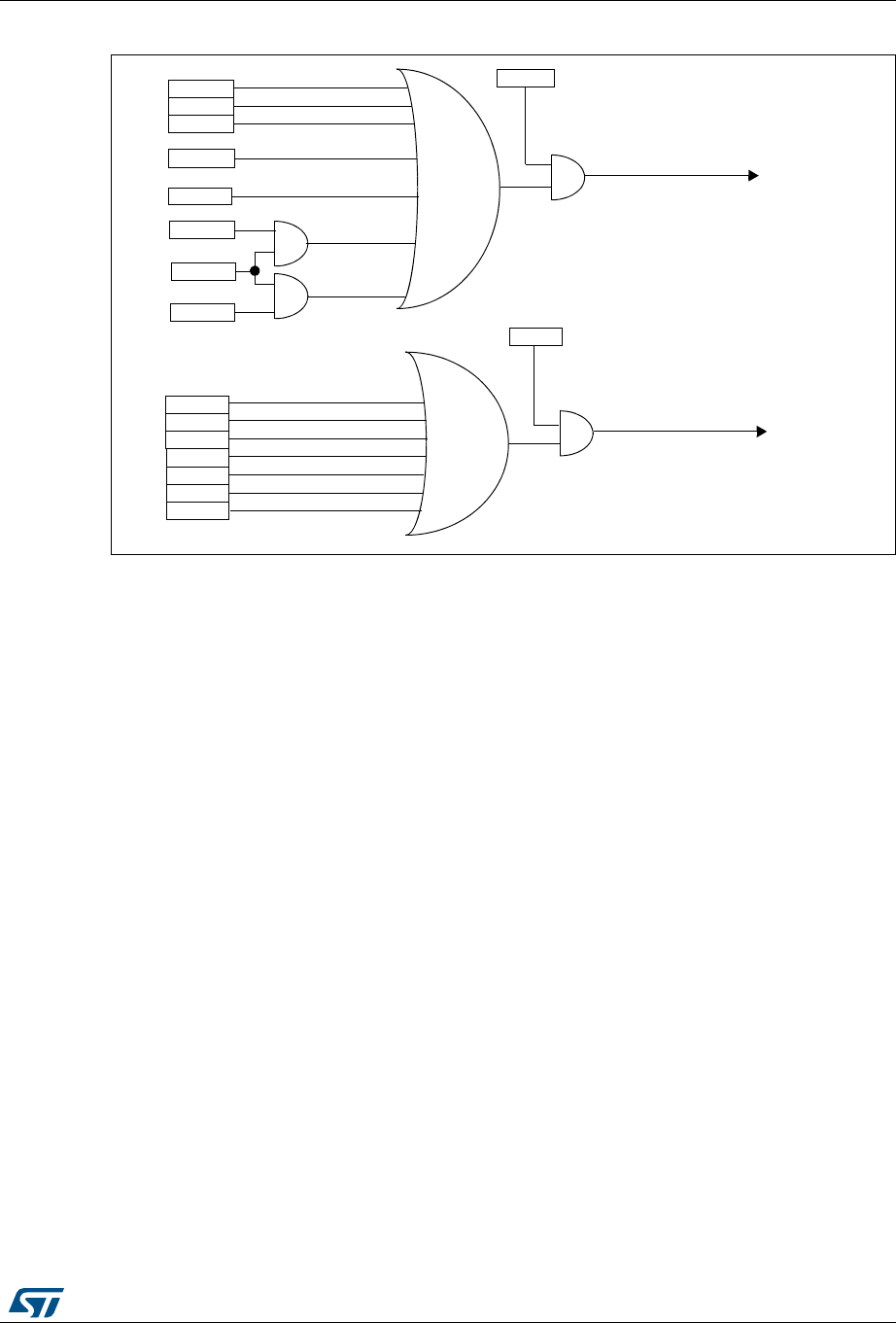
DocID027812 Rev 2 607/766
RM0401 Inter-integrated circuit (I2C) interface
621
Figure 213. I2C interrupt mapping diagram
ADDR
SB
ADD10
RxNE
TxE
BTF
it_event
ARLO
BERR
AF
OVR
PECERR
TIMEOUT
SMBALERT
ITERREN
it_error
ITEVFEN
ITBUFEN
STOPF

Inter-integrated circuit (I2C) interface RM0401
608/766 DocID027812 Rev 2
23.5 I2C debug mode
When the microcontroller enters the debug mode (Cortex®-M4 with FPU core halted), the
SMBUS timeout either continues to work normally or stops, depending on the
DBG_I2Cx_SMBUS_TIMEOUT configuration bits in the DBG module. For more details,
refer to Section 26.16.2: Debug support for timers, watchdog and I2C.
23.6 I2C registers
Refer to Section 1.1 on page 33 for a list of abbreviations used in register descriptions.
The peripheral registers have to be accessed by half-words (16 bits) or words (32 bits).
23.6.1 I2C Control register 1 (I2C_CR1)
Address offset: 0x00
Reset value: 0x0000
15 14 13 12 11 10 9876543210
SW
RST Res. ALERT PEC POS ACK STOP START
NO
STRET
CH
ENGC ENPEC ENARP SMB
TYPE Res. SM
BUS PE
rw rw rw rw rw rw rw rw rw rw rw rw rw rw
Bit 15 SWRST: Software reset
When set, the I2C is under reset state. Before resetting this bit, make sure the I2C lines are
released and the bus is free.
0: I2C Peripheral not under reset
1: I2C Peripheral under reset state
Note: This bit can be used to reinitialize the peripheral after an error or a locked state. As an
example, if the BUSY bit is set and remains locked due to a glitch on the bus, the
SWRST bit can be used to exit from this state.
Bit 14 Reserved, must be kept at reset value
Bit 13 ALERT: SMBus alert
This bit is set and cleared by software, and cleared by hardware when PE=0.
0: Releases SMBA pin high. Alert Response Address Header followed by NACK.
1: Drives SMBA pin low. Alert Response Address Header followed by ACK.
Bit 12 PEC: Packet error checking
This bit is set and cleared by software, and cleared by hardware when PEC is transferred or
by a START or Stop condition or when PE=0.
0: No PEC transfer
1: PEC transfer (in Tx or Rx mode)
Note: PEC calculation is corrupted by an arbitration loss.

DocID027812 Rev 2 609/766
RM0401 Inter-integrated circuit (I2C) interface
621
Bit 11 POS: Acknowledge/PEC Position (for data reception)
This bit is set and cleared by software and cleared by hardware when PE=0.
0: ACK bit controls the (N)ACK of the current byte being received in the shift register. The
PEC bit indicates that current byte in shift register is a PEC.
1: ACK bit controls the (N)ACK of the next byte which will be received in the shift register.
The PEC bit indicates that the next byte in the shift register is a PEC
Note: The POS bit must be used only in 2-byte reception configuration in master mode. It
must be configured before data reception starts, as described in the 2-byte reception
procedure recommended in Master receiver.
Bit 10 ACK: Acknowledge enable
This bit is set and cleared by software and cleared by hardware when PE=0.
0: No acknowledge returned
1: Acknowledge returned after a byte is received (matched address or data)
Bit 9 STOP: Stop generation
The bit is set and cleared by software, cleared by hardware when a Stop condition is
detected, set by hardware when a timeout error is detected.
In Master Mode:
0: No Stop generation.
1: Stop generation after the current byte transfer or after the current Start condition is sent.
In Slave mode:
0: No Stop generation.
1: Release the SCL and SDA lines after the current byte transfer.
Bit 8 START: Start generation
This bit is set and cleared by software and cleared by hardware when start is sent or PE=0.
In Master Mode:
0: No Start generation
1: Repeated start generation
In Slave mode:
0: No Start generation
1: Start generation when the bus is free
Bit 7 NOSTRETCH: Clock stretching disable (Slave mode)
This bit is used to disable clock stretching in slave mode when ADDR or BTF flag is set, until
it is reset by software.
0: Clock stretching enabled
1: Clock stretching disabled
Bit 6 ENGC: General call enable
0: General call disabled. Address 00h is NACKed.
1: General call enabled. Address 00h is ACKed.
Bit 5 ENPEC: PEC enable
0: PEC calculation disabled
1: PEC calculation enabled
Bit 4 ENARP: ARP enable
0: ARP disable
1: ARP enable
SMBus Device default address recognized if SMBTYPE=0
SMBus Host address recognized if SMBTYPE=1
Bit 3 SMBTYPE: SMBus type
0: SMBus Device
1: SMBus Host

Inter-integrated circuit (I2C) interface RM0401
610/766 DocID027812 Rev 2
Note: When the STOP, START or PEC bit is set, the software must not perform any write access
to I2C_CR1 before this bit is cleared by hardware. Otherwise there is a risk of setting a
second STOP, START or PEC request.
23.6.2 I2C Control register 2 (I2C_CR2)
Address offset: 0x04
Reset value: 0x0000
Bit 2 Reserved, must be kept at reset value
Bit 1 SMBUS: SMBus mode
0: I2C mode
1: SMBus mode
Bit 0 PE: Peripheral enable
0: Peripheral disable
1: Peripheral enable
Note: If this bit is reset while a communication is on going, the peripheral is disabled at the
end of the current communication, when back to IDLE state.
All bit resets due to PE=0 occur at the end of the communication.
In master mode, this bit must not be reset before the end of the communication.
15 14 13 12 11 10 9876543210
Res. Res. Res. LAST DMA
EN
ITBUF
EN
ITEVT
EN
ITERR
EN Res. Res. FREQ[5:0]
rw rw rw rw rw rw rw rw rw rw rw
Bits 15:13 Reserved, must be kept at reset value
Bit 12 LAST: DMA last transfer
0: Next DMA EOT is not the last transfer
1: Next DMA EOT is the last transfer
Note: This bit is used in master receiver mode to permit the generation of a NACK on the last
received data.
Bit 11 DMAEN: DMA requests enable
0: DMA requests disabled
1: DMA request enabled when TxE=1 or RxNE =1
Bit 10 ITBUFEN: Buffer interrupt enable
0: TxE = 1 or RxNE = 1 does not generate any interrupt.
1: TxE = 1 or RxNE = 1 generates Event Interrupt (whatever the state of DMAEN)
Bit 9 ITEVTEN: Event interrupt enable
0: Event interrupt disabled
1: Event interrupt enabled
This interrupt is generated when:
– SB = 1 (Master)
– ADDR = 1 (Master/Slave)
– ADD10= 1 (Master)
– STOPF = 1 (Slave)
– BTF = 1 with no TxE or RxNE event
– TxE event to 1 if ITBUFEN = 1
– RxNE event to 1if ITBUFEN = 1

DocID027812 Rev 2 611/766
RM0401 Inter-integrated circuit (I2C) interface
621
ITERREN: Error interrupt enable
0: Error interrupt disabled
1: Error interrupt enabled
This interrupt is generated when:
–BERR = 1
–ARLO = 1
–AF = 1
–OVR = 1
– PECERR = 1
–TIMEOUT = 1
– SMBALERT = 1
Bits 7:6 Reserved, must be kept at reset value
Bits 5:0 FREQ[5:0]: Peripheral clock frequency
The FREQ bits must be configured with the APB clock frequency value (I2C peripheral
connected to APB). The FREQ field is used by the peripheral to generate data setup and
hold times compliant with the I2C specifications. The minimum allowed frequency is 2 MHz,
the maximum frequency is limited by the maximum APB frequency (50 MHz) and cannot
exceed 50 MHz (peripheral intrinsic maximum limit).
0b000000: Not allowed
0b000001: Not allowed
0b000010: 2 MHz
...
0b110010: 50 MHz
Higher than 0b101010: Not allowed

Inter-integrated circuit (I2C) interface RM0401
612/766 DocID027812 Rev 2
23.6.3 I2C Own address register 1 (I2C_OAR1)
Address offset: 0x08
Reset value: 0x0000
23.6.4 I2C Own address register 2 (I2C_OAR2)
Address offset: 0x0C
Reset value: 0x0000
15 14 13 12 11 10 9876543210
ADD
MODE Res. Res. Res. Res. Res. ADD[9:8] ADD[7:1] ADD0
rw rw rw rw rw rw rw rw rw rw rw
Bit 15 ADDMODE Addressing mode (slave mode)
0: 7-bit slave address (10-bit address not acknowledged)
1: 10-bit slave address (7-bit address not acknowledged)
Bit 14 Should always be kept at 1 by software.
Bits 13:10 Reserved, must be kept at reset value
Bits 9:8 ADD[9:8]: Interface address
7-bit addressing mode: don’t care
10-bit addressing mode: bits9:8 of address
Bits 7:1 ADD[7:1]: Interface address
bits 7:1 of address
Bit 0 ADD0: Interface address
7-bit addressing mode: don’t care
10-bit addressing mode: bit 0 of address
15 14 13 12 11 10 9876543210
Res. Res. Res. Res. Res. Res. Res. Res. ADD2[7:1] EN
DUAL
rw rw rw rw rw rw rw rw
Bits 15:8 Reserved, must be kept at reset value
Bits 7:1 ADD2[7:1]: Interface address
bits 7:1 of address in dual addressing mode
Bit 0 ENDUAL: Dual addressing mode enable
0: Only OAR1 is recognized in 7-bit addressing mode
1: Both OAR1 and OAR2 are recognized in 7-bit addressing mode

DocID027812 Rev 2 613/766
RM0401 Inter-integrated circuit (I2C) interface
621
23.6.5 I2C Data register (I2C_DR)
Address offset: 0x10
Reset value: 0x0000
23.6.6 I2C Status register 1 (I2C_SR1)
Address offset: 0x14
Reset value: 0x0000
15 14 13 12 11 10 9876543210
Res. Res. Res. Res. Res. Res. Res. Res. DR[7:0]
rw rw rw rw rw rw rw rw
Bits 15:8 Reserved, must be kept at reset value
Bits 7:0 DR[7:0] 8-bit data register
Byte received or to be transmitted to the bus.
– Transmitter mode: Byte transmission starts automatically when a byte is written in the DR
register. A continuous transmit stream can be maintained if the next data to be transmitted is
put in DR once the transmission is started (TxE=1)
– Receiver mode: Received byte is copied into DR (RxNE=1). A continuous transmit stream
can be maintained if DR is read before the next data byte is received (RxNE=1).
Note: In slave mode, the address is not copied into DR.
Write collision is not managed (DR can be written if TxE=0).
If an ARLO event occurs on ACK pulse, the received byte is not copied into DR
and so cannot be read.
15 14 13 12 11 10 9876543210
SMB
ALERT
TIMEO
UT Res. PEC
ERR OVR AF ARLO BERR TxE RxNE Res. STOPF ADD10 BTF ADDR SB
rc_w0 rc_w0 rc_w0 rc_w0 rc_w0 rc_w0 rc_w0 r r r r r r r

Inter-integrated circuit (I2C) interface RM0401
614/766 DocID027812 Rev 2
Bit 15 SMBALERT: SMBus alert
In SMBus host mode:
0: no SMBALERT
1: SMBALERT event occurred on pin
In SMBus slave mode:
0: no SMBALERT response address header
1: SMBALERT response address header to SMBALERT LOW received
– Cleared by software writing 0, or by hardware when PE=0.
Bit 14 TIMEOUT: Timeout or Tlow error
0: No timeout error
1: SCL remained LOW for 25 ms (Timeout)
or
Master cumulative clock low extend time more than 10 ms (Tlow:mext)
or
Slave cumulative clock low extend time more than 25 ms (Tlow:sext)
– When set in slave mode: slave resets the communication and lines are released by
hardware
– When set in master mode: Stop condition sent by hardware
– Cleared by software writing 0, or by hardware when PE=0.
Note: This functionality is available only in SMBus mode.
Bit 13 Reserved, must be kept at reset value
Bit 12 PECERR: PEC Error in reception
0: no PEC error: receiver returns ACK after PEC reception (if ACK=1)
1: PEC error: receiver returns NACK after PEC reception (whatever ACK)
– Cleared by software writing 0, or by hardware when PE=0.
– Note: When the received CRC is wrong, PECERR is not set in slave mode if the PEC control
bit is not set before the end of the CRC reception. Nevertheless, reading the PEC value
determines whether the received CRC is right or wrong.
Bit 11 OVR: Overrun/Underrun
0: No overrun/underrun
1: Overrun or underrun
– Set by hardware in slave mode when NOSTRETCH=1 and:
– In reception when a new byte is received (including ACK pulse) and the DR register has not
been read yet. New received byte is lost.
– In transmission when a new byte should be sent and the DR register has not been written
yet. The same byte is sent twice.
– Cleared by software writing 0, or by hardware when PE=0.
Note: If the DR write occurs very close to SCL rising edge, the sent data is unspecified and a
hold timing error occurs
Bit 10 AF: Acknowledge failure
0: No acknowledge failure
1: Acknowledge failure
– Set by hardware when no acknowledge is returned.
– Cleared by software writing 0, or by hardware when PE=0.

DocID027812 Rev 2 615/766
RM0401 Inter-integrated circuit (I2C) interface
621
Bit 9 ARLO: Arbitration lost (master mode)
0: No Arbitration Lost detected
1: Arbitration Lost detected
Set by hardware when the interface loses the arbitration of the bus to another master
– Cleared by software writing 0, or by hardware when PE=0.
After an ARLO event the interface switches back automatically to Slave mode (MSL=0).
Note: In SMBUS, the arbitration on the data in slave mode occurs only during the data phase,
or the acknowledge transmission (not on the address acknowledge).
Bit 8 BERR: Bus error
0: No misplaced Start or Stop condition
1: Misplaced Start or Stop condition
– Set by hardware when the interface detects an SDA rising or falling edge while SCL is high,
occurring in a non-valid position during a byte transfer.
– Cleared by software writing 0, or by hardware when PE=0.
Bit 7 TxE: Data register empty (transmitters)
0: Data register not empty
1: Data register empty
– Set when DR is empty in transmission. TxE is not set during address phase.
– Cleared by software writing to the DR register or by hardware after a start or a stop condition
or when PE=0.
TxE is not set if either a NACK is received, or if next byte to be transmitted is PEC (PEC=1)
Note: TxE is not cleared by writing the first data being transmitted, or by writing data when
BTF is set, as in both cases the data register is still empty.
Bit 6 RxNE: Data register not empty (receivers)
0: Data register empty
1: Data register not empty
– Set when data register is not empty in receiver mode. RxNE is not set during address phase.
– Cleared by software reading or writing the DR register or by hardware when PE=0.
RxNE is not set in case of ARLO event.
Note: RxNE is not cleared by reading data when BTF is set, as the data register is still full.
Bit 5 Reserved, must be kept at reset value
Bit 4 STOPF: Stop detection (slave mode)
0: No Stop condition detected
1: Stop condition detected
– Set by hardware when a Stop condition is detected on the bus by the slave after an
acknowledge (if ACK=1).
– Cleared by software reading the SR1 register followed by a write in the CR1 register, or by
hardware when PE=0
Note: The STOPF bit is not set after a NACK reception.
It is recommended to perform the complete clearing sequence (READ SR1 then
WRITE CR1) after the STOPF is set. Refer to Figure 210: Transfer sequence diagram
for slave receiver on page 593.

Inter-integrated circuit (I2C) interface RM0401
616/766 DocID027812 Rev 2
Bit 3 ADD10: 10-bit header sent (Master mode)
0: No ADD10 event occurred.
1: Master has sent first address byte (header).
– Set by hardware when the master has sent the first byte in 10-bit address mode.
– Cleared by software reading the SR1 register followed by a write in the DR register of the
second address byte, or by hardware when PE=0.
Note: ADD10 bit is not set after a NACK reception
Bit 2 BTF: Byte transfer finished
0: Data byte transfer not done
1: Data byte transfer succeeded
– Set by hardware when NOSTRETCH=0 and:
– In reception when a new byte is received (including ACK pulse) and DR has not been read
yet (RxNE=1).
– In transmission when a new byte should be sent and DR has not been written yet (TxE=1).
– Cleared by software by either a read or write in the DR register or by hardware after a start or
a stop condition in transmission or when PE=0.
Note: The BTF bit is not set after a NACK reception
The BTF bit is not set if next byte to be transmitted is the PEC (TRA=1 in I2C_SR2
register and PEC=1 in I2C_CR1 register)
Bit 1 ADDR: Address sent (master mode)/matched (slave mode)
This bit is cleared by software reading SR1 register followed reading SR2, or by hardware
when PE=0.
Address matched (Slave)
0: Address mismatched or not received.
1: Received address matched.
– Set by hardware as soon as the received slave address matched with the OAR registers
content or a general call or a SMBus Device Default Address or SMBus Host or SMBus Alert
is recognized. (when enabled depending on configuration).
Note: In slave mode, it is recommended to perform the complete clearing sequence (READ
SR1 then READ SR2) after ADDR is set. Refer to Figure 210: Transfer sequence
diagram for slave receiver on page 593.
Address sent (Master)
0: No end of address transmission
1: End of address transmission
– For 10-bit addressing, the bit is set after the ACK of the 2nd byte.
– For 7-bit addressing, the bit is set after the ACK of the byte.
Note: ADDR is not set after a NACK reception
Bit 0 SB: Start bit (Master mode)
0: No Start condition
1: Start condition generated.
– Set when a Start condition generated.
– Cleared by software by reading the SR1 register followed by writing the DR register, or by
hardware when PE=0

DocID027812 Rev 2 617/766
RM0401 Inter-integrated circuit (I2C) interface
621
23.6.7 I2C Status register 2 (I2C_SR2)
Address offset: 0x18
Reset value: 0x0000
Note: Reading I2C_SR2 after reading I2C_SR1 clears the ADDR flag, even if the ADDR flag was
set after reading I2C_SR1. Consequently, I2C_SR2 must be read only when ADDR is found
set in I2C_SR1 or when the STOPF bit is cleared.
1514131211109876543210
PEC[7:0] DUALF SMB
HOST
SMB
DEFAU
LT
GEN
CALL Res. TRA BUSY MSL
rrrrrrrrrrrr rrr
Bits 15:8 PEC[7:0] Packet error checking register
This register contains the internal PEC when ENPEC=1.
Bit 7 DUALF: Dual flag (Slave mode)
0: Received address matched with OAR1
1: Received address matched with OAR2
– Cleared by hardware after a Stop condition or repeated Start condition, or when PE=0.
Bit 6 SMBHOST: SMBus host header (Slave mode)
0: No SMBus Host address
1: SMBus Host address received when SMBTYPE=1 and ENARP=1.
– Cleared by hardware after a Stop condition or repeated Start condition, or when PE=0.
Bit 5 SMBDEFAULT: SMBus device default address (Slave mode)
0: No SMBus Device Default address
1: SMBus Device Default address received when ENARP=1
– Cleared by hardware after a Stop condition or repeated Start condition, or when PE=0.
Bit 4 GENCALL: General call address (Slave mode)
0: No General Call
1: General Call Address received when ENGC=1
– Cleared by hardware after a Stop condition or repeated Start condition, or when PE=0.
Bit 3 Reserved, must be kept at reset value

Inter-integrated circuit (I2C) interface RM0401
618/766 DocID027812 Rev 2
Note: Reading I2C_SR2 after reading I2C_SR1 clears the ADDR flag, even if the ADDR flag was
set after reading I2C_SR1. Consequently, I2C_SR2 must be read only when ADDR is found
set in I2C_SR1 or when the STOPF bit is cleared.
23.6.8 I2C Clock control register (I2C_CCR)
Address offset: 0x1C
Reset value: 0x0000
Note: fPCLK1 must be at least 2 MHz to achieve Sm mode I²C frequencies. It must be at least 4
MHz to achieve Fm mode I²C frequencies. It must be a multiple of 10MHz to reach the
400 kHz maximum I²C Fm mode clock.
The CCR register must be configured only when the I2C is disabled (PE = 0).
Bit 2 TRA: Transmitter/receiver
0: Data bytes received
1: Data bytes transmitted
This bit is set depending on the R/W bit of the address byte, at the end of total address
phase.
It is also cleared by hardware after detection of Stop condition (STOPF=1), repeated Start
condition, loss of bus arbitration (ARLO=1), or when PE=0.
Bit 1 BUSY: Bus busy
0: No communication on the bus
1: Communication ongoing on the bus
– Set by hardware on detection of SDA or SCL low
– cleared by hardware on detection of a Stop condition.
It indicates a communication in progress on the bus. This information is still updated when
the interface is disabled (PE=0).
Bit 0 MSL: Master/slave
0: Slave Mode
1: Master Mode
– Set by hardware as soon as the interface is in Master mode (SB=1).
– Cleared by hardware after detecting a Stop condition on the bus or a loss of arbitration
(ARLO=1), or by hardware when PE=0.
1514131211109876543210
F/S DUTY Res. Res. CCR[11:0]
rw rw rw rw rw rw rw rw rw rw rw rw rw rw
Bit 15 F/S: I2C master mode selection
0: Sm mode I2C
1: Fm mode I2C

DocID027812 Rev 2 619/766
RM0401 Inter-integrated circuit (I2C) interface
621
23.6.9 I2C TRISE register (I2C_TRISE)
Address offset: 0x20
Reset value: 0x0002
Bit 14 DUTY: Fm mode duty cycle
0: Fm mode tlow/thigh = 2
1: Fm mode tlow/thigh = 16/9 (see CCR)
Bits 13:12 Reserved, must be kept at reset value
Bits 11:0 CCR[11:0]: Clock control register in Fm/Sm mode (Master mode)
Controls the SCL clock in master mode.
Sm mode or SMBus:
Thigh = CCR * TPCLK1
Tlow = CCR * TPCLK1
Fm mode:
If DUTY = 0:
Thigh = CCR * TPCLK1
Tlow = 2 * CCR * TPCLK1
If DUTY = 1: (to reach 400 kHz)
Thigh = 9 * CCR * TPCLK1
Tlow = 16 * CCR * TPCLK1
For instance: in Sm mode, to generate a 100 kHz SCL frequency:
If FREQR = 08, TPCLK1 = 125 ns so CCR must be programmed with 0x28
(0x28 <=> 40d x 125 ns = 5000 ns.)
Note: The minimum allowed value is 0x04, except in FAST DUTY mode where the minimum
allowed value is 0x01
thigh = tr(SCL) + tw(SCLH). See device datasheet for the definitions of parameters.
tlow = tf(SCL) + tw(SCLL). See device datasheet for the definitions of parameters.
I2C communication speed, fSCL ~ 1/(thigh + tlow). The real frequency may differ due to
the analog noise filter input delay.
The CCR register must be configured only when the I2C is disabled (PE = 0).
15 14 13 12 11 10 9876543210
Res. Res. Res. Res. Res. Res. Res. Res. Res. Res. TRISE[5:0]
rw rw rw rw rw rw
Bits 15:6 Reserved, must be kept at reset value
Bits 5:0 TRISE[5:0]: Maximum rise time in Fm/Sm mode (Master mode)
These bits should provide the maximum duration of the SCL feedback loop in master mode.
The purpose is to keep a stable SCL frequency whatever the SCL rising edge duration.
These bits must be programmed with the maximum SCL rise time given in the I2C bus
specification, incremented by 1.
For instance: in Sm mode, the maximum allowed SCL rise time is 1000 ns.
If, in the I2C_CR2 register, the value of FREQ[5:0] bits is equal to 0x08 and TPCLK1 = 125 ns
therefore the TRISE[5:0] bits must be programmed with 09h.
(1000 ns / 125 ns = 8 + 1)
The filter value can also be added to TRISE[5:0].
If the result is not an integer, TRISE[5:0] must be programmed with the integer part, in order
to respect the tHIGH parameter.
Note: TRISE[5:0] must be configured only when the I2C is disabled (PE = 0).

Inter-integrated circuit (I2C) interface RM0401
620/766 DocID027812 Rev 2
23.6.10 I2C FLTR register (I2C_FLTR)
Address offset: 0x24
Reset value: 0x0000
1514131211109876543210
Res. Res. Res. Res. Res. Res. Res. Res. Res. Res. Res. ANOFF DNF[3:0]
rw rw rw rw rw
Bits 15:5 Reserved, must be kept at reset value
Bit 4 ANOFF: Analog noise filter OFF
0: Analog noise filter enable
1: Analog noise filter disable
Note: ANOFF must be configured only when the I2C is disabled (PE = 0).
Bits 3:0 DNF[3:0]: Digital noise filter
These bits are used to configure the digital noise filter on SDA and SCL inputs. The digital filter
will suppress the spikes with a length of up to DNF[3:0] * TPCLK1.
0000: Digital noise filter disable
0001: Digital noise filter enabled and filtering capability up to 1* TPCLK1.
...
1111: Digital noise filter enabled and filtering capability up to 15* TPCLK1.
Note: DNF[3:0] must be configured only when the I2C is disabled (PE = 0). If the analog filter
is also enabled, the digital filter is added to the analog filter.

DocID027812 Rev 2 621/766
RM0401 Inter-integrated circuit (I2C) interface
621
23.6.11 I2C register map
The table below provides the I2C register map and reset values.
Refer to Section 2.2.2 for the register boundary addresses.
Table 95. I2C register map and reset values
Offset Register
31
30
29
28
27
26
25
24
23
22
21
20
19
18
17
16
15
14
13
12
11
10
9
8
7
6
5
4
3
2
1
0
0x00
I2C_CR1
Res.
Res.
Res.
Res.
Res.
Res.
Res.
Res.
Res.
Res.
Res.
Res.
Res.
Res.
Res.
Res.
SWRST
Res.
ALERT
PEC
POS
ACK
STOP
START
NOSTRETCH
ENGC
ENPEC
ENARP
SMBTYPE
Res.
SMBUS
PE
Reset value 0 00000000000 00
0x04
I2C_CR2
Res.
Res.
Res.
Res.
Res.
Res.
Res.
Res.
Res.
Res.
Res.
Res.
Res.
Res.
Res.
Res.
Res.
Res.
Res.
LAST
DMAEN
ITBUFEN
ITEVTEN
ITERREN
Res.
Res.
FREQ[5:0]
Reset value 00000 000000
0x08
I2C_OAR1
Res.
Res.
Res.
Res.
Res.
Res.
Res.
Res.
Res.
Res.
Res.
Res.
Res.
Res.
Res.
Res.
ADDMODE
Res.
Res.
Res.
Res.
Res.
ADD[
9:8] ADD[7:1]
ADD0
Reset value 0 0000000000
0x0C
I2C_OAR2
Res.
Res.
Res.
Res.
Res.
Res.
Res.
Res.
Res.
Res.
Res.
Res.
Res.
Res.
Res.
Res.
Res.
Res.
Res.
Res.
Res.
Res.
Res.
Res.
ADD2[7:1]
ENDUAL
Reset value 00000000
0x10
I2C_DR
Res.
Res.
Res.
Res.
Res.
Res.
Res.
Res.
Res.
Res.
Res.
Res.
Res.
Res.
Res.
Res.
Res.
Res.
Res.
Res.
Res.
Res.
Res.
Res.
DR[7:0]
Reset value 00000000
0x14
I2C_SR1
Res.
Res.
Res.
Res.
Res.
Res.
Res.
Res.
Res.
Res.
Res.
Res.
Res.
Res.
Res.
Res.
SMBALERT
TIMEOUT
Res.
PECERR
OVR
AF
ARLO
BERR
TxE
RxNE
Res.
STOPF
ADD10
BTF
ADDR
SB
Reset value 00 0000000 00000
0x18
I2C_SR2
Res.
Res.
Res.
Res.
Res.
Res.
Res.
Res.
Res.
Res.
Res.
Res.
Res.
Res.
Res.
Res.
PEC[7:0]
DUALF
SMBHOST
SMBDEFAULT
GENCALL
Res.
TRA
BUSY
MSL
Reset value 000000000000 000
0x1C
I2C_CCR
Res.
Res.
Res.
Res.
Res.
Res.
Res.
Res.
Res.
Res.
Res.
Res.
Res.
Res.
Res.
Res.
F/S
DUTY
Res.
Res.
CCR[11:0]
Reset value 00 000000000000
0x20
I2C_TRISE
Res.
Res.
Res.
Res.
Res.
Res.
Res.
Res.
Res.
Res.
Res.
Res.
Res.
Res.
Res.
Res.
Res.
Res.
Res.
Res.
Res.
Res.
Res.
Res.
Res.
Res.
TRISE[5:0]
Reset value 000010
0x24
I2C_FLTR
Res.
Res.
Res.
Res.
Res.
Res.
Res.
Res.
Res.
Res.
Res.
Res.
Res.
Res.
Res.
Res.
Res.
Res.
Res.
Res.
Res.
Res.
Res.
Res.
Res.
Res.
Res.
ANOFF
DNF[3:0]
Reset value 00000

Universal synchronous asynchronous receiver transmitter (USART) RM0401
622/766 DocID027812 Rev 2
24 Universal synchronous asynchronous receiver
transmitter (USART)
24.1 USART introduction
The universal synchronous asynchronous receiver transmitter (USART) offers a flexible
means of full-duplex data exchange with external equipment requiring an industry standard
NRZ asynchronous serial data format. The USART offers a very wide range of baud rates
using a fractional baud rate generator.
It supports synchronous one-way communication and half-duplex single wire
communication. It also supports the LIN (local interconnection network), Smartcard Protocol
and IrDA (infrared data association) SIR ENDEC specifications, and modem operations
(CTS/RTS). It allows multiprocessor communication.
High speed data communication is possible by using the DMA for multibuffer configuration.

DocID027812 Rev 2 623/766
RM0401 Universal synchronous asynchronous receiver transmitter (USART)
674
24.2 USART main features
•Full duplex, asynchronous communications
•NRZ standard format (Mark/Space)
•Configurable oversampling method by 16 or by 8 to give flexibility between speed and
clock tolerance
•Fractional baud rate generator systems
– Common programmable transmit and receive baud rate (refer to the datasheets
for the value of the baud rate at the maximum APB frequency.
•Programmable data word length (8 or 9 bits)
•Configurable stop bits - support for 1 or 2 stop bits
•LIN Master Synchronous Break send capability and LIN slave break detection
capability
– 13-bit break generation and 10/11 bit break detection when USART is hardware
configured for LIN
•Transmitter clock output for synchronous transmission
•IrDA SIR encoder decoder
– Support for 3/16 bit duration for normal mode
•Smartcard emulation capability
– The Smartcard interface supports the asynchronous protocol Smartcards as
defined in the ISO 7816-3 standards
– 0.5, 1.5 stop bits for Smartcard operation
•Single-wire half-duplex communication
•Configurable multibuffer communication using DMA (direct memory access)
– Buffering of received/transmitted bytes in reserved SRAM using centralized DMA
•Separate enable bits for transmitter and receiver
•Transfer detection flags:
– Receive buffer full
– Transmit buffer empty
– End of transmission flags
•Parity control:
– Transmits parity bit
– Checks parity of received data byte
•Four error detection flags:
– Overrun error
– Noise detection
– Frame error
– Parity error
•Ten interrupt sources with flags:
– CTS changes
– LIN break detection
– Transmit data register empty
– Transmission complete
Universal synchronous asynchronous receiver transmitter (USART) RM0401
624/766 DocID027812 Rev 2
– Receive data register full
– Idle line received
– Overrun error
– Framing error
– Noise error
– Parity error
•Multiprocessor communication - enter into mute mode if address match does not occur
•Wake up from mute mode (by idle line detection or address mark detection)
•Two receiver wakeup modes: Address bit (MSB, 9th bit), Idle line
24.3 USART implementation
This section describes the full set of features implemented in USART1. Refer to Table 96:
USART features for the differences between USART instances.
24.4 USART functional description
The interface is externally connected to another device by three pins (see Figure 214). Any
USART bidirectional communication requires a minimum of two pins: Receive Data In (RX)
and Transmit Data Out (TX):
RX: Receive Data Input is the serial data input. Oversampling techniques are used for data
recovery by discriminating between valid incoming data and noise.
TX: Transmit Data Output. When the transmitter is disabled, the output pin returns to its I/O
port configuration. When the transmitter is enabled and nothing is to be transmitted, the TX
pin is at high level. In single-wire and smartcard modes, this I/O is used to transmit and
receive the data (at USART level, data are then received on SW_RX).
Table 96. USART features
USART modes/features(1)
1. X = supported.
USART1, USART2 USART6
Hardware flow control for modem(2)
2. This feature is not available on all packages (refer to the datasheet for more information).
X-
Continuous communication using DMA X X
Multiprocessor communication X X
Synchronous mode(2) XX
Smartcard mode X X
Single-wire half-duplex communication X X
IrDA SIR ENDEC block X X
LIN mode X X
USART data length 8 or 9 bits

DocID027812 Rev 2 625/766
RM0401 Universal synchronous asynchronous receiver transmitter (USART)
674
Through these pins, serial data is transmitted and received in normal USART mode as
frames comprising:
•An Idle Line prior to transmission or reception
•A start bit
•A data word (8 or 9 bits) least significant bit first
•0.5,1, 1.5, 2 Stop bits indicating that the frame is complete
•This interface uses a fractional baud rate generator - with a 12-bit mantissa and 4-bit
fraction
•A status register (USART_SR)
•Data Register (USART_DR)
•A baud rate register (USART_BRR) - 12-bit mantissa and 4-bit fraction.
•A Guardtime Register (USART_GTPR) in case of Smartcard mode.
Refer to Section 24.6: USART registers for the definition of each bit.
The following pin is required to interface in synchronous mode:
•SCLK: Transmitter clock output. This pin outputs the transmitter data clock for
synchronous transmission corresponding to SPI master mode (no clock pulses on start
bit and stop bit, and a software option to send a clock pulse on the last data bit). In
parallel data can be received synchronously on RX. This can be used to control
peripherals that have shift registers (e.g. LCD drivers). The clock phase and polarity
are software programmable. In smartcard mode, SCLK can provide the clock to the
smartcard.
The following pins are required in Hardware flow control mode:
•nCTS: Clear To Send blocks the data transmission at the end of the current transfer
when high
•nRTS: Request to send indicates that the USART is ready to receive a data (when
low).
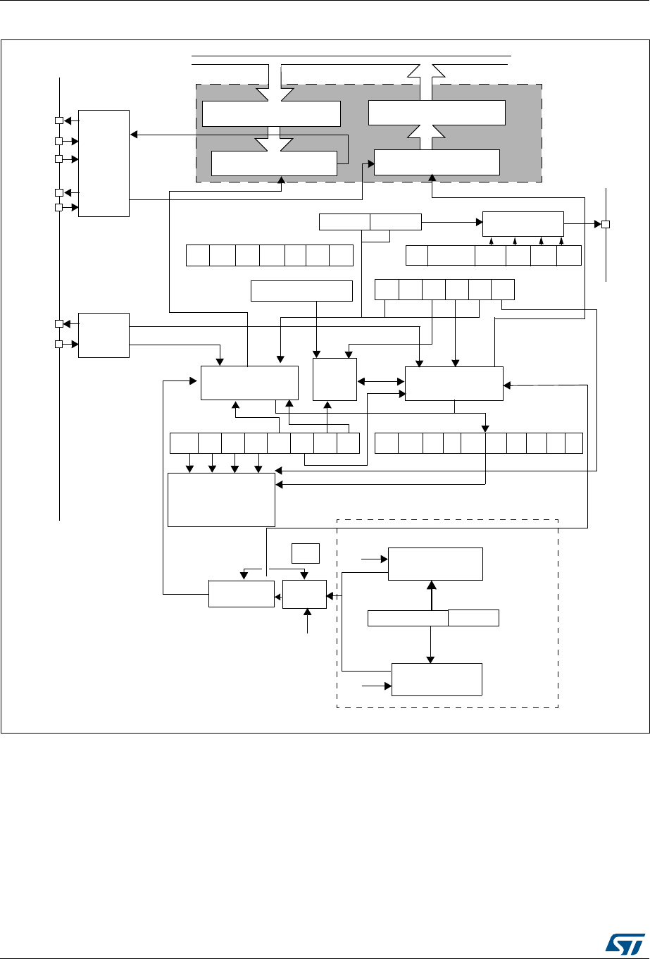
Universal synchronous asynchronous receiver transmitter (USART) RM0401
626/766 DocID027812 Rev 2
Figure 214. USART block diagram
Wakeup
unit
Receiver
control
SR
Transmit
control
TXETC RXNEIDLEORE NF FE
USART
control
interrupt
CR1
MWAKE
Receive data register (RDR)
Receive Shift Register
Read
Transmit data register (TDR)
Transmit Shift Register
Write
SW_RX
TX
(Data register) DR
Transmitter
clock
Receiver
clock
Receiver rate
Transmitter rate
f
PCLKx(x=1,2)
control
control
/
[8 x (2 - OVER8)]
Conventional baud rate generator
SBKRWURETE
IDLERXNE
TCIETXEIE
CR1
UE PCE PS
PEIE
PE
PWDATA
IRLP
SCEN IREN
DMAR
DMAT
USART Address
CR2
CR3
IrDA
SIR
ENDEC
block
LINE CKEN CPOL CPHA LBCL
SCLK control SCLK
CR2
GT
STOP[1:0]
NACK
DIV_Mantissa
15 0
RE
USART_BRR
/USARTDIV
TE
HD
(CPU or DMA)
(CPU or DMA)
PRDATA
Hardware
flow
controller
CTS LBD
RX
IRDA_OUT
IRDA_IN
nRTS
nCTS
GTPR
PSC
IE IE
DIV_Fraction
4
USARTDIV = DIV_Mantissa + (DIV_Fraction / 8 × (2 – OVER8))
SAMPLING
CR1
OVER8
DIVIDER
ai16099
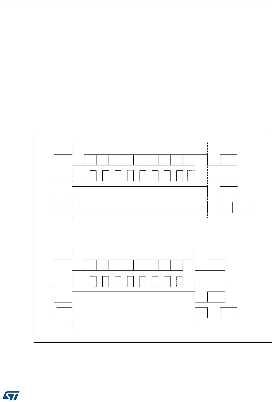
DocID027812 Rev 2 627/766
RM0401 Universal synchronous asynchronous receiver transmitter (USART)
674
24.4.1 USART character description
Word length may be selected as being either 8 or 9 bits by programming the M bit in the
USART_CR1 register (see Figure 215).
The TX pin is in low state during the start bit. It is in high state during the stop bit.
An Idle character is interpreted as an entire frame of “1”s followed by the start bit of the
next frame which contains data (The number of “1” ‘s will include the number of stop bits).
A Break character is interpreted on receiving “0”s for a frame period. At the end of the
break frame the transmitter inserts either 1 or 2 stop bits (logic “1” bit) to acknowledge the
start bit.
Transmission and reception are driven by a common baud rate generator, the clock for each
is generated when the enable bit is set respectively for the transmitter and receiver.
The details of each block is given below.
Figure 215. Word length programming
069
%LW %LW %LW %LW %LW %LW %LW %LW %LW
6WDUW
ELW
6WRS
ELW
1H[W
6WDUW
ELW
,GOHIUDPH
J S
%UHDNIUDPH
&ORFN
%LW %LW %LW %LW %LW %LW %LW %LW
&ORFN
ELWZRUGOHQJWK0ELWLVUHVHW6WRSELW
6WDUW
ELW
6WRS
ELW
6WDUW
ELW
6WDUW
ELW
3RVVLEOH
SDULW\ELW
1H[WGDWDIUDPH'DWDIUDPH
3RVVLEOH
SDULW\ELW
1H[WGDWDIUDPH'DWDIUDPH
6WRS
ELW
6WDUW
ELW
6WRS
ELW
6WDUW
ELW
/%&/ELWFRQWUROVODVWGDWDFORFNSXOVH
,GOHIUDPH
%UHDNIUDPH
1H[W
6WDUW
ELW

Universal synchronous asynchronous receiver transmitter (USART) RM0401
628/766 DocID027812 Rev 2
24.4.2 Transmitter
The transmitter can send data words of either 8 or 9 bits depending on the M bit status.
When the transmit enable bit (TE) is set, the data in the transmit shift register is output on
the TX pin and the corresponding clock pulses are output on the SCLK pin.
Character transmission
During an USART transmission, data shifts out least significant bit first on the TX pin. In this
mode, the USART_DR register consists of a buffer (TDR) between the internal bus and the
transmit shift register (see Figure 214).
Every character is preceded by a start bit which is a logic level low for one bit period. The
character is terminated by a configurable number of stop bits.
The following stop bits are supported by USART: 0.5, 1, 1.5 and 2 stop bits.
Note: The TE bit should not be reset during transmission of data. Resetting the TE bit during the
transmission will corrupt the data on the TX pin as the baud rate counters will get frozen.
The current data being transmitted will be lost.
An idle frame will be sent after the TE bit is enabled.
Configurable stop bits
The number of stop bits to be transmitted with every character can be programmed in
Control register 2, bits 13,12.
•1 stop bit: This is the default value of number of stop bits.
•2 Stop bits: This will be supported by normal USART, single-wire and modem modes.
•0.5 stop bit: To be used when receiving data in Smartcard mode.
•1.5 stop bits: To be used when transmitting and receiving data in Smartcard mode.
An idle frame transmission will include the stop bits.
A break transmission will be 10 low bits followed by the configured number of stop bits
(when m = 0) and 11 low bits followed by the configured number of stop bits (when m = 1). It
is not possible to transmit long breaks (break of length greater than 10/11 low bits).
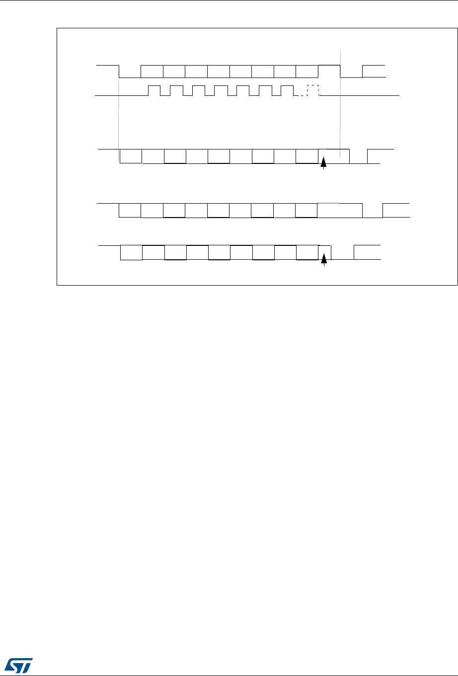
DocID027812 Rev 2 629/766
RM0401 Universal synchronous asynchronous receiver transmitter (USART)
674
Figure 216. Configurable stop bits
Procedure:
1. Enable the USART by writing the UE bit in USART_CR1 register to 1.
2. Program the M bit in USART_CR1 to define the word length.
3. Program the number of stop bits in USART_CR2.
4. Select DMA enable (DMAT) in USART_CR3 if Multi buffer Communication is to take
place. Configure the DMA register as explained in multibuffer communication.
5. Select the desired baud rate using the USART_BRR register.
6. Set the TE bit in USART_CR1 to send an idle frame as first transmission.
7. Write the data to send in the USART_DR register (this clears the TXE bit). Repeat this
for each data to be transmitted in case of single buffer.
8. After writing the last data into the USART_DR register, wait until TC=1. This indicates
that the transmission of the last frame is complete. This is required for instance when
the USART is disabled or enters the Halt mode to avoid corrupting the last
transmission.
Single byte communication
Clearing the TXE bit is always performed by a write to the data register.
The TXE bit is set by hardware and it indicates:
•The data has been moved from TDR to the shift register and the data transmission has
started.
•The TDR register is empty.
•The next data can be written in the USART_DR register without overwriting the
previous data.
This flag generates an interrupt if the TXEIE bit is set.
Bit0 Bit1 Bit2 Bit3 Bit4 Bit5 Bit6 Bit7
Start
Bit Stop
bit
Next
start
bit
8-bit Word length (M bit is reset)
Possible
parity
bit
Data frame
Next data frame
****
** LBCL bit controls last data clock pulse
CLOCK **
Bit0 Bit1 Bit2 Bit3 Bit4 Bit5 Bit6 Bit7
Start
Bit
2 Stop
Bits
Next
Start
Bit
Possible
parity
bit
Data frame
Next data frame
Bit0 Bit1 Bit2 Bit3 Bit4 Bit5 Bit6 Bit7
Start
Bit
Next
start
bit
Possible
Parity
Bit
Data frame
Next data frame
1/2 stop bit
Bit0 Bit1 Bit2 Bit3 Bit4 Bit5 Bit6 Bit7
Start
Bit
Next
start
bit
Possible
Parity
Bit
Data frame
Next data frame
1 1/2 stop bits
a) 1 Stop Bit
b) 1 1/2 stop Bits
c) 2 Stop Bits
d) 1/2 Stop Bit
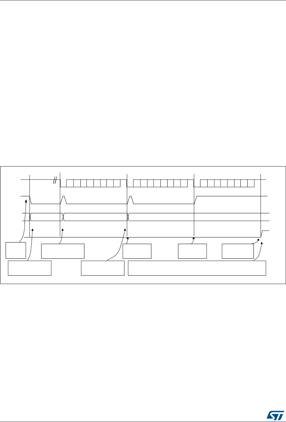
Universal synchronous asynchronous receiver transmitter (USART) RM0401
630/766 DocID027812 Rev 2
When a transmission is taking place, a write instruction to the USART_DR register stores
the data in the TDR register and which is copied in the shift register at the end of the current
transmission.
When no transmission is taking place, a write instruction to the USART_DR register places
the data directly in the shift register, the data transmission starts, and the TXE bit is
immediately set.
If a frame is transmitted (after the stop bit) and the TXE bit is set, the TC bit goes high. An
interrupt is generated if the TCIE bit is set in the USART_CR1 register.
After writing the last data into the USART_DR register, it is mandatory to wait for TC=1
before disabling the USART or causing the microcontroller to enter the low power mode
(see Figure 217: TC/TXE behavior when transmitting).
The TC bit is cleared by the following software sequence:
1. A read from the USART_SR register
2. A write to the USART_DR register
Note: The TC bit can also be cleared by writing a ‘0 to it. This clearing sequence is recommended
only for Multibuffer communication.
Figure 217. TC/TXE behavior when transmitting
Break characters
Setting the SBK bit transmits a break character. The break frame length depends on the M
bit (see Figure 215).
If the SBK bit is set to ‘1 a break character is sent on the TX line after completing the current
character transmission. This bit is reset by hardware when the break character is completed
(during the stop bit of the break character). The USART inserts a logic 1 bit at the end of the
last break frame to guarantee the recognition of the start bit of the next frame.
Note: If the software resets the SBK bit before the commencement of break transmission, the
break character will not be transmitted. For two consecutive breaks, the SBK bit should be
set after the stop bit of the previous break.
48LINE
53!24?$2
&RAME
48%FLAG
&
4#FLAG
&
&RAME
SOFTWAREWAITSUNTIL48%
ANDWRITES&INTO$2
SOFTWAREWAITSUNTIL48%
ANDWRITES&INTO$2
4#ISNOTSET
BECAUSE48%
SOFTWAREWAITSUNTIL4#
&RAME
4#ISSETBECAUSE
48%
SETBYHARDWARE
CLEAREDBYSOFTWARE
SETBYHARDWARE
CLEAREDBYSOFTWARE SETBYHARDWARE
SET
)DLEPREAMBLE
BYHARDWARE
&
SOFTWARE
ENABLESTHE
53!24
4#ISNOTSET
BECAUSE48%
SOFTWAREWAITSUNTIL48%
ANDWRITES&INTO$2
AIB
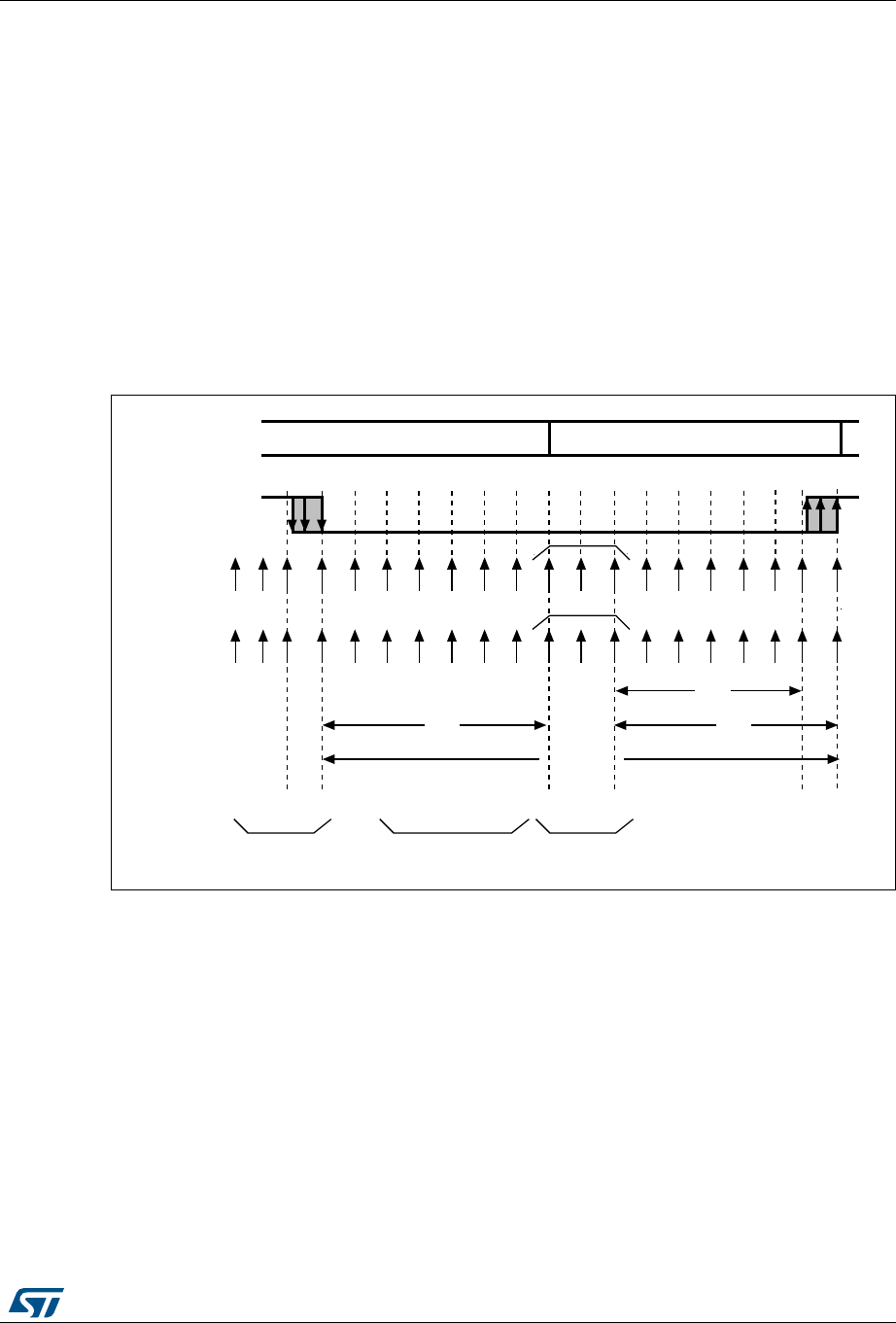
DocID027812 Rev 2 631/766
RM0401 Universal synchronous asynchronous receiver transmitter (USART)
674
Idle characters
Setting the TE bit drives the USART to send an idle frame before the first data frame.
24.4.3 Receiver
The USART can receive data words of either 8 or 9 bits depending on the M bit in the
USART_CR1 register.
Start bit detection
The start bit detection sequence is the same when oversampling by 16 or by 8.
In the USART, the start bit is detected when a specific sequence of samples is recognized.
This sequence is: 1 1 1 0 X 0 X 0 X 0 0 0 0.
Figure 218. Start bit detection when oversampling by 16 or 8
Note: If the sequence is not complete, the start bit detection aborts and the receiver returns to the
idle state (no flag is set) where it waits for a falling edge.
The start bit is confirmed (RXNE flag set, interrupt generated if RXNEIE=1) if the 3 sampled
bits are at 0 (first sampling on the 3rd, 5th and 7th bits finds the 3 bits at 0 and second
sampling on the 8th, 9th and 10th bits also finds the 3 bits at 0).
The start bit is validated (RXNE flag set, interrupt generated if RXNEIE=1) but the NE noise
flag is set if, for both samplings, at least 2 out of the 3 sampled bits are at 0 (sampling on the
3rd, 5th and 7th bits and sampling on the 8th, 9th and 10th bits). If this condition is not met,
the start detection aborts and the receiver returns to the idle state (no flag is set).
If, for one of the samplings (sampling on the 3rd, 5th and 7th bits or sampling on the 8th, 9th
and 10th bits), 2 out of the 3 bits are found at 0, the start bit is validated but the NE noise
flag bit is set.
; ; ;; ;;;;
)DOOLQJHGJH
GHWHFWLRQ
; ; ; ; ; ; ; ;
;
$WOHDVWELWV
RXWRIDW
$WOHDVWELWV
RXWRIDW
2QHELWWLPH
&RQGLWLRQV
WRYDOLGDWH
WKHVWDUWELW
5HDO
VDPSOH
FORFN
,GHDO
VDPSOH
FORFN
5;OLQH
5;VWDWH ,GOH 6WDUWELW
6DPSOHGYDOXHV
DLE

Universal synchronous asynchronous receiver transmitter (USART) RM0401
632/766 DocID027812 Rev 2
Character reception
During an USART reception, data shifts in least significant bit first through the RX pin. In this
mode, the USART_DR register consists of a buffer (RDR) between the internal bus and the
received shift register.
Procedure:
1. Enable the USART by writing the UE bit in USART_CR1 register to 1.
2. Program the M bit in USART_CR1 to define the word length.
3. Program the number of stop bits in USART_CR2.
4. Select DMA enable (DMAR) in USART_CR3 if multibuffer communication is to take
place. Configure the DMA register as explained in multibuffer communication. STEP 3
5. Select the desired baud rate using the baud rate register USART_BRR
6. Set the RE bit USART_CR1. This enables the receiver which begins searching for a
start bit.
When a character is received
•The RXNE bit is set. It indicates that the content of the shift register is transferred to the
RDR. In other words, data has been received and can be read (as well as its
associated error flags).
•An interrupt is generated if the RXNEIE bit is set.
•The error flags can be set if a frame error, noise or an overrun error has been detected
during reception.
•In multibuffer, RXNE is set after every byte received and is cleared by the DMA read to
the Data Register.
•In single buffer mode, clearing the RXNE bit is performed by a software read to the
USART_DR register. The RXNE flag can also be cleared by writing a zero to it. The
RXNE bit must be cleared before the end of the reception of the next character to avoid
an overrun error.
Note: The RE bit should not be reset while receiving data. If the RE bit is disabled during
reception, the reception of the current byte will be aborted.
Break character
When a break character is received, the USART handles it as a framing error.
Idle character
When an idle frame is detected, there is the same procedure as a data received character
plus an interrupt if the IDLEIE bit is set.
Overrun error
An overrun error occurs when a character is received when RXNE has not been reset. Data
can not be transferred from the shift register to the RDR register until the RXNE bit is
cleared.

DocID027812 Rev 2 633/766
RM0401 Universal synchronous asynchronous receiver transmitter (USART)
674
The RXNE flag is set after every byte received. An overrun error occurs if RXNE flag is set
when the next data is received or the previous DMA request has not been serviced. When
an overrun error occurs:
•The ORE bit is set.
•The RDR content will not be lost. The previous data is available when a read to
USART_DR is performed.
•The shift register will be overwritten. After that point, any data received during overrun
is lost.
•An interrupt is generated if either the RXNEIE bit is set or both the EIE and DMAR bits
are set.
•The ORE bit is reset by a read to the USART_SR register followed by a USART_DR
register read operation.
Note: The ORE bit, when set, indicates that at least 1 data has been lost. There are two
possibilities:
•if RXNE=1, then the last valid data is stored in the receive register RDR and can be
read,
•if RXNE=0, then it means that the last valid data has already been read and thus there
is nothing to be read in the RDR. This case can occur when the last valid data is read in
the RDR at the same time as the new (and lost) data is received. It may also occur
when the new data is received during the reading sequence (between the USART_SR
register read access and the USART_DR read access).
Selecting the proper oversampling method
The receiver implements different user-configurable oversampling techniques (except in
synchronous mode) for data recovery by discriminating between valid incoming data and
noise.
The oversampling method can be selected by programming the OVER8 bit in the
USART_CR1 register and can be either 16 or 8 times the baud rate clock (Figure 219 and
Figure 220).
Depending on the application:
•select oversampling by 8 (OVER8=1) to achieve higher speed (up to fPCLK/8). In this
case the maximum receiver tolerance to clock deviation is reduced (refer to
Section 24.4.5: USART receiver tolerance to clock deviation)
•select oversampling by 16 (OVER8=0) to increase the tolerance of the receiver to clock
deviations. In this case, the maximum speed is limited to maximum fPCLK/16
Programming the ONEBIT bit in the USART_CR3 register selects the method used to
evaluate the logic level. There are two options:
•the majority vote of the three samples in the center of the received bit. In this case,
when the 3 samples used for the majority vote are not equal, the NF bit is set
•a single sample in the center of the received bit
Depending on the application:
– select the three samples’ majority vote method (ONEBIT=0) when operating in a
noisy environment and reject the data when a noise is detected (refer to
Figure 97) because this indicates that a glitch occurred during the sampling.
– select the single sample method (ONEBIT=1) when the line is noise-free to
increase the receiver tolerance to clock deviations (see Section 24.4.5: USART
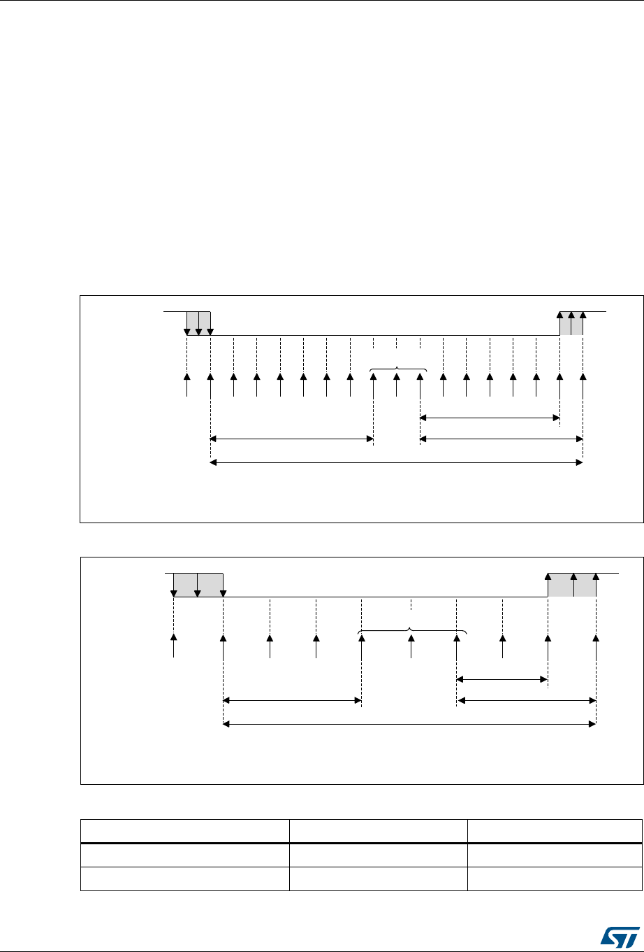
Universal synchronous asynchronous receiver transmitter (USART) RM0401
634/766 DocID027812 Rev 2
receiver tolerance to clock deviation). In this case the NF bit will never be set.
When noise is detected in a frame:
•The NF bit is set at the rising edge of the RXNE bit.
•The invalid data is transferred from the Shift register to the USART_DR register.
•No interrupt is generated in case of single byte communication. However this bit rises
at the same time as the RXNE bit which itself generates an interrupt. In case of
multibuffer communication an interrupt will be issued if the EIE bit is set in the
USART_CR3 register.
The NF bit is reset by a USART_SR register read operation followed by a USART_DR
register read operation.
Note: Oversampling by 8 is not available in the Smartcard, IrDA and LIN modes. In those modes,
the OVER8 bit is forced to ‘0 by hardware.
Figure 219. Data sampling when oversampling by 16
Figure 220. Data sampling when oversampling by 8
Table 97. Noise detection from sampled data
Sampled value NE status Received bit value
000 0 0
001 1 0
06Y9
VDPSOHGYDOXHV
2QHELWWLPH
6DPSOHFORFN
5;OLQH
06Y9
VDPSOHGYDOXHV
2QHELWWLPH
6DPSOH
FORFN[
5;OLQH

DocID027812 Rev 2 635/766
RM0401 Universal synchronous asynchronous receiver transmitter (USART)
674
Framing error
A framing error is detected when:
The stop bit is not recognized on reception at the expected time, following either a de-
synchronization or excessive noise.
When the framing error is detected:
•The FE bit is set by hardware
•The invalid data is transferred from the Shift register to the USART_DR register.
•No interrupt is generated in case of single byte communication. However this bit rises
at the same time as the RXNE bit which itself generates an interrupt. In case of
multibuffer communication an interrupt will be issued if the EIE bit is set in the
USART_CR3 register.
The FE bit is reset by a USART_SR register read operation followed by a USART_DR
register read operation.
Configurable stop bits during reception
The number of stop bits to be received can be configured through the control bits of Control
Register 2 - it can be either 1 or 2 in normal mode and 0.5 or 1.5 in Smartcard mode.
1. 0.5 stop bit (reception in Smartcard mode): No sampling is done for 0.5 stop bit. As
a consequence, no framing error and no break frame can be detected when 0.5 stop bit
is selected.
2. 1 stop bit: Sampling for 1 stop Bit is done on the 8th, 9th and 10th samples.
3. 1.5 stop bits (Smartcard mode): When transmitting in smartcard mode, the device
must check that the data is correctly sent. Thus the receiver block must be enabled (RE
=1 in the USART_CR1 register) and the stop bit is checked to test if the smartcard has
detected a parity error. In the event of a parity error, the smartcard forces the data
signal low during the sampling - NACK signal-, which is flagged as a framing error.
Then, the FE flag is set with the RXNE at the end of the 1.5 stop bit. Sampling for 1.5
stop bits is done on the 16th, 17th and 18th samples (1 baud clock period after the
beginning of the stop bit). The 1.5 stop bit can be decomposed into 2 parts: one 0.5
baud clock period during which nothing happens, followed by 1 normal stop bit period
during which sampling occurs halfway through. Refer to Section 24.4.11 for more
details.
4. 2 stop bits: Sampling for 2 stop bits is done on the 8th, 9th and 10th samples of the first
stop bit. If a framing error is detected during the first stop bit the framing error flag will
010 1 0
011 1 1
100 1 0
101 1 1
110 1 1
111 0 1
Table 97. Noise detection from sampled data (continued)
Sampled value NE status Received bit value

Universal synchronous asynchronous receiver transmitter (USART) RM0401
636/766 DocID027812 Rev 2
be set. The second stop bit is not checked for framing error. The RXNE flag will be set
at the end of the first stop bit.
24.4.4 Fractional baud rate generation
The baud rate for the receiver and transmitter (Rx and Tx) are both set to the same value as
programmed in the Mantissa and Fraction values of USARTDIV.
Equation 1: Baud rate for standard USART (SPI mode included)
Equation 2: Baud rate in Smartcard, LIN and IrDA modes
USARTDIV is an unsigned fixed point number that is coded on the USART_BRR register.
•When OVER8=0, the fractional part is coded on 4 bits and programmed by the
DIV_fraction[3:0] bits in the USART_BRR register
•When OVER8=1, the fractional part is coded on 3 bits and programmed by the
DIV_fraction[2:0] bits in the USART_BRR register, and bit DIV_fraction[3] must be kept
cleared.
Note: The baud counters are updated to the new value in the baud registers after a write operation
to USART_BRR. Hence the baud rate register value should not be changed during
communication.
How to derive USARTDIV from USART_BRR register values when OVER8=0
Example 1:
If DIV_Mantissa = 0d27 and DIV_Fraction = 0d12 (USART_BRR = 0x1BC), then
Mantissa (USARTDIV) = 0d27
Fraction (USARTDIV) = 12/16 = 0d0.75
Therefore USARTDIV = 0d27.75
Example 2:
To program USARTDIV = 0d25.62
This leads to:
DIV_Fraction = 16*0d0.62 = 0d9.92
The nearest real number is 0d10 = 0xA
DIV_Mantissa = mantissa (0d25.620) = 0d25 = 0x19
Then, USART_BRR = 0x19A hence USARTDIV = 0d25.625
Example 3:
To program USARTDIV = 0d50.99
Tx/Rx baud fCK
8 2 OVER8–()USARTDIV××
-----------------------------------------------------------------------------------
=
Tx/Rx baud fCK
16 USARTDIV×
---------------------------------------------
=

DocID027812 Rev 2 637/766
RM0401 Universal synchronous asynchronous receiver transmitter (USART)
674
This leads to:
DIV_Fraction = 16*0d0.99 = 0d15.84
The nearest real number is 0d16 = 0x10 => overflow of DIV_frac[3:0] => carry must be
added up to the mantissa
DIV_Mantissa = mantissa (0d50.990 + carry) = 0d51 = 0x33
Then, USART_BRR = 0x330 hence USARTDIV = 0d51.000
How to derive USARTDIV from USART_BRR register values when OVER8=1
Example 1:
If DIV_Mantissa = 0x27 and DIV_Fraction[2:0]= 0d6 (USART_BRR = 0x1B6), then
Mantissa (USARTDIV) = 0d27
Fraction (USARTDIV) = 6/8 = 0d0.75
Therefore USARTDIV = 0d27.75
Example 2:
To program USARTDIV = 0d25.62
This leads to:
DIV_Fraction = 8*0d0.62 = 0d4.96
The nearest real number is 0d5 = 0x5
DIV_Mantissa = mantissa (0d25.620) = 0d25 = 0x19
Then, USART_BRR = 0x195 => USARTDIV = 0d25.625
Example 3:
To program USARTDIV = 0d50.99
This leads to:
DIV_Fraction = 8*0d0.99 = 0d7.92
The nearest real number is 0d8 = 0x8 => overflow of the DIV_frac[2:0] => carry must be
added up to the mantissa
DIV_Mantissa = mantissa (0d50.990 + carry) = 0d51 = 0x33
Then, USART_BRR = 0x0330 => USARTDIV = 0d51.000

Universal synchronous asynchronous receiver transmitter (USART) RM0401
638/766 DocID027812 Rev 2
Table 98. Error calculation for programmed baud rates at fPCLK = 8 MHz or fPCLK = 12 MHz,
oversampling by 16(1)
Oversampling by 16 (OVER8=0)
Baud rate7 fPCLK = 8 MHz fPCLK = 12 MHz
S.No Desired Actual
Value
programmed
in the baud
rate register
% Error =
(Calculated -
Desired) B.rate /
Desired B.rate
Actual
Value
programmed
in the baud
rate register
% Error
1 1.2 KBps 1.2 KBps 416.6875 0 1.2 KBps 625 0
2 2.4 KBps 2.4 KBps 208.3125 0.01 2.4 KBps 312.5 0
3 9.6 KBps 9.604 KBps 52.0625 0.04 9.6 KBps 78.125 0
4 19.2 KBps 19.185 KBps 26.0625 0.08 19.2 KBps 39.0625 0
5 38.4 KBps 38.462 KBps 13 0.16 38.339 KBps 19.5625 0.16
6 57.6 KBps 57.554 KBps 8.6875 0.08 57.692 KBps 13 0.16
7 115.2 KBps 115.942 KBps 4.3125 0.64 115.385 KBps 6.5 0.16
8 230.4 KBps 228.571 KBps 2.1875 0.79 230.769 KBps 3.25 0.16
9 460.8 KBps 470.588 KBps 1.0625 2.12 461.538 KBps 1.625 0.16
1. The lower the CPU clock the lower the accuracy for a particular baud rate. The upper limit of the achievable baud rate can
be fixed with these data.
Table 99. Error calculation for programmed baud rates at fPCLK = 8 MHz or fPCLK = 12 MHz,
oversampling by 8(1)
Oversampling by 8 (OVER8 = 1)
Baud rate fPCLK = 8 MHz fPCLK = 12 MHz
S.No Desired Actual
Value
programmed
in the baud
rate register
% Error =
(Calculated -
Desired)
B.rate /
Desired
B.rate
Actual
Value
programmed
in the baud
rate register
% Error
1 1.2 KBps 1.2 KBps 833.375 0 1.2 KBps 1250 0
2 2.4 KBps 2.4 KBps 416.625 0.01 2.4 KBps 625 0
3 9.6 KBps 9.604 KBps 104.125 0.04 9.6 KBps 156.25 0
4 19.2 KBps 19.185 KBps 52.125 0.08 19.2 KBps 78.125 0
5 38.4 KBps 38.462 KBps 26 0.16 38.339 KBps 39.125 0.16
6 57.6 KBps 57.554 KBps 17.375 0.08 57.692 KBps 26 0.16
7 115.2 KBps 115.942 KBps 8.625 0.64 115.385 KBps 13 0.16
8 230.4 KBps 228.571 KBps 4.375 0.79 230.769 KBps 6.5 0.16
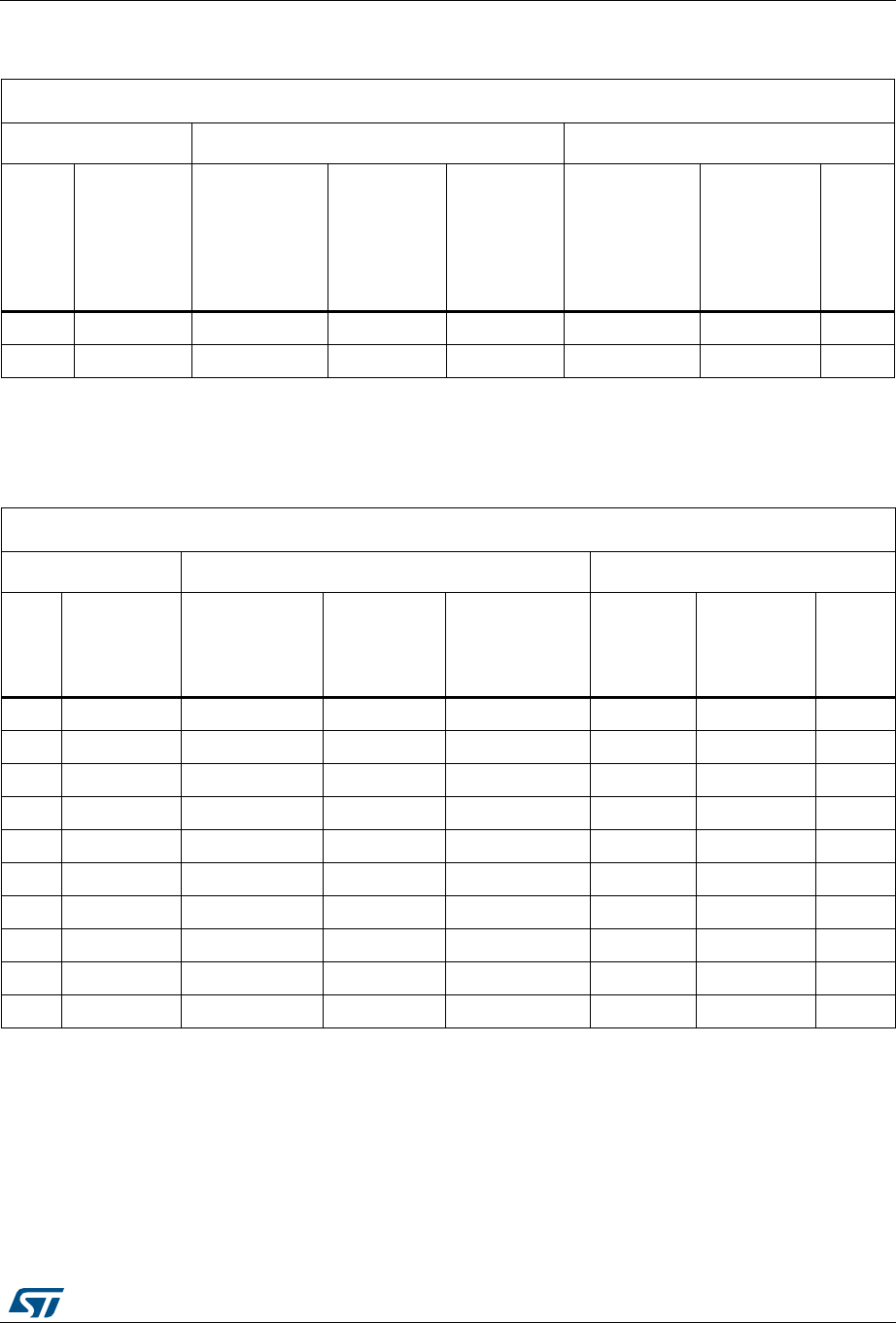
DocID027812 Rev 2 639/766
RM0401 Universal synchronous asynchronous receiver transmitter (USART)
674
9 460.8 KBps 470.588 KBps 2.125 2.12 461.538 KBps 3.25 0.16
10 921.6 KBps 888.889 KBps 1.125 3.55 923.077 KBps 1.625 0.16
1. The lower the CPU clock the lower the accuracy for a particular baud rate. The upper limit of the achievable baud rate can
be fixed with these data.
Table 99. Error calculation for programmed baud rates at fPCLK = 8 MHz or fPCLK = 12 MHz,
oversampling by 8(1) (continued)
Oversampling by 8 (OVER8 = 1)
Baud rate fPCLK = 8 MHz fPCLK = 12 MHz
S.No Desired Actual
Value
programmed
in the baud
rate register
% Error =
(Calculated -
Desired)
B.rate /
Desired
B.rate
Actual
Value
programmed
in the baud
rate register
% Error
Table 100. Error calculation for programmed baud rates at fPCLK = 16 MHz or fPCLK = 24 MHz,
oversampling by 16(1)
Oversampling by 16 (OVER8 = 0)
Baud rate fPCLK = 16 MHz fPCLK = 24 MHz
S.No Desired Actual
Value
programmed
in the baud
rate register
% Error =
(Calculated -
Desired) B.rate /
Desired B.rate
Actual
Value
programmed
in the baud
rate register
% Error
1 1.2 KBps 1.2 KBps 833.3125 0 1.2 1250 0
2 2.4 KBps 2.4 KBps 416.6875 0 2.4 625 0
3 9.6 KBps 9.598 KBps 104.1875 0.02 9.6 156.25 0
4 19.2 KBps 19.208 KBps 52.0625 0.04 19.2 78.125 0
5 38.4 KBps 38.369 KBps 26.0625 0.08 38.4 39.0625 0
6 57.6 KBps 57.554 KBps 17.375 0.08 57.554 26.0625 0.08
7 115.2 KBps 115.108 KBps 8.6875 0.08 115.385 13 0.16
8 230.4 KBps 231.884 KBps 4.3125 0.64 230.769 6.5 0.16
9 460.8 KBps 457.143 KBps 2.1875 0.79 461.538 3.25 0.16
10 921.6 KBps 941.176 KBps 1.0625 2.12 923.077 1.625 0.16
1. The lower the CPU clock the lower the accuracy for a particular baud rate. The upper limit of the achievable baud rate can
be fixed with these data.
Universal synchronous asynchronous receiver transmitter (USART) RM0401
640/766 DocID027812 Rev 2
Table 101. Error calculation for programmed baud rates at fPCLK = 16 MHz or fPCLK = 24 MHz,
oversampling by 8(1)
Oversampling by 8 (OVER8=1)
Baud rate fPCLK = 16 MHz fPCLK = 24 MHz
S.No Desired Actual
Value
programmed
in the baud
rate register
% Error =
(Calculated -
Desired) B.rate /
Desired B.rate
Actual
Value
programmed
in the baud
rate register
% Error
1 1.2 KBps 1.2 KBps 1666.625 0 1.2 KBps 2500 0
2 2.4 KBps 2.4 KBps 833.375 0 2.4 KBps 1250 0
3 9.6 KBps 9.598 KBps 208.375 0.02 9.6 KBps 312.5 0
4 19.2 KBps 19.208 KBps 104.125 0.04 19.2 KBps 156.25 0
5 38.4 KBps 38.369 KBps 52.125 0.08 38.4 KBps 78.125 0
6 57.6 KBps 57.554 KBps 34.75 0.08 57.554 KBps 52.125 0.08
7 115.2 KBps 115.108 KBps 17.375 0.08 115.385 KBps 26 0.16
8 230.4 KBps 231.884 KBps 8.625 0.64 230.769 KBps 13 0.16
9 460.8 KBps 457.143 KBps 4.375 0.79 461.538 KBps 6.5 0.16
10 921.6 KBps 941.176 KBps 2.125 2.12 923.077 KBps 3.25 0.16
11 2 MBps 2000 KBps 1 0 2000 KBps 1.5 0
12 3 MBps NA NA NA 3000 KBps 1 0
1. The lower the CPU clock the lower the accuracy for a particular baud rate. The upper limit of the achievable baud rate can
be fixed with these data.
Table 102. Error calculation for programmed baud rates at fPCLK = 8 MHz or fPCLK = 16 MHz,
oversampling by 16(1)
Oversampling by 16 (OVER8=0)
Baud rate fPCLK = 8 MHz fPCLK = 16 MHz
S.No Desired Actual
Value
programme
d in the
baud rate
register
% Error =
(Calculated -
Desired)B.Rate
/Desired B.Rate
Actual
Value
programmed
in the baud
rate register
% Error
1. 2.4 KBps 2.400 KBps 208.3125 0.00% 2.400 KBps 416.6875 0.00%
2. 9.6 KBps 9.604 KBps 52.0625 0.04% 9.598 KBps 104.1875 0.02%
3. 19.2 KBps 19.185 KBps 26.0625 0.08% 19.208 KBps 52.0625 0.04%
4. 57.6 KBps 57.554 KBps 8.6875 0.08% 57.554 KBps 17.3750 0.08%
5. 115.2 KBps 115.942 KBps 4.3125 0.64% 115.108 KBps 8.6875 0.08%
6. 230.4 KBps 228.571 KBps 2.1875 0.79% 231.884 KBps 4.3125 0.64%
7. 460.8 KBps 470.588 KBps 1.0625 2.12% 457.143 KBps 2.1875 0.79%
DocID027812 Rev 2 641/766
RM0401 Universal synchronous asynchronous receiver transmitter (USART)
674
8. 896 KBps NA NA NA 888.889 KBps 1.1250 0.79%
9. 921.6 KBps NA NA NA 941.176 KBps 1.0625 2.12%
1. The lower the CPU clock the lower the accuracy for a particular baud rate. The upper limit of the achievable baud rate can
be fixed with these data.
Table 103. Error calculation for programmed baud rates at fPCLK = 8 MHz or fPCLK = 16 MHz,
oversampling by 8(1)
Oversampling by 8 (OVER8=1)
Baud rate fPCLK = 8 MHz fPCLK = 16 MHz
S.No Desired Actual
Value
programmed
in the baud
rate register
% Error =
(Calculated -
Desired)B.Rate
/Desired B.Rate
Actual
Value
programmed
in the baud
rate register
%
Error
1. 2.4 KBps 2.400 KBps 416.625 0.01% 2.400 KBps 833.375 0.00%
2. 9.6 KBps 9.604 KBps 104.125 0.04% 9.598 KBps 208.375 0.02%
3. 19.2 KBps 19.185 KBps 52.125 0.08% 19.208 KBps 104.125 0.04%
4. 57.6 KBps 57.557 KBps 17.375 0.08% 57.554 KBps 34.750 0.08%
5. 115.2 KBps 115.942 KBps 8.625 0.64% 115.108 KBps 17.375 0.08%
6. 230.4 KBps 228.571 KBps 4.375 0.79% 231.884 KBps 8.625 0.64%
7. 460.8 KBps 470.588 KBps 2.125 2.12% 457.143 KBps 4.375 0.79%
8. 896 KBps 888.889 KBps 1.125 0.79% 888.889 KBps 2.250 0.79%
9. 921.6 KBps 888.889 KBps 1.125 3.55% 941.176 KBps 2.125 2.12%
10. 1.792 MBps NA NA NA 1.7777 MBps 1.125 0.79%
11. 1.8432 MBps NA NA NA 1.7777 MBps 1.125 3.55%
1. The lower the CPU clock the lower the accuracy for a particular baud rate. The upper limit of the achievable baud rate can
be fixed with these data.
Table 102. Error calculation for programmed baud rates at fPCLK = 8 MHz or fPCLK = 16 MHz,
oversampling by 16(1) (continued)
Oversampling by 16 (OVER8=0)
Baud rate fPCLK = 8 MHz fPCLK = 16 MHz
S.No Desired Actual
Value
programme
d in the
baud rate
register
% Error =
(Calculated -
Desired)B.Rate
/Desired B.Rate
Actual
Value
programmed
in the baud
rate register
% Error

Universal synchronous asynchronous receiver transmitter (USART) RM0401
642/766 DocID027812 Rev 2
Table 104. Error calculation for programmed baud rates at fPCLK = 30 MHz or fPCLK = 60 MHz,
oversampling by 16(1)(2)
Oversampling by 16 (OVER8=0)
Baud rate fPCLK = 30 MHz fPCLK = 60 MHz
S.No Desired Actual
Value
programme
d in the
baud rate
register
% Error =
(Calculated -
Desired)B.Rate
/Desired B.Rate
Actual
Value
programmed
in the baud
rate register
%
Error
1. 2.4 KBps 2.400 KBps 781.2500 0.00% 2.400 KBps 1562.5000 0.00%
2. 9.6 KBps 9.600 KBps 195.3125 0.00% 9.600 KBps 390.6250 0.00%
3. 19.2 KBps 19.194 KBps 97.6875 0.03% 19.200 KBps 195.3125 0.00%
4. 57.6 KBps 57.582KBps 32.5625 0.03% 57.582 KBps 65.1250 0.03%
5. 115.2 KBps 115.385 KBps 16.2500 0.16% 115.163 KBps 32.5625 0.03%
6. 230.4 KBps 230.769 KBps 8.1250 0.16% 230.769 KBps 16.2500 0.16%
7. 460.8 KBps 461.538 KBps 4.0625 0.16% 461.538 KBps 8.1250 0.16%
8. 896 KBps 909.091 KBps 2.0625 1.46% 895.522 KBps 4.1875 0.05%
9. 921.6 KBps 909.091 KBps 2.0625 1.36% 923.077 KBps 4.0625 0.16%
10. 1.792 MBps 1.1764 MBps 1.0625 1.52% 1.8182 MBps 2.0625 1.36%
11. 1.8432 MBps 1.8750 MBps 1.0000 1.73% 1.8182 MBps 2.0625 1.52%
12. 3.584 MBps NA NA NA 3.2594 MBps 1.0625 1.52%
13. 3.6864 MBps NA NA NA 3.7500 MBps 1.0000 1.73%
1. The lower the CPU clock the lower the accuracy for a particular baud rate. The upper limit of the achievable baud rate can
be fixed with these data.
2. Only USART1 and USART6 are clocked with PCLK2. Other USARTs are clocked with PCLK1. Refer to the device
datasheets for the maximum values for PCLK1 and PCLK2.
Table 105. Error calculation for programmed baud rates at fPCLK = 30 MHz or fPCLK = 60 MHz,
oversampling by 8(1) (2)
Oversampling by 8 (OVER8=1)
Baud rate fPCLK = 30 MHz fPCLK =60 MHz
S.No Desired Actual
Value
programme
d in the
baud rate
register
% Error =
(Calculated -
Desired)B.Rate
/Desired B.Rate
Actual
Value
programmed
in the baud
rate register
%
Error
1. 2.4 KBps 2.400 KBps 1562.5000 0.00% 2.400 KBps 3125.0000 0.00%
2. 9.6 KBps 9.600 KBps 390.6250 0.00% 9.600 KBps 781.2500 0.00%
3. 19.2 KBps 19.194 KBps 195.3750 0.03% 19.200 KBps 390.6250 0.00%
4. 57.6 KBps 57.582 KBps 65.1250 0.16% 57.582 KBps 130.2500 0.03%
DocID027812 Rev 2 643/766
RM0401 Universal synchronous asynchronous receiver transmitter (USART)
674
5. 115.2 KBps 115.385 KBps 32.5000 0.16% 115.163 KBps 65.1250 0.03%
6. 230.4 KBps 230.769 KBps 16.2500 0.16% 230.769 KBps 32.5000 0.16%
7. 460.8 KBps 461.538 KBps 8.1250 0.16% 461.538 KBps 16.2500 0.16%
8. 896 KBps 909.091 KBps 4.1250 1.46% 895.522 KBps 8.3750 0.05%
9. 921.6 KBps 909.091 KBps 4.1250 1.36% 923.077 KBps 8.1250 0.16%
10. 1.792 MBps 1.7647 MBps 2.1250 1.52% 1.8182 MBps 4.1250 1.46%
11. 1.8432 MBps 1.8750 MBps 2.0000 1.73% 1.8182 MBps 4.1250 1.36%
12. 3.584 MBps 3.7500 MBps 1.0000 4.63% 3.5294 MBps 2.1250 1.52%
13. 3.6864 MBps 3.7500 MBps 1.0000 1.73% 3.7500 MBps 2.0000 1.73%
14. 7.168 MBps NA NA NA 7.5000 MBps 1.0000 4.63%
15. 7.3728 MBps NA NA NA 7.5000 MBps 1.0000 1.73%
1. The lower the CPU clock the lower the accuracy for a particular baud rate. The upper limit of the achievable baud rate can
be fixed with these data.
2. Only USART1 and USART6 are clocked with PCLK2. Other USARTs are clocked with PCLK1. Refer to the device
datasheets for the maximum values for PCLK1 and PCLK2.
Table 105. Error calculation for programmed baud rates at fPCLK = 30 MHz or fPCLK = 60 MHz,
oversampling by 8(1) (2) (continued)
Oversampling by 8 (OVER8=1)
Baud rate fPCLK = 30 MHz fPCLK =60 MHz
S.No Desired Actual
Value
programme
d in the
baud rate
register
% Error =
(Calculated -
Desired)B.Rate
/Desired B.Rate
Actual
Value
programmed
in the baud
rate register
%
Error
Table 106. Error calculation for programmed baud rates at fPCLK = 42 MHz or fPCLK = 84 Hz,
oversampling by 16(1)(2)
Oversampling by 16 (OVER8=0)
Baud rate fPCLK = 42 MHz fPCLK = 84 MHz
S.No Desired Actual
Value
programme
d in the
baud rate
register
% Error =
(Calculated -
Desired)B.Rate
/Desired B.Rate
Actual
Value
programmed
in the baud
rate register
%
Error
1 1.2 KBps 1.2 KBps 2187.5 0 1.2 KBps 4375 0
2 2.4 KBps 2.4 KBps 1093.75 0 2.4 KBps 2187.5 0
3 9.6 KBps 9.6 KBps 273.4375 0 9.6 KBps 546.875 0
4 19.2 KBps 19.195 KBps 136.75 0.02 19.2 KBps 273.4375 0
5 38.4 KBps 38.391 KBps 68.375 0.02 38.391 KBps 136.75 0.02
6 57.6 KBps 57.613 KBps 45.5625 0.02 57.613 KBps 91.125 0.02

Universal synchronous asynchronous receiver transmitter (USART) RM0401
644/766 DocID027812 Rev 2
7 115.2 KBps 115.068 KBps 22.8125 0.11 115.226 KBps 45.5625 0.02
8 230.4 KBps 230.769 KBps 11.375 0.16 230.137 KBps 22.8125 0.11
9 460.8 KBps 461.538 KBps 5.6875 0.16 461.538 KBps 11.375 0.16
10 921.6 KBps 913.043 KBps 2.875 0.93 923.076 KBps 5.6875 0.93
11 1.792 MBps 1.826 MBps 1.4375 1.9 1.787 MBps 2.9375 0.27
12 1.8432 MBps 1.826 MBps 1.4375 0.93 1.826 MBps 2.875 0.93
13 3.584 MBps NA NA NA 3.652 MBps 1.4375 1.9
14 3.6864 MBps NA NA NA 3.652 MBps 1.4375 0.93
1. The lower the CPU clock the lower the accuracy for a particular baud rate. The upper limit of the achievable baud rate can
be fixed with these data.
2. Only USART1 and USART6 are clocked with PCLK2. Other USARTs are clocked with PCLK1. Refer to the device
datasheets for the maximum values for PCLK1 and PCLK2.
Table 106. Error calculation for programmed baud rates at fPCLK = 42 MHz or fPCLK = 84 Hz,
oversampling by 16(1)(2) (continued)
Oversampling by 16 (OVER8=0)
Baud rate fPCLK = 42 MHz fPCLK = 84 MHz
S.No Desired Actual
Value
programme
d in the
baud rate
register
% Error =
(Calculated -
Desired)B.Rate
/Desired B.Rate
Actual
Value
programmed
in the baud
rate register
%
Error
Table 107. Error calculation for programmed baud rates at fPCLK = 42 MHz or fPCLK = 84 MHz,
oversampling by 8(1)(2)
Oversampling by 8 (OVER8=1)
Baud rate fPCLK = 42 MHz fPCLK = 84 MHz
S.No Desired Actual
Value
programme
d in the
baud rate
register
% Error =
(Calculated -
Desired)B.Rate
/Desired B.Rate
Actual
Value
programmed
in the baud
rate register
%
Error
1. 1.2 KBps 1.2 KBps 4375 0 1.2 KBps 8750 0
2. 2.4 KBps 2.4 KBps 2187.5 0 2.4 KBps 4375 0
3. 9.6 KBps 9.6 KBps 546.875 0 9.6 KBps 1093.75 0
4. 19.2 KBps 19.195 KBps 273.5 0.02 19.2 KBps 546.875 0
5. 38.4 KBps 38.391 KBps 136.75 0.02 38.391 KBps 273.5 0.02
6. 57.6 KBps 57.613 KBps 91.125 0.02 57.613 KBps 182.25 0.02
7. 115.2 KBps 115.068 KBps 45.625 0.11 115.226 KBps 91.125 0.02
8. 230.4 KBps 230.769 KBps 22.75 0.11 230.137 KBps 45.625 0.11
9. 460.8 KBps 461.538 KBps 11.375 0.16 461.538 KBps 22.75 0.16

DocID027812 Rev 2 645/766
RM0401 Universal synchronous asynchronous receiver transmitter (USART)
674
24.4.5 USART receiver tolerance to clock deviation
The USART asynchronous receiver works correctly only if the total clock system deviation is
smaller than the USART receiver tolerance. The causes which contribute to the total
deviation are:
•DTRA: Deviation due to the transmitter error (which also includes the deviation of the
transmitter local oscillator)
•DQUANT: Error due to the baud rate quantization of the receiver
•DREC: Deviation of the receiver local oscillator
•DTCL: Deviation due to the transmission line (generally due to the transceivers which
can introduce an asymmetry between the low-to-high transition timing and the high-to-
low transition timing)
DTRA + DQUANT + DREC + DTCL < USART receiver tolerance
The USART receiver tolerance to properly receive data is equal to the maximum tolerated
deviation and depends on the following choices:
•10- or 11-bit character length defined by the M bit in the USART_CR1 register
•oversampling by 8 or 16 defined by the OVER8 bit in the USART_CR1 register
•use of fractional baud rate or not
•use of 1 bit or 3 bits to sample the data, depending on the value of the ONEBIT bit in
the USART_CR3 register
10. 921.6 KBps 913.043 KBps 5.75 0.93 923.076 KBps 11.375 0.93
11. 1.792 MBps 1.826 MBps 2.875 1.9 1.787Mbps 5.875 0.27
12. 1.8432 MBps 1.826 MBps 2.875 0.93 1.826 MBps 5.75 0.93
13. 3.584 MBps 3.5 MBps 1.5 2.34 3.652 MBps 2.875 1.9
14. 3.6864 MBps 3.82 MBps 1.375 3.57 3.652 MBps 2.875 0.93
15. 7.168 MBps NA NA NA 7 MBps 1.5 2.34
16. 7.3728 MBps NA NA NA 7.636 MBps 1.375 3.57
18. 9 MBps NA NA NA 9.333 MBps 1.125 3.7
20. 10.5 MBps NA NA NA 10.5 MBps 1 0
1. The lower the CPU clock the lower the accuracy for a particular baud rate. The upper limit of the achievable baud rate can
be fixed with these data.
2. Only USART1 and USART6 are clocked with PCLK2. Other USARTs are clocked with PCLK1. Refer to the device
datasheets for the maximum values for PCLK1 and PCLK2.
Table 107. Error calculation for programmed baud rates at fPCLK = 42 MHz or fPCLK = 84 MHz,
oversampling by 8(1)(2) (continued)
Oversampling by 8 (OVER8=1)
Baud rate fPCLK = 42 MHz fPCLK = 84 MHz
S.No Desired Actual
Value
programme
d in the
baud rate
register
% Error =
(Calculated -
Desired)B.Rate
/Desired B.Rate
Actual
Value
programmed
in the baud
rate register
%
Error

Universal synchronous asynchronous receiver transmitter (USART) RM0401
646/766 DocID027812 Rev 2
Note: The figures specified in Table 108 and Table 109 may slightly differ in the special case when
the received frames contain some Idle frames of exactly 10-bit times when M=0 (11-bit times
when M=1).
24.4.6 Multiprocessor communication
There is a possibility of performing multiprocessor communication with the USART (several
USARTs connected in a network). For instance one of the USARTs can be the master, its TX
output is connected to the RX input of the other USART. The others are slaves, their
respective TX outputs are logically ANDed together and connected to the RX input of the
master.
In multiprocessor configurations it is often desirable that only the intended message
recipient should actively receive the full message contents, thus reducing redundant USART
service overhead for all non addressed receivers.
The non addressed devices may be placed in mute mode by means of the muting function.
In mute mode:
•None of the reception status bits can be set.
•All the receive interrupts are inhibited.
•The RWU bit in USART_CR1 register is set to 1. RWU can be controlled automatically
by hardware or written by the software under certain conditions.
The USART can enter or exit from mute mode using one of two methods, depending on the
WAKE bit in the USART_CR1 register:
•Idle Line detection if the WAKE bit is reset,
•Address Mark detection if the WAKE bit is set.
Idle line detection (WAKE=0)
The USART enters mute mode when the RWU bit is written to 1.
It wakes up when an Idle frame is detected. Then the RWU bit is cleared by hardware but
the IDLE bit is not set in the USART_SR register. RWU can also be written to 0 by software.
An example of mute mode behavior using Idle line detection is given in Figure 221.
Table 108. USART receiver tolerance when DIV fraction is 0
M bit
OVER8 bit = 0 OVER8 bit = 1
ONEBIT=0 ONEBIT=1 ONEBIT=0 ONEBIT=1
0 3.75% 4.375% 2.50% 3.75%
1 3.41% 3.97% 2.27% 3.41%
Table 109. USART receiver tolerance when DIV_Fraction is different from 0
M bit
OVER8 bit = 0 OVER8 bit = 1
ONEBIT=0 ONEBIT=1 ONEBIT=0 ONEBIT=1
0 3.33% 3.88% 2% 3%
1 3.03% 3.53% 1.82% 2.73%
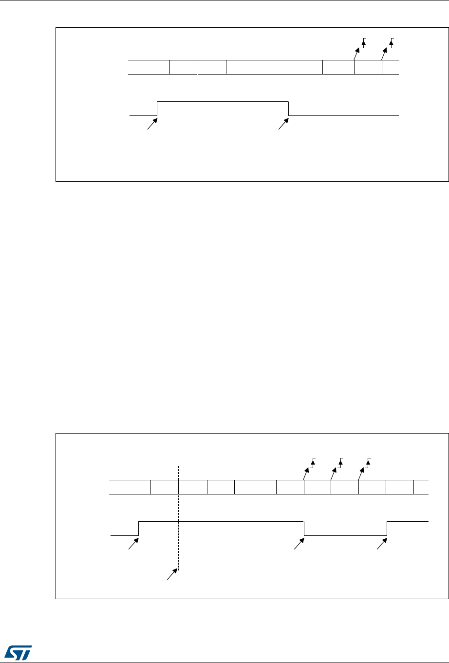
DocID027812 Rev 2 647/766
RM0401 Universal synchronous asynchronous receiver transmitter (USART)
674
Figure 221. Mute mode using Idle line detection
Address mark detection (WAKE=1)
In this mode, bytes are recognized as addresses if their MSB is a ‘1 else they are
considered as data. In an address byte, the address of the targeted receiver is put on the 4
LSB. This 4-bit word is compared by the receiver with its own address which is programmed
in the ADD bits in the USART_CR2 register.
The USART enters mute mode when an address character is received which does not
match its programmed address. In this case, the RWU bit is set by hardware. The RXNE
flag is not set for this address byte and no interrupt nor DMA request is issued as the
USART would have entered mute mode.
It exits from mute mode when an address character is received which matches the
programmed address. Then the RWU bit is cleared and subsequent bytes are received
normally. The RXNE bit is set for the address character since the RWU bit has been
cleared.
The RWU bit can be written to as 0 or 1 when the receiver buffer contains no data (RXNE=0
in the USART_SR register). Otherwise the write attempt is ignored.
An example of mute mode behavior using address mark detection is given in Figure 222.
Figure 222. Mute mode using address mark detection
06Y9
'DWD 'DWD ,'/('DWD 'DWD 'DWD
,GOHIUDPHGHWHFWHG0054ZULWWHQWR
5:8
5;
0XWHPRGH 1RUPDOPRGH
5;1( 5;1(
'DWD
06Y9
,'/( $GGU 'DWD 'DWD ,'/( $GGU 'DWD 'DWD $GGU 'DWD
,QWKLVH[DPSOHWKHFXUUHQWDGGUHVVRIWKHUHFHLYHULV
SURJUDPPHGLQWKH86$57B&5UHJLVWHU
5;1(
1RQPDWFKLQJDGGUHVV0DWFKLQJDGGUHVV
1RQPDWFKLQJDGGUHVV
0054ZULWWHQWR
5;1(ZDVFOHDUHG
5:8
5;
0XWHPRGH 0XWHPRGH1RUPDOPRGH
5;1( 5;1(

Universal synchronous asynchronous receiver transmitter (USART) RM0401
648/766 DocID027812 Rev 2
24.4.7 Parity control
Parity control (generation of parity bit in transmission and parity checking in reception) can
be enabled by setting the PCE bit in the USART_CR1 register. Depending on the frame
length defined by the M bit, the possible USART frame formats are as listed in Table 110.
Even parity
The parity bit is calculated to obtain an even number of “1s” inside the frame made of the 7
or 8 LSB bits (depending on whether M is equal to 0 or 1) and the parity bit.
E.g.: data=00110101; 4 bits set => parity bit will be 0 if even parity is selected (PS bit in
USART_CR1 = 0).
Odd parity
The parity bit is calculated to obtain an odd number of “1s” inside the frame made of the 7 or
8 LSB bits (depending on whether M is equal to 0 or 1) and the parity bit.
E.g.: data=00110101; 4 bits set => parity bit will be 1 if odd parity is selected (PS bit in
USART_CR1 = 1).
Parity checking in reception
If the parity check fails, the PE flag is set in the USART_SR register and an interrupt is
generated if PEIE is set in the USART_CR1 register. The PE flag is cleared by a software
sequence (a read from the status register followed by a read or write access to the
USART_DR data register).
Note: In case of wakeup by an address mark: the MSB bit of the data is taken into account to
identify an address but not the parity bit. And the receiver does not check the parity of the
address data (PE is not set in case of a parity error).
Parity generation in transmission
If the PCE bit is set in USART_CR1, then the MSB bit of the data written in the data register
is transmitted but is changed by the parity bit (even number of “1s” if even parity is selected
(PS=0) or an odd number of “1s” if odd parity is selected (PS=1)).
Note: The software routine that manages the transmission can activate the software sequence
which clears the PE flag (a read from the status register followed by a read or write access
to the data register). When operating in half-duplex mode, depending on the software, this
can cause the PE flag to be unexpectedly cleared.
Table 110. Frame formats
M bit PCE bit USART frame(1)
1. Legends: SB: start bit, STB: stop bit, PB: parity bit.
0 0 | SB | 8 bit data | STB |
0 1 | SB | 7-bit data | PB | STB |
1 0 | SB | 9-bit data | STB |
1 1 | SB | 8-bit data PB | STB |

DocID027812 Rev 2 649/766
RM0401 Universal synchronous asynchronous receiver transmitter (USART)
674
24.4.8 LIN (local interconnection network) mode
The LIN mode is selected by setting the LINEN bit in the USART_CR2 register. In LIN
mode, the following bits must be kept cleared:
•STOP[1:0] and CLKEN in the USART_CR2 register
•SCEN, HDSEL and IREN in the USART_CR3 register.
LIN transmission
The same procedure explained in Section 24.4.2 has to be applied for LIN Master
transmission than for normal USART transmission with the following differences:
•Clear the M bit to configure 8-bit word length.
•Set the LINEN bit to enter LIN mode. In this case, setting the SBK bit sends 13 ‘0 bits
as a break character. Then a bit of value ‘1 is sent to allow the next start detection.
LIN reception
A break detection circuit is implemented on the USART interface. The detection is totally
independent from the normal USART receiver. A break can be detected whenever it occurs,
during Idle state or during a frame.
When the receiver is enabled (RE=1 in USART_CR1), the circuit looks at the RX input for a
start signal. The method for detecting start bits is the same when searching break
characters or data. After a start bit has been detected, the circuit samples the next bits
exactly like for the data (on the 8th, 9th and 10th samples). If 10 (when the LBDL = 0 in
USART_CR2) or 11 (when LBDL=1 in USART_CR2) consecutive bits are detected as ‘0,
and are followed by a delimiter character, the LBD flag is set in USART_SR. If the LBDIE
bit=1, an interrupt is generated. Before validating the break, the delimiter is checked for as it
signifies that the RX line has returned to a high level.
If a ‘1 is sampled before the 10 or 11 have occurred, the break detection circuit cancels the
current detection and searches for a start bit again.
If the LIN mode is disabled (LINEN=0), the receiver continues working as normal USART,
without taking into account the break detection.
If the LIN mode is enabled (LINEN=1), as soon as a framing error occurs (i.e. stop bit
detected at ‘0, which will be the case for any break frame), the receiver stops until the break
detection circuit receives either a ‘1, if the break word was not complete, or a delimiter
character if a break has been detected.
The behavior of the break detector state machine and the break flag is shown in Figure 223.
Examples of break frames are given on Figure 224, where we suppose that LBDL=1 (11-bit
break length), and M=0 (8-bit data).
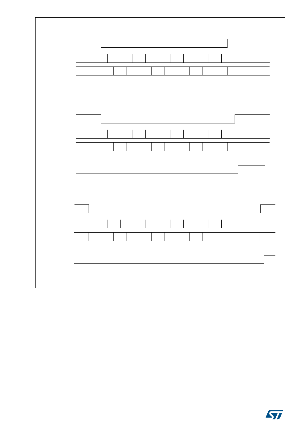
Universal synchronous asynchronous receiver transmitter (USART) RM0401
650/766 DocID027812 Rev 2
Figure 223. Break detection in LIN mode (11-bit break length - LBDL bit is set)
06Y9
,GOH %LW %LW %LW %LW %LW %LW %LW %LW %LW %LW %LW ,GOH
&DVHEUHDNVLJQDOQRWORQJHQRXJK !EUHDNGLVFDUGHG/%')LVQRWVHW
5;OLQH
&DSWXUHVWUREH
%UHDNVWDWH
PDFKLQH
5HDGVDPSOHV
,GOH %LW %LW %LW %LW %LW %LW %LW %LW %LW %LW % ,GOH
&DVHEUHDNVLJQDOMXVWORQJHQRXJK !EUHDNGHWHFWHG/%')LVVHW
5;OLQH
&DSWXUHVWUREH
%UHDNVWDWH
PDFKLQH
5HDGVDPSOHV
%UHDNIUDPH
%UHDNIUDPH
'HOLPLWHULVLPPHGLDWH
/%')
,GOH %LW %LW %LW %LW %LW %LW %LW %LW %LW %LW %LW ,GOH
&DVHEUHDNVLJQDOORQJHQRXJK !EUHDNGHWHFWHG/%')LVVHW
5;OLQH
&DSWXUHVWUREH
%UHDNVWDWH
PDFKLQH
5HDGVDPSOHV
%UHDNIUDPH
/%')
ZDLWGHOLPLWHU
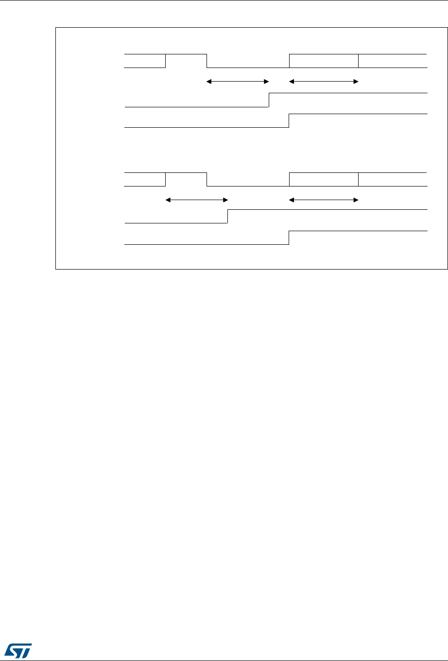
DocID027812 Rev 2 651/766
RM0401 Universal synchronous asynchronous receiver transmitter (USART)
674
Figure 224. Break detection in LIN mode vs. Framing error detection
24.4.9 USART synchronous mode
The synchronous mode is selected by writing the CLKEN bit in the USART_CR2 register to
1. In synchronous mode, the following bits must be kept cleared:
•LINEN bit in the USART_CR2 register,
•SCEN, HDSEL and IREN bits in the USART_CR3 register.
The USART allows the user to control a bidirectional synchronous serial communications in
master mode. The SCLK pin is the output of the USART transmitter clock. No clock pulses
are sent to the SCLK pin during start bit and stop bit. Depending on the state of the LBCL bit
in the USART_CR2 register clock pulses will or will not be generated during the last valid
data bit (address mark). The CPOL bit in the USART_CR2 register allows the user to select
the clock polarity, and the CPHA bit in the USART_CR2 register allows the user to select the
phase of the external clock (see Figure 225, Figure 226 and Figure 227).
During the Idle state, preamble and send break, the external SCLK clock is not activated.
In synchronous mode the USART transmitter works exactly like in asynchronous mode. But
as SCLK is synchronized with TX (according to CPOL and CPHA), the data on TX is
synchronous.
In this mode the USART receiver works in a different manner compared to the
asynchronous mode. If RE=1, the data is sampled on SCLK (rising or falling edge,
depending on CPOL and CPHA), without any oversampling. A setup and a hold time must
be respected (which depends on the baud rate: 1/16 bit time).
Note: The SCLK pin works in conjunction with the TX pin. Thus, the clock is provided only if the
transmitter is enabled (TE=1) and a data is being transmitted (the data register USART_DR
06Y9
GDWD ,'/( %5($. GDWD[ GDWDKHDGHU
GDWDWLPH GDWDWLPH
5;OLQH
5;1()(
/%')
&DVHEUHDNRFFXUULQJDIWHUDQ,GOH
GDWD GDWD %5($. GDWD[ GDWDKHDGHU
GDWDWLPH GDWDWLPH
5;OLQH
5;1()(
/%')
&DVHEUHDNRFFXUULQJZKLOHGDWDLVEHLQJUHFHLYHG
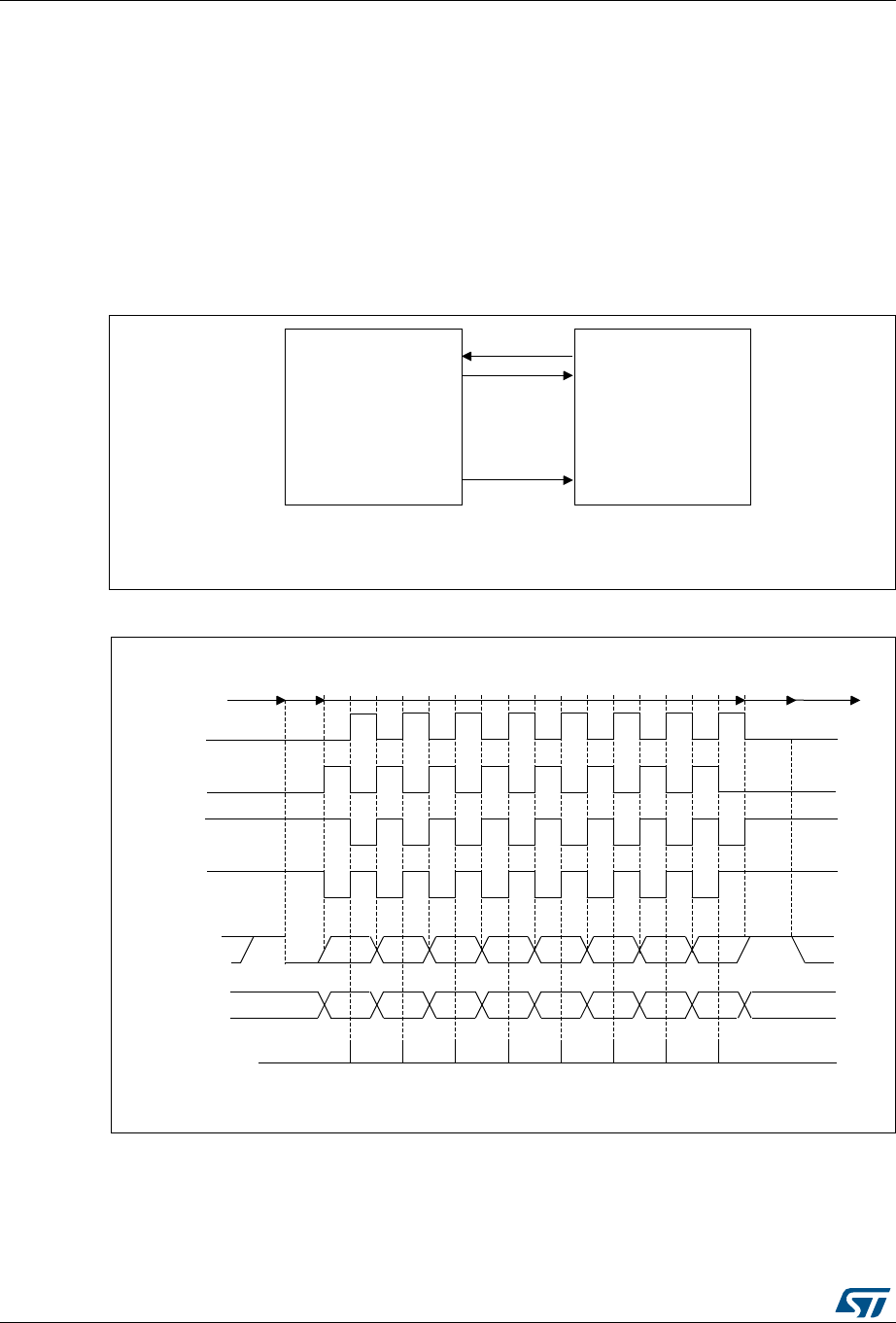
Universal synchronous asynchronous receiver transmitter (USART) RM0401
652/766 DocID027812 Rev 2
has been written). This means that it is not possible to receive a synchronous data without
transmitting data.
The LBCL, CPOL and CPHA bits have to be selected when both the transmitter and the
receiver are disabled (TE=RE=0) to ensure that the clock pulses function correctly. These
bits should not be changed while the transmitter or the receiver is enabled.
It is advised that TE and RE are set in the same instruction in order to minimize the setup
and the hold time of the receiver.
The USART supports master mode only: it cannot receive or send data related to an input
clock (SCLK is always an output).
Figure 225. USART example of synchronous transmission
Figure 226. USART data clock timing diagram (M=0)
06Y9
86$57 6\QFKURQRXVGHYLFH
HJVODYH63,
5;
7;
'DWDRXW
'DWDLQ
&ORFN
6&/.
06Y9
06%
06%
/6%
/6%
6WDUW
6WDUW 6WRS
,GOHRUSUHFHGLQJ
WUDQVPLVVLRQ
,GOHRUQH[W
WUDQVPLVVLRQ
/%&/ELWFRQWUROVODVWGDWDSXOVH
&DSWXUHVWUREH
'DWDRQ5;
IURPVODYH
'DWDRQ7;
IURPPDVWHU
&ORFN&32/ &3+$
&ORFN&32/ &3+$
&ORFN&32/ &3+$
&ORFN&32/ &3+$
6WRS
0ELWV
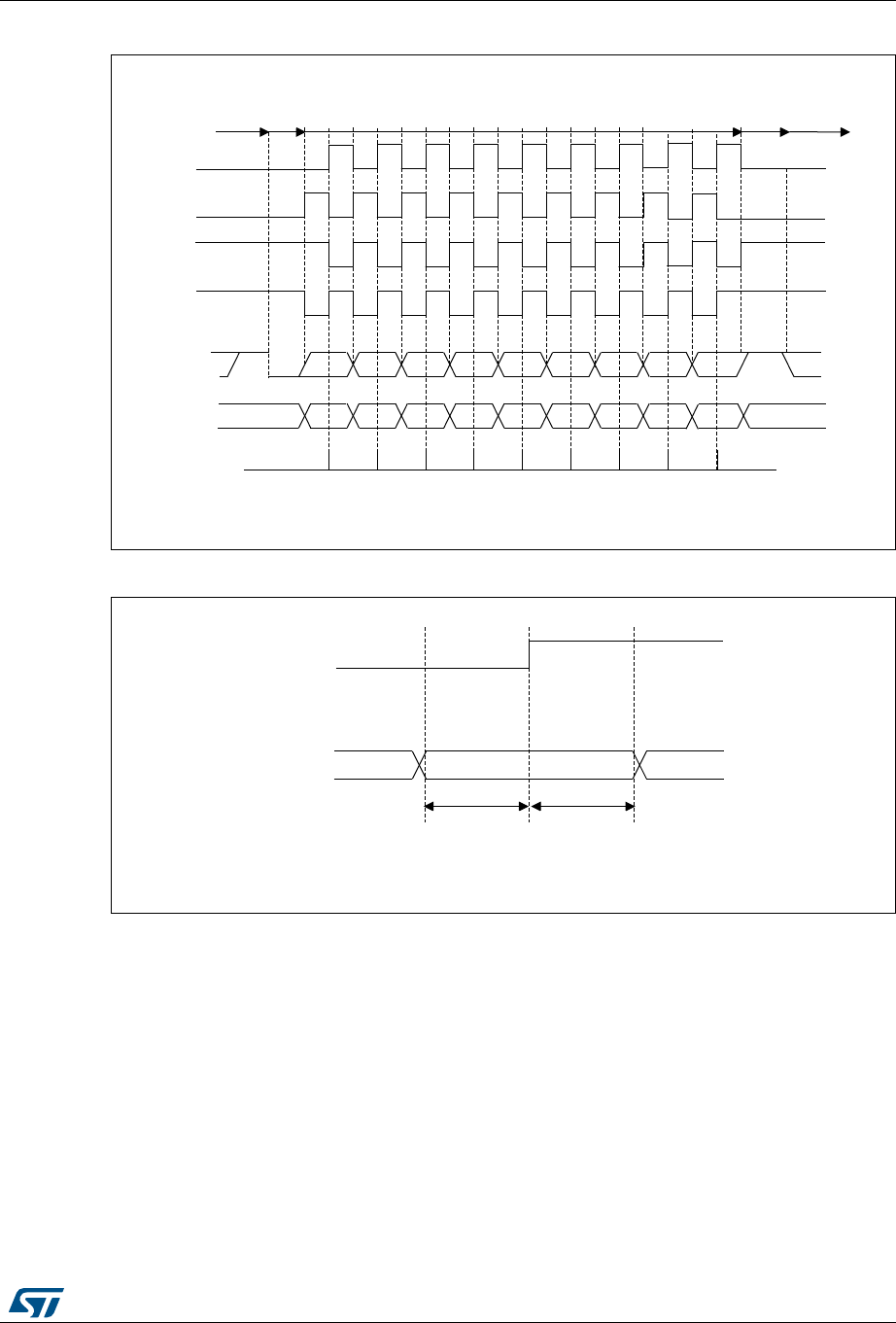
DocID027812 Rev 2 653/766
RM0401 Universal synchronous asynchronous receiver transmitter (USART)
674
Figure 227. USART data clock timing diagram (M=1)
Figure 228. RX data setup/hold time
Note: The function of SCLK is different in Smartcard mode. Refer to the Smartcard mode chapter
for more details.
24.4.10 Single-wire half-duplex communication
The single-wire half-duplex mode is selected by setting the HDSEL bit in the USART_CR3
register. In this mode, the following bits must be kept cleared:
•LINEN and CLKEN bits in the USART_CR2 register,
•SCEN and IREN bits in the USART_CR3 register.
The USART can be configured to follow a single-wire half-duplex protocol where the TX and
RX lines are internally connected. The selection between half- and full-duplex
communication is made with a control bit ‘HALF DUPLEX SEL’ (HDSEL in USART_CR3).
06Y9
06%
06%
/6%
/6%6WDUW
6WDUW 6WRS
,GOHRU
SUHFHGLQJ
WUDQVPLVVLRQ
,GOHRUQH[W
WUDQVPLVVLRQ
/%&/ELWFRQWUROVODVWGDWDSXOVH
&DSWXUH
VWUREH
'DWDRQ5;
IURPVODYH
'DWDRQ7;
IURPPDVWHU
&ORFN&32/
&3+$
&ORFN&32/
&3+$
&ORFN&32/
&3+$
&ORFN&32/
&3+$
6WRS
0ELWV GDWDELWV
06Y9
'DWDRQ5;IURPVODYH
6&/.
FDSWXUHVWUREHRQ6&/.
ULVLQJHGJHLQWKLVH[DPSOH
9DOLG'$7$ELW
W6(783 W+2/'
W6(783 W+2/'ELWWLPH
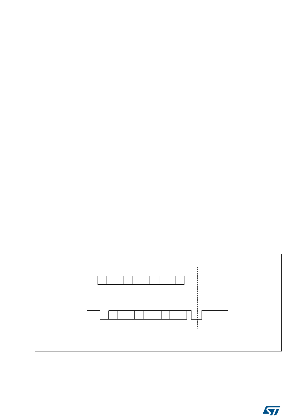
Universal synchronous asynchronous receiver transmitter (USART) RM0401
654/766 DocID027812 Rev 2
As soon as HDSEL is written to 1:
•the TX and RX lines are internally connected
•the RX pin is no longer used
•the TX pin is always released when no data is transmitted. Thus, it acts as a standard
I/O in idle or in reception. It means that the I/O must be configured so that TX is
configured as floating input (or output high open-drain) when not driven by the USART.
Apart from this, the communications are similar to what is done in normal USART mode.
The conflicts on the line must be managed by the software (by the use of a centralized
arbiter, for instance). In particular, the transmission is never blocked by hardware and
continue to occur as soon as a data is written in the data register while the TE bit is set.
24.4.11 Smartcard
The Smartcard mode is selected by setting the SCEN bit in the USART_CR3 register. In
smartcard mode, the following bits must be kept cleared:
•LINEN bit in the USART_CR2 register,
•HDSEL and IREN bits in the USART_CR3 register.
Moreover, the CLKEN bit may be set in order to provide a clock to the smartcard.
The Smartcard interface is designed to support asynchronous protocol Smartcards as
defined in the ISO 7816-3 standard. The USART should be configured as:
•8 bits plus parity: where M=1 and PCE=1 in the USART_CR1 register
•1.5 stop bits when transmitting and receiving: where STOP=11 in the USART_CR2
register.
Note: It is also possible to choose 0.5 stop bit for receiving but it is recommended to use 1.5 stop
bits for both transmitting and receiving to avoid switching between the two configurations.
Figure 229 shows examples of what can be seen on the data line with and without parity
error.
Figure 229. ISO 7816-3 asynchronous protocol
When connected to a Smartcard, the TX output of the USART drives a bidirectional line that
is also driven by the Smartcard. The TX pin must be configured as open-drain.
Smartcard is a single wire half duplex communication protocol.
•Transmission of data from the transmit shift register is guaranteed to be delayed by a
minimum of 1/2 baud clock. In normal operation a full transmit shift register will start
06Y9
:LWKRXW3DULW\HUURU
S
6
*XDUGWLPH
:LWK3DULW\HUURU
S
6
*XDUGWLPH
6WDUWELW
6WDUWELW /LQHSXOOHGORZE\UHFHLYHU
GXULQJVWRSLQFDVHRISDULW\HUURU
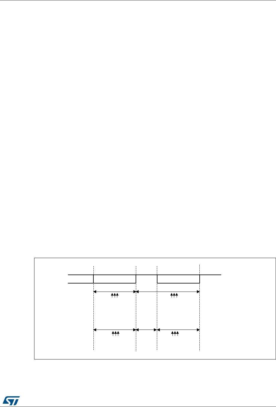
DocID027812 Rev 2 655/766
RM0401 Universal synchronous asynchronous receiver transmitter (USART)
674
shifting on the next baud clock edge. In Smartcard mode this transmission is further
delayed by a guaranteed 1/2 baud clock.
•If a parity error is detected during reception of a frame programmed with a 0.5 or 1.5
stop bit period, the transmit line is pulled low for a baud clock period after the
completion of the receive frame. This is to indicate to the Smartcard that the data
transmitted to USART has not been correctly received. This NACK signal (pulling
transmit line low for 1 baud clock) will cause a framing error on the transmitter side
(configured with 1.5 stop bits). The application can handle re-sending of data according
to the protocol. A parity error is ‘NACK’ed by the receiver if the NACK control bit is set,
otherwise a NACK is not transmitted.
•The assertion of the TC flag can be delayed by programming the Guard Time register.
In normal operation, TC is asserted when the transmit shift register is empty and no
further transmit requests are outstanding. In Smartcard mode an empty transmit shift
register triggers the guard time counter to count up to the programmed value in the
Guard Time register. TC is forced low during this time. When the guard time counter
reaches the programmed value TC is asserted high.
•The de-assertion of TC flag is unaffected by Smartcard mode.
•If a framing error is detected on the transmitter end (due to a NACK from the receiver),
the NACK will not be detected as a start bit by the receive block of the transmitter.
According to the ISO protocol, the duration of the received NACK can be 1 or 2 baud
clock periods.
•On the receiver side, if a parity error is detected and a NACK is transmitted the receiver
will not detect the NACK as a start bit.
Note: A break character is not significant in Smartcard mode. A 0x00 data with a framing error will
be treated as data and not as a break.
No Idle frame is transmitted when toggling the TE bit. The Idle frame (as defined for the
other configurations) is not defined by the ISO protocol.
Figure 230 details how the NACK signal is sampled by the USART. In this example the
USART is transmitting a data and is configured with 1.5 stop bits. The receiver part of the
USART is enabled in order to check the integrity of the data and the NACK signal.
Figure 230. Parity error detection using the 1.5 stop bits
The USART can provide a clock to the smartcard through the SCLK output. In smartcard
mode, SCLK is not associated to the communication but is simply derived from the internal
peripheral input clock through a 5-bit prescaler. The division ratio is configured in the
069
%LW 3DULW\ELW 6WRSELW
ELWWLPH ELWWLPH
ELW
WLPH
6DPSOLQJDW
WKWKWK
6DPSOLQJDW
WKWKWK
6DPSOLQJDW
WKWKWK
6DPSOLQJDW
WKWKWK

Universal synchronous asynchronous receiver transmitter (USART) RM0401
656/766 DocID027812 Rev 2
prescaler register USART_GTPR. SCLK frequency can be programmed from fCK/2 to
fCK/62, where fCK is the peripheral input clock.
24.4.12 IrDA SIR ENDEC block
The IrDA mode is selected by setting the IREN bit in the USART_CR3 register. In IrDA
mode, the following bits must be kept cleared:
•LINEN, STOP and CLKEN bits in the USART_CR2 register,
•SCEN and HDSEL bits in the USART_CR3 register.
The IrDA SIR physical layer specifies use of a Return to Zero, Inverted (RZI) modulation
scheme that represents logic 0 as an infrared light pulse (see Figure 231).
The SIR Transmit encoder modulates the Non Return to Zero (NRZ) transmit bit stream
output from USART. The output pulse stream is transmitted to an external output driver and
infrared LED. USART supports only bit rates up to 115.2Kbps for the SIR ENDEC. In normal
mode the transmitted pulse width is specified as 3/16 of a bit period.
The SIR receive decoder demodulates the return-to-zero bit stream from the infrared
detector and outputs the received NRZ serial bit stream to USART. The decoder input is
normally HIGH (marking state) in the Idle state. The transmit encoder output has the
opposite polarity to the decoder input. A start bit is detected when the decoder input is low.
•IrDA is a half duplex communication protocol. If the Transmitter is busy (i.e. the USART
is sending data to the IrDA encoder), any data on the IrDA receive line will be ignored
by the IrDA decoder and if the Receiver is busy (USART is receiving decoded data
from the USART), data on the TX from the USART to IrDA will not be encoded by IrDA.
While receiving data, transmission should be avoided as the data to be transmitted
could be corrupted.
•A ‘0 is transmitted as a high pulse and a ‘1 is transmitted as a ‘0. The width of the pulse
is specified as 3/16th of the selected bit period in normal mode (see Figure 232).
•The SIR decoder converts the IrDA compliant receive signal into a bit stream for
USART.
•The SIR receive logic interprets a high state as a logic one and low pulses as logic
zeros.
•The transmit encoder output has the opposite polarity to the decoder input. The SIR
output is in low state when Idle.
•The IrDA specification requires the acceptance of pulses greater than 1.41 us. The
acceptable pulse width is programmable. Glitch detection logic on the receiver end
filters out pulses of width less than 2 PSC periods (PSC is the prescaler value
programmed in the IrDA low-power Baud Register, USART_GTPR). Pulses of width
less than 1 PSC period are always rejected, but those of width greater than one and
less than two periods may be accepted or rejected, those greater than 2 periods will be
accepted as a pulse. The IrDA encoder/decoder doesn’t work when PSC=0.
•The receiver can communicate with a low-power transmitter.
•In IrDA mode, the STOP bits in the USART_CR2 register must be configured to “1 stop
bit”.
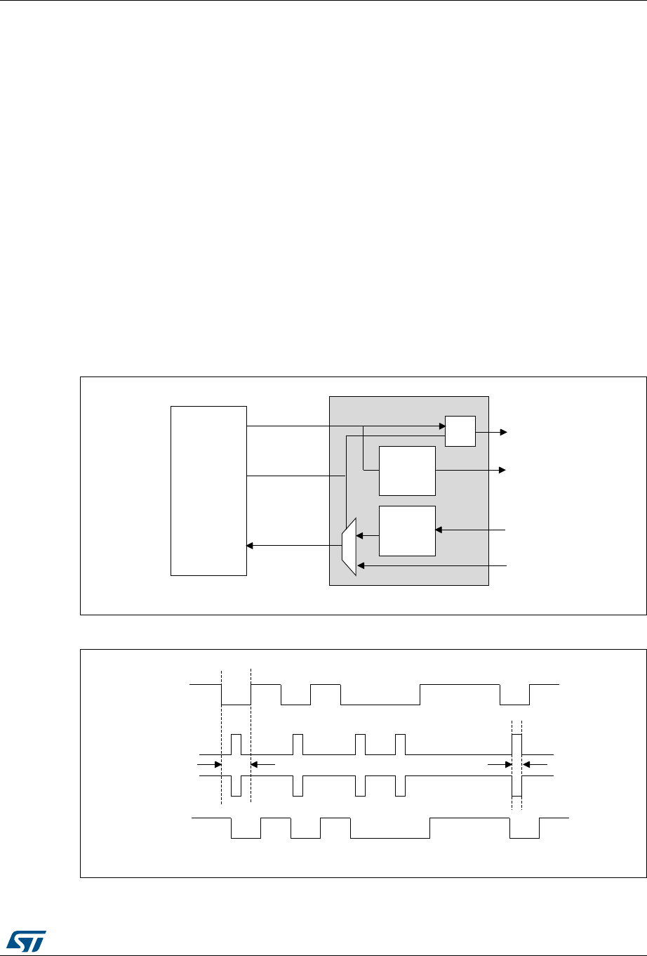
DocID027812 Rev 2 657/766
RM0401 Universal synchronous asynchronous receiver transmitter (USART)
674
IrDA low-power mode
Transmitter:
In low-power mode the pulse width is not maintained at 3/16 of the bit period. Instead, the
width of the pulse is 3 times the low-power baud rate which can be a minimum of 1.42 MHz.
Generally this value is 1.8432 MHz (1.42 MHz < PSC< 2.12 MHz). A low-power mode
programmable divisor divides the system clock to achieve this value.
Receiver:
Receiving in low-power mode is similar to receiving in normal mode. For glitch detection the
USART should discard pulses of duration shorter than 1/PSC. A valid low is accepted only if
its duration is greater than 2 periods of the IrDA low-power Baud clock (PSC value in
USART_GTPR).
Note: A pulse of width less than two and greater than one PSC period(s) may or may not be
rejected.
The receiver set up time should be managed by software. The IrDA physical layer
specification specifies a minimum of 10 ms delay between transmission and reception (IrDA
is a half duplex protocol).
Figure 231. IrDA SIR ENDEC- block diagram
Figure 232. IrDA data modulation (3/16) -Normal mode
6,5(1
06Y9
86$57
25
6,5
7UDQVPLW
(QFRGHU
6,5
5HFHLYH
'(FRGHU
7;
5;
86$57B5;
,U'$B,1
,U'$B287
86$57B7;
06Y9
7;
6WDUW
ELW
6WRS
ELW
%LWSHULRG
,U'$B287
,U'$B,1
5;

Universal synchronous asynchronous receiver transmitter (USART) RM0401
658/766 DocID027812 Rev 2
24.4.13 Continuous communication using DMA
The USART is capable of continuous communication using the DMA. The DMA requests for
Rx buffer and Tx buffer are generated independently.
Transmission using DMA
DMA mode can be enabled for transmission by setting DMAT bit in the USART_CR3
register. Data is loaded from a SRAM area configured using the DMA peripheral (refer to the
DMA specification) to the USART_DR register whenever the TXE bit is set. To map a DMA
channel for USART transmission, use the following procedure (x denotes the channel
number):
1. Write the USART_DR register address in the DMA control register to configure it as the
destination of the transfer. The data will be moved to this address from memory after
each TXE event.
2. Write the memory address in the DMA control register to configure it as the source of
the transfer. The data will be loaded into the USART_DR register from this memory
area after each TXE event.
3. Configure the total number of bytes to be transferred to the DMA control register.
4. Configure the channel priority in the DMA register
5. Configure DMA interrupt generation after half/ full transfer as required by the
application.
6. Clear the TC bit in the SR register by writing 0 to it.
7. Activate the channel in the DMA register.
When the number of data transfers programmed in the DMA Controller is reached, the DMA
controller generates an interrupt on the DMA channel interrupt vector.
In transmission mode, once the DMA has written all the data to be transmitted (the TCIF flag
is set in the DMA_ISR register), the TC flag can be monitored to make sure that the USART
communication is complete. This is required to avoid corrupting the last transmission before
disabling the USART or entering the Stop mode. The software must wait until TC=1. The TC
flag remains cleared during all data transfers and it is set by hardware at the last frame end
of transmission.
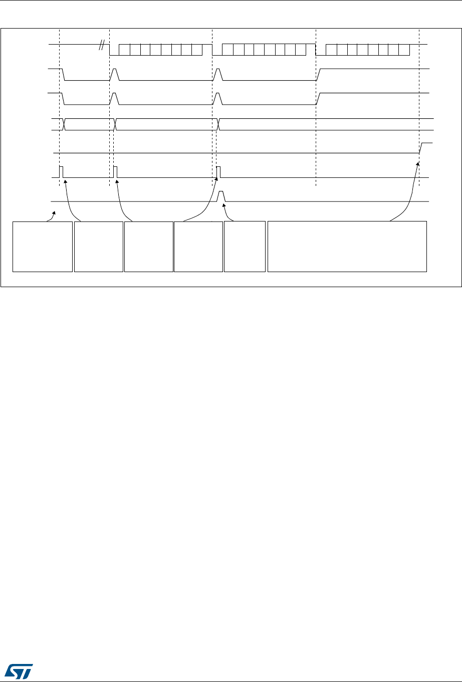
DocID027812 Rev 2 659/766
RM0401 Universal synchronous asynchronous receiver transmitter (USART)
674
Figure 233. Transmission using DMA
Reception using DMA
DMA mode can be enabled for reception by setting the DMAR bit in USART_CR3 register.
Data is loaded from the USART_DR register to a SRAM area configured using the DMA
peripheral (refer to the DMA specification) whenever a data byte is received. To map a DMA
channel for USART reception, use the following procedure:
1. Write the USART_DR register address in the DMA control register to configure it as the
source of the transfer. The data will be moved from this address to the memory after
each RXNE event.
2. Write the memory address in the DMA control register to configure it as the destination
of the transfer. The data will be loaded from USART_DR to this memory area after each
RXNE event.
3. Configure the total number of bytes to be transferred in the DMA control register.
4. Configure the channel priority in the DMA control register
5. Configure interrupt generation after half/ full transfer as required by the application.
6. Activate the channel in the DMA control register.
When the number of data transfers programmed in the DMA Controller is reached, the DMA
controller generates an interrupt on the DMA channel interrupt vector. The DMAR bit should
be cleared by software in the USART_CR3 register during the interrupt subroutine.
) ))
AIB
6RIWZDUH
FRQILJXUHV'0$
WRVHQGGDWD
EORFNVDQG
HQDEOHV86$57
7KH'0$
WUDQVIHULV
FRPSOHWH
7&,) LQ
'0$B,65
'0$ZULWHV
)LQWR
86$57B7'5
'0$ZULWHV
)LQWR
86$57B7'5
'0$ZULWHV
)LQWR
86$57B7'5
6RIWZDUHZDLWVXQWLO7&
6HWE\KDUGZDUH
&OHDUHG
E\
VRIWZDUH
6HWE\
KDUGZDUH
7;OLQH
7;(IODJ
86$57B7'5
'0$UHTXHVW
'0$ZULWHV
86$57B7'5
'0$7&,)IODJ
WUDQVIHU
FRPSOHWH
7&IODJ
)UDPH )UDPH )UDPH
,GOHSUHDPEOH
6HWE\KDUGZDUH
FOHDUHGE\'0$UHDG
6HWE\KDUGZDUH
FOHDUHGE\'0$UHDG 6HWE\KDUGZDUH
,JQRUHGE\WKH'0$EHFDXVH
WKHWUDQVIHULVFRPSOHWH
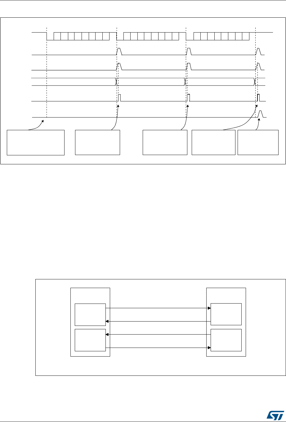
Universal synchronous asynchronous receiver transmitter (USART) RM0401
660/766 DocID027812 Rev 2
Figure 234. Reception using DMA
Error flagging and interrupt generation in multibuffer communication
In case of multibuffer communication if any error occurs during the transaction the error flag
will be asserted after the current byte. An interrupt will be generated if the interrupt enable
flag is set. For framing error, overrun error and noise flag which are asserted with RXNE in
case of single byte reception, there will be separate error flag interrupt enable bit (EIE bit in
the USART_CR3 register), which if set will issue an interrupt after the current byte with
either of these errors.
24.4.14 Hardware flow control
It is possible to control the serial data flow between 2 devices by using the nCTS input and
the nRTS output. The Figure 235 shows how to connect 2 devices in this mode:
Figure 235. Hardware flow control between 2 USARTs
RTS and CTS flow control can be enabled independently by writing respectively RTSE and
CTSE bits to 1 (in the USART_CR3 register).
7;OLQH
)UDPH
) )
6HWE\KDUGZDUH
FOHDUHGE\'0$UHDG
)
DLE
)UDPH )UDPH
5;1(IODJ
86$57B7'5
'0$UHTXHVW
'0$UHDGV
86$57B7'5
'0$7&,)IODJ
WUDQVIHUFRPSOHWH
6RIWZDUHFRQILJXUHVWKH
'0$WRUHFHLYHGDWD
EORFNVDQGHQDEOHV
WKH86$57
'0$UHDGV)
IURP86$57B7'5
7KH'0$WUDQVIHU
LVFRPSOHWH
7&,) LQ
'0$B,65
6HWE\KDUGZDUH
&OHDUHG
E\
VRIWZDUH
'0$UHDGV)
IURP86$57B7'5
'0$UHDGV)
IURP86$57B7'5
06Y9
7;FLUFXLW
86$57
7;
5;FLUFXLW
5;FLUFXLW
86$57
7;FLUFXLW
7;
Q&76
Q&76
Q576
5;
Q576
5;
DocID027812 Rev 2 661/766
RM0401 Universal synchronous asynchronous receiver transmitter (USART)
674
RTS flow control
If the RTS flow control is enabled (RTSE=1), then nRTS is asserted (tied low) as long as the
USART receiver is ready to receive a new data. When the receive register is full, nRTS is
deasserted, indicating that the transmission is expected to stop at the end of the current
frame. Figure 236 shows an example of communication with RTS flow control enabled.
Figure 236. RTS flow control
CTS flow control
If the CTS flow control is enabled (CTSE=1), then the transmitter checks the nCTS input
before transmitting the next frame. If nCTS is asserted (tied low), then the next data is
transmitted (assuming that a data is to be transmitted, in other words, if TXE=0), else the
transmission does not occur. When nCTS is deasserted during a transmission, the current
transmission is completed before the transmitter stops.
When CTSE=1, the CTSIF status bit is automatically set by hardware as soon as the nCTS
input toggles. It indicates when the receiver becomes ready or not ready for communication.
An interrupt is generated if the CTSIE bit in the USART_CR3 register is set. The figure
below shows an example of communication with CTS flow control enabled.
Figure 237. CTS flow control
06Y9
6WDUW
ELW
6WDUW
ELW
6WRS
ELW ,GOH 6WRS
ELW
5;
Q576
'DWDUHDG
'DWDFDQQRZEHWUDQVPLWWHG
5;1( 5;1(
'DWD 'DWD
06Y9
6WDUW
ELW
6WRS
ELW
7;
7'5
&76
'DWD
'DWD
6WRS
ELW ,GOH 6WDUW
ELW
'DWD 'DWD
'DWD
HPSW\ HPSW\
&76
Q&76
7UDQVPLWGDWDUHJLVWHU
:ULWLQJGDWDLQ7'5 7UDQVPLVVLRQRI'DWDLV
GHOD\HGXQWLOQ&76
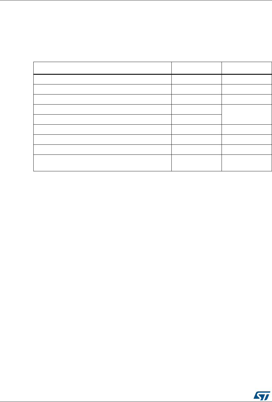
Universal synchronous asynchronous receiver transmitter (USART) RM0401
662/766 DocID027812 Rev 2
Note: Special behavior of break frames: when the CTS flow is enabled, the transmitter does not
check the nCTS input state to send a break.
24.5 USART interrupts
The USART interrupt events are connected to the same interrupt vector (see Figure 238).
•During transmission: Transmission Complete, Clear to Send or Transmit Data Register
empty interrupt.
•While receiving: Idle Line detection, Overrun error, Receive Data register not empty,
Parity error, LIN break detection, Noise Flag (only in multi buffer communication) and
Framing Error (only in multi buffer communication).
These events generate an interrupt if the corresponding Enable Control Bit is set.
Table 111. USART interrupt requests
Interrupt event Event flag Enable control bit
Transmit Data Register Empty TXE TXEIE
CTS flag CTS CTSIE
Transmission Complete TC TCIE
Received Data Ready to be Read RXNE
RXNEIE
Overrun Error Detected ORE
Idle Line Detected IDLE IDLEIE
Parity Error PE PEIE
Break Flag LBD LBDIE
Noise Flag, Overrun error and Framing Error
in multibuffer communication NF or ORE or FE EIE
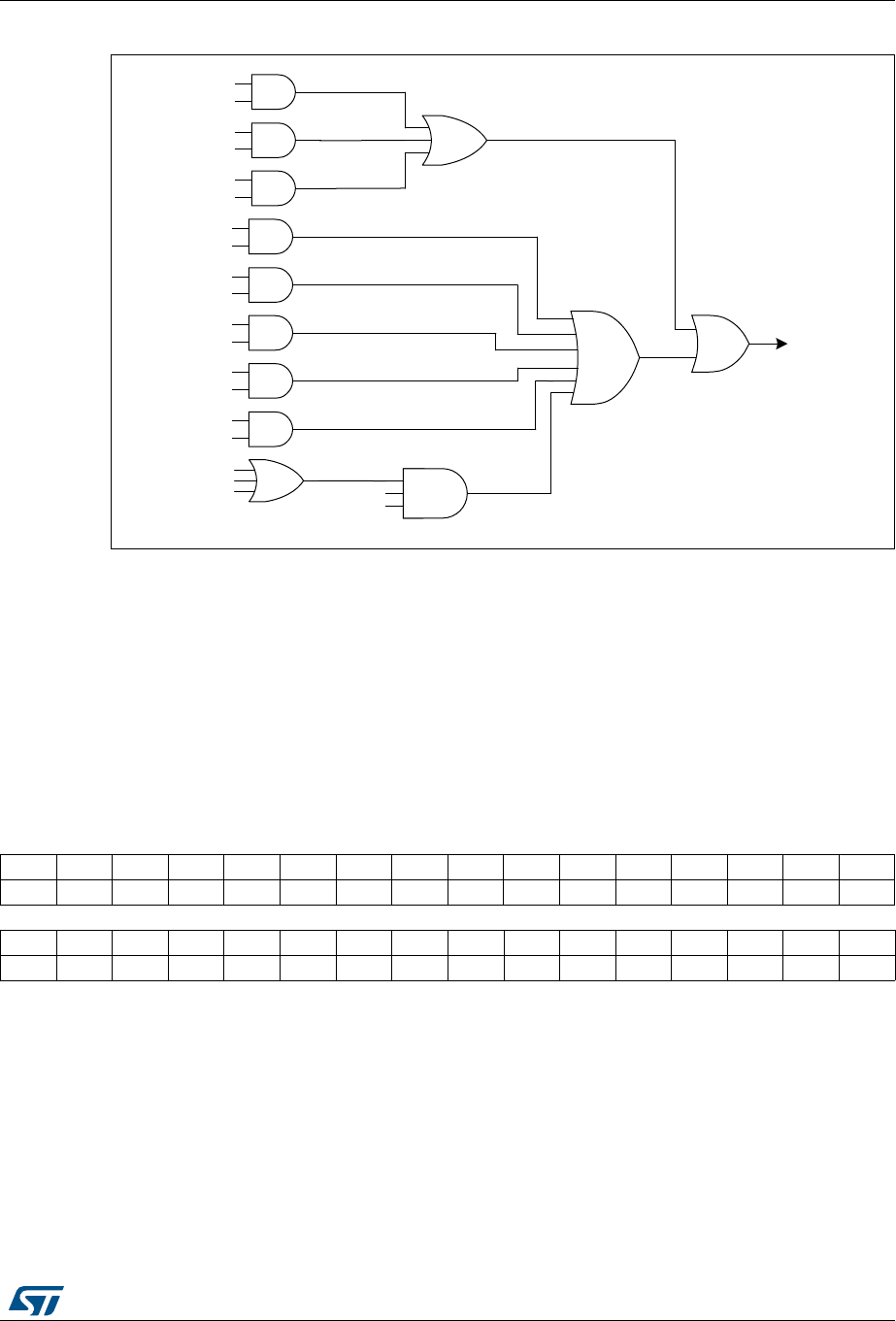
DocID027812 Rev 2 663/766
RM0401 Universal synchronous asynchronous receiver transmitter (USART)
674
Figure 238. USART interrupt mapping diagram
24.6 USART registers
Refer to Section 1.1 on page 33 for a list of abbreviations used in register descriptions.
The peripheral registers have to be accessed by half-words (16 bits) or words (32 bits).
24.6.1 Status register (USART_SR)
Address offset: 0x00
Reset value: 0x00C0 0000
069
7;(
7;(,(
5;1(,(
25(
86$57
LQWHUUXSW
,'/(
,'/(,(
7&
7&,(
&76
&76,(
3(
3(,(
5;1(,(
5;1(
/%'
/%',(
)(
1(
25( (,(
'0$5
31 30 29 28 27 26 25 24 23 22 21 20 19 18 17 16
Res. Res. Res. Res. Res. Res. Res. Res. Res. Res. Res. Res. Res. Res. Res. Res.
15 14 13 12 11 10 9876543210
Res. Res. Res. Res. Res. Res. CTS LBD TXE TC RXNE IDLE ORE NF FE PE
rc_w0 rc_w0 rrc_w0 rc_w0 rrrrr

Universal synchronous asynchronous receiver transmitter (USART) RM0401
664/766 DocID027812 Rev 2
Bits 31:10 Reserved, must be kept at reset value
Bit 9 CTS: CTS flag
This bit is set by hardware when the nCTS input toggles, if the CTSE bit is set. It is cleared
by software (by writing it to 0). An interrupt is generated if CTSIE=1 in the USART_CR3
register.
0: No change occurred on the nCTS status line
1: A change occurred on the nCTS status line
Note: This bit is not available for UART4 & UART5.
Bit 8 LBD: LIN break detection flag
This bit is set by hardware when the LIN break is detected. It is cleared by software (by
writing it to 0). An interrupt is generated if LBDIE = 1 in the USART_CR2 register.
0: LIN Break not detected
1: LIN break detected
Note: An interrupt is generated when LBD=1 if LBDIE=1
Bit 7 TXE: Transmit data register empty
This bit is set by hardware when the content of the TDR register has been transferred into
the shift register. An interrupt is generated if the TXEIE bit =1 in the USART_CR1 register. It
is cleared by a write to the USART_DR register.
0: Data is not transferred to the shift register
1: Data is transferred to the shift register)
Note: This bit is used during single buffer transmission.
Bit 6 TC: Transmission complete
This bit is set by hardware if the transmission of a frame containing data is complete and if
TXE is set. An interrupt is generated if TCIE=1 in the USART_CR1 register. It is cleared by
a software sequence (a read from the USART_SR register followed by a write to the
USART_DR register). The TC bit can also be cleared by writing a '0' to it. This clearing
sequence is recommended only for multibuffer communication.
0: Transmission is not complete
1: Transmission is complete
Bit 5 RXNE: Read data register not empty
This bit is set by hardware when the content of the RDR shift register has been transferred
to the USART_DR register. An interrupt is generated if RXNEIE=1 in the USART_CR1
register. It is cleared by a read to the USART_DR register. The RXNE flag can also be
cleared by writing a zero to it. This clearing sequence is recommended only for multibuffer
communication.
0: Data is not received
1: Received data is ready to be read.
Bit 4 IDLE: IDLE line detected
This bit is set by hardware when an Idle Line is detected. An interrupt is generated if the
IDLEIE=1 in the USART_CR1 register. It is cleared by a software sequence (an read to the
USART_SR register followed by a read to the USART_DR register).
0: No Idle Line is detected
1: Idle Line is detected
Note: The IDLE bit will not be set again until the RXNE bit has been set itself (i.e. a new idle
line occurs).

DocID027812 Rev 2 665/766
RM0401 Universal synchronous asynchronous receiver transmitter (USART)
674
24.6.2 Data register (USART_DR)
Address offset: 0x04
Reset value: 0x0000 0000
Bit 3 ORE: Overrun error
This bit is set by hardware when the word currently being received in the shift register is
ready to be transferred into the RDR register while RXNE=1. An interrupt is generated if
RXNEIE=1 in the USART_CR1 register. It is cleared by a software sequence (an read to the
USART_SR register followed by a read to the USART_DR register).
0: No Overrun error
1: Overrun error is detected
Note: When this bit is set, the RDR register content will not be lost but the shift register will be
overwritten. An interrupt is generated on ORE flag in case of Multi Buffer
communication if the EIE bit is set.
Bit 2 NF: Noise detected flag
This bit is set by hardware when noise is detected on a received frame. It is cleared by a
software sequence (an read to the USART_SR register followed by a read to the
USART_DR register).
0: No noise is detected
1: Noise is detected
Note: This bit does not generate interrupt as it appears at the same time as the RXNE bit
which itself generates an interrupting interrupt is generated on NF flag in case of Multi
Buffer communication if the EIE bit is set.
Note: When the line is noise-free, the NF flag can be disabled by programming the ONEBIT
bit to 1 to increase the USART tolerance to deviations (Refer to Section 24.4.5: USART
receiver tolerance to clock deviation on page 645).
Bit 1 FE: Framing error
This bit is set by hardware when a de-synchronization, excessive noise or a break character
is detected. It is cleared by a software sequence (an read to the USART_SR register
followed by a read to the USART_DR register).
0: No Framing error is detected
1: Framing error or break character is detected
Note: This bit does not generate interrupt as it appears at the same time as the RXNE bit
which itself generates an interrupt. If the word currently being transferred causes both
frame error and overrun error, it will be transferred and only the ORE bit will be set.
An interrupt is generated on FE flag in case of Multi Buffer communication if the EIE bit
is set.
Bit 0 PE: Parity error
This bit is set by hardware when a parity error occurs in receiver mode. It is cleared by a
software sequence (a read from the status register followed by a read or write access to the
USART_DR data register). The software must wait for the RXNE flag to be set before
clearing the PE bit.
An interrupt is generated if PEIE = 1 in the USART_CR1 register.
0: No parity error
1: Parity error
31 30 29 28 27 26 25 24 23 22 21 20 19 18 17 16
Res. Res. Res. Res. Res. Res. Res. Res. Res. Res. Res. Res. Res. Res. Res. Res.
Universal synchronous asynchronous receiver transmitter (USART) RM0401
666/766 DocID027812 Rev 2
24.6.3 Baud rate register (USART_BRR)
Note: The baud counters stop counting if the TE or RE bits are disabled respectively.
Address offset: 0x08
Reset value: 0x0000 0000
15 14 13 12 11 10 9 8 7 6 5 4 3 2 1 0
Res. Res. Res. Res. Res. Res. Res. DR[8:0]
rw rw rw rw rw rw rw rw rw
Bits 31:9 Reserved, must be kept at reset value
Bits 8:0 DR[8:0]: Data value
Contains the Received or Transmitted data character, depending on whether it is read from
or written to.
The Data register performs a double function (read and write) since it is composed of two
registers, one for transmission (TDR) and one for reception (RDR)
The TDR register provides the parallel interface between the internal bus and the output shift
register (see Figure 1).
The RDR register provides the parallel interface between the input shift register and the
internal bus.
When transmitting with the parity enabled (PCE bit set to 1 in the USART_CR1 register), the
value written in the MSB (bit 7 or bit 8 depending on the data length) has no effect because
it is replaced by the parity.
When receiving with the parity enabled, the value read in the MSB bit is the received parity
bit.
31 30 29 28 27 26 25 24 23 22 21 20 19 18 17 16
Res. Res. Res. Res. Res. Res. Res. Res. Res. Res. Res. Res. Res. Res. Res. Res.
15 14 13 12 11 10 9876543210
DIV_Mantissa[11:0] DIV_Fraction[3:0]
rw rw rw rw rw rw rw rw rw rw rw rw rw rw rw rw
Bits 31:16 Reserved, must be kept at reset value
Bits 15:4 DIV_Mantissa[11:0]: mantissa of USARTDIV
These 12 bits define the mantissa of the USART Divider (USARTDIV)
Bits 3:0 DIV_Fraction[3:0]: fraction of USARTDIV
These 4 bits define the fraction of the USART Divider (USARTDIV). When OVER8=1, the
DIV_Fraction3 bit is not considered and must be kept cleared.

DocID027812 Rev 2 667/766
RM0401 Universal synchronous asynchronous receiver transmitter (USART)
674
24.6.4 Control register 1 (USART_CR1)
Address offset: 0x0C
Reset value: 0x0000 0000
31 30 29 28 27 26 25 24 23 22 21 20 19 18 17 16
Res. Res. Res. Res. Res. Res. Res. Res. Res. Res. Res. Res. Res. Res. Res. Res.
15 14 13 12 11 10 9 8 7 6 5 4 3 2 1 0
OVER8 Res. UE MWAKE PCE PS PEIE TXEIE TCIE RXNEIE IDLEIE TE RE RWU SBK
rw rw rw rw rw rw rw rw rw rw rw rw rw rw rw
Bits 31:16 Reserved, must be kept at reset value
Bit 15 OVER8: Oversampling mode
0: oversampling by 16
1: oversampling by 8
Note: Oversampling by 8 is not available in the Smartcard, IrDA and LIN modes: when
SCEN=1,IREN=1 or LINEN=1 then OVER8 is forced to ‘0 by hardware.
Bit 14 Reserved, must be kept at reset value
Bit 13 UE: USART enable
When this bit is cleared the USART prescalers and outputs are stopped and the end of the
current
byte transfer in order to reduce power consumption. This bit is set and cleared by software.
0: USART prescaler and outputs disabled
1: USART enabled
Bit 12 M: Word length
This bit determines the word length. It is set or cleared by software.
0: 1 Start bit, 8 Data bits, n Stop bit
1: 1 Start bit, 9 Data bits, n Stop bit
Note: The M bit must not be modified during a data transfer (both transmission and reception)
Bit 11 WAKE: Wakeup method
This bit determines the USART wakeup method, it is set or cleared by software.
0: Idle Line
1: Address Mark
Bit 10 PCE: Parity control enable
This bit selects the hardware parity control (generation and detection). When the parity
control is enabled, the computed parity is inserted at the MSB position (9th bit if M=1; 8th bit
if M=0) and parity is checked on the received data. This bit is set and cleared by software.
Once it is set, PCE is active after the current byte (in reception and in transmission).
0: Parity control disabled
1: Parity control enabled
Bit 9 PS: Parity selection
This bit selects the odd or even parity when the parity generation/detection is enabled (PCE
bit set). It is set and cleared by software. The parity will be selected after the current byte.
0: Even parity
1: Odd parity

Universal synchronous asynchronous receiver transmitter (USART) RM0401
668/766 DocID027812 Rev 2
Bit 8 PEIE: PE interrupt enable
This bit is set and cleared by software.
0: Interrupt is inhibited
1: An USART interrupt is generated whenever PE=1 in the USART_SR register
Bit 7 TXEIE: TXE interrupt enable
This bit is set and cleared by software.
0: Interrupt is inhibited
1: An USART interrupt is generated whenever TXE=1 in the USART_SR register
Bit 6 TCIE: Transmission complete interrupt enable
This bit is set and cleared by software.
0: Interrupt is inhibited
1: An USART interrupt is generated whenever TC=1 in the USART_SR register
Bit 5 RXNEIE: RXNE interrupt enable
This bit is set and cleared by software.
0: Interrupt is inhibited
1: An USART interrupt is generated whenever ORE=1 or RXNE=1 in the USART_SR
register
Bit 4 IDLEIE: IDLE interrupt enable
This bit is set and cleared by software.
0: Interrupt is inhibited
1: An USART interrupt is generated whenever IDLE=1 in the USART_SR register
Bit 3 TE: Transmitter enable
This bit enables the transmitter. It is set and cleared by software.
0: Transmitter is disabled
1: Transmitter is enabled
Note: 1: During transmission, a “0” pulse on the TE bit (“0” followed by “1”) sends a preamble
(idle line) after the current word, except in smartcard mode.
2: When TE is set there is a 1 bit-time delay before the transmission starts.
Bit 2 RE: Receiver enable
This bit enables the receiver. It is set and cleared by software.
0: Receiver is disabled
1: Receiver is enabled and begins searching for a start bit
Bit 1 RWU: Receiver wakeup
This bit determines if the USART is in mute mode or not. It is set and cleared by software
and can be cleared by hardware when a wakeup sequence is recognized.
0: Receiver in active mode
1: Receiver in mute mode
Note: 1: Before selecting Mute mode (by setting the RWU bit) the USART must first receive a
data byte, otherwise it cannot function in Mute mode with wakeup by Idle line detection.
2: In Address Mark Detection wakeup configuration (WAKE bit=1) the RWU bit cannot
be modified by software while the RXNE bit is set.
Bit 0 SBK: Send break
This bit set is used to send break characters. It can be set and cleared by software. It should
be set by software, and will be reset by hardware during the stop bit of break.
0: No break character is transmitted
1: Break character will be transmitted

DocID027812 Rev 2 669/766
RM0401 Universal synchronous asynchronous receiver transmitter (USART)
674
24.6.5 Control register 2 (USART_CR2)
Address offset: 0x10
Reset value: 0x0000 0000
31 30 29 28 27 26 25 24 23 22 21 20 19 18 17 16
Res. Res. Res. Res. Res. Res. Res. Res. Res. Res. Res. Res. Res. Res. Res. Res.
15 14 13 12 11 10 9876543210
Res. LINEN STOP[1:0] CLKEN CPOL CPHA LBCL Res. LBDIE LBDL Res. ADD[3:0]
rw rw rw rw rw rw rw rw rw rw rw rw rw
Bits 31:15 Reserved, must be kept at reset value
Bit 14 LINEN: LIN mode enable
This bit is set and cleared by software.
0: LIN mode disabled
1: LIN mode enabled
The LIN mode enables the capability to send LIN Synch Breaks (13 low bits) using the SBK bit in
the USART_CR1 register, and to detect LIN Sync breaks.
Bits 13:12 STOP: STOP bits
These bits are used for programming the stop bits.
00: 1 Stop bit
01: 0.5 Stop bit
10: 2 Stop bits
11: 1.5 Stop bit
Note: The 0.5 Stop bit and 1.5 Stop bit are not available for UART4 & UART5.
Bit 11 CLKEN: Clock enable
This bit allows the user to enable the SCLK pin.
0: SCLK pin disabled
1: SCLK pin enabled
This bit is not available for UART4 & UART5.
Bit 10 CPOL: Clock polarity
This bit allows the user to select the polarity of the clock output on the SCLK pin in synchronous
mode. It works in conjunction with the CPHA bit to produce the desired clock/data relationship
0: Steady low value on SCLK pin outside transmission window.
1: Steady high value on SCLK pin outside transmission window.
This bit is not available for UART4 & UART5.
Bit 9 CPHA: Clock phase
This bit allows the user to select the phase of the clock output on the SCLK pin in synchronous
mode. It works in conjunction with the CPOL bit to produce the desired clock/data relationship (see
figures 226 to 227)
0: The first clock transition is the first data capture edge
1: The second clock transition is the first data capture edge
Note: This bit is not available for UART4 & UART5.

Universal synchronous asynchronous receiver transmitter (USART) RM0401
670/766 DocID027812 Rev 2
Note: These 3 bits (CPOL, CPHA, LBCL) should not be written while the transmitter is enabled.
24.6.6 Control register 3 (USART_CR3)
Address offset: 0x14
Reset value: 0x0000 0000
Bit 8 LBCL: Last bit clock pulse
This bit allows the user to select whether the clock pulse associated with the last data bit
transmitted (MSB) has to be output on the SCLK pin in synchronous mode.
0: The clock pulse of the last data bit is not output to the SCLK pin
1: The clock pulse of the last data bit is output to the SCLK pin
Note: 1: The last bit is the 8th or 9th data bit transmitted depending on the 8 or 9 bit format selected
by the M bit in the USART_CR1 register.
2: This bit is not available for UART4 & UART5.
Bit 7 Reserved, must be kept at reset value
Bit 6 LBDIE: LIN break detection interrupt enable
Break interrupt mask (break detection using break delimiter).
0: Interrupt is inhibited
1: An interrupt is generated whenever LBD=1 in the USART_SR register
Bit 5 LBDL: lin break detection length
This bit is for selection between 11 bit or 10 bit break detection.
0: 10-bit break detection
1: 11-bit break detection
Bit 4 Reserved, must be kept at reset value
Bits 3:0 ADD[3:0]: Address of the USART node
This bit-field gives the address of the USART node.
This is used in multiprocessor communication during mute mode, for wake up with address mark
detection.
31 30 29 28 27 26 25 24 23 22 21 20 19 18 17 16
Res. Res. Res. Res. Res. Res. Res. Res. Res. Res. Res. Res. Res. Res. Res. Res.
15 14 13 12 11 10 9 8 7 6 5 4 3 2 1 0
Res. Res. Res. Res. ONEBIT CTSIE CTSE RTSE DMAT DMAR SCEN NACK HDSEL IRLP IREN EIE
rw rw rw rw rw rw rw rw rw rw rw rw
Bits 31:12 Reserved, must be kept at reset value
Bit 11 ONEBIT: One sample bit method enable
This bit allows the user to select the sample method. When the one sample bit method is
selected the noise detection flag (NF) is disabled.
0: Three sample bit method
1: One sample bit method
Bit 10 CTSIE: CTS interrupt enable
0: Interrupt is inhibited
1: An interrupt is generated whenever CTS=1 in the USART_SR register
Note: This bit is not available for UART4 & UART5.

DocID027812 Rev 2 671/766
RM0401 Universal synchronous asynchronous receiver transmitter (USART)
674
Bit 9 CTSE: CTS enable
0: CTS hardware flow control disabled
1: CTS mode enabled, data is only transmitted when the nCTS input is asserted (tied to 0).
If the nCTS input is deasserted while a data is being transmitted, then the transmission is
completed before stopping. If a data is written into the data register while nCTS is
deasserted, the transmission is postponed until nCTS is asserted.
Note: This bit is not available for UART4 & UART5.
Bit 8 RTSE: RTS enable
0: RTS hardware flow control disabled
1: RTS interrupt enabled, data is only requested when there is space in the receive buffer.
The transmission of data is expected to cease after the current character has been
transmitted. The nRTS output is asserted (tied to 0) when a data can be received.
Note: This bit is not available for UART4 & UART5.
Bit 7 DMAT: DMA enable transmitter
This bit is set/reset by software
1: DMA mode is enabled for transmission.
0: DMA mode is disabled for transmission.
Bit 6 DMAR: DMA enable receiver
This bit is set/reset by software
1: DMA mode is enabled for reception
0: DMA mode is disabled for reception
Bit 5 SCEN: Smartcard mode enable
This bit is used for enabling Smartcard mode.
0: Smartcard Mode disabled
1: Smartcard Mode enabled
Note: This bit is not available for UART4 & UART5.
Bit 4 NACK: Smartcard NACK enable
0: NACK transmission in case of parity error is disabled
1: NACK transmission during parity error is enabled
Note: This bit is not available for UART4 & UART5.
Bit 3 HDSEL: Half-duplex selection
Selection of Single-wire Half-duplex mode
0: Half duplex mode is not selected
1: Half duplex mode is selected

Universal synchronous asynchronous receiver transmitter (USART) RM0401
672/766 DocID027812 Rev 2
Bit 2 IRLP: IrDA low-power
This bit is used for selecting between normal and low-power IrDA modes
0: Normal mode
1: Low-power mode
Bit 1 IREN: IrDA mode enable
This bit is set and cleared by software.
0: IrDA disabled
1: IrDA enabled
Bit 0 EIE: Error interrupt enable
Error Interrupt Enable Bit is required to enable interrupt generation in case of a framing
error, overrun error or noise flag (FE=1 or ORE=1 or NF=1 in the USART_SR register) in
case of Multi Buffer Communication (DMAR=1 in the USART_CR3 register).
0: Interrupt is inhibited
1: An interrupt is generated whenever DMAR=1 in the USART_CR3 register and FE=1 or
ORE=1 or NF=1 in the USART_SR register.

DocID027812 Rev 2 673/766
RM0401 Universal synchronous asynchronous receiver transmitter (USART)
674
24.6.7 Guard time and prescaler register (USART_GTPR)
Address offset: 0x18
Reset value: 0x0000 0000
31 30 29 28 27 26 25 24 23 22 21 20 19 18 17 16
Res. Res. Res. Res. Res. Res. Res. Res. Res. Res. Res. Res. Res. Res. Res. Res.
15 14 13 12 11 10 9876543210
GT[7:0] PSC[7:0]
rw rw rw rw rw rw rw rw rw rw rw rw rw rw rw rw
Bits 31:16 Reserved, must be kept at reset value
Bits 15:8 GT[7:0]: Guard time value
This bit-field gives the Guard time value in terms of number of baud clocks.
This is used in Smartcard mode. The Transmission Complete flag is set after this guard time
value.
Note: This bit is not available for UART4 & UART5.
Bits 7:0 PSC[7:0]: Prescaler value
–In IrDA Low-power mode:
PSC[7:0] = IrDA Low-Power Baud Rate
Used for programming the prescaler for dividing the system clock to achieve the low-power
frequency:
The source clock is divided by the value given in the register (8 significant bits):
00000000: Reserved - do not program this value
00000001: divides the source clock by 1
00000010: divides the source clock by 2
...
–In normal IrDA mode: PSC must be set to 00000001.
– In smartcard mode:
PSC[4:0]: Prescaler value
Used for programming the prescaler for dividing the system clock to provide the smartcard
clock.
The value given in the register (5 significant bits) is multiplied by 2 to give the division factor
of the source clock frequency:
00000: Reserved - do not program this value
00001: divides the source clock by 2
00010: divides the source clock by 4
00011: divides the source clock by 6
...
Note: 1: Bits [7:5] have no effect if Smartcard mode is used.
2: This bit is not available for UART4 & UART5.

Universal synchronous asynchronous receiver transmitter (USART) RM0401
674/766 DocID027812 Rev 2
24.6.8 USART register map
The table below gives the USART register map and reset values.
Refer to Section 2.2.2 on page 38 for the register boundary addresses.
Table 112. USART register map and reset values
Offset Register
31
30
29
28
27
26
25
24
23
22
21
20
19
18
17
16
15
14
13
12
11
10
9
8
7
6
5
4
3
2
1
0
0x00
USART_SR
Res.
Res.
Res.
Res.
Res.
Res.
Res.
Res.
Res.
Res.
Res.
Res.
Res.
Res.
Res.
Res.
Res.
Res.
Res.
Res.
Res.
Res.
CTS
LBD
TXE
TC
RXNE
IDLE
ORE
NF
FE
PE
Reset value 0011000000
0x04
USART_DR
Res.
Res.
Res.
Res.
Res.
Res.
Res.
Res.
Res.
Res.
Res.
Res.
Res.
Res.
Res.
Res.
Res.
Res.
Res.
Res.
Res.
Res.
Res.
DR[8:0]
Reset value 000000000
0x08
USART_BRR
Res.
Res.
Res.
Res.
Res.
Res.
Res.
Res.
Res.
Res.
Res.
Res.
Res.
Res.
Res.
Res.
DIV_Mantissa[15:4] DIV_Fraction
[3:0]
Reset value 0000000000000000
0x0C
USART_CR1
Res.
Res.
Res.
Res.
Res.
Res.
Res.
Res.
Res.
Res.
Res.
Res.
Res.
Res.
Res.
Res.
OVER8
Res.
UE
M
WAKE
PCE
PS
PEIE
TXEIE
TCIE
RXNEIE
IDLEIE
TE
RE
RWU
SBK
Reset value 0 00000000000000
0x10
USART_CR2
Res.
Res.
Res.
Res.
Res.
Res.
Res.
Res.
Res.
Res.
Res.
Res.
Res.
Res.
Res.
Res.
Res.
LINEN
STOP
[1:0]
CLKEN
CPOL
CPHA
LBCL
Res.
LBDIE
LBDL
Res.
ADD[3:0]
Reset value 0000000 00 0000
0x14
USART_CR3
Res.
Res.
Res.
Res.
Res.
Res.
Res.
Res.
Res.
Res.
Res.
Res.
Res.
Res.
Res.
Res.
Res.
Res.
Res.
Res.
ONEBIT
CTSIE
CTSE
RTSE
DMAT
DMAR
SCEN
NACK
HDSEL
IRLP
IREN
EIE
Reset value 000000000000
0x18
USART_GTPR
Res.
Res.
Res.
Res.
Res.
Res.
Res.
Res.
Res.
Res.
Res.
Res.
Res.
Res.
Res.
Res.
GT[7:0] PSC[7:0]
Reset value 0000000000000000

DocID027812 Rev 2 675/766
RM0401 Serial peripheral interface/ inter-IC sound (SPI/I2S)
726
25 Serial peripheral interface/ inter-IC sound (SPI/I2S)
25.1 Introduction
The SPI/I²S interface can be used to communicate with external devices using the SPI
protocol or the I2S audio protocol. SPI or I2S mode is selectable by software. SPI mode is
selected by default after a device reset.
The serial peripheral interface (SPI) protocol supports half-duplex, full-duplex and simplex
synchronous, serial communication with external devices. The interface can be configured
as master and in this case it provides the communication clock (SCK) to the external slave
device. The interface is also capable of operating in multimaster configuration.
The Inter-IC sound (I2S) protocol is also a synchronous serial communication interface. It
can operate in slave or master mode, as a receiver or a transmitter
It can address four different audio standards including the Philips I2S standard, the MSB-
and LSB-justified standards and the PCM standard.
Warning: Since some SPI1 pins may be mapped onto some pins used
by the JTAG interface, you can either map SPI/I2S onto other
pins, disable the JTAG and use the SWD interface prior to
configuring the pins listed as SPI I/Os (when debugging the
application) or disable both JTAG/SWD interfaces (for
standalone applications). For more information on the
configuration of the JTAG/SWD interface pins, please refer to
Section 6.3.2: I/O pin multiplexer and mapping.

Serial peripheral interface/ inter-IC sound (SPI/I2S) RM0401
676/766 DocID027812 Rev 2
25.1.1 SPI main features
•Master or slave operation
•full-duplex synchronous transfers on three lines
•Half-duplex synchronous transfer on two lines (with bidirectional data line)
•Simplex synchronous transfers on two lines (with unidirectional data line)
•8-bit to 16-bit transfer frame format selection
•Multimaster mode capability
•8 master mode baud rate prescalers up to fPCLK/2.
•Slave mode frequency up to fPCLK/2.
•NSS management by hardware or software for both master and slave: dynamic change
of master/slave operations
•Programmable clock polarity and phase
•Programmable data order with MSB-first or LSB-first shifting
•Dedicated transmission and reception flags with interrupt capability
•SPI bus busy status flag
•SPI Motorola support
•Hardware CRC feature for reliable communication:
– CRC value can be transmitted as last byte in Tx mode
– Automatic CRC error checking for last received byte
•Master mode fault, overrun flags with interrupt capability
•CRC Error flag
•1-byte/word transmission and reception buffer with DMA capability: Tx and Rx requests

DocID027812 Rev 2 677/766
RM0401 Serial peripheral interface/ inter-IC sound (SPI/I2S)
726
25.1.2 SPI extended features
•SPI TI mode support
25.1.3 I2S features
•Half-duplex communication (only transmitter or receiver)
•Master or slave operations
•8-bit programmable linear prescaler to reach accurate audio sample frequencies (from
8 kHz to 192 kHz)
•Data format may be 16-bit, 24-bit or 32-bit
•Packet frame is fixed to 16-bit (16-bit data frame) or 32-bit (16-bit, 24-bit, 32-bit data
frame) by audio channel
•Programmable clock polarity (steady state)
•Underrun flag in slave transmission mode, overrun flag in reception mode (master and
slave) and Frame Error Flag in reception and transmitter mode (slave only)
•16-bit register for transmission and reception with one data register for both channel
sides
•Supported I2S protocols:
–I
2S Philips standard
– MSB-Justified standard (Left-Justified)
– LSB-Justified standard (Right-Justified)
– PCM standard (with short and long frame synchronization on 16-bit channel frame
or 16-bit data frame extended to 32-bit channel frame)
•Data direction is always MSB first
•DMA capability for transmission and reception (16-bit wide)
•Master clock can be output to drive an external audio component. Ratio is fixed at
256 × FS (where FS is the audio sampling frequency)
•I2S (I2S1, I2S2 and I2S5) clock can be derived from an external clock mapped on the
I2S_CKIN pin.

Serial peripheral interface/ inter-IC sound (SPI/I2S) RM0401
678/766 DocID027812 Rev 2
25.2 SPI/I2S implementation
This manual describes the full set of features implemented in SPI1, SPI2 and SPI5.
Table 113. STM32F410 SPI implementation
SPI Features(1)
1. X = supported.
SPI1 SPI2 SPI5
Hardware CRC calculation X X X
I2S mode XXX
TI mode X X X
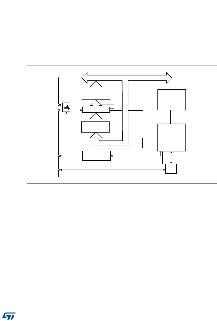
DocID027812 Rev 2 679/766
RM0401 Serial peripheral interface/ inter-IC sound (SPI/I2S)
726
25.3 SPI functional description
25.3.1 General description
The SPI allows synchronous, serial communication between the MCU and external devices.
Application software can manage the communication by polling the status flag or using
dedicated SPI interrupt. The main elements of SPI and their interactions are shown in the
following block diagram Figure 239.
Figure 239. SPI block diagram
Four I/O pins are dedicated to SPI communication with external devices.
•MISO: Master In / Slave Out data. In the general case, this pin is used to transmit data
in slave mode and receive data in master mode.
•MOSI: Master Out / Slave In data. In the general case, this pin is used to transmit data
in master mode and receive data in slave mode.
•SCK: Serial Clock output pin for SPI masters and input pin for SPI slaves.
•NSS: Slave select pin. Depending on the SPI and NSS settings, this pin can be used to
either:
– select an individual slave device for communication
– synchronize the data frame or
– detect a conflict between multiple masters
See Section 25.3.4: Multi-master communication for details.
The SPI bus allows the communication between one master device and one or more slave
devices. The bus consists of at least two wires - one for the clock signal and the other for
synchronous data transfer. Other signals can be added depending on the data exchange
between SPI nodes and their slave select signal management.
06Y9
6KLIWUHJLVWHU
:ULWH
5HDG
&RPPXQLFDWLRQ
FRQWUROOHU
$GGUHVVDQGGDWDEXV
&5&FRQWUROOHU
,QWHUQDO166
&5&(1
&5&1(;7
/6%),567
&32/
&3+$
'))
026,
0,62
6&.
166
5[
EXIIHU
7;
EXIIHU
%5>@
%,',2(
%,',02'(
5;2/1<
166
ORJLF
%DXGUDWH
JHQHUDWRU
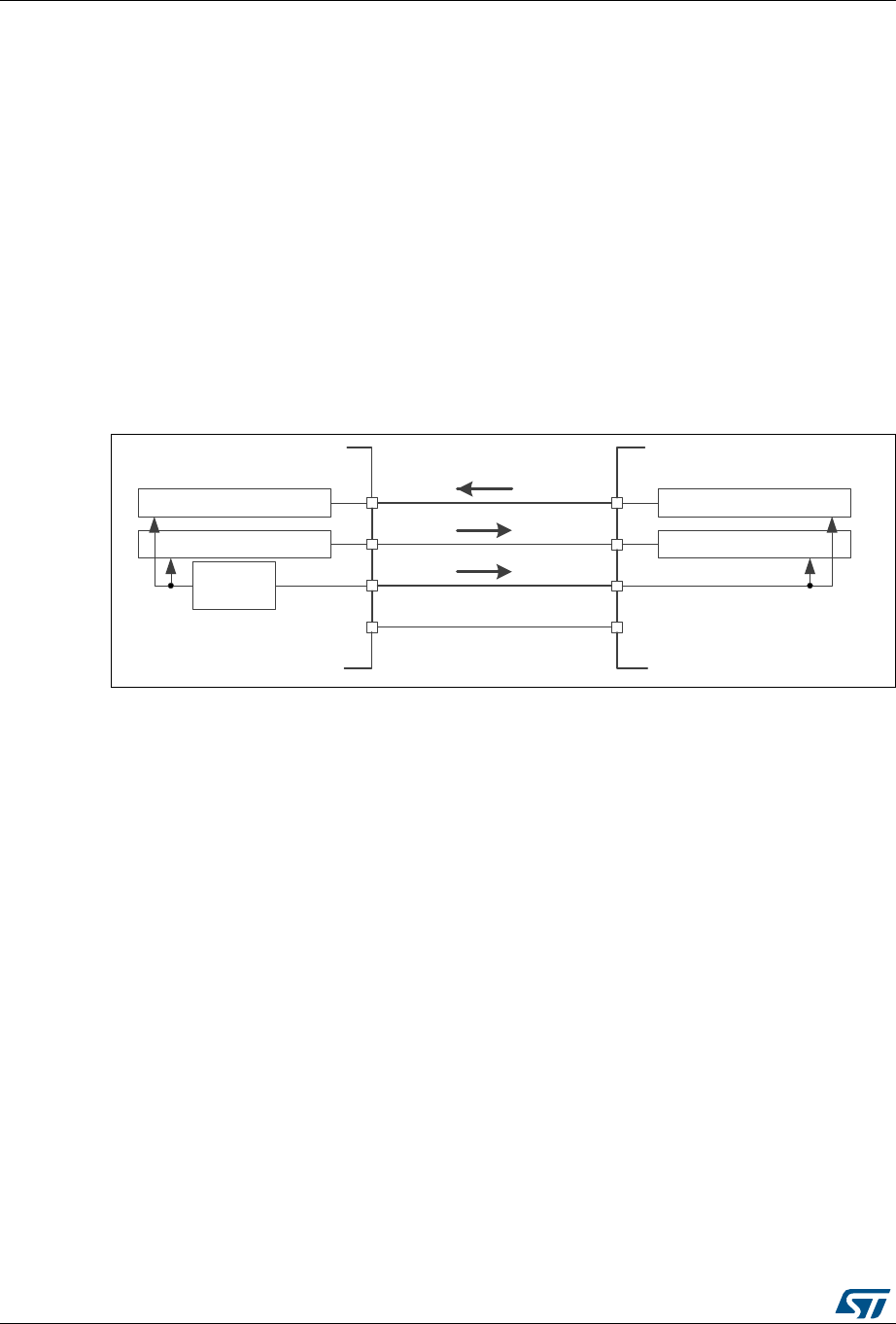
Serial peripheral interface/ inter-IC sound (SPI/I2S) RM0401
680/766 DocID027812 Rev 2
25.3.2 Communications between one master and one slave
The SPI allows the MCU to communicate using different configurations, depending on the
device targeted and the application requirements. These configurations use 2 or 3 wires
(with software NSS management) or 3 or 4 wires (with hardware NSS management).
Communication is always initiated by the master.
Full-duplex communication
By default, the SPI is configured for full-duplex communication. In this configuration, the
shift registers of the master and slave are linked using two unidirectional lines between the
MOSI and the MISO pins. During SPI communication, data is shifted synchronously on the
SCK clock edges provided by the master. The master transmits the data to be sent to the
slave via the MOSI line and receives data from the slave via the MISO line. When the data
frame transfer is complete (all the bits are shifted) the information between the master and
slave is exchanged.
Figure 240. Full-duplex single master/ single slave application
1. The NSS pins can be used to provide a hardware control flow between master and slave. Optionally, the
pins can be left unused by the peripheral. Then the flow has to be handled internally for both master and
slave. For more details see Section 25.3.5: Slave select (NSS) pin management.
Half-duplex communication
The SPI can communicate in half-duplex mode by setting the BIDIMODE bit in the
SPIx_CR1 register. In this configuration, one single cross connection line is used to link the
shift registers of the master and slave together. During this communication, the data is
synchronously shifted between the shift registers on the SCK clock edge in the transfer
direction selected reciprocally by both master and slave with the BDIOE bit in their
SPIx_CR1 registers. In this configuration, the master’s MISO pin and the slave’s MOSI pin
are free for other application uses and act as GPIOs.
5[VKLIWUHJLVWHU
7[VKLIWUHJLVWHU 5[VKLIWUHJLVWHU
7[VKLIWUHJLVWHU
63,FORFN
JHQHUDWRU
0DVWHU 6ODYH
0,62
026,
6&.
166
0,62
026,
6&.
166
06Y9
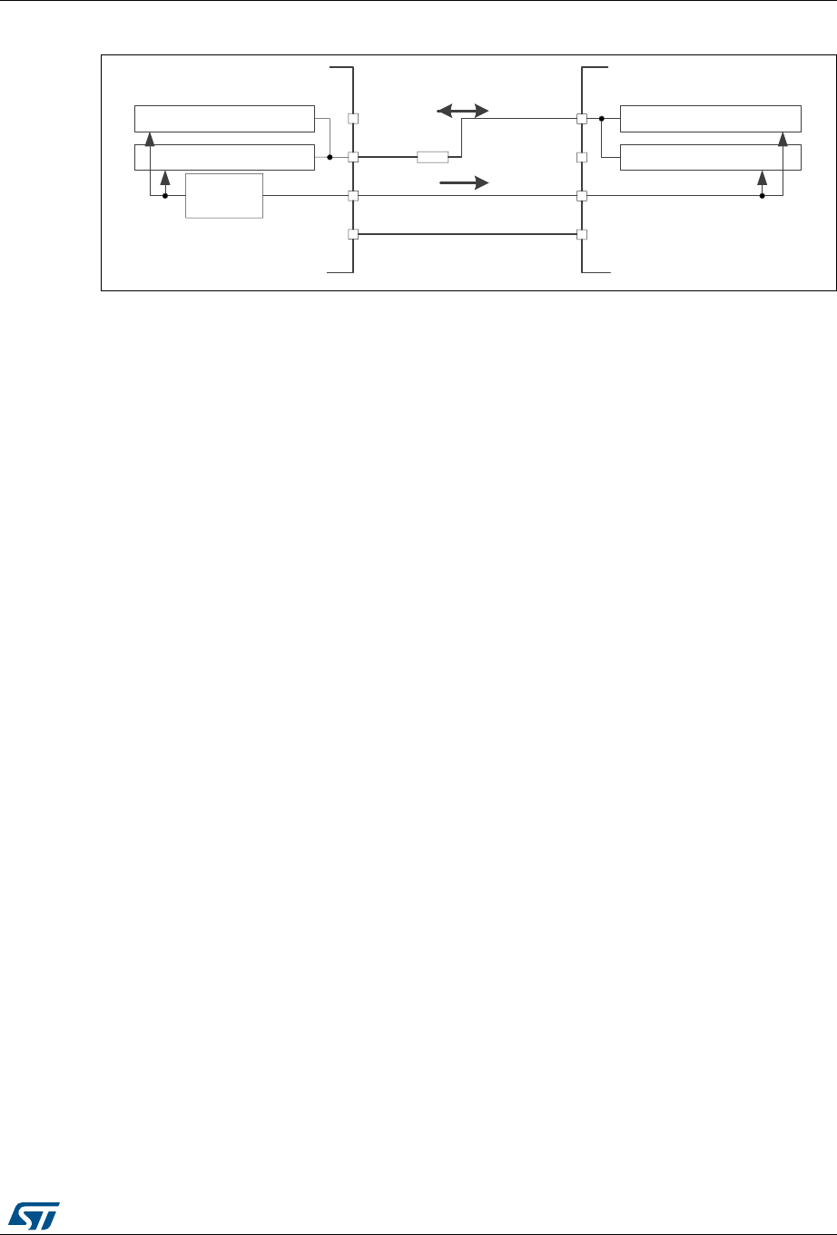
DocID027812 Rev 2 681/766
RM0401 Serial peripheral interface/ inter-IC sound (SPI/I2S)
726
Figure 241. Half-duplex single master/ single slave application
1. The NSS pins can be used to provide a hardware control flow between master and slave. Optionally, the
pins can be left unused by the peripheral. Then the flow has to be handled internally for both master and
slave. For more details see Section 25.3.5: Slave select (NSS) pin management.
2. In this configuration, the master’s MISO pin and the slave’s MOSI pin can be used as GPIOs.
3. A critical situation can happen when communication direction is changed not synchronously between two
nodes working at bidirectionnal mode and new transmitter accesses the common data line while former
transmitter still keeps an opposite value on the line (the value depends on SPI configuration and
communication data). Both nodes then fight while providing opposite output levels on the common line
temporary till next node changes its direction settings correspondingly, too. It is suggested to insert a serial
resistance between MISO and MOSI pins at this mode to protect the outputs and limit the current blowing
between them at this situation.
Simplex communications
The SPI can communicate in simplex mode by setting the SPI in transmit-only or in receive-
only using the RXONLY bit in the SPIx_CR2 register. In this configuration, only one line is
used for the transfer between the shift registers of the master and slave. The remaining
MISO and MOSI pins pair is not used for communication and can be used as standard
GPIOs.
•Transmit-only mode (RXONLY=0): The configuration settings are the same as for full-
duplex. The application has to ignore the information captured on the unused input pin.
This pin can be used as a standard GPIO.
•Receive-only mode (RXONLY=1): The application can disable the SPI output function
by setting the RXONLY bit. In slave configuration, the MISO output is disabled and the
pin can be used as a GPIO. The slave continues to receive data from the MOSI pin
while its slave select signal is active (see 25.3.4: Multi-master communication).
Received data events appear depending on the data buffer configuration. In the master
configuration, the MOSI output is disabled and the pin can be used as a GPIO. The
clock signal is generated continuously as long as the SPI is enabled. The only way to
stop the clock is to clear the RXONLY bit or the SPE bit and wait until the incoming
pattern from the MISO pin is finished and fills the data buffer structure, depending on its
configuration.
5[VKLIWUHJLVWHU
7[VKLIWUHJLVWHU 5[VKLIWUHJLVWHU
7[VKLIWUHJLVWHU
63,FORFN
JHQHUDWRU
0DVWHU 6ODYH
0,62
026,
6&.
166
0,62
026,
6&.
166
Nȍ
06Y9
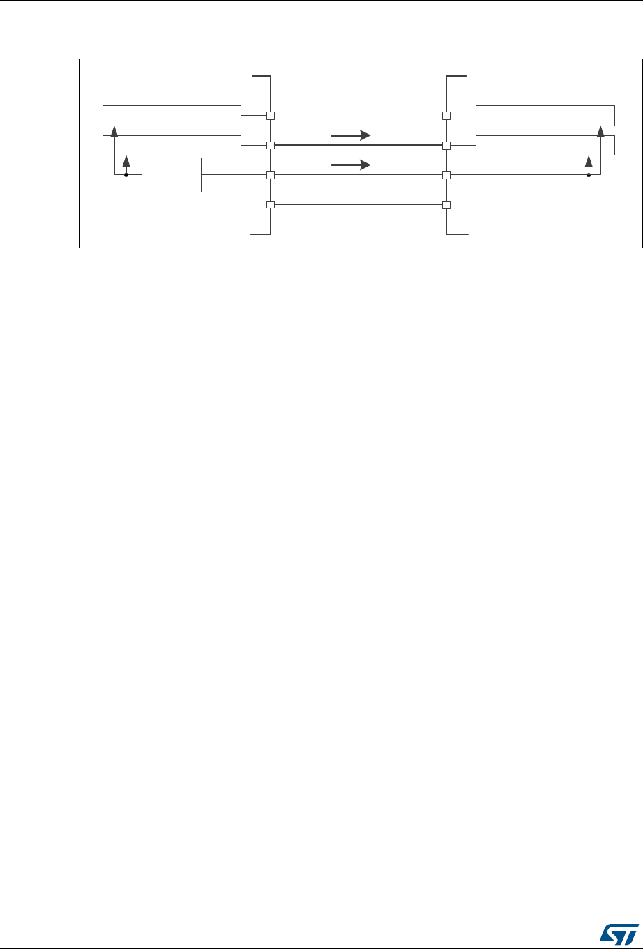
Serial peripheral interface/ inter-IC sound (SPI/I2S) RM0401
682/766 DocID027812 Rev 2
Figure 242. Simplex single master/single slave application (master in transmit-only/
slave in receive-only mode)
1. The NSS pins can be used to provide a hardware control flow between master and slave. Optionally, the
pins can be left unused by the peripheral. Then the flow has to be handled internally for both master and
slave. For more details see Section 25.3.5: Slave select (NSS) pin management.
2. An accidental input information is captured at the input of transmitter Rx shift register. All the events
associated with the transmitter receive flow must be ignored in standard transmit only mode (e.g. OVF
flag).
3. In this configuration, both the MISO pins can be used as GPIOs.
Note: Any simplex communication can be alternatively replaced by a variant of the half duplex
communication with a constant setting of the transaction direction (bidirectional mode is
enabled while BDIO bit is not changed).
25.3.3 Standard multi-slave communication
In a configuration with two or more independent slaves, the master uses GPIO pins to
manage the chip select lines for each slave (see Figure 243.). The master must select one
of the slaves individually by pulling low the GPIO connected to the slave NSS input. When
this is done, a standard master and dedicated slave communication is established.
5[VKLIWUHJLVWHU
7[VKLIWUHJLVWHU 5[VKLIWUHJLVWHU
7[VKLIWUHJLVWHU
63,FORFN
JHQHUDWRU
0DVWHU ^ůĂǀĞ
0,62
026,
6&.
166
0,62
026,
6&.
166
06Y9
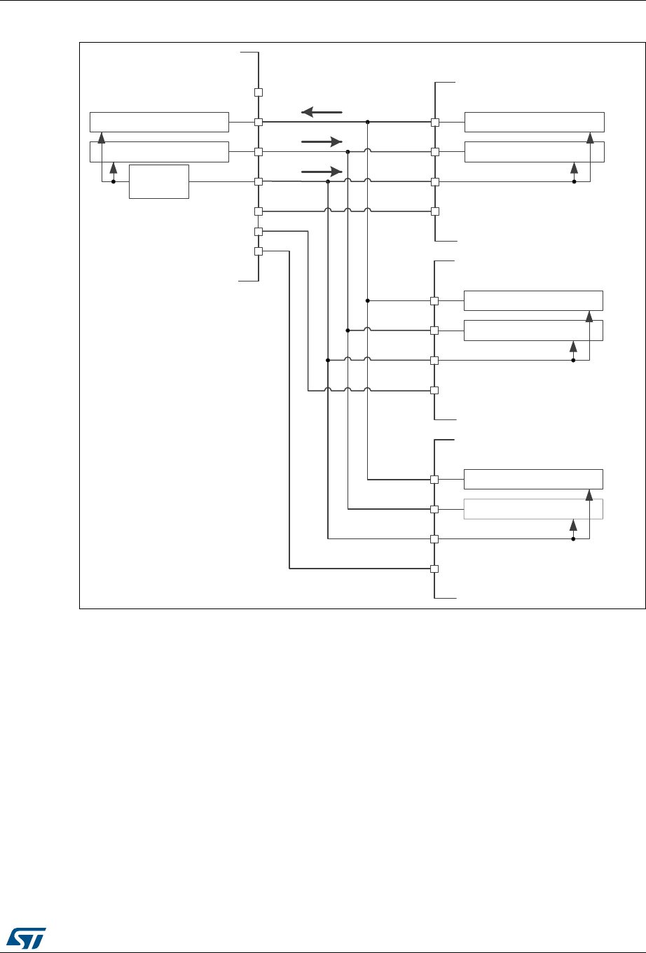
DocID027812 Rev 2 683/766
RM0401 Serial peripheral interface/ inter-IC sound (SPI/I2S)
726
Figure 243. Master and three independent slaves
1. NSS pin is not used on master side at this configuration. It has to be managed internally (SSM=1, SSI=1) to
prevent any MODF error.
2. As MISO pins of the slaves are connected together, all slaves must have the GPIO configuration of their
MISO pin set as alternate function open-drain (see Section 7.3.7: I/O alternate function input/output on
page 181).
25.3.4 Multi-master communication
Unless SPI bus is not designed for a multi-master capability primarily, the user can use build
in feature which detects a potential conflict between two nodes trying to master the bus at
the same time. For this detection, NSS pin is used configured at hardware input mode.
The connection of more than two SPI nodes working at this mode is impossible as only one
node can apply its output on a common data line at time.
When nodes are non active, both stay at slave mode by default. Once one node wants to
overtake control on the bus, it switches itself into master mode and applies active level on
the slave select input of the other node via dedicated GPIO pin. After the session is
5[VKLIWUHJLVWHU
7[VKLIWUHJLVWHU 5[VKLIWUHJLVWHU
7[VKLIWUHJLVWHU
63,FORFN
JHQHUDWRU
0DVWHU 6ODYH
0,62
026,
6&.
166
0,62
026,
6&.
166
5[VKLIWUHJLVWHU
7[VKLIWUHJLVWHU
6ODYH
5[VKLIWUHJLVWHU
7[VKLIWUHJLVWHU
6ODYH
,2
,2
,2
0,62
026,
6&.
166
0,62
026,
6&.
166
06Y9
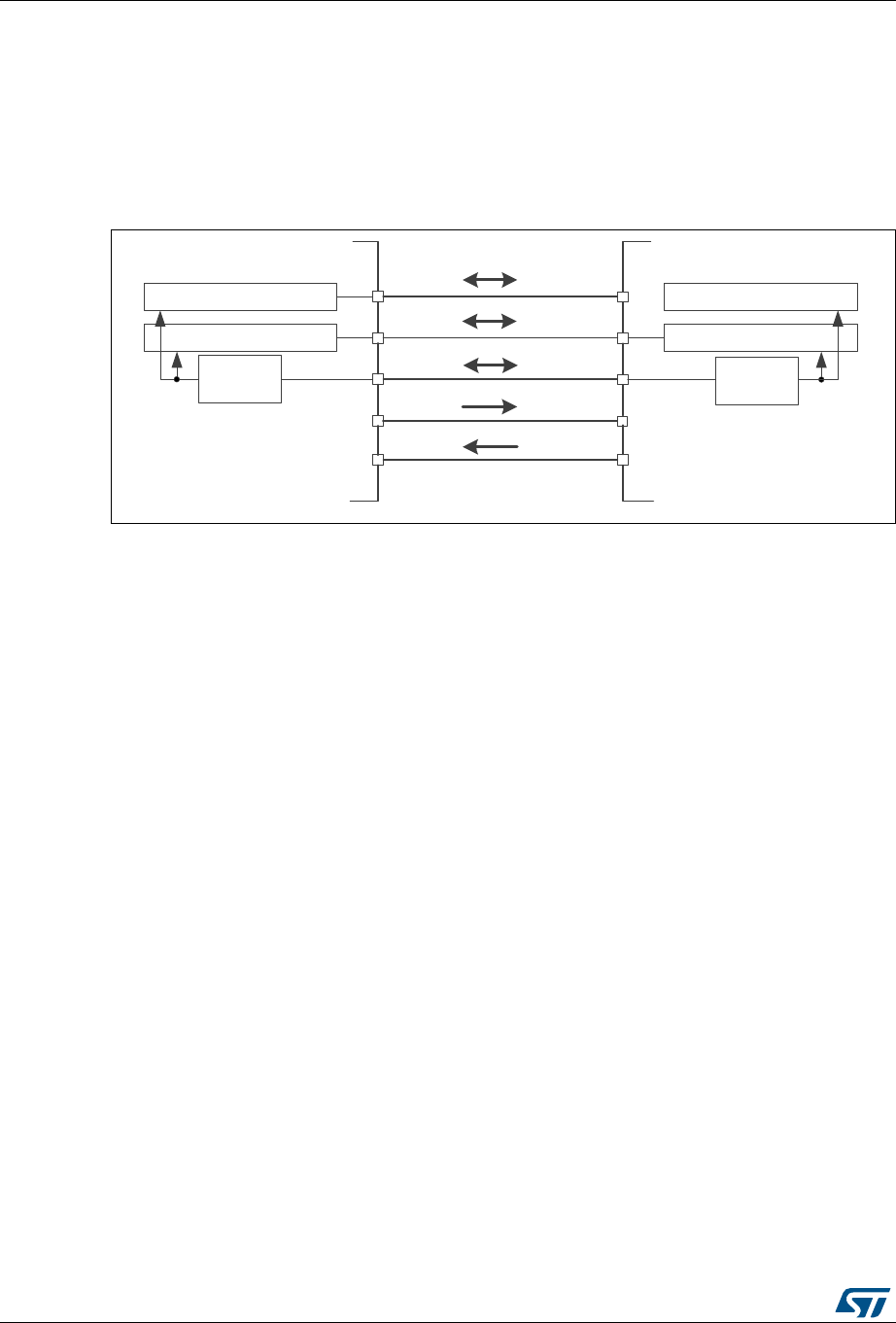
Serial peripheral interface/ inter-IC sound (SPI/I2S) RM0401
684/766 DocID027812 Rev 2
completed, the active slave select signal is released and the node mastering the bus
temporary returns back to passive slave mode waiting for next session start.
If potentially both nodes raised their mastering request at the same time a bus conflict event
appears (see mode fault MODF event). Then the user can apply some simple arbitration
process (e.g. to postpone next attempt by predefined different time-outs applied at both
nodes).
Figure 244. Multi-master application
1. The NSS pin is configured at hardware input mode at both nodes. Its active level enables the MISO line
output control as the passive node is configured as a slave.
25.3.5 Slave select (NSS) pin management
In slave mode, the NSS works as a standard “chip select” input and lets the slave
communicate with the master. In master mode, NSS can be used either as output or input.
As an input it can prevent multimaster bus collision, and as an output it can drive a slave
select signal of a single slave.
Hardware or software slave select management can be set using the SSM bit in the
SPIx_CR1 register:
•Software NSS management (SSM = 1): in this configuration, slave select information
is driven internally by the SSI bit value in register SPIx_CR1. The external NSS pin is
free for other application uses.
•Hardware NSS management (SSM = 0): in this case, there are two possible
configurations. The configuration used depends on the NSS output configuration
(SSOE bit in register SPIx_CR1).
–NSS output enable (SSM=0,SSOE = 1): this configuration is only used when the
MCU is set as master. The NSS pin is managed by the hardware. The NSS signal
is driven low as soon as the SPI is enabled in master mode (SPE=1), and is kept
low until the SPI is disabled (SPE =0).
–NSS output disable (SSM=0, SSOE = 0): if the microcontroller is acting as the
master on the bus, this configuration allows multimaster capability. If the NSS pin
is pulled low in this mode, the SPI enters master mode fault state and the device is
automatically reconfigured in slave mode. In slave mode, the NSS pin works as a
standard “chip select” input and the slave is selected while NSS line is at low level.
5[7[VKLIWUHJLVWHU
7[5[VKLIWUHJLVWHU 7[5[VKLIWUHJLVWHU
5[7[VKLIWUHJLVWHU
63,FORFN
JHQHUDWRU
0DVWHU
6ODYH
DĂƐƚĞƌ
;^ůĂǀĞͿ
0,62
026,
6&.
166
0,62
026,
6&.
166
06Y9
63,FORFN
JHQHUDWRU
*3,2
*3,2
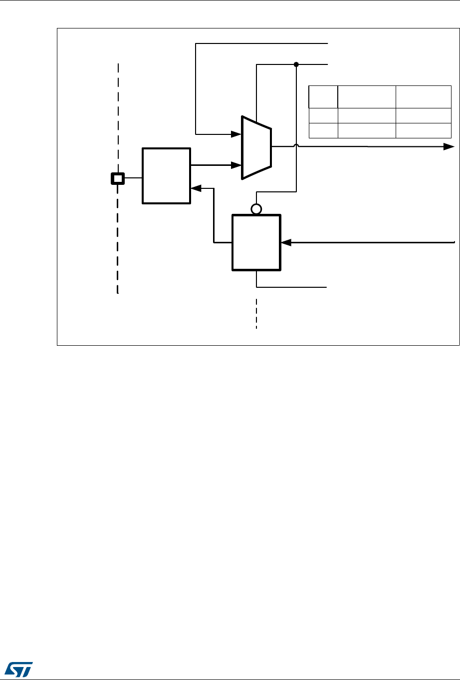
DocID027812 Rev 2 685/766
RM0401 Serial peripheral interface/ inter-IC sound (SPI/I2S)
726
Figure 245. Hardware/software slave select management
166,QSXW
660FRQWUROELW
66,FRQWUROELW
662(FRQWUROELW
1662XWSXW
166
SLQ
XVHGLQ0DVWHUPRGH166
+:PDQDJHPHQWRQO\
166
2XWSXW
&RQWURO
0DVWHU
PRGH 6ODYHPRGH
1RQDFWLYH2.9GG
166
,QS
$FWLYH&RQIOLFW9VV
166H[WHUQDOORJLF 166LQWHUQDOORJLF
*3,2
ORJLF
DLYH

Serial peripheral interface/ inter-IC sound (SPI/I2S) RM0401
686/766 DocID027812 Rev 2
25.3.6 Communication formats
During SPI communication, receive and transmit operations are performed simultaneously.
The serial clock (SCK) synchronizes the shifting and sampling of the information on the data
lines. The communication format depends on the clock phase, the clock polarity and the
data frame format. To be able to communicate together, the master and slaves devices must
follow the same communication format.
Clock phase and polarity controls
Four possible timing relationships may be chosen by software, using the CPOL and CPHA
bits in the SPIx_CR1 register. The CPOL (clock polarity) bit controls the idle state value of
the clock when no data is being transferred. This bit affects both master and slave modes. If
CPOL is reset, the SCK pin has a low-level idle state. If CPOL is set, the SCK pin has a
high-level idle state.
If the CPHA bit is set, the second edge on the SCK pin captures the first data bit transacted
(falling edge if the CPOL bit is reset, rising edge if the CPOL bit is set). Data are latched on
each occurrence of this clock transition type. If the CPHA bit is reset, the first edge on the
SCK pin captures the first data bit transacted (falling edge if the CPOL bit is set, rising edge
if the CPOL bit is reset). Data are latched on each occurrence of this clock transition type.
The combination of CPOL (clock polarity) and CPHA (clock phase) bits selects the data
capture clock edge.
Figure 246, shows an SPI full-duplex transfer with the four combinations of the CPHA and
CPOL bits.
Note: Prior to changing the CPOL/CPHA bits the SPI must be disabled by resetting the SPE bit.
The idle state of SCK must correspond to the polarity selected in the SPIx_CR1 register (by
pulling up SCK if CPOL=1 or pulling down SCK if CPOL=0).
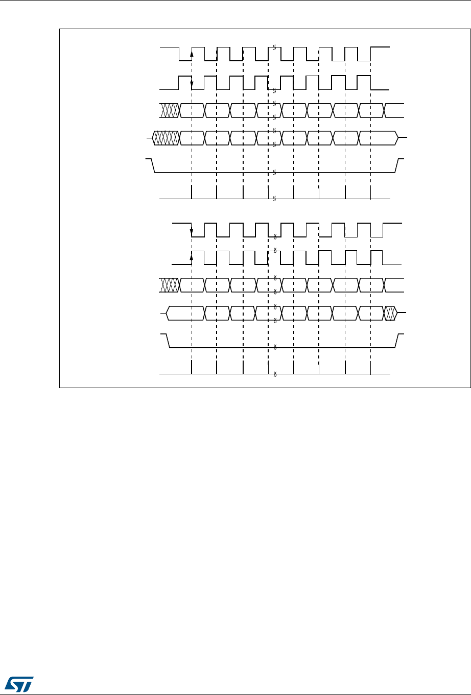
DocID027812 Rev 2 687/766
RM0401 Serial peripheral interface/ inter-IC sound (SPI/I2S)
726
Figure 246. Data clock timing diagram
Note: The order of data bits depends on LSBFIRST bit setting.
Data frame format
The SPI shift register can be set up to shift out MSB-first or LSB-first, depending on the
value of the LSBFIRST bit. Each data frame is 8 or 16 bit long depending on the size of the
data programmed using the DFF bit in the SPI_CR1 register. The selected data frame
format is applicable both for transmission and reception.
#0/,
#0/,
-3"IT ,3"IT
-3"IT ,3"IT
-)3/
-/3)
.33
TOSLAVE
#APTURESTROBE
#0(!
#0/,
#0/,
-3"IT ,3"IT
-3"IT ,3"IT
-)3/
-/3)
.33
TOSLAVE
#APTURESTROBE
#0(!
AID

Serial peripheral interface/ inter-IC sound (SPI/I2S) RM0401
688/766 DocID027812 Rev 2
25.3.7 SPI configuration
The configuration procedure is almost the same for master and slave. For specific mode
setups, follow the dedicated chapters. When a standard communication is to be initialized,
perform these steps:
1. Write proper GPIO registers: Configure GPIO for MOSI, MISO and SCK pins.
2. Write to the SPI_CR1 register:
a) Configure the serial clock baud rate using the BR[2:0] bits (Note: 3).
b) Configure the CPOL and CPHA bits combination to define one of the four
relationships between the data transfer and the serial clock. (Note: 2).
c) Select simplex or half-duplex mode by configuring RXONLY or BIDIMODE and
BIDIOE (RXONLY and BIDIMODE can't be set at the same time).
d) Configure the LSBFIRST bit to define the frame format (Note: 2).
e) Configure the CRCEN and CRCEN bits if CRC is needed (while SCK clock signal
is at idle state).
f) Configure SSM and SSI (Note: 2).
g) Configure the MSTR bit (in multimaster NSS configuration, avoid conflict state on
NSS if master is configured to prevent MODF error).
h) Set the DFF bit to configure the data frame format (8 or 16 bits).
3. Write to SPI_CR2 register:
a) Configure SSOE (Note: 1 & 2).
b) Set the FRF bit if the TI protocol is required.
4. Write to SPI_CRCPR register: Configure the CRC polynomial if needed.
5. Write proper DMA registers: Configure DMA streams dedicated for SPI Tx and Rx in
DMA registers if the DMA streams are used.
Note: (1) Step is not required in slave mode.
(2) Step is not required in TI mode.
(3) The step is not required in slave mode except slave working at TI mode.
25.3.8 Procedure for enabling SPI
It is recommended to enable the SPI slave before the master sends the clock. Otherwise,
undesired data transmission might occur. The slave data register must already contain data
to be sent before starting communication with the master (either on the first edge of the
communication clock, or before the end of the ongoing communication if the clock signal is
continuous). The SCK signal must be settled at an idle state level corresponding to the
selected polarity before the SPI slave is enabled.
At full duplex (or in any transmit-only mode), the master starts communicating when the SPI
is enabled and data to be sent is written in the Tx Buffer.
In any master receive-only mode (RXONLY=1 or BIDIMODE=1 & BIDIOE=0), the master
starts communicating and the clock starts running immediately after the SPI is enabled.
The slave starts communicating when it receives a correct clock signal from the master. The
slave software must write the data to be sent before the SPI master initiates the transfer.
Refer to Section 25.3.11: Communication using DMA (direct memory addressing) for details
on how to handle DMA.

DocID027812 Rev 2 689/766
RM0401 Serial peripheral interface/ inter-IC sound (SPI/I2S)
726
25.3.9 Data transmission and reception procedures
Rx and Tx buffers
In reception, data are received and then stored into an internal Rx buffer while in
transmission, data are first stored into an internal Tx buffer before being transmitted. A read
access to the SPI_DR register returns the Rx buffered value whereas a write access to the
SPI_DR stores the written data into the Tx buffer.
Tx buffer handling
The data frame is loaded from the Tx buffer into the shift register during the first bit
transmission. Bits are then shifted out serially from the shift register to a dedicated output
pin depending on LSBFIRST bit setting.The TXE flag (Tx buffer empty) is set when the data
are transferred from the Tx buffer to the shift register. It indicates that the internal Tx buffer is
ready to be loaded with the next data. An interrupt can be generated if the TXEIE bit of the
SPI_CR2 register is set. Clearing the TXE bit is performed by writing to the SPI_DR register.
A continuous transmit stream can be achieved if the next data to be transmitted are stored
in the Tx buffer while previous frame transmission is still ongoing. When the software writes
to Tx buffer while the TXE flag is not set, the data waiting for transaction is overwritten.
Rx buffer handling
The RXNE flag (Rx buffer not empty) is set on the last sampling clock edge, when the data
are transferred from the shift register to the Rx buffer. It indicates that data are ready to be
read from the SPI_DR register. An interrupt can be generated if the RXNEIE bit in the
SPI_CR2 register is set. Clearing the RXNE bit is performed by reading the SPI_DR
register.
If a device has not cleared the RXNE bit resulting from the previous data byte transmitted,
an overrun condition occurs when the next value is buffered. The OVR bit is set and an
interrupt is generated if the ERRIE bit is set.
Another way to manage the data exchange is to use DMA (see Section 11.2: DMA main
features).
Sequence handling
The BSY bit is set when a current data frame transaction is ongoing. When the clock signal
runs continuously, the BSY flag remains set between data frames on the master side.
However, on the slave side, it becomes low for a minimum duration of one SPI clock cycle
between each data frame transfer.
For some configurations, the BSY flag can be used during the last data transfer to wait until
the completion of the transfer.
When a receive-only mode is configured on the master side, either in half-duplex
(BIDIMODE=1, BIDIOE=0) or simplex configuration (BIDIMODE=0, RXONLY=1), the
master starts the receive sequence as soon as the SPI is enabled. Then the clock signal is
provided by the master and it does not stop until either the SPI or the receive-only mode is
disabled by the master. The master receives data frames continuously up to this moment.
While the master can provide all the transactions in continuous mode (SCK signal is
continuous), it has to respect slave capability to handle data flow and its content at anytime.
When necessary, the master must slow down the communication and provide either a
slower clock or separate frames or data sessions with sufficient delays. Be aware there is no
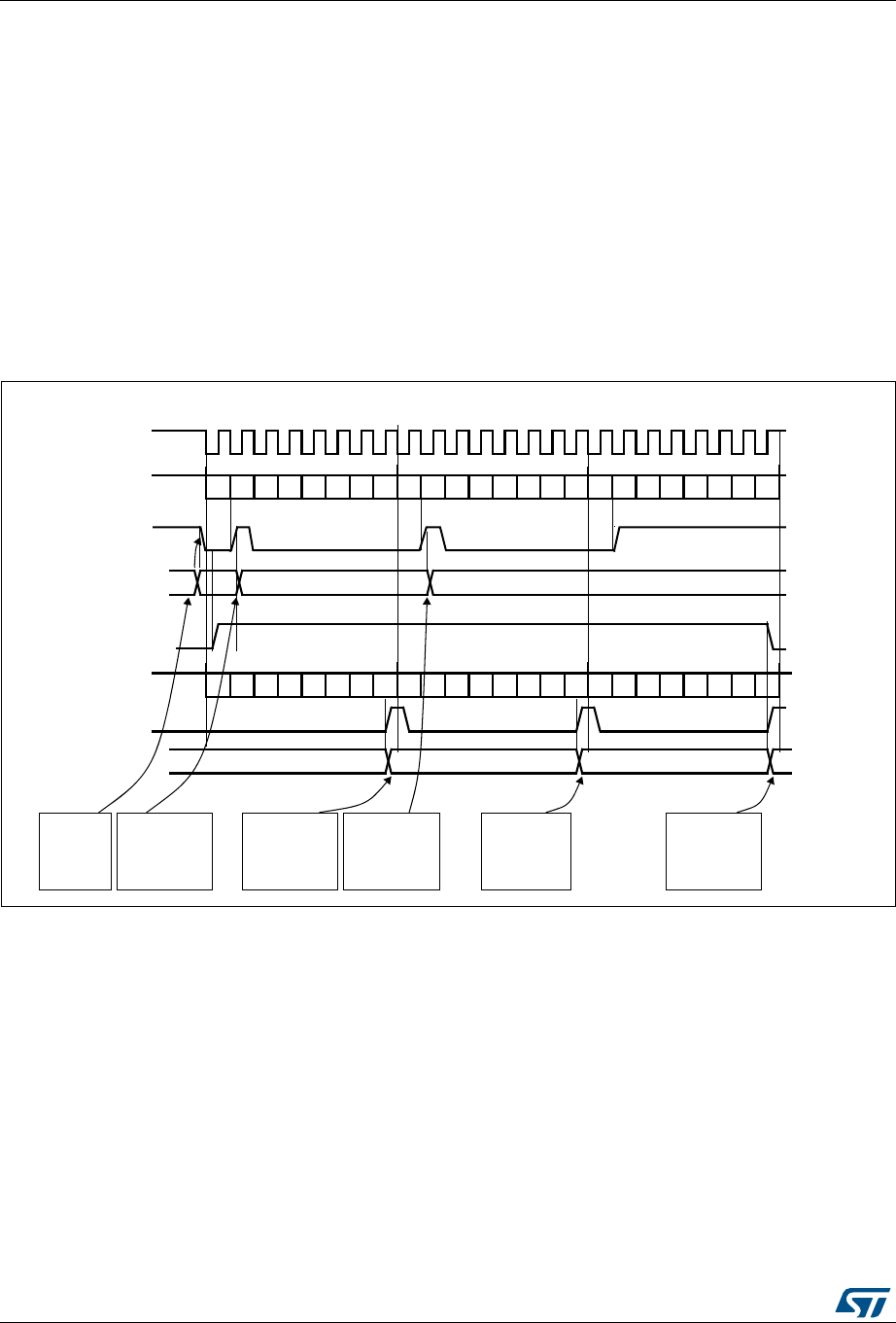
Serial peripheral interface/ inter-IC sound (SPI/I2S) RM0401
690/766 DocID027812 Rev 2
underflow error signal for slave operating in SPI mode, and that data from the slave are
always transacted and processed by the master even if the slave cannot not prepare them
correctly in time. It is preferable for the slave to use DMA, especially when data frames are
shorter and bus rate is high.
Each sequence must be encased by the NSS pulse in parallel with the multislave system to
select just one of the slaves for communication. In single slave systems, using NSS to
control the slave is not necessary. However, the NSS pulse can be used to synchronize the
slave with the beginning of each data transfer sequence. NSS can be managed either by
software or by hardware (see Section 25.3.4: Multi-master communication).
Refer to Figure 247 and Figure 248 for a description of continuous transfers in master / full-
duplex and slave full-duplex mode.
Figure 247. TXE/RXNE/BSY behavior in master / full-duplex mode (BIDIMODE=0,
RXONLY=0) in the case of continuous transfers
0,62026,LQ
7[EXIIHU
'$7$ [$
7;(IODJ
[)
%6<IODJ
[)
VRIWZDUH
ZULWHV[)
LQWR63,B'5
VRIWZDUHZDLWV
XQWLO7;( DQG
ZULWHV[)LQWR
63,B'5
VRIWZDUHZDLWV
XQWLO5;1(
DQGUHDGV[$
IURP63,B'5
VHWE\KDUGZDUH
FOHDUHGE\VRIWZDUH
VHWE\KDUGZDUH
FOHDUHGE\VRIWZDUH VHWE\KDUGZDUH
VHWE\KDUGZDUH
6&.
'$7$ [$ '$7$ [$
UHVHWE\KDUGZDUH
([DPSOHLQ0DVWHUPRGHZLWK&32/ &3+$
[)
5;1(IODJ
ZULWH63,B'5
5[EXIIHU
VHWE\KDUGZDUH
0,62026,RXW
'$7$ [) '$7$ [) '$7$ [)
UHDG63,B'5
[$ [$ [$
VRIWZDUHZDLWV
XQWLO7;( DQG
ZULWHV[)LQWR
63,B'5
VRIWZDUHZDLWV
XQWLO5;1(
DQGUHDGV[$
IURP63,B'5
VRIWZDUHZDLWV
XQWLO5;1(
DQGUHDGV[$
IURP63,B'5
E E E E E E E E E E E E E E E E E E E E E E E E
E E E E E E E E E E E E E E E E E E E E E E E E
FOHDUHGE\VRIWZDUH
DL
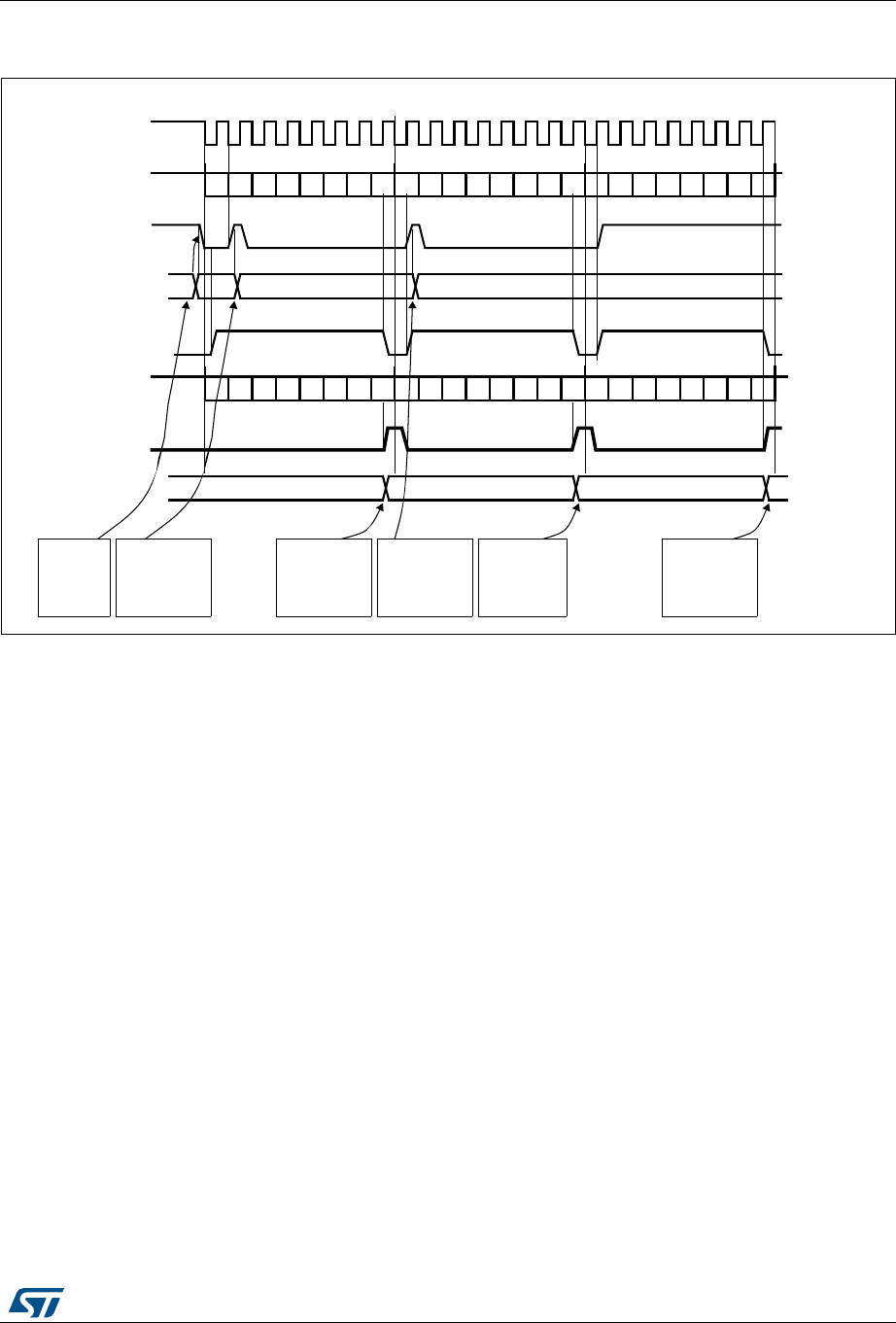
DocID027812 Rev 2 691/766
RM0401 Serial peripheral interface/ inter-IC sound (SPI/I2S)
726
Figure 248. TXE/RXNE/BSY behavior in slave / full-duplex mode (BIDIMODE=0,
RXONLY=0) in the case of continuous transfers
25.3.10 Procedure for disabling the SPI
When SPI is disabled, it is mandatory to follow the disable procedures described in this
paragraph. It is important to do this before the system enters a low-power mode when the
peripheral clock is stopped. Ongoing transactions can be corrupted in this case. In some
modes the disable procedure is the only way to stop continuous communication running.
Master in full duplex or transmit only mode can finish any transaction when it stops providing
data for transmission. In this case, the clock stops after the last data transaction.
Standard disable procedure is based on pulling BSY status together with TXE flag to check
if a transmission session is fully completed. This check can be done in specific cases, too,
when it is necessary to identify the end of ongoing transactions, for example:
•When NSS signal is managed by an arbitrary GPIO toggle and the master has to
provide proper end of NSS pulse for slave, or
•When transactions’ streams from DMA are completed while the last data frame or CRC
frame transaction is still ongoing in the peripheral bus.
The correct disable procedure is (except when receive-only mode is used):
1. Wait until RXNE=1 to receive the last data.
2. Wait until TXE=1 and then wait until BSY=0 before disabling the SPI.
3. Read received data.
Note: During discontinuous communications, there is a 2 APB clock period delay between the
write operation to the SPI_DR register and BSY bit setting. As a consequence it is
[)
VHWE\FOHDUHGE\VRIWZDUH
0,62026,LQ
7[EXIIHU
'$7$ [$
7;(IODJ
[)
%6<IODJ
[)
VRIWZDUH
ZULWHV[)
LQWR63,B'5
VRIWZDUHZDLWV
XQWLO7;( DQG
ZULWHV[)LQWR
63,B'5
VRIWZDUHZDLWV
XQWLO5;1(
DQGUHDGV[$
IURP63,B'5
VHWE\KDUGZDUH
FOHDUHGE\VRIWZDUH
VHWE\KDUGZDUH
FOHDUHGE\VRIWZDUH VHWE\KDUGZDUH
6&.
'$7$ [$ '$7$ [$
UHVHWE\KDUGZDUH
([DPSOHLQ6ODYHPRGHZLWK&32/ &3+$
5;1(IODJ
ZULWHWR63,B'5
5[EXIIHU
VHWE\KDUGZDUH
0,62026,RXW
'$7$ [) '$7$ [) '$7$ [)
UHDGIURP63,B'5
[$ [$ [$
VRIWZDUHZDLWV
XQWLO7;( DQG
ZULWHV[)LQWR
63,B'5
VRIWZDUHZDLWV
XQWLO5;1(
DQGUHDGV[$
IURP63,B'5
VRIWZDUHZDLWV
XQWLO5;1(
DQGUHDGV[$
IURP63,B'5
E E E E E E E E E E E E E E E E E E E E E E E E
E E E E E E E E E E E E E E E E E E E E E E E E
FOHDUHGE\VRIWZDUH
DL

Serial peripheral interface/ inter-IC sound (SPI/I2S) RM0401
692/766 DocID027812 Rev 2
mandatory to wait first until TXE is set and then until BSY is cleared after writing the last
data.
The correct disable procedure for certain receive-only modes is:
1. Interrupt the receive flow by disabling SPI (SPE=0) in the specific time window while
the last data frame is ongoing.
2. Wait until BSY=0 (the last data frame is processed).
3. Read received data.
Note: To stop a continuous receive sequence, a specific time window must be respected during
the reception of the last data frame. It starts when the first bit is sampled and ends before
the last bit transfer starts.
25.3.11 Communication using DMA (direct memory addressing)
To operate at its maximum speed and to facilitate the data register read/write process
required to avoid overrun, the SPI features a DMA capability, which implements a simple
request/acknowledge protocol.
A DMA access is requested when the TXE or RXNE enable bit in the SPIx_CR2 register is
set. Separate requests must be issued to the Tx and Rx buffers.
•In transmission, a DMA request is issued each time TXE is set to 1. The DMA then
writes to the SPIx_DR register.
•In reception, a DMA request is issued each time RXNE is set to 1. The DMA then reads
the SPIx_DR register.
Refer to Figure 249 and Figure 250 for a description of the DMA transmission and reception
waveforms.
When the SPI is used only to transmit data, it is possible to enable only the SPI Tx DMA
channel. In this case, the OVR flag is set because the data received is not read. When the
SPI is used only to receive data, it is possible to enable only the SPI Rx DMA channel.
In transmission mode, when the DMA has written all the data to be transmitted (the TCIF
flag is set in the DMA_ISR register), the BSY flag can be monitored to ensure that the SPI
communication is complete. This is required to avoid corrupting the last transmission before
disabling the SPI or entering the Stop mode. The software must first wait until TXE = 1 and
then until BSY = 0.
When starting communication using DMA, to prevent DMA channel management raising
error events, these steps must be followed in order:
1. Enable DMA Rx buffer in the RXDMAEN bit in the SPI_CR2 register, if DMA Rx is
used.
2. Enable DMA streams for Tx and Rx in DMA registers, if the streams are used.
3. Enable DMA Tx buffer in the TXDMAEN bit in the SPI_CR2 register, if DMA Tx is used.
4. Enable the SPI by setting the SPE bit.
To close communication it is mandatory to follow these steps in order:
1. Disable DMA streams for Tx and Rx in the DMA registers, if the streams are used.
2. Disable the SPI by following the SPI disable procedure.
3. Disable DMA Tx and Rx buffers by clearing the TXDMAEN and RXDMAEN bits in the
SPI_CR2 register, if DMA Tx and/or DMA Rx are used.
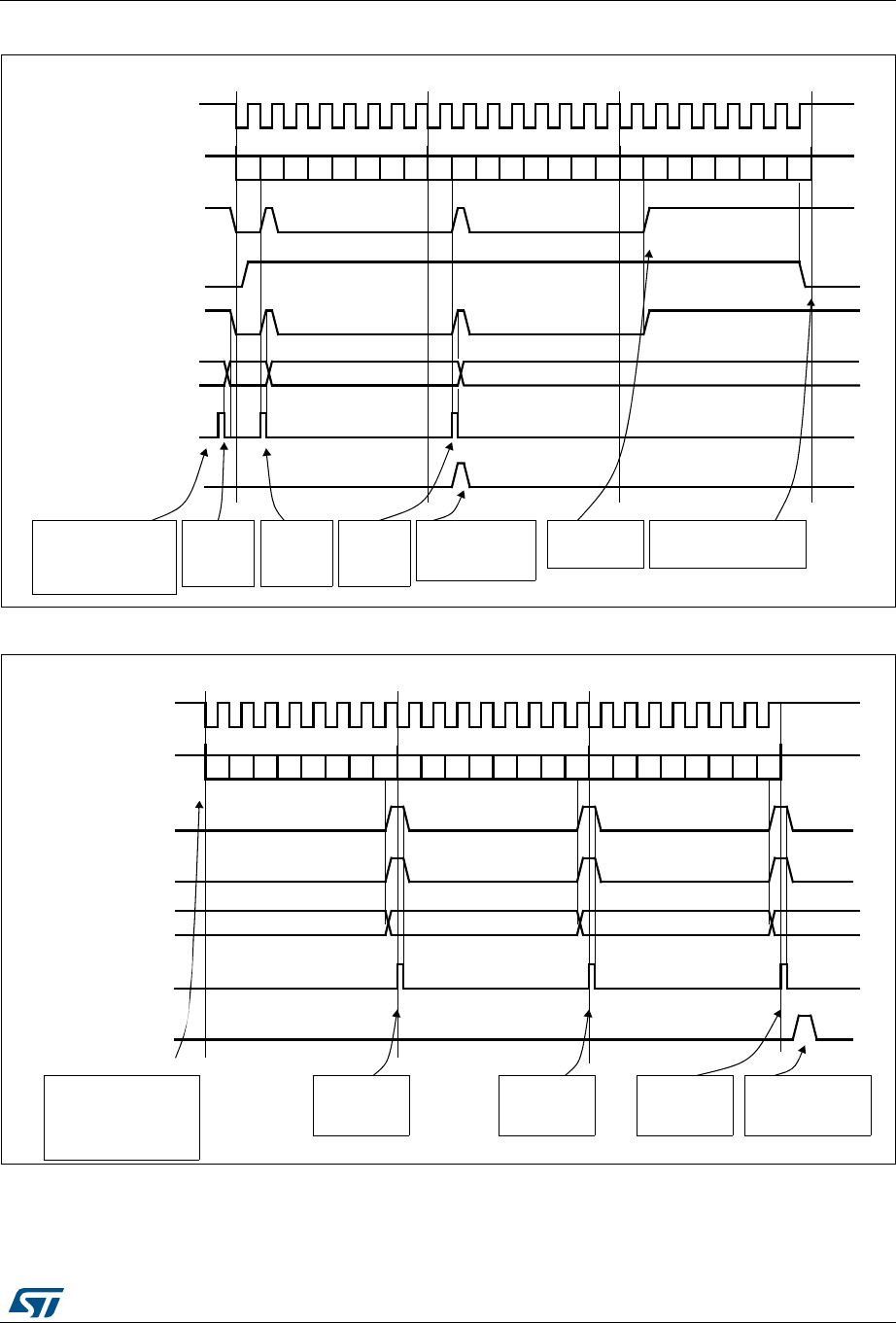
DocID027812 Rev 2 693/766
RM0401 Serial peripheral interface/ inter-IC sound (SPI/I2S)
726
Figure 249. Transmission using DMA
Figure 250. Reception using DMA
[)
7[EXIIHU
7;(IODJ
[)
%6<IODJ
[)
VHWE\KDUGZDUH
FOHDUE\'0$ZULWH
VHWE\KDUGZDUH
FOHDUHGE\'0$ZULWH VHWE\KDUGZDUH
VHWE\KDUGZDUH
6&.
UHVHW
([DPSOHZLWK&32/ &3+$
ZULWHWR63,B'5
0,62026,RXW
'$7$ [) '$7$ [) '$7$ [)
VRIWZDUHFRQILJXUHVWKH
'0$63,7[FKDQQHO
WRVHQGGDWDLWHPV
DQGHQDEOHVWKH63,
'0$ZULWHVWR63,B'5
'0$UHTXHVW LJQRUHGE\WKH'0$EHFDXVH
'0$7&,)IODJ VHWE\KDUGZDUH FOHDUE\VRIWZDUH
'0$ZULWHV
'$7$LQWR
63,B'5
E\KDUGZDUH
'0$ZULWHV
'$7$LQWR
63,B'5
'0$ZULWHV
'$7$LQWR
63,B'5
VRIWZDUHZDLWVXQWLO%6<
'0$WUDQVIHUFRPSOHWH
'0$WUDQVIHULV
FRPSOHWH7&,) LQ
'0$B,65
VRIWZDUHZDLWV
XQWLO7;(
'0$WUDQVIHULVFRPSOHWH
E E E E E E E E E E E E E E E E E E E E E E E E
DL
0,62026,LQ
'$7$ [$
VRIWZDUHFRQILJXUHVWKH
'0$63,5[FKDQQHO
WRUHFHLYHGDWDLWHPV
DQGHQDEOHVWKH63,
6&.
'$7$ [$ '$7$ [$
([DPSOHZLWK&32/ &3+$
5;1(IODJ
5[EXIIHU
VHWE\KDUGZDUH
UHDGIURP63,B'5 [$ [$ [$
'0$UHTXHVW
'0$UHDGV
'$7$IURP
63,B'5
IODJ'0$7&,)
VHWE\KDUGZDUH FOHDU
E\VRIWZDUH
'0$UHDGIURP63,B'5
7KH'0$WUDQVIHULV
FRPSOHWH7&,) LQ
'0$B,65
'0$UHDGV
'$7$IURP
63,B'5
'0$UHDGV
'$7$IURP
63,B'5
'0$WUDQVIHUFRPSOHWH
E E E E E E E E E E E E E E E E E E E E E E E E
FOHDUE\'0$UHDG
DL

Serial peripheral interface/ inter-IC sound (SPI/I2S) RM0401
694/766 DocID027812 Rev 2
25.3.12 SPI status flags
Three status flags are provided for the application to completely monitor the state of the SPI
bus.
Tx buffer empty flag (TXE)
When it is set, the TXE flag indicates that the Tx buffer is empty and that the next data to be
transmitted can be loaded into the buffer. The TXE flag is cleared by writing to the SPI_DR
register.
Rx buffer not empty (RXNE)
When set, the RXNE flag indicates that there are valid received data in the Rx buffer. It is
cleared by reading from the SPI_DR register.
Busy flag (BSY)
The BSY flag is set and cleared by hardware (writing to this flag has no effect).
When BSY is set, it indicates that a data transfer is in progress on the SPI (the SPI bus is
busy). There is one exception in master bidirectional receive mode (MSTR=1 and BDM=1
and BDOE=0) where the BSY flag is kept low during reception.
The BSY flag can be used in certain modes to detect the end of a transfer, thus preventing
corruption of the last transfer when the SPI peripheral clock is disabled before entering a
low-power mode or an NSS pulse end is handled by software.
The BSY flag is also useful for preventing write collisions in a multimaster system.
The BSY flag is cleared under any one of the following conditions:
•When the SPI is correctly disabled
•When a fault is detected in Master mode (MODF bit set to 1)
•In Master mode, when it finishes a data transmission and no new data is ready to be
sent
•In Slave mode, when the BSY flag is set to '0' for at least one SPI clock cycle between
each data transfer.
Note: It is recommended to use always the TXE and RXNE flags (instead of the BSY flags) to
handle data transmission or reception operations.
25.3.13 SPI error flags
An SPI interrupt is generated if one of the following error flags is set and interrupt is enabled
by setting the ERRIE bit.
Overrun flag (OVR)
An overrun condition occurs when the master or the slave completes the reception of the
next data frame while the read operation of the previous frame from the Rx buffer has not
completed (case RXNE flag is set).
In this case, the content of the Rx buffer is not updated with the new data received. A read
operation from the SPI_DR register returns the frame previously received. All other
subsequently transmitted data are lost.

DocID027812 Rev 2 695/766
RM0401 Serial peripheral interface/ inter-IC sound (SPI/I2S)
726
Clearing the OVR bit is done by a read access to the SPI_DR register followed by a read
access to the SPI_SR register.
Mode fault (MODF)
Mode fault occurs when the master device has its internal NSS signal (NSS pin in NSS
hardware mode, or SSI bit in NSS software mode) pulled low. This automatically sets the
MODF bit. Master mode fault affects the SPI interface in the following ways:
•The MODF bit is set and an SPI interrupt is generated if the ERRIE bit is set.
•The SPE bit is cleared. This blocks all output from the device and disables the SPI
interface.
•The MSTR bit is cleared, thus forcing the device into slave mode.
Use the following software sequence to clear the MODF bit:
1. Make a read or write access to the SPIx_SR register while the MODF bit is set.
2. Then write to the SPIx_CR1 register.
To avoid any multiple slave conflicts in a system comprising several MCUs, the NSS pin
must be pulled high during the MODF bit clearing sequence. The SPE and MSTR bits can
be restored to their original state after this clearing sequence. As a security, hardware does
not allow the SPE and MSTR bits to be set while the MODF bit is set. In a slave device the
MODF bit cannot be set except as the result of a previous multimaster conflict.
CRC error (CRCERR)
This flag is used to verify the validity of the value received when the CRCEN bit in the
SPIx_CR1 register is set. The CRCERR flag in the SPIx_SR register is set if the value
received in the shift register does not match the receiver SPIx_RXCRC value. The flag is
cleared by the software.
TI mode frame format error (FRE)
A TI mode frame format error is detected when an NSS pulse occurs during an ongoing
communication when the SPI is operating in slave mode and configured to conform to the TI
mode protocol. When this error occurs, the FRE flag is set in the SPIx_SR register. The SPI
is not disabled when an error occurs, the NSS pulse is ignored, and the SPI waits for the
next NSS pulse before starting a new transfer. The data may be corrupted since the error
detection may result in the loss of two data bytes.
The FRE flag is cleared when SPIx_SR register is read. If the ERRIE bit is set, an interrupt
is generated on the NSS error detection. In this case, the SPI should be disabled because
data consistency is no longer guaranteed and communications should be re-initiated by the
master when the slave SPI is enabled again.
25.4 SPI special features
25.4.1 TI mode
TI protocol in master mode
The SPI interface is compatible with the TI protocol. The FRF bit of the SPIx_CR2 register
can be used to configure the SPI to be compliant with this protocol.
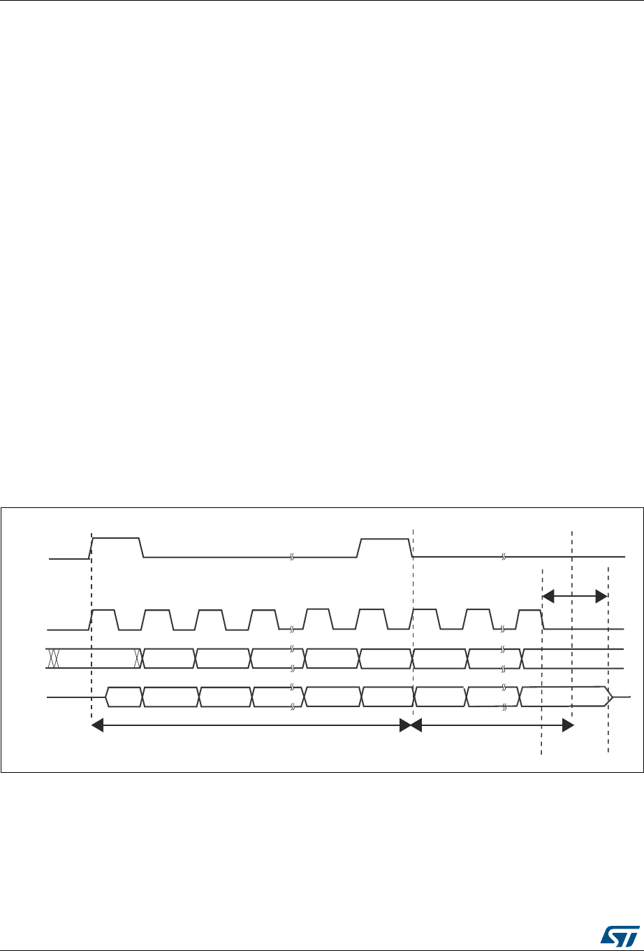
Serial peripheral interface/ inter-IC sound (SPI/I2S) RM0401
696/766 DocID027812 Rev 2
The clock polarity and phase are forced to conform to the TI protocol requirements whatever
the values set in the SPIx_CR1 register. NSS management is also specific to the TI protocol
which makes the configuration of NSS management through the SPIx_CR1 and SPIx_CR2
registers (SSM, SSI, SSOE) impossible in this case.
In slave mode, the SPI baud rate prescaler is used to control the moment when the MISO
pin state changes to HiZ when the current transaction finishes (see Figure 251). Any baud
rate can be used, making it possible to determine this moment with optimal flexibility.
However, the baud rate is generally set to the external master clock baud rate. The delay for
the MISO signal to become HiZ (trelease) depends on internal resynchronization and on the
baud rate value set in through the BR[2:0] bits in the SPIx_CR1 register. It is given by the
formula:
If the slave detects a misplaced NSS pulse during a data frame transaction the TIFRE flag is
set.
This feature is not available for Motorola SPI communications (FRF bit set to 0).
Note: To detect TI frame errors in slave transmitter only mode by using the Error interrupt
(ERRIE=1), the SPI must be configured in 2-line unidirectional mode by setting BIDIMODE
and BIDIOE to 1 in the SPI_CR1 register. When BIDIMODE is set to 0, OVR is set to 1
because the data register is never read and error interrupts are always generated, while
when BIDIMODE is set to 1, data are not received and OVR is never set.
Figure 251: TI mode transfer shows the SPI communication waveforms when TI mode is
selected.
Figure 251. TI mode transfer
25.4.2 CRC calculation
Two separate CRC calculators (on transmission and reception data flows) are implemented
in order to check the reliability of transmitted and received data. The SPI offers CRC8 or
CRC16 calculation depending on the data format selected through the DFF bit. The CRC is
calculated serially using the polynomial programmed in the SPI_CRCPR register.
tbaud_rate
2
----------------------4t
pclk
×+trelease
tbaud_rate
2
----------------------6t
pclk
×+<<
-36
-3"
-)3/
.33
3#+
TRIGGER
SAMPLING
TRIGGER
SAMPLING
TRIGGER
SAMPLING
$/.4#!2% ,3"
-/3)
OR -3" ,3"
-3" ,3"
-3" ,3"
&2!-% &2!-%
T
2%,%!3%

DocID027812 Rev 2 697/766
RM0401 Serial peripheral interface/ inter-IC sound (SPI/I2S)
726
CRC principle
CRC calculation is enabled by setting the CRCEN bit in the SPIx_CR1 register before the
SPI is enabled (SPE = 1). The CRC value is calculated using an odd programmable
polynomial on each bit. The calculation is processed on the sampling clock edge defined by
the CPHA and CPOL bits in the SPIx_CR1 register. The calculated CRC value is checked
automatically at the end of the data block as well as for transfer managed by CPU or by the
DMA. When a mismatch is detected between the CRC calculated internally on the received
data and the CRC sent by the transmitter, a CRCERR flag is set to indicate a data corruption
error. The right procedure for handling the CRC calculation depends on the SPI
configuration and the chosen transfer management.
Note: The polynomial value should only be odd. No even values are supported.
CRC transfer managed by CPU
Communication starts and continues normally until the last data frame has to be sent or
received in the SPIx_DR register. Then CRCNEXT bit has to be set in the SPIx_CR1
register to indicate that the CRC frame transaction will follow after the transaction of the
currently processed data frame. The CRCNEXT bit must be set before the end of the last
data frame transaction. CRC calculation is frozen during CRC transaction.
The received CRC is stored in the Rx buffer like any other data frame.
A CRC-format transaction takes one more data frame to communicate at the end of data
sequence.
When the last CRC data is received, an automatic check is performed comparing the
received value and the value in the SPIx_RXCRC register. Software has to check the
CRCERR flag in the SPIx_SR register to determine if the data transfers were corrupted or
not. Software clears the CRCERR flag by writing '0' to it.
After the CRC reception, the CRC value is stored in the Rx buffer and must be read in the
SPIx_DR register in order to clear the RXNE flag.
CRC transfer managed by DMA
When SPI communication is enabled with CRC communication and DMA mode, the
transmission and reception of the CRC at the end of communication is automatic (with the
exception of reading CRC data in receive-only mode). The CRCNEXT bit does not have to
be handled by the software. The counter for the SPI transmission DMA channel has to be
set to the number of data frames to transmit excluding the CRC frame. On the receiver side,
the received CRC value is handled automatically by DMA at the end of the transaction but
user must take care to flush out the CRC frame received from SPI_DR as it is always loaded
into it.
At the end of the data and CRC transfers, the CRCERR flag in the SPIx_SR register is set if
corruption occurred during the transfer.
Resetting the SPIx_TXCRC and SPIx_RXCRC values
The SPIx_TXCRC and SPIx_RXCRC values are cleared automatically when CRC
calculation is enabled.
When the SPI is configured in slave mode with the CRC feature enabled, a CRC calculation
is performed even if a high level is applied on the NSS pin. This may happen for example in
case of a multislave environment where the communication master addresses slaves
alternately.
Serial peripheral interface/ inter-IC sound (SPI/I2S) RM0401
698/766 DocID027812 Rev 2
Between a slave disabling (high level on NSS) and a new slave enabling (low level on NSS),
the CRC value should be cleared on both master and slave sides to resynchronize the
master and slave respective CRC calculation.
To clear the CRC, follow the below sequence:
1. Disable the SPI
2. Clear the CRCEN bit
3. Enable the CRCEN bit
4. Enable the SPI
Note: When the SPI is in slave mode, the CRC calculator is sensitive to the SCK slave input clock
as soon as the CRCEN bit is set, and this is the case whatever the value of the SPE bit. In
order to avoid any wrong CRC calculation, the software must enable CRC calculation only
when the clock is stable (in steady state). When the SPI interface is configured as a slave,
the NSS internal signal needs to be kept low between the data phase and the CRC phase.
25.5 SPI interrupts
During SPI communication an interrupts can be generated by the following events:
•Transmit Tx buffer ready to be loaded
•Data received in Rx buffer
•Master mode fault
•Overrun error
•TI frame format error
Interrupts can be enabled and disabled separately.
Table 114. SPI interrupt requests
Interrupt event Event flag Enable Control bit
Transmit Tx buffer ready to be loaded TXE TXEIE
Data received in Rx buffer RXNE RXNEIE
Master Mode fault event MODF
ERRIE
Overrun error OVR
CRC error CRCERR
TI frame format error FRE
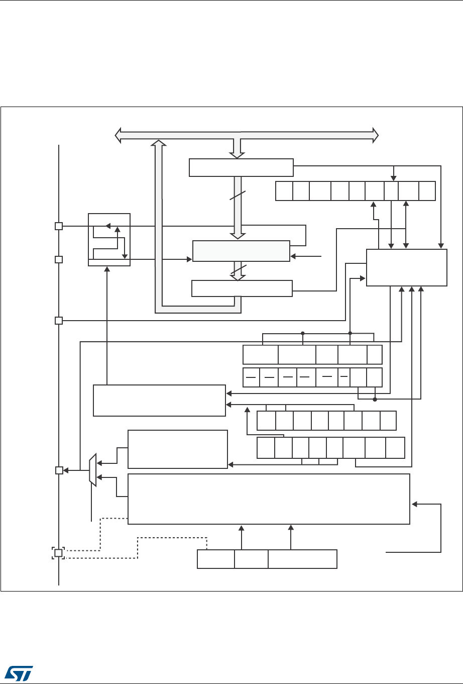
DocID027812 Rev 2 699/766
RM0401 Serial peripheral interface/ inter-IC sound (SPI/I2S)
726
25.6 I2S functional description
25.6.1 I2S general description
The block diagram of the I2S is shown in Figure 252.
Figure 252. I2S block diagram
1. MCK is mapped on the MISO pin.
The SPI can function as an audio I2S interface when the I2S capability is enabled (by setting
the I2SMOD bit in the SPIx_I2SCFGR register). This interface mainly uses the same pins,
flags and interrupts as the SPI.
7[EXIIHU
6KLIWUHJLVWHU
ELW
&RPPXQLFDWLRQ
5[EXIIHU
ELW
026,6'
0DVWHUFRQWUROORJLF
0,62
63,
EDXGUDWHJHQHUDWRU
,602'
/6%ILUVW
/6%
)LUVW 63( %5 %5 %5 0675 &32/ &3+$
%LGL
PRGH
%LGL
2(
&5&
(1
&5&
1H[W ')) 5[
RQO\ 660 66,
$GGUHVVDQGGDWDEXV
FRQWURO
166:6
%6< 295 02') &5&
(55
&+
6,'( 7[( 5[1(
,6FORFNJHQHUDWRU
0&.
,6B
&.
,6
02' ,6(
&+
'$7/(1 /(1
&.
32/
,6&)* ,667'
0&.2( 2'' ,6',9>@
>@ >@ >@
8'5
,6[&/.
069
)5(
&.

Serial peripheral interface/ inter-IC sound (SPI/I2S) RM0401
700/766 DocID027812 Rev 2
The I2S shares three common pins with the SPI:
•SD: Serial Data (mapped on the MOSI pin) to transmit or receive the two time-
multiplexed data channels (in half-duplex mode only).
•WS: Word Select (mapped on the NSS pin) is the data control signal output in master
mode and input in slave mode.
•CK: Serial Clock (mapped on the SCK pin) is the serial clock output in master mode
and serial clock input in slave mode.
An additional pin can be used when a master clock output is needed for some external
audio devices:
•MCK: Master Clock (mapped separately) is used, when the I2S is configured in master
mode (and when the MCKOE bit in the SPIx_I2SPR register is set), to output this
additional clock generated at a preconfigured frequency rate equal to 256 × fS, where
fS is the audio sampling frequency.
The I2S uses its own clock generator to produce the communication clock when it is set in
master mode. This clock generator is also the source of the master clock output. Two
additional registers are available in I2S mode. One is linked to the clock generator
configuration SPIx_I2SPR and the other one is a generic I2S configuration register
SPIx_I2SCFGR (audio standard, slave/master mode, data format, packet frame, clock
polarity, etc.).
The SPIx_CR1 register and all CRC registers are not used in the I2S mode. Likewise, the
SSOE bit in the SPIx_CR2 register and the MODF and CRCERR bits in the SPIx_SR are
not used.
The I2S uses the same SPI register for data transfer (SPIx_DR) in 16-bit wide mode.
25.6.2 Supported audio protocols
The three-line bus has to handle only audio data generally time-multiplexed on two
channels: the right channel and the left channel. However there is only one 16-bit register
for transmission or reception. So, it is up to the software to write into the data register the
appropriate value corresponding to each channel side, or to read the data from the data
register and to identify the corresponding channel by checking the CHSIDE bit in the
SPIx_SR register. Channel left is always sent first followed by the channel right (CHSIDE
has no meaning for the PCM protocol).
Four data and packet frames are available. Data may be sent with a format of:
•16-bit data packed in a 16-bit frame
•16-bit data packed in a 32-bit frame
•24-bit data packed in a 32-bit frame
•32-bit data packed in a 32-bit frame
When using 16-bit data extended on 32-bit packet, the first 16 bits (MSB) are the significant
bits, the 16-bit LSB is forced to 0 without any need for software action or DMA request (only
one read/write operation).
The 24-bit and 32-bit data frames need two CPU read or write operations to/from the
SPIx_DR register or two DMA operations if the DMA is preferred for the application. For 24-
bit data frame specifically, the 8 non significant bits are extended to 32 bits with 0-bits (by
hardware).
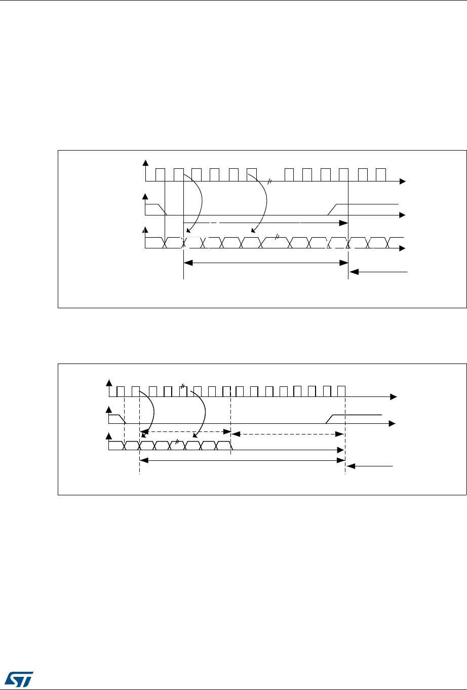
DocID027812 Rev 2 701/766
RM0401 Serial peripheral interface/ inter-IC sound (SPI/I2S)
726
For all data formats and communication standards, the most significant bit is always sent
first (MSB first).
The I2S interface supports four audio standards, configurable using the I2SSTD[1:0] and
PCMSYNC bits in the SPIx_I2SCFGR register.
I2S Philips standard
For this standard, the WS signal is used to indicate which channel is being transmitted. It is
activated one CK clock cycle before the first bit (MSB) is available.
Figure 253. I2S Philips protocol waveforms (16/32-bit full accuracy, CPOL = 0)
Data are latched on the falling edge of CK (for the transmitter) and are read on the rising
edge (for the receiver). The WS signal is also latched on the falling edge of CK.
Figure 254. I2S Philips standard waveforms (24-bit frame with CPOL = 0)
This mode needs two write or read operations to/from the SPIx_DR register.
•In transmission mode:
If 0x8EAA33 has to be sent (24-bit):
069
&.
:6
6'
&DQEHELWRUELW
06% 06%/6%
&KDQQHOOHIW
&KDQQHO
ULJKW
WUDQVPLVVLRQ UHFHSWLRQ
069
&.
:6
6'
7UDQVPLVVLRQ 5HFHSWLRQ
ELWGDWD
06% /6%
&KDQQHOOHIWELW
&KDQQHOULJKW
ELWUHPDLQLQJIRUFHG
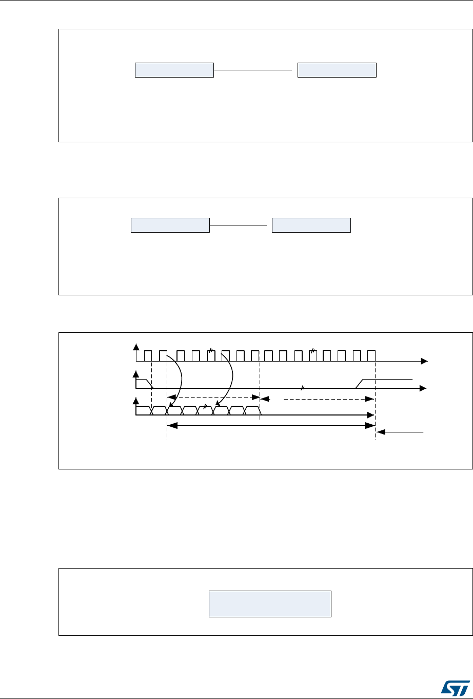
Serial peripheral interface/ inter-IC sound (SPI/I2S) RM0401
702/766 DocID027812 Rev 2
Figure 255. Transmitting 0x8EAA33
•In reception mode:
If data 0x8EAA33 is received:
Figure 256. Receiving 0x8EAA33
Figure 257. I2S Philips standard (16-bit extended to 32-bit packet frame with
CPOL = 0)
When 16-bit data frame extended to 32-bit channel frame is selected during the I2S
configuration phase, only one access to the SPIx_DR register is required. The 16 remaining
bits are forced by hardware to 0x0000 to extend the data to 32-bit format.
If the data to transmit or the received data are 0x76A3 (0x76A30000 extended to 32-bit), the
operation shown in Figure 258 is required.
Figure 258. Example of 16-bit data frame extended to 32-bit channel frame
069
[($$ [;;
)LUVWZULWHWR'DWDUHJLVWHU 6HFRQGZULWHWR'DWDUHJLVWHU
2QO\WKH06%DUHVHQW
WRFRPSDUHWKHELWV
/6%VKDYHQRPHDQLQJ
DQGFDQEHDQ\WKLQJ
069
[($$ [;;
)LUVWUHDGWR'DWDUHJLVWHU 6HFRQGUHDGWR'DWDUHJLVWHU
2QO\WKH06%DUHVHQW
WRFRPSDUHWKHELWV
/6%VKDYHQRPHDQLQJ
DQGFDQEHDQ\WKLQJ
069
&.
:6
6'
7UDQVPLVVLRQ 5HFHSWLRQ
ELWGDWD
06% /6%
&KDQQHOOHIWELW &KDQQHOULJKW
ELWUHPDLQLQJIRUFHG
069
[$
2QO\RQHDFFHVVWR63,[B'5
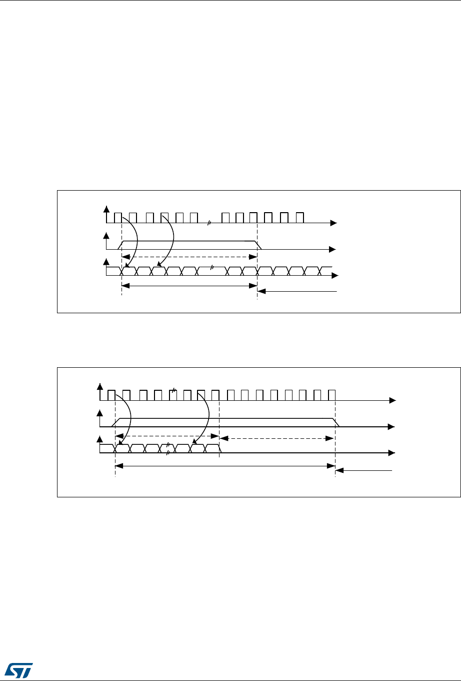
DocID027812 Rev 2 703/766
RM0401 Serial peripheral interface/ inter-IC sound (SPI/I2S)
726
For transmission, each time an MSB is written to SPIx_DR, the TXE flag is set and its
interrupt, if allowed, is generated to load the SPIx_DR register with the new value to send.
This takes place even if 0x0000 have not yet been sent because it is done by hardware.
For reception, the RXNE flag is set and its interrupt, if allowed, is generated when the first
16 MSB half-word is received.
In this way, more time is provided between two write or read operations, which prevents
underrun or overrun conditions (depending on the direction of the data transfer).
MSB justified standard
For this standard, the WS signal is generated at the same time as the first data bit, which is
the MSBit.
Figure 259. MSB Justified 16-bit or 32-bit full-accuracy length with CPOL = 0
Data are latched on the falling edge of CK (for transmitter) and are read on the rising edge
(for the receiver).
Figure 260. MSB justified 24-bit frame length with CPOL = 0
069
&.
:6
6'
7UDQVPLVVLRQ 5HFHSWLRQ
RUELWGDWD
06% /6%
&KDQQHOOHIW
&KDQQHOULJKW
06%
069
&.
:6
6'
7UDQVPLVVLRQ 5HFHSWLRQ
ELWGDWD
06% /6%
&KDQQHOOHIWELW
&KDQQHOULJKW
ELWUHPDLQLQJ
IRUFHG
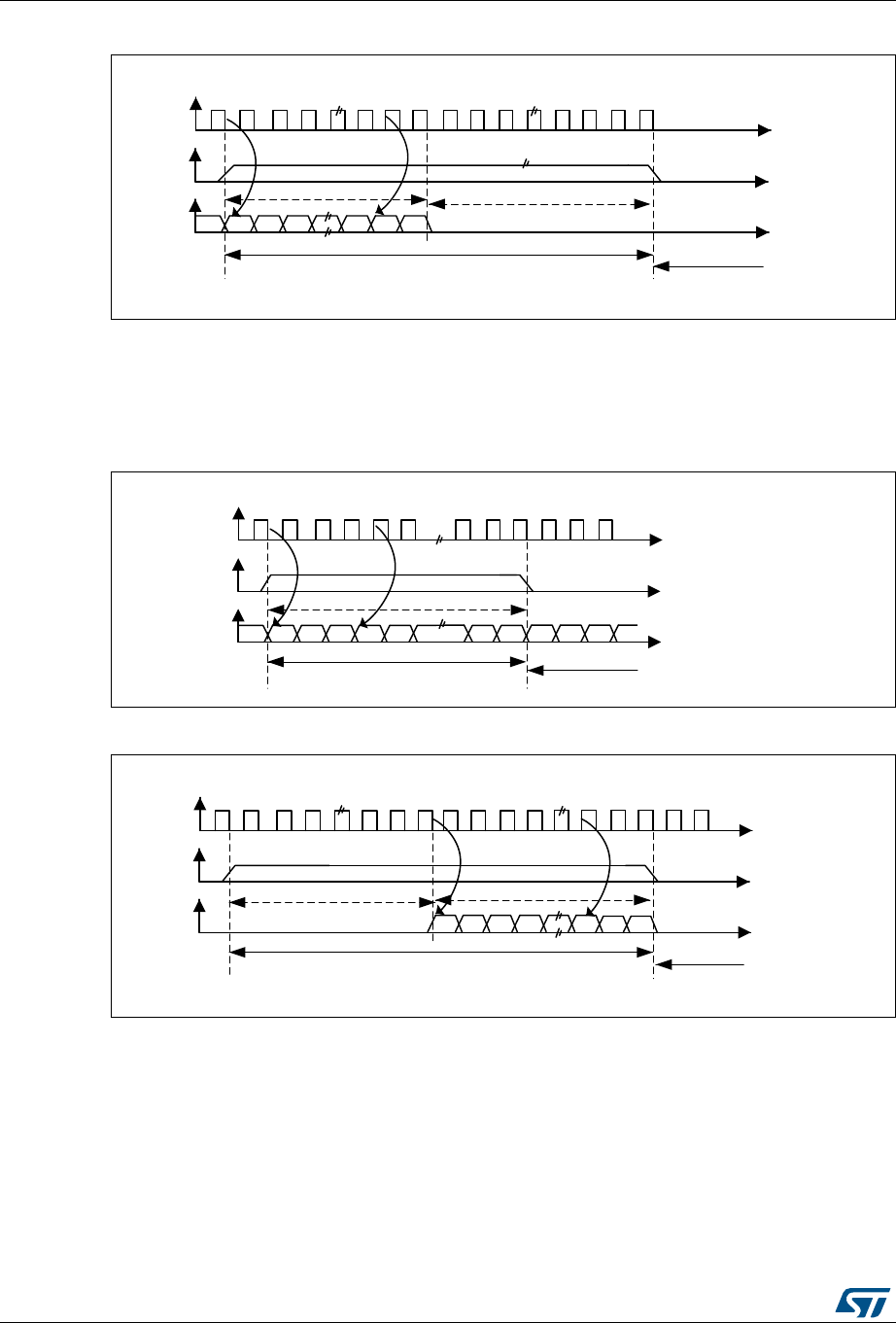
Serial peripheral interface/ inter-IC sound (SPI/I2S) RM0401
704/766 DocID027812 Rev 2
Figure 261. MSB justified 16-bit extended to 32-bit packet frame with CPOL = 0
LSB justified standard
This standard is similar to the MSB justified standard (no difference for the 16-bit and 32-bit
full-accuracy frame formats).
Figure 262. LSB justified 16-bit or 32-bit full-accuracy with CPOL = 0
Figure 263. LSB justified 24-bit frame length with CPOL = 0
069
&.
:6
6'
7UDQVPLVVLRQ 5HFHSWLRQ
ELWGDWD
06% /6%
&KDQQHOOHIWELW
&KDQQHOULJKW
ELWUHPDLQLQJ
IRUFHG
069
&.
:6
6'
7UDQVPLVVLRQ 5HFHSWLRQ
RUELWGDWD
06% /6%
&KDQQHOOHIW
&KDQQHOULJKW
06%
069
&.
:6
6'
7UDQVPLVVLRQ
5HFHSWLRQ
ELWGDWD
IRUFHG
06% /6%
&KDQQHOOHIWELW
&KDQQHOULJKW
ELWUHPDLQLQJ
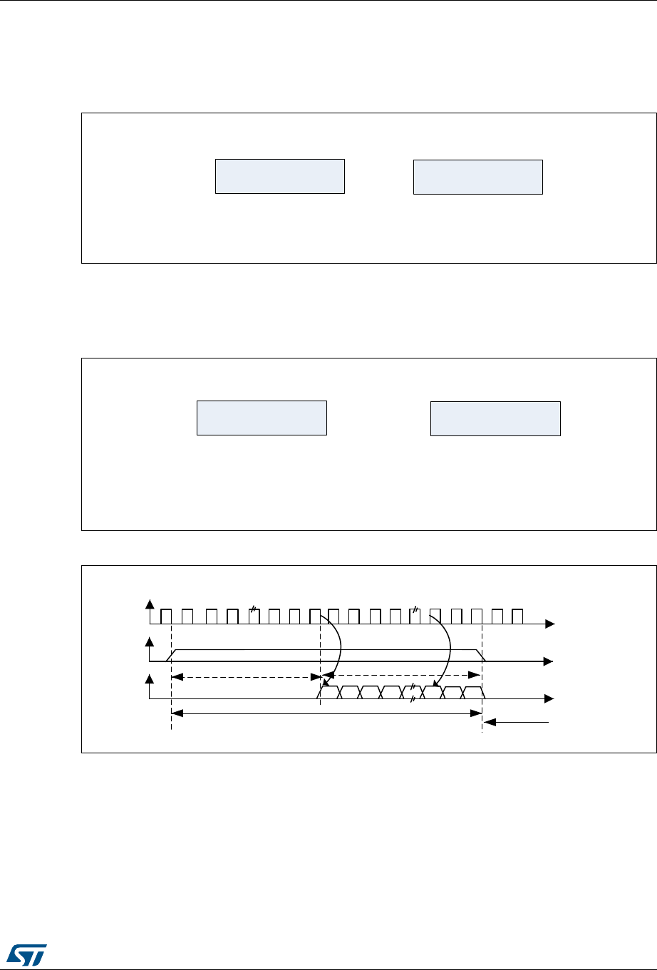
DocID027812 Rev 2 705/766
RM0401 Serial peripheral interface/ inter-IC sound (SPI/I2S)
726
•In transmission mode:
If data 0x3478AE have to be transmitted, two write operations to the SPIx_DR register
are required by software or by DMA. The operations are shown below.
Figure 264. Operations required to transmit 0x3478AE
•In reception mode:
If data 0x3478AE are received, two successive read operations from the SPIx_DR
register are required on each RXNE event.
Figure 265. Operations required to receive 0x3478AE
Figure 266. LSB justified 16-bit extended to 32-bit packet frame with CPOL = 0
When 16-bit data frame extended to 32-bit channel frame is selected during the I2S
configuration phase, Only one access to the SPIx_DR register is required. The 16 remaining
bits are forced by hardware to 0x0000 to extend the data to 32-bit format. In this case it
corresponds to the half-word MSB.
If the data to transmit or the received data are 0x76A3 (0x0000 76A3 extended to 32-bit),
the operation shown in Figure 267 is required.
[;; [$(
)LUVWZULWHWR'DWDUHJLVWHU
FRQGLWLRQHGE\7;(
6HFRQGZULWHWR'DWDUHJLVWHU
FRQGLWLRQHGE\7;(
2QO\WKH/6%RIWKH
KDOIZRUGDUHVLJQLILFDQW
$ILHOGRI[LVIRUFHG
LQVWHDGRIWKH06%V
069
[;; [$(
)LUVWUHDGIURP'DWDUHJLVWHU
FRQGLWLRQHGE\5;1(
6HFRQGUHDGIURP'DWDUHJLVWHU
FRQGLWLRQHGE\5;1(
2QO\WKH/6%RIWKH
KDOIZRUGDUHVLJQLILFDQW
$ILHOGRI[LVIRUFHG
LQVWHDGRIWKH06%V
069
069
&.
:6
6'
7UDQVPLVVLRQ
5HFHSWLRQ
ELWGDWD
IRUFHG
06% /6%
&KDQQHOOHIWELW
&KDQQHOULJKW
ELWUHPDLQLQJ
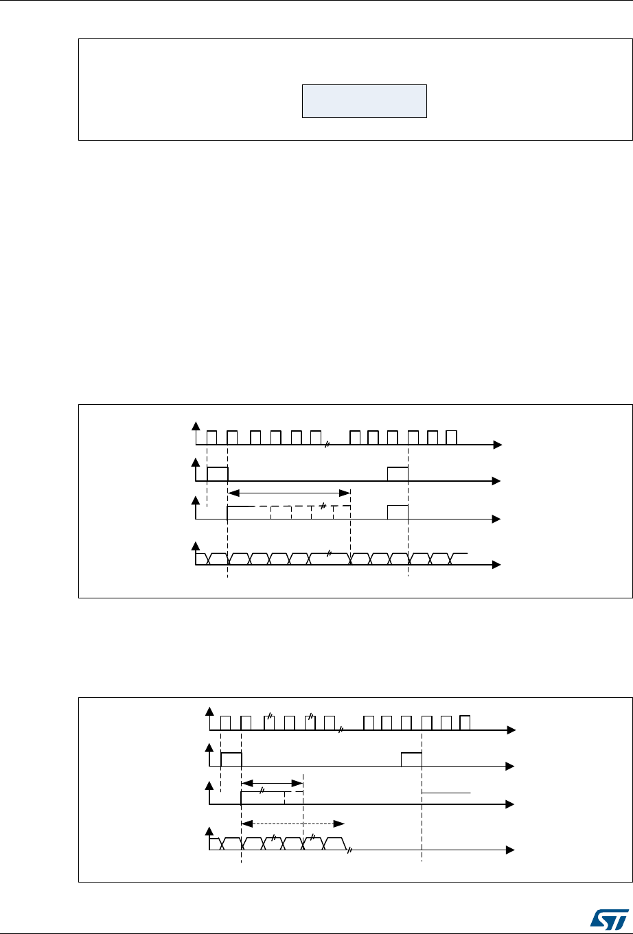
Serial peripheral interface/ inter-IC sound (SPI/I2S) RM0401
706/766 DocID027812 Rev 2
Figure 267. Example of 16-bit data frame extended to 32-bit channel frame
In transmission mode, when a TXE event occurs, the application has to write the data to be
transmitted (in this case 0x76A3). The 0x000 field is transmitted first (extension on 32-bit).
The TXE flag is set again as soon as the effective data (0x76A3) is sent on SD.
In reception mode, RXNE is asserted as soon as the significant half-word is received (and
not the 0x0000 field).
In this way, more time is provided between two write or read operations to prevent underrun
or overrun conditions.
PCM standard
For the PCM standard, there is no need to use channel-side information. The two PCM
modes (short and long frame) are available and configurable using the PCMSYNC bit in
SPIx_I2SCFGR register.
Figure 268. PCM standard waveforms (16-bit)
For long frame synchronization, the WS signal assertion time is fixed to 13 bits in master
mode.
For short frame synchronization, the WS synchronization signal is only one cycle long.
Figure 269. PCM standard waveforms (16-bit extended to 32-bit packet frame)
[$
2QO\RQHDFFHVVWRWKH63,['5UHJLVWHU
069
069
&.
:6
VKRUWIUDPH
6'
:6
ORQJIUDPH
ELWV
06% /6% 06%
069
&.
:6
VKRUWIUDPH
6'
:6
ORQJIUDPH
8SWRELWV
06% /6%
ELWV
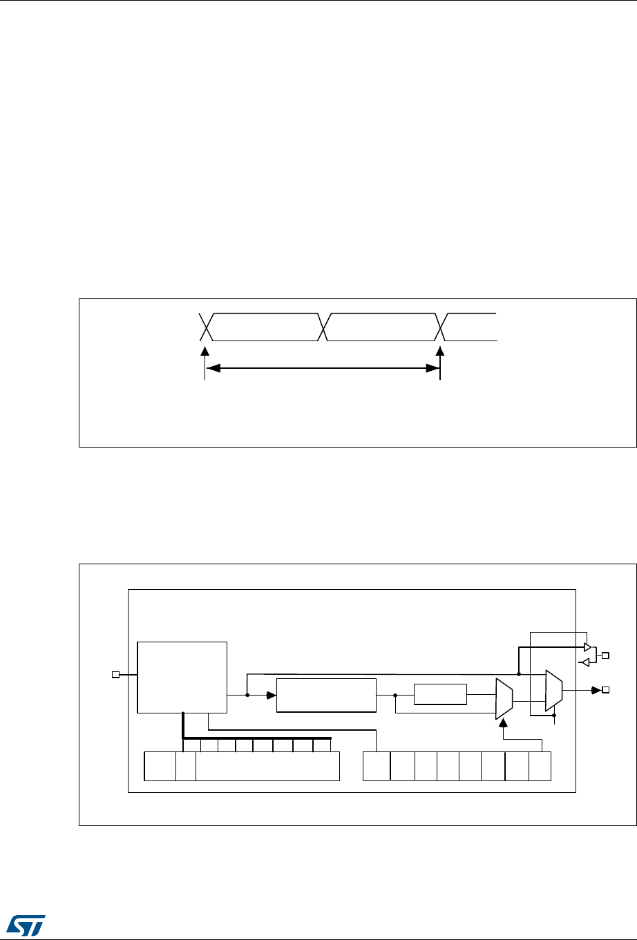
DocID027812 Rev 2 707/766
RM0401 Serial peripheral interface/ inter-IC sound (SPI/I2S)
726
Note: For both modes (master and slave) and for both synchronizations (short and long), the
number of bits between two consecutive pieces of data (and so two synchronization signals)
needs to be specified (DATLEN and CHLEN bits in the SPIx_I2SCFGR register) even in
slave mode.
25.6.3 Clock generator
The I2S bitrate determines the data flow on the I2S data line and the I2S clock signal
frequency.
I2S bitrate = number of bits per channel × number of channels × sampling audio frequency
For a 16-bit audio, left and right channel, the I2S bitrate is calculated as follows:
I2S bitrate = 16 × 2 × fS
It will be: I2S bitrate = 32 x 2 x fS if the packet length is 32-bit wide.
Figure 270. Audio sampling frequency definition
When the master mode is configured, a specific action needs to be taken to properly
program the linear divider in order to communicate with the desired audio frequency.
Figure 271 presents the communication clock architecture. The I2Sx clock is always the
system clock.
Figure 271. I2S clock generator architecture
1. Where x = 2.
The audio sampling frequency may be 192 KHz, 96 kHz, 48 kHz, 44.1 kHz, 32 kHz,
22.05 kHz, 16 kHz, 11.025 kHz or 8 kHz (or any other value within this range). In order to
069
RUELWOHIW
FKDQQHO
RUELW
ULJKWFKDQQHO
RUELWV
VDPSOLQJSRLQW VDPSOLQJSRLQW
)6
)6DXGLRVDPSOLQJIUHTXHQF\
069
0&.2( 2''
ELWOLQHDUGLYLGHU
UHVKDSLQJVWDJH
'LYLGHUE\ 'LY
,ð6',9>@
,ð602'
&+/(1
0&.2(
&.
0&.
,ð6[&/.

Serial peripheral interface/ inter-IC sound (SPI/I2S) RM0401
708/766 DocID027812 Rev 2
reach the desired frequency, the linear divider needs to be programmed according to the
formulas below:
When the master clock is generated (MCKOE in the SPIx_I2SPR register is set):
fS = I2SxCLK / [(16*2)*((2*I2SDIV)+ODD)*8)] when the channel frame is 16-bit wide
fS = I2SxCLK / [(32*2)*((2*I2SDIV)+ODD)*4)] when the channel frame is 32-bit wide
When the master clock is disabled (MCKOE bit cleared):
fS = I2SxCLK / [(16*2)*((2*I2SDIV)+ODD))] when the channel frame is 16-bit wide
fS = I2SxCLK / [(32*2)*((2*I2SDIV)+ODD))] when the channel frame is 32-bit wide
Table 115 provides example precision values for different clock configurations.
Note: Other configurations are possible that allow optimum clock precision.
Table 115. Audio-frequency precision using standard 8 MHz HSE(1)
SYSCLK
(MHz)
Data
length I2SDIV I2SODD MCLK Target fS
(Hz) Real fS (KHz) Error
48 16 8 0 No 96000 93750 2.3438%
48 32 4 0 No 96000 93750 2.3438%
48 16 15 1 No 48000 48387.0968 0.8065%
48 32 8 0 No 48000 46875 2.3438%
48 16 17 0 No 44100 44117.647 0.0400%
48 32 8 1 No 44100 44117.647 0.0400%
48 16 23 1 No 32000 31914.8936 0.2660%
48 32 11 1 No 32000 32608.696 1.9022%
48 16 34 0 No 22050 22058.8235 0.0400%
48 32 17 0 No 22050 22058.8235 0.0400%
48 16 47 0 No 16000 15957.4468 0.2660%
48 32 23 1 No 16000 15957.447 0.2660%
48 16 68 0 No 11025 11029.4118 0.0400%
48 32 34 0 No 11025 11029.412 0.0400%
48 16 94 0 No 8000 7978.7234 0.2660%
48 32 47 0 No 8000 7978.7234 0.2660%
48 16 2 0 Yes 48000 46875 2.3430%
48 32 2 0 Yes 48000 46875 2.3430%
48 16 2 0 Yes 44100 46875 6.2925%
48 32 2 0 Yes 44100 46875 6.2925%
48 16 3 0 Yes 32000 31250 2.3438%
48 32 3 0 Yes 32000 31250 2.3438%
48 16 4 1 Yes 22050 20833.333 5.5178%
48 32 4 1 Yes 22050 20833.333 5.5178%

DocID027812 Rev 2 709/766
RM0401 Serial peripheral interface/ inter-IC sound (SPI/I2S)
726
25.6.4 I2S master mode
The I2S can be configured in master mode. This means that the serial clock is generated on
the CK pin as well as the Word Select signal WS. Master clock (MCK) may be output or not,
controlled by the MCKOE bit in the SPIx_I2SPR register.
Procedure
1. Select the I2SDIV[7:0] bits in the SPIx_I2SPR register to define the serial clock baud
rate to reach the proper audio sample frequency. The ODD bit in the SPIx_I2SPR
register also has to be defined.
2. Select the CKPOL bit to define the steady level for the communication clock. Set the
MCKOE bit in the SPIx_I2SPR register if the master clock MCK needs to be provided
to the external ADC audio component (the I2SDIV and ODD values should be
computed depending on the state of the MCK output, for more details refer to
Section 25.6.3: Clock generator).
3. Set the I2SMOD bit in the SPIx_I2SCFGR register to activate the I2S functions and
choose the I2S standard through the I2SSTD[1:0] and PCMSYNC bits, the data length
through the DATLEN[1:0] bits and the number of bits per channel by configuring the
CHLEN bit. Select also the I2S master mode and direction (Transmitter or Receiver)
through the I2SCFG[1:0] bits in the SPIx_I2SCFGR register.
4. If needed, select all the potential interrupt sources and the DMA capabilities by writing
the SPIx_CR2 register.
5. The I2SE bit in SPIx_I2SCFGR register must be set.
WS and CK are configured in output mode. MCK is also an output, if the MCKOE bit in
SPIx_I2SPR is set.
Transmission sequence
The transmission sequence begins when a half-word is written into the Tx buffer.
Lets assume the first data written into the Tx buffer corresponds to the left channel data.
When data are transferred from the Tx buffer to the shift register, TXE is set and data
corresponding to the right channel have to be written into the Tx buffer. The CHSIDE flag
48 16 6 0 Yes 16000 15625 2.3438%
48 32 6 0 Yes 16000 15625 2.3438%
48 16 8 1 Yes 11025 11029.4118 0.0400%
48 32 8 1 Yes 11025 11029.4118 0.0400%
48 16 11 1 Yes 8000 8152.17391 1.9022%
48 32 11 1 Yes 8000 8152.17391 1.9022%
1. This table gives only example values for different clock configurations. Other configurations allowing
optimum clock precision are possible.
Table 115. Audio-frequency precision using standard 8 MHz HSE(1) (continued)
SYSCLK
(MHz)
Data
length I2SDIV I2SODD MCLK Target fS
(Hz) Real fS (KHz) Error

Serial peripheral interface/ inter-IC sound (SPI/I2S) RM0401
710/766 DocID027812 Rev 2
indicates which channel is to be transmitted. It has a meaning when the TXE flag is set
because the CHSIDE flag is updated when TXE goes high.
A full frame has to be considered as a left channel data transmission followed by a right
channel data transmission. It is not possible to have a partial frame where only the left
channel is sent.
The data half-word is parallel loaded into the 16-bit shift register during the first bit
transmission, and then shifted out, serially, to the MOSI/SD pin, MSB first. The TXE flag is
set after each transfer from the Tx buffer to the shift register and an interrupt is generated if
the TXEIE bit in the SPIx_CR2 register is set.
For more details about the write operations depending on the I2S Standard-mode selected,
refer to Section 25.6.2: Supported audio protocols).
To ensure a continuous audio data transmission, it is mandatory to write the SPIx_DR
register with the next data to transmit before the end of the current transmission.
To switch off the I2S, by clearing I2SE, it is mandatory to wait for TXE = 1 and BSY = 0.
Reception sequence
The operating mode is the same as for transmission mode except for the point 3 (refer to the
procedure described in Section 25.6.4: I2S master mode), where the configuration should
set the master reception mode through the I2SCFG[1:0] bits.
Whatever the data or channel length, the audio data are received by 16-bit packets. This
means that each time the Rx buffer is full, the RXNE flag is set and an interrupt is generated
if the RXNEIE bit is set in SPIx_CR2 register. Depending on the data and channel length
configuration, the audio value received for a right or left channel may result from one or two
receptions into the Rx buffer.
Clearing the RXNE bit is performed by reading the SPIx_DR register.
CHSIDE is updated after each reception. It is sensitive to the WS signal generated by the
I2S cell.
For more details about the read operations depending on the I2S Standard-mode selected,
refer to Section 25.6.2: Supported audio protocols.
If data are received while the previously received data have not been read yet, an overrun is
generated and the OVR flag is set. If the ERRIE bit is set in the SPIx_CR2 register, an
interrupt is generated to indicate the error.
To switch off the I2S, specific actions are required to ensure that the I2S completes the
transfer cycle properly without initiating a new data transfer. The sequence depends on the

DocID027812 Rev 2 711/766
RM0401 Serial peripheral interface/ inter-IC sound (SPI/I2S)
726
configuration of the data and channel lengths, and on the audio protocol mode selected. In
the case of:
•16-bit data length extended on 32-bit channel length (DATLEN = 00 and CHLEN = 1)
using the LSB justified mode (I2SSTD = 10)
a) Wait for the second to last RXNE = 1 (n – 1)
b) Then wait 17 I2S clock cycles (using a software loop)
c) Disable the I2S (I2SE = 0)
•16-bit data length extended on 32-bit channel length (DATLEN = 00 and CHLEN = 1) in
MSB justified, I2S or PCM modes (I2SSTD = 00, I2SSTD = 01 or I2SSTD = 11,
respectively)
a) Wait for the last RXNE
b) Then wait 1 I2S clock cycle (using a software loop)
c) Disable the I2S (I2SE = 0)
•For all other combinations of DATLEN and CHLEN, whatever the audio mode selected
through the I2SSTD bits, carry out the following sequence to switch off the I2S:
a) Wait for the second to last RXNE = 1 (n – 1)
b) Then wait one I2S clock cycle (using a software loop)
c) Disable the I2S (I2SE = 0)
Note: The BSY flag is kept low during transfers.
25.6.5 I2S slave mode
For the slave configuration, the I2S can be configured in transmission or reception mode.
The operating mode is following mainly the same rules as described for the I2S master
configuration. In slave mode, there is no clock to be generated by the I2S interface. The
clock and WS signals are input from the external master connected to the I2S interface.
There is then no need, for the user, to configure the clock.
The configuration steps to follow are listed below:
1. Set the I2SMOD bit in the SPIx_I2SCFGR register to select I2S mode and choose the
I2S standard through the I2SSTD[1:0] bits, the data length through the DATLEN[1:0]
bits and the number of bits per channel for the frame configuring the CHLEN bit. Select
also the mode (transmission or reception) for the slave through the I2SCFG[1:0] bits in
SPIx_I2SCFGR register.
2. If needed, select all the potential interrupt sources and the DMA capabilities by writing
the SPIx_CR2 register.
3. The I2SE bit in SPIx_I2SCFGR register must be set.
Transmission sequence
The transmission sequence begins when the external master device sends the clock and
when the NSS_WS signal requests the transfer of data. The slave has to be enabled before
the external master starts the communication. The I2S data register has to be loaded before
the master initiates the communication.
For the I2S, MSB justified and LSB justified modes, the first data item to be written into the
data register corresponds to the data for the left channel. When the communication starts,
the data are transferred from the Tx buffer to the shift register. The TXE flag is then set in
order to request the right channel data to be written into the I2S data register.

Serial peripheral interface/ inter-IC sound (SPI/I2S) RM0401
712/766 DocID027812 Rev 2
The CHSIDE flag indicates which channel is to be transmitted. Compared to the master
transmission mode, in slave mode, CHSIDE is sensitive to the WS signal coming from the
external master. This means that the slave needs to be ready to transmit the first data
before the clock is generated by the master. WS assertion corresponds to left channel
transmitted first.
Note: The I2SE has to be written at least two PCLK cycles before the first clock of the master
comes on the CK line.
The data half-word is parallel-loaded into the 16-bit shift register (from the internal bus)
during the first bit transmission, and then shifted out serially to the MOSI/SD pin MSB first.
The TXE flag is set after each transfer from the Tx buffer to the shift register and an interrupt
is generated if the TXEIE bit in the SPIx_CR2 register is set.
Note that the TXE flag should be checked to be at 1 before attempting to write the Tx buffer.
For more details about the write operations depending on the I2S Standard-mode selected,
refer to Section 25.6.2: Supported audio protocols.
To secure a continuous audio data transmission, it is mandatory to write the SPIx_DR
register with the next data to transmit before the end of the current transmission. An
underrun flag is set and an interrupt may be generated if the data are not written into the
SPIx_DR register before the first clock edge of the next data communication. This indicates
to the software that the transferred data are wrong. If the ERRIE bit is set into the SPIx_CR2
register, an interrupt is generated when the UDR flag in the SPIx_SR register goes high. In
this case, it is mandatory to switch off the I2S and to restart a data transfer starting from the
left channel.
To switch off the I2S, by clearing the I2SE bit, it is mandatory to wait for TXE = 1 and
BSY = 0.
Reception sequence
The operating mode is the same as for the transmission mode except for the point 1 (refer to
the procedure described in Section 25.6.5: I2S slave mode), where the configuration should
set the master reception mode using the I2SCFG[1:0] bits in the SPIx_I2SCFGR register.
Whatever the data length or the channel length, the audio data are received by 16-bit
packets. This means that each time the RX buffer is full, the RXNE flag in the SPIx_SR
register is set and an interrupt is generated if the RXNEIE bit is set in the SPIx_CR2
register. Depending on the data length and channel length configuration, the audio value
received for a right or left channel may result from one or two receptions into the RX buffer.
The CHSIDE flag is updated each time data are received to be read from the SPIx_DR
register. It is sensitive to the external WS line managed by the external master component.
Clearing the RXNE bit is performed by reading the SPIx_DR register.
For more details about the read operations depending the I2S Standard-mode selected,
refer to Section 25.6.2: Supported audio protocols.
If data are received while the preceding received data have not yet been read, an overrun is
generated and the OVR flag is set. If the bit ERRIE is set in the SPIx_CR2 register, an
interrupt is generated to indicate the error.
To switch off the I2S in reception mode, I2SE has to be cleared immediately after receiving
the last RXNE = 1.

DocID027812 Rev 2 713/766
RM0401 Serial peripheral interface/ inter-IC sound (SPI/I2S)
726
Note: The external master components should have the capability of sending/receiving data in 16-
bit or 32-bit packets via an audio channel.
25.6.6 I2S status flags
Three status flags are provided for the application to fully monitor the state of the I2S bus.
Busy flag (BSY)
The BSY flag is set and cleared by hardware (writing to this flag has no effect). It indicates
the state of the communication layer of the I2S.
When BSY is set, it indicates that the I2S is busy communicating. There is one exception in
master receive mode (I2SCFG = 11) where the BSY flag is kept low during reception.
The BSY flag is useful to detect the end of a transfer if the software needs to disable the I2S.
This avoids corrupting the last transfer. For this, the procedure described below must be
strictly respected.
The BSY flag is set when a transfer starts, except when the I2S is in master receiver mode.
The BSY flag is cleared:
•When a transfer completes (except in master transmit mode, in which the
communication is supposed to be continuous)
•When the I2S is disabled
When communication is continuous:
•In master transmit mode, the BSY flag is kept high during all the transfers
•In slave mode, the BSY flag goes low for one I2S clock cycle between each transfer
Note: Do not use the BSY flag to handle each data transmission or reception. It is better to use the
TXE and RXNE flags instead.
Tx buffer empty flag (TXE)
When set, this flag indicates that the Tx buffer is empty and the next data to be transmitted
can then be loaded into it. The TXE flag is reset when the Tx buffer already contains data to
be transmitted. It is also reset when the I2S is disabled (I2SE bit is reset).
RX buffer not empty (RXNE)
When set, this flag indicates that there are valid received data in the RX Buffer. It is reset
when SPIx_DR register is read.
Channel Side flag (CHSIDE)
In transmission mode, this flag is refreshed when TXE goes high. It indicates the channel
side to which the data to transfer on SD has to belong. In case of an underrun error event in
slave transmission mode, this flag is not reliable and I2S needs to be switched off and
switched on before resuming the communication.
In reception mode, this flag is refreshed when data are received into SPIx_DR. It indicates
from which channel side data have been received. Note that in case of error (like OVR) this
flag becomes meaningless and the I2S should be reset by disabling and then enabling it
(with configuration if it needs changing).
This flag has no meaning in the PCM standard (for both Short and Long frame modes).

Serial peripheral interface/ inter-IC sound (SPI/I2S) RM0401
714/766 DocID027812 Rev 2
When the OVR or UDR flag in the SPIx_SR is set and the ERRIE bit in SPIx_CR2 is also
set, an interrupt is generated. This interrupt can be cleared by reading the SPIx_SR status
register (once the interrupt source has been cleared).
25.6.7 I2S error flags
There are three error flags for the I2S cell.
Underrun flag (UDR)
In slave transmission mode this flag is set when the first clock for data transmission appears
while the software has not yet loaded any value into SPIx_DR. It is available when the
I2SMOD bit in the SPIx_I2SCFGR register is set. An interrupt may be generated if the
ERRIE bit in the SPIx_CR2 register is set.
The UDR bit is cleared by a read operation on the SPIx_SR register.
Overrun flag (OVR)
This flag is set when data are received and the previous data have not yet been read from
the SPIx_DR register. As a result, the incoming data are lost. An interrupt may be generated
if the ERRIE bit is set in the SPIx_CR2 register.
In this case, the receive buffer contents are not updated with the newly received data from
the transmitter device. A read operation to the SPIx_DR register returns the previous
correctly received data. All other subsequently transmitted half-words are lost.
Clearing the OVR bit is done by a read operation on the SPIx_DR register followed by a
read access to the SPIx_SR register.
Frame error flag (FRE)
This flag can be set by hardware only if the I2S is configured in Slave mode. It is set if the
external master is changing the WS line while the slave is not expecting this change. If the
synchronization is lost, the following steps are required to recover from this state and
resynchronize the external master device with the I2S slave device:
1. Disable the I2S.
2. Enable it again when the correct level is detected on the WS line (WS line is high in I2S
mode or low for MSB- or LSB-justified or PCM modes.
Desynchronization between master and slave devices may be due to noisy environment on
the SCK communication clock or on the WS frame synchronization line. An error interrupt
can be generated if the ERRIE bit is set. The desynchronization flag (FRE) is cleared by
software when the status register is read.
25.6.8 I2S interrupts
Table 116 provides the list of I2S interrupts.
Table 116. I2S interrupt requests
Interrupt event Event flag Enable control bit
Transmit buffer empty flag TXE TXEIE
Receive buffer not empty flag RXNE RXNEIE

DocID027812 Rev 2 715/766
RM0401 Serial peripheral interface/ inter-IC sound (SPI/I2S)
726
25.6.9 DMA features
In I2S mode, the DMA works in exactly the same way as it does in SPI mode. There is no
difference except that the CRC feature is not available in I2S mode since there is no data
transfer protection system.
Overrun error OVR
ERRIEUnderrun error UDR
Frame error flag FRE
Table 116. I2S interrupt requests (continued)
Interrupt event Event flag Enable control bit

Serial peripheral interface/ inter-IC sound (SPI/I2S) RM0401
716/766 DocID027812 Rev 2
25.7 SPI and I2S registers
The peripheral registers can be accessed by half-words (16-bit) or words (32-bit). SPI_DR
in addition by can be accessed by 8-bit access.
Refer to Section 1.1 for a list of abbreviations used in register descriptions.
The peripheral registers can be accessed by half-words (16 bits) or words (32 bits).
25.7.1 SPI control register 1 (SPI_CR1) (not used in I2S mode)
Address offset: 0x00
Reset value: 0x0000
1514131211109876543210
BIDI
MODE
BIDI
OE
CRC
EN
CRC
NEXT DFF RX
ONLY SSM SSI LSB
FIRST SPE BR [2:0] MSTR CPOL CPHA
rw rw rw rw rw rw rw rw rw rw rw rw rw rw rw rw
Bit 15 BIDIMODE: Bidirectional data mode enable
This bit enables half-duplex communication using common single bidirectional data line.
Keep RXONLY bit clear when bidirectional mode is active.
0: 2-line unidirectional data mode selected
1: 1-line bidirectional data mode selected
Note: This bit is not used in I2S mode
Bit 14 BIDIOE: Output enable in bidirectional mode
This bit combined with the BIDIMODE bit selects the direction of transfer in bidirectional
mode
0: Output disabled (receive-only mode)
1: Output enabled (transmit-only mode)
Note: This bit is not used in I2S mode.
In master mode, the MOSI pin is used while the MISO pin is used in slave mode.
Bit 13 CRCEN: Hardware CRC calculation enable
0: CRC calculation disabled
1: CRC calculation enabled
Note: This bit should be written only when SPI is disabled (SPE = ‘0’) for correct operation.
It is not used in I2S mode.
Bit 12 CRCNEXT: CRC transfer next
0: Data phase (no CRC phase)
1: Next transfer is CRC (CRC phase)
Note: When the SPI is configured in full duplex or transmitter only modes, CRCNEXT must be
written as soon as the last data is written to the SPI_DR register.
When the SPI is configured in receiver only mode, CRCNEXT must be set after the
second last data reception.
This bit should be kept cleared when the transfers are managed by DMA.
It is not used in I2S mode.

DocID027812 Rev 2 717/766
RM0401 Serial peripheral interface/ inter-IC sound (SPI/I2S)
726
Bit 11 DFF: Data frame format
0: 8-bit data frame format is selected for transmission/reception
1: 16-bit data frame format is selected for transmission/reception
Note: This bit should be written only when SPI is disabled (SPE = ‘0’) for correct operation.
It is not used in I2S mode.
Bit 10 RXONLY: Receive only mode enable
This bit enables simplex communication using a single unidirectional line to receive data
exclusively. Keep BIDIMODE bit clear when receive only mode is active.
This bit is also useful in a multislave system in which this particular slave is not accessed, the
output from the accessed slave is not corrupted.
0: full duplex (Transmit and receive)
1: Output disabled (Receive-only mode)
Note: This bit is not used in I2S mode
Bit 9 SSM: Software slave management
When the SSM bit is set, the NSS pin input is replaced with the value from the SSI bit.
0: Software slave management disabled
1: Software slave management enabled
Note: This bit is not used in I2S mode and SPI TI mode
Bit 8 SSI: Internal slave select
This bit has an effect only when the SSM bit is set. The value of this bit is forced onto the
NSS pin and the IO value of the NSS pin is ignored.
Note: This bit is not used in I2S mode and SPI TI mode
Bit 7 LSBFIRST: Frame format
0: MSB transmitted first
1: LSB transmitted first
Note: This bit should not be changed when communication is ongoing.
It is not used in I2S mode and SPI TI mode
Bit 6 SPE: SPI enable
0: Peripheral disabled
1: Peripheral enabled
Note: This bit is not used in I2S mode.
When disabling the SPI, follow the procedure described in Section 25.3.10: Procedure for
disabling the SPI.
Bits 5:3 BR[2:0]: Baud rate control
000: fPCLK/2
001: fPCLK/4
010: fPCLK/8
011: fPCLK/16
100: fPCLK/32
101: fPCLK/64
110: fPCLK/128
111: fPCLK/256
Note: These bits should not be changed when communication is ongoing.
They are not used in I2S mode.

Serial peripheral interface/ inter-IC sound (SPI/I2S) RM0401
718/766 DocID027812 Rev 2
25.7.2 SPI control register 2 (SPI_CR2)
Address offset: 0x04
Reset value: 0x0000
Bit 2 MSTR: Master selection
0: Slave configuration
1: Master configuration
Note: This bit should not be changed when communication is ongoing.
It is not used in I2S mode.
Bit1 CPOL: Clock polarity
0: CK to 0 when idle
1: CK to 1 when idle
Note: This bit should not be changed when communication is ongoing.
It is not used in I2S mode and SPI TI mode.
Bit 0 CPHA: Clock phase
0: The first clock transition is the first data capture edge
1: The second clock transition is the first data capture edge
Note: This bit should not be changed when communication is ongoing.
It is not used in I2S mode and SPI TI mode.
15 14 13 12 11 10 9 8 7 6 5 4 3 2 1 0
Res. Res. Res. Res. Res. Res. Res. Res. TXEIE RXNEIE ERRIE FRF Res. SSOE TXDMAEN RXDMAEN
rw rw rw rw rw rw rw
Bits 15:8 Reserved, must be kept at reset value.
Bit 7 TXEIE: Tx buffer empty interrupt enable
0: TXE interrupt masked
1: TXE interrupt not masked. Used to generate an interrupt request when the TXE flag is set.
Bit 6 RXNEIE: RX buffer not empty interrupt enable
0: RXNE interrupt masked
1: RXNE interrupt not masked. Used to generate an interrupt request when the RXNE flag is
set.
Bit 5 ERRIE: Error interrupt enable
This bit controls the generation of an interrupt when an error condition occurs (OVR,
CRCERR, MODF, FRE in SPI mode, and UDR, OVR, FRE in I2S mode).
0: Error interrupt is masked
1: Error interrupt is enabled
Bit 4 FRF: Frame format
0: SPI Motorola mode
1 SPI TI mode
Note: This bit is not used in I2S mode.
Bit 3 Reserved. Forced to 0 by hardware.

DocID027812 Rev 2 719/766
RM0401 Serial peripheral interface/ inter-IC sound (SPI/I2S)
726
25.7.3 SPI status register (SPI_SR)
Address offset: 0x08
Reset value: 0x0002
Bit 2 SSOE: SS output enable
0: SS output is disabled in master mode and the cell can work in multimaster configuration
1: SS output is enabled in master mode and when the cell is enabled. The cell cannot work
in a multimaster environment.
Note: This bit is not used in I2S mode and SPI TI mode.
Bit 1 TXDMAEN: Tx buffer DMA enable
When this bit is set, the DMA request is made whenever the TXE flag is set.
0: Tx buffer DMA disabled
1: Tx buffer DMA enabled
Bit 0 RXDMAEN: Rx buffer DMA enable
When this bit is set, the DMA request is made whenever the RXNE flag is set.
0: Rx buffer DMA disabled
1: Rx buffer DMA enabled
15 14 13 12 11 10 9876543 2 10
Res. Res. Res. Res. Res. Res. Res. FRE BSY OVR MODF CRC
ERR UDRCHSIDE TXE RXNE
rrrrrc_w0 rrr r
Bits 15:9 Reserved. Forced to 0 by hardware.
Bit 8 FRE: Frame Error
0: No frame error
1: Frame error occurred.
This bit is set by hardware and cleared by software when the SPI_SR register is read.
This bit is used in SPI TI mode or in I2S mode whatever the audio protocol selected. It
detects a change on NSS or WS line which takes place in slave mode at a non expected
time, informing about a desynchronization between the external master device and the
slave.
Bit 7 BSY: Busy flag
0: SPI (or I2S) not busy
1: SPI (or I2S) is busy in communication or Tx buffer is not empty
This flag is set and cleared by hardware.
Note: BSY flag must be used with caution: refer to Section 25.3.12: SPI status flags and
Section 25.3.10: Procedure for disabling the SPI.
Bit 6 OVR: Overrun flag
0: No overrun occurred
1: Overrun occurred
This flag is set by hardware and reset by a software sequence. Refer to Section 25.3.13: SPI
error flags for the software sequence.

Serial peripheral interface/ inter-IC sound (SPI/I2S) RM0401
720/766 DocID027812 Rev 2
Bit 5 MODF: Mode fault
0: No mode fault occurred
1: Mode fault occurred
This flag is set by hardware and reset by a software sequence. Refer to Section 25.4 on
page 695 for the software sequence.
Note: This bit is not used in I2S mode
Bit 4 CRCERR: CRC error flag
0: CRC value received matches the SPI_RXCRCR value
1: CRC value received does not match the SPI_RXCRCR value
This flag is set by hardware and cleared by software writing 0.
Note: This bit is not used in I2S mode.
Bit 3 UDR: Underrun flag
0: No underrun occurred
1: Underrun occurred
This flag is set by hardware and reset by a software sequence. Refer to Section 25.6.7: I2S
error flags for the software sequence.
Note: This bit is not used in SPI mode.
Bit 2 CHSIDE: Channel side
0: Channel Left has to be transmitted or has been received
1: Channel Right has to be transmitted or has been received
Note: This bit is not used for SPI mode and is meaningless in PCM mode.
Bit 1 TXE: Transmit buffer empty
0: Tx buffer not empty
1: Tx buffer empty
Bit 0 RXNE: Receive buffer not empty
0: Rx buffer empty
1: Rx buffer not empty

DocID027812 Rev 2 721/766
RM0401 Serial peripheral interface/ inter-IC sound (SPI/I2S)
726
25.7.4 SPI data register (SPI_DR)
Address offset: 0x0C
Reset value: 0x0000
25.7.5 SPI CRC polynomial register (SPI_CRCPR) (not used in I2S
mode)
Address offset: 0x10
Reset value: 0x0007
1514131211109876543210
DR[15:0]
rw rw rw rw rw rw rw rw rw rw rw rw rw rw rw rw
Bits 15:0 DR[15:0]: Data register
Data received or to be transmitted.
The data register is split into 2 buffers - one for writing (Transmit Buffer) and another one for
reading (Receive buffer). A write to the data register will write into the Tx buffer and a read
from the data register will return the value held in the Rx buffer.
Note: These notes apply to SPI mode:
Depending on the data frame format selection bit (DFF in SPI_CR1 register), the data
sent or received is either 8-bit or 16-bit. This selection has to be made before enabling
the SPI to ensure correct operation.
For an 8-bit data frame, the buffers are 8-bit and only the LSB of the register
(SPI_DR[7:0]) is used for transmission/reception. When in reception mode, the MSB of
the register (SPI_DR[15:8]) is forced to 0.
For a 16-bit data frame, the buffers are 16-bit and the entire register, SPI_DR[15:0] is
used for transmission/reception.
15 14 13 12 11 10 9876543210
CRCPOLY[15:0]
rw rw rw rw rw rw rw rw rw rw rw rw rw rw rw rw
Bits 15:0 CRCPOLY[15:0]: CRC polynomial register
This register contains the polynomial for the CRC calculation.
The CRC polynomial (0007h) is the reset value of this register. Another polynomial can be
configured as required.
Note: These bits are not used for the I2S mode.

Serial peripheral interface/ inter-IC sound (SPI/I2S) RM0401
722/766 DocID027812 Rev 2
25.7.6 SPI RX CRC register (SPI_RXCRCR) (not used in I2S mode)
Address offset: 0x14
Reset value: 0x0000
25.7.7 SPI TX CRC register (SPI_TXCRCR) (not used in I2S mode)
Address offset: 0x18
Reset value: 0x0000
15 14 13 12 11 10 9876543210
RXCRC[15:0]
rrrrrrrrrrrrrrrr
Bits 15:0 RXCRC[15:0]: Rx CRC register
When CRC calculation is enabled, the RxCRC[15:0] bits contain the computed CRC value of
the subsequently received bytes. This register is reset when the CRCEN bit in SPI_CR1
register is written to 1. The CRC is calculated serially using the polynomial programmed in
the SPI_CRCPR register.
Only the 8 LSB bits are considered when the data frame format is set to be 8-bit data (DFF
bit of SPI_CR1 is cleared). CRC calculation is done based on any CRC8 standard.
The entire 16-bits of this register are considered when a 16-bit data frame format is selected
(DFF bit of the SPI_CR1 register is set). CRC calculation is done based on any CRC16
standard.
Note: A read to this register when the BSY Flag is set could return an incorrect value.These
bits are not used for I2S mode.
15 14 13 12 11 10 9876543210
TXCRC[15:0]
rrrrrrrrrrrrrrrr
Bits 15:0 TXCRC[15:0]: Tx CRC register
When CRC calculation is enabled, the TxCRC[7:0] bits contain the computed CRC value of
the subsequently transmitted bytes. This register is reset when the CRCEN bit of SPI_CR1
is written to 1. The CRC is calculated serially using the polynomial programmed in the
SPI_CRCPR register.
Only the 8 LSB bits are considered when the data frame format is set to be 8-bit data (DFF
bit of SPI_CR1 is cleared). CRC calculation is done based on any CRC8 standard.
The entire 16-bits of this register are considered when a 16-bit data frame format is selected
(DFF bit of the SPI_CR1 register is set). CRC calculation is done based on any CRC16
standard.
Note: A read to this register when the BSY flag is set could return an incorrect value.
These bits are not used for I2S mode.

DocID027812 Rev 2 723/766
RM0401 Serial peripheral interface/ inter-IC sound (SPI/I2S)
726
25.7.8 SPI_I2S configuration register (SPI_I2SCFGR)
Address offset: 0x1C
Reset value: 0x0000
15 14 13 12 11 10 9 8 7 6 5 4 3 2 1 0
Res. Res. Res. ASTRE
NI2SMOD I2SEI2SCFG PCMSY
NC Res. I2SSTD CKPOL DATLEN CHLEN
rw rw rw rw rw rw rw rw rw rw rw
Bits 15:13 Reserved, must be kept at reset value.
Bit 12 ASTREN: Asynchronous start enable.
0: The Asynchronous start is disabled. When the I2S is enabled in slave mode, the I2S slave starts
the transfer when the I2S clock is received and an appropriate transition (depending on the protocol
selected) is detected on the WS signal.
1: The Asynchronous start is enabled. When the I2S is enabled in slave mode, the I2S slave starts
immediately the transfer when the I2S clock is received from the master without checking the
expected transition of WS signal.
Note: Note: The appropriate transition is a falling edge on WS signal when I2S Philips Standard is
used, or a rising edge for other standards.
Bit 11 I2SMOD: I2S mode selection
0: SPI mode is selected
1: I2S mode is selected
Note: This bit should be configured when the SPI or I2S is disabled
Bit 10 I2SE: I2S Enable
0: I2S peripheral is disabled
1: I2S peripheral is enabled
Note: This bit is not used in SPI mode.
Bits 9:8 I2SCFG: I2S configuration mode
00: Slave - transmit
01: Slave - receive
10: Master - transmit
11: Master - receive
Note: This bit should be configured when the I2S is disabled.
It is not used in SPI mode.
Bit 7 PCMSYNC: PCM frame synchronization
0: Short frame synchronization
1: Long frame synchronization
Note: This bit has a meaning only if I2SSTD = 11 (PCM standard is used)
It is not used in SPI mode.
Bit 6 Reserved: forced at 0 by hardware
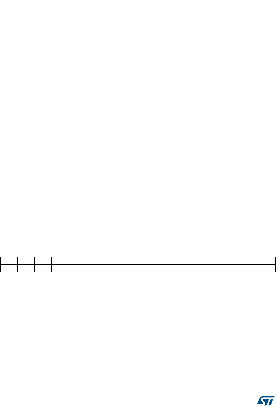
Serial peripheral interface/ inter-IC sound (SPI/I2S) RM0401
724/766 DocID027812 Rev 2
25.7.9 SPI_I2S prescaler register (SPI_I2SPR)
Address offset: 0x20
Reset value: 0000 0010 (0x0002)
Bits 5:4 I2SSTD: I2S standard selection
00: I2S Philips standard.
01: MSB justified standard (left justified)
10: LSB justified standard (right justified)
11: PCM standard
For more details on I2S standards, refer to Section 25.6.2 on page 700. Not used in SPI mode.
Note: For correct operation, these bits should be configured when the I2S is disabled.
Bit 3 CKPOL: Steady state clock polarity
0: I2S clock steady state is low level
1: I2S clock steady state is high level
Note: For correct operation, this bit should be configured when the I2S is disabled.
This bit is not used in SPI mode
Bits 2:1 DATLEN: Data length to be transferred
00: 16-bit data length
01: 24-bit data length
10: 32-bit data length
11: Not allowed
Note: For correct operation, these bits should be configured when the I2S is disabled.
This bit is not used in SPI mode.
Bit 0 CHLEN: Channel length (number of bits per audio channel)
0: 16-bit wide
1: 32-bit wide
The bit write operation has a meaning only if DATLEN = 00 otherwise the channel length is fixed to
32-bit by hardware whatever the value filled in. Not used in SPI mode.
Note: For correct operation, this bit should be configured when the I2S is disabled.
15 14 13 12 11 10 9 8 7 6 5 4 3 2 1 0
Res. Res. Res. Res. Res. Res. MCKOE ODD I2SDIV
rw rw rw
Bits 15:10 Reserved, must be kept at reset value.

DocID027812 Rev 2 725/766
RM0401 Serial peripheral interface/ inter-IC sound (SPI/I2S)
726
Bit 9 MCKOE: Master clock output enable
0: Master clock output is disabled
1: Master clock output is enabled
Note: This bit should be configured when the I2S is disabled. It is used only when the I2S is in master
mode.
This bit is not used in SPI mode.
Bit 8 ODD: Odd factor for the prescaler
0: real divider value is = I2SDIV *2
1: real divider value is = (I2SDIV * 2)+1
Refer to Section 25.6.3 on page 707. Not used in SPI mode.
Note: This bit should be configured when the I2S is disabled. It is used only when the I2S is in master
mode.
Bits 7:0 I2SDIV: I2S Linear prescaler
I2SDIV [7:0] = 0 or I2SDIV [7:0] = 1 are forbidden values.
Refer to Section 25.6.3 on page 707. Not used in SPI mode.
Note: These bits should be configured when the I2S is disabled. It is used only when the I2S is in
master mode.
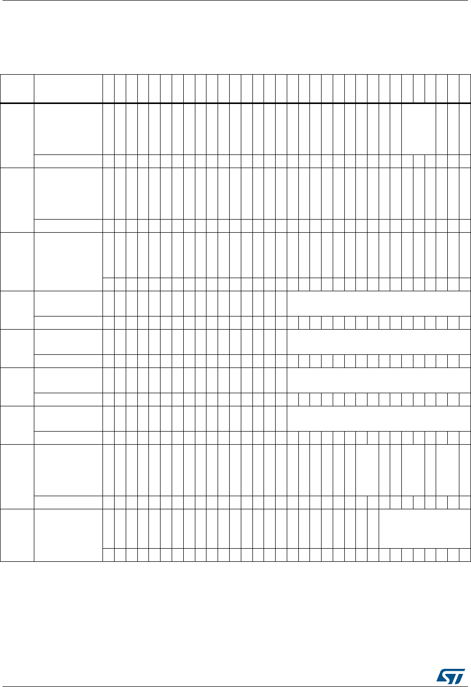
Serial peripheral interface/ inter-IC sound (SPI/I2S) RM0401
726/766 DocID027812 Rev 2
25.7.10 SPI register map
The table provides shows the SPI register map and reset values.
Refer to Section 2.2.2 on page 38 for the register boundary addresses.
Table 117. SPI register map and reset values
Offset Register
31
30
29
28
27
26
25
24
23
22
21
20
19
18
17
16
15
14
13
12
11
10
9
8
7
6
5
4
3
2
1
0
0x00 SPI_CR1
Res.
Res.
Res.
Res.
Res.
Res.
Res.
Res.
Res.
Res.
Res.
Res.
Res.
Res.
Res.
Res.
BIDIMODE
BIDIOE
CRCEN
CRCNEXT
DFF
RXONLY
SSM
SSI
LSBFIRST
SPE
BR
[2:0]
MSTR
CPOL
CPHA
Reset value 0000000000000000
0x04 SPI_CR2
Res.
Res.
Res.
Res.
Res.
Res.
Res.
Res.
Res.
Res.
Res.
Res.
Res.
Res.
Res.
Res.
Res.
Res.
Res.
Res.
Res.
Res.
Res.
Res.
TXEIE
RXNEIE
ERRIE
FRF
Res.
SSOE
TXDMAEN
RXDMAEN
Reset value 0 0 0 0 0 0 0
0x08 SPI_SR
Res.
Res.
Res.
Res.
Res.
Res.
Res.
Res.
Res.
Res.
Res.
Res.
Res.
Res.
Res.
Res.
Res.
Res.
Res.
Res.
Res.
Res.
Res.
FRE
BSY
OVR
MODF
CRCERR
UDR
CHSIDE
TXE
RXNE
Reset value 000000010
0x0C SPI_DR
Res.
Res.
Res.
Res.
Res.
Res.
Res.
Res.
Res.
Res.
Res.
Res.
Res.
Res.
Res.
Res.
DR[15:0]
Reset value 0000000000000000
0x10 SPI_CRCPR
Res.
Res.
Res.
Res.
Res.
Res.
Res.
Res.
Res.
Res.
Res.
Res.
Res.
Res.
Res.
Res.
CRCPOLY[15:0]
Reset value 0000000000000111
0x14 SPI_RXCRCR
Res.
Res.
Res.
Res.
Res.
Res.
Res.
Res.
Res.
Res.
Res.
Res.
Res.
Res.
Res.
Res.
RxCRC[15:0]
Reset value 0000000000000000
0x18 SPI_TXCRCR
Res.
Res.
Res.
Res.
Res.
Res.
Res.
Res.
Res.
Res.
Res.
Res.
Res.
Res.
Res.
Res.
TxCRC[15:0]
Reset value 0000000000000000
0x1C SPI_I2SCFGR
Res.
Res.
Res.
Res.
Res.
Res.
Res.
Res.
Res.
Res.
Res.
Res.
Res.
Res.
Res.
Res.
Res.
Res.
Res.
ASTREN
I2SMOD
I2SE
I2SCFG
PCMSYNC
Res.
I2SSTD
CKPOL
DATLEN
CHLEN
Reset value 000000 000000
0x20 SPI_I2SPR
Res.
Res.
Res.
Res.
Res.
Res.
Res.
Res.
Res.
Res.
Res.
Res.
Res.
Res.
Res.
Res.
Res.
Res.
Res.
Res.
Res.
Res.
MCKOE
ODD
I2SDIV
Reset value 0000000010
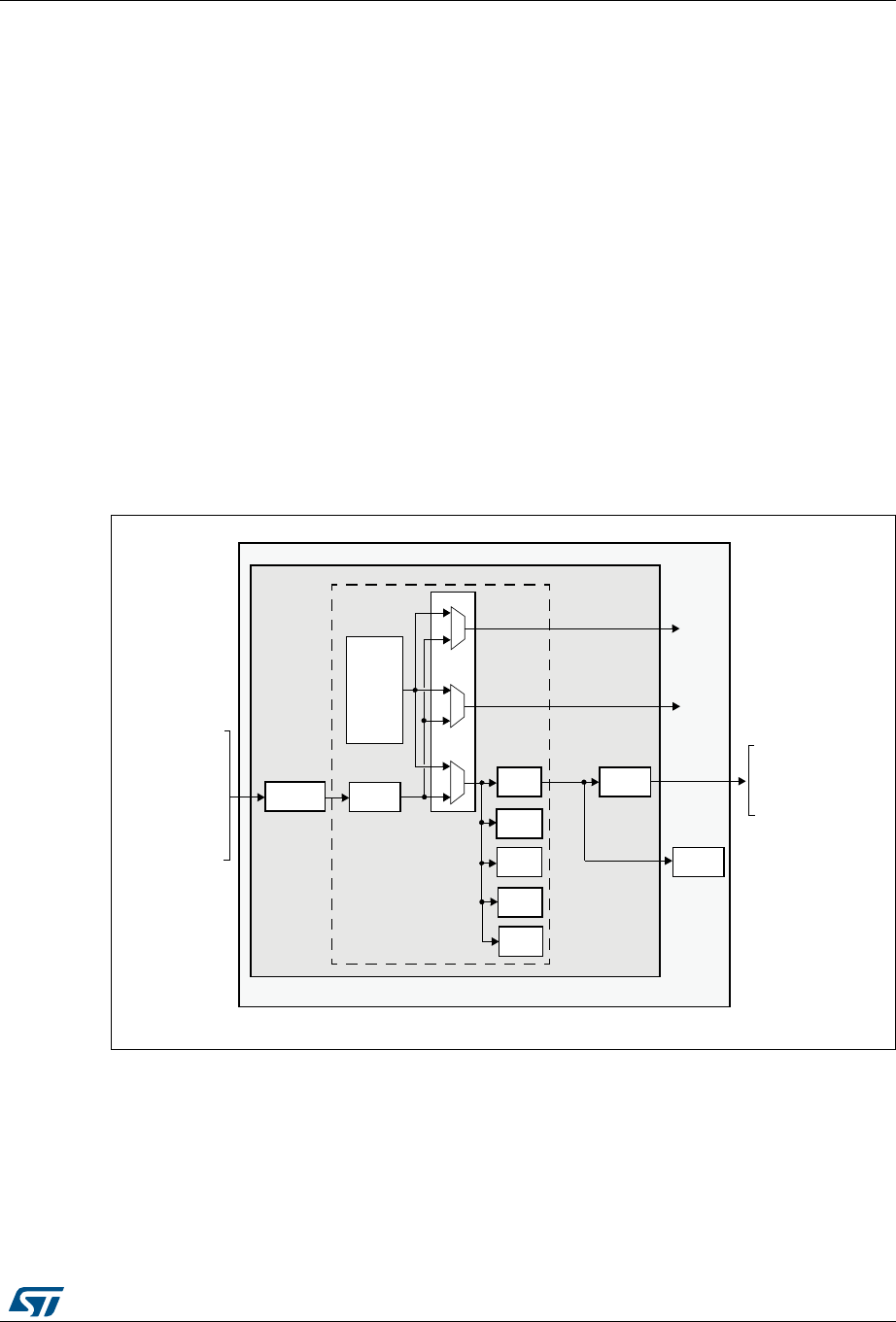
DocID027812 Rev 2 727/766
RM0401 Debug support (DBG)
757
26 Debug support (DBG)
26.1 Overview
The STM32F410 is built around a Cortex®-M4 with FPU core which contains hardware
extensions for advanced debugging features. The debug extensions allow the core to be
stopped either on a given instruction fetch (breakpoint) or data access (watchpoint). When
stopped, the core’s internal state and the system’s external state may be examined. Once
examination is complete, the core and the system may be restored and program execution
resumed.
The debug features are used by the debugger host when connecting to and debugging the
STM32F410 MCUs.
Two interfaces for debug are available:
•Serial wire
•JTAG debug port
Figure 272. Block diagram of STM32 MCU and Cortex®-M4 with FPU-level
debug support
Note: The debug features embedded in the Cortex®-M4 with FPU core are a subset of the ARM®
CoreSight Design Kit.
ESTRICTED$I
#ORTEX-
CORE
37*$0 !("!0
"RIDGE
.6)#
$74
&0"
)4-
40)5
$#ODE
INTERFACE
3YSTEM
INTERFACE
)NTERNALPRIVATE
PERIPHERALBUS00"
%XTERNALPRIVATE
PERIPHERALBUS00"
"USMATRIX
$ATA
4R A CE PO R T
$"'-#5
34-&XXDEBUGSUPPORT
#ORTEX-DEBUGSUPPORT
*4-3
*4$)
*4$/
.*4234
*4#+
37$)/
37#,+
42!#%37/
42!#%37/
42!#%#+
42!#%$;=
-36

Debug support (DBG) RM0401
728/766 DocID027812 Rev 2
The ARM® Cortex®-M4 with FPU core provides integrated on-chip debug support. It is
comprised of:
•SWJ-DP: Serial wire / JTAG debug port
•AHP-AP: AHB access port
•ITM: Instrumentation trace macrocell
•FPB: Flash patch breakpoint
•DWT: Data watchpoint trigger
•TPUI: Trace port unit interface (available on larger packages, where the corresponding
pins are mapped)
•ETM: Embedded Trace Macrocell (available on larger packages, where the
corresponding pins are mapped)
It also includes debug features dedicated to the STM32F410:
•Flexible debug pinout assignment
•MCU debug box (support for low-power modes, control over peripheral clocks, etc.)
Note: For further information on debug functionality supported by the ARM® Cortex®-M4 with FPU
core, refer to the Cortex®-M4 with FPU-r0p1 Technical Reference Manual and to the
CoreSight Design Kit-r0p1 TRM (see Section 26.2: Reference ARM® documentation).
26.2 Reference ARM® documentation
•Cortex®-M4 with FPU r0p1 Technical Reference Manual (TRM)
(see Related documents on page 1)
•ARM® Debug Interface V5
•ARM® CoreSight Design Kit revision r0p1 Technical Reference Manual
26.3 SWJ debug port (serial wire and JTAG)
The STM32F410 core of the integrates the Serial Wire / JTAG Debug Port (SWJ-DP). It is
an ARM® standard CoreSight debug port that combines a JTAG-DP (5-pin) interface and a
SW-DP (2-pin) interface.
•The JTAG Debug Port (JTAG-DP) provides a 5-pin standard JTAG interface to the
AHP-AP port.
•The Serial Wire Debug Port (SW-DP) provides a 2-pin (clock + data) interface to the
AHP-AP port.
In the SWJ-DP, the two JTAG pins of the SW-DP are multiplexed with some of the five JTAG
pins of the JTAG-DP.
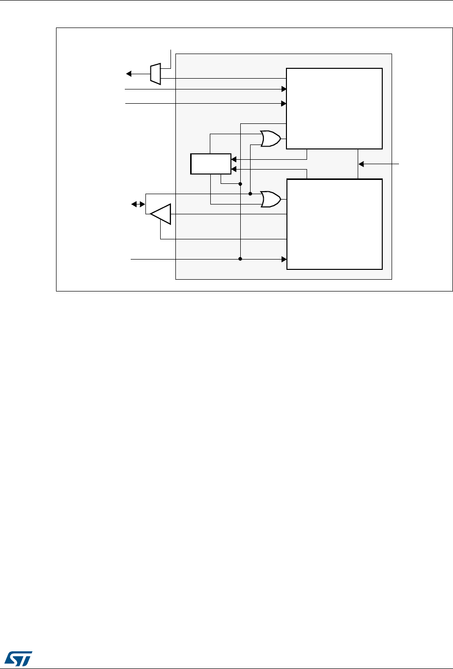
DocID027812 Rev 2 729/766
RM0401 Debug support (DBG)
757
Figure 273. SWJ debug port
Figure 273 shows that the asynchronous TRACE output (TRACESWO) is multiplexed with
TDO. This means that the asynchronous trace can only be used with SW-DP, not JTAG-DP.
26.3.1 Mechanism to select the JTAG-DP or the SW-DP
By default, the JTAG-Debug Port is active.
If the debugger host wants to switch to the SW-DP, it must provide a dedicated JTAG
sequence on TMS/TCK (respectively mapped to SWDIO and SWCLK) which disables the
JTAG-DP and enables the SW-DP. This way it is possible to activate the SWDP using only
the SWCLK and SWDIO pins.
This sequence is:
1. Send more than 50 TCK cycles with TMS (SWDIO) =1
2. Send the 16-bit sequence on TMS (SWDIO) = 0111100111100111 (MSB transmitted
first)
3. Send more than 50 TCK cycles with TMS (SWDIO) =1
26.4 Pinout and debug port pins
The STM32F410 MCUs are available in various packages with different numbers of
available pins. As a result, some functionality (ETM) related to pin availability may differ
between packages.
TRACESWO
JTDO
JTDI
NJTRST nTRST
TDI
TDO
SWJ-DP
TDO
TDI
nTRST
TCK
TMS nPOTRST
JTAG-DP
nPOTRST
From
power-on
reset
DBGRESETn
DBGDI
DBGDO
DBGDOEN
DBGCLK
SW-DP
SWCLKTCK
SWDOEN
SWDO
SWDITMS
SWD/JTAG
select
JTMS/SWDIO
JTCK/SWCLK
(asynchronous trace)
ai17139
Debug support (DBG) RM0401
730/766 DocID027812 Rev 2
26.4.1 SWJ debug port pins
Five pins are used as outputs from the STM32F410 for the SWJ-DP as alternate functions
of general-purpose I/Os. These pins are available on all packages.
26.4.2 Flexible SWJ-DP pin assignment
After RESET (SYSRESETn or PORESETn), all five pins used for the SWJ-DP are assigned
as dedicated pins immediately usable by the debugger host (note that the trace outputs are
not assigned except if explicitly programmed by the debugger host).
However, the STM32F410 MCUs offers the possibility of disabling some or all of the SWJ-
DP ports and so, of releasing the associated pins for general-purpose IO (GPIO) usage. For
more details on how to disable SWJ-DP port pins, please refer to Section 6.3.2: I/O pin
multiplexer and mapping.
.
Note: When the APB bridge write buffer is full, it takes one extra APB cycle when writing the
GPIO_AFR register. This is because the deactivation of the JTAGSW pins is done in two
cycles to guarantee a clean level on the nTRST and TCK input signals of the core.
•Cycle 1: the JTAGSW input signals to the core are tied to 1 or 0 (to 1 for nTRST, TDI
and TMS, to 0 for TCK)
•Cycle 2: the GPIO controller takes the control signals of the SWJTAG IO pins (like
controls of direction, pull-up/down, Schmitt trigger activation, etc.).
Table 118. SWJ debug port pins
SWJ-DP pin name
JTAG debug port SW debug port Pin
assign
ment
Type Description Type Debug assignment
JTMS/SWDIO I JTAG Test Mode
Selection IO Serial Wire Data
Input/Output PA13
JTCK/SWCLK I JTAG Test Clock I Serial Wire Clock PA14
JTDI I JTAG Test Data Input - - PA15
JTDO/TRACESWO O JTAG Test Data Output - TRACESWO if async trace
is enabled PB3
NJTRST I JTAG Test nReset - - PB4
Table 119. Flexible SWJ-DP pin assignment
Available debug ports
SWJ IO pin assigned
PA13 /
JTMS /
SWDIO
PA14 /
JTCK /
SWCLK
PA15 /
JTDI
PB3 /
JTDO
PB4 /
NJTRST
Full SWJ (JTAG-DP + SW-DP) - Reset State X X X X X
Full SWJ (JTAG-DP + SW-DP) but without NJTRST X X X X
JTAG-DP Disabled and SW-DP Enabled X X
JTAG-DP Disabled and SW-DP Disabled Released

DocID027812 Rev 2 731/766
RM0401 Debug support (DBG)
757
26.4.3 Internal pull-up and pull-down on JTAG pins
It is necessary to ensure that the JTAG input pins are not floating since they are directly
connected to flip-flops to control the debug mode features. Special care must be taken with
the SWCLK/TCK pin which is directly connected to the clock of some of these flip-flops.
To avoid any uncontrolled IO levels, the devices embed internal pull-ups and pull-downs on
the JTAG input pins:
•NJTRST: Internal pull-up
•JTDI: Internal pull-up
•JTMS/SWDIO: Internal pull-up
•TCK/SWCLK: Internal pull-down
Once a JTAG IO is released by the user software, the GPIO controller takes control again.
The reset states of the GPIO control registers put the I/Os in the equivalent state:
•NJTRST: AF input pull-up
•JTDI: AF input pull-up
•JTMS/SWDIO: AF input pull-up
•JTCK/SWCLK: AF input pull-down
•JTDO: AF output floating
The software can then use these I/Os as standard GPIOs.
Note: The JTAG IEEE standard recommends to add pull-ups on TDI, TMS and nTRST but there is
no special recommendation for TCK. However, for TCK, the devices needs an integrated
pull-down.
Having embedded pull-ups and pull-downs removes the need to add external resistors.

Debug support (DBG) RM0401
732/766 DocID027812 Rev 2
26.4.4 Using serial wire and releasing the unused debug pins as GPIOs
To use the serial wire DP to release some GPIOs, the user software must change the GPIO
(PA15, PB3 and PB4) configuration mode in the GPIO_MODER register. This releases
PA15, PB3 and PB4 which now become available as GPIOs.
When debugging, the host performs the following actions:
•Under system reset, all SWJ pins are assigned (JTAG-DP + SW-DP).
•Under system reset, the debugger host sends the JTAG sequence to switch from the
JTAG-DP to the SW-DP.
•Still under system reset, the debugger sets a breakpoint on vector reset.
•The system reset is released and the Core halts.
•All the debug communications from this point are done using the SW-DP. The other
JTAG pins can then be reassigned as GPIOs by the user software.
Note: For user software designs, note that:
To release the debug pins, remember that they will be first configured either in input-pull-up
(nTRST, TMS, TDI) or pull-down (TCK) or output tristate (TDO) for a certain duration after
reset until the instant when the user software releases the pins.
When debug pins (JTAG or SW or TRACE) are mapped, changing the corresponding IO pin
configuration in the IOPORT controller has no effect.
26.5 JTAG TAP connection
The MCUs integrate two serially connected JTAG TAPs, the boundary scan TAP (IR is 5-bit
wide) and the Cortex®-M4 with FPU TAP (IR is 4-bit wide).
To access the TAP of the Cortex®-M4 with FPU for debug purposes:
1. First, it is necessary to shift the BYPASS instruction of the boundary scan TAP.
2. Then, for each IR shift, the scan chain contains 9 bits (=5+4) and the unused TAP
instruction must be shifted in using the BYPASS instruction.
3. For each data shift, the unused TAP, which is in BYPASS mode, adds 1 extra data bit in
the data scan chain.
Note: Important: Once Serial-Wire is selected using the dedicated ARM® JTAG sequence, the
boundary scan TAP is automatically disabled (JTMS forced high).
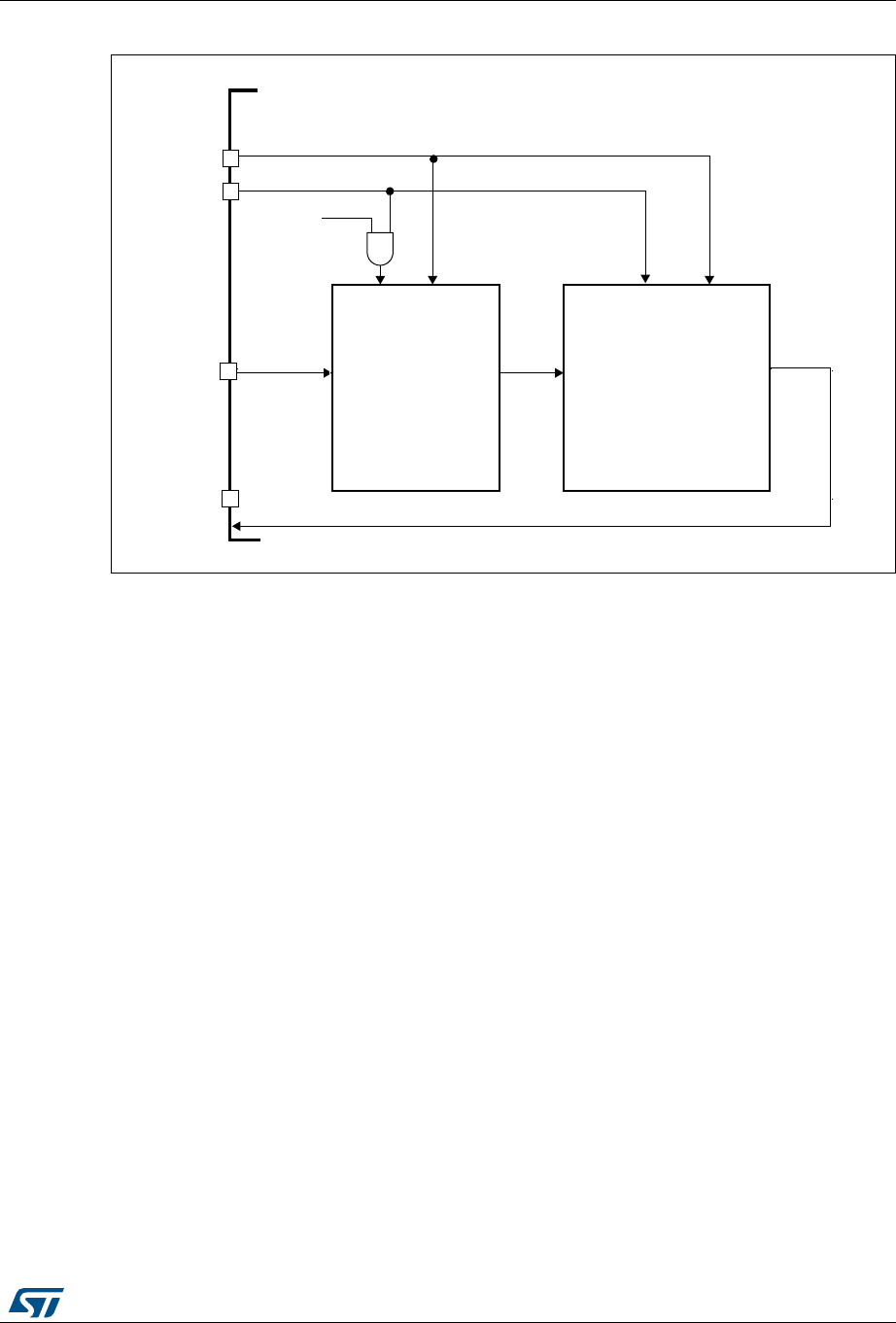
DocID027812 Rev 2 733/766
RM0401 Debug support (DBG)
757
Figure 274. JTAG TAP connections
"OUNDARYSCAN
4!0
.*4234
#ORTEX-4!0
*4-3
4-3 N42344-3 N4234
*4$)
*4$/
4$) 4$/ 4$) 4$/
37$0
34-&XXX
3ELECTED
)2ISBITWIDE )2ISBITWIDE
-36
Debug support (DBG) RM0401
734/766 DocID027812 Rev 2
26.6 ID codes and locking mechanism
There are several ID codes inside the MCUs. ST strongly recommends tools designers to
lock their debuggers using the MCU DEVICE ID code located in the external PPB memory
map at address 0xE0042000.
26.6.1 MCU device ID code
The MCUs integrate an MCU ID code. This ID identifies the ST MCU part-number and the
die revision. It is part of the DBG_MCU component and is mapped on the external PPB bus
(see Section 26.16 on page 746). This code is accessible using the JTAG debug port (4 to 5
pins) or the SW debug port (two pins) or by the user software. It is even accessible while the
MCU is under system reset.
Only the DEV_ID(11:0) should be used for identification by the debugger/programmer tools.
DBGMCU_IDCODE
Address: 0xE004 2000
Only 32-bits access supported. Read-only.
26.6.2 Boundary scan TAP
JTAG ID code
The TAP of the BSC (boundary scan) integrates a JTAG ID code equal to: 0x0645 8041
26.6.3 Cortex®-M4 with FPU TAP
The TAP of the ARM® Cortex®-M4 with FPU integrates a JTAG ID code. This ID code is the
ARM® default one and has not been modified. This code is only accessible by the JTAG
Debug Port.
This code is 0x4BA0 0477 (corresponds to Cortex®-M4 with FPU r0p1, see Section 26.2:
Reference ARM® documentation).
31 30 29 28 27 26 25 24 23 22 21 20 19 18 17 16
REV_ID
rrrrrr r r r r rrrrrr
1514131211109876543210
Res. Res. Res. Res. DEV_ID
rrrrrrrrrrrr
Bits 31:16 REV_ID(15:0) Revision identifier
This field indicates the revision of the device:
0x1000 = Revision A
Bits 15:12 Reserved, must be kept at reset value.
Bits 11:0 DEV_ID(11:0): Device identifier
The device ID is 0x458

DocID027812 Rev 2 735/766
RM0401 Debug support (DBG)
757
26.6.4 Cortex®-M4 with FPU JEDEC-106 ID code
The ARM® Cortex®-M4 with FPU integrates a JEDEC-106 ID code. It is located in the 4KB
ROM table mapped on the internal PPB bus at address 0xE00F FFD0_0xE00F FFE0.
This code is accessible by the JTAG Debug Port (4 to 5 pins) or by the SW Debug Port (two
pins) or by the user software.
26.7 JTAG debug port
A standard JTAG state machine is implemented with a 4-bit instruction register (IR) and five
data registers (for full details, refer to the Cortex®-M4 with FPUr0p1 Technical Reference
Manual (TRM), for references, please see Section 26.2: Reference ARM® documentation).
Table 120. JTAG debug port data registers
IR(3:0) Data register Details
1111 BYPASS
[1 bit]
1110 IDCODE
[32 bits]
ID CODE
0x4BA0 0477 (ARM® Cortex®-M4 with FPU r0p1 ID Code)
1010 DPACC
[35 bits]
Debug port access register
This initiates a debug port and allows access to a debug port register.
– When transferring data IN:
Bits 34:3 = DATA[31:0] = 32-bit data to transfer for a write request
Bits 2:1 = A[3:2] = 2-bit address of a debug port register.
Bit 0 = RnW = Read request (1) or write request (0).
– When transferring data OUT:
Bits 34:3 = DATA[31:0] = 32-bit data which is read following a read
request
Bits 2:0 = ACK[2:0] = 3-bit Acknowledge:
010 = OK/FAULT
001 = WAIT
OTHER = reserved
Refer to Table 121 for a description of the A[3:2] bits

Debug support (DBG) RM0401
736/766 DocID027812 Rev 2
1011 APACC
[35 bits]
Access port access register
Initiates an access port and allows access to an access port register.
– When transferring data IN:
Bits 34:3 = DATA[31:0] = 32-bit data to shift in for a write request
Bits 2:1 = A[3:2] = 2-bit address (sub-address AP registers).
Bit 0 = RnW= Read request (1) or write request (0).
– When transferring data OUT:
Bits 34:3 = DATA[31:0] = 32-bit data which is read following a read
request
Bits 2:0 = ACK[2:0] = 3-bit Acknowledge:
010 = OK/FAULT
001 = WAIT
OTHER = reserved
There are many AP Registers (see AHB-AP) addressed as the
combination of:
– The shifted value A[3:2]
– The current value of the DP SELECT register
1000 ABORT
[35 bits]
Abort register
– Bits 31:1 = Reserved
– Bit 0 = DAPABORT: write 1 to generate a DAP abort.
Table 121. 32-bit debug port registers addressed through the shifted value A[3:2]
Address A[3:2] value Description
0x0 00 Reserved, must be kept at reset value.
0x4 01
DP CTRL/STAT register. Used to:
– Request a system or debug power-up
– Configure the transfer operation for AP accesses
– Control the pushed compare and pushed verify operations.
– Read some status flags (overrun, power-up acknowledges)
0x8 10
DP SELECT register: Used to select the current access port and the
active 4-words register window.
– Bits 31:24: APSEL: select the current AP
– Bits 23:8: reserved
– Bits 7:4: APBANKSEL: select the active 4-words register window on the
current AP
– Bits 3:0: reserved
0xC 11
DP RDBUFF register: Used to allow the debugger to get the final result
after a sequence of operations (without requesting new JTAG-DP
operation)
Table 120. JTAG debug port data registers (continued)
IR(3:0) Data register Details

DocID027812 Rev 2 737/766
RM0401 Debug support (DBG)
757
26.8 SW debug port
26.8.1 SW protocol introduction
This synchronous serial protocol uses two pins:
•SWCLK: clock from host to target
•SWDIO: bidirectional
The protocol allows two banks of registers (DPACC registers and APACC registers) to be
read and written to.
Bits are transferred LSB-first on the wire.
For SWDIO bidirectional management, the line must be pulled-up on the board (100 KΩ
recommended by ARM®).
Each time the direction of SWDIO changes in the protocol, a turnaround time is inserted
where the line is not driven by the host nor the target. By default, this turnaround time is one
bit time, however this can be adjusted by configuring the SWCLK frequency.
26.8.2 SW protocol sequence
Each sequence consist of three phases:
1. Packet request (8 bits) transmitted by the host
2. Acknowledge response (3 bits) transmitted by the target
3. Data transfer phase (33 bits) transmitted by the host or the target
Refer to the Cortex®-M4 with FPU r0p1 TRM for a detailed description of DPACC and
APACC registers.
The packet request is always followed by the turnaround time (default 1 bit) where neither
the host nor target drive the line.
Table 122. Packet request (8-bits)
Bit Name Description
0 Start Must be “1”
1 APnDP 0: DP Access
1: AP Access
2RnW 0: Write Request
1: Read Request
4:3 A[3:2] Address field of the DP or AP registers (refer to Table 121)
5 Parity Single bit parity of preceding bits
6Stop 0
7Park Not driven by the host. Must be read as “1” by the target because of
the pull-up

Debug support (DBG) RM0401
738/766 DocID027812 Rev 2
The ACK Response must be followed by a turnaround time only if it is a READ transaction
or if a WAIT or FAULT acknowledge has been received.
The DATA transfer must be followed by a turnaround time only if it is a READ transaction.
26.8.3 SW-DP state machine (reset, idle states, ID code)
The State Machine of the SW-DP has an internal ID code which identifies the SW-DP. It
follows the JEP-106 standard. This ID code is the default ARM® one and is set to
0x2BA01477 (corresponding to Cortex®-M4 with FPU r0p1).
Note: Note that the SW-DP state machine is inactive until the target reads this ID code.
•The SW-DP state machine is in RESET STATE either after power-on reset, or after the
DP has switched from JTAG to SWD or after the line is high for more than 50 cycles
•The SW-DP state machine is in IDLE STATE if the line is low for at least two cycles
after RESET state.
•After RESET state, it is mandatory to first enter into an IDLE state AND to perform a
READ access of the DP-SW ID CODE register. Otherwise, the target will issue a
FAULT acknowledge response on another transactions.
Further details of the SW-DP state machine can be found in the Cortex®-M4 with FPU r0p1
TRM and the CoreSight Design Kit r0p1 TRM.
26.8.4 DP and AP read/write accesses
•Read accesses to the DP are not posted: the target response can be immediate (if
ACK=OK) or can be delayed (if ACK=WAIT).
•Read accesses to the AP are posted. This means that the result of the access is
returned on the next transfer. If the next access to be done is NOT an AP access, then
the DP-RDBUFF register must be read to obtain the result.
The READOK flag of the DP-CTRL/STAT register is updated on every AP read access
or RDBUFF read request to know if the AP read access was successful.
•The SW-DP implements a write buffer (for both DP or AP writes), that enables it to
accept a write operation even when other transactions are still outstanding. If the write
buffer is full, the target acknowledge response is “WAIT”. With the exception of
Table 123. ACK response (3 bits)
Bit Name Description
0..2 ACK
001: FAULT
010: WAIT
100: OK
Table 124. DATA transfer (33 bits)
Bit Name Description
0..31 WDATA or RDATA Write or Read data
32 Parity Single parity of the 32 data bits

DocID027812 Rev 2 739/766
RM0401 Debug support (DBG)
757
IDCODE read or CTRL/STAT read or ABORT write which are accepted even if the write
buffer is full.
•Because of the asynchronous clock domains SWCLK and HCLK, two extra SWCLK
cycles are needed after a write transaction (after the parity bit) to make the write
effective internally. These cycles should be applied while driving the line low (IDLE
state)
This is particularly important when writing the CTRL/STAT for a power-up request. If the
next transaction (requiring a power-up) occurs immediately, it will fail.
26.8.5 SW-DP registers
Access to these registers are initiated when APnDP=0
Table 125. SW-DP registers
A[3:2] R/W
CTRLSEL bit
of SELECT
register
Register Notes
00 Read - IDCODE The manufacturer code is not set to ST
code. 0x2BA01477 (identifies the SW-DP)
00 Write - ABORT -
01 Read/Write 0 DP-
CTRL/STAT
Purpose is to:
– request a system or debug power-up
– configure the transfer operation for AP
accesses
– control the pushed compare and pushed
verify operations.
– read some status flags (overrun, power-
up acknowledges)
01 Read/Write 1 WIRE
CONTROL
Purpose is to configure the physical serial
port protocol (like the duration of the
turnaround time)
10 Read READ
RESEND
Enables recovery of the read data from a
corrupted debugger transfer, without
repeating the original AP transfer.
10 Write SELECT The purpose is to select the current access
port and the active 4-words register window
11 Read/Write READ
BUFFER
This read buffer is useful because AP
accesses are posted (the result of a read AP
request is available on the next AP
transaction).
This read buffer captures data from the AP,
presented as the result of a previous read,
without initiating a new transaction

Debug support (DBG) RM0401
740/766 DocID027812 Rev 2
26.8.6 SW-AP registers
Access to these registers are initiated when APnDP=1
There are many AP Registers (see AHB-AP) addressed as the combination of:
•The shifted value A[3:2]
•The current value of the DP SELECT register
26.9 AHB-AP (AHB access port) - valid for both JTAG-DP
and SW-DP
Features:
•System access is independent of the processor status.
•Either SW-DP or JTAG-DP accesses AHB-AP.
•The AHB-AP is an AHB master into the Bus Matrix. Consequently, it can access all the
data buses (Dcode Bus, System Bus, internal and external PPB bus) but the ICode
bus.
•Bitband transactions are supported.
•AHB-AP transactions bypass the FPB.
The address of the 32-bits AHP-AP resisters are 6-bits wide (up to 64 words or 256 bytes)
and consists of:
d) Bits [7:4] = the bits [7:4] APBANKSEL of the DP SELECT register
e) Bits [3:2] = the 2 address bits of A[3:2] of the 35-bit packet request for SW-DP.
The AHB-AP of the Cortex®-M4 with FPU includes 9 x 32-bits registers:
Refer to the Cortex®-M4 with FPU r0p1 TRM for further details.
Table 126. Cortex®-M4 with FPU AHB-AP registers
Address
offset Register name Notes
0x00 AHB-AP Control and Status
Word
Configures and controls transfers through the AHB
interface (size, hprot, status on current transfer, address
increment type
0x04 AHB-AP Transfer Address -
0x0C AHB-AP Data Read/Write -
0x10 AHB-AP Banked Data 0
Directly maps the 4 aligned data words without rewriting
the Transfer Address Register.
0x14 AHB-AP Banked Data 1
0x18 AHB-AP Banked Data 2
0x1C AHB-AP Banked Data 3
0xF8 AHB-AP Debug ROM Address Base Address of the debug interface
0xFC AHB-AP ID Register -

DocID027812 Rev 2 741/766
RM0401 Debug support (DBG)
757
26.10 Core debug
Core debug is accessed through the core debug registers. Debug access to these registers
is by means of the Advanced High-performance Bus (AHB-AP) port. The processor can
access these registers directly over the internal Private Peripheral Bus (PPB).
It consists of 4 registers:
Note: Important: these registers are not reset by a system reset. They are only reset by a power-
on reset.
Refer to the Cortex®-M4 with FPU r0p1 TRM for further details.
To Halt on reset, it is necessary to:
•enable the bit0 (VC_CORRESET) of the Debug and Exception Monitor Control
Register
•enable the bit0 (C_DEBUGEN) of the Debug Halting Control and Status Register.
Table 127. Core debug registers
Register Description
DHCSR
The 32-bit Debug Halting Control and Status Register
This provides status information about the state of the processor enable core debug
halt and step the processor
DCRSR The 17-bit Debug Core Register Selector Register:
This selects the processor register to transfer data to or from.
DCRDR
The 32-bit Debug Core Register Data Register:
This holds data for reading and writing registers to and from the processor selected
by the DCRSR (Selector) register.
DEMCR
The 32-bit Debug Exception and Monitor Control Register:
This provides Vector Catching and Debug Monitor Control. This register contains a
bit named TRCENA which enable the use of a TRACE.

Debug support (DBG) RM0401
742/766 DocID027812 Rev 2
26.11 Capability of the debugger host to connect under system
reset
The reset system of the MCUs comprises the following reset sources:
•POR (power-on reset) which asserts a RESET at each power-up.
•Internal watchdog reset
•Software reset
•External reset
The Cortex®-M4 with FPU differentiates the reset of the debug part (generally
PORRESETn) and the other one (SYSRESETn)
This way, it is possible for the debugger to connect under System Reset, programming the
Core Debug Registers to halt the core when fetching the reset vector. Then the host can
release the system reset and the core will immediately halt without having executed any
instructions. In addition, it is possible to program any debug features under System Reset.
Note: It is highly recommended for the debugger host to connect (set a breakpoint in the reset
vector) under system reset.
26.12 FPB (Flash patch breakpoint)
The FPB unit:
•implements hardware breakpoints
•patches code and data from code space to system space. This feature gives the
possibility to correct software bugs located in the Code Memory Space.
The use of a Software Patch or a Hardware Breakpoint is exclusive.
The FPB consists of:
•2 literal comparators for matching against literal loads from Code Space and remapping
to a corresponding area in the System Space.
•6 instruction comparators for matching against instruction fetches from Code Space.
They can be used either to remap to a corresponding area in the System Space or to
generate a Breakpoint Instruction to the core.

DocID027812 Rev 2 743/766
RM0401 Debug support (DBG)
757
26.13 DWT (data watchpoint trigger)
The DWT unit consists of four comparators. They are configurable as:
•a hardware watchpoint or
•a trigger to an ETM or
•a PC sampler or
•a data address sampler
The DWT also provides some means to give some profiling informations. For this, some
counters are accessible to give the number of:
•Clock cycle
•Folded instructions
•Load store unit (LSU) operations
•Sleep cycles
•CPI (clock per instructions)
•Interrupt overhead
26.14 ITM (instrumentation trace macrocell)
26.14.1 General description
The ITM is an application-driven trace source that supports printf style debugging to trace
Operating System (OS) and application events, and emits diagnostic system information.
The ITM emits trace information as packets which can be generated as:
•Software trace. Software can write directly to the ITM stimulus registers to emit
packets.
•Hardware trace. The DWT generates these packets, and the ITM emits them.
•Time stamping. Timestamps are emitted relative to packets. The ITM contains a 21-bit
counter to generate the timestamp. The Cortex®-M4 with FPU clock or the bit clock rate
of the Serial Wire Viewer (SWV) output clocks the counter.
The packets emitted by the ITM are output to the TPIU (Trace Port Interface Unit). The
formatter of the TPIU adds some extra packets (refer to TPIU) and then output the complete
packets sequence to the debugger host.
The bit TRCEN of the Debug Exception and Monitor Control Register must be enabled
before you program or use the ITM.
26.14.2 Time stamp packets, synchronization and overflow packets
Time stamp packets encode time stamp information, generic control and synchronization. It
uses a 21-bit timestamp counter (with possible prescalers) which is reset at each time
stamp packet emission. This counter can be either clocked by the CPU clock or the SWV
clock.
A synchronization packet consists of 6 bytes equal to 0x80_00_00_00_00_00 which is
emitted to the TPIU as 00 00 00 00 00 80 (LSB emitted first).
A synchronization packet is a timestamp packet control. It is emitted at each DWT trigger.

Debug support (DBG) RM0401
744/766 DocID027812 Rev 2
For this, the DWT must be configured to trigger the ITM: the bit CYCCNTENA (bit0) of the
DWT Control Register must be set. In addition, the bit2 (SYNCENA) of the ITM Trace
Control Register must be set.
Note: If the SYNENA bit is not set, the DWT generates Synchronization triggers to the TPIU which
will send only TPIU synchronization packets and not ITM synchronization packets.
An overflow packet consists is a special timestamp packets which indicates that data has
been written but the FIFO was full.
Example of configuration
To output a simple value to the TPIU:
•Configure the TPIU and assign TRACE I/Os by configuring the DBGMCU_CR (refer to
Section 26.17.2: TRACE pin assignment and Section 26.16.3: Debug MCU
Table 128. Main ITM registers
Address Register Details
@E0000FB0 ITM lock access Write 0xC5ACCE55 to unlock Write Access to the other ITM
registers
@E0000E80 ITM trace control
Bits 31-24 = Always 0
Bits 23 = Busy
Bits 22-16 = 7-bits ATB ID which identifies the source of the
trace data.
Bits 15-10 = Always 0
Bits 9:8 = TSPrescale = Time Stamp Prescaler
Bits 7-5 = Reserved
Bit 4 = SWOENA = Enable SWV behavior (to clock the
timestamp counter by the SWV clock).
Bit 3 = DWTENA: Enable the DWT Stimulus
Bit 2 = SYNCENA: this bit must be to 1 to enable the DWT to
generate synchronization triggers so that the TPIU can then
emit the synchronization packets.
Bit 1 = TSENA (Timestamp Enable)
Bit 0 = ITMENA: Global Enable Bit of the ITM
@E0000E40 ITM trace privilege
Bit 3: mask to enable tracing ports31:24
Bit 2: mask to enable tracing ports23:16
Bit 1: mask to enable tracing ports15:8
Bit 0: mask to enable tracing ports7:0
@E0000E00 ITM trace enable Each bit enables the corresponding Stimulus port to generate
trace.
@E0000000-
E000007C
Stimulus port
registers 0-31
Write the 32-bits data on the selected Stimulus Port (32
available) to be traced out.

DocID027812 Rev 2 745/766
RM0401 Debug support (DBG)
757
configuration register)
•Write 0xC5ACCE55 to the ITM Lock Access Register to unlock the write access to the
ITM registers
•Write 0x00010005 to the ITM Trace Control Register to enable the ITM with Sync
enabled and an ATB ID different from 0x00
•Write 0x1 to the ITM Trace Enable Register to enable the Stimulus Port 0
•Write 0x1 to the ITM Trace Privilege Register to unmask stimulus ports 7:0
•Write the value to output in the Stimulus Port Register 0: this can be done by software
(using a printf function)
26.15 ETM (Embedded trace macrocell)
26.15.1 General description
The ETM enables the reconstruction of program execution. Data are traced using the Data
Watchpoint and Trace (DWT) component or the Instruction Trace Macrocell (ITM) whereas
instructions are traced using the Embedded Trace Macrocell (ETM).
The ETM transmits information as packets and is triggered by embedded resources. These
resources must be programmed independently and the trigger source is selected using the
Trigger Event Register (0xE0041008). An event could be a simple event (address match
from an address comparator) or a logic equation between 2 events. The trigger source is
one of the fourth comparators of the DWT module, The following events can be monitored:
•Clock cycle matching
•Data address matching
For more informations on the trigger resources refer to Section 26.13: DWT (data
watchpoint trigger).
The packets transmitted by the ETM are output to the TPIU (Trace Port Interface Unit). The
formatter of the TPIU adds some extra packets (refer to Section 26.17: TPIU (trace port
interface unit)) and then outputs the complete packet sequence to the debugger host.
26.15.2 Signal protocol, packet types
This part is described in the chapter 7 ETMv3 Signal Protocol of the ARM® IHI 0014N
document.
26.15.3 Main ETM registers
For more information on registers refer to the chapter 3 of the ARM® IHI 0014N
specification.
Table 129. Main ETM registers
Address Register Details
0xE0041FB0 ETM Lock Access Write 0xC5ACCE55 to unlock the write access to the
other ETM registers.
0xE0041000 ETM Control This register controls the general operation of the ETM,
for instance how tracing is enabled.

Debug support (DBG) RM0401
746/766 DocID027812 Rev 2
26.15.4 Configuration example
To output a simple value to the TPIU:
1. Configure the TPIU and enable the I/IO_TRACEN to assign TRACE I/Os in the debug
configuration register.
2. Write 0xC5ACCE55 to the ETM Lock Access Register to unlock the write access to the
ITM registers
3. Write 0x00001D1E to the control register (configure the trace)
4. Write 0000406F to the Trigger Event register (define the trigger event)
5. Write 0000006F to the Trace Enable Event register (define an event to start/stop)
6. Write 00000001 to the Trace Start/stop register (enable the trace)
7. Write 0000191E to the ETM Control Register (end of configuration).
26.16 MCU debug component (DBGMCU)
The MCU debug component helps the debugger provide support for:
•Low-power modes
•Clock control for timers, watchdog and I2C during a breakpoint
•Control of the trace pins assignment
26.16.1 Debug support for low-power modes
To enter low-power mode, the instruction WFI or WFE must be executed.
The MCU implements several low-power modes which can either deactivate the CPU clock
or reduce the power of the CPU.
The core does not allow FCLK or HCLK to be turned off during a debug session. As these
are required for the debugger connection, during a debug, they must remain active. The
MCU integrates special means to allow the user to debug software in low-power modes.
0xE0041010 ETM Status This register provides information about the current status
of the trace and trigger logic.
0xE0041008 ETM Trigger Event This register defines the event that will control trigger.
0xE004101C ETM Trace Enable
Control This register defines which comparator is selected.
0xE0041020 ETM Trace Enable Event This register defines the trace enabling event.
0xE0041024 ETM Trace Start/Stop This register defines the traces used by the trigger source
to start and stop the trace, respectively.
Table 129. Main ETM registers (continued)
Address Register Details

DocID027812 Rev 2 747/766
RM0401 Debug support (DBG)
757
For this, the debugger host must first set some debug configuration registers to change the
low-power mode behavior:
•In Sleep mode, DBG_SLEEP bit of DBGMCU_CR register must be previously set by
the debugger. This will feed HCLK with the same clock that is provided to FCLK
(system clock previously configured by the software).
•In Stop mode, the bit DBG_STOP must be previously set by the debugger. This will
enable the internal RC oscillator clock to feed FCLK and HCLK in STOP mode.
26.16.2 Debug support for timers, watchdog and I2C
During a breakpoint, it is necessary to choose how the counter of timers and watchdog
should behave:
•They can continue to count inside a breakpoint. This is usually required when a PWM is
controlling a motor, for example.
•They can stop to count inside a breakpoint. This is required for watchdog purposes.
For the I2C, the user can choose to block the SMBUS timeout during a breakpoint.
26.16.3 Debug MCU configuration register
This register allows the configuration of the MCU under DEBUG. This concerns:
•Low-power mode support
•Timer and watchdog counter support
•Trace pin assignment
This DBGMCU_CR is mapped on the External PPB bus at address 0xE0042004
It is asynchronously reset by the PORESET (and not the system reset). It can be written by
the debugger under system reset.
If the debugger host does not support these features, it is still possible for the user software
to write to these registers.
DBGMCU_CR register
Address: 0xE004 2004
Only 32-bit access supported
POR Reset: 0x0000 0000 (not reset by system reset)
31 30 29 28 27 26 25 24 23 22 21 20 19 18 17 16
Res. Res. Res. Res. Res. Res. Res. Res. Res. Res. Res. Res. Res. Res. Res. Res.
15 14 13 12 11 10 9 8 7 6 5 4 3 2 1 0
Res. Res. Res. Res. Res. Res. Res. Res.
TRACE_
MODE
[1:0]
TRACE
_IOENRes. Res.
DBG_
STAND
BY
DBG_
STOP
DBG_
SLEEP
rw rw rw rw rw rw

Debug support (DBG) RM0401
748/766 DocID027812 Rev 2
26.16.4 Debug MCU APB1 freeze register (DBGMCU_APB1_FZ)
The DBGMCU_APB1_FZ register is used to configure the MCU under Debug. It concerns
APB1 peripherals. It is mapped on the external PPB bus at address 0xE004 2008.
The register is asynchronously reset by the POR (and not the system reset). It can be
written by the debugger under system reset.
Address : 0xE004 2008
Only 32-bits access are supported.
Power-on reset (POR): 0x0000 0000 (not reset by system reset)
Bits 31:8 Reserved, must be kept at reset value.
Bits 7:5 TRACE_MODE[1:0] and TRACE_IOEN: Trace pin assignment control
– With TRACE_IOEN=0:
TRACE_MODE=xx: TRACE pins not assigned (default state)
– With TRACE_IOEN=1:
– TRACE_MODE=00: TRACE pin assignment for Asynchronous Mode
– TRACE_MODE=01: TRACE pin assignment for Synchronous Mode with a
TRACEDATA size of 1
– TRACE_MODE=10: TRACE pin assignment for Synchronous Mode with a
TRACEDATA size of 2
– TRACE_MODE=11: TRACE pin assignment for Synchronous Mode with a
TRACEDATA size of 4
Bits 4:3 Reserved, must be kept at reset value.
Bit 2 DBG_STANDBY: Debug Standby mode
0: (FCLK=Off, HCLK=Off) The whole digital part is unpowered.
From software point of view, exiting from Standby is identical than fetching reset vector
(except a few status bit indicated that the MCU is resuming from Standby)
1: (FCLK=On, HCLK=On) In this case, the digital part is not unpowered and FCLK and
HCLK are provided by the internal RC oscillator which remains active. In addition, the MCU
generate a system reset during Standby mode so that exiting from Standby is identical than
fetching from reset
Bit 1 DBG_STOP: Debug Stop mode
0: (FCLK=Off, HCLK=Off) In STOP mode, the clock controller disables all clocks (including
HCLK and FCLK). When exiting from STOP mode, the clock configuration is identical to the
one after RESET (CPU clocked by the 8 MHz internal RC oscillator (HSI)). Consequently,
the software must reprogram the clock controller to enable the PLL, the Xtal, etc.
1: (FCLK=On, HCLK=On) In this case, when entering STOP mode, FCLK and HCLK are
provided by the internal RC oscillator which remains active in STOP mode. When exiting
STOP mode, the software must reprogram the clock controller to enable the PLL, the Xtal,
etc. (in the same way it would do in case of DBG_STOP=0)
Bit 0 DBG_SLEEP: Debug Sleep mode
0: (FCLK=On, HCLK=Off) In Sleep mode, FCLK is clocked by the system clock as
previously configured by the software while HCLK is disabled.
In Sleep mode, the clock controller configuration is not reset and remains in the previously
programmed state. Consequently, when exiting from Sleep mode, the software does not
need to reconfigure the clock controller.
1: (FCLK=On, HCLK=On) In this case, when entering Sleep mode, HCLK is fed by the same
clock that is provided to FCLK (system clock as previously configured by the software).

DocID027812 Rev 2 749/766
RM0401 Debug support (DBG)
757
31 30 29 28 27 26 25 24 23 22 21 20 19 18 17 16
Res. Res. Res. Res. Res. Res. Res.
DBG_I2CFMP_SMBUS_TIMEOUT
Res.
DBG_I2C2_SMBUS_TIMEOUT
DBG_I2C1_SMBUS_TIMEOUT
Res. Res. Res. Res. Res.
rw rw rw
1514131211109876543210
Res. Res. Res.
DBG_IWDG_STOP
DBG_WWDG_STOP
DBG_RTC_STOP
Res. Res. Res. Res. Res.
DBG_TIM6_STOP
DBG_TIM5_STOP
Res. Res. Res.
rw rw rw rw rw
Bits 31:25 Reserved, must be kept at reset value.
Bit 24 DBG_I2CFMP_SMBUS_TIMEOUT: FMPI2C SMBUS timeout mode stopped when Core is
halted
0: Same behavior as in normal mode
1: The SMBUS timeout is frozen
Bit 23 DBG_I2C3_SMBUS_TIMEOUT: SMBUS timeout mode stopped when Core is halted
0: Same behavior as in normal mode
1: The SMBUS timeout is frozen
Bit 22 DBG_I2C2_SMBUS_TIMEOUT: I2C2 SMBUS timeout mode stopped when Core is halted
0: Same behavior as in normal mode
1: The SMBUS timeout is frozen
Bit 21 DBG_I2C1_SMBUS_TIMEOUT: I2C1 SMBUS timeout mode stopped when Core is halted
0: Same behavior as in normal mode
1: The SMBUS timeout is frozen
Bits 20:13 Reserved, must be kept at reset value.
Bit 12 DBG_IWDG_STOP: Debug independent watchdog stopped when core is halted
0: The independent watchdog counter clock continues even if the core is halted
1: The independent watchdog counter clock is stopped when the core is halted
Bit 11 DBG_WWDG_STOP: Debug Window Watchdog stopped when Core is halted
0: The window watchdog counter clock continues even if the core is halted
1: The window watchdog counter clock is stopped when the core is halted
Bit 10 DBG_RTC_STOP: RTC stopped when Core is halted
0: The RTC counter clock continues even if the core is halted
1: The RTC counter clock is stopped when the core is halted
Bits 9:5 Reserved, must be kept at reset value.

Debug support (DBG) RM0401
750/766 DocID027812 Rev 2
26.16.5 Debug MCU APB2 Freeze register (DBGMCU_APB2_FZ)
The DBGMCU_APB2_FZ register is used to configure the MCU under Debug. It concerns
APB2 peripherals.
This register is mapped on the external PPB bus at address 0xE004 200C
It is asynchronously reset by the POR (and not the system reset). It can be written by the
debugger under system reset.
Address: 0xE004 200C
Only 32-bit access is supported.
POR: 0x0000 0000 (not reset by system reset)
Bit 4 DBG_TIM6_STOP: TIM6 counter stopped when core is halted
0: The clock of the involved Timer Counter is fed even if the core is halted
1: The clock of the involved Timer counter is stopped when the core is halted
Bit 3 DBG_TIM5_STOP: TIM5 counter stopped when core is halted
0: The clock of the involved Timer Counter is fed even if the core is halted
1: The clock of the involved Timer counter is stopped when the core is halted
Bits 2:0 Reserved, must be kept at reset value.
31 30 29 28 27 26 25 24 23 22 21 20 19 18 17 16
Res. Res. Res. Res. Res. Res. Res. Res. Res. Res. Res. Res. Res. DBG_TIM11
_STOP Res. DBG_TIM9_
STOP
rw rw
15 14 13 12 11 10 9 8 7 6 5 4 3 2 1 0
Res. Res. Res. Res. Res. Res. Res. Res. Res. Res. Res. Res. Res. Res. Res. DBG_TIM1_
STOP
rw
Bits 31:19 Reserved, must be kept at reset value.
Bit 18 DBG_TIMx_STOP: TIM11 counter stopped when core is halted
0: The clock of the involved Timer Counter is fed even if the core is halted
1: The clock of the involved Timer counter is stopped when the core is halted
Bit 17 Reserved, must be kept at reset value.
Bit 16 DBG_TIM9_STOP: TIM9 counter stopped when core is halted
0: The clock of the involved Timer Counter is fed even if the core is halted
1: The clock of the involved Timer counter is stopped when the core is halted
Bit 0 DBG_TIM1_STOP: TIM1 counter stopped when core is halted
0: The clock of the involved Timer Counter is fed even if the core is halted
1: The clock of the involved Timer counter is stopped when the core is halted
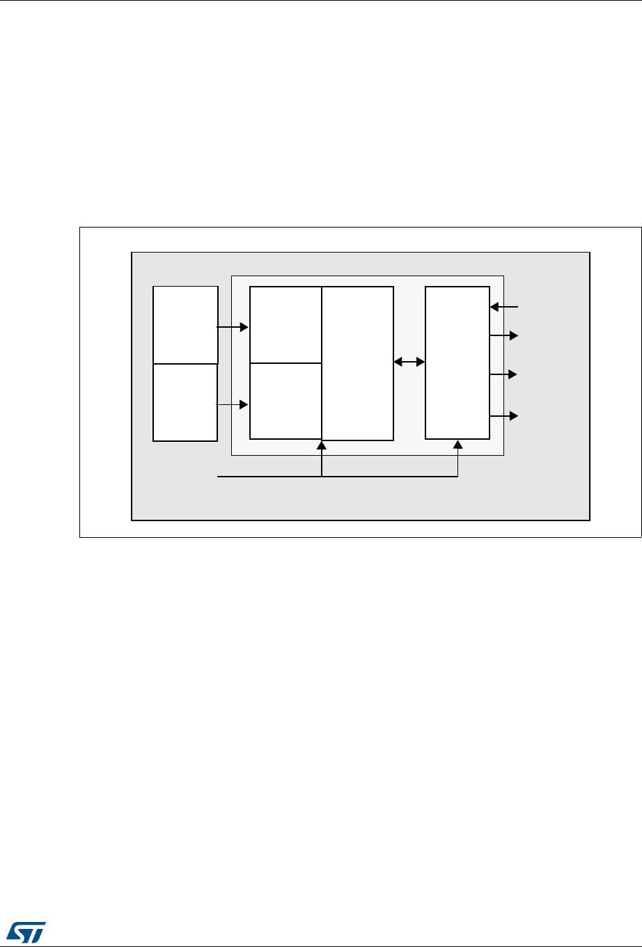
DocID027812 Rev 2 751/766
RM0401 Debug support (DBG)
757
26.17 TPIU (trace port interface unit)
26.17.1 Introduction
The TPIU acts as a bridge between the on-chip trace data from the ITM and the ETM.
The output data stream encapsulates the trace source ID, that is then captured by a trace
port analyzer (TPA).
The core embeds a simple TPIU, especially designed for low-cost debug (consisting of a
special version of the CoreSight TPIU).
Figure 275. TPIU block diagram
formatter
Trace out
(serializer)
TRACECLKIN
TRACECK
TRACEDATA
[3:0]
TRACESWO
CLK domain TRACECLKIN domain
External PPB bus
TPIU
TPIU
Asynchronous
FIFO
Asynchronous
FIFO
ETM
ITM
ai17114
Debug support (DBG) RM0401
752/766 DocID027812 Rev 2
26.17.2 TRACE pin assignment
•Asynchronous mode
The asynchronous mode requires 1 extra pin and is available on all packages. It is only
available if using Serial Wire mode (not in JTAG mode).
•Synchronous mode
The synchronous mode requires from 2 to 6 extra pins depending on the data trace
size and is only available in the larger packages. In addition it is available in JTAG
mode and in Serial Wire mode and provides better bandwidth output capabilities than
asynchronous trace.
TPUI TRACE pin assignment
By default, these pins are NOT assigned. They can be assigned by setting the
TRACE_IOEN and TRACE_MODE bits in the MCU Debug component configuration
register. This configuration has to be done by the debugger host.
In addition, the number of pins to assign depends on the trace configuration (asynchronous
or synchronous).
•Asynchronous mode: 1 extra pin is needed
•Synchronous mode: from 2 to 5 extra pins are needed depending on the size of the
data trace port register (1, 2 or 4):
– TRACECK
– TRACED(0) if port size is configured to 1, 2 or 4
– TRACED(1) if port size is configured to 2 or 4
– TRACED(2) if port size is configured to 4
– TRACED(3) if port size is configured to 4
To assign the TRACE pin, the debugger host must program the bits TRACE_IOEN and
TRACE_MODE[1:0] of the Debug MCU configuration Register (DBGMCU_CR). By default
the TRACE pins are not assigned.
This register is mapped on the external PPB and is reset by the PORESET (and not by the
SYSTEM reset). It can be written by the debugger under SYSTEM reset.
Table 130. Asynchronous TRACE pin assignment
TPUI pin name
Trace synchronous mode
Pin assignment
Type Description
TRACESWO O TRACE Async Data Output PB3
Table 131. Synchronous TRACE pin assignment
TPUI pin name
Trace synchronous mode
Pin assignment
Type Description
TRACECK O TRACE Clock PC6
TRACED[3:0] O TRACE Sync Data Outputs
Can be 1, 2 or 4. PC[10:12], PB11

DocID027812 Rev 2 753/766
RM0401 Debug support (DBG)
757
Note: By default, the TRACECLKIN input clock of the TPIU is tied to GND. It is assigned to HCLK
two clock cycles after the bit TRACE_IOEN has been set.
The debugger must then program the Trace Mode by writing the PROTOCOL[1:0] bits in the
SPP_R (Selected Pin Protocol) register of the TPIU.
•PROTOCOL=00: Trace Port Mode (synchronous)
•PROTOCOL=01 or 10: Serial Wire (Manchester or NRZ) Mode (asynchronous mode).
Default state is 01
It then also configures the TRACE port size by writing the bits [3:0] in the CPSPS_R
(Current Sync Port Size Register) of the TPIU:
•0x1 for 1 pin (default state)
•0x2 for 2 pins
•0x8 for 4 pins
26.17.3 TPUI formatter
The formatter protocol outputs data in 16-byte frames:
•seven bytes of data
•eight bytes of mixed-use bytes consisting of:
– 1 bit (LSB) to indicate it is a DATA byte (‘0) or an ID byte (‘1).
– 7 bits (MSB) which can be data or change of source ID trace.
•one byte of auxiliary bits where each bit corresponds to one of the eight mixed-use
bytes:
– if the corresponding byte was a data, this bit gives bit0 of the data.
– if the corresponding byte was an ID change, this bit indicates when that ID change
takes effect.
Table 132. Flexible TRACE pin assignment
DBGMCU_CR
register
Pins
assigned for:
TRACE IO pin assigned
TRAC
E_IOE
N
TRACE
_MODE
[1:0]
PB3 /JTDO/
TRACESW
O
PC6
TRACEC
K
PC10/
TRACED[0
]
PC11/
TRACED[1
]
PC12/
TRACED[2
]
PB11/
TRACED[3
]
0XX
No Trace
(default state) Released (1) -
100
Asynchronou
s Trace
TRACESW
O- - Released
(usable as GPIO)
101
Synchronous
Trace 1 bit
Released (1)
TRACECK TRACED[0] ---
110
Synchronous
Trace 2 bit TRACECK TRACED[0] TRACED[1] - -
111
Synchronous
Trace 4 bit TRACECK TRACED[0] TRACED[1] TRACED[2] TRACED[3]
1. When Serial Wire mode is used, it is released. But when JTAG is used, it is assigned to JTDO.

Debug support (DBG) RM0401
754/766 DocID027812 Rev 2
Note: Refer to the ARM® CoreSight Architecture Specification v1.0 (ARM® IHI 0029B) for further
information
26.17.4 TPUI frame synchronization packets
The TPUI can generate two types of synchronization packets:
•The Frame Synchronization packet (or Full Word Synchronization packet)
It consists of the word: 0x7F_FF_FF_FF (LSB emitted first). This sequence can not
occur at any other time provided that the ID source code 0x7F has not been used.
It is output periodically between frames.
In continuous mode, the TPA must discard all these frames once a synchronization
frame has been found.
•The Half-Word Synchronization packet
It consists of the half word: 0x7F_FF (LSB emitted first).
It is output periodically between or within frames.
These packets are only generated in continuous mode and enable the TPA to detect
that the TRACE port is in IDLE mode (no TRACE to be captured). When detected by
the TPA, it must be discarded.
26.17.5 Transmission of the synchronization frame packet
There is no Synchronization Counter register implemented in the TPIU of the core.
Consequently, the synchronization trigger can only be generated by the DWT. Refer to the
registers DWT Control Register (bits SYNCTAP[11:10]) and the DWT Current PC Sampler
Cycle Count Register.
The TPUI Frame synchronization packet (0x7F_FF_FF_FF) is emitted:
•after each TPIU reset release. This reset is synchronously released with the rising
edge of the TRACECLKIN clock. This means that this packet is transmitted when the
TRACE_IOEN bit in the DBGMCU_CFG register is set. In this case, the word
0x7F_FF_FF_FF is not followed by any formatted packet.
•at each DWT trigger (assuming DWT has been previously configured). Two cases
occur:
– If the bit SYNENA of the ITM is reset, only the word 0x7F_FF_FF_FF is emitted
without any formatted stream which follows.
– If the bit SYNENA of the ITM is set, then the ITM synchronization packets will
follow (0x80_00_00_00_00_00), formatted by the TPUI (trace source ID added).
26.17.6 Synchronous mode
The trace data output size can be configured to 4, 2 or 1 pin: TRACED(3:0)
The output clock is output to the debugger (TRACECK)
Here, TRACECLKIN is driven internally and is connected to HCLK only when TRACE is
used.
Note: In this synchronous mode, it is not required to provide a stable clock frequency.
The TRACE I/Os (including TRACECK) are driven by the rising edge of TRACLKIN (equal
to HCLK). Consequently, the output frequency of TRACECK is equal to HCLK/2.

DocID027812 Rev 2 755/766
RM0401 Debug support (DBG)
757
26.17.7 Asynchronous mode
This is a low cost alternative to output the trace using only 1 pin: this is the asynchronous
output pin TRACESWO. Obviously there is a limited bandwidth.
TRACESWO is multiplexed with JTDO when using the SW-DP pin. This way, this
functionality is available in all packages.
This asynchronous mode requires a constant frequency for TRACECLKIN. For the standard
UART (NRZ) capture mechanism, 5% accuracy is needed. The Manchester encoded
version is tolerant up to 10%.
26.17.8 TRACECLKIN connection
The TRACECLKIN input is internally connected to HCLK. This means that when in
asynchronous trace mode, the application is restricted to use to time frames where the CPU
frequency is stable.
Note: Important: when using asynchronous trace: it is important to be aware that:
The default clock of the MCUs is the internal RC oscillator. Its frequency under reset is
different from the one after reset release. This is because the RC calibration is the default
one under system reset and is updated at each system reset release.
Consequently, the trace port analyzer (TPA) should not enable the trace (with the
TRACE_IOEN bit) under system reset, because a Synchronization Frame Packet will be
issued with a different bit time than trace packets which will be transmitted after reset
release.
26.17.9 TPIU registers
The TPIU APB registers can be read and written only if the bit TRCENA of the Debug
Exception and Monitor Control Register (DEMCR) is set. Otherwise, the registers are read
as zero (the output of this bit enables the PCLK of the TPIU).
Table 133. Important TPIU registers
Address Register Description
0xE0040004 Current port size
Allows the trace port size to be selected:
Bit 0: Port size = 1
Bit 1: Port size = 2
Bit 2: Port size = 3, not supported
Bit 3: Port Size = 4
Only 1 bit must be set. By default, the port size is one bit. (0x00000001)
0xE00400F0 Selected pin
protocol
Allows the Trace Port Protocol to be selected:
Bit1:0=
00: Sync Trace Port Mode
01: Serial Wire Output - manchester (default value)
10: Serial Wire Output - NRZ
11: reserved

Debug support (DBG) RM0401
756/766 DocID027812 Rev 2
26.17.10 Example of configuration
•Set the bit TRCENA in the Debug Exception and Monitor Control Register (DEMCR)
•Write the TPIU Current Port Size Register to the desired value (default is 0x1 for a 1-bit
port size)
•Write TPIU Formatter and Flush Control Register to 0x102 (default value)
•Write the TPIU Select Pin Protocol to select the sync or async mode. Example: 0x2 for
async NRZ mode (UART like)
•Write the DBGMCU control register to 0x20 (bit IO_TRACEN) to assign TRACE I/Os
for async mode. A TPIU Sync packet is emitted at this time (FF_FF_FF_7F)
•Configure the ITM and write the ITM Stimulus register to output a value
0xE0040304 Formatter and flush
control
Bits 31-9 = always ‘0
Bit 8 = TrigIn = always ‘1 to indicate that triggers are indicated
Bits 7-4 = always 0
Bits 3-2 = always 0
Bit 1 = EnFCont. In Sync Trace mode (Select_Pin_Protocol register
bit1:0=00), this bit is forced to ‘1: the formatter is automatically enabled
in continuous mode. In asynchronous mode (Select_Pin_Protocol
register bit1:0 <> 00), this bit can be written to activate or not the
formatter.
Bit 0 = always 0
The resulting default value is 0x102
Note: In synchronous mode, because the TRACECTL pin is not mapped
outside the chip, the formatter is always enabled in continuous mode -this
way the formatter inserts some control packets to identify the source of
the trace packets).
0xE0040300 Formatter and flush
status Not used in Cortex®-M4 with FPU, always read as 0x00000008
Table 133. Important TPIU registers (continued)
Address Register Description

DocID027812 Rev 2 757/766
RM0401 Debug support (DBG)
757
26.18 DBG register map
The following table summarizes the Debug registers.
Table 134. DBG register map and reset values
Addr. Register
31
30
29
28
27
26
25
24
23
22
21
20
19
18
17
16
15
14
13
12
11
10
9
8
7
6
5
4
3
2
1
0
0xE004
2000
DBGMCU
_IDCODE REV_ID
Res.
Res.
Res.
Res.
DEV_ID
Reset value(1) XXXXXXXXXXXXXXXX XXXXXXXXXXXX
0xE004
2004
DBGMCU_CR
Res.
Res.
Res.
Res.
Res.
Res.
Res.
Res.
Res.
Res.
Res.
Res.
Res.
Res.
Res.
Res.
Res.
Res.
Res.
Res.
Res.
Res.
Res.
Res.
TRACE_
MODE[1:0]
TRACE_IOEN
Res.
Res.
DBG_STANDBY
DBG_STOP
DBG_SLEEP
Reset value 000 000
0xE004
2008
DBGMCU_
APB1_FZ
Res.
Res.
Res.
Res.
Res.
Res.
Res.
DBG_I2CFMP_SMBUS_TIMEOUT
Res.
DBG_I2C2_SMBUS_TIMEOUT
DBG_I2C1_SMBUS_TIMEOUT
Res.
Res.
Res.
Res.
Res.
Res.
Res.
DBG_IWDG_STOP
DBG_WWDG_STOP
Res.
DBG_RTC_STOP
Res.
Res.
Res.
Res.
DBG_TIM6_STOP
DBG_TIM5_STOP
Res.
Res.
Res.
Reset value 0 0 0 0 0 0 0 0
0xE004
200C
DBGMCU_
APB2_FZ
Res.
Res.
Res.
Res.
Res.
Res.
Res.
Res.
Res.
Res.
Res.
Res.
Res.
DBG_TIM11_STOP
Res.
DBG_TIM9_STOP
Res.
Res.
Res.
Res.
Res.
Res.
Res.
Res.
Res.
Res.
Res.
Res.
Res.
Res.
Res.
DBG_TIM1_STOP
Reset value 00 0
1. The reset value is product dependent. For more information, refer to Section 26.6.1: MCU device ID code.
Device electronic signature RM0401
758/1731 DocID027812 Rev 2
27 Device electronic signature
The electronic signature is stored in the Flash memory area. It can be read using the
JTAG/SWD or the CPU. It contains factory-programmed identification data that allow the
user firmware or other external devices to automatically match its interface to the
characteristics of the STM32F4xx microcontrollers.
27.1 Unique device ID register (96 bits)
The unique device identifier is ideally suited:
•for use as serial numbers
•for use as security keys in order to increase the security of code in Flash memory while
using and combining this unique ID with software cryptographic primitives and
protocols before programming the internal Flash memory
•to activate secure boot processes, etc.
The 96-bit unique device identifier provides a reference number which is unique for any
device and in any context. These bits can never be altered by the user.
The 96-bit unique device identifier can also be read in single bytes/half-words/words in
different ways and then be concatenated using a custom algorithm.
Base address: 0x1FFF 7A10
Address offset: 0x00
Read only = 0xXXXX XXXX where X is factory-programmed
Address offset: 0x04
Read only = 0xXXXX XXXX where X is factory-programmed
313029282726252423222120191817161514131211109876543210
U_ID[31:0]
rrrrrrrrrrrrrrrrrrrrrrrrrrrrrrrr
Bits 31:0 U_ID[31:0]: 31:0 unique ID bits
31 30 29 28 27 26 25 24 23 22 21 20 19 18 17 16
U_ID[63:48]
rrrrrrrrrrrrrrrr
15 14 13 12 11 10 9 8 7 6 5 4 3 2 1 0
U_ID[47:32]
rrrrrrrrrrrrrrrr
Bits 31:0 U_ID[63:32]: 63:32 unique ID bits
DocID027812 Rev 2 759/1731
RM0401 Device electronic signature
759
Address offset: 0x08
Read only = 0xXXXX XXXX where X is factory-programmed
27.2 Flash size
Base address: 0x1FFF 7A22
Address offset: 0x00
Read only = 0xXXXX where X is factory-programmed
27.3 Package data register
Base address: 0x1FFF 7BF0
Address offset: 0x00
Read only = 0xXXXX where X is factory-programmed
31 30 29 28 27 26 25 24 23 22 21 20 19 18 17 16
U_ID[95:80]
rrrrrrrrrrrrrrrr
1514131211109876543210
U_ID[79:64]
rrrrrrrrrrrrrrrr
Bits 31:0 U_ID[95:64]: 95:64 Unique ID bits.
1514131211109876543210
F_SIZE
rrrrrrrrrrrrrrrr
Bits 15:0 F_ID[15:0]: Flash memory size
This bitfield indicates the size of the device Flash memory expressed in Kbytes.
1514131211109876543210
Res. Res. Res. Res. Res. PKG[2:0] Res. Res. Res. Res. Res. Res. Res. Res.
rrr
Bits 15:11 Reserved, must be kept at reset value.
Bits 10:8 PKG[2:0]: Package type
0x111: TQFP64
0x001: UFQFPN48
0x000: WLCSP36
0x111: TQFP64
Bits 7:0 Reserved, must be kept at reset value.

Index RM0401
760/766 DocID027812 Rev 2
Index
A
ADC_CCR . . . . . . . . . . . . . . . . . . . . . . . . . . .240
ADC_CR1 . . . . . . . . . . . . . . . . . . . . . . . . . . .230
ADC_CR2 . . . . . . . . . . . . . . . . . . . . . . . . . . .232
ADC_CSR . . . . . . . . . . . . . . . . . . . . . . . . . . .239
ADC_DR . . . . . . . . . . . . . . . . . . . . . . . . . . . .239
ADC_HTR . . . . . . . . . . . . . . . . . . . . . . . . . . .235
ADC_JDRx . . . . . . . . . . . . . . . . . . . . . . . . . . .238
ADC_JOFRx . . . . . . . . . . . . . . . . . . . . . . . . .235
ADC_JSQR . . . . . . . . . . . . . . . . . . . . . . . . . .238
ADC_LTR . . . . . . . . . . . . . . . . . . . . . . . . . . . .235
ADC_SMPR1 . . . . . . . . . . . . . . . . . . . . . . . . .233
ADC_SMPR2 . . . . . . . . . . . . . . . . . . . . . . . . .234
ADC_SQR1 . . . . . . . . . . . . . . . . . . . . . . . . . .236
ADC_SQR2 . . . . . . . . . . . . . . . . . . . . . . . . . .236
ADC_SQR3 . . . . . . . . . . . . . . . . . . . . . . . . . .237
ADC_SR . . . . . . . . . . . . . . . . . . . . . . . . . . . . .229
C
CRC_DR . . . . . . . . . . . . . . . . . . . . . . . . . . . .211
CRC_IDR . . . . . . . . . . . . . . . . . . . . . . . . . . . .212
D
DAC_CR . . . . . . . . . . . . . . . . . . . . . . . . . . . .251
DAC_DHR12L1 . . . . . . . . . . . . . . . . . . . . . . .254
DAC_DHR12R1 . . . . . . . . . . . . . . . . . . . . . . .253
DAC_DHR8R1 . . . . . . . . . . . . . . . . . . . . . . . .254
DAC_DOR1 . . . . . . . . . . . . . . . . . . . . . . . . . .254
DAC_SR . . . . . . . . . . . . . . . . . . . . . . . . . . . . .255
DAC_SWTRIGR . . . . . . . . . . . . . . . . . . . . . . .253
DBGMCU_APB1_FZ . . . . . . . . . . . . . . . . . . .748
DBGMCU_APB2_FZ . . . . . . . . . . . . . . . . . . .750
DBGMCU_CR . . . . . . . . . . . . . . . . . . . . . . . .747
DBGMCU_IDCODE . . . . . . . . . . . . . . . . . . . .734
DMA_HIFCR . . . . . . . . . . . . . . . . . . . . . . . . .185
DMA_HISR . . . . . . . . . . . . . . . . . . . . . . . . . . .183
DMA_LIFCR . . . . . . . . . . . . . . . . . . . . . . . . . .184
DMA_LISR . . . . . . . . . . . . . . . . . . . . . . . . . . .182
DMA_SxCR . . . . . . . . . . . . . . . . . . . . . . . . . .186
DMA_SxFCR . . . . . . . . . . . . . . . . . . . . . . . . .191
DMA_SxM0AR . . . . . . . . . . . . . . . . . . . . . . . .190
DMA_SxM1AR . . . . . . . . . . . . . . . . . . . . . . . .190
DMA_SxNDTR . . . . . . . . . . . . . . . . . . . . . . . .189
DMA_SxPAR . . . . . . . . . . . . . . . . . . . . . . . . .190

DocID027812 Rev 2 761/766
RM0401 Index
764
E
EXTI_EMR . . . . . . . . . . . . . . . . . . . . . . . . . . .205
EXTI_FTSR . . . . . . . . . . . . . . . . . . . . . . . . . .207
EXTI_IMR . . . . . . . . . . . . . . . . . . . . . . . . . . . .205
EXTI_PR . . . . . . . . . . . . . . . . . . . . . . . . . . . .208
EXTI_RTSR . . . . . . . . . . . . . . . . . . . . . . . . . .206
EXTI_SWIER . . . . . . . . . . . . . . . . . . . . . . . . .207
F
FLASH_ACR . . . . . . . . . . . . . . . . . . . . . . . . . .60
FLASH_CR . . . . . . . . . . . . . . . . . . . . . . . . . . .63
FLASH_KEYR . . . . . . . . . . . . . . . . . . . . . . . . .61
FLASH_OPTCR . . . . . . . . . . . . . . . . . . . . . . . .64
FLASH_OPTKEYR . . . . . . . . . . . . . . . . . . . . .61
FLASH_SR . . . . . . . . . . . . . . . . . . . . . . . . . . . .62
FMPI2C_CR1 . . . . . . . . . . . . . . . . . . . . . . . . .569
FMPI2C_CR2 . . . . . . . . . . . . . . . . . . . . . . . . .573
FMPI2C_ICR . . . . . . . . . . . . . . . . . . . . . . . . .582
FMPI2C_ISR . . . . . . . . . . . . . . . . . . . . . . . . .580
FMPI2C_OAR1 . . . . . . . . . . . . . . . . . . . . . . .576
FMPI2C_OAR2 . . . . . . . . . . . . . . . . . . . . . . .577
FMPI2C_PECR . . . . . . . . . . . . . . . . . . . . . . .583
FMPI2C_RXDR . . . . . . . . . . . . . . . . . . . . . . .584
FMPI2C_TIMEOUTR . . . . . . . . . . . . . . . . . . .579
FMPI2C_TIMINGR . . . . . . . . . . . . . . . . . . . . .578
FMPI2C_TXDR . . . . . . . . . . . . . . . . . . . . . . .584
G
GPIOx_AFRH . . . . . . . . . . . . . . . . . . . . . . . . .151
GPIOx_AFRL . . . . . . . . . . . . . . . . . . . . . . . . .150
GPIOx_BSRR . . . . . . . . . . . . . . . . . . . . . . . .149
GPIOx_IDR . . . . . . . . . . . . . . . . . . . . . . . . . .148
GPIOx_LCKR . . . . . . . . . . . . . . . . . . . . . . . . .149
GPIOx_MODER . . . . . . . . . . . . . . . . . . . . . . .146
GPIOx_ODR . . . . . . . . . . . . . . . . . . . . . . . . .148
GPIOx_OSPEEDR . . . . . . . . . . . . . . . . . . . . .147
GPIOx_OTYPER . . . . . . . . . . . . . . . . . . . . . .146
GPIOx_PUPDR . . . . . . . . . . . . . . . . . . . . . . .147
I
I2C_CCR . . . . . . . . . . . . . . . . . . . . . . . . . . . .618
I2C_CR1 . . . . . . . . . . . . . . . . . . . . . . . . . . . .608
I2C_CR2 . . . . . . . . . . . . . . . . . . . . . . . . . . . .610
I2C_DR . . . . . . . . . . . . . . . . . . . . . . . . . . . . .613
I2C_OAR1 . . . . . . . . . . . . . . . . . . . . . . . . . . 576, 612
I2C_OAR2 . . . . . . . . . . . . . . . . . . . . . . . . . . 577, 612
I2C_SR1 . . . . . . . . . . . . . . . . . . . . . . . . . . . . .613
I2C_SR2 . . . . . . . . . . . . . . . . . . . . . . . . . . . . .617
I2C_TIMEOUTR . . . . . . . . . . . . . . . . . . . . . . .579

Index RM0401
762/766 DocID027812 Rev 2
I2C_TIMINGR . . . . . . . . . . . . . . . . . . . . . . . .578
I2C_TRISE . . . . . . . . . . . . . . . . . . . . . . . . . . .619
I2Cx_CR2 . . . . . . . . . . . . . . . . . . . . . . . . . . . .573
IWDG_KR . . . . . . . . . . . . . . . . . . . . . . . . . . .473
IWDG_PR . . . . . . . . . . . . . . . . . . . . . . . . . . .475
IWDG_RLR . . . . . . . . . . . . . . . . . . . . . . . . . .476
IWDG_SR . . . . . . . . . . . . . . . . . . . . . . . . . . .476
L
LPTIM1_OR . . . . . . . . . . . . . . . . . . . . . . . . . .463
LPTIMx_ARR . . . . . . . . . . . . . . . . . . . . . . . . .462
LPTIMx_CFGR . . . . . . . . . . . . . . . . . . . . . . . .458
LPTIMx_CMP . . . . . . . . . . . . . . . . . . . . . . . . .462
LPTIMx_CNT . . . . . . . . . . . . . . . . . . . . . . . . .463
LPTIMx_CR . . . . . . . . . . . . . . . . . . . . . . . . . .461
LPTIMx_ICR . . . . . . . . . . . . . . . . . . . . . . . . . .456
LPTIMx_IER . . . . . . . . . . . . . . . . . . . . . . . . . .457
LPTIMx_ISR . . . . . . . . . . . . . . . . . . . . . . . . . .455
P
PWR_CR . . . . . . . . . . . . . . . . . . . . . . . . . . . . .85
PWR_CSR . . . . . . . . . . . . . . . . . . . . . . . . . . . .87
R
RCC_AHB1ENR . . . . . . . . . . . . . . . . . . . . . .115
RCC_AHB1LPENR . . . . . . . . . . . . . . . . . . . .120
RCC_AHB1RSTR . . . . . . . . . . . . . . . . . . . . .110
RCC_APB1ENR . . . . . . . . . . . . . . . . . . . . . . .116
RCC_APB1LPENR . . . . . . . . . . . . . . . . . . . .122
RCC_APB1RSTR . . . . . . . . . . . . . . . . . . . . .111
RCC_APB2ENR . . . . . . . . . . . . . . . . . . . . . . .118
RCC_APB2LPENR . . . . . . . . . . . . . . . . . . . .124
RCC_APB2RSTR . . . . . . . . . . . . . . . . . . . . .113
RCC_BDCR . . . . . . . . . . . . . . . . . . . . . . . . . .126
RCC_CFGR . . . . . . . . . . . . . . . . . . . . . . . . . .105
RCC_CIR . . . . . . . . . . . . . . . . . . . . . . . . . . . .108
RCC_CR . . . . . . . . . . . . . . . . . . . . . . . . . . . .101
RCC_CSR . . . . . . . . . . . . . . . . . . . . . . . . . . .127
RCC_DCKCFGR . . . . . . . . . . . . . . . . . . . . . .130
RCC_DCKCFGR2 . . . . . . . . . . . . . . . . . . . . .131
RCC_PLLCFGR . . . . . . . . . . . . . . . . . . . . . . .103
RCC_SSCGR . . . . . . . . . . . . . . . . . . . . . . . . .129
RNG_CR . . . . . . . . . . . . . . . . . . . . . . . . . . . .259
RNG_DR . . . . . . . . . . . . . . . . . . . . . . . . . . . .260
RNG_SR . . . . . . . . . . . . . . . . . . . . . . . . . . . .259
RTC_ALRMAR . . . . . . . . . . . . . . . . . . . . . . . .503
RTC_ALRMBR . . . . . . . . . . . . . . . . . . . . . . . .504
RTC_ALRMBSSR . . . . . . . . . . . . . . . . . . . . .514
RTC_BKxR . . . . . . . . . . . . . . . . . . . . . . . . . . .515
RTC_CALIBR . . . . . . . . . . . . . . . . . . . . . . . . .503

DocID027812 Rev 2 763/766
RM0401 Index
764
RTC_CALR . . . . . . . . . . . . . . . . . . . . . . . . . .509
RTC_CR . . . . . . . . . . . . . . . . . . . . . . . . . . . . .497
RTC_DR . . . . . . . . . . . . . . . . . . . . . . . . . . . . .496
RTC_ISR . . . . . . . . . . . . . . . . . . . . . . . . . . . .499
RTC_PRER . . . . . . . . . . . . . . . . . . . . . . . . . .501
RTC_SHIFTR . . . . . . . . . . . . . . . . . . . . . . . . .507
RTC_SSR . . . . . . . . . . . . . . . . . . . . . . . . . . .506
RTC_TR . . . . . . . . . . . . . . . . . . . . . . . . . . . . .495
RTC_TSDR . . . . . . . . . . . . . . . . . . . . . . . . . .508
RTC_TSSSR . . . . . . . . . . . . . . . . . . . . . . . . .509
RTC_TSTR . . . . . . . . . . . . . . . . . . . . . . . . . .508
RTC_WPR . . . . . . . . . . . . . . . . . . . . . . . . . . .505
RTC_WUTR . . . . . . . . . . . . . . . . . . . . . . . . . .502
S
SPI_CR1 . . . . . . . . . . . . . . . . . . . . . . . . . . . .716
SPI_CR2 . . . . . . . . . . . . . . . . . . . . . . . . . . . .718
SPI_CRCPR . . . . . . . . . . . . . . . . . . . . . . . . . .721
SPI_DR . . . . . . . . . . . . . . . . . . . . . . . . . . . . .721
SPI_I2SCFGR . . . . . . . . . . . . . . . . . . . . . . . .723
SPI_I2SPR . . . . . . . . . . . . . . . . . . . . . . . . . . .724
SPI_RXCRCR . . . . . . . . . . . . . . . . . . . . . . . .722
SPI_SR . . . . . . . . . . . . . . . . . . . . . . . . . . . . .719
SPI_TXCRCR . . . . . . . . . . . . . . . . . . . . . . . .722
SYSCFG_CFGR . . . . . . . . . . . . . . . . . . . . . .159
SYSCFG_CFGR2 . . . . . . . . . . . . . . . . . . . . .158
SYSCFG_CMPCR . . . . . . . . . . . . . . . . . . . . .158
SYSCFG_EXTICR1 . . . . . . . . . . . . . . . . . . . .156
SYSCFG_EXTICR2 . . . . . . . . . . . . . . . . . . . .156
SYSCFG_EXTICR3 . . . . . . . . . . . . . . . . . . . .157
SYSCFG_EXTICR4 . . . . . . . . . . . . . . . . . . . .157
SYSCFG_MEMRMP . . . . . . . . . . . . . . . . . . .154
T
TIM5_OR . . . . . . . . . . . . . . . . . . . . . . . . . . . .382
TIMx_ARR . . . . . . . . . . . . . . . . . . . . . . . . . . 378, 417, 427, 442
TIMx_BDTR . . . . . . . . . . . . . . . . . . . . . . . . . .329
TIMx_CCER . . . . . . . . . . . . . . . . . . . . . . . . . 322, 376, 416, 426
TIMx_CCMR1 . . . . . . . . . . . . . . . . . . . . . . . 317, 372, 413, 423
TIMx_CCMR2 . . . . . . . . . . . . . . . . . . . . . . . 321, 375
TIMx_CCR1 . . . . . . . . . . . . . . . . . . . . . . . . . 327, 379, 417, 428
TIMx_CCR2 . . . . . . . . . . . . . . . . . . . . . . . . . 328, 379, 418
TIMx_CCR3 . . . . . . . . . . . . . . . . . . . . . . . . . 328, 379
TIMx_CCR4 . . . . . . . . . . . . . . . . . . . . . . . . . 329, 380
TIMx_CNT . . . . . . . . . . . . . . . . . . . . . . . . . . 326, 378, 417, 427, 441
TIMx_CR1 . . . . . . . . . . . . . . . . . . . . . . . . . . 306, 364, 406, 420, 439
TIMx_CR2 . . . . . . . . . . . . . . . . . . . . . . . . . . 307, 366, 440
TIMx_DCR . . . . . . . . . . . . . . . . . . . . . . . . . . 331, 380
TIMx_DIER . . . . . . . . . . . . . . . . . . . . . . . . . . 312, 368, 409, 421, 440
TIMx_DMAR . . . . . . . . . . . . . . . . . . . . . . . . . 332, 381
TIMx_EGR . . . . . . . . . . . . . . . . . . . . . . . . . . 315, 371, 412, 422, 441

Index RM0401
764/766 DocID027812 Rev 2
TIMx_PSC . . . . . . . . . . . . . . . . . . . . . . . . . . 326, 378, 417, 427, 442
TIMx_RCR . . . . . . . . . . . . . . . . . . . . . . . . . . .327
TIMx_SMCR . . . . . . . . . . . . . . . . . . . . . . . . . 310, 367, 408
TIMx_SR . . . . . . . . . . . . . . . . . . . . . . . . . . . 314, 369, 410, 421, 441
U
USART_BRR . . . . . . . . . . . . . . . . . . . . . . . . .666
USART_CR1 . . . . . . . . . . . . . . . . . . . . . . . . .667
USART_CR2 . . . . . . . . . . . . . . . . . . . . . . . . .669
USART_CR3 . . . . . . . . . . . . . . . . . . . . . . . . .670
USART_DR . . . . . . . . . . . . . . . . . . . . . . . . . .665
USART_GTPR . . . . . . . . . . . . . . . . . . . . . . . .673
USART_SR . . . . . . . . . . . . . . . . . . . . . . . . . .663
W
WWDG_CFR . . . . . . . . . . . . . . . . . . . . . . . . .470
WWDG_CR . . . . . . . . . . . . . . . . . . . . . . . . . .469
WWDG_SR . . . . . . . . . . . . . . . . . . . . . . . . . .470

DocID027812 Rev 2 765/766
RM0401 Revision history
765
28 Revision history
Table 135. Document revision history
Date Revision Changes
07-Sep-2015 1 Initial release.
26-Oct-2015 2
System and memory overview
Updated Figure 2: Memory map.
Interrupts and events (EXTI)
Updated Section 9.1.2: SysTick calibration value
register.
Analog-to-digital converted (ADC)
Removed note in Section : Temperature sensor,
VREFINT and VBAT internal channels.
Digital-to-analog converted (DAC)
Updated Section 12.5.3: DAC output voltage.
Timer 11 (TIM11)
Updated TI1_RMP in Section 16.5.11: TIM11 option
register 1 (TIM11_OR).
Real-time clock (RTC)
Updated Figure 175: RTC block diagram.
Universal synchronous asynchronous receiver
transmitter (USART)
Replaced section USART mode configuration by
Section 24.3: USART implementation.
Fast-mode Plus Inter-integrated circuit interface
(FMPI2C)
Updated Section 22.4.4: FMPI2C initialization, including
Figure 178: Setup and hold timings.
Updated Section 22.7.5: Timing register
(FMPI2C_TIMINGR).
Serial peripheral interface/ inter-IC sound (SPI/I2S)
Updated Figure 240, Figure 241, Figure 242 and
Figure 243.
Updated and added notes below Figure 240, Figure 241
and Figure 242.
Added Section 25.3.4: Multi-master communication.

RM0401
766/766 DocID027812 Rev 2
IMPORTANT NOTICE – PLEASE READ CAREFULLY
STMicroelectronics NV and its subsidiaries (“ST”) reserve the right to make changes, corrections, enhancements, modifications, and
improvements to ST products and/or to this document at any time without notice. Purchasers should obtain the latest relevant information on
ST products before placing orders. ST products are sold pursuant to ST’s terms and conditions of sale in place at the time of order
acknowledgement.
Purchasers are solely responsible for the choice, selection, and use of ST products and ST assumes no liability for application assistance or
the design of Purchasers’ products.
No license, express or implied, to any intellectual property right is granted by ST herein.
Resale of ST products with provisions different from the information set forth herein shall void any warranty granted by ST for such product.
ST and the ST logo are trademarks of ST. All other product or service names are the property of their respective owners.
Information in this document supersedes and replaces information previously supplied in any prior versions of this document.
© 2015 STMicroelectronics – All rights reserved
