Ultra Low Power STM32L0x2 Advanced Arm® Based 32 Bit MCUs Stm32l072 Manual
User Manual:
Open the PDF directly: View PDF ![]() .
.
Page Count: 1001 [warning: Documents this large are best viewed by clicking the View PDF Link!]
- 1 Documentation conventions
- 2 System and memory overview
- 3 Flash program memory and data EEPROM (FLASH)
- 3.1 Introduction
- 3.2 NVM main features
- 3.3 NVM functional description
- 3.4 Memory protection
- 3.5 NVM interrupts
- 3.6 Memory interface management
- 3.7 Flash register description
- 3.7.1 Access control register (FLASH_ACR)
- 3.7.2 Program and erase control register (FLASH_PECR)
- 3.7.3 Power-down key register (FLASH_PDKEYR)
- 3.7.4 PECR unlock key register (FLASH_PEKEYR)
- 3.7.5 Program and erase key register (FLASH_PRGKEYR)
- 3.7.6 Option bytes unlock key register (FLASH_OPTKEYR)
- 3.7.7 Status register (FLASH_SR)
- 3.7.8 Option bytes register (FLASH_OPTR)
- 3.7.9 Write protection register 1 (FLASH_WRPROT1)
- 3.7.10 Write protection register 2 (FLASH_WRPROT2)
- 3.7.11 Flash register map
- 3.8 Option bytes
- 4 Cyclic redundancy check calculation unit (CRC)
- 5 Firewall (FW)
- 5.1 Introduction
- 5.2 Firewall main features
- 5.3 Firewall functional description
- 5.4 Firewall registers
- 5.4.1 Code segment start address (FW_CSSA)
- 5.4.2 Code segment length (FW_CSL)
- 5.4.3 Non-volatile data segment start address (FW_NVDSSA)
- 5.4.4 Non-volatile data segment length (FW_NVDSL)
- 5.4.5 Volatile data segment start address (FW_VDSSA)
- 5.4.6 Volatile data segment length (FW_VDSL)
- 5.4.7 Configuration register (FW_CR)
- 5.4.8 Firewall register map
- 6 Power control (PWR)
- 6.1 Power supplies
- 6.1.1 Independent A/D and DAC converter supply and reference voltage
- 6.1.2 RTC and RTC backup registers
- 6.1.3 Voltage regulator
- 6.1.4 Dynamic voltage scaling management
- 6.1.5 Dynamic voltage scaling configuration
- 6.1.6 Voltage regulator and clock management when VDD drops below 1.71 V
- 6.1.7 Voltage regulator and clock management when modifying the VCORE range
- 6.1.8 Voltage range and limitations when VDD ranges from 1.71 V to 2.0 V
- 6.2 Power supply supervisor
- 6.3 Low-power modes
- 6.3.1 Behavior of clocks in low-power modes
- 6.3.2 Slowing down system clocks
- 6.3.3 Peripheral clock gating
- 6.3.4 Low-power run mode (LP run)
- 6.3.5 Entering low-power mode
- 6.3.6 Exiting low-power mode
- 6.3.7 Sleep mode
- 6.3.8 Low-power sleep mode (LP sleep)
- 6.3.9 Stop mode
- 6.3.10 Standby mode
- 6.3.11 Waking up the device from Stop and Standby modes using the RTC and comparators
- 6.4 Power control registers
- 6.1 Power supplies
- 7 Reset and clock control (RCC)
- 7.1 Reset
- 7.2 Clocks
- 7.2.1 HSE clock
- 7.2.2 HSI16 clock
- 7.2.3 MSI clock
- 7.2.4 HSI48 clock
- 7.2.5 PLL
- 7.2.6 LSE clock
- 7.2.7 LSI clock
- 7.2.8 System clock (SYSCLK) selection
- 7.2.9 System clock source frequency versus voltage range
- 7.2.10 HSE clock security system (CSS)
- 7.2.11 LSE Clock Security System
- 7.2.12 RTC clock
- 7.2.13 Watchdog clock
- 7.2.14 Clock-out capability
- 7.2.15 Internal/external clock measurement using TIM21
- 7.2.16 Clock-independent system clock sources for TIM2/TIM21/TIM22
- 7.3 RCC registers
- 7.3.1 Clock control register (RCC_CR)
- 7.3.2 Internal clock sources calibration register (RCC_ICSCR)
- 7.3.3 Clock recovery RC register (RCC_CRRCR)
- 7.3.4 Clock configuration register (RCC_CFGR)
- 7.3.5 Clock interrupt enable register (RCC_CIER)
- 7.3.6 Clock interrupt flag register (RCC_CIFR)
- 7.3.7 Clock interrupt clear register (RCC_CICR)
- 7.3.8 GPIO reset register (RCC_IOPRSTR)
- 7.3.9 AHB peripheral reset register (RCC_AHBRSTR)
- 7.3.10 APB2 peripheral reset register (RCC_APB2RSTR)
- 7.3.11 APB1 peripheral reset register (RCC_APB1RSTR)
- 7.3.12 GPIO clock enable register (RCC_IOPENR)
- 7.3.13 AHB peripheral clock enable register (RCC_AHBENR)
- 7.3.14 APB2 peripheral clock enable register (RCC_APB2ENR)
- 7.3.15 APB1 peripheral clock enable register (RCC_APB1ENR)
- 7.3.16 GPIO clock enable in Sleep mode register (RCC_IOPSMENR)
- 7.3.17 AHB peripheral clock enable in Sleep mode register (RCC_AHBSMENR)
- 7.3.18 APB2 peripheral clock enable in Sleep mode register (RCC_APB2SMENR)
- 7.3.19 APB1 peripheral clock enable in Sleep mode register (RCC_APB1SMENR)
- 7.3.20 Clock configuration register (RCC_CCIPR)
- 7.3.21 Control/status register (RCC_CSR)
- 7.3.22 RCC register map
- 8 Clock recovery system (CRS)
- 9 General-purpose I/Os (GPIO)
- 9.1 Introduction
- 9.2 GPIO main features
- 9.3 GPIO functional description
- 9.3.1 General-purpose I/O (GPIO)
- 9.3.2 I/O pin alternate function multiplexer and mapping
- 9.3.3 I/O port control registers
- 9.3.4 I/O port data registers
- 9.3.5 I/O data bitwise handling
- 9.3.6 GPIO locking mechanism
- 9.3.7 I/O alternate function input/output
- 9.3.8 External interrupt/wakeup lines
- 9.3.9 Input configuration
- 9.3.10 Output configuration
- 9.3.11 Alternate function configuration
- 9.3.12 Analog configuration
- 9.3.13 Using the HSE or LSE oscillator pins as GPIOs
- 9.3.14 Using the GPIO pins in the RTC supply domain
- 9.4 GPIO registers
- 9.4.1 GPIO port mode register (GPIOx_MODER) (x =A..E and H)
- 9.4.2 GPIO port output type register (GPIOx_OTYPER) (x = A..E and H)
- 9.4.3 GPIO port output speed register (GPIOx_OSPEEDR) (x = A..E and H)
- 9.4.4 GPIO port pull-up/pull-down register (GPIOx_PUPDR) (x = A..E and H)
- 9.4.5 GPIO port input data register (GPIOx_IDR) (x = A..E and H)
- 9.4.6 GPIO port output data register (GPIOx_ODR) (x = A..E and H)
- 9.4.7 GPIO port bit set/reset register (GPIOx_BSRR) (x = A..E and H)
- 9.4.8 GPIO port configuration lock register (GPIOx_LCKR) (x = A..E and H)
- 9.4.9 GPIO alternate function low register (GPIOx_AFRL) (x = A..E and H)
- 9.4.10 GPIO alternate function high register (GPIOx_AFRH) (x = A..E and H)
- 9.4.11 GPIO port bit reset register (GPIOx_BRR) (x = A..E and H)
- 9.4.12 GPIO register map
- 10 System configuration controller (SYSCFG)
- 10.1 Introduction
- 10.2 SYSCFG registers
- 10.2.1 SYSCFG memory remap register (SYSCFG_CFGR1)
- 10.2.2 SYSCFG peripheral mode configuration register (SYSCFG_CFGR2)
- 10.2.3 Reference control and status register (SYSCFG_CFGR3)
- 10.2.4 SYSCFG external interrupt configuration register 1 (SYSCFG_EXTICR1)
- 10.2.5 SYSCFG external interrupt configuration register 2 (SYSCFG_EXTICR2)
- 10.2.6 SYSCFG external interrupt configuration register 3 (SYSCFG_EXTICR3)
- 10.2.7 SYSCFG external interrupt configuration register 4 (SYSCFG_EXTICR4)
- 10.2.8 SYSCFG register map
- 11 Direct memory access controller (DMA)
- 11.1 Introduction
- 11.2 DMA main features
- 11.3 DMA functional description
- 11.4 DMA registers
- 11.4.1 DMA interrupt status register (DMA_ISR)
- 11.4.2 DMA interrupt flag clear register (DMA_IFCR)
- 11.4.3 DMA channel x configuration register (DMA_CCRx) (x = 1..7 , where x = channel number)
- 11.4.4 DMA channel x number of data register (DMA_CNDTRx) (x = 1..7, where x = channel number)
- 11.4.5 DMA channel x peripheral address register (DMA_CPARx) (x = 1..7, where x = channel number)
- 11.4.6 DMA channel x memory address register (DMA_CMARx) (x = 1..7, where x = channel number)
- 11.4.7 DMA channel selection register (DMA_CSELR)
- 11.4.8 DMA register map
- 12 Nested vectored interrupt controller (NVIC)
- 13 Extended interrupt and event controller (EXTI)
- 13.1 Introduction
- 13.2 EXTI main features
- 13.3 EXTI functional description
- 13.4 EXTI interrupt/event line mapping
- 13.5 EXTI registers
- 13.5.1 EXTI interrupt mask register (EXTI_IMR)
- 13.5.2 EXTI event mask register (EXTI_EMR)
- 13.5.3 EXTI rising edge trigger selection register (EXTI_RTSR)
- 13.5.4 Falling edge trigger selection register (EXTI_FTSR)
- 13.5.5 EXTI software interrupt event register (EXTI_SWIER)
- 13.5.6 EXTI pending register (EXTI_PR)
- 13.5.7 EXTI register map
- 14 Analog-to-digital converter (ADC)
- 14.1 Introduction
- 14.2 ADC main features
- 14.3 ADC functional description
- 14.3.1 ADC pins and internal signals
- 14.3.2 ADC voltage regulator (ADVREGEN)
- 14.3.3 Calibration (ADCAL)
- 14.3.4 ADC on-off control (ADEN, ADDIS, ADRDY)
- 14.3.5 ADC clock (CKMODE, PRESC[3:0], LFMEN)
- 14.3.6 Configuring the ADC
- 14.3.7 Channel selection (CHSEL, SCANDIR)
- 14.3.8 Programmable sampling time (SMP)
- 14.3.9 Single conversion mode (CONT=0)
- 14.3.10 Continuous conversion mode (CONT=1)
- 14.3.11 Starting conversions (ADSTART)
- 14.3.12 Timings
- 14.3.13 Stopping an ongoing conversion (ADSTP)
- 14.4 Conversion on external trigger and trigger polarity (EXTSEL, EXTEN)
- 14.5 Data management
- 14.6 Low-power features
- 14.7 Analog window watchdog (AWDEN, AWDSGL, AWDCH, ADC_TR, AWD)
- 14.8 Oversampler
- 14.9 Temperature sensor and internal reference voltage
- 14.10 ADC interrupts
- 14.11 ADC registers
- 14.11.1 ADC interrupt and status register (ADC_ISR)
- 14.11.2 ADC interrupt enable register (ADC_IER)
- 14.11.3 ADC control register (ADC_CR)
- 14.11.4 ADC configuration register 1 (ADC_CFGR1)
- 14.11.5 ADC configuration register 2 (ADC_CFGR2)
- 14.11.6 ADC sampling time register (ADC_SMPR)
- 14.11.7 ADC watchdog threshold register (ADC_TR)
- 14.11.8 ADC channel selection register (ADC_CHSELR)
- 14.11.9 ADC data register (ADC_DR)
- 14.11.10 ADC Calibration factor (ADC_CALFACT)
- 14.11.11 ADC common configuration register (ADC_CCR)
- 14.11.12 ADC register map
- 15 Digital-to-analog converter (DAC)
- 15.1 Introduction
- 15.2 DAC1 main features
- 15.3 DAC output buffer enable
- 15.4 DAC channel enable
- 15.5 Single mode functional description
- 15.6 Dual-mode functional description
- 15.7 Noise generation
- 15.8 Triangle-wave generation
- 15.9 DMA request
- 15.10 DAC registers
- 15.10.1 DAC control register (DAC_CR)
- 15.10.2 DAC software trigger register (DAC_SWTRIGR)
- 15.10.3 DAC channel1 12-bit right-aligned data holding register (DAC_DHR12R1)
- 15.10.4 DAC channel1 12-bit left-aligned data holding register (DAC_DHR12L1)
- 15.10.5 DAC channel1 8-bit right-aligned data holding register (DAC_DHR8R1)
- 15.10.6 DAC channel2 12-bit right-aligned data holding register (DAC_DHR12R2)
- 15.10.7 DAC channel2 12-bit left-aligned data holding register (DAC_DHR12L2)
- 15.10.8 DAC channel2 8-bit right-aligned data holding register (DAC_DHR8R2)
- 15.10.9 Dual DAC 12-bit right-aligned data holding register (DAC_DHR12RD)
- 15.10.10 Dual DAC 12-bit left-aligned data holding register (DAC_DHR12LD)
- 15.10.11 Dual DAC 8-bit right-aligned data holding register (DAC_DHR8RD)
- 15.10.12 DAC channel1 data output register (DAC_DOR1)
- 15.10.13 DAC channel2 data output register (DAC_DOR2)
- 15.10.14 DAC status register (DAC_SR)
- 15.10.15 DAC register map
- 16 Comparator (COMP)
- 17 Touch sensing controller (TSC)
- 17.1 Introduction
- 17.2 TSC main features
- 17.3 TSC functional description
- 17.3.1 TSC block diagram
- 17.3.2 Surface charge transfer acquisition overview
- 17.3.3 Reset and clocks
- 17.3.4 Charge transfer acquisition sequence
- 17.3.5 Spread spectrum feature
- 17.3.6 Max count error
- 17.3.7 Sampling capacitor I/O and channel I/O mode selection
- 17.3.8 Acquisition mode
- 17.3.9 I/O hysteresis and analog switch control
- 17.4 TSC low-power modes
- 17.5 TSC interrupts
- 17.6 TSC registers
- 17.6.1 TSC control register (TSC_CR)
- 17.6.2 TSC interrupt enable register (TSC_IER)
- 17.6.3 TSC interrupt clear register (TSC_ICR)
- 17.6.4 TSC interrupt status register (TSC_ISR)
- 17.6.5 TSC I/O hysteresis control register (TSC_IOHCR)
- 17.6.6 TSC I/O analog switch control register (TSC_IOASCR)
- 17.6.7 TSC I/O sampling control register (TSC_IOSCR)
- 17.6.8 TSC I/O channel control register (TSC_IOCCR)
- 17.6.9 TSC I/O group control status register (TSC_IOGCSR)
- 17.6.10 TSC I/O group x counter register (TSC_IOGxCR) (x = 1..8)
- 17.6.11 TSC register map
- 18 AES hardware accelerator (AES)
- 18.1 Introduction
- 18.2 AES main features
- 18.3 AES implementation
- 18.4 AES functional description
- 18.4.1 AES block diagram
- 18.4.2 AES internal signals
- 18.4.3 AES cryptographic core
- 18.4.4 AES procedure to perform a cipher operation
- 18.4.5 AES decryption key preparation
- 18.4.6 AES ciphertext stealing and data padding
- 18.4.7 AES task suspend and resume
- 18.4.8 AES basic chaining modes (ECB, CBC)
- 18.4.9 AES counter (CTR) mode
- 18.4.10 AES data registers and data swapping
- 18.4.11 AES key registers
- 18.4.12 AES initialization vector registers
- 18.4.13 AES DMA interface
- 18.4.14 AES error management
- 18.5 AES interrupts
- 18.6 AES processing latency
- 18.7 AES registers
- 18.7.1 AES control register (AES_CR)
- 18.7.2 AES status register (AES_SR)
- 18.7.3 AES data input register (AES_DINR)
- 18.7.4 AES data output register (AES_DOUTR)
- 18.7.5 AES key register 0 (AES_KEYR0)
- 18.7.6 AES key register 1 (AES_KEYR1)
- 18.7.7 AES key register 2 (AES_KEYR2)
- 18.7.8 AES key register 3 (AES_KEYR3)
- 18.7.9 AES initialization vector register 0 (AES_IVR0)
- 18.7.10 AES initialization vector register 1 (AES_IVR1)
- 18.7.11 AES initialization vector register 2 (AES_IVR2)
- 18.7.12 AES initialization vector register 3 (AES_IVR3)
- 18.7.13 AES register map
- 19 True random number generator (RNG)
- 20 General-purpose timers (TIM2/TIM3)
- 20.1 TIM2/TIM3 introduction
- 20.2 TIM2/TIM3 main features
- 20.3 TIM2/TIM3 functional description
- 20.3.1 Time-base unit
- 20.3.2 Counter modes
- 20.3.3 Clock selection
- 20.3.4 Capture/compare channels
- 20.3.5 Input capture mode
- 20.3.6 PWM input mode
- 20.3.7 Forced output mode
- 20.3.8 Output compare mode
- 20.3.9 PWM mode
- 20.3.10 One-pulse mode
- 20.3.11 Clearing the OCxREF signal on an external event
- 20.3.12 Encoder interface mode
- 20.3.13 Timer input XOR function
- 20.3.14 Timers and external trigger synchronization
- 20.3.15 Timer synchronization
- 20.3.16 Debug mode
- 20.4 TIM2/TIM3 registers
- 20.4.1 TIMx control register 1 (TIMx_CR1)
- 20.4.2 TIMx control register 2 (TIMx_CR2)
- 20.4.3 TIMx slave mode control register (TIMx_SMCR)
- 20.4.4 TIMx DMA/Interrupt enable register (TIMx_DIER)
- 20.4.5 TIMx status register (TIMx_SR)
- 20.4.6 TIMx event generation register (TIMx_EGR)
- 20.4.7 TIMx capture/compare mode register 1 (TIMx_CCMR1)
- 20.4.8 TIMx capture/compare mode register 2 (TIMx_CCMR2)
- 20.4.9 TIMx capture/compare enable register (TIMx_CCER)
- 20.4.10 TIMx counter (TIMx_CNT)
- 20.4.11 TIMx prescaler (TIMx_PSC)
- 20.4.12 TIMx auto-reload register (TIMx_ARR)
- 20.4.13 TIMx capture/compare register 1 (TIMx_CCR1)
- 20.4.14 TIMx capture/compare register 2 (TIMx_CCR2)
- 20.4.15 TIMx capture/compare register 3 (TIMx_CCR3)
- 20.4.16 TIMx capture/compare register 4 (TIMx_CCR4)
- 20.4.17 TIMx DMA control register (TIMx_DCR)
- 20.4.18 TIMx DMA address for full transfer (TIMx_DMAR)
- 20.4.19 TIM2 option register (TIM2_OR)
- 20.4.20 TIM3 option register (TIM3_OR)
- 20.5 TIMx register map
- 21 General-purpose timers (TIM21/22)
- 21.1 Introduction
- 21.2 TIM21/22 main features
- 21.3 TIM21/22 functional description
- 21.3.1 Timebase unit
- 21.3.2 Counter modes
- 21.3.3 Clock selection
- 21.3.4 Capture/compare channels
- 21.3.5 Input capture mode
- 21.3.6 PWM input mode
- 21.3.7 Forced output mode
- 21.3.8 Output compare mode
- 21.3.9 PWM mode
- 21.3.10 Clearing the OCxREF signal on an external event
- 21.3.11 One-pulse mode
- 21.3.12 Encoder interface mode
- 21.3.13 TIM21/22 external trigger synchronization
- 21.3.14 Timer synchronization (TIM21/22)
- 21.3.15 Debug mode
- 21.4 TIM21/22 registers
- 21.4.1 TIM21/22 control register 1 (TIMx_CR1)
- 21.4.2 TIM21/22 control register 2 (TIMx_CR2)
- 21.4.3 TIM21/22 slave mode control register (TIMx_SMCR)
- 21.4.4 TIM21/22 Interrupt enable register (TIMx_DIER)
- 21.4.5 TIM21/22 status register (TIMx_SR)
- 21.4.6 TIM21/22 event generation register (TIMx_EGR)
- 21.4.7 TIM21/22 capture/compare mode register 1 (TIMx_CCMR1)
- 21.4.8 TIM21/22 capture/compare enable register (TIMx_CCER)
- 21.4.9 TIM21/22 counter (TIMx_CNT)
- 21.4.10 TIM21/22 prescaler (TIMx_PSC)
- 21.4.11 TIM21/22 auto-reload register (TIMx_ARR)
- 21.4.12 TIM21/22 capture/compare register 1 (TIMx_CCR1)
- 21.4.13 TIM21/22 capture/compare register 2 (TIMx_CCR2)
- 21.4.14 TIM21 option register (TIM21_OR)
- 21.4.15 TIM22 option register (TIM22_OR)
- 21.4.16 TIM21/22 register map
- 22 Basic timers (TIM6/7)
- 22.1 Introduction
- 22.2 TIM6/7 main features
- 22.3 TIM6/7 functional description
- 22.4 TIM6/7 registers
- 22.4.1 TIM6/7 control register 1 (TIMx_CR1)
- 22.4.2 TIM6/7 control register 2 (TIMx_CR2)
- 22.4.3 TIM6/7 DMA/Interrupt enable register (TIMx_DIER)
- 22.4.4 TIM6/7 status register (TIMx_SR)
- 22.4.5 TIM6/7 event generation register (TIMx_EGR)
- 22.4.6 TIM6/7 counter (TIMx_CNT)
- 22.4.7 TIM6/7 prescaler (TIMx_PSC)
- 22.4.8 TIM6/7 auto-reload register (TIMx_ARR)
- 22.4.9 TIM6/7 register map
- 23 Low-power timer (LPTIM)
- 23.1 Introduction
- 23.2 LPTIM main features
- 23.3 LPTIM implementation
- 23.4 LPTIM functional description
- 23.5 LPTIM interrupts
- 23.6 LPTIM registers
- 23.6.1 LPTIM interrupt and status register (LPTIM_ISR)
- 23.6.2 LPTIM interrupt clear register (LPTIM_ICR)
- 23.6.3 LPTIM interrupt enable register (LPTIM_IER)
- 23.6.4 LPTIM configuration register (LPTIM_CFGR)
- 23.6.5 LPTIM control register (LPTIM_CR)
- 23.6.6 LPTIM compare register (LPTIM_CMP)
- 23.6.7 LPTIM autoreload register (LPTIM_ARR)
- 23.6.8 LPTIM counter register (LPTIM_CNT)
- 23.6.9 LPTIM register map
- 24 Independent watchdog (IWDG)
- 25 System window watchdog (WWDG)
- 26 Real-time clock (RTC)
- 26.1 Introduction
- 26.2 RTC main features
- 26.3 RTC implementation
- 26.4 RTC functional description
- 26.4.1 RTC block diagram
- 26.4.2 GPIOs controlled by the RTC
- 26.4.3 Clock and prescalers
- 26.4.4 Real-time clock and calendar
- 26.4.5 Programmable alarms
- 26.4.6 Periodic auto-wakeup
- 26.4.7 RTC initialization and configuration
- 26.4.8 Reading the calendar
- 26.4.9 Resetting the RTC
- 26.4.10 RTC synchronization
- 26.4.11 RTC reference clock detection
- 26.4.12 RTC smooth digital calibration
- 26.4.13 Time-stamp function
- 26.4.14 Tamper detection
- 26.4.15 Calibration clock output
- 26.4.16 Alarm output
- 26.5 RTC low-power modes
- 26.6 RTC interrupts
- 26.7 RTC registers
- 26.7.1 RTC time register (RTC_TR)
- 26.7.2 RTC date register (RTC_DR)
- 26.7.3 RTC control register (RTC_CR)
- 26.7.4 RTC initialization and status register (RTC_ISR)
- 26.7.5 RTC prescaler register (RTC_PRER)
- 26.7.6 RTC wakeup timer register (RTC_WUTR)
- 26.7.7 RTC alarm A register (RTC_ALRMAR)
- 26.7.8 RTC alarm B register (RTC_ALRMBR)
- 26.7.9 RTC write protection register (RTC_WPR)
- 26.7.10 RTC sub second register (RTC_SSR)
- 26.7.11 RTC shift control register (RTC_SHIFTR)
- 26.7.12 RTC timestamp time register (RTC_TSTR)
- 26.7.13 RTC timestamp date register (RTC_TSDR)
- 26.7.14 RTC time-stamp sub second register (RTC_TSSSR)
- 26.7.15 RTC calibration register (RTC_CALR)
- 26.7.16 RTC tamper configuration register (RTC_TAMPCR)
- 26.7.17 RTC alarm A sub second register (RTC_ALRMASSR)
- 26.7.18 RTC alarm B sub second register (RTC_ALRMBSSR)
- 26.7.19 RTC option register (RTC_OR)
- 26.7.20 RTC backup registers (RTC_BKPxR)
- 26.7.21 RTC register map
- 27 Inter-integrated circuit (I2C) interface
- 27.1 Introduction
- 27.2 I2C main features
- 27.3 I2C implementation
- 27.4 I2C functional description
- 27.4.1 I2C1/3 block diagram
- 27.4.2 I2C2 block diagram
- 27.4.3 I2C clock requirements
- 27.4.4 Mode selection
- 27.4.5 I2C initialization
- 27.4.6 Software reset
- 27.4.7 Data transfer
- 27.4.8 I2C slave mode
- 27.4.9 I2C master mode
- 27.4.10 I2C_TIMINGR register configuration examples
- 27.4.11 SMBus specific features
- 27.4.12 SMBus initialization
- 27.4.13 SMBus: I2C_TIMEOUTR register configuration examples
- 27.4.14 SMBus slave mode
- 27.4.15 Wakeup from Stop mode on address match
- 27.4.16 Error conditions
- 27.4.17 DMA requests
- 27.4.18 Debug mode
- 27.5 I2C low-power modes
- 27.6 I2C interrupts
- 27.7 I2C registers
- 27.7.1 Control register 1 (I2C_CR1)
- 27.7.2 Control register 2 (I2C_CR2)
- 27.7.3 Own address 1 register (I2C_OAR1)
- 27.7.4 Own address 2 register (I2C_OAR2)
- 27.7.5 Timing register (I2C_TIMINGR)
- 27.7.6 Timeout register (I2C_TIMEOUTR)
- 27.7.7 Interrupt and status register (I2C_ISR)
- 27.7.8 Interrupt clear register (I2C_ICR)
- 27.7.9 PEC register (I2C_PECR)
- 27.7.10 Receive data register (I2C_RXDR)
- 27.7.11 Transmit data register (I2C_TXDR)
- 27.7.12 I2C register map
- 28 Universal synchronous asynchronous receiver transmitter (USART)
- 28.1 Introduction
- 28.2 USART main features
- 28.3 USART extended features
- 28.4 USART implementation
- 28.5 USART functional description
- 28.5.1 USART character description
- 28.5.2 USART transmitter
- 28.5.3 USART receiver
- 28.5.4 USART baud rate generation
- 28.5.5 Tolerance of the USART receiver to clock deviation
- 28.5.6 USART auto baud rate detection
- 28.5.7 Multiprocessor communication using USART
- 28.5.8 Modbus communication using USART
- 28.5.9 USART parity control
- 28.5.10 USART LIN (local interconnection network) mode
- 28.5.11 USART synchronous mode
- 28.5.12 USART Single-wire Half-duplex communication
- 28.5.13 USART Smartcard mode
- 28.5.14 USART IrDA SIR ENDEC block
- 28.5.15 USART continuous communication in DMA mode
- 28.5.16 RS232 hardware flow control and RS485 driver enable using USART
- 28.5.17 Wakeup from Stop mode using USART
- 28.6 USART low-power modes
- 28.7 USART interrupts
- 28.8 USART registers
- 28.8.1 Control register 1 (USART_CR1)
- 28.8.2 Control register 2 (USART_CR2)
- 28.8.3 Control register 3 (USART_CR3)
- 28.8.4 Baud rate register (USART_BRR)
- 28.8.5 Guard time and prescaler register (USART_GTPR)
- 28.8.6 Receiver timeout register (USART_RTOR)
- 28.8.7 Request register (USART_RQR)
- 28.8.8 Interrupt and status register (USART_ISR)
- 28.8.9 Interrupt flag clear register (USART_ICR)
- 28.8.10 Receive data register (USART_RDR)
- 28.8.11 Transmit data register (USART_TDR)
- 28.8.12 USART register map
- 29 Low-power universal asynchronous receiver transmitter (LPUART)
- 29.1 Introduction
- 29.2 LPUART main features
- 29.3 LPUART implementation
- 29.4 LPUART functional description
- 29.4.1 LPUART character description
- 29.4.2 LPUART transmitter
- 29.4.3 LPUART receiver
- 29.4.4 LPUART baud rate generation
- 29.4.5 Tolerance of the LPUART receiver to clock deviation
- 29.4.6 Multiprocessor communication using LPUART
- 29.4.7 LPUART parity control
- 29.4.8 Single-wire Half-duplex communication using LPUART
- 29.4.9 Continuous communication in DMA mode using LPUART
- 29.4.10 RS232 Hardware flow control and RS485 Driver Enable using LPUART
- 29.4.11 Wakeup from Stop mode using LPUART
- 29.5 LPUART low-power mode
- 29.6 LPUART interrupts
- 29.7 LPUART registers
- 29.7.1 Control register 1 (LPUART_CR1)
- 29.7.2 Control register 2 (LPUART_CR2)
- 29.7.3 Control register 3 (LPUART_CR3)
- 29.7.4 Baud rate register (LPUART_BRR)
- 29.7.5 Request register (LPUART_RQR)
- 29.7.6 Interrupt & status register (LPUART_ISR)
- 29.7.7 Interrupt flag clear register (LPUART_ICR)
- 29.7.8 Receive data register (LPUART_RDR)
- 29.7.9 Transmit data register (LPUART_TDR)
- 29.7.10 LPUART register map
- 30 Serial peripheral interface/ inter-IC sound (SPI/I2S)
- 30.1 Introduction
- 30.2 SPI/I2S implementation
- 30.3 SPI functional description
- 30.3.1 General description
- 30.3.2 Communications between one master and one slave
- 30.3.3 Standard multi-slave communication
- 30.3.4 Multi-master communication
- 30.3.5 Slave select (NSS) pin management
- 30.3.6 Communication formats
- 30.3.7 SPI configuration
- 30.3.8 Procedure for enabling SPI
- 30.3.9 Data transmission and reception procedures
- 30.3.10 Procedure for disabling the SPI
- 30.3.11 Communication using DMA (direct memory addressing)
- 30.3.12 SPI status flags
- 30.3.13 SPI error flags
- 30.4 SPI special features
- 30.5 SPI interrupts
- 30.6 I2S functional description
- 30.7 SPI and I2S registers
- 30.7.1 SPI control register 1 (SPI_CR1) (not used in I2S mode)
- 30.7.2 SPI control register 2 (SPI_CR2)
- 30.7.3 SPI status register (SPI_SR)
- 30.7.4 SPI data register (SPI_DR)
- 30.7.5 SPI CRC polynomial register (SPI_CRCPR) (not used in I2S mode)
- 30.7.6 SPI RX CRC register (SPI_RXCRCR) (not used in I2S mode)
- 30.7.7 SPI TX CRC register (SPI_TXCRCR) (not used in I2S mode)
- 30.7.8 SPI_I2S configuration register (SPI_I2SCFGR)
- 30.7.9 SPI_I2S prescaler register (SPI_I2SPR)
- 30.7.10 SPI register map
- 31 Universal serial bus full-speed device interface (USB)
- 32 Debug support (DBG)
- 33 Device electronic signature
- Appendix A Code examples
- A.1 Introduction
- A.2 NVM/RCC Operation code example
- A.3 NVM Operation code example
- A.3.1 Unlocking the data EEPROM and FLASH_PECR register code example
- A.3.2 Locking data EEPROM and FLASH_PECR register code example
- A.3.3 Unlocking the NVM program memory code example
- A.3.4 Unlocking the option bytes area code example
- A.3.5 Write to data EEPROM code example
- A.3.6 Erase to data EEPROM code example
- A.3.7 Program Option byte code example
- A.3.8 Erase Option byte code example
- A.3.9 Program a single word to Flash program memory code example
- A.3.10 Program half-page to Flash program memory code example
- A.3.11 Erase a page in Flash program memory code example
- A.3.12 Mass erase code example
- A.4 Clock Controller
- A.5 GPIOs
- A.6 DMA
- A.7 Interrupts and event
- A.8 ADC
- A.8.1 Calibration code example
- A.8.2 ADC enable sequence code example
- A.8.3 ADC disable sequence code example
- A.8.4 ADC clock selection code example
- A.8.5 Single conversion sequence code example - Software trigger
- A.8.6 Continuous conversion sequence code example - Software trigger
- A.8.7 Single conversion sequence code example - Hardware trigger
- A.8.8 Continuous conversion sequence code example - Hardware trigger
- A.8.9 DMA one shot mode sequence code example
- A.8.10 DMA circular mode sequence code example
- A.8.11 Wait mode sequence code example
- A.8.12 Auto off and no wait mode sequence code example
- A.8.13 Auto off and wait mode sequence code example
- A.8.14 Analog watchdog code example
- A.8.15 Oversampling code example
- A.8.16 Temperature configuration code example
- A.8.17 Temperature computation code example
- A.9 DAC
- A.10 TSC code example
- A.11 Timers
- A.11.1 Upcounter on TI2 rising edge code example
- A.11.2 Up counter on each 2 ETR rising edges code example
- A.11.3 Input capture configuration code example
- A.11.4 Input capture data management code example
- A.11.5 PWM input configuration code example
- A.11.6 PWM input with DMA configuration code example
- A.11.7 Output compare configuration code example
- A.11.8 Edge-aligned PWM configuration example
- A.11.9 Center-aligned PWM configuration example
- A.11.10 ETR configuration to clear OCxREF code example
- A.11.11 Encoder interface code example
- A.11.12 Reset mode code example
- A.11.13 Gated mode code example
- A.11.14 Trigger mode code example
- A.11.15 External clock mode 2 + trigger mode code example
- A.11.16 One-Pulse mode code example
- A.11.17 Timer prescaling another timer code example
- A.11.18 Timer enabling another timer code example
- A.11.19 Master and slave synchronization code example
- A.11.20 Two timers synchronized by an external trigger code example
- A.11.21 DMA burst feature code example
- A.12 Low-power timer (LPTIM)
- A.13 IWDG code example
- A.14 WWDG code example
- A.15 RTC code example
- A.15.1 RTC calendar configuration code example
- A.15.2 RTC alarm configuration code example
- A.15.3 RTC WUT configuration code example
- A.15.4 RTC read calendar code example
- A.15.5 RTC calibration code example
- A.15.6 RTC tamper and time stamp configuration code example
- A.15.7 RTC tamper and time stamp code example
- A.15.8 RTC clock output code example
- A.16 I2C code example
- A.16.1 I2C configured in slave mode code example
- A.16.2 I2C slave transmitter code example
- A.16.3 I2C slave receiver code example
- A.16.4 I2C configured in master mode to receive code example
- A.16.5 I2C configured in master mode to transmit code example
- A.16.6 I2C master transmitter code example
- A.16.7 I2C master receiver code example
- A.16.8 I2C configured in master mode to transmit with DMA code example
- A.16.9 I2C configured in slave mode to receive with DMA code example
- A.17 USART code example
- A.17.1 USART transmitter configuration code example
- A.17.2 USART transmit byte code example
- A.17.3 USART transfer complete code example
- A.17.4 USART receiver configuration code example
- A.17.5 USART receive byte code example
- A.17.6 USART LIN mode code example
- A.17.7 USART synchronous mode code example
- A.17.8 USART single-wire half-duplex code example
- A.17.9 USART smartcard mode code example
- A.17.10 USART IrDA mode code example
- A.17.11 USART DMA code example
- A.17.12 USART hardware flow control code example
- A.18 LPUART code example
- A.19 SPI code example
- A.20 DBG code example
- Revision history
December 2017 DocID025941 Rev 5 1/1001
1
RM0376
Reference manual
Ultra-low-power STM32L0x2 advanced Arm®-based
32-bit MCUs
Introduction
This reference manual targets application developers. It provides complete information on
how to use the STM32L0x2 microcontroller memory and peripherals.
The STM32L0x2 is a line of microcontrollers with different memory sizes, packages and
peripherals.
For ordering information, mechanical and electrical device characteristics please refer to the
corresponding datasheets.
For information on the Arm® Cortex®-M0+ core, please refer to the Cortex®-M0+ Technical
Reference Manual.
Related documents
•Cortex®-M0+ Technical Reference Manual, available from www.arm.com.
•STM32L0 Series Cortex®-M0+ programming manual (PM0223).
•STM32L0x2 datasheets.
www.st.com

Contents RM0376
2/1001 DocID025941 Rev 5
Contents
1 Documentation conventions . . . . . . . . . . . . . . . . . . . . . . . . . . . . . . . . . 51
1.1 List of abbreviations for registers . . . . . . . . . . . . . . . . . . . . . . . . . . . . . . . 51
1.2 Glossary . . . . . . . . . . . . . . . . . . . . . . . . . . . . . . . . . . . . . . . . . . . . . . . . . . 51
1.3 Peripheral availability . . . . . . . . . . . . . . . . . . . . . . . . . . . . . . . . . . . . . . . . 52
1.4 Product category definition . . . . . . . . . . . . . . . . . . . . . . . . . . . . . . . . . . . . 52
2 System and memory overview . . . . . . . . . . . . . . . . . . . . . . . . . . . . . . . . 55
2.1 System architecture . . . . . . . . . . . . . . . . . . . . . . . . . . . . . . . . . . . . . . . . . 55
2.1.1 S0: Cortex®-bus . . . . . . . . . . . . . . . . . . . . . . . . . . . . . . . . . . . . . . . . . . 56
2.1.2 S1: DMA-bus . . . . . . . . . . . . . . . . . . . . . . . . . . . . . . . . . . . . . . . . . . . . . 56
2.1.3 BusMatrix . . . . . . . . . . . . . . . . . . . . . . . . . . . . . . . . . . . . . . . . . . . . . . . . 56
AHB/APB bridges . . . . . . . . . . . . . . . . . . . . . . . . . . . . . . . . . . . . . . . . . . . . . . . . .56
2.2 Memory organization . . . . . . . . . . . . . . . . . . . . . . . . . . . . . . . . . . . . . . . . 57
2.2.1 Introduction . . . . . . . . . . . . . . . . . . . . . . . . . . . . . . . . . . . . . . . . . . . . . . 57
2.2.2 Memory map and register boundary addresses . . . . . . . . . . . . . . . . . . 58
2.3 Embedded SRAM . . . . . . . . . . . . . . . . . . . . . . . . . . . . . . . . . . . . . . . . . . . 63
2.4 Boot configuration . . . . . . . . . . . . . . . . . . . . . . . . . . . . . . . . . . . . . . . . . . 63
Bank swapping (category 5 devices only) . . . . . . . . . . . . . . . . . . . . . . . . . . . . . .64
Physical remap . . . . . . . . . . . . . . . . . . . . . . . . . . . . . . . . . . . . . . . . . . . . . . . . . . .64
Embedded bootloader . . . . . . . . . . . . . . . . . . . . . . . . . . . . . . . . . . . . . . . . . . . . .64
3 Flash program memory and data EEPROM (FLASH) . . . . . . . . . . . . . . 65
3.1 Introduction . . . . . . . . . . . . . . . . . . . . . . . . . . . . . . . . . . . . . . . . . . . . . . . 65
3.2 NVM main features . . . . . . . . . . . . . . . . . . . . . . . . . . . . . . . . . . . . . . . . . . 65
3.3 NVM functional description . . . . . . . . . . . . . . . . . . . . . . . . . . . . . . . . . . . . 66
3.3.1 NVM organization . . . . . . . . . . . . . . . . . . . . . . . . . . . . . . . . . . . . . . . . . 66
3.3.2 Dual-bank boot capability . . . . . . . . . . . . . . . . . . . . . . . . . . . . . . . . . . . 70
3.3.3 Reading the NVM . . . . . . . . . . . . . . . . . . . . . . . . . . . . . . . . . . . . . . . . . 71
Protocol to read . . . . . . . . . . . . . . . . . . . . . . . . . . . . . . . . . . . . . . . . . . . . . . . . . .71
Relation between CPU frequency/Operation mode/NVM read time. . . . . . . . . . .72
Data buffering . . . . . . . . . . . . . . . . . . . . . . . . . . . . . . . . . . . . . . . . . . . . . . . . . . . .74
3.3.4 Writing/erasing the NVM . . . . . . . . . . . . . . . . . . . . . . . . . . . . . . . . . . . . 80
Write/erase protocol . . . . . . . . . . . . . . . . . . . . . . . . . . . . . . . . . . . . . . . . . . . . . . .80
Unlocking/locking operations . . . . . . . . . . . . . . . . . . . . . . . . . . . . . . . . . . . . . . . .81

DocID025941 Rev 5 3/1001
RM0376 Contents
39
Detailed description of NVM write/erase operations. . . . . . . . . . . . . . . . . . . . . . .84
Parallel write half-page Flash program memory . . . . . . . . . . . . . . . . . . . . . . . . . .90
Status register . . . . . . . . . . . . . . . . . . . . . . . . . . . . . . . . . . . . . . . . . . . . . . . . . . .94
3.4 Memory protection . . . . . . . . . . . . . . . . . . . . . . . . . . . . . . . . . . . . . . . . . . 95
3.4.1 RDP (Read Out Protection) . . . . . . . . . . . . . . . . . . . . . . . . . . . . . . . . . . 96
3.4.2 PcROP (Proprietary Code Read-Out Protection) . . . . . . . . . . . . . . . . . . 97
3.4.3 Protections against unwanted write/erase operations . . . . . . . . . . . . . . 99
3.4.4 Write/erase protection management . . . . . . . . . . . . . . . . . . . . . . . . . . 100
3.4.5 Protection errors . . . . . . . . . . . . . . . . . . . . . . . . . . . . . . . . . . . . . . . . . 101
Write protection error flag (WRPERR) . . . . . . . . . . . . . . . . . . . . . . . . . . . . . . . .101
Read error (RDERR) . . . . . . . . . . . . . . . . . . . . . . . . . . . . . . . . . . . . . . . . . . . . .101
3.5 NVM interrupts . . . . . . . . . . . . . . . . . . . . . . . . . . . . . . . . . . . . . . . . . . . . 101
3.5.1 Hard fault . . . . . . . . . . . . . . . . . . . . . . . . . . . . . . . . . . . . . . . . . . . . . . . 102
3.6 Memory interface management . . . . . . . . . . . . . . . . . . . . . . . . . . . . . . . 102
3.6.1 Operation priority and evolution . . . . . . . . . . . . . . . . . . . . . . . . . . . . . . 102
Read . . . . . . . . . . . . . . . . . . . . . . . . . . . . . . . . . . . . . . . . . . . . . . . . . . . . . . . . . .102
Write/erase . . . . . . . . . . . . . . . . . . . . . . . . . . . . . . . . . . . . . . . . . . . . . . . . . . . . .102
Option byte loading. . . . . . . . . . . . . . . . . . . . . . . . . . . . . . . . . . . . . . . . . . . . . . .103
3.6.2 Sequence of operations . . . . . . . . . . . . . . . . . . . . . . . . . . . . . . . . . . . . 103
Read as data while write . . . . . . . . . . . . . . . . . . . . . . . . . . . . . . . . . . . . . . . . . .103
Fetch while write. . . . . . . . . . . . . . . . . . . . . . . . . . . . . . . . . . . . . . . . . . . . . . . . .103
Write while another write operation is ongoing . . . . . . . . . . . . . . . . . . . . . . . . . .104
3.6.3 Change the number of wait states while reading . . . . . . . . . . . . . . . . . 104
3.6.4 Power-down . . . . . . . . . . . . . . . . . . . . . . . . . . . . . . . . . . . . . . . . . . . . . 104
3.7 Flash register description . . . . . . . . . . . . . . . . . . . . . . . . . . . . . . . . . . . . 105
Read registers . . . . . . . . . . . . . . . . . . . . . . . . . . . . . . . . . . . . . . . . . . . . . . . . . .105
Write to registers . . . . . . . . . . . . . . . . . . . . . . . . . . . . . . . . . . . . . . . . . . . . . . . .105
3.7.1 Access control register (FLASH_ACR) . . . . . . . . . . . . . . . . . . . . . . . . 106
3.7.2 Program and erase control register (FLASH_PECR) . . . . . . . . . . . . . 107
3.7.3 Power-down key register (FLASH_PDKEYR) . . . . . . . . . . . . . . . . . . . 111
3.7.4 PECR unlock key register (FLASH_PEKEYR) . . . . . . . . . . . . . . . . . . 111
3.7.5 Program and erase key register (FLASH_PRGKEYR) . . . . . . . . . . . . 111
3.7.6 Option bytes unlock key register (FLASH_OPTKEYR) . . . . . . . . . . . . 112
3.7.7 Status register (FLASH_SR) . . . . . . . . . . . . . . . . . . . . . . . . . . . . . . . . 113
3.7.8 Option bytes register (FLASH_OPTR) . . . . . . . . . . . . . . . . . . . . . . . . . 115
3.7.9 Write protection register 1 (FLASH_WRPROT1) . . . . . . . . . . . . . . . . . 117
3.7.10 Write protection register 2 (FLASH_WRPROT2) . . . . . . . . . . . . . . . . . 118
3.7.11 Flash register map . . . . . . . . . . . . . . . . . . . . . . . . . . . . . . . . . . . . . . . . 119

Contents RM0376
4/1001 DocID025941 Rev 5
3.8 Option bytes . . . . . . . . . . . . . . . . . . . . . . . . . . . . . . . . . . . . . . . . . . . . . . 120
3.8.1 Option bytes description . . . . . . . . . . . . . . . . . . . . . . . . . . . . . . . . . . . 120
3.8.2 Mismatch when loading protection flags . . . . . . . . . . . . . . . . . . . . . . . 121
3.8.3 Reloading Option bytes by software . . . . . . . . . . . . . . . . . . . . . . . . . . 121
4 Cyclic redundancy check calculation unit (CRC) . . . . . . . . . . . . . . . . 122
4.1 Introduction . . . . . . . . . . . . . . . . . . . . . . . . . . . . . . . . . . . . . . . . . . . . . . 122
4.2 CRC main features . . . . . . . . . . . . . . . . . . . . . . . . . . . . . . . . . . . . . . . . . 122
4.3 CRC functional description . . . . . . . . . . . . . . . . . . . . . . . . . . . . . . . . . . . 123
4.3.1 CRC block diagram . . . . . . . . . . . . . . . . . . . . . . . . . . . . . . . . . . . . . . . 123
4.3.2 CRC internal signals . . . . . . . . . . . . . . . . . . . . . . . . . . . . . . . . . . . . . . 123
4.3.3 CRC operation . . . . . . . . . . . . . . . . . . . . . . . . . . . . . . . . . . . . . . . . . . . 123
Polynomial programmability . . . . . . . . . . . . . . . . . . . . . . . . . . . . . . . . . . . . . . . .124
4.4 CRC registers . . . . . . . . . . . . . . . . . . . . . . . . . . . . . . . . . . . . . . . . . . . . . 125
4.4.1 Data register (CRC_DR) . . . . . . . . . . . . . . . . . . . . . . . . . . . . . . . . . . . 125
4.4.2 Independent data register (CRC_IDR) . . . . . . . . . . . . . . . . . . . . . . . . 125
4.4.3 Control register (CRC_CR) . . . . . . . . . . . . . . . . . . . . . . . . . . . . . . . . . 126
4.4.4 Initial CRC value (CRC_INIT) . . . . . . . . . . . . . . . . . . . . . . . . . . . . . . . 126
4.4.5 CRC polynomial (CRC_POL) . . . . . . . . . . . . . . . . . . . . . . . . . . . . . . . 127
4.4.6 CRC register map . . . . . . . . . . . . . . . . . . . . . . . . . . . . . . . . . . . . . . . . 127
5 Firewall (FW) . . . . . . . . . . . . . . . . . . . . . . . . . . . . . . . . . . . . . . . . . . . . . 128
5.1 Introduction . . . . . . . . . . . . . . . . . . . . . . . . . . . . . . . . . . . . . . . . . . . . . . 128
5.2 Firewall main features . . . . . . . . . . . . . . . . . . . . . . . . . . . . . . . . . . . . . . 128
5.3 Firewall functional description . . . . . . . . . . . . . . . . . . . . . . . . . . . . . . . . 129
5.3.1 Firewall AMBA bus snoop . . . . . . . . . . . . . . . . . . . . . . . . . . . . . . . . . . 129
5.3.2 Functional requirements . . . . . . . . . . . . . . . . . . . . . . . . . . . . . . . . . . . 129
Debug consideration. . . . . . . . . . . . . . . . . . . . . . . . . . . . . . . . . . . . . . . . . . . . . .129
Write protection . . . . . . . . . . . . . . . . . . . . . . . . . . . . . . . . . . . . . . . . . . . . . . . . .130
Interruptions management . . . . . . . . . . . . . . . . . . . . . . . . . . . . . . . . . . . . . . . . .130
5.3.3 Firewall segments . . . . . . . . . . . . . . . . . . . . . . . . . . . . . . . . . . . . . . . . 130
Code segment . . . . . . . . . . . . . . . . . . . . . . . . . . . . . . . . . . . . . . . . . . . . . . . . . .130
Non-volatile data segment . . . . . . . . . . . . . . . . . . . . . . . . . . . . . . . . . . . . . . . . .130
Volatile data segment . . . . . . . . . . . . . . . . . . . . . . . . . . . . . . . . . . . . . . . . . . . . .131
5.3.4 Segment accesses and properties . . . . . . . . . . . . . . . . . . . . . . . . . . . 131
Segment access depending on the Firewall state . . . . . . . . . . . . . . . . . . . . . . .131
Segments properties . . . . . . . . . . . . . . . . . . . . . . . . . . . . . . . . . . . . . . . . . . . . .132

DocID025941 Rev 5 5/1001
RM0376 Contents
39
5.3.5 Firewall initialization . . . . . . . . . . . . . . . . . . . . . . . . . . . . . . . . . . . . . . . 132
5.3.6 Firewall states . . . . . . . . . . . . . . . . . . . . . . . . . . . . . . . . . . . . . . . . . . . 133
Opening the Firewall. . . . . . . . . . . . . . . . . . . . . . . . . . . . . . . . . . . . . . . . . . . . . .134
Closing the Firewall . . . . . . . . . . . . . . . . . . . . . . . . . . . . . . . . . . . . . . . . . . . . . .134
5.4 Firewall registers . . . . . . . . . . . . . . . . . . . . . . . . . . . . . . . . . . . . . . . . . . 135
5.4.1 Code segment start address (FW_CSSA) . . . . . . . . . . . . . . . . . . . . . . 135
5.4.2 Code segment length (FW_CSL) . . . . . . . . . . . . . . . . . . . . . . . . . . . . . 135
5.4.3 Non-volatile data segment start address (FW_NVDSSA) . . . . . . . . . . 136
5.4.4 Non-volatile data segment length (FW_NVDSL) . . . . . . . . . . . . . . . . . 136
5.4.5 Volatile data segment start address (FW_VDSSA) . . . . . . . . . . . . . . . 137
5.4.6 Volatile data segment length (FW_VDSL) . . . . . . . . . . . . . . . . . . . . . . 137
5.4.7 Configuration register (FW_CR) . . . . . . . . . . . . . . . . . . . . . . . . . . . . . 138
5.4.8 Firewall register map . . . . . . . . . . . . . . . . . . . . . . . . . . . . . . . . . . . . . . 139
6 Power control (PWR) . . . . . . . . . . . . . . . . . . . . . . . . . . . . . . . . . . . . . . . 140
6.1 Power supplies . . . . . . . . . . . . . . . . . . . . . . . . . . . . . . . . . . . . . . . . . . . . 140
6.1.1 Independent A/D and DAC converter supply and reference voltage . . 141
On packages with more than 64 pins and UFBGA64. . . . . . . . . . . . . . . . . . . . .141
On packages with 64 pins or less (except BGA package) . . . . . . . . . . . . . . . . .141
6.1.2 RTC and RTC backup registers . . . . . . . . . . . . . . . . . . . . . . . . . . . . . . 142
RTC registers access . . . . . . . . . . . . . . . . . . . . . . . . . . . . . . . . . . . . . . . . . . . . .142
6.1.3 Voltage regulator . . . . . . . . . . . . . . . . . . . . . . . . . . . . . . . . . . . . . . . . . 142
6.1.4 Dynamic voltage scaling management . . . . . . . . . . . . . . . . . . . . . . . . 142
Range 1 . . . . . . . . . . . . . . . . . . . . . . . . . . . . . . . . . . . . . . . . . . . . . . . . . . . . . . .143
Range 2 and 3 . . . . . . . . . . . . . . . . . . . . . . . . . . . . . . . . . . . . . . . . . . . . . . . . . .143
6.1.5 Dynamic voltage scaling configuration . . . . . . . . . . . . . . . . . . . . . . . . 144
6.1.6 Voltage regulator and clock management when VDD drops
below 1.71 V . . . . . . . . . . . . . . . . . . . . . . . . . . . . . . . . . . . . . . . . . . . . 144
6.1.7 Voltage regulator and clock management when modifying the
VCORE range . . . . . . . . . . . . . . . . . . . . . . . . . . . . . . . . . . . . . . . . . . . 145
6.1.8 Voltage range and limitations when VDD ranges from 1.71 V to 2.0 V 145
6.2 Power supply supervisor . . . . . . . . . . . . . . . . . . . . . . . . . . . . . . . . . . . . 146
6.2.1 Power-on reset (POR)/power-down reset (PDR) . . . . . . . . . . . . . . . . . 148
6.2.2 Brown out reset (BOR) . . . . . . . . . . . . . . . . . . . . . . . . . . . . . . . . . . . . 148
6.2.3 Programmable voltage detector (PVD) . . . . . . . . . . . . . . . . . . . . . . . . 149
6.2.4 Internal voltage reference (VREFINT) . . . . . . . . . . . . . . . . . . . . . . . . . 150
6.3 Low-power modes . . . . . . . . . . . . . . . . . . . . . . . . . . . . . . . . . . . . . . . . . 151
6.3.1 Behavior of clocks in low-power modes . . . . . . . . . . . . . . . . . . . . . . . . 152

Contents RM0376
6/1001 DocID025941 Rev 5
Sleep and Low-power sleep modes . . . . . . . . . . . . . . . . . . . . . . . . . . . . . . . . . .152
Stop and Standby modes . . . . . . . . . . . . . . . . . . . . . . . . . . . . . . . . . . . . . . . . . .152
6.3.2 Slowing down system clocks . . . . . . . . . . . . . . . . . . . . . . . . . . . . . . . . 153
6.3.3 Peripheral clock gating . . . . . . . . . . . . . . . . . . . . . . . . . . . . . . . . . . . . 153
6.3.4 Low-power run mode (LP run) . . . . . . . . . . . . . . . . . . . . . . . . . . . . . . . 153
Entering Low-power run mode . . . . . . . . . . . . . . . . . . . . . . . . . . . . . . . . . . . . . .153
Exiting Low-power run mode . . . . . . . . . . . . . . . . . . . . . . . . . . . . . . . . . . . . . . .154
6.3.5 Entering low-power mode . . . . . . . . . . . . . . . . . . . . . . . . . . . . . . . . . . 154
6.3.6 Exiting low-power mode . . . . . . . . . . . . . . . . . . . . . . . . . . . . . . . . . . . . 154
6.3.7 Sleep mode . . . . . . . . . . . . . . . . . . . . . . . . . . . . . . . . . . . . . . . . . . . . . 155
I/O states in Sleep mode . . . . . . . . . . . . . . . . . . . . . . . . . . . . . . . . . . . . . . . . . .155
Entering Sleep mode . . . . . . . . . . . . . . . . . . . . . . . . . . . . . . . . . . . . . . . . . . . . .155
Exiting Sleep mode. . . . . . . . . . . . . . . . . . . . . . . . . . . . . . . . . . . . . . . . . . . . . . .155
6.3.8 Low-power sleep mode (LP sleep) . . . . . . . . . . . . . . . . . . . . . . . . . . . 156
I/O states in Low-power sleep mode . . . . . . . . . . . . . . . . . . . . . . . . . . . . . . . . .156
Entering Low-power sleep mode . . . . . . . . . . . . . . . . . . . . . . . . . . . . . . . . . . . .156
Exiting Low-power sleep mode. . . . . . . . . . . . . . . . . . . . . . . . . . . . . . . . . . . . . .157
6.3.9 Stop mode . . . . . . . . . . . . . . . . . . . . . . . . . . . . . . . . . . . . . . . . . . . . . . 158
I/O states in Low-power sleep mode . . . . . . . . . . . . . . . . . . . . . . . . . . . . . . . . .158
Entering Stop mode . . . . . . . . . . . . . . . . . . . . . . . . . . . . . . . . . . . . . . . . . . . . . .158
Exiting Stop mode . . . . . . . . . . . . . . . . . . . . . . . . . . . . . . . . . . . . . . . . . . . . . . .159
6.3.10 Standby mode . . . . . . . . . . . . . . . . . . . . . . . . . . . . . . . . . . . . . . . . . . . 161
I/O states in Standby mode . . . . . . . . . . . . . . . . . . . . . . . . . . . . . . . . . . . . . . . .161
Entering Standby mode . . . . . . . . . . . . . . . . . . . . . . . . . . . . . . . . . . . . . . . . . . .161
Exiting Standby mode. . . . . . . . . . . . . . . . . . . . . . . . . . . . . . . . . . . . . . . . . . . . .161
Debug mode . . . . . . . . . . . . . . . . . . . . . . . . . . . . . . . . . . . . . . . . . . . . . . . . . . . .162
6.3.11 Waking up the device from Stop and Standby modes using the RTC
and comparators . . . . . . . . . . . . . . . . . . . . . . . . . . . . . . . . . . . . . . . . . 162
RTC auto-wakeup (AWU) from the Stop mode . . . . . . . . . . . . . . . . . . . . . . . . .163
RTC auto-wakeup (AWU) from the Standby mode. . . . . . . . . . . . . . . . . . . . . . .163
Comparator auto-wakeup (AWU) from the Stop mode. . . . . . . . . . . . . . . . . . . .164
6.4 Power control registers . . . . . . . . . . . . . . . . . . . . . . . . . . . . . . . . . . . . . . 165
6.4.1 PWR power control register (PWR_CR) . . . . . . . . . . . . . . . . . . . . . . . 165
6.4.2 PWR power control/status register (PWR_CSR) . . . . . . . . . . . . . . . . . 168
6.4.3 PWR register map . . . . . . . . . . . . . . . . . . . . . . . . . . . . . . . . . . . . . . . . 170
7 Reset and clock control (RCC) . . . . . . . . . . . . . . . . . . . . . . . . . . . . . . . 171
7.1 Reset . . . . . . . . . . . . . . . . . . . . . . . . . . . . . . . . . . . . . . . . . . . . . . . . . . . 171
7.1.1 System reset . . . . . . . . . . . . . . . . . . . . . . . . . . . . . . . . . . . . . . . . . . . . 171
Software reset . . . . . . . . . . . . . . . . . . . . . . . . . . . . . . . . . . . . . . . . . . . . . . . . . .171

DocID025941 Rev 5 7/1001
RM0376 Contents
39
Low-power management reset . . . . . . . . . . . . . . . . . . . . . . . . . . . . . . . . . . . . . .171
Option byte loader reset . . . . . . . . . . . . . . . . . . . . . . . . . . . . . . . . . . . . . . . . . . .171
7.1.2 Power reset . . . . . . . . . . . . . . . . . . . . . . . . . . . . . . . . . . . . . . . . . . . . . 172
7.1.3 RTC and backup registers reset . . . . . . . . . . . . . . . . . . . . . . . . . . . . . 172
7.2 Clocks . . . . . . . . . . . . . . . . . . . . . . . . . . . . . . . . . . . . . . . . . . . . . . . . . . . 173
7.2.1 HSE clock . . . . . . . . . . . . . . . . . . . . . . . . . . . . . . . . . . . . . . . . . . . . . . 176
External source (HSE bypass) . . . . . . . . . . . . . . . . . . . . . . . . . . . . . . . . . . . . . .177
External crystal/ceramic resonator (HSE crystal) . . . . . . . . . . . . . . . . . . . . . . . .177
7.2.2 HSI16 clock . . . . . . . . . . . . . . . . . . . . . . . . . . . . . . . . . . . . . . . . . . . . . 177
Calibration . . . . . . . . . . . . . . . . . . . . . . . . . . . . . . . . . . . . . . . . . . . . . . . . . . . . .177
7.2.3 MSI clock . . . . . . . . . . . . . . . . . . . . . . . . . . . . . . . . . . . . . . . . . . . . . . . 178
Calibration . . . . . . . . . . . . . . . . . . . . . . . . . . . . . . . . . . . . . . . . . . . . . . . . . . . . .178
7.2.4 HSI48 clock . . . . . . . . . . . . . . . . . . . . . . . . . . . . . . . . . . . . . . . . . . . . . 178
7.2.5 PLL . . . . . . . . . . . . . . . . . . . . . . . . . . . . . . . . . . . . . . . . . . . . . . . . . . . . 179
7.2.6 LSE clock . . . . . . . . . . . . . . . . . . . . . . . . . . . . . . . . . . . . . . . . . . . . . . . 180
External source (LSE bypass) . . . . . . . . . . . . . . . . . . . . . . . . . . . . . . . . . . . . . .180
7.2.7 LSI clock . . . . . . . . . . . . . . . . . . . . . . . . . . . . . . . . . . . . . . . . . . . . . . . 180
LSI measurement . . . . . . . . . . . . . . . . . . . . . . . . . . . . . . . . . . . . . . . . . . . . . . . .180
7.2.8 System clock (SYSCLK) selection . . . . . . . . . . . . . . . . . . . . . . . . . . . . 181
7.2.9 System clock source frequency versus voltage range . . . . . . . . . . . . . 181
7.2.10 HSE clock security system (CSS) . . . . . . . . . . . . . . . . . . . . . . . . . . . . 181
7.2.11 LSE Clock Security System . . . . . . . . . . . . . . . . . . . . . . . . . . . . . . . . . 182
7.2.12 RTC clock . . . . . . . . . . . . . . . . . . . . . . . . . . . . . . . . . . . . . . . . . . . . . . 182
7.2.13 Watchdog clock . . . . . . . . . . . . . . . . . . . . . . . . . . . . . . . . . . . . . . . . . . 183
7.2.14 Clock-out capability . . . . . . . . . . . . . . . . . . . . . . . . . . . . . . . . . . . . . . . 183
7.2.15 Internal/external clock measurement using TIM21 . . . . . . . . . . . . . . . 183
7.2.16 Clock-independent system clock sources for TIM2/TIM21/TIM22 . . . . 184
7.3 RCC registers . . . . . . . . . . . . . . . . . . . . . . . . . . . . . . . . . . . . . . . . . . . . . 185
7.3.1 Clock control register (RCC_CR) . . . . . . . . . . . . . . . . . . . . . . . . . . . . . 185
7.3.2 Internal clock sources calibration register (RCC_ICSCR) . . . . . . . . . . 188
7.3.3 Clock recovery RC register (RCC_CRRCR) . . . . . . . . . . . . . . . . . . . . 189
7.3.4 Clock configuration register (RCC_CFGR) . . . . . . . . . . . . . . . . . . . . . 190
7.3.5 Clock interrupt enable register (RCC_CIER) . . . . . . . . . . . . . . . . . . . . 192
7.3.6 Clock interrupt flag register (RCC_CIFR) . . . . . . . . . . . . . . . . . . . . . . 194
7.3.7 Clock interrupt clear register (RCC_CICR) . . . . . . . . . . . . . . . . . . . . . 195
7.3.8 GPIO reset register (RCC_IOPRSTR) . . . . . . . . . . . . . . . . . . . . . . . . . 196
7.3.9 AHB peripheral reset register (RCC_AHBRSTR) . . . . . . . . . . . . . . . . 197
7.3.10 APB2 peripheral reset register (RCC_APB2RSTR) . . . . . . . . . . . . . . 198

Contents RM0376
8/1001 DocID025941 Rev 5
7.3.11 APB1 peripheral reset register (RCC_APB1RSTR) . . . . . . . . . . . . . . 199
7.3.12 GPIO clock enable register (RCC_IOPENR) . . . . . . . . . . . . . . . . . . . . 202
7.3.13 AHB peripheral clock enable register (RCC_AHBENR) . . . . . . . . . . . 203
7.3.14 APB2 peripheral clock enable register (RCC_APB2ENR) . . . . . . . . . . 205
7.3.15 APB1 peripheral clock enable register (RCC_APB1ENR) . . . . . . . . . . 207
7.3.16 GPIO clock enable in Sleep mode register (RCC_IOPSMENR) . . . . . 210
7.3.17 AHB peripheral clock enable in Sleep mode
register (RCC_AHBSMENR) . . . . . . . . . . . . . . . . . . . . . . . . . . . . . . . . 211
7.3.18 APB2 peripheral clock enable in Sleep mode
register (RCC_APB2SMENR) . . . . . . . . . . . . . . . . . . . . . . . . . . . . . . . 212
7.3.19 APB1 peripheral clock enable in Sleep mode
register (RCC_APB1SMENR) . . . . . . . . . . . . . . . . . . . . . . . . . . . . . . . 213
7.3.20 Clock configuration register (RCC_CCIPR) . . . . . . . . . . . . . . . . . . . . . 215
7.3.21 Control/status register (RCC_CSR) . . . . . . . . . . . . . . . . . . . . . . . . . . . 216
7.3.22 RCC register map . . . . . . . . . . . . . . . . . . . . . . . . . . . . . . . . . . . . . . . . 220
8 Clock recovery system (CRS) . . . . . . . . . . . . . . . . . . . . . . . . . . . . . . . 223
8.1 Introduction . . . . . . . . . . . . . . . . . . . . . . . . . . . . . . . . . . . . . . . . . . . . . . 223
8.2 CRS main features . . . . . . . . . . . . . . . . . . . . . . . . . . . . . . . . . . . . . . . . . 223
8.3 CRS functional description . . . . . . . . . . . . . . . . . . . . . . . . . . . . . . . . . . . 224
8.3.1 CRS block diagram . . . . . . . . . . . . . . . . . . . . . . . . . . . . . . . . . . . . . . . 224
8.3.2 Synchronization input . . . . . . . . . . . . . . . . . . . . . . . . . . . . . . . . . . . . . 224
8.3.3 Frequency error measurement . . . . . . . . . . . . . . . . . . . . . . . . . . . . . . 225
8.3.4 Frequency error evaluation and automatic trimming . . . . . . . . . . . . . . 226
8.3.5 CRS initialization and configuration . . . . . . . . . . . . . . . . . . . . . . . . . . . 226
RELOAD value . . . . . . . . . . . . . . . . . . . . . . . . . . . . . . . . . . . . . . . . . . . . . . . . . .226
FELIM value . . . . . . . . . . . . . . . . . . . . . . . . . . . . . . . . . . . . . . . . . . . . . . . . . . . .227
8.4 CRS low-power modes . . . . . . . . . . . . . . . . . . . . . . . . . . . . . . . . . . . . . . 227
8.5 CRS interrupts . . . . . . . . . . . . . . . . . . . . . . . . . . . . . . . . . . . . . . . . . . . . 227
8.6 CRS registers . . . . . . . . . . . . . . . . . . . . . . . . . . . . . . . . . . . . . . . . . . . . . 228
8.6.1 CRS control register (CRS_CR) . . . . . . . . . . . . . . . . . . . . . . . . . . . . . 228
8.6.2 CRS configuration register (CRS_CFGR) . . . . . . . . . . . . . . . . . . . . . . 229
8.6.3 CRS interrupt and status register (CRS_ISR) . . . . . . . . . . . . . . . . . . . 230
8.6.4 CRS interrupt flag clear register (CRS_ICR) . . . . . . . . . . . . . . . . . . . . 232
8.6.5 CRS register map . . . . . . . . . . . . . . . . . . . . . . . . . . . . . . . . . . . . . . . . 233
9 General-purpose I/Os (GPIO) . . . . . . . . . . . . . . . . . . . . . . . . . . . . . . . . 234
9.1 Introduction . . . . . . . . . . . . . . . . . . . . . . . . . . . . . . . . . . . . . . . . . . . . . . 234

DocID025941 Rev 5 9/1001
RM0376 Contents
39
9.2 GPIO main features . . . . . . . . . . . . . . . . . . . . . . . . . . . . . . . . . . . . . . . . 234
9.3 GPIO functional description . . . . . . . . . . . . . . . . . . . . . . . . . . . . . . . . . . 234
9.3.1 General-purpose I/O (GPIO) . . . . . . . . . . . . . . . . . . . . . . . . . . . . . . . . 236
9.3.2 I/O pin alternate function multiplexer and mapping . . . . . . . . . . . . . . . 237
9.3.3 I/O port control registers . . . . . . . . . . . . . . . . . . . . . . . . . . . . . . . . . . . 238
9.3.4 I/O port data registers . . . . . . . . . . . . . . . . . . . . . . . . . . . . . . . . . . . . . 238
9.3.5 I/O data bitwise handling . . . . . . . . . . . . . . . . . . . . . . . . . . . . . . . . . . . 238
9.3.6 GPIO locking mechanism . . . . . . . . . . . . . . . . . . . . . . . . . . . . . . . . . . 238
9.3.7 I/O alternate function input/output . . . . . . . . . . . . . . . . . . . . . . . . . . . . 239
9.3.8 External interrupt/wakeup lines . . . . . . . . . . . . . . . . . . . . . . . . . . . . . . 239
9.3.9 Input configuration . . . . . . . . . . . . . . . . . . . . . . . . . . . . . . . . . . . . . . . . 239
9.3.10 Output configuration . . . . . . . . . . . . . . . . . . . . . . . . . . . . . . . . . . . . . . 240
9.3.11 Alternate function configuration . . . . . . . . . . . . . . . . . . . . . . . . . . . . . . 241
9.3.12 Analog configuration . . . . . . . . . . . . . . . . . . . . . . . . . . . . . . . . . . . . . . 242
9.3.13 Using the HSE or LSE oscillator pins as GPIOs . . . . . . . . . . . . . . . . . 242
9.3.14 Using the GPIO pins in the RTC supply domain . . . . . . . . . . . . . . . . . 242
9.4 GPIO registers . . . . . . . . . . . . . . . . . . . . . . . . . . . . . . . . . . . . . . . . . . . . 243
9.4.1 GPIO port mode register (GPIOx_MODER) (x =A..E and H) . . . . . . . 243
9.4.2 GPIO port output type register (GPIOx_OTYPER) (x = A..E and H) . . 243
9.4.3 GPIO port output speed register (GPIOx_OSPEEDR)
(x = A..E and H) . . . . . . . . . . . . . . . . . . . . . . . . . . . . . . . . . . . . . . . . . . 244
9.4.4 GPIO port pull-up/pull-down register (GPIOx_PUPDR)
(x = A..E and H) . . . . . . . . . . . . . . . . . . . . . . . . . . . . . . . . . . . . . . . . . . 244
9.4.5 GPIO port input data register (GPIOx_IDR) (x = A..E and H) . . . . . . . 245
9.4.6 GPIO port output data register (GPIOx_ODR) (x = A..E and H) . . . . . 245
9.4.7 GPIO port bit set/reset register (GPIOx_BSRR) (x = A..E and H) . . . . 245
9.4.8 GPIO port configuration lock register (GPIOx_LCKR)
(x = A..E and H) . . . . . . . . . . . . . . . . . . . . . . . . . . . . . . . . . . . . . . . . . . 246
9.4.9 GPIO alternate function low register (GPIOx_AFRL)
(x = A..E and H) . . . . . . . . . . . . . . . . . . . . . . . . . . . . . . . . . . . . . . . . . . 247
9.4.10 GPIO alternate function high register (GPIOx_AFRH)
(x = A..E and H) . . . . . . . . . . . . . . . . . . . . . . . . . . . . . . . . . . . . . . . . . . 248
9.4.11 GPIO port bit reset register (GPIOx_BRR) (x = A..E and H) . . . . . . . . 248
9.4.12 GPIO register map . . . . . . . . . . . . . . . . . . . . . . . . . . . . . . . . . . . . . . . . 249
10 System configuration controller (SYSCFG) . . . . . . . . . . . . . . . . . . . . 251
10.1 Introduction . . . . . . . . . . . . . . . . . . . . . . . . . . . . . . . . . . . . . . . . . . . . . . 251
10.2 SYSCFG registers . . . . . . . . . . . . . . . . . . . . . . . . . . . . . . . . . . . . . . . . . 252

Contents RM0376
10/1001 DocID025941 Rev 5
10.2.1 SYSCFG memory remap register (SYSCFG_CFGR1) . . . . . . . . . . . . 252
10.2.2 SYSCFG peripheral mode configuration register (SYSCFG_CFGR2) 254
10.2.3 Reference control and status register (SYSCFG_CFGR3) . . . . . . . . . 255
10.2.4 SYSCFG external interrupt configuration register 1
(SYSCFG_EXTICR1) . . . . . . . . . . . . . . . . . . . . . . . . . . . . . . . . . . . . . 256
10.2.5 SYSCFG external interrupt configuration register 2
(SYSCFG_EXTICR2) . . . . . . . . . . . . . . . . . . . . . . . . . . . . . . . . . . . . . 257
10.2.6 SYSCFG external interrupt configuration register 3
(SYSCFG_EXTICR3) . . . . . . . . . . . . . . . . . . . . . . . . . . . . . . . . . . . . . 257
10.2.7 SYSCFG external interrupt configuration register 4
(SYSCFG_EXTICR4) . . . . . . . . . . . . . . . . . . . . . . . . . . . . . . . . . . . . . 258
10.2.8 SYSCFG register map . . . . . . . . . . . . . . . . . . . . . . . . . . . . . . . . . . . . . 258
11 Direct memory access controller (DMA) . . . . . . . . . . . . . . . . . . . . . . . 260
11.1 Introduction . . . . . . . . . . . . . . . . . . . . . . . . . . . . . . . . . . . . . . . . . . . . . . 260
11.2 DMA main features . . . . . . . . . . . . . . . . . . . . . . . . . . . . . . . . . . . . . . . . . 260
11.3 DMA functional description . . . . . . . . . . . . . . . . . . . . . . . . . . . . . . . . . . . 261
11.3.1 DMA transactions . . . . . . . . . . . . . . . . . . . . . . . . . . . . . . . . . . . . . . . . . 261
11.3.2 Arbiter . . . . . . . . . . . . . . . . . . . . . . . . . . . . . . . . . . . . . . . . . . . . . . . . . 262
11.3.3 DMA channels . . . . . . . . . . . . . . . . . . . . . . . . . . . . . . . . . . . . . . . . . . . 262
Programmable data sizes. . . . . . . . . . . . . . . . . . . . . . . . . . . . . . . . . . . . . . . . . .262
Pointer incrementation . . . . . . . . . . . . . . . . . . . . . . . . . . . . . . . . . . . . . . . . . . . .262
Channel configuration procedure . . . . . . . . . . . . . . . . . . . . . . . . . . . . . . . . . . . .263
Circular mode . . . . . . . . . . . . . . . . . . . . . . . . . . . . . . . . . . . . . . . . . . . . . . . . . . .263
Memory-to-memory mode . . . . . . . . . . . . . . . . . . . . . . . . . . . . . . . . . . . . . . . . .263
11.3.4 Programmable data width, data alignment and endianness . . . . . . . . 264
Addressing an AHB peripheral that does not support byte or halfword
write operations . . . . . . . . . . . . . . . . . . . . . . . . . . . . . . . . . . . . . . . . . . . . . . . . .265
11.3.5 Error management . . . . . . . . . . . . . . . . . . . . . . . . . . . . . . . . . . . . . . . . 265
11.3.6 DMA interrupts . . . . . . . . . . . . . . . . . . . . . . . . . . . . . . . . . . . . . . . . . . . 265
11.3.7 DMA request mapping . . . . . . . . . . . . . . . . . . . . . . . . . . . . . . . . . . . . . 266
DMA controller . . . . . . . . . . . . . . . . . . . . . . . . . . . . . . . . . . . . . . . . . . . . . . . . . .266
11.4 DMA registers . . . . . . . . . . . . . . . . . . . . . . . . . . . . . . . . . . . . . . . . . . . . . 268
11.4.1 DMA interrupt status register (DMA_ISR) . . . . . . . . . . . . . . . . . . . . . . 268
11.4.2 DMA interrupt flag clear register (DMA_IFCR) . . . . . . . . . . . . . . . . . . 269
11.4.3 DMA channel x configuration register (DMA_CCRx)
(x = 1..7 , where x = channel number) . . . . . . . . . . . . . . . . . . . . . . . . 270
11.4.4 DMA channel x number of data register (DMA_CNDTRx) (x = 1..7,
where x = channel number) . . . . . . . . . . . . . . . . . . . . . . . . . . . . . . . . . 272

DocID025941 Rev 5 11/1001
RM0376 Contents
39
11.4.5 DMA channel x peripheral address register (DMA_CPARx) (x = 1..7,
where x = channel number) . . . . . . . . . . . . . . . . . . . . . . . . . . . . . . . . . 272
11.4.6 DMA channel x memory address register (DMA_CMARx) (x = 1..7,
where x = channel number) . . . . . . . . . . . . . . . . . . . . . . . . . . . . . . . . . 273
11.4.7 DMA channel selection register (DMA_CSELR) . . . . . . . . . . . . . . . . . 274
11.4.8 DMA register map . . . . . . . . . . . . . . . . . . . . . . . . . . . . . . . . . . . . . . . . 276
12 Nested vectored interrupt controller (NVIC) . . . . . . . . . . . . . . . . . . . . 279
12.1 Main features . . . . . . . . . . . . . . . . . . . . . . . . . . . . . . . . . . . . . . . . . . . . . 279
12.2 SysTick calibration value register . . . . . . . . . . . . . . . . . . . . . . . . . . . . . . 279
12.3 Interrupt and exception vectors . . . . . . . . . . . . . . . . . . . . . . . . . . . . . . . 279
13 Extended interrupt and event controller (EXTI) . . . . . . . . . . . . . . . . . 282
13.1 Introduction . . . . . . . . . . . . . . . . . . . . . . . . . . . . . . . . . . . . . . . . . . . . . . 282
13.2 EXTI main features . . . . . . . . . . . . . . . . . . . . . . . . . . . . . . . . . . . . . . . . . 282
13.3 EXTI functional description . . . . . . . . . . . . . . . . . . . . . . . . . . . . . . . . . . . 282
13.3.1 EXTI block diagram . . . . . . . . . . . . . . . . . . . . . . . . . . . . . . . . . . . . . . . 283
13.3.2 Wakeup event management . . . . . . . . . . . . . . . . . . . . . . . . . . . . . . . . 283
13.3.3 Peripherals asynchronous interrupts . . . . . . . . . . . . . . . . . . . . . . . . . . 284
13.3.4 Hardware interrupt selection . . . . . . . . . . . . . . . . . . . . . . . . . . . . . . . . 284
13.3.5 Hardware event selection . . . . . . . . . . . . . . . . . . . . . . . . . . . . . . . . . . 284
13.3.6 Software interrupt/event selection . . . . . . . . . . . . . . . . . . . . . . . . . . . . 284
13.4 EXTI interrupt/event line mapping . . . . . . . . . . . . . . . . . . . . . . . . . . . . . 285
13.5 EXTI registers . . . . . . . . . . . . . . . . . . . . . . . . . . . . . . . . . . . . . . . . . . . . . 287
13.5.1 EXTI interrupt mask register (EXTI_IMR) . . . . . . . . . . . . . . . . . . . . . . 287
13.5.2 EXTI event mask register (EXTI_EMR) . . . . . . . . . . . . . . . . . . . . . . . . 287
13.5.3 EXTI rising edge trigger selection register (EXTI_RTSR) . . . . . . . . . . 288
13.5.4 Falling edge trigger selection register (EXTI_FTSR) . . . . . . . . . . . . . . 288
13.5.5 EXTI software interrupt event register (EXTI_SWIER) . . . . . . . . . . . . 289
13.5.6 EXTI pending register (EXTI_PR) . . . . . . . . . . . . . . . . . . . . . . . . . . . . 290
13.5.7 EXTI register map . . . . . . . . . . . . . . . . . . . . . . . . . . . . . . . . . . . . . . . . 291
14 Analog-to-digital converter (ADC) . . . . . . . . . . . . . . . . . . . . . . . . . . . . 292
14.1 Introduction . . . . . . . . . . . . . . . . . . . . . . . . . . . . . . . . . . . . . . . . . . . . . . 292
14.2 ADC main features . . . . . . . . . . . . . . . . . . . . . . . . . . . . . . . . . . . . . . . . . 293
14.3 ADC functional description . . . . . . . . . . . . . . . . . . . . . . . . . . . . . . . . . . . 294
14.3.1 ADC pins and internal signals . . . . . . . . . . . . . . . . . . . . . . . . . . . . . . . 294

Contents RM0376
12/1001 DocID025941 Rev 5
14.3.2 ADC voltage regulator (ADVREGEN) . . . . . . . . . . . . . . . . . . . . . . . . . 295
Analog reference for the ADC internal voltage regulator . . . . . . . . . . . . . . . . . .295
ADVREG enable sequence . . . . . . . . . . . . . . . . . . . . . . . . . . . . . . . . . . . . . . . .295
ADVREG disable sequence . . . . . . . . . . . . . . . . . . . . . . . . . . . . . . . . . . . . . . . .296
14.3.3 Calibration (ADCAL) . . . . . . . . . . . . . . . . . . . . . . . . . . . . . . . . . . . . . . 296
Calibration factor forcing Software Procedure . . . . . . . . . . . . . . . . . . . . . . . . . .297
14.3.4 ADC on-off control (ADEN, ADDIS, ADRDY) . . . . . . . . . . . . . . . . . . . . 297
14.3.5 ADC clock (CKMODE, PRESC[3:0], LFMEN) . . . . . . . . . . . . . . . . . . . 299
Low frequency . . . . . . . . . . . . . . . . . . . . . . . . . . . . . . . . . . . . . . . . . . . . . . . . . .300
14.3.6 Configuring the ADC . . . . . . . . . . . . . . . . . . . . . . . . . . . . . . . . . . . . . . 300
14.3.7 Channel selection (CHSEL, SCANDIR) . . . . . . . . . . . . . . . . . . . . . . . . 300
Temperature sensor, VREFINT internal channels . . . . . . . . . . . . . . . . . . . . . . . .301
14.3.8 Programmable sampling time (SMP) . . . . . . . . . . . . . . . . . . . . . . . . . . 301
14.3.9 Single conversion mode (CONT=0) . . . . . . . . . . . . . . . . . . . . . . . . . . . 301
14.3.10 Continuous conversion mode (CONT=1) . . . . . . . . . . . . . . . . . . . . . . . 302
14.3.11 Starting conversions (ADSTART) . . . . . . . . . . . . . . . . . . . . . . . . . . . . 302
14.3.12 Timings . . . . . . . . . . . . . . . . . . . . . . . . . . . . . . . . . . . . . . . . . . . . . . . . 303
14.3.13 Stopping an ongoing conversion (ADSTP) . . . . . . . . . . . . . . . . . . . . . 304
14.4 Conversion on external trigger and trigger polarity (EXTSEL, EXTEN) . 305
14.4.1 Discontinuous mode (DISCEN) . . . . . . . . . . . . . . . . . . . . . . . . . . . . . . 306
14.4.2 Programmable resolution (RES) - fast conversion mode . . . . . . . . . . 306
14.4.3 End of conversion, end of sampling phase (EOC, EOSMP flags) . . . . 307
14.4.4 End of conversion sequence (EOS flag) . . . . . . . . . . . . . . . . . . . . . . . 308
14.4.5 Example timing diagrams (single/continuous modes . . . . . . . . . . . . . . . . .
hardware/software triggers) . . . . . . . . . . . . . . . . . . . . . . . . . . . . . . . . . 308
14.5 Data management . . . . . . . . . . . . . . . . . . . . . . . . . . . . . . . . . . . . . . . . . 310
14.5.1 Data register and data alignment (ADC_DR, ALIGN) . . . . . . . . . . . . . 310
14.5.2 ADC overrun (OVR, OVRMOD) . . . . . . . . . . . . . . . . . . . . . . . . . . . . . . 311
14.5.3 Managing a sequence of data converted without using the DMA . . . . 312
14.5.4 Managing converted data without using the DMA without overrun . . . 312
14.5.5 Managing converted data using the DMA . . . . . . . . . . . . . . . . . . . . . . 312
DMA one shot mode (DMACFG=0) . . . . . . . . . . . . . . . . . . . . . . . . . . . . . . . . . .313
DMA circular mode (DMACFG=1) . . . . . . . . . . . . . . . . . . . . . . . . . . . . . . . . . . .313
14.6 Low-power features . . . . . . . . . . . . . . . . . . . . . . . . . . . . . . . . . . . . . . . . 314
14.6.1 Wait mode conversion . . . . . . . . . . . . . . . . . . . . . . . . . . . . . . . . . . . . . 314
14.6.2 Auto-off mode (AUTOFF) . . . . . . . . . . . . . . . . . . . . . . . . . . . . . . . . . . . 315
14.7 Analog window watchdog (AWDEN, AWDSGL, AWDCH,
ADC_TR, AWD) . . . . . . . . . . . . . . . . . . . . . . . . . . . . . . . . . . . . . . . . . . . 316

DocID025941 Rev 5 13/1001
RM0376 Contents
39
14.8 Oversampler . . . . . . . . . . . . . . . . . . . . . . . . . . . . . . . . . . . . . . . . . . . . . . 317
14.8.1 ADC operating modes supported when oversampling . . . . . . . . . . . . 319
14.8.2 Analog watchdog . . . . . . . . . . . . . . . . . . . . . . . . . . . . . . . . . . . . . . . . . 320
14.8.3 Triggered mode . . . . . . . . . . . . . . . . . . . . . . . . . . . . . . . . . . . . . . . . . . 320
14.9 Temperature sensor and internal reference voltage . . . . . . . . . . . . . . . . 320
Main features . . . . . . . . . . . . . . . . . . . . . . . . . . . . . . . . . . . . . . . . . . . . . . . . . . .321
Reading the temperature . . . . . . . . . . . . . . . . . . . . . . . . . . . . . . . . . . . . . . . . . .322
Calculating the actual VDDA voltage using the internal reference voltage . . . . .322
Converting a supply-relative ADC measurement to an absolute voltage value .322
14.10 ADC interrupts . . . . . . . . . . . . . . . . . . . . . . . . . . . . . . . . . . . . . . . . . . . . 323
14.11 ADC registers . . . . . . . . . . . . . . . . . . . . . . . . . . . . . . . . . . . . . . . . . . . . . 324
14.11.1 ADC interrupt and status register (ADC_ISR) . . . . . . . . . . . . . . . . . . . 324
14.11.2 ADC interrupt enable register (ADC_IER) . . . . . . . . . . . . . . . . . . . . . . 325
14.11.3 ADC control register (ADC_CR) . . . . . . . . . . . . . . . . . . . . . . . . . . . . . 327
14.11.4 ADC configuration register 1 (ADC_CFGR1) . . . . . . . . . . . . . . . . . . . 329
14.11.5 ADC configuration register 2 (ADC_CFGR2) . . . . . . . . . . . . . . . . . . . 333
14.11.6 ADC sampling time register (ADC_SMPR) . . . . . . . . . . . . . . . . . . . . . 334
14.11.7 ADC watchdog threshold register (ADC_TR) . . . . . . . . . . . . . . . . . . . 335
14.11.8 ADC channel selection register (ADC_CHSELR) . . . . . . . . . . . . . . . . 335
14.11.9 ADC data register (ADC_DR) . . . . . . . . . . . . . . . . . . . . . . . . . . . . . . . 336
14.11.10 ADC Calibration factor (ADC_CALFACT) . . . . . . . . . . . . . . . . . . . . . . 336
14.11.11 ADC common configuration register (ADC_CCR) . . . . . . . . . . . . . . . . 337
14.11.12 ADC register map . . . . . . . . . . . . . . . . . . . . . . . . . . . . . . . . . . . . . . . . 339
15 Digital-to-analog converter (DAC) . . . . . . . . . . . . . . . . . . . . . . . . . . . . 341
15.1 Introduction . . . . . . . . . . . . . . . . . . . . . . . . . . . . . . . . . . . . . . . . . . . . . . 341
15.2 DAC1 main features . . . . . . . . . . . . . . . . . . . . . . . . . . . . . . . . . . . . . . . . 341
15.3 DAC output buffer enable . . . . . . . . . . . . . . . . . . . . . . . . . . . . . . . . . . . . 343
15.4 DAC channel enable . . . . . . . . . . . . . . . . . . . . . . . . . . . . . . . . . . . . . . . 343
15.5 Single mode functional description . . . . . . . . . . . . . . . . . . . . . . . . . . . . . 343
15.5.1 DAC data format . . . . . . . . . . . . . . . . . . . . . . . . . . . . . . . . . . . . . . . . . 343
15.5.2 DAC channel conversion . . . . . . . . . . . . . . . . . . . . . . . . . . . . . . . . . . . 343
Independent trigger with single LFSR generation . . . . . . . . . . . . . . . . . . . . . . .344
Independent trigger with single triangle generation . . . . . . . . . . . . . . . . . . . . . .344
15.5.3 DAC output voltage . . . . . . . . . . . . . . . . . . . . . . . . . . . . . . . . . . . . . . . 345
15.5.4 DAC trigger selection . . . . . . . . . . . . . . . . . . . . . . . . . . . . . . . . . . . . . . 345
15.6 Dual-mode functional description . . . . . . . . . . . . . . . . . . . . . . . . . . . . . 346

Contents RM0376
14/1001 DocID025941 Rev 5
15.6.1 DAC data format . . . . . . . . . . . . . . . . . . . . . . . . . . . . . . . . . . . . . . . . . 346
15.6.2 DAC channel conversion in dual mode . . . . . . . . . . . . . . . . . . . . . . . . 346
15.6.3 Description of dual conversion modes . . . . . . . . . . . . . . . . . . . . . . . . . 346
Independent trigger without wave generation. . . . . . . . . . . . . . . . . . . . . . . . . . .347
Independent trigger with single LFSR generation . . . . . . . . . . . . . . . . . . . . . . .347
Independent trigger with different LFSR generation . . . . . . . . . . . . . . . . . . . . . .347
Independent trigger with single triangle generation . . . . . . . . . . . . . . . . . . . . . .348
Independent trigger with different triangle generation . . . . . . . . . . . . . . . . . . . .348
Simultaneous software start . . . . . . . . . . . . . . . . . . . . . . . . . . . . . . . . . . . . . . . .348
Simultaneous trigger without wave generation . . . . . . . . . . . . . . . . . . . . . . . . . .348
Simultaneous trigger with single LFSR generation. . . . . . . . . . . . . . . . . . . . . . .349
Simultaneous trigger with different LFSR generation . . . . . . . . . . . . . . . . . . . . .349
Simultaneous trigger with single triangle generation . . . . . . . . . . . . . . . . . . . . .349
Simultaneous trigger with different triangle generation . . . . . . . . . . . . . . . . . . .350
15.6.4 DAC output voltage . . . . . . . . . . . . . . . . . . . . . . . . . . . . . . . . . . . . . . . 350
15.6.5 DAC trigger selection . . . . . . . . . . . . . . . . . . . . . . . . . . . . . . . . . . . . . . 350
15.7 Noise generation . . . . . . . . . . . . . . . . . . . . . . . . . . . . . . . . . . . . . . . . . . 350
15.8 Triangle-wave generation . . . . . . . . . . . . . . . . . . . . . . . . . . . . . . . . . . . 351
15.9 DMA request . . . . . . . . . . . . . . . . . . . . . . . . . . . . . . . . . . . . . . . . . . . . . . 352
DMA underrun . . . . . . . . . . . . . . . . . . . . . . . . . . . . . . . . . . . . . . . . . . . . . . . . . .352
15.10 DAC registers . . . . . . . . . . . . . . . . . . . . . . . . . . . . . . . . . . . . . . . . . . . . . 353
15.10.1 DAC control register (DAC_CR) . . . . . . . . . . . . . . . . . . . . . . . . . . . . . 353
15.10.2 DAC software trigger register (DAC_SWTRIGR) . . . . . . . . . . . . . . . . 357
15.10.3 DAC channel1 12-bit right-aligned data holding register
(DAC_DHR12R1) . . . . . . . . . . . . . . . . . . . . . . . . . . . . . . . . . . . . . . . . 357
15.10.4 DAC channel1 12-bit left-aligned data holding register
(DAC_DHR12L1) . . . . . . . . . . . . . . . . . . . . . . . . . . . . . . . . . . . . . . . . . 358
15.10.5 DAC channel1 8-bit right-aligned data holding register
(DAC_DHR8R1) . . . . . . . . . . . . . . . . . . . . . . . . . . . . . . . . . . . . . . . . . 358
15.10.6 DAC channel2 12-bit right-aligned data holding register
(DAC_DHR12R2) . . . . . . . . . . . . . . . . . . . . . . . . . . . . . . . . . . . . . . . . 358
15.10.7 DAC channel2 12-bit left-aligned data holding register
(DAC_DHR12L2) . . . . . . . . . . . . . . . . . . . . . . . . . . . . . . . . . . . . . . . . . 359
15.10.8 DAC channel2 8-bit right-aligned data holding register
(DAC_DHR8R2) . . . . . . . . . . . . . . . . . . . . . . . . . . . . . . . . . . . . . . . . . 359
15.10.9 Dual DAC 12-bit right-aligned data holding register
(DAC_DHR12RD) . . . . . . . . . . . . . . . . . . . . . . . . . . . . . . . . . . . . . . . . 360
15.10.10 Dual DAC 12-bit left-aligned data holding register
(DAC_DHR12LD) . . . . . . . . . . . . . . . . . . . . . . . . . . . . . . . . . . . . . . . . 360
15.10.11 Dual DAC 8-bit right-aligned data holding register
(DAC_DHR8RD) . . . . . . . . . . . . . . . . . . . . . . . . . . . . . . . . . . . . . . . . . 360

DocID025941 Rev 5 15/1001
RM0376 Contents
39
15.10.12 DAC channel1 data output register (DAC_DOR1) . . . . . . . . . . . . . . . . 361
15.10.13 DAC channel2 data output register (DAC_DOR2) . . . . . . . . . . . . . . . . 361
15.10.14 DAC status register (DAC_SR) . . . . . . . . . . . . . . . . . . . . . . . . . . . . . . 361
15.10.15 DAC register map . . . . . . . . . . . . . . . . . . . . . . . . . . . . . . . . . . . . . . . . 363
16 Comparator (COMP) . . . . . . . . . . . . . . . . . . . . . . . . . . . . . . . . . . . . . . . 365
16.1 Introduction . . . . . . . . . . . . . . . . . . . . . . . . . . . . . . . . . . . . . . . . . . . . . . 365
16.2 COMP main features . . . . . . . . . . . . . . . . . . . . . . . . . . . . . . . . . . . . . . . 365
16.3 COMP functional description . . . . . . . . . . . . . . . . . . . . . . . . . . . . . . . . . 366
16.3.1 COMP block diagram . . . . . . . . . . . . . . . . . . . . . . . . . . . . . . . . . . . . . . 366
16.3.2 COMP pins and internal signals . . . . . . . . . . . . . . . . . . . . . . . . . . . . . 366
16.3.3 COMP reset and clocks . . . . . . . . . . . . . . . . . . . . . . . . . . . . . . . . . . . . 367
16.3.4 Comparator LOCK mechanism . . . . . . . . . . . . . . . . . . . . . . . . . . . . . . 367
16.3.5 Power mode . . . . . . . . . . . . . . . . . . . . . . . . . . . . . . . . . . . . . . . . . . . . . 367
16.4 COMP interrupts . . . . . . . . . . . . . . . . . . . . . . . . . . . . . . . . . . . . . . . . . . . 367
16.5 COMP registers . . . . . . . . . . . . . . . . . . . . . . . . . . . . . . . . . . . . . . . . . . . 367
16.5.1 Comparator 1 control and status register (COMP1_CSR) . . . . . . . . . . 367
16.5.2 Comparator 2 control and status register (COMP2_CSR) . . . . . . . . . . 369
16.5.3 COMP register map . . . . . . . . . . . . . . . . . . . . . . . . . . . . . . . . . . . . . . . 371
17 Touch sensing controller (TSC) . . . . . . . . . . . . . . . . . . . . . . . . . . . . . . 372
17.1 Introduction . . . . . . . . . . . . . . . . . . . . . . . . . . . . . . . . . . . . . . . . . . . . . . 372
17.2 TSC main features . . . . . . . . . . . . . . . . . . . . . . . . . . . . . . . . . . . . . . . . . 372
17.3 TSC functional description . . . . . . . . . . . . . . . . . . . . . . . . . . . . . . . . . . . 373
17.3.1 TSC block diagram . . . . . . . . . . . . . . . . . . . . . . . . . . . . . . . . . . . . . . . 373
17.3.2 Surface charge transfer acquisition overview . . . . . . . . . . . . . . . . . . . 373
17.3.3 Reset and clocks . . . . . . . . . . . . . . . . . . . . . . . . . . . . . . . . . . . . . . . . . 375
17.3.4 Charge transfer acquisition sequence . . . . . . . . . . . . . . . . . . . . . . . . . 376
17.3.5 Spread spectrum feature . . . . . . . . . . . . . . . . . . . . . . . . . . . . . . . . . . . 377
17.3.6 Max count error . . . . . . . . . . . . . . . . . . . . . . . . . . . . . . . . . . . . . . . . . . 377
17.3.7 Sampling capacitor I/O and channel I/O mode selection . . . . . . . . . . . 378
17.3.8 Acquisition mode . . . . . . . . . . . . . . . . . . . . . . . . . . . . . . . . . . . . . . . . . 379
17.3.9 I/O hysteresis and analog switch control . . . . . . . . . . . . . . . . . . . . . . . 379
17.4 TSC low-power modes . . . . . . . . . . . . . . . . . . . . . . . . . . . . . . . . . . . . . . 380
17.5 TSC interrupts . . . . . . . . . . . . . . . . . . . . . . . . . . . . . . . . . . . . . . . . . . . . 380
17.6 TSC registers . . . . . . . . . . . . . . . . . . . . . . . . . . . . . . . . . . . . . . . . . . . . . 381

Contents RM0376
16/1001 DocID025941 Rev 5
17.6.1 TSC control register (TSC_CR) . . . . . . . . . . . . . . . . . . . . . . . . . . . . . . 381
17.6.2 TSC interrupt enable register (TSC_IER) . . . . . . . . . . . . . . . . . . . . . . 383
17.6.3 TSC interrupt clear register (TSC_ICR) . . . . . . . . . . . . . . . . . . . . . . . . 384
17.6.4 TSC interrupt status register (TSC_ISR) . . . . . . . . . . . . . . . . . . . . . . . 385
17.6.5 TSC I/O hysteresis control register (TSC_IOHCR) . . . . . . . . . . . . . . . 385
17.6.6 TSC I/O analog switch control register (TSC_IOASCR) . . . . . . . . . . . 386
17.6.7 TSC I/O sampling control register (TSC_IOSCR) . . . . . . . . . . . . . . . . 386
17.6.8 TSC I/O channel control register (TSC_IOCCR) . . . . . . . . . . . . . . . . . 387
17.6.9 TSC I/O group control status register (TSC_IOGCSR) . . . . . . . . . . . . 387
17.6.10 TSC I/O group x counter register (TSC_IOGxCR) (x = 1..8) . . . . . . . . 388
17.6.11 TSC register map . . . . . . . . . . . . . . . . . . . . . . . . . . . . . . . . . . . . . . . . . 389
18 AES hardware accelerator (AES) . . . . . . . . . . . . . . . . . . . . . . . . . . . . . 391
18.1 Introduction . . . . . . . . . . . . . . . . . . . . . . . . . . . . . . . . . . . . . . . . . . . . . . 391
18.2 AES main features . . . . . . . . . . . . . . . . . . . . . . . . . . . . . . . . . . . . . . . . . 391
18.3 AES implementation . . . . . . . . . . . . . . . . . . . . . . . . . . . . . . . . . . . . . . . . 392
18.4 AES functional description . . . . . . . . . . . . . . . . . . . . . . . . . . . . . . . . . . . 392
18.4.1 AES block diagram . . . . . . . . . . . . . . . . . . . . . . . . . . . . . . . . . . . . . . . 392
18.4.2 AES internal signals . . . . . . . . . . . . . . . . . . . . . . . . . . . . . . . . . . . . . . . 392
18.4.3 AES cryptographic core . . . . . . . . . . . . . . . . . . . . . . . . . . . . . . . . . . . . 393
Overview. . . . . . . . . . . . . . . . . . . . . . . . . . . . . . . . . . . . . . . . . . . . . . . . . . . . . . .393
Typical data processing . . . . . . . . . . . . . . . . . . . . . . . . . . . . . . . . . . . . . . . . . . .393
Chaining modes . . . . . . . . . . . . . . . . . . . . . . . . . . . . . . . . . . . . . . . . . . . . . . . . .393
Electronic codebook (ECB) mode . . . . . . . . . . . . . . . . . . . . . . . . . . . . . . . . . . .394
Cipher block chaining (CBC) mode . . . . . . . . . . . . . . . . . . . . . . . . . . . . . . . . . .395
Counter (CTR) mode . . . . . . . . . . . . . . . . . . . . . . . . . . . . . . . . . . . . . . . . . . . . .396
18.4.4 AES procedure to perform a cipher operation . . . . . . . . . . . . . . . . . . . 396
Introduction. . . . . . . . . . . . . . . . . . . . . . . . . . . . . . . . . . . . . . . . . . . . . . . . . . . . .396
Initialization of AES. . . . . . . . . . . . . . . . . . . . . . . . . . . . . . . . . . . . . . . . . . . . . . .397
Data append . . . . . . . . . . . . . . . . . . . . . . . . . . . . . . . . . . . . . . . . . . . . . . . . . . . .397
18.4.5 AES decryption key preparation . . . . . . . . . . . . . . . . . . . . . . . . . . . . . 399
18.4.6 AES ciphertext stealing and data padding . . . . . . . . . . . . . . . . . . . . . . 400
18.4.7 AES task suspend and resume . . . . . . . . . . . . . . . . . . . . . . . . . . . . . . 400
18.4.8 AES basic chaining modes (ECB, CBC) . . . . . . . . . . . . . . . . . . . . . . . 401
Overview. . . . . . . . . . . . . . . . . . . . . . . . . . . . . . . . . . . . . . . . . . . . . . . . . . . . . . .401
ECB/CBC encryption sequence . . . . . . . . . . . . . . . . . . . . . . . . . . . . . . . . . . . . .404
ECB/CBC decryption sequence . . . . . . . . . . . . . . . . . . . . . . . . . . . . . . . . . . . . .404
Suspend/resume operations in ECB/CBC modes . . . . . . . . . . . . . . . . . . . . . . .405

DocID025941 Rev 5 17/1001
RM0376 Contents
39
Alternative single ECB/CBC decryption using Mode 4 . . . . . . . . . . . . . . . . . . . .406
18.4.9 AES counter (CTR) mode . . . . . . . . . . . . . . . . . . . . . . . . . . . . . . . . . . 406
Overview. . . . . . . . . . . . . . . . . . . . . . . . . . . . . . . . . . . . . . . . . . . . . . . . . . . . . . .406
CTR encryption and decryption . . . . . . . . . . . . . . . . . . . . . . . . . . . . . . . . . . . . .407
Suspend/resume operations in CTR mode . . . . . . . . . . . . . . . . . . . . . . . . . . . .409
18.4.10 AES data registers and data swapping . . . . . . . . . . . . . . . . . . . . . . . . 409
Data input and output . . . . . . . . . . . . . . . . . . . . . . . . . . . . . . . . . . . . . . . . . . . . .409
Data swapping . . . . . . . . . . . . . . . . . . . . . . . . . . . . . . . . . . . . . . . . . . . . . . . . . .409
Data padding . . . . . . . . . . . . . . . . . . . . . . . . . . . . . . . . . . . . . . . . . . . . . . . . . . .411
18.4.11 AES key registers . . . . . . . . . . . . . . . . . . . . . . . . . . . . . . . . . . . . . . . . 411
18.4.12 AES initialization vector registers . . . . . . . . . . . . . . . . . . . . . . . . . . . . 411
18.4.13 AES DMA interface . . . . . . . . . . . . . . . . . . . . . . . . . . . . . . . . . . . . . . . 411
Data input using DMA. . . . . . . . . . . . . . . . . . . . . . . . . . . . . . . . . . . . . . . . . . . . .412
Data output using DMA . . . . . . . . . . . . . . . . . . . . . . . . . . . . . . . . . . . . . . . . . . .412
DMA operation in different operating modes . . . . . . . . . . . . . . . . . . . . . . . . . . .413
18.4.14 AES error management . . . . . . . . . . . . . . . . . . . . . . . . . . . . . . . . . . . . 414
Read error flag (RDERR) . . . . . . . . . . . . . . . . . . . . . . . . . . . . . . . . . . . . . . . . . .414
Write error flag (WDERR) . . . . . . . . . . . . . . . . . . . . . . . . . . . . . . . . . . . . . . . . . .414
18.5 AES interrupts . . . . . . . . . . . . . . . . . . . . . . . . . . . . . . . . . . . . . . . . . . . . 414
18.6 AES processing latency . . . . . . . . . . . . . . . . . . . . . . . . . . . . . . . . . . . . . 415
18.7 AES registers . . . . . . . . . . . . . . . . . . . . . . . . . . . . . . . . . . . . . . . . . . . . . 416
18.7.1 AES control register (AES_CR) . . . . . . . . . . . . . . . . . . . . . . . . . . . . . . 416
18.7.2 AES status register (AES_SR) . . . . . . . . . . . . . . . . . . . . . . . . . . . . . . 418
18.7.3 AES data input register (AES_DINR) . . . . . . . . . . . . . . . . . . . . . . . . . 419
18.7.4 AES data output register (AES_DOUTR) . . . . . . . . . . . . . . . . . . . . . . 419
18.7.5 AES key register 0 (AES_KEYR0) . . . . . . . . . . . . . . . . . . . . . . . . . . . . 420
18.7.6 AES key register 1 (AES_KEYR1) . . . . . . . . . . . . . . . . . . . . . . . . . . . . 421
18.7.7 AES key register 2 (AES_KEYR2) . . . . . . . . . . . . . . . . . . . . . . . . . . . . 421
18.7.8 AES key register 3 (AES_KEYR3) . . . . . . . . . . . . . . . . . . . . . . . . . . . . 421
18.7.9 AES initialization vector register 0 (AES_IVR0) . . . . . . . . . . . . . . . . . . 422
18.7.10 AES initialization vector register 1 (AES_IVR1) . . . . . . . . . . . . . . . . . . 422
18.7.11 AES initialization vector register 2 (AES_IVR2) . . . . . . . . . . . . . . . . . . 423
18.7.12 AES initialization vector register 3 (AES_IVR3) . . . . . . . . . . . . . . . . . . 423
18.7.13 AES register map . . . . . . . . . . . . . . . . . . . . . . . . . . . . . . . . . . . . . . . . . 423
19 True random number generator (RNG) . . . . . . . . . . . . . . . . . . . . . . . . 425
19.1 Introduction . . . . . . . . . . . . . . . . . . . . . . . . . . . . . . . . . . . . . . . . . . . . . . 425
19.2 RNG main features . . . . . . . . . . . . . . . . . . . . . . . . . . . . . . . . . . . . . . . . . 425

Contents RM0376
18/1001 DocID025941 Rev 5
19.3 RNG functional description . . . . . . . . . . . . . . . . . . . . . . . . . . . . . . . . . . . 426
19.3.1 RNG block diagram . . . . . . . . . . . . . . . . . . . . . . . . . . . . . . . . . . . . . . . 426
19.3.2 RNG internal signals . . . . . . . . . . . . . . . . . . . . . . . . . . . . . . . . . . . . . . 426
19.3.3 Random number generation . . . . . . . . . . . . . . . . . . . . . . . . . . . . . . . . 427
Noise source. . . . . . . . . . . . . . . . . . . . . . . . . . . . . . . . . . . . . . . . . . . . . . . . . . . .428
Post processing . . . . . . . . . . . . . . . . . . . . . . . . . . . . . . . . . . . . . . . . . . . . . . . . .428
Output buffer. . . . . . . . . . . . . . . . . . . . . . . . . . . . . . . . . . . . . . . . . . . . . . . . . . . .428
Health checks . . . . . . . . . . . . . . . . . . . . . . . . . . . . . . . . . . . . . . . . . . . . . . . . . . .429
19.3.4 RNG initialization . . . . . . . . . . . . . . . . . . . . . . . . . . . . . . . . . . . . . . . . . 429
19.3.5 RNG operation . . . . . . . . . . . . . . . . . . . . . . . . . . . . . . . . . . . . . . . . . . . 429
Normal operations . . . . . . . . . . . . . . . . . . . . . . . . . . . . . . . . . . . . . . . . . . . . . . .429
Low-power operations . . . . . . . . . . . . . . . . . . . . . . . . . . . . . . . . . . . . . . . . . . . .430
Software post-processing . . . . . . . . . . . . . . . . . . . . . . . . . . . . . . . . . . . . . . . . . .430
19.3.6 RNG clocking . . . . . . . . . . . . . . . . . . . . . . . . . . . . . . . . . . . . . . . . . . . . 430
19.3.7 Error management . . . . . . . . . . . . . . . . . . . . . . . . . . . . . . . . . . . . . . . . 430
Clock error detection . . . . . . . . . . . . . . . . . . . . . . . . . . . . . . . . . . . . . . . . . . . . .430
Noise source error detection . . . . . . . . . . . . . . . . . . . . . . . . . . . . . . . . . . . . . . .431
19.4 RNG low-power usage . . . . . . . . . . . . . . . . . . . . . . . . . . . . . . . . . . . . . . 431
19.5 RNG interrupts . . . . . . . . . . . . . . . . . . . . . . . . . . . . . . . . . . . . . . . . . . . . 431
19.6 RNG processing time . . . . . . . . . . . . . . . . . . . . . . . . . . . . . . . . . . . . . . . 431
19.7 Entropy source validation . . . . . . . . . . . . . . . . . . . . . . . . . . . . . . . . . . . . 432
19.7.1 Introduction . . . . . . . . . . . . . . . . . . . . . . . . . . . . . . . . . . . . . . . . . . . . . 432
19.7.2 Validation conditions . . . . . . . . . . . . . . . . . . . . . . . . . . . . . . . . . . . . . . 432
19.7.3 Data collection . . . . . . . . . . . . . . . . . . . . . . . . . . . . . . . . . . . . . . . . . . . 432
19.8 RNG registers . . . . . . . . . . . . . . . . . . . . . . . . . . . . . . . . . . . . . . . . . . . . . 433
19.8.1 RNG control register (RNG_CR) . . . . . . . . . . . . . . . . . . . . . . . . . . . . . 433
19.8.2 RNG status register (RNG_SR) . . . . . . . . . . . . . . . . . . . . . . . . . . . . . . 434
19.8.3 RNG data register (RNG_DR) . . . . . . . . . . . . . . . . . . . . . . . . . . . . . . . 435
19.8.4 RNG register map . . . . . . . . . . . . . . . . . . . . . . . . . . . . . . . . . . . . . . . . 435
20 General-purpose timers (TIM2/TIM3) . . . . . . . . . . . . . . . . . . . . . . . . . . 436
20.1 TIM2/TIM3 introduction . . . . . . . . . . . . . . . . . . . . . . . . . . . . . . . . . . . . . 436
20.2 TIM2/TIM3 main features . . . . . . . . . . . . . . . . . . . . . . . . . . . . . . . . . . . . 436
20.3 TIM2/TIM3 functional description . . . . . . . . . . . . . . . . . . . . . . . . . . . . . . 438
20.3.1 Time-base unit . . . . . . . . . . . . . . . . . . . . . . . . . . . . . . . . . . . . . . . . . . . 438
Prescaler description . . . . . . . . . . . . . . . . . . . . . . . . . . . . . . . . . . . . . . . . . . . . .438
20.3.2 Counter modes . . . . . . . . . . . . . . . . . . . . . . . . . . . . . . . . . . . . . . . . . . 440

DocID025941 Rev 5 19/1001
RM0376 Contents
39
Upcounting mode . . . . . . . . . . . . . . . . . . . . . . . . . . . . . . . . . . . . . . . . . . . . . . . .440
Downcounting mode. . . . . . . . . . . . . . . . . . . . . . . . . . . . . . . . . . . . . . . . . . . . . .443
Center-aligned mode (up/down counting) . . . . . . . . . . . . . . . . . . . . . . . . . . . . .446
20.3.3 Clock selection . . . . . . . . . . . . . . . . . . . . . . . . . . . . . . . . . . . . . . . . . . . 450
Internal clock source (CK_INT) . . . . . . . . . . . . . . . . . . . . . . . . . . . . . . . . . . . . .450
External clock source mode 1 . . . . . . . . . . . . . . . . . . . . . . . . . . . . . . . . . . . . . .451
External clock source mode 2 . . . . . . . . . . . . . . . . . . . . . . . . . . . . . . . . . . . . . .453
20.3.4 Capture/compare channels . . . . . . . . . . . . . . . . . . . . . . . . . . . . . . . . . 454
20.3.5 Input capture mode . . . . . . . . . . . . . . . . . . . . . . . . . . . . . . . . . . . . . . . 456
20.3.6 PWM input mode . . . . . . . . . . . . . . . . . . . . . . . . . . . . . . . . . . . . . . . . . 458
20.3.7 Forced output mode . . . . . . . . . . . . . . . . . . . . . . . . . . . . . . . . . . . . . . . 459
20.3.8 Output compare mode . . . . . . . . . . . . . . . . . . . . . . . . . . . . . . . . . . . . . 459
20.3.9 PWM mode . . . . . . . . . . . . . . . . . . . . . . . . . . . . . . . . . . . . . . . . . . . . . 460
PWM edge-aligned mode . . . . . . . . . . . . . . . . . . . . . . . . . . . . . . . . . . . . . . . . . .461
Downcounting configuration . . . . . . . . . . . . . . . . . . . . . . . . . . . . . . . . . . . . . . . .462
PWM center-aligned mode . . . . . . . . . . . . . . . . . . . . . . . . . . . . . . . . . . . . . . . . .462
20.3.10 One-pulse mode . . . . . . . . . . . . . . . . . . . . . . . . . . . . . . . . . . . . . . . . . 464
Particular case: OCx fast enable: . . . . . . . . . . . . . . . . . . . . . . . . . . . . . . . . . . . .465
20.3.11 Clearing the OCxREF signal on an external event . . . . . . . . . . . . . . . 465
20.3.12 Encoder interface mode . . . . . . . . . . . . . . . . . . . . . . . . . . . . . . . . . . . . 466
20.3.13 Timer input XOR function . . . . . . . . . . . . . . . . . . . . . . . . . . . . . . . . . . . 468
20.3.14 Timers and external trigger synchronization . . . . . . . . . . . . . . . . . . . . 469
Slave mode: Reset mode . . . . . . . . . . . . . . . . . . . . . . . . . . . . . . . . . . . . . . . . . .469
Slave mode: Gated mode. . . . . . . . . . . . . . . . . . . . . . . . . . . . . . . . . . . . . . . . . .470
Slave mode: Trigger mode . . . . . . . . . . . . . . . . . . . . . . . . . . . . . . . . . . . . . . . . .471
Slave mode: External Clock mode 2 + trigger mode . . . . . . . . . . . . . . . . . . . . .472
20.3.15 Timer synchronization . . . . . . . . . . . . . . . . . . . . . . . . . . . . . . . . . . . . . 473
Using one timer as prescaler for another timer . . . . . . . . . . . . . . . . . . . . . . . . .473
Using one timer to enable another timer . . . . . . . . . . . . . . . . . . . . . . . . . . . . . .474
Using one timer to start another timer . . . . . . . . . . . . . . . . . . . . . . . . . . . . . . . .476
Starting 2 timers synchronously in response to an external trigger . . . . . . . . . .478
20.3.16 Debug mode . . . . . . . . . . . . . . . . . . . . . . . . . . . . . . . . . . . . . . . . . . . . 479
20.4 TIM2/TIM3 registers . . . . . . . . . . . . . . . . . . . . . . . . . . . . . . . . . . . . . . . . 480
20.4.1 TIMx control register 1 (TIMx_CR1) . . . . . . . . . . . . . . . . . . . . . . . . . . 480
20.4.2 TIMx control register 2 (TIMx_CR2) . . . . . . . . . . . . . . . . . . . . . . . . . . 482
20.4.3 TIMx slave mode control register (TIMx_SMCR) . . . . . . . . . . . . . . . . . 483
20.4.4 TIMx DMA/Interrupt enable register (TIMx_DIER) . . . . . . . . . . . . . . . . 485
20.4.5 TIMx status register (TIMx_SR) . . . . . . . . . . . . . . . . . . . . . . . . . . . . . . 486
20.4.6 TIMx event generation register (TIMx_EGR) . . . . . . . . . . . . . . . . . . . . 488

Contents RM0376
20/1001 DocID025941 Rev 5
20.4.7 TIMx capture/compare mode register 1 (TIMx_CCMR1) . . . . . . . . . . . 489
Output compare mode . . . . . . . . . . . . . . . . . . . . . . . . . . . . . . . . . . . . . . . . . . . .489
Input capture mode. . . . . . . . . . . . . . . . . . . . . . . . . . . . . . . . . . . . . . . . . . . . . . .490
20.4.8 TIMx capture/compare mode register 2 (TIMx_CCMR2) . . . . . . . . . . . 492
Output compare mode . . . . . . . . . . . . . . . . . . . . . . . . . . . . . . . . . . . . . . . . . . . .492
Input capture mode. . . . . . . . . . . . . . . . . . . . . . . . . . . . . . . . . . . . . . . . . . . . . . .493
20.4.9 TIMx capture/compare enable register (TIMx_CCER) . . . . . . . . . . . . 493
20.4.10 TIMx counter (TIMx_CNT) . . . . . . . . . . . . . . . . . . . . . . . . . . . . . . . . . . 495
20.4.11 TIMx prescaler (TIMx_PSC) . . . . . . . . . . . . . . . . . . . . . . . . . . . . . . . . 495
20.4.12 TIMx auto-reload register (TIMx_ARR) . . . . . . . . . . . . . . . . . . . . . . . . 495
20.4.13 TIMx capture/compare register 1 (TIMx_CCR1) . . . . . . . . . . . . . . . . . 496
20.4.14 TIMx capture/compare register 2 (TIMx_CCR2) . . . . . . . . . . . . . . . . . 496
20.4.15 TIMx capture/compare register 3 (TIMx_CCR3) . . . . . . . . . . . . . . . . . 497
20.4.16 TIMx capture/compare register 4 (TIMx_CCR4) . . . . . . . . . . . . . . . . . 497
20.4.17 TIMx DMA control register (TIMx_DCR) . . . . . . . . . . . . . . . . . . . . . . . 498
20.4.18 TIMx DMA address for full transfer (TIMx_DMAR) . . . . . . . . . . . . . . . 498
Example of how to use the DMA burst feature . . . . . . . . . . . . . . . . . . . . . . . . . .499
20.4.19 TIM2 option register (TIM2_OR) . . . . . . . . . . . . . . . . . . . . . . . . . . . . . 500
20.4.20 TIM3 option register (TIM3_OR) . . . . . . . . . . . . . . . . . . . . . . . . . . . . . 501
20.5 TIMx register map . . . . . . . . . . . . . . . . . . . . . . . . . . . . . . . . . . . . . . . . . 502
21 General-purpose timers (TIM21/22) . . . . . . . . . . . . . . . . . . . . . . . . . . . 504
21.1 Introduction . . . . . . . . . . . . . . . . . . . . . . . . . . . . . . . . . . . . . . . . . . . . . . 504
21.2 TIM21/22 main features . . . . . . . . . . . . . . . . . . . . . . . . . . . . . . . . . . . . . 504
21.2.1 TIM21/22 main features . . . . . . . . . . . . . . . . . . . . . . . . . . . . . . . . . . . . 504
21.3 TIM21/22 functional description . . . . . . . . . . . . . . . . . . . . . . . . . . . . . . . 506
21.3.1 Timebase unit . . . . . . . . . . . . . . . . . . . . . . . . . . . . . . . . . . . . . . . . . . . 506
Prescaler description . . . . . . . . . . . . . . . . . . . . . . . . . . . . . . . . . . . . . . . . . . . . .506
21.3.2 Counter modes . . . . . . . . . . . . . . . . . . . . . . . . . . . . . . . . . . . . . . . . . . 508
Upcounting mode . . . . . . . . . . . . . . . . . . . . . . . . . . . . . . . . . . . . . . . . . . . . . . . .508
Downcounting mode. . . . . . . . . . . . . . . . . . . . . . . . . . . . . . . . . . . . . . . . . . . . . .512
Center-aligned mode (up/down counting) . . . . . . . . . . . . . . . . . . . . . . . . . . . . .515
21.3.3 Clock selection . . . . . . . . . . . . . . . . . . . . . . . . . . . . . . . . . . . . . . . . . . . 519
Internal clock source (CK_INT) . . . . . . . . . . . . . . . . . . . . . . . . . . . . . . . . . . . . .519
External clock source mode 2 . . . . . . . . . . . . . . . . . . . . . . . . . . . . . . . . . . . . . .521
21.3.4 Capture/compare channels . . . . . . . . . . . . . . . . . . . . . . . . . . . . . . . . . 522
21.3.5 Input capture mode . . . . . . . . . . . . . . . . . . . . . . . . . . . . . . . . . . . . . . . 524
21.3.6 PWM input mode . . . . . . . . . . . . . . . . . . . . . . . . . . . . . . . . . . . . . . . . . 526

DocID025941 Rev 5 21/1001
RM0376 Contents
39
21.3.7 Forced output mode . . . . . . . . . . . . . . . . . . . . . . . . . . . . . . . . . . . . . . . 527
21.3.8 Output compare mode . . . . . . . . . . . . . . . . . . . . . . . . . . . . . . . . . . . . . 527
21.3.9 PWM mode . . . . . . . . . . . . . . . . . . . . . . . . . . . . . . . . . . . . . . . . . . . . . 528
PWM center-aligned mode . . . . . . . . . . . . . . . . . . . . . . . . . . . . . . . . . . . . . . . . .530
Hints on using center-aligned mode . . . . . . . . . . . . . . . . . . . . . . . . . . . . . . . . . .531
21.3.10 Clearing the OCxREF signal on an external event . . . . . . . . . . . . . . . 531
21.3.11 One-pulse mode . . . . . . . . . . . . . . . . . . . . . . . . . . . . . . . . . . . . . . . . . 532
Particular case: OCx fast enable . . . . . . . . . . . . . . . . . . . . . . . . . . . . . . . . . . . .534
21.3.12 Encoder interface mode . . . . . . . . . . . . . . . . . . . . . . . . . . . . . . . . . . . . 534
21.3.13 TIM21/22 external trigger synchronization . . . . . . . . . . . . . . . . . . . . . . 536
Slave mode: Reset mode . . . . . . . . . . . . . . . . . . . . . . . . . . . . . . . . . . . . . . . . . .536
Slave mode: Gated mode. . . . . . . . . . . . . . . . . . . . . . . . . . . . . . . . . . . . . . . . . .537
Slave mode: Trigger mode . . . . . . . . . . . . . . . . . . . . . . . . . . . . . . . . . . . . . . . . .538
21.3.14 Timer synchronization (TIM21/22) . . . . . . . . . . . . . . . . . . . . . . . . . . . . 539
21.3.15 Debug mode . . . . . . . . . . . . . . . . . . . . . . . . . . . . . . . . . . . . . . . . . . . . 539
21.4 TIM21/22 registers . . . . . . . . . . . . . . . . . . . . . . . . . . . . . . . . . . . . . . . . . 540
21.4.1 TIM21/22 control register 1 (TIMx_CR1) . . . . . . . . . . . . . . . . . . . . . . . 540
21.4.2 TIM21/22 control register 2 (TIMx_CR2) . . . . . . . . . . . . . . . . . . . . . . . 542
21.4.3 TIM21/22 slave mode control register (TIMx_SMCR) . . . . . . . . . . . . . 543
21.4.4 TIM21/22 Interrupt enable register (TIMx_DIER) . . . . . . . . . . . . . . . . 546
21.4.5 TIM21/22 status register (TIMx_SR) . . . . . . . . . . . . . . . . . . . . . . . . . . 546
21.4.6 TIM21/22 event generation register (TIMx_EGR) . . . . . . . . . . . . . . . . 548
21.4.7 TIM21/22 capture/compare mode register 1 (TIMx_CCMR1) . . . . . . . 549
Output compare mode . . . . . . . . . . . . . . . . . . . . . . . . . . . . . . . . . . . . . . . . . . . .549
Input capture mode. . . . . . . . . . . . . . . . . . . . . . . . . . . . . . . . . . . . . . . . . . . . . . .551
21.4.8 TIM21/22 capture/compare enable register (TIMx_CCER) . . . . . . . . . 552
21.4.9 TIM21/22 counter (TIMx_CNT) . . . . . . . . . . . . . . . . . . . . . . . . . . . . . . 553
21.4.10 TIM21/22 prescaler (TIMx_PSC) . . . . . . . . . . . . . . . . . . . . . . . . . . . . . 553
21.4.11 TIM21/22 auto-reload register (TIMx_ARR) . . . . . . . . . . . . . . . . . . . . 553
21.4.12 TIM21/22 capture/compare register 1 (TIMx_CCR1) . . . . . . . . . . . . . 554
21.4.13 TIM21/22 capture/compare register 2 (TIMx_CCR2) . . . . . . . . . . . . . 554
21.4.14 TIM21 option register (TIM21_OR) . . . . . . . . . . . . . . . . . . . . . . . . . . . 555
21.4.15 TIM22 option register (TIM22_OR) . . . . . . . . . . . . . . . . . . . . . . . . . . . 556
21.4.16 TIM21/22 register map . . . . . . . . . . . . . . . . . . . . . . . . . . . . . . . . . . . . . 557
22 Basic timers (TIM6/7) . . . . . . . . . . . . . . . . . . . . . . . . . . . . . . . . . . . . . . 559
22.1 Introduction . . . . . . . . . . . . . . . . . . . . . . . . . . . . . . . . . . . . . . . . . . . . . . 559
22.2 TIM6/7 main features . . . . . . . . . . . . . . . . . . . . . . . . . . . . . . . . . . . . . . . 559

Contents RM0376
22/1001 DocID025941 Rev 5
22.3 TIM6/7 functional description . . . . . . . . . . . . . . . . . . . . . . . . . . . . . . . . . 560
22.3.1 Time-base unit . . . . . . . . . . . . . . . . . . . . . . . . . . . . . . . . . . . . . . . . . . . 560
Prescaler description . . . . . . . . . . . . . . . . . . . . . . . . . . . . . . . . . . . . . . . . . . . . .560
22.3.2 Counting mode . . . . . . . . . . . . . . . . . . . . . . . . . . . . . . . . . . . . . . . . . . 562
22.3.3 Clock source . . . . . . . . . . . . . . . . . . . . . . . . . . . . . . . . . . . . . . . . . . . . 565
22.3.4 Debug mode . . . . . . . . . . . . . . . . . . . . . . . . . . . . . . . . . . . . . . . . . . . . 566
22.4 TIM6/7 registers . . . . . . . . . . . . . . . . . . . . . . . . . . . . . . . . . . . . . . . . . . . 567
22.4.1 TIM6/7 control register 1 (TIMx_CR1) . . . . . . . . . . . . . . . . . . . . . . . . . 567
22.4.2 TIM6/7 control register 2 (TIMx_CR2) . . . . . . . . . . . . . . . . . . . . . . . . . 568
22.4.3 TIM6/7 DMA/Interrupt enable register (TIMx_DIER) . . . . . . . . . . . . . . 568
22.4.4 TIM6/7 status register (TIMx_SR) . . . . . . . . . . . . . . . . . . . . . . . . . . . . 569
22.4.5 TIM6/7 event generation register (TIMx_EGR) . . . . . . . . . . . . . . . . . . 569
22.4.6 TIM6/7 counter (TIMx_CNT) . . . . . . . . . . . . . . . . . . . . . . . . . . . . . . . . 569
22.4.7 TIM6/7 prescaler (TIMx_PSC) . . . . . . . . . . . . . . . . . . . . . . . . . . . . . . . 570
22.4.8 TIM6/7 auto-reload register (TIMx_ARR) . . . . . . . . . . . . . . . . . . . . . . 570
22.4.9 TIM6/7 register map . . . . . . . . . . . . . . . . . . . . . . . . . . . . . . . . . . . . . . . 571
23 Low-power timer (LPTIM) . . . . . . . . . . . . . . . . . . . . . . . . . . . . . . . . . . . 572
23.1 Introduction . . . . . . . . . . . . . . . . . . . . . . . . . . . . . . . . . . . . . . . . . . . . . . 572
23.2 LPTIM main features . . . . . . . . . . . . . . . . . . . . . . . . . . . . . . . . . . . . . . . 572
23.3 LPTIM implementation . . . . . . . . . . . . . . . . . . . . . . . . . . . . . . . . . . . . . . 572
23.4 LPTIM functional description . . . . . . . . . . . . . . . . . . . . . . . . . . . . . . . . . 573
23.4.1 LPTIM block diagram . . . . . . . . . . . . . . . . . . . . . . . . . . . . . . . . . . . . . . 573
23.4.2 LPTIM trigger mapping . . . . . . . . . . . . . . . . . . . . . . . . . . . . . . . . . . . . 573
23.4.3 LPTIM reset and clocks . . . . . . . . . . . . . . . . . . . . . . . . . . . . . . . . . . . . 574
23.4.4 Glitch filter . . . . . . . . . . . . . . . . . . . . . . . . . . . . . . . . . . . . . . . . . . . . . . 574
23.4.5 Prescaler . . . . . . . . . . . . . . . . . . . . . . . . . . . . . . . . . . . . . . . . . . . . . . . 575
23.4.6 Trigger multiplexer . . . . . . . . . . . . . . . . . . . . . . . . . . . . . . . . . . . . . . . . 575
23.4.7 Operating mode . . . . . . . . . . . . . . . . . . . . . . . . . . . . . . . . . . . . . . . . . . 576
One-shot mode: . . . . . . . . . . . . . . . . . . . . . . . . . . . . . . . . . . . . . . . . . . . . . . . . .576
Continous mode: . . . . . . . . . . . . . . . . . . . . . . . . . . . . . . . . . . . . . . . . . . . . . . . .577
23.4.8 Timeout function . . . . . . . . . . . . . . . . . . . . . . . . . . . . . . . . . . . . . . . . . 578
23.4.9 Waveform generation . . . . . . . . . . . . . . . . . . . . . . . . . . . . . . . . . . . . . . 578
23.4.10 Register update . . . . . . . . . . . . . . . . . . . . . . . . . . . . . . . . . . . . . . . . . . 579
23.4.11 Counter mode . . . . . . . . . . . . . . . . . . . . . . . . . . . . . . . . . . . . . . . . . . . 580
23.4.12 Timer enable . . . . . . . . . . . . . . . . . . . . . . . . . . . . . . . . . . . . . . . . . . . . 580
23.4.13 Encoder mode . . . . . . . . . . . . . . . . . . . . . . . . . . . . . . . . . . . . . . . . . . . 581

DocID025941 Rev 5 23/1001
RM0376 Contents
39
23.5 LPTIM interrupts . . . . . . . . . . . . . . . . . . . . . . . . . . . . . . . . . . . . . . . . . . . 582
23.6 LPTIM registers . . . . . . . . . . . . . . . . . . . . . . . . . . . . . . . . . . . . . . . . . . . 583
23.6.1 LPTIM interrupt and status register (LPTIM_ISR) . . . . . . . . . . . . . . . . 583
23.6.2 LPTIM interrupt clear register (LPTIM_ICR) . . . . . . . . . . . . . . . . . . . . 584
23.6.3 LPTIM interrupt enable register (LPTIM_IER) . . . . . . . . . . . . . . . . . . . 585
23.6.4 LPTIM configuration register (LPTIM_CFGR) . . . . . . . . . . . . . . . . . . . 586
23.6.5 LPTIM control register (LPTIM_CR) . . . . . . . . . . . . . . . . . . . . . . . . . . 588
23.6.6 LPTIM compare register (LPTIM_CMP) . . . . . . . . . . . . . . . . . . . . . . . 589
23.6.7 LPTIM autoreload register (LPTIM_ARR) . . . . . . . . . . . . . . . . . . . . . . 590
23.6.8 LPTIM counter register (LPTIM_CNT) . . . . . . . . . . . . . . . . . . . . . . . . . 590
23.6.9 LPTIM register map . . . . . . . . . . . . . . . . . . . . . . . . . . . . . . . . . . . . . . . 591
24 Independent watchdog (IWDG) . . . . . . . . . . . . . . . . . . . . . . . . . . . . . . 592
24.1 Introduction . . . . . . . . . . . . . . . . . . . . . . . . . . . . . . . . . . . . . . . . . . . . . . 592
24.2 IWDG main features . . . . . . . . . . . . . . . . . . . . . . . . . . . . . . . . . . . . . . . . 592
24.3 IWDG functional description . . . . . . . . . . . . . . . . . . . . . . . . . . . . . . . . . . 592
24.3.1 IWDG block diagram . . . . . . . . . . . . . . . . . . . . . . . . . . . . . . . . . . . . . . 592
24.3.2 Window option . . . . . . . . . . . . . . . . . . . . . . . . . . . . . . . . . . . . . . . . . . . 593
Configuring the IWDG when the window option is enabled . . . . . . . . . . . . . . . .593
Configuring the IWDG when the window option is disabled . . . . . . . . . . . . . . . .593
24.3.3 Hardware watchdog . . . . . . . . . . . . . . . . . . . . . . . . . . . . . . . . . . . . . . . 594
24.3.4 Behavior in Stop and Standby modes . . . . . . . . . . . . . . . . . . . . . . . . . 594
24.3.5 Register access protection . . . . . . . . . . . . . . . . . . . . . . . . . . . . . . . . . 594
24.3.6 Debug mode . . . . . . . . . . . . . . . . . . . . . . . . . . . . . . . . . . . . . . . . . . . . 594
24.4 IWDG registers . . . . . . . . . . . . . . . . . . . . . . . . . . . . . . . . . . . . . . . . . . . . 595
24.4.1 Key register (IWDG_KR) . . . . . . . . . . . . . . . . . . . . . . . . . . . . . . . . . . . 595
24.4.2 Prescaler register (IWDG_PR) . . . . . . . . . . . . . . . . . . . . . . . . . . . . . . 596
24.4.3 Reload register (IWDG_RLR) . . . . . . . . . . . . . . . . . . . . . . . . . . . . . . . 597
24.4.4 Status register (IWDG_SR) . . . . . . . . . . . . . . . . . . . . . . . . . . . . . . . . . 598
24.4.5 Window register (IWDG_WINR) . . . . . . . . . . . . . . . . . . . . . . . . . . . . . 599
24.4.6 IWDG register map . . . . . . . . . . . . . . . . . . . . . . . . . . . . . . . . . . . . . . . 600
25 System window watchdog (WWDG) . . . . . . . . . . . . . . . . . . . . . . . . . . 601
25.1 Introduction . . . . . . . . . . . . . . . . . . . . . . . . . . . . . . . . . . . . . . . . . . . . . . 601
25.2 WWDG main features . . . . . . . . . . . . . . . . . . . . . . . . . . . . . . . . . . . . . . 601
25.3 WWDG functional description . . . . . . . . . . . . . . . . . . . . . . . . . . . . . . . . 601

Contents RM0376
24/1001 DocID025941 Rev 5
25.3.1 Enabling the watchdog . . . . . . . . . . . . . . . . . . . . . . . . . . . . . . . . . . . . 602
25.3.2 Controlling the downcounter . . . . . . . . . . . . . . . . . . . . . . . . . . . . . . . . 602
25.3.3 Advanced watchdog interrupt feature . . . . . . . . . . . . . . . . . . . . . . . . . 602
25.3.4 How to program the watchdog timeout . . . . . . . . . . . . . . . . . . . . . . . . 603
25.3.5 Debug mode . . . . . . . . . . . . . . . . . . . . . . . . . . . . . . . . . . . . . . . . . . . . 604
25.4 WWDG registers . . . . . . . . . . . . . . . . . . . . . . . . . . . . . . . . . . . . . . . . . . 605
25.4.1 Control register (WWDG_CR) . . . . . . . . . . . . . . . . . . . . . . . . . . . . . . . 605
25.4.2 Configuration register (WWDG_CFR) . . . . . . . . . . . . . . . . . . . . . . . . . 605
25.4.3 Status register (WWDG_SR) . . . . . . . . . . . . . . . . . . . . . . . . . . . . . . . . 606
25.4.4 WWDG register map . . . . . . . . . . . . . . . . . . . . . . . . . . . . . . . . . . . . . . 607
26 Real-time clock (RTC) . . . . . . . . . . . . . . . . . . . . . . . . . . . . . . . . . . . . . . 608
26.1 Introduction . . . . . . . . . . . . . . . . . . . . . . . . . . . . . . . . . . . . . . . . . . . . . . 608
26.2 RTC main features . . . . . . . . . . . . . . . . . . . . . . . . . . . . . . . . . . . . . . . . . 609
26.3 RTC implementation . . . . . . . . . . . . . . . . . . . . . . . . . . . . . . . . . . . . . . . . 609
26.4 RTC functional description . . . . . . . . . . . . . . . . . . . . . . . . . . . . . . . . . . . 610
26.4.1 RTC block diagram . . . . . . . . . . . . . . . . . . . . . . . . . . . . . . . . . . . . . . . 610
26.4.2 GPIOs controlled by the RTC . . . . . . . . . . . . . . . . . . . . . . . . . . . . . . . 611
26.4.3 Clock and prescalers . . . . . . . . . . . . . . . . . . . . . . . . . . . . . . . . . . . . . . 612
26.4.4 Real-time clock and calendar . . . . . . . . . . . . . . . . . . . . . . . . . . . . . . . 613
26.4.5 Programmable alarms . . . . . . . . . . . . . . . . . . . . . . . . . . . . . . . . . . . . . 614
26.4.6 Periodic auto-wakeup . . . . . . . . . . . . . . . . . . . . . . . . . . . . . . . . . . . . . 614
26.4.7 RTC initialization and configuration . . . . . . . . . . . . . . . . . . . . . . . . . . . 615
RTC register access . . . . . . . . . . . . . . . . . . . . . . . . . . . . . . . . . . . . . . . . . . . . . .615
RTC register write protection . . . . . . . . . . . . . . . . . . . . . . . . . . . . . . . . . . . . . . .615
Calendar initialization and configuration. . . . . . . . . . . . . . . . . . . . . . . . . . . . . . .615
Daylight saving time . . . . . . . . . . . . . . . . . . . . . . . . . . . . . . . . . . . . . . . . . . . . . .616
Programming the alarm . . . . . . . . . . . . . . . . . . . . . . . . . . . . . . . . . . . . . . . . . . .616
Programming the wakeup timer . . . . . . . . . . . . . . . . . . . . . . . . . . . . . . . . . . . . .616
26.4.8 Reading the calendar . . . . . . . . . . . . . . . . . . . . . . . . . . . . . . . . . . . . . . 616
When BYPSHAD control bit is cleared in the RTC_CR register. . . . . . . . . . . . .616
When the BYPSHAD control bit is set in the RTC_CR register (bypass shadow reg-
isters) . . . . . . . . . . . . . . . . . . . . . . . . . . . . . . . . . . . . . . . . . . . . . . . . . . . . . . . . .617
26.4.9 Resetting the RTC . . . . . . . . . . . . . . . . . . . . . . . . . . . . . . . . . . . . . . . . 618
26.4.10 RTC synchronization . . . . . . . . . . . . . . . . . . . . . . . . . . . . . . . . . . . . . . 618
26.4.11 RTC reference clock detection . . . . . . . . . . . . . . . . . . . . . . . . . . . . . . 619
26.4.12 RTC smooth digital calibration . . . . . . . . . . . . . . . . . . . . . . . . . . . . . . . 619
Calibration when PREDIV_A<3 . . . . . . . . . . . . . . . . . . . . . . . . . . . . . . . . . . . . .620

DocID025941 Rev 5 25/1001
RM0376 Contents
39
Verifying the RTC calibration . . . . . . . . . . . . . . . . . . . . . . . . . . . . . . . . . . . . . . .620
Re-calibration on-the-fly . . . . . . . . . . . . . . . . . . . . . . . . . . . . . . . . . . . . . . . . . . .621
26.4.13 Time-stamp function . . . . . . . . . . . . . . . . . . . . . . . . . . . . . . . . . . . . . . 621
26.4.14 Tamper detection . . . . . . . . . . . . . . . . . . . . . . . . . . . . . . . . . . . . . . . . . 622
RTC backup registers. . . . . . . . . . . . . . . . . . . . . . . . . . . . . . . . . . . . . . . . . . . . .622
Tamper detection initialization . . . . . . . . . . . . . . . . . . . . . . . . . . . . . . . . . . . . . .622
Trigger output generation on tamper event . . . . . . . . . . . . . . . . . . . . . . . . . . . .623
Timestamp on tamper event . . . . . . . . . . . . . . . . . . . . . . . . . . . . . . . . . . . . . . . .623
Edge detection on tamper inputs . . . . . . . . . . . . . . . . . . . . . . . . . . . . . . . . . . . .623
Level detection with filtering on RTC_TAMPx inputs . . . . . . . . . . . . . . . . . . . . .623
26.4.15 Calibration clock output . . . . . . . . . . . . . . . . . . . . . . . . . . . . . . . . . . . . 624
26.4.16 Alarm output . . . . . . . . . . . . . . . . . . . . . . . . . . . . . . . . . . . . . . . . . . . . 624
Alarm output . . . . . . . . . . . . . . . . . . . . . . . . . . . . . . . . . . . . . . . . . . . . . . . . . . . .624
26.5 RTC low-power modes . . . . . . . . . . . . . . . . . . . . . . . . . . . . . . . . . . . . . . 625
26.6 RTC interrupts . . . . . . . . . . . . . . . . . . . . . . . . . . . . . . . . . . . . . . . . . . . . 625
26.7 RTC registers . . . . . . . . . . . . . . . . . . . . . . . . . . . . . . . . . . . . . . . . . . . . . 626
26.7.1 RTC time register (RTC_TR) . . . . . . . . . . . . . . . . . . . . . . . . . . . . . . . . 626
26.7.2 RTC date register (RTC_DR) . . . . . . . . . . . . . . . . . . . . . . . . . . . . . . . . 627
26.7.3 RTC control register (RTC_CR) . . . . . . . . . . . . . . . . . . . . . . . . . . . . . . 628
26.7.4 RTC initialization and status register (RTC_ISR) . . . . . . . . . . . . . . . . . 631
26.7.5 RTC prescaler register (RTC_PRER) . . . . . . . . . . . . . . . . . . . . . . . . . 634
26.7.6 RTC wakeup timer register (RTC_WUTR) . . . . . . . . . . . . . . . . . . . . . . 635
26.7.7 RTC alarm A register (RTC_ALRMAR) . . . . . . . . . . . . . . . . . . . . . . . . 636
26.7.8 RTC alarm B register (RTC_ALRMBR) . . . . . . . . . . . . . . . . . . . . . . . . 637
26.7.9 RTC write protection register (RTC_WPR) . . . . . . . . . . . . . . . . . . . . . 638
26.7.10 RTC sub second register (RTC_SSR) . . . . . . . . . . . . . . . . . . . . . . . . . 638
26.7.11 RTC shift control register (RTC_SHIFTR) . . . . . . . . . . . . . . . . . . . . . . 639
26.7.12 RTC timestamp time register (RTC_TSTR) . . . . . . . . . . . . . . . . . . . . . 640
26.7.13 RTC timestamp date register (RTC_TSDR) . . . . . . . . . . . . . . . . . . . . 641
26.7.14 RTC time-stamp sub second register (RTC_TSSSR) . . . . . . . . . . . . . 642
26.7.15 RTC calibration register (RTC_CALR) . . . . . . . . . . . . . . . . . . . . . . . . . 643
26.7.16 RTC tamper configuration register (RTC_TAMPCR) . . . . . . . . . . . . . . 644
26.7.17 RTC alarm A sub second register (RTC_ALRMASSR) . . . . . . . . . . . . 647
26.7.18 RTC alarm B sub second register (RTC_ALRMBSSR) . . . . . . . . . . . . 648
26.7.19 RTC option register (RTC_OR) . . . . . . . . . . . . . . . . . . . . . . . . . . . . . . 649
26.7.20 RTC backup registers (RTC_BKPxR) . . . . . . . . . . . . . . . . . . . . . . . . . 649
26.7.21 RTC register map . . . . . . . . . . . . . . . . . . . . . . . . . . . . . . . . . . . . . . . . 650

Contents RM0376
26/1001 DocID025941 Rev 5
27 Inter-integrated circuit (I2C) interface . . . . . . . . . . . . . . . . . . . . . . . . . 652
27.1 Introduction . . . . . . . . . . . . . . . . . . . . . . . . . . . . . . . . . . . . . . . . . . . . . . 652
27.2 I2C main features . . . . . . . . . . . . . . . . . . . . . . . . . . . . . . . . . . . . . . . . . . 652
27.3 I2C implementation . . . . . . . . . . . . . . . . . . . . . . . . . . . . . . . . . . . . . . . . 653
27.4 I2C functional description . . . . . . . . . . . . . . . . . . . . . . . . . . . . . . . . . . . . 653
27.4.1 I2C1/3 block diagram . . . . . . . . . . . . . . . . . . . . . . . . . . . . . . . . . . . . . . 654
27.4.2 I2C2 block diagram . . . . . . . . . . . . . . . . . . . . . . . . . . . . . . . . . . . . . . . 655
27.4.3 I2C clock requirements . . . . . . . . . . . . . . . . . . . . . . . . . . . . . . . . . . . . 656
27.4.4 Mode selection . . . . . . . . . . . . . . . . . . . . . . . . . . . . . . . . . . . . . . . . . . . 657
Communication flow . . . . . . . . . . . . . . . . . . . . . . . . . . . . . . . . . . . . . . . . . . . . . .657
27.4.5 I2C initialization . . . . . . . . . . . . . . . . . . . . . . . . . . . . . . . . . . . . . . . . . . 658
Enabling and disabling the peripheral . . . . . . . . . . . . . . . . . . . . . . . . . . . . . . . .658
Noise filters. . . . . . . . . . . . . . . . . . . . . . . . . . . . . . . . . . . . . . . . . . . . . . . . . . . . .658
I2C timings . . . . . . . . . . . . . . . . . . . . . . . . . . . . . . . . . . . . . . . . . . . . . . . . . . . . .659
27.4.6 Software reset . . . . . . . . . . . . . . . . . . . . . . . . . . . . . . . . . . . . . . . . . . . 662
27.4.7 Data transfer . . . . . . . . . . . . . . . . . . . . . . . . . . . . . . . . . . . . . . . . . . . . 663
Reception . . . . . . . . . . . . . . . . . . . . . . . . . . . . . . . . . . . . . . . . . . . . . . . . . . . . . .663
Transmission . . . . . . . . . . . . . . . . . . . . . . . . . . . . . . . . . . . . . . . . . . . . . . . . . . .664
Hardware transfer management. . . . . . . . . . . . . . . . . . . . . . . . . . . . . . . . . . . . .664
27.4.8 I2C slave mode . . . . . . . . . . . . . . . . . . . . . . . . . . . . . . . . . . . . . . . . . . 665
I2C slave initialization . . . . . . . . . . . . . . . . . . . . . . . . . . . . . . . . . . . . . . . . . . . . .665
Slave clock stretching (NOSTRETCH = 0) . . . . . . . . . . . . . . . . . . . . . . . . . . . . .666
Slave without clock stretching (NOSTRETCH = 1). . . . . . . . . . . . . . . . . . . . . . .666
Slave Byte Control mode . . . . . . . . . . . . . . . . . . . . . . . . . . . . . . . . . . . . . . . . . .667
Slave transmitter. . . . . . . . . . . . . . . . . . . . . . . . . . . . . . . . . . . . . . . . . . . . . . . . .668
Slave receiver. . . . . . . . . . . . . . . . . . . . . . . . . . . . . . . . . . . . . . . . . . . . . . . . . . .672
27.4.9 I2C master mode . . . . . . . . . . . . . . . . . . . . . . . . . . . . . . . . . . . . . . . . . 674
I2C master initialization . . . . . . . . . . . . . . . . . . . . . . . . . . . . . . . . . . . . . . . . . . .674
Master communication initialization (address phase) . . . . . . . . . . . . . . . . . . . . .676
Initialization of a master receiver addressing a 10-bit address slave . . . . . . . . .677
Master transmitter. . . . . . . . . . . . . . . . . . . . . . . . . . . . . . . . . . . . . . . . . . . . . . . .678
Master receiver. . . . . . . . . . . . . . . . . . . . . . . . . . . . . . . . . . . . . . . . . . . . . . . . . .682
27.4.10 I2C_TIMINGR register configuration examples . . . . . . . . . . . . . . . . . . 686
27.4.11 SMBus specific features . . . . . . . . . . . . . . . . . . . . . . . . . . . . . . . . . . . 687
Introduction. . . . . . . . . . . . . . . . . . . . . . . . . . . . . . . . . . . . . . . . . . . . . . . . . . . .687
SMBUS is based on I2C specification rev 2.1. . . . . . . . . . . . . . . . . . . . . . . . . . .687
Bus protocols . . . . . . . . . . . . . . . . . . . . . . . . . . . . . . . . . . . . . . . . . . . . . . . . . . .687
Address resolution protocol (ARP) . . . . . . . . . . . . . . . . . . . . . . . . . . . . . . . . . . .687
Received Command and Data acknowledge control . . . . . . . . . . . . . . . . . . . . .688

DocID025941 Rev 5 27/1001
RM0376 Contents
39
Host Notify protocol . . . . . . . . . . . . . . . . . . . . . . . . . . . . . . . . . . . . . . . . . . . . . .688
SMBus alert . . . . . . . . . . . . . . . . . . . . . . . . . . . . . . . . . . . . . . . . . . . . . . . . . . . .688
Packet error checking. . . . . . . . . . . . . . . . . . . . . . . . . . . . . . . . . . . . . . . . . . . . .688
Timeouts. . . . . . . . . . . . . . . . . . . . . . . . . . . . . . . . . . . . . . . . . . . . . . . . . . . . . . .688
Bus idle detection . . . . . . . . . . . . . . . . . . . . . . . . . . . . . . . . . . . . . . . . . . . . . . . .690
27.4.12 SMBus initialization . . . . . . . . . . . . . . . . . . . . . . . . . . . . . . . . . . . . . . . 690
Received Command and Data Acknowledge control (Slave mode). . . . . . . . . .690
Specific address (Slave mode) . . . . . . . . . . . . . . . . . . . . . . . . . . . . . . . . . . . . . .690
Packet error checking. . . . . . . . . . . . . . . . . . . . . . . . . . . . . . . . . . . . . . . . . . . . .690
Timeout detection . . . . . . . . . . . . . . . . . . . . . . . . . . . . . . . . . . . . . . . . . . . . . . . .691
Bus Idle detection . . . . . . . . . . . . . . . . . . . . . . . . . . . . . . . . . . . . . . . . . . . . . . . .691
27.4.13 SMBus: I2C_TIMEOUTR register configuration examples . . . . . . . . . 692
27.4.14 SMBus slave mode . . . . . . . . . . . . . . . . . . . . . . . . . . . . . . . . . . . . . . . 693
SMBus Slave transmitter . . . . . . . . . . . . . . . . . . . . . . . . . . . . . . . . . . . . . . . . . .693
SMBus Slave receiver . . . . . . . . . . . . . . . . . . . . . . . . . . . . . . . . . . . . . . . . . . . .694
SMBus Master transmitter . . . . . . . . . . . . . . . . . . . . . . . . . . . . . . . . . . . . . . . . .696
SMBus Master receiver . . . . . . . . . . . . . . . . . . . . . . . . . . . . . . . . . . . . . . . . . . .698
27.4.15 Wakeup from Stop mode on address match . . . . . . . . . . . . . . . . . . . . 700
27.4.16 Error conditions . . . . . . . . . . . . . . . . . . . . . . . . . . . . . . . . . . . . . . . . . . 700
Bus error (BERR) . . . . . . . . . . . . . . . . . . . . . . . . . . . . . . . . . . . . . . . . . . . . . . . .700
Arbitration lost (ARLO) . . . . . . . . . . . . . . . . . . . . . . . . . . . . . . . . . . . . . . . . . . . .701
Overrun/underrun error (OVR) . . . . . . . . . . . . . . . . . . . . . . . . . . . . . . . . . . . . . .701
Packet Error Checking Error (PECERR) . . . . . . . . . . . . . . . . . . . . . . . . . . . . . .701
Timeout Error (TIMEOUT) . . . . . . . . . . . . . . . . . . . . . . . . . . . . . . . . . . . . . . . . .701
Alert (ALERT) . . . . . . . . . . . . . . . . . . . . . . . . . . . . . . . . . . . . . . . . . . . . . . . . . . .702
27.4.17 DMA requests . . . . . . . . . . . . . . . . . . . . . . . . . . . . . . . . . . . . . . . . . . . 702
Transmission using DMA . . . . . . . . . . . . . . . . . . . . . . . . . . . . . . . . . . . . . . . . . .702
Reception using DMA. . . . . . . . . . . . . . . . . . . . . . . . . . . . . . . . . . . . . . . . . . . . .703
27.4.18 Debug mode . . . . . . . . . . . . . . . . . . . . . . . . . . . . . . . . . . . . . . . . . . . . 703
27.5 I2C low-power modes . . . . . . . . . . . . . . . . . . . . . . . . . . . . . . . . . . . . . . . 703
27.6 I2C interrupts . . . . . . . . . . . . . . . . . . . . . . . . . . . . . . . . . . . . . . . . . . . . . 703
27.7 I2C registers . . . . . . . . . . . . . . . . . . . . . . . . . . . . . . . . . . . . . . . . . . . . . . 705
27.7.1 Control register 1 (I2C_CR1) . . . . . . . . . . . . . . . . . . . . . . . . . . . . . . . . 705
27.7.2 Control register 2 (I2C_CR2) . . . . . . . . . . . . . . . . . . . . . . . . . . . . . . . . 708
27.7.3 Own address 1 register (I2C_OAR1) . . . . . . . . . . . . . . . . . . . . . . . . . . 711
27.7.4 Own address 2 register (I2C_OAR2) . . . . . . . . . . . . . . . . . . . . . . . . . . 712
27.7.5 Timing register (I2C_TIMINGR) . . . . . . . . . . . . . . . . . . . . . . . . . . . . . . 713
27.7.6 Timeout register (I2C_TIMEOUTR) . . . . . . . . . . . . . . . . . . . . . . . . . . . 714
27.7.7 Interrupt and status register (I2C_ISR) . . . . . . . . . . . . . . . . . . . . . . . . 715

Contents RM0376
28/1001 DocID025941 Rev 5
27.7.8 Interrupt clear register (I2C_ICR) . . . . . . . . . . . . . . . . . . . . . . . . . . . . 717
27.7.9 PEC register (I2C_PECR) . . . . . . . . . . . . . . . . . . . . . . . . . . . . . . . . . . 718
27.7.10 Receive data register (I2C_RXDR) . . . . . . . . . . . . . . . . . . . . . . . . . . . 719
27.7.11 Transmit data register (I2C_TXDR) . . . . . . . . . . . . . . . . . . . . . . . . . . . 719
27.7.12 I2C register map . . . . . . . . . . . . . . . . . . . . . . . . . . . . . . . . . . . . . . . . . 720
28 Universal synchronous asynchronous receiver
transmitter (USART) . . . . . . . . . . . . . . . . . . . . . . . . . . . . . . . . . . . . . . . 722
28.1 Introduction . . . . . . . . . . . . . . . . . . . . . . . . . . . . . . . . . . . . . . . . . . . . . . 722
28.2 USART main features . . . . . . . . . . . . . . . . . . . . . . . . . . . . . . . . . . . . . . 722
28.3 USART extended features . . . . . . . . . . . . . . . . . . . . . . . . . . . . . . . . . . . 723
28.4 USART implementation . . . . . . . . . . . . . . . . . . . . . . . . . . . . . . . . . . . . . 724
28.5 USART functional description . . . . . . . . . . . . . . . . . . . . . . . . . . . . . . . . 724
28.5.1 USART character description . . . . . . . . . . . . . . . . . . . . . . . . . . . . . . . 727
28.5.2 USART transmitter . . . . . . . . . . . . . . . . . . . . . . . . . . . . . . . . . . . . . . . . 729
Character transmission. . . . . . . . . . . . . . . . . . . . . . . . . . . . . . . . . . . . . . . . . . . .729
Single byte communication. . . . . . . . . . . . . . . . . . . . . . . . . . . . . . . . . . . . . . . . .730
Break characters . . . . . . . . . . . . . . . . . . . . . . . . . . . . . . . . . . . . . . . . . . . . . . . .731
Idle characters . . . . . . . . . . . . . . . . . . . . . . . . . . . . . . . . . . . . . . . . . . . . . . . . . .731
28.5.3 USART receiver . . . . . . . . . . . . . . . . . . . . . . . . . . . . . . . . . . . . . . . . . . 732
Start bit detection . . . . . . . . . . . . . . . . . . . . . . . . . . . . . . . . . . . . . . . . . . . . . . . .732
Character reception . . . . . . . . . . . . . . . . . . . . . . . . . . . . . . . . . . . . . . . . . . . . . .733
Break character . . . . . . . . . . . . . . . . . . . . . . . . . . . . . . . . . . . . . . . . . . . . . . . . .733
Idle character . . . . . . . . . . . . . . . . . . . . . . . . . . . . . . . . . . . . . . . . . . . . . . . . . . .733
Overrun error . . . . . . . . . . . . . . . . . . . . . . . . . . . . . . . . . . . . . . . . . . . . . . . . . . .734
Selecting the proper oversampling method . . . . . . . . . . . . . . . . . . . . . . . . . . . .734
Framing error . . . . . . . . . . . . . . . . . . . . . . . . . . . . . . . . . . . . . . . . . . . . . . . . . . .736
Configurable stop bits during reception . . . . . . . . . . . . . . . . . . . . . . . . . . . . . . .737
28.5.4 USART baud rate generation . . . . . . . . . . . . . . . . . . . . . . . . . . . . . . . . 737
How to derive USARTDIV from USART_BRR register values . . . . . . . . . . . . . .738
28.5.5 Tolerance of the USART receiver to clock deviation . . . . . . . . . . . . . . 739
28.5.6 USART auto baud rate detection . . . . . . . . . . . . . . . . . . . . . . . . . . . . . 741
28.5.7 Multiprocessor communication using USART . . . . . . . . . . . . . . . . . . . 742
Idle line detection (WAKE=0) . . . . . . . . . . . . . . . . . . . . . . . . . . . . . . . . . . . . . . .743
4-bit/7-bit address mark detection (WAKE=1) . . . . . . . . . . . . . . . . . . . . . . . . . .743
28.5.8 Modbus communication using USART . . . . . . . . . . . . . . . . . . . . . . . . 744
Modbus/RTU . . . . . . . . . . . . . . . . . . . . . . . . . . . . . . . . . . . . . . . . . . . . . . . . . . .744
Modbus/ASCII . . . . . . . . . . . . . . . . . . . . . . . . . . . . . . . . . . . . . . . . . . . . . . . . . .744
28.5.9 USART parity control . . . . . . . . . . . . . . . . . . . . . . . . . . . . . . . . . . . . . . 745

DocID025941 Rev 5 29/1001
RM0376 Contents
39
Even parity . . . . . . . . . . . . . . . . . . . . . . . . . . . . . . . . . . . . . . . . . . . . . . . . . . . . .745
Odd parity . . . . . . . . . . . . . . . . . . . . . . . . . . . . . . . . . . . . . . . . . . . . . . . . . . . . . .745
Parity checking in reception . . . . . . . . . . . . . . . . . . . . . . . . . . . . . . . . . . . . . . . .745
Parity generation in transmission . . . . . . . . . . . . . . . . . . . . . . . . . . . . . . . . . . . .745
28.5.10 USART LIN (local interconnection network) mode . . . . . . . . . . . . . . . 746
LIN transmission. . . . . . . . . . . . . . . . . . . . . . . . . . . . . . . . . . . . . . . . . . . . . . . . .746
LIN reception . . . . . . . . . . . . . . . . . . . . . . . . . . . . . . . . . . . . . . . . . . . . . . . . . . .746
28.5.11 USART synchronous mode . . . . . . . . . . . . . . . . . . . . . . . . . . . . . . . . . 748
28.5.12 USART Single-wire Half-duplex communication . . . . . . . . . . . . . . . . . 751
28.5.13 USART Smartcard mode . . . . . . . . . . . . . . . . . . . . . . . . . . . . . . . . . . . 751
Block mode (T=1) . . . . . . . . . . . . . . . . . . . . . . . . . . . . . . . . . . . . . . . . . . . . . . . .754
Direct and inverse convention . . . . . . . . . . . . . . . . . . . . . . . . . . . . . . . . . . . . . .755
28.5.14 USART IrDA SIR ENDEC block . . . . . . . . . . . . . . . . . . . . . . . . . . . . . . 756
IrDA low-power mode . . . . . . . . . . . . . . . . . . . . . . . . . . . . . . . . . . . . . . . . . . . . .757
28.5.15 USART continuous communication in DMA mode . . . . . . . . . . . . . . . . 758
Transmission using DMA . . . . . . . . . . . . . . . . . . . . . . . . . . . . . . . . . . . . . . . . . .758
Reception using DMA. . . . . . . . . . . . . . . . . . . . . . . . . . . . . . . . . . . . . . . . . . . . .759
Error flagging and interrupt generation in multibuffer communication . . . . . . . .760
28.5.16 RS232 hardware flow control and RS485 driver enable
using USART . . . . . . . . . . . . . . . . . . . . . . . . . . . . . . . . . . . . . . . . . . . . 760
RS232 RTS flow control . . . . . . . . . . . . . . . . . . . . . . . . . . . . . . . . . . . . . . . . . . .761
RS232 CTS flow control . . . . . . . . . . . . . . . . . . . . . . . . . . . . . . . . . . . . . . . . . . .761
RS485 Driver Enable . . . . . . . . . . . . . . . . . . . . . . . . . . . . . . . . . . . . . . . . . . . . .762
28.5.17 Wakeup from Stop mode using USART . . . . . . . . . . . . . . . . . . . . . . . . 763
Using Mute mode with Stop mode . . . . . . . . . . . . . . . . . . . . . . . . . . . . . . . . . . .763
Determining the maximum USART baud rate allowing to wakeup correctly from
Stop mode when the USART clock source is the HSI clock. . . . . . . . . . . . . . . .764
28.6 USART low-power modes . . . . . . . . . . . . . . . . . . . . . . . . . . . . . . . . . . . 764
28.7 USART interrupts . . . . . . . . . . . . . . . . . . . . . . . . . . . . . . . . . . . . . . . . . . 765
28.8 USART registers . . . . . . . . . . . . . . . . . . . . . . . . . . . . . . . . . . . . . . . . . . 767
28.8.1 Control register 1 (USART_CR1) . . . . . . . . . . . . . . . . . . . . . . . . . . . . . 767
28.8.2 Control register 2 (USART_CR2) . . . . . . . . . . . . . . . . . . . . . . . . . . . . . 770
28.8.3 Control register 3 (USART_CR3) . . . . . . . . . . . . . . . . . . . . . . . . . . . . . 774
28.8.4 Baud rate register (USART_BRR) . . . . . . . . . . . . . . . . . . . . . . . . . . . . 778
28.8.5 Guard time and prescaler register (USART_GTPR) . . . . . . . . . . . . . . 778
28.8.6 Receiver timeout register (USART_RTOR) . . . . . . . . . . . . . . . . . . . . . 779
28.8.7 Request register (USART_RQR) . . . . . . . . . . . . . . . . . . . . . . . . . . . . . 780
28.8.8 Interrupt and status register (USART_ISR) . . . . . . . . . . . . . . . . . . . . . 781
28.8.9 Interrupt flag clear register (USART_ICR) . . . . . . . . . . . . . . . . . . . . . . 786

Contents RM0376
30/1001 DocID025941 Rev 5
28.8.10 Receive data register (USART_RDR) . . . . . . . . . . . . . . . . . . . . . . . . . 787
28.8.11 Transmit data register (USART_TDR) . . . . . . . . . . . . . . . . . . . . . . . . . 787
28.8.12 USART register map . . . . . . . . . . . . . . . . . . . . . . . . . . . . . . . . . . . . . . 788
29 Low-power universal asynchronous receiver
transmitter (LPUART) . . . . . . . . . . . . . . . . . . . . . . . . . . . . . . . . . . . . . . 790
29.1 Introduction . . . . . . . . . . . . . . . . . . . . . . . . . . . . . . . . . . . . . . . . . . . . . . 790
29.2 LPUART main features . . . . . . . . . . . . . . . . . . . . . . . . . . . . . . . . . . . . . 791
29.3 LPUART implementation . . . . . . . . . . . . . . . . . . . . . . . . . . . . . . . . . . . . 791
29.4 LPUART functional description . . . . . . . . . . . . . . . . . . . . . . . . . . . . . . . 792
29.4.1 LPUART character description . . . . . . . . . . . . . . . . . . . . . . . . . . . . . . 794
29.4.2 LPUART transmitter . . . . . . . . . . . . . . . . . . . . . . . . . . . . . . . . . . . . . . . 796
Character transmission. . . . . . . . . . . . . . . . . . . . . . . . . . . . . . . . . . . . . . . . . . . .796
Single byte communication. . . . . . . . . . . . . . . . . . . . . . . . . . . . . . . . . . . . . . . . .797
Break characters . . . . . . . . . . . . . . . . . . . . . . . . . . . . . . . . . . . . . . . . . . . . . . . .798
Idle characters . . . . . . . . . . . . . . . . . . . . . . . . . . . . . . . . . . . . . . . . . . . . . . . . . .798
29.4.3 LPUART receiver . . . . . . . . . . . . . . . . . . . . . . . . . . . . . . . . . . . . . . . . . 798
Start bit detection . . . . . . . . . . . . . . . . . . . . . . . . . . . . . . . . . . . . . . . . . . . . . . . .798
Character reception . . . . . . . . . . . . . . . . . . . . . . . . . . . . . . . . . . . . . . . . . . . . . .799
Break character . . . . . . . . . . . . . . . . . . . . . . . . . . . . . . . . . . . . . . . . . . . . . . . . .799
Idle character . . . . . . . . . . . . . . . . . . . . . . . . . . . . . . . . . . . . . . . . . . . . . . . . . . .799
Overrun error . . . . . . . . . . . . . . . . . . . . . . . . . . . . . . . . . . . . . . . . . . . . . . . . . . .800
Selecting the clock source . . . . . . . . . . . . . . . . . . . . . . . . . . . . . . . . . . . . . . . . .800
Framing error . . . . . . . . . . . . . . . . . . . . . . . . . . . . . . . . . . . . . . . . . . . . . . . . . . .801
Configurable stop bits during reception . . . . . . . . . . . . . . . . . . . . . . . . . . . . . . .801
29.4.4 LPUART baud rate generation . . . . . . . . . . . . . . . . . . . . . . . . . . . . . . . 801
29.4.5 Tolerance of the LPUART receiver to clock deviation . . . . . . . . . . . . . 803
29.4.6 Multiprocessor communication using LPUART . . . . . . . . . . . . . . . . . . 804
Idle line detection (WAKE=0) . . . . . . . . . . . . . . . . . . . . . . . . . . . . . . . . . . . . . . .804
4-bit/7-bit address mark detection (WAKE=1) . . . . . . . . . . . . . . . . . . . . . . . . . .805
29.4.7 LPUART parity control . . . . . . . . . . . . . . . . . . . . . . . . . . . . . . . . . . . . . 806
Even parity . . . . . . . . . . . . . . . . . . . . . . . . . . . . . . . . . . . . . . . . . . . . . . . . . . . . .806
Odd parity . . . . . . . . . . . . . . . . . . . . . . . . . . . . . . . . . . . . . . . . . . . . . . . . . . . . . .806
Parity checking in reception . . . . . . . . . . . . . . . . . . . . . . . . . . . . . . . . . . . . . . . .807
Parity generation in transmission . . . . . . . . . . . . . . . . . . . . . . . . . . . . . . . . . . . .807
29.4.8 Single-wire Half-duplex communication using LPUART . . . . . . . . . . . 807
29.4.9 Continuous communication in DMA mode using LPUART . . . . . . . . . 807
Transmission using DMA . . . . . . . . . . . . . . . . . . . . . . . . . . . . . . . . . . . . . . . . . .808
Reception using DMA. . . . . . . . . . . . . . . . . . . . . . . . . . . . . . . . . . . . . . . . . . . . .809

DocID025941 Rev 5 31/1001
RM0376 Contents
39
Error flagging and interrupt generation in multibuffer communication . . . . . . . .810
29.4.10 RS232 Hardware flow control and RS485 Driver Enable
using LPUART . . . . . . . . . . . . . . . . . . . . . . . . . . . . . . . . . . . . . . . . . . . 810
RS232 RTS flow control . . . . . . . . . . . . . . . . . . . . . . . . . . . . . . . . . . . . . . . . . . .811
RS232 CTS flow control . . . . . . . . . . . . . . . . . . . . . . . . . . . . . . . . . . . . . . . . . . .811
RS485 Driver Enable . . . . . . . . . . . . . . . . . . . . . . . . . . . . . . . . . . . . . . . . . . . . .812
29.4.11 Wakeup from Stop mode using LPUART . . . . . . . . . . . . . . . . . . . . . . . 813
Using Mute mode with Stop mode . . . . . . . . . . . . . . . . . . . . . . . . . . . . . . . . . . .814
Determining the maximum LPUART baud rate allowing to wakeup correctly from
Stop mode when the LPUART clock source is the HSI clock. . . . . . . . . . . . . . .814
29.5 LPUART low-power mode . . . . . . . . . . . . . . . . . . . . . . . . . . . . . . . . . . . 815
29.6 LPUART interrupts . . . . . . . . . . . . . . . . . . . . . . . . . . . . . . . . . . . . . . . . . 815
29.7 LPUART registers . . . . . . . . . . . . . . . . . . . . . . . . . . . . . . . . . . . . . . . . . 817
29.7.1 Control register 1 (LPUART_CR1) . . . . . . . . . . . . . . . . . . . . . . . . . . . . 817
29.7.2 Control register 2 (LPUART_CR2) . . . . . . . . . . . . . . . . . . . . . . . . . . . . 819
29.7.3 Control register 3 (LPUART_CR3) . . . . . . . . . . . . . . . . . . . . . . . . . . . . 822
29.7.4 Baud rate register (LPUART_BRR) . . . . . . . . . . . . . . . . . . . . . . . . . . . 824
29.7.5 Request register (LPUART_RQR) . . . . . . . . . . . . . . . . . . . . . . . . . . . . 824
29.7.6 Interrupt & status register (LPUART_ISR) . . . . . . . . . . . . . . . . . . . . . . 825
29.7.7 Interrupt flag clear register (LPUART_ICR) . . . . . . . . . . . . . . . . . . . . . 828
29.7.8 Receive data register (LPUART_RDR) . . . . . . . . . . . . . . . . . . . . . . . . 829
29.7.9 Transmit data register (LPUART_TDR) . . . . . . . . . . . . . . . . . . . . . . . . 829
29.7.10 LPUART register map . . . . . . . . . . . . . . . . . . . . . . . . . . . . . . . . . . . . . 831
30 Serial peripheral interface/ inter-IC sound (SPI/I2S) . . . . . . . . . . . . . 832
30.1 Introduction . . . . . . . . . . . . . . . . . . . . . . . . . . . . . . . . . . . . . . . . . . . . . . 832
30.1.1 SPI main features . . . . . . . . . . . . . . . . . . . . . . . . . . . . . . . . . . . . . . . . 832
30.1.2 SPI extended features . . . . . . . . . . . . . . . . . . . . . . . . . . . . . . . . . . . . . 833
30.1.3 I2S features . . . . . . . . . . . . . . . . . . . . . . . . . . . . . . . . . . . . . . . . . . . . . 833
30.2 SPI/I2S implementation . . . . . . . . . . . . . . . . . . . . . . . . . . . . . . . . . . . . . 833
30.3 SPI functional description . . . . . . . . . . . . . . . . . . . . . . . . . . . . . . . . . . . . 834
30.3.1 General description . . . . . . . . . . . . . . . . . . . . . . . . . . . . . . . . . . . . . . . 834
30.3.2 Communications between one master and one slave . . . . . . . . . . . . . 835
Full-duplex communication. . . . . . . . . . . . . . . . . . . . . . . . . . . . . . . . . . . . . . . . .835
Half-duplex communication . . . . . . . . . . . . . . . . . . . . . . . . . . . . . . . . . . . . . . . .835
Simplex communications . . . . . . . . . . . . . . . . . . . . . . . . . . . . . . . . . . . . . . . . . .836
30.3.3 Standard multi-slave communication . . . . . . . . . . . . . . . . . . . . . . . . . . 838
30.3.4 Multi-master communication . . . . . . . . . . . . . . . . . . . . . . . . . . . . . . . . 839

Contents RM0376
32/1001 DocID025941 Rev 5
30.3.5 Slave select (NSS) pin management . . . . . . . . . . . . . . . . . . . . . . . . . . 839
30.3.6 Communication formats . . . . . . . . . . . . . . . . . . . . . . . . . . . . . . . . . . . . 841
Clock phase and polarity controls. . . . . . . . . . . . . . . . . . . . . . . . . . . . . . . . . . . .841
Data frame format. . . . . . . . . . . . . . . . . . . . . . . . . . . . . . . . . . . . . . . . . . . . . . . .842
30.3.7 SPI configuration . . . . . . . . . . . . . . . . . . . . . . . . . . . . . . . . . . . . . . . . . 843
30.3.8 Procedure for enabling SPI . . . . . . . . . . . . . . . . . . . . . . . . . . . . . . . . . 843
30.3.9 Data transmission and reception procedures . . . . . . . . . . . . . . . . . . . 844
Rx and Tx buffers . . . . . . . . . . . . . . . . . . . . . . . . . . . . . . . . . . . . . . . . . . . . . . . .844
Tx buffer handling. . . . . . . . . . . . . . . . . . . . . . . . . . . . . . . . . . . . . . . . . . . . . . . .844
Rx buffer handling . . . . . . . . . . . . . . . . . . . . . . . . . . . . . . . . . . . . . . . . . . . . . . .844
Sequence handling. . . . . . . . . . . . . . . . . . . . . . . . . . . . . . . . . . . . . . . . . . . . . . .844
30.3.10 Procedure for disabling the SPI . . . . . . . . . . . . . . . . . . . . . . . . . . . . . . 846
30.3.11 Communication using DMA (direct memory addressing) . . . . . . . . . . . 847
30.3.12 SPI status flags . . . . . . . . . . . . . . . . . . . . . . . . . . . . . . . . . . . . . . . . . . 849
Tx buffer empty flag (TXE) . . . . . . . . . . . . . . . . . . . . . . . . . . . . . . . . . . . . . . . . .849
Rx buffer not empty (RXNE). . . . . . . . . . . . . . . . . . . . . . . . . . . . . . . . . . . . . . . .849
Busy flag (BSY) . . . . . . . . . . . . . . . . . . . . . . . . . . . . . . . . . . . . . . . . . . . . . . . . .849
30.3.13 SPI error flags . . . . . . . . . . . . . . . . . . . . . . . . . . . . . . . . . . . . . . . . . . . 850
Overrun flag (OVR). . . . . . . . . . . . . . . . . . . . . . . . . . . . . . . . . . . . . . . . . . . . . . .850
Mode fault (MODF). . . . . . . . . . . . . . . . . . . . . . . . . . . . . . . . . . . . . . . . . . . . . . .850
CRC error (CRCERR) . . . . . . . . . . . . . . . . . . . . . . . . . . . . . . . . . . . . . . . . . . . .851
TI mode frame format error (FRE) . . . . . . . . . . . . . . . . . . . . . . . . . . . . . . . . . . .851
30.4 SPI special features . . . . . . . . . . . . . . . . . . . . . . . . . . . . . . . . . . . . . . . . 851
30.4.1 TI mode . . . . . . . . . . . . . . . . . . . . . . . . . . . . . . . . . . . . . . . . . . . . . . . . 851
TI protocol in master mode. . . . . . . . . . . . . . . . . . . . . . . . . . . . . . . . . . . . . . . . .851
30.4.2 CRC calculation . . . . . . . . . . . . . . . . . . . . . . . . . . . . . . . . . . . . . . . . . . 852
CRC principle . . . . . . . . . . . . . . . . . . . . . . . . . . . . . . . . . . . . . . . . . . . . . . . . . . .852
CRC transfer managed by CPU . . . . . . . . . . . . . . . . . . . . . . . . . . . . . . . . . . . . .852
CRC transfer managed by DMA . . . . . . . . . . . . . . . . . . . . . . . . . . . . . . . . . . . . .853
Resetting the SPIx_TXCRC and SPIx_RXCRC values . . . . . . . . . . . . . . . . . . .853
30.5 SPI interrupts . . . . . . . . . . . . . . . . . . . . . . . . . . . . . . . . . . . . . . . . . . . . . 854
30.6 I2S functional description . . . . . . . . . . . . . . . . . . . . . . . . . . . . . . . . . . . . 855
30.6.1 I2S general description . . . . . . . . . . . . . . . . . . . . . . . . . . . . . . . . . . . . 855
30.6.2 I2S full-duplex . . . . . . . . . . . . . . . . . . . . . . . . . . . . . . . . . . . . . . . . . . . 856
30.6.3 Supported audio protocols . . . . . . . . . . . . . . . . . . . . . . . . . . . . . . . . . . 857
I2S Philips standard . . . . . . . . . . . . . . . . . . . . . . . . . . . . . . . . . . . . . . . . . . . . . .858
MSB justified standard . . . . . . . . . . . . . . . . . . . . . . . . . . . . . . . . . . . . . . . . . . . .860
LSB justified standard. . . . . . . . . . . . . . . . . . . . . . . . . . . . . . . . . . . . . . . . . . . . .861
PCM standard. . . . . . . . . . . . . . . . . . . . . . . . . . . . . . . . . . . . . . . . . . . . . . . . . . .863

DocID025941 Rev 5 33/1001
RM0376 Contents
39
30.6.4 Clock generator . . . . . . . . . . . . . . . . . . . . . . . . . . . . . . . . . . . . . . . . . . 864
30.6.5 I2S master mode . . . . . . . . . . . . . . . . . . . . . . . . . . . . . . . . . . . . . . . . . 866
Procedure . . . . . . . . . . . . . . . . . . . . . . . . . . . . . . . . . . . . . . . . . . . . . . . . . . . . . .866
Transmission sequence . . . . . . . . . . . . . . . . . . . . . . . . . . . . . . . . . . . . . . . . . . .866
Reception sequence . . . . . . . . . . . . . . . . . . . . . . . . . . . . . . . . . . . . . . . . . . . . . .867
30.6.6 I2S slave mode . . . . . . . . . . . . . . . . . . . . . . . . . . . . . . . . . . . . . . . . . . 868
Transmission sequence . . . . . . . . . . . . . . . . . . . . . . . . . . . . . . . . . . . . . . . . . . .868
Reception sequence . . . . . . . . . . . . . . . . . . . . . . . . . . . . . . . . . . . . . . . . . . . . . .869
30.6.7 I2S status flags . . . . . . . . . . . . . . . . . . . . . . . . . . . . . . . . . . . . . . . . . . . 869
Busy flag (BSY) . . . . . . . . . . . . . . . . . . . . . . . . . . . . . . . . . . . . . . . . . . . . . . . . .869
Tx buffer empty flag (TXE) . . . . . . . . . . . . . . . . . . . . . . . . . . . . . . . . . . . . . . . . .870
RX buffer not empty (RXNE) . . . . . . . . . . . . . . . . . . . . . . . . . . . . . . . . . . . . . . .870
Channel Side flag (CHSIDE) . . . . . . . . . . . . . . . . . . . . . . . . . . . . . . . . . . . . . . .870
30.6.8 I2S error flags . . . . . . . . . . . . . . . . . . . . . . . . . . . . . . . . . . . . . . . . . . . . 870
Underrun flag (UDR). . . . . . . . . . . . . . . . . . . . . . . . . . . . . . . . . . . . . . . . . . . . . .870
Overrun flag (OVR). . . . . . . . . . . . . . . . . . . . . . . . . . . . . . . . . . . . . . . . . . . . . . .871
Frame error flag (FRE) . . . . . . . . . . . . . . . . . . . . . . . . . . . . . . . . . . . . . . . . . . . .871
30.6.9 I2S interrupts . . . . . . . . . . . . . . . . . . . . . . . . . . . . . . . . . . . . . . . . . . . . 871
30.6.10 DMA features . . . . . . . . . . . . . . . . . . . . . . . . . . . . . . . . . . . . . . . . . . . . 871
30.7 SPI and I2S registers . . . . . . . . . . . . . . . . . . . . . . . . . . . . . . . . . . . . . . . 872
30.7.1 SPI control register 1 (SPI_CR1) (not used in I2S mode) . . . . . . . . . . 872
30.7.2 SPI control register 2 (SPI_CR2) . . . . . . . . . . . . . . . . . . . . . . . . . . . . . 874
30.7.3 SPI status register (SPI_SR) . . . . . . . . . . . . . . . . . . . . . . . . . . . . . . . . 875
30.7.4 SPI data register (SPI_DR) . . . . . . . . . . . . . . . . . . . . . . . . . . . . . . . . . 877
30.7.5 SPI CRC polynomial register (SPI_CRCPR) (not used in I2S
mode) . . . . . . . . . . . . . . . . . . . . . . . . . . . . . . . . . . . . . . . . . . . . . . . . . . 877
30.7.6 SPI RX CRC register (SPI_RXCRCR) (not used in I2S mode) . . . . . . 878
30.7.7 SPI TX CRC register (SPI_TXCRCR) (not used in I2S mode) . . . . . . . 878
30.7.8 SPI_I2S configuration register (SPI_I2SCFGR) . . . . . . . . . . . . . . . . . . 879
30.7.9 SPI_I2S prescaler register (SPI_I2SPR) . . . . . . . . . . . . . . . . . . . . . . . 880
30.7.10 SPI register map . . . . . . . . . . . . . . . . . . . . . . . . . . . . . . . . . . . . . . . . . 881
31 Universal serial bus full-speed device interface (USB) . . . . . . . . . . . 882
31.1 Introduction . . . . . . . . . . . . . . . . . . . . . . . . . . . . . . . . . . . . . . . . . . . . . . 882
31.2 USB main features . . . . . . . . . . . . . . . . . . . . . . . . . . . . . . . . . . . . . . . . . 882
31.3 USB implementation . . . . . . . . . . . . . . . . . . . . . . . . . . . . . . . . . . . . . . . . 882
31.4 USB functional description . . . . . . . . . . . . . . . . . . . . . . . . . . . . . . . . . . . 883
31.4.1 Description of USB blocks . . . . . . . . . . . . . . . . . . . . . . . . . . . . . . . . . . 884

Contents RM0376
34/1001 DocID025941 Rev 5
31.5 Programming considerations . . . . . . . . . . . . . . . . . . . . . . . . . . . . . . . . . 885
31.5.1 Generic USB device programming . . . . . . . . . . . . . . . . . . . . . . . . . . . 885
31.5.2 System and power-on reset . . . . . . . . . . . . . . . . . . . . . . . . . . . . . . . . . 886
USB reset (RESET interrupt) . . . . . . . . . . . . . . . . . . . . . . . . . . . . . . . . . . . . . . .886
Structure and usage of packet buffers . . . . . . . . . . . . . . . . . . . . . . . . . . . . . . . .886
Endpoint initialization . . . . . . . . . . . . . . . . . . . . . . . . . . . . . . . . . . . . . . . . . . . . .888
IN packets (data transmission) . . . . . . . . . . . . . . . . . . . . . . . . . . . . . . . . . . . . . .888
OUT and SETUP packets (data reception) . . . . . . . . . . . . . . . . . . . . . . . . . . . .889
Control transfers . . . . . . . . . . . . . . . . . . . . . . . . . . . . . . . . . . . . . . . . . . . . . . . . .890
31.5.3 Double-buffered endpoints . . . . . . . . . . . . . . . . . . . . . . . . . . . . . . . . . 891
31.5.4 Isochronous transfers . . . . . . . . . . . . . . . . . . . . . . . . . . . . . . . . . . . . . 893
31.5.5 Suspend/Resume events . . . . . . . . . . . . . . . . . . . . . . . . . . . . . . . . . . . 894
31.6 USB registers . . . . . . . . . . . . . . . . . . . . . . . . . . . . . . . . . . . . . . . . . . . . . 897
31.6.1 Common registers . . . . . . . . . . . . . . . . . . . . . . . . . . . . . . . . . . . . . . . . 897
USB control register (USB_CNTR). . . . . . . . . . . . . . . . . . . . . . . . . . . . . . . . . . .897
USB interrupt status register (USB_ISTR) . . . . . . . . . . . . . . . . . . . . . . . . . . . . .899
USB frame number register (USB_FNR) . . . . . . . . . . . . . . . . . . . . . . . . . . . . . .902
USB device address (USB_DADDR) . . . . . . . . . . . . . . . . . . . . . . . . . . . . . . . . .903
Buffer table address (USB_BTABLE). . . . . . . . . . . . . . . . . . . . . . . . . . . . . . . . .903
LPM control and status register (USB_LPMCSR) . . . . . . . . . . . . . . . . . . . . . . .904
Battery charging detector (USB_BCDR) . . . . . . . . . . . . . . . . . . . . . . . . . . . . . .904
Endpoint-specific registers . . . . . . . . . . . . . . . . . . . . . . . . . . . . . . . . . . . . . . . . .905
USB endpoint n register (USB_EPnR), n=[0..7] . . . . . . . . . . . . . . . . . . . . . . . . .906
31.6.2 Buffer descriptor table . . . . . . . . . . . . . . . . . . . . . . . . . . . . . . . . . . . . . 910
Transmission buffer address n (USB_ADDRn_TX) . . . . . . . . . . . . . . . . . . . . . .910
Transmission byte count n (USB_COUNTn_TX) . . . . . . . . . . . . . . . . . . . . . . . .910
Reception buffer address n (USB_ADDRn_RX) . . . . . . . . . . . . . . . . . . . . . . . .911
Reception byte count n (USB_COUNTn_RX) . . . . . . . . . . . . . . . . . . . . . . . . . .911
31.6.3 USB register map . . . . . . . . . . . . . . . . . . . . . . . . . . . . . . . . . . . . . . . . 913
32 Debug support (DBG) . . . . . . . . . . . . . . . . . . . . . . . . . . . . . . . . . . . . . . 915
32.1 Overview . . . . . . . . . . . . . . . . . . . . . . . . . . . . . . . . . . . . . . . . . . . . . . . . 915
32.2 Reference Arm® documentation . . . . . . . . . . . . . . . . . . . . . . . . . . . . . . 916
32.3 Pinout and debug port pins . . . . . . . . . . . . . . . . . . . . . . . . . . . . . . . . . . 916
32.3.1 SWD port pins . . . . . . . . . . . . . . . . . . . . . . . . . . . . . . . . . . . . . . . . . . . 916
32.3.2 SW-DP pin assignment . . . . . . . . . . . . . . . . . . . . . . . . . . . . . . . . . . . . 916
32.3.3 Internal pull-up & pull-down on SWD pins . . . . . . . . . . . . . . . . . . . . . . 917
32.4 ID codes and locking mechanism . . . . . . . . . . . . . . . . . . . . . . . . . . . . . . 917
32.4.1 MCU device ID code . . . . . . . . . . . . . . . . . . . . . . . . . . . . . . . . . . . . . . 917

DocID025941 Rev 5 35/1001
RM0376 Contents
39
DBG_IDCODE . . . . . . . . . . . . . . . . . . . . . . . . . . . . . . . . . . . . . . . . . . . . . . . . . .917
32.5 SWD port . . . . . . . . . . . . . . . . . . . . . . . . . . . . . . . . . . . . . . . . . . . . . . . . 918
32.5.1 SWD protocol introduction . . . . . . . . . . . . . . . . . . . . . . . . . . . . . . . . . . 918
32.5.2 SWD protocol sequence . . . . . . . . . . . . . . . . . . . . . . . . . . . . . . . . . . . 918
32.5.3 SW-DP state machine (reset, idle states, ID code) . . . . . . . . . . . . . . . 919
32.5.4 DP and AP read/write accesses . . . . . . . . . . . . . . . . . . . . . . . . . . . . . . 920
32.5.5 SW-DP registers . . . . . . . . . . . . . . . . . . . . . . . . . . . . . . . . . . . . . . . . . 920
32.5.6 SW-AP registers . . . . . . . . . . . . . . . . . . . . . . . . . . . . . . . . . . . . . . . . . 921
32.6 Core debug . . . . . . . . . . . . . . . . . . . . . . . . . . . . . . . . . . . . . . . . . . . . . . 922
32.7 BPU (Break Point Unit) . . . . . . . . . . . . . . . . . . . . . . . . . . . . . . . . . . . . . . 922
32.7.1 BPU functionality . . . . . . . . . . . . . . . . . . . . . . . . . . . . . . . . . . . . . . . . . 922
32.8 DWT (Data Watchpoint) . . . . . . . . . . . . . . . . . . . . . . . . . . . . . . . . . . . . . 923
32.8.1 DWT functionality . . . . . . . . . . . . . . . . . . . . . . . . . . . . . . . . . . . . . . . . . 923
32.8.2 DWT Program Counter Sample Register . . . . . . . . . . . . . . . . . . . . . . . 923
32.9 MCU debug component (DBG) . . . . . . . . . . . . . . . . . . . . . . . . . . . . . . . 923
32.9.1 Debug support for low-power modes . . . . . . . . . . . . . . . . . . . . . . . . . . 923
32.9.2 Debug support for timers, watchdog and I2C . . . . . . . . . . . . . . . . . . . . 924
32.9.3 Debug MCU configuration register (DBG_CR) . . . . . . . . . . . . . . . . . . 924
32.9.4 Debug MCU APB1 freeze register (DBG_APB1_FZ) . . . . . . . . . . . . . 926
32.9.5 Debug MCU APB2 freeze register (DBG_APB2_FZ) . . . . . . . . . . . . . 928
32.10 DBG register map . . . . . . . . . . . . . . . . . . . . . . . . . . . . . . . . . . . . . . . . . . 929
33 Device electronic signature . . . . . . . . . . . . . . . . . . . . . . . . . . . . . . . . . 930
33.1 Memory size register . . . . . . . . . . . . . . . . . . . . . . . . . . . . . . . . . . . . . . . 930
33.1.1 Flash size register . . . . . . . . . . . . . . . . . . . . . . . . . . . . . . . . . . . . . . . . 930
33.2 Unique device ID registers (96 bits) . . . . . . . . . . . . . . . . . . . . . . . . . . . . 930
Appendix A Code examples. . . . . . . . . . . . . . . . . . . . . . . . . . . . . . . . . . . . . . . . . 932
A.1 Introduction . . . . . . . . . . . . . . . . . . . . . . . . . . . . . . . . . . . . . . . . . . . . . . . 932
A.2 NVM/RCC Operation code example . . . . . . . . . . . . . . . . . . . . . . . . . . . . 932
A.2.1 Increasing the CPU frequency preparation sequence code . . . . . . . . . 932
A.2.2 Decreasing the CPU frequency preparation sequence code . . . . . . . . 932
A.2.3 Switch from PLL to HSI16 sequence code . . . . . . . . . . . . . . . . . . . . . . 933
A.2.4 Switch to PLL sequence code. . . . . . . . . . . . . . . . . . . . . . . . . . . . . . . . 933
A.3 NVM Operation code example . . . . . . . . . . . . . . . . . . . . . . . . . . . . . . . . 934

Contents RM0376
36/1001 DocID025941 Rev 5
A.3.1 Unlocking the data EEPROM and FLASH_PECR register
code example . . . . . . . . . . . . . . . . . . . . . . . . . . . . . . . . . . . . . . . . . . . . 934
A.3.2 Locking data EEPROM and FLASH_PECR register code example. . . 934
A.3.3 Unlocking the NVM program memory code example . . . . . . . . . . . . . . 934
A.3.4 Unlocking the option bytes area code example . . . . . . . . . . . . . . . . . . 935
A.3.5 Write to data EEPROM code example . . . . . . . . . . . . . . . . . . . . . . . . . 935
A.3.6 Erase to data EEPROM code example . . . . . . . . . . . . . . . . . . . . . . . . 935
A.3.7 Program Option byte code example . . . . . . . . . . . . . . . . . . . . . . . . . . . 936
A.3.8 Erase Option byte code example . . . . . . . . . . . . . . . . . . . . . . . . . . . . . 936
A.3.9 Program a single word to Flash program memory code example . . . . 937
A.3.10 Program half-page to Flash program memory code example . . . . . . . 938
A.3.11 Erase a page in Flash program memory code example . . . . . . . . . . . . 939
A.3.12 Mass erase code example . . . . . . . . . . . . . . . . . . . . . . . . . . . . . . . . . . 940
A.4 Clock Controller. . . . . . . . . . . . . . . . . . . . . . . . . . . . . . . . . . . . . . . . . . . . 941
A.4.1 HSE start sequence code example . . . . . . . . . . . . . . . . . . . . . . . . . . . 941
A.4.2 PLL configuration modification code example . . . . . . . . . . . . . . . . . . . 942
A.4.3 MCO selection code example. . . . . . . . . . . . . . . . . . . . . . . . . . . . . . . . 943
A.5 GPIOs . . . . . . . . . . . . . . . . . . . . . . . . . . . . . . . . . . . . . . . . . . . . . . . . . . . 943
A.5.1 Locking mechanism code example. . . . . . . . . . . . . . . . . . . . . . . . . . . . 943
A.5.2 Alternate function selection sequence code example. . . . . . . . . . . . . . 943
A.5.3 Analog GPIO configuration code example . . . . . . . . . . . . . . . . . . . . . . 943
A.6 DMA . . . . . . . . . . . . . . . . . . . . . . . . . . . . . . . . . . . . . . . . . . . . . . . . . . . . 944
A.6.1 DMA Channel Configuration sequence code example . . . . . . . . . . . . . 944
A.7 Interrupts and event . . . . . . . . . . . . . . . . . . . . . . . . . . . . . . . . . . . . . . . . 944
A.7.1 NVIC initialization example . . . . . . . . . . . . . . . . . . . . . . . . . . . . . . . . . . 944
A.7.2 Extended interrupt selection code example . . . . . . . . . . . . . . . . . . . . . 944
A.8 ADC. . . . . . . . . . . . . . . . . . . . . . . . . . . . . . . . . . . . . . . . . . . . . . . . . . . . . 945
A.8.1 Calibration code example . . . . . . . . . . . . . . . . . . . . . . . . . . . . . . . . . . . 945
A.8.2 ADC enable sequence code example . . . . . . . . . . . . . . . . . . . . . . . . . 945
A.8.3 ADC disable sequence code example . . . . . . . . . . . . . . . . . . . . . . . . . 946
A.8.4 ADC clock selection code example . . . . . . . . . . . . . . . . . . . . . . . . . . . 946
A.8.5 Single conversion sequence code example - Software trigger. . . . . . . 946
A.8.6 Continuous conversion sequence code example - Software trigger. . . 947
A.8.7 Single conversion sequence code example - Hardware trigger . . . . . . 947
A.8.8 Continuous conversion sequence code example - Hardware trigger . . 948
A.8.9 DMA one shot mode sequence code example . . . . . . . . . . . . . . . . . . . 948
A.8.10 DMA circular mode sequence code example . . . . . . . . . . . . . . . . . . . . 949

DocID025941 Rev 5 37/1001
RM0376 Contents
39
A.8.11 Wait mode sequence code example. . . . . . . . . . . . . . . . . . . . . . . . . . . 949
A.8.12 Auto off and no wait mode sequence code example . . . . . . . . . . . . . . 949
A.8.13 Auto off and wait mode sequence code example . . . . . . . . . . . . . . . . . 950
A.8.14 Analog watchdog code example. . . . . . . . . . . . . . . . . . . . . . . . . . . . . . 950
A.8.15 Oversampling code example . . . . . . . . . . . . . . . . . . . . . . . . . . . . . . . . 951
A.8.16 Temperature configuration code example. . . . . . . . . . . . . . . . . . . . . . . 951
A.8.17 Temperature computation code example . . . . . . . . . . . . . . . . . . . . . . . 951
A.9 DAC. . . . . . . . . . . . . . . . . . . . . . . . . . . . . . . . . . . . . . . . . . . . . . . . . . . . . 952
A.9.1 Independent trigger without wave generation code example . . . . . . . . 952
A.9.2 Independent trigger with single triangle generation code example. . . . 952
A.9.3 DMA initialization code example . . . . . . . . . . . . . . . . . . . . . . . . . . . . . . 952
A.10 TSC code example . . . . . . . . . . . . . . . . . . . . . . . . . . . . . . . . . . . . . . . . . 953
A.10.1 TSC configuration code example . . . . . . . . . . . . . . . . . . . . . . . . . . . . . 953
A.10.2 TSC interrupt code example . . . . . . . . . . . . . . . . . . . . . . . . . . . . . . . . . 954
A.11 Timers . . . . . . . . . . . . . . . . . . . . . . . . . . . . . . . . . . . . . . . . . . . . . . . . . . . 954
A.11.1 Upcounter on TI2 rising edge code example . . . . . . . . . . . . . . . . . . . . 954
A.11.2 Up counter on each 2 ETR rising edges code example . . . . . . . . . . . . 954
A.11.3 Input capture configuration code example . . . . . . . . . . . . . . . . . . . . . . 955
A.11.4 Input capture data management code example . . . . . . . . . . . . . . . . . . 955
A.11.5 PWM input configuration code example . . . . . . . . . . . . . . . . . . . . . . . . 956
A.11.6 PWM input with DMA configuration code example . . . . . . . . . . . . . . . . 956
A.11.7 Output compare configuration code example . . . . . . . . . . . . . . . . . . . . 957
A.11.8 Edge-aligned PWM configuration example. . . . . . . . . . . . . . . . . . . . . . 957
A.11.9 Center-aligned PWM configuration example . . . . . . . . . . . . . . . . . . . . 958
A.11.10 ETR configuration to clear OCxREF code example . . . . . . . . . . . . . . . 958
A.11.11 Encoder interface code example . . . . . . . . . . . . . . . . . . . . . . . . . . . . . 959
A.11.12 Reset mode code example . . . . . . . . . . . . . . . . . . . . . . . . . . . . . . . . . . 959
A.11.13 Gated mode code example. . . . . . . . . . . . . . . . . . . . . . . . . . . . . . . . . . 960
A.11.14 Trigger mode code example . . . . . . . . . . . . . . . . . . . . . . . . . . . . . . . . . 960
A.11.15 External clock mode 2 + trigger mode code example. . . . . . . . . . . . . . 961
A.11.16 One-Pulse mode code example . . . . . . . . . . . . . . . . . . . . . . . . . . . . . . 961
A.11.17 Timer prescaling another timer code example . . . . . . . . . . . . . . . . . . . 962
A.11.18 Timer enabling another timer code example. . . . . . . . . . . . . . . . . . . . . 962
A.11.19 Master and slave synchronization code example . . . . . . . . . . . . . . . . . 963
A.11.20 Two timers synchronized by an external trigger code example . . . . . . 965
A.11.21 DMA burst feature code example . . . . . . . . . . . . . . . . . . . . . . . . . . . . . 966
A.12 Low-power timer (LPTIM) . . . . . . . . . . . . . . . . . . . . . . . . . . . . . . . . . . . . 967

Contents RM0376
38/1001 DocID025941 Rev 5
A.12.1 Pulse counter configuration code example. . . . . . . . . . . . . . . . . . . . . . 967
A.13 IWDG code example . . . . . . . . . . . . . . . . . . . . . . . . . . . . . . . . . . . . . . . . 967
A.13.1 IWDG configuration code example . . . . . . . . . . . . . . . . . . . . . . . . . . . . 967
A.13.2 IWDG configuration with window code example. . . . . . . . . . . . . . . . . . 967
A.14 WWDG code example. . . . . . . . . . . . . . . . . . . . . . . . . . . . . . . . . . . . . . . 968
A.14.1 WWDG configuration code example. . . . . . . . . . . . . . . . . . . . . . . . . . . 968
A.15 RTC code example . . . . . . . . . . . . . . . . . . . . . . . . . . . . . . . . . . . . . . . . . 968
A.15.1 RTC calendar configuration code example. . . . . . . . . . . . . . . . . . . . . . 968
A.15.2 RTC alarm configuration code example . . . . . . . . . . . . . . . . . . . . . . . . 969
A.15.3 RTC WUT configuration code example . . . . . . . . . . . . . . . . . . . . . . . . 969
A.15.4 RTC read calendar code example . . . . . . . . . . . . . . . . . . . . . . . . . . . . 970
A.15.5 RTC calibration code example . . . . . . . . . . . . . . . . . . . . . . . . . . . . . . . 970
A.15.6 RTC tamper and time stamp configuration code example . . . . . . . . . . 970
A.15.7 RTC tamper and time stamp code example . . . . . . . . . . . . . . . . . . . . . 971
A.15.8 RTC clock output code example . . . . . . . . . . . . . . . . . . . . . . . . . . . . . . 971
A.16 I2C code example . . . . . . . . . . . . . . . . . . . . . . . . . . . . . . . . . . . . . . . . . . 971
A.16.1 I2C configured in slave mode code example . . . . . . . . . . . . . . . . . . . . 971
A.16.2 I2C slave transmitter code example . . . . . . . . . . . . . . . . . . . . . . . . . . . 972
A.16.3 I2C slave receiver code example . . . . . . . . . . . . . . . . . . . . . . . . . . . . . 972
A.16.4 I2C configured in master mode to receive code example. . . . . . . . . . . 972
A.16.5 I2C configured in master mode to transmit code example . . . . . . . . . . 973
A.16.6 I2C master transmitter code example. . . . . . . . . . . . . . . . . . . . . . . . . . 973
A.16.7 I2C master receiver code example . . . . . . . . . . . . . . . . . . . . . . . . . . . . 973
A.16.8 I2C configured in master mode to transmit with DMA code example . . 973
A.16.9 I2C configured in slave mode to receive with DMA code example . . . . 974
A.17 USART code example. . . . . . . . . . . . . . . . . . . . . . . . . . . . . . . . . . . . . . . 974
A.17.1 USART transmitter configuration code example. . . . . . . . . . . . . . . . . . 974
A.17.2 USART transmit byte code example. . . . . . . . . . . . . . . . . . . . . . . . . . . 974
A.17.3 USART transfer complete code example . . . . . . . . . . . . . . . . . . . . . . . 974
A.17.4 USART receiver configuration code example . . . . . . . . . . . . . . . . . . . . 974
A.17.5 USART receive byte code example . . . . . . . . . . . . . . . . . . . . . . . . . . . 975
A.17.6 USART LIN mode code example . . . . . . . . . . . . . . . . . . . . . . . . . . . . . 975
A.17.7 USART synchronous mode code example . . . . . . . . . . . . . . . . . . . . . . 975
A.17.8 USART single-wire half-duplex code example . . . . . . . . . . . . . . . . . . . 976
A.17.9 USART smartcard mode code example . . . . . . . . . . . . . . . . . . . . . . . . 976
A.17.10 USART IrDA mode code example . . . . . . . . . . . . . . . . . . . . . . . . . . . . 976

DocID025941 Rev 5 39/1001
RM0376 Contents
39
A.17.11 USART DMA code example . . . . . . . . . . . . . . . . . . . . . . . . . . . . . . . . . 977
A.17.12 USART hardware flow control code example . . . . . . . . . . . . . . . . . . . . 977
A.18 LPUART code example. . . . . . . . . . . . . . . . . . . . . . . . . . . . . . . . . . . . . . 978
A.18.1 LPUART receiver configuration code example . . . . . . . . . . . . . . . . . . . 978
A.18.2 LPUART receive byte code example . . . . . . . . . . . . . . . . . . . . . . . . . . 978
A.19 SPI code example . . . . . . . . . . . . . . . . . . . . . . . . . . . . . . . . . . . . . . . . . . 978
A.19.1 SPI master configuration code example . . . . . . . . . . . . . . . . . . . . . . . . 978
A.19.2 SPI slave configuration code example . . . . . . . . . . . . . . . . . . . . . . . . . 978
A.19.3 SPI full duplex communication code example . . . . . . . . . . . . . . . . . . . 978
A.19.4 SPI master configuration with DMA code example. . . . . . . . . . . . . . . . 979
A.19.5 SPI slave configuration with DMA code example . . . . . . . . . . . . . . . . . 979
A.19.6 SPI interrupt code example . . . . . . . . . . . . . . . . . . . . . . . . . . . . . . . . . 979
A.20 DBG code example . . . . . . . . . . . . . . . . . . . . . . . . . . . . . . . . . . . . . . . . . 979
A.20.1 DBG read device Id code example . . . . . . . . . . . . . . . . . . . . . . . . . . . . 979
A.20.2 DBG debug in LPM code example . . . . . . . . . . . . . . . . . . . . . . . . . . . . 979
Revision history . . . . . . . . . . . . . . . . . . . . . . . . . . . . . . . . . . . . . . . . . . . . . . . . . . . 980

List of tables RM0376
40/1001 DocID025941 Rev 5
List of tables
Table 1. STM32L0x2 memory density . . . . . . . . . . . . . . . . . . . . . . . . . . . . . . . . . . . . . . . . . . . . . . . 52
Table 2. Overview of features per category . . . . . . . . . . . . . . . . . . . . . . . . . . . . . . . . . . . . . . . . . . . 52
Table 3. STM32L0x2 peripheral register boundary addresses . . . . . . . . . . . . . . . . . . . . . . . . . . . . . 58
Table 4. Boot modes. . . . . . . . . . . . . . . . . . . . . . . . . . . . . . . . . . . . . . . . . . . . . . . . . . . . . . . . . . . . . 63
Table 5. NVM organization (category 3 devices) . . . . . . . . . . . . . . . . . . . . . . . . . . . . . . . . . . . . . . . 66
Table 6. NVM organization for UFB = 0 (192 Kbyte category 5 devices) . . . . . . . . . . . . . . . . . . . . . 67
Table 7. Flash memory and data EEPROM remapping
(192 Kbyte category 5 devices) . . . . . . . . . . . . . . . . . . . . . . . . . . . . . . . . . . . . . . . . . . . . . 68
Table 8. NVM organization for UFB = 0 (128 Kbyte category 5 devices) . . . . . . . . . . . . . . . . . . . . . 68
Table 9. Flash memory and data EEPROM remapping (128 Kbyte category 5 devices). . . . . . . . . 69
Table 10. NVM organization for UFB = 0 (64 Kbyte category 5 devices) . . . . . . . . . . . . . . . . . . . . . . 69
Table 11. Boot pin and BFB2 bit configuration . . . . . . . . . . . . . . . . . . . . . . . . . . . . . . . . . . . . . . . . . . 70
Table 12. Link between master clock power range and frequencies . . . . . . . . . . . . . . . . . . . . . . . . . 72
Table 13. Delays to memory access and number of wait states. . . . . . . . . . . . . . . . . . . . . . . . . . . . . 72
Table 14. Internal buffer management . . . . . . . . . . . . . . . . . . . . . . . . . . . . . . . . . . . . . . . . . . . . . . . . 75
Table 15. Configurations for buffers and speculative reading . . . . . . . . . . . . . . . . . . . . . . . . . . . . . . 78
Table 16. Dhrystone performances in all memory interface configurations . . . . . . . . . . . . . . . . . . . . 79
Table 17. NVM write/erase timings . . . . . . . . . . . . . . . . . . . . . . . . . . . . . . . . . . . . . . . . . . . . . . . . . . . 93
Table 18. NVM write/erase duration . . . . . . . . . . . . . . . . . . . . . . . . . . . . . . . . . . . . . . . . . . . . . . . . . 93
Table 19. Protection level and content of RDP Option bytes. . . . . . . . . . . . . . . . . . . . . . . . . . . . . . . 97
Table 20. Link between protection bits of FLASH_WRPROTx register
and protected address in Flash program memory . . . . . . . . . . . . . . . . . . . . . . . . . . . . . . . 98
Table 21. Memory access vs mode, protection and Flash program memory sectors. . . . . . . . . . . . . 99
Table 22. Flash interrupt request . . . . . . . . . . . . . . . . . . . . . . . . . . . . . . . . . . . . . . . . . . . . . . . . . . . 102
Table 23. Flash interface - register map and reset values . . . . . . . . . . . . . . . . . . . . . . . . . . . . . . . . 119
Table 24. Option byte format . . . . . . . . . . . . . . . . . . . . . . . . . . . . . . . . . . . . . . . . . . . . . . . . . . . . . . 120
Table 25. Option byte organization . . . . . . . . . . . . . . . . . . . . . . . . . . . . . . . . . . . . . . . . . . . . . . . . . . 120
Table 26. CRC internal input/output signals . . . . . . . . . . . . . . . . . . . . . . . . . . . . . . . . . . . . . . . . . . . 123
Table 27. CRC register map and reset values . . . . . . . . . . . . . . . . . . . . . . . . . . . . . . . . . . . . . . . . . 127
Table 28. Segment accesses according to the Firewall state. . . . . . . . . . . . . . . . . . . . . . . . . . . . . . 131
Table 29. Segment granularity and area ranges . . . . . . . . . . . . . . . . . . . . . . . . . . . . . . . . . . . . . . . 132
Table 30. Firewall register map and reset values . . . . . . . . . . . . . . . . . . . . . . . . . . . . . . . . . . . . . . . 139
Table 31. Performance versus VCORE ranges . . . . . . . . . . . . . . . . . . . . . . . . . . . . . . . . . . . . . . . . 143
Table 32. Summary of low-power modes . . . . . . . . . . . . . . . . . . . . . . . . . . . . . . . . . . . . . . . . . . . . . 151
Table 33. Sleep-now . . . . . . . . . . . . . . . . . . . . . . . . . . . . . . . . . . . . . . . . . . . . . . . . . . . . . . . . . . . . . 155
Table 34. Sleep-on-exit. . . . . . . . . . . . . . . . . . . . . . . . . . . . . . . . . . . . . . . . . . . . . . . . . . . . . . . . . . . 156
Table 35. Sleep-now (Low-power sleep) . . . . . . . . . . . . . . . . . . . . . . . . . . . . . . . . . . . . . . . . . . . . . 157
Table 36. Sleep-on-exit (Low-power sleep) . . . . . . . . . . . . . . . . . . . . . . . . . . . . . . . . . . . . . . . . . . . 158
Table 37. Stop mode . . . . . . . . . . . . . . . . . . . . . . . . . . . . . . . . . . . . . . . . . . . . . . . . . . . . . . . . . . . . 160
Table 38. Standby mode. . . . . . . . . . . . . . . . . . . . . . . . . . . . . . . . . . . . . . . . . . . . . . . . . . . . . . . . . . 162
Table 39. PWR - register map and reset values . . . . . . . . . . . . . . . . . . . . . . . . . . . . . . . . . . . . . . . . 170
Table 40. HSE/LSE clock sources . . . . . . . . . . . . . . . . . . . . . . . . . . . . . . . . . . . . . . . . . . . . . . . . . . 176
Table 41. System clock source frequency . . . . . . . . . . . . . . . . . . . . . . . . . . . . . . . . . . . . . . . . . . . . 181
Table 42. RCC register map and reset values . . . . . . . . . . . . . . . . . . . . . . . . . . . . . . . . . . . . . . . . . 220
Table 43. Effect of low-power modes on CRS . . . . . . . . . . . . . . . . . . . . . . . . . . . . . . . . . . . . . . . . . 227
Table 44. Interrupt control bits . . . . . . . . . . . . . . . . . . . . . . . . . . . . . . . . . . . . . . . . . . . . . . . . . . . . . 227
Table 45. CRS register map and reset values . . . . . . . . . . . . . . . . . . . . . . . . . . . . . . . . . . . . . . . . . 233
Table 46. Port bit configuration table . . . . . . . . . . . . . . . . . . . . . . . . . . . . . . . . . . . . . . . . . . . . . . . . 236

DocID025941 Rev 5 41/1001
RM0376 List of tables
43
Table 47. GPIO register map and reset values . . . . . . . . . . . . . . . . . . . . . . . . . . . . . . . . . . . . . . . . 249
Table 48. SYSCFG register map and reset values. . . . . . . . . . . . . . . . . . . . . . . . . . . . . . . . . . . . . . 258
Table 49. Programmable data width & endianness (when bits PINC = MINC = 1). . . . . . . . . . . . . . 264
Table 50. DMA interrupt requests . . . . . . . . . . . . . . . . . . . . . . . . . . . . . . . . . . . . . . . . . . . . . . . . . . . 265
Table 51. Summary of the DMA requests for each channel . . . . . . . . . . . . . . . . . . . . . . . . . . . . . . . 267
Table 52. DMA register map and reset values . . . . . . . . . . . . . . . . . . . . . . . . . . . . . . . . . . . . . . . . . 276
Table 53. List of vectors . . . . . . . . . . . . . . . . . . . . . . . . . . . . . . . . . . . . . . . . . . . . . . . . . . . . . . . . . . 279
Table 54. EXTI lines connections . . . . . . . . . . . . . . . . . . . . . . . . . . . . . . . . . . . . . . . . . . . . . . . . . . . 286
Table 55. Extended interrupt/event controller register map and reset values. . . . . . . . . . . . . . . . . . 291
Table 56. ADC internal signals . . . . . . . . . . . . . . . . . . . . . . . . . . . . . . . . . . . . . . . . . . . . . . . . . . . . . 294
Table 57. ADC pins. . . . . . . . . . . . . . . . . . . . . . . . . . . . . . . . . . . . . . . . . . . . . . . . . . . . . . . . . . . . . . 295
Table 58. Latency between trigger and start of conversion . . . . . . . . . . . . . . . . . . . . . . . . . . . . . . . 300
Table 59. Configuring the trigger polarity . . . . . . . . . . . . . . . . . . . . . . . . . . . . . . . . . . . . . . . . . . . . . 305
Table 60. External triggers . . . . . . . . . . . . . . . . . . . . . . . . . . . . . . . . . . . . . . . . . . . . . . . . . . . . . . . . 305
Table 61. tSAR timings depending on resolution . . . . . . . . . . . . . . . . . . . . . . . . . . . . . . . . . . . . . . . 307
Table 62. Analog watchdog comparison. . . . . . . . . . . . . . . . . . . . . . . . . . . . . . . . . . . . . . . . . . . . . . 317
Table 63. Analog watchdog channel selection . . . . . . . . . . . . . . . . . . . . . . . . . . . . . . . . . . . . . . . . . 317
Table 64. Maximum output results vs N and M. Grayed values indicates truncation . . . . . . . . . . . . 319
Table 65. ADC interrupts . . . . . . . . . . . . . . . . . . . . . . . . . . . . . . . . . . . . . . . . . . . . . . . . . . . . . . . . . 323
Table 66. ADC register map and reset values . . . . . . . . . . . . . . . . . . . . . . . . . . . . . . . . . . . . . . . . . 339
Table 67. DAC pins. . . . . . . . . . . . . . . . . . . . . . . . . . . . . . . . . . . . . . . . . . . . . . . . . . . . . . . . . . . . . . 342
Table 68. External triggers . . . . . . . . . . . . . . . . . . . . . . . . . . . . . . . . . . . . . . . . . . . . . . . . . . . . . . . . 345
Table 69. DAC register map and reset values . . . . . . . . . . . . . . . . . . . . . . . . . . . . . . . . . . . . . . . . . 363
Table 70. COMP register map and reset values. . . . . . . . . . . . . . . . . . . . . . . . . . . . . . . . . . . . . . . . 371
Table 71. Acquisition sequence summary . . . . . . . . . . . . . . . . . . . . . . . . . . . . . . . . . . . . . . . . . . . . 375
Table 72. Spread spectrum deviation versus AHB clock frequency . . . . . . . . . . . . . . . . . . . . . . . . . 377
Table 73. I/O state depending on its mode and IODEF bit value . . . . . . . . . . . . . . . . . . . . . . . . . . . 378
Table 74. Effect of low-power modes on TSC . . . . . . . . . . . . . . . . . . . . . . . . . . . . . . . . . . . . . . . . . 380
Table 75. Interrupt control bits . . . . . . . . . . . . . . . . . . . . . . . . . . . . . . . . . . . . . . . . . . . . . . . . . . . . . 380
Table 76. TSC register map and reset values . . . . . . . . . . . . . . . . . . . . . . . . . . . . . . . . . . . . . . . . . 389
Table 77. AES internal input/output signals . . . . . . . . . . . . . . . . . . . . . . . . . . . . . . . . . . . . . . . . . . . 392
Table 78. CTR mode initialization vector definition. . . . . . . . . . . . . . . . . . . . . . . . . . . . . . . . . . . . . . 408
Table 79. Key endianness in AES_KEYRx registers . . . . . . . . . . . . . . . . . . . . . . . . . . . . . . . . . . . . 411
Table 80. DMA channel configuration for memory-to-AES data transfer . . . . . . . . . . . . . . . . . . . . . 412
Table 81. DMA channel configuration for AES-to-memory data transfer . . . . . . . . . . . . . . . . . . . . . 413
Table 82. AES interrupt requests . . . . . . . . . . . . . . . . . . . . . . . . . . . . . . . . . . . . . . . . . . . . . . . . . . . 415
Table 83. Processing latency (in clock cycle) . . . . . . . . . . . . . . . . . . . . . . . . . . . . . . . . . . . . . . . . . . 415
Table 84. AES register map and reset values . . . . . . . . . . . . . . . . . . . . . . . . . . . . . . . . . . . . . . . . . 423
Table 85. RNG internal input/output signals . . . . . . . . . . . . . . . . . . . . . . . . . . . . . . . . . . . . . . . . . . . 426
Table 86. RNG interrupt requests . . . . . . . . . . . . . . . . . . . . . . . . . . . . . . . . . . . . . . . . . . . . . . . . . . . 431
Table 87. RNG register map and reset map . . . . . . . . . . . . . . . . . . . . . . . . . . . . . . . . . . . . . . . . . . . 435
Table 88. Counting direction versus encoder signals . . . . . . . . . . . . . . . . . . . . . . . . . . . . . . . . . . . . 467
Table 89. TIM2/TIM3 internal trigger connection . . . . . . . . . . . . . . . . . . . . . . . . . . . . . . . . . . . . . . . 485
Table 90. Output control bit for standard OCx channels. . . . . . . . . . . . . . . . . . . . . . . . . . . . . . . . . . 494
Table 91. TIM2/3 register map and reset values . . . . . . . . . . . . . . . . . . . . . . . . . . . . . . . . . . . . . . . 502
Table 92. Counting direction versus encoder signals . . . . . . . . . . . . . . . . . . . . . . . . . . . . . . . . . . . . 535
Table 93. TIMx Internal trigger connection . . . . . . . . . . . . . . . . . . . . . . . . . . . . . . . . . . . . . . . . . . . . 545
Table 94. Output control bit for standard OCx channels. . . . . . . . . . . . . . . . . . . . . . . . . . . . . . . . . . 553
Table 95. TIM21/22 register map and reset values . . . . . . . . . . . . . . . . . . . . . . . . . . . . . . . . . . . . . 557
Table 96. TIM6/7 register map and reset values . . . . . . . . . . . . . . . . . . . . . . . . . . . . . . . . . . . . . . . 571
Table 97. STM32L0x2 LPTIM features . . . . . . . . . . . . . . . . . . . . . . . . . . . . . . . . . . . . . . . . . . . . . . . 572
Table 98. LPTIM1 external trigger connection . . . . . . . . . . . . . . . . . . . . . . . . . . . . . . . . . . . . . . . . . 573

List of tables RM0376
42/1001 DocID025941 Rev 5
Table 99. Prescaler division ratios . . . . . . . . . . . . . . . . . . . . . . . . . . . . . . . . . . . . . . . . . . . . . . . . . . 575
Table 100. Encoder counting scenarios . . . . . . . . . . . . . . . . . . . . . . . . . . . . . . . . . . . . . . . . . . . . . . . 581
Table 101. Interrupt events. . . . . . . . . . . . . . . . . . . . . . . . . . . . . . . . . . . . . . . . . . . . . . . . . . . . . . . . . 582
Table 102. LPTIM register map and reset values. . . . . . . . . . . . . . . . . . . . . . . . . . . . . . . . . . . . . . . . 591
Table 103. IWDG register map and reset values . . . . . . . . . . . . . . . . . . . . . . . . . . . . . . . . . . . . . . . . 600
Table 104. WWDG register map and reset values . . . . . . . . . . . . . . . . . . . . . . . . . . . . . . . . . . . . . . . 607
Table 105. RTC implementation . . . . . . . . . . . . . . . . . . . . . . . . . . . . . . . . . . . . . . . . . . . . . . . . . . . . . 609
Table 106. RTC pin PC13 configuration . . . . . . . . . . . . . . . . . . . . . . . . . . . . . . . . . . . . . . . . . . . . . . . 611
Table 107. RTC_OUT mapping . . . . . . . . . . . . . . . . . . . . . . . . . . . . . . . . . . . . . . . . . . . . . . . . . . . . . 612
Table 108. Effect of low-power modes on RTC . . . . . . . . . . . . . . . . . . . . . . . . . . . . . . . . . . . . . . . . . 625
Table 109. Interrupt control bits . . . . . . . . . . . . . . . . . . . . . . . . . . . . . . . . . . . . . . . . . . . . . . . . . . . . . 625
Table 110. RTC register map and reset values . . . . . . . . . . . . . . . . . . . . . . . . . . . . . . . . . . . . . . . . . 650
Table 111. STM32L0x2 I2C features . . . . . . . . . . . . . . . . . . . . . . . . . . . . . . . . . . . . . . . . . . . . . . . . . 653
Table 112. Comparison of analog vs. digital filters . . . . . . . . . . . . . . . . . . . . . . . . . . . . . . . . . . . . . . . 658
Table 113. I2C-SMBUS specification data setup and hold times . . . . . . . . . . . . . . . . . . . . . . . . . . . . 661
Table 114. I2C configuration. . . . . . . . . . . . . . . . . . . . . . . . . . . . . . . . . . . . . . . . . . . . . . . . . . . . . . . . 665
Table 115. I2C-SMBUS specification clock timings . . . . . . . . . . . . . . . . . . . . . . . . . . . . . . . . . . . . . . 676
Table 116. Examples of timing settings for fI2CCLK = 8 MHz . . . . . . . . . . . . . . . . . . . . . . . . . . . . . . 686
Table 117. Examples of timings settings for fI2CCLK = 16 MHz . . . . . . . . . . . . . . . . . . . . . . . . . . . . 686
Table 118. SMBus timeout specifications . . . . . . . . . . . . . . . . . . . . . . . . . . . . . . . . . . . . . . . . . . . . . . 688
Table 119. SMBUS with PEC configuration . . . . . . . . . . . . . . . . . . . . . . . . . . . . . . . . . . . . . . . . . . . . 691
Table 120. Examples of TIMEOUTA settings for various I2CCLK frequencies
(max tTIMEOUT = 25 ms) . . . . . . . . . . . . . . . . . . . . . . . . . . . . . . . . . . . . . . . . . . . . . . . . . . 692
Table 121. Examples of TIMEOUTB settings for various I2CCLK frequencies . . . . . . . . . . . . . . . . . 692
Table 122. Examples of TIMEOUTA settings for various I2CCLK frequencies
(max tIDLE = 50 µs) . . . . . . . . . . . . . . . . . . . . . . . . . . . . . . . . . . . . . . . . . . . . . . . . . . . . . . 692
Table 123. Low-power modes . . . . . . . . . . . . . . . . . . . . . . . . . . . . . . . . . . . . . . . . . . . . . . . . . . . . . . 703
Table 124. I2C Interrupt requests . . . . . . . . . . . . . . . . . . . . . . . . . . . . . . . . . . . . . . . . . . . . . . . . . . . . 703
Table 125. I2C register map and reset values . . . . . . . . . . . . . . . . . . . . . . . . . . . . . . . . . . . . . . . . . . 720
Table 126. STM32L0x2 USART features . . . . . . . . . . . . . . . . . . . . . . . . . . . . . . . . . . . . . . . . . . . . . . 724
Table 127. Noise detection from sampled data . . . . . . . . . . . . . . . . . . . . . . . . . . . . . . . . . . . . . . . . . 736
Table 128. Error calculation for programmed baud rates at fCK = 32 MHz in both cases of
oversampling by 16 or by 8. . . . . . . . . . . . . . . . . . . . . . . . . . . . . . . . . . . . . . . . . . . . . . . . 739
Table 129. Tolerance of the USART receiver when BRR [3:0] = 0000. . . . . . . . . . . . . . . . . . . . . . . . 740
Table 130. Tolerance of the USART receiver when BRR [3:0] is different from 0000 . . . . . . . . . . . . 740
Table 131. Frame formats . . . . . . . . . . . . . . . . . . . . . . . . . . . . . . . . . . . . . . . . . . . . . . . . . . . . . . . . . 745
Table 132. Effect of low-power modes on the USART . . . . . . . . . . . . . . . . . . . . . . . . . . . . . . . . . . . . 764
Table 133. USART interrupt requests. . . . . . . . . . . . . . . . . . . . . . . . . . . . . . . . . . . . . . . . . . . . . . . . . 765
Table 134. USART register map and reset values . . . . . . . . . . . . . . . . . . . . . . . . . . . . . . . . . . . . . . . 788
Table 135. Error calculation for programmed baud rates at fck = 32,768 KHz. . . . . . . . . . . . . . . . . . 802
Table 136. Error calculation for programmed baud rates at fck = 32 MHz . . . . . . . . . . . . . . . . . . . . . 802
Table 137. Tolerance of the LPUART receiver . . . . . . . . . . . . . . . . . . . . . . . . . . . . . . . . . . . . . . . . . . 803
Table 138. Frame formats . . . . . . . . . . . . . . . . . . . . . . . . . . . . . . . . . . . . . . . . . . . . . . . . . . . . . . . . . 806
Table 139. Effect of low-power modes on the LPUART . . . . . . . . . . . . . . . . . . . . . . . . . . . . . . . . . . . 815
Table 140. LPUART interrupt requests. . . . . . . . . . . . . . . . . . . . . . . . . . . . . . . . . . . . . . . . . . . . . . . . 815
Table 141. LPUART register map and reset values . . . . . . . . . . . . . . . . . . . . . . . . . . . . . . . . . . . . . . 831
Table 142. STM32L0x2 SPI implementation . . . . . . . . . . . . . . . . . . . . . . . . . . . . . . . . . . . . . . . . . . . 833
Table 143. SPI interrupt requests . . . . . . . . . . . . . . . . . . . . . . . . . . . . . . . . . . . . . . . . . . . . . . . . . . . . 854
Table 144. Audio-frequency precision using standard 8 MHz HSE . . . . . . . . . . . . . . . . . . . . . . . . . . 865
Table 145. I2S interrupt requests . . . . . . . . . . . . . . . . . . . . . . . . . . . . . . . . . . . . . . . . . . . . . . . . . . . . 871
Table 146. SPI register map and reset values . . . . . . . . . . . . . . . . . . . . . . . . . . . . . . . . . . . . . . . . . . 881
Table 147. STM32L0x2 USB implementation. . . . . . . . . . . . . . . . . . . . . . . . . . . . . . . . . . . . . . . . . . . 882

DocID025941 Rev 5 43/1001
RM0376 List of tables
43
Table 148. Double-buffering buffer flag definition . . . . . . . . . . . . . . . . . . . . . . . . . . . . . . . . . . . . . . . . 892
Table 149. Bulk double-buffering memory buffers usage . . . . . . . . . . . . . . . . . . . . . . . . . . . . . . . . . . 892
Table 150. Isochronous memory buffers usage . . . . . . . . . . . . . . . . . . . . . . . . . . . . . . . . . . . . . . . . . 894
Table 151. Resume event detection . . . . . . . . . . . . . . . . . . . . . . . . . . . . . . . . . . . . . . . . . . . . . . . . . . 896
Table 152. Reception status encoding . . . . . . . . . . . . . . . . . . . . . . . . . . . . . . . . . . . . . . . . . . . . . . . . 908
Table 153. Endpoint type encoding . . . . . . . . . . . . . . . . . . . . . . . . . . . . . . . . . . . . . . . . . . . . . . . . . . 909
Table 154. Endpoint kind meaning . . . . . . . . . . . . . . . . . . . . . . . . . . . . . . . . . . . . . . . . . . . . . . . . . . . 909
Table 155. Transmission status encoding . . . . . . . . . . . . . . . . . . . . . . . . . . . . . . . . . . . . . . . . . . . . . 909
Table 156. Definition of allocated buffer memory . . . . . . . . . . . . . . . . . . . . . . . . . . . . . . . . . . . . . . . . 912
Table 157. USB register map and reset values . . . . . . . . . . . . . . . . . . . . . . . . . . . . . . . . . . . . . . . . . 913
Table 158. SW debug port pins . . . . . . . . . . . . . . . . . . . . . . . . . . . . . . . . . . . . . . . . . . . . . . . . . . . . . 916
Table 159. REV-ID values . . . . . . . . . . . . . . . . . . . . . . . . . . . . . . . . . . . . . . . . . . . . . . . . . . . . . . . . . 918
Table 160. Packet request (8-bits) . . . . . . . . . . . . . . . . . . . . . . . . . . . . . . . . . . . . . . . . . . . . . . . . . . . 918
Table 161. ACK response (3 bits). . . . . . . . . . . . . . . . . . . . . . . . . . . . . . . . . . . . . . . . . . . . . . . . . . . . 919
Table 162. DATA transfer (33 bits) . . . . . . . . . . . . . . . . . . . . . . . . . . . . . . . . . . . . . . . . . . . . . . . . . . . 919
Table 163. SW-DP registers . . . . . . . . . . . . . . . . . . . . . . . . . . . . . . . . . . . . . . . . . . . . . . . . . . . . . . . . 920
Table 164. 32-bit debug port registers addressed through the shifted value A[3:2] . . . . . . . . . . . . . . 921
Table 165. Core debug registers . . . . . . . . . . . . . . . . . . . . . . . . . . . . . . . . . . . . . . . . . . . . . . . . . . . . 922
Table 166. DBG register map and reset values . . . . . . . . . . . . . . . . . . . . . . . . . . . . . . . . . . . . . . . . . 929
Table 167. Document revision history . . . . . . . . . . . . . . . . . . . . . . . . . . . . . . . . . . . . . . . . . . . . . . . . 980

List of figures RM0376
44/1001 DocID025941 Rev 5
List of figures
Figure 1. System architecture . . . . . . . . . . . . . . . . . . . . . . . . . . . . . . . . . . . . . . . . . . . . . . . . . . . . . . 55
Figure 2. Memory map. . . . . . . . . . . . . . . . . . . . . . . . . . . . . . . . . . . . . . . . . . . . . . . . . . . . . . . . . . . . 57
Figure 3. Structure of one internal buffer . . . . . . . . . . . . . . . . . . . . . . . . . . . . . . . . . . . . . . . . . . . . . . 74
Figure 4. Timing to fetch and execute instructions with prefetch disabled. . . . . . . . . . . . . . . . . . . . . 76
Figure 5. Timing to fetch and execute instructions with prefetch enabled . . . . . . . . . . . . . . . . . . . . . 78
Figure 6. RDP levels . . . . . . . . . . . . . . . . . . . . . . . . . . . . . . . . . . . . . . . . . . . . . . . . . . . . . . . . . . . . . 97
Figure 7. CRC calculation unit block diagram . . . . . . . . . . . . . . . . . . . . . . . . . . . . . . . . . . . . . . . . . 123
Figure 8. STM32L0x2 firewall connection schematics. . . . . . . . . . . . . . . . . . . . . . . . . . . . . . . . . . . 129
Figure 9. Firewall functional states . . . . . . . . . . . . . . . . . . . . . . . . . . . . . . . . . . . . . . . . . . . . . . . . . 133
Figure 10. Power supply overview . . . . . . . . . . . . . . . . . . . . . . . . . . . . . . . . . . . . . . . . . . . . . . . . . . 141
Figure 11. Performance versus VDD and VCORE range . . . . . . . . . . . . . . . . . . . . . . . . . . . . . . . . . 144
Figure 12. Power supply supervisors . . . . . . . . . . . . . . . . . . . . . . . . . . . . . . . . . . . . . . . . . . . . . . . . 147
Figure 13. Power-on reset/power-down reset waveform . . . . . . . . . . . . . . . . . . . . . . . . . . . . . . . . . . 148
Figure 14. BOR thresholds . . . . . . . . . . . . . . . . . . . . . . . . . . . . . . . . . . . . . . . . . . . . . . . . . . . . . . . . 149
Figure 15. PVD thresholds . . . . . . . . . . . . . . . . . . . . . . . . . . . . . . . . . . . . . . . . . . . . . . . . . . . . . . . . . 150
Figure 16. Simplified diagram of the reset circuit. . . . . . . . . . . . . . . . . . . . . . . . . . . . . . . . . . . . . . . . 172
Figure 17. Clock tree . . . . . . . . . . . . . . . . . . . . . . . . . . . . . . . . . . . . . . . . . . . . . . . . . . . . . . . . . . . . 175
Figure 18. Using TIM21 channel 1 input capture to measure
frequencies . . . . . . . . . . . . . . . . . . . . . . . . . . . . . . . . . . . . . . . . . . . . . . . . . . . . . . . . . . . . 183
Figure 19. CRS block diagram. . . . . . . . . . . . . . . . . . . . . . . . . . . . . . . . . . . . . . . . . . . . . . . . . . . . . . 224
Figure 20. CRS counter behavior . . . . . . . . . . . . . . . . . . . . . . . . . . . . . . . . . . . . . . . . . . . . . . . . . . . 225
Figure 21. Basic structure of an I/O port bit . . . . . . . . . . . . . . . . . . . . . . . . . . . . . . . . . . . . . . . . . . . 235
Figure 22. Basic structure of a five-volt tolerant I/O port bit . . . . . . . . . . . . . . . . . . . . . . . . . . . . . . . . 235
Figure 23. Input floating/pull up/pull down configurations . . . . . . . . . . . . . . . . . . . . . . . . . . . . . . . . 240
Figure 24. Output configuration . . . . . . . . . . . . . . . . . . . . . . . . . . . . . . . . . . . . . . . . . . . . . . . . . . . . 241
Figure 25. Alternate function configuration . . . . . . . . . . . . . . . . . . . . . . . . . . . . . . . . . . . . . . . . . . . . 241
Figure 26. High impedance-analog configuration . . . . . . . . . . . . . . . . . . . . . . . . . . . . . . . . . . . . . . . 242
Figure 27. DMA block diagram . . . . . . . . . . . . . . . . . . . . . . . . . . . . . . . . . . . . . . . . . . . . . . . . . . . . . 261
Figure 28. DMA request mapping . . . . . . . . . . . . . . . . . . . . . . . . . . . . . . . . . . . . . . . . . . . . . . . . . . . 266
Figure 29. Extended interrupts and events controller (EXTI) block diagram . . . . . . . . . . . . . . . . . . . 283
Figure 30. Extended interrupt/event GPIO mapping . . . . . . . . . . . . . . . . . . . . . . . . . . . . . . . . . . . . . 285
Figure 31. ADC block diagram . . . . . . . . . . . . . . . . . . . . . . . . . . . . . . . . . . . . . . . . . . . . . . . . . . . . 294
Figure 32. ADC calibration. . . . . . . . . . . . . . . . . . . . . . . . . . . . . . . . . . . . . . . . . . . . . . . . . . . . . . . . . 297
Figure 33. Calibration factor forcing . . . . . . . . . . . . . . . . . . . . . . . . . . . . . . . . . . . . . . . . . . . . . . . . . 297
Figure 34. Enabling/disabling the ADC . . . . . . . . . . . . . . . . . . . . . . . . . . . . . . . . . . . . . . . . . . . . . . . 298
Figure 35. ADC clock scheme . . . . . . . . . . . . . . . . . . . . . . . . . . . . . . . . . . . . . . . . . . . . . . . . . . . . . 299
Figure 36. Analog to digital conversion time . . . . . . . . . . . . . . . . . . . . . . . . . . . . . . . . . . . . . . . . . . . 303
Figure 37. ADC conversion timings . . . . . . . . . . . . . . . . . . . . . . . . . . . . . . . . . . . . . . . . . . . . . . . . . . 304
Figure 38. Stopping an ongoing conversion . . . . . . . . . . . . . . . . . . . . . . . . . . . . . . . . . . . . . . . . . . . 304
Figure 39. Single conversions of a sequence, software trigger . . . . . . . . . . . . . . . . . . . . . . . . . . . . . 308
Figure 40. Continuous conversion of a sequence, software trigger. . . . . . . . . . . . . . . . . . . . . . . . . . 309
Figure 41. Single conversions of a sequence, hardware trigger . . . . . . . . . . . . . . . . . . . . . . . . . . . . 309
Figure 42. Continuous conversions of a sequence, hardware trigger . . . . . . . . . . . . . . . . . . . . . . . . 310
Figure 43. Data alignment and resolution (oversampling disabled: OVSE = 0). . . . . . . . . . . . . . . . . 311
Figure 44. Example of overrun (OVR) . . . . . . . . . . . . . . . . . . . . . . . . . . . . . . . . . . . . . . . . . . . . . . . . 312
Figure 45. Wait mode conversion (continuous mode, software trigger). . . . . . . . . . . . . . . . . . . . . . . 314
Figure 46. Behavior with WAIT=0, AUTOFF=1 . . . . . . . . . . . . . . . . . . . . . . . . . . . . . . . . . . . . . . . . . 315
Figure 47. Behavior with WAIT=1, AUTOFF=1 . . . . . . . . . . . . . . . . . . . . . . . . . . . . . . . . . . . . . . . . . 316

DocID025941 Rev 5 45/1001
RM0376 List of figures
50
Figure 48. Analog watchdog guarded area . . . . . . . . . . . . . . . . . . . . . . . . . . . . . . . . . . . . . . . . . . . . 317
Figure 49. 20-bit to 16-bit result truncation . . . . . . . . . . . . . . . . . . . . . . . . . . . . . . . . . . . . . . . . . . . . 318
Figure 50. Numerical example with 5-bits shift and rounding . . . . . . . . . . . . . . . . . . . . . . . . . . . . . . 318
Figure 51. Triggered oversampling mode (TOVS bit = 1) . . . . . . . . . . . . . . . . . . . . . . . . . . . . . . . . . 320
Figure 52. Temperature sensor and VREFINT channel block diagram . . . . . . . . . . . . . . . . . . . . . . 321
Figure 53. DAC block diagram. . . . . . . . . . . . . . . . . . . . . . . . . . . . . . . . . . . . . . . . . . . . . . . . . . . . . . 342
Figure 54. Data registers in single DAC channel mode . . . . . . . . . . . . . . . . . . . . . . . . . . . . . . . . . . . 343
Figure 55. Timing diagram for conversion with trigger disabled TEN = 0 . . . . . . . . . . . . . . . . . . . . . 344
Figure 56. Data registers in dual DAC channel mode . . . . . . . . . . . . . . . . . . . . . . . . . . . . . . . . . . . . 346
Figure 57. DAC LFSR register calculation algorithm . . . . . . . . . . . . . . . . . . . . . . . . . . . . . . . . . . . . . 350
Figure 58. DAC conversion (SW trigger enabled) with LFSR wave generation. . . . . . . . . . . . . . . . . 351
Figure 59. DAC triangle wave generation . . . . . . . . . . . . . . . . . . . . . . . . . . . . . . . . . . . . . . . . . . . . . 351
Figure 60. DAC conversion (SW trigger enabled) with triangle wave generation . . . . . . . . . . . . . . . 352
Figure 61. Comparator 1 and 2 block diagrams . . . . . . . . . . . . . . . . . . . . . . . . . . . . . . . . . . . . . . . 366
Figure 62. TSC block diagram . . . . . . . . . . . . . . . . . . . . . . . . . . . . . . . . . . . . . . . . . . . . . . . . . . . . . . 373
Figure 63. Surface charge transfer analog I/O group structure . . . . . . . . . . . . . . . . . . . . . . . . . . . . . 374
Figure 64. Sampling capacitor voltage variation . . . . . . . . . . . . . . . . . . . . . . . . . . . . . . . . . . . . . . . . 375
Figure 65. Charge transfer acquisition sequence . . . . . . . . . . . . . . . . . . . . . . . . . . . . . . . . . . . . . . . 376
Figure 66. Spread spectrum variation principle . . . . . . . . . . . . . . . . . . . . . . . . . . . . . . . . . . . . . . . . . 377
Figure 67. AES block diagram . . . . . . . . . . . . . . . . . . . . . . . . . . . . . . . . . . . . . . . . . . . . . . . . . . . . . . 392
Figure 68. ECB encryption and decryption principle . . . . . . . . . . . . . . . . . . . . . . . . . . . . . . . . . . . . . 394
Figure 69. CBC encryption and decryption principle . . . . . . . . . . . . . . . . . . . . . . . . . . . . . . . . . . . . . 395
Figure 70. CTR encryption and decryption principle . . . . . . . . . . . . . . . . . . . . . . . . . . . . . . . . . . . . . 396
Figure 71. STM32 cryptolib AES flowchart example . . . . . . . . . . . . . . . . . . . . . . . . . . . . . . . . . . . . . 397
Figure 72. Encryption key derivation for ECB/CBC decryption (Mode 2). . . . . . . . . . . . . . . . . . . . . . 400
Figure 73. Example of suspend mode management . . . . . . . . . . . . . . . . . . . . . . . . . . . . . . . . . . . . . 401
Figure 74. ECB encryption. . . . . . . . . . . . . . . . . . . . . . . . . . . . . . . . . . . . . . . . . . . . . . . . . . . . . . . . . 401
Figure 75. ECB decryption. . . . . . . . . . . . . . . . . . . . . . . . . . . . . . . . . . . . . . . . . . . . . . . . . . . . . . . . . 402
Figure 76. CBC encryption. . . . . . . . . . . . . . . . . . . . . . . . . . . . . . . . . . . . . . . . . . . . . . . . . . . . . . . . . 402
Figure 77. CBC decryption. . . . . . . . . . . . . . . . . . . . . . . . . . . . . . . . . . . . . . . . . . . . . . . . . . . . . . . . . 403
Figure 78. ECB/CBC encryption (Mode 1) . . . . . . . . . . . . . . . . . . . . . . . . . . . . . . . . . . . . . . . . . . . . . 404
Figure 79. ECB/CBC decryption (Mode 3) . . . . . . . . . . . . . . . . . . . . . . . . . . . . . . . . . . . . . . . . . . . . . 405
Figure 80. Message construction in CTR mode. . . . . . . . . . . . . . . . . . . . . . . . . . . . . . . . . . . . . . . . . 407
Figure 81. CTR encryption. . . . . . . . . . . . . . . . . . . . . . . . . . . . . . . . . . . . . . . . . . . . . . . . . . . . . . . . . 407
Figure 82. CTR decryption. . . . . . . . . . . . . . . . . . . . . . . . . . . . . . . . . . . . . . . . . . . . . . . . . . . . . . . . . 408
Figure 83. 128-bit block construction with respect to data swap . . . . . . . . . . . . . . . . . . . . . . . . . . . . 410
Figure 84. DMA transfer of a 128-bit data block during input phase . . . . . . . . . . . . . . . . . . . . . . . . . 412
Figure 85. DMA transfer of a 128-bit data block during output phase . . . . . . . . . . . . . . . . . . . . . . . . 413
Figure 86. AES interrupt signal generation . . . . . . . . . . . . . . . . . . . . . . . . . . . . . . . . . . . . . . . . . . . . 415
Figure 87. RNG block diagram . . . . . . . . . . . . . . . . . . . . . . . . . . . . . . . . . . . . . . . . . . . . . . . . . . . . . 426
Figure 88. Entropy source model . . . . . . . . . . . . . . . . . . . . . . . . . . . . . . . . . . . . . . . . . . . . . . . . . . . . 427
Figure 89. General-purpose timer block diagram . . . . . . . . . . . . . . . . . . . . . . . . . . . . . . . . . . . . . . . 437
Figure 90. Counter timing diagram with prescaler division change from 1 to 2 . . . . . . . . . . . . . . . . . 439
Figure 91. Counter timing diagram with prescaler division change from 1 to 4 . . . . . . . . . . . . . . . . . 439
Figure 92. Counter timing diagram, internal clock divided by 1 . . . . . . . . . . . . . . . . . . . . . . . . . . . . . 440
Figure 93. Counter timing diagram, internal clock divided by 2 . . . . . . . . . . . . . . . . . . . . . . . . . . . . . 441
Figure 94. Counter timing diagram, internal clock divided by 4 . . . . . . . . . . . . . . . . . . . . . . . . . . . . . 441
Figure 95. Counter timing diagram, internal clock divided by N. . . . . . . . . . . . . . . . . . . . . . . . . . . . . 442
Figure 96. Counter timing diagram, Update event when ARPE=0 (TIMx_ARR not preloaded). . . . . 442
Figure 97. Counter timing diagram, Update event when ARPE=1 (TIMx_ARR preloaded). . . . . . . . 443
Figure 98. Counter timing diagram, internal clock divided by 1 . . . . . . . . . . . . . . . . . . . . . . . . . . . . . 444
Figure 99. Counter timing diagram, internal clock divided by 2 . . . . . . . . . . . . . . . . . . . . . . . . . . . . . 444

List of figures RM0376
46/1001 DocID025941 Rev 5
Figure 100. Counter timing diagram, internal clock divided by 4 . . . . . . . . . . . . . . . . . . . . . . . . . . . . . 445
Figure 101. Counter timing diagram, internal clock divided by N. . . . . . . . . . . . . . . . . . . . . . . . . . . . . 445
Figure 102. Counter timing diagram, Update event when repetition counter
is not used . . . . . . . . . . . . . . . . . . . . . . . . . . . . . . . . . . . . . . . . . . . . . . . . . . . . . . . . . . . . 446
Figure 103. Counter timing diagram, internal clock divided by 1, TIMx_ARR=0x6 . . . . . . . . . . . . . . . 447
Figure 104. Counter timing diagram, internal clock divided by 2 . . . . . . . . . . . . . . . . . . . . . . . . . . . . . 448
Figure 105. Counter timing diagram, internal clock divided by 4, TIMx_ARR=0x36 . . . . . . . . . . . . . . 448
Figure 106. Counter timing diagram, internal clock divided by N. . . . . . . . . . . . . . . . . . . . . . . . . . . . . 449
Figure 107. Counter timing diagram, Update event with ARPE=1 (counter underflow). . . . . . . . . . . . 449
Figure 108. Counter timing diagram, Update event with ARPE=1 (counter overflow) . . . . . . . . . . . . . 450
Figure 109. Control circuit in normal mode, internal clock divided by 1 . . . . . . . . . . . . . . . . . . . . . . . . 451
Figure 110. TI2 external clock connection example. . . . . . . . . . . . . . . . . . . . . . . . . . . . . . . . . . . . . . . 451
Figure 111. Control circuit in external clock mode 1 . . . . . . . . . . . . . . . . . . . . . . . . . . . . . . . . . . . . . . 452
Figure 112. External trigger input block . . . . . . . . . . . . . . . . . . . . . . . . . . . . . . . . . . . . . . . . . . . . . . . . 453
Figure 113. Control circuit in external clock mode 2 . . . . . . . . . . . . . . . . . . . . . . . . . . . . . . . . . . . . . . 454
Figure 114. Capture/compare channel (example: channel 1 input stage) . . . . . . . . . . . . . . . . . . . . . . 455
Figure 115. Capture/compare channel 1 main circuit . . . . . . . . . . . . . . . . . . . . . . . . . . . . . . . . . . . . . 455
Figure 116. Output stage of capture/compare channel (channel 1). . . . . . . . . . . . . . . . . . . . . . . . . . . 456
Figure 117. PWM input mode timing . . . . . . . . . . . . . . . . . . . . . . . . . . . . . . . . . . . . . . . . . . . . . . . . . . 458
Figure 118. Output compare mode, toggle on OC1. . . . . . . . . . . . . . . . . . . . . . . . . . . . . . . . . . . . . . . 460
Figure 119. Edge-aligned PWM waveforms (ARR=8) . . . . . . . . . . . . . . . . . . . . . . . . . . . . . . . . . . . . . 461
Figure 120. Center-aligned PWM waveforms (ARR=8) . . . . . . . . . . . . . . . . . . . . . . . . . . . . . . . . . . . . 463
Figure 121. Example of one-pulse mode. . . . . . . . . . . . . . . . . . . . . . . . . . . . . . . . . . . . . . . . . . . . . . . 464
Figure 122. Clearing TIMx OCxREF . . . . . . . . . . . . . . . . . . . . . . . . . . . . . . . . . . . . . . . . . . . . . . . . . . 466
Figure 123. Example of counter operation in encoder interface mode . . . . . . . . . . . . . . . . . . . . . . . . 468
Figure 124. Example of encoder interface mode with TI1FP1 polarity inverted . . . . . . . . . . . . . . . . . 468
Figure 125. Control circuit in reset mode . . . . . . . . . . . . . . . . . . . . . . . . . . . . . . . . . . . . . . . . . . . . . . . 469
Figure 126. Control circuit in gated mode . . . . . . . . . . . . . . . . . . . . . . . . . . . . . . . . . . . . . . . . . . . . . . 470
Figure 127. Control circuit in trigger mode. . . . . . . . . . . . . . . . . . . . . . . . . . . . . . . . . . . . . . . . . . . . . . 471
Figure 128. Control circuit in external clock mode 2 + trigger mode . . . . . . . . . . . . . . . . . . . . . . . . . . 473
Figure 129. Master/Slave timer example . . . . . . . . . . . . . . . . . . . . . . . . . . . . . . . . . . . . . . . . . . . . . . . 473
Figure 130. Gating timer y with OC1REF of timer x. . . . . . . . . . . . . . . . . . . . . . . . . . . . . . . . . . . . . . . 475
Figure 131. Gating timer y with Enable of timer x . . . . . . . . . . . . . . . . . . . . . . . . . . . . . . . . . . . . . . . . 476
Figure 132. Triggering timer y with update of timer x. . . . . . . . . . . . . . . . . . . . . . . . . . . . . . . . . . . . . . 477
Figure 133. Triggering timer y with Enable of timer x . . . . . . . . . . . . . . . . . . . . . . . . . . . . . . . . . . . . . 477
Figure 134. Triggering timer x and y with timer x TI1 input . . . . . . . . . . . . . . . . . . . . . . . . . . . . . . . . . 478
Figure 135. General-purpose timer block diagram (TIM21/22) . . . . . . . . . . . . . . . . . . . . . . . . . . . . . . 505
Figure 136. Counter timing diagram with prescaler division change from 1 to 2 . . . . . . . . . . . . . . . . . 507
Figure 137. Counter timing diagram with prescaler division change from 1 to 4 . . . . . . . . . . . . . . . . . 508
Figure 138. Counter timing diagram, internal clock divided by 1 . . . . . . . . . . . . . . . . . . . . . . . . . . . . . 509
Figure 139. Counter timing diagram, internal clock divided by 2 . . . . . . . . . . . . . . . . . . . . . . . . . . . . . 510
Figure 140. Counter timing diagram, internal clock divided by 4 . . . . . . . . . . . . . . . . . . . . . . . . . . . . . 510
Figure 141. Counter timing diagram, internal clock divided by N. . . . . . . . . . . . . . . . . . . . . . . . . . . . . 511
Figure 142. Counter timing diagram, update event when ARPE=0 (TIMx_ARR not
preloaded). . . . . . . . . . . . . . . . . . . . . . . . . . . . . . . . . . . . . . . . . . . . . . . . . . . . . . . . . . . . . 511
Figure 143. Counter timing diagram, update event when ARPE=1 (TIMx_ARR
preloaded). . . . . . . . . . . . . . . . . . . . . . . . . . . . . . . . . . . . . . . . . . . . . . . . . . . . . . . . . . . . . 512
Figure 144. Counter timing diagram, internal clock divided by 1 . . . . . . . . . . . . . . . . . . . . . . . . . . . . . 513
Figure 145. Counter timing diagram, internal clock divided by 2 . . . . . . . . . . . . . . . . . . . . . . . . . . . . . 513
Figure 146. Counter timing diagram, internal clock divided by 4 . . . . . . . . . . . . . . . . . . . . . . . . . . . . . 514
Figure 147. Counter timing diagram, internal clock divided by N. . . . . . . . . . . . . . . . . . . . . . . . . . . . . 514
Figure 148. Counter timing diagram, internal clock divided by 1, TIMx_ARR=0x6 . . . . . . . . . . . . . . . 516

DocID025941 Rev 5 47/1001
RM0376 List of figures
50
Figure 149. Counter timing diagram, internal clock divided by 2 . . . . . . . . . . . . . . . . . . . . . . . . . . . . . 516
Figure 150. Counter timing diagram, internal clock divided by 4, TIMx_ARR=0x36 . . . . . . . . . . . . . . 517
Figure 151. Counter timing diagram, internal clock divided by N. . . . . . . . . . . . . . . . . . . . . . . . . . . . . 517
Figure 152. Counter timing diagram, Update event with ARPE=1 (counter underflow). . . . . . . . . . . . 518
Figure 153. Counter timing diagram, Update event with ARPE=1 (counter overflow) . . . . . . . . . . . . . 518
Figure 154. Control circuit in normal mode, internal clock divided by 1 . . . . . . . . . . . . . . . . . . . . . . . . 519
Figure 155. TI2 external clock connection example. . . . . . . . . . . . . . . . . . . . . . . . . . . . . . . . . . . . . . . 520
Figure 156. Control circuit in external clock mode 1 . . . . . . . . . . . . . . . . . . . . . . . . . . . . . . . . . . . . . . 521
Figure 157. External trigger input block . . . . . . . . . . . . . . . . . . . . . . . . . . . . . . . . . . . . . . . . . . . . . . . . 521
Figure 158. Control circuit in external clock mode 2 . . . . . . . . . . . . . . . . . . . . . . . . . . . . . . . . . . . . . . 522
Figure 159. Capture/compare channel (example: channel 1 input stage) . . . . . . . . . . . . . . . . . . . . . . 523
Figure 160. Capture/compare channel 1 main circuit . . . . . . . . . . . . . . . . . . . . . . . . . . . . . . . . . . . . . 523
Figure 161. Output stage of capture/compare channel (channel 1 and 2). . . . . . . . . . . . . . . . . . . . . . 524
Figure 162. PWM input mode timing . . . . . . . . . . . . . . . . . . . . . . . . . . . . . . . . . . . . . . . . . . . . . . . . . . 526
Figure 163. Output compare mode, toggle on OC1 . . . . . . . . . . . . . . . . . . . . . . . . . . . . . . . . . . . . . . . 528
Figure 164. Edge-aligned PWM waveforms (ARR=8) . . . . . . . . . . . . . . . . . . . . . . . . . . . . . . . . . . . . . 529
Figure 165. Center-aligned PWM waveforms (ARR=8) . . . . . . . . . . . . . . . . . . . . . . . . . . . . . . . . . . . . 530
Figure 166. Clearing TIMx OCxREF . . . . . . . . . . . . . . . . . . . . . . . . . . . . . . . . . . . . . . . . . . . . . . . . . . 532
Figure 167. Example of one pulse mode . . . . . . . . . . . . . . . . . . . . . . . . . . . . . . . . . . . . . . . . . . . . . . . 533
Figure 168. Example of counter operation in encoder interface mode . . . . . . . . . . . . . . . . . . . . . . . . 535
Figure 169. Example of encoder interface mode with TI1FP1 polarity inverted . . . . . . . . . . . . . . . . . 536
Figure 170. Control circuit in reset mode . . . . . . . . . . . . . . . . . . . . . . . . . . . . . . . . . . . . . . . . . . . . . . . 537
Figure 171. Control circuit in gated mode . . . . . . . . . . . . . . . . . . . . . . . . . . . . . . . . . . . . . . . . . . . . . . 538
Figure 172. Control circuit in trigger mode. . . . . . . . . . . . . . . . . . . . . . . . . . . . . . . . . . . . . . . . . . . . . . 539
Figure 173. Basic timer block diagram . . . . . . . . . . . . . . . . . . . . . . . . . . . . . . . . . . . . . . . . . . . . . . . . 559
Figure 174. Counter timing diagram with prescaler division change from 1 to 2 . . . . . . . . . . . . . . . . . 561
Figure 175. Counter timing diagram with prescaler division change from 1 to 4 . . . . . . . . . . . . . . . . . 561
Figure 176. Counter timing diagram, internal clock divided by 1 . . . . . . . . . . . . . . . . . . . . . . . . . . . . . 562
Figure 177. Counter timing diagram, internal clock divided by 2 . . . . . . . . . . . . . . . . . . . . . . . . . . . . . 563
Figure 178. Counter timing diagram, internal clock divided by 4 . . . . . . . . . . . . . . . . . . . . . . . . . . . . . 563
Figure 179. Counter timing diagram, internal clock divided by N. . . . . . . . . . . . . . . . . . . . . . . . . . . . . 564
Figure 180. Counter timing diagram, update event when ARPE = 0 (TIMx_ARR not
preloaded). . . . . . . . . . . . . . . . . . . . . . . . . . . . . . . . . . . . . . . . . . . . . . . . . . . . . . . . . . . . . 564
Figure 181. Counter timing diagram, update event when ARPE=1 (TIMx_ARR
preloaded). . . . . . . . . . . . . . . . . . . . . . . . . . . . . . . . . . . . . . . . . . . . . . . . . . . . . . . . . . . . . 565
Figure 182. Control circuit in normal mode, internal clock divided by 1 . . . . . . . . . . . . . . . . . . . . . . . . 566
Figure 183. Low-power timer block diagram . . . . . . . . . . . . . . . . . . . . . . . . . . . . . . . . . . . . . . . . . . . . 573
Figure 184. Glitch filter timing diagram . . . . . . . . . . . . . . . . . . . . . . . . . . . . . . . . . . . . . . . . . . . . . . . . 575
Figure 185. LPTIM output waveform, single counting mode configuration . . . . . . . . . . . . . . . . . . . . . 576
Figure 186. LPTIM output waveform, Single counting mode configuration
and Set-once mode activated (WAVE bit is set) . . . . . . . . . . . . . . . . . . . . . . . . . . . . . . . . 577
Figure 187. LPTIM output waveform, Continuous counting mode configuration . . . . . . . . . . . . . . . . . 577
Figure 188. Waveform generation . . . . . . . . . . . . . . . . . . . . . . . . . . . . . . . . . . . . . . . . . . . . . . . . . . . . 579
Figure 189. Encoder mode counting sequence . . . . . . . . . . . . . . . . . . . . . . . . . . . . . . . . . . . . . . . . . . 582
Figure 190. Independent watchdog block diagram . . . . . . . . . . . . . . . . . . . . . . . . . . . . . . . . . . . . . . . 592
Figure 191. Watchdog block diagram . . . . . . . . . . . . . . . . . . . . . . . . . . . . . . . . . . . . . . . . . . . . . . . . . 602
Figure 192. Window watchdog timing diagram . . . . . . . . . . . . . . . . . . . . . . . . . . . . . . . . . . . . . . . . . 603
Figure 193. RTC block diagram . . . . . . . . . . . . . . . . . . . . . . . . . . . . . . . . . . . . . . . . . . . . . . . . . . . . . . 610
Figure 194. I2C1/3 block diagram . . . . . . . . . . . . . . . . . . . . . . . . . . . . . . . . . . . . . . . . . . . . . . . . . . . . 654
Figure 195. I2C2 block diagram . . . . . . . . . . . . . . . . . . . . . . . . . . . . . . . . . . . . . . . . . . . . . . . . . . . . . . 656
Figure 196. I2C bus protocol . . . . . . . . . . . . . . . . . . . . . . . . . . . . . . . . . . . . . . . . . . . . . . . . . . . . . . . . 657
Figure 197. Setup and hold timings . . . . . . . . . . . . . . . . . . . . . . . . . . . . . . . . . . . . . . . . . . . . . . . . . . . 659

List of figures RM0376
48/1001 DocID025941 Rev 5
Figure 198. I2C initialization flowchart . . . . . . . . . . . . . . . . . . . . . . . . . . . . . . . . . . . . . . . . . . . . . . . . 662
Figure 199. Data reception . . . . . . . . . . . . . . . . . . . . . . . . . . . . . . . . . . . . . . . . . . . . . . . . . . . . . . . . . 663
Figure 200. Data transmission . . . . . . . . . . . . . . . . . . . . . . . . . . . . . . . . . . . . . . . . . . . . . . . . . . . . . . . 664
Figure 201. Slave initialization flowchart . . . . . . . . . . . . . . . . . . . . . . . . . . . . . . . . . . . . . . . . . . . . . . . 667
Figure 202. Transfer sequence flowchart for I2C slave transmitter, NOSTRETCH=0. . . . . . . . . . . . . 669
Figure 203. Transfer sequence flowchart for I2C slave transmitter, NOSTRETCH=1. . . . . . . . . . . . . 670
Figure 204. Transfer bus diagrams for I2C slave transmitter. . . . . . . . . . . . . . . . . . . . . . . . . . . . . . . . 671
Figure 205. Transfer sequence flowchart for slave receiver with NOSTRETCH=0 . . . . . . . . . . . . . . 672
Figure 206. Transfer sequence flowchart for slave receiver with NOSTRETCH=1 . . . . . . . . . . . . . . 673
Figure 207. Transfer bus diagrams for I2C slave receiver. . . . . . . . . . . . . . . . . . . . . . . . . . . . . . . . . . 673
Figure 208. Master clock generation . . . . . . . . . . . . . . . . . . . . . . . . . . . . . . . . . . . . . . . . . . . . . . . . . . 675
Figure 209. Master initialization flowchart . . . . . . . . . . . . . . . . . . . . . . . . . . . . . . . . . . . . . . . . . . . . . . 677
Figure 210. 10-bit address read access with HEAD10R=0 . . . . . . . . . . . . . . . . . . . . . . . . . . . . . . . . . 677
Figure 211. 10-bit address read access with HEAD10R=1 . . . . . . . . . . . . . . . . . . . . . . . . . . . . . . . . . 678
Figure 212. Transfer sequence flowchart for I2C master transmitter for N≤255 bytes . . . . . . . . . . . . 679
Figure 213. Transfer sequence flowchart for I2C master transmitter for N>255 bytes . . . . . . . . . . . . 680
Figure 214. Transfer bus diagrams for I2C master transmitter . . . . . . . . . . . . . . . . . . . . . . . . . . . . . . 681
Figure 215. Transfer sequence flowchart for I2C master receiver for N≤255 bytes. . . . . . . . . . . . . . . 683
Figure 216. Transfer sequence flowchart for I2C master receiver for N >255 bytes . . . . . . . . . . . . . . 684
Figure 217. Transfer bus diagrams for I2C master receiver . . . . . . . . . . . . . . . . . . . . . . . . . . . . . . . . 685
Figure 218. Timeout intervals for tLOW:SEXT, tLOW:MEXT. . . . . . . . . . . . . . . . . . . . . . . . . . . . . . . . . . . . 689
Figure 219. Transfer sequence flowchart for SMBus slave transmitter N bytes + PEC. . . . . . . . . . . . 693
Figure 220. Transfer bus diagrams for SMBus slave transmitter (SBC=1) . . . . . . . . . . . . . . . . . . . . . 694
Figure 221. Transfer sequence flowchart for SMBus slave receiver N Bytes + PEC . . . . . . . . . . . . . 695
Figure 222. Bus transfer diagrams for SMBus slave receiver (SBC=1) . . . . . . . . . . . . . . . . . . . . . . . 696
Figure 223. Bus transfer diagrams for SMBus master transmitter. . . . . . . . . . . . . . . . . . . . . . . . . . . . 697
Figure 224. Bus transfer diagrams for SMBus master receiver . . . . . . . . . . . . . . . . . . . . . . . . . . . . . . 699
Figure 225. I2C interrupt mapping diagram . . . . . . . . . . . . . . . . . . . . . . . . . . . . . . . . . . . . . . . . . . . . . 704
Figure 226. USART block diagram . . . . . . . . . . . . . . . . . . . . . . . . . . . . . . . . . . . . . . . . . . . . . . . . . 726
Figure 227. Word length programming . . . . . . . . . . . . . . . . . . . . . . . . . . . . . . . . . . . . . . . . . . . . . . . . 728
Figure 228. Configurable stop bits . . . . . . . . . . . . . . . . . . . . . . . . . . . . . . . . . . . . . . . . . . . . . . . . . . . . 730
Figure 229. TC/TXE behavior when transmitting . . . . . . . . . . . . . . . . . . . . . . . . . . . . . . . . . . . . . . . . . 731
Figure 230. Start bit detection when oversampling by 16 or 8. . . . . . . . . . . . . . . . . . . . . . . . . . . . . . . 732
Figure 231. Data sampling when oversampling by 16 . . . . . . . . . . . . . . . . . . . . . . . . . . . . . . . . . . . . . 735
Figure 232. Data sampling when oversampling by 8 . . . . . . . . . . . . . . . . . . . . . . . . . . . . . . . . . . . . . . 736
Figure 233. Mute mode using Idle line detection . . . . . . . . . . . . . . . . . . . . . . . . . . . . . . . . . . . . . . . . . 743
Figure 234. Mute mode using address mark detection . . . . . . . . . . . . . . . . . . . . . . . . . . . . . . . . . . . . 744
Figure 235. Break detection in LIN mode (11-bit break length - LBDL bit is set) . . . . . . . . . . . . . . . . . 747
Figure 236. Break detection in LIN mode vs. Framing error detection. . . . . . . . . . . . . . . . . . . . . . . . . 748
Figure 237. USART example of synchronous transmission. . . . . . . . . . . . . . . . . . . . . . . . . . . . . . . . . 749
Figure 238. USART data clock timing diagram (M bits = 00). . . . . . . . . . . . . . . . . . . . . . . . . . . . . . . . 749
Figure 239. USART data clock timing diagram (M bits = 01) . . . . . . . . . . . . . . . . . . . . . . . . . . . . . . . 750
Figure 240. RX data setup/hold time . . . . . . . . . . . . . . . . . . . . . . . . . . . . . . . . . . . . . . . . . . . . . . . . . . 750
Figure 241. ISO 7816-3 asynchronous protocol . . . . . . . . . . . . . . . . . . . . . . . . . . . . . . . . . . . . . . . . . 752
Figure 242. Parity error detection using the 1.5 stop bits . . . . . . . . . . . . . . . . . . . . . . . . . . . . . . . . . . 753
Figure 243. IrDA SIR ENDEC- block diagram . . . . . . . . . . . . . . . . . . . . . . . . . . . . . . . . . . . . . . . . . . . 757
Figure 244. IrDA data modulation (3/16) -Normal Mode . . . . . . . . . . . . . . . . . . . . . . . . . . . . . . . . . . . 758
Figure 245. Transmission using DMA . . . . . . . . . . . . . . . . . . . . . . . . . . . . . . . . . . . . . . . . . . . . . . . . . 759
Figure 246. Reception using DMA . . . . . . . . . . . . . . . . . . . . . . . . . . . . . . . . . . . . . . . . . . . . . . . . . . . . 760
Figure 247. Hardware flow control between 2 USARTs . . . . . . . . . . . . . . . . . . . . . . . . . . . . . . . . . . . 760
Figure 248. RS232 RTS flow control . . . . . . . . . . . . . . . . . . . . . . . . . . . . . . . . . . . . . . . . . . . . . . . . . . 761
Figure 249. RS232 CTS flow control . . . . . . . . . . . . . . . . . . . . . . . . . . . . . . . . . . . . . . . . . . . . . . . . . . 762

DocID025941 Rev 5 49/1001
RM0376 List of figures
50
Figure 250. USART interrupt mapping diagram . . . . . . . . . . . . . . . . . . . . . . . . . . . . . . . . . . . . . . . . . 766
Figure 251. LPUART block diagram . . . . . . . . . . . . . . . . . . . . . . . . . . . . . . . . . . . . . . . . . . . . . . . . . . 793
Figure 252. Word length programming . . . . . . . . . . . . . . . . . . . . . . . . . . . . . . . . . . . . . . . . . . . . . . . . 795
Figure 253. Configurable stop bits . . . . . . . . . . . . . . . . . . . . . . . . . . . . . . . . . . . . . . . . . . . . . . . . . . . . 796
Figure 254. TC/TXE behavior when transmitting . . . . . . . . . . . . . . . . . . . . . . . . . . . . . . . . . . . . . . . . . 798
Figure 255. Mute mode using Idle line detection . . . . . . . . . . . . . . . . . . . . . . . . . . . . . . . . . . . . . . . . . 805
Figure 256. Mute mode using address mark detection . . . . . . . . . . . . . . . . . . . . . . . . . . . . . . . . . . . . 806
Figure 257. Transmission using DMA . . . . . . . . . . . . . . . . . . . . . . . . . . . . . . . . . . . . . . . . . . . . . . . . . 809
Figure 258. Reception using DMA . . . . . . . . . . . . . . . . . . . . . . . . . . . . . . . . . . . . . . . . . . . . . . . . . . . . 810
Figure 259. Hardware flow control between 2 LPUARTs . . . . . . . . . . . . . . . . . . . . . . . . . . . . . . . . . . 810
Figure 260. RS232 RTS flow control . . . . . . . . . . . . . . . . . . . . . . . . . . . . . . . . . . . . . . . . . . . . . . . . . . 811
Figure 261. RS232 CTS flow control . . . . . . . . . . . . . . . . . . . . . . . . . . . . . . . . . . . . . . . . . . . . . . . . . . 812
Figure 262. LPUART interrupt mapping diagram . . . . . . . . . . . . . . . . . . . . . . . . . . . . . . . . . . . . . . . . 816
Figure 263. SPI block diagram. . . . . . . . . . . . . . . . . . . . . . . . . . . . . . . . . . . . . . . . . . . . . . . . . . . . . . . 834
Figure 264. Full-duplex single master/ single slave application. . . . . . . . . . . . . . . . . . . . . . . . . . . . . . 835
Figure 265. Half-duplex single master/ single slave application . . . . . . . . . . . . . . . . . . . . . . . . . . . . . 836
Figure 266. Simplex single master/single slave application (master in transmit-only/
slave in receive-only mode) . . . . . . . . . . . . . . . . . . . . . . . . . . . . . . . . . . . . . . . . . . . . . . . 837
Figure 267. Master and three independent slaves. . . . . . . . . . . . . . . . . . . . . . . . . . . . . . . . . . . . . . . . 838
Figure 268. Multi-master application . . . . . . . . . . . . . . . . . . . . . . . . . . . . . . . . . . . . . . . . . . . . . . . . . . 839
Figure 269. Hardware/software slave select management . . . . . . . . . . . . . . . . . . . . . . . . . . . . . . . . . 840
Figure 270. Data clock timing diagram . . . . . . . . . . . . . . . . . . . . . . . . . . . . . . . . . . . . . . . . . . . . . . . . 842
Figure 271. TXE/RXNE/BSY behavior in master / full-duplex mode (BIDIMODE=0,
RXONLY=0) in the case of continuous transfers . . . . . . . . . . . . . . . . . . . . . . . . . . . . . . . 845
Figure 272. TXE/RXNE/BSY behavior in slave / full-duplex mode (BIDIMODE=0,
RXONLY=0) in the case of continuous transfers . . . . . . . . . . . . . . . . . . . . . . . . . . . . . . . 846
Figure 273. Transmission using DMA . . . . . . . . . . . . . . . . . . . . . . . . . . . . . . . . . . . . . . . . . . . . . . . . . 848
Figure 274. Reception using DMA . . . . . . . . . . . . . . . . . . . . . . . . . . . . . . . . . . . . . . . . . . . . . . . . . . . . 849
Figure 275. TI mode transfer . . . . . . . . . . . . . . . . . . . . . . . . . . . . . . . . . . . . . . . . . . . . . . . . . . . . . . . . 852
Figure 276. I2S block diagram . . . . . . . . . . . . . . . . . . . . . . . . . . . . . . . . . . . . . . . . . . . . . . . . . . . . . . 855
Figure 277. Full-duplex communication . . . . . . . . . . . . . . . . . . . . . . . . . . . . . . . . . . . . . . . . . . . . . . . . 857
Figure 278. I2S Philips protocol waveforms (16/32-bit full accuracy, CPOL = 0). . . . . . . . . . . . . . . . . 858
Figure 279. I2S Philips standard waveforms (24-bit frame with CPOL = 0) . . . . . . . . . . . . . . . . . . . . . 858
Figure 280. Transmitting 0x8EAA33 . . . . . . . . . . . . . . . . . . . . . . . . . . . . . . . . . . . . . . . . . . . . . . . . . . 859
Figure 281. Receiving 0x8EAA33 . . . . . . . . . . . . . . . . . . . . . . . . . . . . . . . . . . . . . . . . . . . . . . . . . . . . 859
Figure 282. I2S Philips standard (16-bit extended to 32-bit packet frame with CPOL = 0) . . . . . . . . . 859
Figure 283. Example of 16-bit data frame extended to 32-bit channel frame . . . . . . . . . . . . . . . . . . . 860
Figure 284. MSB Justified 16-bit or 32-bit full-accuracy length with CPOL = 0 . . . . . . . . . . . . . . . . . . 860
Figure 285. MSB justified 24-bit frame length with CPOL = 0 . . . . . . . . . . . . . . . . . . . . . . . . . . . . . . . 860
Figure 286. MSB justified 16-bit extended to 32-bit packet frame with CPOL = 0 . . . . . . . . . . . . . . . . 861
Figure 287. LSB justified 16-bit or 32-bit full-accuracy with CPOL = 0 . . . . . . . . . . . . . . . . . . . . . . . . 861
Figure 288. LSB justified 24-bit frame length with CPOL = 0. . . . . . . . . . . . . . . . . . . . . . . . . . . . . . . . 861
Figure 289. Operations required to transmit 0x3478AE. . . . . . . . . . . . . . . . . . . . . . . . . . . . . . . . . . . . 862
Figure 290. Operations required to receive 0x3478AE . . . . . . . . . . . . . . . . . . . . . . . . . . . . . . . . . . . . 862
Figure 291. LSB justified 16-bit extended to 32-bit packet frame with CPOL = 0 . . . . . . . . . . . . . . . . 862
Figure 292. Example of 16-bit data frame extended to 32-bit channel frame . . . . . . . . . . . . . . . . . . . 863
Figure 293. PCM standard waveforms (16-bit) . . . . . . . . . . . . . . . . . . . . . . . . . . . . . . . . . . . . . . . . . . 863
Figure 294. PCM standard waveforms (16-bit extended to 32-bit packet frame). . . . . . . . . . . . . . . . . 863
Figure 295. Audio sampling frequency definition . . . . . . . . . . . . . . . . . . . . . . . . . . . . . . . . . . . . . . . . . 864
Figure 296. I2S clock generator architecture . . . . . . . . . . . . . . . . . . . . . . . . . . . . . . . . . . . . . . . . . . . . 864
Figure 297. USB peripheral block diagram . . . . . . . . . . . . . . . . . . . . . . . . . . . . . . . . . . . . . . . . . . . . . 883
Figure 298. Packet buffer areas with examples of buffer description table locations . . . . . . . . . . . . . 887


DocID025941 Rev 5 51/1001
RM0376 Documentation conventions
54
1 Documentation conventions
1.1 List of abbreviations for registers
The following abbreviations are used in register descriptions:
1.2 Glossary
This section gives a brief definition of acronyms and abbreviations used in this document:
•Sector: 32 pages write protection granularity in the Code area
•Page: 32 words for Code and System Memory areas, 1 word for Data, Factory Option
and User Option areas
•Word: data of 32-bit length.
•Half-word: data of 16-bit length.
•Byte: data of 8-bit length.
•IAP (in-application programming): IAP is the ability to re-program the Flash memory
of a microcontroller while the user program is running.
•ICP (in-circuit programming): ICP is the ability to program the Flash memory of a
microcontroller using the JTAG protocol, the SWD protocol or the bootloader while the
device is mounted on the user application board.
•Option bytes: product configuration bits stored in the Flash memory.
•OBL: option byte loader.
•AHB: advanced high-performance bus.
•NVM: non-volatile memory.
•ECC: error code correction.
•DMA: direct memory access.
•MIF: NVM interface.
•PCROP: proprietary code readout protection.
read/write (rw) Software can read and write to this bit.
read-only (r) Software can only read this bit.
write-only (w) Software can only write to this bit. Reading this bit returns the reset value.
read/clear (rc_w0) Software can read as well as clear this bit by writing 0. Writing 1 has no effect on the
bit value.
read/clear (rc_w1) Software can read as well as clear this bit by writing 1. Writing 0 has no effect on the
bit value.
read/clear by read
(rc_r)
Software can read this bit. Reading this bit automatically clears it to 0. Writing this bit
has no effect on the bit value.
read/set (rs) Software can read as well as set this bit. Writing 0 has no effect on the bit value.
Reserved (Res.) Reserved bit, must be kept at reset value.
Documentation conventions RM0376
52/1001 DocID025941 Rev 5
1.3 Peripheral availability
For peripheral availability and number across all sales types, refer to the particular device
datasheet.
1.4 Product category definition
Table 1 gives an overview of memory density versus product line.
The present reference manual describes the superset of features for each product line,
Refer to Table 2 for the list of features per category.
Table 1. STM32L0x2 memory density
Memory density Category 3 Category 5(1)
1. Products under development.
16 Kbytes - -
32 Kbytes STM32L052x
STM32L062x (AES) -
64 Kbytes STM32L052x
STM32L062x (AES) STM32L072x
128 Kbytes - STM32L072x
STM32L082x (AES)
192 Kbytes - STM32L072x
STM32L082x (AES)
Table 2. Overview of features per category
Feature Category 3 Category 5
MPU full-featured full-featured
NVM full-featured,
single bank full-featured
Cyclic redundancy check calculation unit (CRC) full-featured full-featured
Firewall (FW) full-featured full-featured
Power control (PWR) full-featured full-featured
Reset and clock control (RCC) full-featured full-featured
Clock recovery system (CRS) full-featured full-featured
GPIOA full-featured full-featured
GPIOB full-featured full-featured
GPIOC full-featured full-featured
GPIOD [2] full-featured
GPIOE - full-featured
GPIOH [0:1] [0:1][9:10]

DocID025941 Rev 5 53/1001
RM0376 Documentation conventions
54
System configuration controller (SYSCFG) full-featured full-featured
Direct memory access controller (DMA1) full-featured full-featured
Nested vectored interrupt controller (NVIC) full-featured full-featured
Extended interrupt and event controller (EXTI) full-featured full-featured
Analog-to-digital converter (ADC1) full-featured full-featured
Digital-to-analog converter (DAC1) full-featured full-featured
Digital-to-analog converter (DAC2) - full-featured
Comparator (COMP1) full-featured full-featured
Comparator (COMP2) full-featured full-featured
Touch sensing controller (TSC1) full-featured full-featured
Advanced encryption standard hardware accelerator (AES) full-featured full-featured
Random number generator (RNG) full-featured full-featured
General-purpose timers (TIM2) full-featured full-featured
General-purpose timers (TIM3) - full-featured
General-purpose timers (TIM21) full-featured full-featured
General-purpose timers (TIM22) full-featured full-featured
Basic timers (TIM6) full-featured full-featured
Basic timers (TIM7) - full-featured
Low power timer (LPTIM1) full-featured full-featured
Independent watchdog (IWDG) full-featured full-featured
System window watchdog (WWDG) full-featured full-featured
Real-time clock (RTC) full-featured full-featured
Inter-integrated circuit (I2C1) interface full-featured full-featured
Inter-integrated circuit (I2C2) interface full-featured full-featured
Inter-integrated circuit (I2C3) interface - full-featured
Universal synchronous asynchronous receiver transmitter
(USART1) full-featured full-featured
Universal synchronous asynchronous receiver transmitter
(USART2) full-featured full-featured
Universal synchronous asynchronous receiver transmitter
(USART4) - full-featured
Universal synchronous asynchronous receiver transmitter
(USART5) - full-featured
Low-power universal asynchronous receiver transmitter
(LPUART1) full-featured full-featured
Serial peripheral interface(SPI1) full-featured full-featured
Table 2. Overview of features per category (continued)
Feature Category 3 Category 5

Documentation conventions RM0376
54/1001 DocID025941 Rev 5
Serial peripheral interface/ inter-IC sound (SPI2/I2S2) full-featured full-featured
Universal serial bus full-featured-speed device interface
(USB) full-featured full-featured
Debug support (DBG) full-featured full-featured
Device electronic signature full-featured full-featured
Table 2. Overview of features per category (continued)
Feature Category 3 Category 5
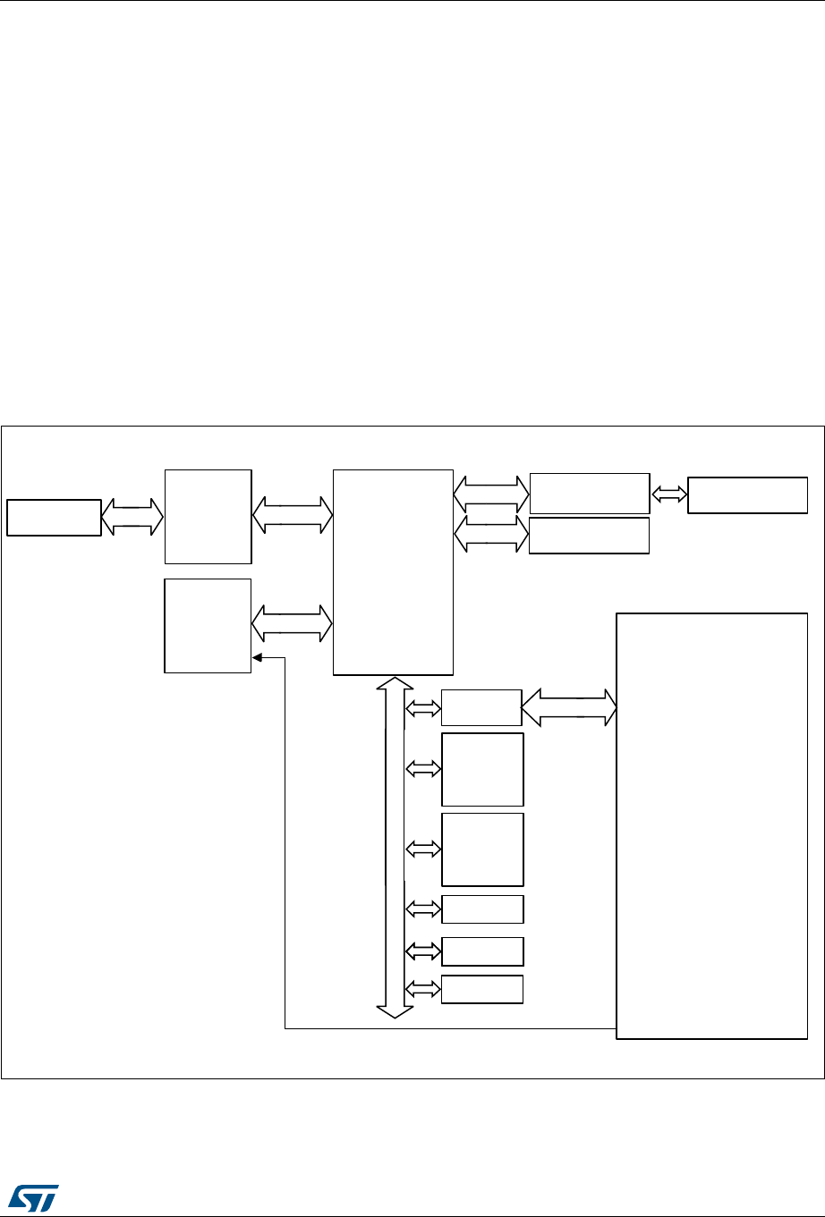
DocID025941 Rev 5 55/1001
RM0376 System and memory overview
56
2 System and memory overview
2.1 System architecture
The main system consists of:
•Two masters:
–Cortex
®-M0+ core (AHB-lite bus)
– GP-DMA (general-purpose DMA)
•Three slaves:
– Internal SRAM
– Internal Non-volatile memory
– AHB to APB, which connects all the APB peripherals
These are interconnected using a multilayer AHB bus architecture as shown in Figure 1:
Figure 1. System architecture
1. Refer to Table 1: STM32L0x2 memory density, to Table 2: Overview of features per category and to the device datasheets
for the GPIO ports and peripherals available on your device.
MS34748V2
Busmatrix
APB buses
MIF
Memory interface
SRAM
AHB2APB
Bridges
Cortex
M0+
DMA
Controller
(Channels
1 to 7)
System bus
DMA
AES
AHB bus
Reset and
clock
controller
(RCC)
Touch
sensing
controller
(TSC)
CRC
DMA request
GPIO ports
A,B,C,D,E,H
NVM memory
RNG
SYSCFG
FIREWALL
PWR
CRS
EXTI
ADC
DAC
COMP1/2
TIM2/3/6/7/21/22
LPTIM1
IWDG
WWDG
RTC
DBGMCU
I2C1/2/3
USART1/2/3/4/LPUART1
SPI1/2
USB SRAM
USB FS
IOPORT

System and memory overview RM0376
56/1001 DocID025941 Rev 5
2.1.1 S0: Cortex®-bus
This bus connects the DCode/ICode bus of the Cortex®-M0+ core to the BusMatrix. This
bus is used by the core to fetch instructions, get data and access the AHB/APB resources.
2.1.2 S1: DMA-bus
This bus connects the AHB master interface of the DMA to the BusMatrix which manages
the access of the different masters to Flash memory and data EEPROM, the SRAM and the
AHB/APB peripherals.
2.1.3 BusMatrix
The BusMatrix manages the access arbitration between masters. The arbitration uses a
Round Robin algorithm. The BusMatrix is composed of two masters (CPU, DMA) and three
slaves (NVM interface, SRAM, AHB2APB1/2 bridges).
AHB/APB bridges
The AHB/APB bridge provide full synchronous connections between the AHB and the 2
APB buses. APB1 and APB2 operate at a maximum frequency of 32 MHz.
Refer to Section 2.2.2: Memory map and register boundary addresses on page 58 for the
address mapping of the peripherals connected to this bridge.
After each device reset, all peripheral clocks are disabled (except for the SRAM and MIF).
Before using a peripheral you have to enable its clock in the RCC_AHBENR,
RCC_APB2ENR, RCC_APB1ENR or RCC_IOPENR register.
Note: When a 16- or 8-bit access is performed on an APB register, the access is transformed into
a 32-bit access: the bridge duplicates the 16- or 8-bit data to feed the 32-bit vector.
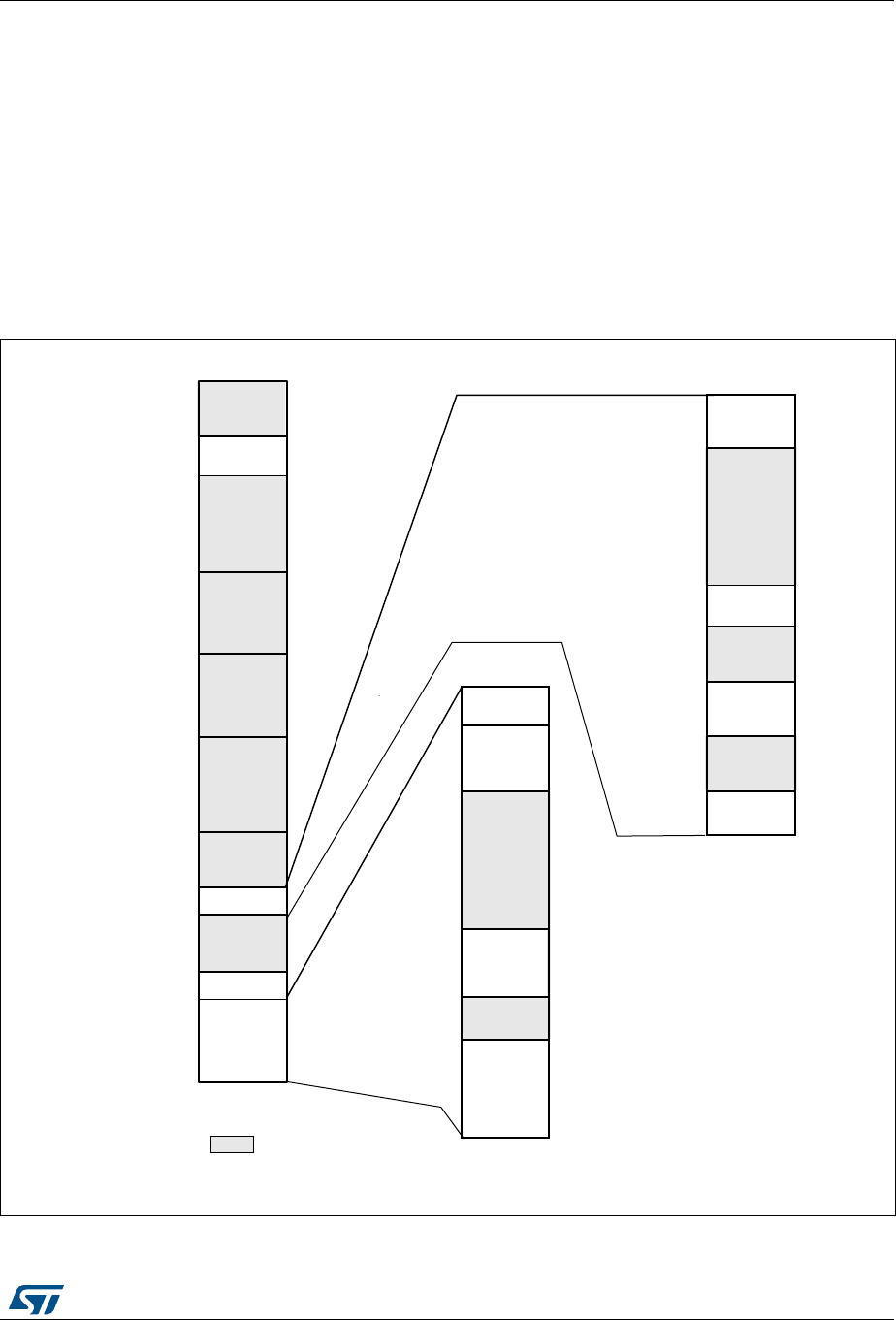
DocID025941 Rev 5 57/1001
RM0376
64
2.2 Memory organization
2.2.1 Introduction
Program memory, data memory, registers and I/O ports are organized within the same linear
4-Gbyte address space.
The bytes are coded in memory in Little Endian format. The lowest numbered byte in a word
is considered the word’s least significant byte and the highest numbered byte the most
significant.
The addressable memory space is divided into 8 main blocks, of 512 Mbyte each.
Figure 2. Memory map
MS34761V1
Reserved
IOPORT
0
1
2
3
4
5
6
7
0xFFFF FFFF
Peripherals
SRAM
Flash system
memory
reserved
System
memory
Option bytes
0xE010 0000
Flash, system
memory or
SRAM,
demending on
BOOT
configuration
0x0000 0000
0xE000 0000
0xC000 0000
0xA000 0000
0x8000 0000
0x6000 0000
0x4000 0000
0x2000 0000
0x0000 0000
0x0800 0000
0x1FFF FFFF
reserved
CODE
APB1
APB2
reserved
0x4000 0000
0x4000 8000
0x4001 0000
0x4001 8000
reserved
0x4002 0000
AHB
0x5000 0000
reserved
0x5000 1FFF
0x4002 63FF
Cortex-M0+
peripherals
RM0376
58/1001 DocID025941 Rev 5
All the memory map areas that are not allocated to on-chip memories and peripherals are
considered “Reserved”. For the detailed mapping of available memory and register areas,
refer to Memory map and register boundary addresses and peripheral sections.
2.2.2 Memory map and register boundary addresses
See the datasheet corresponding to your device for a comprehensive diagram of the
memory map.
The following table gives the boundary addresses of the peripherals available in the
devices.
Table 3. STM32L0x2 peripheral register boundary addresses(1)
Bus Boundary address Size (bytes) Peripheral Peripheral register map
IOPORT
0X5000 1C00 - 0X5000 1FFF 1K GPIOH Section 9.4.12: GPIO register
map
0X5000 1400 - 0X5000 1BFF 2 K Reserved -
0X5000 1000 - 0X5000 13FF 1K GPIOE Section 9.4.12: GPIO register
map
0X5000 0C00 - 0X5000 0FFF 1K GPIOD Section 9.4.12: GPIO register
map
0X5000 0800 - 0X5000 0BFF 1K GPIO C Section 9.4.12: GPIO register
map
0X5000 0400 - 0X5000 07FF 1K GPIOB Section 9.4.12: GPIO register
map
0X5000 0000 - 0X5000 03FF 1K GPIOA Section 9.4.12: GPIO register
map
DocID025941 Rev 5 59/1001
RM0376
64
AHB
0X4002 6400 - 0X4002 FFFF 49 K Reserved -
0X4002 6000 - 0X4002 63FF 1 K
AES (Cat 3 and
5 with AES
only)
Section 18.7.13: AES register
map
0X4002 5400 - 0X4002 5FFF 3 K Reserved -
0X4002 5000 - 0X4002 53FF 1 K RNG Section 19.8.4: RNG register
map
0X4002 4400 - 0X4002 4FFF 3 K Reserved -
0X4002 4000 - 0X4002 43FF 1 K TSC Section 17.6.11: TSC register
map
0X4002 3400 - 0X4002 43FF 3 K Reserved -
0X4002 3000 - 0X4002 33FF 1 K CRC Section 4.4.6: CRC register map
0X4002 2400 - 0X4002 2FFF 3 K Reserved -
0X4002 2000 - 0X4002 23FF 1 K FLASH Section 3.7.11: Flash register
map
0X4002 1400 - 0X4002 1FFF 3 K Reserved -
0X4002 1000 - 0X4002 13FF 1 K RCC Section 7.3.22: RCC register
map
0X4002 0400 - 0X4002 0FFF 3 K Reserved -
0X4002 0000 - 0X4002 03FF 1 K DMA1 Section 11.4.8: DMA register
map
Table 3. STM32L0x2 peripheral register boundary addresses(1) (continued)
Bus Boundary address Size (bytes) Peripheral Peripheral register map
RM0376
60/1001 DocID025941 Rev 5
APB2
0X4001 5C00 - 0X4001 FFFF 42 K Reserved -
0X4001 5800 - 0X4001 5BFF 1 K DBG Section 32.10: DBG register
map
0X4001 3C00 - 0X4001 57FF 7 K Reserved -
0X4001 3800 - 0X4001 3BFF 1 K USART1 Section 28.8.12: USART
register map
0X4001 3400 - 0X4001 37FF 1 K Reserved -
0X4001 3000 - 0X4001 33FF 1 K SPI1 Section 30.7.10: SPI register
map
0X4001 2800 - 0X4001 2FFF 2 K Reserved -
0X4001 2400 - 0X4001 27FF 1 K ADC1 Section 14.11.12: ADC register
map
0X4001 2000 - 0X4001 23FF 1 K Reserved -
0X4001 1C00 - 0X4001 1FFF 1 K Firewall Section 5.4.8: Firewall register
map
0X4001 1800 - 0X4001 1BFF 1 K Reserved -
0X4001 1400 - 0X4001 17FF 1 K TIM22 Section 21.4.16: TIM21/22
register map
0X4001 0C000 - 0X4001 13FF 2 K Reserved -
0X4001 0800 - 0X4001 0BFF 1 K TIM21 Section 21.4.16: TIM21/22
register map
0X4001 0400 - 0X4001 07FF 1 K EXTI Section 13.5.7: EXTI register
map
0X4001 0000 - 0X4001 03FF 1 K SYSCFG,
COMP
Section 10.2.8: SYSCFG
register map, Section 16.5.3:
COMP register map
Table 3. STM32L0x2 peripheral register boundary addresses(1) (continued)
Bus Boundary address Size (bytes) Peripheral Peripheral register map

DocID025941 Rev 5 61/1001
RM0376
64
APB1
0X4000 8000 - 0X4000 FFFF 32 K Reserved -
0X4000 7C00 - 0X4000 7FFF 1 K LPTIM1 Section 23.6.9: LPTIM register
map
0X4000 7800 - 0X4000 7BFF 1K I2C3 Section 27.7.12: I2C register
map
0X4000 7400 - 0X4000 77FF 1 K DAC1/2 Section 15.10.15: DAC register
map
0X4000 7000 - 0X4000 73FF 1 K PWR Section 6.4.3: PWR register
map
0X4000 6C00 - 0X4000 6FFF 1 K CRS Section 8.6.5: CRS register map
0X4000 68000 - 0X4000 6BFF 1 K Reserved -
0X4000 6000 - 0X4000 67FF 2 K USB (SRAM
512x16bit) -
0X4000 5C00 - 0X4000 5FFF 1 K USB FS Section 31.6.3: USB register
map
Table 3. STM32L0x2 peripheral register boundary addresses(1) (continued)
Bus Boundary address Size (bytes) Peripheral Peripheral register map
RM0376
62/1001 DocID025941 Rev 5
APB1
0X4000 5800 - 0X4000 5BFF 1 K I2C2 Section 27.7.12: I2C register
map
0X4000 5400 - 0X4000 57FF 1 K I2C1 Section 27.7.12: I2C register
map
0X4000 5000 - 0X4000 53FF 1 K USART5 Section 28.8.12: USART
register map
0X4000 4C00 - 0X4000 4FFF 1 K USART4 Section 28.8.12: USART
register map
0X4000 4800 - 0X4000 4BFF 1 K LPUART1 Section 29.7.10: LPUART
register map
0X4000 4400 - 0X4000 47FF 1 K USART2 Section 28.8.12: USART
register map
0X4000 3C000 - 0X4000 43FF 2 K Reserved -
0X4000 3800 - 0X4000 3BFF 1 K SPI2 Section 30.7.10: SPI register
map
0X4000 3400 - 0X4000 37FF 1 K Reserved -
0X4000 3000 - 0X4000 33FF 1 K IWDG Section 24.4.6: IWDG register
map
0X4000 2C00 - 0X4000 2FFF 1 K WWDG Section 25.4.4: WWDG register
map
0X4000 2800 - 0X4000 2BFF 1 K RTC +
BKP_REG
Section 26.7.21: RTC register
map
0X4000 1800 - 0X4000 27FF 3 K Reserved -
0X4000 1400 - 0X4000 17FF 1 K TIMER7 Section 22.4.9: TIM6/7 register
map
0X4000 1000 - 0X4000 13FF 1 K TIMER6 Section 22.4.9: TIM6/7 register
map
0X4000 0800 - 0X4000 0FFF 1 K Reserved -
0X4000 0400 - 0X4000 07FF 1 K TIMER3 Section 20.5: TIMx register map
0X4000 0000 - 0X4000 03FF 1 K TIMER2 Section 20.5: TIMx register map
SRAM
0X2000 2000 - 0X3FFF FFFF ~524 M Reserved -
0X2000 0000 - 0X2000 4FFF up to 20 K SRAM -
Table 3. STM32L0x2 peripheral register boundary addresses(1) (continued)
Bus Boundary address Size (bytes) Peripheral Peripheral register map
DocID025941 Rev 5 63/1001
RM0376
64
2.3 Embedded SRAM
STM32L0x2 devices feature up to 20 Kbytes of static SRAM.
This RAM can be accessed as bytes, half-words (16 bits) or full words (32 bits). This
memory can be addressed at maximum system clock frequency without wait state and thus
by both CPU and DMA.
The SRAM start address is 0x2000 0000.
The CPU can access the SRAM from address 0x0000 0000 when physical remap is
selected through boot pin or MEM_MODE (see Section 10.2.1: SYSCFG memory remap
register (SYSCFG_CFGR1)).
2.4 Boot configuration
In the STM32L0x2, three different boot modes can be selected through the BOOT0 pin and
boot configuration bits in the User option byte, as shown in the following table.
NVM
0X0800 0000 - 0X0802 FFFF up to 192 K Flash program
memory -
0x0808 0000 - 0x0808 17FF up to 6 K Data EEPROM -
0x1FF0 0000 - 0x1FF0 1FFF 8 K System
memory -
0x1FF8 0020 - 0x1FF8 007F 96 Factory option
bytes -
0x1FF8 0000 - 0x1FF8 001F 32 User option
bytes -
1. Refer to Table 1: STM32L0x2 memory density, to Table 2: Overview of features per category and to the device datasheets
for the GPIO ports and peripherals available on your device. The memory area corresponding to unavailable GPIO ports or
peripherals are reserved.
Table 3. STM32L0x2 peripheral register boundary addresses(1) (continued)
Bus Boundary address Size (bytes) Peripheral Peripheral register map
Table 4. Boot modes(1)
1. BOOT1 value is the opposite of nBOOT1 option bit.
Boot mode selection
Boot mode Aliasing
BOOT1 pin BOOT0 pin
X0
Flash program
memory Flash program memory is selected as boot area
0 1 System memory System memory is selected as boot area
1 1 Embedded SRAM Embedded SRAM is selected as boot area

RM0376
64/1001 DocID025941 Rev 5
The boot mode configuration is latched on the 4th rising edge of SYSCLK after reset. It is up
to the user to set nBOOT1 and BOOT0 to select the required boot mode.
The boot mode configuration is also re-sampled when exiting from Standby mode.
Consequently the boot mode configuration must not be modified in Standby mode. After this
startup delay has elapsed, the CPU fetches the top-of-stack value from address
0x0000 0000, then starts code execution from the boot memory at 0x0000 0004.
Depending on the selected boot mode, Flash program memory, system memory or SRAM is
accessible as follows:
•Boot from Flash program memory: the Flash program memory is aliased in the boot
memory space (0x0000 0000), but still accessible from its original memory space
(0x0800 0000). In other words, the Flash memory contents can be accessed starting
from address 0x0000 0000 or 0x0800 0000.
•Boot from system memory: the system memory is aliased in the boot memory space
(0x0000 0000), but still accessible from its original memory space (0x1FF0 0000).
•Boot from the embedded SRAM: the SRAM is aliased in the boot memory space
(0x0000 0000), but it is still accessible from its original memory space (0x2000 0000).
Bank swapping (category 5 devices only)
For devices featuring two banks, the bank swapping mechanism allows the CPU to point
either to bank1 or to bank 2 in the boot memory space (0x0000 0000). Either Flash program
and data EEPROM address are changed (see Table 8: NVM organization for UFB = 0
(128 Kbyte category 5 devices), Table 10: NVM organization for UFB = 0 (64 Kbyte category
5 devices)).
Physical remap
Once the boot pin and bit are selected, the application software can modify the memory
accessible in the code area. This modification is performed by programming the
MEM_MODE bits in the SYSCFG memory remap register (SYSCFG_CFGR1).
Embedded bootloader
The embedded bootloader is located in the System memory, programmed by ST during
production. It is used to reprogram the Flash memory using one of the following serial
interfaces:
•For category 3 devices: USART1, USART2, SPI1 or SPI2
•For category 5 devices with USB interface: USART1, USART2 or USB.
•For category 5 devices without USB interface: USART1, USART2, SPI1, SPI2, I2C1 or
I2C2.
For details concerning the bootloader serial interface corresponding I/O, refer to your device
datasheet.
For further details on STM32 bootloader, please refer to AN2606.

DocID025941 Rev 5 65/1001
RM0376 Flash program memory and data EEPROM (FLASH)
121
3 Flash program memory and data EEPROM (FLASH)
3.1 Introduction
The non-volatile memory (NVM) is composed of:
•Up to 192 Kbytes of Flash program memory. This area is used to store the application
code.
•Up to 6 Kbytes of data EEPROM
•An information block:
– Up to 8 Kbytes of System memory
– Up to 8x4 bytes of user Option bytes
– Up to 96 bytes of factory Option bytes
3.2 NVM main features
The NVM interface features:
•Read interface organized by word, half-word or byte in every area
•Programming in the Flash memory performed by word or half-page
•Programming in the Option bytes area performed by word
•Programming in the data EEPROM performed by word, half-word or byte
•Erase operation performed by page (in Flash memory, data EEPROM and Option
bytes)
•Option byte Loader
•ECC (Error Correction Code): 6 bits stored for every word to recognize and correct just
one error
•Mass erase operation
•Read / Write protection
•PCROP protection
•Low-power mode
•Category 5 devices only:
– Dual-bank memory with read-while-write
– Dual-bank boot capability allowing to boot either from Bank 1 or Bank 2 at startup
– Bank swapping capability.
Flash program memory and data EEPROM (FLASH) RM0376
66/1001 DocID025941 Rev 5
3.3 NVM functional description
3.3.1 NVM organization
The NVM is organized as 32-bit memory cells that can be used to store code, data, boot
code or Option bytes.
The memory array is divided into pages. A page is composed of 32 words (or 128 bytes) in
Flash program memory and System memory, and 1 single word (or 4 bytes) in data
EEPROM and Option bytes areas (user and factory).
A Flash sector is made of 32 pages (or 4 Kbytes). The sector is the granularity of the write
protection.
Table 5. NVM organization (category 3 devices)
NVM NVM addresses Size
(bytes) Name Description
Flash program
memory(1)
0x0800 0000 - 0x0800 007F 128 bytes Page 0
sector 0
0x0800 0080 - 0x0800 00FF 128 bytes Page 1
---
0x0800 0F80 - 0x0800 0FFF 128 bytes Page 31
.
.
.
.
.
.
.
.
.
.
.
.
0x0800 7000 - 0x0800 707F 128 bytes Page 224
sector 7
0x0800 7080 - 0x0800 70FF 128 bytes Page 225
---
0x0800 7F80 - 0x0800 7FFF 128 bytes Page 255
.
.
.
.
.
.
.
.
.
.
.
.
0x0800 F000 - 0x0800 F07F 128 bytes Page 480
sector 15
0x0800 F080 - 0x0800 F0FF 128 bytes Page 481
---
0x0800 FF80 - 0x0800 FFFF 128 bytes Page 511
Data EEPROM 0x0808 0000 - 0x0808 07FF 2 Kbytes - Data EEPROM
Information block
0x1FF0 0000 - 0x1FF0 0FFF 4 Kbytes - System memory
0x1FF8 0020 - 0x1FF8 007F 96 bytes - Factory Options
0x1FF8 0000 - 0x1FF8 001F 32 bytes - User Option bytes
1. For 32 Kbyte category 3 devices, the Flash program memory is divided into 256 pages of 128 bytes each.
DocID025941 Rev 5 67/1001
RM0376 Flash program memory and data EEPROM (FLASH)
121
Table 6. NVM organization for UFB = 0 (192 Kbyte category 5 devices)
NVM NVM addresses Size
(bytes) Name Description
Flash program
memory
0x0800 0000 - 0x0800 007F 128 bytes Page 0
sector 0
Bank 1
0x0800 0080 - 0x0800 00FF 128 bytes Page 1
---
0x0800 0F80 - 0x0800 0FFF 128 bytes Page 31
.
.
.
.
.
.
.
.
.
.
.
.
0x0800 7000 - 0x0800 707F 128 bytes Page 224
sector 7
0x0800 7080 - 0x0800 70FF 128 bytes Page 225
---
0x0800 7F80 - 0x0800 7FFF 128 bytes Page 255
.
.
.
.
.
.
.
.
.
.
.
.
---
0x0801 7F80- 0x0801 7FFF 128 bytes Page 767 sector 23
0x0801 8000 - 0x0801 807F 128 bytes Page 768 sector 24
Bank 2
.
.
.
.
.
.
.
.
.
.
.
.
0x0802 F000 - 0x0802 F07F 128 bytes Page 1504
sector 47
0x0802 F080 - 0x0802 F0FF 128 bytes Page 1505
---
0x0802 FF80 - 0x0802 FFFF 128 bytes Page 1535
Data EEPROM
0x0808 0000 - 0x0808 0BFF
6Kbytes
- Data EEPROM Bank 1
0x0808 0C00 - 0x0808 17FF - Data EEPROM Bank 2
Information block
0x1FF0 0000 - 0x1FF0 1FFF 8 Kbytes - System memory
0x1FF8 0020 - 0x1FF8 007F 96 bytes - Factory Options
0x1FF8 0000 - 0x1FF8 001F 32 bytes - User Option bytes
Flash program memory and data EEPROM (FLASH) RM0376
68/1001 DocID025941 Rev 5
Table 7. Flash memory and data EEPROM remapping
(192 Kbyte category 5 devices)
NVM Description
NVM addresses Remapped addresses
MEM_MODE = 0,
BOOT0= 0 and
UFB = 0
MEM_MODE = 0,
BOOT0= 0 and
UFB = 1
MEM_MODE = 0,
BOOT0= 0 and
UFB = 0
MEM_MODE = 0,
BOOT0= 0 and
UFB = 1
Flash
program
memory
Bank 1 0x0800 0000 -
0x0801 7FFF
0x0801 8000 -
0x0802 FFFF
0x0000 0000 -
0x0001 7FFF
0x0001 8000 -
0x0002 FFFF
Bank 2 0x0801 8000 -
0x0802 FFFF
0x08000 0000 -
0x0801 7FFF
0x0001 8000 -
0x0002 FFFF
0x0000 0000 -
0x0001 7FFF
Data
EEPROM
Bank 1 0x0808 0000 -
0x0808 0BFF
0x0808 0C00 -
0x0808 17FF
0x0008 0000 -
0x0008 0BFF
0x0008 0C00 -
0x0008 17FF
Bank 2 0x0808 0C00 -
0x0808 17FF
0x0808 0000 -
0x0008 0BFF
0x0008 0C00 -
0x0008 17FF
0x0008 0000 -
0x0008 0BFF
Table 8. NVM organization for UFB = 0 (128 Kbyte category 5 devices)
NVM NVM addresses Size (bytes) Name Description
Flash program
memory
0x0800 0000 - 0x0800 007F 128 bytes Page 0
sector 0
Bank 1
0x0800 0080 - 0x0800 00FF 128 bytes Page 1
---
0x0800 0F80 - 0x0800 0FFF 128 bytes Page 31
.
.
.
.
.
.
.
.
.
.
.
.
0x0800 7000 - 0x0800 707F 128 bytes Page 224
sector 7
0x0800 7080 - 0x0800 70FF 128 bytes Page 225
---
0x0800 7F80 - 0x0800 7FFF 128 bytes Page 255
.
.
.
.
.
.
.
.
.
.
.
.
0x0800 FF80- 0x0800 FFFF 128 bytes Page 511 sector 15
0x0801 0000 - 0x0801 007F 128 bytes Page 512 sector 16
Bank 2
.
.
.
.
.
.
.
.
.
.
.
.
0x0801 F000 - 0x0801 F07F Page 992
sector 31
---
0x0801 FF80 - 0x0801 FFFF 128 bytes Page 1023
Data EEPROM
0x0808 0000 - 0x0808 0BFF
6Kbytes
- Data EEPROM Bank 1
0x0808 0C00 - 0x0808 17FF - Data EEPROM Bank 2

DocID025941 Rev 5 69/1001
RM0376 Flash program memory and data EEPROM (FLASH)
121
Information block
0x1FF0 0000 - 0x1FF0 1FFF 8 Kbytes - System memory
0x1FF8 0020 - 0x1FF8 007F 96 bytes - Factory Options
0x1FF8 0000 - 0x1FF8 001F 32 bytes User Option bytes
Table 8. NVM organization for UFB = 0 (128 Kbyte category 5 devices) (continued)
NVM NVM addresses Size (bytes) Name Description
Table 9. Flash memory and data EEPROM remapping (128 Kbyte category 5 devices)
NVM Description
NVM addresses Remapped addresses
MEM_MODE = 0,
BOOT0= 0 and
UFB = 0
MEM_MODE = 0,
BOOT0= 0 and
UFB = 1
MEM_MODE = 0,
BOOT0= 0 and
UFB = 0
MEM_MODE = 0,
BOOT0= 0 and
UFB = 1
Flash program
memory
Bank 1 0x0800 0000 -
0x0800 FFFF
0x0801 0000 -
0x0801 FFFF
0x0000 0000 -
0x0000 FFFF
0x0001 0000 -
0x0001 FFFF
Bank 2 0x0801 0000 -
0x0801 FFFF
0x0800 0000 -
0x0800 FFFF
0x0001 0000 -
0x0001 FFFF
0x0000 0000 -
0x0000 FFFF
Data EEPROM
Bank 1 0x0808 0000 -
0x0808 0BFF
0x0808 0C00 -
0x0808 17FF
0x0008 0000 -
0x0008 0BFF
0x0008 0C00 -
0x0008 17FF
Bank 2 0x0808 0C00 -
0x0808 17FF
0x0808 0000 -
0x0808 0BFF
0x0008 0C00 -
0x0008 17FF
0x0008 0000 -
0x0008 0BFF
Table 10. NVM organization for UFB = 0 (64 Kbyte category 5 devices)(1)
NVM NVM addresses Size (bytes) Name Description
Flash program
memory
0x0800 0000 - 0x0800 007F 128 bytes Page 0
sector 0
Bank 1
0x0800 0080 - 0x0800 00FF 128 bytes Page 1
---
0x0800 0F80 - 0x0800 0FFF 128 bytes Page 31
.
.
.
.
.
.
.
.
.
.
.
.
0x0800 F000 - 0x0800 F07F 128 bytes Page 480
sector 15
---
---
0x0800 FF80 - 0x0800 FFFF 128 bytes Page 511
Data EEPROM 0x0808 0C00 - 0x0808 17FF 3 Kbytes - Data EEPROM Bank 2
Information block
0x1FF0 0000 - 0x1FF0 1FFF 8 Kbytes - System memory
0x1FF8 0020 - 0x1FF8 007F 96 bytes - Factory Options
0x1FF8 0000 - 0x1FF8 001F 32 bytes User Option bytes
1. Flash memory and data EEPROM remapping is not possible on 64 Kbyte category 5 devices.

Flash program memory and data EEPROM (FLASH) RM0376
70/1001 DocID025941 Rev 5
3.3.2 Dual-bank boot capability
Category 5 devices have two Flash memory banks: Bank 1 and Bank 2. They feature an
additional boot mechanism which allows booting either from Bank 2 or from Bank 1
depending on BFB2 bit status (bit 23 in FLASH_OPTR register).
•When the BFB2 bit is set and the boot pins are configured to boot from Flash memory
(BOOT0 = 0 and BOOT1 = x), the device maps the System memory at address 0. It
boots from the System memory after reset and Standby and executes (during
approximately 440 µs) the embedded bootloader code which implements the dual-
bank boot mechanism:
a) The System memory code first checks Bank 2. If it contains a valid code (see note
below), it sets the UFB bit in SYSCFG_CFGR1 register to map Bank 2 at address
0x0800 0000, jumps to the application code located in Bank 2, and leaves the
bootloader.
b) If the code located in Bank 2 is not valid, the System memory code checks Bank 1
code. If it is valid (see note below), it jumps to the application located in Bank 1
(UFB is kept at ‘0’ so that Bank 1 remains mapped at address 0x0800 0000).
c) If both Bank 2 and Bank 1 do not contain valid code (see note below), the normal
bootloader operations are executed when the protection level2 is disabled.
Otherwise, the System memory code jumps to Bank 1 regardless of its validity.
Refer to Table 11 for more details.
•When BFB2 bit is reset (default state), the dual-bank boot mechanism is not performed.
Note: The code is considered as valid when the first data located at the bank start address (which
should be the stack pointer) points to a valid address (stack top address).
For category 5 devices, the Flash memory Bank 1 and Bank 2, System memory or SRAM
can be selected as the boot area, as shown in Table 11 below.
Table 11. Boot pin and BFB2 bit configuration
Protection
level
BFB2
bit
Boot mode
selection
Boot mode Aliasing
nBOOT1
option
bit
BOOT0
pin
0 or 1
0
X 0 User Flash memory User Flash memory Bank1 is selected as the
boot area.
1 1 System memory Boot on System memory to execute bootloader.
0 1 Embedded SRAM Boot on Embedded SRAM
1
X 0 System memory
Boot on System memory to execute dual bank
boot mechanism. If Bank 2 and Bank 1are not
valid, bootloader is executed for Flash update.
1 1 System memory Boot on System memory to execute bootloader.
0 1 Embedded SRAM Boot on Embedded SRAM.

DocID025941 Rev 5 71/1001
RM0376 Flash program memory and data EEPROM (FLASH)
121
When entering System memory, you can either execute the bootloader (for Flash update) or
execute Dual Bank Jump (see Table 11).
When protection level2 is enabled, the bootloader is never executed to perform a Flash
update.
When the conditions a, b, and c described below are fulfilled, it is equivalent to configuring
boot pins for System memory boot (BOOT0 = 1 and BOOT1 = 0). In this case when
protection level2 is disabled, normal bootloader operations are executed.
a) BFB2 bit is set.
b) Both banks do not contain valid code.
c) Boot pins configured as follows: BOOT0 = 0 and BOOT1 = x.
When the BFB2 bit is set, and Bank 2 and/or Bank 1 contain valid user application code, the
Dual Bank Boot is always performed (bootloader always jumps to the user code).
Consequently, if you have set the BFB2 bit (to boot from Bank 2) then, to be able to execute
the bootloader code for Flash update when protection level2 is disabled, you have to:
a) Set the BFB2 bit to 0, BOOT0 = 1 and BOOT1 = 0 or,
b) Program the content of address 0x0801 8000/0x0801 0000 (base address of
Bank2) and 0x0800 0000 (base address of Bank1) to 0x0.
3.3.3 Reading the NVM
Protocol to read
To read the NVM content, take any address from Section 3.3.1: NVM organization. The
clock of the memory interface must be running. (see MIFEN bit in Section 7.3.13: AHB
peripheral clock enable register (RCC_AHBENR)).
Depending on the clock frequency, a 0 or a 1 wait state can be necessary to read the NVM.
The user must set the correct number of wait states (LATENCY bit in the FLASH_ACR
register). No control is done to verify if the frequency or the power used is correct, with
respect to the number of wait states. A wrong number of wait states can generate wrong
read values (high frequency and 0 wait states) or a long time to execute a code (low
frequency with 1 wait state).
2
0
X 0 User Flash memory
User Flash memory Bank1 is selected as the
boot area.
1 1 User Flash memory
0 1 User Flash memory
1
X 0 System memory Boot on System memory to execute dual bank
boot mechanism. If Bank 2 isn’t valid, it jumps to
Bank 1.
1 1 System memory
0 1 System memory
Table 11. Boot pin and BFB2 bit configuration (continued)
Protection
level
BFB2
bit
Boot mode
selection
Boot mode Aliasing
nBOOT1
option
bit
BOOT0
pin
Flash program memory and data EEPROM (FLASH) RM0376
72/1001 DocID025941 Rev 5
You can read the NVM by word (4 bytes), half-word (2 bytes) or byte.
When the NVM features only one bank, it is not possible to read the NVM during a
write/erase operation. If a write/erase operation is ongoing, the reading will be in a wait state
until the write/erase operation completes, stalling the master that requested the read
operation, except when the address is read-protected. In this case, the error is sent to the
master by a hard fault or a memory interface flag; no stall is generated and no read is
waiting.
When two banks are available (category 5 devices), read operations from one bank can be
performed while write or erase operations are performed on the other bank.
Relation between CPU frequency/Operation mode/NVM read time
The device (and the NVM) can work at different power ranges. For every range, some
master clock frequencies can be set. Tabl e 1 2 resumes the link between the power range
and the frequencies to ensure a correct time access to the NVM.
Table 13 shows the delays to read a word in the NVM. Comparing the complete time to read
a word (Ttotal) with the clock period, you can see that in Range 3 no wait state is necessary,
also with the maximum frequency (4.2 MHz) allowed by the device. Ttotal is the time that the
NVM needs to return a value, and not the complete time to read it (from memory to Core
through the memory interface); all remaining time is lost.
Table 12. Link between master clock power range and frequencies
Name Power range Maximum frequency
(with 1 wait state)
Maximum frequency
(without wait states)
Range 1 1.65 V - 1.95 V 32 MHz 16 MHz
Range 2 1.35 V - 1.65 V 16 MHz 8 MHz
Range 3 1.05 V - 1.35 V 4.2 MHz 4.2 MHz
Table 13. Delays to memory access and number of wait states
Name Ttotal Frequency Period Number of wait
state required
Range 1 46.1 ns
32 MHz 31.25 1
16 MHz 62.5 0
Range 2 86.8 ns
16 MHz 62.5 1
8 MHz 125 0
Range 3 184.6 ns
4 MHz 250 0
2 MHz 500 0

DocID025941 Rev 5 73/1001
RM0376 Flash program memory and data EEPROM (FLASH)
121
Change the CPU Frequency
After reset, the clock used is the MSI (2.1 MHz) and 0 wait state is configured in the
FLASH_ACR register. The following software sequences have to be respected to tune the
number of wait states needed to access the NVM with the CPU frequency.
A CPU clock or a number of wait state configuration changes may take some time before
being effective. Checking the AHB prescaler factor and the clock source status values is a
way to ensure that the correct CPU clock frequency is the configured one. Similarly, the read
of FLASH_ACR is a way to ensure that the number of programmed wait states is effective.
Increasing the CPU frequency (in the same voltage range)
1. Program 1 wait state in LATENCY bit of FLASH_ACR register, if necessary.
2. Check that the new number of wait states is taken into account by reading the
FLASH_ACR register. When the number of wait states changes, the memory interface
modifies the way the read access is done to the NVM. The number of wait states
cannot be modified when a read operation is ongoing, so the memory interface waits
until no read is done on the NVM. If the master reads back the content of the
FLASH_ACR register, this reading is stopped (and also the master which requested
the reading) until the number of wait states is really changed. If the user does not read
back the register, the following access to the NVM may be done with 0 wait states,
even if the clock frequency has been increased, and consequently the values are
wrong.
3. Modify the CPU clock source and/or the AHB clock prescaler in the Reset & Clock
Controller (RCC).
4. Check that the new CPU clock source and/or the new CPU clock prescaler value is
taken into account by reading respectively the clock source status and/or the AHB
prescaler value in the Reset & Clock Controller (RCC). This check is important as some
clocks may take time to get available.
For code example, refer to A.2.1: Increasing the CPU frequency preparation sequence
code, A.2.3: Switch from PLL to HSI16 sequence code and A.2.4: Switch
to PLL sequence code.
Decreasing the CPU frequency (in the same voltage range)
1. Modify the CPU clock source and/or the AHB clock prescaler in the Reset & Clock
Controller (RCC).
2. Check that the new CPU clock source and/or the new CPU clock prescaler value is
taken into account by reading respectively the clock source status and/or the AHB
prescaler value in the Reset and Clock Controller (RCC).
3. Program 0 wait state in LATENCY bit of the FLASH_ACR register, if needed.
4. Check that the new number of wait states is taken into account by reading
FLASH_ACR. It is necessary to read back the register for the reasons explained in the
previous paragraph.

Flash program memory and data EEPROM (FLASH) RM0376
74/1001 DocID025941 Rev 5
Data buffering
In the NVM, six buffers can impact the performance (and in some conditions help to reduce
the power consumption) during read operations, both for fetch and data. The structure of
one buffer is shown on Figure 3.
Figure 3. Structure of one internal buffer
Each buffer stores 3 different types of information: address, data and history. In a read
operation, if the address is found, the memory interface can return data without accessing
the NVM. Data in the buffer is 32 bit wide (even if the master only reads 8 or 16 bits), so that
a value can be returned whatever the size used in a previous reading. The history is used to
know if the content of a buffer is valid and to delete (with a new value) the older one.
The buffers are used to store the value received by the NVM during normal read operations,
and for speculative readings. Disabling the speculative reading makes that only the data
requested by masters is stored in buffers, if enabled (default). This can increase the
performance as no wait state is necessary if the value is already available in buffers, and
reduce the power consumption as the number of reads in memory is reduced and all
combinatorial paths from memory are stable.
The buffers are divided in groups to manage different tasks. The number of buffers in every
group can change starting from the configuration selected by the user (see Table 14). The
total number of buffers used is always 6 (if enabled). The history is always managed by
group.
The memory interface always searches if a particular address is available in all buffers
without checking the group of buffers and if the read is fetch or data.
At reset or after a write/erase operation that changes several addresses, all buffers are
empty and the history is set to EMPTY. After a program by word, half-word or byte, only the
buffer with the concerned address is cleaned.
MS32395V1
Address
Value
History

DocID025941 Rev 5 75/1001
RM0376 Flash program memory and data EEPROM (FLASH)
121
If a value in a buffer is not empty, the history shows the time elapsed between the moment it
has been read or written. The history is organized as a list of values from the latest to the
oldest one. At a given instant, only one buffer in a group can have a particular value of
history (except the empty value). Moving a buffer to the latest position, all other buffers in
the group move one step further, thus maintaining the order. The history is changed to the
latest position when the buffer is read (the master requests for the buffer content) or written
(with a new value from the NVM). The memory interface always writes the oldest buffer (or
one empty buffer, if any) of the right group when a new address is required in memory.
Three configuration bits of the FLASH_ACR register are used to manage the buffering:
•DISAB_BUF
Setting this bit disables all buffers. When this bit is 1, the prefetch or the pre-read
operations cannot be enabled and if, for example, the master requests the same
address twice, two readings are generated in the NVM.
•PRFTEN
Setting this bit to 1 (with DISAB_BUF to 0) enables the prefetch. When the memory
interface does not have any operation in progress, the address following the last
address fetched is read and stored in a buffer.
•PRE_READ
Setting this bit to 1 (with DISAB_BUF to 0) enables the pre-read. When the memory
interface does not have any operation in progress or prefetch to execute, the address
following the last data address is read and stored in a buffer.
Fetch and prefetch
A memory interface fetch is a read from the NVM to execute the operation that has been
read. The memory interface does not check the master who performs the read operation, or
the location it reads from, but it only verifies if the read operation is done to execute what
has been read. It means that a fetch can be performed:
•in all areas,
•with any size (16 or 32 bits).
The memory interface stores in the buffers:
•The address of jumps so that, in a loop, it is only necessary to access the NVM the first
time, because then the jump address is already available.
•The last read address so that, when performing a fetching on 16 bits, the other 16 bits
are already available.
Table 14. Internal buffer management
DISAB_BUF PREFTEN PRE_READ
Buffers for fetch Buffers for data
Buffers for
jumps
Buffers for
prefetch
Buffers for
last value
Buffers for
pre-read
Buffers for
last value
1 - - 00000
000 30102
010 21102
001 30111
011 21111

Flash program memory and data EEPROM (FLASH) RM0376
76/1001 DocID025941 Rev 5
To manage the fetch, the memory interface uses 4 buffers: at reset (DISAB_BUF = 0,
PRFTEN = 0, PRE_READ = 0). 3 buffers are used to manage the jumps and 1 buffer to
store the last value fetched. With this configuration, the 4 buffers for fetch are organized in 2
groups with separate histories: the group for loops and the group for the last value fetched.
Setting the PRFTEN bit to 1 enables the prefetch. The prefetch is a speculative read in the
NVM, which is executed when no read is requested by masters, and where the memory
interface reads from the last address fetched increased by 4 (one word). This read is with a
lower priority and it is aborted if a master requests a read (data or fetch) to a different
address than the prefetch one. When the prefetch is enabled, one buffer for loops is moved
to a new group (of only one buffer) to store the prefetched value: 2 buffers continue to store
the jumps, 1 buffer is used for prefetch and 1 buffer is used for the last value.
The memory interface can only prefetch one address, so the function is temporarily disabled
when no fetch is done and the prefetch is already completed. After a prefetch, if the master
requests the prefetched value, the content of the prefetch buffer is copied to the last value
buffer and a new prefetch is enabled. If, instead, the master requests a different address,
the content of the prefetch buffer is lost, a read in the NVM is started (if necessary) and,
when it is complete, a new prefetch is enabled at the new address fetched increased by 4.
The prefetch can only increase the performance when reading with 1 wait state and for
mostly linear codes: the user must evaluate the pros and cons to enable or not the prefetch
in every situation. The prefetch increases the consumption because many more readings
are done in the NVM (and not all of them will be used by the master). To see the advantages
of prefetch on Dhrystone code, refer to the Dhrystone performances section.
Figure 4 shows the timing to fetch a linear code in the NVM when the prefetch is disabled,
both for 0 wait state (a) and 1 wait state (b). You can compare these two sequences with the
ones in Figure 5, when the prefetch is enabled, to have an idea of the advantages of a
prefetch on a linear code with 0 and 1 wait states.
Figure 4. Timing to fetch and execute instructions with prefetch disabled
1. (a) corresponds to 0 wait state.
2. (b) corresponds to 1 wait state.
MS32396V1
cycle
1
cycle
2
cycle
3
cycle
4
cycle
6
cycle
7
cycle
8
cycle
9
cycle
10 11
cycle
5
Fetch
1 & 2
Addr
1 & 2
Exec.
1
Exec.
2
Fetch
3 & 4
Addr
3 & 4
Exec.
3
Exec.
4
Fetch
5 & 6
Addr
5 & 6
Exec.
5
Exec.
6
(a)
Fetch
1 & 2
Addr
1 & 2
Exec.
1
Wait Exec.
2
Fetch
3 & 4
Addr
3 & 4
Exec.
3
Wait Exec.
4
Fetch
5 & 6
Addr
5 & 6
Exec.
5
Wait Exec.
6
(b)
cycle

DocID025941 Rev 5 77/1001
RM0376 Flash program memory and data EEPROM (FLASH)
121
Figure 5 shows the timing to fetch and execute instructions from the NVM with 0 wait states
(a) and 1 wait state (b) when the prefetch is enabled. The read executed by the prefetch
appears in green.
Read as data and pre-read
A data read from the memory interface, corresponds to any read operation that is not a
fetch. The master reads operation constants and parameters as data. All reads done by
DMA (to copy from one address to another) are read as data. No check is done on the
location of the data read (can be in every area of the NVM).
At reset, (DISAB_BUF = 0, PRFTEN = 0, PRE_READ = 0), the memory interface uses 2
buffers organized in one group to store the last two values read as data.
In some particular cases (for example when the DMA is reading a lot of consecutive words
in the NVM), it can be useful to enable the pre-read (PRE_READ = 1 with DISAB_BUF = 0).
The pre-read works exactly like the prefetch: it is a speculative reading at the last data
address increased by 4 (one word). With this configuration, one buffer of data is moved to a
new group to store the pre-read value, while the second buffer continues to store the last
value read. For a prefetch, the pre-read value is copied in the last read value if the master
requests it, or is lost if the master requests a different address.
The pre-read has a lower priority than a normal read or a prefetch operation: this means that
it will be launched only when no other type of read is ongoing. Pay attention to the fact that
a pre-read used in a wrong situation can be harmful: in a code where a data read is not
done linearly, reducing the number of buffers (from 2 to 1) used for the last read value can
increase the number of accesses to the NVM (and the time to read the value). Moreover,
this can generate a delay on prefetch. An example of this situation is the code Dhrystone,
whose results are shown in the corresponding section.
As for a prefetch operation, the user must select the right moment to enable and disable the
pre-read.
Flash program memory and data EEPROM (FLASH) RM0376
78/1001 DocID025941 Rev 5
Figure 5. Timing to fetch and execute instructions with prefetch enabled
Table 15 is a summary of the possible configurations.
Table 15. Configurations for buffers and speculative reading
DISAB_BUF PRFTEN PRE_READ Description
1 X X Buffers disabled
0 0 0 Buffer enabled: no speculative reading is done
010
Prefetch enabled: speculative reading on fetch
enabled
001
pre-read enabled: speculative reading on data
enabled
011
Prefetch and pre-read enabled: speculative reading
on fetch and data enabled
MS32397V1
cycle
1
cycle
2
cycle
3
cycle
4
cycle
6
cycle
7
cycle
8
cycle
9
cycle
5
Fetch
1 & 2
Addr
1 & 2
Exec.
1
Exec.
2
Fetch
3 & 4
Addr
3 & 4
Exec.
3
Exec.
4
Fetch
5 & 6
Addr
5 & 6
Exec.
5
Exec.
6
Read
3 & 4
Addr
3 & 4
Read
5 & 6
Addr
5 & 6
(a)
Fetch
1 & 2
Addr
1 & 2
Exec.
1
Wait Exec.
2
Fetch
3 & 4
Addr
3 & 4
Exec.
3
Exec.
4
Fetch
5 & 6
Addr
5 & 6
Exec.
5
Exec.
6
Read
3 & 4
Addr
3 & 4 Wait
Read
5 & 6
Addr
5 & 6 Wait
(b)

DocID025941 Rev 5 79/1001
RM0376 Flash program memory and data EEPROM (FLASH)
121
Dhrystone performances
The Dhrystone test is used to evaluate the memory interface performances. The test has
been executed in all memory interface configurations. Refer to Table 16 for a summary of
the results.
Common parameters are:
•the matrix size is 20 x 20
•the loop is executed 1757 times
•the version of Arm® compiler is 4.1 [Build 561]
Here is some explanation about the results:
•The pre-read is not useful for this test: when enabled with the prefetch, it reduces the
memory interface performance because only one buffer is used to store the last data
read and, in this code, the master rarely reads the data linearly. This justifies the very
small increase of performance when enabled without a prefetch.
•The buffers (without speculative readings) with 1 wait state give a little advantage that
can be considered without any costs.
•At a 0 wait state, the best performance (as certified by Arm®) may be due to a different
code alignment during the compilation.
Table 16. Dhrystone performances in all memory interface configurations
Number of
wait states DISAB_BUF PRFTEN PRE_READ Number of
DMIPS (x1000) DMIPS x MHz
0 1 0 0 953 15.25
0 0 0 0 953 15.25
0 0 1 0 953 15.25
0 0 0 1 953 15.25
0 0 1 1 953 15.25
1 1 0 0 677 21.66
1 0 0 0 690 22.08
1 0 1 0 823 26.34
100169122.11
101181626.11

Flash program memory and data EEPROM (FLASH) RM0376
80/1001 DocID025941 Rev 5
3.3.4 Writing/erasing the NVM
There are many ways to change the NVM content. The memory interface helps to reduce
the possibility of unwanted changes and to implement by hardware all sequences necessary
to erase or write in the different memory areas.
Write/erase protocol
To write/erase memory content when the protections have been removed, the user needs
to:
1. configure the operation to execute,
2. send to the memory interface the right number of data, writing one or several
addresses in the NVM,
3. wait for the operation to complete.
During the waiting time, the user can prepare the next operation (except in very particular
cases) writing the new configuration and starting to write data for the next write/erase
operation.
The waiting time depends on the type of operation. A write/erase can last from Tprog (3.2
ms) to 2 x Tglob (3.7 ms) + Tprog (3.2 ms). The memory interface can be configured to write
a half-page (16 words in the Flash program memory) with only one waiting time. This can
reduce the time to program a big amount of data.
Two different protocols can be used: single programming and multiple programming
operation.
Single programming operation
With this protocol, the software has to write a value in a not-protected address of the NVM.
When the memory interface receives this writing request, it stalls the master for some
pulses of clock (for more details, see Table 17) while it checks the protections and the
previous value and it latches the new value inside the NVM. The software can then start to
configure the next operation. The operation will complete when the EOP bit of FLASH_SR
register rises (if it was 0 at the operation start). The operation time is resumed in Table 19
for all operations.
Multiple programming operation (half page)
You can write a half-page (16 words) in Flash program memory, To execute this protocol,
follow the next conditions:
•PGAERR bit in the FLASH_SR register has to be zero (no previous alignment errors).
•The first address has to be half-page aligned (the 6 lower bits of the address have to be
at zero).
•All 16 words must be in the same half-page (address bits 7 to 31 must be the same for
all 16 words). This means that the first address sets the half-page and the next ones
must be inside this half-page. The written data will be stored sequentially in the next
addresses. It is not important that the addresses increase or change (for example, the
same address can be used 16 times), as the memory interface will automatically
increase the address internally.
•Only words (32 bits) can be written.

DocID025941 Rev 5 81/1001
RM0376 Flash program memory and data EEPROM (FLASH)
121
When the memory interface receives the first address, it stalls the master for some pulses of
clock while it checks the protections and the previous value and it latches the new value
inside the NVM (for more details, see Table 17). Then, the memory interface waits for the
second address. No read is accepted: only a fetch will be executed, but it aborts the ongoing
write operation. After the second address, the memory interface stalls the core for a short
time (less than the previous one) to perform a check and to latch it in the NVM before
waiting for the next one. This sequence continues until all 16 words have been latched
inside the NVM. A wrong alignment or size will abort the write operation. If the 16 addresses
are correctly latched, the memory interface starts the write operation. The operation will
complete when EOP bit of FLASH_SR register rises (if it was 0 at the operation start). The
operation time is resumed in Table 19.
This protocol can be used either through application code running from RAM or through
DMA with application code running from RAM or core sleeping.
Unlocking/locking operations
Before performing a write/erase operation, it is necessary to enable it. The user can write
into the Flash program memory, data EEPROM and Option bytes areas.
To perform a write/erase operation, unlock PELOCK bit of the FLASH_PECR register. When
this bit is unlocked (its value is 0), the other bits of the same register can be modified. When
PELOCK is 0, the write/erase operations can be executed in the data EEPROM.
To write/erase the Flash program memory, unlock PRGLOCK bit of the FLASH_PECR
register. The bit can only be unlocked when PELOCK is 0.
To write/erase the user Option bytes, unlock OPTLOCK bit of the FLASH_PECR register.
The bit can only be unlocked when PELOCK is 0. No relation exists between PRGLOCK
and OPTLOCK: the first one can be unlocked when the second one is locked and vice
versa.
Unlocking the data EEPROM and the FLASH_PECR register
After a reset, the data EEPROM and the FLASH_PECR register are not accessible in write
mode because PELOCK bit in the FLASH_PECR register is set. The same unlocking
sequence unprotects both of them at the same time.
The following sequence is used to unlock the data EEPROM and the FLASH_PECR
register:
•Write PEKEY1 = 0x89ABCDEF to the FLASH_PEKEYR register
•Write PEKEY2 = 0x02030405 to the FLASH_PEKEYR register
For code example, refer to A.3.1: Unlocking the data EEPROM and FLASH_PECR register
code example.

Flash program memory and data EEPROM (FLASH) RM0376
82/1001 DocID025941 Rev 5
Any wrong key sequence will lock up FLASH_PECR until the next reset and generate a
hard fault. Idem if the master tries to write another register between the two key sequences
or if it uses the wrong key. A reading access does not generate an error and does not
interrupt the sequence. A hard fault is returned in any of the four cases below:
•After the first write access if the PEKEY1 value entered is erroneous.
•During the second write access if PEKEY1 is correctly entered but the value of
PEKEY2 does not match.
•If there is any attempt to write a third value to PEKEYR (pay attention: this is also true
for the debugger).
•If there is any attempt to write a different register of the memory interface between
PEKEY1 and PEKEY2.
When properly executed, the unlocking sequence clears PELOCK bit in the FLASH_PECR
register.
To lock FLASH_PECR and the data EEPROM again, the software only needs to set
PELOCK bit in FLASH_PECR. When locked again, PELOCK bit needs a new sequence to
return to 0.
For code example, refer to A.3.2: Locking data EEPROM and FLASH_PECR register code
example.
Unlocking the Flash program memory
An additional protection is implemented to write/erase the Flash program memory.
After a reset, the Flash program memory is no more accessible in write mode: PRGLOCK
bit is set in the FLASH_PECR register. A write access to the Flash program memory is
granted by clearing PRGLOCK bit.
The following sequence is used to unlock the Flash program memory:
• Unlock the FLASH_PECR register (see the Unlocking the data EEPROM and the
FLASH_PECR register section).
• Write PRGKEY1 = 0x8C9DAEBF to the FLASH_PRGKEYR register.
•Write PRGKEY2 = 0x13141516 to the FLASH_PRGKEYR register.
For code example, refer to A.3.3: Unlocking the NVM program memory code example.
If the keys are written with PELOCK set to 1, no error is generated and PRGLOCK remains
at 1. It will be unlocked while re-executing the sequence with PELOCK = 0.
Any wrong key sequence will lock up PRGLOCK in FLASH_PECR until the next reset, and
return a hard fault. A hard fault is returned in any of the four cases below:
•After the first write access if the entered PRGKEY1 value is erroneous.
•During the second write access if PRGKEY1 is correctly entered but the PRGKEY2
value does not match.
•If there is any attempt to write a third value to PRGKEYR (this is also true for the
debugger).
•If there is any attempt to write a different register of the memory interface between
PRGKEY1 and PRGKEY2.
When properly executed, the unlocking sequence clears the PRGLOCK bit and the Flash
program memory is write-accessible.

DocID025941 Rev 5 83/1001
RM0376 Flash program memory and data EEPROM (FLASH)
121
To lock the Flash program memory again, the software only needs to set PRGLOCK bit in
FLASH_PECR. When locked again, PRGLOCK bit needs a new sequence to return to 0. If
PELOCK returns to 1 (locked), PRGLOCK is automatically locked, too.
Unlocking the Option bytes area
An additional write protection is implemented on the Option bytes area. It is necessary to
unlock OPTLOCK to reload or write/erase the Option bytes area.
After a reset, the Option bytes area is not accessible in write mode: OPTLOCK bit in the
FLASH_PECR register is set. A write access to the Option bytes area is granted by clearing
OPTLOCK.
The following sequence is used to unlock the Option bytes area:
1. Unlock the FLASH_PECR register (see the Unlocking the data EEPROM and the
FLASH_PECR register section).
2. Write OPTKEY1 = 0xFBEAD9C8 to the FLASH_OPTKEYR register.
3. Write OPTKEY2 = 0x24252627 to the FLASH_OPTKEYR register.
For code example, refer to A.3.4: Unlocking the option bytes area code example.
If the keys are written with PELOCK = 1, no error is generated, OPTLOCK remains at 1 and
it will be unlocked when re-executing the sequence with PELOCK to 0.
Any wrong key sequence will lock up OPTLOCK in FLASH_PECR until the next reset, and
return a hard fault. A hard fault is returned in any of the four cases below:
•After the first write access if the OPTKEY1 value entered is erroneous.
•During the second write access if OPTKEY1 is correctly entered but the OPTKEY2
value does not match.
•If there is any attempt to write a third value to OPTKEYR (this is also true for the
debugger).
•If there is any attempt to write a different register of the memory interface between
OPTKEY1 and OPTKEY2.
When properly executed, the unlocking sequence clears the OPTLOCK bit and the Option
bytes area is write-accessible.
To lock the Option bytes area again, the software only needs to set OPTLOCK bit in
FLASH_PECR. When relocked, OPTLOCK bit needs a new sequence to return to 0. If
PELOCK returns to 1 (locked), OPTLOCK is automatically locked, too.
Select between different types of operations
When the necessary unlock sequence has been executed (PELOCK, PRGLOCK and
OPTLOCK), the user can enable different types of write and erase operations, writing the
right configuration in the FLASH_PECR register. The bits involved are:
•PRG
•DATA
•FIX
•ERASE
•FPRG

Flash program memory and data EEPROM (FLASH) RM0376
84/1001 DocID025941 Rev 5
Detailed description of NVM write/erase operations
This section details the different types of write and erase operations, showing the necessary
bits for each one.
Write to data EEPROM
•Purpose
Write one word in the data EEPROM with a specific value.
•Size
Write by byte, half-word or word.
•Address
Select a valid address in the data EEPROM.
•Protocol
Single programming operation.
•Requests
PELOCK = 0, ERASE = 0.
•Errors
WRPERR is set to 1 (and the write operation is not executed) if PELOCK = 1 or if the
memory is read-out protected.
•Description
This operation aims at writing a word or a part of a word in the data EEPROM. The user
must write the right value at the right address and with the right size. The memory
interface automatically executes an erase operation when necessary (if all bits are
currently set to 0, there is no need to delete the old content before writing). Similarly, if
the data to write is at 0, only the erase operation is executed. When only a write
operation or an erase operation is executed, the duration is Tprog (3.2 ms); if both are
executed, the duration is 2 x Tprog (6.4 ms). It is possible to force the memory interface
to execute every time both erase and write operations set the FIX flag to 1.
•Duration
Tprog (3.2 ms) or 2 x Tprog (6.4 ms).
•Options
Set the FIX bit to force the memory interface to execute every time an erase (to delete
the old content) and a write operation (to write new data) occur. This gives a fix time for
the operation for any data value and for previous data.
For code example, refer to A.3.5: Write to data EEPROM code example.

DocID025941 Rev 5 85/1001
RM0376 Flash program memory and data EEPROM (FLASH)
121
Erase data EEPROM
•Purpose
Delete one row in data EEPROM. This operation performs the same function as Write a
word which size is null to data EEPROM. It is available for compatibility purpose only.
•Size
Erase only by word.
•Address
Select one valid address in the data EEPROM.
•Protocol
Single programming operation.
•Requests
PELOCK = 0, ERASE = 1 (optional DATA = 1).
•Errors
WRPERR is set to 1 if PELOCK = 1 or if the memory is read-out protected.
SIZERR is set to 1 if the size is not a word.
•Description
This operation aims at deleting the content of a row in the data EEPROM. A row
contains only 1 word. The user must write a value at the right address with a word size.
The data is not important: only an erase is executed (also with data different from zero).
•Duration
Tprog (3.2 ms).
For code example, refer to A.3.6: Erase to data EEPROM code example.
Write Option bytes
•Purpose
Write one word in the Option bytes area with a specific value.
•Size
Write only by word.
•Address
Select a valid address in the Option bytes area.
•Protocol
Single programming operation.
•Requests
PELOCK = 0, OPTLOCK = 0, ERASE = 0.
•Errors
WRPERR is set to 1 if PELOCK = 1 or OPTLOCK = 1.
WRPERR is set to 1 if the actual read-out protection level is 2 (the Option bytes area
cannot be written at Level 2).
SIZERR is set to 1 if the size is not the word
•Description

Flash program memory and data EEPROM (FLASH) RM0376
86/1001 DocID025941 Rev 5
This operation aims at writing a word in the Option bytes area. The Option bytes area
can only be written in Level 0 or Level 1.
The user must consider that, in a word, the 16 higher bits (from 16 to 31) have to be the
complement of the 16 lower bits (from 0 to 15): a mismatch between the higher and
lower parts of data would generate an error during the Option bytes loading (see
Section 3.8: Option bytes) and force the memory interface to load the default values.
The memory interface does not check at the write time if the data is correctly
complemented. The user must write the desired value at the right address with a word
size.
As for data EEPROM, the memory interface deletes the previous content before
writing, if necessary. If the data to write is at 0, the memory interface does not execute
the useless write operation. When only a write operation or only an erase operation is
executed, the duration is Tprog (3.2 ms). If both are executed, the duration is 2 x Tprog
(6.4 ms). The memory interface can be forced to execute every time both erase and
write operations set the FIX flag to 1.
Some configurations need a closer attention because they change the protections. The
memory interface can change the Option bytes write in a Mass Erase or force some
bits not to reduce the protections: for more details, see Section 3.4.4: Write/erase
protection management.
•Duration
Tprog (3.2 ms) or 2 x Tprog (6.4 ms).
•Options
FIX bit can be set to force the memory interface to execute every time an erase (to
delete the old content) and a write operation (to write the new data) occur. This gives a
fix time to program for every data value and for previous data.
For code example, refer to A.3.7: Program Option byte code example.

DocID025941 Rev 5 87/1001
RM0376 Flash program memory and data EEPROM (FLASH)
121
Erase Option bytes
•Purpose
Delete one row in the Option bytes area. This operation performs the same function as
Write Option Byte with a zero value. It is available for compatibility purpose only.
•Size
Erase only by word.
•Address
Select a valid address in the Option bytes area.
•Protocol
Single programming operation.
•Requests
PELOCK = 0, OPTLOCK = 0, ERASE = 1 (optional OPT = 1).
•Errors
WRPERR is set to 1 if PELOCK = 1 or OPTLOCK = 1.
WRPERR is set to 1 if the actual protection level is 2 (the Option bytes area cannot be
erased at Level 2).
SIZERR is set to 1 if the size is not the word.
•Description
This operation aims at deleting the content of a row in the Option bytes area. A row
contains only 1 word. The use must write zero at the right address with a word size.
Refer to Section : Write Option bytes for additional information.
Since all bits are set to 0 after an erase operation, there will be a mismatch during the
Option bytes loading and the default values will be loaded.
•Duration
Tprog (3.2 ms).
For code example, refer to A.3.8: Erase Option byte code example.

Flash program memory and data EEPROM (FLASH) RM0376
88/1001 DocID025941 Rev 5
Program a single word to Flash program memory
•Purpose
Write one word in the Flash program memory with a specific value.
•Size
Write only by word.
•Address
Select an address in the Flash program memory.
•Protocol
Single programming operation.
•Requests
PELOCK = 0, PRGLOCK = 0.
•Errors
WRPERR is set to 1 if PELOCK = 1 or PRGLOCK = 1.
WRPERR is set to 1 if the user tries to write in a write-protected sector (see the PcROP
(Proprietary Code Read-Out Protection) section).
NOTZEROERR is set to 1 if the user tries to write a value in a word which is not zero.
This error does not stop the write operation on category 3 devices while the operation
is stopped on other categories.
SIZERR is set to 1 if the size is not a word.
•Description
This operation allows writing a word in Flash program memory. The user must write the
right value at the right address with a word size. The memory interface cannot execute
an erase to delete the previous content before the write operation is performed.
If the previous content is not null:
– Category 3 devices
NOTZEROERR is set to 1.
The real value written in the memory is the OR of the previous value and the new
value (the memory interface writes 1 when there was 0 before). This is done both
for data and ECC. Reading back the data might not return the old value, the new
one or the ORed values. The ECC is not compatible with the data any more.
– Other categories
NOTZEROERR is set to 1. Writing a word to an address containing a non-null
value is not performed.
•Duration
Tprog (3.2 ms).
For code example, refer to A.3.9: Program a single word to Flash program memory code
example.

DocID025941 Rev 5 89/1001
RM0376 Flash program memory and data EEPROM (FLASH)
121
Program half-page in Flash program memory
•Purpose
Write one half page (16 words) in the Flash program memory.
•Size
Write only by word.
•Address
Select one address in the Flash program memory aligned to a half-page (for the first
address) and inside the same half-page selected by the second address for the next 15
addresses.
•Protocol
Multiple programming operation.
•Requests
PELOCK = 0, PRGLOCK = 0, FPRG = 1, PRG = 1.
•Errors
WRPERR is set to 1 if PELOCK = 1 or PRGLOCK = 1. WRPERR is set to 1 if the user
tries to write in a write-protected sector (see the PcROP (Proprietary Code Read-Out
Protection) section).
NOTZEROERR is set to 1 if the user tries to write a value in a word which is not zero.
This error does not stop the write operation on category 3 devices while the operation
is stopped on other categories. The check is done when all 16 addresses have been
received, before the current write phase in Flash memory. The error flags are set only
when all checks are performed.
SIZERR is set to 1 if the size is not the word.
PGAERR is set to 1 if the first address is not aligned to a half-page and if one of the
following addresses (address from 2 to 16) is outside the half-page determined by the
first address. No check is done to verify if the address has increased or if it has
changed: this is done automatically by the memory interface. What is important is that
the first address is aligned to the half-page, and that the next addresses are in the
same half-page.
FWWERR is set to 1 if the write is aborted because the master fetched in the NVM.
The read as data does not stop the write operation.
•Description
This operation allows writing a half-page in Flash program memory. The user must
write the 16 desired values at the right address with a word size (as explained in the
multiple programming operation). The memory interface cannot execute an erase to
delete the previous content before writing (the user must delete the page before
writing).
As for the single programming operation, if the previous content is not null:
– Category 3 devices
NOTZEROERR is set to 1.
The written value is the OR of previous and new data. This means that reading
back the written address may return a value which is different from the written one.

Flash program memory and data EEPROM (FLASH) RM0376
90/1001 DocID025941 Rev 5
– Other categories
NOTZEROERR is set to 1. Writing a word to an address containing a non-null
value is not performed.
When a half-page operation starts, the memory interface waits for 16 addresses/data,
aborting (with a hard fault) all read accesses that are not a fetch (refer to Fetch and
prefetch). A fetch stops the half-page operation. The memory content remains
unchanged, the FWWERR error is set in the FLASH_SR register. To complete the half-
page programming operation, all the desired values should be written again.
•Duration
Tprog (3.2 ms).
For code example, refer to A.3.10: Program half-page to Flash program memory code
example.
Parallel write half-page Flash program memory
•Purpose
Write 2 half-pages (one per bank) in parallel in Flash program memory.
•Size
Write only by word.
•Address
For each half-page, one address, aligned to half-page start address, must be selected
in Flash program memory. The following 15 addresses must point to the half-page
selected by first address.
Furthermore, the addresses of the second half-page must be on a different bank with
respect to the start address of the first half-page (only the first address is checked).
•Protocol
Multiple programming operation.
•Requests
PELOCK = 0, PRGLOCK = 0, FPRG = 1, PRG = 1, PARALLELBANK=1.
•Errors
This operation can generate the same kind of errors as program half-page in flash
program memory. However, PGAERR is also generated when the second half-page
selected is located in the same bank as the first half-page.
All the errors detected during this operation abort the whole program operation (i.e.
both banks).
•Description
This operation programs in parallel one half-page on both Flash program memory
banks. This speeds up the initial programming of the whole NVM.
It is possible to start with Bank 1 or Bank 2.
•Duration
Tprog (3.2 ms).

DocID025941 Rev 5 91/1001
RM0376 Flash program memory and data EEPROM (FLASH)
121
Erase a page in Flash program memory
•Purpose
Delete one page (32 words) in the Flash program memory.
•Size
Erase only by word (it deletes a page of the Flash program memory writing with a word
size)
•Address
Select a valid address in the Flash program memory.
•Protocol
Single programming operation.
•Requests
PELOCK = 0, PRGLOCK = 0, ERASE = 1, PRG = 1.
•Errors
WRPERR is set to 1 if PELOCK = 1 or PRGLOCK = 1.
WRPERR is set to 1 if the row is in a protected sector (see PcROP (Proprietary Code
Read-Out Protection)).
SIZERR is set to 1 if the size is not the word.
•Description
This operation aims at deleting the content of a row in the Flash program memory. The
user must write a value in the right address with a word size. The data is not important:
only an erase is executed (also with data not at zero). The address does not need to be
aligned to the page: the memory interface will delete the page which contents the
address.
•Duration
Tprog (3.2 ms).
For code example, refer to A.3.11: Erase a page in Flash program memory code example.

Flash program memory and data EEPROM (FLASH) RM0376
92/1001 DocID025941 Rev 5
Mass erase
•Purpose
Remove the read and write protection on the Flash program memory and data
EEPROM.
•Size
Erase only by word.
•Address
To generate a mass erase, it is necessary to write 0x015500AA to the first Option bytes
address (bits 31 to 25 and 15 to 9 are not complemented because they are not used,
and not checked) with Level 1 as the actual level.
•Protocol
Single programming operation.
•Requests
PELOCK = 0, OPTLOCK = 0, Protection Level = 1, the lower nibble of data has to be
0xAA (Level 0), with 0x55 as the third nibble.
•Errors
WRPERR is set to 1 if PELOCK = 1 or OPTLOCK = 1.
WRPERR is set to 1 if the actual protection level is 2 (the Option bytes area cannot be
written in Level 2).
SIZERR is set to 1 if the size is not the word.
•Description
This operation is similar to the write user Option byte operation: the memory interface
changes it in a mass erase when the actual Protection Level is 1 and the requested
Protection Level is 0. The user must write the desired value in the first address of the
Option bytes area with a word size.
A mass erase deletes the content of the Flash program memory and data EEPROM,
changes the protection level to Level 0 and disables PcROP. (WPRMOD = 0). The bits
write protection and BOR_LEVEL remain unchanged.
Unlike all other operations, the software cannot request new writing operations while a
mass erase is ongoing. To be sure that a mass erase has completed, the software can
reset the EOP bit of FLASH_SR register before the write operation and check when
EOP goes to 1 (End Of Program). If this limitation is not respected, a wrong value may
be written in the Flash program memory and data EEPROM when the Protection Level
is written, thus adding unwanted protections (also for mismatch) that could make the
device useless.
•Duration
2 x Tprog (6.4 ms) + Tglob (3.7 ms)
For code example, refer to A.3.12: Mass erase code example.

DocID025941 Rev 5 93/1001
RM0376 Flash program memory and data EEPROM (FLASH)
121
Timing tables
Table 17. NVM write/erase timings
Operation
Delay to latch the first
address/data
(in AHB clock pulses)
Delay to latch the next
address/data
(in AHB clock pulses)
Write to data EEPROM 18 -
Erase data EEPROM 17 -
Write Option bytes 18 -
Erase Option bytes 17 -
Program a single word in Flash
program memory 78 -
Program half-page in Flash
program memory 63 6
Erase a page in Flash program
memory 76 -
Table 18. NVM write/erase duration
Operation Parameters/Conditions Duration
Write to data EEPROM
Previous data = 0
FIX = 0 Tprog (3.2 ms)
Previous data /= 0
New data = 0
Size = word
FIX = 0
Tprog (3.2 ms)
Other situations 2 x Tprog (6.4 ms)
Erase data EEPROM - Tprog (3.2 ms)
Write Option bytes
Previous data = 0
FIX = 0 Tprog (3.2 ms)
Previous data /= 0
New data = 0
FIX = 0
Tprog (3.2 ms)
Other situations 2 x Tprog (6.4 ms)
Erase Option bytes - Tprog (3.2 ms)
Program a single word in
Flash program memory - Tprog (3.2 ms)
Program a half-page in
Flash program memory - Tprog (3.2 ms)
Erase a page in Flash
program memory - Tprog (3.2 ms)
Mass erase - 2 x Tprog (6.4 ms) + Tglob (3.7 ms)

Flash program memory and data EEPROM (FLASH) RM0376
94/1001 DocID025941 Rev 5
Status register
The FLASH_SR Status Register gives some information on the memory interface or the
NVM status (operation(s) ongoing) and about errors that happened.
BSY
This flags is set and reset by hardware. It is set to 1 every time the memory interface
executes a write/erase operation, and it informs that no other operation can be executed. If
a new operation is requested, different behaviors can occur:
•Waiting for read, or waiting for write/erase, or waiting for option loading:
If the software requests a write operation while a write/erase operation is executing
(HVOFF = 0), the memory interface stalls the master and has the pending operation
execute as soon as the write/erase operation is complete.
•Hard fault:
If the software requests a data read in a half-page operation when the memory
interface is waiting for the next address/data (BSY is already 1 but HVOFF = 0), the
memory interface generates a hard fault (because it cannot execute the read) and
continues to wait for missing addresses.
•RDERR error:
If the software requests a read operation while a write/erase operation is executing
(HVOFF = 0) but the address is protected, the memory interface rises the flag and
continues to wait for the end of the write/erase operation.
•Write abort:
If the software fetches in the NVM when the memory interface is waiting for an
address/data in a half-page operation, the write/erase operation is aborted, the
FWWERR flag is raised and the fetch is executed.
EOP
This flag is set by hardware and reset by software. The software can reset it writing 1 in the
status register. This bit is set when the write/erase operation is completed and the memory
interface can work on other operations (or start to work on pending operations).
It is useful to clear it before starting a new write/erase operation, in order to know when the
actual operation is complete. It is very important to wait for this flag to rise when a mass
erase is ongoing, before requesting a new operation.
HVOFF
This flag is set and reset by hardware and it is a memory interface information copy coming
from the NVM: it informs when the High-Voltage Regulators are on (= 0) or off (= 1).
PGAERR
This flag is set by hardware and reset by software. It informs when an alignment error
happened. It is raised when:
•The first address in a half-page operation is not aligned to a half-page (lower 6 bits
equal to zero).
•A half-page change happened in a half-page operation (the addresses from 2 to 16 in a
half-page operation are not in the same half-page, selected by the first address).
An alignment error aborts the write/erase operation and an interrupt can be generated (if
ERRIE = 1 in the FLASH_PECR register). The content of the NVM is not changed.
If this flag is set, the memory interface blocks all other half-page operations.

DocID025941 Rev 5 95/1001
RM0376 Flash program memory and data EEPROM (FLASH)
121
To reset this flag, the software need to write it to 1.
SIZERR
This flag is set by hardware and reset by software. It informs when a size error happened. It
is raised when:
•A write by byte and half-word occurs in the Flash program memory and Option bytes.
•An erase (with bit ERASE = 1 in FLASH_PECR register) by byte or half-word occurs in
all areas.
A size error aborts the write/erase operation and an interrupt can be generated (if
ERRIE = 1 in the FLASH_PECR register). The content of the NVM is not changed.
To reset this flag, the software needs to write it to 1.
NOTZEROERR
This flag is set by hardware and reset by software. It indicates that the application software
is attempting to write to one or more NVM addresses that contain a non-zero value.
Except for category 3 devices, the modify operation is always aborted when this condition is
met. For category 3 devices, a not-zero error does not abort the write/erase operation but
the value might be corrupted.
In a write by half-page, all 16 words are checked between the first address/value and the
second one, and the flag is only set when all words are checked. If the flag is set, it means
that at least one word has an actual value not at zero.
In a write by word, only the targeted word is checked and the flag is immediately set if the
content is not zero.
An interrupt is generated if ERRIE = 1 in FLASH_PECR register. To reset this flag, the
application software needs to program it to 1.
Note: Notification of a not-zero error condition (i.e. NOTZEROERR flag and the associated
interrupt) can be disabled by the application software via the NZDISABLE bit in
FLASH_PECR register. However, for all device except category 3 devices, the condition is
still checked internally and modify operation is anyway blocked
3.4 Memory protection
The user can protect part of the NVM (Flash program memory, data EEPROM and Option
bytes areas) from unwanted write and against code hacking (unwanted read).
The read protection is activated by setting the RDP option byte and then applying a system
reset to reload the new RDP option byte.
Note: If the read protection is set while the debugger has been active (through SWD) after last
POR (power-on reset), apply a POR (power-on reset) or wakeup from Standby mode
instead of a system reset (the option bytes loading is not sufficient).

Flash program memory and data EEPROM (FLASH) RM0376
96/1001 DocID025941 Rev 5
Three types of protections are implemented.
3.4.1 RDP (Read Out Protection)
This type of protection aims at protecting against unwanted read (hacking) of the NVM
content. This protection is managed by RDPROT bitfield in the FLASH_OPTR register. The
value is loaded from the Option bytes area during a boot and copied in the read-only
register.
Three protection levels are defined:
•Level 0: no protection
Level 0 is set when RDPROT is set to 0xAA. When this level is enabled, and if no other
protection is enabled, read and write can be done in the Flash program memory, data
EEPROM and Option bytes areas without restrictions. It is also possible to read and
write the backup registers freely.
•Level 1: memory read protection
Level 1 is set when RDPROT is set to any value except 0xAA and 0xCC, respectively
used for Level 0 and Level 2. This is the default protection level after an Option bytes
erase or when there is a mismatch in the RDPROT field.
Level 1 protects the Flash program memory and data EEPROM. When protection Level
1 is set through boot from RAM, bootloader or debugger, a power-down or a standby is
required to execute the user code.
When this level is enabled:
– No access to the Flash program memory and data EEPROM (read both for fetch
and data and write) and no backup register reading is performed if the debug
features (single-wire), or the device boot in the RAM, or the System memory is
connected. If the user tries to read the Flash memory or data EEPROM, a hard
fault is generated. No restriction is present on other areas: it is possible to read
and write/erase the Option bytes area and to execute or read in the System
Memory.
– All operations are possible when the boot is done in the Flash program memory.
– Writing the first Option byte with a value that changes the protection level to Level
0 (it is necessary that byte 0 is 0xAA and byte 2 is 0x55), a mass erase is
generated. The mass erase deletes the Flash program memory and data
EEPROM, deletes the first Option byte and then rewrites it to enable Level 0 and
disable PCROP (WPRMOD = 0), and deletes the backup registers content.
•Level 2: disable debug and chip read protection
Level 2 is set when RDPROT is set to 0xCC. When this level is enabled, it is only
possible to boot from the Flash program memory, and the debug features (single-wire)
are disabled. The Option bytes are protected against write/erase and the protection
level can no longer be changed. The application can write/erase to the Flash program
memory and data EEPROM (it is only possible to boot from the Flash program memory
and execute the customer code) and access the backup registers. When an Option
bytes loading is executed and Level 2 is enabled, old information on debug or boot in
the RAM or System memory are deleted.
Note: The debug feature is also disabled under reset. STMicroelectronics is not able to perform
analysis on defective parts on which level 2 protection has been set.
Figure 6 resumes the way the protection level can be changed and Table 1 9 the link
between the values read in the Option bytes and the protection level.
DocID025941 Rev 5 97/1001
RM0376 Flash program memory and data EEPROM (FLASH)
121
Figure 6. RDP levels
3.4.2 PcROP (Proprietary Code Read-Out Protection)
The Flash program memory can be protected from being read by a hacking code: the read
data are blocked (not for a fetch). The protected code must not access data in the protected
zone, including the literal pool.
The Flash program memory can be protected against a hacking code read: this blocks the
data read (not for a fetch), assuming that the native code is compiled according to the
PcROP option. This mode is activated setting WPRMOD = 1 in the FLASH_OPTR register.
The protection granularity is the sector (1 sector = 32 pages = 4 KB). To protect a sector, set
to 0 the right bit in the WRPROT configuration: 0 means read and write protection, 1 means
no protection.
Table 20 shows the link between the bits of the WRPROT configuration and the address of
the Flash memory sectors.
MS34776V1
RDP increase
RDP decrease
RDP unchanged
RDP = 0xAA
Mass erase
Write
RDP /= 0xCC and
Write
RDP /= 0xAA
Level 0
RDP = 0xAA
Write
RDP = 0xA
Level 1
RDP /= 0xAA
RDP /= 0xCC
(default)
RDP /= 0xAA and
RDP /= 0xCC
Write
Write
RDP = 0xCC
Level 2
RDP = 0xCC
Write
RDP = 0xCC
Table 19. Protection level and content of RDP Option bytes
RDP byte value RDP complementary value Read Protection status
0xAA 0x55 Level 0
0xCC 0x33 Level 2
Any other value Complement of RDP byte Level 1
Any value Not the complement value of RDP byte Level 1
Flash program memory and data EEPROM (FLASH) RM0376
98/1001 DocID025941 Rev 5
Any read access performed as data (see Read as data and pre-read) in a protected sector
will trigger the RDERR flag in the FLASH_SR register. Any read-protected sector is also
write-protected and any write access to one of these sectors will trigger the WRPERR flag in
the FLASH_SR register.
When WPRMOD = 1 (PcROP enabled), it is not possible to reduce the protection on a
sector: new zeros (to protect new sectors) can be set, but new ones (to remove the
protection from sectors) cannot be added. This is valid regardless of the protection level
(RDPROT configuration). When WPRMOD is active, if the user tries to reset WPRMOD or
to remove the protection from a sector, the programming is launched but WPRMOD or
protected sectors remain unchanged.
Table 20. Link between protection bits of FLASH_WRPROTx register
and protected address in Flash program memory
Bit Start address End address Bit Start address End address
0 0x0800 0000 0x0800 0FFF 24 0x0801 8000 0x0801 8FFF
1 0x0800 1000 0x0800 1FFF 25 0x0801 9000 0x0801 9FFF
2 0x0800 2000 0x0800 2FFF 26 0x0801 A000 0x0801 AFFF
3 0x0800 3000 0x0800 3FFF 27 0x0801 B000 0x0801 BFFF
4 0x0800 4000 0x0800 4FFF 28 0x0801 C000 0x0801 CFFF
5 0x0800 5000 0x0800 5FFF 29 0x0801 D000 0x0801 DFFF
6 0x0800 6000 0x0800 6FFF 30 0x0801 E000 0x0801 EFFF
7 0x0800 7000 0x0800 7FFF 31 0x0801 F000 0x0801 FFFF
8 0x0800 8000 0x0800 8FFF 32 0x0802 0000 0x0802 0FFF
9 0x0800 9000 0x0800 9FFF 33 0x0802 1000 0x0802 1FFF
10 0x0800 A000 0x0800 AFFF 34 0x0802 2000 0x0802 2FFF
11 0x0800 B000 0x0800 BFFF 35 0x0802 3000 0x0802 3FFF
12 0x0800 C000 0x0800 CFFF 36 0x0802 4000 0x0802 4FFF
13 0x0800 D000 0x0800 DFFF 37 0x0802 5000 0x0802 5FFF
14 0x0800 E000 0x0800 EFFF 38 0x0802 6000 0x0802 6FFF
15 0x0800 F000 0x0800 FFFF 39 0x0802 7000 0x0802 7FFF
16 0x0801 0000 0x0801 0FFF 40 0x0802 8000 0x0802 8FFF
17 0x0801 1000 0x0801 1FFF 41 0x0802 9000 0x0802 9FFF
18 0x0801 2000 0x0801 2FFF 42 0x0802 A000 0x0802 AFFF
19 0x0801 3000 0x0801 3FFF 43 0x0802 B000 0x0802 BFFF
20 0x0801 4000 0x0801 4FFF 44 0x0802 C000 0x0802 CFFF
21 0x0801 5000 0x0801 5FFF 45 0x0802 D000 0x0802 DFFF
22 0x0801 6000 0x0801 6FFF 46 0x0802 E000 0x0802 EFFF
23 0x0801 7000 0x0801 7FFF 47 0x0802 F000 0x0802 FFFF

DocID025941 Rev 5 99/1001
RM0376 Flash program memory and data EEPROM (FLASH)
121
The only way to remove a protection from a sector is to request a mass erase (which
changes the protection level to 0 and disables PcROP): when PcROP is disabled, the
protection on sectors can be changed freely.
3.4.3 Protections against unwanted write/erase operations
The memory interface implements two ways to protect against unwanted write/erase
operations which are valid for all matrix or only for specific sectors of the Flash program
memory.
As explained in the Unlocking/locking operations section, the user can:
•Write/erase to the data EEPROM only when PELOCK = 0 in the FLASH_PECR
register.
•Write/erase to the Option bytes area only when PELOCK = 0 and OPTLOCK = 0 in the
FLASH_PECR register.
•Write/erase to the Flash program memory only when PELOCK = 0 and PRGLOCK = 0
in the FLASH_PECR register.
To see the sequences to set PELOCK, PRGLOCK and OPTLOCK, refer to the Unlocking
the data EEPROM and the FLASH_PECR register, Unlocking the Flash program memory
and Unlocking the Option bytes area sections.
In the Flash program memory, it is possible to add another write protection with the sector
granularity. When PcROP is disabled (WPRMODE = 0), the bits of WRPROT are used to
enable the write protection on the sectors. The polarity is opposed relatively to PcROP: to
protect a sector, it is necessary to set the bit to 1; to remove the protection, it is necessary to
set the bit to 0. Table 20 is valid for a write protection as well. As explained, when PcROP is
enabled, the sectors protected against read are also protected against write/erase. It is
always possible to change the write protection on sectors both in Level 0 and Level 1
(provided that it is possible to write/erase to Option bytes and that PcROP is disabled).
Table 21 resumes the protections.
Table 21. Memory access vs mode, protection and Flash program memory sectors
Flash program memory
sectors
Mode
User
(including In Application
Programming)
no Debug, or
no Boot in RAM, or
no Boot in System memory
User
in Debug, or
with Boot in RAM, or
with Boot in System memory
RDP Level 1
Level 0 Level 2 Level 0 Level 1 Level 2
Flash program memory
(FLASH_PRGLOCK = 1) RRR
Protected
(no access) NA(1)
Flash memory
(FLASH_PRLOCK = 0) R / W R / W R / W Protected
(no access) NA(1)
Flash program memory
in WRP pages RRR
Protected
(no access) NA(1)

Flash program memory and data EEPROM (FLASH) RM0376
100/1001 DocID025941 Rev 5
3.4.4 Write/erase protection management
Here is a summary of the rules to change all previous protections:
•When the protection Level is 2, no protection change can be done.
•When in Level 0 or 1, it is always possible to move to Level 2, writing xx33xxCC (the x
are the hexadecimal digits that can have any value) in the first Option byte word.
•When in Level 0, it is possible to move to Level 1, writing any value in the first Option
byte word that is not xx33xxCC (Level 2) or xx55xxAA (Level 0).
•when in Level 1, the protection can be reduced to Level 0, writing xx55xxAA in the first
Option byte word. This generates a mass erase and deletes the PcROP field too.
•It is always possible to enable PcROP (except in Level 2), writing x0xxx1xx in the first
Option byte word. If there is a mismatch during an Option byte loading on this flag,
PcROP is enabled.
•PcROP can be removed on requesting a mass erase (move from Level 1 to Level 0).
•When PcROP is disabled, a write protection can be added on sectors (writing 1) or
removed (writing 0) in the third word of the Option bytes. A mismatch concerns all
write-protected sectors (if PcROP is disabled).
•When PcROP is enabled, protected sectors can be added (writing 0) but cannot be
removed. A mismatch concerns all read- and write-protected sectors (if PcROP is
enabled).
•A mass erase does not delete the third word of the Option bytes: the user must write it
correctly.
Flash program memory
in PCROP pages Fetch Fetch Fetch Protected
(no access) NA(1)
Data EEPROM
(FLASH_PELOCK = 1) RRR
Protected
(no access) NA(1)
Data EEPROM
(FLASH_PELOCK = 0) R / W R / W R / W Protected
(no access) NA(1)
Option bytes
(FLASH_OPTLOCK = 1) RRRRNA
(1)
Option bytes
(FLASH_OPTLOCK = 0) R / W R R / W R / W NA(1)
1. NA stands for “not applicable”.
Table 21. Memory access vs mode, protection and Flash program memory sectors (continued)
Flash program memory
sectors
Mode
User
(including In Application
Programming)
no Debug, or
no Boot in RAM, or
no Boot in System memory
User
in Debug, or
with Boot in RAM, or
with Boot in System memory
RDP Level 1
Level 0 Level 2 Level 0 Level 1 Level 2

DocID025941 Rev 5 101/1001
RM0376 Flash program memory and data EEPROM (FLASH)
121
3.4.5 Protection errors
Write protection error flag (WRPERR)
If an erase/program operation to a write-protected page of the Flash program memory and
data EEPROM is launched, the Write Protection Error flag (WRPERR) is set in the
FLASH_SR register. Consequently, the WRPERR flag is set when the software tries to:
•Write to a WRP page.
•Write to a System memory page or to factory option bytes.
•Write to the Flash program memory, data EEPROM or Option bytes if they are not
unlocked by PEKEY, PRGKEY or OPTKEY.
•Write to the Flash program memory, data EEPROM or Option bytes when the RDP
Option byte is set and the device is in debug mode or is booting from the RAM or from
the System memory.
A write-protection error aborts the write/erase operation and an interrupt can be generated
(if ERRIE = 1 in the FLASH_PECR register).
To reset this flag, the software needs to write it to 1.
Read error (RDERR)
If the software tries to read a sector protected by PcROP, the RDERR flag of FLASH_SR is
raised. The data received on the bus is at 0.
If the error interrupt is enabled (ERRIE = 1 in the FLASH_PECR register), an interrupt is
generated.
To reset this flag, the software needs to write it to 1.
3.5 NVM interrupts
Setting the End of programming interrupt enable bit (EOPIE) in the FLASH_PECR register
enables an interrupt generation when an erase or a programming operation ends
successfully. In this case, the End of programming (EOP) bit in the FLASH_SR register is
set. To reset it, the software needs to write it to 1.
Setting the Error interrupt enable bit (ERRIE) in the FLASH_PECR register enables an
interrupt generation if an error occurs during a programming or an erase operation request.
In this case, one or several error flags are set in the FLASH_SR register:
•RDERR (PCROP Read protection error flags)
•WRPERR (Write protection error flags)
•PGAERR (Programming alignment error flag)
•OPTVERR (Option validity error flag)
•SIZERR (Size error flag)
•FWWERR (Fetch while write error flag)
•NOTZEROERR (Write a not zero word error flag)
To reset the error flag, the software needs to write the right flag to 1.

Flash program memory and data EEPROM (FLASH) RM0376
102/1001 DocID025941 Rev 5
3.5.1 Hard fault
A hard fault is generated on:
•The memory bus if a read access is attempted when RDP is set.
•The memory bus if a read as data is received; then, the memory interface is waiting for
a data/address during a half-page write (after the 1st address and before the 16th
address).
•The register bus if an incorrect value is written in PEKEYR, PRGKEYR, or OPTKEYR.
3.6 Memory interface management
The purpose of this section is to clarify what happens when one operation is requested
while another is ongoing: the way the different operations work together and are managed
by the memory interface.
3.6.1 Operation priority and evolution
There are three types of operations and each of them has different flows:
Read
•If no operation is ongoing and the read address is not protected, the read is executed
without delays and with the actual configurations.
•If the read address is protected, the operation is filtered (the read requested is never
sent to the memory) and an error is raised.
•If the read address is not protected but the memory interface is busy and cannot
perform the operation, the read is put on hold to be executed as soon as possible.
Write/erase
•If no operation is ongoing and the write address is not protected, the write/erase will
start immediately; after some clock pulses (see Table 17) during which the bus and the
Table 22. Flash interrupt request
Interrupt event Event flag Enable control bit
End of operation EOP EOPIE
Error
RDERR
WRPERR
PGAERR
OPTVERR
SIZERR
FWWERR
NOTZEROERR
ERRIE

DocID025941 Rev 5 103/1001
RM0376 Flash program memory and data EEPROM (FLASH)
121
master are blocked, the memory interface continues the operation freeing the bus and
the master.
•If the address is protected, the write/erase is filtered (the write/erase requested is never
sent to the memory) and an error is raised.
•If the address is not protected but one or several conditions are not met, the operation
is aborted (the abort needs more time to be executed because the NVM and data
EEPROM need to return to default configuration) and an error is raised.
•If the address to write/erase is not protected and all rules are respected, and if the
memory interface is busy, the operation is put on hold to be executed as soon as
possible.
Option byte loading
•If a write/erase is ongoing, the Option byte loading waits for the end of operation then it
is executed: no other write/erase is accepted, even if waiting.
•If no write/erase is ongoing, the Option byte is executed directly (the read operation is
executed until the system reset goes to 0 as a result of the Option byte request).
This means that the Option byte loading has a bigger priority than the read and write/erase
operations. All other operations are executed in the order of request.
3.6.2 Sequence of operations
Read as data while write
If the master requests a read as data (see Read as data and pre-read) while a write
operation is ongoing, there are three different cases:
1. If the read is in a protected area, the RDERR flag is raised and the write operation
continues.
2. If the write operation uses a Single programming operation or a Multiple programming
operation (half page) and all addresses/data have been sent to the memory interface,
any read operation from the same bank is put on hold and will be executed when the
write operation is complete. It is important to emphasize that, during all the time spent
when the read waits to be executed, the master is blocked and no other operation can
be executed until the write and read operations are complete. However, any authorized
read operation from the other bank is accepted and served.
3. if the write operation uses a Multiple programming operation (half page) and not all
addresses/data have been sent to the memory interface, the read operation is not
accepted whatever the targeted bank, a hard fault is generated and the memory
interface continues to wait for the missing addresses/data to complete the write
operation.
Fetch while write
If the master fetches an instruction while a write is ongoing, the situation is similar to a read
as data (see step 1 and 2 above), but the last case is as follows:
•If the write operation uses a Multiple programming operation (half page) and not all
addresses/data have been sent to the memory interface, the write is aborted and it is
as it had never happened: the read operation is accepted whatever the targeted bank,
and the value is sent to the master.

Flash program memory and data EEPROM (FLASH) RM0376
104/1001 DocID025941 Rev 5
Write while another write operation is ongoing
If the master requests a write operation while another one is ongoing, there are different
cases:
•If the previous write uses a Single programming operation or a Multiple programming
operation (half page) and all addresses/data have been sent to the memory interface,
and if the new write is in a protected area, the WRPERR flag is raised, the previous
write continues and the new write is deleted.
•If the previous write uses a Single programming operation or a Multiple programming
operation (half page) and all addresses/data have been sent to the memory interface,
and if the new Single programming operation or Multiple programming operation (half
page) is not in a protected area, the new write is put on hold and will be executed when
the first write operation is complete. It is important to emphasize that the master who
requested the second write is blocked until the first write completes and the second has
stored the address and data internally.
•It is forbidden to request a new write when a mass erase is ongoing: during all the
steps of the mass erase, the data is not stored internally and the new data can change
the value stored as a protection, adding unwanted protections.
•It is possible to change configurations to prepare a new write operation when the first
operation uses a Single programming operation or a Multiple programming operation
(half page) and all addresses/data have been sent to the memory interface.
3.6.3 Change the number of wait states while reading
To change the number of wait states, it is necessary to write to the FLASH_ACR register.
The read/write of a register uses a different interface than the memory read/write. The
number of wait states cannot be changed while the memory interface is reading and the
memory interface cannot be stopped if a request is sent to the register interface. For this
reason, while a master is reading the memory and another master changes the wait state
number, the register interface will be locked until the change takes effect (until the readings
stop). To stop the master which is changing the number of wait states, it is important to read
back the content of the FLASH_ACR register: it is not possible to know the number of clock
cycles that will be necessary to change the number of wait states as it depends on the
customer code.
3.6.4 Power-down
To put the NVM in power-down, it is necessary to execute an unlocking sequence.
The following sequence is used to unlock RUN_PD bit of the FLASH_ACR register:
•Write PDKEY1 = 0x04152637 to the FLASH_PDKEYR register.
•Write PEKEY2 = 0xFAFBFCFD to the FLASH_PDKEYR register.
It is necessary to write the two keys without constraints about other read or write. No error is
generated if the wrong key is used: when both have been written, RUN_PD bit is unlocked
and can be written to 1, putting the NVM in power-down mode.
Resetting the RUN_PD flag to 0 (making the NVM available) automatically resets the
sequence and the two keys are requested to re-enable RUN_PD.

DocID025941 Rev 5 105/1001
RM0376 Flash program memory and data EEPROM (FLASH)
121
3.7 Flash register description
Read registers
To read all internal registers of the memory interface, the user must read at the register
addresses. The content is available immediately (no wait state is necessary to read
registers). If the user tries to read the FLASH_ACR register after modifying the number of
wait states, the content will be available when the change takes effect (when no read is
done in the NVM memory, so the number of wait states is changed).
When no register is selected or when a wrong address is sent to the memory interface, a
zero value is sent as an answer. No error is generated.
When the master sends a request to read 8 or 16 bits, the memory interface returns the
corresponding part of the register on the data output bus. For example, if a register content
is 0x12345678 and the master sends a request to read the second byte, the output will be
0x34343434 (because 0x34 is the content of the second register byte when starting to count
bytes from zero). Similarly, if the master sends a request to read half-word zero of the
previous register, the output will be 0x56785678.
Write to registers
In the configuration registers of the memory interface, there are two types of bits:
•the bits that can be written to directly
•the bits needing a particular sequence to unlock.
To know which category a bit belongs to, see the next sections where every bit is explained
in details.
When it is possible to write directly to a register or a key-register, the user must write the
expected value at the register address. If the address is not correct, no error is generated. If
the user tries to modify a read-only register, no error is generated and the modify operation
does not take any effect. It is possible to write registers by byte, half-word and word.
When an unlock sequence is necessary, the correct values to use are given.

Flash program memory and data EEPROM (FLASH) RM0376
106/1001 DocID025941 Rev 5
3.7.1 Access control register (FLASH_ACR)
Address offset: 0x00
Reset value: 0x0000 0000
31 30 29 28 27 26 25 24 23 22 21 20 19 18 17 16
Res. Res. Res. Res. Res. Res. Res. Res. Res. Res. Res. Res. Res. Res. Res. Res.
15 14 13 12 11 10 9 8 7 6 5 4 3 2 1 0
Res. Res. Res. Res. Res. Res. Res. Res. Res.
PRE_READ
DISAB_BUF
RUN_PD
SLEEP_PD
Res.
PRFTEN
LATENCY
rw rw rw rw rw rw
Bits 31:7 Reserved, must be kept at reset value
Bit 6 PRE_READ
This bit enables the pre-read.
0: The pre-read is disabled
1: The pre-read is enabled. The memory interface stores the last address read as data and
tries to read the next one when no other read or write or prefetch operation is ongoing.
Note: It is automatically reset every time the DISAB_BUF bit (in this register) is set to 1.
Bit 5 DISAB_BUF
This bit disables the buffers used as a cache during a read. This means that every read will
access the NVM even for an address already read (for example, the previous address). When
this bit is reset, the PRFTEN and PRE_READ bits are automatically reset, too.
0: The buffers are enabled
1: The buffers are disabled. Every time one NVM value is necessary, one new memory read
sequence has do be done.
Bit 4 RUN_PD
This bit determines if the NVM is in power-down mode or in idle mode when the device is in run
mode. It is possible to write this bit only when there is an unlocked writing of the
FLASH_PDKEYR register.
The correct sequence is explained in Section 3.6.4: Power-down. When writing this bit to 0, the
keys are automatically lost and a new unlock sequence is necessary to re-write it to 1.
0: When the device is in Run mode, the NVM is in Idle mode.
1: When the device is in Run mode, the NVM is in power-down mode.
Bit 3 SLEEP_PD
This bit allows to have the Flash program memory and data EEPROM in power-down mode or
in idle mode when the device is in Sleep mode.
0: When the device is in Sleep mode, the NVM is in Idle mode.
1: When the device is in Sleep mode, the NVM is in power-down mode.

DocID025941 Rev 5 107/1001
RM0376 Flash program memory and data EEPROM (FLASH)
121
3.7.2 Program and erase control register (FLASH_PECR)
Address offset: 0x04
Reset value: 0x0000 0007
This register can only be written after a good write sequence done in FLASH_PEKEYR,
resetting the PELOCK bit.
Bit 2 Reserved, must be kept at reset value
Bit 1 PRFTEN
This bit enables the prefetch. It is automatically reset every time the DISAB_BUF bit (in this
register) is set to 1. To know how the prefetch works, see the Fetch and prefetch section.
0: The prefetch is disabled.
1: The prefetch is enabled. The memory interface stores the last address fetched and tries to
read the next one when no other read or write operation is ongoing.
Bit 0 LATENCY
The value of this bit specifies if a 0 or 1 wait-state is necessary to read the NVM. The user must
write the correct value relative to the core frequency and the operation mode (power). The
correct value to use can be found in Table 13 . No check is done to verify if the configuration is
correct.
To increase the clock frequency, the user has to change this bit to ‘1’, then to increase the
frequency. To reduce the clock frequency, the user has to decrease the frequency, then to
change this bit to ‘0’.
0: Zero wait state is used to read a word in the NVM.
1: One wait state is used to read a word in the NVM.
31 30 29 28 27 26 25 24 23 22 21 20 19 18 17 16
Res. Res. Res. Res. Res. Res. Res. Res.
NZDISABLE
Res. Res. Res. Res.
OBL_LAUNCH
ERRIE
EOPIE
rw rw rw rw
15 14 13 12 11 10 9 8 7 6 5 4 3 2 1 0
PARRALELBANK
Res. Res. Res. Res.
FPRG
ERASE
FIX
Res. Res. Res.
DATA
PROG
OPT_LOCK
PRG_LOCK
PE_LOCK
rw rw rw rw rw rw rs rs rs

Flash program memory and data EEPROM (FLASH) RM0376
108/1001 DocID025941 Rev 5
Bits 31:24 Reserved, must be kept at reset value
Bit 23 NZDISABLE: Non-Zero check notification disable
When this bit is set, the application software does not check if the previous NVM content is
zero before programming a word or an half-page in the program or boot area. As a result,
the NOTZEROERR flag will always remain at 0 and no interrupt will be generated if the
above condition is met. By default, NZDISABLE is set to 0. It can be modified only when
PELOCK is 0.
0: error interrupt disabled
1: error interrupt enabled
On category 3 devices, this bit is not available and the behavior corresponds to
NZDISABLE=0.
Bits 22:19 Reserved, must be kept at reset value
Bit 18 OBL_LAUNCH
Setting this bit, the software requests the reloading of Option byte. The Option byte reloading
does not stop an ongoing modify operation, but it blocks new ones. The Option byte reloading
generates a system reset.
0: Option byte loading completed.
1: Option byte loading to be done.
Note: This bit can only be modified when OPTLOCK is 0. Locking OPTLOCK (or other lock
bits) does not reset this bit.
Bit 17 ERRIE: Error interrupt enable
0: Error interrupt disable.
1: Error interrupt enable.
Note: This bit can only be modified when PELOCK is 0. Locking PELOCK does not reset this
bit; the interrupt remains enabled.
Bit 16 EOPIE: End of programming interrupt enable
0: End of program interrupt disable.
1: End of program interrupt enable.
Note: This bit can only be modified when PELOCK is 0. Locking PELOCK does not reset this
bit; the interrupt remains enabled.
Bit 15 PARALLELBANK: Parallel bank programming mode.
This bit can be set and cleared by software when no program or erase operation is ongoing.
When it is set, 2 half-pages can be programmed, the first one in Bank 1 and the second one
in Bank 2.
0: Parallel bank mode disabled
1: Parallel bank mode enabled
This bit is available only for category 5 devices.
Bits 14:11 Reserved, must be kept at reset value
Bit 10 FPRG: Half Page programming mode
0: Half Page programming disabled.
1: Half Page programming enabled.
Note: This bit can be modified when PELOCK is 0. It is reset when PELOCK is set.
Bit 9 ERASE
0: No erase operation requested.
1: Erase operation requested.
Note: This bit can be modified when PELOCK is 0. It is reset when PELOCK is set.

DocID025941 Rev 5 109/1001
RM0376 Flash program memory and data EEPROM (FLASH)
121
Bit 8 FIX
0: An erase phase is automatically performed, when necessary, before a program operation
in the data EEPROM and the Option bytes areas. The programming time can be:
Tprog (program operation) or 2 * Tprog (erase + program operations).
1: The program operation is always performed with a preliminary erase and the
programming time is: 2 * Tprog.
Note: This bit can be modified when PELOCK is 0. It is reset when PELOCK is set.
Bits 7:5 Reserved, must be kept at reset value
Bit 4 DATA
0: Data EEPROM not selected.
1: Data memory selected.
Note: This bit can be modified when PELOCK is 0. It is reset when PELOCK is set.This bit is
not very useful as the page and word have the same size in the data EEPROM, but it is
used to identify an erase operation (by page) from a word operation.
Bit 3 PROG
This bit is used for half-page program operations and for page erase operations in the Flash
program memory.
0: The Flash program memory is not selected.
1: The Flash program memory is selected.
Note: This bit can be modified when PELOCK is 0. It is reset when PELOCK is set.

Flash program memory and data EEPROM (FLASH) RM0376
110/1001 DocID025941 Rev 5
Bit 2 OPTLOCK: Option bytes lock
This bit blocks the write/erase operations to the user Option bytes area and the
OBL_LAUNCH bit (in this register). It can only be written to 1 to re-lock. To reset to 0, a correct
sequence of unlock with OPTKEYR register is necessary (see Unlocking the Option bytes
area), with PELOCK bit at 0. If the sequence is not correct, the bit will be locked until the next
system reset and a hard fault is generated. If the sequence is executed when PELOCK = 1,
the bit remains locked and no hard fault is generated. The keys to unlock are:
– First key:0xFBEAD9C8
– Second key: 0x24252627
0: The write and erase operations in the Option bytes area are disabled.
1: The write and erase operations in the Option bytes area are enabled.
Note: This bit is set when PELOCK is set.
Bit 1 PRGLOCK: Program memory lock
This bit blocks the write/erase operations to the Flash program memory. It can only be written
to 1 to re-lock. To reset to 0, a correct sequence of unlock with PRGKEYR register is
necessary (see Unlocking the Flash program memory), with PELOCK bit at 0. If the sequence
is not correct, the bit will be locked until the next system reset and a hard fault is generated. If
the sequence is executed when PELOCK = 1, the bit remains locked and no hard fault is
generated. The keys to unlock are:
– First key:0x8C9DAEBF
– Second key: 0x13141516
0: The write and erase operations in the Flash program memory are disabled.
1: The write and erase operations in the Flash program memory are enabled.
Note: This bit is set when PELOCK is set.
Bit 0 PELOCK: FLASH_PECR lock
This bit locks the FLASH_PECR register. It can only be written to 1 to re-lock. To reset to 0, a
correct sequence of unlock with PEKEYR register (see Unlocking the data EEPROM and the
FLASH_PECR register) is necessary. If the sequence is not correct, the bit will be locked until
the next system reset and one hard fault is generated. The keys to unlock are:
– First key: 0x89ABCDEF
– Second key: 0x02030405
0: The FLASH_PECR register is unlocked; it can be modified and the other bits unlocked.
Data write/erase operations are enabled.
1: The FLASH_PECR register is locked and no write/erase operation can start.
DocID025941 Rev 5 111/1001
RM0376 Flash program memory and data EEPROM (FLASH)
121
3.7.3 Power-down key register (FLASH_PDKEYR)
Address offset: 0x08
Reset value: 0x0000 0000
3.7.4 PECR unlock key register (FLASH_PEKEYR)
Address offset: 0x0C
Reset value: 0x0000 0000
3.7.5 Program and erase key register (FLASH_PRGKEYR)
Address offset: 0x10
Reset value: 0x0000 0000
31 30 29 28 27 26 25 24 23 22 21 20 19 18 17 16
FLASH_PDKEYR[31:16]
wwwwww w w ww wwww ww
15 14 13 12 11 10 9 8 7 6 5 4 3 2 1 0
FLASH_PDKEYR15:0]
wwwwww w w ww wwww ww
Bits 31:0 This is a write-only register. With a sequence of two write operations (the first one with
0x04152637 and the second one with 0xFAFBFCFD), the write size being that of a word, it is
possible to unlock the RUN_PD bit of the FLASH_ACR register. For more details, refer to
Section 3.6.4: Power-down.
31 30 29 28 27 26 25 24 23 22 21 20 19 18 17 16
FLASH_PEKEYR[31:16]
wwwwww w w ww w w ww w w
15 14 13 12 11 10 9 8 7 6 5 4 3 2 1 0
FLASH_PEKEYR15:0]
wwwwww w w ww w w ww w w
Bits 31:0 This is a write-only register. With a sequence of two write operations (the first one with
0x89ABCDEF and the second one with 0x02030405), the write size being that of a word, it is
possible to unlock the FLASH_PECR register. For more details, refer to Unlocking the data
EEPROM and the FLASH_PECR register.
31 30 29 28 27 26 25 24 23 22 21 20 19 18 17 16
FLASH_PRGKEYR[31:16]
wwwwww w w ww w w ww w w
15 14 13 12 11 10 9 8 7 6 5 4 3 2 1 0
FLASH_PRGKEYR15:0]
wwwwww w w ww w w ww w w
Bits 31:0 This is a write-only register. With a sequence of two write operations (the first one with
0x8C9DAEBF and the second one with 0x13141516), the write size being that of a word, it is
possible to unlock the Flash program memory. The sequence can only be executed when
PELOCK is already unlocked. For more details, refer to Unlocking the Flash program memory.

Flash program memory and data EEPROM (FLASH) RM0376
112/1001 DocID025941 Rev 5
3.7.6 Option bytes unlock key register (FLASH_OPTKEYR)
Address offset: 0x14
Reset value: 0x0000 0000
31 30 29 28 27 26 25 24 23 22 21 20 19 18 17 16
FLASH_OPTKEYR[31:16]
wwwwww w w wwwwww w w
1514131211109 8 765432 1 0
FLASH_OPTKEYR[15:0]
wwwwww w w wwwwww w w
Bits 31:0 This is a write-only register. With a sequence of two write operations (the first one with
0xFBEAD9C8 and the second one with 0x24252627), the write size being that of a word, it is
possible to unlock the Option bytes area and the OBL_LAUNCH bit. The sequence can only be
executed when PELOCK is already unlocked. For more details, refer to Unlocking the Option
bytes area.

DocID025941 Rev 5 113/1001
RM0376 Flash program memory and data EEPROM (FLASH)
121
3.7.7 Status register (FLASH_SR)
Address offset: 0x018
Reset value: 0x0000 000C
31 30 29 28 27 26 25 24 23 22 21 20 19 18 17 16
Res. Res. Res. Res. Res. Res. Res. Res. Res. Res. Res. Res. Res. Res.
FWWER
NOTZERO
ERR
rc_w1 rc_w1
15 14 13 12 11 10 9 8 7 6 5 4 3 2 1 0
Res. Res.
RDERR
Res.
OPTVERR
SIZERR
PGAERR
WRPERR
Res. Res. Res. Res.
READY
ENDHV
EOP
BSY
rc_w1 rc_w1 rc_w1 rc_w1 rc_w1 r r rc_w1 r
Bits 31:18 Reserved, must be kept at reset value
Bit 17 FWWERR
This bit is set by hardware when a write/erase operation is aborted to perform a fetch. This is
not a real error, but it is used to inform that the write/erase operation did not execute. To reset
this flag, write 1.
0: No write/erase operation aborted to perform a fetch.
1: A write/erase operation aborted to perform a fetch.
Bit 16 NOTZEROERR
This bit is set by hardware when a program in the Flash program or System Memory tries to
overwrite a not-zero area. In category 3 devices, this flag does not stop the program operation:
it is possible that the value found when reading back is not what the user wrote. To reset this
flag, write 1.
0: The write operation is done in an erased region or the memory interface can apply an
erase before a write.
1: The write operation is attempting to write to a not-erased region and the memory interface
cannot apply an erase before a write. Except for category 3 devices, the modify operation is
aborted. For category 3 devices a not-zero error does not abort the write/erase operation.
Bits 15:14 Reserved, must be kept at reset value
Bit 13 RDERR
This bit is set by hardware when the user tries to read an area protected by PcROP. It is
cleared by writing 1.
0: No read protection error happened.
1: One read protection error happened.
Bit 12 Reserved, must be kept at reset value
Bit 11 OPTVERR: Option valid error
This bit is set by hardware when, during an Option byte loading, there was a mismatch for one
or more configurations. It means that the configurations loaded may be different from what the
user wrote in the memory. It is cleared by writing 1.
If an error happens while loading the protections (WPRMOD, RDPROT, WRPROT), the source
code in the Flash program memory may not execute correctly.
0: No error happened during the Option bytes loading.
1: One or more errors happened during the Option bytes loading.

Flash program memory and data EEPROM (FLASH) RM0376
114/1001 DocID025941 Rev 5
Bit 10 SIZERR: Size error
This bit is set by hardware when the size of data to program is not correct. It is cleared by
writing 1.
0: No size error happened.
1: One size error happened.
Bit 9 PGAERR: Programming alignment error
This bit is set by hardware when an alignment error has happened: the first word of a half-page
operation is not aligned to a half-page, or one of the following words in a half-page operation
does not belong to the same half-page as the first word. When this bit is set, it has to be
cleared before writing 1, and no half-page operation is accepted.
0: No alignment error happened.
1: One alignment error happened.
Bit 8 WRPERR: Write protection error
This bit is set by hardware when an address to be programmed or erased is write-protected. It
is cleared by writing 1.
0: No protection error happened.
1: One protection error happened.
Bits 7:4 Reserved, must be kept at reset value
Bit 3 READY
When this bit is set, the NVM is ready for read and write/erase operations.
0: The NVM is not ready. No read or write/erase operation can be done.
1: The NVM is ready.
Bit 2 ENDHV
This bit is set and reset by hardware.
0: High voltage is executing a write/erase operation in the NVM.
1: High voltage is off, no write/erase operation is ongoing.
Bit 1 EOP: End of program
This bit is set by hardware at the end of a write or erase operation when the operation has not
been aborted. It is reset by software (writing 1).
0: No EOP operation occurred
1: An EOP event occurred. An interrupt is generated if EOPIE bit is set.
Bit 0 BSY: Memory interface busy
Write/erase operations are in progress.
0: No write/erase operation is in progress.
1: A write/erase operation is in progress.

DocID025941 Rev 5 115/1001
RM0376 Flash program memory and data EEPROM (FLASH)
121
3.7.8 Option bytes register (FLASH_OPTR)
Address offset 0x1C
Reset value: 0xX0XX 0XXX. It depends on the value programmed in the option bytes.
During production, it is set to 0x8070 00AA.
31 30 29 28 27 26 25 24 23 22 21 20 19 18 17 16
nBOOT1
Res. Res. Res. Res. Res. Res. Res.
BFB2
nRST_STDBY
nRTS_STOP
WDG_SW
BOR_LEV[3:0]
rrrrrrrr
15 14 13 12 11 10 9 8 7 6 5 4 3 2 1 0
Res. Res. Res. Res. Res. Res. Res.
WPRMOD
RDPROT
rrrrrrrrr
Bit 31 nBOOT1
Together with BOOT0 input pad, this bit selects the boot source:
– If BOOT0 = 0 and nBOOT1 = X, then the boot is in the Flash program memory.
– If BOOT0 = 1 and nBOOT1 = 0, then the boot is in the RAM memory.
– If BOOT0 = 1 and nBOOT1 = 1, then the boot is in the System memory.
To change boot sources, an Option bytes reloading is necessary. If there is a mismatch on this
configuration during the Option bytes loading, it is loaded with 1.
If the device is protected at Level 2, BOOT0 and nBOOT1 lose their meaning: the boot is
always forced in the Flash program memory.
Bits 30:24 Reserved, must be kept at reset value
Bit 23 BFB2: Boot from Bank 2
This bit contains the user option byte loaded by the device OPTL. This bit is used to boot
from Bank 2. Actually this bit indicates whether a boot from System memory or from Flash
program memory has been selected. If boot from System memory is selected, the jump to
Bank 1 or Bank 2 is performed by software depending on the value of the first two words at
the beginning of each bank. When BFB2 is set, user Flash memory is not aliased at address
0. Instead, the System Flash memory is aliased at address 0 through MEM_MODE bits in
SYSCFG_CFGR1.
0: BOOT from Bank 1 (category 5 devices) or USER Flash memory (other categories)
1: BOOT from System memory
Note: This bit is available in category 5 devices only.
Bit 22 nRST_STDBY
If there is a mismatch on this configuration during the Option bytes loading, it is loaded with 1.
0: Reset generated when entering the Standby mode.
1: No reset generated.
Bit 21 nRST_STOP
If there is a mismatch on this configuration during the Option bytes loading, it is loaded with 1.
0: Reset generated when entering the Stop mode.
1: No reset generated.

Flash program memory and data EEPROM (FLASH) RM0376
116/1001 DocID025941 Rev 5
Bit 20 WDG_SW
If there is a mismatch on this configuration during the Option bytes loading, it is loaded with 1.
0: Hardware watchdog.
1: Software watchdog.
Bits 19:16 BOR_LEV: Brownout reset threshold level
These bits reset the threshold level for a 1.45 V to 1.55 V voltage range (power-down only). In
this particular case, VDD must have been above VBOR0 to start the device OBL sequence, in
order to disable the BOR. The power-down is then monitored by the PDR. If the BOR is
disabled, a “grey zone” exists between 1.65 V and the VPDR threshold (this means VDD can
be below the minimum operating voltage (1.65 V) without any reset until the VPDR threshold).
If there is a mismatch on this configuration during the Option bytes loading, it is loaded with
0x8.
0xxx: BOR OFF. This is the reset threshold level for the 1.45 V - 1.55 V voltage range
(power-down only).
In this particular case, VDD must have been above BOR LEVEL 1 to start the device OBL
sequence in order to disable the BOR. The power-down is then monitored by the PDR.
Note: If the BOR is disabled, a "grey zone" exists between 1.65 V and the VPDR threshold
(this means that VDD may be below the minimum operating voltage (1.65 V) without
causing a reset until it crosses the VPDR threshold)
1000: BOR LEVEL 1 is the reset threshold level for VBOR0 (around 1.8 V)
1001: BOR LEVEL 2 is the reset threshold level for VBOR1 (around 2.0 V)
1010: BOR LEVEL 3 is the reset threshold level for VBOR2 (around 2.5 V)
1011: BOR LEVEL 4 is the reset threshold level for VBOR3 (around 2.7 V).
1100: BOR LEVEL 5 is the reset threshold level for VBOR4 (around 3.0 V)
Note: Refer to the device datasheets for the exact definition of BOR levels.
Bits 15:9 Reserved, must be kept at reset value
Bit 8 WPRMOD
This bit selects between write and read protection of Flash program memory sectors. If there is
a mismatch on this configuration during the Option bytes loading, it is loaded with 1.
0: PCROP disabled. The WRPROT bits are used as a write protection on a sector.
1: PCROP enabled. The WRPROT bits are used as a read protection on a sector.
Bits 7:0 RDPROT: Read protection
These bits contain the protection level loaded during the Option byte loading. If there is a
mismatch on this configuration during the Option bytes loading, it is loaded with 0x00.
0xAA: Level 0
0xCC: Level 2
Others: Level 1

DocID025941 Rev 5 117/1001
RM0376 Flash program memory and data EEPROM (FLASH)
121
3.7.9 Write protection register 1 (FLASH_WRPROT1)
Address offset: 0x20
Reset value: 0xXXXX XXXX. It depends on the value programmed in the option bytes.
During production, it is set to 0x0000 0000.
31 30 29 28 27 26 25 24 23 22 21 20 19 18 17 16
WRPROT1[31:16]
rrrrrrr rrrrrrrr r
15 14 13 12 11 10 9 8 7 6 5 4 3 2 1 0
WRPROT1[15:0]
rrrrrrr rrrrrrrr r
Bits 31:0 WRPROT1: Write protection
– If WPRMOD = 0 in the FLASH_OPTR register, these bits contain the write protection
configuration for the Flash memory (every bit protects a 4-Kbyte sector: the first bit protects
the first sector, the second bit protects the second page and so on). In this case, 1 = sector
protected, 0 = no protection.
– If WPRMOD = 1, these bits are used to protect from reading as data (see Read as data and
pre-read), and then also from writing, with the same granularity and with the same
combination of bits and sectors. The read protection does not protect against a fetch. In this
case, 1 = no protection, 0 = sector protected.
When WPRMOD = 0, it is possible to set or reset these bits without any limitation changing
the relative Option bytes.
When WPRMOD = 1, it is only possible to increase the protection, which means that the user
can add zeros but cannot add ones.
The mass erase deletes the WPRMOD bits but does not delete the content of this register.
After a mass erase, the user must write the relative Option bytes with zeros to remove
completely the write protections.
If there is a mismatch on this configuration during the Option bytes loading, and the content of
WPRMOD in the FLASH_OPTR register is:
1, this configuration is loaded with 0x0000.
0, this configuration is loaded with 0xFFFF.
If there was a mismatch when WPRMOD was loaded in the FLASH_OPTR register (thus
loaded with ones), the register is loaded with 0x0000.

Flash program memory and data EEPROM (FLASH) RM0376
118/1001 DocID025941 Rev 5
3.7.10 Write protection register 2 (FLASH_WRPROT2)
Address offset: 0x80
Reset value: 0x 0000 XXXX. It depends on the value programmed in the option bytes.
During production, it is set to 0x0000 0000.
31 30 29 28 27 26 25 24 23 22 21 20 19 18 17 16
Res. Res. Res. Res. Res. Res. Res. Res. Res. Res. Res. Res. Res. Res. Res. Res.
15 14 13 12 11 10 9 8 7 6 5 4 3 2 1 0
WRPROT2 [15:0]
rrrrrrr rrrrrrrr r
Bits 31:16 Reserved, must be kept at reset value
Bits 15:0 WRPROT2: Write protection
– If WPRMOD = 0 in the FLASH_OPTR register, these bits contain the write protection
configuration for the Flash memory (every bit protects a 4-Kbyte sector: the first bit protects
the first sector, the second bit protects the second page and so on). In this case, 1 = sector
protected, 0 = no protection.
– If WPRMOD = 1, these bits are used to protect from reading as data (see Read as data and
pre-read), and then also from writing, with the same granularity and with the same
combination of bits and sectors. The read protection does not protect against a fetch. In this
case, 1 = no protection, 0 = sector protected.
When WPRMOD = 0, it is possible to set or reset these bits without any limitation changing
the relative Option bytes.
When WPRMOD = 1, it is only possible to increase the protection, which means that the user
can add zeros but cannot add ones.
The mass erase deletes the WPRMOD bits but does not delete the content of this register.
After a mass erase, the user must write the relative Option bytes with zeros to remove
completely the write protections.
If there is a mismatch on this configuration during the Option bytes loading, and the content of
WPRMOD in the FLASH_OPTR register is:
1, this configuration is loaded with 0x0000.
0, this configuration is loaded with 0xFFFF.
If there was a mismatch when WPRMOD was loaded in the FLASH_OPTR register (thus
loaded with ones), the register is loaded with 0x0000.
DocID025941 Rev 5 119/1001
RM0376 Flash program memory and data EEPROM (FLASH)
121
3.7.11 Flash register map
Refer to Section 2.2.2 on page 58 for the register boundary addresses.
Table 23. Flash interface - register map and reset values
Off-
set Register
31
30
29
28
27
26
25
24
23
22
21
20
19
18
17
16
15
14
13
12
11
10
9
8
7
6
5
4
3
2
1
0
0x00
FLASH_ACR
Res.
Res.
Res.
Res.
Res.
Res.
Res.
Res.
Res.
Res.
Res.
Res.
Res.
Res.
Res.
Res.
Res.
Res.
Res.
Res.
Res.
Res.
Res.
Res.
Res.
PRE_READ
DESAB_8BUF
RUN_PD
SLEEP_PD
Res.
PRFTEN
LATENCY
0x00000000 0000 00
0x004
FLASH_PECR
Res.
Res.
Res.
Res.
Res.
Res.
Res.
Res.
NZDISABLE
Res.
Res.
Res.
Res.
OBL_LAUNCH
ERRIE
EOPIE
PARALLELBANK
Res.
Res.
Res.
Res.
FPRG
ERASE
FIX
Res.
Res.
Res.
DATA
PRG
OPTLOCK
PRGLOCK
PELOCK
0x00000007 0 0 0 0 0 0 0 0 0 0 1 1 1
0x008
FLASH_
PDKEYR PDKEYR[31:0]
0x00000000 0 0 000000000000000000000000000000
0x00C
FLASH_
PKEYR PKEYR[31:0]
0x00000000 0 0 000000000000000000000000000000
0x010
FLASH_
PRGKEYR PRGKEYR[31:0]
0x00000000 0 0 000000000000000000000000000000
0x014
FLASH_
OPTKEYR OPTKEYR[31:0]
0x00000000 0 0 000000000000000000000000000000
0x018
FLASH_SR
Res.
Res.
Res.
Res.
Res.
Res.
Res.
Res.
Res.
Res.
Res.
Res.
Res.
Res.
FWWERR
NOTZEROERR
Res.
Res.
RDERR
Res.
OPTVERR
SIZERR
PGAERR
WRPERR
Res.
Res.
Res.
Res.
READY
ENDHV
EOP
BSY
0x0000000C 0 0 0 0 0 0 0 1 1 0 0
0x01C
FLASH_OPTR
nBOOT1
Res.
Res.
Res.
Res.
Res.
Res.
Res.
BFB2
nRST_STBY
nRST_STOP
WDG_SW
BOR_LEV:0]
Res.
Res.
Res.
Res.
Res.
Res.
Res.
WPRMOD
RDPROT[7:0]
0xX0XX0XXX XXX XXXXXXXX XXXXXXXXX
0x020
FLASH_
WRPROT1 WRPROT1[31:0]
0x0000XXXX XXXXXXXXXXXXXXXXXXXXXXXXXXXXXXXX
0x080
FLASH_
WRPROT2
Res.
Res.
Res.
Res.
Res.
Res.
Res.
Res.
Res.
Res.
Res.
Res.
Res.
Res.
Res.
Res.
WRPROT2[15:0]
0xXXX 0000 X XXXXXXXXXXXXXXX
Flash program memory and data EEPROM (FLASH) RM0376
120/1001 DocID025941 Rev 5
3.8 Option bytes
On the NVM, an area is reserved to store a set of Option bytes which are used to configure
the product. Some option bytes are written in factory while others can be configured by the
end user.
The configuration managed by an end user is stored the Option bytes area (32 bytes). To be
taken into account, a boot sequence must be executed. This boot sequence occurs after a
power-on reset when exiting from Standby mode, or by reloading the option bytes by
software (Section 3.8.3: Reloading Option bytes by software). The Option bytes are
automatically loaded during the boot. They are used to set the content of the FLASH_OPTR
and FLASH_WRPROTx registers.
Every word, when read during the boot, is interpreted as explained in Table 24: the lower 16
bits contain the data to copy in the memory interface registers and the higher 16 bits contain
the complemented value used to check that the data read are correct. If there is an error
during loading operation (the higher part is not the complement of the lower one), the default
value is stored in the registers. The check is done by configuration. Section 3.8.2 explains
what happens when there is a mismatch on protection configurations.
During a write, no control is done to check if the higher part of a word is the complement of
the lower part: this check must be performed by the user application.
3.8.1 Option bytes description
The Option bytes can be read from the memory locations listed in Table 25.
Refer to Section 3.7.8: Option bytes register (FLASH_OPTR) and Section 3.7.9: Write
protection register 1 (FLASH_WRPROT1) for the meaning of each bit.
Table 24. Option byte format
31-24 23-16 15-8 7-0
Complemented
Option byte 1
Complemented
Option byte 0 Option byte 1 Option byte 0
Table 25. Option byte organization
Address [31:16] [15:0]
0x1FF8 0000 nFLASH_OPTR[15:0] FLASH_OPTR[15:0]
0x1FF8 0004 nFLASH_OPTR[31:16] FLASH_OPTR[31:16]
0x1FF8 0008 nFLASH_WRPROT1[15:0] FLASH_WRPROT1[15:0]
0x1FF8 000C nFLASH_WRPROT1[31:16] FLASH_WRPROT1[31:16]
0x1FF8 0010 nFLASH_WRPROT2[15:0] FLASH_WRPROT2[15:0]

DocID025941 Rev 5 121/1001
RM0376 Flash program memory and data EEPROM (FLASH)
121
3.8.2 Mismatch when loading protection flags
When there is a mismatch during an Option byte loading, the memory interface sets the
default value in registers.
In the Option byte area, there are three kinds of protection information:
•RDPROT
This configuration sets the Protection Level. As explained in the next section, changing
this level changes the possibility to access the NVM and the product. The default value
is Level 1. It is possible to return to Level 0 from Level 1 but all content of the data
EEPROM and Flash program memory will be deleted (mass erase). It is always
possible to move to Level 2, but not to change protection levels when Level 2 is loaded
(if the user writes in Option bytes a Level 2 but never reloads the Option bytes, the
memory interface continues to works in the previous level and it is possible to write
again a different protection level in the Option bytes area).
•WPRMOD
This flag is independent from RDPROT and set if the Flash program memory is
protected from read or write. When this flag is 1 (read protection), the only way to reset
it is to request a mass erase (also returning to Level 0). This means that there is no
way to remove the read protection when the device is in Level 2. The default value is 1
(read protection) and a mismatch on this bit also generates the default value for the
WRPROT configuration.
•WRPROT
This configuration sets which sectors of the Flash program memory are read- or write-
protected. If the read protection is disabled (WPRMOD = 0), 1 must be set in the right
bit to protect a sector. If the read protection is enabled (WPRMOD = 1), 0 must be in
the right bit to protect a sector. If during boot there is a mismatch on WPRMOD, this
configuration is loaded with zeros so that all sectors of the Flash program memory are
protected from read. If WPRMOD has been read correctly but there is a mismatch
reading WRPROT, the register will be loaded with zeros if WPRMOD = 1, and with
ones if WPRMOD = 0.
Thus, a mismatch on a protection can have a serious impact on the normal execution of
code (if it is in the Flash program memory): when there is a read protection, only a fetch is
possible. In the Flash program memory, some values are read as data (the constants, for
example) during a code execution; protecting all sectors from read prevents the execution of
the application code from the Flash program memory.
3.8.3 Reloading Option bytes by software
It is possible to request an Option byte reloading by setting the OBL_LAUNCH flag to 1 in
the FLASH_PECR register. This bit can be set only when OPTLOCK = 0 (and PELOCK =
0). Setting this bit, the ongoing write/erase is completed, but no new write/erase or read
operation is executed.
The reload of Option bytes generates a reset of the device but without a power-down. The
options must be reloaded after every change of the Option bytes in the NVM, so that the
changes can apply. It is possible to reload by setting OBL_LAUNCH, or with a power-on of
the V18 domain (i.e. after a power-on reset or after a standby).

Cyclic redundancy check calculation unit (CRC) RM0376
122/1001 DocID025941 Rev 5
4 Cyclic redundancy check calculation unit (CRC)
4.1 Introduction
The CRC (cyclic redundancy check) calculation unit is used to get a CRC code from 8-, 16-
or 32-bit data word and a generator polynomial.
Among other applications, CRC-based techniques are used to verify data transmission or
storage integrity. In the scope of the functional safety standards, they offer a means of
verifying the Flash memory integrity. The CRC calculation unit helps compute a signature of
the software during runtime, to be compared with a reference signature generated at link
time and stored at a given memory location.
4.2 CRC main features
•Uses CRC-32 (Ethernet) polynomial: 0x4C11DB7
X32 + X26 + X23 + X22 + X16 + X12 + X11 + X10 +X8 + X7 + X5 + X4 + X2+ X +1
•Alternatively, uses fully programmable polynomial with programmable size (7, 8, 16, 32
bits)
•Handles 8-,16-, 32-bit data size
•Programmable CRC initial value
•Single input/output 32-bit data register
•Input buffer to avoid bus stall during calculation
•CRC computation done in 4 AHB clock cycles (HCLK) for the 32-bit data size
•General-purpose 8-bit register (can be used for temporary storage)
•Reversibility option on I/O data
DocID025941 Rev 5 123/1001
RM0376 Cyclic redundancy check calculation unit (CRC)
127
4.3 CRC functional description
4.3.1 CRC block diagram
Figure 7. CRC calculation unit block diagram
4.3.2 CRC internal signals
4.3.3 CRC operation
The CRC calculation unit has a single 32-bit read/write data register (CRC_DR). It is used to
input new data (write access), and holds the result of the previous CRC calculation (read
access).
Each write operation to the data register creates a combination of the previous CRC value
(stored in CRC_DR) and the new one. CRC computation is done on the whole 32-bit data
word or byte by byte depending on the format of the data being written.
The CRC_DR register can be accessed by word, right-aligned half-word and right-aligned
byte. For the other registers only 32-bit access is allowed.
The duration of the computation depends on data width:
•4 AHB clock cycles for 32-bit
•2 AHB clock cycles for 16-bit
•1 AHB clock cycles for 8-bit
An input buffer allows to immediately write a second data without waiting for any wait states
due to the previous CRC calculation.
The data size can be dynamically adjusted to minimize the number of write accesses for a
given number of bytes. For instance, a CRC for 5 bytes can be computed with a word write
followed by a byte write.
MS19882V2
Data register (output)
32-bit (read access)
Data register (input)
32-bit (write access)
32-bit AHB bus
crc_hclk
CRC computation
Table 26. CRC internal input/output signals
Signal name Signal type Description
crc_hclk Digital input AHB clock

Cyclic redundancy check calculation unit (CRC) RM0376
124/1001 DocID025941 Rev 5
The input data can be reversed, to manage the various endianness schemes. The reversing
operation can be performed on 8 bits, 16 bits and 32 bits depending on the REV_IN[1:0] bits
in the CRC_CR register.
For example: input data 0x1A2B3C4D is used for CRC calculation as:
0x58D43CB2 with bit-reversal done by byte
0xD458B23C with bit-reversal done by half-word
0xB23CD458 with bit-reversal done on the full word
The output data can also be reversed by setting the REV_OUT bit in the CRC_CR register.
The operation is done at bit level: for example, output data 0x11223344 is converted into
0x22CC4488.
The CRC calculator can be initialized to a programmable value using the RESET control bit
in the CRC_CR register (the default value is 0xFFFFFFFF).
The initial CRC value can be programmed with the CRC_INIT register. The CRC_DR
register is automatically initialized upon CRC_INIT register write access.
The CRC_IDR register can be used to hold a temporary value related to CRC calculation. It
is not affected by the RESET bit in the CRC_CR register.
Polynomial programmability
The polynomial coefficients are fully programmable through the CRC_POL register, and the
polynomial size can be configured to be 7, 8, 16 or 32 bits by programming the
POLYSIZE[1:0] bits in the CRC_CR register. Even polynomials are not supported.
If the CRC data is less than 32-bit, its value can be read from the least significant bits of the
CRC_DR register.
To obtain a reliable CRC calculation, the change on-fly of the polynomial value or size can
not be performed during a CRC calculation. As a result, if a CRC calculation is ongoing, the
application must either reset it or perform a CRC_DR read before changing the polynomial.
The default polynomial value is the CRC-32 (Ethernet) polynomial: 0x4C11DB7.
DocID025941 Rev 5 125/1001
RM0376 Cyclic redundancy check calculation unit (CRC)
127
4.4 CRC registers
4.4.1 Data register (CRC_DR)
Address offset: 0x00
Reset value: 0xFFFF FFFF
4.4.2 Independent data register (CRC_IDR)
Address offset: 0x04
Reset value: 0x0000 0000
31 30 29 28 27 26 25 24 23 22 21 20 19 18 17 16
DR[31:16]
rw
1514131211109876543210
DR[15:0]
rw
Bits 31:0 DR[31:0]: Data register bits
This register is used to write new data to the CRC calculator.
It holds the previous CRC calculation result when it is read.
If the data size is less than 32 bits, the least significant bits are used to write/read the
correct value.
31 30 29 28 27 26 25 24 23 22 21 20 19 18 17 16
Res. Res. Res. Res. Res. Res. Res. Res. Res. Res. Res. Res. Res. Res. Res. Res.
1514131211109876543210
Res. Res. Res. Res. Res. Res. Res. Res. IDR[7:0]
rw
Bits 31:8 Reserved, must be kept at reset value.
Bits 7:0 IDR[7:0]: General-purpose 8-bit data register bits
These bits can be used as a temporary storage location for one byte.
This register is not affected by CRC resets generated by the RESET bit in the CRC_CR register

Cyclic redundancy check calculation unit (CRC) RM0376
126/1001 DocID025941 Rev 5
4.4.3 Control register (CRC_CR)
Address offset: 0x08
Reset value: 0x0000 0000
4.4.4 Initial CRC value (CRC_INIT)
Address offset: 0x10
Reset value: 0xFFFF FFFF
31 30 29 28 27 26 25 24 23 22 21 20 19 18 17 16
Res. Res. Res. Res. Res. Res. Res. Res. Res. Res. Res. Res. Res. Res. Res. Res.
1514131211109876543210
Res. Res. Res. Res. Res. Res. Res. Res. REV_
OUT REV_IN[1:0] POLYSIZE[1:0] Res. Res. RESET
rw rw rw rw rw rs
Bits 31:8 Reserved, must be kept at reset value.
Bit 7 REV_OUT: Reverse output data
This bit controls the reversal of the bit order of the output data.
0: Bit order not affected
1: Bit-reversed output format
Bits 6:5 REV_IN[1:0]: Reverse input data
These bits control the reversal of the bit order of the input data
00: Bit order not affected
01: Bit reversal done by byte
10: Bit reversal done by half-word
11: Bit reversal done by word
Bits 4:3 POLYSIZE[1:0]: Polynomial size
These bits control the size of the polynomial.
00: 32 bit polynomial
01: 16 bit polynomial
10: 8 bit polynomial
11: 7 bit polynomial
Bits 2:1 Reserved, must be kept at reset value.
Bit 0 RESET: RESET bit
This bit is set by software to reset the CRC calculation unit and set the data register to the value
stored in the CRC_INIT register. This bit can only be set, it is automatically cleared by hardware
31 30 29 28 27 26 25 24 23 22 21 20 19 18 17 16
CRC_INIT[31:16]
rw
15 14 13 12 11 10 9 8 7 6 5 4 3 2 1 0
CRC_INIT[15:0]
rw
DocID025941 Rev 5 127/1001
RM0376 Cyclic redundancy check calculation unit (CRC)
127
4.4.5 CRC polynomial (CRC_POL)
Address offset: 0x14
Reset value: 0x04C1 1DB7
4.4.6 CRC register map
Refer to Section 2.2.2 on page 58 for the register boundary addresses.
Bits 31:0 CRC_INIT[31:0]: Programmable initial CRC value
This register is used to write the CRC initial value.
31 30 29 28 27 26 25 24 23 22 21 20 19 18 17 16
POL[31:16]
rw
15 14 13 12 11 10 9 8 7 6 5 4 3 2 1 0
POL[15:0]
rw
Bits 31:0 POL[31:0]: Programmable polynomial
This register is used to write the coefficients of the polynomial to be used for CRC calculation.
If the polynomial size is less than 32 bits, the least significant bits have to be used to program the
correct value.
Table 27. CRC register map and reset values
Offset Register
name
31
30
29
28
27
26
25
24
23
22
21
20
19
18
17
16
15
14
13
12
11
10
9
8
7
6
5
4
3
2
1
0
0x00
CRC_DR DR[31:0]
Reset value 11111111111111111111111111111111
0x04
CRC_IDR
Res.
Res.
Res.
Res.
Res.
Res.
Res.
Res.
Res.
Res.
Res.
Res.
Res.
Res.
Res.
Res.
Res.
Res.
Res.
Res.
Res.
Res.
Res.
Res.
IDR[7:0]
Reset value 00000000
0x08
CRC_CR
Res.
Res.
Res.
Res.
Res.
Res.
Res.
Res.
Res.
Res.
Res.
Res.
Res.
Res.
Res.
Res.
Res.
Res.
Res.
Res.
Res.
Res.
Res.
Res.
REV_OUT
REV_IN[1:0]
POLYSIZE[1:0]
Res.
Res.
RESET
Reset value 00000 0
0x10
CRC_INIT CRC_INIT[31:0]
Reset value 11111111111111111111111111111111
0x14
CRC_POL Polynomial coefficients
Reset value 0x04C11DB7

Firewall (FW) RM0376
128/1001 DocID025941 Rev 5
5 Firewall (FW)
5.1 Introduction
The Firewall is made to protect a specific part of code or data into the Non-Volatile Memory,
and/or to protect the Volatile data into the SRAM from the rest of the code executed outside
the protected area.
5.2 Firewall main features
•The code to protect by the Firewall (Code Segment) may be located in:
– The Flash program memory map
– The SRAM memory, if declared as an executable protected area during the
Firewall configuration step.
•The data to protect can be located either
– in the Flash program or the Data EEPROM memory (non-volatile data segment)
– in the SRAM memory (volatile data segment)
The software can access these protected areas once the Firewall is opened. The Firewall
can be opened or closed using a mechanism based on “call gate” (Refer to Opening the
Firewall).
The start address of each segment and its respective length must be configured before
enabling the Firewall (Refer to Section 5.3.5: Firewall initialization).
Each illegal access into these protected segments (if the Firewall is enabled) generates a
reset which immediately kills the detected intrusion.
Any DMA access to protected segments is forbidden whatever the Firewall state (opened or
closed). It is considered as an illegal access and generates a reset.
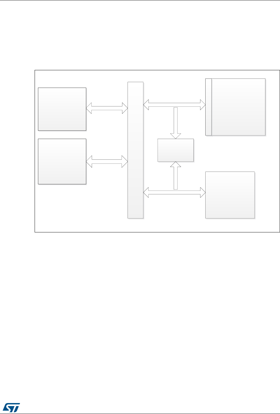
DocID025941 Rev 5 129/1001
RM0376 Firewall (FW)
139
5.3 Firewall functional description
5.3.1 Firewall AMBA bus snoop
The Firewall peripheral is snooping the AMBA buses on which the memories (volatile and
non-volatile) are connected. A global architecture view is illustrated in Figure 8.
Figure 8. STM32L0x2 firewall connection schematics
5.3.2 Functional requirements
There are several requirements to guaranty the highest security level by the application
code/data which needs to be protected by the Firewall and to avoid unwanted Firewall alarm
(reset generation).
Debug consideration
In debug mode, if the Firewall is opened, the accesses by the debugger to the protected
segments are not blocked. For this reason, the Read out level 2 protection must be active in
conjunction with the Firewall implementation.
If the debug is needed, it is possible to proceed in the following way:
•A dummy code having the same API as the protected code may be developed during
the development phase of the final user code. This dummy code may send back
coherent answers (in terms of function and potentially timing if needed), as the
protected code should do in production phase.
•In the development phase, the protected code can be given to the customer-end under
NDA agreement and its software can be developed in level 0 protection. The customer-
end code needs to embed an IAP located in a write protected segment in order to allow
future code updates when the production parts will be Level 2 ROP.
MS32388V3
CORTEX M0+
DMA
Flash program
memory and data
EEPROM
I
N
T
E
R
F
A
C
E
B
U
S
M
A
T
R
I
X
FIREWALL
SRAM
AHB Master 1
AHB Master 2
AHB Slave
AHB Slave

Firewall (FW) RM0376
130/1001 DocID025941 Rev 5
Write protection
In order to offer a maximum security level, the following points need to be respected:
•It is mandatory to keep a write protection on the part of the code enabling the Firewall.
This activation code should be located outside the segments protected by the Firewall.
•The write protection is also mandatory on the code segment protected by the Firewall.
•The page including the reset vector must be write-protected.
Interruptions management
The code protected by the Firewall must not be interruptible. It is up to the user code to
disable any interrupt source before executing the code protected by the Firewall. If this
constraint is not respected, if an interruption comes while the protected code is executed
(Firewall opened), the Firewall will be closed as soon as the interrupt subroutine is
executed. When the code returns back to the protected code area, a Firewall alarm will raise
since the “call gate” sequence will not be applied and a reset will be generated.
Concerning the interrupt vectors and the first user page in the Flash program memory:
•If the first user page (including the reset vector) is protected by the Firewall, the NVIC
vector should be reprogrammed outside the protected segment.
•If the first user page is not protected by the Firewall, the interrupt vectors may be kept
at this location.
There is no interruption generated by the Firewall.
5.3.3 Firewall segments
The Firewall has been designed to protect three different segment areas:
Code segment
This segment is located into the Flash program memory. It should contain the code to
execute which requires the Firewall protection. The segment must be reached using the
“call gate” entry sequence to open the Firewall. A system reset is generated if the “call gate”
entry sequence is not respected (refer to Opening the Firewall) and if the Firewall is enabled
using the FWDIS bit in the system configuration register. The length of the segment and the
segment base address must be configured before enabling the Firewall (refer to
Section 5.3.5: Firewall initialization).
Non-volatile data segment
This segment contains non-volatile data used by the protected code which must be
protected by the Firewall. The access to this segment is defined into Section 5.3.4: Segment
accesses and properties. The Firewall must be opened before accessing the data in this
area. The Non-Volatile data segment should be located into the Flash program or 2-Kbyte
Data EEPROM memory. The segment length and the base address of the segment must be
configured before enabling the Firewall (refer to Section 5.3.5: Firewall initialization).

DocID025941 Rev 5 131/1001
RM0376 Firewall (FW)
139
Volatile data segment
Volatile data used by the protected code located into the code segment must be defined into
the SRAM memory. The access to this segment is defined into the Section 5.3.4: Segment
accesses and properties. Depending on the Volatile data segment configuration, the
Firewall must be opened or not before accessing this segment area. The segment length
and the base address of the segment as well as the segment options must be configured
before enabling the Firewall (refer to Section 5.3.5: Firewall initialization).
The Volatile data segment can also be defined as executable (for the code execution) or
shared using two bit of the Firewall configuration register (bit VDS for the volatile data
sharing option and bit VDE for the volatile data execution capability). For more details, refer
to Table 28.
5.3.4 Segment accesses and properties
All DMA accesses to the protected segments are forbidden, whatever the Firewall state, and
generate a system reset.
Segment access depending on the Firewall state
Each of the three segments has specific properties which are presented in Table 2 8.
Table 28. Segment accesses according to the Firewall state
Segment Firewall opened
access allowed
Firewall closed
access allowed
Firewall disabled
access allowed
Code segment Read and execute
No access allowed.
Any access to the segment
(except the “call gate” entry)
generates a system reset
All accesses are allowed
(according to the EEPROM
protection properties in which
the code is located)
Non-volatile data
segment Read and write No access allowed
All accesses are allowed
(according to the EEPROM
protection properties in which
the code is located)
Volatile data
segment
Read and Write
Execute if VDE = 1 and
VDS = 0 into the Firewall
configuration register
No access allowed if VDS = 0
and VDE = 0 into the Firewall
configuration register
Read/write/execute accesses
allowed if VDS = 1 (whatever
VDE bit value)
Execute if VDE = 1 and VDS = 0
but with a “call gate” entry to
open the Firewall at first.
All accesses are allowed
Firewall (FW) RM0376
132/1001 DocID025941 Rev 5
The Volatile data segment is a bit different from the two others. The segment can be:
•Shared (VDS bit in the register)
It means that the area and the data located into this segment can be shared between
the protected code and the user code executed in a non-protected area. The access is
allowed whether the Firewall is opened or closed or disabled.
The VDS bit gets priority over the VDE bit, this last bit value being ignored in such a
case. It means that the Volatile data segment can execute parts of code located there
without any need to open the Firewall before executing the code.
•Execute
The VDE bit is considered as soon as the VDS bit = 0 in the FW_CR register. If the
VDS bit = 1, refer to the description above on the Volatile data segment sharing. If VDS
= 0 and VDE = 1, the Volatile data segment is executable. To avoid a system reset
generation from the Firewall, the “call gate” sequence should be applied on the Volatile
data segment to open the Firewall as an entry point for the code execution.
Segments properties
Each segment has a specific length register to define the segment size to be protected by
the Firewall: CSL register for the Code segment length register, NVDSL for the Non-volatile
data segment length register, and VDSL register for the Volatile data segment length
register. Granularity and area ranges for each of the segments are presented in Ta ble 29.
5.3.5 Firewall initialization
The initialization phase should take place at the beginning of the user code execution (refer
to the Write protection).
The initialization phase consists of setting up the addresses and the lengths of each
segment which needs to be protected by the Firewall. It must be done before enabling the
Firewall, because the enabling bit can be written once. Thus, when the Firewall is enabled, it
cannot be disabled anymore until the next system reset.
Once the Firewall is enabled, the accesses to the address and length segments are no
longer possible. All write attempts are discarded.
A segment defined with a length equal to 0 is not considered as protected by the Firewall.
As a consequence, there is no reset generation from the Firewall when an access to the
base address of this segment is performed.
After a reset, the Firewall is disabled by default (FWDIS bit in the SYSCFG register is set). It
has to be cleared to enable the Firewall feature.
Table 29. Segment granularity and area ranges
Segment Granularity Area range
Code segment 256 byte up to 64 Kbytes - 256 bytes
Non-volatile data segment 256 byte up to 64 Kbytes - 256 bytes
Volatile data segment 64 byte 8 Kbytes - 64 bytes
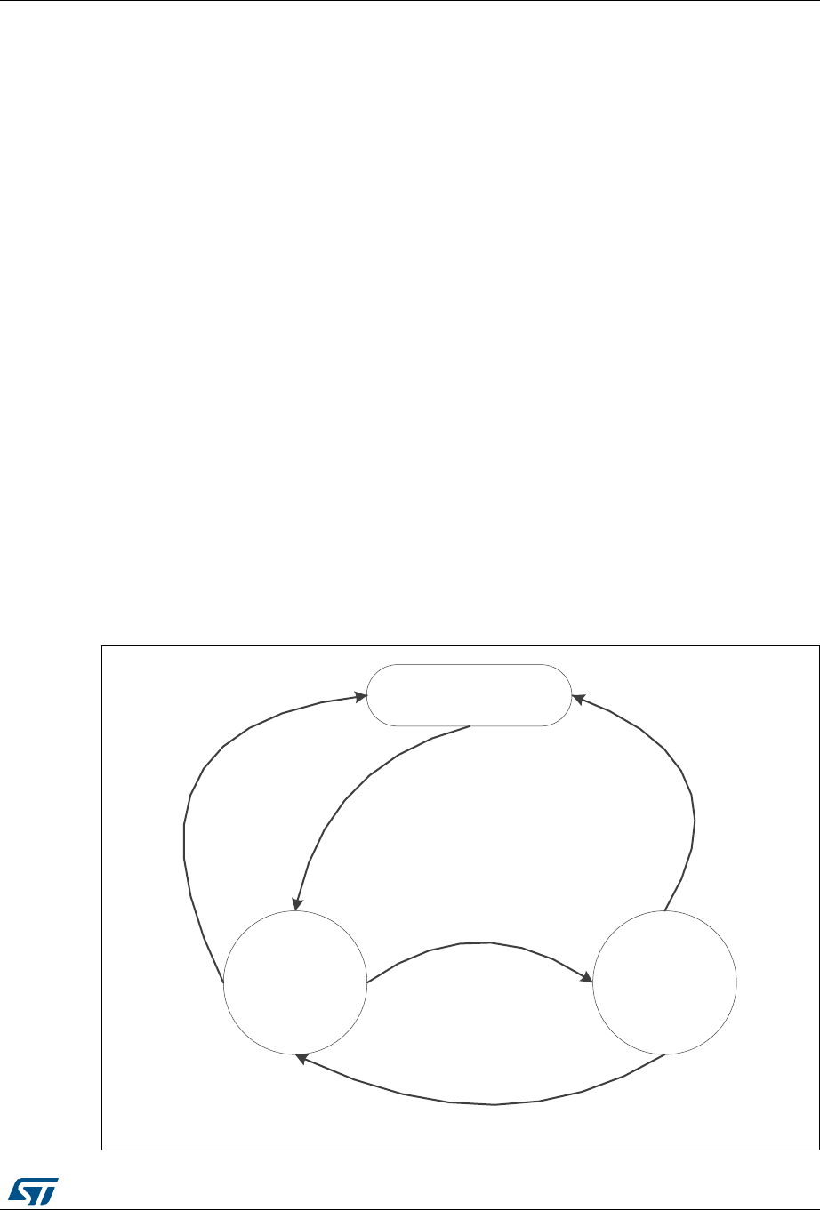
DocID025941 Rev 5 133/1001
RM0376 Firewall (FW)
139
Below is the initialization procedure to follow:
1. Configure the RCC to enable the clock to the Firewall module
2. Configure the RCC to enable the clock of the system configuration registers
3. Set the base address and length of each segment (CSSA, CSL, NVDSSA, NVDSL,
VDSSA, VDSL registers)
4. Set the configuration register of the Firewall (FW_CR register)
5. Enable the Firewall clearing the FWDIS bit in the system configuration register.
The Firewall configuration register (FW_CR register) is the only one which can be managed
in a dynamic way even if the Firewall is enabled:
•when the Non-Volatile data segment is undefined (meaning the NVDSL register is
equal to 0), the accesses to this register are possible whatever the Firewall state
(opened or closed).
•when the Non-Volatile data segment is defined (meaning the NVDSL register is
different from 0), the accesses to this register are only possible when the Firewall is
opened.
5.3.6 Firewall states
The Firewall has three different states as shown in Figure 9:
•Disabled: The FWDIS bit is set by default after the reset. The Firewall is not active.
•Closed: The Firewall protects the accesses to the three segments (Code, Non-volatile
data, and Volatile data segments).
•Opened: The Firewall allows access to the protected segments as defined in
Section 5.3.4: Segment accesses and properties.
Figure 9. Firewall functional states
MS32390V4
Firewall disable
(reset)
Firewall
closed
Firewall
opened
Enable the firewall
(FWDIS = 0)
‘‘call gate’’ entry
Illegal accesses to
the protected
segments
Code protected jumps
to unprotected
segments
Protected code jumps
to an unprotected
segment and FPA = 0

Firewall (FW) RM0376
134/1001 DocID025941 Rev 5
Opening the Firewall
As soon as the Firewall is enabled, it is closed. It means that most of the accesses to the
protected segments are forbidden (refer to Section 5.3.4: Segment accesses and
properties). In order to open the Firewall to interact with the protected segments, it is
mandatory to apply the “call gate” sequence described hereafter.
“call gate” sequence
The “call gate” is composed of 3 words located on the first three 32-bit addresses of the
base address of the code segment and of the Volatile data segment if it is declared as
not shared (VDS = 0) and executable (VDE = 1).
– 1st word: Dummy 32-bit words always closed in order to protect the “call gate”
opening from an access due to a prefetch buffer.
– 2nd and 3rd words: 2 specific 32-bit words called “call gate” and always opened.
To open the Firewall, the code currently executed must jump to the 2nd word of the “call
gate” and execute the code from this point. The 2nd word and 3rd word execution must not
be interrupted by any intermediate instruction fetch; otherwise, the Firewall is not
considered open and comes back to a close state. Then, executing the 3rd word after
receiving the intermediate instruction fetch would generate a system reset as a
consequence.
As soon as the Firewall is opened, the protected segments can be accessed as described in
Section 5.3.4: Segment accesses and properties.
Closing the Firewall
The Firewall is closed immediately after it is enabled (clearing the FWDIS bit in the system
configuration register).
To close the Firewall, the protected code must:
•Write the correct value in the Firewall Pre Arm Flag into the FW_CR register.
•Jump to any executable location outside the Firewall segments.
If the Firewall Pre Arm Flag is not set when the protected code jumps to a non protected
segment, a reset is generated. This control bit is an additional protection to avoid an
undesired attempt to close the Firewall with the private information not yet cleaned (see the
note below).
For security reasons, following the application for which the Firewall is used, it is advised to
clean all private information from CPU registers and hardware cells.

DocID025941 Rev 5 135/1001
RM0376 Firewall (FW)
139
5.4 Firewall registers
5.4.1 Code segment start address (FW_CSSA)
Address offset: 0x00
Reset value: 0x0000 0000
5.4.2 Code segment length (FW_CSL)
Address offset: 0x04
Reset value: 0x0000 0000
31 30 29 28 27 26 25 24 23 22 21 20 19 18 17 16
Res. Res. Res. Res. Res. Res. Res. Res. ADD[23:16]
rw
15141312111098 7 6543210
ADD[15:8] Res. Res. Res. Res. Res. Res. Res. Res.
rw
Bits 31:24 Reserved, must be kept at reset value.
Bits 23:8 ADD[23:8]: code segment start address
The LSB bits of the start address (bit 7:0) are reserved and forced to 0 in order to allow a
256-byte granularity.
Note: These bits can be written only before enabling the Firewall. Refer to Section 5.3.5:
Firewall initialization.
Bits 7:0 Reserved, must be kept at the reset value.
31 30 29 28 27 26 25 24 23 22 21 20 19 18 17 16
Res. Res. Res. Res. Res. Res. Res. Res. Res. Res. LENG[21:16]
rw
1514131211109876543210
LENG15:8] Res. Res. Res. Res. Res. Res. Res. Res.
rw
Bits 31:22 Reserved, must be kept at the reset value.
Bits 21:8 LENG[21:8]: code segment length
LENG[21:8] selects the size of the code segment expressed in bytes but is a multiple of
256 bytes.
The segment area is defined from {ADD[23:8],0x00} to {ADD[23:8]+LENG[21:8], 0x00} - 0x01
Note: If LENG[21:8] = 0 after enabling the Firewall, this segment is not defined, thus not
protected by the Firewall.
These bits can only be written before enabling the Firewall. Refer to Section 5.3.5:
Firewall initialization.
Bits 7:0 Reserved, must be kept at the reset value.
Firewall (FW) RM0376
136/1001 DocID025941 Rev 5
5.4.3 Non-volatile data segment start address (FW_NVDSSA)
Address offset: 0x08
Reset value: 0x0000 0000
5.4.4 Non-volatile data segment length (FW_NVDSL)
Address offset: 0x0C
Reset value: 0x0000 0000
31 30 29 28 27 26 25 24 23 22 21 20 19 18 17 16
Res. Res. Res. Res. Res. Res. Res. Res. ADD[23:16]
rw
15141312111098 7 6543210
ADD[15:8] Res. Res. Res. Res. Res. Res. Res. Res.
rw
Bits 31:24 Reserved, must be kept at the reset value.
Bits 23:8 ADD[23:8]: Non-volatile data segment start address
The LSB bits of the start address (bit 7:0) are reserved and forced to 0 in order to allow a
256-byte granularity.
Note: These bits can only be written before enabling the Firewall. Refer to Section 5.3.5:
Firewall initialization.
Bits 7:0 Reserved, must be kept at the reset value.
31 30 29 28 27 26 25 24 23 22 21 20 19 18 17 16
Res. Res. Res. Res. Res. Res. Res. Res. Res. Res. LENG[21:16]
rw
1514131211109876543210
LENG[15:8] Res. Res. Res. Res. Res. Res. Res. Res.
rw
Bits 31:22 Reserved, must be kept at the reset value.
Bits 21:8 LENG[21:8]: Non-volatile data segment length
LENG[21:8] selects the size of the Non-volatile data segment expressed in bytes but is a
multiple of 256 bytes.
The segment area is defined from {ADD[23:8],0x00} to {ADD[23:8]+LENG[21:8], 0x00} - 0x01
Note: If LENG[21:8] = 0 after enabling the Firewall, this segment is not defined, thus not
protected by the Firewall.
These bits can only be written before enabling the Firewall. Refer to Section 5.3.5:
Firewall initialization.
Bits 7:0 Reserved, must be kept at the reset value.

DocID025941 Rev 5 137/1001
RM0376 Firewall (FW)
139
5.4.5 Volatile data segment start address (FW_VDSSA)
Address offset: 0x10
Reset value: 0x0000 0000
5.4.6 Volatile data segment length (FW_VDSL)
Address offset: 0x14
Reset value: 0x0000 0000
31 30 29 28 27 26 25 24 23 22 21 20 19 18 17 16
Res. Res. Res. Res. Res. Res. Res. Res. Res. Res. Res. Res. Res. Res. Res. Res.
15141312111098 7 6543210
ADD[15:6] Res. Res. Res. Res. Res. Res.
rw
Bits 31:16 Reserved, must be kept at the reset value.
Bits 15:6 ADD[15:6]: Volatile data segment start address
The LSB bit of the start address (bits 5:0) are reserved and forced to 0 in order to allow a
64-byte granularity.
Note: These bits can only be written before enabling the Firewall. Refer to Section 5.3.5:
Firewall initialization.
Bits 5:0 Reserved, must be kept at the reset value.
31 30 29 28 27 26 25 24 23 22 21 20 19 18 17 16
Res. Res. Res. Res. Res. Res. Res. Res. Res. Res. Res. Res. Res. Res. Res. Res.
1514131211109876543210
LENG[15:6] Res. Res. Res. Res. Res. Res.
rw
Bits 31:16 Reserved, must be kept at the reset value.
Bits 15:6 LENG[15:6]: Volatile data segment length
LENG[15:6] selects the size of the volatile data segment expressed in bytes but is a multiple
of 64 bytes.
The segment area is defined from {ADD[15:6],0x00} to {ADD[15:6]+LENG[15:6], 0x00} - 0x01
Note: If LENG[15:6] = 0 after enabling the Firewall, this segment is not defined, thus not
protected by the Firewall.
These bits can only be written before enabling the Firewall. Refer to Section 5.3.5:
Firewall initialization.
Bits 5:0 Reserved, must be kept at the reset value.

Firewall (FW) RM0376
138/1001 DocID025941 Rev 5
5.4.7 Configuration register (FW_CR)
Address offset: 0x20
Reset value: 0x0000 0000
This register is protected in the same way as the Non-volatile data segment (refer to
Section 5.3.5: Firewall initialization).
31 30 29 28 27 26 25 24 23 22 21 20 19 18 17 16
Res. Res. Res. Res. Res. Res. Res. Res. Res. Res. Res. Res. Res. Res. Res. Res.
1514131211109876543210
Res. Res. Res. Res. Res. Res. Res. Res. Res. Res. Res. Res. Res. VDE VDS FPA
rw rw rw
Bits 31:3 Reserved, must be kept at the reset value.
Bit 2 VDE: Volatile data execution
0: Volatile data segment cannot be executed if VDS = 0
1: Volatile data segment is declared executable whatever VDS bit value
When VDS = 1, this bit has no meaning. The Volatile data segment can be executed whatever
the VDE bit value.
If VDS = 1, the code can be executed whatever the Firewall state (opened or closed)
If VDS = 0, the code can only be executed if the Firewall is opened or applying the “call gate”
entry sequence if the Firewall is closed.
Refer to Segment access depending on the Firewall state.
Bit 1 VDS: Volatile data shared
0: Volatile data segment is not shared and cannot be hit by a non protected executable code
when the Firewall is closed. If it is accessed in such a condition, a system reset will be
generated by the Firewall.
1: Volatile data segment is shared with non protected application code. It can be accessed
whatever the Firewall state (opened or closed).
Refer to Segment access depending on the Firewall state.
Bit 0 FPA: Firewall prearm
0: any code executed outside the protected segment when the Firewall is opened will
generate a system reset.
1: any code executed outside the protected segment will close the Firewall.
Refer to Closing the Firewall.

DocID025941 Rev 5 139/1001
RM0376 Firewall (FW)
139
5.4.8 Firewall register map
The table below provides the Firewall register map and reset values.
Refer to Section 2.2.2 on page 58 for the register boundary addresses.
Table 30. Firewall register map and reset values
Offset Register
31
30
29
28
27
26
25
24
23
22
21
20
19
18
17
16
15
14
13
12
11
10
9
8
7
6
5
4
3
2
1
0
0x0 FW_CSSA
Res.
Res.
Res.
Res.
Res.
Res.
Res.
Res.
ADD
Res.
Res.
Res.
Res.
Res.
Res.
Res.
Res.
Reset Value 0000000000000000
0x4 FW_CSL
Res.
Res.
Res.
Res.
Res.
Res.
Res.
Res.
Res.
Res.
LENG
Res.
Res.
Res.
Res.
Res.
Res.
Res.
Res.
Reset Value 00000000000000
0x8 FW_NVDSSA
Res.
Res.
Res.
Res.
Res.
Res.
Res.
Res.
ADD
Res.
Res.
Res.
Res.
Res.
Res.
Res.
Res.
Reset Value 0000000000000000
0xC FW_NVDSL
Res.
Res.
Res.
Res.
Res.
Res.
Res.
Res.
Res.
Res.
LENG
Res.
Res.
Res.
Res.
Res.
Res.
Res.
Res.
Reset Value 00000000000000
0x10 FW_VDSSA
Res.
Res.
Res.
Res.
Res.
Res.
Res.
Res.
Res.
Res.
Res.
Res.
Res.
Res.
Res.
Res.
ADD
Res.
Res.
Res.
Res.
Res.
Res.
Reset Value 0000000000
0x14 FW_VDSL
Res.
Res.
Res.
Res.
Res.
Res.
Res.
Res.
Res.
Res.
Res.
Res.
Res.
Res.
Res.
Res.
LENG
Res.
Res.
Res.
Res.
Res.
Res.
0x18
Res.
Res.
Res.
Res.
Res.
Res.
Res.
Res.
Res.
Res.
Res.
Res.
Res.
Res.
Res.
Res.
Res.
Res.
Res.
Res.
Res.
Res.
Res.
Res.
Res.
Res.
Res.
Res.
Res.
Res.
Res.
Res.
Reset Value
0x1C
Res.
Res.
Res.
Res.
Res.
Res.
Res.
Res.
Res.
Res.
Res.
Res.
Res.
Res.
Res.
Res.
Res.
Res.
Res.
Res.
Res.
Res.
Res.
Res.
Res.
Res.
Res.
Res.
Res.
Res.
Res.
Res.
Reset Value
0x20 FW_CR
Res.
Res.
Res.
Res.
Res.
Res.
Res.
Res.
Res.
Res.
Res.
Res.
Res.
Res.
Res.
Res.
Res.
Res.
Res.
Res.
Res.
Res.
Res.
Res.
Res.
Res.
Res.
Res.
Res.
VDE
VDS
FPA
Reset Value 000

Power control (PWR) RM0376
140/1001 DocID025941 Rev 5
6 Power control (PWR)
6.1 Power supplies
The device requires a 1.8-to-3.6 V VDD operating voltage supply (down to 1.65 V at power-
down) when the BOR is available. The device requires a 1.65-to-3.6 V VDD operating
voltage supply when the BOR is not available.
An embedded linear voltage regulator is used to supply the internal digital power, ranging
from 1.2 to 1.8 V.
•VDD = 1.8 V (at power-on) or 1.65 V (at power-down) to 3.6 V when the BOR is
available. VDD = 1.65 V to 3.6 V, when BOR is not available
VDD is the external power supply for I/Os and internal regulator. It is provided externally
through VDD pins
•VCORE = 1.2 to 1.8 V
VCORE is the power supply for digital peripherals, SRAM and Flash memory. It is
generated by a internal voltage regulator. Three VCORE ranges can be selected by
software depending on VDD (refer Figure 11).
•VSSA, VDDA = 1.8 V (at power-on) or 1.65 V (at power-down) to 3.6 V, when BOR is
available and VSSA, VDDA = 1.65 to 3.6 V, when BOR is not available.
VDDA is the external analog power supply for ADC, DAC, reset blocks, RC oscillators
and PLL. The minimum voltage to be applied to VDDA is 1.8 V when the DAC is used.
•VREF+
VREF+ is the input reference voltage. It is only available as an external pin on a few
packages, otherwise it is bonded to VDDA.
•VDD_USB = 3.0 to 3.6 V
VDD_USB is a dedicated independent USB power supply for full speed transceivers. It is
available on PA11 and PA12 pins provided they are configured as USB alternate
function.
Note: VDD_USB value does not dependent on VDD and VDDA. However, VDD_USB must be the last
supply to be delivered to the device and the first to be switched off. When the three power
supplies are shut down, if VDD_USB remains active for a short period of time and VDDA/VDDIO
fall below the functional range, the device is not be damaged.
The device is still functional when VDD_USB is switched off.
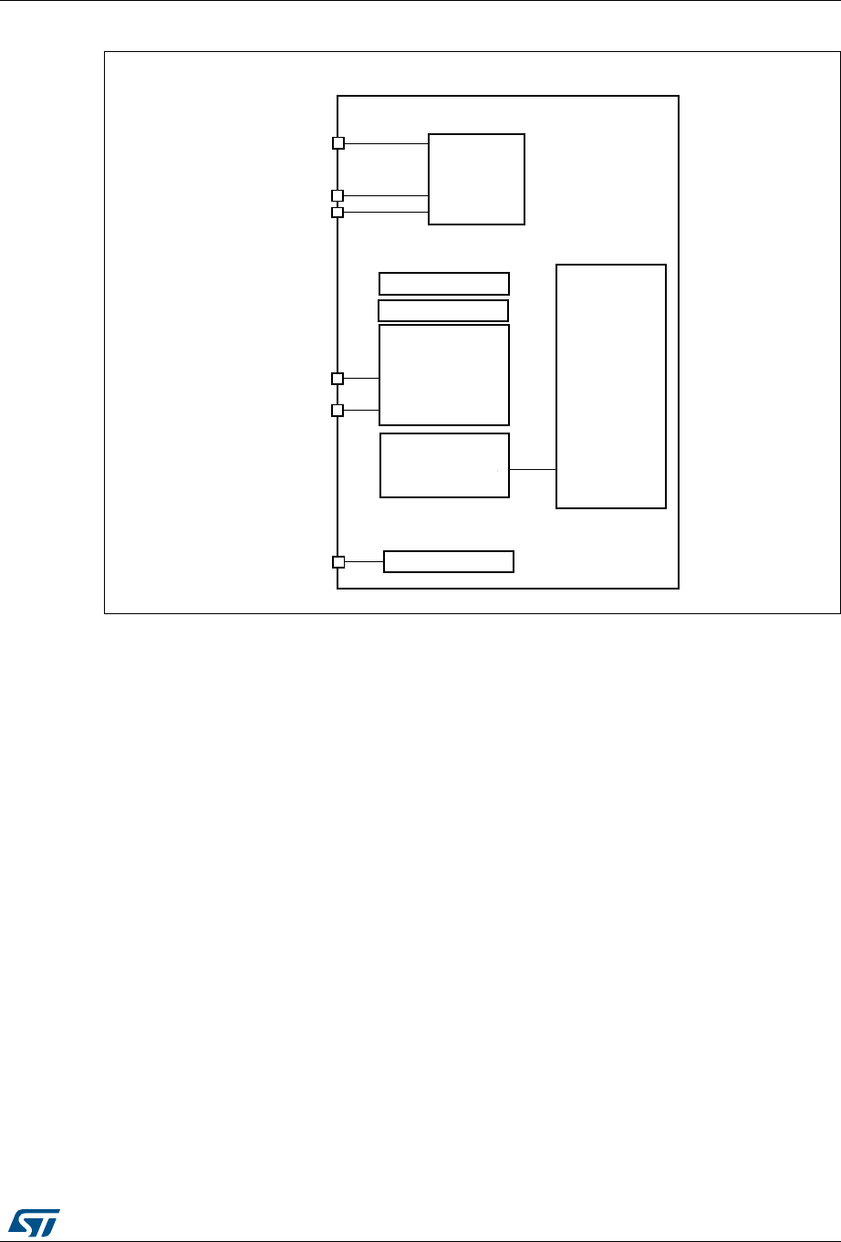
DocID025941 Rev 5 141/1001
RM0376 Power control (PWR)
170
Figure 10. Power supply overview
1. VDDA and VSSA must be connected to VDD and VSS, respectively.
2. Depending on the operating power supply range used, some peripherals may be used with limited features
or performance.
3. VREF+ is only available on TFBGA64 package.
6.1.1 Independent A/D and DAC converter supply and reference voltage
To improve conversion accuracy, the ADC and the DAC have an independent power supply
that can be filtered separately, and shielded from noise on the PCB.
•The ADC voltage supply input is available on a separate VDDA pin
•An isolated supply ground connection is provided on the VSSA pin
On packages with more than 64 pins and UFBGA64
To ensure a better accuracy on low-voltage inputs and outputs, the user can connect to
VREF+ a separate external reference voltage lower than VDD. VREF+ is the highest voltage,
represented by the full scale value, for an analog input (ADC) or output (DAC) signal.
For DAC:
1.8 V ≤ VREF+ ≤ VDDA
For ADC:
1.65 V ≤ VREF+ < VDDA
On packages with 64 pins or less (except BGA package)
VREF+ pin is not available. It is internally connected to the ADC voltage supply (VDDA).
MSv34751V2
VDD
VSS
(VDD) VDDA
(from 1.65 V up to VDDA) VREF+
VDDA domain
VDD domain VCore domain
ADC
DAC
Temp. Sensor
Reset block
PLL
Flash memory
IO supply
Standby
circuitry(Wakeup
logic, IWDG, RTC,
LSE crystal 32K
osc., RCC, CSR)
Voltage regulator
Dynamic voltage
scaling
Core memories
Digital
peripherals
VDD_USB USB transceiver
(VSS) VSSA

Power control (PWR) RM0376
142/1001 DocID025941 Rev 5
6.1.2 RTC and RTC backup registers
The real-time clock (RTC) is an independent BCD timer/counter. The RTC provides a time-
of-day clock/calendar, two programmable alarm interrupts, and a periodic programmable
wakeup flag with interrupt capability. The RTC contains 5 backup data registers (20 bytes).
These backup registers are reset when a tamper detection event occurs. For more details
refer to Real-time clock (RTC) section.
RTC registers access
After reset, the RTC Registers (RTC registers and RTC backup registers) are protected
against possible stray write accesses. To enable access to the RTC Registers, proceed as
follows:
1. Enable the power interface clock by setting the PWREN bits in the RCC_APB1ENR
register.
2. Set the DBP bit in the PWR_CR register (see Section 6.4.1).
3. Select the RTC clock source through RTCSEL[1:0] bits in RCC_CSR register.
4. Enable the RTC clock by programming the RTCEN bit in the RCC_CSR register.
6.1.3 Voltage regulator
An embedded linear voltage regulator supplies all the digital circuitries except for the
Standby circuitry. The regulator output voltage (VCORE) can be programmed by software to
three different ranges within 1.2 - 1.8 V (typical) (see Section 6.1.4).
The voltage regulator is always enabled after Reset. It works in three different modes: main
(MR), low-power (LPR) and power-down, depending on the application modes.
•In Run mode, the regulator is main (MR) mode and supplies full power to the VCORE
domain (core, memories and digital peripherals).
•In Low-power run mode, the regulator is in low-power (LPR) mode and supplies low-
power to the VCORE domain, preserving the contents of the registers and internal
SRAM.
•In Sleep mode, the regulator is main (MR) mode and supplies full power to the VCORE
domain, preserving the contents of the registers and internal SRAM.
•In Low-power sleep mode, the regulator is in low-power (LPR) mode and supplies low-
power to the VCORE domain, preserving the contents of the registers and internal
SRAM.
•In Stop mode the regulator supplies low power to the VCORE domain, preserving the
content of registers and internal SRAM.
•In Standby mode, the regulator is powered off. The content of the registers and SRAM
are lost except for the Standby circuitry.
6.1.4 Dynamic voltage scaling management
The dynamic voltage scaling is a power management technique which consists in
increasing or decreasing the voltage used for the digital peripherals (VCORE), according to
the circumstances.
Dynamic voltage scaling to increase VCORE is known as overvolting. It allows improving the
device performance. Refer to Figure 11 for a description of the device operating conditions
versus CPU performance and to the datasheet electrical characteristics for ADC clock
frequency versus dynamic range.

DocID025941 Rev 5 143/1001
RM0376 Power control (PWR)
170
Dynamic voltage scaling to decrease VCORE is known as undervolting. It is performed to
save power, particularly in laptops and other mobile devices where the energy comes from a
battery and is thus limited.
Range 1
Range 1 is the “high performance” range.
The voltage regulator outputs a 1.8 V voltage (typical) as long as the VDD input voltage is
above 1.71 V. Flash program and erase operations can be performed in this range.
The clock recovery system (CRS) is available only when the device operates in range 1
(see Section 8: Clock recovery system (CRS)).
When VDD is below 2.0 V, the CPU frequency changes from initial to final state must respect
the following conditions:
•fCPUfinal < 4xfCPUinitial.
•In addition, a 5 μs delay must be respected between two changes. For example to
switch from 4.2 to 32 MHz, switch from 4.2 to 16 MHz, wait for 5 μs, then switch from
16 to 32 MHz.
Range 2 and 3
The regulator can also be programmed to output a regulated 1.5 V (typical, range 2) or a
1.2 V (typical, range 3) without any limitations on VDD (1.65 to 3.6 V).
•At 1.5 V, the Flash memory is still functional but with medium read access time. This is
the “medium performance” range. Program and erase operations on the Flash memory
are still possible.
•At 1.2 V, the Flash memory is still functional but with slow read access time. This is the
“low performance” range. Program and erase operations on the Flash memory are not
possible under these conditions.
Refer to Table 31 for details on the performance for each range.
Table 31. Performance versus VCORE ranges
CPU
performance
Power
performance
VCORE
range
Typical
Value (V)
Max frequency
(MHz) VDD range
1 WS 0 WS
High Low 1 1.8 32 16 1.71 - 3.6
Medium Medium 2 1.5 16 8
1.65 - 3.6
Low High 3 1.2 4.2 4.2
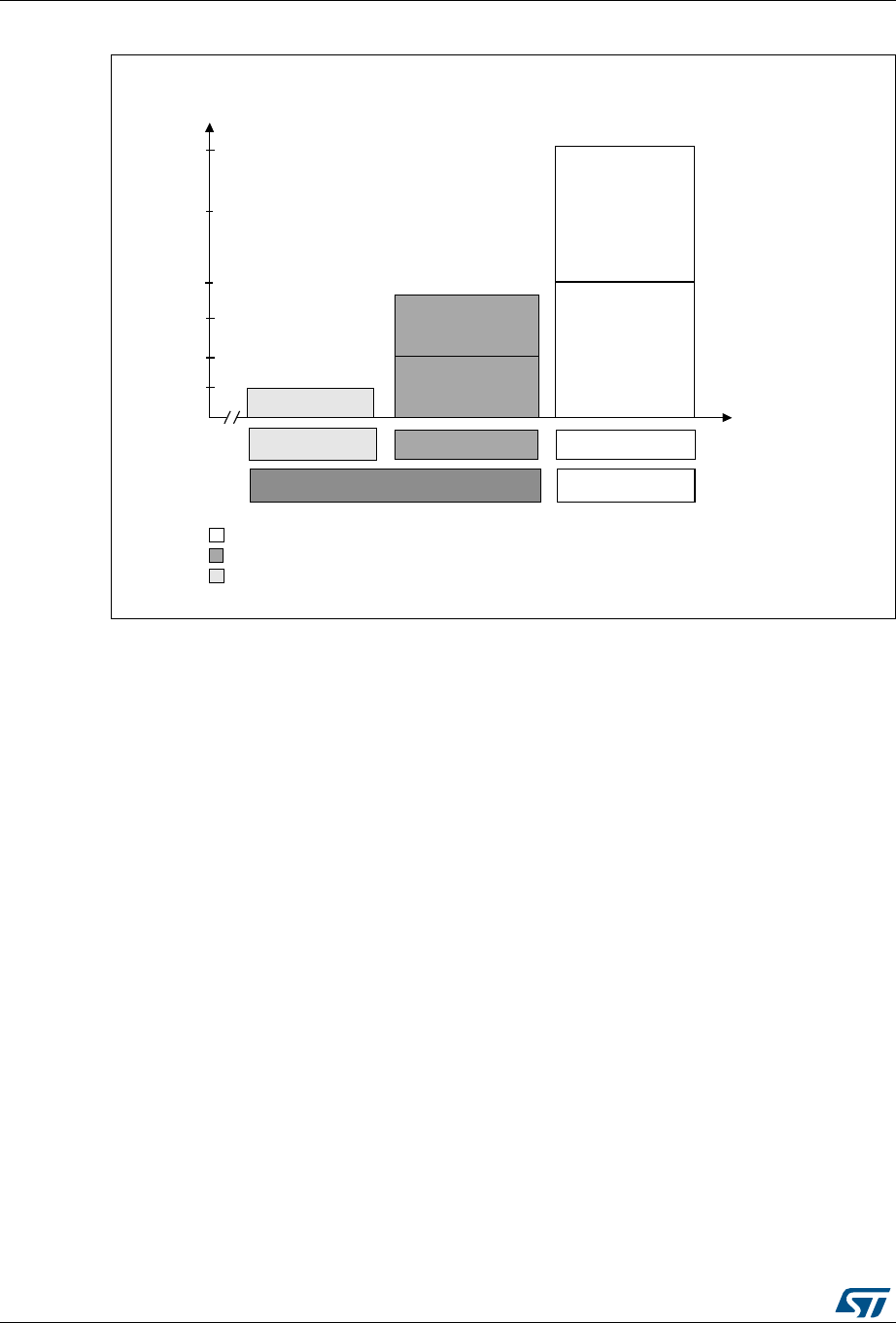
Power control (PWR) RM0376
144/1001 DocID025941 Rev 5
Figure 11. Performance versus VDD and VCORE range
6.1.5 Dynamic voltage scaling configuration
The following sequence is required to program the voltage regulator ranges:
1. Check VDD to identify which ranges are allowed (see Figure 11: Performance versus
VDD and VCORE range).
2. Poll VOSF bit of in PWR_CSR. Wait until it is reset to 0.
3. Configure the voltage scaling range by setting the VOS[1:0] bits in the PWR_CR
register.
4. Poll VOSF bit of in PWR_CSR register. Wait until it is reset to 0.
Note: During voltage scaling configuration, the system clock is stopped until the regulator is
stabilized (VOSF=0). This must be taken into account during application development, in
case a critical reaction time to interrupt is needed, and depending on peripheral used (timer,
communication,...).
6.1.6 Voltage regulator and clock management when VDD drops
below 1.71 V
When VCORE range 1 is selected and VDD drops below 1.71 V, the application must
reconfigure the system.
A three-step sequence is required to reconfigure the system:
1. Detect that VDD drops below 1.71 V:
Use the PVD to monitor the VDD voltage and to generate an interrupt when the voltage
goes under the selected level. To detect the 1.71 V voltage limit, the application can
4.2 MHz
0WS
16 MHz
MHz
32 MHz
1.2 V 1.5 V 1.8 V
VCORE
1.65 V - 3.6 V 1.71 V – 3.6 V
32
1
16 MHz
8 MHz
32
24
16
12
8
4
Range 1
Range 2
Range 3
MS32792V1
VDD
FCPU> 8 MHz
1W S
0WS
FCPU > 16 MHz
1WS
0WS

DocID025941 Rev 5 145/1001
RM0376 Power control (PWR)
170
select by software PVD threshold 2 (2.26 V typical). For more details on the PVD, refer
to Section 6.2.3.
2. Adapt the clock frequency to the voltage range that will be selected at next step:
Below 1.71 V, the system clock frequency is limited to 16 MHz for range 2 and 4.2 MHz
for range 3.
3. Select the required voltage range:
Note that when VDD is below 1.71 V, only range 2 or range 3 can be selected.
Note: When VCORE range 2 or range 3 is selected and VDD drops below 1.71 V, no system
reconfiguration is required.
6.1.7 Voltage regulator and clock management when modifying the
VCORE range
When VDD is above 1.71 V, any of the 3 voltage ranges can be selected:
•When the voltage range is above the targeted voltage range (e.g. from range 1 to 2):
a) Adapt the clock frequency to the lower voltage range that will be selected at next
step.
b) Select the required voltage range.
•When the voltage range is below the targeted voltage range (e.g. from range 3 to 1):
a) Select the required voltage range.
b) Tune the clock frequency if needed.
When VDD is below 1.71 V, only range 2 and 3 can be selected:
•From range 2 to range 3
a) Adapt the clock frequency to voltage range 3.
b) Select voltage range 3.
•From range 3 to range 2
a) Select the voltage range 2.
b) Tune the clock frequency if needed.
6.1.8 Voltage range and limitations when VDD ranges from 1.71 V to 2.0 V
The STM32L0x2 voltage regulator is based on an architecture designed for Ultra-low-power
a. It does not use any external capacitor. Such regulator is sensitive to fast changes of load.
In this case, the output voltage is reduced for a short period of time. Considering that the
core voltage must be higher than 1.65 V to ensure a 32 MHz operation, this phenomenon is
critical for very low VDD voltages (e.g. 1.71 V VDD minimum value).
To guarantee 32 MHz operation at VDD =1.8 V±5%, with 1 wait state, and VCORE range 1,
the CPU frequency in run mode must be managed to prevent any changes exceeding a
ratio of 4 in one shot. A delay of 5 μs must be respected between 2 changes. There is no
limitation when waking up from low-power mode.

Power control (PWR) RM0376
146/1001 DocID025941 Rev 5
6.2 Power supply supervisor
The device has an integrated zeropower power-on reset (POR)/power-down reset (PDR),
coupled with a brown out reset (BOR) circuitry. For devices operating between 1.8 and 3.6
V, the BOR is always active at power-on and ensures proper operation starting from 1.8 V.
After the 1.8 V BOR threshold is reached, the option byte loading process starts, either to
confirm or modify default thresholds, or to disable BOR permanently (in which case, the VDD
min value at power-down is 1.65 V). For devices operating between 1.65 V and 3.6 V, the
BOR is permanently disabled. Consequently, the start-up time at power-on can be
decreased down to 1 ms typically.
Five BOR thresholds can be configured by option bytes, starting from 1.65 to 3 V. To reduce
the power consumption in Stop mode, the internal voltage reference, VREFINT, can be
automatically switch off. The device remains in reset mode when VDD is below a specified
threshold, VPOR, VPDR or VBOR, without the need for any external reset circuit.
The device features an embedded programmable voltage detector (PVD) that monitors the
VDD/VDDA power supply and compares it to the VPVD threshold. 7 different PVD levels can
be selected by software between 1.85 and 3.05 V, with a 200 mV step. An interrupt can be
generated when VDD/VDDA drops below the VPVD threshold and/or when VDD/VDDA is
higher than the VPVD threshold. The interrupt service routine then generates a warning
message and/or put the MCU into a safe state. The PVD is enabled by software.
The different power supply supervisor (POR, PDR, BOR, PVD) are illustrated in Figure 12.
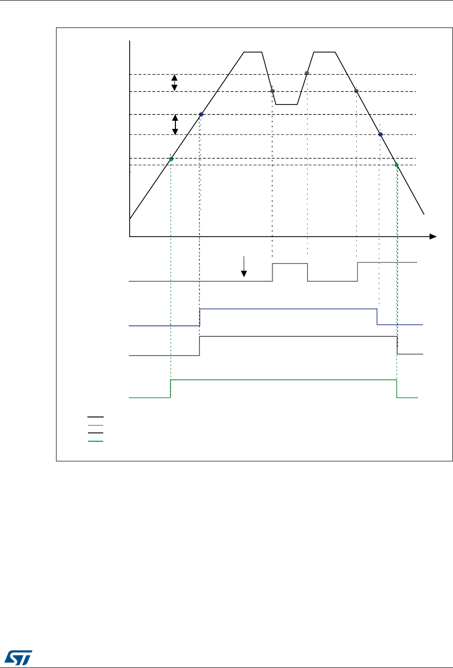
DocID025941 Rev 5 147/1001
RM0376 Power control (PWR)
170
Figure 12. Power supply supervisors
1. The PVD is available on all devices and it is enabled or disabled by software.
2. The BOR is available only on devices operating from 1.8 to 3.6 V, and unless disabled by option byte it will
mask the POR/PDR threshold.
3. When the BOR is disabled by option byte, the reset is asserted when VDD goes below PDR level
4. For devices operating from 1.65 to 3.6 V, there is no BOR and the reset is released when VDD goes above
POR level and asserted when VDD goes below PDR level
V
DD
/V
DD A
PVD output
100 mV
hysteresis
V
PVD
V
BO R hysteresis
100 mV
IT enabled
BOR reset
(NRST)
POR/PDR reset
(NRST)
PVD
BOR always active
POR/PDR (BOR not available)
ai17211b
POR
V/
PDR
V
BOR/PDR reset
(NRST)
BOR disabled by option byte
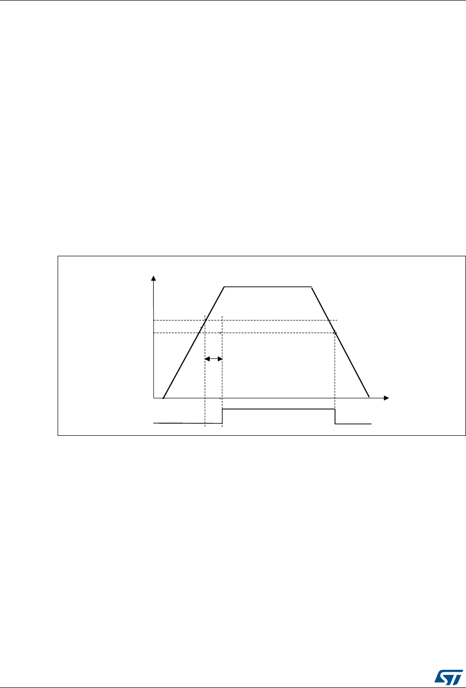
Power control (PWR) RM0376
148/1001 DocID025941 Rev 5
6.2.1 Power-on reset (POR)/power-down reset (PDR)
The device has an integrated POR/PDR circuitry that allows operation down to 1.5 V.
During power-on, the device remains in Reset mode when VDD/VDDA is below a specified
threshold, VPOR, without the need for an external reset circuit. The POR feature is always
enabled and the POR threshold is 1.5 V.
During power-down, the PDR keeps the device under reset when the supply voltage (VDD)
drops below the VPDR threshold. The PDR feature is always enabled and the PDR threshold
is 1.5 V.
The POR and PDR are used only when the BOR is disabled (see Section 6.2.2: Brown out
reset (BOR))). To insure the minimum operating voltage (1.65 V), the BOR should be
configured to BOR Level 1. When the BOR is disabled, a “gray zone” exist between the
minimum operating voltage (1.65 V) and the VPOR/VPDR threshold. This means that VDD
can be lower than 1.65 V without device reset until the VPDR threshold is reached.
For more details concerning the power-on/power-down reset threshold, refer to the
electrical characteristics of the datasheet.
Figure 13. Power-on reset/power-down reset waveform
6.2.2 Brown out reset (BOR)
During power-on, the Brown out reset (BOR) keeps the device under reset until the supply
voltage reaches the specified VBOR threshold.
For devices operating from 1.65 to 3.6 V, the BOR option is not available and the power
supply is monitored by the POR/PDR. As the POR/PDR thresholds are at 1.5 V, a “gray
zone” exists between the VPOR/VPDR thresholds and the minimum product operating
voltage 1.65 V.
For devices operating from 1.8 to 3.6 V, the BOR is always active at power-on and it's
threshold is 1.8 V.
Then when the system reset is released, the BOR level can be reconfigured or disabled by
option byte loading.
If the BOR level is kept at the lowest level, 1.8 V at power-on and 1.65 V at power-down, the
system reset is fully managed by the BOR and the product operating voltages are within
safe ranges.
MS32793V1
VDD/VDDA
Reset
POR
PDR
Temporization
tRSTTEMPO
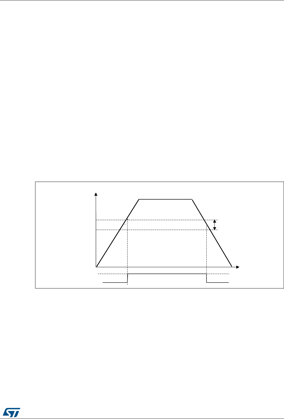
DocID025941 Rev 5 149/1001
RM0376 Power control (PWR)
170
And when the BOR option is disabled by option byte, the power-down reset is controlled by
the PDR and a “gray zone” exists between the 1.65 V and VPDR.
VBOR is configured through device option bytes. By default, the Level 4 threshold is
activated. 5 programmable VBOR thresholds can be selected.
•BOR Level 1 (VBOR0): reset threshold level for 1.69 to 1.80 V voltage range
•BOR Level 2 (VBOR1): reset threshold level for 1.94 to 2.1 V voltage range
•BOR Level 3 (VBOR2): reset threshold level for 2.3 to 2.49 V voltage range
•BOR Level 4 (VBOR3): reset threshold level for 2.54 to 2.74 V voltage range
•BOR Level 5 (VBOR4): reset threshold level for 2.77 to 3.0 V voltage range
When the supply voltage (VDD) drops below the selected VBOR threshold, a device reset is
generated. When the VDD is above the VBOR upper limit the device reset is released and the
system can start.
BOR can be disabled by programming the device option bytes. To disable the BOR function,
VDD must have been higher than VBOR0 to start the device option byte programming
sequence. The power-on and power-down is then monitored by the POR and PDR (see
Section 6.2.1: Power-on reset (POR)/power-down reset (PDR))
The BOR threshold hysteresis is ~100 mV (between the rising and the falling edge of the
supply voltage).
Figure 14. BOR thresholds
6.2.3 Programmable voltage detector (PVD)
You can use the PVD to monitor the VDD power supply by comparing it to a threshold
selected by the PLS[2:0] bits in the PWR_CR (see Section 6.4.1).
The PVD can use an external input analog voltage (PVD_IN) which is compared internally to
VREFINT. The PVD_IN (PB7) has to be configured in Analog mode when PLS[2:0] = 111.
The PVD is enabled by setting the PVDE bit.
A PVDO flag is available in the PWR_CSR register (see Section 6.4.2). It indicates if VDD is
higher or lower than the PVD threshold. This event is internally connected to EXTI line16
and can generate an interrupt if it has been enabled through the EXTI registers. The
rising/falling edge sensitivity of EXTI Line16 should be configured according to the PVD
output behavior: if EXTI line 16 is configured to rising edge sensitivity, the interrupt will be
MS32794V1
VDD/VDDA
Reset
BOR threshold 100mV
hysteresis
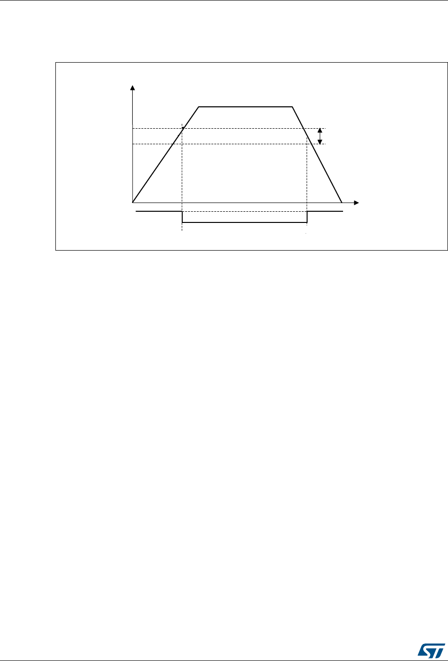
Power control (PWR) RM0376
150/1001 DocID025941 Rev 5
generated when VDD drops below the PVD threshold. As an example the service routine
could perform emergency shutdown tasks.
Figure 15. PVD thresholds
6.2.4 Internal voltage reference (VREFINT)
The internal reference (VREFINT) provides stable voltage for analog peripherals. The
functions managed through the internal voltage reference (VREFINT) are BOR, PVD, ADC,
HSI48 and comparators. The internal voltage reference (VREFINT) is always enabled when
one of these features is used.
The internal voltage reference consumption is not negligible, in particular in Stop and
Standby mode. To reduce power consumption, the ULP bit (ultra-low-power) in the
PWR_CR register can be set to disable the internal voltage reference. However, in this
case, when exiting from the Stop/Standby mode, the functions managed through the internal
voltage reference are not reliable during the internal voltage reference startup time (up to
3ms).
To reduce the wakeup time, the device can exit from Stop/Standby mode without waiting for
the internal voltage reference startup time. This is performed by setting the FWU bit (Fast
wakeup) in the PWR_CR register before entering Stop/Standby mode.
If the ULP bit is set, the functions that were enabled before entering Stop/Standby mode will
be disabled during these modes, and enabled again only after the end of the internal voltage
reference startup time whatever FWU value. The VREFINTRDYF flag in the PWR_CSR
register indicates that the internal voltage reference is ready.
When the device exits from low-power mode on an NRST pulse, it does not wait for internal
voltage reference startup (even if ULP=1 and FWU=0). The application should check the
VREFINTRDYF flag if necessary.
MSv32795V2
VDD/VDDA
PVD output
PVD threshold 100mV
hysteresis

DocID025941 Rev 5 151/1001
RM0376 Power control (PWR)
170
6.3 Low-power modes
By default, the microcontroller is in Run mode after a system or a power-on reset. In Run
mode the CPU is clocked by HCLK and the program code is executed. Several low-power
modes are available to save power when the CPU does not need to be kept running, for
example when waiting for an external event. It is up to the user to select the mode that gives
the best compromise between low-power consumption, performance, short startup time and
available wakeup sources.
The devices feature five low-power modes:
•Low-power run mode: regulator in low-power mode, limited clock frequency, limited
number of peripherals running (refer to Section 6.3.4)
•Sleep mode: Cortex®-M0+ core stopped, peripherals kept running (refer to
Section 6.3.7)
•Low-power sleep mode: Cortex®-M0+core stopped, limited clock frequency, limited
number of peripherals running, regulator in low-power mode, Flash stopped ((refer to
Section 6.3.8))
•Stop mode (all clocks are stopped, regulator running, regulator in low-power mode
(refer to Section 6.3.9)
•Standby mode: VCORE domain powered off ((refer to Section 6.3.10))
In addition, the power consumption in Run mode can be reduced by one of the following
means:
•Slowing down the system clocks
•Gating the clocks to the APBx and AHBx peripherals when they are unused.
Table 32. Summary of low-power modes
Mode name Entry Wakeup Effect on VCORE
domain clocks
Effect on VDD
domain
clocks
Voltage regulator
Low-power
run
LPSDSR and
LPRUN bits +
Clock setting
The regulator is forced
in Main regulator (1.8
V)
None None In low-power
mode
Sleep
(Sleep now or
Sleep-on-exit)
WFI or Return
from ISR Any interrupt CPU CLK OFF
no effect on other
clocks or analog
clock sources
None ON
WFE Wakeup event
Low-power
sleep (Sleep
now or Sleep-
on-exit)
LPSDSR bits +
WFI or Return
from ISR
Any interrupt
CPU CLK OFF
no effect on other
clocks or analog
clock sources,
Flash CLK OFF
None In low-power
mode
LPSDSR bits +
WFE Wakeup event

Power control (PWR) RM0376
152/1001 DocID025941 Rev 5
6.3.1 Behavior of clocks in low-power modes
APB peripheral and DMA clocks can be disabled by software.
Sleep and Low-power sleep modes
The CPU clock is stopped in Sleep and Low-power sleep mode. The memory interface
clocks (Flash memory and RAM interfaces) and all peripherals clocks can be stopped by
software during Sleep. The memory interface clock is stopped and the RAM is in power-
down when in Low-power sleep mode. The AHB to APB bridge clocks are disabled by
hardware during Sleep/Low-power sleep mode when all the clocks of the peripherals
connected to them are disabled.
Stop and Standby modes
The system clock and all high speed clocks are stopped in Stop and Standby modes:
•PLL is disabled
•Internal RC 16 MHz (HSI16) oscillator is disabled
•External 1-24 MHz (HSE) oscillator is disabled
•Internal 65 kHz - 4.2 MHz (MSI) oscillator is disabled
When exiting this mode by an interrupt (Stop mode), the internal MSI or HSI16 can be
selected as system clock. For both oscillators, their respective configuration (range and
trimming) value is kept on Stop mode exit.
When exiting this mode by a reset (Standby mode), the internal MSI oscillator is selected as
system clock. The range and the trimming value are reset to the default 2.1 MHz.
If a Flash program operation or an access to APB domain is ongoing, the Stop/Standby
mode entry is delayed until the Flash memory or the APB access has completed.
Stop
PDDS, LPSDSR
bits +
SLEEPDEEP bit +
WFI, Return from
ISR or WFE
Any EXTI line
(configured in the EXTI
registers, internal and
external lines)
All VCORE
domain clocks
OFF
HSI16(1), HSE
and MSI
oscillators
OFF
In low-power
mode
Standby
PDDS bit +
SLEEPDEEP bit +
WFI, Return from
ISR or WFE
WKUP pin rising edge,
RTC alarm (Alarm A or
Alarm B), RTC Wakeup
event, RTC tamper
event, RTC timestamp
event, external reset in
NRST pin, IWDG reset
OFF
1. HSI16 can run in Stop mode provided HSI16KERON is set in Clock control register (RCC_CR).
Table 32. Summary of low-power modes (continued)
Mode name Entry Wakeup Effect on VCORE
domain clocks
Effect on VDD
domain
clocks
Voltage regulator

DocID025941 Rev 5 153/1001
RM0376 Power control (PWR)
170
6.3.2 Slowing down system clocks
In Run mode the speed of the system clocks (SYSCLK, HCLK, PCLK1, PCLK2) can be
reduced by programming the prescaler registers. These prescalers can also be used to slow
down peripherals before entering Sleep mode.
For more details refer to Section 7.3.4: Clock configuration register (RCC_CFGR).
6.3.3 Peripheral clock gating
In Run mode, the HCLK and PCLKx for individual peripherals and memories can be stopped
at any time to reduce power consumption.
To further reduce power consumption in Sleep mode the peripheral clocks can be disabled
prior to executing the WFI or WFE instructions.
Peripheral clock gating is controlled by the AHB peripheral clock enable register
(RCC_AHBENR), APB2 peripheral clock enable register (RCC_APB2ENR), APB1
peripheral clock enable register (RCC_APB1ENR) (see Section 7.3.13: AHB peripheral
clock enable register (RCC_AHBENR), Section 7.3.15: APB1 peripheral clock enable
register (RCC_APB1ENR) and Section 7.3.14: APB2 peripheral clock enable register
(RCC_APB2ENR)).
Disabling the peripherals clocks in Sleep mode can be performed automatically by resetting
the corresponding bit in RCC_AHBLPENR and RCC_APBxLPENR registers (x can 1 or 2).
6.3.4 Low-power run mode (LP run)
To further reduce the consumption when the system is in Run mode, the regulator can be
configured in low-power mode. In this mode, the system frequency should not exceed
f_MSI range1.
Please refer to the product datasheet for more details on voltage regulator and peripherals
operating conditions.
Note: To be able to read the RTC calendar register when the APB1 clock frequency is less than
seven times the RTC clock frequency (7*RTCLCK), the software must read the calendar
time and date registers twice.
If the second read of the RTC_TR gives the same result as the first read, this ensures that
the data is correct. Otherwise a third read access must be done.
Low-power run mode can only be entered when VCORE is in range 2. In addition, the
dynamic voltage scaling must not be used when Low-power run mode is selected. Only Stop
and Sleep modes with regulator configured in low-power mode is allowed when Low-power
run mode is selected.
Note: In Low-power run mode, all I/O pins keep the same state as in Run mode.
Entering Low-power run mode
To enter Low-power run mode proceed as follows:
1. Each digital IP clock must be enabled or disabled by using the RCC_APBxENR and
RCC_AHBENR registers.
2. The frequency of the system clock must be decreased to not exceed the frequency of
f_MSI range1.
3. The regulator is forced in low-power mode by software (LPRUN and LPSDSR bits set)

Power control (PWR) RM0376
154/1001 DocID025941 Rev 5
Exiting Low-power run mode
To exit Low-power run mode proceed as follows:
1. The regulator is forced in Main regulator mode by software.
2. The Flash memory is switched on, if needed.
3. The frequency of the clock system can be increased.
6.3.5 Entering low-power mode
Low-power modes (except for Low-power run mode) are entered by executing the WFI
(Wait For Interrupt) or WFE (Wait for Event) instructions, or when the SLEEPONEXIT bit in
Cortex®-M0+ System Control register is set on Return from ISR.
Entering low-power mode through WFI or WFE will be executed only is no interrupt and no
event is pending.
6.3.6 Exiting low-power mode
The microcontroller exists from Sleep and Stop mode depending on the way the mode was
entered:
•If the WFI instruction or Return from ISR was used to enter the low-power mode, any
peripheral interrupt acknowledged by the NVIC can wake up the device. This includes
EXTI lines and any GPIO toggle.
•If the WFE instruction was used to enter low-power mode, the microcontroller exits the
low-power mode as soon as an event occurs. The wakeup event can be generated
either by:
– An NVIC IRQ interrupt:
This is done by enabling an interrupt in the peripheral control register but not in the
NVIC, and by enabling the SEVONPEND bit in the Cortex®-M0+ System Control
register. When the microcontroller resumes from WFE, the peripheral interrupt
pending bit and the peripheral NVIC IRQ channel pending bit (in the NVIC
interrupt clear pending register) have to be cleared.
– An event:
This is done by configuring an external or internal EXTI line in event mode. When
the CPU resumes from WFE, it is not necessary to clear the peripheral interrupt
pending bit or the NVIC IRQ channel pending bit as the pending bit corresponding
to the event line is not set.

DocID025941 Rev 5 155/1001
RM0376 Power control (PWR)
170
6.3.7 Sleep mode
I/O states in Sleep mode
In Sleep mode, all I/O pins keep the same state as in Run mode.
Entering Sleep mode
The Sleep mode is entered according to Section 6.3.5: Entering low-power mode.
Refer to Table 33: Sleep-now and Table 34: Sleep-on-exit for details on how to enter Sleep
mode.
Exiting Sleep mode
The Sleep mode is exited according to Section 6.3.6: Exiting low-power mode.
Refer to Table 33: Sleep-now and Table 34: Sleep-on-exit for more details on how to exit
Sleep mode.
Table 33. Sleep-now
Sleep-now mode Description
Mode entry
WFI (Wait for Interrupt) or WFE (Wait for Event) while:
– SLEEPDEEP = 0 and
– No interrupt (for WFI) or event (for WFE) is pending
Refer to the Cortex®-M0+ System Control register (see PM0223 programming
manual).
On return from ISR while:
– SLEEPDEEP = 0 and
– SLEEPONEXIT = 1 and
– No interrupt is pending
Refer to the Cortex®-M0+ System Control register (see PM0223 programming
manual).
Mode exit
If WFI or return from ISR was used for entry:
Interrupt: refer to Table 53: List of vectors
If WFE was used for entry and SVONPEND = 0
Wakeup event: refer to Section 13.3.2: Wakeup event management
If WFE was used for entry and SVONPEND = 1
Interrupt event when disabled in NVIC (refer to Table 53: List of vectors) or
wakeup event (refer to Section 13.3.2: Wakeup event management)
Wakeup latency None

Power control (PWR) RM0376
156/1001 DocID025941 Rev 5
6.3.8 Low-power sleep mode (LP sleep)
I/O states in Low-power sleep mode
In Low-power sleep mode, all I/O pins keep the same state as in Run mode.
Entering Low-power sleep mode
To enter Low-power sleep mode, proceed as follows:
1. The Flash memory can be switched off by using the control bits (SLEEP_PD in the
FLASH_ACR register. This reduces power consumption but increases the wake-up
time.
2. Each digital IP clock must be enabled or disabled by using the RCC_APBxENR and
RCC_AHBENR registers.
3. The frequency of the system clock must be decreased.
4. The regulator is forced in low-power mode by software (LPSDSR bits set).
5. Follow the steps described in Section 6.3.5: Entering low-power mode.
Refer to Table 35: Sleep-now (Low-power sleep) and Table 36: Sleep-on-exit (Low-power
sleep) for details on how to enter Low-power sleep mode.
In Low-power sleep mode, the Flash memory can be switched off and the RAM memory
remains available.
In this mode, the system frequency should not exceed f_MSI range1.
Please refer to product datasheet for more details on voltage regulator and peripherals
operating conditions.
Low-power sleep mode can only be entered when VCORE is in range 2.
Table 34. Sleep-on-exit
Sleep-on-exit Description
Mode entry
WFI (wait for interrupt) while:
– SLEEPDEEP = 0 and
– No interrupt (for WFI) or event (for WFE) is pending
Refer to the Cortex®-M0+ System Control register (see PM0223
programming manual).
On return from ISR while:
– SLEEPDEEP = 0 and
– SLEEPONEXIT = 1 and
– No interrupt is pending
Refer to the Cortex®-M0+ System Control register (see PM0223
programming manual).
Mode exit Interrupt: refer to Table 53: List of vectors
Wakeup latency None

DocID025941 Rev 5 157/1001
RM0376 Power control (PWR)
170
Note: To be able to read the RTC calendar register when the APB1 clock frequency is less than
seven times the RTC clock frequency (7*RTCLCK), the software must read the calendar
time and date registers twice.
If the second read of the RTC_TR gives the same result as the first read, this ensures that
the data is correct. Otherwise a third read access must be done.
Exiting Low-power sleep mode
The Low-power sleep mode is exited according to Section 6.3.6: Exiting low-power mode.
When exiting Low-power sleep mode by issuing an interrupt or a wakeup event, the
regulator is configured in Main regulator mode, the Flash memory is switched on (if
necessary), and the system clock can be increased.
When the voltage regulator operates in low-power mode, an additional startup delay is
incurred when waking up from Low-power sleep mode.
Refer to Table 35: Sleep-now (Low-power sleep) and Table 36: Sleep-on-exit (Low-power
sleep) for more details on how to exit Sleep low-power mode.
Table 35. Sleep-now (Low-power sleep)
Sleep-now mode Description
Mode entry
Voltage regulator in low-power mode and the Flash memory switched off
WFI (Wait for Interrupt) or WFE (wait for event) while:
– SLEEPDEEP = 0 and
– No interrupt (for WFI) or event (for WFE) is pending
Refer to the Cortex®-M0+ System Control register (see PM0223 programming
manual).
On return from ISR while:
– SLEEPDEEP = 0 and
– SLEEPONEXIT = 1 and
– No interrupt is pending
Refer to the Cortex®-M0+ System Control register (see PM0223 programming
manual).
Mode exit
Voltage regulator in Main regulator mode and the Flash memory switched on
If WFI or Return from ISR was used for entry:
Interrupt: Refer to Table 53: List of vectors
If WFE was used for entry and SEVONPEND = 0
Wakeup event: Refer to Section 13.3.2: Wakeup event management
If WFE was used for entry and SVONPEND = 1
Interrupt event when disabled in NVIC (refer to Table 53: List of vectors) or
wakeup event (refer to Section 13.3.2: Wakeup event management)
Wakeup latency Regulator wakeup time from low-power mode

Power control (PWR) RM0376
158/1001 DocID025941 Rev 5
6.3.9 Stop mode
The Stop mode is based on the Cortex®-M0+ Deepsleep mode combined with peripheral
clock gating. The voltage regulator can be configured either in normal or low-power mode.
In Stop mode, all clocks in the VCORE domain are stopped, the PLL, the MSI, the HSI16 and
the HSE RC oscillators are disabled. Internal SRAM and register contents are preserved.
To get the lowest consumption in Stop mode, the internal Flash memory also enters low-
power mode. When the Flash memory is in power-down mode, an additional startup delay is
incurred when waking up from Stop mode.
To minimize the consumption In Stop mode, VREFINT, the BOR, PVD, and temperature
sensor can be switched off before entering Stop mode. This functionality is controlled by the
ULP bit in the PWR_CR register. If the ULP bit is set, the reference is switched off on Stop
mode entry and enabled again on wakeup. .
I/O states in Low-power sleep mode
In Stop mode, all I/O pins keep the same state as in Run mode.
Entering Stop mode
Refer to Section 6.3.5: Entering low-power mode and to Table 37 for details on how to enter
the Stop mode.
If the application needs to disable the external clock before entering Stop mode, the HSEON
bit must be first disabled and the system clock switched to HSI16.
Otherwise, if the HSEON bit is kept enabled while external clock (external oscillator) can be
removed before entering Stop mode, the clock security system (CSS) feature must be
enabled to detect any external oscillator failure and avoid a malfunction behavior when
entering Stop mode.
Table 36. Sleep-on-exit (Low-power sleep)
Sleep-on-exit Description
Mode entry
WFI (wait for interrupt) while:
– SLEEPDEEP = 0 and
– No interrupt (for WFI) or event (for WFE) is pending
Refer to the Cortex®-M0+ System Control register (see PM0223
programming manual).
On return from ISR while:
– SLEEPDEEP = 0 and
– SLEEPONEXIT = 1 and
– No interrupt is pending
Refer to the Cortex®-M0+ System Control register (see PM0223
programming manual).
Mode exit Interrupt: refer to Table 53: List of vectors.
Wakeup latency regulator wakeup time from low-power mode

DocID025941 Rev 5 159/1001
RM0376 Power control (PWR)
170
To further reduce power consumption in Stop mode, the internal voltage regulator can be put
in low-power mode. This is configured by the LPSDSR bit in the PWR_CR register (see
Section 6.4.1). The internal voltage regulator can also be kept in Main mode but the
consumption will be much higher. As a result, it is always implicitly assumed that the
regulator is in low-power mode during Stop mode. The only advantage of keeping the
regulator in Main mode is that the wakeup time from Stop mode is shorter.
If Flash memory programming or an access to the APB domain is ongoing, the Stop mode
entry is delayed until the memory or APB access has completed.
In Stop mode, the following features can be selected by programming individual control bits:
•Independent watchdog (IWDG): the IWDG is started by writing to its Key register or by
hardware option. Once started it cannot be stopped except by a Reset. Refer to
Section 24.3: IWDG functional description in Section 24: Independent watchdog
(IWDG).
•Real-time clock (RTC): this is configured by the RTCEN bit in the RCC_CSR register
(see Section 7.3.21).
•Internal RC oscillator (LSI RC): this is configured by the LSION bit in the RCC_CSR
register.
•External 32.768 kHz oscillator (LSE OSC): this is configured by the LSEON bit in the
RCC_CSR register.
The ADC, DAC can also consume power in Stop mode, unless they are disabled before
entering it. To disable them, the ADON bit in the ADC_CR2 register and the ENx bit in the
DAC_CR register must both be written to 0.
Exiting Stop mode
Refer to Section 6.3.6: Exiting low-power mode and to Table 37 for details on how to exit
Stop mode.
When exiting Stop mode by issuing an interrupt or a wakeup event, the MSI or HSI16 RC
oscillator is selected as system clock depending the bit STOPWUCK in the RCC_CFGR
register.
When the voltage regulator operates in low-power mode, an additional startup delay is
incurred when waking up from Stop mode. By keeping the internal regulator ON during Stop
mode, the consumption is higher although the startup time is reduced.

Power control (PWR) RM0376
160/1001 DocID025941 Rev 5
Table 37. Stop mode
Stop mode Description
Mode entry
WFI (Wait for Interrupt) or WFE (Wait for Event) while:
– No interrupt (for WFI) or event (for WFE) is pending.
– SLEEPDEEP bit is set in Cortex®-M0+ System Control register
– PDDS bit = 0 in Power Control register (PWR_CR)
– WUF bit = 0 in Power Control/Status register (PWR_CSR)
– MSI or HSI16 RC oscillator are selected as system clock for Stop mode
exit by configuring the STOPWUCK bit in the RCC_CFGR register.
Note: To enter the Stop mode, all EXTI Line pending bits (in
Section 13.5.6: EXTI pending register (EXTI_PR)), all peripherals
interrupt pending bits, the RTC Alarm (Alarm A and Alarm B), RTC
wakeup, RTC tamper, and RTC time-stamp flags, must be reset.
Otherwise, the Stop mode entry procedure is ignored and program
execution continues.
On return from ISR while:
– No interrupt is pending.
– SLEEPDEEP bit is set in Cortex®-M0+ System Control register
– SLEEPONEXIT = 1
– PDDS bit = 0 in Power Control register (PWR_CR)
– WUF bit = 0 in Power Control/Status register (PWR_CSR)
– MSI or HSI16 RC oscillator are selected as system clock for Stop mode
exit by configuring the STOPWUCK bit in the RCC_CFGR register.
Note: To enter the Stop mode, all EXTI Line pending bits (in
Section 13.5.6: EXTI pending register (EXTI_PR)), all peripherals
interrupt pending bits, the RTC Alarm (Alarm A and Alarm B), RTC
wakeup, RTC tamper, and RTC time-stamp flags, must be reset.
Otherwise, the Stop mode entry procedure is ignored and program
execution continues.
Mode exit
If WFI or return from ISR was used for entry:
Any EXTI Line configured in Interrupt mode (the corresponding EXTI
Interrupt vector must be enabled in the NVIC). Refer to Table 53: List of
vectors.
If WFE was used for entry and SEVONPEND = 0
Any EXTI Line configured in event mode. Refer to Section 13.3.2:
Wakeup event management on page 283
If WFE was used for entry and SEVONPEND = 1
– Any EXTI Line configured in event mode (even if the corresponding EXTI
interrupt is disabled in the NVIC). The interrupt source can be an external
interrupt or a peripheral with wakeup capability (refer to Table 53: List of
vectors).
– A wakeup event (refer to Section 13.3.2: Wakeup event management on
page 283)
Wakeup latency MSI or HSI16 RC wakeup time + regulator wakeup time from Low-power
mode + FLASH wakeup time

DocID025941 Rev 5 161/1001
RM0376 Power control (PWR)
170
6.3.10 Standby mode
The Standby mode allows to achieve the lowest power consumption. It is based on the
Cortex®-M0+ Deepsleep mode, with the voltage regulator disabled. The VCORE domain is
consequently powered off. The PLL, the MSI, the HSI16 oscillator and the HSE oscillator
are also switched off. SRAM and register contents are lost except for the RTC registers,
RTC backup registers and Standby circuitry (see Figure 10).
I/O states in Standby mode
In Standby mode, all I/O pins are high impedance except for:
•Reset pad
•Wakeup pins (WKUP1, WKUP2, WKUP3)
•RTC functions (tamper, time-stamp, RTC Alarm out, RTC clock calibration out) on the
following I/Os:
– Category 3: PC13, PA0
– Category 5: PC13, PA0, PE6
Entering Standby mode
Refer to Section 6.3.5: Entering low-power mode and to Table 38 for details on how to enter
Standby mode.
In Standby mode, the following features can be selected by programming individual control
bits:
•Independent watchdog (IWDG): the IWDG is started by writing to its Key register or by
hardware option. Once started it cannot be stopped except by a reset. Refer to
Section 24.3: IWDG functional description on page 592.
•Real-time clock (RTC): this is configured by the RTCEN bit in the RCC_CSR register
(see Section 7.3.21).
•Internal RC oscillator (LSI RC): this is configured by the LSION bit in the RCC_CSR
register.
•External 32.768 kHz oscillator (LSE OSC): this is configured by the LSEON bit in the
RCC_CSR register.
Exiting Standby mode
The microcontroller exits Standby mode when an external Reset (NRST pin), an IWDG
Reset, a rising edge on WKUP pins (WUKP1, WKUP2 or WKUP3), an RTC alarm, a tamper
event, or a time-stamp event is detected.
After waking up from Standby mode, program execution restarts in the same way as after a
Reset (boot pins sampling, vector reset is fetched, etc.). The SBF status flag in the
PWR_CSR register (see Section 6.4.2) indicates that the microcontroller was in Standby
mode. All registers are reset to their default value after a system reset except for the register
bits in the RTC domain (see Section 26.7: RTC registers, SBF status flag in the PWR power
control/status register (PWR_CSR), Control/status register (RCC_CSR) and Clock control
register (RCC_CR)).
Refer to Section 6.3.6: Exiting low-power mode and to Table 38 for more details on how to
exit Standby mode.

Power control (PWR) RM0376
162/1001 DocID025941 Rev 5
Debug mode
By default, the debug connection is lost if the application puts the MCU in Stop or Standby
mode while the debug features are used. This is due to the fact that the Cortex®-M0+ core is
no longer clocked.
However, by setting some configuration bits in the DBG_CR register, the software can be
debugged even when using the low-power modes extensively. For more details, refer to
Section 32.9.1: Debug support for low-power modes.
6.3.11 Waking up the device from Stop and Standby modes using the RTC
and comparators
The MCU can be woken up from low-power mode by an RTC Alarm event, an RTC Wakeup
event, a tamper event, a time-stamp event, or a comparator event, without depending on an
external interrupt (Auto-wakeup mode).
These RTC alternate functions can wake up the system from Stop and Standby low-power
modes while the comparator events can only wake up the system from Stop mode.
The system can also wake up from low-power modes without depending on an external
interrupt (Auto-wakeup mode) by using the RTC alarm or the RTC wakeup events.
Table 38. Standby mode
Standby mode Description
Mode entry
WFI (Wait for Interrupt) or WFE (Wait for Event) while:
– SLEEPDEEP = 1 in Cortex®-M0+ System Control register
– PDDS = 1 bit in Power Control register (PWR_CR)
– No interrupt (for WFI) or event (for WFE) is pending.
– WUF = 0 bit in Power Control/Status register (PWR_CSR)
– the RTC flag corresponding to the chosen wakeup source (RTC Alarm A,
RTC Alarm B, RTC wakeup, Tamper or Time-stamp flags) is cleared
On return from ISR while:
– SLEEPDEEP = 1 in Cortex®-M0+ System Control register
– SLEEPONEXIT = 1
– PDDS bit = 1 in Power Control register (PWR_CR)
– No interrupt is pending.
– WUF bit = 0 in Power Control/Status register (PWR_CSR)
– the RTC flag corresponding to the chosen wakeup source (RTC Alarm A,
RTC Alarm B, RTC wakeup, Tamper or Time-stamp flags) is cleared.
Mode exit WKUP pin rising edge, RTC alarm (Alarm A and Alarm B), RTC wakeup,
tamper event, time-stamp event, external reset in NRST pin, IWDG reset.
Wakeup latency Reset phase

DocID025941 Rev 5 163/1001
RM0376 Power control (PWR)
170
The RTC provides a programmable time base for waking up from Stop or Standby mode at
regular intervals. For this purpose, two of the three alternative RTC clock sources can be
selected by programming the RTCSEL[1:0] bits in the RCC_CSR register (see
Section 7.3.21):
•Low-power 32.768 kHz external crystal oscillator (LSE OSC).
This clock source provides a precise time base with very low-power consumption (less
than 1 µA added consumption in typical conditions)
•Low-power internal RC oscillator (LSI RC)
This clock source has the advantage of saving the cost of the 32.768 kHz crystal. This
internal RC Oscillator is designed to use minimum power consumption.
RTC auto-wakeup (AWU) from the Stop mode
•To wake up from the Stop mode with an RTC alarm event, it is necessary to:
a) Configure the EXTI Line 17 to be sensitive to rising edges (Interrupt or Event
modes)
b) Enable the RTC Alarm interrupt in the RTC_CR register
c) Configure the RTC to generate the RTC alarm
•To wake up from the Stop mode with an RTC Tamper or time stamp event, it is
necessary to:
a) Configure the EXTI Line 19 to be sensitive to rising edges (Interrupt or Event
modes)
b) Enable the RTC TimeStamp Interrupt in the RTC_CR register or the RTC Tamper
Interrupt in the RTC_TCR register
c) Configure the RTC to detect the tamper or time stamp event
•To wake up from the Stop mode with an RTC Wakeup event, it is necessary to:
a) Configure the EXTI Line 20 to be sensitive to rising edges (Interrupt or Event
modes)
b) Enable the RTC Wakeup Interrupt in the RTC_CR register
c) Configure the RTC to generate the RTC Wakeup event
RTC auto-wakeup (AWU) from the Standby mode
•To wake up from the Standby mode with an RTC alarm event, it is necessary to:
a) Enable the RTC Alarm interrupt in the RTC_CR register
b) Configure the RTC to generate the RTC alarm
•To wake up from the Stop mode with an RTC Tamper or time stamp event, it is
necessary to:
a) Enable the RTC TimeStamp Interrupt in the RTC_CR register or the RTC Tamper
Interrupt in the RTC_TCR register
b) Configure the RTC to detect the tamper or time stamp event
•To wake up from the Stop mode with an RTC Wakeup event, it is necessary to:
a) Enable the RTC Wakeup Interrupt in the RTC_CR register
b) Configure the RTC to generate the RTC Wakeup event

Power control (PWR) RM0376
164/1001 DocID025941 Rev 5
Comparator auto-wakeup (AWU) from the Stop mode
•To wake up from the Stop mode with a comparator 1 or comparator 2 wakeup event, it
is necessary to:
a) Configure the EXTI Line 21 for comparator 1 or EXTI Line 22 for comparator 2
(Interrupt or Event mode) to be sensitive to the selected edges (falling, rising or
falling and rising)
b) Configure the comparator to generate the event.

DocID025941 Rev 5 165/1001
RM0376 Power control (PWR)
170
6.4 Power control registers
The peripheral registers have to be accessed by half-words (16-bit) or words (32-bit).
6.4.1 PWR power control register (PWR_CR)
Address offset: 0x00
Reset value: 0x0000 1000 (reset by wakeup from Standby mode)
31 30 29 28 27 26 25 24 23 22 21 20 19 18 17 16
Res. Res. Res. Res. Res. Res. Res. Res. Res. Res. Res. Res. Res. Res. Res. Res.
151413121110987654321 0
Res. LPRUN DS_EE
_KOFF VOS[1:0] FWU ULP DBP PLS[2:0] PVDE CSBF CWUF PDDS LPSDSR
rw rw rw rw rw rw rw rw rw rw rw rc_w1 rc_w1 rw rw
Bits 31:15 Reserved, always read as 0.
Bit 14 LPRUN: Low-power run mode
When LPRUN bit is set together with the LPSDSR bit, the regulator is switched from Main
mode to low-power mode. Otherwise, it remains in Main mode. The regulator goes back to
operate in Main mode when LPRUN is reset.
If this bit is set (with LPSDSR bit set) and the CPU enters sleep or Deepsleep mode (LP
sleep or Stop mode), then, when the CPU wakes up from these modes, it enters Run
mode but with LPRUN bit set. To enter again Low-power run mode, it is necessary to
perform a reset and set LPRUN bit again.
It is forbidden to reset LPSDSR when the MCU is in Low-power run mode. LPSDSR is
used as a prepositioning for the entry into low-power mode, indicating to the system which
configuration of the regulator will be selected when entering low-power mode. The
LPSDSR bit must be set before the LPRUN bit is set. LPSDSR can be reset only when
LPRUN bit=0.
0: Voltage regulator in Main mode in Low-power run mode
1: Voltage regulator in low-power mode in Low-power run mode
Bit 13 DS_EE_KOFF: Deepsleep mode with non-volatile memory kept off
When entering low-power mode (Stop or Standby only), if DS_EE_KOFF and RUN_PD
bits are both set in FLASH_ACR register (refer to Section 3.7.1: Access control register
(FLASH_ACR), the non-volatile memory (Flash program memory and data EEPROM) will
not be woken up when exiting from Deepsleep mode.
0: NVM woken up when exiting from Deepsleep mode even if the bit RUN_PD is set
1: NVM not woken up when exiting from low-power mode (if the bit RUN_PD is set)
Bits 12:11 VOS[1:0]: Voltage scaling range selection
These bits are used to select the internal regulator voltage range.
Before resetting the power interface by resetting the PWRRST bit in the RCC_APB1RSTR
register, these bits have to be set to ‘10’ and the frequency of the system has to be
configured accordingly.
00: forbidden (bits are unchanged and keep the previous value, no voltage change
occurs)
01: 1.8 V (range 1)
10: 1.5 V (range 2)
11: 1.2 V (range 3)

Power control (PWR) RM0376
166/1001 DocID025941 Rev 5
Bit 10 FWU: Fast wakeup
This bit works in conjunction with ULP bit.
If ULP = 0, FWU is ignored
If ULP = 1 and FWU = 1: VREFINT startup time is ignored when exiting from low-power mode.
The VREFINTRDYF flag in the PWR_CSR register indicates when the VREFINT is ready
again.
If ULP=1 and FWU = 0: Exiting from low-power mode occurs only when the VREFINT is ready
(after its startup time). This bit is not reset by resetting the PWRRST bit in the
RCC_APB1RSTR register.
0: Low-power modes exit occurs only when VREFINT is ready
1: VREFINT start up time is ignored when exiting low-power modes
Bit 9 ULP: Ultra-low-power mode
When set, the VREFINT is switched off in low-power mode. The BOR, PVD, and temperature
sensor also rely on the voltage reference. This bit is not reset by resetting the PWRRST bit
in the RCC_APB1RSTR register.
0: VREFINT is on in low-power mode
1: VREFINT is off in low-power mode
Bit 8 DBP: Disable backup write protection
In reset state, the RTC, RTC backup registers and RCC CSR register are protected against
parasitic write access. This bit must be set to enable write access to these registers.
0: Access to RTC, RTC Backup and RCC CSR registers disabled
1: Access to RTC, RTC Backup and RCC CSR registers enabled
Note: If the HSE divided by 2, 4, 8 or 16 is used as the RTC clock, this bit must remain set
to 1.
Bits 7:5 PLS[2:0]: PVD level selection
These bits are written by software to select the voltage threshold detected by the power
voltage detector:
000: 1.9 V
001: 2.1 V
010: 2.3 V
011: 2.5 V
100: 2.7 V
101: 2.9 V
110: 3.1 V
111: External input analog voltage (Compare internally to VREFINT)
PVD_IN input (PB7) has to be configured as analog input when PLS[2:0] = 111.
Note: Refer to the electrical characteristics of the datasheet for more details.
Bit 4 PVDE: Power voltage detector enable
This bit is set and cleared by software.
0: PVD disabled
1: PVD enabled
Bit 3 CSBF: Clear standby flag
This bit is always read as 0.
0: No effect
1: Clear the SBF Standby flag (write).

DocID025941 Rev 5 167/1001
RM0376 Power control (PWR)
170
Bit 2 CWUF: Clear wakeup flag
This bit is always read as 0.
0: No effect
1: Clear the WUF Wakeup flag after 2 system clock cycles
Bit 1 PDDS: Power-down deepsleep
This bit is set and cleared by software.
0: Enter Stop mode when the CPU enters Deepsleep.
1: Enter Standby mode when the CPU enters Deepsleep.
Bit 0 LPSDSR: Low-power deepsleep/Sleep/Low-power run
– DeepSleep/Sleep modes
When this bit is set, the regulator switches in low-power mode when the CPU enters sleep
or Deepsleep mode. The regulator goes back to Main mode when the CPU exits from
these modes.
– Low-power run mode
When this bit is set, the regulator switches in low-power mode when the bit LPRUN is set.
The regulator goes back to Main mode when the bit LPRUN is reset.
This bit is set and cleared by software.
0: Voltage regulator on during Deepsleep/Sleep/Low-power run mode
1: Voltage regulator in low-power mode during Deepsleep/Sleep/Low-power run mode

Power control (PWR) RM0376
168/1001 DocID025941 Rev 5
6.4.2 PWR power control/status register (PWR_CSR)
Address offset: 0x04
Reset value: 0x0000 0008 (not reset by wakeup from Standby mode)
Additional APB cycles are needed to read this register versus a standard APB read.
31 30 29 28 27 26 25 24 23 22 21 20 19 18 17 16
Res. Res. Res. Res. Res. Res. Res. Res. Res. Res. Res. Res. Res. Res. Res. Res.
151413121110987654 3 210
Res. Res. Res. Res. Res. EWUP
3
EWUP
2
EWUP
1Res. Res. REG
LPF VOSF VREFIN
TRDYF PVDO SBF WUF
rw rw rw r r r r r r
Bits 31:11 Reserved, must be kept at reset value.
Bit 10 EWUP3: Enable WKUP pin 3
This bit is set and cleared by software.
0: WKUP pin 3 is used for general purpose I/Os. An event on the WKUP pin 3 does not
wakeup the device from Standby mode.
1: WKUP pin 3 is used for wakeup from Standby mode and forced in input pull down
configuration (rising edge on WKUP pin 3wakes-up the system from Standby mode).
Note: This bit is reset by a system reset.
Bit 9 EWUP2: Enable WKUP pin 2
This bit is set and cleared by software.
0: WKUP pin 2 is used for general purpose I/Os. An event on the WKUP pin 2 does not
wakeup the device from Standby mode.
1: WKUP pin 2 is used for wakeup from Standby mode and forced in input pull down
configuration (rising edge on WKUP pin 2 wakes-up the system from Standby mode).
Note: This bit is reset by a system reset.
Bit 8 EWUP1: Enable WKUP pin 1
This bit is set and cleared by software.
0: WKUP pin 1 is used for general purpose I/Os. An event on the WKUP pin 1 does not
wakeup the device from Standby mode.
1: WKUP pin 1 is used for wakeup from Standby mode and forced in input pull down
configuration (rising edge on WKUP pin 1 wakes-up the system from Standby mode).
Note: This bit is reset by a system reset.
Bits 7:6 Reserved, must be kept at reset value.
Bit 5 REGLPF: Regulator LP flag
This bit is set by hardware when the MCU is in Low-power run mode.
When the MCU exits from Low-power run mode, this bit stays at 1 until the regulator is ready in
Main mode. A polling on this bit is recommended to wait for the regulator Main mode. This bit is
reset by hardware when the regulator is ready.
0: Regulator is ready in Main mode
1: Regulator voltage is in low-power mode

DocID025941 Rev 5 169/1001
RM0376 Power control (PWR)
170
Bit 4 VOSF: Voltage Scaling select flag
A delay is required for the internal regulator to be ready after the voltage range is changed.
The VOSF bit indicates that the regulator has reached the voltage level defined with bits VOS
of PWR_CR register.
This bit is set when VOS[1:0] in PWR_CR register change.
It is reset once the regulator is ready.
0: Regulator is ready in the selected voltage range
1: Regulator voltage output is changing to the required VOS level.
Bit 3 VREFINTRDYF: Internal voltage reference (VREFINT) ready flag
This bit indicates the state of the internal voltage reference, VREFINT.
0: VREFINT is OFF
1: VREFINT is ready
Bit 2 PVDO: PVD output
This bit is set and cleared by hardware. It is valid only if PVD is enabled by the PVDE bit.
0: VDD is higher than the PVD threshold selected with the PLS[2:0] bits.
1: VDD is lower than the PVD threshold selected with the PLS[2:0] bits.
Note: The PVD is stopped by Standby mode. For this reason, this bit is equal to 0 after
Standby or reset until the PVDE bit is set.
Bit 1 SBF: Standby flag
This bit is set by hardware and cleared only by a POR/PDR (power-on reset/power-down
reset) or by setting the CSBF bit in the PWR power control register (PWR_CR)
0: Device has not been in Standby mode
1: Device has been in Standby mode
Bit 0 WUF: Wakeup flag
This bit is set by hardware and cleared by a system reset or by setting the CWUF bit in the
PWR power control register (PWR_CR)
0: No wakeup event occurred
1: A wakeup event was received from the WKUP pin or from the RTC alarm (Alarm A or
Alarm B), RTC Tamper event, RTC TimeStamp event or RTC Wakeup).
Note: An additional wakeup event is detected if the WKUP pins are enabled (by setting the
EWUPx (x=1, 2, 3) bits) when the WKUP pin levels are already high.

Power control (PWR) RM0376
170/1001 DocID025941 Rev 5
6.4.3 PWR register map
The following table summarizes the PWR registers.
Refer to Section 2.2.2 on page 58 for the register boundary addresses.
Table 39. PWR - register map and reset values
Offset Register
31
30
29
28
27
26
25
24
23
22
21
20
19
18
17
16
15
14
13
12
11
10
9
8
7
6
5
4
3
2
1
0
0x000 PWR_CR
Res.
Res.
Res.
Res.
Res.
Res.
Res.
Res.
Res.
Res.
Res.
Res.
Res.
Res.
Res.
Res.
Res.
LPRUN
DS_EE_KOFF.
VOS
[1:0]
FWU
ULP
DBP
PLS[2:0]
PVDE
CSBF
CWUF
PDDS
LPSDSR
Reset value 0 1000000000000
0x004 PWR_CSR
Res.
Res.
Res.
Res.
Res.
Res.
Res.
Res.
Res.
Res.
Res.
Res.
Res.
Res.
Res.
Res.
Res.
Res.
Res.
Res.
Res.
EWUP3
EWUP2
EWUP1
Res.
Res.
REGLPF
VOSF
VREFINTRDYF
PVDO
SBF
WUF
Reset value 000 001000

DocID025941 Rev 5 171/1001
RM0376 Reset and clock control (RCC)
222
7 Reset and clock control (RCC)
7.1 Reset
There are three types of reset, defined as system reset, power reset and RTC domain reset.
7.1.1 System reset
A system reset sets all registers to their reset values except for the RTC, RTC backup
registers and control/status registers (RCC_CR and RCC_CSR).
A system reset is generated when one of the following events occurs:
•A low level on the NRST pin (external reset)
•Window watchdog end-of-count condition (WWDG reset)
•Independent watchdog end-of-count condition (IWDG reset)
•A software reset (SW reset) (see Software reset)
•Low-power management reset (see Low-power management reset)
•Option byte loader reset (see Option byte loader reset)
•Exit from Standby mode
•Firewall protection (see Section 5: Firewall (FW))
The reset source can be identified by checking the reset flags in the control/status register,
RCC_CSR (see Section 7.3.21).
Software reset
The SYSRESETREQ bit in Cortex®-M0+ AIRCR register (Application Interrupt and Reset
Control Register) must be set to force a software reset on the device. Refer to Arm®
Cortex®-M0+ Technical Reference Manual for more details.
Low-power management reset
There are two ways to generate a low-power management reset:
•Reset generated when entering Standby mode:
This type of reset is enabled by resetting nRST_STDBY bit in user option bytes. In this
case, whenever a Standby mode entry sequence is successfully executed, the device
is reset instead of entering Standby mode.
•Reset when entering Stop mode:
This type of reset is enabled by resetting nRST_STOP bit in user option bytes. In this
case, whenever a Stop mode entry sequence is successfully executed, the device is
reset instead of entering Stop mode.
Option byte loader reset
The Option byte loader reset is generated when the OBL_LAUNCH bit (bit 18) is set in the
FLASH_PECR register. This bit is used to launch by software the option byte loading.
For further information on the user option bytes, refer to Section 3: Flash program memory
and data EEPROM (FLASH).
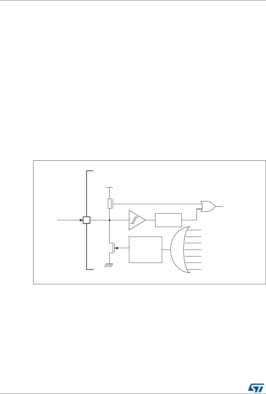
Reset and clock control (RCC) RM0376
172/1001 DocID025941 Rev 5
7.1.2 Power reset
A power reset is generated when one of the following events occurs:
•Power-on/power-down reset (POR/PDR reset)
•BOR reset
A power reset sets all registers to their reset values including for the RTC domain (see
Figure 16)
These sources act on the NRST pin and it is always kept low during the delay phase. The
RESET service routine vector is fixed at address 0x0000_0004 in the memory map. For
more details, refer to Table 53: List of vectors.
The system reset signal provided to the device is output on the NRST pin (except the Exit
from Standby reset which is not output on the NRST pin but generates system reset).
The pulse generator guarantees a minimum reset pulse duration of 20 µs for each internal
reset source. In case of an external reset, the reset pulse is generated while the NRST pin is
asserted low.
When an internal reset occurs, the internal pull-up resistor (RPU) is deactivated in order to
save the power consumption through the pull-up resistor.
Figure 16. Simplified diagram of the reset circuit
7.1.3 RTC and backup registers reset
The RTC peripheral, RTC clock source selection (in RCC_CSR) and the backup registers
are reset only when one of the following events occurs:
•A software reset, triggered by setting the RTCRST bit in the RCC_CSR register (see
Section 7.3.21)
•Power reset (BOR/POR/PDR).
MSv41924V1
External
reset
VDD
RPU
WWDG reset
Firewall reset
Software reset
Low-power manager reset
IWDG reset
Option byte loader reset
BOR reset
Pulse
generator
(min 20 μs)
NRST
System reset
Filter

DocID025941 Rev 5 173/1001
RM0376 Reset and clock control (RCC)
222
7.2 Clocks
Four different clock sources can be used to drive the system clock (SYSCLK):
•HSI16 (high-speed internal) oscillator clock
•HSE (high-speed external) oscillator clock
•PLL clock
•MSI (multispeed internal) oscillator clock
The MSI at 2.1MHz is used as system clock source after startup from power reset,
system or RTC domain reset, and after wake-up from Standby mode.
The HSI16, HSI16 divided by 4, or the MSI at any of its possible frequency can be used
to wake up from Stop mode.
The devices have two secondary clock sources:
•37 kHz low speed internal RC (LSI RC) which drives the independent watchdog and
optionally the RTC used for Auto-wakeup from Stop/Standby mode and the LPTIMER.
•32.768 kHz low speed external crystal (LSE crystal) which optionally drives the real-
time clock (RTCCLK), the LPTIMER and USARTs.
Each clock source can be switched on or off independently when it is not used to optimize
power consumption.
Several prescalers can be used to configure the AHB frequency and the two APBs (APB1
and APB2) domains. The maximum frequency of AHB, APB1 and the APB2 domains is
32 MHz. It depends on the device voltage range. For more details refer to Section 6.1.4:
Dynamic voltage scaling management.
All the peripheral clocks are derived from the system clock (SYSCLK) except:
•The 48 MHz USB and RNG clocks which are derived from one of the two following
source:
– PLL VCO clock.
– RC48 Clock (HSI48)
•The ADC can be derived either from the APB clock or the HSI16 clock.
•The LPUART1 and USART1/2 clock which is derived (selected by software) from one
of the four following sources:
– system clock
– HSI16 clock
– LSE clock
– APB clock (PCLK)
•The I2C1 clock which is derived (selected by software) from one of the three following
sources:
– system clock
– HSI16 clock
– APB clock (PCLK)
•The LPTIMER clock which is derived (selected by software) from one of the four
following sources:
– HSI16 clock
– LSE clock
– LSI clock

Reset and clock control (RCC) RM0376
174/1001 DocID025941 Rev 5
– APB clock (PCLK)
•The RTC clock which is derived from the following clock sources:
– LSE clock,
– LSI clock,
– 4 MHz HSE_RTC (HSE divided by a programmable prescaler).
•IWDG clock which is always the LSI clock.
The system clock (SYSCLK) frequency must be higher or equal to the RTC clock frequency.
The RCC feeds the Cortex? System Timer (SysTick) external clock with the AHB clock
(HCLK) divided by 8. The SysTick can work either with this clock or with the Cortex® clock
(HCLK), configurable in the SysTick Control and Status Register.
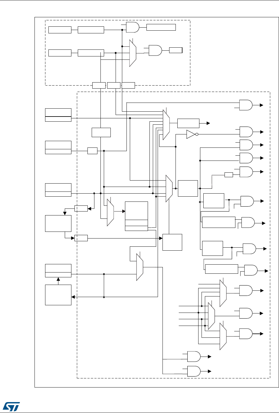
DocID025941 Rev 5 175/1001
RM0376 Reset and clock control (RCC)
222
Figure 17. Clock tree
MS33392V2
Legend:
HSE = High-speed external clock signal
HSI = High-speed internal clock signal
LSI = Low-speed internal clock signal
LSE = Low-speed external clock signal
MSI = Multispeed internal clock signal
Watchdog LS
LSI RC
LSE OSC RTC
LSI tempo
@V33
/ 1,2,4,8,16
HSI16 RC
Level shifters
HSE OSC
Level shifters
RC 48MHz
Level shifters
LSU
1 MHz Clock
Detector
LSD
Clock
Recovery
System
/ 8
LSE tempo
MSI RC
Level shifters
/ 2,4,8,16
/ 2,3,4
Level shifters
PLL
X
3,4,6,8,12,16,
24,32,48
AHB
PRESC
/ 1,2,…, 512
Clock
Source
Control
@V33
@V33
@V33
@V33
@V33
@V18
@V18
@V18
@V18
@V18
usb_en
rng_en
48MHz
USBCLK
48MHz RNG
I2C1CLK
LPUART/
UARTCLK
LPTIMCLK
LSE
HSI16
SYSCLK
PCLK
LSI
not (sleep or
deepsleep)
not (sleep or
deepsleep)
not deepsleep
not deepsleep
HCLK
CK_PWR
FCLK
PLLCLK
HSE
HSI16
MSI
LSE
LSI
Dedicated 48MHz PLL output
HSE present or not
@V33
@VDDCORE
ck_rchs / 1,4 HSI16
HSI48
MSI
1 MHz
ck_pllin
Enable Watchdog
RTC2 enable
ADC enable
ADCCLK
LSU LSD LSD
MCO
MCOSEL
PLLSRC
RTCSEL
System
Clock
APB1
PRESC
/ 1,2,4,8,16
Peripheral
clock enable
PCLK1 to APB1
peripherals
32 MHz
max.
If (APB1 presc=1) x1
else x2)
to TIMx
Peripheral
clock enable
APB2
PRESC
/ 1,2,4,8,16
Peripheral
clock enable
PCLK2 to APB2
peripherals
32 MHz
max.
If (APB2 presc=1) x1
else x2)
to TIMx
Peripheral
clock enable
Peripheral
clock enable
Peripheral
clock enable
SysTick
Timer
HSI48MSEL
4 MHz
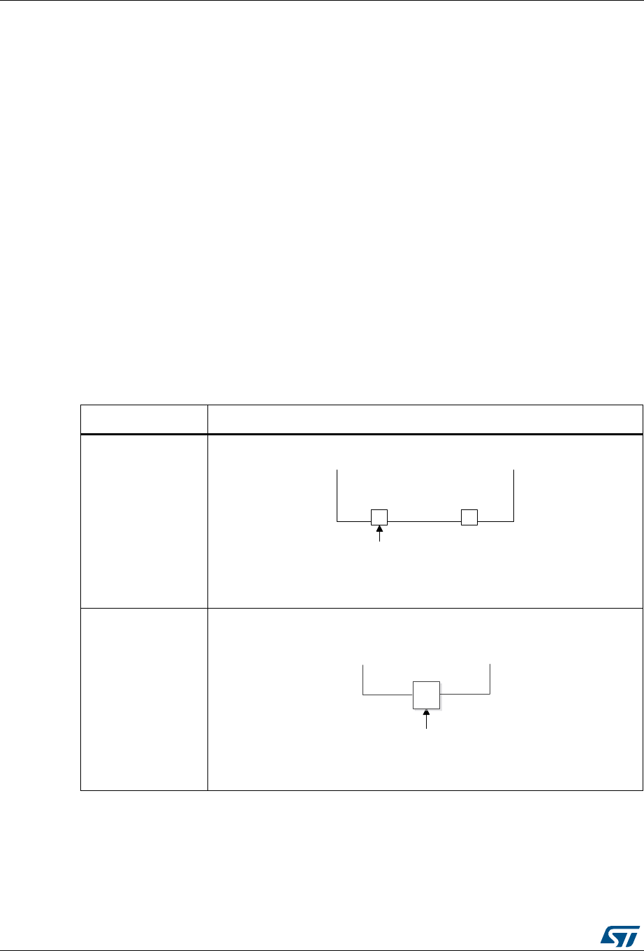
Reset and clock control (RCC) RM0376
176/1001 DocID025941 Rev 5
1. For full details about the internal and external clock source characteristics, please refer to the “Electrical
characteristics” section in your device datasheet.
The timer clock frequencies are automatically fixed by hardware. There are two cases:
1. If the APB prescaler is 1, the timer clock frequencies are set to the same frequency as
that of the APB domain to which the timers are connected.
2. Otherwise, they are set to twice (×2) the frequency of the APB domain to which the
timers are connected.
fCLK acts as Cortex®-M0+ free running clock. For more details refer to the Section 32:
Debug support (DBG).
7.2.1 HSE clock
The high speed external clock signal (HSE) can be generated from two possible clock
sources:
•HSE external crystal/ceramic resonator
•HSE user external clock
The resonator and the load capacitors have to be placed as close as possible to the
oscillator pins in order to minimize output distortion and startup stabilization time. The
loading capacitance values must be adjusted according to the selected oscillator.
Table 40. HSE/LSE clock sources
Clock source Hardware configuration
External clock for
category 3 and 5
devices
External clock
MSv31915V1
OSC_IN OSC_OUT
GPIO
External
source
External
source
CK_IN
GPIO
MSv36151V1

DocID025941 Rev 5 177/1001
RM0376 Reset and clock control (RCC)
222
External source (HSE bypass)
In this mode, an external clock source must be provided. It can have a frequency of up to
32 MHz. This mode is selected by setting the HSEBYP and HSEON bits in the RCC_CR
register (see Section 7.3.1: Clock control register (RCC_CR)). The external clock signal with
~50% duty cycle has to drive the OSC_IN pin while the OSC_OUT pin should be left hi-Z
(see Figure 40). The external clock signal can be square, sinus or triangle. To minimize the
consumption, it is recommended to use the square signal.
External crystal/ceramic resonator (HSE crystal)
The 1 to 24 MHz external oscillator has the advantage of producing a very accurate rate on
the main clock.
The associated hardware configuration is shown in Figure 40. Refer to the electrical
characteristics section of the datasheet for more details.
The HSERDY flag of the RCC_CR register (see Section 7.3.1) indicates whether the HSE
oscillator is stable or not. At startup, the HSE clock is not released until this bit is set by
hardware. An interrupt can be generated if enabled in the RCC_CR register.
The HSE Crystal can be switched on and off using the HSEON bit in the RCC_CR register.
For code example, refer to A.4.1: HSE start sequence code example.
7.2.2 HSI16 clock
The HSI16 clock signal is generated from an internal 16 MHz RC oscillator. It can be used
directly as a system clock or as PLL input.
The HSI16 clock can be used after wake-up from the Stop low-power mode, this ensure a
smaller wake-up time than a wake-up using MSI clock.
The HSI16 RC oscillator has the advantage of providing a clock source at low cost (no
external components). It also has a faster startup time than the HSE crystal oscillator
however, even with calibration the frequency is less accurate than an external crystal
oscillator or ceramic resonator.
Calibration
RC oscillator frequencies can vary from one chip to another due to manufacturing process
variations, this is why each device is factory calibrated by ST for 1% accuracy at an ambient
temperature, TA, of 25 °C.
After reset, the factory calibration value is loaded in the HSI16CAL[7:0] bits in the Internal
Clock Sources Calibration Register (RCC_ICSCR) (see Section 7.3.2).
If the application is subject to voltage or temperature variations, this may affect the RC
oscillator speed. You can trim the HSI16 frequency in the application by using the
HSI16TRIM[4:0] bits in the RCC_ICSCR register. For more details on how to measure the
HSI16 frequency variation please refer to Section 7.2.15: Internal/external clock
measurement using TIM21.
The HSI16RDY flag in the RCC_CR register indicates whether the HSI16 oscillator is stable
or not. At startup, the HSI16 RC output clock is not released until this bit is set by hardware.
The HSI16 RC oscillator can be switched on and off using the HSI16ON bit in the RCC_CR
register.

Reset and clock control (RCC) RM0376
178/1001 DocID025941 Rev 5
7.2.3 MSI clock
The MSI clock signal is generated from an internal RC oscillator. Its frequency range can be
adjusted by software by using the MSIRANGE[2:0] bits in the RCC_ICSCR register (see
Section 7.3.2: Internal clock sources calibration register (RCC_ICSCR)). Seven frequency
ranges are available: 65.536 kHz, 131.072 kHz, 262.144 kHz, 524.288 kHz, 1.048 MHz,
2.097 MHz (default value) and 4.194 MHz.
The MSI clock is always used as system clock after restart from Reset and wake-up from
Standby. After wake-up from Stop mode, the MSI clock can be selected as system clock
instead of HSI16 (or HSI16/4).
When the device restarts after a reset or a wake-up from Standby, the MSI frequency is set
to its default value. The MSI frequency does not change after waking up from Stop.
The MSI RC oscillator has the advantage of providing a low-cost (no external components)
low-power clock source. It is used as wake-up clock in low-power modes to reduce power
consumption.
The MSIRDY flag in the RCC_CR register indicates whether the MSI RC is stable or not. At
startup, the MSI RC output clock is not released until this bit is set by hardware.
The MSI RC can be switched on and off by using the MSION bit in the RCC_CR register
(see Section 7.3.1).
It can also be used as a backup clock source (auxiliary clock) if the HSE crystal oscillator
fails. Refer to Section 7.2.10: HSE clock security system (CSS) on page 181.
Calibration
The MSI RC oscillator frequency can vary from one chip to another due to manufacturing
process variations, this is why each device is factory calibrated by ST for 1% accuracy at an
ambient temperature, TA, of 25 °C.
After reset, the factory calibration value is loaded in the MSICAL[7:0] bits in the
RCC_ICSCR register. If the application is subject to voltage or temperature variations, this
may affect the RC oscillator speed. You can trim the MSI frequency in the application by
using the MSITRIM[7:0] bits in the RCC_ICSCR register. For more details on how to
measure the MSI frequency variation please refer to Section 7.2.15: Internal/external clock
measurement using TIM21.
7.2.4 HSI48 clock
The HSI48 clock signal is generated from an internal 48 MHz RC oscillator and can be used
directly for USB and for random number generator (RNG).
The internal 48MHz RC oscillator is mainly dedicated to provide a high precision clock to the
USB peripheral by means of a special Clock Recovery System (CRS) circuitry. The CRS
can use the USB SOF signal, the LSE or an external signal to automatically and quickly
adjust the oscillator frequency on-fly. It is disabled as soon as the system enters Stop or
Standby mode. When the CRS is not used, the HSI48 RC oscillator runs on its default
frequency which is subject to manufacturing process variations.
For more details on how to configure and use the CRS peripheral please refer to Section 8:
Clock recovery system (CRS).
The HSI48 requires VREFINT and its buffer with 48 MHz RC to be enabled (see

DocID025941 Rev 5 179/1001
RM0376 Reset and clock control (RCC)
222
ENREF_HSI48 in Section 10.2.3: Reference control and status register
(SYSCFG_CFGR3))
The HSI48RDY flag in the Clock recovery RC register (RCC_CRRCR) indicates whether the
HSI48 RC is stable or not. At startup, the HSI48 RC output clock is not released until this bit
is set by hardware.
The HSI48 RC can be switched on and off using the HSI48ON bit in the Clock recovery RC
register (RCC_CRRCR).
7.2.5 PLL
The internal PLL can be clocked by the HSI16 RC or HSE clocks. It drives the system clock
and can be used to generate the 48 MHz clock for the USB peripheral (refer to Figure 17
and Section 7.3.1: Clock control register (RCC_CR).
The PLL input clock frequency must range between 2 and 24 MHz.
The desired frequency is obtained by using the multiplication factor and output division
embedded in the PLL:
•If the USB uses the PLL as clock source, the PLL VCO clock (defined by the PLL
multiplication factor) must be programmed to output a 96 MHz frequency (USBCLK =
PLLVCO/2).
•The system clock is derived from the PLL VCO divided by the output division factor.
Note: The application software must set correctly the PLL multiplication factor to avoid exceeding
96 MHz as PLLVCO when the product is in range 1,
48 MHz as PLLVCO when the product is in range 2,
24 MHz when the product is in range 3.
It must also set correctly the output division to avoid exceeding 32 MHz as SYSCLK.
The minimum input clock frequency for PLL is 2 MHz (when using HSE as PLL source).
The PLL configuration (selection of the source clock, multiplication factor and output division
factor) must be performed before enabling the PLL. Once the PLL is enabled, these
parameters cannot be changed.
To modify the PLL configuration, proceed as follows:
1. Disable the PLL by setting PLLON to 0.
2. Wait until PLLRDY is cleared. The PLL is now fully stopped.
3. Change the desired parameter.
4. Enable the PLL again by setting PLLON to 1.
An interrupt can be generated when the PLL is ready if enabled in the RCC_CIER register
(see Section 7.3.5).
For code example, refer to A.4.2: PLL configuration modification code example.

Reset and clock control (RCC) RM0376
180/1001 DocID025941 Rev 5
7.2.6 LSE clock
The LSE crystal is a 32.768 kHz low speed external crystal or ceramic resonator. It has the
advantage of providing a low-power but highly accurate clock source to the real-time clock
peripheral (RTC) for clock/calendar or other timing functions.
The LSE crystal is switched on and off through the LSEON bit in the RCC_CSR register
(see Section 7.3.21).
The crystal oscillator driving strength can be changed at runtime through the LSEDRV[1:0]
bits of the RCC_CSR register to obtain the best compromise between robustness and short
start-up time on one hand and low power consumption on the other hand. The driving
capability should be changed dynamically to determine the driving level that best matches
the used crystal. In the final application, it is then recommended to program this value in
LSEDRV[1:0] bits.
The LSERDY flag in the RCC_CSR register indicates whether the LSE crystal is stable or
not. At startup, the LSE crystal output clock signal is not released until this bit is set by
hardware. An interrupt can be generated if enabled in the RCC_CIER register (see
Section 7.3.5).
External source (LSE bypass)
In this mode, an external clock source must be provided. It can have a frequency of up to
1 MHz. This mode is selected by setting the LSEBYP and LSEON bits in the RCC_CSR
(see Section 7.3.1). The external clock signal (square, sinus or triangle) with ~50% duty
cycle has to drive the OSC32_IN pin while the OSC32_OUT pin should be left Hi-Z (see
Figure 40).
7.2.7 LSI clock
The LSI RC acts as an low-power clock source that can be kept running in Stop and
Standby mode for the independent watchdog (IWDG). The clock frequency is around
37 kHz.
The LSI RC oscillator can be switched on and off using the LSION bit in the RCC_CSR
register (see Section 7.3.21).
The LSIRDY flag in RCC_CSR indicates whether the low-speed internal oscillator is stable
or not. At startup, the clock is not released until this bit is set by hardware. An interrupt can
be generated if enabled in the RCC_CIER (see Section 7.3.5).
Since the IWDG is activated, the LSI oscillator cannot be stopped by LSION=0. The LSI
oscillator is stopped by system reset (except if IWDG is enabled by hardware option through
WDG_SW option bit in FLASH_OPTR register). If the IWDG was enabled by software, then
the LSI oscillator must be enabled again after system reset to ensure correct IWDG and/or
RTC operation.
LSI measurement
The frequency dispersion of the LSI oscillator can be measured to have accurate RTC time
base and/or IWDG timeout (when LSI is used as clock source for these peripherals) with an
acceptable accuracy. For more details, refer to the electrical characteristics section of the
datasheets. For more details on how to measure the LSI frequency, please refer to
Section 7.2.15: Internal/external clock measurement using TIM21.

DocID025941 Rev 5 181/1001
RM0376 Reset and clock control (RCC)
222
7.2.8 System clock (SYSCLK) selection
Four different clock sources can be used to drive the system clock (SYSCLK):
•The HSI16 oscillator
•The HSE oscillator
•The PLL
•The MSI oscillator clock (default after reset)
When a clock source is used directly or through the PLL as system clock, it is not possible to
stop it.
A switch from one clock source to another occurs only if the target clock source is ready
(clock stable after startup delay or PLL locked). If a clock source which is not yet ready is
selected, the switch will occur when the clock source will be ready. Status bits in the
RCC_CR register indicate which clock(s) is (are) ready and which clock is currently used as
system clock.
7.2.9 System clock source frequency versus voltage range
The following table gives the different clock source maximum frequencies depending on the
product voltage range.
7.2.10 HSE clock security system (CSS)
The Clock security system can be activated on the HSE by software. In this case, the clock
detector is enabled after the HSE oscillator startup delay, and disabled when this oscillator is
stopped.
If an HSE clock failure is detected, this oscillator is automatically disabled and an CSSHSEI
interrupt (Clock Security System Interrupt) is generated to inform the software of the failure,
thus allowing the MCU to perform rescue operations. The CSSHSEI is linked to the
Cortex®-M0+ NMI (Non-Maskable Interrupt) exception vector.
Note: Once the CSSHSE is enabled, if the HSE clock fails, the CSSHSE interrupt occurs and an
NMI is automatically generated. The NMI is executed indefinitely unless the CSSHSE
interrupt pending bit is cleared. As a consequence, the NMI interrupt service routine (ISR)
must clear the CSSHSE interrupt by setting the CSSHSEC bit in the RCC_CICR register.
Table 41. System clock source frequency
Product voltage
range
Clock frequency
MSI HSI16 HSE PLL
Range 1 (1.8 V) 4.2 MHz 16 MHz HSE 32 MHz (external clock)
or 24 MHz (crystal)
32 MHz
(PLLVCO max = 96 MHz)
Range 2 (1.5 V) 4.2 MHz 16 MHz 16 MHz 16 MHz
(PLLVCO max = 48 MHz)
Range 3 (1.2 V) 4.2 MHz NA 8 MHz 4 MHz
(PLLVCO max = 24 MHz)

Reset and clock control (RCC) RM0376
182/1001 DocID025941 Rev 5
If the HSE oscillator is used directly or indirectly as the system clock (indirectly means: it is
used as PLL input clock, and the PLL clock is used as system clock), a detected failure
causes a switch of the system clock and the disabling of the HSE oscillator. If the HSE
oscillator clock is the clock entry of the PLL used as system clock when the failure occurs,
the PLL is disabled too.
When an HSE failure occurs, the system clock can be switched to the MSI or to the internal
16-MHz HSI clock depending on the value of STOPWUCK bit in the RCC_CFGR register.
7.2.11 LSE Clock Security System
Clock Security System can be activated on the LSE by software. This is done by writing the
CSSLSEON bit in the RCC_CSR register. This bit can be disabled by a hardware reset, an
RTC software reset, or after an LSE clock failure detection. CSSLSEON bit must be written
after the LSE and LSI clocks are enabled (LSEON and LSION set) and ready (LSERDY and
LSIRDY bits set by hardware), and after the RTC clock has been selected through the
RTCSEL bit.
The LSE CSS works in all modes: run, Sleep, Stop and Standby.
If a failure is detected on the external 32 kHz oscillator, the LSE clock is no longer supplied
to the RTC but the content of the registers does not change.
A wakeup is generated in Standby mode. In any other modes, an interrupt can be sent to
wake-up the software (see Section 7.3.5).
The software MUST then reset the CSSLSEON bit and stop the defective 32 kHz oscillator
by resetting LSEON bit. It can change the RTC clock source (LSI, HSE or no clock) through
the RTCSEL bit, or take any required action to secure the application.
The frequency of LSE oscillator must be higher than 30 kHz to avoid false positive CSS
detection.
7.2.12 RTC clock
The RTC has the same clock source which can be either the LSE, the LSI, or the HSE
4 MHz clock (HSE divided by a programmable prescaler). It is selected by programming the
RTCSEL[1:0] bits in the RCC_CSR register (see Section 7.3.21) and the RTCPRE[1:0] bits
in the RCC_CR register (see Section 7.3.1).
Once the RTC clock source have been selected, the only possible way of modifying the
selection is to set the RTCRST bit in the RCC_CSR register, or by a POR.
If the LSE or LSI is used as RTC clock source, the RTC continues to work in Stop and
Standby low-power modes, and can be used as wakeup source. However, when the HSE is
the RTC clock source, the RTC cannot be used in the Stop and Standby low-power modes.
When the RTC is clocked by the LSE, the RTC remains clocked and functional under
system reset.
Note: To be able to read the RTC calendar register when the APB1 clock frequency is less than
seven times the RTC clock frequency (7*RTCLCK), the software must read the calendar
time and date registers twice.
If the second read of the RTC_TR gives the same result as the first read, this ensures that
the data is correct. Otherwise a third read access must be done.
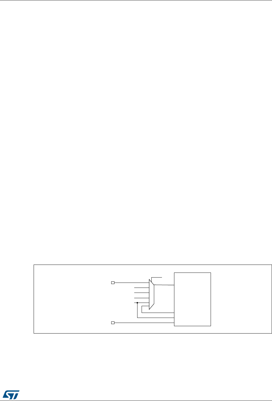
DocID025941 Rev 5 183/1001
RM0376 Reset and clock control (RCC)
222
7.2.13 Watchdog clock
If the Independent watchdog (IWDG) is started by either hardware option or software
access, the LSI oscillator is forced ON and cannot be disabled. After the LSI oscillator
temporization, the clock is provided to the IWDG.
If the IWDG was enabled by software, the LSI clock is disabled after system reset. The LSI
oscillator must then be enabled again to ensure correct IWDG operation.
7.2.14 Clock-out capability
The microcontroller clock output (MCO) capability allows the clock to be output onto the
external MCO pin using a configurable prescaler (1, 2, 4, 8, or 16). The configuration
registers of the corresponding GPIO port must be programmed in alternate function mode.
One of 7 clock signals can be selected as the MCO clock:
•SYSCLK
•HSI16
•HSI48
•MSI
•HSE
•PLL
•LSI
•LSE
The selection is controlled by the MCOSEL[3:0] bits of the RCC_CFGR register (see
Section 7.3.20).
For code example, refer to A.4.3: MCO selection code example.
7.2.15 Internal/external clock measurement using TIM21
It is possible to indirectly measure the frequency of all on-board clock source generators by
means of the TIM21 channel 1 input capture, as represented on Figure 18.
Figure 18. Using TIM21 channel 1 input capture to measure
frequencies
TIM21 has an input multiplexer that selects which of the I/O or the internal clock is to trigger
the input capture. This selection is performed through the TI1_RMP [2:0] bits in the
TIM21_OR register.
MS32913V1
GPIO
GPIO
TI1_RMP[2:0] TIM21
TI(1)
ETR
TI(2)
MSI
LSI
HSE_RTC
LSE
LSE

Reset and clock control (RCC) RM0376
184/1001 DocID025941 Rev 5
The primary purpose of connecting the LSE to the channel 1 input capture is to be able to
accurately measure the HSI16 and MSI system clocks (for this, either the HSI16 or MSI
should be used as the system clock source). The number of HSI16 (MSI, respectively) clock
counts between consecutive edges of the LSE signal provides a measure of the internal
clock period. Taking advantage of the high precision of LSE crystals (typically a few tens of
ppm’s), it is possible to determine the internal clock frequency with the same resolution, and
trim the source to compensate for manufacturing-process- and/or temperature- and voltage-
related frequency deviations.
The MSI and HSI16 oscillators both have dedicated user-accessible calibration bits for this
purpose.
The basic concept consists in providing a relative measurement (e.g. the HSI16/LSE ratio):
the precision is therefore closely related to the ratio between the two clock sources. The
higher the ratio, the better the measurement.
It is however not possible to have a good enough resolution when the MSI clock is low
(typically below 1 MHz). In this case, it is advised to:
•accumulate the results of several captures in a row
•use the timer’s input capture prescaler (up to 1 capture every 8 periods)
•use the RTC_OUT signal at 512 Hz (when the RTC is clocked by the LSE) as the input
for the channel1 input capture. This improves the measurement precision
TIM21 can also be used to measure the LSI, MSI, or HSE_RTC: this is useful for
applications with no crystal. The ultra-low-power LSI oscillator has a wide manufacturing
process deviation: by measuring it as a function of the HSI16 clock source, its frequency
can be determined with the precision of the HSI16.The HSE_RTC frequency (HSE divided
by a programmable prescaler) being relatively high (4 MHz), the relative frequency
measurement is not very accurate. Its main purpose is consequently to obtain a rough
indication of the external crystal frequency. This can be useful to meet the requirements of
the IEC 60730/IEC 61335 standards, which require to be able to determine harmonic or
subharmonic frequencies (–50/+100% deviations).
7.2.16 Clock-independent system clock sources for TIM2/TIM21/TIM22
In a number of applications using the 32.768 kHz clock as RTC timebase, timebases
completely independently from the system clock are useful. This allows to schedule tasks
without having to take into account the processor state (the processor may be stopped or
executing at low, medium or full speed).
For this purpose, the LSE clock is internally redirected to the 3 timers’ ETR inputs, which are
used as additional clock sources. This gives up to three independent time bases (using the
auto-reload feature) with 1 or 2 compare additional channels for fractional events. For
instance, the TIM21 auto-reload interrupt can be programmed for a 1 second tick interrupt
with an additional interrupt occurring 250 ms after the main tick.
Note: In this configuration, make sure that you have at least a ratio of 2 between the external clock
(LSE) and the APB clock. If the application uses an APB clock frequency lower than twice
the LSE clock frequency (typically LSE = 32.768 kHz, so twice LSE = 65.536 kHz), it is
mandatory to use the external trigger prescaler feature of the timer: it can divide the ETR
clock by up to 8.

DocID025941 Rev 5 185/1001
RM0376 Reset and clock control (RCC)
222
7.3 RCC registers
Refer to Section 1.1 for a list of abbreviations used in register descriptions.
7.3.1 Clock control register (RCC_CR)
Address offset: 0x00
System Reset value: 0b0000 0000 00XX 0X00 0000 0011 0000 0000 where X is undefined
Power-on reset value: 0x0000 0300
Access: no wait state, word, half-word and byte access
31 30 29 28 27 26 25 24 23 22 21 20 19 18 17 16
Res. Res. Res. Res. Res. Res. PLL
RDY PLLON Res. Res. RTCPRE[1:0] CSSHS
EON.
HSE
BYP
HSE
RDY
HSE
ON
r rw rwrwrwrw r rw
15 14 13 12 11 10 9 8 7 6 5 4 3 2 1 0
Res. Res. Res. Res. Res. Res. MSI
RDY MSION Res. Res. HSI16
OUTEN
HSI16
DIVF
HSI16
DIVEN
HSI16
RDYF
HSI16K
ERON
HSI16
ON
rrw rwrrwrrwrw
Bits 31:26 Reserved, must be kept at reset value.
Bit 25 PLLRDY: PLL clock ready flag
This bit is set by hardware to indicate that the PLL is locked.
0: PLL unlocked
1: PLL locked
Bit 24 PLLON: PLL enable bit
This bit is set and cleared by software to enable PLL.
Cleared by hardware when entering Stop or Standby mode. This bit can not be reset if the
PLL clock is used as system clock or is selected to become the system clock.
0: PLL OFF
1: PLL ON
Bits 23:22 Reserved, must be kept at reset value.
Bits 21:20 RTCPRE[1:0] RTC prescaler
These bits are set and reset by software to obtain a 4 MHz clock from HSE. This prescaler
cannot be modified if HSE is enabled (HSEON = 1).These bits are reset by a power -on
reset,. Their value is not modified by a system reset.
00: HSE is divided by 2 for RTC clock
01: HSE is divided by 4 for RTC clock
10: HSE is divided by 8 for RTC clock
11: HSE is divided by 16 for RTC clock
Bit 19 CSSHSEON: Clock security system on HSE enable bit
This bit is set by software to enable the clock security system (CSS) on HSE. This bit is "set
only" (disabled by system reset). When CSSHSEON is set, the clock detector is enabled by
hardware when the HSE oscillator is ready, and disabled by hardware if an oscillator failure
is detected.
0: Clock security system OFF (clock detector OFF)
1: Clock security system ON (clock detector ON if HSE oscillator is stable, OFF otherwise)

Reset and clock control (RCC) RM0376
186/1001 DocID025941 Rev 5
Bit 18 HSEBYP: HSE clock bypass bit
This bit is set and cleared by software to bypass the oscillator with an external clock. The
external clock must be enabled with the HSEON bit, to be used by the device.
The HSEBYP bit can be written only if the HSE oscillator is disabled. This bit is reset by
power-on reset. Its value is not modified by system reset
0: HSE oscillator not bypassed
1: HSE oscillator bypassed with an external clock
Bit 17 HSERDY: HSE clock ready flag
This bit is set by hardware to indicate that the HSE oscillator is stable. After the HSEON bit is
cleared, HSERDY goes low after 6 HSE oscillator clock cycles.
0: HSE oscillator not ready
1: HSE oscillator ready
Bit 16 HSEON: HSE clock enable bit
This bit is set and cleared by software.
Cleared by hardware to stop the HSE oscillator when entering Stop or Standby mode. This
bit cannot be reset if the HSE oscillator is used directly or indirectly as the system clock.
0: HSE oscillator OFF
1: HSE oscillator ON
Bits 15:10 Reserved, must be kept at reset value.
Bit 9 MSIRDY: MSI clock ready flag
This bit is set by hardware to indicate that the MSI oscillator is stable.
0: MSI oscillator not ready
1: MSI oscillator ready
Note: Once the MSION bit is cleared, MSIRDY goes low after 6 MSI clock cycles.
Bit 8 MSION: MSI clock enable bit
This bit is set and cleared by software.
Set by hardware to force the MSI oscillator ON when exiting from Stop or Standby mode, or
in case of a failure of the HSE oscillator used directly or indirectly as system clock. This bit
cannot be cleared if the MSI is used as system clock.
0: MSI oscillator OFF
1: MSI oscillator ON
Bits 7:6 Reserved, must be kept at reset value.
Bit 5 HSI16OUTEN: 16 MHz high-speed internal clock output enable
This bit is set and cleared by software. When this bit is set, TIM2 ETR input is connected to
the 16 MHz HSI output clock (HSI16) provided ETR_RMP is set to 011 in TIM2 option
register (TIM2_OR). This bit can be written anytime by the application.
0: HSI16 output clock disabled
1: HSI16 output clock enabled
Bit 4 HSI16DIVF HSI16 divider flag
This bit is set and reset by hardware. As a write in HSI16DIVEN has not an immediate effect
on the frequency, this flag indicates the current status of the HSI16 divider.
0: 16 MHz HSI clock not divided
1: 16 MHz HSI clock divided by 4
Bit 3 HSI16DIVEN HSI16 divider enable bit
This bit is set and reset by software to enable/disable the 16 MHz HSI divider by 4. It can be
written anytime.
0: no 16 MHz HSI division requested
1: 16 MHz HSI division by 4 requested

DocID025941 Rev 5 187/1001
RM0376 Reset and clock control (RCC)
222
Bit 2 HSI16RDYF: Internal high-speed clock ready flag
This bit is set by hardware to indicate that the HSI 16 MHz oscillator is stable. After the
HSI16ON bit is cleared, HSI16RDY goes low after 6 HSI16 clock cycles.
0: HSI 16 MHz oscillator not ready
1: HSI 16 MHz oscillator ready
Bit 1 HSI16KERON: High-speed internal clock enable bit for some IP kernels
This bit is set and reset by software to force the HSI 16 MHz oscillator ON, even in Stop
mode, so that it can be quickly available as kernel clock for USARTs or I2C1. This bit has no
effect on the value of HSI16ON.
0: HSI 16 MHz oscillator not forced ON
1: HSI 16 MHz oscillator forced ON even in Stop mode
Bit 0 HSI16ON: 16 MHz high-speed internal clock enable
This bit is set and cleared by software. It cannot be cleared if the 16 MHz HSI is used directly
or indirectly as system clock.
0: HSI16 oscillator OFF
1: HSI16 oscillator ON

Reset and clock control (RCC) RM0376
188/1001 DocID025941 Rev 5
7.3.2 Internal clock sources calibration register (RCC_ICSCR)
Address offset: 0x04
Reset value: 0x00XX B0XX where X is undefined.
Access: no wait state, word, half-word and byte access
31 30 29 28 27 26 25 24 23 22 21 20 19 18 17 16
MSITRIM[7:0] MSICAL[7:0]
rw rw rw rw rw rw rw rw r r r r r r r r
15 14 13 12 11 10 9 8 7 6 5 4 3 2 1 0
MSIRANGE[2:0] HSI16TRIM[4:0] HSI16CAL[7:0]
rw rw rw rw rw rw rw rw r r r r r r r r
Bits 31:24 MSITRIM[7:0]: MSI clock trimming
These bits are set by software to adjust MSI calibration.
These bits provide an additional user-programmable trimming value that is added to the
MSICAL[7:0] bits. They can be programmed to compensate for the variations in voltage and
temperature that influence the frequency of the internal MSI RC.
Bits 23:16 MSICAL[7:0]: MSI clock calibration
These bits are automatically initialized at startup.
Bits 15:13 MSIRANGE[2:0]: MSI clock ranges
These bits are set by software to choose the frequency range of MSI.7 frequency ranges are
available:
000: range 0 around 65.536 kHz
001: range 1 around 131.072 kHz
010: range 2 around 262.144 kHz
011: range 3 around 524.288 kHz
100: range 4 around 1.048 MHz
101: range 5 around 2.097 MHz (reset value)
110: range 6 around 4.194 MHz
111: not allowed
Bits 12:8 HSI16TRIM[4:0]: High speed internal clock trimming
These bits provide an additional user-programmable trimming value that is added to the
HSI16CAL[7:0] bits. They can be programmed to compensated for the variations in voltage
and temperature that influence the frequency of the internal HSI16 RC.
Bits 7:0 HSI16CAL[7:0] Internal high speed clock calibration
These bits are initialized automatically at startup.

DocID025941 Rev 5 189/1001
RM0376 Reset and clock control (RCC)
222
7.3.3 Clock recovery RC register (RCC_CRRCR)
Address: 0x08
Reset value: 0x0000 XX00
Access: no wait state, word, half-word and byte access
31 30 29 28 27 26 25 24 23 22 21 20 19 18 17 16
Res. Res. Res. Res. Res. Res. Res. Res. Res. Res. Res. Res. Res. Res. Res. Res.
15 14 13 12 11 10 9 8 7 6 5 4 3 2 1 0
HSI48CAL[7:0] Res. Res. Res. Res. Res. HSI48
DIV6EN HSI48RDY HSI48ON
r rrrrr r r rw r rw
Bits 31:16 Reserved, must be kept at reset value.
Bits 15:8 HSI48CAL[7:0]: 48 MHz HSI clock calibration
These bits are read-only. They are set by hardware by loading option bytes during system
reset.
Bits 7:3 Reserved, must be kept at reset value.
Bit 2 HSI48DIV6EN: 48 MHz HSI clock divided by 6 output enable
This bit is set and cleared by software. When it is set, HSI48/6 clock is delivered to TIM3.
0: Output delivering HSI48/6 not enabled
1:Output delivering HSI48/6 enabled
Bit 1 HSI48RDY: 48MHz HSI clock ready flag
This bit is set by hardware to indicate that the 48 MHz RC oscillator is stable. It requires 6
48 MHz RC oscillator clock cycles to fall down after HSION reset.
0: 48 MHz HSI clock not ready
1: 48 MHz HSI clock ready
Bit 0 HSI48ON: 48MHz HSI clock enable bit
This bit is set and cleared by software.
0: 48 MHz HSI clock OFF
1: 48 MHz HSI clock ON

Reset and clock control (RCC) RM0376
190/1001 DocID025941 Rev 5
7.3.4 Clock configuration register (RCC_CFGR)
Address offset: 0x0C
Reset value: 0x0000 0000
Access: 0 ≤ wait state ≤2, word, half-word and byte access
1 or 2 wait states inserted only if the access occurs during clock source switch.
31 30 29 28 27 26 25 24 23 22 21 20 19 18 17 16
Res. MCOPRE[2:0] MCOSEL[3:0] PLLDIV[1:0] PLLMUL[3:0] Res. PLL
SRC
rw rw rw rw rw rw rw rw rw rw rw rw rw rw
15 14 13 12 11 10 9 8 7 6 5 4 3 2 1 0
STOP
WUCK. Res. PPRE2[2:0] PPRE1[2:0] HPRE[3:0] SWS[1:0] SW[1:0]
rw rw rw rw rw rw rw rw rw rw rw r r rw rw
Bit 31 Reserved, must be kept at reset value.
Bits 30:28 MCOPRE[2:0]: Microcontroller clock output prescaler
These bits are set and cleared by software.
It is highly recommended to change this prescaler before MCO output is enabled.
000: MCO is divided by 1
001: MCO is divided by 2
010: MCO is divided by 4
011: MCO is divided by 8
100: MCO is divided by 16
Others: not allowed
Bits 27:24 MCOSEL[3:0]: Microcontroller clock output selection
These bits are set and cleared by software.
0000: MCO output disabled, no clock on MCO
0001: SYSCLK clock selected
0010: HSI16 oscillator clock selected
0011: MSI oscillator clock selected
0100: HSE oscillator clock selected
0101: PLL clock selected
0110: LSI oscillator clock selected
0111: LSE oscillator clock selected
1000: HSI48 oscillator clock selected
Others: reserved
Note: This clock output may have some truncated cycles at startup or during MCO clock
source switching.
Bits 23:22 PLLDIV[1:0]: PLL output division
These bits are set and cleared by software to control PLL output clock division from PLL VCO
clock. These bits can be written only when the PLL is disabled.
00: not allowed
01: PLL clock output = PLLVCO / 2
10: PLL clock output = PLLVCO / 3
11: PLL clock output = PLLVCO / 4

DocID025941 Rev 5 191/1001
RM0376 Reset and clock control (RCC)
222
Bits 21:18 PLLMUL[3:0]: PLL multiplication factor
These bits are written by software to define the PLL multiplication factor to generate the PLL
VCO clock. These bits can be written only when the PLL is disabled.
0000: PLLVCO = PLL clock entry x 3
0001: PLLVCO = PLL clock entry x 4
0010: PLLVCO = PLL clock entry x 6
0011: PLLVCO = PLL clock entry x 8
0100: PLLVCO = PLL clock entry x 12
0101: PLLVCO = PLL clock entry x 16
0110: PLLVCO = PLL clock entry x 24
0111: PLLVCO = PLL clock entry x 32
1000: PLLVCO = PLL clock entry x 48
others: not allowed
Caution: The PLL VCO clock frequency must not exceed 96 MHz when the product is in
Range 1, 48 MHz when the product is in Range 2 and 24 MHz when the product is in
Range 3.
Bit 17 Reserved, must be kept at reset value.
Bit 16 PLLSRC: PLL entry clock source
This bit is set and cleared by software to select PLL clock source. This bit can be written only
when PLL is disabled.
0: HSI16 oscillator clock selected as PLL input clock
1: HSE oscillator clock selected as PLL input clock
Note: The PLL minimum input clock frequency is 2 MHz.
Bit 15 STOPWUCK: Wake-up from Stop clock selection
This bit is set and cleared by software to select the wake-up from Stop clock.
0: internal 64 KHz to 4 MHz (MSI) oscillator selected as wake-up from Stop clock
1: internal 16 MHz (HSI16) oscillator selected as wake-up from Stop clock (or HSI16/4 if
HSI16DIVEN=1)
Bit 14 Reserved, must be kept at reset value.
Bits 13:11 PPRE2[2:0]: APB high-speed prescaler (APB2)
These bits are set and cleared by software to control the division factor of the APB high-
speed clock (PCLK2).
0xx: HCLK not divided
100: HCLK divided by 2
101: HCLK divided by 4
110: HCLK divided by 8
111: HCLK divided by 16
Bits 10:8 PPRE1[2:0]: APB low-speed prescaler (APB1)
These bits are set and cleared by software to control the division factor of the APB low-speed
clock (PCLK1).
0xx: HCLK not divided
100: HCLK divided by 2
101: HCLK divided by 4
110: HCLK divided by 8
111: HCLK divided by 16

Reset and clock control (RCC) RM0376
192/1001 DocID025941 Rev 5
7.3.5 Clock interrupt enable register (RCC_CIER)
Address: 0x10
Reset value: 0x0000 0000
Access: no wait state, word, half-word and byte access
Bits 7:4 HPRE[3:0]: AHB prescaler
These bits are set and cleared by software to control the division factor of the AHB clock.
Caution: Depending on the device voltage range, the software has to set correctly these bits
to ensure that the system frequency does not exceed the maximum allowed
frequency (for more details please refer to the Dynamic voltage scaling management
section in the PWR chapter.) After a write operation to these bits and before
decreasing the voltage range, this register must be read to be sure that the new
value has been taken into account.
0xxx: SYSCLK not divided
1000: SYSCLK divided by 2
1001: SYSCLK divided by 4
1010: SYSCLK divided by 8
1011: SYSCLK divided by 16
1100: SYSCLK divided by 64
1101: SYSCLK divided by 128
1110: SYSCLK divided by 256
1111: SYSCLK divided by 512
Bits 3:2 SWS[1:0]: System clock switch status
These bits are set and cleared by hardware to indicate which clock source is used as system
clock.
00: MSI oscillator used as system clock
01: HSI16 oscillator used as system clock
10: HSE oscillator used as system clock
11: PLL used as system clock
Bits 1:0 SW[1:0]: System clock switch
These bits are set and cleared by software to select SYSCLK source.
Set by hardware to force MSI selection when leaving Standby mode or in case of failure of
the HSE oscillator used directly or indirectly as system clock (if the Clock Security System is
enabled).
00: MSI oscillator used as system clock
01: HSI16 oscillator used as system clock
10: HSE oscillator used as system clock
11: PLL used as system clock
31 30 29 28 27 26 25 24 23 22 21 20 19 18 17 16
Res. Res. Res. Res. Res. Res. Res. Res. Res. Res. Res. Res. Res. Res. Res. Res.
15 14 13 12 11 10 9 8 7 6 5 4 3 2 1 0
Res. Res. Res. Res. Res. Res. Res. Res. CSS
LSE
HSI48
RDYIE
MSI
RDYIE
PLL
RDYIE
HSE
RDYIE
HSI16
RDYIE
LSE
RDYIE
LSI
RDYIE
rrrrrr r r

DocID025941 Rev 5 193/1001
RM0376 Reset and clock control (RCC)
222
Bits 31:8 Reserved, must be kept at reset value.
Bit 7 CSSLSE: LSE CSS interrupt flag
This bit is set and reset by software to enable/disable the interrupt caused by the Clock
Security System on external 32 kHz oscillator.
0: LSE CSS interrupt disabled
1: LSE CSS interrupt enabled
Bit 6 HSI48RDYIE: HSI48 ready interrupt flag
This bit is set and reset by software to enable/disable the interrupt caused by the HSI48
oscillator stabilization.
0: HSI48 ready interrupt disabled
1: HSI48 ready interrupt enabled
Bit 5 MSIRDYIE: MSI ready interrupt flag
This bit is set and reset by software to enable/disable the interrupt caused by the MSI
oscillator stabilization.
0: MSI ready interrupt disabled
1: MSI ready interrupt enabled
Bit 4 PLLRDYIE: PLL ready interrupt flag
This bit is set and reset by software to enable/disable the interrupt caused by the PLL lock.
0: PLL lock interrupt disabled
1: PLL lock interrupt enabled
Bit 3 HSERDYIE: HSE ready interrupt flag
This bit is set and reset by software to enable/disable the interrupt caused by the HSE
oscillator stabilization.
0: HSE ready interrupt disabled
1: HSE ready interrupt enabled
Bit 2 HSI16RDYIE: HSI16 ready interrupt flag
This bit is set and reset by software to enable/disable the interrupt caused by the HSI16
oscillator stabilization.
0: HSI16 ready interrupt disabled
1: HSI16 ready interrupt enabled
Bit 1 LSERDYIE: LSE ready interrupt flag
This bit is set and reset by software to enable/disable the interrupt caused by the LSE
oscillator stabilization.
0: LSE ready interrupt disabled
1: LSE ready interrupt enabled
Bit 0 LSIRDYIE: LSI ready interrupt flag
This bit is set and reset by software to enable/disable the interrupt caused by the LSI
oscillator stabilization.
0: LSI ready interrupt disabled
1: LSI ready interrupt enabled

Reset and clock control (RCC) RM0376
194/1001 DocID025941 Rev 5
7.3.6 Clock interrupt flag register (RCC_CIFR)
Address: 0x14
Reset value: 0x0000 0000
Access: no wait state, word, half-word and byte access
31 30 29 28 27 26 25 24 23 22 21 20 19 18 17 16
Res. Res. Res. Res. Res. Res. Res. Res. Res. Res. Res. Res. Res. Res. Res. Res.
15 14 13 12 11 10 9 8 7 6 5 4 3 2 1 0
Res. Res. Res. Res. Res. Res. Res. CSS
HSEF
CSS
LSEF
HSI48
RDYF
MSI
RDYF
PLL
RDYF
HSE
RDYF
HSI16
RDYF
LSE
RDYF
LSI
RDYF
r rrrrrr r r
Bits 31:9 Reserved, must be kept at reset value.
Bit 8 CSSHSEF: Clock Security System Interrupt flag
This bit is reset by software by writing the CSSHSEC bit. It is set by hardware in case of HSE
clock failure.
0: No clock security interrupt caused by HSE clock failure
1: Clock security interrupt caused by HSE clock failure
Bit 7 CSSLSEF: LSE Clock Security System Interrupt flag
This bit is reset by software by writing the CSSLSEC bit. It is set by hardware in case of LSE
clock failure and the CSSLSE is set.
0: No failure detected on LSE clock failure
1: Failure detected on LSE clock failure
Bit 6 HSI48RDYF: HSI48 ready interrupt flag
This bit is reset by software by writing the HSI48RDYC bit. It is set by hardware when the
CSS becomes stable and the HSI48RDYIE is set.
0: No clock ready interrupt caused by HSI48 clock failure
1: Clock ready interrupt caused by HSI48 clock failure
Bit 5 MSIRDYF: MSI ready interrupt flag
This bit is reset by software by writing the MSIRDYC bit. It is set by hardware when the MSI
clock becomes stable and the MSIRDYIE is set.
0: No clock ready interrupt caused by MSI clock failure
1: Clock ready interrupt caused by MSI clock failure
Bit 4 PLLRDYF: PLL ready interrupt flag
This bit is reset by software by writing the PLLRDYC bit. It is set by hardware when the PLL
clock becomes stable and the PLLRDYIE is set.
0: No clock ready interrupt caused by PLL clock failure
1: Clock ready interrupt caused by PLL clock failure
Bit 3 HSERDYF: HSE ready interrupt flag
This bit is reset by software by writing the HSERDYC bit. It is set by hardware when the HSE
clock becomes stable and the HSERDYIE is set.
0: No clock ready interrupt caused by HSE clock failure
1: Clock ready interrupt caused by HSE clock failure

DocID025941 Rev 5 195/1001
RM0376 Reset and clock control (RCC)
222
7.3.7 Clock interrupt clear register (RCC_CICR)
Address: 0x18
Reset value: 0x0000 0000
Access: no wait state, word, half-word and byte access
Bit 2 HSI16RDYF: HSI16 ready interrupt flag
This bit is reset by software by writing the HSI16RDYC bit. It is set by hardware when the
HSE clock becomes stable and the HSI16RDYIE is set.
0: No clock ready interrupt caused by HSI16 clock failure
1: Clock ready interrupt caused by HSI16 clock failure
Bit 1 LSERDYF: LSE ready interrupt flag
This bit is reset by software by writing the LSERDYC bit. It is set by hardware when the LSE
clock becomes stable and the LSERDYIE is set.
0: No clock ready interrupt caused by LSE clock failure
1: Clock ready interrupt caused by LSE clock failure
Bit 0 LSIRDYF: LSI ready interrupt flag
This bit is reset by software by writing the LSIRDYC bit. It is set by hardware when the LSI
clock becomes stable and the LSIRDYIE is set.
0: No clock ready interrupt caused by LSI clock failure
1: Clock ready interrupt caused by LSI clock failure
31 30 29 28 27 26 25 24 23 22 21 20 19 18 17 16
Res. Res. Res. Res. Res. Res. Res. Res. Res. Res. Res. Res. Res. Res. Res. Res.
15 14 13 12 11 10 9 8 7 6 5 4 3 2 1 0
Res. Res. Res. Res. Res. Res. Res. CSS
HSEC
CSS
LSEC
HSI48
RDYC
MSI
RDYC
PLL
RDYC
HSE
RDYC
HSI16
RDYC
LSE
RDYIC
LSI
RDYC
w wwwwww w w
Bits 31:9 Reserved, must be kept at reset value.
Bit 8 CSSHSEC: Clock Security System Interrupt clear
This bit is set by software to clear the CSSHSEF flag. It is reset by hardware.
0: No effect
1: CSSHSEF flag cleared
Bit 7 CSSLSEC: LSE Clock Security System Interrupt clear
This bit is set by software to clear the CSSLSEF flag. It is reset by hardware.
0: No effect
1: CSSLSEF flag cleared
Bit 6 HSI48RDYC: HSI48 ready Interrupt clear
This bit is set by software to clear the HSI48RDYF flag. It is reset by hardware.
0: No effect
1: HSI48RDYF flag cleared

Reset and clock control (RCC) RM0376
196/1001 DocID025941 Rev 5
7.3.8 GPIO reset register (RCC_IOPRSTR)
Address: 0x1C
Reset value: 0x0000 0000
Access: no wait state, word, half-word and byte access
Bit 5 MSIRDYC: MSI ready Interrupt clear
This bit is set by software to clear the MSIRDYF flag. It is reset by hardware.
0: No effect
1: MSIRDYF flag cleared
Bit 4 PLLRDYC: PLL ready Interrupt clear
This bit is set by software to clear the PLLRDYF flag. It is reset by hardware.
0: No effect
1: PLLRDYF flag cleared
Bit 3 HSERDYC: HSE ready Interrupt clear
This bit is set by software to clear the HSERDYF flag. It is reset by hardware.
0: No effect
1: HSERDYF flag cleared
Bit 2 HSI16RDYC: HSI16 ready Interrupt clear
This bit is set by software to clear the HSI16RDYF flag. It is reset by hardware.
0: No effect
1: HSI16RDYF flag cleared
Bit 1 LSERDYC: LSE ready Interrupt clear
This bit is set by software to clear the LSERDYF flag. It is reset by hardware.
0: No effect
1: LSERDYF flag cleared
Bit 0 LSIRDYC: LSI ready Interrupt clear
This bit is set by software to clear the LSIRDYF flag. It is reset by hardware.
0: No effect
1: LSIRDYF flag cleared
31 30 29 28 27 26 25 24 23 22 21 20 19 18 17 16
Res. Res. Res. Res. Res. Res. Res. Res. Res. Res. Res. Res. Res. Res. Res. Res.
15 14 13 12 11 10 9 8 7 6 5 4 3 2 1 0
Res. Res. Res. Res. Res. Res. Res. Res. IOPH
RST Res. Res. IOPER
ST
IOPD
RST
IOPC
RST
IOPB
RST
IOPA
RST
rw rw rw rw rw rw
Bits 31:8 Reserved, must be kept at reset value.
Bit 7 IOPHRST: I/O port H reset
This bit is set and cleared by software.
0: no effect
1: resets I/O port H

DocID025941 Rev 5 197/1001
RM0376 Reset and clock control (RCC)
222
7.3.9 AHB peripheral reset register (RCC_AHBRSTR)
Address offset: 0x20
Reset value: 0x0000 0000
Access: no wait state, word, half-word and byte access.
Bits 6:5 Reserved, must be kept at reset value.
Bit 4 IOPERST: I/O port E reset
This bit is set and cleared by software.
0: no effect
1: resets I/O port E
Bit 3 IOPDRST: I/O port D reset
This bit is set and cleared by software.
0: no effect
1: resets I/O port D
Bit 2 IOPCRST: I/O port C reset
This bit is set and cleared by software.
0: no effect
1: resets I/O port C
Bit 1 IOPBRST: I/O port B reset
This bit is set and cleared by software.
0: no effect
1: resets I/O port B
Bit 0 IOPARST: I/O port A reset
This bit is set and cleared by software.
0: no effect
1: resets I/O port A
31 30 29 28 27 26 25 24 23 22 21 20 19 18 17 16
Res. Res. Res. Res. Res. Res. Res. CRYP
RST Res. Res. Res. RNGR
ST Res. Res. Res.
rw rw rw
15 14 13 12 11 10 9 8 7 6 5 4 3 2 1 0
Res. Res. Res. CRC
RST Res. Res. Res. MIF
RST Res. Res. Res. Res. Res. Res. Res. DMA
RST
rw rw rw
Bits 31:25 Reserved, must be kept at reset value.
Bit 24 CRYPTRST: Crypto module reset
This bit is set and reset by software.
0: no effect
1: resets CRYPTO module
Bits 23:21 Reserved, must be kept at reset value.
Bit 20 RNGRST: Random Number Generator module reset
This bit is set and reset by software.
0: no effect
1: resets RNG module

Reset and clock control (RCC) RM0376
198/1001 DocID025941 Rev 5
7.3.10 APB2 peripheral reset register (RCC_APB2RSTR)
Address offset: 0x24
Reset value: 0x00000 0000
Access: no wait state, word, half-word and byte access
Bits 19:17 Reserved, must be kept at reset value.
Bit 16 TSCRST: Touch Sensing reset
This bit is set and reset by software.
0: no effect
1: resets Touch sensing module
Bits 15: 13 Reserved, must be kept at reset value.
Bit 12 CRCRST: Test integration module reset
This bit is set and reset by software.
0: no effect
1: resets test integration module
Bits 11:9 Reserved, must be kept at reset value.
Bit 8 MIFRST: Memory interface reset
This bit is set and reset by software.
This reset can be activated only when the E2 is in IDDQ mode.
0: no effect
1: resets memory interface
Bits 7:1 Reserved, must be kept at reset value.
Bit 0 DMARST: DMA reset
This bit is set and reset by software.
0: no effect
1: resets DMA
31 30 29 28 27 26 25 24 23 22 21 20 19 18 17 16
Res. Res. Res. Res. Res. Res. Res. Res. Res. DBG
RST Res. Res. Res. Res. Res. Res.
rw
1514131211109 8 7 6 543210
Res. USART1
RST Res. SPI1
RST Res. Res. ADC
RST Res. Res. Res. TIM22
RST Res. Res. TIM21
RST Res. SYSCF
GRST
rw rw rw rw rw rw
Bits 31:23 Reserved, must be kept at reset value.
Bit 22 DBGRST: DBG reset
This bit is set and cleared by software.
0: No effect
1: Resets DBG
Bits 21:15 Reserved, must be kept at reset value.

DocID025941 Rev 5 199/1001
RM0376 Reset and clock control (RCC)
222
7.3.11 APB1 peripheral reset register (RCC_APB1RSTR)
Address offset: 0x28
Reset value: 0x0000 0000
Access: no wait state, word, half-word and byte access
Bit 14 USART1RST: USART1 reset
This bit is set and cleared by software.
0: No effect
1: Reset USART1
Bit 13 Reserved, must be kept at reset value.
Bit 12 SPI1RST: SPI 1 reset
This bit is set and cleared by software.
0: No effect
1: Reset SPI 1
Bits 11:10 Reserved, must be kept at reset value.
Bit 9 ADCRST: ADC interface reset
This bit is set and cleared by software.
0: No effect
1: Reset ADC interface
Bits 8:6 Reserved, must be kept at reset value.
Bit 5 TIM22RST: TIM22 timer reset
This bit is set and cleared by software.
0: No effect
1: Reset TIM22 timer
Bits 4:3 Reserved, must be kept at reset value.
Bit 2 TIM21RST: TIM21 timer reset
This bit is set and cleared by software.
0: No effect
1: Reset TIM21 timer
Bit 1 Reserved, must be kept at reset value.
Bit 0 SYSCFGRST: System configuration controller reset
This bit is set and cleared by software.
0: No effect
1: Reset System configuration controller
31 30 29 28 27 26 25 24 23 22 21 20 19 18 17 16
LPTIM1
RST
I2C3R
ST
DACR
ST
PWR
RST
CRSR
ST Res. Res. Res. USBRST I2C2R
ST
I2C1R
ST
USART5
RST
USART4
RST
LPUART1
RST
USART2
RST Res.
rw rw rw rw rw rw rw rw rw rw rw rw
15 14 13 12 11 10 9 8 7 6 5 4 3 2 1 0
Res. SPI2R
ST Res. Res. WWDG
RST Res. Res. Res. Res. Res.
TIM7R
ST
TIM6RS
TRes. Res.
TIM3RS
TTIM2
RST
rw rw rw rw rw rw

Reset and clock control (RCC) RM0376
200/1001 DocID025941 Rev 5
Bit 31 LPTIM1RST: Low-power timer reset
This bit is set and cleared by software.
0: No effect
1: Resets low-power timer
Bit 30 I2C3RST: I2C3 reset
This bit is set and cleared by software.
0: No effect
1: Resets I2C3
Bit 29 DACRST: DAC interface reset
This bit is set and cleared by software.
0: No effect
1: Resets DAC interface
Bit 28 PWRRST: Power interface reset
This bit is set and cleared by software.
0: No effect
1: Reset power interface
Bit 27 CRSRST: Clock recovery system reset
This bit is set and cleared by software.
0: No effect
1: Resets Clock recovery system
Bits 26:24 Reserved, must be kept at reset value.
Bit 23 USBRST: USB reset
This bit is set and cleared by software.
0: No effect
1: Reset USB
Bit 22 I2C2RST: I2C2 reset
This bit is set and cleared by software.
0: No effect
1: Resets I2C2
Bit 21 I2C1RST: I2C1 reset
This bit is set and cleared by software.
0: No effect
1: Resets I2C1
Bit 20 USART5RST: USART5 reset
This bit is set and cleared by software.
0: No effect
1: Resets USART5
Bit 19 USART4RST: USART4 reset
This bit is set and cleared by software.
0: No effect
1: Resets USART4
Bit 18 LPUART1RST: LPUART1 reset
This bit is set and cleared by software.
0: No effect
1: Resets LPUART1

DocID025941 Rev 5 201/1001
RM0376 Reset and clock control (RCC)
222
Bit 17 USART2RST: USART2 reset
This bit is set and cleared by software.
0: No effect
1: Resets USART2
Bits 16:15 Reserved, must be kept at reset value.
Bit 14 SPI2RST: SPI2 reset
This bit is set and cleared by software.
0: No effect
1: Resets SPI2
Bits 13:12 Reserved, must be kept at reset value.
Bit 11 WWDGRST: Window watchdog reset
This bit is set and cleared by software.
0: No effect
1: Resets window watchdog
Bits 10:9 Reserved, must be kept at reset value.
Bits 8:6 Reserved, must be kept at reset value.
Bit 5 TIM7RST: Timer 7 reset
Set and cleared by software.
0: No effect
1: Resets timer7
Bit 4 TIM6RST: Timer 6 reset
Set and cleared by software.
0: No effect
1: Resets timer6
Bits 3:2 Reserved, must be kept at reset value.
Bit 1 TIM3RST: Timer3 reset
Set and cleared by software.
0: No effect
1: Resets timer3
Bit 0 TIM2RST: Timer2 reset
Set and cleared by software.
0: No effect
1: Resets timer2

Reset and clock control (RCC) RM0376
202/1001 DocID025941 Rev 5
7.3.12 GPIO clock enable register (RCC_IOPENR)
Address: 0x2C
Reset value: 0x0000 0000
Access: no wait state, word, half-word and byte access
31 30 29 28 27 26 25 24 23 22 21 20 19 18 17 16
Res. Res. Res. Res. Res. Res. Res. Res. Res. Res. Res. Res. Res. Res. Res. Res.
15 14 13 12 11 10 9 8 7 6 5 4 3 2 1 0
Res. Res. Res. Res. Res. Res. Res. Res. IOPH
EN Res. Res. IOPE
EN
IOPD
EN
IOPC
EN
IOPB
EN
IOPA
EN
rw rw rw rw rw rw
Bits 31:8 Reserved, must be kept at reset value.
Bit 7 IOPHEN: I/O port H clock enable bit
This bit is set and cleared by software.
0: port H clock disabled
1: port H clock enabled
Bits 6:45 Reserved, must be kept at reset value.
Bit 4 IOPEEN: I/O port E clock enable bit
This bit is set and cleared by software.
0: port E clock disabled
1: port E clock enabled
Bit 3 IOPDEN: I/O port D clock enable bit
This bit is set and cleared by software.
0: port D clock disabled
1: port D clock enabled
Bit 2 IOPCEN: IO port C clock enable bit
This bit is set and cleared by software.
0: port C clock disabled
1: port C clock enabled
Bit 1 IOPBEN: IO port B clock enable bit
This bit is set and cleared by software.
0: port B clock disabled
1: port B clock enabled
Bit 0 IOPAEN: IO port A clock enable bit
This bit is set and cleared by software.
0: port A clock disabled
1: port A clock enabled

DocID025941 Rev 5 203/1001
RM0376 Reset and clock control (RCC)
222
7.3.13 AHB peripheral clock enable register (RCC_AHBENR)
Address offset: 0x30
Reset value: 0x0000 0100
Access: no wait state, word, half-word and byte access
When the peripheral clock is not active, the peripheral register values may not be readable
by software and the returned value is always 0x0.
31 30 29 28 27 26 25 24 23 22 21 20 19 18 17 16
Res. Res. Res. Res. Res. Res. Res. CRYP
EN Res. Res. Res. RNGE
NRes. Res. Res. TSCEN
rw rw rw
15 14 13 12 11 10 9 8 7 6 5 4 3 2 1 0
Res. Res. Res. CRC
EN Res. Res. Res. MIF
EN Res. Res. Res. Res. Res. Res. Res. DMA
EN
rw rw rw
Bits 31:25 Reserved, must be kept at reset value.
Bit 24 CRYPEN: Crypto clock enable bit
This bit is set and reset by software.
0: Crypto clock disabled
1: Crypto clock enabled
Bits 23:21 Reserved, must be kept at reset value.
Bit 20 RNGEN: Random Number Generator clock enable bit
This bit is set and reset by software.
0: RNG clock disabled
1: RNG clock enabled
Bits 19:17 Reserved, must be kept at reset value.
Bit 16 TSCEN: Touch Sensing clock enable bit
This bit is set and reset by software.
0: Touch sensing clock disabled
1: Touch sensing clock enabled
Bits 15:13 Reserved, must be kept at reset value.
Bit 12 CRCEN: CRC clock enable bit
This bit is set and reset by software.
0: Test integration module clock disabled
1: Test integration module clock enabled
Bits 11:9 Reserved, must be kept at reset value.

Reset and clock control (RCC) RM0376
204/1001 DocID025941 Rev 5
Bit 8 MIFEN: NVM interface clock enable bit
This bit is set and reset by software.
This reset can be activated only when the NVM is in power-down mode.
0: NVM interface clock disabled
1: NVM interface clock enabled
Bits 7:1 Reserved, must be kept at reset value.
Bit 0 DMAEN: DMA clock enable bit
This bit is set and reset by software.
0: DMA clock disabled
1: DMA clock enabled

DocID025941 Rev 5 205/1001
RM0376 Reset and clock control (RCC)
222
7.3.14 APB2 peripheral clock enable register (RCC_APB2ENR)
Address: 0x34
Reset value: 0x0000 0000
Access: word, half-word and byte access
No wait states, except if the access occurs while an access to a peripheral in the APB2
domain is on going. In this case, wait states are inserted until the access to APB2 peripheral
is finished.
Note: When the peripheral clock is not active, the peripheral register values may not be readable
by software and the returned value is always 0x0.
31 30 29 28 27 26 25 24 23 22 21 20 19 18 17 16
Res. Res. Res. Res. Res. Res. Res. Res. Res. DBG
EN Res. Res. Res. Res. Res. Res.
rw
1514131211109 8 7 6 543210
Res. USART1
EN Res. SPI1
EN Res. Res. ADC
EN Res. FWEN Res. TIM22
EN Res. Res. TIM21
EN Res. SYSCF
EN
rw rw rw rs rw rw rw
Bits 31:23 Reserved, must be kept at reset value.
Bit 22 DBGEN: DBG clock enable bit
This bit is set and cleared by software.
0: DBG clock disabled
1: DBG clock enabled
Bits 21:15 Reserved, must be kept at reset value.
Bit 14 USART1EN: USART1 clock enable bit
This bit is set and cleared by software.
0: USART1 clock disabled
1: USART1 clock enabled
Bit 13 Reserved, must be kept at reset value.
Bit 12 SPI1EN: SPI1 clock enable bit
This bit is set and cleared by software.
0: SPI1 clock disabled
1: SPI1 clock enabled
Bits 11:10 Reserved, must be kept at reset value.
Bit 9 ADCEN: ADC clock enable bit
This bit is set and cleared by software.
0: ADC clock disabled
1: ADC clock enabled
Bit 8 Reserved, must be kept at reset value.
Bit 7 FWEN: Firewall clock enable bit
This bit is set by software and reset by hardware. Software can only program this bit to 1.
Writing 0 has not effect.
0: Firewall disabled
1: Firewall clock enabled

Reset and clock control (RCC) RM0376
206/1001 DocID025941 Rev 5
Bit 6 Reserved, must be kept at reset value.
Bit 5 TIM22EN: TIM22 timer clock enable bit
This bit is set and cleared by software.
0:TIM22 clock disabled
1: TIM22 clock enabled
Bits 4:3 Reserved, must be kept at reset value.
Bit 2 TIM21EN: TIM21 timer clock enable bit
This bit is set and cleared by software.
0: TIM21 clock disabled
1: TIM21 clock enabled
Bit 1 Reserved, must be kept at reset value.
Bit 0 SYSCFGEN: System configuration controller clock enable bit
This bit is set and cleared by software.
0: System configuration controller clock disabled
1: System configuration controller clock enabled

DocID025941 Rev 5 207/1001
RM0376 Reset and clock control (RCC)
222
7.3.15 APB1 peripheral clock enable register (RCC_APB1ENR)
Address: 0x38
Reset value: 0x0000 0000
Access: word, half-word and byte access
No wait state, except if the access occurs while an access to a peripheral on APB1 domain
is on going. In this case, wait states are inserted until this access to APB1 peripheral is
finished.
Note: When the peripheral clock is not active, the peripheral register values may not be readable
by software and the returned value is always 0x0.
31 30 29 28 27 26 25 24 23 22 21 20 19 18 17 16
LPTIM1
EN
I2C3E
N
DACE
N
PWRE
N
CRSE
NRes. Res. Res. USBEN I2C2E
N
I2C1E
N
USART5
EN
USART4
EN
LPUART1
EN
USART2
EN Res.
rw rw rw rw rw rw rw rw rw rw rw rw
15 14 13 12 11 10 9 8 7 6 5 4 3 2 1 0
Res. SPI2E
NRes. Res. WWDG
EN Res. Res. Res. Res. Res. TIM7E
NTIM6EN Res. Res. TIM3EN TIM2E
N
rw rw rw rw rw rw
Bit 31 LPTIM1EN: Low-power timer clock enable bit
This bit is set and cleared by software.
0: Low-power timer clock disabled
1: Low-power timer clock enabled
Bit 30 I2C3EN: I2C3 clock enable bit
This bit is set and cleared by software.
0: I2C3 clock disabled
1: I2C3 clock enabled
Bit 29 DACEN: DAC interface clock enable bit
This bit is set and cleared by software.
0: DAC interface clock disabled
1: DAC interface clock enabled
Bit 28 PWREN: Power interface clock enable bit
This bit is set and cleared by software.
0: Power interface clock disabled
1: Power interface clock enabled
Bit 27 CRSEN: Clock recovery system clock enable bit
This bit is set and cleared by software.
0: Clock recovery system clock disabled
1: Clock recovery system clock enabled
Bits 26:24 Reserved, must be kept at reset value.
Bit 23 USBEN: USB clock enable bit
This bit is set and cleared by software.
0: USB clock disabled
1: USB clock enabled

Reset and clock control (RCC) RM0376
208/1001 DocID025941 Rev 5
Bit 22 I2C2EN: I2C2 clock enable bit
This bit is set and cleared by software.
0: I2C2 clock disabled
1: I2C2 clock enabled
Bit 21 I2C1EN: I2C1 clock enable bit
This bit is set and cleared by software.
0: I2C1 clock disabled
1: I2C1 clock enabled
Bit 20 USART5EN: USART5 clock enable bit
This bit is set and cleared by software.
0: USART5 clock disabled
1: USART5 clock enabled
Bit 19 USART4EN: USART4 clock enable bit
This bit is set and cleared by software.
0: USART4 clock disabled
1: USART4 clock enabled
Bit 18 LPUART1EN: LPUART1 clock enable bit
This bit is set and cleared by software.
0: LPUART1 clock disabled
1: LPUART1 clock enabled
Bit 17 USART2EN: USART2 clock enable bit
This bit is set and cleared by software.
0: USART2 clock disabled
1: USART2 clock enabled
Bits 16:15 Reserved, must be kept at reset value.
Bit 14 SPI2EN: SPI2 clock enable bit
This bit is set and cleared by software.
0: SPI2 clock disabled
1: SPI2 clock enabled
Bits 13:12 Reserved, must be kept at reset value.
Bit 11 WWDGEN: Window watchdog clock enable bit
This bit is set and cleared by software.
0: Window watchdog clock disabled
1: Window watchdog clock enabled
Bits 10:9 Reserved, must be kept at reset value.
Bits 8:6 Reserved, must be kept at reset value.
Bit 5 TIM7EN: Timer 7 clock enable bit
Set and cleared by software.
0: Timer 7 clock disabled
1: Timer 7 clock enabled
Bit 4 TIM6EN: Timer 6 clock enable bit
Set and cleared by software.
0: Timer 6 clock disabled
1: Timer 6 clock enabled

DocID025941 Rev 5 209/1001
RM0376 Reset and clock control (RCC)
222
Bits 3:2 Reserved, must be kept at reset value.
Bit 1 TIM3EN: Timer3 clock enable bit
Set and cleared by software.
0: Timer3 clock disabled
1: Timer3 clock enabled
Bit 0 TIM2EN: Timer2 clock enable bit
Set and cleared by software.
0: Timer2 clock disabled
1: Timer2 clock enabled

Reset and clock control (RCC) RM0376
210/1001 DocID025941 Rev 5
7.3.16 GPIO clock enable in Sleep mode register (RCC_IOPSMENR)
Address: 0x3C
Reset value: the bits corresponding to the available GPIO ports are set
Access: no wait state, word, half-word and byte access
31 30 29 28 27 26 25 24 23 22 21 20 19 18 17 16
Res. Res. Res. Res. Res. Res. Res. Res. Res. Res. Res. Res. Res. Res. Res. Res.
1514131211109876543210
Res. Res. Res. Res. Res. Res. Res. Res. IOPHS
MEN Res. Res. IOPES
MEN
IOPDS
MEN
IOPCS
MEN
IOPBS
MEN
IOPAS
MEN
rw rw rw rw rw rw
Bits 31: 8 Reserved, must be kept at reset value.
Bit 7 IOPHSMEN: Port H clock enable during Sleep mode bit
This bit is set and cleared by software.
0: Port H clock is disabled in Sleep mode
1: Port H clock is enabled in Sleep mode (if enabled by IOPHEN)
Bits 6:5 Reserved, must be kept at reset value.
Bit 4 IOPESMEN: Port E clock enable during Sleep mode bit
This bit is set and cleared by software.
0: Port E clock is disabled in Sleep mode
1: Port E clock is enabled in Sleep mode (if enabled by IOPDEN)
Bit 3 IOPDSMEN: Port D clock enable during Sleep mode bit
This bit is set and cleared by software.
0: Port D clock is disabled in Sleep mode
1: Port D clock is enabled in Sleep mode (if enabled by IOPDEN)
Bit 2 IOPCSMEN: Port C clock enable during Sleep mode bit
This bit is set and cleared by software.
0: Port C clock is disabled in Sleep mode
1: Port C clock is enabled in Sleep mode (if enabled by IOPCEN)
Bit 1 IOPBSMEN: Port B clock enable during Sleep mode bit
This bit is set and cleared by software.
0: Port B clock is disabled in Sleep mode
1: Port B clock is enabled in Sleep mode (if enabled by IOPBEN)
Bit 0 IOPASMEN: Port A clock enable during Sleep mode bit
This bit is set and cleared by software.
0: Port A clock is disabled in Sleep mode
1: Port A clock is enabled in Sleep mode (if enabled by IOPAEN)

DocID025941 Rev 5 211/1001
RM0376 Reset and clock control (RCC)
222
7.3.17 AHB peripheral clock enable in Sleep mode
register (RCC_AHBSMENR)
Address: 0x40
Reset value: the bits corresponding to the available peripherals are set
Access: no wait state, word, half-word and byte access
31 30 29 28 27 26 25 24 23 22 21 20 19 18 17 16
Res. Res. Res. Res. Res. Res. Res. CRYP
SMEN Res. Res. Res. RNGS
MEN Res. Res. Res. TSCSM
EN
rw rw rw
15 14 13 12 11 10 9 8 7 6 5 4 3 2 1 0
Res. Res. Res. CRC
SMEN Res. Res. SRAM
SMEN
MIF
SMEN Res. Res. Res. Res. Res. Res. Res. DMA
SMEN
rw rw rw rw
Bits 31:25 Reserved, must be kept at reset value.
Bit 24 CRYPSMEN: Crypto clock enable during Sleep mode bit
This bit is set and reset by software.
0: Crypto clock disabled in Sleep mode
1: Crypto clock enabled in Sleep mode
Bits 23:21 Reserved, must be kept at reset value.
Bit 20 RNGSMEN: Random Number Generator clock enable during Sleep mode bit
This bit is set and reset by software.
0: RNG clock disabled in Sleep mode
1: RNG clock enabled in Sleep mode (if enabled by RNGEN)
Bits 19:17 Reserved, must be kept at reset value.
Bit 16 TSCSMEN: Touch Sensing clock enable during Sleep mode bit
This bit is set and reset by software.
0: Touch Sensing clock disabled in Sleep mode
1: Touch sensing clock enabled in Sleep mode (if enabled by TSCEN)
Bits 15: 13 Reserved, must be kept at reset value.
Bit 12 CRCSMEN: CRC clock enable during Sleep mode bit
This bit is set and reset by software.
0: Test integration module clock disabled in Sleep mode
1: Test integration module clock enabled in Sleep mode (if enabled by CRCEN)
Bits 11:10 Reserved, must be kept at reset value.
Bit 9 SRAMSMEN: SRAM interface clock enable during Sleep mode bit
This bit is set and reset by software.
0: NVM interface clock disabled in Sleep mode
1: NVM interface clock enabled in Sleep mode

Reset and clock control (RCC) RM0376
212/1001 DocID025941 Rev 5
7.3.18 APB2 peripheral clock enable in Sleep mode
register (RCC_APB2SMENR)
Address: 0x44
Reset value: the bits corresponding to the available peripherals are set.
Access: no wait state, word, half-word and byte access
Bit 8 MIFSMEN: NVM interface clock enable during Sleep mode bit
This bit is set and reset by software.
0: NVM interface clock disabled in Sleep mode
1: NVM interface clock enabled in Sleep mode
Bits 7:1 Reserved, must be kept at reset value.
Bit 0 DMASMEN: DMA clock enable during Sleep mode bit
This bit is set and reset by software.
0: DMA clock disabled in Sleep mode
1: DMA clock enabled in Sleep mode
31 30 29 28 27 26 25 24 23 22 21 20 19 18 17 16
Res. Res. Res. Res. Res. Res. Res. Res. Res. DBG
SMEN Res. Res. Res. Res. Res. Res.
rw
1514131211109 8 7 6 543210
Res. USART1
SMEN Res. SPI1
SMEN Res. Res. ADC
SMEN Res. Res. Res. TIM22
SMEN Res. Res. TIM21
SMEN Res. SYSCF
SMEN
rw rw rw rw rw rw
Bits 31:23 Reserved, must be kept at reset value.
Bit 22 DBGSMEN: DBG clock enable during Sleep mode bit
This bit is set and cleared by software.
0: DBG clock disabled in Sleep mode
1: DBG clock enabled in Sleep mode (if enabled by DBGEN)
Bits 21:15 Reserved, must be kept at reset value.
Bit 14 USART1SMEN: USART1 clock enable during Sleep mode bit
This bit is set and cleared by software.
0: USART1 clock disabled in Sleep mode
1: USART1 clock enabled in Sleep mode (if enabled by USART1EN)
Bit 13 Reserved, must be kept at reset value.
Bit 12 SPI1SMEN: SPI1 clock enable during Sleep mode bit
This bit is set and cleared by software.
0: SPI1 clock disabled in Sleep mode
1: SPI1 clock enabled in Sleep mode (if enabled by SPI1EN)
Bits 11:10 Reserved, must be kept at reset value.
Bit 9 ADCSMEN: ADC clock enable during Sleep mode bit
This bit is set and cleared by software.
0: ADC clock disabled in Sleep mode
1: ADC clock enabled in Sleep mode (if enabled by ADCEN)

DocID025941 Rev 5 213/1001
RM0376 Reset and clock control (RCC)
222
7.3.19 APB1 peripheral clock enable in Sleep mode
register (RCC_APB1SMENR)
Address: 0x48
Reset value: the bits corresponding to the available peripherals are set
Note: Access: no wait state, word, half-word and byte access
Bits 8:6 Reserved, must be kept at reset value.
Bit 5 TIM22SMEN: TIM22 timer clock enable during Sleep mode bit
This bit is set and cleared by software.
0:TIM22 clock disabled in Sleep mode
1: TIM22 clock enabled in Sleep mode (if enabled by TIM22EN)
Bits 4:3 Reserved, must be kept at reset value.
Bit 2 TIM21SMEN: TIM21 timer clock enable during Sleep mode bit
This bit is set and cleared by software.
0: TIM21 clock disabled in Sleep mode
1: TIM21 clock enabled in Sleep mode (if enabled by TIM21EN)
Bit 1 Reserved, must be kept at reset value.
Bit 0 SYSCFGSMEN: System configuration controller clock enable during Sleep mode bit
This bit is set and cleared by software.
0: System configuration controller clock disabled in Sleep mode
1: System configuration controller clock enabled in Sleep mode
31 30 29 28 27 26 25 24 23 22 21 20 19 18 17 16
LPTIM1
SMEN
I2C3S
MEN
DACS
MEN
PWRS
MEN
CRSS
MEN Res. Res. Res. USBS
MEN
I2C2S
MEN
I2C1S
MEN
USART5
SMEN
USART4
SMEN
LPUART1
SMEN
USART2
SMEN Res.
rw rw rw rw rw rw rw rw rw rw rw rw
15 14 13 12 11 10 9 8 7 6 5 4 3 2 1 0
Res. SPI2S
MEN Res. Res. WWDG
SMEN Res. Res. Res. Res. TIM7S
MEN
TIM6SM
EN Res. Res. TIM3SM
EN
TIM2S
MEN
rw rw rw rw rw rw
Bit 31 LPTIM1SMEN: Low-power timer clock enable during Sleep mode bit
This bit is set and cleared by software.
0: Low-power timer clock disabled in Sleep mode
1: Low-power timer clock enabled in Sleep mode (if enabled by LPTIM1EN)
Bit 30 I2C3SMEN: I2C3 clock enable during Sleep mode bit
This bit is set and cleared by software.
0: I2C3 clock disabled in Sleep mode
1: I2C3 clock enabled in Sleep mode (if enabled by I2C3EN)
Bit 29 DACSMEN: DAC interface clock enable during Sleep mode bit
This bit is set and cleared by software.
0: DAC interface clock disabled in Sleep mode
1: DAC interface clock enabled in Sleep mode (if enabled by DACEN)

Reset and clock control (RCC) RM0376
214/1001 DocID025941 Rev 5
Bit 28 PWRSMEN: Power interface clock enable during Sleep mode bit
This bit is set and cleared by software.
0: Power interface clock disabled in Sleep mode
1: Power interface clock enabled in Sleep mode (if enabled by PWREN)
Bit 27 CRSSMEN: Clock recovery system clock enable during Sleep mode bit
This bit is set and cleared by software.
0: Clock recovery system clock disabled in Sleep mode
1: Clock recovery system clock enabled in Sleep mode (if enabled by CRSEN)
Bits 26:24 Reserved, must be kept at reset value.
Bit 23 USBSMEN: USB clock enable during Sleep mode bit
This bit is set and cleared by software.
0: USB clock disabled in Sleep mode
1: USB clock enabled in Sleep mode (if enabled by USBEN)
Bit 22 I2C2SMEN: I2C2 clock enable during Sleep mode bit
This bit is set and cleared by software.
0: I2C2 clock disabled in Sleep mode
1: I2C2 clock enabled in Sleep mode (if enabled by I2C2EN)
Bit 21 I2C1SMEN: I2C1 clock enable during Sleep mode bit
This bit is set and cleared by software.
0: I2C1 clock disabled in Sleep mode
1: I2C1 clock enabled in Sleep mode (if enabled by I2C1EN)
Bit 20 USART5SMEN: USART5 clock enable during Sleep mode bit
This bit is set and cleared by software.
0: USART5 clock disabled in Sleep mode
1: USART5 clock enabled in Sleep mode (if enabled by USART5EN)
Bit 19 USART4SMEN: USART4 clock enable during Sleep mode bit
This bit is set and cleared by software.
0: USART4 clock disabled in Sleep mode
1: USART4 clock enabled in Sleep mode (if enabled by USART4EN)
Bit 18 LPUART1SMEN: LPUART1 clock enable during Sleep mode bit
This bit is set and cleared by software.
0: LPUART1 clock disabled in Sleep mode
1: LPUART1 clock enabled in Sleep mode (if enabled by LPUART1EN)
Bit 17 USART2SMEN: USART2 clock enable during Sleep mode bit
This bit is set and cleared by software.
0: USART2 clock disabled in Sleep mode
1: USART2 clock enabled in Sleep mode (if enabled by USART2EN)
Bits 16:15 Reserved, must be kept at reset value.
Bit 14 SPI2SMEN: SPI2 clock enable during Sleep mode bit
This bit is set and cleared by software.
0: SPI2 clock disabled in Sleep mode
1: SPI2 clock enabled in Sleep mode (if enabled by SPI2SEN)
Bits 13:12 Reserved, must be kept at reset value.

DocID025941 Rev 5 215/1001
RM0376 Reset and clock control (RCC)
222
7.3.20 Clock configuration register (RCC_CCIPR)
Address: 0x4C
Reset value: 0x0000 0000
Access: no wait state, word, half-word and byte access
Bit 11 WWDGSMEN: Window watchdog clock enable during Sleep mode bit
This bit is set and cleared by software.
0: Window watchdog clock disabled in Sleep mode
1: Window watchdog clock enabled in Sleep mode (if enabled by WWDGEN)
Bits 10:9 Reserved, must be kept at reset value.
Bits 8:6 Reserved, must be kept at reset value.
Bit 5 TIM7SMEN: Timer 7 clock enable during Sleep mode bit
Set and cleared by software.
0: Timer 7 clock disabled in Sleep mode
1: Timer 7 clock enabled in Sleep mode (if enabled by TIM7EN)
Bit 4 TIM6SMEN: Timer 6 clock enable during Sleep mode bit
Set and cleared by software.
0: Timer 6 clock disabled in Sleep mode
1: Timer 6 clock enabled in Sleep mode (if enabled by TIM6EN)
Bits 3:2 Reserved, must be kept at reset value.
Bit 1 TIM3SMEN: Timer3 clock enable during Sleep mode bit
Set and cleared by software.
0: Timer3 clock disabled in Sleep mode
1: Timer3 clock enabled in Sleep mode (if enabled by TIM3EN)
Bit 0 TIM2SMEN: Timer2 clock enable during Sleep mode bit
Set and cleared by software.
0: Timer2 clock disabled in Sleep mode
1: Timer2 clock enabled in Sleep mode (if enabled by TIM2EN)
31 30 29 28 27 26 25 24 23 22 21 20 19 18 17 16
Res. Res. Res. Res. Res. HSI48SE
LRes. Res. Res. Res. Res. Res. LPTIM1
SEL1
LPTIM1S
EL0
I2C3SE
L1
I2C3SE
L0
rw rw rw rw rw
15 14 13 12 11 10 9 8 7 6 5 4 3 2 1 0
Res. Res. I2C1
SEL1
I2C1
SEL0
LPUART1
SEL1
LPUART1
SEL0 Res. Res. Res. Res. Res. Res. USART2
SEL1
USART2
SEL0
USART1
SEL1
USART1
SEL0
rw rw rw rw rw rw rw rw
Bits 31:27 Reserved, must be kept at reset value.
Bit26 HSI48SEL: 48 MHz HSI48 clock source selection bit
This bit is set and cleared by software to select the HSI48 clock source for USB and RNG.
0: PLL USB clock selected as HSI48 clock
1: RC48 clock selected as HSI48 clock
Bits 25:20 Reserved, must be kept at reset value.

Reset and clock control (RCC) RM0376
216/1001 DocID025941 Rev 5
7.3.21 Control/status register (RCC_CSR)
Address: 0x50
Power-on reset value: 0x0C00 0000
Access: 0 ≤ wait state ≤ 3, word, half-word and byte access
Wait states are inserted in case of successive accesses to this register.
Bits 19:18 LPTIM1SEL: Low-power Timer clock source selection bits
This bit is set and cleared by software.
00: APB clock selected as LP Timer clock
01: LSI clock selected as LP Timer clock
10: HSI16 clock selected as LP Timer clock
11: LSE clock selected as LP Timer clock
Bits 17:16 I2C3SEL: I2C3 clock source selection bits
This bit is set and cleared by software.
00: APB clock selected as I2C3 clock
01: System clock selected as I2C3 clock
10: HSI16 clock selected as I2C3 clock
11: not used
Bits 15:14 Reserved, must be kept at reset value.
Bits 13:12 I2C1SEL: I2C1 clock source selection bits
This bit is set and cleared by software.
00: APB clock selected as I2C1 clock
01: System clock selected as I2C1 clock
10: HSI16 clock selected as I2C1 clock
11: not used
Bits 11:10 LPUART1SEL: LPUART1 clock source selection bits
This bit is set and cleared by software.
00: APB clock selected as LPUART1 clock
01: System clock selected as LPUART1 clock
10: HSI16 clock selected as LPUART1 clock
11: LSE clock selected as LPUART1 clock
Bits 9:4 Reserved, must be kept at reset value.
Bits 3:2 USART2SEL: USART2 clock source selection bits
This bit is set and cleared by software.
00: APB clock selected as USART2 clock
01: System clock selected as USART2 clock
10: HSI16 clock selected as USART2 clock
11: LSE clock selected as USART2 clock
Bits 1:0 USART1SEL: USART1 clock source selection bits
This bit is set and cleared by software.
00: APB clock selected as USART1 clock
01: System clock selected as USART1 clock
10: HSI16 clock selected as USART1 clock
11: LSE clock selected as USART1 clock

DocID025941 Rev 5 217/1001
RM0376 Reset and clock control (RCC)
222
Note: The LSEON, LSEBYP, RTCSEL,LSEDRV and RTCEN bits in the RCC control and status
register (RCC_CSR) are in the RTC domain. As these bits are write protected after reset,
the DBP bit in the Power control register (PWR_CR) has to be set to be able to modify them.
Refer to Section 6.1.2: RTC and RTC backup registers for further information. These bits
are only reset after a RTC domain reset (see Section 6.1.2). Any internal or external reset
does not have any effect on them.
31 30 29 28 27 26 25 24 23 22 21 20 19 18 17 16
LPWR
RSTF
WWDG
RSTF
IWDG
RSTF
SFT
RSTF
POR
RSTF
PIN
RSTF
OBL
RS TF
FW
RSTF RMVF Res. Res. Res. RTC
RST.
RTC
EN RTCSEL[1:0]
r r rrrr r rrt_w rwrwrwrw
151413121110 9 8 7 65432 1 0
Res. CSSLS
ED
CSSLS
EON LSEDRV[1:0] LSE
BYP LSERDY LSEON Res. Res. Res. Res. Res. Res. LSI
RDY LSION
rrw rw rw r rw rrw
Bit 31 LPWRRSTF: Low-power reset flag
This bit is set by hardware when a Low-power management reset occurs.
It is cleared by writing to the RMVF bit, or by a POR.
0: No Low-power management reset occurred
1: Low-power management reset occurred
For further information on Low-power management reset, refer to Section : Low-power
management reset.
Bit 30 WWDGRSTF: Window watchdog reset flag
This bit is set by hardware when a window watchdog reset occurs.
It is cleared by writing to the RMVF bit, or by a POR.
0: No window watchdog reset occurred
1: Window watchdog reset occurred
Bit 29 IWDGRSTF: Independent watchdog reset flag
This bit is set by hardware when an independent watchdog reset from VDD domain occurs.
It is cleared by writing to the RMVF bit, or by a POR.
0: No watchdog reset occurred
1: Watchdog reset occurred
Bit 28 SFTRSTF: Software reset flag
This bit is set by hardware when a software reset occurs.
It is cleared by writing to the RMVF bit, or by a POR.
0: No software reset occurred
1: Software reset occurred
Bit 27 PORRSTF: POR/PDR reset flag
This bit is set by hardware when a POR/PDR reset occurs.
It is cleared by writing to the RMVF bit.
0: No POR/PDR reset occurred
1: POR/PDR reset occurred
Bit 26 PINRSTF: PIN reset flag
This bit is set by hardware when a reset from the NRST pin occurs.
It is cleared by writing to the RMVF bit, or by a POR.
0: No reset from NRST pin occurred
1: Reset from NRST pin occurred

Reset and clock control (RCC) RM0376
218/1001 DocID025941 Rev 5
Bit 25 OBLRSTF Options bytes loading reset flag
This bit is set by hardware when an OBL reset occurs.
It is cleared by writing to the RMVF bit, or by a POR.
0: No OBL reset occurred
1: OBL reset occurred
Bit 24 FWRSTF: Firewall reset flag
This bit is set by hardware when the firewall has generated a reset. It is cleared by writing to
the RMVF bit, or by a power-on reset.
0: No firewall reset occurred
1: firewall reset occurred
Bit 23 RMVF: Remove reset flag
This bit is set by software to clear the reset flags.
0: No effect
1: Clear the reset flags
Bits 22:20 Reserved, must be kept at reset value.
Bit 19 RTCRST: RTC software reset bit
This bit is set and cleared by software.
0: Reset not activated
1: Resets the RTC peripheral, its clock source selection and the backup registers.
Bit 18 RTCEN: RTC clock enable bit
This bit is set and cleared by software.
It is reset by setting the RTCRST bit or by a POR.
0: RTC clock disabled
1: RTC clock enabled
Bits 17:16 RTCSEL[1:0]: RTC clock source selection bits
These bits are set by software to select the clock source for the RTC.
Once the RTC clock source has been selected it cannot be switched until RTCRST is set or
a Power On Reset occurred. The only exception is if the LSE oscillator clock was selected, if
the LSE clock stops and it is detected by the CSSHSE, in that case the clock can be
switched.
00: No clock
01: LSE oscillator clock used as RTC clock
10: LSI oscillator clock used as RTC clock
11: HSE oscillator clock divided by a programmable prescaler (selection through the
RTCPRE[1:0] bits in the RCC clock control register (RCC_CR)) used as the RTC clock
If the LSE or LSI is used as RTC clock source, the RTC continues to work in Stop and
Standby low-power modes, and can be used as wake-up source. However, when the HSE
clock is used as RTC clock source, the RTC cannot be used in Stop and Standby low-power
modes.
Bit 15 Reserved, must be kept at reset value.
Bit 14 CSSLSED: CSS on LSE failure detection flag
This bit is set by hardware to indicate when a failure has been detected by the clock security
system on the external 32 kHz oscillator (LSE).
It is cleared by a power-on reset or by an RTC software reset (RTCRST bit).
0: No failure detected on LSE (32 kHz oscillator)
1: Failure detected on LSE (32 kHz oscillator)

DocID025941 Rev 5 219/1001
RM0376 Reset and clock control (RCC)
222
Bit 13 CSSLSEON CSS on LSE enable bit
This bit is set by software to enable the Clock Security System on LSE (32 kHz oscillator).
CSSLSEON must be enabled after the LSE and LSI oscillators are enabled (LSEON and
LSION bits enabled) and ready (LSERDY and LSIRDY flags set by hardware), and after the
RTCSEL bit is selected.
Once enabled this bit cannot be disabled, except after an LSE failure detection (CSSLSED
=1). In that case the software MUST disable the CSSLSEON bit.
Reset by power on reset and RTC software reset (RTCRST bit).
0: CSS on LSE (32 kHz oscillator) OFF
1: CSS on LSE (32 kHz oscillator) ON
Bits 12-11 LSEDRV; LSE oscillator Driving capability bits
These bits are set by software to select the driving capability of the LSE oscillator.
They are cleared by a power-on reset or an RTC reset. Once “00” has been written, the
content of LSEDRV cannot be changed by software.
00: Lowest drive
01: Medium low drive
10: Medium high drive
11: Highest drive
Bit 10 LSEBYP: External low-speed oscillator bypass bit
This bit is set and cleared by software to bypass oscillator in debug mode. This bit can be
written only when the LSE oscillator is disabled.
It is reset by setting the RTCRST bit or by a POR.
0: LSE oscillator not bypassed
1: LSE oscillator bypassed
Bit 9 LSERDY: External low-speed oscillator ready bit
This bit is set and cleared by hardware to indicate when the LSE oscillator is stable. After the
LSEON bit is cleared, LSERDY goes low after 6 LSE oscillator clock cycles.
It is reset by setting the RTCRST bit or by a POR.
0: External 32 kHz oscillator not ready
1: External 32 kHz oscillator ready
Bit 8 LSEON: External low-speed oscillator enable bit
This bit is set and cleared by software.
It is reset by setting the RTCRST bit or by a POR.
0: LSE oscillator OFF
1:LSE oscillator ON
Bits 7:3 Reserved, must be kept at reset value.
Bit 1 LSIRDY: Internal low-speed oscillator ready bit
This bit is set and cleared by hardware to indicate when the LSI oscillator is stable. After the
LSION bit is cleared, LSIRDY goes low after 3 LSI oscillator clock cycles.
This bit is reset by system reset.
0: LSI oscillator not ready
1: LSI oscillator ready
Bit 0 LSION: Internal low-speed oscillator enable bit
This bit is set and cleared by software.
It is reset by system reset.
0: LSI oscillator OFF
1: LSI oscillator ON
Reset and clock control (RCC) RM0376
220/1001 DocID025941 Rev 5
7.3.22 RCC register map
The following table gives the RCC register map and the reset values.
Table 42. RCC register map and reset values
Off-
set Register
31
30
29
28
27
26
25
24
23
22
21
20
19
18
17
16
15
14
13
12
11
10
9
8
7
6
5
4
3
2
1
0
0x00 RCC_CR
Res.
Res.
Res.
Res.
Res.
Res.
PLL RDY
PLL ON
Res.
Res.
RTC
PRE
[1:0]
CSSLSEON
HSEBYP
HSERDY
HSEON
Res.
Res.
Res.
Res.
Res.
Res.
MSIRDY
MSION
Res.
Res.
HSI16OUTEN
HSI16DIVF
HSI16DIVEN
HSI16RDYF
HSI16KERON
HSI16ON
Reset value 00 XX0X00 11 000000
0x04 RCC_ICSCR MSITRIM[7:0] MSICAL[7:0] MSIRAN
GE[2:0]
HSI16TRIM[4:0
]HSI16CAL[7:0]
Reset value 00000000xxxxxxxx10110000xxxxxxxx
0x08 RCC_CRRCR
Res.
Res.
Res.
Res.
Res.
Res.
Res.
Res.
Res.
Res.
Res.
Res.
Res.
Res.
Res.
Res.
HSI48CAL[7:0]
Res.
Res.
Res.
Res.
Res.
HSI48DIV6EN
HSI48RDY
HSI48ON
Reset value 00000000 000
0x0C RCC_CFGR
Res.
MCOPR
E
[2:0]
Res.
MCOSE
L [3:0]
PLL
DIV
[1:0]
PLLMUL[3:
0]
Res.
PLLSRC
STOPWUCK
Res.
PPRE2
[2:0]
PPRE1
[2:0] HPRE[3:0] SWS
[1:0]
SW
[1:0]
Reset value 000 000000000 00 00000000000000
0x10 RCC_CIER
Res.
Res.
Res.
Res.
Res.
Res.
Res.
Res.
Res.
Res.
Res.
Res.
Res.
Res.
Res.
Res.
Res.
Res.
Res.
Res.
Res.
Res.
Res.
Res.
CSSLSE
HSI48RDYIE
MSIRDYIE
PLLRDYIE
HSERDYIE
HSI16RDYIE
LSERDYIE
LSIRDYIE
Reset value 00000000
0x14 RCC_CIFR
Res.
Res.
Res.
Res.
Res.
Res.
Res.
Res.
Res.
Res.
Res.
Res.
Res.
Res.
Res.
Res.
Res.
Res.
Res.
Res.
Res.
Res.
Res.
CSSHSEF.
CSSLSEF.
HSI48RDYF
MSIRDYF
PLLRDYF
HSERDYF
HSI16RDYF
LSERDYF
LSIRDYF
Reset value 000000000
0x18 RCC_CICR
Res.
Res.
Res.
Res.
Res.
Res.
Res.
Res.
Res.
Res.
Res.
Res.
Res.
Res.
Res.
Res.
Res.
Res.
Res.
Res.
Res.
Res.
Res.
CSSHSEC.
CSSLSEC.
HSI48RDYC
MSIRDYC
PLLRDYC
HSERDYC
HSI16RDYC
LSERDYC
LSIRDYC
Reset value 000000000
0x1C RCC_IOPRSTR
Res.
Res.
Res.
Res.
Res.
Res.
Res.
Res.
Res.
Res.
Res.
Res.
Res.
Res.
Res.
Res.
Res.
Res.
Res.
Res.
Res.
Res.
Res.
Res.
IOPHRS
Res.
Res.
IOPERST
IOPDRS
IOPCRS
IOPBRST
IOPARST
Reset value 0 00000
0x20 RCC_AHBRSTR
Res.
Res.
Res.
Res.
Res.
Res.
Res.
CRYPRST
Res.
Res.
Res.
RNGRST
Res.
Res.
Res.
TSCRST
Res.
Res.
Res.
CRCRST
Res.
Res.
Res.
MIFRST
Res.
Res.
Res.
Res.
Res.
Res.
Res.
DMARST
Reset value 0 0 0 0 0 0

DocID025941 Rev 5 221/1001
RM0376 Reset and clock control (RCC)
222
0x24 RCC_APB2RSTR
Res.
Res.
Res.
Res.
Res.
Res.
Res.
Res.
Res.
DBGRST
Res.
Res.
Res.
Res.
Res.
Res.
Res.
USART1RST
Res.
SPI1RST
Res.
Res.
ADCRST
Res.
Res.
Res.
TM12RST
Res.
Res.
TIM21RST
Res.
SYSCFGRST
Reset value 0 0 0 0 0 0 0
0x28 RCC_APB1RSTR
LPTIM1RST
I2C3RST
DACRST.
PWRRST
CRSRST.
Res.
Res.
Res.
USBRST.
I2C2RST
I2C1RST
USART5RST
USART4RST
LPUART1RST
USART2RST
Res.
Res.
SPI2RST
Res.
Res.
WWDRST
Res.
Res.
Res.
Res.
Res.
TIM7RST
TIM6RST
Res.
Res.
TIM3RST
TIM2RST
Reset value 00000 0000000 0 0 00 00
0x2C RCC_IOPENR
Res.
Res.
Res.
Res.
Res.
Res.
Res.
Res.
Res.
Res.
Res.
Res.
Res.
Res.
Res.
Res.
Res.
Res.
Res.
Res.
Res.
Res.
Res.
Res.
IOPHEN
Res.
Res.
IOPEEN
IOPDEN
IOPCEN
IOPBEN
IOPAEN
Reset value 0 00000
0x30 RCC_AHBENR
Res.
Res.
Res.
Res.
Res.
Res.
Res.
CRYPEN
Res.
Res.
Res.
RNGEN
Res.
Res.
Res.
Res.
Res.
Res.
CRCEN
Res.
Res.
Res.
MIFEN
Res.
Res.
Res.
Res.
Res.
Res.
Res.
DMAEN
Reset value 0 0 0 0 1 0
0x34 RCC_APB2ENR
Res.
Res.
Res.
Res.
Res.
Res.
Res.
Res.
Res.
DBGEN
Res.
Res.
Res.
Res.
Res.
Res.
Res.
USART1EN
Res.
SPI1EN
Res.
Res.
ADCEN
Res.
FWEN
Res.
TIM22EN
Res.
Res.
TIM21EN
Res.
SYSCFGEN
Reset value 0 0 0 0 0 0 0 0
0x38 RCC_APB1ENR
LPTIM1EN
I2C3EN
DACEN.
PWREN
CRSEN.
Res.
Res.
Res.
USBEN
I2C2EN
I2C1EN
USART5EN
USART4EN
LPUART1EN
USART2EN
Res.
Res.
SPI2EN
Res.
Res.
WWDGEN
Res.
Res
Res.
Res.
Res.
TIM7EN
TIM6EN
Res.
Res.
TIM3EN
TIM2EN
Reset value 00000 0000000 0 0 00 00
0x3C RCC_IOPSMEN
Res.
Res.
Res.
Res.
Res.
Res.
Res.
Res.
Res.
Res.
Res.
Res.
Res.
Res.
Res.
Res.
Res.
Res.
Res.
Res.
Res.
Res.
Res.
Res.
IOPHSMEN
Res.
Res.
IOPESMEN
IOPDSMEN
IOPCSMEN
IOPBSMEN
IOPASMEN
Reset value 1 11111
0x40 RCC_AHBSMENR
Res.
Res.
Res.
Res.
Res.
Res.
Res.
CRYPSMEN
Res.
Res.
Res.
RNGSMEN
Res.
Res.
Res.
TSCSMEN
Res.
Res.
Res.
CRCSMEN
Res.
Res.
SRAMSMEN
MIFSMEN
Res.
Res.
Res.
Res.
Res.
Res.
Res.
DMASMEN
Reset value 1 1 1 1 1 1 1
0x44 RCC_APB2SMENR
Res.
Res.
Res.
Res.
Res.
Res.
Res.
Res.
Res.
DBGSMEN
Res.
Res.
Res.
Res.
Res.
Res.
Res.
USART1SMEN
Res.
SPI1SMEN
Res.
Res.
ADCSMEN
Res.
Res.
Res.
TIM22SMEN
Res.
Res.
TIM21SMEN
Res.
SYSCFGSMEN
Reset value 1 1 1 1 1 1 1
Table 42. RCC register map and reset values (continued)
Off-
set Register
31
30
29
28
27
26
25
24
23
22
21
20
19
18
17
16
15
14
13
12
11
10
9
8
7
6
5
4
3
2
1
0
Reset and clock control (RCC) RM0376
222/1001 DocID025941 Rev 5
Refer to Section 2.2.2 on page 58 for the register boundary addresses.
0x48 RCC_APB1SMENR
LPTIM1SMEN
I2C3SMEN
DACSMEN.
PWRSMEN
CRSSMEN.
Res.
Res.
Res.
USBSMEN
I2C2SMEN
I2C1SMEN
USART5SMEN
USART4SMEN
LPUART1SMEN
USART2SMEN
Res.
Res.
SPI2SMEN
Res.
Res.
WWDGSMEN
Res.
Res
Res.
Res.
Res.
TIM7SMEN
TIM6SMEN
Res.
Res.
TIM3SMEN
TIM2SMEN
Reset value 11111 1111111 1 1 11 11
0x4C RCC_CCIPR
Res.
Res.
Res.
Res.
Res.
HSI48SEL
Res.
Res.
Res.
Res.
Res.
Res.
LPTIM1SEL1
LPTIM1SEL0
I2C3SEL1
I2C3SEL0
Res.
Res.
I2C1SEL1
I2C1SEL0
LPUART1SEL1
LPUART1SEL0
Res.
Res.
Res.
Res.
Res.
Res.
USART2SEL1
USART2SEL0
USART1SEL1
USART1SEL0
Reset value 0 0000 0000 0000
0x50 RCC_CSR
LPWRSTF
WWDGRSTF
IWDGRSTF
SFTRSTF
PORRSTF
PINRSTF
OBLRSTF
FWRSTF
RMVF
Res.
Res.
Res.
RTCRST
RTCEN
RTC
SEL
[1:0]
Res.
CSSLSED
CSSLSEON
LSE
DRV
[1:0]
LSEBYP
LSERDY
LSEON
Res.
Res.
Res.
Res.
Res.
Res.
LSIRDY
LSION
Reset value 000011000 0000 0000000 00
Table 42. RCC register map and reset values (continued)
Off-
set Register
31
30
29
28
27
26
25
24
23
22
21
20
19
18
17
16
15
14
13
12
11
10
9
8
7
6
5
4
3
2
1
0

DocID025941 Rev 5 223/1001
RM0376 Clock recovery system (CRS)
233
8 Clock recovery system (CRS)
8.1 Introduction
The clock recovery system (CRS) is an advanced digital controller acting on the internal
fine-granularity trimmable RC oscillator HSI48. The CRS provides a powerful means for
oscillator output frequency evaluation, based on comparison with a selectable
synchronization signal. It is capable of doing automatic adjustment of oscillator trimming
based on the measured frequency error value, while keeping the possibility of a manual
trimming.
The CRS is ideally suited to provide a precise clock to the USB peripheral. In such case, the
synchronization signal can be derived from the start-of-frame (SOF) packet signalization on
the USB bus, which is sent by a USB host at precise 1-ms intervals.
The synchronization signal can also be derived from the LSE oscillator output or it can be
generated by user software.
8.2 CRS main features
•Selectable synchronization source with programmable prescaler and polarity:
– External pin
– LSE oscillator output
– USB SOF packet reception
•Possibility to generate synchronization pulses by software
•Automatic oscillator trimming capability with no need of CPU action
•Manual control option for faster start-up convergence
•16-bit frequency error counter with automatic error value capture and reload
•Programmable limit for automatic frequency error value evaluation and status reporting
•Maskable interrupts/events:
– Expected synchronization (ESYNC)
– Synchronization OK (SYNCOK)
– Synchronization warning (SYNCWARN)
– Synchronization or trimming error (ERR)
Clock recovery system (CRS) RM0376
224/1001 DocID025941 Rev 5
8.3 CRS functional description
8.3.1 CRS block diagram
Figure 19. CRS block diagram
8.3.2 Synchronization input
The CRS synchronization (SYNC) source, selectable through the CRS_CFGR register, can
be the signal from the LSE clock or the USB SOF signal. For a better robustness of the
SYNC input, a simple digital filter (2 out of 3 majority votes, sampled by the RC48 clock) is
implemented to filter out any glitches. This source signal also has a configurable polarity
and can then be divided by a programmable binary prescaler to obtain a synchronization
signal in a suitable frequency range (usually around 1 kHz).
For more information on the CRS synchronization source configuration, refer to
Section 8.6.2: CRS configuration register (CRS_CFGR).
It is also possible to generate a synchronization event by software, by setting the SWSYNC
bit in the CRS_CR register.
MSv34708V1
LSE
USB
SYNCSRC
GPIO
OSC32_IN
OSC32_OUT
USB_DP
USB_DM
SYNC divider
(/1,/2,/4,…,/128)
SWSYNC
RELOAD
SYNC
16-bit counter
FECAP
RC 48 MHz
HSI48
RCC
CRS_SYNC
FELIM
TRIM FEDIR
To USB
To RNG
DocID025941 Rev 5 225/1001
RM0376 Clock recovery system (CRS)
233
8.3.3 Frequency error measurement
The frequency error counter is a 16-bit down/up counter which is reloaded with the RELOAD
value on each SYNC event. It starts counting down till it reaches the zero value, where the
ESYNC (expected synchronization) event is generated. Then it starts counting up to the
OUTRANGE limit where it eventually stops (if no SYNC event is received) and generates a
SYNCMISS event. The OUTRANGE limit is defined as the frequency error limit (FELIM field
of the CRS_CFGR register) multiplied by 128.
When the SYNC event is detected, the actual value of the frequency error counter and its
counting direction are stored in the FECAP (frequency error capture) field and in the FEDIR
(frequency error direction) bit of the CRS_ISR register. When the SYNC event is detected
during the downcounting phase (before reaching the zero value), it means that the actual
frequency is lower than the target (and so, that the TRIM value should be incremented),
while when it is detected during the upcounting phase it means that the actual frequency is
higher (and that the TRIM value should be decremented).
Figure 20. CRS counter behavior
CRS counter value
RELOAD
OUTRANGE
(128 x FELIM)
WARNING LIMIT
(3 x FELIM)
TOLERANCE LIMIT
(FELIM)
SYNCERR SYNCWARN SYNCOK SYNCWARN
SYNCMISS
+2 +10 -1 -2
0
Down Up
Frequency
error counter
stopped
0
Trimming action:
CRS event:
MSv32122V1
ESYNC

Clock recovery system (CRS) RM0376
226/1001 DocID025941 Rev 5
8.3.4 Frequency error evaluation and automatic trimming
The measured frequency error is evaluated by comparing its value with a set of limits:
– TOLERANCE LIMIT, given directly in the FELIM field of the CRS_CFGR register
– WARNING LIMIT, defined as 3 * FELIM value
– OUTRANGE (error limit), defined as 128 * FELIM value
The result of this comparison is used to generate the status indication and also to control the
automatic trimming which is enabled by setting the AUTOTRIMEN bit in the CRS_CR
register:
•When the frequency error is below the tolerance limit, it means that the actual trimming
value in the TRIM field is the optimal one and that then, no trimming action is
necessary.
– SYNCOK status indicated
– TRIM value not changed in AUTOTRIM mode
•When the frequency error is below the warning limit but above or equal to the tolerance
limit, it means that some trimming action is necessary but that adjustment by one
trimming step is enough to reach the optimal TRIM value.
– SYNCOK status indicated
– TRIM value adjusted by one trimming step in AUTOTRIM mode
•When the frequency error is above or equal to the warning limit but below the error
limit, it means that a stronger trimming action is necessary, and there is a risk that the
optimal TRIM value will not be reached for the next period.
– SYNCWARN status indicated
– TRIM value adjusted by two trimming steps in AUTOTRIM mode
•When the frequency error is above or equal to the error limit, it means that the
frequency is out of the trimming range. This can also happen when the SYNC input is
not clean or when some SYNC pulse is missing (for example when one USB SOF is
corrupted).
– SYNCERR or SYNCMISS status indicated
– TRIM value not changed in AUTOTRIM mode
Note: If the actual value of the TRIM field is so close to its limits that the automatic trimming would
force it to overflow or underflow, then the TRIM value is set just to the limit and the
TRIMOVF status is indicated.
In AUTOTRIM mode (AUTOTRIMEN bit set in the CRS_CR register), the TRIM field of
CRS_CR is adjusted by hardware and is read-only.
8.3.5 CRS initialization and configuration
RELOAD value
The RELOAD value should be selected according to the ratio between the target frequency
and the frequency of the synchronization source after prescaling. It is then decreased by
one in order to reach the expected synchronization on the zero value. The formula is the
following:
RELOAD = (fTARGET / fSYNC) -1
The reset value of the RELOAD field corresponds to a target frequency of 48 MHz and a
synchronization signal frequency of 1 kHz (SOF signal from USB).
DocID025941 Rev 5 227/1001
RM0376 Clock recovery system (CRS)
233
FELIM value
The selection of the FELIM value is closely coupled with the HSI48 oscillator characteristics
and its typical trimming step size. The optimal value corresponds to half of the trimming step
size, expressed as a number of HSI48 oscillator clock ticks. The following formula can be
used:
FELIM = (fTARGET / fSYNC) * STEP[%] / 100% / 2
The result should be always rounded up to the nearest integer value in order to obtain the
best trimming response. If frequent trimming actions are not wanted in the application, the
trimming hysteresis can be increased by increasing slightly the FELIM value.
The reset value of the FELIM field corresponds to (fTARGET / fSYNC) = 48000 and to a typical
trimming step size of 0.14%.
Caution: There is no hardware protection from a wrong configuration of the RELOAD and FELIM
fields which can lead to an erratic trimming response. The expected operational mode
requires proper setup of the RELOAD value (according to the synchronization source
frequency), which is also greater than 128 * FELIM value (OUTRANGE limit).
8.4 CRS low-power modes
8.5 CRS interrupts
Table 43. Effect of low-power modes on CRS
Mode Description
Sleep No effect.
CRS interrupts cause the device to exit the Sleep mode.
Stop CRS registers are frozen.
The CRS stops operating until the Stop or Standby mode is exited and the HSI48 oscillator
restarted.
Standby
Table 44. Interrupt control bits
Interrupt event Event flag Enable
control bit
Clear
flag bit
Expected synchronization ESYNCF ESYNCIE ESYNCC
Synchronization OK SYNCOKF SYNCOKIE SYNCOKC
Synchronization warning SYNCWARNF SYNCWARNIE SYNCWARNC
Synchronization or trimming error
(TRIMOVF, SYNCMISS, SYNCERR) ERRF ERRIE ERRC

Clock recovery system (CRS) RM0376
228/1001 DocID025941 Rev 5
8.6 CRS registers
Refer to Section 1.1 on page 51 of the reference manual for a list of abbreviations used in
register descriptions.
The peripheral registers can be accessed by words (32-bit).
8.6.1 CRS control register (CRS_CR)
Address offset: 0x00
Reset value: 0x0000 2000
31 30 29 28 27 26 25 24 23 22 21 20 19 18 17 16
Res. Res. Res. Res. Res. Res. Res. Res. Res. Res. Res. Res. Res. Res. Res. Res.
1514131211109876543210
Res. Res. TRIM[5:0] SWSY
NC
AUTOT
RIMEN CEN Res. ESYNC
IE ERRIE
SYNC
WARNI
E
SYNCO
KIE
rw rw rw rw rw rw rt_w rw rw rw rw rw rw
Bits 31:14 Reserved, must be kept at reset value.
Bits 13:8 TRIM[5:0]: HSI48 oscillator smooth trimming
These bits provide a user-programmable trimming value to the HSI48 oscillator. They can be
programmed to adjust to variations in voltage and temperature that influence the frequency
of the HSI48.
The default value is 32, which corresponds to the middle of the trimming interval. The
trimming step is around 67 kHz between two consecutive TRIM steps. A higher TRIM value
corresponds to a higher output frequency.
When the AUTOTRIMEN bit is set, this field is controlled by hardware and is read-only.
Bit 7 SWSYNC: Generate software SYNC event
This bit is set by software in order to generate a software SYNC event. It is automatically
cleared by hardware.
0: No action
1: A software SYNC event is generated.
Bit 6 AUTOTRIMEN: Automatic trimming enable
This bit enables the automatic hardware adjustment of TRIM bits according to the measured
frequency error between two SYNC events. If this bit is set, the TRIM bits are read-only. The
TRIM value can be adjusted by hardware by one or two steps at a time, depending on the
measured frequency error value. Refer to Section 8.3.4: Frequency error evaluation and
automatic trimming for more details.
0: Automatic trimming disabled, TRIM bits can be adjusted by the user.
1: Automatic trimming enabled, TRIM bits are read-only and under hardware control.
Bit 5 CEN: Frequency error counter enable
This bit enables the oscillator clock for the frequency error counter.
0: Frequency error counter disabled
1: Frequency error counter enabled
When this bit is set, the CRS_CFGR register is write-protected and cannot be modified.
Bit 4 Reserved, must be kept at reset value.

DocID025941 Rev 5 229/1001
RM0376 Clock recovery system (CRS)
233
8.6.2 CRS configuration register (CRS_CFGR)
This register can be written only when the frequency error counter is disabled (CEN bit is
cleared in CRS_CR). When the counter is enabled, this register is write-protected.
Address offset: 0x04
Reset value: 0x2022 BB7F
Bit 3 ESYNCIE: Expected SYNC interrupt enable
0: Expected SYNC (ESYNCF) interrupt disabled
1: Expected SYNC (ESYNCF) interrupt enabled
Bit 2 ERRIE: Synchronization or trimming error interrupt enable
0: Synchronization or trimming error (ERRF) interrupt disabled
1: Synchronization or trimming error (ERRF) interrupt enabled
Bit 1 SYNCWARNIE: SYNC warning interrupt enable
0: SYNC warning (SYNCWARNF) interrupt disabled
1: SYNC warning (SYNCWARNF) interrupt enabled
Bit 0 SYNCOKIE: SYNC event OK interrupt enable
0: SYNC event OK (SYNCOKF) interrupt disabled
1: SYNC event OK (SYNCOKF) interrupt enabled
31 30 29 28 27 26 25 24 23 22 21 20 19 18 17 16
SYNCP
OL Res. SYNCSRC[1:0] Res. SYNCDIV[2:0] FELIM[7:0]
rw rw rw rw rw rw rw rw rw rw rw rw rw rw
1514131211109876543210
RELOAD[15:0]
rw rw rw rw rw rw rw rw rw rw rw rw rw rw rw rw
Bit 31 SYNCPOL: SYNC polarity selection
This bit is set and cleared by software to select the input polarity for the SYNC signal source.
0: SYNC active on rising edge (default)
1: SYNC active on falling edge
Bit 30 Reserved, must be kept at reset value.
Bits 29:28 SYNCSRC[1:0]: SYNC signal source selection
These bits are set and cleared by software to select the SYNC signal source.
00: GPIO selected as SYNC signal source
01: LSE selected as SYNC signal source
10: USB SOF selected as SYNC signal source (default).
11: Reserved
Note: When using USB LPM (Link Power Management) and the device is in Sleep mode, the
periodic USB SOF will not be generated by the host. No SYNC signal will therefore be
provided to the CRS to calibrate the HSI48 on the run. To guarantee the required clock
precision after waking up from Sleep mode, the LSE or reference clock on the GPIOs
should be used as SYNC signal.
Bit 27 Reserved, must be kept at reset value.
Clock recovery system (CRS) RM0376
230/1001 DocID025941 Rev 5
8.6.3 CRS interrupt and status register (CRS_ISR)
Address offset: 0x08
Reset value: 0x0000 0000
Bits 26:24 SYNCDIV[2:0]: SYNC divider
These bits are set and cleared by software to control the division factor of the SYNC signal.
000: SYNC not divided (default)
001: SYNC divided by 2
010: SYNC divided by 4
011: SYNC divided by 8
100: SYNC divided by 16
101: SYNC divided by 32
110: SYNC divided by 64
111: SYNC divided by 128
Bits 23:16 FELIM[7:0]: Frequency error limit
FELIM contains the value to be used to evaluate the captured frequency error value latched
in the FECAP[15:0] bits of the CRS_ISR register. Refer to Section 8.3.4: Frequency error
evaluation and automatic trimming for more details about FECAP evaluation.
Bits 15:0 RELOAD[15:0]: Counter reload value
RELOAD is the value to be loaded in the frequency error counter with each SYNC event.
Refer to Section 8.3.3: Frequency error measurement for more details about counter
behavior.
31 30 29 28 27 26 25 24 23 22 21 20 19 18 17 16
FECAP[15:0]
rrrrrrrrrrrrrrrr
1514131211 10 9 8 7654 3 2 1 0
FEDIR Res. Res. Res. Res. TRIMOVF SYNCMISS SYNCERR Res. Res. Res. Res. ESYNCF ERRF SYNCWARNF SYNCOKF
rrrr rrrr
Bits 31:16 FECAP[15:0]: Frequency error capture
FECAP is the frequency error counter value latched in the time of the last SYNC event.
Refer to Section 8.3.4: Frequency error evaluation and automatic trimming for more details
about FECAP usage.
Bit 15 FEDIR: Frequency error direction
FEDIR is the counting direction of the frequency error counter latched in the time of the last
SYNC event. It shows whether the actual frequency is below or above the target.
0: Upcounting direction, the actual frequency is above the target.
1: Downcounting direction, the actual frequency is below the target.
Bits 14:11 Reserved, must be kept at reset value.
Bit 10 TRIMOVF: Trimming overflow or underflow
This flag is set by hardware when the automatic trimming tries to over- or under-flow the
TRIM value. An interrupt is generated if the ERRIE bit is set in the CRS_CR register. It is
cleared by software by setting the ERRC bit in the CRS_ICR register.
0: No trimming error signalized
1: Trimming error signalized

DocID025941 Rev 5 231/1001
RM0376 Clock recovery system (CRS)
233
Bit 9 SYNCMISS: SYNC missed
This flag is set by hardware when the frequency error counter reached value FELIM * 128
and no SYNC was detected, meaning either that a SYNC pulse was missed or that the
frequency error is too big (internal frequency too high) to be compensated by adjusting the
TRIM value, and that some other action should be taken. At this point, the frequency error
counter is stopped (waiting for a next SYNC) and an interrupt is generated if the ERRIE bit is
set in the CRS_CR register. It is cleared by software by setting the ERRC bit in the
CRS_ICR register.
0: No SYNC missed error signalized
1: SYNC missed error signalized
Bit 8 SYNCERR: SYNC error
This flag is set by hardware when the SYNC pulse arrives before the ESYNC event and the
measured frequency error is greater than or equal to FELIM * 128. This means that the
frequency error is too big (internal frequency too low) to be compensated by adjusting the
TRIM value, and that some other action should be taken. An interrupt is generated if the
ERRIE bit is set in the CRS_CR register. It is cleared by software by setting the ERRC bit in
the CRS_ICR register.
0: No SYNC error signalized
1: SYNC error signalized
Bits 7:4 Reserved, must be kept at reset value.
Bit 3 ESYNCF: Expected SYNC flag
This flag is set by hardware when the frequency error counter reached a zero value. An
interrupt is generated if the ESYNCIE bit is set in the CRS_CR register. It is cleared by
software by setting the ESYNCC bit in the CRS_ICR register.
0: No expected SYNC signalized
1: Expected SYNC signalized
Bit 2 ERRF: Error flag
This flag is set by hardware in case of any synchronization or trimming error. It is the logical
OR of the TRIMOVF, SYNCMISS and SYNCERR bits. An interrupt is generated if the ERRIE
bit is set in the CRS_CR register. It is cleared by software in reaction to setting the ERRC bit
in the CRS_ICR register, which clears the TRIMOVF, SYNCMISS and SYNCERR bits.
0: No synchronization or trimming error signalized
1: Synchronization or trimming error signalized
Bit 1 SYNCWARNF: SYNC warning flag
This flag is set by hardware when the measured frequency error is greater than or equal to
FELIM * 3, but smaller than FELIM * 128. This means that to compensate the frequency
error, the TRIM value must be adjusted by two steps or more. An interrupt is generated if the
SYNCWARNIE bit is set in the CRS_CR register. It is cleared by software by setting the
SYNCWARNC bit in the CRS_ICR register.
0: No SYNC warning signalized
1: SYNC warning signalized
Bit 0 SYNCOKF: SYNC event OK flag
This flag is set by hardware when the measured frequency error is smaller than FELIM * 3.
This means that either no adjustment of the TRIM value is needed or that an adjustment by
one trimming step is enough to compensate the frequency error. An interrupt is generated if
the SYNCOKIE bit is set in the CRS_CR register. It is cleared by software by setting the
SYNCOKC bit in the CRS_ICR register.
0: No SYNC event OK signalized
1: SYNC event OK signalized

Clock recovery system (CRS) RM0376
232/1001 DocID025941 Rev 5
8.6.4 CRS interrupt flag clear register (CRS_ICR)
Address offset: 0x0C
Reset value: 0x0000 0000
31 30 29 28 27 26 25 24 23 22 21 20 19 18 17 16
Res. Res. Res. Res. Res. Res. Res. Res. Res. Res. Res. Res. Res. Res. Res. Res.
15 14 13 12 11 10 9 8 7 6 5 4 3 2 1 0
Res. Res. Res. Res. Res. Res. Res. Res. Res. Res. Res. Res. ESYNCC ERRC SYNCWARNC SYNCOKC
rw rw rw rw
Bits 31:4 Reserved, must be kept at reset value.
Bit 3 ESYNCC: Expected SYNC clear flag
Writing 1 to this bit clears the ESYNCF flag in the CRS_ISR register.
Bit 2 ERRC: Error clear flag
Writing 1 to this bit clears TRIMOVF, SYNCMISS and SYNCERR bits and consequently also
the ERRF flag in the CRS_ISR register.
Bit 1 SYNCWARNC: SYNC warning clear flag
Writing 1 to this bit clears the SYNCWARNF flag in the CRS_ISR register.
Bit 0 SYNCOKC: SYNC event OK clear flag
Writing 1 to this bit clears the SYNCOKF flag in the CRS_ISR register.
DocID025941 Rev 5 233/1001
RM0376 Clock recovery system (CRS)
233
8.6.5 CRS register map
Refer to Section 2.2.2 on page 58 for the register boundary addresses.
Table 45. CRS register map and reset values
Offset Register
31
30
29
28
27
26
25
24
23
22
21
20
19
18
17
16
15
14
13
12
11
10
9
8
7
6
5
4
3
2
1
0
0x00
CRS_CR
Res.
Res.
Res.
Res.
Res.
Res.
Res.
Res.
Res.
Res.
Res.
Res.
Res.
Res.
Res.
Res.
Res.
Res.
TRIM[5:0]
SWSYNC
AUTOTRIMEN
CEN
Res.
ESYNCIE
ERRIE
SYNCWARNIE
SYNCOKIE
Reset value 10000000000000
0x04
CRS_CFGR
SYNCPOL
Res.
SYNC
SRC
[1:0]
Res.
SYNC
DIV
[2:0]
FELIM[7:0] RELOAD[15:0]
Reset value 0 1 0 000001000101011101101111111
0x08
CRS_ISR FECAP[15:0]
FEDIR
Res.
Res.
Res.
Res.
TRIMOVF
SYNCMISS
SYNCERR
Res.
Res.
Res.
Res.
ESYNCF
ERRF
SYNCWARNF
SYNCOKF
Reset value 000 00000000000000 000 0000
0x0C
CRS_ICR
Res.
Res.
Res.
Res.
Res.
Res.
Res.
Res.
Res.
Res.
Res.
Res.
Res.
Res.
Res.
Res.
Res.
Res.
Res.
Res.
Res.
Res.
Res.
Res.
Res.
Res.
Res.
Res.
ESYNCC
ERRC
SYNCWARNC
SYNCOKC
Reset value 0000

General-purpose I/Os (GPIO) RM0376
234/1001 DocID025941 Rev 5
9 General-purpose I/Os (GPIO)
9.1 Introduction
Each general-purpose I/O port has four 32-bit configuration registers (GPIOx_MODER,
GPIOx_OTYPER, GPIOx_OSPEEDR and GPIOx_PUPDR), two 32-bit data registers
(GPIOx_IDR and GPIOx_ODR) and a 32-bit set/reset register (GPIOx_BSRR). In addition
all GPIOs have a 32-bit locking register (GPIOx_LCKR) and two 32-bit alternate function
selection registers (GPIOx_AFRH and GPIOx_AFRL).
9.2 GPIO main features
•Output states: push-pull or open drain + pull-up/down
•Output data from output data register (GPIOx_ODR) or peripheral (alternate function
output)
•Speed selection for each I/O
•Input states: floating, pull-up/down, analog
•Input data to input data register (GPIOx_IDR) or peripheral (alternate function input)
•Bit set and reset register (GPIOx_ BSRR) for bitwise write access to GPIOx_ODR
•Locking mechanism (GPIOx_LCKR) provided to freeze the I/O port configurations
•Analog function
•Alternate function selection registers
•Fast toggle capable of changing every two clock cycles
•Highly flexible pin multiplexing allows the use of I/O pins as GPIOs or as one of several
peripheral functions
9.3 GPIO functional description
Subject to the specific hardware characteristics of each I/O port listed in the datasheet, each
port bit of the general-purpose I/O (GPIO) ports can be individually configured by software in
several modes:
•Input floating
•Input pull-up
•Input-pull-down
•Analog
•Output open-drain with pull-up or pull-down capability
•Output push-pull with pull-up or pull-down capability
•Alternate function push-pull with pull-up or pull-down capability
•Alternate function open-drain with pull-up or pull-down capability
Each I/O port bit is freely programmable, however the I/O port registers have to be
accessed as 32-bit words, half-words or bytes. The purpose of the GPIOx_BSRR and
GPIOx_BRR registers is to allow atomic read/modify accesses to any of the GPIOx_ODR
registers. In this way, there is no risk of an IRQ occurring between the read and the modify
access.
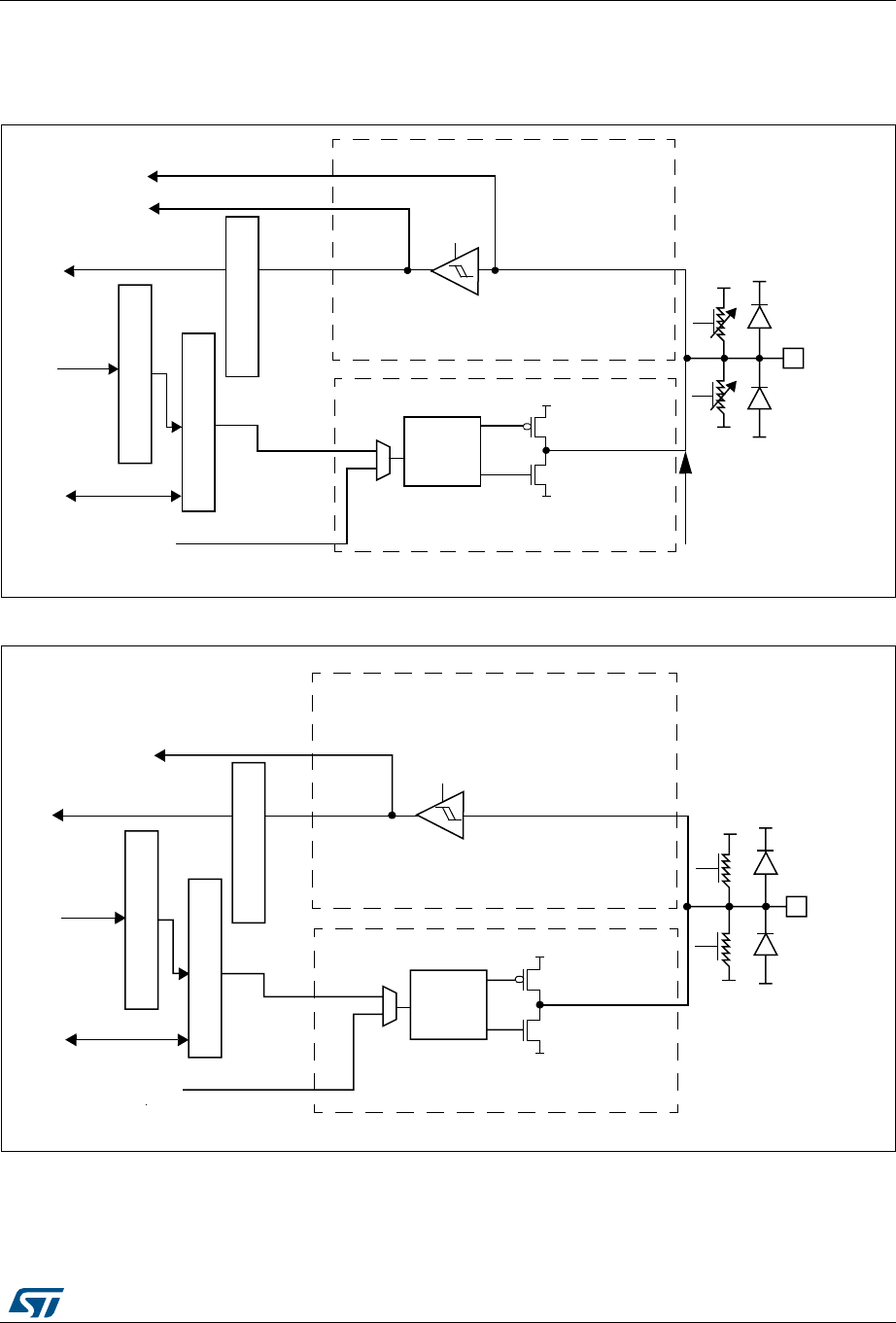
DocID025941 Rev 5 235/1001
RM0376 General-purpose I/Os (GPIO)
250
Figure 21 and Figure 22 show the basic structures of a standard and a 5 V tolerant I/O port
bit, respectively. Table 46 gives the possible port bit configurations.
Figure 21. Basic structure of an I/O port bit
Figure 22. Basic structure of a five-volt tolerant I/O port bit
1. VDD_FT is a potential specific to five-volt tolerant I/Os and different from VDD.
Alternate function output
Alternate function input
Push-pull,
open-drain or
disabled
Input data register
Output data register
Read/write
From on-chip
peripheral
To on-chip
peripheral
Output
control
Analog
on/off
Pull
Pull
down
on/off
I/O pin
V
DDIOx
V
DDIOx
V
SS
V
SS
trigger
V
SS
V
DDIOx
Protection
diode
Protection
diode
on/off
Input driver
Output driver
up
P-MOS
N-MOS
Read
Bit set/reset registers
Write
Analog
MS31476V1
Alternate function output
Alternate function input
Push-pull,
open-drain or
disabled
Output data register
Read/write
From on-chip
peripheral
To on-chip
peripheral
Output
control
on/off Pull
Pull
on/off
I/O pin
V
DDIOx
V
DDIOx
V
SS
V
SS
TTL Schmitt
trigger
V
SS
V
DD_FT
(1)
Protection
diode
Protection
diode
on/off
Input driver
Output driver
down
up
P-MOS
N-MOS
Read
Bit set/reset registers
Write
Input data register
ai15939d
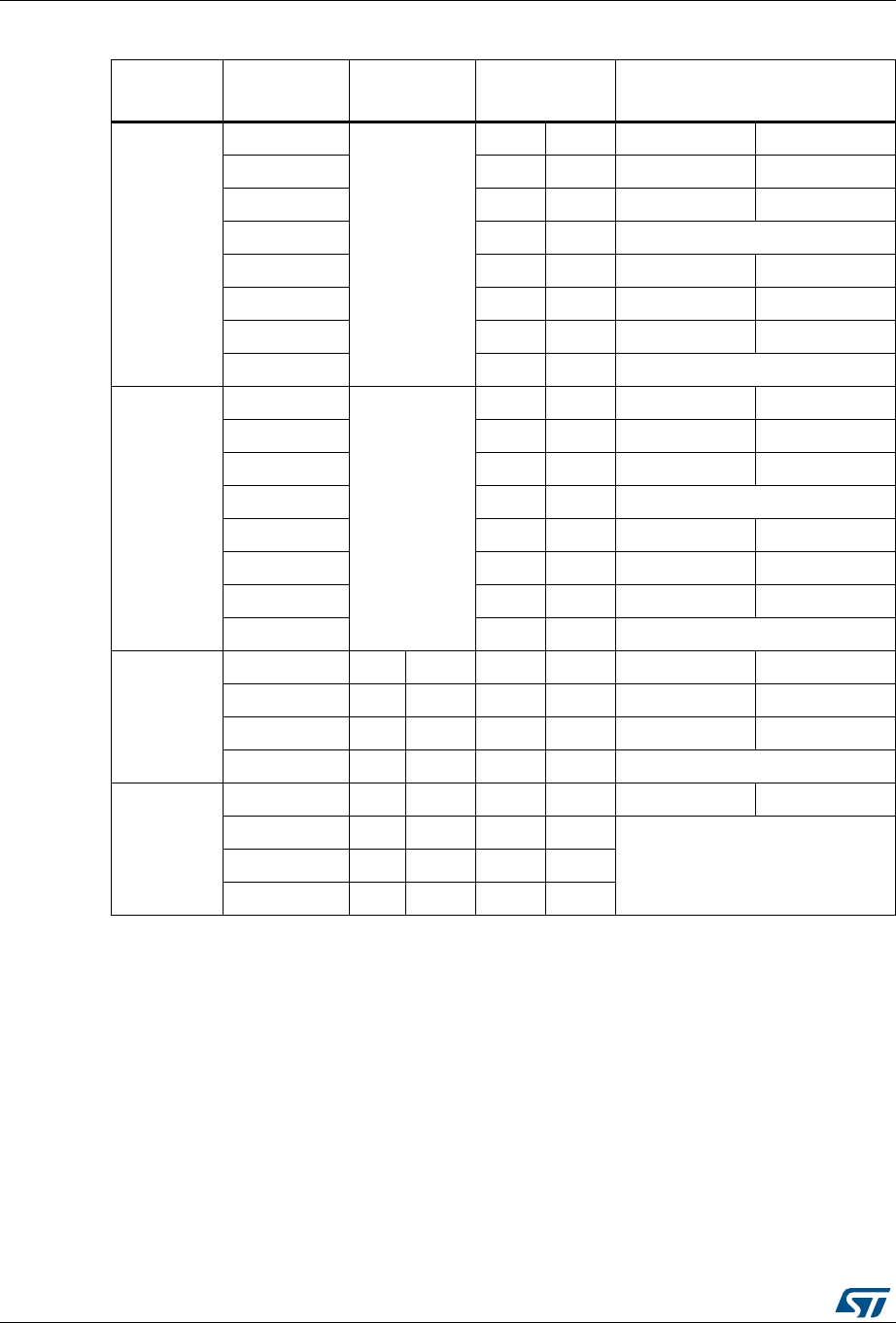
General-purpose I/Os (GPIO) RM0376
236/1001 DocID025941 Rev 5
9.3.1 General-purpose I/O (GPIO)
During and just after reset, the alternate functions are not active and most of the I/O ports
are configured in analog mode.
The debug pins are in AF pull-up/pull-down after reset:
•PA14: SWCLK in pull-down
•PA13: SWDIO in pull-up
Table 46. Port bit configuration table(1)
1. GP = general-purpose, PP = push-pull, PU = pull-up, PD = pull-down, OD = open-drain, AF = alternate
function.
MODE(i)
[1:0] OTYPER(i) OSPEED(i)
[1:0]
PUPD(i)
[1:0] I/O configuration
01
0
SPEED
[1:0]
0 0 GP output PP
0 0 1 GP output PP + PU
0 1 0 GP output PP + PD
0 1 1 Reserved
1 0 0 GP output OD
1 0 1 GP output OD + PU
1 1 0 GP output OD + PD
1 1 1 Reserved (GP output OD)
10
0
SPEED
[1:0]
0 0 AF PP
001AFPP + PU
010AFPP + PD
0 1 1 Reserved
100AFOD
101AFOD + PU
110AFOD + PD
1 1 1 Reserved
00
x x x 0 0 Input Floating
x x x 0 1 Input PU
x x x 1 0 Input PD
x x x 1 1 Reserved (input floating)
11
x x x 0 0 Input/output Analog
xxx01
Reservedxxx10
xxx11

DocID025941 Rev 5 237/1001
RM0376 General-purpose I/Os (GPIO)
250
When the pin is configured as output, the value written to the output data register
(GPIOx_ODR) is output on the I/O pin. It is possible to use the output driver in push-pull
mode or open-drain mode (only the low level is driven, high level is HI-Z).
The input data register (GPIOx_IDR) captures the data present on the I/O pin at every AHB
clock cycle.
All GPIO pins have weak internal pull-up and pull-down resistors, which can be activated or
not depending on the value in the GPIOx_PUPDR register.
9.3.2 I/O pin alternate function multiplexer and mapping
The device I/O pins are connected to on-board peripherals/modules through a multiplexer
that allows only one peripheral alternate function (AF) connected to an I/O pin at a time. In
this way, there can be no conflict between peripherals available on the same I/O pin.
Each I/O pin has a multiplexer with up to sixteen alternate function inputs (AF0 to AF15) that
can be configured through the GPIOx_AFRL (for pin 0 to 7) and GPIOx_AFRH (for pin 8 to
15) registers:
•After reset the multiplexer selection is alternate function 0 (AF0). The I/Os are
configured in alternate function mode through GPIOx_MODER register.
•The specific alternate function assignments for each pin are detailed in the device
datasheet.
In addition to this flexible I/O multiplexing architecture, each peripheral has alternate
functions mapped onto different I/O pins to optimize the number of peripherals available in
smaller packages.
To use an I/O in a given configuration, the user has to proceed as follows:
•Debug function: after each device reset these pins are assigned as alternate function
pins immediately usable by the debugger host
•GPIO: configure the desired I/O as output, input or analog in the GPIOx_MODER
register.
•Peripheral alternate function:
– Connect the I/O to the desired AFx in one of the GPIOx_AFRL or GPIOx_AFRH
register.
– Select the type, pull-up/pull-down and output speed via the GPIOx_OTYPER,
GPIOx_PUPDR and GPIOx_OSPEEDER registers, respectively.
– Configure the desired I/O as an alternate function in the GPIOx_MODER register.
•Additional functions:
– For the ADC, DAC and COMP, configure the desired I/O in analog mode in the
GPIOx_MODER register and configure the required function in the ADC, DAC and
COMP registers.
– For the additional functions like RTC, WKUPx and oscillators, configure the
required function in the related RTC, PWR and RCC registers. These functions
have priority over the configuration in the standard GPIO registers.
Refer to the “Alternate function mapping” table in the device datasheet for the detailed
mapping of the alternate function I/O pins.

General-purpose I/Os (GPIO) RM0376
238/1001 DocID025941 Rev 5
9.3.3 I/O port control registers
Each of the GPIO ports has four 32-bit memory-mapped control registers (GPIOx_MODER,
GPIOx_OTYPER, GPIOx_OSPEEDR, GPIOx_PUPDR) to configure up to 16 I/Os. The
GPIOx_MODER register is used to select the I/O mode (input, output, AF, analog). The
GPIOx_OTYPER and GPIOx_OSPEEDR registers are used to select the output type (push-
pull or open-drain) and speed. The GPIOx_PUPDR register is used to select the pull-
up/pull-down whatever the I/O direction.
9.3.4 I/O port data registers
Each GPIO has two 16-bit memory-mapped data registers: input and output data registers
(GPIOx_IDR and GPIOx_ODR). GPIOx_ODR stores the data to be output, it is read/write
accessible. The data input through the I/O are stored into the input data register
(GPIOx_IDR), a read-only register.
See Section 9.4.5: GPIO port input data register (GPIOx_IDR) (x = A..E and H) and
Section 9.4.6: GPIO port output data register (GPIOx_ODR) (x = A..E and H) for the register
descriptions.
9.3.5 I/O data bitwise handling
The bit set reset register (GPIOx_BSRR) is a 32-bit register which allows the application to
set and reset each individual bit in the output data register (GPIOx_ODR). The bit set reset
register has twice the size of GPIOx_ODR.
To each bit in GPIOx_ODR, correspond two control bits in GPIOx_BSRR: BS(i) and BR(i).
When written to 1, bit BS(i) sets the corresponding ODR(i) bit. When written to 1, bit BR(i)
resets the ODR(i) corresponding bit.
Writing any bit to 0 in GPIOx_BSRR does not have any effect on the corresponding bit in
GPIOx_ODR. If there is an attempt to both set and reset a bit in GPIOx_BSRR, the set
action takes priority.
Using the GPIOx_BSRR register to change the values of individual bits in GPIOx_ODR is a
“one-shot” effect that does not lock the GPIOx_ODR bits. The GPIOx_ODR bits can always
be accessed directly. The GPIOx_BSRR register provides a way of performing atomic
bitwise handling.
There is no need for the software to disable interrupts when programming the GPIOx_ODR
at bit level: it is possible to modify one or more bits in a single atomic AHB write access.
9.3.6 GPIO locking mechanism
It is possible to freeze the GPIO control registers by applying a specific write sequence to
the GPIOx_LCKR register. The frozen registers are GPIOx_MODER, GPIOx_OTYPER,
GPIOx_OSPEEDR, GPIOx_PUPDR, GPIOx_AFRL and GPIOx_AFRH.
To write the GPIOx_LCKR register, a specific write / read sequence has to be applied. When
the right LOCK sequence is applied to bit 16 in this register, the value of LCKR[15:0] is used
to lock the configuration of the I/Os (during the write sequence the LCKR[15:0] value must
be the same). When the LOCK sequence has been applied to a port bit, the value of the port
bit can no longer be modified until the next MCU reset or peripheral reset. Each
GPIOx_LCKR bit freezes the corresponding bit in the control registers (GPIOx_MODER,
GPIOx_OTYPER, GPIOx_OSPEEDR, GPIOx_PUPDR, GPIOx_AFRL and GPIOx_AFRH.

DocID025941 Rev 5 239/1001
RM0376 General-purpose I/Os (GPIO)
250
The LOCK sequence (refer to Section 9.4.8: GPIO port configuration lock register
(GPIOx_LCKR) (x = A..E and H)) can only be performed using a word (32-bit long) access
to the GPIOx_LCKR register due to the fact that GPIOx_LCKR bit 16 has to be set at the
same time as the [15:0] bits.
For code example, refer to A.5.1: Locking mechanism code example.
For more details refer to LCKR register description in Section 9.4.8: GPIO port configuration
lock register (GPIOx_LCKR) (x = A..E and H).
9.3.7 I/O alternate function input/output
Two registers are provided to select one of the alternate function inputs/outputs available for
each I/O. With these registers, the user can connect an alternate function to some other pin
as required by the application.
This means that a number of possible peripheral functions are multiplexed on each GPIO
using the GPIOx_AFRL and GPIOx_AFRH alternate function registers. The application can
thus select any one of the possible functions for each I/O. The AF selection signal being
common to the alternate function input and alternate function output, a single channel is
selected for the alternate function input/output of a given I/O.
To know which functions are multiplexed on each GPIO pin, refer to the device datasheet.
For code example, refer to A.5.2: Alternate function selection sequence code example.
9.3.8 External interrupt/wakeup lines
All ports have external interrupt capability. To use external interrupt lines, the port must be
configured in input mode.Section 13: Extended interrupt and event controller (EXTI) and to
Section 13.3.2: Wakeup event management.
9.3.9 Input configuration
When the I/O port is programmed as input:
•The output buffer is disabled
•The Schmitt trigger input is activated
•The pull-up and pull-down resistors are activated depending on the value in the
GPIOx_PUPDR register
•The data present on the I/O pin are sampled into the input data register every AHB
clock cycle
•A read access to the input data register provides the I/O state
Figure 23 shows the input configuration of the I/O port bit.
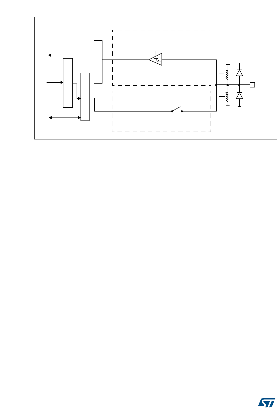
General-purpose I/Os (GPIO) RM0376
240/1001 DocID025941 Rev 5
Figure 23. Input floating/pull up/pull down configurations
9.3.10 Output configuration
When the I/O port is programmed as output:
•The output buffer is enabled:
– Open drain mode: A “0” in the Output register activates the N-MOS whereas a “1”
in the Output register leaves the port in Hi-Z (the P-MOS is never activated)
– Push-pull mode: A “0” in the Output register activates the N-MOS whereas a “1” in
the Output register activates the P-MOS
•The Schmitt trigger input is activated
•The pull-up and pull-down resistors are activated depending on the value in the
GPIOx_PUPDR register
•The data present on the I/O pin are sampled into the input data register every AHB
clock cycle
•A read access to the input data register gets the I/O state
•A read access to the output data register gets the last written value
Figure 24 shows the output configuration of the I/O port bit.
on/off
pull
pull
on/off
I/O pin
VDDIOx
VSS
TTL Schmitt
trigger
VSS
VDDIOx
protection
diode
protection
diode
on
input driver
output driver
down
up
Input data register
Output data register
Read/write
Read
Bit set/reset registers
Write
MS31477V1
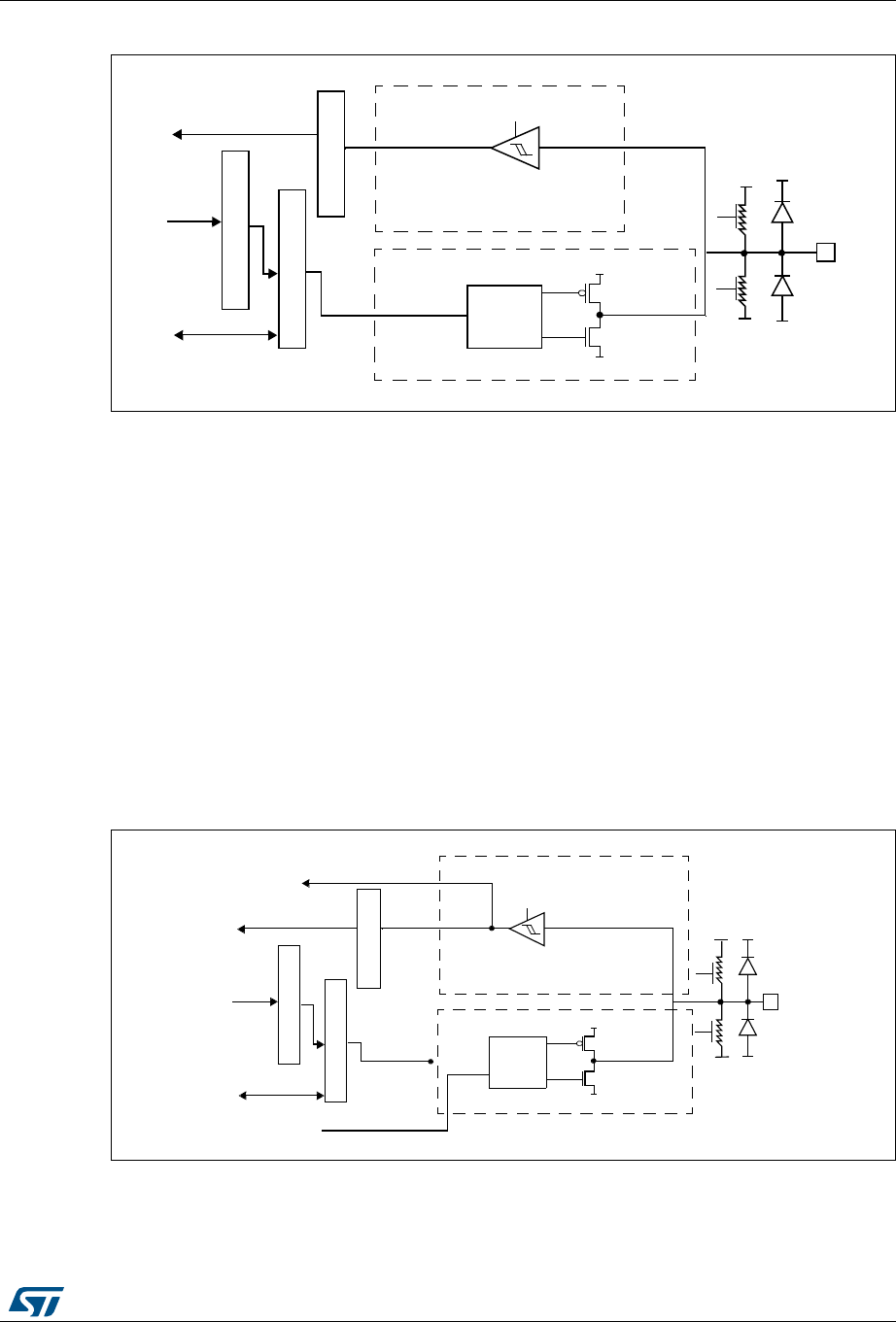
DocID025941 Rev 5 241/1001
RM0376 General-purpose I/Os (GPIO)
250
Figure 24. Output configuration
9.3.11 Alternate function configuration
When the I/O port is programmed as alternate function:
•The output buffer can be configured in open-drain or push-pull mode
•The output buffer is driven by the signals coming from the peripheral (transmitter
enable and data)
•The Schmitt trigger input is activated
•The weak pull-up and pull-down resistors are activated or not depending on the value
in the GPIOx_PUPDR register
•The data present on the I/O pin are sampled into the input data register every AHB
clock cycle
•A read access to the input data register gets the I/O state
Figure 25 shows the Alternate function configuration of the I/O port bit.
Figure 25. Alternate function configuration
Push-pull or
Open-drain
Output
control
VDDIOx
VSS
TTL Schmitt
trigger
on
Input driver
Output driver
P-MOS
N-MOS
Input data register
Output data register
Read/write
Read
Bit set/reset registers
Write
on/off
pull
pull
on/off
VDDIOx
VSS VSS
VDDIOx
protection
diode
protection
diode
down
up
I/O pin
MS31478V1
MSv34756V1
Alternate function output
Alternate function input
push-pull or
open-drain
From on-chip
peripheral
To on-chip
peripheral
Output
control
VDD
VSS
TTL Schmitt
trigger
on
Input driver
Output driver
P-MOS
N-MOS
Input data register
Output data register
Read/write
Read
Bit set/reset registers
Write
on/off
on/off
VDDIOx
VSS VSS
protection
diode
protection
diode
Pull
Pull
I/O pin
down
up
VDDIOx
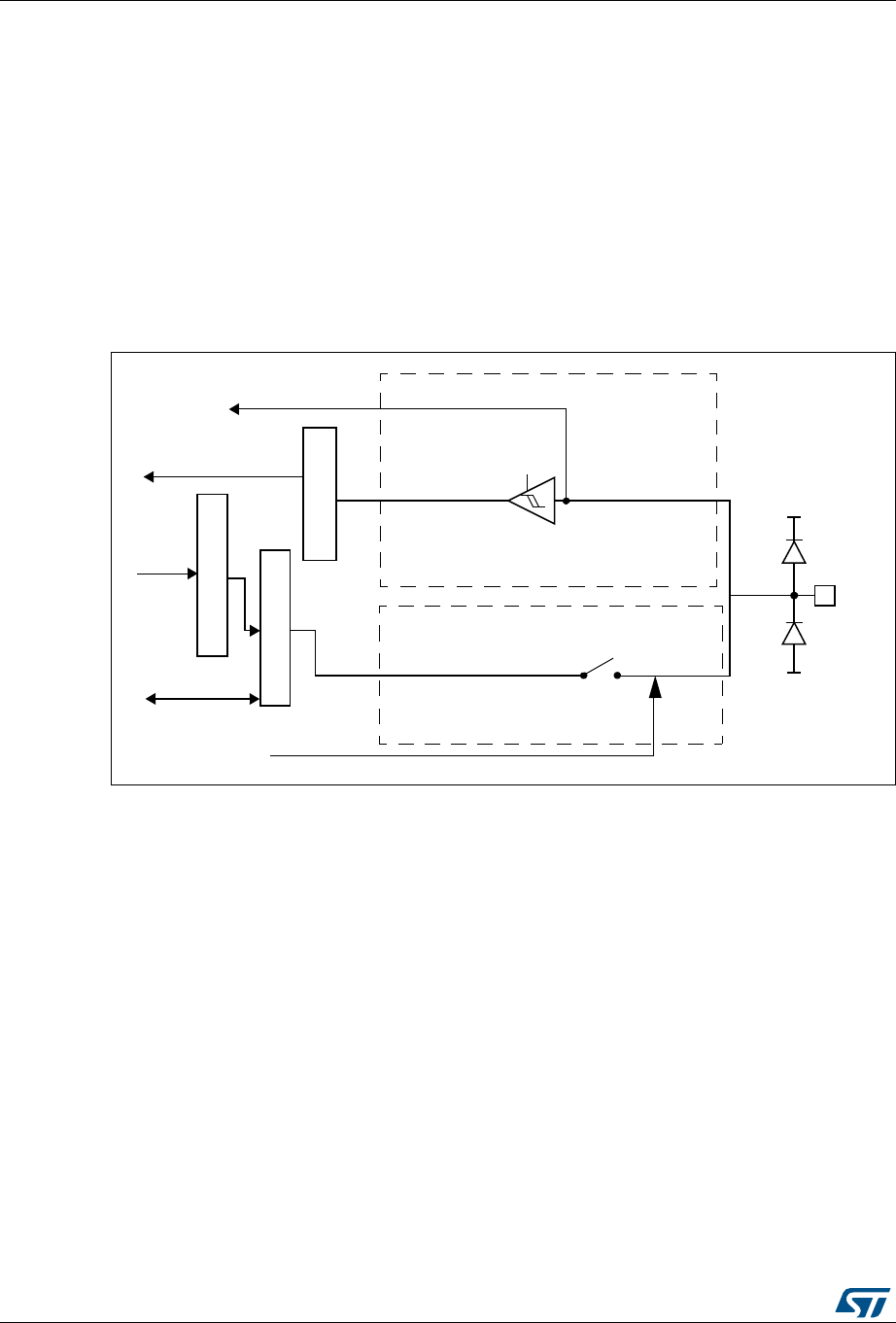
General-purpose I/Os (GPIO) RM0376
242/1001 DocID025941 Rev 5
9.3.12 Analog configuration
When the I/O port is programmed as analog configuration:
•The output buffer is disabled
•The Schmitt trigger input is deactivated, providing zero consumption for every analog
value of the I/O pin. The output of the Schmitt trigger is forced to a constant value (0).
•The weak pull-up and pull-down resistors are disabled by hardware
•Read access to the input data register gets the value “0”
For code example, refer to A.5.3: Analog GPIO configuration code example.
Figure 26 shows the high-impedance, analog-input configuration of the I/O port bits.
Figure 26. High impedance-analog configuration
9.3.13 Using the HSE or LSE oscillator pins as GPIOs
When the HSE or LSE oscillator is switched OFF (default state after reset), the related
oscillator pins can be used as normal GPIOs.
When the HSE or LSE oscillator is switched ON (by setting the HSEON or LSEON bit in the
RCC_CSR register) the oscillator takes control of its associated pins and the GPIO
configuration of these pins has no effect.
When the oscillator is configured in a user external clock mode, only the OSC_IN or
OSC32_IN pin is reserved for clock input and the OSC_OUT or OSC32_OUT pin can still be
used as normal GPIO.
9.3.14 Using the GPIO pins in the RTC supply domain
The PC13/PC14/PC15 GPIO functionality is lost when the core supply domain is powered
off (when the device enters Standby mode). In this case, if their GPIO configuration is not
bypassed by the RTC configuration, these pins are set in an analog input mode.
For details about I/O control by the RTC, refer to Section 26.4: RTC functional description.
From on-chip
peripheral
To on-chip
peripheral
Analog
trigger
off
Input driver
0
Input data register
Output data register
Read/write
Read
Bit set/reset registers
Write
Analog
VSS
VDDIOx
protection
diode
protection
diode
I/O pin
MS31480V1
TTL Schmitt
DocID025941 Rev 5 243/1001
RM0376 General-purpose I/Os (GPIO)
250
9.4 GPIO registers
This section gives a detailed description of the GPIO registers.
For a summary of register bits, register address offsets and reset values, refer to Table 47.
The peripheral registers can be written in word, half word or byte mode.
9.4.1 GPIO port mode register (GPIOx_MODER) (x =A..E and H)
Address offset:0x00
Reset values:
•0xEBFF FCFF for port A
•0xFFFF FFFF for the other ports
9.4.2 GPIO port output type register (GPIOx_OTYPER) (x = A..E and H)
Address offset: 0x04
Reset value: 0x0000 0000
31 30 29 28 27 26 25 24 23 22 21 20 19 18 17 16
MODE15[1:0] MODE14[1:0] MODE13[1:0] MODE12[1:0] MODE11[1:0] MODE10[1:0] MODE9[1:0] MODE8[1:0]
rw rw rw rw rw rw rw rw rw rw rw rw rw rw rw rw
1514131211109876543210
MODE7[1:0] MODE6[1:0] MODE5[1:0] MODE4[1:0] MODE3[1:0] MODE2[1:0] MODE1[1:0] MODE0[1:0]
rw rw rw rw rw rw rw rw rw rw rw rw rw rw rw rw
Bits 2y+1:2y MODEy[1:0]: Port x configuration bits (y = 0..15)
These bits are written by software to configure the I/O mode.
00: Input mode
01: General purpose output mode
10: Alternate function mode
11: Analog mode (reset state)
31 30 29 28 27 26 25 24 23 22 21 20 19 18 17 16
Res. Res. Res. Res. Res. Res. Res. Res. Res. Res. Res. Res. Res. Res. Res. Res.
1514131211109876543210
OT15 OT14 OT13 OT12 OT11 OT10 OT9 OT8 OT7 OT6 OT5 OT4 OT3 OT2 OT1 OT0
rw rw rw rw rw rw rw rw rw rw rw rw rw rw rw rw
Bits 31:16 Reserved, must be kept at reset value.
Bits 15:0 OTy: Port x configuration bits (y = 0..15)
These bits are written by software to configure the I/O output type.
0: Output push-pull (reset state)
1: Output open-drain
General-purpose I/Os (GPIO) RM0376
244/1001 DocID025941 Rev 5
9.4.3 GPIO port output speed register (GPIOx_OSPEEDR)
(x = A..E and H)
Address offset: 0x08
Reset value:
•0x0C00 0000 for port A
•0x0000 0000 for the other ports
9.4.4 GPIO port pull-up/pull-down register (GPIOx_PUPDR)
(x = A..E and H)
Address offset: 0x0C
Reset values:
•0x2400 0000 for port A
•0x0000 0000 for the other ports
31 30 29 28 27 26 25 24 23 22 21 20 19 18 17 16
OSPEED15
[1:0]
OSPEED14
[1:0]
OSPEED13
[1:0]
OSPEED12
[1:0]
OSPEED11
[1:0]
OSPEED10
[1:0]
OSPEED9
[1:0]
OSPEED8
[1:0]
rw rw rw rw rw rw rw rw rw rw rw rw rw rw rw rw
15 14 13 12 11 10 9 8 7 6 5 4 3 2 1 0
OSPEED7
[1:0]
OSPEED6
[1:0]
OSPEED5
[1:0]
OSPEED4
[1:0]
OSPEED3
[1:0]
OSPEED2
[1:0]
OSPEED1
[1:0]
OSPEED0
[1:0]
rw rw rw rw rw rw rw rw rw rw rw rw rw rw rw rw
Bits 2y+1:2y OSPEEDy[1:0]: Port x configuration bits (y = 0..15)
These bits are written by software to configure the I/O output speed.
00: Low speed
01: Medium speed
10: High speed
11: Very high speed
Note: Refer to the device datasheet for the frequency specifications and the power supply
and load conditions for each speed.
31 30 29 28 27 26 25 24 23 22 21 20 19 18 17 16
PUPD15[1:0] PUPD14[1:0] PUPD13[1:0] PUPD12[1:0] PUPD11[1:0] PUPD10[1:0] PUPD9[1:0] PUPD8[1:0]
rw rw rw rw rw rw rw rw rw rw rw rw rw rw rw rw
1514131211109876543210
PUPD7[1:0] PUPD6[1:0] PUPD5[1:0] PUPD4[1:0] PUPD3[1:0] PUPD2[1:0] PUPD1[1:0] PUPD0[1:0]
rw rw rw rw rw rw rw rw rw rw rw rw rw rw rw rw
Bits 2y+1:2y PUPDy[1:0]: Port x configuration bits (y = 0..15)
These bits are written by software to configure the I/O pull-up or pull-down
00: No pull-up, pull-down
01: Pull-up
10: Pull-down
11: Reserved
DocID025941 Rev 5 245/1001
RM0376 General-purpose I/Os (GPIO)
250
9.4.5 GPIO port input data register (GPIOx_IDR) (x = A..E and H)
Address offset: 0x10
Reset value: 0x0000 XXXX
9.4.6 GPIO port output data register (GPIOx_ODR) (x = A..E and H)
Address offset: 0x14
Reset value: 0x0000 0000
9.4.7 GPIO port bit set/reset register (GPIOx_BSRR) (x = A..E and H)
Address offset: 0x18
Reset value: 0x0000 0000
31 30 29 28 27 26 25 24 23 22 21 20 19 18 17 16
Res. Res. Res. Res. Res. Res. Res. Res. Res. Res. Res. Res. Res. Res. Res. Res.
1514131211109876543210
ID15 ID14 ID13 ID12 ID11 ID10 ID9 ID8 ID7 ID6 ID5 ID4 ID3 ID2 ID1 ID0
rrrrrr r r r r rrrrrr
Bits 31:16 Reserved, must be kept at reset value.
Bits 15:0 IDy: Port input data bit (y = 0..15)
These bits are read-only. They contain the input value of the corresponding I/O port.
31 30 29 28 27 26 25 24 23 22 21 20 19 18 17 16
Res. Res. Res. Res. Res. Res. Res. Res. Res. Res. Res. Res. Res. Res. Res. Res.
1514131211109876543210
OD15 OD14 OD13 OD12 OD11 OD10 OD9 OD8 OD7 OD6 OD5 OD4 OD3 OD2 OD1 OD0
rw rw rw rw rw rw rw rw rw rw rw rw rw rw rw rw
Bits 31:16 Reserved, must be kept at reset value.
Bits 15:0 ODy: Port output data bit (y = 0..15)
These bits can be read and written by software.
Note: For atomic bit set/reset, the OD bits can be individually set and/or reset by writing to the
GPIOx_BSRR or GPIOx_BRR registers (x = A..E and H).
31 30 29 28 27 26 25 24 23 22 21 20 19 18 17 16
BR15 BR14 BR13 BR12 BR11 BR10 BR9 BR8 BR7 BR6 BR5 BR4 BR3 BR2 BR1 BR0
wwwwwwwwwwwwwwww
1514131211109876543210
BS15 BS14 BS13 BS12 BS11 BS10 BS9 BS8 BS7 BS6 BS5 BS4 BS3 BS2 BS1 BS0
wwwwwwwwwwwwwwww

General-purpose I/Os (GPIO) RM0376
246/1001 DocID025941 Rev 5
9.4.8 GPIO port configuration lock register (GPIOx_LCKR)
(x = A..E and H)
This register is used to lock the configuration of the port bits when a correct write sequence
is applied to bit 16 (LCKK). The value of bits [15:0] is used to lock the configuration of the
GPIO. During the write sequence, the value of LCKR[15:0] must not change. When the
LOCK sequence has been applied on a port bit, the value of this port bit can no longer be
modified until the next MCU reset or peripheral reset.
Note: A specific write sequence is used to write to the GPIOx_LCKR register. Only word access
(32-bit long) is allowed during this locking sequence.
Each lock bit freezes a specific configuration register (control and alternate function
registers).
Address offset: 0x1C
Reset value: 0x0000 0000
Bits 31:16 BRy: Port x reset bit y (y = 0..15)
These bits are write-only. A read to these bits returns the value 0x0000.
0: No action on the corresponding ODx bit
1: Resets the corresponding ODx bit
Note: If both BSx and BRx are set, BSx has priority.
Bits 15:0 BSy: Port x set bit y (y= 0..15)
These bits are write-only. A read to these bits returns the value 0x0000.
0: No action on the corresponding ODx bit
1: Sets the corresponding ODx bit
31 30 29 28 27 26 25 24 23 22 21 20 19 18 17 16
Res. Res. Res. Res. Res. Res. Res. Res. Res. Res. Res. Res. Res. Res. Res. LCKK
rw
15 14 13 12 11 10 9 8 7 6 5 4 3 2 1 0
LCK15 LCK14 LCK13 LCK12 LCK11 LCK10 LCK9 LCK8 LCK7 LCK6 LCK5 LCK4 LCK3 LCK2 LCK1 LCK0
rw rw rw rw rw rw rw rw rw rw rw rw rw rw rw rw
DocID025941 Rev 5 247/1001
RM0376 General-purpose I/Os (GPIO)
250
9.4.9 GPIO alternate function low register (GPIOx_AFRL)
(x = A..E and H)
Address offset: 0x20
Reset value: 0x0000 0000
Bits 31:17 Reserved, must be kept at reset value.
Bit 16 LCKK: Lock key
This bit can be read any time. It can only be modified using the lock key write sequence.
0: Port configuration lock key not active
1: Port configuration lock key active. The GPIOx_LCKR register is locked until the next MCU
reset or peripheral reset.
LOCK key write sequence:
WR LCKR[16] = ‘1’ + LCKR[15:0]
WR LCKR[16] = ‘0’ + LCKR[15:0]
WR LCKR[16] = ‘1’ + LCKR[15:0]
RD LCKR
RD LCKR[16] = ‘1’ (this read operation is optional but it confirms that the lock is active)
Note: During the LOCK key write sequence, the value of LCK[15:0] must not change.
Any error in the lock sequence aborts the lock.
After the first lock sequence on any bit of the port, any read access on the LCKK bit will
return ‘1’ until the next MCU reset or peripheral reset.
Bits 15:0 LCKy: Port x lock bit y (y= 0..15)
These bits are read/write but can only be written when the LCKK bit is ‘0.
0: Port configuration not locked
1: Port configuration locked
31 30 29 28 27 26 25 24 23 22 21 20 19 18 17 16
AFSEL7[3:0] AFSEL6[3:0] AFSEL5[3:0] AFSEL4[3:0]
rw rw rw rw rw rw rw rw rw rw rw rw rw rw rw rw
1514131211109876543210
AFSEL3[3:0] AFSEL2[3:0] AFSEL1[3:0] AFSEL0[3:0]
rw rw rw rw rw rw rw rw rw rw rw rw rw rw rw rw
Bits 31:0 AFSELy[3:0]: Alternate function selection for port x pin y (y = 0..7)
These bits are written by software to configure alternate function I/Os
AFSELy selection:
0000: AF0
0001: AF1
0010: AF2
0011: AF3
0100: AF4
0101: AF5
0110: AF6
0111: AF7
1000: Reserved
1001: Reserved
1010: Reserved
1011: Reserved
1100: Reserved
1101: Reserved
1110: Reserved
1111: Reserved
General-purpose I/Os (GPIO) RM0376
248/1001 DocID025941 Rev 5
9.4.10 GPIO alternate function high register (GPIOx_AFRH)
(x = A..E and H)
Address offset: 0x24
Reset value: 0x0000 0000
9.4.11 GPIO port bit reset register (GPIOx_BRR) (x = A..E and H)
Address offset: 0x28
Reset value: 0x0000 0000
31 30 29 28 27 26 25 24 23 22 21 20 19 18 17 16
AFSEL15[3:0] AFSEL14[3:0] AFSEL13[3:0] AFSEL12[3:0]
rw rw rw rw rw rw rw rw rw rw rw rw rw rw rw rw
1514131211109876543210
AFSEL11[3:0] AFSEL10[3:0] AFSEL9[3:0] AFSEL8[3:0]
rw rw rw rw rw rw rw rw rw rw rw rw rw rw rw rw
Bits 31:0 AFSELy[3:0]: Alternate function selection for port x pin y (y = 8..15)
These bits are written by software to configure alternate function I/Os
AFSELy selection:
0000: AF0
0001: AF1
0010: AF2
0011: AF3
0100: AF4
0101: AF5
0110: AF6
0111: AF7
1000: Reserved
1001: Reserved
1010: Reserved
1011: Reserved
1100: Reserved
1101: Reserved
1110: Reserved
1111: Reserved
31 30 29 28 27 26 25 24 23 22 21 20 19 18 17 16
Res. Res. Res. Res. Res. Res. Res. Res. Res. Res. Res. Res. Res. Res. Res. Res.
1514131211109876543210
BR15 BR14 BR13 BR12 BR11 BR10 BR9 BR8 BR7 BR6 BR5 BR4 BR3 BR2 BR1 BR0
wwwwwwwwwwwwwwww
Bits 31:16 Reserved
Bits 15:0 BRy: Port x Reset bit y (y= 0..15)
These bits are write-only. A read to these bits returns the value 0x0000
0: No action on the corresponding ODx bit
1: Reset the corresponding ODx bit

DocID025941 Rev 5 249/1001
RM0376 General-purpose I/Os (GPIO)
250
9.4.12 GPIO register map
The following table gives the GPIO register map and reset values.
Table 47. GPIO register map and reset values
Offset Register name
31
30
29
28
27
26
25
24
23
22
21
20
19
18
17
16
15
14
13
12
11
10
9
8
7
6
5
4
3
2
1
0
0x00 GPIOA_MODER
MODE15[1:0]
MODE14[1:0]
MODE13[1:0]
MODE12[1:0]
MODE11[1:0]
MODE10[1:0]
MODE9[1:0]
MODE8[1:0]
MODE7[1:0]
MODE6[1:0]
MODE5[1:0]
MODE4[1:0]
MODE3[1:0]
MODE2[1:0]
MODE1[1:0]
MODE0[1:0]
Reset value 11101011111111111111110011111111
0x00
GPIOx_MODER
(where x = B..E, H)
MODE15[1:0]
MODE14[1:0]
MODE13[1:0]
MODE12[1:0]
MODE11[1:0]
MODE10[1:0]
MODE9[1:0]
MODE8[1:0]
MODE7[1:0]
MODE6[1:0]
MODE5[1:0]
MODE4[1:0]
MODE3[1:0]
MODE2[1:0]
MODE1[1:0]
MODE0[1:0]
Reset value 11111111111111111111111111111111
0x00
GPIOx_MODER
(where x = C..K)
MODER15[1:0]
MODER14[1:0]
MODER13[1:0]
MODER12[1:0]
MODER11[1:0]
MODER10[1:0]
MODER9[1:0]
MODER8[1:0]
MODER7[1:0]
MODER6[1:0]
MODER5[1:0]
MODER4[1:0]
MODER3[1:0]
MODER2[1:0]
MODEv1[1:0]
MODER0[1:0]
Reset value 11111111111111111111111111111111
0x04
GPIOx_OTYPER
(where x = A..E,H)
Res.
Res.
Res.
Res.
Res.
Res.
Res.
Res.
Res.
Res.
Res.
Res.
Res.
Res.
Res.
Res.
OT15
OT14
OT13
OT12
OT11
OT10
OT9
OT8
OT7
OT6
OT5
OT4
OT3
OT2
OT1
OT0
Reset value 0000000000000000
0x08 GPIOA_OSPEEDR
OSPEED15[1:0]
OSPEED14[1:0]
OSPEED13[1:0]
OSPEED12[1:0]
OSPEED11[1:0]
OSPEED10[1:0]
OSPEED9[1:0]
OSPEED8[1:0]
OSPEED7[1:0]
OSPEED6[1:0]
OSPEED5[1:0]
OSPEED4[1:0]
OSPEED3[1:0]
OSPEED2[1:0]
OSPEED1[1:0]
OSPEED0[1:0]
Reset value 00001100000000000000000000000000
0x08
GPIOx_OSPEEDR
(where x = B..E,H)
OSPEED15[1:0]
OSPEED14[1:0]
OSPEED13[1:0]
OSPEED12[1:0]
OSPEED11[1:0]
OSPEED10[1:0]
OSPEED9[1:0]
OSPEED8[1:0]
OSPEED7[1:0]
OSPEED6[1:0]
OSPEED5[1:0]
OSPEED4[1:0]
OSPEED3[1:0]
OSPEED2[1:0]
OSPEED1[1:0]
OSPEED0[1:0]
Reset value 00000000000000000000000000000000
0x0C GPIOA_PUPDR
PUPD15[1:0]
PUPD14[1:0]
PUPD13[1:0]
PUPD12[1:0]
PUPD11[1:0]
PUPD10[1:0]
PUPD9[1:0]
PUPD8[1:0]
PUPD7[1:0]
PUPD6[1:0]
PUPD5[1:0]
PUPD4[1:0]
PUPD3[1:0]
PUPD2[1:0]
PUPD1[1:0]
PUPD0[1:0]
Reset value 00100100000000000000000000000000
0x10
GPIOx_IDR
(where x = A..E,H)
Res.
Res.
Res.
Res.
Res.
Res.
Res.
Res.
Res.
Res.
Res.
Res.
Res.
Res.
Res.
Res.
ID15
ID14
ID13
ID12
ID11
ID10
ID9
ID8
ID7
ID6
ID5
ID4
ID3
ID2
ID1
ID0
Reset value xxxxxxxxxxxxxxxx
0x14
GPIOx_ODR
(where x = A..E,H)
Res.
Res.
Res.
Res.
Res.
Res.
Res.
Res.
Res.
Res.
Res.
Res.
Res.
Res.
Res.
Res.
OD15
OD14
OD13
OD12
OD11
OD10
OD9
OD8
OD7
OD6
OD5
OD4
OD3
OD2
OD1
OD0
Reset value 0000000000000000
0x18
GPIOx_BSRR
(where x = A..E,H)
BR15
BR14
BR13
BR12
BR11
BR10
BR9
BR8
BR7
BR6
BR5
BR4
BR3
BR2
BR1
BR0
BS15
BS14
BS13
BS12
BS11
BS10
BS9
BS8
BS7
BS6
BS5
BS4
BS3
BS2
BS1
BS0
Reset value 00000000000000000000000000000000
0x1C
GPIOx_LCKR
(where x = A..E,H)
Res.
Res.
Res.
Res.
Res.
Res.
Res.
Res.
Res.
Res.
Res.
Res.
Res.
Res.
Res.
LCKK
LCK15
LCK14
LCK13
LCK12
LCK11
LCK10
LCK9
LCK8
LCK7
LCK6
LCK5
LCK4
LCK3
LCK2
LCK1
LCK0
Reset value 00000000000000000

General-purpose I/Os (GPIO) RM0376
250/1001 DocID025941 Rev 5
Refer to Section 2.2 for the register boundary addresses.
0x20
GPIOx_AFRL
(where x = A..E,H)AFSEL7[3:0] AFSEL6[3:0] AFSEL5[3:0] AFSEL4[3:0] AFSEL3[3:0] AFSEL2[3:0] AFSEL1[3:0] AFSEL0[3:0]
Reset value 00000000000000000000000000000000
0x24
GPIOx_AFRH
(where x = A..E,H)AFSEL15[3:0] AFSEL14[3:0] AFSEL13[3:0] AFSEL12[3:0] AFSEL11[3:0] AFSEL10[3:0] AFSEL9[3:0] AFSEL8[3:0]
Reset value 00000000000000000000000000000000
0x28
GPIOx_BRR
(where x = A..E,H)
Res.
Res.
Res.
Res.
Res.
Res.
Res.
Res.
Res.
Res.
Res.
Res.
Res.
Res.
Res.
Res.
BR15
BR14
BR13
BR12
BR11
BR10
BR9
BR8
BR7
BR6
BR5
BR4
BR3
BR2
BR1
BR0
Reset value 0000000000000000
Table 47. GPIO register map and reset values (continued)
Offset Register name
31
30
29
28
27
26
25
24
23
22
21
20
19
18
17
16
15
14
13
12
11
10
9
8
7
6
5
4
3
2
1
0

DocID025941 Rev 5 251/1001
RM0376 System configuration controller (SYSCFG)
259
10 System configuration controller (SYSCFG)
10.1 Introduction
The devices feature a set of configuration registers. The main purposes of the system
configuration controller are the following:
•Remapping memories
•Remapping some trigger sources to timer input capture channels
•Managing external interrupts line multiplexing to the internal edge detector
•Enabling dedicated functions such as input capture multiplexing or oscillator pin
remapping
•I2C Fm+ mode management
•Firewall management
•Temperature sensor and Internal voltage reference management (including for
Comparator, 48 MHz HSI and ADC purposes).
The Cortex®-M0+ can wake up from WFE (Wait For Event) when a transition occurs on the
eventin input signal. To support semaphore management in multiprocessor environment,
the core can also output events on the signal output EVENTOUT, during SEV instruction
execution.
In STM32L0x2 devices, an event input can be generated by an external interrupt line or by
an RTC alarm interrupt. It is also possible to select which output pin is connected to the
EVENTOUT signal of the Cortex®-M0+. The EVENTOUT multiplexing is managed by the
GPIO alternate function capability (see Section 9.4.9: GPIO alternate function low register
(GPIOx_AFRL) (x = A..E and H) and Section 9.4.10: GPIO alternate function high register
(GPIOx_AFRH) (x = A..E and H)).
Note: EVENTOUT is not mapped on all GPIOs (for example PC13, PC14, PC15).

System configuration controller (SYSCFG) RM0376
252/1001 DocID025941 Rev 5
10.2 SYSCFG registers
The peripheral registers have to be accessed by words (32-bit).
10.2.1 SYSCFG memory remap register (SYSCFG_CFGR1)
This register is used for specific configurations related to memory remap:
Note: This register is not reset through the SYSCFGRST bit in the RCC_APB2RSTR register.
Address offset: 0x00
Reset value: 0x000x 000x (X is the memory mode selected by the boot configuration).
)
31 30 29 28 27 26 25 24 23 22 21 20 19 18 17 16
Res. Res. Res. Res. Res. Res. Res. Res. Res. Res. Res. Res. Res. Res. Res. Res.
1514131211109876543210
Res. Res. Res. Res. Res. Res. BOOT_MODE Res. Res. Res. Res. UFB Res. MEM_MODE
r r rw rw rw
Bits 31:10 Reserved, must be kept at reset value
Bits 9:8 BOOT_MODE: Boot mode selected by the boot pins status bits
These bits are read-only. They indicate the boot mode selected by the BOOT pins. Bit 9
corresponds to the complement of nBOOT1 bit in the FLASH_OPTR register. Its value is
defined in the option bytes. Bit 8 corresponds to the value sampled on BOOT0 pin (see
Section 2.4: Boot configuration on page 63).
00: Main Flash memory boot mode
01: System Flash memory boot mode
10: Reserved
11: Embedded SRAM boot mode
Bits 7:4 Reserved, must be kept at reset value

DocID025941 Rev 5 253/1001
RM0376 System configuration controller (SYSCFG)
259
Bit 3 UFB: User bank swapping
This bit is available only on category 5 devices and reserved on other categories.
It is set and cleared by software. It controls the Bank 1/2 mapping (see Table 8: NVM
organization for UFB = 0 (128 Kbyte category 5 devices) and Table 10: NVM organization
for UFB = 0 (64 Kbyte category 5 devices)).
0: Flash Program memory Bank 1 is mapped at 0x0800 0000 (and aliased at 0x0000 0000 if
MEM_MODE=00) and Data EEPROM Bank 1 at 0x0808 0000 (aliased at 0x0008 0000 if
MEM_MODE=00)
1: Flash Program memory Bank 2 is mapped at 0x0800 0000 (and aliased at 0x0000 0000 if
MEM_MODE=00) and Data EEPROM Bank 2 at 0x0808 0000 (and aliased at 0x0008 0000
if MEM_MODE=00)
Bit 2 Reserved, must be kept at reset value
Bits 1:0 MEM_MODE: Memory mapping selection bits
These bits are set and cleared by software. This bit controls the memory’s internal mapping
at address 0x0000 0000. After reset these bits take on the memory mapping selected by the
BOOT pins (see Section 2.4: Boot configuration on page 63).
00: Main Flash memory mapped at 0x0000 0000
01: System Flash memory mapped at 0x0000 0000
10: reserved
11: SRAM mapped at 0x0000 0000.

System configuration controller (SYSCFG) RM0376
254/1001 DocID025941 Rev 5
10.2.2 SYSCFG peripheral mode configuration register (SYSCFG_CFGR2)
Address offset: 0x04
Reset value: 0x0000 0001
31 30 29 28 27 26 25 24 23 22 21 20 19 18 17 16
Res. Res. Res. Res. Res. Res. Res. Res. Res. Res. Res. Res. Res. Res. Res. Res.
15 14 13 12 11 10 9 8 7 6 5 4 3 2 1 0
Res. I2C3_
FMP I2C2_FMP I2C1_FMP I2C_PB9
_FMP
I2C_PB8
_FMP
I2C_PB7
_FMP
I2C_PB6
_FMP Res. Res. Res. FWDIS
rw rw rw rw
Bits 31:15 Reserved, must be kept at reset value
Bit 14 I2C3 FMP: I2C3 Fm+ drive capability enable bit
This bit is set and cleared by software. When it is set, Fm+ mode is enabled on I2C3 pins
PC0, PC1, PA8 and PB4 selected through the IOPORT control registers AF selection bits.
Bit 13 I2C2 FMP: I2C2 Fm+ drive capability enable bit
This bit is set and cleared by software. When it is set, Fm+ mode is enabled on I2C2 pins
PB13 and PB14 selected through the IOPORT control registers AF selection bits.
Bit 12 I2C1 FMP: I2C1 Fm+ drive capability enable bit
This bit is set and cleared by software. When it is set, Fm+ mode is enabled on I2C1 pins
selected through the IOPORT control registers AF selection bits. This bit is bit is OR-ed with
I2C_PBx_FMP bits.
Bit 11 I2C PB9 FMP: Fm+ drive capability on PB9 enable bit
This bit is set and cleared by software. When it is set, it forces Fm+ drive capability on PB9.
Bit 10 I2C PB8 FMP: Fm+ drive capability on PB8 enable bit
This bit is set and cleared by software. When it is set, it forces Fm+ drive capability on PB8.
Bit 9 I2C PB7 FMP: Fm+ drive capability on PB7 enable bit
This bit is set and cleared by software. When it is set, it forces Fm+ drive capability on PB7.
Bit 8 I2C PB6 FMP: Fm+ drive capability on PB6 enable bit
This bit is set and cleared by software. When it is set, it forces Fm+ drive capability on PB6.
Bits 7:1 Reserved, must be kept at reset value
Bit 0 FWDIS: Firewall disable bit
This bit is set by default (after reset). It is cleared by software to protect the access to the
memory segments according to the Firewall configuration.Once cleared it cannot be set by
software. Only a system reset set the bit.
0: Firewall access enabled
1: Firewall access disabled
Note: This bit cannot be set by an APB reset. A system reset is required to set it.

DocID025941 Rev 5 255/1001
RM0376 System configuration controller (SYSCFG)
259
10.2.3 Reference control and status register (SYSCFG_CFGR3)
The SYSCFG_CFGR3 register is the reference control/status register. It contains all the
bits/flags related to VREFINT and temperature sensor.
Address offset: 0x20
System reset value: 0x0000 0000
31 30 29 28 27 26 25 24 23 22 21 20 19 18 17 16
REF_
LOCK
VREFINT
_RDYF Res. Res. Res. Res. Res. Res. Res. Res. Res. Res. Res. Res. Res. Res.
rs r
15 14 13 12 11 10 9 8 7 6 5 4 3 2 1 0
Res. Res. ENREF_
HSI48
ENBUF_
VREFINT_
COMP2
Res. Res.
ENBUF_
SENSOR
_ADC
ENBUF_
VREFINT
_ ADC
Res. Res. SEL_VREF
_OUT Res. Res. Res. EN_VR
EFINT
rw rw rw rw rw rw rw
Bit 31 REF_LOCK: SYSCFG_CFGR3 lock bit
This bit is set by software and cleared by a hardware system reset. It locks the whole
content of the reference control/Status register, SYSCFG_CFGR3[31:0].
0: SYSCFG_CFGR3[31:0] bits are read/write
1: SYSCFG_CFGR3[31:0] bits are read-only
Bit 30 VREFINT_RDYF: VREFINT ready flag
This bit is read-only. It shows the state of the internal voltage reference, VREFINT. When
set, it indicates that VREFINT is available for BOR, PVD.
0: VREFINT OFF
1: VREFINT ready
Bits 29:14 Reserved, must be kept at reset value
Bit 13 ENREF_HSI48: VREFINT reference for HSI48 oscillator enable bit
This bit is set and cleared by software (only if REF_LOCK not set).
0: Buffer used to generate VREFINT reference for the HSI48 oscillator switched OFF.
1: Buffer used to generate VREFINT reference for the HSI48oscillator switched ON.
Bit 12 ENBUF_VREFINT_COMP2: VREFINT reference for COMP2 scaler enable bit
This bit is set and cleared by software (only if REF_LOCK not set).
0: Disables the buffer used to generate VREFINT references for COMP2.
1: Enables the buffer used to generate VREFINT references for COMP2.
Bits 11:10 Reserved, must be kept at reset value
Bit 9 ENBUF_SENSOR_ADC: Temperature sensor reference for ADC enable bit
This bit is set and cleared by software (only if REF_LOCK not set). When this bit is set, the
VREFINT is automatically enabled.
0: Disables the buffer used to generate VREFINT reference for the temperature sensor.
1: Enables the buffer used to generate VREFINT reference for the temperature sensor.
Bit 8 ENBUF_VREFINT_ADC: VREFINT reference for ADC enable bit
This bit is set and cleared by software (only if REF_LOCK not set).
0: Disables the buffer used to generate VREFINT reference for the ADC.
1: Enables the buffer used to generate VREFINT reference for the ADC.
Bits 7:6 Reserved, must be kept at reset value

System configuration controller (SYSCFG) RM0376
256/1001 DocID025941 Rev 5
10.2.4 SYSCFG external interrupt configuration register 1
(SYSCFG_EXTICR1)
Address offset: 0x08
Reset value: 0x0000
Bits 5:4 SEL_VREF_OUT: VREFINT_ADC connection bit
These bits are set and cleared by software (only if REF_LOCK not set). These bits select
which pad is connected to VREFINT_ADC when ENBUF_VREFINT_ADC is set.
00: no pad connected
01: PB0 connected
10: PB1 connected
11: PB0 and PB1 connected
Bits 3:1 Reserved, must be kept at reset value
Bit 0 EN_VREFINT: VREFINT enable and scaler control for COMP2 enable bit
This bit is set and cleared by software (only if REF_LOCK not set). It switches on VREFINT
internal reference voltage and enables the scaler for COMP2.
0: VREFINT voltage disabled in low-power mode (if ULP=1) and scaler for COMP2 disabled
1: VREFINT voltage enabled in low-power mode and scaler for COMP2 enabled
Note: It is forbidden to configure both EN_VREFINT=1 and ULP=1 if the device is in Stop
mode or in Sleep/Low-power sleep mode (refer to Section 6.4.1: PWR power control
register (PWR_CR) for a description of the ULP bit). If the device is not in low-power
mode, VREFINT is always enabled whatever the state of EN_VREFINT and ULP.
EN_VREFINT controls only COMP2 scaler.
31 30 29 28 27 26 25 24 23 22 21 20 19 18 17 16
Reserved
1514131211109876543210
EXTI3[3:0] EXTI2[3:0] EXTI1[3:0] EXTI0[3:0]
rw rw rw rw rw rw rw rw rw rw rw rw rw rw rw rw
Bits 31:16 Reserved
Bits 15:0 EXTIx[3:0]: EXTI x configuration (x = 0 to 3)
These bits are written by software to select the source input for the EXTIx external interrupt.
0000: PA[x] pin
0001: PB[x] pin
0010: PC[x] pin
0011: PD[x] pin
0100: PE[x] pin
0101: PH[x] (only PH[1:0] and PH[10:9])
Other configurations are reserved

DocID025941 Rev 5 257/1001
RM0376 System configuration controller (SYSCFG)
259
10.2.5 SYSCFG external interrupt configuration register 2
(SYSCFG_EXTICR2)
Address offset: 0x0C
Reset value: 0x0000
10.2.6 SYSCFG external interrupt configuration register 3
(SYSCFG_EXTICR3)
Address offset: 0x10
Reset value: 0x0000
31 30 29 28 27 26 25 24 23 22 21 20 19 18 17 16
Reserved
1514131211109876543210
EXTI7[3:0] EXTI6[3:0] EXTI5[3:0] EXTI4[3:0]
rw rw rw rw rw rw rw rw rw rw rw rw rw rw rw rw
Bits 31:16 Reserved
Bits 15:0 EXTIx[3:0]: EXTI x configuration (x = 4 to 7)
These bits are written by software to select the source input for the EXTIx external interrupt.
0000: PA[x] pin
0001: PB[x] pin
0010: PC[x] pin
0011: PD[x] pin
0100: PE[x] pin
Other configurations are reserved
31 30 29 28 27 26 25 24 23 22 21 20 19 18 17 16
Reserved
1514131211109876543210
EXTI11[3:0] EXTI10[3:0] EXTI9[3:0] EXTI8[3:0]
rw rw rw rw rw rw rw rw rw rw rw rw rw rw rw rw
Bits 31:16 Reserved
Bits 15:0 EXTIx[3:0]: EXTI x configuration (x = 8 to 11)
These bits are written by software to select the source input for the EXTIx external interrupt.
0000: PA[x] pin
0001: PB[x] pin
0010: PC[x] pin
0011: PD[x] pin
0100: PE[x] pin
0101: PH[x] (only PH[1:0] and PH[10:9])
Other configurations are reserved.
System configuration controller (SYSCFG) RM0376
258/1001 DocID025941 Rev 5
10.2.7 SYSCFG external interrupt configuration register 4
(SYSCFG_EXTICR4)
Address offset: 0x14
Reset value: 0x0000
10.2.8 SYSCFG register map
The following table gives the SYSCFG register map and the reset values.
31 30 29 28 27 26 25 24 23 22 21 20 19 18 17 16
Reserved
1514131211109876543210
EXTI15[3:0] EXTI14[3:0] EXTI13[3:0] EXTI12[3:0]
rw rw rw rw rw rw rw rw rw rw rw rw rw rw rw rw
Bits 31:16 Reserved
Bits 15:0 EXTIx[3:0]: EXTI x configuration (x = 12 to 15)
These bits are written by software to select the source input for the EXTIx external interrupt.
0000: PA[x] pin
0001: PB[x] pin
0010: PC[x] pin
0011: PD[x] pin
0100: PE[x] pin
Other configurations are reserved.
Table 48. SYSCFG register map and reset values
Offset Register
31
30
29
28
27
26
25
24
23
22
21
20
19
18
17
16
15
14
13
12
11
10
9
8
7
6
5
4
3
2
1
0
0x00 SYSCFG_CFGR1
Res.
Res.
Res.
Res.
Res.
Res.
Res.
Res.
Res.
Res.
Res.
Res.
Res.
Res.
Res.
Res.
Res.
Res.
Res.
Res.
Res.
Res.
BOOT_MODE
Res.
Res.
Res.
Res.
UFB.
Res.
MEM_MODE
Reset value xx x xx
0x04 SYSCFG_CFGR2
Res.
Res.
Res.
Res.
Res.
Res.
Res.
Res.
Res.
Res.
Res.
Res.
Res.
Res.
Res.
Res.
Res.
I2C3_FMP
I2C2_FMP
I2C1_FMP
I2C_PB9_FMP
I2C_PB8_FMP
I2C_PB7_FMP
I2C_PB6_FMP
Res.
Res.
Res.
FWDISEN
Reset value 0000000 1
0x08
SYSCFG_
EXTICR1
Res.
Res.
Res.
Res.
Res.
Res.
Res.
Res.
Res.
Res.
Res.
Res.
Res.
Res.
Res.
Res.
EXTI3[3:0] EXTI2[3:0] EXTI1[3:0] EXTI0[3:0]
Reset value 0000000000000000
0x0C
SYSCFG_
EXTICR2
Res.
Res.
Res.
Res.
Res.
Res.
Res.
Res.
Res.
Res.
Res.
Res.
Res.
Res.
Res.
Res.
EXTI7[3:0] EXTI6[3:0] EXTI5[3:0] EXTI4[3:0]
Reset value 0000000000000000

DocID025941 Rev 5 259/1001
RM0376 System configuration controller (SYSCFG)
259
Refer to Section 2.2.2 on page 58 for the register boundary addresses.
0x10
SYSCFG_
EXTICR3
Res.
Res.
Res.
Res.
Res.
Res.
Res.
Res.
Res.
Res.
Res.
Res.
Res.
Res.
Res.
Res.
EXTI11[3:0] EXTI10[3:0] EXTI9[3:0] EXTI8[3:0]
Reset value 0000000000000000
0x14
SYSCFG_
EXTICR4
Res.
Res.
Res.
Res.
Res.
Res.
Res.
Res.
Res.
Res.
Res.
Res.
Res.
Res.
Res.
Res.
EXTI15[3:0] EXTI14[3:0] EXTI13[3:0] EXTI12[3:0]
Reset value 0000000000000000
0x18 COMP1_CTRL Refer to Section 16: Comparator (COMP)
0x1C COMP2_CTRL
0x20 SYSCFG_CFGR3
REF_LOCK
VREFINT_RDYF
Res.
Res.
Res.
Res.
Res.
Res.
Res.
Res.
Res.
Res.
Res.
Res.
Res.
Res.
Res.
Res.
ENREF_HSI48
ENBUF_VREFINT_COMP2
Res.
Res.
ENBUF_SENSOR_ADC
ENBUF_VREFINT_ADC
Res.
Res.
SEL_VREF_OUT
Res.
Res.
Res.
EN_VREFINT
Reset value 0 0 0 0 0 0 0 0 0
Table 48. SYSCFG register map and reset values (continued)
Offset Register
31
30
29
28
27
26
25
24
23
22
21
20
19
18
17
16
15
14
13
12
11
10
9
8
7
6
5
4
3
2
1
0

Direct memory access controller (DMA) RM0376
260/1001 DocID025941 Rev 5
11 Direct memory access controller (DMA)
11.1 Introduction
Direct memory access (DMA) is used in order to provide high-speed data transfer between
peripherals and memory as well as memory to memory. Data can be quickly moved by DMA
without any CPU actions. This keeps CPU resources free for other operations.
The DMA controller has up to 7 channels, each dedicated to managing memory access
requests from one or more peripherals. It has an arbiter for handling the priority between
DMA requests.
11.2 DMA main features
•Up to 7 independently configurable channels (requests)
•Each channel is connected to dedicated hardware DMA requests, software trigger is
also supported on each channel. This configuration is done by software.
•Priorities between requests from the DMA channels are software programmable (4
levels consisting of very high, high, medium, low) or hardware in case of equality
(request 1 has priority over request 2, etc.)
•Independent source and destination transfer size (byte, half word, word), emulating
packing and unpacking. Source/destination addresses must be aligned on the data
size.
•Support for circular buffer management
•3 event flags (DMA Half Transfer, DMA Transfer complete and DMA Transfer Error)
logically ORed together in a single interrupt request for each channel
•Memory-to-memory transfer
•Peripheral-to-memory and memory-to-peripheral, and peripheral-to-peripheral
transfers
•Access to Flash, SRAM, APB and AHB peripherals as source and destination
•Programmable number of data to be transferred: up to 65535
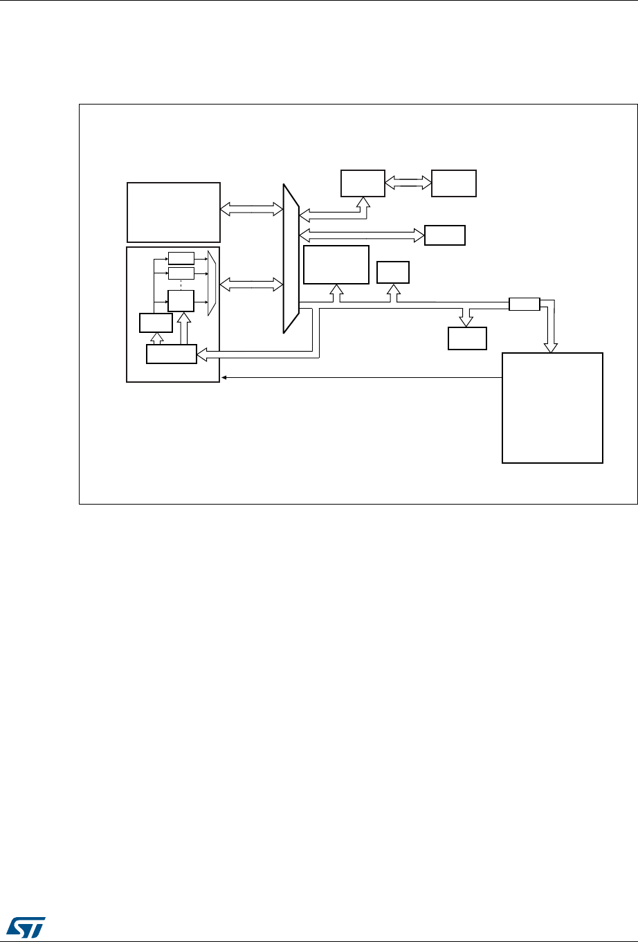
DocID025941 Rev 5 261/1001
RM0376 Direct memory access controller (DMA)
278
11.3 DMA functional description
The block diagram is shown in the following figure.
Figure 27. DMA block diagram
The DMA controller performs direct memory transfer by sharing the system bus with the
Cortex®-M0+ core. The DMA request may stop the CPU access to the system bus for some
bus cycles, when the CPU and DMA are targeting the same destination (memory or
peripheral). The bus matrix implements round-robin scheduling, thus ensuring at least half
of the system bus bandwidth (both to memory and peripheral) for the CPU.
11.3.1 DMA transactions
After an event, the peripheral sends a request signal to the DMA Controller. The DMA
controller serves the request depending on the channel priorities. As soon as the DMA
Controller accesses the peripheral, an Acknowledge is sent to the peripheral by the DMA
Controller. The peripheral releases its request as soon as it gets the Acknowledge from the
DMA Controller. Once the request is de-asserted by the peripheral, the DMA Controller
release the Acknowledge. If there are more requests, the peripheral can initiate the next
transaction.
In summary, each DMA transfer consists of three operations:
•The loading of data from the peripheral data register or a location in memory addressed
through an internal current peripheral/memory address register. The start address used
for the first transfer is the base peripheral/memory address programmed in the
DMA_CPARx or DMA_CMARx register.
MS32796V3
SRAM
Ch.1
Ch.2
Arbiter
Cortex-
M0+
AHB Slave
DMA
System
DMA request
APB
Bus matrix
DMA
Reset &
Clock control
(RCC)
FLITF Flash
up to
Ch.7
ADC
SPI1/SPI2
USART1/2/4/5
LPUART1
I2C1/2/3
TIM2/3/6/7
DAC2
CRC
Bridge
AES

Direct memory access controller (DMA) RM0376
262/1001 DocID025941 Rev 5
•The storage of the data loaded to the peripheral data register or a location in memory
addressed through an internal current peripheral/memory address register. The start
address used for the first transfer is the base peripheral/memory address programmed
in the DMA_CPARx or DMA_CMARx register.
•The post-decrementing of the DMA_CNDTRx register, which contains the number of
transactions that have still to be performed.
11.3.2 Arbiter
The arbiter manages the channel requests based on their priority and launches the
peripheral/memory access sequences.
The priorities are managed in two stages:
•Software: each channel priority can be configured in the DMA_CCRx register. There
are four levels:
– Very high priority
– High priority
– Medium priority
– Low priority
•Hardware: if 2 requests have the same software priority level, the channel with the
lowest number will get priority versus the channel with the highest number. For
example, channel 2 gets priority over channel 4.
11.3.3 DMA channels
Each channel can handle DMA transfer between a peripheral register located at a fixed
address and a memory address. The amount of data to be transferred (up to 65535) is
programmable. The register which contains the amount of data items to be transferred is
decremented after each transaction.
Programmable data sizes
Transfer data sizes of the peripheral and memory are fully programmable through the
PSIZE and MSIZE bits in the DMA_CCRx register.
Pointer incrementation
Peripheral and memory pointers can optionally be automatically post-incremented after
each transaction depending on the PINC and MINC bits in the DMA_CCRx register. If
incremented mode is enabled, the address of the next transfer will be the address of the
previous one incremented by 1, 2 or 4 depending on the chosen data size. The first transfer
address is the one programmed in the DMA_CPARx/DMA_CMARx registers. During
transfer operations, these registers keep the initially programmed value. The current
transfer addresses (in the current internal peripheral/memory address register) are not
accessible by software.
If the channel is configured in non-circular mode, no DMA request is served after the last
transfer (that is once the number of data items to be transferred has reached zero). In order
to reload a new number of data items to be transferred into the DMA_CNDTRx register, the
DMA channel must be disabled.

DocID025941 Rev 5 263/1001
RM0376 Direct memory access controller (DMA)
278
Note: If a DMA channel is disabled, the DMA registers are not reset. The DMA channel registers
(DMA_CCRx, DMA_CPARx and DMA_CMARx) retain the initial values programmed during
the channel configuration phase.
In circular mode, after the last transfer, the DMA_CNDTRx register is automatically reloaded
with the initially programmed value. The current internal address registers are reloaded with
the base address values from the DMA_CPARx/DMA_CMARx registers.
Channel configuration procedure
The following sequence should be followed to configure a DMA channel x (where x is the
channel number).
1. Set the peripheral register address in the DMA_CPARx register. The data will be
moved from/ to this address to/ from the memory after the peripheral event.
2. Set the memory address in the DMA_CMARx register. The data will be written to or
read from this memory after the peripheral event.
3. Configure the total number of data to be transferred in the DMA_CNDTRx register.
After each peripheral event, this value will be decremented.
4. Configure the channel priority using the PL[1:0] bits in the DMA_CCRx register
5. Configure data transfer direction, circular mode, peripheral & memory incremented
mode, peripheral & memory data size, and interrupt after half and/or full transfer in the
DMA_CCRx register
6. Activate the channel by setting the ENABLE bit in the DMA_CCRx register.
For code example, refer to A.6.1: DMA Channel Configuration sequence code example.
As soon as the channel is enabled, it can serve any DMA request from the peripheral
connected on the channel.
Once half of the bytes are transferred, the half-transfer flag (HTIF) is set and an interrupt is
generated if the Half-Transfer Interrupt Enable bit (HTIE) is set. At the end of the transfer,
the Transfer Complete Flag (TCIF) is set and an interrupt is generated if the Transfer
Complete Interrupt Enable bit (TCIE) is set.
Circular mode
Circular mode is available to handle circular buffers and continuous data flows (e.g. ADC
scan mode). This feature can be enabled using the CIRC bit in the DMA_CCRx register.
When circular mode is activated, the number of data to be transferred is automatically
reloaded with the initial value programmed during the channel configuration phase, and the
DMA requests continue to be served.
Memory-to-memory mode
The DMA channels can also work without being triggered by a request from a peripheral.
This mode is called Memory to Memory mode.
If the MEM2MEM bit in the DMA_CCRx register is set, then the channel initiates transfers
as soon as it is enabled by software by setting the Enable bit (EN) in the DMA_CCRx
register. The transfer stops once the DMA_CNDTRx register reaches zero. Memory to
Memory mode may not be used at the same time as Circular mode.

Direct memory access controller (DMA) RM0376
264/1001 DocID025941 Rev 5
11.3.4 Programmable data width, data alignment and endianness
When PSIZE and MSIZE are not equal, the DMA performs some data alignments as
described in Table 49: Programmable data width & endianness (when bits PINC = MINC =
1).
Table 49. Programmable data width & endianness (when bits PINC = MINC = 1)
Source
port
width
Destination
port width
Number
of data
items to
transfer
(NDT)
Source content:
address / data Transfer operations
Destination
content:
address / data
88 4
@0x0 / B0
@0x1 / B1
@0x2 / B2
@0x3 / B3
1: READ B0[7:0] @0x0 then WRITE B0[7:0] @0x0
2: READ B1[7:0] @0x1 then WRITE B1[7:0] @0x1
3: READ B2[7:0] @0x2 then WRITE B2[7:0] @0x2
4: READ B3[7:0] @0x3 then WRITE B3[7:0] @0x3
@0x0 / B0
@0x1 / B1
@0x2 / B2
@0x3 / B3
816 4
@0x0 / B0
@0x1 / B1
@0x2 / B2
@0x3 / B3
1: READ B0[7:0] @0x0 then WRITE 00B0[15:0] @0x0
2: READ B1[7:0] @0x1 then WRITE 00B1[15:0] @0x2
3: READ B2[7:0] @0x2 then WRITE 00B2[15:0] @0x4
4: READ B3[7:0] @0x3 then WRITE 00B3[15:0] @0x6
@0x0 / 00B0
@0x2 / 00B1
@0x4 / 00B2
@0x6 / 00B3
832 4
@0x0 / B0
@0x1 / B1
@0x2 / B2
@0x3 / B3
1: READ B0[7:0] @0x0 then WRITE 000000B0[31:0] @0x0
2: READ B1[7:0] @0x1 then WRITE 000000B1[31:0] @0x4
3: READ B2[7:0] @0x2 then WRITE 000000B2[31:0] @0x8
4: READ B3[7:0] @0x3 then WRITE 000000B3[31:0] @0xC
@0x0 / 000000B0
@0x4 / 000000B1
@0x8 / 000000B2
@0xC / 000000B3
16 8 4
@0x0 / B1B0
@0x2 / B3B2
@0x4 / B5B4
@0x6 / B7B6
1: READ B1B0[15:0] @0x0 then WRITE B0[7:0] @0x0
2: READ B3B2[15:0] @0x2 then WRITE B2[7:0] @0x1
3: READ B5B4[15:0] @0x4 then WRITE B4[7:0] @0x2
4: READ B7B6[15:0] @0x6 then WRITE B6[7:0] @0x3
@0x0 / B0
@0x1 / B2
@0x2 / B4
@0x3 / B6
16 16 4
@0x0 / B1B0
@0x2 / B3B2
@0x4 / B5B4
@0x6 / B7B6
1: READ B1B0[15:0] @0x0 then WRITE B1B0[15:0] @0x0
2: READ B3B2[15:0] @0x2 then WRITE B3B2[15:0] @0x2
3: READ B5B4[15:0] @0x4 then WRITE B5B4[15:0] @0x4
4: READ B7B6[15:0] @0x6 then WRITE B7B6[15:0] @0x6
@0x0 / B1B0
@0x2 / B3B2
@0x4 / B5B4
@0x6 / B7B6
16 32 4
@0x0 / B1B0
@0x2 / B3B2
@0x4 / B5B4
@0x6 / B7B6
1: READ B1B0[15:0] @0x0 then WRITE 0000B1B0[31:0] @0x0
2: READ B3B2[15:0] @0x2 then WRITE 0000B3B2[31:0] @0x4
3: READ B5B4[15:0] @0x4 then WRITE 0000B5B4[31:0] @0x8
4: READ B7B6[15:0] @0x6 then WRITE 0000B7B6[31:0] @0xC
@0x0 / 0000B1B0
@0x4 / 0000B3B2
@0x8 / 0000B5B4
@0xC / 0000B7B6
32 8 4
@0x0 / B3B2B1B0
@0x4 / B7B6B5B4
@0x8 / BBBAB9B8
@0xC / BFBEBDBC
1: READ B3B2B1B0[31:0] @0x0 then WRITE B0[7:0] @0x0
2: READ B7B6B5B4[31:0] @0x4 then WRITE B4[7:0] @0x1
3: READ BBBAB9B8[31:0] @0x8 then WRITE B8[7:0] @0x2
4: READ BFBEBDBC[31:0] @0xC then WRITE BC[7:0] @0x3
@0x0 / B0
@0x1 / B4
@0x2 / B8
@0x3 / BC
32 16 4
@0x0 / B3B2B1B0
@0x4 / B7B6B5B4
@0x8 / BBBAB9B8
@0xC / BFBEBDBC
1: READ B3B2B1B0[31:0] @0x0 then WRITE B1B0[15:0] @0x0
2: READ B7B6B5B4[31:0] @0x4 then WRITE B5B4[15:0] @0x2
3: READ BBBAB9B8[31:0] @0x8 then WRITE B9B8[15:0] @0x4
4: READ BFBEBDBC[31:0] @0xC then WRITE BDBC[15:0] @0x6
@0x0 / B1B0
@0x2 / B5B4
@0x4 / B9B8
@0x6 / BDBC
32 32 4
@0x0 / B3B2B1B0
@0x4 / B7B6B5B4
@0x8 / BBBAB9B8
@0xC / BFBEBDBC
1: READ B3B2B1B0[31:0] @0x0 then WRITE B3B2B1B0[31:0] @0x0
2: READ B7B6B5B4[31:0] @0x4 then WRITE B7B6B5B4[31:0] @0x4
3: READ BBBAB9B8[31:0] @0x8 then WRITE BBBAB9B8[31:0] @0x8
4: READ BFBEBDBC[31:0] @0xC then WRITE BFBEBDBC[31:0] @0xC
@0x0 / B3B2B1B0
@0x4 / B7B6B5B4
@0x8 / BBBAB9B8
@0xC / BFBEBDBC

DocID025941 Rev 5 265/1001
RM0376 Direct memory access controller (DMA)
278
Addressing an AHB peripheral that does not support byte or halfword
write operations
When the DMA initiates an AHB byte or halfword write operation, the data are duplicated on
the unused lanes of the HWDATA[31:0] bus. So when the used AHB slave peripheral does
not support byte or halfword write operations (when HSIZE is not used by the peripheral)
and does not generate any error, the DMA writes the 32 HWDATA bits as shown in the two
examples below:
•To write the halfword “0xABCD”, the DMA sets the HWDATA bus to “0xABCDABCD”
with HSIZE = HalfWord
•To write the byte “0xAB”, the DMA sets the HWDATA bus to “0xABABABAB” with
HSIZE = Byte
Assuming that the AHB/APB bridge is an AHB 32-bit slave peripheral that does not take the
HSIZE data into account, it will transform any AHB byte or halfword operation into a 32-bit
APB operation in the following manner:
•An AHB byte write operation of the data “0xB0” to 0x0 (or to 0x1, 0x2 or 0x3) will be
converted to an APB word write operation of the data “0xB0B0B0B0” to 0x0
•An AHB halfword write operation of the data “0xB1B0” to 0x0 (or to 0x2) will be
converted to an APB word write operation of the data “0xB1B0B1B0” to 0x0
For instance, to write the APB backup registers (16-bit registers aligned to a 32-bit address
boundary), the software must configure the memory source size (MSIZE) to “16-bit” and the
peripheral destination size (PSIZE) to “32-bit”.
11.3.5 Error management
A DMA transfer error can be generated by reading from or writing to a reserved address
space. When a DMA transfer error occurs during a DMA read or a write access, the faulty
channel is automatically disabled through a hardware clear of its EN bit in the corresponding
Channel configuration register (DMA_CCRx). The channel's transfer error interrupt flag
(TEIF) in the DMA_IFR register is set and an interrupt is generated if the transfer error
interrupt enable bit (TEIE) in the DMA_CCRx register is set.
11.3.6 DMA interrupts
An interrupt can be produced on a Half-transfer, Transfer complete or Transfer error for
each DMA channel. Separate interrupt enable bits are available for flexibility.
Table 50. DMA interrupt requests
Interrupt event Event flag Enable control bit
Half-transfer HTIF HTIE
Transfer complete TCIF TCIE
Transfer error TEIF TEIE
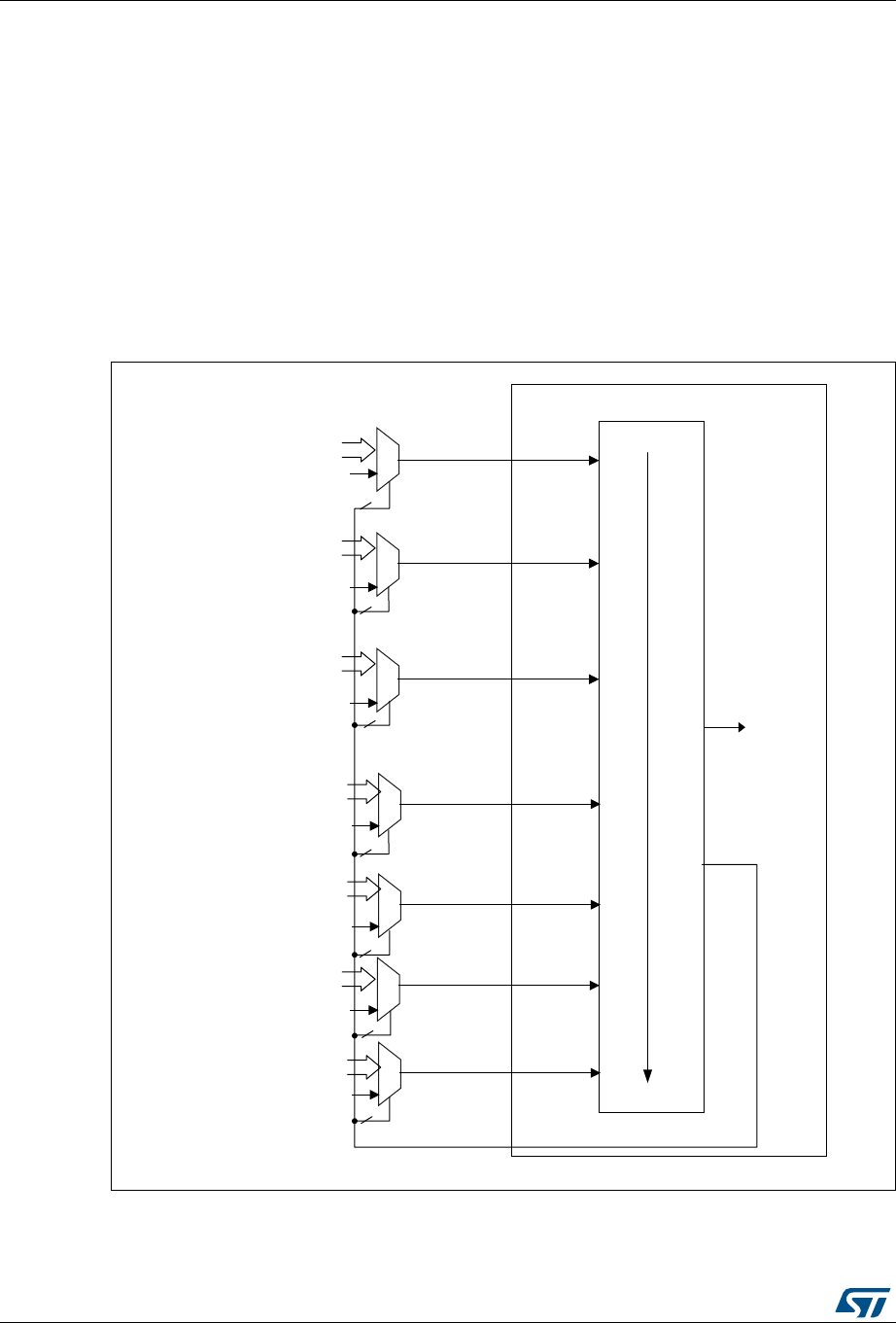
Direct memory access controller (DMA) RM0376
266/1001 DocID025941 Rev 5
11.3.7 DMA request mapping
DMA controller
The hardware requests from the peripherals (TIM2/6, ADC, DAC, SPI1/2, I2C1/2, AES
(available only on Cat. 3 and 5 with AES), USART1/2 and LPUART1) are mapped to the
DMA channels (1 to 7) through the DMA channel selection register (s). On one channel,
only one request must be enabled at a time. A peripheral request, including channel
disabling, should not be selected more than once across channels. Refer to Figure 28: DMA
request mapping.
The peripheral DMA requests can be independently activated/de-activated by programming
the DMA control bit in the registers of the corresponding peripheral.
Figure 28. DMA request mapping
Table 51 lists the DMA requests for each channel.
Peripheral request signals
Internal
DMA request
Fixed hardware priority
High priority
Low priority
DMA
SW trigger 1
(MEM2MEM bit)
SW trigger 2
(MEM2MEM bit)
SW trigger 3
(MEM2MEM bit)
SW trigger 5
(MEM2MEM bit)
SW trigger 6
(MEM2MEM bit)
SW trigger 7
(MEM2MEM bit)
ADC, TIM2_CH3,AES_IN
ADC,SPI1_RX,USART1_TX,
LPUART1_TX,I2C1_TX,I2C3_TX,
TIM2_UP,TIM6_UP/DAC chan. 1,
AES_OUT,TIM3_CH3,
USART4_RX, USART5_RX
SPI1_TX, USART1_RX,I2C3_RX
LPUART1_RX, I2C1_RX,
TIM2_CH2, TIM3_CH4,TIM3_UP,
USART4_TX,USART5_TX,
AES_OUT
SPI2_RX, USART1_TX,
USART2_TX, I2C2_TX, I2C3_TX,
TIM2_CH4,TIM7_UP/DAC chan. 2
SPI2_TX, USART1_RX,
USART2_RX, I2C2_RX,
TIM2_CH1, TIM3_CH1, AES_IN,
I2C3_RX
SPI2_RX, USART2_RX,
LPUART1_RX, I2C1_TX,
TIM3_TRIG, USART4_RX,
USART5_RX
SPI2_TX, USART2_TX,
USART4_TX, USART5_TX,
LPUART1_TX, I2C1_RX,
TIM2_CH2, TIM2_CH4
SW trigger 4
(MEM2MEM bit)
MS33701V3
DMA_CSELR
C7S
4
C6S
4
C5S
4
C4S
4
C3S
4
C2S
4
C1S
4

DocID025941 Rev 5 267/1001
RM0376 Direct memory access controller (DMA)
278
Table 51. Summary of the DMA requests for each channel
Request
number Peripherals Channel
1Channel 2 Channel 3 Channel 4 Channel 5 Channel 6 Channel 7
0ADC ADC ADC - - - -
1SPI1 - SPI1_RX SPI1_TX - - - -
2SPI2 - - - SPI2_RX SPI2_TX SPI2_RX SPI2_TX
3USART1 -USART1_
TX
USART1_
RX
USART1_
TX
USART1_
RX --
4USART2 -- -
USART2_
TX
USART2_
RX
USART2_
RX
USART2_
TX
5 LPUART1 -LPUART1_
TX
LPUART1_
RX --
LPUART1
_RX
LPUART1_
TX
6I2C1 - I2C1_TX I2C1_RX - -- I2C1_TX I2C1_RX
7I2C2 - - - I2C2_TX I2C2_RX - -
8TIM2 TIM2_
CH3 TIM2_UP TIM2_CH2 TIM2_CH4 TIM2_CH1 TIM2_CH2
TIM2_CH4
9
TIM6_UP/
DAC_
channel1
-TIM6/DAC_
channel1 -----
10 TIM3 - TIM3_CH3 TIM3_CH4
TIM3_UP - TIM3_CH1 TIM3_
TRIG -
11 AES(1) AES_IN AES_OUT AES_OUT AES_IN
12 USART4 -USART4_
RX
USART4_T
X--
USART4_
RX
USART4_
TX
13 USART5 -USART5_
RX
USART5_T
X--
USART5_
RX
USART5_
TX
14 I2C3 - I2C3_TX I2C3_RX I2C3_TX I2C3_RX - -
15
TIM7_UO/
DAC_
channel2
-- -
TIM7/DAC_
channel2 ---
1. Available only on category 3 and 5 with AES.

Direct memory access controller (DMA) RM0376
268/1001 DocID025941 Rev 5
11.4 DMA registers
Refer to Section 1.1 on page 51 for a list of abbreviations used in register descriptions.
The peripheral registers can be accessed by bytes (8-bit), half-words (16-bit) or words (32-
bit).
11.4.1 DMA interrupt status register (DMA_ISR)
Address offset: 0x00
Reset value: 0x0000 0000
31 30 29 28 27 26 25 24 23 22 21 20 19 18 17 16
Res. Res. Res. Res. TEIF7 HTIF7 TCIF7 GIF7 TEIF6 HTIF6 TCIF6 GIF6 TEIF5 HTIF5 TCIF5 GIF5
rrrrrrrrrrrr
1514131211109876543210
TEIF4 HTIF4 TCIF4 GIF4 TEIF3 HTIF3 TCIF3 GIF3 TEIF2 HTIF2 TCIF2 GIF2 TEIF1 HTIF1 TCIF1 GIF1
rrrrrrrrrrrrrrrr
Bits 31:28 Reserved, must be kept at reset value.
Bits 27, 23, 19, 15,
11, 7, 3
TEIFx: Channel x transfer error flag (x = 1..7)
This bit is set by hardware. It is cleared by software writing 1 to the corresponding bit in the
DMA_IFCR register.
0: No transfer error (TE) on channel x
1: A transfer error (TE) occurred on channel x
Bits 26, 22, 18, 14,
10, 6, 2
HTIFx: Channel x half transfer flag (x = 1..7)
This bit is set by hardware. It is cleared by software writing 1 to the corresponding bit in the
DMA_IFCR register.
0: No half transfer (HT) event on channel x
1: A half transfer (HT) event occurred on channel x
Bits 25, 21, 17, 13,
9, 5, 1
TCIFx: Channel x transfer complete flag (x = 1..7)
This bit is set by hardware. It is cleared by software writing 1 to the corresponding bit in the
DMA_IFCR register.
0: No transfer complete (TC) event on channel x
1: A transfer complete (TC) event occurred on channel x
Bits 24, 20, 16, 12,
8, 4, 0
GIFx: Channel x global interrupt flag (x = 1..7)
This bit is set by hardware. It is cleared by software writing 1 to the corresponding bit in the
DMA_IFCR register.
0: No TE, HT or TC event on channel x
1: A TE, HT or TC event occurred on channel x

DocID025941 Rev 5 269/1001
RM0376 Direct memory access controller (DMA)
278
11.4.2 DMA interrupt flag clear register (DMA_IFCR)
Address offset: 0x04
Reset value: 0x0000 0000
31 30 29 28 27 26 25 24 23 22 21 20 19 18 17 16
Res. Res. Res. Res. CTEIF7 CHTIF7 CTCIF7 CGIF7 CTEIF6 CHTIF6 CTCIF6 CGIF6 CTEIF5 CHTIF5 CTCIF5 CGIF5
wwwwwwwwwwww
1514131211109876543210
CTEIF4 CHTIF4 CTCIF4 CGIF4 CTEIF3 CHTIF3 CTCIF3 CGIF3 CTEIF2 CHTIF2 CTCIF2 CGIF2 CTEIF1 CHTIF1 CTCIF1 CGIF1
wwwwwwwwwwwwwwww
Bits 31:28 Reserved, must be kept at reset value.
Bits 27, 23, 19, 15,
11, 7, 3
CTEIFx: Channel x transfer error clear (x = 1..7)
This bit is set by software.
0: No effect
1: Clears the corresponding TEIF flag in the DMA_ISR register
Bits 26, 22, 18, 14,
10, 6, 2
CHTIFx: Channel x half transfer clear (x = 1..7)
This bit is set by software.
0: No effect
1: Clears the corresponding HTIF flag in the DMA_ISR register
Bits 25, 21, 17, 13,
9, 5, 1
CTCIFx: Channel x transfer complete clear (x = 1..7)
This bit is set by software.
0: No effect
1: Clears the corresponding TCIF flag in the DMA_ISR register
Bits 24, 20, 16, 12,
8, 4, 0
CGIFx: Channel x global interrupt clear (x = 1..7)
This bit is set by software.
0: No effect
1: Clears the GIF, TEIF, HTIF and TCIF flags in the DMA_ISR register

Direct memory access controller (DMA) RM0376
270/1001 DocID025941 Rev 5
11.4.3 DMA channel x configuration register (DMA_CCRx)
(x = 1..7 , where x = channel number)
Address offset: 0x08 + 0d20 × (channel number – 1)
Reset value: 0x0000 0000
31 30 29 28 27 26 25 24 23 22 21 20 19 18 17 16
Res. Res. Res. Res. Res. Res. Res. Res. Res. Res. Res. Res. Res. Res. Res. Res.
1514131211109876543210
Res. MEM2
MEM PL[1:0] MSIZE[1:0] PSIZE[1:0] MINC PINC CIRC DIR TEIE HTIE TCIE EN
rw rw rw rw rw rw rw rw rw rw rw rw rw rw rw
Bits 31:15 Reserved, must be kept at reset value.
Bit 14 MEM2MEM: Memory to memory mode
This bit is set and cleared by software.
0: Memory to memory mode disabled
1: Memory to memory mode enabled
Bits 13:12 PL[1:0]: Channel priority level
These bits are set and cleared by software.
00: Low
01: Medium
10: High
11: Very high
Bits 11:10 MSIZE[1:0]: Memory size
These bits are set and cleared by software.
00: 8-bits
01: 16-bits
10: 32-bits
11: Reserved
Bits 9:8 PSIZE[1:0]: Peripheral size
These bits are set and cleared by software.
00: 8-bits
01: 16-bits
10: 32-bits
11: Reserved
Bit 7 MINC: Memory increment mode
This bit is set and cleared by software.
0: Memory increment mode disabled
1: Memory increment mode enabled
Bit 6 PINC: Peripheral increment mode
This bit is set and cleared by software.
0: Peripheral increment mode disabled
1: Peripheral increment mode enabled

DocID025941 Rev 5 271/1001
RM0376 Direct memory access controller (DMA)
278
Bit 5 CIRC: Circular mode
This bit is set and cleared by software.
0: Circular mode disabled
1: Circular mode enabled
Bit 4 DIR: Data transfer direction
This bit is set and cleared by software.
0: Read from peripheral
1: Read from memory
Bit 3 TEIE: Transfer error interrupt enable
This bit is set and cleared by software.
0: TE interrupt disabled
1: TE interrupt enabled
Bit 2 HTIE: Half transfer interrupt enable
This bit is set and cleared by software.
0: HT interrupt disabled
1: HT interrupt enabled
Bit 1 TCIE: Transfer complete interrupt enable
This bit is set and cleared by software.
0: TC interrupt disabled
1: TC interrupt enabled
Bit 0 EN: Channel enable
This bit is set and cleared by software.
0: Channel disabled
1: Channel enabled

Direct memory access controller (DMA) RM0376
272/1001 DocID025941 Rev 5
11.4.4 DMA channel x number of data register (DMA_CNDTRx) (x = 1..7,
where x = channel number)
Address offset: 0x0C + 0d20 × (channel number – 1)
Reset value: 0x0000 0000
11.4.5 DMA channel x peripheral address register (DMA_CPARx) (x = 1..7,
where x = channel number)
Address offset: 0x10 + 0d20 × (channel number – 1)
Reset value: 0x0000 0000
This register must not be written when the channel is enabled.
31 30 29 28 27 26 25 24 23 22 21 20 19 18 17 16
Res. Res. Res. Res. Res. Res. Res. Res. Res. Res. Res. Res. Res. Res. Res. Res.
1514131211109876543210
NDT[15:0]
rw rw rw rw rw rw rw rw rw rw rw rw rw rw rw rw
Bits 31:16 Reserved, must be kept at reset value.
Bits 15:0 NDT[15:0]: Number of data to transfer
Number of data to be transferred (0 up to 65535). This register can only be written when the
channel is disabled. Once the channel is enabled, this register is read-only, indicating the
remaining bytes to be transmitted. This register decrements after each DMA transfer.
Once the transfer is completed, this register can either stay at zero or be reloaded
automatically by the value previously programmed if the channel is configured in circular
mode.
If this register is zero, no transaction can be served whether the channel is enabled or not.
31 30 29 28 27 26 25 24 23 22 21 20 19 18 17 16
PA [31:16]
rw rw rw rw rw rw rw rw rw rw rw rw rw rw rw rw
1514131211109876543210
PA [15:0]
rw rw rw rw rw rw rw rw rw rw rw rw rw rw rw rw
Bits 31:0 PA[31:0]: Peripheral address
Base address of the peripheral data register from/to which the data will be read/written.
When PSIZE is 01 (16-bit), the PA[0] bit is ignored. Access is automatically aligned to a half-
word address.
When PSIZE is 10 (32-bit), PA[1:0] are ignored. Access is automatically aligned to a word
address.

DocID025941 Rev 5 273/1001
RM0376 Direct memory access controller (DMA)
278
11.4.6 DMA channel x memory address register (DMA_CMARx) (x = 1..7,
where x = channel number)
Address offset: 0x14 + 0d20 × (channel number – 1)
Reset value: 0x0000 0000
This register must not be written when the channel is enabled.
31 30 29 28 27 26 25 24 23 22 21 20 19 18 17 16
MA [31:16]
rw rw rw rw rw rw rw rw rw rw rw rw rw rw rw rw
1514131211109876543210
MA [15:0]
rw rw rw rw rw rw rw rw rw rw rw rw rw rw rw rw
Bits 31:0 MA[31:0]: Memory address
Base address of the memory area from/to which the data will be read/written.
When MSIZE is 01 (16-bit), the MA[0] bit is ignored. Access is automatically aligned to a half-
word address.
When MSIZE is 10 (32-bit), MA[1:0] are ignored. Access is automatically aligned to a word
address.

Direct memory access controller (DMA) RM0376
274/1001 DocID025941 Rev 5
11.4.7 DMA channel selection register (DMA_CSELR)
Address offset: 0xA8
Reset value: 0x0000 0000
This register is used to manage the remapping of DMA channels (see Figure 28).
31 30 29 28 27 26 25 24 23 22 21 20 19 18 17 16
Res. Res. Res. Res. C7S [3:0] C6S [3:0] C5S [3:0]
rw rw rw rw rw rw rw rw rw rw rw rw
1514131211109876543210
C4S [3:0] C3S [3:0] C2S [3:0] C1S [3:0]
rw rw rw rw rw rw rw rw rw rw rw rw rw rw rw rw
Bits 31:28 Reserved, must be kept at reset value.
Bits 27:24 C7S[3:0]: DMA channel 7 selection
0010: DMA channel 7 remapped to SPI2_TX
0100: DMA channel 7 remapped to USART2_TX
0101: DMA channel 7 remapped to LPUART1_TX
0110: DMA channel 7 remapped to I2C1_RX
1000: DMA channel 7 remapped to TIM2_CH2/TIM2_CH4
1100: DMA channel 7 remapped to USART4_TX
1101: DMA channel 7 remapped to USART5_TX
Other configurations: DMA channel 7 not remapped
Bits 23:20 C6S[3:0]: DMA channel 6 selection
0010: DMA channel 6 remapped to SPI2_RX
0100: DMA channel 6 remapped to USART2_RX
0101: DMA channel 6 remapped to LPUART1_RX
0110: DMA channel 6 remapped to I2C1_TX
1010: DMA channel 6 remapped to TIM3_TRIG
1100: DMA channel 6 remapped to USART4_RX
1101: DMA channel 6remapped to USART5_RX
Other configurations: DMA channel 6 not remapped
Bits 19:16 C5S[3:0]: DMA channel 5 selection
0010: DMA channel 5 remapped to SPI2_TX
0011: DMA channel 5 remapped to USART1_RX
0100: DMA channel 5 remapped to USART2_RX
0111: DMA channel 5 remapped to I2C2_RX
1000: DMA channel 5 remapped to TIM2_CH1
1010: DMA channel 5 remapped to TIM3_CH1
1011: DMA channel 5 remapped to AES_IN
1110: DMA channel 5 remapped to I2C3_RX
Other configurations: DMA channel 5 not remapped

DocID025941 Rev 5 275/1001
RM0376 Direct memory access controller (DMA)
278
Bits 15:12 C4S[3:0]: DMA channel 4 selection
0010: DMA channel 4 remapped to SPI2_RX
0011: DMA channel 4 remapped to USART1_TX
0100: DMA channel 4 remapped to USART2_TX
0111: DMA channel 4 remapped to I2C2_TX
1000: DMA channel 4 remapped to TIM2_CH4
1110: DMA channel 4 remapped to I2C3_TX
1111: DMA channel 4 remapped to TIM7_UP/DAC channel 2
Other configurations: DMA channel 4 not remapped
Bits 11:8 C3S[3:0]: DMA channel 3 selection
0001: DMA channel 3 remapped to SPI1_TX
0011: DMA channel 3 remapped to USART1_RX
0101: DMA channel 3 remapped to LPUART1_RX
0110: DMA channel 3 remapped to I2C1_RX
1000: DMA channel 3 remapped to TIM2_CH2
1010: DMA channel 3 remapped to TIM4_CH4/TIM4_UP
1011: DMA channel 3 remapped to AES_OUT
1100: DMA channel 3 remapped to USART4_TX
1101: DMA channel 3 remapped to USART4_TX
1110: DMA channel 3 remapped to I2C3_RX
Other configurations: DMA channel 3 not remapped
Bits 7:4 C2S[3:0]: DMA channel 2 selection
0000: DMA channel 2 remapped to ADC
0001: DMA channel 2 remapped to SPI1_RX
0011: DMA channel 2 remapped to USART1_TX
0101: DMA channel 2 remapped to LPUART1_TX
0110: DMA channel 2 remapped to I2C1_TX
1000: DMA channel 2 remapped to TIM2_UP
1001: DMA channel 2 remapped to TIM6_UP/DAC channel 1
1010: DMA channel 2 remapped to TIM3_CH3
1011: DMA channel 2 remapped to AES_OUT
1100: DMA channel 2 remapped to USART4_RX
1101: DMA channel 2 remapped to USART5_RX
1110: DMA channel 2 remapped to I2C3_TX
Other configurations: DMA channel 2 not remapped
Bits 3:0 C1S[3:0]: DMA channel 1 selection
0000: DMA channel 1 remapped to ADC
1000: DMA channel 1 remapped to TIM2_CH3
1011: DMA channel 1 remapped to AES_IN
Other configurations: DMA channel 1 not remapped
Direct memory access controller (DMA) RM0376
276/1001 DocID025941 Rev 5
11.4.8 DMA register map
The following table gives the DMA register map and the reset values.
Table 52. DMA register map and reset values
Offset Register
name
31
30
29
28
27
26
25
24
23
22
21
20
19
18
17
16
15
14
13
12
11
10
9
8
7
6
5
4
3
2
1
0
0x00 DMA_ISR
Res.
Res.
Res.
Res.
TEIF7
HTIF7
TCIF7
GIF7
TEIF6
HTIF6
TCIF6
GIF6
TEIF5
HTIF5
TCIF5
GIF5
TEIF4
HTIF4
TCIF4
GIF4
TEIF3
HTIF3
TCIF3
GIF3
TEIF2
HTIF2
TCIF2
GIF2
TEIF1
HTIF1
TCIF1
GIF1
Reset value 0000000000000000000000000000
0x04
DMA_IFCR
Res.
Res.
Res.
Res.
CTEIF7
CHTIF7
CTCIF7
CGIF7
CTEIF6
CHTIF6
CTCIF6
CGIF6
CTEIF5
CHTIF5
CTCIF5
CGIF5
CTEIF4
CHTIF4
CTCIF4
CGIF4
CTEIF3
CHTIF3
CTCIF3
CGIF3
CTEIF2
CHTIF2
CTCIF2
CGIF2
CTEIF1
CHTIF1
CTCIF1
CGIF1
Reset value 0000000000000000000000000000
0x08 DMA_CCR1
Res.
Res.
Res.
Res.
Res.
Res.
Res.
Res.
Res.
Res.
Res.
Res.
Res.
Res.
Res.
Res.
Res.
MEM2MEM
PL
[1:0]
MSIZE [1:0]
PSIZE [1:0]
MINC
PINC
CIRC
DIR
TEIE
HTIE
TCIE
EN
Reset value 000000000000000
0x0C DMA_CNDTR1
Res.
Res.
Res.
Res.
Res.
Res.
Res.
Res.
Res.
Res.
Res.
Res.
Res.
Res.
Res.
Res.
NDT[15:0]
Reset value 0000000000000000
0x10 DMA_CPAR1 PA[31:0]
Reset value 00000000000000000000000000000000
0x14
DMA_CMAR1 MA[31:0]
Reset value 00000000000000000000000000000000
0x18 Reserved
Res.
Res.
Res.
Res.
Res.
Res.
Res.
Res.
Res.
Res.
Res.
Res.
Res.
Res.
Res.
Res.
Res.
Res.
Res.
Res.
Res.
Res.
Res.
Res.
Res.
Res.
Res.
Res.
Res.
Res.
Res.
Res.
0x1C DMA_CCR2
Res.
Res.
Res.
Res.
Res.
Res.
Res.
Res.
Res.
Res.
Res.
Res.
Res.
Res.
Res.
Res.
Res.
MEM2MEM
PL
[1:0]
MSIZE [1:0]
PSIZE [1:0]
MINC
PINC
CIRC
DIR
TEIE
HTIE
TCIE
EN
Reset value 000000000000000
0x20
DMA_CNDTR2
Res.
Res.
Res.
Res.
Res.
Res.
Res.
Res.
Res.
Res.
Res.
Res.
Res.
Res.
Res.
Res.
NDT[15:0]
Reset value 0000000000000000
0x24 DMA_CPAR2 PA[31:0]
Reset value 00000000000000000000000000000000
0x28
DMA_CMAR2 MA[31:0]
Reset value 00000000000000000000000000000000
0x2C Reserved
Res.
Res.
Res.
Res.
Res.
Res.
Res.
Res.
Res.
Res.
Res.
Res.
Res.
Res.
Res.
Res.
Res.
Res.
Res.
Res.
Res.
Res.
Res.
Res.
Res.
Res.
Res.
Res.
Res.
Res.
Res.
Res.
0x30 DMA_CCR3
Res.
Res.
Res.
Res.
Res.
Res.
Res.
Res.
Res.
Res.
Res.
Res.
Res.
Res.
Res.
Res.
Res.
MEM2MEM
PL
[1:0]
MSIZE [1:0]
PSIZE [1:0]
MINC
PINC
CIRC
DIR
TEIE
HTIE
TCIE
EN
Reset value 000000000000000
0x34
DMA_CNDTR3
Res.
Res.
Res.
Res.
Res.
Res.
Res.
Res.
Res.
Res.
Res.
Res.
Res.
Res.
Res.
Res.
NDT[15:0]
Reset value 0000000000000000
0x38 DMA_CPAR3 PA[31:0]
Reset value 00000000000000000000000000000000
0x3C DMA_CMAR3 MA[31:0]
Reset value 00000000000000000000000000000000
DocID025941 Rev 5 277/1001
RM0376 Direct memory access controller (DMA)
278
0x40 Reserved
Res.
Res.
Res.
Res.
Res.
Res.
Res.
Res.
Res.
Res.
Res.
Res.
Res.
Res.
Res.
Res.
Res.
Res.
Res.
Res.
Res.
Res.
Res.
Res.
Res.
Res.
Res.
Res.
Res.
Res.
Res.
Res.
0x44
DMA_CCR4
Res.
Res.
Res.
Res.
Res.
Res.
Res.
Res.
Res.
Res.
Res.
Res.
Res.
Res.
Res.
Res.
Res.
MEM2MEM
PL
[1:0]
MSIZE [1:0]
PSIZE [1:0]
MINC
PINC
CIRC
DIR
TEIE
HTIE
TCIE
EN
Reset value 000000000000000
0x48 DMA_CNDTR4
Res.
Res.
Res.
Res.
Res.
Res.
Res.
Res.
Res.
Res.
Res.
Res.
Res.
Res.
Res.
Res.
NDT[15:0]
Reset value 0000000000000000
0x4C
DMA_CPAR4 PA[31:0]
Reset value 00000000000000000000000000000000
0x50 DMA_CMAR4 MA[31:0]
Reset value 00000000000000000000000000000000
0x54 Reserved
Res.
Res.
Res.
Res.
Res.
Res.
Res.
Res.
Res.
Res.
Res.
Res.
Res.
Res.
Res.
Res.
Res.
Res.
Res.
Res.
Res.
Res.
Res.
Res.
Res.
Res.
Res.
Res.
Res.
Res.
Res.
Res.
0x58 DMA_CCR5
Res.
Res.
Res.
Res.
Res.
Res.
Res.
Res.
Res.
Res.
Res.
Res.
Res.
Res.
Res.
Res.
Res.
MEM2MEM
PL
[1:0]
MSIZE [1:0]
PSIZE [1:0]
MINC
PINC
CIRC
DIR
TEIE
HTIE
TCIE
EN
Reset value 000000000000000
0x5C DMA_CNDTR5
Res.
Res.
Res.
Res.
Res.
Res.
Res.
Res.
Res.
Res.
Res.
Res.
Res.
Res.
Res.
Res.
NDT[15:0]
Reset value 0000000000000000
0x60 DMA_CPAR5 PA[31:0]
Reset value 00000000000000000000000000000000
0x64
DMA_CMAR5 MA[31:0]
Reset value 00000000000000000000000000000000
0x68 Reserved
Res.
Res.
Res.
Res.
Res.
Res.
Res.
Res.
Res.
Res.
Res.
Res.
Res.
Res.
Res.
Res.
Res.
Res.
Res.
Res.
Res.
Res.
Res.
Res.
Res.
Res.
Res.
Res.
Res.
Res.
Res.
Res.
0x6C DMA_CCR6
Res.
Res.
Res.
Res.
Res.
Res.
Res.
Res.
Res.
Res.
Res.
Res.
Res.
Res.
Res.
Res.
Res.
MEM2MEM
PL
[1:0]
MSIZE [1:0]
PSIZE [1:0]
MINC
PINC
CIRC
DIR
TEIE
HTIE
TCIE
EN
Reset value 000000000000000
0x70 DMA_CNDTR6
Res.
Res.
Res.
Res.
Res.
Res.
Res.
Res.
Res.
Res.
Res.
Res.
Res.
Res.
Res.
Res.
NDT[15:0]
Reset value 0000000000000000
0x74 DMA_CPAR6 PA[31:0]
Reset value 00000000000000000000000000000000
0x78
DMA_CMAR6 MA[31:0]
Reset value 00000000000000000000000000000000
0x7C Reserved
Res.
Res.
Res.
Res.
Res.
Res.
Res.
Res.
Res.
Res.
Res.
Res.
Res.
Res.
Res.
Res.
Res.
Res.
Res.
Res.
Res.
Res.
Res.
Res.
Res.
Res.
Res.
Res.
Res.
Res.
Res.
Res.
0x80 DMA_CCR7
Res.
Res.
Res.
Res.
Res.
Res.
Res.
Res.
Res.
Res.
Res.
Res.
Res.
Res.
Res.
Res.
Res.
MEM2MEM
PL
[1:0]
MSIZE [1:0]
PSIZE [1:0]
MINC
PINC
CIRC
DIR
TEIE
HTIE
TCIE
EN
Reset value 000000000000000
0x84
DMA_CNDTR7
Res.
Res.
Res.
Res.
Res.
Res.
Res.
Res.
Res.
Res.
Res.
Res.
Res.
Res.
Res.
Res.
NDT[15:0]
Reset value 0000000000000000
Table 52. DMA register map and reset values (continued)
Offset Register
name
31
30
29
28
27
26
25
24
23
22
21
20
19
18
17
16
15
14
13
12
11
10
9
8
7
6
5
4
3
2
1
0

Direct memory access controller (DMA) RM0376
278/1001 DocID025941 Rev 5
Refer to Section 2.2.2 on page 58 for the register boundary addresses.
0x88
DMA_CPAR7 PA[31:0]
Reset value 00000000000000000000000000000000
0x8C DMA_CMAR7 MA[31:0]
Reset value 00000000000000000000000000000000
0x90 -
0xA7 Reserved
Res.
Res.
Res.
Res.
Res.
Res.
Res.
Res.
Res.
Res.
Res.
Res.
Res.
Res.
Res.
Res.
Res.
Res.
Res.
Res.
Res.
Res.
Res.
Res.
Res.
Res.
Res.
Res.
Res.
Res.
Res.
Res.
0xA8 DMA_CSELR
Res.
Res.
Res.
Res.
C7S[3:0] C6S[3:0] C5S[3:0] C4S[3:0] C3S[3:0] C2S[3:0] C1S[3:0]
Reset value 0000000000000000000000000000
Table 52. DMA register map and reset values (continued)
Offset Register
name
31
30
29
28
27
26
25
24
23
22
21
20
19
18
17
16
15
14
13
12
11
10
9
8
7
6
5
4
3
2
1
0

DocID025941 Rev 5 279/1001
RM0376 Nested vectored interrupt controller (NVIC)
291
12 Nested vectored interrupt controller (NVIC)
12.1 Main features
•Up to 39 maskable interrupt channels (see Table 53), These do not include the 16
interrupt lines of Cortex®-M0+.
•4 programmable priority levels (2 bits of interrupt priority are used)
•Low-latency exception and interrupt handling
•Power management control
•Implementation of system control registers
The NVIC and the processor core interface are closely coupled, which enables low-latency
interrupt processing and efficient processing of late arriving interrupts.
All interrupts including the core exceptions are managed by the NVIC. For more information
on exceptions and NVIC programming, refer to the STM32L0 Series Cortex®-M0+
programming manual (PM0223).
For code example, refer to A.7.1: NVIC initialization example.
12.2 SysTick calibration value register
The SysTick calibration value is fixed to 4000, which gives a reference time base of 1 ms
with the SysTick clock set to 4 MHz (max HCLK/8).
12.3 Interrupt and exception vectors
Table 53 is the vector table for STM32L0x2 devices.
Table 53. List of vectors(1)(2)
Position Priority Type of
priority Acronym Description Address
- - - Reserved 0x0000_0000
-3 fixed Reset Reset 0x0000_0004
-2 fixed NMI_Handler
Non maskable interrupt. The RCC
Clock Security System (CSS) is
linked to the NMI vector.
0x0000_0008
-1 fixed HardFault_Handler All class of fault 0x0000_000C
- - - Reserved 0x0000_0010 -
0x0000_002B
3settable SVC_Handler System service call via SWI
instruction 0x0000_002C
- - - Reserved 0x0000_0030 -
0x0000_0037
5settable PendSV_Handler Pendable request for system service 0x0000_0038
6settable SysTick_Handler System tick timer 0x0000_003C

Nested vectored interrupt controller (NVIC) RM0376
280/1001 DocID025941 Rev 5
0 7 settable WWDG Window Watchdog interrupt 0x0000_0040
1 8 settable PVD PVD through EXTI Line detection
interrupt 0x0000_0044
2 9 settable RTC
RTC global interrupt through
EXTI17/19/20 line and LSE CSS
interrupt through EXTI 19 line
0x0000_0048
3 10 settable FLASH Flash memory and data EEPROM
global interrupt 0x0000_004C
4 11 settable RCC_CRS RCC and CRS global interrupt 0x0000_0050
5 12 settable EXTI[1:0] EXTI Line0 and 1 interrupts 0x0000_0054
6 13 settable EXTI[3:2] EXTI Line2 and 3 interrupts 0x0000_0058
7 14 settable EXTI[15:4] EXTI Line4 to 15 interrupts 0x0000_005C
8 15 settable TSC Touch sense controller interrupt 0x0000_0060
9 16 settable DMA1_Channel1 DMA1 Channel1 global interrupt 0x0000_0064
10 17 settable DMA1_Channel[3:2] DMA1 Channel2 and 3 interrupts 0x0000_0068
11 18 settable DMA1_Channel[7:4] DMA1 Channel4 to 7 interrupts 0x0000_006C
12 19 settable ADC_COMP ADC and comparator interrupts
through EXTI21 and 22 0x0000_0070
13 20 settable LPTIM1 LPTIMER1 interrupt through EXTI29 0x0000_0074
14 21 settable USART4/USART5 USART4/USART5 global interrupt 0x0000_0078
15 22 settable TIM2 TIMER2 global interrupt 0x0000_007C
16 23 settable TIM3 TIMER3 global interrupt 0x0000_0080
17 24 settable TIM6_DAC TIMER6 global interrupt and DAC
interrupt 0x0000_0084
18 25 settable TIM7 TIMER7 global interrupt 0x0000_0088
19 26 settable - reserved 0x0000_008C
20 27 settable TIM21 TIMER21 global interrupt 0x0000_0090
21 28 settable I2C3 I2C3 global interrupt 0x0000_0094
22 29 settable TIM22 TIMER22 global interrupt 0x0000_0098
23 30 settable I2C1 I2C1 global interrupt through EXTI23 0x0000_009C
24 31 settable I2C2 I2C2 global interrupt 0x0000_00A0
25 32 settable SPI1 SPI1 global interrupt 0x0000_00A4
26 33 settable SPI2 SPI2 global interrupt 0x0000_00A8
27 34 settable USART1 USART1 global interrupt through
EXTI25 0x0000_00AC
28 35 settable USART2 USART2 global interrupt through
EXTI26 0x0000_00B0
Table 53. List of vectors(1)(2) (continued)
Position Priority Type of
priority Acronym Description Address

DocID025941 Rev 5 281/1001
RM0376 Nested vectored interrupt controller (NVIC)
291
29 36 settable LPUART1 + AES
+RNG
LPUART1 global interrupt through
EXTI28 + AES global interrupt +
RNG global interrupt
0x0000_00B4
31 38 settable USB USB event interrupt through EXTI18 0x0000_00BC
1. The grayed cells correspond to the Cortex®-M0+ interrupts.
2. Refer to Table 1: STM32L0x2 memory density, to Table 2: Overview of features per category and to the device datasheets
for the GPIO ports and peripherals available on your device. The memory area corresponding to unavailable GPIO ports or
peripherals are reserved.
Table 53. List of vectors(1)(2) (continued)
Position Priority Type of
priority Acronym Description Address

Extended interrupt and event controller (EXTI) RM0376
282/1001 DocID025941 Rev 5
13 Extended interrupt and event controller (EXTI)
13.1 Introduction
The extended interrupts and events controller (EXTI) manages the external and internal
asynchronous events/interrupts and generates the event request to the CPU/interrupt
controller plus a wake-up request to the power controller.
The EXTI allows the management of up to 30 event lines which can wake up the device
from Stop mode.
Some of the lines are configurable: in this case the active edge can be chosen
independently, and a status flag indicates the source of the interrupt. The configurable lines
are used by the I/Os external interrupts, and by few peripherals. Some of the lines are
direct: they are used by some peripherals to generate a wakeup from Stop event or
interrupt. In this case the status flag is provided by the peripheral.
Each line can be masked independently for interrupt or event generation.
Te EXTI controller also allows to emulate, by programming to a dedicated register, events or
interrupts by software multiplexed with the corresponding hardware event line.
13.2 EXTI main features
The EXTI main features are the following:
•Generation of up to 30 event/interrupt requests
– 22 configurable lines
– 7 direct lines
•Independent mask on each event/interrupt line
•Configurable rising or falling edge (configurable lines only)
•Dedicated status bit (configurable lines only)
•Emulation of event/interrupt requests (configurable lines only)
13.3 EXTI functional description
For the configurable interrupt lines, the interrupt line should be configured and enabled in
order to generate an interrupt. This is done by programming the two trigger registers with
the desired edge detection and by enabling the interrupt request by writing a ‘1’ to the
corresponding bit in the interrupt mask register. When the selected edge occurs on the
interrupt line, an interrupt request is generated. The pending bit corresponding to the
interrupt line is also set. This request is cleared by writing a ‘1’ in the pending register.
For the direct interrupt lines: the interrupt is enabled by default in the interrupt mask register
and there is no corresponding pending bit in the pending register.
To generate an event, the event line should be configured and enabled. This is done by
programming the two trigger registers with the desired edge detection and by enabling the
event request by writing a ‘1’ to the corresponding bit in the event mask register. When the
selected edge occurs on the event line, an event pulse is generated. The pending bit
corresponding to the event line is not set.
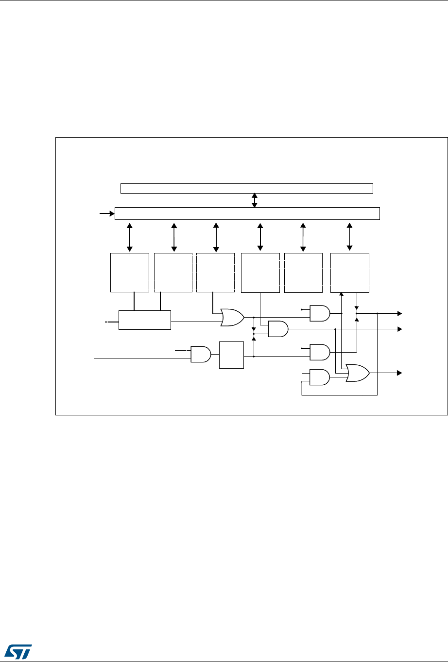
DocID025941 Rev 5 283/1001
RM0376 Extended interrupt and event controller (EXTI)
291
For the configurable lines, an interrupt/event request can also be generated by software by
writing a ‘1’ in the software interrupt/event register.
Note: The interrupts or events associated to the direct lines are triggered only when the system is
in Stop mode. If the system is still running, no interrupt/event is generated by the EXTI.
13.3.1 EXTI block diagram
The block diagram is shown in Figure 29.
Figure 29. Extended interrupts and events controller (EXTI) block diagram
13.3.2 Wakeup event management
The STM32L0x2 microcontrollers are able to handle external or internal events in order to
wake up the core (WFE). The wakeup event can be generated by either:
•enabling an interrupt in the peripheral control register but not in the NVIC, and enabling
the SEVONPEND bit in the Cortex®-M0+ system control register (see STM32L0 Series
Cortex®-M0+ programming manual (PM0223)). When the MCU resumes from WFE,
the peripheral interrupt pending bit and the peripheral NVIC IRQ channel pending bit (in
the NVIC interrupt clear pending register) have to be cleared.
•or configuring an EXTI line in event mode. When the CPU resumes from WFE, it is not
necessary to clear the peripheral interrupt pending bit or the NVIC IRQ channel
pending bit as the pending bit corresponding to the event line is not set.
MSv32798V1
APB bus
Peripheral interface
Edge detect
circuit
PCLK
Interrupts
Software
interrupt
event
register
Rising
trigger
selection
register
Pending
request
register
Interrupt
mask
register
Falling
trigger
selection
register
Event
mask
register
Rising
edge
detect.
Stop mode
Direct
events
Configurable
events
Events
Wakeup

Extended interrupt and event controller (EXTI) RM0376
284/1001 DocID025941 Rev 5
13.3.3 Peripherals asynchronous interrupts
Some peripherals can generate events when the system is in Run mode or in Stop mode,
thus allowing to wake up the system from Stop mode.
To accomplish this, the peripheral generates both a synchronized (to the system clock, e.g.
APB clock) and an asynchronous version of the event. This asynchronous event is
connected to an EXTI direct line.
Note: Few peripherals with wakeup from Stop capability are connected to an EXTI configurable
line. In this case the EXTI configuration is required to allow the wakeup from Stop mode.
13.3.4 Hardware interrupt selection
To configure a line as an interrupt source, use the following procedure:
1. Configure the mask bits of the Interrupt lines (EXTI_IMR)
2. Configure the Trigger Selection bits of the Interrupt lines (EXTI_RTSR and
EXTI_FTSR)
3. Configure the enable and mask bits that control the NVIC IRQ channel mapped to the
extended interrupt controller (EXTI) so that an interrupt coming from any one of the
lines can be correctly acknowledged.
The direct lines do not require any EXTI configuration.
For code example, refer to A.7.2: Extended interrupt selection code example.
13.3.5 Hardware event selection
To configure a line as an event source, use the following procedure:
1. Configure the mask bits of the Event lines (EXTI_EMR)
2. Configure the Trigger Selection bits of the Event lines (EXTI_RTSR and EXTI_FTSR).
13.3.6 Software interrupt/event selection
Any of the configurable lines can be configured as software interrupt/event lines. The
procedure below must be followed to generate a software interrupt.
1. Configure the mask bits of the Interrupt/Event lines (EXTI_IMR, EXTI_EMR)
2. Set the required bit in the software interrupt register (EXTI_SWIER).
DocID025941 Rev 5 285/1001
RM0376 Extended interrupt and event controller (EXTI)
291
13.4 EXTI interrupt/event line mapping
In the STM32L0x2, 30 interrupt/event lines are available.The GPIOs are connected to 16
configurable interrupt/event lines as shown in Figure 30.
Figure 30. Extended interrupt/event GPIO mapping
Note: Refer to the datasheet for the list of available I/O ports.
EXTI0
EXTI1
EXTI15
PA 1 5
PB15
PC15
MS32799V1
EXTI2
PA2
PB2
PC2
PA1
PB1
PH1
PA0
PB0
PC0
PH0
EXTI15[3:0] bits in SYSCFG_EXTICR4 register
EXTI2[3:0] bits in SYSCFG_EXTICR1 register
EXTI1[3:0] bits in SYSCFG_EXTICR1 register
EXTI0[3:0] bits in SYSCFG_EXTICR1 register
PD2
PC1
Extended interrupt and event controller (EXTI) RM0376
286/1001 DocID025941 Rev 5
The 30 lines are connected as shown in Table 54: EXTI lines connections:
Table 54. EXTI lines connections
EXTI line Line source Line type
0-15 GPIO configurable
16 PVD configurable
17 RTC alarm configurable
18 USB wakeup event direct
19 RTC tamper or timestamp or
CSS_LSE configurable
20 RTC wakeup timer configurable
21 COMP1 output configurable
22 COMP2 output configurable
23 I2C1 wakeup direct
24 I2C3 wakeup direct
25 USART 1 wakeup direct
26 USART2 wakeup direct
27 Reserved
28 LPUART1 wakeup direct
29 LPTIM1 wakeup direct

DocID025941 Rev 5 287/1001
RM0376 Extended interrupt and event controller (EXTI)
291
13.5 EXTI registers
Refer to Section 1.1 for a list of abbreviations used in register descriptions.
The peripheral registers have to be accessed by words (32-bit).
13.5.1 EXTI interrupt mask register (EXTI_IMR)
Address offset: 0x00
Reset value: 0x3F84 0000
13.5.2 EXTI event mask register (EXTI_EMR)
Address offset: 0x04
Reset value: 0x0000 0000
31 30 29 28 27 26 25 24 23 22 21 20 19 18 17 16
Res. Res. IM29 IM28 Res. IM26 IM25 IM24 IM23 IM22 IM21 IM20 IM19 IM18 IM17 IM16
rw rw rw rw rw rw rw rw rw rw rw rw rw
15 14 13 12 11 10 9 8 7 6 5 4 3 2 1 0
IM15 IM14 IM13 IM12 IM11 IM10 IM9 IM8 IM7 IM6 IM5 IM4 IM3 IM2 IM1 IM0
rw rw rw rw rw rw rw rw rw rw rw rw rw rw rw rw
Bits 31:30 Reserved, must be kept at reset value.
Bits 29:28 IMx: Interrupt mask on line x (x = 29 to 28)
0: Interrupt request from Line x is masked
1: Interrupt request from Line x is not masked
Bit 27 Reserved, must be kept at reset value.
Bits 26:0 IMx: Interrupt mask on line x (x = 26 to 0)
0: Interrupt request from Line x is masked
1: Interrupt request from Line x is not masked
31 30 29 28 27 26 25 24 23 22 21 20 19 18 17 16
Res. Res. EM29 EM28 Res. EM26 EM25 EM24 EM23 EM22 EM21 EM20 EM19 EM18 EM17 EM16
rw rw rw rw rw rw rw rw rw rw rw rw rw
15 14 13 12 11 10 9 8 7 6 5 4 3 2 1 0
EM15 EM14 EM13 EM12 EM11 EM10 EM9 EM8 EM7 EM6 EM5 EM4 EM3 EM2 EM1 EM0
rw rw rw rw rw rw rw rw rw rw rw rw rw rw rw rw
Bits 31:30 Reserved, must be kept at reset value.
Bits 29:28 EMx: Event mask on line x (x = 29 to 28)
0: Event request from Line x is masked
1: Event request from Line x is not masked
Bit 27 Reserved, must be kept at reset value.
Bits 26:0 EMx: Event mask on line x (x = 26 to 0)
0: Event request from Line x is masked
1: Event request from Line x is not masked
Extended interrupt and event controller (EXTI) RM0376
288/1001 DocID025941 Rev 5
13.5.3 EXTI rising edge trigger selection register (EXTI_RTSR)
Address offset: 0x08
Reset value: 0x0000 0000
Note: The configurable wakeup lines are edge triggered, no glitch must be generated on these
lines.
If a rising edge on the configurable interrupt line occurs while writing to the EXTI_RTSR
register, the pending bit will not be set.
Rising and falling edge triggers can be set for the same interrupt line. In this configuration,
both generate a trigger condition.
13.5.4 Falling edge trigger selection register (EXTI_FTSR)
Address offset: 0x0C
Reset value: 0x0000 0000
31 30 29 28 27 26 25 24 23 22 21 20 19 18 17 16
Res. Res. Res. Res. Res. Res. Res. Res. Res. RT22 RT21 RT20 RT19 Res. RT17 RT16
rw rw rw rw rw rw
1514131211109 8 7654RT162 1 0
RT15 RT14 RT13 RT12 RT11 RT10 RT9 RT8 RT7 RT6 RT5 RT4 RT3 RT2 RT1 RT0
rw rw rw rw rw rw rw rw rw rw rw rw rw rw rw rw
Bits 31:23 Reserved, must be kept at reset value.
Bits 22:19 RTx: Rising trigger event configuration bit of line x (x = 22 to 19)
0: Rising trigger disabled (for Event and Interrupt) for input line x
1: Rising trigger enabled (for Event and Interrupt) for input line x
Bit 18 Reserved, must be kept at reset value.
Bits 17:0 RTx: Rising trigger event configuration bit of line x (x = 17 to 0)
0: Rising trigger disabled (for Event and Interrupt) for input line x
1: Rising trigger enabled (for Event and Interrupt) for input line x
31 30 29 28 27 26 25 24 23 22 21 20 19 18 17 16
Res. Res. Res. Res. Res. Res. Res. Res. Res. FT22 FT21 FT20 FT19 Res. FT17 FT16
rw rw rw rw rw rw
1514131211109 8 765432 1 0
FT15 FT14 FT13 FT12 FT11 FT10 FT9 FT8 FT7 FT6 FT5 FT4 FT3 FT2 FT1 FT0
rw rw rw rw rw rw rw rw rw rw rw rw rw rw rw rw

DocID025941 Rev 5 289/1001
RM0376 Extended interrupt and event controller (EXTI)
291
Note: The configurable wakeup lines are edge triggered, no glitch must be generated on these
lines.
If a falling edge on the configurable interrupt line occurs while writing to the EXTI_FTSR
register, the pending bit will not be set.
Rising and falling edge triggers can be set for the same interrupt line. In this configuration,
both generate a trigger condition.
13.5.5 EXTI software interrupt event register (EXTI_SWIER)
Address offset: 0x10
Reset value: 0x0000 0000
Bits 31:23 Reserved, must be kept at reset value.
Bits 22:19 FTx: Falling trigger event configuration bit of line x (x = 22 to 19)
0: Falling trigger disabled (for Event and Interrupt) for input line x
1: Falling trigger enabled (for Event and Interrupt) for input line x
Bit 18 Reserved, must be kept at reset value.
Bits 17:0 FTx: Falling trigger event configuration bit of line x (x = 17 to 0)
0: Falling trigger disabled (for Event and Interrupt) for input line x
1: Falling trigger enabled (for Event and Interrupt) for input line x
31 30 29 28 27 26 25 24 23 22 21 20 19 18 17 16
Res. Res. Res. Res. Res. Res. Res. Res. Res. SWI22SWI21SWI20SWI19 Res. SWI17 SWI16
rw rw rw rw rw rw
1514131211109 8 765432 1 0
SWI15 SWI14 SWI13 SWI12 SWI11 SWI10 SWI9 SWI8 SWI7 SWI6 SWI5 SWI4 SWI3 SWI2 SWI1 SWI0
rw rw rw rw rw rw rw rw rw rw rw rw rw rw rw rw
Bits 31:23 Reserved, must be kept at reset value.
Bits 22:19 SWIx: Software interrupt on line x (x = 22 to 19)
Writing a 1 to this bit when it is at 0 sets the corresponding pending bit in EXTI_PR. If the
interrupt is enabled on this line in EXTI_IMR and EXTI_EMR, an interrupt request is
generated.
This bit is cleared by clearing the corresponding bit in EXTI_PR (by writing a 1 to this bit).
Bit 18 Reserved, must be kept at reset value.
Bits 17:0 SWIx: Software interrupt on line x (x = 17 to 0)
Writing a 1 to this bit when it is at 0 sets the corresponding pending bit in EXTI_PR. If the
interrupt is enabled on this line in EXTI_IMR and EXTI_EMR, an interrupt request is
generated.
This bit is cleared by clearing the corresponding bit in EXTI_PR (by writing a 1 to this bit).

Extended interrupt and event controller (EXTI) RM0376
290/1001 DocID025941 Rev 5
13.5.6 EXTI pending register (EXTI_PR)
Address offset: 0x14
Reset value: undefined
31 30 29 28 27 26 25 24 23 22 21 20 19 18 17 16
Res. Res. Res. Res. Res. Res. Res. Res. Res. PIF22 PIF21 PIF20 PIF19 Res. PIF17 PIF16
rc_w1 rc_w1 rc_w1 rc_w1 rc_w1 rc_w1
1514131211109 8 765432 1 0
PIF15 PIF14 PIF13 PIF12 PIF11 PIF10 PIF9 PIF8 PIF7 PIF6 PIF5 PIF4 PIF3 PIF2 PIF1 PIF0
rc_w1 rc_w1 rc_w1 rc_w1 rc_w1 rc_w1 rc_w1 rc_w1 rc_w1 rc_w1 rc_w1 rc_w1 rc_w1 rc_w1 rc_w1 rc_w1
Bits 31:23 Reserved, must be kept at reset value.
Bits 22:19 PIFx: Pending interrupt flag on line x (x = 22 to 19)
0: No trigger request occurred
1: The selected trigger request occurred
This bit is set when the selected edge event arrives on the interrupt line. This bit is cleared
by writing it to 1 or by changing the sensitivity of the edge detector.
Bit 18 Reserved, must be kept at reset value.
Bits 17:0 PIFx: Pending interrupt flag on line x (x = 17 to 0)
0: No trigger request occurred
1: The selected trigger request occurred
This bit is set when the selected edge event arrives on the interrupt line. This bit is cleared
by writing it to 1 or by changing the sensitivity of the edge detector.
DocID025941 Rev 5 291/1001
RM0376 Extended interrupt and event controller (EXTI)
291
13.5.7 EXTI register map
The following table gives the EXTI register map and the reset values.
Refer to Section 2.2.2 for the register boundary addresses.
Table 55. Extended interrupt/event controller register map and reset values
Offset Register
31
30
29
28
27
26
25
24
23
22
21
20
19
18
17
16
15
14
13
12
11
10
9
8
7
6
5
4
3
2
1
0
0x00 EXTI_IMR
Res.
Res.
IM[29:28]
Res.
IM[26:24]
IM[23:0]
Reset value 11 111100001000000000000000000
0x04 EXTI_EMR
Res.
Res.
EM[29:28]
Res.
EM[26:24]
EM[23:0]
Reset value 000000000000000000000000000000
0x08 EXTI_RTSR
Res.
Res.
Res.
Res.
Res.
Res.
Res.
Res.
Res.
RT[22:19]
Res.
RT[17:0]
Reset value 0000 000000000000000000
0x0C EXTI_FTSR
Res.
Res.
Res.
Res.
Res.
Res.
Res.
Res.
Res.
FT[22:19]
Res.
FT[17:0]
Reset value 0000 000000000000000000
0x10 EXTI_SWIER
Res.
Res.
Res.
Res.
Res.
Res.
Res.
Res.
Res.
SWI
[22:19]
Res.
SWI[17:0]
Reset value 0000 000000000000000000
0x14 EXTI_PR
Res.
Res.
Res.
Res.
Res.
Res.
Res.
Res.
Res.
PIF
[22:19]
Res.
PIF[17:0]
Reset value 0000 000000000000000000

Analog-to-digital converter (ADC) RM0376
292/1001 DocID025941 Rev 5
14 Analog-to-digital converter (ADC)
14.1 Introduction
The 12-bit ADC is a successive approximation analog-to-digital converter. It has up to 19
multiplexed channels allowing it to measure signals from 16 external and 2 internal sources.
A/D conversion of the various channels can be performed in single, continuous, scan or
discontinuous mode. The result of the ADC is stored in a left-aligned or right-aligned 16-bit
data register.
The analog watchdog feature allows the application to detect if the input voltage goes
outside the user-defined higher or lower thresholds.
An efficient low-power mode is implemented to allow very low consumption at low
frequency.
A built-in hardware oversampler allows to improve analog performances while off-loading
the related computational burden from the CPU.

DocID025941 Rev 5 293/1001
RM0376 Analog-to-digital converter (ADC)
340
14.2 ADC main features
•High performance
– 12-bit, 10-bit, 8-bit or 6-bit configurable resolution
– ADC conversion time: 0.87 µs for 12-bit resolution (1.14 MHz), 0.81 µs conversion
time for 10-bit resolution, faster conversion times can be obtained by lowering
resolution.
– Self-calibration
– Programmable sampling time
– Data alignment with built-in data coherency
– DMA support
•Low-power
– Application can reduce PCLK frequency for low-power operation while still
keeping optimum ADC performance. For example, 0.87 µs conversion time is
kept, whatever the frequency of PCLK)
– Wait mode: prevents ADC overrun in applications with low frequency PCLK
– Auto off mode: ADC is automatically powered off except during the active
conversion phase. This dramatically reduces the power consumption of the ADC.
•Analog input channels
– 16 external analog inputs
– 1 channel for internal temperature sensor (VSENSE)
– 1 channel for internal reference voltage (VREFINT)
•Start-of-conversion can be initiated:
– By software
– By hardware triggers with configurable polarity (internal timer events or GPIO
input events)
•Conversion modes
– Can convert a single channel or can scan a sequence of channels.
– Single mode converts selected inputs once per trigger
– Continuous mode converts selected inputs continuously
– Discontinuous mode
•Interrupt generation at the end of sampling, end of conversion, end of sequence
conversion, and in case of analog watchdog or overrun events
•Analog watchdog
•Oversampler
– 16-bit data register
– Oversampling ratio adjustable from 2 to 256x
– Programmable data shift up to 8-bits
•ADC supply requirements: 1.65 to 3.6 V
•ADC input range: VSSA ≤ VIN ≤ VDDA
Figure 31 shows the block diagram of the ADC.
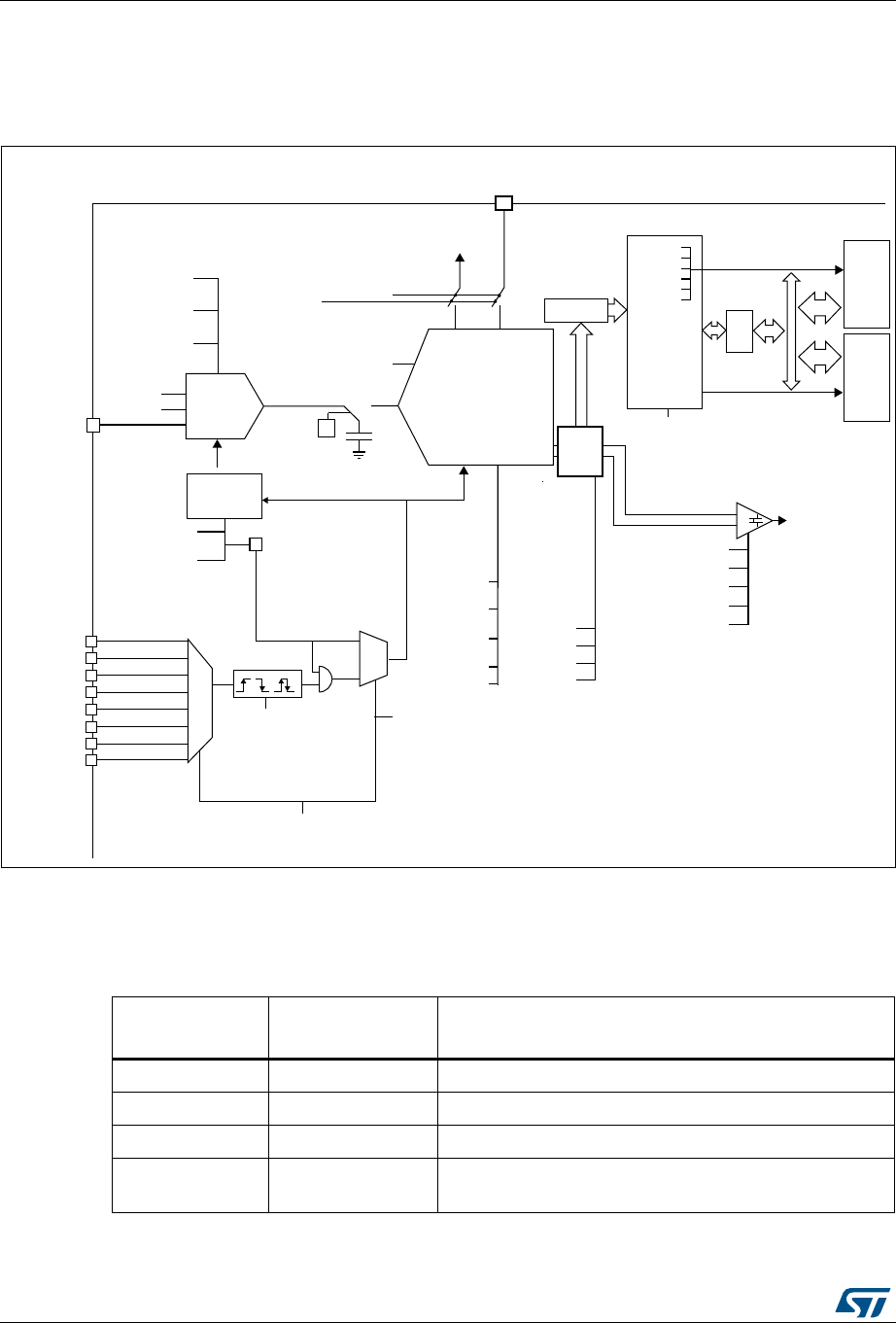
Analog-to-digital converter (ADC) RM0376
294/1001 DocID025941 Rev 5
14.3 ADC functional description
Figure 31 shows the ADC block diagram and Table 57 gives the ADC pin description.
Figure 31. ADC block diagram
1. Refer to Table 60: External triggers for TRGi mapping.
14.3.1 ADC pins and internal signals
VREFINT
TS
TRG0
CONT
singe/cont
Input
Selection &
Scan Control
SMP[2:0]
sampling time
Start & Stop
Control
ADC_IN[15:0] analog input
channels
WAIT
auto-delayed conv
ADSTP
stop conv
ADSTART
s/w trigger
EXTEN[1:0]
trigger enable
and edge selection
h/w
trigger
EXTSEL[2:0]
trigger selection
ADCAL
self calibration
AWDx
SAR ADC
VIN
start
Bias & Ref
ALIGN
left/right
RES[1:0]
12, 10, 8, 6 bits
OVRMOD
overrun mode
APB
interface
DMAEN
DMA request
ADC Interrupt CPU
DMA
IRQ
CH_SEL[18:0]
SCANDIR
DMACFG
AREADY
EOSMP
EOC
EOS
OVR
AWD
AWDxEN Analog
AWDxSGL
AWDCHx[4:0]
LT x [ 1 1 :0 ]
HTx[11:0]
JOFFSETx[11:0]
JOFFSETx_CH[11:0]
CONVERTED DATA
DISCEN
discontinuous
watchdog
AHB
to
APB
mode
up/down
AUTOFF
auto-off mode
ADEN/ADDIS
Analog Supply
1.8 to 3.6 V
MS34764V4
ADC VREF+
1.65 to 3.6 V
TRG2
TRG3
TRG4
TRG5
TRG6
TRG7
TRG1
TRGi mapped
at product level
maste
slave
A
H
B
maste
DATA[15:0]
Over-
sampler
OVSR[2:0]
OVSE
OVSS[3:0]
TOVS
Table 56. ADC internal signals
Internal signal
name Signal type Description
TRGx Input ADC conversion triggers
VSENSE Input Internal temperature sensor output voltage
VREFINT Input Internal voltage reference output voltage
ADC_AWDx_OUT Output Internal analog watchdog output signal connected to on-
chip timers (x = Analog watchdog number = 1)

DocID025941 Rev 5 295/1001
RM0376 Analog-to-digital converter (ADC)
340
14.3.2 ADC voltage regulator (ADVREGEN)
The ADC has a specific internal voltage regulator which must be enabled and stable before
using the ADC.
The ADC voltage regulator stabilization time is entirely managed by the hardware and
software does not need to care about it.
After ADC operations are complete, the ADC can be disabled (ADEN=0). It is then possible
to save additional power by disabling the ADC voltage regulator (refer to the ADC voltage
regulator disable sequence).
Note: When the internal voltage regulator is disabled, the internal analog calibration is kept.
Analog reference for the ADC internal voltage regulator
The internal ADC voltage regulator uses a buffered copy of the internal voltage reference.
This buffer is always enabled when the main voltage regulator is in normal Run mode (MR
mode, with the device operating either in Run or Sleep mode). When the main voltage
regulator is in Low-power run mode (LPR mode, with the device operating in Low-power
run, Low-power sleep or Stop mode), the voltage reference is disabled and the ADC cannot
be used anymore.
The software must follow the procedure described below to manage the ADC in Low power-
run mode:
1. Make sure that the ADC is disabled (ADEN = 0).
2. Write ADVREGEN = 0.
3. Enter Low-power run mode
4. Resume from Low-power run mode.
5. Check that REGLPF = 0.
6. Enable the ADC voltage regulator by using the sequence described in Section :
ADVREG enable sequence (ADVREGEN= 1 in ADC_CR).
7. Write ADC_CR ADEN = 1 and wait until ADC_CR ADRDY = 1.
8. Write ADRDY = 1 to clear it.
ADVREG enable sequence
There are three ways to enable the voltage regulator:
•by writing ADVREGEN=1.
•by launching the calibration by writing by ADCAL=1 (the ADVREGEN bit will be
automatically set to 1)
•by enabling the ADC by writing ADEN=1
Table 57. ADC pins
Name Signal type Remarks
VDDA
Input, analog power
supply
Analog power supply and positive reference voltage
for the ADC, VDDA ≥ VDD
VSSA
Input, analog supply
ground
Ground for analog power supply. Must be at VSS
potential
ADC_INx Analog input signals 16 analog input channels

Analog-to-digital converter (ADC) RM0376
296/1001 DocID025941 Rev 5
ADVREG disable sequence
To disable the ADC voltage regulator, perform the sequence below:
1. Ensure that the ADC is disabled (ADEN=0)
2. Write ADVREGEN=0
14.3.3 Calibration (ADCAL)
The ADC has a calibration feature. During the procedure, the ADC calculates a calibration
factor which is internally applied to the ADC until the next ADC power-off. The application
must not use the ADC during calibration and must wait until it is complete.
Calibration should be performed before starting A/D conversion. It removes the offset error
which may vary from chip to chip due to process variation.
The calibration is initiated by software by setting bit ADCAL=1. Calibration can only be
initiated when the ADC is disabled (when ADEN=0). ADCAL bit stays at 1 during all the
calibration sequence. It is then cleared by hardware as soon the calibration completes. After
this, the calibration factor can be read from the ADC_DR register (from bits 6 to 0).
The internal analog calibration is kept if the ADC is disabled (ADEN=0) or if the ADC voltage
reference is disabled (ADVREGEN = 0). When the ADC operating conditions change (VDDA
changes are the main contributor to ADC offset variations and temperature change to a
lesser extend), it is recommended to re-run a calibration cycle.
The calibration factor is lost in the following cases:
•The product is in Standby mode (power supply removed from the ADC)
•The ADC peripheral is reset.
The calibration factor is maintained in the following low-power modes: Low-power run, Low-
power sleep and Stop.
It is still possible to save and restore the calibration factor by software to save time when re-
starting the ADC (as long as temperature and voltage are stable during the ADC power
down).
The calibration factor can be written if the ADC is enabled but not converting (ADEN=1 and
ADSTART=0). Then, at the next start of conversion, the calibration factor is automatically
injected into the analog ADC. This loading is transparent and does not add any cycle
latency to the start of the conversion.
Software calibration procedure
1. Ensure that ADEN=0 and DMAEN=0.
2. Set ADCAL=1.
3. Wait until ADCAL=0 (or until EOCAL=1). This can be handled by interrupt if the
interrupt is enabled by setting the EOCALIE bit in the ADC_IER register. The ADCAL
bit can remain set for some time even after EOCAL has been set. As a result, the
software must wait for ADCAL=0 after EOCAL=1 to be able to set ADEN=1 for next
ADC conversions.
4. The calibration factor can be read from bits 6:0 of ADC_DR or ADC_CALFACT
registers.
For code example, refer to A.8.1: Calibration code example.
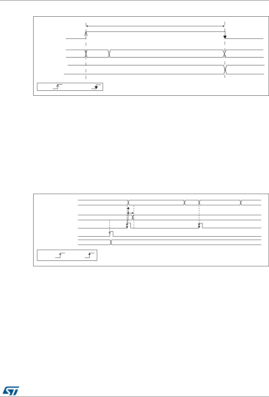
DocID025941 Rev 5 297/1001
RM0376 Analog-to-digital converter (ADC)
340
Figure 32. ADC calibration
If the ADC voltage regulator was not previously set, it will be automatically enabled when
setting ADCAL=1 (bit ADVREGEN is automatically set by hardware). In this case, the ADC
calibration time is longer to take into account the stabilization time of the ADC voltage
regulator.
At the end of the calibration, the ADC voltage regulator remains enabled.
Calibration factor forcing Software Procedure
1. Ensure that ADEN= 1 and ADSTART =0 (ADC started with no conversion ongoing)
2. Write ADC_CALFACT with the saved calibration factor
3. The calibration factor will be used as soon as a new conversion will be launched.
Figure 33. Calibration factor forcing
14.3.4 ADC on-off control (ADEN, ADDIS, ADRDY)
At power-up, the ADC is disabled and put in power-down mode (ADEN=0).
As shown in Figure 34, the ADC needs a stabilization time of tSTAB before it starts
converting accurately.
Two control bits are used to enable or disable the ADC:
•Set ADEN=1 to enable the ADC. The ADRDY flag is set as soon as the ADC is ready
for operation.
•Set ADDIS=1 to disable the ADC and put the ADC in power down mode. The ADEN
and ADDIS bits are then automatically cleared by hardware as soon as the ADC is fully
disabled.
If the ADC voltage regulator was not previously set, it will be automatically enabled when
setting ADEN=1 (bit ADVREGEN is automatically set by hardware). In this case, the ADC
tCAB
ADCAL
ADC State
ADC_DR[6:0] 0x00
MS33703V1
CALIBRATE OFFStartup
OFF
by S/W by H/W
CALIBRATION
FACTOR
ADC_CALFACT6:0]
ADC state
F2
F1 F2
Ready (not converting) Converting channel Ready Converting channel
(Single ended) (Single ended)
Updating
calibration
MS31925V1
by S/W
Internal
calibration factor[6:0]
Start conversion
(hardware or software)
WRITE ADC_CALFACT
CALFACT[6:0]
by H/W
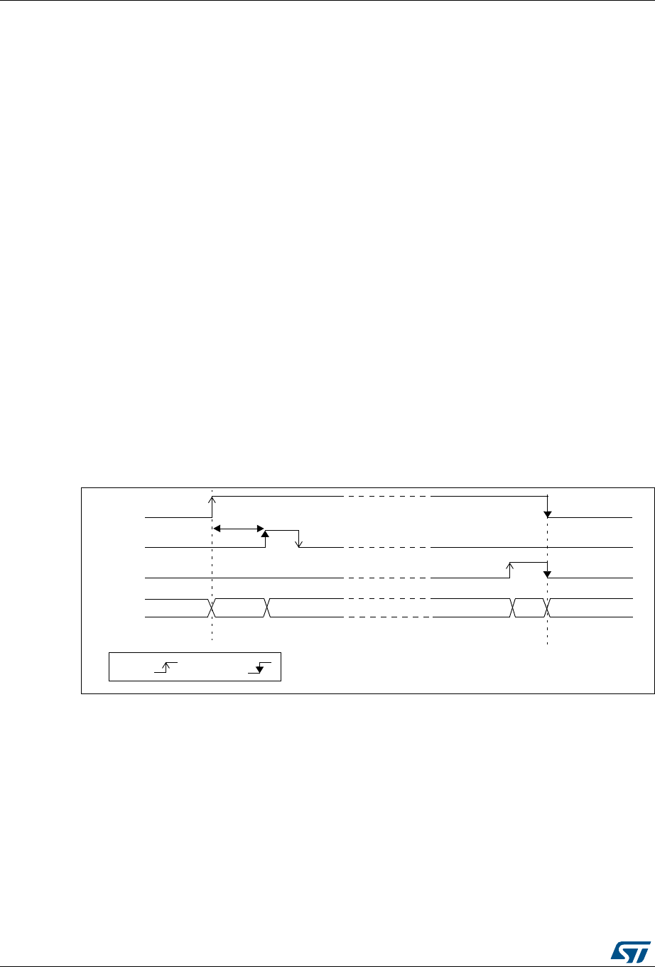
Analog-to-digital converter (ADC) RM0376
298/1001 DocID025941 Rev 5
stabilization time tSTAB is longer to take into account the stabilization time of the ADC
voltage regulator.
Conversion can then start either by setting ADSTART to 1 (refer to Section 14.4: Conversion
on external trigger and trigger polarity (EXTSEL, EXTEN) on page 305) or when an external
trigger event occurs if triggers are enabled.
Follow this procedure to enable the ADC:
1. Clear the ADRDY bit in ADC_ISR register by programming this bit to 1.
2. Set ADEN=1 in the ADC_CR register.
3. Wait until ADRDY=1 in the ADC_ISR register (ADRDY is set after the ADC startup
time). This can be handled by interrupt if the interrupt is enabled by setting the
ADRDYIE bit in the ADC_IER register.
For code example, refer to A.8.2: ADC enable sequence code example.
Follow this procedure to disable the ADC:
1. Check that ADSTART=0 in the ADC_CR register to ensure that no conversion is
ongoing. If required, stop any ongoing conversion by writing 1 to the ADSTP bit in the
ADC_CR register and waiting until this bit is read at 0.
2. Set ADDIS=1 in the ADC_CR register.
3. If required by the application, wait until ADEN=0 in the ADC_CR register, indicating that
the ADC is fully disabled (ADDIS is automatically reset once ADEN=0).
4. Clear the ADRDY bit in ADC_ISR register by programming this bit to 1 (optional).
For code example, refer to A.8.3: ADC disable sequence code example.
Figure 34. Enabling/disabling the ADC
Note: In Auto-off mode (AUTOFF=1) the power-on/off phases are performed automatically, by
hardware and the ADRDY flag is not set.
MS30264V2
tSTAB
ADEN
A
DRDY
ADDIS
ADC
OFF Startup RDY CONVERTING CH RDY OFF
by H/W
by S/W
REQ
-OF
stat
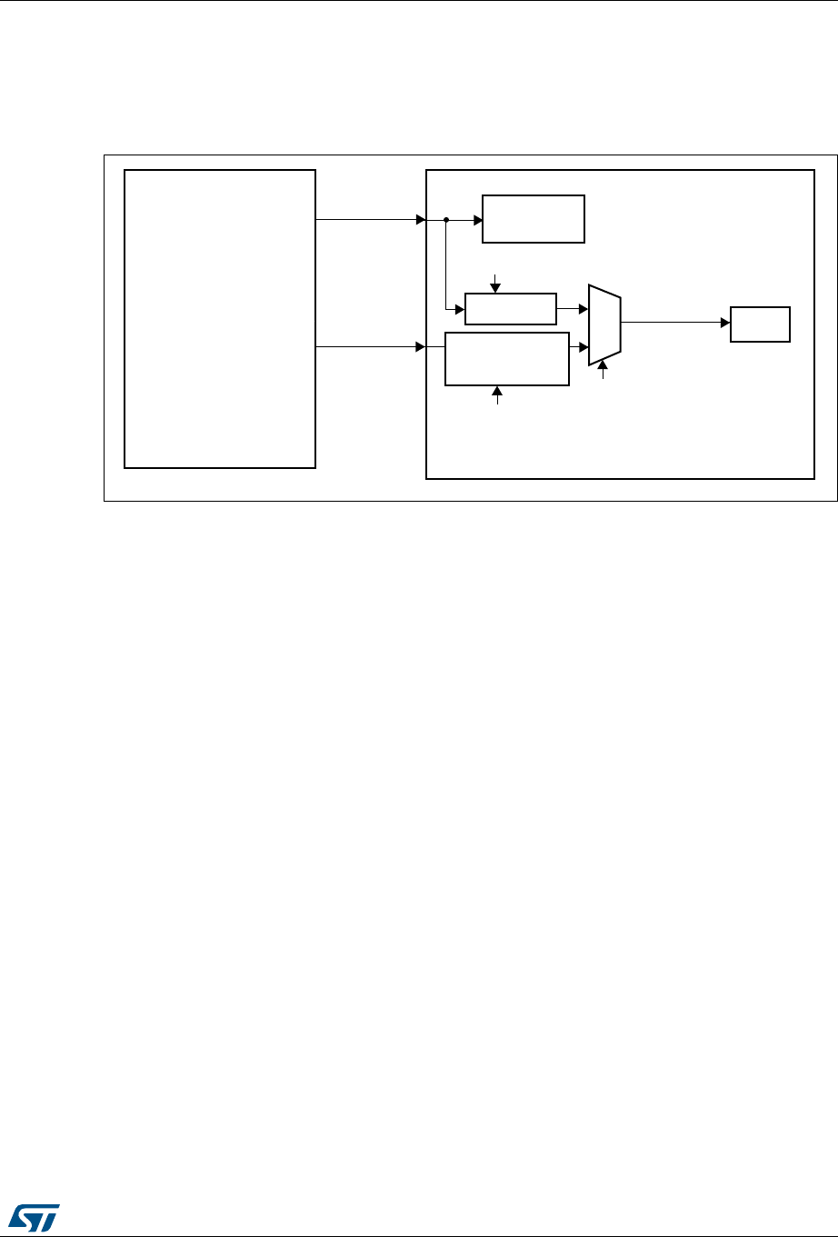
DocID025941 Rev 5 299/1001
RM0376 Analog-to-digital converter (ADC)
340
14.3.5 ADC clock (CKMODE, PRESC[3:0], LFMEN)
The ADC has a dual clock-domain architecture, so that the ADC can be fed with a clock
(ADC asynchronous clock) independent from the APB clock (PCLK).
Figure 35. ADC clock scheme
1. Refer to Section Reset and clock control (RCC) for how PCLK and ADC asynchronous clock are enabled.
The input clock of the analog ADC can be selected between two different clock sources (see
Figure 35: ADC clock scheme to see how PCLK and the ADC asynchronous clock are
enabled):
a) The ADC clock can be a specific clock source, named “ADC asynchronous clock“
which is independent and asynchronous with the APB clock.
Refer to RCC Section for more information on generating this clock source.
To select this scheme, bits CKMODE[1:0] of the ADC_CFGR2 register must be
reset.
b) The ADC clock can be derived from the APB clock of the ADC bus interface,
divided by a programmable factor (2 or 4) according to bits CKMODE[1:0].
To select this scheme, bits CKMODE[1:0] of the ADC_CFGR2 register must be
different from “00”.
For code example, refer to A.8.4: ADC clock selection code example.
In option a), the generated ADC clock can eventually be divided by a prescaler (1, 2, 4, 6, 8,
10, 12, 16, 32, 64, 128, 256) when programming the bits PRESC[3:0] in the ADC_CCR
register).
Option a) has the advantage of reaching the maximum ADC clock frequency whatever the
APB clock scheme selected.
Option b) has the advantage of bypassing the clock domain resynchronizations. This can be
useful when the ADC is triggered by a timer and if the application requires that the ADC is
precisely triggered without any uncertainty (otherwise, an uncertainty of the trigger instant is
added by the resynchronizations between the two clock domains).
MS31926V1
ADITF
RCC
(Reset & Clock Controller)
PCLK
ADC
asynchronous
clock
APB interface
Analog ADC_CK Analog
ADC1
/1 or /2 or /4 Others
00
Bits CKMODE[1:0]
of ADC_CFGR2
Bits CKMODE[1:0]
of ADC_CFGR2
/1,2,4,6,8,10,12
16,32,64,128,256
Bits PRESC[3:0]
of ADC_CCR

Analog-to-digital converter (ADC) RM0376
300/1001 DocID025941 Rev 5
Caution: When selecting CKMODE[1:0]=11 (PCLK divided by 1), the user must ensure that PCLK
has a 50% duty cycle. This is done by selecting a system clock with a 50% duty cycle and
configuring the APB prescaler in bypass modes in the RCC (refer to there Reset and clock
controller section). In case of an internal source clock, this implies only that the AHB and
APB prescalers do not divide the clock.
Low frequency
When selecting an analog ADC clock frequency lower than 3.5 MHz, it is mandatory to first
enable the Low Frequency Mode by setting bit LFMEN=1 into the ADC_CCR register
14.3.6 Configuring the ADC
Software must write to the ADCAL and ADEN bits in the ADC_CR register if the ADC is
disabled (ADEN must be 0).
Software must only write to the ADSTART and ADDIS bits in the ADC_CR register only if
the ADC is enabled and there is no pending request to disable the ADC (ADEN = 1 and
ADDIS = 0).
For all the other control bits in the ADC_IER, ADC_CFGRi, ADC_SMPR, ADC_TR,
ADC_CHSELR and ADC_CCR registers, refer to the description of the corresponding
control bit in Section 14.11: ADC registers.
Software must only write to the ADSTP bit in the ADC_CR register if the ADC is enabled
(and possibly converting) and there is no pending request to disable the ADC (ADSTART =
1 and ADDIS = 0).
Note: There is no hardware protection preventing software from making write operations forbidden
by the above rules. If such a forbidden write access occurs, the ADC may enter an
undefined state. To recover correct operation in this case, the ADC must be disabled (clear
ADEN=0 and all the bits in the ADC_CR register).
14.3.7 Channel selection (CHSEL, SCANDIR)
There are up to 19 multiplexed channels:
•16 analog inputs from GPIO pins (ADC_INx)
•2 internal analog inputs (Temperature Sensor, Internal Reference Voltage)
It is possible to convert a single channel or a sequence of channels.
Table 58. Latency between trigger and start of conversion
ADC clock source CKMODE[1:0] Latency between the trigger event
and the start of conversion
HSI16 MHz clock 00 Latency is not deterministic (jitter)
PCLK divided by 2 01 Latency is deterministic (no jitter) and equal to
4.25 ADC clock cycles
PCLK divided by 4 10 Latency is deterministic (no jitter) and equal to
4.125 ADC clock cycles
PCLK divided by 1 11 Latency is deterministic (no jitter) and equal to
4.5 ADC clock cycles

DocID025941 Rev 5 301/1001
RM0376 Analog-to-digital converter (ADC)
340
The sequence of the channels to be converted can be programmed in the ADC_CHSELR
channel selection register: each analog input channel has a dedicated selection bit
(CHSELx).
The order in which the channels will be scanned can be configured by programming the bit
SCANDIR bit in the ADC_CFGR1 register:
•SCANDIR=0: forward scan Channel 0 to Channel 18
•SCANDIR=1: backward scan Channel 18 to Channel 0
Temperature sensor, VREFINT internal channels
The temperature sensor is connected to channel ADC_IN18.
The internal voltage reference VREFINT is connected to channel ADC_IN17.
14.3.8 Programmable sampling time (SMP)
Before starting a conversion, the ADC needs to establish a direct connection between the
voltage source to be measured and the embedded sampling capacitor of the ADC. This
sampling time must be enough for the input voltage source to charge the sample and hold
capacitor to the input voltage level.
Having a programmable sampling time allows to trim the conversion speed according to the
input resistance of the input voltage source.
The ADC samples the input voltage for a number of ADC clock cycles that can be modified
using the SMP[2:0] bits in the ADC_SMPR register.
This programmable sampling time is common to all channels. If required by the application,
the software can change and adapt this sampling time between each conversions.
The total conversion time is calculated as follows:
tCONV = Sampling time + 12.5 x ADC clock cycles
Example:
With ADC_CLK = 16 MHz and a sampling time of 1.5 ADC clock cycles:
tCONV = 1.5 + 12.5 = 14 ADC clock cycles = 0.875 µs
The ADC indicates the end of the sampling phase by setting the EOSMP flag.
14.3.9 Single conversion mode (CONT=0)
In Single conversion mode, the ADC performs a single sequence of conversions, converting
all the channels once. This mode is selected when CONT=0 in the ADC_CFGR1 register.
Conversion is started by either:
•Setting the ADSTART bit in the ADC_CR register
•Hardware trigger event
Inside the sequence, after each conversion is complete:
•The converted data are stored in the 16-bit ADC_DR register
•The EOC (end of conversion) flag is set
•An interrupt is generated if the EOCIE bit is set

Analog-to-digital converter (ADC) RM0376
302/1001 DocID025941 Rev 5
After the sequence of conversions is complete:
•The EOS (end of sequence) flag is set
•An interrupt is generated if the EOSIE bit is set
Then the ADC stops until a new external trigger event occurs or the ADSTART bit is set
again.
Note: To convert a single channel, program a sequence with a length of 1.
14.3.10 Continuous conversion mode (CONT=1)
In continuous conversion mode, when a software or hardware trigger event occurs, the ADC
performs a sequence of conversions, converting all the channels once and then
automatically re-starts and continuously performs the same sequence of conversions. This
mode is selected when CONT=1 in the ADC_CFGR1 register. Conversion is started by
either:
•Setting the ADSTART bit in the ADC_CR register
•Hardware trigger event
Inside the sequence, after each conversion is complete:
•The converted data are stored in the 16-bit ADC_DR register
•The EOC (end of conversion) flag is set
•An interrupt is generated if the EOCIE bit is set
After the sequence of conversions is complete:
•The EOS (end of sequence) flag is set
•An interrupt is generated if the EOSIE bit is set
Then, a new sequence restarts immediately and the ADC continuously repeats the
conversion sequence.
Note: To convert a single channel, program a sequence with a length of 1.
It is not possible to have both discontinuous mode and continuous mode enabled: it is
forbidden to set both bits DISCEN=1 and CONT=1.
14.3.11 Starting conversions (ADSTART)
Software starts ADC conversions by setting ADSTART=1.
When ADSTART is set, the conversion:
•Starts immediately if EXTEN = 00 (software trigger)
•At the next active edge of the selected hardware trigger if EXTEN ≠ 00
The ADSTART bit is also used to indicate whether an ADC operation is currently ongoing. It
is possible to re-configure the ADC while ADSTART=0, indicating that the ADC is idle.
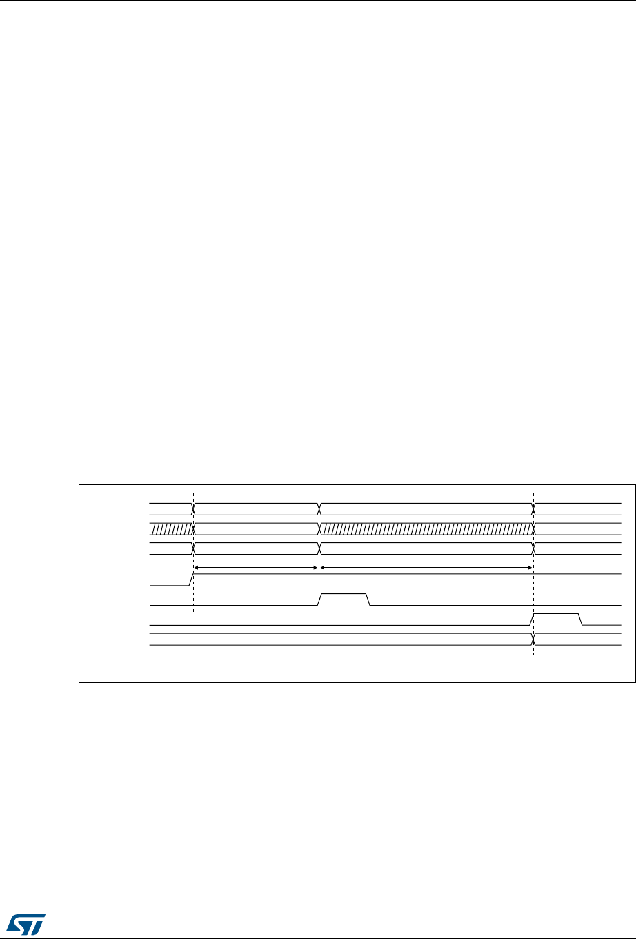
DocID025941 Rev 5 303/1001
RM0376 Analog-to-digital converter (ADC)
340
The ADSTART bit is cleared by hardware:
•In single mode with software trigger (CONT=0, EXTEN=00)
– At any end of conversion sequence (EOS=1)
•In discontinuous mode with software trigger (CONT=0, DISCEN=1, EXTEN=00)
– At end of conversion (EOC=1)
•In all cases (CONT=x, EXTEN=XX)
– After execution of the ADSTP procedure invoked by software (see
Section 14.3.13: Stopping an ongoing conversion (ADSTP) on page 304)
Note: In continuous mode (CONT=1), the ADSTART bit is not cleared by hardware when the EOS
flag is set because the sequence is automatically relaunched.
When hardware trigger is selected in single mode (CONT=0 and EXTEN = 01), ADSTART is
not cleared by hardware when the EOS flag is set. This avoids the need for software having
to set the ADSTART bit again and ensures the next trigger event is not missed.
14.3.12 Timings
The elapsed time between the start of a conversion and the end of conversion is the sum of
the configured sampling time plus the successive approximation time depending on data
resolution:
Figure 36. Analog to digital conversion time
tCONV = tSMPL + tSAR = [ 1.5 |min + 12.5 |12bit ] x tADC_CLK
tCONV = tSMPL + tSAR = 93.8 ns |min + 781.3 ns |12bit = 0.875 µs |min (for fADC_CLK = 16 MHz)
Analog
channel
Internal S/H
tt
depends on SMP[2:0]
set
by SW
EOSMP cleared by SW
MS30336V1
DATA N-1 DATA N
CH(N) CH(N+1)
ADC state
ADSTART
ADC_DR
EOC
SMPL
RDY SAMPLING CH(N) CONVERTING CH(N) SAMPLING CH(N+1)
Sample AIN(N+1)
Hold AIN(N)
Sample AIN(N+1)
SAR
(1) (2)
set by HW
cleared
by SW
set
by HW
(1) tSMPL
depends on RES[2:0]
(2) tSAR
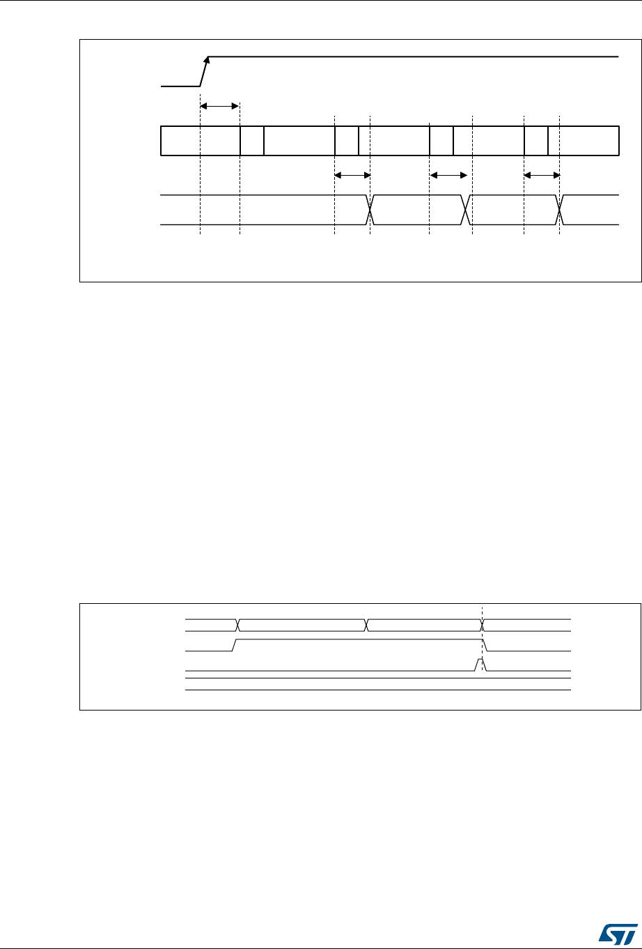
Analog-to-digital converter (ADC) RM0376
304/1001 DocID025941 Rev 5
Figure 37. ADC conversion timings
1. EXTEN =00 or EXTEN ≠ 00
2. Trigger latency (refer to datasheet for more details)
3. ADC_DR register write latency (refer to datasheet for more details)
14.3.13 Stopping an ongoing conversion (ADSTP)
The software can decide to stop any ongoing conversions by setting ADSTP=1 in the
ADC_CR register.
This will reset the ADC operation and the ADC will be idle, ready for a new operation.
When the ADSTP bit is set by software, any ongoing conversion is aborted and the result is
discarded (ADC_DR register is not updated with the current conversion).
The scan sequence is also aborted and reset (meaning that restarting the ADC would re-
start a new sequence).
Once this procedure is complete, the ADSTP and ADSTART bits are both cleared by
hardware and the software must wait until ADSTART=0 before starting new conversions.
Figure 38. Stopping an ongoing conversion
MSv33174V1
Ready S0 Conversion 0
tLATENCY
(2)
ADSTART(1)
ADC state
ADC_DR
S1 Conversion 1 S2 Conversion 2 S3 Conversion 3
WLATENCY
(3) WLATENCY
(3) WLATENCY
(3)
Data 1Data 0 Data 2
DATA N-1
ADC state
ADSTART set by SW
RDY SAMPLING CH(N)
ADC_DR
cleared by HW
MS30337V1
CONVERTING CH(N) RDY
ADSTOP cleared by HW
set by SW
DocID025941 Rev 5 305/1001
RM0376 Analog-to-digital converter (ADC)
340
14.4 Conversion on external trigger and trigger polarity (EXTSEL,
EXTEN)
A conversion or a sequence of conversion can be triggered either by software or by an
external event (for example timer capture). If the EXTEN[1:0] control bits are not equal to
“0b00”, then external events are able to trigger a conversion with the selected polarity. The
trigger selection is effective once software has set bit ADSTART=1.
Any hardware triggers which occur while a conversion is ongoing are ignored.
If bit ADSTART=0, any hardware triggers which occur are ignored.
Table 59 provides the correspondence between the EXTEN[1:0] values and the trigger
polarity.
Note: The polarity of the external trigger can be changed only when the ADC is not converting
(ADSTART= 0).
The EXTSEL[2:0] control bits are used to select which of 8 possible events can trigger
conversions.
Table 60 gives the possible external trigger for regular conversion.
Software source trigger events can be generated by setting the ADSTART bit in the
ADC_CR register.
Note: The trigger selection can be changed only when the ADC is not converting (ADSTART= 0).
Table 59. Configuring the trigger polarity
Source EXTEN[1:0]
Trigger detection disabled 00
Detection on rising edge 01
Detection on falling edge 10
Detection on both rising and falling edges 11
Table 60. External triggers
Name Source EXTSEL[2:0]
TRG0 TIM6_TRGO 000
TRG1 TIM21_CH2 001
TRG2 TIM2_TRGO 010
TRG3 TIM2_CH4 011
TRG4 TIM22_TRGO 100
TRG5(1)
1. Available on all categories except category 3.
TIM2_CH3 101
TRG6 TIM3_TRGO 110
TRG7 EXTI line 11 111

Analog-to-digital converter (ADC) RM0376
306/1001 DocID025941 Rev 5
14.4.1 Discontinuous mode (DISCEN)
This mode is enabled by setting the DISCEN bit in the ADC_CFGR1 register.
In this mode (DISCEN=1), a hardware or software trigger event is required to start each
conversion defined in the sequence. On the contrary, if DISCEN=0, a single hardware or
software trigger event successively starts all the conversions defined in the sequence.
Example:
•DISCEN=1, channels to be converted = 0, 3, 7, 10
– 1st trigger: channel 0 is converted and an EOC event is generated
– 2nd trigger: channel 3 is converted and an EOC event is generated
– 3rd trigger: channel 7 is converted and an EOC event is generated
– 4th trigger: channel 10 is converted and both EOC and EOS events are
generated.
– 5th trigger: channel 0 is converted an EOC event is generated
– 6th trigger: channel 3 is converted and an EOC event is generated
–...
•DISCEN=0, channels to be converted = 0, 3, 7, 10
– 1st trigger: the complete sequence is converted: channel 0, then 3, 7 and 10. Each
conversion generates an EOC event and the last one also generates an EOS
event.
– Any subsequent trigger events will restart the complete sequence.
Note: It is not possible to have both discontinuous mode and continuous mode enabled: it is
forbidden to set both bits DISCEN=1 and CONT=1.
14.4.2 Programmable resolution (RES) - fast conversion mode
It is possible to obtain faster conversion times (tSAR) by reducing the ADC resolution.
The resolution can be configured to be either 12, 10, 8, or 6 bits by programming the
RES[1:0] bits in the ADC_CFGR1 register. Lower resolution allows faster conversion times
for applications where high data precision is not required.
Note: The RES[1:0] bit must only be changed when the ADEN bit is reset.
The result of the conversion is always 12 bits wide and any unused LSB bits are read as
zeros.
Lower resolution reduces the conversion time needed for the successive approximation
steps as shown in Table 61.

DocID025941 Rev 5 307/1001
RM0376 Analog-to-digital converter (ADC)
340
14.4.3 End of conversion, end of sampling phase (EOC, EOSMP flags)
The ADC indicates each end of conversion (EOC) event.
The ADC sets the EOC flag in the ADC_ISR register as soon as a new conversion data
result is available in the ADC_DR register. An interrupt can be generated if the EOCIE bit is
set in the ADC_IER register. The EOC flag is cleared by software either by writing 1 to it, or
by reading the ADC_DR register.
The ADC also indicates the end of sampling phase by setting the EOSMP flag in the
ADC_ISR register. The EOSMP flag is cleared by software by writing1 to it. An interrupt can
be generated if the EOSMPIE bit is set in the ADC_IER register.
The aim of this interrupt is to allow the processing to be synchronized with the conversions.
Typically, an analog multiplexer can be accessed in hidden time during the conversion
phase, so that the multiplexer is positioned when the next sampling starts.
Note: As there is only a very short time left between the end of the sampling and the end of the
conversion, it is recommenced to use polling or a WFE instruction rather than an interrupt
and a WFI instruction.
Table 61. tSAR timings depending on resolution
RES[1:0]
bits
tSAR
(ADC clock
cycles)
tSAR (ns) at
fADC = 16 MHz
tSMPL (min)
(ADC clock
cycles)
tCONV
(ADC clock cycles)
(with min. tSMPL)
tCONV (ns) at
fADC = 16 MHz
12 12.5 781 ns 1.5 14 875 ns
10 11.5 719 ns 1.5 13 812 ns
8 9.5 594 ns 1.5 11 688 ns
6 7.5 469 ns 1.5 9 562 ns
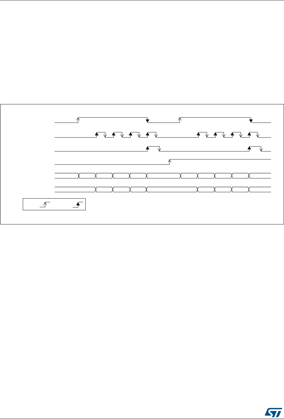
Analog-to-digital converter (ADC) RM0376
308/1001 DocID025941 Rev 5
14.4.4 End of conversion sequence (EOS flag)
The ADC notifies the application of each end of sequence (EOS) event.
The ADC sets the EOS flag in the ADC_ISR register as soon as the last data result of a
conversion sequence is available in the ADC_DR register. An interrupt can be generated if
the EOSIE bit is set in the ADC_IER register. The EOS flag is cleared by software by writing
1 to it.
14.4.5 Example timing diagrams (single/continuous modes
hardware/software triggers)
Figure 39. Single conversions of a sequence, software trigger
1. EXTEN=00, CONT=0
2. CHSEL=0x20601, WAIT=0, AUTOFF=0
For code example, refer to A.8.5: Single conversion sequence code example - Software
trigger.
MSv30338V2
RDY
EOC
SCANDIR
CH9 CH17 CH9
ADC_DR D0 D10 D17 D10 D9 D9
ADC state(2)
ADSTART(1)
EOS
D9 D17
RDYCH0
CH10
RDY CH17
CH10CH0
by S/W by H/W
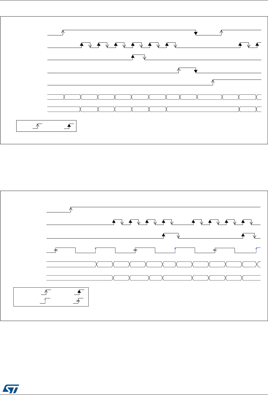
DocID025941 Rev 5 309/1001
RM0376 Analog-to-digital converter (ADC)
340
Figure 40. Continuous conversion of a sequence, software trigger
1. EXTEN=00, CONT=1,
2. CHSEL=0x20601, WAIT=0, AUTOFF=0
For code example, refer to A.8.6: Continuous conversion sequence code example -
Software trigger.
Figure 41. Single conversions of a sequence, hardware trigger
1. EXTSEL=TRGx (over-frequency), EXTEN=01 (rising edge), CONT=0
2. CHSEL=0xF, SCANDIR=0, WAIT=0, AUTOFF=0
For code example, refer to A.8.7: Single conversion sequence code example - Hardware
trigger.
MSv30339V2
ADSTP
CH9 CH17 STP
D0 D10
CH9
D0 D9
CH10
D17
EOC
SCANDIR
ADC_DR
ADC state(2)
ADSTART(1)
EOS
RDY CH17CH10CH0
by S/W by H/W
RDY CH0 CH10
D9 D17
MSv30340V2
CH1 CH1CH3 CH0 CH2
D0 D1 D2 D1 D2 D3
D3
CH2
EOC
ADC_DR
ADC state(2)
ADSTART(1)
EOS
RDYRDY CH0 CH3
TRGx(1)
RDY
D0
by H/W
ignored
by S/W
triggered
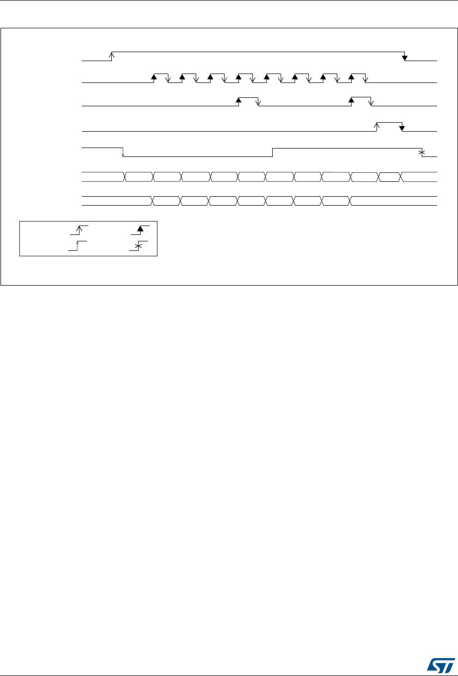
Analog-to-digital converter (ADC) RM0376
310/1001 DocID025941 Rev 5
Figure 42. Continuous conversions of a sequence, hardware trigger
1. EXTSEL=TRGx, EXTEN=10 (falling edge), CONT=1
2. CHSEL=0xF, SCANDIR=0, WAIT=0, AUTOFF=0
For code example, refer to A.8.8: Continuous conversion sequence code example -
Hardware trigger.
14.5 Data management
14.5.1 Data register and data alignment (ADC_DR, ALIGN)
At the end of each conversion (when an EOC event occurs), the result of the converted data
is stored in the ADC_DR data register which is 16-bit wide.
The format of the ADC_DR depends on the configured data alignment and resolution.
The ALIGN bit in the ADC_CFGR1 register selects the alignment of the data stored after
conversion. Data can be right-aligned (ALIGN=0) or left-aligned (ALIGN=1) as shown in
Figure 43.
MSv30341V2
CH1 CH2
D0 D1 D2
CH0 CH2 CH0
D3 D0 D1 D2 D3
STOP
ADC_DR
ADSTP
by H/W
CH1 CH3
ignored
EOC
ADC state(2)
ADSTART(1)
EOS
RDYCH0 CH3
TRGx(1)
RDY
by S/W
triggered

DocID025941 Rev 5 311/1001
RM0376 Analog-to-digital converter (ADC)
340
Figure 43. Data alignment and resolution (oversampling disabled: OVSE = 0)
14.5.2 ADC overrun (OVR, OVRMOD)
The overrun flag (OVR) indicates a data overrun event, when the converted data was not
read in time by the CPU or the DMA, before the data from a new conversion is available.
The OVR flag is set in the ADC_ISR register if the EOC flag is still at ‘1’ at the time when a
new conversion completes. An interrupt can be generated if the OVRIE bit is set in the
ADC_IER register.
When an overrun condition occurs, the ADC keeps operating and can continue to convert
unless the software decides to stop and reset the sequence by setting the ADSTP bit in the
ADC_CR register.
The OVR flag is cleared by software by writing 1 to it.
It is possible to configure if the data is preserved or overwritten when an overrun event
occurs by programming the OVRMOD bit in the ADC_CFGR1 register:
•OVRMOD=0
– An overrun event preserves the data register from being overwritten: the old data
is maintained and the new conversion is discarded. If OVR remains at 1, further
conversions can be performed but the resulting data is discarded.
•OVRMOD=1
– The data register is overwritten with the last conversion result and the previous
unread data is lost. If OVR remains at 1, further conversions can be performed
and the ADC_DR register always contains the data from the latest conversion.
0x0
0x00
0x00
0x00
DR[11:0]
DR[9:0]
DR[7:0]
0x00
DR[11:0]
DR[9:0]
DR[7:0]
DR[5:0]
DR[5:0]
0x0
0x00
0x00
0x0
ALIGN RES
00x0
1
0x1
0x2
0x3
0x0
0x1
0x2
0x3
15 14 13 12 11 10 9 8 7 6 5 4 3 2 1 0
MS30342V1
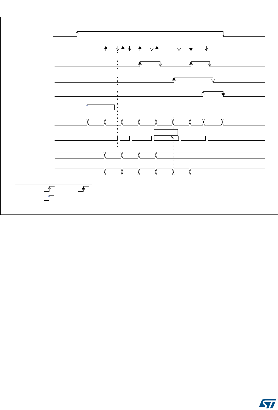
Analog-to-digital converter (ADC) RM0376
312/1001 DocID025941 Rev 5
Figure 44. Example of overrun (OVR)
14.5.3 Managing a sequence of data converted without using the DMA
If the conversions are slow enough, the conversion sequence can be handled by software.
In this case the software must use the EOC flag and its associated interrupt to handle each
data result. Each time a conversion is complete, the EOC bit is set in the ADC_ISR register
and the ADC_DR register can be read. The OVRMOD bit in the ADC_CFGR1 register
should be configured to 0 to manage overrun events as an error.
14.5.4 Managing converted data without using the DMA without overrun
It may be useful to let the ADC convert one or more channels without reading the data after
each conversion. In this case, the OVRMOD bit must be configured at 1 and the OVR flag
should be ignored by the software. When OVRMOD=1, an overrun event does not prevent
the ADC from continuing to convert and the ADC_DR register always contains the latest
conversion data.
14.5.5 Managing converted data using the DMA
Since all converted channel values are stored in a single data register, it is efficient to use
DMA when converting more than one channel. This avoids losing the conversion data
results stored in the ADC_DR register.
When DMA mode is enabled (DMAEN bit set to 1 in the ADC_CFGR1 register), a DMA
request is generated after the conversion of each channel. This allows the transfer of the
MSv30343V3
RDY
EOC
EOS
CH0 CH1 CH2 CH0
D0 D1 D2
CH1 CH2 CH0 STOP
D0
OVR
RDY
D0 D1 D2 D0 D1 D2
ADC_DR read
access
OVERRUN
by S/W by H/W
triggered
ADC_DR
(OVRMOD=0)
ADSTP
ADC state(2)
ADSTART(1)
TRGx(1)
ADC_DR
(OVRMOD=1)

DocID025941 Rev 5 313/1001
RM0376 Analog-to-digital converter (ADC)
340
converted data from the ADC_DR register to the destination location selected by the
software.
Note: The DMAEN bit in the ADC_CFGR1 register must be set after the ADC calibration phase.
Despite this, if an overrun occurs (OVR=1) because the DMA could not serve the DMA
transfer request in time, the ADC stops generating DMA requests and the data
corresponding to the new conversion is not transferred by the DMA. Which means that all
the data transferred to the RAM can be considered as valid.
Depending on the configuration of OVRMOD bit, the data is either preserved or overwritten
(refer to Section 14.5.2: ADC overrun (OVR, OVRMOD) on page 311).
The DMA transfer requests are blocked until the software clears the OVR bit.
Two different DMA modes are proposed depending on the application use and are
configured with bit DMACFG in the ADC_CFGR1 register:
•DMA one shot mode (DMACFG=0).
This mode should be selected when the DMA is programmed to transfer a fixed
number of data words.
•DMA circular mode (DMACFG=1)
This mode should be selected when programming the DMA in circular mode.
DMA one shot mode (DMACFG=0)
In this mode, the ADC generates a DMA transfer request each time a new conversion data
word is available and stops generating DMA requests once the DMA has reached the last
DMA transfer (when a DMA_EOT interrupt occurs, see Section 11: Direct memory access
controller (DMA) on page 260) even if a conversion has been started again.
For code example, refer to A.8.9: DMA one shot mode sequence code example.
When the DMA transfer is complete (all the transfers configured in the DMA controller have
been done):
•The content of the ADC data register is frozen.
•Any ongoing conversion is aborted and its partial result discarded
•No new DMA request is issued to the DMA controller. This avoids generating an
overrun error if there are still conversions which are started.
•The scan sequence is stopped and reset
•The DMA is stopped
DMA circular mode (DMACFG=1)
In this mode, the ADC generates a DMA transfer request each time a new conversion data
word is available in the data register, even if the DMA has reached the last DMA transfer.
This allows the DMA to be configured in circular mode to handle a continuous analog input
data stream.
For code example, refer to A.8.10: DMA circular mode sequence code example.
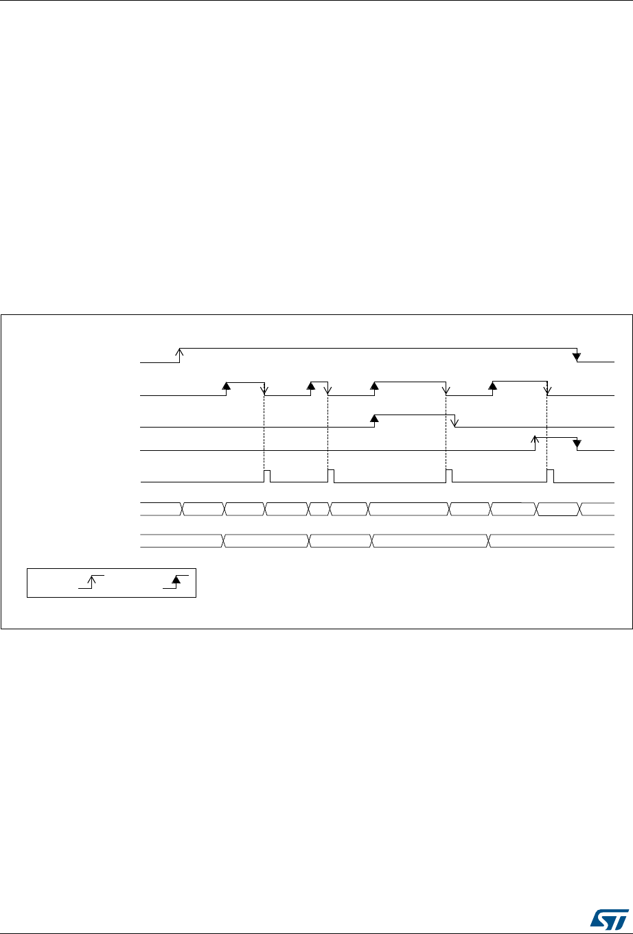
Analog-to-digital converter (ADC) RM0376
314/1001 DocID025941 Rev 5
14.6 Low-power features
14.6.1 Wait mode conversion
Wait mode conversion can be used to simplify the software as well as optimizing the
performance of applications clocked at low frequency where there might be a risk of ADC
overrun occurring.
When the WAIT bit is set to 1 in the ADC_CFGR1 register, a new conversion can start only
if the previous data has been treated, once the ADC_DR register has been read or if the
EOC bit has been cleared.
This is a way to automatically adapt the speed of the ADC to the speed of the system that
reads the data.
Note: Any hardware triggers which occur while a conversion is ongoing or during the wait time
preceding the read access are ignored.
Figure 45. Wait mode conversion (continuous mode, software trigger)
1. EXTEN=00, CONT=1
2. CHSEL=0x3, SCANDIR=0, WAIT=1, AUTOFF=0
For code example, refer to A.8.11: Wait mode sequence code example.
MSv30344V2
ADC_DR
by S/W
ADSTP
EOC
ADC state
ADSTART
EOS
CH1 CH2 STOP
CH1CH3 RDYDLYRDY DLY
ADC_DR Read access
DLY DLY
D1 D3 D1
D2
by H/W
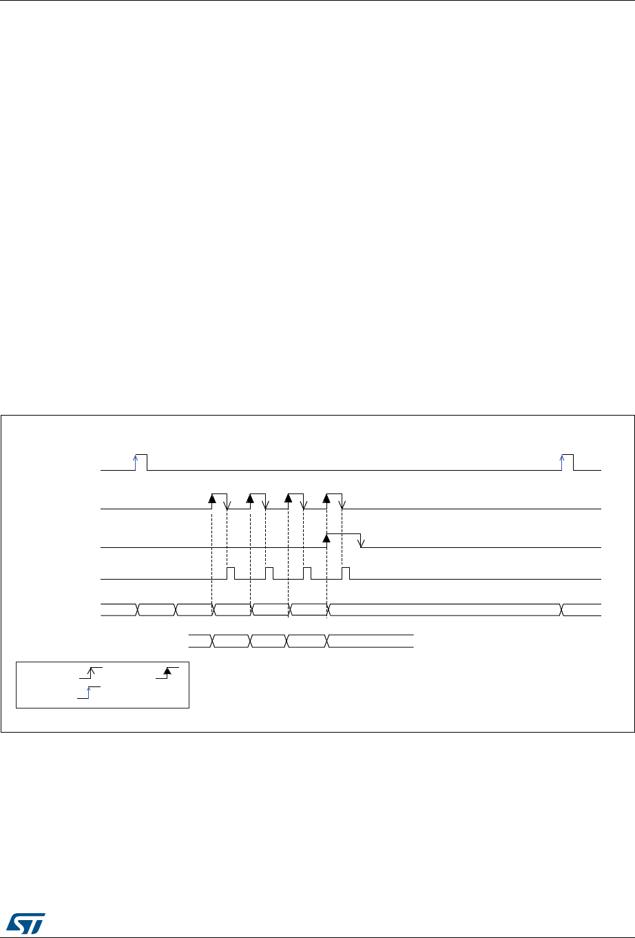
DocID025941 Rev 5 315/1001
RM0376 Analog-to-digital converter (ADC)
340
14.6.2 Auto-off mode (AUTOFF)
The ADC has an automatic power management feature which is called auto-off mode, and
is enabled by setting AUTOFF=1 in the ADC_CFGR1 register.
When AUTOFF=1, the ADC is always powered off when not converting and automatically
wakes-up when a conversion is started (by software or hardware trigger). A startup-time is
automatically inserted between the trigger event which starts the conversion and the
sampling time of the ADC. The ADC is then automatically disabled once the sequence of
conversions is complete.
Auto-off mode can cause a dramatic reduction in the power consumption of applications
which need relatively few conversions or when conversion requests are timed far enough
apart (for example with a low frequency hardware trigger) to justify the extra power and
extra time used for switching the ADC on and off.
Auto-off mode can be combined with the wait mode conversion (WAIT=1) for applications
clocked at low frequency. This combination can provide significant power savings if the ADC
is automatically powered-off during the wait phase and restarted as soon as the ADC_DR
register is read by the application (see Figure 47: Behavior with WAIT=1, AUTOFF=1).
Note: Please refer to the Section Reset and clock control (RCC) for the description of how to
manage the dedicated 14 MHz internal oscillator. The ADC interface can automatically
switch ON/OFF the 14 MHz internal oscillator to save power.
Figure 46. Behavior with WAIT=0, AUTOFF=1
1. EXTSEL=TRGx, EXTEN=01 (rising edge), CONT=x, ADSTART=1, CHSEL=0xF, SCANDIR=0, WAIT=1, AUTOFF=1
For code example, refer to A.8.12: Auto off and no wait mode sequence code example.
MSv30345V2
TRGx
EOC
EOS
ADC_DR Read
access
ADC state
ADC_DR
by H/Wby S/W
triggered
D1 D3
D2 D4
RDY CH1 CH2
Startup CH4
CH3 OFF Startup
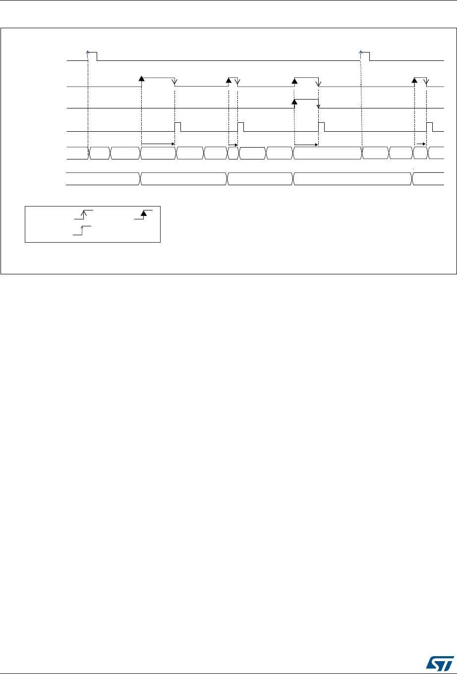
Analog-to-digital converter (ADC) RM0376
316/1001 DocID025941 Rev 5
Figure 47. Behavior with WAIT=1, AUTOFF=1
1. EXTSEL=TRGx, EXTEN=01 (rising edge), CONT=x, ADSTART=1, CHSEL=0xF, SCANDIR=0, WAIT=1, AUTOFF=1
For code example, refer to A.8.13: Auto off and wait mode sequence code example.
14.7 Analog window watchdog (AWDEN, AWDSGL, AWDCH,
ADC_TR, AWD)
AWD analog watchdog is enabled by setting the AWDEN bit in the ADC_CFGR1 register. It
is used to monitor that either one selected channel or all enabled channels (see Table 63:
Analog watchdog channel selection) remain within a configured voltage range (window) as
shown in Figure 48.
The AWD analog watchdog status bit is set if the analog voltage converted by the ADC is
below a lower threshold or above a higher threshold. These thresholds are programmed in
HT[11:0] and LT[11:0] bit of ADC_TR regsiter. An interrupt can be enabled by setting the
AWDIE bit in the ADC_IER register.
The AWD flag is cleared by software by programming it to it.
When converting data with a resolution of less than 12-bit (according to bits DRES[1:0]), the
LSB of the programmed thresholds must be kept cleared because the internal comparison
is always performed on the full 12-bit raw converted data (left aligned).
For code example, refer to A.8.14: Analog watchdog code example.
Table 62 describes how the comparison is performed for all the possible resolutions.
MSv30346V2
D1 D2 D3 D4
TRGx
EOC
EOS
ADC_DR Read
access
ADC state
ADC_DR
RDY CH1 OFFStartup CH2
OFF
Startup
DLY
Startup CH3 OFF
DLY DLY
Startup CH1
OFF
CH2
DLY
by H/Wby S/W
triggered
DocID025941 Rev 5 317/1001
RM0376 Analog-to-digital converter (ADC)
340
Table 63 shows how to configure the AWDSGL and AWDEN bits in the ADC_CFGR1
register to enable the analog watchdog on one or more channels.
Figure 48. Analog watchdog guarded area
14.8 Oversampler
The oversampling unit performs data preprocessing to offload the CPU. It can handle
multiple conversions and average them into a single data with increased data width, up to
16-bit.
It provides a result with the following form, where N and M can be adjusted:
Table 62. Analog watchdog comparison
Resolution
bits
RES[1:0]
Analog Watchdog comparison between:
Comments
Raw converted
data, left aligned(1) Thresholds
00: 12-bit DATA[11:0] LT[11:0] and HT[11:0] -
01: 10-bit DATA[11:2],00 LT[11:0] and HT[11:0] The user must configure LT1[1:0] and HT1[1:0] to “00”
10: 8-bit DATA[11:4],0000 LT[11:0] and HT[11:0] The user must configure LT1[3:0] and HT1[3:0] to
“0000”
11: 6-bit DATA[11:6],000000 LT[11:0] and HT[11:0] The user must configure LT1[5:0] and HT1[5:0] to
“000000”
1. The watchdog comparison is performed on the raw converted data before any alignment calculation.
Table 63. Analog watchdog channel selection
Channels guarded by the analog watchdog AWDSGL bit AWDEN bit
None x 0
All channels 0 1
Single(1) channel
1. Selected by the AWDCH[4:0] bits
11
ai16048b
Analog voltage
Higher threshold
Lower threshold
Guarded area
HT
LT
Result 1
M
-----Conversion tn
()
n0=
nN1–=
∑
×=
Analog-to-digital converter (ADC) RM0376
318/1001 DocID025941 Rev 5
It allows to perform by hardware the following functions: averaging, data rate reduction,
SNR improvement, basic filtering.
The oversampling ratio N is defined using the OVFS[2:0] bits in the ADC_CFGR2 register. It
can range from 2x to 256x. The division coefficient M consists of a right bit shift up to 8 bits.
It is configured through the OVSS[3:0] bits in the ADC_CFGR2 register.
For code example, refer to A.8.15: Oversampling code example.
The summation unit can yield a result up to 20 bits (256 x 12-bit), which is first shifted right.
The upper bits of the result are then truncated, keeping only the 16 least significant bits
rounded to the nearest value using the least significant bits left apart by the shifting, before
being finally transferred into the ADC_DR data register.
Note: If the intermediate result after the shifting exceeds 16 bits, the upper bits of the result are
simply truncated.
Figure 49. 20-bit to 16-bit result truncation
The Figure 50 gives a numerical example of the processing, from a raw 20-bit accumulated
data to the final 16-bit result.
Figure 50. Numerical example with 5-bits shift and rounding
The Table 64 below gives the data format for the various N and M combination, for a raw
conversion data equal to 0xFFF.
037111519
Raw 20-bit data
Truncation
and rounding
Shifting
015
MS31928V2
0
37111519
Raw 20-bit data:
BF
15
B737D
1D
MS31929V1
Final result after 5-bits shift
and rounding to nearest

DocID025941 Rev 5 319/1001
RM0376 Analog-to-digital converter (ADC)
340
The conversion timings in oversampled mode do not change compared to standard
conversion mode: the sample time is maintained equal during the whole oversampling
sequence. New data are provided every N conversion, with an equivalent delay equal to N x
tCONV = N x (tSMPL + tSAR). The flags features are raised as following:
•the end of the sampling phase (EOSMP) is set after each sampling phase
•the end of conversion (EOC) occurs once every N conversions, when the oversampled
result is available
•the end of sequence (EOCSEQ) occurs once the sequence of oversampled data is
completed (i.e. after N x sequence length conversions total)
14.8.1 ADC operating modes supported when oversampling
In oversampling mode, most of the ADC operating modes are available:
•Single or continuous mode conversions, forward or backward scanned sequences
•ADC conversions start either by software or with triggers
•ADC stop during a conversion (abort)
•Data read via CPU or DMA with overrun detection
•Low-power modes (WAIT, AUTOFF)
•Programmable resolution: in this case, the reduced conversion values (as per RES[1:0]
bits in ADC_CFGR1 register) are accumulated, truncated, rounded and shifted in the
same way as 12-bit conversions are
Note: The alignment mode is not available when working with oversampled data. The ALIGN bit in
ADC_CFGR1 is ignored and the data are always provided right-aligned.
Table 64. Maximum output results vs N and M. Grayed values indicates truncation
Oversa
mpling
ratio
Max
Raw data
No-shift
OVSS =
0000
1-bit
shift
OVSS =
0001
2-bit
shift
OVSS =
0010
3-bit
shift
OVSS =
0011
4-bit
shift
OVSS =
0100
5-bit
shift
OVSS =
0101
6-bit
shift
OVSS =
0110
7-bit
shift
OVSS =
0111
8-bit
shift
OVSS =
1000
2x 0x1FFE 0x1FFE 0x0FFF 0x0800 0x0400 0x0200 0x0100 0x0080 0x0040 0x0020
4x 0x3FFC 0x3FFC 0x1FFE 0x0FFF 0x0800 0x0400 0x0200 0x0100 0x0080 0x0040
8x 0x7FF8 0x7FF8 0x3FFC 0x1FFE 0x0FFF 0x0800 0x0400 0x0200 0x0100 0x0080
16x 0xFFF0 0xFFF0 0x7FF8 0x3FFC 0x1FFE 0x0FFF 0x0800 0x0400 0x0200 0x0100
32x 0x1FFE0 0xFFE0 0xFFF0 0x7FF8 0x3FFC 0x1FFE 0x0FFF 0x0800 0x0400 0x0200
64x 0x3FFC0 0xFFC0 0xFFE0 0xFFF0 0x7FF8 0x3FFC 0x1FFE 0x0FFF 0x0800 0x0400
128x 0x7FF80 0xFF80 0xFFC0 0xFFE0 0xFFF0 0x7FF8 0x3FFC 0x1FFE 0x0FFF 0x0800
256x 0xFFF00 0xFF00 0xFF80 0xFFC0 0xFFE0 0xFFF0 0x7FF8 0x3FFC 0x1FFE 0x0FFF
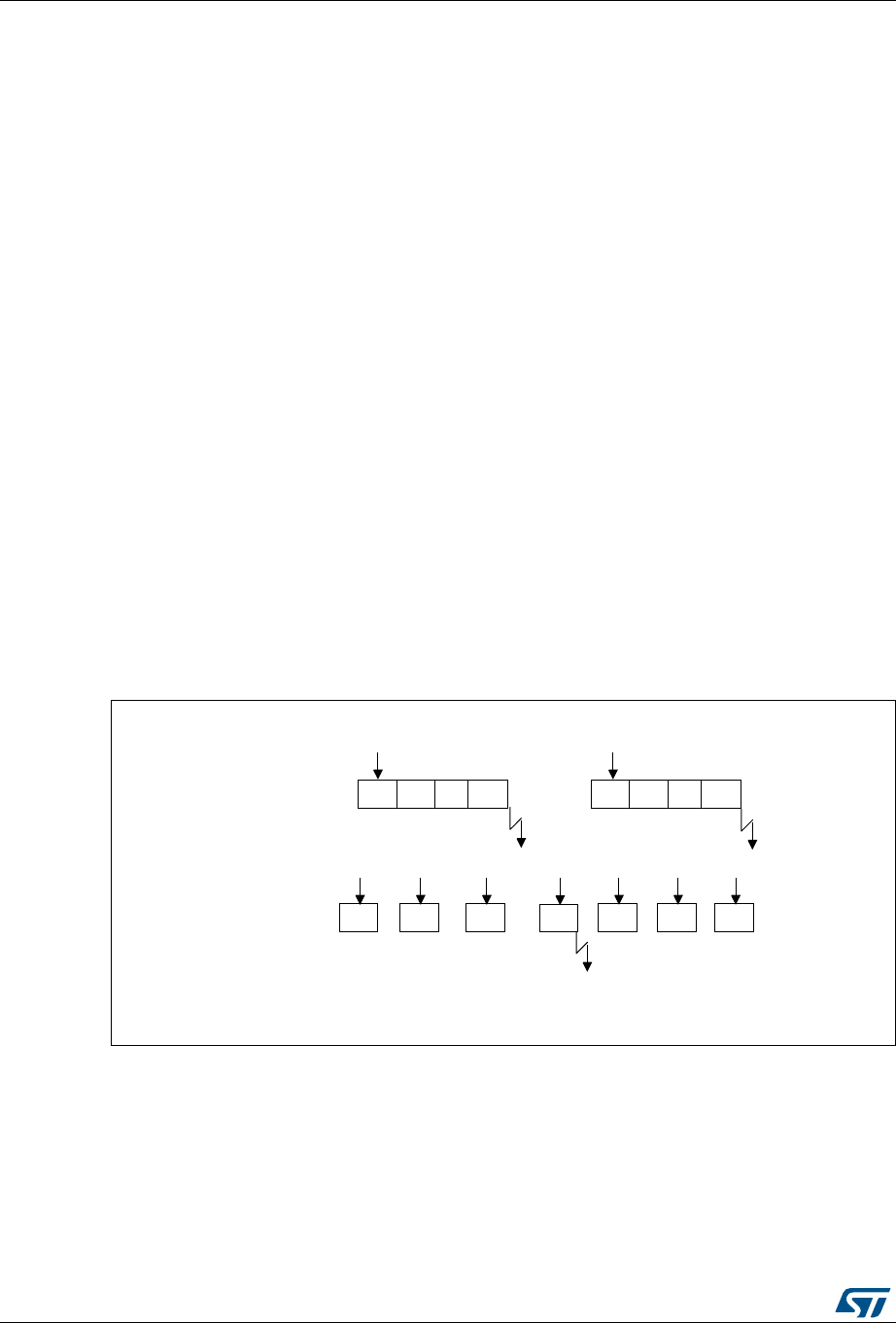
Analog-to-digital converter (ADC) RM0376
320/1001 DocID025941 Rev 5
14.8.2 Analog watchdog
The analog watchdog functionality is available (AWDSGL, AWDEN bits), with the following
differences:
•the RES[1:0] bits are ignored, comparison is always done on using the full 12-bits
values HT[11:0] and LT[11:0]
•the comparison is performed on the most significant 12 bits of the 16 bits oversampled
results ADC_DR[15:4]
Note: Care must be taken when using high shifting values. This reduces the comparison range.
For instance, if the oversampled result is shifted by 4 bits thus yielding a 12-bit data right-
aligned, the affective analog watchdog comparison can only be performed on 8 bits. The
comparison is done between ADC_DR[11:4] and HT[7:0] / LT[[7:0], and HT[11:8] / LT[11:8]
must be kept reset.
14.8.3 Triggered mode
The averager can also be used for basic filtering purposes. Although not a very efficient filter
(slow roll-off and limited stop band attenuation), it can be used as a notch filter to reject
constant parasitic frequencies (typically coming from the mains or from a switched mode
power supply). For this purpose, a specific discontinuous mode can be enabled with TOVS
bit in ADC_CFGR2, to be able to have an oversampling frequency defined by a user and
independent from the conversion time itself.
Figure 51 below shows how conversions are started in response to triggers in discontinuous
mode.
If the TOVS bit is set, the content of the DISCEN bit is ignored and considered as 1.
Figure 51. Triggered oversampling mode (TOVS bit = 1)
14.9 Temperature sensor and internal reference voltage
The temperature sensor can be used to measure the junction temperature (TJ) of the
device. The temperature sensor is internally connected to the ADC_IN18 input channel
which is used to convert the sensor’s output voltage to a digital value. The sampling time for
the temperature sensor analog pin must be greater than the minimum TS_temp value
specified in the datasheet. When not in use, the sensor can be put in power down mode.
MS33700V1
Ch(N)
0
Ch(N)
1
Ch(N)
2
Ch(N)
3
Trigger Trigger
CONT = 0
(DISCEN = 1)*
TOVS = 0
(DISCEN = 1)*: DISCEN bit is forced to 1 by software when TOVS bit is set
EOC flag set
EOC flag set
CONT = 0
(DISCEN = 1)*
TOVS = 1
Trigger
Ch(N)
0
Ch(N)
1
Ch(N)
2
Ch(N)
3
Trigger
Ch(N)
2
Trigger
Ch(N)
3
Trigger
Ch(N)
2
Trigger
Ch(N)
0
Trigger
Ch(N)
1
Trigger
Ch(N)
1
Ch(N)
0
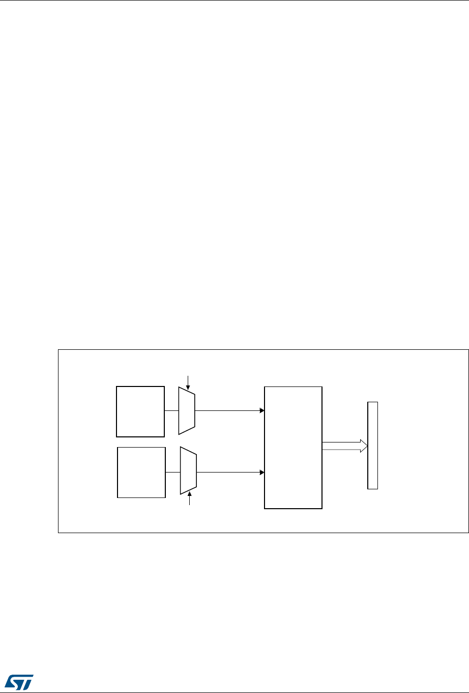
DocID025941 Rev 5 321/1001
RM0376 Analog-to-digital converter (ADC)
340
The internal voltage reference (VREFINT) provides a stable (bandgap) voltage output for the
ADC and comparators. VREFINT is internally connected to the ADC_IN17 input channel. The
precise voltage of VREFINT is individually measured for each part by ST during production
test and stored in the system memory area. It is accessible in read-only mode.
Figure 52 shows the block diagram of connections between the temperature sensor, the
internal voltage reference and the ADC.
The TSEN bit must be set to enable the conversion of ADC_IN18 (temperature sensor) and
the VREFEN bit must be set to enable the conversion of ADC_IN17 (VREFINT).
The temperature sensor output voltage changes linearly with temperature. The offset of this
line varies from chip to chip due to process variation (up to 45 °C from one chip to another).
The uncalibrated internal temperature sensor is more suited for applications that detect
temperature variations instead of absolute temperatures. To improve the accuracy of the
temperature sensor measurement, calibration values are stored in system memory for each
device by ST during production.
During the manufacturing process, the calibration data of the temperature sensor and the
internal voltage reference are stored in the system memory area. The user application can
then read them and use them to improve the accuracy of the temperature sensor or the
internal reference. Refer to the datasheet for additional information.
Main features
•Supported temperature range: –40 to 125 °C
•Linearity: ±2 °C max., precision depending on calibration
Figure 52. Temperature sensor and VREFINT channel block diagram
MS34765V1
V
SENSE
TSEN control bit
Address/data bus
converted
data
V
REFINT
ADC_IN18
Temperature
sensor
Internal
power block
ADC
VREFEN control bit
ADC_IN17

Analog-to-digital converter (ADC) RM0376
322/1001 DocID025941 Rev 5
Reading the temperature
1. Select the ADC_IN18 input channel
2. Select an appropriate sampling time specified in the device datasheet (TS_temp).
3. Set the TSEN bit in the ADC_CCR register to wake up the temperature sensor from
power down mode and wait for its stabilization time (tSTART).
For code example, refer to A.8.16: Temperature configuration code example.
4. Start the ADC conversion by setting the ADSTART bit in the ADC_CR register (or by
external trigger)
5. Read the resulting VSENSE data in the ADC_DR register
6. Calculate the temperature using the following formula
Where:
•TS_CAL2 is the temperature sensor calibration value acquired at 130°C
•TS_CAL1 is the temperature sensor calibration value acquired at 30°C
•TS_DATA is the actual temperature sensor output value converted by ADC
Refer to the specific device datasheet for more information about TS_CAL1 and
TS_CAL2 calibration points.
For code example, refer to A.8.17: Temperature computation code example.
Note: The sensor has a startup time after waking from power down mode before it can output
VSENSE at the correct level. The ADC also has a startup time after power-on, so to minimize
the delay, the ADEN and TSEN bits should be set at the same time.
Calculating the actual VDDA voltage using the internal reference voltage
The VDDA power supply voltage applied to the microcontroller may be subject to variation or
not precisely known. The embedded internal voltage reference (VREFINT) and its
calibration data acquired by the ADC during the manufacturing process at VDDA = 3 V can
be used to evaluate the actual VDDA voltage level.
The following formula gives the actual VDDA voltage supplying the device:
VDDA = 3 V x VREFINT_CAL / VREFINT_DATA
Where:
•VREFINT_CAL is the VREFINT calibration value
•VREFINT_DATA is the actual VREFINT output value converted by ADC
Converting a supply-relative ADC measurement to an absolute voltage value
The ADC is designed to deliver a digital value corresponding to the ratio between the analog
power supply and the voltage applied on the converted channel. For most application use
cases, it is necessary to convert this ratio into a voltage independent of VDDA. For
applications where VDDA is known and ADC converted values are right-aligned you can use
the following formula to get this absolute value:
Temperature in °C() 130 °C 30 °C–
TS_CAL2 TS_CAL1–
----------------------------------------------------------TS_DATA TS_CAL1–()30 °C+×=
Temperature in °C()
V30 VSENSE
–
Avg_Slope
---------------------------------- 30 °C+=

DocID025941 Rev 5 323/1001
RM0376 Analog-to-digital converter (ADC)
340
For applications where VDDA value is not known, you must use the internal voltage
reference and VDDA can be replaced by the expression provided in the section Calculating
the actual VDDA voltage using the internal reference voltage, resulting in the following
formula:
Where:
•VREFINT_CAL is the VREFINT calibration value
•ADC_DATAx is the value measured by the ADC on channel x (right-aligned)
•VREFINT_DATA is the actual VREFINT output value converted by the ADC
•full_SCALE is the maximum digital value of the ADC output. For example with 12-bit
resolution, it will be 212 - 1 = 4095 or with 8-bit resolution, 28 - 1 = 255.
Note: If ADC measurements are done using an output format other than 12 bit right-aligned, all the
parameters must first be converted to a compatible format before the calculation is done.
14.10 ADC interrupts
An interrupt can be generated by any of the following events:
•End Of Calibration (EOCAL flag)
•ADC power-up, when the ADC is ready (ADRDY flag)
•End of any conversion (EOC flag)
•End of a sequence of conversions (EOS flag)
•When an analog watchdog detection occurs (AWD flag)
•When the end of sampling phase occurs (EOSMP flag)
•when a data overrun occurs (OVR flag)
Separate interrupt enable bits are available for flexibility.
VCHANNELx
VDDA
FULL_SCALE
------------------------------------- ADC_DATAx
×=
VCHANNELx
3 V VREFINT_CAL ADC_DATAx
××
VREFINT_DATA FULL_SCALE×
--------------------------------------------------------------------------------------------------
=
Table 65. ADC interrupts
Interrupt event Event flag Enable control bit
End Of Calibration EOCAL EOCALIE
ADC ready ADRDY ADRDYIE
End of conversion EOC EOCIE
End of sequence of conversions EOS EOSIE
Analog watchdog status bit is set AWD AWDIE
End of sampling phase EOSMP EOSMPIE
Overrun OVR OVRIE

Analog-to-digital converter (ADC) RM0376
324/1001 DocID025941 Rev 5
14.11 ADC registers
Refer to Section 1.1 on page 51 for a list of abbreviations used in register descriptions.
14.11.1 ADC interrupt and status register (ADC_ISR)
Address offset: 0x00
Reset value: 0x0000 0000
31 30 29 28 27 26 25 24 23 22 21 20 19 18 17 16
Res. Res. Res. Res. Res. Res. Res. Res. Res. Res. Res. Res. Res. Res. Res. Res.
1514131211109876543210
Res. Res. Res. Res. EOCAL Res. Res. Res. AWD Res. Res. OVR EOS EOC EOSMP ADRDY
rc_w1 rc_w1 rc_w1 rc_w1 rc_w1 rc_w1 rc_w1
Bits 31:13 Reserved, must be kept at reset value.
Bit 12 Reserved, must be kept at reset value.
Bit 11 EOCAL: End Of Calibration flag
This bit is set by hardware when calibration is complete. It is cleared by software writing 1 to it.
0: Calibration is not complete
1: Calibration is complete
Bit 10 Reserved, must be kept at reset value.
Bits 9:8 Reserved, must be kept at reset value.
Bit 7 AWD: Analog watchdog flag
This bit is set by hardware when the converted voltage crosses the values programmed in ADC_TR
register. It is cleared by software by programming it to 1.
0: No analog watchdog event occurred (or the flag event was already acknowledged and cleared by
software)
1: Analog watchdog event occurred
Bits 6:5 Reserved, must be kept at reset value.
Bit 4 OVR: ADC overrun
This bit is set by hardware when an overrun occurs, meaning that a new conversion has complete
while the EOC flag was already set. It is cleared by software writing 1 to it.
0: No overrun occurred (or the flag event was already acknowledged and cleared by software)
1: Overrun has occurred
Bit 3 EOS: End of sequence flag
This bit is set by hardware at the end of the conversion of a sequence of channels selected by the
CHSEL bits. It is cleared by software writing 1 to it.
0: Conversion sequence not complete (or the flag event was already acknowledged and cleared by
software)
1: Conversion sequence complete

DocID025941 Rev 5 325/1001
RM0376 Analog-to-digital converter (ADC)
340
14.11.2 ADC interrupt enable register (ADC_IER)
Address offset: 0x04
Reset value: 0x0000 0000
Bit 2 EOC: End of conversion flag
This bit is set by hardware at the end of each conversion of a channel when a new data result is
available in the ADC_DR register. It is cleared by software writing 1 to it or by reading the ADC_DR
register.
0: Channel conversion not complete (or the flag event was already acknowledged and cleared by
software)
1: Channel conversion complete
Bit 1 EOSMP: End of sampling flag
This bit is set by hardware during the conversion, at the end of the sampling phase.It is cleared by
software by programming it to ‘1’.
0: Not at the end of the sampling phase (or the flag event was already acknowledged and cleared by
software)
1: End of sampling phase reached
Bit 0 ADRDY: ADC ready
This bit is set by hardware after the ADC has been enabled (bit ADEN=1) and when the ADC reaches
a state where it is ready to accept conversion requests.
It is cleared by software writing 1 to it.
0: ADC not yet ready to start conversion (or the flag event was already acknowledged and cleared
by software)
1: ADC is ready to start conversion
31 30 29 28 27 26 25 24 23 22 21 20 19 18 17 16
Res. Res. Res. Res. Res. Res. Res. Res. Res. Res. Res. Res. Res. Res. Res. Res.
15 14 13 12 11 10 9 8 7 6 5 4 3 2 1 0
Res. Res. Res. Res. EOCAL
IE Res. AWDIE Res. Res. OVRIE EOSIE EOCIE EOSMP
IE
ADRDY
IE
rw rw rw rw rw rw rw
Bits 31:13 Reserved, must be kept at reset value.
Bit 12 Reserved, must be kept at reset value.
Bit 11 EOCALIE: End of calibration interrupt enable
This bit is set and cleared by software to enable/disable the end of calibration interrupt.
0: End of calibration interrupt disabled
1: End of calibration interrupt enabled
Note: The software is allowed to write this bit only when ADSTART bit is cleared to 0 (this ensures
that no conversion is ongoing).
Bit 10 Reserved, must be kept at reset value.
Bits 9:8 Reserved, must be kept at reset value.

Analog-to-digital converter (ADC) RM0376
326/1001 DocID025941 Rev 5
Bit 7 AWDIE: Analog watchdog interrupt enable
This bit is set and cleared by software to enable/disable the analog watchdog interrupt.
0: Analog watchdog interrupt disabled
1: Analog watchdog interrupt enabled
Note: The Software is allowed to write this bit only when ADSTART bit is cleared to 0 (this ensures
that no conversion is ongoing).
Bits 6:5 Reserved, must be kept at reset value.
Bit 4 OVRIE: Overrun interrupt enable
This bit is set and cleared by software to enable/disable the overrun interrupt.
0: Overrun interrupt disabled
1: Overrun interrupt enabled. An interrupt is generated when the OVR bit is set.
Note: The software is allowed to write this bit only when ADSTART bit is cleared to 0 (this ensures
that no conversion is ongoing).
Bit 3 EOSIE: End of conversion sequence interrupt enable
This bit is set and cleared by software to enable/disable the end of sequence of conversions interrupt.
0: EOS interrupt disabled
1: EOS interrupt enabled. An interrupt is generated when the EOS bit is set.
Note: The software is allowed to write this bit only when ADSTART bit is cleared to 0 (this ensures
that no conversion is ongoing).
Bit 2 EOCIE: End of conversion interrupt enable
This bit is set and cleared by software to enable/disable the end of conversion interrupt.
0: EOC interrupt disabled
1: EOC interrupt enabled. An interrupt is generated when the EOC bit is set.
Note: The software is allowed to write this bit only when ADSTART bit is cleared to 0 (this ensures
that no conversion is ongoing).
Bit 1 EOSMPIE: End of sampling flag interrupt enable
This bit is set and cleared by software to enable/disable the end of the sampling phase interrupt.
0: EOSMP interrupt disabled.
1: EOSMP interrupt enabled. An interrupt is generated when the EOSMP bit is set.
Note: The software is allowed to write this bit only when ADSTART bit is cleared to 0 (this ensures
that no conversion is ongoing).
Bit 0 ADRDYIE: ADC ready interrupt enable
This bit is set and cleared by software to enable/disable the ADC Ready interrupt.
0: ADRDY interrupt disabled.
1: ADRDY interrupt enabled. An interrupt is generated when the ADRDY bit is set.
Note: The software is allowed to write this bit only when ADSTART bit is cleared to 0 (this ensures
that no conversion is ongoing).

DocID025941 Rev 5 327/1001
RM0376 Analog-to-digital converter (ADC)
340
14.11.3 ADC control register (ADC_CR)
Address offset: 0x08
Reset value: 0x0000 0000
31 30 29 28 27 26 25 24 23 22 21 20 19 18 17 16
ADCAL Res. Res. ADVR
EGEN Res. Res. Res. Res. Res. Res. Res. Res. Res. Res. Res. Res.
rs rw
15 14 13 12 11 10 9 8 7 6 5 4 3 2 1 0
Res. Res. Res. Res. Res. Res. Res. Res. Res. Res. Res. ADSTP Res. ADSTA
RT ADDIS ADEN
rs rs rs rs
Bit 31 ADCAL: ADC calibration
This bit is set by software to start the calibration of the ADC.
It is cleared by hardware after calibration is complete.
0: Calibration complete
1: Write 1 to calibrate the ADC. Read at 1 means that a calibration is in progress.
Note: The software is allowed to set ADCAL only when the ADC is disabled (ADCAL=0, ADSTART=0,
ADSTP=0, ADDIS=0 and ADEN=0).
The software is allowed to update the calibration factor by writing ADC_CALFACT only when
ADEN=1 and ADSTART=0 (ADC enabled and no conversion is ongoing).
Bits 30:29 Reserved, must be kept at reset value.
Bit 28 ADVREGEN: ADC Voltage Regulator Enable
This bit can be set:
– by software, to enable the ADC internal voltage regulator.
– by hardware, when launching the calibration (setting ADCAL=1) or when enabling the ADC (setting
ADEN=1)
It is cleared by software to disable the voltage regulator. It can be cleared only if ADEN is set to 0.
0: ADC voltage regulator disabled
1: ADC voltage regulator enabled
Note: The software can program this bit field only when the ADC is disabled (ADCAL=0,
ADSTART=0, ADSTP=0, ADDIS=0 and ADEN=0).
Bits 27:5 Reserved, must be kept at reset value.
Bit 4 ADSTP: ADC stop conversion command
This bit is set by software to stop and discard an ongoing conversion (ADSTP Command).
It is cleared by hardware when the conversion is effectively discarded and the ADC is ready to
accept a new start conversion command.
0: No ADC stop conversion command ongoing
1: Write 1 to stop the ADC. Read 1 means that an ADSTP command is in progress.
Note: Setting ADSTP to ‘1’ is only effective when ADSTART=1 and ADDIS=0 (ADC is enabled and
may be converting and there is no pending request to disable the ADC)
Bit 3 Reserved, must be kept at reset value.

Analog-to-digital converter (ADC) RM0376
328/1001 DocID025941 Rev 5
Bit 2 ADSTART: ADC start conversion command
This bit is set by software to start ADC conversion. Depending on the EXTEN [1:0] configuration bits,
a conversion either starts immediately (software trigger configuration) or once a hardware trigger
event occurs (hardware trigger configuration).
It is cleared by hardware:
– In single conversion mode (CONT=0, DISCEN=0), when software trigger is selected (EXTEN=00):
at the assertion of the end of Conversion Sequence (EOS) flag.
– In discontinuous conversion mode(CONT=0, DISCEN=1), when the software trigger is selected
(EXTEN=00): at the assertion of the end of Conversion (EOC) flag.
– In all other cases: after the execution of the ADSTP command, at the same time as the ADSTP bit is
cleared by hardware.
0: No ADC conversion is ongoing.
1: Write 1 to start the ADC. Read 1 means that the ADC is operating and may be converting.
Note: The software is allowed to set ADSTART only when ADEN=1 and ADDIS=0 (ADC is enabled
and there is no pending request to disable the ADC).
Bit 1 ADDIS: ADC disable command
This bit is set by software to disable the ADC (ADDIS command) and put it into power-down state
(OFF state).
It is cleared by hardware once the ADC is effectively disabled (ADEN is also cleared by hardware at
this time).
0: No ADDIS command ongoing
1: Write 1 to disable the ADC. Read 1 means that an ADDIS command is in progress.
Note: Setting ADDIS to ‘1’ is only effective when ADEN=1 and ADSTART=0 (which ensures that no
conversion is ongoing)
Bit 0 ADEN: ADC enable command
This bit is set by software to enable the ADC. The ADC will be effectively ready to operate once the
ADRDY flag has been set.
It is cleared by hardware when the ADC is disabled, after the execution of the ADDIS command.
0: ADC is disabled (OFF state)
1: Write 1 to enable the ADC.
Note: The software is allowed to set ADEN only when all bits of ADC_CR registers are 0 (ADCAL=0,
ADSTP=0, ADSTART=0, ADDIS=0 and ADEN=0)

DocID025941 Rev 5 329/1001
RM0376 Analog-to-digital converter (ADC)
340
14.11.4 ADC configuration register 1 (ADC_CFGR1)
Address offset: 0x0C
Reset value: 0x0000 0000
31 30 29 28 27 26 25 24 23 22 21 20 19 18 17 16
Res. AWDCH[4:0] Res. Res. AWDEN AWDSGL Res. Res. Res. Res. Res. DISCEN
rw rw rw rw rw rw rw rw
15 14 13 12 11 10 9 8 7 6 5 4 3 2 1 0
AUTOFF WAIT CONT OVRMOD EXTEN[1:0] Res. EXTSEL[2:0] ALIGN RES[1:0] SCAND
IR
DMAC
FG DMAEN
rw rw rw rw rw rw rw rw rw rw rw
Bit 31 Reserved, must be kept at reset value.
Bits 30:26 AWDCH[4:0]: Analog watchdog channel selection
These bits are set and cleared by software. They select the input channel to be guarded by
the analog watchdog.
00000: ADC analog input Channel 0 monitored by AWD
00001: ADC analog input Channel 1 monitored by AWD
.....
10001: ADC analog input Channel 17 monitored by AWD
10010: ADC analog input Channel 18 monitored by AWD
Others: Reserved
Note: The channel selected by the AWDCH[4:0] bits must be also set into the CHSELR
register
The software is allowed to write this bit only when ADSTART bit is cleared to 0 (this
ensures that no conversion is ongoing).
Bits 25:24 Reserved, must be kept at reset value.
Bit 23 AWDEN: Analog watchdog enable
This bit is set and cleared by software.
0: Analog watchdog disabled
1: Analog watchdog enabled
Note: The software is allowed to write this bit only when ADSTART bit is cleared to 0 (this
ensures that no conversion is ongoing).
Bit 22 AWDSGL: Enable the watchdog on a single channel or on all channels
This bit is set and cleared by software to enable the analog watchdog on the channel
identified by the AWDCH[4:0] bits or on all the channels
0: Analog watchdog enabled on all channels
1: Analog watchdog enabled on a single channel
Note: The software is allowed to write this bit only when ADSTART bit is cleared to 0 (this
ensures that no conversion is ongoing).
Bits 21:17 Reserved, must be kept at reset value.

Analog-to-digital converter (ADC) RM0376
330/1001 DocID025941 Rev 5
Bit 16 DISCEN: Discontinuous mode
This bit is set and cleared by software to enable/disable discontinuous mode.
0: Discontinuous mode disabled
1: Discontinuous mode enabled
Note: It is not possible to have both discontinuous mode and continuous mode enabled: it is
forbidden to set both bits DISCEN=1 and CONT=1.
The software is allowed to write this bit only when ADSTART bit is cleared to 0 (this
ensures that no conversion is ongoing).
Bit 15 AUTOFF: Auto-off mode
This bit is set and cleared by software to enable/disable auto-off mode..
0: Auto-off mode disabled
1: Auto-off mode enabled
Note: The software is allowed to write this bit only when ADSTART bit is cleared to 0 (this
ensures that no conversion is ongoing).
Bit 14 WAIT: Wait conversion mode
This bit is set and cleared by software to enable/disable wait conversion mode..
0: Wait conversion mode off
1: Wait conversion mode on
Note: The software is allowed to write this bit only when ADSTART bit is cleared to 0 (this
ensures that no conversion is ongoing).
Bit 13 CONT: Single / continuous conversion mode
This bit is set and cleared by software. If it is set, conversion takes place continuously until it
is cleared.
0: Single conversion mode
1: Continuous conversion mode
Note: It is not possible to have both discontinuous mode and continuous mode enabled: it is
forbidden to set both bits DISCEN=1 and CONT=1.
The software is allowed to write this bit only when ADSTART bit is cleared to 0 (this
ensures that no conversion is ongoing).
Bit 12 OVRMOD: Overrun management mode
This bit is set and cleared by software and configure the way data overruns are managed.
0: ADC_DR register is preserved with the old data when an overrun is detected.
1: ADC_DR register is overwritten with the last conversion result when an overrun is
detected.
Note: The software is allowed to write this bit only when ADSTART bit is cleared to 0 (this
ensures that no conversion is ongoing).
Bits 11:10 EXTEN[1:0]: External trigger enable and polarity selection
These bits are set and cleared by software to select the external trigger polarity and enable
the trigger.
00: Hardware trigger detection disabled (conversions can be started by software)
01: Hardware trigger detection on the rising edge
10: Hardware trigger detection on the falling edge
11: Hardware trigger detection on both the rising and falling edges
Note: The software is allowed to write this bit only when ADSTART bit is cleared to 0 (this
ensures that no conversion is ongoing).
Bit 9 Reserved, must be kept at reset value.

DocID025941 Rev 5 331/1001
RM0376 Analog-to-digital converter (ADC)
340
Bits 8:6 EXTSEL[2:0]: External trigger selection
These bits select the external event used to trigger the start of conversion (refer to Table 60:
External triggers for details):
000: TRG0
001: TRG1
010: TRG2
011: TRG3
100: TRG4
101: TRG5
110: TRG6
111: TRG7
Note: The software is allowed to write this bit only when ADSTART bit is cleared to 0 (this
ensures that no conversion is ongoing).
Bit 5 ALIGN: Data alignment
This bit is set and cleared by software to select right or left alignment. Refer to Figure 43:
Data alignment and resolution (oversampling disabled: OVSE = 0) on page 311
0: Right alignment
1: Left alignment
Note: The software is allowed to write this bit only when ADSTART bit is cleared to 0 (this
ensures that no conversion is ongoing).
Bits 4:3 RES[1:0]: Data resolution
These bits are written by software to select the resolution of the conversion.
00: 12 bits
01: 10 bits
10: 8 bits
11: 6 bits
Note: The software is allowed to write these bits only when ADEN=0.

Analog-to-digital converter (ADC) RM0376
332/1001 DocID025941 Rev 5
Bit 2 SCANDIR: Scan sequence direction
This bit is set and cleared by software to select the direction in which the channels will be
scanned in the sequence.
0: Upward scan (from CHSEL0 to CHSEL18)
1: Backward scan (from CHSEL18 to CHSEL0)
Note: The software is allowed to write this bit only when ADSTART bit is cleared to 0 (this
ensures that no conversion is ongoing).
Bit 1 DMACFG: Direct memory access configuration
This bit is set and cleared by software to select between two DMA modes of operation and is
effective only when DMAEN=1.
0: DMA one shot mode selected
1: DMA circular mode selected
For more details, refer to Section 14.5.5: Managing converted data using the DMA on
page 312
Note: The software is allowed to write this bit only when ADSTART bit is cleared to 0 (this
ensures that no conversion is ongoing).
Bit 0 DMAEN: Direct memory access enable
This bit is set and cleared by software to enable the generation of DMA requests. This allows
to use the DMA controller to manage automatically the converted data. For more details,
refer to Section 14.5.5: Managing converted data using the DMA on page 312.
0: DMA disabled
1: DMA enabled
Note: The software is allowed to write this bit only when ADSTART bit is cleared to 0 (this
ensures that no conversion is ongoing).

DocID025941 Rev 5 333/1001
RM0376 Analog-to-digital converter (ADC)
340
14.11.5 ADC configuration register 2 (ADC_CFGR2)
Address offset: 0x10
Reset value: 0x0000 0000
31 30 29 28 27 26 25 24 23 22 21 20 19 18 17 16
CKMODE[1:0] Res. Res. Res. Res. Res. Res. Res. Res. Res. Res. Res. Res. Res. Res.
rw rw
1514131211109876543210
Res. Res. Res. Res. Res. Res. TOVS OVSS[3:0] OVSR[2:0] Res. OVSE
rw rw rw rw rw rw rw rw rw rw
Bits 31:30 CKMODE[1:0]: ADC clock mode
These bits are set and cleared by software to define how the analog ADC is clocked:
00: ADCCLK (Asynchronous clock mode), generated at product level (refer to RCC section)
01: PCLK/2 (Synchronous clock mode)
10: PCLK/4 (Synchronous clock mode)
11: PCLK (Synchronous clock mode). This configuration must be enabled only if PCLK has a 50%
duty clock cycle (APB prescaler configured inside the RCC must be bypassed and the system clock
must by 50% duty cycle)
In all synchronous clock modes, there is no jitter in the delay from a timer trigger to the start of a
conversion.
Note: The software is allowed to write these bits only when the ADC is disabled (ADCAL=0,
ADSTART=0, ADSTP=0, ADDIS=0 and ADEN=0).
Bits 29:10 Reserved, must be kept at reset value.
Bit 9 TOVS: Triggered Oversampling
This bit is set and cleared by software.
0: All oversampled conversions for a channel are done consecutively after a trigger
1: Each oversampled conversion for a channel needs a trigger
Note: The software is allowed to write this bit only when ADSTART=0 (which ensures that no
conversion is ongoing).
Bits 8:5 OVSS[3:0]: Oversampling shift
This bit is set and cleared by software.
0000: No shift
0001: Shift 1-bit
0010: Shift 2-bits
0011: Shift 3-bits
0100: Shift 4-bits
0101: Shift 5-bits
0110: Shift 6-bits
0111: Shift 7-bits
1000: Shift 8-bits
Others: Reserved
Note: The software is allowed to write this bit only when ADSTART=0 (which ensures that no
conversion is ongoing).

Analog-to-digital converter (ADC) RM0376
334/1001 DocID025941 Rev 5
14.11.6 ADC sampling time register (ADC_SMPR)
Address offset: 0x14
Reset value: 0x0000 0000
Bits 4:2 OVSR[2:0]: Oversampling ratio
This bit filed defines the number of oversampling ratio.
000: 2x
001: 4x
010: 8x
011: 16x
100: 32x
101: 64x
110: 128x
111: 256x
Note: The software is allowed to write this bit only when ADSTART=0 (which ensures that no
conversion is ongoing).
Bit 1 Reserved, must be kept at reset value.
Bit 0 OVSE: Oversampler Enable
This bit is set and cleared by software.
0: Oversampler disabled
1: Oversampler enabled
Note: Software is allowed to write this bit only when ADSTART=0 (which ensures that no conversion
is ongoing).
31 30 29 28 27 26 25 24 23 22 21 20 19 18 17 16
Res. Res. Res. Res. Res. Res. Res. Res. Res. Res. Res. Res. Res. Res. Res. Res.
1514131211109876543210
Res. Res. Res. Res. Res. Res. Res. Res. Res. Res. Res. Res. Res. SMP[2:0]
rw
Bits 31:3 Reserved, must be kept at reset value.
Bits 2:0 SMP[2:0]: Sampling time selection
These bits are written by software to select the sampling time that applies to all channels.
000: 1.5 ADC clock cycles
001: 3.5 ADC clock cycles
010: 7.5 ADC clock cycles
011: 12.5 ADC clock cycles
100: 19.5 ADC clock cycles
101: 39.5 ADC clock cycles
110: 79.5 ADC clock cycles
111: 160.5 ADC clock cycles
Note: The software is allowed to write this bit only when ADSTART=0 (which ensures that no
conversion is ongoing).
DocID025941 Rev 5 335/1001
RM0376 Analog-to-digital converter (ADC)
340
14.11.7 ADC watchdog threshold register (ADC_TR)
Address offset: 0x20
Reset value: 0x0FFF 0000
14.11.8 ADC channel selection register (ADC_CHSELR)
Address offset: 0x28
Reset value: 0x0000 0000
31 30 29 28 27 26 25 24 23 22 21 20 19 18 17 16
Res. Res. Res. Res. HT[11:0]
rw rw rw rw rw rw rw rw rw rw rw rw
1514131211109876543210
Res. Res. Res. Res. LT[11:0]
rw rw rw rw rw rw rw rw rw rw rw rw
Bits 31:28 Reserved, must be kept at reset value.
Bits 27:16 HT[11:0]: Analog watchdog higher threshold
These bits are written by software to define the higher threshold for the analog watchdog. Refer to
Section 14.7: Analog window watchdog (AWDEN, AWDSGL, AWDCH, ADC_TR, AWD) on
page 316
Note: The software is allowed to write this bit only when ADSTART=0 (which ensures that no
conversion is ongoing).
Bits 15:12 Reserved, must be kept at reset value.
Bits 11:0 LT[11:0]: Analog watchdog lower threshold
These bits are written by software to define the lower threshold for the analog watchdog.
Refer to Section 14.7: Analog window watchdog (AWDEN, AWDSGL, AWDCH, ADC_TR, AWD) on
page 316
Note: The software is allowed to write this bit only when ADSTART=0 (which ensures that no
conversion is ongoing).
31 30 29 28 27 26 25 24 23 22 21 20 19 18 17 16
Res. Res. Res. Res. Res. Res. Res. Res. Res. Res. Res. Res. Res. CHSEL
18
CHSEL
17
CHSEL
16
rw rw rw
1514131211109876543210
CHSEL
15
CHSEL
14
CHSEL
13
CHSEL
12
CHSEL
11
CHSEL
10
CHSEL
9
CHSEL
8
CHSEL
7
CHSEL
6
CHSEL
5
CHSEL
4
CHSEL
3
CHSEL
2
CHSEL
1
CHSEL
0
rw rw rw rw rw rw rw rw rw rw rw rw rw rw rw rw
Analog-to-digital converter (ADC) RM0376
336/1001 DocID025941 Rev 5
14.11.9 ADC data register (ADC_DR)
Address offset: 0x40
Reset value: 0x0000 0000
14.11.10 ADC Calibration factor (ADC_CALFACT)
Address offset: 0xB4
Reset value: 0x0000 0000
Bits 31:19 Reserved, must be kept at reset value.
Bits 18:0 CHSELx: Channel-x selection
These bits are written by software and define which channels are part of the sequence of channels to
be converted.
0: Input Channel-x is not selected for conversion
1: Input Channel-x is selected for conversion
Note: The software is allowed to write this bit only when ADSTART=0 (which ensures that no
conversion is ongoing).
31 30 29 28 27 26 25 24 23 22 21 20 19 18 17 16
Res. Res. Res. Res. Res. Res. Res. Res. Res. Res. Res. Res. Res. Res. Res. Res.
1514131211109876543210
DATA[15:0]
rrrrrrrrrrrrrrrr
Bits 31:16 Reserved, must be kept at reset value.
Bits 15:0 DATA[15:0]: Converted data
These bits are read-only. They contain the conversion result from the last converted channel. The data
are left- or right-aligned as shown in Figure 43: Data alignment and resolution (oversampling disabled:
OVSE = 0) on page 311.
Just after a calibration is complete, DATA[6:0] contains the calibration factor.
31 30 29 28 27 26 25 24 23 22 21 20 19 18 17 16
Res. Res. Res. Res. Res. Res. Res. Res. Res. Res. Res. Res. Res. Res. Res. Res.
1514131211109876543210
Res. Res. Res. Res. Res. Res. Res. Res. Res. CALFACT[6:0]
rw rw rw rw rw rw rw

DocID025941 Rev 5 337/1001
RM0376 Analog-to-digital converter (ADC)
340
14.11.11 ADC common configuration register (ADC_CCR)
Address offset: 0x308
Reset value: 0x0000 0000
Bits 31:7 Reserved, must be kept at reset value.
Bits 6:0 CALFACT[6:0]: Calibration factor
These bits are written by hardware or by software.
– Once a single-ended inputs calibration is complete, they are updated by hardware with the
calibration factors.
– Software can write these bits with a new calibration factor. If the new calibration factor is different
from the current one stored into the analog ADC, it will then be applied once a new single-ended
calibration is launched.
– Just after a calibration is complete, DATA[6:0] contains the calibration factor.
Note: Software is allowed to write these bits only when ADEN=1 and ADSTART=0 (ADC is enabled
and no calibration is ongoing and no conversion is ongoing).
31 30 29 28 27 26 25 24 23 22 21 20 19 18 17 16
Res. Res. Res. Res. Res. Res. LFMEN Res. TSEN VREF
EN PRESC[3:0] Res. Res.
rw rw rw rw rw rw rw
1514131211109876543210
Res. Res. Res. Res. Res. Res. Res. Res. Res. Res. Res. Res. Res. Res. Res. Res.
Bits 31:26 Reserved, must be kept at reset value.
Bit 25 LFMEN: Low Frequency Mode enable
This bit is set and cleared by software to enable/disable the Low Frequency Mode.
It is mandatory to enable this mode the user selects an ADC clock frequency lower than 3.5 MHz
0: Low Frequency Mode disabled
1: Low Frequency Mode enabled
Note: The software is allowed to write this bit only when ADSTART=0 (which ensures that no
conversion is ongoing.
Bit 24 Reserved, must be kept at reset value.
Bit 23 TSEN: Temperature sensor enable
This bit is set and cleared by software to enable/disable the temperature sensor.
0: Temperature sensor disabled
1: Temperature sensor enabled
Note: Software is allowed to write this bit only when ADSTART=0 (which ensures that no conversion
is ongoing).

Analog-to-digital converter (ADC) RM0376
338/1001 DocID025941 Rev 5
Bit 22 VREFEN: VREFINT enable
This bit is set and cleared by software to enable/disable the VREFINT.
0: VREFINT disabled
1: VREFINT enabled
Note: Software is allowed to write this bit only when ADSTART=0 (which ensures that no conversion
is ongoing).
Bits 21:18 PRESC[3:0]: ADC prescaler
Set and cleared by software to select the frequency of the clock to the ADC. The clock is common for
all the ADCs.
0000: input ADC clock not divided
0001: input ADC clock divided by 2
0010: input ADC clock divided by 4
0011: input ADC clock divided by 6
0100: input ADC clock divided by 8
0101: input ADC clock divided by 10
0110: input ADC clock divided by 12
0111: input ADC clock divided by 16
1000: input ADC clock divided by 32
1001: input ADC clock divided by 64
1010: input ADC clock divided by 128
1011: input ADC clock divided by 256
Other: Reserved
Note: Software is allowed to write these bits only when the ADC is disabled (ADCAL=0, ADSTART=0,
ADSTP=0, ADDIS=0 and ADEN=0).
Bits 17:0 Reserved, must be kept at reset value.
DocID025941 Rev 5 339/1001
RM0376 Analog-to-digital converter (ADC)
340
14.11.12 ADC register map
The following table summarizes the ADC registers.
Table 66. ADC register map and reset values
Offset Register
31
30
29
28
27
26
25
24
23
22
21
20
19
18
17
16
15
14
13
12
11
10
9
8
7
6
5
4
3
2
1
0
0x00 ADC_ISR
Res.
Res.
Res.
Res.
Res.
Res.
Res.
Res.
Res.
Res.
Res.
Res.
Res.
Res.
Res.
Res.
Res.
Res.
Res.
Res.
EOCAL
Res.
Res.
Res.
AWD
Res.
Res.
OVR
EOS
EOC
EOSMP
ADRDY
Reset value 0 0 00000
0x04 ADC_IER
Res.
Res.
Res.
Res.
Res.
Res.
Res.
Res.
Res.
Res.
Res.
Res.
Res.
Res.
Res.
Res.
Res.
Res.
Res.
Res.
EOCALIE
Res.
Res.
Res.
AWDIE
Res.
Res.
OVRIE
EOSIE
EOCIE
EOSMPIE
ADRDYIE
Reset value 0 0 00000
0x08 ADC_CR
ADCAL
Res.
Res.
ADVREGEN
Res.
Res.
Res.
Res.
Res.
Res.
Res.
Res.
Res.
Res.
Res.
Res.
Res.
Res.
Res.
Res.
Res.
Res.
Res.
Res.
Res.
Res.
Res.
ADSTP
Res.
ADSTART
ADDIS
ADEN
Reset value 0 00 000
0x0C ADC_CFGR1
Res.
AWDCH[4:0]
Res.
Res.
AWDEN
AWDSGL
Res.
Res.
Res.
Res.
Res.
DISCEN
AUTOFF
WAIT
CONT
OVRMOD
EXTEN[1:0]
Res.
EXTSEL
[2:0]
ALIGN
RES
[1:0]
SCANDIR
DMACFG
DMAEN
Reset value 00000 00 0000000 000000000
0x10 ADC_CFGR2
CKMODE[1:0]
Res
Res.
Res.
Res.
Res.
Res.
Res.
Res.
Res.
Res.
Res.
Res.
Res.
Res.
Res.
Res.
Res.
Res.
Res.
Res.
TOVS
OVSS[3:0] OVSR[2:0
]
Res.
OVSE
Reset value 00 0000000000
0x14 ADC_SMPR
Res.
Res.
Res.
Res.
Res.
Res.
Res.
Res.
Res.
Res.
Res.
Res.
Res.
Res.
Res.
Res.
Res.
Res.
Res.
Res.
Res.
Res.
Res.
Res.
Res.
Res.
Res.
Res.
Res.
SMP
[2:0]
Reset value 000
0x18 Reserved Reserved
0x1C Reserved Reserved
0x20 ADC_TR
Res.
Res.
Res.
Res.
HT[11:0]
Res.
Res.
Res.
Res.
LT[11:0]
Reset value 111111111111 000000000000
0x24 Reserved Reserved
0x28 ADC_CHSELR
Res.
Res.
Res.
Res.
Res.
Res.
Res.
Res.
Res.
Res.
Res.
Res.
Res.
CHSEL18
CHSEL17
CHSEL16
CHSEL15
CHSEL14
CHSEL13
CHSEL12
CHSEL11
CHSEL10
CHSEL9
CHSEL8
CHSEL7
CHSEL6
CHSEL5
CHSEL4
CHSEL3
CHSEL2
CHSEL1
CHSEL0
Reset value 0000000000000000000
0x2C
0x30
0x34
0x38
0x3C
Reserved Reserved
0x40 ADC_DR
Res.
Res.
Res.
Res.
Res.
Res.
Res.
Res.
Res.
Res.
Res.
Res.
Res.
Res.
Res.
Res.
DATA[15:0]
Reset value 0000000000000000
... Reserved Reserved
... Reserved Reserved
0xB4 ADC_CALFACT
Res.
Res.
Res.
Res.
Res.
Res.
Res.
Res.
Res.
Res.
Res.
Res.
Res.
Res.
Res.
Res.
Res.
Res.
Res.
Res.
Res.
Res.
Res.
Res.
Res.
CALFACT[6:0]
Reset value 0000000
... Reserved Reserved

Analog-to-digital converter (ADC) RM0376
340/1001 DocID025941 Rev 5
Refer to Section 2.2.2 on page 58 for the register boundary addresses.
0x308 ADC_CCR
Res.
Res.
Res.
Res.
Res.
Res.
LFMEN
Res.
TSEN
VREFEN
PRESC3
PRESC2
PRESC1
PRESC0
Res.
Res.
Res.
Res.
Res.
Res.
Res.
Res.
Res.
Res.
Res.
Res.
Res.
Res.
Res.
Res.
Res.
Res.
Reset value 0 000000
Table 66. ADC register map and reset values (continued)
Offset Register
31
30
29
28
27
26
25
24
23
22
21
20
19
18
17
16
15
14
13
12
11
10
9
8
7
6
5
4
3
2
1
0

DocID025941 Rev 5 341/1001
RM0376 Digital-to-analog converter (DAC)
364
15 Digital-to-analog converter (DAC)
15.1 Introduction
The DAC module is a 12-bit, voltage output digital-to-analog converter. The DAC can be
configured in 8- or 12-bit mode and may be used in conjunction with the DMA controller. In
12-bit mode, the data could be left- or right-aligned. An input reference voltage,
VREF+(shared with ADC), is available. The output can optionally be buffered for higher
current drive.
15.2 DAC1 main features
The devices integrate two DAC converters, featuring one output channel each: DAC_OUT1
and DAC_OUT2.
DAC1 main features are the following:
•One data holding register
•Left or right data alignment in 12-bit mode
•Synchronized update capability
•Noise-wave generation
•Triangular-wave generation
•Dual DAC channels with independent or simultaneous conversions
•DMA capability (including underrun detection)
•External triggers for conversion
•Input voltage reference, VREF+
Figure 53 shows the block diagram of a DAC channel and Table 67 gives the pin
description.
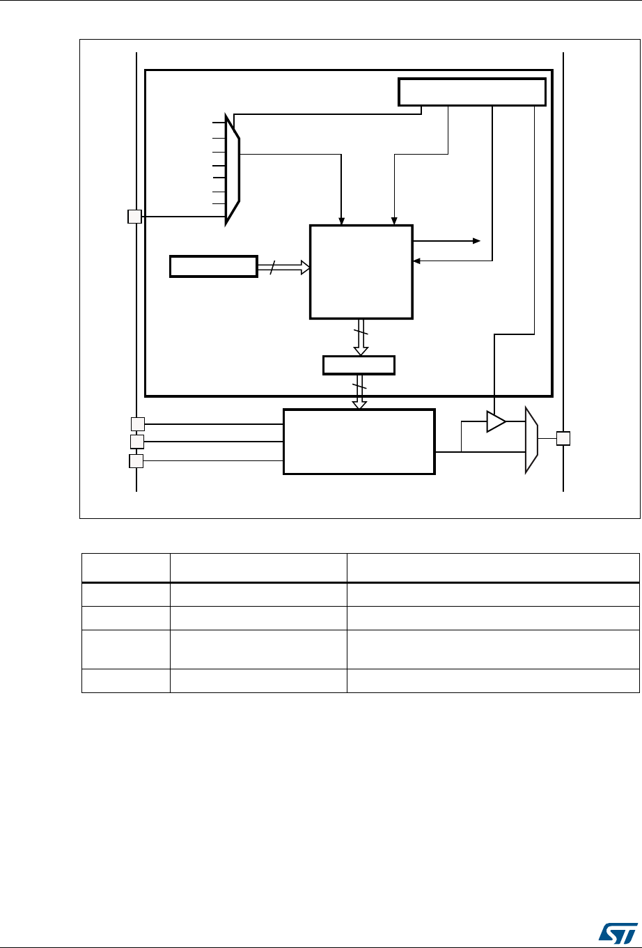
Digital-to-analog converter (DAC) RM0376
342/1001 DocID025941 Rev 5
Figure 53. DAC block diagram
Note: Once DAC_Channelx is enabled, the corresponding GPIO pin (PA4 or PA5) is automatically
connected to the analog converter output (DAC_OUTx). In order to avoid parasitic
consumption, PA4/PA5 pin should first be configured to analog (AIN).
Table 67. DAC pins
Name Signal type Remarks
VDDA Input, analog supply Analog power supply
VSSA Input, analog supply ground Ground for analog power supply
VREF+
Input, analog positive
reference The higher/positive reference voltage for the DAC1
DAC_OUT1/2 Analog output signal DAC channelx analog output
MS33718V3
VDDA
VREF+
DAC_ OU T1/2
Control logic
DHRx
12-bit
12-bit
DM A req ue stx
TSELx[2:0] bits
EXTI_9
DMAENx
TENx
DORx
Digital-to-analog
converterx
12-bit
DAC control register
Trigger selector
BOFF
TIM6_TRGO
TIM21_TRGO
TIM2_TRGO
SWTRIGx
VSSA
TIM3_TRGO
TIM7_TRGO
TIM3_CH3
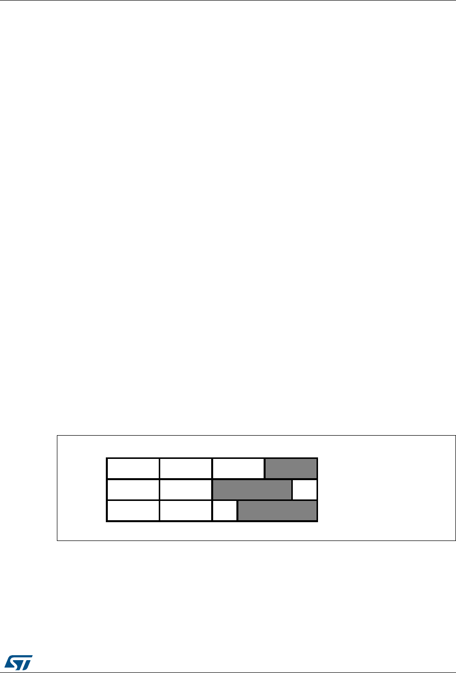
DocID025941 Rev 5 343/1001
RM0376 Digital-to-analog converter (DAC)
364
15.3 DAC output buffer enable
The DAC integrates two output buffers that can be used to reduce the output impedance
and to drive external loads directly without having to add an external operational amplifier.
The DAC channel output buffer can be enabled and disabled through the BOFF1 bit in the
DAC_CR register.
15.4 DAC channel enable
Each DAC channel can be powered on by setting the corresponding ENx bit in the DAC_CR
register. Each DAC channel is then enabled after a startup time tWAKEUP.
Note: The ENx bit enables the analog DAC Channelx macrocell only. The DAC Channelx digital
interface is enabled even if the ENx bit is reset.
15.5 Single mode functional description
15.5.1 DAC data format
There are three possibilities:
•8-bit right alignment: the software has to load data into the DAC_DHR8Rx [7:0] bits
(stored into the DHRx[11:4] bits)
•12-bit left alignment: the software has to load data into the DAC_DHR12Lx [15:4] bits
(stored into the DHRx[11:0] bits)
•12-bit right alignment: the software has to load data into the DAC_DHR12Rx [11:0] bits
(stored into the DHRx[11:0] bits)
Depending on the loaded DAC_DHRyyyx register, the data written by the user is shifted and
stored into the corresponding DHRx (data holding registerx, which are internal non-memory-
mapped registers). The DHRx register is then loaded into the DORx register either
automatically, by software trigger or by an external event trigger.
Figure 54. Data registers in single DAC channel mode
15.5.2 DAC channel conversion
The DAC_DORx cannot be written directly and any data transfer to the DAC channelx must
be performed by loading the DAC_DHRx register (write to DAC_DHR8Rx, DAC_DHR12Lx,
DAC_DHR12Rx).
Data stored in the DAC_DHRx register are automatically transferred to the DAC_DORx
register after one APB1 clock cycle, if no hardware trigger is selected (TENx bit in DAC_CR
31 24 15 7 0
8-bit right aligned
12-bit left aligned
12-bit right aligned
ai14710b
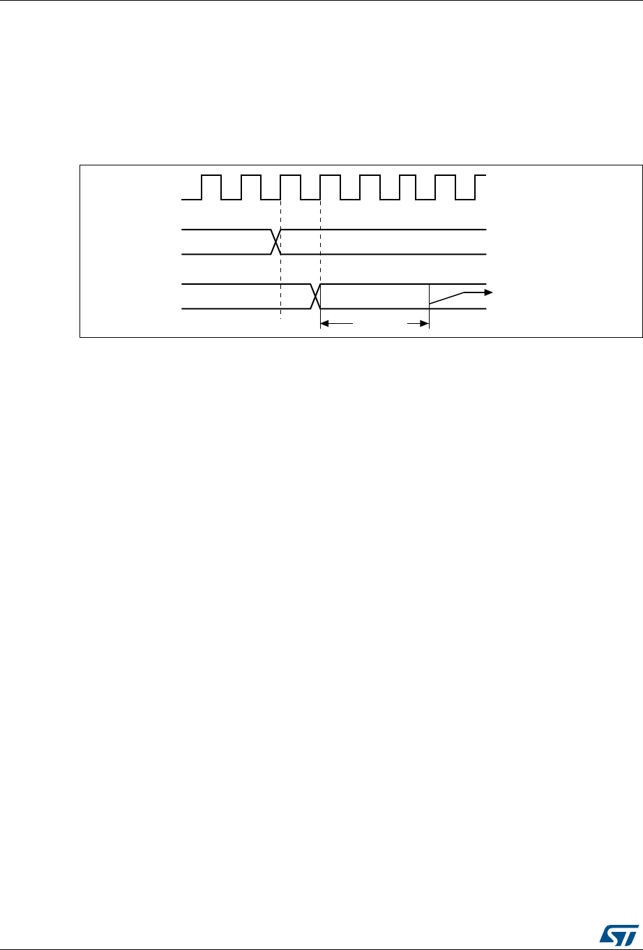
Digital-to-analog converter (DAC) RM0376
344/1001 DocID025941 Rev 5
register is reset). However, when a hardware trigger is selected (TENx bit in DAC_CR
register is set) and a trigger occurs, the transfer is performed three PCLK1 clock cycles
later.
When DAC_DORx is loaded with the DAC_DHRx contents, the analog output voltage
becomes available after a time tSETTLING that depends on the power supply voltage and the
analog output load.
Figure 55. Timing diagram for conversion with trigger disabled TEN = 0
Independent trigger with single LFSR generation
To configure the DAC in this conversion mode (see Section 15.7: Noise generation), the
following sequence is required:
1. Set the DAC channel trigger enable bit TENx.
2. Configure the trigger source by setting TSELx[2:0] bits.
3. Configure the DAC channel WAVEx[1:0] bits as “01” and the same LFSR mask value in
the MAMPx[3:0] bits
4. Load the DAC channel data into the desired DAC_DHRx register (DHR12RD,
DHR12LD or DHR8RD).
When a DAC channelx trigger arrives, the LFSRx counter, with the same mask, is added to
the DHRx register and the sum is transferred into DAC_DORx (three APB clock cycles
later). Then the LFSRx counter is updated.
For code example, refer to A.9.1: Independent trigger without wave generation code
example.
Independent trigger with single triangle generation
To configure the DAC in this conversion mode (see Section 15.8: Triangle-wave generation),
the following sequence is required:
1. Set the DAC channelx trigger enable TENx bits.
2. Configure the trigger source by setting TSELx[2:0] bits.
3. Configure the DAC channelx WAVEx[1:0] bits as “1x” and the same maximum
amplitude value in the MAMPx[3:0] bits
4. Load the DAC channelx data into the desired DAC_DHRx register. (DHR12RD,
DHR12LD or DHR8RD).
When a DAC channelx trigger arrives, the DAC channelx triangle counter, with the same
triangle amplitude, is added to the DHRx register and the sum is transferred into
DAC_DORx (three APB clock cycles later). The DAC channelx triangle counter is then
updated.
A
PB1_CLK
0x1AC
0x1AC
tSETTLING
DHR
DOR
Output voltage
available on DAC_OUT pin
ai14711b
DocID025941 Rev 5 345/1001
RM0376 Digital-to-analog converter (DAC)
364
For code example, refer to A.9.2: Independent trigger with single triangle generation code
example.
15.5.3 DAC output voltage
Digital inputs are converted to output voltages on a linear conversion between 0 and VREF+.
The analog output voltages on each DAC channel pin are determined by the following
equation:
15.5.4 DAC trigger selection
If the TENx control bit is set, conversion can then be triggered by an external event (timer
counter, external interrupt line). The TSELx[2:0] control bits determine which possible
events will trigger conversion as shown in Table 68.
Each time a DAC interface detects a rising edge on the selected timer TRGO output, or on
the selected external interrupt line 9, the last data stored into the DAC_DHRx register are
transferred into the DAC_DORx register. The DAC_DORx register is updated three APB1
cycles after the trigger occurs.
If the software trigger is selected, the conversion starts once the SWTRIG bit is set.
SWTRIG is reset by hardware once the DAC_DORx register has been loaded with the
DAC_DHRx register contents.
Note: TSELx[2:0] bit cannot be changed when the ENx bit is set. When software trigger is
selected, the transfer from the DAC_DHRx register to the DAC_DORx register takes only
one APB1 clock cycle.
DACoutput VREF+
DOR
4096
--------------
×=
Table 68. External triggers
Source Type TSEL[2:0]
TIM6 TRGO event
Internal signal from on-chip
timers
000
TIM3 TRGO event 001
TIM3 CH3 event 010
TIM21 TRGO event 011
TIM2 TRGO event 100
TIM7 TRGO event 101
EXTI line9 External pin 110
SWTRIG Software control bit 111
Digital-to-analog converter (DAC) RM0376
346/1001 DocID025941 Rev 5
15.6 Dual-mode functional description
15.6.1 DAC data format
In Dual DAC channel mode, there are three possibilities:
•8-bit right alignment: data for DAC channel1 to be loaded in the DAC_DHR8RD [7:0]
bits (stored in the DHR1[11:4] bits) and data for DAC channel2 to be loaded in the
DAC_DHR8RD [15:8] bits (stored in the DHR2[11:4] bits)
•12-bit left alignment: data for DAC channel1 to be loaded into the DAC_DHR12LD
[15:4] bits (stored into the DHR1[11:0] bits) and data for DAC channel2 to be loaded
into the DAC_DHR12LD [31:20] bits (stored in the DHR2[11:0] bits)
•12-bit right alignment: data for DAC channel1 to be loaded into the DAC_DHR12RD
[11:0] bits (stored in the DHR1[11:0] bits) and data for DAC channel2 to be loaded into
the DAC_DHR12LD [27:16] bits (stored in the DHR2[11:0] bits)
Depending on the loaded DAC_DHRyyyD register, the data written by the user is shifted
and stored in DHR1 and DHR2 (data holding registers, which are internal non-memory-
mapped registers). The DHR1 and DHR2 registers are then loaded into the DOR1 and
DOR2 registers, respectively, either automatically, by software trigger or by an external
event trigger.
Figure 56. Data registers in dual DAC channel mode
15.6.2 DAC channel conversion in dual mode
The DAC channel conversion in dual mode is performed in the same way as in single mode
(refer to Section 15.5.2) except that the data have to be loaded by writing to DAC_DHR8Rx,
DAC_DHR12Lx, DAC_DHR12Rx, DAC_DHR8RD, DAC_DHR12LD or DAC_DHR12RD.
15.6.3 Description of dual conversion modes
To efficiently use the bus bandwidth in applications that require the two DAC channels at the
same time, three dual registers are implemented: DHR8RD, DHR12RD and DHR12LD. A
unique register access is then required to drive both DAC channels at the same time.
Eleven conversion modes are possible using the two DAC channels and these dual
registers. All the conversion modes can nevertheless be obtained using separate DHRx
registers if needed.
All modes are described in the paragraphs below.
Refer to Section 15.5.2: DAC channel conversion for details on the APB bus (APB or APB1)
that clocks the DAC conversions.
31 24 15 7 0
8-bit right aligned
12-bit left aligned
12-bit right aligned
ai14709b

DocID025941 Rev 5 347/1001
RM0376 Digital-to-analog converter (DAC)
364
Independent trigger without wave generation
To configure the DAC in this conversion mode, the following sequence is required:
1. Set the two DAC channel trigger enable bits TEN1 and TEN2
2. Configure different trigger sources by setting different values in the TSEL1[2:0] and
TSEL2[2:0] bits
3. Load the dual DAC channel data into the desired DHR register (DAC_DHR12RD,
DAC_DHR12LD or DAC_DHR8RD)
When a DAC channel1 trigger arrives, the DHR1 register is transferred into DAC_DOR1
(three APB clock cycles later).
When a DAC channel2 trigger arrives, the DHR2 register is transferred into DAC_DOR2
(three APB clock cycles later).
Independent trigger with single LFSR generation
To configure the DAC in this conversion mode (refer to Section 15.7: Noise generation), the
following sequence is required:
1. Set the two DAC channel trigger enable bits TEN1 and TEN2
2. Configure different trigger sources by setting different values in the TSEL1[2:0] and
TSEL2[2:0] bits
3. Configure the two DAC channel WAVEx[1:0] bits as “01” and the same LFSR mask
value in the MAMPx[3:0] bits
4. Load the dual DAC channel data into the desired DHR register (DHR12RD, DHR12LD
or DHR8RD)
When a DAC channel1 trigger arrives, the LFSR1 counter, with the same mask, is added to
the DHR1 register and the sum is transferred into DAC_DOR1 (three APB clock cycles
later). Then the LFSR1 counter is updated.
When a DAC channel2 trigger arrives, the LFSR2 counter, with the same mask, is added to
the DHR2 register and the sum is transferred into DAC_DOR2 (three APB clock cycles
later). Then the LFSR2 counter is updated.
Independent trigger with different LFSR generation
To configure the DAC in this conversion mode (refer to Section 15.7: Noise generation), the
following sequence is required:
1. Set the two DAC channel trigger enable bits TEN1 and TEN2
2. Configure different trigger sources by setting different values in the TSEL1[2:0] and
TSEL2[2:0] bits
3. Configure the two DAC channel WAVEx[1:0] bits as “01” and set different LFSR masks
values in the MAMP1[3:0] and MAMP2[3:0] bits
4. Load the dual DAC channel data into the desired DHR register (DAC_DHR12RD,
DAC_DHR12LD or DAC_DHR8RD)
When a DAC channel1 trigger arrives, the LFSR1 counter, with the mask configured by
MAMP1[3:0], is added to the DHR1 register and the sum is transferred into DAC_DOR1
(three APB clock cycles later). Then the LFSR1 counter is updated.
When a DAC channel2 trigger arrives, the LFSR2 counter, with the mask configured by
MAMP2[3:0], is added to the DHR2 register and the sum is transferred into DAC_DOR2
(three APB clock cycles later). Then the LFSR2 counter is updated.

Digital-to-analog converter (DAC) RM0376
348/1001 DocID025941 Rev 5
Independent trigger with single triangle generation
To configure the DAC in this conversion mode (refer to Section 15.8: Triangle-wave
generation), the following sequence is required:
1. Set the DAC channelx trigger enable TENx bits.
2. Configure different trigger sources by setting different values in the TSELx[2:0] bits
3. Configure the DAC channelx WAVEx[1:0] bits as “1x” and the same maximum
amplitude value in the MAMPx[3:0] bits
4. Load the DAC channelx data into the desired DAC_DHRx register.
Refer to Section 15.5.2: DAC channel conversion for details on the APB bus (APB or APB1)
that clocks the DAC conversions.
When a DAC channelx trigger arrives, the DAC channelx triangle counter, with the same
triangle amplitude, is added to the DHRx register and the sum is transferred into
DAC_DORx (three APB clock cycles later). The DAC channelx triangle counter is then
updated.
Independent trigger with different triangle generation
To configure the DAC in this conversion mode (refer to Section 15.8: Triangle-wave
generation), the following sequence is required:
1. Set the DAC channelx trigger enable TENx bits.
2. Configure different trigger sources by setting different values in the TSELx[2:0] bits
3. Configure the DAC channelx WAVEx[1:0] bits as “1x” and set different maximum
amplitude values in the MAMPx[3:0] bits
4. Load the DAC channelx data into the desired DAC_DHRx register.
When a DAC channelx trigger arrives, the DAC channelx triangle counter, with a triangle
amplitude configured by MAMPx[3:0], is added to the DHRx register and the sum is
transferred into DAC_DORx (three APB clock cycles later). The DAC channelx triangle
counter is then updated.
Simultaneous software start
To configure the DAC in this conversion mode, the following sequence is required:
1. Load the dual DAC channel data to the desired DHR register (DAC_DHR12RD,
DAC_DHR12LD or DAC_DHR8RD)
In this configuration, one APB clock cycles).
Simultaneous trigger without wave generation
To configure the DAC in this conversion mode, the following sequence is required:
1. Set the two DAC channel trigger enable bits TEN1 and TEN2
2. Configure the same trigger source for both DAC channels by setting the same value in
the TSEL1[2:0] and TSEL2[2:0] bits
3. Load the dual DAC channel data to the desired DHR register (DAC_DHR12RD,
DAC_DHR12LD or DAC_DHR8RD)
When a trigger arrives, the DHR1 and DHR2 registers are transferred into DAC_DOR1 and
DAC_DOR2, respectively (after three APB clock cycles).

DocID025941 Rev 5 349/1001
RM0376 Digital-to-analog converter (DAC)
364
Simultaneous trigger with single LFSR generation
To configure the DAC in this conversion mode (refer to Section 15.7: Noise generation), the
following sequence is required:
1. Set the two DAC channel trigger enable bits TEN1 and TEN2
2. Configure the same trigger source for both DAC channels by setting the same value in
the TSEL1[2:0] and TSEL2[2:0] bits
3. Configure the two DAC channel WAVEx[1:0] bits as “01” and the same LFSR mask
value in the MAMPx[3:0] bits
4. Load the dual DAC channel data to the desired DHR register (DHR12RD, DHR12LD or
DHR8RD)
When a trigger arrives, the LFSR1 counter, with the same mask, is added to the DHR1
register and the sum is transferred into DAC_DOR1 (three APB clock cycles later). The
LFSR1 counter is then updated. At the same time, the LFSR2 counter, with the same mask,
is added to the DHR2 register and the sum is transferred into DAC_DOR2 (three APB clock
cycles later). The LFSR2 counter is then updated.
Simultaneous trigger with different LFSR generation
To configure the DAC in this conversion mode (refer to Section 15.7: Noise generation), the
following sequence is required:
1. Set the two DAC channel trigger enable bits TEN1 and TEN2
2. Configure the same trigger source for both DAC channels by setting the same value in
the TSEL1[2:0] and TSEL2[2:0] bits
3. Configure the two DAC channel WAVEx[1:0] bits as “01” and set different LFSR mask
values using the MAMP1[3:0] and MAMP2[3:0] bits
4. Load the dual DAC channel data into the desired DHR register (DAC_DHR12RD,
DAC_DHR12LD or DAC_DHR8RD)
When a trigger arrives, the LFSR1 counter, with the mask configured by MAMP1[3:0], is
added to the DHR1 register and the sum is transferred into DAC_DOR1 (three APB clock
cycles later). The LFSR1 counter is then updated.
At the same time, the LFSR2 counter, with the mask configured by MAMP2[3:0], is added to
the DHR2 register and the sum is transferred into DAC_DOR2 (three APB clock cycles
later). The LFSR2 counter is then updated.
Simultaneous trigger with single triangle generation
To configure the DAC in this conversion mode (refer to Section 15.8: Triangle-wave
generation), the following sequence is required:
1. Set the DAC channelx trigger enable TEN1x bits.
2. Configure the same trigger source for both DAC channels by setting the same value in
the TSELx[2:0] bits.
3. Configure the DAC channelx WAVEx[1:0] bits as “1x” and the same maximum
amplitude value using the MAMPx[3:0] bits
4. Load the DAC channelx data into the desired DAC_DHRx registers.
When a trigger arrives, the DAC channelx triangle counter, with the same triangle amplitude,
is added to the DHRx register and the sum is transferred into DAC_DORx (three APB clock
cycles later). The DAC channelx triangle counter is then updated.
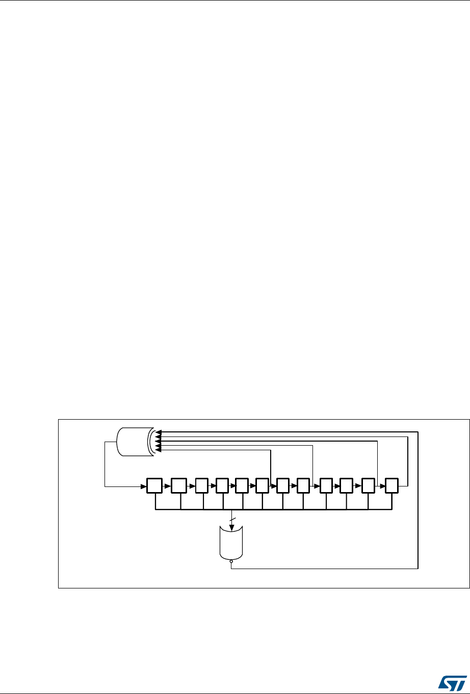
Digital-to-analog converter (DAC) RM0376
350/1001 DocID025941 Rev 5
Simultaneous trigger with different triangle generation
To configure the DAC in this conversion mode ‘refer to Section 15.8: Triangle-wave
generation), the following sequence is required:
1. Set the DAC channelx trigger enable TENx bits.
2. Configure the same trigger source for DAC channelx by setting the same value in the
TSELx[2:0] bits
3. Configure the DAC channelx WAVEx[1:0] bits as “1x” and set different maximum
amplitude values in the MAMPx[3:0] bits.
4. Load the DAC channelx data into the desired DAC_DHRx registers.
When a trigger arrives, the DAC channelx triangle counter, with a triangle amplitude
configured by MAMPx[3:0], is added to the DHRx register and the sum is transferred into
DAC_DORx (three APB clock cycles later). Then the DAC channelx triangle counter is
updated.
15.6.4 DAC output voltage
Refer to Section 15.5.3: DAC output voltage.
15.6.5 DAC trigger selection
Refer to Section 15.5.4: DAC trigger selection
15.7 Noise generation
In order to generate a variable-amplitude pseudonoise, an LFSR (linear feedback shift
register) is available. DAC noise generation is selected by setting WAVEx[1:0] to “01”. The
preloaded value in LFSR is 0xAAA. This register is updated three APB clock cycles after
each trigger event, following a specific calculation algorithm.
Figure 57. DAC LFSR register calculation algorithm
The LFSR value, that may be masked partially or totally by means of the MAMPx[3:0] bits in
the DAC_CR register, is added up to the DAC_DHRx contents without overflow and this
value is then stored into the DAC_DORx register.
If LFSR is 0x0000, a ‘1 is injected into it (antilock-up mechanism).
11 10 9 8 7 6 5 4 3 2 1 0
12
NOR
X12
X0
X
X4
X6
XOR
ai14713c
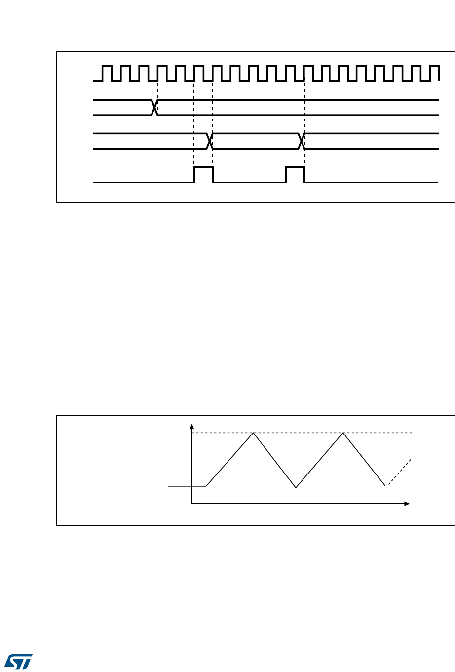
DocID025941 Rev 5 351/1001
RM0376 Digital-to-analog converter (DAC)
364
It is possible to reset LFSR wave generation by resetting the WAVEx[1:0] bits.
Figure 58. DAC conversion (SW trigger enabled) with LFSR wave generation
Note: The DAC trigger must be enabled for noise generation by setting the TENx bit in the
DAC_CR register.
15.8 Triangle-wave generation
It is possible to add a small-amplitude triangular waveform on a DC or slowly varying signal.
DAC triangle-wave generation is selected by setting WAVEx[1:0] to “10”. The amplitude is
configured through the MAMPx[3:0] bits in the DAC_CR register. An internal triangle counter
is incremented three APB clock cycles after each trigger event. The value of this counter is
then added to the DAC_DHRx register without overflow and the sum is stored into the
DAC_DORx register. The triangle counter is incremented as long as it is less than the
maximum amplitude defined by the MAMPx[3:0] bits. Once the configured amplitude is
reached, the counter is decremented down to 0, then incremented again and so on.
It is possible to reset triangle wave generation by resetting the WAVEx[1:0] bits.
Figure 59. DAC triangle wave generation
APB1_CLK
0x00
0xAAA
DHR
DOR
ai14714b
0xD55
SWTRIG
MAMPx[3:0] max amplitude
+ DAC_DHRx base value
DAC_DHRx base value
Incrementation
ai14715c
Decrementation
0
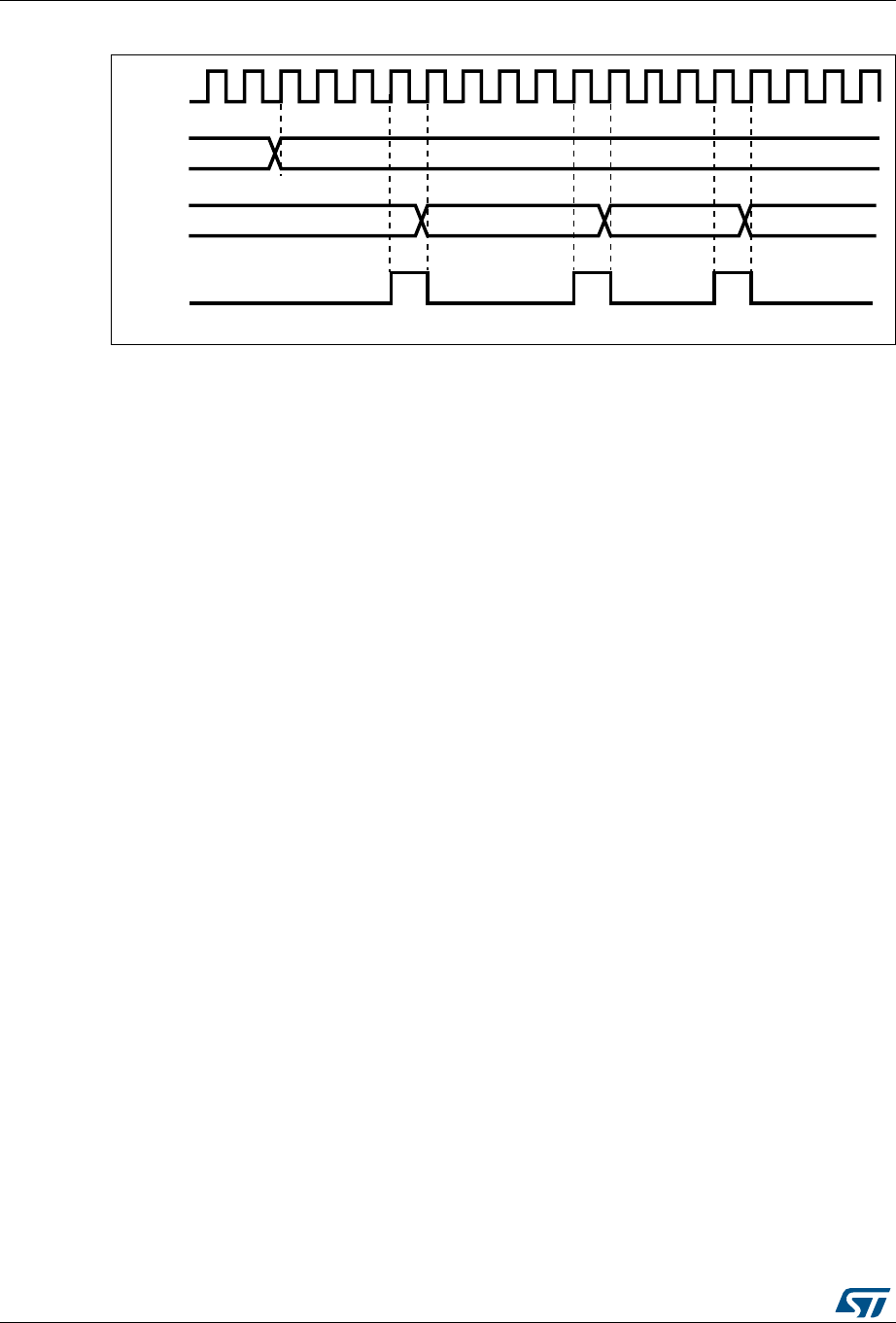
Digital-to-analog converter (DAC) RM0376
352/1001 DocID025941 Rev 5
Figure 60. DAC conversion (SW trigger enabled) with triangle wave generation
Note: The DAC trigger must be enabled for triangle generation by setting the TENx bit in the
DAC_CR register.
The MAMPx[3:0] bits must be configured before enabling the DAC, otherwise they cannot
be changed.
15.9 DMA request
Each DAC channel has a DMA capability. Two DMA channels are used to service DAC
channel DMA requests.
A DAC DMA request is generated when an external trigger (but not a software trigger)
occurs while the DMAENx bit is set. The value of the DAC_DHRx register is then transferred
to the DAC_DORx register.
In dual mode, if both DMAENx bits are set, two DMA requests are generated. If only one
DMA request is needed, user should set only the corresponding DMAENx bit. In this way,
the application can manage both DAC channels in dual mode by using one DMA request
and a unique DMA channel.
DMA underrun
The DAC DMA request is not queued so that if a second external trigger arrives before the
acknowledgment for the first external trigger is received (first request), then no new request
is issued and the DMA channelx underrun flag DMAUDRx in the DAC_SR register is set,
reporting the error condition. DMA data transfers are then disabled and no further DMA
request is treated. The DAC channelx continues to convert old data.
The software should clear the DMAUDRx flag by writing “1”, clear the DMAEN bit of the
used DMA stream and re-initialize both DMA and DAC channelx to restart the transfer
correctly. The software should modify the DAC trigger conversion frequency or lighten the
DMA workload to avoid a new DMA. Finally, the DAC conversion can be resumed by
enabling both DMA data transfer and conversion trigger.
For each DAC channel, an interrupt is also generated if the corresponding DMAUDRIEx bit
in the DAC_CR register is enabled.
For code example, refer to A.9.3: DMA initialization code example.
APB1_CLK
0xABE
0xABE
DHR
DOR
ai14716b
0xABF
SWTRIG
0xAC0

DocID025941 Rev 5 353/1001
RM0376 Digital-to-analog converter (DAC)
364
15.10 DAC registers
Refer to Section 1.1 on page 51 for a list of abbreviations used in register descriptions.
The peripheral registers have to be accessed by words (32-bit).
15.10.1 DAC control register (DAC_CR)
Address offset: 0x00
Reset value: 0x0000 0000
31 30 29 28 27 26 25 24 23 22 21 20 19 18 17 16
Res. Res. DMAU
DRIE2
DMA
EN2 MAMP2[3:0] WAVE2[1:0] TSEL2[2:0] TEN2 BOFF2 EN2
rw rw rw rw rw rw rw rw rw rw rw rw rw rw
151413121110987 6 543210
Res. Res. DMAU
DRIE1
DMA
EN1 MAMP1[3:0] WAVE1[1:0] TSEL1[2:0] TEN1 BOFF1 EN1
rw rw rw rw rw rw rw rw rw rw rw rw rw rw
Bits 31:30 Reserved, must be kept at reset value.
Bit 29 DMAUDRIE2: DAC channel2 DMA underrun interrupt enable
This bit is set and cleared by software.
0: DAC channel2 DMA underrun interrupt disabled
1: DAC channel2 DMA underrun interrupt enabled
Note: This bit is available in dual mode only. It is reserved in single mode.
Bit 28 DMAEN2: DAC channel2 DMA enable
This bit is set and cleared by software.
0: DAC channel2 DMA mode disabled
1: DAC channel2 DMA mode enabled
Note: This bit is available in dual mode only. It is reserved in single mode.
Bits 27:24 MAMP2[3:0]: DAC channel2 mask/amplitude selector
These bits are written by software to select mask in wave generation mode or amplitude in
triangle generation mode.
0000: Unmask bit0 of LFSR/ triangle amplitude equal to 1
0001: Unmask bits[1:0] of LFSR/ triangle amplitude equal to 3
0010: Unmask bits[2:0] of LFSR/ triangle amplitude equal to 7
0011: Unmask bits[3:0] of LFSR/ triangle amplitude equal to 15
0100: Unmask bits[4:0] of LFSR/ triangle amplitude equal to 31
0101: Unmask bits[5:0] of LFSR/ triangle amplitude equal to 63
0110: Unmask bits[6:0] of LFSR/ triangle amplitude equal to 127
0111: Unmask bits[7:0] of LFSR/ triangle amplitude equal to 255
1000: Unmask bits[8:0] of LFSR/ triangle amplitude equal to 511
1001: Unmask bits[9:0] of LFSR/ triangle amplitude equal to 1023
1010: Unmask bits[10:0] of LFSR/ triangle amplitude equal to 2047
≥1011: Unmask bits[11:0] of LFSR/ triangle amplitude equal to 4095
Note: These bits are available only in dual mode when wave generation is supported.
Otherwise, they are reserved and must be kept at reset value.

Digital-to-analog converter (DAC) RM0376
354/1001 DocID025941 Rev 5
Bits 23:22 WAVE2[1:0]: DAC channel2 noise/triangle wave generation enable
These bits are set/reset by software.
00: wave generation disabled
01: Noise wave generation enabled
1x: Triangle wave generation enabled
Note: Only used if bit TEN2 = 1 (DAC channel2 trigger enabled)
These bits are available only in dual mode when wave generation is supported.
Otherwise, they are reserved and must be kept at reset value.
Bits 21:19 TSEL2[2:0]: DAC channel2 trigger selection
These bits select the external event used to trigger DAC channel2
000: Timer 6 TRGO event
001: Timer 3 TRGO event
010: Timer 3 CH3 event
011: Timer 21 TRGO event
100: Timer 2 TRGO event
101: Timer 7 TRGO event
110: EXTI line9
111: Software trigger
Note: Only used if bit TEN2 = 1 (DAC channel2 trigger enabled).
These bits are available in dual mode only. They are reserved in single mode.
Bit 18 TEN2: DAC channel2 trigger enable
This bit is set and cleared by software to enable/disable DAC channel2 trigger
0: DAC channel2 trigger disabled and data written into the DAC_DHRx register are
transferred one APB1clock cycle later to the DAC_DOR2 register
1: DAC channel2 trigger enabled and data from the DAC_DHRx register are transferred
three APB1 clock cycles later to the DAC_DOR2 register
Note: When software trigger is selected, the transfer from the DAC_DHRx register to the
DAC_DOR2 register takes only one APB1 clock cycle.
Note: This bit is available in dual mode only. It is reserved in single mode.
Bit 17 BOFF2: DAC channel2 output buffer disable
This bit is set and cleared by software to enable/disable DAC channel2 output buffer.
0: DAC channel2 output buffer enabled
1: DAC channel2 output buffer disabled
Note: This bit is available in dual mode only. It is reserved in single mode.
Bit 16 EN2: DAC channel2 enable
This bit is set and cleared by software to enable/disable DAC channel2.
0: DAC channel2 disabled
1: DAC channel2 enabled
Note: This bit is available in dual mode only. It is reserved in single mode.
Bits 15:14 Reserved, must be kept at reset value.
Bit 13 DMAUDRIE1: DAC channel1 DMA Underrun Interrupt enable
This bit is set and cleared by software.
0: DAC channel1 DMA Underrun Interrupt disabled
1: DAC channel1 DMA Underrun Interrupt enabled

DocID025941 Rev 5 355/1001
RM0376 Digital-to-analog converter (DAC)
364
Bit 12 DMAEN1: DAC channel1 DMA enable
This bit is set and cleared by software.
0: DAC channel1 DMA mode disabled
1: DAC channel1 DMA mode enabled
Bits 11:8 MAMP1[3:0]: DAC channel1 mask/amplitude selector
These bits are written by software to select mask in wave generation mode or amplitude in
triangle generation mode.
0000: Unmask bit0 of LFSR/ triangle amplitude equal to 1
0001: Unmask bits[1:0] of LFSR/ triangle amplitude equal to 3
0010: Unmask bits[2:0] of LFSR/ triangle amplitude equal to 7
0011: Unmask bits[3:0] of LFSR/ triangle amplitude equal to 15
0100: Unmask bits[4:0] of LFSR/ triangle amplitude equal to 31
0101: Unmask bits[5:0] of LFSR/ triangle amplitude equal to 63
0110: Unmask bits[6:0] of LFSR/ triangle amplitude equal to 127
0111: Unmask bits[7:0] of LFSR/ triangle amplitude equal to 255
1000: Unmask bits[8:0] of LFSR/ triangle amplitude equal to 511
1001: Unmask bits[9:0] of LFSR/ triangle amplitude equal to 1023
1010: Unmask bits[10:0] of LFSR/ triangle amplitude equal to 2047
≥ 1011: Unmask bits[11:0] of LFSR/ triangle amplitude equal to 4095
Bits 7:6 WAVE1[1:0]: DAC channel1 noise/triangle wave generation enable
These bits are set and cleared by software.
00: Wave generation disabled
01: Noise wave generation enabled
1x: Triangle wave generation enabled
Note: Only used if bit TEN1 = 1 (DAC channel1 trigger enabled).
Bits 5:3 TSEL1[2:0]: DAC channel1 trigger selection
These bits select the external event used to trigger DAC channel1.
000: Timer 6 TRGO event
001: Timer 3 TRGO event
010: Timer 3 CH3 event
011: Timer 21 TRGO event
100: Timer 2 TRGO event
101: Timer 7 TRGO event
110: EXTI line9
111: Software trigger
Note: Only used if bit TEN1 = 1 (DAC channel1 trigger enabled).

Digital-to-analog converter (DAC) RM0376
356/1001 DocID025941 Rev 5
Bit 2 TEN1: DAC channel1 trigger enable
This bit is set and cleared by software to enable/disable DAC channel1 trigger.
0: DAC channel1 trigger disabled and data written into the DAC_DHRx register are
transferred one APB1 clock cycle later to the DAC_DOR1 register
1: DAC channel1 trigger enabled and data from the DAC_DHRx register are transferred
three APB1 clock cycles later to the DAC_DOR1 register
Note: When software trigger is selected, the transfer from the DAC_DHRx register to the
DAC_DOR1 register takes only one APB1 clock cycle.
Bit 1 BOFF1: DAC channel1 output buffer disable
This bit is set and cleared by software to enable/disable DAC channel1 output buffer.
0: DAC channel1 output buffer enabled
1: DAC channel1 output buffer disabled
Bit 0 EN1: DAC channel1 enable
This bit is set and cleared by software to enable/disable DAC channel1.
0: DAC channel1 disabled
1: DAC channel1 enabled
DocID025941 Rev 5 357/1001
RM0376 Digital-to-analog converter (DAC)
364
15.10.2 DAC software trigger register (DAC_SWTRIGR)
Address offset: 0x04
Reset value: 0x0000 0000
15.10.3 DAC channel1 12-bit right-aligned data holding register
(DAC_DHR12R1)
Address offset: 0x08
Reset value: 0x0000 0000
31 30 29 28 27 26 25 24 23 22 21 20 19 18 17 16
Res. Res. Res. Res. Res. Res. Res. Res. Res. Res. Res. Res. Res. Res. Res. Res.
15 14 13 12 11 10 9 8 7 6 5 4 3 2 1 0
Res. Res. Res. Res. Res. Res. Res. Res. Res. Res. Res. Res. Res. Res. SWTRIG2 SWTRIG1
ww
Bits 31:2 Reserved, must be kept at reset value.
Bit 1 SWTRIG2: DAC channel2 software trigger
This bit is set and cleared by software to enable/disable the software trigger.
0: Software trigger disabled
1: Software trigger enabled
Note: This bit is cleared by hardware (one APB1 clock cycle later) once the DAC_DHR2
register value has been loaded into the DAC_DOR2 register.
This bit is available in dual mode only. It is reserved in single mode.
Bit 0 SWTRIG1: DAC channel1 software trigger
This bit is set and cleared by software to enable/disable the software trigger.
0: Software trigger disabled
1: Software trigger enabled
Note: This bit is cleared by hardware (one APB1 clock cycle later) once the DAC_DHR1
register value has been loaded into the DAC_DOR1 register.
31 30 29 28 27 26 25 24 23 22 21 20 19 18 17 16
Res. Res. Res. Res. Res. Res. Res. Res. Res. Res. Res. Res. Res. Res. Res. Res.
1514131211109876543210
Res. Res. Res. Res. DACC1DHR[11:0]
rw rw rw rw rw rw rw rw rw rw rw rw
Bits 31:12 Reserved, must be kept at reset value.
Bits 11:0 DACC1DHR[11:0]: DAC channel1 12-bit right-aligned data
These bits are written by software which specifies 12-bit data for DAC channel1.
Digital-to-analog converter (DAC) RM0376
358/1001 DocID025941 Rev 5
15.10.4 DAC channel1 12-bit left-aligned data holding register
(DAC_DHR12L1)
Address offset: 0x0C
Reset value: 0x0000 0000
15.10.5 DAC channel1 8-bit right-aligned data holding register
(DAC_DHR8R1)
Address offset: 0x10
Reset value: 0x0000 0000
15.10.6 DAC channel2 12-bit right-aligned data holding register
(DAC_DHR12R2)
Address offset: 0x14
Reset value: 0x0000 0000
31 30 29 28 27 26 25 24 23 22 21 20 19 18 17 16
Res. Res. Res. Res. Res. Res. Res. Res. Res. Res. Res. Res. Res. Res. Res. Res.
1514131211109876543210
DACC1DHR[11:0] v Res. Res. Res.
rw rw rw rw rw rw rw rw rw rw rw rw
Bits 31:16 Reserved, must be kept at reset value.
Bits 15:4 DACC1DHR[11:0]: DAC channel1 12-bit left-aligned data
These bits are written by software which specifies 12-bit data for DAC channel1.
Bits 3:0 Reserved, must be kept at reset value.
31 30 29 28 27 26 25 24 23 22 21 20 19 18 17 16
Res. Res. Res. Res. Res. Res. Res. Res. Res. Res. Res. Res. Res. Res. Res. Res.
1514131211109876543210
Res. Res. Res. Res. Res. Res. Res. Res. DACC1DHR[7:0]
rw rw rw rw rw rw rw rw
Bits 31:8 Reserved, must be kept at reset value.
Bits 7:0 DACC1DHR[7:0]: DAC channel1 8-bit right-aligned data
These bits are written by software which specifies 8-bit data for DAC channel1.
31 30 29 28 27 26 25 24 23 22 21 20 19 18 17 16
Res. Res. Res. Res. Res. Res. Res. Res. Res. Res. Res. Res. Res. Res. Res. Res.
1514131211109876543210
Res. Res. Res. Res. DACC2DHR[11:0]
rw rw rw rw rw rw rw rw rw rw rw rw

DocID025941 Rev 5 359/1001
RM0376 Digital-to-analog converter (DAC)
364
15.10.7 DAC channel2 12-bit left-aligned data holding register
(DAC_DHR12L2)
Address offset: 0x18
Reset value: 0x0000 0000
15.10.8 DAC channel2 8-bit right-aligned data holding register
(DAC_DHR8R2)
Address offset: 0x1C
Reset value: 0x0000 0000
Bits 31:12 Reserved, must be kept at reset value.
Bits 11:0 DACC2DHR[11:0]: DAC channel2 12-bit right-aligned data
These bits are written by software which specifies 12-bit data for DAC channel2.
31 30 29 28 27 26 25 24 23 22 21 20 19 18 17 16
Res. Res. Res. Res. Res. Res. Res. Res. Res. Res. Res. Res. Res. Res. Res. Res.
1514131211109876543210
DACC2DHR[11:0] Res. Res. Res. Res.
rw rw rw rw rw rw rw rw rw rw rw rw
Bits 31:16 Reserved, must be kept at reset value.
Bits 15:4 DACC2DHR[11:0]: DAC channel2 12-bit left-aligned data
These bits are written by software which specify 12-bit data for DAC channel2.
Bits 3:0 Reserved, must be kept at reset value.
31 30 29 28 27 26 25 24 23 22 21 20 19 18 17 16
Res. Res. Res. Res. Res. Res. Res. Res. Res. Res. Res. Res. Res. Res. Res. Res.
1514131211109876543210
Res. Res. Res. Res. Res. Res. Res. Res. DACC2DHR[7:0]
rw rw rw rw rw rw rw rw
Bits 31:8 Reserved, must be kept at reset value.
Bits 7:0 DACC2DHR[7:0]: DAC channel2 8-bit right-aligned data
These bits are written by software which specifies 8-bit data for DAC channel2.
Digital-to-analog converter (DAC) RM0376
360/1001 DocID025941 Rev 5
15.10.9 Dual DAC 12-bit right-aligned data holding register
(DAC_DHR12RD)
Address offset: 0x20
Reset value: 0x0000 0000
15.10.10 Dual DAC 12-bit left-aligned data holding register
(DAC_DHR12LD)
Address offset: 0x24
Reset value: 0x0000 0000
15.10.11 Dual DAC 8-bit right-aligned data holding register
(DAC_DHR8RD)
Address offset: 0x28
Reset value: 0x0000 0000
31 30 29 28 27 26 25 24 23 22 21 20 19 18 17 16
Res. Res. Res. Res. DACC2DHR[11:0]
rw rw rw rw rw rw rw rw rw rw rw rw
1514131211109876543210
Res. Res. Res. Res. DACC1DHR[11:0]
rw rw rw rw rw rw rw rw rw rw rw rw
Bits 31:28 Reserved, must be kept at reset value.
Bits 27:16 DACC2DHR[11:0]: DAC channel2 12-bit right-aligned data
These bits are written by software which specifies 12-bit data for DAC channel2.
Bits 15:12 Reserved, must be kept at reset value.
Bits 11:0 DACC1DHR[11:0]: DAC channel1 12-bit right-aligned data
These bits are written by software which specifies 12-bit data for DAC channel1.
31 30 29 28 27 26 25 24 23 22 21 20 19 18 17 16
DACC2DHR[11:0] Res. Res. Res. Res.
rw rw rw rw rw rw rw rw rw rw rw rw
1514131211109876543210
DACC1DHR[11:0] Res. Res. Res. Res.
rw rw rw rw rw rw rw rw rw rw rw rw
Bits 31:20 DACC2DHR[11:0]: DAC channel2 12-bit left-aligned data
These bits are written by software which specifies 12-bit data for DAC channel2.
Bits 19:16 Reserved, must be kept at reset value.
Bits 15:4 DACC1DHR[11:0]: DAC channel1 12-bit left-aligned data
These bits are written by software which specifies 12-bit data for DAC channel1.
Bits 3:0 Reserved, must be kept at reset value.
31 30 29 28 27 26 25 24 23 22 21 20 19 18 17 16
Res. Res. Res. Res. Res. Res. Res. Res. Res. Res. Res. Res. Res. Res. Res. Res.

DocID025941 Rev 5 361/1001
RM0376 Digital-to-analog converter (DAC)
364
15.10.12 DAC channel1 data output register (DAC_DOR1)
Address offset: 0x2C
Reset value: 0x0000 0000
15.10.13 DAC channel2 data output register (DAC_DOR2)
Address offset: 0x30
Reset value: 0x0000 0000
15.10.14 DAC status register (DAC_SR)
Address offset: 0x34
Reset value: 0x0000 0000
1514131211109876543210
DACC2DHR[7:0] DACC1DHR[7:0]
rw rw rw rw rw rw rw rw rw rw rw rw rw rw rw rw
Bits 31:16 Reserved, must be kept at reset value.
Bits 15:8 DACC2DHR[7:0]: DAC channel2 8-bit right-aligned data
These bits are written by software which specifies 8-bit data for DAC channel2.
Bits 7:0 DACC1DHR[7:0]: DAC channel1 8-bit right-aligned data
These bits are written by software which specifies 8-bit data for DAC channel1.
31 30 29 28 27 26 25 24 23 22 21 20 19 18 17 16
Res. Res. Res. Res. Res. Res. Res. Res. Res. Res. Res. Res. Res. Res. Res. Res.
1514131211109876543210
Res. Res. Res. Res. DACC1DOR[11:0]
rrrrrrrrrrrr
Bits 31:12 Reserved, must be kept at reset value.
Bits 11:0 DACC1DOR[11:0]: DAC channel1 data output
These bits are read-only, they contain data output for DAC channel1.
31 30 29 28 27 26 25 24 23 22 21 20 19 18 17 16
Res. Res. Res. Res. Res. Res. Res. Res. Res. Res. Res. Res. Res. Res. Res. Res.
1514131211109876543210
Res. Res. Res. Res. DACC2DOR[11:0]
rrrrrrrrrrrr
Bits 31:12 Reserved, must be kept at reset value.
Bits 11:0 DACC2DOR[11:0]: DAC channel2 data output
These bits are read-only, they contain data output for DAC channel2.

Digital-to-analog converter (DAC) RM0376
362/1001 DocID025941 Rev 5
31 30 29 28 27 26 25 24 23 22 21 20 19 18 17 16
Res. Res. DMAUDR2 Res. Res. Res. Res. Res. Res. Res. Res. Res. Res. Res. Res. Res.
rc_w1
1514 13 1211109876543210
Res. Res. DMAUDR1 Res. Res. Res. Res. Res. Res. Res. Res. Res. Res. Res. Res. Res.
rc_w1
Bits 31:30 Reserved, must be kept at reset value.
Bit 29 DMAUDR2: DAC channel2 DMA underrun flag
This bit is set by hardware and cleared by software (by writing it to 1).
0: No DMA underrun error condition occurred for DAC channel2
1: DMA underrun error condition occurred for DAC channel2 (the currently selected trigger is
driving DAC channel2 conversion at a frequency higher than the DMA service capability rate)
Note: This bit is available in dual mode only. It is reserved in single mode.
Bits 28:14 Reserved, must be kept at reset value.
Bit 13 DMAUDR1: DAC channel1 DMA underrun flag
This bit is set by hardware and cleared by software (by writing it to 1).
0: No DMA underrun error condition occurred for DAC channel1
1: DMA underrun error condition occurred for DAC channel1 (the currently selected trigger is
driving DAC channel1 conversion at a frequency higher than the DMA service capability rate)
Bits 12:0 Reserved, must be kept at reset value.

DocID025941 Rev 5 363/1001
RM0376 Digital-to-analog converter (DAC)
364
15.10.15 DAC register map
Table 69 summarizes the DAC registers.
Table 69. DAC register map and reset values
Offset Register
name
31
30
29
28
27
26
25
24
23
22
21
20
19
18
17
16
15
14
13
12
11
10
9
8
7
6
5
4
3
2
1
0
0x00
DAC_CR
Res.
Res.
DMAUDRIE2
DMAEN2
MAMP2[3:0]
WAVE2[1:0]
TSEL2[2:0]
TEN2
BOFF2
EN2
Res.
Res.
DMAUDRIE1
DMAEN1
MAMP1[3:0].
WAVE1[1:0]
TSEL1[2:0]
TEN1
BOFF1
EN1
Reset value 000000000 00000 000000000 00000
0x04
DAC_
SWTRIGR
Res.
Res.
Res.
Res.
Res.
Res.
Res.
Res.
Res.
Res.
Res.
Res.
Res.
Res.
Res.
Res.
Res.
Res.
Res.
Res.
Res.
Res.
Res.
Res.
Res.
Res.
Res.
Res.
Res.
Res.
SWTRIG2
SWTRIG1
Reset value 00
0x08
DAC_
DHR12R1
Res.
Res.
Res.
Res.
Res.
Res.
Res.
Res.
Res.
Res.
Res.
Res.
Res.
Res.
Res.
Res.
Res.
Res.
Res.
Res.
DACC1DHR[11:0]
Reset value 000000000000
0x0C
DAC_
DHR12L1
Res.
Res.
Res.
Res.
Res.
Res.
Res.
Res.
Res.
Res.
Res.
Res.
Res.
Res.
Res.
Res.
DACC1DHR[11:0]
Res.
Res.
Res.
Res.
Reset value 000000000000
0x10
DAC_
DHR8R1
Res.
Res.
Res.
Res.
Res.
Res.
Res.
Res.
Res.
Res.
Res.
Res.
Res.
Res.
Res.
Res.
Res.
Res.
Res.
Res.
Res.
Res.
Res.
Res.
DACC1DHR[7:0]
Reset value 000 00000
0x14
DAC_
DHR12R2
Res.
Res.
Res.
Res.
Res.
Res.
Res.
Res.
Res.
Res.
Res.
Res.
Res.
Res.
Res.
Res.
Res.
Res.
Res.
Res.
DACC2DHR[11:0]
Reset value 000000000000
0x18
DAC_
DHR12L2
Res.
Res.
Res.
Res.
Res.
Res.
Res.
Res.
Res.
Res.
Res.
Res.
Res.
Res.
Res.
Res.
DACC2DHR[11:0]
Res.
Res.
Res.
Res.
Reset value 000000000000
0x1C
DAC_
DHR8R2
Res.
Res.
Res.
Res.
Res.
Res.
Res.
Res.
Res.
Res.
Res.
Res.
Res.
Res.
Res.
Res.
Res.
Res.
Res.
Res.
Res.
Res.
Res.
Res.
DACC2DHR[7:0]
Reset value 000 00000
0x20
DAC_
DHR12RD
Res.
Res.
Res.
Res.
DACC2DHR[11:0]
Res.
Res.
Res.
Res.
DACC1DHR[11:0]
Reset value 000000000000 0000000 00000
0x24
DAC_
DHR12LD DACC2DHR[11:0]
Res.
Res.
Res.
Res.
DACC1DHR[11:0]
Res.
Res.
Res.
Res.
Reset value 00000000000 0 00000000000 0
0x28
DAC_
DHR8RD
Res.
Res.
Res.
Res.
Res.
Res.
Res.
Res.
Res.
Res.
Res.
Res.
Res.
Res.
Res.
Res.
DACC2DHR[7:0] DACC1DHR[7:0]
Reset value 0000000000000000
0x2C
DAC_DOR1
Res.
Res.
Res.
Res.
Res.
Res.
Res.
Res.
Res.
Res.
Res.
Res.
Res.
Res.
Res.
Res.
Res.
Res.
Res.
Res.
DACC1DOR[11:0]
Reset value 000000000000
0x30
DAC_DOR2
Res.
Res.
Res.
Res.
Res.
Res.
Res.
Res.
Res.
Res.
Res.
Res.
Res.
Res.
Res.
Res.
Res.
Res.
Res.
Res.
DACC2DOR[11:0]
Reset value 000000000000

Digital-to-analog converter (DAC) RM0376
364/1001 DocID025941 Rev 5
Refer to Section 2.2.2 on page 58 for the register boundary addresses.
0x34
DAC_SR
Res.
Res.
DMAUDR2
Res.
Res.
Res.
Res.
Res.
Res.
Res.
Res.
Res.
Res.
Res.
Res.
Res.
Res.
Res.
DMAUDR1
Res.
Res.
Res.
Res.
Res.
Res.
Res.
Res.
Res.
Res.
Res.
Res.
Res.
Reset value 0 0
Table 69. DAC register map (continued)and reset values (continued)
Offset Register
name
31
30
29
28
27
26
25
24
23
22
21
20
19
18
17
16
15
14
13
12
11
10
9
8
7
6
5
4
3
2
1
0

DocID025941 Rev 5 365/1001
RM0376 Comparator (COMP)
371
16 Comparator (COMP)
16.1 Introduction
STM32L0x2 devices embed two ultra-low-power comparators COMP1, and COMP2 that
can be used either as standalone devices (all terminal are available on I/Os) or combined
with the timers.
The comparators can be used for a variety of functions including:
•Wake-up from low-power mode triggered by an analog signal,
•Analog signal conditioning,
•Cycle-by-cycle current control loop when combined with the DAC and a PWM output
from a timer.
16.2 COMP main features
•COMP1 comparator with ultra low consumption
•COMP2 comparator with rail-to-rail inputs, fast or slow mode
•Each comparator has positive and configurable negative inputs used for flexible voltage
selection:
– I/O pins
–DAC
– Internal reference voltage and three submultiple values (1/4, 1/2, 3/4) provided by
scaler (buffered voltage divider)
•Programmable speed / consumption (COMP2 only)
•The outputs can be redirected to an I/O or to timer inputs for triggering:
– Capture events
•COMP1, and COMP2 can be combined in a window comparator. Each comparator has
interrupt generation capability with wake-up from Sleep and Stop modes (through the
EXTI controller)
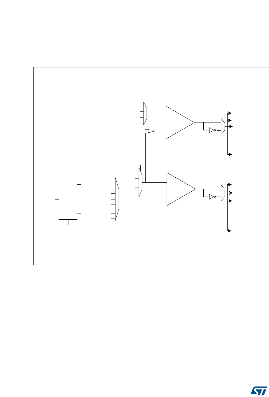
Comparator (COMP) RM0376
366/1001 DocID025941 Rev 5
16.3 COMP functional description
16.3.1 COMP block diagram
The block diagram of the comparators is shown in Figure 61: Comparator 1 and 2 block
diagrams.
Figure 61. Comparator 1 and 2 block diagrams
16.3.2 COMP pins and internal signals
The I/Os used as comparators inputs must be configured in analog mode in the GPIOs
registers.
The comparator output can be connected to the I/Os using the alternate function channel
given in “Alternate function mapping” table in the datasheet.
The output can also be internally redirected to a variety of timer input for the following
purposes:
•Input capture for timing measures
It is possible to have the comparator output simultaneously redirected internally and
externally.
-
+
-
+
COMP1POLARITY
COMP1VALUE
COMP1INNSEL
PA1
COMP1WM
COMP2INPSEL
PA3
PB4
PB6
PB7
VREFINT
¼ VREFINT
½ VREFINT
¾ VREFINT
PA2
PA4 (DAC1)
PA5 (DAC2)
PB3
COMP2INNSEL
COMP2VALUE
TIM2_ETR
TIM2_CH4
TIM21_ETR
TIM21_CH2
TIM22_ETR
TIM22_CH1
LPTIM_ETR
LPTIM_CH2
TIM2_ETR
TIM2_CH4
TIM21_ETR
TIM21_CH2
TIM22_ETR
TIM22_CH1
LPTIM_ETR
LPTIM_CH2
VREFINT
PA0
PA4 (DAC1)
PA5 (DAC2)
Wakeup
EXTI line 21
Wakeup
EXTI line 22
COMP1
COMP2
MSv33715V5
-
+
GPIOx
GPIOx
COMP2POLARITY
PB5
Scaler
VREFINT
ENBUF_
VREFINT
_COMP2

DocID025941 Rev 5 367/1001
RM0376 Comparator (COMP)
371
16.3.3 COMP reset and clocks
The COMP clock provided by the clock controller is synchronous with the PCLK (APB
clock).
There is no clock enable control bit provided in the RCC controller. Reset and clock enable
bits are common for COMP and SYSCFG.
Note: Important: The polarity selection logic and the output redirection to the port works
independently from the PCLK clock. This allows the comparator to work even in Stop mode.
16.3.4 Comparator LOCK mechanism
The comparators can be used for safety purposes, such as over-current or thermal
protection. For applications having specific functional safety requirements, it is necessary to
insure that the comparator programming cannot be altered in case of spurious register
access or program counter corruption.
For this purpose, the comparator control and status registers can be write-protected (read-
only).
Once the programming is completed, the COMPxLOCK bit can be set to 1. This causes the
whole COMPx_CSR register to become read-only, including the COMPxLOCK bit.
The write protection can only be reset by a MCU reset.
16.3.5 Power mode
COMP2 power consumption versus propagation delay can be adjusted to have the optimum
trade-off for a given application.
COMP2_SPEED bit in the COMP2_CSR register can be programmed to provide either
higher speed/consumption or lower speed/consumption.
16.4 COMP interrupts
The comparator outputs are internally connected to the Extended interrupts and events
controller. Each comparator has its own EXTI line and can generate either interrupts or
events. The same mechanism is used to exit from low-power modes.
Refer to Interrupt and events section for more details.
16.5 COMP registers
16.5.1 Comparator 1 control and status register (COMP1_CSR)
The COMP1_CSR is the Comparator1 control/status register. It contains all the bits /flags
related to comparator1.
Address offset: 0x18
System reset value: 0x0000 0000

Comparator (COMP) RM0376
368/1001 DocID025941 Rev 5
31 30 29 28 27 26 25 24 23 22 21 20 19 18 17 16
COMP1
LOCK
COMP1
VALUE Res. Res. Res. Res. Res. Res. Res. Res. Res. Res. Res. Res. Res. Res.
rs r
15 14 13 12 11 10 9 8 7 6 5 4 3 2 1 0
COMP1
POLARITY Res. Res. COMP1
LPTIMIN1 Res. Res. Res. COMP1
WM Res. Res. COMP1INN
SEL Res. Res. Res. COMP1
EN
rw rw rw rw rw rw
Bit 31 COMP1LOCK: COMP1_CSR register lock bit
This bit is set by software and cleared by a hardware system reset. It locks the whole
content of the comparator 1 control register, COMP1_CSR[31:0]
0: COMP1_CSR[31:0] for comparator 1 are read/write
1: COMP1_CSR[31:0] for comparator 1 are read-only
Bit 30 COMP1VALUE: Comparator 1 output status bit
This bit is read-only. It reflects the current comparator 1 output taking into account
COMP1POLARITY bit effect.
Bits 29:16 Reserved, must be kept at reset value
Bit 15 COMP1POLARITY: Comparator 1 polarity selection bit
This bit is set and cleared by software (only if COMP1LOCK not set). It inverts Comparator
1 polarity.
0: Comparator 1 output value not inverted
1: Comparator 1output value inverted
Bits 14:13 Reserved, must be kept at reset value
Bit 12 COMP1LPTIMIN1: Comparator 1 LPTIM input propagation bit
This bit is set and cleared by software (assuming COMP1LOCK not set). It sends
COMP1VALUE to LPTIM input 1.
0: Comparator 1 output gated
1: Comparator 1 output sent to LPTIM input 1
Bits 11:9 Reserved, must be kept at reset value
Bit 8 COMP1WM: Comparator 1 window mode selection bit
This bit is set and cleared by software (only if COMP1LOCK not set). It selects comparator
1 window mode where the Plus inputs of both comparators are connected together.
0: Plus input of comparator 1 connected to PA1.
1: Plus input of comparator 1 shorted with Plus input of comparator 2 (see COMP1_CSR).
Bits 7:6 Reserved, must be kept at reset value

DocID025941 Rev 5 369/1001
RM0376 Comparator (COMP)
371
16.5.2 Comparator 2 control and status register (COMP2_CSR)
The COMP2_CSR is the Comparator2 control/status register. It contains all the bits /flags
related to comparator2.
Address offset: 0x1C
System reset value: 0x0000 0000
Bits 5:4 COMP1INNSEL: Comparator 1 Input Minus connection configuration bit
These bits are set and cleared by software (only if COMP1LOCK not set). They select which
input is connected with the Input Minus of comparator 1
00: VREFINT
01: PA0
10: DAC1/PA4
11: DAC2/PA5
Bits 3:1 Reserved, must be kept at reset value
Bit 0 COMP1EN: Comparator 1 enable bit
This bit is set and cleared by software (only if COMP1LOCK not set). It switches
oncomparator1
0: Comparator 1 switched OFF.
1: Comparator 1 switched ON.
31 30 29 28 27 26 25 24 23 22 21 20 19 18 17 16
COMP2
LOCK
COMP2
VALUE Res. Res. Res. Res. Res. Res. Res. Res. Res. Res. Res. Res. Res. Res.
rs r
15 14 13 12 11 10 9 8 7 6 5 4 3 2 1 0
COMP2
POLARITY Res. COMP2
LPTIMIN1
COMP2
LPTIMIN2 Res. COMP2INPSEL Res. COMP2INNSEL COMP2
SPEED Res. Res. COMP2
EN
rw rw rw rw rw rw rw rw rw rw rw
Bit 31 COMP2LOCK: COMP2_CSR register lock bit
This bit is set by software and cleared by a hardware system reset. It locks the whole
content of the comparator 2 control register, COMP2_CSR[31:0]
0: COMP2_CSR[31:0] for comparator 1 are read/write
1: COMP2_CSR[31:0] for comparator 1 are read-only
Bit 30 COMP2VALUE: Comparator 2 output status bit
This bit is read-only. It reflects the current comparator 2 output taking into account
COMP2POLARITY bit effect.
Bits 29:16 Reserved, must be kept at reset value
Bit 15 COMP2POLARITY: Comparator 2 polarity selection bit
This bit is set and cleared by software (only if COMP2LOCK not set). It inverts Comparator
1 polarity.
0: Comparator 2 output value not inverted
1: Comparator 2 output value inverted
Bit 14 Reserved, must be kept at reset value

Comparator (COMP) RM0376
370/1001 DocID025941 Rev 5
Bit 13 COMP2LPTIMIN1: Comparator 2 LPTIM input 1 propagation bit
This bit is set and cleared by software (assuming COMP2LOCK not set). It sends
COMP2VALUE to LPTIM input 1.
0: Comparator 2 output gated
1: Comparator 2 output sent to LPTIM input 1
Note: COMP2LPTIMIN1 and COMP2LPTIMIN2 cannot both be set to ‘1’.
Bit 12 COMP2LPTIMIN2: Comparator 2 LPTIM input 2 propagation bit
This bit is set and cleared by software (assuming COMP2LOCK not set). It sends
COMP2VALUE to LPTIM input 2.
0: Comparator 2 output gated
1: Comparator 2 output sent to LPTIM input 2
Note: COMP2LPTIMIN1 and COMP2LPTIMIN2 cannot both be set to ‘1’.
Bit 11 Reserved, must be kept at reset value
Bits 10:8 COMP2INPSEL: Comparator 2 Input Plus connection configuration bit
These bits are set and cleared by software (only if COMP2LOCK not set). They select which
input is connected with the Input Plus of comparator 2
000: PA3
001: PB4
010: PB5
011: PB6
100: PB7
Others: Reserved.
Bit 7 Reserved, must be kept at reset value
Bits 6:4 COMP2INNSEL: Comparator 2 Input Minus connection configuration bit
These bits are set and cleared by software (only if COMP2LOCK not set). They select which
input is connected with the Input Minus of comparator 2.
000: VREFINT
001: PA2
010: DAC /PA4
011: DAC2/PA5
100: 1/4 VREFINT
101: 1/2 VREFINT
110: 3/4 VREFINT
111: PB3
Note: If VREFINT or a fraction of VREFINT (using the scaler) is selected, then EN_VREFINT
bit must be set in the SYSCFG_CFGR3 register (see Section 10.2.3: Reference
control and status register (SYSCFG_CFGR3)).
Bit 3 COMP2SPEED: Comparator 2 power mode selection bit
This bit is set and cleared by software (only if COMP2LOCK not set). It selects comparator
2 power mode.
0: slow speed
1: fast speed
Bits 2:1 Reserved, must be kept at reset value
Bit 0 COMP2EN: Comparator 2 enable bit
This bit is set and cleared by software (only if COMP2LOCK not set). It switches
oncomparator2.
0: Comparator 2 switched off.
1: Comparator 2 switched ON.

DocID025941 Rev 5 371/1001
RM0376 Comparator (COMP)
371
16.5.3 COMP register map
The following table summarizes the comparator registers.
The comparator registers share SYSCFG peripheral register base addresses.
Refer to Section 2.2.2 on page 58 for the register boundary addresses.
Table 70. COMP register map and reset values
Offset Register
31
30
29
28
27
26
25
24
23
22
21
20
19
18
17
16
15
14
13
12
11
10
9
8
7
6
5
4
3
2
1
0
0x18 COMP1_CSR
COMP1LOCK
COMP1VALUE
Res.
Res.
Res.
Res.
Res.
Res.
Res.
Res.
Res.
Res.
Res.
Res.
Res.
Res.
COMP1POLARITY
Res.
Res.
COMP1LPTIMIN1
Res.
Res.
Res.
COMP1WM
Res.
Res.
COMP1INNSEL
Res.
Res.
Res.
COMP1EN
Reset value 0 0 0 0 0 0 0 0
0x1C COMP2_CSR
COMP2LOCK
COMP2VALUE
Res.
Res.
Res.
Res.
Res.
Res.
Res.
Res.
Res.
Res.
Res.
Res.
Res.
Res.
COMP2POLARITY
Res.
COMP2LPTIMIN1
COMP2LPTIMIN2
Res.
COMP2INPSEL
Res.
COMP2INNSEL
COMP2SPEED
Res.
Res.
COMP2EN
Reset value 00 0 00 000 0000 0

Touch sensing controller (TSC) RM0376
372/1001 DocID025941 Rev 5
17 Touch sensing controller (TSC)
17.1 Introduction
The touch sensing controller provides a simple solution for adding capacitive sensing
functionality to any application. Capacitive sensing technology is able to detect finger
presence near an electrode which is protected from direct touch by a dielectric (for example
glass, plastic). The capacitive variation introduced by the finger (or any conductive object) is
measured using a proven implementation based on a surface charge transfer acquisition
principle.
The touch sensing controller is fully supported by the STMTouch touch sensing firmware
library which is free to use and allows touch sensing functionality to be implemented reliably
in the end application.
17.2 TSC main features
The touch sensing controller has the following main features:
•Proven and robust surface charge transfer acquisition principle
•Supports up to 24 capacitive sensing channels
•Up to 8 capacitive sensing channels can be acquired in parallel offering a very good
response time
•Spread spectrum feature to improve system robustness in noisy environments
•full hardware management of the charge transfer acquisition sequence
•Programmable charge transfer frequency
•Programmable sampling capacitor I/O pin
•Programmable channel I/O pin
•Programmable max count value to avoid long acquisition when a channel is faulty
•Dedicated end of acquisition and max count error flags with interrupt capability
•One sampling capacitor for up to 3 capacitive sensing channels to reduce the system
components
•Compatible with proximity, touchkey, linear and rotary touch sensor implementation
•Designed to operate with STMTouch touch sensing firmware library
Note: The number of capacitive sensing channels is dependent on the size of the packages and
subject to IO availability.
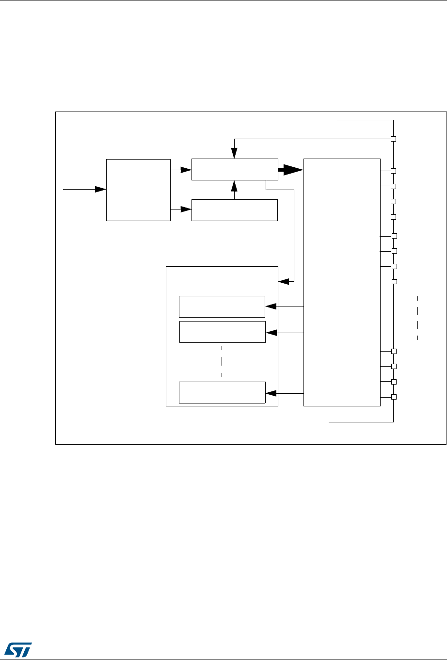
DocID025941 Rev 5 373/1001
RM0376 Touch sensing controller (TSC)
390
17.3 TSC functional description
17.3.1 TSC block diagram
The block diagram of the touch sensing controller is shown in Figure 62: TSC block
diagram.
Figure 62. TSC block diagram
17.3.2 Surface charge transfer acquisition overview
The surface charge transfer acquisition is a proven, robust and efficient way to measure a
capacitance. It uses a minimum number of external components to operate with a single
ended electrode type. This acquisition is designed around an analog I/O group which is
composed of four GPIOs (see Figure 63). Several analog I/O groups are available to allow
the acquisition of several capacitive sensing channels simultaneously and to support a
larger number of capacitive sensing channels. Within a same analog I/O group, the
acquisition of the capacitive sensing channels is sequential.
One of the GPIOs is dedicated to the sampling capacitor CS. Only one sampling capacitor
I/O per analog I/O group must be enabled at a time.
MS30929V1
G1_IO
1
G1_IO
2
G1_IO
3
G1_IO
4
G2_I
O1
G2_I
O2
G2_I
O3
G2_I
O4
Gx_IO
1
Gx_IO
2
Gx_IO
3
Gx_IO
4
I/O control
logic
SYNC
Pulse generator
Spread spectrum
TSC_IOG1CR
TSC_IOG2CR
TSC_IOGxCR
fHCLK Clock
prescalers
Group counters
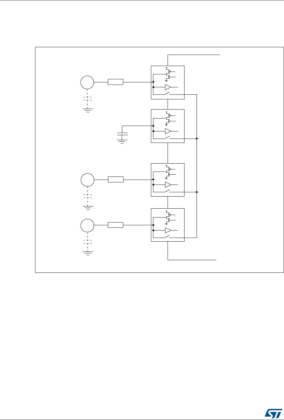
Touch sensing controller (TSC) RM0376
374/1001 DocID025941 Rev 5
The remaining GPIOs are dedicated to the electrodes and are commonly called channels.
For some specific needs (such as proximity detection), it is possible to simultaneously
enable more than one channel per analog I/O group.
Figure 63. Surface charge transfer analog I/O group structure
Note: Gx_IOy where x is the analog I/O group number and y the GPIO number within the selected
group.
The surface charge transfer acquisition principle consists of charging an electrode
capacitance (CX) and transferring a part of the accumulated charge into a sampling
capacitor (CS). This sequence is repeated until the voltage across CS reaches a given
threshold (VIH in our case). The number of charge transfers required to reach the threshold
is a direct representation of the size of the electrode capacitance.
The Table 71 details the charge transfer acquisition sequence of the capacitive sensing
channel 1. States 3 to 7 are repeated until the voltage across CS reaches the given
threshold. The same sequence applies to the acquisition of the other channels. The
electrode serial resistor RS improves the ESD immunity of the solution.
MS30930V1
CX1
G1_IO1
RS1
CX2
G1_IO3
RS2
CX3
G1_IO4
RS3
G1_IO2
CS
Analog
I/O group
Electrode 1
Electrode 2
Electrode 3
DocID025941 Rev 5 375/1001
RM0376 Touch sensing controller (TSC)
390
The voltage variation over the time on the sampling capacitor CS is detailed below:
Figure 64. Sampling capacitor voltage variation
17.3.3 Reset and clocks
The TSC clock source is the AHB clock (HCLK). Two programmable prescalers are used to
generate the pulse generator and the spread spectrum internal clocks:
•The pulse generator clock (PGCLK) is defined using the PGPSC[2:0] bits of the
TSC_CR register
•The spread spectrum clock (SSCLK) is defined using the SSPSC bit of the TSC_CR
register
The Reset and Clock Controller (RCC) provides dedicated bits to enable the touch sensing
controller clock and to reset this peripheral. For more information, please refer to Section 7:
Reset and clock control (RCC).
Table 71. Acquisition sequence summary
State G1_IO1
(channel)
G1_IO2
(sampling)
G1_IO3
(channel)
G1_IO4
(channel) State description
#1
Input floating
with analog
switch closed
Output open-
drain low with
analog switch
closed
Input floating with analog switch
closed
Discharge all CX and
CS
#2 Input floating Dead time
#3 Output push-
pull high Input floating Charge CX1
#4 Input floating Dead time
#5 Input floating with analog switch
closed Input floating Charge transfer from
CX1 to CS
#6 Input floating Dead time
#7 Input floating Measure CS voltage
MS30931V1
t
VCS
Threshold =VIH
VDD
Burst duration
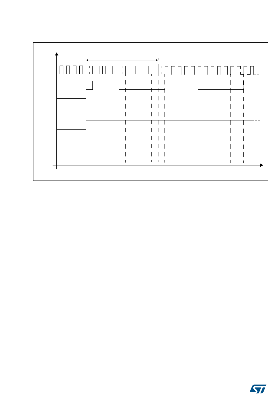
Touch sensing controller (TSC) RM0376
376/1001 DocID025941 Rev 5
17.3.4 Charge transfer acquisition sequence
An example of a charge transfer acquisition sequence is detailed in Figure 65.
Figure 65. Charge transfer acquisition sequence
For higher flexibility, the charge transfer frequency is fully configurable. Both the pulse high
state (charge of CX) and the pulse low state (transfer of charge from CX to CS) duration can
be defined using the CTPH[3:0] and CTPL[3:0] bits in the TSC_CR register. The standard
range for the pulse high and low states duration is 500 ns to 2 µs. To ensure a correct
measurement of the electrode capacitance, the pulse high state duration must be set to
ensure that CX is always fully charged.
A dead time where both the sampling capacitor I/O and the channel I/O are in input floating
state is inserted between the pulse high and low states to ensure an optimum charge
transfer acquisition sequence. This state duration is 2 periods of HCLK.
At the end of the pulse high state and if the spread spectrum feature is enabled, a variable
number of periods of the SSCLK clock are added.
The reading of the sampling capacitor I/O, to determine if the voltage across CS has
reached the given threshold, is performed at the end of the pulse low state and its duration
is one period of HCLK.
Note: The following TSC control register configurations are forbidden:
•
bits PGPSC are set to ‘000’ and bits CTPL are set to ‘0000’
•
bits PGPSC are set to ‘000’ and bits CTPL are set to ‘0001’
•
bits PGPSC are set to ‘001’ and bits CTPL are set to ‘0000’
MS30932V1
Charge transfer frequency
Dead time state
Pulse low state
Spread Spectrum state
(charge transfer
CS reading state
CXHiZ
1
0
CSHiZ
1
0
State
CL
K_AHB
t
Discharge
CX and CS
Pulse high state
(charge of CX)
from CX to CS)
Dead time state
Dead time state
Dead time state
CS reading state
Dead time state
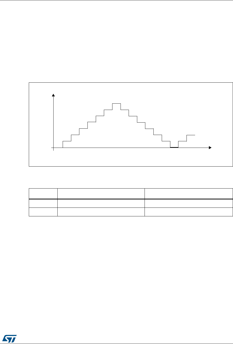
DocID025941 Rev 5 377/1001
RM0376 Touch sensing controller (TSC)
390
17.3.5 Spread spectrum feature
The spread spectrum feature allows to generate a variation of the charge transfer
frequency. This is done to improve the robustness of the charge transfer acquisition in noisy
environments and also to reduce the induced emission. The maximum frequency variation
is in the range of 10% to 50% of the nominal charge transfer period. For instance, for a
nominal charge transfer frequency of 250 kHz (4 µs), the typical spread spectrum deviation
is 10% (400 ns) which leads to a minimum charge transfer frequency of ~227 kHz.
In practice, the spread spectrum consists of adding a variable number of SSCLK periods to
the pulse high state using the principle shown below:
Figure 66. Spread spectrum variation principle
The table below details the maximum frequency deviation with different HCLK settings:
The spread spectrum feature can be disabled/enabled using the SSE bit in the TSC_CR
register. The frequency deviation is also configurable to accommodate the device HCLK
clock frequency and the selected charge transfer frequency through the SSPSC and
SSD[6:0] bits in the TSC_CR register.
17.3.6 Max count error
The max count error prevents long acquisition times resulting from a faulty capacitive
sensing channel. It consists of specifying a maximum count value for the analog I/O group
counters. This maximum count value is specified using the MCV[2:0] bits in the TSC_CR
register. As soon as an acquisition group counter reaches this maximum value, the ongoing
acquisition is stopped and the end of acquisition (EOAF bit) and max count error (MCEF bit)
flags are both set. An interrupt can also be generated if the corresponding end of acquisition
(EOAIE bit) or/and max count error (MCEIE bit) interrupt enable bits are set.
Table 72. Spread spectrum deviation versus AHB clock frequency
fHCLK Spread spectrum step Maximum spread spectrum deviation
24 MHz 41.6 ns 10666.6 ns
32 MHz 27.7 ns 7111.1 ns
MS30933V1
Number of pulse
s
Deviation value
0
1
2
3
(SSD +1)
n-1 n+1
n

Touch sensing controller (TSC) RM0376
378/1001 DocID025941 Rev 5
17.3.7 Sampling capacitor I/O and channel I/O mode selection
To allow the GPIOs to be controlled by the touch sensing controller, the corresponding
alternate function must be enabled through the standard GPIO registers and the GPIOxAFR
registers.
The GPIOs modes controlled by the TSC are defined using the TSC_IOSCR and
TSC_IOCCR register.
When there is no ongoing acquisition, all the I/Os controlled by the touch sensing controller
are in default state. While an acquisition is ongoing, only unused I/Os (neither defined as
sampling capacitor I/O nor as channel I/O) are in default state. The IODEF bit in the
TSC_CR register defines the configuration of the I/Os which are in default state. The table
below summarizes the configuration of the I/O depending on its mode.
Unused I/O mode
An unused I/O corresponds to a GPIO controlled by the TSC peripheral but not defined as
an electrode I/O nor as a sampling capacitor I/O.
Sampling capacitor I/O mode
To allow the control of the sampling capacitor I/O by the TSC peripheral, the corresponding
GPIO must be first set to alternate output open drain mode and then the corresponding
Gx_IOy bit in the TSC_IOSCR register must be set.
Only one sampling capacitor per analog I/O group must be enabled at a time.
Channel I/O mode
To allow the control of the channel I/O by the TSC peripheral, the corresponding GPIO must
be first set to alternate output push-pull mode and the corresponding Gx_IOy bit in the
TSC_IOCCR register must be set.
For proximity detection where a higher equivalent electrode surface is required or to speed-
up the acquisition process, it is possible to enable and simultaneously acquire several
channels belonging to the same analog I/O group.
Table 73. I/O state depending on its mode and IODEF bit value
IODEF bit Acquisition
status
Unused I/O
mode
Channel I/O
mode
Sampling
capacitor I/O
mode
0
(output push-pull
low)
No Output push-pull
low
Output push-pull
low
Output push-pull
low
0
(output push-pull
low)
ongoing Output push-pull
low --
1
(input floating) No Input floating Input floating Input floating
1
(input floating) ongoing Input floating - -

DocID025941 Rev 5 379/1001
RM0376 Touch sensing controller (TSC)
390
Note: During the acquisition phase and even if the TSC peripheral alternate function is not
enabled, as soon as the TSC_IOSCR or TSC_IOCCR bit is set, the corresponding GPIO
analog switch is automatically controlled by the touch sensing controller.
17.3.8 Acquisition mode
The touch sensing controller offers two acquisition modes:
•Normal acquisition mode: the acquisition starts as soon as the START bit in the
TSC_CR register is set.
•Synchronized acquisition mode: the acquisition is enabled by setting the START bit in
the TSC_CR register but only starts upon the detection of a falling edge or a rising
edge and high level on the SYNC input pin. This mode is useful for synchronizing the
capacitive sensing channels acquisition with an external signal without additional CPU
load.
The GxE bits in the TSC_IOGCSR registers specify which analog I/O groups are enabled
(corresponding counter is counting). The CS voltage of a disabled analog I/O group is not
monitored and this group does not participate in the triggering of the end of acquisition flag.
However, if the disabled analog I/O group contains some channels, they will be pulsed.
When the CS voltage of an enabled analog I/O group reaches the given threshold, the
corresponding GxS bit of the TSC_IOGCSR register is set. When the acquisition of all
enabled analog I/O groups is complete (all GxS bits of all enabled analog I/O groups are
set), the EOAF flag in the TSC_ISR register is set. An interrupt request is generated if the
EOAIE bit in the TSC_IER register is set.
In the case that a max count error is detected, the ongoing acquisition is stopped and both
the EOAF and MCEF flags in the TSC_ISR register are set. Interrupt requests can be
generated for both events if the corresponding bits (EOAIE and MCEIE bits of the TSCIER
register) are set. Note that when the max count error is detected the remaining GxS bits in
the enabled analog I/O groups are not set.
To clear the interrupt flags, the corresponding EOAIC and MCEIC bits in the TSC_ICR
register must be set.
The analog I/O group counters are cleared when a new acquisition is started. They are
updated with the number of charge transfer cycles generated on the corresponding
channel(s) upon the completion of the acquisition.
For code example, refer to A.10.1: TSC configuration code example.
17.3.9 I/O hysteresis and analog switch control
In order to offer a higher flexibility, the touch sensing controller also allows to take the control
of the Schmitt trigger hysteresis and analog switch of each Gx_IOy. This control is available
whatever the I/O control mode is (controlled by standard GPIO registers or other
peripherals) assuming that the touch sensing controller is enabled. This may be useful to
perform a different acquisition sequence or for other purposes.
In order to improve the system immunity, the Schmitt trigger hysteresis of the GPIOs
controlled by the TSC must be disabled by resetting the corresponding Gx_IOy bit in the
TSC_IOHCR register.
Touch sensing controller (TSC) RM0376
380/1001 DocID025941 Rev 5
17.4 TSC low-power modes
17.5 TSC interrupts
For code example, refer to A.10.2: TSC interrupt code example.
Table 74. Effect of low-power modes on TSC
Mode Description
Sleep No effect
TSC interrupts cause the device to exit Sleep mode.
Stop TSC registers are frozen
The TSC stops its operation until the Stop or Standby mode is exited.
Standby
Table 75. Interrupt control bits
Interrupt event Enable
control bit Event flag Clear flag
bit
Exit the
Sleep
mode
Exit the
Stop mode
Exit the
Standby
mode
End of acquisition EOAIE EOAIF EOAIC yes no no
Max count error MCEIE MCEIF MCEIC yes no no

DocID025941 Rev 5 381/1001
RM0376 Touch sensing controller (TSC)
390
17.6 TSC registers
Refer to Section 1.1 on page 51 of the reference manual for a list of abbreviations used in
register descriptions.
The peripheral registers can be accessed by words (32-bit).
17.6.1 TSC control register (TSC_CR)
Address offset: 0x00
Reset value: 0x0000 0000
31 30 29 28 27 26 25 24 23 22 21 20 19 18 17 16
CTPH[3:0] CTPL[3:0] SSD[6:0] SSE
rw rw rw rw rw rw rw rw rw rw rw rw rw rw rw rw
1514131211109876543210
SSPSC PGPSC[2:0] Res. Res. Res. Res. MCV[2:0] IODEF SYNC
POL AM START TSCE
rw rw rw rw rw rw rw rw rw rw rw rw
Bits 31:28 CTPH[3:0]: Charge transfer pulse high
These bits are set and cleared by software. They define the duration of the high state of the
charge transfer pulse (charge of CX).
0000: 1x tPGCLK
0001: 2x tPGCLK
...
1111: 16x tPGCLK
Note: These bits must not be modified when an acquisition is ongoing.
Bits 27:24 CTPL[3:0]: Charge transfer pulse low
These bits are set and cleared by software. They define the duration of the low state of the
charge transfer pulse (transfer of charge from CX to CS).
0000: 1x tPGCLK
0001: 2x tPGCLK
...
1111: 16x tPGCLK
Note: These bits must not be modified when an acquisition is ongoing.
Note: Some configurations are forbidden. Please refer to the Section 17.3.4: Charge transfer
acquisition sequence for details.
Bits 23:17 SSD[6:0]: Spread spectrum deviation
These bits are set and cleared by software. They define the spread spectrum deviation which
consists in adding a variable number of periods of the SSCLK clock to the charge transfer
pulse high state.
0000000: 1x tSSCLK
0000001: 2x tSSCLK
...
1111111: 128x tSSCLK
Note: These bits must not be modified when an acquisition is ongoing.

Touch sensing controller (TSC) RM0376
382/1001 DocID025941 Rev 5
Bit 16 SSE: Spread spectrum enable
This bit is set and cleared by software to enable/disable the spread spectrum feature.
0: Spread spectrum disabled
1: Spread spectrum enabled
Note: This bit must not be modified when an acquisition is ongoing.
Bit 15 SSPSC: Spread spectrum prescaler
This bit is set and cleared by software. It selects the AHB clock divider used to generate the
spread spectrum clock (SSCLK).
0: fHCLK
1: fHCLK /2
Note: This bit must not be modified when an acquisition is ongoing.
Bits 14:12 PGPSC[2:0]: Pulse generator prescaler
These bits are set and cleared by software.They select the AHB clock divider used to generate
the pulse generator clock (PGCLK).
000: fHCLK
001: fHCLK /2
010: fHCLK /4
011: fHCLK /8
100: fHCLK /16
101: fHCLK /32
110: fHCLK /64
111: fHCLK /128
Note: These bits must not be modified when an acquisition is ongoing.
Note: Some configurations are forbidden. Please refer to the Section 17.3.4: Charge transfer
acquisition sequence for details.
Bits 11:8 Reserved, must be kept at reset value.
Bits 7:5 MCV[2:0]: Max count value
These bits are set and cleared by software. They define the maximum number of charge
transfer pulses that can be generated before a max count error is generated.
000: 255
001: 511
010: 1023
011: 2047
100: 4095
101: 8191
110: 16383
111: reserved
Note: These bits must not be modified when an acquisition is ongoing.
Bit 4 IODEF: I/O Default mode
This bit is set and cleared by software. It defines the configuration of all the TSC I/Os when
there is no ongoing acquisition. When there is an ongoing acquisition, it defines the
configuration of all unused I/Os (not defined as sampling capacitor I/O or as channel I/O).
0: I/Os are forced to output push-pull low
1: I/Os are in input floating
Note: This bit must not be modified when an acquisition is ongoing.
Bit 3 SYNCPOL: Synchronization pin polarity
This bit is set and cleared by software to select the polarity of the synchronization input pin.
0: Falling edge only
1: Rising edge and high level

DocID025941 Rev 5 383/1001
RM0376 Touch sensing controller (TSC)
390
17.6.2 TSC interrupt enable register (TSC_IER)
Address offset: 0x04
Reset value: 0x0000 0000
Bit 2 AM: Acquisition mode
This bit is set and cleared by software to select the acquisition mode.
0: Normal acquisition mode (acquisition starts as soon as START bit is set)
1: Synchronized acquisition mode (acquisition starts if START bit is set and when the
selected signal is detected on the SYNC input pin)
Note: This bit must not be modified when an acquisition is ongoing.
Bit 1 START: Start a new acquisition
This bit is set by software to start a new acquisition. It is cleared by hardware as soon as the
acquisition is complete or by software to cancel the ongoing acquisition.
0: Acquisition not started
1: Start a new acquisition
Bit 0 TSCE: Touch sensing controller enable
This bit is set and cleared by software to enable/disable the touch sensing controller.
0: Touch sensing controller disabled
1: Touch sensing controller enabled
Note: When the touch sensing controller is disabled, TSC registers settings have no effect.
31 30 29 28 27 26 25 24 23 22 21 20 19 18 17 16
Res. Res. Res. Res. Res. Res. Res. Res. Res. Res. Res. Res. Res. Res. Res. Res.
1514131211109876543210
Res. Res. Res. Res. Res. Res. Res. Res. Res. Res. Res. Res. Res. Res. MCEIE EOAIE
rw rw
Bits 31:2 Reserved, must be kept at reset value.
Bit 1 MCEIE: Max count error interrupt enable
This bit is set and cleared by software to enable/disable the max count error interrupt.
0: Max count error interrupt disabled
1: Max count error interrupt enabled
Bit 0 EOAIE: End of acquisition interrupt enable
This bit is set and cleared by software to enable/disable the end of acquisition interrupt.
0: End of acquisition interrupt disabled
1: End of acquisition interrupt enabled

Touch sensing controller (TSC) RM0376
384/1001 DocID025941 Rev 5
17.6.3 TSC interrupt clear register (TSC_ICR)
Address offset: 0x08
Reset value: 0x0000 0000
31 30 29 28 27 26 25 24 23 22 21 20 19 18 17 16
Res. Res. Res. Res. Res. Res. Res. Res. Res. Res. Res. Res. Res. Res. Res. Res.
1514131211109876543210
Res. Res. Res. Res. Res. Res. Res. Res. Res. Res. Res. Res. Res. Res. MCEIC EOAIC
rw rw
Bits 31:2 Reserved, must be kept at reset value.
Bit 1 MCEIC: Max count error interrupt clear
This bit is set by software to clear the max count error flag and it is cleared by hardware when
the flag is reset. Writing a ‘0’ has no effect.
0: No effect
1: Clears the corresponding MCEF of the TSC_ISR register
Bit 0 EOAIC: End of acquisition interrupt clear
This bit is set by software to clear the end of acquisition flag and it is cleared by hardware
when the flag is reset. Writing a ‘0’ has no effect.
0: No effect
1: Clears the corresponding EOAF of the TSC_ISR register

DocID025941 Rev 5 385/1001
RM0376 Touch sensing controller (TSC)
390
17.6.4 TSC interrupt status register (TSC_ISR)
Address offset: 0x0C
Reset value: 0x0000 0000
17.6.5 TSC I/O hysteresis control register (TSC_IOHCR)
Address offset: 0x10
Reset value: 0xFFFF FFFF
31 30 29 28 27 26 25 24 23 22 21 20 19 18 17 16
Res. Res. Res. Res. Res. Res. Res. Res. Res. Res. Res. Res. Res. Res. Res. Res.
1514131211109876543210
Res. Res. Res. Res. Res. Res. Res. Res. Res. Res. Res. Res. Res. Res. MCEF EOAF
rr
Bits 31:2 Reserved, must be kept at reset value.
Bit 1 MCEF: Max count error flag
This bit is set by hardware as soon as an analog I/O group counter reaches the max count
value specified. It is cleared by software writing 1 to the bit MCEIC of the TSC_ICR register.
0: No max count error (MCE) detected
1: Max count error (MCE) detected
Bit 0 EOAF: End of acquisition flag
This bit is set by hardware when the acquisition of all enabled group is complete (all GxS bits
of all enabled analog I/O groups are set or when a max count error is detected). It is cleared by
software writing 1 to the bit EOAIC of the TSC_ICR register.
0: Acquisition is ongoing or not started
1: Acquisition is complete
31 30 29 28 27 26 25 24 23 22 21 20 19 18 17 16
G8_IO4 G8_IO3 G8_IO2 G8_IO1 G7_IO4 G7_IO3 G7_IO2 G7_IO1 G6_IO4 G6_IO3 G6_IO2 G6_IO1 G5_IO4 G5_IO3 G5_IO2 G5_IO1
rw rw rw rw rw rw rw rw rw rw rw rw rw rw rw rw
1514131211109876543210
G4_IO4 G4_IO3 G4_IO2 G4_IO1 G3_IO4 G3_IO3 G3_IO2 G3_IO1 G2_IO4 G2_IO3 G2_IO2 G2_IO1 G1_IO4 G1_IO3 G1_IO2 G1_IO1
rw rw rw rw rw rw rw rw rw rw rw rw rw rw rw rw
Bits 31:0 Gx_IOy: Gx_IOy Schmitt trigger hysteresis mode
These bits are set and cleared by software to enable/disable the Gx_IOy Schmitt trigger
hysteresis.
0: Gx_IOy Schmitt trigger hysteresis disabled
1: Gx_IOy Schmitt trigger hysteresis enabled
Note: These bits control the I/O Schmitt trigger hysteresis whatever the I/O control mode is
(even if controlled by standard GPIO registers).

Touch sensing controller (TSC) RM0376
386/1001 DocID025941 Rev 5
17.6.6 TSC I/O analog switch control register (TSC_IOASCR)
Address offset: 0x18
Reset value: 0x0000 0000
17.6.7 TSC I/O sampling control register (TSC_IOSCR)
Address offset: 0x20
Reset value: 0x0000 0000
31 30 29 28 27 26 25 24 23 22 21 20 19 18 17 16
G8_IO4 G8_IO3 G8_IO2 G8_IO1 G7_IO4 G7_IO3 G7_IO2 G7_IO1 G6_IO4 G6_IO3 G6_IO2 G6_IO1 G5_IO4 G5_IO3 G5_IO2 G5_IO1
rw rw rw rw rw rw rw rw rw rw rw rw rw rw rw rw
1514131211109876543210
G4_IO4 G4_IO3 G4_IO2 G4_IO1 G3_IO4 G3_IO3 G3_IO2 G3_IO1 G2_IO4 G2_IO3 G2_IO2 G2_IO1 G1_IO4 G1_IO3 G1_IO2 G1_IO1
rw rw rw rw rw rw rw rw rw rw rw rw rw rw rw rw
Bits 31:0 Gx_IOy: Gx_IOy analog switch enable
These bits are set and cleared by software to enable/disable the Gx_IOy analog switch.
0: Gx_IOy analog switch disabled (opened)
1: Gx_IOy analog switch enabled (closed)
Note: These bits control the I/O analog switch whatever the I/O control mode is (even if
controlled by standard GPIO registers).
31 30 29 28 27 26 25 24 23 22 21 20 19 18 17 16
G8_IO4 G8_IO3 G8_IO2 G8_IO1 G7_IO4 G7_IO3 G7_IO2 G7_IO1 G6_IO4 G6_IO3 G6_IO2 G6_IO1 G5_IO4 G5_IO3 G5_IO2 G5_IO1
rw rw rw rw rw rw rw rw rw rw rw rw rw rw rw rw
1514131211109876543210
G4_IO4 G4_IO3 G4_IO2 G4_IO1 G3_IO4 G3_IO3 G3_IO2 G3_IO1 G2_IO4 G2_IO3 G2_IO2 G2_IO1 G1_IO4 G1_IO3 G1_IO2 G1_IO1
rw rw rw rw rw rw rw rw rw rw rw rw rw rw rw rw
Bits 31:0 Gx_IOy: Gx_IOy sampling mode
These bits are set and cleared by software to configure the Gx_IOy as a sampling capacitor
I/O. Only one I/O per analog I/O group must be defined as sampling capacitor.
0: Gx_IOy unused
1: Gx_IOy used as sampling capacitor
Note: These bits must not be modified when an acquisition is ongoing.
During the acquisition phase and even if the TSC peripheral alternate function is not
enabled, as soon as the TSC_IOSCR bit is set, the corresponding GPIO analog switch
is automatically controlled by the touch sensing controller.

DocID025941 Rev 5 387/1001
RM0376 Touch sensing controller (TSC)
390
17.6.8 TSC I/O channel control register (TSC_IOCCR)
Address offset: 0x28
Reset value: 0x0000 0000
17.6.9 TSC I/O group control status register (TSC_IOGCSR)
Address offset: 0x30
Reset value: 0x0000 0000
31 30 29 28 27 26 25 24 23 22 21 20 19 18 17 16
G8_IO4 G8_IO3 G8_IO2 G8_IO1 G7_IO4 G7_IO3 G7_IO2 G7_IO1 G6_IO4 G6_IO3 G6_IO2 G6_IO1 G5_IO4 G5_IO3 G5_IO2 G5_IO1
rw rw rw rw rw rw rw rw rw rw rw rw rw rw rw rw
15 14 13 12 11 10 9 8 7 6 5 4 3 2 1 0
G4_IO4 G4_IO3 G4_IO2 G4_IO1 G3_IO4 G3_IO3 G3_IO2 G3_IO1 G2_IO4 G2_IO3 G2_IO2 G2_IO1 G1_IO4 G1_IO3 G1_IO2 G1_IO1
rw rw rw rw rw rw rw rw rw rw rw rw rw rw rw rw
Bits 31:0 Gx_IOy: Gx_IOy channel mode
These bits are set and cleared by software to configure the Gx_IOy as a channel I/O.
0: Gx_IOy unused
1: Gx_IOy used as channel
Note: These bits must not be modified when an acquisition is ongoing.
During the acquisition phase and even if the TSC peripheral alternate function is not
enabled, as soon as the TSC_IOCCR bit is set, the corresponding GPIO analog switch
is automatically controlled by the touch sensing controller.
31 30 29 28 27 26 25 24 23 22 21 20 19 18 17 16
Res. Res. Res. Res. Res. Res. Res. Res. G8S G7S G6S G5S G4S G3S G2S G1S
rrrrrrrr
1514131211109876543210
Res. Res. Res. Res. Res. Res. Res. Res. G8E G7E G6E G5E G4E G3E G2E G1E
rw rw rw rw rw rw rw rw
Touch sensing controller (TSC) RM0376
388/1001 DocID025941 Rev 5
17.6.10 TSC I/O group x counter register (TSC_IOGxCR) (x = 1..8)
Address offset: 0x30 + 0x04 x Analog I/O group number
Reset value: 0x0000 0000
Bits 31:24 Reserved, must be kept at reset value.
Bits 23:16 GxS: Analog I/O group x status
These bits are set by hardware when the acquisition on the corresponding enabled analog I/O
group x is complete. They are cleared by hardware when a new acquisition is started.
0: Acquisition on analog I/O group x is ongoing or not started
1: Acquisition on analog I/O group x is complete
Note: When a max count error is detected the remaining GxS bits of the enabled analog I/O
groups are not set.
Bits 15:8 Reserved, must be kept at reset value.
Bits 7:0 GxE: Analog I/O group x enable
These bits are set and cleared by software to enable/disable the acquisition (counter is
counting) on the corresponding analog I/O group x.
0: Acquisition on analog I/O group x disabled
1: Acquisition on analog I/O group x enabled
31 30 29 28 27 26 25 24 23 22 21 20 19 18 17 16
Res. Res. Res. Res. Res. Res. Res. Res. Res. Res. Res. Res. Res. Res. Res. Res.
1514131211109876543210
Res. Res. CNT[13:0]
rrrrrrrrrrrrrr
Bits 31:14 Reserved, must be kept at reset value.
Bits 13:0 CNT[13:0]: Counter value
These bits represent the number of charge transfer cycles generated on the analog I/O group
x to complete its acquisition (voltage across CS has reached the threshold).

DocID025941 Rev 5 389/1001
RM0376 Touch sensing controller (TSC)
390
17.6.11 TSC register map
Table 76. TSC register map and reset values
Offset Register
31
30
29
28
27
26
25
24
23
22
21
20
19
18
17
16
15
14
13
12
11
10
9
8
7
6
5
4
3
2
1
0
0x0000
TSC_CR CTPH[3:0] CTPL[3:0] SSD[6:0]
SSE
SSPSC
PGPSC[2:0]
Res.
Res.
Res.
Res.
MCV
[2:0]
IODEF
SYNCPOL
AM
START
TSCE
Reset value 00000000000000000000 00000000
0x0004
TSC_IER
Res.
Res.
Res.
Res.
Res.
Res.
Res.
Res.
Res.
Res.
Res.
Res.
Res.
Res.
Res.
Res.
Res.
Res.
Res.
Res.
Res.
Res.
Res.
Res.
Res.
Res.
Res.
Res.
Res.
Res.
MCEIE
EOAIE
Reset value 00
0x0008
TSC_ICR
Res.
Res.
Res.
Res.
Res.
Res.
Res.
Res.
Res.
Res.
Res.
Res.
Res.
Res.
Res.
Res.
Res.
Res.
Res.
Res.
Res.
Res.
Res.
Res.
Res.
Res.
Res.
Res.
Res.
Res.
MCEIC
EOAIC
Reset value 00
0x000C
TSC_ISR
Res.
Res.
Res.
Res.
Res.
Res.
Res.
Res.
Res.
Res.
Res.
Res.
Res.
Res.
Res.
Res.
Res.
Res.
Res.
Res.
Res.
Res.
Res.
Res.
Res.
Res.
Res.
Res.
Res.
Res.
MCEF
EOAF
Reset value 00
0x0010
TSC_IOHCR
G8_IO4
G8_IO3
G8_IO2
G8_IO1
G7_IO4
G7_IO3
G7_IO2
G7_IO1
G6_IO4
G6_IO3
G6_IO2
G6_IO1
G5_IO4
G5_IO3
G5_IO2
G5_IO1
G4_IO4
G4_IO3
G4_IO2
G4_IO1
G3_IO4
G3_IO3
G3_IO2
G3_IO1
G2_IO4
G2_IO3
G2_IO2
G2_IO1
G1_IO4
G1_IO3
G1_IO2
G1_IO1
Reset value 11111111111111111111111111111111
0x0014 Reserved
0x0018
TSC_IOASCR
G8_IO4
G8_IO3
G8_IO2
G8_IO1
G7_IO4
G7_IO3
G7_IO2
G7_IO1
G6_IO4
G6_IO3
G6_IO2
G6_IO1
G5_IO4
G5_IO3
G5_IO2
G5_IO1
G4_IO4
G4_IO3
G4_IO2
G4_IO1
G3_IO4
G3_IO3
G3_IO2
G3_IO1
G2_IO4
G2_IO3
G2_IO2
G2_IO1
G1_IO4
G1_IO3
G1_IO2
G1_IO1
Reset value 00000000000000000000000000000000
0x001C Reserved
0x0020
TSC_IOSCR
G8_IO4
G8_IO3
G8_IO2
G8_IO1
G7_IO4
G7_IO3
G7_IO2
G7_IO1
G6_IO4
G6_IO3
G6_IO2
G6_IO1
G5_IO4
G5_IO3
G5_IO2
G5_IO1
G4_IO4
G4_IO3
G4_IO2
G4_IO1
G3_IO4
G3_IO3
G3_IO2
G3_IO1
G2_IO4
G2_IO3
G2_IO2
G2_IO1
G1_IO4
G1_IO3
G1_IO2
G1_IO1
Reset value 00000000000000000000000000000000
0x0024 Reserved
0x0028
TSC_IOCCR
G8_IO4
G8_IO3
G8_IO2
G8_IO1
G7_IO4
G7_IO3
G7_IO2
G7_IO1
G6_IO4
G6_IO3
G6_IO2
G6_IO1
G5_IO4
G5_IO3
G5_IO2
G5_IO1
G4_IO4
G4_IO3
G4_IO2
G4_IO1
G3_IO4
G3_IO3
G3_IO2
G3_IO1
G2_IO4
G2_IO3
G2_IO2
G2_IO1
G1_IO4
G1_IO3
G1_IO2
G1_IO1
Reset value 00000000000000000000000000000000
0x002C Reserved
0x0030
TSC_IOGCSR
Res.
Res.
Res.
Res.
Res.
Res.
Res.
Res.
G8S
G7S
G6S
G5S
G4S
G3S
G2S
G1S
Res.
Res.
Res.
Res.
Res.
Res.
Res.
Res.
G8E
G7E
G6E
G5E
G4E
G3E
G2E
G1E
Reset value 00000000 00000000
0x0034
TSC_IOG1CR
Res.
Res.
Res.
Res.
Res.
Res.
Res.
Res.
Res.
Res.
Res.
Res.
Res.
Res.
Res.
Res.
Res.
Res.
CNT[13:0]
Reset value 00000000000000
0x0038
TSC_IOG2CR
Res.
Res.
Res.
Res.
Res.
Res.
Res.
Res.
Res.
Res.
Res.
Res.
Res.
Res.
Res.
Res.
Res.
Res.
CNT[13:0]
Reset value 00000000000000
Touch sensing controller (TSC) RM0376
390/1001 DocID025941 Rev 5
Refer to Section 2.2.2 on page 58 for the register boundary addresses.
0x003C
TSC_IOG3CR
Res.
Res.
Res.
Res.
Res.
Res.
Res.
Res.
Res.
Res.
Res.
Res.
Res.
Res.
Res.
Res.
Res.
Res.
CNT[13:0]
Reset value 00000000000000
0x0040
TSC_IOG4CR
Res.
Res.
Res.
Res.
Res.
Res.
Res.
Res.
Res.
Res.
Res.
Res.
Res.
Res.
Res.
Res.
Res.
Res.
CNT[13:0]
Reset value 00000000000000
0x0044
TSC_IOG5CR
Res.
Res.
Res.
Res.
Res.
Res.
Res.
Res.
Res.
Res.
Res.
Res.
Res.
Res.
Res.
Res.
Res.
Res.
CNT[13:0]
Reset value 00000000000000
0x0048
TSC_IOG6CR
Res.
Res.
Res.
Res.
Res.
Res.
Res.
Res.
Res.
Res.
Res.
Res.
Res.
Res.
Res.
Res.
Res.
Res.
CNT[13:0]
Reset value 00000000000000
0x004C
TSC_IOG7CR
Res.
Res.
Res.
Res.
Res.
Res.
Res.
Res.
Res.
Res.
Res.
Res.
Res.
Res.
Res.
Res.
Res.
Res.
CNT[13:0]
Reset value 00000000000000
0x0050
TSC_IOG8CR
Res.
Res.
Res.
Res.
Res.
Res.
Res.
Res.
Res.
Res.
Res.
Res.
Res.
Res.
Res.
Res.
Res.
Res.
CNT[13:0]
Reset value 00000000000000
Table 76. TSC register map and reset values (continued)
Offset Register
31
30
29
28
27
26
25
24
23
22
21
20
19
18
17
16
15
14
13
12
11
10
9
8
7
6
5
4
3
2
1
0

DocID025941 Rev 5 391/1001
AES hardware accelerator (AES)
424
18 AES hardware accelerator (AES)
18.1 Introduction
The AES hardware accelerator (AES) encrypts or decrypts data, using an algorithm and
implementation fully compliant with the advanced encryption standard (AES) defined in
Federal information processing standards (FIPS) publication 197.
Multiple chaining modes are supported (ECB, CBC, CTR), for key size of 128 bits.
The AES accelerator is a 32-bit AHB peripheral. It supports DMA single transfers for
incoming and outgoing data (two DMA channels required).
The AES peripheral provides hardware acceleration to AES cryptographic algorithms
packaged in STM32 cryptographic library.
AES is an AMBA AHB slave peripheral, accessible through 32-bit word single accesses only
(otherwise an AHB bus error is generated and write accesses are ignored).
18.2 AES main features
•Compliance with NIST “Advanced encryption standard (AES), FIPS publication 197”
from November 2001
•128-bit data block processing
•Support for cipher key length of 128-bit
•Encryption and decryption with multiple chaining modes:
– Electronic codebook (ECB) mode
– Cipher block chaining (CBC) mode
– Counter (CTR) mode
•213 clock cycle latency for processing one 128-bit block of data
•Integrated key scheduler with its key derivation stage (ECB or CBC decryption only)
•AMBA AHB slave peripheral, accessible through 32-bit word single accesses only
•128-bit register for storing the cryptographic key (four 32-bit registers)
•128-bit register for storing initialization vector (four 32-bit registers)
– Used for the initialization vector when AES is configured in CBC mode or for the
32-bit counter initialization when CTR mode is selected
•32-bit buffer for data input and output
•Automatic data flow control with support of single-transfer direct memory access (DMA)
using two channels (one for incoming data, one for processed data)
•Data-swapping logic to support 1-, 8-, 16- or 32-bit data
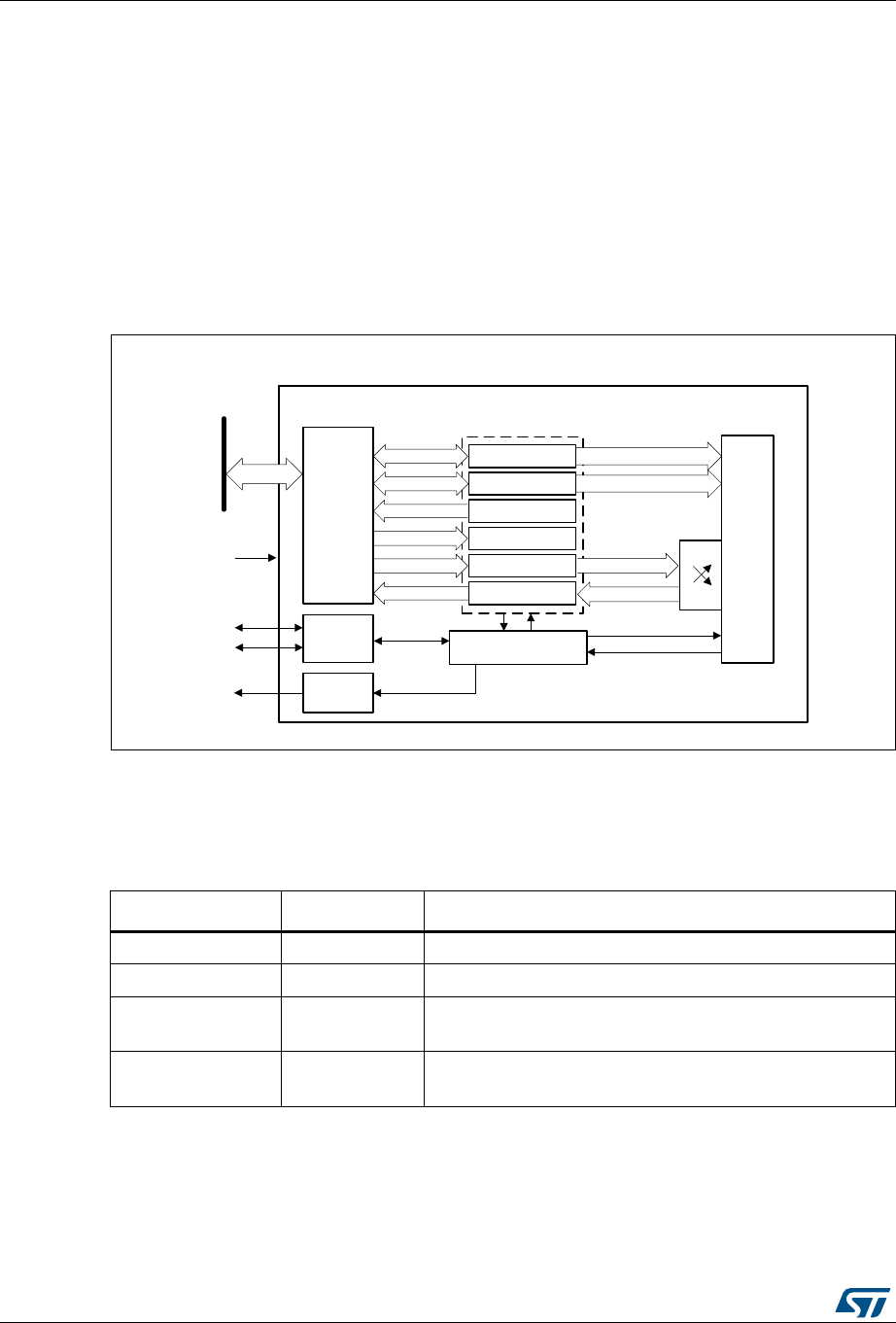
AES hardware accelerator (AES)
392/1001 DocID025941 Rev 5
18.3 AES implementation
The device has a single instance of AES peripheral.
18.4 AES functional description
18.4.1 AES block diagram
Figure 67 shows the block diagram of AES.
Figure 67. AES block diagram
18.4.2 AES internal signals
Table 77 describes the user relevant internal signals interfacing the AES peripheral.
MSv42155V1
aes_hclk
Banked registers
DOUT
KEY
IVI
DIN
AES
key
control
status
IV, counter
data in
data out
aes_it
32-bit
AHB bus
aes_in_dma
AES_CR
AES_KEYRx
AES_SR
AES_IVRx
AES_DINR
AES_DOUTR
AES
Core
(AEA)
swap
AHB
interface
IRQ
interface
Control Logic
DMA
interface
aes_out_dma
32-bit
access
Table 77. AES internal input/output signals
Signal name Signal type Description
aes_hclk digital input AHB bus clock
aes_it digital output AES interrupt request
aes_in_dma digital
input/output Input DMA single request/acknowledge
aes_out_dma digital
input/output Output DMA single request/acknowledge

DocID025941 Rev 5 393/1001
AES hardware accelerator (AES)
424
18.4.3 AES cryptographic core
Overview
The AES cryptographic core consists of the following components:
•AES algorithm (AEA)
•key input
•initialization vector (IV) input
The AES core works on 128-bit data blocks (four words) with 128-bit key length. Depending
on the chaining mode, the AES requires zero or one 96-bit initialization vector IV (and a 32-
bit counter field).
The AES features the following modes of operation:
•Mode 1:
Plaintext encryption using a key stored in the AES_KEYRx registers
•Mode 2:
ECB or CBC decryption key preparation. It must be used prior to selecting Mode 3 with
ECB or CBC chaining modes. The key prepared for decryption is stored automatically
in the AES_KEYRx registers. Now the AES peripheral is ready to switch to Mode 3 for
executing data decryption.
•Mode 3:
Ciphertext decryption using a key stored in the AES_KEYRx registers. When ECB and
CBC chaining modes are selected, the key must be prepared beforehand, through
Mode 2.
•Mode 4:
ECB or CBC ciphertext single decryption using the key stored in the AES_KEYRx
registers (the initial key is derived automatically).
Note: Mode 2 and mode 4 are only used when performing ECB and CBC decryption.
When Mode 4 is selected only one decryption can be done, therefore usage of Mode 2 and
Mode 3 is recommended instead.
The operating mode is selected by programming the MODE[1:0] bitfield of the AES_CR
register. It may be done only when the AES peripheral is disabled.
Typical data processing
Typical usage of the AES is described in Section 18.4.4: AES procedure to perform a cipher
operation on page 396.
Note: The outputs of the intermediate AEA stages are never revealed outside the cryptographic
boundary, with the exclusion of the IVI bitfield.
Chaining modes
The following chaining modes are supported by AES, selected through the CHMOD[1:0]
bitfield of the AES_CR register:
•Electronic code book (ECB)
•Cipher block chaining (CBC)
•Counter (CTR)
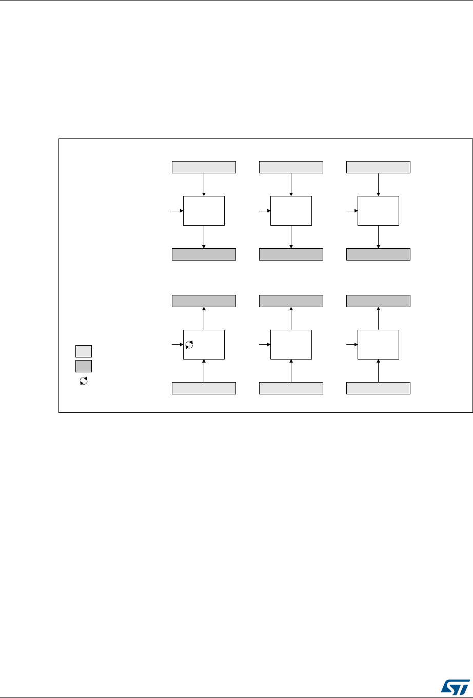
AES hardware accelerator (AES)
394/1001 DocID025941 Rev 5
Note: The chaining mode may be changed only when AES is disabled (bit EN of the AES_CR
register set).
Principle of each AES chaining mode is provided in the following subsections.
Detailed information is in dedicated sections, starting from Section 18.4.8: AES basic
chaining modes (ECB, CBC).
Electronic codebook (ECB) mode
Figure 68. ECB encryption and decryption principle
ECB is the simplest mode of operation. There are no chaining operations, and no special
initialization stage. The message is divided into blocks and each block is encrypted or
decrypted separately.
Note: For decryption, a special key scheduling is required before processing the first block.
MSv42140V1
Encryption
Plaintext block 1 Plaintext block 2 Plaintext block 3
Ciphertext block 1 Ciphertext block 2 Ciphertext block 3
Encrypt Encrypt Encrypt
Decryption
key key key
Plaintext block 1 Plaintext block 2 Plaintext block 3
Ciphertext block 1 Ciphertext block 2 Ciphertext block 3
Decrypt Decrypt Decrypt
key key key
input
output
key
scheduling
Legend
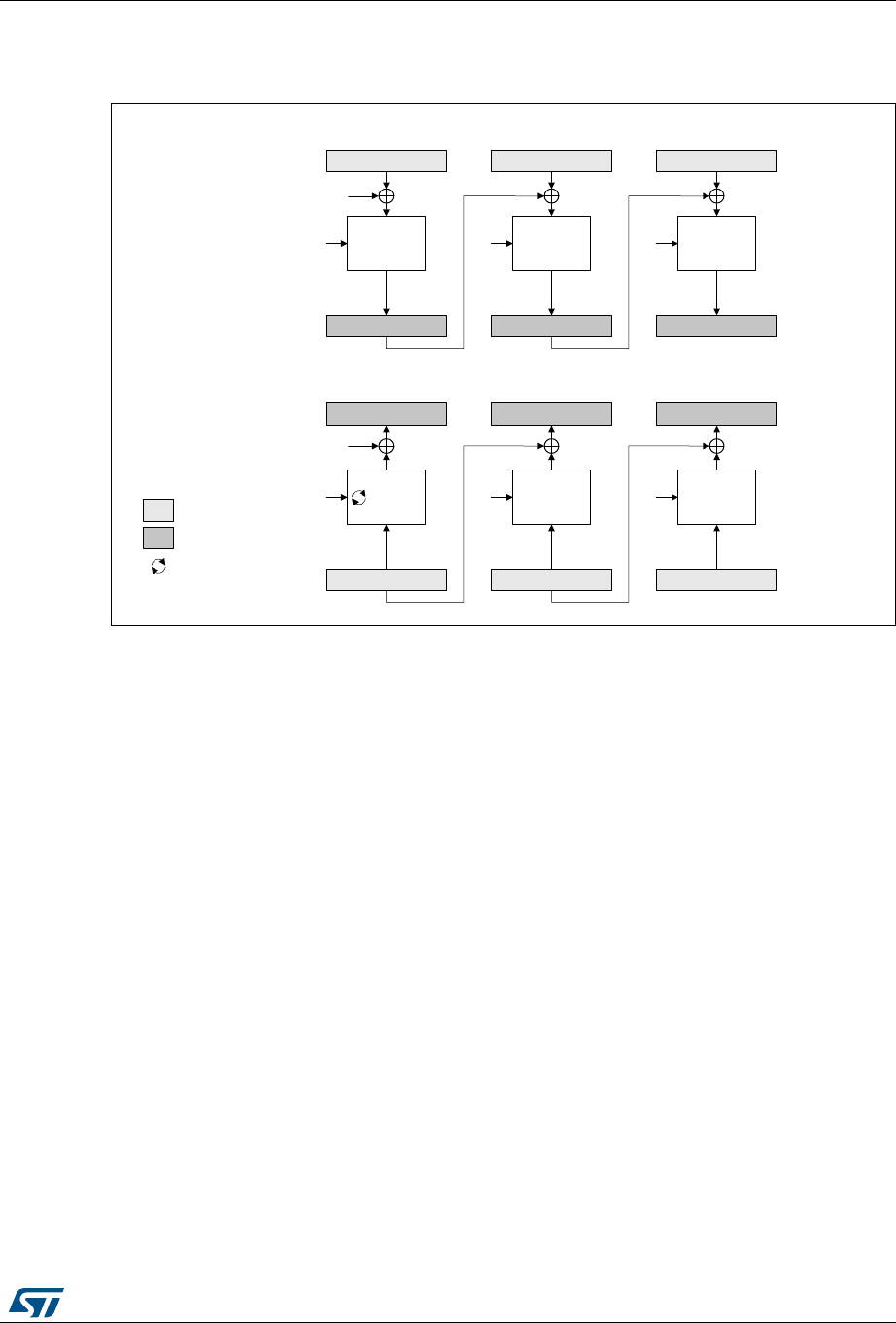
DocID025941 Rev 5 395/1001
AES hardware accelerator (AES)
424
Cipher block chaining (CBC) mode
Figure 69. CBC encryption and decryption principle
In CBC mode the output of each block chains with the input of the following block. To make
each message unique, an initialization vector is used during the first block processing.
Note: For decryption, a special key scheduling is required before processing the first block.
MSv42141V1
Encryption
Plaintext block 1 Plaintext block 2 Plaintext block 3
Ciphertext block 1 Ciphertext block 2 Ciphertext block 3
Encrypt Encrypt Encrypt
Decryption
key key key
Plaintext block 1 Plaintext block 2 Plaintext block 3
Ciphertext block 1 Ciphertext block 2 Ciphertext block 3
Decrypt Decrypt Decrypt
key key key
input
output
key
scheduling
Legend
initialization
vector
initialization
vector
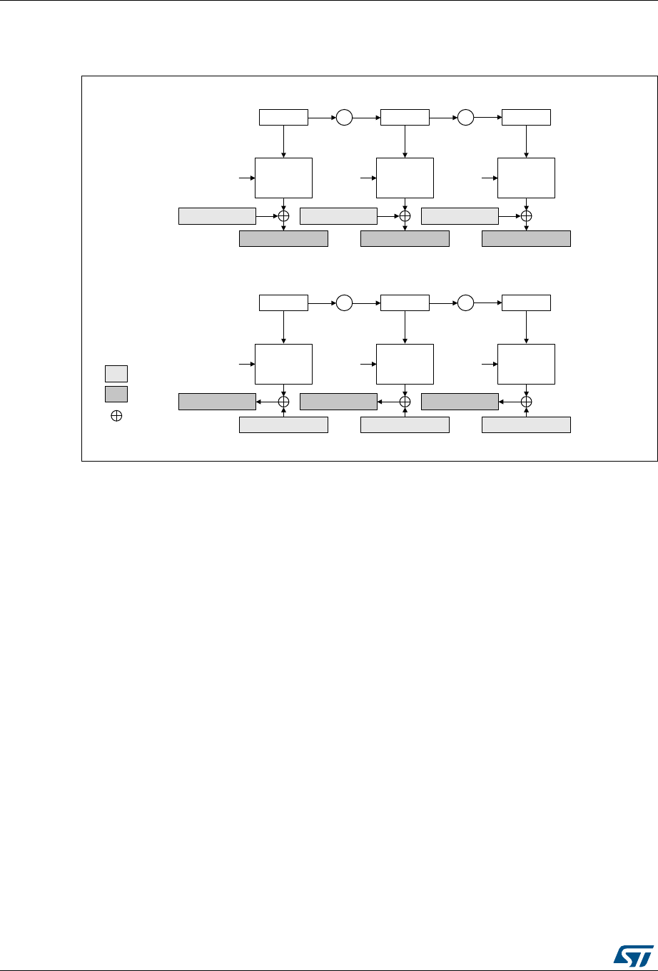
AES hardware accelerator (AES)
396/1001 DocID025941 Rev 5
Counter (CTR) mode
Figure 70. CTR encryption and decryption principle
The CTR mode uses the AES core to generate a key stream. The keys are then XORed
with the plaintext to obtain the ciphertext as specified in NIST Special Publication 800-38A,
Recommendation for Block Cipher Modes of Operation.
Note: Unlike with ECB and CBC modes, no key scheduling is required for the CTR decryption,
since in this chaining scheme the AES core is always used in encryption mode for producing
the key stream, or counter blocks.
18.4.4 AES procedure to perform a cipher operation
Introduction
A typical cipher operation is explained below. Detailed information is provided in sections
starting from Section 18.4.8: AES basic chaining modes (ECB, CBC).
The flowcharts shown in Figure 71 describe the way STM32 cryptographic library
implements the AES algorithm. AES accelerates the execution of the AES-128
cryptographic algorithm in ECB, CBC, and CTR operating modes.
Note: For more details on the cryptographic library, refer to the UM1924 user manual “STM32
crypto library” available from www.st.com.
MSv42142V1
Encryption
Plaintext block 1
Ciphertext block 1 Ciphertext block 2 Ciphertext block 3
Encrypt Encrypt Encrypt
Decryption
Ciphertext block 1 Ciphertext block 2 Ciphertext block 3
Decrypt Decrypt Decrypt
input
output
Legend
key key key
key key key
Plaintext block 2 Plaintext block 3
Counter Counter Counter
+1 +1
Plaintext block 1 Plaintext block 2 Plaintext block 3
Counter Counter Counter
+1 +1
XOR
value value + 1 value + 2
value value + 1 value + 2
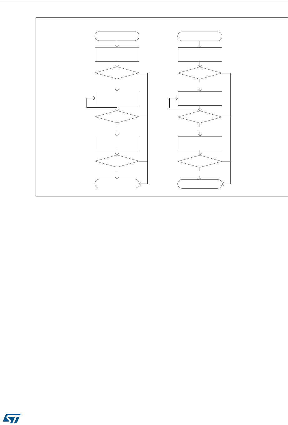
DocID025941 Rev 5 397/1001
AES hardware accelerator (AES)
424
Figure 71. STM32 cryptolib AES flowchart example
Initialization of AES
To initialize AES, first disable it by clearing the EN bit of the AES_CR register. Then perform
the following steps in any order:
•Configure the AES mode, by programming the MODE[1:0] bitfield of the AES_CR
register.
– For encryption, Mode 1 must be selected (MODE[1:0] = 00).
– For decryption, Mode 3 must be selected (MODE[1:0] = 10), unless ECB or CBC
chaining modes are used. In this latter case, an initial key derivation of the
encryption key must be performed, as described in Section 18.4.5: AES
decryption key preparation.
•Select the chaining mode, by programming the CHMOD[1:0] bitfield of the AES_CR
register
•Write a symmetric key into the AES_KEYRx registers .
•Configure the data type (1-, 8-, 16- or 32-bit), with the DATATYPE[1:0] bitfield in the
AES_CR register.
•When it is required (for example in CBC or CTR chaining modes), write the initialization
vectors into the AES_IVRx register.
Data append
This section describes different ways of appending data for processing, where the size of
data to process is not a multiple of 128 bits.
MSv42146V1
Error status
Begin
AES_x encrypt init
AES_x encrypt
append
Error status
AES_x encrypt finish/
final
Error status
End
success
success
success
Encryption
Error status
Begin
AES_x decrypt init
AES_x decrypt
append
Error status
AES_x decrypt finish/
final
Error status
End
success
success
success
Decryption
Data to append Data to append

AES hardware accelerator (AES)
398/1001 DocID025941 Rev 5
For ECB or CBC mode, refer to Section 18.4.6: AES ciphertext stealing and data padding.
The second-last and the last block management in these cases is more complex than in the
sequence described in this section.
Data append through polling
This method uses flag polling to control the data append.
For all other cases, the data is appended through the following sequence:
1. Enable the AES peripheral by setting the EN bit of the AES_CR register.
2. Repeat the following sub-sequence until the payload is entirely processed:
a) Write four input data words into the AES_DINR register.
b) Wait until the status flag CCF is set in the AES_SR, then read the four data words
from the AES_DOUTR register.
c) Clear the CCF flag, by setting the CCFC bit of the AES_CR register.
d) If the data block just processed is the second-last block of the message and the
significant data in the last block to process is inferior to 128 bits, pad the
remainder of the last block with zeros
3. Discard the data that is not part of the payload, then disable the AES peripheral by
clearing the EN bit of the AES_CR register.
Note: Up to three wait cycles are automatically inserted between two consecutive writes to the
AES_DINR register, to allow sending the key to the AES processor.
Data append using interrupt
The method uses interrupt from the AES peripheral to control the data append, through the
following sequence:
1. Enable interrupts from AES by setting the CCFIE bit of the AES_CR register.
2. Enable the AES peripheral by setting the EN bit of the AES_CR register.
3. Write first four input data words into the AES_DINR register.
4. Handle the data in the AES interrupt service routine, upon interrupt:
a) Read four output data words from the AES_DOUTR register.
b) Clear the CCF flag and thus the pending interrupt, by setting the CCFC bit of the
AES_CR register
c) If the data block just processed is the second-last block of an message and the
significant data in the last block to process is inferior to 128 bits, pad the
remainder of the last block with zeros. Then proceed with point 4e).
d) If the data block just processed is the last block of the message, discard the data
that is not part of the payload, then disable the AES peripheral by clearing the EN
bit of the AES_CR register and quit the interrupt service routine.
e) Write next four input data words into the AES_DINR register and quit the interrupt
service routine.
Note: AES is tolerant of delays between consecutive read or write operations, which allows, for
example, an interrupt from another peripheral to be served between two AES computations.
Data append using DMA
With this method, all the transfers and processing are managed by DMA and AES. To use
the method, proceed as follows:

DocID025941 Rev 5 399/1001
AES hardware accelerator (AES)
424
1. Prepare the last four-word data block (if the data to process does not fill it completely),
by padding the remainder of the block with zeros.
2. Configure the DMA controller so as to transfer the data to process from the memory to
the AES peripheral input and the processed data from the AES peripheral output to the
memory, as described in Section 18.4.13: AES DMA interface. Configure the DMA
controller so as to generate an interrupt on transfer completion.
3. Enable the AES peripheral by setting the EN bit of the AES_CR register
4. Enable DMA requests by setting the DMAINEN and DMAOUTEN bits of the AES_CR
register.
5. Upon DMA interrupt indicating the transfer completion, get the AES-processed data
from the memory.
Note: The CCF flag has no use with this method, because the reading of the AES_DOUTR
register is managed by DMA automatically, without any software action, at the end of the
computation phase.
18.4.5 AES decryption key preparation
For an ECB or CBC decryption, a key for the first round of decryption must be derived from
the key of the last round of encryption. This is why a complete key schedule of encryption is
required before performing the decryption. This key preparation is not required for AES
decryption in modes other than ECB or CBC.
Recommended method is to select the Mode 2 by setting to 01 the MODE[1:0] bitfield of the
AES_CR (key process only), then proceed with the decryption by setting MODE[1:0] to 10
(Mode 3, decryption only). Mode 2 usage is described below:
1. Disable the AES peripheral by clearing the EN bit of the AES_CR register.
2. Select Mode 2 by setting to 01 the MODE[1:0] bitfield of the AES_CR. The
CHMOD[1:0] bitfield is not significant in this case because this key derivation mode is
independent of the chaining algorithm selected.
3. Write the AES_KEYRx registers (128bits) with encryption key, as shown in Figure 72.
Writes to the AES_IVRx registers have no effect.
4. Enable the AES peripheral, by setting the EN bit of the AES_CR register.
5. Wait until the CCF flag is set in the AES_SR register.
6. Derived key is available in AES core, ready to use for decryption. Application can also
read the AES_KEYRx register to obtain the derived key if needed, as shown in
Figure 72 (the processed key is loaded automatically into the AES_KEYRx registers).
Note: The AES is disabled by hardware when the derivation key is available.
To restart a derivation key computation, repeat steps 3, 4, 5 and 6 .

AES hardware accelerator (AES)
400/1001 DocID025941 Rev 5
Figure 72. Encryption key derivation for ECB/CBC decryption (Mode 2)
If the software stores the initial key prepared for decryption, it is enough to do the key
schedule operation only once for all the data to be decrypted with a given cipher key.
Note: Alternative key preparation is to select Mode 4 by setting to 11 the MODE[1:0] bitfield of the
AES_CR register. In this case Mode 3 cannot be used.
18.4.6 AES ciphertext stealing and data padding
When using AES in ECB or CBC modes to manage messages the size of which is not a
multiple of the block size (128 bits), ciphertext stealing techniques are used, such as those
described in NIST Special Publication 800-38A, Recommendation for Block Cipher Modes
of Operation: Three Variants of Ciphertext Stealing for CBC Mode. Since the AES peripheral
on the device does not support such techniques, the last two blocks of input data must be
handled in a special way by the application.
Note: Ciphertext stealing techniques are not documented in this reference manual.
Similarly, when AES is used in other modes than ECB or CBC, an incomplete input data
block (that is, block with input data shorter than 128 bits) must be padded with zeros prior to
encryption (that is, extra bits must be appended to the trailing end of the data string). After
decryption, the extra bits must be discarded. As AES does not implement automatic data
padding operation to the last block, the application must follow the recommendation given
in Section 18.4.4: AES procedure to perform a cipher operation on page 396 to manage
messages the size of which is not a multiple of 128 bits.
Note: Padding data are swapped in a similar way as normal data, according to the
DATATYPE[1:0] field of the AES_CR register (see Section 18.4.10: AES data registers and
data swapping on page 409 for details).
18.4.7 AES task suspend and resume
A message can be suspended if another message with a higher priority must be processed.
When this highest priority message is sent, the suspended message can resume in both
encryption or decryption mode.
Suspend/resume operations do not break the chaining operation and the message
processing can resume as soon as AES is enabled again to receive the next data block.
Figure 73 gives an example of suspend/resume operation: Message 1 is suspended in
order to send a shorter and higher-priority Message 2.
MS18937V2
WR
EK3
WR
EK2
WR
EK1
WR
EK0 Wait until flag CCF = 1 RD
DK3
RD
DK2
RD
DK1
RD
DK0
Input phase
4 write operations into
AES_KEYRx[31:0]
Computation phase
Output phase (optional)
4 read operations of
AES_KEYRx[31:0]
EK = encryption key = 4 words (EK3, … , EK0)
DK = decryption key = 4 words (DK3, … , DK0)
MSB LSB MSB LSB
EN = 1 into AES_CR 128-bit derivation key
stored into AES_KEYRx
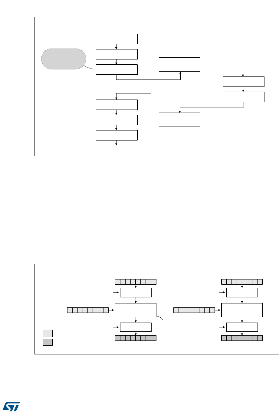
DocID025941 Rev 5 401/1001
AES hardware accelerator (AES)
424
Figure 73. Example of suspend mode management
A detailed description of suspend/resume operations is in the sections dedicated to each
AES mode.
18.4.8 AES basic chaining modes (ECB, CBC)
Overview
This section gives a brief explanation of the four basic operation modes provided by the
AES computing core: ECB encryption, ECB decryption, CBC encryption and CBC
decryption. For detailed information, refer to the FIPS publication 197 from November 26,
2001.
Figure 74 illustrates the electronic codebook (ECB) encryption.
Figure 74. ECB encryption
In ECB encrypt mode, the 128-bit plaintext input data block Px in the AES_DINR register
first goes through bit/byte/half-word swapping. The swap result Ix is processed with the AES
core set in encrypt mode, using a 128--bit key. The encryption result Ox goes through
bit/byte/half-word swapping, then is stored in the AES_DOUTR register as 128-bit ciphertext
MSv42148V1
128-bit block 1
Message 1
128-bit block 2
128-bit block 4
128-bit block 5
128-bit block 6
...
AES suspend
sequence
AES resume
sequence
128-bit block 1
128-bit block 2
Message 2
128-bit block 3
New higher-priority
message 2 to be
processed
MSv19105V2
Encrypt
AES_KEYRx (KEY)
AES_DINR (plaintext P1)
AES_DOUTR (ciphertext C1)
Swap
management
DATATYPE[1:0]
DATATYPE[1:0] Swap
management
Encrypt
AES_KEYRx (KEY)
AES_DINR (plaintext P2)
AES_DOUTR (ciphertext C2)
Swap
management
DATATYPE[1:0]
DATATYPE[1:0] Swap
management
input
output
Legend
I1 I2
O1 O2
Block 1 Block 2
AES core
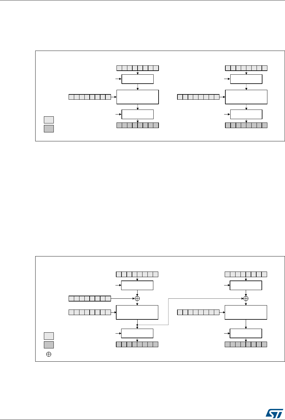
AES hardware accelerator (AES)
402/1001 DocID025941 Rev 5
output data block Cx. The ECB encryption continues in this way until the last complete
plaintext block is encrypted.
Figure 75 illustrates the electronic codebook (ECB) decryption.
Figure 75. ECB decryption
To perform an AES decryption in the ECB mode, the secret key has to be prepared by
collecting the last-round encryption key (which requires to first execute the complete key
schedule for encryption), and using it as the first-round key for the decryption of the
ciphertext. This preparation is supported by the AES core.
In ECB decrypt mode, the 128-bit ciphertext input data block C1 in the AES_DINR register
first goes through bit/byte/half-word swapping. The keying sequence is reversed compared
to that of the ECB encryption. The swap result I1 is processed with the AES core set in
decrypt mode, using the formerly prepared decryption key. The decryption result goes
through bit/byte/half-word swapping, then is stored in the AES_DOUTR register as 128-bit
plaintext output data block P1. The ECB decryption continues in this way until the last
complete ciphertext block is decrypted.
Figure 76 illustrates the cipher block chaining (CBC) encryption mode.
Figure 76. CBC encryption
In CBC encrypt mode, the first plaintext input block, after bit/byte/half-word swapping (P1’),
is XOR-ed with a 128-bit IVI bitfield (initialization vector and counter), producing the I1 input
data for encrypt with the AES core, using a 128- key. The resulting 128-bit output block O1,
after swapping operation, is used as ciphertext C1. The O1 data is then XOR-ed with the
MSv19106V2
Decrypt
AES_KEYRx (KEY)
AES_DINR (ciphertext C1)
AES_DOUTR (plaintext P1)
Swap
management
DATATYPE[1:0]
DATATYPE[1:0] Swap
management
Decrypt
AES_KEYRx (KEY)
AES_DINR (ciphertext C2)
AES_DOUTR (plaintext P2)
Swap
management
DATATYPE[1:0]
DATATYPE[1:0] Swap
management
input
output
Legend
I1 I2
O1 O2
Block 1 Block 2
MSv19107V2
Block cipher
encryption
AES_KEYRx (KEY)
AES_DINR (plaintext P1)
AES_DOUTR (ciphertext C1)
Swap
management
DATATYPE[1:0]
DATATYPE[1:0] Swap
management
Block cipher
encryption
AES_KEYRx (KEY)
AES_DINR (plaintext P2)
AES_DOUTR (ciphertext C2)
Swap
management
DATATYPE[1:0]
DATATYPE[1:0] Swap
management
AES_IVRx (init. vector)
input
output
Legend
XOR
I1 I2
O1 O2
Block 1 Block 2
IVI P1' P2'
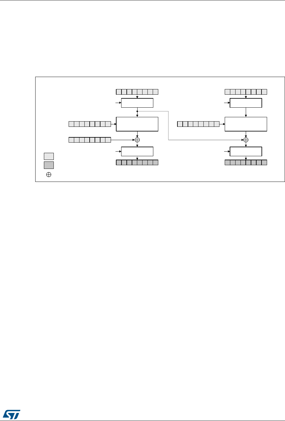
DocID025941 Rev 5 403/1001
AES hardware accelerator (AES)
424
second-block plaintext data P2’ to produce the I2 input data for the AES core to produce the
second block of ciphertext data. The chaining of data blocks continues in this way until the
last plaintext block in the message is encrypted.
If the message size is not a multiple of 128 bits, the final partial data block is encrypted in
the way explained in Section 18.4.6: AES ciphertext stealing and data padding.
Figure 77 illustrates the cipher block chaining (CBC) decryption mode.
Figure 77. CBC decryption
In CBC decrypt mode, like in ECB decrypt mode, the secret key must be prepared to
perform an AES decryption.
After the key preparation process, the decryption goes as follows: the first 128-bit ciphertext
block (after the swap operation) is used directly as the AES core input block I1 for decrypt
operation, using the 128-bit key. Its output O1 is XOR-ed with the 128-bit IVI field (that must
be identical to that used during encryption) to produce the first plaintext block P1.
The second ciphertext block is processed in the same way as the first block, except that the
I1 data from the first block is used in place of the initialization vector.
The decryption continues in this way until the last complete ciphertext block is decrypted.
If the message size is not a multiple of 128 bits, the final partial data block is decrypted in
the way explained in Section 18.4.6: AES ciphertext stealing and data padding.
For more information on data swapping, refer to Section 18.4.10: AES data registers and
data swapping.
MSv19104V2
Decrypt
AES_KEYRx (KEY)
AES_DINR (ciphertext C1)
AES_DOUTR (plaintext P1)
Swap
management
DATATYPE[1:0]
DATATYPE[1:0] Swap
management
Decrypt
AES_KEYRx (KEY)
AES_DINR (ciphertext C2)
AES_DOUTR (plaintext P2)
Swap
management
DATATYPE[1:0]
DATATYPE[1:0] Swap
management
AES_IVRx (IV)
input
output
Legend
XOR
I1 I2
O1 O2
Block 1 Block 2
IVI
P1' P2'
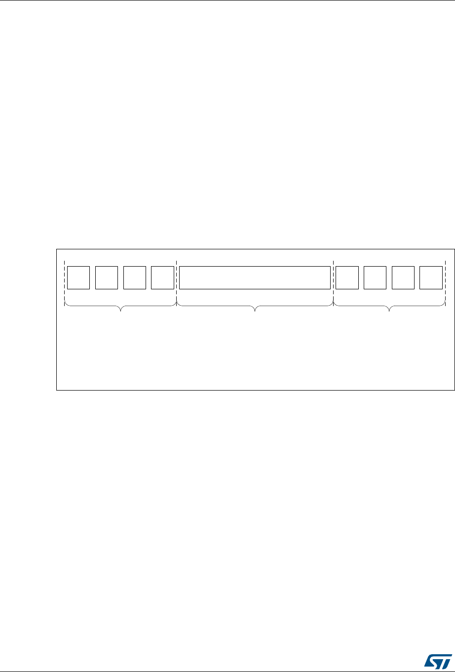
AES hardware accelerator (AES)
404/1001 DocID025941 Rev 5
ECB/CBC encryption sequence
The sequence of events to perform an ECB/CBC encryption (more detail in Section 18.4.4):
1. Disable the AES peripheral by clearing the EN bit of the AES_CR register.
2. Select the Mode 1 by to 00 the MODE[1:0] bitfield of the AES_CR register and select
ECB or CBC chaining mode by setting the CHMOD[1:0] bitfield of the AES_CR register
to 00 or 01, respectively. Data type can also be defined, using DATATYPE[1:0] bitfield.
3. Write the AES_KEYRx registers (128 bits) with encryption key. Fill the AES_IVRx
registers with the initialization vector data if CBC mode has been selected.
4. Enable the AES peripheral by setting the EN bit of the AES_CR register.
5. Write the AES_DINR register four times to input the plaintext (MSB first), as shown in
Figure 78.
6. Wait until the CCF flag is set in the AES_SR register.
7. Read the AES_DOUTR register four times to get the ciphertext (MSB first) as shown in
Figure 78. Then clear the CCF flag by setting the CCFC bit of the AES_CR register.
8. Repeat steps 5,6,7to process all the blocks with the same encryption key.
Figure 78. ECB/CBC encryption (Mode 1)
ECB/CBC decryption sequence
The sequence of events to perform an AES ECB/CBC decryption is as follows (more detail
in Section 18.4.4):
1. Follow the steps described in Section 18.4.5: AES decryption key preparation on
page 399, in order to prepare the decryption key in AES core.
2. Disable the AES peripheral by clearing the EN bit of the AES_CR register.
3. Select the Mode 3 by setting to 10 the MODE[1:0] bitfield of the AES_CR register and
select ECB or CBC chaining mode by setting the CHMOD[1:0] bitfield of the AES_CR
register to 00 or 01, respectively. Data type can also be defined, using DATATYPE[1:0]
bitfield.
4. Write the AES_IVRx registers with the initialization vector (required in CBC mode only).
5. Enable AES by setting the EN bit of the AES_CR register.
6. Write the AES_DINR register four times to input the cipher text (MSB first), as shown in
Figure 79.
7. Wait until the CCF flag is set in the AES_SR register.
8. Read the AES_DOUTR register four times to get the plain text (MSB first), as shown in
Figure 79. Then clear the CCF flag by setting the CCFC bit of the AES_CR register.
MS18936V3
WR
PT3
WR
PT2
WR
PT1
WR
PT0 Wait until flag CCF = 1 RD
CT3
RD
CT2
RD
CT1
RD
CT0
Input phase
4 write operations into
AES_DINR[31:0]
Computation phase Output phase
4 read operations of
AES_DOUTR[31:0]
PT = plaintext = 4 words (PT3, … , PT0)
CT = ciphertext = 4 words (CT3, … , CT0)
MSB LSB MSB LSB

DocID025941 Rev 5 405/1001
AES hardware accelerator (AES)
424
9. Repeat steps 6,7,8 to process all the blocks encrypted with the same key.
Figure 79. ECB/CBC decryption (Mode 3)
Suspend/resume operations in ECB/CBC modes
To suspend the processing of a message, proceed as follows:
1. If DMA is used, stop the AES DMA transfers to the IN FIFO by clearing the DMAINEN
bit of the AES_CR register.
2. If DMA is not used, read four times the AES_DOUTR register to save the last
processed block. If DMA is used, wait until the CCF flag is set in the AES_SR register
then stop the DMA transfers from the OUT FIFO by clearing the DMAOUTEN bit of the
AES_CR register.
3. If DMA is not used, poll the CCF flag of the AES_SR register until it becomes 1
(computation completed).
4. Clear the CCF flag by setting the CCFC bit of the AES_CR register.
5. Save initialization vector registers (only required in CBC mode as AES_IVRx registers
are altered during the data processing).
6. Disable the AES peripheral by clearing the bit EN of the AES_CR register.
7. Save the current AES configuration in the memory (except AES initialization vector
values).
8. If DMA is used, save the DMA controller status (pointers for IN and OUT data transfers,
number of remaining bytes, and so on).
Note: In point 7, the derived key information stored in AES_KEYRx registers can optionally be
saved in memory if the interrupted process is a decryption. Otherwise those registers do not
need to be saved as the original key value is known by the application
MS18938V3
WR
CT3
WR
CT2
WR
CT1
WR
CT0 Wait until flag CCF = 1 RD
PT3
RD
PT2
RD
PT1
RD
PT0
Input phase
4 write operations into
AES_DINR[31:0]
Computation phase Output phase
4 read operations from
AES_DOUTR[31:0]
PT = plaintext = 4 words (PT3, … , PT0)
CT = ciphertext = 4 words (CT3, … , CT0)
MSB LSB MSB LSB

AES hardware accelerator (AES)
406/1001 DocID025941 Rev 5
To resume the processing of a message, proceed as follows:
1. If DMA is used, configure the DMA controller so as to complete the rest of the FIFO IN
and FIFO OUT transfers.
2. Ensure that AES is disabled (the EN bit of the AES_CR must be 0).
3. Restore the AES_CR and AES_KEYRx register setting, using the values of the saved
configuration. In case of decryption, derived key information can be written in
AES_KEYRx register instead of the original key value.
4. Prepare the decryption key as described in Section 18.4.5: AES decryption key
preparation (only required for ECB or CBC decryption). This step is not necessary if
derived key information has been loaded in AES_KEYRx registers.
5. Restore AES_IVRx registers using the saved configuration (only required in CBC
mode).
6. Enable the AES peripheral by setting the EN bit of the AES_CR register.
7. If DMA is used, enable AES DMA transfers by setting the DMAINEN and DMAOUTEN
bits of the AES_CR register.
Alternative single ECB/CBC decryption using Mode 4
The sequence of events to perform a single round of ECB/CBC decryption using Mode 4 is:
1. Disable the AES peripheral by clearing the EN bit of the AES_CR register.
2. Select the Mode 4 by setting to 11 the MODE[1:0] bitfield of the AES_CR register and
select ECB or CBC chaining mode by setting the CHMOD[21:0] bitfield of the AES_CR
register to 000 or 001, respectively.
3. Select key length of 128 or 256 bits via KEYSIZE bitfield of the AES_CR register.
4. Write the AES_KEYRx registers with the encryption key. Write the AES_IVRx registers
if the CBC mode is selected.
5. Enable the AES peripheral by setting the EN bit of the AES_CR register.
6. Write the AES_DINR register four times to input the cipher text (MSB first).
7. Wait until the CCF flag is set in the AES_SR register.
8. Read the AES_DOUTR register four times to get the plain text (MSB first). Then clear
the CCF flag by setting the CCFC bit of the AES_CR register.
Note: When mode 4 is selected mode 3 cannot be used.
In mode 4, the AES_KEYRx registers contain the encryption key during all phases of the
processing. No derivation key is stored in these registers. It is stored internally in AES.
18.4.9 AES counter (CTR) mode
Overview
The counter mode (CTR) uses AES as a key-stream generator. The generated keys are
then XOR-ed with the plaintext to obtain the ciphertext.
CTR chaining is defined in NIST Special Publication 800-38A, Recommendation for Block
Cipher Modes of Operation. A typical message construction in CTR mode is given in
Figure 80.
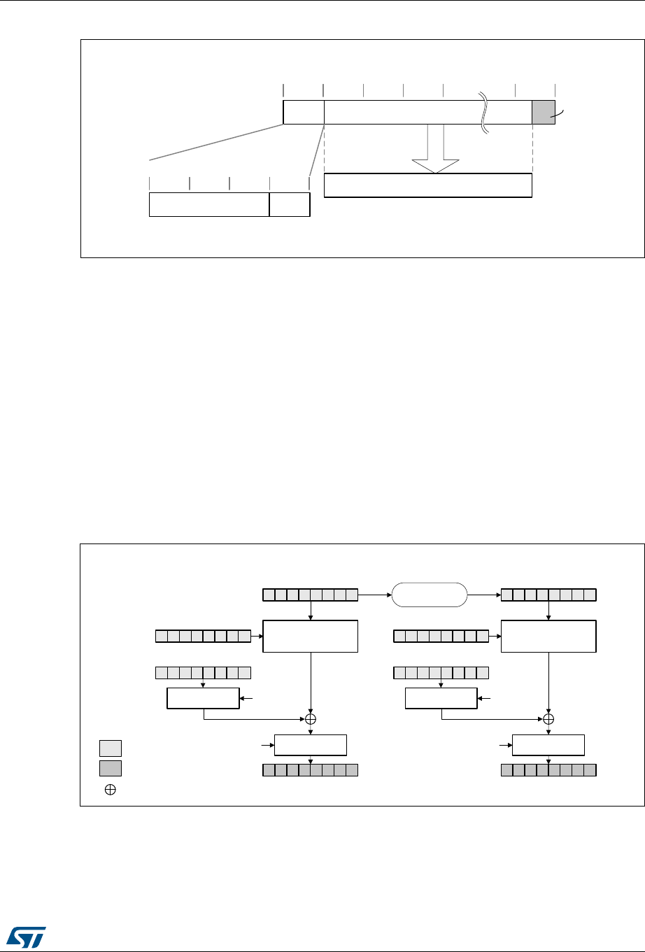
DocID025941 Rev 5 407/1001
AES hardware accelerator (AES)
424
Figure 80. Message construction in CTR mode
The structure of this message is:
•A 16-byte initial counter block (ICB), composed of two distinct fields:
–Initialization vector (IV): a 96-bit value that must be unique for each encryption
cycle with a given key.
–Counter: a 32-bit big-endian integer that is incremented each time a block
processing is completed. The initial value of the counter should be set to 1.
•The plaintext P is encrypted as ciphertext C, with a known length. This length can be
non-multiple of 16 bytes, in which case a plaintext padding is required.
CTR encryption and decryption
Figure 81 and Figure 82 describe the CTR encryption and decryption process, respectively,
as implemented in the AES peripheral. The CTR mode is selected by writing 10 to the
CHMOD[1:0] bitfield of AES_CR register.
Figure 81. CTR encryption
MSv42156V1
16-byte boundaries
ICB Ciphertext (C) 0
4-byte boundaries
CounterInitialization vector (IV)
decrypt
Plaintext (P)
Zero
padding
MSv19102V2
Encrypt
AES_KEYRx (KEY)
AES_DINR (plaintext P1)
AES_DOUTR (ciphertext C1)
DATATYPE[1:0] Swap
management
AES_IVRx
(IV + 32-bit counter)
input
output
Legend
XOR
Swap
management
DATATYPE[1:0]
Encrypt
AES_KEYRx (KEY)
AES_DOUTR (ciphertext C2)
DATATYPE[1:0] Swap
management
AES_IVRx
Swap
management
DATATYPE[1:0]
Counter
increment (+1)
AES_DINR (plaintext P2)
I1 I2
O1 O2
Block 1 Block 2
P1' P2'
C1' C2'
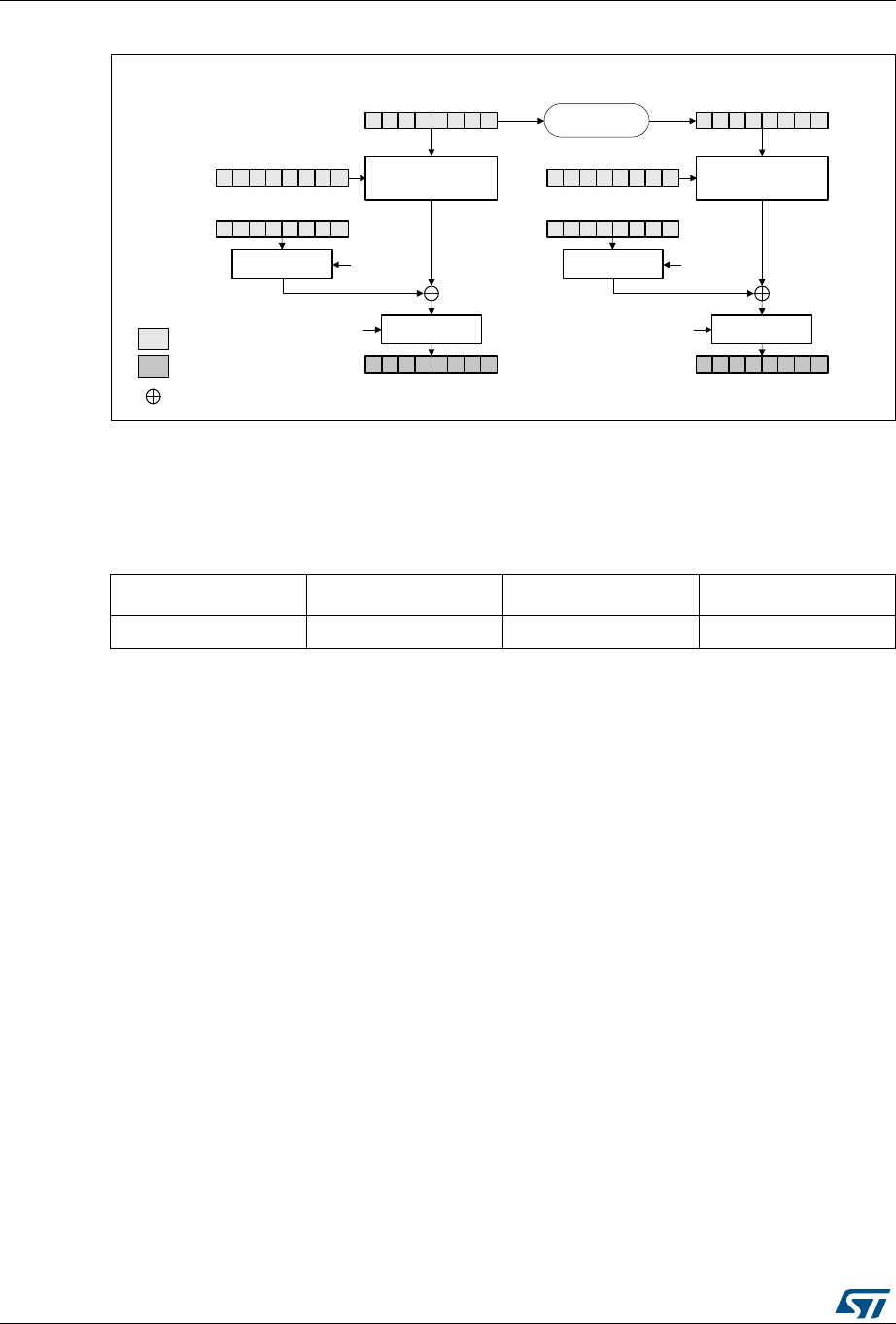
AES hardware accelerator (AES)
408/1001 DocID025941 Rev 5
Figure 82. CTR decryption
In CTR mode, the cryptographic core output (also called keystream) Ox is XOR-ed with
relevant input block (Px' for encryption, Cx' for decryption), to produce the correct output
block (Cx' for encryption, Px' for decryption). Initialization vectors in AES must be initialized
as shown in Table 7 8.
Unlike in CBC mode that uses the AES_IVRx registers only once when processing the first
data block, in CTR mode AES_IVRx registers are used for processing each data block, and
the AES peripheral increments the counter bits of the initialization vector (leaving the nonce
bits unchanged).
CTR decryption does not differ from CTR encryption, since the core always encrypts the
current counter block to produce the key stream that is then XOR-ed with the plaintext (CTR
encryption) or ciphertext (CTR decryption) input. In CTR mode, the MODE[1:0] bitfield
settings 11, 10 or 00 default all to encryption mode, and the setting 01 (key derivation) is
forbidden.
Table 78. CTR mode initialization vector definition
AES_IVR3[31:0] AES_IVR2[31:0] AES_IVR1[31:0] AES_IVR0[31:0]
Nonce[31:0] Nonce[63:32] Nonce[95:64] 32-bit counter = 0x0001
MSv18942V2
Encrypt
AES_KEYRx (KEY)
AES_DINR (ciphertext C1)
AES_DOUTR (plaintext P1)
DATATYPE[1:0] Swap
management
AES_IVRx
Nonce + 32-bit counter
input
output
Legend
XOR
Swap
management
DATATYPE[1:0]
Encrypt
AES_KEYRx (KEY)
AES_DOUTR (plaintext P2)
DATATYPE[1:0] Swap
management
AES_IVRx
Nonce + 32-bit counter (+1)
Swap
management
DATATYPE[1:0]
Counter
increment (+1)
AES_DINR (ciphertext C2)
I1 I2
O1 O2
Block 1 Block 2
C1' C2'
P1' P2'

DocID025941 Rev 5 409/1001
AES hardware accelerator (AES)
424
The sequence of events to perform an encryption or a decryption in CTR chaining mode:
1. Ensure that AES is disabled (the EN bit of the AES_CR must be 0).
2. Select CTR chaining mode by setting to 10 the CHMOD[1:0] bitfield of the AES_CR
register. Set MODE[1:0] bitfield to any value other than 01.
3. Initialize the AES_KEYRx registers, and load the AES_IVRx registers as described in
Table 78.
4. Set the EN bit of the AES_CR register, to start encrypting the current counter (EN is
automatically reset when the calculation finishes).
5. If it is the last block, pad the data with zeros to have a complete block, if needed.
6. Append data in AES, and read the result. The three possible scenarios are described in
Section 18.4.4: AES procedure to perform a cipher operation.
7. Repeat the previous step till the second-last block is processed. For the last block,
apply the two previous steps and discard the bits that are not part of the payload (if the
size of the significant data in the last input block is less than 16 bytes).
Suspend/resume operations in CTR mode
Like for the CBC mode, it is possible to interrupt a message to send a higher priority
message, and resume the message that was interrupted. Detailed CBC suspend/resume
sequence is described in Section 18.4.8: AES basic chaining modes (ECB, CBC).
Note: Like for CBC mode, the AES_IVRx registers must be reloaded during the resume operation.
18.4.10 AES data registers and data swapping
Data input and output
A 128-bit data block is entered into the AES peripheral with four successive 32-bit word
writes into the AES_DINR register (bitfield DIN[127:0]), the most significant word (bits
[127:96]) first, the least significant word (bits [31:0]) last.
A 128-bit data block is retrieved from the AES peripheral with four successive 32-bit word
reads from the AES_DOUTR register (bitfield DOUT[127:0]), the most significant word (bits
[127:96]) first, the least significant word (bits [31:0]) last.
The 32-bit data word for AES_DINR register or from AES_DOUTR register is organized in
big endian order, that is:
•the most significant byte of a word to write into AES_DINR must be put on the lowest
address out of the four adjacent memory locations keeping the word to write, or
•the most significant byte of a word read from AES_DOUTR goes to the lowest address
out of the four adjacent memory locations receiving the word
For using DMA for input data block write into AES, the four words of the input block must be
stored in the memory consecutively and in big-endian order, that is, the most significant
word on the lowest address. See Section 18.4.13: AES DMA interface.
Data swapping
The AES peripheral can be configured to perform a bit-, a byte-, a half-word-, or no
swapping on the input data word in the AES_DINR register, before loading it to the AES
processing core, and on the data output from the AES processing core, before sending it to
the AES_DOUTR register. The choice depends on the type of data. For example, a byte
swapping is used for an ASCII text stream.
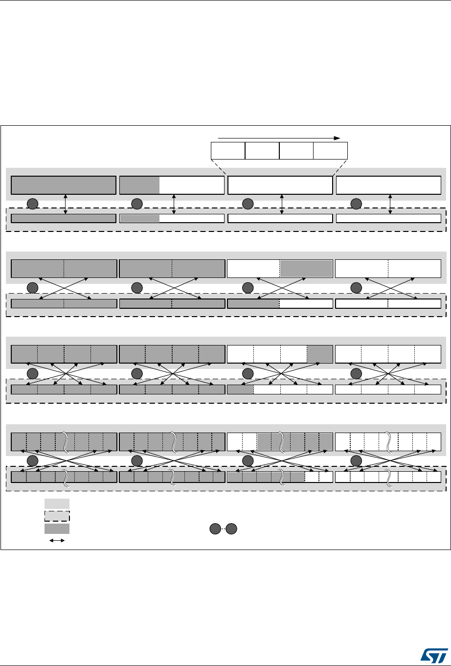
AES hardware accelerator (AES)
410/1001 DocID025941 Rev 5
The data swap type is selected through the DATATYPE[1:0] bitfield of the AES_CR register.
The selection applies both to the input and the output of the AES core.
For different data swap types, Figure 83 shows the construction of AES processing core
input buffer data P127..0, from the input data entered through the AES_DINR register, or the
construction of the output data available through the AES_DOUTR register, from the AES
processing core output buffer data P127..0.
Figure 83. 128-bit block construction with respect to data swap
Note: The data in AES key registers (AES_KEYRx) and initialization registers (AES_IVRx) are not
sensitive to the swap mode selection.
MSv42153V2
DATATYPE[1:0] = 00: no swapping
Word 2Word 3
D127 D96 P95
LSBMSB
DATATYPE[1:0] = 01: 16-bit (half-word) swapping
Word 3
DATATYPE[1:0] = 10: 8-bit (byte) swapping
Word 2Word 3
DATATYPE[1:0] = 11: bit swapping
Word 3
LSB
MSB
LSB
MSB
LSBMSB
LSBMSB
MSB
MSB
MSB LSB
LSB
Word 0Word 1
LSB
Word 0
Word 0Word 1
D63 D32 D31 D0
D64
Word 2
Zero padding (example)
Legend:
Data swap
Word 2
D95
Word 1
Word 0Word 1
AES input/output data block in memory
AES core input/output buffer data
1
1
1
1
2
2
2
2
3
3
3
3
4
4
4
4
Order of write to AES_DINR / read from AES_DOUTR
MSB
LSB
increasing memory address
D127 D96 D63 D32 D31 D0
D64D95
D127 D96 D95D112 D111 D80 D31 D0D15D16D64D79 D32D63 D48 D47
D127..120 D103..96D119..112 D111.104 D71...64D95..88 D87..80 D79..72 D63...56 D55...48 D47...40 D39...32 D31...24 D23...16 D15...8 D7...0
D127 D126 D125
D98 D97 D96 D95 D94 D93 D31 D30 D29 D0D1D2D66 D65 D64 D63 D62 D61 D34 D33 D32
byte 3 byte 2 byte 1 byte 0
D63 D55 D47 D39D56 D48 D40 D32
most significant bit (127) of memory data block / AEC core buffer
least significant bit (0) of memory data block / AEC core buffer
Dx input/output data bit ‘x’
D96D111 D127 D112 D64D79 D95 D80 D32D47 D63 D48 D0D15 D31 D16
D103..96 D111.104 D119..112 D127..120 D71...64 D79..72 D87..80 D95..88 D39...32 D47...40 D55...48 D63...56 D7...0 D15...8 D23...16 D31...24
D96
D127
D97
D126
D98
D125
D95D64 D94D65 D93D66 D63D32 D62D33 D61D34 D31D0 D30D1 D29D2
1 4

DocID025941 Rev 5 411/1001
AES hardware accelerator (AES)
424
Data padding
Figure 83 also gives an example of memory data block padding with zeros such that the
zeroed bits after the data swap form a contiguous zone at the MSB end of the AES core
input buffer. The example shows the padding of an input data block containing:
•48 message bits, with DATATYPE[1:0] = 01
•56 message bits, with DATATYPE[1:0] = 10
•34 message bits, with DATATYPE[1:0] = 11
18.4.11 AES key registers
The AES_KEYRx registers store the encryption or decryption key bitfield KEY[127:0]. The
data to write to or to read from each register is organized in the memory in little-endian
order, that is, with most significant byte on the highest address.
The key is spread over the four registers in little-endian configuration, as shown on
Table 79.
The key for encryption or decryption may be written into these registers when the AES
peripheral is disabled.
The key registers are not affected by the data swapping controlled by DATATYPE[1:0]
bitfield of the AES_CR register.
18.4.12 AES initialization vector registers
The four AES_IVRx registers keep the initialization vector input bitfield IVI[127:0]. The data
to write to or to read from each register is organized in the memory in little-endian order, that
is, with most significant byte on the highest address. The registers are also ordered from
lowest address (AES_IVR0) to highest address (AES_IVR3).
The signification of data in the bitfield depends on the chaining mode selected. When used,
the bitfield is updated upon each computation cycle of the AES core.
Write operations to the AES_IVRx registers when the AES peripheral is enabled have no
effect to the register contents. For modifying the contents of the AES_IVRx registers, the EN
bit of the AES_CR register must first be cleared.
Reading the AES_IVRx registers returns the latest counter value (useful for managing
suspend mode) when the AES peripheral is disabled and returns zeros when it is enabled.
The AES_IVRx registers are not affected by the data swapping feature controlled by the
DATATYPE[1:0] bitfield of the CRYP_CR register.
18.4.13 AES DMA interface
The AES peripheral provides an interface to connect to the DMA (direct memory access)
controller. The DMA operation is controlled through the AES_CR register.
Table 79. Key endianness in AES_KEYRx registers
AES_KEYR3[31:0] AES_KEYR2[31:0] AES_KEYR1[31:0] AES_KEYR0[31:0]
KEY[127:96] KEY[95:64] KEY[63:32] KEY[31:0]
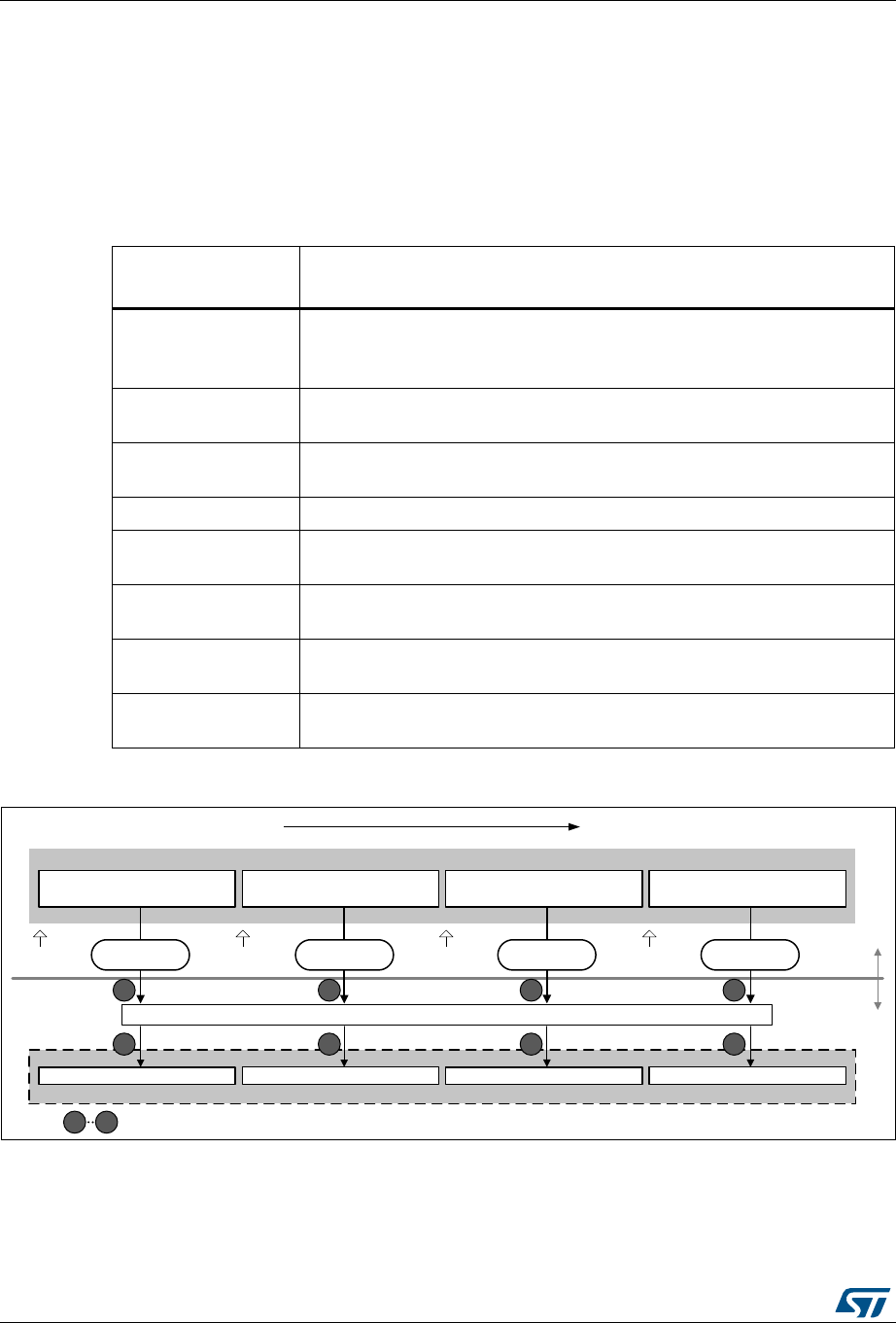
AES hardware accelerator (AES)
412/1001 DocID025941 Rev 5
Data input using DMA
Setting the DMAINEN bit of the AES_CR register enables DMA writing into AES. The AES
peripheral then initiates a DMA request during the input phase each time it requires a word
to be written to the AES_DINR register. It asserts four DMA requests to transfer one 128-bit
(four-word) input data block from memory, as shown in Figure 84.
See Table 80 for recommended DMA configuration.
Figure 84. DMA transfer of a 128-bit data block during input phase
Data output using DMA
Setting the DMAOUTEN bit of the AES_CR register enables DMA reading from AES. The
AES peripheral then initiates a DMA request during the Output phase each time it requires a
Table 80. DMA channel configuration for memory-to-AES data transfer
DMA channel control
register field Recommended configuration
Transfer size
Message length: a multiple of 128 bits.
According to the algorithm and the mode selected, special padding/
ciphertext stealing might be required.
Source burst size
(memory) Single
Destination burst size
(peripheral) Single
DMA FIFO size AES FIFO_size = 4 bytes.
Source transfer width
(memory) 32-bit words
Destination transfer
width (peripheral) 32-bit words
Source address
increment (memory) Yes, after each 32-bit transfer
Destination address
increment (peripheral)
Fixed address of AES_DINR (no increment)
MSv42160V1
AES core input buffer
AES_DINR
LSB
MSB
(No swapping)
Memory accessed through DMA
Word2Word3 Word0Word1
DMA
single write
DMA req N DMA req N+1 DMA req N+2 DMA req N+3
I127 I96 I63 I32 I31 I0
I64I95
D127 D96 D63 D32 D31 D0
D64D95
DIN[127:96] DIN[95:64] DIN[63:32] DIN[31:0]
DMA
single write DMA
single write DMA
single write
Chronological order
Increasing address
LSBMSB
AES
peripheral System
1 2 3 4
1Order of write to AES_DINR
1 2 3 4
4
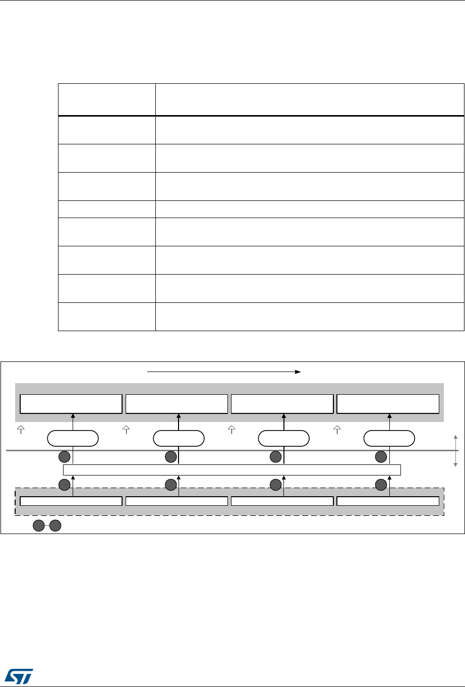
DocID025941 Rev 5 413/1001
AES hardware accelerator (AES)
424
word to be read from the AES_DOUTR register. It asserts four DMA requests to transfer one
128-bit (four-word) output data block to memory, as shown in Figure 85.
See Table 81 for recommended DMA configuration.
Figure 85. DMA transfer of a 128-bit data block during output phase
DMA operation in different operating modes
DMA operations are usable when Mode 1 (encryption) or Mode 3 (decryption) are selected
via the MODE[1:0] bitfield of the register AES_CR. As in Mode 2 (key derivation) the
AES_KEYRx registers must be written by software, enabling the DMA transfer through the
DMAINEN and DMAOUTEN bits of the AES_CR register have no effect in that mode.
Table 81. DMA channel configuration for AES-to-memory data transfer
DMA channel control
register field Recommended configuration
Transfer size It is the message length multiple of AES block size (4 words). According to
the case extra bytes will have to be discarded.
Source burst size
(peripheral) Single
Destination burst size
(memory) Single
DMA FIFIO size AES FIFO_size = 4 bytes
Source transfer width
(peripheral) 32-bit words
Destination transfer
width (memory) 32-bit words
Source address
increment (peripheral) Fixed address of AES_DINR (no increment)
Destination address
increment (memory)
Yes, after each 32-bit transfer
MSv42161V1
AES core output buffer
LSB
MSB
(No swapping)
Memory accessed through DMA
Word2Word3 Word0Word1
DMA
single read
DMA req N DMA req N+1 DMA req N+2 DMA req N+3
O127 O96 O63 O32 O31 O0
O64O95
D127 D96 D63 D32 D31 D0
D64D95
DOUT[127:96] DOUT[95:64] DOUT[63:32] DOUT[31:0]
DMA
single read DMA
single read DMA
single read
Chronological order
Increasing address
LSBMSB
System
AES
peripheral
1 2 3 4
1 2 3 4
1Order of read from AES_DOUTR
4
AES_DOUTR

AES hardware accelerator (AES)
414/1001 DocID025941 Rev 5
DMA single requests are generated by AES until it is disabled. So, after the data output
phase at the end of processing of a 128-bit data block, AES switches automatically to a new
data input phase for the next data block, if any.
When the data transferring between AES and memory is managed by DMA, the CCF flag is
not relevant and can be ignored (left set) by software. It must only be cleared when
transiting back to data transferring managed by software. See Suspend/resume operations
in ECB/CBC modes in Section 18.4.8: AES basic chaining modes (ECB, CBC) as example.
18.4.14 AES error management
The read error flag (RDERR) and write error flag (WRERR) of the AES_SR register are set
when an unexpected read or write operation, respectively, is detected. An interrupt can be
generated if the error interrupt enable (ERRIE) bit of the AES_CR register is set. For more
details, refer to Section 18.5: AES interrupts.
Note: AES is not disabled after an error detection and continues processing.
AES can be re-initialized at any moment by clearing then setting the EN bit of the AES_CR
register.
Read error flag (RDERR)
When an unexpected read operation is detected during the computation phase or during the
input phase, the AES read error flag (RDERR) is set in the AES_SR register. An interrupt is
generated if the ERRIE bit of the AES_CR register is set.
The RDERR flag is cleared by setting the corresponding ERRC bit of the AES_CR register.
Write error flag (WDERR)
When an unexpected write operation is detected during the computation phase or during the
output phase, the AES write error flag (WRERR) is set in the AES_SR register. An interrupt
is generated if the ERRIE bit of the AES_CR register is set.
The WDERR flag is cleared by setting the corresponding ERRC bit of the AES_CR register.
18.5 AES interrupts
There are three individual maskable interrupt sources generated by the AES peripheral, to
signal the following events:
•computation completed
•read error, see Section 18.4.14
•write error, see Section 18.4.14
These three sources are combined into a common interrupt signal aes_it that connects to
NVIC (nested vectored interrupt controller).
DocID025941 Rev 5 415/1001
AES hardware accelerator (AES)
424
Figure 86. AES interrupt signal generation
Each AES interrupt source can individually be enabled/disabled, by setting/clearing the
corresponding enable bit of the AES_CR register. See Figure 86.
The status of the individual maskable interrupt sources can be read from the AES_SR
register.
Table 82 gives a summary of the interrupt sources, their event flags and enable bits.
18.6 AES processing latency
The tables below summarize the latency to process a 128-bit block for each mode of
operation.
Table 82. AES interrupt requests
AES interrupt event Event flag Enable bit
computation completed flag CCF CCFIE
read error flag RDERR ERRIE
write error flag WRERR ERRIE
MSv42162V1
WRERR
ERRIE aes_it
(goes to NVIC)
RDERR
ERRIE
CCF
CCFIE
Flags in AES_SR register
Bits of AES_CR register
Table 83. Processing latency (in clock cycle)
Mode of operation Algorithm Input phase Computation
phase
Output
phase Total
Mode 1: Encryption ECB, CBC, CTR 8 202 4 214
Mode 2: Key derivation for decryption ECB, CBC - 80 - 80
Mode 3: Decryption ECB, CBC, CTR 8 202 4 214
Mode 4: Key derivation then
decryption ECB, CBC 8 276 4 288

AES hardware accelerator (AES)
416/1001 DocID025941 Rev 5
18.7 AES registers
18.7.1 AES control register (AES_CR)
Address offset: 0x00
Reset value: 0x0000 0000
31 30 29 28 27 26 25 24 23 22 21 20 19 18 17 16
Res. Res. Res. Res. Res. Res. Res. Res. Res. Res. Res. Res. Res. Res. Res. Res.
1514131211109876543210
Res. Res. Res. DMAO
UTEN
DMAIN
EN ERRIE CCFIE ERRC CCFC CHMOD[1:0] MODE[1:0] DATATYPE[1:0] EN
rw rw rw rw rw rw rw rw rw rw rw rw rw
Bit 31:13 Reserved, must be kept at zero
Bit 12 DMAOUTEN: DMA output enable
This bit enables/disables data transferring with DMA, in the output phase:
0: Disable
1: Enable
When the bit is set, DMA requests are automatically generated by AES during the output data
phase. This feature is only effective when Mode 1 or Mode 3 is selected through the MODE[1:0]
bitfield. It is not effective for Mode 2 (key derivation).
Usage of DMA with Mode 4 (single decryption) is not recommended.
Bit 11 DMAINEN: DMA input enable
This bit enables/disables data transferring with DMA, in the input phase:
0: Disable
1: Enable
When the bit is set, DMA requests are automatically generated by AES during the input data phase.
This feature is only effective when Mode 1 or Mode 3 is selected through the MODE[1:0] bitfield. It is
not effective for Mode 2 (key derivation).
Usage of DMA with Mode 4 (single decryption) is not recommended.
Bit 10 ERRIE: Error interrupt enable
This bit enables or disables (masks) the AES interrupt generation when RDERR and/or WRERR is
set:
0: Disable (mask)
1: Enable
Bit 9 CCFIE: CCF interrupt enable
This bit enables or disables (masks) the AES interrupt generation when CCF (computation complete
flag) is set:
0: Disable (mask)
1: Enable

DocID025941 Rev 5 417/1001
AES hardware accelerator (AES)
424
Bit 8 ERRC: Error flag clear
Upon written to 1, this bit clears the RDERR and WRERR error flags in the AES_SR register:
0: No effect
1: Clear RDERR and WRERR flags
Reading the flag always returns zero.
Bit 7 CCFC: Computation complete flag clear
Upon written to 1, this bit clears the computation complete flag (CCF) in the AES_SR register:
0: No effect
1: Clear CCF
Reading the flag always returns zero.
Bits 6:5 CHMOD[1:0]: Chaining mode selection
This bitfield selects the AES chaining mode:
00: Electronic codebook (ECB)
01: Cipher-Block Chaining (CBC)
10: Counter Mode (CTR)
11: Reserved
The bitfield value change is allowed only when AES is disabled, so as to avoid an unpredictable
behavior.
Bits 4:3 MODE[1:0]: AES operating mode
This bitfield selects the AES operating mode:
00: Mode 1: encryption
01: Mode 2: key derivation (or key preparation for ECB/CBC decryption)
10: Mode 3: decryption
11: Mode 4: key derivation then single decryption
The bitfield value change is allowed only when AES is disabled, so as to avoid an unpredictable
behavior. Any attempt to selecting Mode 4 while either ECB or CBC chaining mode is not selected,
defaults to effective selection of Mode 3. It is not possible to select a Mode 3 following a Mode 4.
Bits 2:1 DATATYPE[1:0]: Data type selection
This bitfield defines the format of data written in the AES_DINR register or read from the
AES_DOUTR register, through selecting the mode of data swapping:
00: None
01: Half-word (16-bit)
10: Byte (8-bit)
11: Bit
For more details, refer to Section 18.4.10: AES data registers and data swapping.
The bitfield value change is allowed only when AES is disabled, so as to avoid an unpredictable
behavior.
Bit 0 EN: AES enable
This bit enables/disables the AES peripheral:
0: Disable
1: Enable
At any moment, clearing then setting the bit re-initializes the AES peripheral.
This bit is automatically cleared by hardware when the key preparation process ends (Mode 2).

AES hardware accelerator (AES)
418/1001 DocID025941 Rev 5
18.7.2 AES status register (AES_SR)
Address offset: 0x04
Reset value: 0x0000 0000
31 30 29 28 27 26 25 24 23 22 21 20 19 18 17 16
Res. Res. Res. Res. Res. Res. Res. Res. Res. Res. Res. Res. Res. Res. Res. Res.
r rrrr r r r r r r r r r r r
15 14 13 12 11 10 9 8 7 6 5 4 3 2 1 0
Res. Res. Res. Res. Res. Res. Res. Res. Res. Res. Res. Res. Res. WRERR RDERR CCF
r rrrr r r r r r r r rrrr
Bits 31:3 Reserved, must be kept at zero
Bit 2 WRERR: Write error
This flag indicates the detection of an unexpected write operation to the AES_DINR register (during
computation or data output phase):
0: Not detected
1: Detected
The flag is set by hardware. It is cleared by software upon setting the ERRC bit of the AES_CR
register.
Upon the flag setting, an interrupt is generated if enabled through the ERRIE bit of the AES_CR
register.
The flag setting has no impact on the AES operation.
The flag is not effective when key derivation mode is selected.
Bit 1 RDERR: Read error flag
This flag indicates the detection of an unexpected read operation from the AES_DOUTR register
(during computation or data input phase):
0: Not detected
1: Detected
The flag is set by hardware. It is cleared by software upon setting the ERRC bit of the AES_CR
register.
Upon the flag setting, an interrupt is generated if enabled through the ERRIE bit of the AES_CR
register.
The flag setting has no impact on the AES operation.
The flag is not effective when key derivation mode is selected.
Bit 0 CCF: Computation completed flag
This flag indicates whether the computation is completed:
0: Not completed
1: Completed
The flag is set by hardware upon the completion of the computation. It is cleared by software, upon
setting the CCFC bit of the AES_CR register.
Upon the flag setting, an interrupt is generated if enabled through the CCFIE bit of the AES_CR
register.
The flag is significant only when the DMAOUTEN bit is 0. It may stay high when DMA_EN is 1.

DocID025941 Rev 5 419/1001
AES hardware accelerator (AES)
424
18.7.3 AES data input register (AES_DINR)
Address offset: 0x08
Reset value: 0x0000 0000
Only 32-bit access type is supported.
18.7.4 AES data output register (AES_DOUTR)
Address offset: 0x0C
Reset value: 0x0000 0000
Only 32-bit access type is supported.
31 30 29 28 27 26 25 24 23 22 21 20 19 18 17 16
DIN[x+31:x+16]
rw rw rw rw rw rw rw rw rw rw rw rw rw rw rw rw
15 14 13 12 11 10 9 8 7 6 5 4 3 2 1 0
DIN[x+15:x]
rw rw rw rw rw rw rw rw rw rw rw rw rw rw rw rw
Bits 31:0 DIN[x+31:x]: One of four 32- bit words o f a 128-bi t input da ta block be ing written into th e periphe ral
This bitfield feeds a 32-bit input buffer. A 4-fold sequential write to this bitfield during the input phase
virtually writes a complete 128-bit block of input data to the AES peripheral. Upon each write, the
data from the input buffer are handled by the data swap block according to the DATATYPE[1:0]
bitfield, then written into the AES core 128-bit input buffer.
The substitution for “x”, from the first to the fourth write operation, is: 96, 64, 32, and 0. In other
words, data from the first to the fourth write operation are: DIN[127:96], DIN[95:64], DIN[63:32], and
DIN[31:0].
The data signification of the input data block depends on the AES operating mode:
- Mode 1 (encryption): plaintext
- Mode 2 (key derivation): the bitfield is not used (AES_KEYRx registers used for input)
- Mode 3 (decryption) and Mode 4 (key derivation then single decryption): ciphertext
The data swap operation is described in Section 18.4.10: AES data registers and data swapping on
page 409.
31 30 29 28 27 26 25 24 23 22 21 20 19 18 17 16
DOUT[x+31:x+16]
rrrrrrrrrrrrrrrr
1514131211109876543210
DOUT[x+15:0]
rrrrrrrrrrrrrrrr

AES hardware accelerator (AES)
420/1001 DocID025941 Rev 5
18.7.5 AES key register 0 (AES_KEYR0)
Address offset: 0x10
Reset value: 0x0000 0000
Bits 31:0 DOUT[x+31:x]: One of four 32-bit words of a 128-bit output data block being read from the peripheral
This bitfield fetches a 32-bit output buffer. A 4-fold sequential read of this bitfield, upon the
computation completion (CCF set), virtually reads a complete 128-bit block of output data from the
AES peripheral. Before reaching the output buffer, the data produced by the AES core are handled
by the data swap block according to the DATATYPE[1:0] bitfield.
The substitution for DOUT[x+31:x], from the first to the fourth read operation, is: 96, 64, 32, and 0. In
other words, data from the first to the fourth read operation are: DOUT[127:96], DOUT[95:64],
DOUT[63:32], and DOUT[31:0].
The data signification of the output data block depends on the AES operating mode:
- Mode 1 (encryption): ciphertext
- Mode 2 (key derivation): the bitfield is not used (AES_KEYRx registers used for output).
- Mode 3 (decryption) and Mode 4 (key derivation then single decryption): plaintext
The data swap operation is described in Section 18.4.10: AES data registers and data swapping on
page 409.
31 30 29 28 27 26 25 24 23 22 21 20 19 18 17 16
KEY[31:16]
rw rw rw rw rw rw rw rw rw rw rw rw rw rw rw rw
1514131211109876543210
KEY[15:0]
rw rw rw rw rw rw rw rw rw rw rw rw rw rw rw rw
Bits 31:0 KEY[31:0]: Cryptographic key, bits [31:0]
This bitfield contains the bits [31:0] of the AES encryption or decryption key, depending on the
operating mode:
- In Mode 1 (encryption), Mode 2 (key derivation) and Mode 4 (key derivation then single
decryption): the value to write into the bitfield is the encryption key.
- In Mode 3 (decryption): the value to write into the bitfield is the encryption key to be derived before
being used for decryption. After writing the encryption key into the bitfield, its reading before
enabling AES returns the same value. Its reading after enabling AES and after the CCF flag is set
returns the decryption key derived from the encryption key.
Note: In mode 4 (key derivation then single decryption) the bitfield always contains the encryption
key.
The AES_KEYRx registers may be written only when the AES peripheral is disabled.
Refer to Section 18.4.11: AES key registers on page 411 for more details.
DocID025941 Rev 5 421/1001
AES hardware accelerator (AES)
424
18.7.6 AES key register 1 (AES_KEYR1)
Address offset: 0x14
Reset value: 0x0000 0000
18.7.7 AES key register 2 (AES_KEYR2)
Address offset: 0x18
Reset value: 0x0000 0000
18.7.8 AES key register 3 (AES_KEYR3)
Address offset: 0x1C
Reset value: 0x0000 0000
31 30 29 28 27 26 25 24 23 22 21 20 19 18 17 16
KEY[63:48]
rw rw rw rw rw rw rw rw rw rw rw rw rw rw rw rw
1514131211109876543210
KEY[47:32]
rw rw rw rw rw rw rw rw rw rw rw rw rw rw rw rw
Bits 31:0 KEY[63:32]: Cryptographic key, bits [63:32]
Refer to the AES_KEYR0 register for description of the KEY[127:0] bitfield.
31 30 29 28 27 26 25 24 23 22 21 20 19 18 17 16
KEY[95:80]
rw rw rw rw rw rw rw rw rw rw rw rw rw rw rw rw
1514131211109876543210
KEY[79:64]
rw rw rw rw rw rw rw rw rw rw rw rw rw rw rw rw
Bits 31:0 KEY[95:64]: Cryptographic key, bits [95:64]
Refer to the AES_KEYR0 register for description of the KEY[127:0] bitfield.
31 30 29 28 27 26 25 24 23 22 21 20 19 18 17 16
KEY[127:112]
rw rw rw rw rw rw rw rw rw rw rw rw rw rw rw rw
15 14 13 12 11 10 9 8 7 6 5 4 3 2 1 0
KEY[111:96]
rw rw rw rw rw rw rw rw rw rw rw rw rw rw rw rw
Bits 31:0 KEY[127:96]: Cryptographic key, bits [127:96]
Refer to the AES_KEYR0 register for description of the KEY[127:0] bitfield.
AES hardware accelerator (AES)
422/1001 DocID025941 Rev 5
18.7.9 AES initialization vector register 0 (AES_IVR0)
Address offset: 0x20
Reset value: 0x0000 0000
18.7.10 AES initialization vector register 1 (AES_IVR1)
Address offset: 0x24
Reset value: 0x0000 0000
31 30 29 28 27 26 25 24 23 22 21 20 19 18 17 16
IVI[31:16]
rw rw rw rw rw rw rw rw rw rw rw rw rw rw rw rw
1514131211109876543210
IVI[15:0]
rw rw rw rw rw rw rw rw rw rw rw rw rw rw rw rw
Bits 31:0 IVI[31:0]: Initialization vector input, bits [31:0]
Refer to Section 18.4.12: AES initialization vector registers on page 411 for description of the
IVI[127:0] bitfield.
The initialization vector is only used in chaining modes other than ECB.
The initialization vector may be written only when the AES peripheral is disabled.
Reading this bitfield while AES is enabled returns 0x0000 0000.
31 30 29 28 27 26 25 24 23 22 21 20 19 18 17 16
IVI[63:48]
rw rw rw rw rw rw rw rw rw rw rw rw rw rw rw rw
1514131211109876543210
IVI[47:32]
rw rw rw rw rw rw rw rw rw rw rw rw rw rw rw rw
Bits 31:0 IVI[63:32]: Initialization vector input, bits [63:32]
Refer to Section 18.4.12: AES initialization vector registers on page 411 for description of the
IVI[127:0] bitfield.
The initialization vector is only used in chaining modes other than ECB.
The initialization vector may be written only when the AES peripheral is disabled.
Reading this bitfield while AES is enabled returns 0x0000 0000.
DocID025941 Rev 5 423/1001
AES hardware accelerator (AES)
424
18.7.11 AES initialization vector register 2 (AES_IVR2)
Address offset: 0x28
Reset value: 0x0000 0000
18.7.12 AES initialization vector register 3 (AES_IVR3)
Address offset: 0x2C
Reset value: 0x0000 0000
18.7.13 AES register map
31 30 29 28 27 26 25 24 23 22 21 20 19 18 17 16
IVI[95:80]
rw rw rw rw rw rw rw rw rw rw rw rw rw rw rw rw
1514131211109876543210
IVI[79:64]
rw rw rw rw rw rw rw rw rw rw rw rw rw rw rw rw
Bits 31:0 IVI[95:64]: Initialization vector input, bits [95:64]
Refer to Section 18.4.12: AES initialization vector registers on page 411 for description of the
IVI[127:0] bitfield.
The initialization vector is only used in chaining modes other than ECB.
The initialization vector may be written only when the AES peripheral is disabled.
Reading this bitfield while AES is enabled returns 0x0000 0000.
31 30 29 28 27 26 25 24 23 22 21 20 19 18 17 16
IVI[127:112]
rw rw rw rw rw rw rw rw rw rw rw rw rw rw rw rw
1514131211109876543210
IVI[111:96]
rw rw rw rw rw rw rw rw rw rw rw rw rw rw rw rw
Bits 31:0 IVI[127:96]: Initialization vector input, bits [127:96]
Refer to Section 18.4.12: AES initialization vector registers on page 411 for description of the
IVI[127:0] bitfield.
The initialization vector is only used in chaining modes other than ECB.
The initialization vector may be written only when the AES peripheral is disabled.
Reading this bitfield while AES is enabled returns 0x0000 0000.
Table 84. AES register map and reset values
Offset Register
31
30
29
28
27
26
25
24
23
22
21
20
19
18
17
16
15
14
13
12
11
10
9
8
7
6
5
4
3
2
1
0
0x0000
AES_CR
Res.
Res.
Res.
Res.
Res.
Res.
Res.
Res.
Res.
Res.
Res.
Res.
Res.
Res.
Res.
Res.
Res.
Res.
Res.
DMAOUTEN
DMAINEN
ERRIE
CCFIE
ERRC
CCFC
CHMOD[1:0]
MODE[1:0]
DATATYPE[1:0]
EN
Reset value 0000000000000
AES hardware accelerator (AES)
424/1001 DocID025941 Rev 5
Refer to Section 2.2.2 on page 58 for the register boundary addresses.
0x0004 AES_SR
Res.
Res.
Res.
Res.
Res.
Res.
Res.
Res.
Res.
Res.
Res.
Res.
Res.
Res.
Res.
Res.
Res.
Res.
Res.
Res.
Res.
Res.
Res.
Res.
Res.
Res.
Res.
Res.
WRERR
RDERR
CCF
Reset value 000
0x0008
AES_DINR
x=96,64,32,0 DIN[x+31:x]
Reset value 00000000000000000000000000000000
0x000
C
AES_DOUTR
x=96,64,32,0 DOUT[x+31:x]
Reset value 00000000000000000000000000000000
0x0010 AES_KEYR0 KEY[31:0]
Reset value 00000000000000000000000000000000
0x0014
AES_KEYR1 KEY[63:32]
Reset value 00000000000000000000000000000000
0x0018
AES_KEYR2 KEY[95:64]
Reset value 00000000000000000000000000000000
0x001
C
AES_KEYR3 KEY[127:96]
Reset value 00000000000000000000000000000000
0x0020 AES_IVR0 IVI[31:0]
Reset value 00000000000000000000000000000000
0x0024 AES_IVR1 IVI[63:32]
Reset value 00000000000000000000000000000000
0x0028 AES_IVR2 IVI[95:64]
Reset value 00000000000000000000000000000000
0x002
C
AES_IVR3 IVI[127:96]
Reset value 00000000000000000000000000000000
Table 84. AES register map and reset values (continued)
Offset Register
31
30
29
28
27
26
25
24
23
22
21
20
19
18
17
16
15
14
13
12
11
10
9
8
7
6
5
4
3
2
1
0

DocID025941 Rev 5 425/1001
RM0376 True random number generator (RNG)
435
19 True random number generator (RNG)
19.1 Introduction
The RNG is a true random number generator that continuously provides 32-bit entropy
samples, based on an analog noise source. It can be used by the application as a live
entropy source to build a NIST compliant Deterministic Random Bit Generator (DRBG).
The RNG true random number generator has been validated according to the German
AIS-31 standard.
19.2 RNG main features
•The RNG delivers 32-bit true random numbers, produced by an analog entropy source
post-processed with linear-feedback shift registers (LFSR).
•It is validated according to the AIS-31 pre-defined class PTG.2 evaluation methodology,
which is part of the German Common Criteria (CC) scheme.
•It produces one 32-bit random samples every 42 RNG clock cycles (dedicated clock).
•It allows embedded continuous basic health tests with associated error management
– Includes too low sampling clock detection and repetition count tests.
•It can be disabled to reduce power consumption.
•It has an AMBA AHB slave peripheral, accessible through 32-bit word single accesses
only (else an AHB bus error is generated). Warning! any write not equal to 32 bits might
corrupt the register content.
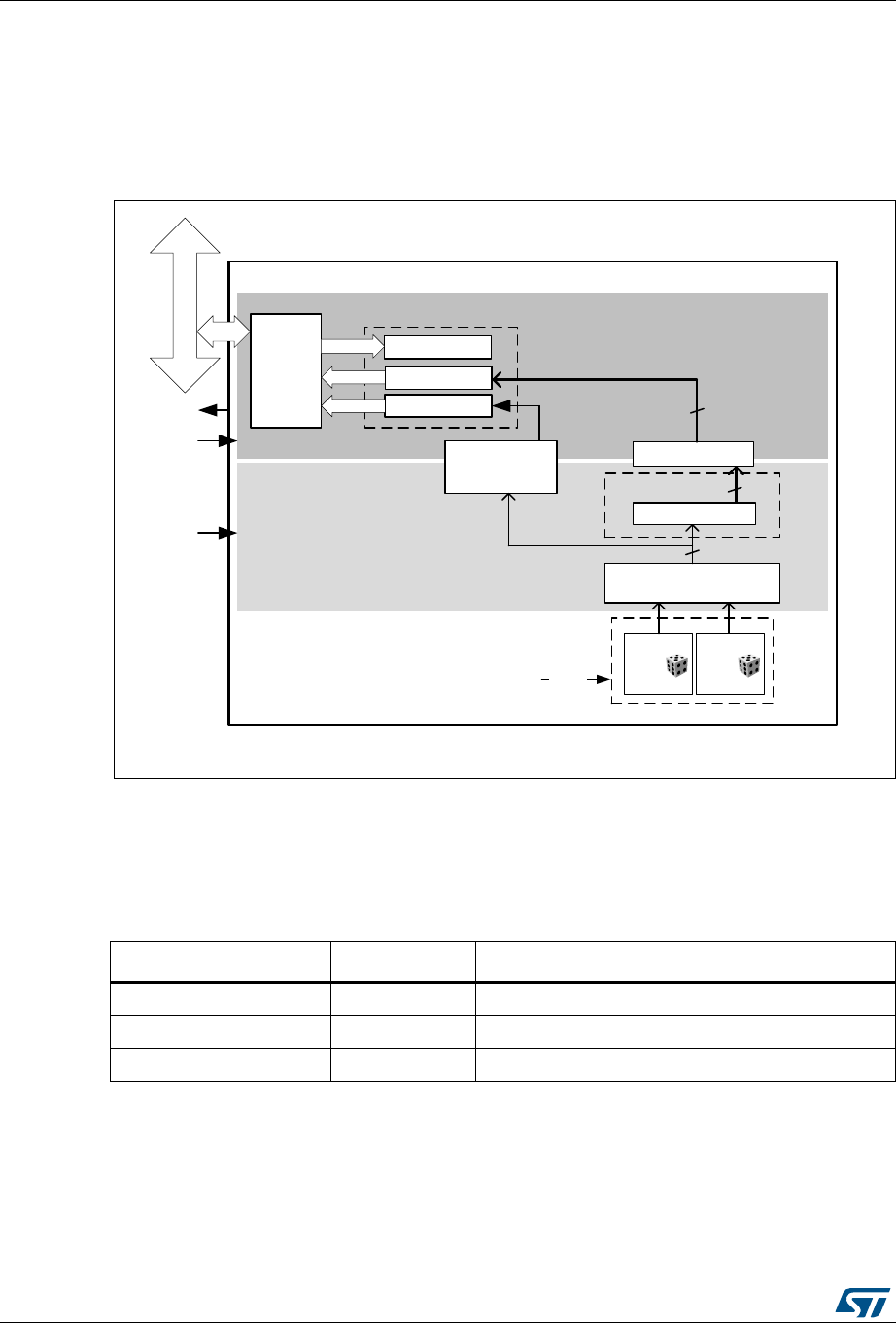
True random number generator (RNG) RM0376
426/1001 DocID025941 Rev 5
19.3 RNG functional description
19.3.1 RNG block diagram
Figure 87 shows the RNG block diagram.
Figure 87. RNG block diagram
19.3.2 RNG internal signals
Table 85 describes a list of useful-to-know internal signals available at the RNG level, not at
the STM32 product level (on pads).
MSv42096V1
T-RNGv1
RNG_SR
AHB
interface
status
RNG_CR
Analog
noise
source 1
Banked Registers
Sampling &
Normalization (x 2)
Analog noise source
2-bit
Analog
noise
source 2
en_osc
32-bit AHB Bus
rng_it
rng_hclk
rng_clk
AHB clock domain
RNG clock domain
Data shift reg
16-bit
8-bit LFSR (x2)
Post-processing logic 16-bit
Fault detection
Clock checker
Alarms
RNG_DR
data
control
Table 85. RNG internal input/output signals
Signal name Signal type Description
rng_it digital output RNG global interrupt request
rng_hclk digital input AHB clock
rng_clk digital input RNG dedicated clock, asynchronous to rng_hclk
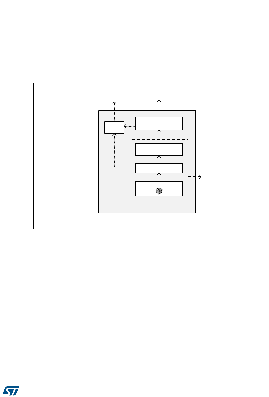
DocID025941 Rev 5 427/1001
RM0376 True random number generator (RNG)
435
19.3.3 Random number generation
The true random number generator (RNG) delivers truly random data through its AHB
interface at deterministic intervals. The RNG implements the entropy source model pictured
on Figure 88, and provides three main functions to the application:
•Collects the bitstring output of the entropy source box
•Obtains samples of the noise source for validation purpose
•Collects error messages from continuous health tests
Figure 88. Entropy source model
The main components of the RNG are:
•A source of physical randomness (analog noise source)
•A digitization stage for this analog noise source
•A stage delivering post-processed noise source (raw data)
•An output buffer for the raw data. If further cryptographic conditioning is required by the
application it will need to be performed by software.
•An optional output for the digitized noise source (unbuffered, on digital pads)
•Basic health tests on the digitized noise source
All those components are detailed below.
MSv42095V1
Entropy source
Noise Source
Digitization
Post-processing
(optional)
Raw data
Conditioning
(optional)
Heath
tests
Output
Error
message
Output
(raw data or
digitized noise
source)

True random number generator (RNG) RM0376
428/1001 DocID025941 Rev 5
Noise source
The noise source is the component that contains the non-deterministic, entropy-providing
activity that is ultimately responsible for the uncertainty associated with the bitstring output
by the entropy source. It is composed of:
•Two analog noise sources, each based on three XORed free-running ring oscillator
outputs. It is possible to disable those analog oscillators to save power, as described in
Section 19.4: RNG low-power usage.
•A sampling stage of these outputs clocked by a dedicated clock input (rng_clk),
delivering a 2-bit raw data output.
This noise source sampling is independent to the AHB interface clock frequency
(rng_hclk).
Note: In Section 19.7: Entropy source validation recommended RNG clock frequencies are given.
Post processing
The sample values obtained from a true random noise source consist of 2-bit bitstrings.
Because this noise source output is biased, the RNG implements a post-processing
component that reduces that bias to a tolerable level.
The RNG post-processing consists of two stages, applied to each noise source bits:
•The RNG takes half of the bits from the sampled noise source, and half of the bits from
inverted sampled noise source. Thus, if the source generates more ‘1’ than ‘0’ (or the
opposite), it is filtered
•A linear feedback shift register (LFSR) performs a whitening process, producing 8-bit
bitstrings.
This component is clocked by the RNG clock.
The times required between two random number generations, and between the RNG
initialization and availability of first sample are described in Section 19.6: RNG processing
time.
Output buffer
The RNG_DR data output register can store up to two 16-bit words which have been output
from the post-processing component (LFSR). In order to read back 32-bit random samples it
is required to wait 42 RNG clock cycles.
Whenever a random number is available through the RNG_DR register the DRDY flag
transitions from “0” to “1”. This flag remains high until output buffer becomes empty after
reading one word from the RNG_DR register.
Note: When interrupts are enabled an interrupt is generated when this data ready flag transitions
from “0” to “1”. Interrupt is then cleared automatically by the RNG as explained above.

DocID025941 Rev 5 429/1001
RM0376 True random number generator (RNG)
435
Health checks
This component ensures that the entire entropy source (with its noise source) starts then
operates as expected, obtaining assurance that failures are caught quickly and with a high
probability and reliability.
The RNG implements the following health check features:
1. Behavior tests, applied to the entropy source at run-time
– Repetition count test, flagging an error when:
a) One of the noise source has provided more than 64 consecutive bits at a constant
value (“0” or “1”)
b) One of the noise sources has delivered more than 32 consecutive occurrence of
two bits patterns (“01” or “10”)
2. Vendor specific continuous test
– Real-time “too slow” sampling clock detector, flagging an error when one RNG
clock cycle is smaller than AHB clock cycle divided by 16.
The CECS and SECS status bits in the RNG_SR register indicate when an error condition is
detected, as detailed in Section 19.3.7: Error management.
Note: An interrupt can be generated when an error is detected.
19.3.4 RNG initialization
When a hardware reset occurs the following chain of events occurs:
1. The analog noise source is enabled, and logic starts sampling the analog output after
four RNG clock cycles, filling LFSR shift register and associated 16-bit post-processing
shift register.
2. The output buffer is refilled automatically according to the RNG usage.
The associated initialization time can be found in Section 19.6: RNG processing time.
19.3.5 RNG operation
Normal operations
To run the RNG using interrupts the following steps are recommended:
1. Enable the interrupts by setting the IE bit in the RNG_CR register. At the same time
enable the RNG by setting the bit RNGEN=1.
2. An interrupt is now generated when a random number is ready or when an error
occurs. Therefore at each interrupt, check that:
– No error occurred. The SEIS and CEIS bits should be set to ‘0’ in the RNG_SR
register.
– A random number is ready. The DRDY bit must be set to ‘1’ in the RNG_SR
register.
– If above two conditions are true the content of the RNG_DR register can be read.

True random number generator (RNG) RM0376
430/1001 DocID025941 Rev 5
To run the RNG in polling mode following steps are recommended:
1. Enable the random number generation by setting the RNGEN bit to “1” in the RNG_CR
register.
2. Read the RNG_SR register and check that:
– No error occurred (the SEIS and CEIS bits should be set to ‘0’)
– A random number is ready (the DRDY bit should be set to ‘1’)
3. If above conditions are true read the content of the RNG_DR register.
Note: When data is not ready (DRDY=”0”) RNG_DR returns zero.
Low-power operations
If the power consumption is a concern to the application, low-power strategies can be used,
as described in Section 19.4: RNG low-power usage on page 431.
Software post-processing
If a NIST approved DRBG with 128 bits of security strength is required an approved random
generator software must be built around the RNG true random number generator.
19.3.6 RNG clocking
The RNG runs on two different clocks: the AHB bus clock and a dedicated RNG clock.
The AHB clock is used to clock the AHB banked registers and the post-processing
component. The RNG clock is used for noise source sampling. Recommended clock
configurations are detailed in Section 19.7: Entropy source validation.
Caution: When the CED bit in the RNG_CR register is set to “0”, the RNG clock frequency must be
higher than AHB clock frequency divided by 16, otherwise the clock checker will flag a clock
error (CECS or CEIS in the RNG_SR register) and the RNG will stop producing random
numbers.
See Section 19.3.1: RNG block diagram for details (AHB and RNG clock domains).
19.3.7 Error management
In parallel to random number generation an health check block verifies the correct noise
source behavior and the frequency of the RNG source clock as detailed in this section.
Associated error state is also described.
Clock error detection
When the clock error detection is enabled (CED = 0) and if the RNG clock frequency is too
low, the RNG stops generating random numbers and sets to “1” both the CEIS and CECS
bits to indicate that a clock error occurred. In this case, the application should check that the
RNG clock is configured correctly (see Section 19.3.6: RNG clocking) and then it must clear
the CEIS bit interrupt flag. As soon as the RNG clock operates correctly, the CECS bit will
be automatically cleared.
The RNG operates only when the CECS flag is set to “0”. However note that the clock error
has no impact on the previously generated random numbers, and the RNG_DR register
contents can still be used.
DocID025941 Rev 5 431/1001
RM0376 True random number generator (RNG)
435
Noise source error detection
When a noise source (or seed) error occurs, the RNG stops generating random numbers
and sets to “1” both SEIS and SECS bits to indicate that a seed error occurred. If a value is
available in the RNG_DR register, it must not be used as it may not have enough entropy.
In order to fully recover from a seed error application must clear the SEIS bit by writing it to
“0”, then clear and set the RNGEN bit to reinitialize and restart the RNG.
19.4 RNG low-power usage
If power consumption is a concern, the RNG can be disabled as soon as the DRDY bit is set
to “1” by setting the RNGEN bit to “0” in the RNG_CR register. The 32-bit random value
stored in the RNG_DR register will be still be available. If a new random is needed the
application will need to re-enable the RNG and wait for 42+4 RNG clock cycles.
When disabling the RNG the user deactivates all the analog seed generators, whose power
consumption is given in the datasheet electrical characteristics section.
19.5 RNG interrupts
In the RNG an interrupt can be produced on the following events:
•Data ready flag
•Seed error, see Section 19.3.7: Error management
•Clock error, see Section 19.3.7: Error management
Dedicated interrupt enable control bits are available as shown in Table 86
The user can enable or disable the above interrupt sources individually by changing the
mask bits or the general interrupt control bit IE in the RNG_CR register. The status of the
individual interrupt sources can be read from the RNG_SR register.
Note: Interrupts are generated only when RNG is enabled.
19.6 RNG processing time
The RNG can produce one 32-bit random numbers every 42 RNG clock cycles.
After enabling or re-enabling the RNG using the RNGEN bit it takes 46 RNG clock cycles
before random data are available.
Table 86. RNG interrupt requests
Interrupt event Event flag Enable control bit
Data ready flag DRDY IE
Seed error flag SEIS IE
Clock error flag CEIS IE

True random number generator (RNG) RM0376
432/1001 DocID025941 Rev 5
19.7 Entropy source validation
19.7.1 Introduction
In order to assess the amount of entropy available from the RNG, STMicroelectronics has
tested the peripheral against AIS-31 PTG.2 set of tests. The results can be provided on
demand or the customer can reproduce the measurements using the AIS reference
software. The customer could also test the RNG against an older NIST SP800-22 set of
tests.
19.7.2 Validation conditions
STMicroelectronics has validated the RNG true random number generator in the following
conditions:
•RNG clock rng_clk= 48 MHz (CED bit = ‘0’ in RNG_CR register) and rng_clk= 400kHz
(CED bit=”1” in RNG_CR)
•AHB clock rng_hclk= 60 MHz
19.7.3 Data collection
If raw data needs to be read instead of pre-processed data the developer is invited to
contact STMicroelectronics to receive the correct procedure to follow.

DocID025941 Rev 5 433/1001
RM0376 True random number generator (RNG)
435
19.8 RNG registers
The RNG is associated with a control register, a data register and a status register.
19.8.1 RNG control register (RNG_CR)
Address offset: 0x000
Reset value: 0x0000 0000
31 30 29 28 27 26 25 24 23 22 21 20 19 18 17 16
Res. Res. Res. Res. Res. Res. Res. Res. Res. Res. Res. Res. Res. Res. Res. Res.
15 14 13 12 11 10 9 8 7 6 5 4 3 2 1 0
Res. Res. Res. Res. Res. Res. Res. Res. Res. Res. CED Res. IE RNGEN Res. Res.
rw rw rw
Bits 31:6 Reserved, must be kept at reset value
Bit 5 CED: Clock error detection
0: Clock error detection is enable
1: Clock error detection is disable
The clock error detection cannot be enabled nor disabled on-the-fly when the RNG is
enabled, i.e. to enable or disable CED the RNG must be disabled.
Bit 4 Reserved, must be kept at reset value.
Bit 3 IE: Interrupt Enable
0: RNG Interrupt is disabled
1: RNG Interrupt is enabled. An interrupt is pending as soon as DRDY=’1’, SEIS=’1’ or
CEIS=’1’ in the RNG_SR register.
Bit 2 RNGEN: True random number generator enable
0: True random number generator is disabled. Analog noise sources are powered off and
logic clocked by the RNG clock is gated.
1: True random number generator is enabled.
Bits 1:0 Reserved, must be kept at reset value.

True random number generator (RNG) RM0376
434/1001 DocID025941 Rev 5
19.8.2 RNG status register (RNG_SR)
Address offset: 0x004
Reset value: 0x0000 0000
31 30 29 28 27 26 25 24 23 22 21 20 19 18 17 16
Res. Res. Res. Res. Res. Res. Res. Res. Res. Res. Res. Res. Res. Res. Res. Res.
1514131211109876543210
Res. Res. Res. Res. Res. Res. Res. Res. Res. SEIS CEIS Res. Res. SECS CECS DRDY
rc_w0 rc_w0 r r r
Bits 31:7 Reserved, must be kept at reset value.
Bit 6 SEIS: Seed error interrupt status
This bit is set at the same time as SECS. It is cleared by writing it to ‘0’.
0: No faulty sequence detected
1: At least one faulty sequence has been detected. See SECS bit description for details.
An interrupt is pending if IE = ‘1’ in the RNG_CR register.
Bit 5 CEIS: Clock error interrupt status
This bit is set at the same time as CECS. It is cleared by writing it to ‘0’.
0: The RNG clock is correct (fRNGCLK > fHCLK/16)
1: The RNG clock has been detected too slow (fRNGCLK < fHCLK/16)
An interrupt is pending if IE = ‘1’ in the RNG_CR register.
Bits 4:3 Reserved, must be kept at reset value.
Bit 2 SECS: Seed error current status
0: No faulty sequence has currently been detected. If the SEIS bit is set, this means that a
faulty sequence was detected and the situation has been recovered.
1: One of the noise source has provided more than 64 consecutive bits at a constant value
(“0” or “1”), or more than 32 consecutive occurrence of two bits patterns (“01” or “10”)
Bit 1 CECS: Clock error current status
0: The RNG clock is correct (fRNGCLK> fHCLK/16). If the CEIS bit is set, this means that a
slow clock was detected and the situation has been recovered.
1: The RNG clock is too slow (fRNGCLK< fHCLK/16).
Note: CECS bit is valid only if the CED bit in the RNG_CR register is set to “0”.
Bit 0 DRDY: Data Ready
0: The RNG_DR register is not yet valid, no random data is available.
1: The RNG_DR register contains valid random data.
Once the RNG_DR register has been read, this bit returns to ‘0’ until a new random value is
generated.
If IE=’1’ in the RNG_CR register, an interrupt is generated when DRDY=’1’.
DocID025941 Rev 5 435/1001
RM0376 True random number generator (RNG)
435
19.8.3 RNG data register (RNG_DR)
Address offset: 0x008
Reset value: 0x0000 0000
The RNG_DR register is a read-only register that delivers a 32-bit random value when read.
After being read this register delivers a new random value after 42 periods of RNG clock if
the output FIFO is empty.
The content of this register is valid when DRDY=’1’, even if RNGEN=’0’.
19.8.4 RNG register map
Table 87 gives the RNG register map and reset values.
31 30 29 28 27 26 25 24 23 22 21 20 19 18 17 16
RNDATA[31:16]
rrrrrrrrrrrrrrrr
1514131211109876543210
RNDATA[15:0]
rrrrrrrrrrrrrrrr
Bits 31:0 RNDATA[31:0]: Random data
32-bit random data which are valid when DRDY=’1’. When DRDY=’0’ RNDATA value is zero.
Table 87. RNG register map and reset map
Offset Register name
31
30
29
28
27
26
25
24
23
22
21
20
19
18
17
16
15
14
13
12
11
10
9
8
7
6
5
4
3
2
1
0
0x000 RNG_CR
Res.
Res.
Res.
Res.
Res.
Res.
Res.
Res.
Res.
Res.
Res.
Res.
Res.
Res.
Res.
Res.
Res.
Res.
Res.
Res.
Res.
Res.
Res.
Res.
Res.
Res.
CED
Res.
IE
RNGEN
Res.
Res.
Reset value 000
0x004 RNG_SR
Res.
Res.
Res.
Res.
Res.
Res.
Res.
Res.
Res.
Res.
Res.
Res.
Res.
Res.
Res.
Res.
Res.
Res.
Res.
Res.
Res.
Res.
Res.
Res.
Res.
SEIS
CEIS
Res.
Res.
SECS
CECS
DRDY
Reset value 00 000
0x008 RNG_DR RNDATA[31:0]
Reset value 00000000000000000000000000000000

General-purpose timers (TIM2/TIM3) RM0376
436/1001 DocID025941 Rev 5
20 General-purpose timers (TIM2/TIM3)
20.1 TIM2/TIM3 introduction
The general-purpose timers consist of a 16-bit auto-reload counter driven by a
programmable prescaler.
They may be used for a variety of purposes, including measuring the pulse lengths of input
signals (input capture) or generating output waveforms (output compare and PWM).
Pulse lengths and waveform periods can be modulated from a few microseconds to several
milliseconds using the timer prescaler and the RCC clock controller prescalers.
The timers are completely independent, and do not share any resources. They can be
synchronized together as described in Section 20.3.15.
20.2 TIM2/TIM3 main features
General-purpose TIMx timer features include:
•16-bit (TIM2/3) up, down, up/down auto-reload counter.
•16-bit programmable prescaler used to divide (also “on the fly”) the counter clock
frequency by any factor between 1 and 65535.
•Up to 4 independent channels for:
– Input capture
– Output compare
– PWM generation (Edge- and Center-aligned modes)
– One-pulse mode output
•Synchronization circuit to control the timer with external signals and to interconnect
several timers.
•Interrupt/DMA generation on the following events:
– Update: counter overflow/underflow, counter initialization (by software or
internal/external trigger)
– Trigger event (counter start, stop, initialization or count by internal/external trigger)
– Input capture
– Output compare
•Supports incremental (quadrature) encoder and hall-sensor circuitry for positioning
purposes
•Trigger input for external clock or cycle-by-cycle current management
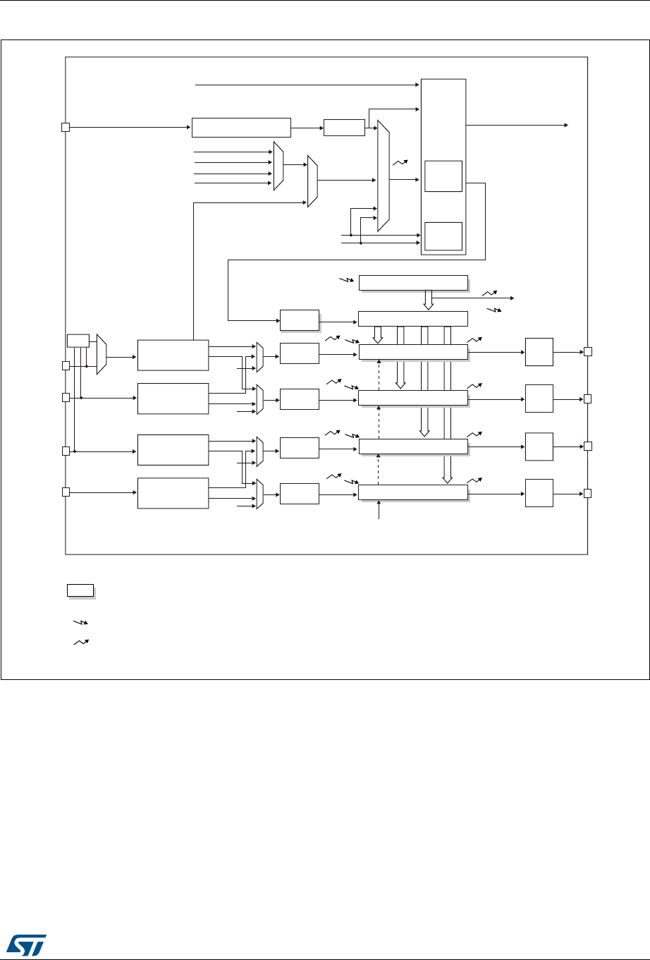
DocID025941 Rev 5 437/1001
RM0376 General-purpose timers (TIM2/TIM3)
503
Figure 89. General-purpose timer block diagram
U
U
U
CC1I
CC2I
Trigger
controller
+/-
Stop, clear or up/down
TI1FP1
TI2FP2
ITR0
ITR1
ITR2 TRGI
Output
control
TRGO
OC1REF
OC2REF
U
UI
Reset, enable, up, count
CK_PSC
IC1
IC2 IC2PS
IC1PS
TI1FP1
TGI
TRC
TRC
ITR
TRC
TI1F_ED
CC1I
CC2I
TI1FP2
TI2FP1
TI2FP2
TI1
TI2
TIMx_CH1
TIMx_CH2
OC1
OC2 TIMx_CH2
TIMx_CH1
to other timers
to DAC/ADC
Slave
controller
mode
PSC
prescaler CNT counter
Internal clock (CK_INT)
CK_CNT
TIMxCLK from RCC
ITR3
MS19673V1
XOR
Input filter &
edge detector
Capture/Compare 1 register
Notes:
Reg Preload registers transferred
to active registers on U event
according to control bit
Event
Interrupt & DMA output
Auto-reload register
Capture/Compare 2 register
Prescaler
Prescaler
Input filter &
edge detector
Output
control
U
U
CC3I
CC4I
Output
control
OC3REF
OC4REF
IC3
IC4 IC4PS
IC3PS
TI4FP3
TI4FP4
TIMx_CH3
TIMx_CH4
OC3
OC4 TIMx_CH4
TIMx_CH3
Input filter &
edge detector
Capture/Compare 3 register
Capture/Compare 4 register
Prescaler
Prescaler
Input filter &
edge detector
Output
control
TRC
TI3FP3
TI3FP4
TRC
CC3I
CC4I
TI3
TI4
Encoder
interface
TIMx_ETR Input filter
Polarity selection & edge
detector & prescaler
ETR ETRP
ETRF
ETRF

General-purpose timers (TIM2/TIM3) RM0376
438/1001 DocID025941 Rev 5
20.3 TIM2/TIM3 functional description
20.3.1 Time-base unit
The main block of the programmable timer is a 16-bit with its related auto-reload register.
The counter can count up, down or both up and down but also down or both up and down.
The counter clock can be divided by a prescaler.
The counter, the auto-reload register and the prescaler register can be written or read by
software. This is true even when the counter is running.
The time-base unit includes:
•Counter Register (TIMx_CNT)
•Prescaler Register (TIMx_PSC):
•Auto-Reload Register (TIMx_ARR)
The auto-reload register is preloaded. Writing to or reading from the auto-reload register
accesses the preload register. The content of the preload register are transferred into the
shadow register permanently or at each update event (UEV), depending on the auto-reload
preload enable bit (ARPE) in TIMx_CR1 register. The update event is sent when the counter
reaches the overflow (or underflow when downcounting) and if the UDIS bit equals 0 in the
TIMx_CR1 register. It can also be generated by software. The generation of the update
event is described in detail for each configuration.
The counter is clocked by the prescaler output CK_CNT, which is enabled only when the
counter enable bit (CEN) in TIMx_CR1 register is set (refer also to the slave mode controller
description to get more details on counter enabling).
Note that the actual counter enable signal CNT_EN is set 1 clock cycle after CEN.
Prescaler description
The prescaler can divide the counter clock frequency by any factor between 1 and 65536. It
is based on a 16-bit counter controlled through a 16-bit/32-bit register (in the TIMx_PSC
register). It can be changed on the fly as this control register is buffered. The new prescaler
ratio is taken into account at the next update event.
Figure 90 and Figure 20.3.2 give some examples of the counter behavior when the
prescaler ratio is changed on the fly:

DocID025941 Rev 5 439/1001
RM0376 General-purpose timers (TIM2/TIM3)
503
Figure 90. Counter timing diagram with prescaler division change from 1 to 2
Figure 91. Counter timing diagram with prescaler division change from 1 to 4
CK_PSC
00
CEN
Timerclock = CK_CNT
Counter register
Update event (UEV)
0
Prescaler control register 1
0
Write a new value in TIMx_PSC
Prescaler buffer 1
0
Prescaler counter 010 10101
01 02 03
FA FBF7 F8 F9 FC
MS31076V2
0
3
0
01230123
MS31077V2
CK_PSC
CEN
Timerclock = CK_CNT
Counter register
Update event (UEV)
Prescaler control register
Write a new value in TIMx_PSC
Prescaler buffer
Prescaler counter
00 01
FA FB
F7 F8 F9 FC
30
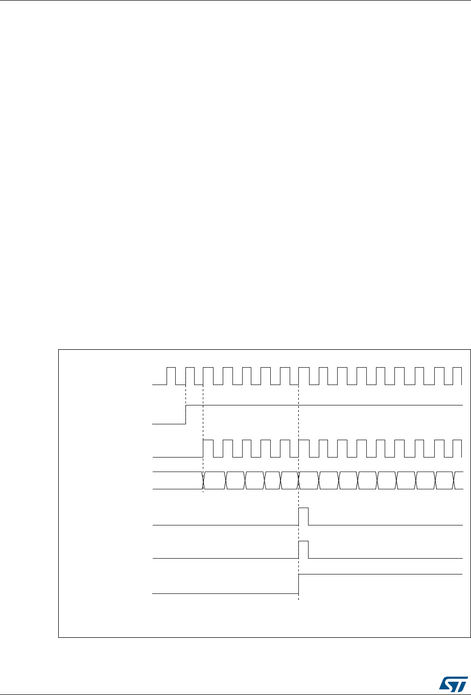
General-purpose timers (TIM2/TIM3) RM0376
440/1001 DocID025941 Rev 5
20.3.2 Counter modes
Upcounting mode
In upcounting mode, the counter counts from 0 to the auto-reload value (content of the
TIMx_ARR register), then restarts from 0 and generates a counter overflow event.
An Update event can be generated at each counter overflow or by setting the UG bit in the
TIMx_EGR register (by software or by using the slave mode controller).
The UEV event can be disabled by software by setting the UDIS bit in TIMx_CR1 register.
This is to avoid updating the shadow registers while writing new values in the preload
registers. Then no update event occurs until the UDIS bit has been written to 0. However,
the counter restarts from 0, as well as the counter of the prescaler (but the prescale rate
does not change). In addition, if the URS bit (update request selection) in TIMx_CR1
register is set, setting the UG bit generates an update event UEV but without setting the UIF
flag (thus no interrupt or DMA request is sent). This is to avoid generating both update and
capture interrupts when clearing the counter on the capture event.
When an update event occurs, all the registers are updated and the update flag (UIF bit in
TIMx_SR register) is set (depending on the URS bit):
•The buffer of the prescaler is reloaded with the preload value (content of the TIMx_PSC
register)
•The auto-reload shadow register is updated with the preload value (TIMx_ARR)
The following figures show some examples of the counter behavior for different clock
frequencies when TIMx_ARR=0x36.
Figure 92. Counter timing diagram, internal clock divided by 1
00 02 03 04 05 06 0732 33 34 35 36
31
MS31078V2
CK_PSC
CNT_EN
Timerclock = CK_CNT
Counter register
Update event (UEV)
Counter overflow
Update interrupt flag
(UIF)
01

DocID025941 Rev 5 441/1001
RM0376 General-purpose timers (TIM2/TIM3)
503
Figure 93. Counter timing diagram, internal clock divided by 2
Figure 94. Counter timing diagram, internal clock divided by 4
MS31079V2
CK_PSC
CNT_EN
Timerclock = CK_CNT
Counter register
Update event (UEV)
Counter overflow
Update interrupt flag
(UIF)
0034 0035 0036 0000 0001 0002 0003
0000
0001
0035 0036
MS31080V2
CK_PSC
Timerclock = CK_CNT
Counter register
Update event (UEV)
Counter overflow
Update interrupt flag
(UIF)
CNT_EN

General-purpose timers (TIM2/TIM3) RM0376
442/1001 DocID025941 Rev 5
Figure 95. Counter timing diagram, internal clock divided by N
Figure 96. Counter timing diagram, Update event when ARPE=0 (TIMx_ARR not
preloaded)
00
1F 20
MS31081V2
CK_PSC
Timerclock = CK_CNT
Counter register
Update event (UEV)
Counter overflow
Update interrupt flag
(UIF)
FF 36
MS31082V2
CK_PSC
Timerclock = CK_CNT
Counter register
Update event (UEV)
Counter overflow
Update interrupt flag
(UIF)
00 02 03 04 05 06 0732 33 34 35 3631 01
CEN
Auto-reload preload
register
Write a new value in TIMx_ARR

DocID025941 Rev 5 443/1001
RM0376 General-purpose timers (TIM2/TIM3)
503
Figure 97. Counter timing diagram, Update event when ARPE=1 (TIMx_ARR
preloaded)
Downcounting mode
In downcounting mode, the counter counts from the auto-reload value (content of the
TIMx_ARR register) down to 0, then restarts from the auto-reload value and generates a
counter underflow event.
An Update event can be generate at each counter underflow or by setting the UG bit in the
TIMx_EGR register (by software or by using the slave mode controller)
The UEV update event can be disabled by software by setting the UDIS bit in TIMx_CR1
register. This is to avoid updating the shadow registers while writing new values in the
preload registers. Then no update event occurs until UDIS bit has been written to 0.
However, the counter restarts from the current auto-reload value, whereas the counter of the
prescaler restarts from 0 (but the prescale rate doesn’t change).
In addition, if the URS bit (update request selection) in TIMx_CR1 register is set, setting the
UG bit generates an update event UEV but without setting the UIF flag (thus no interrupt or
DMA request is sent). This is to avoid generating both update and capture interrupts when
clearing the counter on the capture event.
When an update event occurs, all the registers are updated and the update flag (UIF bit in
TIMx_SR register) is set (depending on the URS bit):
•The buffer of the prescaler is reloaded with the preload value (content of the TIMx_PSC
register).
•The auto-reload active register is updated with the preload value (content of the
TIMx_ARR register). Note that the auto-reload is updated before the counter is
reloaded, so that the next period is the expected one.
MS31083V2
F5 36
CK_PSC
Timerclock = CK_CNT
Counter register
Update event (UEV)
Counter overflow
Update interrupt flag
(UIF)
00 02 03 04 05 06 07F1 F2 F3 F4 F5F0 01
CEN
Auto-reload preload
register
Write a new value in TIMx_ARR
Auto-reload shadow
register F5 36
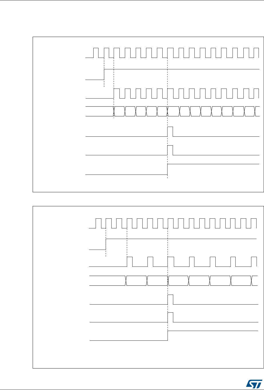
General-purpose timers (TIM2/TIM3) RM0376
444/1001 DocID025941 Rev 5
The following figures show some examples of the counter behavior for different clock
frequencies when TIMx_ARR=0x36.
Figure 98. Counter timing diagram, internal clock divided by 1
Figure 99. Counter timing diagram, internal clock divided by 2
36 34 33 32 31 30 2F
04 03 02 01 00
05
MS31184V1
CK_PSC
CNT_EN
Timerclock = CK_CNT
Counter register
Update event (UEV)
Counter underflow
(cnt_udf)
Update interrupt flag
(UIF)
35
MS31185V1
CK_PSC
CNT_EN
Timerclock = CK_CNT
Counter register
Update event (UEV)
Counter underflow
Update interrupt flag
(UIF)
0002 0001 0000 0036 0035 0034 0033
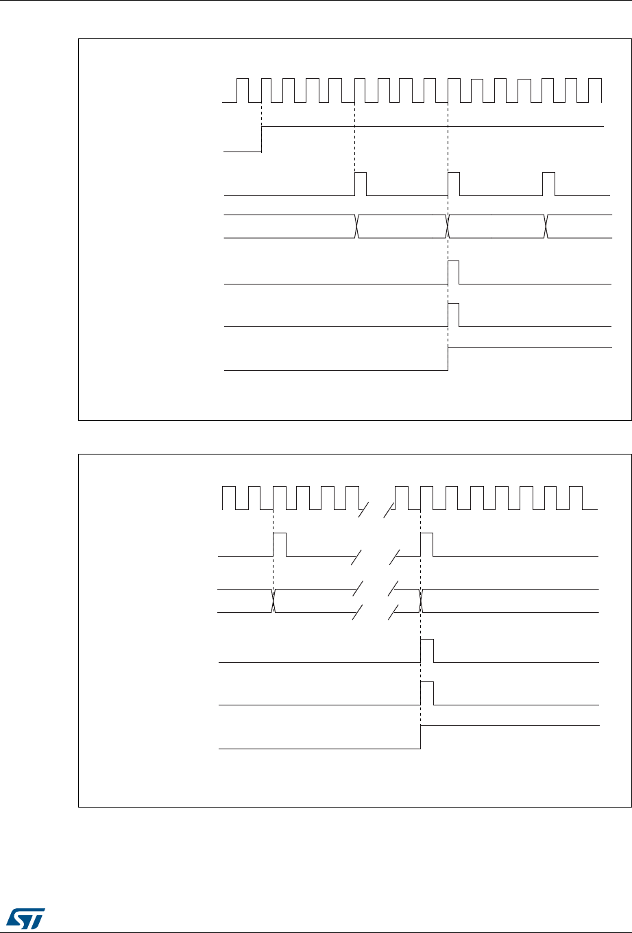
DocID025941 Rev 5 445/1001
RM0376 General-purpose timers (TIM2/TIM3)
503
Figure 100. Counter timing diagram, internal clock divided by 4
Figure 101. Counter timing diagram, internal clock divided by N
0000
0001
0001 0000
MS31186V1
CK_PSC
Timerclock = CK_CNT
Counter register
Update event (UEV)
Counter underflow
Update interrupt flag
(UIF)
CNT_EN
001F20
MS31187V1
CK_PSC
Timerclock = CK_CNT
Counter register
Update event (UEV)
Counter underflow
Update interrupt flag
(UIF)
36
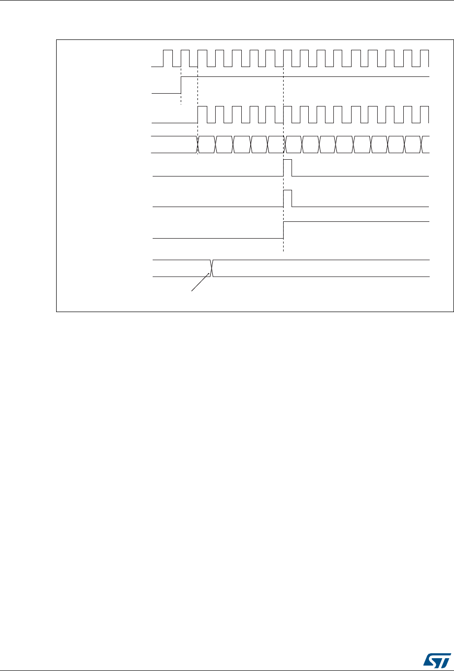
General-purpose timers (TIM2/TIM3) RM0376
446/1001 DocID025941 Rev 5
Figure 102. Counter timing diagram, Update event when repetition counter
is not used
Center-aligned mode (up/down counting)
In center-aligned mode, the counter counts from 0 to the auto-reload value (content of the
TIMx_ARR register) – 1, generates a counter overflow event, then counts from the auto-
reload value down to 1 and generates a counter underflow event. Then it restarts counting
from 0.
Center-aligned mode is active when the CMS bits in TIMx_CR1 register are not equal to
'00'. The Output compare interrupt flag of channels configured in output is set when: the
counter counts down (Center aligned mode 1, CMS = "01"), the counter counts up (Center
aligned mode 2, CMS = "10") the counter counts up and down (Center aligned mode 3,
CMS = "11").
In this mode, the direction bit (DIR from TIMx_CR1 register) cannot be written. It is updated
by hardware and gives the current direction of the counter.
The update event can be generated at each counter overflow and at each counter underflow
or by setting the UG bit in the TIMx_EGR register (by software or by using the slave mode
controller) also generates an update event. In this case, the counter restarts counting from
0, as well as the counter of the prescaler.
The UEV update event can be disabled by software by setting the UDIS bit in TIMx_CR1
register. This is to avoid updating the shadow registers while writing new values in the
preload registers. Then no update event occurs until the UDIS bit has been written to 0.
However, the counter continues counting up and down, based on the current auto-reload
value.
In addition, if the URS bit (update request selection) in TIMx_CR1 register is set, setting the
UG bit generates an update event UEV but without setting the UIF flag (thus no interrupt or
FF 36
MS31188V1
CK_PSC
Timerclock = CK_CNT
Counter register
Update event (UEV)
Counter underflow
Update interrupt flag
(UIF)
0002030405 30 2F3233343536 3101
CEN
Auto-reload preload
register
Write a new value in TIMx_ARR
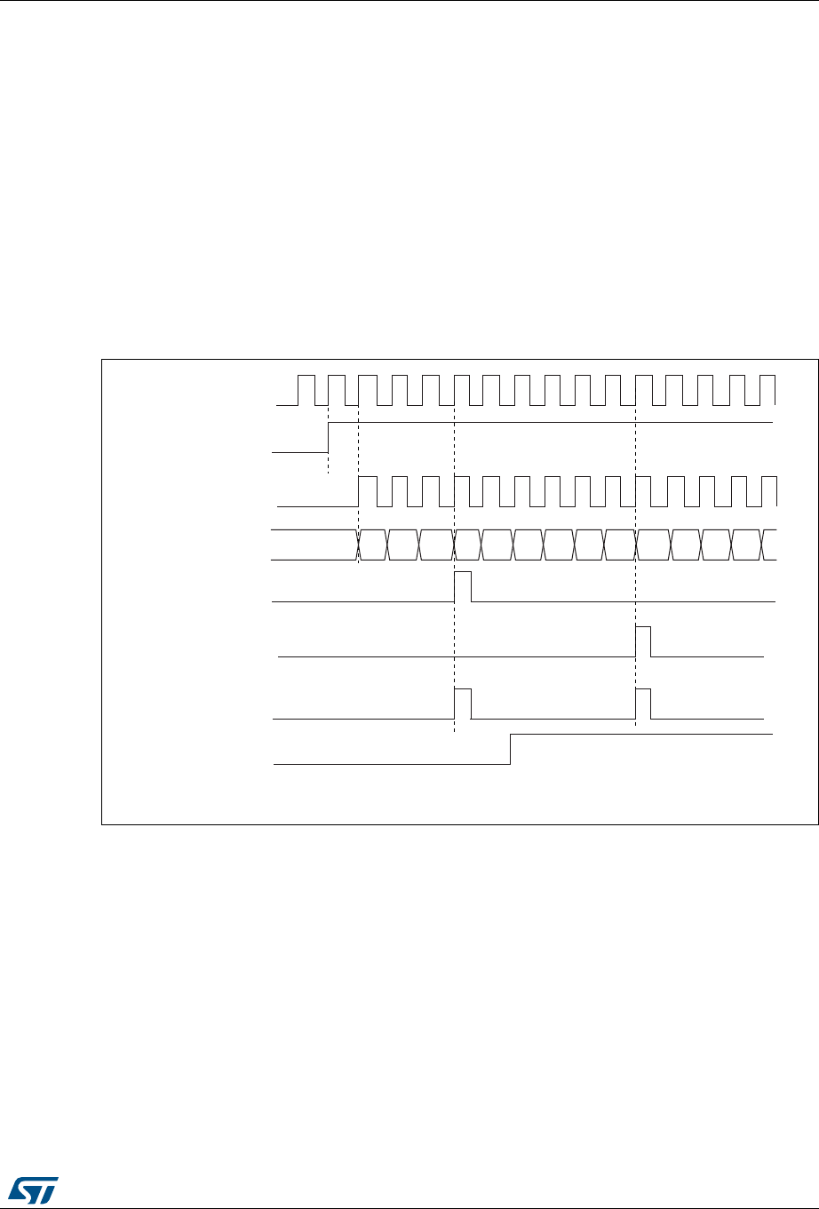
DocID025941 Rev 5 447/1001
RM0376 General-purpose timers (TIM2/TIM3)
503
DMA request is sent). This is to avoid generating both update and capture interrupt when
clearing the counter on the capture event.
When an update event occurs, all the registers are updated and the update flag (UIF bit in
TIMx_SR register) is set (depending on the URS bit):
•The buffer of the prescaler is reloaded with the preload value (content of the TIMx_PSC
register).
•The auto-reload active register is updated with the preload value (content of the
TIMx_ARR register). Note that if the update source is a counter overflow, the auto-
reload is updated before the counter is reloaded, so that the next period is the expected
one (the counter is loaded with the new value).
The following figures show some examples of the counter behavior for different clock
frequencies.
Figure 103. Counter timing diagram, internal clock divided by 1, TIMx_ARR=0x6
1. Here, center-aligned mode 1 is used (for more details refer to Section 20.4.1: TIMx control register 1
(TIMx_CR1) on page 480).
MS31189V1
CK_PSC
Timerclock = CK_CNT
Counter register
Update event (UEV)
Counter overflow
Update interrupt flag
(UIF)
00020304 05 06
01
CEN
02 03 0401 05 0304
Counter underflow
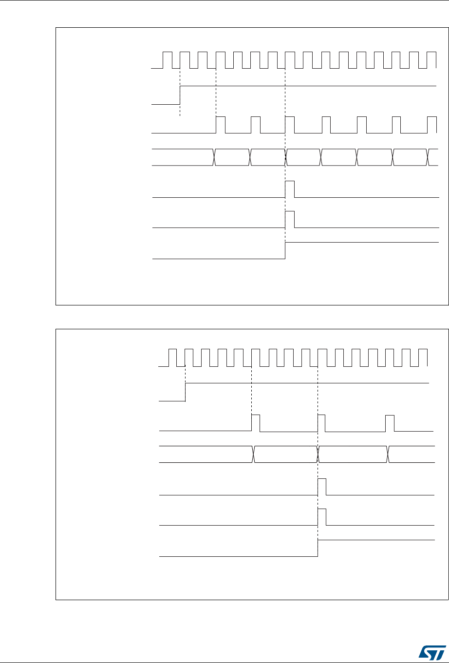
General-purpose timers (TIM2/TIM3) RM0376
448/1001 DocID025941 Rev 5
Figure 104. Counter timing diagram, internal clock divided by 2
Figure 105. Counter timing diagram, internal clock divided by 4, TIMx_ARR=0x36
1. Center-aligned mode 2 or 3 is used with an UIF on overflow.
MS31190V1
CK_PSC
CNT_EN
Timerclock = CK_CNT
Counter register
Update event (UEV)
Counter underflow
Update interrupt flag
(UIF)
0003 0002 0001 0000 0001 0002 0003
0034 0035
MS31191V1
CK_PSC
Timerclock = CK_CNT
Counter register
Update event (UEV)
Counter overflow
Update interrupt flag
(UIF)
CNT_EN
Note: Here, center_aligned mode 2 or 3 is updated with an UIF on overflow
0036 0035
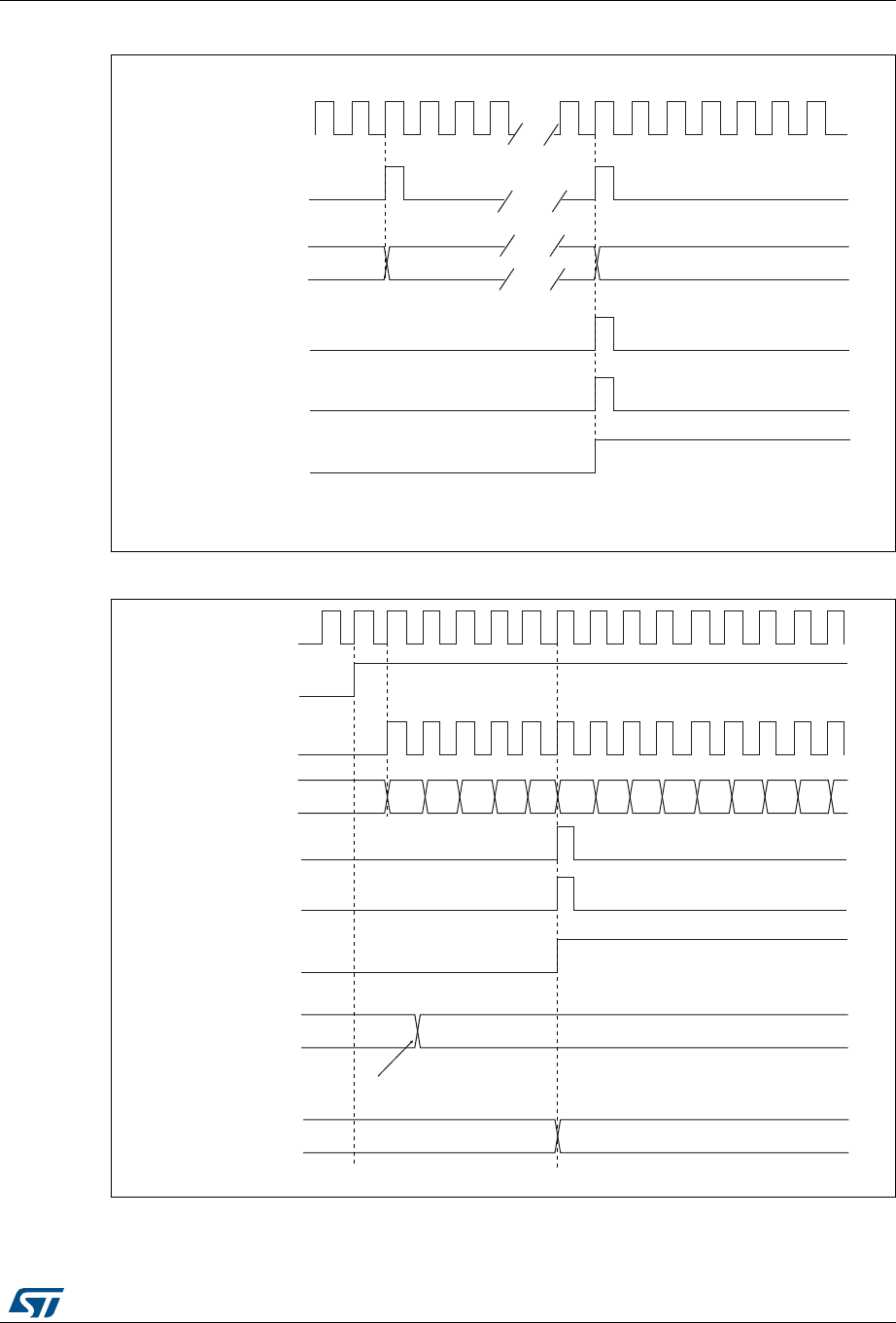
DocID025941 Rev 5 449/1001
RM0376 General-purpose timers (TIM2/TIM3)
503
Figure 106. Counter timing diagram, internal clock divided by N
Figure 107. Counter timing diagram, Update event with ARPE=1 (counter underflow)
00
1F
20
MS31192V1
CK_PSC
Timerclock = CK_CNT
Counter register
Update event (UEV)
Counter underflow
Update interrupt flag
(UIF)
01
FD 36
MS31193V1
CK_PSC
Timerclock = CK_CNT
Counter register
Update event (UEV)
Counter underflow
Update interrupt flag
(UIF)
00 02 03 04 05 06 0701
CEN
Auto-reload preload
register
Write a new value in TIMx_ARR
06 05 04 03 02 01
FD 36
Auto-reload active
register
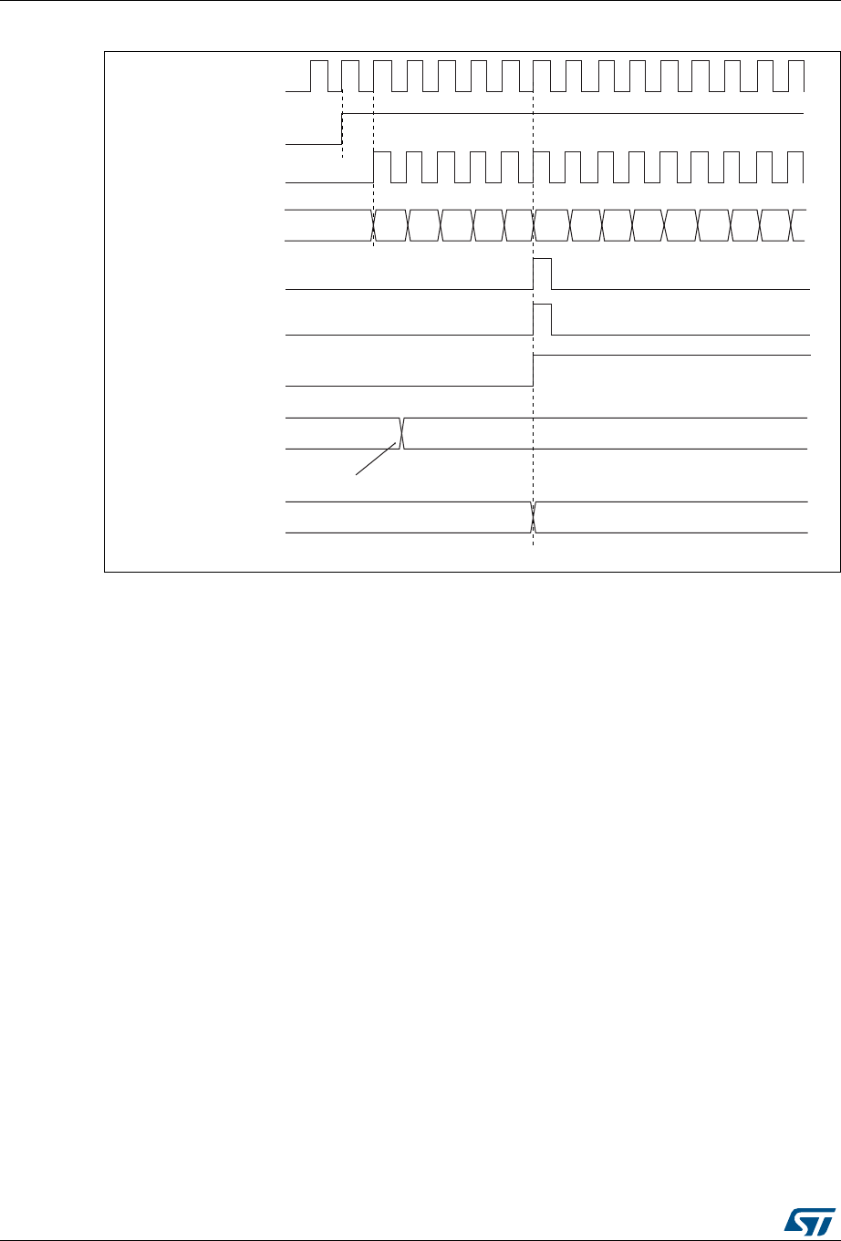
General-purpose timers (TIM2/TIM3) RM0376
450/1001 DocID025941 Rev 5
Figure 108. Counter timing diagram, Update event with ARPE=1 (counter overflow)
20.3.3 Clock selection
The counter clock can be provided by the following clock sources:
•Internal clock (CK_INT)
•External clock mode1: external input pin (TIx)
•External clock mode2: external trigger input (ETR)
•Internal trigger inputs (ITRx): using one timer as prescaler for another timer. Refer to :
Using one timer as prescaler for another timer on page 473 for more details.
Internal clock source (CK_INT)
If the slave mode controller is disabled (SMS=000 in the TIMx_SMCR register), then the
CEN, DIR (in the TIMx_CR1 register) and UG bits (in the TIMx_EGR register) are actual
control bits and can be changed only by software (except UG which remains cleared
automatically). As soon as the CEN bit is written to 1, the prescaler is clocked by the internal
clock CK_INT.
Figure 109 shows the behavior of the control circuit and the upcounter in normal mode,
without prescaler.
MS31194V1
FD 36
CK_PSC
Timer clock = CK_CNT
Counter register
Update event (UEV)
Counter overflow
Update interrupt flag
(UIF)
36 34 33 32 31 30 2FF8 F9 FA FB FCF7 35
CEN
Auto-reload preload
register
Write a new value in TIMx_ARR
Auto-reload active
register FD 36
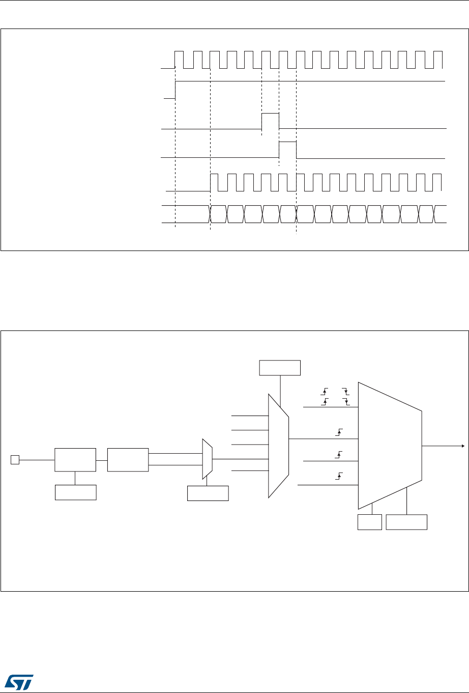
DocID025941 Rev 5 451/1001
RM0376 General-purpose timers (TIM2/TIM3)
503
Figure 109. Control circuit in normal mode, internal clock divided by 1
External clock source mode 1
This mode is selected when SMS=111 in the TIMx_SMCR register. The counter can count at
each rising or falling edge on a selected input.
Figure 110. TI2 external clock connection example
Internal clock
Counter clock = CK_CNT = CK_PSC
Counter register
CEN=CNT_EN
UG
CNT_INIT
MS31085V2
00 02 03 04 05 06 0732 33 34 35 36
31 01
External clock
mode 1
Internal clock
mode
TRGI
CK_INT
CK_PSC
TIMx_SMCR
SMS[2:0]
ITRx
TI1_ED
TI1FP1
TI2FP2
TIMx_SMCR
TS[2:0]
TI2 0
1
TIMx_CCER
CC2P
Filter
ICF[3:0]
TIMx_CCMR1
Edge
detector
TI2F_Rising
TI2F_Falling
110
0xx
100
101
MS31196V1
(internal clock)
TI1F or
TI2F or
or
Encoder
mode
ETRF 111
External clock
mode 2
ETRF
ECE
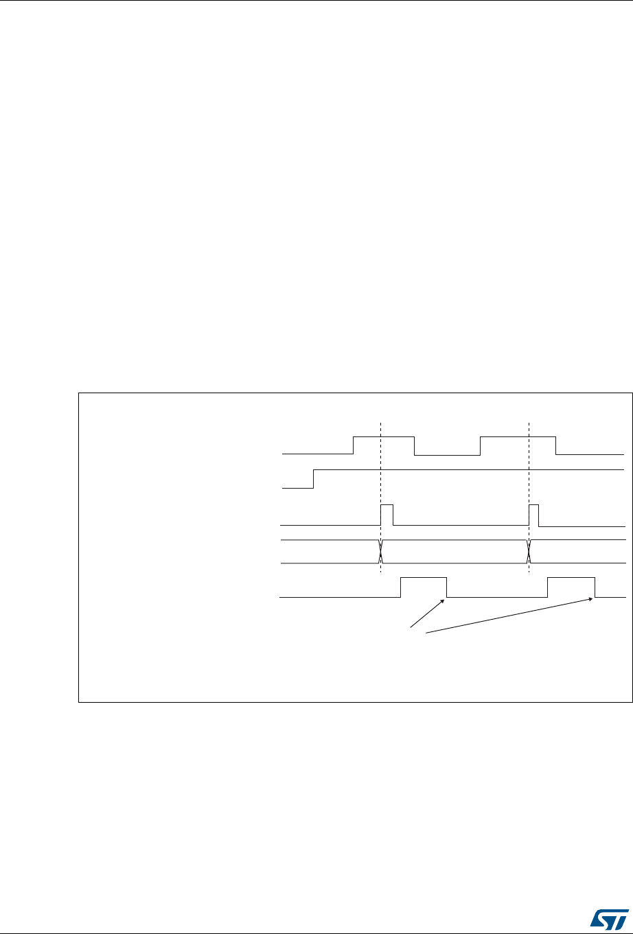
General-purpose timers (TIM2/TIM3) RM0376
452/1001 DocID025941 Rev 5
For example, to configure the upcounter to count in response to a rising edge on the TI2
input, use the following procedure:
1. Configure channel 2 to detect rising edges on the TI2 input by writing CC2S= ‘01 in the
TIMx_CCMR1 register.
2. Configure the input filter duration by writing the IC2F[3:0] bits in the TIMx_CCMR1
register (if no filter is needed, keep IC2F=0000).
Note: The capture prescaler is not used for triggering, so you don’t need to configure it.
3. Select rising edge polarity by writing CC2P=0 and CC2NP=0 in the TIMx_CCER
register.
4. Configure the timer in external clock mode 1 by writing SMS=111 in the TIMx_SMCR
register.
5. Select TI2 as the input source by writing TS=110 in the TIMx_SMCR register.
6. Enable the counter by writing CEN=1 in the TIMx_CR1 register.
For code example, refer to A.11.1: Upcounter on TI2 rising edge code example.
When a rising edge occurs on TI2, the counter counts once and the TIF flag is set.
The delay between the rising edge on TI2 and the actual clock of the counter is due to the
resynchronization circuit on TI2 input.
Figure 111. Control circuit in external clock mode 1
Counter clock = CK_CNT = CK_PSC
Counter register 35 3634
TI2
CNT_EN
TIF
Write TIF=0
MS31087V2
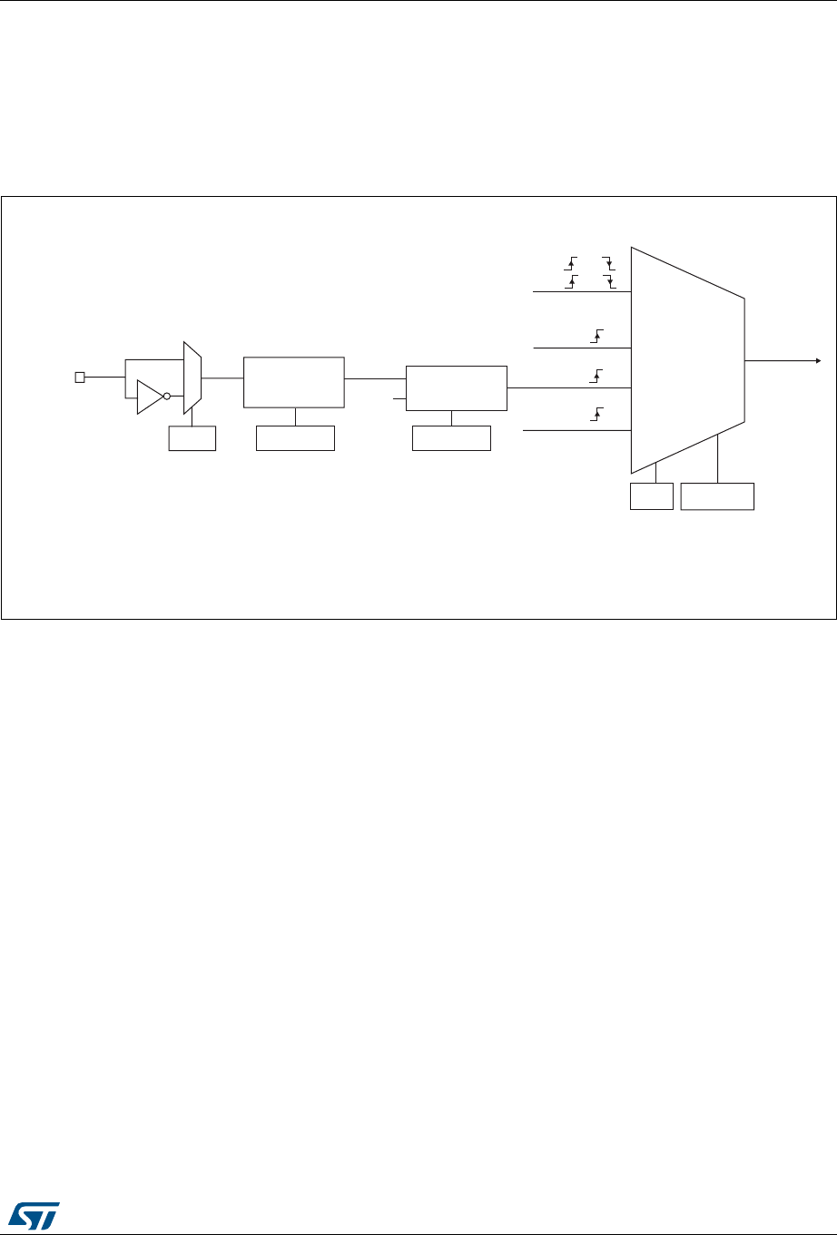
DocID025941 Rev 5 453/1001
RM0376 General-purpose timers (TIM2/TIM3)
503
External clock source mode 2
This mode is selected by writing ECE=1 in the TIMx_SMCR register.
The counter can count at each rising or falling edge on the external trigger input ETR.
Figure 112 gives an overview of the external trigger input block.
Figure 112. External trigger input block
For example, to configure the upcounter to count each 2 rising edges on ETR, use the
following procedure:
1. As no filter is needed in this example, write ETF[3:0]=0000 in the TIMx_SMCR register.
2. Set the prescaler by writing ETPS[1:0]=01 in the TIMx_SMCR register
3. Select rising edge detection on the ETR pin by writing ETP=0 in the TIMx_SMCR
register
4. Enable external clock mode 2 by writing ECE=1 in the TIMx_SMCR register.
5. Enable the counter by writing CEN=1 in the TIMx_CR1 register.
For code example, refer to A.11.2: Up counter on each 2 ETR rising edges code example.
The counter counts once each 2 ETR rising edges.
The delay between the rising edge on ETR and the actual clock of the counter is due to the
resynchronization circuit on the ETRP signal.
External clock
mode 1
Internal clock
mode
TRGI
CK_INT
CK_PSC
TIMx_SMCR
SMS[2:0]
MS33116V1
(internal clock)
TI1F or
TI2F or
or
Encoder
mode
External clock
mode 2
ETRF
ECE
0
1
TIMx_SMCR
ETP
ETR pin
ETR
Divider
/1, /2, /4, /8 Filter
downcounter
f
ETRP
TIMx_SMCR
ETPS[1:0]
TIMx_SMCR
ETF[3:0]
DTS
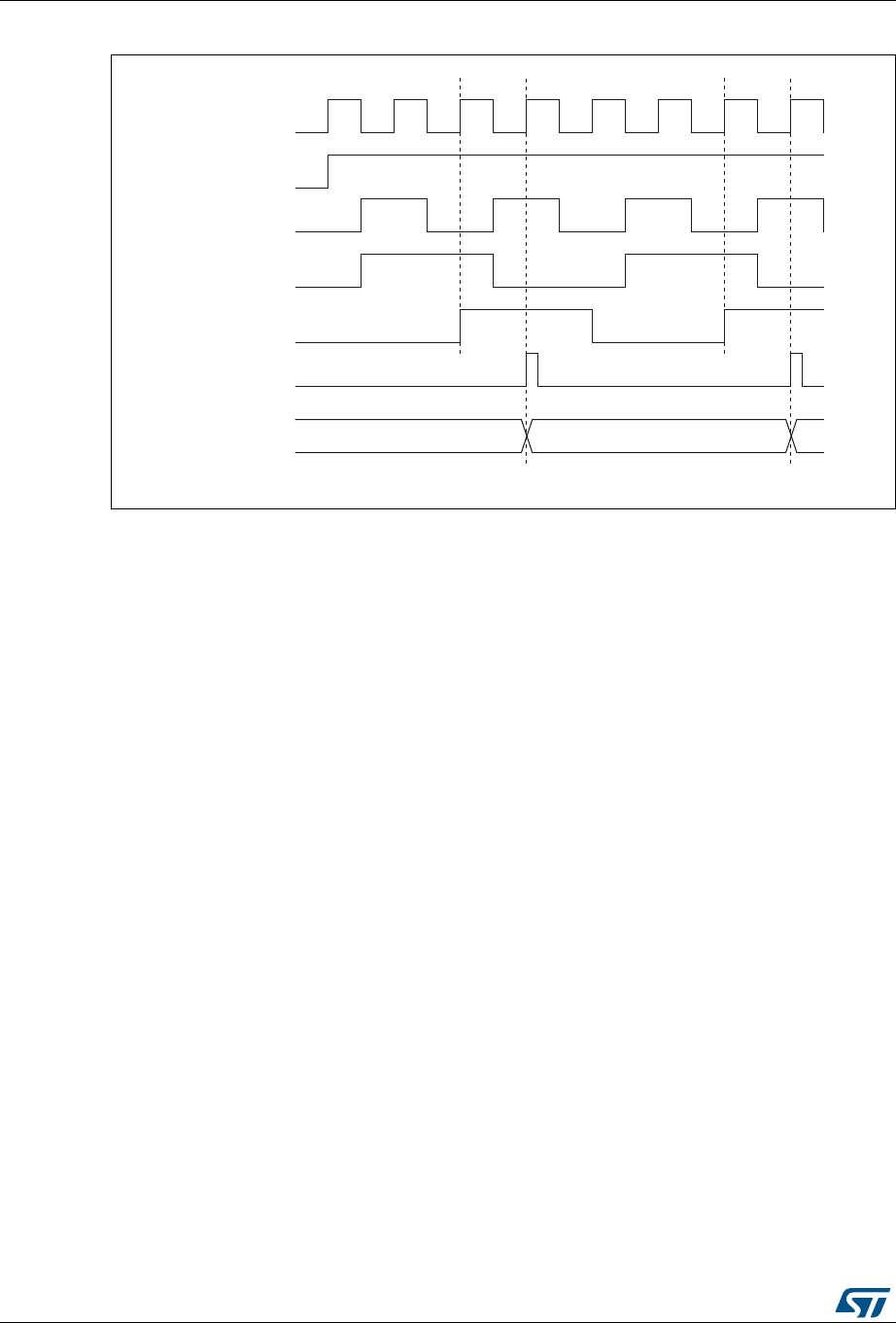
General-purpose timers (TIM2/TIM3) RM0376
454/1001 DocID025941 Rev 5
Figure 113. Control circuit in external clock mode 2
20.3.4 Capture/compare channels
Each Capture/Compare channel is built around a capture/compare register (including a
shadow register), a input stage for capture (with digital filter, multiplexing and prescaler) and
an output stage (with comparator and output control).
The following figure gives an overview of one Capture/Compare channel.
The input stage samples the corresponding TIx input to generate a filtered signal TIxF.
Then, an edge detector with polarity selection generates a signal (TIxFPx) which can be
used as trigger input by the slave mode controller or as the capture command. It is
prescaled before the capture register (ICxPS).
MS33111V2
34 35 36
fCK_INT
CNT_EN
ETR
ETRP
ETRF
Counter clock =
CK_INT =CK_PSC
Counter register
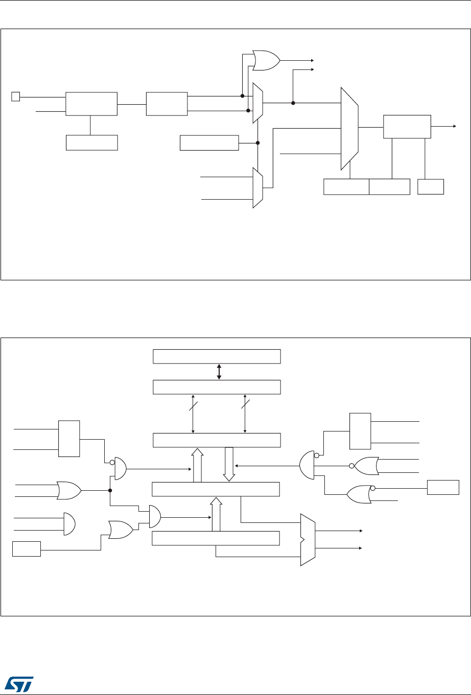
DocID025941 Rev 5 455/1001
RM0376 General-purpose timers (TIM2/TIM3)
503
Figure 114. Capture/compare channel (example: channel 1 input stage)
The output stage generates an intermediate waveform which is then used for reference:
OCxRef (active high). The polarity acts at the end of the chain.
Figure 115. Capture/compare channel 1 main circuit
0
1
Divider
/1, /2, /4, /8
ICPS[1:0]
TI1F_ED
To the slave mode controller
TI1FP1
11
01
CC1S[1:0]
IC1
TI2FP1
TRC
(from slave mode
controller)
10 IC1PS
0
1
MS33115V1
TI1
TIMx_CCER
CC1P/CC1NP
Filter
downcounter
ICF[3:0]
TIMx_CCMR1
Edge
detector
TI1F_Rising
TI1F_Falling
TIMx_CCMR1
TIMx_CCER
TI2F_Rising
(from channel 2)
TI2F_Falling
(from channel 2)
TI1F
f
CC1E
DTS
CC1E
Capture/compare shadow register
Comparator
Capture/compare preload register
Counter
IC1PS
CC1S[0]
CC1S[1]
Capture
Input
mode
S
R
Read CCR1H
Read CCR1L
read_in_progress
capture_transfer CC1S[0]
CC1S[1]
S
R
write CCR1H
write CCR1L
write_in_progress
Output
mode
UEV
OC1PE
(from time
base unit)
compare_transfer
APB Bus
88
high
low
(if 16-bit)
MCU-peripheral interface
TIMx_CCMR1
OC1PE
CNT>CCR1
CNT=CCR1
TIMx_EGR
CC1G
MS33144V1
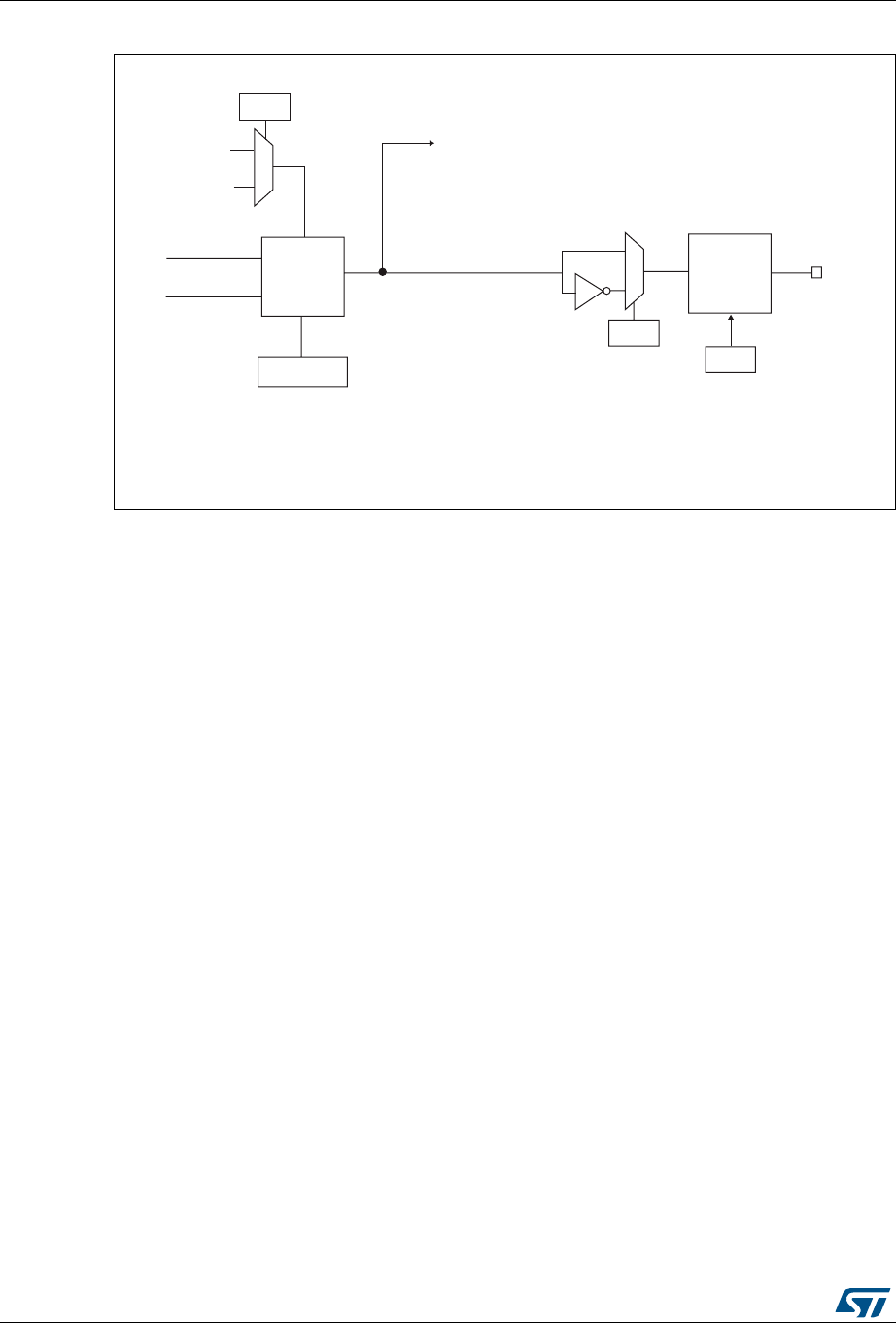
General-purpose timers (TIM2/TIM3) RM0376
456/1001 DocID025941 Rev 5
Figure 116. Output stage of capture/compare channel (channel 1)
The capture/compare block is made of one preload register and one shadow register. Write
and read always access the preload register.
In capture mode, captures are actually done in the shadow register, which is copied into the
preload register.
In compare mode, the content of the preload register is copied into the shadow register
which is compared to the counter.
20.3.5 Input capture mode
In Input capture mode, the Capture/Compare Registers (TIMx_CCRx) are used to latch the
value of the counter after a transition detected by the corresponding ICx signal. When a
capture occurs, the corresponding CCXIF flag (TIMx_SR register) is set and an interrupt or
a DMA request can be sent if they are enabled. If a capture occurs while the CCxIF flag was
already high, then the over-capture flag CCxOF (TIMx_SR register) is set. CCxIF can be
cleared by software by writing it to 0 or by reading the captured data stored in the
TIMx_CCRx register. CCxOF is cleared when you write it to 0.
The following example shows how to capture the counter value in TIMx_CCR1 when TI1
input rises. To do this, use the following procedure:
1. Select the active input: TIMx_CCR1 must be linked to the TI1 input, so write the CC1S
bits to 01 in the TIMx_CCMR1 register. As soon as CC1S becomes different from 00,
the channel is configured in input and the TIMx_CCR1 register becomes read-only.
2. Program the input filter duration you need with respect to the signal you connect to the
timer (when the input is one of the TIx (ICxF bits in the TIMx_CCMRx register). Let’s
imagine that, when toggling, the input signal is not stable during at must 5 internal clock
cycles. We must program a filter duration longer than these 5 clock cycles. We can
validate a transition on TI1 when 8 consecutive samples with the new level have been
MS33146V1
Output
mode
controller
CNT > CCR1
CNT = CCR1
TIMx_CCMR1
OC1M[2:0]
0
1
CC1P
TIMx_CCER
Output
enable
circuit
OC1
CC1E TIM1_CCER
To the master
mode controller
OC1REF
0
1
ocref_clr_int
ETRF
OCREF_CLR
OCCS
TIMx_SMCR

DocID025941 Rev 5 457/1001
RM0376 General-purpose timers (TIM2/TIM3)
503
detected (sampled at fDTS frequency). Then write IC1F bits to 0011 in the
TIMx_CCMR1 register.
3. Select the edge of the active transition on the TI1 channel by writing the CC1P and
CC1NP bits to 00 in the TIMx_CCER register (rising edge in this case).
4. Program the input prescaler. In our example, we wish the capture to be performed at
each valid transition, so the prescaler is disabled (write IC1PS bits to 00 in the
TIMx_CCMR1 register).
5. Enable capture from the counter into the capture register by setting the CC1E bit in the
TIMx_CCER register.
6. If needed, enable the related interrupt request by setting the CC1IE bit in the
TIMx_DIER register, and/or the DMA request by setting the CC1DE bit in the
TIMx_DIER register.
For code example, refer to A.11.3: Input capture configuration code example.
When an input capture occurs:
•The TIMx_CCR1 register gets the value of the counter on the active transition.
•CC1IF flag is set (interrupt flag). CC1OF is also set if at least two consecutive captures
occurred whereas the flag was not cleared.
•An interrupt is generated depending on the CC1IE bit.
•A DMA request is generated depending on the CC1DE bit.
For code example, refer to A.11.4: Input capture data management code example.
In order to handle the overcapture, it is recommended to read the data before the
overcapture flag. This is to avoid missing an overcapture which could happen after reading
the flag and before reading the data.
Note: IC interrupt and/or DMA requests can be generated by software by setting the
corresponding CCxG bit in the TIMx_EGR register.

General-purpose timers (TIM2/TIM3) RM0376
458/1001 DocID025941 Rev 5
20.3.6 PWM input mode
This mode is a particular case of input capture mode. The procedure is the same except:
•Two ICx signals are mapped on the same TIx input.
•These 2 ICx signals are active on edges with opposite polarity.
•One of the two TIxFP signals is selected as trigger input and the slave mode controller
is configured in reset mode.
For example, you can measure the period (in TIMx_CCR1 register) and the duty cycle (in
TIMx_CCR2 register) of the PWM applied on TI1 using the following procedure (depending
on CK_INT frequency and prescaler value):
1. Select the active input for TIMx_CCR1: write the CC1S bits to 01 in the TIMx_CCMR1
register (TI1 selected).
2. Select the active polarity for TI1FP1 (used both for capture in TIMx_CCR1 and counter
clear): write the CC1P to ‘0’ and the CC1NP bit to ‘0’ (active on rising edge).
3. Select the active input for TIMx_CCR2: write the CC2S bits to 10 in the TIMx_CCMR1
register (TI1 selected).
4. Select the active polarity for TI1FP2 (used for capture in TIMx_CCR2): write the CC2P
bit to ‘1’ and the CC2NP bit to ’0’(active on falling edge).
5. Select the valid trigger input: write the TS bits to 101 in the TIMx_SMCR register
(TI1FP1 selected).
6. Configure the slave mode controller in reset mode: write the SMS bits to 100 in the
TIMx_SMCR register.
7. Enable the captures: write the CC1E and CC2E bits to ‘1 in the TIMx_CCER register.
For code example, refer to A.11.5: PWM input configuration code example.
Figure 117. PWM input mode timing

DocID025941 Rev 5 459/1001
RM0376 General-purpose timers (TIM2/TIM3)
503
20.3.7 Forced output mode
In output mode (CCxS bits = 00 in the TIMx_CCMRx register), each output compare signal
(OCxREF and then OCx) can be forced to active or inactive level directly by software,
independently of any comparison between the output compare register and the counter.
To force an output compare signal (OCxREF/OCx) to its active level, you just need to write
101 in the OCxM bits in the corresponding TIMx_CCMRx register. Thus OCxREF is forced
high (OCxREF is always active high) and OCx get opposite value to CCxP polarity bit.
e.g.: CCxP=0 (OCx active high) => OCx is forced to high level.
OCxREF signal can be forced low by writing the OCxM bits to 100 in the TIMx_CCMRx
register.
Anyway, the comparison between the TIMx_CCRx shadow register and the counter is still
performed and allows the flag to be set. Interrupt and DMA requests can be sent
accordingly. This is described in the Output Compare Mode section.
20.3.8 Output compare mode
This function is used to control an output waveform or indicating when a period of time has
elapsed.
When a match is found between the capture/compare register and the counter, the output
compare function:
•Assigns the corresponding output pin to a programmable value defined by the output
compare mode (OCxM bits in the TIMx_CCMRx register) and the output polarity (CCxP
bit in the TIMx_CCER register). The output pin can keep its level (OCXM=000), be set
active (OCxM=001), be set inactive (OCxM=010) or can toggle (OCxM=011) on match.
•Sets a flag in the interrupt status register (CCxIF bit in the TIMx_SR register).
•Generates an interrupt if the corresponding interrupt mask is set (CCXIE bit in the
TIMx_DIER register).
•Sends a DMA request if the corresponding enable bit is set (CCxDE bit in the
TIMx_DIER register, CCDS bit in the TIMx_CR2 register for the DMA request
selection).
The TIMx_CCRx registers can be programmed with or without preload registers using the
OCxPE bit in the TIMx_CCMRx register.
In output compare mode, the update event UEV has no effect on OCxREF and OCx output.
The timing resolution is one count of the counter. Output compare mode can also be used to
output a single pulse (in One-pulse mode).
Procedure:
1. Select the counter clock (internal, external, prescaler).
2. Write the desired data in the TIMx_ARR and TIMx_CCRx registers.
3. Set the CCxIE and/or CCxDE bits if an interrupt and/or a DMA request is to be
generated.
4. Select the output mode. For example, you must write OCxM=011, OCxPE=0, CCxP=0
and CCxE=1 to toggle OCx output pin when CNT matches CCRx, CCRx preload is not
used, OCx is enabled and active high.
5. Enable the counter by setting the CEN bit in the TIMx_CR1 register.
For code example, refer to A.11.7: Output compare configuration code example.

General-purpose timers (TIM2/TIM3) RM0376
460/1001 DocID025941 Rev 5
The TIMx_CCRx register can be updated at any time by software to control the output
waveform, provided that the preload register is not enabled (OCxPE=0, else TIMx_CCRx
shadow register is updated only at the next update event UEV). An example is given in
Figure 118.
Figure 118. Output compare mode, toggle on OC1.
20.3.9 PWM mode
Pulse width modulation mode allows you to generate a signal with a frequency determined
by the value of the TIMx_ARR register and a duty cycle determined by the value of the
TIMx_CCRx register.
The PWM mode can be selected independently on each channel (one PWM per OCx
output) by writing 110 (PWM mode 1) or ‘111 (PWM mode 2) in the OCxM bits in the
TIMx_CCMRx register. You must enable the corresponding preload register by setting the
OCxPE bit in the TIMx_CCMRx register, and eventually the auto-reload preload register (in
upcounting or center-aligned modes) by setting the ARPE bit in the TIMx_CR1 register.
As the preload registers are transferred to the shadow registers only when an update event
occurs, before starting the counter, you have to initialize all the registers by setting the UG
bit in the TIMx_EGR register.
OCx polarity is software programmable using the CCxP bit in the TIMx_CCER register. It
can be programmed as active high or active low. OCx output is enabled by the CCxE bit in
the TIMx_CCER register. Refer to the TIMx_CCERx register description for more details.
MS31092V1
OC1REF= OC1
TIM1_CNT B200 B201
0039
TIM1_CCR1 003A
Write B201h in the CC1R register
Match detected on CCR1
Interrupt generated if enabled
003B
B201
003A
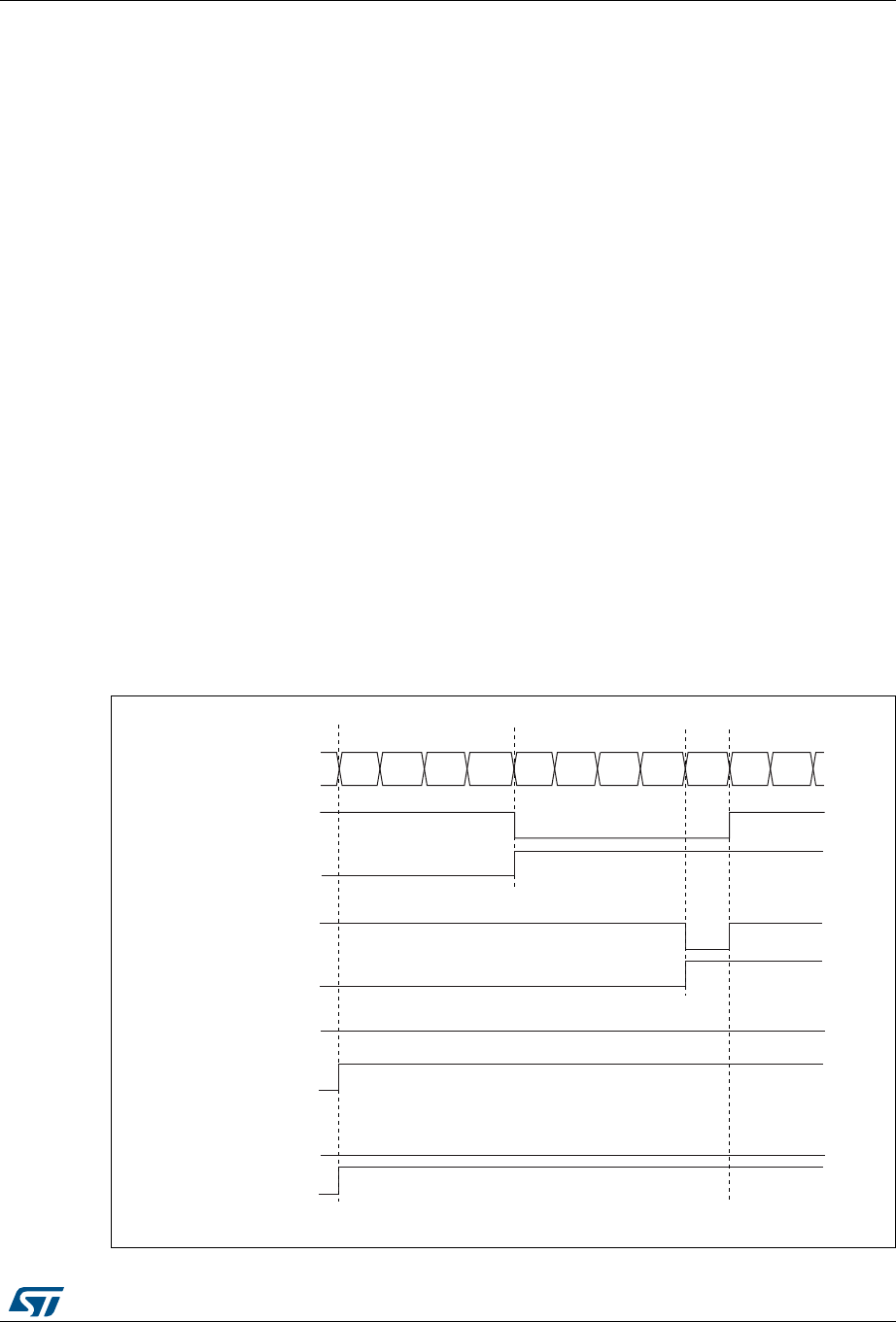
DocID025941 Rev 5 461/1001
RM0376 General-purpose timers (TIM2/TIM3)
503
In PWM mode (1 or 2), TIMx_CNT and TIMx_CCRx are always compared to determine
whether TIMx_CCRx ≤ TIMx_CNT or TIMx_CNT ≤ TIMx_CCRx (depending on the direction
of the counter). However, to comply with the OCREF_CLR functionality (OCREF can be
cleared by an external event through the ETR signal until the next PWM period), the
OCREF signal is asserted only:
•When the result of the comparison changes, or
•When the output compare mode (OCxM bits in TIMx_CCMRx register) switches from
the “frozen” configuration (no comparison, OCxM=‘000) to one of the PWM modes
(OCxM=‘110 or ‘111).
This forces the PWM by software while the timer is running.
The timer is able to generate PWM in edge-aligned mode or center-aligned mode
depending on the CMS bits in the TIMx_CR1 register.
PWM edge-aligned mode
Upcounting configuration
Upcounting is active when the DIR bit in the TIMx_CR1 register is low. Refer to Section :
Upcounting mode on page 440.
In the following example, we consider PWM mode 1. The reference PWM signal OCxREF is
high as long as TIMx_CNT <TIMx_CCRx else it becomes low. If the compare value in
TIMx_CCRx is greater than the auto-reload value (in TIMx_ARR) then OCxREF is held at ‘1.
If the compare value is 0 then OCxREF is held at ‘0. Figure 119 shows some edge-aligned
PWM waveforms in an example where TIMx_ARR=8.
For code example, refer to A.11.8: Edge-aligned PWM configuration example.
Figure 119. Edge-aligned PWM waveforms (ARR=8)
MS31093V1
Counter register
‘1’
012 3456 7801
OCXREF
CCxIF
OCXREF
CCxIF
OCXREF
CCxIF
OCXREF
CCxIF
CCRx=4
CCRx=8
CCRx>8
CCRx=0
‘0’

General-purpose timers (TIM2/TIM3) RM0376
462/1001 DocID025941 Rev 5
Downcounting configuration
Downcounting is active when DIR bit in TIMx_CR1 register is high. Refer to Section :
Downcounting mode on page 443.
In PWM mode 1, the reference signal OCxREF is low as long as TIMx_CNT>TIMx_CCRx
else it becomes high. If the compare value in TIMx_CCRx is greater than the auto-reload
value in TIMx_ARR, then OCxREF is held at ‘1. 0% PWM is not possible in this mode.
PWM center-aligned mode
Center-aligned mode is active when the CMS bits in TIMx_CR1 register are different from
‘00 (all the remaining configurations having the same effect on the OCxREF/OCx signals).
The compare flag is set when the counter counts up, when it counts down or both when it
counts up and down depending on the CMS bits configuration. The direction bit (DIR) in the
TIMx_CR1 register is updated by hardware and must not be changed by software. Refer to
Section : Center-aligned mode (up/down counting) on page 446.
Figure 120 shows some center-aligned PWM waveforms in an example where:
•TIMx_ARR=8,
•PWM mode is the PWM mode 1,
•The flag is set when the counter counts down corresponding to the center-aligned
mode 1 selected for CMS=01 in TIMx_CR1 register.
For code example, refer to A.11.9: Center-aligned PWM configuration example.
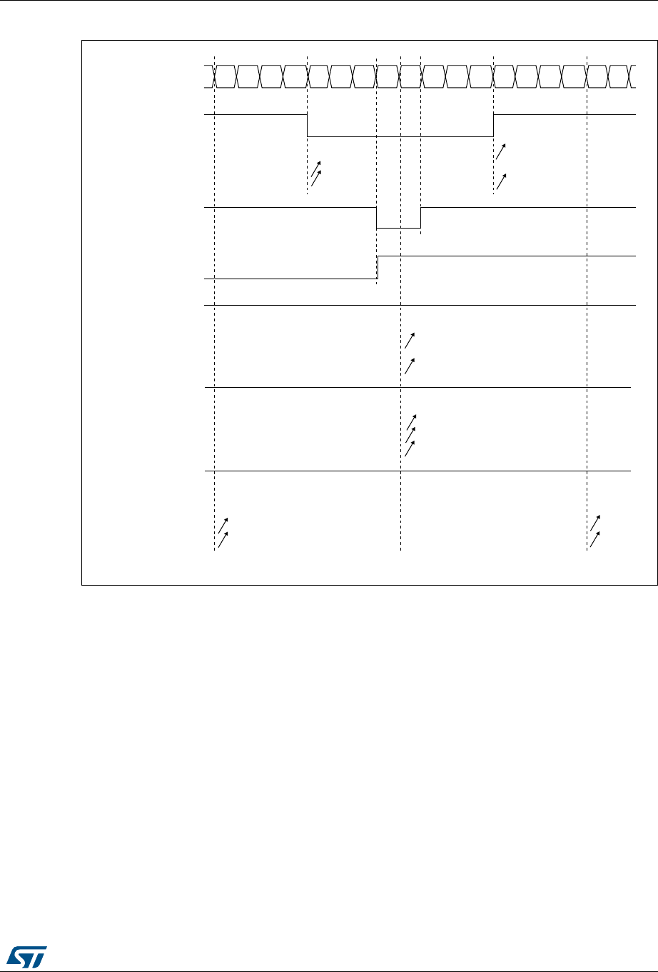
DocID025941 Rev 5 463/1001
RM0376 General-purpose timers (TIM2/TIM3)
503
Figure 120. Center-aligned PWM waveforms (ARR=8)
Hints on using center-aligned mode:
•When starting in center-aligned mode, the current up-down configuration is used. It
means that the counter counts up or down depending on the value written in the DIR bit
in the TIMx_CR1 register. Moreover, the DIR and CMS bits must not be changed at the
same time by the software.
•Writing to the counter while running in center-aligned mode is not recommended as it
can lead to unexpected results. In particular:
– The direction is not updated if you write a value in the counter that is greater than
the auto-reload value (TIMx_CNT>TIMx_ARR). For example, if the counter was
counting up, it continues to count up.
– The direction is updated if you write 0 or write the TIMx_ARR value in the counter
but no Update Event UEV is generated.
•The safest way to use center-aligned mode is to generate an update by software
(setting the UG bit in the TIMx_EGR register) just before starting the counter and not to
write the counter while it is running.
CCxIF
01234567876 5432 101
Counter register
CCRx = 4
OCxREF
CMS=01
CMS=10
CMS=11
CCxIF
CCRx=7
OCxREF
CMS=10 or 11
CCxIF
CCRx=8
OCxREF
CMS=01
CMS=10
CMS=11
‘1’
CCxIF
CCRx>8
OCxREF
CMS=01
CMS=10
CMS=11
‘1’
CCxIF
CCRx=0
OCxREF
CMS=01
CMS=10
CMS=11
‘0’
AI14681b
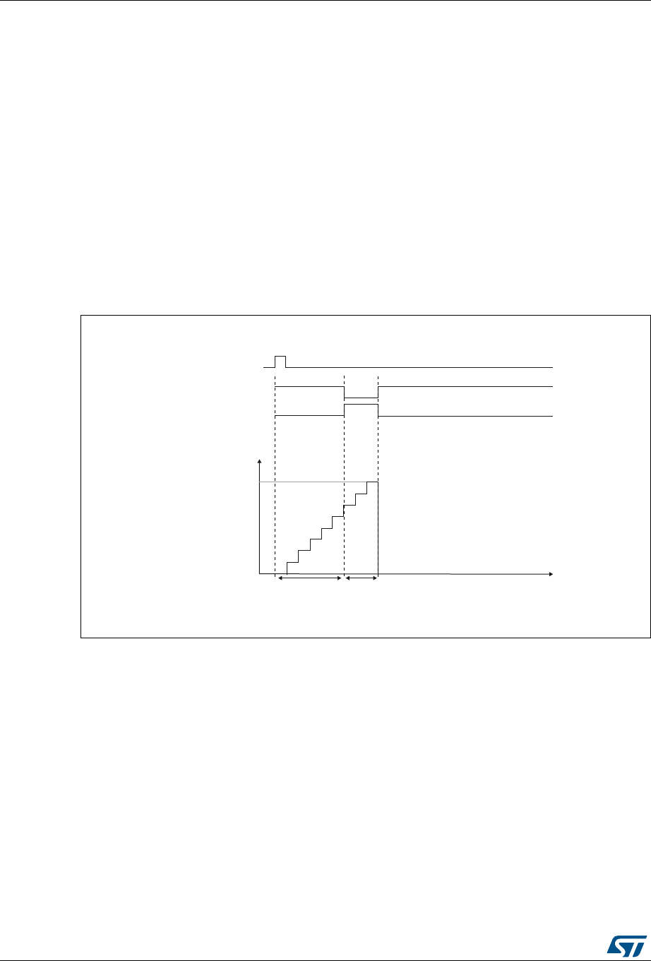
General-purpose timers (TIM2/TIM3) RM0376
464/1001 DocID025941 Rev 5
20.3.10 One-pulse mode
One-pulse mode (OPM) is a particular case of the previous modes. It allows the counter to
be started in response to a stimulus and to generate a pulse with a programmable length
after a programmable delay.
Starting the counter can be controlled through the slave mode controller. Generating the
waveform can be done in output compare mode or PWM mode. You select One-pulse mode
by setting the OPM bit in the TIMx_CR1 register. This makes the counter stop automatically
at the next update event UEV.
A pulse can be correctly generated only if the compare value is different from the counter
initial value. Before starting (when the timer is waiting for the trigger), the configuration must
be:
•In upcounting: CNT<CCRx ≤ ARR (in particular, 0<CCRx),
•In downcounting: CNT>CCRx.
Figure 121. Example of one-pulse mode.
For example you may want to generate a positive pulse on OC1 with a length of tPULSE and
after a delay of tDELAY as soon as a positive edge is detected on the TI2 input pin.
Let’s use TI2FP2 as trigger 1:
1. Map TI2FP2 on TI2 by writing CC2S=01 in the TIMx_CCMR1 register.
2. TI2FP2 must detect a rising edge, write CC2P=0 and CC2NP=’0’ in the TIMx_CCER
register.
3. Configure TI2FP2 as trigger for the slave mode controller (TRGI) by writing TS=110 in
the TIMx_SMCR register.
4. TI2FP2 is used to start the counter by writing SMS to ‘110 in the TIMx_SMCR register
(trigger mode).
For code example, refer to A.11.16: One-Pulse mode code example.
MS31099V1
TI2
OC1REF
Counter
t
0
TIM1_ARR
TIM1_CCR1
OC1
tDELAY tPULSE

DocID025941 Rev 5 465/1001
RM0376 General-purpose timers (TIM2/TIM3)
503
The OPM waveform is defined by writing the compare registers (taking into account the
clock frequency and the counter prescaler).
•The tDELAY is defined by the value written in the TIMx_CCR1 register.
•The tPULSE is defined by the difference between the auto-reload value and the compare
value (TIMx_ARR - TIMx_CCR1+1).
•Let’s say you want to build a waveform with a transition from ‘0 to ‘1 when a compare
match occurs and a transition from ‘1 to ‘0 when the counter reaches the auto-reload
value. To do this you enable PWM mode 2 by writing OC1M=111 in the TIMx_CCMR1
register. You can optionally enable the preload registers by writing OC1PE=1 in the
TIMx_CCMR1 register and ARPE in the TIMx_CR1 register. In this case you have to
write the compare value in the TIMx_CCR1 register, the auto-reload value in the
TIMx_ARR register, generate an update by setting the UG bit and wait for external
trigger event on TI2. CC1P is written to ‘0 in this example.
In our example, the DIR and CMS bits in the TIMx_CR1 register should be low.
You only want 1 pulse (Single mode), so you write '1 in the OPM bit in the TIMx_CR1
register to stop the counter at the next update event (when the counter rolls over from the
auto-reload value back to 0). When OPM bit in the TIMx_CR1 register is set to '0', so the
Repetitive Mode is selected.
Particular case: OCx fast enable:
In One-pulse mode, the edge detection on TIx input set the CEN bit which enables the
counter. Then the comparison between the counter and the compare value makes the
output toggle. But several clock cycles are needed for these operations and it limits the
minimum delay tDELAY min we can get.
If you want to output a waveform with the minimum delay, you can set the OCxFE bit in the
TIMx_CCMRx register. Then OCxRef (and OCx) is forced in response to the stimulus,
without taking in account the comparison. Its new level is the same as if a compare match
had occurred. OCxFE acts only if the channel is configured in PWM1 or PWM2 mode.
For code example, refer to A.11.16: One-Pulse mode code example.
20.3.11 Clearing the OCxREF signal on an external event
1. The external trigger prescaler should be kept off: bits ETPS[1:0] in the TIMx_SMCR
register are cleared to 00.
2. The external clock mode 2 must be disabled: bit ECE in the TIMx_SMCR register is
cleared to 0.
3. The external trigger polarity (ETP) and the external trigger filter (ETF) can be
configured according to the application’s needs.
For code example, refer to A.11.10: ETR configuration to clear OCxREF code example.
Figure 122 shows the behavior of the OCxREF signal when the ETRF input becomes high,
for both values of the OCxCE enable bit. In this example, the timer TIMx is programmed in
PWM mode.
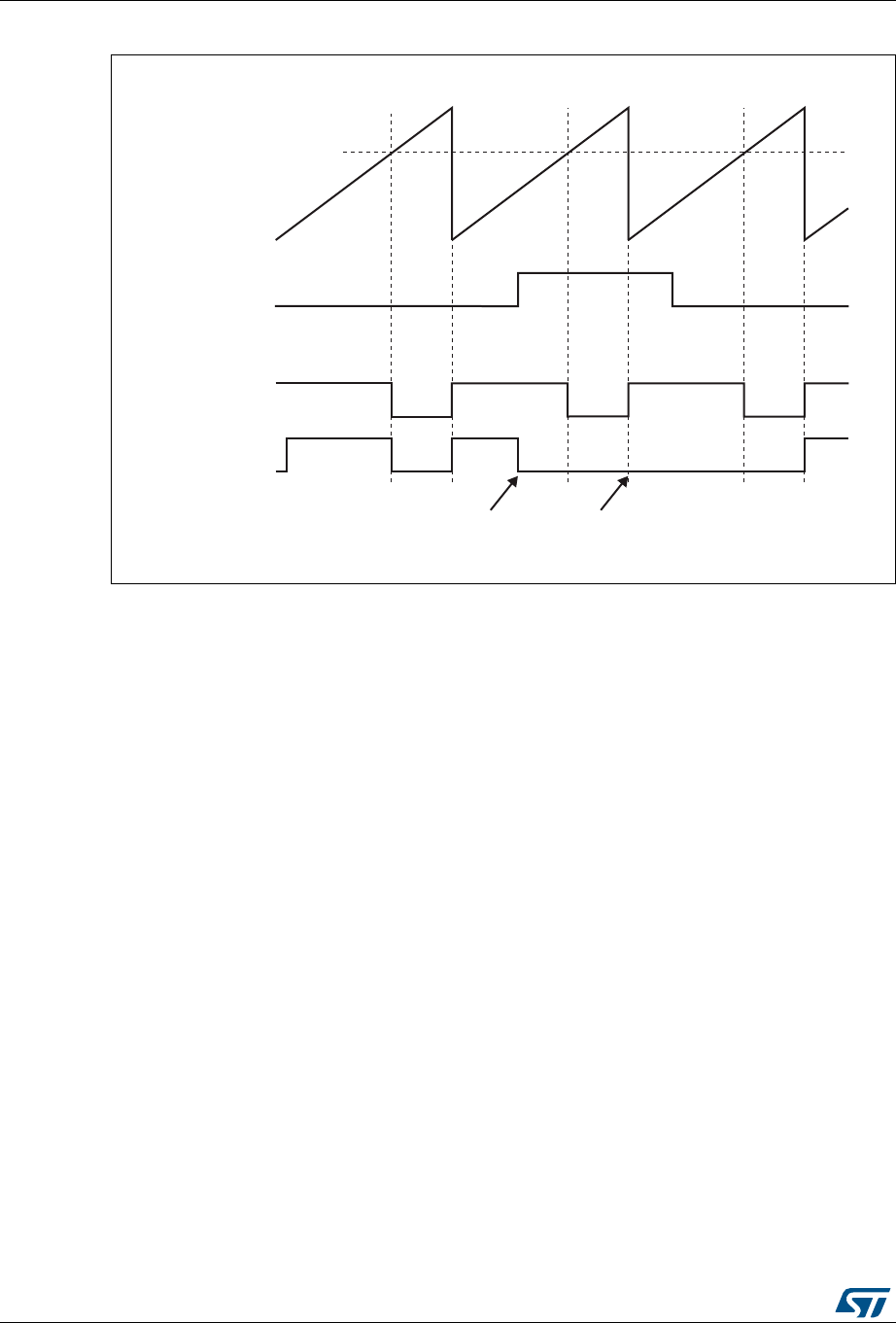
General-purpose timers (TIM2/TIM3) RM0376
466/1001 DocID025941 Rev 5
Figure 122. Clearing TIMx OCxREF
1. In case of a PWM with a 100% duty cycle (if CCRx>ARR), OCxREF is enabled again at the next counter
overflow.
20.3.12 Encoder interface mode
To select Encoder Interface mode write SMS=‘001 in the TIMx_SMCR register if the counter
is counting on TI2 edges only, SMS=010 if it is counting on TI1 edges only and SMS=011 if
it is counting on both TI1 and TI2 edges.
Select the TI1 and TI2 polarity by programming the CC1P and CC2P bits in the TIMx_CCER
register. CC1NP and CC2NP must be kept cleared. When needed, you can program the
input filter as well.
The two inputs TI1 and TI2 are used to interface to an incremental encoder. Refer to
Table 88. The counter is clocked by each valid transition on TI1FP1 or TI2FP2 (TI1 and TI2
after input filter and polarity selection, TI1FP1=TI1 if not filtered and not inverted,
TI2FP2=TI2 if not filtered and not inverted) assuming that it is enabled (CEN bit in
TIMx_CR1 register written to ‘1). The sequence of transitions of the two inputs is evaluated
and generates count pulses as well as the direction signal. Depending on the sequence the
counter counts up or down, the DIR bit in the TIMx_CR1 register is modified by hardware
accordingly. The DIR bit is calculated at each transition on any input (TI1 or TI2), whatever
the counter is counting on TI1 only, TI2 only or both TI1 and TI2.
Encoder interface mode acts simply as an external clock with direction selection. This
means that the counter just counts continuously between 0 and the auto-reload value in the
TIMx_ARR register (0 to ARR or ARR down to 0 depending on the direction). So you must
configure TIMx_ARR before starting. In the same way, the capture, compare, prescaler,
trigger output features continue to work as normal.
In this mode, the counter is modified automatically following the speed and the direction of
the incremental encoder and its content, therefore, always represents the encoder’s
MS33105V1
(CCRx)
Counter (CNT)
ETRF
OCxREF
(OCxCE = ‘0’)
OCxREF
(OCxCE = ‘1’)
OCxREF_CLR
becomes high
OCxREF_CLR
still high

DocID025941 Rev 5 467/1001
RM0376 General-purpose timers (TIM2/TIM3)
503
position. The count direction correspond to the rotation direction of the connected sensor.
The table summarizes the possible combinations, assuming TI1 and TI2 don’t switch at the
same time.
An external incremental encoder can be connected directly to the MCU without external
interface logic. However, comparators are normally be used to convert the encoder’s
differential outputs to digital signals. This greatly increases noise immunity. The third
encoder output which indicate the mechanical zero position, may be connected to an
external interrupt input and trigger a counter reset.
Figure 123 gives an example of counter operation, showing count signal generation and
direction control. It also shows how input jitter is compensated where both edges are
selected. This might occur if the sensor is positioned near to one of the switching points. For
this example we assume that the configuration is the following:
•CC1S= 01 (TIMx_CCMR1 register, TI1FP1 mapped on TI1)
•CC2S= 01 (TIMx_CCMR2 register, TI2FP2 mapped on TI2)
•CC1P=0, CC1NP = ‘0’ (TIMx_CCER register, TI1FP1 noninverted, TI1FP1=TI1)
•CC2P=0, CC2NP = ‘0’ (TIMx_CCER register, TI2FP2 noninverted, TI2FP2=TI2)
•SMS= 011 (TIMx_SMCR register, both inputs are active on both rising and falling
edges)
•CEN= 1 (TIMx_CR1 register, Counter is enabled)
For code example, refer to A.11.11: Encoder interface code example.
Table 88. Counting direction versus encoder signals
Active edge
Level on opposite
signal (TI1FP1 for
TI2, TI2FP2 for TI1)
TI1FP1 signal TI2FP2 signal
Rising Falling Rising Falling
Counting on
TI1 only
High Down Up No Count No Count
Low Up Down No Count No Count
Counting on
TI2 only
High No Count No Count Up Down
Low No Count No Count Down Up
Counting on
TI1 and TI2
High Down Up Up Down
Low Up Down Down Up
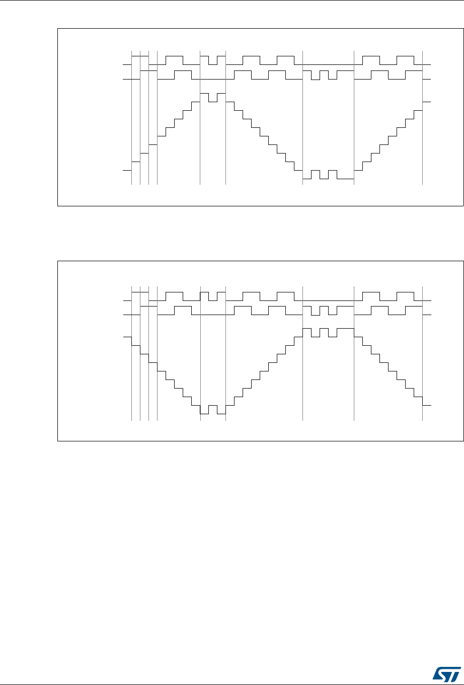
General-purpose timers (TIM2/TIM3) RM0376
468/1001 DocID025941 Rev 5
Figure 123. Example of counter operation in encoder interface mode
Figure 124 gives an example of counter behavior when TI1FP1 polarity is inverted (same
configuration as above except CC1P=1).
Figure 124. Example of encoder interface mode with TI1FP1 polarity inverted
The timer, when configured in Encoder Interface mode provides information on the sensor’s
current position. You can obtain dynamic information (speed, acceleration, deceleration) by
measuring the period between two encoder events using a second timer configured in
capture mode. The output of the encoder which indicates the mechanical zero can be used
for this purpose. Depending on the time between two events, the counter can also be read
at regular times. You can do this by latching the counter value into a third input capture
register if available (then the capture signal must be periodic and can be generated by
another timer). when available, it is also possible to read its value through a DMA request
generated by a Real-Time clock.
20.3.13 Timer input XOR function
The TI1S bit in the TIMx_CR2 register, allows the input filter of channel 1 to be connected to
the output of a XOR gate, combining the three input pins TIMx_CH1 to TIMx_CH3.
The XOR output can be used with all the timer input functions such as trigger or input
capture.
TI1
backwardjitter jitter
up down up
TI2
Counter
forward forward
MS33107V1
TI1
backwardjitter jitter
updown
TI2
Counter
forward forward
MS33108V1
down
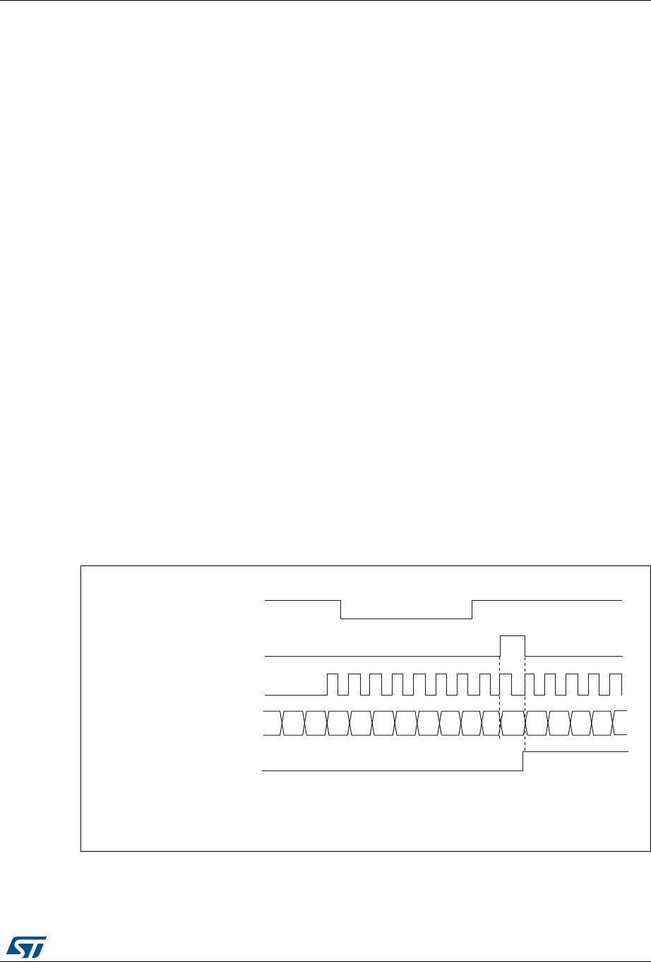
DocID025941 Rev 5 469/1001
RM0376 General-purpose timers (TIM2/TIM3)
503
20.3.14 Timers and external trigger synchronization
The TIMx Timers can be synchronized with an external trigger in several modes: Reset
mode, Gated mode and Trigger mode.
Slave mode: Reset mode
The counter and its prescaler can be reinitialized in response to an event on a trigger input.
Moreover, if the URS bit from the TIMx_CR1 register is low, an update event UEV is
generated. Then all the preloaded registers (TIMx_ARR, TIMx_CCRx) are updated.
In the following example, the upcounter is cleared in response to a rising edge on TI1 input:
•Configure the channel 1 to detect rising edges on TI1. Configure the input filter duration
(in this example, we don’t need any filter, so we keep IC1F=0000). The capture
prescaler is not used for triggering, so you don’t need to configure it. The CC1S bits
select the input capture source only, CC1S = 01 in the TIMx_CCMR1 register. Write
CC1P=0 and CC1NP=0 in TIMx_CCER register to validate the polarity (and detect
rising edges only).
•Configure the timer in reset mode by writing SMS=100 in TIMx_SMCR register. Select
TI1 as the input source by writing TS=101 in TIMx_SMCR register.
•Start the counter by writing CEN=1 in the TIMx_CR1 register.
For code example, refer to A.11.12: Reset mode code example.
The counter starts counting on the internal clock, then behaves normally until TI1 rising
edge. When TI1 rises, the counter is cleared and restarts from 0. In the meantime, the
trigger flag is set (TIF bit in the TIMx_SR register) and an interrupt request, or a DMA
request can be sent if enabled (depending on the TIE and TDE bits in TIMx_DIER register).
The following figure shows this behavior when the auto-reload register TIMx_ARR=0x36.
The delay between the rising edge on TI1 and the actual reset of the counter is due to the
resynchronization circuit on TI1 input.
Figure 125. Control circuit in reset mode
MS31401V2
00
Counter clock = ck_cnt = ck_psc
Counter register 01 02 03 00 01 02 0332 33 34 35 36
UG
TI1
3130
TIF
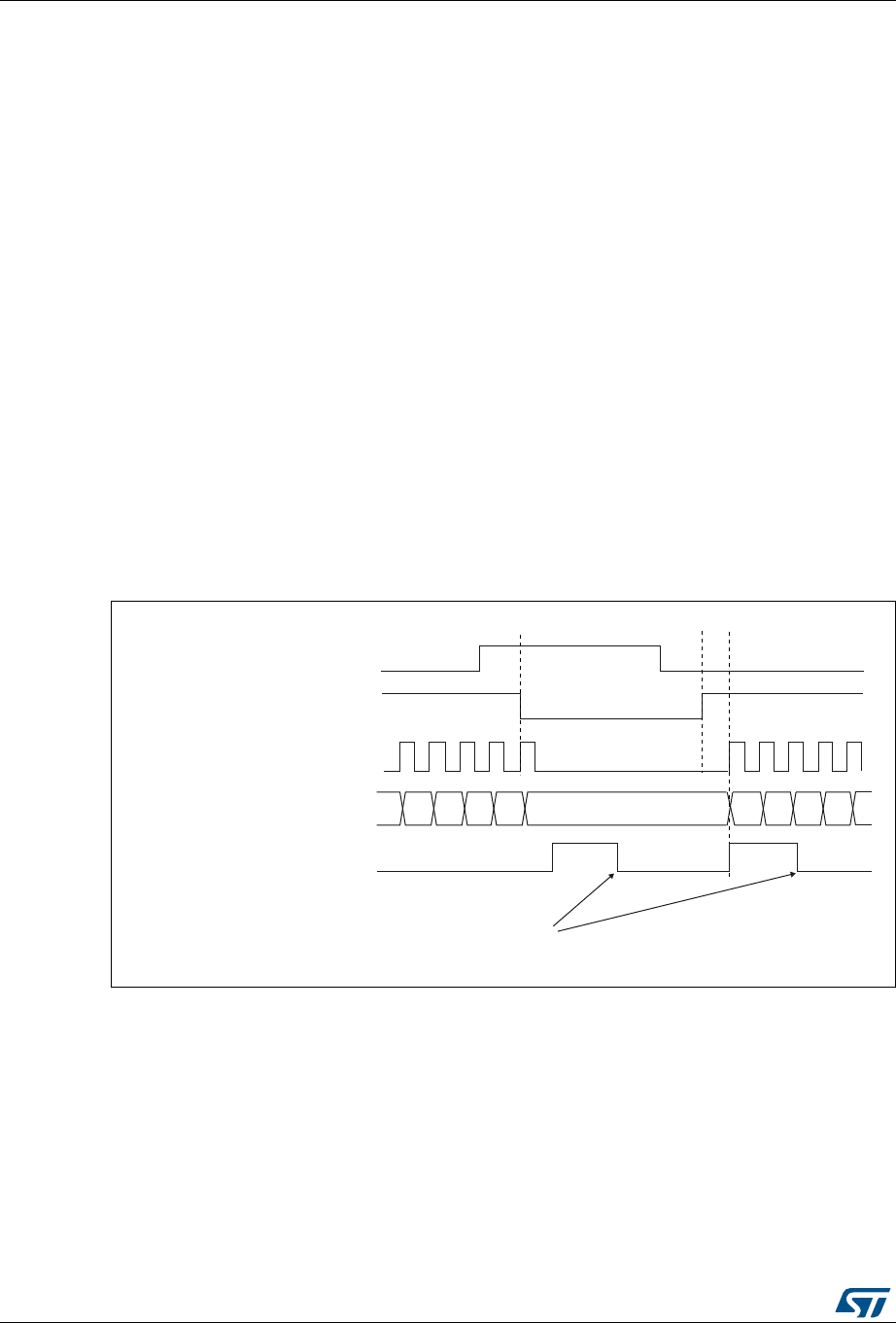
General-purpose timers (TIM2/TIM3) RM0376
470/1001 DocID025941 Rev 5
Slave mode: Gated mode
The counter can be enabled depending on the level of a selected input.
In the following example, the upcounter counts only when TI1 input is low:
1. Configure the channel 1 to detect low levels on TI1. Configure the input filter duration
(in this example, we don’t need any filter, so we keep IC1F=0000). The capture
prescaler is not used for triggering, so you don’t need to configure it. The CC1S bits
select the input capture source only, CC1S=01 in TIMx_CCMR1 register. Write
CC1P=1 and CC1NP=0 in TIMx_CCER register to validate the polarity (and detect low
level only).
2. Configure the timer in gated mode by writing SMS=101 in TIMx_SMCR register. Select
TI1 as the input source by writing TS=101 in TIMx_SMCR register.
3. Enable the counter by writing CEN=1 in the TIMx_CR1 register (in gated mode, the
counter doesn’t start if CEN=0, whatever is the trigger input level).
For code example, refer to A.11.13: Gated mode code example.
The counter starts counting on the internal clock as long as TI1 is low and stops as soon as
TI1 becomes high. The TIF flag in the TIMx_SR register is set both when the counter starts
or stops.
The delay between the rising edge on TI1 and the actual stop of the counter is due to the
resynchronization circuit on TI1 input.
Figure 126. Control circuit in gated mode
1. The configuration “CCxP=CCxNP=1” (detection of both rising and falling edges) does not have any effect
in gated mode because gated mode acts on a level and not on an edge.
MS31402V1
TI1
cnt_en
Write TIF=0
37
Counter clock = ck_cnt = ck_psc
Counter register 38
32 33 34 35 36
3130
TIF
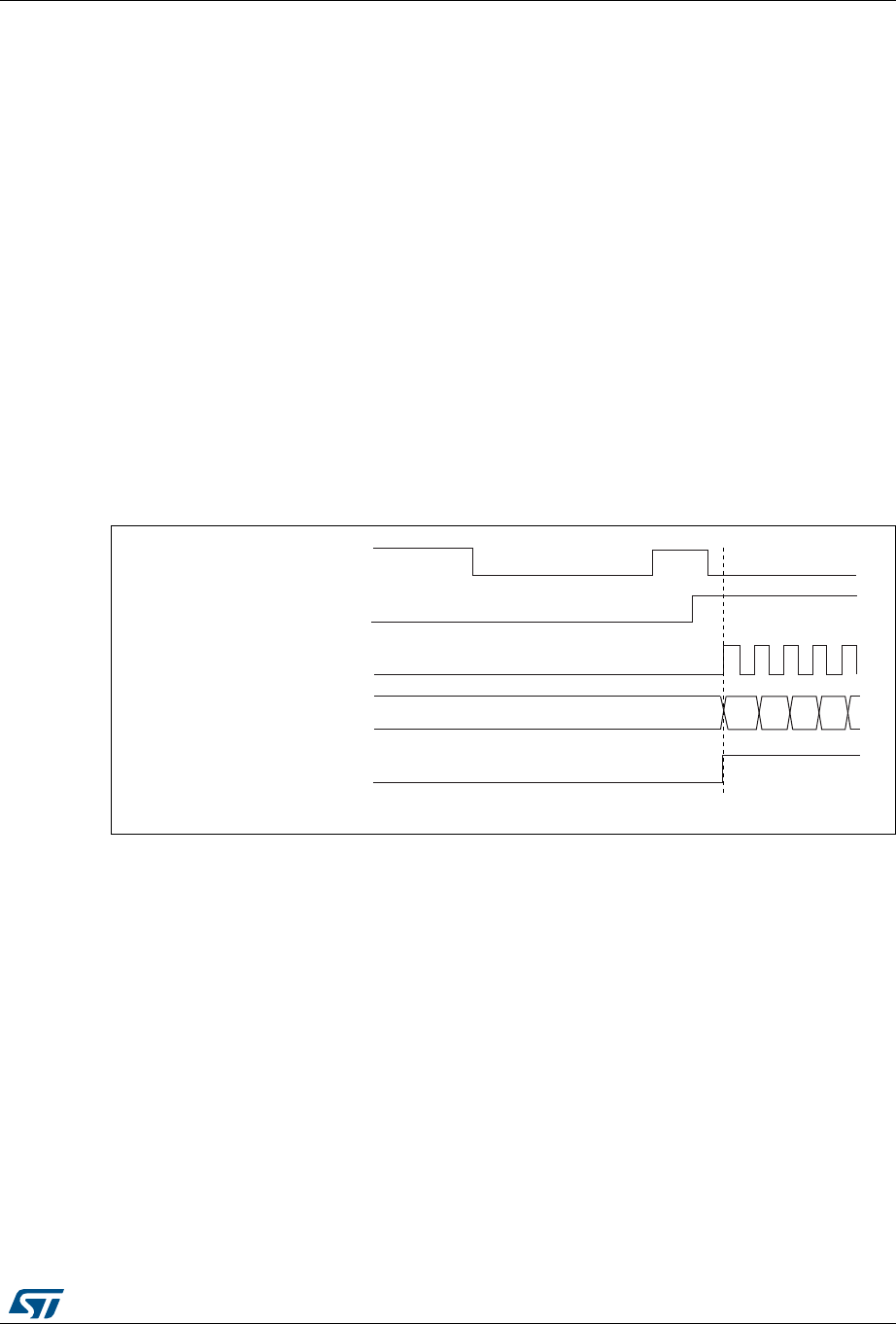
DocID025941 Rev 5 471/1001
RM0376 General-purpose timers (TIM2/TIM3)
503
Slave mode: Trigger mode
The counter can start in response to an event on a selected input.
In the following example, the upcounter starts in response to a rising edge on TI2 input:
1. Configure the channel 2 to detect rising edges on TI2. Configure the input filter duration
(in this example, we don’t need any filter, so we keep IC2F=0000). The capture
prescaler is not used for triggering, so you don’t need to configure it. CC2S bits are
selecting the input capture source only, CC2S=01 in TIMx_CCMR1 register. Write
CC2P=1 and CC2NP=0 in TIMx_CCER register to validate the polarity (and detect low
level only).
2. Configure the timer in trigger mode by writing SMS=110 in TIMx_SMCR register. Select
TI2 as the input source by writing TS=110 in TIMx_SMCR register.
For code example, refer to A.11.14: Trigger mode code example.
When a rising edge occurs on TI2, the counter starts counting on the internal clock and the
TIF flag is set.
The delay between the rising edge on TI2 and the actual start of the counter is due to the
resynchronization circuit on TI2 input.
Figure 127. Control circuit in trigger mode
MS31403V1
TI2
cnt_en
37
Counter clock = ck_cnt = ck_psc
Counter register 38
34 35 36
TIF

General-purpose timers (TIM2/TIM3) RM0376
472/1001 DocID025941 Rev 5
Slave mode: External Clock mode 2 + trigger mode
The external clock mode 2 can be used in addition to another slave mode (except external
clock mode 1 and encoder mode). In this case, the ETR signal is used as external clock
input, and another input can be selected as trigger input when operating in reset mode,
gated mode or trigger mode. It is recommended not to select ETR as TRGI through the TS
bits of TIMx_SMCR register.
In the following example, the upcounter is incremented at each rising edge of the ETR
signal as soon as a rising edge of TI1 occurs:
1. Configure the external trigger input circuit by programming the TIMx_SMCR register as
follows:
– ETF = 0000: no filter
– ETPS=00: prescaler disabled
– ETP=0: detection of rising edges on ETR and ECE=1 to enable the external clock
mode 2.
2. Configure the channel 1 as follows, to detect rising edges on TI:
– IC1F=0000: no filter.
– The capture prescaler is not used for triggering and does not need to be
configured.
– CC1S=01in TIMx_CCMR1 register to select only the input capture source
– CC1P=0 and CC1NP=0 in TIMx_CCER register to validate the polarity (and detect
rising edge only).
3. Configure the timer in trigger mode by writing SMS=110 in TIMx_SMCR register. Select
TI1 as the input source by writing TS=101 in TIMx_SMCR register.
For code example, refer to A.11.15: External clock mode 2 + trigger mode code example.
A rising edge on TI1 enables the counter and sets the TIF flag. The counter then counts on
ETR rising edges.
The delay between the rising edge of the ETR signal and the actual reset of the counter is
due to the resynchronization circuit on ETRP input.
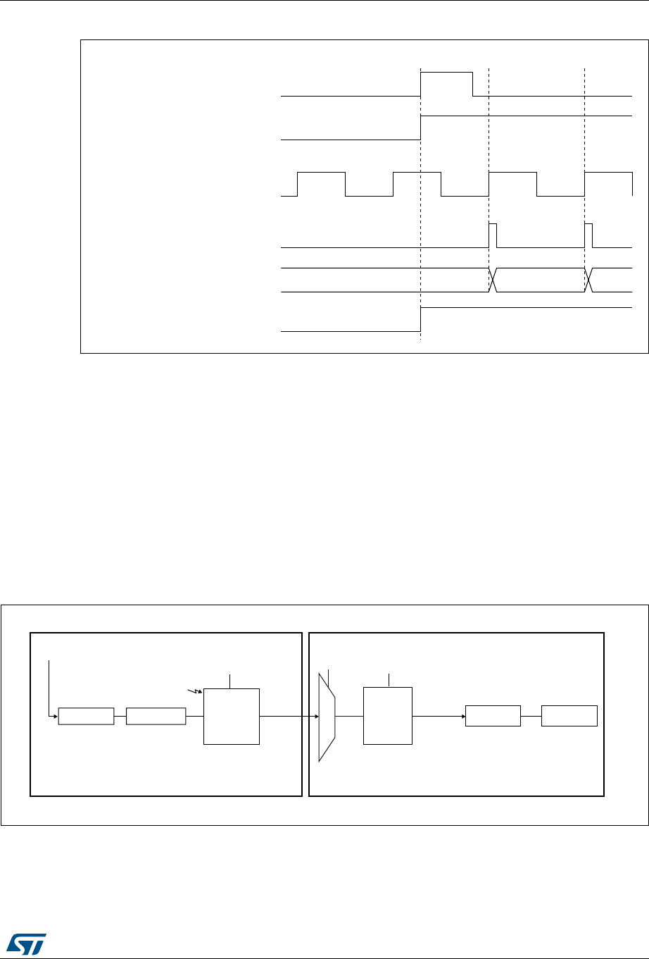
DocID025941 Rev 5 473/1001
RM0376 General-purpose timers (TIM2/TIM3)
503
Figure 128. Control circuit in external clock mode 2 + trigger mode
20.3.15 Timer synchronization
The TIMx timers are linked together internally for timer synchronization or chaining. When
one Timer is configured in Master Mode, it can reset, start, stop or clock the counter of
another Timer configured in Slave Mode.
Figure 129: Master/Slave timer example presents an overview of the trigger selection and
the master mode selection blocks.
Note: The clock of the slave timer must be enabled prior to receive events from the master timer,
and must not be changed on-the-fly while triggers are received from the master timer.
Using one timer as prescaler for another timer
Figure 129. Master/Slave timer example
MS33110V1
34 35 36
TIF
Counter register
Counter clock = CK_CNT = CK_PSC
ETR
CEN/CNT_EN
TI1
MS33136V1
Counter
Master
mode
control
UEV
Prescaler
Clock
Slave
mode
control CounterPrescaler
CK_PSCITR1TRGO1
MMS SMS
TS
Input
trigger
selection
TIMx TIMy

General-purpose timers (TIM2/TIM3) RM0376
474/1001 DocID025941 Rev 5
For example, you can configure Timer x to act as a prescaler for Timer y. Refer to
Figure 129. To do this, follow the sequence below:
1. Configure Timer x in master mode so that it outputs a periodic trigger signal on each
update event UEV. If you write MMS=010 in the TIMx_CR2 register, a rising edge is
output on TRGO1 each time an update event is generated.
2. To connect the TRGO1 output of Timer x to Timer y, Timer y must be configured in
slave mode using ITR1 as internal trigger. You select this through the TS bits in the
TIMy_SMCR register (writing TS=000).
3. Then you put the slave mode controller in external clock mode 1 (write SMS=111 in the
TIMy_SMCR register). This causes Timer y to be clocked by the rising edge of the
periodic Timer x trigger signal (which correspond to the timer x counter overflow).
4. Finally both timers must be enabled by setting their respective CEN bits (TIMx_CR1
register).
For code example, refer to A.11.17: Timer prescaling another timer code example.
Note: If OCx is selected on Timer x as trigger output (MMS=1xx), its rising edge is used to clock
the counter of timer y.
Using one timer to enable another timer
In this example, we control the enable of Timer y with the output compare 1 of Timer x.
Refer to Figure 129 for connections. Timer y counts on the divided internal clock only when
OC1REF of Timer x is high. Both counter clock frequencies are divided by 3 by the
prescaler compared to CK_INT (fCK_CNT = fCK_INT/3).
1. Configure Timer x master mode to send its Output Compare 1 Reference (OC1REF)
signal as trigger output (MMS=100 in the TIMx_CR2 register).
2. Configure the Timer x OC1REF waveform (TIMx_CCMR1 register).
3. Configure Timer y to get the input trigger from Timer x (TS=000 in the TIMy_SMCR
register).
4. Configure Timer y in gated mode (SMS=101 in TIMy_SMCR register).
5. Enable Timer y by writing ‘1 in the CEN bit (TIMy_CR1 register).
6. Start Timer x by writing ‘1 in the CEN bit (TIMx_CR1 register).
For code example, refer to A.11.18: Timer enabling another timer code example.
Note: The counter 2 clock is not synchronized with counter 1, this mode only affects the Timer y
counter enable signal.
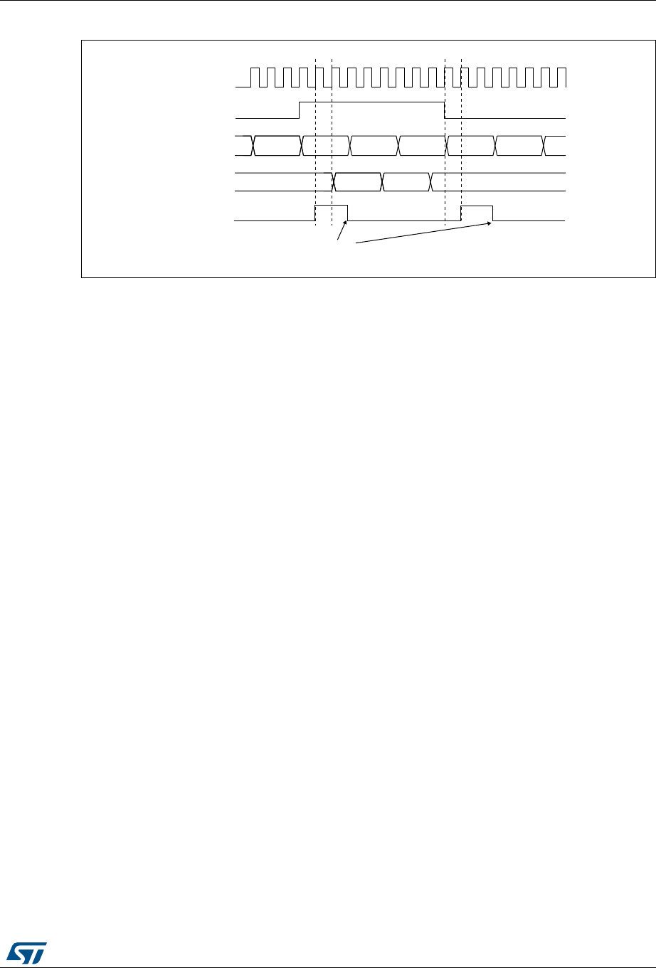
DocID025941 Rev 5 475/1001
RM0376 General-purpose timers (TIM2/TIM3)
503
Figure 130. Gating timer y with OC1REF of timer x
In the example in Figure 130, the Timer y counter and prescaler are not initialized before
being started. So they start counting from their current value. It is possible to start from a
given value by resetting both timers before starting Timer x. You can then write any value
you want in the timer counters. The timers can easily be reset by software using the UG bit
in the TIMx_EGR registers.
In the next example, we synchronize Timer x and Timer y. Timer x is the master and starts
from 0. Timer y is the slave and starts from 0xE7. The prescaler ratio is the same for both
timers. Timer y stops when Timer x is disabled by writing ‘0 to the CEN bit in the TIMy_CR1
register:
1. Configure Timer x master mode to send its Output Compare 1 Reference (OC1REF)
signal as trigger output (MMS=100 in the TIMx_CR2 register).
2. Configure the Timer x OC1REF waveform (TIMx_CCMR1 register).
3. Configure Timer y to get the input trigger from Timer x (TS=000 in the TIMy_SMCR
register).
4. Configure Timer y in gated mode (SMS=101 in TIMy_SMCR register).
5. Reset Timer x by writing ‘1 in UG bit (TIMx_EGR register).
6. Reset Timer y by writing ‘1 in UG bit (TIMy_EGR register).
7. Initialize Timer y to 0xE7 by writing ‘0xE7’ in the timer y counter (TIMy_CNTL).
8. Enable Timer y by writing ‘1 in the CEN bit (TIMy_CR1 register).
9. Start Timer x by writing ‘1 in the CEN bit (TIMx_CR1 register).
10. Stop Timer x by writing ‘0 in the CEN bit (TIMx_CR1 register).
For code example, refer to A.11.19: Master and slave synchronization code example.
MS33137V1
CK_INT
FC FD FE FF 00 01
TIMERx-OC1REF
TIMERx-CNT
30463045 3047 3048
TIMERy-CNT
TIMERy-TIF
Write TIF = 0
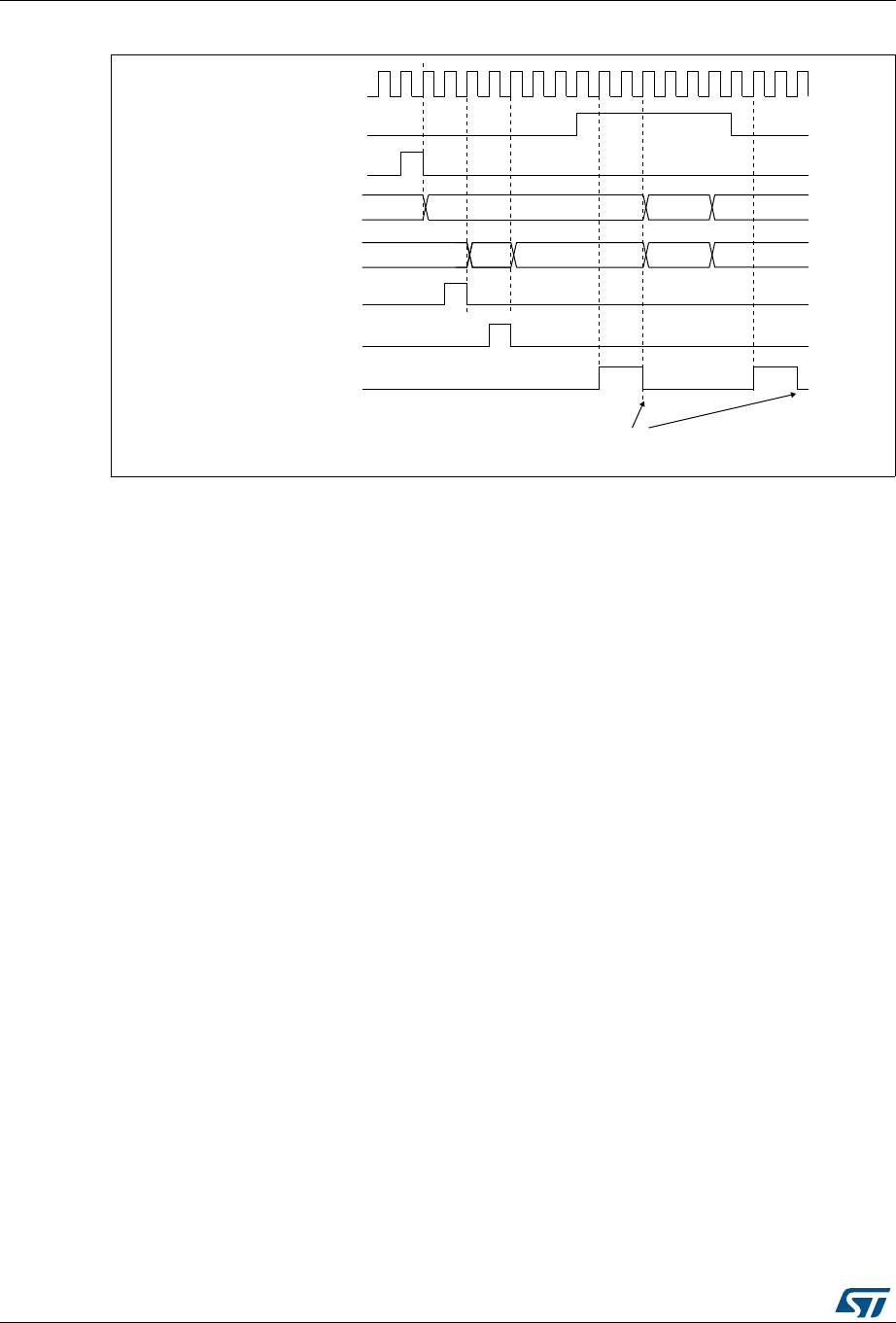
General-purpose timers (TIM2/TIM3) RM0376
476/1001 DocID025941 Rev 5
Figure 131. Gating timer y with Enable of timer x
Using one timer to start another timer
In this example, we set the enable of Timer y with the update event of Timer x. Refer to
Figure 129 for connections. Timer y starts counting from its current value (which can be
nonzero) on the divided internal clock as soon as the update event is generated by Timer x.
When Timer y receives the trigger signal its CEN bit is automatically set and the counter
counts until we write ‘0 to the CEN bit in the TIM2_CR1 register. Both counter clock
frequencies are divided by 3 by the prescaler compared to CK_INT (fCK_CNT = fCK_INT/3).
1. Configure Timer x master mode to send its Update Event (UEV) as trigger output
(MMS=010 in the TIMx_CR2 register).
2. Configure the Timer x period (TIMx_ARR registers).
3. Configure Timer y to get the input trigger from Timer x (TS=000 in the TIMy_SMCR
register).
4. Configure Timer y in trigger mode (SMS=110 in TIMy_SMCR register).
5. Start Timer x by writing ‘1 in the CEN bit (TIMx_CR1 register).
MS33138V1
CK_INT
75 00
E7
TIMERx-CNT_INIT
TIMERx-CNT
AB
TIMERy-CNT
TIMERy-CNT_INIT
Write TIF = 0
01 02
E9E800
TIMERx-CEN=CNT_EN
TIMERy-write CNT
TIMERy-TIF
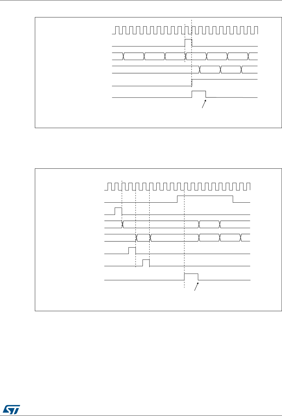
DocID025941 Rev 5 477/1001
RM0376 General-purpose timers (TIM2/TIM3)
503
Figure 132. Triggering timer y with update of timer x
As in the previous example, you can initialize both counters before starting counting.
Figure 133 shows the behavior with the same configuration as in Figure 132 but in trigger
mode instead of gated mode (SMS=110 in the TIMy_SMCR register).
Figure 133. Triggering timer y with Enable of timer x
MS33139V1
CK_INT
TIMERy-CNT
FDTIMERx-CNT
Write TIF = 0
TIMERy-CEN=CNT_EN
TIMERy-TIF
FE FF 00 01 02
46 47 4845
TIMERx-UEV
MS33140V1
CK_INT
TIMERy-CNT
TIMERx-CNT_INIT
Write TIF = 0
TIMERx-CEN=CNT_EN
TIMERy-TIF
E7
0200 01
E9
75
CD 00 E8 EA
TIMERx-CNT
TIMERy-CNT_INIT
TIMERy
write CNT
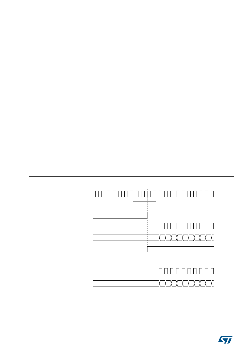
General-purpose timers (TIM2/TIM3) RM0376
478/1001 DocID025941 Rev 5
Starting 2 timers synchronously in response to an external trigger
In this example, we set the enable of timer x when its TI1 input rises, and the enable of
Timer y with the enable of Timer x. Refer to Figure 129 for connections. To ensure the
counters are aligned, Timer x must be configured in Master/Slave mode (slave with respect
to TI1, master with respect to Timer y):
1. Configure Timer x master mode to send its Enable as trigger output (MMS=001 in the
TIMx_CR2 register).
2. Configure Timer x slave mode to get the input trigger from TI1 (TS=100 in the
TIMx_SMCR register).
3. Configure Timer x in trigger mode (SMS=110 in the TIMx_SMCR register).
4. Configure the Timer x in Master/Slave mode by writing MSM=1 (TIMx_SMCR register).
5. Configure Timer y to get the input trigger from Timer x (TS=000 in the TIMy_SMCR
register).
6. Configure Timer y in trigger mode (SMS=110 in the TIMy_SMCR register).
For code example, refer to A.11.20: Two timers synchronized by an external trigger code
example.
When a rising edge occurs on TI1 (Timer x), both counters starts counting synchronously on
the internal clock and both TIF flags are set.
Note: In this example both timers are initialized before starting (by setting their respective UG
bits). Both counters starts from 0, but you can easily insert an offset between them by
writing any of the counter registers (TIMx_CNT). You can see that the master/slave mode
insert a delay between CNT_EN and CK_PSC on timer x.
Figure 134. Triggering timer x and y with timer x TI1 input
MS33141V1
CK_INT
TIMERy-CNT
TIMERx-CEN=CNT_EN
TIMERy-TIF
01
TIMERx-CNT 02 03 04 05 06 07 08 09
00
01 02 03 04 05 06 07 08 0900
TIMERy-CEN=CNT_EN
TIMERx-TIF
TIMERx-CK_PSC
TIMERx-TI1
TIMERy-CK_PSC

DocID025941 Rev 5 479/1001
RM0376 General-purpose timers (TIM2/TIM3)
503
20.3.16 Debug mode
When the microcontroller enters debug mode (Cortex®-M0+ core - halted), the TIMx counter
either continues to work normally or stops, depending on DBG_TIMx_STOP configuration
bit in DBG module. For more details, refer to Section 32.9.2: Debug support for timers,
watchdog and I2C.

General-purpose timers (TIM2/TIM3) RM0376
480/1001 DocID025941 Rev 5
20.4 TIM2/TIM3 registers
Refer to Section 1.1 on page 51 for a list of abbreviations used in register descriptions.
The 32-bit peripheral registers have to be written by words (32 bits). All other peripheral
registers have to be written by half-words (16 bits) or words (32 bits). Read accesses can be
done by bytes (8 bits), half-words (16 bits) or words (32 bits).
20.4.1 TIMx control register 1 (TIMx_CR1)
Address offset: 0x00
Reset value: 0x0000
1514131211109876543210
Res. Res. Res. Res. Res. Res. CKD[1:0] ARPE CMS DIR OPM URS UDIS CEN
rw rw rw rw rw rw rw rw rw rw
Bits 15:10 Reserved, must be kept at reset value.
Bits 9:8 CKD: Clock division
This bit-field indicates the division ratio between the timer clock (CK_INT) frequency and
sampling clock used by the digital filters (ETR, TIx),
00: tDTS = tCK_INT
01: tDTS = 2 × tCK_INT
10: tDTS = 4 × tCK_INT
11: Reserved
Bit 7 ARPE: Auto-reload preload enable
0: TIMx_ARR register is not buffered
1: TIMx_ARR register is buffered
Bits 6:5 CMS: Center-aligned mode selection
00: Edge-aligned mode. The counter counts up or down depending on the direction bit
(DIR).
01: Center-aligned mode 1. The counter counts up and down alternatively. Output compare
interrupt flags of channels configured in output (CCxS=00 in TIMx_CCMRx register) are set
only when the counter is counting down.
10: Center-aligned mode 2. The counter counts up and down alternatively. Output compare
interrupt flags of channels configured in output (CCxS=00 in TIMx_CCMRx register) are set
only when the counter is counting up.
11: Center-aligned mode 3. The counter counts up and down alternatively. Output compare
interrupt flags of channels configured in output (CCxS=00 in TIMx_CCMRx register) are set
both when the counter is counting up or down.
Note: It is not allowed to switch from edge-aligned mode to center-aligned mode as long as
the counter is enabled (CEN=1)
Bit 4 DIR: Direction
0: Counter used as upcounter
1: Counter used as downcounter
Note: This bit is read only when the timer is configured in Center-aligned mode or Encoder
mode.
Bit 3 OPM: One-pulse mode
0: Counter is not stopped at update event
1: Counter stops counting at the next update event (clearing the bit CEN)

DocID025941 Rev 5 481/1001
RM0376 General-purpose timers (TIM2/TIM3)
503
Bit 2 URS: Update request source
This bit is set and cleared by software to select the UEV event sources.
0: Any of the following events generate an update interrupt or DMA request if enabled.
These events can be:
– Counter overflow/underflow
– Setting the UG bit
– Update generation through the slave mode controller
1: Only counter overflow/underflow generates an update interrupt or DMA request if
enabled.
Bit 1 UDIS: Update disable
This bit is set and cleared by software to enable/disable UEV event generation.
0: UEV enabled. The Update (UEV) event is generated by one of the following events:
– Counter overflow/underflow
– Setting the UG bit
– Update generation through the slave mode controller
Buffered registers are then loaded with their preload values.
1: UEV disabled. The Update event is not generated, shadow registers keep their value
(ARR, PSC, CCRx). However the counter and the prescaler are reinitialized if the UG bit is
set or if a hardware reset is received from the slave mode controller.
Bit 0 CEN: Counter enable
0: Counter disabled
1: Counter enabled
Note: External clock, gated mode and encoder mode can work only if the CEN bit has been
previously set by software. However trigger mode can set the CEN bit automatically by
hardware.
CEN is cleared automatically in one-pulse mode, when an update event occurs.

General-purpose timers (TIM2/TIM3) RM0376
482/1001 DocID025941 Rev 5
20.4.2 TIMx control register 2 (TIMx_CR2)
Address offset: 0x04
Reset value: 0x0000
1514131211109876543210
Res. Res. Res. Res. Res. Res. Res. Res. TI1S MMS[2:0] CCDS Res. Res. Res.
rw rw rw rw rw
Bits 15:8 Reserved, must be kept at reset value.
Bit 7 TI1S: TI1 selection
0: The TIMx_CH1 pin is connected to TI1 input
1: The TIMx_CH1, CH2 and CH3 pins are connected to the TI1 input (XOR combination)
Bits 6:4 MMS: Master mode selection
These bits allow to select the information to be sent in master mode to slave timers for
synchronization (TRGO). The combination is as follows:
000: Reset - the UG bit from the TIMx_EGR register is used as trigger output (TRGO). If the
reset is generated by the trigger input (slave mode controller configured in reset mode) then
the signal on TRGO is delayed compared to the actual reset.
001: Enable - the Counter enable signal, CNT_EN, is used as trigger output (TRGO). It is
useful to start several timers at the same time or to control a window in which a slave timer is
enabled. The Counter Enable signal is generated by a logic OR between CEN control bit
and the trigger input when configured in gated mode.
When the Counter Enable signal is controlled by the trigger input, there is a delay on TRGO,
except if the master/slave mode is selected (see the MSM bit description in TIMx_SMCR
register).
010: Update - The update event is selected as trigger output (TRGO). For instance a master
timer can then be used as a prescaler for a slave timer.
011: Compare Pulse - The trigger output send a positive pulse when the CC1IF flag is to be
set (even if it was already high), as soon as a capture or a compare match occurred.
(TRGO)
100: Compare - OC1REF signal is used as trigger output (TRGO)
101: Compare - OC2REF signal is used as trigger output (TRGO)
110: Compare - OC3REF signal is used as trigger output (TRGO)
111: Compare - OC4REF signal is used as trigger output (TRGO)
Note: The clock of the slave timer or ADC must be enabled prior to receiving events from the
master timer, and must not be changed on-the-fly while triggers are received from the
master timer.
Bit 3 CCDS: Capture/compare DMA selection
0: CCx DMA request sent when CCx event occurs
1: CCx DMA requests sent when update event occurs
Bits 2:0 Reserved, must be kept at reset value.

DocID025941 Rev 5 483/1001
RM0376 General-purpose timers (TIM2/TIM3)
503
20.4.3 TIMx slave mode control register (TIMx_SMCR)
Address offset: 0x08
Reset value: 0x0000
1514131211109876543210
ETP ECE ETPS[1:0] ETF[3:0] MSM TS[2:0] Res. SMS[2:0]
rw rw rw rw rw rw rw rw rw rw rw rw rw rw rw
Bit 15 ETP: External trigger polarity
This bit selects whether ETR or ETR is used for trigger operations
0: ETR is noninverted, active at high level or rising edge
1: ETR is inverted, active at low level or falling edge
Bit 14 ECE: External clock enable
This bit enables External clock mode 2.
0: External clock mode 2 disabled
1: External clock mode 2 enabled. The counter is clocked by any active edge on the ETRF
signal.
1: Setting the ECE bit has the same effect as selecting external clock mode 1 with TRGI
connected to ETRF (SMS=111 and TS=111).
2: It is possible to simultaneously use external clock mode 2 with the following slave modes:
reset mode, gated mode and trigger mode. Nevertheless, TRGI must not be connected to
ETRF in this case (TS bits must not be 111).
3: If external clock mode 1 and external clock mode 2 are enabled at the same time, the
external clock input is ETRF.
Bits 13:12 ETPS: External trigger prescaler
External trigger signal ETRP frequency must be at most 1/4 of CK_INT frequency. A
prescaler can be enabled to reduce ETRP frequency. It is useful when inputting fast external
clocks.
00: Prescaler OFF
01: ETRP frequency divided by 2
10: ETRP frequency divided by 4
11: ETRP frequency divided by 8
Bits 11:8 ETF[3:0]: External trigger filter
This bit-field then defines the frequency used to sample ETRP signal and the length of the
digital filter applied to ETRP. The digital filter is made of an event counter in which N
consecutive events are needed to validate a transition on the output:
0000: No filter, sampling is done at fDTS
0001: fSAMPLING=fCK_INT, N=2
0010: fSAMPLING=fCK_INT, N=4
0011: fSAMPLING=fCK_INT, N=8
0100: fSAMPLING=fDTS/2, N=6
0101: fSAMPLING=fDTS/2, N=8
0110: fSAMPLING=fDTS/4, N=6
0111: fSAMPLING=fDTS/4, N=8
1000: fSAMPLING=fDTS/8, N=6
1001: fSAMPLING=fDTS/8, N=8
1010: fSAMPLING=fDTS/16, N=5
1011: fSAMPLING=fDTS/16, N=6
1100: fSAMPLING=fDTS/16, N=8
1101: fSAMPLING=fDTS/32, N=5
1110: fSAMPLING=fDTS/32, N=6
1111: fSAMPLING=fDTS/32, N=8

General-purpose timers (TIM2/TIM3) RM0376
484/1001 DocID025941 Rev 5
Bit 7 MSM: Master/Slave mode
0: No action
1: The effect of an event on the trigger input (TRGI) is delayed to allow a perfect
synchronization between the current timer and its slaves (through TRGO). It is useful if we
want to synchronize several timers on a single external event.
Bits 6:4 TS: Trigger selection
This bit-field selects the trigger input to be used to synchronize the counter.
000: Internal Trigger 0 (ITR0).
001: Internal Trigger 1 (ITR1).
010: Internal Trigger 2 (ITR2).
011: Reserved.
100: TI1 Edge Detector (TI1F_ED)
101: Filtered Timer Input 1 (TI1FP1)
110: Filtered Timer Input 2 (TI2FP2)
111: External Trigger input (ETRF)
See Table 89: TIM2/TIM3 internal trigger connection on page 485 for more details on ITRx
meaning for each Timer.
Note: These bits must be changed only when they are not used (e.g. when SMS=000) to
avoid wrong edge detections at the transition.
Bit 3 Reserved, must be kept at ‘1’.
Bits 2:0 SMS: Slave mode selection
When external signals are selected the active edge of the trigger signal (TRGI) is linked to
the polarity selected on the external input (see Input Control register and Control Register
description.
000: Slave mode disabled - if CEN = ‘1 then the prescaler is clocked directly by the internal
clock.
001: Encoder mode 1 - Counter counts up/down on TI2FP1 edge depending on TI1FP2
level.
010: Encoder mode 2 - Counter counts up/down on TI1FP2 edge depending on TI2FP1
level.
011: Encoder mode 3 - Counter counts up/down on both TI1FP1 and TI2FP2 edges
depending on the level of the other input.
100: Reset Mode - Rising edge of the selected trigger input (TRGI) reinitializes the counter
and generates an update of the registers.
101: Gated Mode - The counter clock is enabled when the trigger input (TRGI) is high. The
counter stops (but is not reset) as soon as the trigger becomes low. Both start and stop of
the counter are controlled.
110: Trigger Mode - The counter starts at a rising edge of the trigger TRGI (but it is not
reset). Only the start of the counter is controlled.
111: External Clock Mode 1 - Rising edges of the selected trigger (TRGI) clock the counter.
Note: The gated mode must not be used if TI1F_ED is selected as the trigger input (TS=100).
Indeed, TI1F_ED outputs 1 pulse for each transition on TI1F, whereas the gated mode
checks the level of the trigger signal.
The clock of the slave timer must be enabled prior to receiving events from the master
timer, and must not be changed on-the-fly while triggers are received from the master
timer."

DocID025941 Rev 5 485/1001
RM0376 General-purpose timers (TIM2/TIM3)
503
20.4.4 TIMx DMA/Interrupt enable register (TIMx_DIER)
Address offset: 0x0C
Reset value: 0x0000
Table 89. TIM2/TIM3 internal trigger connection
Slave TIM ITR0 (TS = 000) ITR1 (TS = 001) ITR2 (TS = 010)
TIM2 TIM21 TIM22 TIM3
TIM3 TIM2 TIM22 TIM21
1514131211109876543210
Res. TDE Res. CC4DE CC3DE CC2DE CC1DE UDE Res. TIE Res. CC4IE CC3IE CC2IE CC1IE UIE
rw rw rw rw rw rw rw rw rw rw rw rw
Bit 15 Reserved, must be kept at reset value.
Bit 14 TDE: Trigger DMA request enable
0: Trigger DMA request disabled.
1: Trigger DMA request enabled.
Bit 13 Reserved, always read as 0
Bit 12 CC4DE: Capture/Compare 4 DMA request enable
0: CC4 DMA request disabled.
1: CC4 DMA request enabled.
Bit 11 CC3DE: Capture/Compare 3 DMA request enable
0: CC3 DMA request disabled.
1: CC3 DMA request enabled.
Bit 10 CC2DE: Capture/Compare 2 DMA request enable
0: CC2 DMA request disabled.
1: CC2 DMA request enabled.
Bit 9 CC1DE: Capture/Compare 1 DMA request enable
0: CC1 DMA request disabled.
1: CC1 DMA request enabled.
Bit 8 UDE: Update DMA request enable
0: Update DMA request disabled.
1: Update DMA request enabled.
Bit 7 Reserved, must be kept at reset value.
Bit 6 TIE: Trigger interrupt enable
0: Trigger interrupt disabled.
1: Trigger interrupt enabled.
Bit 5 Reserved, must be kept at reset value.
Bit 4 CC4IE: Capture/Compare 4 interrupt enable
0: CC4 interrupt disabled.
1: CC4 interrupt enabled.

General-purpose timers (TIM2/TIM3) RM0376
486/1001 DocID025941 Rev 5
20.4.5 TIMx status register (TIMx_SR)
Address offset: 0x10
Reset value: 0x0000
Bit 3 CC3IE: Capture/Compare 3 interrupt enable
0: CC3 interrupt disabled
1: CC3 interrupt enabled
Bit 2 CC2IE: Capture/Compare 2 interrupt enable
0: CC2 interrupt disabled
1: CC2 interrupt enabled
Bit 1 CC1IE: Capture/Compare 1 interrupt enable
0: CC1 interrupt disabled
1: CC1 interrupt enabled
Bit 0 UIE: Update interrupt enable
0: Update interrupt disabled
1: Update interrupt enabled
1514131211109876543210
Res. Res. Res. CC4OF CC3OF CC2OF CC1OF Res. Res. TIF Res. CC4IF CC3IF CC2IF CC1IF UIF
rc_w0 rc_w0 rc_w0 rc_w0 rc_w0 rc_w0 rc_w0 rc_w0 rc_w0 rc_w0
Bits 15:13 Reserved, must be kept at reset value.
Bit 12 CC4OF: Capture/Compare 4 overcapture flag
refer to CC1OF description
Bit 11 CC3OF: Capture/Compare 3 overcapture flag
refer to CC1OF description
Bit 10 CC2OF: Capture/compare 2 overcapture flag
refer to CC1OF description
Bit 9 CC1OF: Capture/Compare 1 overcapture flag
This flag is set by hardware only when the corresponding channel is configured in input
capture mode. It is cleared by software by writing it to ‘0.
0: No overcapture has been detected
1: The counter value has been captured in TIMx_CCR1 register while CC1IF flag was
already set
Bits 8:7 Reserved, must be kept at reset value.
Bit 6 TIF: Trigger interrupt flag
This flag is set by hardware on trigger event (active edge detected on TRGI input when the
slave mode controller is enabled in all modes but gated mode. It is set when the counter
starts or stops when gated mode is selected. It is cleared by software.
0: No trigger event occurred
1: Trigger interrupt pending
Bit 5 Reserved, must be kept at reset value.
Bit 4 CC4IF: Capture/Compare 4 interrupt flag
refer to CC1IF description

DocID025941 Rev 5 487/1001
RM0376 General-purpose timers (TIM2/TIM3)
503
Bit 3 CC3IF: Capture/Compare 3 interrupt flag
refer to CC1IF description
Bit 2 CC2IF: Capture/Compare 2 interrupt flag
refer to CC1IF description
Bit 1 CC1IF: Capture/compare 1 interrupt flag
If channel CC1 is configured as output:
This flag is set by hardware when the counter matches the compare value, with some
exception in center-aligned mode (refer to the CMS bits in the TIMx_CR1 register
description). It is cleared by software.
0: No match
1: The content of the counter TIMx_CNT matches the content of the TIMx_CCR1 register.
When the contents of TIMx_CCR1 are greater than the contents of TIMx_ARR, the CC1IF bit
goes high on the counter overflow (in upcounting and up/down-counting modes) or underflow
(in downcounting mode)
If channel CC1 is configured as input:
This bit is set by hardware on a capture. It is cleared by software or by reading the
TIMx_CCR1 register.
0: No input capture occurred
1: The counter value has been captured in TIMx_CCR1 register (An edge has been detected
on IC1 which matches the selected polarity)
Bit 0 UIF: Update interrupt flag
″This bit is set by hardware on an update event. It is cleared by software.
0: No update occurred.
1: Update interrupt pending. This bit is set by hardware when the registers are updated:
″At overflow or underflow and if UDIS=0 in the TIMx_CR1 register.
″When CNT is reinitialized by software using the UG bit in TIMx_EGR register, if URS=0
and UDIS=0 in the TIMx_CR1 register.
When CNT is reinitialized by a trigger event (refer to the synchro control register description),
if URS=0 and UDIS=0 in the TIMx_CR1 register.

General-purpose timers (TIM2/TIM3) RM0376
488/1001 DocID025941 Rev 5
20.4.6 TIMx event generation register (TIMx_EGR)
Address offset: 0x14
Reset value: 0x0000
1514131211109876543210
Res. Res. Res. Res. Res. Res. Res. Res. Res. TG Res. CC4G CC3G CC2G CC1G UG
w wwwww
Bits 15:7 Reserved, must be kept at reset value.
Bit 6 TG: Trigger generation
This bit is set by software in order to generate an event, it is automatically cleared by
hardware.
0: No action
1: The TIF flag is set in TIMx_SR register. Related interrupt or DMA transfer can occur if
enabled.
Bit 5 Reserved, must be kept at reset value.
Bit 4 CC4G: Capture/compare 4 generation
refer to CC1G description
Bit 3 CC3G: Capture/compare 3 generation
refer to CC1G description
Bit 2 CC2G: Capture/compare 2 generation
refer to CC1G description
Bit 1 CC1G: Capture/compare 1 generation
This bit is set by software in order to generate an event, it is automatically cleared by
hardware.
0: No action
1: A capture/compare event is generated on channel 1:
If channel CC1 is configured as output:
CC1IF flag is set, Corresponding interrupt or DMA request is sent if enabled.
If channel CC1 is configured as input:
The current value of the counter is captured in TIMx_CCR1 register. The CC1IF flag is set,
the corresponding interrupt or DMA request is sent if enabled. The CC1OF flag is set if the
CC1IF flag was already high.
Bit 0 UG: Update generation
This bit can be set by software, it is automatically cleared by hardware.
0: No action
1: Re-initialize the counter and generates an update of the registers. Note that the prescaler
counter is cleared too (anyway the prescaler ratio is not affected). The counter is cleared if
the center-aligned mode is selected or if DIR=0 (upcounting), else it takes the auto-reload
value (TIMx_ARR) if DIR=1 (downcounting).

DocID025941 Rev 5 489/1001
RM0376 General-purpose timers (TIM2/TIM3)
503
20.4.7 TIMx capture/compare mode register 1 (TIMx_CCMR1)
Address offset: 0x18
Reset value: 0x0000
The channels can be used in input (capture mode) or in output (compare mode). The
direction of a channel is defined by configuring the corresponding CCxS bits. All the other
bits of this register have a different function in input and in output mode. For a given bit,
OCxx describes its function when the channel is configured in output, ICxx describes its
function when the channel is configured in input. So you must take care that the same bit
can have a different meaning for the input stage and for the output stage.
Output compare mode
1514131211109876543210
OC2CE OC2M[2:0] OC2PE OC2FE CC2S[1:0] OC1CE OC1M[2:0] OC1PE OC1FE CC1S[1:0]
IC2F[3:0] IC2PSC[1:0] IC1F[3:0] IC1PSC[1:0]
rw rw rw rw rw rw rw rw rw rw rw rw rw rw rw rw
Bit 15 OC2CE: Output compare 2 clear enable
Bits 14:12 OC2M[2:0]: Output compare 2 mode
Bit 11 OC2PE: Output compare 2 preload enable
Bit 10 OC2FE: Output compare 2 fast enable
Bits 9:8 CC2S[1:0]: Capture/Compare 2 selection
This bit-field defines the direction of the channel (input/output) as well as the used input.
00: CC2 channel is configured as output
01: CC2 channel is configured as input, IC2 is mapped on TI2
10: CC2 channel is configured as input, IC2 is mapped on TI1
11: CC2 channel is configured as input, IC2 is mapped on TRC. This mode is working only if
an internal trigger input is selected through the TS bit (TIMx_SMCR register)
Note: CC2S bits are writable only when the channel is OFF (CC2E = 0 in TIMx_CCER).
Bit 7 OC1CE: Output compare 1 clear enable
OC1CE: Output Compare 1 Clear Enable
0: OC1Ref is not affected by the ETRF input
1: OC1Ref is cleared as soon as a High level is detected on ETRF input

General-purpose timers (TIM2/TIM3) RM0376
490/1001 DocID025941 Rev 5
Input capture mode
Bits 6:4 OC1M: Output compare 1 mode
These bits define the behavior of the output reference signal OC1REF from which OC1 and
OC1N are derived. OC1REF is active high whereas OC1 and OC1N active level depends
on CC1P and CC1NP bits.
000: Frozen - The comparison between the output compare register TIMx_CCR1 and the
counter TIMx_CNT has no effect on the outputs.(this mode is used to generate a timing
base).
001: Set channel 1 to active level on match. OC1REF signal is forced high when the counter
TIMx_CNT matches the capture/compare register 1 (TIMx_CCR1).
010: Set channel 1 to inactive level on match. OC1REF signal is forced low when the
counter TIMx_CNT matches the capture/compare register 1 (TIMx_CCR1).
011: Toggle - OC1REF toggles when TIMx_CNT=TIMx_CCR1.
100: Force inactive level - OC1REF is forced low.
101: Force active level - OC1REF is forced high.
110: PWM mode 1 - In upcounting, channel 1 is active as long as TIMx_CNT<TIMx_CCR1
else inactive. In downcounting, channel 1 is inactive (OC1REF=‘0) as long as
TIMx_CNT>TIMx_CCR1 else active (OC1REF=1).
111: PWM mode 2 - In upcounting, channel 1 is inactive as long as TIMx_CNT<TIMx_CCR1
else active. In downcounting, channel 1 is active as long as TIMx_CNT>TIMx_CCR1 else
inactive.
Note: In PWM mode 1 or 2, the OCREF level changes only when the result of the
comparison changes or when the output compare mode switches from “frozen” mode
to “PWM” mode.
Bit 3 OC1PE: Output compare 1 preload enable
0: Preload register on TIMx_CCR1 disabled. TIMx_CCR1 can be written at anytime, the
new value is taken in account immediately.
1: Preload register on TIMx_CCR1 enabled. Read/Write operations access the preload
register. TIMx_CCR1 preload value is loaded in the active register at each update event.
Note: The PWM mode can be used without validating the preload register only in one-pulse
mode (OPM bit set in TIMx_CR1 register). Else the behavior is not guaranteed.
Bit 2 OC1FE: Output compare 1 fast enable
This bit is used to accelerate the effect of an event on the trigger in input on the CC output.
0: CC1 behaves normally depending on counter and CCR1 values even when the trigger is
ON. The minimum delay to activate CC1 output when an edge occurs on the trigger input is
5 clock cycles.
1: An active edge on the trigger input acts like a compare match on CC1 output. Then, OC
is set to the compare level independently from the result of the comparison. Delay to sample
the trigger input and to activate CC1 output is reduced to 3 clock cycles. OCFE acts only if
the channel is configured in PWM1 or PWM2 mode.
Bits 1:0 CC1S: Capture/Compare 1 selection
This bit-field defines the direction of the channel (input/output) as well as the used input.
00: CC1 channel is configured as output.
01: CC1 channel is configured as input, IC1 is mapped on TI1.
10: CC1 channel is configured as input, IC1 is mapped on TI2.
11: CC1 channel is configured as input, IC1 is mapped on TRC. This mode is working only if
an internal trigger input is selected through TS bit (TIMx_SMCR register)
Note: CC1S bits are writable only when the channel is OFF (CC1E = 0 in TIMx_CCER).

DocID025941 Rev 5 491/1001
RM0376 General-purpose timers (TIM2/TIM3)
503
Bits 15:12 IC2F: Input capture 2 filter
Bits 11:10 IC2PSC[1:0]: Input capture 2 prescaler
Bits 9:8 CC2S: Capture/compare 2 selection
This bit-field defines the direction of the channel (input/output) as well as the used input.
00: CC2 channel is configured as output.
01: CC2 channel is configured as input, IC2 is mapped on TI2.
10: CC2 channel is configured as input, IC2 is mapped on TI1.
11: CC2 channel is configured as input, IC2 is mapped on TRC. This mode is working only if
an internal trigger input is selected through TS bit (TIMx_SMCR register)
Note: CC2S bits are writable only when the channel is OFF (CC2E = 0 in TIMx_CCER).
Bits 7:4 IC1F: Input capture 1 filter
This bit-field defines the frequency used to sample TI1 input and the length of the digital filter
applied to TI1. The digital filter is made of an event counter in which N consecutive events
are needed to validate a transition on the output:
0000: No filter, sampling is done at fDTS 1000: fSAMPLING=fDTS/8, N=6
0001: fSAMPLING=fCK_INT, N=2 1001: fSAMPLING=fDTS/8, N=8
0010: fSAMPLING=fCK_INT, N=4 1010: fSAMPLING=fDTS/16, N=5
0011: fSAMPLING=fCK_INT, N=8 1011: fSAMPLING=fDTS/16, N=6
0100: fSAMPLING=fDTS/2, N=6 1100: fSAMPLING=fDTS/16, N=8
0101: fSAMPLING=fDTS/2, N=8 1101: fSAMPLING=fDTS/32, N=5
0110: fSAMPLING=fDTS/4, N=6 1110: fSAMPLING=fDTS/32, N=6
0111: fSAMPLING=fDTS/4, N=8 1111: fSAMPLING=fDTS/32, N=8
Bits 3:2 IC1PSC: Input capture 1 prescaler
This bit-field defines the ratio of the prescaler acting on CC1 input (IC1).
The prescaler is reset as soon as CC1E=0 (TIMx_CCER register).
00: no prescaler, capture is done each time an edge is detected on the capture input
01: capture is done once every 2 events
10: capture is done once every 4 events
11: capture is done once every 8 events
Bits 1:0 CC1S: Capture/Compare 1 selection
This bit-field defines the direction of the channel (input/output) as well as the used input.
00: CC1 channel is configured as output
01: CC1 channel is configured as input, IC1 is mapped on TI1
10: CC1 channel is configured as input, IC1 is mapped on TI2
11: CC1 channel is configured as input, IC1 is mapped on TRC. This mode is working only if
an internal trigger input is selected through TS bit (TIMx_SMCR register)
Note: CC1S bits are writable only when the channel is OFF (CC1E = 0 in TIMx_CCER).

General-purpose timers (TIM2/TIM3) RM0376
492/1001 DocID025941 Rev 5
20.4.8 TIMx capture/compare mode register 2 (TIMx_CCMR2)
Address offset: 0x1C
Reset value: 0x0000
Refer to the above CCMR1 register description.
Output compare mode
1514131211109876543210
OC4CE OC4M[2:0] OC4PE OC4FE CC4S[1:0] OC3CE OC3M[2:0] OC3PE OC3FE CC3S[1:0]
IC4F[3:0] IC4PSC[1:0] IC3F[3:0] IC3PSC[1:0]
rw rw rw rw rw rw rw rw rw rw rw rw rw rw rw rw
Bit 15 OC4CE: Output compare 4 clear enable
Bits 14:12 OC4M: Output compare 4 mode
Bit 11 OC4PE: Output compare 4 preload enable
Bit 10 OC4FE: Output compare 4 fast enable
Bits 9:8 CC4S: Capture/Compare 4 selection
This bit-field defines the direction of the channel (input/output) as well as the used input.
00: CC4 channel is configured as output
01: CC4 channel is configured as input, IC4 is mapped on TI4
10: CC4 channel is configured as input, IC4 is mapped on TI3
11: CC4 channel is configured as input, IC4 is mapped on TRC. This mode is working only if
an internal trigger input is selected through TS bit (TIMx_SMCR register)
Note: CC4S bits are writable only when the channel is OFF (CC4E = 0 in TIMx_CCER).
Bit 7 OC3CE: Output compare 3 clear enable
Bits 6:4 OC3M: Output compare 3 mode
Bit 3 OC3PE: Output compare 3 preload enable
Bit 2 OC3FE: Output compare 3 fast enable
Bits 1:0 CC3S: Capture/Compare 3 selection
This bit-field defines the direction of the channel (input/output) as well as the used input.
00: CC3 channel is configured as output
01: CC3 channel is configured as input, IC3 is mapped on TI3
10: CC3 channel is configured as input, IC3 is mapped on TI4
11: CC3 channel is configured as input, IC3 is mapped on TRC. This mode is working only if
an internal trigger input is selected through TS bit (TIMx_SMCR register)
Note: CC3S bits are writable only when the channel is OFF (CC3E = 0 in TIMx_CCER).

DocID025941 Rev 5 493/1001
RM0376 General-purpose timers (TIM2/TIM3)
503
Input capture mode
20.4.9 TIMx capture/compare enable register (TIMx_CCER)
Address offset: 0x20
Reset value: 0x0000
Bits 15:12 IC4F: Input capture 4 filter
Bits 11:10 IC4PSC: Input capture 4 prescaler
Bits 9:8 CC4S: Capture/Compare 4 selection
This bit-field defines the direction of the channel (input/output) as well as the used input.
00: CC4 channel is configured as output
01: CC4 channel is configured as input, IC4 is mapped on TI4
10: CC4 channel is configured as input, IC4 is mapped on TI3
11: CC4 channel is configured as input, IC4 is mapped on TRC. This mode is working only if
an internal trigger input is selected through TS bit (TIMx_SMCR register)
Note: CC4S bits are writable only when the channel is OFF (CC4E = 0 in TIMx_CCER).
Bits 7:4 IC3F: Input capture 3 filter
Bits 3:2 IC3PSC: Input capture 3 prescaler
Bits 1:0 CC3S: Capture/Compare 3 selection
This bit-field defines the direction of the channel (input/output) as well as the used input.
00: CC3 channel is configured as output
01: CC3 channel is configured as input, IC3 is mapped on TI3
10: CC3 channel is configured as input, IC3 is mapped on TI4
11: CC3 channel is configured as input, IC3 is mapped on TRC. This mode is working only if
an internal trigger input is selected through TS bit (TIMx_SMCR register)
Note: CC3S bits are writable only when the channel is OFF (CC3E = 0 in TIMx_CCER).
1514131211109876543210
CC4NP Res. CC4P CC4E CC3NP Res. CC3P CC3E CC2NP Res. CC2P CC2E CC1NP Res. CC1P CC1E
rw rw rw rw rw rw rw rw rw rw rw rw
Bit 15 CC4NP: Capture/Compare 4 output Polarity.
Refer to CC1NP description
Bit 14 Reserved, must be kept at reset value.
Bit 13 CC4P: Capture/Compare 4 output Polarity.
refer to CC1P description
Bit 12 CC4E: Capture/Compare 4 output enable.
refer to CC1E description
Bit 11 CC3NP: Capture/Compare 3 output Polarity.
refer to CC1NP description
Bit 10 Reserved, must be kept at reset value.
Bit 9 CC3P: Capture/Compare 3 output Polarity.
refer to CC1P description
Bit 8 CC3E: Capture/Compare 3 output enable.
refer to CC1E description

General-purpose timers (TIM2/TIM3) RM0376
494/1001 DocID025941 Rev 5
Bit 7 CC2NP: Capture/Compare 2 output Polarity.
refer to CC1NP description
Bit 6 Reserved, must be kept at reset value.
Bit 5 CC2P: Capture/Compare 2 output Polarity.
refer to CC1P description
Bit 4 CC2E: Capture/Compare 2 output enable.
refer to CC1E description
Bit 3 CC1NP: Capture/Compare 1 output Polarity.
CC1 channel configured as output:
CC1NP must be kept cleared in this case.
CC1 channel configured as input:
This bit is used in conjunction with CC1P to define TI1FP1/TI2FP1 polarity. refer to CC1P
description.
Bit 2 Reserved, must be kept at reset value.
Bit 1 CC1P: Capture/Compare 1 output Polarity.
CC1 channel configured as output:
0: OC1 active high
1: OC1 active low
CC1 channel configured as input:
CC1NP/CC1P bits select TI1FP1 and TI2FP1 polarity for trigger or capture operations.
00: noninverted/rising edge
Circuit is sensitive to TIxFP1 rising edge (capture, trigger in reset, external clock or trigger
mode), TIxFP1 is not inverted (trigger in gated mode, encoder mode).
01: inverted/falling edge
Circuit is sensitive to TIxFP1 falling edge (capture, trigger in reset, external clock or trigger
mode), TIxFP1 is inverted (trigger in gated mode, encoder mode).
10: reserved, do not use this configuration.
11: noninverted/both edges
Circuit is sensitive to both TIxFP1 rising and falling edges (capture, trigger in reset, external
clock or trigger mode), TIxFP1 is not inverted (trigger in gated mode). This configuration
must not be used for encoder mode.
Bit 0 CC1E: Capture/Compare 1 output enable.
CC1 channel configured as output:
0: Off - OC1 is not active
1: On - OC1 signal is output on the corresponding output pin
CC1 channel configured as input:
This bit determines if a capture of the counter value can actually be done into the input
capture/compare register 1 (TIMx_CCR1) or not.
0: Capture disabled
1: Capture enabled
Table 90. Output control bit for standard OCx channels
CCxE bit OCx output state
0 Output Disabled (OCx=0, OCx_EN=0)
1 OCx=OCxREF + Polarity, OCx_EN=1

DocID025941 Rev 5 495/1001
RM0376 General-purpose timers (TIM2/TIM3)
503
Note: The state of the external I/O pins connected to the standard OCx channels depends on the
OCx channel state and the GPIO registers.
20.4.10 TIMx counter (TIMx_CNT)
Address offset: 0x24
Reset value: 0x0000
20.4.11 TIMx prescaler (TIMx_PSC)
Address offset: 0x28
Reset value: 0x0000
20.4.12 TIMx auto-reload register (TIMx_ARR)
Address offset: 0x2C
Reset value: 0xFFFF FFFF
1514131211109876543210
CNT[15:0]
rw rw rw rw rw rw rw rw rw rw rw rw rw rw rw rw
Bits 15:0 CNT[15:0]: Low counter value
1514131211109876543210
PSC[15:0]
rw rw rw rw rw rw rw rw rw rw rw rw rw rw rw rw
Bits 15:0 PSC[15:0]: Prescaler value
The counter clock frequency (CK_CNT) is equal to fCK_PSC / (PSC[15:0] + 1).
PSC contains the value to be loaded in the active prescaler register at each update event
(including when the counter is cleared through UG bit of TIMx_EGR register or through
trigger controller when configured in “reset mode”).
1514131211109876543210
ARR[15:0]
rw rw rw rw rw rw rw rw rw rw rw rw rw rw rw rw
Bits 15:0 ARR[15:0]: Low Auto-reload value
ARR is the value to be loaded in the actual auto-reload register.
Refer to the Section 20.3.1: Time-base unit on page 438 for more details about ARR update
and behavior.
The counter is blocked while the auto-reload value is null.

General-purpose timers (TIM2/TIM3) RM0376
496/1001 DocID025941 Rev 5
20.4.13 TIMx capture/compare register 1 (TIMx_CCR1)
Address offset: 0x34
Reset value: 0x0000
20.4.14 TIMx capture/compare register 2 (TIMx_CCR2)
Address offset: 0x38
Reset value: 0x0000
1514131211109876543210
CCR1[15:0]
rw/r rw/r rw/r rw/r rw/r rw/r rw/r rw/r rw/r rw/r rw/r rw/r rw/r rw/r rw/r rw/r
Bits 15:0 CCR1[15:0]: Low Capture/Compare 1 value
If channel CC1 is configured as output:
CCR1 is the value to be loaded in the actual capture/compare 1 register (preload value).
It is loaded permanently if the preload feature is not selected in the TIMx_CCMR1 register
(bit OC1PE). Else the preload value is copied in the active capture/compare 1 register when
an update event occurs.
The active capture/compare register contains the value to be compared to the counter
TIMx_CNT and signaled on OC1 output.
If channel CC1is configured as input:
CCR1 is the counter value transferred by the last input capture 1 event (IC1). The
TIMx_CCR1 register is read-only and cannot be programmed.
1514131211109876543210
CCR2[15:0]
rw/r rw/r rw/r rw/r rw/r rw/r rw/r rw/r rw/r rw/r rw/r rw/r rw/r rw/r rw/r rw/r
Bits 15:0 CCR2[15:0]: Low Capture/Compare 2 value
If channel CC2 is configured as output:
CCR2 is the value to be loaded in the actual capture/compare 2 register (preload value).
It is loaded permanently if the preload feature is not selected in the TIMx_CCMR2 register
(bit OC2PE). Else the preload value is copied in the active capture/compare 2 register when
an update event occurs.
The active capture/compare register contains the value to be compared to the counter
TIMx_CNT and signalled on OC2 output.
If channel CC2 is configured as input:
CCR2 is the counter value transferred by the last input capture 2 event (IC2). The
TIMx_CCR2 register is read-only and cannot be programmed.

DocID025941 Rev 5 497/1001
RM0376 General-purpose timers (TIM2/TIM3)
503
20.4.15 TIMx capture/compare register 3 (TIMx_CCR3)
Address offset: 0x3C
Reset value: 0x0000
20.4.16 TIMx capture/compare register 4 (TIMx_CCR4)
Address offset: 0x40
Reset value: 0x0000
1514131211109876543210
CCR3[15:0]
rw/r rw/r rw/r rw/r rw/r rw/r rw/r rw/r rw/r rw/r rw/r rw/r rw/r rw/r rw/r rw/r
Bits 15:0 CCR3[15:0]: Low Capture/Compare value
If channel CC3 is configured as output:
CCR3 is the value to be loaded in the actual capture/compare 3 register (preload value).
It is loaded permanently if the preload feature is not selected in the TIMx_CCMR3 register
(bit OC3PE). Else the preload value is copied in the active capture/compare 3 register when
an update event occurs.
The active capture/compare register contains the value to be compared to the counter
TIMx_CNT and signalled on OC3 output.
If channel CC3is configured as input:
CCR3 is the counter value transferred by the last input capture 3 event (IC3). The
TIMx_CCR3 register is read-only and cannot be programmed.
1514131211109876543210
CCR4[15:0]
rw/r rw/r rw/r rw/r rw/r rw/r rw/r rw/r rw/r rw/r rw/r rw/r rw/r rw/r rw/r rw/r
Bits 15:0 CCR4[15:0]: Low Capture/Compare value
If CC4 channel is configured as output (CC4S bits):
CCR4 is the value to be loaded in the actual capture/compare 4 register (preload value).
It is loaded permanently if the preload feature is not selected in the TIMx_CCMR4 register
(bit OC4PE). Else the preload value is copied in the active capture/compare 4 register when
an update event occurs.
The active capture/compare register contains the value to be compared to the counter
TIMx_CNT and signalled on OC4 output.
If CC4 channel is configured as input (CC4S bits in TIMx_CCMR4 register):
CCR4 is the counter value transferred by the last input capture 4 event (IC4). The
TIMx_CCR4 register is read-only and cannot be programmed.

General-purpose timers (TIM2/TIM3) RM0376
498/1001 DocID025941 Rev 5
20.4.17 TIMx DMA control register (TIMx_DCR)
Address offset: 0x48
Reset value: 0x0000
20.4.18 TIMx DMA address for full transfer (TIMx_DMAR)
Address offset: 0x4C
Reset value: 0x0000
1514131211109876543210
Res. Res. Res. DBL[4:0] Res. Res. Res. DBA[4:0]
rw rw rw rw rw rw rw rw rw rw
Bits 15:13 Reserved, must be kept at reset value.
Bits 12:8 DBL[4:0]: DMA burst length
This 5-bit vector defines the number of DMA transfers (the timer recognizes a burst transfer
when a read or a write access is done to the TIMx_DMAR address).
00000: 1 transfer,
00001: 2 transfers,
00010: 3 transfers,
...
10001: 18 transfers.
Bits 7:5 Reserved, must be kept at reset value.
Bits 4:0 DBA[4:0]: DMA base address
This 5-bit vector defines the base-address for DMA transfers (when read/write access are
done through the TIMx_DMAR address). DBA is defined as an offset starting from the
address of the TIMx_CR1 register.
Example:
00000: TIMx_CR1,
00001: TIMx_CR2,
00010: TIMx_SMCR,
...
Example: Let us consider the following transfer: DBL = 7 transfers & DBA = TIMx_CR1. In this
case the transfer is done to/from 7 registers starting from the TIMx_CR1 address.
1514131211109876543210
DMAB[15:0]
rw rw rw rw rw rw rw rw rw rw rw rw rw rw rw rw
Bits 15:0 DMAB[15:0]: DMA register for burst accesses
A read or write operation to the DMAR register accesses the register located at the address
(TIMx_CR1 address) + (DBA + DMA index) x 4
where TIMx_CR1 address is the address of the control register 1, DBA is the DMA base
address configured in TIMx_DCR register, DMA index is automatically controlled by the
DMA transfer, and ranges from 0 to DBL (DBL configured in TIMx_DCR).

DocID025941 Rev 5 499/1001
RM0376 General-purpose timers (TIM2/TIM3)
503
Example of how to use the DMA burst feature
In this example the timer DMA burst feature is used to update the contents of the CCRx
registers (x = 2, 3, 4) with the DMA transferring half words into the CCRx registers.
This is done in the following steps:
1. Configure the corresponding DMA channel as follows:
– DMA channel peripheral address is the DMAR register address
– DMA channel memory address is the address of the buffer in the RAM containing
the data to be transferred by DMA into CCRx registers.
– Number of data to transfer = 3 (See note below).
– Circular mode disabled.
2. Configure the DCR register by configuring the DBA and DBL bit fields as follows:
DBL = 3 transfers, DBA = 0xE.
3. Enable the TIMx update DMA request (set the UDE bit in the DIER register).
4. Enable TIMx
5. Enable the DMA channel
For code example, refer to A.11.21: DMA burst feature code example.
Note: This example is for the case where every CCRx register to be updated once. If every CCRx
register is to be updated twice for example, the number of data to transfer should be 6. Let's
take the example of a buffer in the RAM containing data1, data2, data3, data4, data5 and
data6. The data is transferred to the CCRx registers as follows: on the first update DMA
request, data1 is transferred to CCR2, data2 is transferred to CCR3, data3 is transferred to
CCR4 and on the second update DMA request, data4 is transferred to CCR2, data5 is
transferred to CCR3 and data6 is transferred to CCR4.

General-purpose timers (TIM2/TIM3) RM0376
500/1001 DocID025941 Rev 5
20.4.19 TIM2 option register (TIM2_OR)
Address offset: 0x50
Reset value: 0x0000
1514131211109876543210
Res. Res. Res. Res. Res. Res. Res. Res. Res. Res. Res. TI4_RMP ETR_RMP
rw rw rw rw rw
Bits 15:5 Reserved, must be kept at reset value.
Bits 4:3 TI4_RMP: Internal trigger (TI4 connected to TIM2_CH4) remap
This bit is set and cleared by software.
01: TIM2 TI4 input connected to COMP2_OUT
10: TIM2 TI4 input connected to COMP1_OUT
others: TIM2 TI4 input connected to ORed GPIOs. Refer to the Alternate function mapping
table in the device datasheets.
Bits 2:0 ETR_RMP: Timer2 ETR remap
This bit is set and cleared by software.
111: TIM2 ETR input is connected to COMP1_OUT
110: TIM2 ETR input is connected to COMP2_OUT
101: TIM2 ETR input is connected to LSE
100: TIM2 ETR input is connected to HSI48 (see note below)
011: TIM2 ETR input is connected to HSI16 when HSI16OUTEN bit is set in Clock control
register (RCC_CR) (except for category 3 devices)
others: TIM2 ETR input is connected to ORed GPIOs. Refer to the Alternate function
mapping table in the device datasheets
Note: When TIM2 ETR is fed with HSI48, this ETR must be prescaled internally to the TIMER2
because the maximum system frequency is 32 MHz.

DocID025941 Rev 5 501/1001
RM0376 General-purpose timers (TIM2/TIM3)
503
20.4.20 TIM3 option register (TIM3_OR)
Address offset: 0x50
Reset value: 0x0000
1514131211109876543210
Res. Res. Res. Res. Res. Res. Res. Res. Res. Res. Res. TI_RMP ETR_RMP
rw rw rw rw rw
Bits 15:5 Reserved, must be kept at reset value.
Bit 4 TI_RMP: Timer3 remapping on PC9
This bit is set and cleared by software.
1: TIM3_CH4 selected
0: USB_NOE selected
Bit 3 TI_RMP: Timer3 remap on PB5
This bit is set and cleared by software.
1: TIM3_CH2 selected
0: TIM22_CH2 selected
Bit 2 TI_RMP: Timer3 TI remap
This bit is set and cleared by software.
1: TIM3_TI1 input is connected to PE3, PA6, PC6 or PB4
0: TIM3 _TI1 input is connected to USB_SOF
Bits 1:0 ETR_RMP: Timer3 ETR remap
These bits are set and cleared by software.
10: TIM3_ETR input is connected to HSI48 divided by 6 provided HSI48DIV6EN bit is set
(see Section 7.3.3: Clock recovery RC register (RCC_CRRCR))
others configurations: TIM3_ETR input is connected to PE2 or PD2
General-purpose timers (TIM2/TIM3) RM0376
502/1001 DocID025941 Rev 5
20.5 TIMx register map
TIMx registers are mapped as described in the table below:
Table 91. TIM2/3 register map and reset values
Offset Register 1514131211109876543210
0x00 TIMx_CR1
Res.
Res.
Res.
Res.
Res.
Res.
CKD [1:0]
ARPE
CMS[1:0]
DIR
OPM
URS
UDIS
CEN
Reset value 0000000000
0x04 TIMx_CR2
Res.
Res.
Res.
Res.
Res.
Res.
Res.
Res.
TI1S
MMS[2:0]
CCDS
Res.
Res.
Res.
Reset value 0 0 0 0 0
0x08 TIMx_SMCR
ETP
ECE
ETPS [1:0]
ETF[3:0]
MSM
TS[2:0]
Res.
SMS[2:0]
Reset value 000000000000 000
0x0C TIMx_DIER
Res.
TDE
Res.
CC4DE
CC3DE
CC2DE
CC1DE
UDE
Res.
TIE
Res.
CC4IE
CC3IE
CC2IE
CC1IE
UIE
Reset value 0 0 0 0 0 0 0 0 0 0 0 0
0x10 TIMx_SR
Res.
Res.
Res.
CC4OF
CC3OF
CC2OF
CC1OF
Res.
Res.
TIF
Res.
CC4IF
CC3IF
CC2IF
CC1IF
UIF
Reset value 0000 0 00000
0x14 TIMx_EGR
Res.
Res.
Res.
Res.
Res.
Res.
Res.
Res.
Res.
TG
Res.
CC4G
CC3G
CC2G
CC1G
UG
Reset value 0 0 0 0 0 0
0x18
TIMx_CCMR1
Output
Compare mode
OC2CE
OC2M
[2:0]
OC2PE
OC2FE
CC2S [1:0]
OC1CE
OC1M
[2:0]
OC1PE
OC1FE
CC1S [1:0]
Reset value 0000000000000000
TIMx_CCMR1
Input Capture
mode
IC2F[3:0]
IC2
PSC
[1:0]
CC2S [1:0] IC1F[3:0]
IC1
PSC
[1:0]
CC1S [1:0]
Reset value 0000000000000000
0x1C
TIMx_CCMR2
Output
Compare mode
OC4CE
OC4M
[2:0]
OC4PE
OC4FE
CC4S [1:0]
OC3CE
OC3M
[2:0]
OC3PE
OC3FE
CC3S [1:0]
Reset value 0000000000000000
TIMx_CCMR2
Input Capture
mode
IC4F[3:0]
IC4
PSC
[1:0]
CC4S [1:0] IC3F[3:0]
IC3
PSC
[1:0]
CC3S [1:0]
Reset value 0000000000000000
0x20 TIMx_CCER
CC4NP
Res.
CC4P
CC4E
CC3NP
Res.
CC3P
CC3E
CC2NP
Res.
CC2P
CC2E
CC1NP
Res.
CC1P
CC1E
Reset value 0 0 0 0 0 0 0 0 0 0 0 0
0x24 TIMx_CNT CNT[15:0]
Reset value 0000000000000000
0x28 TIMx_PSC PSC[15:0]
Reset value 0000000000000000
DocID025941 Rev 5 503/1001
RM0376 General-purpose timers (TIM2/TIM3)
503
Refer to Section 2.2.2 on page 58 for the register boundary addresses.
0x2C TIMx_ARR ARR[15:0]
Reset value 0000000000000000
0x30 Res.
0x34 TIMx_CCR1 CCR1[15:0]
Reset value 0000000000000000
0x38 TIMx_CCR2 CCR2[15:0]
Reset value 0000000000000000
0x3C TIMx_CCR3 CCR3[15:0]
Reset value 0000000000000000
0x40 TIMx_CCR4 CCR4[15:0]
Reset value 0000000000000000
0x44 Res.
0x48 TIMx_DCR
Res.
Res.
Res.
DBL[4:0]
Res.
Res.
Res.
DBA[4:0]
Reset value 00000 00000
0x4C TIMx_DMAR DMAB[15:0]
Reset value 0000000000000000
0x50 TIM2_OR
Res.
Res.
Res.
Res.
Res.
Res.
Res.
Res.
Res.
Res.
Res.
Res.
TI4_RMP
ETR_RMP
Reset value 0000
0x50 TIM3_OR
Res.
Res.
Res.
Res.
Res.
Res.
Res.
Res.
Res.
Res.
Res.
TI_RMP ETR_RMP
Reset value 00000
Table 91. TIM2/3 register map and reset values (continued)
Offset Register 1514131211109876543210

General-purpose timers (TIM21/22) RM0376
504/1001 DocID025941 Rev 5
21 General-purpose timers (TIM21/22)
21.1 Introduction
The TIM21/22 general-purpose timers consist of a 16-bit auto-reload counter driven by a
programmable prescaler.
They may be used for a variety of purposes, including measuring the pulse lengths of input
signals (input capture) or generating output waveforms (output compare, PWM).
Pulse lengths and waveform periods can be modulated from a few microseconds to several
milliseconds using the timer prescaler and the RCC clock controller prescalers.
The TIM21/22 timers are completely independent, and do not share any resources. They
can be synchronized together as described in Section 21.3.14.
21.2 TIM21/22 main features
21.2.1 TIM21/22 main features
The features of the TIM21/22 general-purpose timers include:
•16-bit up, down, up/down, auto-reload counter
•16-bit programmable prescaler used to divide the counter clock frequency by any factor
between 1 and 65535 (can be changed “on the fly”)
•Up to 2 independent channels for:
– Input capture
– Output compare
– PWM generation (edge- and center-aligned mode)
– One-pulse mode output
•Synchronization circuit to control the timer with external signals and to interconnect
several timers together
•Interrupt generation on the following events:
– Update: counter overflow/underflow, counter initialization (by software or internal
trigger)
– Trigger event (counter start, stop, initialization or count by internal trigger)
– Input capture
– Output compare
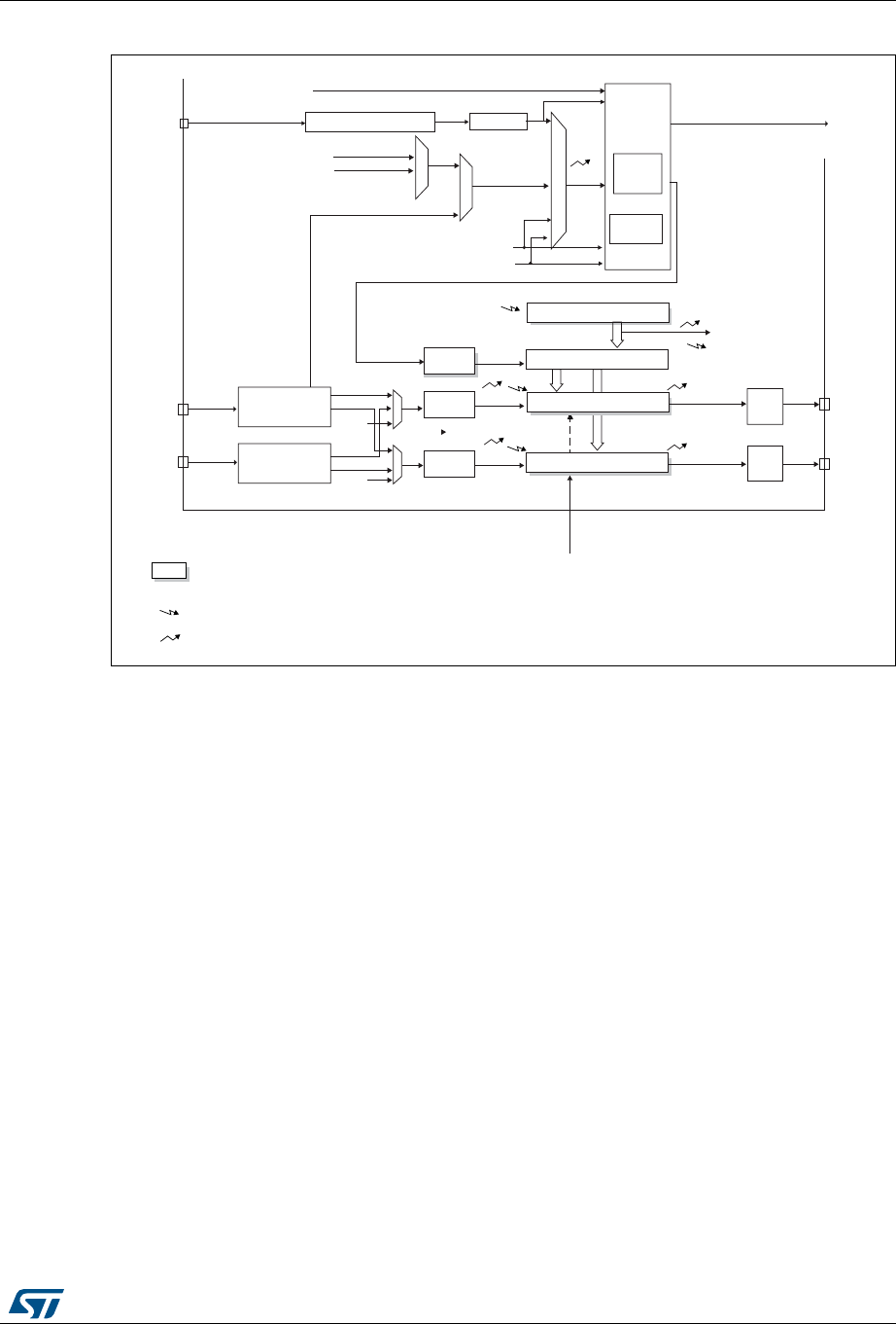
DocID025941 Rev 5 505/1001
RM0376 General-purpose timers (TIM21/22)
558
Figure 135. General-purpose timer block diagram (TIM21/22)
MSv33704V2
U
U
U
CC1I
CC2I
Trigger
controller
+/-
Stop, Clear
ITR0
ITR1 TRGI
Output
control
OC1REF
OC2REF
U
UI
Reset, enable, up, count
CK_PSC
IC1
IC2 IC2PS
IC1PS
TI1FP1
TGI
TRC
TRC
ITR
TRC
TI1F_ED
CC1I
CC2I
TI1FP2
TI2FP1
TI2FP2
TI1
TI2
TIMx_CH1
TIMx_CH2
OC1
OC2
TIMx_CH1
TIMx_CH2
Slave
controller
mode
PSC
prescaler CNT counter
Internal clock (CK_INT)
CK_CNT
Input filter &
edge detector Capture/Compare 1 register
Notes:
Reg Preload registers transferred
to active registers on U event
according to control bit
Event
Interrupt
Auto-reload register
Capture/Compare 2 register
Prescaler
Prescaler
Input filter &
edge detector
Output
control
TIMx_ETR ETR ETRP
Polarity selection & edge Input filter
ETRF
TI1FP1
TI2FP2
Encoder
interface
TRGO
ETRF

General-purpose timers (TIM21/22) RM0376
506/1001 DocID025941 Rev 5
21.3 TIM21/22 functional description
21.3.1 Timebase unit
The main block of the timer is a 16-bit counter with its related auto-reload register. The
counters counts up, down or both up and down but also down or both up and down. The
counter clock can be divided by a prescaler.
The counter, the auto-reload register and the prescaler register can be written or read by
software. This is true even when the counter is running.
The timebase unit includes:
•Counter register (TIMx_CNT)
•Prescaler register (TIMx_PSC)
•Auto-reload register (TIMx_ARR)
The auto-reload register is preloaded. Writing to or reading from the auto-reload register
accesses the preload register. The content of the preload register are transferred into the
shadow register permanently or at each update event (UEV), depending on the auto-reload
preload enable bit (ARPE) in TIMx_CR1 register. The update event is sent when the counter
reaches the overflow and if the UDIS bit equals 0 in the TIMx_CR1 register. It can also be
generated by software. The generation of the update event is described in detailed for each
configuration.
The counter is clocked by the prescaler output CK_CNT, which is enabled only when the
counter enable bit (CEN) in TIMx_CR1 register is set (refer also to the slave mode controller
description to get more details on counter enabling).
Note that the counter starts counting 1 clock cycle after setting the CEN bit in the TIMx_CR1
register.
Prescaler description
The prescaler can divide the counter clock frequency by any factor between 1 and 65536. It
is based on a 16-bit counter controlled through a 16-bit register (in the TIMx_PSC register).
It can be changed on the fly as this control register is buffered. The new prescaler ratio is
taken into account at the next update event.
Figure 137 and Figure 138 give some examples of the counter behavior when the prescaler
ratio is changed on the fly.
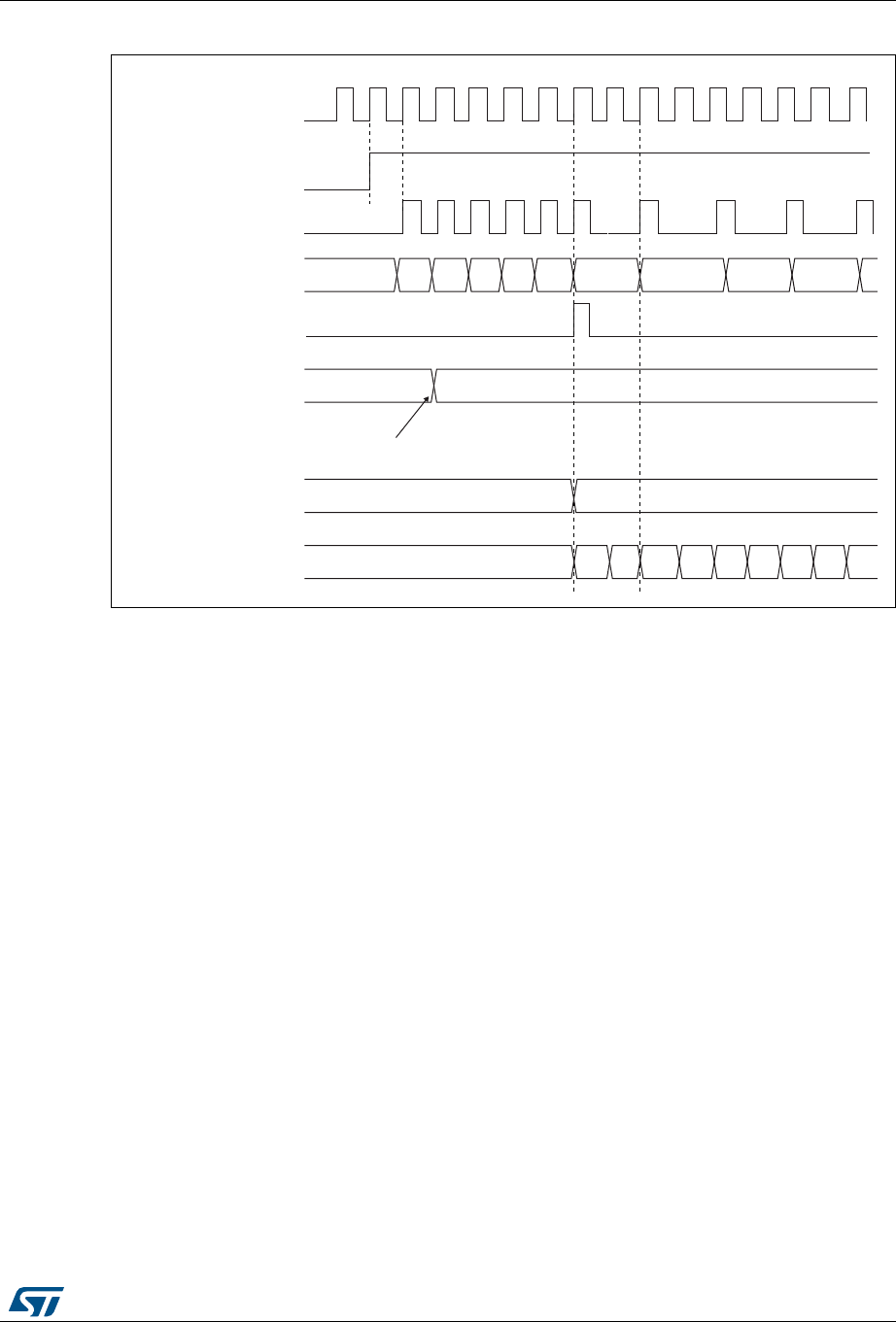
DocID025941 Rev 5 507/1001
RM0376 General-purpose timers (TIM21/22)
558
Figure 136. Counter timing diagram with prescaler division change from 1 to 2
CK_PSC
00
CEN
Timerclock = CK_CNT
Counter register
Update event (UEV)
0
Prescaler control register 1
0
Write a new value in TIMx_PSC
Prescaler buffer 1
0
Prescaler counter 010 10101
01 02 03
FA FBF7 F8 F9 FC
MS31076V2
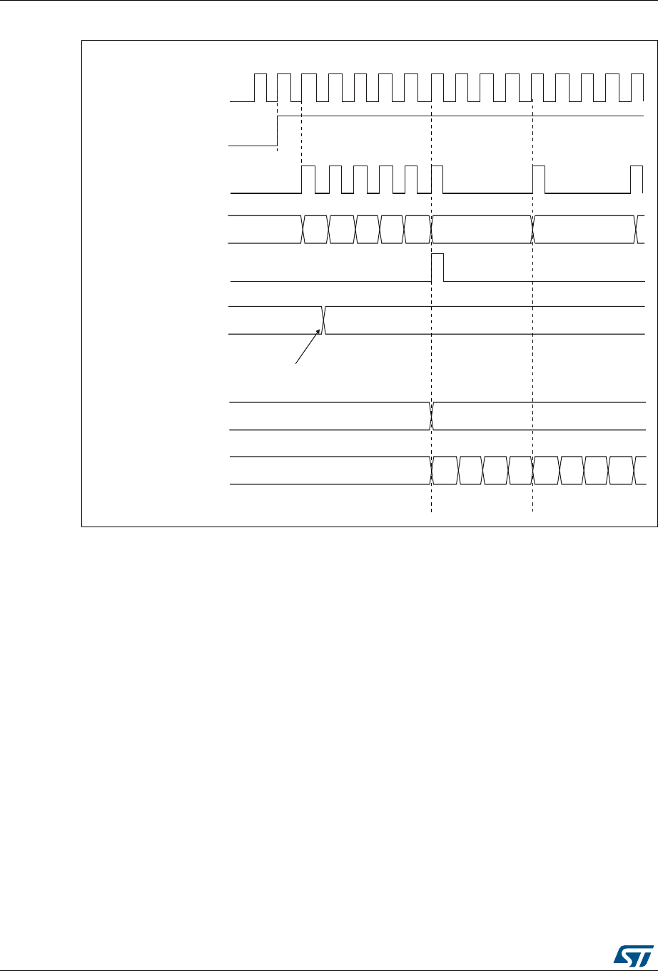
General-purpose timers (TIM21/22) RM0376
508/1001 DocID025941 Rev 5
Figure 137. Counter timing diagram with prescaler division change from 1 to 4
21.3.2 Counter modes
Upcounting mode
In upcounting mode, the counter counts from 0 to the auto-reload value (content of the
TIMx_ARR register), then restarts from 0 and generates a counter overflow event.
Setting the UG bit in the TIMx_EGR register (by software or by using the slave mode
controller on TIM21/22) also generates an update event.
The UEV event can be disabled by software by setting the UDIS bit in the TIMx_CR1
register. This is to avoid updating the shadow registers while writing new values in the
preload registers. Then no update event occurs until the UDIS bit has been written to 0.
However, the counter restarts from 0, as well as the counter of the prescaler (but the
prescale rate does not change). In addition, if the URS bit (update request selection) in
TIMx_CR1 register is set, setting the UG bit generates an update event UEV but without
setting the UIF flag (thus no interrupt is sent). This is to avoid generating both update and
capture interrupts when clearing the counter on the capture event.
0
3
0
01230123
MS31077V2
CK_PSC
CEN
Timerclock = CK_CNT
Counter register
Update event (UEV)
Prescaler control register
Write a new value in TIMx_PSC
Prescaler buffer
Prescaler counter
00 01
FA FB
F7 F8 F9 FC
30
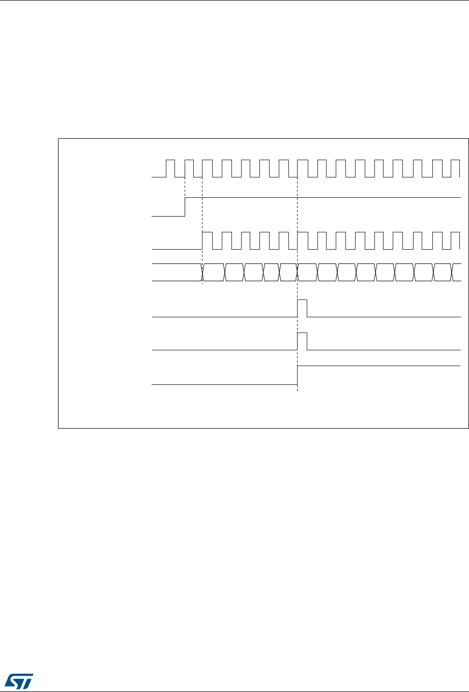
DocID025941 Rev 5 509/1001
RM0376 General-purpose timers (TIM21/22)
558
When an update event occurs, all the registers are updated and the update flag (UIF bit in
TIMx_SR register) is set (depending on the URS bit):
•The auto-reload shadow register is updated with the preload value (TIMx_ARR),
•The buffer of the prescaler is reloaded with the preload value (content of the TIMx_PSC
register).
The following figures show some examples of the counter behavior for different clock
frequencies when TIMx_ARR=0x36.
Figure 138. Counter timing diagram, internal clock divided by 1
00 02 03 04 05 06 0732 33 34 35 36
31
MS31078V2
CK_PSC
CNT_EN
Timerclock = CK_CNT
Counter register
Update event (UEV)
Counter overflow
Update interrupt flag
(UIF)
01

General-purpose timers (TIM21/22) RM0376
510/1001 DocID025941 Rev 5
Figure 139. Counter timing diagram, internal clock divided by 2
Figure 140. Counter timing diagram, internal clock divided by 4
MS31079V2
CK_PSC
CNT_EN
Timerclock = CK_CNT
Counter register
Update event (UEV)
Counter overflow
Update interrupt flag
(UIF)
0034 0035 0036 0000 0001 0002 0003
0000
0001
0035 0036
MS31080V2
CK_PSC
Timerclock = CK_CNT
Counter register
Update event (UEV)
Counter overflow
Update interrupt flag
(UIF)
CNT_EN
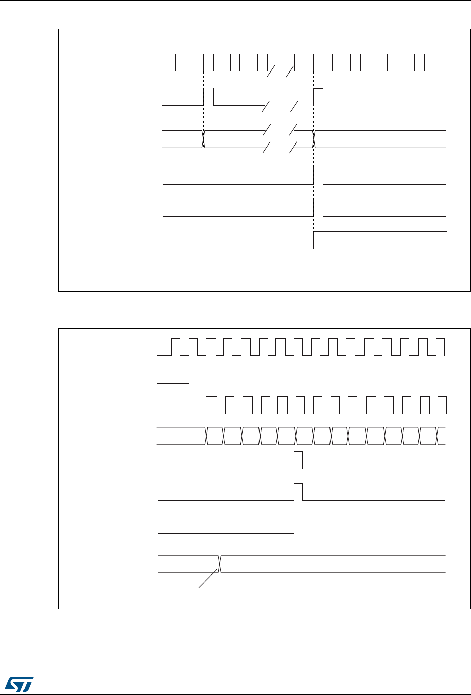
DocID025941 Rev 5 511/1001
RM0376 General-purpose timers (TIM21/22)
558
Figure 141. Counter timing diagram, internal clock divided by N
Figure 142. Counter timing diagram, update event when ARPE=0 (TIMx_ARR not
preloaded)
00
1F 20
MS31081V2
CK_PSC
Timerclock = CK_CNT
Counter register
Update event (UEV)
Counter overflow
Update interrupt flag
(UIF)
FF 36
MS31082V2
CK_PSC
Timerclock = CK_CNT
Counter register
Update event (UEV)
Counter overflow
Update interrupt flag
(UIF)
00 02 03 04 05 06 0732 33 34 35 3631 01
CEN
Auto-reload preload
register
Write a new value in TIMx_ARR
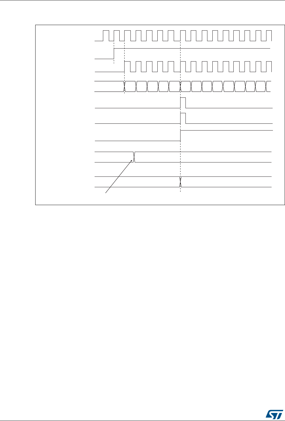
General-purpose timers (TIM21/22) RM0376
512/1001 DocID025941 Rev 5
Figure 143. Counter timing diagram, update event when ARPE=1 (TIMx_ARR
preloaded)
Downcounting mode
In downcounting mode, the counter counts from the auto-reload value (content of the
TIMx_ARR register) down to 0, then restarts from the auto-reload value and generates a
counter underflow event.
An Update event can be generate at each counter underflow or by setting the UG bit in the
TIMx_EGR register (by software or by using the slave mode controller)
The UEV update event can be disabled by software by setting the UDIS bit in TIMx_CR1
register. This is to avoid updating the shadow registers while writing new values in the
preload registers. Then no update event occurs until UDIS bit has been written to 0.
However, the counter restarts from the current auto-reload value, whereas the counter of the
prescaler restarts from 0 (but the prescale rate doesn’t change).
In addition, if the URS bit (update request selection) in TIMx_CR1 register is set, setting the
UG bit generates an update event UEV but without setting the UIF flag (thus no interrupt or
DMA request is sent). This is to avoid generating both update and capture interrupts when
clearing the counter on the capture event.
When an update event occurs, all the registers are updated and the update flag (UIF bit in
TIMx_SR register) is set (depending on the URS bit):
•The buffer of the prescaler is reloaded with the preload value (content of the TIMx_PSC
register).
•The auto-reload active register is updated with the preload value (content of the
TIMx_ARR register). Note that the auto-reload is updated before the counter is
reloaded, so that the next period is the expected one.
MS31083V2
F5 36
CK_PSC
Timerclock = CK_CNT
Counter register
Update event (UEV)
Counter overflow
Update interrupt flag
(UIF)
00 02 03 04 05 06 07F1 F2 F3 F4 F5F0 01
CEN
Auto-reload preload
register
Write a new value in TIMx_ARR
Auto-reload shadow
register F5 36
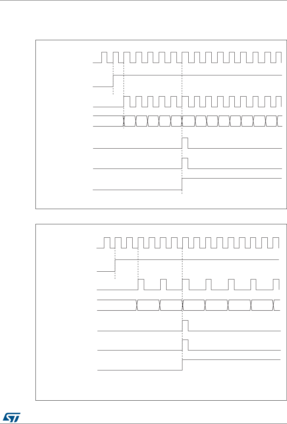
DocID025941 Rev 5 513/1001
RM0376 General-purpose timers (TIM21/22)
558
The following figures show some examples of the counter behavior for different clock
frequencies when TIMx_ARR=0x36.
Figure 144. Counter timing diagram, internal clock divided by 1
Figure 145. Counter timing diagram, internal clock divided by 2
36 34 33 32 31 30 2F
04 03 02 01 00
05
MS31184V1
CK_PSC
CNT_EN
Timerclock = CK_CNT
Counter register
Update event (UEV)
Counter underflow
(cnt_udf)
Update interrupt flag
(UIF)
35
MS31185V1
CK_PSC
CNT_EN
Timerclock = CK_CNT
Counter register
Update event (UEV)
Counter underflow
Update interrupt flag
(UIF)
0002 0001 0000 0036 0035 0034 0033
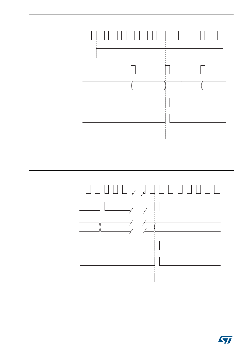
General-purpose timers (TIM21/22) RM0376
514/1001 DocID025941 Rev 5
Figure 146. Counter timing diagram, internal clock divided by 4
Figure 147. Counter timing diagram, internal clock divided by N
0000
0001
0001 0000
MS31186V1
CK_PSC
Timerclock = CK_CNT
Counter register
Update event (UEV)
Counter underflow
Update interrupt flag
(UIF)
CNT_EN
001F20
MS31187V1
CK_PSC
Timerclock = CK_CNT
Counter register
Update event (UEV)
Counter underflow
Update interrupt flag
(UIF)
36

DocID025941 Rev 5 515/1001
RM0376 General-purpose timers (TIM21/22)
558
Center-aligned mode (up/down counting)
In center-aligned mode, the counter counts from 0 to the auto-reload value (content of the
TIMx_ARR register) – 1, generates a counter overflow event, then counts from the auto-
reload value down to 1 and generates a counter underflow event. Then it restarts counting
from 0.
Center-aligned mode is active when the CMS bits in TIMx_CR1 register are not equal to
'00'. The Output compare interrupt flag of channels configured in output is set when: the
counter counts down (Center aligned mode 1, CMS = "01"), the counter counts up (Center
aligned mode 2, CMS = "10") the counter counts up and down (Center aligned mode 3,
CMS = "11").
In this mode, the direction bit (DIR from TIMx_CR1 register) cannot be written. It is updated
by hardware and gives the current direction of the counter.
The update event can be generated at each counter overflow and at each counter underflow
or by setting the UG bit in the TIMx_EGR register (by software or by using the slave mode
controller) also generates an update event. In this case, the counter restarts counting from
0, as well as the counter of the prescaler.
The UEV update event can be disabled by software by setting the UDIS bit in TIMx_CR1
register. This is to avoid updating the shadow registers while writing new values in the
preload registers. Then no update event occurs until the UDIS bit has been written to 0.
However, the counter continues counting up and down, based on the current auto-reload
value.
In addition, if the URS bit (update request selection) in TIMx_CR1 register is set, setting the
UG bit generates an update event UEV but without setting the UIF flag (thus no interrupt or
DMA request is sent). This is to avoid generating both update and capture interrupt when
clearing the counter on the capture event.
When an update event occurs, all the registers are updated and the update flag (UIF bit in
TIMx_SR register) is set (depending on the URS bit):
•The buffer of the prescaler is reloaded with the preload value (content of the TIMx_PSC
register).
•The auto-reload active register is updated with the preload value (content of the
TIMx_ARR register). Note that if the update source is a counter overflow, the auto-
reload is updated before the counter is reloaded, so that the next period is the expected
one (the counter is loaded with the new value).
The following figures show some examples of the counter behavior for different clock
frequencies.
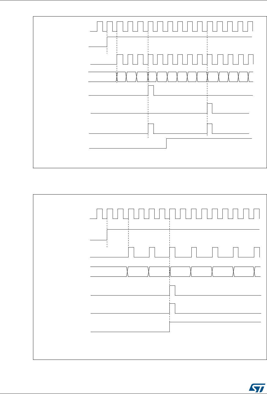
General-purpose timers (TIM21/22) RM0376
516/1001 DocID025941 Rev 5
Figure 148. Counter timing diagram, internal clock divided by 1, TIMx_ARR=0x6
1. Here, center-aligned mode 1 is used (for more details refer to Section 21.4.1: TIM21/22 control register 1
(TIMx_CR1) on page 540).
Figure 149. Counter timing diagram, internal clock divided by 2
MS31189V1
CK_PSC
Timerclock = CK_CNT
Counter register
Update event (UEV)
Counter overflow
Update interrupt flag
(UIF)
00020304 05 06
01
CEN
02 03 0401 05 0304
Counter underflow
MS31190V1
CK_PSC
CNT_EN
Timerclock = CK_CNT
Counter register
Update event (UEV)
Counter underflow
Update interrupt flag
(UIF)
0003 0002 0001 0000 0001 0002 0003
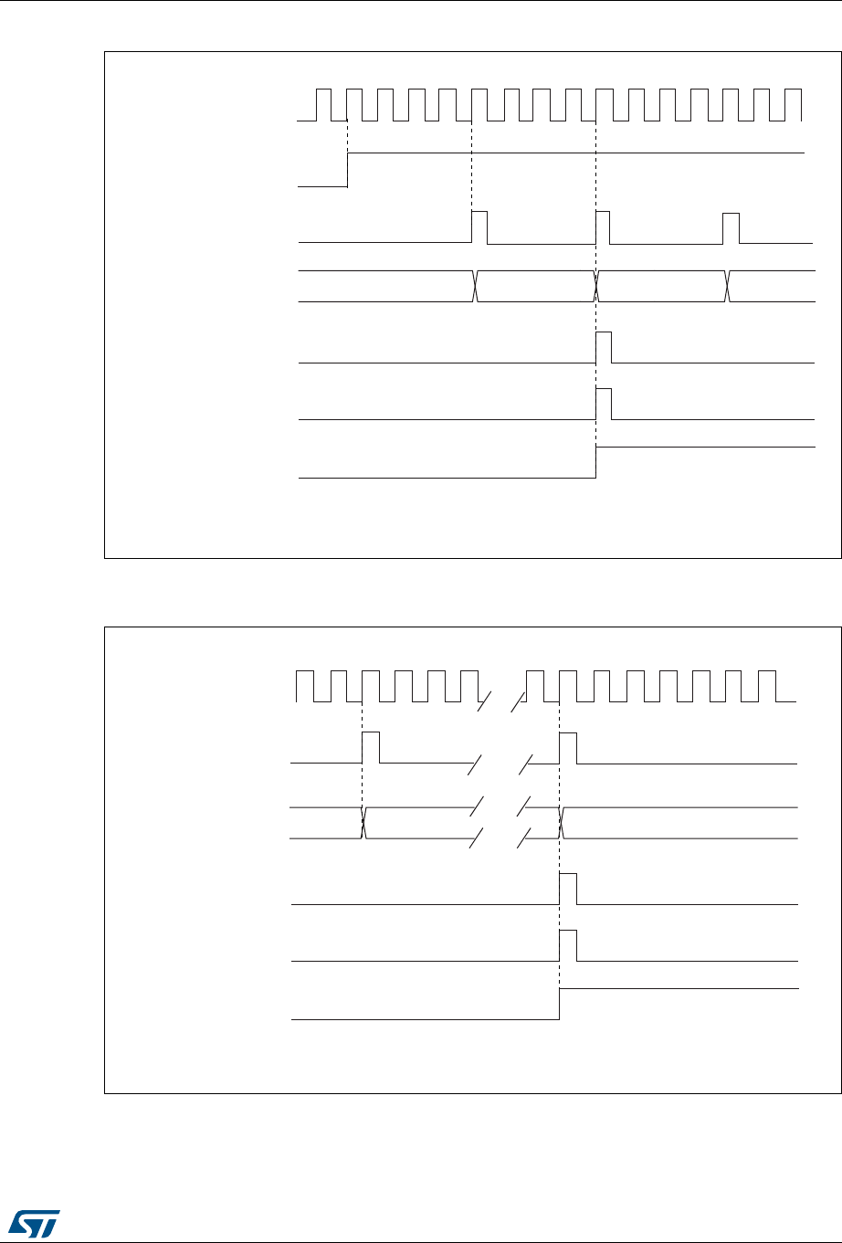
DocID025941 Rev 5 517/1001
RM0376 General-purpose timers (TIM21/22)
558
Figure 150. Counter timing diagram, internal clock divided by 4, TIMx_ARR=0x36
1. Center-aligned mode 2 or 3 is used with an UIF on overflow.
Figure 151. Counter timing diagram, internal clock divided by N
0034 0035
MS31191V1
CK_PSC
Timerclock = CK_CNT
Counter register
Update event (UEV)
Counter overflow
Update interrupt flag
(UIF)
CNT_EN
Note: Here, center_aligned mode 2 or 3 is updated with an UIF on overflow
0036 0035
00
1F
20
MS31192V1
CK_PSC
Timerclock = CK_CNT
Counter register
Update event (UEV)
Counter underflow
Update interrupt flag
(UIF)
01
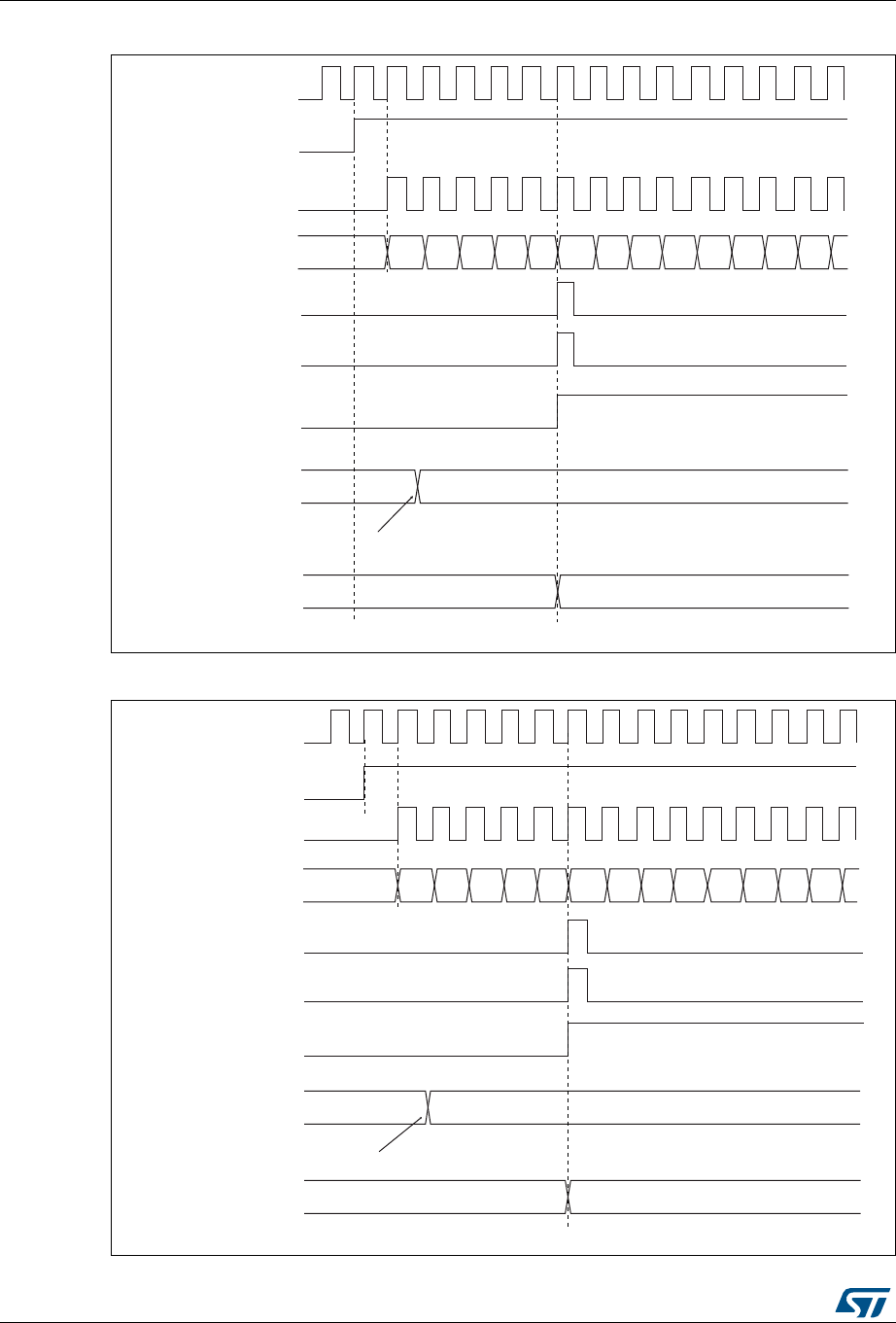
General-purpose timers (TIM21/22) RM0376
518/1001 DocID025941 Rev 5
Figure 152. Counter timing diagram, Update event with ARPE=1 (counter underflow)
Figure 153. Counter timing diagram, Update event with ARPE=1 (counter overflow)
FD 36
MS31193V1
CK_PSC
Timerclock = CK_CNT
Counter register
Update event (UEV)
Counter underflow
Update interrupt flag
(UIF)
00 02 03 04 05 06 0701
CEN
Auto-reload preload
register
Write a new value in TIMx_ARR
06 05 04 03 02 01
FD 36
Auto-reload active
register
MS31194V1
FD 36
CK_PSC
Timer clock = CK_CNT
Counter register
Update event (UEV)
Counter overflow
Update interrupt flag
(UIF)
36 34 33 32 31 30 2FF8 F9 FA FB FCF7 35
CEN
Auto-reload preload
register
Write a new value in TIMx_ARR
Auto-reload active
register FD 36
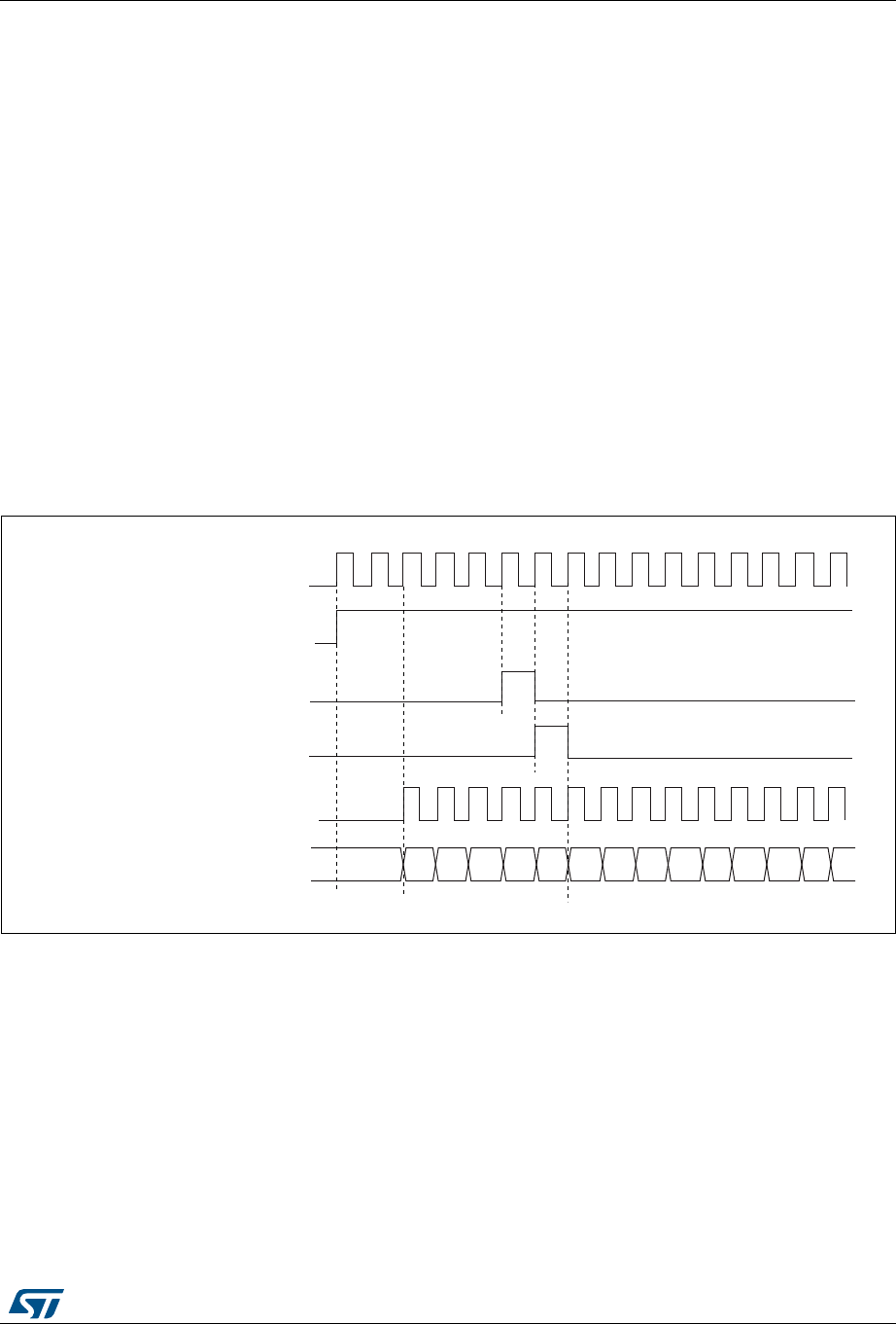
DocID025941 Rev 5 519/1001
RM0376 General-purpose timers (TIM21/22)
558
21.3.3 Clock selection
The counter clock can be provided by the following clock sources:
•Internal clock (CK_INT)
•External clock mode1: external input pin (TIx)
•External clock mode2: external trigger input (ETR connected internally to LSE)
•Internal trigger inputs (ITRx): connecting the trigger output from another timer. Refer to
Section : Using one timer as prescaler for another timer for more details.
Internal clock source (CK_INT)
The internal clock source is selected when the slave mode controller is disabled
(SMS=’000’). The CEN bit in the TIMx_CR1 register and the UG bit in the TIMx_EGR
register are then used as control bits and can be changed only by software (except for UG
which remains cleared). As soon as the CEN bit is programmed to 1, the prescaler is
clocked by the internal clock CK_INT.
Figure 154 shows the behavior of the control circuit and the upcounter in normal mode,
without prescaler.
Figure 154. Control circuit in normal mode, internal clock divided by 1
Internal clock
Counter clock = CK_CNT = CK_PSC
Counter register
CEN=CNT_EN
UG
CNT_INIT
MS31085V2
00 02 03 04 05 06 0732 33 34 35 36
31 01
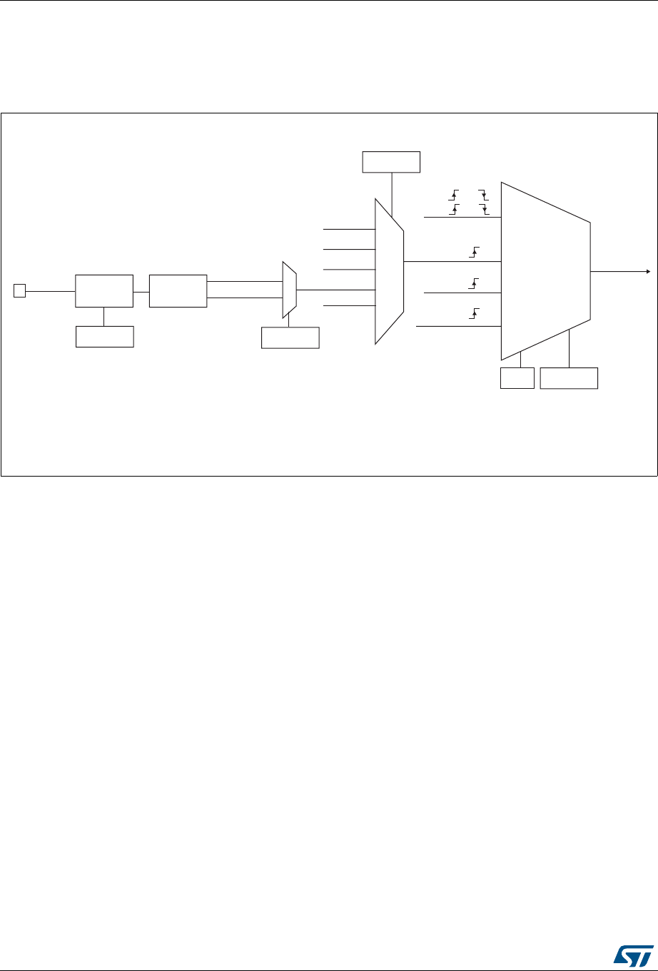
General-purpose timers (TIM21/22) RM0376
520/1001 DocID025941 Rev 5
External clock source mode 1
This mode is selected when SMS=’111’ in the TIMx_SMCR register. The counter can count
at each rising or falling edge on a selected input.
Figure 155. TI2 external clock connection example
For example, to configure the upcounter to count in response to a rising edge on the TI2
input, use the following procedure:
1. Configure channel 2 to detect rising edges on the TI2 input by writing CC2S = ‘01’ in
the TIMx_CCMR1 register.
2. Configure the input filter duration by writing the IC2F[3:0] bits in the TIMx_CCMR1
register (if no filter is needed, keep IC2F=’0000’).
3. Select the rising edge polarity by writing CC2P=’0’ and CC2NP=’0’ in the TIMx_CCER
register.
4. Configure the timer in external clock mode 1 by writing SMS=’111’ in the TIMx_SMCR
register.
5. Select TI2 as the trigger input source by writing TS=’110’ in the TIMx_SMCR register.
6. Enable the counter by writing CEN=’1’ in the TIMx_CR1 register.
For code example, refer to A.11.1: Upcounter on TI2 rising edge code example.
Note: The capture prescaler is not used for triggering, so you don’t need to configure it.
When a rising edge occurs on TI2, the counter counts once and the TIF flag is set.
The delay between the rising edge on TI2 and the actual clock of the counter is due to the
resynchronization circuit on TI2 input.
External clock
mode 1
Internal clock
mode
TRGI
CK_INT
CK_PSC
TIMx_SMCR
SMS[2:0]
ITRx
TI1_ED
TI1FP1
TI2FP2
TIMx_SMCR
TS[2:0]
TI2 0
1
TIMx_CCER
CC2P
Filter
ICF[3:0]
TIMx_CCMR1
Edge
detector
TI2F_Rising
TI2F_Falling
110
0xx
100
101
MS31196V1
(internal clock)
TI1F or
TI2F or
or
Encoder
mode
ETRF 111
External clock
mode 2
ETRF
ECE
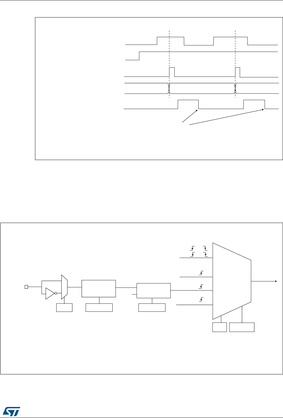
DocID025941 Rev 5 521/1001
RM0376 General-purpose timers (TIM21/22)
558
Figure 156. Control circuit in external clock mode 1
External clock source mode 2
This mode is selected by writing ECE=1 in the TIMx_SMCR register.
The counter can count at each rising or falling edge on the external trigger input ETR.
The Figure 157 gives an overview of the external trigger input block.
Figure 157. External trigger input block
Counter clock = CK_CNT = CK_PSC
Counter register 35 3634
TI2
CNT_EN
TIF
Write TIF=0
MS31087V2
External clock
mode 1
Internal clock
mode
TRGI
CK_INT
CK_PSC
TIMx_SMCR
SMS[2:0]
MS33116V1
(internal clock)
TI1F or
TI2F or
or
Encoder
mode
External clock
mode 2
ETRF
ECE
0
1
TIMx_SMCR
ETP
ETR pin
ETR
Divider
/1, /2, /4, /8 Filter
downcounter
f
ETRP
TIMx_SMCR
ETPS[1:0]
TIMx_SMCR
ETF[3:0]
DTS
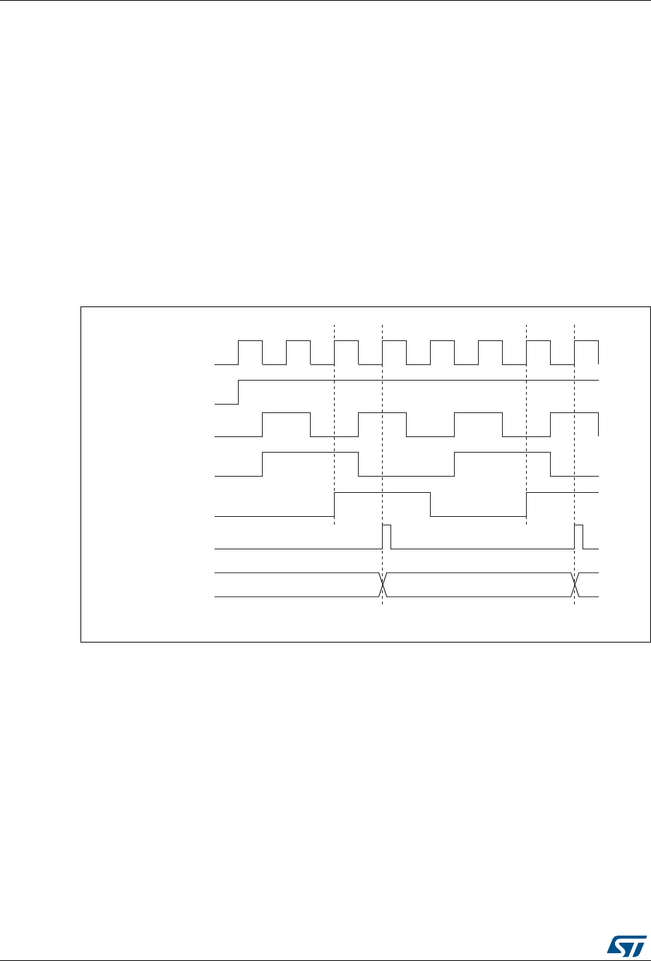
General-purpose timers (TIM21/22) RM0376
522/1001 DocID025941 Rev 5
For example, to configure the upcounter to count each 2 rising edges on ETR, use the
following procedure:
1. As no filter is needed in this example, write ETF[3:0]=0000 in the TIMx_SMCR register.
2. Set the prescaler by writing ETPS[1:0]=01 in the TIMx_SMCR register
3. Select rising edge detection on the ETR pin by writing ETP=0 in the TIMx_SMCR
register
4. Enable external clock mode 2 by writing ECE=1 in the TIMx_SMCR register.
5. Enable the counter by writing CEN=1 in the TIMx_CR1 register.
For code example, refer to A.11.2: Up counter on each 2 ETR rising edges code example.
The counter counts once each 2 ETR rising edges.
The delay between the rising edge on ETR and the actual clock of the counter is due to the
resynchronization circuit on the ETRP signal.
Figure 158. Control circuit in external clock mode 2
21.3.4 Capture/compare channels
Each Capture/Compare channel is built around a capture/compare register (including a
shadow register), a input stage for capture (with digital filter, multiplexing and prescaler) and
an output stage (with comparator and output control).
Figure 159 to Figure 161 give an overview of one capture/compare channel.
The input stage samples the corresponding TIx input to generate a filtered signal TIxF.
Then, an edge detector with polarity selection generates a signal (TIxFPx) which can be
used as trigger input by the slave mode controller or as the capture command. It is
prescaled before the capture register (ICxPS).
MS33111V2
34 35 36
fCK_INT
CNT_EN
ETR
ETRP
ETRF
Counter clock =
CK_INT =CK_PSC
Counter register
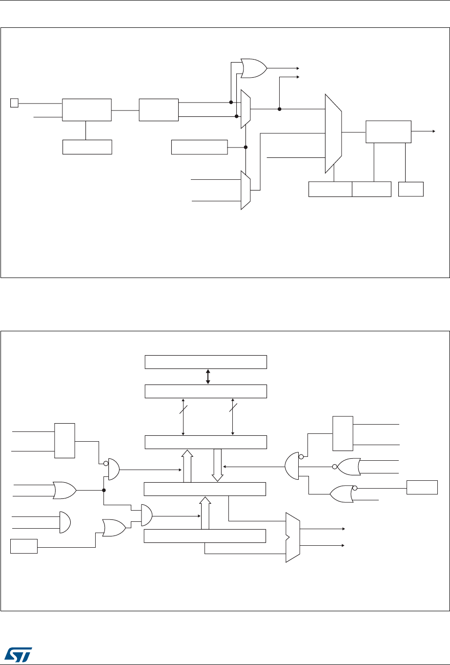
DocID025941 Rev 5 523/1001
RM0376 General-purpose timers (TIM21/22)
558
Figure 159. Capture/compare channel (example: channel 1 input stage)
The output stage generates an intermediate waveform which is then used for reference:
OCxRef (active high). The polarity acts at the end of the chain.
Figure 160. Capture/compare channel 1 main circuit
0
1
Divider
/1, /2, /4, /8
ICPS[1:0]
TI1F_ED
To the slave mode controller
TI1FP1
11
01
CC1S[1:0]
IC1
TI2FP1
TRC
(from slave mode
controller)
10 IC1PS
0
1
MS33115V1
TI1
TIMx_CCER
CC1P/CC1NP
Filter
downcounter
ICF[3:0]
TIMx_CCMR1
Edge
detector
TI1F_Rising
TI1F_Falling
TIMx_CCMR1
TIMx_CCER
TI2F_Rising
(from channel 2)
TI2F_Falling
(from channel 2)
TI1F
f
CC1E
DTS
CC1E
Capture/compare shadow register
Comparator
Capture/compare preload register
Counter
IC1PS
CC1S[0]
CC1S[1]
Capture
Input
mode
S
R
Read CCR1H
Read CCR1L
read_in_progress
capture_transfer CC1S[0]
CC1S[1]
S
R
write CCR1H
write CCR1L
write_in_progress
Output
mode
UEV
OC1PE
(from time
base unit)
compare_transfer
APB Bus
88
high
low
(if 16-bit)
MCU-peripheral interface
TIM1_CCMR1
OC1PE
CNT>CCR1
CNT=CCR1
TIM1_EGR
CC1G
MS31089V2
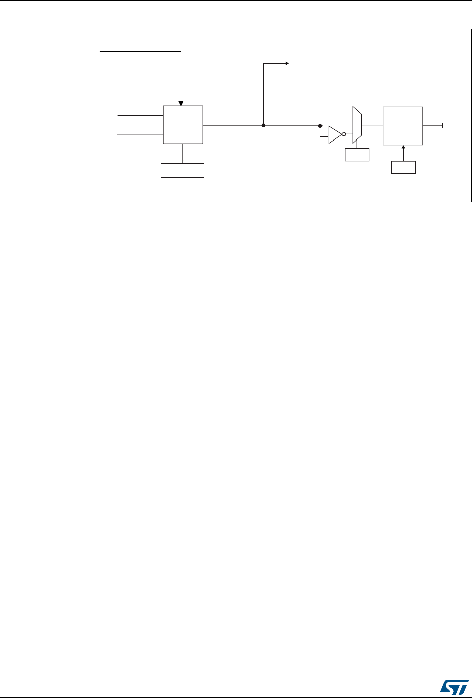
General-purpose timers (TIM21/22) RM0376
524/1001 DocID025941 Rev 5
Figure 161. Output stage of capture/compare channel (channel 1 and 2)
The capture/compare block is made of one preload register and one shadow register. Write
and read always access the preload register.
In capture mode, captures are actually done in the shadow register, which is copied into the
preload register.
In compare mode, the content of the preload register is copied into the shadow register
which is compared to the counter.
21.3.5 Input capture mode
In Input capture mode, the Capture/Compare Registers (TIMx_CCRx) are used to latch the
value of the counter after a transition detected by the corresponding ICx signal. When a
capture occurs, the corresponding CCXIF flag (TIMx_SR register) is set and an interrupt or
a DMA request can be sent if they are enabled. If a capture occurs while the CCxIF flag was
already high, then the over-capture flag CCxOF (TIMx_SR register) is set. CCxIF can be
cleared by software by writing it to ‘0’ or by reading the captured data stored in the
TIMx_CCRx register. CCxOF is cleared when you write it to ‘0’.
The following example shows how to capture the counter value in TIMx_CCR1 when TI1
input rises. To do this, use the following procedure:
1. Select the active input: TIMx_CCR1 must be linked to the TI1 input, so write the CC1S
bits to ‘01’ in the TIMx_CCMR1 register. As soon as CC1S becomes different from ‘00’,
the channel is configured in input mode and the TIMx_CCR1 register becomes read-
only.
2. Program the input filter duration you need with respect to the signal you connect to the
timer (when the input is one of the TIx (ICxF bits in the TIMx_CCMRx register). Let’s
imagine that, when toggling, the input signal is not stable during at must 5 internal clock
cycles. We must program a filter duration longer than these 5 clock cycles. We can
validate a transition on TI1 when 8 consecutive samples with the new level have been
MSv33714V1
TIMx_CCER
Output
mode
controller
CNT > CCR2
CNT = CCR2
TIMx_CCMR1
0
1
TIMx_CCER
Output
enable
circuit
OCx
CCxE
To the master
mode controller
OCx_REF
OCxM[2:0]
CCxP
ETRF

DocID025941 Rev 5 525/1001
RM0376 General-purpose timers (TIM21/22)
558
detected (sampled at fDTS frequency). Then write IC1F bits to ‘0011’ in the
TIMx_CCMR1 register.
3. Select the edge of the active transition on the TI1 channel by programming CC1P and
CC1NP bits to ‘00’ in the TIMx_CCER register (rising edge in this case).
4. Program the input prescaler. In our example, we wish the capture to be performed at
each valid transition, so the prescaler is disabled (write IC1PS bits to ‘00’ in the
TIMx_CCMR1 register).
5. Enable capture from the counter into the capture register by setting the CC1E bit in the
TIMx_CCER register.
6. If needed, enable the related interrupt request by setting the CC1IE bit in the
TIMx_DIER register.
For code example, refer to A.11.3: Input capture configuration code example.
When an input capture occurs:
•The TIMx_CCR1 register gets the value of the counter on the active transition.
•CC1IF flag is set (interrupt flag). CC1OF is also set if at least two consecutive captures
occurred whereas the flag was not cleared.
•An interrupt is generated depending on the CC1IE bit.
For code example, refer to A.11.4: Input capture data management code example.
In order to handle the overcapture, it is recommended to read the data before the
overcapture flag. This is to avoid missing an overcapture which could happen after reading
the flag and before reading the data.
Note: IC interrupt requests can be generated by software by setting the corresponding CCxG bit in
the TIMx_EGR register.
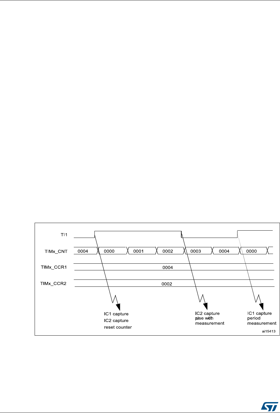
General-purpose timers (TIM21/22) RM0376
526/1001 DocID025941 Rev 5
21.3.6 PWM input mode
This mode is a particular case of input capture mode. The procedure is the same except:
•Two ICx signals are mapped on the same TIx input.
•These 2 ICx signals are active on edges with opposite polarity.
•One of the two TIxFP signals is selected as trigger input and the slave mode controller
is configured in reset mode.
For example, you can measure the period (in TIMx_CCR1 register) and the duty cycle (in
TIMx_CCR2 register) of the PWM applied on TI1 using the following procedure (depending
on CK_INT frequency and prescaler value):
1. Select the active input for TIMx_CCR1: write the CC1S bits to ‘01’ in the TIMx_CCMR1
register (TI1 selected).
2. Select the active polarity for TI1FP1 (used both for capture in TIMx_CCR1 and counter
clear): program the CC1P and CC1NP bits to ‘00’ (active on rising edge).
3. Select the active input for TIMx_CCR2: write the CC2S bits to ‘10’ in the TIMx_CCMR1
register (TI1 selected).
4. Select the active polarity for TI1FP2 (used for capture in TIMx_CCR2): program the
CC2P and CC2NP bits to ‘11’ (active on falling edge).
5. Select the valid trigger input: write the TS bits to ‘101’ in the TIMx_SMCR register
(TI1FP1 selected).
6. Configure the slave mode controller in reset mode: write the SMS bits to ‘100’ in the
TIMx_SMCR register.
7. Enable the captures: write the CC1E and CC2E bits to ‘1’ in the TIMx_CCER register.
For code example, refer to A.11.5: PWM input configuration code example.
Figure 162. PWM input mode timing
1. The PWM input mode can be used only with the TIMx_CH1/TIMx_CH2 signals due to the fact that only
TI1FP1 and TI2FP2 are connected to the slave mode controller.

DocID025941 Rev 5 527/1001
RM0376 General-purpose timers (TIM21/22)
558
21.3.7 Forced output mode
In output mode (CCxS bits = ‘00’ in the TIMx_CCMRx register), each output compare signal
(OCxREF and then OCx) can be forced to active or inactive level directly by software,
independently of any comparison between the output compare register and the counter.
To force an output compare signal (OCXREF/OCx) to its active level, you just need to write
‘101’ in the OCxM bits in the corresponding TIMx_CCMRx register. Thus OCXREF is forced
high (OCxREF is always active high) and OCx get opposite value to CCxP polarity bit.
For example: CCxP=’0’ (OCx active high) => OCx is forced to high level.
The OCxREF signal can be forced low by writing the OCxM bits to ‘100’ in the
TIMx_CCMRx register.
Anyway, the comparison between the TIMx_CCRx shadow register and the counter is still
performed and allows the flag to be set. Interrupt requests can be sent accordingly. This is
described in the output compare mode section below.
21.3.8 Output compare mode
This function is used to control an output waveform or indicating when a period of time has
elapsed.
When a match is found between the capture/compare register and the counter, the output
compare function:
1. Assigns the corresponding output pin to a programmable value defined by the output
compare mode (OCxM bits in the TIMx_CCMRx register) and the output polarity (CCxP
bit in the TIMx_CCER register). The output pin can keep its level (OCXM=’000’), be set
active (OCxM=’001’), be set inactive (OCxM=’010’) or can toggle (OCxM=’011’) on
match.
2. Sets a flag in the interrupt status register (CCxIF bit in the TIMx_SR register).
3. Generates an interrupt if the corresponding interrupt mask is set (CCXIE bit in the
TIMx_DIER register).
The TIMx_CCRx registers can be programmed with or without preload registers using the
OCxPE bit in the TIMx_CCMRx register.
In output compare mode, the update event UEV has no effect on OCxREF and OCx output.
The timing resolution is one count of the counter. Output compare mode can also be used to
output a single pulse (in One-pulse mode).
Procedure:
1. Select the counter clock (internal, external, prescaler).
2. Write the desired data in the TIMx_ARR and TIMx_CCRx registers.
3. Set the CCxIE bit if an interrupt request is to be generated.
4. Select the output mode. For example:
– Write OCxM = ‘011’ to toggle OCx output pin when CNT matches CCRx
– Write OCxPE = ‘0’ to disable preload register
– Write CCxP = ‘0’ to select active high polarity
– Write CCxE = ‘1’ to enable the output
5. Enable the counter by setting the CEN bit in the TIMx_CR1 register.
For code example, refer to A.11.7: Output compare configuration code example.

General-purpose timers (TIM21/22) RM0376
528/1001 DocID025941 Rev 5
The TIMx_CCRx register can be updated at any time by software to control the output
waveform, provided that the preload register is not enabled (OCxPE=’0’, else TIMx_CCRx
shadow register is updated only at the next update event UEV). An example is given in
Figure 163.
Figure 163. Output compare mode, toggle on OC1
21.3.9 PWM mode
Pulse Width Modulation mode allows you to generate a signal with a frequency determined
by the value of the TIMx_ARR register and a duty cycle determined by the value of the
TIMx_CCRx register.
The PWM mode can be selected independently on each channel (one PWM per OCx
output) by writing the OCxM bits in the TIMx_CCMRx register. Only the edge-aligned mode
is available on TIMER20 and TIMER21. You must enable the corresponding preload
register by setting the OCxPE bit in the TIMx_CCMRx register, and eventually the auto-
reload preload register (in upcounting or center-aligned modes) by setting the ARPE bit in
the TIMx_CR1 register.
As the preload registers are transferred to the shadow registers only when an update event
occurs, before starting the counter, you have to initialize all the registers by setting the UG
bit in the TIMx_EGR register.
The OCx polarity is software programmable using the CCxP bit in the TIMx_CCER register.
It can be programmed as active high or active low. The OCx output is enabled by the CCxE
bit in the TIMx_CCER register. Refer to the TIMx_CCERx register description for more
details.
In PWM mode (1 or 2), TIMx_CNT and TIMx_CCRx are always compared to determine
whether TIMx_CNT ≤ TIMx_CCRx.
MS31092V1
OC1REF= OC1
TIM1_CNT B200 B201
0039
TIM1_CCR1 003A
Write B201h in the CC1R register
Match detected on CCR1
Interrupt generated if enabled
003B
B201
003A
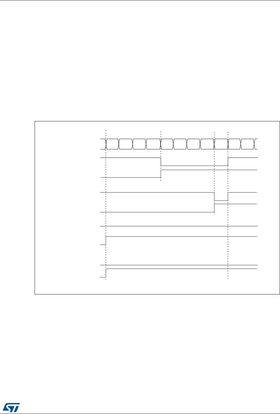
DocID025941 Rev 5 529/1001
RM0376 General-purpose timers (TIM21/22)
558
The timer is able to generate PWM in edge-aligned mode only since the counter is
upcounting.
•Upcounting configuration
Upcounting is active when the DIR bit in the TIMx_CR1 register is low. Refer to the
Upcounting mode on page 508.
In the following example, we consider PWM mode 1. The reference PWM signal
OCxREF is high as long as TIMx_CNT < TIMx_CCRx else it becomes low. If the
compare value in TIMx_CCRx is greater than the auto-reload value (in TIMx_ARR)
then OCxREF is held at ‘1’. If the compare value is 0 then OCxRef is held at ‘0’.
Figure 164 shows some edge-aligned PWM waveforms in an example where
TIMx_ARR=8.
For code example, refer to A.11.8: Edge-aligned PWM configuration example.
Figure 164. Edge-aligned PWM waveforms (ARR=8)
•Downcounting configuration
Downcounting is active when DIR bit in TIMx_CR1 register is high. Refer to the
Downcounting mode on page 512
In PWM mode 1, the reference signal OCxRef is low as long as
TIMx_CNT > TIMx_CCRx else it becomes high. If the compare value in TIMx_CCRx is
greater than the auto-reload value in TIMx_ARR, then OCxREF is held at ‘1’. 0% PWM
is not possible in this mode.
MS31093V1
Counter register
‘1’
012 3456 7801
OCXREF
CCxIF
OCXREF
CCxIF
OCXREF
CCxIF
OCXREF
CCxIF
CCRx=4
CCRx=8
CCRx>8
CCRx=0
‘0’
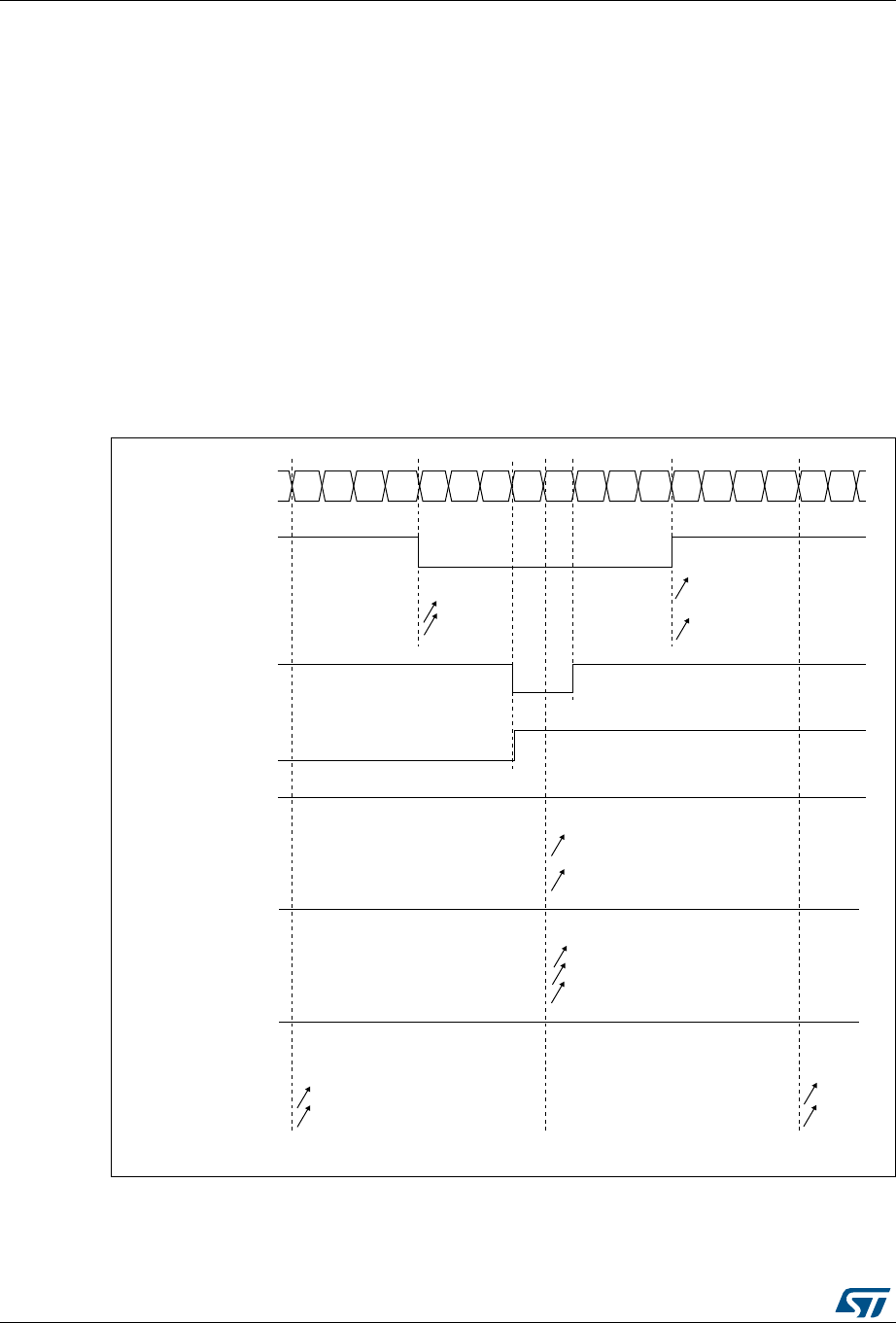
General-purpose timers (TIM21/22) RM0376
530/1001 DocID025941 Rev 5
PWM center-aligned mode
Center-aligned mode is active when the CMS bits in TIMx_CR1 register are different from
‘00’ (all the remaining configurations having the same effect on the OCxRef/OCx signals).
The compare flag is set when the counter counts up, when it counts down or both when it
counts up and down depending on the CMS bits configuration. The direction bit (DIR) in the
TIMx_CR1 register is updated by hardware and must not be changed by software. Refer to
the Center-aligned mode (up/down counting) on page 515.
Figure 165 shows some center-aligned PWM waveforms in an example where:
•TIMx_ARR=8,
•PWM mode is the PWM mode 1,
•The flag is set when the counter counts down corresponding to the center-aligned
mode 1 selected for CMS=01 in TIMx_CR1 register.
For code example, refer to A.11.9: Center-aligned PWM configuration example.
Figure 165. Center-aligned PWM waveforms (ARR=8)
CCxIF
01234567876 5432 101
Counter register
CCRx = 4
OCxREF
CMS=01
CMS=10
CMS=11
CCxIF
CCRx=7
OCxREF
CMS=10 or 11
CCxIF
CCRx=8
OCxREF
CMS=01
CMS=10
CMS=11
‘1’
CCxIF
CCRx>8
OCxREF
CMS=01
CMS=10
CMS=11
‘1’
CCxIF
CCRx=0
OCxREF
CMS=01
CMS=10
CMS=11
‘0’
AI14681b

DocID025941 Rev 5 531/1001
RM0376 General-purpose timers (TIM21/22)
558
Hints on using center-aligned mode
•When starting in center-aligned mode, the current up-down configuration is used. It
means that the counter counts up or down depending on the value written in the DIR bit
in the TIMx_CR1 register. Moreover, the DIR and CMS bits must not be changed at the
same time by the software.
•Writing to the counter while running in center-aligned mode is not recommended as it
can lead to unexpected results. In particular:
– The direction is not updated if you write a value in the counter that is greater than
the auto-reload value (TIMx_CNT>TIMx_ARR). For example, if the counter was
counting up, it continues to count up.
– The direction is updated if you write 0 or write the TIMx_ARR value in the counter
but no Update Event UEV is generated.
•The safest way to use center-aligned mode is to generate an update by software
(setting the UG bit in the TIMx_EGR register) just before starting the counter and not to
write the counter while it is running.
21.3.10 Clearing the OCxREF signal on an external event
The OCxREF signal for a given channel can be driven Low by applying a High level to the
ETRF input (OCxCE enable bit of the corresponding TIMx_CCMRx register set to ‘1’). The
OCxREF signal remains Low until the next update event, UEV, occurs.
This function can only be used in output compare and PWM modes, and does not work in
forced mode.
For example, the ETR signal can be connected to the output of a comparator to be used for
current handling. In this case, the ETR must be configured as follow:
1. The External Trigger Prescaler should be kept off: bits ETPS[1:0] of the TIMx_SMCR
register set to ‘00’.
2. The external clock mode 2 must be disabled: bit ECE of the TIMx_SMCR register set to
‘0’.
3. The External Trigger Polarity (ETP) and the External Trigger Filter (ETF) can be
configured according to the user needs.
For code example, refer to A.11.10: ETR configuration to clear OCxREF code example.
Figure 166 shows the behavior of the OCxREF signal when the ETRF Input becomes High,
for both values of the enable bit OCxCE. In this example, the timer TIMx is programmed in
PWM mode.

General-purpose timers (TIM21/22) RM0376
532/1001 DocID025941 Rev 5
Figure 166. Clearing TIMx OCxREF
Note: In case of a PWM with a 100% duty cycle (if CCRx>ARR), then OCxREF is enabled again at
the next counter overflow.
21.3.11 One-pulse mode
One-pulse mode (OPM) is a particular case of the previous modes. It allows the counter to
be started in response to a stimulus and to generate a pulse with a programmable length
after a programmable delay.
Starting the counter can be controlled through the slave mode controller. Generating the
waveform can be done in output compare mode or PWM mode. You select One-pulse mode
by setting the OPM bit in the TIMx_CR1 register. This makes the counter stop automatically
at the next update event UEV.
A pulse can be correctly generated only if the compare value is different from the counter
initial value. Before starting (when the timer is waiting for the trigger), the configuration must
be as follows:
CNT < CCRx ≤ ARR (in particular, 0 < CCRx)
MS33105V1
(CCRx)
Counter (CNT)
ETRF
OCxREF
(OCxCE = ‘0’)
OCxREF
(OCxCE = ‘1’)
OCxREF_CLR
becomes high
OCxREF_CLR
still high
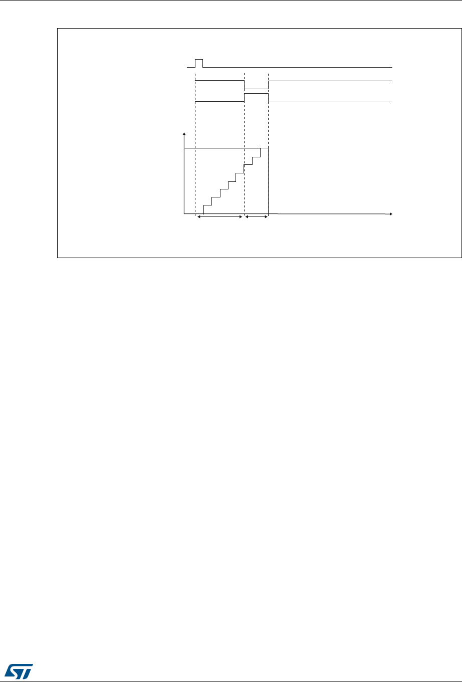
DocID025941 Rev 5 533/1001
RM0376 General-purpose timers (TIM21/22)
558
Figure 167. Example of one pulse mode
For example you may want to generate a positive pulse on OC1 with a length of tPULSE and
after a delay of tDELAY as soon as a positive edge is detected on the TI2 input pin.
Use TI2FP2 as trigger 1:
1. Map TI2FP2 to TI2 by writing CC2S=’01’ in the TIMx_CCMR1 register.
2. TI2FP2 must detect a rising edge, write CC2P=’0’ and CC2NP = ‘0’ in the TIMx_CCER
register.
3. Configure TI2FP2 as trigger for the slave mode controller (TRGI) by writing TS=’110’ in
the TIMx_SMCR register.
4. TI2FP2 is used to start the counter by writing SMS to ‘110’ in the TIMx_SMCR register
(trigger mode).
The OPM waveform is defined by writing the compare registers (taking into account the
clock frequency and the counter prescaler).
•The tDELAY is defined by the value written in the TIMx_CCR1 register.
•The tPULSE is defined by the difference between the auto-reload value and the compare
value (TIMx_ARR - TIMx_CCR1+1).
•Let’s say you want to build a waveform with a transition from ‘0’ to ‘1’ when a compare
match occurs and a transition from ‘1’ to ‘0’ when the counter reaches the auto-reload
value. To do this you enable PWM mode 2 by writing OC1M=’111’ in the TIMx_CCMR1
register. You can optionally enable the preload registers by writing OC1PE=’1’ in the
TIMx_CCMR1 register and ARPE in the TIMx_CR1 register. In this case you have to
write the compare value in the TIMx_CCR1 register, the auto-reload value in the
TIMx_ARR register, generate an update by setting the UG bit and wait for external
trigger event on TI2. CC1P is written to ‘0’ in this example.
In our example, the DIR and CMS bits in the TIMx_CR1 register should be low.
For code example, refer to A.11.16: One-Pulse mode code example.
MS31099V1
TI2
OC1REF
Counter
t
0
TIM1_ARR
TIM1_CCR1
OC1
tDELAY tPULSE

General-purpose timers (TIM21/22) RM0376
534/1001 DocID025941 Rev 5
You only want 1 pulse (Single mode), so you write '1 in the OPM bit in the TIMx_CR1
register to stop the counter at the next update event (when the counter rolls over from the
auto-reload value back to 0). When OPM bit in the TIMx_CR1 register is set to '0', so the
Repetitive Mode is selected.
Particular case: OCx fast enable
In One-pulse mode, the edge detection on TIx input set the CEN bit which enables the
counter. Then the comparison between the counter and the compare value makes the
output toggle. But several clock cycles are needed for these operations and it limits the
minimum delay tDELAY min we can get.
If you want to output a waveform with the minimum delay, you can set the OCxFE bit in the
TIMx_CCMRx register. Then OCxRef (and OCx) are forced in response to the stimulus,
without taking in account the comparison. Its new level is the same as if a compare match
had occurred. OCxFE acts only if the channel is configured in PWM1 or PWM2 mode.
For code example, refer to A.11.16: One-Pulse mode code example.
21.3.12 Encoder interface mode
To select Encoder Interface mode write SMS=‘001 in the TIMx_SMCR register if the counter
is counting on TI2 edges only, SMS=010 if it is counting on TI1 edges only and SMS=011 if
it is counting on both TI1 and TI2 edges.
Select the TI1 and TI2 polarity by programming the CC1P and CC2P bits in the TIMx_CCER
register. CC1NP and CC2NP must be kept cleared. When needed, you can program the
input filter as well. CC1NP and CC2NP must be kept low.
The two inputs TI1 and TI2 are used to interface to an incremental encoder. Refer to
Table 92. The counter is clocked by each valid transition on TI1FP1 or TI2FP2 (TI1 and TI2
after input filter and polarity selection, TI1FP1=TI1 if not filtered and not inverted,
TI2FP2=TI2 if not filtered and not inverted) assuming that it is enabled (CEN bit in
TIMx_CR1 register written to ‘1). The sequence of transitions of the two inputs is evaluated
and generates count pulses as well as the direction signal. Depending on the sequence the
counter counts up or down, the DIR bit in the TIMx_CR1 register is modified by hardware
accordingly. The DIR bit is calculated at each transition on any input (TI1 or TI2), whatever
the counter is counting on TI1 only, TI2 only or both TI1 and TI2.
Encoder interface mode acts simply as an external clock with direction selection. This
means that the counter just counts continuously between 0 and the auto-reload value in the
TIMx_ARR register (0 to ARR or ARR down to 0 depending on the direction). So you must
configure TIMx_ARR before starting. In the same way, the capture, compare, prescaler,
trigger output features continue to work as normal.
In this mode, the counter is modified automatically following the speed and the direction of
the quadrature encoder and its content, therefore, always represents the encoder’s position.
The count direction correspond to the rotation direction of the connected sensor. The table
summarizes the possible combinations, assuming TI1 and TI2 don’t switch at the same
time.
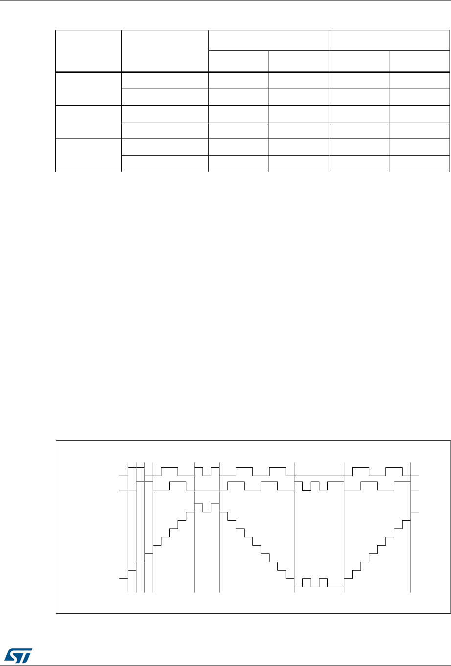
DocID025941 Rev 5 535/1001
RM0376 General-purpose timers (TIM21/22)
558
An external incremental encoder can be connected directly to the MCU without external
interface logic. However, comparators are normally be used to convert the encoder’s
differential outputs to digital signals. This greatly increases noise immunity. The third
encoder output which indicate the mechanical zero position, may be connected to an
external interrupt input and trigger a counter reset.
Figure 168 gives an example of counter operation, showing count signal generation and
direction control. It also shows how input jitter is compensated where both edges are
selected. This might occur if the sensor is positioned near to one of the switching points. For
this example we assume that the configuration is the following:
•CC1S= 01 (TIMx_CCMR1 register, TI1FP1 mapped on TI1)
•CC2S= 01 (TIMx_CCMR2 register, TI2FP2 mapped on TI2)
•CC1P and CC1NP = ‘0’ (TIMx_CCER register, TI1FP1 noninverted, TI1FP1=TI1)
•CC2P and CC2NP = ‘0’ (TIMx_CCER register, TI2FP2 noninverted, TI2FP2=TI2)
•SMS= 011 (TIMx_SMCR register, both inputs are active on both rising and falling
edges)
•CEN= 1 (TIMx_CR1 register, Counter is enabled)
For code example, refer to A.11.11: Encoder interface code example.
Figure 168. Example of counter operation in encoder interface mode
Table 92. Counting direction versus encoder signals
Active edge
Level on opposite
signal (TI1FP1 for
TI2, TI2FP2 for TI1)
TI1FP1 signal TI2FP2 signal
Rising Falling Rising Falling
Counting on
TI1 only
High Down Up No Count No Count
Low Up Down No Count No Count
Counting on
TI2 only
High No Count No Count Up Down
Low No Count No Count Down Up
Counting on
TI1 and TI2
High Down Up Up Down
Low Up Down Down Up
TI1
backwardjitter jitter
up down up
TI2
Counter
forward forward
MS33107V1
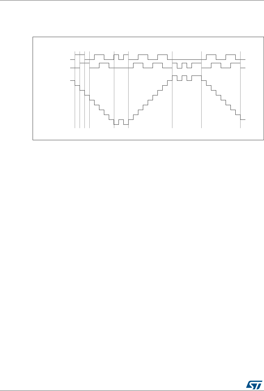
General-purpose timers (TIM21/22) RM0376
536/1001 DocID025941 Rev 5
Figure 169 gives an example of counter behavior when TI1FP1 polarity is inverted (same
configuration as above except CC1P=1).
Figure 169. Example of encoder interface mode with TI1FP1 polarity inverted
The timer, when configured in Encoder Interface mode provides information on the sensor’s
current position. You can obtain dynamic information (speed, acceleration, deceleration) by
measuring the period between two encoder events using a second timer configured in
capture mode. The output of the encoder which indicates the mechanical zero can be used
for this purpose. Depending on the time between two events, the counter can also be read
at regular times. You can do this by latching the counter value into a third input capture
register if available (then the capture signal must be periodic and can be generated by
another timer). when available, it is also possible to read its value through a DMA request
generated by a Real-Time clock.
21.3.13 TIM21/22 external trigger synchronization
The TIM21/22 timers can be synchronized with an external trigger in several modes: Reset
mode, Gated mode and Trigger mode.
Slave mode: Reset mode
The counter and its prescaler can be reinitialized in response to an event on a trigger input.
Moreover, if the URS bit from the TIMx_CR1 register is low, an update event UEV is
generated. Then all the preloaded registers (TIMx_ARR, TIMx_CCRx) are updated.
In the following example, the upcounter is cleared in response to a rising edge on TI1 input:
1. Configure the channel 1 to detect rising edges on TI1. Configure the input filter duration
(in this example, we don’t need any filter, so we keep IC1F=’0000’). The capture
prescaler is not used for triggering, so you don’t need to configure it. The CC1S bits
select the input capture source only, CC1S = ‘01’ in the TIMx_CCMR1 register.
Program CC1P and CC1NP to ‘00’ in TIMx_CCER register to validate the polarity (and
detect rising edges only).
2. Configure the timer in reset mode by writing SMS=’100’ in TIMx_SMCR register. Select
TI1 as the input source by writing TS=’101’ in TIMx_SMCR register.
3. Start the counter by writing CEN=’1’ in the TIMx_CR1 register.
For code example, refer to A.11.12: Reset mode code example.
TI1
backwardjitter jitter
updown
TI2
Counter
forward forward
MS33108V1
down
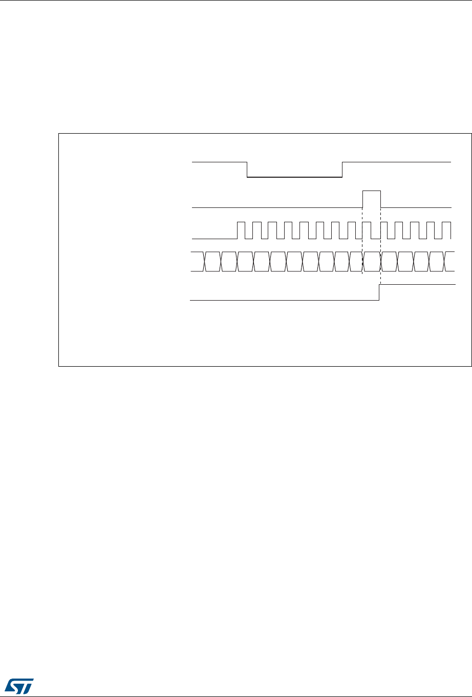
DocID025941 Rev 5 537/1001
RM0376 General-purpose timers (TIM21/22)
558
The counter starts counting on the internal clock, then behaves normally until TI1 rising
edge. When TI1 rises, the counter is cleared and restarts from 0. In the meantime, the
trigger flag is set (TIF bit in the TIMx_SR register) and an interrupt request can be sent if
enabled (depending on the TIE bit in TIMx_DIER register).
The following figure shows this behavior when the auto-reload register TIMx_ARR=0x36.
The delay between the rising edge on TI1 and the actual reset of the counter is due to the
resynchronization circuit on TI1 input.
Figure 170. Control circuit in reset mode
Slave mode: Gated mode
The counter can be enabled depending on the level of a selected input.
In the following example, the upcounter counts only when TI1 input is low:
1. Configure the channel 1 to detect low levels on TI1. Configure the input filter duration
(in this example, we don’t need any filter, so we keep IC1F=’0000’). The capture
prescaler is not used for triggering, so you don’t need to configure it. The CC1S bits
select the input capture source only, CC1S=’01’ in TIMx_CCMR1 register. Program
CC1P=’1’ and CC1NP= ‘0’ in TIMx_CCER register to validate the polarity (and detect
low level only).
2. Configure the timer in gated mode by writing SMS=’101’ in TIMx_SMCR register.
Select TI1 as the input source by writing TS=’101’ in TIMx_SMCR register.
3. Enable the counter by writing CEN=’1’ in the TIMx_CR1 register (in gated mode, the
counter doesn’t start if CEN=’0’, whatever is the trigger input level).
For code example, refer to A.11.13: Gated mode code example.
The counter starts counting on the internal clock as long as TI1 is low and stops as soon as
TI1 becomes high. The TIF flag in the TIMx_SR register is set both when the counter starts
or stops.
The delay between the rising edge on TI1 and the actual stop of the counter is due to the
resynchronization circuit on TI1 input.
MS31401V2
00
Counter clock = ck_cnt = ck_psc
Counter register 01 02 03 00 01 02 0332 33 34 35 36
UG
TI1
3130
TIF
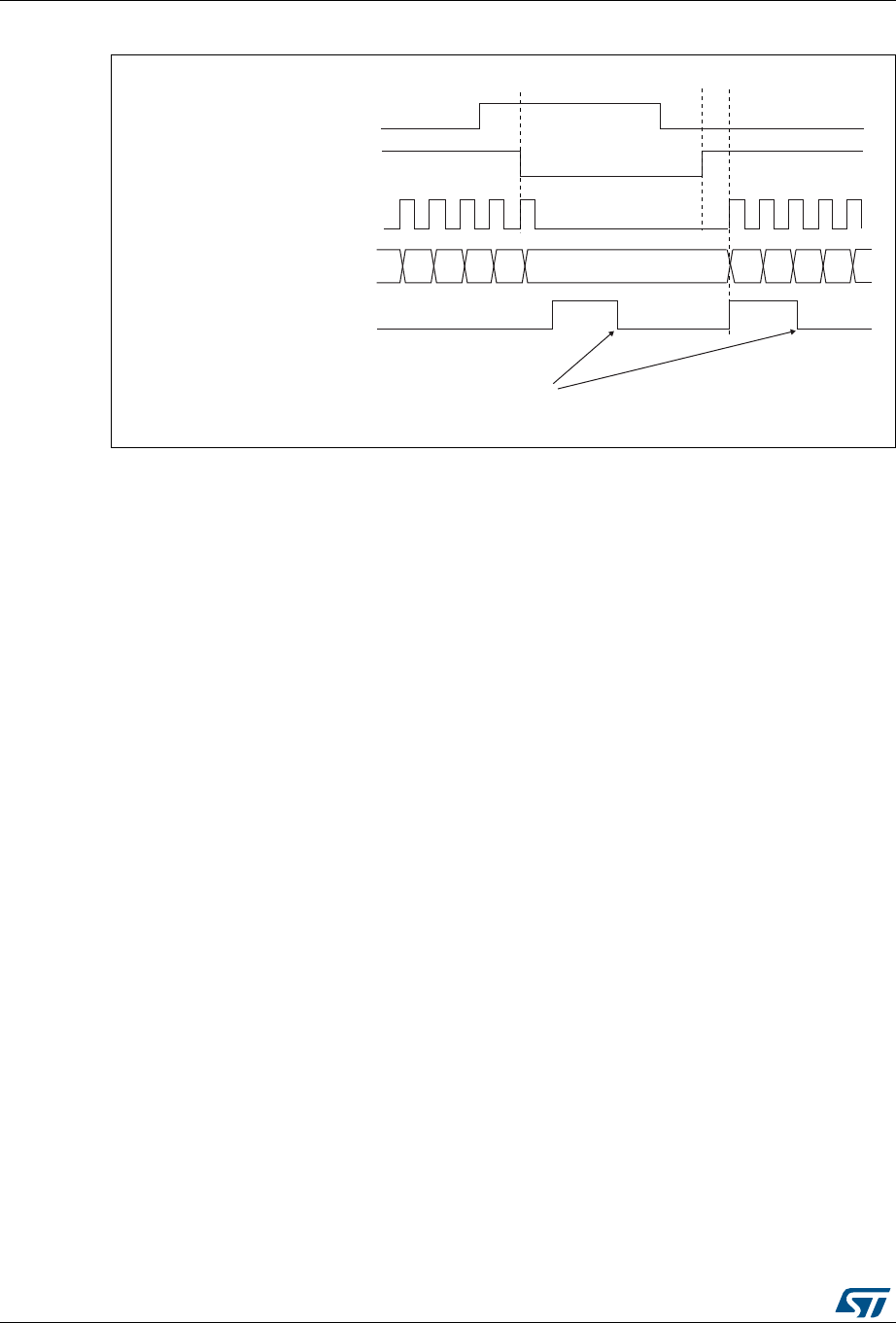
General-purpose timers (TIM21/22) RM0376
538/1001 DocID025941 Rev 5
Figure 171. Control circuit in gated mode
Slave mode: Trigger mode
The counter can start in response to an event on a selected input.
In the following example, the upcounter starts in response to a rising edge on TI2 input:
1. Configure the external trigger input circuit by programming the TIMx_SMCR register as
follows:
– ETF = 0000: no filter
– ETPS = 00: prescaler disabled
– ETP = 0: detection of rising edges on ETR and ECE=1 to enable the external clock
mode 2.
1. Configure the channel 2 to detect rising edges on TI2. Configure the input filter duration
(in this example, we don’t need any filter, so we keep IC2F=’0000’). The capture
prescaler is not used for triggering, so you don’t need to configure it. The CC2S bits are
configured to select the input capture source only, CC2S=’01’ in TIMx_CCMR1 register.
Program CC2P=’1’ and CC2NP=’0’ in TIMx_CCER register to validate the polarity (and
detect low level only).
2. Configure the timer in trigger mode by writing SMS=’110’ in TIMx_SMCR register.
Select TI2 as the input source by writing TS=’110’ in TIMx_SMCR register.
For code example, refer to A.11.14: Trigger mode code example.
When a rising edge occurs on TI2, the counter starts counting on the internal clock and the
TIF flag is set.
The delay between the rising edge on TI2 and the actual start of the counter is due to the
resynchronization circuit on TI2 input.
MS31402V1
TI1
cnt_en
Write TIF=0
37
Counter clock = ck_cnt = ck_psc
Counter register 38
32 33 34 35 36
3130
TIF

DocID025941 Rev 5 539/1001
RM0376 General-purpose timers (TIM21/22)
558
Figure 172. Control circuit in trigger mode
21.3.14 Timer synchronization (TIM21/22)
The timers are linked together internally for timer synchronization or chaining. Refer to
Section 20.3.15: Timer synchronization on page 473 for details.
21.3.15 Debug mode
When the microcontroller enters debug mode (Cortex®-M0+ core halted), the TIMx counter
either continues to work normally or stops, depending on DBG_TIMx_STOP configuration
bit in DBG module. For more details, refer to Section 32.9.2: Debug support for timers,
watchdog and I2C.
MS31403V1
TI2
cnt_en
37
Counter clock = ck_cnt = ck_psc
Counter register 38
34 35 36
TIF

General-purpose timers (TIM21/22) RM0376
540/1001 DocID025941 Rev 5
21.4 TIM21/22 registers
Refer to Section 1.1 on page 51 for a list of abbreviations used in register descriptions.
The peripheral registers have to be written by half-words (16 bits) or words (32 bits). Read
accesses can be done by bytes (8 bits), half-words (16 bits) or words (32 bits).
21.4.1 TIM21/22 control register 1 (TIMx_CR1)
Address offset: 0x00
Reset value: 0x0000
1514131211109876543210
Res. Res. Res. Res. Res. Res. CKD[1:0] ARPE CMS[1:0] DIR OPM URS UDIS CEN
rw rw rw rw rw rw rw rw rw rw
Bits 15:10 Reserved, must be kept at reset value.
Bits 9:8 CKD: Clock division
This bit-field indicates the division ratio between the timer clock (CK_INT) frequency and
sampling clock used by the digital filters (TIx),
00: tDTS = tCK_INT
01: tDTS = 2 × tCK_INT
10: tDTS = 4 × tCK_INT
11: Reserved
Bit 7 ARPE: Auto-reload preload enable
0: TIMx_ARR register is not buffered.
1: TIMx_ARR register is buffered.
Bits 6:5 CMS[1:0]: Center-aligned mode selection
00: Edge-aligned mode. The counter counts up or down depending on the direction bit
(DIR).
01: Center-aligned mode 1. The counter counts up and down alternatively. Output compare
interrupt flags of channels configured in output (CCxS=00 in TIMx_CCMRx register) are set
only when the counter is counting down.
10: Center-aligned mode 2. The counter counts up and down alternatively. Output compare
interrupt flags of channels configured in output (CCxS=00 in TIMx_CCMRx register) are set
only when the counter is counting up.
11: Center-aligned mode 3. The counter counts up and down alternatively. Output compare
interrupt flags of channels configured in output (CCxS=00 in TIMx_CCMRx register) are set
both when the counter is counting up or down.
Note: It is not allowed to switch from edge-aligned mode to center-aligned mode as long as
the counter is enabled (CEN=1).
Bit 4 DIR: Direction
0: Counter used as upcounter
1: Counter used as downcounter
Bit 3 OPM: One-pulse mode
0: Counter is not stopped on the update event
1: Counter stops counting on the next update event (clearing the CEN bit).

DocID025941 Rev 5 541/1001
RM0376 General-purpose timers (TIM21/22)
558
Bit 2 URS: Update request source
This bit is set and cleared by software to select the UEV event sources.
0: Any of the following events generates an update interrupt if enabled:
– Counter overflow
– Setting the UG bit
1: Only counter overflow generates an update interrupt if enabled.
Bit 1 UDIS: Update disable
This bit is set and cleared by software to enable/disable update event (UEV) generation.
0: UEV enabled. An UEV is generated by one of the following events:
– Counter overflow
– Setting the UG bit
Buffered registers are then loaded with their preload values.
1: UEV disabled. No UEV is generated, shadow registers keep their value (ARR, PSC,
CCRx). The counter and the prescaler are reinitialized if the UG bit is set.
Bit 0 CEN: Counter enable
0: Counter disabled
1: Counter enabled
CEN is cleared automatically in one-pulse mode, when an update event occurs.

General-purpose timers (TIM21/22) RM0376
542/1001 DocID025941 Rev 5
21.4.2 TIM21/22 control register 2 (TIMx_CR2)
Address offset: 0x04
Reset value: 0x0000
1514131211109876543210
Res. Res. Res. Res. Res. Res. Res. Res. Res. MMS[2:0] Res. Res. Res. Res.
rw rw rw
Bits 15:7 Reserved, must be kept at reset value.
Bits 6:4 MMS: Master mode selection
These bits allow to select the information to be sent in master mode to slave timers for
synchronization (TRGO). The combination is as follows:
000: Reset - the UG bit from the TIMx_EGR register is used as trigger output (TRGO). If the
reset is generated by the trigger input (slave mode controller configured in reset mode) then
the signal on TRGO is delayed compared to the actual reset.
001: Enable - the Counter enable signal, CNT_EN, is used as trigger output (TRGO). It is
useful to start several timers at the same time or to control a window in which a slave timer is
enabled. The Counter Enable signal is generated by a logic OR between CEN control bit
and the trigger input when configured in gated mode.
When the Counter Enable signal is controlled by the trigger input, there is a delay on TRGO,
except if the master/slave mode is selected (see the MSM bit description in TIMx_SMCR
register).
010: Update - The update event is selected as trigger output (TRGO). For instance a master
timer can then be used as a prescaler for a slave timer.
011: Compare Pulse - The trigger output send a positive pulse when the CC1IF flag is to be
set (even if it was already high), as soon as a capture or a compare match occurred.
(TRGO)
100: Compare - OC1REF signal is used as trigger output (TRGO)
101: Compare - OC2REF signal is used as trigger output (TRGO)
110: Reserved
111: Reserved
Bits 3:0 Reserved, must be kept at reset value.

DocID025941 Rev 5 543/1001
RM0376 General-purpose timers (TIM21/22)
558
21.4.3 TIM21/22 slave mode control register (TIMx_SMCR)
Address offset: 0x08
Reset value: 0x0000
1514131211109876543210
ETP ECE ETPS[1:0] ETF[3:0] MSM TS[2:0] Res. SMS[2:0]
rw rw rw rw rw rw rw rw rw rw rw rw rw rw rw
Bit 15 ETP: External trigger polarity
This bit selects whether ETR or ETR is used for trigger operations
0: ETR is non-inverted, active at high level or rising edge.
1: ETR is inverted, active at low level or falling edge.
Bit 14 ECE: External clock enable
This bit enables External clock mode 2.
0: External clock mode 2 disabled
1: External clock mode 2 enabled. The counter is clocked by any active edge on the ETRF
signal.
Note: Setting the ECE bit has the same effect as selecting external clock mode 1 with TRGI
connected to ETRF (SMS=111 and TS=111).
It is possible to simultaneously use external clock mode 2 with the following slave
modes: reset mode, gated mode and trigger mode. Nevertheless, TRGI must not be
connected to ETRF in this case (TS bits must not be 111).
If external clock mode 1 and external clock mode 2 are enabled at the same time, the
external clock input is ETRF.
Bits 13:12 ETPS[1:0]: External trigger prescaler
External trigger signal ETRP frequency must be at most 1/4 of TIMxCLK frequency. A
prescaler can be enabled to reduce ETRP frequency. It is useful when inputting fast external
clocks.
00: Prescaler OFF
01: ETRP frequency divided by 2
10: ETRP frequency divided by 4
11: ETRP frequency divided by 8

General-purpose timers (TIM21/22) RM0376
544/1001 DocID025941 Rev 5
Bits 11:8 ETF[3:0]: External trigger filter
This bit-field then defines the frequency used to sample ETRP signal and the length of the
digital filter applied to ETRP. The digital filter is made of an event counter in which N
consecutive events are needed to validate a transition on the output:
0000: No filter, sampling is done at fDTS
0001: fSAMPLING=fCK_INT, N=2
0010: fSAMPLING=fCK_INT, N=4
0011: fSAMPLING=fCK_INT, N=8
0100: fSAMPLING=fDTS/2, N=6
0101: fSAMPLING=fDTS/2, N=8
0110: fSAMPLING=fDTS/4, N=6
0111: fSAMPLING=fDTS/4, N=8
1000: fSAMPLING=fDTS/8, N=6
1001: fSAMPLING=fDTS/8, N=8
1010: fSAMPLING=fDTS/16, N=5
1011: fSAMPLING=fDTS/16, N=6
1100: fSAMPLING=fDTS/16, N=8
1101: fSAMPLING=fDTS/32, N=5
1110: fSAMPLING=fDTS/32, N=6
1111: fSAMPLING=fDTS/32, N=8
Bit 7 MSM: Master/Slave mode
0: No action
1: The effect of an event on the trigger input (TRGI) is delayed to allow a perfect
synchronization between the current timer and its slaves (through TRGO). It is useful in
order to synchronize several timers on a single external event.

DocID025941 Rev 5 545/1001
RM0376 General-purpose timers (TIM21/22)
558
Bits 6:4 TS: Trigger selection
This bitfield selects the trigger input to be used to synchronize the counter.
000: Internal Trigger 0 (ITR0)
001: Internal Trigger 1 (ITR1)
010: Reserved
011: Reserved
100: TI1 Edge Detector (TI1F_ED)
101: Filtered Timer Input 1 (TI1FP1)
110: Filtered Timer Input 2 (TI2FP2)
111: Reserved.
See Table 93: TIMx Internal trigger connection on page 545 for more details on the meaning
of ITRx for each timer.
Note: These bits must be changed only when they are not used (e.g. when SMS=’000’) to
avoid wrong edge detections at the transition.
Bit 3 Reserved, must be kept at reset value.
Bits 2:0 SMS: Slave mode selection
When external signals are selected, the active edge of the trigger signal (TRGI) is linked to
the polarity selected on the external input (see Input control register and Control register
descriptions.
000: Slave mode disabled - if CEN = 1 then the prescaler is clocked directly by the internal
clock
001: Encoder mode 1
010: Encoder mode 2
011: Encoder mode 3
100: Reset mode - Rising edge of the selected trigger input (TRGI) reinitializes the counter
and generates an update of the registers
101: Gated mode - The counter clock is enabled when the trigger input (TRGI) is high. The
counter stops (but is not reset) as soon as the trigger becomes low. Counter starts and stops
are both controlled
110: Trigger mode - The counter starts on a rising edge of the trigger TRGI (but it is not
reset). Only the start of the counter is controlled
111: External Clock Mode 1
Note: The Gated mode must not be used if TI1F_ED is selected as the trigger input
(TS=’100’). Indeed, TI1F_ED outputs 1 pulse for each transition on TI1F, whereas the
Gated mode checks the level of the trigger signal.
Table 93. TIMx Internal trigger connection(1)
1. When a timer is not present in the product, the corresponding trigger ITRx is not available.
Slave TIM ITR0 (TS = 000) ITR1 (TS = 001)
TIM21 TIM2 TIM22
TIM22 TIM21 TIM2

General-purpose timers (TIM21/22) RM0376
546/1001 DocID025941 Rev 5
21.4.4 TIM21/22 Interrupt enable register (TIMx_DIER)
Address offset: 0x0C
Reset value: 0x0000
21.4.5 TIM21/22 status register (TIMx_SR)
Address offset: 0x10
Reset value: 0x0000
1514131211109876543210
Res. Res. Res. Res. Res. Res. Res. Res. Res. TIE Res. Res. Res. CC2IE CC1IE UIE
rw rw rw rw
Bits 15:7 Reserved, must be kept at reset value.
Bit 6 TIE: Trigger interrupt enable
0: Trigger interrupt disabled.
1: Trigger interrupt enabled.
Bits 5:3 Reserved, must be kept at reset value.
Bit 2 CC2IE: Capture/Compare 2 interrupt enable
0: CC2 interrupt disabled.
1: CC2 interrupt enabled.
Bit 1 CC1IE: Capture/Compare 1 interrupt enable
0: CC1 interrupt disabled.
1: CC1 interrupt enabled.
Bit 0 UIE: Update interrupt enable
0: Update interrupt disabled.
1: Update interrupt enabled.
1514131211109876543210
Res. Res. Res. Res. Res. CC2OF CC1OF Res. Res. TIF Res. Res. Res. CC2IF CC1IF UIF
rc_w0 rc_w0 rc_w0 rc_w0 rc_w0 rc_w0
Bits 15:11 Reserved, must be kept at reset value.
Bit 10 CC2OF: Capture/compare 2 overcapture flag
refer to CC1OF description
Bit 9 CC1OF: Capture/Compare 1 overcapture flag
This flag is set by hardware only when the corresponding channel is configured in input
capture mode. It is cleared by software by writing it to ‘0’.
0: No overcapture has been detected.
1: The counter value has been captured in TIMx_CCR1 register while CC1IF flag was
already set
Bits 8:7 Reserved, must be kept at reset value.

DocID025941 Rev 5 547/1001
RM0376 General-purpose timers (TIM21/22)
558
Bit 6 TIF: Trigger interrupt flag
This flag is set by hardware on trigger event (active edge detected on TRGI input when the
slave mode controller is enabled in all modes but gated mode. It is set when the counter
starts or stops when gated mode is selected. It is cleared by software.
0: No trigger event occurred.
1: Trigger interrupt pending.
Bits 5:3 Reserved, must be kept at reset value.
Bit 2 CC2IF: Capture/Compare 2 interrupt flag
refer to CC1IF description
Bit 1 CC1IF: Capture/compare 1 interrupt flag
If channel CC1 is configured as output:
This flag is set by hardware when the counter matches the compare value. It is cleared by
software.
0: No match.
1: The content of the counter TIMx_CNT matches the content of the TIMx_CCR1 register.
When the contents of TIMx_CCR1 are greater than the contents of TIMx_ARR, the CC1IF
bit goes high on the counter overflow.
If channel CC1 is configured as input:
This bit is set by hardware on a capture. It is cleared by software or by reading the
TIMx_CCR1 register.
0: No input capture occurred.
1: The counter value has been captured in TIMx_CCR1 register (an edge has been detected
on IC1 which matches the selected polarity).
Bit 0 UIF: Update interrupt flag
This bit is set by hardware on an update event. It is cleared by software.
0: No update occurred.
1: Update interrupt pending. This bit is set by hardware when the registers are updated:
– At overflow and if UDIS=’0’ in the TIMx_CR1 register.
– When CNT is reinitialized by software using the UG bit in TIMx_EGR register, if URS=’0’ and
UDIS=’0’ in the TIMx_CR1 register.
– When CNT is reinitialized by a trigger event (refer to the synchro control register
description), if URS=’0’ and UDIS=’0’ in the TIMx_CR1 register.

General-purpose timers (TIM21/22) RM0376
548/1001 DocID025941 Rev 5
21.4.6 TIM21/22 event generation register (TIMx_EGR)
Address offset: 0x14
Reset value: 0x0000
1514131211109876543210
Res. Res. Res. Res. Res. Res. Res. Res. Res. TG Res. Res. Res. CC2G CC1G UG
w www
Bits 15:7 Reserved, must be kept at reset value.
Bit 6 TG: Trigger generation
This bit is set by software in order to generate an event, it is automatically cleared by
hardware.
0: No action
1: The TIF flag is set in the TIMx_SR register. Related interrupt can occur if enabled
Bits 5:3 Reserved, must be kept at reset value.
Bit 2 CC2G: Capture/compare 2 generation
refer to CC1G description
Bit 1 CC1G: Capture/compare 1 generation
This bit is set by software to generate an event, it is automatically cleared by hardware.
0: No action
1: A capture/compare event is generated on channel 1:
If channel CC1 is configured as output:
the CC1IF flag is set, the corresponding interrupt is sent if enabled.
If channel CC1 is configured as input:
The current counter value is captured in the TIMx_CCR1 register. The CC1IF flag is set, the
corresponding interrupt is sent if enabled. The CC1OF flag is set if the CC1IF flag was
already high.
Bit 0 UG: Update generation
This bit can be set by software, it is automatically cleared by hardware.
0: No action
1: Re-initializes the counter and generates an update of the registers. The prescaler counter
is also cleared and the prescaler ratio is not affected. The counter is cleared.

DocID025941 Rev 5 549/1001
RM0376 General-purpose timers (TIM21/22)
558
21.4.7 TIM21/22 capture/compare mode register 1 (TIMx_CCMR1)
Address offset: 0x18
Reset value: 0x0000
The channels can be used in input (capture mode) or in output (compare mode). The
direction of a channel is defined by configuring the corresponding CCxS bits. All the other
bits in this register have different functions in input and output modes. For a given bit, OCxx
describes its function when the channel is configured in output mode, ICxx describes its
function when the channel is configured in input mode. So you must take care that the same
bit can have different meanings for the input stage and the output stage.
Output compare mode
1514131211109876543210
Res. OC2M[2:0] OC2PE OC2FE CC2S[1:0] Res. OC1M[2:0] OC1PE OC1FE CC1S[1:0]
IC2F[3:0] IC2PSC[1:0] IC1F[3:0] IC1PSC[1:0]
rw rw rw rw rw rw rw rw rw rw rw rw rw rw
Bit 15 Reserved, must be kept at reset value.
Bits 14:12 OC2M[2:0]: Output compare 2 mode
Bit 11 OC2PE: Output compare 2 preload enable
Bit 10 OC2FE: Output compare 2 fast enable
Bits 9:8 CC2S[1:0]: Capture/Compare 2 selection
This bitfield defines the direction of the channel (input/output) as well as the used input.
00: CC2 channel is configured as output
01: CC2 channel is configured as input, IC2 is mapped on TI2
10: CC2 channel is configured as input, IC2 is mapped on TI1
11: CC2 channel is configured as input, IC2 is mapped on TRC. This mode works only if an
internal trigger input is selected through the TS bit (TIMx_SMCR register
Note: The CC2S bits are writable only when the channel is OFF (CC2E = 0 in TIMx_CCER).
Bit 7 Reserved, must be kept at reset value.

General-purpose timers (TIM21/22) RM0376
550/1001 DocID025941 Rev 5
Bits 6:4 OC1M: Output compare 1 mode
These bits define the behavior of the output reference signal OC1REF from which OC1 and
OC1N are derived. OC1REF is active high whereas the active levels of OC1 and OC1N
depend on the CC1P and CC1NP bits, respectively.
000: Frozen - The comparison between the output compare register TIMx_CCR1 and the
counter TIMx_CNT has no effect on the outputs.(this mode is used to generate a timing
base).
001: Set channel 1 to active level on match. The OC1REF signal is forced high when the
TIMx_CNT counter matches the capture/compare register 1 (TIMx_CCR1).
010: Set channel 1 to inactive level on match. The OC1REF signal is forced low when the
TIMx_CNT counter matches the capture/compare register 1 (TIMx_CCR1).
011: Toggle - OC1REF toggles when TIMx_CNT=TIMx_CCR1
100: Force inactive level - OC1REF is forced low
101: Force active level - OC1REF is forced high
110: PWM mode 1 - In upcounting, channel 1 is active as long as TIMx_CNT<TIMx_CCR1
else it is inactive. In downcounting, channel 1 is inactive (OC1REF=‘0) as long as
TIMx_CNT>TIMx_CCR1, else it is active (OC1REF=’1’)
111: PWM mode 2 - In upcounting, channel 1 is inactive as long as TIMx_CNT<TIMx_CCR1
else it is active. In downcounting, channel 1 is active as long as TIMx_CNT>TIMx_CCR1
else it is inactive.
Note: In PWM mode 1 or 2, the OCREF level changes only when the result of the
comparison changes or when the output compare mode switches from “frozen” mode
to “PWM” mode.
Bit 3 OC1PE: Output compare 1 preload enable
0: Preload register on TIMx_CCR1 disabled. TIMx_CCR1 can be written at anytime, the
new value is taken into account immediately
1: Preload register on TIMx_CCR1 enabled. Read/Write operations access the preload
register. TIMx_CCR1 preload value is loaded into the active register at each update event
Note: The PWM mode can be used without validating the preload register only in one-pulse
mode (OPM bit set in the TIMx_CR1 register). Else the behavior is not guaranteed.
Bit 2 OC1FE: Output compare 1 fast enable
This bit is used to accelerate the effect of an event on the trigger in input on the CC output.
0: CC1 behaves normally depending on the counter and CCR1 values even when the
trigger is ON. The minimum delay to activate the CC1 output when an edge occurs on the
trigger input is 5 clock cycles
1: An active edge on the trigger input acts like a compare match on the CC1 output. Then,
OC is set to the compare level independently of the result of the comparison. Delay to
sample the trigger input and to activate CC1 output is reduced to 3 clock cycles. OC1FE
acts only if the channel is configured in PWM1 or PWM2 mode.
Bits 1:0 CC1S: Capture/Compare 1 selection
This bitfield defines the direction of the channel (input/output) as well as the used input.
00: CC1 channel is configured as output
01: CC1 channel is configured as input, IC1 is mapped on TI1
10: CC1 channel is configured as input, IC1 is mapped on TI2
11: CC1 channel is configured as input, IC1 is mapped on TRC. This mode works only if an
internal trigger input is selected through the TS bit (TIMx_SMCR register)
Note: The CC1S bits are writable only when the channel is OFF (CC1E = 0 in TIMx_CCER).

DocID025941 Rev 5 551/1001
RM0376 General-purpose timers (TIM21/22)
558
Input capture mode
Bits 15:12 IC2F: Input capture 2 filter
Bits 11:10 IC2PSC[1:0]: Input capture 2 prescaler
Bits 9:8 CC2S: Capture/compare 2 selection
This bitfield defines the direction of the channel (input/output) as well as the used input.
00: CC2 channel is configured as output
01: CC2 channel is configured as input, IC2 is mapped on TI2
10: CC2 channel is configured as input, IC2 is mapped on TI1
11: CC2 channel is configured as input, IC2 is mapped on TRC. This mode works only if an
internal trigger input is selected through the TS bit (TIMx_SMCR register)
Note: The CC2S bits are writable only when the channel is OFF (CC2E = 0 in TIMx_CCER).
Bits 7:4 IC1F: Input capture 1 filter
This bitfield defines the frequency used to sample the TI1 input and the length of the digital
filter applied to TI1. The digital filter is made of an event counter in which N consecutive
events are needed to validate a transition on the output:
0000: No filter, sampling is done at fDTS 1000: fSAMPLING=fDTS/8, N=6
0001: fSAMPLING=fCK_INT, N=2 1001: fSAMPLING=fDTS/8, N=8
0010: fSAMPLING=fCK_INT, N=4 1010: fSAMPLING=fDTS/16, N=5
0011: fSAMPLING=fCK_INT, N=8 1011: fSAMPLING=fDTS/16, N=6
0100: fSAMPLING=fDTS/2, N=6 1100: fSAMPLING=fDTS/16, N=8
0101: fSAMPLING=fDTS/2, N=8 1101: fSAMPLING=fDTS/32, N=5
0110: fSAMPLING=fDTS/4, N=6 1110: fSAMPLING=fDTS/32, N=6
0111: fSAMPLING=fDTS/4, N=8 1111: fSAMPLING=fDTS/32, N=8
Bits 3:2 IC1PSC: Input capture 1 prescaler
This bitfield defines the ratio of the prescaler acting on the CC1 input (IC1).
The prescaler is reset as soon as CC1E=’0’ (TIMx_CCER register).
00: no prescaler, capture is done each time an edge is detected on the capture input
01: capture is done once every 2 events
10: capture is done once every 4 events
11: capture is done once every 8 events
Bits 1:0 CC1S: Capture/Compare 1 selection
This bitfield defines the direction of the channel (input/output) as well as the used input.
00: CC1 channel is configured as output
01: CC1 channel is configured as input, IC1 is mapped on TI1
10: CC1 channel is configured as input, IC1 is mapped on TI2
11: CC1 channel is configured as input, IC1 is mapped on TRC. This mode is working only if
an internal trigger input is selected through TS bit (TIMx_SMCR register)
Note: The CC1S bits are writable only when the channel is OFF (CC1E = 0 in TIMx_CCER).

General-purpose timers (TIM21/22) RM0376
552/1001 DocID025941 Rev 5
21.4.8 TIM21/22 capture/compare enable register (TIMx_CCER)
Address offset: 0x20
Reset value: 0x0000
1514131211109876543210
Res. Res. Res. Res. Res. Res. Res. Res. CC2NP Res. CC2P CC2E CC1NP Res. CC1P CC1E
rw rw rw rw rw rw
Bits 15:8 Reserved, must be kept at reset value.
Bit 7 CC2NP: Capture/Compare 2 output Polarity
refer to CC1NP description
Bit 6 Reserved, must be kept at reset value.
Bit 5 CC2P: Capture/Compare 2 output Polarity
refer to CC1P description
Bit 4 CC2E: Capture/Compare 2 output enable
refer to CC1E description
Bit 3 CC1NP: Capture/Compare 1 complementary output Polarity
CC1 channel configured as output: CC1NP must be kept cleared
CC1 channel configured as input: CC1NP is used in conjunction with CC1P to define
TI1FP1/TI2FP1 polarity (refer to CC1P description).
Bit 2 Reserved, must be kept at reset value.
Bit 1 CC1P: Capture/Compare 1 output Polarity.
CC1 channel configured as output:
0: OC1 active high.
1: OC1 active low.
CC1 channel configured as input:
CC1NP/CC1P bits select TI1FP1 and TI2FP1 polarity for trigger or capture operations.
00: noninverted/rising edge
Circuit is sensitive to TIxFP1 rising edge (capture, trigger in reset, external clock or trigger
mode), TIxFP1 is not inverted (trigger in gated mode, encoder mode).
01: inverted/falling edge
Circuit is sensitive to TIxFP1 falling edge (capture, trigger in reset, external clock or trigger
mode), TIxFP1 is inverted (trigger in gated mode, encoder mode).
10: reserved, do not use this configuration.
Note: 11: noninverted/both edges
Circuit is sensitive to both TIxFP1 rising and falling edges (capture, trigger in reset,
external clock or trigger mode), TIxFP1 is not inverted (trigger in gated mode). This
configuration must not be used for encoder mode.
Bit 0 CC1E: Capture/Compare 1 output enable.
CC1 channel configured as output:
0: Off - OC1 is not active.
1: On - OC1 signal is output on the corresponding output pin.
CC1 channel configured as input:
This bit determines if a capture of the counter value can actually be done into the input
capture/compare register 1 (TIMx_CCR1) or not.
0: Capture disabled.
1: Capture enabled.
DocID025941 Rev 5 553/1001
RM0376 General-purpose timers (TIM21/22)
558
Note: The states of the external I/O pins connected to the standard OCx channels depend on the
state of the OCx channel and on the GPIO registers.
21.4.9 TIM21/22 counter (TIMx_CNT)
Address offset: 0x24
Reset value: 0x0000
21.4.10 TIM21/22 prescaler (TIMx_PSC)
Address offset: 0x28
Reset value: 0x0000
21.4.11 TIM21/22 auto-reload register (TIMx_ARR)
Address offset: 0x2C
Reset value: 0xFFFF
Table 94. Output control bit for standard OCx channels
CCxE bit OCx output state
0 Output disabled (OCx=’0’, OCx_EN=’0’)
1 OCx=OCxREF + Polarity, OCx_EN=’1’
1514131211109876543210
CNT[15:0]
rw rw rw rw rw rw rw rw rw rw rw rw rw rw rw rw
Bits 15:0 CNT[15:0]: Counter value
1514131211109876543210
PSC[15:0]
rw rw rw rw rw rw rw rw rw rw rw rw rw rw rw rw
Bits 15:0 PSC[15:0]: Prescaler value
The counter clock frequency (CK_CNT) is equal to fCK_PSC / (PSC[15:0] + 1).
PSC contains the value to be loaded in the active prescaler register at each update event
(including when the counter is cleared through UG bit of TIMx_EGR register or through
trigger controller when configured in “reset mode”).
1514131211109876543210
ARR[15:0]
rw rw rw rw rw rw rw rw rw rw rw rw rw rw rw rw
Bits 15:0 ARR[15:0]: Auto-reload value
ARR is the value to be loaded into the actual auto-reload register.
Refer to the Section 21.3.1: Timebase unit on page 506 for more details about ARR update
and behavior.
The counter is blocked while the auto-reload value is null.

General-purpose timers (TIM21/22) RM0376
554/1001 DocID025941 Rev 5
21.4.12 TIM21/22 capture/compare register 1 (TIMx_CCR1)
Address offset: 0x34
Reset value: 0x0000
21.4.13 TIM21/22 capture/compare register 2 (TIMx_CCR2)
Address offset: 0x38
Reset value: 0x0000
1514131211109876543210
CCR1[15:0]
rw/r rw/r rw/r rw/r rw/r rw/r rw/r rw/r rw/r rw/r rw/r rw/r rw/r rw/r rw/r rw/r
Bits 15:0 CCR1[15:0]: Capture/Compare 1 value
If channel CC1 is configured as output:
CCR1 is the value to be loaded into the actual capture/compare 1 register (preload value).
It is loaded permanently if the preload feature is not selected in the TIMx_CCMR1 register
(OC1PE bit). Else the preload value is copied into the active capture/compare 1 register
when an update event occurs.
The active capture/compare register contains the value to be compared to the TIMx_CNT
counter and signaled on the OC1 output.
If channel CC1is configured as input:
CCR1 is the counter value transferred by the last input capture 1 event (IC1). The
TIMx_CCR1 register is read-only and cannot be programmed.
1514131211109876543210
CCR2[15:0]
rw/r rw/r rw/r rw/r rw/r rw/r rw/r rw/r rw/r rw/r rw/r rw/r rw/r rw/r rw/r rw/r
Bits 15:0 CCR2[15:0]: Capture/Compare 2 value
If channel CC2 is configured as output:
CCR2 is the value to be loaded into the actual capture/compare 2 register (preload value).
It is loaded permanently if the preload feature is not selected in the TIMx_CCMR2 register
(OC2PE bit). Else the preload value is copied into the active capture/compare 2 register
when an update event occurs.
The active capture/compare register contains the value to be compared to the TIMx_CNT
counter and signalled on the OC2 output.
If channel CC2 is configured as input:
CCR2 is the counter value transferred by the last input capture 2 event (IC2). The
TIMx_CCR2 register is read-only and cannot be programmed.

DocID025941 Rev 5 555/1001
RM0376 General-purpose timers (TIM21/22)
558
21.4.14 TIM21 option register (TIM21_OR)
Address offset: 0x50
Reset value: 0x0000
15 14 13 12 11 10 9 8 7 6 5 4 3 2 1 0
Res. Res. Res. Res. Res. Res. Res. Res. Res. Res. TI2_RMP TI1_RMP ETR_RMP
rw rw rw rw rw rw
Bits 15:6 Reserved, must be kept at reset value.
Bit 5 TI2_RMP: Timer21 TI2 (connected to TIM21_CH1) remap
This bit is set and cleared by software.
0: TIM21 TI2 input connected to GPIO. Refer to the Alternate function mapping table in the
device datasheet.
1: TIM21 TI2 input connected to COMP2_OUT
Bits 4:2 TI1_RMP: Timer21 TI1 (connected to TIM21_CH1) remap
This bit is set and cleared by software.
000: TIM21 TI1 input connected to GPIO. Refer to the Alternate function mapping table in the
device datasheet.
001:TIM21 TI1 input connected to RTC WAKEUP interrupt
010: TIM21 TI1 input connected to HSE_RTC clock
011: TIM21 TI1 input connected to MSI clock
100: TIM21 TI1 input connected to LSE clock
101: TIM21 TI1 input connected to LSI clock
110: TIM21 TI1 input connected to COMP1_OUT
111: TIM21 TI1 input connected to MCO clock
Bits 1:0 ETR_RMP: Timer21 ETR remap
This bit is set and cleared by software.
00: TIM21 ETR input connected to GPIO. Refer to the Alternate function mapping table in the
device datasheet.
01: TIM21 ETR input connected to COMP2_OUT
10: TIM21 ETR input connected to COMP1_OUT
11: TIM21 ETR input connected to LSE clock

General-purpose timers (TIM21/22) RM0376
556/1001 DocID025941 Rev 5
21.4.15 TIM22 option register (TIM22_OR)
Address offset: 0x50
Reset value: 0x0000
1514131211109876543210
Res. Res. Res. Res. Res. Res. Res. Res. Res. Res. Res. Res. TI1_RMP ETR_RMP
rw rw rw rw
Bits 15:4 Reserved, must be kept at reset value.
Bits 3:2 TI1_RMP: Timer 22 TI1 (connected to TIM22_CH1) remap
This bit is set and cleared by software.
00: TIM22 TI1 input connected to GPIO. Refer to the Alternate function mapping table in the
device datasheet.
01:TIM22 TI1 input connected to COMP2_OUT
10: TIM22 TI1 input connected to COMP1_OUT
11: TIM22 TI1 input connected to GPIO. Refer to the Alternate function mapping table in the
device datasheet.
Bits 1:0 ETR_RMP: Timer 22 ETR remap
This bit is set and cleared by software.
00: TIM22 ETR input connected to GPIO. Refer to the Alternate function mapping table in the
device datasheet.
01: TIM22 ETR input connected to COMP2_OUT
10: TIM22 ETR input connected to COMP1_OUT
11: TIM22 ETR input connected to LSE clock
DocID025941 Rev 5 557/1001
RM0376 General-purpose timers (TIM21/22)
558
21.4.16 TIM21/22 register map
The table below shows TIM21/22 register map and reset values.
Table 95. TIM21/22 register map and reset values
Offset Register
15
14
13
12
11
10
9
8
7
6
5
4
3
2
1
0
0x00
TIMx_CR1
Res.
Res.
Res.
Res.
Res.
Res.
CKD
[1:0]
ARPE
CMS
[1:0]
DIR
OPM
URS
UDIS
CEN
Reset value 000 00000
0x04
TIMx_CR2
Res.
Res.
Res.
Res.
Res.
Res.
Res.
Res.
Res.
MMS[2:0]
Res.
Res.
Res.
Res.
Reset value 0 0 0
0x08
TIMx_SMCR
ETP
ECE
ETPS[1:0]
ETF[3:0]
MSM
TS[2:0]
Res.
SMS[2:0]
Reset value 000000000000 000
0x0C
TIMx_DIER
Res.
Res.
Res.
Res.
Res.
Res.
Res.
Res.
Res.
TIE
Res.
Res.
Res.
CC2IE
CC1IE
UIE
Reset value 0 0 0 0
0x10
TIMx_SR
Res.
Res.
Res.
Res.
Res.
CC2OF
CC1OF
Res.
Res.
TIF
Res.
Res.
Res.
CC2IF
CC1IF
UIF
Reset value 0 0 0 0 0 0
0x14
TIMx_EGR
Res.
Res.
Res.
Res.
Res.
Res.
Res.
Res.
Res.
TG
Res.
Res.
Res.
CC2G
CC1G
UG
Reset value 0 0 0 0
0x18
TIMx_CCMR1
Output Compare
mode
Res.
OC2M
[2:0]
OC2PE
OC2FE
CC2S
[1:0]
Res.
OC1M
[2:0]
OC1PE
OC1FE
CC1S
[1:0]
Reset value 0000000 0000000
TIMx_CCMR1
Input Capture mode IC2F[3:0] IC2PSC
[1:0]
CC2S
[1:0] IC1F[3:0] IC1PSC
[1:0]
CC1S
[1:0]
Reset value 0000000000000000
0x1C Res.
0x20
TIMx_CCER
Res.
Res.
Res.
Res.
Res.
Res.
Res.
Res.
CC2NP
Res.
CC2P
CC2E
CC1NP
Res.
CC1P
CC1E
Reset value 0 0 0 0 0 0
0x24
TIMx_CNT CNT[15:0]
Reset value 0000000000000000
General-purpose timers (TIM21/22) RM0376
558/1001 DocID025941 Rev 5
Refer to Section 2.2.2 on page 58 for the register boundary addresses.
0x28
TIMx_PSC PSC[15:0]
Reset value 0000000000000000
0x2C
TIMx_ARR ARR[15:0]
Reset value 1111111111111111
0x30 Res.
0x34
TIMx_CCR1 CCR1[15:0]
Reset value 0000000000000000
0x38
TIMx_CCR2 CCR2[15:0]
Reset value 0000000000000000
0x3C to
0x4C Res.
0x38
TIMx_CCR2 CCR2[15:0]
Reset value 0000000000000000
0x50
TIM21_OR
Res.
Res.
Res.
Res.
Res.
Res.
Res.
Res.
Res.
Res.
TI2_RMP
TI1_RMP
ETR_RMP
Reset value 0 0 0 0 0 0
0x50
TIM22_OR
Res.
Res.
Res.
Res.
Res.
Res.
Res.
Res.
Res.
Res.
Res.
Res.
TI1_RMP
ETR_RMP
Reset value 0 0 0 0
Table 95. TIM21/22 register map and reset values (continued)
Offset Register
15
14
13
12
11
10
9
8
7
6
5
4
3
2
1
0
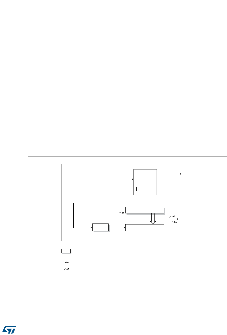
DocID025941 Rev 5 559/1001
RM0376 Basic timers (TIM6/7)
571
22 Basic timers (TIM6/7)
22.1 Introduction
The basic timers TIM6, TIM7 consist of a 16-bit auto-reload counter driven by a
programmable prescaler.
They can be used as generic timers for timebase generation but they are also specifically
used to drive the digital-to-analog converter (DAC). In fact, the timers are internally
connected to the DAC and are able to drive it through their trigger outputs.
The timers are completely independent, and do not share any resources.
22.2 TIM6/7 main features
Basic timer (TIM6/TIM7) features include:
•16-bit auto-reload upcounter
•16-bit programmable prescaler used to divide (also “on the fly”) the counter clock
frequency by any factor between 1 and 65536
•Synchronization circuit to trigger the DAC
•Interrupt/DMA generation on the update event: counter overflow
Figure 173. Basic timer block diagram
MS33142V1
Internal clock (CK_INT)
Auto-reload register
CNT counter
+
CK_PSC CK_CNT
Stop, clear or up
UI
U
U
Notes:
Reg Preload registers transferred
to active registers on U event
according to control bit
Event
Interrupt & DMA output
PSC
prescaler
Trigger
controller
Reset, enable, Count
TIMxCLK from RCC
TRGO to DAC
Control

Basic timers (TIM6/7) RM0376
560/1001 DocID025941 Rev 5
22.3 TIM6/7 functional description
22.3.1 Time-base unit
The main block of the programmable timer is a 16-bit upcounter with its related auto-reload
register. The counter clock can be divided by a prescaler.
The counter, the auto-reload register and the prescaler register can be written or read by
software. This is true even when the counter is running.
The time-base unit includes:
•Counter Register (TIMx_CNT)
•Prescaler Register (TIMx_PSC)
•Auto-Reload Register (TIMx_ARR)
The auto-reload register is preloaded. The preload register is accessed each time an
attempt is made to write or read the auto-reload register. The contents of the preload
register are transferred into the shadow register permanently or at each update event UEV,
depending on the auto-reload preload enable bit (ARPE) in the TIMx_CR1 register. The
update event is sent when the counter reaches the overflow value and if the UDIS bit equals
0 in the TIMx_CR1 register. It can also be generated by software. The generation of the
update event is described in detail for each configuration.
The counter is clocked by the prescaler output CK_CNT, which is enabled only when the
counter enable bit (CEN) in the TIMx_CR1 register is set.
Note that the actual counter enable signal CNT_EN is set 1 clock cycle after CEN.
Prescaler description
The prescaler can divide the counter clock frequency by any factor between 1 and 65536. It
is based on a 16-bit counter controlled through a 16-bit register (in the TIMx_PSC register).
It can be changed on the fly as the TIMx_PSC control register is buffered. The new
prescaler ratio is taken into account at the next update event.
Figure 174 and Figure 175 give some examples of the counter behavior when the prescaler
ratio is changed on the fly.
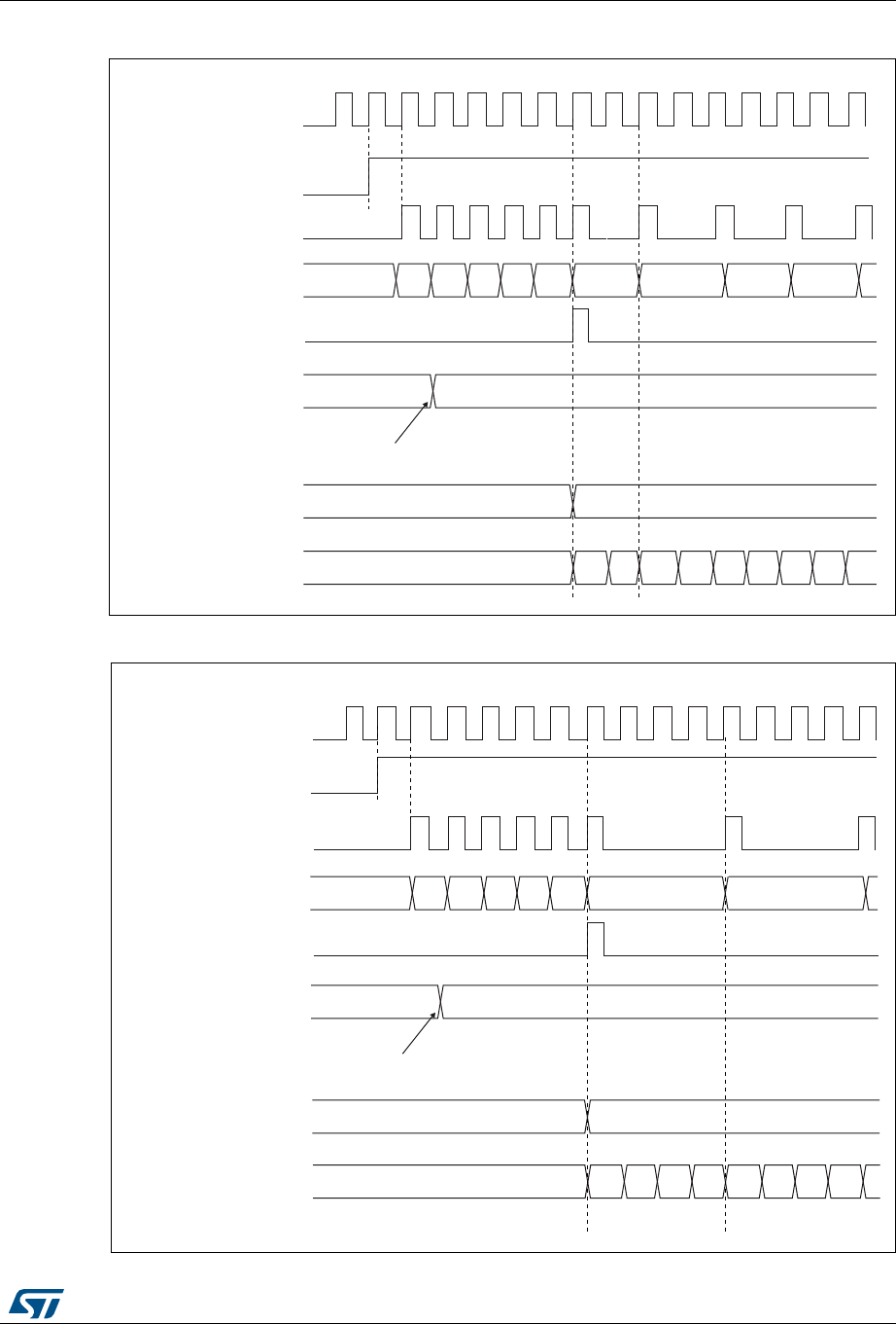
DocID025941 Rev 5 561/1001
RM0376 Basic timers (TIM6/7)
571
Figure 174. Counter timing diagram with prescaler division change from 1 to 2
Figure 175. Counter timing diagram with prescaler division change from 1 to 4
CK_PSC
00
CEN
Timerclock = CK_CNT
Counter register
Update event (UEV)
0
Prescaler control register 1
0
Write a new value in TIMx_PSC
Prescaler buffer 1
0
Prescaler counter 010 10101
01 02 03
FA FBF7 F8 F9 FC
MS31076V2
0
3
0
01230123
MS31077V2
CK_PSC
CEN
Timerclock = CK_CNT
Counter register
Update event (UEV)
Prescaler control register
Write a new value in TIMx_PSC
Prescaler buffer
Prescaler counter
00 01
FA FB
F7 F8 F9 FC
30

Basic timers (TIM6/7) RM0376
562/1001 DocID025941 Rev 5
22.3.2 Counting mode
The counter counts from 0 to the auto-reload value (contents of the TIMx_ARR register),
then restarts from 0 and generates a counter overflow event.
An update event can be generate at each counter overflow or by setting the UG bit in the
TIMx_EGR register (by software or by using the slave mode controller).
The UEV event can be disabled by software by setting the UDIS bit in the TIMx_CR1
register. This avoids updating the shadow registers while writing new values into the preload
registers. In this way, no update event occurs until the UDIS bit has been written to 0,
however, the counter and the prescaler counter both restart from 0 (but the prescale rate
does not change). In addition, if the URS (update request selection) bit in the TIMx_CR1
register is set, setting the UG bit generates an update event UEV, but the UIF flag is not set
(so no interrupt or DMA request is sent).
When an update event occurs, all the registers are updated and the update flag (UIF bit in
the TIMx_SR register) is set (depending on the URS bit):
•The buffer of the prescaler is reloaded with the preload value (contents of the
TIMx_PSC register)
•The auto-reload shadow register is updated with the preload value (TIMx_ARR)
The following figures show some examples of the counter behavior for different clock
frequencies when TIMx_ARR = 0x36.
Figure 176. Counter timing diagram, internal clock divided by 1
00 02 03 04 05 06 0732 33 34 35 36
31
MS31078V2
CK_PSC
CNT_EN
Timerclock = CK_CNT
Counter register
Update event (UEV)
Counter overflow
Update interrupt flag
(UIF)
01
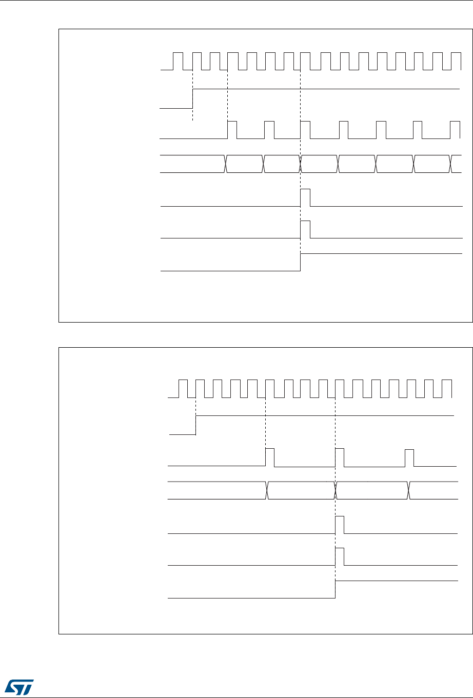
DocID025941 Rev 5 563/1001
RM0376 Basic timers (TIM6/7)
571
Figure 177. Counter timing diagram, internal clock divided by 2
Figure 178. Counter timing diagram, internal clock divided by 4
MS31079V2
CK_PSC
CNT_EN
Timerclock = CK_CNT
Counter register
Update event (UEV)
Counter overflow
Update interrupt flag
(UIF)
0034 0035 0036 0000 0001 0002 0003
0000
0001
0035 0036
MS31080V2
CK_PSC
Timerclock = CK_CNT
Counter register
Update event (UEV)
Counter overflow
Update interrupt flag
(UIF)
CNT_EN
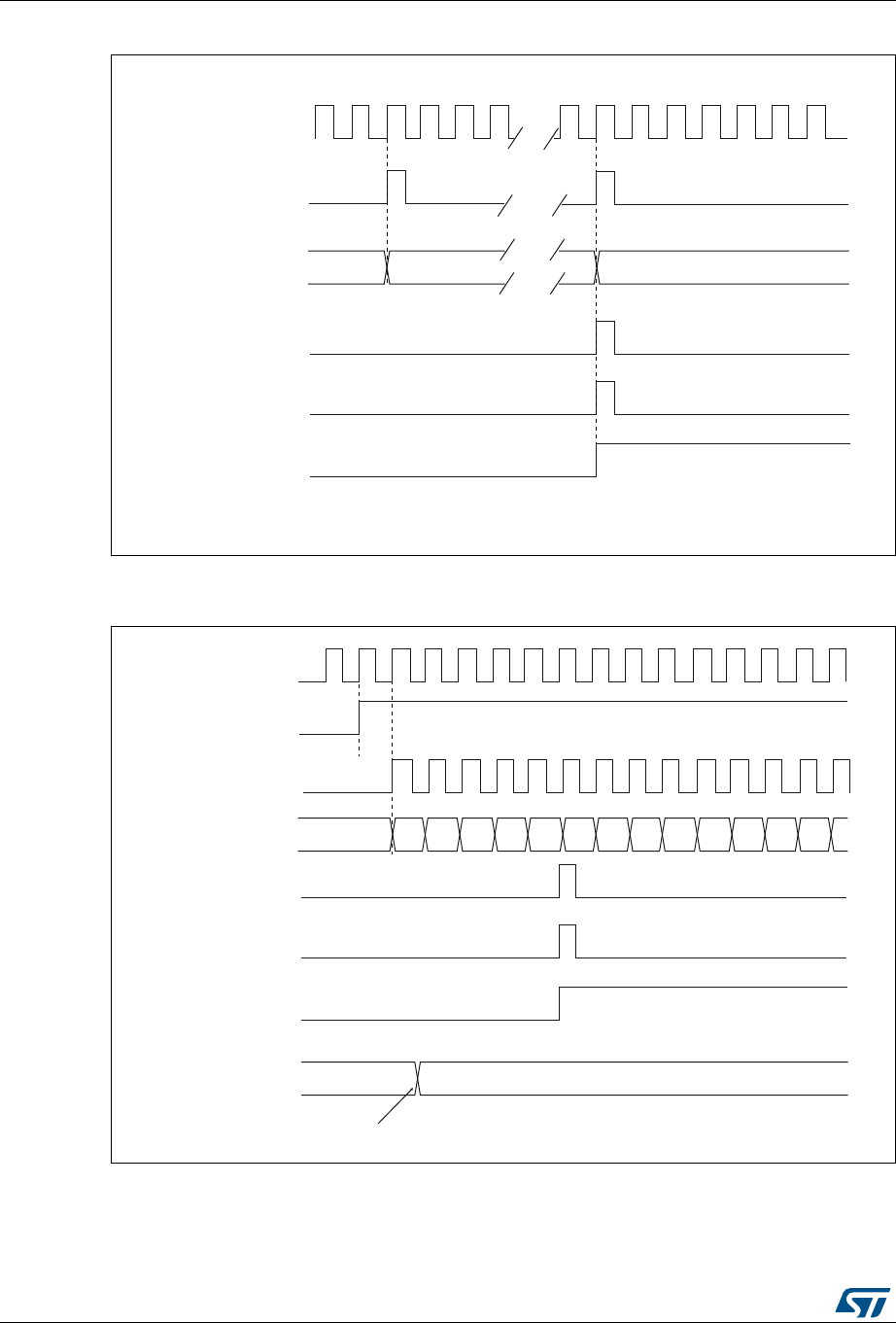
Basic timers (TIM6/7) RM0376
564/1001 DocID025941 Rev 5
Figure 179. Counter timing diagram, internal clock divided by N
Figure 180. Counter timing diagram, update event when ARPE = 0 (TIMx_ARR not
preloaded)
00
1F 20
MS31081V2
CK_PSC
Timerclock = CK_CNT
Counter register
Update event (UEV)
Counter overflow
Update interrupt flag
(UIF)
FF 36
MS31082V2
CK_PSC
Timerclock = CK_CNT
Counter register
Update event (UEV)
Counter overflow
Update interrupt flag
(UIF)
00 02 03 04 05 06 0732 33 34 35 3631 01
CEN
Auto-reload preload
register
Write a new value in TIMx_ARR
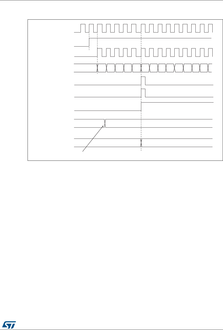
DocID025941 Rev 5 565/1001
RM0376 Basic timers (TIM6/7)
571
Figure 181. Counter timing diagram, update event when ARPE=1 (TIMx_ARR
preloaded)
22.3.3 Clock source
The counter clock is provided by the Internal clock (CK_INT) source.
The CEN (in the TIMx_CR1 register) and UG bits (in the TIMx_EGR register) are actual
control bits and can be changed only by software (except for UG that remains cleared
automatically). As soon as the CEN bit is written to 1, the prescaler is clocked by the internal
clock CK_INT.
Figure 182 shows the behavior of the control circuit and the upcounter in normal mode,
without prescaler.
MS31083V2
F5 36
CK_PSC
Timerclock = CK_CNT
Counter register
Update event (UEV)
Counter overflow
Update interrupt flag
(UIF)
00 02 03 04 05 06 07F1 F2 F3 F4 F5F0 01
CEN
Auto-reload preload
register
Write a new value in TIMx_ARR
Auto-reload shadow
register F5 36
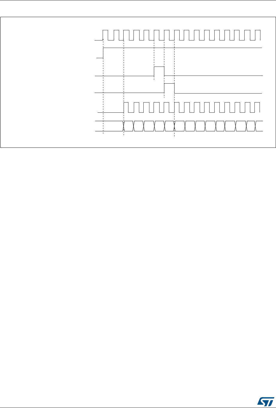
Basic timers (TIM6/7) RM0376
566/1001 DocID025941 Rev 5
Figure 182. Control circuit in normal mode, internal clock divided by 1
22.3.4 Debug mode
When the microcontroller enters the debug mode (Cortex®-M0+ core - halted), the TIMx
counter either continues to work normally or stops, depending on the DBG_TIMx_STOP
configuration bit in the DBG module. For more details, refer to Section 32.9.2: Debug
support for timers, watchdog and I2C.
Internal clock
Counter clock = CK_CNT = CK_PSC
Counter register
CEN=CNT_EN
UG
CNT_INIT
MS31085V2
00 02 03 04 05 06 0732 33 34 35 36
31 01

DocID025941 Rev 5 567/1001
RM0376 Basic timers (TIM6/7)
571
22.4 TIM6/7 registers
Refer to Section 1.1: List of abbreviations for registers for a list of abbreviations used in
register descriptions.
The peripheral registers have to be written by half-words (16 bits) or words (32 bits). Read
accesses can be done by bytes (8 bits), half-words (16 bits) or words (32 bits).
22.4.1 TIM6/7 control register 1 (TIMx_CR1)
Address offset: 0x00
Reset value: 0x0000
1514131211109876543210
Res. Res. Res. Res. Res. Res. Res. Res. ARPE Res. Res. Res. OPM URS UDIS CEN
rw rw rw rw rw
Bits 15:8 Reserved, must be kept at reset value.
Bit 7 ARPE: Auto-reload preload enable
0: TIMx_ARR register is not buffered.
1: TIMx_ARR register is buffered.
Bits 6:4 Reserved, must be kept at reset value.
Bit 3 OPM: One-pulse mode
0: Counter is not stopped at update event
1: Counter stops counting at the next update event (clearing the CEN bit).
Bit 2 URS: Update request source
This bit is set and cleared by software to select the UEV event sources.
0: Any of the following events generates an update interrupt or DMA request if enabled.
These events can be:
– Counter overflow/underflow
– Setting the UG bit
– Update generation through the slave mode controller
1: Only counter overflow/underflow generates an update interrupt or DMA request if
enabled.
Bit 1 UDIS: Update disable
This bit is set and cleared by software to enable/disable UEV event generation.
0: UEV enabled. The Update (UEV) event is generated by one of the following events:
– Counter overflow/underflow
– Setting the UG bit
– Update generation through the slave mode controller
Buffered registers are then loaded with their preload values.
1: UEV disabled. The Update event is not generated, shadow registers keep their value
(ARR, PSC). However the counter and the prescaler are reinitialized if the UG bit is set or if
a hardware reset is received from the slave mode controller.
Bit 0 CEN: Counter enable
0: Counter disabled
1: Counter enabled
Note: Gated mode can work only if the CEN bit has been previously set by software.
However trigger mode can set the CEN bit automatically by hardware.
CEN is cleared automatically in one-pulse mode, when an update event occurs.

Basic timers (TIM6/7) RM0376
568/1001 DocID025941 Rev 5
22.4.2 TIM6/7 control register 2 (TIMx_CR2)
Address offset: 0x04
Reset value: 0x0000
22.4.3 TIM6/7 DMA/Interrupt enable register (TIMx_DIER)
Address offset: 0x0C
Reset value: 0x0000
1514131211109876543210
Res. Res. Res. Res. Res. Res. Res. Res. Res. MMS[2:0] Res. Res. Res. Res.
rw rw rw
Bits 15:7 Reserved, must be kept at reset value.
Bits 6:4 MMS: Master mode selection
These bits are used to select the information to be sent in master mode to slave timers for
synchronization (TRGO). The combination is as follows:
000: Reset - the UG bit from the TIMx_EGR register is used as a trigger output (TRGO). If
reset is generated by the trigger input (slave mode controller configured in reset mode) then
the signal on TRGO is delayed compared to the actual reset.
001: Enable - the Counter enable signal, CNT_EN, is used as a trigger output (TRGO). It is
useful to start several timers at the same time or to control a window in which a slave timer
is enabled. The Counter Enable signal is generated by a logic OR between CEN control bit
and the trigger input when configured in gated mode.
When the Counter Enable signal is controlled by the trigger input, there is a delay on TRGO,
except if the master/slave mode is selected (see the MSM bit description in the TIMx_SMCR
register).
010: Update - The update event is selected as a trigger output (TRGO). For instance a
master timer can then be used as a prescaler for a slave timer.
Bits 3:0 Reserved, must be kept at reset value.
1514131211109876543210
Res. Res. Res. Res. Res. Res. Res. UDE Res. Res. Res. Res. Res. Res. Res. UIE
rw rw
Bits 15:9 Reserved, must be kept at reset value.
Bit 8 UDE: Update DMA request enable
0: Update DMA request disabled.
1: Update DMA request enabled.
Bits 7:1 Reserved, must be kept at reset value.
Bit 0 UIE: Update interrupt enable
0: Update interrupt disabled.
1: Update interrupt enabled.

DocID025941 Rev 5 569/1001
RM0376 Basic timers (TIM6/7)
571
22.4.4 TIM6/7 status register (TIMx_SR)
Address offset: 0x10
Reset value: 0x0000
22.4.5 TIM6/7 event generation register (TIMx_EGR)
Address offset: 0x14
Reset value: 0x0000
22.4.6 TIM6/7 counter (TIMx_CNT)
Address offset: 0x24
Reset value: 0x0000
1514131211109876543210
Res. Res. Res. Res. Res. Res. Res. Res. Res. Res. Res. Res. Res. Res. Res. UIF
rc_w0
Bits 15:1 Reserved, must be kept at reset value.
Bit 0 UIF: Update interrupt flag
This bit is set by hardware on an update event. It is cleared by software.
0: No update occurred.
1: Update interrupt pending. This bit is set by hardware when the registers are updated:
– At overflow or underflow regarding the repetition counter value and if UDIS = 0 in the
TIMx_CR1 register.
– When CNT is reinitialized by software using the UG bit in the TIMx_EGR register, if URS = 0
and UDIS = 0 in the TIMx_CR1 register.
1514131211109876543210
Res. Res. Res. Res. Res. Res. Res. Res. Res. Res. Res. Res. Res. Res. Res. UG
w
Bits 15:1 Reserved, must be kept at reset value.
Bit 0 UG: Update generation
This bit can be set by software, it is automatically cleared by hardware.
0: No action.
1: Re-initializes the timer counter and generates an update of the registers. Note that the
prescaler counter is cleared too (but the prescaler ratio is not affected).
1514131211109876543210
CNT[15:0]
rw rw rw rw rw rw rw rw rw rw rw rw rw rw rw rw
Bits 15:0 CNT[15:0]: Counter value
Basic timers (TIM6/7) RM0376
570/1001 DocID025941 Rev 5
22.4.7 TIM6/7 prescaler (TIMx_PSC)
Address offset: 0x28
Reset value: 0x0000
22.4.8 TIM6/7 auto-reload register (TIMx_ARR)
Address offset: 0x2C
Reset value: 0xFFFF
1514131211109876543210
PSC[15:0]
rw rw rw rw rw rw rw rw rw rw rw rw rw rw rw rw
Bits 15:0 PSC[15:0]: Prescaler value
The counter clock frequency (CK_CNT) is equal to fCK_PSC / (PSC[15:0] + 1).
PSC contains the value to be loaded in the active prescaler register at each update event
(including when the counter is cleared through UG bit of TIMx_EGR register or through
trigger controller when configured in “reset mode”).
1514131211109876543210
ARR[15:0]
rw rw rw rw rw rw rw rw rw rw rw rw rw rw rw rw
Bits 15:0 ARR[15:0]: Auto-reload value
ARR is the value to be loaded into the actual auto-reload register.
Refer to Section 22.3.1: Time-base unit on page 560 for more details about ARR update and
behavior.
The counter is blocked while the auto-reload value is null.

DocID025941 Rev 5 571/1001
RM0376 Basic timers (TIM6/7)
571
22.4.9 TIM6/7 register map
TIMx registers are mapped as 16-bit addressable registers as described in the table below:
Refer to Section 2.2.2 on page 58 for the register boundary addresses.
Table 96. TIM6/7 register map and reset values
Offset Register
15
14
13
12
11
10
9
8
7
6
5
4
3
2
1
0
0x00
TIMx_CR1
Res.
Res.
Res.
Res.
Res.
Res.
Res.
Res.
ARPE
Res.
Res.
Res.
OPM
URS
UDIS
CEN
Reset value 0 0000
0x04
TIMx_CR2
Res.
Res.
Res.
Res.
Res.
Res.
Res.
Res.
Res.
MMS[2:0]
Res.
Res.
Res.
Res.
Reset value 0 0 0
0x08 Res.
0x0C
TIMx_DIER
Res.
Res.
Res.
Res.
Res.
Res.
Res.
UDE
Res.
Res.
Res.
Res.
Res.
Res.
Res.
UIE
Reset value 0 0
0x10
TIMx_SR
Res.
Res.
Res.
Res.
Res.
Res.
Res.
Res.
Res.
Res.
Res.
Res.
Res.
Res.
Res.
UIF
Reset value 0
0x14
TIMx_EGR
Res.
Res.
Res.
Res.
Res.
Res.
Res.
Res.
Res.
Res.
Res.
Res.
Res.
Res.
Res.
UG
Reset value 0
0x18 Res.
0x1C Res.
0x20 Res.
0x24
TIMx_CNT CNT[15:0]
Reset value 0000000000 0 00000
0x28
TIMx_PSC PSC[15:0]
Reset value 0000000000 0 00000
0x2C
TIMx_ARR ARR[15:0]
Reset value 1111111111 1 11111

Low-power timer (LPTIM) RM0376
572/1001 DocID025941 Rev 5
23 Low-power timer (LPTIM)
23.1 Introduction
The LPTIM is a 16-bit timer that benefits from the ultimate developments in power
consumption reduction. Thanks to its diversity of clock sources, the LPTIM is able to keep
running in all power modes except for Standby mode. Given its capability to run even with
no internal clock source, the LPTIM can be used as a “Pulse Counter” which can be useful
in some applications. Also, the LPTIM capability to wake up the system from low-power
modes, makes it suitable to realize “Timeout functions” with extremely low power
consumption.
The LPTIM introduces a flexible clock scheme that provides the needed functionalities and
performance, while minimizing the power consumption.
23.2 LPTIM main features
•16 bit upcounter
•3-bit prescaler with 8 possible dividing factors (1,2,4,8,16,32,64,128)
•Selectable clock
– Internal clock sources: LSE, LSI, HSI16 or APB clock
– External clock source over LPTIM input (working with no LP oscillator running,
used by Pulse Counter application)
•16 bit ARR autoreload register
•16 bit compare register
•Continuous/One-shot mode
•Selectable software/hardware input trigger
•Programmable Digital Glitch filter
•Configurable output: Pulse, PWM
•Configurable I/O polarity
•Encoder mode
23.3 LPTIM implementation
Table 97 describes LPTIM implementation on STM32L0x2 devices.
Table 97. STM32L0x2 LPTIM features
LPTIM modes/features(1)
1. X = supported.
LPTIM1
Encoder mode X
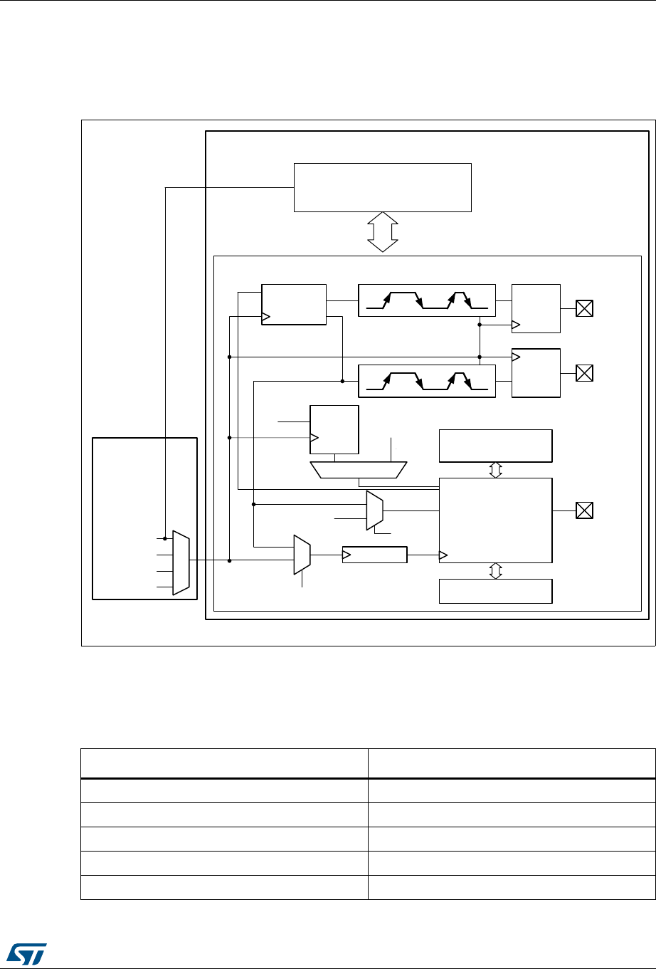
DocID025941 Rev 5 573/1001
RM0376 Low-power timer (LPTIM)
591
23.4 LPTIM functional description
23.4.1 LPTIM block diagram
Figure 183. Low-power timer block diagram
23.4.2 LPTIM trigger mapping
The LPTIM external trigger connections are detailed hereafter:
RCC
LPTIM
APB_ITF
Kernel
MS32468V2
sw
trigger
up to 8 ext
trigger
CLKMUX
HSI16
LSI
LSE
APB clock
16-bit compare
16-bit counter
16-bit ARR
Out
Prescaler
Mux trigger
Glitch
filter
Glitch
filter Input 1
Encoder Glitch
filter Input 2
Up/down
CKSEL
1
1
0
0
‘1' COUNT
MODE
Table 98. LPTIM1 external trigger connection
TRIGSEL External trigger
lptim_ext_trig0 PB6 or PC3
lptim_ext_trig1 RTC alarm A
lptim_ext_trig2 RTC alarm B
lptim_ext_trig3 RTC_TAMP1 input detection
lptim_ext_trig4 RTC_TAMP2 input detection

Low-power timer (LPTIM) RM0376
574/1001 DocID025941 Rev 5
23.4.3 LPTIM reset and clocks
The LPTIM can be clocked using several clock sources. It can be clocked using an internal
clock signal which can be chosen among APB, LSI, LSE or HSI16 sources through the
Reset and Clock controller (RCC). Also, the LPTIM can be clocked using an external clock
signal injected on its external Input1. When clocked with an external clock source, the
LPTIM may run in one of these two possible configurations:
•The first configuration is when the LPTIM is clocked by an external signal but in the
same time an internal clock signal is provided to the LPTIM either from APB or any
other embedded oscillator including LSE, LSI and HSI16.
•The second configuration is when the LPTIM is solely clocked by an external clock
source through its external Input1. This configuration is the one used to realize Timeout
function or Pulse counter function when all the embedded oscillators are turned off
after entering a low-power mode.
Programming the CKSEL and COUNTMODE bits allows controlling whether the LPTIM will
use an external clock source or an internal one.
When configured to use an external clock source, the CKPOL bits are used to select the
external clock signal active edge. If both edges are configured to be active ones, an internal
clock signal should also be provided (first configuration). In this case, the internal clock
signal frequency should be at least four times higher than the external clock signal
frequency.
23.4.4 Glitch filter
The LPTIM inputs, either external (mapped to microcontroller GPIOs) or internal (mapped
on the chip-level to other embedded peripherals, such as embedded comparators), are
protected with digital filters that prevent any glitches and noise perturbations to propagate
inside the LPTIM. This is in order to prevent spurious counts or triggers.
Before activating the digital filters, an internal clock source should first be provided to the
LPTIM. This is necessary to guarantee the proper operation of the filters.
The digital filters are divided into two groups:
•The first group of digital filters protects the LPTIM external inputs. The digital filters
sensitivity is controlled by the CKFLT bits
•The second group of digital filters protects the LPTIM internal trigger inputs. The digital
filters sensitivity is controlled by the TRGFLT bits.
Note: The digital filters sensitivity is controlled by groups. It is not possible to configure each digital
filter sensitivity separately inside the same group.
The filter sensitivity acts on the number of consecutive equal samples that should be
detected on one of the LPTIM inputs to consider a signal level change as a valid transition.
lptim_ext_trig5 RTC_TAMP3 input detection
lptim_ext_trig6 COMP1_OUT
lptim_ext_trig7 COMP2_OUT
Table 98. LPTIM1 external trigger connection (continued)
TRIGSEL External trigger
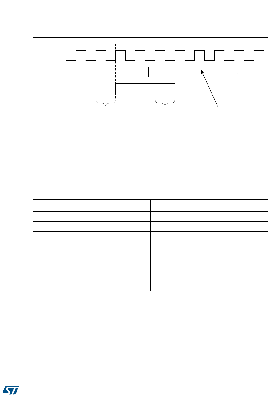
DocID025941 Rev 5 575/1001
RM0376 Low-power timer (LPTIM)
591
Figure 184 shows an example of glitch filter behavior in case of a 2 consecutive samples
programmed.
Figure 184. Glitch filter timing diagram
Note: In case no internal clock signal is provided, the digital filter must be deactivated by setting
the CKFLT and TRGFLT bits to ‘0’. In that case, an external analog filter may be used to
protect the LPTIM external inputs against glitches.
23.4.5 Prescaler
The LPTIM 16-bit counter is preceded by a configurable power-of-2 prescaler. The prescaler
division ratio is controlled by the PRESC[2:0] 3-bit field. The table below lists all the possible
division ratios:
23.4.6 Trigger multiplexer
The LPTIM counter may be started either by software or after the detection of an active
edge on one of the 8 trigger inputs.
TRIGEN[1:0] is used to determine the LPTIM trigger source:
•When TRIGEN[1:0] equals ‘00’, The LPTIM counter is started as soon as one of the
CNTSTRT or the SNGSTRT bits is set by software.
•The three remaining possible values for the TRIGEN[1:0] are used to configure the
active edge used by the trigger inputs. The LPTIM counter starts as soon as an active
edge is detected.
MS32490V1
CLKMUX
Input
Filter out
2 consecutive samples 2 consecutive samples Filtered
Table 99. Prescaler division ratios
programming dividing factor
000 /1
001 /2
010 /4
011 /8
100 /16
101 /32
110 /64
111 /128
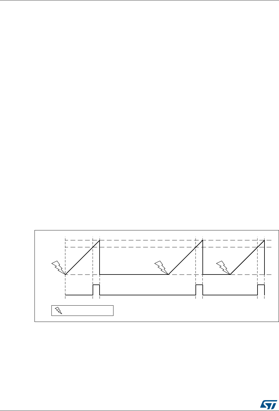
Low-power timer (LPTIM) RM0376
576/1001 DocID025941 Rev 5
When TRIGEN[1:0] is different than ‘00’, TRIGSEL[2:0] is used to select which of the 8
trigger inputs is used to start the counter.
The external triggers are considered asynchronous signals for the LPTIM. So after a trigger
detection, a two-counter-clock period latency is needed before the timer starts running due
to the synchronization.
If a new trigger event occurs when the timer is already started it will be ignored (unless
timeout function is enabled).
Note: The timer must be enabled before setting the SNGSTRT/CNTSTRT bits. Any write on these
bits when the timer is disabled will be discarded by hardware.
23.4.7 Operating mode
The LPTIM features two operating modes:
•The Continuous mode: the timer is free running, the timer is started from a trigger event
and never stops until the timer is disabled
•One-shot mode: the timer is started from a trigger event and stops when reaching the
ARR value.
One-shot mode:
To enable the one-shot counting, the SNGSTRT bit must be set.
A new trigger event will re-start the timer. Any trigger event occurring after the counter starts
and before the counter reaches ARR will be discarded.
In case an external trigger is selected, each external trigger event arriving after the
SNGSTRT bit is set, and after the counter register has stopped (contains zero value), will
start the counter for a new one-shot counting cycle as shown in Figure 185.
Figure 185. LPTIM output waveform, single counting mode configuration
- Set-once mode activated:
It should be noted that when the WAVE bit-field in the LPTIM_CFGR register is set, the Set-
once mode is activated. In this case, the counter is only started once following the first
trigger, and any subsequent trigger event is discarded as shown in Figure 186.
MSv39230V2
PWM
0
Compare
LPTIM_ARR
External trigger event
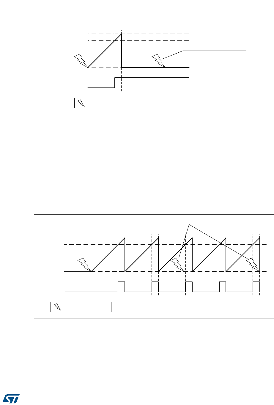
DocID025941 Rev 5 577/1001
RM0376 Low-power timer (LPTIM)
591
Figure 186. LPTIM output waveform, Single counting mode configuration
and Set-once mode activated (WAVE bit is set)
In case of software start (TRIGEN[1:0] = ‘00’), the SNGSTRT setting will start the counter for
one-shot counting.
Continous mode:
To enable the continuous counting, the CNTSTRT bit must be set.
In case an external trigger is selected, an external trigger event arriving after CNTSTRT is
set will start the counter for continuous counting. Any subsequent external trigger event will
be discarded as shown in Figure 187.
In case of software start (TRIGEN[1:0] = ‘00’), setting CNTSTRT will start the counter for
continuous counting.
Figure 187. LPTIM output waveform, Continuous counting mode configuration
SNGSTRT and CNTSTRT bits can only be set when the timer is enabled (The ENABLE bit
is set to ‘1’). It is possible to change “on the fly” from One-shot mode to Continuous mode.
If the Continuous mode was previously selected, setting SNGSTRT will switch the LPTIM to
the One-shot mode. The counter (if active) will stop as soon as it reaches ARR.
If the One-shot mode was previously selected, setting CNTSTRT will switch the LPTIM to
the Continuous mode. The counter (if active) will restart as soon as it reaches ARR.
MSv39231V2
PWM
0
Compare
LPTIM_ARR
Discarded trigger
External trigger event
MSv39229V2
PWM
0
Compare
LPTIM_ARR
Discarded triggers
External trigger event

Low-power timer (LPTIM) RM0376
578/1001 DocID025941 Rev 5
23.4.8 Timeout function
The detection of an active edge on one selected trigger input can be used to reset the
LPTIM counter. This feature is controlled through the TIMOUT bit.
The first trigger event will start the timer, any successive trigger event will reset the counter
and the timer will restart.
A low-power timeout function can be realized. The timeout value corresponds to the
compare value; if no trigger occurs within the expected time frame, the MCU is waked-up by
the compare match event.
23.4.9 Waveform generation
Two 16-bit registers, the LPTIM_ARR (autoreload register) and LPTIM_CMP (Compare
register), are used to generate several different waveforms on LPTIM output
The timer can generate the following waveforms:
•The PWM mode: the LPTIM output is set as soon as a match occurs between the
LPTIM_CMP and the LPTIM_CNT registers. The LPTIM output is reset as soon as a
match occurs between the LPTIM_ARR and the LPTIM_CNT registers
•The One-pulse mode: the output waveform is similar to the one of the PWM mode for
the first pulse, then the output is permanently reset
•The Set-once mode: the output waveform is similar to the One-pulse mode except that
the output is kept to the last signal level (depends on the output configured polarity).
The above described modes require that the LPTIM_ARR register value be strictly greater
than the LPTIM_CMP register value.
The LPTIM output waveform can be configured through the WAVE bit as follow:
•Resetting the WAVE bit to ‘0’ forces the LPTIM to generate either a PWM waveform or
a One pulse waveform depending on which bit is set: CNTSTRT or SNGSTRT.
•Setting the WAVE bit to ‘1’ forces the LPTIM to generate a Set-once mode waveform.
The WAVPOL bit controls the LPTIM output polarity. The change takes effect immediately,
so the output default value will change immediately after the polarity is re-configured, even
before the timer is enabled.
Signals with frequencies up to the LPTIM clock frequency divided by 2 can be generated.
Figure 188 below shows the three possible waveforms that can be generated on the LPTIM
output. Also, it shows the effect of the polarity change using the WAVPOL bit.
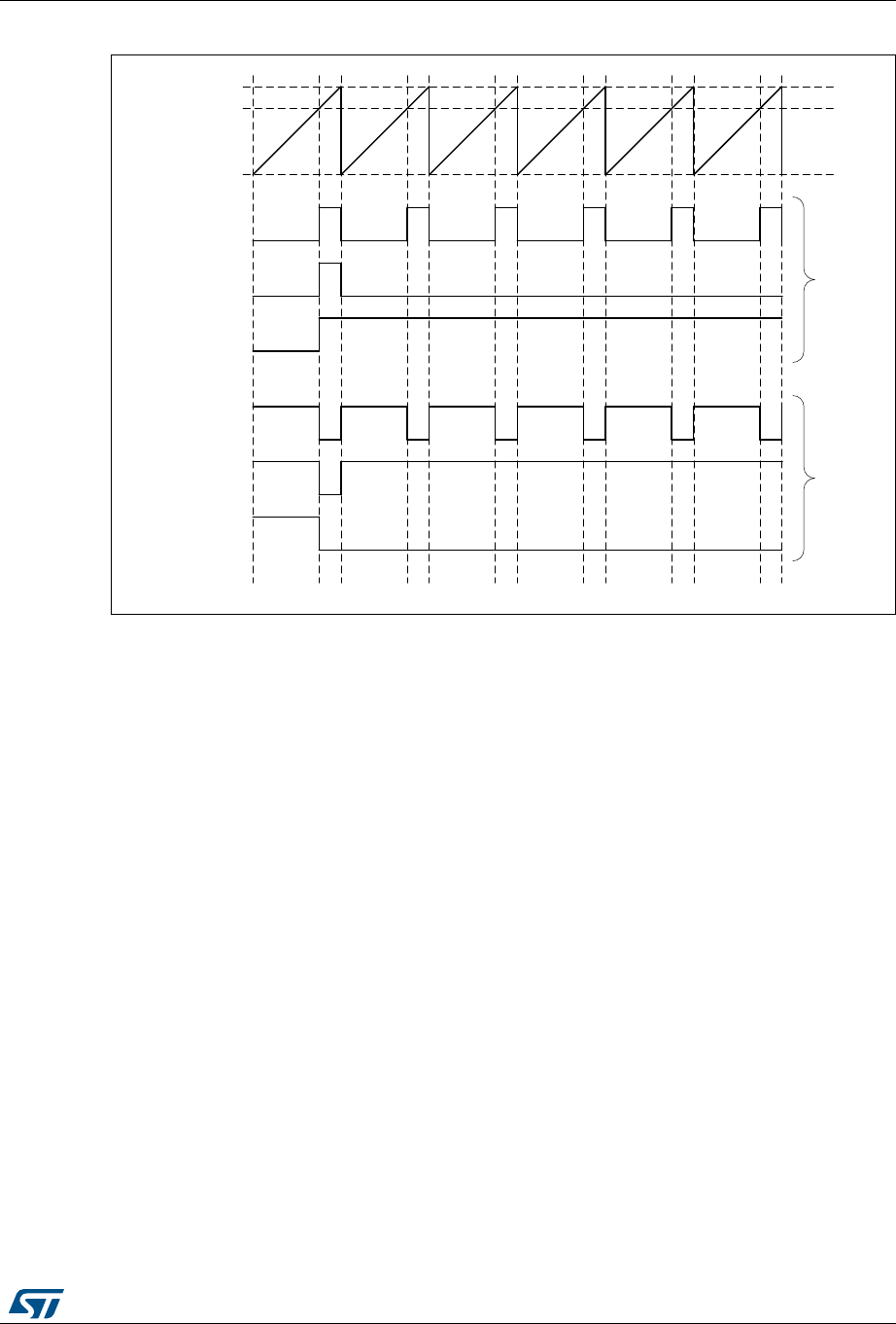
DocID025941 Rev 5 579/1001
RM0376 Low-power timer (LPTIM)
591
Figure 188. Waveform generation
23.4.10 Register update
The LPTIM_ARR register and LPTIM_CMP register are updated immediately after the APB
bus write operation, or at the end of the current period if the timer is already started.
The PRELOAD bit controls how the LPTIM_ARR and the LPTIM_CMP registers are
updated:
•When the PRELOAD bit is reset to ‘0’, the LPTIM_ARR and the LPTIM_CMP registers
are immediately updated after any write access.
•When the PRELOAD bit is set to ‘1’, the LPTIM_ARR and the LPTIM_CMP registers
are updated at the end of the current period, if the timer has been already started.
The LPTIM APB interface and the LPTIM kernel logic use different clocks, so there is some
latency between the APB write and the moment when these values are available to the
counter comparator. Within this latency period, any additional write into these registers must
be avoided.
The ARROK flag and the CMPOK flag in the LPTIM_ISR register indicate when the write
operation is completed to respectively the LPTIM_ARR register and the LPTIM_CMP
register.
After a write to the LPTIM_ARR register or the LPTIM_CMP register, a new write operation
to the same register can only be performed when the previous write operation is completed.
Any successive write before respectively the ARROK flag or the CMPOK flag be set, will
lead to unpredictable results.
MS32467V2
LPTIM_ARR
Compare
0
PWM
One shot
Set once
PWM
One shot
Set once
Pol = 0
Pol = 1

Low-power timer (LPTIM) RM0376
580/1001 DocID025941 Rev 5
23.4.11 Counter mode
The LPTIM counter can be used to count external events on the LPTIM Input1 or it can be
used to count internal clock cycles. The CKSEL and COUNTMODE bits control which
source will be used for updating the counter.
In case the LPTIM is configured to count external events on Input1, the counter can be
updated following a rising edge, falling edge or both edges depending on the value written
to the CKPOL[1:0] bits.
The count modes below can be selected, depending on CKSEL and COUNTMODE values:
•CKSEL = 0: the LPTIM is clocked by an internal clock source
– COUNTMODE = 0
The LPTIM is configured to be clocked by an internal clock source and the LPTIM
counter is configured to be updated following each internal clock pulse.
– COUNTMODE = 1
The LPTIM external Input1 is sampled with the internal clock provided to the
LPTIM.
Consequently, in order to not miss any event, the frequency of the changes on the
external Input1 signal should never exceed the frequency of the internal clock
provided to the LPTIM. Also, the internal clock provided to the LPTIM must not be
prescaled (PRESC[2:0] = 000).
•CKSEL = 1: the LPTIM is clocked by an external clock source
COUNTMODE value is don’t care.
In this configuration, the LPTIM has no need for an internal clock source (except if the
glitch filters are enabled). The signal injected on the LPTIM external Input1 is used as
system clock for the LPTIM. This configuration is suitable for operation modes where
no embedded oscillator is enabled.
For this configuration, the LPTIM counter can be updated either on rising edges or
falling edges of the input1 clock signal but not on both rising and falling edges.
Since the signal injected on the LPTIM external Input1 is also used to clock the LPTIM
kernel logic, there is some initial latency (after the LPTIM is enabled) before the counter
is incremented. More precisely, the first five active edges on the LPTIM external Input1
(after LPTIM is enable) are lost.
For code example, refer to A.12.1: Pulse counter configuration code example.
23.4.12 Timer enable
The ENABLE bit located in the LPTIM_CR register is used to enable/disable the LPTIM
kernel logic. After setting the ENABLE bit, a delay of two counter clock is needed before the
LPTIM is actually enabled.
The LPTIM_CFGR and LPTIM_IER registers must be modified only when the LPTIM is
disabled.
DocID025941 Rev 5 581/1001
RM0376 Low-power timer (LPTIM)
591
23.4.13 Encoder mode
This mode allows handling signals from quadrature encoders used to detect angular
position of rotary elements. Encoder interface mode acts simply as an external clock with
direction selection. This means that the counter just counts continuously between 0 and the
auto-reload value programmed into the LPTIM_ARR register (0 up to ARR or ARR down to
0 depending on the direction). Therefore you must configure LPTIM_ARR before starting.
From the two external input signals, Input1 and Input2, a clock signal is generated to clock
the LPTIM counter. The phase between those two signals determines the counting direction.
The Encoder mode is only available when the LPTIM is clocked by an internal clock source.
The signals frequency on both Input1 and Input2 inputs must not exceed the LPTIM internal
clock frequency divided by 4. This is mandatory in order to guarantee a proper operation of
the LPTIM.
Direction change is signalized by the two Down and Up flags in the LPTIM_ISR register.
Also, an interrupt can be generated for both direction change events if enabled through the
LPTIM_IER register.
To activate the Encoder mode the ENC bit has to be set to ‘1’. The LPTIM must first be
configured in Continuous mode.
When Encoder mode is active, the LPTIM counter is modified automatically following the
speed and the direction of the incremental encoder. Therefore, its content always
represents the encoder’s position. The count direction, signaled by the Up and Down flags,
correspond to the rotation direction of the encoder rotor.
According to the edge sensitivity configured using the CKPOL[1:0] bits, different counting
scenarios are possible. The following table summarizes the possible combinations,
assuming that Input1 and Input2 do not switch at the same time.
The following figure shows a counting sequence for Encoder mode where both-edge
sensitivity is configured.
Caution: In this mode the LPTIM must be clocked by an internal clock source, so the CKSEL bit must
be maintained to its reset value which is equal to ‘0’. Also, the prescaler division ratio must
be equal to its reset value which is 1 (PRESC[2:0] bits must be ‘000’).
Table 100. Encoder counting scenarios
Active edge
Level on opposite
signal (Input1 for
Input2, Input2 for
Input1)
Input1 signal Input2 signal
Rising Falling Rising Falling
Rising Edge
High Down No count Up No count
Low Up No count Down No count
Falling Edge
High No count Up No count Down
Low No count Down No count Up
Both Edges
High Down Up Up Down
Low Up Down Down Up
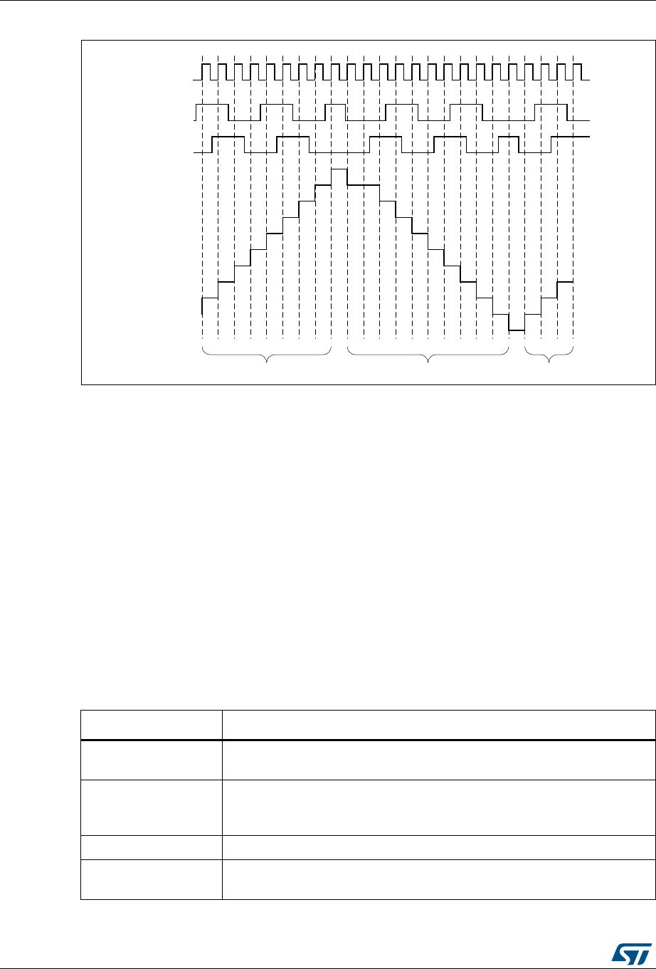
Low-power timer (LPTIM) RM0376
582/1001 DocID025941 Rev 5
Figure 189. Encoder mode counting sequence
23.5 LPTIM interrupts
The following events generate an interrupt/wake-up event, if they are enabled through the
LPTIM_IER register:
•Compare match
•Auto-reload match (whatever the direction if encoder mode)
•External trigger event
•Autoreload register write completed
•Compare register write completed
•Direction change (encoder mode), programmable (up / down / both).
Note: If any bit in the LPTIM_IER register (Interrupt Enable Register) is set after that its
corresponding flag in the LPTIM_ISR register (Status Register) is set, the interrupt is not
asserted.
MS32491V1
T1
Counter
up updown
T2
Table 101. Interrupt events
Interrupt event Description
Compare match Interrupt flag is raised when the content of the Counter register
(LPTIM_CNT) matches the content of the Compare register (LPTIM_CMP).
Auto-reload match
Interrupt flag is raised when the content of the Counter register
(LPTIM_CNT) matches the content of the Auto-reload register
(LPTIM_ARR).
External trigger event Interrupt flag is raised when an external trigger event is detected
Auto-reload register
update OK
Interrupt flag is raised when the write operation to the LPTIM_ARR register
is complete.

DocID025941 Rev 5 583/1001
RM0376 Low-power timer (LPTIM)
591
23.6 LPTIM registers
23.6.1 LPTIM interrupt and status register (LPTIM_ISR)
Address offset: 0x00
Reset value: 0x0000 0000
Compare register
update OK
Interrupt flag is raised when the write operation to the LPTIM_CMP register
is complete.
Direction change
Used in Encoder mode. Two interrupt flags are embedded to signal
direction change:
– UP flag signals up-counting direction change
– DOWN flag signals down-counting direction change.
Table 101. Interrupt events (continued)
Interrupt event Description
31 30 29 28 27 26 25 24 23 22 21 20 19 18 17 16
Res. Res. Res. Res. Res. Res. Res. Res. Res. Res. Res. Res. Res. Res. Res. Res.
15 14 13 12 11 10 9 8 7 6 5 4 3 2 1 0
Res. Res. Res. Res. Res. Res. Res. Res. Res. DOWN UP ARROK CMPOK EXTTRIG ARRM CMPM
rr r r r rr
Bits 31:9 Reserved, must be kept at reset value.
Bits 8:7 Reserved, must be kept at reset value.
Bit 6 DOWN: Counter direction change up to down
In Encoder mode, DOWN bit is set by hardware to inform application that the counter direction has
changed from up to down.
Bit 5 UP: Counter direction change down to up
In Encoder mode, UP bit is set by hardware to inform application that the counter direction has
changed from down to up.
Bit 4 ARROK: Autoreload register update OK
ARROK is set by hardware to inform application that the APB bus write operation to the LPTIM_ARR
register has been successfully completed.
Bit 3 CMPOK: Compare register update OK
CMPOK is set by hardware to inform application that the APB bus write operation to the
LPTIM_CMP register has been successfully completed.

Low-power timer (LPTIM) RM0376
584/1001 DocID025941 Rev 5
23.6.2 LPTIM interrupt clear register (LPTIM_ICR)
Address offset: 0x04
Reset value: 0x0000 0000
Bit 2 EXTTRIG: External trigger edge event
EXTTRIG is set by hardware to inform application that a valid edge on the selected external trigger
input has occurred. If the trigger is ignored because the timer has already started, then this flag is
not set.
Bit 1 ARRM: Autoreload match
ARRM is set by hardware to inform application that LPTIM_CNT register’s value reached the
LPTIM_ARR register’s value.
Bit 0 CMPM: Compare match
The CMPM bit is set by hardware to inform application that LPTIM_CNT register value reached the
LPTIM_CMP register’s value.
31 30 29 28 27 26 25 24 23 22 21 20 19 18 17 16
Res. Res. Res. Res. Res. Res. Res. Res. Res. Res. Res. Res. Res. Res. Res. Res.
1514131211109876543210
Res. Res. Res. Res. Res. Res. Res. Res. Res. DOWN
CF UPCF ARRO
KCF
CMPO
KCF
EXTTR
IGCF
ARRM
CF
CMPM
CF
wwwwwww
Bits 31:9 Reserved, must be kept at reset value.
Bits 8:7 Reserved, must be kept at reset value.
Bit 6 DOWNCF: Direction change to down Clear Flag
Writing 1 to this bit clear the DOWN flag in the LPT_ISR register
Bit 5 UPCF: Direction change to UP Clear Flag
Writing 1 to this bit clear the UP flag in the LPT_ISR register
Bit 4 ARROKCF: Autoreload register update OK Clear Flag
Writing 1 to this bit clears the ARROK flag in the LPT_ISR register
Bit 3 CMPOKCF: Compare register update OK Clear Flag
Writing 1 to this bit clears the CMPOK flag in the LPT_ISR register
Bit 2 EXTTRIGCF: External trigger valid edge Clear Flag
Writing 1 to this bit clears the EXTTRIG flag in the LPT_ISR register
Bit 1 ARRMCF: Autoreload match Clear Flag
Writing 1 to this bit clears the ARRM flag in the LPT_ISR register
Bit 0 CMPMCF: compare match Clear Flag
Writing 1 to this bit clears the CMP flag in the LPT_ISR register

DocID025941 Rev 5 585/1001
RM0376 Low-power timer (LPTIM)
591
23.6.3 LPTIM interrupt enable register (LPTIM_IER)
Address offset: 0x08
Reset value: 0x0000 0000
Caution: The LPTIM_IER register must only be modified when the LPTIM is disabled (ENABLE bit reset to ‘0’)
31 30 29 28 27 26 25 24 23 22 21 20 19 18 17 16
Res. Res. Res. Res. Res. Res. Res. Res. Res. Res. Res. Res. Res. Res. Res. Res.
1514131211109876543210
Res. Res. Res. Res. Res. Res. Res. Res. Res. DOWNI
EUPIE ARRO
KIE
CMPO
KIE
EXTTR
IGIE
ARRMI
E
CMPMI
E
rw rw rw rw rw rw rw
Bits 31:9 Reserved, must be kept at reset value.
Bits 8:7 Reserved, must be kept at reset value.
Bit 6 DOWNIE: Direction change to down Interrupt Enable
0: DOWN interrupt disabled
1: DOWN interrupt enabled
Bit 5 UPIE: Direction change to UP Interrupt Enable
0: UP interrupt disabled
1: UP interrupt enabled
Bit 4 ARROKIE: Autoreload register update OK Interrupt Enable
0: ARROK interrupt disabled
1: ARROK interrupt enabled
Bit 3 CMPOKIE: Compare register update OK Interrupt Enable
0: CMPOK interrupt disabled
1: CMPOK interrupt enabled
Bit 2 EXTTRIGIE: External trigger valid edge Interrupt Enable
0: EXTTRIG interrupt disabled
1: EXTTRIG interrupt enabled
Bit 1 ARRMIE: Autoreload match Interrupt Enable
0: ARRM interrupt disabled
1: ARRM interrupt enabled
Bit 0 CMPMIE: Compare match Interrupt Enable
0: CMPM interrupt disabled
1: CMPM interrupt enabled

Low-power timer (LPTIM) RM0376
586/1001 DocID025941 Rev 5
23.6.4 LPTIM configuration register (LPTIM_CFGR)
Address offset: 0x0C
Reset value: 0x0000 0000
31 30 29 28 27 26 25 24 23 22 21 20 19 18 17 16
Res. Res. Res. Res. Res. Res. Res. ENC COUNT
MODE PRELOAD WAVPOL WAVE TIMOUT TRIGEN[1:0] Res.
rw rw rw rw rw rw rw rw
15 14 13 12 11 10 9 8 7 6 5 4 3 2 1 0
TRIGSEL[2:0] Res. PRESC[2:0] Res. TRGFLT[1:0] Res. CKFLT[1:0] CKPOL[1:0] CKSEL
rw rw rw rw rw rw rw rw rw rw rw rw rw
Bits 31:25 Reserved, must be kept at reset value.
Bit 24 ENC: Encoder mode enable
The ENC bit controls the Encoder mode
0: Encoder mode disabled
1: Encoder mode enabled
Bit 23 COUNTMODE: counter mode enabled
The COUNTMODE bit selects which clock source is used by the LPTIM to clock the counter:
0: the counter is incremented following each internal clock pulse
1: the counter is incremented following each valid clock pulse on the LPTIM external Input1
Bit 22 PRELOAD: Registers update mode
The PRELOAD bit controls the LPTIM_ARR and the LPTIM_CMP registers update modality
0: Registers are updated after each APB bus write access
1: Registers are updated at the end of the current LPTIM period
Bit 21 WAVPOL: Waveform shape polarity
The WAVEPOL bit controls the output polarity
0: The LPTIM output reflects the compare results between LPTIM_ARR and LPTIM_CMP
registers
1: The LPTIM output reflects the inverse of the compare results between LPTIM_ARR and
LPTIM_CMP registers
Bit 20 WAVE: Waveform shape
The WAVE bit controls the output shape
0: Deactivate Set-once mode, PWM / One Pulse waveform (depending on OPMODE bit)
1: Activate the Set-once mode
Bit 19 TIMOUT: Timeout enable
The TIMOUT bit controls the Timeout feature
0: a trigger event arriving when the timer is already started will be ignored
1: A trigger event arriving when the timer is already started will reset and restart the counter
Bits 18:17 TRIGEN[1:0]: Trigger enable and polarity
The TRIGEN bits controls whether the LPTIM counter is started by an external trigger or not. If the
external trigger option is selected, three configurations are possible for the trigger active edge:
00: software trigger (counting start is initiated by software)
01: rising edge is the active edge
10: falling edge is the active edge
11: both edges are active edges

DocID025941 Rev 5 587/1001
RM0376 Low-power timer (LPTIM)
591
Bit 16 Reserved, must be kept at reset value.
Bits 15:13 TRIGSEL[2:0]: Trigger selector
The TRIGSEL bits select the trigger source that will serve as a trigger event for the LPTIM among
the below 8 available sources:
000: lptim_ext_trig0
001: lptim_ext_trig1
010: lptim_ext_trig2
011: lptim_ext_trig3
100: lptim_ext_trig4
101: lptim_ext_trig5
110: lptim_ext_trig6
111: lptim_ext_trig7
See Section 23.4.2: LPTIM trigger mapping for details.
Bit 12 Reserved, must be kept at reset value.
Bits 11:9 PRESC[2:0]: Clock prescaler
The PRESC bits configure the prescaler division factor. It can be one among the following division
factors:
000: /1
001: /2
010: /4
011: /8
100: /16
101: /32
110: /64
111: /128
Bit 8 Reserved, must be kept at reset value.
Bits 7:6 TRGFLT[1:0]: Configurable digital filter for trigger
The TRGFLT value sets the number of consecutive equal samples that should be detected when a
level change occurs on an internal trigger before it is considered as a valid level transition. An
internal clock source must be present to use this feature
00: any trigger active level change is considered as a valid trigger
01: trigger active level change must be stable for at least 2 clock periods before it is considered as
valid trigger.
10: trigger active level change must be stable for at least 4 clock periods before it is considered as
valid trigger.
11: trigger active level change must be stable for at least 8 clock periods before it is considered as
valid trigger.
Bit 5 Reserved, must be kept at reset value.

Low-power timer (LPTIM) RM0376
588/1001 DocID025941 Rev 5
Caution: The LPTIM_CFGR register must only be modified when the LPTIM is disabled (ENABLE bit
reset to ‘0’).
23.6.5 LPTIM control register (LPTIM_CR)
Address offset: 0x10
Reset value: 0x0000 0000
Bits 4:3 CKFLT[1:0]: Configurable digital filter for external clock
The CKFLT value sets the number of consecutive equal samples that should be detected when a
level change occurs on an external clock signal before it is considered as a valid level transition. An
internal clock source must be present to use this feature
00: any external clock signal level change is considered as a valid transition
01: external clock signal level change must be stable for at least 2 clock periods before it is
considered as valid transition.
10: external clock signal level change must be stable for at least 4 clock periods before it is
considered as valid transition.
11: external clock signal level change must be stable for at least 8 clock periods before it is
considered as valid transition.
Bits 2:1 CKPOL[1:0]: Clock Polarity
If LPTIM is clocked by an external clock source:
When the LPTIM is clocked by an external clock source, CKPOL bits is used to configure the active
edge or edges used by the counter:
00: the rising edge is the active edge used for counting
01: the falling edge is the active edge used for counting
10: both edges are active edges. When both external clock signal edges are considered active
ones, the LPTIM must also be clocked by an internal clock source with a frequency equal to at
least four time the external clock frequency.
11: not allowed
If the LPTIM is configured in Encoder mode (ENC bit is set):
00: the encoder sub-mode 1 is active
01: the encoder sub-mode 2 is active
10: the encoder sub-mode 3 is active
Refer to Section 23.4.13: Encoder mode for more details about Encoder mode sub-modes.
Bit 0 CKSEL: Clock selector
The CKSEL bit selects which clock source the LPTIM will use:
0: LPTIM is clocked by internal clock source (APB clock or any of the embedded oscillators)
1: LPTIM is clocked by an external clock source through the LPTIM external Input1
31 30 29 28 27 26 25 24 23 22 21 20 19 18 17 16
Res. Res. Res. Res. Res. Res. Res. Res. Res. Res. Res. Res. Res. Res. Res. Res.
1514131211109876543210
Res. Res. Res. Res. Res. Res. Res. Res. Res. Res. Res. Res. Res. CNT
STRT
SNG
STRT
ENA
BLE
rw rw rw

DocID025941 Rev 5 589/1001
RM0376 Low-power timer (LPTIM)
591
23.6.6 LPTIM compare register (LPTIM_CMP)
Address offset: 0x14
Reset value: 0x0000 0000
Caution: The LPTIM_CMP register must only be modified when the LPTIM is enabled (ENABLE bit
set to ‘1’).
Bits 31:3 Reserved, must be kept at reset value.
Bit 2 CNTSTRT: Timer start in Continuous mode
This bit is set by software and cleared by hardware.
In case of software start (TRIGEN[1:0] = ‘00’), setting this bit starts the LPTIM in Continuous mode.
If the software start is disabled (TRIGEN[1:0] different than ‘00’), setting this bit starts the timer in
Continuous mode as soon as an external trigger is detected.
If this bit is set when a single pulse mode counting is ongoing, then the timer will not stop at the next
match between the LPTIM_ARR and LPTIM_CNT registers and the LPTIM counter keeps counting
in Continuous mode.
This bit can be set only when the LPTIM is enabled. It will be automatically reset by hardware.
Bit 1 SNGSTRT: LPTIM start in Single mode
This bit is set by software and cleared by hardware.
In case of software start (TRIGEN[1:0] = ‘00’), setting this bit starts the LPTIM in single pulse mode.
If the software start is disabled (TRIGEN[1:0] different than ‘00’), setting this bit starts the LPTIM in
single pulse mode as soon as an external trigger is detected.
If this bit is set when the LPTIM is in continuous counting mode, then the LPTIM will stop at the
following match between LPTIM_ARR and LPTIM_CNT registers.
This bit can only be set when the LPTIM is enabled. It will be automatically reset by hardware.
Bit 0 ENABLE: LPTIM enable
The ENABLE bit is set and cleared by software.
0:LPTIM is disabled
1:LPTIM is enabled
31 30 29 28 27 26 25 24 23 22 21 20 19 18 17 16
Res. Res. Res. Res. Res. Res. Res. Res. Res. Res. Res. Res. Res. Res. Res. Res.
15 14 13 12 11 10 9 8 7 6 5 4 3 2 1 0
CMP[15:0]
rw
Bits 31:16 Reserved, must be kept at reset value.
Bits 15:0 CMP[15:0]: Compare value
CMP is the compare value used by the LPTIM.

Low-power timer (LPTIM) RM0376
590/1001 DocID025941 Rev 5
23.6.7 LPTIM autoreload register (LPTIM_ARR)
Address offset: 0x18
Reset value: 0x0000 0001
Caution: The LPTIM_ARR register must only be modified when the LPTIM is enabled (ENABLE bit
set to ‘1’).
23.6.8 LPTIM counter register (LPTIM_CNT)
Address offset: 0x1C
Reset value: 0x0000 0000
31 30 29 28 27 26 25 24 23 22 21 20 19 18 17 16
Res. Res. Res. Res. Res. Res. Res. Res. Res. Res. Res. Res. Res. Res. Res. Res.
15 14 13 12 11 10 9 8 7 6 5 4 3 2 1 0
ARR[15:0]
rw
Bits 31:16 Reserved, must be kept at reset value.
Bits 15:0 ARR[15:0]: Auto reload value
ARR is the autoreload value for the LPTIM.
This value must be strictly greater than the CMP[15:0] value.
31 30 29 28 27 26 25 24 23 22 21 20 19 18 17 16
Res. Res. Res. Res. Res. Res. Res. Res. Res. Res. Res. Res. Res. Res. Res. Res.
1514131211109876543210
CNT[15:0]
r
Bits 31:16 Reserved, must be kept at reset value.
Bits 15:0 CNT[15:0]: Counter value
When the LPTIM is running with an asynchronous clock, reading the LPTIM_CNT register may
return unreliable values. So in this case it is necessary to perform two consecutive read accesses
and verify that the two returned values are identical.
It should be noted that for a reliable LPTIM_CNT register read access, two consecutive read
accesses must be performed and compared. A read access can be considered reliable when the
values of the two consecutive read accesses are equal.
DocID025941 Rev 5 591/1001
RM0376 Low-power timer (LPTIM)
591
23.6.9 LPTIM register map
The following table summarizes the LPTIM registers.
Refer to Section 2.2.2 on page 58 for the register boundary addresses.
Table 102. LPTIM register map and reset values
Offset Register name
31
30
29
28
27
26
25
24
23
22
21
20
19
18
17
16
15
14
13
12
11
10
9
8
7
6
5
4
3
2
1
0
0x00
LPTIM_ISR
Res.
Res.
Res.
Res.
Res.
Res.
Res.
Res.
Res.
Res.
Res.
Res.
Res.
Res.
Res.
Res.
Res.
Res.
Res.
Res.
Res.
Res.
Res.
Res.
Res.
DOWN
UP
ARROK
CMPOK
EXTTRIG
ARRM
CMPM
Reset value 0000000
0x04
LPTIM_ICR
Res.
Res.
Res.
Res.
Res.
Res.
Res.
Res.
Res.
Res.
Res.
Res.
Res.
Res.
Res.
Res.
Res.
Res.
Res.
Res.
Res.
Res.
Res.
Res.
Res.
DOWNCF
UPCF
ARROKCF
CMPOKCF
EXTTRIGCF
ARRMCF
CMPMCF
Reset value 0000000
0x08
LPTIM_IER
Res.
Res.
Res.
Res.
Res.
Res.
Res.
Res.
Res.
Res.
Res.
Res.
Res.
Res.
Res.
Res.
Res.
Res.
Res.
Res.
Res.
Res.
Res.
Res.
Res.
DOWNIE
UPIE
ARROKIE
CMPOKIE
EXTTRIGIE
ARRMIE
CMPMIE
Reset value 0000000
0x0C
LPTIM_CFGR
Res.
Res.
Res.
Res.
Res.
Res.
Res.
ENC
COUNTMODE
PRELOAD
WAVPOL
WAVE
TIMOUT
TRIGEN
Res.
TRIGSEL[2:0]
Res.
PRESC
Res.
TRGFLT
Res.
CKFLT
CKPOL
CKSEL
Reset value 00000000 000 000 00 00000
0x10
LPTIM_CR
Res.
Res.
Res.
Res.
Res.
Res.
Res.
Res.
Res.
Res.
Res.
Res.
Res.
Res.
Res.
Res.
Res.
Res.
Res.
Res.
Res.
Res.
Res.
Res.
Res.
Res.
Res.
RSTARE
Res.
CNTSTRT
SNGSTRT
ENABLE
Reset value 0000
0x14
LPTIM_CMP
Res.
Res.
Res.
Res.
Res.
Res.
Res.
Res.
Res.
Res.
Res.
Res.
Res.
Res.
Res.
Res.
CMP[15:0]
Reset value 0000000000000000
0x18
LPTIM_ARR
Res.
Res.
Res.
Res.
Res.
Res.
Res.
Res.
Res.
Res.
Res.
Res.
Res.
Res.
Res.
Res.
ARR[15:0]
Reset value 0000000000000001
0x1C
LPTIM_CNT
Res.
Res.
Res.
Res.
Res.
Res.
Res.
Res.
Res.
Res.
Res.
Res.
Res.
Res.
Res.
Res.
CNT[15:0]
Reset value 0000000000000000
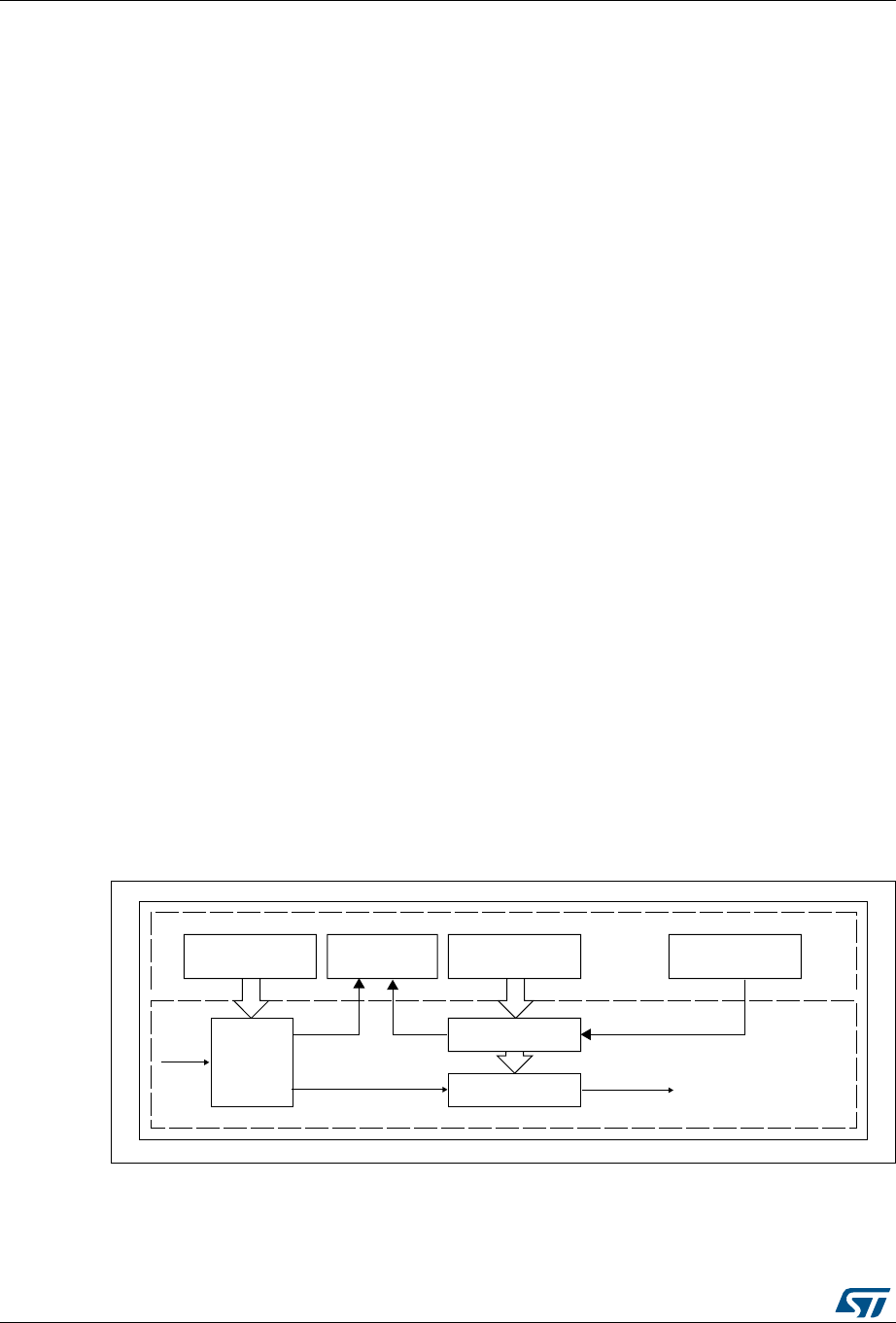
Independent watchdog (IWDG) RM0376
592/1001 DocID025941 Rev 5
24 Independent watchdog (IWDG)
24.1 Introduction
The devices feature an embedded watchdog peripheral that offers a combination of high
safety level, timing accuracy and flexibility of use. The Independent watchdog peripheral
detects and solves malfunctions due to software failure, and triggers system reset when the
counter reaches a given timeout value.
The independent watchdog (IWDG) is clocked by its own dedicated low-speed clock (LSI)
and thus stays active even if the main clock fails.
The IWDG is best suited for applications that require the watchdog to run as a totally
independent process outside the main application, but have lower timing accuracy
constraints. For further information on the window watchdog, refer to Section 25 on page
601.
24.2 IWDG main features
•Free-running downcounter
•Clocked from an independent RC oscillator (can operate in Standby and Stop modes)
•Conditional Reset
– Reset (if watchdog activated) when the downcounter value becomes lower than
0x000
– Reset (if watchdog activated) if the downcounter is reloaded outside the window
24.3 IWDG functional description
24.3.1 IWDG block diagram
Figure 190 shows the functional blocks of the independent watchdog module.
Figure 190. Independent watchdog block diagram
1. The watchdog function is implemented in the CORE voltage domain that is still functional in Stop and
Standby modes.
IWDG reset
prescaler
IWDG_PR
Prescaler register
IWDG_RLR
Reload register
8-bit
LSI
(40 kHz)
IWDG_KR
Key register
CORE
VDD voltage domain
IWDG_SR
Status register
MS19944V2
12-bit reload value
12-bit downcounter

DocID025941 Rev 5 593/1001
RM0376 Independent watchdog (IWDG)
600
When the independent watchdog is started by writing the value 0x0000 CCCC in the Key
register (IWDG_KR), the counter starts counting down from the reset value of 0xFFF. When
it reaches the end of count value (0x000) a reset signal is generated (IWDG reset).
Whenever the key value 0x0000 AAAA is written in the Key register (IWDG_KR), the
IWDG_RLR value is reloaded in the counter and the watchdog reset is prevented.
24.3.2 Window option
The IWDG can also work as a window watchdog by setting the appropriate window in the
Window register (IWDG_WINR).
If the reload operation is performed while the counter is greater than the value stored in the
Window register (IWDG_WINR), then a reset is provided.
The default value of the Window register (IWDG_WINR) is 0x0000 0FFF, so if it is not
updated, the window option is disabled.
As soon as the window value is changed, a reload operation is performed in order to reset
the downcounter to the Reload register (IWDG_RLR) value and ease the cycle number
calculation to generate the next reload.
Configuring the IWDG when the window option is enabled
1. Enable the IWDG by writing 0x0000 CCCC in the Key register (IWDG_KR).
2. Enable register access by writing 0x0000 5555 in the Key register (IWDG_KR).
3. Write the IWDG prescaler by programming Prescaler register (IWDG_PR) from 0 to 7.
4. Write the Reload register (IWDG_RLR).
5. Wait for the registers to be updated (IWDG_SR = 0x0000 0000).
6. Write to the Window register (IWDG_WINR). This automatically refreshes the counter
value in the Reload register (IWDG_RLR).
Note: Writing the window value allows to refresh the Counter value by the RLR when Status
register (IWDG_SR) is set to 0x0000 0000.
For code example, refer to A.13.2: IWDG configuration with window code example.
Configuring the IWDG when the window option is disabled
When the window option it is not used, the IWDG can be configured as follows:
1. Enable the IWDG by writing 0x0000 CCCC in the Key register (IWDG_KR).
2. Enable register access by writing 0x0000 5555 in the Key register (IWDG_KR).
3. Write the prescaler by programming the Prescaler register (IWDG_PR) from 0 to 7.
4. Write the Reload register (IWDG_RLR).
5. Wait for the registers to be updated (IWDG_SR = 0x0000 0000).
6. Refresh the counter value with IWDG_RLR (IWDG_KR = 0x0000 AAAA).
For code example, refer to A.13.1: IWDG configuration code example.

Independent watchdog (IWDG) RM0376
594/1001 DocID025941 Rev 5
24.3.3 Hardware watchdog
If the “Hardware watchdog” feature is enabled through the device option bits, the watchdog
is automatically enabled at power-on, and generates a reset unless the Key register
(IWDG_KR) is written by the software before the counter reaches end of count or if the
downcounter is reloaded inside the window.
24.3.4 Behavior in Stop and Standby modes
Once running, the IWDG cannot be stopped.
24.3.5 Register access protection
Write access to Prescaler register (IWDG_PR), Reload register (IWDG_RLR) and Window
register (IWDG_WINR) is protected. To modify them, the user must first write the code
0x0000 5555 in the Key register (IWDG_KR). A write access to this register with a different
value will break the sequence and register access will be protected again. This is the case
of the reload operation (writing 0x0000 AAAA).
A status register is available to indicate that an update of the prescaler or the down-counter
reload value or the window value is on going.
24.3.6 Debug mode
When the microcontroller enters Debug mode (core halted), the IWDG counter either
continues to work normally or stops, depending on DBG_IWDG_STOP configuration bit in
DBG module.

DocID025941 Rev 5 595/1001
RM0376 Independent watchdog (IWDG)
600
24.4 IWDG registers
Refer to Section 1.1 on page 51 for a list of abbreviations used in register descriptions.
The peripheral registers can be accessed by half-words (16-bit) or words (32-bit).
24.4.1 Key register (IWDG_KR)
Address offset: 0x00
Reset value: 0x0000 0000 (reset by Standby mode)
31 30 29 28 27 26 25 24 23 22 21 20 19 18 17 16
Res. Res. Res. Res. Res. Res. Res. Res. Res. Res. Res. Res. Res. Res. Res. Res.
1514131211109876543210
KEY[15:0]
wwwwwwwwwwwwwwww
Bits 31:16 Reserved, must be kept at reset value.
Bits 15:0 KEY[15:0]: Key value (write only, read 0x0000)
These bits must be written by software at regular intervals with the key value 0xAAAA,
otherwise the watchdog generates a reset when the counter reaches 0.
Writing the key value 0x5555 to enable access to the IWDG_PR, IWDG_RLR and
IWDG_WINR registers (see Section 24.3.5: Register access protection)
Writing the key value 0xCCCC starts the watchdog (except if the hardware watchdog option is
selected)

Independent watchdog (IWDG) RM0376
596/1001 DocID025941 Rev 5
24.4.2 Prescaler register (IWDG_PR)
Address offset: 0x04
Reset value: 0x0000 0000
31 30 29 28 27 26 25 24 23 22 21 20 19 18 17 16
Res. Res. Res. Res. Res. Res. Res. Res. Res. Res. Res. Res. Res. Res. Res. Res.
1514131211109876543210
Res. Res. Res. Res. Res. Res. Res. Res. Res. Res. Res. Res. Res. PR[2:0]
rw rw rw
Bits 31:3 Reserved, must be kept at reset value.
Bits 2:0 PR[2:0]: Prescaler divider
These bits are write access protected see Section 24.3.5: Register access protection. They are
written by software to select the prescaler divider feeding the counter clock. PVU bit of the
Status register (IWDG_SR) must be reset in order to be able to change the prescaler divider.
000: divider /4
001: divider /8
010: divider /16
011: divider /32
100: divider /64
101: divider /128
110: divider /256
111: divider /256
Note: Reading this register returns the prescaler value from the VDD voltage domain. This
value may not be up to date/valid if a write operation to this register is ongoing. For this
reason the value read from this register is valid only when the PVU bit in the Status
register (IWDG_SR) is reset.

DocID025941 Rev 5 597/1001
RM0376 Independent watchdog (IWDG)
600
24.4.3 Reload register (IWDG_RLR)
Address offset: 0x08
Reset value: 0x0000 0FFF (reset by Standby mode)
31 30 29 28 27 26 25 24 23 22 21 20 19 18 17 16
Res. Res. Res. Res. Res. Res. Res. Res. Res. Res. Res. Res. Res. Res. Res. Res.
1514131211109876543210
Res. Res. Res. Res. RL[11:0]
rw rw rw rw rw rw rw rw rw rw rw rw
Bits 31:12 Reserved, must be kept at reset value.
Bits 11:0 RL[11:0]: Watchdog counter reload value
These bits are write access protected see Register access protection. They are written by
software to define the value to be loaded in the watchdog counter each time the value 0xAAAA
is written in the Key register (IWDG_KR). The watchdog counter counts down from this value.
The timeout period is a function of this value and the clock prescaler. Refer to the datasheet for
the timeout information.
The RVU bit in the Status register (IWDG_SR) must be reset to be able to change the reload
value.
Note: Reading this register returns the reload value from the VDD voltage domain. This value
may not be up to date/valid if a write operation to this register is ongoing on it. For this
reason the value read from this register is valid only when the RVU bit in the Status
register (IWDG_SR) is reset.

Independent watchdog (IWDG) RM0376
598/1001 DocID025941 Rev 5
24.4.4 Status register (IWDG_SR)
Address offset: 0x0C
Reset value: 0x0000 0000 (not reset by Standby mode)
Note: If several reload, prescaler, or window values are used by the application, it is mandatory to
wait until RVU bit is reset before changing the reload value, to wait until PVU bit is reset
before changing the prescaler value, and to wait until WVU bit is reset before changing the
window value. However, after updating the prescaler and/or the reload/window value it is not
necessary to wait until RVU or PVU or WVU is reset before continuing code execution
except in case of low-power mode entry.
31 30 29 28 27 26 25 24 23 22 21 20 19 18 17 16
Res. Res. Res. Res. Res. Res. Res. Res. Res. Res. Res. Res. Res. Res. Res. Res.
1514131211109876543210
Res. Res. Res. Res. Res. Res. Res. Res. Res. Res. Res. Res. Res. WVU RVU PVU
rrr
Bits 31:3 Reserved, must be kept at reset value.
Bit 2 WVU: Watchdog counter window value update
This bit is set by hardware to indicate that an update of the window value is ongoing. It is reset
by hardware when the reload value update operation is completed in the VDD voltage domain
(takes up to five RC 40 kHz cycles).
Window value can be updated only when WVU bit is reset.
This bit is generated only if generic “window” = 1
Bit 1 RVU: Watchdog counter reload value update
This bit is set by hardware to indicate that an update of the reload value is ongoing. It is reset
by hardware when the reload value update operation is completed in the VDD voltage domain
(takes up to five RC 40 kHz cycles).
Reload value can be updated only when RVU bit is reset.
Bit 0 PVU: Watchdog prescaler value update
This bit is set by hardware to indicate that an update of the prescaler value is ongoing. It is
reset by hardware when the prescaler update operation is completed in the VDD voltage
domain (takes up to five RC 40 kHz cycles).
Prescaler value can be updated only when PVU bit is reset.

DocID025941 Rev 5 599/1001
RM0376 Independent watchdog (IWDG)
600
24.4.5 Window register (IWDG_WINR)
Address offset: 0x10
Reset value: 0x0000 0FFF (reset by Standby mode)
31 30 29 28 27 26 25 24 23 22 21 20 19 18 17 16
Res. Res. Res. Res. Res. Res. Res. Res. Res. Res. Res. Res. Res. Res. Res. Res.
1514131211109876543210
Res. Res. Res. Res. WIN[11:0]
rw rw rw rw rw rw rw rw rw rw rw rw
Bits 31:12 Reserved, must be kept at reset value.
Bits 11:0 WIN[11:0]: Watchdog counter window value
These bits are write access protected, see Section 24.3.5, they contain the high limit of the
window value to be compared with the downcounter.
To prevent a reset, the downcounter must be reloaded when its value is lower than the window
register value and greater than 0x0
The WVU bit in the Status register (IWDG_SR) must be reset in order to be able to change the
reload value.
Note: Reading this register returns the reload value from the VDD voltage domain. This value
may not be valid if a write operation to this register is ongoing. For this reason the value
read from this register is valid only when the WVU bit in the Status register (IWDG_SR)
is reset.

Independent watchdog (IWDG) RM0376
600/1001 DocID025941 Rev 5
24.4.6 IWDG register map
The following table gives the IWDG register map and reset values.
Refer to Section 2.2.2: Memory map and register boundary addresses for the register
boundary addresses.
Table 103. IWDG register map and reset values
Offset Register
name
31
30
29
28
27
26
25
24
23
22
21
20
19
18
17
16
15
14
13
12
11
10
9
8
7
6
5
4
3
2
1
0
0x00 IWDG_KR
Res.
Res.
Res.
Res.
Res.
Res.
Res.
Res.
Res.
Res.
Res.
Res.
Res.
Res.
Res.
Res.
KEY[15:0]
Reset value 0000000000000000
0x04 IWDG_PR
Res.
Res.
Res.
Res.
Res.
Res.
Res.
Res.
Res.
Res.
Res.
Res.
Res.
Res.
Res.
Res.
Res.
Res.
Res.
Res.
Res.
Res.
Res.
Res.
Res.
Res.
Res.
Res.
Res.
PR[2:0]
Reset value 000
0x08 IWDG_RLR
Res.
Res.
Res.
Res.
Res.
Res.
Res.
Res.
Res.
Res.
Res.
Res.
Res.
Res.
Res.
Res.
Res.
Res.
Res.
Res.
RL[11:0]
Reset value 111111111111
0x0C IWDG_SR
Res.
Res.
Res.
Res.
Res.
Res.
Res.
Res.
Res.
Res.
Res.
Res.
Res.
Res.
Res.
Res.
Res.
Res.
Res.
Res.
Res.
Res.
Res.
Res.
Res.
Res.
Res.
Res.
Res.
WVU
RVU
PVU
Reset value 000
0x10 IWDG_WINR
Res.
Res.
Res.
Res.
Res.
Res.
Res.
Res.
Res.
Res.
Res.
Res.
Res.
Res.
Res.
Res.
Res.
Res.
Res.
Res.
WIN[11:0]
Reset value 111111111111

DocID025941 Rev 5 601/1001
RM0376 System window watchdog (WWDG)
607
25 System window watchdog (WWDG)
25.1 Introduction
The system window watchdog (WWDG) is used to detect the occurrence of a software fault,
usually generated by external interference or by unforeseen logical conditions, which
causes the application program to abandon its normal sequence. The watchdog circuit
generates an MCU reset on expiry of a programmed time period, unless the program
refreshes the contents of the downcounter before the T6 bit becomes cleared. An MCU
reset is also generated if the 7-bit downcounter value (in the control register) is refreshed
before the downcounter has reached the window register value. This implies that the
counter must be refreshed in a limited window.
The WWDG clock is prescaled from the APB1 clock and has a configurable time-window
that can be programmed to detect abnormally late or early application behavior.
The WWDG is best suited for applications which require the watchdog to react within an
accurate timing window.
25.2 WWDG main features
•Programmable free-running downcounter
•Conditional reset
– Reset (if watchdog activated) when the downcounter value becomes lower than
0x40
– Reset (if watchdog activated) if the downcounter is reloaded outside the window
(see Figure 192)
•Early wakeup interrupt (EWI): triggered (if enabled and the watchdog activated) when
the downcounter is equal to 0x40.
25.3 WWDG functional description
If the watchdog is activated (the WDGA bit is set in the WWDG_CR register) and when the
7-bit downcounter (T[6:0] bits) is decremented from 0x40 to 0x3F (T6 becomes cleared), it
initiates a reset. If the software reloads the counter while the counter is greater than the
value stored in the window register, then a reset is generated.
The application program must write in the WWDG_CR register at regular intervals during
normal operation to prevent an MCU reset. This operation must occur only when the counter
value is lower than the window register value and higher than 0x3F. The value to be stored
in the WWDG_CR register must be between 0xFF and 0xC0.
Refer to Figure 191 for the WWDG block diagram.
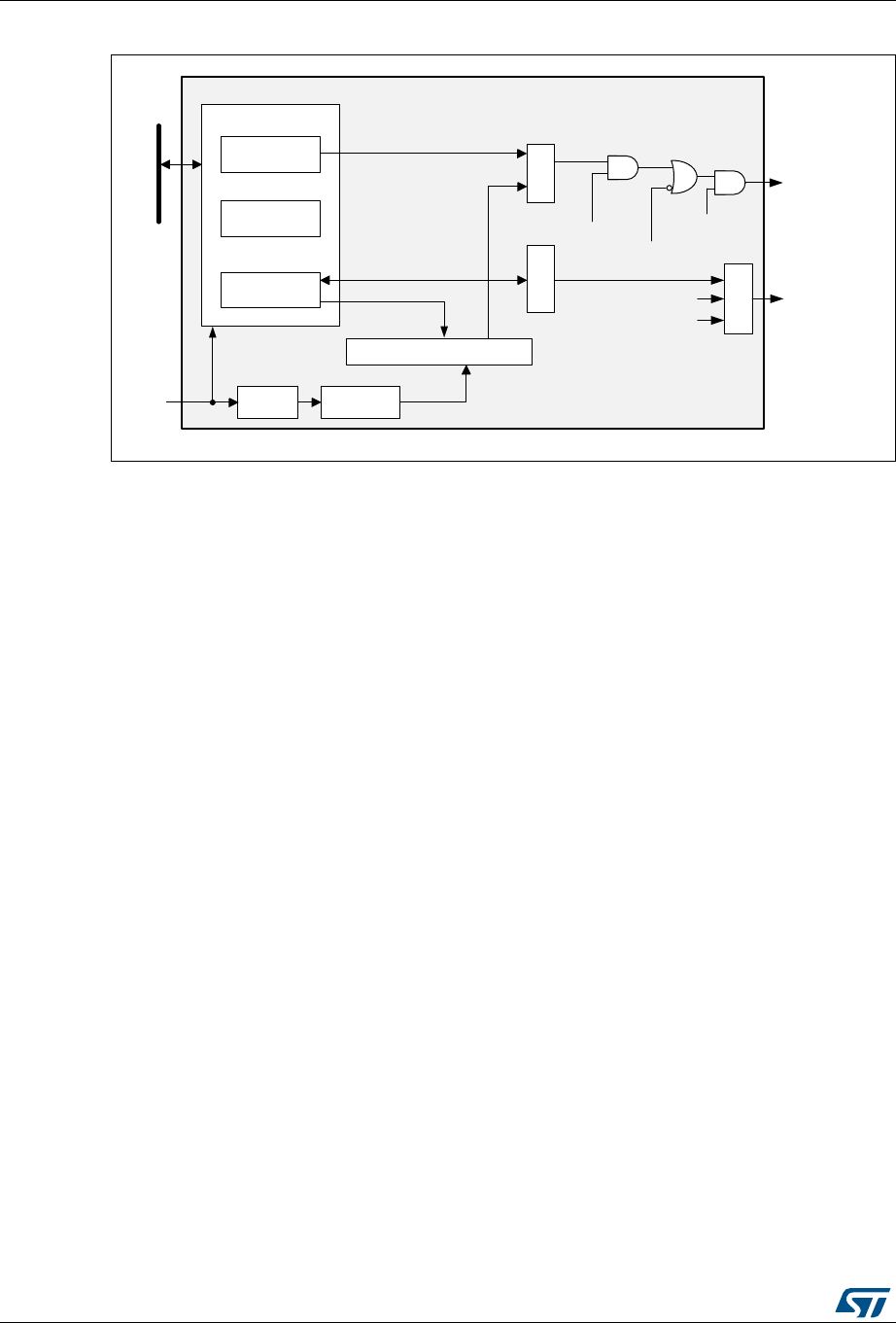
System window watchdog (WWDG) RM0376
602/1001 DocID025941 Rev 5
Figure 191. Watchdog block diagram
25.3.1 Enabling the watchdog
The watchdog is always disabled after a reset. It is enabled by setting the WDGA bit in the
WWDG_CR register, then it cannot be disabled again except by a reset.
25.3.2 Controlling the downcounter
This downcounter is free-running, counting down even if the watchdog is disabled. When
the watchdog is enabled, the T6 bit must be set to prevent generating an immediate reset.
The T[5:0] bits contain the number of increments which represents the time delay before the
watchdog produces a reset. The timing varies between a minimum and a maximum value
due to the unknown status of the prescaler when writing to the WWDG_CR register (see
Figure 192). The Configuration register (WWDG_CFR) contains the high limit of the window:
To prevent a reset, the downcounter must be reloaded when its value is lower than the
window register value and greater than 0x3F. Figure 192 describes the window watchdog
process.
Note: The T6 bit can be used to generate a software reset (the WDGA bit is set and the T6 bit is
cleared).
25.3.3 Advanced watchdog interrupt feature
The Early Wakeup Interrupt (EWI) can be used if specific safety operations or data logging
must be performed before the actual reset is generated. The EWI interrupt is enabled by
setting the EWI bit in the WWDG_CFR register. When the downcounter reaches the value
0x40, an EWI interrupt is generated and the corresponding interrupt service routine (ISR)
can be used to trigger specific actions (such as communications or data logging), before
resetting the device.
In some applications, the EWI interrupt can be used to manage a software system check
and/or system recovery/graceful degradation, without generating a WWDG reset. In this
case, the corresponding interrupt service routine (ISR) should reload the WWDG counter to
avoid the WWDG reset, then trigger the required actions.
MS47214V1
7-bit DownCounter (CNT)
WWDG
pclk
APB bus
÷ 4096 ÷ 2WDGTB
Write to WWDG_CR
CMP = 1 when
T[6:0] > W[6:0]
CMP
T[6:0]
preload
WWDG_CR
wwdg_out_rst
wwdg_it
= 0x40 ?
readback
WWDG_CFR W[6:0]
cnt_out
Register interface
WWDG_SR
T6
T[6:0]
WDGA
EWI
Logic
EWIF
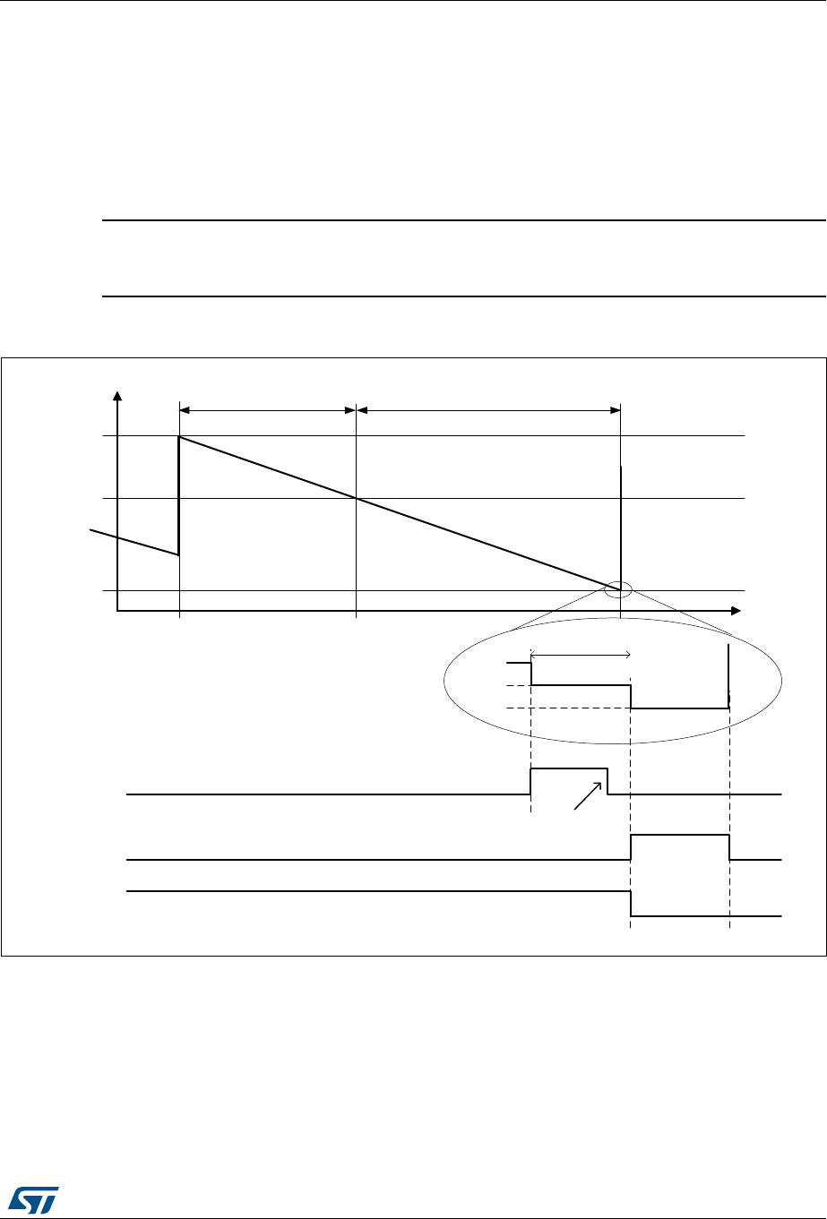
DocID025941 Rev 5 603/1001
RM0376 System window watchdog (WWDG)
607
The EWI interrupt is cleared by writing '0' to the EWIF bit in the WWDG_SR register.
Note: When the EWI interrupt cannot be served, e.g. due to a system lock in a higher priority task,
the WWDG reset will eventually be generated.
25.3.4 How to program the watchdog timeout
Use the formula in Figure 192 to calculate the WWDG timeout.
Warning: When writing to the WWDG_CR register, always write 1 in the
T6 bit to avoid generating an immediate reset.
Figure 192. Window watchdog timing diagram
The formula to calculate the timeout value is given by:
MS47266V1
W[6:0]
0x3F
0x41
0x40
0x3F
wwdg_ewit
wwdg_rst
Refresh not allowed Refresh allowed
Time
T[6:0]
Tpclk x 4096 x 2WDGTB
CNT DownCounter
T6 bit
EWIF = 0
tWWDG tPCLK1 4096 2WDGTB[1:0] T5:0[]1+()×××=ms()

System window watchdog (WWDG) RM0376
604/1001 DocID025941 Rev 5
where:
tWWDG: WWDG timeout
tPCLK: APB1 clock period measured in ms
4096: value corresponding to internal divider
As an example, lets assume APB1 frequency is equal to 32 MHz, WDGTB[1:0] is set to 3
and T[5:0] is set to 63:
Refer to the datasheet for the minimum and maximum values of the tWWDG.
For code example, refer to A.14.1: WWDG configuration code example.
25.3.5 Debug mode
When the microcontroller enters debug mode (processor halted), the WWDG counter either
continues to work normally or stops, depending on the configuration bit in DBG module. For
more details refer to Section 32.9.2: Debug support for timers, watchdog and I2C.
tWWDG 1 32000⁄()4096 23
×× 63 1+()×65.54ms==

DocID025941 Rev 5 605/1001
RM0376 System window watchdog (WWDG)
607
25.4 WWDG registers
Refer to Section 1.1 on page 51 for a list of abbreviations used in register descriptions.
The peripheral registers can be accessed by half-words (16-bit) or words (32-bit).
25.4.1 Control register (WWDG_CR)
Address offset: 0x000
Reset value: 0x0000 007F
25.4.2 Configuration register (WWDG_CFR)
Address offset: 0x004
Reset value: 0x0000 007F
31 30 29 28 27 26 25 24 23 22 21 20 19 18 17 16
Res. Res. Res. Res. Res. Res. Res. Res. Res. Res. Res. Res. Res. Res. Res. Res.
1514131211109876543210
Res. Res. Res. Res. Res. Res. Res. Res. WDGA T[6:0]
rs rw rw rw rw rw rw rw
Bits 31:8 Reserved, must be kept at reset value.
Bit 7 WDGA: Activation bit
This bit is set by software and only cleared by hardware after a reset. When WDGA = 1, the
watchdog can generate a reset.
0: Watchdog disabled
1: Watchdog enabled
Bits 6:0 T[6:0]: 7-bit counter (MSB to LSB)
These bits contain the value of the watchdog counter, decremented every
(4096 x 2WDGTB[1:0]) PCLK cycles. A reset is produced when it is decremented from 0x40 to
0x3F (T6 becomes cleared).
31 30 29 28 27 26 25 24 23 22 21 20 19 18 17 16
Res. Res. Res. Res. Res. Res. Res. Res. Res. Res. Res. Res. Res. Res. Res. Res.
1514131211109876543210
Res. Res. Res. Res. Res. Res. EWI WDGTB[1:0] W[6:0]
rs rw rw rw rw rw rw rw rw rw
Bits 31:10 Reserved, must be kept at reset value.
Bit 9 EWI: Early wakeup interrupt
When set, an interrupt occurs whenever the counter reaches the value 0x40. This interrupt is
only cleared by hardware after a reset.

System window watchdog (WWDG) RM0376
606/1001 DocID025941 Rev 5
25.4.3 Status register (WWDG_SR)
Address offset: 0x008
Reset value: 0x0000 0000
Bits 8:7 WDGTB[1:0]: Timer base
The time base of the prescaler can be modified as follows:
00: CK Counter Clock (PCLK div 4096) div 1
01: CK Counter Clock (PCLK div 4096) div 2
10: CK Counter Clock (PCLK div 4096) div 4
11: CK Counter Clock (PCLK div 4096) div 8
Bits 6:0 W[6:0]: 7-bit window value
These bits contain the window value to be compared with the downcounter.
31 30 29 28 27 26 25 24 23 22 21 20 19 18 17 16
Res. Res. Res. Res. Res. Res. Res. Res. Res. Res. Res. Res. Res. Res. Res. Res.
1514131211109876543210
Res. Res. Res. Res. Res. Res. Res. Res. Res. Res. Res. Res. Res. Res. Res. EWIF
rc_w0
Bits 31:1 Reserved, must be kept at reset value.
Bit 0 EWIF: Early wakeup interrupt flag
This bit is set by hardware when the counter has reached the value 0x40. It must be cleared by
software by writing ‘0’. Writing ‘1’ has no effect. This bit is also set if the interrupt is not enabled.

DocID025941 Rev 5 607/1001
RM0376 System window watchdog (WWDG)
607
25.4.4 WWDG register map
The following table gives the WWDG register map and reset values.
Refer to Section 2.2.2: Memory map and register boundary addresses for the register
boundary addresses.
Table 104. WWDG register map and reset values
Offset Register
31
30
29
28
27
26
25
24
23
22
21
20
19
18
17
16
15
14
13
12
11
10
9
8
7
6
5
4
3
2
1
0
0x000 WWDG_CR
Res.
Res.
Res.
Res.
Res.
Res.
Res.
Res.
Res.
Res.
Res.
Res.
Res.
Res.
Res.
Res.
Res.
Res.
Res.
Res.
Res.
Res.
Res.
Res.
WDGA
T[6:0]
Reset value 01111111
0x004 WWDG_CFR
Res.
Res.
Res.
Res.
Res.
Res.
Res.
Res.
Res.
Res.
Res.
Res.
Res.
Res.
Res.
Res.
Res.
Res.
Res.
Res.
Res.
Res.
EWI
WDGTB1
WDGTB0
W[6:0]
Reset value 0001111111
0x008 WWDG_SR
Res.
Res.
Res.
Res.
Res.
Res.
Res.
Res.
Res.
Res.
Res.
Res.
Res.
Res.
Res.
Res.
Res.
Res.
Res.
Res.
Res.
Res.
Res.
Res.
Res.
Res.
Res.
Res.
Res.
Res.
Res.
EWIF
Reset value 0

Real-time clock (RTC) RM0376
608/1001 DocID025941 Rev 5
26 Real-time clock (RTC)
26.1 Introduction
The RTC provides an automatic wakeup to manage all low-power modes.
The real-time clock (RTC) is an independent BCD timer/counter. The RTC provides a time-
of-day clock/calendar with programmable alarm interrupts.
The RTC includes also a periodic programmable wakeup flag with interrupt capability.
Two 32-bit registers contain the seconds, minutes, hours (12- or 24-hour format), day (day
of week), date (day of month), month, and year, expressed in binary coded decimal format
(BCD). The sub-seconds value is also available in binary format.
Compensations for 28-, 29- (leap year), 30-, and 31-day months are performed
automatically. Daylight saving time compensation can also be performed.
Additional 32-bit registers contain the programmable alarm subseconds, seconds, minutes,
hours, day, and date.
A digital calibration feature is available to compensate for any deviation in crystal oscillator
accuracy.
After RTC domain reset, all RTC registers are protected against possible parasitic write
accesses.
As long as the supply voltage remains in the operating range, the RTC never stops,
regardless of the device status (Run mode, low-power mode or under reset).
DocID025941 Rev 5 609/1001
RM0376 Real-time clock (RTC)
651
26.2 RTC main features
The RTC unit main features are the following (see Figure 193: RTC block diagram):
•Calendar with subseconds, seconds, minutes, hours (12 or 24 format), day (day of
week), date (day of month), month, and year.
•Daylight saving compensation programmable by software.
•Programmable alarm with interrupt function. The alarm can be triggered by any
combination of the calendar fields.
•Automatic wakeup unit generating a periodic flag that triggers an automatic wakeup
interrupt.
•Reference clock detection: a more precise second source clock (50 or 60 Hz) can be
used to enhance the calendar precision.
•Accurate synchronization with an external clock using the subsecond shift feature.
•Digital calibration circuit (periodic counter correction): 0.95 ppm accuracy, obtained in a
calibration window of several seconds
•Time-stamp function for event saving
•Tamper detection event with configurable filter and internal pull-up
•Maskable interrupts/events:
–Alarm A
–Alarm B
– Wakeup interrupt
– Time-stamp
– Tamper detection
•5 backup registers.
26.3 RTC implementation
Table 105. RTC implementation(1)
1. X = supported, ‘-’= not supported.
RTC Features Category 3 Category 5
Periodic wakeup timer X X
RTC_TAMP1
RTC_TAMP2 X X
RTC_TAMP3 - X
Alarm A X X
Alarm B X X
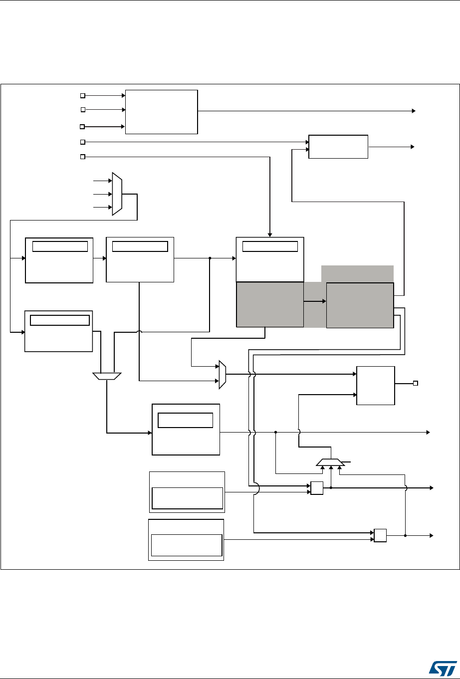
Real-time clock (RTC) RM0376
610/1001 DocID025941 Rev 5
26.4 RTC functional description
26.4.1 RTC block diagram
Figure 193. RTC block diagram
1. RTC_TAMP3 is available only on category 5 devices.
MS33460V5
Calendar
HSE
prescaled
LSE (32.768 Hz)
LSI
Synchronous
15-bit prescaler
(default = 256)
ALRAF
RTC_PRER
Backup registers
and RTC tamper
control registers
TAMPxF
Time stamp
registers TSF
Ouput
control
Smooth
calibration
=
RTC_PRERRTC_CALR
Shadow registers
RTC_TR,
RTC_DR
RTC_ALRMAR
RTC_ALRMASSR
Shadow register
RTC_SSR
RTC_ALRMBR
RTC_ALRMBSSR
=ALRBF
Prescaler
2, 4, 8, 16
WUCKSEL[1:0]
16-bit wakeup
auto reload timer
RTC_WUTR
WUTF
OSEL[1:0]
RTC_TAMP2
RTC_TAMP1
RTC_TS
RTC_REFIN
RTCCLK
Asynchronous
7-bit prescaler
(default = 128)
ck_apre
(default 256 Hz)
ck_spre
(default 1 Hz)
Alarm A
Alarm B
RTC_OUT
RTC_CALIB
RTC_ALARM
RTC_TAMP3

DocID025941 Rev 5 611/1001
RM0376 Real-time clock (RTC)
651
The RTC includes:
•Two alarms
•Up to three tamper events from I/Os
– Tamper detection erases the backup registers.
•One timestamp event from I/O
•Tamper event detection can generate a timestamp event
•5 x 32-bit backup registers
•Output functions: RTC_OUT which selects one of the following two outputs:
– RTC_CALIB: 512 Hz or 1Hz clock output (with an LSE frequency of 32.768 kHz).
This output is enabled by setting the COE bit in the RTC_CR register.
– RTC_ALARM: This output is enabled by configuring the OSEL[1:0] bits in the
RTC_CR register which select the Alarm A, Alarm B or Wakeup outputs.
•Input functions:
– RTC_TS: timestamp event
– RTC_TAMP1: tamper1 event detection
– RTC_TAMP2: tamper2 event detection
– RTC_TAMP3: tamper3 event detection (only on category 5 devices).
– RTC_REFIN: 50 or 60 Hz reference clock input
26.4.2 GPIOs controlled by the RTC
RTC_OUT, RTC_TS and RTC_TAMP1 are mapped on the same pin (PC13). PC13 pin
configuration is controlled by the RTC, whatever the PC13 GPIO configuration, except for
the RTC_ALARM output open-drain mode.
The output mechanism follows the priority order shown in Table 106.
Table 106. RTC pin PC13 configuration(1)
PC13 Pin
configuration
and function
OSEL[1:0]
bits
(RTC_ALARM
output
enable)
COE bit
(RTC_CALIB
output
enable)
RTC_OUT
_RMP
bit
RTC_ALARM
_TYPE
bit
TAMP1E bit
(RTC_TAMP1
input
enable)
TSE bit
(RTC_TS
input
enable)
RTC_ALARM
output OD 01 or 10 or 11 Don’t care
0
0 Don’t care Don’t care
1
RTC_ALARM
output PP 01 or 10 or 11 Don’t care
0
1 Don’t care Don’t care
1
RTC_CALIB
output PP 00 1 0 Don’t care Don’t care Don’t care
RTC_TAMP1
input floating
00 0 Don’t care
Don’t care 1 000 1
1
01 or 10 or 11 0

Real-time clock (RTC) RM0376
612/1001 DocID025941 Rev 5
In addition, it is possible to remap RTC_OUT on PB14 pin thanks to RTC_OUT_RMP bit. In
this case it is mandatory to configure PB14 GPIO registers as alternate function with the
correct type. The remap functions are shown in Table 107.
26.4.3 Clock and prescalers
The RTC clock source (RTCCLK) is selected through the clock controller among the LSE
clock, the LSI oscillator clock, and the HSE clock. For more information on the RTC clock
source configuration, refer to Section 7: Reset and clock control (RCC).
RTC_TS and
RTC_TAMP1
input floating
00 0 Don’t care
Don’t care 1 100 1
1
01 or 10 or 11 0
RTC_TS input
floating
00 0 Don’t care
Don’t care 0 100 1
1
01 or 10 or 11 0
Wakeup pin or
Standard
GPIO
00 0 Don’t care
Don’t care 0 000 1
1
01 or 10 or 11 0
1. OD: open drain; PP: push-pull.
Table 106. RTC pin PC13 configuration(1) (continued)
PC13 Pin
configuration
and function
OSEL[1:0]
bits
(RTC_ALARM
output
enable)
COE bit
(RTC_CALIB
output
enable)
RTC_OUT
_RMP
bit
RTC_ALARM
_TYPE
bit
TAMP1E bit
(RTC_TAMP1
input
enable)
TSE bit
(RTC_TS
input
enable)
Table 107. RTC_OUT mapping
OSEL[1:0] bits
(RTC_ALARM
output enable)
COE bit
(RTC_CALIB output
enable)
RTC_OUT_RMP
bit RTC_OUT on PC13 RTC_OUT on PB14
00 0
0
--
00 1 RTC_CALIB -
01 or 10 or 11 Don’t care RTC_ALARM -
00 0
1
--
00 1 - RTC_CALIB
01 or 10 or 11 0 - RTC_ALARM
01 or 10 or 11 1 RTC_ALARM RTC_CALIB

DocID025941 Rev 5 613/1001
RM0376 Real-time clock (RTC)
651
A programmable prescaler stage generates a 1 Hz clock which is used to update the
calendar. To minimize power consumption, the prescaler is split into 2 programmable
prescalers (see Figure 193: RTC block diagram):
•A 7-bit asynchronous prescaler configured through the PREDIV_A bits of the
RTC_PRER register.
•A 15-bit synchronous prescaler configured through the PREDIV_S bits of the
RTC_PRER register.
Note: When both prescalers are used, it is recommended to configure the asynchronous prescaler
to a high value to minimize consumption.
The asynchronous prescaler division factor is set to 128, and the synchronous division
factor to 256, to obtain an internal clock frequency of 1 Hz (ck_spre) with an LSE frequency
of 32.768 kHz.
The minimum division factor is 1 and the maximum division factor is 222.
This corresponds to a maximum input frequency of around 4 MHz.
fck_apre is given by the following formula:
The ck_apre clock is used to clock the binary RTC_SSR subseconds downcounter. When it
reaches 0, RTC_SSR is reloaded with the content of PREDIV_S.
fck_spre is given by the following formula:
The ck_spre clock can be used either to update the calendar or as timebase for the 16-bit
wakeup auto-reload timer. To obtain short timeout periods, the 16-bit wakeup auto-reload
timer can also run with the RTCCLK divided by the programmable 4-bit asynchronous
prescaler (see Section 26.4.6: Periodic auto-wakeup for details).
26.4.4 Real-time clock and calendar
The RTC calendar time and date registers are accessed through shadow registers which
are synchronized with PCLK (APB clock). They can also be accessed directly in order to
avoid waiting for the synchronization duration.
•RTC_SSR for the subseconds
•RTC_TR for the time
•RTC_DR for the date
Every two RTCCLK periods, the current calendar value is copied into the shadow registers,
and the RSF bit of RTC_ISR register is set (see Section 26.7.4: RTC initialization and status
register (RTC_ISR)). The copy is not performed in Stop and Standby mode. When exiting
these modes, the shadow registers are updated after up to 2 RTCCLK periods.
When the application reads the calendar registers, it accesses the content of the shadow
registers. It is possible to make a direct access to the calendar registers by setting the
fCK_APRE
fRTCCLK
PREDIV_A 1+
---------------------------------------
=
fCK_SPRE
fRTCCLK
PREDIV_S 1+()PREDIV_A 1+()×
-----------------------------------------------------------------------------------------------
=

Real-time clock (RTC) RM0376
614/1001 DocID025941 Rev 5
BYPSHAD control bit in the RTC_CR register. By default, this bit is cleared, and the user
accesses the shadow registers.
When reading the RTC_SSR, RTC_TR or RTC_DR registers in BYPSHAD=0 mode, the
frequency of the APB clock (fAPB) must be at least 7 times the frequency of the RTC clock
(fRTCCLK).
The shadow registers are reset by system reset.
26.4.5 Programmable alarms
The RTC unit provides programmable alarm: Alarm A and Alarm B. The description below is
given for Alarm A, but can be translated in the same way for Alarm B.
The programmable alarm function is enabled through the ALRAE bit in the RTC_CR
register. The ALRAF is set to 1 if the calendar subseconds, seconds, minutes, hours, date
or day match the values programmed in the alarm registers RTC_ALRMASSR and
RTC_ALRMAR. Each calendar field can be independently selected through the MSKx bits
of the RTC_ALRMAR register, and through the MASKSSx bits of the RTC_ALRMASSR
register. The alarm interrupt is enabled through the ALRAIE bit in the RTC_CR register.
Caution: If the seconds field is selected (MSK1 bit reset in RTC_ALRMAR), the synchronous
prescaler division factor set in the RTC_PRER register must be at least 3 to ensure correct
behavior.
Alarm A and Alarm B (if enabled by bits OSEL[1:0] in RTC_CR register) can be routed to the
RTC_ALARM output. RTC_ALARM output polarity can be configured through bit POL the
RTC_CR register.
26.4.6 Periodic auto-wakeup
The periodic wakeup flag is generated by a 16-bit programmable auto-reload down-counter.
The wakeup timer range can be extended to 17 bits.
The wakeup function is enabled through the WUTE bit in the RTC_CR register.
The wakeup timer clock input can be:
•RTC clock (RTCCLK) divided by 2, 4, 8, or 16.
When RTCCLK is LSE(32.768kHz), this allows to configure the wakeup interrupt period
from 122 µs to 32 s, with a resolution down to 61 µs.
•ck_spre (usually 1 Hz internal clock)
When ck_spre frequency is 1Hz, this allows to achieve a wakeup time from 1 s to
around 36 hours with one-second resolution. This large programmable time range is
divided in 2 parts:
– from 1s to 18 hours when WUCKSEL [2:1] = 10
– and from around 18h to 36h when WUCKSEL[2:1] = 11. In this last case 216 is
added to the 16-bit counter current value.When the initialization sequence is
complete (see Programming the wakeup timer on page 616), the timer starts
counting down.When the wakeup function is enabled, the down-counting remains
active in low-power modes. In addition, when it reaches 0, the WUTF flag is set in
the RTC_ISR register, and the wakeup counter is automatically reloaded with its
reload value (RTC_WUTR register value).
The WUTF flag must then be cleared by software.

DocID025941 Rev 5 615/1001
RM0376 Real-time clock (RTC)
651
When the periodic wakeup interrupt is enabled by setting the WUTIE bit in the RTC_CR
register, it can exit the device from low-power modes.
The periodic wakeup flag can be routed to the RTC_ALARM output provided it has been
enabled through bits OSEL[1:0] of RTC_CR register. RTC_ALARM output polarity can be
configured through the POL bit in the RTC_CR register.
System reset, as well as low-power modes (Sleep, Stop and Standby) have no influence on
the wakeup timer.
26.4.7 RTC initialization and configuration
RTC register access
The RTC registers are 32-bit registers. The APB interface introduces 2 wait-states in RTC
register accesses except on read accesses to calendar shadow registers when
BYPSHAD=0.
RTC register write protection
After system reset, the RTC registers are protected against parasitic write access by
clearing the DBP bit in the PWR_CR register (refer to the power control section). DBP bit
must be set in order to enable RTC registers write access.
After RTC domain reset, all the RTC registers are write-protected. Writing to the RTC
registers is enabled by writing a key into the Write Protection register, RTC_WPR.
The following steps are required to unlock the write protection on all the RTC registers
except for RTC_TAMPCR, RTC_BKPxR, RTC_OR and RTC_ISR[13:8].
1. Write ‘0xCA’ into the RTC_WPR register.
2. Write ‘0x53’ into the RTC_WPR register.
Writing a wrong key reactivates the write protection.
The protection mechanism is not affected by system reset.
Calendar initialization and configuration
To program the initial time and date calendar values, including the time format and the
prescaler configuration, the following sequence is required:
1. Set INIT bit to 1 in the RTC_ISR register to enter initialization mode. In this mode, the
calendar counter is stopped and its value can be updated.
2. Poll INITF bit of in the RTC_ISR register. The initialization phase mode is entered when
INITF is set to 1. It takes around 2 RTCCLK clock cycles (due to clock synchronization).
3. To generate a 1 Hz clock for the calendar counter, program both the prescaler factors in
RTC_PRER register.
4. Load the initial time and date values in the shadow registers (RTC_TR and RTC_DR),
and configure the time format (12 or 24 hours) through the FMT bit in the RTC_CR
register.
5. Exit the initialization mode by clearing the INIT bit. The actual calendar counter value is
then automatically loaded and the counting restarts after 4 RTCCLK clock cycles.
When the initialization sequence is complete, the calendar starts counting.

Real-time clock (RTC) RM0376
616/1001 DocID025941 Rev 5
Note: After a system reset, the application can read the INITS flag in the RTC_ISR register to
check if the calendar has been initialized or not. If this flag equals 0, the calendar has not
been initialized since the year field is set at its RTC domain reset default value (0x00).
To read the calendar after initialization, the software must first check that the RSF flag is set
in the RTC_ISR register.
For code example, refer to A.15.1: RTC calendar configuration code example.
Daylight saving time
The daylight saving time management is performed through bits SUB1H, ADD1H, and BKP
of the RTC_CR register.
Using SUB1H or ADD1H, the software can subtract or add one hour to the calendar in one
single operation without going through the initialization procedure.
In addition, the software can use the BKP bit to memorize this operation.
Programming the alarm
A similar procedure must be followed to program or update the programmable alarms. The
procedure below is given for Alarm A but can be translated in the same way for Alarm B.
1. Clear ALRAE in RTC_CR to disable Alarm A.
2. Program the Alarm A registers (RTC_ALRMASSR/RTC_ALRMAR).
3. Set ALRAE in the RTC_CR register to enable Alarm A again.
Note: Each change of the RTC_CR register is taken into account after around 2 RTCCLK clock
cycles due to clock synchronization.
For code example, refer to A.15.2: RTC alarm configuration code example.
Programming the wakeup timer
The following sequence is required to configure or change the wakeup timer auto-reload
value (WUT[15:0] in RTC_WUTR):
1. Clear WUTE in RTC_CR to disable the wakeup timer.
2. Poll WUTWF until it is set in RTC_ISR to make sure the access to wakeup auto-reload
counter and to WUCKSEL[2:0] bits is allowed. It takes around 2 RTCCLK clock cycles
(due to clock synchronization).
3. Program the wakeup auto-reload value WUT[15:0], and the wakeup clock selection
(WUCKSEL[2:0] bits in RTC_CR). Set WUTE in RTC_CR to enable the timer again.
The wakeup timer restarts down-counting. The WUTWF bit is cleared up to 2 RTCCLK
clock cycles after WUTE is cleared, due to clock synchronization.
For code example, refer to A.15.3: RTC WUT configuration code example.
26.4.8 Reading the calendar
When BYPSHAD control bit is cleared in the RTC_CR register
To read the RTC calendar registers (RTC_SSR, RTC_TR and RTC_DR) properly, the APB1
clock frequency (fPCLK) must be equal to or greater than seven times the RTC clock
frequency (fRTCCLK). This ensures a secure behavior of the synchronization mechanism.

DocID025941 Rev 5 617/1001
RM0376 Real-time clock (RTC)
651
If the APB1 clock frequency is less than seven times the RTC clock frequency, the software
must read the calendar time and date registers twice. If the second read of the RTC_TR
gives the same result as the first read, this ensures that the data is correct. Otherwise a third
read access must be done. In any case the APB1 clock frequency must never be lower than
the RTC clock frequency.
The RSF bit is set in RTC_ISR register each time the calendar registers are copied into the
RTC_SSR, RTC_TR and RTC_DR shadow registers. The copy is performed every two
RTCCLK cycles. To ensure consistency between the 3 values, reading either RTC_SSR or
RTC_TR locks the values in the higher-order calendar shadow registers until RTC_DR is
read. In case the software makes read accesses to the calendar in a time interval smaller
than 2 RTCCLK periods: RSF must be cleared by software after the first calendar read, and
then the software must wait until RSF is set before reading again the RTC_SSR, RTC_TR
and RTC_DR registers.
After waking up from low-power mode (Stop or Standby), RSF must be cleared by software.
The software must then wait until it is set again before reading the RTC_SSR, RTC_TR and
RTC_DR registers.
The RSF bit must be cleared after wakeup and not before entering low-power mode.
After a system reset, the software must wait until RSF is set before reading the RTC_SSR,
RTC_TR and RTC_DR registers. Indeed, a system reset resets the shadow registers to
their default values.
After an initialization (refer to Calendar initialization and configuration on page 615): the
software must wait until RSF is set before reading the RTC_SSR, RTC_TR and RTC_DR
registers.
After synchronization (refer to Section 26.4.10: RTC synchronization): the software must
wait until RSF is set before reading the RTC_SSR, RTC_TR and RTC_DR registers.
For code example, refer to A.15.4: RTC read calendar code example.
When the BYPSHAD control bit is set in the RTC_CR register (bypass shadow
registers)
Reading the calendar registers gives the values from the calendar counters directly, thus
eliminating the need to wait for the RSF bit to be set. This is especially useful after exiting
from low-power modes (STOP or Standby), since the shadow registers are not updated
during these modes.
When the BYPSHAD bit is set to 1, the results of the different registers might not be
coherent with each other if an RTCCLK edge occurs between two read accesses to the
registers. Additionally, the value of one of the registers may be incorrect if an RTCCLK edge
occurs during the read operation. The software must read all the registers twice, and then
compare the results to confirm that the data is coherent and correct. Alternatively, the
software can just compare the two results of the least-significant calendar register.
Note: While BYPSHAD=1, instructions which read the calendar registers require one extra APB
cycle to complete.

Real-time clock (RTC) RM0376
618/1001 DocID025941 Rev 5
26.4.9 Resetting the RTC
The calendar shadow registers (RTC_SSR, RTC_TR and RTC_DR) and some bits of the
RTC status register (RTC_ISR) are reset to their default values by all available system reset
sources.
On the contrary, the following registers are reset to their default values by a RTC domain
reset and are not affected by a system reset: the RTC current calendar registers, the RTC
control register (RTC_CR), the prescaler register (RTC_PRER), the RTC calibration register
(RTC_CALR), the RTC shift register (RTC_SHIFTR), the RTC timestamp registers
(RTC_TSSSR, RTC_TSTR and RTC_TSDR), the RTC tamper configuration register
(RTC_TAMPCR), the RTC backup registers (RTC_BKPxR), the wakeup timer register
(RTC_WUTR), the Alarm A and Alarm B registers (RTC_ALRMASSR/RTC_ALRMAR and
RTC_ALRMBSSR/RTC_ALRMBR), and the Option register (RTC_OR).
In addition, when it is clocked by the LSE, the RTC keeps on running under system reset if
the reset source is different from the RTC domain reset one (refer to the RTC clock section
of the Reset and clock controller for details on the list of RTC clock sources not affected by
system reset). When a RTC domain reset occurs, the RTC is stopped and all the RTC
registers are set to their reset values.
26.4.10 RTC synchronization
The RTC can be synchronized to a remote clock with a high degree of precision. After
reading the sub-second field (RTC_SSR or RTC_TSSSR), a calculation can be made of the
precise offset between the times being maintained by the remote clock and the RTC. The
RTC can then be adjusted to eliminate this offset by “shifting” its clock by a fraction of a
second using RTC_SHIFTR.
RTC_SSR contains the value of the synchronous prescaler counter. This allows one to
calculate the exact time being maintained by the RTC down to a resolution of
1 / (PREDIV_S + 1) seconds. As a consequence, the resolution can be improved by
increasing the synchronous prescaler value (PREDIV_S[14:0]. The maximum resolution
allowed (30.52 μs with a 32768 Hz clock) is obtained with PREDIV_S set to 0x7FFF.
However, increasing PREDIV_S means that PREDIV_A must be decreased in order to
maintain the synchronous prescaler output at 1 Hz. In this way, the frequency of the
asynchronous prescaler output increases, which may increase the RTC dynamic
consumption.
The RTC can be finely adjusted using the RTC shift control register (RTC_SHIFTR). Writing
to RTC_SHIFTR can shift (either delay or advance) the clock by up to a second with a
resolution of 1 / (PREDIV_S + 1) seconds. The shift operation consists of adding the
SUBFS[14:0] value to the synchronous prescaler counter SS[15:0]: this will delay the clock.
If at the same time the ADD1S bit is set, this results in adding one second and at the same
time subtracting a fraction of second, so this will advance the clock.
Caution: Before initiating a shift operation, the user must check that SS[15] = 0 in order to ensure that
no overflow will occur.
As soon as a shift operation is initiated by a write to the RTC_SHIFTR register, the SHPF
flag is set by hardware to indicate that a shift operation is pending. This bit is cleared by
hardware as soon as the shift operation has completed.
Caution: This synchronization feature is not compatible with the reference clock detection feature:
firmware must not write to RTC_SHIFTR when REFCKON=1.

DocID025941 Rev 5 619/1001
RM0376 Real-time clock (RTC)
651
26.4.11 RTC reference clock detection
The update of the RTC calendar can be synchronized to a reference clock, RTC_REFIN,
which is usually the mains frequency (50 or 60 Hz). The precision of the RTC_REFIN
reference clock should be higher than the 32.768 kHz LSE clock. When the RTC_REFIN
detection is enabled (REFCKON bit of RTC_CR set to 1), the calendar is still clocked by the
LSE, and RTC_REFIN is used to compensate for the imprecision of the calendar update
frequency (1 Hz).
Each 1 Hz clock edge is compared to the nearest RTC_REFIN clock edge (if one is found
within a given time window). In most cases, the two clock edges are properly aligned. When
the 1 Hz clock becomes misaligned due to the imprecision of the LSE clock, the RTC shifts
the 1 Hz clock a bit so that future 1 Hz clock edges are aligned. Thanks to this mechanism,
the calendar becomes as precise as the reference clock.
The RTC detects if the reference clock source is present by using the 256 Hz clock
(ck_apre) generated from the 32.768 kHz quartz. The detection is performed during a time
window around each of the calendar updates (every 1 s). The window equals 7 ck_apre
periods when detecting the first reference clock edge. A smaller window of 3 ck_apre
periods is used for subsequent calendar updates.
Each time the reference clock is detected in the window, the synchronous prescaler which
outputs the ck_spre clock is forced to reload. This has no effect when the reference clock
and the 1 Hz clock are aligned because the prescaler is being reloaded at the same
moment. When the clocks are not aligned, the reload shifts future 1 Hz clock edges a little
for them to be aligned with the reference clock.
If the reference clock halts (no reference clock edge occurred during the 3 ck_apre window),
the calendar is updated continuously based solely on the LSE clock. The RTC then waits for
the reference clock using a large 7 ck_apre period detection window centered on the
ck_spre edge.
When the RTC_REFIN detection is enabled, PREDIV_A and PREDIV_S must be set to their
default values:
•PREDIV_A = 0x007F
•PREVID_S = 0x00FF
Note: RTC_REFIN clock detection is not available in Standby mode.
26.4.12 RTC smooth digital calibration
The RTC frequency can be digitally calibrated with a resolution of about 0.954 ppm with a
range from -487.1 ppm to +488.5 ppm. The correction of the frequency is performed using
series of small adjustments (adding and/or subtracting individual RTCCLK pulses). These
adjustments are fairly well distributed so that the RTC is well calibrated even when observed
over short durations of time.
The smooth digital calibration is performed during a cycle of about 220 RTCCLK pulses, or
32 seconds when the input frequency is 32768 Hz. This cycle is maintained by a 20-bit
counter, cal_cnt[19:0], clocked by RTCCLK.
The smooth calibration register (RTC_CALR) specifies the number of RTCCLK clock cycles
to be masked during the 32-second cycle:
•Setting the bit CALM[0] to 1 causes exactly one pulse to be masked during the 32-

Real-time clock (RTC) RM0376
620/1001 DocID025941 Rev 5
second cycle.
•Setting CALM[1] to 1 causes two additional cycles to be masked
•Setting CALM[2] to 1 causes four additional cycles to be masked
•and so on up to CALM[8] set to 1 which causes 256 clocks to be masked.
Note: CALM[8:0] (RTC_CALR) specifies the number of RTCCLK pulses to be masked during the
32-second cycle. Setting the bit CALM[0] to ‘1’ causes exactly one pulse to be masked
during the 32-second cycle at the moment when cal_cnt[19:0] is 0x80000; CALM[1]=1
causes two other cycles to be masked (when cal_cnt is 0x40000 and 0xC0000); CALM[2]=1
causes four other cycles to be masked (cal_cnt = 0x20000/0x60000/0xA0000/ 0xE0000);
and so on up to CALM[8]=1 which causes 256 clocks to be masked (cal_cnt = 0xXX800).
While CALM allows the RTC frequency to be reduced by up to 487.1 ppm with fine
resolution, the bit CALP can be used to increase the frequency by 488.5 ppm. Setting CALP
to ‘1’ effectively inserts an extra RTCCLK pulse every 211 RTCCLK cycles, which means
that 512 clocks are added during every 32-second cycle.
Using CALM together with CALP, an offset ranging from -511 to +512 RTCCLK cycles can
be added during the 32-second cycle, which translates to a calibration range of -487.1 ppm
to +488.5 ppm with a resolution of about 0.954 ppm.
The formula to calculate the effective calibrated frequency (FCAL) given the input frequency
(FRTCCLK) is as follows:
FCAL = FRTCCLK x [1 + (CALP x 512 - CALM) / (220 + CALM - CALP x 512)]
Calibration when PREDIV_A<3
The CALP bit can not be set to 1 when the asynchronous prescaler value (PREDIV_A bits in
RTC_PRER register) is less than 3. If CALP was already set to 1 and PREDIV_A bits are
set to a value less than 3, CALP is ignored and the calibration operates as if CALP was
equal to 0.
To perform a calibration with PREDIV_A less than 3, the synchronous prescaler value
(PREDIV_S) should be reduced so that each second is accelerated by 8 RTCCLK clock
cycles, which is equivalent to adding 256 clock cycles every 32 seconds. As a result,
between 255 and 256 clock pulses (corresponding to a calibration range from 243.3 to
244.1 ppm) can effectively be added during each 32-second cycle using only the CALM bits.
With a nominal RTCCLK frequency of 32768 Hz, when PREDIV_A equals 1 (division factor
of 2), PREDIV_S should be set to 16379 rather than 16383 (4 less). The only other
interesting case is when PREDIV_A equals 0, PREDIV_S should be set to 32759 rather
than 32767 (8 less).
If PREDIV_S is reduced in this way, the formula given the effective frequency of the
calibrated input clock is as follows:
FCAL = FRTCCLK x [1 + (256 - CALM) / (220 + CALM - 256)]
In this case, CALM[7:0] equals 0x100 (the midpoint of the CALM range) is the correct
setting if RTCCLK is exactly 32768.00 Hz.
Verifying the RTC calibration
RTC precision is ensured by measuring the precise frequency of RTCCLK and calculating
the correct CALM value and CALP values. An optional 1 Hz output is provided to allow
applications to measure and verify the RTC precision.

DocID025941 Rev 5 621/1001
RM0376 Real-time clock (RTC)
651
Measuring the precise frequency of the RTC over a limited interval can result in a
measurement error of up to 2 RTCCLK clock cycles over the measurement period,
depending on how the digital calibration cycle is aligned with the measurement period.
However, this measurement error can be eliminated if the measurement period is the same
length as the calibration cycle period. In this case, the only error observed is the error due to
the resolution of the digital calibration.
•By default, the calibration cycle period is 32 seconds.
Using this mode and measuring the accuracy of the 1 Hz output over exactly 32 seconds
guarantees that the measure is within 0.477 ppm (0.5 RTCCLK cycles over 32 seconds, due
to the limitation of the calibration resolution).
•CALW16 bit of the RTC_CALR register can be set to 1 to force a 16- second calibration
cycle period.
In this case, the RTC precision can be measured during 16 seconds with a maximum error
of 0.954 ppm (0.5 RTCCLK cycles over 16 seconds). However, since the calibration
resolution is reduced, the long term RTC precision is also reduced to 0.954 ppm: CALM[0]
bit is stuck at 0 when CALW16 is set to 1.
•CALW8 bit of the RTC_CALR register can be set to 1 to force a 8- second calibration
cycle period.
In this case, the RTC precision can be measured during 8 seconds with a maximum error of
1.907 ppm (0.5 RTCCLK cycles over 8s). The long term RTC precision is also reduced to
1.907 ppm: CALM[1:0] bits are stuck at 00 when CALW8 is set to 1.
Re-calibration on-the-fly
The calibration register (RTC_CALR) can be updated on-the-fly while RTC_ISR/INITF=0, by
using the follow process:
1. Poll the RTC_ISR/RECALPF (re-calibration pending flag).
2. If it is set to 0, write a new value to RTC_CALR, if necessary. RECALPF is then
automatically set to 1
3. Within three ck_apre cycles after the write operation to RTC_CALR, the new calibration
settings take effect.
For code example, refer to A.15.5: RTC calibration code example.
26.4.13 Time-stamp function
Time-stamp is enabled by setting the TSE bit of RTC_CR register to 1.
The calendar is saved in the time-stamp registers (RTC_TSSSR, RTC_TSTR, RTC_TSDR)
when a time-stamp event is detected on the RTC_TS pin.
When a time-stamp event occurs, the time-stamp flag bit (TSF) in RTC_ISR register is set.
By setting the TSIE bit in the RTC_CR register, an interrupt is generated when a time-stamp
event occurs.
If a new time-stamp event is detected while the time-stamp flag (TSF) is already set, the
time-stamp overflow flag (TSOVF) flag is set and the time-stamp registers (RTC_TSTR and
RTC_TSDR) maintain the results of the previous event.

Real-time clock (RTC) RM0376
622/1001 DocID025941 Rev 5
Note: TSF is set 2 ck_apre cycles after the time-stamp event occurs due to synchronization
process.
There is no delay in the setting of TSOVF. This means that if two time-stamp events are
close together, TSOVF can be seen as '1' while TSF is still '0'. As a consequence, it is
recommended to poll TSOVF only after TSF has been set.
Caution: If a time-stamp event occurs immediately after the TSF bit is supposed to be cleared, then
both TSF and TSOVF bits are set.To avoid masking a time-stamp event occurring at the
same moment, the application must not write ‘0’ into TSF bit unless it has already read it to
‘1’.
Optionally, a tamper event can cause a time-stamp to be recorded. See the description of
the TAMPTS control bit in Section 26.7.16: RTC tamper configuration register
(RTC_TAMPCR).
26.4.14 Tamper detection
The RTC_TAMPx input events can be configured either for edge detection, or for level
detection with filtering.
The tamper detection can be configured for the following purposes:
•erase the RTC backup registers (default configuration)
•generate an interrupt, capable to wakeup from Stop and Standby modes
•generate a hardware trigger for the low-power timers
RTC backup registers
The backup registers (RTC_BKPxR) are not reset by system reset or when the device
wakes up from Standby mode.
The backup registers are reset when a tamper detection event occurs (see Section 26.7.20:
RTC backup registers (RTC_BKPxR) and Tamper detection initialization on page 622)
except if the TAMPxNOERASE bit is set, or if TAMPxMF is set in the RTC_TAMPCR
register.
Tamper detection initialization
Each input can be enabled by setting the corresponding TAMPxE bits to 1 in the
RTC_TAMPCR register.
Each RTC_TAMPx tamper detection input is associated with a flag TAMPxF in the RTC_ISR
register.
When TAMPxMF is cleared:
The TAMPxF flag is asserted after the tamper event on the pin, with the latency provided
below:
•3 ck_apre cycles when TAMPFLT differs from 0x0 (Level detection with filtering)
•3 ck_apre cycles when TAMPTS=1 (Timestamp on tamper event)
•No latency when TAMPFLT=0x0 (Edge detection) and TAMPTS=0
A new tamper occurring on the same pin during this period and as long as TAMPxF is set
cannot be detected.
When TAMPxMF is set:

DocID025941 Rev 5 623/1001
RM0376 Real-time clock (RTC)
651
A new tamper occurring on the same pin cannot be detected during the latency described
above and 2.5 ck_rtc additional cycles.
By setting the TAMPIE bit in the RTC_TAMPCR register, an interrupt is generated when a
tamper detection event occurs (when TAMPxF is set). Setting TAMPIE is not allowed when
one or more TAMPxMF is set.
When TAMPIE is cleared, each tamper pin event interrupt can be individually enabled by
setting the corresponding TAMPxIE bit in the RTC_TAMPCR register. Setting TAMPxIE is
not allowed when the corresponding TAMPxMF is set.
Trigger output generation on tamper event
The tamper event detection can be used as trigger input by the low-power timers.
When TAMPxMF bit in cleared in RTC_TAMPCR register, the TAMPxF flag must be cleared
by software in order to allow a new tamper detection on the same pin.
When TAMPxMF bit is set, the TAMPxF flag is masked, and kept cleared in RTC_ISR
register. This configuration allows to trig automatically the low-power timers in Stop mode,
without requiring the system wakeup to perform the TAMPxF clearing. In this case, the
backup registers are not cleared.
Timestamp on tamper event
With TAMPTS set to ‘1’, any tamper event causes a timestamp to occur. In this case, either
the TSF bit or the TSOVF bit are set in RTC_ISR, in the same manner as if a normal
timestamp event occurs. The affected tamper flag register TAMPxF is set at the same time
that TSF or TSOVF is set.
Edge detection on tamper inputs
If the TAMPFLT bits are “00”, the RTC_TAMPx pins generate tamper detection events when
either a rising edge or a falling edge is observed depending on the corresponding
TAMPxTRG bit. The internal pull-up resistors on the RTC_TAMPx inputs are deactivated
when edge detection is selected.
Caution: When using the edge detection, it is recommended to check by software the tamper pin
level just after enabling the tamper detection (by reading the GPIO registers), and before
writing sensitive values in the backup registers, to ensure that an active edge did not occur
before enabling the tamper event detection.
When TAMPFLT="00" and TAMPxTRG = 0 (rising edge detection), a tamper event may be
detected by hardware if the tamper input is already at high level before enabling the tamper
detection.
After a tamper event has been detected and cleared, the RTC_TAMPx should be disabled
and then re-enabled (TAMPxE set to 1) before re-programming the backup registers
(RTC_BKPxR). This prevents the application from writing to the backup registers while the
RTC_TAMPx input value still indicates a tamper detection. This is equivalent to a level
detection on the RTC_TAMPx input.
Level detection with filtering on RTC_TAMPx inputs
Level detection with filtering is performed by setting TAMPFLT to a non-zero value. A tamper
detection event is generated when either 2, 4, or 8 (depending on TAMPFLT) consecutive
samples are observed at the level designated by the TAMPxTRG bits.

Real-time clock (RTC) RM0376
624/1001 DocID025941 Rev 5
The RTC_TAMPx inputs are precharged through the I/O internal pull-up resistance before
its state is sampled, unless disabled by setting TAMPPUDIS to 1,The duration of the
precharge is determined by the TAMPPRCH bits, allowing for larger capacitances on the
RTC_TAMPx inputs.
The trade-off between tamper detection latency and power consumption through the pull-up
can be optimized by using TAMPFREQ to determine the frequency of the sampling for level
detection.
Note: Refer to the datasheets for the electrical characteristics of the pull-up resistors.
For code example, refer to A.15.6: RTC tamper and time stamp configuration code example.
26.4.15 Calibration clock output
When the COE bit is set to 1 in the RTC_CR register, a reference clock is provided on the
RTC_CALIB device output.
If the COSEL bit in the RTC_CR register is reset and PREDIV_A = 0x7F, the RTC_CALIB
frequency is fRTCCLK/64. This corresponds to a calibration output at 512 Hz for an RTCCLK
frequency at 32.768 kHz. The RTC_CALIB duty cycle is irregular: there is a light jitter on
falling edges. It is therefore recommended to use rising edges.
When COSEL is set and “PREDIV_S+1” is a non-zero multiple of 256 (i.e: PREDIV_S[7:0] =
0xFF), the RTC_CALIB frequency is fRTCCLK/(256 * (PREDIV_A+1)). This corresponds to a
calibration output at 1 Hz for prescaler default values (PREDIV_A = Ox7F, PREDIV_S =
0xFF), with an RTCCLK frequency at 32.768 kHz. The 1 Hz output is affected when a shift
operation is on going and may toggle during the shift operation (SHPF=1).
Note: When the RTC_CALIB or RTC_ALARM output is selected, the RTC_OUT pin is
automatically configured as output.
When COSEL bit is cleared, the RTC_CALIB output is the output of the 6th stage of the
asynchronous prescaler.
When COSEL bit is set, the RTC_CALIB output is the output of the 8th stage of the
synchronous prescaler.
For code example, refer to A.15.7: RTC tamper and time stamp code example.
26.4.16 Alarm output
The OSEL[1:0] control bits in the RTC_CR register are used to activate the alarm output
RTC_ALARM, and to select the function which is output. These functions reflect the
contents of the corresponding flags in the RTC_ISR register.
The polarity of the output is determined by the POL control bit in RTC_CR so that the
opposite of the selected flag bit is output when POL is set to 1.
Alarm output
The RTC_ALARM pin can be configured in output open drain or output push-pull using the
control bit RTC_ALARM_TYPE in the RTC_OR register.
Note: Once the RTC_ALARM output is enabled, it has priority over RTC_CALIB (COE bit is don't
care and must be kept cleared).
When the RTC_CALIB or RTC_ALARM output is selected, the RTC_OUT pin is
automatically configured as output.
DocID025941 Rev 5 625/1001
RM0376 Real-time clock (RTC)
651
26.5 RTC low-power modes
26.6 RTC interrupts
All RTC interrupts are connected to the EXTI controller. Refer to Section 13.5: EXTI
registers.
To enable RTC interrupt(s), the following sequence is required:
1. Configure and enable the NVIC line(s) corresponding to the RTC event(s) in interrupt
mode and select the rising edge sensitivity.
2. Configure and enable the RTC IRQ channel in the NVIC.
3. Configure the RTC to generate RTC interrupt(s).
Table 108. Effect of low-power modes on RTC
Mode Description
Sleep No effect
RTC interrupts cause the device to exit the Sleep mode.
Stop
The RTC remains active when the RTC clock source is LSE or LSI. RTC alarm, RTC
tamper event, RTC timestamp event, and RTC Wakeup cause the device to exit the Stop
mode.
Standby
The RTC remains active when the RTC clock source is LSE or LSI. RTC alarm, RTC
tamper event, RTC timestamp event, and RTC Wakeup cause the device to exit the
Standby mode.
Table 109. Interrupt control bits
Interrupt event Event flag
Enable
control
bit
Exit from
Sleep
mode
Exit from
Stop
mode
Exit from
Standby
mode
Alarm A ALRAF ALRAIE yes yes(1)
1. Wakeup from STOP and Standby modes is possible only when the RTC clock source is LSE or LSI.
yes(1)
Alarm B ALRBF ALRBIE yes yes(1) yes(1)
RTC_TS input (timestamp) TSF TSIE yes yes(1) yes(1)
RTC_TAMP1 input detection TAMP1F TAMPIE yes yes(1) yes(1)
RTC_TAMP2 input detection TAMP2F TAMPIE yes yes(1) yes(1)
Wakeup timer interrupt WUTF WUTIE yes yes(1) yes(1)

Real-time clock (RTC) RM0376
626/1001 DocID025941 Rev 5
26.7 RTC registers
Refer to Section 1.1 on page 51 of the reference manual for a list of abbreviations used in
register descriptions.
The peripheral registers can be accessed by words (32-bit).
26.7.1 RTC time register (RTC_TR)
The RTC_TR is the calendar time shadow register. This register must be written in
initialization mode only. Refer to Calendar initialization and configuration on page 615 and
Reading the calendar on page 616.
This register is write protected. The write access procedure is described in RTC register
write protection on page 615.
Address offset: 0x00
RTC domain reset value: 0x0000 0000
System reset: 0x0000 0000 when BYPSHAD = 0. Not affected when BYPSHAD = 1.
31 30 29 28 27 26 25 24 23 22 21 20 19 18 17 16
Res. Res. Res. Res. Res. Res. Res. Res. Res. PM HT[1:0] HU[3:0]
rw rw rw rw rw rw rw
1514131211109876543210
Res. MNT[2:0] MNU[3:0] Res. ST[2:0] SU[3:0]
rw rw rw rw rw rw rw rw rw rw rw rw rw rw
Bits 31-23 Reserved, must be kept at reset value
Bit 22 PM: AM/PM notation
0: AM or 24-hour format
1: PM
Bits 21:20 HT[1:0]: Hour tens in BCD format
Bits 19:16 HU[3:0]: Hour units in BCD format
Bit 15 Reserved, must be kept at reset value.
Bits 14:12 MNT[2:0]: Minute tens in BCD format
Bits 11:8 MNU[3:0]: Minute units in BCD format
Bit 7 Reserved, must be kept at reset value.
Bits 6:4 ST[2:0]: Second tens in BCD format
Bits 3:0 SU[3:0]: Second units in BCD format

DocID025941 Rev 5 627/1001
RM0376 Real-time clock (RTC)
651
26.7.2 RTC date register (RTC_DR)
The RTC_DR is the calendar date shadow register. This register must be written in
initialization mode only. Refer to Calendar initialization and configuration on page 615 and
Reading the calendar on page 616.
This register is write protected. The write access procedure is described in RTC register
write protection on page 615.
Address offset: 0x04
RTC domain reset value: 0x0000 2101
System reset: 0x0000 2101 when BYPSHAD = 0. Not affected when BYPSHAD = 1.
31 30 29 28 27 26 25 24 23 22 21 20 19 18 17 16
Res. Res. Res. Res. Res. Res. Res. Res. YT[3:0] YU[3:0]
rw rw rw rw rw rw rw rw
1514131211109876543210
WDU[2:0] MT MU[3:0] Res. Res. DT[1:0] DU[3:0]
rw rw rw rw rw rw rw rw rw rw rw rw rw rw
Bits 31:24 Reserved, must be kept at reset value
Bits 23:20 YT[3:0]: Year tens in BCD format
Bits 19:16 YU[3:0]: Year units in BCD format
Bits 15:13 WDU[2:0]: Week day units
000: forbidden
001: Monday
...
111: Sunday
Bit 12 MT: Month tens in BCD format
Bits 11:8 MU: Month units in BCD format
Bits 7:6 Reserved, must be kept at reset value.
Bits 5:4 DT[1:0]: Date tens in BCD format
Bits 3:0 DU[3:0]: Date units in BCD format

Real-time clock (RTC) RM0376
628/1001 DocID025941 Rev 5
26.7.3 RTC control register (RTC_CR)
Address offset: 0x08
RTC domain reset value: 0x0000 0000
System reset: not affected
31 30 29 28 27 26 25 24 23 22 21 20 19 18 17 16
Res. Res. Res. Res. Res. Res. Res. Res. COE OSEL[1:0] POL COSEL BKP SUB1H ADD1H
rw rw rw rw rw rw w w
15 14 13 12 11 10 9 8 7 6 5 4 3 2 1 0
TSIE WUTIE ALRBIE ALRAIE TSE WUTE ALRBE ALRAE Res. FMT BYPS
HAD REFCKON TSEDGE WUCKSEL[2:0]
rw rw rw rw rw rw rw rw rw rw rw rw rw rw rw
Bits 31:24 Reserved, must be kept at reset value.
Bit 23 COE: Calibration output enable
This bit enables the RTC_CALIB output
0: Calibration output disabled
1: Calibration output enabled
Bits 22:21 OSEL[1:0]: Output selection
These bits are used to select the flag to be routed to RTC_ALARM output
00: Output disabled
01: Alarm A output enabled
10: Alarm B output enabled
11: Wakeup output enabled
Bit 20 POL: Output polarity
This bit is used to configure the polarity of RTC_ALARM output
0: The pin is high when ALRAF/ALRBF/WUTF is asserted (depending on OSEL[1:0])
1: The pin is low when ALRAF/ALRBF/WUTF is asserted (depending on OSEL[1:0]).
Bit 19 COSEL: Calibration output selection
When COE=1, this bit selects which signal is output on RTC_CALIB.
0: Calibration output is 512 Hz (with default prescaler setting)
1: Calibration output is 1 Hz (with default prescaler setting)
These frequencies are valid for RTCCLK at 32.768 kHz and prescalers at their default values
(PREDIV_A=127 and PREDIV_S=255). Refer to Section 26.4.15: Calibration clock output
Bit 18 BKP: Backup
This bit can be written by the user to memorize whether the daylight saving time change has
been performed or not.
Bit 17 SUB1H: Subtract 1 hour (winter time change)
When this bit is set, 1 hour is subtracted to the calendar time if the current hour is not 0. This
bit is always read as 0.
Setting this bit has no effect when current hour is 0.
0: No effect
1: Subtracts 1 hour to the current time. This can be used for winter time change outside
initialization mode.

DocID025941 Rev 5 629/1001
RM0376 Real-time clock (RTC)
651
Bit 16 ADD1H: Add 1 hour (summer time change)
When this bit is set, 1 hour is added to the calendar time. This bit is always read as 0.
0: No effect
1: Adds 1 hour to the current time. This can be used for summer time change outside
initialization mode.
Bit 15 TSIE: Time-stamp interrupt enable
0: Time-stamp Interrupt disable
1: Time-stamp Interrupt enable
Bit 14 WUTIE: Wakeup timer interrupt enable
0: Wakeup timer interrupt disabled
1: Wakeup timer interrupt enabled
Bit 13 ALRBIE: Alarm B interrupt enable
0: Alarm B Interrupt disable
1: Alarm B Interrupt enable
Bit 12 ALRAIE: Alarm A interrupt enable
0: Alarm A interrupt disabled
1: Alarm A interrupt enabled
Bit 11 TSE: timestamp enable
0: timestamp disable
1: timestamp enable
Bit 10 WUTE: Wakeup timer enable
0: Wakeup timer disabled
1: Wakeup timer enabled
Bit 9 ALRBE: Alarm B enable
0: Alarm B disabled
1: Alarm B enabled
Bit 8 ALRAE: Alarm A enable
0: Alarm A disabled
1: Alarm A enabled
Bit 7 Reserved, must be kept at reset value.
Bit 6 FMT: Hour format
0: 24 hour/day format
1: AM/PM hour format
Bit 5 BYPSHAD: Bypass the shadow registers
0: Calendar values (when reading from RTC_SSR, RTC_TR, and RTC_DR) are taken from
the shadow registers, which are updated once every two RTCCLK cycles.
1: Calendar values (when reading from RTC_SSR, RTC_TR, and RTC_DR) are taken
directly from the calendar counters.
Note: If the frequency of the APB1 clock is less than seven times the frequency of RTCCLK,
BYPSHAD must be set to ‘1’.

Real-time clock (RTC) RM0376
630/1001 DocID025941 Rev 5
Note: Bits 7, 6 and 4 of this register can be written in initialization mode only (RTC_ISR/INITF = 1).
WUT = Wakeup unit counter value. WUT = (0x0000 to 0xFFFF) + 0x10000 added when
WUCKSEL[2:1 = 11].
Bits 2 to 0 of this register can be written only when RTC_CR WUTE bit = 0 and RTC_ISR
WUTWF bit = 1.
It is recommended not to change the hour during the calendar hour increment as it could
mask the incrementation of the calendar hour.
ADD1H and SUB1H changes are effective in the next second.
This register is write protected. The write access procedure is described in RTC register
write protection on page 615.
Caution: TSE must be reset when TSEDGE is changed to avoid spuriously setting of TSF.
Bit 4 REFCKON: RTC_REFIN reference clock detection enable (50 or 60 Hz)
0: RTC_REFIN detection disabled
1: RTC_REFIN detection enabled
Note: PREDIV_S must be 0x00FF.
Bit 3 TSEDGE: Time-stamp event active edge
0: RTC_TS input rising edge generates a time-stamp event
1: RTC_TS input falling edge generates a time-stamp event
TSE must be reset when TSEDGE is changed to avoid unwanted TSF setting.
Bits 2:0 WUCKSEL[2:0]: Wakeup clock selection
000: RTC/16 clock is selected
001: RTC/8 clock is selected
010: RTC/4 clock is selected
011: RTC/2 clock is selected
10x: ck_spre (usually 1 Hz) clock is selected
11x: ck_spre (usually 1 Hz) clock is selected and 216 is added to the WUT counter value
(see note below)

DocID025941 Rev 5 631/1001
RM0376 Real-time clock (RTC)
651
26.7.4 RTC initialization and status register (RTC_ISR)
This register is write protected (except for RTC_ISR[13:8] bits). The write access procedure
is described in RTC register write protection on page 615.
Address offset: 0x0C
RTC domain reset value: 0x0000 0007
System reset: not affected except INIT, INITF, and RSF bits which are cleared to ‘0’
31 30 29 28 27 26 25 24 23 22 21 20 19 18 17 16
Res. Res. Res. Res. Res. Res. Res. Res. Res. Res. Res. Res. Res. Res. Res. RECALPF
r
15 14 13 12 11 10 9 8 7 6 5 4 3 2 1 0
TAMP3F TAMP2F TAMP1F TSOVF TSF WUTF ALRBF ALRAF INIT INITF RSF INITS SHPF WUTWF ALRB
WF ALRAWF
rc_w0 rc_w0 rc_w0 rc_w0 rc_w0 rc_w0 rc_w0 rc_w0 rw r rc_w0 r r r r r
Bits 31:17 Reserved, must be kept at reset value
Bit 16 RECALPF: Recalibration pending Flag
The RECALPF status flag is automatically set to ‘1’ when software writes to the RTC_CALR
register, indicating that the RTC_CALR register is blocked. When the new calibration settings
are taken into account, this bit returns to ‘0’. Refer to Re-calibration on-the-fly.
Bit 15 TAMP3F: RTC_TAMP3 detection flag
This flag is set by hardware when a tamper detection event is detected on the RTC_TAMP3
input.
It is cleared by software writing 0
Bit 14 TAMP2F: RTC_TAMP2 detection flag
This flag is set by hardware when a tamper detection event is detected on the RTC_TAMP2
input.
It is cleared by software writing 0
Bit 13 TAMP1F: RTC_TAMP1 detection flag
This flag is set by hardware when a tamper detection event is detected on the RTC_TAMP1
input.
It is cleared by software writing 0
Bit 12 TSOVF: Time-stamp overflow flag
This flag is set by hardware when a time-stamp event occurs while TSF is already set.
This flag is cleared by software by writing 0. It is recommended to check and then clear
TSOVF only after clearing the TSF bit. Otherwise, an overflow might not be noticed if a time-
stamp event occurs immediately before the TSF bit is cleared.
Bit 11 TSF: Time-stamp flag
This flag is set by hardware when a time-stamp event occurs.
This flag is cleared by software by writing 0.
Bit 10 WUTF: Wakeup timer flag
This flag is set by hardware when the wakeup auto-reload counter reaches 0.
This flag is cleared by software by writing 0.
This flag must be cleared by software at least 1.5 RTCCLK periods before WUTF is set to 1
again.

Real-time clock (RTC) RM0376
632/1001 DocID025941 Rev 5
Bit 9 ALRBF: Alarm B flag
This flag is set by hardware when the time/date registers (RTC_TR and RTC_DR) match the
Alarm B register (RTC_ALRMBR).
This flag is cleared by software by writing 0.
Bit 8 ALRAF: Alarm A flag
This flag is set by hardware when the time/date registers (RTC_TR and RTC_DR) match the
Alarm A register (RTC_ALRMAR).
This flag is cleared by software by writing 0.
Bit 7 INIT: Initialization mode
0: Free running mode
1: Initialization mode used to program time and date register (RTC_TR and RTC_DR), and
prescaler register (RTC_PRER). Counters are stopped and start counting from the new
value when INIT is reset.
Bit 6 INITF: Initialization flag
When this bit is set to 1, the RTC is in initialization state, and the time, date and prescaler
registers can be updated.
0: Calendar registers update is not allowed
1: Calendar registers update is allowed
Bit 5 RSF: Registers synchronization flag
This bit is set by hardware each time the calendar registers are copied into the shadow
registers (RTC_SSRx, RTC_TRx and RTC_DRx). This bit is cleared by hardware in
initialization mode, while a shift operation is pending (SHPF=1), or when in bypass shadow
register mode (BYPSHAD=1). This bit can also be cleared by software.
It is cleared either by software or by hardware in initialization mode.
0: Calendar shadow registers not yet synchronized
1: Calendar shadow registers synchronized
Bit 4 INITS: Initialization status flag
This bit is set by hardware when the calendar year field is different from 0 (RTC domain reset
state).
0: Calendar has not been initialized
1: Calendar has been initialized
Bit 3 SHPF: Shift operation pending
0: No shift operation is pending
1: A shift operation is pending
This flag is set by hardware as soon as a shift operation is initiated by a write to the
RTC_SHIFTR register. It is cleared by hardware when the corresponding shift operation has
been executed. Writing to the SHPF bit has no effect.

DocID025941 Rev 5 633/1001
RM0376 Real-time clock (RTC)
651
Note: The bits ALRAF, ALRBF, WUTF and TSF are cleared 2 APB clock cycles after programming
them to 0.
Bit 2 WUTWF: Wakeup timer write flag
This bit is set by hardware up to 2 RTCCLK cycles after the WUTE bit has been set to 0 in
RTC_CR, and is cleared up to 2 RTCCLK cycles after the WUTE bit has been set to 1. The
wakeup timer values can be changed when WUTE bit is cleared and WUTWF is set.
0: Wakeup timer configuration update not allowed
1: Wakeup timer configuration update allowed
Bit 1 ALRBWF: Alarm B write flag
This bit is set by hardware when Alarm B values can be changed, after the ALRBE bit has
been set to 0 in RTC_CR.
It is cleared by hardware in initialization mode.
0: Alarm B update not allowed
1: Alarm B update allowed
Bit 0 ALRAWF: Alarm A write flag
This bit is set by hardware when Alarm A values can be changed, after the ALRAE bit has
been set to 0 in RTC_CR.
It is cleared by hardware in initialization mode.
0: Alarm A update not allowed
1: Alarm A update allowed

Real-time clock (RTC) RM0376
634/1001 DocID025941 Rev 5
26.7.5 RTC prescaler register (RTC_PRER)
This register must be written in initialization mode only. The initialization must be performed
in two separate write accesses. Refer to Calendar initialization and configuration on
page 615.
This register is write protected. The write access procedure is described in RTC register
write protection on page 615.
Address offset: 0x10
RTC domain reset value: 0x007F 00FF
System reset: not affected
31 30 29 28 27 26 25 24 23 22 21 20 19 18 17 16
Res. Res. Res. Res. Res. Res. Res. Res. Res. PREDIV_A[6:0]
rw rw rw rw rw rw rw
1514131211109876543210
Res. PREDIV_S[14:0]
rw rw rw rw rw rw rw rw rw rw rw rw rw rw rw
Bits 31:23 Reserved, must be kept at reset value
Bits 22:16 PREDIV_A[6:0]: Asynchronous prescaler factor
This is the asynchronous division factor:
ck_apre frequency = RTCCLK frequency/(PREDIV_A+1)
Bit 15 Reserved, must be kept at reset value.
Bits 14:0 PREDIV_S[14:0]: Synchronous prescaler factor
This is the synchronous division factor:
ck_spre frequency = ck_apre frequency/(PREDIV_S+1)

DocID025941 Rev 5 635/1001
RM0376 Real-time clock (RTC)
651
26.7.6 RTC wakeup timer register (RTC_WUTR)
This register can be written only when WUTWF is set to 1 in RTC_ISR.
This register is write protected. The write access procedure is described in RTC register
write protection on page 615.
Address offset: 0x14
RTC domain reset value: 0x0000 FFFF
System reset: not affected
31 30 29 28 27 26 25 24 23 22 21 20 19 18 17 16
Res. Res. Res. Res. Res. Res. Res. Res. Res. Res. Res. Res. Res. Res. Res. Res.
1514131211109876543210
WUT[15:0]
rw rw rw rw rw rw rw rw rw rw rw rw rw rw rw rw
Bits 31:16 Reserved, must be kept at reset value
Bits 15:0 WUT[15:0]: Wakeup auto-reload value bits
When the wakeup timer is enabled (WUTE set to 1), the WUTF flag is set every (WUT[15:0]
+ 1) ck_wut cycles. The ck_wut period is selected through WUCKSEL[2:0] bits of the
RTC_CR register
When WUCKSEL[2] = 1, the wakeup timer becomes 17-bits and WUCKSEL[1] effectively
becomes WUT[16] the most-significant bit to be reloaded into the timer.
The first assertion of WUTF occurs (WUT+1) ck_wut cycles after WUTE is set. Setting
WUT[15:0] to 0x0000 with WUCKSEL[2:0] =011 (RTCCLK/2) is forbidden.

Real-time clock (RTC) RM0376
636/1001 DocID025941 Rev 5
26.7.7 RTC alarm A register (RTC_ALRMAR)
This register can be written only when ALRAWF is set to 1 in RTC_ISR, or in initialization
mode.
This register is write protected. The write access procedure is described in RTC register
write protection on page 615.
Address offset: 0x1C
RTC domain reset value: 0x0000 0000
System reset: not affected
31 30 29 28 27 26 25 24 23 22 21 20 19 18 17 16
MSK4 WDSEL DT[1:0] DU[3:0] MSK3 PM HT[1:0] HU[3:0]
rw rw rw rw rw rw rw rw rw rw rw rw rw rw rw rw
1514131211109876543210
MSK2 MNT[2:0] MNU[3:0] MSK1 ST[2:0] SU[3:0]
rw rw rw rw rw rw rw rw rw rw rw rw rw rw rw rw
Bit 31 MSK4: Alarm A date mask
0: Alarm A set if the date/day match
1: Date/day don’t care in Alarm A comparison
Bit 30 WDSEL: Week day selection
0: DU[3:0] represents the date units
1: DU[3:0] represents the week day. DT[1:0] is don’t care.
Bits 29:28 DT[1:0]: Date tens in BCD format.
Bits 27:24 DU[3:0]: Date units or day in BCD format.
Bit 23 MSK3: Alarm A hours mask
0: Alarm A set if the hours match
1: Hours don’t care in Alarm A comparison
Bit 22 PM: AM/PM notation
0: AM or 24-hour format
1: PM
Bits 21:20 HT[1:0]: Hour tens in BCD format.
Bits 19:16 HU[3:0]: Hour units in BCD format.
Bit 15 MSK2: Alarm A minutes mask
0: Alarm A set if the minutes match
1: Minutes don’t care in Alarm A comparison
Bits 14:12 MNT[2:0]: Minute tens in BCD format.
Bits 11:8 MNU[3:0]: Minute units in BCD format.
Bit 7 MSK1: Alarm A seconds mask
0: Alarm A set if the seconds match
1: Seconds don’t care in Alarm A comparison
Bits 6:4 ST[2:0]: Second tens in BCD format.
Bits 3:0 SU[3:0]: Second units in BCD format.

DocID025941 Rev 5 637/1001
RM0376 Real-time clock (RTC)
651
26.7.8 RTC alarm B register (RTC_ALRMBR)
This register can be written only when ALRBWF is set to 1 in RTC_ISR, or in initialization
mode.
This register is write protected. The write access procedure is described in RTC register
write protection on page 615.
Address offset: 0x20
RTC domain reset value: 0x0000 0000
System reset: not affected
31 30 29 28 27 26 25 24 23 22 21 20 19 18 17 16
MSK4 WDSEL DT[1:0] DU[3:0] MSK3 PM HT[1:0] HU[3:0]
rw rw rw rw rw rw rw rw rw rw rw rw rw rw rw rw
1514131211109876543210
MSK2 MNT[2:0] MNU[3:0] MSK1 ST[2:0] SU[3:0]
rw rw rw rw rw rw rw rw rw rw rw rw rw rw rw rw
Bit 31 MSK4: Alarm B date mask
0: Alarm B set if the date and day match
1: Date and day don’t care in Alarm B comparison
Bit 30 WDSEL: Week day selection
0: DU[3:0] represents the date units
1: DU[3:0] represents the week day. DT[1:0] is don’t care.
Bits 29:28 DT[1:0]: Date tens in BCD format
Bits 27:24 DU[3:0]: Date units or day in BCD format
Bit 23 MSK3: Alarm B hours mask
0: Alarm B set if the hours match
1: Hours don’t care in Alarm B comparison
Bit 22 PM: AM/PM notation
0: AM or 24-hour format
1: PM
Bits 21:20 HT[1:0]: Hour tens in BCD format
Bits 19:16 HU[3:0]: Hour units in BCD format
Bit 15 MSK2: Alarm B minutes mask
0: Alarm B set if the minutes match
1: Minutes don’t care in Alarm B comparison
Bits 14:12 MNT[2:0]: Minute tens in BCD format
Bits 11:8 MNU[3:0]: Minute units in BCD format
Bit 7 MSK1: Alarm B seconds mask
0: Alarm B set if the seconds match
1: Seconds don’t care in Alarm B comparison
Bits 6:4 ST[2:0]: Second tens in BCD format
Bits 3:0 SU[3:0]: Second units in BCD format

Real-time clock (RTC) RM0376
638/1001 DocID025941 Rev 5
26.7.9 RTC write protection register (RTC_WPR)
Address offset: 0x24
Reset value: 0x0000 0000
26.7.10 RTC sub second register (RTC_SSR)
Address offset: 0x28
RTC domain reset value: 0x0000 0000
System reset: 0x0000 0000 when BYPSHAD = 0. Not affected when BYPSHAD = 1.
31 30 29 28 27 26 25 24 23 22 21 20 19 18 17 16
Res. Res. Res. Res. Res. Res. Res. Res. Res. Res. Res. Res. Res. Res. Res. Res.
1514131211109876543210
Res. Res. Res. Res. Res. Res. Res. Res. KEY
wwwwwwww
Bits 31:8 Reserved, must be kept at reset value.
Bits 7:0 KEY: Write protection key
This byte is written by software.
Reading this byte always returns 0x00.
Refer to RTC register write protection for a description of how to unlock RTC register write
protection.
31 30 29 28 27 26 25 24 23 22 21 20 19 18 17 16
Res. Res. Res. Res. Res. Res. Res. Res. Res. Res. Res. Res. Res. Res. Res. Res.
1514131211109876543210
SS[15:0]
rrrrrrrrrrrrrrrr
Bits31:16 Reserved, must be kept at reset value
Bits 15:0 SS: Sub second value
SS[15:0] is the value in the synchronous prescaler counter. The fraction of a second is given by
the formula below:
Second fraction = (PREDIV_S - SS) / (PREDIV_S + 1)
Note: SS can be larger than PREDIV_S only after a shift operation. In that case, the correct
time/date is one second less than as indicated by RTC_TR/RTC_DR.

DocID025941 Rev 5 639/1001
RM0376 Real-time clock (RTC)
651
26.7.11 RTC shift control register (RTC_SHIFTR)
This register is write protected. The write access procedure is described in RTC register
write protection on page 615.
Address offset: 0x2C
RTC domain reset value: 0x0000 0000
System reset: not affected
31 30 29 28 27 26 25 24 23 22 21 20 19 18 17 16
ADD1S Res. Res. Res. Res. Res. Res. Res. Res. Res. Res. Res. Res. Res. Res. Res.
w
1514131211109876543210
Res. SUBFS[14:0]
wwwwwwwwwwwwwww
Bit 31 ADD1S: Add one second
0: No effect
1: Add one second to the clock/calendar
This bit is write only and is always read as zero. Writing to this bit has no effect when a shift
operation is pending (when SHPF=1, in RTC_ISR).
This function is intended to be used with SUBFS (see description below) in order to effectively
add a fraction of a second to the clock in an atomic operation.
Bits 30:15 Reserved, must be kept at reset value
Bits 14:0 SUBFS: Subtract a fraction of a second
These bits are write only and is always read as zero. Writing to this bit has no effect when a
shift operation is pending (when SHPF=1, in RTC_ISR).
The value which is written to SUBFS is added to the synchronous prescaler counter. Since this
counter counts down, this operation effectively subtracts from (delays) the clock by:
Delay (seconds) = SUBFS / (PREDIV_S + 1)
A fraction of a second can effectively be added to the clock (advancing the clock) when the
ADD1S function is used in conjunction with SUBFS, effectively advancing the clock by:
Advance (seconds) = (1 - (SUBFS / (PREDIV_S + 1))).
Note: Writing to SUBFS causes RSF to be cleared. Software can then wait until RSF=1 to be
sure that the shadow registers have been updated with the shifted time.

Real-time clock (RTC) RM0376
640/1001 DocID025941 Rev 5
26.7.12 RTC timestamp time register (RTC_TSTR)
The content of this register is valid only when TSF is set to 1 in RTC_ISR. It is cleared when
TSF bit is reset.
Address offset: 0x30
RTC domain reset value: 0x0000 0000
System reset: not affected
31 30 29 28 27 26 25 24 23 22 21 20 19 18 17 16
Res. Res. Res. Res. Res. Res. Res. Res. Res. PM HT[1:0] HU[3:0]
rrrrrrr
1514131211109876543210
Res. MNT[2:0] MNU[3:0] Res. ST[2:0] SU[3:0]
rrrrrrr rrrrrrr
Bits 31:23 Reserved, must be kept at reset value
Bit 22 PM: AM/PM notation
0: AM or 24-hour format
1: PM
Bits 21:20 HT[1:0]: Hour tens in BCD format.
Bits 19:16 HU[3:0]: Hour units in BCD format.
Bit 15 Reserved, must be kept at reset value
Bits 14:12 MNT[2:0]: Minute tens in BCD format.
Bits 11:8 MNU[3:0]: Minute units in BCD format.
Bit 7 Reserved, must be kept at reset value
Bits 6:4 ST[2:0]: Second tens in BCD format.
Bits 3:0 SU[3:0]: Second units in BCD format.

DocID025941 Rev 5 641/1001
RM0376 Real-time clock (RTC)
651
26.7.13 RTC timestamp date register (RTC_TSDR)
The content of this register is valid only when TSF is set to 1 in RTC_ISR. It is cleared when
TSF bit is reset.
Address offset: 0x34
RTC domain reset value: 0x0000 0000
System reset: not affected
31 30 29 28 27 26 25 24 23 22 21 20 19 18 17 16
Res. Res. Res. Res. Res. Res. Res. Res. Res. Res. Res. Res. Res. Res. Res. Res.
1514131211109876543210
WDU[1:0] MT MU[3:0] Res. Res. DT[1:0] DU[3:0]
rrrrrrrr rrrrrr
Bits 31:16 Reserved, must be kept at reset value
Bits 15:13 WDU[1:0]: Week day units
Bit 12 MT: Month tens in BCD format
Bits 11:8 MU[3:0]: Month units in BCD format
Bits 7:6 Reserved, must be kept at reset value
Bits 5:4 DT[1:0]: Date tens in BCD format
Bits 3:0 DU[3:0]: Date units in BCD format

Real-time clock (RTC) RM0376
642/1001 DocID025941 Rev 5
26.7.14 RTC time-stamp sub second register (RTC_TSSSR)
The content of this register is valid only when RTC_ISR/TSF is set. It is cleared when the
RTC_ISR/TSF bit is reset.
Address offset: 0x38
RTC domain reset value: 0x0000 0000
System reset: not affected
31 30 29 28 27 26 25 24 23 22 21 20 19 18 17 16
Res. Res. Res. Res. Res. Res. Res. Res. Res. Res. Res. Res. Res. Res. Res. Res.
1514131211109876543210
SS[15:0]
rrrrrrrrrrrrrrrr
Bits 31:16 Reserved, must be kept at reset value
Bits 15:0 SS: Sub second value
SS[15:0] is the value of the synchronous prescaler counter when the timestamp event
occurred.

DocID025941 Rev 5 643/1001
RM0376 Real-time clock (RTC)
651
26.7.15 RTC calibration register (RTC_CALR)
This register is write protected. The write access procedure is described in RTC register
write protection on page 615.
Address offset: 0x3C
RTC domain reset value: 0x0000 0000
System reset: not affected
31 30 29 28 27 26 25 24 23 22 21 20 19 18 17 16
Res. Res. Res. Res. Res. Res. Res. Res. Res. Res. Res. Res. Res. Res. Res. Res.
1514131211109876543210
CALP CALW8 CALW
16 Res. Res. Res. Res. CALM[8:0]
rw rw rw rw rw rw rw rw rw rw rw rw
Bits 31:16 Reserved, must be kept at reset value
Bit 15 CALP: Increase frequency of RTC by 488.5 ppm
0: No RTCCLK pulses are added.
1: One RTCCLK pulse is effectively inserted every 211 pulses (frequency increased by
488.5 ppm).
This feature is intended to be used in conjunction with CALM, which lowers the frequency of
the calendar with a fine resolution. if the input frequency is 32768 Hz, the number of RTCCLK
pulses added during a 32-second window is calculated as follows: (512 * CALP) - CALM.
Refer to Section 26.4.12: RTC smooth digital calibration.
Bit 14 CALW8: Use an 8-second calibration cycle period
When CALW8 is set to ‘1’, the 8-second calibration cycle period is selected.
Note: CALM[1:0] are stuck at “00” when CALW8=’1’. Refer to Section 26.4.12: RTC smooth
digital calibration.
Bit 13 CALW16: Use a 16-second calibration cycle period
When CALW16 is set to ‘1’, the 16-second calibration cycle period is selected.This bit must
not be set to ‘1’ if CALW8=1.
Note: CALM[0] is stuck at ‘0’ when CALW16=’1’. Refer to Section 26.4.12: RTC smooth
digital calibration.
Bits 12:9 Reserved, must be kept at reset value
Bits 8:0 CALM[8:0]: Calibration minus
The frequency of the calendar is reduced by masking CALM out of 220 RTCCLK pulses (32
seconds if the input frequency is 32768 Hz). This decreases the frequency of the calendar
with a resolution of 0.9537 ppm.
To increase the frequency of the calendar, this feature should be used in conjunction with
CALP. See Section 26.4.12: RTC smooth digital calibration on page 619.

Real-time clock (RTC) RM0376
644/1001 DocID025941 Rev 5
26.7.16 RTC tamper configuration register (RTC_TAMPCR)
Address offset: 0x40
RTC domain reset value: 0x0000 0000
System reset: not affected
31 30 29 28 27 26 25 24 23 22 21 20 19 18 17 16
Res. Res. Res. Res. Res. Res. Res. TAMP3
MF
TAMP3
NO
ERASE
TAMP3
IE
TAMP2
MF
TAMP2
NO
ERASE
TAMP2
IE
TAMP1
MF
TAMP1
NO
ERASE
TAMP1
IE
rw rw rw rw rw rw rw rw rw
1514131211109876543210
TAMP
PUDIS
TAMPPRCH
[1:0] TAMPFLT[1:0] TAMPFREQ[2:0] TAMP
TS
TAMP3
TRG
TAMP3
E
TAMP2
TRG
TAMP2
E
TAMPI
E
TAMP1
TRG
TAMP1
E
rw rw rw rw rw rw rw rw rw rw rw rw rw rw rw rw
Bits 31:25 Reserved, must be kept at reset value.
Bit 24 TAMP3MF: Tamper 3 mask flag
0: Tamper 3 event generates a trigger event and TAMP3F must be cleared by software to
allow next tamper event detection.
1: Tamper 3 event generates a trigger event. TAMP3F is masked and internally cleared by
hardware. The backup registers are not erased.
Note: The Tamper 3 interrupt must not be enabled when TAMP3MF is set.
Bit 23 TAMP3NOERASE: Tamper 3 no erase
0: Tamper 3 event erases the backup registers.
1: Tamper 3 event does not erase the backup registers.
Bit 22 TAMP3IE: Tamper 3 interrupt enable
0: Tamper 3 interrupt is disabled if TAMPIE = 0.
1: Tamper 3 interrupt enabled.
Bit 21 TAMP2MF: Tamper 2 mask flag
0: Tamper 2 event generates a trigger event and TAMP2F must be cleared by software to
allow next tamper event detection.
1: Tamper 2 event generates a trigger event. TAMP2F is masked and internally cleared by
hardware. The backup registers are not erased.
Note: The Tamper 2 interrupt must not be enabled when TAMP2MF is set.
Bit 20 TAMP2NOERASE: Tamper 2 no erase
0: Tamper 2 event erases the backup registers.
1: Tamper 2 event does not erase the backup registers.
Bit 19 TAMP2IE: Tamper 2 interrupt enable
0: Tamper 2 interrupt is disabled if TAMPIE = 0.
1: Tamper 2 interrupt enabled.
Bit 18 TAMP1MF: Tamper 1 mask flag
0: Tamper 1 event generates a trigger event and TAMP1F must be cleared by software to
allow next tamper event detection.
1: Tamper 1 event generates a trigger event. TAMP1F is masked and internally cleared by
hardware.The backup registers are not erased.
Note: The Tamper 1 interrupt must not be enabled when TAMP1MF is set.

DocID025941 Rev 5 645/1001
RM0376 Real-time clock (RTC)
651
Bit 17 TAMP1NOERASE: Tamper 1 no erase
0: Tamper 1 event erases the backup registers.
1: Tamper 1 event does not erase the backup registers.
Bit 16 TAMP1IE: Tamper 1 interrupt enable
0: Tamper 1 interrupt is disabled if TAMPIE = 0.
1: Tamper 1 interrupt enabled.
Bit 15 TAMPPUDIS: RTC_TAMPx pull-up disable
This bit determines if each of the RTC_TAMPx pins are precharged before each sample.
0: Precharge RTC_TAMPx pins before sampling (enable internal pull-up)
1: Disable precharge of RTC_TAMPx pins.
Bits 14:13 TAMPPRCH[1:0]: RTC_TAMPx precharge duration
These bit determines the duration of time during which the pull-up/is activated before each
sample. TAMPPRCH is valid for each of the RTC_TAMPx inputs.
0x0: 1 RTCCLK cycle
0x1: 2 RTCCLK cycles
0x2: 4 RTCCLK cycles
0x3: 8 RTCCLK cycles
Bits 12:11 TAMPFLT[1:0]: RTC_TAMPx filter count
These bits determines the number of consecutive samples at the specified level (TAMP*TRG)
needed to activate a Tamper event. TAMPFLT is valid for each of the RTC_TAMPx inputs.
0x0: Tamper event is activated on edge of RTC_TAMPx input transitions to the active level
(no internal pull-up on RTC_TAMPx input).
0x1: Tamper event is activated after 2 consecutive samples at the active level.
0x2: Tamper event is activated after 4 consecutive samples at the active level.
0x3: Tamper event is activated after 8 consecutive samples at the active level.
Bits 10:8 TAMPFREQ[2:0]: Tamper sampling frequency
Determines the frequency at which each of the RTC_TAMPx inputs are sampled.
0x0: RTCCLK / 32768 (1 Hz when RTCCLK = 32768 Hz)
0x1: RTCCLK / 16384 (2 Hz when RTCCLK = 32768 Hz)
0x2: RTCCLK / 8192 (4 Hz when RTCCLK = 32768 Hz)
0x3: RTCCLK / 4096 (8 Hz when RTCCLK = 32768 Hz)
0x4: RTCCLK / 2048 (16 Hz when RTCCLK = 32768 Hz)
0x5: RTCCLK / 1024 (32 Hz when RTCCLK = 32768 Hz)
0x6: RTCCLK / 512 (64 Hz when RTCCLK = 32768 Hz)
0x7: RTCCLK / 256 (128 Hz when RTCCLK = 32768 Hz)
Bit 7 TAMPTS: Activate timestamp on tamper detection event
0: Tamper detection event does not cause a timestamp to be saved
1: Save timestamp on tamper detection event
TAMPTS is valid even if TSE=0 in the RTC_CR register.
Bit 6 TAMP3TRG: Active level for RTC_TAMP3 input
if TAMPFLT ≠ 00:
0: RTC_TAMP3 input staying low triggers a tamper detection event.
1: RTC_TAMP3 input staying high triggers a tamper detection event.
if TAMPFLT = 00:
0: RTC_TAMP3 input rising edge triggers a tamper detection event.
1: RTC_TAMP3 input falling edge triggers a tamper detection event.

Real-time clock (RTC) RM0376
646/1001 DocID025941 Rev 5
Caution: When TAMPFLT = 0, TAMPxE must be reset when TAMPxTRG is changed to avoid
spuriously setting TAMPxF.
Bit 5 TAMP3E: RTC_TAMP3 detection enable
0: RTC_TAMP3 input detection disabled
1: RTC_TAMP3 input detection enabled
Bit 4 TAMP2TRG: Active level for RTC_TAMP2 input
if TAMPFLT != 00:
0: RTC_TAMP2 input staying low triggers a tamper detection event.
1: RTC_TAMP2 input staying high triggers a tamper detection event.
if TAMPFLT = 00:
0: RTC_TAMP2 input rising edge triggers a tamper detection event.
1: RTC_TAMP2 input falling edge triggers a tamper detection event.
Bit 3 TAMP2E: RTC_TAMP2 input detection enable
0: RTC_TAMP2 detection disabled
1: RTC_TAMP2 detection enabled
Bit 2 TAMPIE: Tamper interrupt enable
0: Tamper interrupt disabled
1: Tamper interrupt enabled.
Note: This bit enables the interrupt for all tamper pins events, whatever TAMPxIE level. If this
bit is cleared, each tamper event interrupt can be individually enabled by setting
TAMPxIE.
Bit 1 TAMP1TRG: Active level for RTC_TAMP1 input
If TAMPFLT != 00
0: RTC_TAMP1 input staying low triggers a tamper detection event.
1: RTC_TAMP1 input staying high triggers a tamper detection event.
if TAMPFLT = 00:
0: RTC_TAMP1 input rising edge triggers a tamper detection event.
1: RTC_TAMP1 input falling edge triggers a tamper detection event.
Bit 0 TAMP1E: RTC_TAMP1 input detection enable
0: RTC_TAMP1 detection disabled
1: RTC_TAMP1 detection enabled

DocID025941 Rev 5 647/1001
RM0376 Real-time clock (RTC)
651
26.7.17 RTC alarm A sub second register (RTC_ALRMASSR)
This register can be written only when ALRAE is reset in RTC_CR register, or in initialization
mode.
This register is write protected. The write access procedure is described in RTC register
write protection on page 615
Address offset: 0x44
RTC domain reset value: 0x0000 0000
System reset: not affected
31 30 29 28 27 26 25 24 23 22 21 20 19 18 17 16
Res. Res. Res. Res. MASKSS[3:0] Res. Res. Res. Res. Res. Res. Res. Res.
rw rw rw rw
1514131211109876543210
Res. SS[14:0]
rw rw rw rw rw rw rw rw rw rw rw rw w rw rw
Bits 31:28 Reserved, must be kept at reset value.
Bits 27:24 MASKSS[3:0]: Mask the most-significant bits starting at this bit
0: No comparison on sub seconds for Alarm A. The alarm is set when the seconds unit is
incremented (assuming that the rest of the fields match).
1: SS[14:1] are don’t care in Alarm A comparison. Only SS[0] is compared.
2: SS[14:2] are don’t care in Alarm A comparison. Only SS[1:0] are compared.
3: SS[14:3] are don’t care in Alarm A comparison. Only SS[2:0] are compared.
...
12: SS[14:12] are don’t care in Alarm A comparison. SS[11:0] are compared.
13: SS[14:13] are don’t care in Alarm A comparison. SS[12:0] are compared.
14: SS[14] is don’t care in Alarm A comparison. SS[13:0] are compared.
15: All 15 SS bits are compared and must match to activate alarm.
The overflow bits of the synchronous counter (bits 15) is never compared. This bit can be
different from 0 only after a shift operation.
Bits23:15 Reserved, must be kept at reset value.
Bits 14:0 SS[14:0]: Sub seconds value
This value is compared with the contents of the synchronous prescaler counter to determine if
Alarm A is to be activated. Only bits 0 up MASKSS-1 are compared.

Real-time clock (RTC) RM0376
648/1001 DocID025941 Rev 5
26.7.18 RTC alarm B sub second register (RTC_ALRMBSSR)
This register can be written only when ALRBE is reset in RTC_CR register, or in initialization
mode.
This register is write protected.The write access procedure is described in Section : RTC
register write protection.
Address offset: 0x48
RTC domain reset value: 0x0000 0000
System reset: not affected
31 30 29 28 27 26 25 24 23 22 21 20 19 18 17 16
Res. Res. Res. Res. MASKSS[3:0] Res. Res. Res. Res. Res. Res. Res. Res.
rw rw rw rw
1514131211109876543210
Res. SS[14:0]
rw rw rw rw rw rw rw rw rw rw rw rw w rw rw
Bits 31:28 Reserved, must be kept at reset value.
Bits 27:24 MASKSS[3:0]: Mask the most-significant bits starting at this bit
0x0: No comparison on sub seconds for Alarm B. The alarm is set when the seconds unit is
incremented (assuming that the rest of the fields match).
0x1: SS[14:1] are don’t care in Alarm B comparison. Only SS[0] is compared.
0x2: SS[14:2] are don’t care in Alarm B comparison. Only SS[1:0] are compared.
0x3: SS[14:3] are don’t care in Alarm B comparison. Only SS[2:0] are compared.
...
0xC: SS[14:12] are don’t care in Alarm B comparison. SS[11:0] are compared.
0xD: SS[14:13] are don’t care in Alarm B comparison. SS[12:0] are compared.
0xE: SS[14] is don’t care in Alarm B comparison. SS[13:0] are compared.
0xF: All 15 SS bits are compared and must match to activate alarm.
The overflow bits of the synchronous counter (bits 15) is never compared. This bit can be
different from 0 only after a shift operation.
Bits 23:15 Reserved, must be kept at reset value.
Bits 14:0 SS[14:0]: Sub seconds value
This value is compared with the contents of the synchronous prescaler counter to determine
if Alarm B is to be activated. Only bits 0 up to MASKSS-1 are compared.
DocID025941 Rev 5 649/1001
RM0376 Real-time clock (RTC)
651
26.7.19 RTC option register (RTC_OR)
Address offset: 0x4C
RTC domain reset value: 0x0000 0000
System reset: not affected
26.7.20 RTC backup registers (RTC_BKPxR)
Address offset: 0x50 to 0x60
RTC domain reset value: 0x0000 0000
System reset: not affected
31 30 29 28 27 26 25 24 23 22 21 20 19 18 17 16
Res. Res. Res. Res. Res. Res. Res. Res. Res. Res. Res. Res. Res. Res. Res. Res.
1514131211109876543210
Res. Res. Res. Res. Res. Res. Res. Res. Res. Res. Res. Res. Res. Res.
RTC_
OUT_
RMP
RTC_
ALARM
_TYPE
rw rw
Bits 31:2 Reserved, must be kept at reset value.
Bit 1 RTC_OUT_RMP: RTC_OUT remap
Setting this bit allows to remap the RTC outputs on PB14 as follows:
RTC_OUT_RMP = ‘0’:
If OSEL/= ‘00’: RTC_ALARM is output on PC13
If OSEL= ‘00’ and COE = ‘1’: RTC_CALIB is output on PC13
RTC_OUT_RMP = ‘1’:
If OSEL /= ‘00’ and COE = ‘0’: RTC_ALARM is output on PB14
If OSEL = ‘00’ and COE = ‘1’: RTC_CALIB is output on PB14
If OSEL /= ‘00’ and COE = ‘1’: RTC_CALIB is output on PB14 and RTC_ALARM is output
on PC13.
Bit 0 RTC_ALARM_TYPE: RTC_ALARM output type on PC13
This bit is set and cleared by software
0: RTC_ALARM, when mapped on PC13, is open-drain output
1: RTC_ALARM, when mapped on PC13, is push-pull output
31 30 29 28 27 26 25 24 23 22 21 20 19 18 17 16
BKP[31:16]
rw rw rw rw rw rw rw rw rw rw rw rw rw rw rw rw
1514131211109876543210
BKP[15:0]
rw rw rw rw rw rw rw rw rw rw rw rw rw w rw rw
Bits 31:0 BKP[31:0]
The application can write or read data to and from these registers.
Real-time clock (RTC) RM0376
650/1001 DocID025941 Rev 5
26.7.21 RTC register map
Table 110. RTC register map and reset values
Offset Register
name
31
30
29
28
27
26
25
24
23
22
21
20
19
18
17
16
15
14
13
12
11
10
9
8
7
6
5
4
3
2
1
0
0x00 RTC_TR
Res.
Res.
Res.
Res.
Res.
Res.
Res.
Res.
Res.
PM
HT[1:0]
HU[3:0]
Res.
MNT[2:0] MNU[3:0]
Res.
ST[2:0] SU[3:0]
Reset value 0000000 0000000 0000000
0x04 RTC_DR
Res.
Res.
Res.
Res.
Res.
Res.
Res.
Res.
YT[3:0] YU[3:0] WDU[2:0]
MT
MU[3:0]
Res.
Res.
DT
[1:0] DU[3:0]
Reset value 0000000000100001 000001
0x08 RTC_CR
Res.
Res.
Res.
Res.
Res.
Res.
Res.
Res.
COE
OSE
L
[1:0]
POL
COSEL
BKP
SUB1H
ADD1H
TSIE
WUTIE
ALRBIE
ALRAIE
TSE
WUTE
ALRBE
ALRAE
Res.
FMT
BYPSHAD
REFCKON
TSEDGE
WUCKS
EL[2:0]
Reset value 0000 00000000000 0000000
0x0C RTC_ISR
Res.
Res.
Res.
Res.
Res.
Res.
Res.
Res.
Res.
Res.
Res.
Res.
Res.
Res.
Res.
RECALPF
TAMP3F
.TAMP2F
TAMP1F
TSOVF
TSF
WUTF
ALRBF
ALRAF
INIT
INITF
RSF
INITS
SHPF
WUT WF
ALRBWF
ALRAWF
Reset value 0 000000000000111
0x10 RTC_PRER
Res.
Res.
Res.
Res.
Res.
Res.
Res.
Res.
Res.
PREDIV_A[6:0] PREDIV_S[14:0]
Reset value 11111110000000011111111
0x14 RTC_WUTR
Res.
Res.
Res.
Res.
Res.
Res.
Res.
Res.
Res.
Res.
Res.
Res.
Res.
Res.
Res.
Res.
WUT[15:0]
Reset value 1111111111111111
0x1C RTC_ALRMAR
MSK4
WDSEL
DT
[1:0] DU[3:0]
MSK3
PM
HT
[1:0] HU[3:0]
MSK2
MNT[2:0] MNU[3:0]
MSK1
ST[2:0] SU[3:0]
Reset value 00000000000000000000000000000000
0x20 RTC_ALRMBR
MSK4
WDSEL
DT
[1:0] DU[3:0]
MSK3
PM
HT
[1:0] HU[3:0]
MSK2
MNT[2:0] MNU[3:0]
MSK2
ST[2:0] SU[3:0]
Reset value 00000000000000000000000000000000
0x24 RTC_WPR
Res.
Res.
Res.
Res.
Res.
Res.
Res.
Res.
Res.
Res.
Res.
Res.
Res.
Res.
Res.
Res.
Res.
Res.
Res.
Res.
Res.
Res.
Res.
Res.
KEY
Reset value 00000000
0x28 RTC_SSR
Res.
Res.
Res.
Res.
Res.
Res.
Res.
Res.
Res.
Res.
Res.
Res.
Res.
Res.
Res.
Res.
SS[15:0]
Reset value 0000000000000000
0x2C RTC_SHIFTR
ADD1S
Res.
Res.
Res.
Res.
Res.
Res.
Res.
Res.
Res.
Res.
Res.
Res.
Res.
Res.
Res.
Res.
SUBFS[14:0]
Reset value 0 000000000000000
0x30 RTC_TSTR
Res.
Res.
Res.
Res.
Res.
Res.
Res.
Res.
Res.
PM
HT[1:0]
HU[3:0]
Res.
MNT[2:0]
MNU[3:0]
Res.
ST[2:0] SU[3:0]
Reset value 0000000 0000000 0000000
0x34 RTC_TSDR
Res.
Res.
Res.
Res.
Res.
Res.
Res.
Res.
Res.
Res.
Res.
Res.
Res.
Res.
Res.
Res.
WDU[1:0]
MT
MU[3:0]
Res.
Res.
DT
[1:0] DU[3:0]
Reset value 00000000 000000
DocID025941 Rev 5 651/1001
RM0376 Real-time clock (RTC)
651
Refer to Section 2.2.2 on page 58 for the register boundary addresses.
0x38 RTC_TSSSR
Res.
Res.
Res.
Res.
Res.
Res.
Res.
Res.
Res.
Res.
Res.
Res.
Res.
Res.
Res.
Res.
SS[15:0]
Reset value 0000000000000000
0x3C RTC_ CALR
Res.
Res.
Res.
Res.
Res.
Res.
Res.
Res.
Res.
Res.
Res.
Res.
Res.
Res.
Res.
Res.
CALP
CALW8
CALW16
Res.
Res.
Res.
Res.
CALM[8:0]
Reset value 000 000000000
0x40 RTC_TAMPCR
Res.
Res.
Res.
Res.
Res.
Res.
Res.
TAMP3MF
TAMP3NOERASE
TAMP3IE
TAMP2MF
TAMP2NOERASE
TAMP2IE
TAMP1MF
TAMP1NOERASE
TAMP1IE
TAMPPUDIS
TAMPPRCH[1:0]
TAMPFLT[1:0]
TAMPFREQ[2:0]
TAMPTS
TAMP3TRG
TAMP3E
TAMP2TRG
.TAMP2E
.TAMPIE
TAMP1TRG
TAMP1E
Reset value 0000000000000000000000000
0x44
RTC_
ALRMASSR
Res.
Res.
Res.
Res.
MASKSS
[3:0]
Res.
Res.
Res.
Res.
Res.
Res.
Res.
Res.
Res.
SS[14:0]
Reset value 0000 000000000000000
0x48
RTC_
ALRMBSSR
Res.
Res.
Res.
Res.
MASKSS
[3:0]
Res.
Res.
Res.
Res.
Res.
Res.
Res.
Res.
Res.
SS[14:0]
Reset value 0000 000000000000000
0x4C RTC_ OR
Res.
Res.
Res.
Res.
Res.
Res.
Res.
Res.
Res.
Res.
Res.
Res.
Res.
Res.
Res.
Res.
Res.
Res.
Res.
Res.
Res.
Res.
Res.
Res.
Res.
Res.
Res.
Res.
Res.
Res.
RTC_OUT_RMP
RTC_ALARM_TYPE
Reset value 00
0x50
to 0x60
RTC_BKP0R BKP[31:0]
Reset value 00000000000000000000000000000000
to
RTC_BKP4R BKP[31:0]
Reset value 00000000000000000000000000000000
Table 110. RTC register map and reset values (continued)
Offset Register
name
31
30
29
28
27
26
25
24
23
22
21
20
19
18
17
16
15
14
13
12
11
10
9
8
7
6
5
4
3
2
1
0

Inter-integrated circuit (I2C) interface RM0376
652/1001 DocID025941 Rev 5
27 Inter-integrated circuit (I2C) interface
27.1 Introduction
The I2C (inter-integrated circuit) bus interface handles communications between the
microcontroller and the serial I2C bus. It provides multimaster capability, and controls all I2C
bus-specific sequencing, protocol, arbitration and timing. It supports Standard-mode (Sm),
Fast-mode (Fm) and Fast-mode Plus (Fm+).
It is also SMBus (system management bus) and PMBus (power management bus)
compatible.
DMA can be used to reduce CPU overload.
27.2 I2C main features
•I2C bus specification rev03 compatibility:
– Slave and master modes
– Multimaster capability
– Standard-mode (up to 100 kHz)
– Fast-mode (up to 400 kHz)
– Fast-mode Plus (up to 1 MHz)
– 7-bit and 10-bit addressing mode
– Multiple 7-bit slave addresses (2 addresses, 1 with configurable mask)
– All 7-bit addresses acknowledge mode
– General call
– Programmable setup and hold times
– Easy to use event management
– Optional clock stretching
– Software reset
•1-byte buffer with DMA capability
•Programmable analog and digital noise filters

DocID025941 Rev 5 653/1001
RM0376 Inter-integrated circuit (I2C) interface
721
The following additional features are also available depending on the product
implementation (see Section 27.3: I2C implementation):
•SMBus specification rev 2.0 compatibility:
– Hardware PEC (Packet Error Checking) generation and verification with ACK
control
– Command and data acknowledge control
– Address resolution protocol (ARP) support
– Host and Device support
– SMBus alert
– Timeouts and idle condition detection
•PMBus rev 1.1 standard compatibility
•Independent clock: a choice of independent clock sources allowing the I2C
communication speed to be independent from the PCLK reprogramming
•Wakeup from Stop mode on address match.
27.3 I2C implementation
This manual describes the full set of features implemented in I2C1, I2C3. I2C2 supports a
smaller set of features, but is otherwise identical to I2C1/I2C3. The differences are listed
below.
27.4 I2C functional description
In addition to receiving and transmitting data, this interface converts it from serial to parallel
format and vice versa. The interrupts are enabled or disabled by software. The interface is
connected to the I2C bus by a data pin (SDA) and by a clock pin (SCL). It can be connected
with a standard (up to 100 kHz), Fast-mode (up to 400 kHz) or Fast-mode Plus (up to
1MHz) I
2C bus.
This interface can also be connected to a SMBus with the data pin (SDA) and clock pin
(SCL).
Table 111. STM32L0x2 I2C features
I2C features(1) I2C1 I2C2 I2C3
7-bit addressing mode X X X
10-bit addressing mode X X X
Standard-mode (up to 100 kbit/s) X X X
Fast-mode (up to 400 kbit/s)
Fast-mode Plus with 20mA output drive I/Os (up to 1 Mbit/s)(2) XXX
Independent clock X - X
Wakeup from Stop mode X - X
SMBus/PMBus X - X
1. X = supported.
2. Refer to the datasheet for the list of I/Os that support this feature.
Inter-integrated circuit (I2C) interface RM0376
654/1001 DocID025941 Rev 5
If SMBus feature is supported: the additional optional SMBus Alert pin (SMBA) is also
available.
27.4.1 I2C1/3 block diagram
The block diagram of the I2C1 interface is shown in Figure 194.
Figure 194. I2C1/3 block diagram
The I2C1/3 is clocked by an independent clock source which allows to the I2C to operate
independently from the PCLK frequency.
MSv46198V1
I2CCLK
Wakeup
on
address
match
SMBUS
PEC
generation/
check
Shift register
Data control
SMBus
Timeout
check
Clock control
Master clock
generation
Slave clock
stretching
SMBus Alert
control &
status
Digital
noise
filter I2C1_SCL
I2C1_SMBA
Registers
APB bus
GPIO
logic
Analog
noise
filter
Digital
noise
filter I2C1_SDA
GPIO
logic
Analog
noise
filter
PCLK
I2c_ker_ck

DocID025941 Rev 5 655/1001
RM0376 Inter-integrated circuit (I2C) interface
721
This independent clock source can be selected from the following three clock sources:
•PCLK1: APB1 clock (default value)
•HSI16: internal 16 MHz RC oscillator
•SYSCLK: system clock
Refer to Section 7: Reset and clock control (RCC) for more details.
For I2C I/Os supporting 20 mA output current drive for Fast-mode Plus operation, the driving
capability is enabled through control bits in the system configuration controller (SYSCFG).
Refer to Section 27.3: I2C implementation.
27.4.2 I2C2 block diagram
The block diagram of the I2C2 interface is shown in Figure 195.
Inter-integrated circuit (I2C) interface RM0376
656/1001 DocID025941 Rev 5
Figure 195. I2C2 block diagram
For I2C I/Os supporting 20 mA output current drive for Fast-mode Plus operation, the driving
capability is enabled through control bits in the system configuration controller (SYSCFG).
Refer to Section 27.3: I2C implementation.
27.4.3 I2C clock requirements
The I2C kernel is clocked by I2CCLK.
The I2CCLK period tI2CCLK must respect the following conditions:
tI2CCLK < (tLOW - tfilters) / 4 and tI2CCLK < tHIGH
with:
tLOW: SCL low time and tHIGH: SCL high time
MSv46199V2
Wakeup
on
address
match
SMBUS
PEC
generation/
check
Shift register
Data control
SMBus
Timeout
check
Clock control
Master clock
generation
Slave clock
stretching
SMBus Alert
control &
status
Digital
noise
filter I2C1_SCL
I2C1_SMBA
Registers
APB bus
GPIO
logic
Analog
noise
filter
Digital
noise
filter I2C1_SDA
GPIO
logic
Analog
noise
filter
PCLK
I2CCLK
DocID025941 Rev 5 657/1001
RM0376 Inter-integrated circuit (I2C) interface
721
tfilters: when enabled, sum of the delays brought by the analog filter and by the digital filter.
Analog filter delay is maximum 260 ns. Digital filter delay is DNF x tI2CCLK.
The PCLK clock period tPCLK must respect the following condition:
tPCLK < 4/3 tSCL
with tSCL: SCL period
Caution: When the I2C kernel is clocked by PCLK, this clock must respect the conditions for tI2CCLK.
27.4.4 Mode selection
The interface can operate in one of the four following modes:
•Slave transmitter
•Slave receiver
•Master transmitter
•Master receiver
By default, it operates in slave mode. The interface automatically switches from slave to
master when it generates a START condition, and from master to slave if an arbitration loss
or a STOP generation occurs, allowing multimaster capability.
Communication flow
In Master mode, the I2C interface initiates a data transfer and generates the clock signal. A
serial data transfer always begins with a START condition and ends with a STOP condition.
Both START and STOP conditions are generated in master mode by software.
In Slave mode, the interface is capable of recognizing its own addresses (7 or 10-bit), and
the General Call address. The General Call address detection can be enabled or disabled
by software. The reserved SMBus addresses can also be enabled by software.
Data and addresses are transferred as 8-bit bytes, MSB first. The first byte(s) following the
START condition contain the address (one in 7-bit mode, two in 10-bit mode). The address
is always transmitted in Master mode.
A 9th clock pulse follows the 8 clock cycles of a byte transfer, during which the receiver must
send an acknowledge bit to the transmitter. Refer to the following figure.
Figure 196. I2C bus protocol
MS19854V1
SDA
SCL
Start
condition
Stop
condition
MSB ACK
12 89

Inter-integrated circuit (I2C) interface RM0376
658/1001 DocID025941 Rev 5
Acknowledge can be enabled or disabled by software. The I2C interface addresses can be
selected by software.
27.4.5 I2C initialization
Enabling and disabling the peripheral
The I2C peripheral clock must be configured and enabled in the clock controller (refer to
Section 7: Reset and clock control (RCC)).
Then the I2C can be enabled by setting the PE bit in the I2C_CR1 register.
When the I2C is disabled (PE=0), the I2C performs a software reset. Refer to
Section 27.4.6: Software reset for more details.
Noise filters
Before enabling the I2C peripheral by setting the PE bit in I2C_CR1 register, the user must
configure the noise filters, if needed. By default, an analog noise filter is present on the SDA
and SCL inputs. This analog filter is compliant with the I2C specification which requires the
suppression of spikes with a pulse width up to 50 ns in Fast-mode and Fast-mode Plus. The
user can disable this analog filter by setting the ANFOFF bit, and/or select a digital filter by
configuring the DNF[3:0] bit in the I2C_CR1 register.
When the digital filter is enabled, the level of the SCL or the SDA line is internally changed
only if it remains stable for more than DNF x I2CCLK periods. This allows to suppress
spikes with a programmable length of 1 to 15 I2CCLK periods.
Caution: Changing the filter configuration is not allowed when the I2C is enabled.
Table 112. Comparison of analog vs. digital filters
Analog filter Digital filter
Pulse width of
suppressed spikes ≥ 50 ns Programmable length from 1 to 15 I2C peripheral
clocks
Benefits Available in Stop mode
– Programmable length: extra filtering capability
vs. standard requirements
– Stable length
Drawbacks Variation vs. temperature,
voltage, process
Wakeup from Stop mode on address match is not
available when digital filter is enabled
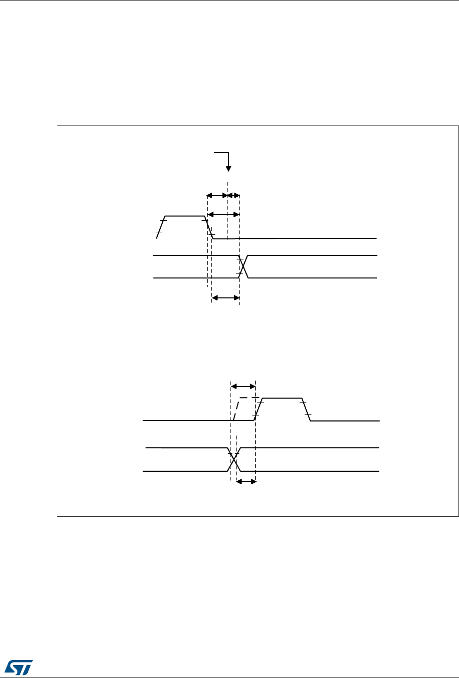
DocID025941 Rev 5 659/1001
RM0376 Inter-integrated circuit (I2C) interface
721
I2C timings
The timings must be configured in order to guarantee a correct data hold and setup time,
used in master and slave modes. This is done by programming the PRESC[3:0],
SCLDEL[3:0] and SDADEL[3:0] bits in the I2C_TIMINGR register.
The STM32CubeMX tool calculates and provides the I2C_TIMINGR content in the I2C
configuration window
Figure 197. Setup and hold timings
MSv40108V1
tSYNC1
SCL falling edge internal
detection
SDADEL: SCL stretched low by the I2C
SDA output delay
SCL
SDA
DATA HOLD TIME
tHD;DAT
SCLDEL
SCL stretched low by the I2C
SCL
SDA
DATA SETUP TIME
tSU;STA
Data hold time: in case of transmission, the data is sent on SDA output after
the SDADEL delay, if it is already available in I2C_TXDR.
Data setup time: in case of transmission, the SCLDEL counter starts
when the data is sent on SDA output.

Inter-integrated circuit (I2C) interface RM0376
660/1001 DocID025941 Rev 5
•When the SCL falling edge is internally detected, a delay is inserted before sending
SDA output. This delay is tSDADEL = SDADEL x tPRESC + tI2CCLK where tPRESC = (PRESC+1)
x tI2CCLK.
TSDADEL impacts the hold time tHD;DAT.
The total SDA output delay is:
tSYNC1 + {[SDADEL x (PRESC+1) + 1] x tI2CCLK }
tSYNC1 duration depends on these parameters:
– SCL falling slope
– When enabled, input delay brought by the analog filter: tAF(min) < tAF < tAF(max) ns.
– When enabled, input delay brought by the digital filter: tDNF = DNF x tI2CCLK
– Delay due to SCL synchronization to I2CCLK clock (2 to 3 I2CCLK periods)
In order to bridge the undefined region of the SCL falling edge, the user must program
SDADEL in such a way that:
{tf (max) +tHD;DAT (min) -tAF(min) - [(DNF +3) x tI2CCLK]} / {(PRESC +1) x tI2CCLK } ≤ SDADEL
SDADEL ≤ {tHD;DAT (max) -tAF(max) - [(DNF+4) x tI2CCLK]} / {(PRESC +1) x tI2CCLK }
Note: tAF(min) / tAF(max) are part of the equation only when the analog filter is enabled. Refer to
device datasheet for tAF values.
The maximum tHD;DAT could be 3.45 µs, 0.9 µs and 0.45 µs for Standard-mode, Fast-mode
and Fast-mode Plus, but must be less than the maximum of tVD;DAT by a transition time.
This maximum must only be met if the device does not stretch the LOW period (tLOW) of the
SCL signal. If the clock stretches the SCL, the data must be valid by the set-up time before
it releases the clock.
The SDA rising edge is usually the worst case, so in this case the previous equation
becomes:
SDADEL ≤ {tVD;DAT (max) -tr (max) -260 ns - [(DNF+4) x tI2CCLK]} / {(PRESC +1) x tI2CCLK }.
Note: This condition can be violated when NOSTRETCH=0, because the device stretches SCL
low to guarantee the set-up time, according to the SCLDEL value.
Refer to Table 113: I2C-SMBUS specification data setup and hold times for tf, tr, tHD;DAT and
tVD;DAT standard values.
•After tSDADEL delay, or after sending SDA output in case the slave had to stretch the
clock because the data was not yet written in I2C_TXDR register, SCL line is kept at
low level during the setup time. This setup time is tSCLDEL = (SCLDEL+1) x tPRESC where
tPRESC = (PRESC+1) x tI2CCLK.
tSCLDEL impacts the setup time tSU;DAT .
In order to bridge the undefined region of the SDA transition (rising edge usually worst
case), the user must program SCLDEL in such a way that:
{[tr (max) + tSU;DAT (min)] / [(PRESC+1)] x tI2CCLK]} - 1 <= SCLDEL
Refer to Table 113: I2C-SMBUS specification data setup and hold times for tr and tSU;DAT
standard values.
The SDA and SCL transition time values to be used are the ones in the application. Using
the maximum values from the standard increases the constraints for the SDADEL and
SCLDEL calculation, but ensures the feature whatever the application.

DocID025941 Rev 5 661/1001
RM0376 Inter-integrated circuit (I2C) interface
721
Note: At every clock pulse, after SCL falling edge detection, the I2C master or slave stretches SCL
low during at least [(SDADEL+SCLDEL+1) x (PRESC+1) + 1] x tI2CCLK, in both transmission
and reception modes. In transmission mode, in case the data is not yet written in I2C_TXDR
when SDADEL counter is finished, the I2C keeps on stretching SCL low until the next data
is written. Then new data MSB is sent on SDA output, and SCLDEL counter starts,
continuing stretching SCL low to guarantee the data setup time.
If NOSTRETCH=1 in slave mode, the SCL is not stretched. Consequently the SDADEL
must be programmed in such a way to guarantee also a sufficient setup time.
Additionally, in master mode, the SCL clock high and low levels must be configured by
programming the PRESC[3:0], SCLH[7:0] and SCLL[7:0] bits in the I2C_TIMINGR register.
•When the SCL falling edge is internally detected, a delay is inserted before releasing
the SCL output. This delay is tSCLL = (SCLL+1) x tPRESC where tPRESC = (PRESC+1) x
tI2CCLK.
tSCLL impacts the SCL low time tLOW .
•When the SCL rising edge is internally detected, a delay is inserted before forcing the
SCL output to low level. This delay is tSCLH = (SCLH+1) x tPRESC where tPRESC =
(PRESC+1) x tI2CCLK. tSCLH impacts the SCL high time tHIGH .
Refer to I2C master initialization for more details.
Caution: Changing the timing configuration is not allowed when the I2C is enabled.
The I2C slave NOSTRETCH mode must also be configured before enabling the peripheral.
Refer to I2C slave initialization for more details.
Caution: Changing the NOSTRETCH configuration is not allowed when the I2C is enabled.
Table 113. I2C-SMBUS specification data setup and hold times
Symbol Parameter
Standard-mode
(Sm)
Fast-mode
(Fm)
Fast-mode Plus
(Fm+) SMBUS
Unit
Min. Max Min. Max Min. Max Min. Max
tHD;DAT Data hold time 0-0-0 -0.3-
µs
tVD;DAT Data valid time - 3.45 - 0.9 - 0.45 - -
tSU;DAT Data setup time 250 - 100 - 50 - 250 -
ns
tr
Rise time of both SDA
and SCL signals - 1000 - 300 - 120 - 1000
tf
Fall time of both SDA
and SCL signals - 300 - 300 - 120 - 300
Inter-integrated circuit (I2C) interface RM0376
662/1001 DocID025941 Rev 5
Figure 198. I2C initialization flowchart
27.4.6 Software reset
A software reset can be performed by clearing the PE bit in the I2C_CR1 register. In that
case I2C lines SCL and SDA are released. Internal states machines are reset and
communication control bits, as well as status bits come back to their reset value. The
configuration registers are not impacted.
Here is the list of impacted register bits:
1. I2C_CR2 register: START, STOP, NACK
2. I2C_ISR register: BUSY, TXE, TXIS, RXNE, ADDR, NACKF, TCR, TC, STOPF, BERR,
ARLO, OVR
and in addition when the SMBus feature is supported:
1. I2C_CR2 register: PECBYTE
2. I2C_ISR register: PECERR, TIMEOUT, ALERT
PE must be kept low during at least 3 APB clock cycles in order to perform the software
reset. This is ensured by writing the following software sequence: - Write PE=0 - Check
PE=0 - Write PE=1.
MS19847V2
Clear PE bit in I2C_CR1
Initial settings
Configure ANFOFF and DNF[3:0] in I2C_CR1
Configure PRESC[3:0],
SDADEL[3:0], SCLDEL[3:0], SCLH[7:0],
SCLL[7:0] in I2C_TIMINGR
Configure NOSTRETCH in I2C_CR1
Set PE bit in I2C_CR1
End
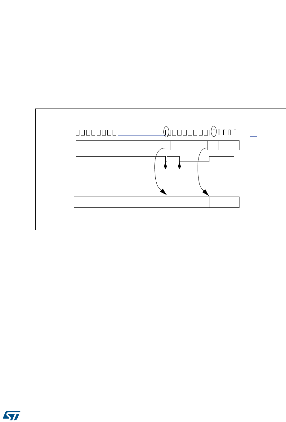
DocID025941 Rev 5 663/1001
RM0376 Inter-integrated circuit (I2C) interface
721
27.4.7 Data transfer
The data transfer is managed through transmit and receive data registers and a shift
register.
Reception
The SDA input fills the shift register. After the 8th SCL pulse (when the complete data byte is
received), the shift register is copied into I2C_RXDR register if it is empty (RXNE=0). If
RXNE=1, meaning that the previous received data byte has not yet been read, the SCL line
is stretched low until I2C_RXDR is read. The stretch is inserted between the 8th and 9th
SCL pulse (before the Acknowledge pulse).
Figure 199. Data reception
xx
Shift register data1
data1
xx data2
RXNE
ACK pulse
data0 data2
ACK pulse
xx
I2C_RXDR
rd data1rd data0
SCL
legend:
SCL
stretch
MS19848V1
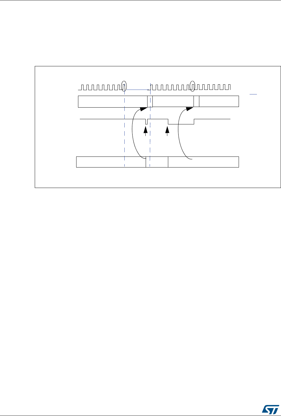
Inter-integrated circuit (I2C) interface RM0376
664/1001 DocID025941 Rev 5
Transmission
If the I2C_TXDR register is not empty (TXE=0), its content is copied into the shift register
after the 9th SCL pulse (the Acknowledge pulse). Then the shift register content is shifted
out on SDA line. If TXE=1, meaning that no data is written yet in I2C_TXDR, SCL line is
stretched low until I2C_TXDR is written. The stretch is done after the 9th SCL pulse.
Figure 200. Data transmission
Hardware transfer management
The I2C has a byte counter embedded in hardware in order to manage byte transfer and to
close the communication in various modes such as:
– NACK, STOP and ReSTART generation in master mode
– ACK control in slave receiver mode
– PEC generation/checking when SMBus feature is supported
The byte counter is always used in master mode. By default it is disabled in slave mode, but
it can be enabled by software by setting the SBC (Slave Byte Control) bit in the I2C_CR2
register.
The number of bytes to be transferred is programmed in the NBYTES[7:0] bit field in the
I2C_CR2 register. If the number of bytes to be transferred (NBYTES) is greater than 255, or
if a receiver wants to control the acknowledge value of a received data byte, the reload
mode must be selected by setting the RELOAD bit in the I2C_CR2 register. In this mode,
TCR flag is set when the number of bytes programmed in NBYTES has been transferred,
and an interrupt is generated if TCIE is set. SCL is stretched as long as TCR flag is set. TCR
is cleared by software when NBYTES is written to a non-zero value.
When the NBYTES counter is reloaded with the last number of bytes, RELOAD bit must be
cleared.
MS19849V1
xx
Shift register
data1
data1
xx
data2
TXE
ACK pulse
data0 data2
ACK pulse
xx
I2C_TXDR
wr data1 wr data2
SCL legend:
SCL
stretch

DocID025941 Rev 5 665/1001
RM0376 Inter-integrated circuit (I2C) interface
721
When RELOAD=0 in master mode, the counter can be used in 2 modes:
•Automatic end mode (AUTOEND = ‘1’ in the I2C_CR2 register). In this mode, the
master automatically sends a STOP condition once the number of bytes programmed
in the NBYTES[7:0] bit field has been transferred.
•Software end mode (AUTOEND = ‘0’ in the I2C_CR2 register). In this mode, software
action is expected once the number of bytes programmed in the NBYTES[7:0] bit field
has been transferred; the TC flag is set and an interrupt is generated if the TCIE bit is
set. The SCL signal is stretched as long as the TC flag is set. The TC flag is cleared by
software when the START or STOP bit is set in the I2C_CR2 register. This mode must
be used when the master wants to send a RESTART condition.
Caution: The AUTOEND bit has no effect when the RELOAD bit is set.
27.4.8 I2C slave mode
I2C slave initialization
In order to work in slave mode, the user must enable at least one slave address. Two
registers I2C_OAR1 and I2C_OAR2 are available in order to program the slave own
addresses OA1 and OA2.
•OA1 can be configured either in 7-bit mode (by default) or in 10-bit addressing mode by
setting the OA1MODE bit in the I2C_OAR1 register.
OA1 is enabled by setting the OA1EN bit in the I2C_OAR1 register.
•If additional slave addresses are required, the 2nd slave address OA2 can be
configured. Up to 7 OA2 LSB can be masked by configuring the OA2MSK[2:0] bits in
the I2C_OAR2 register. Therefore for OA2MSK configured from 1 to 6, only OA2[7:2],
OA2[7:3], OA2[7:4], OA2[7:5], OA2[7:6] or OA2[7] are compared with the received
address. As soon as OA2MSK is not equal to 0, the address comparator for OA2
excludes the I2C reserved addresses (0000 XXX and 1111 XXX), which are not
acknowledged. If OA2MSK=7, all received 7-bit addresses are acknowledged (except
reserved addresses). OA2 is always a 7-bit address.
These reserved addresses can be acknowledged if they are enabled by the specific
enable bit, if they are programmed in the I2C_OAR1 or I2C_OAR2 register with
OA2MSK=0.
OA2 is enabled by setting the OA2EN bit in the I2C_OAR2 register.
•The General Call address is enabled by setting the GCEN bit in the I2C_CR1 register.
When the I2C is selected by one of its enabled addresses, the ADDR interrupt status flag is
set, and an interrupt is generated if the ADDRIE bit is set.
Table 114. I2C configuration
Function SBC bit RELOAD bit AUTOEND bit
Master Tx/Rx NBYTES + STOP x 0 1
Master Tx/Rx + NBYTES + RESTART x 0 0
Slave Tx/Rx
all received bytes ACKed 0xx
Slave Rx with ACK control 1 1 x

Inter-integrated circuit (I2C) interface RM0376
666/1001 DocID025941 Rev 5
By default, the slave uses its clock stretching capability, which means that it stretches the
SCL signal at low level when needed, in order to perform software actions. If the master
does not support clock stretching, the I2C must be configured with NOSTRETCH=1 in the
I2C_CR1 register.
After receiving an ADDR interrupt, if several addresses are enabled the user must read the
ADDCODE[6:0] bits in the I2C_ISR register in order to check which address matched. DIR
flag must also be checked in order to know the transfer direction.
Slave clock stretching (NOSTRETCH = 0)
In default mode, the I2C slave stretches the SCL clock in the following situations:
•When the ADDR flag is set: the received address matches with one of the enabled
slave addresses. This stretch is released when the ADDR flag is cleared by software
setting the ADDRCF bit.
•In transmission, if the previous data transmission is completed and no new data is
written in I2C_TXDR register, or if the first data byte is not written when the ADDR flag
is cleared (TXE=1). This stretch is released when the data is written to the I2C_TXDR
register.
•In reception when the I2C_RXDR register is not read yet and a new data reception is
completed. This stretch is released when I2C_RXDR is read.
•When TCR = 1 in Slave Byte Control mode, reload mode (SBC=1 and RELOAD=1),
meaning that the last data byte has been transferred. This stretch is released when
then TCR is cleared by writing a non-zero value in the NBYTES[7:0] field.
•After SCL falling edge detection, the I2C stretches SCL low during
[(SDADEL+SCLDEL+1) x (PRESC+1) + 1] x tI2CCLK.
Slave without clock stretching (NOSTRETCH = 1)
When NOSTRETCH = 1 in the I2C_CR1 register, the I2C slave does not stretch the SCL
signal.
•The SCL clock is not stretched while the ADDR flag is set.
•In transmission, the data must be written in the I2C_TXDR register before the first SCL
pulse corresponding to its transfer occurs. If not, an underrun occurs, the OVR flag is
set in the I2C_ISR register and an interrupt is generated if the ERRIE bit is set in the
I2C_CR1 register. The OVR flag is also set when the first data transmission starts and
the STOPF bit is still set (has not been cleared). Therefore, if the user clears the
STOPF flag of the previous transfer only after writing the first data to be transmitted in
the next transfer, he ensures that the OVR status is provided, even for the first data to
be transmitted.
•In reception, the data must be read from the I2C_RXDR register before the 9th SCL
pulse (ACK pulse) of the next data byte occurs. If not an overrun occurs, the OVR flag
is set in the I2C_ISR register and an interrupt is generated if the ERRIE bit is set in the
I2C_CR1 register.
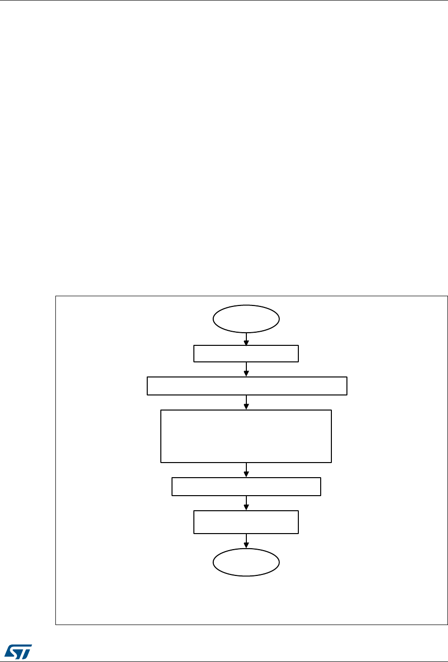
DocID025941 Rev 5 667/1001
RM0376 Inter-integrated circuit (I2C) interface
721
Slave Byte Control mode
In order to allow byte ACK control in slave reception mode, Slave Byte Control mode must
be enabled by setting the SBC bit in the I2C_CR1 register. This is required to be compliant
with SMBus standards.
Reload mode must be selected in order to allow byte ACK control in slave reception mode
(RELOAD=1). To get control of each byte, NBYTES must be initialized to 0x1 in the ADDR
interrupt subroutine, and reloaded to 0x1 after each received byte. When the byte is
received, the TCR bit is set, stretching the SCL signal low between the 8th and 9th SCL
pulses. The user can read the data from the I2C_RXDR register, and then decide to
acknowledge it or not by configuring the ACK bit in the I2C_CR2 register. The SCL stretch is
released by programming NBYTES to a non-zero value: the acknowledge or not-
acknowledge is sent and next byte can be received.
NBYTES can be loaded with a value greater than 0x1, and in this case, the reception flow is
continuous during NBYTES data reception.
Note: The SBC bit must be configured when the I2C is disabled, or when the slave is not
addressed, or when ADDR=1.
The RELOAD bit value can be changed when ADDR=1, or when TCR=1.
Caution: Slave Byte Control mode is not compatible with NOSTRETCH mode. Setting SBC when
NOSTRETCH=1 is not allowed.
Figure 201. Slave initialization flowchart
MS19850V2
Initial settings
Slave
initialization
Clear {OA1EN, OA2EN} in I2C_OAR1 and I2C_OAR2
Configure {OA1[9:0], OA1MODE, OA1EN,
OA2[6:0], OA2MSK[2:0], OA2EN, GCEN}
Configure SBC in I2C_CR1*
Enable interrupts and/or
DMA in I2C_CR1
End
*SBC must be set to support SMBus features

Inter-integrated circuit (I2C) interface RM0376
668/1001 DocID025941 Rev 5
For code example, refer to A.16.1: I2C configured in slave mode code example.
Slave transmitter
A transmit interrupt status (TXIS) is generated when the I2C_TXDR register becomes
empty. An interrupt is generated if the TXIE bit is set in the I2C_CR1 register.
The TXIS bit is cleared when the I2C_TXDR register is written with the next data byte to be
transmitted.
When a NACK is received, the NACKF bit is set in the I2C_ISR register and an interrupt is
generated if the NACKIE bit is set in the I2C_CR1 register. The slave automatically releases
the SCL and SDA lines in order to let the master perform a STOP or a RESTART condition.
The TXIS bit is not set when a NACK is received.
When a STOP is received and the STOPIE bit is set in the I2C_CR1 register, the STOPF
flag is set in the I2C_ISR register and an interrupt is generated. In most applications, the
SBC bit is usually programmed to ‘0’. In this case, If TXE = 0 when the slave address is
received (ADDR=1), the user can choose either to send the content of the I2C_TXDR
register as the first data byte, or to flush the I2C_TXDR register by setting the TXE bit in
order to program a new data byte.
In Slave Byte Control mode (SBC=1), the number of bytes to be transmitted must be
programmed in NBYTES in the address match interrupt subroutine (ADDR=1). In this case,
the number of TXIS events during the transfer corresponds to the value programmed in
NBYTES.
Caution: When NOSTRETCH=1, the SCL clock is not stretched while the ADDR flag is set, so the
user cannot flush the I2C_TXDR register content in the ADDR subroutine, in order to
program the first data byte. The first data byte to be sent must be previously programmed in
the I2C_TXDR register:
•This data can be the data written in the last TXIS event of the previous transmission
message.
•If this data byte is not the one to be sent, the I2C_TXDR register can be flushed by
setting the TXE bit in order to program a new data byte. The STOPF bit must be
cleared only after these actions, in order to guarantee that they are executed before the
first data transmission starts, following the address acknowledge.
If STOPF is still set when the first data transmission starts, an underrun error will be
generated (the OVR flag is set).
If a TXIS event is needed, (Transmit Interrupt or Transmit DMA request), the user must
set the TXIS bit in addition to the TXE bit, in order to generate a TXIS event.
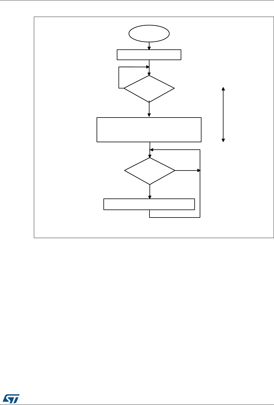
DocID025941 Rev 5 669/1001
RM0376 Inter-integrated circuit (I2C) interface
721
Figure 202. Transfer sequence flowchart for I2C slave transmitter, NOSTRETCH=0
MS19851V2
Slave initialization
Slave
transmission
Read ADDCODE and DIR in I2C_ISR
Optional: Set I2C_ISR.TXE = 1
Set I2C_ICR.ADDRCF
Write I2C_TXDR.TXDATA
I2C_ISR.ADDR
=1?
No
Yes
I2C_ISR.TXIS
=1?
Yes
No
SCL
stretched
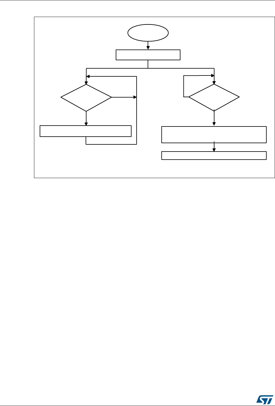
Inter-integrated circuit (I2C) interface RM0376
670/1001 DocID025941 Rev 5
Figure 203. Transfer sequence flowchart for I2C slave transmitter, NOSTRETCH=1
MS19852V2
Slave initialization
Slave
transmission
Optional: Set I2C_ISR.TXE = 1
and I2C_ISR.TXIS=1
Write I2C_TXDR.TXDATA
I2C_ISR.STOPF
=1?
No
Yes
I2C_ISR.TXIS
=1?
Yes
No
Set I2C_ICR.STOPCF
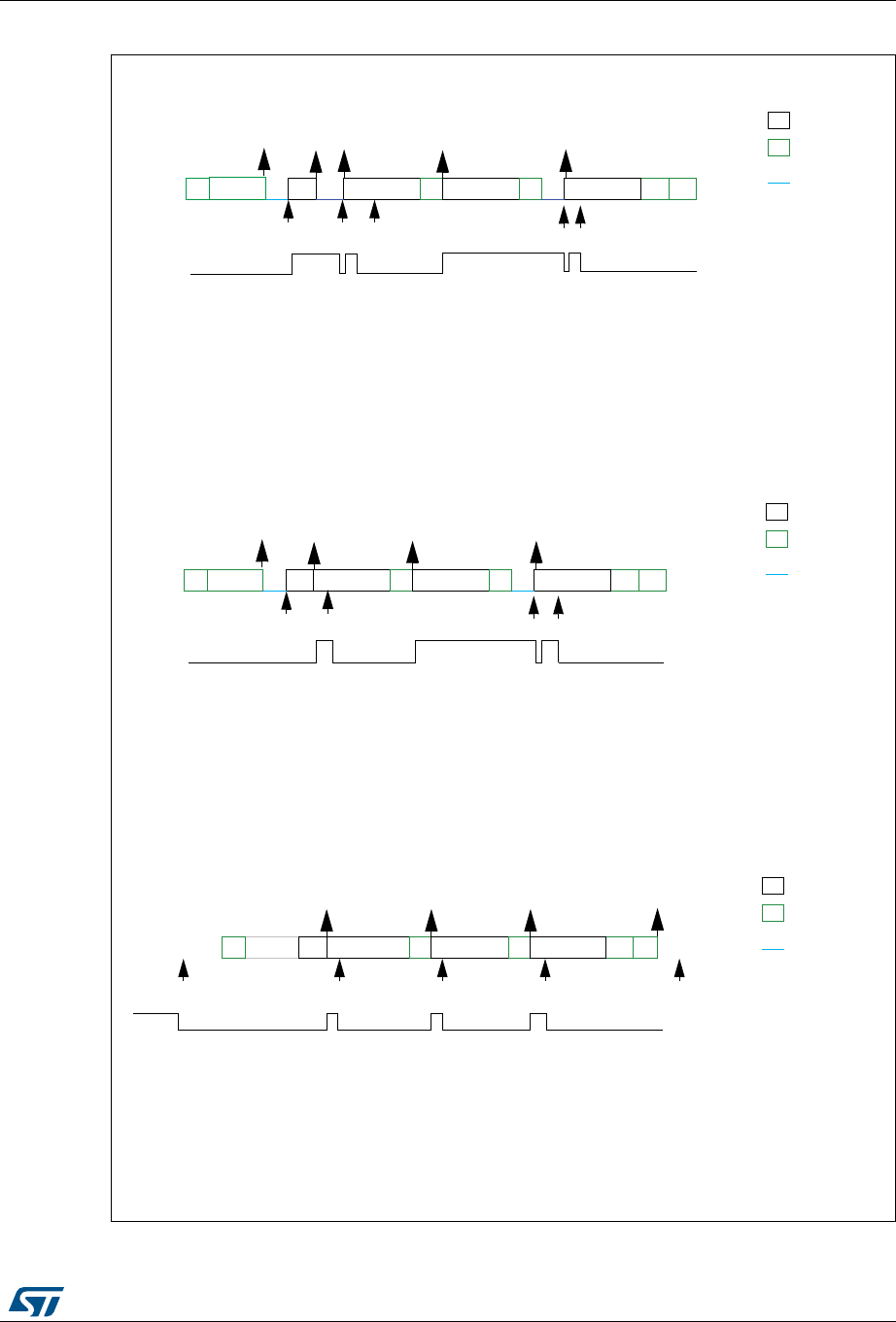
DocID025941 Rev 5 671/1001
RM0376 Inter-integrated circuit (I2C) interface
721
Figure 204. Transfer bus diagrams for I2C slave transmitter
For code example, refer to A.16.2: I2C slave transmitter code example.
MS19853V1
Example I2C slave transmitter 3 bytes with 1st data flushed,
NOSTRETCH=0:
EV1: ADDR ISR: check ADDCODE and DIR, set TXE, set ADDRCF
EV2: TXIS ISR: wr data1
EV3: TXIS ISR: wr data2
EV4: TXIS ISR: wr data3
EV5: TXIS ISR: wr data4 (not sent)
ADDR
A
TXIS
A
TXIS
NA
TXIS
TXE
P
legend:
transmission
reception
SCL stretch
EV1 EV2 EV4 EV5
Example I2C slave transmitter 3 bytes, NOSTRETCH=1:
EV1: wr data1
EV2: TXIS ISR: wr data2
EV3: TXIS ISR: wr data3
EV4: TXIS ISR: wr data4 (not sent)
EV5: STOPF ISR: (optional: set TXE and TXIS), set STOPCF
A
TXIS TXIS
TXE
legend:
transmission
reception
SCL stretch
EV2 EV3 EV4
TXIS
EV1
STOPF
EV5
Example I2C slave transmitter 3 bytes without 1st data flush,
NOSTRETCH=0:
EV1: ADDR ISR: check ADDCODE and DIR, set ADDRCF
EV2: TXIS ISR: wr data2
EV3: TXIS ISR: wr data3
EV4: TXIS ISR: wr data4 (not sent)
ADDR TXIS TXIS TXIS
TXE
legend :
transmission
reception
SCL stretch
EV1 EV2 EV3 EV4
TXIS
EV3
S Address data1 A data2 data3ANAP
S Address A data1 A data2 A data3 NA P
SAddress A data3
data2
data1
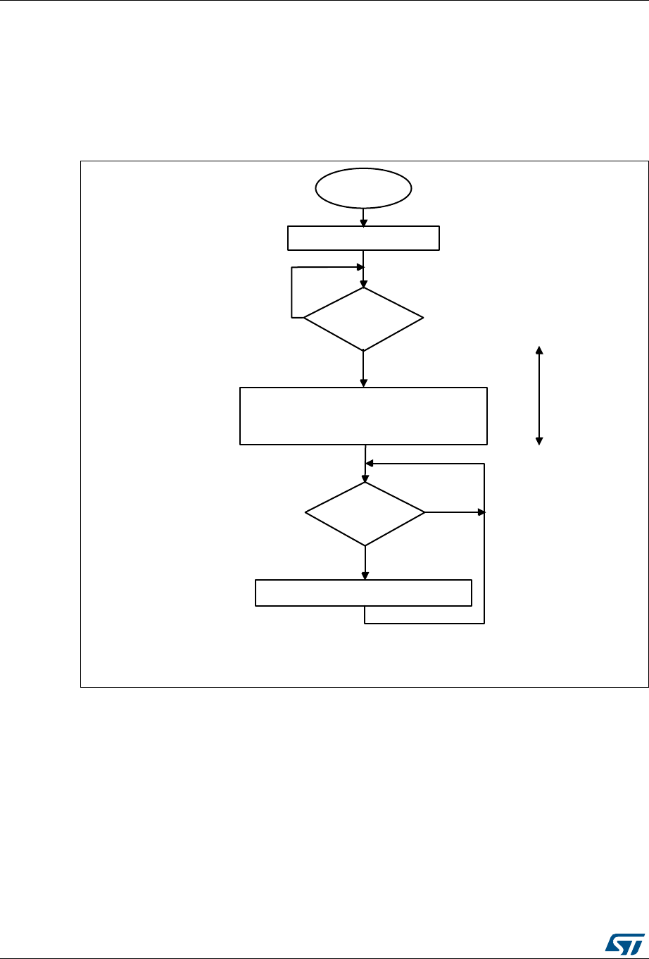
Inter-integrated circuit (I2C) interface RM0376
672/1001 DocID025941 Rev 5
Slave receiver
RXNE is set in I2C_ISR when the I2C_RXDR is full, and generates an interrupt if RXIE is
set in I2C_CR1. RXNE is cleared when I2C_RXDR is read.
When a STOP is received and STOPIE is set in I2C_CR1, STOPF is set in I2C_ISR and an
interrupt is generated.
Figure 205. Transfer sequence flowchart for slave receiver with NOSTRETCH=0
MS19855V2
Slave initialization
Slave reception
Read ADDCODE and DIR in I2C_ISR
Set I2C_ICR.ADDRCF
Write I2C_RXDR.RXDATA
I2C_ISR.ADDR
=1?
No
Yes
I2C_ISR.RXNE
=1?
Yes
No
SCL
stretched
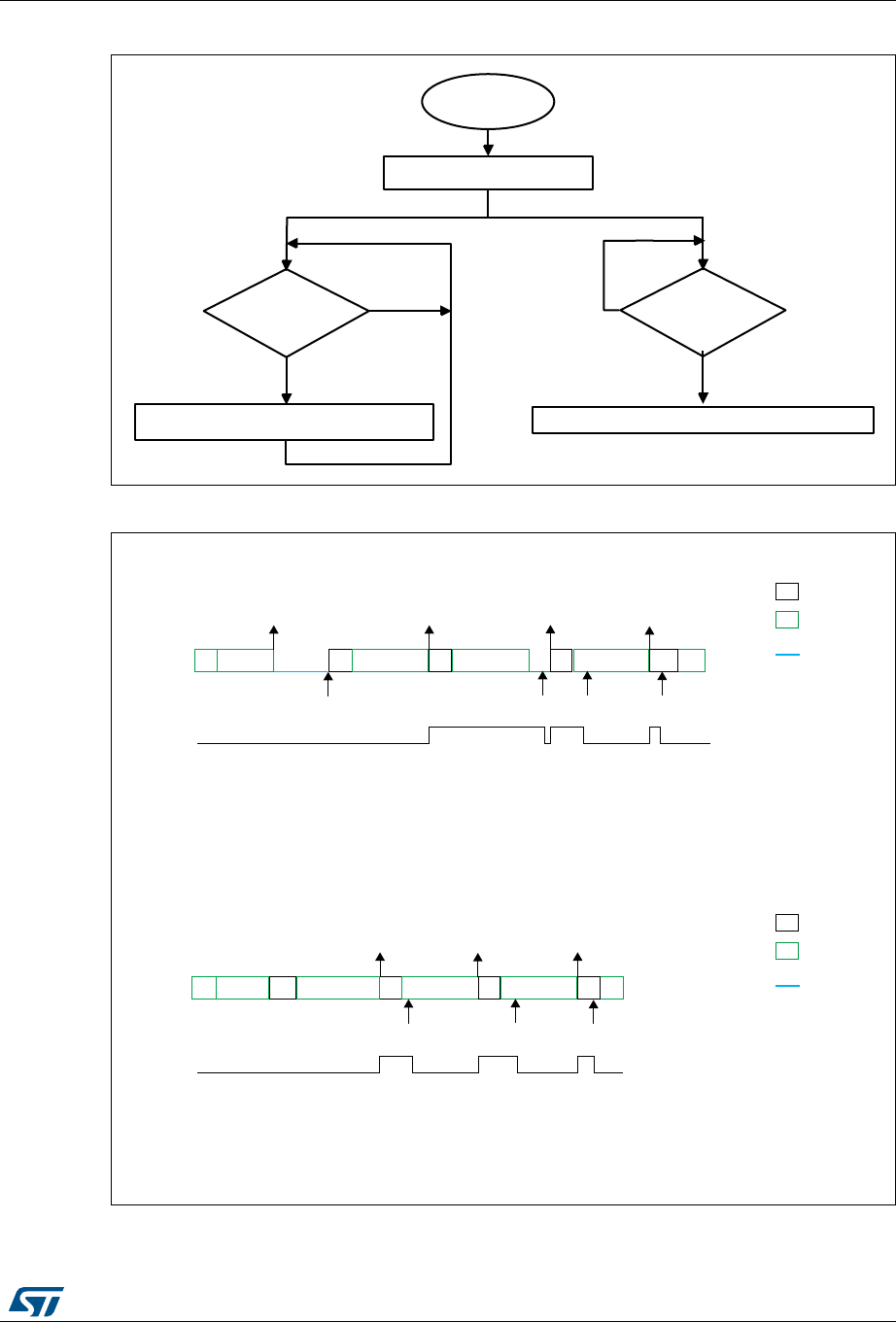
DocID025941 Rev 5 673/1001
RM0376 Inter-integrated circuit (I2C) interface
721
Figure 206. Transfer sequence flowchart for slave receiver with NOSTRETCH=1
Figure 207. Transfer bus diagrams for I2C slave receiver
For code example, refer to A.16.3: I2C slave receiver code example.
MS19856V2
Slave initialization
Slave reception
Read I2C_RXDR.RXDATA
I2C_ISR.STOPF
=1?
No
Yes
I2C_ISR.RXNE
=1?
Yes
No
Set I2C_ICR.STOPCF
MS19857V2
EV1: ADDR ISR: check ADDCODE and DIR, set ADDRCF
EV2: RXNE ISR: rd data1
EV3 : RXNE ISR: rd data2
EV4: RXNE ISR: rd data3
A
ADDR
AA
RXNE
A
RXNE
RXNE
legend:
transmission
reception
SCL stretch
EV1 EV2 EV3
EV1: RXNE ISR: rd data1
EV2: RXNE ISR: rd data2
EV3: RXNE ISR: rd data3
EV4: STOPF ISR: set STOPCF
A
AA A
RXNE
legend:
transmission
reception
SCL stretch
RXNE
EV4
Example I2C slave receiver 3 bytes, NOSTRETCH=1:
SAddress data 1 data 2 data 3 P
Example I2C slave receiver 3 bytes, NOSTRETCH=0:
SAddress data1 data2 data3
EV3
EV2
EV1
RXNE RXNE RXNE

Inter-integrated circuit (I2C) interface RM0376
674/1001 DocID025941 Rev 5
27.4.9 I2C master mode
I2C master initialization
Before enabling the peripheral, the I2C master clock must be configured by setting the
SCLH and SCLL bits in the I2C_TIMINGR register.
The STM32CubeMX tool calculates and provides the I2C_TIMINGR content in the I2C
Configuration window.
A clock synchronization mechanism is implemented in order to support multi-master
environment and slave clock stretching.
In order to allow clock synchronization:
•The low level of the clock is counted using the SCLL counter, starting from the SCL low
level internal detection.
•The high level of the clock is counted using the SCLH counter, starting from the SCL
high level internal detection.
The I2C detects its own SCL low level after a tSYNC1 delay depending on the SCL falling
edge, SCL input noise filters (analog + digital) and SCL synchronization to the I2CxCLK
clock. The I2C releases SCL to high level once the SCLL counter reaches the value
programmed in the SCLL[7:0] bits in the I2C_TIMINGR register.
The I2C detects its own SCL high level after a tSYNC2 delay depending on the SCL rising
edge, SCL input noise filters (analog + digital) and SCL synchronization to I2CxCLK clock.
The I2C ties SCL to low level once the SCLH counter is reached reaches the value
programmed in the SCLH[7:0] bits in the I2C_TIMINGR register.
Consequently the master clock period is:
tSCL = tSYNC1 + tSYNC2 + {[(SCLH+1) + (SCLL+1)] x (PRESC+1) x tI2CCLK}
The duration of tSYNC1 depends on these parameters:
– SCL falling slope
– When enabled, input delay induced by the analog filter.
– When enabled, input delay induced by the digital filter: DNF x tI2CCLK
– Delay due to SCL synchronization with I2CCLK clock (2 to 3 I2CCLK periods)
The duration of tSYNC2 depends on these parameters:
– SCL rising slope
– When enabled, input delay induced by the analog filter.
– When enabled, input delay induced by the digital filter: DNF x tI2CCLK
– Delay due to SCL synchronization with I2CCLK clock (2 to 3 I2CCLK periods)
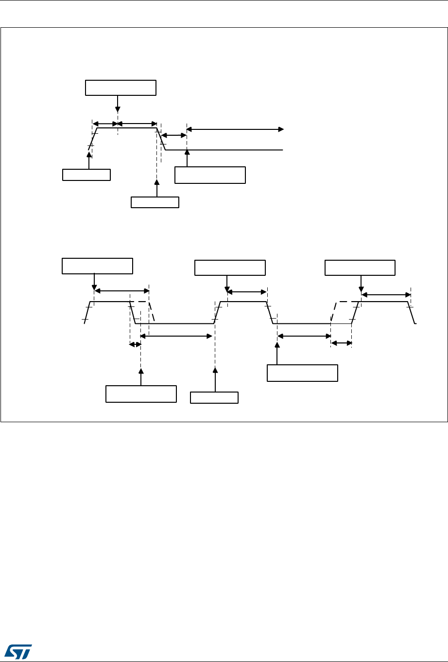
DocID025941 Rev 5 675/1001
RM0376 Inter-integrated circuit (I2C) interface
721
Figure 208. Master clock generation
Caution: In order to be I2C or SMBus compliant, the master clock must respect the timings given
below:
MS19858V1
tSYNC1
SCL high level detected
SCLH counter starts
SCLH
SCL
SCL master clock generation
SCL released SCL low level detected
SCLL counter starts
SCL driven low
SCLL
tSYNC2
SCL master clock synchronization
SCLL
SCL driven low by
another device
SCL low level detected
SCLL counter starts SCL released
SCLH
SCLH
SCL high level detected
SCLH counter starts SCL high level detected
SCLH counter starts
SCL low level detected
SCLL counter starts
SCLL
SCL driven low by
another device
SCLH
SCL high level detected
SCLH counter starts

Inter-integrated circuit (I2C) interface RM0376
676/1001 DocID025941 Rev 5
Note: SCLL is also used to generate the tBUF and tSU:STA timings.
SCLH is also used to generate the tHD:STA and tSU:STO timings.
Refer to Section 27.4.10: I2C_TIMINGR register configuration examples for examples of
I2C_TIMINGR settings vs. I2CCLK frequency.
Master communication initialization (address phase)
In order to initiate the communication, the user must program the following parameters for
the addressed slave in the I2C_CR2 register:
•Addressing mode (7-bit or 10-bit): ADD10
•Slave address to be sent: SADD[9:0]
•Transfer direction: RD_WRN
•In case of 10-bit address read: HEAD10R bit. HEAD10R must be configure to indicate
if the complete address sequence must be sent, or only the header in case of a
direction change.
•The number of bytes to be transferred: NBYTES[7:0]. If the number of bytes is equal to
or greater than 255 bytes, NBYTES[7:0] must initially be filled with 0xFF.
The user must then set the START bit in I2C_CR2 register. Changing all the above bits is
not allowed when START bit is set.
Then the master automatically sends the START condition followed by the slave address as
soon as it detects that the bus is free (BUSY = 0) and after a delay of tBUF.
In case of an arbitration loss, the master automatically switches back to slave mode and can
acknowledge its own address if it is addressed as a slave.
Table 115. I2C-SMBUS specification clock timings
Symbol Parameter
Standard-
mode (Sm)
Fast-mode
(Fm)
Fast-mode
Plus (Fm+) SMBUS
Unit
Min Max Min Max Min Max Min Max
fSCL SCL clock frequency - 100 - 400 - 1000 - 100 kHz
tHD:STA
Hold time (repeated) START
condition 4.0 - 0.6 - 0.26 - 4.0 - µs
tSU:STA
Set-up time for a repeated
START condition 4.7 - 0.6 - 0.26 - 4.7 - µs
tSU:STO Set-up time for STOP condition 4.0 - 0.6 - 0.26 - 4.0 - µs
tBUF
Bus free time between a
STOP and START condition
4.7 - 1.3 - 0.5 - 4.7 - µs
tLOW Low period of the SCL clock 4.7 - 1.3 - 0.5 - 4.7 - µs
tHIGH Period of the SCL clock 4.0 - 0.6 - 0.26 - 4.0 50 µs
tr Rise time of both SDA and
SCL signals - 1000 - 300 - 120 - 1000 ns
tf
Fall time of both SDA and SCL
signals - 300 - 300 - 120 - 300 ns
DocID025941 Rev 5 677/1001
RM0376 Inter-integrated circuit (I2C) interface
721
Note: The START bit is reset by hardware when the slave address has been sent on the bus,
whatever the received acknowledge value. The START bit is also reset by hardware if an
arbitration loss occurs.
In 10-bit addressing mode, when the Slave Address first 7 bits is NACKed by the slave, the
master will re-launch automatically the slave address transmission until ACK is received. In
this case ADDRCF must be set if a NACK is received from the slave, in order to stop
sending the slave address.
If the I2C is addressed as a slave (ADDR=1) while the START bit is set, the I2C switches to
slave mode and the START bit is cleared when the ADDRCF bit is set.
Note: The same procedure is applied for a Repeated Start condition. In this case BUSY=1.
Figure 209. Master initialization flowchart
For code example, refer to A.16.4: I2C configured in master mode to receive code example
andA.16.5: I2C configured in master mode to transmit code example.
Initialization of a master receiver addressing a 10-bit address slave
•If the slave address is in 10-bit format, the user can choose to send the complete read
sequence by clearing the HEAD10R bit in the I2C_CR2 register. In this case the master
automatically sends the following complete sequence after the START bit is set:
(Re)Start + Slave address 10-bit header Write + Slave address 2nd byte + REStart +
Slave address 10-bit header Read
Figure 210. 10-bit address read access with HEAD10R=0
MS19859V2
Initial settings
Master
initialization
Enable interrupts and/or DMA in I2C_CR1
End
MSv41066V1
DATA A PADATA
Slave address
2nd byte
Slave address
1st 7 bits
SrA2A1 R/WR/W
Slave address
1st 7 bits
S A3
1 1 1 1 0 X X 1
1 1 1 1 0 X X 0
Write Read
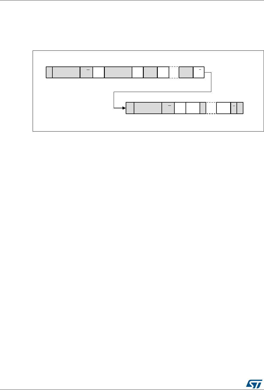
Inter-integrated circuit (I2C) interface RM0376
678/1001 DocID025941 Rev 5
•If the master addresses a 10-bit address slave, transmits data to this slave and then
reads data from the same slave, a master transmission flow must be done first. Then a
repeated start is set with the 10 bit slave address configured with HEAD10R=1. In this
case the master sends this sequence: ReStart + Slave address 10-bit header Read.
Figure 211. 10-bit address read access with HEAD10R=1
Master transmitter
In the case of a write transfer, the TXIS flag is set after each byte transmission, after the 9th
SCL pulse when an ACK is received.
A TXIS event generates an interrupt if the TXIE bit is set in the I2C_CR1 register. The flag is
cleared when the I2C_TXDR register is written with the next data byte to be transmitted.
The number of TXIS events during the transfer corresponds to the value programmed in
NBYTES[7:0]. If the total number of data bytes to be sent is greater than 255, reload mode
must be selected by setting the RELOAD bit in the I2C_CR2 register. In this case, when
NBYTES data have been transferred, the TCR flag is set and the SCL line is stretched low
until NBYTES[7:0] is written to a non-zero value.
The TXIS flag is not set when a NACK is received.
•When RELOAD=0 and NBYTES data have been transferred:
– In automatic end mode (AUTOEND=1), a STOP is automatically sent.
– In software end mode (AUTOEND=0), the TC flag is set and the SCL line is
stretched low in order to perform software actions:
A RESTART condition can be requested by setting the START bit in the I2C_CR2
register with the proper slave address configuration, and number of bytes to be
transferred. Setting the START bit clears the TC flag and the START condition is
sent on the bus.
A STOP condition can be requested by setting the STOP bit in the I2C_CR2
register. Setting the STOP bit clears the TC flag and the STOP condition is sent on
the bus.
•If a NACK is received: the TXIS flag is not set, and a STOP condition is automatically
sent after the NACK reception. the NACKF flag is set in the I2C_ISR register, and an
interrupt is generated if the NACKIE bit is set.
MS19823V1
DATADATA
Slave address
2nd byte
Slave address
1st 7 bits
Sr
AA
R/W
Slave address
1st 7 bits
S A
1 1 1 1 0 X X 1
1 1 1 1 0 X X 0
Write
Read
DATA A PADATAA
A/AR/W
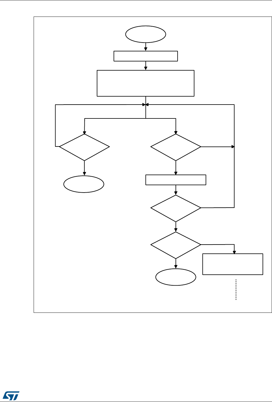
DocID025941 Rev 5 679/1001
RM0376 Inter-integrated circuit (I2C) interface
721
Figure 212. Transfer sequence flowchart for I2C master transmitter for N≤255 bytes
MS19860V2
Master initialization
Master
transmission
Write I2C_TXDR
I2C_ISR.TXIS
=1?
No
Yes
I2C_ISR.NACKF =
1?
Yes
No
NBYTES = N
AUTOEND = 0 for RESTART; 1 for STOP
Configure slave address
Set I2C_CR2.START
End
NBYTES
transmitted?
I2C_ISR.TC =
1?
Yes
End
No
Yes
No Set I2C_CR2.START with
slave addess NBYTES ...
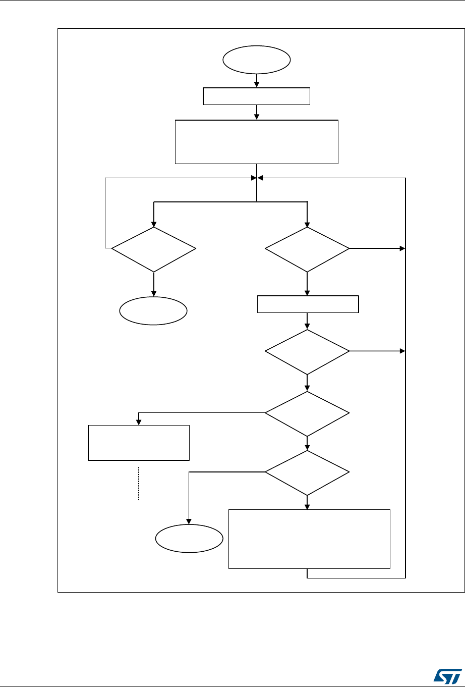
Inter-integrated circuit (I2C) interface RM0376
680/1001 DocID025941 Rev 5
Figure 213. Transfer sequence flowchart for I2C master transmitter for N>255 bytes
MS19861V3
Master initialization
Master
transmission
Write I2C_TXDR
I2C_ISR.TXIS
=1?
No
Yes
I2C_ISR.NACKF
= 1?
Yes
No
NBYTES = 0xFF; N=N-255
RELOAD = 1
Configure slave address
Set I2C_CR2.START
End
NBYTES
transmitted ?
I2C_ISR.TC
= 1?
Yes
End
No
Yes
No
Set I2C_CR2.START
with slave addess
NBYTES ...
I2C_ISR.TCR
= 1?
Yes
IF N< 256
NBYTES = N; N = 0; RELOAD = 0
AUTOEND = 0 for RESTART; 1 for STOP
ELSE
NBYTES = 0xFF; N = N-255
RELOAD = 1
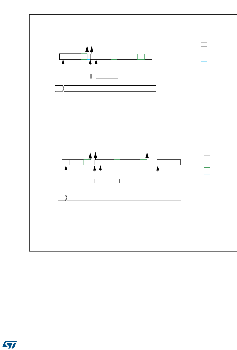
DocID025941 Rev 5 681/1001
RM0376 Inter-integrated circuit (I2C) interface
721
Figure 214. Transfer bus diagrams for I2C master transmitter
For code example, refer to A.16.6: I2C master transmitter code example.
MS19862V1
Example I2C master transmitter 2 bytes, automatic end mode (STOP)
INIT: program Slave address, program NBYTES = 2, AUTOEND=1, set START
EV1: TXIS ISR: wr data1
EV2: TXIS ISR: wr data2
TXISTXIS
legend:
transmission
reception
SCL stretch
EV1 EV2
xx 2
INIT
Example I2C master transmitter 2 bytes, software end mode (RESTART)
INIT: program Slave address, program NBYTES = 2, AUTOEND=0, set START
EV1: TXIS ISR: wr data1
EV2: TXIS ISR: wr data2
EV3: TC ISR: program Slave address, program NBYTES = N, set START
TXIS TXIS legend:
transmiss
ion
reception
SCL stret
ch
EV1 EV2
INIT
TC
TXE
TXE
EV3
NBYTES
NBYTES 2
xx
S Address A data1 A data2 ReS AddressA
S Address A data1 A data2 AP

Inter-integrated circuit (I2C) interface RM0376
682/1001 DocID025941 Rev 5
Master receiver
In the case of a read transfer, the RXNE flag is set after each byte reception, after the 8th
SCL pulse. An RXNE event generates an interrupt if the RXIE bit is set in the I2C_CR1
register. The flag is cleared when I2C_RXDR is read.
If the total number of data bytes to be received is greater than 255, reload mode must be
selected by setting the RELOAD bit in the I2C_CR2 register. In this case, when
NBYTES[7:0] data have been transferred, the TCR flag is set and the SCL line is stretched
low until NBYTES[7:0] is written to a non-zero value.
•When RELOAD=0 and NBYTES[7:0] data have been transferred:
– In automatic end mode (AUTOEND=1), a NACK and a STOP are automatically
sent after the last received byte.
– In software end mode (AUTOEND=0), a NACK is automatically sent after the last
received byte, the TC flag is set and the SCL line is stretched low in order to allow
software actions:
A RESTART condition can be requested by setting the START bit in the I2C_CR2
register with the proper slave address configuration, and number of bytes to be
transferred. Setting the START bit clears the TC flag and the START condition,
followed by slave address, are sent on the bus.
A STOP condition can be requested by setting the STOP bit in the I2C_CR2
register. Setting the STOP bit clears the TC flag and the STOP condition is sent on
the bus.
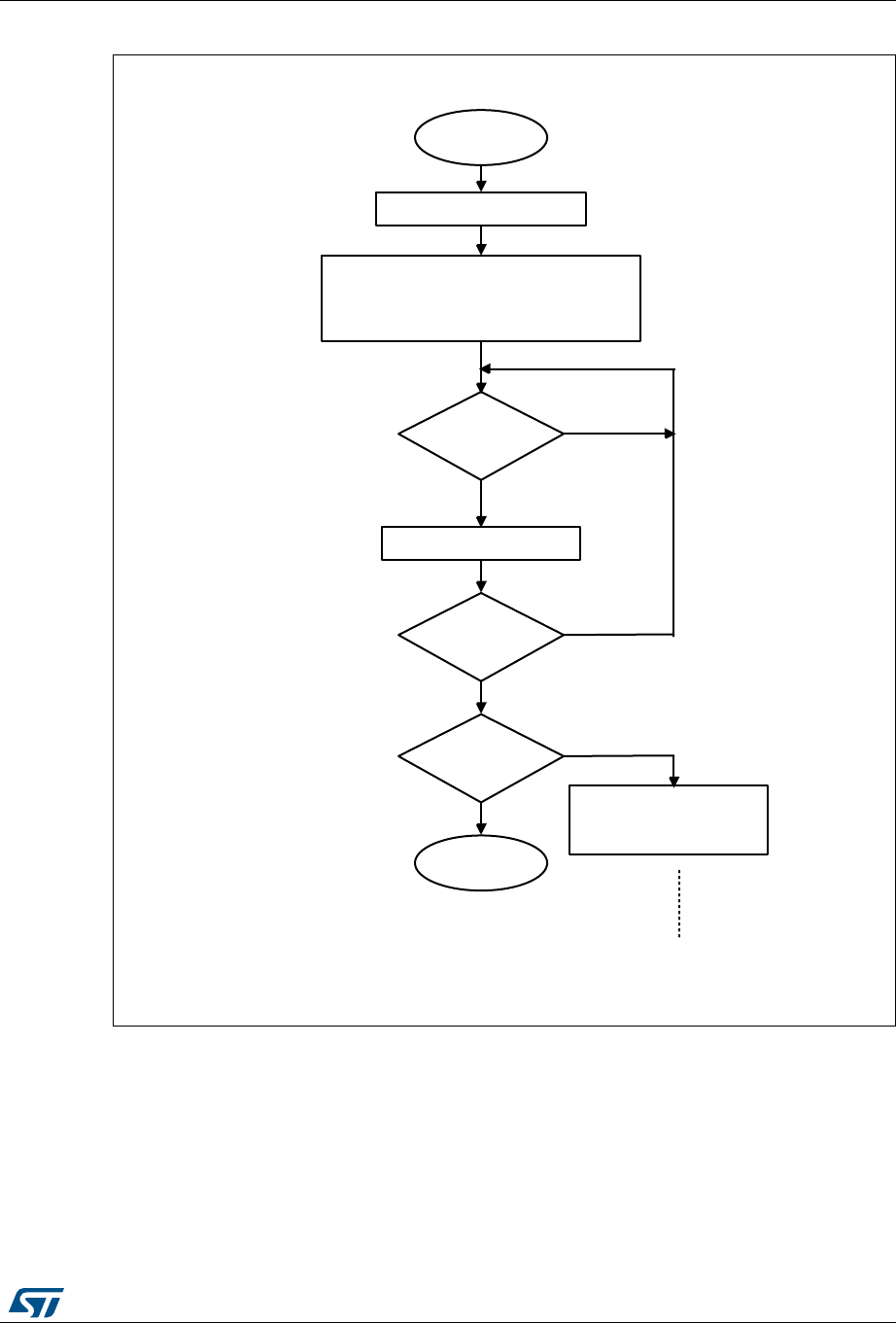
DocID025941 Rev 5 683/1001
RM0376 Inter-integrated circuit (I2C) interface
721
Figure 215. Transfer sequence flowchart for I2C master receiver for N≤255 bytes
MS19863V2
Master initialization
Master reception
Read I2C_RXDR
I2C_ISR.RXNE
=1?
No
Yes
NBYTES = N
AUTOEND = 0 for RESTART; 1 for STOP
Configure slave address
Set I2C_CR2.START
NBYTES
received?
I2C_ISR.TC =
1?
Yes
End
No
Yes
No Set I2C_CR2.START with
slave addess NBYTES ...
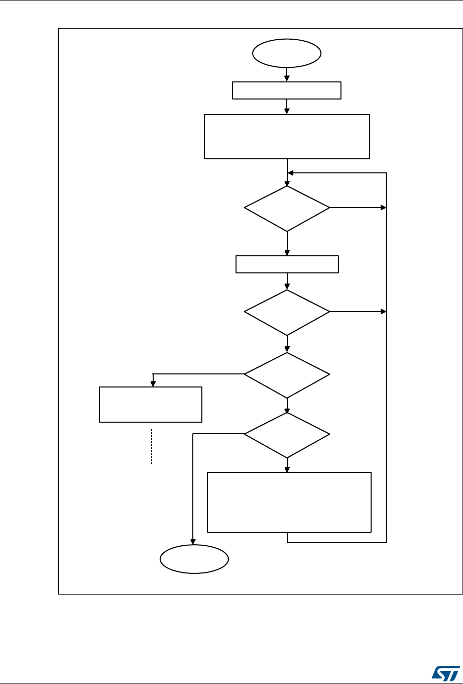
Inter-integrated circuit (I2C) interface RM0376
684/1001 DocID025941 Rev 5
Figure 216. Transfer sequence flowchart for I2C master receiver for N >255 bytes
MS19864V2
Master initialization
Master reception
Read I2C_RXDR
I2C_ISR.RXNE
=1?
No
Yes
NBYTES = 0xFF; N=N-255
RELOAD =1
Configure slave address
Set I2C_CR2.START
NBYTES
received?
I2C_ISR.TC =
1?
Yes
End
No
Yes
No
Set I2C_CR2.START with
slave addess NBYTES ...
I2C_ISR.TCR
= 1?
Yes
IF N< 256
NBYTES =N; N=0;RELOAD=0
AUTOEND=0 for RESTART; 1 for STOP
ELSE
NBYTES =0xFF;N=N-255
RELOAD=1
No
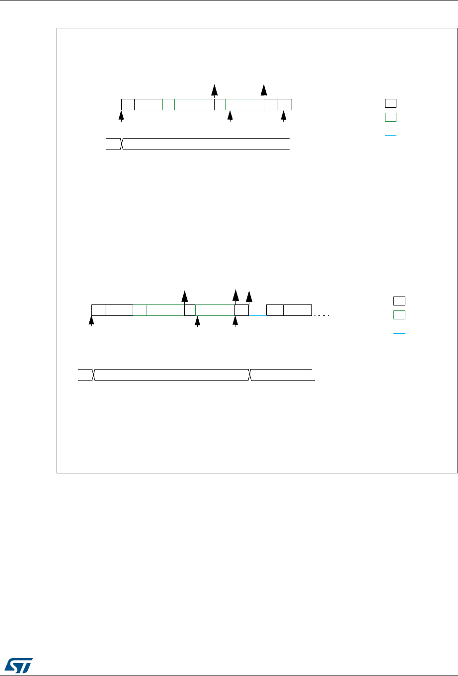
DocID025941 Rev 5 685/1001
RM0376 Inter-integrated circuit (I2C) interface
721
Figure 217. Transfer bus diagrams for I2C master receiver
For code example refer to A.16.7: I2C master receiver code example.
MS19865V1
Example I2C master receiver 2 bytes, automatic end mode (STOP)
INIT: program Slave address, program NBYTES = 2, AUTOEND=1, set START
EV1: RXNE ISR: rd data1
EV2: RXNE ISR: rd data2
A
RXNE RXNE
NBYTES
legend:
transmission
reception
SCL stretch
EV1
xx 2
INIT
Example I2C master receiver 2 bytes, software end mode (RESTART)
INIT: program Slave address, program NBYTES = 2, AUTOEND=0, set START
EV1: RXNE ISR: rd data1
EV2: RXNE ISR: read data2
EV3: TC ISR: program Slave address, program NBYTES = N, set START
A
RXNE RXNE
NBYTES
legend:
transmiss
ion
reception
SCL stret
ch
EV1 EV2
xx
INIT
N
EV2
2
TC
AddressS A data1 data2 NA ReS Address
S Address A data1 data2 NA P
Inter-integrated circuit (I2C) interface RM0376
686/1001 DocID025941 Rev 5
27.4.10 I2C_TIMINGR register configuration examples
The tables below provide examples of how to program the I2C_TIMINGR to obtain timings
compliant with the I2C specification. In order to get more accurate configuration values, the
STM32CubeMX tool (I2C Configuration window) should be used.
Table 116. Examples of timing settings for fI2CCLK = 8 MHz
Parameter
Standard-mode (Sm) Fast-mode (Fm) Fast-mode Plus (Fm+)
10 kHz 100 kHz 400 kHz 500 kHz
PRESC 1 1 0 0
SCLL 0xC7 0x13 0x9 0x6
tSCLL 200x250 ns = 50 µs 20x250 ns = 5.0 µs 10x125 ns = 1250 ns 7x125 ns = 875 ns
SCLH 0xC3 0xF 0x3 0x3
tSCLH 196x250 ns = 49 µs 16x250 ns = 4.0µs 4x125ns = 500ns 4x125 ns = 500 ns
tSCL(1) ~100 µs(2) ~10 µs(2) ~2500 ns(3) ~2000 ns(4)
SDADEL 0x2 0x2 0x1 0x0
tSDADEL 2x250 ns = 500 ns 2x250 ns = 500 ns 1x125 ns = 125 ns 0 ns
SCLDEL 0x4 0x4 0x3 0x1
tSCLDEL 5x250 ns = 1250 ns 5x250 ns = 1250 ns 4x125 ns = 500 ns 2x125 ns = 250 ns
1. SCL period tSCL is greater than tSCLL + tSCLH due to SCL internal detection delay. Values provided for tSCL are examples
only.
2. tSYNC1 + tSYNC2 minimum value is 4 x tI2CCLK = 500 ns. Example with tSYNC1 + tSYNC2 = 1000 ns
3. tSYNC1 + tSYNC2 minimum value is 4 x tI2CCLK = 500 ns. Example with tSYNC1 + tSYNC2 = 750 ns
4. tSYNC1 + tSYNC2 minimum value is 4 x tI2CCLK = 500 ns. Example with tSYNC1 + tSYNC2 = 655 ns
Table 117. Examples of timings settings for fI2CCLK = 16 MHz
Parameter
Standard-mode (Sm) Fast-mode (Fm) Fast-mode Plus (Fm+)
10 kHz 100 kHz 400 kHz 1000 kHz
PRESC 3 3 1 0
SCLL 0xC7 0x13 0x9 0x4
tSCLL 200 x 250 ns = 50 µs 20 x 250 ns = 5.0 µs 10 x 125 ns = 1250 ns 5 x 62.5 ns = 312.5 ns
SCLH 0xC3 0xF 0x3 0x2
tSCLH 196 x 250 ns = 49 µs 16 x 250 ns = 4.0 µs 4 x 125ns = 500 ns 3 x 62.5 ns = 187.5 ns
tSCL(1) ~100 µs(2) ~10 µs(2) ~2500 ns(3) ~1000 ns(4)
SDADEL 0x2 0x2 0x2 0x0
tSDADEL 2 x 250 ns = 500 ns 2 x 250 ns = 500 ns 2 x 125 ns = 250 ns 0 ns
SCLDEL 0x4 0x4 0x3 0x2
tSCLDEL 5 x 250 ns = 1250 ns 5 x 250 ns = 1250 ns 4 x 125 ns = 500 ns 3 x 62.5 ns = 187.5 ns
1. SCL period tSCL is greater than tSCLL + tSCLH due to SCL internal detection delay. Values provided for tSCL are examples
only.

DocID025941 Rev 5 687/1001
RM0376 Inter-integrated circuit (I2C) interface
721
27.4.11 SMBus specific features
This section is relevant only when SMBus feature is supported. Refer to Section 27.3: I2C
implementation.
Introduction
The System Management Bus (SMBus) is a two-wire interface through which various
devices can communicate with each other and with the rest of the system. It is based on I2C
principles of operation. SMBus provides a control bus for system and power management
related tasks.
This peripheral is compatible with the SMBUS specification rev 2.0 (http://smbus.org).
The System Management Bus Specification refers to three types of devices.
•A slave is a device that receives or responds to a command.
•A master is a device that issues commands, generates the clocks and terminates the
transfer.
•A host is a specialized master that provides the main interface to the system’s CPU. A
host must be a master-slave and must support the SMBus host notify protocol. Only
one host is allowed in a system.
This peripheral can be configured as master or slave device, and also as a host.
SMBUS is based on I2C specification rev 2.1.
Bus protocols
There are eleven possible command protocols for any given device. A device may use any
or all of the eleven protocols to communicate. The protocols are Quick Command, Send
Byte, Receive Byte, Write Byte, Write Word, Read Byte, Read Word, Process Call, Block
Read, Block Write and Block Write-Block Read Process Call. These protocols should be
implemented by the user software.
For more details of these protocols, refer to SMBus specification version 2.0
(http://smbus.org).
Address resolution protocol (ARP)
SMBus slave address conflicts can be resolved by dynamically assigning a new unique
address to each slave device. In order to provide a mechanism to isolate each device for the
purpose of address assignment each device must implement a unique device identifier
(UDID). This 128-bit number is implemented by software.
This peripheral supports the Address Resolution Protocol (ARP). The SMBus Device
Default Address (0b1100 001) is enabled by setting SMBDEN bit in I2C_CR1 register. The
ARP commands should be implemented by the user software.
Arbitration is also performed in slave mode for ARP support.
For more details of the SMBus Address Resolution Protocol, refer to SMBus specification
version 2.0 (http://smbus.org).
2. tSYNC1 + tSYNC2 minimum value is 4 x tI2CCLK = 250 ns. Example with tSYNC1 + tSYNC2 = 1000 ns
3. tSYNC1 + tSYNC2 minimum value is 4 x tI2CCLK = 250 ns. Example with tSYNC1 + tSYNC2 = 750 ns
4. tSYNC1 + tSYNC2 minimum value is 4 x tI2CCLK = 250 ns. Example with tSYNC1 + tSYNC2 = 500 ns

Inter-integrated circuit (I2C) interface RM0376
688/1001 DocID025941 Rev 5
Received Command and Data acknowledge control
A SMBus receiver must be able to NACK each received command or data. In order to allow
the ACK control in slave mode, the Slave Byte Control mode must be enabled by setting
SBC bit in I2C_CR1 register. Refer to Slave Byte Control mode on page 667 for more
details.
Host Notify protocol
This peripheral supports the Host Notify protocol by setting the SMBHEN bit in the I2C_CR1
register. In this case the host will acknowledge the SMBus Host address (0b0001 000).
When this protocol is used, the device acts as a master and the host as a slave.
SMBus alert
The SMBus ALERT optional signal is supported. A slave-only device can signal the host
through the SMBALERT# pin that it wants to talk. The host processes the interrupt and
simultaneously accesses all SMBALERT# devices through the Alert Response Address
(0b0001 100). Only the device(s) which pulled SMBALERT# low will acknowledge the Alert
Response Address.
When configured as a slave device(SMBHEN=0), the SMBA pin is pulled low by setting the
ALERTEN bit in the I2C_CR1 register. The Alert Response Address is enabled at the same
time.
When configured as a host (SMBHEN=1), the ALERT flag is set in the I2C_ISR register
when a falling edge is detected on the SMBA pin and ALERTEN=1. An interrupt is
generated if the ERRIE bit is set in the I2C_CR1 register. When ALERTEN=0, the ALERT
line is considered high even if the external SMBA pin is low.
If the SMBus ALERT pin is not needed, the SMBA pin can be used as a standard GPIO if
ALERTEN=0.
Packet error checking
A packet error checking mechanism has been introduced in the SMBus specification to
improve reliability and communication robustness. Packet Error Checking is implemented
by appending a Packet Error Code (PEC) at the end of each message transfer. The PEC is
calculated by using the C(x) = x8 + x2 + x + 1 CRC-8 polynomial on all the message bytes
(including addresses and read/write bits).
The peripheral embeds a hardware PEC calculator and allows to send a Not Acknowledge
automatically when the received byte does not match with the hardware calculated PEC.
Timeouts
This peripheral embeds hardware timers in order to be compliant with the 3 timeouts defined
in SMBus specification version 2.0.
. Table 118. SMBus timeout specifications
Symbol Parameter
Limits
Unit
Min Max
tTIMEOUT Detect clock low timeout 25 35 ms
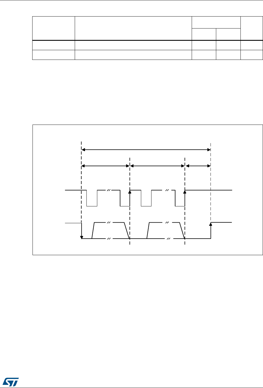
DocID025941 Rev 5 689/1001
RM0376 Inter-integrated circuit (I2C) interface
721
Figure 218. Timeout intervals for tLOW:SEXT, tLOW:MEXT.
tLOW:SEXT(1) Cumulative clock low extend time (slave device) - 25 ms
tLOW:MEXT(2) Cumulative clock low extend time (master device) - 10 ms
1. tLOW:SEXT is the cumulative time a given slave device is allowed to extend the clock cycles in one message
from the initial START to the STOP. It is possible that, another slave device or the master will also extend
the clock causing the combined clock low extend time to be greater than tLOW:SEXT. Therefore, this
parameter is measured with the slave device as the sole target of a full-speed master.
2. tLOW:MEXT is the cumulative time a master device is allowed to extend its clock cycles within each byte of a
message as defined from START-to-ACK, ACK-to-ACK, or ACK-to-STOP. It is possible that a slave device
or another master will also extend the clock causing the combined clock low time to be greater than
tLOW:MEXT on a given byte. Therefore, this parameter is measured with a full speed slave device as the sole
target of the master.
Table 118. SMBus timeout specifications (continued)
Symbol Parameter
Limits
Unit
Min Max
MS19866V1
Start Stop
tLOW:SEXT
tLOW:MEXT tLOW:MEXT tLOW:MEXT
ClkAck ClkAck
SMBCLK
SMBDAT

Inter-integrated circuit (I2C) interface RM0376
690/1001 DocID025941 Rev 5
Bus idle detection
A master can assume that the bus is free if it detects that the clock and data signals have
been high for tIDLE greater than tHIGH,MAX. (refer to Table 113: I2C-SMBUS specification data
setup and hold times)
This timing parameter covers the condition where a master has been dynamically added to
the bus and may not have detected a state transition on the SMBCLK or SMBDAT lines. In
this case, the master must wait long enough to ensure that a transfer is not currently in
progress. The peripheral supports a hardware bus idle detection.
27.4.12 SMBus initialization
This section is relevant only when SMBus feature is supported. Refer to Section 27.3: I2C
implementation.
In addition to I2C initialization, some other specific initialization must be done in order to
perform SMBus communication:
Received Command and Data Acknowledge control (Slave mode)
A SMBus receiver must be able to NACK each received command or data. In order to allow
ACK control in slave mode, the Slave Byte Control mode must be enabled by setting the
SBC bit in the I2C_CR1 register. Refer to Slave Byte Control mode on page 667 for more
details.
Specific address (Slave mode)
The specific SMBus addresses should be enabled if needed. Refer to Bus idle detection on
page 690 for more details.
•The SMBus Device Default address (0b1100 001) is enabled by setting the SMBDEN
bit in the I2C_CR1 register.
•The SMBus Host address (0b0001 000) is enabled by setting the SMBHEN bit in the
I2C_CR1 register.
•The Alert Response Address (0b0001100) is enabled by setting the ALERTEN bit in the
I2C_CR1 register.
Packet error checking
PEC calculation is enabled by setting the PECEN bit in the I2C_CR1 register. Then the PEC
transfer is managed with the help of a hardware byte counter: NBYTES[7:0] in the I2C_CR2
register. The PECEN bit must be configured before enabling the I2C.
The PEC transfer is managed with the hardware byte counter, so the SBC bit must be set
when interfacing the SMBus in slave mode. The PEC is transferred after NBYTES-1 data
have been transferred when the PECBYTE bit is set and the RELOAD bit is cleared. If
RELOAD is set, PECBYTE has no effect.
Caution: Changing the PECEN configuration is not allowed when the I2C is enabled.

DocID025941 Rev 5 691/1001
RM0376 Inter-integrated circuit (I2C) interface
721
Timeout detection
The timeout detection is enabled by setting the TIMOUTEN and TEXTEN bits in the
I2C_TIMEOUTR register. The timers must be programmed in such a way that they detect a
timeout before the maximum time given in the SMBus specification version 2.0.
•tTIMEOUT check
In order to enable the tTIMEOUT check, the 12-bit TIMEOUTA[11:0] bits must be
programmed with the timer reload value in order to check the tTIMEOUT parameter. The
TIDLE bit must be configured to ‘0’ in order to detect the SCL low level timeout.
Then the timer is enabled by setting the TIMOUTEN in the I2C_TIMEOUTR register.
If SCL is tied low for a time greater than (TIMEOUTA+1) x 2048 x tI2CCLK, the TIMEOUT
flag is set in the I2C_ISR register.
Refer to Table 120: Examples of TIMEOUTA settings for various I2CCLK frequencies
(max tTIMEOUT = 25 ms).
Caution: Changing the TIMEOUTA[11:0] bits and TIDLE bit configuration is not allowed when the
TIMEOUTEN bit is set.
•tLOW:SEXT and tLOW:MEXT check
Depending on if the peripheral is configured as a master or as a slave, The 12-bit
TIMEOUTB timer must be configured in order to check tLOW:SEXT for a slave and
tLOW:MEXT for a master. As the standard specifies only a maximum, the user can choose
the same value for the both.
Then the timer is enabled by setting the TEXTEN bit in the I2C_TIMEOUTR register.
If the SMBus peripheral performs a cumulative SCL stretch for a time greater than
(TIMEOUTB+1) x 2048 x tI2CCLK, and in the timeout interval described in Bus idle
detection on page 690 section, the TIMEOUT flag is set in the I2C_ISR register.
Refer to Table 121: Examples of TIMEOUTB settings for various I2CCLK frequencies
Caution: Changing the TIMEOUTB configuration is not allowed when the TEXTEN bit is set.
Bus Idle detection
In order to enable the tIDLE check, the 12-bit TIMEOUTA[11:0] field must be programmed
with the timer reload value in order to obtain the tIDLE parameter. The TIDLE bit must be
configured to ‘1 in order to detect both SCL and SDA high level timeout.
Then the timer is enabled by setting the TIMOUTEN bit in the I2C_TIMEOUTR register.
If both the SCL and SDA lines remain high for a time greater than (TIMEOUTA+1) x 4 x
tI2CCLK, the TIMEOUT flag is set in the I2C_ISR register.
Refer to Table 122: Examples of TIMEOUTA settings for various I2CCLK frequencies (max
tIDLE = 50 µs)
Table 119. SMBUS with PEC configuration
Mode SBC bit RELOAD bit AUTOEND bit PECBYTE bit
Master Tx/Rx NBYTES + PEC+ STOP x 0 1 1
Master Tx/Rx NBYTES + PEC + ReSTART x 0 0 1
Slave Tx/Rx with PEC 1 0 x 1
Inter-integrated circuit (I2C) interface RM0376
692/1001 DocID025941 Rev 5
Caution: Changing the TIMEOUTA and TIDLE configuration is not allowed when the TIMEOUTEN is
set.
27.4.13 SMBus: I2C_TIMEOUTR register configuration examples
This section is relevant only when SMBus feature is supported. Refer to Section 27.3: I2C
implementation.
•Configuring the maximum duration of tTIMEOUT to 25 ms:
•Configuring the maximum duration of tLOW:SEXT and tLOW:MEXT to 8 ms:
•Configuring the maximum duration of tIDLE to 50 µs
Table 120. Examples of TIMEOUTA settings for various I2CCLK frequencies
(max tTIMEOUT = 25 ms)
fI2CCLK
TIMEOUTA[11:0]
bits
TIDLE
bit
TIMEOUTEN
bit tTIMEOUT
8 MHz 0x61 0 1 98 x 2048 x 125 ns = 25 ms
16 MHz 0xC3 0 1 196 x 2048 x 62.5 ns = 25 ms
32 MHz 0x186 0 1 391 x 2048 x 31.25 ns = 25 ms
Table 121. Examples of TIMEOUTB settings for various I2CCLK frequencies
fI2CCLK
TIMEOUTB[11:0]
bits TEXTEN bit tLOW:EXT
8 MHz 0x1F 1 32 x 2048 x 125 ns = 8 ms
16 MHz 0x3F 1 64 x 2048 x 62.5 ns = 8 ms
32 MHz 0x7C 1 125 x 2048 x 31.25 ns = 8 ms
Table 122. Examples of TIMEOUTA settings for various I2CCLK frequencies
(max tIDLE = 50 µs)
fI2CCLK
TIMEOUTA[11:0]
bits TIDLE bit TIMEOUTEN
bit tTIDLE
8 MHz 0x63 1 1 100 x 4 x 125 ns = 50 µs
16 MHz 0xC7 1 1 200 x 4 x 62.5 ns = 50 µs
32 MHz 0x18F 1 1 400 x 4 x 31.25 ns = 50 µs
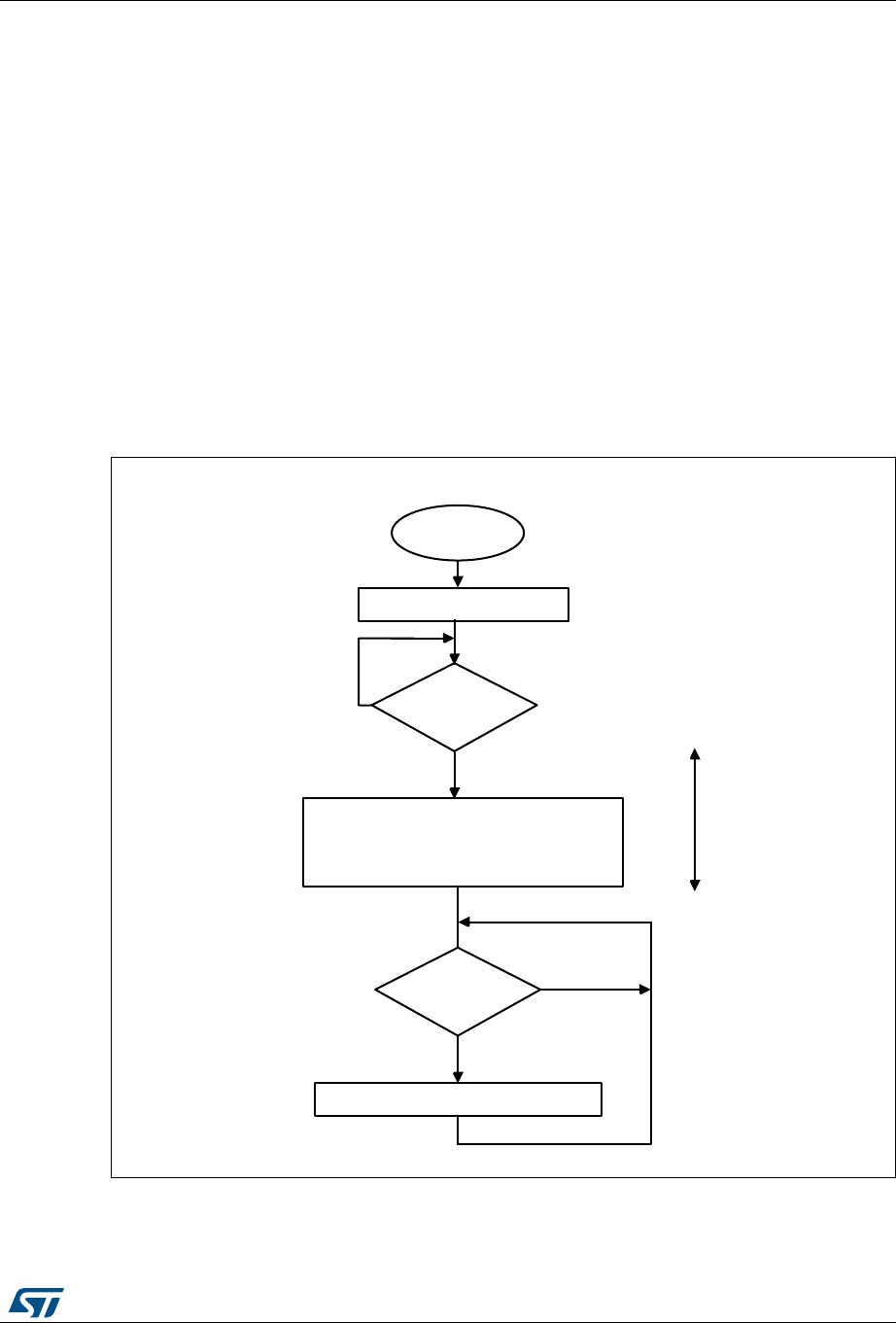
DocID025941 Rev 5 693/1001
RM0376 Inter-integrated circuit (I2C) interface
721
27.4.14 SMBus slave mode
This section is relevant only when SMBus feature is supported. Refer to Section 27.3: I2C
implementation.
In addition to 2C slave transfer management (refer to Section 27.4.8: I2C slave mode) some
additional software flowcharts are provided to support SMBus.
SMBus Slave transmitter
When the IP is used in SMBus, SBC must be programmed to ‘1’ in order to allow the PEC
transmission at the end of the programmed number of data bytes. When the PECBYTE bit
is set, the number of bytes programmed in NBYTES[7:0] includes the PEC transmission. In
that case the total number of TXIS interrupts will be NBYTES-1 and the content of the
I2C_PECR register is automatically transmitted if the master requests an extra byte after the
NBYTES-1 data transfer.
Caution: The PECBYTE bit has no effect when the RELOAD bit is set.
Figure 219. Transfer sequence flowchart for SMBus slave transmitter N bytes + PEC
MS19867V2
Slave initialization
SMBus slave
transmission
Write I2C_TXDR.TXDATA
I2C_ISR.TXIS
=1?
No
Yes
I2C_ISR.ADDR =
1?
Yes
No
Read ADDCODE and DIR in I2C_ISR
I2C_CR2.NBYTES = N + 1
PECBYTE=1
Set I2C_ICR.ADDRCF
SCL
stretched
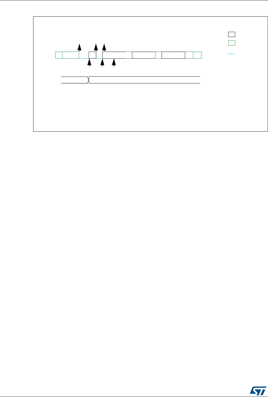
Inter-integrated circuit (I2C) interface RM0376
694/1001 DocID025941 Rev 5
Figure 220. Transfer bus diagrams for SMBus slave transmitter (SBC=1)
SMBus Slave receiver
When the I2C is used in SMBus mode, SBC must be programmed to ‘1’ in order to allow the
PEC checking at the end of the programmed number of data bytes. In order to allow the
ACK control of each byte, the reload mode must be selected (RELOAD=1). Refer to Slave
Byte Control mode on page 667 for more details.
In order to check the PEC byte, the RELOAD bit must be cleared and the PECBYTE bit
must be set. In this case, after NBYTES-1 data have been received, the next received byte
is compared with the internal I2C_PECR register content. A NACK is automatically
generated if the comparison does not match, and an ACK is automatically generated if the
comparison matches, whatever the ACK bit value. Once the PEC byte is received, it is
copied into the I2C_RXDR register like any other data, and the RXNE flag is set.
In the case of a PEC mismatch, the PECERR flag is set and an interrupt is generated if the
ERRIE bit is set in the I2C_CR1 register.
If no ACK software control is needed, the user can program PECBYTE=1 and, in the same
write operation, program NBYTES with the number of bytes to be received in a continuous
flow. After NBYTES-1 are received, the next received byte is checked as being the PEC.
Caution: The PECBYTE bit has no effect when the RELOAD bit is set.
MS19869V1
Example SMBus slave transmitter 2 bytes + PEC,
EV1: ADDR ISR: check ADDCODE, program NBYTES=3, set PECBYTE, set ADDRCF
EV2: TXIS ISR: wr data1
EV3: TXIS ISR: wr data2
ADDR
legend:
transmission
reception
SCL stretch
EV1 EV2
TXIS TXIS
EV3
NBYTES 3
S Address A Adata1 data2 PECA NA P
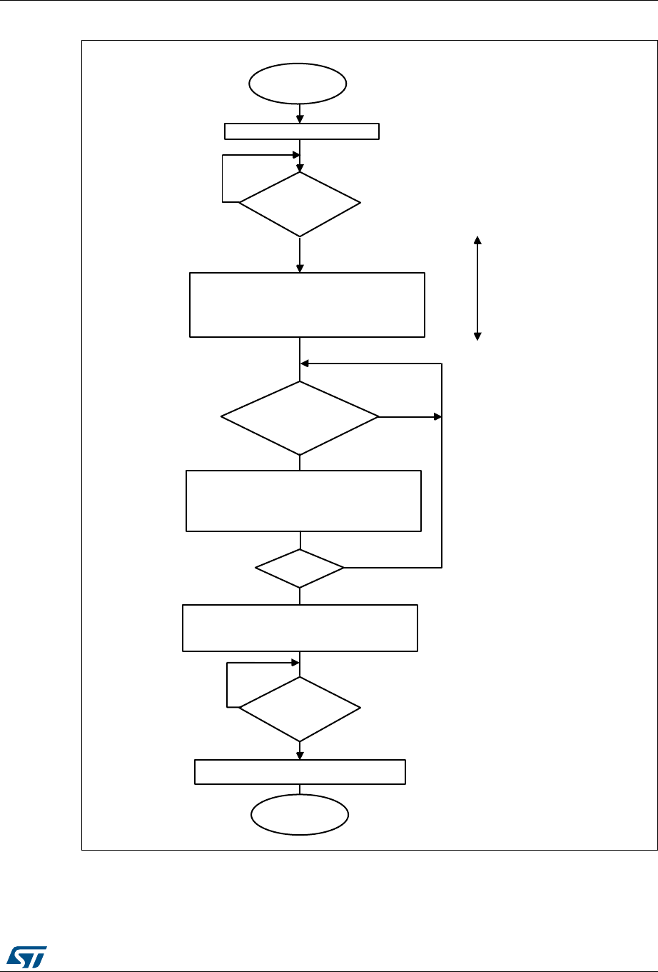
DocID025941 Rev 5 695/1001
RM0376 Inter-integrated circuit (I2C) interface
721
Figure 221. Transfer sequence flowchart for SMBus slave receiver N Bytes + PEC
MS19868V2
Slave initialization
SMBus slave
reception
Read I2C_RXDR.RXDATA
I2C_ISR.RXNE =1?
I2C_ISR.TCR = 1?
No
Yes
I2C_ISR.ADDR =
1?
Yes
No
Read ADDCODE and DIR in I2C_ISR
I2C_CR2.NBYTES = 1, RELOAD =1
PECBYTE=1
Set I2C_ICR.ADDRCF
SCL
stretched
Read I2C_RXDR.RXDATA
Program I2C_CR2.NACK = 0
I2C_CR2.NBYTES = 1
N = N - 1
N = 1?
Read I2C_RXDR.RXDATA
Program RELOAD = 0
NACK = 0 and NBYTES = 1
I2C_ISR.RXNE =1?
No
End
No
Yes
Yes
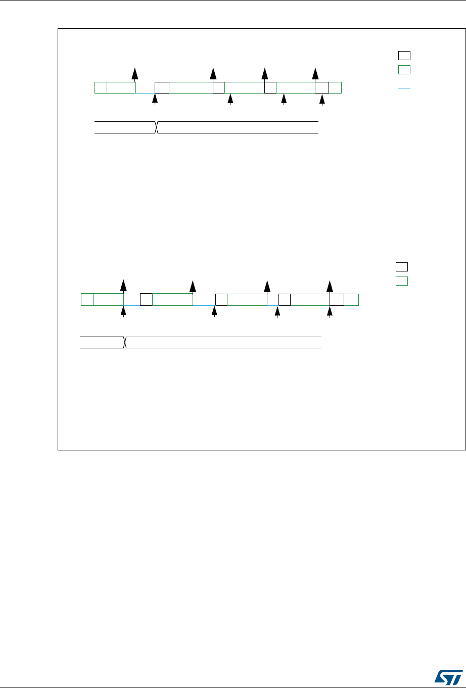
Inter-integrated circuit (I2C) interface RM0376
696/1001 DocID025941 Rev 5
Figure 222. Bus transfer diagrams for SMBus slave receiver (SBC=1)
This section is relevant only when SMBus feature is supported. Refer to Section 27.3: I2C
implementation.
In addition to I2C master transfer management (refer to Section 27.4.9: I2C master mode)
some additional software flowcharts are provided to support SMBus.
SMBus Master transmitter
When the SMBus master wants to transmit the PEC, the PECBYTE bit must be set and the
number of bytes must be programmed in the NBYTES[7:0] field, before setting the START
bit. In this case the total number of TXIS interrupts will be NBYTES-1. So if the PECBYTE
bit is set when NBYTES=0x1, the content of the I2C_PECR register is automatically
transmitted.
If the SMBus master wants to send a STOP condition after the PEC, automatic end mode
should be selected (AUTOEND=1). In this case, the STOP condition automatically follows
the PEC transmission.
MS19870V1
Example SMBus slave receiver 2 bytes + PEC
Address
S
EV1: ADDR ISR: check ADDCODE and DIR, program NBYTES = 3, PECBYTE=1, RELOAD=0, set ADDRCF
EV2: RXNE ISR: rd data1
EV3: RXNE ISR: rd data2
EV4: RXNE ISR: rd PEC
A
data1
A
data2
A
RXNE
PEC
A
RXNE
P
legend:
transmission
reception
SCL stretch
EV1 EV2 EV3 EV4
ADDR
RXNE
NBYTES
Example SMBus slave receiver 2 bytes + PEC, with ACK control
(RELOAD=1/0)
Address
S
EV1: ADDR ISR: check ADDCODE and DIR, program NBYTES = 1, PECBYTE=1, RELOAD=1, set ADDRCF
EV2: RXNE-TCR ISR: rd data1, program NACK=0 and NBYTES = 1
EV3: RXNE-TCR ISR: rd data2, program NACK=0, NBYTES = 1 and RELOAD=0
EV4: RXNE-TCR ISR: rd PEC
A
ADDR
data1
A
data2
A
RXNE,TCR
PEC
A
RXNE,TCR
P
legend :
transmission
reception
SCL stretch
3VE2VE1VE
RXNE
EV4
NBYTES 1
3
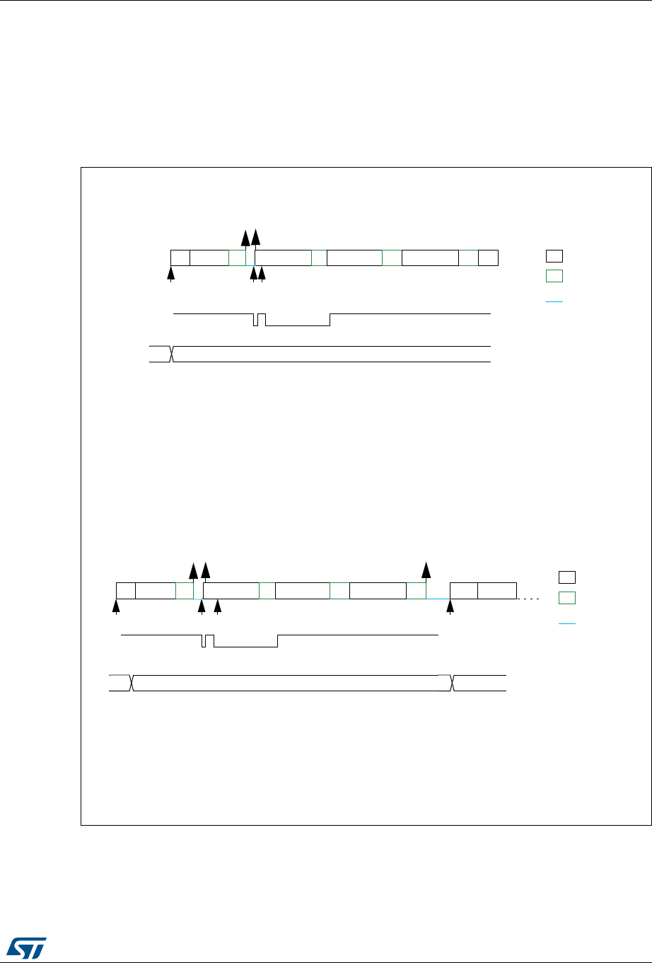
DocID025941 Rev 5 697/1001
RM0376 Inter-integrated circuit (I2C) interface
721
When the SMBus master wants to send a RESTART condition after the PEC, software
mode must be selected (AUTOEND=0). In this case, once NBYTES-1 have been
transmitted, the I2C_PECR register content is transmitted and the TC flag is set after the
PEC transmission, stretching the SCL line low. The RESTART condition must be
programmed in the TC interrupt subroutine.
Caution: The PECBYTE bit has no effect when the RELOAD bit is set.
Figure 223. Bus transfer diagrams for SMBus master transmitter
MS19871V1
Example SMBus master transmitter 2 bytes + PEC, automatic end mode (STOP)
Address
S
INIT: program Slave address, program NBYTES = 3, AUTOEND=1, set PECBYTE, set START
EV1: TXIS ISR: wr data1
EV2: TXIS ISR: wr data2
A
data1
A
TXIS TXIS
data2
A
NBYTES
A
legend:
transmission
reception
SCL stretch
EV1
xx 3
INIT
Example SMBus master transmitter 2 bytes + PEC, software end mode (RESTART)
INIT: program Slave address, program NBYTES = 3, AUTOEND=0, set PECBYTE, set START
EV1: TXIS ISR: wr data1
EV2: TXIS ISR: wr data2
EV3: TC ISR: program Slave address, program NBYTES = N, set START
NBYTES
Rstart
legend:
transmission
reception
SCL stretch
xx
Address
N
PEC
P
EV2
A
3
TXE
Address
S
A
data1
A
TXIS TXIS
data2
A
EV1
INIT
PEC
EV2
TC
EV3

Inter-integrated circuit (I2C) interface RM0376
698/1001 DocID025941 Rev 5
SMBus Master receiver
When the SMBus master wants to receive the PEC followed by a STOP at the end of the
transfer, automatic end mode can be selected (AUTOEND=1). The PECBYTE bit must be
set and the slave address must be programmed, before setting the START bit. In this case,
after NBYTES-1 data have been received, the next received byte is automatically checked
versus the I2C_PECR register content. A NACK response is given to the PEC byte, followed
by a STOP condition.
When the SMBus master receiver wants to receive the PEC byte followed by a RESTART
condition at the end of the transfer, software mode must be selected (AUTOEND=0). The
PECBYTE bit must be set and the slave address must be programmed, before setting the
START bit. In this case, after NBYTES-1 data have been received, the next received byte is
automatically checked versus the I2C_PECR register content. The TC flag is set after the
PEC byte reception, stretching the SCL line low. The RESTART condition can be
programmed in the TC interrupt subroutine.
Caution: The PECBYTE bit has no effect when the RELOAD bit is set.
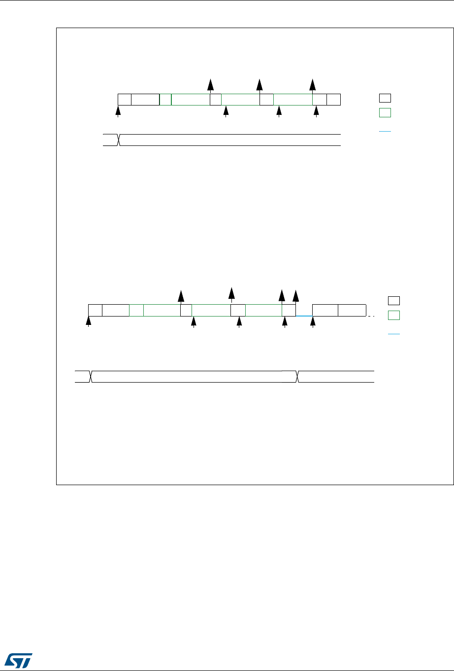
DocID025941 Rev 5 699/1001
RM0376 Inter-integrated circuit (I2C) interface
721
Figure 224. Bus transfer diagrams for SMBus master receiver
MS19872V1
Example SMBus master receiver 2 bytes + PEC, automatic end mode (STOP)
Address
S
INIT: program Slave address, program NBYTES = 3, AUTOEND=1, set PECBYTE, set START
EV1: RXNE ISR: rd data1
EV2: RXNE ISR: rd data2
EV3: RXNE ISR: rd PEC
A
data1
A
RXNE RXNE
data2
A
NBYTES
NA
legend:
transmission
reception
SCL stretch
3VE1VE
xx 3
INIT
Example SMBus master receiver 2 bytes + PEC, software end mode (RESTART)
Address
S
INIT: program Slave address, program NBYTES = 3, AUTOEND=0, set PECBYTE, set START
EV1: RXNE ISR: rd data1
EV2: RXNE ISR: rd data2
EV3: RXNE ISR: read PEC
EV4: TC ISR: program Slave address, program NBYTES = N, set START
A
data1
A
RXNE RXNE
data2
A
NBYTES
Restart
legend:
transmission
reception
SCL stretch
EV1 EV2
xx
INIT
Address
N
PEC
P
RXNE
EV2
NA
PEC
RXNE
3
EV3
TC
EV4

Inter-integrated circuit (I2C) interface RM0376
700/1001 DocID025941 Rev 5
27.4.15 Wakeup from Stop mode on address match
This section is relevant only when Wakeup from Stop mode feature is supported. Please
refer to Section 27.3: I2C implementation.
The I2C is able to wakeup the MCU from Stop mode (APB clock is off), when it is
addressed. All addressing modes are supported.
Wakeup from Stop mode is enabled by setting the WUPEN bit in the I2C_CR1 register. The
oscillator must be selected as the clock source for I2CCLK in order to allow wakeup from
Stop mode.
During Stop mode, the is switched off. When a START is detected, the I2C interface
switches the on, and stretches SCL low until is woken up.
is then used for the address reception.
In case of an address match, the I2C stretches SCL low during MCU wakeup time. The
stretch is released when ADDR flag is cleared by software, and the transfer goes on
normally.
If the address does not match, the is switched off again and the MCU is not woken up.
Note: If the I2C clock is the system clock, or if WUPEN = 0, the is not switched on after a START
is received.
Only an ADDR interrupt can wakeup the MCU. Therefore do not enter Stop mode when the
I2C is performing a transfer as a master, or as an addressed slave after the ADDR flag is
set. This can be managed by clearing SLEEPDEEP bit in the ADDR interrupt routine and
setting it again only after the STOPF flag is set.
Caution: The digital filter is not compatible with the wakeup from Stop mode feature. If the DNF bit is
not equal to 0, setting the WUPEN bit has no effect.
Caution: This feature is available only when the I2C clock source is the oscillator.
Caution: Clock stretching must be enabled (NOSTRETCH=0) to ensure proper operation of the
wakeup from Stop mode feature.
Caution: If wakeup from Stop mode is disabled (WUPEN=0), the I2C peripheral must be disabled
before entering Stop mode (PE=0).
27.4.16 Error conditions
The following are the error conditions which may cause communication to fail.
Bus error (BERR)
A bus error is detected when a START or a STOP condition is detected and is not located
after a multiple of 9 SCL clock pulses. A START or a STOP condition is detected when a
SDA edge occurs while SCL is high.
The bus error flag is set only if the I2C is involved in the transfer as master or addressed
slave (i.e not during the address phase in slave mode).
In case of a misplaced START or RESTART detection in slave mode, the I2C enters
address recognition state like for a correct START condition.
When a bus error is detected, the BERR flag is set in the I2C_ISR register, and an interrupt
is generated if the ERRIE bit is set in the I2C_CR1 register.

DocID025941 Rev 5 701/1001
RM0376 Inter-integrated circuit (I2C) interface
721
Arbitration lost (ARLO)
An arbitration loss is detected when a high level is sent on the SDA line, but a low level is
sampled on the SCL rising edge.
•In master mode, arbitration loss is detected during the address phase, data phase and
data acknowledge phase. In this case, the SDA and SCL lines are released, the
START control bit is cleared by hardware and the master switches automatically to
slave mode.
•In slave mode, arbitration loss is detected during data phase and data acknowledge
phase. In this case, the transfer is stopped, and the SCL and SDA lines are released.
When an arbitration loss is detected, the ARLO flag is set in the I2C_ISR register, and an
interrupt is generated if the ERRIE bit is set in the I2C_CR1 register.
Overrun/underrun error (OVR)
An overrun or underrun error is detected in slave mode when NOSTRETCH=1 and:
•In reception when a new byte is received and the RXDR register has not been read yet.
The new received byte is lost, and a NACK is automatically sent as a response to the
new byte.
•In transmission:
– When STOPF=1 and the first data byte should be sent. The content of the
I2C_TXDR register is sent if TXE=0, 0xFF if not.
– When a new byte should be sent and the I2C_TXDR register has not been written
yet, 0xFF is sent.
When an overrun or underrun error is detected, the OVR flag is set in the I2C_ISR register,
and an interrupt is generated if the ERRIE bit is set in the I2C_CR1 register.
Packet Error Checking Error (PECERR)
This section is relevant only when the SMBus feature is supported. Refer to Section 27.3:
I2C implementation.
A PEC error is detected when the received PEC byte does not match with the I2C_PECR
register content. A NACK is automatically sent after the wrong PEC reception.
When a PEC error is detected, the PECERR flag is set in the I2C_ISR register, and an
interrupt is generated if the ERRIE bit is set in the I2C_CR1 register.
Timeout Error (TIMEOUT)
This section is relevant only when the SMBus feature is supported. Refer to Section 27.3:
I2C implementation.
A timeout error occurs for any of these conditions:
•TIDLE=0 and SCL remained low for the time defined in the TIMEOUTA[11:0] bits: this is
used to detect a SMBus timeout.
•TIDLE=1 and both SDA and SCL remained high for the time defined in the TIMEOUTA
[11:0] bits: this is used to detect a bus idle condition.
•Master cumulative clock low extend time reached the time defined in the
TIMEOUTB[11:0] bits (SMBus tLOW:MEXT parameter)
•Slave cumulative clock low extend time reached the time defined in TIMEOUTB[11:0]
bits (SMBus tLOW:SEXT parameter)

Inter-integrated circuit (I2C) interface RM0376
702/1001 DocID025941 Rev 5
When a timeout violation is detected in master mode, a STOP condition is automatically
sent.
When a timeout violation is detected in slave mode, SDA and SCL lines are automatically
released.
When a timeout error is detected, the TIMEOUT flag is set in the I2C_ISR register, and an
interrupt is generated if the ERRIE bit is set in the I2C_CR1 register.
Alert (ALERT)
This section is relevant only when the SMBus feature is supported. Refer to Section 27.3:
I2C implementation.
The ALERT flag is set when the I2C interface is configured as a Host (SMBHEN=1), the
alert pin detection is enabled (ALERTEN=1) and a falling edge is detected on the SMBA pin.
An interrupt is generated if the ERRIE bit is set in the I2C_CR1 register.
27.4.17 DMA requests
Transmission using DMA
DMA (Direct Memory Access) can be enabled for transmission by setting the TXDMAEN bit
in the I2C_CR1 register. Data is loaded from an SRAM area configured using the DMA
peripheral (see Section 11: Direct memory access controller (DMA) on page 260) to the
I2C_TXDR register whenever the TXIS bit is set.
Only the data are transferred with DMA.
•In master mode: the initialization, the slave address, direction, number of bytes and
START bit are programmed by software (the transmitted slave address cannot be
transferred with DMA). When all data are transferred using DMA, the DMA must be
initialized before setting the START bit. The end of transfer is managed with the
NBYTES counter. Refer to Master transmitter on page 678.
For code example refer to A.16.8: I2C configured in master mode to transmit with DMA code
example.
•In slave mode:
– With NOSTRETCH=0, when all data are transferred using DMA, the DMA must be
initialized before the address match event, or in ADDR interrupt subroutine, before
clearing ADDR.
– With NOSTRETCH=1, the DMA must be initialized before the address match
event.
•For instances supporting SMBus: the PEC transfer is managed with NBYTES counter.
Refer to SMBus Slave transmitter on page 693 and SMBus Master transmitter on
page 696.
Note: If DMA is used for transmission, the TXIE bit does not need to be enabled.

DocID025941 Rev 5 703/1001
RM0376 Inter-integrated circuit (I2C) interface
721
Reception using DMA
DMA (Direct Memory Access) can be enabled for reception by setting the RXDMAEN bit in
the I2C_CR1 register. Data is loaded from the I2C_RXDR register to an SRAM area
configured using the DMA peripheral (refer to Section 11: Direct memory access controller
(DMA) on page 260) whenever the RXNE bit is set. Only the data (including PEC) are
transferred with DMA.
•In master mode, the initialization, the slave address, direction, number of bytes and
START bit are programmed by software. When all data are transferred using DMA, the
DMA must be initialized before setting the START bit. The end of transfer is managed
with the NBYTES counter. For code example refer to A.16.9: I2C configured in slave
mode to receive with DMA code example.
•In slave mode with NOSTRETCH=0, when all data are transferred using DMA, the
DMA must be initialized before the address match event, or in the ADDR interrupt
subroutine, before clearing the ADDR flag.
•If SMBus is supported (see Section 27.3: I2C implementation): the PEC transfer is
managed with the NBYTES counter. Refer to SMBus Slave receiver on page 694 and
SMBus Master receiver on page 698.
Note: If DMA is used for reception, the RXIE bit does not need to be enabled.
27.4.18 Debug mode
When the microcontroller enters debug mode (core halted), the SMBus timeout either
continues to work normally or stops, depending on the DBG_I2Cx_SMBUS_TIMEOUT
configuration bits in the DBG module.
27.5 I2C low-power modes
27.6 I2C interrupts
The table below gives the list of I2C interrupt requests.
Table 123. Low-power modes
Mode Description
Sleep No effect
I2C interrupts cause the device to exit the Sleep mode.
Stop The contents of I2C registers are kept.
Standby The I2C peripheral is powered down and must be reinitialized after exiting Standby.
Table 124. I2C Interrupt requests
Interrupt event Event flag Event flag/Interrupt
clearing method
Interrupt enable
control bit
Receive buffer not empty RXNE Read I2C_RXDR
register RXIE
Transmit buffer interrupt status TXIS Write I2C_TXDR
register TXIE
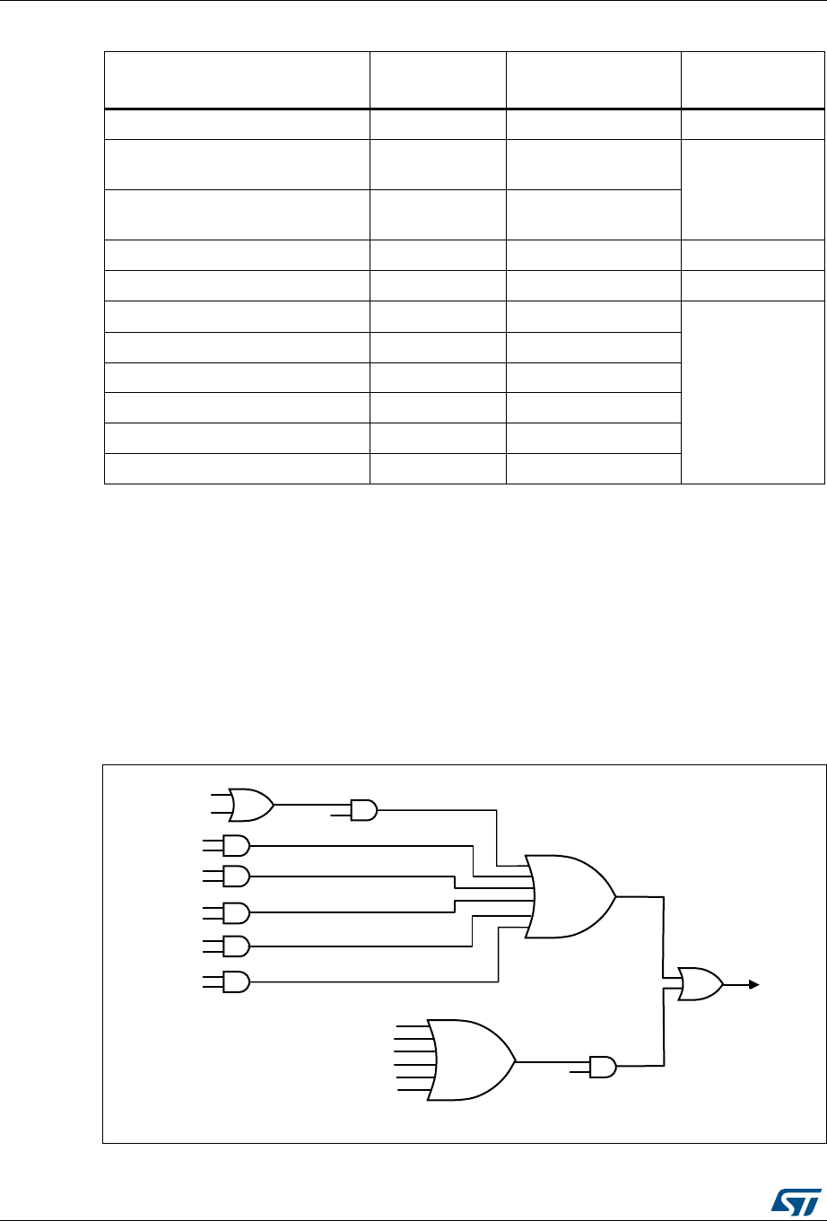
Inter-integrated circuit (I2C) interface RM0376
704/1001 DocID025941 Rev 5
Depending on the product implementation, all these interrupts events can either share the
same interrupt vector (I2C global interrupt), or be grouped into 2 interrupt vectors (I2C event
interrupt and I2C error interrupt). Refer to Table 53: List of vectors for details.
In order to enable the I2C interrupts, the following sequence is required:
1. Configure and enable the I2C IRQ channel in the NVIC.
2. Configure the I2C to generate interrupts.
The I2C wakeup event is connected to the EXTI controller (refer to Section 13.5: EXTI
registers).
Figure 225. I2C interrupt mapping diagram
Stop detection interrupt flag STOPF Write STOPCF=1 STOPIE
Transfer Complete Reload TCR Write I2C_CR2 with
NBYTES[7:0] ≠ 0
TCIE
Transfer complete TC Write START=1 or
STOP=1
Address matched ADDR Write ADDRCF=1 ADDRIE
NACK reception NACKF Write NACKCF=1 NACKIE
Bus error BERR Write BERRCF=1
ERRIE
Arbitration loss ARLO Write ARLOCF=1
Overrun/Underrun OVR Write OVRCF=1
PEC error PECERR Write PECERRCF=1
Timeout/tLOW error TIMEOUT Write TIMEOUTCF=1
SMBus Alert ALERT Write ALERTCF=1
Table 124. I2C Interrupt requests (continued)
Interrupt event Event flag Event flag/Interrupt
clearing method
Interrupt enable
control bit
MSv41065V1
TCR
TXIS
TXIE
RXNE
RXIE
STOPF
STOPIE
ADDR
ADDRIE
NACKF
NACKIE
I2C global interrupt
BERR
OVR
ARLO
TIMEOUT
ALERT
PECERR
TCIE
ERRIE
TC
I2C error interrupt
I2C event interrupt

DocID025941 Rev 5 705/1001
RM0376 Inter-integrated circuit (I2C) interface
721
27.7 I2C registers
Refer to Section 1.1 on page 51 for a list of abbreviations used in register descriptions.
The peripheral registers are accessed by words (32-bit).
27.7.1 Control register 1 (I2C_CR1)
Address offset: 0x00
Reset value: 0x0000 0000
Access: No wait states, except if a write access occurs while a write access to this register is
ongoing. In this case, wait states are inserted in the second write access until the previous
one is completed. The latency of the second write access can be up to 2 x PCLK1 + 6 x
I2CCLK.
31 30 29 28 27 26 25 24 23 22 21 20 19 18 17 16
Res. Res. Res. Res. Res. Res. Res. Res. PECEN ALERT
EN
SMBD
EN
SMBH
EN GCEN WUPE
N
NOSTR
ETCH SBC
rw rw rw rw rw rw rw rw
15141312111098 7 6543210
RXDMA
EN
TXDMA
EN Res. ANF
OFF DNF ERRIE TCIE STOP
IE
NACK
IE
ADDR
IE RXIE TXIE PE
rw rw rw rw rw rw rw rw rw rw rw rw
Bits 31:24 Reserved, must be kept at reset value.
Bit 23 PECEN: PEC enable
0: PEC calculation disabled
1: PEC calculation enabled
Note: If the SMBus feature is not supported, this bit is reserved and forced by hardware to ‘0’.
Refer to Section 27.3: I2C implementation.
Bit 22 ALERTEN: SMBus alert enable
Device mode (SMBHEN=0):
0: Releases SMBA pin high and Alert Response Address Header disabled: 0001100x
followed by NACK.
1: Drives SMBA pin low and Alert Response Address Header enables: 0001100x followed
by ACK.
Host mode (SMBHEN=1):
0: SMBus Alert pin (SMBA) not supported.
1: SMBus Alert pin (SMBA) supported.
Note: When ALERTEN=0, the SMBA pin can be used as a standard GPIO.
If the SMBus feature is not supported, this bit is reserved and forced by hardware to ‘0’.
Refer to Section 27.3: I2C implementation.
Bit 21 SMBDEN: SMBus Device Default address enable
0: Device default address disabled. Address 0b1100001x is NACKed.
1: Device default address enabled. Address 0b1100001x is ACKed.
Note: If the SMBus feature is not supported, this bit is reserved and forced by hardware to ‘0’.
Refer to Section 27.3: I2C implementation.

Inter-integrated circuit (I2C) interface RM0376
706/1001 DocID025941 Rev 5
Bit 20 SMBHEN: SMBus Host address enable
0: Host address disabled. Address 0b0001000x is NACKed.
1: Host address enabled. Address 0b0001000x is ACKed.
Note: If the SMBus feature is not supported, this bit is reserved and forced by hardware to ‘0’.
Refer to Section 27.3: I2C implementation.
Bit 19 GCEN: General call enable
0: General call disabled. Address 0b00000000 is NACKed.
1: General call enabled. Address 0b00000000 is ACKed.
Bit 18 WUPEN: Wakeup from Stop mode enable
0: Wakeup from Stop mode disable.
1: Wakeup from Stop mode enable.
Note: If the Wakeup from Stop mode feature is not supported, this bit is reserved and forced
by hardware to ‘0’. Please refer to Section 27.3: I2C implementation.
Note: WUPEN can be set only when DNF = ‘0000’
Bit 17 NOSTRETCH: Clock stretching disable
This bit is used to disable clock stretching in slave mode. It must be kept cleared in master
mode.
0: Clock stretching enabled
1: Clock stretching disabled
Note: This bit can only be programmed when the I2C is disabled (PE = 0).
Bit 16 SBC: Slave byte control
This bit is used to enable hardware byte control in slave mode.
0: Slave byte control disabled
1: Slave byte control enabled
Bit 15 RXDMAEN: DMA reception requests enable
0: DMA mode disabled for reception
1: DMA mode enabled for reception
Bit 14 TXDMAEN: DMA transmission requests enable
0: DMA mode disabled for transmission
1: DMA mode enabled for transmission
Bit 13 Reserved, must be kept at reset value.
Bit 12 ANFOFF: Analog noise filter OFF
0: Analog noise filter enabled
1: Analog noise filter disabled
Note: This bit can only be programmed when the I2C is disabled (PE = 0).
Bits 11:8 DNF[3:0]: Digital noise filter
These bits are used to configure the digital noise filter on SDA and SCL input. The digital filter
will filter spikes with a length of up to DNF[3:0] * tI2CCLK
0000: Digital filter disabled
0001: Digital filter enabled and filtering capability up to 1 tI2CCLK
...
1111: digital filter enabled and filtering capability up to15 tI2CCLK
Note: If the analog filter is also enabled, the digital filter is added to the analog filter.
This filter can only be programmed when the I2C is disabled (PE = 0).

DocID025941 Rev 5 707/1001
RM0376 Inter-integrated circuit (I2C) interface
721
Bit 7 ERRIE: Error interrupts enable
0: Error detection interrupts disabled
1: Error detection interrupts enabled
Note: Any of these errors generate an interrupt:
Arbitration Loss (ARLO)
Bus Error detection (BERR)
Overrun/Underrun (OVR)
Timeout detection (TIMEOUT)
PEC error detection (PECERR)
Alert pin event detection (ALERT)
Bit 6 TCIE: Transfer Complete interrupt enable
0: Transfer Complete interrupt disabled
1: Transfer Complete interrupt enabled
Note: Any of these events will generate an interrupt:
Transfer Complete (TC)
Transfer Complete Reload (TCR)
Bit 5 STOPIE: STOP detection Interrupt enable
0: Stop detection (STOPF) interrupt disabled
1: Stop detection (STOPF) interrupt enabled
Bit 4 NACKIE: Not acknowledge received Interrupt enable
0: Not acknowledge (NACKF) received interrupts disabled
1: Not acknowledge (NACKF) received interrupts enabled
Bit 3 ADDRIE: Address match Interrupt enable (slave only)
0: Address match (ADDR) interrupts disabled
1: Address match (ADDR) interrupts enabled
Bit 2 RXIE: RX Interrupt enable
0: Receive (RXNE) interrupt disabled
1: Receive (RXNE) interrupt enabled
Bit 1 TXIE: TX Interrupt enable
0: Transmit (TXIS) interrupt disabled
1: Transmit (TXIS) interrupt enabled
Bit 0 PE: Peripheral enable
0: Peripheral disable
1: Peripheral enable
Note: When PE=0, the I2C SCL and SDA lines are released. Internal state machines and
status bits are put back to their reset value. When cleared, PE must be kept low for at
least 3 APB clock cycles.

Inter-integrated circuit (I2C) interface RM0376
708/1001 DocID025941 Rev 5
27.7.2 Control register 2 (I2C_CR2)
Address offset: 0x04
Reset value: 0x0000 0000
Access: No wait states, except if a write access occurs while a write access to this register is
ongoing. In this case, wait states are inserted in the second write access until the previous
one is completed. The latency of the second write access can be up to 2 x PCLK1 + 6 x
I2CCLK.
31 30 29 28 27 26 25 24 23 22 21 20 19 18 17 16
Res. Res. Res. Res. Res. PEC
BYTE
AUTO
END
RE
LOAD NBYTES[7:0]
rs rw rw rw
1514131211109876543210
NACK STOP START HEAD
10R ADD10 RD_
WRN SADD[9:0]
rs rs rs rw rw rw rw
Bits 31:27 Reserved, must be kept at reset value.
Bit 26 PECBYTE: Packet error checking byte
This bit is set by software, and cleared by hardware when the PEC is transferred, or when a
STOP condition or an Address matched is received, also when PE=0.
0: No PEC transfer.
1: PEC transmission/reception is requested
Note: Writing ‘0’ to this bit has no effect.
This bit has no effect when RELOAD is set.
This bit has no effect is slave mode when SBC=0.
If the SMBus feature is not supported, this bit is reserved and forced by hardware to ‘0’.
Refer to Section 27.3: I2C implementation.
Bit 25 AUTOEND: Automatic end mode (master mode)
This bit is set and cleared by software.
0: software end mode: TC flag is set when NBYTES data are transferred, stretching SCL low.
1: Automatic end mode: a STOP condition is automatically sent when NBYTES data are
transferred.
Note: This bit has no effect in slave mode or when the RELOAD bit is set.
Bit 24 RELOAD: NBYTES reload mode
This bit is set and cleared by software.
0: The transfer is completed after the NBYTES data transfer (STOP or RESTART will follow).
1: The transfer is not completed after the NBYTES data transfer (NBYTES will be reloaded).
TCR flag is set when NBYTES data are transferred, stretching SCL low.
Bits 23:16 NBYTES[7:0]: Number of bytes
The number of bytes to be transmitted/received is programmed there. This field is don’t care in
slave mode with SBC=0.
Note: Changing these bits when the START bit is set is not allowed.

DocID025941 Rev 5 709/1001
RM0376 Inter-integrated circuit (I2C) interface
721
Bit 15 NACK: NACK generation (slave mode)
The bit is set by software, cleared by hardware when the NACK is sent, or when a STOP
condition or an Address matched is received, or when PE=0.
0: an ACK is sent after current received byte.
1: a NACK is sent after current received byte.
Note: Writing ‘0’ to this bit has no effect.
This bit is used in slave mode only: in master receiver mode, NACK is automatically
generated after last byte preceding STOP or RESTART condition, whatever the NACK
bit value.
When an overrun occurs in slave receiver NOSTRETCH mode, a NACK is
automatically generated whatever the NACK bit value.
When hardware PEC checking is enabled (PECBYTE=1), the PEC acknowledge value
does not depend on the NACK value.
Bit 14 STOP: Stop generation (master mode)
The bit is set by software, cleared by hardware when a Stop condition is detected, or when PE
= 0.
In Master Mode:
0: No Stop generation.
1: Stop generation after current byte transfer.
Note: Writing ‘0’ to this bit has no effect.
Bit 13 START: Start generation
This bit is set by software, and cleared by hardware after the Start followed by the address
sequence is sent, by an arbitration loss, by a timeout error detection, or when PE = 0. It can
also be cleared by software by writing ‘1’ to the ADDRCF bit in the I2C_ICR register.
0: No Start generation.
1: Restart/Start generation:
– If the I2C is already in master mode with AUTOEND = 0, setting this bit generates a
Repeated Start condition when RELOAD=0, after the end of the NBYTES transfer.
– Otherwise setting this bit will generate a START condition once the bus is free.
Note: Writing ‘0’ to this bit has no effect.
The START bit can be set even if the bus is BUSY or I2C is in slave mode.
This bit has no effect when RELOAD is set. In 10-bit addressing mode, if a NACK is
received on the first part of the address, the START bit is not cleared by hardware and
the master will resend the address sequence, unless the START bit is cleared by
software
Bit 12 HEAD10R: 10-bit address header only read direction (master receiver mode)
0: The master sends the complete 10 bit slave address read sequence: Start + 2 bytes 10bit
address in write direction + Restart + 1st 7 bits of the 10 bit address in read direction.
1: The master only sends the 1st 7 bits of the 10 bit address, followed by Read direction.
Note: Changing this bit when the START bit is set is not allowed.
Bit 11 ADD10: 10-bit addressing mode (master mode)
0: The master operates in 7-bit addressing mode,
1: The master operates in 10-bit addressing mode
Note: Changing this bit when the START bit is set is not allowed.
Bit 10 RD_WRN: Transfer direction (master mode)
0: Master requests a write transfer.
1: Master requests a read transfer.
Note: Changing this bit when the START bit is set is not allowed.

Inter-integrated circuit (I2C) interface RM0376
710/1001 DocID025941 Rev 5
Bits 9:8 SADD[9:8]: Slave address bit 9:8 (master mode)
In 7-bit addressing mode (ADD10 = 0):
These bits are don’t care
In 10-bit addressing mode (ADD10 = 1):
These bits should be written with bits 9:8 of the slave address to be sent
Note: Changing these bits when the START bit is set is not allowed.
Bits 7:1 SADD[7:1]: Slave address bit 7:1 (master mode)
In 7-bit addressing mode (ADD10 = 0):
These bits should be written with the 7-bit slave address to be sent
In 10-bit addressing mode (ADD10 = 1):
These bits should be written with bits 7:1 of the slave address to be sent.
Note: Changing these bits when the START bit is set is not allowed.
Bit 0 SADD0: Slave address bit 0 (master mode)
In 7-bit addressing mode (ADD10 = 0):
This bit is don’t care
In 10-bit addressing mode (ADD10 = 1):
This bit should be written with bit 0 of the slave address to be sent
Note: Changing these bits when the START bit is set is not allowed.

DocID025941 Rev 5 711/1001
RM0376 Inter-integrated circuit (I2C) interface
721
27.7.3 Own address 1 register (I2C_OAR1)
Address offset: 0x08
Reset value: 0x0000 0000
Access: No wait states, except if a write access occurs while a write access to this register is
ongoing. In this case, wait states are inserted in the second write access until the previous
one is completed. The latency of the second write access can be up to 2 x PCLK1 + 6 x
I2CCLK.
31 30 29 28 27 26 25 24 23 22 21 20 19 18 17 16
Res. Res. Res. Res. Res. Res. Res. Res. Res. Res. Res. Res. Res. Res. Res. Res.
1514131211109876543210
OA1EN Res. Res. Res. Res. OA1
MODE OA1[9:8] OA1[7:1] OA1[0]
rw rw rw rw rw
Bits 31:16 Reserved, must be kept at reset value.
Bit 15 OA1EN: Own Address 1 enable
0: Own address 1 disabled. The received slave address OA1 is NACKed.
1: Own address 1 enabled. The received slave address OA1 is ACKed.
Bits 14:11 Reserved, must be kept at reset value.
Bit 10 OA1MODE Own Address 1 10-bit mode
0: Own address 1 is a 7-bit address.
1: Own address 1 is a 10-bit address.
Note: This bit can be written only when OA1EN=0.
Bits 9:8 OA1[9:8]: Interface address
7-bit addressing mode: do not care
10-bit addressing mode: bits 9:8 of address
Note: These bits can be written only when OA1EN=0.
Bits 7:1 OA1[7:1]: Interface address
7-bit addressing mode: 7-bit address
10-bit addressing mode: bits 7:1 of 10-bit address
Note: These bits can be written only when OA1EN=0.
Bit 0 OA1[0]: Interface address
7-bit addressing mode: do not care
10-bit addressing mode: bit 0 of address
Note: This bit can be written only when OA1EN=0.

Inter-integrated circuit (I2C) interface RM0376
712/1001 DocID025941 Rev 5
27.7.4 Own address 2 register (I2C_OAR2)
Address offset: 0x0C
Reset value: 0x0000 0000
Access: No wait states, except if a write access occurs while a write access to this register is
ongoing. In this case, wait states are inserted in the second write access until the previous
one is completed. The latency of the second write access can be up to 2 x PCLK1 + 6 x
I2CCLK.
31 30 29 28 27 26 25 24 23 22 21 20 19 18 17 16
Res. Res. Res. Res. Res. Res. Res. Res. Res. Res. Res. Res. Res. Res. Res. Res.
15 14 13 12 11 10 9 8 7 6 5 4 3 2 1 0
OA2EN Res. Res. Res. Res. OA2MSK[2:0] OA2[7:1] Res.
rw rw rw
Bits 31:16 Reserved, must be kept at reset value.
Bit 15 OA2EN: Own Address 2 enable
0: Own address 2 disabled. The received slave address OA2 is NACKed.
1: Own address 2 enabled. The received slave address OA2 is ACKed.
Bits 14:11 Reserved, must be kept at reset value.
Bits 10:8 OA2MSK[2:0]: Own Address 2 masks
000: No mask
001: OA2[1] is masked and don’t care. Only OA2[7:2] are compared.
010: OA2[2:1] are masked and don’t care. Only OA2[7:3] are compared.
011: OA2[3:1] are masked and don’t care. Only OA2[7:4] are compared.
100: OA2[4:1] are masked and don’t care. Only OA2[7:5] are compared.
101: OA2[5:1] are masked and don’t care. Only OA2[7:6] are compared.
110: OA2[6:1] are masked and don’t care. Only OA2[7] is compared.
111: OA2[7:1] are masked and don’t care. No comparison is done, and all (except reserved)
7-bit received addresses are acknowledged.
Note: These bits can be written only when OA2EN=0.
As soon as OA2MSK is not equal to 0, the reserved I2C addresses (0b0000xxx and
0b1111xxx) are not acknowledged even if the comparison matches.
Bits 7:1 OA2[7:1]: Interface address
7-bit addressing mode: 7-bit address
Note: These bits can be written only when OA2EN=0.
Bit 0 Reserved, must be kept at reset value.

DocID025941 Rev 5 713/1001
RM0376 Inter-integrated circuit (I2C) interface
721
27.7.5 Timing register (I2C_TIMINGR)
Address offset: 0x10
Reset value: 0x0000 0000
Access: No wait states
Note: This register must be configured when the I2C is disabled (PE = 0).
Note: The STM32CubeMX tool calculates and provides the I2C_TIMINGR content in the I2C
Configuration window.
31 30 29 28 27 26 25 24 23 22 21 20 19 18 17 16
PRESC[3:0] Res. Res. Res. Res. SCLDEL[3:0] SDADEL[3:0]
rw rw rw
15141312111098 7 654321 0
SCLH[7:0] SCLL[7:0]
rw rw
Bits 31:28 PRESC[3:0]: Timing prescaler
This field is used to prescale I2CCLK in order to generate the clock period tPRESC used for data
setup and hold counters (refer to I2C timings on page 659) and for SCL high and low level
counters (refer to I2C master initialization on page 674).
tPRESC = (PRESC+1) x tI2CCLK
Bits 27:24 Reserved, must be kept at reset value.
Bits 23:20 SCLDEL[3:0]: Data setup time
This field is used to generate a delay tSCLDEL between SDA edge and SCL rising edge. In
master mode and in slave mode with NOSTRETCH = 0, the SCL line is stretched low during
tSCLDEL.
tSCLDEL = (SCLDEL+1) x tPRESC
Note: tSCLDEL is used to generate tSU:DAT timing.
Bits 19:16 SDADEL[3:0]: Data hold time
This field is used to generate the delay tSDADEL between SCL falling edge and SDA edge. In
master mode and in slave mode with NOSTRETCH = 0, the SCL line is stretched low during
tSDADEL.
tSDADEL= SDADEL x tPRESC
Note: SDADEL is used to generate tHD:DAT timing.
Bits 15:8 SCLH[7:0]: SCL high period (master mode)
This field is used to generate the SCL high period in master mode.
tSCLH = (SCLH+1) x tPRESC
Note: SCLH is also used to generate tSU:STO and tHD:STA timing.
Bits 7:0 SCLL[7:0]: SCL low period (master mode)
This field is used to generate the SCL low period in master mode.
tSCLL = (SCLL+1) x tPRESC
Note: SCLL is also used to generate tBUF and tSU:STA timings.

Inter-integrated circuit (I2C) interface RM0376
714/1001 DocID025941 Rev 5
27.7.6 Timeout register (I2C_TIMEOUTR)
Address offset: 0x14
Reset value: 0x0000 0000
Access: No wait states, except if a write access occurs while a write access to this register is
ongoing. In this case, wait states are inserted in the second write access until the previous
one is completed. The latency of the second write access can be up to 2 x PCLK1 + 6 x
I2CCLK.
Note: If the SMBus feature is not supported, this register is reserved and forced by hardware to
“0x00000000”. Refer to Section 27.3: I2C implementation.
31 30 29 28 27 26 25 24 23 22 21 20 19 18 17 16
TEXTEN Res. Res. Res. TIMEOUTB [11:0]
rw rw
15 14 13 12 11109876543210
TIMOUTEN Res. Res. TIDLE TIMEOUTA [11:0]
rw rw rw
Bit 31 TEXTEN: Extended clock timeout enable
0: Extended clock timeout detection is disabled
1: Extended clock timeout detection is enabled. When a cumulative SCL stretch for more
than tLOW:EXT is done by the I2C interface, a timeout error is detected (TIMEOUT=1).
Bits 30:28 Reserved, must be kept at reset value.
Bits 27:16 TIMEOUTB[11:0]: Bus timeout B
This field is used to configure the cumulative clock extension timeout:
In master mode, the master cumulative clock low extend time (tLOW:MEXT) is detected
In slave mode, the slave cumulative clock low extend time (tLOW:SEXT) is detected
tLOW:EXT= (TIMEOUTB+1) x 2048 x tI2CCLK
Note: These bits can be written only when TEXTEN=0.
Bit 15 TIMOUTEN: Clock timeout enable
0: SCL timeout detection is disabled
1: SCL timeout detection is enabled: when SCL is low for more than tTIMEOUT (TIDLE=0) or
high for more than tIDLE (TIDLE=1), a timeout error is detected (TIMEOUT=1).
Bits 14:13 Reserved, must be kept at reset value.
Bit 12 TIDLE: Idle clock timeout detection
0: TIMEOUTA is used to detect SCL low timeout
1: TIMEOUTA is used to detect both SCL and SDA high timeout (bus idle condition)
Note: This bit can be written only when TIMOUTEN=0.
Bits 11:0 TIMEOUTA[11:0]: Bus Timeout A
This field is used to configure:
– The SCL low timeout condition tTIMEOUT when TIDLE=0
tTIMEOUT= (TIMEOUTA+1) x 2048 x tI2CCLK
– The bus idle condition (both SCL and SDA high) when TIDLE=1
tIDLE= (TIMEOUTA+1) x 4 x tI2CCLK
Note: These bits can be written only when TIMOUTEN=0.

DocID025941 Rev 5 715/1001
RM0376 Inter-integrated circuit (I2C) interface
721
27.7.7 Interrupt and status register (I2C_ISR)
Address offset: 0x18
Reset value: 0x0000 0001
Access: No wait states
31 30 29 28 27 26 25 24 23 22 21 20 19 18 17 16
Res. Res. Res. Res. Res. Res. Res. Res. ADDCODE[6:0] DIR
rr
1514131211109876543210
BUSY Res. ALERT TIME
OUT
PEC
ERR OVR ARLO BERR TCR TC STOPF NACKF ADDR RXNE TXIS TXE
r rrrrrrrrrrrrrsrs
Bits 31:24 Reserved, must be kept at reset value.
Bits 23:17 ADDCODE[6:0]: Address match code (Slave mode)
These bits are updated with the received address when an address match event occurs
(ADDR = 1).
In the case of a 10-bit address, ADDCODE provides the 10-bit header followed by the 2 MSBs
of the address.
Bit 16 DIR: Transfer direction (Slave mode)
This flag is updated when an address match event occurs (ADDR=1).
0: Write transfer, slave enters receiver mode.
1: Read transfer, slave enters transmitter mode.
Bit 15 BUSY: Bus busy
This flag indicates that a communication is in progress on the bus. It is set by hardware when a
START condition is detected. It is cleared by hardware when a Stop condition is detected, or
when PE=0.
Bit 14 Reserved, must be kept at reset value.
Bit 13 ALERT: SMBus alert
This flag is set by hardware when SMBHEN=1 (SMBus host configuration), ALERTEN=1 and
a SMBALERT event (falling edge) is detected on SMBA pin. It is cleared by software by setting
the ALERTCF bit.
Note: This bit is cleared by hardware when PE=0.
If the SMBus feature is not supported, this bit is reserved and forced by hardware to ‘0’.
Refer to Section 27.3: I2C implementation.
Bit 12 TIMEOUT: Timeout or tLOW detection flag
This flag is set by hardware when a timeout or extended clock timeout occurred. It is cleared
by software by setting the TIMEOUTCF bit.
Note: This bit is cleared by hardware when PE=0.
If the SMBus feature is not supported, this bit is reserved and forced by hardware to ‘0’.
Refer to Section 27.3: I2C implementation.

Inter-integrated circuit (I2C) interface RM0376
716/1001 DocID025941 Rev 5
Bit 11 PECERR: PEC Error in reception
This flag is set by hardware when the received PEC does not match with the PEC register
content. A NACK is automatically sent after the wrong PEC reception. It is cleared by software
by setting the PECCF bit.
Note: This bit is cleared by hardware when PE=0.
If the SMBus feature is not supported, this bit is reserved and forced by hardware to ‘0’.
Refer to Section 27.3: I2C implementation.
Bit 10 OVR: Overrun/Underrun (slave mode)
This flag is set by hardware in slave mode with NOSTRETCH=1, when an overrun/underrun
error occurs. It is cleared by software by setting the OVRCF bit.
Note: This bit is cleared by hardware when PE=0.
Bit 9 ARLO: Arbitration lost
This flag is set by hardware in case of arbitration loss. It is cleared by software by setting the
ARLOCF bit.
Note: This bit is cleared by hardware when PE=0.
Bit 8 BERR: Bus error
This flag is set by hardware when a misplaced Start or Stop condition is detected whereas the
peripheral is involved in the transfer. The flag is not set during the address phase in slave
mode. It is cleared by software by setting BERRCF bit.
Note: This bit is cleared by hardware when PE=0.
Bit 7 TCR: Transfer Complete Reload
This flag is set by hardware when RELOAD=1 and NBYTES data have been transferred. It is
cleared by software when NBYTES is written to a non-zero value.
Note: This bit is cleared by hardware when PE=0.
This flag is only for master mode, or for slave mode when the SBC bit is set.
Bit 6 TC: Transfer Complete (master mode)
This flag is set by hardware when RELOAD=0, AUTOEND=0 and NBYTES data have been
transferred. It is cleared by software when START bit or STOP bit is set.
Note: This bit is cleared by hardware when PE=0.
Bit 5 STOPF: Stop detection flag
This flag is set by hardware when a Stop condition is detected on the bus and the peripheral is
involved in this transfer:
– either as a master, provided that the STOP condition is generated by the peripheral.
– or as a slave, provided that the peripheral has been addressed previously during this
transfer.
It is cleared by software by setting the STOPCF bit.
Note: This bit is cleared by hardware when PE=0.
Bit 4 NACKF: Not Acknowledge received flag
This flag is set by hardware when a NACK is received after a byte transmission. It is cleared by
software by setting the NACKCF bit.
Note: This bit is cleared by hardware when PE=0.
Bit 3 ADDR: Address matched (slave mode)
This bit is set by hardware as soon as the received slave address matched with one of the
enabled slave addresses. It is cleared by software by setting ADDRCF bit.
Note: This bit is cleared by hardware when PE=0.

DocID025941 Rev 5 717/1001
RM0376 Inter-integrated circuit (I2C) interface
721
27.7.8 Interrupt clear register (I2C_ICR)
Address offset: 0x1C
Reset value: 0x0000 0000
Access: No wait states
Bit 2 RXNE: Receive data register not empty (receivers)
This bit is set by hardware when the received data is copied into the I2C_RXDR register, and is
ready to be read. It is cleared when I2C_RXDR is read.
Note: This bit is cleared by hardware when PE=0.
Bit 1 TXIS: Transmit interrupt status (transmitters)
This bit is set by hardware when the I2C_TXDR register is empty and the data to be
transmitted must be written in the I2C_TXDR register. It is cleared when the next data to be
sent is written in the I2C_TXDR register.
This bit can be written to ‘1’ by software when NOSTRETCH=1 only, in order to generate a
TXIS event (interrupt if TXIE=1 or DMA request if TXDMAEN=1).
Note: This bit is cleared by hardware when PE=0.
Bit 0 TXE: Transmit data register empty (transmitters)
This bit is set by hardware when the I2C_TXDR register is empty. It is cleared when the next
data to be sent is written in the I2C_TXDR register.
This bit can be written to ‘1’ by software in order to flush the transmit data register I2C_TXDR.
Note: This bit is set by hardware when PE=0.
31 30 29 28 27 26 25 24 23 22 21 20 19 18 17 16
Res. Res. Res. Res. Res. Res. Res. Res. Res. Res. Res. Res. Res. Res. Res. Res.
1514131211109876543210
Res. Res. ALERT
CF
TIM
OUTCF PECCF OVRCF ARLO
CF
BERR
CF Res. Res. STOP
CF
NACK
CF
ADDR
CF Res. Res. Res.
wwwwww www
Bits 31:14 Reserved, must be kept at reset value.
Bit 13 ALERTCF: Alert flag clear
Writing 1 to this bit clears the ALERT flag in the I2C_ISR register.
Note: If the SMBus feature is not supported, this bit is reserved and forced by hardware to ‘0’.
Refer to Section 27.3: I2C implementation.
Bit 12 TIMOUTCF: Timeout detection flag clear
Writing 1 to this bit clears the TIMEOUT flag in the I2C_ISR register.
Note: If the SMBus feature is not supported, this bit is reserved and forced by hardware to ‘0’.
Refer to Section 27.3: I2C implementation.
Bit 11 PECCF: PEC Error flag clear
Writing 1 to this bit clears the PECERR flag in the I2C_ISR register.
Note: If the SMBus feature is not supported, this bit is reserved and forced by hardware to ‘0’.
Refer to Section 27.3: I2C implementation.
Bit 10 OVRCF: Overrun/Underrun flag clear
Writing 1 to this bit clears the OVR flag in the I2C_ISR register.
Inter-integrated circuit (I2C) interface RM0376
718/1001 DocID025941 Rev 5
27.7.9 PEC register (I2C_PECR)
Address offset: 0x20
Reset value: 0x0000 0000
Access: No wait states
Note: If the SMBus feature is not supported, this register is reserved and forced by hardware to
“0x00000000”. Refer to Section 27.3: I2C implementation.
Bit 9 ARLOCF: Arbitration Lost flag clear
Writing 1 to this bit clears the ARLO flag in the I2C_ISR register.
Bit 8 BERRCF: Bus error flag clear
Writing 1 to this bit clears the BERRF flag in the I2C_ISR register.
Bits 7:6 Reserved, must be kept at reset value.
Bit 5 STOPCF: Stop detection flag clear
Writing 1 to this bit clears the STOPF flag in the I2C_ISR register.
Bit 4 NACKCF: Not Acknowledge flag clear
Writing 1 to this bit clears the NACKF flag in I2C_ISR register.
Bit 3 ADDRCF: Address matched flag clear
Writing 1 to this bit clears the ADDR flag in the I2C_ISR register. Writing 1 to this bit also clears
the START bit in the I2C_CR2 register.
Bits 2:0 Reserved, must be kept at reset value.
31 30 29 28 27 26 25 24 23 22 21 20 19 18 17 16
Res. Res. Res. Res. Res. Res. Res. Res. Res. Res. Res. Res. Res. Res. Res. Res.
1514131211109876543210
Res. Res. Res. Res. Res. Res. Res. Res. PEC[7:0]
r
Bits 31:8 Reserved, must be kept at reset value.
Bits 7:0 PEC[7:0] Packet error checking register
This field contains the internal PEC when PECEN=1.
The PEC is cleared by hardware when PE=0.
DocID025941 Rev 5 719/1001
RM0376 Inter-integrated circuit (I2C) interface
721
27.7.10 Receive data register (I2C_RXDR)
Address offset: 0x24
Reset value: 0x0000 0000
Access: No wait states
27.7.11 Transmit data register (I2C_TXDR)
Address offset: 0x28
Reset value: 0x0000 0000
Access: No wait states
31 30 29 28 27 26 25 24 23 22 21 20 19 18 17 16
Res. Res. Res. Res. Res. Res. Res. Res. Res. Res. Res. Res. Res. Res. Res. Res.
1514131211109876543210
Res. Res. Res. Res. Res. Res. Res. Res. RXDATA[7:0]
r
Bits 31:8 Reserved, must be kept at reset value.
Bits 7:0 RXDATA[7:0] 8-bit receive data
Data byte received from the I2C bus.
31 30 29 28 27 26 25 24 23 22 21 20 19 18 17 16
Res. Res. Res. Res. Res. Res. Res. Res. Res. Res. Res. Res. Res. Res. Res. Res.
1514131211109876543210
Res. Res. Res. Res. Res. Res. Res. Res. TXDATA[7:0]
rw
Bits 31:8 Reserved, must be kept at reset value.
Bits 7:0 TXDATA[7:0] 8-bit transmit data
Data byte to be transmitted to the I2C bus.
Note: These bits can be written only when TXE=1.
Inter-integrated circuit (I2C) interface RM0376
720/1001 DocID025941 Rev 5
27.7.12 I2C register map
The table below provides the I2C register map and reset values.
Table 125. I2C register map and reset values
Offset Register
name
31
30
29
28
27
26
25
24
23
22
21
20
19
18
17
16
15
14
13
12
11
10
9
8
7
6
5
4
3
2
1
0
0x0
I2C_CR1
Res.
Res.
Res.
Res.
Res.
Res.
Res.
Res.
PECEN
ALERTEN
SMBDEN
SMBHEN
GCEN
WUPEN
NOSTRETCH
SBC
RXDMAEN
TXDMAEN
Res.
ANFOFF
DNF[3:0]
ERRIE
TCIE
STOPIE
NACKIE
ADDRIE
RXIE
TXIE
PE
Reset value 0000000000 0000000000000
0x4
I2C_CR2
Res.
Res.
Res.
Res.
Res.
PECBYTE
AUTOEND
RELOAD
NBYTES[7:0]
NACK
STOP
START
HEAD10R
ADD10
RD_WRN
SADD[9:0]
Reset value 000000000000000000000000000
0x8
I2C_OAR1
Res.
Res.
Res.
Res.
Res.
Res.
Res.
Res.
Res.
Res.
Res.
Res.
Res.
Res.
Res.
Res.
OA1EN
Res.
Res.
Res.
Res.
OA1MODE
OA1[9:0]
Reset value 0 00000000000
0xC
I2C_OAR2
Res.
Res.
Res.
Res.
Res.
Res.
Res.
Res.
Res.
Res.
Res.
Res.
Res.
Res.
Res.
Res.
OA2EN
Res.
Res.
Res.
Res.
OA2MS
K [2:0] OA2[7:1]
Res.
Reset value 0 0000000000
0x10
I2C_TIMINGR PRESC[3:0]
Res.
Res.
Res.
Res.
SCLDEL[3:0
]
SDADEL[3:
0] SCLH[7:0] SCLL[7:0]
Reset value 0000 000000000000000000000000
0x14
I2C_
TIMEOUTR
TEXTEN
Res.
Res.
Res.
TIMEOUTB[11:0]
TIMOUTEN
Res.
TIDLE
TIMEOUTA[11:0]
Reset value 0 0000000000000 0000000000000
0x18
I2C_ISR
Res.
Res.
Res.
Res.
Res.
Res.
Res.
Res.
ADDCODE[6:0]
DIR
BUSY
Res.
ALERT
TIMEOUT
PECERR
OVR
ARLO
BERR
TCR
TC
STOPF
NACKF
ADDR
RXNE
TXIS
TXE
Reset value 000000000 00000000000001
0x1C
I2C_ICR
Res.
Res.
Res.
Res.
Res.
Res.
Res.
Res.
Res.
Res.
Res.
Res.
Res.
Res.
Res.
Res.
Res.
Res.
ALERTCF
TIMOUTCF
PECCF
OVRCF
ARLOCF
BERRCF
Res.
Res.
STOPCF
NACKCF
ADDRCF
Res.
Res.
Res.
Reset value 000000 000
0x20
I2C_PECR
Res.
Res.
Res.
Res.
Res.
Res.
Res.
Res.
Res.
Res.
Res.
Res.
Res.
Res.
Res.
Res.
Res.
Res.
Res.
Res.
Res.
Res.
Res.
Res.
PEC[7:0]
Reset value 00000000
0x24
I2C_RXDR
Res.
Res.
Res.
Res.
Res.
Res.
Res.
Res.
Res.
Res.
Res.
Res.
Res.
Res.
Res.
Res.
Res.
Res.
Res.
Res.
Res.
Res.
Res.
Res.
RXDATA[7:0]
Reset value 00000000

DocID025941 Rev 5 721/1001
RM0376 Inter-integrated circuit (I2C) interface
721
Refer to Section 2.2.2 on page 58 for the register boundary addresses.
0x28
I2C_TXDR
Res.
Res.
Res.
Res.
Res.
Res.
Res.
Res.
Res.
Res.
Res.
Res.
Res.
Res.
Res.
Res.
Res.
Res.
Res.
Res.
Res.
Res.
Res.
Res.
TXDATA[7:0]
Reset value 00000000
Table 125. I2C register map and reset values (continued)
Offset Register
name
31
30
29
28
27
26
25
24
23
22
21
20
19
18
17
16
15
14
13
12
11
10
9
8
7
6
5
4
3
2
1
0

Universal synchronous asynchronous receiver transmitter (USART) RM0376
722/1001 DocID025941 Rev 5
28 Universal synchronous asynchronous receiver
transmitter (USART)
28.1 Introduction
The universal synchronous asynchronous receiver transmitter (USART) offers a flexible
means of Full-duplex data exchange with external equipment requiring an industry standard
NRZ asynchronous serial data format. The USART offers a very wide range of baud rates
using a programmable baud rate generator.
It supports synchronous one-way communication and Half-duplex Single-wire
communication, as well as multiprocessor communications. It also supports the LIN (Local
Interconnect Network), Smartcard protocol and IrDA (Infrared Data Association) SIR
ENDEC specifications and Modem operations (CTS/RTS).
High speed data communication is possible by using the DMA (direct memory access) for
multibuffer configuration.
28.2 USART main features
•Full-duplex asynchronous communications
•NRZ standard format (mark/space)
•Configurable oversampling method by 16 or 8 to give flexibility between speed and
clock tolerance
•A common programmable transmit and receive baud rate of up to 4 Mbit/s when the
clock frequency is 32 MHz and oversampling is by 8
•Dual clock domain allowing:
– USART functionality and wakeup from Stop mode
– Convenient baud rate programming independent from the PCLK reprogramming
•Auto baud rate detection
•Programmable data word length (7, 8 or 9 bits)
•Programmable data order with MSB-first or LSB-first shifting
•Configurable stop bits (1 or 2 stop bits)
•Synchronous mode and clock output for synchronous communications
•Single-wire Half-duplex communications
•Continuous communications using DMA
•Received/transmitted bytes are buffered in reserved SRAM using centralized DMA
•Separate enable bits for transmitter and receiver
•Separate signal polarity control for transmission and reception
•Swappable Tx/Rx pin configuration
•Hardware flow control for modem and RS-485 transceiver

DocID025941 Rev 5 723/1001
RM0376 Universal synchronous asynchronous receiver transmitter (USART)
831
•Communication control/error detection flags
•Parity control:
– Transmits parity bit
– Checks parity of received data byte
•Fourteen interrupt sources with flags
•Multiprocessor communications
The USART enters mute mode if the address does not match.
•Wakeup from mute mode (by idle line detection or address mark detection)
28.3 USART extended features
•LIN master synchronous break send capability and LIN slave break detection capability
– 13-bit break generation and 10/11-bit break detection when USART is hardware
configured for LIN
•IrDA SIR encoder decoder supporting 3/16 bit duration for normal mode
•Smartcard mode
– Supports the T=0 and T=1 asynchronous protocols for smartcards as defined in
the ISO/IEC 7816-3 standard
– 0.5 and 1.5 stop bits for smartcard operation
•Support for ModBus communication
– Timeout feature
– CR/LF character recognition
Universal synchronous asynchronous receiver transmitter (USART) RM0376
724/1001 DocID025941 Rev 5
28.4 USART implementation
28.5 USART functional description
Any USART bidirectional communication requires a minimum of two pins: Receive data In
(RX) and Transmit data Out (TX):
•RX: Receive data Input.
This is the serial data input. Oversampling techniques are used for data recovery by
discriminating between valid incoming data and noise.
•TX: Transmit data Output.
When the transmitter is disabled, the output pin returns to its I/O port configuration.
When the transmitter is enabled and nothing is to be transmitted, the TX pin is at high
level. In Single-wire and Smartcard modes, this I/O is used to transmit and receive the
data.
Table 126. STM32L0x2 USART features(1)
USART modes/features USART1/2 USART4 USART5 LPUART
1
Hardware flow control for modem X X - X
Continuous communication using DMA X X X X
Multiprocessor communication X X X X
Synchronous mode X X X -
Smartcard mode X - - -
Single-wire Half-duplex communication X X X X
Ir SIR ENDEC block X - - -
LIN mode X - - -
Dual clock domain and wakeup from Stop mode X - - X
Receiver timeout interrupt X - - -
Modbus communication X - - -
Auto baud rate detection X - - -
Driver Enable X X X X
USART data length 7(2), 8 and 9 bits
1. X = supported.
2. In 7-bit data length mode, Smartcard mode, LIN master mode and Auto baud rate (0x7F and 0x55 frames) detection are
not supported.

DocID025941 Rev 5 725/1001
RM0376 Universal synchronous asynchronous receiver transmitter (USART)
831
Serial data are transmitted and received through these pins in normal USART mode. The
frames are comprised of:
•An Idle Line prior to transmission or reception
•A start bit
•A data word (7, 8 or 9 bits) least significant bit first
•0.5, 1, 1.5, 2 stop bits indicating that the frame is complete
•The USART interface uses a baud rate generator
•A status register (USART_ISR)
•Receive and transmit data registers (USART_RDR, USART_TDR)
•A baud rate register (USART_BRR)
•A guard-time register (USART_GTPR) in case of Smartcard mode.
Refer to Section 28.8: USART registers on page 767 for the definitions of each bit.
The following pin is required to interface in synchronous mode and Smartcard mode:
•CK: Clock output. This pin outputs the transmitter data clock for synchronous
transmission corresponding to SPI master mode (no clock pulses on start bit and stop
bit, and a software option to send a clock pulse on the last data bit). In parallel, data
can be received synchronously on RX. This can be used to control peripherals that
have shift registers. The clock phase and polarity are software programmable. In
Smartcard mode, CK output can provide the clock to the smartcard.
The following pins are required in RS232 Hardware flow control mode:
•CTS: Clear To Send blocks the data transmission at the end of the current transfer
when high
•RTS: Request to send indicates that the USART is ready to receive data (when low).
The following pin is required in RS485 Hardware control mode:
•DE: Driver Enable activates the transmission mode of the external transceiver.
Note: DE and RTS share the same pin.
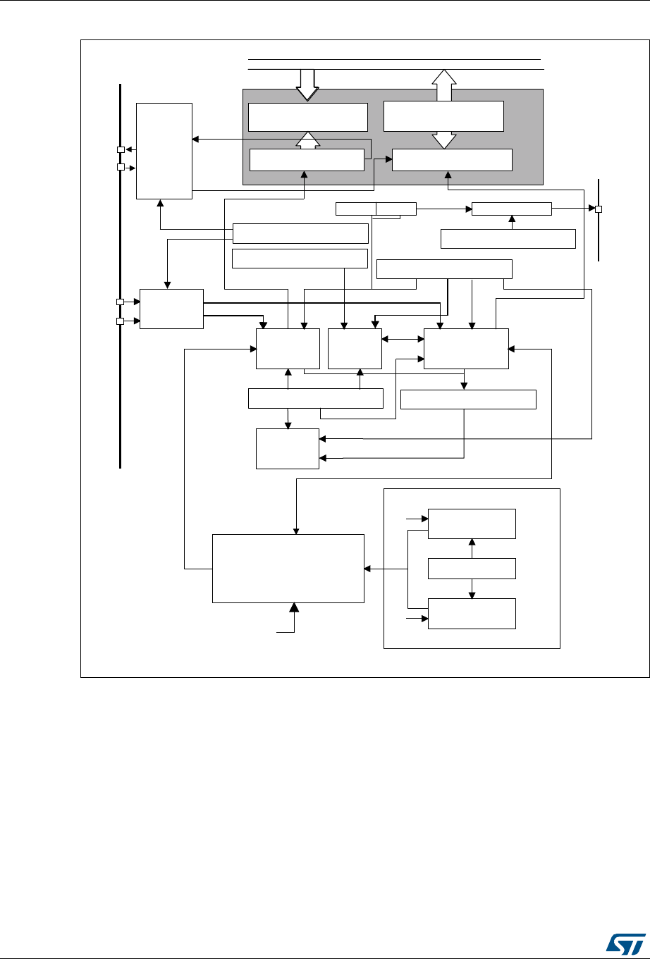
Universal synchronous asynchronous receiver transmitter (USART) RM0376
726/1001 DocID025941 Rev 5
Figure 226. USART block diagram
1. For details on coding USARTDIV in the USART_BRR register, please refer to Section 28.5.4: USART baud
rate generation.
2. fCK can be fLSE, fHSI, fPCLK, fSYS.
MS19821V5
Receive shift register
BRR[15:0]
Write Read DR (data register)
(CPU or DMA) (CPU or DMA)
Transmit data register
(TDR)
PWDATA PRDATA
Receive data register
(RDR)
Transmit shift register
USART_CR3 register
USART_CR2 register
RTS/
DE
CTS
Hardware
flow
controller
IrDA
SIR
ENDEC
block
Transmit
control
USART_CR1 register
Wakeup
unit
USART_CR1 register
USART_GTPR register
GT PSC CK control
USART_CR2 register
Receiver
control
Receiver
clock
USART_ISR register
USART
interrupt
control
USART_BRR register
Transmitter
rate controller
Receiver rate
controller
/USARTDIV or 2/USARTDIV
(depending on the
oversampling mode)
(Note 1)
fCK
Transmitter
clock
Conventional baud rate generator
(Note 2)
TE
RE
CK
TX
RX

DocID025941 Rev 5 727/1001
RM0376 Universal synchronous asynchronous receiver transmitter (USART)
831
28.5.1 USART character description
The word length can be selected as being either 7 or 8 or 9 bits by programming the M[1:0]
bits in the USART_CR1 register (see Figure 227).
•7-bit character length: M[1:0] = 10
•8-bit character length: M[1:0] = 00
•9-bit character length: M[1:0] = 01
Note: The 7-bit mode is supported only on some USARTs. In addition, not all modes are
supported in 7-bit data length mode. Refer to Section 28.4: USART implementation for
additional information.
By default, the signal (TX or RX) is in low state during the start bit. It is in high state during
the stop bit.
These values can be inverted, separately for each signal, through polarity configuration
control.
An Idle character is interpreted as an entire frame of “1”s (the number of “1”s includes the
number of stop bits).
A Break character is interpreted on receiving “0”s for a frame period. At the end of the
break frame, the transmitter inserts 2 stop bits.
Transmission and reception are driven by a common baud rate generator, the clock for each
is generated when the enable bit is set respectively for the transmitter and receiver.
The details of each block is given below.
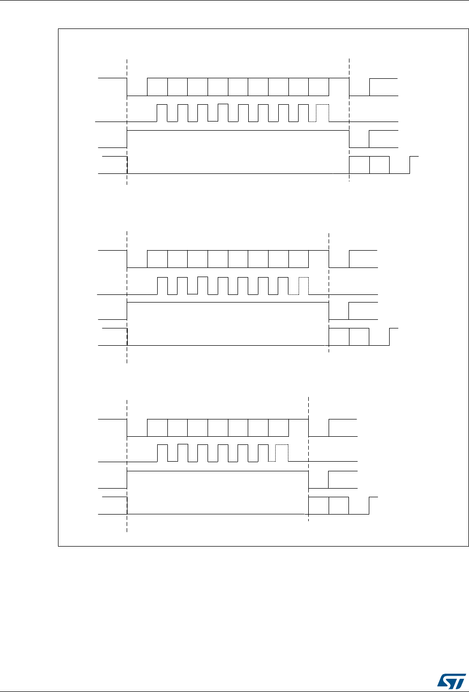
Universal synchronous asynchronous receiver transmitter (USART) RM0376
728/1001 DocID025941 Rev 5
Figure 227. Word length programming
MS33194V2
Bit0 Bit1 Bit2 Bit3 Bit4 Bit5 Bit6 Bit7 Bit8
Start
bit
Stop
bit
Next
Start
bit
Idle frame
9-bit word length (M = 01 ), 1 Stop bit
Possible
Parity
bit
Break frame
Data frame
Clock **
Start
bit
Stop
bit
Start
bit
Stop
bit
Bit0 Bit1 Bit2 Bit3 Bit4 Bit5 Bit6 Bit7
Start
bit
Stop
bit
Next
Start
bit
Idle frame
8-bit word length (M = 00 ), 1 Stop bit
Possible
Parity
bit
Break frame
Data frame
Clock **
Start
bit
Stop
bit
Start
bit
Stop
bit
Bit0 Bit1 Bit2 Bit3 Bit4 Bit5 Bit6
Start
bit
Stop
bit
Next
Start
bit
Idle frame
7-bit word length (M = 10 ), 1 Stop bit
Possible
Parity
bit
Break frame
Data frame
Clock
** LBCL bit controls last data clock pulse
**
Start
bit
Stop
bit
Start
bit
Stop
bit

DocID025941 Rev 5 729/1001
RM0376 Universal synchronous asynchronous receiver transmitter (USART)
831
28.5.2 USART transmitter
The transmitter can send data words of either 7, 8 or 9 bits depending on the M bits status.
The Transmit Enable bit (TE) must be set in order to activate the transmitter function. The
data in the transmit shift register is output on the TX pin and the corresponding clock pulses
are output on the CK pin.
Character transmission
During an USART transmission, data shifts out least significant bit first (default
configuration) on the TX pin. In this mode, the USART_TDR register consists of a buffer
(TDR) between the internal bus and the transmit shift register (see Figure 226).
Every character is preceded by a start bit which is a logic level low for one bit period. The
character is terminated by a configurable number of stop bits.
The following stop bits are supported by USART: 0.5, 1, 1.5 and 2 stop bits.
Note: The TE bit must be set before writing the data to be transmitted to the USART_TDR.
The TE bit should not be reset during transmission of data. Resetting the TE bit during the
transmission will corrupt the data on the TX pin as the baud rate counters will get frozen.
The current data being transmitted will be lost.
An idle frame will be sent after the TE bit is enabled.
Configurable stop bits
The number of stop bits to be transmitted with every character can be programmed in
Control register 2, bits 13,12.
•1 stop bit: This is the default value of number of stop bits.
•2 stop bits: This will be supported by normal USART, Single-wire and Modem modes.
•1.5 stop bits: To be used in Smartcard mode.
•0.5 stop bit: To be used when receiving data in Smartcard mode.
An idle frame transmission will include the stop bits.
A break transmission will be 10 low bits (when M[1:0] = 00) or 11 low bits (when M[1:0] = 01)
or 9 low bits (when M[1:0] = 10) followed by 2 stop bits (see Figure 228). It is not possible to
transmit long breaks (break of length greater than 9/10/11 low bits).
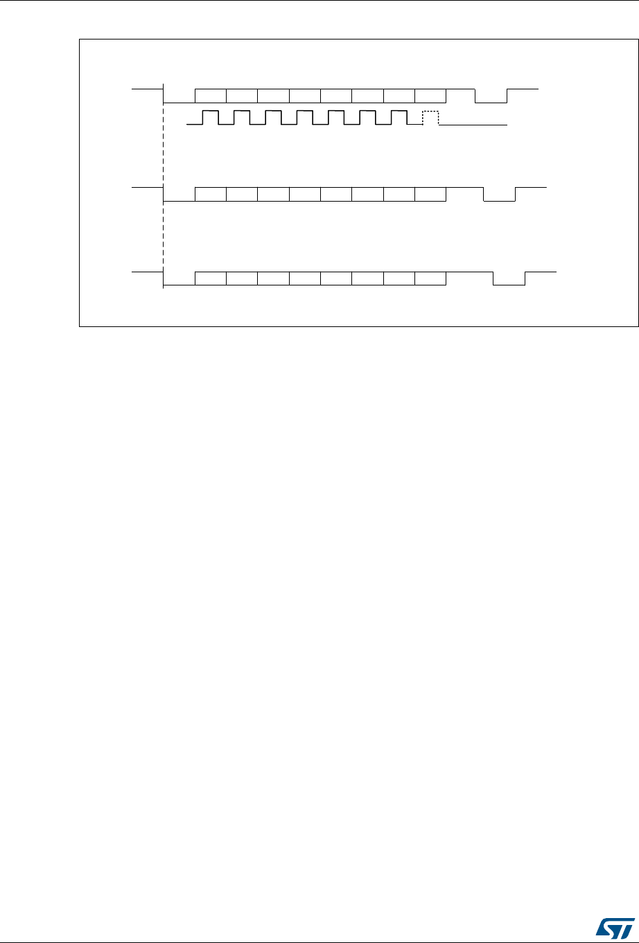
Universal synchronous asynchronous receiver transmitter (USART) RM0376
730/1001 DocID025941 Rev 5
Figure 228. Configurable stop bits
Character transmission procedure
1. Program the M bits in USART_CR1 to define the word length.
2. Select the desired baud rate using the USART_BRR register.
3. Program the number of stop bits in USART_CR2.
4. Enable the USART by writing the UE bit in USART_CR1 register to 1.
5. Select DMA enable (DMAT) in USART_CR3 if multibuffer communication is to take
place. Configure the DMA register as explained in multibuffer communication.
6. Set the TE bit in USART_CR1 to send an idle frame as first transmission.
7. Write the data to send in the USART_TDR register (this clears the TXE bit). Repeat this
for each data to be transmitted in case of single buffer.
8. After writing the last data into the USART_TDR register, wait until TC=1. This indicates
that the transmission of the last frame is complete. This is required for instance when
the USART is disabled or enters the Halt mode to avoid corrupting the last
transmission.
For code example, refer to A.17.1: USART transmitter configuration code example.
Single byte communication
Clearing the TXE bit is always performed by a write to the transmit data register.
The TXE bit is set by hardware and it indicates:
•The data has been moved from the USART_TDR register to the shift register and the
data transmission has started.
•The USART_TDR register is empty.
•The next data can be written in the USART_TDR register without overwriting the
previous data.
For code example, refer to A.17.2: USART transmit byte code example.
This flag generates an interrupt if the TXEIE bit is set.
MSv31887V1
** LBCL bit controls last data clock pulse
Bit7Start bit Stop
bit
Next
start
bit
Possible
parity bit
Data frame Next data frame
CLOCK **
Next data frame
8-bit data, 1 Stop bit
8-bit data, 1 1/2 Stop bits
8-bit data, 2 Stop bits
Bit6Bit5Bit4Bit3Bit2Bit1Bit0
Bit7Start bit 1.5
Stop
bits
Next
start
bit
Possible
parity bit
Data frame
Bit6Bit5Bit4Bit3Bit2Bit1Bit0
Next data frame
Bit7Start bit 2
Stop
bits
Next
start
bit
Possible
parity bit
Data frame
Bit6Bit5Bit4Bit3Bit2Bit1Bit0
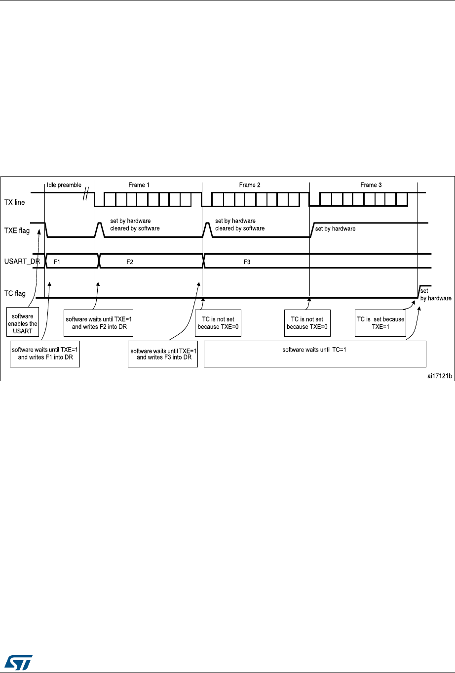
DocID025941 Rev 5 731/1001
RM0376 Universal synchronous asynchronous receiver transmitter (USART)
831
When a transmission is taking place, a write instruction to the USART_TDR register stores
the data in the TDR register; next, the data is copied in the shift register at the end of the
currently ongoing transmission.
When no transmission is taking place, a write instruction to the USART_TDR register places
the data in the shift register, the data transmission starts, and the TXE bit is set.
If a frame is transmitted (after the stop bit) and the TXE bit is set, the TC bit goes high. An
interrupt is generated if the TCIE bit is set in the USART_CR1 register.
After writing the last data in the USART_TDR register, it is mandatory to wait for TC=1
before disabling the USART or causing the microcontroller to enter the low-power mode
(see Figure 229: TC/TXE behavior when transmitting).
Figure 229. TC/TXE behavior when transmitting
For code example, refer to A.17.3: USART transfer complete code example.
Break characters
Setting the SBKRQ bit transmits a break character. The break frame length depends on the
M bits (see Figure 227).
If a ‘1’ is written to the SBKRQ bit, a break character is sent on the TX line after completing
the current character transmission. The SBKF bit is set by the write operation and it is reset
by hardware when the break character is completed (during the stop bits after the break
character). The USART inserts a logic 1 signal (STOP) for the duration of 2 bits at the end of
the break frame to guarantee the recognition of the start bit of the next frame.
In the case the application needs to send the break character following all previously
inserted data, including the ones not yet transmitted, the software should wait for the TXE
flag assertion before setting the SBKRQ bit.
Idle characters
Setting the TE bit drives the USART to send an idle frame before the first data frame.
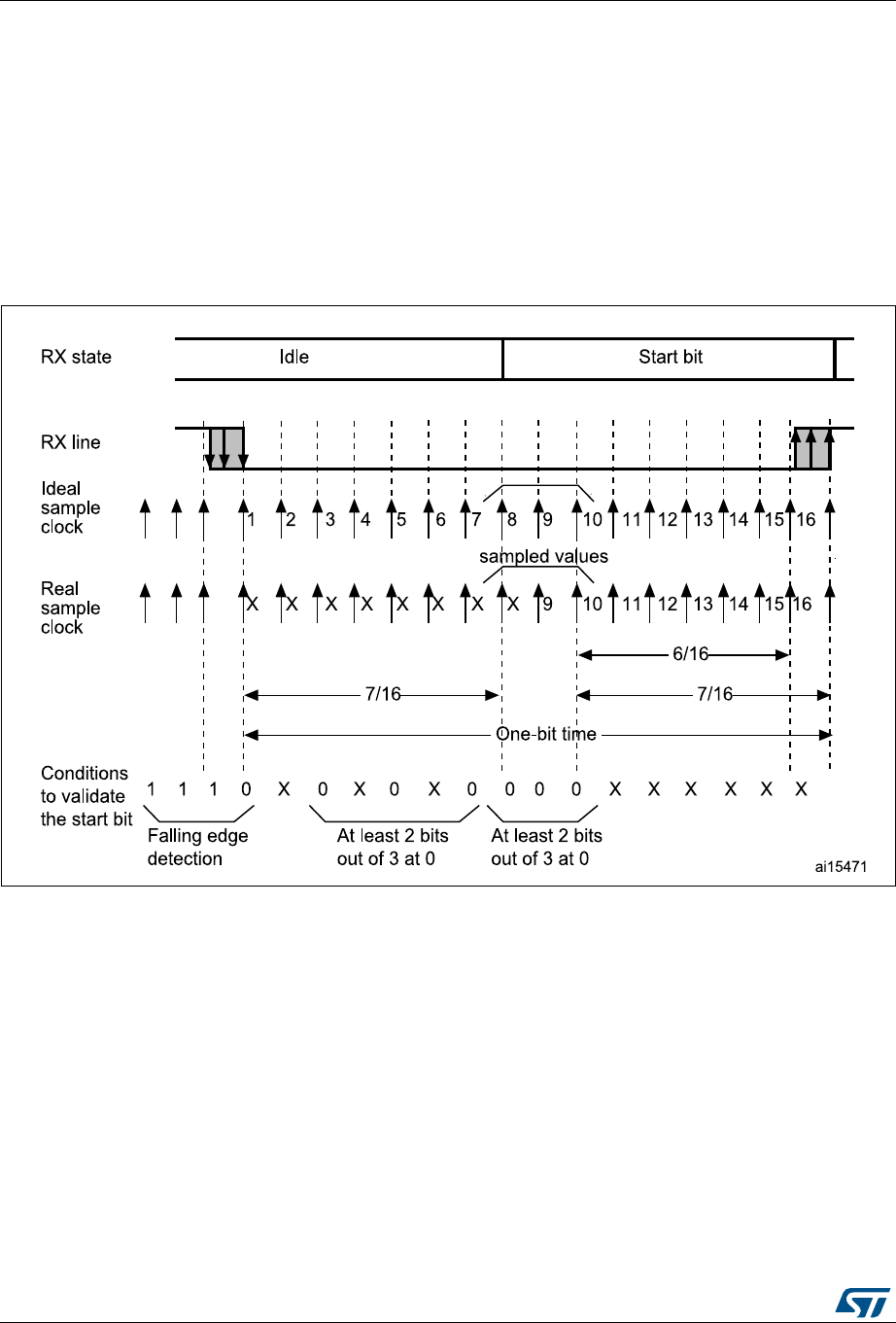
Universal synchronous asynchronous receiver transmitter (USART) RM0376
732/1001 DocID025941 Rev 5
28.5.3 USART receiver
The USART can receive data words of either 7, 8 or 9 bits depending on the M bits in the
USART_CR1 register.
Start bit detection
The start bit detection sequence is the same when oversampling by 16 or by 8.
In the USART, the start bit is detected when a specific sequence of samples is recognized.
This sequence is: 1 1 1 0 X 0 X 0X 0X 0 X 0X 0.
Figure 230. Start bit detection when oversampling by 16 or 8
Note: If the sequence is not complete, the start bit detection aborts and the receiver returns to the
idle state (no flag is set), where it waits for a falling edge.
The start bit is confirmed (RXNE flag set, interrupt generated if RXNEIE=1) if the 3 sampled
bits are at 0 (first sampling on the 3rd, 5th and 7th bits finds the 3 bits at 0 and second
sampling on the 8th, 9th and 10th bits also finds the 3 bits at 0).
The start bit is validated (RXNE flag set, interrupt generated if RXNEIE=1) but the NF noise
flag is set if,
a) for both samplings, 2 out of the 3 sampled bits are at 0 (sampling on the 3rd, 5th
and 7th bits and sampling on the 8th, 9th and 10th bits)
or
b) for one of the samplings (sampling on the 3rd, 5th and 7th bits or sampling on the
8th, 9th and 10th bits), 2 out of the 3 bits are found at 0.

DocID025941 Rev 5 733/1001
RM0376 Universal synchronous asynchronous receiver transmitter (USART)
831
If neither conditions a. or b. are met, the start detection aborts and the receiver returns to the
idle state (no flag is set).
Character reception
During an USART reception, data shifts in least significant bit first (default configuration)
through the RX pin. In this mode, the USART_RDR register consists of a buffer (RDR)
between the internal bus and the receive shift register.
Character reception procedure
1. Program the M bits in USART_CR1 to define the word length.
2. Select the desired baud rate using the baud rate register USART_BRR
3. Program the number of stop bits in USART_CR2.
4. Enable the USART by writing the UE bit in USART_CR1 register to 1.
5. Select DMA enable (DMAR) in USART_CR3 if multibuffer communication is to take
place. Configure the DMA register as explained in multibuffer communication.
6. Set the RE bit USART_CR1. This enables the receiver which begins searching for a
start bit.
For code example, refer to A.17.4: USART receiver configuration code example.
When a character is received:
•The RXNE bit is set to indicate that the content of the shift register is transferred to the
RDR. In other words, data has been received and can be read (as well as its
associated error flags).
•An interrupt is generated if the RXNEIE bit is set.
•The error flags can be set if a frame error, noise or an overrun error has been detected
during reception. PE flag can also be set with RXNE.
•In multibuffer, RXNE is set after every byte received and is cleared by the DMA read of
the Receive data Register.
•In single buffer mode, clearing the RXNE bit is performed by a software read to the
USART_RDR register. The RXNE flag can also be cleared by writing 1 to the RXFRQ
in the USART_RQR register. The RXNE bit must be cleared before the end of the
reception of the next character to avoid an overrun error.
For code example, refer to A.17.5: USART receive byte code example.
Break character
When a break character is received, the USART handles it as a framing error.
Idle character
When an idle frame is detected, there is the same procedure as for a received data
character plus an interrupt if the IDLEIE bit is set.

Universal synchronous asynchronous receiver transmitter (USART) RM0376
734/1001 DocID025941 Rev 5
Overrun error
An overrun error occurs when a character is received when RXNE has not been reset. Data
can not be transferred from the shift register to the RDR register until the RXNE bit is
cleared.
The RXNE flag is set after every byte received. An overrun error occurs if RXNE flag is set
when the next data is received or the previous DMA request has not been serviced. When
an overrun error occurs:
•The ORE bit is set.
•The RDR content will not be lost. The previous data is available when a read to
USART_RDR is performed.
•The shift register will be overwritten. After that point, any data received during overrun
is lost.
•An interrupt is generated if either the RXNEIE bit is set or EIE bit is set.
•The ORE bit is reset by setting the ORECF bit in the ICR register.
Note: The ORE bit, when set, indicates that at least 1 data has been lost. There are two
possibilities:
- if RXNE=1, then the last valid data is stored in the receive register RDR and can be read,
- if RXNE=0, then it means that the last valid data has already been read and thus there is
nothing to be read in the RDR. This case can occur when the last valid data is read in the
RDR at the same time as the new (and lost) data is received.
Selecting the proper oversampling method
When the dual clock domain with the wakeup from Stop mode is supported, the clock
source can be one of the following sources: PCLK (default), LSE, HSI16 or SYSCLK.
Otherwise, the USART clock source is PCLK.
Choosing LSE or HSI16 as clock source may allow the USART to receive data while the
MCU is in low-power mode. Depending on the received data and wakeup mode selection,
the USART wakes up the MCU, when needed, in order to transfer the received data by
software reading the USART_RDR register or by DMA.
For the other clock sources, the system must be active in order to allow USART
communication.
The receiver implements different user-configurable oversampling techniques for data
recovery by discriminating between valid incoming data and noise. This allows a trade-off
between the maximum communication speed and noise/clock inaccuracy immunity.
The oversampling method can be selected by programming the OVER8 bit in the
USART_CR1 register and can be either 16 or 8 times the baud rate clock (Figure 231 and
Figure 232).
Depending on the application:
•Select oversampling by 8 (OVER8=1) to achieve higher speed (up to fCK/8). In this
case the maximum receiver tolerance to clock deviation is reduced (refer to
Section 28.5.5: Tolerance of the USART receiver to clock deviation on page 739)
•Select oversampling by 16 (OVER8=0) to increase the tolerance of the receiver to
clock deviations. In this case, the maximum speed is limited to maximum fCK/16 where
fCK is the clock source frequency.
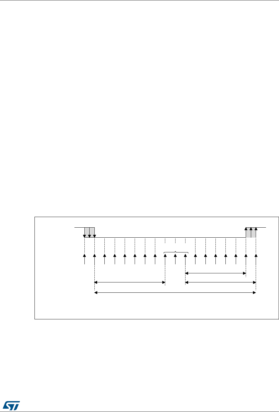
DocID025941 Rev 5 735/1001
RM0376 Universal synchronous asynchronous receiver transmitter (USART)
831
Programming the ONEBIT bit in the USART_CR3 register selects the method used to
evaluate the logic level. There are two options:
•The majority vote of the three samples in the center of the received bit. In this case,
when the 3 samples used for the majority vote are not equal, the NF bit is set
•A single sample in the center of the received bit
Depending on the application:
– select the three samples’ majority vote method (ONEBIT=0) when operating in a
noisy environment and reject the data when a noise is detected (refer to
Figure 127) because this indicates that a glitch occurred during the sampling.
– select the single sample method (ONEBIT=1) when the line is noise-free to
increase the receiver’s tolerance to clock deviations (see Section 28.5.5:
Tolerance of the USART receiver to clock deviation on page 739). In this case the
NF bit will never be set.
When noise is detected in a frame:
•The NF bit is set at the rising edge of the RXNE bit.
•The invalid data is transferred from the Shift register to the USART_RDR register.
•No interrupt is generated in case of single byte communication. However this bit rises
at the same time as the RXNE bit which itself generates an interrupt. In case of
multibuffer communication an interrupt will be issued if the EIE bit is set in the
USART_CR3 register.
The NF bit is reset by setting NFCF bit in ICR register.
Note: Oversampling by 8 is not available in LIN, Smartcard and IrDA modes. In those modes, the
OVER8 bit is forced to ‘0’ by hardware.
Figure 231. Data sampling when oversampling by 16
MSv31152V1
1 2 3 4 5 6 7 8 9 10 11 12 13 14 15 16
sampled values
6/16
7/167/16
One bit time
Sample clock
RX line
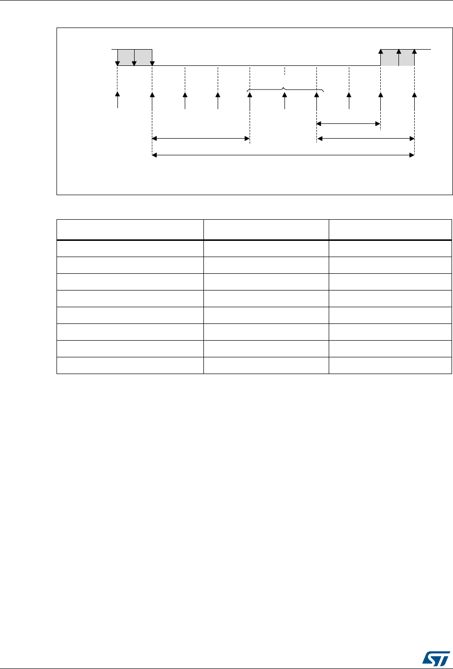
Universal synchronous asynchronous receiver transmitter (USART) RM0376
736/1001 DocID025941 Rev 5
Figure 232. Data sampling when oversampling by 8
Framing error
A framing error is detected when the stop bit is not recognized on reception at the expected
time, following either a de-synchronization or excessive noise.
When the framing error is detected:
•The FE bit is set by hardware
•The invalid data is transferred from the Shift register to the USART_RDR register.
•No interrupt is generated in case of single byte communication. However this bit rises
at the same time as the RXNE bit which itself generates an interrupt. In case of
multibuffer communication an interrupt will be issued if the EIE bit is set in the
USART_CR3 register.
The FE bit is reset by writing 1 to the FECF in the USART_ICR register.
Table 127. Noise detection from sampled data
Sampled value NE status Received bit value
000 0 0
001 1 0
010 1 0
011 1 1
100 1 0
101 1 1
110 1 1
111 0 1
MSv31153V1
1 2 3 4 5 6 7
sampled values
2/8
3/8
3/8
One bit time
Sample
clock (x8)
RX line
8

DocID025941 Rev 5 737/1001
RM0376 Universal synchronous asynchronous receiver transmitter (USART)
831
Configurable stop bits during reception
The number of stop bits to be received can be configured through the control bits of Control
Register 2 - it can be either 1 or 2 in normal mode and 0.5 or 1.5 in Smartcard mode.
•
0.5 stop bit (reception in Smartcard mode): No sampling is done for 0.5 stop bit. As
a consequence, no framing error and no break frame can be detected when 0.5 stop bit
is selected.
•1 stop bit: Sampling for 1 stop Bit is done on the 8th, 9th and 10th samples.
•1.5 stop bits (Smartcard mode): When transmitting in Smartcard mode, the device
must check that the data is correctly sent. Thus the receiver block must be enabled (RE
=1 in the USART_CR1 register) and the stop bit is checked to test if the smartcard has
detected a parity error. In the event of a parity error, the smartcard forces the data
signal low during the sampling - NACK signal-, which is flagged as a framing error.
Then, the FE flag is set with the RXNE at the end of the 1.5 stop bits. Sampling for 1.5
stop bits is done on the 16th, 17th and 18th samples (1 baud clock period after the
beginning of the stop bit). The 1.5 stop bits can be decomposed into 2 parts: one 0.5
baud clock period during which nothing happens, followed by 1 normal stop bit period
during which sampling occurs halfway through. Refer to Section 28.5.13: USART
Smartcard mode on page 751 for more details.
•2 stop bits: Sampling for 2 stop bits is done on the 8th, 9th and 10th samples of the
first stop bit. If a framing error is detected during the first stop bit the framing error flag
will be set. The second stop bit is not checked for framing error. The RXNE flag will be
set at the end of the first stop bit.
28.5.4 USART baud rate generation
The baud rate for the receiver and transmitter (Rx and Tx) are both set to the same value as
programmed in the USART_BRR register.
Equation 1: Baud rate for standard USART (SPI mode included) (OVER8 = 0 or 1)
In case of oversampling by 16, the equation is:
In case of oversampling by 8, the equation is:
Equation 2: Baud rate in Smartcard, LIN and IrDA modes (OVER8 = 0)
In Smartcard, LIN and IrDA modes, only Oversampling by 16 is supported:
Tx/Rx baud fCK
USARTDIV
--------------------------------
=
Tx/Rx baud 2f
CK
×
USARTDIV
--------------------------------
=
Tx/Rx baud fCK
USARTDIV
--------------------------------
=

Universal synchronous asynchronous receiver transmitter (USART) RM0376
738/1001 DocID025941 Rev 5
USARTDIV is an unsigned fixed point number that is coded on the USART_BRR register.
•When OVER8 = 0, BRR = USARTDIV.
•When OVER8 = 1
– BRR[2:0] = USARTDIV[3:0] shifted 1 bit to the right.
– BRR[3] must be kept cleared.
– BRR[15:4] = USARTDIV[15:4]
Note: The baud counters are updated to the new value in the baud registers after a write operation
to USART_BRR. Hence the baud rate register value should not be changed during
communication.
In case of oversampling by 16 or 8, USARTDIV must be greater than or equal to 16d.
How to derive USARTDIV from USART_BRR register values
Example 1
To obtain 9600 baud with fCK = 8 MHz.
•In case of oversampling by 16:
USARTDIV = 8 000 000/9600
BRR = USARTDIV = 833d = 0341h
•In case of oversampling by 8:
USARTDIV = 2 * 8 000 000/9600
USARTDIV = 1666,66 (1667d = 683h)
BRR[3:0] = 3h << 1 = 1h
BRR = 0x681
Example 2
To obtain 921.6 Kbaud with fCK = 32 MHz.
•In case of oversampling by 16:
USARTDIV = 32 000 000/921 600
BRR = USARTDIV = 35d = 23h
•In case of oversampling by 8:
USARTDIV = 2 * 32 000 000/921 600
USARTDIV = 70d = 46h
BRR[3:0] = USARTDIV[3:0] >> 1 = 6h >> 1 = 3h
BRR = 0x43

DocID025941 Rev 5 739/1001
RM0376 Universal synchronous asynchronous receiver transmitter (USART)
831
28.5.5 Tolerance of the USART receiver to clock deviation
The asynchronous receiver of the USART works correctly only if the total clock system
deviation is less than the tolerance of the USART receiver. The causes which contribute to
the total deviation are:
•DTRA: Deviation due to the transmitter error (which also includes the deviation of the
transmitter’s local oscillator)
•DQUANT: Error due to the baud rate quantization of the receiver
•DREC: Deviation of the receiver’s local oscillator
•DTCL: Deviation due to the transmission line (generally due to the transceivers which
can introduce an asymmetry between the low-to-high transition timing and the high-to-
low transition timing)
Table 128. Error calculation for programmed baud rates at fCK = 32 MHz in both cases of
oversampling by 16 or by 8(1)
Baud rate Oversampling by 16 (OVER8 = 0) Oversampling by 8 (OVER8 = 1)
S.No Desired Actual BRR
% Error =
(Calculated -
Desired)B.Rate /
Desired B.Rate
Actual BRR % Error
1 2.4 KBps 2.4 KBps 0x3415 0 2.4 KBps 0x6825 0
2 9.6 KBps 9.6 KBps 0xD05 0 9.6 KBps 0x1A05 0
3 19.2 KBps 19.19 KBps 0x683 0.02 19.2 KBps 0xD02 0
4 38.4 KBps 38.41 KBps 0x341 0.04 38.39 KBps 0x681 0.02
5 57.6 KBps 57.55 KBps 0x22C 0.08 57.6 KBps 0x453 0
6 115.2 KBps 115.1 KBps 0x116 0.08 115.11 KBps 0x226 0.08
7 230.4 KBps 230.21 KBps 0x8B 0.08 230.21 KBps 0x113 0.08
8 460.8 KBps 463.76 KBps 0x045 0.64 460.06 KBps 0x85 0.08
9 921.6 KBps 914.28 KBps 0x23 0.79 927.5 KBps 0x42 0.79
10 2 MBps 2 MBps 0x10 0 2 MBps 0x20 0
12 4MBps 4MBps NA NA 4MBps 0x10 0
1. The lower the CPU clock the lower the accuracy for a particular baud rate. The upper limit of the achievable baud rate can
be fixed with these data.
DTRA DQUANT DREC DTCL DWU++++USART receiver′s tolerance<
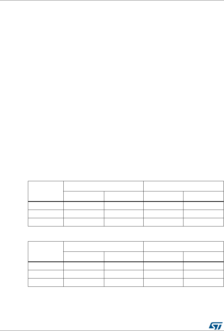
Universal synchronous asynchronous receiver transmitter (USART) RM0376
740/1001 DocID025941 Rev 5
where
DWU is the error due to sampling point deviation when the wakeup from Stop mode is
used.
when M[1:0] = 01:
when M[1:0] = 00:
when M[1:0] = 10:
tWUUSART is the time between detection of start bit falling edge and the instant when
clock (requested by the peripheral) is ready and reaching the peripheral and regulator
is ready. tWUUSART corresponds to tWUSTOP value provided in the datasheet.
The USART receiver can receive data correctly at up to the maximum tolerated
deviation specified in Table 129 and Table 129 depending on the following choices:
•9-, 10- or 11-bit character length defined by the M bits in the USART_CR1 register
•Oversampling by 8 or 16 defined by the OVER8 bit in the USART_CR1 register
•Bits BRR[3:0] of USART_BRR register are equal to or different from 0000.
•Use of 1 bit or 3 bits to sample the data, depending on the value of the ONEBIT bit in
the USART_CR3 register.
Note: The data specified in Table 129 and Table 130 may slightly differ in the special case when
the received frames contain some Idle frames of exactly 10-bit durations when M bits = 00
(11-bit durations when M bits =01 or 9- bit durations when M bits = 10).
Table 129. Tolerance of the USART receiver when BRR [3:0] = 0000
M bits
OVER8 bit = 0 OVER8 bit = 1
ONEBIT=0 ONEBIT=1 ONEBIT=0 ONEBIT=1
00 3.75% 4.375% 2.50% 3.75%
01 3.41% 3.97% 2.27% 3.41%
10 4.16% 4.86% 2.77% 4.16%
Table 130. Tolerance of the USART receiver when BRR [3:0] is different from 0000
M bits
OVER8 bit = 0 OVER8 bit = 1
ONEBIT=0 ONEBIT=1 ONEBIT=0 ONEBIT=1
00 3.33% 3.88% 2% 3%
01 3.03% 3.53% 1.82% 2.73%
10 3.7% 4.31% 2.22% 3.33%
DWU tWUUSART
11 Tbit×
---------------------------
=
DWU tWUUSART
10 Tbit×
---------------------------
=
DWU tWUUSART
9Tbit×
---------------------------
=

DocID025941 Rev 5 741/1001
RM0376 Universal synchronous asynchronous receiver transmitter (USART)
831
28.5.6 USART auto baud rate detection
The USART is able to detect and automatically set the USART_BRR register value based
on the reception of one character. Automatic baud rate detection is useful under two
circumstances:
•The communication speed of the system is not known in advance
•The system is using a relatively low accuracy clock source and this mechanism allows
the correct baud rate to be obtained without measuring the clock deviation.
The clock source frequency must be compatible with the expected communication speed
(when oversampling by 16, the baud rate is between fCK/65535 and fCK/16. when
oversampling by 8, the baud rate is between fCK/65535 and fCK/8).
Before activating the auto baud rate detection, the auto baud rate detection mode must be
chosen. There are various modes based on different character patterns.
They can be chosen through the ABRMOD[1:0] field in the USART_CR2 register. In these
auto baud rate modes, the baud rate is measured several times during the synchronization
data reception and each measurement is compared to the previous one.
These modes are:
•Mode 0: Any character starting with a bit at 1. In this case the USART measures the
duration of the Start bit (falling edge to rising edge).
•Mode 1: Any character starting with a 10xx bit pattern. In this case, the USART
measures the duration of the Start and of the 1st data bit. The measurement is done
falling edge to falling edge, ensuring better accuracy in the case of slow signal slopes.
•Mode 2: A 0x7F character frame (it may be a 0x7F character in LSB first mode or a
0xFE in MSB first mode). In this case, the baud rate is updated first at the end of the
start bit (BRs), then at the end of bit 6 (based on the measurement done from falling
edge to falling edge: BR6). Bit 0 to bit 6 are sampled at BRs while further bits of the
character are sampled at BR6.
•Mode 3: A 0x55 character frame. In this case, the baud rate is updated first at the end
of the start bit (BRs), then at the end of bit 0 (based on the measurement done from
falling edge to falling edge: BR0), and finally at the end of bit 6 (BR6). Bit 0 is sampled
at BRs, bit 1 to bit 6 are sampled at BR0, and further bits of the character are sampled
at BR6.
In parallel, another check is performed for each intermediate transition of RX line. An
error is generated if the transitions on RX are not sufficiently synchronized with the
receiver (the receiver being based on the baud rate calculated on bit 0).
Prior to activating auto baud rate detection, the USART_BRR register must be initialized by
writing a non-zero baud rate value.
The automatic baud rate detection is activated by setting the ABREN bit in the USART_CR2
register. The USART will then wait for the first character on the RX line. The auto baud rate
operation completion is indicated by the setting of the ABRF flag in the USART_ISR
register. If the line is noisy, the correct baud rate detection cannot be guaranteed. In this
case the BRR value may be corrupted and the ABRE error flag will be set. This also
happens if the communication speed is not compatible with the automatic baud rate
detection range (bit duration not between 16 and 65536 clock periods (oversampling by 16)
and not between 8 and 65536 clock periods (oversampling by 8)).
The RXNE interrupt will signal the end of the operation.

Universal synchronous asynchronous receiver transmitter (USART) RM0376
742/1001 DocID025941 Rev 5
At any later time, the auto baud rate detection may be relaunched by resetting the ABRF
flag (by writing a 0).
Note: If the USART is disabled (UE=0) during an auto baud rate operation, the BRR value may be
corrupted.
28.5.7 Multiprocessor communication using USART
In multiprocessor communication, the following bits are to be kept cleared:
•LINEN bit in the USART_CR2 register,
•HDSEL, IREN and SCEN bits in the USART_CR3 register.
It is possible to perform multiprocessor communication with the USART (with several
USARTs connected in a network). For instance one of the USARTs can be the master, its TX
output connected to the RX inputs of the other USARTs. The others are slaves, their
respective TX outputs are logically ANDed together and connected to the RX input of the
master.
In multiprocessor configurations it is often desirable that only the intended message
recipient should actively receive the full message contents, thus reducing redundant USART
service overhead for all non addressed receivers.
The non addressed devices may be placed in mute mode by means of the muting function.
In order to use the mute mode feature, the MME bit must be set in the USART_CR1
register.
In mute mode:
•None of the reception status bits can be set.
•All the receive interrupts are inhibited.
•The RWU bit in USART_ISR register is set to 1. RWU can be controlled automatically
by hardware or by software, through the MMRQ bit in the USART_RQR register, under
certain conditions.
The USART can enter or exit from mute mode using one of two methods, depending on the
WAKE bit in the USART_CR1 register:
•Idle Line detection if the WAKE bit is reset,
•Address Mark detection if the WAKE bit is set.
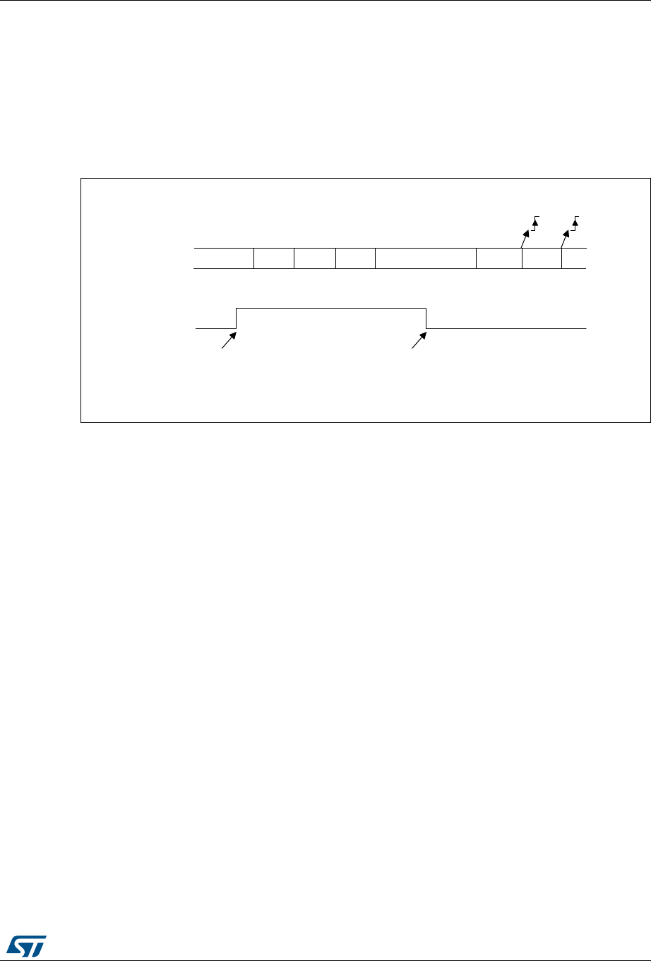
DocID025941 Rev 5 743/1001
RM0376 Universal synchronous asynchronous receiver transmitter (USART)
831
Idle line detection (WAKE=0)
The USART enters mute mode when the MMRQ bit is written to 1 and the RWU is
automatically set.
It wakes up when an Idle frame is detected. Then the RWU bit is cleared by hardware but
the IDLE bit is not set in the USART_ISR register. An example of mute mode behavior using
Idle line detection is given in Figure 233.
Figure 233. Mute mode using Idle line detection
Note: If the MMRQ is set while the IDLE character has already elapsed, mute mode will not be
entered (RWU is not set).
If the USART is activated while the line is IDLE, the idle state is detected after the duration
of one IDLE frame (not only after the reception of one character frame).
4-bit/7-bit address mark detection (WAKE=1)
In this mode, bytes are recognized as addresses if their MSB is a ‘1’ otherwise they are
considered as data. In an address byte, the address of the targeted receiver is put in the 4
or 7 LSBs. The choice of 7 or 4-bit address detection is done using the ADDM7 bit. This 4-
bit/7-bit word is compared by the receiver with its own address which is programmed in the
ADD bits in the USART_CR2 register.
Note: In 7-bit and 9-bit data modes, address detection is done on 6-bit and 8-bit addresses
(ADD[5:0] and ADD[7:0]) respectively.
The USART enters mute mode when an address character is received which does not
match its programmed address. In this case, the RWU bit is set by hardware. The RXNE
flag is not set for this address byte and no interrupt or DMA request is issued when the
USART enters mute mode.
The USART also enters mute mode when the MMRQ bit is written to 1. The RWU bit is also
automatically set in this case.
The USART exits from mute mode when an address character is received which matches
the programmed address. Then the RWU bit is cleared and subsequent bytes are received
normally. The RXNE bit is set for the address character since the RWU bit has been
cleared.
An example of mute mode behavior using address mark detection is given in Figure 234.
MSv31154V1
Data 1 Data 2 IDLEData 3 Data 4 Data 6
Idle frame detectedMMRQ written to 1
RWU
RX
Mute mode Normal mode
RXNE RXNE
Data 5
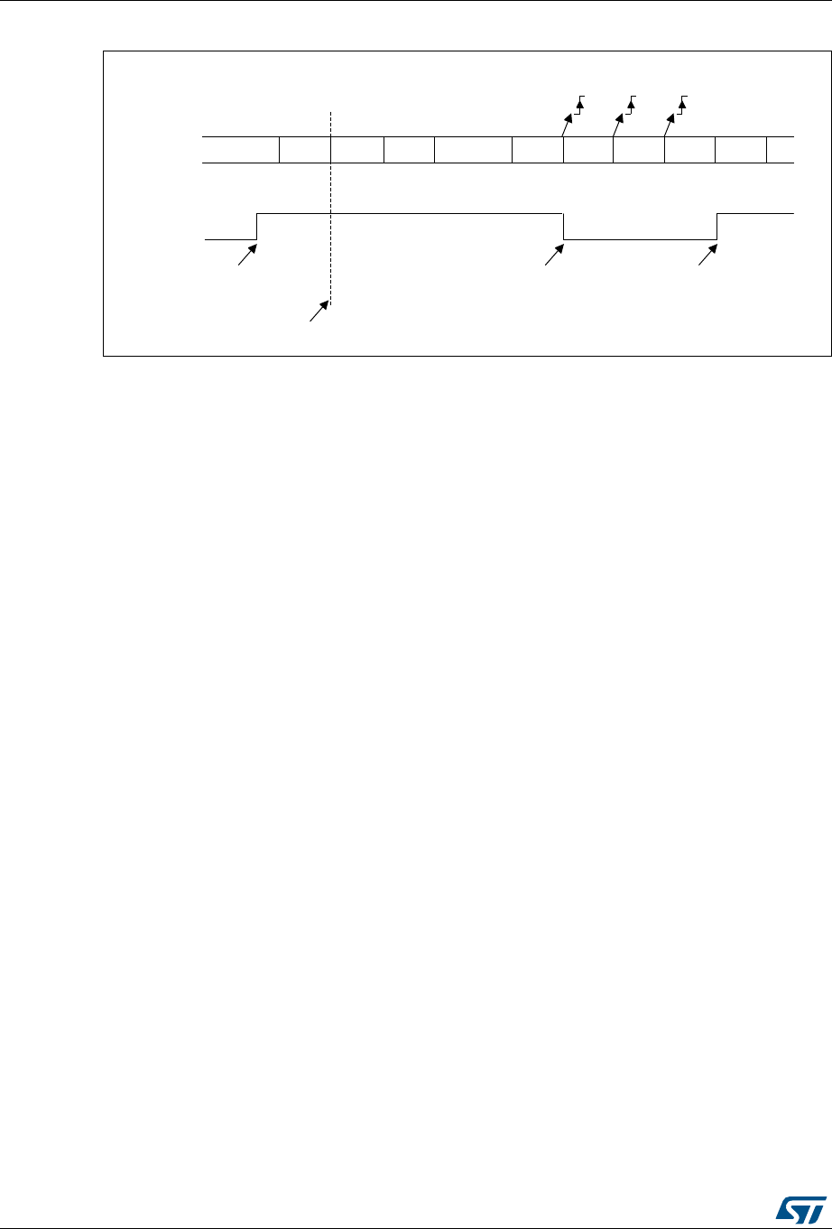
Universal synchronous asynchronous receiver transmitter (USART) RM0376
744/1001 DocID025941 Rev 5
Figure 234. Mute mode using address mark detection
28.5.8 Modbus communication using USART
The USART offers basic support for the implementation of Modbus/RTU and Modbus/ASCII
protocols. Modbus/RTU is a half duplex, block transfer protocol. The control part of the
protocol (address recognition, block integrity control and command interpretation) must be
implemented in software.
The USART offers basic support for the end of the block detection, without software
overhead or other resources.
Modbus/RTU
In this mode, the end of one block is recognized by a “silence” (idle line) for more than 2
character times. This function is implemented through the programmable timeout function.
The timeout function and interrupt must be activated, through the RTOEN bit in the
USART_CR2 register and the RTOIE in the USART_CR1 register. The value corresponding
to a timeout of 2 character times (for example 22 x bit duration) must be programmed in the
RTO register. when the receive line is idle for this duration, after the last stop bit is received,
an interrupt is generated, informing the software that the current block reception is
completed.
Modbus/ASCII
In this mode, the end of a block is recognized by a specific (CR/LF) character sequence.
The USART manages this mechanism using the character match function.
By programming the LF ASCII code in the ADD[7:0] field and by activating the character
match interrupt (CMIE=1), the software is informed when a LF has been received and can
check the CR/LF in the DMA buffer.
MSv31155V1
IDLE Addr=0 Data 1 Data 2 IDLE Addr=1 Data 3 Data 4 Addr=2 Data 5
In this example, the current address of the receiver is 1
(programmed in the USART_CR2 register)
RXNE
Non-matching addressMatching address
Non-matching address
MMRQ written to 1
(RXNE was cleared)
RWU
RX
Mute mode Mute modeNormal mode
RXNE RXNE

DocID025941 Rev 5 745/1001
RM0376 Universal synchronous asynchronous receiver transmitter (USART)
831
28.5.9 USART parity control
Parity control (generation of parity bit in transmission and parity checking in reception) can
be enabled by setting the PCE bit in the USART_CR1 register. Depending on the frame
length defined by the M bits, the possible USART frame formats are as listed in Table 131.
Even parity
The parity bit is calculated to obtain an even number of “1s” inside the frame of the 6, 7 or 8
LSB bits (depending on M bits values) and the parity bit.
As an example, if data=00110101, and 4 bits are set, then the parity bit will be 0 if even
parity is selected (PS bit in USART_CR1 = 0).
Odd parity
The parity bit is calculated to obtain an odd number of “1s” inside the frame made of the 6, 7
or 8 LSB bits (depending on M bits values) and the parity bit.
As an example, if data=00110101 and 4 bits set, then the parity bit will be 1 if odd parity is
selected (PS bit in USART_CR1 = 1).
Parity checking in reception
If the parity check fails, the PE flag is set in the USART_ISR register and an interrupt is
generated if PEIE is set in the USART_CR1 register. The PE flag is cleared by software
writing 1 to the PECF in the USART_ICR register.
Parity generation in transmission
If the PCE bit is set in USART_CR1, then the MSB bit of the data written in the data register
is transmitted but is changed by the parity bit (even number of “1s” if even parity is selected
(PS=0) or an odd number of “1s” if odd parity is selected (PS=1)).
Table 131. Frame formats
M bits PCE bit USART frame(1)
1. Legends: SB: start bit, STB: stop bit, PB: parity bit. In the data register, the PB is always taking the MSB
position (9th, 8th or 7th, depending on the M bits value).
00 0 | SB | 8-bit data | STB |
00 1 | SB | 7-bit data | PB | STB |
01 0 | SB | 9-bit data | STB |
01 1 | SB | 8-bit data | PB | STB |
10 0 | SB | 7-bit data | STB |
10 1 | SB | 6-bit data | PB | STB |

Universal synchronous asynchronous receiver transmitter (USART) RM0376
746/1001 DocID025941 Rev 5
28.5.10 USART LIN (local interconnection network) mode
This section is relevant only when LIN mode is supported. Please refer to Section 28.4:
USART implementation on page 724.
The LIN mode is selected by setting the LINEN bit in the USART_CR2 register. In LIN
mode, the following bits must be kept cleared:
•STOP[1:0] and CLKEN in the USART_CR2 register,
•SCEN, HDSEL and IREN in the USART_CR3 register.
For code example, refer to A.17.6: USART LIN mode code example.
LIN transmission
The procedure explained in Section 28.5.2: USART transmitter has to be applied for LIN
Master transmission. It must be the same as for normal USART transmission with the
following differences:
•Clear the M bits to configure 8-bit word length.
•Set the LINEN bit to enter LIN mode. In this case, setting the SBKRQ bit sends 13 ‘0’
bits as a break character. Then 2 bits of value ‘1’ are sent to allow the next start
detection.
LIN reception
When LIN mode is enabled, the break detection circuit is activated. The detection is totally
independent from the normal USART receiver. A break can be detected whenever it occurs,
during Idle state or during a frame.
When the receiver is enabled (RE=1 in USART_CR1), the circuit looks at the RX input for a
start signal. The method for detecting start bits is the same when searching break
characters or data. After a start bit has been detected, the circuit samples the next bits
exactly like for the data (on the 8th, 9th and 10th samples). If 10 (when the LBDL = 0 in
USART_CR2) or 11 (when LBDL=1 in USART_CR2) consecutive bits are detected as ‘0,
and are followed by a delimiter character, the LBDF flag is set in USART_ISR. If the LBDIE
bit=1, an interrupt is generated. Before validating the break, the delimiter is checked for as it
signifies that the RX line has returned to a high level.
If a ‘1’ is sampled before the 10 or 11 have occurred, the break detection circuit cancels the
current detection and searches for a start bit again.
If the LIN mode is disabled (LINEN=0), the receiver continues working as normal USART,
without taking into account the break detection.
If the LIN mode is enabled (LINEN=1), as soon as a framing error occurs (i.e. stop bit
detected at ‘0’, which will be the case for any break frame), the receiver stops until the break
detection circuit receives either a ‘1’, if the break word was not complete, or a delimiter
character if a break has been detected.
The behavior of the break detector state machine and the break flag is shown on the
Figure 235: Break detection in LIN mode (11-bit break length - LBDL bit is set) on page 747.
Examples of break frames are given on Figure 236: Break detection in LIN mode vs.
Framing error detection on page 748.
DocID025941 Rev 5 747/1001
RM0376 Universal synchronous asynchronous receiver transmitter (USART)
831
Figure 235. Break detection in LIN mode (11-bit break length - LBDL bit is set)
MSv31156V1
Idle Bit0 Bit1 Bit2 Bit3 Bit4 Bit5 Bit6 Bit7 Bit8 Bit9 Bit10 Idle
0000 000 0001
Case 1: break signal not long enough => break discarded, LBDF is not set
RX line
Capture strobe
Break state
machine
Read samples
Idle Bit0 Bit1 Bit2 Bit3 Bit4 Bit5 Bit6 Bit7 Bit8 Bit9 B10 Idle
0000 000 0000
Case 2: break signal just long enough => break detected, LBDF is set
RX line
Capture strobe
Break state
machine
Read samples
Break frame
Break frame
Delimiter is immediate
LBDF
Idle Bit0 Bit1 Bit2 Bit3 Bit4 Bit5 Bit6 Bit7 Bit8 Bit9 Bit10 Idle
0000 000 0000
Case 3: break signal long enough => break detected, LBDF is set
RX line
Capture strobe
Break state
machine
Read samples
Break frame
LBDF
wait delimiter
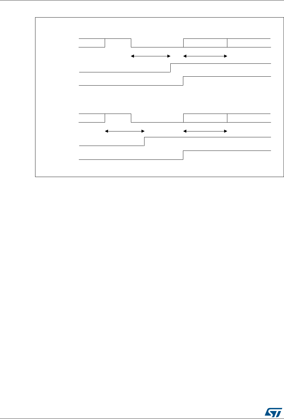
Universal synchronous asynchronous receiver transmitter (USART) RM0376
748/1001 DocID025941 Rev 5
Figure 236. Break detection in LIN mode vs. Framing error detection
28.5.11 USART synchronous mode
The synchronous mode is selected by writing the CLKEN bit in the USART_CR2 register to
1. In synchronous mode, the following bits must be kept cleared:
•LINEN bit in the USART_CR2 register,
•SCEN, HDSEL and IREN bits in the USART_CR3 register.
In this mode, the USART can be used to control bidirectional synchronous serial
communications in master mode. The CK pin is the output of the USART transmitter clock.
No clock pulses are sent to the CK pin during start bit and stop bit. Depending on the state
of the LBCL bit in the USART_CR2 register, clock pulses are, or are not, generated during
the last valid data bit (address mark). The CPOL bit in the USART_CR2 register is used to
select the clock polarity, and the CPHA bit in the USART_CR2 register is used to select the
phase of the external clock (see Figure 237, Figure 238 and Figure 239).
During the Idle state, preamble and send break, the external CK clock is not activated.
In synchronous mode the USART transmitter works exactly like in asynchronous mode. But
as CK is synchronized with TX (according to CPOL and CPHA), the data on TX is
synchronous.
In this mode the USART receiver works in a different manner compared to the
asynchronous mode. If RE=1, the data is sampled on CK (rising or falling edge, depending
on CPOL and CPHA), without any oversampling. A setup and a hold time must be
respected (which depends on the baud rate: 1/16 bit duration).
MSv31157V1
data 1 IDLE BREAK data 2 (0x55) data 3 (header)
1 data time 1 data time
RX line
RXNE /FE
LBDF
Case 1: break occurring after an Idle
data 1 data2 BREAK data 2 (0x55) data 3 (header)
1 data time 1 data time
RX line
RXNE /FE
LBDF
Case 2: break occurring while data is being received
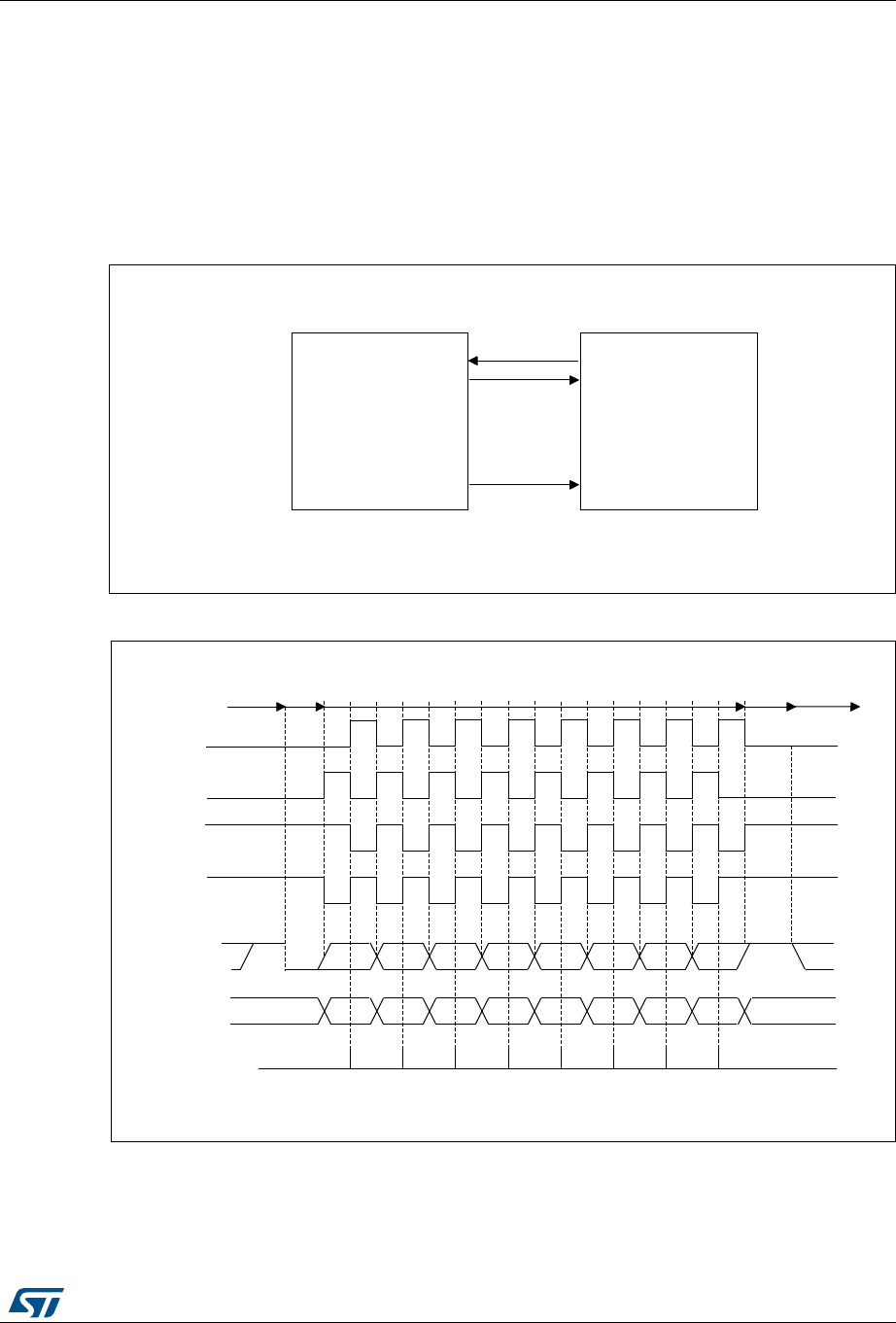
DocID025941 Rev 5 749/1001
RM0376 Universal synchronous asynchronous receiver transmitter (USART)
831
Note: The CK pin works in conjunction with the TX pin. Thus, the clock is provided only if the
transmitter is enabled (TE=1) and data is being transmitted (the data register USART_TDR
written). This means that it is not possible to receive synchronous data without transmitting
data.
The LBCL, CPOL and CPHA bits have to be selected when the USART is disabled (UE=0)
to ensure that the clock pulses function correctly.
For code example, refer to A.17.7: USART synchronous mode code example.
Figure 237. USART example of synchronous transmission
Figure 238. USART data clock timing diagram (M bits = 00)
MSv31158V2
USART Synchronous device
(e.g. slave SPI)
RX
TX
Data out
Data in
Clock
CK
MSv34709V2
01234567
01234567
*
*
*
*
MSB
MSB
LSB
LSB
Start
Start Stop
Idle or preceding
transmission
Idle or next
transmission
*
*LBCL bit controls last data pulse
Capture strobe
Data on RX
(from slave)
Data on TX
(from master)
Clock (CPOL=1, CPHA=1)
Clock (CPOL=1, CPHA=0)
Clock (CPOL=0, CPHA=1)
Clock (CPOL=0, CPHA=0)
Stop
M bits = 00 (8 data bits)
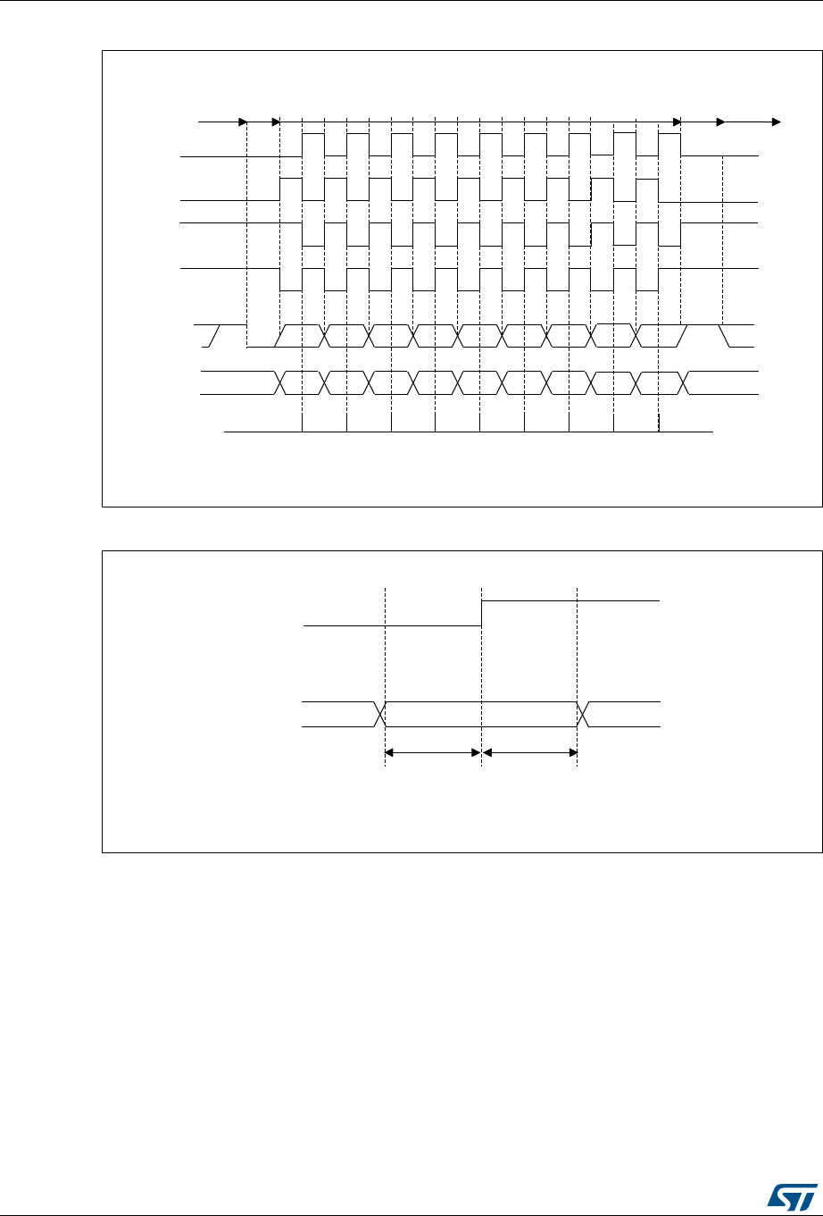
Universal synchronous asynchronous receiver transmitter (USART) RM0376
750/1001 DocID025941 Rev 5
Figure 239. USART data clock timing diagram (M bits = 01)
Figure 240. RX data setup/hold time
Note: The function of CK is different in Smartcard mode. Refer to Section 28.5.13: USART
Smartcard mode for more details.
MSv34710V1
0 1 2 3 4 5 6 8
0 1 2 3 4 5 6 8
*
*
*
*
MSB
MSB
LSB
LSBStart
Start Stop
Idle or
preceding
transmission
Idle or next
transmission
*
*LBCL bit controls last data pulse
Capture
strobe
Data on RX
(from slave)
Data on TX
(from master)
Clock (CPOL=1,
CPHA=1)
Clock (CPOL=1,
CPHA=0)
Clock (CPOL=0,
CPHA=1)
Clock (CPOL=0,
CPHA=0)
Stop
M bits =01 (9 data bits)
7
7
MSv31161V2
Data on RX (from slave)
CK
(capture strobe on CK rising
edge in this example)
Valid DATA bit
tSETUP tHOLD
tSETUP=tHOLD 1/16 bit time

DocID025941 Rev 5 751/1001
RM0376 Universal synchronous asynchronous receiver transmitter (USART)
831
28.5.12 USART Single-wire Half-duplex communication
Single-wire Half-duplex mode is selected by setting the HDSEL bit in the USART_CR3
register. In this mode, the following bits must be kept cleared:
•LINEN and CLKEN bits in the USART_CR2 register,
•SCEN and IREN bits in the USART_CR3 register.
The USART can be configured to follow a Single-wire Half-duplex protocol where the TX
and RX lines are internally connected. The selection between half- and Full-duplex
communication is made with a control bit HDSEL in USART_CR3.
As soon as HDSEL is written to 1:
•The TX and RX lines are internally connected
•The RX pin is no longer used
•The TX pin is always released when no data is transmitted. Thus, it acts as a standard
I/O in idle or in reception. It means that the I/O must be configured so that TX is
configured as alternate function open-drain with an external pull-up.
Apart from this, the communication protocol is similar to normal USART mode. Any conflicts
on the line must be managed by software (by the use of a centralized arbiter, for instance).
In particular, the transmission is never blocked by hardware and continues as soon as data
is written in the data register while the TE bit is set.
For code example, refer to A.17.8: USART single-wire half-duplex code example.
28.5.13 USART Smartcard mode
This section is relevant only when Smartcard mode is supported. Please refer to
Section 28.4: USART implementation on page 724.
Smartcard mode is selected by setting the SCEN bit in the USART_CR3 register. In
Smartcard mode, the following bits must be kept cleared:
•LINEN bit in the USART_CR2 register,
•HDSEL and IREN bits in the USART_CR3 register.
Moreover, the CLKEN bit may be set in order to provide a clock to the smartcard.
The smartcard interface is designed to support asynchronous protocol for smartcards as
defined in the ISO 7816-3 standard. Both T=0 (character mode) and T=1 (block mode) are
supported.
The USART should be configured as:
•8 bits plus parity: where word length is set to 8 bits and PCE=1 in the USART_CR1
register
•1.5 stop bits: where STOP=11 in the USART_CR2 register. It is also possible to choose
0.5 stop bit for receiving.
For code example, refer to A.17.9: USART smartcard mode code example.
In T=0 (character) mode, the parity error is indicated at the end of each character during the
guard time period.
Figure 241 shows examples of what can be seen on the data line with and without parity
error.

Universal synchronous asynchronous receiver transmitter (USART) RM0376
752/1001 DocID025941 Rev 5
Figure 241. ISO 7816-3 asynchronous protocol
When connected to a smartcard, the TX output of the USART drives a bidirectional line that
is also driven by the smartcard. The TX pin must be configured as open drain.
Smartcard mode implements a single wire half duplex communication protocol.
•Transmission of data from the transmit shift register is guaranteed to be delayed by a
minimum of 1/2 baud clock. In normal operation a full transmit shift register starts
shifting on the next baud clock edge. In Smartcard mode this transmission is further
delayed by a guaranteed 1/2 baud clock.
•In transmission, if the smartcard detects a parity error, it signals this condition to the
USART by driving the line low (NACK). This NACK signal (pulling transmit line low for 1
baud clock) causes a framing error on the transmitter side (configured with 1.5 stop
bits). The USART can handle automatic re-sending of data according to the protocol.
The number of retries is programmed in the SCARCNT bit field. If the USART
continues receiving the NACK after the programmed number of retries, it stops
transmitting and signals the error as a framing error. The TXE bit can be set using the
TXFRQ bit in the USART_RQR register.
•Smartcard auto-retry in transmission: a delay of 2.5 baud periods is inserted between
the NACK detection by the USART and the start bit of the repeated character. The TC
bit is set immediately at the end of reception of the last repeated character (no guard-
time). If the software wants to repeat it again, it must insure the minimum 2 baud
periods required by the standard.
•If a parity error is detected during reception of a frame programmed with a 1.5 stop bits
period, the transmit line is pulled low for a baud clock period after the completion of the
receive frame. This is to indicate to the smartcard that the data transmitted to the
USART has not been correctly received. A parity error is NACKed by the receiver if the
NACK control bit is set, otherwise a NACK is not transmitted (to be used in T=1 mode).
If the received character is erroneous, the RXNE/receive DMA request is not activated.
According to the protocol specification, the smartcard must resend the same character.
If the received character is still erroneous after the maximum number of retries
specified in the SCARCNT bit field, the USART stops transmitting the NACK and
signals the error as a parity error.
•Smartcard auto-retry in reception: the BUSY flag remains set if the USART NACKs the
card but the card doesn’t repeat the character.
MSv31162V1
Without Parity error
p
76543210S
Guard time
WithParity error
p
76543210S
Guard time
Start bit
Start bit Line pulled low by receiver
during stop in case of parity error
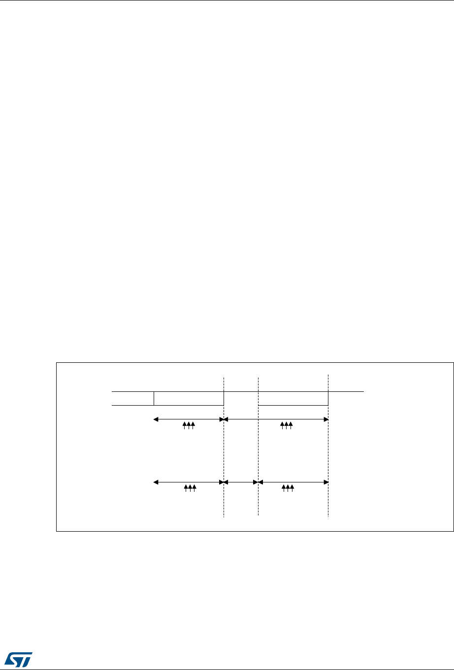
DocID025941 Rev 5 753/1001
RM0376 Universal synchronous asynchronous receiver transmitter (USART)
831
•In transmission, the USART inserts the Guard Time (as programmed in the Guard Time
register) between two successive characters. As the Guard Time is measured after the
stop bit of the previous character, the GT[7:0] register must be programmed to the
desired CGT (Character Guard Time, as defined by the 7816-3 specification) minus 12
(the duration of one character).
•The assertion of the TC flag can be delayed by programming the Guard Time register.
In normal operation, TC is asserted when the transmit shift register is empty and no
further transmit requests are outstanding. In Smartcard mode an empty transmit shift
register triggers the Guard Time counter to count up to the programmed value in the
Guard Time register. TC is forced low during this time. When the Guard Time counter
reaches the programmed value TC is asserted high.
•The de-assertion of TC flag is unaffected by Smartcard mode.
•If a framing error is detected on the transmitter end (due to a NACK from the receiver),
the NACK is not detected as a start bit by the receive block of the transmitter.
According to the ISO protocol, the duration of the received NACK can be 1 or 2 baud
clock periods.
•On the receiver side, if a parity error is detected and a NACK is transmitted the receiver
does not detect the NACK as a start bit.
Note: A break character is not significant in Smartcard mode. A 0x00 data with a framing error is
treated as data and not as a break.
No Idle frame is transmitted when toggling the TE bit. The Idle frame (as defined for the
other configurations) is not defined by the ISO protocol.
Figure 242 details how the NACK signal is sampled by the USART. In this example the
USART is transmitting data and is configured with 1.5 stop bits. The receiver part of the
USART is enabled in order to check the integrity of the data and the NACK signal.
Figure 242. Parity error detection using the 1.5 stop bits
The USART can provide a clock to the smartcard through the CK output. In Smartcard
mode, CK is not associated to the communication but is simply derived from the internal
peripheral input clock through a 5-bit prescaler. The division ratio is configured in the
prescaler register USART_GTPR. CK frequency can be programmed from fCK/2 to fCK/62,
where fCK is the peripheral input clock.
MSv31163V1
Bit 7 Parity bit 1.5 Stop bit
1 bit time 1.5 bit time
0.5 bit time
Sampling at
8th, 9th, 10th
Sampling at
8th, 9th, 10th
Sampling at
8th, 9th, 10th
Sampling at
8th, 9th, 10th

Universal synchronous asynchronous receiver transmitter (USART) RM0376
754/1001 DocID025941 Rev 5
Block mode (T=1)
In T=1 (block) mode, the parity error transmission is deactivated, by clearing the NACK bit in
the UART_CR3 register.
When requesting a read from the smartcard, in block mode, the software must enable the
receiver Timeout feature by setting the RTOEN bit in the USART_CR2 register and program
the RTO bits field in the RTOR register to the BWT (block wait time) - 11 value. If no answer
is received from the card before the expiration of this period, the RTOF flag will be set and a
timeout interrupt will be generated (if RTOIE bit in the USART_CR1 register is set). If the
first character is received before the expiration of the period, it is signaled by the RXNE
interrupt.
Note: The RXNE interrupt must be enabled even when using the USART in DMA mode to read
from the smartcard in block mode. In parallel, the DMA must be enabled only after the first
received byte.
After the reception of the first character (RXNE interrupt), the RTO bit fields in the RTOR
register must be programmed to the CWT (character wait time) - 11 value, in order to allow
the automatic check of the maximum wait time between two consecutive characters. This
time is expressed in baudtime units. If the smartcard does not send a new character in less
than the CWT period after the end of the previous character, the USART signals this to the
software through the RTOF flag and interrupt (when RTOIE bit is set).
Note: The RTO counter starts counting:
- From the end of the stop bit in case STOP = 00.
- From the end of the second stop bit in case of STOP = 10.
- 1 bit duration after the beginning of the STOP bit in case STOP = 11.
- From the beginning of the STOP bit in case STOP = 01.
As in the Smartcard protocol definition, the BWT/CWT values are defined from the
beginning (start bit) of the last character. The RTO register must be programmed to BWT -
11 or CWT -11, respectively, taking into account the length of the last character itself.
A block length counter is used to count all the characters received by the USART. This
counter is reset when the USART is transmitting (TXE=0). The length of the block is
communicated by the smartcard in the third byte of the block (prologue field). This value
must be programmed to the BLEN field in the USART_RTOR register. when using DMA
mode, before the start of the block, this register field must be programmed to the minimum
value (0x0). with this value, an interrupt is generated after the 4th received character. The
software must read the LEN field (third byte), its value must be read from the receive buffer.
In interrupt driven receive mode, the length of the block may be checked by software or by
programming the BLEN value. However, before the start of the block, the maximum value of
BLEN (0xFF) may be programmed. The real value will be programmed after the reception of
the third character.
If the block is using the LRC longitudinal redundancy check (1 epilogue byte), the
BLEN=LEN. If the block is using the CRC mechanism (2 epilogue bytes), BLEN=LEN+1
must be programmed. The total block length (including prologue, epilogue and information
fields) equals BLEN+4. The end of the block is signaled to the software through the EOBF
flag and interrupt (when EOBIE bit is set).
In case of an error in the block length, the end of the block is signaled by the RTO interrupt
(Character wait Time overflow).

DocID025941 Rev 5 755/1001
RM0376 Universal synchronous asynchronous receiver transmitter (USART)
831
Note: The error checking code (LRC/CRC) must be computed/verified by software.
Direct and inverse convention
The Smartcard protocol defines two conventions: direct and inverse.
The direct convention is defined as: LSB first, logical bit value of 1 corresponds to a H state
of the line and parity is even. In order to use this convention, the following control bits must
be programmed: MSBFIRST=0, DATAINV=0 (default values).
The inverse convention is defined as: MSB first, logical bit value 1 corresponds to an L state
on the signal line and parity is even. In order to use this convention, the following control bits
must be programmed: MSBFIRST=1, DATAINV=1.
Note: When logical data values are inverted (0=H, 1=L), the parity bit is also inverted in the same
way.
In order to recognize the card convention, the card sends the initial character, TS, as the
first character of the ATR (Answer To Reset) frame. The two possible patterns for the TS
are: LHHL LLL LLH and LHHL HHH LLH.
•(H) LHHL LLL LLH sets up the inverse convention: state L encodes value 1 and
moment 2 conveys the most significant bit (MSB first). when decoded by inverse
convention, the conveyed byte is equal to '3F'.
•(H) LHHL HHH LLH sets up the direct convention: state H encodes value 1 and
moment 2 conveys the least significant bit (LSB first). when decoded by direct
convention, the conveyed byte is equal to '3B'.
Character parity is correct when there is an even number of bits set to 1 in the nine
moments 2 to 10.
As the USART does not know which convention is used by the card, it needs to be able to
recognize either pattern and act accordingly. The pattern recognition is not done in
hardware, but through a software sequence. Moreover, supposing that the USART is
configured in direct convention (default) and the card answers with the inverse convention,
TS = LHHL LLL LLH => the USART received character will be ‘03’ and the parity will be odd.
Therefore, two methods are available for TS pattern recognition:
Method 1
The USART is programmed in standard Smartcard mode/direct convention. In this case, the
TS pattern reception generates a parity error interrupt and error signal to the card.
•The parity error interrupt informs the software that the card didn’t answer correctly in
direct convention. Software then reprograms the USART for inverse convention
•In response to the error signal, the card retries the same TS character, and it will be
correctly received this time, by the reprogrammed USART
Alternatively, in answer to the parity error interrupt, the software may decide to reprogram
the USART and to also generate a new reset command to the card, then wait again for the
TS.

Universal synchronous asynchronous receiver transmitter (USART) RM0376
756/1001 DocID025941 Rev 5
Method 2
The USART is programmed in 9-bit/no-parity mode, no bit inversion. In this mode it receives
any of the two TS patterns as:
(H) LHHL LLL LLH = 0x103 -> inverse convention to be chosen
(H) LHHL HHH LLH = 0x13B -> direct convention to be chosen
The software checks the received character against these two patterns and, if any of them
match, then programs the USART accordingly for the next character reception.
If none of the two is recognized, a card reset may be generated in order to restart the
negotiation.
28.5.14 USART IrDA SIR ENDEC block
This section is relevant only when IrDA mode is supported. Please refer to Section 28.4:
USART implementation on page 724.
IrDA mode is selected by setting the IREN bit in the USART_CR3 register. In IrDA mode,
the following bits must be kept cleared:
•LINEN, STOP and CLKEN bits in the USART_CR2 register,
•SCEN and HDSEL bits in the USART_CR3 register.
The IrDA SIR physical layer specifies use of a Return to Zero, Inverted (RZI) modulation
scheme that represents logic 0 as an infrared light pulse (see Figure 243).
The SIR Transmit encoder modulates the Non Return to Zero (NRZ) transmit bit stream
output from USART. The output pulse stream is transmitted to an external output driver and
infrared LED. USART supports only bit rates up to 115.2 Kbps for the SIR ENDEC. In
normal mode the transmitted pulse width is specified as 3/16 of a bit period.
The SIR receive decoder demodulates the return-to-zero bit stream from the infrared
detector and outputs the received NRZ serial bit stream to the USART. The decoder input is
normally high (marking state) in the Idle state. The transmit encoder output has the opposite
polarity to the decoder input. A start bit is detected when the decoder input is low.
•IrDA is a half duplex communication protocol. If the Transmitter is busy (when the
USART is sending data to the IrDA encoder), any data on the IrDA receive line is
ignored by the IrDA decoder and if the Receiver is busy (when the USART is receiving
decoded data from the IrDA decoder), data on the TX from the USART to IrDA is not
encoded. while receiving data, transmission should be avoided as the data to be
transmitted could be corrupted.
•A 0 is transmitted as a high pulse and a 1 is transmitted as a 0. The width of the pulse
is specified as 3/16th of the selected bit period in normal mode (see Figure 244).
•The SIR decoder converts the IrDA compliant receive signal into a bit stream for
USART.
•The SIR receive logic interprets a high state as a logic one and low pulses as logic
zeros.
•The transmit encoder output has the opposite polarity to the decoder input. The SIR
output is in low state when Idle.
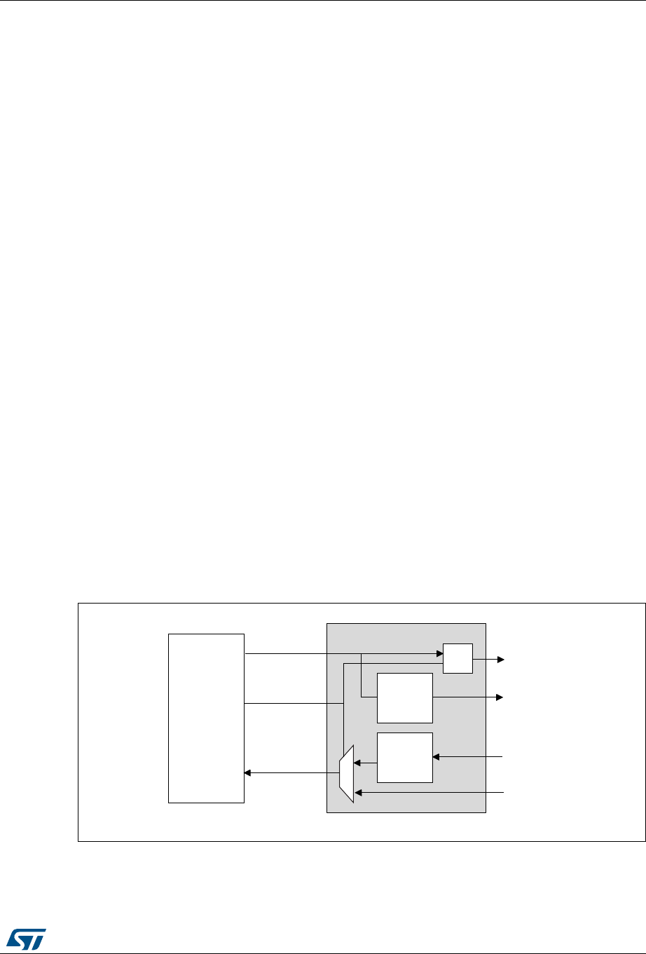
DocID025941 Rev 5 757/1001
RM0376 Universal synchronous asynchronous receiver transmitter (USART)
831
•The IrDA specification requires the acceptance of pulses greater than 1.41 µs. The
acceptable pulse width is programmable. Glitch detection logic on the receiver end
filters out pulses of width less than 2 PSC periods (PSC is the prescaler value
programmed in the USART_GTPR). Pulses of width less than 1 PSC period are always
rejected, but those of width greater than one and less than two periods may be
accepted or rejected, those greater than 2 periods will be accepted as a pulse. The
IrDA encoder/decoder doesn’t work when PSC=0.
•The receiver can communicate with a low-power transmitter.
•In IrDA mode, the STOP bits in the USART_CR2 register must be configured to “1 stop
bit”.
For code example, refer to A.17.10: USART IrDA mode code example.
IrDA low-power mode
Transmitter
In low-power mode the pulse width is not maintained at 3/16 of the bit period. Instead, the
width of the pulse is 3 times the low-power baud rate which can be a minimum of 1.42 MHz.
Generally, this value is 1.8432 MHz (1.42 MHz < PSC< 2.12 MHz). A low-power mode
programmable divisor divides the system clock to achieve this value.
Receiver
Receiving in low-power mode is similar to receiving in normal mode. For glitch detection the
USART should discard pulses of duration shorter than 1 PSC period. A valid low is accepted
only if its duration is greater than 2 periods of the IrDA low-power Baud clock (PSC value in
the USART_GTPR).
Note: A pulse of width less than two and greater than one PSC period(s) may or may not be
rejected.
The receiver set up time should be managed by software. The IrDA physical layer
specification specifies a minimum of 10 ms delay between transmission and reception (IrDA
is a half duplex protocol).
Figure 243. IrDA SIR ENDEC- block diagram
SIREN
MSv31164V2
USART
OR
SIR
Transmit
Encoder
SIR
Receive
DEcoder
TX
RX
USART_RX
IrDA_IN
IrDA_OUT
USART_TX
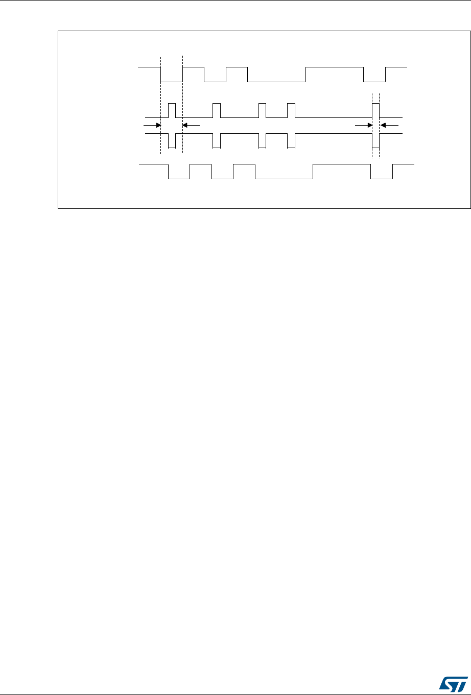
Universal synchronous asynchronous receiver transmitter (USART) RM0376
758/1001 DocID025941 Rev 5
Figure 244. IrDA data modulation (3/16) -Normal Mode
28.5.15 USART continuous communication in DMA mode
The USART is capable of performing continuous communication using the DMA. The DMA
requests for Rx buffer and Tx buffer are generated independently.
Note: Please refer to Section 28.4: USART implementation on page 724 to determine if the DMA
mode is supported. If DMA is not supported, use the USART as explained in Section 28.5.2:
USART transmitter or Section 28.5.3: USART receiver. To perform continuous
communication, the user can clear the TXE/ RXNE flags In the USART_ISR register.
For code example, refer to A.17.11: USART DMA code example.
Transmission using DMA
DMA mode can be enabled for transmission by setting DMAT bit in the USART_CR3
register. Data is loaded from a SRAM area configured using the DMA peripheral (refer to
Section 11: Direct memory access controller (DMA) on page 260) to the USART_TDR
register whenever the TXE bit is set. To map a DMA channel for USART transmission, use
the following procedure (x denotes the channel number):
1. Write the USART_TDR register address in the DMA control register to configure it as
the destination of the transfer. The data is moved to this address from memory after
each TXE event.
2. Write the memory address in the DMA control register to configure it as the source of
the transfer. The data is loaded into the USART_TDR register from this memory area
after each TXE event.
3. Configure the total number of bytes to be transferred to the DMA control register.
4. Configure the channel priority in the DMA register
5. Configure DMA interrupt generation after half/ full transfer as required by the
application.
6. Clear the TC flag in the USART_ISR register by setting the TCCF bit in the
USART_ICR register.
7. Activate the channel in the DMA register.
When the number of data transfers programmed in the DMA Controller is reached, the DMA
controller generates an interrupt on the DMA channel interrupt vector.
MSv31165V1
TX
Start
bit
0101001101
Stop
bit
Bit period
IrDA_OUT
IrDA_IN
RX
3/16
0101 001101
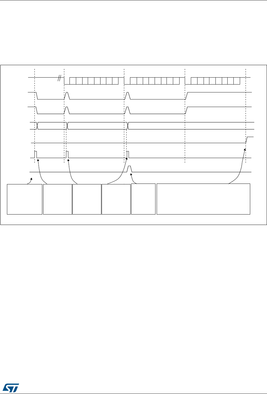
DocID025941 Rev 5 759/1001
RM0376 Universal synchronous asynchronous receiver transmitter (USART)
831
In transmission mode, once the DMA has written all the data to be transmitted (the TCIF flag
is set in the DMA_ISR register), the TC flag can be monitored to make sure that the USART
communication is complete. This is required to avoid corrupting the last transmission before
disabling the USART or entering Stop mode. Software must wait until TC=1. The TC flag
remains cleared during all data transfers and it is set by hardware at the end of transmission
of the last frame.
Figure 245. Transmission using DMA
Reception using DMA
DMA mode can be enabled for reception by setting the DMAR bit in USART_CR3 register.
Data is loaded from the USART_RDR register to a SRAM area configured using the DMA
peripheral (refer to Section 11: Direct memory access controller (DMA) on page 260)
whenever a data byte is received. To map a DMA channel for USART reception, use the
following procedure:
1. Write the USART_RDR register address in the DMA control register to configure it as
the source of the transfer. The data is moved from this address to the memory after
each RXNE event.
2. Write the memory address in the DMA control register to configure it as the destination
of the transfer. The data is loaded from USART_RDR to this memory area after each
RXNE event.
3. Configure the total number of bytes to be transferred to the DMA control register.
4. Configure the channel priority in the DMA control register
5. Configure interrupt generation after half/ full transfer as required by the application.
6. Activate the channel in the DMA control register.
When the number of data transfers programmed in the DMA Controller is reached, the DMA
controller generates an interrupt on the DMA channel interrupt vector.
F2 F3F1
ai17192b
Software
configures DMA
to send 3 data
blocks and
enables USART
The DMA
transfer is
complete
(TCIF=1 in
DMA_ISR)
DMA writes
F1 into
USART_TDR
DMA writes
F2 into
USART_TDR
DMA writes
F3 into
USART_TDR
Software waits until TC=1
Set by hardware
Cleared
by
software
Set by
hardware
TX line
TXE flag
USART_TDR
DMA request
DMA writes
USART_TDR
DMA TCIF flag
(transfer
complete)
TC flag
Frame 1 Frame 2 Frame 3
Idle preamble
Set by hardware
cleared by DMA read
Set by hardware
cleared by DMA read Set by hardware
Ignored by the DMA because
the transfer is complete
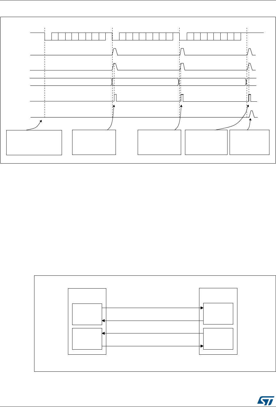
Universal synchronous asynchronous receiver transmitter (USART) RM0376
760/1001 DocID025941 Rev 5
Figure 246. Reception using DMA
Error flagging and interrupt generation in multibuffer communication
In multibuffer communication if any error occurs during the transaction the error flag is
asserted after the current byte. An interrupt is generated if the interrupt enable flag is set.
For framing error, overrun error and noise flag which are asserted with RXNE in single byte
reception, there is a separate error flag interrupt enable bit (EIE bit in the USART_CR3
register), which, if set, enables an interrupt after the current byte if any of these errors occur.
28.5.16 RS232 hardware flow control and RS485 driver enable
using USART
It is possible to control the serial data flow between 2 devices by using the CTS input and
the RTS output. The Figure 247 shows how to connect 2 devices in this mode:
Figure 247. Hardware flow control between 2 USARTs
TX line
Frame 1
F2 F3
Set by hardware
cleared by DMA read
F1
ai17193b
Frame 2 Frame 3
RXNE flag
USART_TDR
DMA request
DMA reads
USART_TDR
DMA TCIF flag
(transfer complete)
Software configures the
DMA to receive 3 data
blocks and enables
the USART
DMA reads F3
from USART_TDR
The DMA transfer
is complete
(TCIF=1 in
DMA_ISR)
Set by hardware
Cleared
by
software
DMA reads F2
from USART_TDR
DMA reads F1
from USART_TDR
MSv31169V2
TX circuit
USART 1
TX
RX circuit
RX circuit
USART 2
TX circuit
TX
CTS
CTSRTS
RX
RTS
RX
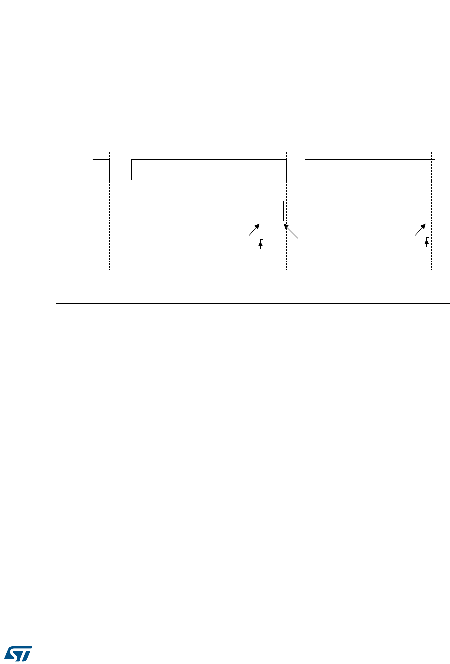
DocID025941 Rev 5 761/1001
RM0376 Universal synchronous asynchronous receiver transmitter (USART)
831
RS232 RTS and CTS flow control can be enabled independently by writing the RTSE and
CTSE bits respectively to 1 (in the USART_CR3 register).
RS232 RTS flow control
If the RTS flow control is enabled (RTSE=1), then RTS is asserted (tied low) as long as the
USART receiver is ready to receive a new data. When the receive register is full, RTS is de-
asserted, indicating that the transmission is expected to stop at the end of the current frame.
Figure 248 shows an example of communication with RTS flow control enabled.
Figure 248. RS232 RTS flow control
RS232 CTS flow control
If the CTS flow control is enabled (CTSE=1), then the transmitter checks the CTS input
before transmitting the next frame. If CTS is asserted (tied low), then the next data is
transmitted (assuming that data is to be transmitted, in other words, if TXE=0), else the
transmission does not occur. when CTS is de-asserted during a transmission, the current
transmission is completed before the transmitter stops.
When CTSE=1, the CTSIF status bit is automatically set by hardware as soon as the CTS
input toggles. It indicates when the receiver becomes ready or not ready for communication.
An interrupt is generated if the CTSIE bit in the USART_CR3 register is set. Figure 249
shows an example of communication with CTS flow control enabled.
MSv31168V2
Start
bit
Start
bit
Stop
bit Idle Stop
bit
RX
RTS
Data 1 read
Data 2 can now be transmitted
RXNE RXNE
Data 1 Data 2

Universal synchronous asynchronous receiver transmitter (USART) RM0376
762/1001 DocID025941 Rev 5
Figure 249. RS232 CTS flow control
Note: For correct behavior, CTS must be asserted at least 3 USART clock source periods before
the end of the current character. In addition it should be noted that the CTSCF flag may not
be set for pulses shorter than 2 x PCLK periods.
For code example, refer to A.17.12: USART hardware flow control code example.
RS485 Driver Enable
The driver enable feature is enabled by setting bit DEM in the USART_CR3 control register.
This allows the user to activate the external transceiver control, through the DE (Driver
Enable) signal. The assertion time is the time between the activation of the DE signal and
the beginning of the START bit. It is programmed using the DEAT [4:0] bit fields in the
USART_CR1 control register. The de-assertion time is the time between the end of the last
stop bit, in a transmitted message, and the de-activation of the DE signal. It is programmed
using the DEDT [4:0] bit fields in the USART_CR1 control register. The polarity of the DE
signal can be configured using the DEP bit in the USART_CR3 control register.
In USART, the DEAT and DEDT are expressed in sample time units (1/8 or 1/16 bit duration,
depending on the oversampling rate).
MSv31167V2
Start
bit
Stop
bit
TX
TDR
CTS
Data 1
Data 2
Stop
bit Idle Start
bit
Data 2 Data 3
Data 3
empty empty
CTS
CTS
Transmit data register
Writing data 3 in TDR Transmission of Data 3 is
delayed until CTS = 0

DocID025941 Rev 5 763/1001
RM0376 Universal synchronous asynchronous receiver transmitter (USART)
831
28.5.17 Wakeup from Stop mode using USART
The USART is able to wake up the MCU from Stopmode when the UESM bit is set and the
USART clock is set to HSI or LSE (refer to Section Reset and clock control (RCC)).
•USART source clock is HSI
If during stop mode the HSI clock is switched OFF, when a falling edge on the USART
receive line is detected, the USART interface requests the HSI clock to be switched
ON. The HSI clock is then used for the frame reception.
– If the wakeup event is verified, the MCU wakes up from low-power mode and data
reception goes on normally.
– If the wakeup event is not verified, the HSI clock is switched OFF again, the MCU
is not waken up and stays in low-power mode and the clock request is released.
•USART source clock is LSE
Same principle as described in case of USART source clock is HSI with the difference
that the LSE is ON in stop mode, but the LSE clock is not propagated to USART if the
USART is not requesting it. The LSE clock is not OFF but there is a clock gating to
avoid useless consumption.
When the USART clock source is configured to be fLSE or fHSI, it is possible to keep enabled
this clock during STOP mode by setting the UCESM bit in USART_CR3 control register.
The MCU wakeup from Stop mode can be done using the standard RXNE interrupt. In this
case, the RXNEIE bit must be set before entering Stop mode.
Alternatively, a specific interrupt may be selected through the WUS bit fields.
In order to be able to wake up the MCU from Stop mode, the UESM bit in the USART_CR1
control register must be set prior to entering Stop mode.
When the wakeup event is detected, the WUF flag is set by hardware and a wakeup
interrupt is generated if the WUFIE bit is set.
Note: Before entering Stop mode, the user must ensure that the USART is not performing a
transfer. BUSY flag cannot ensure that Stop mode is never entered during a running
reception.
The WUF flag is set when a wakeup event is detected, independently of whether the MCU is
in Stop or in an active mode.
When entering Stop mode just after having initialized and enabled the receiver, the REACK
bit must be checked to ensure the USART is actually enabled.
When DMA is used for reception, it must be disabled before entering Stop mode and re-
enabled upon exit from Stop mode.
The wakeup from Stop mode feature is not available for all modes. For example it doesn’t
work in SPI mode because the SPI operates in master mode only.
Using Mute mode with Stop mode
If the USART is put into Mute mode before entering Stop mode:
•Wakeup from Mute mode on idle detection must not be used, because idle detection
cannot work in Stop mode.
•If the wakeup from Mute mode on address match is used, then the source of wake-up
from Stop mode must also be the address match. If the RXNE flag is set when entering

Universal synchronous asynchronous receiver transmitter (USART) RM0376
764/1001 DocID025941 Rev 5
the Stop mode, the interface will remain in mute mode upon address match and wake
up from Stop.
•If the USART is configured to wake up the MCU from Stop mode on START bit
detection, the WUF flag is set, but the RXNE flag is not set.
Determining the maximum USART baud rate allowing to wakeup correctly
from Stop mode when the USART clock source is the HSI clock
The maximum baud rate allowing to wakeup correctly from stop mode depends on:
•the parameter tWUUSART provided in the device datasheet
•the USART receiver tolerance provided in the Section 28.5.5: Tolerance of the USART
receiver to clock deviation.
Let us take this example: OVER8 = 0, M bits = 10, ONEBIT = 1, BRR [3:0] = 0000.
In these conditions, according to Table 129: Tolerance of the USART receiver when BRR
[3:0] = 0000, the USART receiver tolerance is 4.86 %.
DTRA + DQUANT + DREC + DTCL + DWU < USART receiver's tolerance
DWU max = tWUUSART / (11 x Tbit Min)
Tbit Min = tWUUSART / (11 x DWU max)
If we consider an ideal case where the parameters DTRA, DQUANT, DREC and DTCL are
at 0%, the DWU max is 4.86 %. In reality, we need to consider at least the HSI inaccuracy.
Let us consider HSI inaccuracy = 1 %, tWUUSART = 8.1 μs (in case of Stop mode with main
regulator in Run mode, Range 1 ):
DWU max = 4.86 % - 1 % = 3.86 %
Tbit min = 8.1 µs / (9 ₓ 3.86 %) = 23.31 μs.
In these conditions, the maximum baud rate allowing to wakeup correctly from Stop mode is
1/23.31 μs = 42 Kbaud.
28.6 USART low-power modes
Table 132. Effect of low-power modes on the USART
Mode Description
Sleep No effect. USART interrupt causes the device to exit Sleep mode.
Low-power run No effect.
Low-power sleep No effect. USART interrupt causes the device to exit Low-power sleep
mode.
Stop
The USART is able to wake up the MCU from Stop mode when the UESM
bit is set and the USART clock is set to HSI16 or LSE.
The MCU wakeup from Stop mode can be done using the standard RXNE
interrupt.
Standby The USART is powered down and must be reinitialized when the device
has exited from Standby mode.
DocID025941 Rev 5 765/1001
RM0376 Universal synchronous asynchronous receiver transmitter (USART)
831
28.7 USART interrupts
The USART interrupt events are connected to the same interrupt vector (see Figure 250).
•During transmission: Transmission Complete, Clear to Send, Transmit data Register
empty or Framing error (in Smartcard mode) interrupt.
•During reception: Idle Line detection, Overrun error, Receive data register not empty,
Parity error, LIN break detection, Noise Flag, Framing Error, Character match, etc.
These events generate an interrupt if the corresponding Enable Control Bit is set.
Table 133. USART interrupt requests
Interrupt event Event flag Enable Control
bit
Transmit data register empty TXE TXEIE
CTS interrupt CTSIF CTSIE
Transmission Complete TC TCIE
Receive data register not empty (data ready to be read) RXNE
RXNEIE
Overrun error detected ORE
Idle line detected IDLE IDLEIE
Parity error PE PEIE
LIN break LBDF LBDIE
Noise Flag, Overrun error and Framing Error in multibuffer
communication. NF or ORE or FE EIE
Character match CMF CMIE
Receiver timeout RTOF RTOIE
End of Block EOBF EOBIE
Wakeup from Stop mode WUF(1)
1. The WUF interrupt is active only in Stop mode.
WUFIE


DocID025941 Rev 5 767/1001
RM0376 Universal synchronous asynchronous receiver transmitter (USART)
831
28.8 USART registers
Refer to Section 1.1 on page 51 for a list of abbreviations used in register descriptions.
28.8.1 Control register 1 (USART_CR1)
Address offset: 0x00
Reset value: 0x0000
31 30 29 28 27 26 25 24 23 22 21 20 19 18 17 16
Res. Res. Res. M1 EOBIE RTOIE DEAT[4:0] DEDT[4:0]
rw rw rw rw rw rw rw rw rw rw rw rw rw
15141312111098765 43210
OVER8 CMIE MME M0 WAKE PCE PS PEIE TXEIE TCIE RXNEIE IDLEIE TE RE UESM UE
rw rw rw rw rw rw rw rw rw rw rw rw rw rw rw rw
Bits 31:29 Reserved, must be kept at reset value
Bit 28 M1: Word length
This bit, with bit 12 (M0), determines the word length. It is set or cleared by software.
M[1:0] = 00: 1 Start bit, 8 data bits, n stop bits
M[1:0] = 01: 1 Start bit, 9 data bits, n stop bits
M[1:0] = 10: 1 Start bit, 7 data bits, n stop bits
This bit can only be written when the USART is disabled (UE=0).
Note: Not all modes are supported In 7-bit data length mode. Refer to Section 28.4: USART
implementation for details.
Bit 27 EOBIE: End of Block interrupt enable
This bit is set and cleared by software.
0: Interrupt is inhibited
1: A USART interrupt is generated when the EOBF flag is set in the USART_ISR register
Note: If the USART does not support Smartcard mode, this bit is reserved and must be kept
at reset value. Please refer to Section 28.4: USART implementation on page 724.
Bit 26 RTOIE: Receiver timeout interrupt enable
This bit is set and cleared by software.
0: Interrupt is inhibited
1: An USART interrupt is generated when the RTOF bit is set in the USART_ISR register.
Note: If the USART does not support the Receiver timeout feature, this bit is reserved and
must be kept at reset value. Section 28.4: USART implementation on page 724.
Bits 25:21 DEAT[4:0]: Driver Enable assertion time
This 5-bit value defines the time between the activation of the DE (Driver Enable) signal and
the beginning of the start bit. It is expressed in sample time units (1/8 or 1/16 bit duration,
depending on the oversampling rate).
This bit field can only be written when the USART is disabled (UE=0).
Note: If the Driver Enable feature is not supported, this bit is reserved and must be kept at
reset value. Please refer to Section 28.4: USART implementation on page 724.

Universal synchronous asynchronous receiver transmitter (USART) RM0376
768/1001 DocID025941 Rev 5
Bits 20:16 DEDT[4:0]: Driver Enable de-assertion time
This 5-bit value defines the time between the end of the last stop bit, in a transmitted
message, and the de-activation of the DE (Driver Enable) signal. It is expressed in sample
time units (1/8 or 1/16 bit duration, depending on the oversampling rate).
If the USART_TDR register is written during the DEDT time, the new data is transmitted only
when the DEDT and DEAT times have both elapsed.
This bit field can only be written when the USART is disabled (UE=0).
Note: If the Driver Enable feature is not supported, this bit is reserved and must be kept at
reset value. Please refer to Section 28.4: USART implementation on page 724.
Bit 15 OVER8: Oversampling mode
0: Oversampling by 16
1: Oversampling by 8
This bit can only be written when the USART is disabled (UE=0).
Note: In LIN, IrDA and modes, this bit must be kept at reset value.
Bit 14 CMIE: Character match interrupt enable
This bit is set and cleared by software.
0: Interrupt is inhibited
1: A USART interrupt is generated when the CMF bit is set in the USART_ISR register.
Bit 13 MME: Mute mode enable
This bit activates the mute mode function of the USART. when set, the USART can switch
between the active and mute modes, as defined by the WAKE bit. It is set and cleared by
software.
0: Receiver in active mode permanently
1: Receiver can switch between mute mode and active mode.
Bit 12 M0: Word length
This bit, with bit 28 (M1), determines the word length. It is set or cleared by software. See Bit
28 (M1) description.
This bit can only be written when the USART is disabled (UE=0).
Bit 11 WAKE: Receiver wakeup method
This bit determines the USART wakeup method from Mute mode. It is set or cleared by
software.
0: Idle line
1: Address mark
This bit field can only be written when the USART is disabled (UE=0).
Bit 10 PCE: Parity control enable
This bit selects the hardware parity control (generation and detection). When the parity
control is enabled, the computed parity is inserted at the MSB position (9th bit if M=1; 8th bit
if M=0) and parity is checked on the received data. This bit is set and cleared by software.
Once it is set, PCE is active after the current byte (in reception and in transmission).
0: Parity control disabled
1: Parity control enabled
This bit field can only be written when the USART is disabled (UE=0).
Bit 9 PS: Parity selection
This bit selects the odd or even parity when the parity generation/detection is enabled (PCE
bit set). It is set and cleared by software. The parity will be selected after the current byte.
0: Even parity
1: Odd parity
This bit field can only be written when the USART is disabled (UE=0).

DocID025941 Rev 5 769/1001
RM0376 Universal synchronous asynchronous receiver transmitter (USART)
831
Bit 8 PEIE: PE interrupt enable
This bit is set and cleared by software.
0: Interrupt is inhibited
1: A USART interrupt is generated whenever PE=1 in the USART_ISR register
Bit 7 TXEIE: interrupt enable
This bit is set and cleared by software.
0: Interrupt is inhibited
1: A USART interrupt is generated whenever TXE=1 in the USART_ISR register
Bit 6 TCIE: Transmission complete interrupt enable
This bit is set and cleared by software.
0: Interrupt is inhibited
1: A USART interrupt is generated whenever TC=1 in the USART_ISR register
Bit 5 RXNEIE: RXNE interrupt enable
This bit is set and cleared by software.
0: Interrupt is inhibited
1: A USART interrupt is generated whenever ORE=1 or RXNE=1 in the USART_ISR
register
Bit 4 IDLEIE: IDLE interrupt enable
This bit is set and cleared by software.
0: Interrupt is inhibited
1: A USART interrupt is generated whenever IDLE=1 in the USART_ISR register
Bit 3 TE: Transmitter enable
This bit enables the transmitter. It is set and cleared by software.
0: Transmitter is disabled
1: Transmitter is enabled
Note: During transmission, a “0” pulse on the TE bit (“0” followed by “1”) sends a preamble
(idle line) after the current word, except in Smartcard mode. In order to generate an idle
character, the TE must not be immediately written to 1. In order to ensure the required
duration, the software can poll the TEACK bit in the USART_ISR register.
In Smartcard mode, when TE is set there is a 1 bit-time delay before the transmission
starts.

Universal synchronous asynchronous receiver transmitter (USART) RM0376
770/1001 DocID025941 Rev 5
28.8.2 Control register 2 (USART_CR2)
Address offset: 0x04
Reset value: 0x0000
Bit 2 RE: Receiver enable
This bit enables the receiver. It is set and cleared by software.
0: Receiver is disabled
1: Receiver is enabled and begins searching for a start bit
Bit 1 UESM: USART enable in Stop mode
When this bit is cleared, the USART is not able to wake up the MCU from Stop mode.
When this bit is set, the USART is able to wake up the MCU from Stop mode, provided that
the USART clock selection is HSI16 or LSE in the RCC.
This bit is set and cleared by software.
0: USART not able to wake up the MCU from Stop mode.
1: USART able to wake up the MCU from Stop mode. When this function is active, the clock
source for the USART must be HSI16 or LSE (see Section Reset and clock control
(RCC).
Note: It is recommended to set the UESM bit just before entering Stop mode and clear it on
exit from Stop mode.
If the USART does not support the wakeup from Stop feature, this bit is reserved and
must be kept at reset value. Please refer to Section 28.4: USART implementation on
page 724.
Bit 0 UE: USART enable
When this bit is cleared, the USART prescalers and outputs are stopped immediately, and
current operations are discarded. The configuration of the USART is kept, but all the status
flags, in the USART_ISR are set to their default values. This bit is set and cleared by
software.
0: USART prescaler and outputs disabled, low-power mode
1: USART enabled
Note: In order to go into low-power mode without generating errors on the line, the TE bit
must be reset before and the software must wait for the TC bit in the USART_ISR to be
set before resetting the UE bit.
The DMA requests are also reset when UE = 0 so the DMA channel must be disabled
before resetting the UE bit.
31 30 29 28 27 26 25 24 23 22 21 20 19 18 17 16
ADD[7:4] ADD[3:0] RTOEN ABRMOD[1:0] ABREN MSBFI
RST DATAINV TXINV RXINV
rw rw rw rw rw rw rw rw rw rw rw rw rw rw rw rw
1514131211109876543 2 10
SWAP LINEN STOP[1:0] CLKEN CPOL CPHA LBCL Res. LBDIE LBDL ADDM7 Res. Res. Res. Res.
rw rw rw rw rw rw rw rw rw rw rw

DocID025941 Rev 5 771/1001
RM0376 Universal synchronous asynchronous receiver transmitter (USART)
831
Bits 31:28 ADD[7:4]: Address of the USART node
This bit-field gives the address of the USART node or a character code to be recognized.
This is used in multiprocessor communication during Mute mode or Stop mode, for wakeup with 7-
bit address mark detection. The MSB of the character sent by the transmitter should be equal to 1.
It may also be used for character detection during normal reception, Mute mode inactive (for
example, end of block detection in ModBus protocol). In this case, the whole received character (8-
bit) is compared to the ADD[7:0] value and CMF flag is set on match.
This bit field can only be written when reception is disabled (RE = 0) or the USART is disabled
(UE=0)
Bits 27:24 ADD[3:0]: Address of the USART node
This bit-field gives the address of the USART node or a character code to be recognized.
This is used in multiprocessor communication during Mute mode or Stop mode, for wakeup with
address mark detection.
This bit field can only be written when reception is disabled (RE = 0) or the USART is disabled
(UE=0)
Bit 23 RTOEN: Receiver timeout enable
This bit is set and cleared by software.
0: Receiver timeout feature disabled.
1: Receiver timeout feature enabled.
When this feature is enabled, the RTOF flag in the USART_ISR register is set if the RX line is idle
(no reception) for the duration programmed in the RTOR (receiver timeout register).
Note: If the USART does not support the Receiver timeout feature, this bit is reserved and must be
kept at reset value. Please refer to Section 28.4: USART implementation on page 724.
Bits 22:21 ABRMOD[1:0]: Auto baud rate mode
These bits are set and cleared by software.
00: Measurement of the start bit is used to detect the baud rate.
01: Falling edge to falling edge measurement. (the received frame must start with a single bit = 1 ->
Frame = Start10xxxxxx)
10: 0x7F frame detection.
11: 0x55 frame detection
This bit field can only be written when ABREN = 0 or the USART is disabled (UE=0).
Note: If DATAINV=1 and/or MSBFIRST=1 the patterns must be the same on the line, for example
0xAA for MSBFIRST)
If the USART does not support the auto baud rate feature, this bit is reserved and must be kept
at reset value. Please refer to Section 28.4: USART implementation on page 724.
Bit 20 ABREN: Auto baud rate enable
This bit is set and cleared by software.
0: Auto baud rate detection is disabled.
1: Auto baud rate detection is enabled.
Note: If the USART does not support the auto baud rate feature, this bit is reserved and must be kept
at reset value. Please refer to Section 28.4: USART implementation on page 724.
Bit 19 MSBFIRST: Most significant bit first
This bit is set and cleared by software.
0: data is transmitted/received with data bit 0 first, following the start bit.
1: data is transmitted/received with the MSB (bit 7/8/9) first, following the start bit.
This bit field can only be written when the USART is disabled (UE=0).

Universal synchronous asynchronous receiver transmitter (USART) RM0376
772/1001 DocID025941 Rev 5
Bit 18 DATAINV: Binary data inversion
This bit is set and cleared by software.
0: Logical data from the data register are send/received in positive/direct logic. (1=H, 0=L)
1: Logical data from the data register are send/received in negative/inverse logic. (1=L, 0=H). The
parity bit is also inverted.
This bit field can only be written when the USART is disabled (UE=0).
Bit 17 TXINV: TX pin active level inversion
This bit is set and cleared by software.
0: TX pin signal works using the standard logic levels (VDD =1/idle, Gnd=0/mark)
1: TX pin signal values are inverted. (VDD =0/mark, Gnd=1/idle).
This allows the use of an external inverter on the TX line.
This bit field can only be written when the USART is disabled (UE=0).
Bit 16 RXINV: RX pin active level inversion
This bit is set and cleared by software.
0: RX pin signal works using the standard logic levels (VDD =1/idle, Gnd=0/mark)
1: RX pin signal values are inverted. (VDD =0/mark, Gnd=1/idle).
This allows the use of an external inverter on the RX line.
This bit field can only be written when the USART is disabled (UE=0).
Bit 15 SWAP: Swap TX/RX pins
This bit is set and cleared by software.
0: TX/RX pins are used as defined in standard pinout
1: The TX and RX pins functions are swapped. This allows to work in the case of a cross-wired
connection to another USART.
This bit field can only be written when the USART is disabled (UE=0).
Bit 14 LINEN: LIN mode enable
This bit is set and cleared by software.
0: LIN mode disabled
1: LIN mode enabled
The LIN mode enables the capability to send LIN synchronous breaks (13 low bits) using the
SBKRQ bit in the USART_RQR register, and to detect LIN Sync breaks.
This bit field can only be written when the USART is disabled (UE=0).
Note: If the USART does not support LIN mode, this bit is reserved and must be kept at reset value.
Please refer to Section 28.4: USART implementation on page 724.
Bits 13:12 STOP[1:0]: STOP bits
These bits are used for programming the stop bits.
00: 1 stop bit
01: 0.5 stop bit
10: 2 stop bits
11: 1.5 stop bits
This bit field can only be written when the USART is disabled (UE=0).
Bit 11 CLKEN: Clock enable
This bit allows the user to enable the CK pin.
0: CK pin disabled
1: CK pin enabled
This bit can only be written when the USART is disabled (UE=0).
Note: If neither synchronous mode nor Smartcard mode is supported, this bit is reserved and must
be kept at reset value. Please refer to Section 28.4: USART implementation on page 724.

DocID025941 Rev 5 773/1001
RM0376 Universal synchronous asynchronous receiver transmitter (USART)
831
Note: In order to provide correctly the CK clock to the Smartcard, the steps below must be
respected:
- UE = 0
- SCEN = 1
- GTPR configuration
- CLKEN= 1
- UE = 1
Bit 10 CPOL: Clock polarity
This bit allows the user to select the polarity of the clock output on the CK pin in synchronous mode.
It works in conjunction with the CPHA bit to produce the desired clock/data relationship
0: Steady low value on CK pin outside transmission window
1: Steady high value on CK pin outside transmission window
This bit can only be written when the USART is disabled (UE=0).
Note: If synchronous mode is not supported, this bit is reserved and must be kept at reset value.
Please refer to Section 28.4: USART implementation on page 724.
Bit 9 CPHA: Clock phase
This bit is used to select the phase of the clock output on the CK pin in synchronous mode. It works
in conjunction with the CPOL bit to produce the desired clock/data relationship (see Figure 238 and
Figure 239)
0: The first clock transition is the first data capture edge
1: The second clock transition is the first data capture edge
This bit can only be written when the USART is disabled (UE=0).
Note: If synchronous mode is not supported, this bit is reserved and must be kept at reset value.
Please refer to Section 28.4: USART implementation on page 724.
Bit 8 LBCL: Last bit clock pulse
This bit is used to select whether the clock pulse associated with the last data bit transmitted (MSB)
has to be output on the CK pin in synchronous mode.
0: The clock pulse of the last data bit is not output to the CK pin
1: The clock pulse of the last data bit is output to the CK pin
Caution: The last bit is the 7th or 8th or 9th data bit transmitted depending on the 7 or 8 or 9 bit
format selected by the M bits in the USART_CR1 register.
This bit can only be written when the USART is disabled (UE=0).
Note: If synchronous mode is not supported, this bit is reserved and must be kept at reset value.
Please refer to Section 28.4: USART implementation on page 724.
Bit 7 Reserved, must be kept at reset value.
Bit 6 LBDIE: LIN break detection interrupt enable
Break interrupt mask (break detection using break delimiter).
0: Interrupt is inhibited
1: An interrupt is generated whenever LBDF=1 in the USART_ISR register
Note: If LIN mode is not supported, this bit is reserved and must be kept at reset value. Please refer
to Section 28.4: USART implementation on page 724.

Universal synchronous asynchronous receiver transmitter (USART) RM0376
774/1001 DocID025941 Rev 5
Note: The 3 bits (CPOL, CPHA, LBCL) should not be written while the transmitter is enabled.
28.8.3 Control register 3 (USART_CR3)
Address offset: 0x08
Reset value: 0x0000
Bit 5 LBDL: LIN break detection length
This bit is for selection between 11 bit or 10 bit break detection.
0: 10-bit break detection
1: 11-bit break detection
This bit can only be written when the USART is disabled (UE=0).
Note: If LIN mode is not supported, this bit is reserved and must be kept at reset value. Please refer
to Section 28.4: USART implementation on page 724.
Bit 4 ADDM7:7-bit Address Detection/4-bit Address Detection
This bit is for selection between 4-bit address detection or 7-bit address detection.
0: 4-bit address detection
1: 7-bit address detection (in 8-bit data mode)
This bit can only be written when the USART is disabled (UE=0)
Note: In 7-bit and 9-bit data modes, the address detection is done on 6-bit and 8-bit address
(ADD[5:0] and ADD[7:0]) respectively.
Bits 3:0 Reserved, must be kept at reset value.
31 30 29 28 27 26 25 24 23 22 21 20 19 18 17 16
Res. Res. Res. Res. Res. Res. Res. Res. UCESM WUFIE WUS SCARCNT2:0] Res.
rw rw rw rw rw rw rw
15141312111098 7 6543210
DEP DEM DDRE OVR
DIS
ONE
BIT CTSIE CTSE RTSE DMAT DMAR SCEN NACK HDSEL IRLP IREN EIE
rw rw rw rw rw rw rw rw rw rw v v rw rw rw rw
Bits 31:25 Reserved, must be kept at reset value.
Bit 24 Reserved, must be kept at reset value.
Bit 23 UCESM: USART Clock Enable in Stop mode.
This bit is set and cleared by software.
0: USART Clock is disabled in STOP mode.
1: USART Clock is enabled in STOP mode.
Bit 22 WUFIE: Wakeup from Stop mode interrupt enable
This bit is set and cleared by software.
0: Interrupt is inhibited
1: An USART interrupt is generated whenever WUF=1 in the USART_ISR register
Note: WUFIE must be set before entering in Stop mode.
The WUF interrupt is active only in Stop mode.
If the USART does not support the wakeup from Stop feature, this bit is reserved and
must be kept at reset value.

DocID025941 Rev 5 775/1001
RM0376 Universal synchronous asynchronous receiver transmitter (USART)
831
Bits 21:20 WUS[1:0]: Wakeup from Stop mode interrupt flag selection
This bit-field specify the event which activates the WUF (wakeup from Stop mode flag).
00: WUF active on address match (as defined by ADD[7:0] and ADDM7)
01:Reserved.
10: WuF active on Start bit detection
11: WUF active on RXNE.
This bit field can only be written when the USART is disabled (UE=0).
Note: If the USART does not support the wakeup from Stop feature, this bit is reserved and
must be kept at reset value.
Bits 19:17 SCARCNT[2:0]: Smartcard auto-retry count
This bit-field specifies the number of retries in transmit and receive, in Smartcard mode.
In transmission mode, it specifies the number of automatic retransmission retries, before
generating a transmission error (FE bit set).
In reception mode, it specifies the number or erroneous reception trials, before generating a
reception error (RXNE and PE bits set).
This bit field must be programmed only when the USART is disabled (UE=0).
When the USART is enabled (UE=1), this bit field may only be written to 0x0, in order to stop
retransmission.
0x0: retransmission disabled - No automatic retransmission in transmit mode.
0x1 to 0x7: number of automatic retransmission attempts (before signaling error)
Note: If Smartcard mode is not supported, this bit is reserved and must be kept at reset
value. Please refer to Section 28.4: USART implementation on page 724.
Bit16 Reserved, must be kept at reset value.
Bit 15 DEP: Driver enable polarity selection
0: DE signal is active high.
1: DE signal is active low.
This bit can only be written when the USART is disabled (UE=0).
Note: If the Driver Enable feature is not supported, this bit is reserved and must be kept at
reset value. Please refer to Section 28.4: USART implementation on page 724.
Bit 14 DEM: Driver enable mode
This bit allows the user to activate the external transceiver control, through the DE signal.
0: DE function is disabled.
1: DE function is enabled. The DE signal is output on the RTS pin.
This bit can only be written when the USART is disabled (UE=0).
Note: If the Driver Enable feature is not supported, this bit is reserved and must be kept at
reset value. Section 28.4: USART implementation on page 724.
Bit 13 DDRE: DMA Disable on Reception Error
0: DMA is not disabled in case of reception error. The corresponding error flag is set but
RXNE is kept 0 preventing from overrun. As a consequence, the DMA request is not
asserted, so the erroneous data is not transferred (no DMA request), but next correct
received data will be transferred (used for Smartcard mode).
1: DMA is disabled following a reception error. The corresponding error flag is set, as well as
RXNE. The DMA request is masked until the error flag is cleared. This means that the
software must first disable the DMA request (DMAR = 0) or clear RXNE before clearing the
error flag.
This bit can only be written when the USART is disabled (UE=0).
Note: The reception errors are: parity error, framing error or noise error.

Universal synchronous asynchronous receiver transmitter (USART) RM0376
776/1001 DocID025941 Rev 5
Bit 12 OVRDIS: Overrun Disable
This bit is used to disable the receive overrun detection.
0: Overrun Error Flag, ORE, is set when received data is not read before receiving new data.
1: Overrun functionality is disabled. If new data is received while the RXNE flag is still set
the ORE flag is not set and the new received data overwrites the previous content of the
USART_RDR register.
This bit can only be written when the USART is disabled (UE=0).
Note: This control bit allows checking the communication flow without reading the data.
Bit 11 ONEBIT: One sample bit method enable
This bit allows the user to select the sample method. When the one sample bit method is
selected the noise detection flag (NF) is disabled.
0: Three sample bit method
1: One sample bit method
This bit can only be written when the USART is disabled (UE=0).
Note: ONEBIT feature applies only to data bits, It does not apply to Start bit.
Bit 10 CTSIE: CTS interrupt enable
0: Interrupt is inhibited
1: An interrupt is generated whenever CTSIF=1 in the USART_ISR register
Note: If the hardware flow control feature is not supported, this bit is reserved and must be
kept at reset value. Please refer to Section 28.4: USART implementation on page 724.
Bit 9 CTSE: CTS enable
0: CTS hardware flow control disabled
1: CTS mode enabled, data is only transmitted when the CTS input is asserted (tied to 0). If
the CTS input is de-asserted while data is being transmitted, then the transmission is
completed before stopping. If data is written into the data register while CTS is de-asserted,
the transmission is postponed until CTS is asserted.
This bit can only be written when the USART is disabled (UE=0)
Note: If the hardware flow control feature is not supported, this bit is reserved and must be
kept at reset value. Please refer to Section 28.4: USART implementation on page 724.
Bit 8 RTSE: RTS enable
0: RTS hardware flow control disabled
1: RTS output enabled, data is only requested when there is space in the receive buffer. The
transmission of data is expected to cease after the current character has been transmitted.
The RTS output is asserted (pulled to 0) when data can be received.
This bit can only be written when the USART is disabled (UE=0).
Note: If the hardware flow control feature is not supported, this bit is reserved and must be
kept at reset value. Please refer to Section 28.4: USART implementation on page 724.
Bit 7 DMAT: DMA enable transmitter
This bit is set/reset by software
1: DMA mode is enabled for transmission
0: DMA mode is disabled for transmission
Bit 6 DMAR: DMA enable receiver
This bit is set/reset by software
1: DMA mode is enabled for reception
0: DMA mode is disabled for reception

DocID025941 Rev 5 777/1001
RM0376 Universal synchronous asynchronous receiver transmitter (USART)
831
Bit 5 SCEN: Smartcard mode enable
This bit is used for enabling Smartcard mode.
0: Smartcard Mode disabled
1: Smartcard Mode enabled
This bit field can only be written when the USART is disabled (UE=0).
Note: If the USART does not support Smartcard mode, this bit is reserved and must be kept
at reset value. Please refer to Section 28.4: USART implementation on page 724.
Bit 4 NACK: Smartcard NACK enable
0: NACK transmission in case of parity error is disabled
1: NACK transmission during parity error is enabled
This bit field can only be written when the USART is disabled (UE=0).
Note: If the USART does not support Smartcard mode, this bit is reserved and must be kept
at reset value. Please refer to Section 28.4: USART implementation on page 724.
Bit 3 HDSEL: Half-duplex selection
Selection of Single-wire Half-duplex mode
0: Half duplex mode is not selected
1: Half duplex mode is selected
This bit can only be written when the USART is disabled (UE=0).
Bit 2 IRLP: IrDA low-power
This bit is used for selecting between normal and low-power IrDA modes
0: Normal mode
1: Low-power mode
This bit can only be written when the USART is disabled (UE=0).
Note: If IrDA mode is not supported, this bit is reserved and must be kept at reset value.
Please refer to Section 28.4: USART implementation on page 724.
Bit 1 IREN: IrDA mode enable
This bit is set and cleared by software.
0: IrDA disabled
1: IrDA enabled
This bit can only be written when the USART is disabled (UE=0).
Note: If IrDA mode is not supported, this bit is reserved and must be kept at reset value.
Please refer to Section 28.4: USART implementation on page 724.
Bit 0 EIE: Error interrupt enable
Error Interrupt Enable Bit is required to enable interrupt generation in case of a framing
error, overrun error or noise flag (FE=1 or ORE=1 or NF=1 in the USART_ISR register).
0: Interrupt is inhibited
1: An interrupt is generated when FE=1 or ORE=1 or NF=1 in the USART_ISR register.
Universal synchronous asynchronous receiver transmitter (USART) RM0376
778/1001 DocID025941 Rev 5
28.8.4 Baud rate register (USART_BRR)
This register can only be written when the USART is disabled (UE=0). It may be
automatically updated by hardware in auto baud rate detection mode.
Address offset: 0x0C
Reset value: 0x0000
28.8.5 Guard time and prescaler register (USART_GTPR)
Address offset: 0x10
Reset value: 0x0000
31 30 29 28 27 26 25 24 23 22 21 20 19 18 17 16
Res. Res. Res. Res. Res. Res. Res. Res. Res. Res. Res. Res. Res. Res. Res. Res.
1514131211109876543210
BRR[15:0]
rw rw rw rw rw rw rw rw rw rw rw rw rw rw rw rw
Bits 31:16 Reserved, must be kept at reset value.
Bits 15:4 BRR[15:4]
BRR[15:4] = USARTDIV[15:4]
Bits 3:0 BRR[3:0]
When OVER8 = 0, BRR[3:0] = USARTDIV[3:0].
When OVER8 = 1:
BRR[2:0] = USARTDIV[3:0] shifted 1 bit to the right.
BRR[3] must be kept cleared.
31 30 29 28 27 26 25 24 23 22 21 20 19 18 17 16
Res. Res. Res. Res. Res. Res. Res. Res. Res. Res. Res. Res. Res. Res. Res. Res.
1514131211109876543210
GT[7:0] PSC[7:0]
rw rw

DocID025941 Rev 5 779/1001
RM0376 Universal synchronous asynchronous receiver transmitter (USART)
831
28.8.6 Receiver timeout register (USART_RTOR)
Address offset: 0x14
Reset value: 0x0000
Bits 31:16 Reserved, must be kept at reset value
Bits 15:8 GT[7:0]: Guard time value
This bit-field is used to program the Guard time value in terms of number of baud clock
periods.
This is used in Smartcard mode. The Transmission Complete flag is set after this guard time
value.
This bit field can only be written when the USART is disabled (UE=0).
Note: If Smartcard mode is not supported, this bit is reserved and must be kept at reset value.
Please refer to Section 28.4: USART implementation on page 724.
Bits 7:0 PSC[7:0]: Prescaler value
In IrDA Low-power and normal IrDA mode:
PSC[7:0] = IrDA Normal and Low-Power Baud Rate
Used for programming the prescaler for dividing the USART source clock to achieve the low-
power frequency:
The source clock is divided by the value given in the register (8 significant bits):
00000000: Reserved - do not program this value
00000001: divides the source clock by 1
00000010: divides the source clock by 2
...
In Smartcard mode:
PSC[4:0]: Prescaler value
Used for programming the prescaler for dividing the USART source clock to provide the
Smartcard clock.
The value given in the register (5 significant bits) is multiplied by 2 to give the division factor
of the source clock frequency:
00000: Reserved - do not program this value
00001: divides the source clock by 2
00010: divides the source clock by 4
00011: divides the source clock by 6
...
This bit field can only be written when the USART is disabled (UE=0).
Note: Bits [7:5] must be kept at reset value if Smartcard mode is used.
This bit field is reserved and must be kept at reset value when the Smartcard and IrDA
modes are not supported. Please refer to Section 28.4: USART implementation on
page 724.
31 30 29 28 27 26 25 24 23 22 21 20 19 18 17 16
BLEN[7:0] RTO[23:16]
rw rw rw rw rw rw rw rw rw rw rw rw rw rw rw rw
1514131211109876543210
RTO[15:0]
rw rw rw rw rw rw rw rw rw rw rw rw rw rw rw rw

Universal synchronous asynchronous receiver transmitter (USART) RM0376
780/1001 DocID025941 Rev 5
Note: RTOR can be written on the fly. If the new value is lower than or equal to the counter, the
RTOF flag is set.
This register is reserved and forced by hardware to “0x00000000” when the Receiver
timeout feature is not supported. Please refer to Section 28.4: USART implementation on
page 724.
28.8.7 Request register (USART_RQR)
Address offset: 0x18
Reset value: 0x0000
Bits 31:24 BLEN[7:0]: Block Length
This bit-field gives the Block length in Smartcard T=1 Reception. Its value equals the number
of information characters + the length of the Epilogue Field (1-LEC/2-CRC) - 1.
Examples:
BLEN = 0 -> 0 information characters + LEC
BLEN = 1 -> 0 information characters + CRC
BLEN = 255 -> 254 information characters + CRC (total 256 characters))
In Smartcard mode, the Block length counter is reset when TXE=0.
This bit-field can be used also in other modes. In this case, the Block length counter is reset
when RE=0 (receiver disabled) and/or when the EOBCF bit is written to 1.
Note: This value can be programmed after the start of the block reception (using the data
from the LEN character in the Prologue Field). It must be programmed only once per
received block.
Bits 23:0 RTO[23:0]: Receiver timeout value
This bit-field gives the Receiver timeout value in terms of number of bit duration.
In standard mode, the RTOF flag is set if, after the last received character, no new start bit is
detected for more than the RTO value.
In Smartcard mode, this value is used to implement the CWT and BWT. See Smartcard
section for more details.
In this case, the timeout measurement is done starting from the Start Bit of the last received
character.
Note: This value must only be programmed once per received character.
31 30 29 28 27 26 25 24 23 22 21 20 19 18 17 16
Res. Res. Res. Res. Res. Res. Res. Res. Res. Res. Res. Res. Res. Res. Res. Res.
151413121110987654321 0
Res. Res. Res. Res. Res. Res. Res. Res. Res. Res. Res. TXFRQ RXFRQ MMRQ SBKRQ ABRRQ
wwww w

DocID025941 Rev 5 781/1001
RM0376 Universal synchronous asynchronous receiver transmitter (USART)
831
28.8.8 Interrupt and status register (USART_ISR)
Address offset: 0x1C
Reset value: 0x0200 00C0
Bits 31:5 Reserved, must be kept at reset value
Bit 4 TXFRQ: Transmit data flush request
Writing 1 to this bit sets the TXE flag.
This allows to discard the transmit data. This bit must be used only in Smartcard mode,
when data has not been sent due to errors (NACK) and the FE flag is active in the
USART_ISR register.
If the USART does not support Smartcard mode, this bit is reserved and must be kept at
reset value. Please refer to Section 28.4: USART implementation on page 724.
Bit 3 RXFRQ: Receive data flush request
Writing 1 to this bit clears the RXNE flag.
This allows to discard the received data without reading it, and avoid an overrun condition.
Bit 2 MMRQ: Mute mode request
Writing 1 to this bit puts the USART in mute mode and sets the RWU flag.
Bit 1 SBKRQ: Send break request
Writing 1 to this bit sets the SBKF flag and request to send a BREAK on the line, as soon as
the transmit machine is available.
Note: In the case the application needs to send the break character following all previously
inserted data, including the ones not yet transmitted, the software should wait for the
TXE flag assertion before setting the SBKRQ bit.
Bit 0 ABRRQ: Auto baud rate request
Writing 1 to this bit resets the ABRF flag in the USART_ISR and request an automatic baud
rate measurement on the next received data frame.
Note: If the USART does not support the auto baud rate feature, this bit is reserved and must
be kept at reset value. Please refer to Section 28.4: USART implementation on
page 724.
31 30 29 28 27 26 25 24 23 22 21 20 19 18 17 16
Res. Res. Res. Res. Res. Res. Res. Res. Res. REACK TEACK WUF RWU SBKF CMF BUSY
rrrrrrr
1514131211109876543210
ABRF ABRE Res. EOBF RTOF CTS CTSIF LBDF TXE TC RXNE IDLE ORE NF FE PE
rr rrrrrrrrrrrrr
Bits 31:25 Reserved, must be kept at reset value.
Bits 24:23 Reserved, must be kept at reset value.

Universal synchronous asynchronous receiver transmitter (USART) RM0376
782/1001 DocID025941 Rev 5
Bit 22 REACK: Receive enable acknowledge flag
This bit is set/reset by hardware, when the Receive Enable value is taken into account by
the USART.
When the wakeup from Stop mode is supported, the REACK flag can be used to verify that
the USART is ready for reception before entering Stop mode.
Bit 21 TEACK: Transmit enable acknowledge flag
This bit is set/reset by hardware, when the Transmit Enable value is taken into account by
the USART.
It can be used when an idle frame request is generated by writing TE=0, followed by TE=1
in the USART_CR1 register, in order to respect the TE=0 minimum period.
Bit 20 WUF: Wakeup from Stop mode flag
This bit is set by hardware, when a wakeup event is detected. The event is defined by the
WUS bit field. It is cleared by software, writing a 1 to the WUCF in the USART_ICR register.
An interrupt is generated if WUFIE=1 in the USART_CR3 register.
Note: When UESM is cleared, WUF flag is also cleared.
The WUF interrupt is active only in Stop mode.
If the USART does not support the wakeup from Stop feature, this bit is reserved and
kept at reset value.
Bit 19 RWU: Receiver wakeup from Mute mode
This bit indicates if the USART is in mute mode. It is cleared/set by hardware when a
wakeup/mute sequence is recognized. The mute mode control sequence (address or IDLE)
is selected by the WAKE bit in the USART_CR1 register.
When wakeup on IDLE mode is selected, this bit can only be set by software, writing 1 to the
MMRQ bit in the USART_RQR register.
0: Receiver in active mode
1: Receiver in mute mode
Bit 18 SBKF: Send break flag
This bit indicates that a send break character was requested. It is set by software, by writing
1 to the SBKRQ bit in the USART_RQR register. It is automatically reset by hardware during
the stop bit of break transmission.
0: No break character is transmitted
1: Break character will be transmitted
Bit 17 CMF: Character match flag
This bit is set by hardware, when the character defined by ADD[7:0] is received. It is cleared
by software, writing 1 to the CMCF in the USART_ICR register.
An interrupt is generated if CMIE=1in the USART_CR1 register.
0: No Character match detected
1: Character Match detected
Bit 16 BUSY: Busy flag
This bit is set and reset by hardware. It is active when a communication is ongoing on the
RX line (successful start bit detected). It is reset at the end of the reception (successful or
not).
0: USART is idle (no reception)
1: Reception on going

DocID025941 Rev 5 783/1001
RM0376 Universal synchronous asynchronous receiver transmitter (USART)
831
Bit 15 ABRF: Auto baud rate flag
This bit is set by hardware when the automatic baud rate has been set (RXNE will also be
set, generating an interrupt if RXNEIE = 1) or when the auto baud rate operation was
completed without success (ABRE=1) (ABRE, RXNE and FE are also set in this case)
It is cleared by software, in order to request a new auto baud rate detection, by writing 1 to
the ABRRQ in the USART_RQR register.
Note: If the USART does not support the auto baud rate feature, this bit is reserved and kept
at reset value.
Bit 14 ABRE: Auto baud rate error
This bit is set by hardware if the baud rate measurement failed (baud rate out of range or
character comparison failed)
It is cleared by software, by writing 1 to the ABRRQ bit in the USART_CR3 register.
Note: If the USART does not support the auto baud rate feature, this bit is reserved and kept
at reset value.
Bit 13 Reserved, must be kept at reset value.
Bit 12 EOBF: End of block flag
This bit is set by hardware when a complete block has been received (for example T=1
Smartcard mode). The detection is done when the number of received bytes (from the start
of the block, including the prologue) is equal or greater than BLEN + 4.
An interrupt is generated if the EOBIE=1 in the USART_CR2 register.
It is cleared by software, writing 1 to the EOBCF in the USART_ICR register.
0: End of Block not reached
1: End of Block (number of characters) reached
Note: If Smartcard mode is not supported, this bit is reserved and kept at reset value. Please
refer to Section 28.4: USART implementation on page 724.
Bit 11 RTOF: Receiver timeout
This bit is set by hardware when the timeout value, programmed in the RTOR register has
lapsed, without any communication. It is cleared by software, writing 1 to the RTOCF bit in
the USART_ICR register.
An interrupt is generated if RTOIE=1 in the USART_CR1 register.
In Smartcard mode, the timeout corresponds to the CWT or BWT timings.
0: Timeout value not reached
1: Timeout value reached without any data reception
Note: If a time equal to the value programmed in RTOR register separates 2 characters,
RTOF is not set. If this time exceeds this value + 2 sample times (2/16 or 2/8,
depending on the oversampling method), RTOF flag is set.
The counter counts even if RE = 0 but RTOF is set only when RE = 1. If the timeout has
already elapsed when RE is set, then RTOF will be set.
If the USART does not support the Receiver timeout feature, this bit is reserved and
kept at reset value.
Bit 10 CTS: CTS flag
This bit is set/reset by hardware. It is an inverted copy of the status of the CTS input pin.
0: CTS line set
1: CTS line reset
Note: If the hardware flow control feature is not supported, this bit is reserved and kept at
reset value.

Universal synchronous asynchronous receiver transmitter (USART) RM0376
784/1001 DocID025941 Rev 5
Bit 9 CTSIF: CTS interrupt flag
This bit is set by hardware when the CTS input toggles, if the CTSE bit is set. It is cleared by
software, by writing 1 to the CTSCF bit in the USART_ICR register.
An interrupt is generated if CTSIE=1 in the USART_CR3 register.
0: No change occurred on the CTS status line
1: A change occurred on the CTS status line
Note: If the hardware flow control feature is not supported, this bit is reserved and kept at
reset value.
Bit 8 LBDF: LIN break detection flag
This bit is set by hardware when the LIN break is detected. It is cleared by software, by
writing 1 to the LBDCF in the USART_ICR.
An interrupt is generated if LBDIE = 1 in the USART_CR2 register.
0: LIN Break not detected
1: LIN break detected
Note: If the USART does not support LIN mode, this bit is reserved and kept at reset value.
Please refer to Section 28.4: USART implementation on page 724.
Bit 7 TXE: Transmit data register empty
This bit is set by hardware when the content of the USART_TDR register has been
transferred into the shift register. It is cleared by a write to the USART_TDR register.
The TXE flag can also be cleared by writing 1 to the TXFRQ in the USART_RQR register, in
order to discard the data (only in Smartcard T=0 mode, in case of transmission failure).
An interrupt is generated if the TXEIE bit =1 in the USART_CR1 register.
0: data is not transferred to the shift register
1: data is transferred to the shift register)
Note: This bit is used during single buffer transmission.
Bit 6 TC: Transmission complete
This bit is set by hardware if the transmission of a frame containing data is complete and if
TXE is set. An interrupt is generated if TCIE=1 in the USART_CR1 register. It is cleared by
software, writing 1 to the TCCF in the USART_ICR register or by a write to the USART_TDR
register.
An interrupt is generated if TCIE=1 in the USART_CR1 register.
0: Transmission is not complete
1: Transmission is complete
Note: If TE bit is reset and no transmission is on going, the TC bit will be set immediately.
Bit 5 RXNE: Read data register not empty
This bit is set by hardware when the content of the RDR shift register has been transferred
to the USART_RDR register. It is cleared by a read to the USART_RDR register. The RXNE
flag can also be cleared by writing 1 to the RXFRQ in the USART_RQR register.
An interrupt is generated if RXNEIE=1 in the USART_CR1 register.
0: data is not received
1: Received data is ready to be read.

DocID025941 Rev 5 785/1001
RM0376 Universal synchronous asynchronous receiver transmitter (USART)
831
Bit 4 IDLE: Idle line detected
This bit is set by hardware when an Idle Line is detected. An interrupt is generated if
IDLEIE=1 in the USART_CR1 register. It is cleared by software, writing 1 to the IDLECF in
the USART_ICR register.
0: No Idle line is detected
1: Idle line is detected
Note: The IDLE bit will not be set again until the RXNE bit has been set (i.e. a new idle line
occurs).
If mute mode is enabled (MME=1), IDLE is set if the USART is not mute (RWU=0),
whatever the mute mode selected by the WAKE bit. If RWU=1, IDLE is not set.
Bit 3 ORE: Overrun error
This bit is set by hardware when the data currently being received in the shift register is
ready to be transferred into the RDR register while RXNE=1. It is cleared by a software,
writing 1 to the ORECF, in the USART_ICR register.
An interrupt is generated if RXNEIE=1 or EIE = 1 in the USART_CR1 register.
0: No overrun error
1: Overrun error is detected
Note: When this bit is set, the RDR register content is not lost but the shift register is
overwritten. An interrupt is generated if the ORE flag is set during multibuffer
communication if the EIE bit is set.
This bit is permanently forced to 0 (no overrun detection) when the OVRDIS bit is set in
the USART_CR3 register.
Bit 2 NF: START bit Noise detection flag
This bit is set by hardware when noise is detected on a received frame. It is cleared by
software, writing 1 to the NFCF bit in the USART_ICR register.
0: No noise is detected
1: Noise is detected
Note: This bit does not generate an interrupt as it appears at the same time as the RXNE bit
which itself generates an interrupt. An interrupt is generated when the NF flag is set
during multibuffer communication if the EIE bit is set.
Note: When the line is noise-free, the NF flag can be disabled by programming the ONEBIT
bit to 1 to increase the USART tolerance to deviations (Refer to Section 28.5.5:
Tolerance of the USART receiver to clock deviation on page 739).
Bit 1 FE: Framing error
This bit is set by hardware when a de-synchronization, excessive noise or a break character
is detected. It is cleared by software, writing 1 to the FECF bit in the USART_ICR register.
In Smartcard mode, in transmission, this bit is set when the maximum number of transmit
attempts is reached without success (the card NACKs the data frame).
An interrupt is generated if EIE = 1 in the USART_CR1 register.
0: No Framing error is detected
1: Framing error or break character is detected
Bit 0 PE: Parity error
This bit is set by hardware when a parity error occurs in receiver mode. It is cleared by
software, writing 1 to the PECF in the USART_ICR register.
An interrupt is generated if PEIE = 1 in the USART_CR1 register.
0: No parity error
1: Parity error

Universal synchronous asynchronous receiver transmitter (USART) RM0376
786/1001 DocID025941 Rev 5
28.8.9 Interrupt flag clear register (USART_ICR)
Address offset: 0x20
Reset value: 0x0000
31 30 29 28 27 26 25 24 23 22 21 20 19 18 17 16
Res. Res. Res. Res. Res. Res. Res. Res. Res. Res. Res. WUCF Res. Res. CMCF Res.
rc_w1 rc_w1
1514131211109876543210
Res. Res. Res. EOBCF RTOCF Res. CTSCF LBDCF Res. TCCF Res. IDLECF ORECF NCF FECF PECF
rc_w1 rc_w1 rc_w1 rc_w1 rc_w1 rc_w1 rc_w1 rc_w1 rc_w1 rc_w1
Bits 31:21 Reserved, must be kept at reset value.
Bit 20 WUCF: Wakeup from Stop mode clear flag
Writing 1 to this bit clears the WUF flag in the USART_ISR register.
Note: If the USART does not support the wakeup from Stop feature, this bit is reserved and
must be kept at reset value.
Bits 19:18 Reserved, must be kept at reset value.
Bit 17 CMCF: Character match clear flag
Writing 1 to this bit clears the CMF flag in the USART_ISR register.
Bits 16:13 Reserved, must be kept at reset value.
Bit 12 EOBCF: End of block clear flag
Writing 1 to this bit clears the EOBF flag in the USART_ISR register.
Note: If the USART does not support Smartcard mode, this bit is reserved and must be kept
at reset value. Please refer to Section 28.4: USART implementation on page 724.
Bit 11 RTOCF: Receiver timeout clear flag
Writing 1 to this bit clears the RTOF flag in the USART_ISR register.
Note: If the USART does not support the Receiver timeout feature, this bit is reserved and
must be kept at reset value. Please refer to Section 28.4: USART implementation on
page 724.
Bit 10 Reserved, must be kept at reset value.
Bit 9 CTSCF: CTS clear flag
Writing 1 to this bit clears the CTSIF flag in the USART_ISR register.
Note: If the hardware flow control feature is not supported, this bit is reserved and must be
kept at reset value. Please refer to Section 28.4: USART implementation on page 724.
Bit 8 LBDCF: LIN break detection clear flag
Writing 1 to this bit clears the LBDF flag in the USART_ISR register.
Note: If LIN mode is not supported, this bit is reserved and must be kept at reset value.
Please refer to Section 28.4: USART implementation on page 724.
Bit 7 Reserved, must be kept at reset value.
Bit 6 TCCF: Transmission complete clear flag
Writing 1 to this bit clears the TC flag in the USART_ISR register.
Bit 5 Reserved, must be kept at reset value.
Bit 4 IDLECF: Idle line detected clear flag
Writing 1 to this bit clears the IDLE flag in the USART_ISR register.
DocID025941 Rev 5 787/1001
RM0376 Universal synchronous asynchronous receiver transmitter (USART)
831
28.8.10 Receive data register (USART_RDR)
Address offset: 0x24
Reset value: Undefined
28.8.11 Transmit data register (USART_TDR)
Address offset: 0x28
Reset value: Undefined
Bit 3 ORECF: Overrun error clear flag
Writing 1 to this bit clears the ORE flag in the USART_ISR register.
Bit 2 NCF: Noise detected clear flag
Writing 1 to this bit clears the NF flag in the USART_ISR register.
Bit 1 FECF: Framing error clear flag
Writing 1 to this bit clears the FE flag in the USART_ISR register.
Bit 0 PECF: Parity error clear flag
Writing 1 to this bit clears the PE flag in the USART_ISR register.
31 30 29 28 27 26 25 24 23 22 21 20 19 18 17 16
Res. Res. Res. Res. Res. Res. Res. Res. Res. Res. Res. Res. Res. Res. Res. Res.
1514131211109876543210
Res. Res. Res. Res. Res. Res. Res. RDR[8:0]
rrrrrrrrr
Bits 31:9 Reserved, must be kept at reset value.
Bits 8:0 RDR[8:0]: Receive data value
Contains the received data character.
The RDR register provides the parallel interface between the input shift register and the
internal bus (see Figure 226).
When receiving with the parity enabled, the value read in the MSB bit is the received parity
bit.
31 30 29 28 27 26 25 24 23 22 21 20 19 18 17 16
Res. Res. Res. Res. Res. Res. Res. Res. Res. Res. Res. Res. Res. Res. Res. Res.
1514131211109876543210
Res. Res. Res. Res. Res. Res. Res. TDR[8:0]
rw rw rw rw rw rw rw rw rw
Universal synchronous asynchronous receiver transmitter (USART) RM0376
788/1001 DocID025941 Rev 5
28.8.12 USART register map
The table below gives the USART register map and reset values.
Bits 31:9 Reserved, must be kept at reset value.
Bits 8:0 TDR[8:0]: Transmit data value
Contains the data character to be transmitted.
The TDR register provides the parallel interface between the internal bus and the output
shift register (see Figure 226).
When transmitting with the parity enabled (PCE bit set to 1 in the USART_CR1 register),
the value written in the MSB (bit 7 or bit 8 depending on the data length) has no effect
because it is replaced by the parity.
Note: This register must be written only when TXE=1.
Table 134. USART register map and reset values
Offset Register
31
30
29
28
27
26
25
24
23
22
21
20
19
18
17
16
15
14
13
12
11
10
9
8
7
6
5
4
3
2
1
0
0x00
USART_CR1
Res.
Res.
Res.
M1
EOBIE
RTOIE
DEAT4
DEAT3
DEAT2
DEAT1
DEAT0
DEDT4
DEDT3
DEDT2
DEDT1
DEDT0
OVER8
CMIE
MME
M0
WAKE
PCE
PS
PEIE
TXEIE
TCIE
RXNEIE
IDLEIE
TE
RE
UESM
UE
Reset value 0000000000000000 0 000000000000
0x04
USART_CR2 ADD[7:4] ADD[3:0]
RTOEN
ABRMOD1
ABRMOD0
ABREN
MSBFIRST
DATAINV
TXINV
RXINV
SWAP
LINEN
STOP
[1:0]
CLKEN
CPOL
CPHA
LBCL
Res.
LBDIE
LBDL
ADDM7
Res.
Res.
Res.
Res.
Reset value 0000000000000000000 0 0000 000
0x08
USART_CR3
Res.
Res.
Res.
Res.
Res.
Res.
Res.
Res.
UCESM
WUFIE
WUS
SCARCNT2:0]
Res.
DEP
DEM
DDRE
OVRDIS
ONEBIT
CTSIE
CTSE
RTSE
DMAT
DMAR
SCEN
NACK
HDSEL
IRLP
IREN
EIE
Reset value 0000000 000 0 000000000000
0x0C
USART_BRR
Res.
Res.
Res.
Res.
Res.
Res.
Res.
Res.
Res.
Res.
Res.
Res.
Res.
Res.
Res.
Res.
BRR[15:0]
Reset value 000 0 000000000000
0x10
USART_GTPR
Res.
Res.
Res.
Res.
Res.
Res.
Res.
Res.
Res.
Res.
Res.
Res.
Res.
Res.
Res.
Res.
GT[7:0] PSC[7:0]
Reset value 000 0 000000000000
0x14
USART_RTOR BLEN[7:0] RTO[23:0]
Reset value 0000000000000000000 0 000000000000
0x18
USART_RQR
Res.
Res.
Res.
Res.
Res.
Res.
Res.
Res.
Res.
Res.
Res.
Res.
Res.
Res.
Res.
Res.
Res.
Res.
Res.
Res.
Res.
Res.
Res.
Res.
Res.
Res.
Res.
TXFRQ
RXFRQ
MMRQ
SBKRQ
ABRRQ
Reset value 00000
DocID025941 Rev 5 789/1001
RM0376 Universal synchronous asynchronous receiver transmitter (USART)
831
Refer to Section 2.2 on page 57 for the register boundary addresses.
0x1C
USART_ISR
Res.
Res.
Res.
Res.
Res.
Res.
Res.
Res.
Res.
REACK
TEACK
WUF
RWU
SBKF
CMF
BUSY
ABRF
ABRE
Res.
EOBF
RTOF
CTS
CTSIF
LBDF
TXE
TC
RXNE
IDLE
ORE
NF
FE
PE
Reset value 000000000 0000011000000
0x20
USART_ICR
Res.
Res.
Res.
Res.
Res.
Res.
Res.
Res.
Res.
Res.
Res.
WUCF
Res.
Res.
CMCF
Res.
Res.
Res.
Res.
EOBCF
RTOCF
Res.
CTSCF
LBDCF
Res.
TCCF
Res.
IDLECF
ORECF
NCF
FECF
PECF
Reset value 0 0 0 0 0 0 0 0 0 0 0 0
0x24
USART_RDR
Res.
Res.
Res.
Res.
Res.
Res.
Res.
Res.
Res.
Res.
Res.
Res.
Res.
Res.
Res.
Res.
Res.
Res.
Res.
Res.
Res.
Res.
Res.
RDR[8:0]
Reset value XXXXXXXXX
0x28
USART_TDR
Res.
Res.
Res.
Res.
Res.
Res.
Res.
Res.
Res.
Res.
Res.
Res.
Res.
Res.
Res.
Res.
Res.
Res.
Res.
Res.
Res.
Res.
Res.
TDR[8:0]
Reset value XXXXXXXXX
Table 134. USART register map and reset values (continued)
Offset Register
31
30
29
28
27
26
25
24
23
22
21
20
19
18
17
16
15
14
13
12
11
10
9
8
7
6
5
4
3
2
1
0

Low-power universal asynchronous receiver transmitter (LPUART) RM0376
790/1001 DocID025941 Rev 5
29 Low-power universal asynchronous receiver
transmitter (LPUART)
29.1 Introduction
The low-power universal asynchronous receiver transmitted (LPUART) is an UART which
allows Full-duplex UART communications with a limited power consumption. Only
32.768 kHz LSE clock is required to allow UART communications up to 9600 baud/s. Higher
baud rates can be reached when the LPUART is clocked by clock sources different from the
LSE clock.
Even when the microcontroller is in Stop mode, the LPUART can wait for an incoming UART
frame while having an extremely low energy consumption. The LPUART includes all
necessary hardware support to make asynchronous serial communications possible with
minimum power consumption.
It supports Half-duplex Single-wire communications and Modem operations (CTS/RTS).
It also supports multiprocessor communications.
DMA (direct memory access) can be used for data transmission/reception.

DocID025941 Rev 5 791/1001
RM0376 Low-power universal asynchronous receiver transmitter (LPUART)
831
29.2 LPUART main features
•Full-duplex asynchronous communications
•NRZ standard format (mark/space)
•Programmable baud rate from 300 baud/s to 9600 baud/s using a 32.768 kHz clock
source. Higher baud rates can be achieved by using a higher frequency clock source
•Dual clock domain allowing
– UART functionality and wakeup from Stop mode
– Convenient baud rate programming independent from the PCLK reprogramming
•Programmable data word length (7 or 8 or 9 bits)
•Programmable data order with MSB-first or LSB-first shifting
•Configurable stop bits (1 or 2 stop bits)
•Single-wire Half-duplex communications
•Continuous communications using DMA
•Received/transmitted bytes are buffered in reserved SRAM using centralized DMA.
•Separate enable bits for transmitter and receiver
•Separate signal polarity control for transmission and reception
•Swappable Tx/Rx pin configuration
•Hardware flow control for modem and RS-485 transceiver
•Transfer detection flags:
– Receive buffer full
– Transmit buffer empty
– Busy and end of transmission flags
•Parity control:
– Transmits parity bit
– Checks parity of received data byte
•Four error detection flags:
– Overrun error
– Noise detection
– Frame error
– Parity error
•Fourteen interrupt sources with flags
•Multiprocessor communications
The LPUART enters mute mode if the address does not match.
•Wakeup from mute mode (by idle line detection or address mark detection)
29.3 LPUART implementation
The STM32L0x2 devices embed one LPUART. Refer to Section 28.4: USART
implementation for LPUART supported features.

Low-power universal asynchronous receiver transmitter (LPUART) RM0376
792/1001 DocID025941 Rev 5
29.4 LPUART functional description
Any LPUART bidirectional communication requires a minimum of two pins: Receive data In
(RX) and Transmit data Out (TX):
•RX: Receive data Input.
This is the serial data input.
•TX: Transmit data Output.
When the transmitter is disabled, the output pin returns to its I/O port configuration.
When the transmitter is enabled and nothing is to be transmitted, the TX pin is at high
level. In Single-wire mode, this I/O is used to transmit and receive the data.
Through these pins, serial data is transmitted and received in normal LPUART mode as
frames comprising:
•An Idle Line prior to transmission or reception
•A start bit
•A data word (7 or 8 or 9 bits) least significant bit first
•1, 2 stop bits indicating that the frame is complete
•The LPUART interface uses a baud rate generator
•A status register (LPUART_ISR)
•Receive and transmit data registers (LPUART_RDR, LPUART_TDR)
•A baud rate register (LPUART_BRR)
Refer to Section 29.7: LPUART registers for the definitions of each bit.
The following pins are required in RS232 Hardware flow control mode:
•CTS: Clear To Send blocks the data transmission at the end of the current transfer
when high
•RTS: Request to send indicates that the LPUART is ready to receive data (when low).
The following pin is required in RS485 Hardware control mode:
•DE: Driver Enable activates the transmission mode of the external transceiver.
Note: DE and RTS share the same pin.
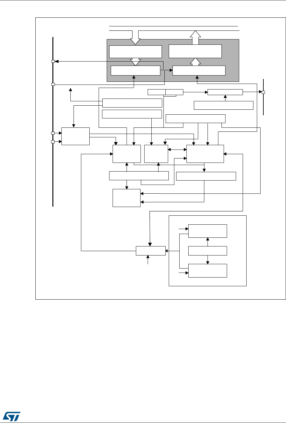
DocID025941 Rev 5 793/1001
RM0376 Low-power universal asynchronous receiver transmitter (LPUART)
831
Figure 251. LPUART block diagram
MSv31884V5
BRR[19:0]
TE
Write Read DR (data register)
(CPU or DMA) (CPU or DMA)
PWDATA PRDATA
Transmit shift register
LPUARTx_CR3 register
LPUARTx_CR2 register
RTS/
DE
CTS
Hardware
flow
controller
Transmit
control
LPUARTx_CR1 register
Wakeup
unit
LPUARTx_CR1 register
LPUART_GTPR register
GT PSC CK control
LPUARTx_CR2 register
Receiver
control
Receiver
clock
LPUARTx_ISR register
LPUART
interrupt
control
LPUARTx_BRR register
Transmitter
rate controller
Receiver rate
controller
/LPUARTDIV
fCK ( fLSE , fHSI,
fPCLK or fSYS)
Transmitter
clock
Conventional baud rate generator
CK
LPUARTDIV = BBR[19:0]
Transmit data register
(TDR)
Receive data register
(RDR)
Receive shift register
RE
TX
RX

Low-power universal asynchronous receiver transmitter (LPUART) RM0376
794/1001 DocID025941 Rev 5
29.4.1 LPUART character description
Word length may be selected as being either 7 or 8 or 9 bits by programming the M[1:0] bits
in the LPUART_CR1 register (see Figure 252).
•7-bit character length: M[1:0] = 10
•8-bit character length: M[1:0] = 00
•9-bit character length: M[1:0] = 01
By default, the signal (TX or RX) is in low state during the start bit. It is in high state during
the stop bit.
These values can be inverted, separately for each signal, through polarity configuration
control.
An Idle character is interpreted as an entire frame of “1”s. (The number of “1”s includes the
number of stop bits).
A Break character is interpreted on receiving “0”s for a frame period. At the end of the
break frame, the transmitter inserts 2 stop bits.
Transmission and reception are driven by a common baud rate generator, the clock for each
is generated when the enable bit is set respectively for the transmitter and receiver.
The details of each block is given below.
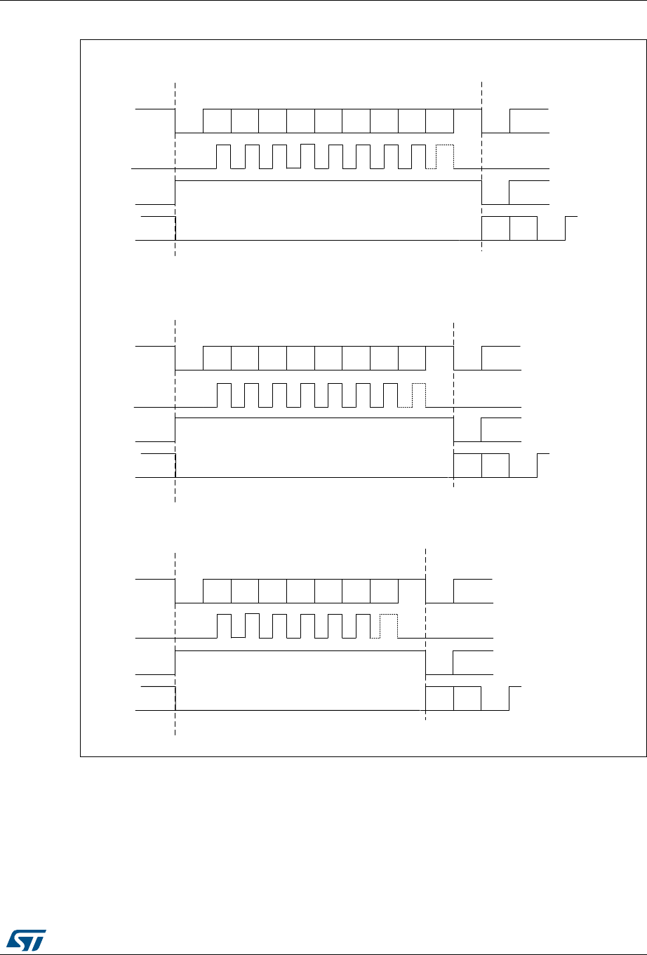
DocID025941 Rev 5 795/1001
RM0376 Low-power universal asynchronous receiver transmitter (LPUART)
831
Figure 252. Word length programming
MS33194V2
Bit0 Bit1 Bit2 Bit3 Bit4 Bit5 Bit6 Bit7 Bit8
Start
bit
Stop
bit
Next
Start
bit
Idle frame
9-bit word length (M = 01 ), 1 Stop bit
Possible
Parity
bit
Break frame
Data frame
Clock **
Start
bit
Stop
bit
Start
bit
Stop
bit
Bit0 Bit1 Bit2 Bit3 Bit4 Bit5 Bit6 Bit7
Start
bit
Stop
bit
Next
Start
bit
Idle frame
8-bit word length (M = 00 ), 1 Stop bit
Possible
Parity
bit
Break frame
Data frame
Clock **
Start
bit
Stop
bit
Start
bit
Stop
bit
Bit0 Bit1 Bit2 Bit3 Bit4 Bit5 Bit6
Start
bit
Stop
bit
Next
Start
bit
Idle frame
7-bit word length (M = 10 ), 1 Stop bit
Possible
Parity
bit
Break frame
Data frame
Clock
** LBCL bit controls last data clock pulse
**
Start
bit
Stop
bit
Start
bit
Stop
bit
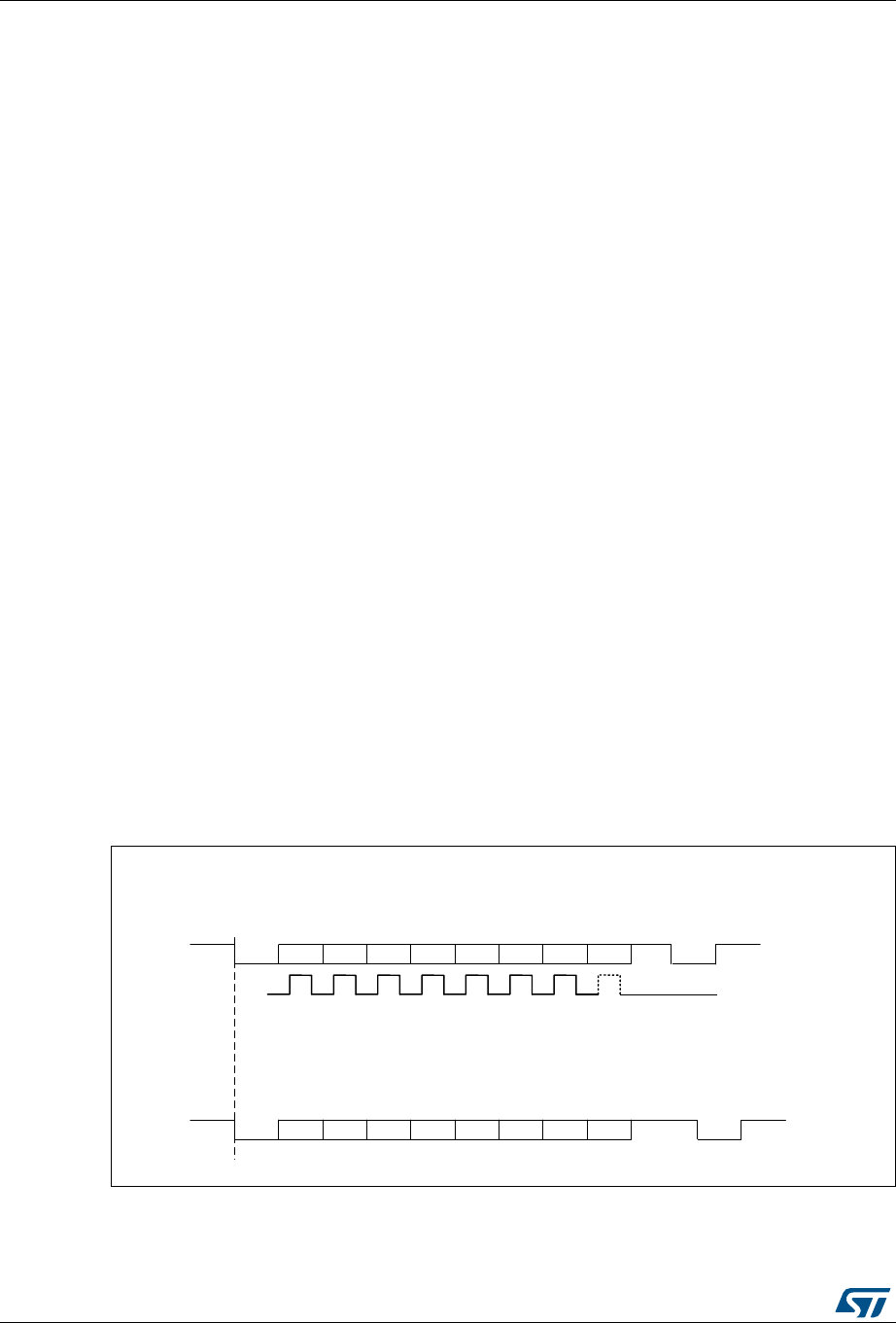
Low-power universal asynchronous receiver transmitter (LPUART) RM0376
796/1001 DocID025941 Rev 5
29.4.2 LPUART transmitter
The transmitter can send data words of either 7 or 8 or 9 bits depending on the M bits status.
The Transmit Enable bit (TE) must be set in order to activate the transmitter function. The
data in the transmit shift register is output on the TX pin.
Character transmission
During an LPUART transmission, data shifts out least significant bit first (default
configuration) on the TX pin. In this mode, the LPUART_TDR register consists of a buffer
(TDR) between the internal bus and the transmit shift register (see Figure 226).
Every character is preceded by a start bit which is a logic level low for one bit period. The
character is terminated by a configurable number of stop bits.
The following stop bits are supported by LPUART: 1 and 2 stop bits.
Note: The TE bit must be set before writing the data to be transmitted to the LPUART_TDR.
The TE bit should not be reset during transmission of data. Resetting the TE bit during the
transmission will corrupt the data on the TX pin as the baud rate counters will get frozen.
The current data being transmitted will be lost.
An idle frame will be sent after the TE bit is enabled.
Configurable stop bits
The number of stop bits to be transmitted with every character can be programmed in
Control register 2, bits 13,12.
•1 stop bit: This is the default value of number of stop bits.
•2 stop bits: This will be supported by normal LPUART, Single-wire and Modem
modes.
An idle frame transmission will include the stop bits.
A break transmission will be 10 low bits (when M[1:0] = 00) or 11 low bits (when M[1:0] = 01)
or 9 low bits (when M[1:0] = 10) followed by 2 stop bits. It is not possible to transmit long
breaks (break of length greater than 9/10/11 low bits).
Figure 253. Configurable stop bits
MS31885V1
8-bit Word length (M[1:0]=00 bit is reset)
** LBCL bit controls last data clock pulse
Bit7Start bit Stop
bit
Next
start
bit
Possible
parity bit
Data frame Next data frame
CLOCK **
a) 1 Stop bit
b) 2 Stop bits
Bit6Bit5Bit4Bit3Bit2Bit1Bit0
Next data frame
Bit7Start bit 2
Stop
bits
Next
start
bit
Possible
parity bit
Data frame
Bit6Bit5Bit4Bit3Bit2Bit1Bit0

DocID025941 Rev 5 797/1001
RM0376 Low-power universal asynchronous receiver transmitter (LPUART)
831
Character transmission procedure
1. Program the M bits in LPUART_CR1 to define the word length.
2. Select the desired baud rate using the LPUART_BRR register.
3. Program the number of stop bits in LPUART_CR2.
4. Enable the LPUART by writing the UE bit in LPUART_CR1 register to 1.
5. Select DMA enable (DMAT) in LPUART_CR3 if multibuffer Communication is to take
place. Configure the DMA register as explained in multibuffer communication.
6. Set the TE bit in LPUART_CR1 to send an idle frame as first transmission.
7. Write the data to send in the LPUART_TDR register (this clears the TXE bit). Repeat
this for each data to be transmitted in case of single buffer.
8. After writing the last data into the LPUART_TDR register, wait until TC=1. This
indicates that the transmission of the last frame is complete. This is required for
instance when the LPUART is disabled or enters the Halt mode to avoid corrupting the
last transmission.
Single byte communication
Clearing the TXE bit is always performed by a write to the transmit data register.
The TXE bit is set by hardware and it indicates:
•The data has been moved from the LPUART_TDR register to the shift register and the
data transmission has started.
•The LPUART_TDR register is empty.
•The next data can be written in the LPUART_TDR register without overwriting the
previous data.
This flag generates an interrupt if the TXEIE bit is set.
When a transmission is taking place, a write instruction to the LPUART_TDR register stores
the data in the TDR register; next, the data is copied in the shift register at the end of the
currently ongoing transmission.
When no transmission is taking place, a write instruction to the LPUART_TDR register
places the data in the shift register, the data transmission starts, and the TXE bit is set.
If a frame is transmitted (after the stop bit) and the TXE bit is set, the TC bit goes high. An
interrupt is generated if the TCIE bit is set in the LPUART_CR1 register.
After writing the last data in the LPUART_TDR register, it is mandatory to wait for TC=1
before disabling the LPUART or causing the microcontroller to enter the low-power mode
(see Figure 229: TC/TXE behavior when transmitting).
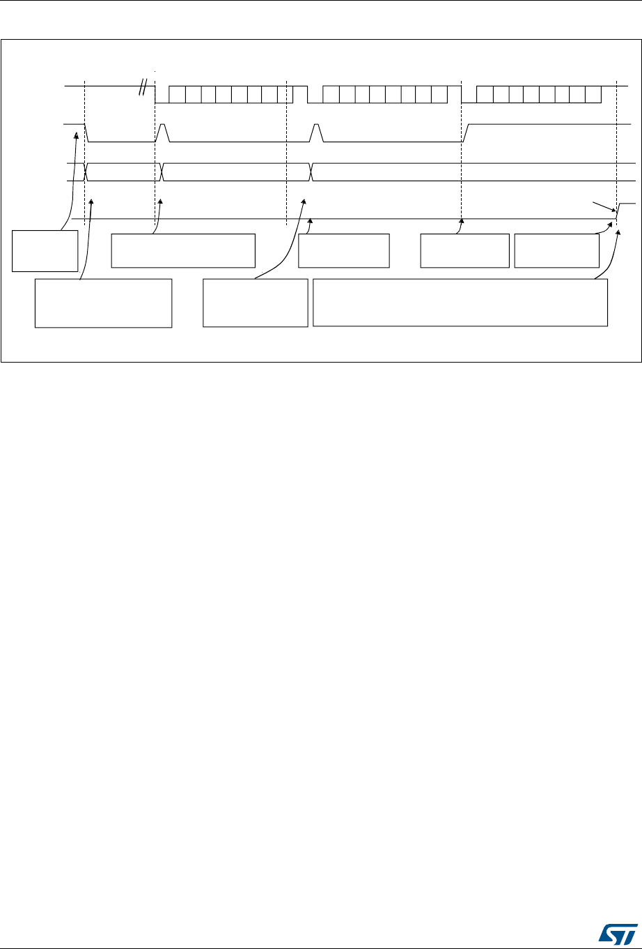
Low-power universal asynchronous receiver transmitter (LPUART) RM0376
798/1001 DocID025941 Rev 5
Figure 254. TC/TXE behavior when transmitting
Break characters
Setting the SBKRQ bit transmits a break character. The break frame length depends on the
M bits (see Figure 252).
If a ‘1’ is written to the SBKRQ bit, a break character is sent on the TX line after completing
the current character transmission. The SBKF bit is set by the write operation and it is reset
by hardware when the break character is completed (during the stop bits after the break
character). The LPUART inserts a logic 1 signal (STOP) for the duration of 2 bits at the end
of the break frame to guarantee the recognition of the start bit of the next frame.
In the case the application needs to send the break character following all previously
inserted data, including the ones not yet transmitted, the software should wait for the TXE
flag assertion before setting the SBKRQ bit.
Idle characters
Setting the TE bit drives the LPUART to send an idle frame before the first data frame.
29.4.3 LPUART receiver
The LPUART can receive data words of either 7 or 8 or 9 bits depending on the M bits in the
LPUART_CR1 register.
Start bit detection
In LPUART, for START bit detection, a falling edge should be detected first on the Rx line,
then a sample is taken in the middle of the start bit to confirm that it is still ‘0’. If the start
sample is at ‘1’, then the noise error flag (NF) is set, then the START bit is discarded and the
receiver waits for a new START bit. Else, the receiver continues to sample all incoming bits
normally.
TX line
LPUART_DR
Frame 1
TXE flag
F2
TC flag
F3
Frame 2
Software waits until TXE=1
and writes F2 into DR
Software waits until
TXE=1 and writes
F3 into DR
TC is not set
because TXE=0
Software waits until TC=1
Frame 3
TC is set
because TXE=1
Set by hardware
cleared by software
Set by hardware
cleared by software Set by hardware
Set by hardware
Idle preamble
F1
Software
enables the
LPUART
TC is not set
because TXE=0
Software waits until TXE=1
and writes F1 into DR
MSv31889V1

DocID025941 Rev 5 799/1001
RM0376 Low-power universal asynchronous receiver transmitter (LPUART)
831
Character reception
During an LPUART reception, data shifts in least significant bit first (default configuration)
through the RX pin. In this mode, the LPUART_RDR register consists of a buffer (RDR)
between the internal bus and the received shift register.
Character reception procedure
1. Program the M bits in LPUART_CR1 to define the word length.
2. Select the desired baud rate using the baud rate register LPUART_BRR
3. Program the number of stop bits in LPUART_CR2.
4. Enable the LPUART by writing the UE bit in LPUART_CR1 register to 1.
5. Select DMA enable (DMAR) in LPUART_CR3 if multibuffer communication is to take
place. Configure the DMA register as explained in multibuffer communication.
6. Set the RE bit LPUART_CR1. This enables the receiver which begins searching for a
start bit.
When a character is received
•The RXNE bit is set. It indicates that the content of the shift register is transferred to the
RDR. In other words, data has been received and can be read (as well as its
associated error flags).
•An interrupt is generated if the RXNEIE bit is set.
•The error flags can be set if a frame error, noise or an overrun error has been detected
during reception. PE flag can also be set with RXNE.
•In multibuffer, RXNE is set after every byte received and is cleared by the DMA read of
the Receive data Register.
•In single buffer mode, clearing the RXNE bit is performed by a software read to the
LPUART_RDR register. The RXNE flag can also be cleared by writing 1 to the RXFRQ
in the LPUART_RQR register. The RXNE bit must be cleared before the end of the
reception of the next character to avoid an overrun error.
Break character
When a break character is received, the LPUART handles it as a framing error.
Idle character
When an idle frame is detected, there is the same procedure as for a received data
character plus an interrupt if the IDLEIE bit is set.

Low-power universal asynchronous receiver transmitter (LPUART) RM0376
800/1001 DocID025941 Rev 5
Overrun error
An overrun error occurs when a character is received when RXNE has not been reset. Data
can not be transferred from the shift register to the RDR register until the RXNE bit is
cleared.
The RXNE flag is set after every byte received. An overrun error occurs if RXNE flag is set
when the next data is received or the previous DMA request has not been serviced. When
an overrun error occurs:
•The ORE bit is set.
•The RDR content will not be lost. The previous data is available when a read to
LPUART_RDR is performed.
•The shift register will be overwritten. After that point, any data received during overrun
is lost.
•An interrupt is generated if either the RXNEIE bit is set or EIE bit is set.
•The ORE bit is reset by setting the ORECF bit in the ICR register.
Note: The ORE bit, when set, indicates that at least 1 data has been lost. There are two
possibilities:
- if RXNE=1, then the last valid data is stored in the receive register RDR and can be read,
- if RXNE=0, then it means that the last valid data has already been read and thus there is
nothing to be read in the RDR. This case can occur when the last valid data is read in the
RDR at the same time as the new (and lost) data is received.
Selecting the clock source
The choice of the clock source is done through the Reset and Clock Control system (RCC).
The clock source must be chosen before enabling the LPUART (by setting the UE bit).
The choice of the clock source must be done according to two criteria:
•Possible use of the LPUART in low-power mode
•Communication speed.
The clock source frequency is fCK.
When the dual clock domain and the wakeup from Stop mode features are supported, the
clock source can be one of the following sources: fPCLK (default), fLSE, fHSI or fSYS.
Otherwise, the LPUART clock source is fPCLK .
Choosing fLSE, fHSI as clock source may allow the LPUART to receive data while the MCU is
in low-power mode. Depending on the received data and wakeup mode selection, the
LPUART wakes up the MCU, when needed, in order to transfer the received data by
software reading the LPUART_RDR register or by DMA.
For the other clock sources, the system must be active in order to allow LPUART
communication.
The communication speed range (specially the maximum communication speed) is also
determined by the clock source.
The receiver samples each incoming baud as close as possible to the middle of the baud-
period. Only a single sample is taken of each of the incoming bauds.
Note: There is no noise detection for data.

DocID025941 Rev 5 801/1001
RM0376 Low-power universal asynchronous receiver transmitter (LPUART)
831
Framing error
A framing error is detected when the stop bit is not recognized on reception at the expected
time, following either a de-synchronization or excessive noise.
When the framing error is detected:
•The FE bit is set by hardware.
•The invalid data is transferred from the Shift register to the LPUART_RDR register.
•No interrupt is generated in case of single byte communication. However this bit rises
at the same time as the RXNE bit which itself generates an interrupt. In case of
multibuffer communication an interrupt will be issued if the EIE bit is set in the
LPUART_CR3 register.
The FE bit is reset by writing 1 to the FECF in the LPUART_ICR register.
Configurable stop bits during reception
The number of stop bits to be received can be configured through the control bits of Control
Register 2 - it can be either 1 or 2 in normal mode.
•1 stop bit: Sampling for 1 stop Bit is done on the 8th, 9th and 10th samples.
•2 stop bits: Sampling for the 2 stop bits is done in the middle of the second stop bit.
The RXNE and FE flags are set just after this sample i.e. during the second stop bit.
The first stop bit is not checked for framing error.
29.4.4 LPUART baud rate generation
The baud rate for the receiver and transmitter (Rx and Tx) are both set to the same value as
programmed in the LPUART_BRR register.
The baud rate for the receiver and transmitter (Rx and Tx) are both set to the same value as
programmed in the LPUART_BRR register.
LPUARTDIV is coded on the LPUART_BRR register.
Note: The baud counters are updated to the new value in the baud registers after a write operation
to LPUART_BRR. Hence the baud rate register value should not be changed during
communication.
It is forbidden to write values less than 0x300 in the LPUART_BRR register.
fck must be in the range [3 x baud rate, 4096 x baud rate].
The maximum baud rate that can be reached when the LPUART clock source is the LSE, is
9600 baud. Higher baud rates can be reached when the LPUART is clocked by clock
sources different than the LSE clock. For example, if the USART clock source is the system
clock (maximum is 32 MHz), the maximum baud rate that can be reached is 10 Mbaud.
Tx/Rx baud 256 f×CK
LPUARTDIV
------------------------------------
=
Low-power universal asynchronous receiver transmitter (LPUART) RM0376
802/1001 DocID025941 Rev 5
Table 135. Error calculation for programmed baud rates at fck = 32,768 KHz
Baud rate fCK = 32,768 KHz
S.No Desired Actual Value programmed in the baud
rate register
% Error = (Calculated - Desired)
B.rate / Desired B.rate
1 300 Bps 300 Bps 0x6D3A 0
2 600 Bps 600 Bps 0x369D 0
3 1200 Bps 1200.087 Bps 0x1B4E 0.007
4 2400 Bps 2400.17 Bps 0xDA7 0.007
5 4800 Bps 4801.72 Bps 0x6D3 0.035
6 9600 Bps 9608.94 Bps 0x369 0.093
Table 136. Error calculation for programmed baud rates at fck = 32 MHz
Baud rate fCK = 32,768 KHz
Desired Actual Value programmed in the baud
rate register
% Error = (Calculated - Desired)
B.rate / Desired B.rate
9600 Bps 9608.94 Bps 9600,004 D0555
19200 19200,030 682AA 0,0001
38400 38400,06 34155 0,0001
57600 57600,09 22B8E 0,0001
115200 115200,18 115C7 0,0001
230400 230403,60 8AE3 0,0015
460800 460820,16 4571 0,004
921600 921692,17 22B8 0,01
4000000 4000000,00 800 0
10000000 10002442,00 333 0,024

DocID025941 Rev 5 803/1001
RM0376 Low-power universal asynchronous receiver transmitter (LPUART)
831
29.4.5 Tolerance of the LPUART receiver to clock deviation
The asynchronous receiver of the LPUART works correctly only if the total clock system
deviation is less than the tolerance of the LPUART receiver. The causes which contribute to
the total deviation are:
•DTRA: Deviation due to the transmitter error (which also includes the deviation of the
transmitter’s local oscillator)
•DQUANT: Error due to the baud rate quantization of the receiver
•DREC: Deviation of the receiver’s local oscillator
•DTCL: Deviation due to the transmission line (generally due to the transceivers which
can introduce an asymmetry between the low-to-high transition timing and the high-to-
low transition timing)
where
DWU is the error due to sampling point deviation when the wakeup from Stop mode is
used.
when M[1:0] = 01:
when M[1:0] = 00:
when M[1:0] = 10:
tWULPUART is the time between detection of start bit falling edge and the instant when
clock (requested by the peripheral) is ready and reaching the peripheral and regulator
is ready. tWULPUART corresponds to tWUSTOP value provided in the datasheet.
The LPUART receiver can receive data correctly at up to the maximum tolerated deviation
specified in Table 137:
•7, 8 or 9-bit character length defined by the M bits in the LPUARTx_CR1 register
•1 or 2 stop bits
DTRA DQUANT DREC DTCL DWU++++LPUART receiver tolerance<
DWU tWULPUART
11 Tbit×
------------------------------
=
DWU tWULPUART
10 Tbit×
------------------------------
=
DWU tWULPUART
9Tbit×
------------------------------
=
Table 137. Tolerance of the LPUART receiver
M bits 768 ≤ BRR <1024 1024 ≤ BRR < 2048 2048 ≤ BRR < 4096 4096 ≤ BRR
8 bits (M=00), 1 stop bit 1.82% 2.56% 3.90% 4.42%
9 bits (M=01), 1 stop bit 1.69% 2.33% 2.53% 4.14%
7 bits (M=10), 1 stop bit 2.08% 2.86% 4.35% 4.42%
8 bits (M=00), 2 stop bit 2.08% 2.86% 4.35% 4.42%
9 bits (M=01), 2 stop bit 1.82% 2.56% 3.90% 4.42%
7 bits (M=10), 2stop bit 2.34% 3.23% 4.92% 4.42%

Low-power universal asynchronous receiver transmitter (LPUART) RM0376
804/1001 DocID025941 Rev 5
Note: The data specified in Table 137 may slightly differ in the special case when the received
frames contain some Idle frames of exactly 10-bit durations when M bits = 00 (11-bit
durations when M bits =01 or 9- bit durations when M bits = 10).
29.4.6 Multiprocessor communication using LPUART
It is possible to perform multiprocessor communication with the LPUART (with several
LPUARTs connected in a network). For instance one of the LPUARTs can be the master, its
TX output connected to the RX inputs of the other LPUARTs. The others are slaves, their
respective TX outputs are logically ANDed together and connected to the RX input of the
master.
In multiprocessor configurations it is often desirable that only the intended message
recipient should actively receive the full message contents, thus reducing redundant
LPUART service overhead for all non addressed receivers.
The non addressed devices may be placed in mute mode by means of the muting function.
In order to use the mute mode feature, the MME bit must be set in the LPUART_CR1
register.
In mute mode:
•None of the reception status bits can be set.
•All the receive interrupts are inhibited.
•The RWU bit in LPUART_ISR register is set to 1. RWU can be controlled automatically
by hardware or by software, through the MMRQ bit in the LPUART_RQR register,
under certain conditions.
The LPUART can enter or exit from mute mode using one of two methods, depending on
the WAKE bit in the LPUART_CR1 register:
•Idle Line detection if the WAKE bit is reset,
•Address Mark detection if the WAKE bit is set.
Idle line detection (WAKE=0)
The LPUART enters mute mode when the MMRQ bit is written to 1 and the RWU is
automatically set.
It wakes up when an Idle frame is detected. Then the RWU bit is cleared by hardware but
the IDLE bit is not set in the LPUART_ISR register. An example of mute mode behavior
using Idle line detection is given in Figure 233.

DocID025941 Rev 5 805/1001
RM0376 Low-power universal asynchronous receiver transmitter (LPUART)
831
Figure 255. Mute mode using Idle line detection
Note: If the MMRQ is set while the IDLE character has already elapsed, mute mode will not be
entered (RWU is not set).
If the LPUART is activated while the line is IDLE, the idle state is detected after the duration
of one IDLE frame (not only after the reception of one character frame).
4-bit/7-bit address mark detection (WAKE=1)
In this mode, bytes are recognized as addresses if their MSB is a ‘1’ otherwise they are
considered as data. In an address byte, the address of the targeted receiver is put in the 4
or 7 LSBs. The choice of 7 or 4 bit address detection is done using the ADDM7 bit. This 4-
bit/7-bit word is compared by the receiver with its own address which is programmed in the
ADD bits in the LPUART_CR2 register.
Note: In 7-bit and 9-bit data modes, address detection is done on 6-bit and 8-bit addresses
(ADD[5:0] and ADD[7:0]) respectively.
The LPUART enters mute mode when an address character is received which does not
match its programmed address. In this case, the RWU bit is set by hardware. The RXNE
flag is not set for this address byte and no interrupt or DMA request is issued when the
LPUART enters mute mode.
The LPUART also enters mute mode when the MMRQ bit is written to 1. The RWU bit is
also automatically set in this case.
The LPUART exits from mute mode when an address character is received which matches
the programmed address. Then the RWU bit is cleared and subsequent bytes are received
normally. The RXNE bit is set for the address character since the RWU bit has been
cleared.
An example of mute mode behavior using address mark detection is given in Figure 234.
MSv31154V1
Data 1 Data 2 IDLEData 3 Data 4 Data 6
Idle frame detectedMMRQ written to 1
RWU
RX
Mute mode Normal mode
RXNE RXNE
Data 5
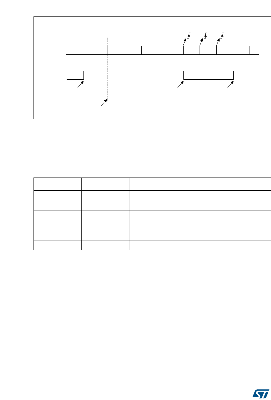
Low-power universal asynchronous receiver transmitter (LPUART) RM0376
806/1001 DocID025941 Rev 5
Figure 256. Mute mode using address mark detection
29.4.7 LPUART parity control
Parity control (generation of parity bit in transmission and parity checking in reception) can
be enabled by setting the PCE bit in the LPUART_CR1 register. Depending on the frame
length defined by the M bits, the possible LPUART frame formats are as listed in Table 131.
Even parity
The parity bit is calculated to obtain an even number of “1s” inside the frame which is made
of the 6, 7 or 8 LSB bits (depending on M bits values) and the parity bit.
As an example, if data=00110101, and 4 bits are set, then the parity bit will be 0 if even
parity is selected (PS bit in LPUART_CR1 = 0).
Odd parity
The parity bit is calculated to obtain an odd number of “1s” inside the frame made of the 6, 7
or 8 LSB bits (depending on M bits values) and the parity bit.
As an example, if data=00110101 and 4 bits set, then the parity bit will be 1 if odd parity is
selected (PS bit in LPUART_CR1 = 1).
MSv31888V2
IDLE Addr=0 Data 1 Data 2 IDLE Addr=1 Data 3 Data 4 Addr=2 Data 5
In this example, the current address of the receiver is 1
(programmed in the LPUART_CR2 register)
RXNE
Non-matching addressMatching address
Non-matching address
MMRQ written to 1
(RXNE was cleared)
RWU
RX
Mute mode Mute modeNormal mode
RXNE RXNE
Table 138. Frame formats
M bits PCE bit LPUART frame(1)
1. Legends: SB: start bit, STB: stop bit, PB: parity bit.
2. In the data register, the PB is always taking the MSB position (9th, 8th or 7th, depending on the M bits
value).
00 0 | SB | 8-bit data | STB |
00 1 | SB | 7-bit data | PB | STB |
01 0 | SB | 9-bit data | STB |
01 1 | SB | 8-bit data | PB | STB |
10 0 | SB | 7-bit data | STB |
10 1 | SB | 6-bit data | PB | STB |

DocID025941 Rev 5 807/1001
RM0376 Low-power universal asynchronous receiver transmitter (LPUART)
831
Parity checking in reception
If the parity check fails, the PE flag is set in the LPUART_ISR register and an interrupt is
generated if PEIE is set in the LPUART_CR1 register. The PE flag is cleared by software
writing 1 to the PECF in the LPUART_ICR register.
Parity generation in transmission
If the PCE bit is set in LPUARTx_CR1, then the MSB bit of the data written in the data
register is transmitted but is changed by the parity bit (even number of “1s” if even parity is
selected (PS=0) or an odd number of “1s” if odd parity is selected (PS=1)).
29.4.8 Single-wire Half-duplex communication using LPUART
Single-wire Half-duplex mode is selected by setting the HDSEL bit in the LPUART_CR3
register. In this mode, the following bits must be kept cleared:
•LINEN and CLKEN bits in the LPUART_CR2 register,
•SCEN and IREN bits in the LPUART_CR3 register.
The LPUART can be configured to follow a Single-wire Half-duplex protocol where the TX
and RX lines are internally connected. The selection between half- and Full-duplex
communication is made with a control bit HDSEL in LPUART_CR3.
As soon as HDSEL is written to 1:
•The TX and RX lines are internally connected
•The RX pin is no longer used
•The TX pin is always released when no data is transmitted. Thus, it acts as a standard
I/O in idle or in reception. It means that the I/O must be configured so that TX is
configured as alternate function open-drain with an external pull-up.
Apart from this, the communication protocol is similar to normal LPUART mode. Any
conflicts on the line must be managed by software (by the use of a centralized arbiter, for
instance). In particular, the transmission is never blocked by hardware and continues as
soon as data is written in the data register while the TE bit is set.
Note: In LPUART, in the case of 1-stop bit configuration, the RXNE flag is set in the middle of the
stop bit.
29.4.9 Continuous communication in DMA mode using LPUART
The LPUART is capable of performing continuous communication using the DMA. The DMA
requests for Rx buffer and Tx buffer are generated independently.
Note: Use the LPUART as explained in Section 29.4.3. To perform continuous communication,
you can clear the TXE/ RXNE flags In the LPUART_ISR register.

Low-power universal asynchronous receiver transmitter (LPUART) RM0376
808/1001 DocID025941 Rev 5
Transmission using DMA
DMA mode can be enabled for transmission by setting DMAT bit in the LPUART_CR3
register. Data is loaded from a SRAM area configured using the DMA peripheral (refer to
Section 11: Direct memory access controller (DMA) on page 260) to the LPUART_TDR
register whenever the TXE bit is set. To map a DMA channel for LPUART transmission, use
the following procedure (x denotes the channel number):
1. Write the LPUART_TDR register address in the DMA control register to configure it as
the destination of the transfer. The data is moved to this address from memory after
each TXE event.
2. Write the memory address in the DMA control register to configure it as the source of
the transfer. The data is loaded into the LPUART_TDR register from this memory area
after each TXE event.
3. Configure the total number of bytes to be transferred to the DMA control register.
4. Configure the channel priority in the DMA register
5. Configure DMA interrupt generation after half/ full transfer as required by the
application.
6. Clear the TC flag in the LPUART_ISR register by setting the TCCF bit in the
LPUART_ICR register.
7. Activate the channel in the DMA register.
When the number of data transfers programmed in the DMA Controller is reached, the DMA
controller generates an interrupt on the DMA channel interrupt vector.
In transmission mode, once the DMA has written all the data to be transmitted (the TCIF flag
is set in the DMA_ISR register), the TC flag can be monitored to make sure that the
LPUART communication is complete. This is required to avoid corrupting the last
transmission before disabling the LPUART or entering Stop mode. Software must wait until
TC=1. The TC flag remains cleared during all data transfers and it is set by hardware at the
end of transmission of the last frame.
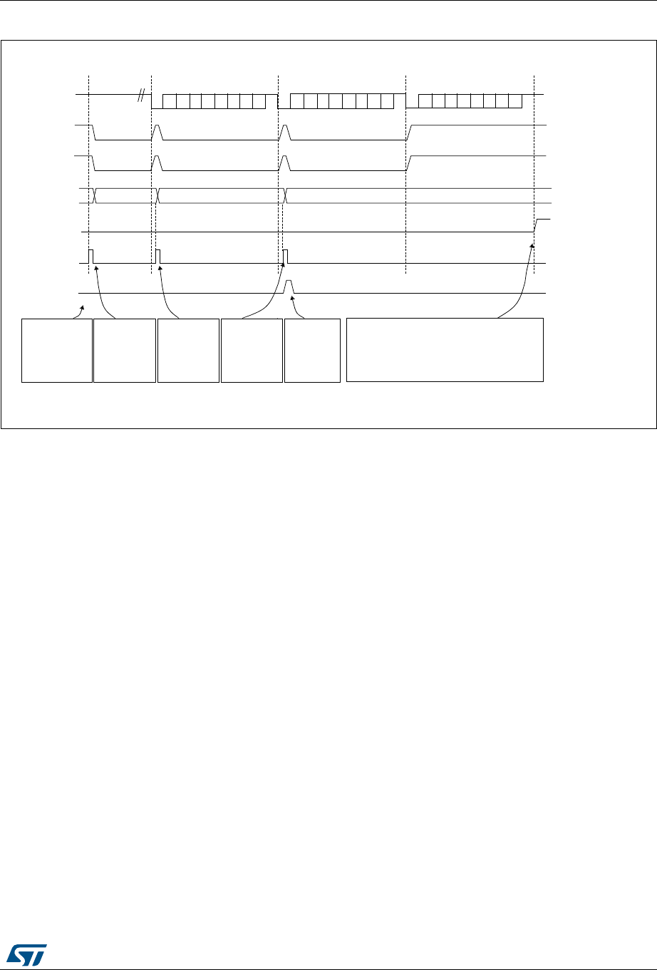
DocID025941 Rev 5 809/1001
RM0376 Low-power universal asynchronous receiver transmitter (LPUART)
831
Figure 257. Transmission using DMA
Reception using DMA
DMA mode can be enabled for reception by setting the DMAR bit in LPUART_CR3 register.
Data is loaded from the LPUART_RDR register to a SRAM area configured using the DMA
peripheral (refer Section 11: Direct memory access controller (DMA) on page 260)
whenever a data byte is received. To map a DMA channel for LPUART reception, use the
following procedure:
1. Write the LPUART_RDR register address in the DMA control register to configure it as
the source of the transfer. The data is moved from this address to the memory after
each RXNE event.
2. Write the memory address in the DMA control register to configure it as the destination
of the transfer. The data is loaded from LPUART_RDR to this memory area after each
RXNE event.
3. Configure the total number of bytes to be transferred to the DMA control register.
4. Configure the channel priority in the DMA control register
5. Configure interrupt generation after half/ full transfer as required by the application.
6. Activate the channel in the DMA control register.
When the number of data transfers programmed in the DMA Controller is reached, the DMA
controller generates an interrupt on the DMA channel interrupt vector.
F2 F3F1
MSv31890V2
Software
configures
DMA to send 3
data blocks
and enables
LPUART
The DMA
transfer is
complete
(TCIF=1 in
DMA_ISR)
DMA writes F2
into
LPUART_TDR
DMA writes F3
into
LPUART_TDR
Software waits until TC=1
Set by hardware
Cleared by software
Set by hardware
TX line
TXE flag
LPUART_TDR
DMA request
DMA writes
LPUART_TDR
DMA TCIF flag(transfer complete)
TC flag
Frame 1 Frame 2 Frame 3
Idle preamble
Set by hardware cleared
by DMA read
Set by hardware cleared by
DMA read Set by hardware
Ignored by the DMA because the transfer
is complete
a
DMA writes F1
into
LPUART_TDR
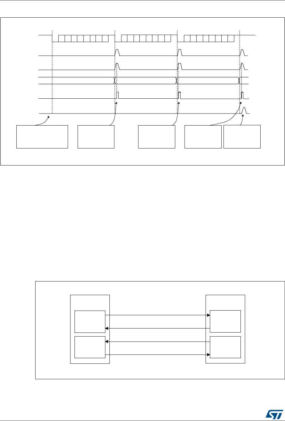
Low-power universal asynchronous receiver transmitter (LPUART) RM0376
810/1001 DocID025941 Rev 5
Figure 258. Reception using DMA
Error flagging and interrupt generation in multibuffer communication
In multibuffer communication if any error occurs during the transaction the error flag is
asserted after the current byte. An interrupt is generated if the interrupt enable flag is set.
For framing error, overrun error and noise flag which are asserted with RXNE in single byte
reception, there is a separate error flag interrupt enable bit (EIE bit in the LPUART_CR3
register), which, if set, enables an interrupt after the current byte if any of these errors occur.
29.4.10 RS232 Hardware flow control and RS485 Driver Enable
using LPUART
It is possible to control the serial data flow between 2 devices by using the CTS input and
the RTS output. The Figure 247 shows how to connect 2 devices in this mode:
Figure 259. Hardware flow control between 2 LPUARTs
RS232 RTS and CTS flow control can be enabled independently by writing the RTSE and
CTSE bits respectively to 1 (in the LPUART_CR3 register).
MSv31891V2
TX line
Frame 1
F2 F3
Set by hardwarecleared by
DMA read
F1
Frame 2 Frame 3
RXNE flag
LPUART_TDR
DMA request
DMA reads
LPUART_TDR
DMA TCIF flag
(transfer complete)
Software configures
theDMA to receive 3
datablocks and enables
the LPUART
DMA reads F3
from
LPUART_TDR
The DMA
transfer is
complete
(TCIF=1 in
DMA_ISR)
Set by hardware
Cleared by
software
DMA reads F2
From
LPUART_TDR
DMA reads
F1from
LPUART_TDR
MSv31892V2
TX circuit
LPUART 1
TX
RX circuit
RX circuit
LPUART 2
TX circuit
TX
CTS
CTS
RTS
RX
RTS
RX
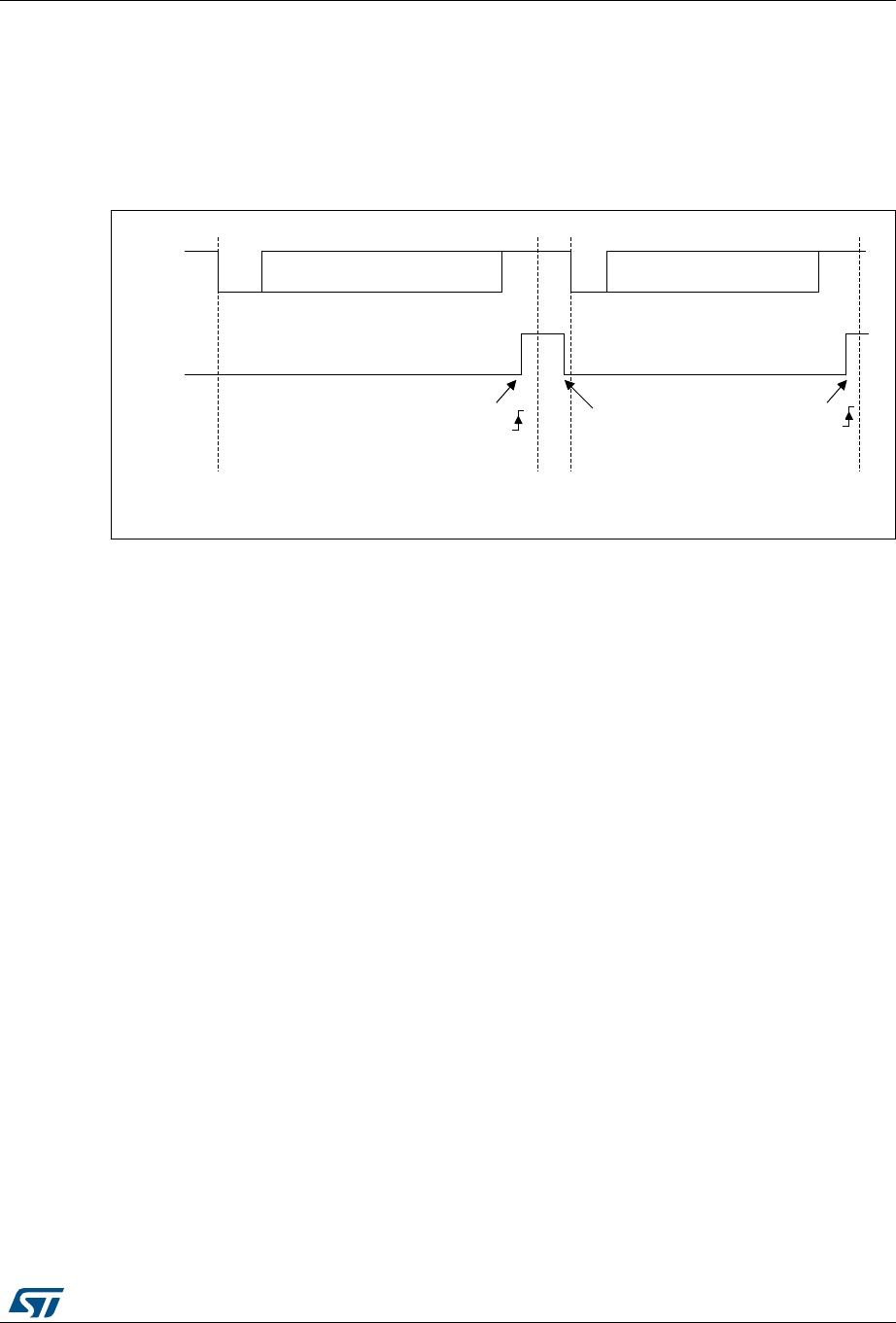
DocID025941 Rev 5 811/1001
RM0376 Low-power universal asynchronous receiver transmitter (LPUART)
831
RS232 RTS flow control
If the RTS flow control is enabled (RTSE=1), then RTS is asserted (tied low) as long as the
LPUART receiver is ready to receive a new data. when the receive register is full, RTS is de-
asserted, indicating that the transmission is expected to stop at the end of the current frame.
Figure 248 shows an example of communication with RTS flow control enabled.
Figure 260. RS232 RTS flow control
RS232 CTS flow control
If the CTS flow control is enabled (CTSE=1), then the transmitter checks the CTS input
before transmitting the next frame. If CTS is asserted (tied low), then the next data is
transmitted (assuming that data is to be transmitted, in other words, if TXE=0), else the
transmission does not occur. When CTS is de-asserted during a transmission, the current
transmission is completed before the transmitter stops.
When CTSE=1, the CTSIF status bit is automatically set by hardware as soon as the CTS
input toggles. It indicates when the receiver becomes ready or not ready for communication.
An interrupt is generated if the CTSIE bit in the LPUART_CR3 register is set. Figure 249
shows an example of communication with CTS flow control enabled.
MSv31168V2
Start
bit
Start
bit
Stop
bit Idle Stop
bit
RX
RTS
Data 1 read
Data 2 can now be transmitted
RXNE RXNE
Data 1 Data 2
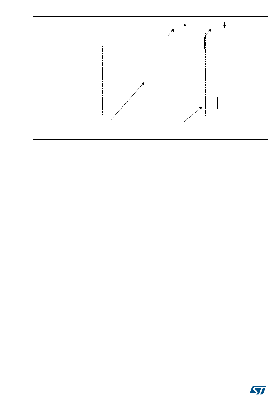
Low-power universal asynchronous receiver transmitter (LPUART) RM0376
812/1001 DocID025941 Rev 5
Figure 261. RS232 CTS flow control
Note: For correct behavior, CTS must be asserted at least 3 LPUART clock source periods before
the end of the current character. In addition it should be noted that the CTSCF flag may not
be set for pulses shorter than 2 x PCLK periods.
RS485 Driver Enable
The driver enable feature is enabled by setting bit DEM in the LPUART_CR3 control
register. This allows the user to activate the external transceiver control, through the DE
(Driver Enable) signal. The assertion time is the time between the activation of the DE signal
and the beginning of the START bit. It is programmed using the DEAT [4:0] bit fields in the
LPUART_CR1 control register. The de-assertion time is the time between the end of the last
stop bit, in a transmitted message, and the de-activation of the DE signal. It is programmed
using the DEDT [4:0] bit fields in the LPUART_CR1 control register. The polarity of the DE
signal can be configured using the DEP bit in the LPUART_CR3 control register.
In LPUART, the DEAT and DEDT are expressed in USART clock source (fCK) cycles:
•The Driver enable assertion time =
– (1 + (DEAT x P)) x fCK , if P <> 0
– (1 + DEAT) x fCK , if P = 0
•The Driver enable de-assertion time =
– (1 + (DEDT x P)) x fCK , if P <> 0
– (1 + DEDT) x fCK , if P = 0
With P = BRR[14:11]
MSv31167V2
Start
bit
Stop
bit
TX
TDR
CTS
Data 1
Data 2
Stop
bit Idle Start
bit
Data 2 Data 3
Data 3
empty empty
CTS
CTS
Transmit data register
Writing data 3 in TDR Transmission of Data 3 is
delayed until CTS = 0

DocID025941 Rev 5 813/1001
RM0376 Low-power universal asynchronous receiver transmitter (LPUART)
831
29.4.11 Wakeup from Stop mode using LPUART
The LPUART is able to wake up the MCU from Stop modewhen the UESM bit is set and the
LPUART clock is set to HSI or LSE (refer to the Reset and clock control (RCC) section.
•LPUART source clock is HSI
If during stop mode the HSI clock is switched OFF, when a falling edge on the LPUART
receive line is detected, the LPUART interface requests the HSI clock to be switched
ON. The HSI clock is then used for the frame reception.
– If the wakeup event is verified, the MCU wakes up from low-power mode and data
reception goes on normally.
– If the wakeup event is not verified, the HSI clock is switched OFF again, the MCU
is not waken up and stays in low-power mode and the clock request is released.
•LPUART source clock is LSE
Same principle as described in case of LPUART source clock is HSI with the difference
that the LSE is ON in stop mode, but the LSE clock is not propagated to LPUART if the
LPUART is not requesting it. The LSE clock is not OFF but there is a clock gating to
avoid useless consumption.
When the LPUART clock source is configured to be fLSE or fHSI, it is possible to keep
enabled this clock during STOP mode by setting the UCESM bit in LPUART_CR3 control
register.
Note: When LPUART is used to wakeup from stop with LSE is selected as LPUART clock source,
and desired baud rate is 9600 baud, the bit UCESM bit in LPUART_CR3 control register
must be set.
The MCU wakeup from Stop mode can be done using the standard RXNE interrupt. In this
case, the RXNEIE bit must be set before entering Stop mode.
Alternatively, a specific interrupt may be selected through the WUS bit fields.
In order to be able to wake up the MCU from Stop mode, the UESM bit in the LPUART_CR1
control register must be set prior to entering Stop mode.
When the wakeup event is detected, the WUF flag is set by hardware and a wakeup
interrupt is generated if the WUFIE bit is set.
For code example, refer to A.18.1: LPUART receiver configuration code example and
A.18.2: LPUART receive byte code example.
Note: Before entering Stop mode, the user must ensure that the LPUART is not performing a
transfer. BUSY flag cannot ensure that Stop mode is never entered during a running
reception.
The WUF flag is set when a wakeup event is detected, independently of whether the MCU is
in Stop or in an active mode.
When entering Stop mode just after having initialized and enabled the receiver, the REACK
bit must be checked to ensure the LPUART is actually enabled.
When DMA is used for reception, it must be disabled before entering Stop mode and re-
enabled upon exit from Stop mode.
The wakeup from Stop mode feature is not available for all modes. For example it doesn’t
work in SPI mode because the SPI operates in master mode only.

Low-power universal asynchronous receiver transmitter (LPUART) RM0376
814/1001 DocID025941 Rev 5
Using Mute mode with Stop mode
If the LPUART is put into Mute mode before entering Stop mode:
•Wakeup from Mute mode on idle detection must not be used, because idle detection
cannot work in Stop mode.
•If the wakeup from Mute mode on address match is used, then the source of wake-up
from Stop mode must also be the address match. If the RXNE flag is set when entering
the Stop mode, the interface will remain in mute mode upon address match and wake
up from Stop.
•If the LPUART is configured to wake up the MCU from Stop mode on START bit
detection, the WUF flag is set, but the RXNE flag is not set.
Determining the maximum LPUART baud rate allowing to wakeup correctly
from Stop mode when the LPUART clock source is the HSI clock
The maximum baud rate allowing to wakeup correctly from stop mode depends on:
•the parameter tWULPUART (wakeup time from Stop mode) provided in the device
datasheet
•the LPUART receiver tolerance provided in the Section 29.4.5: Tolerance of the
LPUART receiver to clock deviation.
Let us take this example: M bits = 01, 2 stop bits, BRR ≥ 4096.
In these conditions, according to Table 137: Tolerance of the LPUART receiver, the
LPUART receiver tolerance is 4.42 %.
DTRA + DQUANT + DREC + DTCL + DWU < LPUART receiver tolerance
DWU max = tWULPUART / (11 x Tbit Min)
Tbit Min = tWULPUART / (11 x DWU max)
If we consider an ideal case where the parameters DTRA, DQUANT, DREC and DTCL are
at 0%, the DWU max is 4.42 %. In reality, we need to consider at least the HSI inaccuracy.
Let us consider the HSI inaccuracy = 1 %, tWULPUART = 8.1 μs (in case of Stop mode with
main regulator in Run mode, Range 1 ):
DWU max = 4.42 % - 1 % = 3.42 %
Tbit min = 8.1 µs / (11 ₓ 3.42 %) = 2.5 μs.
In these conditions, the maximum baud rate allowing to wakeup correctly from Stop mode is
1/ 21.5 μs = 46 Kbaud.
DocID025941 Rev 5 815/1001
RM0376 Low-power universal asynchronous receiver transmitter (LPUART)
831
29.5 LPUART low-power mode
29.6 LPUART interrupts
The LPUART interrupt events are connected to the same interrupt vector (see Figure 250).
•During transmission: Transmission Complete, Clear to Send, Transmit data Register
empty or Framing error interrupt.
•During reception: Idle Line detection, Overrun error, Receive data register not empty,
Parity error, Noise Flag, Framing Error, Character match, etc.
These events generate an interrupt if the corresponding Enable Control Bit is set.
Table 139. Effect of low-power modes on the LPUART
Mode Description
Sleep No effect. USART interrupt causes the device to exit Sleep mode.
Low-power run No effect.
Low-power sleep No effect. USART interrupt causes the device to exit Low-power sleep
mode.
Stop
The LPUART is able to wake up the MCU from Stop mode when the
UESM bit is set and the LPUART clock is set to HSI16 or LSE.
The MCU wakeup from Stop mode can be done using either the standard
RXNE or the WUF interrupt.
Standby The LPUART is powered down and must be reinitialized when the device
has exited from Standby mode.
Table 140. LPUART interrupt requests
Interrupt event Event flag Enable
Control bit
Transmit data register empty TXE TXEIE
CTS interrupt CTSIF CTSIE
Transmission Complete TC TCIE
Receive data register not empty (data ready to be read) RXNE
RXNEIE
Overrun error detected ORE
Idle line detected IDLE IDLEIE
Parity error PE PEIE
Noise Flag, Overrun error and Framing Error in multibuffer
communication. NF or ORE or FE EIE
Character match CMF CMIE
Wakeup from Stop mode WUF(1)
1. The wUF interrupt is active only in Stop mode.
WUFIE


DocID025941 Rev 5 817/1001
RM0376 Low-power universal asynchronous receiver transmitter (LPUART)
831
29.7 LPUART registers
Refer to Section 1.1 on page 51 for a list of abbreviations used in register descriptions.
29.7.1 Control register 1 (LPUART_CR1)
Address offset: 0x00
Reset value: 0x0000
31 30 29 28 27 26 25 24 23 22 21 20 19 18 17 16
Res. Res. Res. M1 Res. Res. DEAT[4:0] DEDT[4:0]
rw rw rw rw rw rw rw rw rw rw rw
15141312111098765 43210
Res. CMIE MME M0 WAKE PCE PS PEIE TXEIE TCIE RXNEIE IDLEIE TE RE UESM UE
rw rw rw rw rw rw rw rw rw rw rw rw rw rw rw
Bits 31:29 Reserved, must be kept at reset value
Bit 28 M1: Word length
This bit, with bit 12 (M0) determines the word length. It is set or cleared by software.
M[1:0] = 00: 1 Start bit, 8 data bits, n stop bits
M[1:0] = 01: 1 Start bit, 9 data bits, n stop bits
M[1:0] = 10: 1 Start bit, 7 data bits, n stop bits
This bit can only be written when the LPUART is disabled (UE=0).
Bit 27 Reserved, must be kept at reset value
Bit 26 Reserved, must be kept at reset value
Bits 25:21 DEAT[4:0]: Driver Enable assertion time
This 5-bit value defines the time between the activation of the DE (Driver Enable) signal and
the beginning of the start bit. It is expressed in UCLK (USART clock) clock cycles. For more
details, refer to RS485 Driver Enable paragraph.
This bit field can only be written when the LPUART is disabled (UE=0).
Bits 20:16 DEDT[4:0]: Driver Enable de-assertion time
This 5-bit value defines the time between the end of the last stop bit, in a transmitted
message, and the de-activation of the DE (Driver Enable) signal. It is expressed in UCLK
(USART clock) clock cycles. For more details, refer to RS485 Driver Enable paragraph.
If the LPUART_TDR register is written during the DEDT time, the new data is transmitted
only when the DEDT and DEAT times have both elapsed.
This bit field can only be written when the LPUART is disabled (UE=0).
Bit 15 Reserved, must be kept at reset value
Bit 14 CMIE: Character match interrupt enable
This bit is set and cleared by software.
0: Interrupt is inhibited
1: A LPUART interrupt is generated when the CMF bit is set in the LPUART_ISR register.
Bit 13 MME: Mute mode enable
This bit activates the mute mode function of the LPUART. When set, the LPUART can switch
between the active and mute modes, as defined by the WAKE bit. It is set and cleared by
software.
0: Receiver in active mode permanently
1: Receiver can switch between mute mode and active mode.

Low-power universal asynchronous receiver transmitter (LPUART) RM0376
818/1001 DocID025941 Rev 5
Bit 12 M0: Word length
This bit, with bit 28 (M1) determines the word length. It is set or cleared by software. See Bit
28 (M1) description.
This bit can only be written when the LPUART is disabled (UE=0).
Bit 11 WAKE: Receiver wakeup method
This bit determines the LPUART wakeup method from Mute mode. It is set or cleared by
software.
0: Idle line
1: Address mark
This bit field can only be written when the LPUART is disabled (UE=0).
Bit 10 PCE: Parity control enable
This bit selects the hardware parity control (generation and detection). When the parity
control is enabled, the computed parity is inserted at the MSB position (9th bit if M=1; 8th bit
if M=0) and parity is checked on the received data. This bit is set and cleared by software.
Once it is set, PCE is active after the current byte (in reception and in transmission).
0: Parity control disabled
1: Parity control enabled
This bit field can only be written when the LPUART is disabled (UE=0).
Bit 9 PS: Parity selection
This bit selects the odd or even parity when the parity generation/detection is enabled (PCE
bit set). It is set and cleared by software. The parity will be selected after the current byte.
0: Even parity
1: Odd parity
This bit field can only be written when the LPUART is disabled (UE=0).
Bit 8 PEIE: PE interrupt enable
This bit is set and cleared by software.
0: Interrupt is inhibited
1: An LPUART interrupt is generated whenever PE=1 in the LPUART_ISR register
Bit 7 TXEIE: interrupt enable
This bit is set and cleared by software.
0: Interrupt is inhibited
1: An LPUART interrupt is generated whenever TXE=1 in the LPUART_ISR register
Bit 6 TCIE: Transmission complete interrupt enable
This bit is set and cleared by software.
0: Interrupt is inhibited
1: An LPUART interrupt is generated whenever TC=1 in the LPUART_ISR register
Bit 5 RXNEIE: RXNE interrupt enable
This bit is set and cleared by software.
0: Interrupt is inhibited
1: An LPUART interrupt is generated whenever ORE=1 or RXNE=1 in the LPUART_ISR
register
Bit 4 IDLEIE: IDLE interrupt enable
This bit is set and cleared by software.
0: Interrupt is inhibited
1: An LPUART interrupt is generated whenever IDLE=1 in the LPUART_ISR register

DocID025941 Rev 5 819/1001
RM0376 Low-power universal asynchronous receiver transmitter (LPUART)
831
29.7.2 Control register 2 (LPUART_CR2)
Address offset: 0x04
Reset value: 0x0000
Bit 3 TE: Transmitter enable
This bit enables the transmitter. It is set and cleared by software.
0: Transmitter is disabled
1: Transmitter is enabled
Note: During transmission, a “0” pulse on the TE bit (“0” followed by “1”) sends a preamble
(idle line) after the current word. In order to generate an idle character, the TE must not
be immediately written to 1. In order to ensure the required duration, the software can
poll the TEACK bit in the LPUART_ISR register.
When TE is set there is a 1 bit-time delay before the transmission starts.
Bit 2 RE: Receiver enable
This bit enables the receiver. It is set and cleared by software.
0: Receiver is disabled
1: Receiver is enabled and begins searching for a start bit
Bit 1 UESM: LPUART enable in Stop mode
When this bit is cleared, the LPUART is not able to wake up the MCU from Stop mode.
When this bit is set, the LPUART is able to wake up the MCU from Stop mode, provided that
the LPUART clock selection is HSI or LSE in the RCC.
This bit is set and cleared by software.
0: LPUART not able to wake up the MCU from Stop mode.
1: LPUART able to wake up the MCU from Stop mode. When this function is active, the
clock source for the LPUART must be HSI or LSE (see Section Reset and clock control
(RCC)).
Note: It is recommended to set the UESM bit just before entering Stop mode and clear it on
exit from Stop mode.
Bit 0 UE: LPUART enable
When this bit is cleared, the LPUART prescalers and outputs are stopped immediately, and
current operations are discarded. The configuration of the LPUART is kept, but all the status
flags, in the LPUART_ISR are reset. This bit is set and cleared by software.
0: LPUART prescaler and outputs disabled, low-power mode
1: LPUART enabled
Note: In order to go into low-power mode without generating errors on the line, the TE bit
must be reset before and the software must wait for the TC bit in the LPUART_ISR to
be set before resetting the UE bit.
The DMA requests are also reset when UE = 0 so the DMA channel must be disabled
before resetting the UE bit.
31 30 29 28 27 26 25 24 23 22 21 20 19 18 17 16
ADD[7:4] ADD[3:0] Res. Res. Res. Res. MSBFI
RST DATAINV TXINV RXINV
rw rw rw rw rw rw rw rw rw rw rw rw
1514131211109876543 2 10
SWAP Res. STOP[1:0] Res. Res. Res. Res. Res. Res. Res. ADDM7 Res. Res. Res. Res.
rw rw rw rw

Low-power universal asynchronous receiver transmitter (LPUART) RM0376
820/1001 DocID025941 Rev 5
Bits 31:28 ADD[7:4]: Address of the LPUART node
This bit-field gives the address of the LPUART node or a character code to be recognized.
This is used in multiprocessor communication during Mute mode or Stop mode, for wakeup with 7-
bit address mark detection. The MSB of the character sent by the transmitter should be equal to 1.
It may also be used for character detection during normal reception, Mute mode inactive (for
example, end of block detection in Modbus protocol). In this case, the whole received character (8-
bit) is compared to the ADD[7:0] value and CMF flag is set on match.
This bit field can only be written when reception is disabled (RE = 0) or the LPUART is disabled
(UE=0)
Bits 27:24 ADD[3:0]: Address of the LPUART node
This bit-field gives the address of the LPUART node or a character code to be recognized.
This is used in multiprocessor communication during Mute mode or Stop mode, for wakeup with
address mark detection.
This bit field can only be written when reception is disabled (RE = 0) or the LPUART is disabled
(UE=0)
Bits 23:20 Reserved, must be kept at reset value
Bit 19 MSBFIRST: Most significant bit first
This bit is set and cleared by software.
0: data is transmitted/received with data bit 0 first, following the start bit.
1: data is transmitted/received with the MSB (bit 7/8/9) first, following the start bit.
This bit field can only be written when the LPUART is disabled (UE=0).
Bit 18 DATAINV: Binary data inversion
This bit is set and cleared by software.
0: Logical data from the data register are send/received in positive/direct logic. (1=H, 0=L)
1: Logical data from the data register are send/received in negative/inverse logic. (1=L, 0=H). The
parity bit is also inverted.
This bit field can only be written when the LPUART is disabled (UE=0).
Bit 17 TXINV: TX pin active level inversion
This bit is set and cleared by software.
0: TX pin signal works using the standard logic levels (VDD =1/idle, Gnd=0/mark)
1: TX pin signal values are inverted. (VDD =0/mark, Gnd=1/idle).
This allows the use of an external inverter on the TX line.
This bit field can only be written when the LPUART is disabled (UE=0).
Bit 16 RXINV: RX pin active level inversion
This bit is set and cleared by software.
0: RX pin signal works using the standard logic levels (VDD =1/idle, Gnd=0/mark)
1: RX pin signal values are inverted. ((VDD =0/mark, Gnd=1/idle).
This allows the use of an external inverter on the RX line.
This bit field can only be written when the LPUART is disabled (UE=0).
Bit 15 SWAP: Swap TX/RX pins
This bit is set and cleared by software.
0: TX/RX pins are used as defined in standard pinout
1: The TX and RX pins functions are swapped. This allows to work in the case of a cross-wired
connection to another UART.
This bit field can only be written when the LPUART is disabled (UE=0).
Bit 14 Reserved, must be kept at reset value

DocID025941 Rev 5 821/1001
RM0376 Low-power universal asynchronous receiver transmitter (LPUART)
831
Bits 13:12 STOP[1:0]: STOP bits
These bits are used for programming the stop bits.
00: 1 stop bit
01: Reserved.
10: 2 stop bits
11: Reserved
This bit field can only be written when the LPUART is disabled (UE=0).
Bits 11:5 Reserved, must be kept at reset value
Bit 4 ADDM7:7-bit Address Detection/4-bit Address Detection
This bit is for selection between 4-bit address detection or 7-bit address detection.
0: 4-bit address detection
1: 7-bit address detection (in 8-bit data mode)
This bit can only be written when the LPUART is disabled (UE=0)
Note: In 7-bit and 9-bit data modes, the address detection is done on 6-bit and 8-bit address
(ADD[5:0] and ADD[7:0]) respectively.
Bits 3:0 Reserved, must be kept at reset value.

Low-power universal asynchronous receiver transmitter (LPUART) RM0376
822/1001 DocID025941 Rev 5
29.7.3 Control register 3 (LPUART_CR3)
Address offset: 0x08
Reset value: 0x0000
31 30 29 28 27 26 25 24 23 22 21 20 19 18 17 16
Res. Res. Res. Res. Res. Res. Res. Res. UCESM WUFIE WUS[2:0] Res. Res. Res. Res.
rw rw rw rw
15141312111098 7 6543210
DEP DEM DDRE OVR
DIS Res. CTSIE CTSE RTSE DMAT DMAR Res. Res. HD
SEL Res. Res. EIE
rw rw rw rw rw rw rw rw rw rw rw
Bits 31:24 Reserved, must be kept at reset value.
Bit 23 UCESM: LPUART Clock Enable in Stop mode.
This bit is set and cleared by software.
0: LPUART Clock is disabled in STOP mode.
1: LPUART Clock is enabled in STOP mode.
Note: In order to be able to wakeup the MCU from stop mode with LPUART at 9600 baud,
the UCESM bit must be set prior to entering the stop mode.
Bit 22 WUFIE: Wakeup from Stop mode interrupt enable
This bit is set and cleared by software.
0: Interrupt is inhibited
1: An LPUART interrupt is generated whenever WUF=1 in the LPUART_ISR register
Note: WUFIE must be set before entering in Stop mode.
The WUF interrupt is active only in Stop mode.
If the LPUART does not support the wakeup from Stop feature, this bit is reserved and
must be kept at reset value.
Bits 21:20 WUS[1:0]: Wakeup from Stop mode interrupt flag selection
This bit-field specify the event which activates the WUF (wakeup from Stop mode flag).
00: WUF active on address match (as defined by ADD[7:0] and ADDM7)
01:Reserved.
10: WUF active on Start bit detection
11: WUF active on RXNE.
This bit field can only be written when the LPUART is disabled (UE=0).
Note: If the LPUART does not support the wakeup from Stop feature, this bit is reserved and
must be kept at reset value.
Bits 19:16 Reserved, must be kept at reset value.
Bit 15 DEP: Driver enable polarity selection
0: DE signal is active high.
1: DE signal is active low.
This bit can only be written when the LPUART is disabled (UE=0).
Bit 14 DEM: Driver enable mode
This bit allows the user to activate the external transceiver control, through the DE signal.
0: DE function is disabled.
1: DE function is enabled. The DE signal is output on the RTS pin.
This bit can only be written when the LPUART is disabled (UE=0).

DocID025941 Rev 5 823/1001
RM0376 Low-power universal asynchronous receiver transmitter (LPUART)
831
Bit 13 DDRE: DMA Disable on Reception Error
0: DMA is not disabled in case of reception error. The corresponding error flag is set but
RXNE is kept 0 preventing from overrun. As a consequence, the DMA request is not
asserted, so the erroneous data is not transferred (no DMA request), but next correct
received data will be transferred.
1: DMA is disabled following a reception error. The corresponding error flag is set, as well
as RXNE. The DMA request is masked until the error flag is cleared. This means that the
software must first disable the DMA request (DMAR = 0) or clear RXNE before clearing the
error flag.
This bit can only be written when the LPUART is disabled (UE=0).
Note: The reception errors are: parity error, framing error or noise error.
Bit 12 OVRDIS: Overrun Disable
This bit is used to disable the receive overrun detection.
0: Overrun Error Flag, ORE, is set when received data is not read before receiving new
data.
1: Overrun functionality is disabled. If new data is received while the RXNE flag is still set
the ORE flag is not set and the new received data overwrites the previous content of the
LPUART_RDR register.
This bit can only be written when the LPUART is disabled (UE=0).
Note: This control bit allows checking the communication flow without reading the data.
Bit 11 Reserved, must be kept at reset value.
Bit 10 CTSIE: CTS interrupt enable
0: Interrupt is inhibited
1: An interrupt is generated whenever CTSIF=1 in the LPUART_ISR register
Bit 9 CTSE: CTS enable
0: CTS hardware flow control disabled
1: CTS mode enabled, data is only transmitted when the CTS input is asserted (tied to 0). If
the CTS input is de-asserted while data is being transmitted, then the transmission is
completed before stopping. If data is written into the data register while CTS is de-asserted,
the transmission is postponed until CTS is asserted.
This bit can only be written when the LPUART is disabled (UE=0)
Bit 8 RTSE: RTS enable
0: RTS hardware flow control disabled
1: RTS output enabled, data is only requested when there is space in the receive buffer. The
transmission of data is expected to cease after the current character has been transmitted.
The RTS output is asserted (pulled to 0) when data can be received.
This bit can only be written when the LPUART is disabled (UE=0).
Bit 7 DMAT: DMA enable transmitter
This bit is set/reset by software
1: DMA mode is enabled for transmission
0: DMA mode is disabled for transmission
Bit 6 DMAR: DMA enable receiver
This bit is set/reset by software
1: DMA mode is enabled for reception
0: DMA mode is disabled for reception
Bits 5:4 Reserved, must be kept at reset value.

Low-power universal asynchronous receiver transmitter (LPUART) RM0376
824/1001 DocID025941 Rev 5
29.7.4 Baud rate register (LPUART_BRR)
This register can only be written when the LPUART is disabled (UE=0).
Address offset: 0x0C
Reset value: 0x0000
Note: It is forbidden to write values less than 0x300 in the LPUART_BRR register.
Provided that LPUARTx_BRR must be > = 0x300 and LPUART_BRR is 20-bit, a care
should be taken when generating high baud rates using high fck values. fck must be in the
range [3 x baud rate,.4096 x baud rate].
29.7.5 Request register (LPUART_RQR)
Address offset: 0x18
Reset value: 0x0000
Bit 3 HDSEL: Half-duplex selection
Selection of Single-wire Half-duplex mode
0: Half duplex mode is not selected
1: Half duplex mode is selected
This bit can only be written when the LPUART is disabled (UE=0).
Bits 2:1 Reserved, must be kept at reset value.
Bit 0 EIE: Error interrupt enable
Error Interrupt Enable Bit is required to enable interrupt generation in case of a framing
error, overrun error or noise flag (FE=1 or ORE=1 or NF=1 in the LPUART_ISR register).
0: Interrupt is inhibited
1: An interrupt is generated when FE=1 or ORE=1 or NF=1 in the LPUART_ISR register.
31 30 29 28 27 26 25 24 23 22 21 20 19 18 17 16
Res. Res. Res. Res. Res. Res. Res. Res. Res. Res. Res. Res. BRR[19:16]
rw rw rw rw
1514131211109876543210
BRR[15:0]
rw rw rw rw rw rw rw rw rw rw rw rw rw rw rw rw
Bits 31:20 Reserved, must be kept at reset value.
Bits 19:0 BRR[19:0]
31 30 29 28 27 26 25 24 23 22 21 20 19 18 17 16
Res. Res. Res. Res. Res. Res. Res. Res. Res. Res. Res. Res. Res. Res. Res. Res.
151413121110987654321 0
Res. Res. Res. Res. Res. Res. Res. Res. Res. Res. Res. Res. RXFRQ MMRQ SBKRQ Res.
www

DocID025941 Rev 5 825/1001
RM0376 Low-power universal asynchronous receiver transmitter (LPUART)
831
29.7.6 Interrupt & status register (LPUART_ISR)
Address offset: 0x1C
Reset value: 0x00C0
Bits 31:4 Reserved, must be kept at reset value
Bit 3 RXFRQ: Receive data flush request
Writing 1 to this bit clears the RXNE flag.
This allows to discard the received data without reading it, and avoid an overrun condition.
Bit 2 MMRQ: Mute mode request
Writing 1 to this bit puts the LPUART in mute mode and resets the RWU flag.
Bit 1 SBKRQ: Send break request
Writing 1 to this bit sets the SBKF flag and request to send a BREAK on the line, as soon as
the transmit machine is available.
Note: In the case the application needs to send the break character following all previously
inserted data, including the ones not yet transmitted, the software should wait for the
TXE flag assertion before setting the SBKRQ bit.
Bit 0 Reserved, must be kept at reset value
31 30 29 28 27 26 25 24 23 22 21 20 19 18 17 16
Res. Res. Res. Res. Res. Res. Res. Res. Res. RE
ACK
TE
ACK WUF RWU SBKF CMF BUSY
rrrrrrr
1514131211109876543210
Res. Res. Res. Res. Res. CTS CTSIF Res. TXE TC RXNE IDLE ORE NF FE PE
rr rrrrrrrr
Bits 31:23 Reserved, must be kept at reset value.
Bit 22 REACK: Receive enable acknowledge flag
This bit is set/reset by hardware, when the Receive Enable value is taken into account by
the LPUART.
It can be used to verify that the LPUART is ready for reception before entering Stop mode.
Note: If the LPUART does not support the wakeup from Stop feature, this bit is reserved and
kept at reset value.
Bit 21 TEACK: Transmit enable acknowledge flag
This bit is set/reset by hardware, when the Transmit Enable value is taken into account by
the LPUART.
It can be used when an idle frame request is generated by writing TE=0, followed by TE=1
in the LPUART_CR1 register, in order to respect the TE=0 minimum period.
Bit 20 WUF: Wakeup from Stop mode flag
This bit is set by hardware, when a wakeup event is detected. The event is defined by the
WUS bit field. It is cleared by software, writing a 1 to the WUCF in the LPUART_ICR register.
An interrupt is generated if WUFIE=1 in the LPUART_CR3 register.
Note: When UESM is cleared, WUF flag is also cleared.
The WUF interrupt is active only in Stop mode.
If the LPUART does not support the wakeup from Stop feature, this bit is reserved and
kept at reset value.

Low-power universal asynchronous receiver transmitter (LPUART) RM0376
826/1001 DocID025941 Rev 5
Bit 19 RWU: Receiver wakeup from Mute mode
This bit indicates if the LPUART is in mute mode. It is cleared/set by hardware when a
wakeup/mute sequence is recognized. The mute mode control sequence (address or IDLE)
is selected by the WAKE bit in the LPUART_CR1 register.
When wakeup on IDLE mode is selected, this bit can only be set by software, writing 1 to the
MMRQ bit in the LPUART_RQR register.
0: Receiver in active mode
1: Receiver in mute mode
Bit 18 SBKF: Send break flag
This bit indicates that a send break character was requested. It is set by software, by writing
1 to the SBKRQ bit in the LPUART_CR3 register. It is automatically reset by hardware
during the stop bit of break transmission.
0: No break character is transmitted
1: Break character will be transmitted
Bit 17 CMF: Character match flag
This bit is set by hardware, when the character defined by ADD[7:0] is received. It is cleared
by software, writing 1 to the CMCF in the LPUART_ICR register.
An interrupt is generated if CMIE=1in the LPUART_CR1 register.
0: No Character match detected
1: Character Match detected
Bit 16 BUSY: Busy flag
This bit is set and reset by hardware. It is active when a communication is ongoing on the
RX line (successful start bit detected). It is reset at the end of the reception (successful or
not).
0: LPUART is idle (no reception)
1: Reception on going
Bits 15:11 Reserved, must be kept at reset value.
Bit 10 CTS: CTS flag
This bit is set/reset by hardware. It is an inverted copy of the status of the CTS input pin.
0: CTS line set
1: CTS line reset
Note: If the hardware flow control feature is not supported, this bit is reserved and kept at
reset value.
Bit 9 CTSIF: CTS interrupt flag
This bit is set by hardware when the CTS input toggles, if the CTSE bit is set. It is cleared by
software, by writing 1 to the CTSCF bit in the LPUART_ICR register.
An interrupt is generated if CTSIE=1 in the LPUART_CR3 register.
0: No change occurred on the CTS status line
1: A change occurred on the CTS status line
Note: If the hardware flow control feature is not supported, this bit is reserved and kept at
reset value.
Bit 8 Reserved, must be kept at reset value.

DocID025941 Rev 5 827/1001
RM0376 Low-power universal asynchronous receiver transmitter (LPUART)
831
Bit 7 TXE: Transmit data register empty
This bit is set by hardware when the content of the LPUART_TDR register has been
transferred into the shift register. It is cleared by a write to the LPUART_TDR register.
An interrupt is generated if the TXEIE bit =1 in the LPUART_CR1 register.
0: data is not transferred to the shift register
1: data is transferred to the shift register)
Note: This bit is used during single buffer transmission.
Bit 6 TC: Transmission complete
This bit is set by hardware if the transmission of a frame containing data is complete and if
TXE is set. An interrupt is generated if TCIE=1 in the LPUART_CR1 register. It is cleared by
software, writing 1 to the TCCF in the LPUART_ICR register or by a write to the
LPUART_TDR register.
An interrupt is generated if TCIE=1 in the LPUART_CR1 register.
0: Transmission is not complete
1: Transmission is complete
Note: If TE bit is reset and no transmission is on going, the TC bit will be set immediately.
Bit 5 RXNE: Read data register not empty
This bit is set by hardware when the content of the RDR shift register has been transferred
to the LPUART_RDR register. It is cleared by a read to the LPUART_RDR register. The
RXNE flag can also be cleared by writing 1 to the RXFRQ in the LPUART_RQR register.
An interrupt is generated if RXNEIE=1 in the LPUART_CR1 register.
0: data is not received
1: Received data is ready to be read.
Bit 4 IDLE: Idle line detected
This bit is set by hardware when an Idle Line is detected. An interrupt is generated if
IDLEIE=1 in the LPUART_CR1 register. It is cleared by software, writing 1 to the IDLECF in
the LPUART_ICR register.
0: No Idle line is detected
1: Idle line is detected
Note: The IDLE bit will not be set again until the RXNE bit has been set (i.e. a new idle line
occurs).
If mute mode is enabled (MME=1), IDLE is set if the LPUART is not mute (RWU=0),
whatever the mute mode selected by the WAKE bit. If RWU=1, IDLE is not set.
Bit 3 ORE: Overrun error
This bit is set by hardware when the data currently being received in the shift register is
ready to be transferred into the RDR register while RXNE=1. It is cleared by a software,
writing 1 to the ORECF, in the LPUART_ICR register.
An interrupt is generated if RXNEIE=1 or EIE = 1 in the LPUART_CR1 register.
0: No overrun error
1: Overrun error is detected
Note: When this bit is set, the RDR register content is not lost but the shift register is
overwritten. An interrupt is generated if the ORE flag is set during multibuffer
communication if the EIE bit is set.
This bit is permanently forced to 0 (no overrun detection) when the OVRDIS bit is set in
the LPUART_CR3 register.

Low-power universal asynchronous receiver transmitter (LPUART) RM0376
828/1001 DocID025941 Rev 5
29.7.7 Interrupt flag clear register (LPUART_ICR)
Address offset: 0x20
Reset value: 0x0000
Bit 2 NF: START bit Noise detection flag
This bit is set by hardware when noise is detected on the START bit of a received frame. It is
cleared by software, writing 1 to the NFCF bit in the LPUART_ICR register.
0: No noise is detected
1: Noise is detected
Note: This bit does not generate an interrupt as it appears at the same time as the RXNE bit
which itself generates an interrupt. An interrupt is generated when the NF flag is set
during multibuffer communication if the EIE bit is set.
Bit 1 FE: Framing error
This bit is set by hardware when a de-synchronization, excessive noise or a break character
is detected. It is cleared by software, writing 1 to the FECF bit in the LPUART_ICR register.
An interrupt is generated if EIE = 1 in the LPUART_CR1 register.
0: No Framing error is detected
1: Framing error or break character is detected
Bit 0 PE: Parity error
This bit is set by hardware when a parity error occurs in receiver mode. It is cleared by
software, writing 1 to the PECF in the LPUART_ICR register.
An interrupt is generated if PEIE = 1 in the LPUART_CR1 register.
0: No parity error
1: Parity error
31 30 29 28 27 26 25 24 23 22 21 20 19 18 17 16
Res. Res. Res. Res. Res. Res. Res. Res. Res. Res. Res. WUCF Res. Res. CMCF Res.
ww
1514131211109876543210
Res. Res. Res. Res. Res. Res. CTSCF Res. Res. TCCF Res. IDLECF ORECF NCF FECF PECF
w w wwwww
Bits 31:21 Reserved, must be kept at reset value.
Bit 20 WUCF: Wakeup from Stop mode clear flag
Writing 1 to this bit clears the WUF flag in the LPUART_ISR register.
Note: If the LPUART does not support the wakeup from Stop feature, this bit is reserved and
kept at reset value.
Bits 19:18 Reserved, must be kept at reset value.
Bit 17 CMCF: Character match clear flag
Writing 1 to this bit clears the CMF flag in the LPUART_ISR register.
Bits 16:10 Reserved, must be kept at reset value.
Bit 9 CTSCF: CTS clear flag
Writing 1 to this bit clears the CTSIF flag in the LPUART_ISR register.
Bits 8:7 Reserved, must be kept at reset value.
DocID025941 Rev 5 829/1001
RM0376 Low-power universal asynchronous receiver transmitter (LPUART)
831
29.7.8 Receive data register (LPUART_RDR)
Address offset: 0x24
Reset value: Undefined
29.7.9 Transmit data register (LPUART_TDR)
Address offset: 0x28
Reset value: Undefined
Bit 6 TCCF: Transmission complete clear flag
Writing 1 to this bit clears the TC flag in the LPUART_ISR register.
Bit 5 Reserved, must be kept at reset value.
Bit 4 IDLECF: Idle line detected clear flag
Writing 1 to this bit clears the IDLE flag in the LPUART_ISR register.
Bit 3 ORECF: Overrun error clear flag
Writing 1 to this bit clears the ORE flag in the LPUART_ISR register.
Bit 2 NCF: Noise detected clear flag
Writing 1 to this bit clears the NF flag in the LPUART_ISR register.
Bit 1 FECF: Framing error clear flag
Writing 1 to this bit clears the FE flag in the LPUART_ISR register.
Bit 0 PECF: Parity error clear flag
Writing 1 to this bit clears the PE flag in the LPUART_ISR register.
31 30 29 28 27 26 25 24 23 22 21 20 19 18 17 16
Res. Res. Res. Res. Res. Res. Res. Res. Res. Res. Res. Res. Res. Res. Res. Res.
1514131211109876543210
Res. Res. Res. Res. Res. Res. Res. RDR[8:0]
rrrrrrrrr
Bits 31:9 Reserved, must be kept at reset value.
Bits 8:0 RDR[8:0]: Receive data value
Contains the received data character.
The RDR register provides the parallel interface between the input shift register and the
internal bus (see Figure 226).
When receiving with the parity enabled, the value read in the MSB bit is the received parity
bit.
31 30 29 28 27 26 25 24 23 22 21 20 19 18 17 16
Res. Res. Res. Res. Res. Res. Res. Res. Res. Res. Res. Res. Res. Res. Res. Res.
1514131211109876543210
Res. Res. Res. Res. Res. Res. Res. TDR[8:0]
rw rw rw rw rw rw rw rw rw

Low-power universal asynchronous receiver transmitter (LPUART) RM0376
830/1001 DocID025941 Rev 5
Bits 31:9 Reserved, must be kept at reset value.
Bits 8:0 TDR[8:0]: Transmit data value
Contains the data character to be transmitted.
The TDR register provides the parallel interface between the internal bus and the output
shift register (see Figure 226).
When transmitting with the parity enabled (PCE bit set to 1 in the LPUART_CR1 register),
the value written in the MSB (bit 7 or bit 8 depending on the data length) has no effect
because it is replaced by the parity.
Note: This register must be written only when TXE=1.
DocID025941 Rev 5 831/1001
RM0376 Low-power universal asynchronous receiver transmitter (LPUART)
831
29.7.10 LPUART register map
The table below gives the LPUART register map and reset values.
Refer to Section 2.2 on page 57 for the register boundary addresses.
Table 141. LPUART register map and reset values
Offset Register
31
30
29
28
27
26
25
24
23
22
21
20
19
18
17
16
15
14
13
12
11
10
9
8
7
6
5
4
3
2
1
0
0x00
LPUART_
CR1
Res.
Res.
Res.
M1
Res.
Res.
DEAT4
DEAT3
DEAT2
DEAT1
DEAT0
DEDT4
DEDT3
DEDT2
DEDT1
DEDT0
Res.
CMIE
MME
M
WAKE
PCE
PS
PEIE
TXEIE
TCIE
RXNEIE
IDLEIE
TE
RE
UESM
UE
Reset value 0 0000000000 00 0000000000000
0x04
LPUART_
CR2 ADD[7:4] ADD[3:0]
Res.
Res.
Res.
Res.
MSBFIRST
DATAINV
TXINV
RXINV
SWAP
Res.
STOP
[1:0]
Res.
Res.
Res.
Res.
Res.
Res.
Res.
ADDM7
Res.
Res.
Res.
Res.
Reset value 00000000 00000 0 0 0
0x08
LPUART_
CR3
Res.
Res.
Res.
Res.
Res.
Res.
Res.
Res.
UCESM
WUFIE
WUS
[1:0]
Res.
Res.
Res.
Res.
DEP
DEM
DDRE
OVRDIS
Res.
CTSIE
CTSE
RTSE
DMAT
DMAR
Res.
Res.
HDSEL
Res.
Res.
EIE
Reset value 0000 00 0 0 00000 0 0
0x0C
LPUART_
BRR
Res.
Res.
Res.
Res.
Res.
Res.
Res.
Res.
Res.
Res.
Res.
Res.
BRR[19:0]
Reset value 00 0000000000000
0x10-
0x14 Reserved
0x18
LPUART_
RQR
Res.
Res.
Res.
Res.
Res.
Res.
Res.
Res.
Res.
Res.
Res.
Res.
Res.
Res.
Res.
Res.
Res.
Res.
Res.
Res.
Res.
Res.
Res.
Res.
Res.
Res.
Res.
Res.
RXFRQ
MMRQ
SBKRQ
Res.
Reset value 000
0x1C
LPUART_ISR
Res.
Res.
Res.
Res.
Res.
Res.
Res.
Res.
Res.
REACK
TEACK
WUF
RWU
SBKF
CMF
BUSY
Res.
Res.
Res.
Res.
Res.
CTS
CTSIF
Res.
TXE
TC
RXNE
IDLE
ORE
NF
FE
PE
Reset value 0000000 00 11000000
0x20
LPUART_ICR
Res.
Res.
Res.
Res.
Res.
Res.
Res.
Res.
Res.
Res.
Res.
WUCF
Res.
Res.
CMCF
Res.
Res.
Res.
Res.
Res.
Res.
Res.
CTSCF
Res.
Res.
TCCF
Res.
Res.
ORECF
NCF
FECF
PECF
Reset value 0 0 0 0 0000
0x24
LPUART_
RDR
Res.
Res.
Res.
Res.
Res.
Res.
Res.
Res.
Res.
Res.
Res.
Res.
Res.
Res.
Res.
Res.
Res.
Res.
Res.
Res.
Res.
Res.
Res.
RDR[8:0]
Reset value XXXXXXXXX
0x28
LPUART_
TDR
Res.
Res.
Res.
Res.
Res.
Res.
Res.
Res.
Res.
Res.
Res.
Res.
Res.
Res.
Res.
Res.
Res.
Res.
Res.
Res.
Res.
Res.
Res.
TDR[8:0]
Reset value XXXXXXXXX

Serial peripheral interface/ inter-IC sound (SPI/I2S) RM0376
832/1001 DocID025941 Rev 5
30 Serial peripheral interface/ inter-IC sound (SPI/I2S)
30.1 Introduction
The SPI/I²S interface can be used to communicate with external devices using the SPI
protocol or the I2S audio protocol. SPI or I2S mode is selectable by software. SPI mode is
selected by default after a device reset.
The serial peripheral interface (SPI) protocol supports half-duplex, full-duplex and simplex
synchronous, serial communication with external devices. The interface can be configured
as master and in this case it provides the communication clock (SCK) to the external slave
device. The interface is also capable of operating in multimaster configuration.
The Inter-IC sound (I2S) protocol is also a synchronous serial communication interface. It
can operate in slave or master mode with half-duplex communication. Full duplex
operations are possible by combining two I2S blocks.
It can address four different audio standards including the Philips I2S standard, the MSB-
and LSB-justified standards and the PCM standard.
30.1.1 SPI main features
•Master or slave operation
•Full-duplex synchronous transfers on three lines
•Half-duplex synchronous transfer on two lines (with bidirectional data line)
•Simplex synchronous transfers on two lines (with unidirectional data line)
•8-bit to 16-bit transfer frame format selection
•Multimaster mode capability
•8 master mode baud rate prescalers up to fPCLK/2.
•Slave mode frequency up to fPCLK/2.
•NSS management by hardware or software for both master and slave: dynamic change
of master/slave operations
•Programmable clock polarity and phase
•Programmable data order with MSB-first or LSB-first shifting
•Dedicated transmission and reception flags with interrupt capability
•SPI bus busy status flag
•SPI Motorola support
•Hardware CRC feature for reliable communication:
– CRC value can be transmitted as last byte in Tx mode
– Automatic CRC error checking for last received byte
•Master mode fault, overrun flags with interrupt capability
•CRC Error flag
•1-byte/word transmission and reception buffer with DMA capability: Tx and Rx requests

DocID025941 Rev 5 833/1001
RM0376 Serial peripheral interface/ inter-IC sound (SPI/I2S)
881
30.1.2 SPI extended features
•SPI TI mode support
30.1.3 I2S features
•Half-duplex communication (only transmitter or receiver)
•Master or slave operations
•8-bit programmable linear prescaler to reach accurate audio sample frequencies (from
8 kHz to 192 kHz)
•Data format may be 16-bit, 24-bit or 32-bit
•Packet frame is fixed to 16-bit (16-bit data frame) or 32-bit (16-bit, 24-bit, 32-bit data
frame) by audio channel
•Programmable clock polarity (steady state)
•Underrun flag in slave transmission mode, overrun flag in reception mode (master and
slave) and Frame Error Flag in reception and transmitter mode (slave only)
•16-bit register for transmission and reception with one data register for both channel
sides
•Supported I2S protocols:
–I
2S Philips standard
– MSB-Justified standard (Left-Justified)
– LSB-Justified standard (Right-Justified)
– PCM standard (with short and long frame synchronization on 16-bit channel frame
or 16-bit data frame extended to 32-bit channel frame)
•Data direction is always MSB first
•DMA capability for transmission and reception (16-bit wide)
•Master clock can be output to drive an external audio component. Ratio is fixed at
256 × FS (where FS is the audio sampling frequency)
30.2 SPI/I2S implementation
This manual describes the full set of features implemented in SPI1 and SPI2.
Table 142. STM32L0x2 SPI implementation
SPI Features(1)
1. X = supported.
SPI1 SPI2
Hardware CRC calculation X X
I2S mode - X
TI mode X X
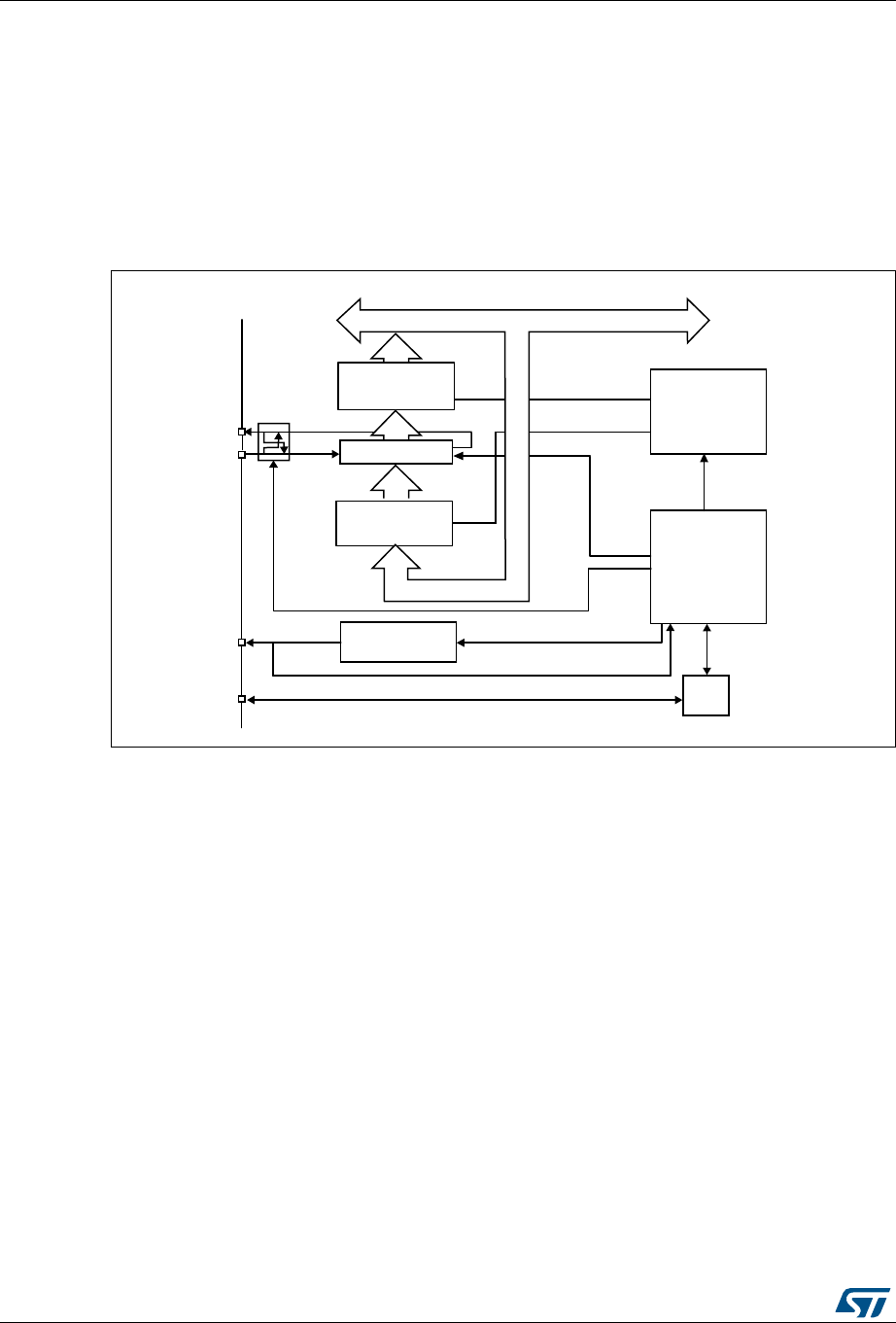
Serial peripheral interface/ inter-IC sound (SPI/I2S) RM0376
834/1001 DocID025941 Rev 5
30.3 SPI functional description
30.3.1 General description
The SPI allows synchronous, serial communication between the MCU and external devices.
Application software can manage the communication by polling the status flag or using
dedicated SPI interrupt. The main elements of SPI and their interactions are shown in the
following block diagram Figure 263.
Figure 263. SPI block diagram
Four I/O pins are dedicated to SPI communication with external devices.
•MISO: Master In / Slave Out data. In the general case, this pin is used to transmit data
in slave mode and receive data in master mode.
•MOSI: Master Out / Slave In data. In the general case, this pin is used to transmit data
in master mode and receive data in slave mode.
•SCK: Serial Clock output pin for SPI masters and input pin for SPI slaves.
•NSS: Slave select pin. Depending on the SPI and NSS settings, this pin can be used to
either:
– select an individual slave device for communication
– synchronize the data frame or
– detect a conflict between multiple masters
See Section 30.3.5: Slave select (NSS) pin management for details.
The SPI bus allows the communication between one master device and one or more slave
devices. The bus consists of at least two wires - one for the clock signal and the other for
synchronous data transfer. Other signals can be added depending on the data exchange
between SPI nodes and their slave select signal management.
MSv33711V1
Shift register
Write
Read
Communication
controller
Address and data bus
CRC controller
Internal NSS
CRCEN
CRCNEXT
LSBFIRST
CPOL
CPHA
DFF
MOSI
MISO
SCK
NSS
Rx
buffer
TX
buffer
BR[2:0]
BIDIOE
BIDIMODE
RXOLNY
NSS
logic
Baud rate
generator
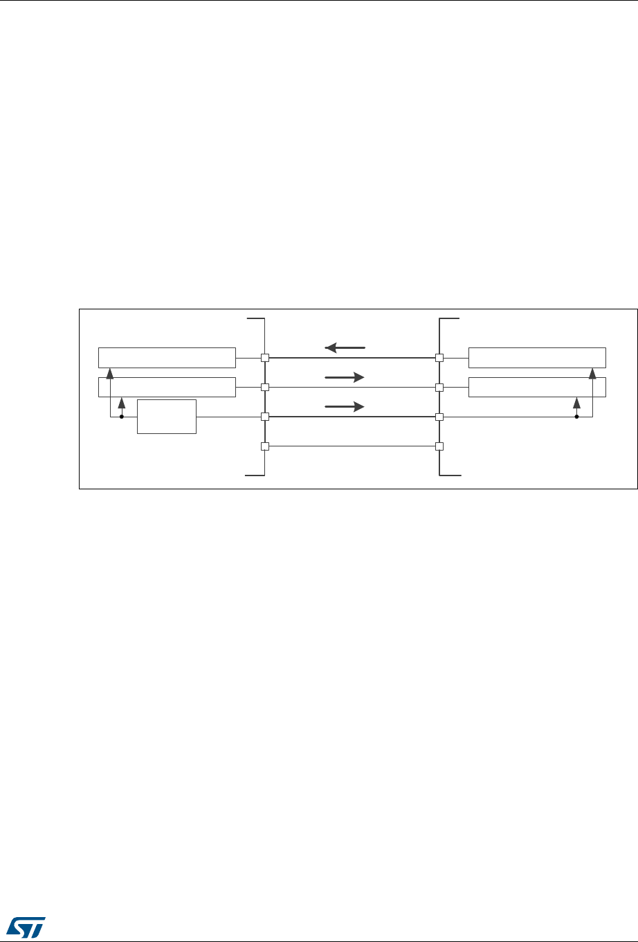
DocID025941 Rev 5 835/1001
RM0376 Serial peripheral interface/ inter-IC sound (SPI/I2S)
881
30.3.2 Communications between one master and one slave
The SPI allows the MCU to communicate using different configurations, depending on the
device targeted and the application requirements. These configurations use 2 or 3 wires
(with software NSS management) or 3 or 4 wires (with hardware NSS management).
Communication is always initiated by the master.
Full-duplex communication
By default, the SPI is configured for full-duplex communication. In this configuration, the
shift registers of the master and slave are linked using two unidirectional lines between the
MOSI and the MISO pins. During SPI communication, data is shifted synchronously on the
SCK clock edges provided by the master. The master transmits the data to be sent to the
slave via the MOSI line and receives data from the slave via the MISO line. When the data
frame transfer is complete (all the bits are shifted) the information between the master and
slave is exchanged.
Figure 264. Full-duplex single master/ single slave application
1. The NSS pins can be used to provide a hardware control flow between master and slave. Optionally, the
pins can be left unused by the peripheral. Then the flow has to be handled internally for both master and
slave. For more details see Section 30.3.5: Slave select (NSS) pin management.
Half-duplex communication
The SPI can communicate in half-duplex mode by setting the BIDIMODE bit in the
SPIx_CR1 register. In this configuration, one single cross connection line is used to link the
shift registers of the master and slave together. During this communication, the data is
synchronously shifted between the shift registers on the SCK clock edge in the transfer
direction selected reciprocally by both master and slave with the BDIOE bit in their
SPIx_CR1 registers. In this configuration, the master’s MISO pin and the slave’s MOSI pin
are free for other application uses and act as GPIOs.
Rx shift register
Tx shift register Rx shift register
Tx shift register
SPI clock
generator
Master Slave
MISO
MOSI
SCK
NSS
MISO
MOSI
SCK
NSS
(1) (1)
MSv39623V1
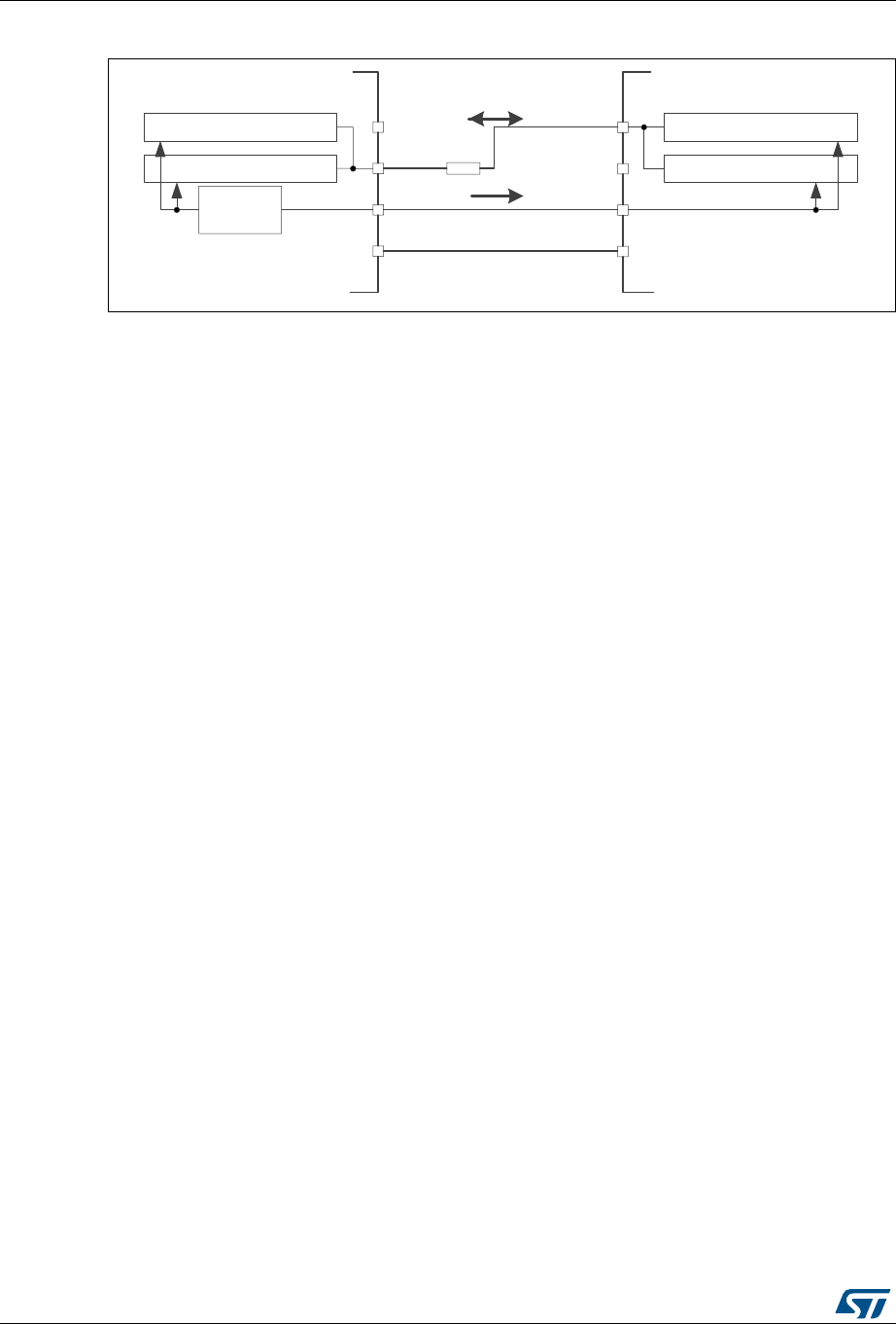
Serial peripheral interface/ inter-IC sound (SPI/I2S) RM0376
836/1001 DocID025941 Rev 5
Figure 265. Half-duplex single master/ single slave application
1. The NSS pins can be used to provide a hardware control flow between master and slave. Optionally, the
pins can be left unused by the peripheral. Then the flow has to be handled internally for both master and
slave. For more details see Section 30.3.5: Slave select (NSS) pin management.
2. In this configuration, the master’s MISO pin and the slave’s MOSI pin can be used as GPIOs.
3. A critical situation can happen when communication direction is changed not synchronously between two
nodes working at bidirectionnal mode and new transmitter accesses the common data line while former
transmitter still keeps an opposite value on the line (the value depends on SPI configuration and
communication data). Both nodes then fight while providing opposite output levels on the common line
temporary till next node changes its direction settings correspondingly, too. It is suggested to insert a serial
resistance between MISO and MOSI pins at this mode to protect the outputs and limit the current blowing
between them at this situation.
Simplex communications
The SPI can communicate in simplex mode by setting the SPI in transmit-only or in receive-
only using the RXONLY bit in the SPIx_CR2 register. In this configuration, only one line is
used for the transfer between the shift registers of the master and slave. The remaining
MISO and MOSI pins pair is not used for communication and can be used as standard
GPIOs.
•Transmit-only mode (RXONLY=0): The configuration settings are the same as for full-
duplex. The application has to ignore the information captured on the unused input pin.
This pin can be used as a standard GPIO.
•Receive-only mode (RXONLY=1): The application can disable the SPI output function
by setting the RXONLY bit. In slave configuration, the MISO output is disabled and the
pin can be used as a GPIO. The slave continues to receive data from the MOSI pin
while its slave select signal is active (see 30.3.5: Slave select (NSS) pin management).
Received data events appear depending on the data buffer configuration. In the master
configuration, the MOSI output is disabled and the pin can be used as a GPIO. The
clock signal is generated continuously as long as the SPI is enabled. The only way to
stop the clock is to clear the RXONLY bit or the SPE bit and wait until the incoming
pattern from the MISO pin is finished and fills the data buffer structure, depending on its
configuration.
Rx shift register
Tx shift register Rx shift register
Tx shift register
SPI clock
generator
Master Slave
MISO
MOSI
SCK
NSS
MISO
MOSI
SCK
NSS
(1) (1)
(2)
(2)
1kΩ
(3)
MSv39624V1
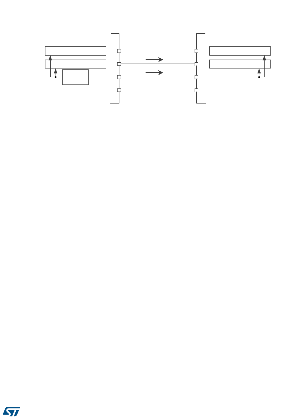
DocID025941 Rev 5 837/1001
RM0376 Serial peripheral interface/ inter-IC sound (SPI/I2S)
881
Figure 266. Simplex single master/single slave application (master in transmit-only/
slave in receive-only mode)
1. The NSS pins can be used to provide a hardware control flow between master and slave. Optionally, the
pins can be left unused by the peripheral. Then the flow has to be handled internally for both master and
slave. For more details see Section 30.3.5: Slave select (NSS) pin management.
2. An accidental input information is captured at the input of transmitter Rx shift register. All the events
associated with the transmitter receive flow must be ignored in standard transmit only mode (e.g. OVF
flag).
3. In this configuration, both the MISO pins can be used as GPIOs.
Note: Any simplex communication can be alternatively replaced by a variant of the half-duplex
communication with a constant setting of the transaction direction (bidirectional mode is
enabled while BDIO bit is not changed).
Rx shift register
Tx shift register Rx shift register
Tx shift register
SPI clock
generator
Master Slave
MISO
MOSI
SCK
NSS
MISO
MOSI
SCK
NSS
(1) (1)
(2)
MSv39625V1
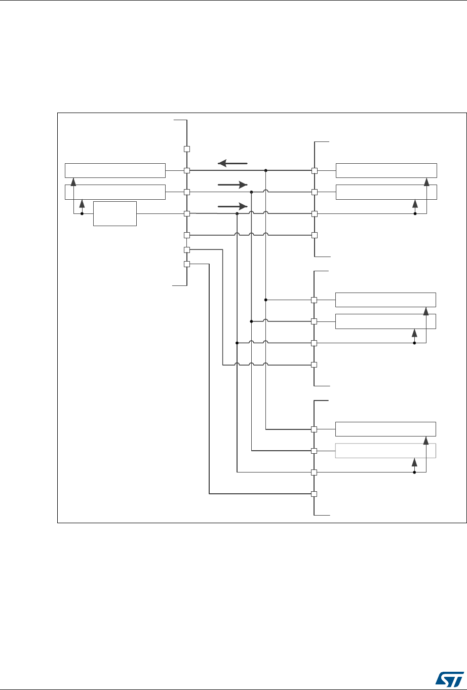
Serial peripheral interface/ inter-IC sound (SPI/I2S) RM0376
838/1001 DocID025941 Rev 5
30.3.3 Standard multi-slave communication
In a configuration with two or more independent slaves, the master uses GPIO pins to
manage the chip select lines for each slave (see Figure 267.). The master must select one
of the slaves individually by pulling low the GPIO connected to the slave NSS input. When
this is done, a standard master and dedicated slave communication is established.
Figure 267. Master and three independent slaves
1. NSS pin is not used on master side at this configuration. It has to be managed internally (SSM=1, SSI=1) to
prevent any MODF error.
2. As MISO pins of the slaves are connected together, all slaves must have the GPIO configuration of their
MISO pin set as alternate function open-drain (see Section 9.3.7: I/O alternate function input/output on
page 239).
Rx shift register
Tx shift register Rx shift register
Tx shift register
SPI clock
generator
Master Slave 1
MISO
MOSI
SCK
NSS
MISO
MOSI
SCK
NSS
(1)
Rx shift register
Tx shift register
Slave 2
Rx shift register
Tx shift register
Slave 3
IO1
IO2
IO3
MISO
MOSI
SCK
NSS
MISO
MOSI
SCK
NSS
MSv39626V1
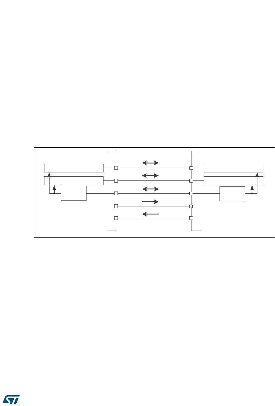
DocID025941 Rev 5 839/1001
RM0376 Serial peripheral interface/ inter-IC sound (SPI/I2S)
881
30.3.4 Multi-master communication
Unless SPI bus is not designed for a multi-master capability primarily, the user can use build
in feature which detects a potential conflict between two nodes trying to master the bus at
the same time. For this detection, NSS pin is used configured at hardware input mode.
The connection of more than two SPI nodes working at this mode is impossible as only one
node can apply its output on a common data line at time.
When nodes are non active, both stay at slave mode by default. Once one node wants to
overtake control on the bus, it switches itself into master mode and applies active level on
the slave select input of the other node via dedicated GPIO pin. After the session is
completed, the active slave select signal is released and the node mastering the bus
temporary returns back to passive slave mode waiting for next session start.
If potentially both nodes raised their mastering request at the same time a bus conflict event
appears (see mode fault MODF event). Then the user can apply some simple arbitration
process (e.g. to postpone next attempt by predefined different time-outs applied at both
nodes).
Figure 268. Multi-master application
1. The NSS pin is configured at hardware input mode at both nodes. Its active level enables the MISO line
output control as the passive node is configured as a slave.
30.3.5 Slave select (NSS) pin management
In slave mode, the NSS works as a standard “chip select” input and lets the slave
communicate with the master. In master mode, NSS can be used either as output or input.
As an input it can prevent multimaster bus collision, and as an output it can drive a slave
select signal of a single slave.
Hardware or software slave select management can be set using the SSM bit in the
SPIx_CR1 register:
•Software NSS management (SSM = 1): in this configuration, slave select information
is driven internally by the SSI bit value in register SPIx_CR1. The external NSS pin is
free for other application uses.
•Hardware NSS management (SSM = 0): in this case, there are two possible
configurations. The configuration used depends on the NSS output configuration
(SSOE bit in register SPIx_CR1).
Rx (Tx) shift register
Tx (Rx) shift register Tx (Rx) shift register
Rx (Tx) shift register
SPI clock
generator
Master
(Slave)
Master
(Slave)
MISO
MOSI
SCK
NSS
MISO
MOSI
SCK
NSS
(1)
(1)
MSv39628V1
SPI clock
generator
GPIO
GPIO
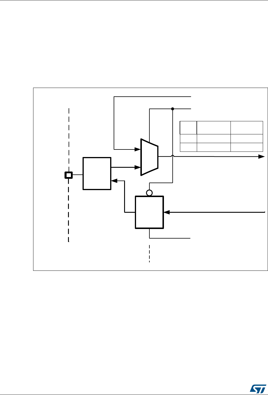
Serial peripheral interface/ inter-IC sound (SPI/I2S) RM0376
840/1001 DocID025941 Rev 5
–NSS output enable (SSM=0,SSOE = 1): this configuration is only used when the
MCU is set as master. The NSS pin is managed by the hardware. The NSS signal
is driven low as soon as the SPI is enabled in master mode (SPE=1), and is kept
low until the SPI is disabled (SPE =0).
–NSS output disable (SSM=0, SSOE = 0): if the microcontroller is acting as the
master on the bus, this configuration allows multimaster capability. If the NSS pin
is pulled low in this mode, the SPI enters master mode fault state and the device is
automatically reconfigured in slave mode. In slave mode, the NSS pin works as a
standard “chip select” input and the slave is selected while NSS line is at low level.
Figure 269. Hardware/software slave select management
1
0NSS Input
SSM control bit
SSI control bit
SSOE control bit
NSS Output
NSS
pin
(used in Master mode & NSS
HW management only)
NSS
Output
Control
Master
mode Slave mode
Non activeOKVdd
NSS
Inp.
ActiveConflictVss
NSS external logic NSS internal logic
GPIO
logic
aiv14746e

DocID025941 Rev 5 841/1001
RM0376 Serial peripheral interface/ inter-IC sound (SPI/I2S)
881
30.3.6 Communication formats
During SPI communication, receive and transmit operations are performed simultaneously.
The serial clock (SCK) synchronizes the shifting and sampling of the information on the data
lines. The communication format depends on the clock phase, the clock polarity and the
data frame format. To be able to communicate together, the master and slaves devices must
follow the same communication format.
Clock phase and polarity controls
Four possible timing relationships may be chosen by software, using the CPOL and CPHA
bits in the SPIx_CR1 register. The CPOL (clock polarity) bit controls the idle state value of
the clock when no data is being transferred. This bit affects both master and slave modes. If
CPOL is reset, the SCK pin has a low-level idle state. If CPOL is set, the SCK pin has a
high-level idle state.
If the CPHA bit is set, the second edge on the SCK pin captures the first data bit transacted
(falling edge if the CPOL bit is reset, rising edge if the CPOL bit is set). Data are latched on
each occurrence of this clock transition type. If the CPHA bit is reset, the first edge on the
SCK pin captures the first data bit transacted (falling edge if the CPOL bit is set, rising edge
if the CPOL bit is reset). Data are latched on each occurrence of this clock transition type.
The combination of CPOL (clock polarity) and CPHA (clock phase) bits selects the data
capture clock edge.
Figure 270, shows an SPI full-duplex transfer with the four combinations of the CPHA and
CPOL bits.
Note: Prior to changing the CPOL/CPHA bits the SPI must be disabled by resetting the SPE bit.
The idle state of SCK must correspond to the polarity selected in the SPIx_CR1 register (by
pulling up SCK if CPOL=1 or pulling down SCK if CPOL=0).
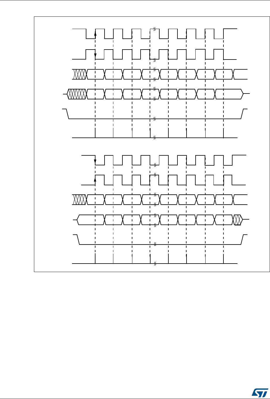
Serial peripheral interface/ inter-IC sound (SPI/I2S) RM0376
842/1001 DocID025941 Rev 5
Figure 270. Data clock timing diagram
Note: The order of data bits depends on LSBFIRST bit setting.
Data frame format
The SPI shift register can be set up to shift out MSB-first or LSB-first, depending on the
value of the LSBFIRST bit. Each data frame is 8 or 16 bit long depending on the size of the
data programmed using the DFF bit in the SPI_CR1 register. The selected data frame
format is applicable both for transmission and reception.
CPOL = 1
CPOL = 0
MSBit LSBit
MSBit LSBit
MISO
MOSI
NSS
(to slave)
Capture strobe
CPHA =1
CPOL = 1
CPOL = 0
MSBit LSBit
MSBit LSBit
MISO
MOSI
NSS
(to slave)
Capture strobe
CPHA =0
ai17154d

DocID025941 Rev 5 843/1001
RM0376 Serial peripheral interface/ inter-IC sound (SPI/I2S)
881
30.3.7 SPI configuration
The configuration procedure is almost the same for master and slave. For specific mode
setups, follow the dedicated chapters. When a standard communication is to be initialized,
perform these steps:
1. Write proper GPIO registers: Configure GPIO for MOSI, MISO and SCK pins.
2. Write to the SPI_CR1 register:
a) Configure the serial clock baud rate using the BR[2:0] bits (Note: 3).
b) Configure the CPOL and CPHA bits combination to define one of the four
relationships between the data transfer and the serial clock. (Note: 2 - except the
case when CRC is enabled at TI mode).
c) Select simplex or half-duplex mode by configuring RXONLY or BIDIMODE and
BIDIOE (RXONLY and BIDIMODE can't be set at the same time).
d) Configure the LSBFIRST bit to define the frame format (Note: 2).
e) Configure the CRCEN and CRCEN bits if CRC is needed (while SCK clock signal
is at idle state).
f) Configure SSM and SSI (Note: 2).
g) Configure the MSTR bit (in multimaster NSS configuration, avoid conflict state on
NSS if master is configured to prevent MODF error).
h) Set the DFF bit to configure the data frame format (8 or 16 bits).
3. Write to SPI_CR2 register:
a) Configure SSOE (Note: 1 & 2).
b) Set the FRF bit if the TI protocol is required.
4. Write to SPI_CRCPR register: Configure the CRC polynomial if needed.
5. Write proper DMA registers: Configure DMA streams dedicated for SPI Tx and Rx in
DMA registers if the DMA streams are used.
Note: (1) Step is not required in slave mode.
(2) Step is not required in TI mode.
(3) The step is not required in slave mode except slave working at TI mode.
For code example, refer to A.19.1: SPI master configuration code example and A.19.2: SPI
slave configuration code example.
30.3.8 Procedure for enabling SPI
It is recommended to enable the SPI slave before the master sends the clock. Otherwise,
undesired data transmission might occur. The slave data register must already contain data
to be sent before starting communication with the master (either on the first edge of the
communication clock, or before the end of the ongoing communication if the clock signal is
continuous). The SCK signal must be settled at an idle state level corresponding to the
selected polarity before the SPI slave is enabled.
At full-duplex (or in any transmit-only mode), the master starts communicating when the SPI
is enabled and data to be sent is written in the Tx Buffer.
In any master receive-only mode (RXONLY=1 or BIDIMODE=1 & BIDIOE=0), the master
starts communicating and the clock starts running immediately after the SPI is enabled.
The slave starts communicating when it receives a correct clock signal from the master. The
slave software must write the data to be sent before the SPI master initiates the transfer.

Serial peripheral interface/ inter-IC sound (SPI/I2S) RM0376
844/1001 DocID025941 Rev 5
Refer to Section 30.3.11: Communication using DMA (direct memory addressing) for details
on how to handle DMA.
30.3.9 Data transmission and reception procedures
Rx and Tx buffers
In reception, data are received and then stored into an internal Rx buffer while in
transmission, data are first stored into an internal Tx buffer before being transmitted. A read
access to the SPI_DR register returns the Rx buffered value whereas a write access to the
SPI_DR stores the written data into the Tx buffer.
Tx buffer handling
The data frame is loaded from the Tx buffer into the shift register during the first bit
transmission. Bits are then shifted out serially from the shift register to a dedicated output
pin depending on LSBFIRST bit setting.The TXE flag (Tx buffer empty) is set when the data
are transferred from the Tx buffer to the shift register. It indicates that the internal Tx buffer is
ready to be loaded with the next data. An interrupt can be generated if the TXEIE bit of the
SPI_CR2 register is set. Clearing the TXE bit is performed by writing to the SPI_DR register.
A continuous transmit stream can be achieved if the next data to be transmitted are stored
in the Tx buffer while previous frame transmission is still ongoing. When the software writes
to Tx buffer while the TXE flag is not set, the data waiting for transaction is overwritten.
Rx buffer handling
The RXNE flag (Rx buffer not empty) is set on the last sampling clock edge, when the data
are transferred from the shift register to the Rx buffer. It indicates that data are ready to be
read from the SPI_DR register. An interrupt can be generated if the RXNEIE bit in the
SPI_CR2 register is set. Clearing the RXNE bit is performed by reading the SPI_DR
register.
If a device has not cleared the RXNE bit resulting from the previous data byte transmitted,
an overrun condition occurs when the next value is buffered. The OVR bit is set and an
interrupt is generated if the ERRIE bit is set.
Another way to manage the data exchange is to use DMA (see Section 11.2: DMA main
features).
Sequence handling
The BSY bit is set when a current data frame transaction is ongoing. When the clock signal
runs continuously, the BSY flag remains set between data frames on the master side.
However, on the slave side, it becomes low for a minimum duration of one SPI clock cycle
between each data frame transfer.
For some configurations, the BSY flag can be used during the last data transfer to wait until
the completion of the transfer.
When a receive-only mode is configured on the master side, either in half-duplex
(BIDIMODE=1, BIDIOE=0) or simplex configuration (BIDIMODE=0, RXONLY=1), the
master starts the receive sequence as soon as the SPI is enabled. Then the clock signal is
provided by the master and it does not stop until either the SPI or the receive-only mode is
disabled by the master. The master receives data frames continuously up to this moment.
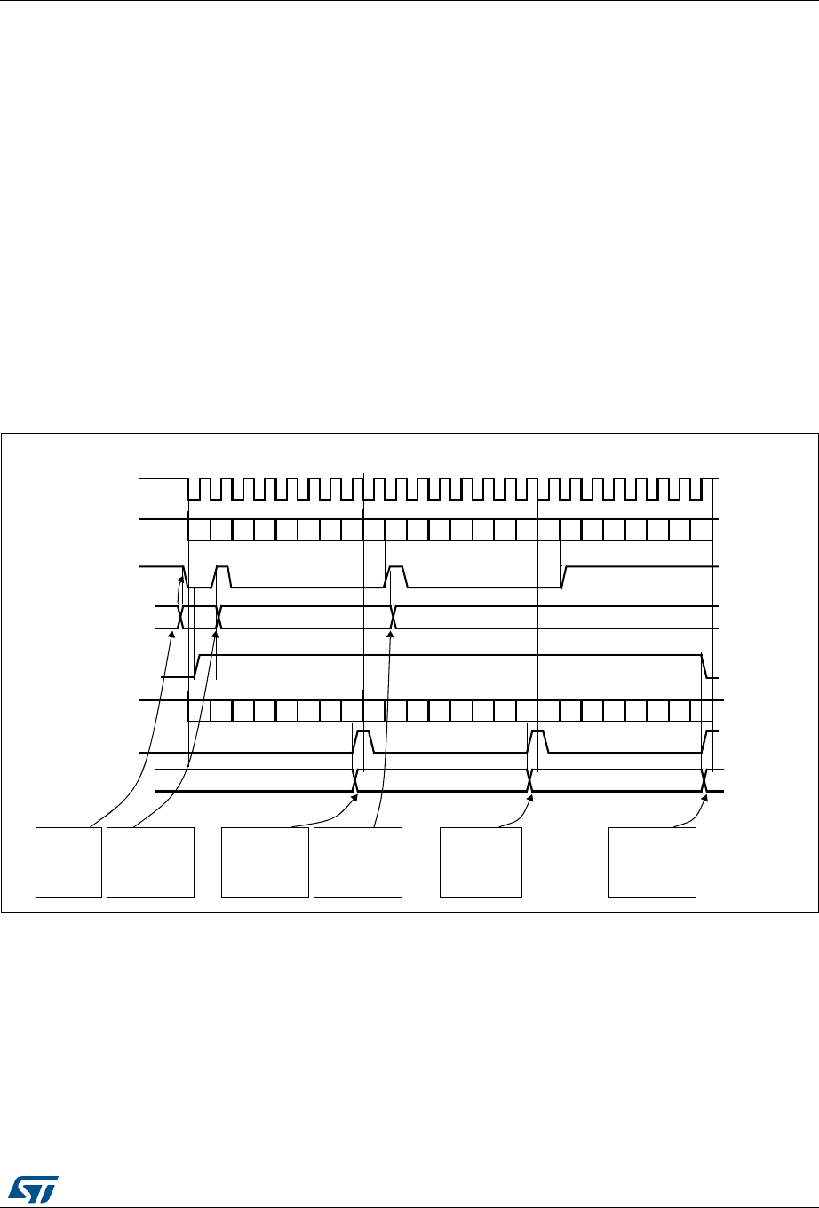
DocID025941 Rev 5 845/1001
RM0376 Serial peripheral interface/ inter-IC sound (SPI/I2S)
881
While the master can provide all the transactions in continuous mode (SCK signal is
continuous), it has to respect slave capability to handle data flow and its content at anytime.
When necessary, the master must slow down the communication and provide either a
slower clock or separate frames or data sessions with sufficient delays. Be aware there is no
underflow error signal for slave operating in SPI mode, and that data from the slave are
always transacted and processed by the master even if the slave cannot not prepare them
correctly in time. It is preferable for the slave to use DMA, especially when data frames are
shorter and bus rate is high.
Each sequence must be encased by the NSS pulse in parallel with the multislave system to
select just one of the slaves for communication. In single slave systems, using NSS to
control the slave is not necessary. However, the NSS pulse can be used to synchronize the
slave with the beginning of each data transfer sequence. NSS can be managed either by
software or by hardware (see Section 30.3.4: Multi-master communication).
Refer to Figure 271 and Figure 272 for a description of continuous transfers in master / full-
duplex and slave full-duplex mode.
Figure 271. TXE/RXNE/BSY behavior in master / full-duplex mode (BIDIMODE=0,
RXONLY=0) in the case of continuous transfers
For code example, refer to A.19.3: SPI full duplex communication code example.
MISO/MOSI (in)
Tx buffer
DATA 1 = 0xA1
TXE flag
0xF2
BSY flag
0xF3
software
writes 0xF1
into SPI_DR
software waits
until TXE=1 and
writes 0xF2 into
SPI_DR
software waits
until RXNE=1
and reads 0xA1
from SPI_DR
set by hardware
cleared by software
set by hardware
cleared by software set by hardware
set by hardware
SCK
DATA 2 = 0xA2 DATA 3 = 0xA3
reset by hardware
Example in Master mode with CPOL=1, CPHA=1
0xF1
RXNE flag
(write SPI_DR)
Rx buffer
set by hardware
MISO/MOSI (out)
DATA1 = 0xF1 DATA2 = 0xF2 DATA3 = 0xF3
(read SPI_DR)
0xA1 0xA2 0xA3
software waits
until TXE=1 and
writes 0xF3 into
SPI_DR
software waits
until RXNE=1
and reads 0xA2
from SPI_ DR
software waits
until RXNE=1
and reads 0xA3
from SPI_DR
b0 b1 b2 b3 b4 b5 b6 b7 b0 b1 b2 b3 b4 b5 b6 b7 b0 b1 b2 b3 b4 b5 b6 b7
b0 b1 b2 b3 b4 b5 b6 b7 b0 b1 b2 b3 b4 b5 b6 b7 b0 b1 b2 b3 b4 b5 b6 b7
cleared by software
ai17343
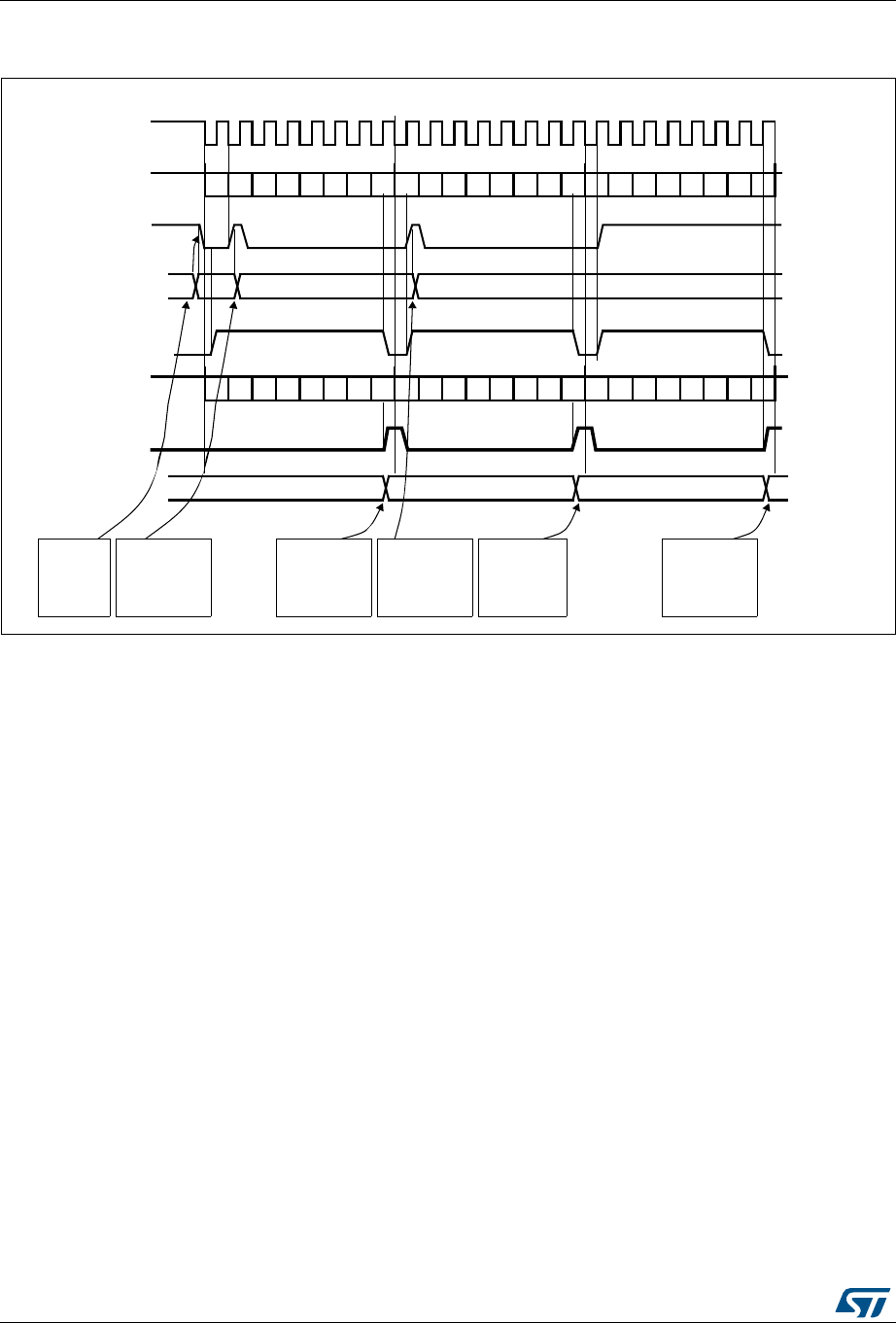
Serial peripheral interface/ inter-IC sound (SPI/I2S) RM0376
846/1001 DocID025941 Rev 5
Figure 272. TXE/RXNE/BSY behavior in slave / full-duplex mode (BIDIMODE=0,
RXONLY=0) in the case of continuous transfers
30.3.10 Procedure for disabling the SPI
When SPI is disabled, it is mandatory to follow the disable procedures described in this
paragraph. It is important to do this before the system enters a low-power mode when the
peripheral clock is stopped. Ongoing transactions can be corrupted in this case. In some
modes the disable procedure is the only way to stop continuous communication running.
Master in full-duplex or transmit only mode can finish any transaction when it stops
providing data for transmission. In this case, the clock stops after the last data transaction.
Standard disable procedure is based on pulling BSY status together with TXE flag to check
if a transmission session is fully completed. This check can be done in specific cases, too,
when it is necessary to identify the end of ongoing transactions, for example:
•When NSS signal is managed by an arbitrary GPIO toggle and the master has to
provide proper end of NSS pulse for slave, or
•When transactions’ streams from DMA are completed while the last data frame or CRC
frame transaction is still ongoing in the peripheral bus.
The correct disable procedure is (except when receive-only mode is used):
1. Wait until RXNE=1 to receive the last data.
2. Wait until TXE=1 and then wait until BSY=0 before disabling the SPI.
3. Read received data.
0xF1
set by cleared by software
MISO/MOSI (in)
Tx buffer
DATA 1 = 0xA1
TXE flag
0xF2
BSY flag
0xF3
software
writes 0xF1
into SPI_DR
software waits
until TXE=1 and
writes 0xF2 into
SPI_DR
software waits
until RXNE=1
and reads 0xA1
from SPI_DR
set by hardware
cleared by software
set by hardware
cleared by software set by hardware
SCK
DATA 2 = 0xA2 DATA 3 = 0xA3
reset by hardware
Example in Slave mode with CPOL=1, CPHA=1
RXNE flag
(write to SPI_DR)
Rx buffer
set by hardware
MISO/MOSI (out)
DATA 1 = 0xF1 DATA 2 = 0xF2 DATA 3 = 0xF3
(read from SPI_DR)
0xA1 0xA2 0xA3
software waits
until TXE=1 and
writes 0xF3 into
SPI_DR
software waits
until RXNE=1
and reads 0xA2
from SPI_ DR
software waits
until RXNE=1
and reads 0xA3
from SPI_DR
b0 b1 b2 b3 b4 b5 b6 b7 b0 b1 b2 b3 b4 b5 b6 b7 b0 b1 b2 b3 b4 b5 b6 b7
b0 b1 b2 b3 b4 b5 b6 b7 b0 b1 b2 b3 b4 b5 b6 b7 b0 b1 b2 b3 b4 b5 b6 b7
cleared by software
ai17344

DocID025941 Rev 5 847/1001
RM0376 Serial peripheral interface/ inter-IC sound (SPI/I2S)
881
Note: During discontinuous communications, there is a 2 APB clock period delay between the
write operation to the SPI_DR register and BSY bit setting. As a consequence it is
mandatory to wait first until TXE is set and then until BSY is cleared after writing the last
data.
The correct disable procedure for certain receive-only modes is:
1. Interrupt the receive flow by disabling SPI (SPE=0) in the specific time window while
the last data frame is ongoing.
2. Wait until BSY=0 (the last data frame is processed).
3. Read received data.
Note: To stop a continuous receive sequence, a specific time window must be respected during
the reception of the last data frame. It starts when the first bit is sampled and ends before
the last bit transfer starts.
30.3.11 Communication using DMA (direct memory addressing)
To operate at its maximum speed and to facilitate the data register read/write process
required to avoid overrun, the SPI features a DMA capability, which implements a simple
request/acknowledge protocol.
A DMA access is requested when the TXE or RXNE enable bit in the SPIx_CR2 register is
set. Separate requests must be issued to the Tx and Rx buffers.
•In transmission, a DMA request is issued each time TXE is set to 1. The DMA then
writes to the SPIx_DR register.
•In reception, a DMA request is issued each time RXNE is set to 1. The DMA then reads
the SPIx_DR register.
Refer to Figure 273 and Figure 274 for a description of the DMA transmission and reception
waveforms.
When the SPI is used only to transmit data, it is possible to enable only the SPI Tx DMA
channel. In this case, the OVR flag is set because the data received is not read. When the
SPI is used only to receive data, it is possible to enable only the SPI Rx DMA channel.
In transmission mode, when the DMA has written all the data to be transmitted (the TCIF
flag is set in the DMA_ISR register), the BSY flag can be monitored to ensure that the SPI
communication is complete. This is required to avoid corrupting the last transmission before
disabling the SPI or entering the Stop mode. The software must first wait until TXE = 1 and
then until BSY = 0.
When starting communication using DMA, to prevent DMA channel management raising
error events, these steps must be followed in order:
1. Enable DMA Rx buffer in the RXDMAEN bit in the SPI_CR2 register, if DMA Rx is
used.
2. Enable DMA streams for Tx and Rx in DMA registers, if the streams are used.
3. Enable DMA Tx buffer in the TXDMAEN bit in the SPI_CR2 register, if DMA Tx is used.
4. Enable the SPI by setting the SPE bit.
For code example, refer to A.19.4: SPI master configuration with DMA code example and
A.19.5: SPI slave configuration with DMA code example.
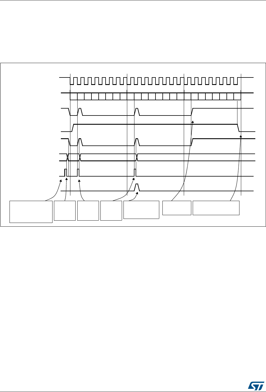
Serial peripheral interface/ inter-IC sound (SPI/I2S) RM0376
848/1001 DocID025941 Rev 5
To close communication it is mandatory to follow these steps in order:
1. Disable DMA streams for Tx and Rx in the DMA registers, if the streams are used.
2. Disable the SPI by following the SPI disable procedure.
3. Disable DMA Tx and Rx buffers by clearing the TXDMAEN and RXDMAEN bits in the
SPI_CR2 register, if DMA Tx and/or DMA Rx are used.
Figure 273. Transmission using DMA
0xF1
Tx buffer
TXE flag
0xF2
BSY flag
0xF3
set by hardware
clear by DMA write
set by hardware
cleared by DMA write set by hardware
set by hardware
SCK
reset
Example with CPOL=1, CPHA=1
(write to SPI_DR)
MISO/MOSI (out)
DATA 1 = 0xF1 DATA 2 = 0xF2 DATA 3 = 0xF3
software configures the
DMA SPI Tx channel
to send 3 data items
and enables the SPI
DMA writes to SPI_DR
DMA request ignored by the DMA because
DMA TCIF flag set by hardware clear by software
DMA writes
DATA1 into
SPI_DR
by hardware
DMA writes
DATA2 into
SPI_DR
DMA writes
DATA3 into
SPI_DR
software waits until BSY=0
(DMA transfer complete)
DMA transfer is
complete (TCIF=1 in
DMA_ISR)
software waits
until TXE=1
DMA transfer is complete
b0 b1 b2 b3 b4 b5 b6 b7 b0 b1 b2 b3 b4 b5 b6 b7 b0 b1 b2 b3 b4 b5 b6 b7
ai17349
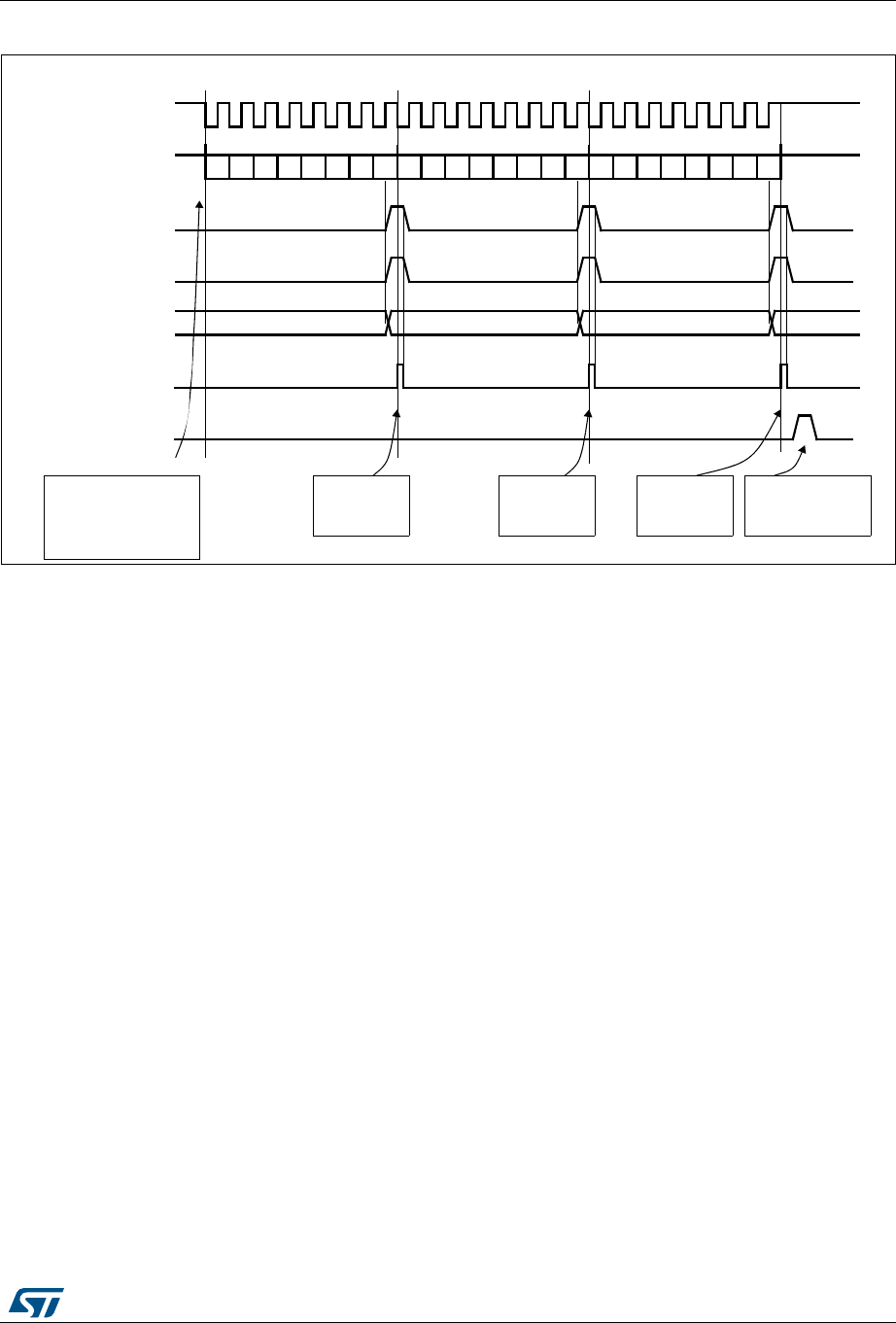
DocID025941 Rev 5 849/1001
RM0376 Serial peripheral interface/ inter-IC sound (SPI/I2S)
881
Figure 274. Reception using DMA
30.3.12 SPI status flags
Three status flags are provided for the application to completely monitor the state of the SPI
bus.
Tx buffer empty flag (TXE)
When it is set, the TXE flag indicates that the Tx buffer is empty and that the next data to be
transmitted can be loaded into the buffer. The TXE flag is cleared by writing to the SPI_DR
register.
Rx buffer not empty (RXNE)
When set, the RXNE flag indicates that there are valid received data in the Rx buffer. It is
cleared by reading from the SPI_DR register.
Busy flag (BSY)
The BSY flag is set and cleared by hardware (writing to this flag has no effect).
When BSY is set, it indicates that a data transfer is in progress on the SPI (the SPI bus is
busy). There is one exception in master bidirectional receive mode (MSTR=1 and BDM=1
and BDOE=0) where the BSY flag is kept low during reception.
The BSY flag can be used in certain modes to detect the end of a transfer, thus preventing
corruption of the last transfer when the SPI peripheral clock is disabled before entering a
low-power mode or an NSS pulse end is handled by software.
The BSY flag is also useful for preventing write collisions in a multimaster system.
MISO/MOSI (in)
DATA 1 = 0xA1
software configures the
DMA SPI Rx channel
to receive 3 data items
and enables the SPI
SCK
DATA 2 = 0xA2 DATA 3 = 0xA3
Example with CPOL=1, CPHA=1
RXNE flag
Rx buffer
set by hardware
(read from SPI_DR) 0xA1 0xA2 0xA3
DMA request
DMA reads
DATA3 from
SPI_DR
flag DMA TCIF
set by hardware clear
by software
DMA read from SPI_DR
The DMA transfer is
complete (TCIF=1 in
DMA_ISR)
DMA reads
DATA2 from
SPI_DR
DMA reads
DATA1 from
SPI_DR
(DMA transfer complete)
b0 b1 b2 b3 b4 b5 b6 b7 b0 b1 b2 b3 b4 b5 b6 b7 b0 b1 b2 b3 b4 b5 b6 b7
clear by DMA read
ai17350

Serial peripheral interface/ inter-IC sound (SPI/I2S) RM0376
850/1001 DocID025941 Rev 5
The BSY flag is cleared under any one of the following conditions:
•When the SPI is correctly disabled
•When a fault is detected in Master mode (MODF bit set to 1)
•In Master mode, when it finishes a data transmission and no new data is ready to be
sent
•In Slave mode, when the BSY flag is set to '0' for at least one SPI clock cycle between
each data transfer.
Note: It is recommended to use always the TXE and RXNE flags (instead of the BSY flags) to
handle data transmission or reception operations.
30.3.13 SPI error flags
An SPI interrupt is generated if one of the following error flags is set and interrupt is enabled
by setting the ERRIE bit.
Overrun flag (OVR)
An overrun condition occurs when the master or the slave completes the reception of the
next data frame while the read operation of the previous frame from the Rx buffer has not
completed (case RXNE flag is set).
In this case, the content of the Rx buffer is not updated with the new data received. A read
operation from the SPI_DR register returns the frame previously received. All other
subsequently transmitted data are lost.
Clearing the OVR bit is done by a read access to the SPI_DR register followed by a read
access to the SPI_SR register.
Mode fault (MODF)
Mode fault occurs when the master device has its internal NSS signal (NSS pin in NSS
hardware mode, or SSI bit in NSS software mode) pulled low. This automatically sets the
MODF bit. Master mode fault affects the SPI interface in the following ways:
•The MODF bit is set and an SPI interrupt is generated if the ERRIE bit is set.
•The SPE bit is cleared. This blocks all output from the device and disables the SPI
interface.
•The MSTR bit is cleared, thus forcing the device into slave mode.
Use the following software sequence to clear the MODF bit:
1. Make a read or write access to the SPIx_SR register while the MODF bit is set.
2. Then write to the SPIx_CR1 register.
To avoid any multiple slave conflicts in a system comprising several MCUs, the NSS pin
must be pulled high during the MODF bit clearing sequence. The SPE and MSTR bits can
be restored to their original state after this clearing sequence. As a security, hardware does
not allow the SPE and MSTR bits to be set while the MODF bit is set. In a slave device the
MODF bit cannot be set except as the result of a previous multimaster conflict.

DocID025941 Rev 5 851/1001
RM0376 Serial peripheral interface/ inter-IC sound (SPI/I2S)
881
CRC error (CRCERR)
This flag is used to verify the validity of the value received when the CRCEN bit in the
SPIx_CR1 register is set. The CRCERR flag in the SPIx_SR register is set if the value
received in the shift register does not match the receiver SPIx_RXCRC value. The flag is
cleared by the software.
TI mode frame format error (FRE)
A TI mode frame format error is detected when an NSS pulse occurs during an ongoing
communication when the SPI is operating in slave mode and configured to conform to the TI
mode protocol. When this error occurs, the FRE flag is set in the SPIx_SR register. The SPI
is not disabled when an error occurs, the NSS pulse is ignored, and the SPI waits for the
next NSS pulse before starting a new transfer. The data may be corrupted since the error
detection may result in the loss of two data bytes.
The FRE flag is cleared when SPIx_SR register is read. If the ERRIE bit is set, an interrupt
is generated on the NSS error detection. In this case, the SPI should be disabled because
data consistency is no longer guaranteed and communications should be re-initiated by the
master when the slave SPI is enabled again.
30.4 SPI special features
30.4.1 TI mode
TI protocol in master mode
The SPI interface is compatible with the TI protocol. The FRF bit of the SPIx_CR2 register
can be used to configure the SPI to be compliant with this protocol.
The clock polarity and phase are forced to conform to the TI protocol requirements whatever
the values set in the SPIx_CR1 register. NSS management is also specific to the TI protocol
which makes the configuration of NSS management through the SPIx_CR1 and SPIx_CR2
registers (SSM, SSI, SSOE) impossible in this case.
In slave mode, the SPI baud rate prescaler is used to control the moment when the MISO
pin state changes to HiZ when the current transaction finishes (see Figure 275). Any baud
rate can be used, making it possible to determine this moment with optimal flexibility.
However, the baud rate is generally set to the external master clock baud rate. The delay for
the MISO signal to become HiZ (trelease) depends on internal resynchronization and on the
baud rate value set in through the BR[2:0] bits in the SPIx_CR1 register. It is given by the
formula:
If the slave detects a misplaced NSS pulse during a data frame transaction the TIFRE flag is
set.
This feature is not available for Motorola SPI communications (FRF bit set to 0).
tbaud_rate
2
----------------------4t
pclk
×+trelease
tbaud_rate
2
----------------------6t
pclk
×+<<
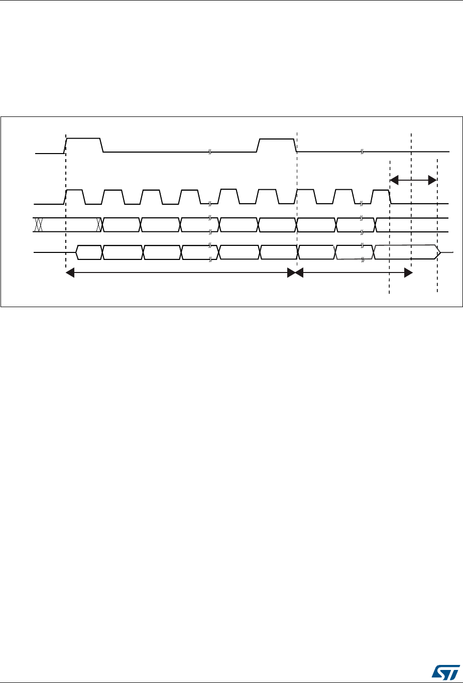
Serial peripheral interface/ inter-IC sound (SPI/I2S) RM0376
852/1001 DocID025941 Rev 5
Note: To detect TI frame errors in slave transmitter only mode by using the Error interrupt
(ERRIE=1), the SPI must be configured in 2-line unidirectional mode by setting BIDIMODE
and BIDIOE to 1 in the SPI_CR1 register. When BIDIMODE is set to 0, OVR is set to 1
because the data register is never read and error interrupts are always generated, while
when BIDIMODE is set to 1, data are not received and OVR is never set.
Figure 275 shows the SPI communication waveforms when TI mode is selected.
Figure 275. TI mode transfer
30.4.2 CRC calculation
Two separate CRC calculators (on transmission and reception data flows) are implemented
in order to check the reliability of transmitted and received data. The SPI offers CRC8 or
CRC16 calculation depending on the data format selected through the DFF bit. The CRC is
calculated serially using the polynomial programmed in the SPI_CRCPR register.
CRC principle
CRC calculation is enabled by setting the CRCEN bit in the SPIx_CR1 register before the
SPI is enabled (SPE = 1). The CRC value is calculated using an odd programmable
polynomial on each bit. The calculation is processed on the sampling clock edge defined by
the CPHA and CPOL bits in the SPIx_CR1 register. The calculated CRC value is checked
automatically at the end of the data block as well as for transfer managed by CPU or by the
DMA. When a mismatch is detected between the CRC calculated internally on the received
data and the CRC sent by the transmitter, a CRCERR flag is set to indicate a data corruption
error. The right procedure for handling the CRC calculation depends on the SPI
configuration and the chosen transfer management.
Note: The polynomial value should only be odd. No even values are supported.
CRC transfer managed by CPU
Communication starts and continues normally until the last data frame has to be sent or
received in the SPIx_DR register. Then CRCNEXT bit has to be set in the SPIx_CR1
register to indicate that the CRC frame transaction will follow after the transaction of the
currently processed data frame. The CRCNEXT bit must be set before the end of the last
data frame transaction. CRC calculation is frozen during CRC transaction.
MS19835V2
MSB
MISO
NSS
SCK
trigger
sampling
trigger
sampling
trigger
sampling
Do not care LSB
MOSI
1 or 0 MSB LSB
MSB LSB
MSB LSB
FRAME 1 FRAME 2
t
RELEASE

DocID025941 Rev 5 853/1001
RM0376 Serial peripheral interface/ inter-IC sound (SPI/I2S)
881
The received CRC is stored in the Rx buffer like any other data frame.
A CRC-format transaction takes one more data frame to communicate at the end of data
sequence.
When the last CRC data is received, an automatic check is performed comparing the
received value and the value in the SPIx_RXCRC register. Software has to check the
CRCERR flag in the SPIx_SR register to determine if the data transfers were corrupted or
not. Software clears the CRCERR flag by writing '0' to it.
After the CRC reception, the CRC value is stored in the Rx buffer and must be read in the
SPIx_DR register in order to clear the RXNE flag.
CRC transfer managed by DMA
When SPI communication is enabled with CRC communication and DMA mode, the
transmission and reception of the CRC at the end of communication is automatic (with the
exception of reading CRC data in receive-only mode). The CRCNEXT bit does not have to
be handled by the software. The counter for the SPI transmission DMA channel has to be
set to the number of data frames to transmit excluding the CRC frame. On the receiver side,
the received CRC value is handled automatically by DMA at the end of the transaction but
user must take care to flush out the CRC frame received from SPI_DR as it is always loaded
into it.
At the end of the data and CRC transfers, the CRCERR flag in the SPIx_SR register is set if
corruption occurred during the transfer.
Resetting the SPIx_TXCRC and SPIx_RXCRC values
The SPIx_TXCRC and SPIx_RXCRC values are cleared automatically when CRC
calculation is enabled.
When the SPI is configured in slave mode with the CRC feature enabled, a CRC calculation
is performed even if a high level is applied on the NSS pin. This may happen for example in
case of a multislave environment where the communication master addresses slaves
alternately.
Between a slave disabling (high level on NSS) and a new slave enabling (low level on NSS),
the CRC value should be cleared on both master and slave sides to resynchronize the
master and slave respective CRC calculation.
To clear the CRC, follow the below sequence:
1. Disable the SPI
2. Clear the CRCEN bit
3. Enable the CRCEN bit
4. Enable the SPI
Note: When the SPI is in slave mode, the CRC calculator is sensitive to the SCK slave input clock
as soon as the CRCEN bit is set, and this is the case whatever the value of the SPE bit. In
order to avoid any wrong CRC calculation, the software must enable the CRC calculation
only when the clock is stable (in steady state). When the SPI interface is configured as a
slave, the NSS internal signal needs to be kept low between the data phase and the CRC
phase once the CRCNEXT signal is released.
At TI mode, despite the fact that the clock phase and clock polarity setting is fixed and
independent on the SPIx_CR1 register, the corresponding setting CPOL=0 CPHA=1 has to
be kept at the SPIx_CR1 register anyway if CRC is applied. In addition, the CRC calculation
Serial peripheral interface/ inter-IC sound (SPI/I2S) RM0376
854/1001 DocID025941 Rev 5
has to be reset between sessions by the SPI disable sequence by re-enabling the CRCEN
bit described above at both master and slave sides, else the CRC calculation can be
corrupted at this specific mode.
30.5 SPI interrupts
During SPI communication an interrupts can be generated by the following events:
•Transmit Tx buffer ready to be loaded
•Data received in Rx buffer
•Master mode fault
•Overrun error
•TI frame format error
Interrupts can be enabled and disabled separately.
For code example, refer to A.19.6: SPI interrupt code example.
Table 143. SPI interrupt requests
Interrupt event Event flag Enable Control bit
Transmit Tx buffer ready to be loaded TXE TXEIE
Data received in Rx buffer RXNE RXNEIE
Master Mode fault event MODF
ERRIE
Overrun error OVR
CRC error CRCERR
TI frame format error FRE
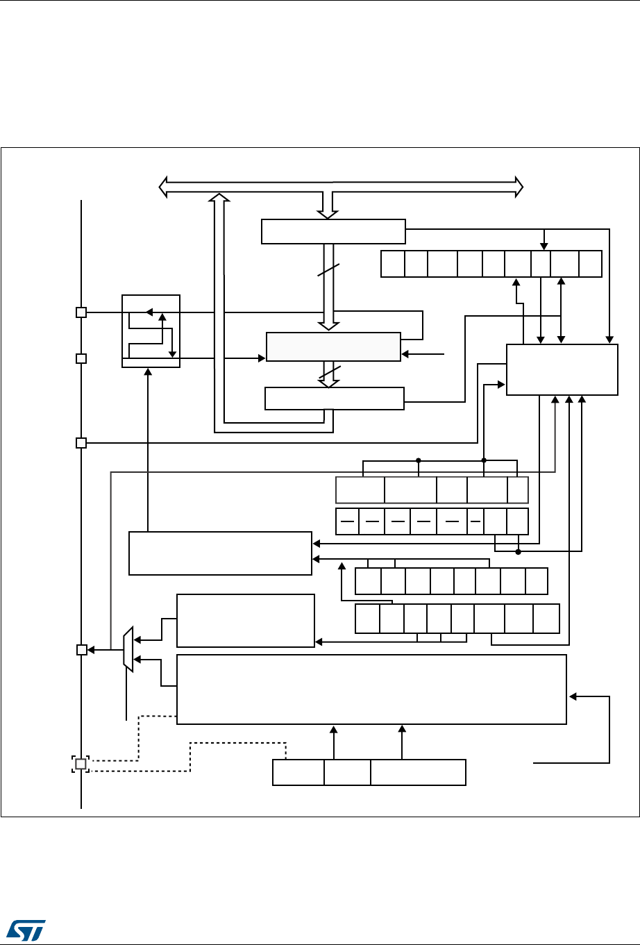
DocID025941 Rev 5 855/1001
RM0376 Serial peripheral interface/ inter-IC sound (SPI/I2S)
881
30.6 I2S functional description
30.6.1 I2S general description
The block diagram of the I2S is shown in Figure 276.
Figure 276. I2S block diagram
1. MCK is mapped on the MISO pin.
The SPI can function as an audio I2S interface when the I2S capability is enabled (by setting
the I2SMOD bit in the SPIx_I2SCFGR register). This interface mainly uses the same pins,
flags and interrupts as the SPI.
Tx buffer
Shift register
16-bit
Communication
Rx buffer
16-bit
MOSI/SD
Master control logic
MISO
SPI
baud rate generator
I2SMOD
LSB first
LSB
First SPE BR2 BR1 BR0 MSTR CPOL CPHA
Bidi
mode
Bidi
OE
CRC
EN
CRC
Next DFF Rx
only SSM SSI
Address and data bus
control
NSS/WS
BSY OVR MODF CRC
ERR
CH
SIDE TxE RxNE
I2S clock generator
MCK
I2S_
CK
I2S
MOD I2SE
CH
DATLEN LEN
CK
POL
I2SCFG I2SSTD
MCKOE ODD I2SDIV[7:0]
[1:0] [1:0] [1:0]
UDR
I2SxCLK
MS32126V1
FRE
CK

Serial peripheral interface/ inter-IC sound (SPI/I2S) RM0376
856/1001 DocID025941 Rev 5
The I2S shares three common pins with the SPI:
•SD: Serial Data (mapped on the MOSI pin) to transmit or receive the two time-
multiplexed data channels (in half-duplex mode only).
•WS: Word Select (mapped on the NSS pin) is the data control signal output in master
mode and input in slave mode.
•CK: Serial Clock (mapped on the SCK pin) is the serial clock output in master mode
and serial clock input in slave mode.
An additional pin can be used when a master clock output is needed for some external
audio devices:
•MCK: Master Clock (mapped separately) is used, when the I2S is configured in master
mode (and when the MCKOE bit in the SPIx_I2SPR register is set), to output this
additional clock generated at a preconfigured frequency rate equal to 256 × fS, where
fS is the audio sampling frequency.
The I2S uses its own clock generator to produce the communication clock when it is set in
master mode. This clock generator is also the source of the master clock output. Two
additional registers are available in I2S mode. One is linked to the clock generator
configuration SPIx_I2SPR and the other one is a generic I2S configuration register
SPIx_I2SCFGR (audio standard, slave/master mode, data format, packet frame, clock
polarity, etc.).
The SPIx_CR1 register and all CRC registers are not used in the I2S mode. Likewise, the
SSOE bit in the SPIx_CR2 register and the MODF and CRCERR bits in the SPIx_SR are
not used.
The I2S uses the same SPI register for data transfer (SPIx_DR) in 16-bit wide mode.
30.6.2 I2S full-duplex
Figure 277 shows how to perform full-duplex communications using two SPI/I2S instances.
In this case, the WS and CK IOs of both SPI2S must be connected together.
For the master full-duplex mode, one of the SPI2S block must be programmed in master
(I2SCFG = ‘10’ or ‘11’), and the other SPI2S block must be programmed in slave (I2SCFG =
‘00’ or ‘01’). The MCK can be generated or not, depending on the application needs.
For the slave full-duplex mode, both SPI2S blocks must be programmed in slave. One of
them in the slave receiver (I2SCFG = ‘01’), and the other in the slave transmitter (I2SCFG =
‘00’). The master external device then provides the bit clock (CK) and the frame
synchronization (WS).
Note that the full-duplex mode can be used for all the supported standards: I2S Philips, MSB
justified, LSB justified and PCM.
For the full-duplex mode, both SPI2S instances must use the same standard, with the same
parameters: I2SMOD, I2SSTD, CKPOL, PCMSYNC, DATLEN and CHLEN must contain the
same value on both instances.
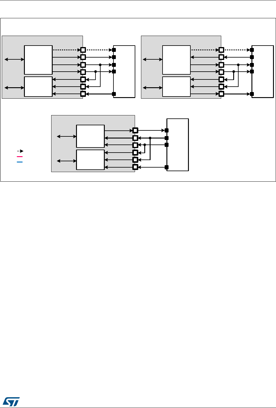
DocID025941 Rev 5 857/1001
RM0376 Serial peripheral interface/ inter-IC sound (SPI/I2S)
881
Figure 277. Full-duplex communication
30.6.3 Supported audio protocols
The three-line bus has to handle only audio data generally time-multiplexed on two
channels: the right channel and the left channel. However there is only one 16-bit register
for transmission or reception. So, it is up to the software to write into the data register the
appropriate value corresponding to each channel side, or to read the data from the data
register and to identify the corresponding channel by checking the CHSIDE bit in the
SPIx_SR register. Channel left is always sent first followed by the channel right (CHSIDE
has no meaning for the PCM protocol).
Four data and packet frames are available. Data may be sent with a format of:
•16-bit data packed in a 16-bit frame
•16-bit data packed in a 32-bit frame
•24-bit data packed in a 32-bit frame
•32-bit data packed in a 32-bit frame
When using 16-bit data extended on 32-bit packet, the first 16 bits (MSB) are the significant
bits, the 16-bit LSB is forced to 0 without any need for software action or DMA request (only
one read/write operation).
The 24-bit and 32-bit data frames need two CPU read or write operations to/from the
SPIx_DR register or two DMA operations if the DMA is preferred for the application. For 24-
bit data frame specifically, the 8 non significant bits are extended to 32 bits with 0-bits (by
hardware).
For all data formats and communication standards, the most significant bit is always sent
first (MSB first).
MSv42093V1
SPI2Sx
(MASTER-TX)
SPI2Sy
(SLAVE-RX)
MCK (O)
CK (O)
WS (O)
SD (O)
CK (I)
WS (I)
SD (I)
External
slave
device
STM32
SPI2Sx
(SLAVE-TX)
SPI2Sy
(SLAVE-RX)
CK (I)
WS (I)
SD (O)
CK (I)
WS (I)
SD (I)
External
master
device
STM32
Optional
SPI2Sx
(MASTER-RX)
SPI2Sy
(SLAVE-TX)
MCK (O)
CK (O)
WS (O)
SD (I)
CK (I)
WS (I)
SD (O)
External
slave
device
STM32
MASTER full-duplex configurations
SLAVE full-duplex configurations
spix_tx_dm
a
spix_rx_dm
a
spix_tx_dm
a
spix_rx_dm
a
spix_rx_dm
a
spix_tx_dm
a
Master
Slave
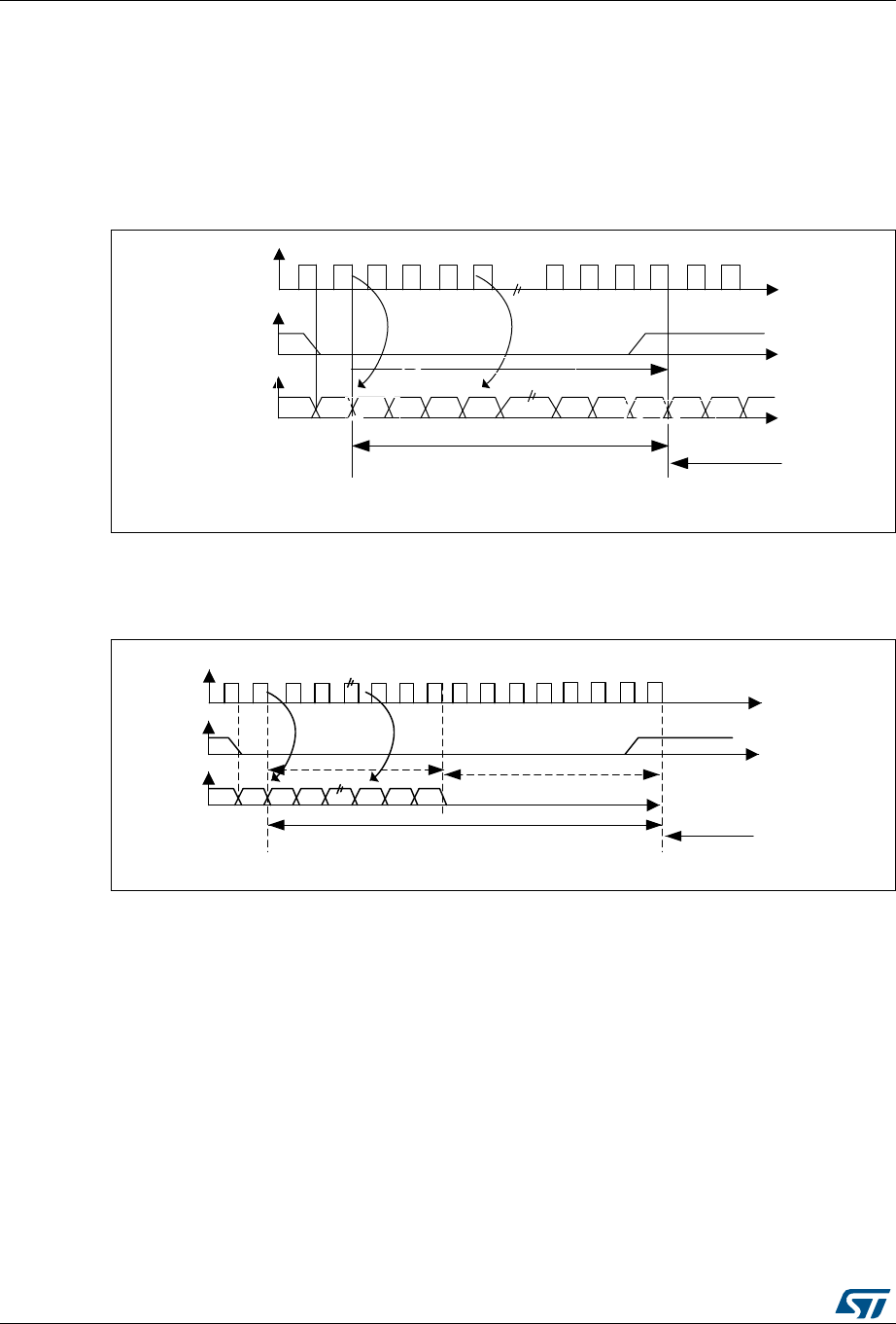
Serial peripheral interface/ inter-IC sound (SPI/I2S) RM0376
858/1001 DocID025941 Rev 5
The I2S interface supports four audio standards, configurable using the I2SSTD[1:0] and
PCMSYNC bits in the SPIx_I2SCFGR register.
I2S Philips standard
For this standard, the WS signal is used to indicate which channel is being transmitted. It is
activated one CK clock cycle before the first bit (MSB) is available.
Figure 278. I2S Philips protocol waveforms (16/32-bit full accuracy, CPOL = 0)
Data are latched on the falling edge of CK (for the transmitter) and are read on the rising
edge (for the receiver). The WS signal is also latched on the falling edge of CK.
Figure 279. I2S Philips standard waveforms (24-bit frame with CPOL = 0)
This mode needs two write or read operations to/from the SPIx_DR register.
MS19591V1
CK
WS
SD
Can be 16-bit or 32-bit
MSB MSBLSB
Channel left
Channel
right
transmission reception
MS19592V1
CK
WS
SD
Transmission Reception
24-bit data
MSB LSB
Channel left 32-bit
Channel right
8-bit remaining 0 forced
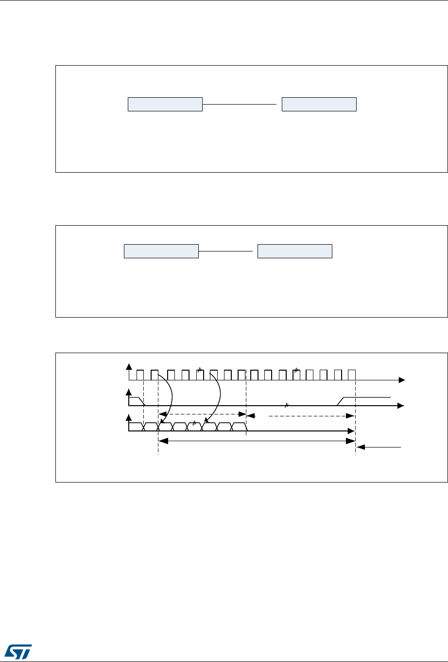
DocID025941 Rev 5 859/1001
RM0376 Serial peripheral interface/ inter-IC sound (SPI/I2S)
881
•In transmission mode:
If 0x8EAA33 has to be sent (24-bit):
Figure 280. Transmitting 0x8EAA33
•In reception mode:
If data 0x8EAA33 is received:
Figure 281. Receiving 0x8EAA33
Figure 282. I2S Philips standard (16-bit extended to 32-bit packet frame with
CPOL = 0)
When 16-bit data frame extended to 32-bit channel frame is selected during the I2S
configuration phase, only one access to the SPIx_DR register is required. The 16 remaining
bits are forced by hardware to 0x0000 to extend the data to 32-bit format.
If the data to transmit or the received data are 0x76A3 (0x76A30000 extended to 32-bit), the
operation shown in Figure 283 is required.
MS19593V1
0x8EAA 0x33XX
First write to Data register Second write to Data register
Only the 8 MSB are sent
to compare the 24 bits
8 LSBs have no meaning
and can be anything
MS19594V1
0x8EAA 0x33XX
First read to Data register Second read to Data register
Only the 8 MSB are sent
to compare the 24 bits
8 LSBs have no meaning
and can be anything
MS19599V1
CK
WS
SD
Transmission Reception
16-bit data
MSB LSB
Channel left 32-bit Channel right
16-bit remaining 0 forced
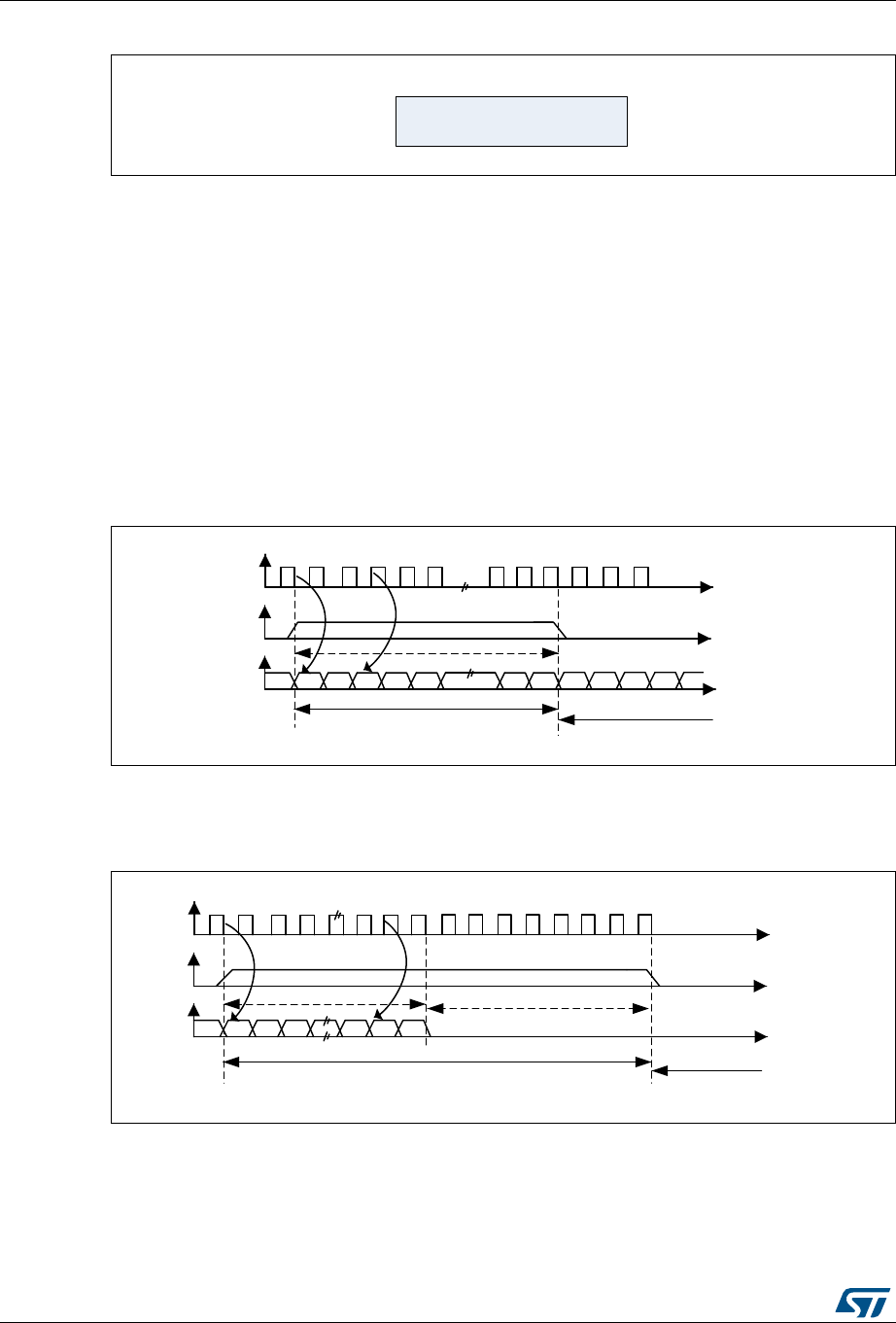
Serial peripheral interface/ inter-IC sound (SPI/I2S) RM0376
860/1001 DocID025941 Rev 5
Figure 283. Example of 16-bit data frame extended to 32-bit channel frame
For transmission, each time an MSB is written to SPIx_DR, the TXE flag is set and its
interrupt, if allowed, is generated to load the SPIx_DR register with the new value to send.
This takes place even if 0x0000 have not yet been sent because it is done by hardware.
For reception, the RXNE flag is set and its interrupt, if allowed, is generated when the first
16 MSB half-word is received.
In this way, more time is provided between two write or read operations, which prevents
underrun or overrun conditions (depending on the direction of the data transfer).
MSB justified standard
For this standard, the WS signal is generated at the same time as the first data bit, which is
the MSBit.
Figure 284. MSB Justified 16-bit or 32-bit full-accuracy length with CPOL = 0
Data are latched on the falling edge of CK (for transmitter) and are read on the rising edge
(for the receiver).
Figure 285. MSB justified 24-bit frame length with CPOL = 0
MS19595V1
0x76A3
Only one access to SPIx_DR
MS30100 V1
CK
WS
SD
Transmission Reception
16- or 32 bit data
MSB LSB
Channel left
Channel right
MSB
MS30101V1
CK
WS
SD
Transmission Reception
24 bit data
MSB LSB
Channel left 32-bit
Channel right
8-bit remaining
0 forced
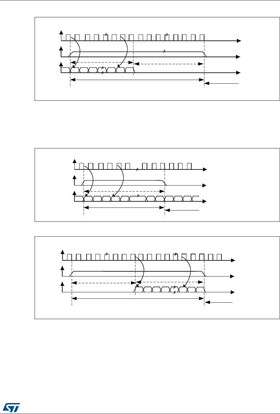
DocID025941 Rev 5 861/1001
RM0376 Serial peripheral interface/ inter-IC sound (SPI/I2S)
881
Figure 286. MSB justified 16-bit extended to 32-bit packet frame with CPOL = 0
LSB justified standard
This standard is similar to the MSB justified standard (no difference for the 16-bit and 32-bit
full-accuracy frame formats).
Figure 287. LSB justified 16-bit or 32-bit full-accuracy with CPOL = 0
Figure 288. LSB justified 24-bit frame length with CPOL = 0
MS30102V1
CK
WS
SD
Transmission Reception
16-bit data
MSB LSB
Channel left 32-bit
Channel right
16-bit remaining
0 forced
MS30103V1
CK
WS
SD
Transmission Reception
16- or 32-bit data
MSB LSB
Channel left
Channel right
MSB
MS30104V1
CK
WS
SD
Transmission
Reception
8-bit data
0 forced
MSB LSB
Channel left 32-bit
Channel right
24-bit remaining
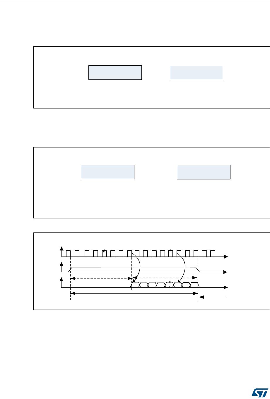
Serial peripheral interface/ inter-IC sound (SPI/I2S) RM0376
862/1001 DocID025941 Rev 5
•In transmission mode:
If data 0x3478AE have to be transmitted, two write operations to the SPIx_DR register
are required by software or by DMA. The operations are shown below.
Figure 289. Operations required to transmit 0x3478AE
•In reception mode:
If data 0x3478AE are received, two successive read operations from the SPIx_DR
register are required on each RXNE event.
Figure 290. Operations required to receive 0x3478AE
Figure 291. LSB justified 16-bit extended to 32-bit packet frame with CPOL = 0
When 16-bit data frame extended to 32-bit channel frame is selected during the I2S
configuration phase, Only one access to the SPIx_DR register is required. The 16 remaining
bits are forced by hardware to 0x0000 to extend the data to 32-bit format. In this case it
corresponds to the half-word MSB.
If the data to transmit or the received data are 0x76A3 (0x0000 76A3 extended to 32-bit),
the operation shown in Figure 292 is required.
0xXX34 0x78AE
First write to Data register
conditioned by TXE=1
Second write to Data register
conditioned by TXE=1
Only the 8 LSB of the
half-word are significant.
A field of 0x00 is forced
instead of the 8 MSBs.
MS19596V1
0xXX34 0x78AE
First read from Data register
conditioned by RXNE=1
Second read from Data register
conditioned by RXNE=1
Only the 8 LSB of the
half-word are significant.
A field of 0x00 is forced
instead of the 8 MSBs.
MS19597V1
MS30105V1
CK
WS
SD
Transmission
Reception
16-bit data
0 forced
MSB LSB
Channel left 32-bit
Channel right
16-bit remaining
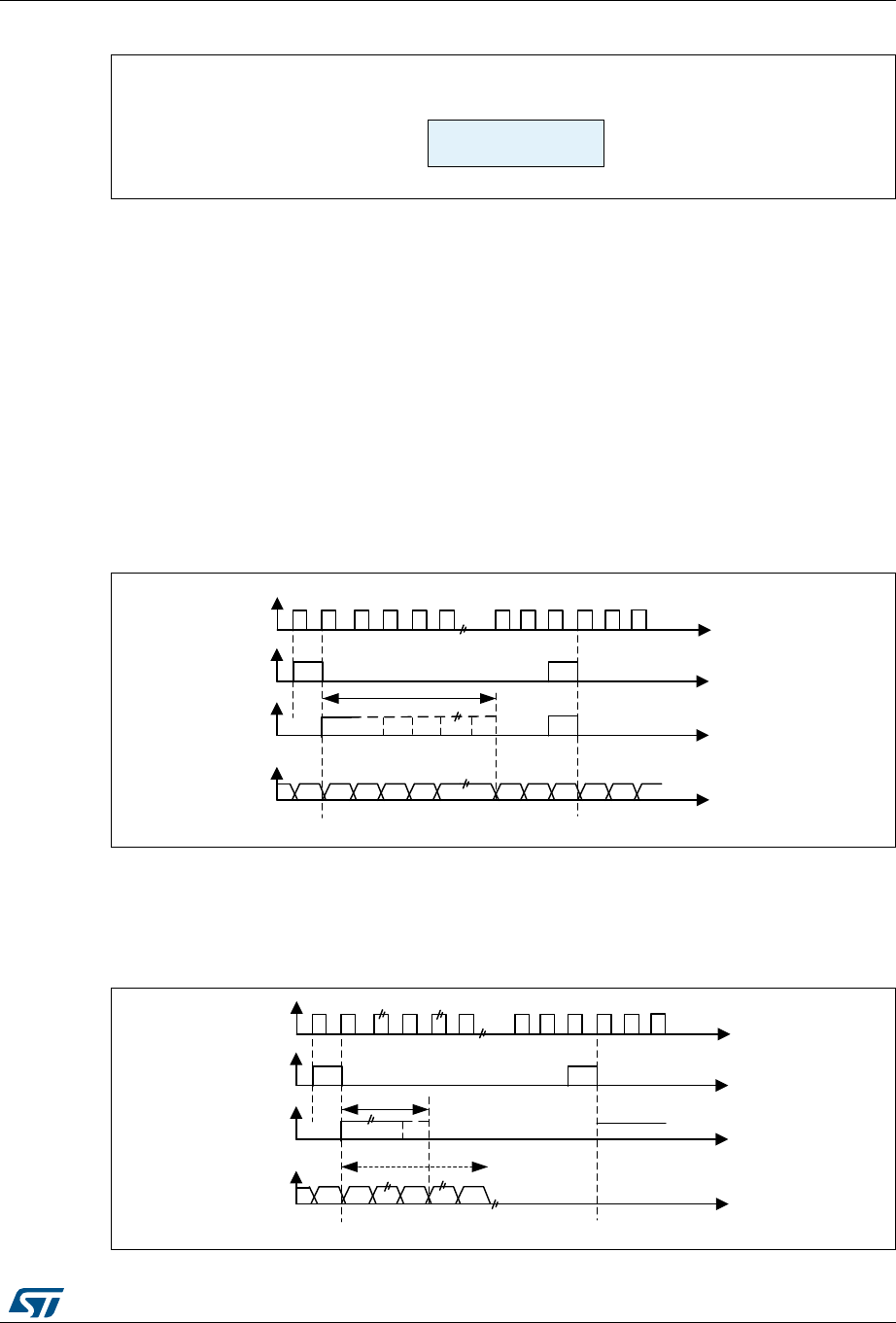
DocID025941 Rev 5 863/1001
RM0376 Serial peripheral interface/ inter-IC sound (SPI/I2S)
881
Figure 292. Example of 16-bit data frame extended to 32-bit channel frame
In transmission mode, when a TXE event occurs, the application has to write the data to be
transmitted (in this case 0x76A3). The 0x000 field is transmitted first (extension on 32-bit).
The TXE flag is set again as soon as the effective data (0x76A3) is sent on SD.
In reception mode, RXNE is asserted as soon as the significant half-word is received (and
not the 0x0000 field).
In this way, more time is provided between two write or read operations to prevent underrun
or overrun conditions.
PCM standard
For the PCM standard, there is no need to use channel-side information. The two PCM
modes (short and long frame) are available and configurable using the PCMSYNC bit in
SPIx_I2SCFGR register.
Figure 293. PCM standard waveforms (16-bit)
For long frame synchronization, the WS signal assertion time is fixed to 13 bits in master
mode.
For short frame synchronization, the WS synchronization signal is only one cycle long.
Figure 294. PCM standard waveforms (16-bit extended to 32-bit packet frame)
0x76A3
Only one access to the SPIx-DR register
MS19598V1
MS30106V1
CK
WS
short frame
SD
WS
long frame
13-bits
MSB LSB MSB
MS30107V1
CK
WS
short frame
SD
WS
long frame
Up to 13-bits
MSB LSB
16 bits
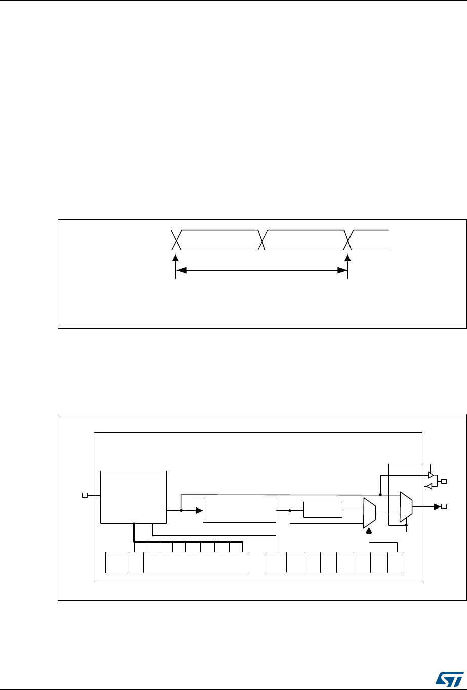
Serial peripheral interface/ inter-IC sound (SPI/I2S) RM0376
864/1001 DocID025941 Rev 5
Note: For both modes (master and slave) and for both synchronizations (short and long), the
number of bits between two consecutive pieces of data (and so two synchronization signals)
needs to be specified (DATLEN and CHLEN bits in the SPIx_I2SCFGR register) even in
slave mode.
30.6.4 Clock generator
The I2S bitrate determines the data flow on the I2S data line and the I2S clock signal
frequency.
I2S bitrate = number of bits per channel × number of channels × sampling audio frequency
For a 16-bit audio, left and right channel, the I2S bitrate is calculated as follows:
I2S bitrate = 16 × 2 × fS
It will be: I2S bitrate = 32 x 2 x fS if the packet length is 32-bit wide.
Figure 295. Audio sampling frequency definition
When the master mode is configured, a specific action needs to be taken to properly
program the linear divider in order to communicate with the desired audio frequency.
Figure 296 presents the communication clock architecture. The I2Sx clock is always the
system clock.
Figure 296. I2S clock generator architecture
1. Where x = 2.
MS30108V1
16-or 32-bit left
channel
16-or 32-bit
right channel
32- or 64-bits
sampling point sampling point
FS
FS : audio sampling frequency
MS30109V1
MCKOE ODD
8-bit linear divider
+ reshaping stage
Divider by 4 Div2
I²SDIV[7:0]
I²SMOD
CHLEN
0
1
0
1
MCKOE
CK
MCK
I²SxCLK

DocID025941 Rev 5 865/1001
RM0376 Serial peripheral interface/ inter-IC sound (SPI/I2S)
881
The audio sampling frequency may be 192 KHz, 96 kHz, 48 kHz, 44.1 kHz, 32 kHz,
22.05 kHz, 16 kHz, 11.025 kHz or 8 kHz (or any other value within this range). In order to
reach the desired frequency, the linear divider needs to be programmed according to the
formulas below:
When the master clock is generated (MCKOE in the SPIx_I2SPR register is set):
fS = I2SxCLK / [(16*2)*((2*I2SDIV)+ODD)*8)] when the channel frame is 16-bit wide
fS = I2SxCLK / [(32*2)*((2*I2SDIV)+ODD)*4)] when the channel frame is 32-bit wide
When the master clock is disabled (MCKOE bit cleared):
fS = I2SxCLK / [(16*2)*((2*I2SDIV)+ODD))] when the channel frame is 16-bit wide
fS = I2SxCLK / [(32*2)*((2*I2SDIV)+ODD))] when the channel frame is 32-bit wide
Table 144 provides example precision values for different clock configurations.
Note: Other configurations are possible that allow optimum clock precision.
Table 144. Audio-frequency precision using standard 8 MHz HSE
SYSCLK
(MHz)
Data
length I2SDIV I2SODD MCLK Target fs(Hz) Real fs (kHz) Error
32 16 5 0 No 96000 100 4.1667%
32 32 2 0 No 96000 100 4.1667%
32 16 10 1 No 48000 47.619 0.7937%
32 32 5 0 No 48000 50 4.1667%
32 16 11 1 No 44100 43.478 1.4098%
32 32 5 1 No 44100 45.454 3.0715%
32 16 15 1 No 32000 32.258 0.8065%
32 32 8 0 No 32000 31.25 2.3430%
32 16 22 1 No 22050 22.222 0.7811%
32 32 11 1 No 22050 21.739 1.4098%
32 16 31 1 No 16000 15.873 0.7937%
32 32 15 1 No 16000 16.129 0.8065%
32 16 45 1 No 11025 10.989 0.3264%
32 32 22 1 No 11025 11.111 0.7811%
32 16 62 1 No 8000 8 0.0000%
32 32 31 1 No 8000 7.936 0.7937%
32 16 2 0 Yes 32000 31.25 2.3430%
32 32 2 0 Yes 32000 31.25 2.3430%
32 16 3 0 Yes 22050 20.833 5.5170%
32 32 3 0 Yes 22050 20.833 5.5170%
32 16 4 0 Yes 16000 15.625 2.3428%
32 32 4 0 Yes 16000 15.625 2.3428%
32 16 5 1 Yes 11025 11.363 3.0715%

Serial peripheral interface/ inter-IC sound (SPI/I2S) RM0376
866/1001 DocID025941 Rev 5
30.6.5 I2S master mode
The I2S can be configured in master mode. This means that the serial clock is generated on
the CK pin as well as the Word Select signal WS. Master clock (MCK) may be output or not,
controlled by the MCKOE bit in the SPIx_I2SPR register.
Procedure
1. Select the I2SDIV[7:0] bits in the SPIx_I2SPR register to define the serial clock baud
rate to reach the proper audio sample frequency. The ODD bit in the SPIx_I2SPR
register also has to be defined.
2. Select the CKPOL bit to define the steady level for the communication clock. Set the
MCKOE bit in the SPIx_I2SPR register if the master clock MCK needs to be provided
to the external DAC/ADC audio component (the I2SDIV and ODD values should be
computed depending on the state of the MCK output, for more details refer to
Section 30.6.4: Clock generator).
3. Set the I2SMOD bit in the SPIx_I2SCFGR register to activate the I2S functions and
choose the I2S standard through the I2SSTD[1:0] and PCMSYNC bits, the data length
through the DATLEN[1:0] bits and the number of bits per channel by configuring the
CHLEN bit. Select also the I2S master mode and direction (Transmitter or Receiver)
through the I2SCFG[1:0] bits in the SPIx_I2SCFGR register.
4. If needed, select all the potential interrupt sources and the DMA capabilities by writing
the SPIx_CR2 register.
5. The I2SE bit in SPIx_I2SCFGR register must be set.
WS and CK are configured in output mode. MCK is also an output, if the MCKOE bit in
SPIx_I2SPR is set.
Transmission sequence
The transmission sequence begins when a half-word is written into the Tx buffer.
Lets assume the first data written into the Tx buffer corresponds to the left channel data.
When data are transferred from the Tx buffer to the shift register, TXE is set and data
corresponding to the right channel have to be written into the Tx buffer. The CHSIDE flag
indicates which channel is to be transmitted. It has a meaning when the TXE flag is set
because the CHSIDE flag is updated when TXE goes high.
A full frame has to be considered as a left channel data transmission followed by a right
channel data transmission. It is not possible to have a partial frame where only the left
channel is sent.
The data half-word is parallel loaded into the 16-bit shift register during the first bit
transmission, and then shifted out, serially, to the MOSI/SD pin, MSB first. The TXE flag is
32 32 5 1 Yes 11025 11.363 3.0715%
32 16 8 0 Yes 8000 7.812 2.3428%
32 32 8 0 Yes 8000 7.812 2.3428%
Table 144. Audio-frequency precision using standard 8 MHz HSE (continued)
SYSCLK
(MHz)
Data
length I2SDIV I2SODD MCLK Target fs(Hz) Real fs (kHz) Error

DocID025941 Rev 5 867/1001
RM0376 Serial peripheral interface/ inter-IC sound (SPI/I2S)
881
set after each transfer from the Tx buffer to the shift register and an interrupt is generated if
the TXEIE bit in the SPIx_CR2 register is set.
For more details about the write operations depending on the I2S Standard-mode selected,
refer to Section 30.6.3: Supported audio protocols).
To ensure a continuous audio data transmission, it is mandatory to write the SPIx_DR
register with the next data to transmit before the end of the current transmission.
To switch off the I2S, by clearing I2SE, it is mandatory to wait for TXE = 1 and BSY = 0.
Reception sequence
The operating mode is the same as for transmission mode except for the point 3 (refer to the
procedure described in Section 30.6.5: I2S master mode), where the configuration should
set the master reception mode through the I2SCFG[1:0] bits.
Whatever the data or channel length, the audio data are received by 16-bit packets. This
means that each time the Rx buffer is full, the RXNE flag is set and an interrupt is generated
if the RXNEIE bit is set in SPIx_CR2 register. Depending on the data and channel length
configuration, the audio value received for a right or left channel may result from one or two
receptions into the Rx buffer.
Clearing the RXNE bit is performed by reading the SPIx_DR register.
CHSIDE is updated after each reception. It is sensitive to the WS signal generated by the
I2S cell.
For more details about the read operations depending on the I2S Standard-mode selected,
refer to Section 30.6.3: Supported audio protocols.
If data are received while the previously received data have not been read yet, an overrun is
generated and the OVR flag is set. If the ERRIE bit is set in the SPIx_CR2 register, an
interrupt is generated to indicate the error.
To switch off the I2S, specific actions are required to ensure that the I2S completes the
transfer cycle properly without initiating a new data transfer. The sequence depends on the
configuration of the data and channel lengths, and on the audio protocol mode selected. In
the case of:
•16-bit data length extended on 32-bit channel length (DATLEN = 00 and CHLEN = 1)
using the LSB justified mode (I2SSTD = 10)
a) Wait for the second to last RXNE = 1 (n – 1)
b) Then wait 17 I2S clock cycles (using a software loop)
c) Disable the I2S (I2SE = 0)
•16-bit data length extended on 32-bit channel length (DATLEN = 00 and CHLEN = 1) in
MSB justified, I2S or PCM modes (I2SSTD = 00, I2SSTD = 01 or I2SSTD = 11,
respectively)
a) Wait for the last RXNE
b) Then wait 1 I2S clock cycle (using a software loop)
c) Disable the I2S (I2SE = 0)

Serial peripheral interface/ inter-IC sound (SPI/I2S) RM0376
868/1001 DocID025941 Rev 5
•For all other combinations of DATLEN and CHLEN, whatever the audio mode selected
through the I2SSTD bits, carry out the following sequence to switch off the I2S:
a) Wait for the second to last RXNE = 1 (n – 1)
b) Then wait one I2S clock cycle (using a software loop)
c) Disable the I2S (I2SE = 0)
Note: The BSY flag is kept low during transfers.
30.6.6 I2S slave mode
For the slave configuration, the I2S can be configured in transmission or reception mode.
The operating mode is following mainly the same rules as described for the I2S master
configuration. In slave mode, there is no clock to be generated by the I2S interface. The
clock and WS signals are input from the external master connected to the I2S interface.
There is then no need, for the user, to configure the clock.
The configuration steps to follow are listed below:
1. Set the I2SMOD bit in the SPIx_I2SCFGR register to select I2S mode and choose the
I2S standard through the I2SSTD[1:0] bits, the data length through the DATLEN[1:0]
bits and the number of bits per channel for the frame configuring the CHLEN bit. Select
also the mode (transmission or reception) for the slave through the I2SCFG[1:0] bits in
SPIx_I2SCFGR register.
2. If needed, select all the potential interrupt sources and the DMA capabilities by writing
the SPIx_CR2 register.
3. The I2SE bit in SPIx_I2SCFGR register must be set.
Transmission sequence
The transmission sequence begins when the external master device sends the clock and
when the NSS_WS signal requests the transfer of data. The slave has to be enabled before
the external master starts the communication. The I2S data register has to be loaded before
the master initiates the communication.
For the I2S, MSB justified and LSB justified modes, the first data item to be written into the
data register corresponds to the data for the left channel. When the communication starts,
the data are transferred from the Tx buffer to the shift register. The TXE flag is then set in
order to request the right channel data to be written into the I2S data register.
The CHSIDE flag indicates which channel is to be transmitted. Compared to the master
transmission mode, in slave mode, CHSIDE is sensitive to the WS signal coming from the
external master. This means that the slave needs to be ready to transmit the first data
before the clock is generated by the master. WS assertion corresponds to left channel
transmitted first.
Note: The I2SE has to be written at least two PCLK cycles before the first clock of the master
comes on the CK line.
The data half-word is parallel-loaded into the 16-bit shift register (from the internal bus)
during the first bit transmission, and then shifted out serially to the MOSI/SD pin MSB first.
The TXE flag is set after each transfer from the Tx buffer to the shift register and an interrupt
is generated if the TXEIE bit in the SPIx_CR2 register is set.
Note that the TXE flag should be checked to be at 1 before attempting to write the Tx buffer.

DocID025941 Rev 5 869/1001
RM0376 Serial peripheral interface/ inter-IC sound (SPI/I2S)
881
For more details about the write operations depending on the I2S Standard-mode selected,
refer to Section 30.6.3: Supported audio protocols.
To secure a continuous audio data transmission, it is mandatory to write the SPIx_DR
register with the next data to transmit before the end of the current transmission. An
underrun flag is set and an interrupt may be generated if the data are not written into the
SPIx_DR register before the first clock edge of the next data communication. This indicates
to the software that the transferred data are wrong. If the ERRIE bit is set into the SPIx_CR2
register, an interrupt is generated when the UDR flag in the SPIx_SR register goes high. In
this case, it is mandatory to switch off the I2S and to restart a data transfer starting from the
left channel.
To switch off the I2S, by clearing the I2SE bit, it is mandatory to wait for TXE = 1 and
BSY = 0.
Reception sequence
The operating mode is the same as for the transmission mode except for the point 1 (refer to
the procedure described in Section 30.6.6: I2S slave mode), where the configuration should
set the master reception mode using the I2SCFG[1:0] bits in the SPIx_I2SCFGR register.
Whatever the data length or the channel length, the audio data are received by 16-bit
packets. This means that each time the RX buffer is full, the RXNE flag in the SPIx_SR
register is set and an interrupt is generated if the RXNEIE bit is set in the SPIx_CR2
register. Depending on the data length and channel length configuration, the audio value
received for a right or left channel may result from one or two receptions into the RX buffer.
The CHSIDE flag is updated each time data are received to be read from the SPIx_DR
register. It is sensitive to the external WS line managed by the external master component.
Clearing the RXNE bit is performed by reading the SPIx_DR register.
For more details about the read operations depending the I2S Standard-mode selected,
refer to Section 30.6.3: Supported audio protocols.
If data are received while the preceding received data have not yet been read, an overrun is
generated and the OVR flag is set. If the bit ERRIE is set in the SPIx_CR2 register, an
interrupt is generated to indicate the error.
To switch off the I2S in reception mode, I2SE has to be cleared immediately after receiving
the last RXNE = 1.
Note: The external master components should have the capability of sending/receiving data in 16-
bit or 32-bit packets via an audio channel.
30.6.7 I2S status flags
Three status flags are provided for the application to fully monitor the state of the I2S bus.
Busy flag (BSY)
The BSY flag is set and cleared by hardware (writing to this flag has no effect). It indicates
the state of the communication layer of the I2S.
When BSY is set, it indicates that the I2S is busy communicating. There is one exception in
master receive mode (I2SCFG = 11) where the BSY flag is kept low during reception.

Serial peripheral interface/ inter-IC sound (SPI/I2S) RM0376
870/1001 DocID025941 Rev 5
The BSY flag is useful to detect the end of a transfer if the software needs to disable the I2S.
This avoids corrupting the last transfer. For this, the procedure described below must be
strictly respected.
The BSY flag is set when a transfer starts, except when the I2S is in master receiver mode.
The BSY flag is cleared:
•When a transfer completes (except in master transmit mode, in which the
communication is supposed to be continuous)
•When the I2S is disabled
When communication is continuous:
•In master transmit mode, the BSY flag is kept high during all the transfers
•In slave mode, the BSY flag goes low for one I2S clock cycle between each transfer
Note: Do not use the BSY flag to handle each data transmission or reception. It is better to use the
TXE and RXNE flags instead.
Tx buffer empty flag (TXE)
When set, this flag indicates that the Tx buffer is empty and the next data to be transmitted
can then be loaded into it. The TXE flag is reset when the Tx buffer already contains data to
be transmitted. It is also reset when the I2S is disabled (I2SE bit is reset).
RX buffer not empty (RXNE)
When set, this flag indicates that there are valid received data in the RX Buffer. It is reset
when SPIx_DR register is read.
Channel Side flag (CHSIDE)
In transmission mode, this flag is refreshed when TXE goes high. It indicates the channel
side to which the data to transfer on SD has to belong. In case of an underrun error event in
slave transmission mode, this flag is not reliable and I2S needs to be switched off and
switched on before resuming the communication.
In reception mode, this flag is refreshed when data are received into SPIx_DR. It indicates
from which channel side data have been received. Note that in case of error (like OVR) this
flag becomes meaningless and the I2S should be reset by disabling and then enabling it
(with configuration if it needs changing).
This flag has no meaning in the PCM standard (for both Short and Long frame modes).
When the OVR or UDR flag in the SPIx_SR is set and the ERRIE bit in SPIx_CR2 is also
set, an interrupt is generated. This interrupt can be cleared by reading the SPIx_SR status
register (once the interrupt source has been cleared).
30.6.8 I2S error flags
There are three error flags for the I2S cell.
Underrun flag (UDR)
In slave transmission mode this flag is set when the first clock for data transmission appears
while the software has not yet loaded any value into SPIx_DR. It is available when the
I2SMOD bit in the SPIx_I2SCFGR register is set. An interrupt may be generated if the

DocID025941 Rev 5 871/1001
RM0376 Serial peripheral interface/ inter-IC sound (SPI/I2S)
881
ERRIE bit in the SPIx_CR2 register is set.
The UDR bit is cleared by a read operation on the SPIx_SR register.
Overrun flag (OVR)
This flag is set when data are received and the previous data have not yet been read from
the SPIx_DR register. As a result, the incoming data are lost. An interrupt may be generated
if the ERRIE bit is set in the SPIx_CR2 register.
In this case, the receive buffer contents are not updated with the newly received data from
the transmitter device. A read operation to the SPIx_DR register returns the previous
correctly received data. All other subsequently transmitted half-words are lost.
Clearing the OVR bit is done by a read operation on the SPIx_DR register followed by a
read access to the SPIx_SR register.
Frame error flag (FRE)
This flag can be set by hardware only if the I2S is configured in Slave mode. It is set if the
external master is changing the WS line while the slave is not expecting this change. If the
synchronization is lost, the following steps are required to recover from this state and
resynchronize the external master device with the I2S slave device:
1. Disable the I2S.
2. Enable it again when the correct level is detected on the WS line (WS line is high in I2S
mode or low for MSB- or LSB-justified or PCM modes.
Desynchronization between master and slave devices may be due to noisy environment on
the SCK communication clock or on the WS frame synchronization line. An error interrupt
can be generated if the ERRIE bit is set. The desynchronization flag (FRE) is cleared by
software when the status register is read.
30.6.9 I2S interrupts
Table 145 provides the list of I2S interrupts.
30.6.10 DMA features
In I2S mode, the DMA works in exactly the same way as it does in SPI mode. There is no
difference except that the CRC feature is not available in I2S mode since there is no data
transfer protection system.
Table 145. I2S interrupt requests
Interrupt event Event flag Enable control bit
Transmit buffer empty flag TXE TXEIE
Receive buffer not empty flag RXNE RXNEIE
Overrun error OVR
ERRIEUnderrun error UDR
Frame error flag FRE

Serial peripheral interface/ inter-IC sound (SPI/I2S) RM0376
872/1001 DocID025941 Rev 5
30.7 SPI and I2S registers
The peripheral registers can be accessed by half-words (16-bit) or words (32-bit). SPI_DR
in addition by can be accessed by 8-bit access.
Refer to Section 1.1 for a list of abbreviations used in register descriptions.
The peripheral registers can be accessed by half-words (16 bits) or words (32 bits).
30.7.1 SPI control register 1 (SPI_CR1) (not used in I2S mode)
Address offset: 0x00
Reset value: 0x0000
1514131211109876543210
BIDI
MODE
BIDI
OE
CRC
EN
CRC
NEXT DFF RX
ONLY SSM SSI LSB
FIRST SPE BR [2:0] MSTR CPOL CPHA
rw rw rw rw rw rw rw rw rw rw rw rw rw rw rw rw
Bit 15 BIDIMODE: Bidirectional data mode enable
This bit enables half-duplex communication using common single bidirectional data line.
Keep RXONLY bit clear when bidirectional mode is active.
0: 2-line unidirectional data mode selected
1: 1-line bidirectional data mode selected
Note: This bit is not used in I2S mode
Bit 14 BIDIOE: Output enable in bidirectional mode
This bit combined with the BIDIMODE bit selects the direction of transfer in bidirectional
mode
0: Output disabled (receive-only mode)
1: Output enabled (transmit-only mode)
Note: In master mode, the MOSI pin is used while the MISO pin is used in slave mode.
This bit is not used in I2S mode.
Bit 13 CRCEN: Hardware CRC calculation enable
0: CRC calculation disabled
1: CRC calculation enabled
Note: This bit should be written only when SPI is disabled (SPE = ‘0’) for correct operation.
It is not used in I2S mode.
Bit 12 CRCNEXT: CRC transfer next
0: Data phase (no CRC phase)
1: Next transfer is CRC (CRC phase)
Note: When the SPI is configured in full-duplex or transmitter only modes, CRCNEXT must be
written as soon as the last data is written to the SPI_DR register.
When the SPI is configured in receiver only mode, CRCNEXT must be set after the
second last data reception.
This bit should be kept cleared when the transfers are managed by DMA.
It is not used in I2S mode.

DocID025941 Rev 5 873/1001
RM0376 Serial peripheral interface/ inter-IC sound (SPI/I2S)
881
Bit 11 DFF: Data frame format
0: 8-bit data frame format is selected for transmission/reception
1: 16-bit data frame format is selected for transmission/reception
Note: This bit should be written only when SPI is disabled (SPE = ‘0’) for correct operation.
It is not used in I2S mode.
Bit 10 RXONLY: Receive only mode enable
This bit enables simplex communication using a single unidirectional line to receive data
exclusively. Keep BIDIMODE bit clear when receive only mode is active.
This bit is also useful in a multislave system in which this particular slave is not accessed, the
output from the accessed slave is not corrupted.
0: full-duplex (Transmit and receive)
1: Output disabled (Receive-only mode)
Note: This bit is not used in I2S mode
Bit 9 SSM: Software slave management
When the SSM bit is set, the NSS pin input is replaced with the value from the SSI bit.
0: Software slave management disabled
1: Software slave management enabled
Note: This bit is not used in I2S mode and SPI TI mode
Bit 8 SSI: Internal slave select
This bit has an effect only when the SSM bit is set. The value of this bit is forced onto the
NSS pin and the IO value of the NSS pin is ignored.
Note: This bit is not used in I2S mode and SPI TI mode
Bit 7 LSBFIRST: Frame format
0: MSB transmitted first
1: LSB transmitted first
Note: This bit should not be changed when communication is ongoing.
It is not used in I2S mode and SPI TI mode
Bit 6 SPE: SPI enable
0: Peripheral disabled
1: Peripheral enabled
Note: When disabling the SPI, follow the procedure described in Section 30.3.10: Procedure
for disabling the SPI.
This bit is not used in I2S mode.
Bits 5:3 BR[2:0]: Baud rate control
000: fPCLK/2
001: fPCLK/4
010: fPCLK/8
011: fPCLK/16
100: fPCLK/32
101: fPCLK/64
110: fPCLK/128
111: fPCLK/256
Note: These bits should not be changed when communication is ongoing.
They are not used in I2S mode.

Serial peripheral interface/ inter-IC sound (SPI/I2S) RM0376
874/1001 DocID025941 Rev 5
30.7.2 SPI control register 2 (SPI_CR2)
Address offset: 0x04
Reset value: 0x0000
Bit 2 MSTR: Master selection
0: Slave configuration
1: Master configuration
Note: This bit should not be changed when communication is ongoing.
It is not used in I2S mode.
Bit1 CPOL: Clock polarity
0: CK to 0 when idle
1: CK to 1 when idle
Note: This bit should not be changed when communication is ongoing.
It is not used in I2S mode and SPI TI mode except the case when CRC is applied
at TI mode.
Bit 0 CPHA: Clock phase
0: The first clock transition is the first data capture edge
1: The second clock transition is the first data capture edge
Note: This bit should not be changed when communication is ongoing.
It is not used in I2S mode and SPI TI mode except the case when CRC is applied
at TI mode.
15 14 13 12 11 10 9 8 7 6 5 4 3 2 1 0
Res. Res. Res. Res. Res. Res. Res. Res. TXEIE RXNEIE ERRIE FRF Res. SSOE TXDMAEN RXDMAEN
rw rw rw rw rw rw rw
Bits 15:8 Reserved, must be kept at reset value.
Bit 7 TXEIE: Tx buffer empty interrupt enable
0: TXE interrupt masked
1: TXE interrupt not masked. Used to generate an interrupt request when the TXE flag is set.
Bit 6 RXNEIE: RX buffer not empty interrupt enable
0: RXNE interrupt masked
1: RXNE interrupt not masked. Used to generate an interrupt request when the RXNE flag is
set.
Bit 5 ERRIE: Error interrupt enable
This bit controls the generation of an interrupt when an error condition occurs (OVR,
CRCERR, MODF, FRE in SPI mode, and UDR, OVR, FRE in I2S mode).
0: Error interrupt is masked
1: Error interrupt is enabled
Bit 4 FRF: Frame format
0: SPI Motorola mode
1 SPI TI mode
Note: This bit is not used in I2S mode.
Bit 3 Reserved. Forced to 0 by hardware.

DocID025941 Rev 5 875/1001
RM0376 Serial peripheral interface/ inter-IC sound (SPI/I2S)
881
30.7.3 SPI status register (SPI_SR)
Address offset: 0x08
Reset value: 0x0002
Bit 2 SSOE: SS output enable
0: SS output is disabled in master mode and the cell can work in multimaster configuration
1: SS output is enabled in master mode and when the cell is enabled. The cell cannot work
in a multimaster environment.
Note: This bit is not used in I2S mode and SPI TI mode.
Bit 1 TXDMAEN: Tx buffer DMA enable
When this bit is set, the DMA request is made whenever the TXE flag is set.
0: Tx buffer DMA disabled
1: Tx buffer DMA enabled
Bit 0 RXDMAEN: Rx buffer DMA enable
When this bit is set, the DMA request is made whenever the RXNE flag is set.
0: Rx buffer DMA disabled
1: Rx buffer DMA enabled
1514131211109876543 2 10
Res. Res. Res. Res. Res. Res. Res. FRE BSY OVR MODF CRC
ERR UDR CHSIDE TXE RXNE
rrrrrc_w0r r rr
Bits 15:9 Reserved. Forced to 0 by hardware.
Bit 8 FRE: Frame Error
0: No frame error
1: Frame error occurred.
This bit is set by hardware and cleared by software when the SPI_SR register is read.
This bit is used in SPI TI mode or in I2S mode whatever the audio protocol selected. It
detects a change on NSS or WS line which takes place in slave mode at a non expected
time, informing about a desynchronization between the external master device and the
slave.
Bit 7 BSY: Busy flag
0: SPI (or I2S) not busy
1: SPI (or I2S) is busy in communication or Tx buffer is not empty
This flag is set and cleared by hardware.
Note: BSY flag must be used with caution: refer to Section 30.3.12: SPI status flags and
Section 30.3.10: Procedure for disabling the SPI.
Bit 6 OVR: Overrun flag
0: No overrun occurred
1: Overrun occurred
This flag is set by hardware and reset by a software sequence. Refer to Section 30.3.13: SPI
error flags for the software sequence.

Serial peripheral interface/ inter-IC sound (SPI/I2S) RM0376
876/1001 DocID025941 Rev 5
Bit 5 MODF: Mode fault
0: No mode fault occurred
1: Mode fault occurred
This flag is set by hardware and reset by a software sequence. Refer to Section 30.4 on
page 851 for the software sequence.
Note: This bit is not used in I2S mode
Bit 4 CRCERR: CRC error flag
0: CRC value received matches the SPI_RXCRCR value
1: CRC value received does not match the SPI_RXCRCR value
This flag is set by hardware and cleared by software writing 0.
Note: This bit is not used in I2S mode.
Bit 3 UDR: Underrun flag
0: No underrun occurred
1: Underrun occurred
This flag is set by hardware and reset by a software sequence. Refer to Section 30.6.8: I2S
error flags for the software sequence.
Note: This bit is not used in SPI mode.
Bit 2 CHSIDE: Channel side
0: Channel Left has to be transmitted or has been received
1: Channel Right has to be transmitted or has been received
Note: This bit is not used for SPI mode and is meaningless in PCM mode.
Bit 1 TXE: Transmit buffer empty
0: Tx buffer not empty
1: Tx buffer empty
Bit 0 RXNE: Receive buffer not empty
0: Rx buffer empty
1: Rx buffer not empty

DocID025941 Rev 5 877/1001
RM0376 Serial peripheral interface/ inter-IC sound (SPI/I2S)
881
30.7.4 SPI data register (SPI_DR)
Address offset: 0x0C
Reset value: 0x0000
30.7.5 SPI CRC polynomial register (SPI_CRCPR) (not used in I2S
mode)
Address offset: 0x10
Reset value: 0x0007
1514131211109876543210
DR[15:0]
rw rw rw rw rw rw rw rw rw rw rw rw rw rw rw rw
Bits 15:0 DR[15:0]: Data register
Data received or to be transmitted.
The data register is split into 2 buffers - one for writing (Transmit Buffer) and another one for
reading (Receive buffer). A write to the data register will write into the Tx buffer and a read
from the data register will return the value held in the Rx buffer.
Note: These notes apply to SPI mode:
Depending on the data frame format selection bit (DFF in SPI_CR1 register), the data
sent or received is either 8-bit or 16-bit. This selection has to be made before enabling
the SPI to ensure correct operation.
For an 8-bit data frame, the buffers are 8-bit and only the LSB of the register
(SPI_DR[7:0]) is used for transmission/reception. When in reception mode, the MSB of
the register (SPI_DR[15:8]) is forced to 0.
For a 16-bit data frame, the buffers are 16-bit and the entire register, SPI_DR[15:0] is
used for transmission/reception.
1514131211109876543210
CRCPOLY[15:0]
rw rw rw rw rw rw rw rw rw rw rw rw rw rw rw rw
Bits 15:0 CRCPOLY[15:0]: CRC polynomial register
This register contains the polynomial for the CRC calculation.
The CRC polynomial (0007h) is the reset value of this register. Another polynomial can be
configured as required.
Note: These bits are not used for the I2S mode.

Serial peripheral interface/ inter-IC sound (SPI/I2S) RM0376
878/1001 DocID025941 Rev 5
30.7.6 SPI RX CRC register (SPI_RXCRCR) (not used in I2S mode)
Address offset: 0x14
Reset value: 0x0000
30.7.7 SPI TX CRC register (SPI_TXCRCR) (not used in I2S mode)
Address offset: 0x18
Reset value: 0x0000
1514131211109876543210
RXCRC[15:0]
rrrrrrrrrrrrrrrr
Bits 15:0 RXCRC[15:0]: Rx CRC register
When CRC calculation is enabled, the RxCRC[15:0] bits contain the computed CRC value of
the subsequently received bytes. This register is reset when the CRCEN bit in SPI_CR1
register is written to 1. The CRC is calculated serially using the polynomial programmed in
the SPI_CRCPR register.
Only the 8 LSB bits are considered when the data frame format is set to be 8-bit data (DFF
bit of SPI_CR1 is cleared). CRC calculation is done based on any CRC8 standard.
The entire 16-bits of this register are considered when a 16-bit data frame format is selected
(DFF bit of the SPI_CR1 register is set). CRC calculation is done based on any CRC16
standard.
Note: A read to this register when the BSY Flag is set could return an incorrect value.These
bits are not used for I2S mode.
1514131211109876543210
TXCRC[15:0]
rrrrrrrrrrrrrrrr
Bits 15:0 TXCRC[15:0]: Tx CRC register
When CRC calculation is enabled, the TxCRC[7:0] bits contain the computed CRC value of
the subsequently transmitted bytes. This register is reset when the CRCEN bit of SPI_CR1
is written to 1. The CRC is calculated serially using the polynomial programmed in the
SPI_CRCPR register.
Only the 8 LSB bits are considered when the data frame format is set to be 8-bit data (DFF
bit of SPI_CR1 is cleared). CRC calculation is done based on any CRC8 standard.
The entire 16-bits of this register are considered when a 16-bit data frame format is selected
(DFF bit of the SPI_CR1 register is set). CRC calculation is done based on any CRC16
standard.
Note: A read to this register when the BSY flag is set could return an incorrect value. These
bits are not used for I2S mode.

DocID025941 Rev 5 879/1001
RM0376 Serial peripheral interface/ inter-IC sound (SPI/I2S)
881
30.7.8 SPI_I2S configuration register (SPI_I2SCFGR)
Address offset: 0x1C
Reset value: 0x0000
15 14 13 12 11 10 9 8 7 6 5 4 3 2 1 0
Res. Res. Res. Res. I2SMOD I2SE I2SCFG PCMSY
NC Res. I2SSTD CKPOL DATLEN CHLEN
rw rw rw rw rw rw rw rw rw rw rw
Bits 15:12 Reserved, must be kept at reset value.
Bit 11 I2SMOD: I2S mode selection
0: SPI mode is selected
1: I2S mode is selected
Note: This bit should be configured when the SPI or I2S is disabled
Bit 10 I2SE: I2S Enable
0: I2S peripheral is disabled
1: I2S peripheral is enabled
Note: This bit is not used in SPI mode.
Bits 9:8 I2SCFG: I2S configuration mode
00: Slave - transmit
01: Slave - receive
10: Master - transmit
11: Master - receive
Note: This bit should be configured when the I2S is disabled.
It is not used in SPI mode.
Bit 7 PCMSYNC: PCM frame synchronization
0: Short frame synchronization
1: Long frame synchronization
Note: This bit has a meaning only if I2SSTD = 11 (PCM standard is used)
It is not used in SPI mode.
Bit 6 Reserved: forced at 0 by hardware
Bits 5:4 I2SSTD: I2S standard selection
00: I2S Philips standard.
01: MSB justified standard (left justified)
10: LSB justified standard (right justified)
11: PCM standard
For more details on I2S standards, refer to Section 30.6.3 on page 857. Not used in SPI mode.
Note: For correct operation, these bits should be configured when the I2S is disabled.
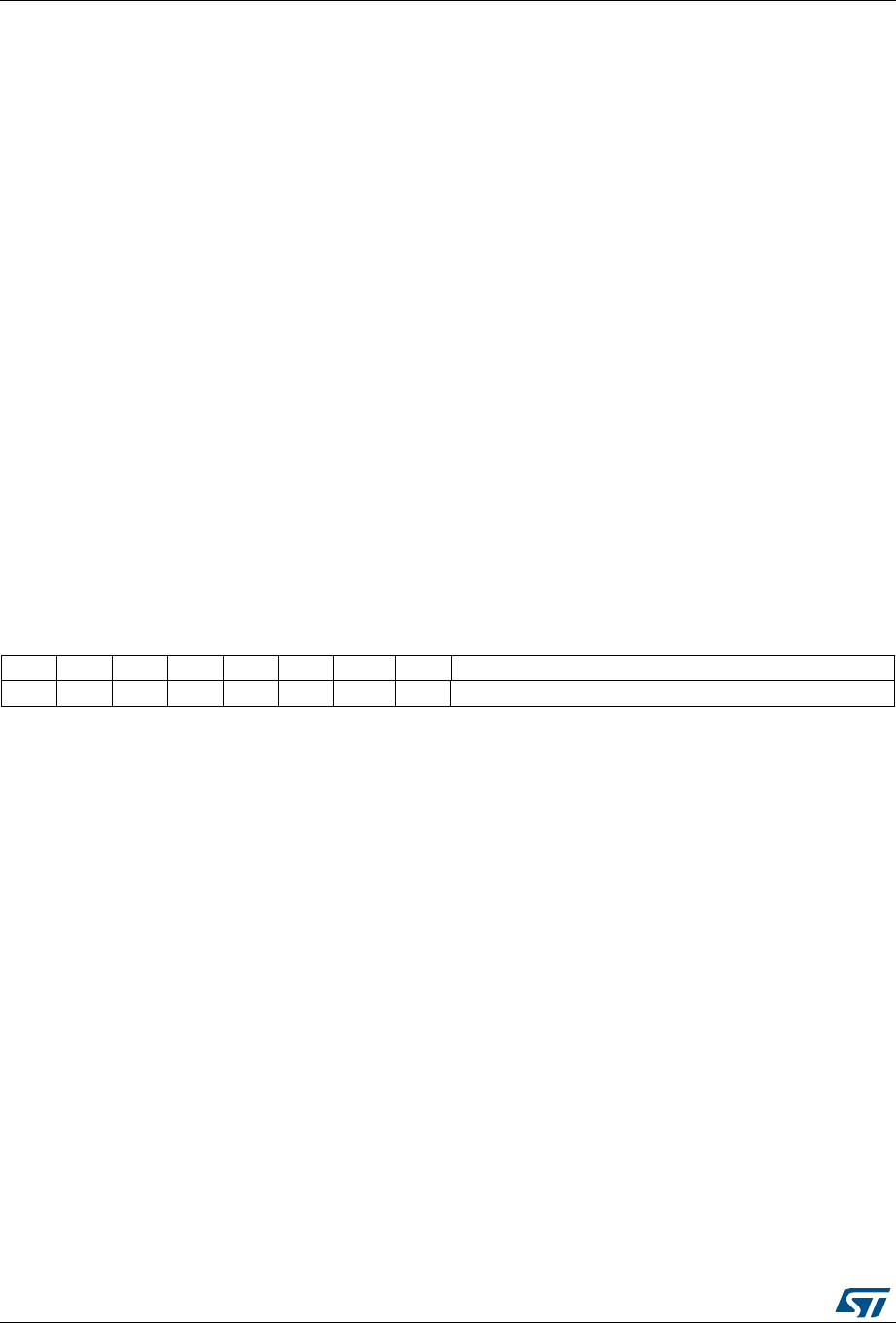
Serial peripheral interface/ inter-IC sound (SPI/I2S) RM0376
880/1001 DocID025941 Rev 5
30.7.9 SPI_I2S prescaler register (SPI_I2SPR)
Address offset: 0x20
Reset value: 0000 0010 (0x0002)
Bit 3 CKPOL: Steady state clock polarity
0: I2S clock steady state is low level
1: I2S clock steady state is high level
Note: For correct operation, this bit should be configured when the I2S is disabled.
This bit is not used in SPI mode
Bits 2:1 DATLEN: Data length to be transferred
00: 16-bit data length
01: 24-bit data length
10: 32-bit data length
11: Not allowed
Note: For correct operation, these bits should be configured when the I2S is disabled.
This bit is not used in SPI mode.
Bit 0 CHLEN: Channel length (number of bits per audio channel)
0: 16-bit wide
1: 32-bit wide
The bit write operation has a meaning only if DATLEN = 00 otherwise the channel length is fixed to
32-bit by hardware whatever the value filled in. Not used in SPI mode.
Note: For correct operation, this bit should be configured when the I2S is disabled.
1514131211109 876543210
Res. Res. Res. Res. Res. Res. MCKOE ODD I2SDIV
rw rw rw
Bits 15:10 Reserved, must be kept at reset value.
Bit 9 MCKOE: Master clock output enable
0: Master clock output is disabled
1: Master clock output is enabled
Note: This bit should be configured when the I2S is disabled. It is used only when the I2S is in master
mode.
This bit is not used in SPI mode.
Bit 8 ODD: Odd factor for the prescaler
0: real divider value is = I2SDIV *2
1: real divider value is = (I2SDIV * 2)+1
Refer to Section 30.6.4 on page 864. Not used in SPI mode.
Note: This bit should be configured when the I2S is disabled. It is used only when the I2S is in master
mode.
Bits 7:0 I2SDIV: I2S Linear prescaler
I2SDIV [7:0] = 0 or I2SDIV [7:0] = 1 are forbidden values.
Refer to Section 30.6.4 on page 864. Not used in SPI mode.
Note: These bits should be configured when the I2S is disabled. It is used only when the I2S is in
master mode.
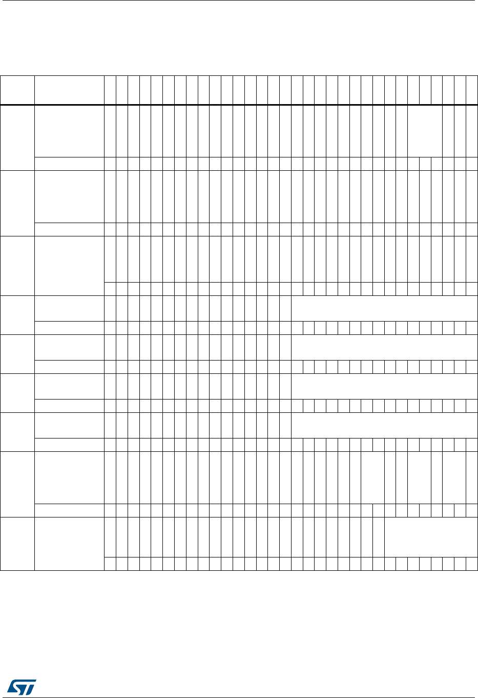
DocID025941 Rev 5 881/1001
RM0376 Serial peripheral interface/ inter-IC sound (SPI/I2S)
881
30.7.10 SPI register map
The table provides shows the SPI register map and reset values.
Refer to Section 2.2.2 on page 58 for the register boundary addresses.
Table 146. SPI register map and reset values
Offset Register
31
30
29
28
27
26
25
24
23
22
21
20
19
18
17
16
15
14
13
12
11
10
9
8
7
6
5
4
3
2
1
0
0x00 SPI_CR1
Res.
Res.
Res.
Res.
Res.
Res.
Res.
Res.
Res.
Res.
Res.
Res.
Res.
Res.
Res.
Res.
BIDIMODE
BIDIOE
CRCEN
CRCNEXT
DFF
RXONLY
SSM
SSI
LSBFIRST
SPE
BR
[2:0]
MSTR
CPOL
CPHA
Reset value 0000000000000000
0x04 SPI_CR2
Res.
Res.
Res.
Res.
Res.
Res.
Res.
Res.
Res.
Res.
Res.
Res.
Res.
Res.
Res.
Res.
Res.
Res.
Res.
Res.
Res.
Res.
Res.
Res.
TXEIE
RXNEIE
ERRIE
FRF
Res.
SSOE
TXDMAEN
RXDMAEN
Reset value 0 0 0 0 0 0 0
0x08 SPI_SR
Res.
Res.
Res.
Res.
Res.
Res.
Res.
Res.
Res.
Res.
Res.
Res.
Res.
Res.
Res.
Res.
Res.
Res.
Res.
Res.
Res.
Res.
Res.
FRE
BSY
OVR
MODF
CRCERR
UDR
CHSIDE
TXE
RXNE
Reset value 000000010
0x0C SPI_DR
Res.
Res.
Res.
Res.
Res.
Res.
Res.
Res.
Res.
Res.
Res.
Res.
Res.
Res.
Res.
Res.
DR[15:0]
Reset value 0000000000000000
0x10 SPI_CRCPR
Res.
Res.
Res.
Res.
Res.
Res.
Res.
Res.
Res.
Res.
Res.
Res.
Res.
Res.
Res.
Res.
CRCPOLY[15:0]
Reset value 0000000000000111
0x14 SPI_RXCRCR
Res.
Res.
Res.
Res.
Res.
Res.
Res.
Res.
Res.
Res.
Res.
Res.
Res.
Res.
Res.
Res.
RxCRC[15:0]
Reset value 0000000000000000
0x18 SPI_TXCRCR
Res.
Res.
Res.
Res.
Res.
Res.
Res.
Res.
Res.
Res.
Res.
Res.
Res.
Res.
Res.
Res.
TxCRC[15:0]
Reset value 0000000000000000
0x1C SPI_I2SCFGR
Res.
Res.
Res.
Res.
Res.
Res.
Res.
Res.
Res.
Res.
Res.
Res.
Res.
Res.
Res.
Res.
Res.
Res.
Res.
Res.
I2SMOD
I2SE
I2SCFG
PCMSYNC
Res.
I2SSTD
CKPOL
DATLEN
CHLEN
Reset value 00000 000000
0x20 SPI_I2SPR
Res.
Res.
Res.
Res.
Res.
Res.
Res.
Res.
Res.
Res.
Res.
Res.
Res.
Res.
Res.
Res.
Res.
Res.
Res.
Res.
Res.
Res.
MCKOE
ODD
I2SDIV
Reset value 0000000010

Universal serial bus full-speed device interface (USB) RM0376
882/1001 DocID025941 Rev 5
31 Universal serial bus full-speed device interface (USB)
31.1 Introduction
The USB peripheral implements an interface between a full-speed USB 2.0 bus and the
APB bus.
USB suspend/resume are supported which allows to stop the device clocks for low-power
consumption.
31.2 USB main features
•USB specification version 2.0 full-speed compliant
•Configurable number of endpoints from 1 to 8
•Up to 1024 bytes of dedicated packet buffer memory SRAM
•Cyclic redundancy check (CRC) generation/checking, Non-return-to-zero Inverted
(NRZI) encoding/decoding and bit-stuffing
•Isochronous transfers support
•Double-buffered bulk/isochronous endpoint support
•USB Suspend/Resume operations
•Frame locked clock pulse generation
•USB 2.0 Link Power Management support
•Battery Charging Specification Revision 1.2 support
•USB connect / disconnect capability (controllable embedded pull-up resistor on
USB_DP line)
31.3 USB implementation
Table 147 describes the USB implementation in the devices.
Table 147. STM32L0x2 USB implementation
USB features(1)
1. X= supported
-
USB
Number of endpoints 8
Size of dedicated packet buffer memory SRAM 1024 bytes
Dedicated packet buffer memory SRAM access scheme 2 x 16 bits / word
USB 2.0 Link Power Management (LPM) support X
Battery Charging Detection (BCD) support X
Embedded pull-up resistor on USB_DP line X
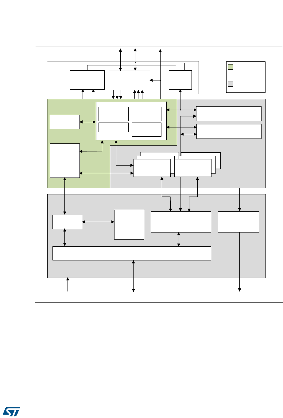
DocID025941 Rev 5 883/1001
RM0376 Universal serial bus full-speed device interface (USB)
914
31.4 USB functional description
Figure 297 shows the block diagram of the USB peripheral.
Figure 297. USB peripheral block diagram
The USB peripheral provides an USB-compliant connection between the host PC and the
function implemented by the microcontroller. Data transfer between the host PC and the
system memory occurs through a dedicated packet buffer memory accessed directly by the
USB peripheral. This dedicated memory size is up to 1024 bytes, and up to 16 mono-
directional or 8 bidirectional endpoints can be used. The USB peripheral interfaces with the
USB host, detecting token packets, handling data transmission/reception, and processing
handshake packets as required by the USB standard. Transaction formatting is performed
by the hardware, including CRC generation and checking.
Each endpoint is associated with a buffer description block indicating where the endpoint-
related memory area is located, how large it is or how many bytes must be transmitted.
When a token for a valid function/endpoint pair is recognized by the USB peripheral, the
related data transfer (if required and if the endpoint is configured) takes place. The data
Control
MSv32120V2
S.I.E.
USB clock
(48 MHz)
DP
USB PHY
Register
mapper
APB interface
PCLK APB bus IRQs to NVIC
Arbiter Packet
buffer
memory
Register
mapper
Control
registers and logic
Interrupt
registers and logic
Endpoint
registers
Endpoint
registers
Endpoint
selection
Clock
recovery
RX-TX
Suspend
timer
Packet
buffer
interface
Analog
transceiver
DM
Interrupt
mapper
APB wrapper
BCD
Embedded
pull-up
NOE
PCLK

Universal serial bus full-speed device interface (USB) RM0376
884/1001 DocID025941 Rev 5
buffered by the USB peripheral is loaded in an internal 16-bit register and memory access to
the dedicated buffer is performed. When all the data has been transferred, if needed, the
proper handshake packet over the USB is generated or expected according to the direction
of the transfer.
At the end of the transaction, an endpoint-specific interrupt is generated, reading status
registers and/or using different interrupt response routines. The microcontroller can
determine:
•which endpoint has to be served,
•which type of transaction took place, if errors occurred (bit stuffing, format, CRC,
protocol, missing ACK, over/underrun, etc.).
Special support is offered to isochronous transfers and high throughput bulk transfers,
implementing a double buffer usage, which allows to always have an available buffer for the
USB peripheral while the microcontroller uses the other one.
The unit can be placed in low-power mode (SUSPEND mode), by writing in the control
register, whenever required. At this time, all static power dissipation is avoided, and the USB
clock can be slowed down or stopped. The detection of activity at the USB inputs, while in
low-power mode, wakes the device up asynchronously. A special interrupt source can be
connected directly to a wakeup line to allow the system to immediately restart the normal
clock generation and/or support direct clock start/stop.
31.4.1 Description of USB blocks
The USB peripheral implements all the features related to USB interfacing, which include
the following blocks:
•USB Physical Interface (USB PHY): This block is maintaining the electrical interface to
an external USB host. It contains the differential analog transceiver itself, controllable
embedded pull-up resistor (connected to USB_DP line) and support for Battery
Charging Detection (BCD), multiplexed on same USB_DP and USB_DM lines. The
output enable control signal of the analog transceiver (active low) is provided externally
on USB_NOE. It can be used to drive some activity LED or to provide information about
the actual communication direction to some other circuitry.
•Serial Interface Engine (SIE): The functions of this block include: synchronization
pattern recognition, bit-stuffing, CRC generation and checking, PID
verification/generation, and handshake evaluation. It must interface with the USB
transceivers and uses the virtual buffers provided by the packet buffer interface for
local data storage. This unit also generates signals according to USB peripheral
events, such as Start of Frame (SOF), USB_Reset, Data errors etc. and to Endpoint
related events like end of transmission or correct reception of a packet; these signals
are then used to generate interrupts.
•Timer: This block generates a start-of-frame locked clock pulse and detects a global
suspend (from the host) when no traffic has been received for 3 ms.
•Packet Buffer Interface: This block manages the local memory implementing a set of
buffers in a flexible way, both for transmission and reception. It can choose the proper
buffer according to requests coming from the SIE and locate them in the memory
addresses pointed by the Endpoint registers. It increments the address after each
exchanged byte until the end of packet, keeping track of the number of exchanged
bytes and preventing the buffer to overrun the maximum capacity.

DocID025941 Rev 5 885/1001
RM0376 Universal serial bus full-speed device interface (USB)
914
•Endpoint-Related Registers: Each endpoint has an associated register containing the
endpoint type and its current status. For mono-directional/single-buffer endpoints, a
single register can be used to implement two distinct endpoints. The number of
registers is 8, allowing up to 16 mono-directional/single-buffer or up to 7 double-buffer
endpoints in any combination. For example the USB peripheral can be programmed to
have 4 double buffer endpoints and 8 single-buffer/mono-directional endpoints.
•Control Registers: These are the registers containing information about the status of
the whole USB peripheral and used to force some USB events, such as resume and
power-down.
•Interrupt Registers: These contain the Interrupt masks and a record of the events. They
can be used to inquire an interrupt reason, the interrupt status or to clear the status of a
pending interrupt.
Note: * Endpoint 0 is always used for control transfer in single-buffer mode.
The USB peripheral is connected to the APB bus through an APB interface, containing the
following blocks:
•Packet Memory: This is the local memory that physically contains the Packet Buffers. It
can be used by the Packet Buffer interface, which creates the data structure and can
be accessed directly by the application software. The size of the Packet Memory is up
to 1024 bytes, structured as 512 half-words by 16 bits.
•Arbiter: This block accepts memory requests coming from the APB bus and from the
USB interface. It resolves the conflicts by giving priority to APB accesses, while always
reserving half of the memory bandwidth to complete all USB transfers. This time-duplex
scheme implements a virtual dual-port SRAM that allows memory access, while an
USB transaction is happening. Multiword APB transfers of any length are also allowed
by this scheme.
•Register Mapper: This block collects the various byte-wide and bit-wide registers of the
USB peripheral in a structured 16-bit wide half-word set addressed by the APB.
•APB Wrapper: This provides an interface to the APB for the memory and register. It
also maps the whole USB peripheral in the APB address space.
•Interrupt Mapper: This block is used to select how the possible USB events can
generate interrupts and map them to the NVIC.
31.5 Programming considerations
In the following sections, the expected interactions between the USB peripheral and the
application program are described, in order to ease application software development.
31.5.1 Generic USB device programming
This part describes the main tasks required of the application software in order to obtain
USB compliant behavior. The actions related to the most general USB events are taken into
account and paragraphs are dedicated to the special cases of double-buffered endpoints
and Isochronous transfers. Apart from system reset, action is always initiated by the USB
peripheral, driven by one of the USB events described below.

Universal serial bus full-speed device interface (USB) RM0376
886/1001 DocID025941 Rev 5
31.5.2 System and power-on reset
Upon system and power-on reset, the first operation the application software should perform
is to provide all required clock signals to the USB peripheral and subsequently de-assert its
reset signal so to be able to access its registers. The whole initialization sequence is
hereafter described.
As a first step application software needs to activate register macrocell clock and de-assert
macrocell specific reset signal using related control bits provided by device clock
management logic.
After that, the analog part of the device related to the USB transceiver must be switched on
using the PDWN bit in CNTR register, which requires a special handling. This bit is intended
to switch on the internal voltage references that supply the port transceiver. This circuit has
a defined startup time (tSTARTUP specified in the datasheet) during which the behavior of the
USB transceiver is not defined. It is thus necessary to wait this time, after setting the PDWN
bit in the CNTR register, before removing the reset condition on the USB part (by clearing
the FRES bit in the CNTR register). Clearing the ISTR register then removes any spurious
pending interrupt before any other macrocell operation is enabled.
At system reset, the microcontroller must initialize all required registers and the packet
buffer description table, to make the USB peripheral able to properly generate interrupts and
data transfers. All registers not specific to any endpoint must be initialized according to the
needs of application software (choice of enabled interrupts, chosen address of packet
buffers, etc.). Then the process continues as for the USB reset case (see further
paragraph).
USB reset (RESET interrupt)
When this event occurs, the USB peripheral is put in the same conditions it is left by the
system reset after the initialization described in the previous paragraph: communication is
disabled in all endpoint registers (the USB peripheral will not respond to any packet). As a
response to the USB reset event, the USB function must be enabled, having as USB
address 0, implementing only the default control endpoint (endpoint address is 0 too). This
is accomplished by setting the Enable Function (EF) bit of the USB_DADDR register and
initializing the EP0R register and its related packet buffers accordingly. During USB
enumeration process, the host assigns a unique address to this device, which must be
written in the ADD[6:0] bits of the USB_DADDR register, and configures any other
necessary endpoint.
When a RESET interrupt is received, the application software is responsible to enable again
the default endpoint of USB function 0 within 10 ms from the end of reset sequence which
triggered the interrupt.
Structure and usage of packet buffers
Each bidirectional endpoint may receive or transmit data from/to the host. The received data
is stored in a dedicated memory buffer reserved for that endpoint, while another memory
buffer contains the data to be transmitted by the endpoint. Access to this memory is
performed by the packet buffer interface block, which delivers a memory access request
and waits for its acknowledgment. Since the packet buffer memory has to be accessed by
the microcontroller also, an arbitration logic takes care of the access conflicts, using half
APB cycle for microcontroller access and the remaining half for the USB peripheral access.
In this way, both the agents can operate as if the packet memory is a dual-port SRAM,
without being aware of any conflict even when the microcontroller is performing back-to-
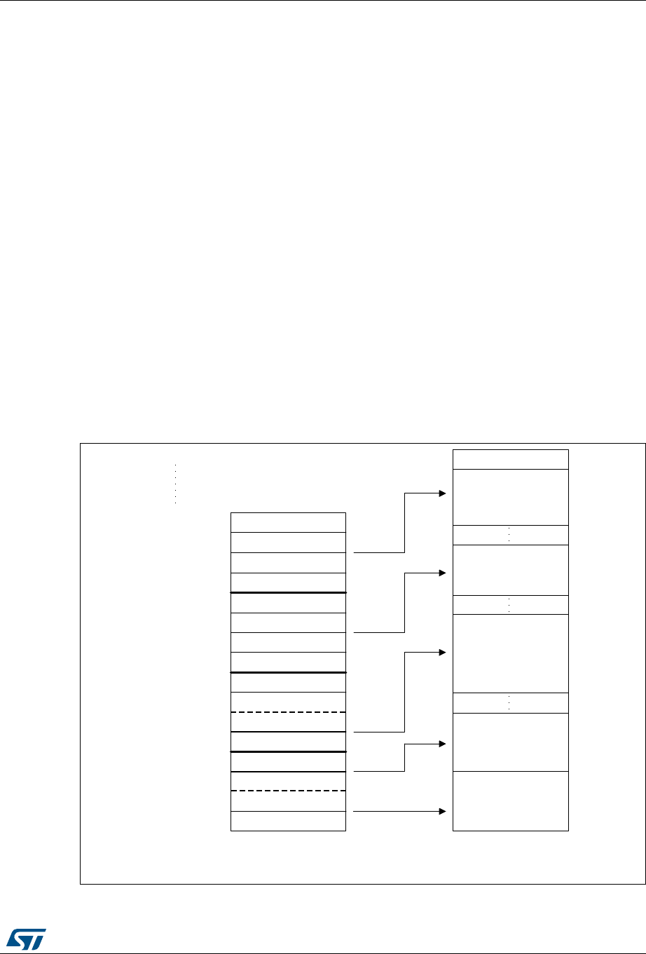
DocID025941 Rev 5 887/1001
RM0376 Universal serial bus full-speed device interface (USB)
914
back accesses. The USB peripheral logic uses a dedicated clock. The frequency of this
dedicated clock is fixed by the requirements of the USB standard at 48 MHz, and this can be
different from the clock used for the interface to the APB bus. Different clock configurations
are possible where the APB clock frequency can be higher or lower than the USB peripheral
one.
Note: Due to USB data rate and packet memory interface requirements, the APB clock must have
a minimum frequency of 10 MHz to avoid data overrun/underrun problems.
Each endpoint is associated with two packet buffers (usually one for transmission and the
other one for reception). Buffers can be placed anywhere inside the packet memory
because their location and size is specified in a buffer description table, which is also
located in the packet memory at the address indicated by the USB_BTABLE register. Each
table entry is associated to an endpoint register and it is composed of four 16-bit half-words
so that table start address must always be aligned to an 8-byte boundary (the lowest three
bits of USB_BTABLE register are always “000”). Buffer descriptor table entries are
described in the Section 31.6.2: Buffer descriptor table. If an endpoint is unidirectional and it
is neither an Isochronous nor a double-buffered bulk, only one packet buffer is required (the
one related to the supported transfer direction). Other table locations related to unsupported
transfer directions or unused endpoints, are available to the user. Isochronous and double-
buffered bulk endpoints have special handling of packet buffers (Refer to Section 31.5.4:
Isochronous transfers and Section 31.5.3: Double-buffered endpoints respectively). The
relationship between buffer description table entries and packet buffer areas is depicted in
Figure 298.
Figure 298. Packet buffer areas with examples of buffer description table locations
MSv32129V1
0001_1110 (1E) COUNT3_TX_1
ADDR3_TX_1
COUNT3_TX_0
ADDR3_TX_0
COUNT2_RX_1
ADDR2_RX_1
COUNT2_RX_0
ADDR2_RX_0
COUNT1_RX
ADDR1_RX
COUNT1_TX
ADDR1_TX
COUNT0_RX
ADDR0_RX
COUNT0_TX
ADDR0_TX
0001_1100 (1C)
0001_1010 (1A)
0001_1000 (18)
0001_0110 (16)
0001_0100 (14)
0001_0010 (12)
0001_0000 (10)
0000_1110 (0E)
0000_1100 (0C)
0000_1010 (0A)
0000_1000 (08)
0000_0110 (06)
0000_0100 (04)
0000_0010 (02)
0000_0000 (00)
Buffer description table locations
Buffer for
double-buffered
IN Endpoint 3
Buffer for
double-buffered
OUT Endpoint 2
Transmission
buffer for
single-buffered
Endpoint 1
Reception buffer
for
Endpoint 0
Transmission
buffer for
Endpoint 0
Packet buffers

Universal serial bus full-speed device interface (USB) RM0376
888/1001 DocID025941 Rev 5
Each packet buffer is used either during reception or transmission starting from the bottom.
The USB peripheral will never change the contents of memory locations adjacent to the
allocated memory buffers; if a packet bigger than the allocated buffer length is received
(buffer overrun condition) the data will be copied to the memory only up to the last available
location.
Endpoint initialization
The first step to initialize an endpoint is to write appropriate values to the
ADDRn_TX/ADDRn_RX registers so that the USB peripheral finds the data to be
transmitted already available and the data to be received can be buffered. The EP_TYPE
bits in the USB_EPnR register must be set according to the endpoint type, eventually using
the EP_KIND bit to enable any special required feature. On the transmit side, the endpoint
must be enabled using the STAT_TX bits in the USB_EPnR register and COUNTn_TX must
be initialized. For reception, STAT_RX bits must be set to enable reception and
COUNTn_RX must be written with the allocated buffer size using the BL_SIZE and
NUM_BLOCK fields. Unidirectional endpoints, except Isochronous and double-buffered bulk
endpoints, need to initialize only bits and registers related to the supported direction. Once
the transmission and/or reception are enabled, register USB_EPnR and locations
ADDRn_TX/ADDRn_RX, COUNTn_TX/COUNTn_RX (respectively), should not be modified
by the application software, as the hardware can change their value on the fly. When the
data transfer operation is completed, notified by a CTR interrupt event, they can be
accessed again to re-enable a new operation.
IN packets (data transmission)
When receiving an IN token packet, if the received address matches a configured and valid
endpoint, the USB peripheral accesses the contents of ADDRn_TX and COUNTn_TX
locations inside the buffer descriptor table entry related to the addressed endpoint. The
content of these locations is stored in its internal 16 bit registers ADDR and COUNT (not
accessible by software). The packet memory is accessed again to read the first byte to be
transmitted (Refer to Structure and usage of packet buffers on page 886) and starts sending
a DATA0 or DATA1 PID according to USB_EPnR bit DTOG_TX. When the PID is
completed, the first byte, read from buffer memory, is loaded into the output shift register to
be transmitted on the USB bus. After the last data byte is transmitted, the computed CRC is
sent. If the addressed endpoint is not valid, a NAK or STALL handshake packet is sent
instead of the data packet, according to STAT_TX bits in the USB_EPnR register.
The ADDR internal register is used as a pointer to the current buffer memory location while
COUNT is used to count the number of remaining bytes to be transmitted. Each half-word
read from the packet buffer memory is transmitted over the USB bus starting from the least
significant byte. Transmission buffer memory is read starting from the address pointed by
ADDRn_TX for COUNTn_TX/2 half-words. If a transmitted packet is composed of an odd
number of bytes, only the lower half of the last half-word accessed will be used.
On receiving the ACK receipt by the host, the USB_EPnR register is updated in the
following way: DTOG_TX bit is toggled, the endpoint is made invalid by setting
STAT_TX=10 (NAK) and bit CTR_TX is set. The application software must first identify the
endpoint, which is requesting microcontroller attention by examining the EP_ID and DIR bits
in the USB_ISTR register. Servicing of the CTR_TX event starts clearing the interrupt bit;
the application software then prepares another buffer full of data to be sent, updates the
COUNTn_TX table location with the number of byte to be transmitted during the next
transfer, and finally sets STAT_TX to ‘11 (VALID) to re-enable transmissions. While the
STAT_TX bits are equal to ‘10 (NAK), any IN request addressed to that endpoint is NAKed,

DocID025941 Rev 5 889/1001
RM0376 Universal serial bus full-speed device interface (USB)
914
indicating a flow control condition: the USB host will retry the transaction until it succeeds. It
is mandatory to execute the sequence of operations in the above mentioned order to avoid
losing the notification of a second IN transaction addressed to the same endpoint
immediately following the one which triggered the CTR interrupt.
OUT and SETUP packets (data reception)
These two tokens are handled by the USB peripheral more or less in the same way; the
differences in the handling of SETUP packets are detailed in the following paragraph about
control transfers. When receiving an OUT/SETUP PID, if the address matches a valid
endpoint, the USB peripheral accesses the contents of the ADDRn_RX and COUNTn_RX
locations inside the buffer descriptor table entry related to the addressed endpoint. The
content of the ADDRn_RX is stored directly in its internal register ADDR. While COUNT is
now reset and the values of BL_SIZE and NUM_BLOCK bit fields, which are read within
COUNTn_RX content are used to initialize BUF_COUNT, an internal 16 bit counter, which is
used to check the buffer overrun condition (all these internal registers are not accessible by
software). Data bytes subsequently received by the USB peripheral are packed in half-
words (the first byte received is stored as least significant byte) and then transferred to the
packet buffer starting from the address contained in the internal ADDR register while
BUF_COUNT is decremented and COUNT is incremented at each byte transfer. When the
end of DATA packet is detected, the correctness of the received CRC is tested and only if no
errors occurred during the reception, an ACK handshake packet is sent back to the
transmitting host.
In case of wrong CRC or other kinds of errors (bit-stuff violations, frame errors, etc.), data
bytes are still copied in the packet memory buffer, at least until the error detection point, but
ACK packet is not sent and the ERR bit in USB_ISTR register is set. However, there is
usually no software action required in this case: the USB peripheral recovers from reception
errors and remains ready for the next transaction to come. If the addressed endpoint is not
valid, a NAK or STALL handshake packet is sent instead of the ACK, according to bits
STAT_RX in the USB_EPnR register and no data is written in the reception memory buffers.
Reception memory buffer locations are written starting from the address contained in the
ADDRn_RX for a number of bytes corresponding to the received data packet length, CRC
included (i.e. data payload length + 2), or up to the last allocated memory location, as
defined by BL_SIZE and NUM_BLOCK, whichever comes first. In this way, the USB
peripheral never writes beyond the end of the allocated reception memory buffer area. If the
length of the data packet payload (actual number of bytes used by the application) is greater
than the allocated buffer, the USB peripheral detects a buffer overrun condition. in this case,
a STALL handshake is sent instead of the usual ACK to notify the problem to the host, no
interrupt is generated and the transaction is considered failed.
When the transaction is completed correctly, by sending the ACK handshake packet, the
internal COUNT register is copied back in the COUNTn_RX location inside the buffer
description table entry, leaving unaffected BL_SIZE and NUM_BLOCK fields, which
normally do not require to be re-written, and the USB_EPnR register is updated in the
following way: DTOG_RX bit is toggled, the endpoint is made invalid by setting STAT_RX =
‘10 (NAK) and bit CTR_RX is set. If the transaction has failed due to errors or buffer overrun
condition, none of the previously listed actions take place. The application software must
first identify the endpoint, which is requesting microcontroller attention by examining the
EP_ID and DIR bits in the USB_ISTR register. The CTR_RX event is serviced by first
determining the transaction type (SETUP bit in the USB_EPnR register); the application
software must clear the interrupt flag bit and get the number of received bytes reading the
COUNTn_RX location inside the buffer description table entry related to the endpoint being

Universal serial bus full-speed device interface (USB) RM0376
890/1001 DocID025941 Rev 5
processed. After the received data is processed, the application software should set the
STAT_RX bits to ‘11 (Valid) in the USB_EPnR, enabling further transactions. While the
STAT_RX bits are equal to ‘10 (NAK), any OUT request addressed to that endpoint is
NAKed, indicating a flow control condition: the USB host will retry the transaction until it
succeeds. It is mandatory to execute the sequence of operations in the above mentioned
order to avoid losing the notification of a second OUT transaction addressed to the same
endpoint following immediately the one which triggered the CTR interrupt.
Control transfers
Control transfers are made of a SETUP transaction, followed by zero or more data stages,
all of the same direction, followed by a status stage (a zero-byte transfer in the opposite
direction). SETUP transactions are handled by control endpoints only and are very similar to
OUT ones (data reception) except that the values of DTOG_TX and DTOG_RX bits of the
addressed endpoint registers are set to 1 and 0 respectively, to initialize the control transfer,
and both STAT_TX and STAT_RX are set to ‘10 (NAK) to let software decide if subsequent
transactions must be IN or OUT depending on the SETUP contents. A control endpoint must
check SETUP bit in the USB_EPnR register at each CTR_RX event to distinguish normal
OUT transactions from SETUP ones. A USB device can determine the number and
direction of data stages by interpreting the data transferred in the SETUP stage, and is
required to STALL the transaction in the case of errors. To do so, at all data stages before
the last, the unused direction should be set to STALL, so that, if the host reverses the
transfer direction too soon, it gets a STALL as a status stage.
While enabling the last data stage, the opposite direction should be set to NAK, so that, if
the host reverses the transfer direction (to perform the status stage) immediately, it is kept
waiting for the completion of the control operation. If the control operation completes
successfully, the software will change NAK to VALID, otherwise to STALL. At the same time,
if the status stage will be an OUT, the STATUS_OUT (EP_KIND in the USB_EPnR register)
bit should be set, so that an error is generated if a status transaction is performed with not-
zero data. When the status transaction is serviced, the application clears the STATUS_OUT
bit and sets STAT_RX to VALID (to accept a new command) and STAT_TX to NAK (to delay
a possible status stage immediately following the next setup).
Since the USB specification states that a SETUP packet cannot be answered with a
handshake different from ACK, eventually aborting a previously issued command to start
the new one, the USB logic doesn’t allow a control endpoint to answer with a NAK or STALL
packet to a SETUP token received from the host.
When the STAT_RX bits are set to ‘01 (STALL) or ‘10 (NAK) and a SETUP token is
received, the USB accepts the data, performing the required data transfers and sends back
an ACK handshake. If that endpoint has a previously issued CTR_RX request not yet
acknowledged by the application (i.e. CTR_RX bit is still set from a previously completed
reception), the USB discards the SETUP transaction and does not answer with any
handshake packet regardless of its state, simulating a reception error and forcing the host to
send the SETUP token again. This is done to avoid losing the notification of a SETUP
transaction addressed to the same endpoint immediately following the transaction, which
triggered the CTR_RX interrupt.

DocID025941 Rev 5 891/1001
RM0376 Universal serial bus full-speed device interface (USB)
914
31.5.3 Double-buffered endpoints
All different endpoint types defined by the USB standard represent different traffic models,
and describe the typical requirements of different kind of data transfer operations. When
large portions of data are to be transferred between the host PC and the USB function, the
bulk endpoint type is the most suited model. This is because the host schedules bulk
transactions so as to fill all the available bandwidth in the frame, maximizing the actual
transfer rate as long as the USB function is ready to handle a bulk transaction addressed to
it. If the USB function is still busy with the previous transaction when the next one arrives, it
will answer with a NAK handshake and the host PC will issue the same transaction again
until the USB function is ready to handle it, reducing the actual transfer rate due to the
bandwidth occupied by re-transmissions. For this reason, a dedicated feature called
‘double-buffering’ can be used with bulk endpoints.
When ‘double-buffering’ is activated, data toggle sequencing is used to select, which buffer
is to be used by the USB peripheral to perform the required data transfers, using both
‘transmission’ and ‘reception’ packet memory areas to manage buffer swapping on each
successful transaction in order to always have a complete buffer to be used by the
application, while the USB peripheral fills the other one. For example, during an OUT
transaction directed to a ‘reception’ double-buffered bulk endpoint, while one buffer is being
filled with new data coming from the USB host, the other one is available for the
microcontroller software usage (the same would happen with a ‘transmission’ double-
buffered bulk endpoint and an IN transaction).
Since the swapped buffer management requires the usage of all 4 buffer description table
locations hosting the address pointer and the length of the allocated memory buffers, the
USB_EPnR registers used to implement double-buffered bulk endpoints are forced to be
used as unidirectional ones. Therefore, only one STAT bit pair must be set at a value
different from ‘00 (Disabled): STAT_RX if the double-buffered bulk endpoint is enabled for
reception, STAT_TX if the double-buffered bulk endpoint is enabled for transmission. In
case it is required to have double-buffered bulk endpoints enabled both for reception and
transmission, two USB_EPnR registers must be used.
To exploit the double-buffering feature and reach the highest possible transfer rate, the
endpoint flow control structure, described in previous chapters, has to be modified, in order
to switch the endpoint status to NAK only when a buffer conflict occurs between the USB
peripheral and application software, instead of doing it at the end of each successful
transaction. The memory buffer which is currently being used by the USB peripheral is
defined by the DTOG bit related to the endpoint direction: DTOG_RX (bit 14 of USB_EPnR
register) for ‘reception’ double-buffered bulk endpoints or DTOG_TX (bit 6 of USB_EPnR
register) for ‘transmission’ double-buffered bulk endpoints. To implement the new flow
control scheme, the USB peripheral should know which packet buffer is currently in use by
the application software, so to be aware of any conflict. Since in the USB_EPnR register,
there are two DTOG bits but only one is used by USB peripheral for data and buffer
sequencing (due to the unidirectional constraint required by double-buffering feature) the
other one can be used by the application software to show which buffer it is currently using.
This new buffer flag is called SW_BUF. In the following table the correspondence between
USB_EPnR register bits and DTOG/SW_BUF definition is explained, for the cases of
‘transmission’ and ‘reception’ double-buffered bulk endpoints.
Universal serial bus full-speed device interface (USB) RM0376
892/1001 DocID025941 Rev 5
The memory buffer which is currently being used by the USB peripheral is defined by DTOG
buffer flag, while the buffer currently in use by application software is identified by SW_BUF
buffer flag. The relationship between the buffer flag value and the used packet buffer is the
same in both cases, and it is listed in the following table.
Double-buffering feature for a bulk endpoint is activated by:
•Writing EP_TYPE bit field at ‘00 in its USB_EPnR register, to define the endpoint as a
bulk, and
•Setting EP_KIND bit at ‘1 (DBL_BUF), in the same register.
The application software is responsible for DTOG and SW_BUF bits initialization according
to the first buffer to be used; this has to be done considering the special toggle-only property
that these two bits have. The end of the first transaction occurring after having set
DBL_BUF, triggers the special flow control of double-buffered bulk endpoints, which is used
for all other transactions addressed to this endpoint until DBL_BUF remain set. At the end of
each transaction the CTR_RX or CTR_TX bit of the addressed endpoint USB_EPnR
register is set, depending on the enabled direction. At the same time, the affected DTOG bit
in the USB_EPnR register is hardware toggled making the USB peripheral buffer swapping
completely software independent. Unlike common transactions, and the first one after
Table 148. Double-buffering buffer flag definition
Buffer flag ‘Transmission’ endpoint ‘Reception’ endpoint
DTOG DTOG_TX (USB_EPnR bit 6) DTOG_RX (USB_EPnR bit 14)
SW_BUF USB_EPnR bit 14 USB_EPnR bit 6
Table 149. Bulk double-buffering memory buffers usage
Endpoint
Type DTOG SW_BUF Packet buffer used by USB
Peripheral
Packet buffer used by
Application Software
IN
01
ADDRn_TX_0 / COUNTn_TX_0
Buffer description table locations.
ADDRn_TX_1 / COUNTn_TX_1
Buffer description table locations.
10
ADDRn_TX_1 / COUNTn_TX_1
Buffer description table locations
ADDRn_TX_0 / COUNTn_TX_0
Buffer description table locations.
0 0 None (1)
1. Endpoint in NAK Status.
ADDRn_TX_0 / COUNTn_TX_0
Buffer description table locations.
1 1 None (1) ADDRn_TX_0 / COUNTn_TX_0
Buffer description table locations.
OUT
01
ADDRn_RX_0 / COUNTn_RX_0
Buffer description table locations.
ADDRn_RX_1 / COUNTn_RX_1
Buffer description table locations.
10
ADDRn_RX_1 / COUNTn_RX_1
Buffer description table locations.
ADDRn_RX_0 / COUNTn_RX_0
Buffer description table locations.
0 0 None (1) ADDRn_RX_0 / COUNTn_RX_0
Buffer description table locations.
1 1 None (1) ADDRn_RX_1 / COUNTn_RX_1
Buffer description table locations.

DocID025941 Rev 5 893/1001
RM0376 Universal serial bus full-speed device interface (USB)
914
DBL_BUF setting, STAT bit pair is not affected by the transaction termination and its value
remains ‘11 (Valid). However, as the token packet of a new transaction is received, the
actual endpoint status will be masked as ‘10 (NAK) when a buffer conflict between the USB
peripheral and the application software is detected (this condition is identified by DTOG and
SW_BUF having the same value, see Table 149 on page 892). The application software
responds to the CTR event notification by clearing the interrupt flag and starting any
required handling of the completed transaction. When the application packet buffer usage is
over, the software toggles the SW_BUF bit, writing ‘1 to it, to notify the USB peripheral about
the availability of that buffer. In this way, the number of NAKed transactions is limited only by
the application elaboration time of a transaction data: if the elaboration time is shorter than
the time required to complete a transaction on the USB bus, no re-transmissions due to flow
control will take place and the actual transfer rate will be limited only by the host PC.
The application software can always override the special flow control implemented for
double-buffered bulk endpoints, writing an explicit status different from ‘11 (Valid) into the
STAT bit pair of the related USB_EPnR register. In this case, the USB peripheral will always
use the programmed endpoint status, regardless of the buffer usage condition.
31.5.4 Isochronous transfers
The USB standard supports full speed peripherals requiring a fixed and accurate data
production/consume frequency, defining this kind of traffic as ‘Isochronous’. Typical
examples of this data are: audio samples, compressed video streams, and in general any
sort of sampled data having strict requirements for the accuracy of delivered frequency.
When an endpoint is defined to be ‘isochronous’ during the enumeration phase, the host
allocates in the frame the required bandwidth and delivers exactly one IN or OUT packet
each frame, depending on endpoint direction. To limit the bandwidth requirements, no re-
transmission of failed transactions is possible for Isochronous traffic; this leads to the fact
that an isochronous transaction does not have a handshake phase and no ACK packet is
expected or sent after the data packet. For the same reason, Isochronous transfers do not
support data toggle sequencing and always use DATA0 PID to start any data packet.
The Isochronous behavior for an endpoint is selected by setting the EP_TYPE bits at ‘10 in
its USB_EPnR register; since there is no handshake phase the only legal values for the
STAT_RX/STAT_TX bit pairs are ‘00 (Disabled) and ‘11 (Valid), any other value will produce
results not compliant to USB standard. Isochronous endpoints implement double-buffering
to ease application software development, using both ‘transmission’ and ‘reception’ packet
memory areas to manage buffer swapping on each successful transaction in order to have
always a complete buffer to be used by the application, while the USB peripheral fills the
other.
The memory buffer which is currently used by the USB peripheral is defined by the DTOG
bit related to the endpoint direction (DTOG_RX for ‘reception’ isochronous endpoints,
DTOG_TX for ‘transmission’ isochronous endpoints, both in the related USB_EPnR
register) according to Table 150.

Universal serial bus full-speed device interface (USB) RM0376
894/1001 DocID025941 Rev 5
As it happens with double-buffered bulk endpoints, the USB_EPnR registers used to
implement Isochronous endpoints are forced to be used as unidirectional ones. In case it is
required to have Isochronous endpoints enabled both for reception and transmission, two
USB_EPnR registers must be used.
The application software is responsible for the DTOG bit initialization according to the first
buffer to be used; this has to be done considering the special toggle-only property that these
two bits have. At the end of each transaction, the CTR_RX or CTR_TX bit of the addressed
endpoint USB_EPnR register is set, depending on the enabled direction. At the same time,
the affected DTOG bit in the USB_EPnR register is hardware toggled making buffer
swapping completely software independent. STAT bit pair is not affected by transaction
completion; since no flow control is possible for Isochronous transfers due to the lack of
handshake phase, the endpoint remains always ‘11 (Valid). CRC errors or buffer-overrun
conditions occurring during Isochronous OUT transfers are anyway considered as correct
transactions and they always trigger an CTR_RX event. However, CRC errors will anyway
set the ERR bit in the USB_ISTR register to notify the software of the possible data
corruption.
31.5.5 Suspend/Resume events
The USB standard defines a special peripheral state, called SUSPEND, in which the
average current drawn from the USB bus must not be greater than 2.5 mA. This
requirement is of fundamental importance for bus-powered devices, while self-powered
devices are not required to comply to this strict power consumption constraint. In suspend
mode, the host PC sends the notification by not sending any traffic on the USB bus for more
than 3 ms: since a SOF packet must be sent every 1 ms during normal operations, the USB
peripheral detects the lack of 3 consecutive SOF packets as a suspend request from the
host PC and set the SUSP bit to ‘1 in USB_ISTR register, causing an interrupt if enabled.
Once the device is suspended, its normal operation can be restored by a so called
RESUME sequence, which can be started from the host PC or directly from the peripheral
itself, but it is always terminated by the host PC. The suspended USB peripheral must be
anyway able to detect a RESET sequence, reacting to this event as a normal USB reset
event.
Table 150. Isochronous memory buffers usage
Endpoint
Type
DTOG bit
value
Packet buffer used by the
USB peripheral
Packet buffer used by the
application software
IN
0
ADDRn_TX_0 / COUNTn_TX_0
buffer description table
locations.
ADDRn_TX_1 / COUNTn_TX_1
buffer description table
locations.
1
ADDRn_TX_1 / COUNTn_TX_1
buffer description table
locations.
ADDRn_TX_0 / COUNTn_TX_0
buffer description table
locations.
OUT
0
ADDRn_RX_0 / COUNTn_RX_0
buffer description table
locations.
ADDRn_RX_1 / COUNTn_RX_1
buffer description table
locations.
1
ADDRn_RX_1 / COUNTn_RX_1
buffer description table
locations.
ADDRn_RX_0 / COUNTn_RX_0
buffer description table
locations.

DocID025941 Rev 5 895/1001
RM0376 Universal serial bus full-speed device interface (USB)
914
The actual procedure used to suspend the USB peripheral is device dependent since
according to the device composition, different actions may be required to reduce the total
consumption.
A brief description of a typical suspend procedure is provided below, focused on the USB-
related aspects of the application software routine responding to the SUSP notification of
the USB peripheral:
1. Set the FSUSP bit in the USB_CNTR register to 1. This action activates the suspend
mode within the USB peripheral. As soon as the suspend mode is activated, the check
on SOF reception is disabled to avoid any further SUSP interrupts being issued while
the USB is suspended.
2. Remove or reduce any static power consumption in blocks different from the USB
peripheral.
3. Set LP_MODE bit in USB_CNTR register to 1 to remove static power consumption in
the analog USB transceivers but keeping them able to detect resume activity.
4. Optionally turn off external oscillator and device PLL to stop any activity inside the
device.
Universal serial bus full-speed device interface (USB) RM0376
896/1001 DocID025941 Rev 5
When an USB event occurs while the device is in SUSPEND mode, the RESUME
procedure must be invoked to restore nominal clocks and regain normal USB behavior.
Particular care must be taken to insure that this process does not take more than 10 ms
when the wakening event is an USB reset sequence (See “Universal Serial Bus
Specification” for more details). The start of a resume or reset sequence, while the USB
peripheral is suspended, clears the LP_MODE bit in USB_CNTR register asynchronously.
Even if this event can trigger an WKUP interrupt if enabled, the use of an interrupt response
routine must be carefully evaluated because of the long latency due to system clock restart;
to have the shorter latency before re-activating the nominal clock it is suggested to put the
resume procedure just after the end of the suspend one, so its code is immediately
executed as soon as the system clock restarts. To prevent ESD discharges or any other kind
of noise from waking-up the system (the exit from suspend mode is an asynchronous
event), a suitable analog filter on data line status is activated during suspend; the filter width
is about 70 ns.
The following is a list of actions a resume procedure should address:
1. Optionally turn on external oscillator and/or device PLL.
2. Clear FSUSP bit of USB_CNTR register.
3. If the resume triggering event has to be identified, bits RXDP and RXDM in the
USB_FNR register can be used according to Table 151, which also lists the intended
software action in all the cases. If required, the end of resume or reset sequence can
be detected monitoring the status of the above mentioned bits by checking when they
reach the “10” configuration, which represent the Idle bus state; moreover at the end of
a reset sequence the RESET bit in USB_ISTR register is set to 1, issuing an interrupt if
enabled, which should be handled as usual.
A device may require to exit from suspend mode as an answer to particular events not
directly related to the USB protocol (e.g. a mouse movement wakes up the whole system).
In this case, the resume sequence can be started by setting the RESUME bit in the
USB_CNTR register to ‘1 and resetting it to 0 after an interval between 1 ms and 15 ms (this
interval can be timed using ESOF interrupts, occurring with a 1 ms period when the system
clock is running at nominal frequency). Once the RESUME bit is clear, the resume
sequence will be completed by the host PC and its end can be monitored again using the
RXDP and RXDM bits in the USB_FNR register.
Note: The RESUME bit must be anyway used only after the USB peripheral has been put in
suspend mode, setting the FSUSP bit in USB_CNTR register to 1.
Table 151. Resume event detection
[RXDP,RXDM] status Wakeup event Required resume software action
“00” Root reset None
“10” None (noise on bus) Go back in Suspend mode
“01” Root resume None
“11” Not allowed (noise on bus) Go back in Suspend mode

DocID025941 Rev 5 897/1001
RM0376 Universal serial bus full-speed device interface (USB)
914
31.6 USB registers
The USB peripheral registers can be divided into the following groups:
•Common Registers: Interrupt and Control registers
•Endpoint Registers: Endpoint configuration and status
•Buffer Descriptor Table: Location of packet memory used to locate data buffers
All register addresses are expressed as offsets with respect to the USB peripheral registers
base address 0x4000 5C00, except the buffer descriptor table locations, which starts at the
address specified by the USB_BTABLE register.
Refer to Section 1.1 on page 51 for a list of abbreviations used in register descriptions.
The peripheral registers can be accessed by half-words (16-bit) or words (32-bit).
31.6.1 Common registers
These registers affect the general behavior of the USB peripheral defining operating mode,
interrupt handling, device address and giving access to the current frame number updated
by the host PC.
USB control register (USB_CNTR)
Address offset: 0x40
Reset value: 0x0003
15 14 13 12 11 10 9 8 7 6 5 4 3 2 1 0
CTR
M
PMAOVR
M
ERR
M
WKUP
M
SUSP
M
RESET
M
SOF
M
ESOF
M
L1REQ
M
Res
.
L1
RESUME
RE
SUME
F
SUSP
LP_
MODE
PDW
N
F
RES
rw rw rw rw rw rw rw rw rw rw rw rw rw rw rw
Bit 15 CTRM: Correct transfer interrupt mask
0: Correct Transfer (CTR) Interrupt disabled.
1: CTR Interrupt enabled, an interrupt request is generated when the corresponding bit in the
USB_ISTR register is set.
Bit 14 PMAOVRM: Packet memory area over / underrun interrupt mask
0: PMAOVR Interrupt disabled.
1: PMAOVR Interrupt enabled, an interrupt request is generated when the corresponding bit
in the USB_ISTR register is set.
Bit 13 ERRM: Error interrupt mask
0: ERR Interrupt disabled.
1: ERR Interrupt enabled, an interrupt request is generated when the corresponding bit in
the USB_ISTR register is set.
Bit 12 WKUPM: Wakeup interrupt mask
0: WKUP Interrupt disabled.
1: WKUP Interrupt enabled, an interrupt request is generated when the corresponding bit in
the USB_ISTR register is set.
Bit 11 SUSPM: Suspend mode interrupt mask
0: Suspend Mode Request (SUSP) Interrupt disabled.
1: SUSP Interrupt enabled, an interrupt request is generated when the corresponding bit in
the USB_ISTR register is set.

Universal serial bus full-speed device interface (USB) RM0376
898/1001 DocID025941 Rev 5
Bit 10 RESETM: USB reset interrupt mask
0: RESET Interrupt disabled.
1: RESET Interrupt enabled, an interrupt request is generated when the corresponding bit in
the USB_ISTR register is set.
Bit 9 SOFM: Start of frame interrupt mask
0: SOF Interrupt disabled.
1: SOF Interrupt enabled, an interrupt request is generated when the corresponding bit in the
USB_ISTR register is set.
Bit 8 ESOFM: Expected start of frame interrupt mask
0: Expected Start of Frame (ESOF) Interrupt disabled.
1: ESOF Interrupt enabled, an interrupt request is generated when the corresponding bit in
the USB_ISTR register is set.
Bit 7 L1REQM: LPM L1 state request interrupt mask
0: LPM L1 state request (L1REQ) Interrupt disabled.
1: L1REQ Interrupt enabled, an interrupt request is generated when the corresponding bit in
the USB_ISTR register is set.
Bit 6 Reserved.
Bit 5 L1RESUME: LPM L1 Resume request
The microcontroller can set this bit to send a LPM L1 Resume signal to the host. After the
signaling ends, this bit is cleared by hardware.
Bit 4 RESUME: Resume request
The microcontroller can set this bit to send a Resume signal to the host. It must be activated,
according to USB specifications, for no less than 1 ms and no more than 15 ms after which
the Host PC is ready to drive the resume sequence up to its end.
Bit 3 FSUSP: Force suspend
Software must set this bit when the SUSP interrupt is received, which is issued when no
traffic is received by the USB peripheral for 3 ms.
0: No effect.
1: Enter suspend mode. Clocks and static power dissipation in the analog transceiver are left
unaffected. If suspend power consumption is a requirement (bus-powered device), the
application software should set the LP_MODE bit after FSUSP as explained below.

DocID025941 Rev 5 899/1001
RM0376 Universal serial bus full-speed device interface (USB)
914
USB interrupt status register (USB_ISTR)
Address offset: 0x44
Reset value: 0x0000 0000
This register contains the status of all the interrupt sources allowing application software to
determine, which events caused an interrupt request.
The upper part of this register contains single bits, each of them representing a specific
event. These bits are set by the hardware when the related event occurs; if the
corresponding bit in the USB_CNTR register is set, a generic interrupt request is generated.
The interrupt routine, examining each bit, will perform all necessary actions, and finally it will
clear the serviced bits. If any of them is not cleared, the interrupt is considered to be still
pending, and the interrupt line will be kept high again. If several bits are set simultaneously,
only a single interrupt will be generated.
Endpoint transaction completion can be handled in a different way to reduce interrupt
response latency. The CTR bit is set by the hardware as soon as an endpoint successfully
completes a transaction, generating a generic interrupt request if the corresponding bit in
USB_CNTR is set. An endpoint dedicated interrupt condition is activated independently
from the CTRM bit in the USB_CNTR register. Both interrupt conditions remain active until
software clears the pending bit in the corresponding USB_EPnR register (the CTR bit is
actually a read only bit). For endpoint-related interrupts, the software can use the Direction
of Transaction (DIR) and EP_ID read-only bits to identify, which endpoint made the last
interrupt request and called the corresponding interrupt service routine.
Bit 2 LP_MODE: Low-power mode
This mode is used when the suspend-mode power constraints require that all static power
dissipation is avoided, except the one required to supply the external pull-up resistor. This
condition should be entered when the application is ready to stop all system clocks, or
reduce their frequency in order to meet the power consumption requirements of the USB
suspend condition. The USB activity during the suspend mode (WKUP event)
asynchronously resets this bit (it can also be reset by software).
0: No Low-power mode.
1: Enter Low-power mode.
Bit 1 PDWN: Power down
This bit is used to completely switch off all USB-related analog parts if it is required to
completely disable the USB peripheral for any reason. When this bit is set, the USB
peripheral is disconnected from the transceivers and it cannot be used.
0: Exit Power Down.
1: Enter Power down mode.
Bit 0 FRES: Force USB Reset
0: Clear USB reset.
1: Force a reset of the USB peripheral, exactly like a RESET signaling on the USB. The USB
peripheral is held in RESET state until software clears this bit. A “USB-RESET” interrupt is
generated, if enabled.
15 14 13 12 11 10 9 8 7 6 5 4 3 2 1 0
CTR PMA
OVR ERR WKUP SUSP RESET SOF ESOF L1REQ Res. Res. DIR EP_ID[3:0]
r rc_w0 rc_w0 rc_w0 rc_w0 rc_w0 rc_w0 rc_w0 rc_w0 r r r r r

Universal serial bus full-speed device interface (USB) RM0376
900/1001 DocID025941 Rev 5
The user can choose the relative priority of simultaneously pending USB_ISTR events by
specifying the order in which software checks USB_ISTR bits in an interrupt service routine.
Only the bits related to events, which are serviced, are cleared. At the end of the service
routine, another interrupt will be requested, to service the remaining conditions.
To avoid spurious clearing of some bits, it is recommended to clear them with a load
instruction where all bits which must not be altered are written with 1, and all bits to be
cleared are written with ‘0 (these bits can only be cleared by software). Read-modify-write
cycles should be avoided because between the read and the write operations another bit
could be set by the hardware and the next write will clear it before the microprocessor has
the time to serve the event.
The following describes each bit in detail:
Bit 15 CTR: Correct transfer
This bit is set by the hardware to indicate that an endpoint has successfully completed a
transaction; using DIR and EP_ID bits software can determine which endpoint requested the
interrupt. This bit is read-only.
Bit 14 PMAOVR: Packet memory area over / underrun
This bit is set if the microcontroller has not been able to respond in time to an USB memory
request. The USB peripheral handles this event in the following way: During reception an
ACK handshake packet is not sent, during transmission a bit-stuff error is forced on the
transmitted stream; in both cases the host will retry the transaction. The PMAOVR interrupt
should never occur during normal operations. Since the failed transaction is retried by the
host, the application software has the chance to speed-up device operations during this
interrupt handling, to be ready for the next transaction retry; however this does not happen
during Isochronous transfers (no isochronous transaction is anyway retried) leading to a loss
of data in this case. This bit is read/write but only ‘0 can be written and writing ‘1 has no
effect.
Bit 13 ERR: Error
This flag is set whenever one of the errors listed below has occurred:
NANS: No ANSwer. The timeout for a host response has expired.
CRC: Cyclic Redundancy Check error. One of the received CRCs, either in the token or in
the data, was wrong.
BST: Bit Stuffing error. A bit stuffing error was detected anywhere in the PID, data, and/or
CRC.
FVIO: Framing format Violation. A non-standard frame was received (EOP not in the right
place, wrong token sequence, etc.).
The USB software can usually ignore errors, since the USB peripheral and the PC host
manage retransmission in case of errors in a fully transparent way. This interrupt can be
useful during the software development phase, or to monitor the quality of transmission over
the USB bus, to flag possible problems to the user (e.g. loose connector, too noisy
environment, broken conductor in the USB cable and so on). This bit is read/write but only ‘0
can be written and writing ‘1 has no effect.
Bit 12 WKUP: Wakeup
This bit is set to 1 by the hardware when, during suspend mode, activity is detected that
wakes up the USB peripheral. This event asynchronously clears the LP_MODE bit in the
CTLR register and activates the USB_WAKEUP line, which can be used to notify the rest of
the device (e.g. wakeup unit) about the start of the resume process. This bit is read/write but
only ‘0 can be written and writing ‘1 has no effect.

DocID025941 Rev 5 901/1001
RM0376 Universal serial bus full-speed device interface (USB)
914
Bit 11 SUSP: Suspend mode request
This bit is set by the hardware when no traffic has been received for 3 ms, indicating a
suspend mode request from the USB bus. The suspend condition check is enabled
immediately after any USB reset and it is disabled by the hardware when the suspend mode
is active (FSUSP=1) until the end of resume sequence. This bit is read/write but only ‘0 can
be written and writing ‘1 has no effect.
Bit 10 RESET: USB reset request
Set when the USB peripheral detects an active USB RESET signal at its inputs. The USB
peripheral, in response to a RESET, just resets its internal protocol state machine, generating
an interrupt if RESETM enable bit in the USB_CNTR register is set. Reception and
transmission are disabled until the RESET bit is cleared. All configuration registers do not
reset: the microcontroller must explicitly clear these registers (this is to ensure that the
RESET interrupt can be safely delivered, and any transaction immediately followed by a
RESET can be completed). The function address and endpoint registers are reset by an USB
reset event.
This bit is read/write but only ‘0 can be written and writing ‘1 has no effect.
Bit 9 SOF: Start of frame
This bit signals the beginning of a new USB frame and it is set when a SOF packet arrives
through the USB bus. The interrupt service routine may monitor the SOF events to have a
1 ms synchronization event to the USB host and to safely read the USB_FNR register which
is updated at the SOF packet reception (this could be useful for isochronous applications).
This bit is read/write but only ‘0 can be written and writing ‘1 has no effect.
Bit 8 ESOF: Expected start of frame
This bit is set by the hardware when an SOF packet is expected but not received. The host
sends an SOF packet each 1 ms, but if the hub does not receive it properly, the Suspend
Timer issues this interrupt. If three consecutive ESOF interrupts are generated (i.e. three
SOF packets are lost) without any traffic occurring in between, a SUSP interrupt is
generated. This bit is set even when the missing SOF packets occur while the Suspend
Timer is not yet locked. This bit is read/write but only ‘0 can be written and writing ‘1 has no
effect.
Bit 7 L1REQ: LPM L1 state request
This bit is set by the hardware when LPM command to enter the L1 state is successfully
received and acknowledged. This bit is read/write but only ‘0 can be written and writing ‘1 has
no effect.

Universal serial bus full-speed device interface (USB) RM0376
902/1001 DocID025941 Rev 5
USB frame number register (USB_FNR)
Address offset: 0x48
Reset value: 0x0XXX where X is undefined
Bits 6:5 Reserved.
Bit 4 DIR: Direction of transaction
This bit is written by the hardware according to the direction of the successful transaction,
which generated the interrupt request.
If DIR bit=0, CTR_TX bit is set in the USB_EPnR register related to the interrupting endpoint.
The interrupting transaction is of IN type (data transmitted by the USB peripheral to the host
PC).
If DIR bit=1, CTR_RX bit or both CTR_TX/CTR_RX are set in the USB_EPnR register
related to the interrupting endpoint. The interrupting transaction is of OUT type (data
received by the USB peripheral from the host PC) or two pending transactions are waiting to
be processed.
This information can be used by the application software to access the USB_EPnR bits
related to the triggering transaction since it represents the direction having the interrupt
pending. This bit is read-only.
Bits 3:0 EP_ID[3:0]: Endpoint Identifier
These bits are written by the hardware according to the endpoint number, which generated
the interrupt request. If several endpoint transactions are pending, the hardware writes the
endpoint identifier related to the endpoint having the highest priority defined in the following
way: Two endpoint sets are defined, in order of priority: Isochronous and double-buffered
bulk endpoints are considered first and then the other endpoints are examined. If more than
one endpoint from the same set is requesting an interrupt, the EP_ID bits in USB_ISTR
register are assigned according to the lowest requesting endpoint register, EP0R having the
highest priority followed by EP1R and so on. The application software can assign a register
to each endpoint according to this priority scheme, so as to order the concurring endpoint
requests in a suitable way. These bits are read only.
151413121110987654321 0
RXDP RXDM LCK LSOF[1:0] FN[10:0]
rrr r r rrrrrrrrrr r
Bit 15 RXDP: Receive data + line status
This bit can be used to observe the status of received data plus upstream port data line. It
can be used during end-of-suspend routines to help determining the wakeup event.
Bit 14 RXDM: Receive data - line status
This bit can be used to observe the status of received data minus upstream port data line. It
can be used during end-of-suspend routines to help determining the wakeup event.

DocID025941 Rev 5 903/1001
RM0376 Universal serial bus full-speed device interface (USB)
914
USB device address (USB_DADDR)
Address offset: 0x4C
Reset value: 0x0000
Buffer table address (USB_BTABLE)
Address offset: 0x50
Reset value: 0x0000
Bit 13 LCK: Locked
This bit is set by the hardware when at least two consecutive SOF packets have been
received after the end of an USB reset condition or after the end of an USB resume
sequence. Once locked, the frame timer remains in this state until an USB reset or USB
suspend event occurs.
Bits 12:11 LSOF[1:0]: Lost SOF
These bits are written by the hardware when an ESOF interrupt is generated, counting the
number of consecutive SOF packets lost. At the reception of an SOF packet, these bits are
cleared.
Bits 10:0 FN[10:0]: Frame number
This bit field contains the 11-bits frame number contained in the last received SOF packet.
The frame number is incremented for every frame sent by the host and it is useful for
Isochronous transfers. This bit field is updated on the generation of an SOF interrupt.
15 14 13 12 11 10 9 8 7 6 5 4 3 2 1 0
Res. Res. Res. Res. Res. Res. Res. Res. EF ADD6 ADD5 ADD4 ADD3 ADD2 ADD1 ADD0
rw rw rw rw rw rw rw rw
Bits 15:8 Reserved
Bit 7 EF: Enable function
This bit is set by the software to enable the USB device. The address of this device is
contained in the following ADD[6:0] bits. If this bit is at ‘0 no transactions are handled,
irrespective of the settings of USB_EPnR registers.
Bits 6:0 ADD[6:0]: Device address
These bits contain the USB function address assigned by the host PC during the
enumeration process. Both this field and the Endpoint Address (EA) field in the associated
USB_EPnR register must match with the information contained in a USB token in order to
handle a transaction to the required endpoint.
1514131211109876543210
BTABLE[15:3] Res. Res. Res.
rw rw rw rw rw rw rw rw rw rw rw rw rw

Universal serial bus full-speed device interface (USB) RM0376
904/1001 DocID025941 Rev 5
LPM control and status register (USB_LPMCSR)
Address offset: 0x54
Reset value: 0x0000
Battery charging detector (USB_BCDR)
Address offset: 0x58
Reset value: 0x0000
Bits 15:3 BTABLE[15:3]: Buffer table
These bits contain the start address of the buffer allocation table inside the dedicated packet
memory. This table describes each endpoint buffer location and size and it must be aligned
to an 8 byte boundary (the 3 least significant bits are always ‘0). At the beginning of every
transaction addressed to this device, the USB peripheral reads the element of this table
related to the addressed endpoint, to get its buffer start location and the buffer size (Refer to
Structure and usage of packet buffers on page 886).
Bits 2:0 Reserved, forced by hardware to 0.
1514131211109876543210
Res. Res. Res. Res. Res. Res. Res. Res. BESL[3:0] REM
WAKE Res. LPM
ACK
LPM
EN
r r rw rw
Bits 15:8 Reserved.
Bits 7:4 BESL[3:0]: BESL value
These bits contain the BESL value received with last ACKed LPM Token
Bit 3 REMWAKE: bRemoteWake value
This bit contains the bRemoteWake value received with last ACKed LPM Token
Bit 2 Reserved
Bit 1 LPMACK: LPM Token acknowledge enable
0: the valid LPM Token will be NYET.
1: the valid LPM Token will be ACK.
The NYET/ACK will be returned only on a successful LPM transaction:
No errors in both the EXT token and the LPM token (else ERROR)
A valid bLinkState = 0001B (L1) is received (else STALL)
Bit 0 LPMEN: LPM support enable
This bit is set by the software to enable the LPM support within the USB device. If this bit is
at ‘0 no LPM transactions are handled.
1514131211109876543210
DPPU Res. Res. Res. Res. Res. Res. Res. PS2
DET SDET PDET DC
DET SDEN PDEN DCD
EN
BCD
EN
rw r r r r rw rw rw rw

DocID025941 Rev 5 905/1001
RM0376 Universal serial bus full-speed device interface (USB)
914
Endpoint-specific registers
The number of these registers varies according to the number of endpoints that the USB
peripheral is designed to handle. The USB peripheral supports up to 8 bidirectional
endpoints. Each USB device must support a control endpoint whose address (EA bits) must
be set to 0. The USB peripheral behaves in an undefined way if multiple endpoints are
enabled having the same endpoint number value. For each endpoint, an USB_EPnR
register is available to store the endpoint specific information.
Bit 15 DPPU: DP pull-up control
This bit is set by software to enable the embedded pull-up on the DP line. Clearing it to ‘0’
can be used to signalize disconnect to the host when needed by the user software.
Bits 14:8 Reserved.
Bit 7 PS2DET: DM pull-up detection status
This bit is active only during PD and gives the result of comparison between DM voltage
level and VLGC threshold. In normal situation, the DM level should be below this threshold. If
it is above, it means that the DM is externally pulled high. This can be caused by connection
to a PS2 port (which pulls-up both DP and DM lines) or to some proprietary charger not
following the BCD specification.
0: Normal port detected (connected to SDP, ACA, CDP or DCP).
1: PS2 port or proprietary charger detected.
Bit 6 SDET: Secondary detection (SD) status
This bit gives the result of SD.
0: CDP detected.
1: DCP detected.
Bit 5 PDET: Primary detection (PD) status
This bit gives the result of PD.
0: no BCD support detected (connected to SDP or proprietary device).
1: BCD support detected (connected to ACA, CDP or DCP).
Bit 4 DCDET: Data contact detection (DCD) status
This bit gives the result of DCD.
0: data lines contact not detected.
1: data lines contact detected.
Bit 3 SDEN: Secondary detection (SD) mode enable
This bit is set by the software to put the BCD into SD mode. Only one detection mode (DCD,
PD, SD or OFF) should be selected to work correctly.
Bit 2 PDEN: Primary detection (PD) mode enable
This bit is set by the software to put the BCD into PD mode. Only one detection mode (DCD,
PD, SD or OFF) should be selected to work correctly.
Bit 1 DCDEN: Data contact detection (DCD) mode enable
This bit is set by the software to put the BCD into DCD mode. Only one detection mode
(DCD, PD, SD or OFF) should be selected to work correctly.
Bit 0 BCDEN: Battery charging detector (BCD) enable
This bit is set by the software to enable the BCD support within the USB device. When
enabled, the USB PHY is fully controlled by BCD and cannot be used for normal
communication. Once the BCD discovery is finished, the BCD should be placed in OFF
mode by clearing this bit to ‘0 in order to allow the normal USB operation.

Universal serial bus full-speed device interface (USB) RM0376
906/1001 DocID025941 Rev 5
USB endpoint n register (USB_EPnR), n=[0..7]
Address offset: 0x00 to 0x1C
Reset value: 0x0000
They are also reset when an USB reset is received from the USB bus or forced through bit
FRES in the CTLR register, except the CTR_RX and CTR_TX bits, which are kept
unchanged to avoid missing a correct packet notification immediately followed by an USB
reset event. Each endpoint has its USB_EPnR register where n is the endpoint identifier.
Read-modify-write cycles on these registers should be avoided because between the read
and the write operations some bits could be set by the hardware and the next write would
modify them before the CPU has the time to detect the change. For this purpose, all bits
affected by this problem have an ‘invariant’ value that must be used whenever their
modification is not required. It is recommended to modify these registers with a load
instruction where all the bits, which can be modified only by the hardware, are written with
their ‘invariant’ value.
151413121110987 6543210
CTR_
RX
DTOG
_RX STAT_RX[1:0] SETUP EP
TYPE[1:0]
EP_
KIND
CTR_
TX
DTOG_
TX STAT_TX[1:0] EA[3:0]
rc_w0t t t r rwrwrwrc_w0t t t rwrwrwrw
Bit 15 CTR_RX: Correct Transfer for reception
This bit is set by the hardware when an OUT/SETUP transaction is successfully completed
on this endpoint; the software can only clear this bit. If the CTRM bit in USB_CNTR register
is set accordingly, a generic interrupt condition is generated together with the endpoint
related interrupt condition, which is always activated. The type of occurred transaction, OUT
or SETUP, can be determined from the SETUP bit described below.
A transaction ended with a NAK or STALL handshake does not set this bit, since no data is
actually transferred, as in the case of protocol errors or data toggle mismatches.
This bit is read/write but only ‘0 can be written, writing 1 has no effect.
Bit 14 DTOG_RX: Data Toggle, for reception transfers
If the endpoint is not Isochronous, this bit contains the expected value of the data toggle bit
(0=DATA0, 1=DATA1) for the next data packet to be received. Hardware toggles this bit,
when the ACK handshake is sent to the USB host, following a data packet reception having
a matching data PID value; if the endpoint is defined as a control one, hardware clears this
bit at the reception of a SETUP PID addressed to this endpoint.
If the endpoint is using the double-buffering feature this bit is used to support packet buffer
swapping too (Refer to Section 31.5.3: Double-buffered endpoints).
If the endpoint is Isochronous, this bit is used only to support packet buffer swapping since
no data toggling is used for this sort of endpoints and only DATA0 packet are transmitted
(Refer to Section 31.5.4: Isochronous transfers). Hardware toggles this bit just after the end
of data packet reception, since no handshake is used for isochronous transfers.
This bit can also be toggled by the software to initialize its value (mandatory when the
endpoint is not a control one) or to force specific data toggle/packet buffer usage. When the
application software writes ‘0, the value of DTOG_RX remains unchanged, while writing ‘1
makes the bit value toggle. This bit is read/write but it can be only toggled by writing 1.

DocID025941 Rev 5 907/1001
RM0376 Universal serial bus full-speed device interface (USB)
914
Bits 13:12 STAT_RX [1:0]: Status bits, for reception transfers
These bits contain information about the endpoint status, which are listed in Table 152:
Reception status encoding on page 908.These bits can be toggled by software to initialize
their value. When the application software writes ‘0, the value remains unchanged, while
writing ‘1 makes the bit value toggle. Hardware sets the STAT_RX bits to NAK when a
correct transfer has occurred (CTR_RX=1) corresponding to a OUT or SETUP (control only)
transaction addressed to this endpoint, so the software has the time to elaborate the
received data before it acknowledge a new transaction
Double-buffered bulk endpoints implement a special transaction flow control, which control
the status based upon buffer availability condition (Refer to Section 31.5.3: Double-buffered
endpoints).
If the endpoint is defined as Isochronous, its status can be only “VALID” or “DISABLED”, so
that the hardware cannot change the status of the endpoint after a successful transaction. If
the software sets the STAT_RX bits to ‘STALL’ or ‘NAK’ for an Isochronous endpoint, the
USB peripheral behavior is not defined. These bits are read/write but they can be only
toggled by writing ‘1.
Bit 11 SETUP: Setup transaction completed
This bit is read-only and it is set by the hardware when the last completed transaction is a
SETUP. This bit changes its value only for control endpoints. It must be examined, in the
case of a successful receive transaction (CTR_RX event), to determine the type of
transaction occurred. To protect the interrupt service routine from the changes in SETUP
bits due to next incoming tokens, this bit is kept frozen while CTR_RX bit is at 1; its state
changes when CTR_RX is at 0. This bit is read-only.
Bits 10:9 EP_TYPE[1:0]: Endpoint type
These bits configure the behavior of this endpoint as described in Table 153: Endpoint type
encoding on page 909. Endpoint 0 must always be a control endpoint and each USB
function must have at least one control endpoint which has address 0, but there may be
other control endpoints if required. Only control endpoints handle SETUP transactions,
which are ignored by endpoints of other kinds. SETUP transactions cannot be answered
with NAK or STALL. If a control endpoint is defined as NAK, the USB peripheral will not
answer, simulating a receive error, in the receive direction when a SETUP transaction is
received. If the control endpoint is defined as STALL in the receive direction, then the
SETUP packet will be accepted anyway, transferring data and issuing the CTR interrupt.
The reception of OUT transactions is handled in the normal way, even if the endpoint is a
control one.
Bulk and interrupt endpoints have very similar behavior and they differ only in the special
feature available using the EP_KIND configuration bit.
The usage of Isochronous endpoints is explained in Section 31.5.4: Isochronous transfers
Bit 8 EP_KIND: Endpoint kind
The meaning of this bit depends on the endpoint type configured by the EP_TYPE bits.
Table 154 summarizes the different meanings.
DBL_BUF: This bit is set by the software to enable the double-buffering feature for this bulk
endpoint. The usage of double-buffered bulk endpoints is explained in Section 31.5.3:
Double-buffered endpoints.
STATUS_OUT: This bit is set by the software to indicate that a status out transaction is
expected: in this case all OUT transactions containing more than zero data bytes are
answered ‘STALL’ instead of ‘ACK’. This bit may be used to improve the robustness of the
application to protocol errors during control transfers and its usage is intended for control
endpoints only. When STATUS_OUT is reset, OUT transactions can have any number of
bytes, as required.

Universal serial bus full-speed device interface (USB) RM0376
908/1001 DocID025941 Rev 5
Bit 7 CTR_TX: Correct Transfer for transmission
This bit is set by the hardware when an IN transaction is successfully completed on this
endpoint; the software can only clear this bit. If the CTRM bit in the USB_CNTR register is
set accordingly, a generic interrupt condition is generated together with the endpoint related
interrupt condition, which is always activated.
A transaction ended with a NAK or STALL handshake does not set this bit, since no data is
actually transferred, as in the case of protocol errors or data toggle mismatches.
This bit is read/write but only ‘0 can be written.
Bit 6 DTOG_TX: Data Toggle, for transmission transfers
If the endpoint is non-isochronous, this bit contains the required value of the data toggle bit
(0=DATA0, 1=DATA1) for the next data packet to be transmitted. Hardware toggles this bit
when the ACK handshake is received from the USB host, following a data packet
transmission. If the endpoint is defined as a control one, hardware sets this bit to 1 at the
reception of a SETUP PID addressed to this endpoint.
If the endpoint is using the double buffer feature, this bit is used to support packet buffer
swapping too (Refer to Section 31.5.3: Double-buffered endpoints)
If the endpoint is Isochronous, this bit is used to support packet buffer swapping since no
data toggling is used for this sort of endpoints and only DATA0 packet are transmitted (Refer
to Section 31.5.4: Isochronous transfers). Hardware toggles this bit just after the end of data
packet transmission, since no handshake is used for Isochronous transfers.
This bit can also be toggled by the software to initialize its value (mandatory when the
endpoint is not a control one) or to force a specific data toggle/packet buffer usage. When
the application software writes ‘0, the value of DTOG_TX remains unchanged, while writing
‘1 makes the bit value toggle. This bit is read/write but it can only be toggled by writing 1.
Bits 5:4 STAT_TX [1:0]: Status bits, for transmission transfers
These bits contain the information about the endpoint status, listed in Table 15 5. These bits
can be toggled by the software to initialize their value. When the application software writes
‘0, the value remains unchanged, while writing ‘1 makes the bit value toggle. Hardware sets
the STAT_TX bits to NAK, when a correct transfer has occurred (CTR_TX=1) corresponding
to a IN or SETUP (control only) transaction addressed to this endpoint. It then waits for the
software to prepare the next set of data to be transmitted.
Double-buffered bulk endpoints implement a special transaction flow control, which controls
the status based on buffer availability condition (Refer to Section 31.5.3: Double-buffered
endpoints).
If the endpoint is defined as Isochronous, its status can only be “VALID” or “DISABLED”.
Therefore, the hardware cannot change the status of the endpoint after a successful
transaction. If the software sets the STAT_TX bits to ‘STALL’ or ‘NAK’ for an Isochronous
endpoint, the USB peripheral behavior is not defined. These bits are read/write but they can
be only toggled by writing ‘1.
Bits 3:0 EA[3:0]: Endpoint address
Software must write in this field the 4-bit address used to identify the transactions directed to
this endpoint. A value must be written before enabling the corresponding endpoint.
Table 152. Reception status encoding
STAT_RX[1:0] Meaning
00 DISABLED: all reception requests addressed to this endpoint are ignored.
01 STALL: the endpoint is stalled and all reception requests result in a STALL
handshake.
10 NAK: the endpoint is naked and all reception requests result in a NAK handshake.
11 VALID: this endpoint is enabled for reception.

DocID025941 Rev 5 909/1001
RM0376 Universal serial bus full-speed device interface (USB)
914
Table 153. Endpoint type encoding
EP_TYPE[1:0] Meaning
00 BULK
01 CONTROL
10 ISO
11 INTERRUPT
Table 154. Endpoint kind meaning
EP_TYPE[1:0] EP_KIND meaning
00 BULK DBL_BUF
01 CONTROL STATUS_OUT
10 ISO Not used
11 INTERRUPT Not used
Table 155. Transmission status encoding
STAT_TX[1:0] Meaning
00 DISABLED: all transmission requests addressed to this endpoint are ignored.
01 STALL: the endpoint is stalled and all transmission requests result in a STALL
handshake.
10 NAK: the endpoint is naked and all transmission requests result in a NAK
handshake.
11 VALID: this endpoint is enabled for transmission.

Universal serial bus full-speed device interface (USB) RM0376
910/1001 DocID025941 Rev 5
31.6.2 Buffer descriptor table
Although the buffer descriptor table is located inside the packet buffer memory, its entries
can be considered as additional registers used to configure the location and size of the
packet buffers used to exchange data between the USB macro cell and the device.
The first packet memory location is located at 0x4000 6000. The buffer descriptor table
entry associated with the USB_EPnR registers is described below. The packet memory
should be accessed only by byte (8-bit) or half-word (16-bit) accesses. Word (32-bit)
accesses are not allowed.
A thorough explanation of packet buffers and the buffer descriptor table usage can be found
in Structure and usage of packet buffers on page 886.
Transmission buffer address n (USB_ADDRn_TX)
Address offset: [USB_BTABLE] + n*8
Note: In case of double-buffered or isochronous endpoints in the IN direction, this address location
is referred to as USB_ADDRn_TX_0.
In case of double-buffered or isochronous endpoints in the OUT direction, this address
location is used for USB_ADDRn_RX_0.
Transmission byte count n (USB_COUNTn_TX)
Address offset: [USB_BTABLE] + n*8 + 2
Note: In case of double-buffered or isochronous endpoints in the IN direction, this address location
is referred to as USB_COUNTn_TX_0.
In case of double-buffered or isochronous endpoints in the OUT direction, this address
location is used for USB_COUNTn_RX_0.
15 14 13 12 11 10 9 8 7 6 5 4 3 2 1 0
ADDRn_TX[15:1] -
rw rw rw rw rw rw rw rw rw rw rw rw rw rw rw -
Bits 15:1 ADDRn_TX[15:1]: Transmission buffer address
These bits point to the starting address of the packet buffer containing data to be transmitted
by the endpoint associated with the USB_EPnR register at the next IN token addressed to it.
Bit 0 Must always be written as ‘0 since packet memory is half-word wide and all packet buffers
must be half-word aligned.
151413121110987654321 0
Res. Res. Res. Res. Res. Res. COUNTn_TX[9:0]
rw rw rw rw rw rw rw rw rw rw

DocID025941 Rev 5 911/1001
RM0376 Universal serial bus full-speed device interface (USB)
914
Reception buffer address n (USB_ADDRn_RX)
Address offset: [USB_BTABLE] + n*8 + 4
Note: In case of double-buffered or isochronous endpoints in the OUT direction, this address
location is referred to as USB_ADDRn_RX_1.
In case of double-buffered or isochronous endpoints in the IN direction, this address location
is used for USB_ADDRn_TX_1.
Reception byte count n (USB_COUNTn_RX)
Address offset: [USB_BTABLE] + n*8 + 6
Note: In case of double-buffered or isochronous endpoints in the OUT direction, this address
location is referred to as USB_COUNTn_RX_1.
In case of double-buffered or isochronous endpoints in the IN direction, this address location
is used for USB_COUNTn_TX_1.
This table location is used to store two different values, both required during packet
reception. The most significant bits contains the definition of allocated buffer size, to allow
buffer overflow detection, while the least significant part of this location is written back by the
USB peripheral at the end of reception to give the actual number of received bytes. Due to
the restrictions on the number of available bits, buffer size is represented using the number
of allocated memory blocks, where block size can be selected to choose the trade-off
between fine-granularity/small-buffer and coarse-granularity/large-buffer. The size of
allocated buffer is a part of the endpoint descriptor and it is normally defined during the
Bits 15:10 These bits are not used since packet size is limited by USB specifications to 1023 bytes. Their
value is not considered by the USB peripheral.
Bits 9:0 COUNTn_TX[9:0]: Transmission byte count
These bits contain the number of bytes to be transmitted by the endpoint associated with the
USB_EPnR register at the next IN token addressed to it.
1514131211109876543210
ADDRn_RX[15:1] -
rw rw rw rw rw rw rw rw rw rw rw rw rw rw rw -
Bits 15:1 ADDRn_RX[15:1]: Reception buffer address
These bits point to the starting address of the packet buffer, which will contain the data
received by the endpoint associated with the USB_EPnR register at the next OUT/SETUP
token addressed to it.
Bit 0 This bit must always be written as ‘0 since packet memory is half-word wide and all packet
buffers must be half-word aligned.
151413121110987654321 0
BLSIZE NUM_BLOCK[4:0] COUNTn_RX[9:0]
rwrwrwrwrwrwrrrrrrrrr r
Universal serial bus full-speed device interface (USB) RM0376
912/1001 DocID025941 Rev 5
enumeration process according to its maxPacketSize parameter value (See “Universal
Serial Bus Specification”).
Bit 15 BL_SIZE: Block size
This bit selects the size of memory block used to define the allocated buffer area.
– If BL_SIZE=0, the memory block is 2-byte large, which is the minimum block
allowed in a half-word wide memory. With this block size the allocated buffer size
ranges from 2 to 62 bytes.
– If BL_SIZE=1, the memory block is 32-byte large, which allows to reach the
maximum packet length defined by USB specifications. With this block size the
allocated buffer size theoretically ranges from 32 to 1024 bytes, which is the longest
packet size allowed by USB standard specifications. However, the applicable size is
limited by the available buffer memory.
Bits 14:10 NUM_BLOCK[4:0]: Number of blocks
These bits define the number of memory blocks allocated to this packet buffer. The actual
amount of allocated memory depends on the BL_SIZE value as illustrated in Table 156.
Bits 9:0 COUNTn_RX[9:0]: Reception byte count
These bits contain the number of bytes received by the endpoint associated with the
USB_EPnR register during the last OUT/SETUP transaction addressed to it.
Table 156. Definition of allocated buffer memory
Value of
NUM_BLOCK[4:0]
Memory allocated
when BL_SIZE=0
Memory allocated
when BL_SIZE=1
0 (‘00000) Not allowed 32 bytes
1 (‘00001) 2 bytes 64 bytes
2 (‘00010) 4 bytes 96 bytes
3 (‘00011) 6 bytes 128 bytes
... ... ...
14 (‘01110) 28 bytes 480 bytes
15 (‘01111) 30 bytes
16 (‘10000) 32 bytes
... ... ...
29 (‘11101) 58 bytes
30 (‘11110) 60 bytes
31 (‘11111) 62 bytes N/A
DocID025941 Rev 5 913/1001
RM0376 Universal serial bus full-speed device interface (USB)
914
31.6.3 USB register map
The table below provides the USB register map and reset values.
Table 157. USB register map and reset values
Offset Register
31
30
29
28
27
26
25
24
23
22
21
20
19
18
17
16
15
14
13
12
11
10
9
8
7
6
5
4
3
2
1
0
0x00 USB_EP0R
Res.
Res.
Res.
Res.
Res.
Res.
Res.
Res.
Res.
Res.
Res.
Res.
Res.
Res.
Res.
Res.
CTR_RX
DTOG_RX
STAT_
RX
[1:0]
SETUP
EP
TYPE
[1:0]
EP_KIND
CTR_TX
DTOG_TX
STAT_
TX
[1:0]
EA[3:0]
Reset value 0000000000000000
0x04 USB_EP1R
Res.
Res.
Res.
Res.
Res.
Res.
Res.
Res.
Res.
Res.
Res.
Res.
Res.
Res.
Res.
Res.
CTR_RX
DTOG_RX
STAT_
RX
[1:0]
SETUP
EP
TYPE
[1:0]
EP_KIND
CTR_TX
DTOG_TX
STAT_
TX
[1:0]
EA[3:0]
Reset value 0000000000000000
0x08 USB_EP2R
Res.
Res.
Res.
Res.
Res.
Res.
Res.
Res.
Res.
Res.
Res.
Res.
Res.
Res.
Res.
Res.
CTR_RX
DTOG_RX
STAT_
RX
[1:0]
SETUP
EP
TYPE
[1:0]
EP_KIND
CTR_TX
DTOG_TX
STAT_
TX
[1:0]
EA[3:0]
Reset value 0000000000000000
0x0C USB_EP3R
Res.
Res.
Res.
Res.
Res.
Res.
Res.
Res.
Res.
Res.
Res.
Res.
Res.
Res.
Res.
Res.
CTR_RX
DTOG_RX
STAT_
RX
[1:0]
SETUP
EP
TYPE
[1:0]
EP_KIND
CTR_TX
DTOG_TX
STAT_
TX
[1:0]
EA[3:0]
Reset value 0000000000000000
0x10 USB_EP4R
Res.
Res.
Res.
Res.
Res.
Res.
Res.
Res.
Res.
Res.
Res.
Res.
Res.
Res.
Res.
Res.
CTR_RX
DTOG_RX
STAT_
RX
[1:0]
SETUP
EP
TYPE
[1:0]
EP_KIND
CTR_TX
DTOG_TX
STAT_
TX
[1:0]
EA[3:0]
Reset value 0000000000000000
0x14 USB_EP5R
Res.
Res.
Res.
Res.
Res.
Res.
Res.
Res.
Res.
Res.
Res.
Res.
Res.
Res.
Res.
Res.
CTR_RX
DTOG_RX
STAT_
RX
[1:0]
SETUP
EP
TYPE
[1:0]
EP_KIND
CTR_TX
DTOG_TX
STAT_
TX
[1:0]
EA[3:0]
Reset value 0000000000000000
0x18 USB_EP6R
Res.
Res.
Res.
Res.
Res.
Res.
Res.
Res.
Res.
Res.
Res.
Res.
Res.
Res.
Res.
Res.
CTR_RX
DTOG_RX
STAT_
RX
[1:0]
SETUP
EP
TYPE
[1:0]
EP_KIND
CTR_TX
DTOG_TX
STAT_
TX
[1:0]
EA[3:0]
Reset value 0000000000000000
0x1C USB_EP7R
Res.
Res.
Res.
Res.
Res.
Res.
Res.
Res.
Res.
Res.
Res.
Res.
Res.
Res.
Res.
Res.
CTR_RX
DTOG_RX
STAT_
RX
[1:0]
SETUP
EP
TYPE
[1:0]
EP_KIND
CTR_TX
DTOG_TX
STAT_
TX
[1:0]
EA[3:0]
Reset value 0000000000000000
0x20-
0x3F Reserved
0x40 USB_CNTR
Res.
Res.
Res.
Res.
Res.
Res.
Res.
Res.
Res.
Res.
Res.
Res.
Res.
Res.
Res.
Res.
CTRM
PMAOVRM
ERRM
WKUPM
SUSPM
RESETM
SOFM
ESOFM
L1REQM
Res.
L1RESUME
RESUME
FSUSP
LPMODE
PDWN
FRES
Reset value 00000000 00011
0x44 USB_ISTR
Res.
Res.
Res.
Res.
Res.
Res.
Res.
Res.
Res.
Res.
Res.
Res.
Res.
Res.
Res.
Res.
CTR
PMAOVR
ERR
WKUP
SUSP
RESET
SOF
ESOF
L1REQ
Res.
Res.
DIR
EP_ID[3:0]
Reset value 00000000 00000
0x48 USB_FNR
Res.
Res.
Res.
Res.
Res.
Res.
Res.
Res.
Res.
Res.
Res.
Res.
Res.
Res.
Res.
Res.
RXDP
RXDM
LCK
LSOF
[1:0] FN[10:0]
Reset value 00000xxxxxxxxxxx
0x4C USB_DADDR
Res.
Res.
Res.
Res.
Res.
Res.
Res.
Res.
Res.
Res.
Res.
Res.
Res.
Res.
Res.
Res.
Res.
Res.
Res.
Res.
Res.
Res.
Res.
Res.
EF ADD[6:0]
Reset value 00000000

Universal serial bus full-speed device interface (USB) RM0376
914/1001 DocID025941 Rev 5
Refer to Section 2.2.2 on page 58 for the register boundary addresses.
0x50 USB_BTABLE
Res.
Res.
Res.
Res.
Res.
Res.
Res.
Res.
Res.
Res.
Res.
Res.
Res.
Res.
Res.
Res.
BTABLE[15:3]
Res.
Res.
Res.
Reset value 0000000000000
0x54 USB_LPMCSR
Res.
Res.
Res.
Res.
Res.
Res.
Res.
Res.
Res.
Res.
Res.
Res.
Res.
Res.
Res.
Res.
Res.
Res.
Res.
Res.
Res.
Res.
Res.
Res.
BESL[3:0]
REMWAKE
Res.
LPMACK
LPMEN
Reset value 00000 00
0x58 USB_BCDR
Res.
Res.
Res.
Res.
Res.
Res.
Res.
Res.
Res.
Res.
Res.
Res.
Res.
Res.
Res.
Res.
DPPU
Res.
Res.
Res.
Res.
Res.
Res.
Res.
PS2DET
SDET
PDET
DCDET
SDEN
PDEN
DCDEN
BCDEN
Reset value 0 00000000
Table 157. USB register map and reset values (continued)
Offset Register
31
30
29
28
27
26
25
24
23
22
21
20
19
18
17
16
15
14
13
12
11
10
9
8
7
6
5
4
3
2
1
0
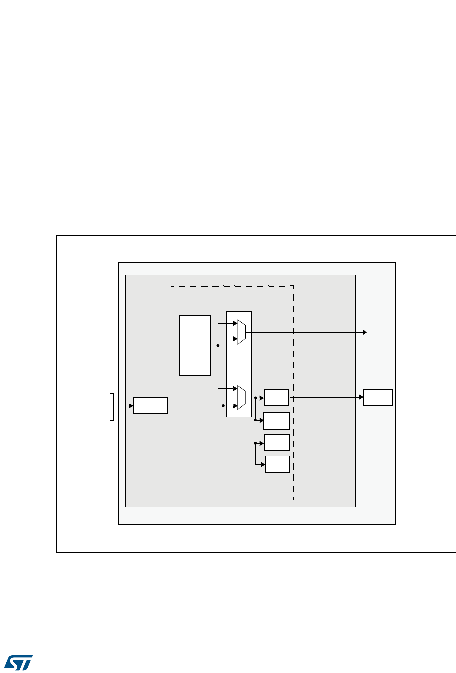
DocID025941 Rev 5 915/1001
RM0376 Debug support (DBG)
929
32 Debug support (DBG)
32.1 Overview
The STM32L0x2 devices are built around a Cortex®-M0+ core which contains hardware
extensions for advanced debugging features. The debug extensions allow the core to be
stopped either on a given instruction fetch (breakpoint) or data access (watchpoint). When
stopped, the core’s internal state and the system’s external state may be examined. Once
examination is complete, the core and the system may be restored and program execution
resumed.
The debug features are used by the debugger host when connecting to and debugging the
STM32L0x2 MCUs.
One interface for debug is available:
•Serial wire
Figure 299. Block diagram of STM32L0x2 MCU and Cortex®-M0+-level debug support
1. The debug features embedded in the Cortex®-M0+ core are a subset of the Arm® CoreSight Design Kit.
The Arm® Cortex®-M0+ core provides integrated on-chip debug support. It is comprised of:
•SW-DP: Serial wire
•BPU: Break point unit
•DWT: Data watchpoint trigger
Cortex-M0
Core
SW-DP
Bridge
NVIC
DWT
BPU
System
interface
Debug AP
Bus matrix
DBGMCU
STM32 MCU debug suppo rt
Cortex-M0 debug support
SWDIO
SWCLK
MS19240V2
Debug AP
Debug support (DBG) RM0376
916/1001 DocID025941 Rev 5
It also includes debug features dedicated to the STM32L0x2 microcontrollers:
•Flexible debug pinout assignment
•MCU debug box (support for low-power modes, control over peripheral clocks, etc.)
Note: For further information on debug functionality supported by the Arm® Cortex®-M0+ core,
refer to the Cortex®-M0+ Technical Reference Manual (see Section 32.2: Reference Arm®
documentation).
32.2 Reference Arm® documentation
•Cortex®-M0+ Technical Reference Manual (TRM)
It is available from www.infocenter.arm.com
•Arm® Debug Interface V5
•Arm® CoreSight Design Kit revision r1p1 Technical Reference Manual
32.3 Pinout and debug port pins
The STM32L0x2 MCUs are available in various packages with different numbers of
available pins.
32.3.1 SWD port pins
Two pins are used as outputs for the SW-DP as alternate functions of general purpose I/Os.
These pins are available on all packages.
32.3.2 SW-DP pin assignment
After reset (SYSRESETn or PORESETn), the pins used for the SW-DP are assigned as
dedicated pins which are immediately usable by the debugger host.
However, the MCU offers the possibility to disable the SWD port and can then release the
associated pins for general-purpose I/O (GPIO) usage. For more details on how to disable
SW-DP port pins, please refer to Section 9.3.2: I/O pin alternate function multiplexer and
mapping on page 237.
Table 158. SW debug port pins
SW-DP pin name
SW debug port Pin
assignment
Type Debug assignment
SWDIO IO Serial Wire Data Input/Output PA13
SWCLK I Serial Wire Clock PA14

DocID025941 Rev 5 917/1001
RM0376 Debug support (DBG)
929
32.3.3 Internal pull-up & pull-down on SWD pins
Once the SW I/O is released by the user software, the GPIO controller takes control of these
pins. The reset states of the GPIO control registers put the I/Os in the equivalent states:
•SWDIO: input pull-up
•SWCLK: input pull-down
Embedded pull-up and pull-down resistors remove the need to add external resistors.
32.4 ID codes and locking mechanism
There are several ID codes inside the MCU. ST strongly recommends the tool
manufacturers to lock their debugger using the MCU device ID located at address
0x40015800.
32.4.1 MCU device ID code
The STM32L0x2 products integrate an MCU ID code. This ID identifies the ST MCU part
number and the die revision.
This code is accessible by the software debug port (two pins) or by the user software.
Only the DEV_ID[15:0] should be used for identification by the debugger/programmer tools
(the revision ID must not be taken into account).
For code example, refer to A.20.1: DBG read device Id code example.
DBG_IDCODE
Address: 0x4001 5800
Only 32-bit access supported. Read-only
31 30 29 28 27 26 25 24 23 22 21 20 19 18 17 16
REV_ID
rrrrrr r r r r rrrrrr
1514131211109876543210
Res. Res. Res. Res. DEV_ID
rrrrrrrrrrr
Bits 31:16 REV_ID[15:0] Revision identifier
This field indicates the revision of the device (see Table 159: REV-ID values).
Bits 15:12 Reserved: read 0b0110.
Bits 11:0 DEV_ID[11:0]: Device identifier
This field indicates the device ID:
Category 3 devices: 0x417
Category 5 devices: 0x447
Debug support (DBG) RM0376
918/1001 DocID025941 Rev 5
32.5 SWD port
32.5.1 SWD protocol introduction
This synchronous serial protocol uses two pins:
•SWCLK: clock from host to target
•SWDIO: bidirectional
The protocol allows two banks of registers (DPACC registers and APACC registers) to be
read and written to.
Bits are transferred LSB-first on the wire.
For SWDIO bidirectional management, the line must be pulled-up on the board (100 kΩ
recommended by Arm®). These pull-up resistors can be configured internally. No external
pull-up resistors are required. .
Each time the direction of SWDIO changes in the protocol, a turnaround time is inserted
where the line is not driven by the host nor the target. By default, this turnaround time is one
bit time, however this can be adjusted by configuring the SWCLK frequency.
32.5.2 SWD protocol sequence
Each sequence consist of three phases:
1. Packet request (8 bits) transmitted by the host
2. Acknowledge response (3 bits) transmitted by the target
3. Data transfer phase (33 bits) transmitted by the host or the target
Table 159. REV-ID values
REV_ID Cat. 3 devices Cat. 5 devices
0x1000 Rev A
0x1008 Rev Z -
0x1018 Rev Y -
0x1038 Rev X -
0x2000 - Rev B
0x2008 - Rev Z
Table 160. Packet request (8-bits)
Bit Name Description
0 Start Must be “1”
1 APnDP 0: DP Access
1: AP Access
2RnW 0: Write Request
1: Read Request
4:3 A[3:2] Address field of the DP or AP registers (refer to Table 164 on
page 921)

DocID025941 Rev 5 919/1001
RM0376 Debug support (DBG)
929
Refer to the Cortex®-M0+ TRM for a detailed description of DPACC and APACC registers.
The packet request is always followed by the turnaround time (default 1 bit) where neither
the host nor target drive the line.
The ACK Response must be followed by a turnaround time only if it is a READ transaction
or if a WAIT or FAULT acknowledge has been received.
The DATA transfer must be followed by a turnaround time only if it is a READ transaction.
32.5.3 SW-DP state machine (reset, idle states, ID code)
The State Machine of the SW-DP has an internal ID code which identifies the SW-DP. It
follows the JEP-106 standard. This ID code is the default Arm® one and is set to
0x0BC11477(corresponding to Cortex®-M0+).
Note: Note that the SW-DP state machine is inactive until the target reads this ID code.
•The SW-DP state machine is in RESET STATE either after power-on reset, or after the
line is high for more than 50 cycles
•The SW-DP state machine is in IDLE STATE if the line is low for at least two cycles
after RESET state.
•After RESET state, it is mandatory to first enter into an IDLE state AND to perform a
READ access of the DP-SW ID CODE register. Otherwise, the target will issue a
FAULT acknowledge response on another transactions.
Further details of the SW-DP state machine can be found in the Cortex®-M0+ TRM and the
CoreSight Design Kit r1p0 TRM.
5 Parity Single bit parity of preceding bits
6Stop 0
7Park Not driven by the host. Must be read as “1” by the target
because of the pull-up
Table 161. ACK response (3 bits)
Bit Name Description
0..2 ACK
001: FAULT
010: WAIT
100: OK
Table 162. DATA transfer (33 bits)
Bit Name Description
0..31 WDATA or
RDATA Write or Read data
32 Parity Single parity of the 32 data bits
Table 160. Packet request (8-bits) (continued)
Bit Name Description

Debug support (DBG) RM0376
920/1001 DocID025941 Rev 5
32.5.4 DP and AP read/write accesses
•Read accesses to the DP are not posted: the target response can be immediate (if
ACK=OK) or can be delayed (if ACK=WAIT).
•Read accesses to the AP are posted. This means that the result of the access is
returned on the next transfer. If the next access to be done is NOT an AP access, then
the DP-RDBUFF register must be read to obtain the result.
The READOK flag of the DP-CTRL/STAT register is updated on every AP read access
or RDBUFF read request to know if the AP read access was successful.
•The SW-DP implements a write buffer (for both DP or AP writes), that enables it to
accept a write operation even when other transactions are still outstanding. If the write
buffer is full, the target acknowledge response is “WAIT”. With the exception of
IDCODE read or CTRL/STAT read or ABORT write which are accepted even if the write
buffer is full.
•Because of the asynchronous clock domains SWCLK and HCLK, two extra SWCLK
cycles are needed after a write transaction (after the parity bit) to make the write
effective internally. These cycles should be applied while driving the line low (IDLE
state)
This is particularly important when writing the CTRL/STAT for a power-up request. If the
next transaction (requiring a power-up) occurs immediately, it will fail.
32.5.5 SW-DP registers
Access to these registers are initiated when APnDP=0
Table 163. SW-DP registers
A[3:2] R/W
CTRLSEL bit
of SELECT
register
Register Notes
00 Read IDCODE
The manufacturer code is set to the default
Arm® code for Cortex®-M0+:
0x0BC11477 (identifies the SW-DP)
00 Write ABORT
01 Read/Write 0 DP-CTRL/STAT
Purpose is to:
– request a system or debug power-up
– configure the transfer operation for AP
accesses
– control the pushed compare and pushed
verify operations.
– read some status flags (overrun, power-up
acknowledges)
01 Read/Write 1 WIRE
CONTROL
Purpose is to configure the physical serial
port protocol (like the duration of the
turnaround time)
10 Read READ
RESEND
Enables recovery of the read data from a
corrupted debugger transfer, without
repeating the original AP transfer.

DocID025941 Rev 5 921/1001
RM0376 Debug support (DBG)
929
32.5.6 SW-AP registers
Access to these registers are initiated when APnDP=1
There are many AP Registers addressed as the combination of:
•The shifted value A[3:2]
•The current value of the DP SELECT register.
10 Write SELECT The purpose is to select the current access
port and the active 4-words register window
11 Read/Write READ BUFFER
This read buffer is useful because AP
accesses are posted (the result of a read AP
request is available on the next AP
transaction).
This read buffer captures data from the AP,
presented as the result of a previous read,
without initiating a new transaction
Table 163. SW-DP registers (continued)
A[3:2] R/W
CTRLSEL bit
of SELECT
register
Register Notes
Table 164. 32-bit debug port registers addressed through the shifted value A[3:2]
Address A[3:2] value Description
0x0 00 Reserved, must be kept at reset value.
0x4 01
DP CTRL/STAT register. Used to:
– Request a system or debug power-up
– Configure the transfer operation for AP accesses
– Control the pushed compare and pushed verify operations.
– Read some status flags (overrun, power-up acknowledges)
0x8 10
DP SELECT register: Used to select the current access port and the
active 4-words register window.
– Bits 31:24: APSEL: select the current AP
– Bits 23:8: reserved
– Bits 7:4: APBANKSEL: select the active 4-words register window on the
current AP
– Bits 3:0: reserved
0xC 11
DP RDBUFF register: Used to allow the debugger to get the final result
after a sequence of operations (without requesting new JTAG-DP
operation)

Debug support (DBG) RM0376
922/1001 DocID025941 Rev 5
32.6 Core debug
Core debug is accessed through the core debug registers. Debug access to these registers
is by means of the debug access port. It consists of four registers:
These registers are not reset by a system reset. They are only reset by a power-on reset.
Refer to the Cortex®-M0+ TRM for further details.
To Halt on reset, it is necessary to:
•enable the bit0 (VC_CORRESET) of the Debug and Exception Monitor Control
Register
•enable the bit0 (C_DEBUGEN) of the Debug Halting Control and Status Register
32.7 BPU (Break Point Unit)
The Cortex®-M0+ BPU implementation provides four breakpoint registers. The BPU is a
subset of the Flash Patch and Breakpoint (FPB) block available in ARMv7-M (Cortex®-M3
and Cortex®-M4).
32.7.1 BPU functionality
The processor breakpoints implement PC based breakpoint functionality.
Refer the ARMv6-M Arm® and the Arm® CoreSight Components Technical Reference
Manual for more information about the BPU CoreSight identification registers, and their
addresses and access types.
Table 165. Core debug registers
Register Description
DHCSR
The 32-bit Debug Halting Control and Status Register
This provides status information about the state of the processor enable core debug
halt and step the processor
DCRSR The 17-bit Debug Core Register Selector Register:
This selects the processor register to transfer data to or from.
DCRDR
The 32-bit Debug Core Register Data Register:
This holds data for reading and writing registers to and from the processor selected
by the DCRSR (Selector) register.
DEMCR The 32-bit Debug Exception and Monitor Control Register:
This provides Vector Catching and Debug Monitor Control.

DocID025941 Rev 5 923/1001
RM0376 Debug support (DBG)
929
32.8 DWT (Data Watchpoint)
The Cortex®-M0+ DWT implementation provides two watchpoint register sets.
32.8.1 DWT functionality
The processor watchpoints implement both data address and PC based watchpoint
functionality, a PC sampling register, and support comparator address masking, as
described in the ARMv6-M Arm®.
32.8.2 DWT Program Counter Sample Register
A processor that implements the data watchpoint unit also implements the ARMv6-M
optional DWT Program Counter Sample Register (DWT_PCSR). This register permits a
debugger to periodically sample the PC without halting the processor. This provides coarse
grained profiling. See the ARMv6-M Arm® for more information.
The Cortex®-M0+ DWT_PCSR records both instructions that pass their condition codes and
those that fail.
32.9 MCU debug component (DBG)
The MCU debug component helps the debugger provide support for:
•Low-power modes
•Clock control for timers, watchdog and I2C during a breakpoint
32.9.1 Debug support for low-power modes
To enter low-power mode, the instruction WFI or WFE must be executed.
The MCU implements several low-power modes which can either deactivate the CPU clock
or reduce the power of the CPU.
The core does not allow FCLK or HCLK to be turned off during a debug session. As these
are required for the debugger connection, during a debug, they must remain active. The
MCU integrates special means to allow the user to debug software in low-power modes.
For this, the debugger host must first set some debug configuration registers to change the
low-power mode behavior:
•In Sleep mode: FCLK and HCLK are still active. Consequently, this mode does not
impose any restrictions on the standard debug features.
•In Stop/Standby mode, the DBG_STOP bit must be previously set by the debugger.
This enables the internal RC oscillator clock to feed FCLK and HCLK in Stop mode.
When one of the DBG_STANDBY, DBG_STOP and DBG_SLEEP bit is set and the internal
reference voltage is stopped in low-power mode (ULP bit set in PWR_CR register), then the
Fast wakeup must be enabled (FWU bit set in PWR_CR).
For code example, refer to A.20.2: DBG debug in LPM code example.

Debug support (DBG) RM0376
924/1001 DocID025941 Rev 5
32.9.2 Debug support for timers, watchdog and I2C
During a breakpoint, it is necessary to choose how the counter of timers and watchdog
should behave:
•They can continue to count inside a breakpoint. This is usually required when a PWM is
controlling a motor, for example.
•They can stop to count inside a breakpoint. This is required for watchdog purposes.
For the I2C, the user can choose to block the SMBUS timeout during a breakpoint.
32.9.3 Debug MCU configuration register (DBG_CR)
The DBG_CR register allows to configure the low-power modes when the MCU is under
debug. When one of DBG_CR bits is set, if ULP bit is set in PWR_CR, then FWU bit of
PWR_CR must be set.
It is mapped at address 0x4001 5804.
This register is asynchronously reset by the PORESET (and not the system reset). It can be
written by the debugger under system reset.
If the debugger host does not support these features, it is still possible for the user software
to write to these registers.
Address: 0x04
Only 32-bit access supported
POR Reset: 0x0000 0000 (not reset by system reset)
31 30 29 28 27 26 25 24 23 22 21 20 19 18 17 16
Res. Res. Res. Res. Res. Res. Res. Res. Res. Res. Res. Res. Res. Res. Res. Res.
15 14 13 12 11 10 9 8 7 6 5 4 3 2 1 0
Res. Res. Res. Res. Res. Res. Res. Res. Res. Res. Res. Res. Res.
DBG_
STAND
BY
DBG_
STOP
DBG_
SLEEP
rw rw rw

DocID025941 Rev 5 925/1001
RM0376 Debug support (DBG)
929
Bits 31:3 Reserved, must be kept at reset value.
Bit 2 DBG_STANDBY: Debug Standby mode
0: (FCLK=Off, HCLK=Off) The whole digital part is unpowered.
From software point of view, exiting from Standby is identical than fetching reset vector
(except a few status bit indicated that the MCU is resuming from Standby)
1: (FCLK=On, HCLK=On) In this case, the digital part is not unpowered and FCLK and
HCLK are provided by the internal RC oscillator which remains active. In addition, the MCU
generate a system reset during Standby mode so that exiting from Standby is identical than
fetching from reset
Bit 1 DBG_STOP: Debug Stop mode
0: (FCLK=Off, HCLK=Off) In Stop mode, the clock controller disables all clocks (including
HCLK and FCLK). When exiting from Stop mode, the clock configuration is identical to the
one after RESET. Consequently, the software must reprogram the clock controller to enable
the PLL, the Xtal, etc.
1: (FCLK=On, HCLK=On) In this case, when entering Stop mode, FCLK and HCLK are
provided by the internal RC oscillator which remains active in Stop mode. When exiting Stop
mode, the software must reprogram the clock controller to enable the PLL, the Xtal, etc. (in
the same way it would do in case of DBG_STOP=0)
Bit 0 DBG_SLEEP: Debug Sleep mode
0: In Sleep mode, FCLK is clocked by the system clock previously configured by the
software while HCLK is disabled. The clock controller configuration is not reset and remains
in its previously programmed state. As a consequence, when exiting from Sleep mode, the
software does not need to reconfigure the clock controller.
1: In this case, when entering in Sleep mode, HCLK is fed by the same clock that is provided
to FCLK (system clock previously configured by the software).
Debug support (DBG) RM0376
926/1001 DocID025941 Rev 5
32.9.4 Debug MCU APB1 freeze register (DBG_APB1_FZ)
The DBG_APB1_FZ register is used to configure the following APB peripherals, when the
MCU under debug:
•Timer clock counter freeze
•I2C SMBUS timeout freeze
•System window watchdog and independent watchdog counter freeze support.
This register is mapped at address 0x4001 5808.
The register is asynchronously reset by the POR (and not the system reset). It can be
written by the debugger under system reset.
Address offset: 0X08
Only 32-bit access are supported.
Power on reset (POR): 0x0000 0000 (not reset by system reset)
31 30 29 28 27 26 25 24 23 22 21 20 19 18 17 16
DBG_LPTIMER_STO
P
DBG_I2C3_STOP
Res. Res. Res. Res. Res. Res. Res. Res.
DBG_I2C1_STOP
Res. Res. Res. Res. Res.
rw rw rw
1514131211109876543210
Res. Res. Res.
DBG_IWDG_STOP
DBG_WWDG_STOP
DBG_RTC_STOP
Res. Res. Res. Res.
DBG_TIM7_STOP
DBG_TIM6_STOP
Res. Res.
.DBG_TIM3_STOP
.DBG_TIM2_STOP
rw rw rw rw rw rw rw
Bit 31 DBG_LPTIMER_STOP: LPTIM1 counter stopped when core is halted
0: LPTIM1 counter clock is fed even if the core is halted
1: LPTIM1 counter clock is stopped when the core is halted
Bit 30 DBG_I2C3_STOP: I2C3 SMBUS timeout mode stopped when core is halted
0: Same behavior as in normal mode
1: I2C3 SMBUS timeout is frozen
Bits 29:22 Reserved, must be kept at reset value.
Bit 21 DBG_I2C1_STOP: I2C1 SMBUS timeout mode stopped when core is halted
0: Same behavior as in normal mode
1: I2C1 SMBUS timeout is frozen
Bits 20:13 Reserved, must be kept at reset value.
Bit 12 DBG_IWDG_STOP: Debug independent watchdog stopped when core is halted
0: The independent watchdog counter clock continues even if the core is halted
1: The independent watchdog counter clock is stopped when the core is halted

DocID025941 Rev 5 927/1001
RM0376 Debug support (DBG)
929
Bit 11 DBG_WWDG_STOP: Debug window watchdog stopped when core is halted
0: The window watchdog counter clock continues even if the core is halted
1: The window watchdog counter clock is stopped when the core is halted
Bit 10 DBG_RTC_STOP: Debug RTC stopped when core is halted
0: The clock of the RTC counter is fed even if the core is halted
1: The clock of the RTC counter is stopped when the core is halted
Bits 9:6 Reserved, must be kept at reset value.
Bit 5 DBG_TIM7_STOP: TIM7 counter stopped when core is halted
0: The counter clock of TIM7 is fed even if the core is halted
1: The counter clock of TIM7 is stopped when the core is halted
Bit 4 DBG_TIM6_STOP: TIM6 counter stopped when core is halted
0: The counter clock of TIM6 is fed even if the core is halted
1: The counter clock of TIM6 is stopped when the core is halted
Bits 3:2 Reserved, must be kept at reset value.
Bit 1 DBG_TIM3_STOP: TIM3 counter stopped when core is halted
0: The counter clock of TIM3 is fed even if the core is halted
1: The counter clock of TIM3 is stopped when the core is halted
Bit 0 DBG_TIM2_STOP: TIM2 counter stopped when core is halted
0: The counter clock of TIM2 is fed even if the core is halted
1: The counter clock of TIM2 is stopped when the core is halted

Debug support (DBG) RM0376
928/1001 DocID025941 Rev 5
32.9.5 Debug MCU APB2 freeze register (DBG_APB2_FZ)
The DBG_APB2_FZ register is used to configure some APB peripheral features when the
MCU is under DEBUG:
•Timer clock counter freeze.
This register is mapped at address 0x4001580C.
It is asynchronously reset by the POR (and not the system reset). It can be written by the
debugger under system reset.
Address: 0x0C
Only 32-bit access is supported.
POR: 0x0000 0000 (not reset by system reset)
31 30 29 28 27 26 25 24 23 22 21 20 19 18 17 16
Res. Res. Res. Res. Res. Res. Res. Res. Res. Res. Res. Res. Res. Res. Res. Res.
1514131211109876543 2 1 0
Res. Res. Res. Res. Res. Res. Res. Res. Res. Res.
DBG_TIM22_STOP
Res. Res.
DBG_TIM21_STOP
Res. Res.
rw rw
Bits 31:6 Reserved, must be kept at reset value.
Bit 5 DBG_TIM22_STOP: TIM22 counter stopped when core is halted
0: The counter clock of TIM22 is fed even if the core is halted
1: The counter clock of TIM22 is stopped when the core is halted
Bits 4:3 Reserved, must be kept at reset value.
Bit 2 DBG_TIM21_STOP: TIM21 counter stopped when core is halted
0: The counter clock of TIM21 is fed even if the core is halted
1: The counter clock of TIM21 is stopped when the core is halted
Bits 1:0 Reserved, must be kept at reset value.

DocID025941 Rev 5 929/1001
RM0376 Debug support (DBG)
929
32.10 DBG register map
The following table summarizes the Debug registers.
. Table 166. DBG register map and reset values
Addr. Register
31
30
29
28
27
26
25
24
23
22
21
20
19
18
17
16
15
14
13
12
11
10
9
8
7
6
5
4
3
2
1
0
0x40015800
DBG_
IDCODE REV_ID
Res.
Res.
Res.
Res.
DEV_ID
Reset value(1) XXXXXXXXXXXXXXXX XXXXXXXXXXXX
0x40015804
DBG_CR
Res.
Res.
Res.
Res.
Res.
Res.
Res.
Res.
Res.
Res.
Res.
Res.
Res.
Res.
Res.
Res.
Res.
Res.
Res.
Res.
Res.
Res.
Res.
Res.
Res.
Res.
Res.
Res.
Res.
DBG_STANDBY
DBG_STOP
DBG_SLEEP
Reset value 000
0x40015808
DBG_
APB1_FZ
DBG_LPTIMER_STO
DBG_I2C3_STOP.
Res.
Res.
Res.
Res.
Res.
Res.
Res.
Res.
DBG_I2C1_STOP
Res.
Res.
Res.
Res.
Res.
Res.
Res.
Res.
DBG_IWDG_STOP
DBG_WWDG_STOP
DBG_RTC_STOP
Res.
Res.
Res.
Res.
DBG_TIM7_STOP
DBG_TIM6_STOP
Res.
Res.
DBG_TIM3_STOP
DBG_TIM2_STOP
Reset value 00 0 000 00 00
0x4001580C
DBG_
APB2_FZ
Res.
Res.
Res.
Res.
Res.
Res.
Res.
Res.
Res.
Res.
Res.
Res.
Res.
Res.
Res.
Res.
Res.
Res.
Res.
Res.
Res.
Res.
Res.
Res.
Res.
Res.
DBG_TIM22_STOP
Res.
Res.
DBG_TIM21_STOP
Res.
Res.
Reset value 00
1. The reset value is product dependent. For more information, refer to Section 32.4.1: MCU device ID code.

Device electronic signature RM0376
930/1001 DocID025941 Rev 5
33 Device electronic signature
This section applies to all STM32L0x2 devices, unless otherwise specified.
The electronic signature is stored in the System memory area in the Flash memory module,
and can be read using the JTAG/SWD or the CPU. It contains factory-programmed
identification data that allow the user firmware or other external devices to automatically
match its interface to the characteristics of the STM32L0x2 microcontroller.
33.1 Memory size register
33.1.1 Flash size register
Base address: 0x1FF8 007C
Read only = 0xXXXX where X is factory-programmed
33.2 Unique device ID registers (96 bits)
The unique device identifier is ideally suited:
•for use as serial numbers
•for use as security keys in order to increase the security of code in Flash memory while
using and combining this unique ID with software cryptographic primitives and
protocols before programming the internal Flash memory
•to activate secure boot processes, etc.
The 96-bit unique device identifier provides a reference number which is unique for any
device and in any context. These bits can never be altered by the user.
The 96-bit unique device identifier can also be read in single bytes/half-words/words in
different ways and then be concatenated using a custom algorithm.
15 14 13 12 11 10 9 8 7 6 5 4 3 2 1 0
F_SIZE
rrrrrrrrrrrrrrrr
Bits 15:0 F_SIZE: Flash memory size
The value stored in this field indicates the Flash memory size of the device expressed in
Kbytes.
Example: 0x0040 = 64 Kbytes.
DocID025941 Rev 5 931/1001
RM0376 Device electronic signature
931
Base address: 0x1FF8 0050
Address offset: 0x00
Read only = 0xXXXX XXXX where X is factory-programmed
Address offset: 0x04
Read only = 0xXXXX XXXX where X is factory-programmed
Address offset: 0x14
Read only = 0xXXXX XXXX where X is factory-programmed
31 30 29 28 27 26 25 24 23 22 21 20 19 18 17 16
U_ID(31:16)
rrrrrrrrrrrrrrrr
1514131211109876543210
U_ID(15:0)
rrrrrrrrrrrrrrrr
Bits 31:0 U_ID(31:24): WAF_NUM[7:0]
Wafer number (8-bit unsigned number)
U_ID(23:0): LOT_NUM[55:32]
Lot number (ASCII code)
63 62 61 60 59 58 57 56 55 54 53 52 51 50 49 48
U_ID(63:48)
rrrrrrrrrrrrrrrr
47 46 45 44 43 42 41 40 39 38 37 36 35 34 33 32
U_ID(47:32)
rrrrrrrrrrrrrrrr
Bits 63:32 U_ID(63:32): LOT_NUM[31:0]
Lot number (ASCII code)
95 94 93 92 91 90 89 88 87 86 85 84 83 82 81 80
U_ID(95:80)
rrrrrrrrrrrrrrrr
79 78 77 76 75 74 73 72 71 70 69 68 67 66 65 64
U_ID(79:64)
rrrrrrrrrrrrrrrr
Bits 95:64 U_ID(95:64): 95:64 unique ID bits

Code examples RM0376
932/1001 DocID025941 Rev 5
Appendix A Code examples
A.1 Introduction
This appendix shows the code examples of the sequence described in this Reference
Manual.
These code examples are extracted from the STM32L0xx Snippet firmware package
STM32SnippetsL0 available on www.st.com.
These code examples used the peripheral bit and register description from the CMSIS
header file (stm32l0xx.h).
Code lines starting with // should be uncommented if the given register has been modified
before.
A.2 NVM/RCC Operation code example
A.2.1 Increasing the CPU frequency preparation sequence code
/* (1) Set one wait state in Latency bit of FLASH_ACR */
/* (2) Check the latency is set */
/* (3) Switch the clock on HSI16/4 and disable PLL */
/* (4) Set PLLMUL to 16 to get 32MHz on CPU clock */
/* (5) Enable and switch on PLL */
FLASH->ACR |= FLASH_ACR_LATENCY; /* (1) */
while ((FLASH->ACR & FLASH_ACR_LATENCY) == 0); /* (2) */
SwitchFromPLLtoHSI(); /* (3) */
RCC->CFGR = (RCC->CFGR & (~(uint32_t)RCC_CFGR_PLLMUL))
| RCC_CFGR_PLLMUL16; /* (4) */
SwitchOnPLL(); /* (5) */
A.2.2 Decreasing the CPU frequency preparation sequence code
/* (1) Switch the clock on HSI16/4 and disable PLL */
/* (2) Set PLLMUL to 4 to get 8MHz on CPU clock */
/* (3) Enable and switch on PLL */
/* (4) Set one wait state in Latency bit of FLASH_ACR */
/* (5) Check the latency is set */
SwitchFromPLLtoHSI(); /* (1) */
RCC->CFGR = (RCC->CFGR & (~(uint32_t)RCC_CFGR_PLLMUL))
| RCC_CFGR_PLLMUL4; /* (2) */
SwitchOnPLL(); /* (3) */
FLASH->ACR &= ~FLASH_ACR_LATENCY; /* (4) */
while ((FLASH->ACR & FLASH_ACR_LATENCY) != 0); /* (5) */

DocID025941 Rev 5 933/1001
RM0376 Code examples
979
A.2.3 Switch from PLL to HSI16 sequence code
uint32_t tickstart;
/* (1) Switch the clock on HSI16/4 */
/* (2) Wait for clock switched on HSI16/4 */
/* (3) Disable the PLL by resetting PLLON */
/* (4) Wait until PLLRDY is cleared */
RCC->CFGR = (RCC->CFGR & (~RCC_CFGR_SW)) | RCC_CFGR_SW_HSI; /* (1) */
tickstart = Tick;
while ((RCC->CFGR & RCC_CFGR_SWS) != RCC_CFGR_SWS_HSI) /* (2) */
{
if ((Tick - tickstart ) > CLOCKSWITCH_TIMEOUT_VALUE)
{
/* Manage error */
return;
}
}
RCC->CR &= ~RCC_CR_PLLON; /* (3) */
tickstart = Tick;
while ((RCC->CR & RCC_CR_PLLRDY) != 0) /* (4) */
{
if ((Tick - tickstart ) > PLL_TIMEOUT_VALUE)
{
/* Manage error */
}
}
Note: Tick is a global variable incremented in the SysTick ISR each millisecond.
A.2.4 Switch to PLL sequence code
uint32_t tickstart;
/* (1) Switch on the PLL */
/* (2) Wait for PLL ready */
/* (3) Switch the clock to the PLL */
/* (4) Wait until the clock is switched to the PLL */
RCC->CR |= RCC_CR_PLLON; /* (1) */
tickstart = Tick;
while ((RCC->CR & RCC_CR_PLLRDY) == 0) /* (2) */
{
if ((Tick - tickstart ) > PLL_TIMEOUT_VALUE)
{
error = ERROR_PLL_TIMEOUT; /* Report an error */
return;
}
}
RCC->CFGR = (RCC->CFGR & (~RCC_CFGR_SW)) | RCC_CFGR_SW_PLL; /* (3) */

Code examples RM0376
934/1001 DocID025941 Rev 5
tickstart = Tick;
while ((RCC->CFGR & RCC_CFGR_SWS) != RCC_CFGR_SWS_PLL) /* (4) */
{
if ((Tick - tickstart ) > CLOCKSWITCH_TIMEOUT_VALUE)
{
error = ERROR_CLKSWITCH_TIMEOUT; /* Report an error */
return;
}
}
Note: Tick is a global variable incremented in the SysTick ISR each millisecond.
A.3 NVM Operation code example
A.3.1 Unlocking the data EEPROM and FLASH_PECR register
code example
/* (1) Wait till no operation is on going */
/* (2) Check if the PELOCK is unlocked */
/* (3) Perform unlock sequence */
while ((FLASH->SR & FLASH_SR_BSY) != 0) /* (1) */
{
/* For robust implementation, add here time-out management */
}
if ((FLASH->PECR & FLASH_PECR_PELOCK) != 0) /* (2) */
{
FLASH->PEKEYR = FLASH_PEKEY1; /* (3) */
FLASH->PEKEYR = FLASH_PEKEY2;
}
A.3.2 Locking data EEPROM and FLASH_PECR register code example
/* (1) Wait till no operation is on going */
/* (2) Locks the NVM by setting PELOCK in PECR */
while ((FLASH->SR & FLASH_SR_BSY) != 0) /* (1) */
{
/* For robust implementation, add here time-out management */
}
FLASH->PECR |= FLASH_PECR_PELOCK; /* (2) */
A.3.3 Unlocking the NVM program memory code example
/* (1) Wait till no operation is on going */
/* (2) Check that the PELOCK is unlocked */
/* (3) Check if the PRGLOCK is unlocked */
/* (4) Perform unlock sequence */
while ((FLASH->SR & FLASH_SR_BSY) != 0) /* (1) */

DocID025941 Rev 5 935/1001
RM0376 Code examples
979
{
/* For robust implementation, add here time-out management */
}
if ((FLASH->PECR & FLASH_PECR_PELOCK) == 0) /* (2) */
{
if ((FLASH->PECR & FLASH_PECR_PRGLOCK) != 0) /* (3) */
{
FLASH->PRGKEYR = FLASH_PRGKEY1; /* (4) */
FLASH->PRGKEYR = FLASH_PRGKEY2;
}
}
A.3.4 Unlocking the option bytes area code example
/* (1) Wait till no operation is on going */
/* (2) Check that the PELOCK is unlocked */
/* (3) Check if the OPTLOCK is unlocked */
/* (4) Perform unlock sequence */
while ((FLASH->SR & FLASH_SR_BSY) != 0) /* (1) */
{
/* For robust implementation, add here time-out management */
}
if ((FLASH->PECR & FLASH_PECR_PELOCK) == 0) /* (2) */
{
if ((FLASH->PECR & FLASH_PECR_OPTLOCK) != 0) /* (2) */
{
FLASH->OPTKEYR = FLASH_OPTKEY1; /* (3) */
FLASH->OPTKEYR = FLASH_OPTKEY2;
}
}
A.3.5 Write to data EEPROM code example
*(uint8_t *)(DATA_E2_ADDR+i) = DATA_BYTE;
*(uint16_t *)(DATA_E2_ADDR+j) = DATA_16B_WORD;
*(uint32_t *)(DATA_E2_ADDR) = DATA_32B_WORD;
DATA_E2_ADDR is an aligned address in the data EEPROM area.
i can be any integer.
j must be an even integer.
A.3.6 Erase to data EEPROM code example
/* (1) Set the ERASE and DATA bits in the FLASH_PECR register
to enable page erasing */
/* (2) Write a 32-bit word value at the desired address
to start the erase sequence */

Code examples RM0376
936/1001 DocID025941 Rev 5
/* (3) Enter in wait for interrupt. The EOP check is done in the Flash ISR
*/
/* (6) Reset the ERASE and DATA bits in the FLASH_PECR register
to disable the page erase */
FLASH->PECR |= FLASH_PECR_ERASE | FLASH_PECR_DATA; /* (1) */
*(__IO uint32_t *)addr = (uint32_t)0; /* (2) */
__WFI(); /* (3) */
FLASH->PECR &= ~(FLASH_PECR_ERASE | FLASH_PECR_DATA); /* (4) */
A.3.7 Program Option byte code example
/**
* This function programs a 16-bit option byte and its complement word.
* Param None
* Retval None
*/
__INLINE __RAM_FUNC void OptionByteProg(uint8_t index, uint16_t data)
{
/* (1) Write a 32-bit word value at the option byte address,
the 16-bit data is extended with its compemented value */
/* (3) Wait until the BSY bit is reset in the FLASH_SR register */
/* (4) Check the EOP flag in the FLASH_SR register */
/* (5) Clear EOP flag by software by writing EOP at 1 */
*(__IO uint32_t *)(OB_BASE + index) = (uint32_t)((~data << 16) | data);
/* (1) */
while ((FLASH->SR & FLASH_SR_BSY) != 0) /* (2) */
{
/* For robust implementation, add here time-out management */
}
if ((FLASH->SR & FLASH_SR_EOP) != 0) /* (3) */
{
FLASH->SR = FLASH_SR_EOP; /* (4) */
}
else
{
/* Manage the error cases */
}
}
Note: This function must be loaded in RAM.
A.3.8 Erase Option byte code example
/**
* This function erases a 16-bit option byte and its complement
word.
* Param None

DocID025941 Rev 5 937/1001
RM0376 Code examples
979
* Retval None
*/
__INLINE __RAM_FUNC void OptionByteErase(uint8_t index)
{
/* (1) Set the ERASE bit in the FLASH_PECR register
to enable option byte erasing */
/* (2) Write a 32-bit word value at the option byte address to be erased
to start the erase sequence */
/* (3) Wait until the BSY bit is reset in the FLASH_SR register */
/* (4) Check the EOP flag in the FLASH_SR register */
/* (5) Clear EOP flag by software by writing EOP at 1 */
/* (6) Reset the ERASE and PROG bits in the FLASH_PECR register
to disable the page erase */
FLASH->PECR |= FLASH_PECR_ERASE; /* (1) */
*(__IO uint32_t *)(OB_BASE + index) = 0; /* (2) */
while ((FLASH->SR & FLASH_SR_BSY) != 0) /* (3) */
{
/* For robust implementation, add here time-out management */
}
if ((FLASH->SR & FLASH_SR_EOP) != 0) /* (4) */
{
FLASH->SR |= FLASH_SR_EOP; /* (5) */
}
else
{
/* Manage the error cases */
}
FLASH->PECR &= ~(FLASH_PECR_ERASE); /* (6) */
}
Note: This function must be loaded in RAM.
A.3.9 Program a single word to Flash program memory code example
/* (1) Perform the data write (32-bit word) at the desired address */
/* (2) Wait until the BSY bit is reset in the FLASH_SR register */
/* (3) Check the EOP flag in the FLASH_SR register */
/* (4) clear it by software by writing it at 1 */
*(__IO uint32_t*)(flash_addr) = data; /* (1) */
while ((FLASH->SR & FLASH_SR_BSY) != 0) /* (2) */
{
/* For robust implementation, add here time-out management */
}
if ((FLASH->SR & FLASH_SR_EOP) != 0) /* (3) */
{
FLASH->SR = FLASH_SR_EOP; /* (4) */

Code examples RM0376
938/1001 DocID025941 Rev 5
}
else
{
/* Manage the error cases */
}
A.3.10 Program half-page to Flash program memory code example
/**
* This function programs a half page. It is executed from the RAM.
* The Programming bit (PROG) and half-page programming bit (FPRG)
* is set at the beginning and reset at the end of the function,
* in case of successive programming, these two operations
* could be performed outside the function.
* This function waits the end of programming, clears the appropriate
* bit in the Status register and eventually reports an error.
* Param flash_addr is the first address of the half-page to be programmed
* data is the 32-bit word array to program
* Retval None
*/
__RAM_FUNC void FlashHalfPageProg(uint32_t flash_addr, uint32_t *data)
{
uint8_t i;
/* (1) Set the PROG and FPRG bits in the FLASH_PECR register
to enable a half page programming */
/* (2) Perform the data write (half-word) at the desired address */
/* (3) Wait until the BSY bit is reset in the FLASH_SR register */
/* (4) Check the EOP flag in the FLASH_SR register */
/* (5) clear it by software by writing it at 1 */
/* (6) Reset the PROG and FPRG bits to disable programming */
FLASH->PECR |= FLASH_PECR_PROG | FLASH_PECR_FPRG; /* (1) */
for (i = 0; i < ((FLASH_PAGE_SIZE/2) / 4); i++)
{
*(__IO uint32_t*)(flash_addr) = *data++; /* (2) */
}
while ((FLASH->SR & FLASH_SR_BSY) != 0) /* (3) */
{
/* For robust implementation, add here time-out management */
}
if ((FLASH->SR & FLASH_SR_EOP) != 0) /* (4) */
{
FLASH->SR = FLASH_SR_EOP; /* (5) */
}
else
{

DocID025941 Rev 5 939/1001
RM0376 Code examples
979
/* Manage the error cases */
}
FLASH->PECR &= ~(FLASH_PECR_PROG | FLASH_PECR_FPRG); /* (6) */
}
Note: This function must be loaded in RAM.
A.3.11 Erase a page in Flash program memory code example
/**
* This function erases a page of flash.
* The Page Erase bit (PER) is set at the beginning and reset
* at the end of the function, in case of successive erase,
* these two operations could be performed outside the function.
* Param page_addr is an address inside the page to erase
* Retval None
*/
__INLINE void FlashErase(uint32_t page_addr)
{
/* (1) Set the ERASE and PROG bits in the FLASH_PECR register
to enable page erasing */
/* (2) Write a 32-bit word value in an address of the selected page
to start the erase sequence */
/* (3) Wait until the BSY bit is reset in the FLASH_SR register */
/* (4) Check the EOP flag in the FLASH_SR register */
/* (5) Clear EOP flag by software by writing EOP at 1 */
/* (6) Reset the ERASE and PROG bits in the FLASH_PECR register
to disable the page erase */
FLASH->PECR |= FLASH_PECR_ERASE | FLASH_PECR_PROG; /* (1) */
*(__IO uint32_t *)page_addr = (uint32_t)0; /* (2) */
while ((FLASH->SR & FLASH_SR_BSY) != 0) /* (3) */
{
/* For robust implementation, add here time-out management */
}
if ((FLASH->SR & FLASH_SR_EOP) != 0) /* (4) */
{
FLASH->SR = FLASH_SR_EOP; /* (5) */
}
else
{
/* Manage the error cases */
}
FLASH->PECR &= ~(FLASH_PECR_ERASE | FLASH_PECR_PROG); /* (6) */
}

Code examples RM0376
940/1001 DocID025941 Rev 5
A.3.12 Mass erase code example
/**
* This function performs a mass erase of the flash.
* This function is loaded in RAM.
* Param None
* Retval while successful, the function never returns except if executed
from RAM
*/
__RAM_FUNC void FlashMassErase(void)
{
/* (1) Check if the read protection is not level 2 */
/* (2) Check if the read protection is not level 1 */
/* (3) Erase the Option byte containing the read protection */
/* (4) Reload the Option bytes */
/* (5) Program read protection to level 1 by writing 0xAA
to start the mass erase */
/* (6) Lock the NVM by setting the PELOCK bit */
if ((FLASH->OPTR & 0x000000FF) == 0xCC) /* (1) */
{
/* Report the error and abort*/
return;
}
else if ((FLASH->OPTR & 0x000000FF) == 0xAA) /* (2) */
{
OptionByteErase(FLASH_OPTR0); /* (3) */
FLASH->PECR |= FLASH_PECR_OBL_LAUNCH; /* (4) */
/* The MCU will reset while executing the option bytes reloading */
}
OptionByteProg(FLASH_OPTR0, 0x00AA); /* (5) */
if (*(uint32_t *)(FLASH_MAIN_ADDR ) != (uint32_t)0) /* Check the erasing
of the page by reading all the page value */
{
/* Report the error */
}
LockNVM(); /* (6) */
while (1) /* Infinite loop */
{
}
}
Note: This function uses two other ones in A.3.7: Program Option byte code example and A.3.8:
Erase Option byte code example.

DocID025941 Rev 5 941/1001
RM0376 Code examples
979
A.4 Clock Controller
A.4.1 HSE start sequence code example
/**
* This function enables the interrupton HSE ready,
* and start the HSE as external clock.
* Param None
* Retval None
*/
__INLINE void StartHSE(void)
{
/* Configure NVIC for RCC */
/* (1) Enable Interrupt on RCC */
/* (2) Set priority for RCC */
NVIC_EnableIRQ(RCC_CRS_IRQn); /* (1) */
NVIC_SetPriority(RCC_CRS_IRQn,0); /* (2) */
/* (1) Enable interrupt on HSE ready */
/* (2) Enable the CSS
Enable the HSE and set HSEBYP to use the external clock
instead of an oscillator
Enable HSE */
/* Note : the clock is switched to HSE in the RCC_CRS_IRQHandler ISR */
RCC->CIER |= RCC_CIER_HSERDYIE; /* (1) */
RCC->CR |= RCC_CR_CSSHSEON | RCC_CR_HSEBYP | RCC_CR_HSEON; /* (2) */
}
/**
* This function handles RCC interrupt request
* and switch the system clock to HSE.
* Param None
* Retval None
*/
void RCC_CRS_IRQHandler(void)
{
/* (1) Check the flag HSE ready */
/* (2) Clear the flag HSE ready */
/* (3) Switch the system clock to HSE */
if ((RCC->CifR & RCC_CifR_HSERDYF) != 0) /* (1) */
{
RCC->CICR |= RCC_CICR_HSERDYC; /* (2) */
RCC->CFGR = ((RCC->CFGR & (~RCC_CFGR_SW)) | RCC_CFGR_SW_HSE); /* (3) */
}
else

Code examples RM0376
942/1001 DocID025941 Rev 5
{
/* Manage error */
}
}
A.4.2 PLL configuration modification code example
/* (1) Test if PLL is used as System clock */
/* (2) Select HSI as system clock */
/* (3) Wait for HSI switched */
/* (4) Disable the PLL */
/* (5) Wait until PLLRDY is cleared */
/* (6) Set latency to 1 wait state */
/* (7) Set the PLL multiplier to 24 and divider by 3 */
/* (8) Enable the PLL */
/* (9) Wait until PLLRDY is set */
/* (10) Select PLL as system clock */
/* (11) Wait until the PLL is switched on */
if ((RCC->CFGR & RCC_CFGR_SWS) == RCC_CFGR_SWS_PLL) /* (1) */
{
RCC->CFGR = (RCC->CFGR & (uint32_t) (~RCC_CFGR_SW))
| RCC_CFGR_SW_HSI; /* (2) */
while ((RCC->CFGR & RCC_CFGR_SWS) != RCC_CFGR_SWS_HSI) /* (3) */
{
/* For robust implementation, add here time-out management */
}
}
RCC->CR &= (uint32_t)(~RCC_CR_PLLON);/* (4) */
while((RCC->CR & RCC_CR_PLLRDY) != 0) /* (5) */
{
/* For robust implementation, add here time-out management */
}
FLASH->ACR |= FLASH_ACR_LATENCY; /* (6) */
RCC->CFGR = RCC->CFGR & (~(RCC_CFGR_PLLMUL| RCC_CFGR_PLLDIV ))
| (RCC_CFGR_PLLMUL24 | RCC_CFGR_PLLDIV2); /* (7) */
RCC->CR |= RCC_CR_PLLON; /* (8) */
while ((RCC->CR & RCC_CR_PLLRDY) == 0) /* (9) */
{
/* For robust implementation, add here time-out management */
}
RCC->CFGR |= (uint32_t) (RCC_CFGR_SW_PLL); /* (10) */
while ((RCC->CFGR & RCC_CFGR_SWS) != RCC_CFGR_SWS_PLL) /* (11) */
{
/* For robust implementation, add here time-out management */
}

DocID025941 Rev 5 943/1001
RM0376 Code examples
979
A.4.3 MCO selection code example
/* (1) Clear the MCO selection bits */
/* (2)Select system clock/4 to be output on the MCO without prescaler */
RCC->CFGR &= (uint32_t) RCC_CFGR_MCOSEL; /* (1) */
RCC->CFGR |= RCC_CFGR_MCO_SYSCLK | RCC_CFGR_MCO_PRE_4; /* (2) */
A.5 GPIOs
A.5.1 Locking mechanism code example
/* (1) Write LCKK bit to 1 and set the pin bits to lock */
/* (2) Write LCKK bit to 0 and set the pin bits to lock */
/* (3) Write LCKK bit to 1 and set the pin bits to lock */
/* (4) Read the Lock register */
/* (5) Check the Lock register (optionnal) */
GPIOA->LCKR = GPIO_LCKR_LCKK + lock; /* (1) */
GPIOA->LCKR = lock; /* (2) */
GPIOA->LCKR = GPIO_LCKR_LCKK + lock; /* (3) */
GPIOA->LCKR; /* (4) */
if ((GPIOA->LCKR & GPIO_LCKR_LCKK) == 0) /* (5) */
{
/* Manage error */
}
A.5.2 Alternate function selection sequence code example
/* (1) Enable the peripheral clock of Timer 2 */
/* (2) Enable the peripheral clock of GPIOA */
/* (3) Select Alternate function mode (10) on GPIOA pin 0 */
/* (4) Select TIM2_CH1 on PA0 by enabling AF2 for pin 0 in GPIOA AFRL
register */
RCC->APB1ENR |= RCC_APB1ENR_TIM2EN; /* (1) */
RCC->IOPENR |= RCC_IOPENR_GPIOAEN; /* (2) */
GPIOA->MODER = (GPIOA->MODER & ~(GPIO_MODER_MODE0)) \
| (GPIO_MODER_MODE0_1); /* (3) */
GPIOA->AFR[0] |= 0x2; /* (4) */
A.5.3 Analog GPIO configuration code example
/* (1) Enable the peripheral clock of GPIOA */
/* (2) Select Analog mode (00- default) on GPIOA pin 0 */
RCC->IOPENR |= RCC_IOPENR_GPIOAEN; /* (1) */
GPIOA->MODER &= ~(GPIO_MODER_MODE0); /* (2) */

Code examples RM0376
944/1001 DocID025941 Rev 5
A.6 DMA
A.6.1 DMA Channel Configuration sequence code example
/* (1) Enable the peripheral clock on DMA */
/* (2) Remap DMA channel1 on ADC (reset value) */
/* (3) Enable DMA transfer on ADC */
/* (4) Configure the peripheral data register address */
/* (5) Configure the memory address */
/* (6) Configure the number of DMA tranfer to be performs on channel 1 */
/* (7) Configure increment, size and interrupts */
/* (8) Enable DMA Channel 1 */
RCC->AHBENR |= RCC_AHBENR_DMA1EN; /* (1) */
//DMA1_CSELR->CSELR &= (uint32_t)(~DMA_CSELR_C1S); /* (2) */
ADC1->CFGR1 |= ADC_CFGR1_DMAEN; /* (3) */
DMA1_Channel1->CPAR = (uint32_t) (&(ADC1->DR)); /* (4) */
DMA1_Channel1->CMAR = (uint32_t)(ADC_array); /* (5) */
DMA1_Channel1->CNDTR = 3; /* (6) */
DMA1_Channel1->CCR |= DMA_CCR_MINC | DMA_CCR_MSIZE_0 | DMA_CCR_PSIZE_0 \
| DMA_CCR_TEIE | DMA_CCR_TCIE ; /* (7) */
DMA1_Channel1->CCR |= DMA_CCR_EN; /* (8) */
/* Configure NVIC for DMA */
/* (1) Enable Interrupt on DMA Channel 1 */
/* (2) Set priority for DMA Channel 1 */
NVIC_EnableIRQ(DMA1_Channel1_IRQn); /* (1) */
NVIC_SetPriority(DMA1_Channel1_IRQn,0); /* (2) */
A.7 Interrupts and event
A.7.1 NVIC initialization example
/* Configure NVIC for ADC */
/* (1) Enable Interrupt on ADC */
/* (2) Set priority for ADC */
NVIC_EnableIRQ(ADC1_COMP_IRQn); /* (1) */
NVIC_SetPriority(ADC1_COMP_IRQn,0); /* (2) */
A.7.2 Extended interrupt selection code example
/* (1) Enable the peripheral clock of GPIOA */
/* (2) Select input mode (00) on GPIOA pin 0 */
/* (3) Select Port A for pin 0 extended interrupt by writing 0000
in EXTI0 (reset value) */
/* (4) Configure the corresponding mask bit in the EXTI_IMR register */

DocID025941 Rev 5 945/1001
RM0376 Code examples
979
/* (5) Configure the Trigger Selection bits of the Interrupt line
on rising edge */
/* (6) Configure the Trigger Selection bits of the Interrupt line
on falling edge */
RCC->IOPENR |= RCC_IOPENR_GPIOAEN; /* (1) */
GPIOA->MODER = (GPIOA->MODER & ~(GPIO_MODER_MODE0)); /* (2) */
//SYSCFG->EXTICR[0] &= (uint16_t)~SYSCFG_EXTICR1_EXTI0_PA; /* (3) */
EXTI->IMR |= 0x0001; /* (4) */
EXTI->RTSR |= 0x0001; /* (5) */
//EXTI->FTSR |= 0x0001; /* (6) */
/* Configure NVIC for Extended Interrupt */
/* (7) Enable Interrupt on EXTI0_1 */
/* (8) Set priority for EXTI0_1 */
NVIC_EnableIRQ(EXTI0_1_IRQn); /* (7) */
NVIC_SetPriority(EXTI0_1_IRQn,0); /* (8) */
A.8 ADC
A.8.1 Calibration code example
/* (1) Ensure that ADEN = 0 */
/* (2) Clear ADEN */
/* (3) Set ADCAL=1 */
/* (4) Wait until EOCAL=1 */
/* (5) Clear EOCAL */
if ((ADC1->CR & ADC_CR_ADEN) != 0) /* (1) */
{
ADC1->CR |= ADC_CR_ADDIS; /* (2) */
}
ADC1->CR |= ADC_CR_ADCAL; /* (3) */
while ((ADC1->ISR & ADC_ISR_EOCAL) == 0) /* (4) */
{
/* For robust implementation, add here time-out management */
}
ADC1->ISR |= ADC_ISR_EOCAL; /* (5) */
A.8.2 ADC enable sequence code example
/* (1) Clear the ADRDY bit */
/* (2) Enable the ADC */
/* (3) Wait until ADC ready */
ADC1->ISR |= ADC_ISR_ADRDY; /* (1) */
ADC1->CR |= ADC_CR_ADEN; /* (2) */
if ((ADC1->CFGR1 & ADC_CFGR1_AUTOFF) == 0)

Code examples RM0376
946/1001 DocID025941 Rev 5
{
while ((ADC1->ISR & ADC_ISR_ADRDY) == 0) /* (3) */
{
/* For robust implementation, add here time-out management */
}
}
A.8.3 ADC disable sequence code example
/* (1) Ensure that no conversion on going */
/* (2) Stop any ongoing conversion */
/* (3) Wait until ADSTP is reset by hardware i.e. conversion is stopped */
/* (4) Disable the ADC */
/* (5) Wait until the ADC is fully disabled */
if ((ADC1->CR & ADC_CR_ADSTART) != 0) /* (1) */
{
ADC1->CR |= ADC_CR_ADSTP; /* (2) */
}
while ((ADC1->CR & ADC_CR_ADSTP) != 0) /* (3) */
{
/* For robust implementation, add here time-out management */
}
ADC1->CR |= ADC_CR_ADDIS; /* (4) */
while ((ADC1->CR & ADC_CR_ADEN) != 0) /* (5) */
{
/* For robust implementation, add here time-out management */
}
A.8.4 ADC clock selection code example
/* (1) Select PCLK by writing 11 in CKMODE */
ADC1->CFGR2 |= ADC_CFGR2_CKMODE; /* (1) */
A.8.5 Single conversion sequence code example - Software trigger
/* (1) Select HSI16 by writing 00 in CKMODE (reset value) */
/* (2) Select the auto off mode */
/* (3) Select CHSEL17 for VRefInt */
/* (4) Select a sampling mode of 111 i.e. 239.5 ADC clk to be greater than
17.1us */
/* (5) Wake-up the VREFINT (only for Temp sensor and VRefInt) */
//ADC1->CFGR2 &= ~ADC_CFGR2_CKMODE; /* (1) */
ADC1->CFGR1 |= ADC_CFGR1_AUTOFF; /* (2) */
ADC1->CHSELR = ADC_CHSELR_CHSEL17; /* (3) */
ADC1->SMPR |= ADC_SMPR_SMP_0 | ADC_SMPR_SMP_1 | ADC_SMPR_SMP_2; /* (4) */
ADC->CCR |= ADC_CCR_VREFEN; /* (5) */
…

DocID025941 Rev 5 947/1001
RM0376 Code examples
979
/* Performs the AD conversion */
ADC1->CR |= ADC_CR_ADSTART; /* start the ADC conversion */
while ((ADC1->ISR & ADC_ISR_EOC) == 0) /* wait end of conversion */
{
/* For robust implementation, add here time-out management */
}
A.8.6 Continuous conversion sequence code example - Software trigger
/* (1) Select HSI16 by writing 00 in CKMODE (reset value) */
/* (2) Select the continuous mode and scanning direction */
/* (3) Select CHSEL4, CHSEL9 and CHSEL17 */
/* (4) Select a sampling mode of 111 i.e. 239.5 ADC clk to be greater
than 5 us */
/* (5) Enable interrupts on EOC, EOSEQ and overrrun */
/* (6) Wake-up the VREFINT (only for Temp sensor and VRefInt) */
//ADC1->CFGR2 &= ~ADC_CFGR2_CKMODE; /* (1) */
ADC1->CFGR1 |= ADC_CFGR1_WAIT |ADC_CFGR1_CONT | ADC_CFGR1_SCANDIR;/* (2) */
ADC1->CHSELR = ADC_CHSELR_CHSEL4 | ADC_CHSELR_CHSEL9 \
| ADC_CHSELR_CHSEL17; /* (3) */
ADC1->SMPR |= ADC_SMPR_SMP_0 | ADC_SMPR_SMP_1 | ADC_SMPR_SMP_2; /* (4) */
ADC1->IER = ADC_IER_EOCIE | ADC_IER_EOSEQIE | ADC_IER_OVRIE; /* (5) */
ADC->CCR |= ADC_CCR_VREFEN; /* (6) */
/* Configure NVIC for ADC */
/* (1) Enable Interrupt on ADC */
/* (2) Set priority for ADC */
NVIC_EnableIRQ(ADC1_COMP_IRQn); /* (1) */
NVIC_SetPriority(ADC1_COMP_IRQn,0); /* (2) */
A.8.7 Single conversion sequence code example - Hardware trigger
/* (1) Select HSI16 by writing 00 in CKMODE (reset value) */
/* (2) Select the external trigger on falling edge and external trigger on
TIM22_TRGO by selecting TRG4 (EXTSEL = 100) */
/* (3) Select CHSEL17 for VRefInt */
/* (4) Select a sampling mode of 111 i.e. 239.5 ADC clk to be greater
than 5us */
/* (5) Wake-up the VREFINT (only for Temp sensor and VRefInt) */
//ADC1->CFGR2 &= ~ADC_CFGR2_CKMODE; /* (1) */
ADC1->CFGR1 |= ADC_CFGR1_EXTEN_0 | ADC_CFGR1_EXTSEL_2 ; /* (2) */
ADC1->CHSELR = ADC_CHSELR_CHSEL17; /* (3) */
ADC1->SMPR |= ADC_SMPR_SMP_0 | ADC_SMPR_SMP_1 | ADC_SMPR_SMP_2; /* (4) */
ADC->CCR |= ADC_CCR_VREFEN; /* (5) */
Note: Then TIM22 must be configured to generate an external trigger on TRG0 periodically.

Code examples RM0376
948/1001 DocID025941 Rev 5
A.8.8 Continuous conversion sequence code example - Hardware trigger
/* (1) Select HSI16 by writing 00 in CKMODE (reset value) */
/* (2) Select the external trigger on TIM22_TRGO (TRG4 i.e. EXTSEL = 100
and rising edge, the continuous mode and scanning direction */
/* (3) Select CHSEL4, CHSEL9 and CHSEL17 */
/* (4) Select a sampling mode of 111 i.e. 239.5 ADC clk to be greater
than 5us */
/* (5) Enable interrupts on EOC, EOSEQ and overrrun */
/* (6) Wake-up the VREFINT (only for Temp sensor and VRefInt) */
//ADC1->CFGR2 &= ~ADC_CFGR2_CKMODE; /* (1) */
ADC1->CFGR1 |= ADC_CFGR1_EXTEN_0 | ADC_CFGR1_EXTSEL_2 | ADC_CFGR1_CONT \
| ADC_CFGR1_SCANDIR; /* (2) */
ADC1->CHSELR = ADC_CHSELR_CHSEL4 | ADC_CHSELR_CHSEL9 \
| ADC_CHSELR_CHSEL17; /* (3 */
ADC1->SMPR |= ADC_SMPR_SMP_0 | ADC_SMPR_SMP_1 | ADC_SMPR_SMP_2; /* (4) */
ADC1->IER = ADC_IER_EOCIE | ADC_IER_EOSEQIE | ADC_IER_OVRIE; /* (5) */
ADC->CCR |= ADC_CCR_VREFEN; /* (6) */
/* Configure NVIC for ADC */
/* (1) Enable Interrupt on ADC */
/* (2) Set priority for ADC */
NVIC_EnableIRQ(ADC1_COMP_IRQn); /* (1) */
NVIC_SetPriority(ADC1_COMP_IRQn,0); /* (2) */
A.8.9 DMA one shot mode sequence code example
/* (1) Enable the peripheral clock on DMA */
/* (2) Enable DMA transfer on ADC - DMACFG is kept at 0 for one shot mode */
/* (3) Configure the peripheral data register address */
/* (4) Configure the memory address */
/* (5) Configure the number of DMA transfer to be performs
on DMA channel 1 */
/* (6) Configure increment, size and interrupts */
/* (7) Enable DMA Channel 1 */
RCC->AHBENR |= RCC_AHBENR_DMA1EN; /* (1) */
ADC1->CFGR1 |= ADC_CFGR1_DMAEN; /* (2) */
DMA1_Channel1->CPAR = (uint32_t) (&(ADC1->DR)); /* (3) */
DMA1_Channel1->CMAR = (uint32_t)(ADC_array); /* (4) */
DMA1_Channel1->CNDTR = NUMBER_OF_ADC_CHANNEL; /* (5) */
DMA1_Channel1->CCR |= DMA_CCR_MINC | DMA_CCR_MSIZE_0 | DMA_CCR_PSIZE_0 \
| DMA_CCR_TEIE | DMA_CCR_TCIE ; /* (6) */
DMA1_Channel1->CCR |= DMA_CCR_EN; /* (7) */

DocID025941 Rev 5 949/1001
RM0376 Code examples
979
A.8.10 DMA circular mode sequence code example
/* (1) Enable the peripheral clock on DMA */
/* (2) Enable DMA transfer on ADC and circular mode */
/* (3) Configure the peripheral data register address */
/* (4) Configure the memory address */
/* (5) Configure the number of DMA tranfer to be performs
on DMA channel 1 */
/* (6) Configure increment, size, interrupts and circular mode */
/* (7) Enable DMA Channel 1 */
RCC->AHBENR |= RCC_AHBENR_DMA1EN; /* (1) */
ADC1->CFGR1 |= ADC_CFGR1_DMAEN | ADC_CFGR1_DMACFG; /* (2) */
DMA1_Channel1->CPAR = (uint32_t) (&(ADC1->DR)); /* (3) */
DMA1_Channel1->CMAR = (uint32_t)(ADC_array); /* (4) */
DMA1_Channel1->CNDTR = NUMBER_OF_ADC_CHANNEL; /* (5) */
DMA1_Channel1->CCR |= DMA_CCR_MINC | DMA_CCR_MSIZE_0 | DMA_CCR_PSIZE_0 \
| DMA_CCR_TEIE | DMA_CCR_CIRC; /* (6) */
DMA1_Channel1->CCR |= DMA_CCR_EN; /* (7) */
A.8.11 Wait mode sequence code example
/* (1) Select PCLK by writing 11 in CKMODE */
/* (2) Select the continuous mode and the wait mode */
/* (3) Select CHSEL4, CHSEL9 and CHSEL17 */
/* (4) Select a sampling mode of 111 i.e. 239.5 ADC clk to be greater
than 17.1us */
/* (5) Enable interrupts on overrrun */
/* (6) Wake-up the VREFINT (only for Temp sensor and VRefInt) */
ADC1->CFGR2 |= ADC_CFGR2_CKMODE; /* (1) */
ADC1->CFGR1 |= ADC_CFGR1_CONT | ADC_CFGR1_WAIT; /* (2) */
ADC1->CHSELR = ADC_CHSELR_CHSEL4 | ADC_CHSELR_CHSEL9 \
| ADC_CHSELR_CHSEL17; /* (3 */
ADC1->SMPR |= ADC_SMPR_SMP_0 | ADC_SMPR_SMP_1 | ADC_SMPR_SMP_2; /* (4) */
ADC1->IER = ADC_IER_OVRIE; /* (5) */
ADC->CCR |= ADC_CCR_VREFEN; /* (6) */
A.8.12 Auto off and no wait mode sequence code example
/* (1) Select HSI16 by writing 00 in CKMODE (reset value) */
/* (2) Select the external trigger on TIM22_TRGO and falling edge,
the continuous mode, scanning direction and auto off */
/* (3) Select CHSEL4, CHSEL9 and CHSEL17 */
/* (4) Select a sampling mode of 111 i.e. 239.5 ADC clk to be greater
than 5us */
/* (5) Enable interrupts on EOC, EOSEQ and overrrun */
/* (6) Wake-up the VREFINT (only for Temp sensor and VRefInt) */
//ADC1->CFGR2 &= ~ADC_CFGR2_CKMODE; /* (1) */

Code examples RM0376
950/1001 DocID025941 Rev 5
ADC1->CFGR1 |= ADC_CFGR1_EXTEN_0 | ADC_CFGR1_EXTSEL_2 \
| ADC_CFGR1_SCANDIR | ADC_CFGR1_AUTOFF; /* (2) */
ADC1->CHSELR = ADC_CHSELR_CHSEL4 | ADC_CHSELR_CHSEL9 \
| ADC_CHSELR_CHSEL17; /* (3) */
ADC1->SMPR |= ADC_SMPR_SMP_0 | ADC_SMPR_SMP_1 | ADC_SMPR_SMP_2; /* (4) */
ADC1->IER = ADC_IER_EOCIE | ADC_IER_EOSEQIE | ADC_IER_OVRIE; /* (5) */
ADC->CCR |= ADC_CCR_VREFEN; /* (6) */
A.8.13 Auto off and wait mode sequence code example
/* (1) Select HSI16 by writing 00 in CKMODE (reset value) */
/* (2) Select the continuous mode, the wait mode and the Auto off */
/* (3) Select CHSEL4, CHSEL9 and CHSEL17 */
/* (4) Select a sampling mode of 111 i.e. 239.5 ADC clk to be greater
than 5us */
/* (5) Enable interrupt on overrrun */
/* (6) Wake-up the VREFINT (only for Temp sensor and VRefInt) */
//ADC1->CFGR2 &= ~ADC_CFGR2_CKMODE; /* (1) */
ADC1->CFGR1 |= ADC_CFGR1_CONT | ADC_CFGR1_WAIT | ADC_CFGR1_AUTOFF;/* (2) */
ADC1->CHSELR = ADC_CHSELR_CHSEL4 | ADC_CHSELR_CHSEL9 \
| ADC_CHSELR_CHSEL17; /* (3) */
ADC1->SMPR |= ADC_SMPR_SMP_0 | ADC_SMPR_SMP_1 | ADC_SMPR_SMP_2; /* (4) */
ADC1->IER = ADC_IER_OVRIE; /* (5) */
ADC->CCR |= ADC_CCR_VREFEN; /* (6) */
A.8.14 Analog watchdog code example
/* Define the upper limit 15% above the factory value
the value is adapted according to the application power supply
versus the factory calibration power supply */
uint16_t vrefint_high = (*VREFINT_CAL_ADDR)* VDD_CALIB / VDD_APPLI * 115 /
100;
/* Define the lower limit 15% below the factory value
the value is adapted according to the application power supply
versus the factory calibration power supply */
uint16_t vrefint_low = (*VREFINT_CAL_ADDR) * VDD_CALIB / VDD_APPLI * 85 /
100;
/* (1) Select HSI16 by writing 00 in CKMODE (reset value) */
/* (2) Select the continuous mode
and configure the Analog watchdog to monitor only CH17 */
/* (3) Define analog watchdog range : 16b-MSW is the high limit
and 16b-LSW is the low limit */
/* (4) Select CHSEL4, CHSEL9 and CHSEL17 */
/* (5) Select a sampling mode of 111 i.e. 239.5 ADC clk to be greater
than 5us */

DocID025941 Rev 5 951/1001
RM0376 Code examples
979
/* (6) Enable interrupts on EOC, EOSEQ and Analog Watchdog */
/* (7) Wake-up the VREFINT (only for VBAT, Temp sensor and VRefInt) */
//ADC1->CFGR2 &= ~ADC_CFGR2_CKMODE; /* (1) */
ADC1->CFGR1 |= ADC_CFGR1_CONT \
| (17<<26) | ADC_CFGR1_AWDEN | ADC_CFGR1_AWDSGL; /* (2) */
ADC1->TR = (vrefint_high << 16) + vrefint_low; /* (3 */
ADC1->CHSELR = ADC_CHSELR_CHSEL4 | ADC_CHSELR_CHSEL9
| ADC_CHSELR_CHSEL17; /* (4) */
ADC1->SMPR |= ADC_SMPR_SMP_0 | ADC_SMPR_SMP_1 | ADC_SMPR_SMP_2; /* (5) */
ADC1->IER = ADC_IER_EOCIE | ADC_IER_EOSEQIE | ADC_IER_AWDIE; /* (6) */
ADC->CCR |= ADC_CCR_VREFEN; /* (7) */
A.8.15 Oversampling code example
/* (1) Select HSI16 by writing 00 in CKMODE (reset value)
Enable oversampling with ratio 16 and shifted by 1,
without trigger */
ADC1->CFGR2 = (ADC1->CFGR2 & (~ADC_CFGR2_CKMODE))
| (ADC_CFGR2_OVSE | ADC_CFGR2_OVSR_1 | ADC_CFGR2_OVSR_0
| ADC_CFGR2_OVSS_0); /* (1) */
A.8.16 Temperature configuration code example
/* (1) Select HSI16 by writing 00 in CKMODE (reset value) */
/* (2) Select continuous mode */
/* (3) Select CHSEL18 for temperature sensor */
/* (4) Select a sampling mode of 111 i.e. 239.5 ADC clk to be greater
than 2.2us */
/* (5) Wake-up the Temperature sensor (only for Temp sensor and
VRefInt) */
//ADC1->CFGR2 &= ~ADC_CFGR2_CKMODE; /* (1) */
ADC1->CFGR1 |= ADC_CFGR1_CONT; /* (2) */
ADC1->CHSELR = ADC_CHSELR_CHSEL18; /* (3) */
ADC1->SMPR |= ADC_SMPR_SMP; /* (4) */
ADC->CCR |= ADC_CCR_TSEN; /* (5) */
A.8.17 Temperature computation code example
/* Temperature sensor calibration value address */
#define TEMP130_CAL_ADDR ((uint16_t*) ((uint32_t) 0x1FF8007E))
#define TEMP30_CAL_ADDR ((uint16_t*) ((uint32_t) 0x1FF8007A))
#define VDD_CALIB ((uint16_t) (300))
#define VDD_APPLI ((uint16_t) (330))
int32_t ComputeTemperature(uint32_t measure)
{
int32_t temperature;
temperature = ((measure * VDD_APPLI / VDD_CALIB)

Code examples RM0376
952/1001 DocID025941 Rev 5
- (int32_t) *TEMP30_CAL_ADDR );
temperature = temperature * (int32_t)(130 - 30);
temperature = temperature / (int32_t)(*TEMP130_CAL_ADDR -
*TEMP30_CAL_ADDR);
temperature = temperature + 30;
return(temperature);
}
A.9 DAC
A.9.1 Independent trigger without wave generation code example
/* (1) Enable the peripheral clock of the DAC */
/* (2) Configure WAVE1 at 01 and LFSR mask amplitude (MAMP1)
at 1000 for a 511-bits amplitude,
enable the DAC ch1,
disable buffer on ch1,
and select TIM6 as trigger by keeping 000 in TSEL1 */
RCC->APB1ENR |= RCC_APB1ENR_DACEN; /* (1) */
DAC->CR |= DAC_CR_WAVE1_0 | DAC_CR_MAMP1_3 \
| DAC_CR_BOFF1 | DAC_CR_TEN1 | DAC_CR_EN1; /* (2) */
DAC->DHR12R1 = DAC_OUT1_VALUE; /* Initialize the DAC output value */
A.9.2 Independent trigger with single triangle generation code example
/* (1) Enable the peripheral clock of the DAC */
/* (2) Configure WAVE1 at 10 and LFSR mask amplitude (MAMP1)
at 1001 for a 1023-bits amplitude,
enable the DAC ch1,
disable buffer on ch1,
and select TIM6 as trigger by keeping 000 in TSEL1 */
RCC->APB1ENR |= RCC_APB1ENR_DACEN; /* (1) */
DAC->CR |= DAC_CR_WAVE1_1 | DAC_CR_MAMP1_3 | DAC_CR_MAMP1_0 \
| DAC_CR_BOFF1 | DAC_CR_TEN1 | DAC_CR_EN1; /* (2) */
DAC->DHR12R1 = DAC_OUT1_VALUE; /* Define the low value of the triangle on
channel1 */
A.9.3 DMA initialization code example
/* (1) Enable the peripheral clock of the DAC */
/* (2) Enable DMA transfer on DAC ch1,
enable interrupt on DMA underrun DAC,
enable the DAC ch1, enable the trigger on ch 1,
disable the buffer on ch1,
and select TIM6 as trigger by keeping 000 in TSEL1 */
RCC->APB1ENR |= RCC_APB1ENR_DACEN; /* (1) */

DocID025941 Rev 5 953/1001
RM0376 Code examples
979
DAC->CR |= DAC_CR_DMAUDRIE1 | DAC_CR_DMAEN1 | DAC_CR_BOFF1
| DAC_CR_TEN1 | DAC_CR_EN1; /* (2) */
/* (1) Enable the peripheral clock on DMA */
/* (2) Remap DAC on DMA channel 2 */
/* (3) Configure the peripheral data register address */
/* (4) Configure the memory address */
/* (5) Configure the number of DMA tranfer to be performs
on DMA channel x */
/* (6) Configure increment, size (16-bits), interrupts, transfer
from memory to peripheral and circular mode */
/* (7) Enable DMA Channel x */
RCC->AHBENR |= RCC_AHBENR_DMA1EN; /* (1) */
DMA1_CSELR->CSELR |= (uint32_t)(9 << 4); /* (2) */
DMA1_Channel2->CPAR = (uint32_t) (&(DAC->DHR12R1)); /* (3) */
DMA1_Channel2->CMAR = (uint32_t)(sin_data); /* (4) */
DMA1_Channel2->CNDTR = SIN_ARRAY_SIZE; /* (5) */
DMA1_Channel2->CCR |= DMA_CCR_MINC | DMA_CCR_MSIZE_0 | DMA_CCR_PSIZE_0 \
| DMA_CCR_DIR | DMA_CCR_TEIE | DMA_CCR_CIRC; /* (6) */
DMA1_Channel2->CCR |= DMA_CCR_EN; /* (7) */
/* Configure NVIC for DMA */
/* (1) Enable Interrupt on DMA Channels x */
/* (2) Set priority for DMA Channels x */
NVIC_EnableIRQ(DMA1_Channel2_3_IRQn); /* (1) */
NVIC_SetPriority(DMA1_Channel2_3_IRQn,3); /* (2) */
A.10 TSC code example
A.10.1 TSC configuration code example
/* Configure TSC */
/* With a Charge transfer cycle around 8µs */
/* (1)Select fPGCLK = fHCLK/32
Set pulse high = 2xtPGCLK,Master
Set pulse low = 2xtPGCLK
Set Max count value = 16383 pulses
Enable TSC */
/* (2) Disable hysteresis */
/* (3) Enable end of acquisition IT */
/* (4) Sampling enabled, G2IO4 */
/* (5) Channel enabled, G2IO3 */
/* (6) Enable group, G2 */
TSC->CR = TSC_CR_PGPSC_2 | TSC_CR_PGPSC_0 | TSC_CR_CTPH_0 | TSC_CR_CTPL_0
| TSC_CR_MCV_2 | TSC_CR_MCV_1 | TSC_CR_TSCE; /* (1) */

Code examples RM0376
954/1001 DocID025941 Rev 5
TSC->IOHCR &= (uint32_t)(~(TSC_IOHCR_G2_IO3 | TSC_IOHCR_G2_IO4)); /* (2) */
TSC->IER = TSC_IER_EOAIE; /* (3) */
TSC->IOSCR = TSC_IOSCR_G2_IO4; /* (4) */
TSC->IOCCR = TSC_IOCCR_G2_IO3; /* (5) */
TSC->IOGCSR |= TSC_IOGCSR_G2E; /* (6) */
A.10.2 TSC interrupt code example
/* End of acquisition flag */
if((TSC->ISR & TSC_ISR_EOAF) == TSC_ISR_EOAF)
{
TSC->ICR = TSC_ICR_EOAIC; /* Clear flag, TSC_ICR_EOAIC = 1 */
AcquisitionValue = TSC->IOGXCR[1]; /* Get G2 counter value */
}
A.11 Timers
A.11.1 Upcounter on TI2 rising edge code example
/* (1) Configure channel 1 to detect rising edges on the TI1 input
by writing CC1S = ‘01’, and configure the input filter
duration by writing the IC1F[3:0] bits in the TIMx_CCMR1
register (if no filter is needed, keep IC2F=0000).*/
/* (2) Select rising edge polarity by writing CC1P=0 in the TIMx_CCER
register
Not necessary as it keeps the reset value. */
/* (3) Configure the timer in external clock mode 1 by writing SMS=111
Select TI1 as the trigger input source by writing TS=101
in the TIMx_SMCR register. */
/* (4) Enable the counter by writing CEN=1 in the TIMx_CR1 register. */
TIMx->CCMR1 |= TIM_CCMR1_IC1F_0 | TIM_CCMR1_IC1F_1
| TIM_CCMR1_CC1S_0; /* (1 */
//TIMx->CCER &= (uint16_t)(~TIM_CCER_CC1P); /* (2) */
TIMx->SMCR |= TIM_SMCR_SMS | TIM_SMCR_TS_2 | TIM_SMCR_TS_0; /* (3) */
TIMx->CR1 |= TIM_CR1_CEN; /* (4) */
A.11.2 Up counter on each 2 ETR rising edges code example
/* (1) As no filter is needed in this example, write ETF[3:0]=0000
in the TIMx_SMCR register. Keep the reset value.
Set the prescaler by writing ETPS[1:0]=01 in the TIMx_SMCR
register.
Select rising edge detection on the ETR pin by writing ETP=0
in the TIMx_SMCR register. Keep the reset value.
Enable external clock mode 2 by writing ECE=1 in the TIMx_SMCR
register. */

DocID025941 Rev 5 955/1001
RM0376 Code examples
979
/* (2) Enable the counter by writing CEN=1 in the TIMx_CR1 register. */
TIMx->SMCR |= TIM_SMCR_ETPS_0 | TIM_SMCR_ECE; /* (1) */
TIMx->CR1 |= TIM_CR1_CEN; /* (2) */
A.11.3 Input capture configuration code example
/* (1) Select the active input TI1 (CC1S = 01),
program the input filter for 8 clock cycles (IC1F = 0011),
select the rising edge on CC1 (CC1P = 0, reset value)
and prescaler at each valid transition (IC1PS = 00, reset value) */
/* (2) Enable capture by setting CC1E */
/* (3) Enable interrupt on Capture/Compare */
/* (4) Enable counter */
TIMx->CCMR1 |= TIM_CCMR1_CC1S_0 \
| TIM_CCMR1_IC1F_0 | TIM_CCMR1_IC1F_1; /* (1 */
TIMx->CCER |= TIM_CCER_CC1E; /* (2) */
TIMx->DIER |= TIM_DIER_CC1IE; /* (3) */
TIMx->CR1 |= TIM_CR1_CEN; /* (4) */
A.11.4 Input capture data management code example
This code must be inserted in the timer interrupt subroutine.
if ((TIMx->SR & TIM_SR_CC1IF) != 0)
{
if ((TIMx->SR & TIM_SR_CC1OF) != 0) /* Check the overflow */
{
/* Overflow error management */
gap = 0; /* Reinitialize the laps computing */
TIMx->SR = ~(TIM_SR_CC1OF | TIM_SR_CC1IF); /* Clear the flags */
return;
}
if (gap == 0) /* Test if it is the first rising edge */
{
counter0 = TIMx->CCR1; /* Read the capture counter which clears the
CC1ICF */
gap = 1; /* Indicate that the first rising edge has yet been detected */
}
else
{
counter1 = TIMx->CCR1; /* Read the capture counter which clears the
CC1ICF */
if (counter1 > counter0) /* Check capture counter overflow */
{
Counter = counter1 - counter0;
}
else
{

Code examples RM0376
956/1001 DocID025941 Rev 5
Counter = counter1 + 0xFFFF - counter0 + 1;
}
counter0 = counter1;
}
}
else
{
/* Manage error */
}
Note: This code manages only single counter overflows. To manage several counter overflows,
the update interrupt must be enabled (UIE = 1) and properly managed.
A.11.5 PWM input configuration code example
/* (1) Select the active input TI1 for TIMx_CCR1 (CC1S = 01),
select the active input TI1 for TIMx_CCR2 (CC2S = 10) */
/* (2) Select TI1FP1 as valid trigger input (TS = 101)
configure the slave mode in reset mode (SMS = 100) */
/* (3) Enable capture by setting CC1E and CC2E
select the rising edge on CC1 and CC1N (CC1P = 0 and CC1NP = 0,
reset value),
select the falling edge on CC2 (CC2P = 1). */
/* (4) Enable interrupt on Capture/Compare 1 */
/* (5) Enable counter */
TIMx->CCMR1 |= TIM_CCMR1_CC1S_0 | TIM_CCMR1_CC2S_1; /* (1 */
TIMx->SMCR |= TIM_SMCR_TS_2 | TIM_SMCR_TS_0 \
| TIM_SMCR_SMS_2; /* (2) */
TIMx->CCER |= TIM_CCER_CC1E | TIM_CCER_CC2E | TIM_CCER_CC2P; /* (3) */
TIMx->DIER |= TIM_DIER_CC1IE; /* (4) */
TIMx->CR1 |= TIM_CR1_CEN; /* (5) */
A.11.6 PWM input with DMA configuration code example
/* (1) Enable the peripheral clock on DMA */
/* (2) Remap DMA channel5 and 7 on TIM2_CH1 and TIM2_CH2
by writing 1000 in DMA_CSELR_C5S and DMA_CSELR_C7S */
/* (3) Configure the peripheral data register address for DMA channel x */
/* (4) Configure the memory address for DMA channel x */
/* (5) Configure the number of DMA tranfer to be performed
on DMA channel x */
/* (6) Configure no increment (reset value), size (16-bits), interrupts,
transfer from peripheral to memory and circular mode
for DMA channel x */
/* (7) Enable DMA Channel x */

DocID025941 Rev 5 957/1001
RM0376 Code examples
979
RCC->AHBENR |= RCC_AHBENR_DMA1EN; /* (1) */
DMA1_CSELR->CSELR |= 8 << (4 * (5-1)) | 8 << (4 * (7-1)); /* (2) */
DMA1_Channel5->CPAR = (uint32_t) (&(TIMx->CCR1)); /* (3) */
DMA1_Channel5->CMAR = (uint32_t)(&Period); /* (4) */
DMA1_Channel5->CNDTR = 1; /* (5) */
DMA1_Channel5->CCR |= DMA_CCR_MSIZE_0 | DMA_CCR_PSIZE_0 \
| DMA_CCR_TEIE | DMA_CCR_CIRC; /* (6) */
DMA1_Channel5->CCR |= DMA_CCR_EN; /* (7) */
/* repeat (3) to (6) for channel 6 */
DMA1_Channel7->CPAR = (uint32_t) (&(TIMx->CCR2)); /* (2) */
DMA1_Channel7->CMAR = (uint32_t)(&DutyCycle); /* (3) */
DMA1_Channel7->CNDTR = 1; /* (4) */
DMA1_Channel7->CCR |= DMA_CCR_MSIZE_0 | DMA_CCR_PSIZE_0 \
| DMA_CCR_TEIE | DMA_CCR_CIRC; /* (5) */
DMA1_Channel7->CCR |= DMA_CCR_EN; /* (6) */
/* Configure NVIC for DMA */
/* (1) Enable Interrupt on DMA Channels x */
/* (2) Set priority for DMA Channels x */
NVIC_EnableIRQ(DMA1_Channel4_5_6_7_IRQn); /* (1) */
NVIC_SetPriority(DMA1_Channel4_5_6_7_IRQn,3); /* (2) */
A.11.7 Output compare configuration code example
/* (1) Set prescaler to 3, so APBCLK/4 i.e 4MHz */
/* (2) Set ARR = 4000 - 1 */
/* (3) Set CCRx = ARR, as timer clock is 4MHz, an event occurs each 1 ms */
/* (4) Select toggle mode on OC1 (OC1M = 011),
disable preload register on OC1 (OC1PE = 0, reset value) */
/* (5) Select active high polarity on OC1 (CC1P = 0, reset value),
enable the output on OC1 (CC1E = 1 */
/* (6) Enable output (MOE = 1 */
/* (7) Enable counter */
TIMx->PSC |= 3; /* (1) */
TIMx->ARR = 4000 - 1; /* (2) */
TIMx->CCR1 = 4000 - 1; /* (3) */
TIMx->CCMR1 |= TIM_CCMR1_OC1M_0 | TIM_CCMR1_OC1M_1; /* (4) */
TIMx->CCER |= TIM_CCER_CC1E; /* (5 */
TIMx->CR1 |= TIM_CR1_CEN; /* (6) */
A.11.8 Edge-aligned PWM configuration example
/* (1) Set prescaler to 15, so APBCLK/16 i.e 1MHz */
/* (2) Set ARR = 8, as timer clock is 1MHz the period is 9 us */
/* (3) Set CCRx = 4, , the signal will be high during 4 us */

Code examples RM0376
958/1001 DocID025941 Rev 5
/* (4) Select PWM mode 1 on OC1 (OC1M = 110),
enable preload register on OC1 (OC1PE = 1) */
/* (5) Select active high polarity on OC1 (CC1P = 0, reset value),
enable the output on OC1 (CC1E = 1) */
/* (6) Enable output (MOE = 1)- optional*/
/* (7) Enable counter (CEN = 1)
select edge aligned mode (CMS = 00, reset value)
select direction as upcounter (DIR = 0, reset value) */
/* (8) Force update generation (UG = 1) */
TIMx->PSC = 15; /* (1) */
TIMx->ARR = 8; /* (2) */
TIMx->CCR1 = 4; /* (3) */
TIMx->CCMR1 |= TIM_CCMR1_OC1M_2 | TIM_CCMR1_OC1M_1
| TIM_CCMR1_OC1PE; /* (4) */
TIMx->CCER |= TIM_CCER_CC1E; /* (5) */
TIMx->CR1 |= TIM_CR1_CEN; /* (6) */
TIMx->EGR |= TIM_EGR_UG; /* (7) */
A.11.9 Center-aligned PWM configuration example
/* (1) Set prescaler to 15, so APBCLK/16 i.e 1MHz */
/* (2) Set ARR = 8, as timer clock is 1MHz and center-aligned counting,
the period is 16 us */
/* (3) Set CCRx = 7, the signal will be high during 14 us */
/* (4) Select PWM mode 1 on OC1 (OC1M = 110),
enable preload register on OC1 (OC1PE = 1, reset value) */
/* (5) Select active high polarity on OC1 (CC1P = 0, reset value),
enable the output on OC1 (CC1E = 1 */
/* (6) Enable output (MOE = 1 */
/* (7) Enable counter (CEN = 1)
select center-aligned mode 1 (CMS = 01) */
/* (8) Force update generation (UG = 1) */
TIMx->PSC = 15; /* (1) */
TIMx->ARR = 8; /* (2) */
TIMx->CCR1 = 7; /* (3) */
TIMx->CCMR1 |= TIM_CCMR1_OC1M_2 | TIM_CCMR1_OC1M_1
| TIM_CCMR1_OC1PE; /* (4) */
TIMx->CCER |= TIM_CCER_CC1E; /* (5) */
TIMx->CR1 |= TIM_CR1_CMS_0 | TIM_CR1_CEN; /* (6) */
TIMx->EGR |= TIM_EGR_UG; /* (7) */
A.11.10 ETR configuration to clear OCxREF code example
/* (1) Set prescaler to 15, so APBCLK/16 i.e 1MHz */
/* (2) Set ARR = 8, as timer clock is 1MHz the period is 9 us */
/* (3) Set CCRx = 4, , the signal will be high during 4 us */
/* (4) Select PWM mode 1 on OC1 (OC1M = 110),

DocID025941 Rev 5 959/1001
RM0376 Code examples
979
enable preload register on OC1 (OC1PE = 1)
enable clearing on OC1 for ETR clearing (OC1CE = 1)*/
/* (5) Select active high polarity on OC1 (CC1P = 0, reset value),
enable the output on OC1 (CC1E = 1)*/
/* (6) Select ETR as OCREF clear source (reserved bit = 1)
select External Trigger Prescaler off (ETPS = 00, reset value)
disable external clock mode 2 (ECE = 0, reset value)
select active at high level (ETP = 0, reset value) */
/* (7) Enable counter (CEN = 1)
select edge aligned mode (CMS = 00, reset value)
select direction as upcounter (DIR = 0, reset value) */
/* (8) Force update generation (UG = 1) */
TIMx->PSC = 15; /* (1) */
TIMx->ARR = 8; /* (2) */
TIMx->CCR1 = 4; /* (3) */
TIMx->CCMR1 |= TIM_CCMR1_OC1M_2 | TIM_CCMR1_OC1M_1 | TIM_CCMR1_OC1PE \
| TIM_CCMR1_OC1CE; /* (4) */
TIMx->CCER |= TIM_CCER_CC1E; /* (5) */
TIMx->SMCR |= (1<<3); /* (6) */
TIMx->CR1 |= TIM_CR1_CEN; /* (7) */
TIMx->EGR |= TIM_EGR_UG; /* (8) */
A.11.11 Encoder interface code example
/* (1) Configure TI1FP1 on TI1 (CC1S = 01)
configure TI1FP2 on TI2 (CC2S = 01) */
/* (2) Configure TI1FP1 and TI1FP2 non inverted (CC1P = CC2P = 0, reset
value) */
/* (3) Configure both inputs are active on both rising and falling edges
(SMS = 011) */
/* (4) Enable the counter by writing CEN=1 in the TIMx_CR1 register. */
TIMx->CCMR1 |= TIM_CCMR1_CC1S_0 | TIM_CCMR1_CC2S_0; /* (1 */
//TIMx->CCER &= (uint16_t)(~(TIM_CCER_CC21 | TIM_CCER_CC2P); /* (2) */
TIMx->SMCR |= TIM_SMCR_SMS_0 | TIM_SMCR_SMS_1; /* (3) */
TIMx->CR1 |= TIM_CR1_CEN; /* (4) */
A.11.12 Reset mode code example
/* (1) Configure channel 1 to detect rising edges on the TI1 input
by writing CC1S = ‘01’,
and configure the input filter duration by writing the IC1F[3:0]
bits
in the TIMx_CCMR1 register (if no filter is needed, keep
IC1F=0000).*/

Code examples RM0376
960/1001 DocID025941 Rev 5
/* (2) Select rising edge polarity by writing CC1P=0 in the TIMx_CCER
register
Not necessary as it keeps the reset value. */
/* (3) Configure the timer in reset mode by writing SMS=100
Select TI1 as the trigger input source by writing TS=101
in the TIMx_SMCR register.*/
/* (4) Set prescaler to 16000-1 in order to get an increment each 1ms */
/* (5) Enable the counter by writing CEN=1 in the TIMx_CR1 register. */
TIMx->CCMR1 |= TIM_CCMR1_CC1S_0; /* (1 */
//TIMx->CCER &= (uint16_t)(~TIM_CCER_CC1P); /* (2) */
TIMx->SMCR |= TIM_SMCR_SMS_2 | TIM_SMCR_TS_2 | TIM_SMCR_TS_0; /* (3) */
TIMx->PSC = 15999; /* (4) */
TIMx->CR1 |= TIM_CR1_CEN; /* (5) */
A.11.13 Gated mode code example
/* (1) Configure channel 1 to detect low level on the TI1 input
by writing CC1S = ‘01’,
and configure the input filter duration by writing the IC1F[3:0]
bits
in the TIMx_CCMR1 register (if no filter is needed, keep
IC1F=0000).*/
/* (2) Select polarity by writing CC1P=1 in the TIMx_CCER register */
/* (3) Configure the timer in gated mode by writing SMS=101
Select TI1 as the trigger input source by writing TS=101
in the TIMx_SMCR register.*/
/* (4) Set prescaler to 4000-1 in order to get an increment each 250us */
/* (5) Enable the counter by writing CEN=1 in the TIMx_CR1 register. */
TIMx->CCMR1 |= TIM_CCMR1_CC1S_0; /* (1 */
TIMx->CCER |= TIM_CCER_CC1P; /* (2) */
TIMx->SMCR |= TIM_SMCR_SMS_2 | TIM_SMCR_SMS_0 \
| TIM_SMCR_TS_2 | TIM_SMCR_TS_0; /* (3) */
TIMx->PSC = 3999; /* (4) */
TIMx->CR1 |= TIM_CR1_CEN; /* (5) */
A.11.14 Trigger mode code example
/* (1) Configure channel 2 to detect rising edge on the TI2 input
by writing CC2S = ‘01’,
and configure the input filter duration by writing the IC1F[3:0]
bits
in the TIMx_CCMR1 register (if no filter is needed, keep
IC1F=0000).*/
/* (2) Select polarity by writing CC2P=0 (reset value) in the TIMx_CCER
register */
/* (3) Configure the timer in trigger mode by writing SMS=110

DocID025941 Rev 5 961/1001
RM0376 Code examples
979
Select TI2 as the trigger input source by writing TS=110
in the TIMx_SMCR register.*/
/* (4) Set prescaler to 4000-1 in order to get an increment each 250us */
TIMx->CCMR1 |= TIM_CCMR1_CC2S_0; /* (1 */
//TIMx->CCER &= ~TIM_CCER_CC2P; /* (2) */
TIMx->SMCR |= TIM_SMCR_SMS_2 | TIM_SMCR_SMS_1 \
| TIM_SMCR_TS_2 | TIM_SMCR_TS_1; /* (3) */
TIMx->PSC = 3999; /* (4) */
A.11.15 External clock mode 2 + trigger mode code example
/* (1) Configure no input filter (ETF=0000, reset value)
configure prescaler disabled (ETPS = 0, reset value)
select detection on rising edge on ETR (ETP = 0, reset value)
enable external clock mode 2 (ECE = 1 */
/* (2) Configure no input filter (IC1F=0000, reset value)
select input capture source on TI1 (CC1S = 01) */
/* (3) Select polarity by writing CC1P=0 (reset value) in the TIMx_CCER
register */
/* (4) Configure the timer in trigger mode by writing SMS=110
Select TI1 as the trigger input source by writing TS=101
in the TIMx_SMCR register.*/
TIMx->SMCR |= TIM_SMCR_ECE; /* (1) */
TIMx->CCMR1 |= TIM_CCMR1_CC1S_0; /* (2 */
//TIMx->CCER &= ~TIM_CCER_CC1P; /* (3) */
TIMx->SMCR |= TIM_SMCR_SMS_2 | TIM_SMCR_SMS_1 \
| TIM_SMCR_TS_2 | TIM_SMCR_TS_0; /* (4) */
A.11.16 One-Pulse mode code example
/* The OPM waveform is defined by writing the compare registers */
/* (1) Set prescaler to 15, so APBCLK/16 i.e 1MHz */
/* (2) Set ARR = 7, as timer clock is 1MHz the period is 8 us */
/* (3) Set CCRx = 5, the burst will be delayed for 5 us (must be > 0 */
/* (4) Select PWM mode 2 on OC1 (OC1M = 111),
enable preload register on OC1 (OC1PE = 1, reset value)
enable fast enable (no delay) if PULSE_WITHOUT_DELAY is set*/
/* (5) Select active high polarity on OC1 (CC1P = 0, reset value),
enable the output on OC1 (CC1E = 1 */
/* (6) Enable output (MOE = 1) */
/* (7) Write '1 in the OPM bit in the TIMx_CR1 register to stop the
counter
at the next update event (OPM = 1)
enable auto-reload register(ARPE = 1) */
TIMx->PSC = 15; /* (1) */

Code examples RM0376
962/1001 DocID025941 Rev 5
TIMx->ARR = 7; /* (2) */
TIMx->CCR1 = 5; /* (3) */
TIMx->CCMR1 |= TIM_CCMR1_OC1M_2 | TIM_CCMR1_OC1M_1 | TIM_CCMR1_OC1M_0
| TIM_CCMR1_OC1PE
#if PULSE_WITHOUT_DELAY > 0
| TIM_CCMR1_OC1FE
#endif
; /* (4) */
TIMx->CCER |= TIM_CCER_CC1E; /* (5) */
TIMx->CR1 |= TIM_CR1_OPM | TIM_CR1_ARPE; /* (6) */
A.11.17 Timer prescaling another timer code example
/* (1) Select Update Event as Trigger output (TRG0) by writing MMS = 010
in TIMx_CR2. */
/* (2) Configure TIMy in slave mode using ITR1 as internal trigger
by writing TS = 000 in TIMy_SMCR (reset value)
Configure TIMy in external clock mode 1, by writing SMS=111 in the
TIMy_SMCR register. */
/* (3) Set TIMx prescaler to 15999 in order to get an increment each 1ms */
/* (4) Set TIMx Autoreload to 999 in order to get an overflow (so an UEV)
each second */
/* (5) Set TIMx Autoreload to 24*3600-1 in order to get an overflow
each 24-hour */
/* (6) Enable the counter by writing CEN=1 in the TIMx_CR1 register. */
/* (7) Enable the counter by writing CEN=1 in the TIMy_CR1 register. */
TIMx->CR2 |= TIM_CR2_MMS_1; /* (1 */
TIMy->SMCR |= TIM_SMCR_SMS_2 | TIM_SMCR_SMS_1 | TIM_SMCR_SMS_0; /* (2) */
TIMx->PSC = 15999; /* (3) */
TIMx->ARR = 999; /* (4) */
TIMy->ARR = (24 * 3600) - 1; /* (5) */
TIMx->CR1 |= TIM_CR1_CEN; /* (6) */
TIMy->CR1 |= TIM_CR1_CEN; /* (7) */
A.11.18 Timer enabling another timer code example
/* (1) Configure Timer x master mode to send its Output Compare 1
Reference (OC1REF)
signal as trigger output (MMS=100 in the TIMx_CR2 register). */
/* (2) Configure the Timer x OC1REF waveform (TIMx_CCMR1 register)
Channel 1 is in PWM mode 1 when the counter is less than the
capture/compare
register (write OC1M = 110) */
/* (3) Configure TIMy in slave mode using ITR1 as internal trigger
by writing TS = 000 in TIMy_SMCR (reset value)
Configure TIMy in gated mode, by writing SMS=101 in the

DocID025941 Rev 5 963/1001
RM0376 Code examples
979
TIMy_SMCR register. */
/* (4) Set TIMx prescaler to 2 */
/* (5) Set TIMy prescaler to 2 */
/* (6) Set TIMx Autoreload to 999 in order to get an overflow (so an UEV)
each 100ms */
/* (7) Set capture compare register to a value between 0 and 999 */
TIMx->CR2 |= TIM_CR2_MMS_2; /* (1 */
TIMx->CCMR1 |= TIM_CCMR1_OC1M_2 | TIM_CCMR1_OC1M_1; /* (2) */
TIMy->SMCR |= TIM_SMCR_SMS_2 | TIM_SMCR_SMS_0; /* (3) */
TIMx->PSC = 2; /* (4) */
TIMy->PSC = 2; /* (5) */
TIMx->ARR = 999; /* (6) */
TIMx-> CCR1 = 700; /* (7) */
/* Configure the slave timer to generate toggling on each count */
/* (1) Configure the Timer 2 in PWM mode 1 (write OC1M = 110) */
/* (2) Set TIMx Autoreload to 1 */
/* (3) Set capture compare register to 1 */
TIMy->CCMR1 |= TIM_CCMR1_OC1M_2 | TIM_CCMR1_OC1M_1; /* (1) */
TIMy->ARR = 1; /* (2) */
TIMy-> CCR1 = 1; /* (3) */
/* Enable the output of TIMx OC1 */
/* (1) Select active high polarity on OC1 (CC1P = 0, reset value),
enable the output on OC1 (CC1E = 1 */
/* (2) Enable output (MOE = 1 */
TIMx->CCER |= TIM_CCER_CC1E;
/* Enable the output of TIMy OC1 */
/* (1) Select active high polarity on OC1 (CC1P = 0, reset value),
enable the output on OC1 (CC1E = 1 */
/* (2) Enable output (MOE = 1 */
TIMy->CCER |= TIM_CCER_CC1E;
/* (1) Enable the slave counter first by writing CEN=1 in the TIMy_CR1
register. */
/* (2) Enable the master counter by writing CEN=1 in the TIMx_CR1
register. */
TIMy->CR1 |= TIM_CR1_CEN; /* (1) */
TIMx->CR1 |= TIM_CR1_CEN; /* (2) */
A.11.19 Master and slave synchronization code example
/* (1) Configure Timer x in master mode to send its enable signal
as trigger output (MMS=001 in the TIMx_CR2 register). */
/* (2) Configure the Timer x Channel 1 waveform (TIMx_CCMR1 register)
is in PWM mode 1 (write OC1M = 110) */

Code examples RM0376
964/1001 DocID025941 Rev 5
/* (3) Configure TIMy in slave mode using ITR1 as internal trigger
by writing TS = 000 in TIMy_SMCR (reset value)
Configure TIMy in gated mode, by writing SMS=101 in the
TIMy_SMCR register. */
/* (4) Set TIMx prescaler to 2 */
/* (5) Set TIMy prescaler to 2 */
/* (6) Set TIMx Autoreload to 99 in order to get an overflow (so an UEV)
each 10ms */
/* (7) Set capture compare register to a value between 0 and 99 */
TIMx->CR2 |= TIM_CR2_MMS_0; /* (1 */
TIMx->CCMR1 |= TIM_CCMR1_OC1M_2 | TIM_CCMR1_OC1M_1; /* (2) */
TIMy->SMCR |= TIM_SMCR_SMS_2 | TIM_SMCR_SMS_0; /* (3) */
TIMx->PSC = 2; /* (4) */
TIMy->PSC = 2; /* (5) */
TIMx->ARR = 99; /* (6) */
TIMx-> CCR1 = 25; /* (7) */
/* Configure the slave timer Channel 1 as PWM as Timer to show
synchronicity */
/* (1) Configure the Timer y in PWM mode 1 (write OC1M = 110) */
/* (2) Set TIMx Autoreload to 99 */
/* (3) Set capture compare register to 25 */
TIMy->CCMR1 |= TIM_CCMR1_OC1M_2 | TIM_CCMR1_OC1M_1; /* (1) */
TIMy->ARR = 99; /* (2) */
TIMy-> CCR1 = 25; /* (3) */
/* Enable the output of TIMx OC1 */
/* (1) Select active high polarity on OC1 (CC1P = 0, reset value),
enable the output on OC1 (CC1E = 1 */
/* (2) Enable output (MOE = 1 */
TIMx->CCER |= TIM_CCER_CC1E;
/* Enable the output of TIMy OC1 */
/* (1) Select active high polarity on OC1 (CC1P = 0, reset value),
enable the output on OC1 (CC1E = 1 */
/* (2) Enable output (MOE = 1 */
TIMy->CCER |= TIM_CCER_CC1E;
/* (1) Reset Timer x by writing ‘1 in UG bit (TIMx_EGR register) */
/* (2) Reset Timer y by writing ‘1 in UG bit (TIMy_EGR register) */
TIMx->EGR |= TIM_EGR_UG;
TIMy->EGR |= TIM_EGR_UG;
/* (1) Enable the slave counter first by writing CEN=1
in the TIMy_CR1 register.
TIMy will start synchronously with the master timer*/
/* (2) Start the master counter by writing CEN=1 in the TIMx_CR1
register. */

DocID025941 Rev 5 965/1001
RM0376 Code examples
979
TIMy->CR1 |= TIM_CR1_CEN; /* (1) */
TIMx->CR1 |= TIM_CR1_CEN; /* (2) */
A.11.20 Two timers synchronized by an external trigger code example
/* (1) Configure TIMx master mode to send its enable signal
as trigger output (MMS=001 in the TIMx_CR2 register). */
/* (2) Configure TIMx in slave mode to get the input trigger from TI1
by writing TS = 100 in TIMx_SMCR
Configure TIMx in trigger mode, by writing SMS=110 in the
TIMx_SMCR register.
Configure TIMx in Master/Slave mode by writing MSM = 1
in TIMx_SMCR */
/* (3) Configure TIMy in slave mode to get the input trigger from Timer1
by writing TS = 000 in TIMy_SMCR (reset value)
Configure TIMy in trigger mode, by writing SMS=110 in the
TIMy_SMCR register. */
/* (4) Reset Timer x counter by writing '1' in UG bit (TIMx_EGR register) */
/* (5) Reset Timer y counter by writing '1' in UG bit (TIMy_EGR register) */
TIMx->CR2 |= TIM_CR2_MMS_0; /* (1 */
TIMx->SMCR |= TIM_SMCR_TS_2 | TIM_SMCR_SMS_2 | TIM_SMCR_SMS_1
| TIM_SMCR_MSM; /* (2) */
TIMy->SMCR |= TIM_SMCR_SMS_2 | TIM_SMCR_SMS_1; /* (3) */
TIMx->EGR |= TIM_EGR_UG; /* (4) */
TIMy->EGR |= TIM_EGR_UG; /* (5) */
/* Configure the Timer Channel 2 as PWM as PWM */
/* (1) Configure the Timer 1 Channel 2 waveform (TIM1_CCMR1 register)
is in PWM mode 1 (write OC2M = 110) */
/* (2) Set TIMx prescaler to 2 */
/* (3) Set TIMx Autoreload to 99 in order to get an overflow (so an UEV)
each 10ms */
/* (4) Set capture compare register to a value between 0 and 99 */
TIMx->CCMR1 |= TIM_CCMR1_OC2M_2 | TIM_CCMR1_OC2M_1; /* (1) */
TIMx->PSC = 2; /* (2) */
TIMx->ARR = 99; /* (3) */
TIMx-> CCR2 = 25; /* (4) */
/* Configure the slave timer Channel 1 as PWM as Timer
to show synchronicity */
/* (1) Configure the Timer 2 in PWM mode 1 (write OC1M = 110) */
/* (2) Set TIMy prescaler to 2 */
/* (3) Set TIMx Autoreload to 99 */
/* (4) Set capture compare register to 25 */
TIMy->CCMR1 |= TIM_CCMR1_OC1M_2 | TIM_CCMR1_OC1M_1; /* (1) */
TIMy->PSC = 2; /* (2) */

Code examples RM0376
966/1001 DocID025941 Rev 5
TIMy->ARR = 99; /* (2) */
TIMy-> CCR1 = 25; /* (3) */
/* Enable the output of TIMx OC1 */
/* (1) Select active high polarity on OC1 (CC1P = 0, reset value),
enable the output on OC1 (CC1E = 1 */
/* (2) Enable output (MOE = 1 */
TIMx->CCER |= TIM_CCER_CC2E;
/* Enable the output of TIMy OC1 */
/* (1) Select active high polarity on OC1 (CC1P = 0, reset value),
enable the output on OC1 (CC1E = 1 */
/* (2) Enable output (MOE = 1 */
TIMy->CCER |= TIM_CCER_CC1E;
A.11.21 DMA burst feature code example
/* Configure DMA Burst Feature */
/* Configure the corresponding DMA channel */
/* (1) Enable the peripheral clocks of Timer x and DMA*/
/* (2) Remap DMA channel2 on TIM2_UP by writing 1000 in DMA_CSELR_C2S */
/* (3) Set DMA channel peripheral address is the DMAR register address */
/* (4) Set DMA channel memory address is the address of the buffer in the
RAM containing the data to be transferred by DMA into CCRx
registers */
/* (5) Set the number of data transfer to sizeof(Duty_Cycle_Table) */
/* (6) Configure DMA transfer in CCR register
enable the circular mode by setting CIRC bit (optional)
set memory size to 16_bits MSIZE = 01
set peripheral size to 32_bits PSIZE = 10
enable memory increment mode by setting MINC
set data transfer direction read from memory by setting DIR */
/* (7) Configure TIMx_DCR register with DBL = 3 transfers
and DBA = (@TIMx->CCR2 - @TIMx->CR1) >> 2 = 0xE */
/* (8) Enable the TIMx update DMA request by setting UDE bit in DIER
register */
/* (9) Enable TIMx */
/* (10)Enable DMA channel */
RCC->AHBENR |= RCC_AHBENR_DMA1EN; /* (1) */
DMA1_CSELR->CSELR |= 8 << (4 * (2-1)); /* (2) */
DMA1_Channel2->CPAR = (uint32_t)(&(TIMx->DMAR)); /* (3) */
DMA1_Channel2->CMAR = (uint32_t)(Duty_Cycle_Table); /* (4) */
DMA1_Channel2->CNDTR = 10*3; /* (5) */
DMA1_Channel2->CCR |= DMA_CCR_CIRC | DMA_CCR_MSIZE_0 | DMA_CCR_PSIZE_1
| DMA_CCR_MINC | DMA_CCR_DIR; /* (6) */
TIMx->DCR = (3 << 8)

DocID025941 Rev 5 967/1001
RM0376 Code examples
979
+ ((((uint32_t)(&TIM2->CCR2)) - ((uint32_t)(&TIM2->CR1))) >> 2)
; /* (7) */
TIMx->DIER |= TIM_DIER_UDE; /* (8) */
TIMx->CR1 |= TIM_CR1_CEN; /* (9) */
DMA1_Channel2->CCR |= DMA_CCR_EN; /* (10) */
A.12 Low-power timer (LPTIM)
A.12.1 Pulse counter configuration code example
/* (1) Configure LPTimer in Counter on External Input1.*/
/* (2) Enable interrupt on Autoreload match */
/* (3) Enable LPTimer */
/* (4) Set Autoreload to 4 in order to get an interrupt after 10 pulses
because the 5 first pulses don't increment the counter */
LPTIM1->CFGR |= LPTIM_CFGR_COUNTMODE | LPTIM_CFGR_CKSEL; /* (1 */
LPTIM1->IER |= LPTIM_IER_ARRMIE; /* (2) */
LPTIM1->CR |= LPTIM_CR_ENABLE; /* (3) */
LPTIM1->ARR = 4; /* (4) */
LPTIM1->CR |= LPTIM_CR_CNTSTRT; /* start the counter in continuous */
A.13 IWDG code example
A.13.1 IWDG configuration code example
/* (1) Activate IWDG (not needed if done in option bytes) */
/* (2) Enable write access to IWDG registers */
/* (3) Set prescaler by 8 */
/* (4) Set reload value to have a rollover each 100ms */
/* (5) Check if flags are reset */
/* (6) Refresh counter */
IWDG->KR = IWDG_START; /* (1) */
IWDG->KR = IWDG_WRITE_ACCESS; /* (2) */
IWDG->PR = IWDG_PR_PR_0; /* (3) */
IWDG->RLR = IWDG_RELOAD; /* (4) */
while(IWDG->SR) /* (5) */
{
/* add time out here for a robust application */
}
IWDG->KR = IWDG_REFRESH; /* (6) */
A.13.2 IWDG configuration with window code example
/* (1) Activate IWDG (not needed if done in option bytes) */
/* (2) Enable write access to IWDG registers */

Code examples RM0376
968/1001 DocID025941 Rev 5
/* (3) Set prescaler by 8 */
/* (4) Set reload value to have a rollover each 100ms */
/* (5) Check if flags are reset */
/* (6) Set a 50ms window, this will refresh the IWDG */
IWDG->KR = IWDG_START; /* (1) */
IWDG->KR = IWDG_WRITE_ACCESS; /* (2) */
IWDG->PR = IWDG_PR_PR_0; /* (3) */
IWDG->RLR = IWDG_RELOAD; /* (4) */
while(IWDG->SR) /* (5) */
{
/* add time out here for a robust application */
}
IWDG->WINR = IWDG_RELOAD >> 1; /* (6) */
A.14 WWDG code example
A.14.1 WWDG configuration code example
/* (1) set prescaler to have a rollover each about 16.5ms, set window
value (about 7.5ms) */
/* (2) Refresh WWDG before activate it */
/* (3) Activate WWDG */
WWDG->CFR = 0x0060; /* (1) */
WWDG->CR = WWDG_REFRESH; /* (2) */
WWDG->CR |= WWDG_CR_WDGA; /* (3) */
A.15 RTC code example
A.15.1 RTC calendar configuration code example
/* (1) Write access for RTC registers */
/* (2) Enable init phase */
/* (3) Wait until it is allow to modify RTC register values */
/* (4) set prescaler, 40kHz/64 => 625Hz, 625Hz/625 => 1Hz */
/* (5) New time in TR */
/* (6) Disable init phase */
/* (7) Disable write access for RTC registers */
RTC->WPR = 0xCA; /* (1) */
RTC->WPR = 0x53; /* (1) */
RTC->ISR = RTC_ISR_INIT; /* (2) */
while((RTC->ISR & RTC_ISR_INITF)!=RTC_ISR_INITF) /* (3) */
{
/* add time out here for a robust application */
}
RTC->PRER = 0x003F0270; /* (4) */

DocID025941 Rev 5 969/1001
RM0376 Code examples
979
RTC->TR = RTC_TR_PM | Time; /* (5) */
RTC->ISR =~ RTC_ISR_INIT; /* (6) */
RTC->WPR = 0xFE; /* (7) */
RTC->WPR = 0x64; /* (7) */
A.15.2 RTC alarm configuration code example
/* (1) Write access for RTC registers */
/* (2) Disable alarm A to modify it */
/* (3) Wait until it is allow to modify alarm A value */
/* (4) Modify alarm A mask to have an interrupt each 1Hz */
/* (5) Enable alarm A and alarm A interrupt */
/* (6) Disable write access */
RTC->WPR = 0xCA; /* (1) */
RTC->WPR = 0x53; /* (1) */
RTC->CR &=~ RTC_CR_ALRAE; /* (2) */
while((RTC->ISR & RTC_ISR_ALRAWF) != RTC_ISR_ALRAWF) /* (3) */
{
/* add time out here for a robust application */
}
RTC->ALRMAR = RTC_ALRMAR_MSK4 | RTC_ALRMAR_MSK3 | RTC_ALRMAR_MSK2 |
RTC_ALRMAR_MSK1; /* (4) */
RTC->CR = RTC_CR_ALRAIE | RTC_CR_ALRAE; /* (5) */
RTC->WPR = 0xFE; /* (6) */
RTC->WPR = 0x64; /* (6) */
A.15.3 RTC WUT configuration code example
/* (1) Write access for RTC registers */
/* (2) Disable wake up timerto modify it */
/* (3) Wait until it is allow to modify wake up reload value */
/* (4) Modify wake up value reload counter to have a wake up each 1Hz */
/* (5) Enable wake up counter and wake up interrupt */
/* (6) Disable write access */
RTC->WPR = 0xCA; /* (1) */
RTC->WPR = 0x53; /* (1) */
RTC->CR &=~ RTC_CR_WUTE; /* (2) */
while((RTC->ISR & RTC_ISR_WUTWF) != RTC_ISR_WUTWF) /* (3) */
{
/* add time out here for a robust application */
}
RTC->WUTR = 0x9C0; /* (4) */
RTC->CR = RTC_CR_WUTE | RTC_CR_WUTIE; /* (5) */
RTC->WPR = 0xFE; /* (6) */
RTC->WPR = 0x64; /* (6) */

Code examples RM0376
970/1001 DocID025941 Rev 5
A.15.4 RTC read calendar code example
if((RTC->ISR & RTC_ISR_RSF) == RTC_ISR_RSF)
{
TimeToCompute = RTC->TR; /* get time */
DateToCompute = RTC->DR; /* need to read date also */
}
A.15.5 RTC calibration code example
/* (1) Write access for RTC registers */
/* (2) Enable init phase */
/* (3) Wait until it is allow to modify RTC register values */
/* (4) set prescaler, 40kHz/125 => 320 Hz, 320Hz/320 => 1Hz */
/* (5) New time in TR */
/* (6) Disable init phase */
/* (7) Wait until it's allow to modify calibartion register */
/* (8) Set calibration to around +20ppm, which is a standard value @25°C */
/* Note: the calibration is relevant when LSE is selected for RTC clock */
/* (9) Disable write access for RTC registers */
RTC->WPR = 0xCA; /* (1) */
RTC->WPR = 0x53; /* (1) */
RTC->ISR = RTC_ISR_INIT; /* (2) */
while((RTC->ISR & RTC_ISR_INITF)!=RTC_ISR_INITF) /* (3) */
{
/* add time out here for a robust application */
}
RTC->PRER = (124<<16) | 319; /* (4) */
RTC->TR = RTC_TR_PM | Time; /* (5) */
RTC->ISR &=~ RTC_ISR_INIT; /* (6) */
while((RTC->ISR & RTC_ISR_RECALPF) == RTC_ISR_RECALPF) /* (7) */
{
/* add time out here for a robust application */
}
RTC->CALR = RTC_CALR_CALP | 482; /* (8) */
RTC->WPR = 0xFE; /* (9) */
RTC->WPR = 0x64; /* (9) */
A.15.6 RTC tamper and time stamp configuration code example
/* Tamper configuration:
- Disable precharge (PU)
- RTCCLK/256 tamper sampling frequency
- Activate time stamp on tamper detection
- input rising edge trigger detection on RTC_TAMP2 (PA0)
- Tamper interrupt enable */
RTC->TAFCR = RTC_TAFCR_TAMPPUDIS | RTC_TAFCR_TAMPFREQ | RTC_TAFCR_TAMPTS

DocID025941 Rev 5 971/1001
RM0376 Code examples
979
| RTC_TAFCR_TAMP2E | RTC_TAFCR_TAMPIE;
A.15.7 RTC tamper and time stamp code example
/* Check tamper and timestamp flag */
if(((RTC->ISR & (RTC_ISR_TAMP2F)) == (RTC_ISR_TAMP2F)) && ((RTC->ISR &
(RTC_ISR_TSF)) == (RTC_ISR_TSF)))
{
RTC->ISR =~ (RTC_ISR_TAMP2F); /* clear tamper flag */
EXTI->PR = EXTI_PR_PR19; /* clear exti line 19 flag */
TimeToCompute = RTC->TSTR; /* get tamper time in timestamp register */
RTC->ISR =~ (RTC_ISR_TSF); /* clear timestamp flag */
}
A.15.8 RTC clock output code example
/* (1) Write access for RTC registers */
/* (2) Disable alarm A to modify it */
/* (3) Wait until it is allow to modify alarm A value */
/* (4) Modify alarm A mask to have an interrupt each 1Hz */
/* (5) Enable alarm A and alarm A interrupt, calibration output (1Hz)
enable */
/* (6) Disable write access */
RTC->WPR = 0xCA; /* (1) */
RTC->WPR = 0x53; /* (1) */
RTC->CR &=~ RTC_CR_ALRAE; /* (2) */
while((RTC->ISR & RTC_ISR_ALRAWF) != RTC_ISR_ALRAWF) /* (3) */
{
/* add time out here for a robust application */
}
RTC->ALRMAR = RTC_ALRMAR_MSK4 | RTC_ALRMAR_MSK3 | RTC_ALRMAR_MSK2 |
RTC_ALRMAR_MSK1; /* (4) */
RTC->CR = RTC_CR_ALRAIE | RTC_CR_ALRAE | RTC_CR_COE | RTC_CR_COSEL; /*(5 */
RTC->WPR = 0xFE; /* (6) */
RTC->WPR = 0x64; /* (6) */
A.16 I2C code example
A.16.1 I2C configured in slave mode code example
/* (1) Timing register value is computed with the AN4235 xls file,
fast Mode @400kHz with I2CCLK = 16MHz, rise time = 100ns,
fall time = 10ns */
/* (2) Periph enable, address match interrupt enable */
/* (3) 7-bit address = 0x5A */
/* (4) Enable own address 1 */

Code examples RM0376
972/1001 DocID025941 Rev 5
I2C1->TIMINGR = (uint32_t)0x00300619; /* (1) */
I2C1->CR1 = I2C_CR1_PE | I2C_CR1_ADDRIE; /* (2) */
I2C1->OAR1 |= (uint32_t)(I2C1_OWN_ADDRESS << 1); /* (3) */
I2C1->OAR1 |= I2C_OAR1_OA1EN; /* (4) */
A.16.2 I2C slave transmitter code example
uint32_t I2C_InterruptStatus = I2C1->ISR; /* Get interrupt status */
/* Check address match */
if((I2C_InterruptStatus & I2C_ISR_ADDR) == I2C_ISR_ADDR)
{
I2C1->ICR |= I2C_ICR_ADDRCF; /* Clear address match flag */
/* Check if transfer direction is read (slave transmitter) */
if((I2C1->ISR & I2C_ISR_DIR) == I2C_ISR_DIR)
{
I2C1->CR1 |= I2C_CR1_TXIE; /* Set transmit IT */
}
}
else if((I2C_InterruptStatus & I2C_ISR_TXIS) == I2C_ISR_TXIS)
{
I2C1->CR1 &=~ I2C_CR1_TXIE; /* Disable transmit IT */
I2C1->TXDR = I2C_BYTE_TO_SEND; /* Byte to send */
}
A.16.3 I2C slave receiver code example
uint32_t I2C_InterruptStatus = I2C1->ISR; /* Get interrupt status */
if((I2C_InterruptStatus & I2C_ISR_ADDR) == I2C_ISR_ADDR)
{
I2C1->ICR |= I2C_ICR_ADDRCF; /* Address match event */
}
else if((I2C_InterruptStatus & I2C_ISR_RXNE) == I2C_ISR_RXNE)
{
/* Read receive register, will clear RXNE flag */
if(I2C1->RXDR == I2C_BYTE_TO_SEND)
{
/* Process */
}
}
A.16.4 I2C configured in master mode to receive code example
/* (1) Timing register value is computed with the AN4235 xls file,
fast Mode @400kHz with I2CCLK = 16MHz, rise time = 100ns, fall time =
10ns */
/* (2) Periph enable, receive interrupt enable */
/* (3) Slave address = 0x5A, read transfer, 1 byte to receive, autoend */

DocID025941 Rev 5 973/1001
RM0376 Code examples
979
I2C2->TIMINGR = (uint32_t)0x00300619; /* (1) */
I2C2->CR1 = I2C_CR1_PE | I2C_CR1_RXIE; /* (2) */
I2C2->CR2 = I2C_CR2_AUTOEND | (1<<16) | I2C_CR2_RD_WRN |
(I2C1_OWN_ADDRESS<<1); /* (3) */
A.16.5 I2C configured in master mode to transmit code example
/* (1) Timing register value is computed with the AN4235 xls file,
fast Mode @400kHz with I2CCLK = 16MHz, rise time = 100ns, fall time =
10ns */
/* (2) Periph enable */
/* (3) Slave address = 0x5A, write transfer, 1 byte to transmit, autoend */
I2C2->TIMINGR = (uint32_t)0x00300619; /* (1) */
I2C2->CR1 = I2C_CR1_PE; /* (2) */
I2C2->CR2 = I2C_CR2_AUTOEND | (1<<16) | (I2C1_OWN_ADDRESS<<1); /* (3) */
A.16.6 I2C master transmitter code example
/* Check Tx empty */
if((I2C2->ISR & I2C_ISR_TXE) == (I2C_ISR_TXE))
{
I2C2->TXDR = I2C_BYTE_TO_SEND; /* Byte to send */
I2C2->CR2 |= I2C_CR2_START; /* Go */
}
A.16.7 I2C master receiver code example
if((I2C2->ISR & I2C_ISR_RXNE) == I2C_ISR_RXNE)
{
/* Read receive register, will clear RXNE flag */
if(I2C2->RXDR == I2C_BYTE_TO_SEND)
{
/* Process */
}
}
A.16.8 I2C configured in master mode to transmit with DMA code example
/* (1) Timing register value is computed with the AN4235 xls file,
fast Mode @400kHz with I2CCLK = 16MHz, rise time = 100ns, fall time =
10ns */
/* (2) Periph enable */
/* (3) Slave address = 0x5A, write transfer, 2 bytes to transmit, autoend */
I2C2->TIMINGR = (uint32_t)0x00300619; /* (1) */
I2C2->CR1 = I2C_CR1_PE | I2C_CR1_TXDMAEN; /* (2) */
I2C2->CR2 = I2C_CR2_AUTOEND | (SIZE_OF_DATA << 16) |
(I2C1_OWN_ADDRESS<<1); /* (3) */

Code examples RM0376
974/1001 DocID025941 Rev 5
A.16.9 I2C configured in slave mode to receive with DMA code example
/* (1) Timing register value is computed with the AN4235 xls file,
fast Mode @400kHz with I2CCLK = 16MHz, rise time = 100ns, fall time =
10ns */
/* (2) Periph enable, receive DMA enable */
/* (3) 7-bit address = 0x5A */
/* (4) Enable own address 1 */
I2C1->TIMINGR = (uint32_t)0x00300619; /* (1) */
I2C1->CR1 = I2C_CR1_PE | I2C_CR1_RXDMAEN | I2C_CR1_ADDRIE; /* (2) */
I2C1->OAR1 |= (uint32_t)(I2C1_OWN_ADDRESS << 1); /* (3) */
I2C1->OAR1 |= I2C_OAR1_OA1EN; /* (4) */
A.17 USART code example
A.17.1 USART transmitter configuration code example
/* (1) oversampling by 16, 9600 baud */
/* (2) 8 data bit, 1 start bit, 1 stop bit, no parity */
USART1->BRR = 160000 / 96; /* (1) */
USART1->CR1 = USART_CR1_TE | USART_CR1_UE; /* (2) */
A.17.2 USART transmit byte code example
/* start USART transmission */
USART1->TDR = stringtosend[send++]; /* Will inititiate TC if TXE */
A.17.3 USART transfer complete code example
if((USART1->ISR & USART_ISR_TC) == USART_ISR_TC)
{
if(send == sizeof(stringtosend))
{
send=0;
USART1->ICR = USART_ICR_TCCF; /* Clear transfer complete flag */
}
else
{
/* clear transfer complete flag and fill TDR with a new char */
USART1->TDR = stringtosend[send++];
}
}
A.17.4 USART receiver configuration code example
/* (1) oversampling by 16, 9600 baud */
/* (2) 8 data bit, 1 start bit, 1 stop bit, no parity, reception mode */

DocID025941 Rev 5 975/1001
RM0376 Code examples
979
USART1->BRR = 160000 / 96; /* (1) */
USART1->CR1 = USART_CR1_RXNEIE | USART_CR1_RE | USART_CR1_UE; /* (2) */
A.17.5 USART receive byte code example
if((USART1->ISR & USART_ISR_RXNE) == USART_ISR_RXNE)
{
chartoreceive = (uint8_t)(USART1->RDR); /* Receive data, clear flag */
}
A.17.6 USART LIN mode code example
/* (1) oversampling by 16, 9600 baud */
/* (2) LIN mode */
/* (3) 8 data bit, 1 start bit, 1 stop bit, no parity, reception and
transmission enabled */
USART1->BRR = 160000 / 96; /* (1) */
USART1->CR2 = USART_CR2_LINEN | USART_CR2_LBDIE; /* (2) */
USART1->CR1 = USART_CR1_TE | USART_CR1_RXNEIE | USART_CR1_RE |
USART_CR1_UE; /* (3) */
while((USART1->ISR & USART_ISR_TC) != USART_ISR_TC)/* polling idle frame
Transmission */
{
/* add time out here for a robust application */
}
USART1->ICR = USART_ICR_TCCF;/* Clear TC flag */
USART1->CR1 |= USART_CR1_TCIE;/* Enable TC interrupt */
A.17.7 USART synchronous mode code example
/* (1) oversampling by 16, 9600 baud */
/* (2) Synchronous mode */
/* CPOL and CPHA = 0 => rising first edge */
/* Last bit clock pulse */
/* Most significant bit first in transmit/receive */
/* (3) 8 data bit, 1 start bit, 1 stop bit, no parity */
/* Transmission enabled, reception enabled */
USART1->BRR = 160000 / 96; /* (1) */
USART1->CR2 = USART_CR2_MSBFIRST | USART_CR2_CLKEN | USART_CR2_LBCL; /* (2)
*/
USART1->CR1 = USART_CR1_TE | USART_CR1_RXNEIE | USART_CR1_RE |
USART_CR1_UE; /* (3) */
/* polling idle frame Transmission w/o clock */
while((USART1->ISR & USART_ISR_TC) != USART_ISR_TC)
{
/* add time out here for a robust application */
}
USART1->ICR = USART_ICR_TCCF;/* clear TC flag */

Code examples RM0376
976/1001 DocID025941 Rev 5
USART1->CR1 |= USART_CR1_TCIE;/* enable TC interrupt */
A.17.8 USART single-wire half-duplex code example
/* (1) oversampling by 16, 9600 baud */
/* (2) Single-wire half-duplex mode */
/* (3) 8 data bit, 1 start bit, 1 stop bit, no parity, reception and
transmission enabled */
USART1->BRR = 160000 / 96; /* (1) */
USART1->CR3 = USART_CR3_HDSEL; /* (2) */
USART1->CR1 = USART_CR1_TE | USART_CR1_RXNEIE | USART_CR1_RE |
USART_CR1_UE; /* (3) */
while((USART1->ISR & USART_ISR_TC) != USART_ISR_TC)/* polling idle frame
Transmission */
{
/* add time out here for a robust application */
}
USART1->ICR = USART_ICR_TCCF;/* Clear TC flag */
USART1->CR1 |= USART_CR1_TCIE;/* Enable TC interrupt */
A.17.9 USART smartcard mode code example
/* (1) oversampling by 16, 9600 baud */
/* (2) Clock divided by 16 = 1MHz */
/* (3) Samrt card mode enable */
/* (4) 1.5 stop bits, clock enable */
/* (5) 8-data bit plus parity, 1 start bit */
USART1->BRR = 160000 / 96; /* (1) */
USART1->GTPR = 16 >> 1; /* (2) */
USART1->CR3 = USART_CR3_SCEN; /* (3) */
USART1->CR2 = USART_CR2_STOP_1 | USART_CR2_STOP_0 | USART_CR2_CLKEN;/*(4 */
USART1->CR1 = USART_CR1_M | USART_CR1_PCE | USART_CR1_TE |
USART_CR1_UE;/* (5) */
/* Polling idle frame transmission transfer complete (this frame is not
sent) */
while((USART1->ISR & USART_ISR_TC) != USART_ISR_TC)
{
/* add time out here for a robust application */
}
USART1->ICR = USART_ICR_TCCF;/* clear TC flag */
USART1->CR1 |= USART_CR1_TCIE;/* enable TC interrupt */
A.17.10 USART IrDA mode code example
/* (1) oversampling by 16, 9600 baud */
/* (2) Divide by 24 to achieve the low power frequency */
/* (3) Enable IrDA */
/* (4) 8 data bit, 1 start bit, 1 stop bit, no parity */

DocID025941 Rev 5 977/1001
RM0376 Code examples
979
USART1->BRR = 160000 / 96; /* (1) */
USART1->GTPR = 24; /* (2) */
USART1->CR3 = USART_CR3_IREN; /* (3) */
USART1->CR1 = USART_CR1_TE | USART_CR1_UE; /* (4) */
/* polling idle frame Transmission */
while((USART1->ISR & USART_ISR_TC) != USART_ISR_TC)
{
/* add time out here for a robust application */
}
USART1->ICR = USART_ICR_TCCF;/* clear TC flag */
USART1->CR1 |= USART_CR1_TCIE;/* enable TC interrupt */
A.17.11 USART DMA code example
/* (1) oversampling by 16, 9600 baud */
/* (2) Enable DMA in reception and transmission */
/* (3) 8 data bit, 1 start bit, 1 stop bit, no parity, reception and
transmission enabled */
USART1->BRR = 160000 / 96; /* (1) */
USART1->CR3 = USART_CR3_DMAT | USART_CR3_DMAR; /* (2) */
USART1->CR1 = USART_CR1_TE | USART_CR1_RE | USART_CR1_UE; /* (3) */
while((USART1->ISR & USART_ISR_TC) != USART_ISR_TC)/* polling idle frame
Transmission */
{
/* add time out here for a robust application */
}
USART1->ICR = USART_ICR_TCCF;/* Clear TC flag */
A.17.12 USART hardware flow control code example
/* (1) oversampling by 16, 9600 baud */
/* (2) RTS and CTS enabled */
/* (3) 8 data bit, 1 start bit, 1 stop bit, no parity, reception and
transmission enabled */
USART1->BRR = 160000 / 96; /* (1) */
USART1->CR3 = USART_CR3_RTSE | USART_CR3_CTSE; /* (2) */
USART1->CR1 = USART_CR1_TE | USART_CR1_RXNEIE | USART_CR1_RE |
USART_CR1_UE; /* (3) */
while((USART1->ISR & USART_ISR_TC) != USART_ISR_TC)/* polling idle frame
Transmission */
{
/* add time out here for a robust application */
}
USART1->ICR = USART_ICR_TCCF;/* Clear TC flag */
USART1->CR1 |= USART_CR1_TCIE;/* Enable TC interrupt */

Code examples RM0376
978/1001 DocID025941 Rev 5
A.18 LPUART code example
A.18.1 LPUART receiver configuration code example
/* (1) oversampling by 16, 9600 baud */
/* (2) Enable STOP mode, 8 data bit, 1 start bit, 1 stop bit, no parity,
reception mode */
LPUART1->BRR = 0x369; /* (1) */
LPUART1->CR1 = USART_CR1_UESM | USART_CR1_RXNEIE | USART_CR1_RE |
USART_CR1_UE; /* (2) */
A.18.2 LPUART receive byte code example
if((LPUART1->ISR & USART_ISR_RXNE) == USART_ISR_RXNE)
{
chartoreceive = (uint8_t)(LPUART1->RDR); /* Receive data, clear flag */
}
A.19 SPI code example
A.19.1 SPI master configuration code example
/* (1) Master selection, BR: Fpclk/256,
CPOL and CPHA at zero (rising first edge) */
/* (2) Slave select output enabled, RXNE IT, 8-bit Rx fifo */
/* (3) Enable SPI1 */
SPI1->CR1 = SPI_CR1_MSTR | SPI_CR1_BR; /* (1) */
SPI1->CR2 = SPI_CR2_SSOE | SPI_CR2_RXNEIE; /* (2) */
SPI1->CR1 |= SPI_CR1_SPE; /* (3) */
A.19.2 SPI slave configuration code example
/* nSS hard, slave, CPOL and CPHA at zero (rising first edge) */
/* (1) RXNE IT, 8-bit Rx fifo */
/* (2) Enable SPI2 */
SPI2->CR2 = SPI_CR2_RXNEIE; /* (1) */
SPI2->CR1 |= SPI_CR1_SPE; /* (2) */
A.19.3 SPI full duplex communication code example
if((SPI1->SR & SPI_SR_TXE) == SPI_SR_TXE) /* Test Tx empty */
{
/* Will inititiate 8-bit transmission if TXE */
*(uint8_t *)&(SPI1->DR) = SPI1_DATA;
}

DocID025941 Rev 5 979/1001
RM0376 Code examples
979
A.19.4 SPI master configuration with DMA code example
/* (1) Master selection, BR: Fpclk/256
CPOL and CPHA at zero (rising first edge) */
/* (2) TX and RX with DMA, slave select output enabled, RXNE IT, 8-bit Rx
fifo */
/* (3) Enable SPI1 */
SPI1->CR1 = SPI_CR1_MSTR | SPI_CR1_BR; /* (1) */
SPI1->CR2 = SPI_CR2_TXDMAEN | SPI_CR2_RXDMAEN | SPI_CR2_SSOE;; /* (2) */
SPI1->CR1 |= SPI_CR1_SPE; /* (3) */
A.19.5 SPI slave configuration with DMA code example
/* nSS hard, slave, CPOL and CPHA at zero (rising first edge) */
/* (1) TX and RX with DMA, RXNE IT, 8-bit Rx fifo */
/* (2) Enable SPI2 */
SPI2->CR2 = SPI_CR2_TXDMAEN | SPI_CR2_RXDMAEN; /* (1) */
SPI2->CR1 |= SPI_CR1_SPE; /* (2) */
A.19.6 SPI interrupt code example
if((SPI1->SR & SPI_SR_RXNE) == SPI_SR_RXNE)
{
SPI1_Data = (uint8_t)SPI1->DR; /* receive data, clear flag */
/* Process */
}
A.20 DBG code example
A.20.1 DBG read device Id code example
MCU_Id = DBGMCU->IDCODE; /* Read MCU Id, 32-bit access */
A.20.2 DBG debug in LPM code example
DBGMCU->CR |= DBGMCU_CR_DBG_STOP; /* To be able to debug in stop mode */

Revision history RM0376
980/1001 DocID025941 Rev 5
Revision history
Table 167. Document revision history
Date Revision Changes
30-Apr-2014 1 Initial release.
04-May-2015 2
Section 1.3: Peripheral availability: added category 5
(STM32L07xx/8xx) features, updated Table 1: STM32L0x2 memory
density and added Table 2.: Overview of features per category.
Added Appendix A: Code examples.
System and memory overview
Added category 5 features.
Updated TIMER 7 register addresses in Table 3: STM32L0x2
peripheral register boundary addresses.
Flash memory/data EEPROM
Added category 5 features.
Replaced FLASH_WRPROT by FLASH_WRPROT1 and added
FLASH_WRPROT2 register. Updated BOR_LEV description and
renamed BOOT1 into nBOOT1 in FLASH_OPTCR register.
Updated READY flag description in FLASH_SR register.
CRC
Updated Section 25.2: CRC main features and Section : Polynomial
programmability.
FIREWALL
Updated Section 5.3.5: Firewall initialization.
PWR
Removed limitation related to 1.8V minimum VDDA for ADC and
updated VREF+ in Section 6.1: Power supplies. Updated packages in
Section 6.1.1: Independent A/D and DAC converter supply and
reference voltage. Updated Figure 10: Power supply overview.
Updated Range 1 description in Section 6.1.5: Dynamic voltage
scaling management.
Updated Section : Range 1 to specify that the CRS is available only in
range 1.
Updated Table 32: Summary of low-power modes.
Added Section 6.3.5: Entering low-power mode and Section 6.3.6:
Exiting low-power mode.
Updated Section 6.3.7: Sleep mode to remove details on mode entry
and exit and updated Table 33: Sleep-now and Table 34: Sleep-on-
exit.
Updated Section 6.3.8: Low-power sleep mode (LP sleep) to remove
details on mode entry and exit and updated Table 35: Sleep-now
(Low-power sleep) and Table 36: Sleep-on-exit (Low-power sleep).

DocID025941 Rev 5 981/1001
RM0376 Revision history
994
04-May-2015 2
(continued)
PWR (continued)
Updated Section 6.3.9: Stop mode to remove details on mode entry
and exit and updated Table 37: Stop mode.
Updated Section 6.3.10: Standby mode to remove details on mode
entry and exit and updated Table 38: Standby mode.
Updated LPRUN bit description in Section 6.4.1: PWR power control
register (PWR_CR). Added EWUP3 bit in Section 6.4.2: PWR power
control/status register (PWR_CSR). Updated Section : Range 1 to
specify that the CRS is available only in range 1.
RCC
Updated ADC clock in Section 7.2: Clocks. Added HSE failure in
Section 7.2.10: HSE clock security system (CSS).
Added HSI16OUTEN bit in Section 7.3.1: Clock control register
(RCC_CR).
Added HSI48DIV6EN and updated HSI48DIV6EN in Section 7.3.3:
Clock recovery RC register (RCC_CRRCR).
Section 7.3.7: Clock interrupt clear register (RCC_CICR): changed bit
access type to ‘w, renamed USB bit into UFB and bit moved to bit 3.
Renamed MIFIEN into FWEN and description updated in Section
7.3.14: APB2 peripheral clock enable register (RCC_APB2ENR).
Updated Section 7.3.21: Control/status register (RCC_CSR).
Added IOPERST in Section 7.3.8: GPIO reset register
(RCC_IOPRSTR), IOPEENR in Section 7.3.12: GPIO clock enable
register (RCC_IOPENR), and IOPESMEN in Section 7.3.16: GPIO
clock enable in Sleep mode register (RCC_IOPSMENR).
Renamed TOUCHRST into TSCRST in Section 7.3.9: AHB peripheral
reset register (RCC_AHBRSTR). Section 7.3.11: APB1 peripheral
reset register (RCC_APB1RSTR): Added USART4RST, USART5RST,
TIM3RST, TIM7RST and I2C3RST. Renamed UARTxRST bits into
USARTxRST.
Section 7.3.15: APB1 peripheral clock enable register
(RCC_APB1ENR): Added USART4EN, USART5EN, TIM3EN and
TIM7EN and I2C3EN. Renamed UARTxEN bits into USARTxEN.
Renamed TOUCHEN into TSCEN in Section 7.3.13: AHB peripheral
clock enable register (RCC_AHBENR). Renamed TOUCHSMEM into
TSCSMEM in Section 7.3.17: AHB peripheral clock enable in Sleep
mode register (RCC_AHBSMENR).
Section 7.3.19: APB1 peripheral clock enable in Sleep mode register
(RCC_APB1SMENR): Added USART4SMEN, USART5SMEN,
TIM3SMEN , TIM7SMEN and I2C3SMEN. Renmaed UARTxSMEN
bits into USARTxSMEN.
Added I2C3SEL bits in Section 7.3.20: Clock configuration register
(RCC_CCIPR).
CRS:
Added note related to SYNCSRC[1:0] in Section 7.7.2: CRS
configuration register (CRS_CFGR) register.
Table 167. Document revision history (continued)
Date Revision Changes

Revision history RM0376
982/1001 DocID025941 Rev 5
04-May-2015 2
(continued)
GPIOs
Add Port E for category 5 devices.
SYSCFG
Updated Figure 1: System architecture to add STM32L07/08
peripherals.
Added UBS bit in Section 10.2.1: SYSCFG memory remap register
(SYSCFG_CFGR1). Replaced REF_CFGR3 by SYSCFG_CFGR3.
Added I2C3_FMP bit and updated CAPA bits in Section 10.2.2:
SYSCFG peripheral mode configuration register (SYSCFG_CFGR2).
Updated Section 10.2.4: SYSCFG external interrupt configuration
register 1 (SYSCFG_EXTICR1), Section 10.2.5: SYSCFG external
interrupt configuration register 2 (SYSCFG_EXTICR2), Section 10.2.6:
SYSCFG external interrupt configuration register 3
(SYSCFG_EXTICR3) and Section 10.2.7: SYSCFG external interrupt
configuration register 4 (SYSCFG_EXTICR4).
DMA
Updated DMA mapping/channel selection for category 5 devices.
INTERRUPTS
Changed number of priority levels from 16 to 4.
Updated Table 53: List of vectors and Table 54: EXTI lines connections
to add category 5 peripherals and update vectors 17 and 18. Added
bit24 in all EXTI registers.
ADC
Updated Figure 28: ADC block diagram.
Section 13.4.1: ADC voltage regulator (ADVREGEN): changed
REF_CTRL into REF_CFGR3 and ENBUF_EN_VREFINT_ADC into
ENBUF_VREFINT_ADC.
Removed limitation related to 1.8 V VDDA minimum value. Changed
VDDA= 3.3 V into 3 V in Section 13.11: Temperature sensor and
internal reference voltage.
Updated AWDCH bitfield definition in ADC_CFGR1Section 13.15.4:
ADC configuration register 1 (ADC_CFGR1).
DAC
Added dual DAC feature and DAC channel 2. Added TIM3 and TIM7
TRGO events in Table 68: External triggers.
Changed VREF+ into VDDA in Section 15.6.4: DAC output voltage.
Table 167. Document revision history (continued)
Date Revision Changes

DocID025941 Rev 5 983/1001
RM0376 Revision history
994
04-May-2015 2
(continued)
COMP
Updated Figure 159: Comparator 1 and 2 block diagrams
(STM32F303xB/C/D/E, STM32F358xC and STM32F398xE).
Added COMP1LPTIMIN1 in Section 22.6.1: Comparator 1 control and
status register (COMP1_CSR).
Added COMP2LPTIMIN2 and COMP2LPTIMIN1, and updated
COMP2INSEL definition in Section 22.6.2: Comparator 2 control and
status register (COMP2_CSR).
RNG:
Replaced PLL48CLK by RNG_CLK.
Added note 1 below Figure 322: RNG block diagram.
General-purpose timers (TIM2/3)
Added TIMER3.
Removed 32-bit option.
Updated sequence to use TI2FP2 as trigger 1 in Section 21.3.10: One-
pulse mode.
Added note related to slave timer clock in Section 21.3.15: Timer
synchronization.
Updated MMS bit description in Section 21.4.2: TIMx control register 2
(TIMx_CR2) to add note related to slave timer clock.
Updated SMS bits and Table 97: TIM2/TIM3 internal trigger connection
in Section 21.4.3: TIMx slave mode control register (TIMx_SMCR) and
added note related to slave timer clock.
Removed note related to TIMx_BDTR in OC1M and OC1PE bit
description of Section 21.4.7: TIMx capture/compare mode register 1
(TIMx_CCMR1)/output compare.
Updated ETR_RMP description in Section 21.4.19: TIM2 option
register (TIM2_OR).
General-purpose timers (TIM21/22)
Updated sequence to use TI2FP2 as trigger 1 in Section 22.3.11: One-
pulse mode.
Removed note in IC1F bit description of Section 22.4.7: TIM21/22
capture/compare mode register 1 (TIMx_CCMR1)
Basic timers
Added TIMER7.
LPTIM
Updated TRIGSEL description in Section 45.7.4: LPTIM configuration
register (LPTIM_CFGR). Added ext_trig5 in Table 95: LPTIM external
trigger connection.
WWDG
Updated Figure 547: Watchdog block diagram and timeout formula
and example in Section 49.3.5: How to program the watchdog timeout.
Table 167. Document revision history (continued)
Date Revision Changes

Revision history RM0376
984/1001 DocID025941 Rev 5
04-May-2015 2
(continued)
RTC
Added tamper 3 event (category 5 devices only).
Updated WUCKSEL bits in Figure 190: RTC block diagram.
Section 26.4.5: Programmable alarms: Changed MSK0 to MSK1 in
caution note.
I2C
Updated NOSTRECH definition in Section 52.7.1: Control register 1
(I2C_CR1).
USART
Added USART4/5 for category 5 devices.
Updated Figure 238: USART block diagram.
Added Low-power modes sections.
Updated Section : Single byte communication.
Updated Table 136: Error calculation for programmed baud rates at
fCK = 32 MHz in both cases of oversampling by 16 or by 8.
Updated Figure 255: IrDA SIR ENDEC- block diagram, Figure 257:
Transmission using DMA and Figure 258: Reception using DMA.
Removed UCESM bit from USARTx_CR3 as well as the capability to
keep enabled USART clock during Stop mode.
Updated REACK flag description in USARTx_ISR register.
LPUART
Updated Figure 263: LPUART block diagram.
Added Low-power modes sections.
Removed note in Section 30.4.1: LPUART character description.
Updated Table 143: Error calculation for programmed baud rates at fck
= 32,768 KHz
Updated Table 148: LPUART interrupt requests.
Changed LPUARTx_RDR and LPUARTx_TDR reset values in Table
149: LPUART register map and reset values.
Removed UCESM bit from LPUART_CR3 as well as the capability to
keep enabled LPUART clock during Stop mode.
SPI
Updated Table 152: Audio-frequency precision using standard 8 MHz
HSE.
DEBUG
Updated REV_ID bitfield in Section : DBG_IDCODE. Added bits to
support I2C3, TIM3 and TIM7 in Section 33.9.4: Debug MCU APB1
freeze register (DBG_APB1_FZ).
Updated Appendix A: Code examples.
Table 167. Document revision history (continued)
Date Revision Changes

DocID025941 Rev 5 985/1001
RM0376 Revision history
994
19-Feb-2016 3
Updated Section 2.3: Embedded SRAM.
Flash program memory and data EEPROM
Split NVM memory organization table for category 5 devices into 2
tables: NVM organization for UFB = 0 and Flash memory and data
EEPROM remapping.
Updated Table 7: Flash memory and data EEPROM remapping (192
Kbyte category 5 devices) and Table 9: Flash memory and data
EEPROM remapping (128 Kbyte category 5 devices). Updated Table
10: NVM organization for UFB = 0 (64 Kbyte category 5 devices):
BOOT0= 0 and UBS = 1 configuration forbidden.
Replaced bus error by hard fault in the whole section.
Updated Section 3.3.2: Dual-bank boot capability.
Updated description of Level 1 memory read protection in Section
3.4.1: RDP (Read Out Protection).
Updated reset value in Section 3.7.8: Option bytes register
(FLASH_OPTR), Section 3.7.9: Write protection register 1
(FLASH_WRPROT1) and Section 3.7.10: Write protection register 2
(FLASH_WRPROT2).
Updated BFB2 bit description in Section 3.7.8: Option bytes register
(FLASH_OPTR).
Power control (PWR)
Updated Section 6.2.4: Internal voltage reference (VREFINT) to add
exit from Standby mode on an NRST pulse.
Added note related to HSI16 in Stop mode in Table 32: Summary of
low-power modes.
Updated condition for entering low-power mode in Section 6.3.5:
Entering low-power mode, Table 33: Sleep-now, Table 34: Sleep-on-
exit, Table 35: Sleep-now (Low-power sleep), Table 36: Sleep-on-exit
(Low-power sleep), Table 37: Stop mode and Table 38: Standby mode.
Updated DS_EE_KOFF bit definition in PWR power control register
(PWR_CR).
Reset and clock control (RCC)
Updated Section 7.1.2: Power reset and Figure 16: Simplified diagram
of the reset circuit.
Suppressed EN_VREFINT in Section 7.2.4: HSI48 clock..
Updated Section 7.2.7: LSI clock and Section 7.2.13: Watchdog clock.
Modified HSI16OUTEN bit definition and HSI16KERON and
HSI16RDYF access type in Section 7.3.1: Clock control register
(RCC_CR).
Added case of RTC clocked by the LSE in Section 7.2.12: RTC and
LCD clock.
Updated register reset value HSIDIV6EN bit in Section 7.3.3: Clock
recovery RC register (RCC_CRRCR).
Updated GPIO clock enable in Sleep mode register
(RCC_IOPSMENR), AHB peripheral clock enable in Sleep mode
register (RCC_AHBSMENR), APB2 peripheral clock enable in Sleep
mode register (RCC_APB2SMENR) and APB1 peripheral clock
enable in Sleep mode register (RCC_APB1SMENR) reset values.
Table 167. Document revision history (continued)
Date Revision Changes

Revision history RM0376
986/1001 DocID025941 Rev 5
19-Feb-2016 3
(continued)
System configuration controller (SYSCFG)
Updated UFB bit description in SYSCFG memory remap register
(SYSCFG_CFGR1).
Updated SYSCFG peripheral mode configuration register
(SYSCFG_CFGR2) reset value.
Removed EN_VERFINT, VREFINT_COMP_RDYF,
VREFINT_ADC_RDYF, SENSOR_ADC_RDYF and
REF_HSI48_RDYF bits in Reference control and status register
(SYSCFG_CFGR3).
General-purpose I/Os (GPIOs)
Updated OSPEEDy[1:0] definition in Section 13.4.3: GPIO port output
speed register (GPIOx_OSPEEDR) (x = A..K, Z).
Nested vector interrupt controller
Removed MemManage_Handler, BusFault_Handler,Usagefault
_Handler and DebugMon_Handler from Table 53: List of vectors.
Updated EXTI_IMR reset value.
Analog-to-digital converter (ADC)
Replaced AUTDLY by WAIT in Figure 28: ADC block diagram.
Changed tADC into tCONV.
Updated Section : Analog reference for the ADC internal voltage
regulator. Updated ADC enable sequence in Section 13.4.6: ADC on-
off control (ADEN, ADDIS, ADRDY). Updated Section 13.4.14:
Starting conversions (ADSTART) and ADSTART bit description in
Section 13.15.3: ADC control register (ADC_CR).
Updated EOSMP bit description in Section 13.15.1: ADC interrupt and
status register (ADC_ISR).
Touch sensing controller (TSC)
Removed Section Capacitive sensing GPIOs.
Added note in Section 26.3.4: Charge transfer acquisition sequence.
Added notes in CTPL and PGPSC bit description in Section 26.6.1:
TSC control register (TSC_CR).
TIMER2/3
Updated ETR_RMP bit definition in TIM2 option register (TIM2_OR).
TIMER21/22
Updated SMS bit definition in Section 22.4.3: TIM21/22 slave mode
control register (TIMx_SMCR).
Restricted Table 103: TIM21/22 register map and reset values to 16
bits instead of 32.
Table 167. Document revision history (continued)
Date Revision Changes

DocID025941 Rev 5 987/1001
RM0376 Revision history
994
19-Feb-2016 3
(continued)
TIMER6/7
Restricted Table 104: TIM6/7 register map and reset values to 16 bits
instead of 32.
Low-power timer (LPTIM)
Updated Section 45.4.9: Operating mode.
Added Section Figure 542.: LPTIM output waveform, single counting
mode configuration, Section Figure 544.: LPTIM output waveform,
Single counting mode configuration and Set-once mode activated
(WAVE bit is set) and Section Figure 545.: LPTIM output waveform,
Continuous counting mode configuration.
Updated CNT bitfield definition in Section 45.7.8: LPTIM counter
register (LPTIM_CNT).
Removed LPTIM1_OR and LPTIM2_OR.
Real-time clock (RTC2)
Updated note below Figure 190: RTC block diagram.
Updated step 3 in Section : Programming the wakeup timer.
Updated behavior of RTC under system reset in Section 26.4.9:
Resetting the RTC.
Modified WUTWF description in Section 26.7.4: RTC initialization and
status register (RTC_ISR).
Inter-integrated circuit interface (I2C)
Added description of stretch mechanism that guarantees setup and
hold times in Section : I2C timings and SCDEL bit description in
Section 52.7.5: Timing register (I2C_TIMINGR).
Universal synchronous asynchronous receiver transmitter
(USART)
Replaced nCTS by CTS, nRTS by RTS and SCLK by CK.
Updated note related to RTO counter in Section : Block mode (T=1).
Changed tWUSTOP to tWUUSART in Section 29.5.5: Tolerance of the
USART receiver to clock deviation.
Updated Section 29.5.10: USART LIN (local interconnection network)
mode.
Added Section : Determining the maximum USART baud rate allowing
to wakeup correctly from Stop mode when the USART clock source is
the HSI clock..
Updated Section 29.8.3: Control register 3 (USART_CR3) ‘ONEBIT’
bit 11 description adding a note.
Updated RTOF bit definition in Section 29.8.8: Interrupt and status
register (USART_ISR).
Table 167. Document revision history (continued)
Date Revision Changes

Revision history RM0376
988/1001 DocID025941 Rev 5
19-Feb-2016 3
(continued)
Low-power UART (LPUART)
Replaced nCTS by CTS, nRTS by RTS and SCLK by CK.
Updated Section 30.4.4: LPUART baud rate generation.
Added Section 30.4.5: Tolerance of the LPUART receiver to clock
deviation and Section : Determining the maximum LPUART baud rate
allowing to wakeup correctly from Stop mode when the LPUART clock
source is the HSI clock.
Updated Table 147: Effect of low-power modes on the LPUART.
Removed TFQRX in Table 149: LPUART register map and reset
values.
SPI/I2S:
Updated Figure 276, Figure 277, Figure 278 and Figure 279.
Updated and added notes below Figure 276, Figure 277 and Figure
278.
Added Section 31.3.4: Multi-master communication.
Debug
Updated SWDIO bidirectional management in Section 33.5.1: SWD
protocol introduction.
Updated Section 33.9.1: Debug support for low-power modes.
Updated Section 33.9.3: Debug MCU configuration register
(DBG_CR).
Added Table 167: REV-ID values in Section : DBG_IDCODE.
Device electronic signature
Updated Section 34.2: Unique device ID registers (96 bits).
Code examples
Updated Section A.3.7: Program Option byte code example and
Section A.3.9: Program a single word to Flash program memory code
example, Section A.3.10: Program half-page to Flash program
memory code example and Section A.3.11: Erase a page in Flash
program memory code example.
Updated Appendix A.8.2: ADC enable sequence code example,
Section A.8.5: Single conversion sequence code example - Software
trigger, Section A.8.6: Continuous conversion sequence code example
- Software trigger, Section A.8.7: Single conversion sequence code
example - Hardware trigger, Section A.8.8: Continuous conversion
sequence code example - Hardware trigger, Section A.8.11: Wait
mode sequence code example, Section A.8.12: Auto off and no wait
mode sequence code example, Section A.8.13: Auto off and wait
mode sequence code example, Section A.8.14: Analog watchdog
code example and Section A.8.16: Temperature configuration code
example.
Table 167. Document revision history (continued)
Date Revision Changes

DocID025941 Rev 5 989/1001
RM0376 Revision history
994
19-Feb-2016 3
(continued)
Code examples (continued)
Updated Section A.11.4: Input capture data management code
example and Section A.11.10: ETR configuration to clear OCxREF
code example.
Updated Section A.15.1: RTC calendar configuration code example,
Section A.15.5: RTC calibration code example and Section A.15.7:
RTC tamper and time stamp code example.
Updated Section A.17.3: USART transfer complete code example,
Section A.17.6: USART LIN mode code example, Section A.17.7:
USART synchronous mode code example, Section A.17.8: USART
single-wire half-duplex code example, Section A.17.9: USART
smartcard mode code example, Section A.17.10: USART IrDA mode
code example, Section A.17.11: USART DMA code example and
Section A.17.12: USART hardware flow control code example.
Table 167. Document revision history (continued)
Date Revision Changes

Revision history RM0376
990/1001 DocID025941 Rev 5
14-Nov-2016 4
Flash program memory and data EEPROM
In Section 3.4.1: RDP (Read Out Protection), for protection level 2,
added note related to debug feature disabled under reset.
FIREWALL
Updated LENG bitfield description in Section 5.4.6: Volatile data
segment length (FW_VDSL).
Power control (PWR)
Updated voltage regulator status in Stop mode in Table 32: Summary
of low-power modes.
Updated power consumption methods in Stop mode in Section :
Entering Stop mode.
Updated PDDS bit description in Section 6.4.1: PWR power control
register (PWR_CR).
Reset and clock control (RCC)
HSE RTC clock source frequency changed to 4 MHz.
Section 7.1.2: Power reset: added internal pull-up deactivation in case
of internal reset and updated Figure 16: Simplified diagram of the reset
circuit.
Updated Section 7.2.11: LSE Clock Security System to add condition
on LSE oscillator minimum frequency.
System configuration controller (SYSCFG)
Updated Reference control and status register (SYSCFG_CFGR3):
Added EN_VREFINT
Renamed ENBUF_VREFINT_COMP into ENBUF_VREFINT_COMP2
and description updated.
Updated ENBUF_SENSOR_ADC and ENBUF_VREFINT_ADC
DMA controller (DMA)
Removed DMA_REQx from Figure 25: DMA request mapping.
Analog-to-digital converter (ADC)
Replaced ADVREFEN by ADVREGEN in Section : Analog reference
for the ADC internal voltage regulator.
Updated calibration software procedure in Section 14.4.2: Calibration
(ADCAL).
Changed EXTEN value from 00 to 01 in the note related to HW trigger
selection in Section 13.4.14: Starting conversions (ADSTART).
Comparator (COMP)
Updated COMPx_CSR registers to add a note related to VREFINT in
COMP2INNSEL bit description.
Table 167. Document revision history (continued)
Date Revision Changes

DocID025941 Rev 5 991/1001
RM0376 Revision history
994
14-Nov-2016 4
(continued)
General-purpose timers (TIM2/3)
Replace TIM2_SMCR by TIMy_SMCR in Section : Using one timer to
start another timer and Section : Starting 2 timers synchronously in
response to an external trigger.
Updated PSC[15:0] bitfield definition in Section 21.4.11: TIMx
prescaler (TIMx_PSC).
Changed TIMx capture/compare register 1 (TIMx_CCR1), TIMx
capture/compare register 2 (TIMx_CCR2), TIMx capture/compare
register 3 (TIMx_CCR3) and TIMx capture/compare register 4
(TIMx_CCR4) registers to read-only when CCy channel is configured
as input.
Replace USB_OE by USB_NOE in TIM3 option register (TIM3_OR).
Lite timers (TIM21/22)
Updated PSC[15:0] bitfield definition in Section 22.4.10: TIM21/22
prescaler (TIMx_PSC).
Changed TIMx_ARR reset value to 0xFFFF FFFF in Section 22.4.11.
Changed TIM21/22 control register 1 (TIMx_CR1) and TIM21/22
control register 2 (TIMx_CR2) registers to read-only when CCy
channel is configured as input.
Basic timers (TIM6/7)
Updated PSC[15:0] bitfield definition in Section 23.4.7: TIM6/7
prescaler (TIMx_PSC).
Changed TIMx_ARR reset value to 0xFFFF FFFF in Section 23.4.8.
Real-time clock (RTC)
Replaced HSE/32 by HSE prescaled in Figure 190: RTC block
diagram.
Added Section 26.3: RTC implementation. Removed notes related to
RTC_TAMP3 availability depending on categories in RTC_ISR and
RTC_TAMPCR.
Updated Section 26.4.15: Calibration clock output.
Section 26.7.3: RTC control register (RTC_CR):
Added caution note at the end of the section.
Updated ADD1H and SUB1H descriptions
Updated caution note at the end of Section 26.7.16: RTC tamper
configuration register (RTC_TAMPCR).
Updated RTC backup registers (RTC_BKPxR) register description.
Inter-integrated circuit interface (I2C)
Updated Section 52.4.4: I2C initialization, Section 52.4.7: I2C slave
mode and Section 52.7.5: Timing register (I2C_TIMINGR).
Updated:
Note on Section 52.4.8: I2C master mode
Bit 13 on Section 52.7.2: Control register 2 (I2C_CR2).
Table 167. Document revision history (continued)
Date Revision Changes

Revision history RM0376
992/1001 DocID025941 Rev 5
14-Nov-2016 4
(continued)
Universal synchronous asynchronous receiver transmitter
(USART)
Updated Section 29.5.17: Wakeup from Stop mode using USART.
Added bit USESM in Section 29.5.17: Wakeup from Stop mode using
USART and Section 29.8.3: Control register 3 (USART_CR3).
Low-power UART (LPUART)
Updated Section 30.4.11: Wakeup from Stop mode using LPUART.
Added bit USESM in Section 30.4.11: Wakeup from Stop mode using
LPUART and Section 30.7.3: Control register 3 (LPUART_CR3).
Updated RWU bit description to remove the note related to wakeup
from Stop in Interrupt & status register (LPUART_ISR).
Added Table 144: Error calculation for programmed baud rates at fck =
32 MHz.
Table 167. Document revision history (continued)
Date Revision Changes

DocID025941 Rev 5 993/1001
RM0376 Revision history
994
05-Dec-2017 5
Flash program memory and data EEPROM
Updated Section 3.4: Memory protection.
Updated level 1 description in Section 3.4.1: RDP (Read Out
Protection).
Improved read while write description in Section 3.6.2: Sequence of
operations and Table 11: Boot pin and BFB2 bit configuration.
Power controller
Updated Section 6.2.3: Programmable voltage detector (PVD).
Updated VOSF bit description in Section 6.4.2: PWR power
control/status register (PWR_CSR).
Updated Section : Exiting Standby mode.
Reset and clock controller (RCC)
Updated Section 7.2.6: LSE clock.
Updated HSI16RDYF bit description in Section 7.3.1: Clock control
register (RCC_CR).
System configuration controller (SYSCFG)
Updated EN_VREFINT bit description in Section 10.2.3: Reference
control and status register (SYSCFG_CFGR3).
Analog-to-digital converted (ADC)
Renamed EOSEQ, EOSEQIE, EXTENSEL bits into EOS, EOSIE,
EXTEN. Replaced tADC by tCONV in the whole document.
Changed number of internal analog inputs to 2 instead of 3
(temperature sensor and int. reference voltage).
Added ADC_AWDx_OUT in Table 56: ADC internal signals.
Updated step 2 of calibration software procedure in Section 14.3.3:
Calibration (ADCAL).
Updated Section 14.3.3: Calibration (ADCAL).
Updated tCONV unit in Table 61: tSAR timings depending on resolution.
Added note related to the management of the internal oscillator in
Section 14.6.2: Auto-off mode (AUTOFF).
Replaced ADC_HTR and ADC_LTR registers by HT[11:0] and LT[11:0]
in Section 14.7: Analog window watchdog (AWDEN, AWDSGL,
AWDCH, ADC_TR, AWD) and updated Figure 48: Analog watchdog
guarded area.
Comparator (COMP)
Updated Figure 61: Comparator 1 and 2 block diagrams.
AES hardware acceleerator (AES)
General update.
Table 167. Document revision history (continued)
Date Revision Changes

Revision history RM0376
994/1001 DocID025941 Rev 5
05-Dec-2017 5
(continued)
Window watchdog (WWDG)
Updated Figure 191.
Updated Section 25.3.5: Debug mode.
Updated Table 104: WWDG register map and reset values.
Real-time clock (RTC)
Updated Section 26.4.2: GPIOs controlled by the RTC.
Inter-integrated circuit interface (I2C)
Updated OA1[7:1] and OA2[7:1] bit descriptions in Section 27.7.3:
Own address 1 register (I2C_OAR1) and Section 27.7.4: Own address
2 register (I2C_OAR2), respectively.
Updated NACKCF bit definition in Section 27.7.8: Interrupt clear
register (I2C_ICR).
Universal synchronous asynchronous receiver transmitter
(USART)
Added definition of tWUUSART in Section 28.5.5: Tolerance of the
USART receiver to clock deviation.
Restored PSC bit description for Section 28.8.5: Guard time and
prescaler register (USART_GTPR).
Low-power UART (LPUART)
Added definition of tWLPUART in Section 29.4.5: Tolerance of the
LPUART receiver to clock deviation.
Added Note in Section 29.4.11: Wakeup from Stop mode using
LPUART.
Note related to 7-bit data length removed in Section 29.7.1: Control
register 1 (LPUART_CR1).
Debug
Updated Cortex-M0+ ID code in Section 32.5.3: SW-DP state machine
(reset, idle states, ID code) and Section 32.5.5: SW-DP registers.
Updated Appendix A.3.10: Program half-page to Flash program
memory code example and A.8.1: Calibration code example.
Table 167. Document revision history (continued)
Date Revision Changes

DocID025941 Rev 5 995/1001
RM0376 Index
1000
Index
A
ADC_CALFACT . . . . . . . . . . . . . . . . . . . . . . .336
ADC_CCR . . . . . . . . . . . . . . . . . . . . . . . . . . .337
ADC_CFGR1 . . . . . . . . . . . . . . . . . . . . . . . . .329
ADC_CFGR2 . . . . . . . . . . . . . . . . . . . . . . . . .333
ADC_CHSELR . . . . . . . . . . . . . . . . . . . . . . . .335
ADC_CR . . . . . . . . . . . . . . . . . . . . . . . . . . . .327
ADC_DR . . . . . . . . . . . . . . . . . . . . . . . . . . . .336
ADC_IER . . . . . . . . . . . . . . . . . . . . . . . . . . . .325
ADC_ISR . . . . . . . . . . . . . . . . . . . . . . . . . . . .324
ADC_SMPR . . . . . . . . . . . . . . . . . . . . . . . . . .334
ADC_TR . . . . . . . . . . . . . . . . . . . . . . . . . . . . .335
AES_CR . . . . . . . . . . . . . . . . . . . . . . . . . . . . .416
AES_DINR . . . . . . . . . . . . . . . . . . . . . . . . . . .419
AES_DOUTR . . . . . . . . . . . . . . . . . . . . . . . . .419
AES_IVR . . . . . . . . . . . . . . . . . . . . . . . . . . . .422
AES_KEYRx . . . . . . . . . . . . . . . . . . . . . . . . .420
AES_SR . . . . . . . . . . . . . . . . . . . . . . . . . . . . .418
C
COMP1_CSR . . . . . . . . . . . . . . . . . . . . . . . . .367
COMP2_CSR . . . . . . . . . . . . . . . . . . . . . . . . .369
CRC_CR . . . . . . . . . . . . . . . . . . . . . . . . . . . .126
CRC_DR . . . . . . . . . . . . . . . . . . . . . . . . . . . .125
CRC_IDR . . . . . . . . . . . . . . . . . . . . . . . . . . . .125
CRC_INIT . . . . . . . . . . . . . . . . . . . . . . . . . . . .126
CRC_POL . . . . . . . . . . . . . . . . . . . . . . . . . . .127
CRS_CFGR . . . . . . . . . . . . . . . . . . . . . . . . . .229
CRS_CR . . . . . . . . . . . . . . . . . . . . . . . . . . . .228
CRS_ICR . . . . . . . . . . . . . . . . . . . . . . . . . . . .232
CRS_ISR . . . . . . . . . . . . . . . . . . . . . . . . . . . .230
D
DAC_CR . . . . . . . . . . . . . . . . . . . . . . . . . . . .353
DAC_DHR12L1 . . . . . . . . . . . . . . . . . . . . . . .358
DAC_DHR12L2 . . . . . . . . . . . . . . . . . . . . . . .359
DAC_DHR12LD . . . . . . . . . . . . . . . . . . . . . . .360
DAC_DHR12R1 . . . . . . . . . . . . . . . . . . . . . . .357
DAC_DHR12R2 . . . . . . . . . . . . . . . . . . . . . . .358
DAC_DHR12RD . . . . . . . . . . . . . . . . . . . . . . .360
DAC_DHR8R1 . . . . . . . . . . . . . . . . . . . . . . . .358
DAC_DHR8R2 . . . . . . . . . . . . . . . . . . . . . . . .359
DAC_DHR8RD . . . . . . . . . . . . . . . . . . . . . . . .360
DAC_DOR1 . . . . . . . . . . . . . . . . . . . . . . . . . .361
DAC_DOR2 . . . . . . . . . . . . . . . . . . . . . . . . . .361
DAC_SR . . . . . . . . . . . . . . . . . . . . . . . . . . . . .361

Index RM0376
996/1001 DocID025941 Rev 5
DAC_SWTRIGR . . . . . . . . . . . . . . . . . . . . . . .357
DBG_APB1_FZ . . . . . . . . . . . . . . . . . . . . . . .926
DBG_APB2_FZ . . . . . . . . . . . . . . . . . . . . . . .928
DBG_CR . . . . . . . . . . . . . . . . . . . . . . . . . . . .924
DBG_IDCODE . . . . . . . . . . . . . . . . . . . . . . . .917
DBGMCU_CR . . . . . . . . . . . . . . . . . . . . . . . .924
DMA_CCRx . . . . . . . . . . . . . . . . . . . . . . . . . .270
DMA_CMARx . . . . . . . . . . . . . . . . . . . . . . . . .273
DMA_CNDTRx . . . . . . . . . . . . . . . . . . . . . . . .272
DMA_CPARx . . . . . . . . . . . . . . . . . . . . . . . . .272
DMA_CSELR . . . . . . . . . . . . . . . . . . . . . . . . .274
DMA_IFCR . . . . . . . . . . . . . . . . . . . . . . . . . . .269
DMA_ISR . . . . . . . . . . . . . . . . . . . . . . . . . . . .268
E
EXTI_EMR . . . . . . . . . . . . . . . . . . . . . . . . . . .287
EXTI_FTSR . . . . . . . . . . . . . . . . . . . . . . . . . .288
EXTI_IMR . . . . . . . . . . . . . . . . . . . . . . . . . . . .287
EXTI_PR . . . . . . . . . . . . . . . . . . . . . . . . . . . .290
EXTI_RTSR . . . . . . . . . . . . . . . . . . . . . . . . . .288
EXTI_SWIER . . . . . . . . . . . . . . . . . . . . . . . . .289
F
FLASH_ACR . . . . . . . . . . . . . . . . . . . . . . . . .106
FLASH_CR . . . . . . . . . . . . . . . . . . . . . . . . . .111
FLASH_KEYR . . . . . . . . . . . . . . . . . . . . . . . .107
FLASH_OPTKEYR . . . . . . . . . . . . . . . . . . . 111-112
FLASH_OPTR . . . . . . . . . . . . . . . . . . . . . . . .115
FLASH_PDKEYR . . . . . . . . . . . . . . . . . . . . . .111
FLASH_PECR . . . . . . . . . . . . . . . . . . . . . . . .107
FLASH_PEKEYR . . . . . . . . . . . . . . . . . . . . . .111
FLASH_PRGKEYR . . . . . . . . . . . . . . . . . . . .111
FLASH_SR . . . . . . . . . . . . . . . . . . . . . . . . . . 111, 113
FLASH_WRPROT1 . . . . . . . . . . . . . . . . . . . .117
FLASH_WRPROT2 . . . . . . . . . . . . . . . . . . . .118
FMPI2C_ISR . . . . . . . . . . . . . . . . . . . . . . . . .715
FW_CR . . . . . . . . . . . . . . . . . . . . . . . . . . . . .138
FW_CSL . . . . . . . . . . . . . . . . . . . . . . . . . . . . .135
FW_CSSA . . . . . . . . . . . . . . . . . . . . . . . . . . .135
FW_NVDSL . . . . . . . . . . . . . . . . . . . . . . . . . .136
FW_NVDSSA . . . . . . . . . . . . . . . . . . . . . . . . .136
FW_VDSL . . . . . . . . . . . . . . . . . . . . . . . . . . .137
FW_VDSSA . . . . . . . . . . . . . . . . . . . . . . . . . .137
G
GPIOx_AFRH . . . . . . . . . . . . . . . . . . . . . . . . .248
GPIOx_AFRL . . . . . . . . . . . . . . . . . . . . . . . . .247
GPIOx_BRR . . . . . . . . . . . . . . . . . . . . . . . . . .248
GPIOx_BSRR . . . . . . . . . . . . . . . . . . . . . . . .245
GPIOx_IDR . . . . . . . . . . . . . . . . . . . . . . . . . .245

DocID025941 Rev 5 997/1001
RM0376 Index
1000
GPIOx_LCKR . . . . . . . . . . . . . . . . . . . . . . . . .246
GPIOx_MODER . . . . . . . . . . . . . . . . . . . . . . .243
GPIOx_ODR . . . . . . . . . . . . . . . . . . . . . . . . .245
GPIOx_OSPEEDR . . . . . . . . . . . . . . . . . . . . .244
GPIOx_OTYPER . . . . . . . . . . . . . . . . . . . . . .243
GPIOx_PUPDR . . . . . . . . . . . . . . . . . . . . . . .244
I
I2C_CR1 . . . . . . . . . . . . . . . . . . . . . . . . . . . .705
I2C_CR2 . . . . . . . . . . . . . . . . . . . . . . . . . . . .708
I2C_ICR . . . . . . . . . . . . . . . . . . . . . . . . . . . . .717
I2C_ISR . . . . . . . . . . . . . . . . . . . . . . . . . . . . .715
I2C_OAR1 . . . . . . . . . . . . . . . . . . . . . . . . . . .711
I2C_OAR2 . . . . . . . . . . . . . . . . . . . . . . . . . . .712
I2C_PECR . . . . . . . . . . . . . . . . . . . . . . . . . . .718
I2C_RXDR . . . . . . . . . . . . . . . . . . . . . . . . . . .719
I2C_TIMEOUTR . . . . . . . . . . . . . . . . . . . . . . .714
I2C_TIMINGR . . . . . . . . . . . . . . . . . . . . . . . .713
I2C_TXDR . . . . . . . . . . . . . . . . . . . . . . . . . . .719
I2Cx_CR2 . . . . . . . . . . . . . . . . . . . . . . . . . . . 135-138, 708
IWDG_KR . . . . . . . . . . . . . . . . . . . . . . . . . . .595
IWDG_PR . . . . . . . . . . . . . . . . . . . . . . . . . . .596
IWDG_RLR . . . . . . . . . . . . . . . . . . . . . . . . . .597
IWDG_SR . . . . . . . . . . . . . . . . . . . . . . . . . . .598
IWDG_WINR . . . . . . . . . . . . . . . . . . . . . . . . .599
L
LPTIM_ARR . . . . . . . . . . . . . . . . . . . . . . . . . .590
LPTIM_CFGR . . . . . . . . . . . . . . . . . . . . . . . .586
LPTIM_CMP . . . . . . . . . . . . . . . . . . . . . . . . . .589
LPTIM_CNT . . . . . . . . . . . . . . . . . . . . . . . . . .590
LPTIM_CR . . . . . . . . . . . . . . . . . . . . . . . . . . .588
LPTIM_ICR . . . . . . . . . . . . . . . . . . . . . . . . . .584
LPTIM_IER . . . . . . . . . . . . . . . . . . . . . . . . . . .585
LPTIM_ISR . . . . . . . . . . . . . . . . . . . . . . . . . . .583
LPUART_BRR . . . . . . . . . . . . . . . . . . . . . . . .824
LPUART_CR1 . . . . . . . . . . . . . . . . . . . . . . . .817
LPUART_CR2 . . . . . . . . . . . . . . . . . . . . . . . .819
LPUART_CR3 . . . . . . . . . . . . . . . . . . . . . . . .822
LPUART_ICR . . . . . . . . . . . . . . . . . . . . . . . . .828
LPUART_ISR . . . . . . . . . . . . . . . . . . . . . . . . .825
LPUART_RDR . . . . . . . . . . . . . . . . . . . . . . . .829
LPUART_RQR . . . . . . . . . . . . . . . . . . . . . . . .824
LPUART_TDR . . . . . . . . . . . . . . . . . . . . . . . .829
P
PWR_CR . . . . . . . . . . . . . . . . . . . . . . . . . . . .165
PWR_CSR . . . . . . . . . . . . . . . . . . . . . . . . . . .168

Index RM0376
998/1001 DocID025941 Rev 5
R
RCC_AHBENR . . . . . . . . . . . . . . . . . . . . . . .203
RCC_AHBRSTR . . . . . . . . . . . . . . . . . . . . . .197
RCC_AHBSMENR . . . . . . . . . . . . . . . . . . . . .211
RCC_APB1ENR . . . . . . . . . . . . . . . . . . . . . . .207
RCC_APB1RSTR . . . . . . . . . . . . . . . . . . . . .199
RCC_APB1SMENR . . . . . . . . . . . . . . . . . . . .213
RCC_APB2ENR . . . . . . . . . . . . . . . . . . . . . . .205
RCC_APB2RSTR . . . . . . . . . . . . . . . . . . . . .198
RCC_APB2SMENR . . . . . . . . . . . . . . . . . . . .212
RCC_CCIPR . . . . . . . . . . . . . . . . . . . . . . . . .215
RCC_CFGR . . . . . . . . . . . . . . . . . . . . . . . . . .190
RCC_CICR . . . . . . . . . . . . . . . . . . . . . . . . . . .195
RCC_CIER . . . . . . . . . . . . . . . . . . . . . . . . . . .192
RCC_CIFR . . . . . . . . . . . . . . . . . . . . . . . . . . .194
RCC_CR . . . . . . . . . . . . . . . . . . . . . . . . . . . .185
RCC_CRRCR . . . . . . . . . . . . . . . . . . . . . . . .189
RCC_CSR . . . . . . . . . . . . . . . . . . . . . . . . . . .216
RCC_ICSCR . . . . . . . . . . . . . . . . . . . . . . . . .188
RCC_IOPENR . . . . . . . . . . . . . . . . . . . . . . . .202
RCC_IOPRSTR . . . . . . . . . . . . . . . . . . . . . . .196
RCC_IOPSMENR . . . . . . . . . . . . . . . . . . . . .210
RNG_CR . . . . . . . . . . . . . . . . . . . . . . . . . . . .433
RNG_DR . . . . . . . . . . . . . . . . . . . . . . . . . . . .435
RNG_SR . . . . . . . . . . . . . . . . . . . . . . . . . . . .434
RTC_ALRMAR . . . . . . . . . . . . . . . . . . . . . . . .636
RTC_ALRMBR . . . . . . . . . . . . . . . . . . . . . . . .637
RTC_ALRMBSSR . . . . . . . . . . . . . . . . . . . . .648
RTC_BKPxR . . . . . . . . . . . . . . . . . . . . . . . . .649
RTC_CALR . . . . . . . . . . . . . . . . . . . . . . . . . .643
RTC_CR . . . . . . . . . . . . . . . . . . . . . . . . . . . . .628
RTC_DR . . . . . . . . . . . . . . . . . . . . . . . . . . . . .627
RTC_ISR . . . . . . . . . . . . . . . . . . . . . . . . . . . .631
RTC_OR . . . . . . . . . . . . . . . . . . . . . . . . . . . .649
RTC_PRER . . . . . . . . . . . . . . . . . . . . . . . . . .634
RTC_SHIFTR . . . . . . . . . . . . . . . . . . . . . . . . .639
RTC_SSR . . . . . . . . . . . . . . . . . . . . . . . . . . .638
RTC_TR . . . . . . . . . . . . . . . . . . . . . . . . . . . . .626
RTC_TSDR . . . . . . . . . . . . . . . . . . . . . . . . . .641
RTC_TSSSR . . . . . . . . . . . . . . . . . . . . . . . . .642
RTC_TSTR . . . . . . . . . . . . . . . . . . . . . . . . . .640
RTC_WPR . . . . . . . . . . . . . . . . . . . . . . . . . . .638
RTC_WUTR . . . . . . . . . . . . . . . . . . . . . . . . . .635
S
SPI_CR1 . . . . . . . . . . . . . . . . . . . . . . . . . . . .872
SPI_CR2 . . . . . . . . . . . . . . . . . . . . . . . . . . . .874
SPI_CRCPR . . . . . . . . . . . . . . . . . . . . . . . . . .877
SPI_DR . . . . . . . . . . . . . . . . . . . . . . . . . . . . .877
SPI_I2SCFGR . . . . . . . . . . . . . . . . . . . . . . . .879
SPI_I2SPR . . . . . . . . . . . . . . . . . . . . . . . . . . .880

DocID025941 Rev 5 999/1001
RM0376 Index
1000
SPI_RXCRCR . . . . . . . . . . . . . . . . . . . . . . . .878
SPI_SR . . . . . . . . . . . . . . . . . . . . . . . . . . . . .875
SPI_TXCRCR . . . . . . . . . . . . . . . . . . . . . . . .878
SYSCFG_CFGR1 . . . . . . . . . . . . . . . . . . . . .252
SYSCFG_CFGR2 . . . . . . . . . . . . . . . . . . . . .254
SYSCFG_CFGR3 . . . . . . . . . . . . . . . . . . . . .255
SYSCFG_EXTICR1 . . . . . . . . . . . . . . . . . . . .256
SYSCFG_EXTICR2 . . . . . . . . . . . . . . . . . . . .257
SYSCFG_EXTICR3 . . . . . . . . . . . . . . . . . . . .257
SYSCFG_EXTICR4 . . . . . . . . . . . . . . . . . . . .258
T
TIM2_OR . . . . . . . . . . . . . . . . . . . . . . . . . . . .500
TIM21_OR . . . . . . . . . . . . . . . . . . . . . . . . . . .555
TIM22_OR . . . . . . . . . . . . . . . . . . . . . . . . . . .556
TIM3_OR . . . . . . . . . . . . . . . . . . . . . . . . . . . .501
TIMx_ARR . . . . . . . . . . . . . . . . . . . . . . . . . . 495, 553, 570
TIMx_CCER . . . . . . . . . . . . . . . . . . . . . . . . . 493, 552
TIMx_CCMR1 . . . . . . . . . . . . . . . . . . . . . . . 489, 549
TIMx_CCMR2 . . . . . . . . . . . . . . . . . . . . . . . .492
TIMx_CCR1 . . . . . . . . . . . . . . . . . . . . . . . . . 496, 554
TIMx_CCR2 . . . . . . . . . . . . . . . . . . . . . . . . . 496, 554
TIMx_CCR3 . . . . . . . . . . . . . . . . . . . . . . . . . .497
TIMx_CCR4 . . . . . . . . . . . . . . . . . . . . . . . . . .497
TIMx_CNT . . . . . . . . . . . . . . . . . . . . . . . . . . 495, 553, 569
TIMx_CR1 . . . . . . . . . . . . . . . . . . . . . . . . . . 480, 540, 567
TIMx_CR2 . . . . . . . . . . . . . . . . . . . . . . . . . . 482, 542, 568
TIMx_DCR . . . . . . . . . . . . . . . . . . . . . . . . . . .498
TIMx_DIER . . . . . . . . . . . . . . . . . . . . . . . . . . 485, 546, 568
TIMx_DMAR . . . . . . . . . . . . . . . . . . . . . . . . . .498
TIMx_EGR . . . . . . . . . . . . . . . . . . . . . . . . . . 488, 548, 569
TIMx_PSC . . . . . . . . . . . . . . . . . . . . . . . . . . 495, 553, 570
TIMx_SMCR . . . . . . . . . . . . . . . . . . . . . . . . . 483, 543
TIMx_SR . . . . . . . . . . . . . . . . . . . . . . . . . . . 486, 546, 569
TSC_CR . . . . . . . . . . . . . . . . . . . . . . . . . . . . .381
TSC_ICR . . . . . . . . . . . . . . . . . . . . . . . . . . . .384
TSC_IER . . . . . . . . . . . . . . . . . . . . . . . . . . . .383
TSC_IOASCR . . . . . . . . . . . . . . . . . . . . . . . .386
TSC_IOCCR . . . . . . . . . . . . . . . . . . . . . . . . .387
TSC_IOGCSR . . . . . . . . . . . . . . . . . . . . . . . .387
TSC_IOGxCR . . . . . . . . . . . . . . . . . . . . . . . .388
TSC_IOHCR . . . . . . . . . . . . . . . . . . . . . . . . .385
TSC_IOSCR . . . . . . . . . . . . . . . . . . . . . . . . . .386
TSC_ISR . . . . . . . . . . . . . . . . . . . . . . . . . . . .385
U
USART_BRR . . . . . . . . . . . . . . . . . . . . . . . . .778
USART_CR1 . . . . . . . . . . . . . . . . . . . . . . . . .767
USART_CR2 . . . . . . . . . . . . . . . . . . . . . . . . .770
USART_CR3 . . . . . . . . . . . . . . . . . . . . . . . . .774
USART_GTPR . . . . . . . . . . . . . . . . . . . . . . . .778

Index RM0376
1000/1001 DocID025941 Rev 5
USART_ICR . . . . . . . . . . . . . . . . . . . . . . . . . .786
USART_ISR . . . . . . . . . . . . . . . . . . . . . . . . . .781
USART_RDR . . . . . . . . . . . . . . . . . . . . . . . . .787
USART_RQR . . . . . . . . . . . . . . . . . . . . . . . . .780
USART_RTOR . . . . . . . . . . . . . . . . . . . . . . . .779
USART_TDR . . . . . . . . . . . . . . . . . . . . . . . . .787
USB_ADDRn_RX . . . . . . . . . . . . . . . . . . . . . .911
USB_ADDRn_TX . . . . . . . . . . . . . . . . . . . . . .910
USB_BCDR . . . . . . . . . . . . . . . . . . . . . . . . . .904
USB_BTABLE . . . . . . . . . . . . . . . . . . . . . . . .903
USB_CNTR . . . . . . . . . . . . . . . . . . . . . . . . . .897
USB_COUNTn_RX . . . . . . . . . . . . . . . . . . . .911
USB_COUNTn_TX . . . . . . . . . . . . . . . . . . . .910
USB_DADDR . . . . . . . . . . . . . . . . . . . . . . . . .903
USB_EPnR . . . . . . . . . . . . . . . . . . . . . . . . . .906
USB_FNR . . . . . . . . . . . . . . . . . . . . . . . . . . .902
USB_ISTR . . . . . . . . . . . . . . . . . . . . . . . . . . .899
USB_LPMCSR . . . . . . . . . . . . . . . . . . . . . . . .904
W
WWDG_CFR . . . . . . . . . . . . . . . . . . . . . . . . .605
WWDG_CR . . . . . . . . . . . . . . . . . . . . . . . . . .605
WWDG_SR . . . . . . . . . . . . . . . . . . . . . . . . . .606

DocID025941 Rev 5 1001/1001
RM0376
1001
IMPORTANT NOTICE – PLEASE READ CAREFULLY
STMicroelectronics NV and its subsidiaries (“ST”) reserve the right to make changes, corrections, enhancements, modifications, and
improvements to ST products and/or to this document at any time without notice. Purchasers should obtain the latest relevant information on
ST products before placing orders. ST products are sold pursuant to ST’s terms and conditions of sale in place at the time of order
acknowledgement.
Purchasers are solely responsible for the choice, selection, and use of ST products and ST assumes no liability for application assistance or
the design of Purchasers’ products.
No license, express or implied, to any intellectual property right is granted by ST herein.
Resale of ST products with provisions different from the information set forth herein shall void any warranty granted by ST for such product.
ST and the ST logo are trademarks of ST. All other product or service names are the property of their respective owners.
Information in this document supersedes and replaces information previously supplied in any prior versions of this document.
© 2017 STMicroelectronics – All rights reserved
