STM32 LCD Development Board For GSM Applications
User Manual: olimex -
Open the PDF directly: View PDF ![]() .
.
Page Count: 19
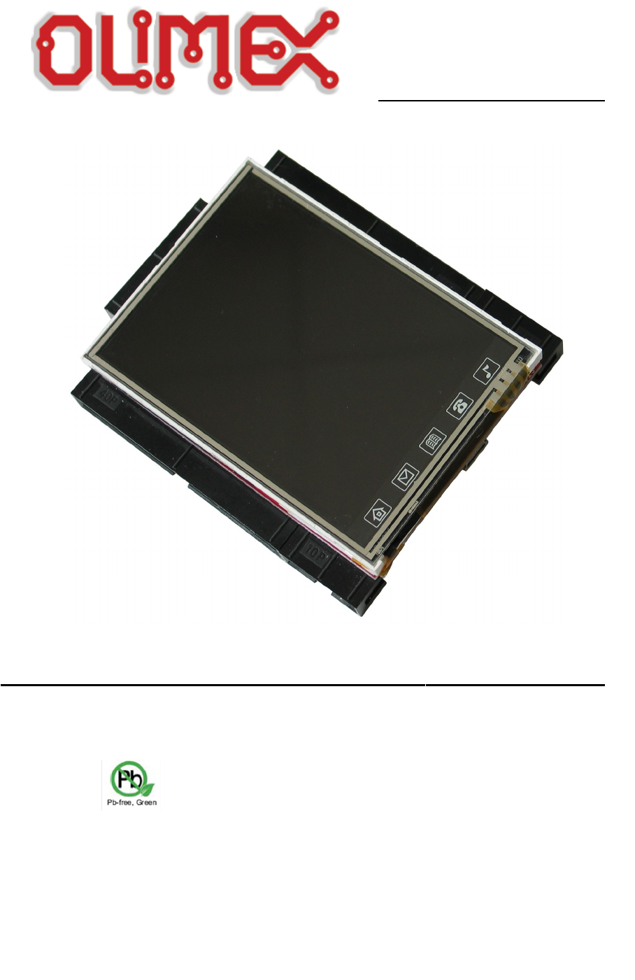
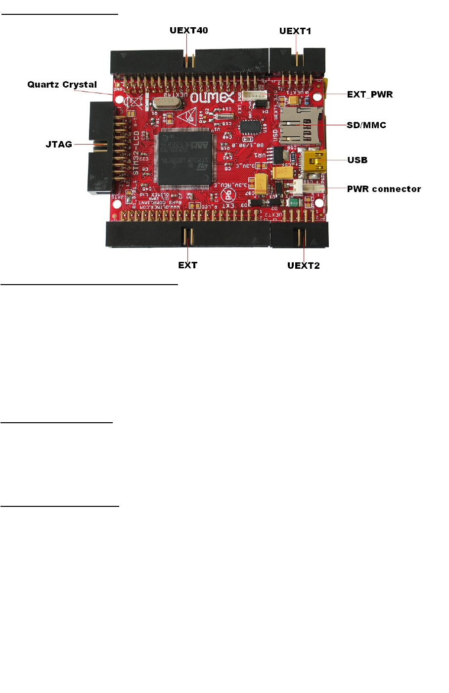
STM32-LCD development board
Users Manual
All boards produced by Olimex are ROHS compliant
Revision Initial, May 2009
Copyright(c) 2009, OLIMEX Ltd, All rights reserved
Page 1

INTRODUCTION:
STM32-LCD is development prototype board with STM32F103ZE micro-
controller from STMicroelectronics. This powerful microcontroller supports various
serial interfaces such as USB, USART, SPI. In addition you will find also accelero-
meter, JTAG, TFT LCD, mini SD/MMC card connector on this board and most of
the GPIOs are on extension headers where you can connect your additional
circuits. All this allows you to build a diversity of powerful applications to be used
in a wide range of situations.
BOARD FEATURES:
–Microcontroller – STM32F103ZE - high-performance ARM® Cortex™-M3 32-bit
RISC core operating at a 72 MHz frequency, high-speed embedded memories
(Flash memory - 512 Kbytes and SRAM - 64 Kbytes), and an extensive range of
enhanced I/Os and peripherals connected to two APB buses.
–JTAG connector
–EXT connector
–UEXT40 connector
–UEXT1 connector
–UEXT2 connector
–EXT_PWR connector
–Mini SD/MMC
–Mini USB
–LCD TFT 320x240 pixels coloured with touch screen
–Power source connector
–Accelerometer
–8 MHz crystal oscillator
–Reset circuit
–Clock circuit
–PCB: FR-4, 1.5 mm (0,062"), soldermask, silkscreen component print
–Dimensions 79.2x57.6 mm (3.12x2.27”)
Page 2

ELECTROSTATIC WARNING:
The STM32-LCD board is shipped in protective anti-static packaging. The board
must not be subject to high electrostatic potentials. General practice for working
with static sensitive devices should be applied when working with this board.
BOARD USE REQUIREMENTS:
Cables: The cable you will need depends on the programmer/debugger you use. If
you use ARM-JTAG-EW, you will need USB A-B cable.
Hardware: Programmer/Debugger ARM-JTAG-EW or other compatible
programming/debugging tool if you work with EW-ARM.
You can use also ARM-USB-OCD, ARM-USB-TINY, ARM-JTAG. or other
compatible programming/debugging tool.
PROCESSOR FEATURES:
STM32-LCD use High-density performance line ARM-based 32-bit MCU with these features:
–Core: ARM 32-bit Cortex™-M3 CPU
–72 MHz maximum frequency, 1.25 DMIPS/MHz (Dhrystone 2.1) per-
formance at 0 wait state memory access
–Single-cycle multiplication and hardware division
–Memories
–512 Kbytes of Flash memory
–64 Kbytes of SRAM
–Flexible static memory controller with 4 Chip Select. Supports Compact
Flash, SRAM, PSRAM, NOR and NAND memories
–LCD parallel interface, 8080/6800 modes
–Clock, reset and supply management
–2.0 to 3.6 V application supply and I/Os
–POR, PDR, and programmable voltage detector (PVD)
–4-to-16 MHz crystal oscillator
–Internal 8 MHz factory-trimmed RC
–Internal 40 kHz RC with calibration
–32 kHz oscillator for RTC with calibration
–Low power
–Sleep, Stop and Standby modes
–VBAT supply for RTC and backup registers
–3 × 12-bit, 1 µs A/D converters (up to 21 channels)
Page 3

–Conversion range: 0 to 3.6 V
–Triple-sample and hold capability
–Temperature sensor
–2 × 12-bit D/A converters
–DMA: 12-channel DMA controller
–Supported peripherals: timers, ADCs, DAC, SDIO, I2Ss, SPIs, I2Cs and
USARTs
–Debug mode
–Serial wire debug (SWD) & JTAG interfaces
–Cortex-M3 Embedded Trace Macrocell™
–112 fast I/O ports
–112 I/Os, all mappable on 16 external interrupt vectors, all 5 V-tolerant
except for analog inputs
–11 timers
–four 16-bit timers, each with up to 4 IC/OC/PWM or pulse counter and
quadrature (incremental) encoder input
–2 × 16-bit motor control PWM timers with dead-time generation and
emergency stop
–2 × watchdog timers (Independent and Window)
–SysTick timer: a 24-bit downcounter
–2 × 16-bit basic timers to drive the DAC
–13 communication interfaces
–2 × I2C interfaces (SMBus/PMBus)
–5 USARTs (ISO 7816 interface, LIN, IrDA capability, modem control)
–3 SPIs (18 Mbit/s), 2 with I2S interface multiplexed
–CAN interface (2.0B Active)
–USB 2.0 full speed interface
–SDIO interface
–CRC calculation unit, 96-bit unique ID
Page 4
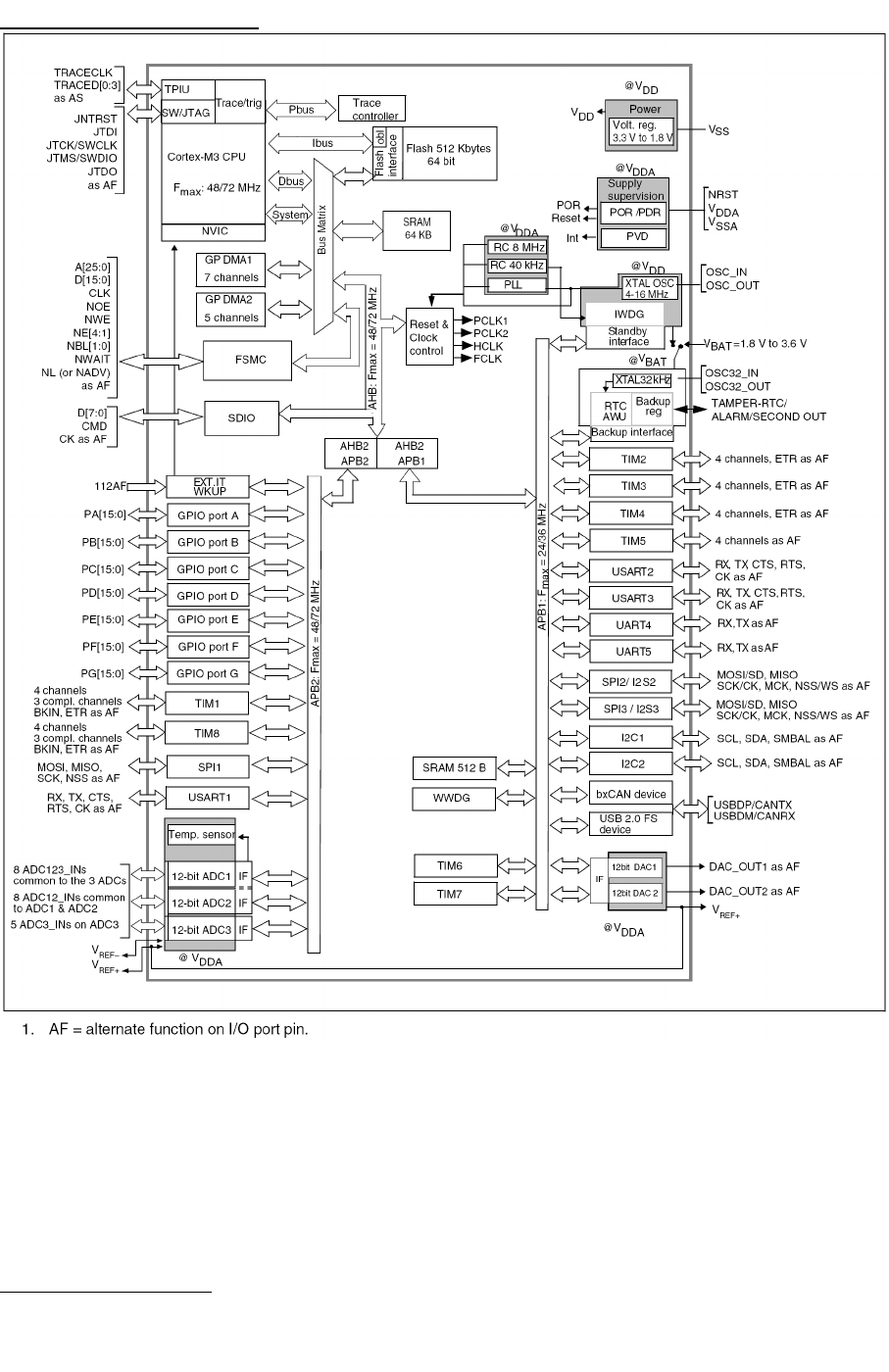
BLOCK DIAGRAM:
MEMORY MAP:
Page 5
Page 6
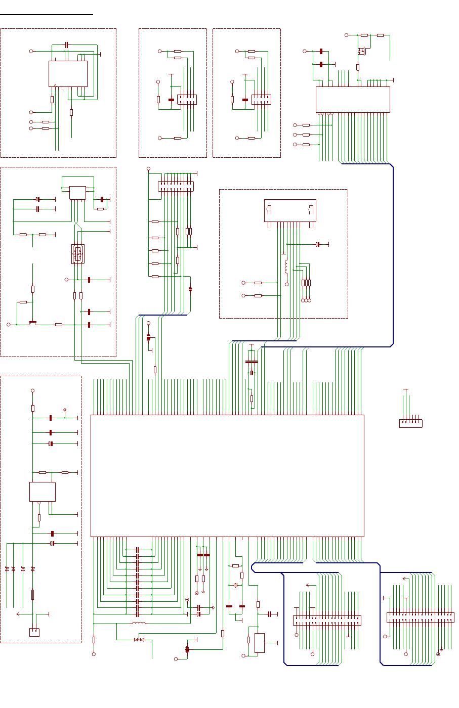
SCHEMATIC:
Page 7
100nF 100nF
100nF
100nF
100nF
100nF
100nF
1 u F
10uF/6.3V
27pF
2 7p F
10pF
10pF
47p F(NA) 47 pF(NA )
100nF
100nF
47uF /6.3V
100nF
100nF
100nF
100nF
100nF
100nF
100nF
100nF
100nF
100nF
100nF
10uF/6.3V
100nF
NA
10nF
100uF/6.3V/tant
1 0 0u F/6 . 3V /t a nt 100nF
100nF
1N5819S
1N5819S
1N5819S
1N5819S
BAT54C
BH 40R
CO N 6
FB0805
IR L ML 6 40 2
BH 2 0R
470nH
4V_ MIN-6V _MAX
8MHz
32768/6pF
BC 807
100K
NA NA
4.7K4.7K
4.7K
NA
10K
10K
2 0 K
4.7K
NA
33K
3 30 K /1 %
10K
47K /1%
10K
390R
47R
22R
22R
47K /1%
2 K
1M
1.5K
1 .5 K
10K
560R
2K
560R
33K
NA
33K
33K
33K33K
4.7K 4.7K 33K
10K10K
10K
10K
10K
10K
10K
10K
NA
RF11 0 _S MD
FS- K32 0QV B- V1
ST M3 2 F1 0 3Z E(L Q FP 1 44 )
NA
USBLC 6-2P6 L IS 3L V02 DL- TR (LG A1 6)
BH 1 0R
BH 10R
BH 40R
MINI_USB
MI CR O_SD_C ARD _holder
3.3V
3.3V
3.3V
3 .3 V
3.3V3.3V
3.3V
3.3V 3. 3V
3.3V
3.3V
3.3V
3.3V
3.3V 3. 3V
3.3V
3.3V _A
3.3V
3 .3 V
3.3V _A
3.3V
3.3V
3.3V_A
3.3V 3 .3 V
3.3V
3.3V 3. 3V
3.3V
3.3V
3.3V
3.3V
3.3V
3 .3 V3 .3 V
3.3V
VIN
VIN
VIN
MC P18 25-ADJE/D C
+5V_J -L IN K
+5 V_ J-L INK +5 V_ USB
+5 V_U SB
+5 V_U SB
+5 V_U SB
+5 V_U SB
/NCE 2
/NCE 2
/O E
/O E
/W E
/W E
AD C 12 _ IN 8
AD C12 _IN8
AD C12 _IN9
AD C 1 2_ IN 9
AD C12 _IN14
AD C 12 _ IN 1 4
AD C12 _IN1 5
AD C12 _IN15
BAT_PW R
BA T_PW R
D0
D0
D1
D1
D2
D2
D3
D3
D4
D4
D5
D5
D6
D6
D7
D7
D8
D8
D9
D9
D10
D10
D11
D11
D12
D12
D13
D13
D14
D14
D1 5
D15
DISC
DISC
I2 C 1 _S CL 1
I2C1 _SC L1
I2 C1_ SC L1
I2 C 1 _S CL 2
I2 C 1_ S CL 2
I2C1 _SD A1
I2C1 _SD A1
I2 C1_ SDA1
I2 C1_ SD A2
I2C1 _SD A2
I2 C 2_ S CL
I2 C2_ SC L
I2C2 _SD A
I2 C 2_ S DA
PA 1
PA 1
PA 8
PA 8
PB 2
PB2
PB 5
PB 5
PC 6
PC 6
PC 7
PC 7
PC 13
PC 13
PD 6
PD 6
PD 11
PD 1 1
PD 12
PD 12
PE 0
PE 0
PE1
PE 1
PE 5
PE 5
PE6
PE 6
PF0
PF0
PF1
PF1
PF2
PF2
PF3
PF3
PF4
PF4
PF5
PF5
PF6
PF6
PF7
PF7
PF8
PF8
PF9
PF9
PF1 0
PF10
PF1 1
PF11
PF12
PF12
PF1 3
PF1 3
PF14
PF1 4
PF15
PF15
PG 0
PG 0
PG 1
PG 1
PG 2
PG 2
PG 3
PG 3
PG 4
PG 4
PG 5
PG 5
PG 6
PG 6
PG 7
PG 7
PG 8
PG 8
PG 9
PG 9
PG 1 0
PG 1 0
PG 11
PG 1 1
PG 1 2
PG 1 2
PG 1 3
PG 13
PG 1 4
PG 1 4
PG 1 5
PG 1 5
RST
RST
RST
RST
RST
SD _CL K
SD _CL K SD _CL K
SD _ CM D
SD _CMD SD_C MD
SD _D0
SD _D0 SD_ D0
SD _D1
SD _D1SD _D1
SD _ D2
SD _ D2SD _ D2
SD _ D3
SD _D3 SD_ D3
SE NS_INT
SE NS_INT
SP I1 _MISO
SP I1 _MISO
SP I1 _ MIS O
SP I1 _MOSI
SP I1 _MOSI
SP I1 _MOSI
SP I1_N SS
SPI1_N SS
SP I1 _ N SS
SP I1 _ NS S
SP I1_S CK
SPI1_S CK
SP I1_S CK
SP I1_S CK
SP I2 _MISO
SP I2 _ MIS O
SP I2 _MOSI
SP I2 _ MO S I
SP I2_N SS
SP I2 _NSS
SP I2 _SCK
SP I2 _SCK
TC K
TC K
TDI
TD I
TD O
TD O
TFT _LIG H T
TFT _L IG H T
TFT_R S
TFT_R S TFT_R ST
TFT _RST
TMS
TMS
TR ST
TRST
TR ST
US AR T1 _RX
USART1 _RX
USART1 _RX
U SA RT1 _ TX
USART1 _TX
USART1 _TX
USART2 _RX
USART2 _RX
USART2 _TX
USART2 _TX
USBDM
USBD M
USBDP
USBDP
USB_P
U SB_ P
USB_P
VB AT
VB AT
VR EF+
VR EF+
XL
XL
XR
XR
YD
YD
YU
YU
3.3V_E
3.3V_MCU_ E
1
2
3
B0_1/B0_0
1
2
3
B1 _ 0 /B1 _ 1
C1 C3
C5
C6
C7
C8
C9
C10
C11
C12
C13
C14
C15
C16 C 17
C18
C19
C20
C23
C28
C32
C33
C38
C39
C40
C42
C44
C45
C47
C58
C72
C79
C80
C96
C97 C 99
C10 0
D1
D2
D3
D4
D5
1 2
3 4
5 6
7 8
9 10
11 12
13 14
15 16
17 18
19 20
21 22
23 24
25 26
27 28
29 30
31 32
33 34
35 36
37 38
39 40
EXT
1
2
3
4
5
6
EXT_PW R
FB1
FET1
GND
1 2
3 4
5 6
7 8
9 10
11 12
13 14
15 16
17 18
19 20
JA TG
L5
1
2
PW R
Q1
Q2
Q3
1 2
R- T
R1
R2 R3
R4R5
R6
R7
R8
R9
R10
R11
R12
R13
R14
R15
R16
R17
R19
R20
R21
R2 2
R36
R38
R40
R4 1
R50
R51
R5 4
R69
R9 0
R91
R10 0
R10 4
R10 5
R10 6
R1 0 7R1 0 8
R1 1 8 R1 1 9 R 12 0
R14 7R1 48
R14 9
R15 0
R15 1
R15 2
R15 3
R15 4
R15 5
RF1
R_L CD
#CS
4
#RD
7
#RESET
8
#WR
6
DB0
9
DB1
10
DB2
11
DB3
12
DB4
13
DB5
14
DB6
15
DB7
16
DB8
17
DB9
18
DB10
19
DB11
20
DB12
21
DB13
22
DB14
23
DB15
24
GND 1
GND 25
GND 37
LEDA 35
LEDA 36
LEDK1 30
LEDK2 31
LEDK3 32
LEDK4 33
LEDK5 34
RS
5
VCC 2
VCC 3
XL 27
XR 29
YD 26
YU 28
TFT
BOOT0
138
NC
106
NRST
25
OSC_IN
23
OSC_OUT
24
PA0/WKUP/USART2_CTS/ADC123_IN0/TIM5_CH1/TIM2_CH1_ETR/TIM8_ETR 34
PA1/USART2_RTS/ADC123_IN1/TIM5_CH2/TIM2_CH2 35
PA2/USART2_TX/TIM5_CH3/ADC123_IN2/TIM2_CH3 36
PA3/USART2_RX/TIM5_CH4/ADC123_IN3/TIM2_CH4 37
PA4/SPI1_NSS/DAC_OUT1/USART2_CK/ADC12_IN4 40
PA5/SPI1_SCK/DAC_OUT2/ADC12_IN5 41
PA6/SPI1_MISO/TIM8_BKIN/ADC12_IN6/TIM3_CH1/TIM1_BKIN 42
PA7/SPI1_MOSI/TIM8_CH1N/ADC12_IN7/TIM3_CH2/TIM1_CH1N 43
PA8/USART1_CK/TIM1_CH1/MCO 100
PA9/USART1_TX/TIM1_CH2 101
PA10/USART1_RX/TIM1_CH3 102
PA11/USART1_CTS/CANRX/TIM1_CH4/USBDM 103
PA12/USART1_RTS/CANTX/TIM1_ETR/USBDP 104
PA13/JTMS-SWDIO 105
PA14/JTCK-SWCLK 109
PA15/JTDI/SPI3_NSS/I2S3_WS/TIM2_CH1_ETR/SPI1_NSS 110
PB0/ADC12_IN8/TIM3_CH3/TIM8_CH2N/TIM1_CH2N 46
PB1/ADC12_IN9/TIM3_CH4/TIM8_CH3N/TIM1_CH3N 47
PB2/BOOT1 48
PB3/TRACESWO/JTDO/SPI3_SCK/I2S3_CK/TIM2_CH2/SPI1_SCK 133
PB4/JNTRST/SPI3_MISO/TIM3_CH1/SPI1_MISO 134
PB5/I2C1_SMBAI/SPI3_MOSI/I2S3_SD/TIM3_CH2/SPI1_MOSI 135
PB6/I2C1_SCL/TIM4_CH1/USART1_TX 136
PB7/I2C1_SDA/FSMC_NL/TIM4_CH2/USART1_RX 137
PB8/TIM4_CH3/SDIO_D4/I2C1_SCL/CANRX 139
PB9/TIM4_CH4/SDIO_D5/I2C1_SDA/CANTX 140
PB10/I2C2_SCL/USART3_TX/TIM2_CH3 69
PB11/I2C2_SDA/USART3_RX/TIM2_CH4 70
PB12/SPI2_NSS/I2S2_WS/I2C2_SMBAI/USART3_CK/TIM1_BKIN 73
PB13/SPI2_SCK/I2S2_CK/USART3_CTS/TIM1_CH1N 74
PB14/SPI2_MISO/USART3_RTS/TIM1_CH2N 75
PB15/SPI2_MOSI/I2S2_SD/TIM1_CH3N 76
PC0/ADC123_IN10 26
PC1/ADC123_IN11 27
PC2/ADC123_IN12 28
PC3/ADC123_IN13 29
PC4/ADC12_IN14 44
PC5/ADC12_IN15 45
PC6/I2S2_MCK/TIM8_CH1/SDIO_D6/TIM3_CH1 96
PC7/I2S3_MCK/TIM8_CH2/SDIO_D7/TIM3_CH2 97
PC8/TIM8_CH3/SDIO_D0/TIM3_CH3 98
PC9/TIM8_CH4/SDIO_D1/TIM3_CH4 99
PC10/UART4_TX/SDIO_D2/USART3_TX 111
PC11/UART4_RX/SDIO_D3/USART3_RX 112
PC12/UART5_TX/SDIO_CK/USART3_CK 113
PC13/TAMPER-RTC 7
PC14/OSC32_IN 8
PC15/OSC32_OUT 9
PD0/OSC_IN/FSMC_D2/CANRX 114
PD1/OSC_OUT/FSMC_D3/CANTX 115
PD2/TIM3_ETR/UART5_RX/SDIO_CMD 116
PD3/FSMC_CLK/USART2_CTS 117
PD4/FSMC_NOE/USART2_RTS 118
PD5/FSMC_NWE/USART2_TX 119
PD6/FSMC_NWAIT/USART2_RX 122
PD7/FSMC_NE1/FSMC_NCE2/USART2_CK 123
PD8/FSMC_D13/USART3_TX 77
PD9/FSMC_D14/USART3_RX 78
PD10/FSMC_D15/USART3_CK 79
PD11/FSMC_A16/USART3_CTS 80
PD12/FSMC_A17/TIM4_CH1/USART3_RTS 81
PD13/FSMC_A18/TIM4_CH2 82
PD14/FSMC_D0/TIM4_CH3 85
PD15/FSMC_D1/TIM4_CH4 86
PE0/TIM4_ETR/FSMC_NBL0 141
PE1/FSMC_NBL1 142
PE2/TRACECK/FSMC_A23 1
PE3/TRACED0/FSMC_A19 2
PE4/TRACED1/FSMC_A20 3
PE5/TRACED2/FSMC_A21 4
PE6/TRACED3/FSMC_A22 5
PE7/FSMC_D4/TIM1_ETR 58
PE8/FSMC_D5/TIM1_CH1N 59
PE9/FSMC_D6/TIM1_CH1 60
PE10/FSMC_D7/TIM1_CH2N 63
PE11/FSMC_D8/TIM1_CH2 64
PE12/FSMC_D9/TIM1_CH3N 65
PE13/FSMC_D10/TIM1_CH3 66
PE14/FSMC_D11/TIM1_CH4 67
PE15/FSMC_D12/TIM1_BKIN 68
PF0/FSMC_A0
10
PF1/FSMC_A1
11
PF2/FSMC_A2
12
PF3/FSMC_A3
13
PF4/FSMC_A4
14
PF5/FSMC_A5
15
PF6/ADC3_IN4/FSMC_NIORD
18
PF7/ADC3_IN5/FSMC_NREG
19
PF8/ADC3_IN6/FSMC_NIOWR
20
PF9/ADC3_IN7/FSMC_CD
21
PF10/ADC3_IN8/FSMC_INTR
22
PF11/FSMC_NIOS16
49
PF12/FSMC_A6
50
PF13/FSMC_A7
53
PF14/FSMC_A8
54
PF15/FSMC_A9
55
PG0/FSMC_A10
56
PG1/FSMC_A11
57
PG2/FSMC_A12
87
PG3/FSMC_A13
88
PG4/FSMC_A14
89
PG5/FSMC_A15
90
PG6/FSMC_INT2
91
PG7/FSMC_INT3
92
PG8
93
PG9/FSMC_NE2/FSMC_NCE3
124
PG10/FSMC_NCE4_1/FSMC_NE3
125
PG11/FSMC_NCE4_2
126
PG12/FSMC_NE4
127
PG13/FSMC_A24
128
PG14/FSMC_A25
129
PG15
132
VBAT
6
VDDA
33
VDD_1
72
VDD_2
108
VDD_3
144
VDD_4
39
VDD_5
17
VDD_6
52
VDD_7
62
VDD_8
84
VDD_9
95
VDD_10
121
VDD_11
131
VREF+
32
VREF-
31
VSSA
30
VSS_1
71
VSS_2
107
VSS_3
143
VSS_4
38
VSS_5
16
VSS_6
51
VSS_7
61
VSS_8
83
VSS_9
94
VSS_10
120
VSS_11
130
U1
3
12
GND
VCC RESET
U2
1
2
34
5
6
U9
CK
8
CS
6
GND 9
GND1 14
GND2 16
NC 7
RDY/INT
1
RES_1
10
RES_2
12
RES_3
15
SCL/SPC
5
SDA/SDI/SDO
3
SDO
2
VDD 11
VDD1 13
VDD_IO 4
U10
1 2
3 4
5 6
7 8
9 10
UEXT1
UEXT1_ 3.3 V
1 2
3 4
5 6
7 8
9 10
UEXT2
UEXT2_ 3.3 V
1 2
3 4
5 6
7 8
9 10
11 12
13 14
15 16
17 18
19 20
21 22
23 24
25 26
27 28
29 30
31 32
33 34
35 36
37 38
39 40
UEXT40
D+
D-
GND
GND1
GND2
GND3
GND4
ID
VBUS
USB
CD/DAT3/CS
2
CLK/SCLK
5
CMD/DI
3
CP1
9
CP2
11
DAT0/DO
7
DAT1/RES
8
DAT2/RES
1
VDD
4VSS
6
WP1
10
WP2
12
USD
#SHDN
1
ADJ 5
GND
3
GND
6
VIN
2VOUT 4
VR 1
STM32-LCD
Rev . I nitia l
COP YR IG HT(C ), 2 009
h ttp :/ /w ww .o l ime x. co m/ d ev
0R
0R
+
+
+
+
+
GND
0R
0R
0R
0R
USB
POWER SUPPLY CIRCUIT
USB CIRCUIT ACCELEROMETER
SD/MMC CARD
UEXT2
UEXT1
DACOU T1
DACOU T2
0
BOARD LAYOUT
POWER SUPPLY CIRCUIT:
STM32-LCD can take power from four sources:
–Power connector – 4V – 6V DC.
–BAT_PWR from EXT_PWR – 4V DC.
–+5V_J-LINK from JTAG connector
–+5V_USB from USB connector
The programmed board power consumption is about 200 mA.
RESET CIRCUIT:
STM32-LCD reset circuit includes R8 (10k), R69 (560 Ohm), C28 (100nF)
pin 15 of JTAG connector, EXT pin 32, UEXT40 pin 32 and STM32F103ZE pin 25
(NRST).
CLOCK CIRCUIT:
Quartz crystal 8 MHz is connected to STM32F103ZE pin 23 (OSC_IN) and
pin 24 (OSC_OUT).
Quartz crystal 32.768 kHz is connected to STM32F103ZE pin 8
(PC14/OSC32_IN) and pin 9 (PC15/OSC32_OUT).
Page 8
JUMPER DESCRIPTION:
R-T
Connect RST with TRST.
Default state is open.
UEXT1_3.3V
This jumper when closed, supplies 3.3 V voltage to UEXT1 pin 1.
Default state is closed.
UEXT2_3.3V
This jumper when closed, supplies 3.3 V voltage to UEXT2 pin 1.
Default state is closed.
3.3V_E
This jumper, when closed, enable the main 3.3 V regulator VR1 - MCP1825-ADJE/DC.
Default state is closed.
3.3V_MCU_E
This jumper, when closed, enables STM32F103ZE 3.3 V power supply.
Default state is closed.
R_LCD
You can use this jumper, when it's open, to measure the current of LCD backlight.
Default state is closed.
B0_1/B0_0
Select BOOT0 Boot mode.
Default state is in position B0_0.
B1_0/B1_1
Select BOOT1 Boot mode.
Default state – B1_0 – not shorted and B1_1 – not shorted.
Boot mode selection pins Boot Mode Aliasing
BOOT1 BOOT0
x 0 Main Flash memory Main Flash memory is selected as boot space
0 1 System memory System memory is selected as boot space
1 1 Embedded SRAM Embedded SRAM is selected as boot space
INPUT/OUTPUT:
–LCD TFT 320x240 pixels coloured with touch screen.
Page 9
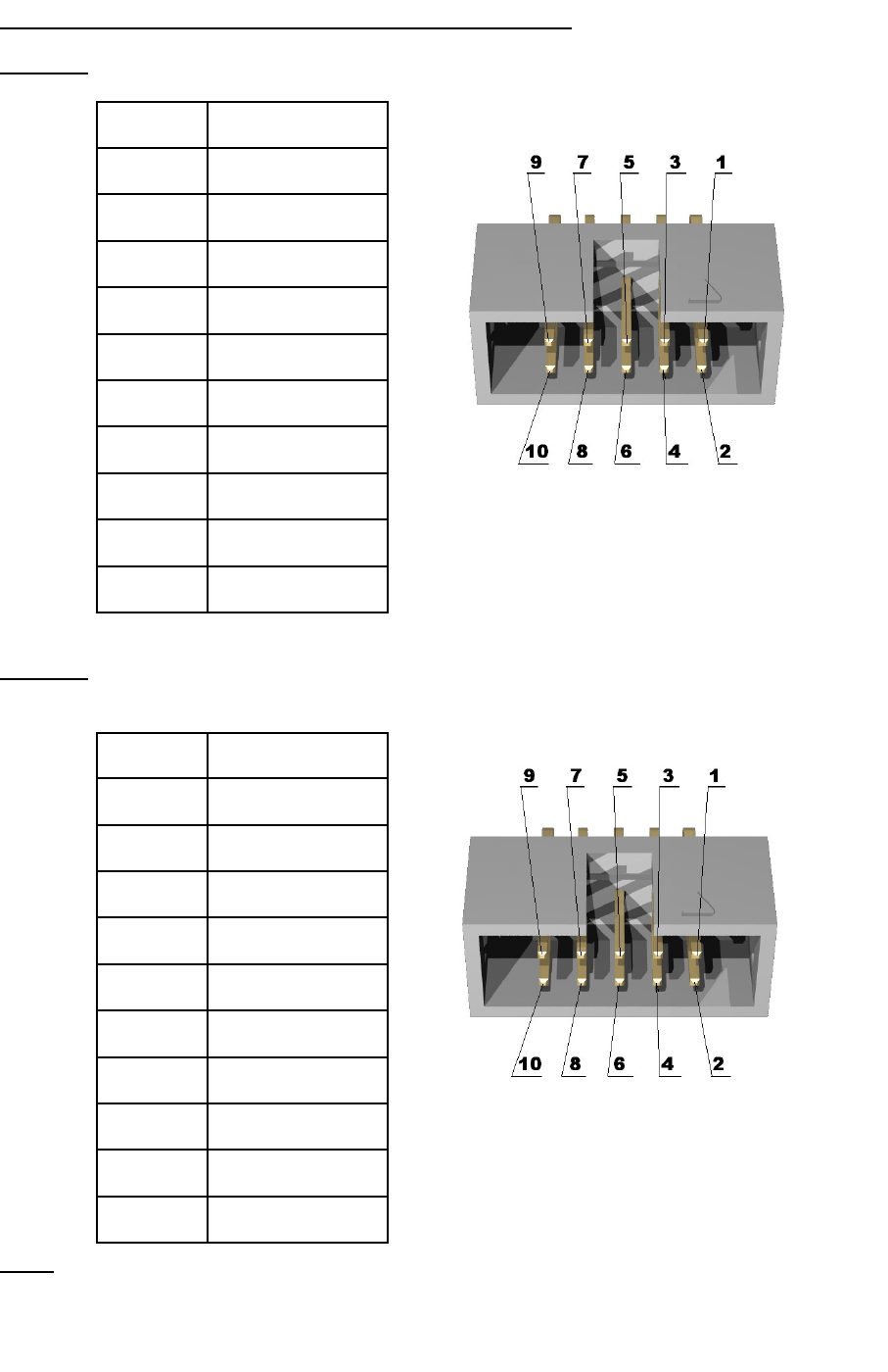
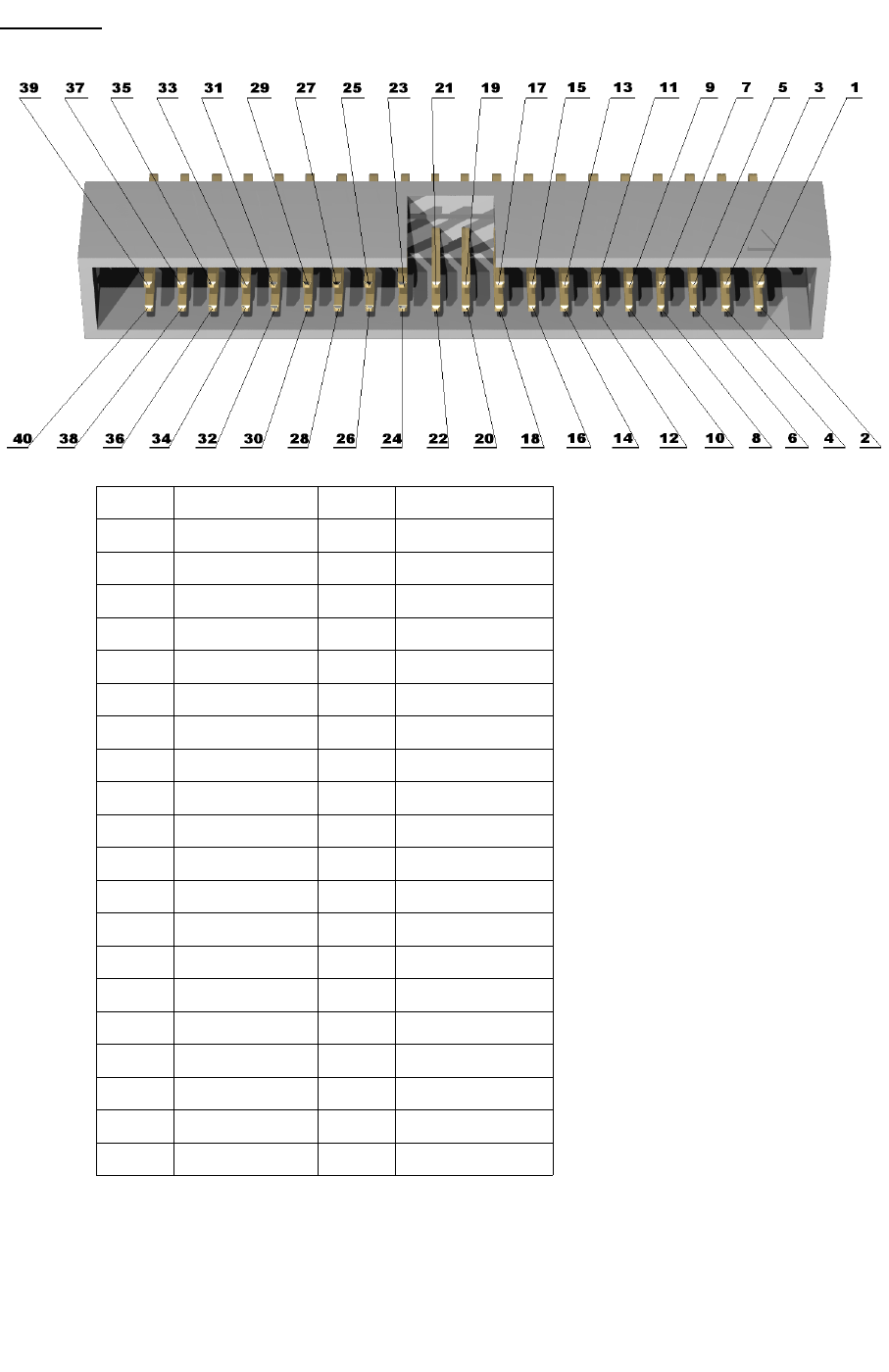
EXTERNAL CONNECTORS DESCRIPTION:
UEXT1
Pin # Signal Name
1 3.3V
2 GND
3 USART1_TX
4 USART1_RX
5 I2C1_SCL1
6 I2C1_SDA1
7 SPI1_MISO
8 SPI1_MOSI
9 SPI1_SCK
10 SPI1_NSS
UEXT2
Pin # Signal Name
1 3.3V
2 GND
3 USART2_TX
4 USART2_RX
5 I2C1_SCL2
6 I2C1_SDA2
7 SPI2_MISO
8 SPI2_MOSI
9 SPI2_SCK
10 SPI2_NSS
EXT
Page 10
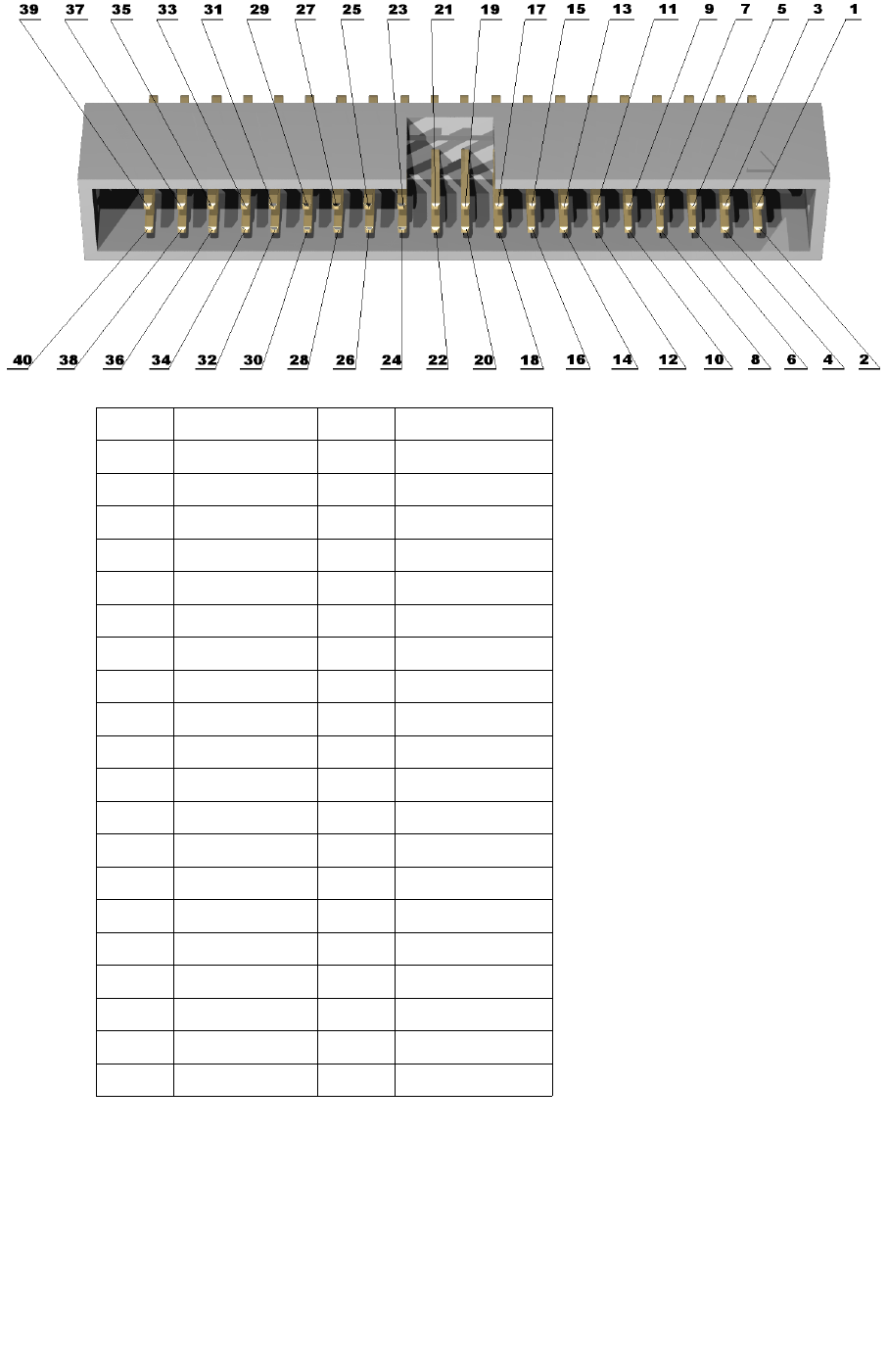
Pin # Signal Name Pin # Signal Name
1 3.3 V 2 GND
3 PE0 4 PE1
5 PE5 6 PE6
7 PC6 8 PC7
9 PC13 10 PB5
11 3.3 V 12 GND
13 +5V_USB 14 VIN
15 PG15 16 PG14
17 PG13 18 PG12
19 PG11 20 PG10
21 PG9 22 PG8
23 PG7 24 PG6
25 PG5 26 PG4
27 PG3 28 PG2
29 PG1 30 PG0
31 VBAT 32 RST
33 GND 34 PD6
35 PD12 36 PD11
37 PB2 38 USB_P
39 PA1 40 PA8
Page 11
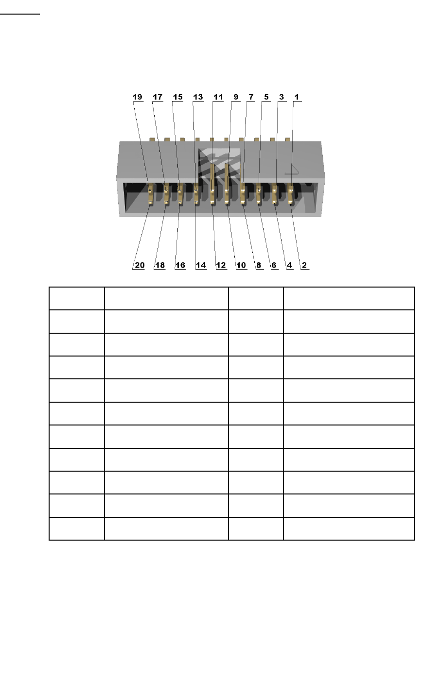
UEXT40
Pin # Signal Name Pin # Signal Name
1 3.3 V 2 GND
3 USART1_TX 4 USART1_RX
5 I2C1_SCL1 6 I2C1_SDA1
7 SPI1_MISO 8 SPI1_MOSI
9 SPI1_SCK 10 SPI1_NSS
11 3.3 V 12 GND
13 +5V_USB 14 VIN
15 PF15 16 PF14
17 PF13 18 PF12
19 PF11 20 PF10
21 PF9 22 PF8
23 PF7 24 PF6
25 PF5 26 PF4
27 PF3 28 PF2
29 PF1 30 PF0
31 3.3V_A 32 RST
33 AGND 34 ADC12_IN8
35 VREF+ 36 ADC12_IN9
37 SPI1_NSS 38 ADC12_IN14
39 SPI1_SCK 40 ADC12_IN15
Page 12
JTAG:
The JTAG connector allows the software debugger to talk via a JTAG (Joint Test Action
Group) port directly to the core. Instructions may be inserted and executed by the core thus allowing
STM32F103ZE memory to be programmed with code and executed step by step by the host software.
Pin # Signal Name Pin # Signal Name
1 3.3V 2 3.3V
3 TRST 4 GND
5 TDI 6 GND
7 TMS 8 GND
9 TCK 10 GND
11 pull-down 12 GND
13 TDO 14 GND
15 RST 16 GND
17 pull-down 18 GND
19 +5V J-LINK 20 GND
Page 13
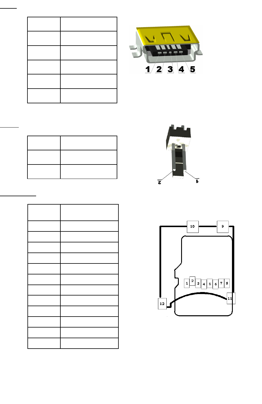
USB
Pin # Signal Name
1 +5V_USB
2 USBDM
3 USBDP
4 NC
5 GND
PWR
Pin # Signal Name
1 VIN (4 – 6) V DC
2 GND
SD/MMC
Pin # Signal Name
1 SD_D2
2 SD_D3
3 SD_CMD
4 VDD (3.3V)
5 SD_CLK
6 GND
7 SD_D0
8 SD_D1
9 Not connected
10 Not connected
11 Not connected
12 Not connected
Page 14

SPI
Up to three SPIs are able to communicate up to 18 Mbits/s in slave and
master modes in full-duplex and simplex communication modes. The 3-bit prescaler
gives 8 master mode frequencies and the frame is configurable to 8 bits or 16 bits.
The hardware CRC generation/verification supports basic SD Card/MMC modes.
All SPIs can be served by the DMA controller.
I 2
S
Two standard I2S interfaces (multiplexed with SPI2 and SPI3) are available,
that can be operated in master or slave mode. These interfaces can be configured to
operate with 16/32 bit resolution, as input or output channels. Audio sampling
frequencies from 8 kHz up to 48 kHz are supported. When either or both of the I2S
interfaces is/are configured in master mode, the master clock can be output to the
external DAC/CODEC at 256 times the sampling frequency.
I 2
C
Up to two I²C bus interfaces can operate in multimaster and slave modes.
They can support standard and fast modes.
They support 7/10-bit addressing mode and 7-bit dual addressing mode (as
slave). A hardware CRC generation/verification is embedded.
They can be served by DMA and they support SMBus 2.0/PMBus.
Page 15
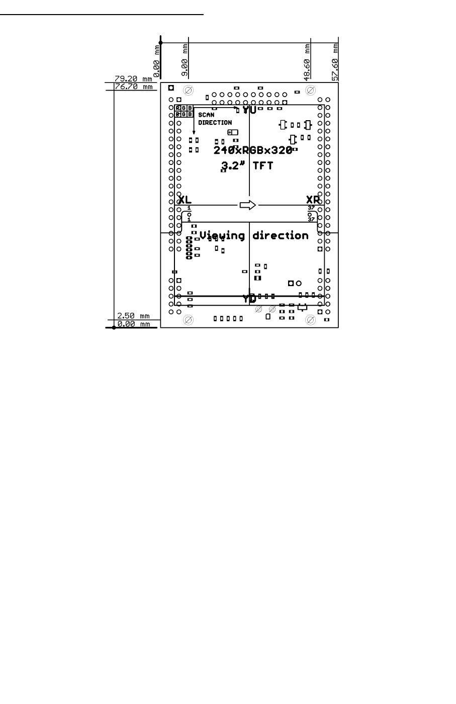
MECHANICAL DIMENSIONS
Page 16

AVAILABLE DEMO SOFTWARE
–STM32-LCD-DEMO
Page 17


Disclaimer:
© 2009 Olimex Ltd. All rights reserved. Olimex®, logo and combinations thereof, are registered
trademarks of Olimex Ltd. Other terms and product names may be trademarks of others.
The information in this document is provided in connection with Olimex products. No license, express
or implied or otherwise, to any intellectual property right is granted by this document or in
connection with the sale of Olimex products.
Neither the whole nor any part of the information contained in or the product described in this
document may be adapted or reproduced in any material from except with the prior written
permission of the copyright holder.
The product described in this document is subject to continuous development and improvements. All
particulars of the product and its use contained in this document are given by OLIMEX in good faith.
However all warranties implied or expressed including but not limited to implied warranties of
merchantability or fitness for purpose are excluded.
This document is intended only to assist the reader in the use of the product. OLIMEX Ltd. shall not
be liable for any loss or damage arising from the use of any information in this document or any error
or omission in such information or any incorrect use of the product.
Page 19
