SY7201 Datasheet. Www.s Manuals.com. Silergy
User Manual: Marking of electronic components, SMD Codes DQ, DQ**, DQ***, DQ-**, DQ-***, DQQ, DQR. Datasheets 2SD2211, BD4834FVE, BD4834G, BZT52H-B7V5, MAX6314US26D2-T, RT9014-JNPQW, RT9198-28PB, SY7201.
Open the PDF directly: View PDF ![]() .
.
Page Count: 5
SY7201
30V High Current Boost LED Driver
Preliminary Specification
SY7201 Rev. 0.1 Silergy Corp. Confidential- Prepared for Customer Use Only 1
General Description
SY7201 is a DC/DC step-up converter that delivers an
accurate constant current for driving LEDs. Operation
at a fixed switching frequency of 1MHz allows the
device to be used with small value external ceramic
capacitors and inductor. LEDs connected in series are
driven with a regulated current set by the external
resistor. The SY7201 is ideal for driving up to eight
white LEDs in series or up to 30V.
Applications
• GPS Navigation Systems
• Handheld Devices
• Portable Media Players
Features
• Input voltage range 2.5V to 9V
• Switch current limit 2A
• Drives LED strings up to 30V
• 1MHz fixed frequency minimizes the external
components
• Internal softstart limits the inrush current
• Open LED overvoltage protection
• RoHS Compliant and Halogen Free
• Compact package: SOT23-6 pin
Ordering Information
Temperature Code
C: - 40°C~85°C
Package Code
AB: SOT23-6
Spec Code
SY7201□
□□
□(□□
□□□□
□□)□
□□
□
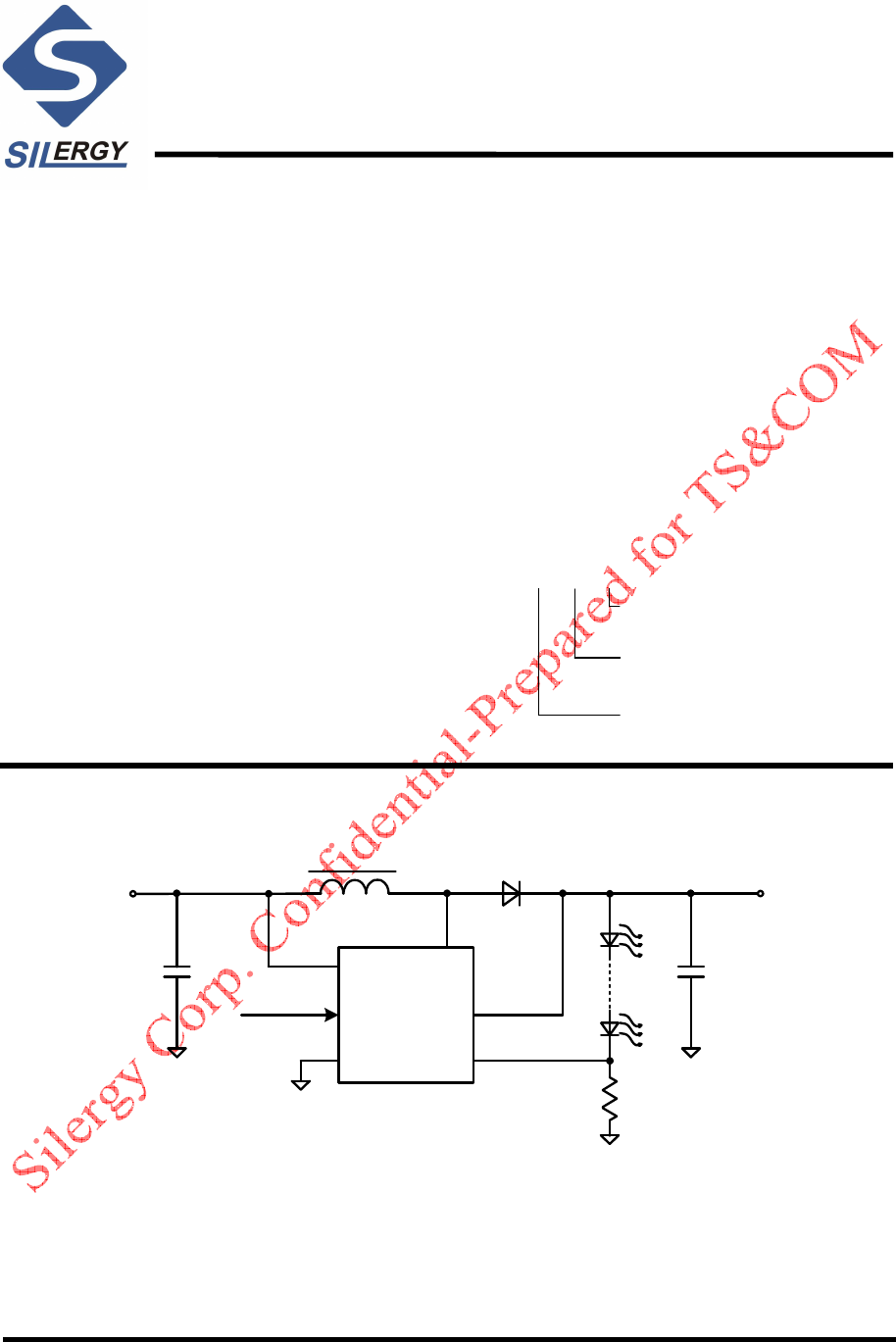
Typical Applications
LD
Cout
R1
Vout
Vin
IN LX
FB
EN/PWM
Dimming
GND
OVP
Cin
Figure 1. Schematic Diagram
SY7201
SY7201 Rev. 0.1 Silergy Corp. Confidential- Prepared for Customer Use Only 2
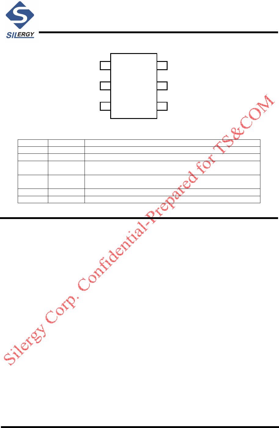
Pinout (top view)
(SOT23-6)
Top Mark: DQxyz (Device code: DQ, x=year code, y=week code, z= lot number code)
Pin Name
Pin Number
Pin Description
LX 1 Inductor node. Connect an inductor between IN pin and LX pin.
GND 2 Ground pin.
FB 3 Feedback pin. Connect a resistor R1 between FB and GND to program
the output current: I
OUT
=0.2V/R
1
.
EN/PWM
4 Enable and dimming control. The recommended PWM frequency
should be higher than 20kHz.
OVP 5 Over voltage protection. The value is 33V.
IN 6 Input pin. Decouple this pin to GND pin with 1uF ceramic capacitor.
Absolute Maximum Ratings (Note 1)
IN, ------------------------------------------------------------------------------------------------------------------- 10V
LX, OVP ---------------------------------------------------------------------------------------------------------- 36V
All other pins ------------------------------------------------------------------------------------------------------- 6V
Power Dissipation, P
D
@ T
A
= 25°C, SOT23-6 --------------------------------------------------------------- 0.4W
Package Thermal Resistance (Note 2)
SOT23-6, θ
JA
-------------------------------------------------------------------------------------------- 250°C/W
SOT23-6, θ
JC
-------------------------------------------------------------------------------------------- 130°C/W
Junction Temperature Range ------------------------------------------------------------------------------------ 150°C
Lead Temperature (Soldering, 10 sec.) ------------------------------------------------------------------------- 260°C
Storage Temperature Range -------------------------------------------------------------------------------------
-
65°C to 150°C
ESD Susceptibility (Note 2)
HBM (Human Body Mode) ------------------------------------------------------------------------------------- 2kV
MM (Machine Mode) -------------------------------------------------------------------------------------------- 200V
Recommended Operating Conditions (Note 3)
IN, ------------------------------------------------------------------------------------------------------------------- 2.5V to 9V
LX, OVP ----------------------------------------------------------------------------------------------------------- 2.5V to 30V
All other pins ------------------------------------------------------------------------------------------------------ 0 to 3.6V
Junction Temperature Range ------------------------------------------------------------------------------------ -40°C to 125°C
Ambient Temperature Range ----------------------------------------------------------------------------------- -40°C to 85°C
LX
GND
FB EN/PWM
OVP
IN
1
2
3
6
4
5
SY7201
SY7201 Rev. 0.1 Silergy Corp. Confidential- Prepared for Customer Use Only 3
Electrical Characteristics
(V
IN
= 3.6V, T
A
= 25°C, unless otherwise specified)
Parameter Symbol
Conditions Min Typ Max Unit
Input Voltage Range V
IN
2.5 9.0 V
Quiescent Current I
Q
FB=0.3V 0.1 0.6 mA
Shutdown Current I
SHDN
EN=0 10 15 uA
Feedback Reference Voltage V
REF
196 200 204 mV
FB Input Current I
FB
FB=0.3V 1 uA
Low Side Main FET RON R
DS(ON)
200 mΩ
Main FET Current Limit I
LIM
2 A
EN Rising Threshold V
ENH
1.5 V
EN Falling Threshold V
ENL
0.4 V
Input UVLO threshold V
UVLO
2.4 V
UVLO hysteresis V
HYS
0.1 V
Oscillator Frequency F
OSC
I
OUT
=100mA 1.0 MHz
Min On Time 100 ns
Max Duty Cycle 90 %
Thermal Shutdown T
SD
150 ℃
Thermal Hysteresis T
HYST
20 ℃
Output Clamp voltage V
OCL
“Open LED” 33 V
Note 1: Stresses listed as the above “Absolute Maximum Ratings” may cause permanent damage to the device.
These are for stress ratings. Functional operation of the device at these or any other conditions beyond those
indicated in the operational sections of the specifications is not implied. Exposure to absolute maximum rating
conditions for extended periods may remain possibility to affect device reliability.
Note 2:
θ
JA is measured in the natural convection at TA = 25°C on a low effective single layer thermal
conductivity test board of JEDEC 51-3 thermal measurement standard. Pin 2 of SOT23-6 packages is the case
position for
θ
JC measurement.
Note 3: The device is not guaranteed to function outside its operating conditions.
SY7201
SY7201 Rev. 0.1 Silergy Corp. Confidential- Prepared for Customer Use Only 4
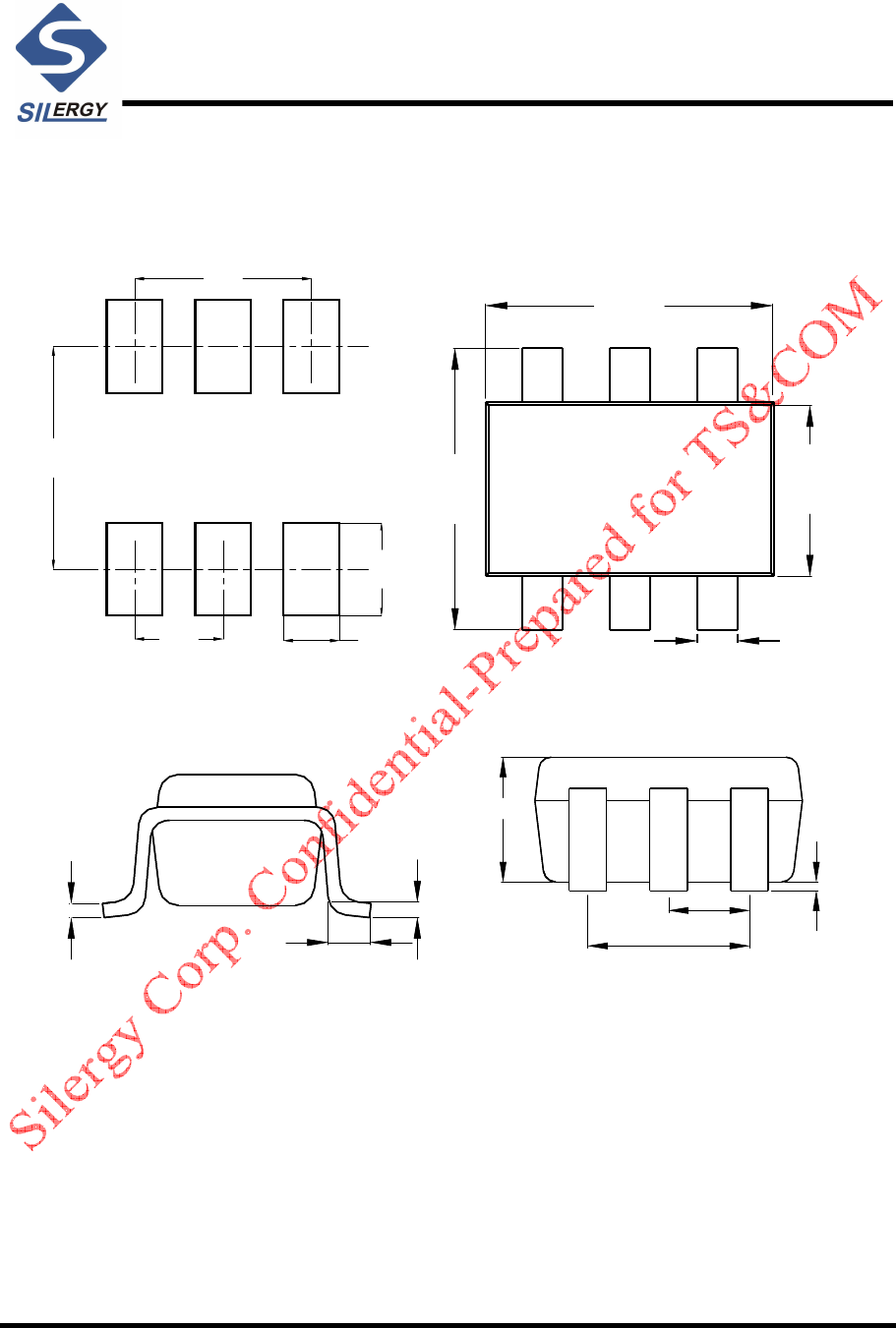
SOT23-6 Package outline & PCB layout design
0.95
2.40
1.90
0.60
1.00
0.95
2.40
1.90
0.60
1.00
1.50 - 1.70
0.30 - 0.50
2.80 - 3.10
2.70 - 3.00
1.50 - 1.70
0.30 - 0.50
2.80 - 3.10
2.70 - 3.00
Recommended Pad Layout
0.1 - 0.15
0.25 REF
0.3 - 0.6
0.1 - 0.15
0.25 REF
0.3 - 0.6
1.0 - 1.3
0.01 - 0.1
1.90 TYP
0.95 TYP
1.0 - 1.3
0.01 - 0.1
1.90 TYP
0.95 TYP
Notes: All dimensions are in millimeters.
All dimensions don’t include mold flash & metal burr.