TB6600HG Datasheet. Www.s Manuals.com. 20140130 Toshiba
User Manual: Datasheets TB6600, TB6600HG.
Open the PDF directly: View PDF ![]() .
.
Page Count: 36
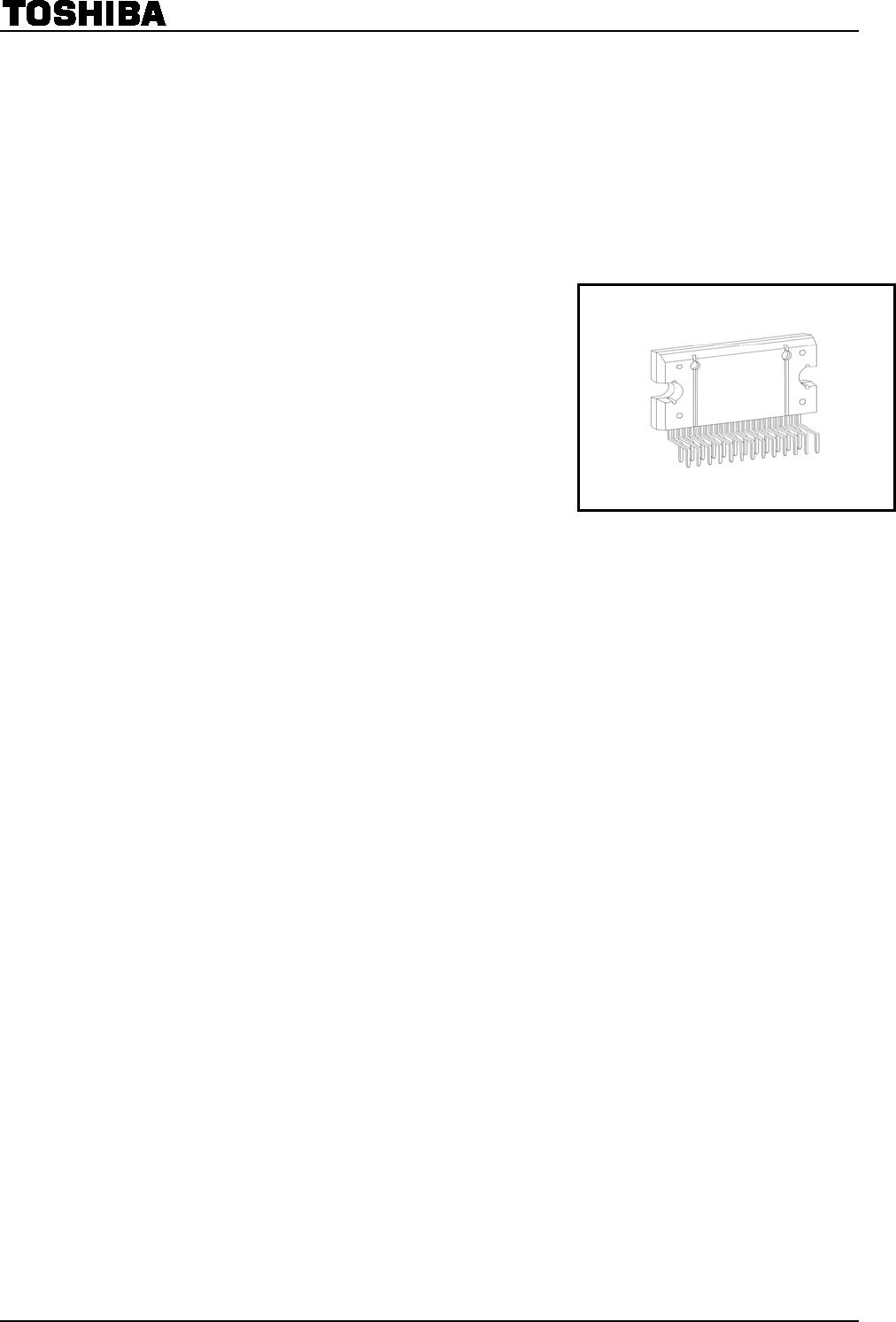
TB6600HG
2014-01-30
1
TOSHIBA BiCD Integrated Circuit Silicon Monolithic
TB6600HG
PWM Chopper-Type bipolar
Stepping Motor Driver IC
The TB6600HG is a PWM chopper-type single-chip bipolar sinusoidal
micro-step stepping motor driver.
Forward and reverse rotation control is available with 2-phase,
1-2-phase, W1-2-phase, 2W1-2-phase, and 4W1-2-phase excitation
modes.
2-phase bipolar-type stepping motor can be driven by only clock signal
with low vibration and high efficiency.
Features
• Single-chip bipolar sinusoidal micro-step stepping motor driver
• Ron (upper + lower) = 0.4 Ω (typ.)
• Forward and reverse rotation control available
• Selectable phase drive (1/1, 1/2, 1/4, 1/8, and 1/16 step)
• Output withstand voltage: Vcc = 50 V
• Output current: IOUT = 5.0 A (absolute maximum ratings, peak)
IOUT = 4.5 A (operating range, maximal value)
• Packages: HZIP25-P-1.00F
• Built-in input pull-down resistance: 100 kΩ (typ.), (only TQ terminal: 70kΩ(typ.))
• Output monitor pins (ALERT): Maximum of IALERT = 1 mA
• Output monitor pins (MO): Maximum of IMO = 1 mA
• Equipped with reset and enable pins
• Stand by function
• Single power supply
• Built-in thermal shutdown (TSD) circuit
• Built-in under voltage lock out (UVLO) circuit
• Built-in over-current detection (ISD) circuit
TB6600HG
Weight:
HZIP25-P-1.00F: 7.7g (typ.)
HZIP25-P-1.00F
TB6600HG
2014-01-30
2
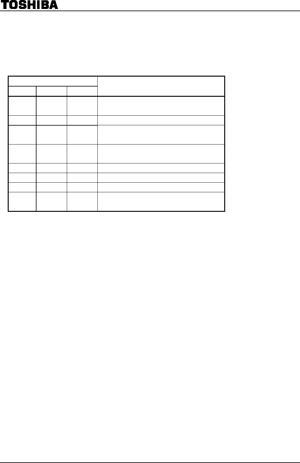
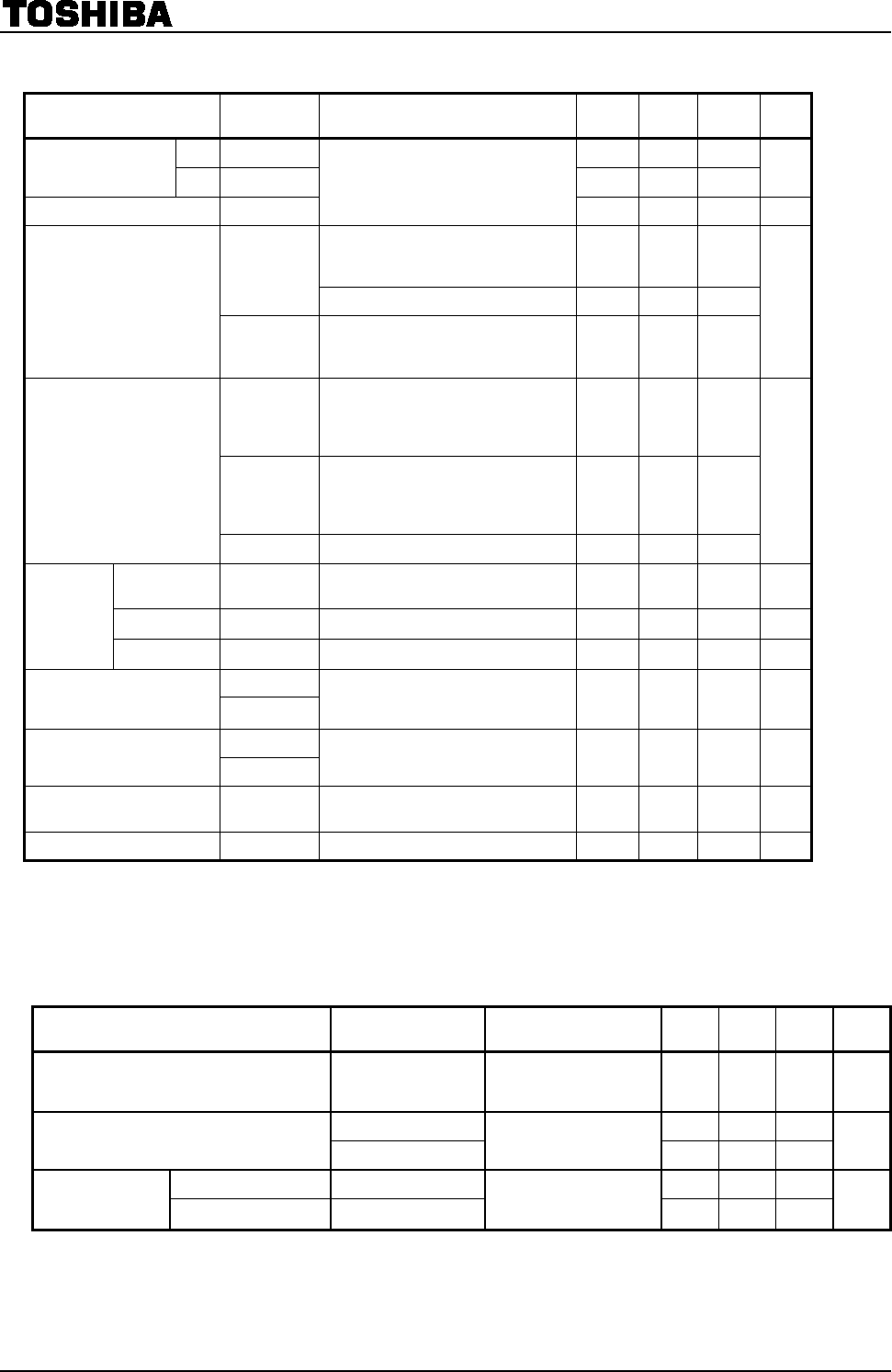
Pin Functions
Pin No. I/O Symbol Functional Description Remark
1 Output ALERT TSD / ISD monitor pin Pull-up by external resistance
2 ― SGND Signal ground
3 Input TQ Torque (output current) setting input pin
4 Input Latch/Auto Select a return type for TSD. L: Latch, H: Automatic return
5 Input Vref Voltage input for 100% current level
6 Input Vcc Power supply
7 Input M1 Excitation mode setting input pin
8 Input M2 Excitation mode setting input pin
9 Input M3 Excitation mode setting input pin
10 Output OUT2B B channel output 2
11 ― NFB B channel output current detection pin
12 Output OUT1B B channel output 1
13 ― PGNDB Power ground
14 Output OUT2A A channel output 2
15 ― NFA A channel output current detection pin
16 Output OUT1A A channel output 1
17 ― PGNDA Power ground
18 Input ENABLE Enable signal input pin H: Enable, L: All outputs off
19 Input RESET Reset signal input pin L: Initial mode
20 Input Vcc Power supply
21 Input CLK CLK pulse input pin
22 Input CW/CCW Forward/reverse control pin L: CW, H:CCW
23 ― OSC Resistor connection pin for internal oscillation setting
24 Output Vreg Control side connection pin for power capacitor
Connecting capacitor to
SGND
25 Output MO Electrical angle monitor pin Pull-up by external resistance
<Terminal circuits>
Input pins
(M1, M2, M3,CLK, CW/CCW,
ENABLE, RESET, Latch/Auto)
Input pins
(TQ)
10kΩ
100k
Ω
VDD
10kΩ
7
0kΩ
TB6600HG
2014-01-30
3
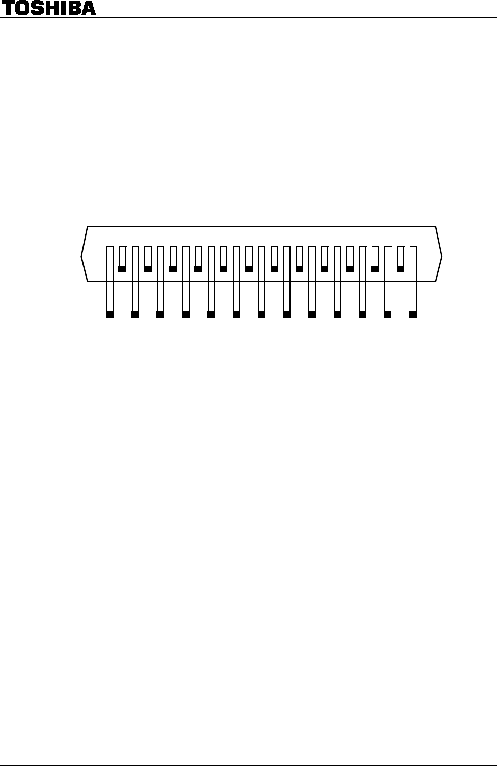
Pin Assignment
(
Top View
)
MO
M1
RESET
TQ
ALERT
Vref
PGNDA
CLK
OSC
N
FA
PGNDB
N
FB
M3
23
25
11
13
15
17
19
21
16
18
20
22
24
1
3
5
7
9
Vcc
CW/CCW
Vreg
2
4
6
8
10
12
14
SGND
Latch/Auto
Vcc
M2
OUT2B
OUT1B
OUT2A
OUT1A
ENABLE
TB6600HG
2014-01-30
4
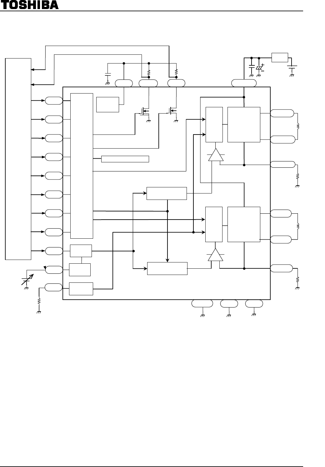
Block Diagram
Setting of Vref
Input Voltage ratio
TQ
L 30%
H 100%
M1
M2
CW/CCW
CLK
M3
OSC
Input
circuit
1/3
TSD / ISD / UVLO
MO
ALERT
H-Bridge
driver A
OUT1A
OUT2A
NFA
H-Bridge
driver B
OUT1B
OUT2B
NFB
Vref
SGND
PGNDB
Current selector
circuit A
3
4
12
15
14
16
6, 20
1
25
24
7
8
9
22
21
19
18
17
2
Current selector
circuit B
Pre
-drive
Pre
-drive
11
OSC
10
RESET
13
PGNDA
23
5
Latch/Auto
TQ
Vcc
Vreg
100%/30%
Reg(5V)
ENABLE
TB6600HG
2014-01-30
5
Description of Functions
1. Excitation Settings
The excitation mode can be selected from the following eight modes using the M1, M2 and M3 inputs. New
excitation mode starts from the initial mode when M1, M2, or M3 inputs are shifted during motor operation.
In this case, output current waveform may not continue.
Input Mode
(Excitation)
M1 M2 M3
L L L Standby mode
(Operation of the internal circuit is almost turned off.)
L L H 1/1 (2-phase excitation, full-step)
L H L 1/2A type (1-2 phase excitation A type)
( 0%, 71%, 100% )
L H H 1/2B type (1-2 phase excitation B type)
( 0%, 100% )
H L L 1/4 (W1-2 phase excitation)
H L H 1/8 (2W1-2 phase excitation)
H H L 1/16 (4W1-2 phase excitation)
H H H Standby mode
(Operation of the internal circuit is almost turned off.)
Note: To change the exciting mode by changing M1, M2, and M3, make sure not to set M1 = M2 = M3 = L or M1 = M2 =
M3 = H.
Standby mode
The operation mode moves to the standby mode under the condition M1 = M2 = M3 = L or M1 = M2 = M3
= H.
The power consumption is minimized by turning off all the operations except protecting operation.
In standby mode, output terminal MO is HZ.
Standby mode is released by changing the state of M1=M2=M3=L and M1=M2=M3=H to other state.
Input signal is not accepted for about 200 μs after releasing the standby mode.
TB6600HG
2014-01-30
6
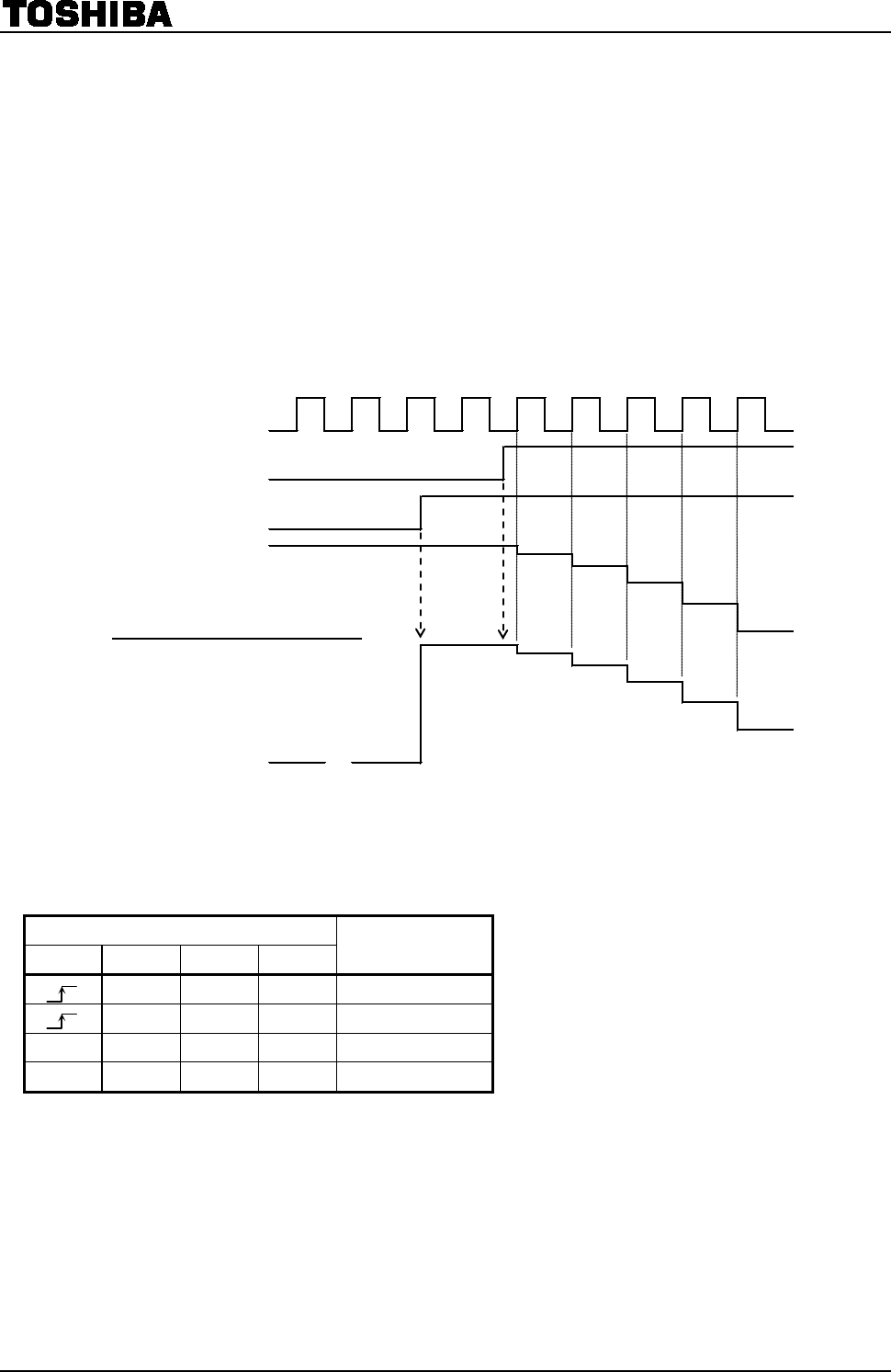
2. Function
(1)To turn on the output, configure the ENABLE pin high. To turn off the output, configure the ENABLE
pin low.
(2) The output changes to the Initial mode shown in the table below when the ENABLE signal goes High
level and the RESET signal goes Low level. (In this mode, the status of the CLK and CW/CCW pins are
irrelevant.)
(3) As shown in the below figure of Example 1, when the ENABLE signal goes Low level, it sets an OFF on
the output. In this mode, the output changes to the initial mode when the RESET signal goes Low level.
Under this condition, the initial mode is output by setting the ENABLE signal High level. And the motor
operates from the initial mode by setting the RESET signal High level.
(*: Output current starts rising at the timing of PWM frequency just after ENABLE pin outputs high.)
Command of the standby has a higher priority
than ENABLE. Standby mode can be turned on
and off regardless of the state of ENABLE.
X: Don’t Care
Input Output mode
CLK CW/CCW RESET ENABLE
L H H CW
H H H CCW
X X L H Initial mode
X X X L Z
(例1)
内部電流設定
Z
出力電流(A相)
CLK
RESET
ENABLE
(Example 1)
Internal current set
Output
current
(phase A )
(*)
TB6600HG
2014-01-30
7
3. Initial Mode
When RESET is used, the phase currents are as follows.
Excitation Mode Phase A Current Phase B Current
1/1 (2-phase excitation, full-step) 100% -100%
1/2A type (1-2 phase excitation A type) (0%, 71%, 100%) 100% 0%
1/2B type (1-2 phase excitation B type) (0%, 100%) 100% 0%
1/4 (W1-2 phase excitation) 100% 0%
1/8 (2W1-2 phase excitation) 100% 0%
1/16 (4W1-2 phase excitation) 100% 0%
current direction is defined as follows.
OUT1A → OUT2A: Forward direction
OUT1B → OUT2B: Forward direction
4. 100% current settings (Current value)
100% current value is determined by Vref inputted from external part and the external resistance for
detecting output current. Vref is doubled 1/3 inside IC.
Io (100%) = (1/3 × Vref) ÷ RNF
The average current is lower than the calculated value because this IC has the method of peak current
detection.
Pleas use the IC under the conditions as follows;
0.11Ω ≤ RNF ≤ 0.5Ω, 0.3V ≤ Vref ≤ 1.95V
5. OSC
Triangle wave is generated internally by CR oscillation by connecting external resistor to OSC terminal.
Rosc should be from 30kΩ to 120kΩ. The relation of Rosc and fchop is shown in below table and figure. The
values of fchop of the below table are design guarantee values. They are not tested for pre-shipment.
Rosc(kΩ)
fchop(kHz)
Min
Typ.
Max
30
-
60
-
51
-
40
-
120
-
20
-
TB6600HG
2014-01-30
8
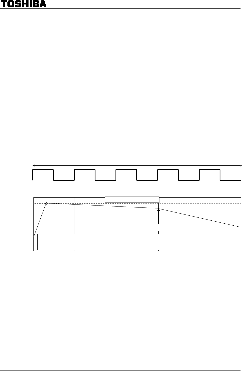
6. Decay Mode
It takes approximately five OSCM cycles for charging-discharging a current in PWM mode. The 40% fast
decay mode is created by inducing decay during the last two cycles in Fast Decay mode.
The ratio 40% of the fast decay mode is always fixed.
The relation between the master clock frequency (fMCLK), the OSCM frequency (fOSCM) and the PWM
frequency (fchop) is shown as follows:
fOSCM = 1/20 ×fMCLK
fchop = 1/100 ×fMCLK
When Rosc=51kΩ, the master clock=4MHz, OSCM=200kHz, the frequency of PWM(fchop)=40kHz.
6-1. Current Waveform and Mixed Decay Mode settings
The period of PWM operation is equal to five periods of OSCM.
The ratio 40% of the fast decay mode is always fixed.
The “NF” refers to the point at which the output current reaches its predefined current level.
MDT means the point of MDT (MIXED DECAY TIMMING) in the below diagram.
OSC
M
Interna
l
Waveform
fchop
NF
40
%
fast
Decay
Mode
MDT
Charge mode
→
NF: Predefined current level
→
Slow mode
→
MDT(Mixed decay timing) → Fast mode → Current monitoring →
(When predefined current level > Output current) Charge mode
Predefined Current Level
TB6600HG
2014-01-30
9
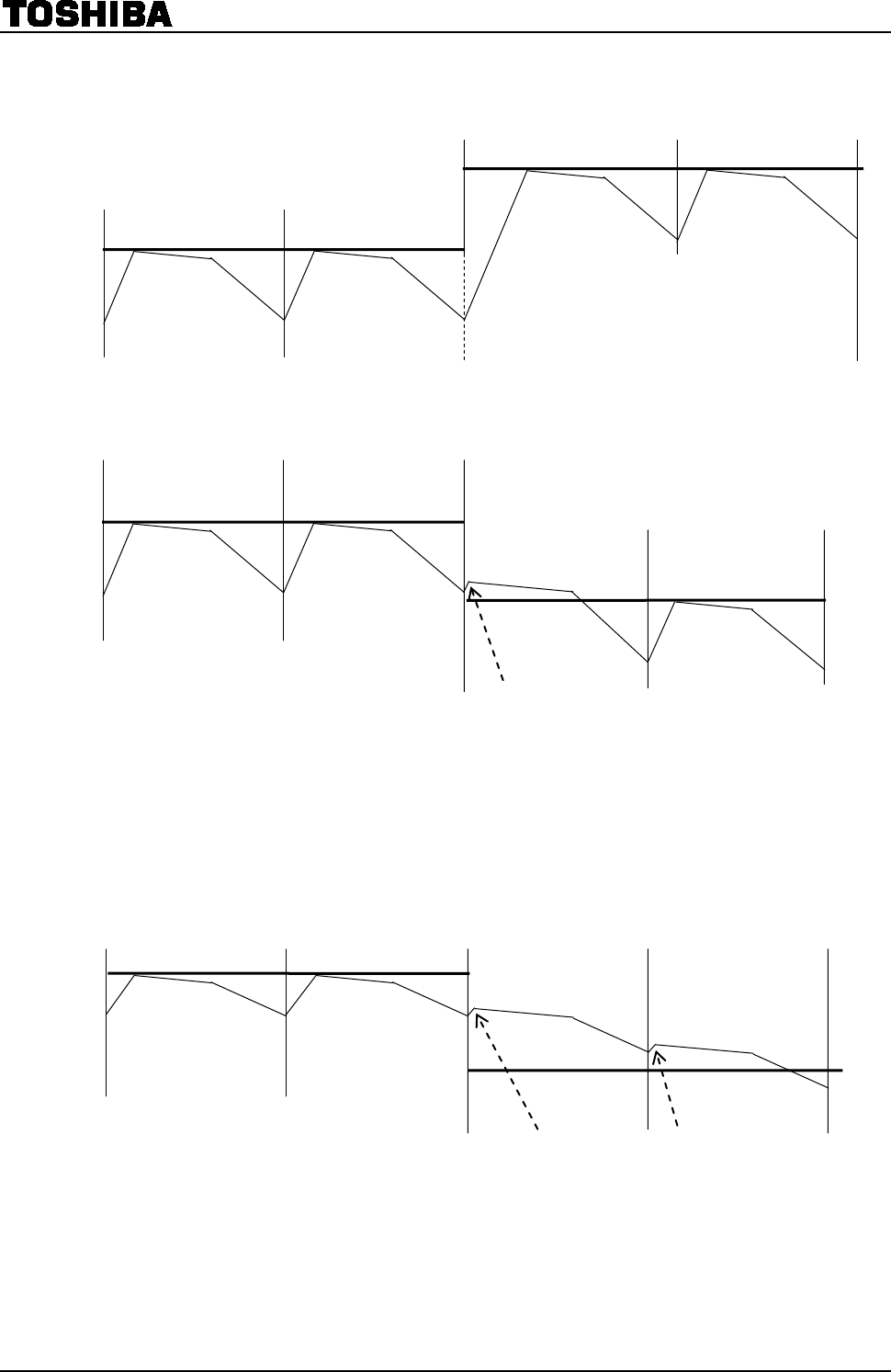
6-2. Effect of Decay Mode
• Increasing the current (sine wave)
• Decreasing the current (In case the current is decreased to the predefined value in a short time because
it decays quickly.)
• Decreasing the current (In case it takes a long time to decrease the current to the predefined value
because the current decays slowly.)
During Mixed Decay and Fast Decay modes, if the predefined current level is less than the output current at
the RNF (current monitoring point), the Charge mode in the next chopping cycle will disappear (though the
current control mode is briefly switched to Charge mode in actual operations for current sensing) and the
current is controlled in Slow and Fast Decay modes (mode switching from Slow Decay mode to Fast Decay
mode at the MDT point).
Note: The above figures are rough illustration of the output current. In actual current waveforms, transient response
curves can be observed.
Predefined
Curre
nt Level
Slow
Slow
Fast
Predefined
Curre
nt Level
Slow
Charge
Fast
Fast
Fast
Slow
Charge Charge
Even if the output current rises above the predefined current at the RNF point, the
current control mode is briefly switched to Charge mode for current sensing.
Slow
Slow
Charge
Slow
Fast
Slow
Fast
Charge
Predefined
Curre
nt Level
Predefined
Curre
nt Level
Fast
Charge
Fast
Charge
Even if the output current rises above the predefi
ned current at the RNF point, the
current control mode is briefly switched to Charge mode for current sensing.
Slow
Slow
Slow
Slow
Fast
Fast
Charge
Charge
Fast
Charge
Fast
Charge
Predefined
Curre
nt Level
Predefined
Curre
nt Level
TB6600HG
2014-01-30
10
6-3. Current Waveforms in Mixed Decay Mode
• When the NF points come after Mixed Decay Timing points
• When the output current value > predefined current level in Mixed Decay mode
NF
NF
OS
CM
Internal
waveform
IOUT
fchop
fchop
Predefined
Current Level
Predefined Current Level
40
%
Fast
DECAY
MODE
MDT (MIXED DECAY TIMMING) points
NF
40
%
Fast
DECAY
MODE
IOUT
fchop
fchop
Predefined
Current Level
CLK signal input
Switches to Fast mode after Charge mode
NF
MDT (MIXED DECAY TIMMING) points
NF
NF
IOUT
fchop
fchop
Predefined
Current
Level
CLK signal input
fchop
MDT (MIXED DECAY TIMMING) points
Predefined Current
Level
40
%
Fast
DECAY
MODE
Even if the output current rises above the predefined curren
t at the
RNF point, the current control mode is briefly
switched to Charge
mode for current sensing.
Predefined
Current Level
TB6600HG
2014-01-30
11
Output Stage Transistor Operation Mode
Output Stage Transistor Operation Functions
CLK U1 U2 L1 L2
CHARGE ON OFF OFF ON
SLOW OFF OFF ON ON
FAST OFF ON ON OFF
Note: The above chart shows an example of when the current flows as indicated by the arrows in the above figures.
If the current flows in the opposite direction, refer to the following chart:
CLK U1 U2 L1 L2
CHARGE OFF ON ON OFF
SLOW OFF OFF ON ON
FAST ON OFF OFF ON
Upon transitions of above-mentioned functions, a dead time of about 300 ns (Design guarantee value) is inserted
respectively.
U1
L1
U2
L2
PGND
OFF
OFF
U1
L1
U2
L2
OFF
ON
Note
Load
PGND
U1
L1
U2
L2
Note
Load
PGND
Note
RNF
Vcc
ON
ON
Load
Charge Mode
Slow Mode
Fast Mode
ON
RNF
Vcc
RNF
Vcc
OFF
OFF
OFF
ON
ON
OUT1 OUT2
OUT1 OUT2
OUT1 OUT2
TB6600HG
2014-01-30
12
Thermal Shut-Down circuit (TSD)
(1) Automatic return
TSD = 160°C (typ.) (Note)
TSDhys = 70°C (typ.) (Note)
Automatic return has a temperature hysteresis shown in the above figure.
In case of automatic return, the return timing is adjusted at charge start of fchop after the temperature falls to the
return temperature (90°C (typ.) in the above figure).
The return period after the temperature falls corresponds to one cycle to two cycles of fchop.
(2) Latch type
TSD = 160°C (typ.) (Note)
The operation returns by programming the ENABLE as H → L → H shown in above figure or turning on power
supply and turning on UVLO function. In this time, term of L level of ENABLE should be 0.3ms or more.
To recover the operation, the junction temperature (the chip temperature) should be 90°C or less when ENABLE
input is switched from L to H level. Otherwise, the operation does not recover.
Note: Pre-shipment testing is not performed.
・
State of internal IC when TSD circuit operates.
The states of the internal IC and outputs, while the shutdown circuit is operating, correspond to the state when
ENABLE is L.
The state after automatic return corresponds to the state when ENABLE is H. Please configure the Reset L to
rotate the motor from the initial state.
1
60°C (typ.) (Note)
Junction temperature (Chip temperature)
ALERT output H
L
90°C (typ.) (Note)
Output on Output off Output on
Output state
160°C (typ.)
(Note)
Junction temperature (Chip temperature)
ALERT output
H
L
Output on Output off Output on
ENABLE input
0.3ms or more when Rosc=51k
Ω
Output state
H
L
(*)Output current starts rising at the
timing of PWM frequency just after
ENABLE pin outputs high.
(*)

TB6600HG
2014-01-30
13
Latch/Auto is an input pin for determining the return method of TSD.
If Latch/Auto pin outputs low, TSD function returns by either of turning on power supply again or programming
the ENABLE as H → L → H.
If Latch/Auto pin outputs high, it returns automatically.
In standby mode, TSD function returns automatically regardless of the state of the Latch/Auto pin.
When power supply voltage Vcc is less than 8V, TSD function cannot operate regardless of the state of the
Latch/Auto pin.
TB6600HG
2014-01-30
14
ISD (Over current detection)
Current that flows through output power MOSFETs are monitored individually. If over-current is detected
in at least one of the eight output power MOSFETs, all output power MOSFETs are turned off then this
status is kept until ENABLE signal is input. In this time, term of L level of ENABLE should be 0.3ms or
more.
Masking term of 1μs or more (typ. when Rosc=51kΩ) (Note) should be provided in order to protect detection
error by noise. ISD does not work during the masking term.
Over current detection value ISD=6.5 A (Note)
The operation returns by programming the ENABLE as H → L → H shown in above figure or turning
on power supply and turning on UVLO function.
Note: Pre-shipment testing is not performed.
・
State of internal IC when ISD circuit operates.
The states of the internal IC and outputs, while the over current detection circuit is operating, correspond to the
state when ENABLE is L.
The state after automatic return corresponds to the state when ENABLE is H. Please configure the Reset L to
rotate the motor from the initial state.
Return method of ISD
ISD function returns by either of turning on power supply again or programming the ENABLE as H → L → H
regardless of the state of the Latch/Auto pin.
In standby mode, ISD function cannot operate.
When power supply voltage Vcc is less than 8V, ISD function cannot operate.
DMOS
Power transistor current
6.5A (typ.)
Dead band
1
μs or more(typ.)
Output on Output off Output on
Output state
(*)Output current starts rising at the
timing of PWM frequency just after
EN
ABLE pin outputs high.
ALERT output
H
L
ENABLE input
0.3ms or more when Rosc=51k
Ω
H
L
(*)

TB6600HG
2014-01-30
15
Under Voltage Lock Out (UVLO) circuit
Outputs are shutoff by operating at 5.5 V (Typ.) of Vcc or less.
It has a hysteresis of 0.5 V (Typ.) and returns to output when Vcc reaches 6.0 V (Typ.). The following values are
design guarantee values.
・
State of internal IC when UVLO circuit operates.
The states of the internal IC and outputs correspond to the state in the ENABLE mode and the initial mode at
the same time.
After a return, it can start from the initial mode.
When Vcc falls to around 5.5 V and UVLO operates, output turns off.
It recovers automatically from the initial mode when both Vcc rise to around 6.0 V or more. The following
values are design guarantee values.
TB6600HG
2014-01-30
16
ALERT output
ALERT terminal outputs low in detecting either TSD or ISD.
ALERT terminal is connected to power supply externally via pull-up resistance.
VALERT = 0.5 V (max.) at 1 mA
Applied voltage to pull-up resistance is up to 5.5 V. And conducted current is up to 1 mA.
It is recommended to gain 5 V by connecting the external pull-up resistance to Vreg pin.
MO output
MO turns on at the predetermined state and output low.
MO terminal is connected to power supply externally via pull-up resistance.
VMO = 0.5 V (max.) at 1 mA
Applied voltage to pull-up resistance is up to 5.5 V. And conducted current is up to 1 mA.
It is recommended to gain 5 V by connecting the external pull-up resistance to Vreg pin.
Voltage pull-up of MO and ALERT pins
・It is recommended to pull-up voltage to Vreg pin.
・In case of pull-up to except 5 V (for instance, 3.3 V etc.), it is recommended to use other power supply (ex. 3.3 V)
while Vcc output between the operation range. When Vcc decreases lower than the operation range and Vreg
decreases from 5 V to 0 V under the condition that other power supply is used to pull-up voltage, the current
continues to conduct from other power supply to the IC inside through the diode shown in the figure. Though this
phenomenon does not cause destruction and malfunction of the IC, please consider the set design not to continue
such a state for a long time.
・As for the pull-up resistance for MO and ALERT pins, please select large resistance enough for the conducting
current so as not to exceed the standard value of 1 mA.
Please use the resistance of 30 kΩ or more in case of applying 5 V, and 20 kΩ or more in case of applying 3.3 V.
TSD ISD ALERT
Under TSD detection
Under ISD detection
Low
Normal Under ISD detection
Under TSD detection
Normal
Normal Normal Z
State MO
Initial Low
Not initial Z
(To Vreg in the IC)
(To pull-
up resistance)
TB6600HG
2014-01-30
17
Sequence and current level in each excitation mode
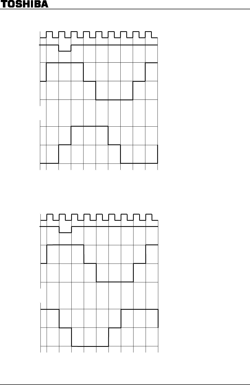
1/1-step Excitation Mode (M1: L, M2: L, M3: H, CW Mode)
1/1-step Excitation Mode (M1: L, M2: L, M3: H, CCW Mode)
CLK
100
(%)
0
−
100
t0
t1
t2
t3
t7
t8
t4
t5
t6
IA
100
(%)
0
−100
IB
MO
CLK
100
(%)
0
−100
t0
t1
t2
t3
t7
t8
t4
t5
t6
IA
100
(%)
0
−100
IB
MO
It operates from the initial state after the excitation mode is switched.
TB6600HG
2014-01-30
18
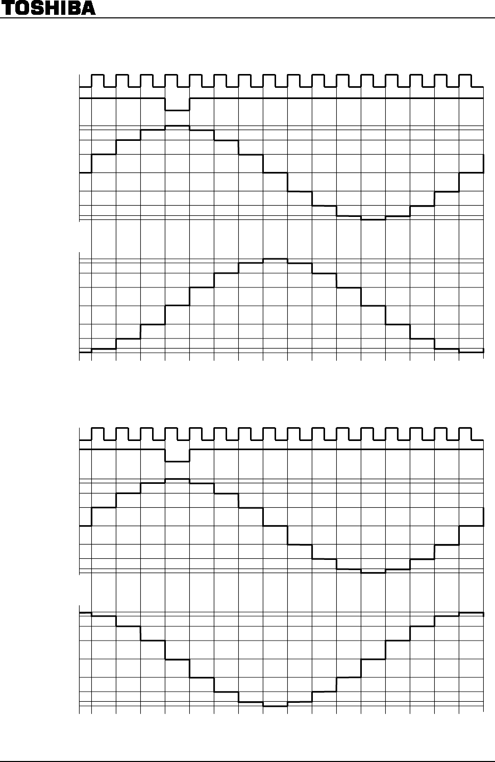
1/2-step Excitation Mode (A type) (M1: L, M2: H, M3: L, CW Mode)
1/2-step Excitation Mode (A type) (M1: L, M2: H, M3: L, CCW Mode)
CLK
100
(%)
0
−
100
t0
t1
t2
t3
t7
t8
t4
t5
t6
71
−
71
IA
100
(%)
0
−100
71
−71
IB
MO
CLK
100
(%)
0
−100
t0
t1
t2
t3
t7
t8
t4
t5
t6
71
−71
IA
100
(%)
0
−100
71
−71
IB
MO
It operates from the initial state after the excitation mode is switched.
TB6600HG
2014-01-30
19
1/2-step Excitation Mode (B type) (M1: L, M2: H, M3: H, CW Mode)
1/2-step Excitation Mode (B type) (M1: L, M2: H, M3: H, CCW Mode)
CLK
100
(%)
0
−
100
t0
t1
t2
t3
t7
t8
t4
t5
t6
IA
100
(%)
0
−100
IB
MO
CLK
100
(%)
0
−100
t0
t1
t2
t3
t7
t8
t4
t5
t6
IA
100
(%)
0
−100
71
−71
IB
MO
It operates from the initial state after the excitation mode is switched.
TB6600HG
2014-01-30
20
1/4-step Excitation Mode (M1: H, M2: L, M3: L, CW Mode)
1/4-step Excitation Mode (M1: H, M2: L, M3: L, CCW Mode)
CLK
100
(%)
0
−100
t0
t1
t2
t3
t7
t8
t4
t5
t6
71
−71
IA
IB
t9
t10
t11
t15
t16
t12
t13
t14
38
−
38
92
−
92
100
(%)
0
−
100
71
−
71
38
−38
92
−92
MO
It operates from the initial state after the excitation mode is switched.
CLK
100
(%)
0
−
100
t0
t1
t2
t3
t7
t8
t4
t5
t6
71
−
71
IA
IB
t9
t10
t11
t15
t16
t12
t13
t14
38
−38
92
−92
100
(%)
0
−100
71
−71
38
−38
92
−92
MO
TB6600HG
2014-01-30
21
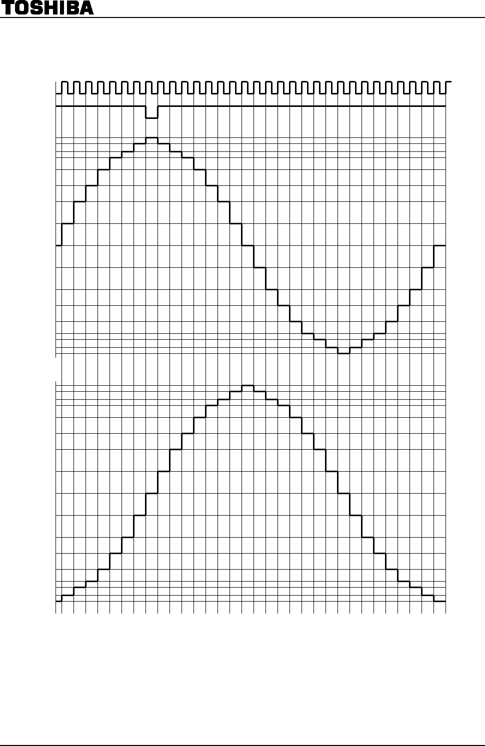
1/8-Step Excitation Mode (M1: H, M2: L, M3: H, CW Mode)
IA
IB
It operates from the initial state after the excitation mode is switched.
MO
38
CLK
t0
t1
t2
t3
t7
t8
t4
t5
t12
t13
t6
100
(%)
98
92
83
71
56
38
20
0
−
20
−
38
−
56
−
71
−92
−
98
−100
100
(%)
98
92
83
71
56
20
0
−
20
−
38
−
56
−
71
−
98
−
100
t9
t10
t11
t14
t17
t18
t15
t16
t19
t20
t21
t22
t27
t28
t24
t25
t29
t30
t31
t32
t23
t26
−83
−83
−92
TB6600HG
2014-01-30
22
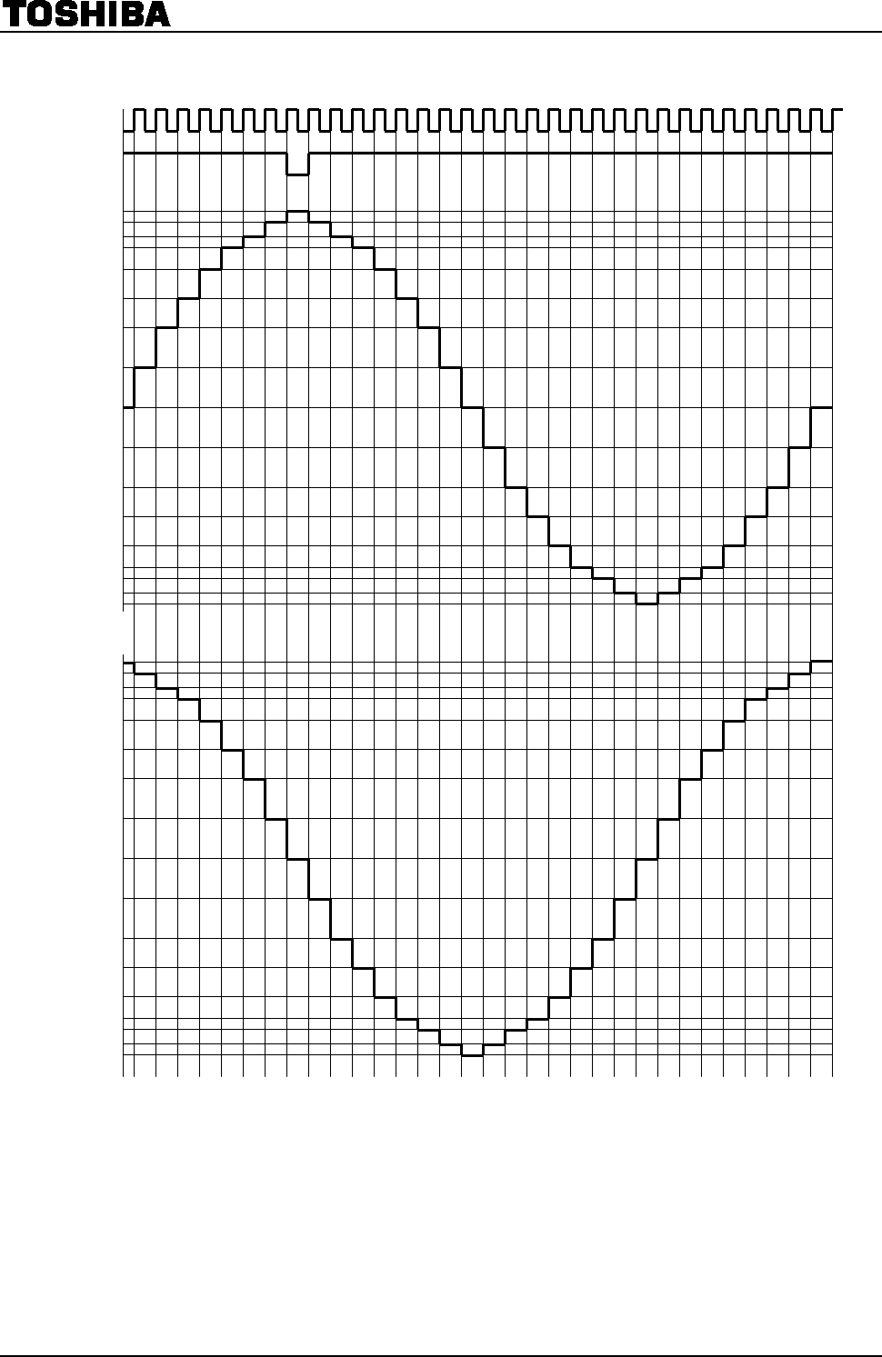
1/8-Step Excitation Mode (M1: H, M2: L, M3: H, CCW Mode)
It operates from the initial state after the excitation mode is switched.
MO
38
−
83
−92
−83
−
71
CLK
100
(%)
98
92
83
71
56
38
20
0
−20
−
38
−56
−
92
−98
−
100
100
(%)
98
92
83
71
56
20
0
−20
−38
−
56
−71
−
98
−
100
t0
t1
t2
t3
t7
t8
t4
t5
t12
t13
t6
t9
t10
t11
t14
t17
t18
t15
t16
t19
t20
t21
t22
t27
t28
t24
t25
t29
t30
t31
t32
t23
t26
IA
IB
TB6600HG
2014-01-30
23
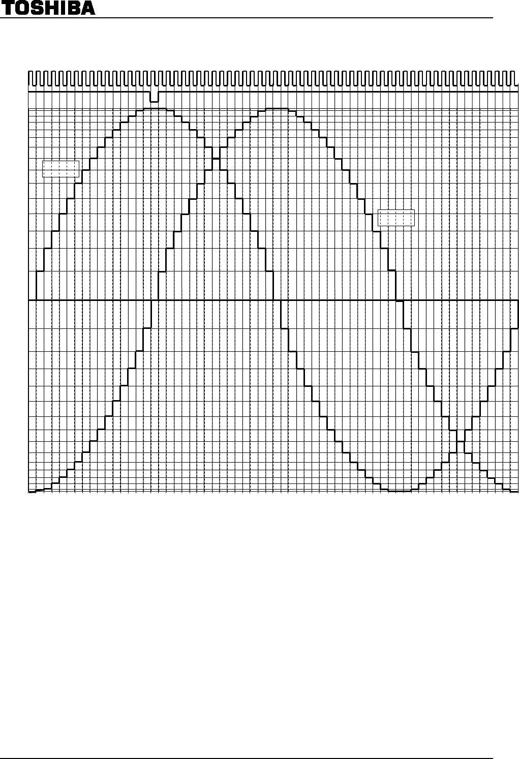
1/16-step Excitation Mode (M1: H, M2: H, M3: L, CW Mode)
−100
−98
0
−96
−88
−92
−77
−71
−56
−63
−47
−38
−29
−20
−10
−83
10
20
29
38
47
56
63
71
77
83
88
92
96
98
100
[%]
CLK
t0・・・・・・・・・・・・・・・・・・・・・・・・・・・・・・・・・・・・・・・・・・・・・・・・・・・・・・・・・・・・・・・・・・・・・・・・・・・・・・・・・・・・・・・・・・・・・・・・・・・・・・・・・・・・・・・・・・・・・・・t64
I
A
I
B
It operates from the initial state after the excitation mode is switched.
MO
TB6600HG
2014-01-30
24
1/16-step Excitation Mode (M1: H, M2: H, M3: L, CCW Mode)
−100
−98
0
−96
−88
−92
−77
−71
−56
−63
−47
−38
−29
−20
−10
−83
10
20
29
38
47
56
63
71
77
83
88
92
96
98
100
[%]
CLK
t0・・・・・・・・・・・・・・・・・・・・・・・・・・・・・・・・・・・・・・・・・・・・・・・・・・・・・・・・・・・・・・・・・・・・・・・・・・・・・・・・・・・・・・・・・・・・・・・・・・・・・・・・・・・・・・・・・・・・・・・t64
I
A
I
B
MO
It operates from the initial state after the excitation mode is switched.
TB6600HG
2014-01-30
25
Current level
2-phase, 1-2-phase, W1-2-phase, 2W1-2-phase, 4W1-2-phase excitation (unit: %)
Current level (1/16, 1/8, 1/4, 1/2, 1/1 )
θ16 --- 100.0 ---
θ1595.5 99.5 100.0
θ1494.1 98.1 100.0
θ1391.7 95.7 99.7
θ1288.4 92.4 96.4
θ1184.2 88.2 92.2
θ1079.1 83.1 87.1
θ9 73.3 77.3 81.3
θ8 66.7 70.7 74.7
θ7 59.4 63.4 67.4
θ6 51.6 55.6 59.6
θ543.1 47.1 51.1
θ4 34.3 38.3 42.3
θ3 25.0 29.0 33.0
θ2 15.5 19.5 23.5
θ1 5.8 9.8 13.8
θ0 --- 0.0 ---
%
Max.
Unit
1/16,
1/8, 1/4,
1/2, 1/1
Min.
Typ.
TB6600HG
2014-01-30
26
Absolute Maximum Ratings (Ta = 25°C)
Characteristic Symbol Rating Unit
Power supply voltage Vcc 50 V
Output current (per one phase) IO
(PEAK)
5.0 A
Drain current (ALERT, MO) I (ALERT) 1 mA
I (MO)
Input voltage VIN 6 V
Power dissipation PD
3.2 (Note 1) W
40 (Note 2)
Operating temperature Topr -30 to 85 °C
Storage temperature Tstg -55 to 150 °C
Note 1: Ta = 25°C, No heatsink
Note 2: Ta = 25°C, with infinite heatsink.
The absolute maximum ratings of a semiconductor device are a set of ratings that must not be exceeded, even for a
moment. Do not exceed any of these ratings.
Exceeding the rating (s) may cause the device breakdown, damage or deterioration, and may result injury by explosion
or combustion.
Please use the IC within the specified operating ranges.
Operating Range (Ta = −30~85°C)
Characteristic Symbol Test Condition Min Typ. Max Unit
Power supply voltage Vcc ― 8.0 ― 42 V
Output current IOUT ― ― ― 4.5 A
Input voltage VIN ― 0 ― 5.5 V
Vref ― 0.3 ― 1.95 V
Clock frequency in logical part fCLK ― ― ― 200 kHz
Chopping frequency fchop See page 7. 20 40 60 kHz
Note: Two Vcc terminals should be programmed the same voltage.
The maximum current of the operating range can not be necessarily conducted depending on various
conditions because output current is limited by the power dissipation PD.
Make sure to avoid using the IC in the condition that would cause the temperature to exceed Tj (avg.)
=107°C.
The power supply voltage of 42 V and the output current of 4.5 A are the maximum values of operating range.
Please design the circuit with enough derating within this range by considering the power supply variation, the
external resistance, and the electrical characteristics of the IC. In case of exceeding the power supply voltage
of 42 V and the output current of 4.5 A, the IC will not operate normally.
TB6600HG
2014-01-30
27
Electrical Characteristics (Ta = 25°C, Vcc = 24 V)
Characteristic Symbol Test Condition Min Typ. Max Unit
Input voltage High VIN (H)
M1, M2, M3, CW/CCW, CLK,
RESET, ENABLE, Latch/Auto, TQ
2.0 ― 5.5 V
Low VIN (L) -0.2 ― 0.8
Input hysteresis voltage VH ― 400 ― mV
Input current
IIN (H)
M1, M2, M3, CW/CCW, CLK,
RESET, ENABLE, Latch/Auto
VIN = 5.0 V
― 50 75
μA
TQ, VIN = 5.0 V ― 70 105
IIN (L)
M1, M2, M3, CW/CCW, CLK,
RESET, ENABLE, Latch/Auto, TQ
VIN = 0 V
― ― 1
Vcc supply current
Icc1
Output open,
RESET: H, ENABLE: H、
M1:L, M2:L, M3:H (1/1-
step mode)
CLK:L
― 4.2 7
mA
Icc2
Output open,
RESET: L, ENABLE: L
M1:L, M2:L, M3:H (1/1-step mode)
CLK:L
― 3.6 7
Icc3 Standby mode (M1:L, M2:L, M3:L) ― 1.8 4
Vref input
circuit
Current limit
voltage VNF Vref = 3.0 V(Note 1), TQ=H 0.9 1.0 1.1 V
Input current IIN(Vref) Vref = 3.0 V(Note 1) ― ― 1 μA
Divider ratio Vref/VNF
Maximum current: 100%, TQ=H ― 3 ― ―
Minimum CLK pulse width twCLKH CLK 2.2 ― ― μs
twCLKL
Output residual voltage VOL MO IOL = 1 mA ― ― 0.5 V
VOL ALERT
Internal constant voltage Vreg External capacitor = 0.1 μF
(in standby mode) 4.5 5.0 5.5 V
Chopping frequency fchop Rosc=51kΩ 28 40 52 kHz
Note 1: Though Vref of the test condition for pre-shipment is 3.0V, make sure to configure Vref within the operating
range which is written in page 26 in driving the motor.
Electrical Characteristics (Ta = 25°C, Vcc = 24 V)
Characteristic Symbol Test Condition Min Typ. Max Unit
Output ON resistor Ron U + Ron L IOUT = 4 A ― 0.4 0.6 Ω
Output transistor switching characteristics tr VNF = 0 V, Output: Open ― 50 ― ns
tf ― 500 ―
Output leakage
current
Upper side ILH Vcc = 50 V
― ― 5
μA
Lower side ILL ― ― 5
TB6600HG
2014-01-30
28
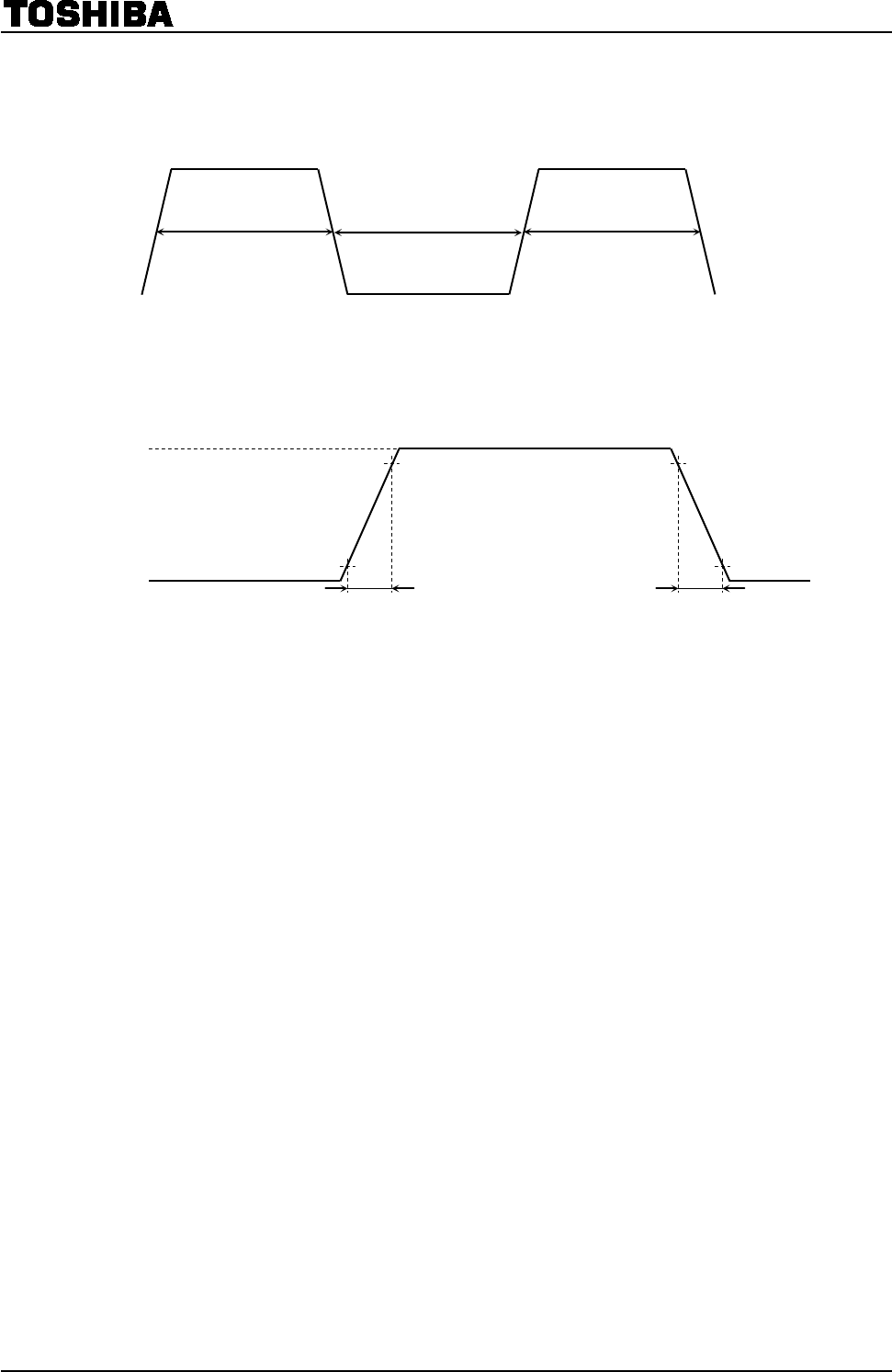
Timing Waveforms and Names
CLK
Vcc
GND
tr
tf
10%
90%
90%
10%
Figure 1 Timing Waveforms and Names
tw
CLKH
twCLKH
Figure 2 Timing Waveforms and Names
twCLKL
OUT1A, OUT2A,
OUT1B, OUT2B
TB6600HG
2014-01-30
29
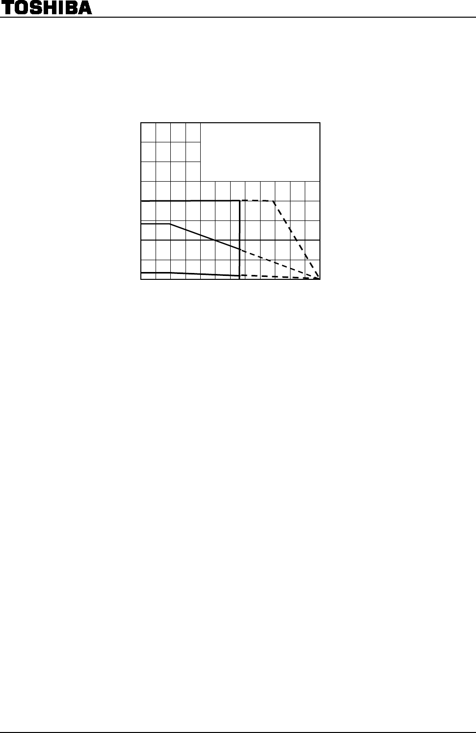
Power Dissipation
TB6600HG
PD – Ta
Ambient temperature Ta (°C)
Power dissipation PD (W)
①
②
③
25 0 150
0
80
75
40
100
20
60
50
125
① Infinite heatsink
Rθj-c = 1°C/W
② HEATSINK (RθHS = 3.5°C/W)
Rθj-c + RθHS = 4.5°C/W
③ IC only
Rθj-a = 39°C/W
TB6600HG
2014-01-30
30
1. How to Turn on the Power
In applying Vcc or shutdown, ENABLE should be Low.
See Example 1(ENABLE = High → RESET = High) and Example 2(RESET = High → ENABLE = High)
as follows. In example 1, a motor can start driving from the initial mode.
(1) CLK: Current step proceeds to the next mode with respect to every rising edge of CLK.
(2) ENABLE: It is in Hi-Z state in low level. It is output in high level.
RESET: It is in the initial mode (Phase A=100% and Phase B=0%) in low level.
①ENABLE=Low and RESET=Low: Hi-Z. Internal current setting is in initial mode.
②ENABLE=Low and RESET=High: Hi-Z. Internal current setting proceeds by internal counter.
③ENABLE=High and RESET=Low: Output in the initial mode (Phase A=100% and Phase B=0%).
④ENABLE=High and RESET=High: Output at the value which is determined by the internal counter.
<Recommended control input sequence>
(例2)
Z
出力電流(A相)
CLK
RESET
ENABLE
内部電流設定
(例1)
内部電流設定
Z
出力電流(A相)
CLK
RESET
ENABLE
(Example 1)
Internal current set
Output current
(Phase A)
(Example
2)
Internal current set
Output current
(Phase A)
(*
:
Output current starts rising at the timing of PWM frequency just after ENABLE pin outputs high.)
(*)
(*)
TB6600HG
2014-01-30
31
Application Circuit
Note 1: Capacitors for the power supply lines should be connected as close to the IC as possible.
Note 2: Current detecting resistances (RNFA and RNFB) should be connected as close to the IC as possible.
Note 3: Pay attention for wire layout of PCB not to allow GND line to have large common impedance.
Note 4: External capacitor connecting to Vreg should be 0.1μF. Pay attention for the wire between this
capacitor and Vreg terminal and the wire between this capacitor and SGND not to be influenced by
noise.
Note 5: The IC may not operate normally when large common impedance is existed in GND line or the IC is
easily influenced by noise. For example, if the IC operates continuously for a long time under the
circumstance of large current and high voltage, the number of clock signals inputted to CLK
terminal and that of steps of output current waveform may not proportional. And so, the IC may not
operate normally. To avoid this malfunction, make sure to conduct Note.1 to Note.4 and evaluate
the IC enough before using the IC.
24V
M1
M2
CW/CCW
CLK
ENABLE
M3
OSC
TSD/ISD/UVLO
MO
ALERT
H-Bridge
driver A
Vcc
OUT1A
OUT2A
NFA
H-Bridge
driver B
OUT1B
OUT2B
NFB
Vref
SGND
Current selector
circuit A
Current selector
circuit B
Pre
-drive
Pre
-drive
OSC
MCU
0.2
Ω
0.2
Ω
24V
RESET
PGNDA
PGNDB
Latch/Auto
Vreg
51kΩ
TQ
Control
logic
1/3
100%/
30%
0.1μF
0.1μF 47μF
Reg (5V)
fuse
TB6600HG
2014-01-30
32
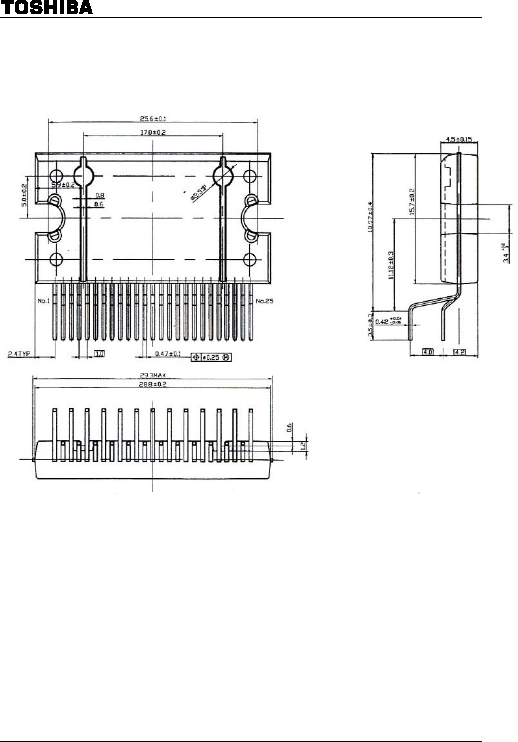
Package Dimensions
Weight: 7.7 g (typ.)
Unit:
mm
Note:These dimensions are measured from the surface of the heat sink
.
Note

TB6600HG
2014-01-30
33
Notes on Contents
1. Block Diagrams
Some of the functional blocks, circuits, or constants in the block diagram may be omitted or simplified for
explanatory purposes.
2. Equivalent Circuits
The equivalent circuit diagrams may be simplified or some parts of them may be omitted for explanatory
purposes.
3. Timing Charts
Timing charts may be simplified for explanatory purposes.
4. Application Circuits
The application circuits shown in this document are provided for reference purposes only. Thorough evaluation
is required, especially at the mass production design stage.
Toshiba does not grant any license to any industrial property rights by providing these examples of application
circuits.
5. Test Circuits
Components in the test circuits are used only to obtain and confirm the device characteristics. These components
and circuits are not guaranteed to prevent malfunction or failure from occurring in the application equipment.
IC Usage Considerations
Notes on handling of ICs
[1] The absolute maximum ratings of a semiconductor device are a set of ratings that must not be exceeded, even
for a moment. Do not exceed any of these ratings.
Exceeding the rating(s) may cause the device breakdown, damage or deterioration, and may result injury by
explosion or combustion.
[2] Use an appropriate power supply fuse to ensure that a large current does not continuously flow in case of over
current and/or IC failure. The IC will fully break down when used under conditions that exceed its absolute
maximum ratings, when the wiring is routed improperly or when an abnormal pulse noise occurs from the
wiring or load, causing a large current to continuously flow and the breakdown can lead smoke or ignition. To
minimize the effects of the flow of a large current in case of breakdown, appropriate settings, such as fuse
capacity, fusing time and insertion circuit location, are required.
[3] If your design includes an inductive load such as a motor coil, incorporate a protection circuit into the design to
prevent device malfunction or breakdown caused by the current resulting from the inrush current at power ON
or the negative current resulting from the back electromotive force at power OFF. IC breakdown may cause
injury, smoke or ignition.
Use a stable power supply with ICs with built-in protection functions. If the power supply is unstable, the
protection function may not operate, causing IC breakdown. IC breakdown may cause injury, smoke or ignition.
[4] Do not insert devices in the wrong orientation or incorrectly.
Make sure that the positive and negative terminals of power supplies are connected properly.
Otherwise, the current or power consumption may exceed the absolute maximum rating, and exceeding the
rating(s) may cause the device breakdown, damage or deterioration, and may result injury by explosion or
combustion.
In addition, do not use any device that is applied the current with inserting in the wrong orientation or
incorrectly even just one time.

TB6600HG
2014-01-30
34
Points to remember on handling of ICs
(1) Over current Detection Circuit
Over current detection circuits (referred to as current limiter circuits) do not necessarily protect ICs under all
circumstances. If the over current detection circuits operate against the over current, clear the over current
status immediately.
Depending on the method of use and usage conditions, such as exceeding absolute maximum ratings can cause
the over current detection circuit to not operate properly or IC breakdown before operation. In addition,
depending on the method of use and usage conditions, if over current continues to flow for a long time after
operation, the IC may generate heat resulting in breakdown.
(2) Thermal Shutdown Circuit
Thermal shutdown circuits do not necessarily protect ICs under all circumstances. If the thermal shutdown
circuits operate against the over temperature, clear the heat generation status immediately.
Depending on the method of use and usage conditions, such as exceeding absolute maximum ratings can cause
the thermal shutdown circuit to not operate properly or IC breakdown before operation.
(3) Heat Radiation Design
In using an IC with large current flow such as power amp, regulator or driver, please design the device so that
heat is appropriately radiated, not to exceed the specified junction temperature (Tj) at any time and condition.
These ICs generate heat even during normal use. An inadequate IC heat radiation design can lead to decrease
in IC life, deterioration of IC characteristics or IC breakdown. In addition, please design the device taking into
considerate the effect of IC heat radiation with peripheral components.
(4) Back-EMF
When a motor rotates in the reverse direction, stops or slows down abruptly, a current flow back to the motor’s
power supply due to the effect of back-EMF. If the current sink capability of the power supply is small, the
device’s motor power supply and output pins might be exposed to conditions beyond absolute maximum ratings.
To avoid this problem, take the effect of back-EMF into consideration in system design.
(5) Short-circuiting between outputs, air contamination faults, faults due to improper grounding, short-circuiting
between contiguous pins
Utmost care is necessary in the design of the power supply lines, GND lines, and output lines since the IC may
be destroyed by short-circuiting between outputs, air contamination faults, or faults due to improper grounding,
or by short-circuiting between contiguous pins. They may destroy not only the IC but also peripheral parts and
may contribute to injuries for users. Over current may continue to flow in the IC because of this destruction
and cause smoke or ignition of the IC. Expect the volume of this over current and add an appropriate power
supply fuse in order to minimize the effects of the over current. Capacity of the fuse, fusing time, and the
inserting position in the circuit should be configured suitably.

TB6600HG
2014-01-30
35
RESTRICTIONS ON PRODUCT USE
• Toshiba Corporation, and its subsidiaries and affiliates (collectively "TOSHIBA"), reserve the right to make changes to the information
in this document, and related hardware, software and systems (collectively "Product") without notice.
• This document and any information herein may not be reproduced without prior written permission from TOSHIBA. Even with
TOSHIBA's written permission, reproduction is permissible only if reproduction is without alteration/omission.
• Though TOSHIBA works continually to improve Product's quality and reliability, Product can malfunction or fail. Customers are
responsible for complying with safety standards and for providing adequate designs and safeguards for their hardware, software and
systems which minimize risk and avoid situations in which a malfunction or failure of Product could cause loss of human life, bodily
injury or damage to property, including data loss or corruption. Before customers use the Product, create designs including the
Product, or incorporate the Product into their own applications, customers must also refer to and comply with (a) the latest versions of
all relevant TOSHIBA information, including without limitation, this document, the specifications, the data sheets and application notes
for Product and the precautions and conditions set forth in the "TOSHIBA Semiconductor Reliability Handbook" and (b) the
instructions for the application with which the Product will be used with or for. Customers are solely responsible for all aspects of their
own product design or applications, including but not limited to (a) determining the appropriateness of the use of this Product in such
design or applications; (b) evaluating and determining the applicability of any information contained in this document, or in charts,
diagrams, programs, algorithms, sample application circuits, or any other referenced documents; and (c) validating all operating
parameters for such designs and applications. TOSHIBA ASSUMES NO LIABILITY FOR CUSTOMERS' PRODUCT DESIGN OR
APPLICATIONS.
• PRODUCT IS NEITHER INTENDED NOR WARRANTED FOR USE IN EQUIPMENTS OR SYSTEMS THAT REQUIRE
EXTRAORDINARILY HIGH LEVELS OF QUALITY AND/OR RELIABILITY, AND/OR A MALFUNCTION OR FAILURE OF WHICH
MAY CAUSE LOSS OF HUMAN LIFE, BODILY INJURY, SERIOUS PROPERTY DAMAGE AND/OR SERIOUS PUBLIC IMPACT
("UNINTENDED USE"). Except for specific applications as expressly stated in this document, Unintended Use includes, without
limitation, equipment used in nuclear facilities, equipment used in the aerospace industry, medical equipment, equipment used for
automobiles, trains, ships and other transportation, traffic signaling equipment, equipment used to control combustions or explosions,
safety devices, elevators and escalators, devices related to electric power, and equipment used in finance-related fields. IF YOU USE
PRODUCT FOR UNINTENDED USE, TOSHIBA ASSUMES NO LIABILITY FOR PRODUCT. For details, please contact your
TOSHIBA sales representative.
• Do not disassemble, analyze, reverse-engineer, alter, modify, translate or copy Product, whether in whole or in part.
• Product shall not be used for or incorporated into any products or systems whose manufacture, use, or sale is prohibited under any
applicable laws or regulations.
• The information contained herein is presented only as guidance for Product use. No responsibility is assumed by TOSHIBA for any
infringement of patents or any other intellectual property rights of third parties that may result from the use of Product. No license to
any intellectual property right is granted by this document, whether express or implied, by estoppel or otherwise.
• ABSENT A WRITTEN SIGNED AGREEMENT, EXCEPT AS PROVIDED IN THE RELEVANT TERMS AND CONDITIONS OF SALE
FOR PRODUCT, AND TO THE MAXIMUM EXTENT ALLOWABLE BY LAW, TOSHIBA (1) ASSUMES NO LIABILITY
WHATSOEVER, INCLUDING WITHOUT LIMITATION, INDIRECT, CONSEQUENTIAL, SPECIAL, OR INCIDENTAL DAMAGES OR
LOSS, INCLUDING WITHOUT LIMITATION, LOSS OF PROFITS, LOSS OF OPPORTUNITIES, BUSINESS INTERRUPTION AND
LOSS OF DATA, AND (2) DISCLAIMS ANY AND ALL EXPRESS OR IMPLIED WARRANTIES AND CONDITIONS RELATED TO
SALE, USE OF PRODUCT, OR INFORMATION, INCLUDING WARRANTIES OR CONDITIONS OF MERCHANTABILITY, FITNESS
FOR A PARTICULAR PURPOSE, ACCURACY OF INFORMATION, OR NONINFRINGEMENT.
• Do not use or otherwise make available Product or related software or technology for any military purposes, including without
limitation, for the design, development, use, stockpiling or manufacturing of nuclear, chemical, or biological weapons or missile
technology products (mass destruction weapons). Product and related software and technology may be controlled under the
applicable export laws and regulations including, without limitation, the Japanese Foreign Exchange and Foreign Trade Law and the
U.S. Export Administration Regulations. Export and re-export of Product or related software or technology are strictly prohibited
except in compliance with all applicable export laws and regulations.
• Please contact your TOSHIBA sales representative for details as to environmental matters such as the RoHS compatibility of Product.
Please use Product in compliance with all applicable laws and regulations that regulate the inclusion or use of controlled substances,
including without limitation, the EU RoHS Directive. TOSHIBA ASSUMES NO LIABILITY FOR DAMAGES OR LOSSES
OCCURRING AS A RESULT OF NONCOMPLIANCE WITH APPLICABLE LAWS AND REGULATIONS.