PMP7977 User's Guide AC701 Tidu150
User Manual: AC701
Open the PDF directly: View PDF ![]() .
.
Page Count: 107 [warning: Documents this large are best viewed by clicking the View PDF Link!]
- AC701 Evaluation Board for the Artix-7 FPGA
- Revision History
- Table of Contents
- AC701 Evaluation Board Features
- Overview
- Feature Descriptions
- Artix-7 FPGA
- DDR3 Memory Module
- Quad-SPI Flash Memory
- SPI External Programming Header
- SD Card Interface
- USB JTAG Module
- Clock Generation
- GTP Transceivers
- PCI Express Edge Connector
- SFP/SFP+ Connector
- 10/100/1000 Mb/s Tri-Speed Ethernet PHY
- Ethernet PHY User LEDs
- USB-to-UART Bridge
- HDMI Video Output
- LCD Character Display
- I2C Bus Switch
- AC701 Board LEDs
- User I/O
- Switches
- FPGA Mezzanine Card Interface
- AC701 Board Power System
- XADC Power System Measurement
- Power Management
- XADC Header
- Configuration Options
- Default Switch and Jumper Settings
- VITA 57.1 FMC Connector Pinouts
- Master Constraints File Listing
- Board Setup
- Board Specifications
- Additional Resources
- Regulatory and Compliance Information

AC701 Evaluation Board
for the Artix-7 FPGA
User Guide
UG952 (v1.1) January 30, 2013
AC701 Evaluation Board www.xilinx.com UG952 (v1.1) January 30, 2013
© Copyright 2012–2013 Xilinx, Inc. Xilinx, the Xilinx logo, Artix, ISE, Kintex, Spartan, Virtex, Vivado, Zynq, and other designated brands
included herein are trademarks of Xilinx in the United States and other countries. PCI, PCI Express, PCIe, and PCI-X are trademarks of
PCI-SIG. All other trademarks are the property of their respective owners.
DISCLAIMER
The information disclosed to you hereunder (the “Materials”) is provided solely for the selection and use of Xilinx products. To the maximum
extent permitted by applicable law: (1) Materials are made available “AS IS” and with all faults, Xilinx hereby DISCLAIMS ALL
WARRANTIES AND CONDITIONS, EXPRESS, IMPLIED, OR STATUTORY, INCLUDING BUT NOT LIMITED TO WARRANTIES OF
MERCHANTABILITY, NON-INFRINGEMENT, OR FITNESS FOR ANY PARTICULAR PURPOSE; and (2) Xilinx shall not be liable (whether
in contract or tort, including negligence, or under any other theory of liability) for any loss or damage of any kind or nature related to, arising
under, or in connection with, the Materials (including your use of the Materials), including for any direct, indirect, special, incidental, or
consequential loss or damage (including loss of data, profits, goodwill, or any type of loss or damage suffered as a result of any action
brought by a third party) even if such damage or loss was reasonably foreseeable or Xilinx had been advised of the possibility of the same.
Xilinx assumes no obligation to correct any errors contained in the Materials, or to advise you of any corrections or update. You may not
reproduce, modify, distribute, or publicly display the Materials without prior written consent. Certain products are subject to the terms and
conditions of the Limited Warranties which can be viewed at http://www.xilinx.com/warranty.htm; IP cores may be subject to warranty and
support terms contained in a license issued to you by Xilinx. Xilinx products are not designed or intended to be fail-safe or for use in any
application requiring fail-safe performance; you assume sole risk and liability for use of Xilinx products in Critical Applications:
http://www.xilinx.com/warranty.htm#critapps.
Revision History
The following table shows the revision history for this document.
Date Version Revision
10/23/12 1.0 Initial Xilinx release.
01/30/13 1.1 Updated photograph in Figure 1-2, page 8 to revision 1.0 of the AC701 board. Revised
Figure 1-3. Revised last paragraph under DDR3 Memory Module, page 12, fourth
paragraph under USB JTAG Module, page 20, third paragraph under GTP Clock MUX,
page 25, first paragraph under 125 MHz Clock Generator, page 26, first, second and third
paragraphs under FMC HPC GBT Clocks, page 28, fourth paragraph under PCI Express
Edge Connector, page 33, and the first paragraph under SFP/SFP+ Connector, page 34.
Revised third and fourth rows in Table 1-13, page 35 and the fifth row in Table 1-14,
page 36. Revised second paragraph and added fourth paragraph under LCD Character
Display, page 43. Revised first paragraph under I2C Bus Switch, page 45. Added
Figure 1-30, page 49, Figure 1-32, page 49 and Figure 1-33, page 50. revised Figure 1-39,
page 54. Added section AC701 Board Power System, page 59 and section XADC Power
System Measurement, page 64. Added third paragraph under Power Management,
page 67. Revised Figure 1-47, page 75. Revised Figure A-2, page 78. Updated the Master
Constraints File Listing in Appendix C. Added Appendix G, Regulatory and
Compliance Information.

AC701 Evaluation Board www.xilinx.com 3
UG952 (v1.1) January 30, 2013
Revision History . . . . . . . . . . . . . . . . . . . . . . . . . . . . . . . . . . . . . . . . . . . . . . . . . . . . . . . . . . . . . 2
Chapter 1: AC701 Evaluation Board Features
Overview . . . . . . . . . . . . . . . . . . . . . . . . . . . . . . . . . . . . . . . . . . . . . . . . . . . . . . . . . . . . . . . . . . . . 5
Additional Information . . . . . . . . . . . . . . . . . . . . . . . . . . . . . . . . . . . . . . . . . . . . . . . . . . . . . 5
AC701 Board Features . . . . . . . . . . . . . . . . . . . . . . . . . . . . . . . . . . . . . . . . . . . . . . . . . . . . . . 5
Feature Descriptions . . . . . . . . . . . . . . . . . . . . . . . . . . . . . . . . . . . . . . . . . . . . . . . . . . . . . . . . . 7
Artix-7 FPGA . . . . . . . . . . . . . . . . . . . . . . . . . . . . . . . . . . . . . . . . . . . . . . . . . . . . . . . . . . . . . 9
DDR3 Memory Module . . . . . . . . . . . . . . . . . . . . . . . . . . . . . . . . . . . . . . . . . . . . . . . . . . . . 12
Quad-SPI Flash Memory . . . . . . . . . . . . . . . . . . . . . . . . . . . . . . . . . . . . . . . . . . . . . . . . . . . 16
SPI External Programming Header . . . . . . . . . . . . . . . . . . . . . . . . . . . . . . . . . . . . . . . . . . 17
SD Card Interface . . . . . . . . . . . . . . . . . . . . . . . . . . . . . . . . . . . . . . . . . . . . . . . . . . . . . . . . . 18
USB JTAG Module . . . . . . . . . . . . . . . . . . . . . . . . . . . . . . . . . . . . . . . . . . . . . . . . . . . . . . . . 20
Clock Generation . . . . . . . . . . . . . . . . . . . . . . . . . . . . . . . . . . . . . . . . . . . . . . . . . . . . . . . . . 21
GTP Transceivers . . . . . . . . . . . . . . . . . . . . . . . . . . . . . . . . . . . . . . . . . . . . . . . . . . . . . . . . . 31
PCI Express Edge Connector . . . . . . . . . . . . . . . . . . . . . . . . . . . . . . . . . . . . . . . . . . . . . . . 33
SFP/SFP+ Connector . . . . . . . . . . . . . . . . . . . . . . . . . . . . . . . . . . . . . . . . . . . . . . . . . . . . . . 34
10/100/1000 Mb/s Tri-Speed Ethernet PHY . . . . . . . . . . . . . . . . . . . . . . . . . . . . . . . . . . 36
Ethernet PHY User LEDs . . . . . . . . . . . . . . . . . . . . . . . . . . . . . . . . . . . . . . . . . . . . . . . . . . 38
USB-to-UART Bridge . . . . . . . . . . . . . . . . . . . . . . . . . . . . . . . . . . . . . . . . . . . . . . . . . . . . . . 39
HDMI Video Output . . . . . . . . . . . . . . . . . . . . . . . . . . . . . . . . . . . . . . . . . . . . . . . . . . . . . . 40
LCD Character Display . . . . . . . . . . . . . . . . . . . . . . . . . . . . . . . . . . . . . . . . . . . . . . . . . . . . 43
I2C Bus Switch . . . . . . . . . . . . . . . . . . . . . . . . . . . . . . . . . . . . . . . . . . . . . . . . . . . . . . . . . . . 45
AC701 Board LEDs . . . . . . . . . . . . . . . . . . . . . . . . . . . . . . . . . . . . . . . . . . . . . . . . . . . . . . . 46
User I/O . . . . . . . . . . . . . . . . . . . . . . . . . . . . . . . . . . . . . . . . . . . . . . . . . . . . . . . . . . . . . . . . 47
Switches . . . . . . . . . . . . . . . . . . . . . . . . . . . . . . . . . . . . . . . . . . . . . . . . . . . . . . . . . . . . . . . . . 52
FPGA Mezzanine Card Interface . . . . . . . . . . . . . . . . . . . . . . . . . . . . . . . . . . . . . . . . . . . . 54
AC701 Board Power System . . . . . . . . . . . . . . . . . . . . . . . . . . . . . . . . . . . . . . . . . . . . . . . . 59
XADC Power System Measurement . . . . . . . . . . . . . . . . . . . . . . . . . . . . . . . . . . . . . . . . . 64
Power Management . . . . . . . . . . . . . . . . . . . . . . . . . . . . . . . . . . . . . . . . . . . . . . . . . . . . . . . 67
XADC Header . . . . . . . . . . . . . . . . . . . . . . . . . . . . . . . . . . . . . . . . . . . . . . . . . . . . . . . . . . . . 72
Configuration Options . . . . . . . . . . . . . . . . . . . . . . . . . . . . . . . . . . . . . . . . . . . . . . . . . . . . . . 75
Appendix A: Default Switch and Jumper Settings
User GPIO DIP Switch SW2. . . . . . . . . . . . . . . . . . . . . . . . . . . . . . . . . . . . . . . . . . . . . . . . . 77
Configuration DIP Switch SW1. . . . . . . . . . . . . . . . . . . . . . . . . . . . . . . . . . . . . . . . . . . . . . 78
Default Jumper Settings. . . . . . . . . . . . . . . . . . . . . . . . . . . . . . . . . . . . . . . . . . . . . . . . . . . . . 79
Appendix B: VITA 57.1 FMC Connector Pinouts
Appendix C: Master Constraints File Listing
AC701 Board XDC File Listing. . . . . . . . . . . . . . . . . . . . . . . . . . . . . . . . . . . . . . . . . . . . . . . 83
Table of Contents

4www.xilinx.com AC701 Evaluation Board
UG952 (v1.1) January 30, 2013
Appendix D: Board Setup
Installing the AC701 Board in a PC Chassis . . . . . . . . . . . . . . . . . . . . . . . . . . . . . . . . . . 99
Appendix E: Board Specifications
Dimensions . . . . . . . . . . . . . . . . . . . . . . . . . . . . . . . . . . . . . . . . . . . . . . . . . . . . . . . . . . . . . . . . 101
Environmental . . . . . . . . . . . . . . . . . . . . . . . . . . . . . . . . . . . . . . . . . . . . . . . . . . . . . . . . . . . . . 101
Temperature . . . . . . . . . . . . . . . . . . . . . . . . . . . . . . . . . . . . . . . . . . . . . . . . . . . . . . . . . . . . 101
Humidity . . . . . . . . . . . . . . . . . . . . . . . . . . . . . . . . . . . . . . . . . . . . . . . . . . . . . . . . . . . . . . . 101
Operating Voltage . . . . . . . . . . . . . . . . . . . . . . . . . . . . . . . . . . . . . . . . . . . . . . . . . . . . . . . 101
Appendix F: Additional Resources
Xilinx Resources . . . . . . . . . . . . . . . . . . . . . . . . . . . . . . . . . . . . . . . . . . . . . . . . . . . . . . . . . . . 103
Solution Centers . . . . . . . . . . . . . . . . . . . . . . . . . . . . . . . . . . . . . . . . . . . . . . . . . . . . . . . . . . . 103
Further Resources . . . . . . . . . . . . . . . . . . . . . . . . . . . . . . . . . . . . . . . . . . . . . . . . . . . . . . . . . . 103
References . . . . . . . . . . . . . . . . . . . . . . . . . . . . . . . . . . . . . . . . . . . . . . . . . . . . . . . . . . . . . . . . . 104
Appendix G: Regulatory and Compliance Information
Declaration of Conformity . . . . . . . . . . . . . . . . . . . . . . . . . . . . . . . . . . . . . . . . . . . . . . . . . 105
Directives . . . . . . . . . . . . . . . . . . . . . . . . . . . . . . . . . . . . . . . . . . . . . . . . . . . . . . . . . . . . . . . . . . 105
Standards . . . . . . . . . . . . . . . . . . . . . . . . . . . . . . . . . . . . . . . . . . . . . . . . . . . . . . . . . . . . . . . . . . 105
Electromagnetic Compatibility . . . . . . . . . . . . . . . . . . . . . . . . . . . . . . . . . . . . . . . . . . . . 105
Safety . . . . . . . . . . . . . . . . . . . . . . . . . . . . . . . . . . . . . . . . . . . . . . . . . . . . . . . . . . . . . . . . . . 105
Markings . . . . . . . . . . . . . . . . . . . . . . . . . . . . . . . . . . . . . . . . . . . . . . . . . . . . . . . . . . . . . . . . . . 106

AC701 Evaluation Board www.xilinx.com 5
UG952 (v1.1) January 30, 2013
Chapter 1
AC701 Evaluation Board Features
Overview
The AC701 evaluation board for the Artix™-7 FPGA provides a hardware environment for
developing and evaluating designs targeting the Artix-7 XC7A200T-2FBG676C FPGA. The
AC701 board provides features common to many embedded processing systems,
including a DDR3 SODIMM memory, an 4-lane PCI Express® interface, a tri-mode
Ethernet PHY, general purpose I/O, and a UART interface. Other features can be added by
using mezzanine cards attached to the VITA-57 FPGA mezzanine connector (FMC)
provided on the board. A high pin count (HPC) FMC connector is provided. See AC701
Board Features for a complete list of features. The details for each feature are described in
Feature Descriptions, page 7.
Additional Information
See Appendix F, Additional Resources for references to documents, files and resources
relevant to the AC701 board.
AC701 Board Features
• Artix-7 XC7A200T-2FBG676C FPGA
• 1 GB DDR3 memory SODIMM
• 256 Mb Quad-SPI Flash memory
• Secure Digital (SD) connector
• USB JTAG via Digilent module
•Clock Generation
• Fixed 200 MHz LVDS oscillator
•I
2C programmable LVDS oscillator
• SMA connectors
• SMA connectors for GTP transceiver clocking
•GTP transceivers
• FMC HPC connector (two GTP transceivers)
• SMA connectors (one pair each for TX, RX and REFCLK)
• PCI Express (four lanes)
• Small form-factor pluggable plus (SFP+) connector
• Ethernet PHY RGMII interface (RJ-45 connector)
• PCI Express endpoint connectivity

6www.xilinx.com AC701 Evaluation Board
UG952 (v1.1) January 30, 2013
Chapter 1: AC701 Evaluation Board Features
• Gen1 4-lane (x4)
• Gen2 4-lane (x4)
• SFP+ Connector
• 10/100/1000 tri-speed Ethernet PHY
• USB-to-UART bridge
•HDMI codec
•I
2C bus
•I
2C MUX
•I
2C EEPROM (1 KB)
•USER I
2C programmable LVDS oscillator
• DDR3 SODIMM socket
•HDMI codec
• FMC HPC connector
• SFP+ connector
•I
2C programmable jitter-attenuating precision clock multiplier
• Status LEDs
•Ethernet status
• Power good
•FPGA INIT
•FPGA DONE
•User I/O
•USER LEDs (four GPIO)
• User pushbuttons (five directional)
• CPU reset pushbutton
•User DIP switch (4-pole GPIO)
• User SMA GPIO connectors (one pair)
• LCD character display (16 characters x 2 lines)
•• Switches
• Power on/off slide switch
•FPGA_PROG_B pushbutton switch
• Configuration mode DIP switch
• VITA 57.1 FMC HPC Connector
• Power management
• PMBus voltage and current monitoring via TI power controller
•XADC header
• Configuration options
•Quad SPI
• USB JTAG configuration port
• Platform cable header JTAG configuration port
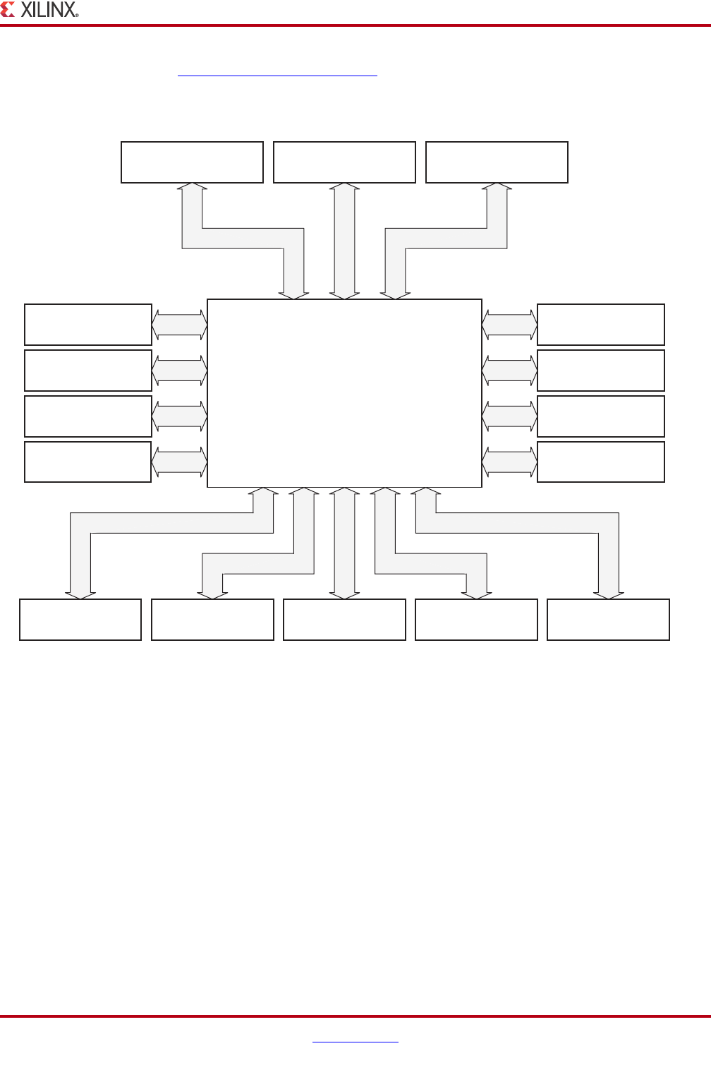
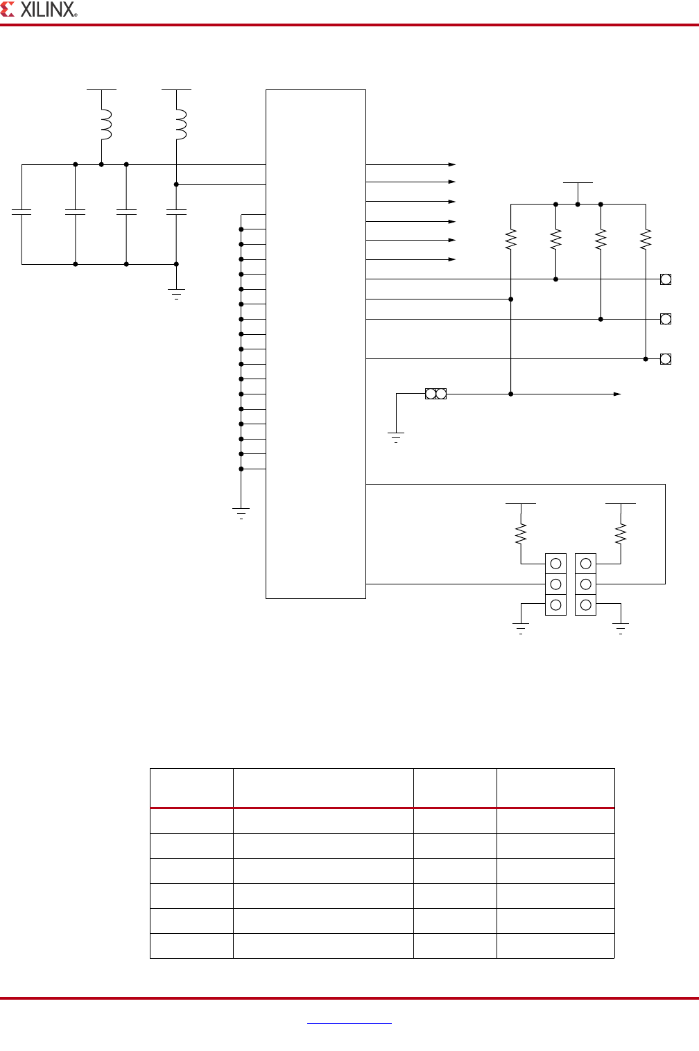
The AC701 board block diagram is shown in Figure 1-1. The AC701 board schematics are
available for download from:
AC701 Evaluation Board www.xilinx.com 7
UG952 (v1.1) January 30, 2013
Feature Descriptions
http://www.xilinx.com/AC701
Caution! The AC701 board can be damaged by electrostatic discharge (ESD). Follow
standard ESD prevention measures when handling the board
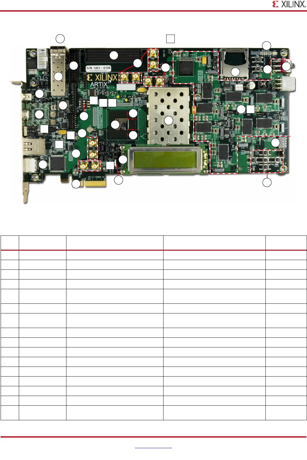
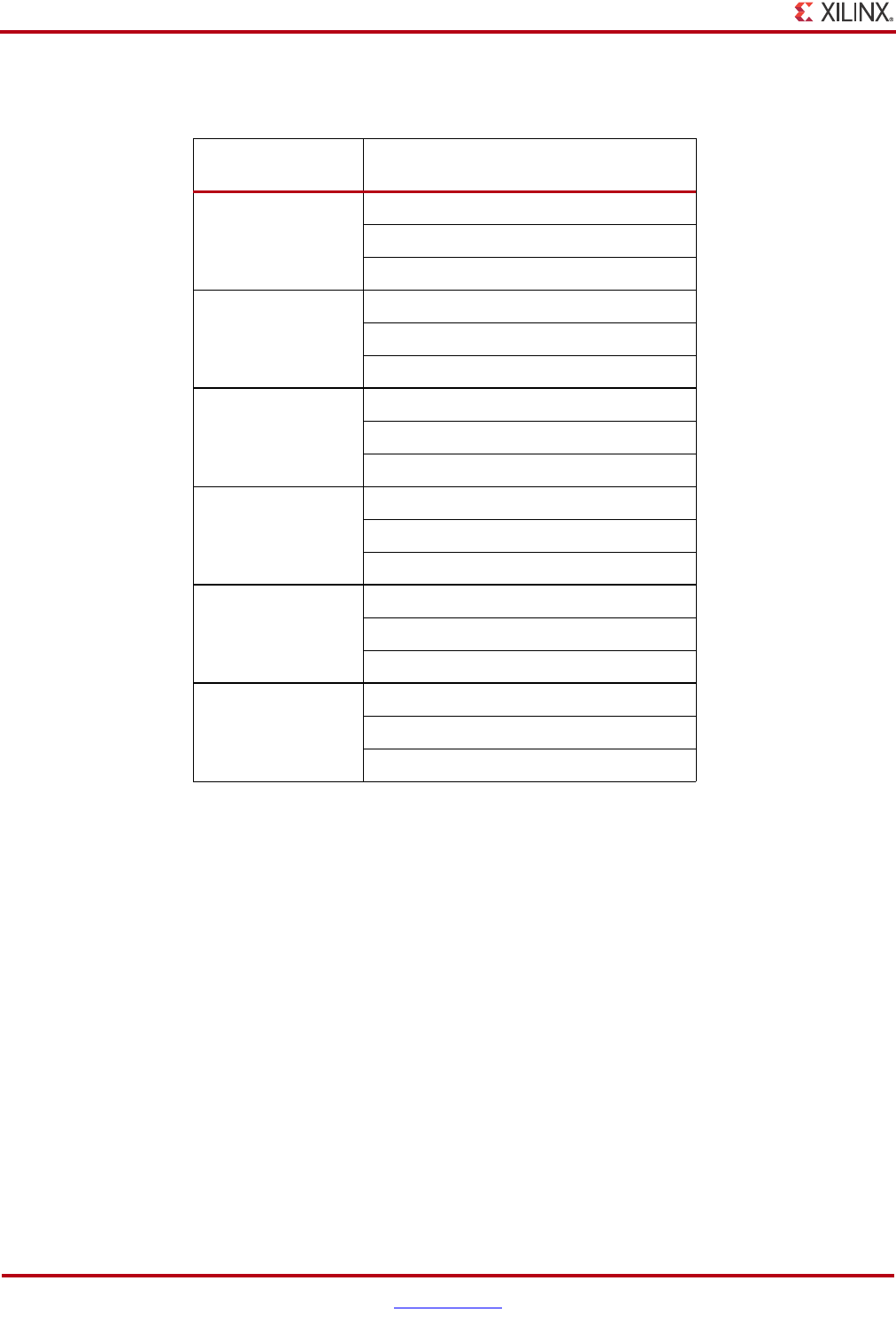
Feature Descriptions
Figure 1-2 shows the AC701 board. Each numbered feature that is referenced in Figure 1-2
is described in the sections that follow.
Note: The image in Figure 1-2 is for reference only and might not reflect the current revision of the
board.
X-Ref Target - Figure 1-1
Figure 1-1: AC701 Board Block Diagram
UG952_c1_01_101512
Artix-7 FPGA
XC7A200T-2FBG676C
128 Mb Quad-SPI
Flash Memory
SD Card
Interface
4-lane PCI Express
Edge Connector
LCD Display
(2 line x 16 characters)
1 KB EEPROM (I2C)
I2C Bus Switch
XADC Header
User Switches,
Buttons, and LEDs
HDMI Video
Interface
Differential Clock
GTP SMA Clock
1 GB DDR3 Memory
(SODIMM)
FMC Connector
(HPC)
10/100/1000 Ethernet
Interface
DIP Switch SW1
Config USB-to-UART Bridge JTAG Interface
micro-B USB Connector SFP+ Single Cage
8www.xilinx.com AC701 Evaluation Board
UG952 (v1.1) January 30, 2013
Chapter 1: AC701 Evaluation Board Features
X-Ref Target - Figure 1-2
Figure 1-2: AC701 Board Components
UG952_c1_02_011513
18
29
30
31
13
5
14
1
67
30
11
11
8
9
32
10
3
16
17
12
15
2
25
00
Square callout references a component
on the back side of the board
Round callout references a component
on the front side of the board
00
4
26
23
21
28
22
24
20
19
27
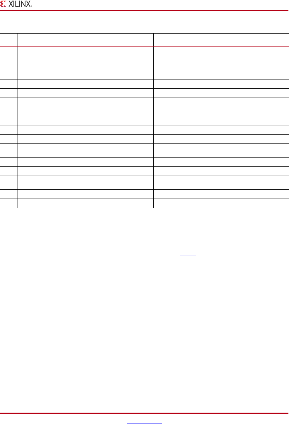
Table 1-1: AC701 Board Component Descriptions
Callout Reference Designator Component Description Notes Schematic 0381502
Page Number
1 U1 Artix-7 FPGA Xilinx XC7A200T-2FBG676C
2 J1 DDR3 SODIMM Socket w/Memory Micron MT8JT12864HZ-1G6G1 10
3 U7 Quad-SPI Flash Memory Micron/Numonyx N25Q256A13ESF40G 4
4 U29 SD Card Interface Connector Molex 67840-8001 14
5 U26 USB-JTAG Module Digilent USB JTAG Module (with micro-B
receptacle)
4
6 U51 System Clock Source (back side of board) SiTime SIT9102AI-243N25E200.0000 3
7 U34 Programmable User Clock Source
10MHz-810MHz (back side of board)
Silicon Labs SI570BAB000544DG (default
156.250MHz)
3
8 J31, J32 SMA User Clock Input Rosenberger 32K10K-400L5 3
9 J25, J26 SMA GTP Ref. Clock Input Rosenberger 32K10K-400L5 3
10 U24 Jitter Attenuated Clock (back side of board) Silicon Labs SI5324-C-GM 16
11 U1 GTP Transceivers Embedded within FPGA U1 30
12 P1 PCI Express Edge Connector 4-lane card edge connector 28
13 P3 SFP/SFP+ Connector Molex 74441-0010 20
14 U12 10/100/1000 Tri-Speed Ethernet PHY Marvell 88E1116RA0-NNC1C000 15
15 U2 GTP Transceiver Clock Generator 125MHz ICS ICS84402IAGI-01LF 3
16 J17, U44 USB-to-UART Bridge (back side of board) and
mini-B receptacle (front side of board)
Silicon Labs CP2103GM 5
AC701 Evaluation Board www.xilinx.com 9
UG952 (v1.1) January 30, 2013
Feature Descriptions
Artix-7 FPGA
[Figure 1-2, callout 1]
The AC701 board is populated with the Artix-7 XC7A200T-2FBG676C FPGA.
For further information on Artix-7 FPGAs, see DS180, 7 Series FPGAs Overview.
FPGA Configuration
The AC701 board supports two of the five 7 Series FPGA configuration modes:
• Master SPI using the on-board Quad SPI Flash memory
• JTAG using a standard-A to micro-B USB cable for connecting the host PC to the
AC701 board configuration port or via J4 Platform Cable USB/Parallel Cable IV flat
cable connector
Each configuration interface corresponds to one or more configuration modes and bus
widths as listed in Table 1-2. The mode switches M2, M1, and M0 are on SW1 positions 1,
2, and 3 respectively as shown in Figure 1-3.
17 P2, U48 HDMI Video Connector and Device Molex 500254-1927, Analog Devices
ADV7511KSTZ-P
19, 18
18 J23 LCD Character Display Connector 2 x 7 0.1 in male pin header 14
19 U52 I2C Bus Switch TI PCA9548ARGER 6
20 DS11 - DS13 Ethernet PHY Status LEDs, Green Lumex SML-LX0603GW 15
21 DS2 - DS5 User GPIO LEDs, Green Lumex SML-LX0603GW 21
22 SW3 – SW7 User Pushbuttons E-Switch E-Switch TL3301EF100QG 21
23 SW2 GPIO DIP Switch, 4-pole C&K SDA04H1SBD 21
24 SW10 User Rotary Switch Panasonic EVQ-WK4001 21
25 J33, J34 SMA User GPIO Rosenberger 32K10K-400L5 3
26 SW15 Power On/Off Slide Switch C&K 1201M2S3AQE2 38
27 SW9 FPGA_PROG_B Pushbutton Switch
(Active-Low)
E-Switch TL3301EF100QG 7
28 SW1 Configuration Mode DIP Switch, 3-pole C&K SDA03H1SBD 7
29 J30 FMC HPC Connector Samtec ASP_134486_01 24-27
30 U8, U9, U49, U53-U60 Power Management (voltage regulators front
side of board, controllers back side of board)
TI UCD90120ARGC controllers in conjunction with
various regulators
39-50
31 J19 XADC Header 2X10 0.1 in. male header 31
32 J44, J45, J46, J47 MGT TX, RX SMA Pairs Rosenberger 32K10K-400L5 3
Table 1-1: AC701 Board Component Descriptions (Cont’d)
Callout Reference Designator Component Description Notes Schematic 0381502
Page Number
10 www.xilinx.com AC701 Evaluation Board
UG952 (v1.1) January 30, 2013
Chapter 1: AC701 Evaluation Board Features
The default mode setting is M[2:0] = 001, which selects Master SPI at board power-on.
Refer to the Configuration Options, page 75 for more information about the mode switch
SW1.
For full details on configuring the FPGA, see UG470, 7 Series FPGAs Configuration User
Guide
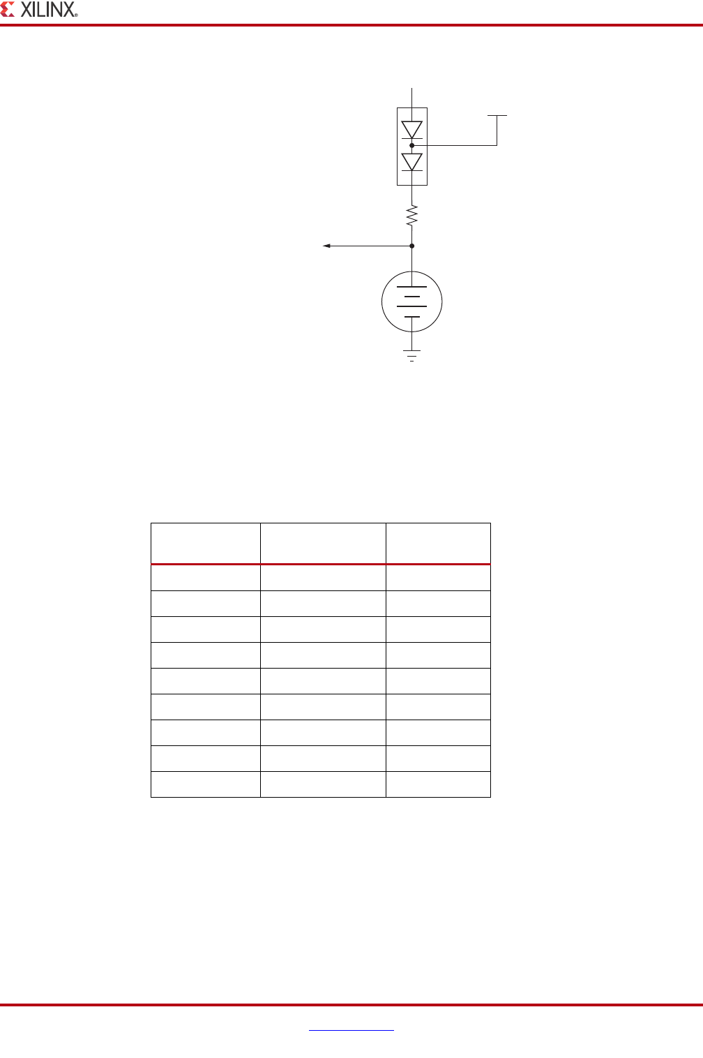
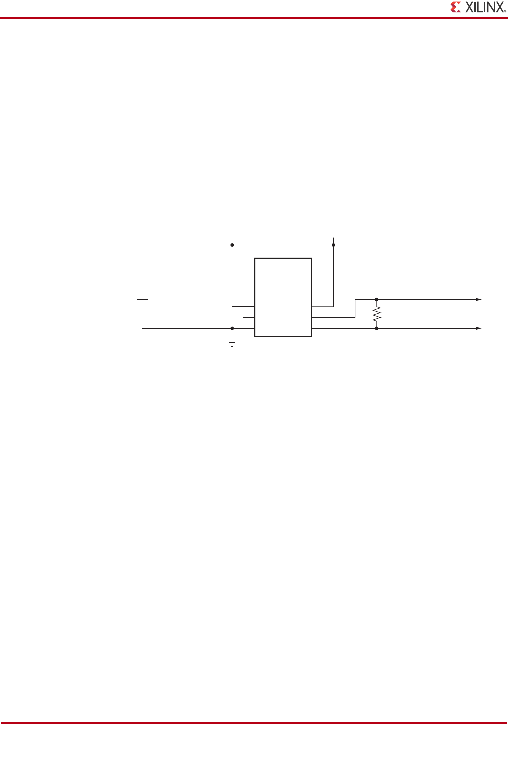
Encryption Key Backup Circuit
FPGA U1 implements bitstream encryption key technology. The AC701 board provides the
encryption key backup battery circuit shown in Figure 1-4. The rechargeable 1.5V lithium
button-type battery B1 is soldered to the board with the positive output connected to
FPGA U1 VCCBATT pin G14. The battery supply current IBATT specification is 150 nA max
when board power is off. B1 is charged from the VCC1V8 1.8V rail through a series diode
with a typical forward voltage drop of 0.38V. and 4.7 KΩ current limit resistor. The nominal
charging voltage is 1.62V.
X-Ref Target - Figure 1-3
Figure 1-3: SW1 Default Settings
Table 1-2: AC701 Board FPGA Configuration Modes
Configuration
Mode
SW1 DIP switch
Settings (M[2:0])
Bus
Width
CCLK
Direction
Master SPI 001 x1, x2, x4 Output
JTAG 101 x1 Not Applicable
R339
1.21K 1%
1/10W
R338
1.21K 1%
1/10W
R337
1.21K 1%
1/10W
FPGA_3V3
SW1
1
2
3
6
5
4
SDA03H1SBD
FPGA_M2
FPGA_M1
FPGA_M0
UG952_c1_03_011713
NC
AC701 Evaluation Board www.xilinx.com 11
UG952 (v1.1) January 30, 2013
Feature Descriptions
I/O Voltage Rails
In addition to Bank 0, there are 8 I/O banks available on the Artix-7 device. The voltages
applied to the FPGA I/O banks used by the AC701 board are listed in Table 1-3.
X-Ref Target - Figure 1-4
Figure 1-4: Encryption Key Backup Circuit
UG952_c1_04_092812
GND
2
2
1
1
B1
1.5V
Seiko
TS518SE_FL35E
2
1
3
BAS40-04
D6
40V
200 mW
NC
FPGA_VBATT
+
VCC1V8 (1.8V)
R83
4.70K 5%
1/10W
Table 1-3: FPGA Bank Voltage Rails
U1 FPGA Bank Power Supply Rail
Net Name Voltage
Bank 0 FPGA_3V3 3.3V
Bank 12 VCCO_VADJ 2.5V
Bank 13 FPGA_1V8 1.8V
Bank 14 FPGA_3V3 3.3V
Bank 15 VCCO_VADJ 2.5V
Bank 16 VCCO_VADJ 2.5V
Bank 33 FPGA_1V5 1.5V
Bank 34 FPGA_1V5 1.5V
Bank 35 FPGA_1V5 1.5V
12 www.xilinx.com AC701 Evaluation Board
UG952 (v1.1) January 30, 2013
Chapter 1: AC701 Evaluation Board Features
DDR3 Memory Module
[Figure 1-2, callout 2]
The memory module at J1 is a 1 GB DDR3 small outline dual-inline memory module
(SODIMM). It provides volatile synchronous dynamic random access memory (SDRAM)
for storing user code and data. The SODIMM socket has a perforated EMI shield
surrounding it as seen in Figure 1-2.
• Part number: MT8JTF12864HZ-1G6G1 (Micron Technology)
• Supply voltage: 1.5V
• Data path width: 64 bits
• Data rate: Up to 1,600 MT/s
The DDR3 interface is implemented across I/O banks 32, 33, and 34. Each bank is a 1.5V
high-performance (HP) bank. An external 0.75V reference VTTREF is provided for data
interface banks 32 and 34. Any interface connected to these banks that requires a reference
voltage must use this FPGA voltage reference. The connections between the DDR 3
memory and the FPGA are listed in Table 1-4.
Table 1-4: DDR3 Memory Connections to the FPGA
U1 FPGA Pin Net Name
J1 DDR3 Memory
Pin Number Pin Name
M4 DDR3_A0 98 A0
J3 DDR3_A1 97 A1
J1 DDR3_A2 96 A2
L4 DDR3_A3 95 A3
K5 DDR3_A4 92 A4
M7 DDR3_A5 91 A5
K1 DDR3_A6 90 A6
M6 DDR3_A7 86 A7
H1 DDR3_A8 89 A8
K3 DDR3_A9 85 A9
N7 DDR3_A10 107 A10/AP
L5 DDR3_A11 84 A11
L7 DDR3_A12 83 A12_BC_N
N6 DDR3_A13 119 A13
L3 DDR3_A14 80 A14
K2 DDR3_A15 78 A15
N1 DDR3_BA0 109 BA0
M1 DDR3_BA1 108 BA1
H2 DDR3_BA2 79 BA2
AB6 DDR3_D0 5 DQ0
AC701 Evaluation Board www.xilinx.com 13
UG952 (v1.1) January 30, 2013
Feature Descriptions
AA8 DDR3_D1 7 DQ1
Y8 DDR3_D2 15 DQ2
AB5 DDR3_D3 17 DQ3
AA5 DDR3_D4 4 DQ4
Y5 DDR3_D5 6 DQ5
Y6 DDR3_D6 16 DQ6
Y7 DDR3_D7 18 DQ7
AF4 DDR3_D8 21 DQ8
AF5 DDR3_D9 23 DQ9
AF3 DDR3_D10 33 DQ10
AE3 DDR3_D11 35 DQ11
AD3 DDR3_D12 22 DQ12
AC3 DDR3_D13 24 DQ13
AB4 DDR3_D14 34 DQ14
AA4 DDR3_D15 36 DQ15
AC2 DDR3_D16 39 DQ16
AB2 DDR3_D17 41 DQ17
AF2 DDR3_D18 51 DQ18
AE2 DDR3_D19 53 DQ19
Y1 DDR3_D20 40 DQ20
Y2 DDR3_D21 42 DQ21
AC1 DDR3_D22 50 DQ22
AB1 DDR3_D23 52 DQ23
Y3 DDR3_D24 57 DQ24
W3 DDR3_D25 59 DQ25
W6 DDR3_D26 67 DQ26
V6 DDR3_D27 69 DQ27
W4 DDR3_D28 56 DQ28
W5 DDR3_D29 58 DQ29
W1 DDR3_D30 68 DQ30
V1 DDR3_D31 70 DQ31
G2 DDR3_D32 129 DQ32
Table 1-4: DDR3 Memory Connections to the FPGA (Cont’d)
U1 FPGA Pin Net Name
J1 DDR3 Memory
Pin Number Pin Name
14 www.xilinx.com AC701 Evaluation Board
UG952 (v1.1) January 30, 2013
Chapter 1: AC701 Evaluation Board Features
D1 DDR3_D33 131 DQ33
E1 DDR3_D34 141 DQ34
E2 DDR3_D35 143 DQ35
F2 DDR3_D36 130 DQ36
A2 DDR3_D37 132 DQ37
A3 DDR3_D38 140 DQ38
C2 DDR3_D39 142 DQ39
C3 DDR3_D40 147 DQ40
D3 DDR3_D41 149 DQ41
A4 DDR3_D42 157 DQ42
B4 DDR3_D43 159 DQ43
C4 DDR3_D44 146 DQ44
D4 DDR3_D45 148 DQ45
D5 DDR3_D46 158 DQ46
E5 DDR3_D47 160 DQ47
F4 DDR3_D48 163 DQ48
G4 DDR3_D49 165 DQ49
K6 DDR3_D50 175 DQ50
K7 DDR3_D51 177 DQ51
K8 DDR3_D52 164 DQ52
L8 DDR3_D53 166 DQ53
J5 DDR3_D54 174 DQ54
J6 DDR3_D55 176 DQ55
G6 DDR3_D56 181 DQ56
H6 DDR3_D57 183 DQ57
F7 DDR3_D58 191 DQ58
F8 DDR3_D59 193 DQ59
G8 DDR3_D60 180 DQ60
H8 DDR3_D61 182 DQ61
D6 DDR3_D62 192 DQ62
E6 DDR3_D63 194 DQ63
AC6 DDR3_DM0 11 DM0
Table 1-4: DDR3 Memory Connections to the FPGA (Cont’d)
U1 FPGA Pin Net Name
J1 DDR3 Memory
Pin Number Pin Name
AC701 Evaluation Board www.xilinx.com 15
UG952 (v1.1) January 30, 2013
Feature Descriptions
AC4 DDR3_DM1 28 DM1
AA3 DDR3_DM2 46 DM2
U7 DDR3_DM3 63 DM3
G1 DDR3_DM4 136 DM4
F3 DDR3_DM5 153 DM5
G5 DDR3_DM6 170 DM6
H9 DDR3_DM7 187 DM7
W8 DDR3_DQS0_N 10 DQS0_N
V8 DDR3_DQS0_P 12 DQS0_P
AE5 DDR3_DQS1_N 27 DQS1_N
AD5 DDR3_DQS1_P 29 DQS1_P
AE1 DDR3_DQS2_N 45 DQS2_N
AD1 DDR3_DQS2_P 47 DQS2_P
V2 DDR3_DQS3_N 62 DQS3_N
V3 DDR3_DQS3_P 64 DQS3_P
B1 DDR3_DQS4_N 135 DQS4_N
C1 DDR3_DQS4_P 137 DQS4_P
A5 DDR3_DQS5_N 152 DQS5_N
B5 DDR3_DQS5_P 154 DQS5_P
H4 DDR3_DQS6_N 169 DQS6_N
J4 DDR3_DQS6_P 171 DQS6_P
G7 DDR3_DQS7_N 186 DQS7_N
H7 DDR3_DQS7_P 188 DQS7_P
R2 DDR3_ODT0 116 ODT0
U2 DDR3_ODT1 120 ODT1
N8 DDR3_RESET_B 30 RESET_B
T3 DDR3_S0_B 114 S0_B
T2 DDR3_S1_B 121 S1_B
U1 DDR3_TEMP_
EVENT 198 EVENT_B
R1 DDR3_WE_B 113 WE_B
T4 DDR3_CAS_B 115 CAS_B
Table 1-4: DDR3 Memory Connections to the FPGA (Cont’d)
U1 FPGA Pin Net Name
J1 DDR3 Memory
Pin Number Pin Name
16 www.xilinx.com AC701 Evaluation Board
UG952 (v1.1) January 30, 2013
Chapter 1: AC701 Evaluation Board Features
The AC701 board DDR3 memory interface adheres to the constraints guidelines
documented in the DDR3 Design Guidelines section of UG586, 7 Series FPGAs Memory
Interface Solutions User Guide. The AC701 board DDR3 memory interface is a 40Ω
impedance implementation. Other memory interface details are available in UG586 and
UG473, 7 Series FPGAs Memory Resources User Guide.
Quad-SPI Flash Memory
[Figure 1-2, callout 3]
The Quad-SPI Flash memory U7 provides 256 Mb of non-volatile storage that can be used
for configuration and data storage.
• Part number: N25Q256A13ESF40G (Numonyx)
• Supply voltage: 3.3V
• Data path width: 4 bits
• Data rate: Various depending on Single/Dual/Quad mode and CCLK rate
Four data lines and the FPGA's CCLK pin are wired to the Quad-SPI Flash memory. The
connections between the SPI Flash memory and the FPGA are listed in Table 1-5.
The configuration section of UG470, 7 Series FPGAs Configuration User Guide provides details
on using the Quad-SPI Flash memory. Figure 1-5 shows the connections of the Quad-SPI
P1 DDR3_RAS_B 110 RAS_B
P4 DDR3_CKE0 73 CKE0
N4 DDR3_CKE1 74 CKE1
L2 DDR3_CLK0_N 103 CK0_N
M2 DDR3_CLK0_P 101 CK0_P
N2 DDR3_CLK1_N 104 CK1_N
N3 DDR3_CLK1_P 102 CK1_P
Table 1-4: DDR3 Memory Connections to the FPGA (Cont’d)
U1 FPGA Pin Net Name
J1 DDR3 Memory
Pin Number Pin Name
Table 1-5: Quad-SPI Flash Memory Connections to the FPGA
U1 FPGA Pin Net Name
U7 Quad-SPI Flash Memory
Pin Number Pin Name
R14 FLASH_D0 15 DQ0
R15 FLASH_D1 8 DQ1
P14 FLASH_D2 9 DQ2
N14 FLASH_D3 1 DQ3
H13 FPGA_CCLK 16 C
P18 QSPI_IC_CS_B 7 S_B
AC701 Evaluation Board www.xilinx.com 17
UG952 (v1.1) January 30, 2013
Feature Descriptions
Flash memory on the AC701 board. For more details, see the Numonyx
N25Q256A13ESF40G data sheet http://www.micron.com.
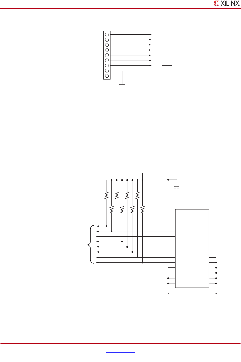
SPI External Programming Header
In addition to the QSPI device FPGA U1 connections shown in Table 1-5, the FPGA U1 SPI
interface is connected to an external programming header J7.
Table 1-6 shows the SPI J7 connections to FPGA U1.
Figure 1-6 shows the J7 SPI external programming connector.
X-Ref Target - Figure 1-5
Figure 1-5: 256 Mb Quad-SPI Flash memory
UG952_c1_05_101812
VCC3V3
N25Q256
256 Mb Serial
Flash Memory
GND
1
2
3
5
7
6
U7
4
8
VCC3V3
C18
0.1μF 25V
X5R
FLASH_D2
DQ1
16
15
14
12
10
11
13
9
SB
NC3
NC2
NC1
NC0
VCC
HOLD_B/DQ3
WB/VPP/DQ2
VSS
NC4
NC5
NC6
NC7
DQ0
C
R17
DNP
R18
4.7kΩ 5%
R431
15Ω 1%
R432
15Ω 1%
FLASH_D0
FPGA_CCLK
FLASH_D2_R
FLASH_D0_R
GND
VCC3V3
R20
DNP
R19
4.7kΩ 5%
R21
4.7kΩ 5%
R430
15Ω 1%
R429
15Ω 1%
FLASH_D2_R
FLASH_D3_R
FLASH_D3
FLASH_D1
QSPI_IC_CS_B
Table 1-6: SPI J7 Connections to the FPGA
U1 FPGA Pin Schematic Net
Name J7 Pin
AE16 FPGA_PROG_B 1
N14 FLASH_D3 2
P14 FLASH_D2 3
J3.2 QSPI_CS_B 4
R14 FLASH_D0 5
R15 FLASH_D1 6
H13 FPGA_CCLK 7
NA GND 8
NA VCC3V3 9
18 www.xilinx.com AC701 Evaluation Board
UG952 (v1.1) January 30, 2013
Chapter 1: AC701 Evaluation Board Features
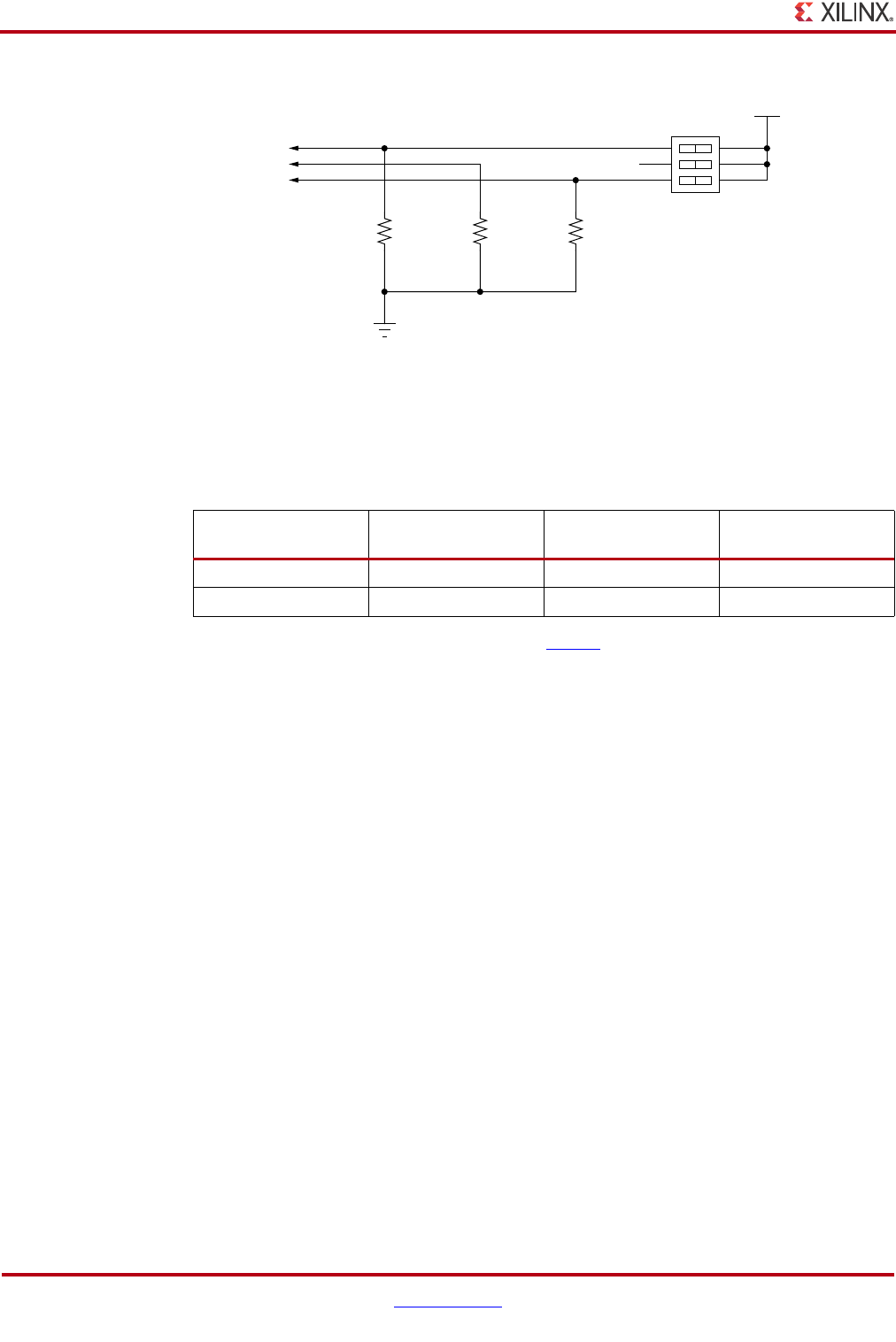
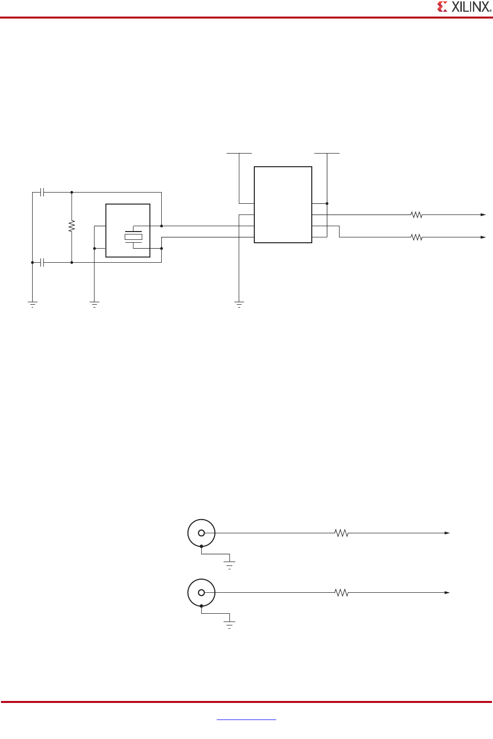
SD Card Interface
[Figure 1-2, callout 4]
The AC701 board includes a secure digital input/output (SDIO) interface to provide
user-logic access to general purpose non-volatile SDIO memory cards and peripherals. The
SD card slot is designed to support 50 MHz high speed SD cards.
The SDIO signals are connected to I/O bank 14 which has its VCCO set to 3.3V. Figure 1-7
shows the connections of the SD card interface on the AC701 board.
Table 1-7 lists the SD card interface connections to the FPGA.
X-Ref Target - Figure 1-6
Figure 1-6: SPI J7 External Programming Connector
UG952_c1_06_092812
VCC3V3
GND
2
3
4
6
8
7
5
9
FLASH_D3
FLASH_D2
QSPI_CS_B
FLASH_D0
FLASH_D1
FPGA_CCLK
1FPGA_PROG_B
J7
HDR
1X9
X-Ref Target - Figure 1-7
Figure 1-7: SD Card Interface
UG952_c1_07_100212
SDIO Card
Connector
U29
DETECT
DAT2
DAT1
DAT0
CLK
CMD
CD_DAT3
VDD
PROTECT
GNDTAB2VSS1
GNDTAB1
VSS2
GND
GND
SDIO_SDWP 11
SDIO_SDDET 10
SDIO_DAT2 9
SDIO_DAT1 8
SDIO_DAT0 7
SDIO_CLK 5
SDIO_CMD
1SDIO_CD_DAT3
VCC3V3
C52
0.1μF 25V
X5R
GND
4
6
3
D_P
12
GNDTAB3
GNDTAB4
IOGND1
IOGND2
15
16
17
18
13
14
51.1K 1% Eight Places
VCC3V3
R319
R325
R324
R318
R322
R323
R317
R321
2
To FPGA
Bank 14
(U1)
AC701 Evaluation Board www.xilinx.com 19
UG952 (v1.1) January 30, 2013
Feature Descriptions
Table 1-7: SDIO Connections to the FPGA
U1 FPGA Pin
Name Schematic Net Name
U29 SDIO Connector
Pin Number Pin Name
R20 SDIO_SDWP 11 SDWP
P24 SDIO_SDDET 10 SDDET
N23 SDIO_CMD 2 CMD
N24 SDIO_CLK 5 CLK
P23 SDIO_DAT2 9 DAT2
N19 SDIO_DAT1 8 DAT1
P19 SDIO_DAT0 7 DAT0
P21 SDIO_CD_DAT3 1 CD_DAT3
20 www.xilinx.com AC701 Evaluation Board
UG952 (v1.1) January 30, 2013
Chapter 1: AC701 Evaluation Board Features
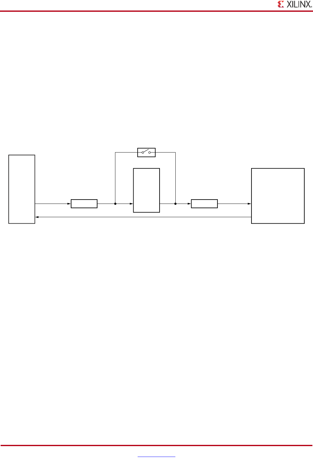
USB JTAG Module
[Figure 1-2, callout 5]
JTAG configuration is provided through a Digilent onboard USB-to-JTAG configuration
logic module (U26) where a host computer accesses the AC701 board JTAG chain through
a standard-A plug (host side) to micro-B plug (AC701 board side) USB cable.
A 2-mm JTAG header (J4) is also provided in parallel for access by Xilinx download cables
such as the Platform Cable USB II and the Parallel Cable IV.
The JTAG chain of the AC701 board is illustrated in Figure 1-8. JTAG configuration is
allowed at any time regardless of FPGA mode pin settings. JTAG initiated configuration
takes priority over the configuration method selected through the FPGA mode pin settings
at SW1.
When an FMC daughter card is attached to the AC701 board it is automatically added to
the JTAG chain through electronically controlled single-pole single-throw (SPST) switches
U27. The SPST switch is in a normally closed state and transitions to an open state when an
FMC daughter card is attached. Switch U27 adds an attached FMC HPC daughter card to
the FPGAs JTAG chain as determined by the FMC_HPC_PRSNT_M2C_B signal. The
attached FMC card must implement a TDI-to-TDO connection via a device or bypass
jumper in order for the JTAG chain to be completed to the FPGA U1.
The JTAG connectivity on the AC701 board allows a host computer to download
bitstreams to the FPGA using the Xilinx iMPACT software. In addition, the JTAG connector
allows debug tools such as the ChipScope™ Pro Analyzer or a software debugger to access
the FPGA. The iMPACT software tool can also indirectly program the Quad-SPI Flash
memory. To accomplish this, the iMPACT software configures the FPGA with a temporary
design to access and program the Quad-SPI Flash memory device. The JTAG circuit is
shown in Figure 1-9.
X-Ref Target - Figure 1-8
Figure 1-8: JTAG Chain Block Diagram
UG952_c1_08_012913
Part of U19
BUFFER
USB
Module
(U26)
or
JTAG
Connector
(J4)
TDO
TDI
U1
FPGA
TDI
TDO
FMC HPC
Connector
TDI TDO
J30
N.C.
SPST Bus Switch
U27
Part of U19
BUFFER
AC701 Evaluation Board www.xilinx.com 21
UG952 (v1.1) January 30, 2013
Feature Descriptions
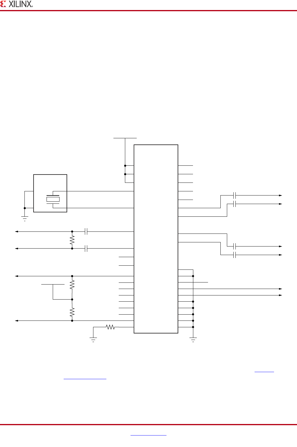
Clock Generation
There are three clock sources available for the FPGA fabric on the AC701 board (refer to
Table 1-8).
X-Ref Target - Figure 1-9
Figure 1-9: JTAG Circuit
UG952_c1_09_101512
JTAG_TDI
FMC_TDI_BUF
FPGA_TDO
FPGA_TMS_BUF
FPGA_TCK_BUF
FPGA_TDI_BUF
FMC1_TDO_FPGA_TDI
FMC1_HPC_TMS_BUF
FMC1_HPC_PRSNT_M2C_B
JTAG_TMS
JTAG_TCK
JTAG_TDO
FMC1_HPC_TCK_BUF
FMC1 HPC
Connector
TDI
TDO
J30
TMS
TCK
PRSNT_L
VCC3V3
Artix-7
FPGA
TDI
N16
TDO
U1
TMS
TCK
Digilent
USB-JTAG
Module
TMS
TDI
SN74LV541A
Buffer
U19
R95 15Ω
U26
R96 15Ω
R94 15Ω
TCK
TDO
TMS
TDI
J4
TCK
TDO
JTAG
Header
VCC3V3
VCC3V3
U27
Bank 0
Bank 14
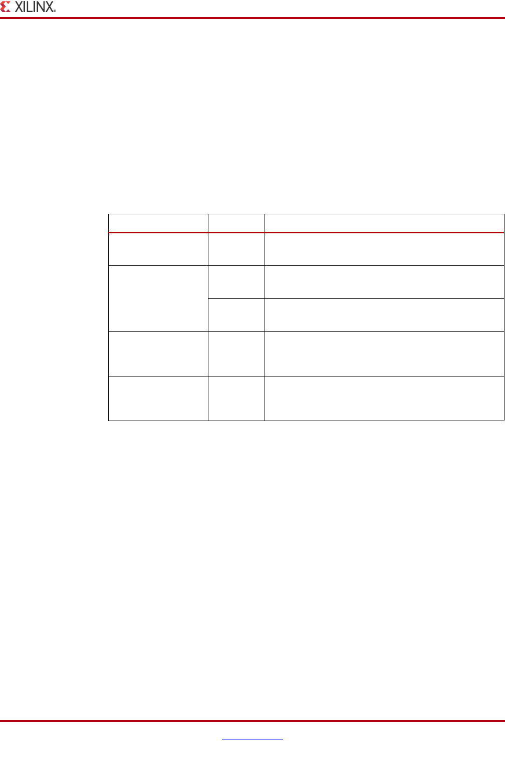
Table 1-8: AC701 Board Clock Sources
Clock Name Reference Description
System Clock U51 SiT9102 2.5V LVDS 200 MHz Fixed Frequency
Oscillator (Si Time). See System Clock Source, page 22.
User Clock
U34
Si570 3.3V LVDS I2C Programmable Oscillator
(Silicon Labs). Default power-on frequency 156.250
MHz. See Programmable User Clock Source, page 23.
User SMA Clock
(differential pair)
J31 USER_SMA_CLOCK_P (net name).
See User SMA Clock Input, page 24.
J32 USER_SMA_CLOCK_N (net name)
See User SMA Clock Input, page 24
22 www.xilinx.com AC701 Evaluation Board
UG952 (v1.1) January 30, 2013
Chapter 1: AC701 Evaluation Board Features
System Clock Source
[Figure 1-2, callout 6]
The AC701 board has a 2.5V LVDS differential 200 MHz oscillator (U51) soldered onto the
back side of the board and wired to an FPGA MRCC clock input on bank 34. This 200 MHz
signal pair is named SYSCLK_P and SYSCLK_N, which are connected to FPGA U1 pins R3
and P3 respectively.
• Oscillator: Si Time SiT9102AI-243N25E200.00000 (200 MHz)
• PPM frequency jitter: 50 ppm
• Differential Output
For more details, see the Si Time SiT9102 data sheet http://www.sitime.com. The system
clock circuit is shown in Figure 1-10.
X-Ref Target - Figure 1-10
Figure 1-10: System Clock Source
UG952_c1_10_100212
GND
VCC2V5
SIT9102
200 MHz
Oscillator
OE
NC
GND
VCC
OUT_B
OUT
1
2
3
6
5
4
U51
R166
100Ω 1% SYSCLK_P
SYSCLK_N
C30
0.1 μF 10V
X5R
AC701 Evaluation Board www.xilinx.com 23
UG952 (v1.1) January 30, 2013
Feature Descriptions
Programmable User Clock Source
[Figure 1-2, callout 7]
The AC701 board has a programmable low-jitter 3.3V differential oscillator (U34) driving
the FPGA MRCC inputs of bank 14. This USER_CLOCK_P and USER_CLOCK_N clock
signal pair are connected to FPGA U1 pins M21 and M22 respectively. On power-up the
user clock defaults to an output frequency of 156.250 MHz. User applications can change
the output frequency within the range of 10 MHz to 810 MHz through an I2C interface.
Power cycling the AC701 board will revert the user clock to its default frequency of
156.250 MHz.
• Programmable Oscillator: Silicon Labs Si570BAB000544DG (10 MHz - 810 MHz)
• Differential Output
The user clock circuit is shown in Figure 1-11.
References
The Silicon Labs Si570 data sheet is available from http://www.silabs.com.
X-Ref Target - Figure 1-11
Figure 1-11: User Clock Source
UG952_c1_11_101512
GND
VCC3V3
Si570
Programmable
Oscillator
NC
OE
GND
SCL
SDA
VDD
1
2
3
8
7
6
U34
R15
4.7KΩ 5%
USER CLOCK N
C192
0.01 μF 25V
X7R
CLK- 4
5
GND
VCC3V3
CLK+ USER CLOCK P
USER CLOCK SDA
USER CLOCK SCL 10 MHz - 810 MHz
To I2C
Bus Switch
(U49)
24 www.xilinx.com AC701 Evaluation Board
UG952 (v1.1) January 30, 2013
Chapter 1: AC701 Evaluation Board Features
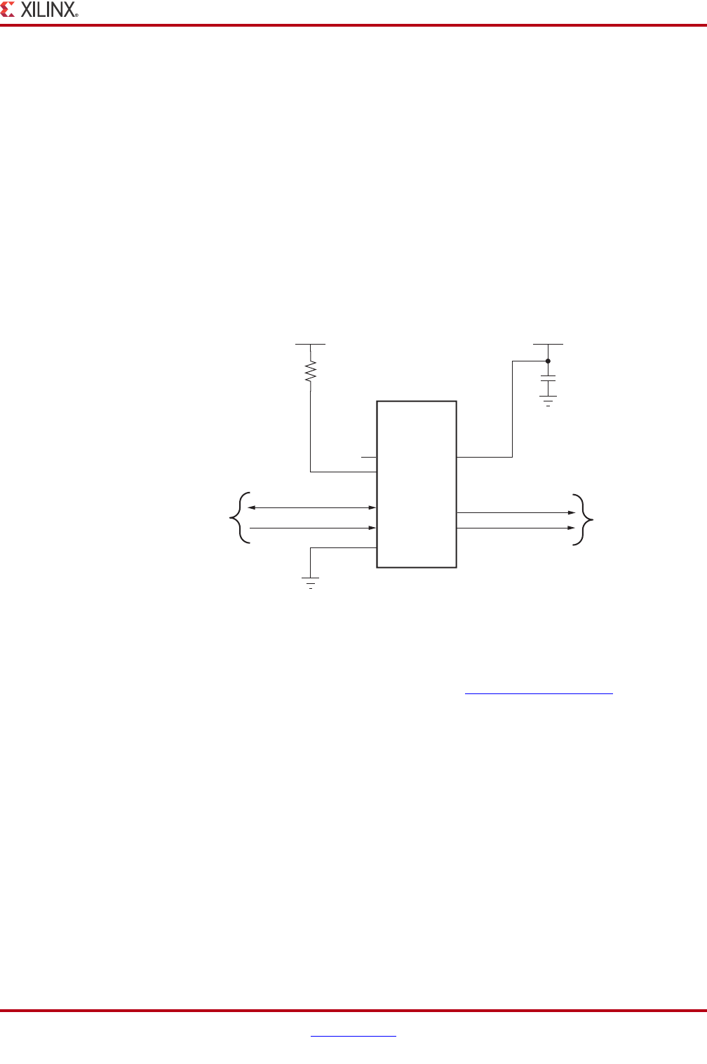
User SMA Clock Input
[Figure 1-2, callout 8]
An external high-precision clock signal can be provided to the FPGA bank 15 by
connecting differential clock signals through the onboard 50Ω SMA connectors J31 (P) and
J32 (N). The differential clock signal names are USER_SMA_CLOCK_P and
USER_SMA_CLOCK_N, which are connected to FPGA U1 pins J23 and H23 respectively.
The user-provided differential clock circuit is shown in Figure 1-12.
Note: This user clock is input to FPGA bank 15 which is powered by VCCO_VADJ. The
VCCO_VADJ rail is typically 2.5V but may be reprogrammed to be either 1.8V or 3.3V. The
USER_SMA_CLOCK_P/N signals should not exceed the VCCO_VADJ voltage (1.8V, 2.5V or 3.3V)
in use.
X-Ref Target - Figure 1-12
Figure 1-12: User SMA Clock Source
USER_SMA_CLOCK_P
J32
USER_SMA_CLOCK_N
GND
J31
GND
UG952_c1_12_100212
SMA
Connector
SMA
Connector
AC701 Evaluation Board www.xilinx.com 25
UG952 (v1.1) January 30, 2013
Feature Descriptions
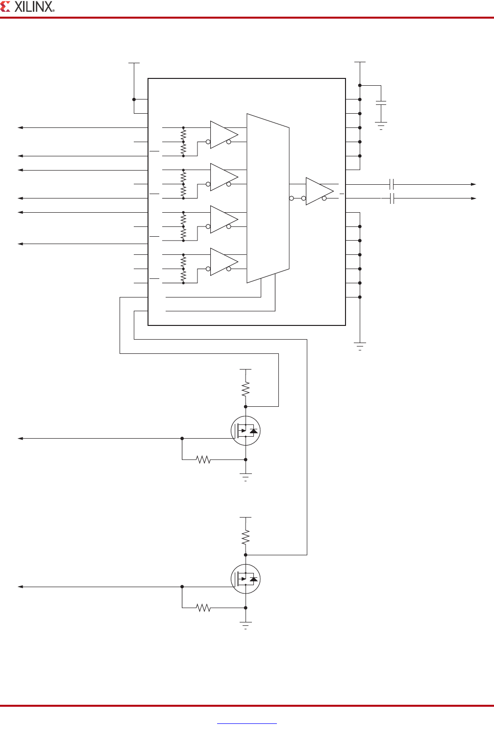
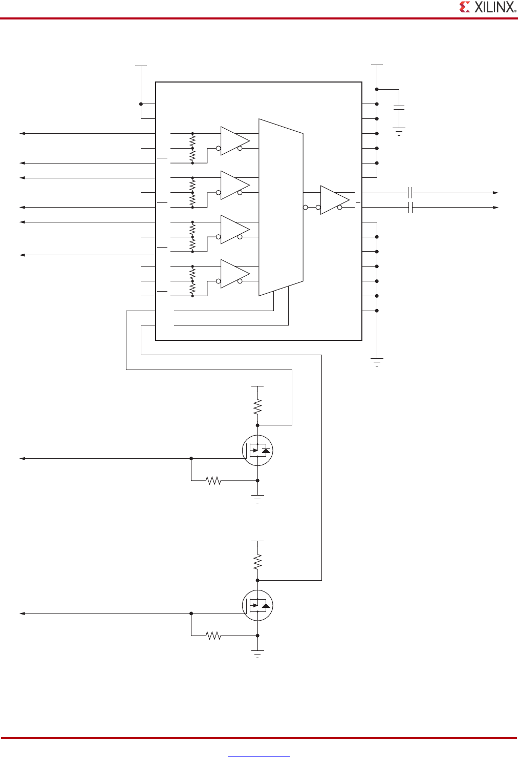
GTP Clock MUX
The AC701 board FPGA U1 MGT Bank 213 has two clock inputs, MGTREFCLK0 and
MGTREFCLK1. Each clock input is driven by a capacitively-coupled clock sourced from a
SY9544UMG 4-to-1 MUX.
Each MUX has a clock source at three of its four inputs, the fourth input is not connected.
Clock MUX U3 SY89544UMG drives Bank 213 MGTREFCLK0 pins AA13 (P) and AB13
(N), and clock MUX U4 SY89544UMG drives Bank 213 MGTREFCLK1 pins AA11 (P) and
AB11 (N). See Table 1-10 for clock MUX U3 connections, and Table 1-11 for clock MUX U4
connections.
Table 1-9 lists the MGT sources for U3 and U4.
Table 1-9: MGT Clock MUX U3 and U4 Clock Sources
Clock Name Reference Description
125 MHz Clock
Generator U2 ICS844021 Crystal-to-LVDS Clock Generator (ICS).
See 125 MHz Clock Generator, page 26.
GTP SMA REF Clock
(differential pair)
J25 SMA_MGT_REFCLK_P (net name).
See GTP SMA Clock Input, page 26.
J26 SMA_MGT_REFCLK_N (net name).
See GTP SMA Clock Input, page 26.
Jitter Attenuated
Clock U24
Si5324C LVDS precision clock multiplier/jitter
attenuator (Silicon Labs).
See Jitter Attenuated Clock, page 27.
FMC HPC GBT
Clocks J30
FMC_HPC_GBTCLK0_M2C_C_P/N (net name) (U3),
FMC_HPC_GBTCLK1_M2C_C_P/N (net name) (U4).
See FMC HPC GBT Clocks, page 28.
26 www.xilinx.com AC701 Evaluation Board
UG952 (v1.1) January 30, 2013
Chapter 1: AC701 Evaluation Board Features
125 MHz Clock Generator
[Figure 1-2, callout 15]
Clock MUX U3 input 0 (pin4 P, pin 2 N) is driven by U2 ICS84402I Crystal-to-LVDS clock
generator. This device uses 25 MHz crystal X3 as its base input frequency and, via an
internal VCO, multiplies this by five to produce a 0.45 ps (typical) RMS phase jitter,
125 MHz LVDS output. The circuit for the 125 MHz clock is shown in Figure 1-13.
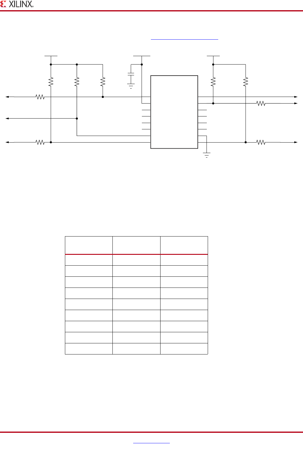
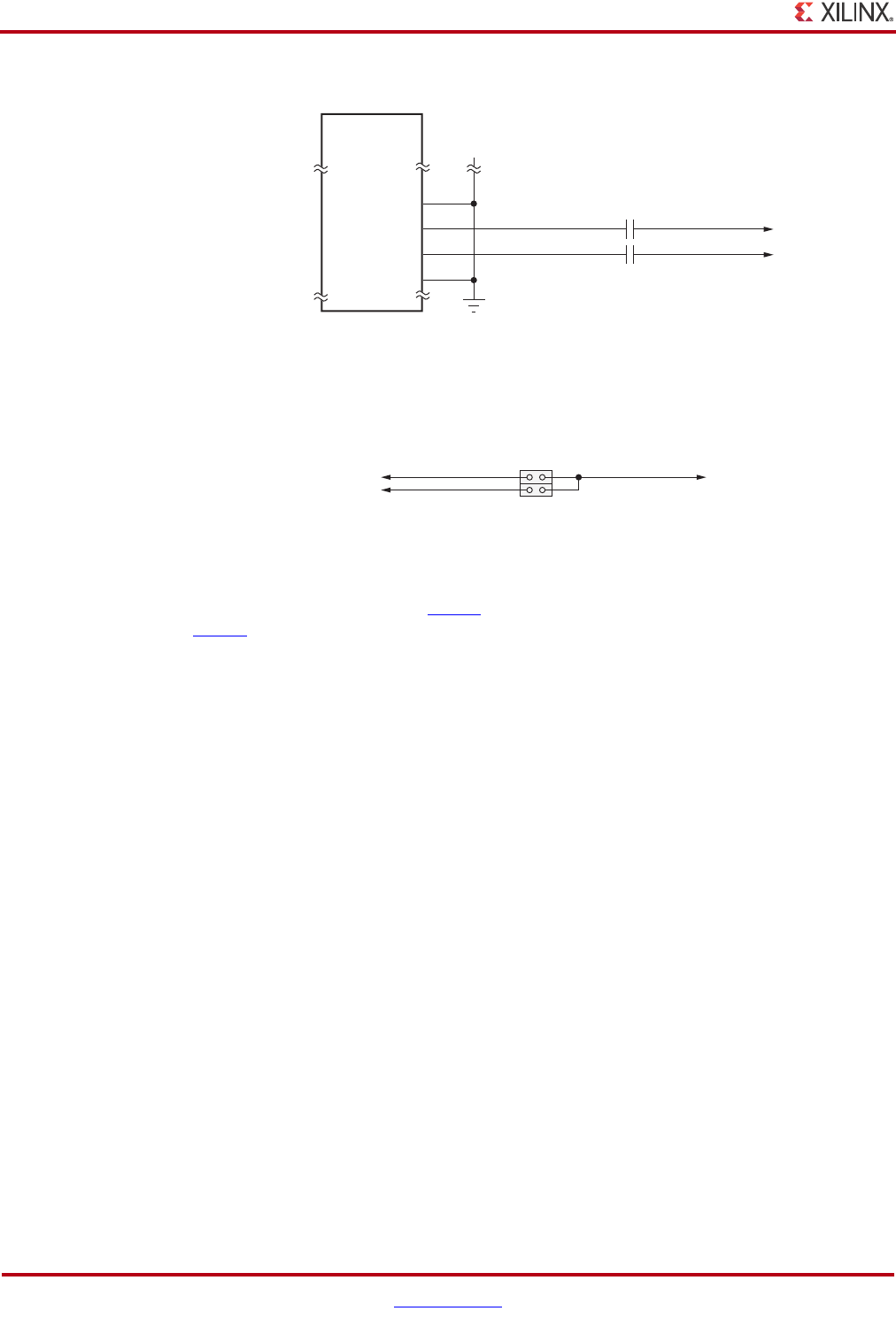
GTP SMA Clock Input
[Figure 1-2, callout 9]
The AC701 board includes a pair of SMA connectors for a GTP clock that are wired to GTP
quad bank 213 via clock MUX U4. This differential clock has signal names
SMA_MGT_REFCLK_P and SMA_REFCLK_N, which are connected to MGT clock MUX
U4 input 0 pins 4 and 2 respectively. The clock MUX output pins 10 (P-side) and 11 (N-side)
are capacitively coupled to FPGA U1 GTP quad 213 MGTREFCLK1 pin AA11 and AB11
respectively. Figure 1-14 shows this direct-coupled SMA clock input circuit.
• External user-provided GTP reference clock on SMA input connectors
• Differential Input
X-Ref Target - Figure 1-13
Figure 1-13: AC701 Board 125 MHz U3 MUX Input0 Source Circuit
GND_EPHYCLK GND_EPHYCLKGND_EPHYCLK
R320
1.0M 5%
R487
0Ω 5%
R486
0Ω 5%
C300
18pF 50V
NPO
C301
18pF 50V
NPO
EPHYCLK_XTAL_OUT
GND2
GND1
X2
X1
X3
25.00 MHz
50 ppm
EPHYCLK_XTAL_IN
21
3
4
VDD
Q0
NQ0
OE
XTAL_OUT
XTAL_IN
GND
VDDA 8
7
6
5
3
4
2
1
U2
VDDA_EPHYCLK
EPHYCLK_Q0_C_N EPHYCLK_Q0_N
EPHYCLK_Q0_C_P EPHYCLK_Q0_P
ICS844021I
VDD_EPHYCLK
UG952_c1_13_101512
X-Ref Target - Figure 1-14
Figure 1-14: GTP SMA Clock Source
UG952_c1_14_101512
SMA_MGT_REFCLK_PSMA_MGT_REFCLK_C_P
SMA
Connector
J25
GND
R485
0Ω 5%
0Ω 5%
SMA_MGT_REFCLK_NSMA_MGT_REFCLK_C_N
SMA
Connector
J26
GND
R484
AC701 Evaluation Board www.xilinx.com 27
UG952 (v1.1) January 30, 2013
Feature Descriptions
Jitter Attenuated Clock
[Figure 1-2, callout 10]
The AC701 board includes a Silicon Labs Si5324 jitter attenuator U24 on the back side of the
board. FPGA user logic can implement a clock recovery circuit and then output this clock
to a differential I/O pair on I/O bank 16 (REC_CLOCK_C_P, FPGA U1 pin D23 and
REC_CLOCK_C_N, FPGA U1 pin D24) for jitter attenuation. Duplicate capacitively
coupled jitter attenuated clocks are routed to a pair of MGT clock MUXes U3 and U4. See
Table 1-9, page 25.
The primary purpose of this clock is to support CPRI/OBSAI applications that perform
clock recovery from a user-supplied SFP/SFP+ module and use the jitter attenuated
recovered clock to drive the reference clock inputs of a GTP transceiver. The jitter
attenuated clock circuit is shown in Figure 1-15.
See the Silicon Labs Si5324 datasheet for more information on this device http://
www.silabs.com. The SI5324 U24 connections to FPGA U1 are shown in Table 1-9.
X-Ref Target - Figure 1-15
Figure 1-15: Jitter Attenuated Clock
UG952_c1_15_011813
R424
4.7KΩ 5%
SI5324_VCC
SI5324_VCC
Si5324C-C-GM
Clock Multiplier/
Jitter Attenuator
VDDA
GND
XB
XA
NC5
32
65
29
28
U24
CKOUT1_N
7
8
CKOUT1_P
C31
0.1μF 25V
X5R
C32
0.1μF 25V
X5R
SI5324_XTAL_XA
GND2
GND1
XB
XA
X6
114.285 MHz
20 ppm
SI5324_OUT0_C_N
SI5324_OUT0_C_P
C9
0.1μF 25V
X5R
C10
0.1μF 25V
X5R
SI5324_OUT1_C_P
SI5324_OUT1_C_N
SI5324_OUT_N
SI5324_OUT_N
SI5324_OUT_P
SI5324_OUT_P
SI5324_XTAL_XB
GND
NC4
21
3
4
C33
0.1μF 25V
X5R
C34
0.1μF 25V
X5R
REC_CLOCK_P
REC_CLOCK_N
REC_CLOCK_C_P
REC_CLOCK_C_N
16
17
R167
100Ω
R4
4.7K
R292
4.7K
CKIN1_P
CKIN1_N
NC
NC
12
13
CKIN2_P
CKIN2_N
10
5
VDDA
VDDA
2
NC3
2
NC2
2
NC1 NC
NC
NC
NC
NC
35
34
CKOUT2_N
CKOUT2_P
SI5324_INT_ALM_B 3
NC 4
NC 11
NC 15
NC 18
NC 19
NC 20
SI5326_RST_B 1
21 31
GND2
9
GND1
31
A2_SS
31
A1
24
A0
22 SI5324_SCL
SCL
23SI5324_SDA
SDA_SDO
27 NC
SDI
36
CMODE
GND
INC
DEC
LOL
RATE1
RATE0
C2B
INT_C1B
CS_CA
RST_B
37
GNDPAD
28 www.xilinx.com AC701 Evaluation Board
UG952 (v1.1) January 30, 2013
Chapter 1: AC701 Evaluation Board Features
FMC HPC GBT Clocks
The FMC HPC connector J30 sources two MGT clocks, FMC1_HPC_GBTCLK0_M2C_P/N
from connector section D, and FMC1_HPC_GBTCLK1_M2C_P/N from connector
section B. Table 1-10 and Table 1-11 list the MGT clock MUX U3 and U4 connections.
The MUX U3 clock input channel select nets are SFP_MGT_CLK_SEL[1:0].
SFP_MGT_CLK_SEL1 is wired to FPGA U1 pin C24 and SFP_MGT_CLK_SEL0 is wired to
FPGA U1 pin B26 on FPGA U1 Bank 16.
The MUX U4 clock input channel select nets are PCIE_MGT_CLK_SEL[1:0].
PCIE_MGT_CLK_SEL1 is wired to FPGA U1 pin C26 and PCIE_MGT_CLK_SEL0 is wired
to FPGA U1 pin A24 on FPGA U1 Bank 16.
The U3 MUX circuit is shown in Figure 1-16. The U4 MUX circuit is shown in Figure 1-17.
Table 1-10: MUX U3 SY89544UMG MGT Clock Inputs
Clock Source
Schematic Net Name
SY89544UMG U3
Schematic Net Name
FPGA U1 Bank 213
Device Ref
Des Pin Input Pin Output Pin Pin Pin Name
ICS84402I U2
7EPHYCLK_Q0_P
IN0
4
Qout_P 10
Qout_N 11
SFP_MGT_CLK0_P(1)
SFP_MGT_CLK0_N(1) AA13
AB13
MGTREFCLK0P
MGTREFCLK0N
6EPHYCLK_Q0_N 2
SI5324-C-GM U24
29 SI5324_OUT0_C_N
IN1
32
28 SI5324_OUT0_C_P 30
FMC HPC J30
D4 FMC1_HPC_
GBTCLK0_M2C_P
IN2
27
D5 FMC1_HPC_
GBTCLK0_M2C_N 25
Notes:
1. U3 output clock nets SFP_MGT_CLK0_P/N contain a series 0.1uF capacitor.
Table 1-11: MUX U4 SY89544UMG MGT Clock Inputs
Clock Source
Schematic Net Name
SY89544UMG U4 Schematic Net Name FPGA U1 Bank 213
Device Ref
Des Pin Input Pin Output Pin Pin Pin Name
SMA J25 1 SMA_MGT_REFCLK_P
IN0
4
Qout_P 10
Qout_N 11
SFP_MGT_CLK1_P(1)
SFP_MGT_CLK1_N(1) AA11
AB11
MGTREFCLK1P
MGTREFCLK1N
SMA J26 1 SMA_MGT_REFCLK_N 2
SI5324-C-GM U24
35 SI5324_OUT1_C_P
IN1
32
34 SI5324_OUT1_C_N 30
FMC HPC J30
B20 FMC1_HPC_
GBTCLK1_M2C_P
IN2
27
B21 FMC1_HPC_
GBTCLK1_M2C_N 25
Notes:
1. U4 output clock nets SFP_MGT_CLK1_P/N contain a series 0.1uF capacitor.
AC701 Evaluation Board www.xilinx.com 29
UG952 (v1.1) January 30, 2013
Feature Descriptions
X-Ref Target - Figure 1-16
Figure 1-16: MGT Clock MUX U3 Circuit
Q24
NDS336P
460 mW
SFP_MGT_CLK_SEL0
MGT_CLK0_SEL0
MGT_CLK0_SEL1
SFP_MGT_CLK0_P
SFP_MGT_CLK0_P
0
VCC1
VCC2
FMC1_HBC_GBTCLK0_M2C_C_P
IN0
Q
VCC8
VCC7
VCC6
VCC5
VCC4
VCC3
Q
GND1
GND2
GND3
GND4
GND5
GND6
PWRPAD
VT0
IN0
IN1
NC
NC
NC
NC
NC
NC
VT1
IN1
IN2
VT2
IN2
IN3
VT3
IN3
SEL0
SEL1
1
2
3
S0 S1
U3
SY89544UMG
50
50
50
50
50
50
50
50
VCC2V5 VCC2V5
FMC1_HBC_GBTCLK0_M2C_C_N
EPHYCLK_Q0_P
EPHYCLK_Q0_N
SI5324_OUT0_C_P
SI5324_OUT0_C_N
18
17
20
24
28
29
10
11
7
9
12
13
16
18
33
5
4
3
2
32
31
30
27
26
25
23
22
21
6
19
GND
GND
VCC2V5
Q25
NDS336P
460 mW
SFP_MGT_CLK_SEL1
GND
VCC2V5
R332
10K
1/10W
1%
R333
10K
1/10W
1%
R455
10K
1/10W
1%
R454
10K
1/10W
1%
C105
0.1μF
25V
X5R
C320
0.1μF
25V
X5R
C318
0.1μF
25V
X5R
GND
UG952_c1_16_101612
TO MGT BANK 213
MGTREFCLK0_P/N
PINS AA13, AB13
30 www.xilinx.com AC701 Evaluation Board
UG952 (v1.1) January 30, 2013
Chapter 1: AC701 Evaluation Board Features
X-Ref Target - Figure 1-17
Figure 1-17: MGT Clock MUX U4 Circuit
Q23
NDS336P
460 mW
PCIE_MGT_CLK_SEL0
MGT_CLK1_SEL0
MGT_CLK1_SEL1
SFP_MGT_CLK1_P
SFP_MGT_CLK1_P
0
VCC1
VCC2
FMC1_HBC_GBTCLK1_M2C_C_P
IN0
Q
VCC8
VCC7
VCC6
VCC5
VCC4
VCC3
Q
GND1
GND2
GND3
GND4
GND5
GND6
PWRPAD
VT0
IN0
IN1
NC
NC
NC
NC
NC
NC
VT1
IN1
IN2
VT2
IN2
IN3
VT3
IN3
SEL0
SEL1
1
2
3
S0 S1
U4
SY89544UMG
50
50
50
50
50
50
50
50
VCC2V5 VCC2V5
FMC1_HBC_GBTCLK1_M2C_C_N
SMA_MGT_REFCLK_P
SMA_MGT_REFCLK_N
SI5324_OUT1_C_P
SI5324_OUT1_C_N
18
17
20
24
28
29
10
11
7
9
12
13
16
18
33
5
4
3
2
32
31
30
27
26
25
23
22
21
6
19
GND
GND
VCC2V5
Q22
NDS336P
460 mW
PCIE_MGT_CLK_SEL1
GND
VCC2V5
R151
10K
1/10W
1%
R152
10K
1/10W
1%
R453
10K
1/10W
1%
R452
10K
1/10W
1%
C106
0.1μF
25V
X5R
TO MGT BANK 213
MGTREFCLK1_P/N
PINS AA11, AB11
C321
0.1μF
25V
X5R
C322
0.1μF
25V
X5R
GND
UG952_c1_17_101612

AC701 Evaluation Board www.xilinx.com 31
UG952 (v1.1) January 30, 2013
Feature Descriptions
GTP Transceivers
[Figure 1-2, callout 11]
The AC701 board provides access to 8 GTP transceivers:
• Four of the GTP transceivers are wired to the PCI Express® x4 endpoint edge
connector (P1) fingers
• Two of the GTP transceivers are wired to the FMC HPC connector (J30)
• One GTP is wired to SMA connectors (RX: J46, J47 TX: J44, J45)
• One GTP is wired to the SFP/SFP+ Module connector (P3)
The GTP transceivers in 7 series FPGAs are grouped into four channels described as
Quads. The reference clock for a Quad can be sourced from the Quad above or Quad below
the GTP Quad of interest. There are two GTP Quads on the AC701 board with connectivity
as shown here:
• Quad 213
• Contains 4 GTP transceivers:
-GTP0 SFP
-GTP1 FMC HPC DP0
-GTP2 FMC HPC DP1
-GTP3 SMA TX/RX Connector Pairs
• MGTREFCLK0 Clock Mux U3 output
• MGTREFCLK1 Clock Mux U4 output
• Quad 216
• Contains 4 GTP transceivers for PCIe lanes 0-3
• MGTREFCLK0 PCIe edge connector clock
•MGTREFCLK1 NC
Table 1-12 lists the GTP interface connections to the FPGA (U1).
32 www.xilinx.com AC701 Evaluation Board
UG952 (v1.1) January 30, 2013
Chapter 1: AC701 Evaluation Board Features
Table 1-12: GTP Interface Connections for FPGA U1
Transceiver Bank Placement Pin
Number Pin Name Schematic Net Name Connected
Pin Connected Device
GTP_BANK_213 GTPE2_CHANNEL_
X0Y0
AC10 MGTPTXP0_213 SFP_TX_P P3.18 SFP+ Conn. P3
AD10 MGTPTXN0_213 SFP_TX_N P3.19 SFP+ Conn. P3
AC12 MGTPRXP0_213 SFP_RX_P P3.13 SFP+ Conn. P3
AD12 MGTPRXN0_213 SFP_RX_N P3.12 SFP+ Conn. P3
GTPE2_CHANNEL_
X0Y1
AE9 MGTPTXP1_213 FMC1_HPC_DP0_C2M_P J30.C2 FMC HPC J30
AF9 MGTPTXN1_213 FMC1_HPC_DP0_C2M_N J30.C3 FMC HPC J30
AE13 MGTPRXP1_213 FMC1_HPC_DP0_M2C_P J30.C6 FMC HPC J30
AF13 MGTPRXN1_213 FMC1_HPC_DP0_M2C_N J30.C7 FMC HPC J30
GTPE2_CHANNEL_
X0Y2
AC8 MGTPTXP2_213 FMC1_HPC_DP1_C2M_P J30.A22 FMC HPC J30
AD8 MGTPTXN2_213 FMC1_HPC_DP1_C2M_N J30.A23 FMC HPC J30
AC14 MGTPRXP2_213 FMC1_HPC_DP1_M2C_P J30.A2 FMC HPC J30
AD14 MGTPRXN2_213 FMC1_HPC_DP1_M2C_N J30.A3 FMC HPC J30
GTPE2_CHANNEL_
X0Y3
AE7 MGTPTXP3_213 SMA_MGT_TX_P J44.1 Clock Input SMA
AF7 MGTPTXN3_213 SMA_MGT_TX_N J45.1 Clock Input SMA
AE11 MGTPRXP3_213 SMA_MGT_RX_P J46.1 Clock Input SMA
AF11 MGTPRXN3_213 SMA_MGT_RX_N J47.1 Clock Input SMA
GTPE2_CHANNEL_
X0Y0
AA13 MGTREFCLK0P_213 SFP_MGT_CLK0_C_P U3.10(1) Clock Mux U3
AB13 MGTREFCLK0N_213 SFP_MGT_CLK0_C_N U3.11(1) Clock Mux U3
AA11 MGTREFCLK1P_213 SFP_MGT_CLK1_C_P U4.10(1) Clock Mux U4
AB11 MGTREFCLK1N_213 SFP_MGT_CLK1_C_N U4.11(1) Clock Mux U4
AC701 Evaluation Board www.xilinx.com 33
UG952 (v1.1) January 30, 2013
Feature Descriptions
For more information on the GTP transceivers see UG476, 7 Series FPGAs GTX Transceivers
User Guide.
PCI Express Edge Connector
[Figure 1-2, callout 12]
The 4-lane PCI Express edge connector performs data transfers at the rate of 2.5 GT/s for a
Gen1 application and 5.0 GT/s for a Gen2 application. The PCIe transmit and receive
signal data paths have a characteristic impedance of 85Ω ±10%. The PCIe clock is routed as
a 100Ω differential pair. The 7 series FPGAs GTP transceivers are used for multi-gigabit per
second serial interfaces.
The XC7A200T-2FBG676C FPGA (-2 speed grade) included with the AC701 board
supports up to Gen2 x4.
The PCIe clock is input from the edge connector. It is AC coupled to the FPGA through the
MGTREFCLK0 pins of Quad 216. PCIE_CLK_Q0_P is connected to FPGA U1 pin F11, and
the _N net is connected to pin E11. The PCI Express clock circuit is shown in Figure 1-18.
GTP_BANK_216 GTPE2_CHANNEL_
X0Y4
B7 MGTPTXP0_216 PCIE_TX3_P P1.A29(2) PCIe Edge Conn. P1
A7 MGTPTXN0_216 PCIE_TX3_N P1.A30(2) PCIe Edge Conn. P1
B11 MGTPRXP0_216 PCIE_RX3_P P1.B27 PCIe Edge Conn. P1
A11 MGTPRXN0_216 PCIE_RX3_N P1.B28 PCIe Edge Conn. P1
GTPE2_CHANNEL_
X0Y5
D8 MGTPTXP1_216 PCIE_TX2_P P1.A25(2) PCIe Edge Conn. P1
C8 MGTPTXN1_216 PCIE_TX2_N P1.A26(2) PCIe Edge Conn. P1
D14 MGTPRXP1_216 PCIE_RX2_P P1.B23 PCIe Edge Conn. P1
C14 MGTPRXN1_216 PCIE_RX2_N P1.B24 PCIe Edge Conn. P1
GTPE2_CHANNEL_
X0Y6
B9 MGTPTXP2_216 PCIE_TX1_P P1.A21(2) PCIe Edge Conn. P1
A9 MGTPTXN2_216 PCIE_TX1_N P1.A22(2) PCIe Edge Conn. P1
B13 MGTPRXP2_216 PCIE_RX1_P P1.B19 PCIe Edge Conn. P1
A13 MGTPRXN2_216 PCIE_RX1_N P1.B20 PCIe Edge Conn. P1
GTPE2_CHANNEL_
X0Y7
D10 MGTPTXP3_216 PCIE_TX0_P P1.A16(2) PCIe Edge Conn. P1
C10 MGTPTXN3_216 PCIE_TX0_N P1.A17(2) PCIe Edge Conn. P1
D12 MGTPRXP3_216 PCIE_RX0_P P1.B14 PCIe Edge Conn. P1
C12 MGTPRXN3_216 PCIE_RX0_N P1.B15 PCIe Edge Conn. P1
GTPE2_CHANNEL_
X0Y1
F11 MGTREFCLK0P_216 PCIE_CLK_QO_P P1.A13(2) PCIe Edge Conn. P1
E11 MGTREFCLK0N_216 PCIE_CLK_QO_N P1.A14(2) PCIe Edge Conn. P1
F13 MGTREFCLK1P_216 NC NA NA
E13 MGTREFCLK1N_216 NC NA NA
Notes:
1. Clock Mux U3 and U4 output nets are capacitively coupled to the GTP REFCLK input pins.
2. PCIE_TXn_P/N and PCIE_CLK_Q0_P/N are capacitively coupled to the PCIe edge connector P1.
Table 1-12: GTP Interface Connections for FPGA U1 (Cont’d)
Transceiver Bank Placement Pin
Number Pin Name Schematic Net Name Connected
Pin Connected Device
34 www.xilinx.com AC701 Evaluation Board
UG952 (v1.1) January 30, 2013
Chapter 1: AC701 Evaluation Board Features
PCIe lane width/size is selected via jumper J12 (Figure 1-19). The default lane size
selection is 4-lane (J12 pins 3 and 4) jumpered).
Table 1-12, page 32 lists the PCIe edge connector connections.
For more information refer to UG476, 7 Series FPGAs GTP Transceivers User Guide and
UG477 7 Series FPGAs Integrated Block for PCI Express User Guide (AXI).
SFP/SFP+ Connector
[Figure 1-2, callout 13]
The AC701 board contains a small form-factor pluggable (SFP+) connector and cage
assembly (P3) that accepts SFP or SFP+ modules. Figure 1-20 shows the SFP+ module
connector circuitry.
X-Ref Target - Figure 1-18
Figure 1-18: PCI Express Clock
X-Ref Target - Figure 1-19
Figure 1-19: PCI Express Lane Size Select Jumper J12
UG952_c1_18_100312
PCI Express
Four-Lane
Edge connector
GND
GND
A15
A13
A14
P1
REFCLK+
A12
GND
C188
0.01μF 25V
X7R
C189
0.01μF 25V
X7R
PCIE_CLK_Q0_P
PCIE_CLK_Q0_N
PCIE_CLK_Q0_C_P
PCIE_CLK_Q0_C_N
OE
REFCLK-
UG952_c1_19_100312
PCIE_PRSNT_B
PCIE_PRSNT_X1
PCIE_PRSNT_X4
J12
1
3
2
4
AC701 Evaluation Board www.xilinx.com 35
UG952 (v1.1) January 30, 2013
Feature Descriptions
Table 1-13 lists the SFP+ module RX and TX connections to the FPGA.
X-Ref Target - Figure 1-20
Figure 1-20: SFP+ Module Connector
UG952_c1_20_011813
GND12
GND1
GND2
GND3
GND4
GND5
GND6
GND7
GND8
GND9
GND10
TD_N
TD_P
VCCT
VCCR
RD_P
RD_N
LOS
VEET_3
VEET_2
VEER_3
VEER_1
VEER_2
VEET_1
RS0
RS1
MOD_ABS
SCL
SDA
TX_DISABLE
TX_FAULT
GND11
2-3: LOW BW TX2-3: LOW BW RX
1-2: FULL BW RX
SFP Enable
1-2: FULL BW TX
SFP_RS1
SFP_VCCT
32
21
22
23
24
25
26
27
28
29
30
19
18
16
15
13
12
8
20
17
14
10
11
1
7
9
6
5
4
3
2
31
P3
SFP+ Module
Connector
74441-0010
SFP_LOS
SFP_TX_FAULT
SFP_IIC_SDA
SFP_IIC_SCL
SFP_RX_P
SFP_RX_N
SFP_TX_P
SFP_TX_DISABLE
SFP_RS0
3
2
1J38J39
12 J6
HDR_1X2
SFP_MOD_DETECT 1
J21
SFP_TX_N
SFP_VCCR
R392
4.7K
1/10W
5%
L7
4.7μH
3.0 A
VCC3V3
C22
0.1μF
25V
X5R
GND
VCC3V3
L6
4.7μH
3.0 A
C115
22μF
25V
X5R
C23
0.1μF
25V
X5R
C114
22μF
25V
X5R
GND
SFP_TX_DISABLE
R12
4.7K
1/10W
5%
VCC3V3
GND
R11
4.7K
1/10W
5%
R13
4.7K
1/10W
5%
R14
4.7K
1/10W
5%
1
J22
1
HDR_1X1
J20
HDR_1X3
R391
4.7K
1/10W
5%
VCC3V3VCC3V3
GND
GND
1
2
3
Table 1-13: FPGA U1 to SFP+ Module Connections
FPGA Pin
(U1)
Schematic
Net Name
SFP+ Pin
(P5)
SFP+ Pin Name
(P5)
AD12 SFP_RX_N 12 RD_N
AC12 SFP_RX_P 13 RD_P
AD10 SFP_TX_N 19 TD_N
AC10 SFP_TX_P 18 TD_P
R18 SFP_TX_DISABLE 3 TX_DISABLE
R23 SFP_LOS 8 LOS
36 www.xilinx.com AC701 Evaluation Board
UG952 (v1.1) January 30, 2013
Chapter 1: AC701 Evaluation Board Features
Table 1-14 lists the SFP+ module control and status connections.
10/100/1000 Mb/s Tri-Speed Ethernet PHY
[Figure 1-2, callout 14]
The AC701 board uses the Marvell Alaska PHY device (88E1116R) at U12 for Ethernet
communications at 10 Mb/s, 100 Mb/s, or 1,000 Mb/s. The board supports RGMII mode
only. The PHY connection to a user-provided ethernet cable is through a Halo
HFJ11-1G01E RJ-45 connector (P4) with built-in magnetics.
On power-up, or on reset, the PHY is configured to operate in RGMII mode with PHY
address 0b00111 using the settings shown in Table 1-15. These settings can be overwritten
via software commands passed over the MDIO interface.
Table 1-14: SFP+ Module Control and Status
SFP Control/Status
Signal Board Connection
SFP_TX_FAULT Test Point J22
High = Fault
Low = Normal Operation
SFP_TX_DISABLE Jumper J6 (and FPGA pin R18)
Off = SFP Disabled
On = SFP Enabled
SFP_MOD_DETECT Test Point J21
High = Module Not Present
Low = Module Present
SFP_RS0 Jumper J38
Jumper Pins 1-2 = Full RX Bandwidth
Jumper Pins 2-3 = Reduced RX Bandwidth
SFP_RS1 Jumper J39
Jumper Pins 1-2 = Full TX Bandwidth
Jumper Pins 2-3 = Reduced TX Bandwidth
SFP_LOS Test Point J20
High = Loss of Receiver Signal
Low = Normal Operation
AC701 Evaluation Board www.xilinx.com 37
UG952 (v1.1) January 30, 2013
Feature Descriptions
The Ethernet connections from the XC7A200T at U1 to the 88E1116R PHY device at U12 are
listed in Table 1-16 Ethernet PHY Connections to FPGA U1.
Table 1-15: Ethernet PHY U12 Configuration Pin Settings
U12 Pin Name (No.) Setting Configuration
CONFIG0 (64) VCCO1V8 PHYAD[1]=1 PHYAD[0]=1
CONFIG1 (1) PHY_LED0 PHYAD[3]=0 PHYAD[2]=1
CONFIG2 (2) GND ENA_XC=0 PHYAD[4]=0
PHY_LED0 ENA_XC=0 PHYAD[4]=1
VCC1V8 ENA_XC=1 PHYAD[4]=1
CONFIG3 (3) GND RGMII_TX=0 RGMII_RX=0
PHY_LED0 RGMII_TX=0 RGMII_RX=1
PHY_LED1 RGMII_TX=1 RGMII_RX=0
VCC1V8 RGMII_TX=1 RGMII_RX=1
Table 1-16: Ethernet PHY U12 Connections to FPGA U1
FPGA U1 Pin Number Schematic Net Name
M88E1116R U12
Pin Name
T14 PHY_MDIO 45 MDIO
W18 PHY_MDC 48 MDC
U22 PHY_TX_CLK 60 TX_CLK
T15 PHY_TX_CTRL 63 TX_CTRL
T17 PHY_TXD3 62 TXD3
T18 PHY_TXD2 61 TXD2
U15 PHY_TXD1 59 TXD1
U16 PHY_TXD0 58 TXD0
U21 PHY_RX_CLK 53 RX_CLK
U14 PHY_RX_CTRL 49 RX_CTRL
V14 PHY_RXD3 55 RXD3
V16 PHY_RXD2 54 RXD2
V17 PHY_RXD1 51 RXD1
U17 PHY_RXD0 50 RXD0
V18 PHY_RESET_B 10 RESET_B
38 www.xilinx.com AC701 Evaluation Board
UG952 (v1.1) January 30, 2013
Chapter 1: AC701 Evaluation Board Features
Ethernet PHY Clock Source
A 25.00 MHz, 50 ppm crystal at X1 is the clock source for the 88E1116R PHY at U12.
Figure 1-21 shows the clock source.
Ethernet PHY User LEDs
[Figure 1-2, callout 20]
The three Ethernet PHY user LEDs shown in Figure 1-22 are located near the RJ45 Ethernet
jack P4. The on/off state for each LED is software dependent and has no specific meaning
at Ethernet PHY power-on.
X-Ref Target - Figure 1-21
Figure 1-21: Ethernet PHY Clock Source
UG952_c1_21_100312
GND
R275
1.0M 5%
C406
18pF 50V
NPO
NC
NC
C405
18pF 50V
NPO
PHY_XTAL_OUT
GND2
GND1
X2
X1
X1
25.00 MHz
50 ppm
PHY_XTAL_IN
34
1
2
X-Ref Target - Figure 1-22
Figure 1-22: Ethernet PHY User LEDs
Q3
NDS331N
460 mW
DS12
LED-GRN-SMT
PHY_LED1
R280
261Ω
1/10W
VCC3V3
GND
Q3
NDS331N
460 mW
DS11
LED-GRN-SMT
PHY_LED2
R279
261Ω
1/10W
VCC3V3
GND
Q3
NDS331N
460 mW
DS13
LED-GRN-SMT
PHY_LED0
R281
261Ω
1/10W
VCC3V3
GND
UG952_c1_22_100312
AC701 Evaluation Board www.xilinx.com 39
UG952 (v1.1) January 30, 2013
Feature Descriptions
Refer to the Marvell 88E1116R Alaska Gigabit Ethernet transceiver datasheet for details
concerning the use of the Ethernet PHY user LEDs. They are referred to in the datasheet as
LED0, LED1, and LED2. The product brief and other product information for the Marvell
88E1116R Alaska Gigabit ethernet transceiver is available at:
http://www.marvell.com/transceivers/alaska-gbe/
The Marvell 88E1116R PHY datasheet may be obtained under NDA with Marvell, whose
contact information may be found at: http://www.marvell.com.
USB-to-UART Bridge
[Figure 1-2, callout 16]
The AC701 board contains a Silicon Labs CP2103GM USB-to-UART bridge device (U44)
which allows a connection to a host computer with a USB port. The USB cable is supplied
in the Evaluation Kit (standard-A plug to host computer, mini-B plug to AC701 board
connector J17). The CP2103GM is powered by the USB 5V provided by the host PC when
the USB cable is plugged into the USB port on the AC701 board.
Xilinx UART IP is expected to be implemented in the FPGA fabric. The FPGA supports the
USB-to-UART bridge using four signal pins: Transmit (TX), Receive (RX), Request to Send
(RTS), and Clear to Send (CTS).
Silicon Labs provides royalty-free Virtual COM Port (VCP) drivers for the host computer.
These drivers permit the CP2103GM USB-to-UART bridge to appear as a COM port to
communications application software (for example, TeraTerm or HyperTerm) that runs on
the host computer. The VCP device drivers must be installed on the host PC prior to
establishing communications with the AC701 board.
Table 1-17 shows the USB signal definitions at J17.
Table 1-18 shows the USB connections between the FPGA and the UART.
Table 1-17: USB J17 Mini-B Receptacle Pin Assignments and Signal Definitions
USB Receptacle
Pins (J17)
Receptacle Pin
Name
Schematic
Net Name Description U44 Pin
(CP2103GM)
U44 Pin Name
(CP2103GM)
1VBUS
USB_UART_
VBUS
+5V from host system -
U12 CP2103 power 7, 8 REGIN, VBUS
2 D_N USB_D_N
Bidirectional
differential serial data
(N-side)
4D-
3 D_P USB_D_P
Bidirectional
differential serial data
(P-side)
3D+
4GND
USB_UART_
GND Signal ground 2, 29 GND, GND
40 www.xilinx.com AC701 Evaluation Board
UG952 (v1.1) January 30, 2013
Chapter 1: AC701 Evaluation Board Features
Refer to the Silicon Labs website for technical information on the CP2103GM and the VCP
drivers http://www.silabs.com.
HDMI Video Output
[Figure 1-2, callout 17]
The AC701 board provides a High-Definition Multimedia Interface (HDMI) video output
using the Analog Devices ADV7511KSTZ-P HDMI transmitter (U48). The HDMI output is
provided on a Molex 500254-1927 HDMI type-A connector (P2). The ADV7511 is wired to
support 1080P 60Hz, YCbCr 4:4:4 encoding via 24-bit input data mapping.
The AC701 board supports the following HDMI device interfaces:
• 24 data lines
• Independent VSYNC, HSYNC
• Single-ended input CLK
• Interrupt Out Pin to FPGA
•I
2C
•SPDIF
Table 1-18: FPGA to UART Connections
U1 FPGA Pin UART function
in FPGA
Schematic Net
Name
U44 CP2103GM
Pin
UART Function
in CP2103GM
W19 RTS, output USB_UART_
CTS 22 CTS, input
V19 CTS, input USB_UART_
RTS 23 RTS, output
U19 TX, data out USB_UART_
RX 24 RXD, data in
T19 RX, data in USB_UART_
TX 25 TXD, data out
AC701 Evaluation Board www.xilinx.com 41
UG952 (v1.1) January 30, 2013
Feature Descriptions
Figure 1-23 shows the HDMI codec circuit.
X-Ref Target - Figure 1-23
Figure 1-23: HDMI Codec Circuit
UG952_c1_23_100312
GND
GND
VCC3V3
GND
GND
OE
GNDOUT
VCC
D31
D32
D33
D34
D35
D12
D13
D14
D15
D29
D30
D1
D4
D5
D6
D28
D27
D26
D25
D24
D23
D22
D21
D20
D0
D19
D3
D2
D11
D10
D9
D8
D7
D16
GND10
DE
CLK
D18
D17
SPDIF
VSYNC
HSYNC
SDA
SCL CEC_CLK
SPDIF_OUT
INT
PD
PVDD1
PVDD2
PVDD3
AVDD2
AVDD3
AVDD1
GND1
GND2
GND6
GND3
GND4
GND5
GND7
GND8
GND9
GND11
DVDD_3V
BGVDD
DVDD1
DVDD2
DVDD3
DVDD4
DVDD5
HPD
To HDMI
Connector
HDMI_CEC_12MHZ_CLK
HDMI_SPDIF_OUT
61
60
59
58
57
84
83
82
81
63
62
95
92
91
90
64
65
66
67
68
69
70
71
72
96
73
93
94
85
86
87
88
89
80
44
97
79
74
78
10
2
98
56
55 50
46
45
38
21
24
25
34
41
29
99
100
23
18
20
22
27
31
37
75
47
26
76
77
49
19
1
30
U48
ADV7511
HDMI_D18
VCC1V8
HDMI_HEAC_C_N HDMI_AVDDHDMI_PLVDD
HDMI_PLVDD
2
1
X5R
25V
0.1UF
C78
HDMI_CLK
HDMI_HSYNC
HDMI_VSYNC
HDMI_INT
1
1%
1/10W
2.43K
R105
R106
2.43K
1/10W
1%
IIC_SCL_HDMI
1
23
4
U41
12.00000 MHZ
SIT8102
50PPM
VCC2V5
IIC_SDA_HDMI
HDMI_DVDD
HDMI_DE
R104
2.43K
1/10W
1%
HDMI_SPDIF
HDMI_AVDD
HDMI_DVDD_3V
HDMI_D11
HDMI_D8
HDMI_D9
HDMI_D16
HDMI_D17
HDMI_D19
HDMI_D10
HDMI_D7
HDMI_D4
HDMI_D5
HDMI_D6
HDMI_D21
HDMI_D22
HDMI_D23
HDMI_D35
NC
NC
NC
NC
NC
NC
NC
NC
NC
NC
NC
NC
HDMI_D34
HDMI_D33
HDMI_D32
HDMI_D31
HDMI_D30
HDMI_D29
HDMI_D28
HDMI_D20
HEAC_P
HEAC_N
TX2_P
TX2_N
TX1_P
TX1_N
TX0_P
TX0_N
TXC_P
TXC_N
DDCSDA
DDCSCL
CEC
52
51
43
42
40
39
36
35
33
32
54
53
48 HDMI_CEC
HDMI_DDCSDA
HDMI_D0_P
HDMI_DDCSCL
HDMI_HEAC_N
HDMI_HEAC_P
HDMI_CLK_N
HDMI_CLK_P
HDMI_D2_N
HDMI_D2_P
HDMI_D1_N
HDMI_D1_P
HDMI_D0_N
To HDMI
Connector to
FPGA U1
DSD0
DSD1
DSD2
DSD3
DSD4
DSD5
DSD_CLK
I2S0
I2S2
I2S1
LRCLK
SCLK
I2S3
R_EXT
MCLK
3
4
5
6
7
8
9
12
14
13
17
16
15
28
11
R102
887
42 www.xilinx.com AC701 Evaluation Board
UG952 (v1.1) January 30, 2013
Chapter 1: AC701 Evaluation Board Features
Table 1-19 lists the connections between the codec and the FPGA.
Table 1-19: FPGA to HDMI Codec Connections (ADV7511)
FPGA Pin (U1) Schematic Net Name
ADV7511 (U48)
Pin Name
AA24 HDMI_R_D4 92 D4
Y25 HDMI_R_D5 91 D5
Y26 HDMI_R_D6 90 D6
V26 HDMI_R_D7 89 D7
W26 HDMI_R_D8 88 D8
W25 HDMI_R_D9 87 D9
W24 HDMI_R_D10 86 D10
U26 HDMI_R_D11 85 D11
U25 HDMI_R_D16 80 D16
V24 HDMI_R_D17 78 D17
U20 HDMI_R_D18 74 D18
W23 HDMI_R_D19 73 D19
W20 HDMI_R_D20 72 D20
U24 HDMI_R_D21 71 D21
Y20 HDMI_R_D22 70 D22
V23 HDMI_R_D23 69 D23
AA23 HDMI_R_D28 64 D28
AA25 HDMI_R_D29 63 D29
AB25 HDMI_R_D30 62 D30
AC24 HDMI_R_D31 61 D31
AB24 HDMI_R_D32 60 D32
Y22 HDMI_R_D33 59 D33
Y23 HDMI_R_D34 58 D34
V22 HDMI_R_D35 57 D35
AB26 HDMI_R_DE 97 DE
Y21 HDMI_R_SPDIF 10 SPDIF
V21 HDMI_R_CLK 79 CLK
AC26 HDMI_R_VSYNC 2 VSYNC
AA22 HDMI_R_HSYNC 98 HSYNC
W21 HDMI_INT 45 INT
T20 HDMI_SPDIF_OUT_LS 46 SPDIF_OUT
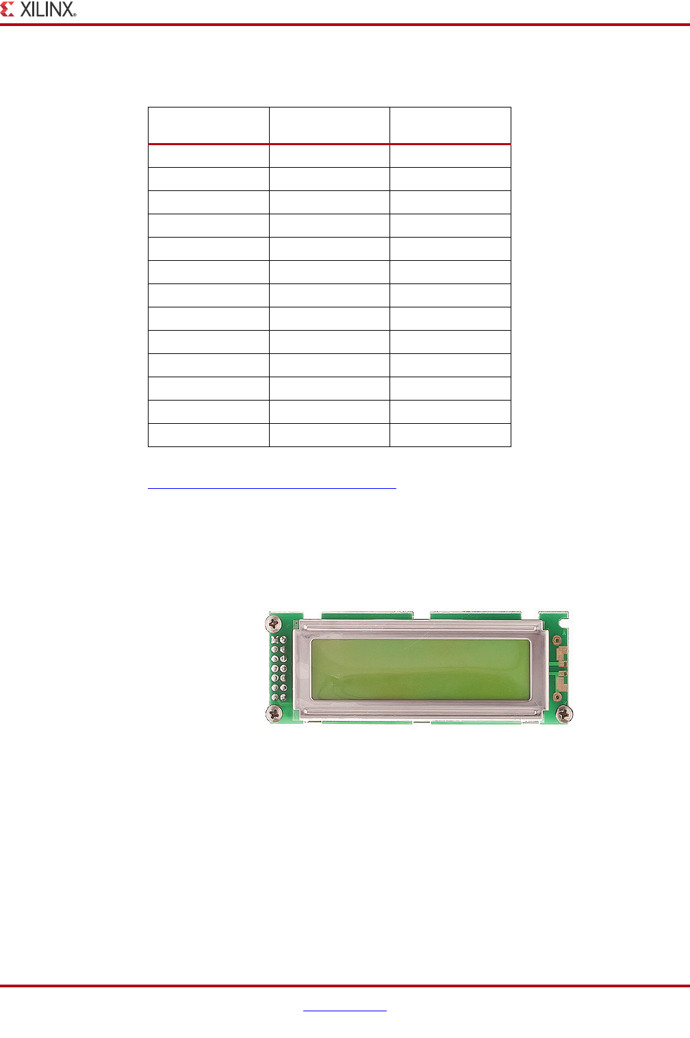
AC701 Evaluation Board www.xilinx.com 43
UG952 (v1.1) January 30, 2013
Feature Descriptions
Table 1-20 lists the connections between the codec and the HDMI connector P2.
Information about the ADV7511 is available on the Analog Devices website at
http://www.analog.com/en/index.html.
LCD Character Display
[Figure 1-2, callout 18]
A 2-line by 16-character display is provided on the AC701 board (Figure 1-24).
The character display runs at 5.0V and is connected to the FPGA's 3.3V HP bank 14
through a TI TXS0108E 8-bit bidirectional voltage level translator (U45). Figure 1-25 shows
the LCD interface circuit.
Table 1-20: ADV7511 Connections to HDMI Connector
ADV7511 (U48) Schematic Net Name HDMI Connector P2
Pin
36 HDMI_D0_P 7
35 HDMI_D0_N 9
40 HDMI_D1_P 4
39 HDMI_D1_N 6
43 HDMI_D2_P 1
42 HDMI_D2_N 3
33 HDMI_CLK_P 10
32 HDMI_CLK_N 12
54 HDMI_DDCSDA 16
53 HDMI_DDCSCL 15
52 HDMI_HEAC_P 14
51 HDMI_HEAC_N 19
48 HDMI_CRC 13
X-Ref Target - Figure 1-24
Figure 1-24: LCD Display
UG952_c1_24_101612
LCD Display (16 x 2)
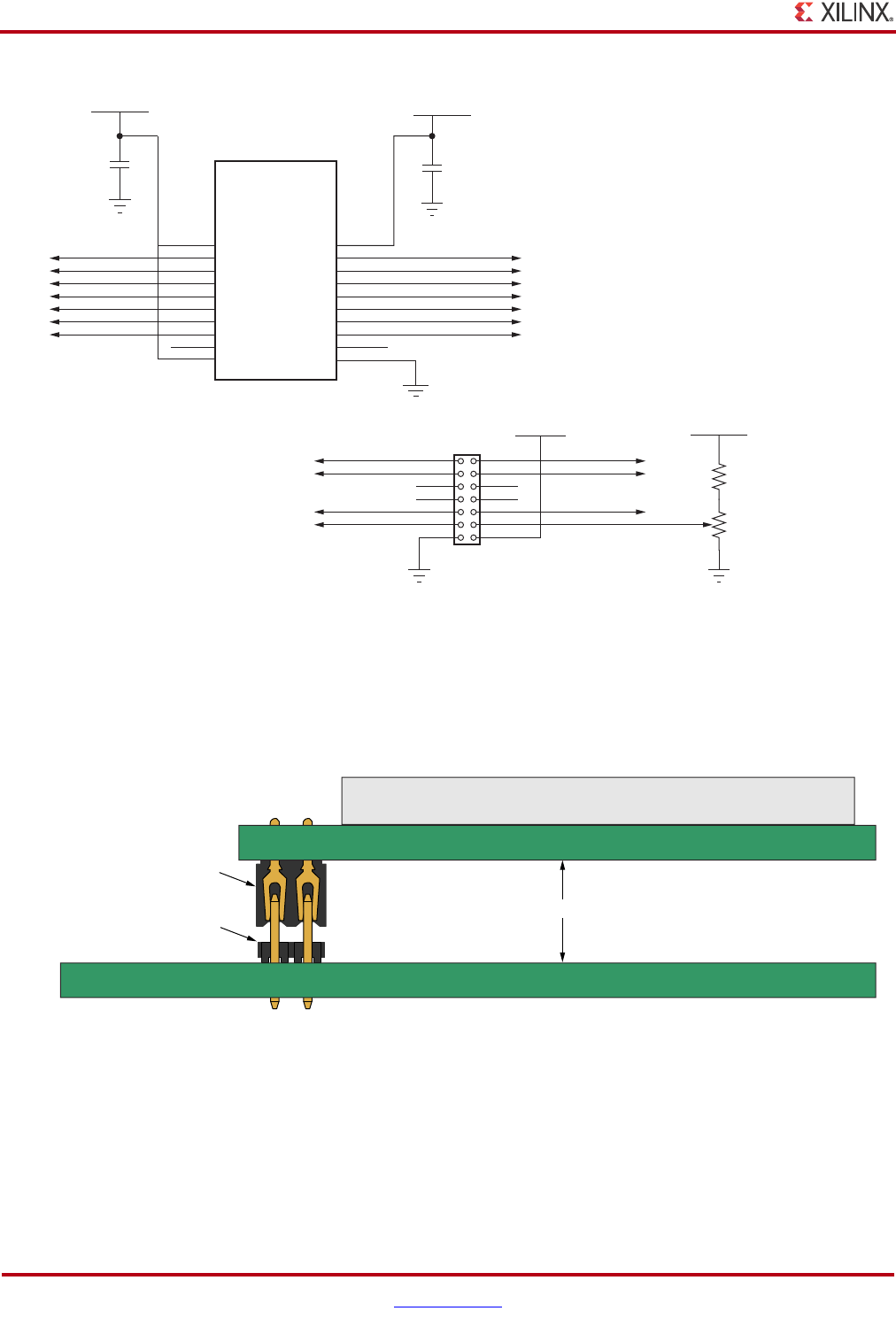
44 www.xilinx.com AC701 Evaluation Board
UG952 (v1.1) January 30, 2013
Chapter 1: AC701 Evaluation Board Features
The AC701 board base board uses a male Samtec MTLW-107-07-G-D-265 2x7 header (J23)
with 0.025-inch square posts on 0.100-inch centers for connecting to a Samtec
SLW-107-01-L-D female socket on the LCD display panel assembly. The LCD header
shown in Figure 1-26.
X-Ref Target - Figure 1-25
Figure 1-25: LCD Interface Circuit
UG952_c1_25_100312
LCD Contrast
Potentiometer
LCD_RW
LCD_DB4
LCD_DB6
LCD_RS
LCD_E
NC
NC
LCD_DB5
LCD_DB7
9
87
65
43
2
10
1
12
14
11
13
LCD_VEE
GND
VCCB
B1
B2
B3
B4
B6
B7
GND
A3
A8
OE
A4
A5
A7
A6
B5
A1
A2
B8
VCCA 19
20
18
17
16
14
13
11
4
9
10
5
6
8
7
15
1
3
12
2
U45
FPGA_3V3
LCD_E_LS
LCD_RW_LS
LCD_DB4_LS
LCD_DB5_LS
LCD_DB6_LS
LCD_DB7_LS
LCD_RS_LS
NC
LCD_RS
LCD_DB7
LCD_DB6
LCD_DB5
LCD_DB4
LCD_RW
LCD_E
NC
TXS0108E 8-Bit
Bidirectional
Voltage Level
Translator
J23
GND
VCC5V0
R118
6.81kΩ
R232
2 kΩ
NC
NC
VCC5V0
C472
0.1μF 25V
X5R
GND
VCC5V0
C473
0.1μF 25V
X5R
GND
GND
X-Ref Target - Figure 1-26
Figure 1-26: LCD Header Details
UG952_c1_26_101812
LCD Display Assembly
PWA
10 mm
Low Profile Socket
Samtec SLW-107-01-L-D
Low Profile Terminal
Samtec MTLW-107-07-G-D-265
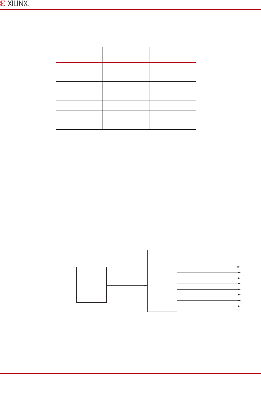
AC701 Evaluation Board www.xilinx.com 45
UG952 (v1.1) January 30, 2013
Feature Descriptions
Table 1-21 lists the connections between the FPGA and the LCD header. If the LCD is not
installed, the J23 pins listed in Table 1-21 can be used for GPIO.
References
The datasheet for the Displaytech S162DBABC LCD can be found at
http://www.displaytech-us.com/products/charactermodules.php. Choose the S162D
model full spec download arrow.
I2C Bus Switch
[Figure 1-2, callout 19]
The AC701 board implements a single I2C port on FPGA Bank 14 ( IIC_SDA_MAIN, FPGA
pin K25 and IIC_SCL_MAIN, FPGA pin N18), which is routed through a Texas
Instruments PCA9548 1-to-8 channel I2C switch (U52). The I2C switch can operate at
speeds up to 400 kHz. The U52 bus switch at I2C address 0x74/0b01110100 must be
addressed and configured to select the desired target downstream device.
The AC701 board I2C bus topology is shown in Figure 1-27.
User applications that communicate with devices on one of the downstream I2C buses
must first set up a path to the desired bus through the U52 bus switch at I2C address 0x74/
0b01110100.
Table 1-21: FPGA to LCD Header Connections
FPGA Pin
(U1)
Schematic Net
Name
LCD Header Pin
(J23)
L25 LCD_DB4_LS 4
M24 LCD_DB5_LS 3
M25 LCD_DB6_LS 2
L22 LCD_DB7_LS 1
L24 LCD_RW_LS 10
L23 LCD_RS_LS 11
L20 LCD_E_LS 9
X-Ref Target - Figure 1-27
Figure 1-27: I2C Bus Topology
PCA9548
12C 1-to-8
Bus Switch
CH7 - SI5324_SDA/SCL
U52
IIC_SDA/SCL_MAIN
CH6 - IIC_SDA/SCL_DDR3
CH5 - IIC_SDA/SCL_HDMI
CH4 - SFP_IIC_SDA/SCL
CH3 - EEPROM_IIC_SDA/SCL
CH2 - (NOT USED)
CH1 - FMC_HPC_IIC_SDA/SCL
CH0 - USER_CLK_SDL/SCL
FPGA
Bank 14
(3.3V)
0x74
U1
UG952_C1_27_100312
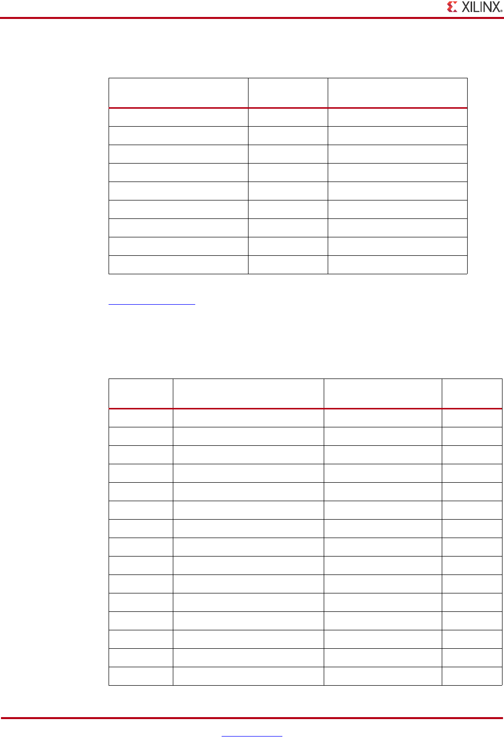
46 www.xilinx.com AC701 Evaluation Board
UG952 (v1.1) January 30, 2013
Chapter 1: AC701 Evaluation Board Features
. Table 1-22 lists the address for each bus.
Information about the PCA9548 is available on the TI Semiconductor website at
http://www.ti.com.
AC701 Board LEDs
Table 1-23 lists all LEDs on the AC701 board.
Table 1-22: I2C Bus Addresses
I2C Bus I2C Switch
Position I2C Address
PCA9548 N/A 0b1110100
USER_CLK_SDA/SCL 0 0b1011101
FMC1_HPC_IIC_SDA/SCL 1 0bXXXXX00
NOT USED 2 NOT USED
EEPROM_IIC_SDA/SCL 3 0b1010100
SFP_IIC_SDA/SCL 4 0b1010000
IIC_SDA/SCL_HDMI 5 0b0111001
IIC_SDA/SCL_DDR3 6 0b1010000, 0b0011000
SI5324_SDA/SCL 7 0b1010000
Table 1-23: AC701 Board LEDs
Reference
Designator Description Notes Schematic
Page
DS1 INIT Dual Color Red/Green Avago HSMF-C155 7
DS2 GPIO LED0 Lumex SML-LX0603GW 21
DS3 GPIO LED1 Lumex SML-LX0603GW 21
DS4 GPIO LED2 Lumex SML-LX0603GW 21
DS5 GPIO LED3 Lumex SML-LX0603GW 21
DS6 U8 TI Controller #1 PWRGOOD Lumex SML-LX0603GW 39
DS10 FPGA DONE Lumex SML-LX0603GW 7
DS11 EPHY U12 Status LED2 Lumex SML-LX0603GW 15
DS12 EPHY U12 Status LED1 Lumex SML-LX0603GW 15
DS13 EPHY U12 Status LED0 Lumex SML-LX0603GW 15
DS14 FMC PWRCTL1_VCC4B_PG Lumex SML-LX0603GW 24
DS15 VCCINT ON Lumex SML-LX0603GW 40
DS16 VCCAUX ON Lumex SML-LX0603GW 41
DS17 VCCBRAM ON Lumex SML-LX0603GW 42
DS18 FPGA_1V5 ON Lumex SML-LX0603GW 43
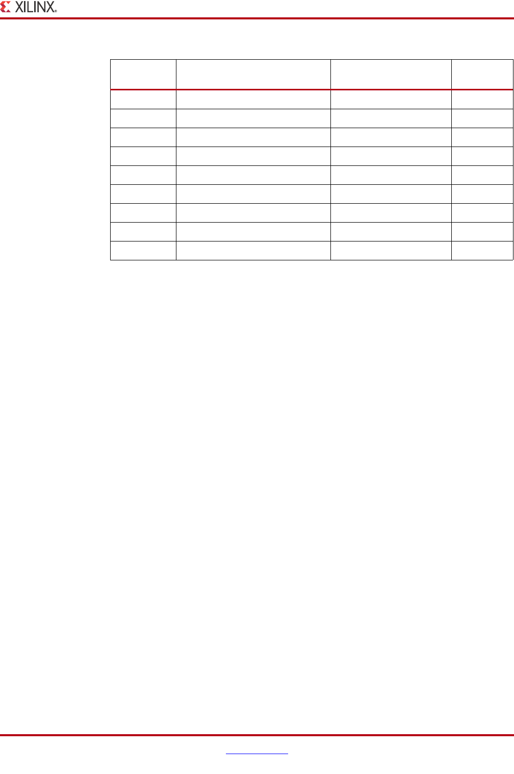
AC701 Evaluation Board www.xilinx.com 47
UG952 (v1.1) January 30, 2013
Feature Descriptions
User I/O
[Figure 1-2, callout 21 - 25]
The AC701 board provides the following user and general purpose I/O capabilities:
• Four user GPIO LEDs (callout 21)
• GPIO_LED_[3-0]: DS5, DS4, DS3, DS2
• Five user pushbuttons and reset switch (callout 22)
• GPIO_SW_[NESWC]: SW3, SW4, SW5, SW7, SW6
• CPU_RESET: SW8
• 4-position user DIP Switch (callout 23)
• GPIO_DIP_SW[4-0]: SW2
• User Rotary Switch (callout 24, hidden beneath the LCD)
• ROTARY_PUSH, ROTARY_INCA, ROTARY_INCB: SW10
• User SMA (callout 25)
• USER_SMA_GPIO_P, USER_SMA_GPIO_N: J33, J34
• 2 line x 16 character LCD Character Display (callout 18)
• If the display is unmounted, connector J23 pins are available as 7 independent
GPIOs
• 6-pin in-line male 0.1 inch PMOD header
• PMOD[3-0]: J48
DS19 VCCO_VADJ ON Lumex SML-LX0603GW 46
DS20 DDR3 SODIMM RTERM VTT ON Lumex SML-LX0603GW 44
DS21 VCC3V3 ON Lumex SML-LX0603GW 48
DS22 12V INPUT POWER ON Lumex SML-LX0603GW 38
DS23 U9 TI Controller #2 PWRGOOD Lumex SML-LX0603GW 45
DS24 MGTAVCC ON Lumex SML-LX0603GW 49
DS25 MGTAVTT ON Lumex SML-LX0603GW 50
DS26 FPGA_1V8 ON Lumex SML-LX0603GW 47
DS27 DDR3 SODIMM VTT ON Lumex SML-LX0603GW 44
Notes:
1. The Lumex SML-LX0603GW LED is Green
Table 1-23: AC701 Board LEDs (Cont’d)
Reference
Designator Description Notes Schematic
Page
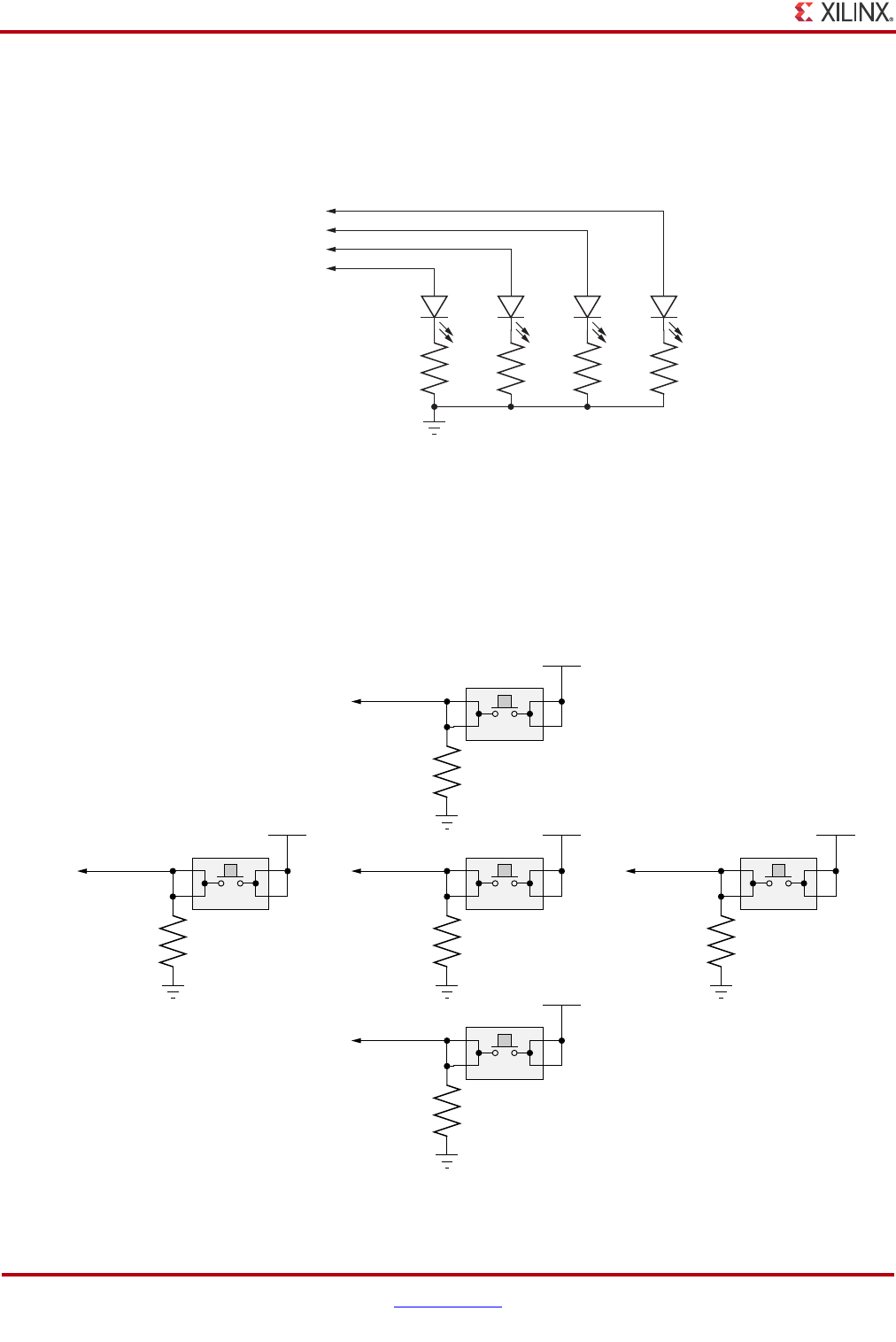
48 www.xilinx.com AC701 Evaluation Board
UG952 (v1.1) January 30, 2013
Chapter 1: AC701 Evaluation Board Features
User GPIO LEDs
[Figure 1-2, callout 21]
Figure 1-28 shows the user LED circuits.
User Pushbuttons and Reset Switch
[Figure 1-2, callout 22]
Figure 1-29 shows the user pushbutton switch circuits.
X-Ref Target - Figure 1-28
Figure 1-28: User LEDs
UG952_c1_28_100312
R147
49.9Ω
1%
DS2
R148
49.9Ω
1%
DS3
R149
49.9Ω
1%
DS4
R150
49.9Ω
1%
GND
DS5
GPIO_LED_2
GPIO_LED_0
GPIO_LED_1
GPIO_LED_3
X-Ref Target - Figure 1-29
Figure 1-29: User Pushbuttons
UG952_c1_29_011813
FPGA_1V5
GPIO SW C
R39
4.7kΩ
0.1 W
5%
GND
4
32
1
SW6
FPGA_1V5
GPIO SW N
R36
4.7kΩ
0.1 W
5%
GND
4
32
1
SW3
FPGA_1V5
GPIO SW S
R38
4.7kΩ
0.1 W
5%
GND
4
32
1
SW5
FPGA_1V5
GPIO SW W
R40
4.7kΩ
0.1 W
5%
GND
4
32
1
SW7
FPGA_1V5
GPIO SW E
R37
4.7kΩ
0.1 W
5%
GND
4
32
1
SW4
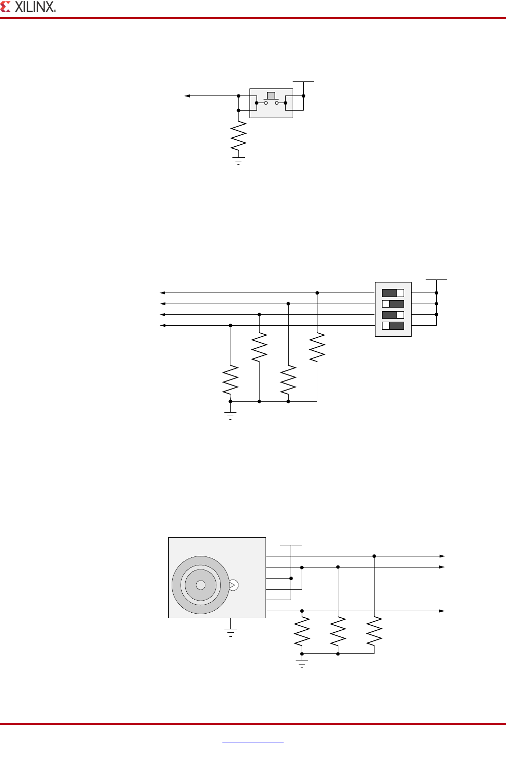
AC701 Evaluation Board www.xilinx.com 49
UG952 (v1.1) January 30, 2013
Feature Descriptions
Figure 1-30 shows the user CPU_RESET pushbutton switch circuit.
GPIO DIP Switch
[Figure 1-2, callout 23]
Figure 1-31 shows the GPIO DIP Switch circuit.
User Rotary Switch
[Figure 1-2, callout 24]
Figure 1-32 shows the user rotary switch circuit.
X-Ref Target - Figure 1-30
Figure 1-30: CPU_RESET Pushbutton
UG952_c1_140_011813
FPGA_1V5
CPU_RESET
R41
4.7kΩ
0.1 W
5%
GND
4
32
1
SW8
X-Ref Target - Figure 1-31
Figure 1-31: GPIO DIP Switch
UG952_c1_30_100412
SDA04H1SBD
SW2 FPGA_1V5
GPIO_DIP_SW0
GPIO_DIP_SW1
GPIO_DIP_SW2
GPIO_DIP_SW3
R53
4.7kΩ
0.1 W
5%
R52
4.7kΩ
0.1 W
5%
R51
4.7kΩ
0.1 W
5%
R50
4.7kΩ
0.1 W
5%
1
2
3
4
8
7
6
5
GND
X-Ref Target - Figure 1-32
Figure 1-32: User Rotary Switch Circuit
UG952_c1_141_011813
VCC3V3
R45
4.7kΩ
0.1 W
5%
R43
4.7kΩ
0.1 W
5%
R44
4.7kΩ
0.1 W
5%
EVQ-WK4001
Edge-Drive Jog Encoder
SW10
B
SW1B
SW2
SW1A
COM
A
GND
6
5
4
3
2
1
GND
ROTARY INCB
ROTARY PUSH
ROTARY INCA
GND
7
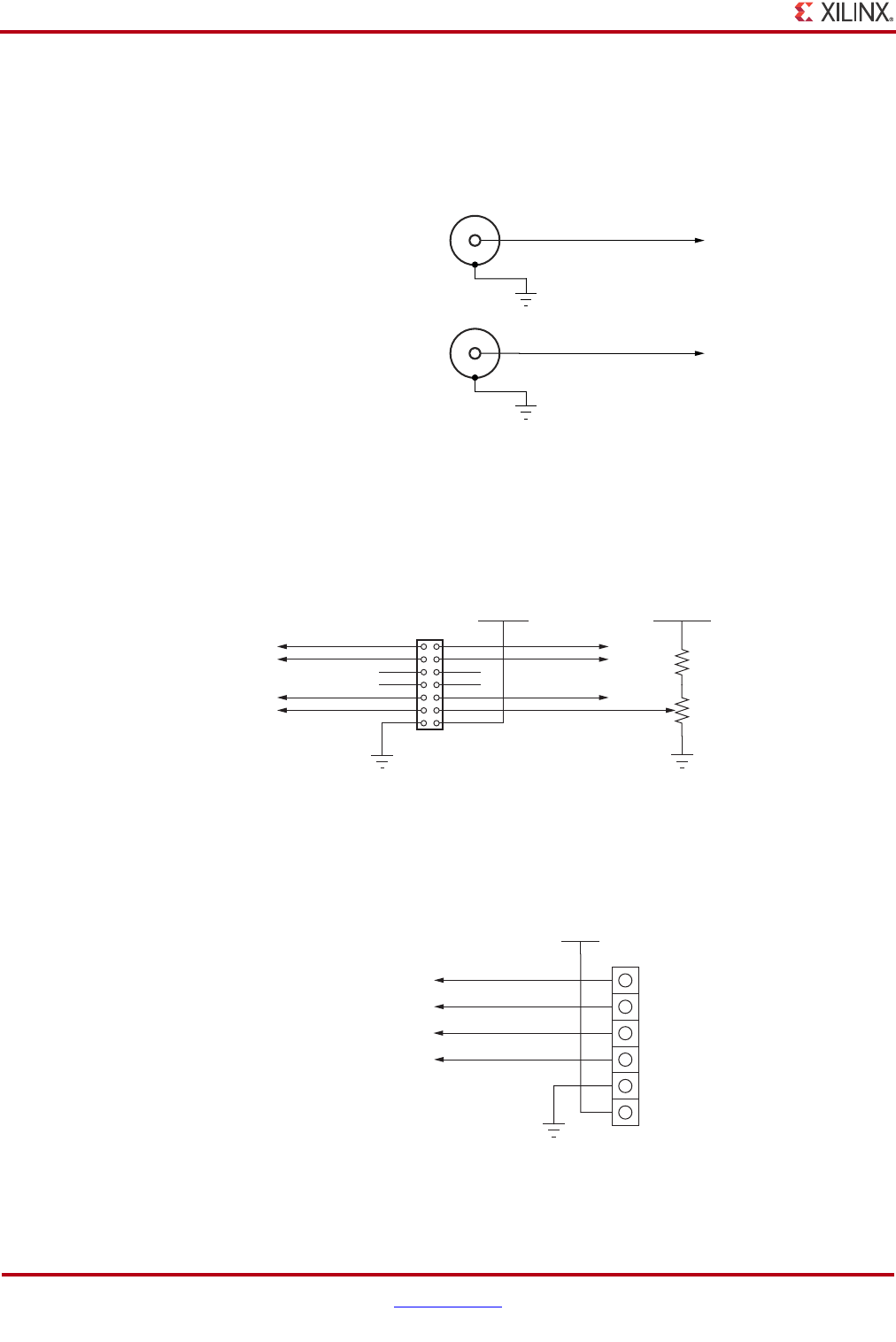
50 www.xilinx.com AC701 Evaluation Board
UG952 (v1.1) January 30, 2013
Chapter 1: AC701 Evaluation Board Features
User SMA Connectors
[Figure 1-2, callout 25]
Figure 1-33 shows the user SMA connector circuit.
LCD Connector
Figure 1-34 shows the LCD J23 2x7 male pin header circuit.
PMOD Connector
Figure 1-35 shows the J48 PMOD male pin header.
X-Ref Target - Figure 1-33
Figure 1-33: User SMA Connector
USER_SMA_GPIO_P
J34
USER_SMA_GPIO_N
GND
J33
GND
UG952_c1_142_011813
SMA
Connector
SMA
Connector
X-Ref Target - Figure 1-34
Figure 1-34: LCD Header J23
X-Ref Target - Figure 1-35
Figure 1-35: PMOD Header J48
UG952_c1_31_100412
LCD Contrast
Potentiometer
LCD_RW
LCD_DB4
LCD_DB6
LCD_RS
LCD_E
NC
NC
LCD_DB5
LCD_DB7
9
87
65
43
2
10
1
12
14
11
13
LCD_VEE
J23
GND
VCC5V0
R118
6.81kΩ
R232
2 kΩ
NC
NC
VCC5V0
GND
3
4
5
6
2
1
J48
HDR_1X6
VCC3V3
PMOD_0
PMOD_1
PMOD_2
PMOD_3
GND
UG952_c1_32_100412

AC701 Evaluation Board www.xilinx.com 51
UG952 (v1.1) January 30, 2013
Feature Descriptions
Table 1-24 lists the GPIO Connections to FPGA U1.
Table 1-24: GPIO Connections to FPGA U1
FPGA (U1) Pin Schematic Net Name GPIO Pin
User LEDs (Active High)
M26 GPIO_LED_0 DS2.2
T24 GPIO_LED_1 DS3.2
T25 GPIO_LED_2 DS4.2
R26 GPIO_LED_3 DS5.2
Directional Push-Button Switches (Active High)
P6 GPIO_SW_N SW3.3
U5 GPIO_SW_E SW4.3
T5 GPIO_SW_S SW5.3
R5 GPIO_SW_W SW7.3
U6 GPIO_SW_C SW6.3
CPU_RESET Push-Button Switches (Active High)
U4 CPU_RESET SW8.3
4-Pole DIP Switch (Active High)
R8 GPIO_DIP_SW0 SW2.1
P8 GPIO_DIP_SW1 SW2.2
R7 GPIO_DIP_SW2 SW2.3
R6 GPIO_DIP_SW3 SW2.4
Rotary Encoder Switch (Active High)
P20 ROTARY_INCB SW10.6
N21 ROTARY_PUSH SW10.5
N22 ROTARY_INCA SW10.1
User SMA Connectors
T8 USER_SMA_GPIO_P J33.1
T7 USER_SMA_GPIO_N J34.1
52 www.xilinx.com AC701 Evaluation Board
UG952 (v1.1) January 30, 2013
Chapter 1: AC701 Evaluation Board Features
Switches
[Figure 1-2, callout 26 - 27]
The AC701 board includes a power and a configuration switch:
• Power On/Off Slide Switch SW15 (callout 26)
• FPGA_PROG_B SW14, active-Low (callout 27)
Power On/Off Slide Switch SW15
[Figure 1-2, callout 26]
The AC701 board power switch is SW15. Sliding the switch actuator from the Off to On
position applies 12V power from J49, a 6-pin mini-fit connector. Green LED DS22
illuminates when the AC701 board power is on. See Power Management for details on the
onboard power system.
Caution! Do NOT plug a PC ATX power supply 6-pin connector into J49 on the AC701 board
The ATX 6-pin connector has a different pinout than J49. Connecting an ATX 6-pin connector into
J49 will damage the AC701 board and void the board warranty.
User LCD male pin header
L22 LCD_DB7 J23.1
M25 LCD_DB6 J23.2
M24 LCD_DB5 J23.3
L25 LCD_DB4 J23.4
L20 LCD_E J23.9
L24 LCD_RW J23.10
L23 LCD_RS J23.11
User GPIO PMOD male pin header
P26 PMOD_0 J48.1
T22 PMOD_1 J48.2
R22 PMOD_2 J48.3
T23 PMOD_3 J48.4
Table 1-24: GPIO Connections to FPGA U1 (Cont’d)
FPGA (U1) Pin Schematic Net Name GPIO Pin

AC701 Evaluation Board www.xilinx.com 53
UG952 (v1.1) January 30, 2013
Feature Descriptions
Figure 1-36 shows the simplified diagram of the power connector J49, power switch SW15
and indicator LED DS22.
The AC701 Evaluation Kit provides the adapter cable shown in Figure 1-37 for powering
the AC701 board from the ATX power supply 4-pin peripheral connector. The Xilinx part
number for this cable is 2600304, and is equivalent to Sourcegate Technologies part number
AZCBL-WH-1109-RA4.
FPGA_PROG_B Pushbutton SW9 (Active-Low)
[Figure 1-2, callout 27]
Switch SW9 grounds the FPGA's PROG_B pin when pressed. This action initiates an FPGA
reconfiguration. The FPGA_PROG_B signal is connected to FPGA U1 pin AE16.
See UG470, 7 Series FPGAs Configuration User Guide for further details on configuring
the 7 series FPGAs.
Figure 1-38 shows SW9.
X-Ref Target - Figure 1-36
Figure 1-36: Power On/Off Switch SW15
X-Ref Target - Figure 1-37
Figure 1-37: ATX Power Supply Adapter Cable
UG952_c1_33_101612
VCC12 P IN
VCC12 P
R369
1kΩ
1%
GND
1
2
3
4
SW15
C539
330μF
25V
GND
DS22
5
6
J49
1
2
3
4
5
6
12V
N/C
COM
12V
N/C
COM
GND
Power
PCIe
UG952_c1_34_101612
To ATX 4-Pin Peripheral
Power Connector
To J49 on AC701 Board
X-Ref Target - Figure 1-38
Figure 1-38: FPGA_PROG_B Pushbutton SW9
UG952_c1_35_100412
FPGA_3V3
FPGA_PROG_B
R42
4.7kΩ
0.1 W
5%
GND
1
23
4
SW9
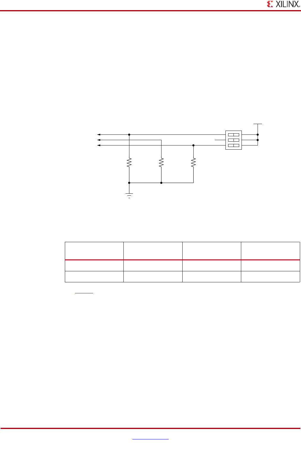
54 www.xilinx.com AC701 Evaluation Board
UG952 (v1.1) January 30, 2013
Chapter 1: AC701 Evaluation Board Features
Configuration Mode Switch SW1
The AC701 board supports two of the five 7 series FPGA configuration modes:
• Master SPI using the on-board Quad SPI flash memory
• JTAG using a standard-A to micro-B USB cable for connecting the host PC to the
AC701 board configuration port (via Digilent module)
Each configuration interface corresponds to one or more configuration modes and bus
widths as listed in Table 1-25. The mode switches M2, M1, and M0 are on SW1 positions 1,
2, and 3 respectively as shown in Figure 1-39.
Note: On the AC701 board, SW1 switch position 2 is not used.
The default mode setting is M[2:0] = 001, which selects Master SPI at board power-on.
See UG470, 7 Series FPGAs Configuration User Guide for further details on configuring the 7
series FPGAs.
FPGA Mezzanine Card Interface
[Figure 1-2, callout 29]
The AC701 board supports the VITA 57.1 FPGA Mezzanine Card (FMC) specification by
providing high pin count (HPC) connector J30. HPC J30 is keyed so that a the mezzanine
card faces away from the AC701 board when connected.
Signaling Speed Ratings:
• Single-ended: 9 GHz (18 Gb/s)
• Differential Optimal Vertical: 9 GHz (18 Gb/s)
• Differential Optimal Horizontal: 16 GHz (32 Gb/s)
• High Density Vertical: 7 GHz (15 Gb/s)
X-Ref Target - Figure 1-39
Figure 1-39: Mode Switch SW1
Table 1-25: AC701 Board FPGA Configuration Modes
Configuration Mode SW13 DIP Switch
Settings (M[2:0]) Bus Width CCLK Direction
Master SPI 001 x1, x2, x4 Output
JTAG 101 x1 Not Applicable
R339
1.21K 1%
1/10W
R338
1.21K 1%
1/10W
R337
1.21K 1%
1/10W
FPGA_3V3
SW1
1
2
3
6
5
4
SDA03H1SBD
FPGA_M2
FPGA_M1
FPGA_M0
UG952_c1_36_011713
NC
AC701 Evaluation Board www.xilinx.com 55
UG952 (v1.1) January 30, 2013
Feature Descriptions
The Samtec connector system is rated for signaling speeds up to 9 GHz (18 Gb/s) based on
a -3 dB insertion loss point within a two-level signaling environment.
Connector Type:
• Samtec SEAF Series, 1.27 mm (0.050 in) pitch. Mates with SEAM series connector
For more information about SEAF series connectors, go to the Samtec website at:
www.samtec.com.
HPC Connector J30
[Figure 1-2, callout 29]
The 400-pin HPC connector defined By the FMC specification (Figure B-1, page 81)
provides connectivity for up to:
• 160 single-ended or 80 differential user-defined signals
• 10 GTP transceivers
•2 GTP clocks
•4 differential clocks
• 159 ground and 15 power connections
The connections between the HPC connector at J30 and FPGA U1 (Table 1-26) implements
a subset of this connectivity:
• 58 differential user defined pairs
• 34 LA pairs (LA00-LA33)
• 24 HA pairs (HA00-HA23)
•4 GTP transceivers
•1 GTP clock
•2 differential clocks
• 159 ground and 15 power connections
Note: The AC701 board VADJ voltage for HPC connector J30 is determined by the FMC VADJ
power sequencing logic described in Power Management, page 67.
Table 1-26: HPC Connections, J30 to FPGA U1
J30 FMC
HPC Pin Schematic Net Name U1 FPGA
Pin
J30 FMC
HPC Pin Schematic Net Name U1 FPGA
Pin
A2 FMC1_HPC_DP1_M2C_P AC14 B1 NC NA
A3 FMC1_HPC_DP1_M2C_N AD14 B4 NC NA
A6 NC NA B5 NC NA
A7 NC NA B8 NC NA
A10 NC NA B9 NC NA
A11 NC NA B12 NC NA
A14 NC NA B13 NC NA
A15 NC NA B16 NC NA
A18 NC NA B17 NC NA
56 www.xilinx.com AC701 Evaluation Board
UG952 (v1.1) January 30, 2013
Chapter 1: AC701 Evaluation Board Features
A19 NC NA B20 FMC1_HPC_GBTCLK1_M2C_P U4.27
A22 FMC1_HPC_DP1_C2M_P AC8 B21 FMC1_HPC_GBTCLK1_M2C_N U4.25
A23 FMC1_HPC_DP1_C2M_N AD8 B24 NC NA
A26 NC NA B25 NC NA
A27 NC NA B28 NC NA
A30 NC NA B29 NC NA
A31 NC NA B32 NC NA
A34 NC NA B33 NC NA
A35 NC NA B36 NC NA
A38 NC NA B37 NC NA
A39 NC NA B40 NC NA
C2 FMC1_HPC_DP0_C2M_P AE9 D1 CTRL2_PWRGOOD P15
C3 FMC1_HPC_DP0_C2M_N AF9 D4 FMC1_HPC_GBTCLK0_M2C_P U3.27
C6 FMC1_HPC_DP0_M2C_P AE13 D5 FMC1_HPC_GBTCLK0_M2C_N U3.25
C7 FMC1_HPC_DP0_M2C_N AF13 D8 FMC1_HPC_LA01_CC_P E17
C10 FMC1_HPC_LA06_P G19 D9 FMC1_HPC_LA01_CC_N E18
C11 FMC1_HPC_LA06_N F20 D11 FMC1_HPC_LA05_P G15
C14 FMC1_HPC_LA10_P A17 D12 FMC1_HPC_LA05_N F15
C15 FMC1_HPC_LA10_N A18 D14 FMC1_HPC_LA09_P E16
C18 FMC1_HPC_LA14_P C21 D15 FMC1_HPC_LA09_N D16
C19 FMC1_HPC_LA14_N B21 D17 FMC1_HPC_LA13_P B20
C22 FMC1_HPC_LA18_CC_P G20 D18 FMC1_HPC_LA13_N A20
C23 FMC1_HPC_LA18_CC_N G21 D20 FMC1_HPC_LA17_CC_P K21
C26 FMC1_HPC_LA27_P F23 D21 FMC1_HPC_LA17_CC_N J21
C27 FMC1_HPC_LA27_N E23 D23 FMC1_HPC_LA23_P K20
C30 FMC1_HPC_IIC_SCL U52.19 D24 FMC1_HPC_LA23_N J20
C31 FMC1_HPC_IIC_SDA U52.20 D26 FMC1_HPC_LA26_P J24
C34 GND NA D27 FMC1_HPC_LA26_N H24
C35 VCC12_P NA D29 FMC1_HPC_TCK_BUF U19.13
C37 VCC12_P NA D30 FMC1_TDI_BUF U19.17
C39 VCC3V3 NA D31 FMC1_TDO_FPGA_TDI U19.2
D32 VCC3V3 NA
Table 1-26: HPC Connections, J30 to FPGA U1 (Cont’d)
J30 FMC
HPC Pin Schematic Net Name U1 FPGA
Pin
J30 FMC
HPC Pin Schematic Net Name U1 FPGA
Pin
AC701 Evaluation Board www.xilinx.com 57
UG952 (v1.1) January 30, 2013
Feature Descriptions
D33 FMC1_HPC_TMS_BUF U19.15
D34 NC NA
D35 GND NA
D36 VCC3V3 NA
D38 VCC3V3 NA
D40 VCC3V3 NA
E2 FMC1_HPC_HA01_CC_P AB21 F1 FMC1_HPC_PG_M2C N17
E3 FMC1_HPC_HA01_CC_N AC21 F4 FMC1_HPC_HA00_CC_P AA19
E6 FMC1_HPC_HA05_P AD25 F5 FMC1_HPC_HA00_CC_N AB19
E7 FMC1_HPC_HA05_N AD26 F7 FMC1_HPC_HA04_P AF24
E9 FMC1_HPC_HA09_P AF19 F8 FMC1_HPC_HA04_N AF25
E10 FMC1_HPC_HA09_N AF20 F10 FMC1_HPC_HA08_P AD21
E12 FMC1_HPC_HA13_P AC18 F11 FMC1_HPC_HA08_N AE21
E13 FMC1_HPC_HA13_N AD18 F13 FMC1_HPC_HA12_P AC19
E15 FMC1_HPC_HA16_P AE17 F14 FMC1_HPC_HA12_N AD19
E16 FMC1_HPC_HA16_N AF17 F16 FMC1_HPC_HA15_P Y18
E18 FMC1_HPC_HA20_P Y16 F17 FMC1_HPC_HA15_N AA18
E19 FMC1_HPC_HA20_N Y17 F19 FMC1_HPC_HA19_P AC17
E21 NC NA F20 FMC1_HPC_HA19_N AD17
E22 NC NA F22 NC NA
E24 NC NA F23 NC NA
E25 NC NA F25 NC NA
E27 NC NA F26 NC NA
E28 NC NA F28 NC NA
E30 NC NA F29 NC NA
E31 NC NA F31 NC NA
E33 NC NA F32 NC NA
E34 NC NA F34 NC NA
E36 NC NA F35 NC NA
E37 NC NA F37 NC NA
E39 VCC1V8 NA F38 NC NA
F40 VCC1V8 NA
Table 1-26: HPC Connections, J30 to FPGA U1 (Cont’d)
J30 FMC
HPC Pin Schematic Net Name U1 FPGA
Pin
J30 FMC
HPC Pin Schematic Net Name U1 FPGA
Pin
58 www.xilinx.com AC701 Evaluation Board
UG952 (v1.1) January 30, 2013
Chapter 1: AC701 Evaluation Board Features
G2 FMC1_HPC_CLK1_M2C_P H1 NC NA
G3 FMC1_HPC_CLK1_M2C_N H2 FMC1_HPC_PRSNT_M2C N16
G6 FMC1_HPC_LA00_CC_P D18 H4 FMC1_HPC_CLK0_M2C_P D19
G7 FMC1_HPC_LA00_CC_N C18 H5 FMC1_HPC_CLK0_M2C_N C19
G9 FMC1_HPC_LA03_P G17 H7 FMC1_HPC_LA02_P H14
G10 FMC1_HPC_LA03_N F17 H8 FMC1_HPC_LA02_N H15
G12 FMC1_HPC_LA08_P C17 H10 FMC1_HPC_LA04_P F18
G13 FMC1_HPC_LA08_N B17 H11 FMC1_HPC_LA04_N F19
G15 FMC1_HPC_LA12_P E20 H13 FMC1_HPC_LA07_P H16
G16 FMC1_HPC_LA12_N D20 H14 FMC1_HPC_LA07_N G16
G18 FMC1_HPC_LA16_P E21 H16 FMC1_HPC_LA11_P B19
G19 FMC1_HPC_LA16_N D21 H17 FMC1_HPC_LA11_N A19
G21 FMC1_HPC_LA20_P M16 H19 FMC1_HPC_LA15_P B22
G22 FMC1_HPC_LA20_N M17 H20 FMC1_HPC_LA15_N A22
G24 FMC1_HPC_LA22_P L17 H22 FMC1_HPC_LA19_P M14
G25 FMC1_HPC_LA22_N L18 H23 FMC1_HPC_LA19_N L14
G27 FMC1_HPC_LA25_P G22 H25 FMC1_HPC_LA21_P J19
G28 FMC1_HPC_LA25_N F22 H26 FMC1_HPC_LA21_N H19
G30 FMC1_HPC_LA29_P G24 H28 FMC1_HPC_LA24_P J18
G31 FMC1_HPC_LA29_N F24 H29 FMC1_HPC_LA24_N H18
G33 FMC1_HPC_LA31_P E26 H31 FMC1_HPC_LA28_P K22
G34 FMC1_HPC_LA31_N D26 H32 FMC1_HPC_LA28_N K23
G36 FMC1_HPC_LA33_P G25 H34 FMC1_HPC_LA30_P E25
G37 FMC1_HPC_LA33_N F25 H35 FMC1_HPC_LA30_N D25
G39 VCC1V8 NA H37 FMC1_HPC_LA32_P H26
H38 FMC1_HPC_LA32_N G26
H40 VCC1V8 NA
J2 NC NA K1 NC NA
J3 NC NA K4 NC NA
J6 FMC1_HPC_HA03_P AC22 K5 NC NA
J7 FMC1_HPC_HA03_N AC23 K7 FMC1_HPC_HA02_P AE25
J9 FMC1_HPC_HA07_P AD23 K8 FMC1_HPC_HA02_N AE26
Table 1-26: HPC Connections, J30 to FPGA U1 (Cont’d)
J30 FMC
HPC Pin Schematic Net Name U1 FPGA
Pin
J30 FMC
HPC Pin Schematic Net Name U1 FPGA
Pin
AC701 Evaluation Board www.xilinx.com 59
UG952 (v1.1) January 30, 2013
Feature Descriptions
AC701 Board Power System
The AC701 board hosts a power system based on the Texas Instruments (TI) UCD90120A
power supply sequencer and monitor, and the TPS84K and LMZ22000 family voltage
regulators.
UCD90120A Description
The UCD90120A is a 12-rail PMBus/I2C addressable power-supply sequencer and
monitor. The device integrates a 12-bit ADC for monitoring up to 12 power-supply voltage
inputs. Twenty-six GPIO pins can be used for power supply enables, power-on reset
signals, external interrupts, cascading, or other system functions. 12 of these pins offer
PWM functionality. Using these pins, the UCD90120A device offers support for margining
and general-purpose PWM functions.
J10 FMC1_HPC_HA07_N AD24 K10 FMC1_HPC_HA06_P AE23
J12 FMC1_HPC_HA11_P AD20 K11 FMC1_HPC_HA06_N AF23
J13 FMC1_HPC_HA11_N AE20 K13 FMC1_HPC_HA10_P AE22
J15 FMC1_HPC_HA14_P AE18 K14 FMC1_HPC_HA10_N AF22
J16 FMC1_HPC_HA14_N AF18 K16 FMC1_HPC_HA17_CC_P AA20
J18 FMC1_HPC_HA18_P AA17 K17 FMC1_HPC_HA17_CC_N AB20
J19 FMC1_HPC_HA18_N AB17 K19 FMC1_HPC_HA21_P AB16
J21 FMC1_HPC_HA22_P Y15 K20 FMC1_HPC_HA21_N AC16
J22 FMC1_HPC_HA22_N AA15 K22 FMC1_HPC_HA23_P W14
J24 NC NA K23 FMC1_HPC_HA23_N W15
J25 NC NA K25 NC NA
J27 NC NA K26 NC NA
J28 NC NA K28 NC NA
J30 NC NA K29 NC NA
J31 NC NA K31 NC NA
J33 NC NA K32 NC NA
J34 NC NA K34 NC NA
J36 NC NA K35 NC NA
J37 NC NA K37 NC NA
J39 FMC1_VIO_B_M2C NA K38 NC NA
K40 FMC1_VIO_B_M2C NA
Table 1-26: HPC Connections, J30 to FPGA U1 (Cont’d)
J30 FMC
HPC Pin Schematic Net Name U1 FPGA
Pin
J30 FMC
HPC Pin Schematic Net Name U1 FPGA
Pin
60 www.xilinx.com AC701 Evaluation Board
UG952 (v1.1) January 30, 2013
Chapter 1: AC701 Evaluation Board Features
The UCD90120A device is configured by using the PC-based TI Fusion Digital Power
Designer software. This software provides a graphical user interface (GUI) for configuring,
storing, and monitoring power system operating parameters.
TPS84K Family Regulator Description
The TPS84621RUQ (6A) and TPS84320RUQ (3A) regulators are integrated synchronous
buck switching regulators that combines a DC/DC converter with power MOSFETs, an
inductor, and passives into low profile, BQFN packages. The TPS84K devices accept an
input voltage rail between 4.5V and 14.5V and deliver an adjustable output voltage in the
0.6V to 5.5V range. This type power solution allows as few as 3 external components and
eliminates the loop compensation and magnetic parts selection process.
LMZ22000 Family Regulator Description
The LMZ22010 power module is an step-down DC-DC switching regulator capable of
driving up to 10A load. The LMZ22010 can accept an input voltage rail between 6V and
20V and deliver an adjustable and highly accurate output voltage as low as 0.8V. The
LMZ22010 requires two external resistors and external capacitors to complete the design.
The LMZ22010 is a reliable and robust design with the following protection features:
thermal shutdown, programmable input under-voltage lockout, output over-voltage
protection, short-circuits protection, output current limit, and allows startup into a
pre-biased output. The sync input allows synchronization over the 314 kHz to 600 kHz
switching frequency range and up to 6 modules can be connected in parallel for higher
load currents.
Table 1-27 shows the AC701 board power system configuration for controller U8.
Table 1-27: Controller U8 Power System Configuration
Sequencer
Schematic
Regulator Type Voltage Current
Page Contents Net Name
#1 U8 PMBus Addr 101, 4 Rails
39 UCD90120A #1
40 Addr 101, Rail 1 VCCINT LMZ12010 (U49) 1.0V 10A
41 Addr 101, Rail 2 VCCAUX TPS84621 (U53) 1.8V 6A
42 Addr 101, Rail 3 VCCBRAM TPS84320 (U54) 1.0V 3A
43 Addr 101, Rail 4 FPGA_1V5 TPS84621 (U55) 1.5V 6A
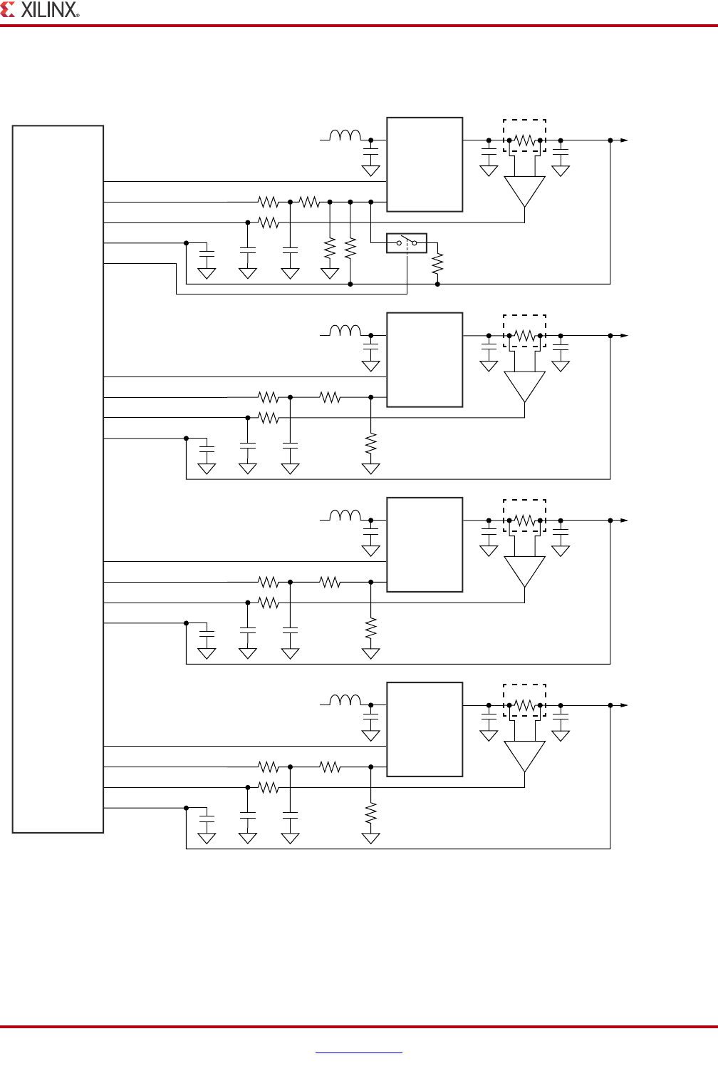
AC701 Evaluation Board www.xilinx.com 61
UG952 (v1.1) January 30, 2013
Feature Descriptions
Figure 1-40 shows the power system for UCD90120A U8 controller #1
X-Ref Target - Figure 1-40
Figure 1-40: U8 Controller #1 UCD90120A Power System
UG952_c1_137_011513
UCD90120A
Controller
(Controller 1)
U8
1. Capacitors labled Cf are bulk filter capacitors.
2. Voltage Sense is connected at point of load.
GPIO (Out)
FPWM (Out)
ADC (In)
ADC (In)
GPIO (Out)
Input
Filter
LMZ12008
U49 (1.0V Nom)
Vin Vout
EN
FB
Rail Enable
PWM Margin
Current Sense
Voltage Sense(2)
Low Pwr Select
Rs 5mΩ
+12V
Vfb
VCCINT 1.0V
CfCf(1)
G = 40.22
VCCINT 0A-10A
CS = 0V-2.01V
GPIO (Out)
FPWM (Out)
ADC (In)
ADC (In)
Input
Filter
TPS84621
U53 (1.8V Nom)
Vin Vout
EN
FB
Rail Enable
PWM Margin
Current Sense
Voltage Sense(2)
Rs 5mΩ
+12V
Vfb
VCCAUX 1.8V
CfCf
G = 67.67
VCCAUX 0A-6A
CS = 0V-2.03V
GPIO (Out)
FPWM (Out)
ADC (In)
ADC (In)
Input
Filter
TPS84320
U54 (1.0V Nom)
Vin Vout
EN
FB
Rail Enable
PWM Margin
Current Sense
Voltage Sense(2)
Rs 5mΩ
+12V
Vfb
VCCBRAM 1.0V
CfCf
G = 221.7
VCCVBRAM
0A-1.8A
CS = 0V-1.996V
GPIO (Out)
FPWM (Out)
ADC (In)
ADC (In)
Input
Filter
TPS84621
U55 (1.5V Nom)
Vin Vout
EN
FB
Rail Enable
PWM Margin
Current Sense
Voltage Sense(2)
Rs 5mΩ
+12V
Vfb
FPGA_1V5 1.5V
CfCf
G = 67.67
FPGA_1V5
0A- 6A
CS = 0V-2.03V
Notes:
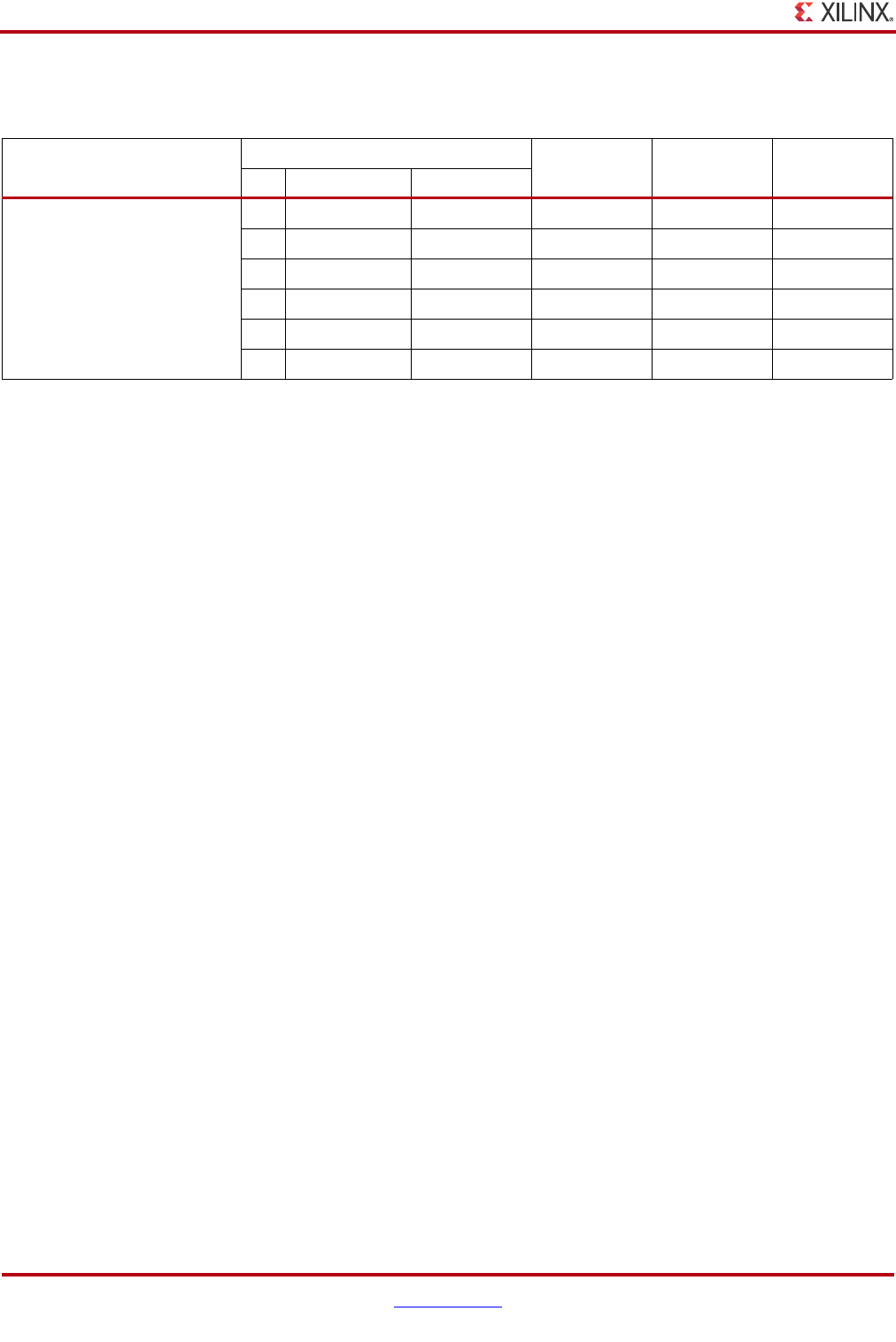
62 www.xilinx.com AC701 Evaluation Board
UG952 (v1.1) January 30, 2013
Chapter 1: AC701 Evaluation Board Features
Table 1-28 shows the AC701 TI power system configuration for controller U9.
Table 1-28: Controller U9 Power System Configuration
Sequencer
Schematic
Regulator Type Voltage Current
Page Page Contents Net Name
#2 U9 PMBus Addr 102, 5 Rails
45 UCD90120A #2
46 Addr 102, Rail 1 VCCO_VADJ TPS84621 (U56) 2.5V 6A
47 Addr 102, Rail 2 FPGA_1V8 TPS84320 (U57) 1.8V 3A
48 Addr 102, Rail 3 FPGA_3V3 TPS84621 (U58) 3.3V 6A
49 Addr 102, Rail 4 MGTAVCC TPS84320 (U59) 1.0V 3A
50 Addr 102, Rail 5 MGTAVTT TPS84320 (U60) 1.2V 3A
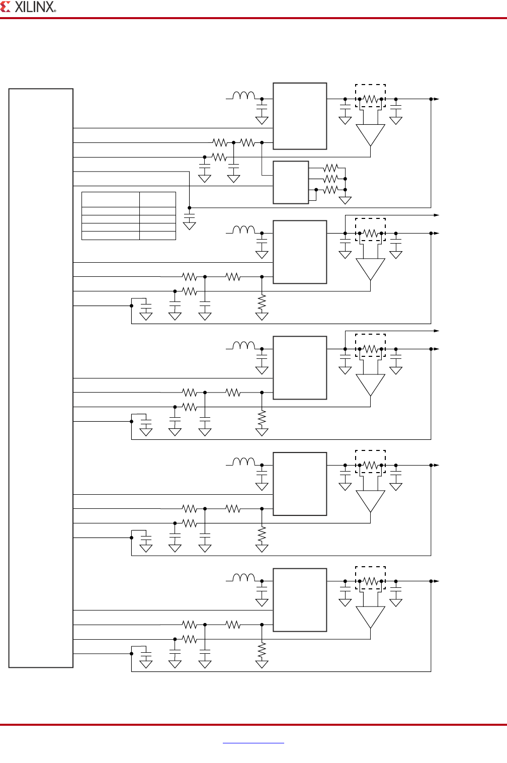
AC701 Evaluation Board www.xilinx.com 63
UG952 (v1.1) January 30, 2013
Feature Descriptions
Figure 1-41 shows the power system for UCD90120A U9 controller #2 rails 1 through 5.
X-Ref Target - Figure 1-41
Figure 1-41: U9 Controller #2 UCD90120A Power System
UG952_c1_138_011513
UCD90120A
Controller
(Controller 2)
U9 1. Capacitors labled Cf are bulk filter capacitors.
2. Voltage Sense is connected
GPIO (Out)
FPWM (Out)
ADC (In)
ADC (In)
GPIO (Out)
Input
Filter
TPS84621
U49 (2.5V Nom)
Vin Vout
EN
FB
Rail Enable
PWM Margin
Current Sense
Voltage Sense(2)
FMC_ADJ_SEL[1:0]
Rs 5mΩ
+12V
Vfb
VCCO_ADJ 2.5V
CfCf(1)
G = 125.07
VCCO_VADJ
0A-3.2A
CS = 0V-2.00V
Notes:
GPIO (Out)
FPWM (Out)
ADC (In)
ADC (In)
Input
Filter
TPS84320
U57 (1.8V Nom)
Vin Vout
EN
FB
Rail Enable
PWM Margin
Current Sense
Voltage Sense(2)
Rs 5mΩ
+12V
Vfb
FPGA_1V8 1.8V
CfCf
G = 125.07
FPGA_1V8
0A-3.2A
CS = 0V-2.00V
VCC1V8 1.8V
GPIO (Out)
FPWM (Out)
ADC (In)
ADC (In)
Input
Filter
TPS84321
U58 (3.3V Nom)
Vin Vout
EN
FB
Rail Enable
PWM Margin
Current Sense
Voltage Sense(2)
Rs 5mΩ
+12V
Vfb
FPGA_3V3 3.3V
CfCf
G = 125.07
FPGA_3V3
0A-3.2A
CS = 0V-2.00V
VCC3V3 3.3V
GPIO (Out)
FPWM (Out)
ADC (In)
ADC (In)
Input
Filter
TPS84320
U59 (1.0V Nom)
Vin Vout
EN
FB
Rail Enable
PWM Margin
Current Sense
Voltage Sense(2)
Rs 5mΩ
+12V
Vfb
CfCf
G = 134.3
MGTAVCC
0A-3.0A
CS = 0V-2.02V
MGTAVCC 1.0V
GPIO (Out)
FPWM (Out)
ADC (In)
ADC (In)
Input
Filter
TPS84320
U60 (1.2V Nom)
Vin Vout
EN
FB
Rail Enable
PWM Margin
Current Sense
Voltage Sense(2)
Rs 5mΩ
+12V
Vfb
MGTAVTT 1.2V
CfCf
G = 268.4
MGTAVTT
0A-1.5A
CS = 0V-2.02V
U64 I0B
I1B
I2B
I3B
YB
S[1:0]
FMC_ADJ_SEL[1:0]
Value
0 0
0 1
1 0
1 1
VCCO_ADJ
Output
2.5V
1.8V
3.3V
3.3V
at point of load.
(Not measued separately)
(Not measued separately)

64 www.xilinx.com AC701 Evaluation Board
UG952 (v1.1) January 30, 2013
Chapter 1: AC701 Evaluation Board Features
The TPS84K and LMZ22000 family adjustable voltage regulators have their output voltage
set by an external resistor. The regulator topology on the AC701 board permits the
UCD90120A to monitor rail voltage and current. Voltage margining at +5% and -5% is also
implemented.
Each voltage regulator's external VOUT setting resistor is calculated and implemented as if
the regulator is standalone. The UCD90120A has two ADC inputs allocated per voltage
rail, one input for the remote voltage sense connection, the other for the current sense
resistor op amp output voltage connection. The UCD90120A ADC full scale input is 2.5V.
The remote voltage feedback is scaled to approximately 2V if it exceeds 2V—that is, the
VCCO_VADJ rail for the 2.5V and 3.3V modes, and the FPGA_3V3 rail also at 3.3V are
resistor attenuated to scale the remotely sensed voltage at 0.606 to give approximately 2V
at the ADC input pin for a 3.3V remote sense value. Rails below 2V are not scaled.
Each rail's current sense op amp has its gain set to provide approximately 2V max at the TI
UCD90120A ADC input pin when the rail current is at its expected maximum current
level, as shown in Figure 1-40 (U8 controller #1) and Figure 1-41 (U9 controller #2).
The UCD90120A has an assignable group of GPIO pins with PWM capability. Each
controller channel has a PWM GPIO pin connected to the associated voltage regulator
VADJ pin. The external VOUT setting resistor is also wired to this pin. The PWM GPIO pin
is configured in 3-state mode. This pin is not driven unless a Margin command is executed.
The Margin command is available within the TI Fusion Digital Power designer software.
During the margin high or low operation, the PWM GPIO pin drives a voltage into the
voltage regulator VADJ pin, which causes a slight voltage change resulting in the regulator
VOUT moving to the margin +5% or -5% voltage commanded.
XADC Power System Measurement
The AC701 board XADC interface includes power system voltage and current measuring
capability. The VCCINT, VCCAUX and VCCBRAM rail voltages are measured via the
XADC internal voltage measurement capability. Other rails are measured via two external
Analog Devices ADG707BRU multiplexers U14 and U13. Each rail has a TI INA333 op amp
strapped across its series current sense resistor Kelvin terminals. This op amp has its gain
adjusted to give approximately 1V at the expected full scale current value for the rail.
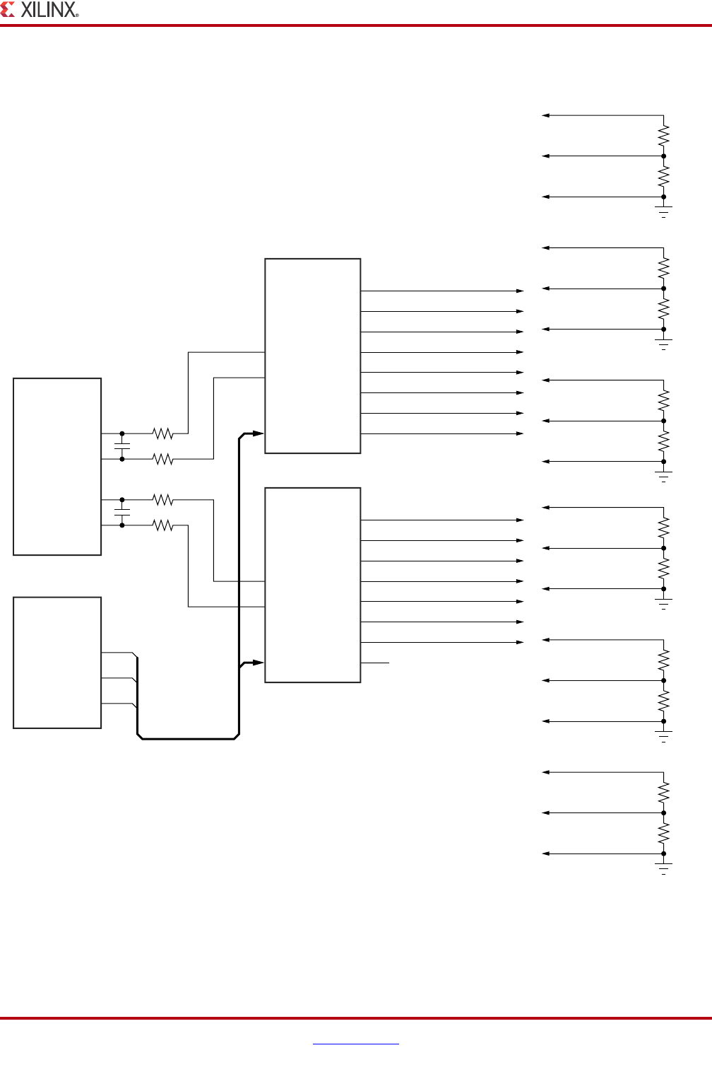
AC701 Evaluation Board www.xilinx.com 65
UG952 (v1.1) January 30, 2013
Feature Descriptions
Figure 1-42 shows the XADC external multiplexer block diagram.
X-Ref Target - Figure 1-42
Figure 1-42: XADC External Multiplexer Block Diagram
UG952_c1_139_011813
1. ..._XADC_P/N =Remote voltage sense.
2. ..._XADC_CS_P/N = Current Sense from op amp.
XC7A200T
FPGA
(Bank 15)
U1
ADIP K16
AD1N K17
AD9P M15
AD9N L15
Notes:
49.9
49.9
10 pF
49.9
49.9
10 pF
XC7A200T
FPGA
(Bank 16)
U1
A0 B25
A1 A25
A2 A23
VCCINT_XADC_CS_P/N
VCCAUX_XADC_CS_P/N
VCCBRAM_XADC_CS_P/N
FPGA_1V5_XADC_P/N
FPGA_1V5_XADC_CS_P/N
VCCO_VADJ_XADC_P/N
VCCO_VADJ_XADC_CS_P/N
FPGA_1V8_XADC_P/N
FPGA_1V8_XADC_CS_P/N
FPGA_3V3_XADC_P/N
FPGA_3V3_XADC_CS_P/N
MGTAVCC_XADC_P/N
MGTAVCC_XADC_CS_P/N
MGTAVTT_XADC_P/N
MGTAVTT_XADC_CS_P/N
NC
ADG707BRU
U14
S1A/B
S2A/B
S3A/B
S4A/B
S5A/B
S6A/B
S7A/B
S8A/B
DA
DB
A[2:0]
ADG707BRU
U13
S1A/B
S2A/B
S3A/B
S4A/B
S5A/B
S6A/B
S7A/B
S8A/B
DA
DB
A[2:0]
GND
1.00 K
1.00 K
FPGA_1V5_SENSE_P
FPGA_1V5_XADC_P
FPGA_1V5_XADC_N
(1.5V Scaled to 0.75V)
GND
3.01 K
1.00 K
VCCO_VADJ_SENSE_P
VCCO_VADJ_XADC_P
VCCO_VADJ_XADC_N
(2.5V Scaled to 0.625V)
GND
3.01 K
1.00 K
FPGA_1V8_SENSE_P
FPGA_1V8_XADC_P
FPGA_1V8_XADC_N
(1.8V Scaled to 0.45V)
GND
1.00 K
1.00 K
MGTAVCC_SENSE_P
MGTAVCC_XADC_P
MGTAVCC_XADC_N
(1.0V Scaled to 0.5V)
GND
1.00 K
1.00 K
MGTAVTT_SENSE_P
MGTAVTT_XADC_P
MGTAVTT_XADC_N
(1.2V Scaled to 0.6V)
GND
3.01 K
1.00 K
FPGA_3V3_SENSE_P
FPGA_3V3_XADC_P
FPGA_3V3_XADC_N
(3.3V Scaled to 0.825V)
66 www.xilinx.com AC701 Evaluation Board
UG952 (v1.1) January 30, 2013
Chapter 1: AC701 Evaluation Board Features
See Tables Table 1-29 and Table 1-30 which list the AC701 board XADC power system
voltage and current measurement details for the external muxes U14 and U13.
Table 1-29: XADC Measurements through Mux U14
Measurement
Type
Rail
Name
Current
Range
Isense Op Amp
Schematic
Net Name
8-to-1 Multiplexer U14
Mux
A[2:0]Reference
Designator Gain Vo Range Pin
Number
Pin
Name
V VCCINT NA NA NA NA XADC INTERNAL NA NA NA
I VCCINT CS 0A-4A U16 50 0V-0.996V
VCCINT_XADC_CS_P 19 S1A 000
VCCINT_XADC_CS_N 11 S1B
V VCCAUX NA NA NA NA XADC INTERNAL NA NA NA
I VCCAUX CS 0A-6A U17 30 0V-0.913V
VCCAUX_XADC_CS_P 20 S2A 001
VCCAUX_XADC_CS_N 10 S2B
V VCCBRAM NA NA NA NA XADC INTERNAL NA NA NA
I VCCBRAM CS 0A-1.8A U20 100 0V-0.909V
VCCBRAM_XADC_CS_P 21 S3A 010
VCCBRAM_XADC_CS_N 9 S3B
V FPGA_1V5 NA FPGA_1V5 REMOTE SENSE DIVIDED TO
DELIVER 0.75V ON FPGA_1V5_XADC_P
FPGA_1V5_XADC_P 22 S4A 011
FPGA_1V5_SENSE_N 8 S4B
I FPGA_1V5 CS 0A-6A U18 20 0V-0.604V
FPGA_1V5_XADC_CS_P 23 S5A 100
FPGA_1V5_XADC_CS_N 7 S5B
VVCCO_VADJNA
VCCO_VADJ 2.5V REMOTE SENSE
DIVIDED TO DELIVER 0.625V ON
FPGA_1V5_XADC_P
VCCO_VADJ_XADC_P 24 S6A 101
VCCO_VADJ_SENSE_N 6 S6B
I VCCO_VADJ CS 0A-3.2A U22 50 0V-0.796V
VCCO_VADJ_XADC_CS_P 25 S7A 110
VCC0VADJ_XADC_CS_N 5 S7B
V FPGA_1V8 NA FPGA_1V8 REMOTE SENSE DIVIDED TO
DELIVER 0.45V ON FPGA_1V8_XADC_P
FPGA_1V8_XADC_P 26 S8A 111
FPGA_1V8_SENSE_N 4 S8B
Table 1-30: XADC Measurements through Mux U13
Measurement
Type
Rail
Name
Current
Range
Isense Op Amp
Schematic
Net Name
8-to-1 Multiplexer U14
Mux
A[2:0]Reference
Designator Gain Vo Range Pin
Number
Pin
Name
I FPGA_1V8 CS 0A-3A U21 50 0V-0.747V
FPGA_1V8_XADC_CS_P 19 S1A 000
FPGA_1V8_XADC_CS_N 11 S1B
VFPGA_3V3
SENSE NA
FPGA_3V3 REMOTE SENSE DIVIDED
TO DELIVER 0.825V ON
FPGA_3V3_XADC_P
FPGA_3V3_XADC_P 20 S2A 001
FPGA_3V3_SENSE_N 10 S2B
I FPGA_3V3 CS 0A-3.2A U15 50 0V-0.796V
FPGA_3V3_XADC_CS_P 21 S3A 010
FPGA_3V3_XADC_CS_N 9 S3B
VMGTAVCC
SENSE NA
MGTAVCC REMOTE SENSE DIVIDED
TO DELIVER 0.5V ON
MGTAVCC_XADC_P
MGTAVCC_XADC_P 22 S4A 011
MGTAVCC_SENSE_N 8 S4B
I MGTAVCC CS 0A-3A U25 50 0V-0.747V
MGTAVCC_XADC_CS_P 23 S5A 100
MGTAVCC_XADC_CS_N 7 S5B
AC701 Evaluation Board www.xilinx.com 67
UG952 (v1.1) January 30, 2013
Feature Descriptions
Power Management
[Figure 1-2, callout 30]
The AC701 board uses power regulators and PMBus compliant system controllers from
Texas Instruments to supply core and auxiliary voltages. The Texas Instruments Fusion
Digital Power graphical user interface is used to monitor the voltage and current levels of
the board power modules.
The AC701 board power distribution diagram is shown in Figure 1-43.
The pcb layout and power system design meets the recommended criteria described in the
UG483, 7 Series FPGAs PCB Design and Pin Planning Guide.
VMGTAVTT
SENSE NA
MGTAVTT REMOTE SENSE DIVIDED
TO DELIVER 0.6V ON
MGTAVTT_XADC_P
MGTAVTT_XADC_P 24 S6A 101
MGTAVTT_SENSE_N 6 S6B
I MGTAVTT CS 0A-1.5A U23 100 0V-0.756V
MGTAVTT_XADC_CS_P 25 S7A 110
MGTAVTT_XADC_CS_N 5 S7B
NOT USED NOT CONNECTED)
NC 26 S8A 111
NC 4 S8B
Table 1-30: XADC Measurements through Mux U13 (Cont’d)
Measurement
Type
Rail
Name
Current
Range
Isense Op Amp
Schematic
Net Name
8-to-1 Multiplexer U14
Mux
A[2:0]Reference
Designator Gain Vo Range Pin
Number
Pin
Name
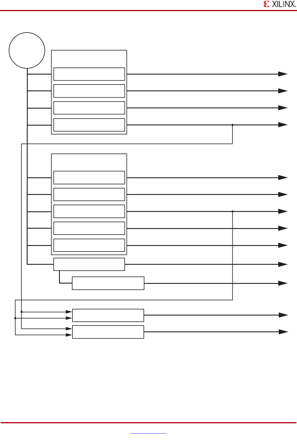
68 www.xilinx.com AC701 Evaluation Board
UG952 (v1.1) January 30, 2013
Chapter 1: AC701 Evaluation Board Features
X-Ref Target - Figure 1-43
Figure 1-43: AC701 Board Onboard Power Regulators
UG952_c1_37_100512
VCCAUX
VCCBRAM
FPGA_1V5
VCCO_VAJ
FPGA_1V8
MGTAVCC
12V PWR
Jack
J49
VCC3V3
VCCINT
VCC5V0
VTTDDR
XADC_VCC
DDR3_VTERM
Power Controller 2
PMBUS 102
MGTAVTT
Switching Regulator
5.0V at 2A
U46
Source/Sink Regulator
0.75V at 3A
U37
Switching Regulator
0.75V at 3A
U36
Linear Regulator
1.7V–2.0V at 300 mA
U10
Switching Module
1.5V at 6A
U55
Switching Module
1.0V at 6A
U59
Switching Module
3.3V at 6A
U58
Switching Module
1.8V at 6A
U57
Switching Module
1.2V–3.3V at 6A
U56
Switching Module
1.2V at 3A
U60
Switching Regulator
1.0V at 8A
U49
Switching Module
1.8V at 3A
U53
Switching Module
1.0V at 3A
U54
Power Controller 1
PMBUS 101
U8
U9
1.5V/2=0.75V REFIN
1.5V/2=0.75V REFIN
3.3V POWER
3.3V POWER
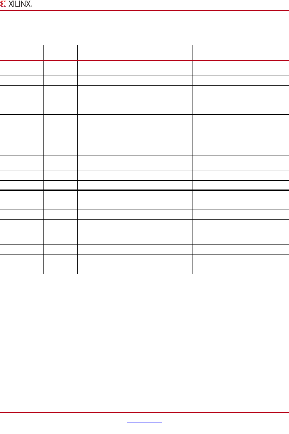
AC701 Evaluation Board www.xilinx.com 69
UG952 (v1.1) January 30, 2013
Feature Descriptions
The AC701 board core and auxiliary voltages are listed in Table 1-25.
Monitoring Voltage and Current
Voltage and current monitoring and voltage control are available for the TI controlled
power rails through the Texas Instruments Fusion Digital Power Designer graphical user
interface (GUI). The two onboard TI UCD90120A power controllers (U8 at PMBus address
101 and U9 at address 102) are wired to the same PMBus. The PMBus connector, J2, is
provided for use with the TI USB Interface Adapter PMBus pod (TI part number EVM
USB-TO-GPIO) and associated TI Fusion Digital Power Designer GUI. This is the simplest
and most convenient way to monitor the voltage and current values for the power rail
listed in Table 1-32 and Table 1-33.
In each of these the two tables (one per controller), the Power Good (PG) On Threshold is
the set-point at or above which the particular rail is deemed good. The PG Off Threshold is
the set-point at or below which the particular rail is no longer deemed good. The controller
Table 1-31: AC701 Board Onboard Power System Devices
Device Type Reference
Designator Description Power Rail Net
Name
Power Rail
Voltag e
Schematic
Page
UCD90120A
(4 Rails) U8 PMBus Controller - PMBus Addr = 101 39
LMZ22010TZ U49 10A 0.8V - 6V Adj. Switching Regulator VCCINT 1.00V 40
TPS84621RUQ U53 6A 0.6V - 5.5V Adj. Switching Regulator VCCAUX 1.80V 41
TPS84320RUQ U54 3A 0.6V - 5.5V Adj. Switching Regulator VCCBRAM 1.00V 42
TPS84621RUQ U55 6A 0.6V - 5.5V Adj. Switching Regulator FPGA_1V5 1.50V 43
UCD90120A
(5 Rails) U9 PMBus Controller - PMBus Addr = 102 45
TPS84621RUQ U56 6A 0.6V - 5.5V Adj. Switching Regulator VCCO_VADJ 2.50V 46
TPS84320RUQ U57 3A 0.6V - 5.5V Adj. Switching Regulator VCC1V8/
FPGA_1V8 1.80V 47
TPS84621RUQ U58 6A 0.6V - 5.5V Adj. Switching Regulator VCC3V3/
FPGA_3V3 3.30V 48
TPS84320RUQ U59 3A 0.6V - 5.5V Adj. Switching Regulator MGTAVCC 1.00V 49
TPS84320RUQ U60 3A 0.6V - 5.5V Adj. Switching Regulator MGTAVTT 1.20V 50
LMZ12002 U46 2A 0.8V - 6V Adj. Linear Regulator VCC5V0 5.00V 34
TL1963ADCQR U62 1.5A 1.21V - 5V Adj. LDO Linear Regulator VCC2V5 2.50V 48
TPS51200DR U37 3A Source-Sink DDR Termination Regulator VTTDDR 0.75V 44
TPS51200DR U36 3A Source-Sink DDR Termination Regulator DDR3_VTERM_
R_0V75 0.75V 44
TPS79433DCQ U61 0.25A 1.2V - 5.5V Adj. LDO Linear Regulator V33D_CTL1 3.30V 39
TPS79433DCQ U63 0.25A 1.2V - 5.5V Adj. LDO Linear Regulator V33D_CTL2 3.30V 45
ADP123 U10 0.3A 0.8V - 5V Adj. Linear Regulator XADC_VCC 1.85V 29
REF3012 U35 50uA Fixed 1.25V Voltage Reference XADC_VREF 1.25V 29
Notes:
1. See Table 1-32
2. See Table 1-33
70 www.xilinx.com AC701 Evaluation Board
UG952 (v1.1) January 30, 2013
Chapter 1: AC701 Evaluation Board Features
internally ORs these PG conditions together and drives an output PG pin high only if all
active rail PG states are good. The on and off delay parameter values are relative to when
the board power on-off slide switch SW15 is turned on and off.
Table 1-32 defines the voltage and current values for each power rail controlled by the
UCD90120A U8 controller at PMBus Address 101.
Table 1-33 defines the voltage and current values for each power rail controlled by the
UCD90120A U9 controller at PMBus Address 102.
VCCO_VADJ Voltage Control
The FMC VCCO_VADJ rail is set to 2.5V. When the AC701 board is powered on, the state
of the FMC_VADJ_ON_B signal wired to header J8 is sampled by the TI UCD90120A
controller U9. If a jumper is installed on J8, signal FMC_VADJ_ON_B is held low, and TI
controller U9 energizes the FMC VCCO_VADJ rail at power on.
Removing the jumper at J8 after the board is powered up will not affect the 2.5V power
delivered to the VCCO_VADJ rail and it will remain on.
A jumper installed at J8 is the default setting. If a jumper is not installed on J8 at power-on,
the signal FMC_VADJ_ON_B is high and the AC701 board will not energize the
VCCO_VADJ 2.5V power.
Installing a jumper at J8 after the AC701 board powers up in this mode will turn on the
VCCO_VADJ rail.
Table 1-32: Power Rail Specifications for UCD90120A PMBus Controller U8 at Address 101
Rail Nominal
Voltage Power Good On Power Good Off
Turn On
Delay
(ms)
Turn
Off
Delay
(ms)
Fault
Shutdown
Slaves
Rail Turn-on
Dependencies
Rail GPI
1 VINT_1V0 1.000 0.900 -10.0% 0.850 -15.0% 0.0 15.0 Rail #2,3,4 None None
2 VAUX_1V8 1.800 1.620 -10.0% 1.530 -15.0% 10.0 5.0 Rail #1,3,4 Rail #3 None
3 VBRAM_1V0 1.000 0.900 -10.0% 0.850 -15.0% 5.0 10.0 Rail #1,2,4 Rail #1 None
4 FPGA_1V5 1.500 1.350 -10.0% 1.275 -15.0% 15.0 0.0 Rail #1,2,3 Rail #2 None
Table 1-33: Power Rail Specifications for UCD90120A PMBus controller U9 at Address 102
Rail Nominal
Voltage Power Good On Power Good Off
Turn
On
Delay
(ms)
Turn
Off
Delay
(ms)
Fault
Shutdown
Slaves
Rail Turn-on
Dependencies
Rail GPI
1 VADJ_2V5 2.500 2.250 -10.0% 2.125 -15.0% 5.0 15.0 Rail #2,3,4,5 Rail #3
FMC_
VADJ _
ON_B
2 FPGA_1V8 1.800 1.620 -10.0% 1.530 -15.0% 10.0 10.0 Rail #1,3,4,5 None None
3 FPGA_3V3 3.300 2.970 -10.0% 2.805 -15.0% 0.0 20.0 Rail #1,2,4,5 None None
4 MGTVC_1V0 1.000 0.900 -10.0% 0.850 -15.0% 5.0 5.0 Rail #1,2,3,5 Rail #2 None
5 MGTVT_1V2 1.200 1.080 -10.0% 1.020 -15.0% 10.0 0.0 Rail #1,2,3,4 Rail #4 None
AC701 Evaluation Board www.xilinx.com 71
UG952 (v1.1) January 30, 2013
Feature Descriptions
In this VCCO_VADJ off mode, the user can control when to turn on VCCO_VADJ and to
what voltage level (1.8V, 2.5V or 3.3V).
With VCCO_VADJ off, the FPGA still configures and has access to the TI controller PMBUS
and the VADJ_ON_B signal which are wired to FPGA U1 Bank 14. The combination of
these features allows the user to develop code to command the VCCO_VADJ rail to be set
to 1.8V or 3.3V instead of the default setting of 2.5V.
Refer to AC701 board schematic page 46 for a brief discussion concerning selectable
VCCO_VADJ voltages. The important controller-to-regulator circuit signals are
VCCO_VADJ_EN and FMC_ADJ_SEL[1:0]. In the VCCO_VADJ off mode, controller U9
does not toggle the regulator turn-on signal VCCO_VADJ_EN high so the U56 regulator
stays off. The user must re-program the controller U9 VCCO_VADJ rail settings to the
desired VCCO_VADJ voltage so that the controller expects the new voltage to appear on its
MON1 remote sense pin. The FMC_ADJ_SEL[1:0] controller GPIO16 and GPIO17 pins
must be set to the correct logic levels to force the VCCO_VADJ regulator Rset MUX U64 to
select the appropriate RT_CLK and VADJ resistors for the desired voltage as shown in
Table 1-34.
When the new VCCO_VADJ rail settings and Rset MUX logic levels are programmed into
controller U9, the FMC_VADJ_ON_B signal can be driven low by user FPGA logic and the
controller toggles the VCCO_VADJ_EN signal high to allow the rail to come up at the new
VCCO_VADJ voltage level.
Documentation describing PMBUS programming for the UCD90120A controller is
available at http://www.ti.com/fusiondocs.
Cooling Fan Control
Cooling fan RPM is controlled and monitored by user-created IP in the FPGA using the fan
control circuit is shown in Figure 1-44.
FPGA U1 can be cooled by a user-supplied 12V DC fan connected to J61. 12VDC is
provided to the fan through J61 pin 2. The fan GND return is provided through J61 pin 1
and transistor Q17. Fan speed is controlled by a pulse-width-modulated signal from FPGA
U1 pin J26 (on Bank 15) driving the gate of Q17. The default unprogrammed FPGA fan
operation mode is ON. The fan speed tachometer signal on J61 pin 3 can be monitored on
FPGA U1 pin J25 (on Bank 15).
Table 1-34: VCCO_VADJ Voltage Selection
FMC_ADJ_SEL[10] VCCO_ADJ (V)
BIT 1 BIT 0
002.5V
011.8V
103.3V
11NOT USED
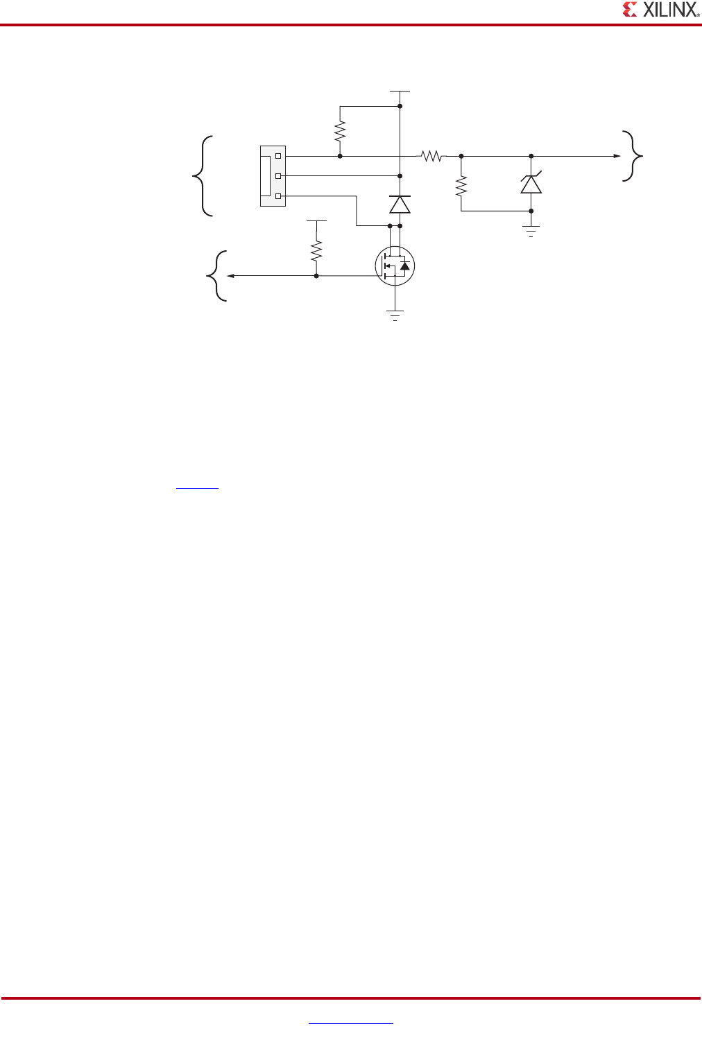
72 www.xilinx.com AC701 Evaluation Board
UG952 (v1.1) January 30, 2013
Chapter 1: AC701 Evaluation Board Features
XADC Header
[Figure 1-2, callout 31]
7 series FPGAs provide an Analog Front End (XADC) block. The XADC block includes
a dual 12-bit, 1 MSPS Analog-to-Digital Convertor (ADC) and on-chip sensors. See
UG480, 7 Series FPGAs XADC Dual 12-Bit 1MSPS Analog-to-Digital Converter User Guide
for details on the capabilities of the analog front end. Figure 1-45 shows the AC701
board XADC support features.
X-Ref Target - Figure 1-44
Figure 1-44: FPGA Cooling Fan Circuit
GND
SM_FAN_PWM
SM_FAN_TACH
1
2
3
J61
R245
10.0K 1%
1/10W
GND
R277
1.00K 1%
1/16W
D15
2.7V
500 mW
MM3Z2V7B
R390
4.75K 1%
1/10W
R393
10.0K 1%
1/10W
VCC12_P
D14
100V
500 mW
DL4148
Q17
NDT30555L
1.3 W
1
2
3
4
VCC2V5
UG952_c1_38_100512
Cooling
Fan
FPGA
U1 Pin J26
FPGA
U1 Pin J25
Fan GND
Fan +12V
Fan Tach

AC701 Evaluation Board www.xilinx.com 73
UG952 (v1.1) January 30, 2013
Feature Descriptions
The AC701 board supports both the internal FPGA sensor measurements and the external
measurement capabilities of the XADC. Internal measurements of the die temperature,
VCCINT, VCCAUX, and VCCBRAM are available. The AC701 board VCCINT and
VCCBRAM are provided by a common 1.0 V supply.
Jumper J42 can be used to select either an external differential voltage reference
(XADC_VREF) or on-chip voltage reference (jumper J42 2–3) for the analog-to-digital
converter.
For external measurements an XADC header (J19) is provided. This header can be used to
provide analog inputs to the FPGA's dedicated VP/VN channel, and to the VAUXP[0]/
VAUXN[0], VAUXP[8]/VAUXN[8] auxiliary analog input channels. Simultaneous
sampling of Channel 0 and Channel 8 is supported.
A user-provided analog signal multiplexer card can be used to sample additional external
analog inputs using the 4 GPIO pins available on the XADC header as multiplexer address
lines. Figure 1-46 shows the XADC header J19 connections.
X-Ref Target - Figure 1-45
Figure 1-45: Header XADC_VREF Voltage Source Options
FPGA
U1
VAUX0N
VAUX0P
VAUX8N
VAUX8P
VREF (1.25V)
VREFN
VCCADC
GNDADC
VN
VP
DXP
DXN
UG952_c1_39_101612
100Ω
1 nF
100Ω
100Ω
1 nF
100Ω
To
Header
J49
Dual Use IO
(Analog/Digital)
100Ω
1 nF
100ΩTo
Header
J19
100 nF
XADC_AGND
REF3012
U35
Out In
Gnd
J42
XADC_AGND
Internal
Reference
XADC_VREF to
XADC Header J19.11
10 μF
Ferrite Bead
100 nF 1 nF
Ferrite Bead
J10
J9
Star Grid
Connection
J54
XADC_VCC
XADC_VCC
XADC_AGND
GND
VREFP XADC_VREFP
ADP123
U10
Out In
Gnd
XADC_AGND
10 μF
XADC_VCC Header J49
100 nF
XADC_AGND
XADC_VCC
J43
Ferrite Bead
VCCAUX
VCC5V0
10 μF
XADC_VCC5V0 to
XADC Header J19.13
1.8V 150 mV max
J53
Filter 5V Supply
Locate Components on Board
Close to
Package Pins
Close to
Package Pins
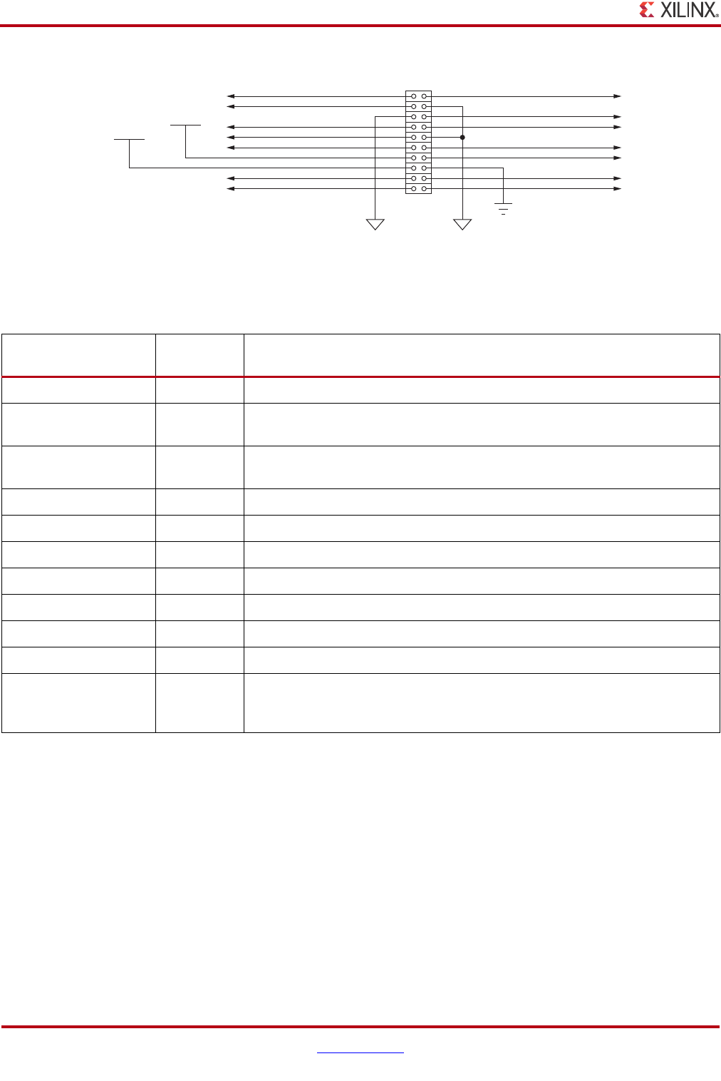
74 www.xilinx.com AC701 Evaluation Board
UG952 (v1.1) January 30, 2013
Chapter 1: AC701 Evaluation Board Features
Table 1-35 describes the XADC header J19 pin functions.
X-Ref Target - Figure 1-46
Figure 1-46: XADC header (J19)
UG952_c1_40_101612
XADC_VP
XADC_VAUX0N
XADC_VAUX8P
XADC_DXN
XADC_VCC_HEADER
XADC_VN
XADC_VAUX0P
XADC_VAUX8N
XADC_DXP
XADC_VREF
XADC_GPIO_0
XADC_GPIO_2
XADC_GPIO_1
XADC_GPIO_3
J19
1
3
5
7
9
11
13
15
17
19
2
4
6
8
10
12
14
16
18
20
GND
XADC_AGNDXADC_AGND
XADC_VCC5V0
VCCO_VADJ
Table 1-35: XADC Header J19 Pinout
Net Name J19 Pin
Number Description
XADC_VN, _VP 1, 2 Dedicated analog input channel for the XADC.
XADC_VAUX0P, N 3, 6 Auxiliary analog input channel 0. Also supports use as IO inputs when anti
alias capacitor is not present.
XADC_VAUX8N, P 7, 8 Auxiliary analog input channel 8. Also supports use as IO inputs when anti
alias capacitor is not present.
DXP, DXN 9, 12 Access to thermal diode.
XADC_AGND 4, 5, 10 Analog ground reference.
XADC_VREF 11 1.25V reference from the board.
XADC_VCC5V0 13 Filtered 5V supply from board.
XADC_VCC_HEADER 14 Analog 1.8V supply for XADC.
VCCO_VADJ 15 VCCO supply for bank which is the source of DIO pins.
GND 16 Digital Ground (board) Reference
XADC_GPIO_3, 2, 1, 0 19, 20, 17, 18
Digital IO. These pins should come from the same bank. These IOs should not
be shared with other functions because they are required to support three-state
operation.
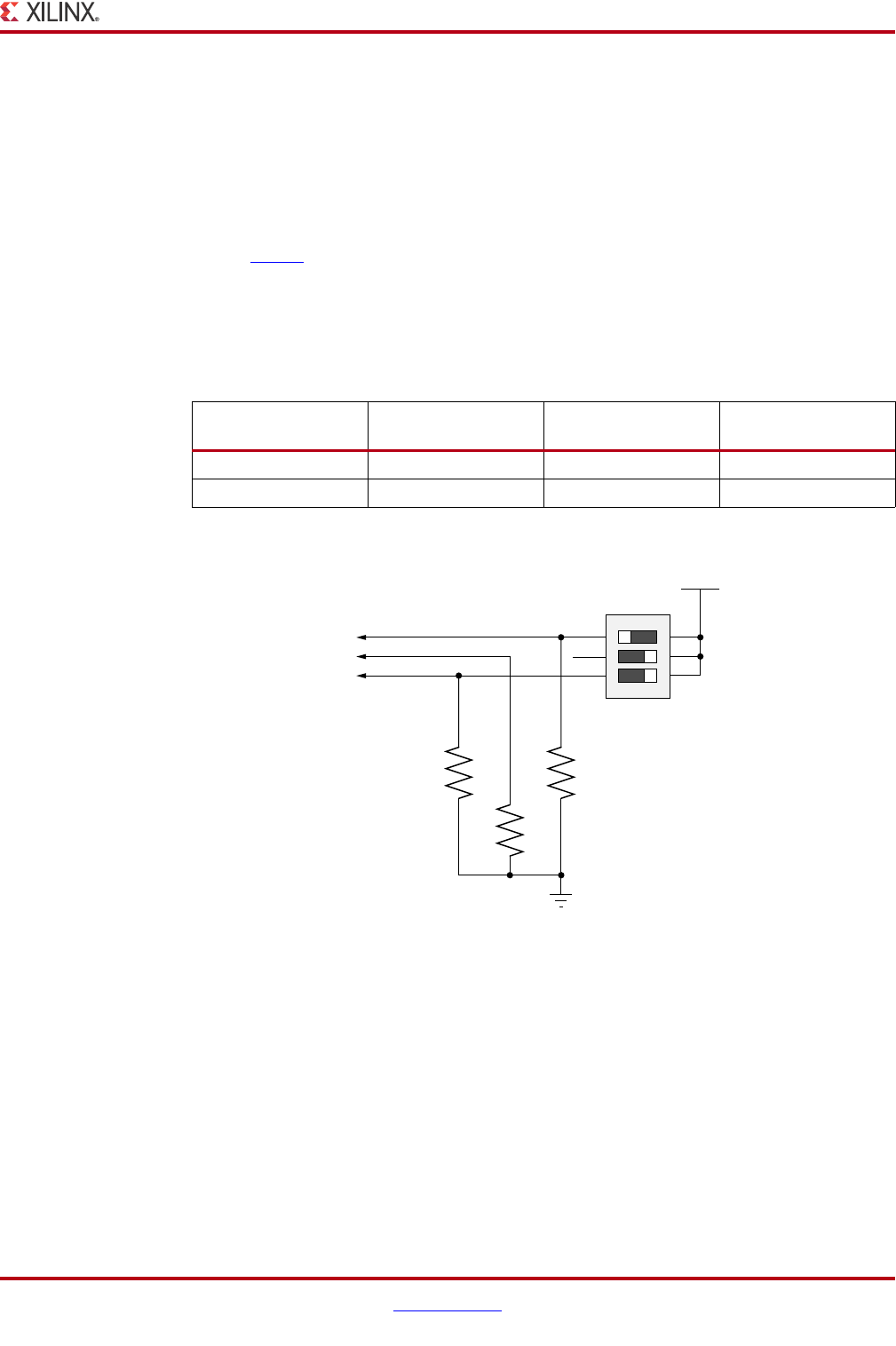
AC701 Evaluation Board www.xilinx.com 75
UG952 (v1.1) January 30, 2013
Configuration Options
Configuration Options
The FPGA on the AC701 board can be configured using these methods:
• Master SPI (uses the Quad-SPI Flash U7).
• JTAG (uses the U26 Digilent USB-to-JTAG Bridge or J4 Download Cable connector).
See USB JTAG Module, page 20 for more information.
SeeUG480, 7 Series FPGAs XADC Dual 12-Bit 1MSPS Analog-to-Digital Converter User
Guide for further details on configuration modes.
The method used to configure the FPGA is controlled by the mode pins (M2, M1, M0)
setting selected through DIP switch SW1. Table 1-36 lists the supported mode switch
settings.
Figure 1-47 shows mode switch SW1.
Table 1-36: Mode Switch SW1 Settings
Configuration
Mode Mode Pins (M[2:0]) Bus
Width
CCLK
Direction
Master SPI 001 x1, x2, x4 Output
JTAG 101 x1 Not Applicable
X-Ref Target - Figure 1-47
Figure 1-47: Mode Switch
UG952_c1_41_011813
SDA03H1SBD
SW1
FPGA_3V3
FPGA_M2
FPGA_M0
FPGA_M1
R339
1.21K
0.1W
1%
R338
1.21K
0.1 W
1%
R337
1.21K
0.1W
1%
1
2
3
6
5
4
GND
ON
NC
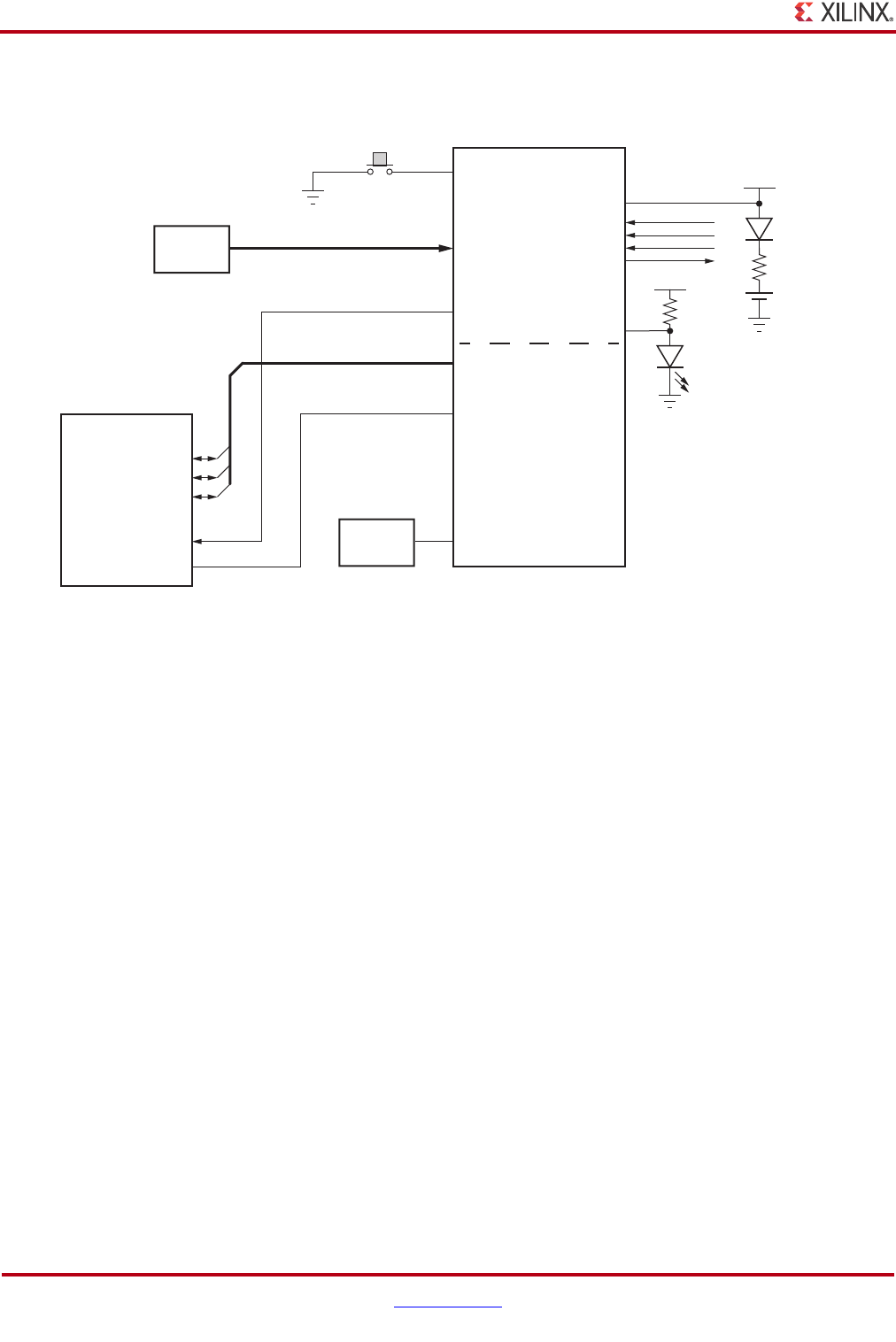
76 www.xilinx.com AC701 Evaluation Board
UG952 (v1.1) January 30, 2013
Chapter 1: AC701 Evaluation Board Features
Figure 1-48 shows the QSPI U7 configuration circuit.
X-Ref Target - Figure 1-48
Figure 1-48: AC701 Board QSPI Configuration Circuit
UG952_c1_42_101612
DQ[1:0]
DQ2_WP
DQ3_HOLD_B
C
S-B
U7
N25Q256A13ESF40G
QUAD SPI
TCK
TMS
TDI
TDO
Bank 0
CCLK
VBATT
M[2:0]
DONE
PROG_B
PROG_B
U1
FPGA
SW9
Bank 14
D[3:0]
FCS_B
EMCCLK
SIT8103
GND
VCC1V8
VCC3V3
R396
4.7K
GND
R396
261Ω
D6
BAS40-04
B1
DS10
GREEN
GND
U40
Oscillator
90 MHz
SW1
Mode
Switch
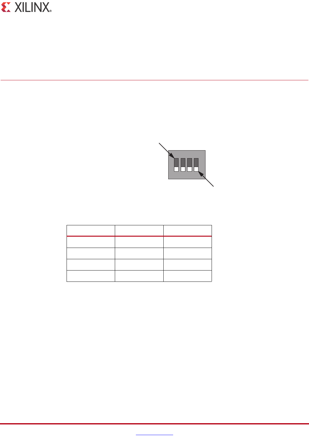
AC701 Evaluation Board www.xilinx.com 77
UG952 (v1.1) January 30, 2013
Appendix A
Default Switch and Jumper Settings
User GPIO DIP Switch SW2
See Figure 1-2, page 8 callout 23 for location of SW2. Default settings are shown in
Figure A-1 and details are listed in Table A-1.
X-Ref Target - Figure A-1
Figure A-1: SW2 Default Settings
Table A - 1 : SW2 Default Switch Settings
Position Function Default
1 GPIO_DIP_SW0 Off
2 GPIO_DIP_SW1 Off
3 GPIO_DIP_SW2 Off
4 GPIO_DIP_SW3 Off
UG952_aA_01_100712
SW2
1
OFF Position = 0
ON Position = 1
234
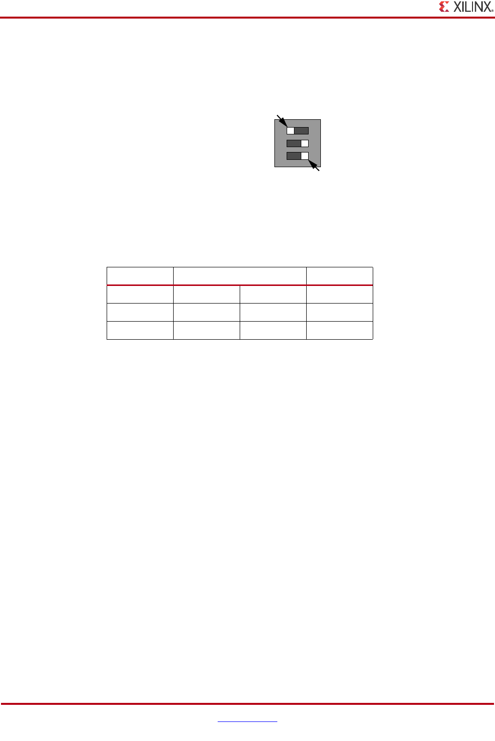
Appendix A: Default Switch and Jumper Settings
78 www.xilinx.com AC701 Evaluation Board
UG952 (v1.1) January 30, 2013
Configuration DIP Switch SW1
See Figure 1-2, page 8 callout 28 for location of SW1. Default settings are shown in
Figure A-2 and details are listed in Table A-2.
The default mode setting M[2:0] = 001 selects Master SPI configuration at board
power-on.
X-Ref Target - Figure A-2
Figure A-2: SW1 Default Settings
Table A - 2 : SW1 Default Switch Settings
Position Function Default
1FPGA_M2 M2 Off
2FPGA_M1 M1 Off
3FPGA_M0 M0 On
UG952_aA_02_011813
SW1 OFF Position = 0
ON Position = 1
1 2 3
M2
M1
M0
ON
Default Jumper Settings
AC701 Evaluation Board www.xilinx.com 79
UG952 (v1.1) January 30, 2013
Default Jumper Settings
The AC701 board default jumper configurations are listed in Table A-3.
Table A - 3 : AC701 Default Jumper Settings
Header Jumper Description Schematic
Page
2-pin
J11 1-2 XADC VCCINT 4A range 34
J53 1-2 XADC_VCC5V0 = 5V 29
J9 1-2 REF3012 XADC_AGND L3 bypassed 29
J10 1-2 REF3012 XADC_AGND = GND 29
J63 None Voltage Regulators Enabled 38
J52 None Test Header, Not a Jumper 7
J5 1-2 EPHY U12.2 CONFIG2 = LOW 15
J8 1-2 VCCO_VADJ (FMC) Voltage = ON 45
J3 None SPI SELECT = On-Board SPI Device 4
J6 1-2 SFP+ Enabled 20
3-pin
J35 1-2 EPHY U12.3 CONFIG3 = HI 15
J36 None EPHY U12.2 CONFIG2 Option Header 15
J37 None EPHY U12.3 CONFIG3 Option Header 15
J43 2-3 XADC_VCC = ADP123 1.85V 29
J54 2-3 REF3012 VIN = XADC_VCC 29
J42 1-2 XADC_VREFP = REF3012 XADC_VREF 29
J38 1-2 SFP RX BW = FULL 20
J39 1-2 SFP TX BW = FULL 20
2x2
J12 3-4 PCIE Lane Width = 4 28

AC701 Evaluation Board www.xilinx.com 81
UG952 (v1.1) January 30, 2013
Appendix B
VITA 57.1 FMC Connector Pinouts
Figure B-1 shows the pinout of the FPGA mezzanine card (FMC) high pin count (HPC)
connector defined by the VITA 57.1 FMC specification. For a description of how the AC701
board implements the FMC specification, see FPGA Mezzanine Card Interface, page 54
and HPC Connector J30, page 55.
X-Ref Target - Figure B-1
Figure B-1: FMC HPC Connector Pinout
UG952_aB_01_101612
1
2
3
4
5
6
7
8
9
10
11
12
13
14
15
16
17
18
19
20
21
22
23
24
25
26
27
28
29
30
31
32
33
34
35
36
37
38
39
40
VREF_B_M2C
GND
GND
CLK2_M2C_P
CLK2_M2C_N
GND
HA02_P
HA02_N
GND
HA06_P
HA06_N
GND
HA10_P
HA10_N
GND
HA17_P_CC
HA17_N_CC
GND
HA21_P
HA21_N
GND
HA23_P
HA23_N
GND
HB00_P_CC
HB00_N_CC
GND
HB06_P_CC
HB06_N_CC
GND
HB10_P
HB10_N
GND
HB14_P
HB14_N
GND
HB17_P_CC
HB17_N_CC
GND
VIO_B_M2C
GND
CLK3_M2C_P
CLK3_M2C_N
GND
GND
HA03_P
HA03_N
GND
HA07_P
HA07_N
GND
HA11_P
HA11_N
GND
HA14_P
HA14_N
GND
HA18_P
HA18_N
GND
HA22_P
HA22_N
GND
HB01_P
HB01_N
GND
HB07_P
HB07_N
GND
HB11_P
HB11_N
GND
HB15_P
HB15_N
GND
HB18_P
HB18_N
GND
VIO_B_M2C
GND
VREF_A_M2C
PRSNT_M2C_L
GND
CLK0_M2C_P
CLK0_M2C_N
GND
LA02_P
LA02_N
GND
LA04_P
LA04_N
GND
LA07_P
LA07_N
GND
LA11_P
LA11_N
GND
LA15_P
LA15_N
GND
LA19_P
LA19_N
GND
LA21_P
LA21_N
GND
LA24_P
LA24_N
GND
LA28_P
LA28_N
GND
LA30_P
LA30_N
GND
LA32_P
LA32_N
GND
VADJ
GND
DP1_M2C_P
DP1_M2C_N
GND
GND
DP2_M2C_P
DP2_M2C_N
GND
GND
DP3_M2C_P
DP3_M2C_N
GND
GND
DP4_M2C_P
DP4_M2C_N
GND
GND
DP5_M2C_P
DP5_M2C_N
GND
GND
DP1_C2M_P
DP1_C2M_N
GND
GND
DP2_C2M_P
DP2_C2M_N
GND
GND
DP3_C2M_P
DP3_C2M_N
GND
GND
DP4_C2M_P
DP4_C2M_N
GND
GND
DP5_C2M_P
DP5_C2M_N
GND
RES1
GND
GND
DP9_M2C_P
DP9_M2C_N
GND
GND
DP8_M2C_P
DP8_M2C_N
GND
GND
DP7_M2C_P
DP7_M2C_N
GND
GND
DP6_M2C_P
DP6_M2C_N
GND
GND
GBTCLK1_M2C_P
GBTCLK1_M2C_N
GND
GND
DP9_C2M_P
DP9_C2M_N
GND
GND
DP8_C2M_P
DP8_C2M_N
GND
GND
DP7_C2M_P
DP7_C2M_N
GND
GND
DP6_C2M_P
DP6_C2M_N
GND
GND
RES0
GND
DP0_C2M_P
DP0_C2M_N
GND
GND
DP0_M2C_P
DP0_M2C_N
GND
GND
LA06_P
LA06_N
GND
GND
LA10_P
LA10_N
GND
GND
LA14_P
LA14_N
GND
GND
LA18_P_CC
LA18_N_CC
GND
GND
LA27_P
LA27_N
GND
GND
SCL
SDA
GND
GND
GA0
12P0V
GND
12P0V
GND
3P3V
GND
PG_C2M
GND
GND
GBTCLK0_M2C_P
GBTCLK0_M2C_N
GND
GND
LA01_P_CC
LA01_N_CC
GND
LA05_P
LA05_N
GND
LA09_P
LA09_N
GND
LA13_P
LA13_N
GND
LA17_P_CC
LA17_N_CC
GND
LA23_P
LA23_N
GND
LA26_P
LA26_N
GND
TCK
TDI
TDO
3P3VAUX
TMS
TRST_L
GA1
3P3V
GND
3P3V
GND
3P3V
GND
HA01_P_CC
HA01_N_CC
GND
GND
HA05_P
HA05_N
GND
HA09_P
HA09_N
GND
HA13_P
HA13_N
GND
HA16_P
HA16_N
GND
HA20_P
HA20_N
GND
HB03_P
HB03_N
GND
HB05_P
HB05_N
GND
HB09_P
HB09_N
GND
HB13_P
HB13_N
GND
HB19_P
HB19_N
GND
HB21_P
HB21_N
GND
VADJ
GND
PG_M2C
GND
GND
HA00_P_CC
HA00_N_CC
GND
HA04_P
HA04_N
GND
HA08_P
HA08_N
GND
HA12_P
HA12_N
GND
HA15_P
HA15_N
GND
HA19_P
HA19_N
GND
HB02_P
HB02_N
GND
HB04_P
HB04_N
GND
HB08_P
HB08_N
GND
HB12_P
HB12_N
GND
HB16_P
HB16_N
GND
HB20_P
HB20_N
GND
VADJ
GND
CLK1_M2C_P
CLK1_M2C_N
GND
GND
LA00_P_CC
LA00_N_CC
GND
LA03_P
LA03_N
GND
LA08_P
LA08_N
GND
LA12_P
LA12_N
GND
LA16_P
LA16_N
GND
LA20_P
LA20_N
GND
LA22_P
LA22_N
GND
LA25_P
LA25_N
GND
LA29_P
LA29_N
GND
LA31_P
LA31_N
GND
LA33_P
LA33_N
GND
VADJ
GND
KJHGFEDCBA

AC701 Evaluation Board www.xilinx.com 83
UG952 (v1.1) January 30, 2013
Appendix C
Master Constraints File Listing
TheAC701 board master Xilinx® design constraints (XDC) file template provides for
designs targeting the AC701 board. Net names in the constraints listed in the AC701 Board
XDC File Listing correlate with net names on the AC701 board schematic. Users must
identify the appropriate pins and replace the net names in this list with net names in the
user RTL. For more information, see UG903, Vivado Design Suite User Guide, Using
Constraints:
http://www.xilinx.com/support/documentation/sw_manuals/xilinx2012_4/
ug903-vivado-using-constraints.pdf
Users can refer to the XDC files generated by tools such as Memory Interface Generator
(MIG) for memory interfaces and Base System Builder (BSB) for more detailed I/O
standards information required for each particular interface.
The FMC HPC connector J30 is connected to a 2.5V Vcco bank. Because each user’s FMC
card implements customer-specific circuitry, the FMC bank I/O standards must be
uniquely defined by each customer.
Note: The XDC file listed in this appendix might not be the latest version. Always refer to the AC701
Evaluation Kit product page (www.xilinx.com/ac701) for the latest FPGA-pins constraints file.
AC701 Board XDC File Listing
set_property PACKAGE_PIN AB22 [get_ports No]
set_property IOSTANDARD LVCMOS25 [get_ports No]
set_property PACKAGE_PIN AE25 [get_ports FMC1_HPC_HA02_P]
set_property IOSTANDARD LVCMOS25 [get_ports FMC1_HPC_HA02_P]
set_property PACKAGE_PIN AE26 [get_ports FMC1_HPC_HA02_N]
set_property IOSTANDARD LVCMOS25 [get_ports FMC1_HPC_HA02_N]
set_property PACKAGE_PIN AC22 [get_ports FMC1_HPC_HA03_P]
set_property IOSTANDARD LVCMOS25 [get_ports FMC1_HPC_HA03_P]
set_property PACKAGE_PIN AC23 [get_ports FMC1_HPC_HA03_N]
set_property IOSTANDARD LVCMOS25 [get_ports FMC1_HPC_HA03_N]
set_property PACKAGE_PIN AF24 [get_ports FMC1_HPC_HA04_P]
set_property IOSTANDARD LVCMOS25 [get_ports FMC1_HPC_HA04_P]
set_property PACKAGE_PIN AF25 [get_ports FMC1_HPC_HA04_N]
set_property IOSTANDARD LVCMOS25 [get_ports FMC1_HPC_HA04_N]
set_property PACKAGE_PIN AD25 [get_ports FMC1_HPC_HA05_P]
set_property IOSTANDARD LVCMOS25 [get_ports FMC1_HPC_HA05_P]
set_property PACKAGE_PIN AD26 [get_ports FMC1_HPC_HA05_N]
set_property IOSTANDARD LVCMOS25 [get_ports FMC1_HPC_HA05_N]
set_property PACKAGE_PIN AE23 [get_ports FMC1_HPC_HA06_P]
set_property IOSTANDARD LVCMOS25 [get_ports FMC1_HPC_HA06_P]
set_property PACKAGE_PIN AF23 [get_ports FMC1_HPC_HA06_N]

Appendix C: Master Constraints File Listing
84 www.xilinx.com AC701 Evaluation Board
UG952 (v1.1) January 30, 2013
set_property IOSTANDARD LVCMOS25 [get_ports FMC1_HPC_HA06_N]
set_property PACKAGE_PIN AD23 [get_ports FMC1_HPC_HA07_P]
set_property IOSTANDARD LVCMOS25 [get_ports FMC1_HPC_HA07_P]
set_property PACKAGE_PIN AD24 [get_ports FMC1_HPC_HA07_N]
set_property IOSTANDARD LVCMOS25 [get_ports FMC1_HPC_HA07_N]
set_property PACKAGE_PIN AD21 [get_ports FMC1_HPC_HA08_P]
set_property IOSTANDARD LVCMOS25 [get_ports FMC1_HPC_HA08_P]
set_property PACKAGE_PIN AE21 [get_ports FMC1_HPC_HA08_N]
set_property IOSTANDARD LVCMOS25 [get_ports FMC1_HPC_HA08_N]
set_property PACKAGE_PIN AF19 [get_ports FMC1_HPC_HA09_P]
set_property IOSTANDARD LVCMOS25 [get_ports FMC1_HPC_HA09_P]
set_property PACKAGE_PIN AF20 [get_ports FMC1_HPC_HA09_N]
set_property IOSTANDARD LVCMOS25 [get_ports FMC1_HPC_HA09_N]
set_property PACKAGE_PIN AE22 [get_ports FMC1_HPC_HA10_P]
set_property IOSTANDARD LVCMOS25 [get_ports FMC1_HPC_HA10_P]
set_property PACKAGE_PIN AF22 [get_ports FMC1_HPC_HA10_N]
set_property IOSTANDARD LVCMOS25 [get_ports FMC1_HPC_HA10_N]
set_property PACKAGE_PIN AD20 [get_ports FMC1_HPC_HA11_P]
set_property IOSTANDARD LVCMOS25 [get_ports FMC1_HPC_HA11_P]
set_property PACKAGE_PIN AE20 [get_ports FMC1_HPC_HA11_N]
set_property IOSTANDARD LVCMOS25 [get_ports FMC1_HPC_HA11_N]
set_property PACKAGE_PIN AB21 [get_ports FMC1_HPC_HA01_CC_P]
set_property IOSTANDARD LVCMOS25 [get_ports FMC1_HPC_HA01_CC_P]
set_property PACKAGE_PIN AC21 [get_ports FMC1_HPC_HA01_CC_N]
set_property IOSTANDARD LVCMOS25 [get_ports FMC1_HPC_HA01_CC_N]
set_property PACKAGE_PIN AA20 [get_ports FMC1_HPC_HA17_CC_P]
set_property IOSTANDARD LVCMOS25 [get_ports FMC1_HPC_HA17_CC_P]
set_property PACKAGE_PIN AB20 [get_ports FMC1_HPC_HA17_CC_N]
set_property IOSTANDARD LVCMOS25 [get_ports FMC1_HPC_HA17_CC_N]
set_property PACKAGE_PIN AA19 [get_ports FMC1_HPC_HA00_CC_P]
set_property IOSTANDARD LVCMOS25 [get_ports FMC1_HPC_HA00_CC_P]
set_property PACKAGE_PIN AB19 [get_ports FMC1_HPC_HA00_CC_N]
set_property IOSTANDARD LVCMOS25 [get_ports FMC1_HPC_HA00_CC_N]
set_property PACKAGE_PIN AC19 [get_ports FMC1_HPC_HA12_P]
set_property IOSTANDARD LVCMOS25 [get_ports FMC1_HPC_HA12_P]
set_property PACKAGE_PIN AD19 [get_ports FMC1_HPC_HA12_N]
set_property IOSTANDARD LVCMOS25 [get_ports FMC1_HPC_HA12_N]
set_property PACKAGE_PIN AC18 [get_ports FMC1_HPC_HA13_P]
set_property IOSTANDARD LVCMOS25 [get_ports FMC1_HPC_HA13_P]
set_property PACKAGE_PIN AD18 [get_ports FMC1_HPC_HA13_N]
set_property IOSTANDARD LVCMOS25 [get_ports FMC1_HPC_HA13_N]
set_property PACKAGE_PIN AE18 [get_ports FMC1_HPC_HA14_P]
set_property IOSTANDARD LVCMOS25 [get_ports FMC1_HPC_HA14_P]
set_property PACKAGE_PIN AF18 [get_ports FMC1_HPC_HA14_N]
set_property IOSTANDARD LVCMOS25 [get_ports FMC1_HPC_HA14_N]
set_property PACKAGE_PIN Y18 [get_ports FMC1_HPC_HA15_P]
set_property IOSTANDARD LVCMOS25 [get_ports FMC1_HPC_HA15_P]
set_property PACKAGE_PIN AA18 [get_ports FMC1_HPC_HA15_N]
set_property IOSTANDARD LVCMOS25 [get_ports FMC1_HPC_HA15_N]
set_property PACKAGE_PIN AE17 [get_ports FMC1_HPC_HA16_P]
set_property IOSTANDARD LVCMOS25 [get_ports FMC1_HPC_HA16_P]
set_property PACKAGE_PIN AF17 [get_ports FMC1_HPC_HA16_N]
set_property IOSTANDARD LVCMOS25 [get_ports FMC1_HPC_HA16_N]
set_property PACKAGE_PIN AA17 [get_ports FMC1_HPC_HA18_P]
set_property IOSTANDARD LVCMOS25 [get_ports FMC1_HPC_HA18_P]
set_property PACKAGE_PIN AB17 [get_ports FMC1_HPC_HA18_N]
set_property IOSTANDARD LVCMOS25 [get_ports FMC1_HPC_HA18_N]
set_property PACKAGE_PIN AC17 [get_ports FMC1_HPC_HA19_P]
set_property IOSTANDARD LVCMOS25 [get_ports FMC1_HPC_HA19_P]

AC701 Board XDC File Listing
AC701 Evaluation Board www.xilinx.com 85
UG952 (v1.1) January 30, 2013
set_property PACKAGE_PIN AD17 [get_ports FMC1_HPC_HA19_N]
set_property IOSTANDARD LVCMOS25 [get_ports FMC1_HPC_HA19_N]
set_property PACKAGE_PIN Y16 [get_ports FMC1_HPC_HA20_P]
set_property IOSTANDARD LVCMOS25 [get_ports FMC1_HPC_HA20_P]
set_property PACKAGE_PIN Y17 [get_ports FMC1_HPC_HA20_N]
set_property IOSTANDARD LVCMOS25 [get_ports FMC1_HPC_HA20_N]
set_property PACKAGE_PIN AB16 [get_ports FMC1_HPC_HA21_P]
set_property IOSTANDARD LVCMOS25 [get_ports FMC1_HPC_HA21_P]
set_property PACKAGE_PIN AC16 [get_ports FMC1_HPC_HA21_N]
set_property IOSTANDARD LVCMOS25 [get_ports FMC1_HPC_HA21_N]
set_property PACKAGE_PIN Y15 [get_ports FMC1_HPC_HA22_P]
set_property IOSTANDARD LVCMOS25 [get_ports FMC1_HPC_HA22_P]
set_property PACKAGE_PIN AA15 [get_ports FMC1_HPC_HA22_N]
set_property IOSTANDARD LVCMOS25 [get_ports FMC1_HPC_HA22_N]
set_property PACKAGE_PIN W14 [get_ports FMC1_HPC_HA23_P]
set_property IOSTANDARD LVCMOS25 [get_ports FMC1_HPC_HA23_P]
set_property PACKAGE_PIN W15 [get_ports FMC1_HPC_HA23_N]
set_property IOSTANDARD LVCMOS25 [get_ports FMC1_HPC_HA23_N]
set_property PACKAGE_PIN W16 [get_ports No]
set_property IOSTANDARD LVCMOS25 [get_ports No]
set_property PACKAGE_PIN U24 [get_ports HDMI_R_D21]
set_property IOSTANDARD LVCMOS18 [get_ports HDMI_R_D21]
set_property PACKAGE_PIN U25 [get_ports HDMI_R_D16]
set_property IOSTANDARD LVCMOS18 [get_ports HDMI_R_D16]
set_property PACKAGE_PIN U26 [get_ports HDMI_R_D11]
set_property IOSTANDARD LVCMOS18 [get_ports HDMI_R_D11]
set_property PACKAGE_PIN V26 [get_ports HDMI_R_D7]
set_property IOSTANDARD LVCMOS18 [get_ports HDMI_R_D7]
set_property PACKAGE_PIN W26 [get_ports HDMI_R_D8]
set_property IOSTANDARD LVCMOS18 [get_ports HDMI_R_D8]
set_property PACKAGE_PIN AB26 [get_ports HDMI_R_DE]
set_property IOSTANDARD LVCMOS18 [get_ports HDMI_R_DE]
set_property PACKAGE_PIN AC26 [get_ports HDMI_R_VSYNC]
set_property IOSTANDARD LVCMOS18 [get_ports HDMI_R_VSYNC]
set_property PACKAGE_PIN W25 [get_ports HDMI_R_D9]
set_property IOSTANDARD LVCMOS18 [get_ports HDMI_R_D9]
set_property PACKAGE_PIN Y26 [get_ports HDMI_R_D6]
set_property IOSTANDARD LVCMOS18 [get_ports HDMI_R_D6]
set_property PACKAGE_PIN Y25 [get_ports HDMI_R_D5]
set_property IOSTANDARD LVCMOS18 [get_ports HDMI_R_D5]
set_property PACKAGE_PIN AA25 [get_ports HDMI_R_D29]
set_property IOSTANDARD LVCMOS18 [get_ports HDMI_R_D29]
set_property PACKAGE_PIN V24 [get_ports HDMI_R_D17]
set_property IOSTANDARD LVCMOS18 [get_ports HDMI_R_D17]
set_property PACKAGE_PIN W24 [get_ports HDMI_R_D10]
set_property IOSTANDARD LVCMOS18 [get_ports HDMI_R_D10]
set_property PACKAGE_PIN AA24 [get_ports HDMI_R_D4]
set_property IOSTANDARD LVCMOS18 [get_ports HDMI_R_D4]
set_property PACKAGE_PIN AB25 [get_ports HDMI_R_D30]
set_property IOSTANDARD LVCMOS18 [get_ports HDMI_R_D30]
set_property PACKAGE_PIN AA22 [get_ports HDMI_R_HSYNC]
set_property IOSTANDARD LVCMOS18 [get_ports HDMI_R_HSYNC]
set_property PACKAGE_PIN AA23 [get_ports HDMI_R_D28]
set_property IOSTANDARD LVCMOS18 [get_ports HDMI_R_D28]
set_property PACKAGE_PIN AB24 [get_ports HDMI_R_D32]
set_property IOSTANDARD LVCMOS18 [get_ports HDMI_R_D32]
set_property PACKAGE_PIN AC24 [get_ports HDMI_R_D31]
set_property IOSTANDARD LVCMOS18 [get_ports HDMI_R_D31]
set_property PACKAGE_PIN V23 [get_ports HDMI_R_D23]

Appendix C: Master Constraints File Listing
86 www.xilinx.com AC701 Evaluation Board
UG952 (v1.1) January 30, 2013
set_property IOSTANDARD LVCMOS18 [get_ports HDMI_R_D23]
set_property PACKAGE_PIN W23 [get_ports HDMI_R_D19]
set_property IOSTANDARD LVCMOS18 [get_ports HDMI_R_D19]
set_property PACKAGE_PIN Y22 [get_ports HDMI_R_D33]
set_property IOSTANDARD LVCMOS18 [get_ports HDMI_R_D33]
set_property PACKAGE_PIN Y23 [get_ports HDMI_R_D34]
set_property IOSTANDARD LVCMOS18 [get_ports HDMI_R_D34]
set_property PACKAGE_PIN U22 [get_ports PHY_TX_CLK]
set_property IOSTANDARD LVCMOS18 [get_ports PHY_TX_CLK]
set_property PACKAGE_PIN V22 [get_ports HDMI_R_D35]
set_property IOSTANDARD LVCMOS18 [get_ports HDMI_R_D35]
set_property PACKAGE_PIN U21 [get_ports PHY_RX_CLK]
set_property IOSTANDARD LVCMOS18 [get_ports PHY_RX_CLK]
set_property PACKAGE_PIN V21 [get_ports HDMI_R_CLK]
set_property IOSTANDARD LVCMOS18 [get_ports HDMI_R_CLK]
set_property PACKAGE_PIN W21 [get_ports HDMI_INT]
set_property IOSTANDARD LVCMOS18 [get_ports HDMI_INT]
set_property PACKAGE_PIN Y21 [get_ports HDMI_R_SPDIF]
set_property IOSTANDARD LVCMOS18 [get_ports HDMI_R_SPDIF]
set_property PACKAGE_PIN T20 [get_ports HDMI_SPDIF_OUT_LS]
set_property IOSTANDARD LVCMOS18 [get_ports HDMI_SPDIF_OUT_LS]
set_property PACKAGE_PIN U20 [get_ports HDMI_R_D18]
set_property IOSTANDARD LVCMOS18 [get_ports HDMI_R_D18]
set_property PACKAGE_PIN W20 [get_ports HDMI_R_D20]
set_property IOSTANDARD LVCMOS18 [get_ports HDMI_R_D20]
set_property PACKAGE_PIN Y20 [get_ports HDMI_R_D22]
set_property IOSTANDARD LVCMOS18 [get_ports HDMI_R_D22]
set_property PACKAGE_PIN T19 [get_ports USB_UART_TX]
set_property IOSTANDARD LVCMOS18 [get_ports USB_UART_TX]
set_property PACKAGE_PIN U19 [get_ports USB_UART_RX]
set_property IOSTANDARD LVCMOS18 [get_ports USB_UART_RX]
set_property PACKAGE_PIN V19 [get_ports USB_UART_RTS]
set_property IOSTANDARD LVCMOS18 [get_ports USB_UART_RTS]
set_property PACKAGE_PIN W19 [get_ports USB_UART_CTS]
set_property IOSTANDARD LVCMOS18 [get_ports USB_UART_CTS]
set_property PACKAGE_PIN V18 [get_ports PHY_RESET_B]
set_property IOSTANDARD LVCMOS18 [get_ports PHY_RESET_B]
set_property PACKAGE_PIN W18 [get_ports PHY_MDC]
set_property IOSTANDARD LVCMOS18 [get_ports PHY_MDC]
set_property PACKAGE_PIN T14 [get_ports PHY_MDIO]
set_property IOSTANDARD LVCMOS18 [get_ports PHY_MDIO]
set_property PACKAGE_PIN T15 [get_ports PHY_TX_CTRL]
set_property IOSTANDARD LVCMOS18 [get_ports PHY_TX_CTRL]
set_property PACKAGE_PIN T17 [get_ports PHY_TXD3]
set_property IOSTANDARD LVCMOS18 [get_ports PHY_TXD3]
set_property PACKAGE_PIN T18 [get_ports PHY_TXD2]
set_property IOSTANDARD LVCMOS18 [get_ports PHY_TXD2]
set_property PACKAGE_PIN U15 [get_ports PHY_TXD1]
set_property IOSTANDARD LVCMOS18 [get_ports PHY_TXD1]
set_property PACKAGE_PIN U16 [get_ports PHY_TXD0]
set_property IOSTANDARD LVCMOS18 [get_ports PHY_TXD0]
set_property PACKAGE_PIN U14 [get_ports PHY_RX_CTRL]
set_property IOSTANDARD LVCMOS18 [get_ports PHY_RX_CTRL]
set_property PACKAGE_PIN V14 [get_ports PHY_RXD3]
set_property IOSTANDARD LVCMOS18 [get_ports PHY_RXD3]
set_property PACKAGE_PIN V16 [get_ports PHY_RXD2]
set_property IOSTANDARD LVCMOS18 [get_ports PHY_RXD2]
set_property PACKAGE_PIN V17 [get_ports PHY_RXD1]
set_property IOSTANDARD LVCMOS18 [get_ports PHY_RXD1]

AC701 Board XDC File Listing
AC701 Evaluation Board www.xilinx.com 87
UG952 (v1.1) January 30, 2013
set_property PACKAGE_PIN U17 [get_ports PHY_RXD0]
set_property IOSTANDARD LVCMOS18 [get_ports PHY_RXD0]
set_property PACKAGE_PIN M19 [get_ports SI5324_INT_ALM_B]
set_property IOSTANDARD LVCMOS33 [get_ports SI5324_INT_ALM_B]
set_property PACKAGE_PIN R14 [get_ports FLASH_D0]
set_property IOSTANDARD LVCMOS33 [get_ports FLASH_D0]
set_property PACKAGE_PIN R15 [get_ports FLASH_D1]
set_property IOSTANDARD LVCMOS33 [get_ports FLASH_D1]
set_property PACKAGE_PIN P14 [get_ports FLASH_D2]
set_property IOSTANDARD LVCMOS33 [get_ports FLASH_D2]
set_property PACKAGE_PIN N14 [get_ports FLASH_D3]
set_property IOSTANDARD LVCMOS33 [get_ports FLASH_D3]
set_property PACKAGE_PIN P15 [get_ports CTRL2_PWRGOOD]
set_property IOSTANDARD LVCMOS33 [get_ports CTRL2_PWRGOOD]
set_property PACKAGE_PIN P16 [get_ports FPGA_EMCCLK]
set_property IOSTANDARD LVCMOS33 [get_ports FPGA_EMCCLK]
set_property PACKAGE_PIN N16 [get_ports FMC1_HPC_PRSNT_M2C_B]
set_property IOSTANDARD LVCMOS33 [get_ports FMC1_HPC_PRSNT_M2C_B]
set_property PACKAGE_PIN N17 [get_ports FMC1_HPC_PG_M2C]
set_property IOSTANDARD LVCMOS33 [get_ports FMC1_HPC_PG_M2C]
set_property PACKAGE_PIN R16 [get_ports FMC_VADJ_ON_B]
set_property IOSTANDARD LVCMOS33 [get_ports FMC_VADJ_ON_B]
set_property PACKAGE_PIN R17 [get_ports IIC_MUX_RESET_B]
set_property IOSTANDARD LVCMOS33 [get_ports IIC_MUX_RESET_B]
set_property PACKAGE_PIN P18 [get_ports QSPI_IC_CS_B]
set_property IOSTANDARD LVCMOS33 [get_ports QSPI_IC_CS_B]
set_property PACKAGE_PIN N18 [get_ports IIC_SCL_MAIN]
set_property IOSTANDARD LVCMOS33 [get_ports IIC_SCL_MAIN]
set_property PACKAGE_PIN K25 [get_ports IIC_SDA_MAIN]
set_property IOSTANDARD LVCMOS33 [get_ports IIC_SDA_MAIN]
set_property PACKAGE_PIN K26 [get_ports PCIE_WAKE_B]
set_property IOSTANDARD LVCMOS33 [get_ports PCIE_WAKE_B]
set_property PACKAGE_PIN M20 [get_ports PCIE_PERST]
set_property IOSTANDARD LVCMOS33 [get_ports PCIE_PERST]
set_property PACKAGE_PIN L20 [get_ports LCD_E_LS]
set_property IOSTANDARD LVCMOS33 [get_ports LCD_E_LS]
set_property PACKAGE_PIN L24 [get_ports LCD_RW_LS]
set_property IOSTANDARD LVCMOS33 [get_ports LCD_RW_LS]
set_property PACKAGE_PIN L25 [get_ports LCD_DB4_LS]
set_property IOSTANDARD LVCMOS33 [get_ports LCD_DB4_LS]
set_property PACKAGE_PIN M24 [get_ports LCD_DB5_LS]
set_property IOSTANDARD LVCMOS33 [get_ports LCD_DB5_LS]
set_property PACKAGE_PIN M25 [get_ports LCD_DB6_LS]
set_property IOSTANDARD LVCMOS33 [get_ports LCD_DB6_LS]
set_property PACKAGE_PIN L22 [get_ports LCD_DB7_LS]
set_property IOSTANDARD LVCMOS33 [get_ports LCD_DB7_LS]
set_property PACKAGE_PIN L23 [get_ports LCD_RS_LS]
set_property IOSTANDARD LVCMOS33 [get_ports LCD_RS_LS]
set_property PACKAGE_PIN M21 [get_ports USER_CLOCK_P]
set_property IOSTANDARD LVDS_25 [get_ports USER_CLOCK_P]
set_property PACKAGE_PIN M22 [get_ports USER_CLOCK_N]
set_property IOSTANDARD LVDS_25 [get_ports USER_CLOCK_N]
set_property PACKAGE_PIN N21 [get_ports ROTARY_PUSH]
set_property IOSTANDARD LVCMOS33 [get_ports ROTARY_PUSH]
set_property PACKAGE_PIN N22 [get_ports ROTARY_INCA]
set_property IOSTANDARD LVCMOS33 [get_ports ROTARY_INCA]
set_property PACKAGE_PIN P20 [get_ports ROTARY_INCB]
set_property IOSTANDARD LVCMOS33 [get_ports ROTARY_INCB]
set_property PACKAGE_PIN P21 [get_ports SDIO_CD_DAT3]

Appendix C: Master Constraints File Listing
88 www.xilinx.com AC701 Evaluation Board
UG952 (v1.1) January 30, 2013
set_property IOSTANDARD LVCMOS33 [get_ports SDIO_CD_DAT3]
set_property PACKAGE_PIN N23 [get_ports SDIO_CMD]
set_property IOSTANDARD LVCMOS33 [get_ports SDIO_CMD]
set_property PACKAGE_PIN N24 [get_ports SDIO_CLK]
set_property IOSTANDARD LVCMOS33 [get_ports SDIO_CLK]
set_property PACKAGE_PIN P19 [get_ports SDIO_DAT0]
set_property IOSTANDARD LVCMOS33 [get_ports SDIO_DAT0]
set_property PACKAGE_PIN N19 [get_ports SDIO_DAT1]
set_property IOSTANDARD LVCMOS33 [get_ports SDIO_DAT1]
set_property PACKAGE_PIN P23 [get_ports SDIO_DAT2]
set_property IOSTANDARD LVCMOS33 [get_ports SDIO_DAT2]
set_property PACKAGE_PIN P24 [get_ports SDIO_SDDET]
set_property IOSTANDARD LVCMOS33 [get_ports SDIO_SDDET]
set_property PACKAGE_PIN R20 [get_ports SDIO_SDWP]
set_property IOSTANDARD LVCMOS33 [get_ports SDIO_SDWP]
set_property PACKAGE_PIN R21 [get_ports PMBUS_CLK_LS]
set_property IOSTANDARD LVCMOS33 [get_ports PMBUS_CLK_LS]
set_property PACKAGE_PIN R25 [get_ports PMBUS_DATA_LS]
set_property IOSTANDARD LVCMOS33 [get_ports PMBUS_DATA_LS]
set_property PACKAGE_PIN P25 [get_ports PMBUS_CTRL_LS]
set_property IOSTANDARD LVCMOS33 [get_ports PMBUS_CTRL_LS]
set_property PACKAGE_PIN N26 [get_ports PMBUS_ALERT_LS]
set_property IOSTANDARD LVCMOS33 [get_ports PMBUS_ALERT_LS]
set_property PACKAGE_PIN M26 [get_ports GPIO_LED_0]
set_property IOSTANDARD LVCMOS33 [get_ports GPIO_LED_0]
set_property PACKAGE_PIN T24 [get_ports GPIO_LED_1]
set_property IOSTANDARD LVCMOS33 [get_ports GPIO_LED_1]
set_property PACKAGE_PIN T25 [get_ports GPIO_LED_2]
set_property IOSTANDARD LVCMOS33 [get_ports GPIO_LED_2]
set_property PACKAGE_PIN R26 [get_ports GPIO_LED_3]
set_property IOSTANDARD LVCMOS33 [get_ports GPIO_LED_3]
set_property PACKAGE_PIN P26 [get_ports PMOD_0]
set_property IOSTANDARD LVCMOS33 [get_ports PMOD_0]
set_property PACKAGE_PIN T22 [get_ports PMOD_1]
set_property IOSTANDARD LVCMOS33 [get_ports PMOD_1]
set_property PACKAGE_PIN R22 [get_ports PMOD_2]
set_property IOSTANDARD LVCMOS33 [get_ports PMOD_2]
set_property PACKAGE_PIN T23 [get_ports PMOD_3]
set_property IOSTANDARD LVCMOS33 [get_ports PMOD_3]
set_property PACKAGE_PIN R23 [get_ports SFP_LOS]
set_property IOSTANDARD LVCMOS33 [get_ports SFP_LOS]
set_property PACKAGE_PIN R18 [get_ports SFP_TX_DISABLE]
set_property IOSTANDARD LVCMOS33 [get_ports SFP_TX_DISABLE]
set_property PACKAGE_PIN K18 [get_ports XADC_GPIO_2]
set_property IOSTANDARD LVCMOS25 [get_ports XADC_GPIO_2]
set_property PACKAGE_PIN K15 [get_ports XADC_VAUX0_R_P]
set_property IOSTANDARD LVCMOS25 [get_ports XADC_VAUX0_R_P]
set_property PACKAGE_PIN J16 [get_ports XADC_VAUX0_R_N]
set_property IOSTANDARD LVCMOS25 [get_ports XADC_VAUX0_R_N]
set_property PACKAGE_PIN J14 [get_ports XADC_VAUX8_R_P]
set_property IOSTANDARD LVCMOS25 [get_ports XADC_VAUX8_R_P]
set_property PACKAGE_PIN J15 [get_ports XADC_VAUX8_R_N]
set_property IOSTANDARD LVCMOS25 [get_ports XADC_VAUX8_R_N]
set_property PACKAGE_PIN K16 [get_ports XADC_AD1_R_P]
set_property IOSTANDARD LVCMOS25 [get_ports XADC_AD1_R_P]
set_property PACKAGE_PIN K17 [get_ports XADC_AD1_R_N]
set_property IOSTANDARD LVCMOS25 [get_ports XADC_AD1_R_N]
set_property PACKAGE_PIN M14 [get_ports FMC1_HPC_LA19_P]
set_property IOSTANDARD LVCMOS25 [get_ports FMC1_HPC_LA19_P]

AC701 Board XDC File Listing
AC701 Evaluation Board www.xilinx.com 89
UG952 (v1.1) January 30, 2013
set_property PACKAGE_PIN L14 [get_ports FMC1_HPC_LA19_N]
set_property IOSTANDARD LVCMOS25 [get_ports FMC1_HPC_LA19_N]
set_property PACKAGE_PIN M15 [get_ports XADC_AD9_R_P]
set_property IOSTANDARD LVCMOS25 [get_ports XADC_AD9_R_P]
set_property PACKAGE_PIN L15 [get_ports XADC_AD9_R_N]
set_property IOSTANDARD LVCMOS25 [get_ports XADC_AD9_R_N]
set_property PACKAGE_PIN M16 [get_ports FMC1_HPC_LA20_P]
set_property IOSTANDARD LVCMOS25 [get_ports FMC1_HPC_LA20_P]
set_property PACKAGE_PIN M17 [get_ports FMC1_HPC_LA20_N]
set_property IOSTANDARD LVCMOS25 [get_ports FMC1_HPC_LA20_N]
set_property PACKAGE_PIN J19 [get_ports FMC1_HPC_LA21_P]
set_property IOSTANDARD LVCMOS25 [get_ports FMC1_HPC_LA21_P]
set_property PACKAGE_PIN H19 [get_ports FMC1_HPC_LA21_N]
set_property IOSTANDARD LVCMOS25 [get_ports FMC1_HPC_LA21_N]
set_property PACKAGE_PIN L17 [get_ports FMC1_HPC_LA22_P]
set_property IOSTANDARD LVCMOS25 [get_ports FMC1_HPC_LA22_P]
set_property PACKAGE_PIN L18 [get_ports FMC1_HPC_LA22_N]
set_property IOSTANDARD LVCMOS25 [get_ports FMC1_HPC_LA22_N]
set_property PACKAGE_PIN K20 [get_ports FMC1_HPC_LA23_P]
set_property IOSTANDARD LVCMOS25 [get_ports FMC1_HPC_LA23_P]
set_property PACKAGE_PIN J20 [get_ports FMC1_HPC_LA23_N]
set_property IOSTANDARD LVCMOS25 [get_ports FMC1_HPC_LA23_N]
set_property PACKAGE_PIN J18 [get_ports FMC1_HPC_LA24_P]
set_property IOSTANDARD LVCMOS25 [get_ports FMC1_HPC_LA24_P]
set_property PACKAGE_PIN H18 [get_ports FMC1_HPC_LA24_N]
set_property IOSTANDARD LVCMOS25 [get_ports FMC1_HPC_LA24_N]
set_property PACKAGE_PIN G20 [get_ports FMC1_HPC_LA18_CC_P]
set_property IOSTANDARD LVCMOS25 [get_ports FMC1_HPC_LA18_CC_P]
set_property PACKAGE_PIN G21 [get_ports FMC1_HPC_LA18_CC_N]
set_property IOSTANDARD LVCMOS25 [get_ports FMC1_HPC_LA18_CC_N]
set_property PACKAGE_PIN K21 [get_ports FMC1_HPC_LA17_CC_P]
set_property IOSTANDARD LVCMOS25 [get_ports FMC1_HPC_LA17_CC_P]
set_property PACKAGE_PIN J21 [get_ports FMC1_HPC_LA17_CC_N]
set_property IOSTANDARD LVCMOS25 [get_ports FMC1_HPC_LA17_CC_N]
set_property PACKAGE_PIN H21 [get_ports FMC1_HPC_CLK1_M2C_P]
set_property IOSTANDARD LVDS_25 [get_ports FMC1_HPC_CLK1_M2C_P]
set_property PACKAGE_PIN H22 [get_ports FMC1_HPC_CLK1_M2C_N]
set_property IOSTANDARD LVDS_25 [get_ports FMC1_HPC_CLK1_M2C_N]
set_property PACKAGE_PIN J23 [get_ports USER_SMA_CLOCK_P]
set_property IOSTANDARD LVCMOS25 [get_ports USER_SMA_CLOCK_P]
set_property PACKAGE_PIN H23 [get_ports USER_SMA_CLOCK_N]
set_property IOSTANDARD LVCMOS25 [get_ports USER_SMA_CLOCK_N]
set_property PACKAGE_PIN G22 [get_ports FMC1_HPC_LA25_P]
set_property IOSTANDARD LVCMOS25 [get_ports FMC1_HPC_LA25_P]
set_property PACKAGE_PIN F22 [get_ports FMC1_HPC_LA25_N]
set_property IOSTANDARD LVCMOS25 [get_ports FMC1_HPC_LA25_N]
set_property PACKAGE_PIN J24 [get_ports FMC1_HPC_LA26_P]
set_property IOSTANDARD LVCMOS25 [get_ports FMC1_HPC_LA26_P]
set_property PACKAGE_PIN H24 [get_ports FMC1_HPC_LA26_N]
set_property IOSTANDARD LVCMOS25 [get_ports FMC1_HPC_LA26_N]
set_property PACKAGE_PIN F23 [get_ports FMC1_HPC_LA27_P]
set_property IOSTANDARD LVCMOS25 [get_ports FMC1_HPC_LA27_P]
set_property PACKAGE_PIN E23 [get_ports FMC1_HPC_LA27_N]
set_property IOSTANDARD LVCMOS25 [get_ports FMC1_HPC_LA27_N]
set_property PACKAGE_PIN K22 [get_ports FMC1_HPC_LA28_P]
set_property IOSTANDARD LVCMOS25 [get_ports FMC1_HPC_LA28_P]
set_property PACKAGE_PIN K23 [get_ports FMC1_HPC_LA28_N]
set_property IOSTANDARD LVCMOS25 [get_ports FMC1_HPC_LA28_N]
set_property PACKAGE_PIN G24 [get_ports FMC1_HPC_LA29_P]

Appendix C: Master Constraints File Listing
90 www.xilinx.com AC701 Evaluation Board
UG952 (v1.1) January 30, 2013
set_property IOSTANDARD LVCMOS25 [get_ports FMC1_HPC_LA29_P]
set_property PACKAGE_PIN F24 [get_ports FMC1_HPC_LA29_N]
set_property IOSTANDARD LVCMOS25 [get_ports FMC1_HPC_LA29_N]
set_property PACKAGE_PIN E25 [get_ports FMC1_HPC_LA30_P]
set_property IOSTANDARD LVCMOS25 [get_ports FMC1_HPC_LA30_P]
set_property PACKAGE_PIN D25 [get_ports FMC1_HPC_LA30_N]
set_property IOSTANDARD LVCMOS25 [get_ports FMC1_HPC_LA30_N]
set_property PACKAGE_PIN E26 [get_ports FMC1_HPC_LA31_P]
set_property IOSTANDARD LVCMOS25 [get_ports FMC1_HPC_LA31_P]
set_property PACKAGE_PIN D26 [get_ports FMC1_HPC_LA31_N]
set_property IOSTANDARD LVCMOS25 [get_ports FMC1_HPC_LA31_N]
set_property PACKAGE_PIN H26 [get_ports FMC1_HPC_LA32_P]
set_property IOSTANDARD LVCMOS25 [get_ports FMC1_HPC_LA32_P]
set_property PACKAGE_PIN G26 [get_ports FMC1_HPC_LA32_N]
set_property IOSTANDARD LVCMOS25 [get_ports FMC1_HPC_LA32_N]
set_property PACKAGE_PIN G25 [get_ports FMC1_HPC_LA33_P]
set_property IOSTANDARD LVCMOS25 [get_ports FMC1_HPC_LA33_P]
set_property PACKAGE_PIN F25 [get_ports FMC1_HPC_LA33_N]
set_property IOSTANDARD LVCMOS25 [get_ports FMC1_HPC_LA33_N]
set_property PACKAGE_PIN J25 [get_ports SM_FAN_TACH]
set_property IOSTANDARD LVCMOS25 [get_ports SM_FAN_TACH]
set_property PACKAGE_PIN J26 [get_ports SM_FAN_PWM]
set_property IOSTANDARD LVCMOS25 [get_ports SM_FAN_PWM]
set_property PACKAGE_PIN L19 [get_ports XADC_GPIO_3]
set_property IOSTANDARD LVCMOS25 [get_ports XADC_GPIO_3]
set_property PACKAGE_PIN H17 [get_ports XADC_GPIO_0]
set_property IOSTANDARD LVCMOS25 [get_ports XADC_GPIO_0]
set_property PACKAGE_PIN H14 [get_ports FMC1_HPC_LA02_P]
set_property IOSTANDARD LVCMOS25 [get_ports FMC1_HPC_LA02_P]
set_property PACKAGE_PIN H15 [get_ports FMC1_HPC_LA02_N]
set_property IOSTANDARD LVCMOS25 [get_ports FMC1_HPC_LA02_N]
set_property PACKAGE_PIN G17 [get_ports FMC1_HPC_LA03_P]
set_property IOSTANDARD LVCMOS25 [get_ports FMC1_HPC_LA03_P]
set_property PACKAGE_PIN F17 [get_ports FMC1_HPC_LA03_N]
set_property IOSTANDARD LVCMOS25 [get_ports FMC1_HPC_LA03_N]
set_property PACKAGE_PIN F18 [get_ports FMC1_HPC_LA04_P]
set_property IOSTANDARD LVCMOS25 [get_ports FMC1_HPC_LA04_P]
set_property PACKAGE_PIN F19 [get_ports FMC1_HPC_LA04_N]
set_property IOSTANDARD LVCMOS25 [get_ports FMC1_HPC_LA04_N]
set_property PACKAGE_PIN G15 [get_ports FMC1_HPC_LA05_P]
set_property IOSTANDARD LVCMOS25 [get_ports FMC1_HPC_LA05_P]
set_property PACKAGE_PIN F15 [get_ports FMC1_HPC_LA05_N]
set_property IOSTANDARD LVCMOS25 [get_ports FMC1_HPC_LA05_N]
set_property PACKAGE_PIN G19 [get_ports FMC1_HPC_LA06_P]
set_property IOSTANDARD LVCMOS25 [get_ports FMC1_HPC_LA06_P]
set_property PACKAGE_PIN F20 [get_ports FMC1_HPC_LA06_N]
set_property IOSTANDARD LVCMOS25 [get_ports FMC1_HPC_LA06_N]
set_property PACKAGE_PIN H16 [get_ports FMC1_HPC_LA07_P]
set_property IOSTANDARD LVCMOS25 [get_ports FMC1_HPC_LA07_P]
set_property PACKAGE_PIN G16 [get_ports FMC1_HPC_LA07_N]
set_property IOSTANDARD LVCMOS25 [get_ports FMC1_HPC_LA07_N]
set_property PACKAGE_PIN C17 [get_ports FMC1_HPC_LA08_P]
set_property IOSTANDARD LVCMOS25 [get_ports FMC1_HPC_LA08_P]
set_property PACKAGE_PIN B17 [get_ports FMC1_HPC_LA08_N]
set_property IOSTANDARD LVCMOS25 [get_ports FMC1_HPC_LA08_N]
set_property PACKAGE_PIN E16 [get_ports FMC1_HPC_LA09_P]
set_property IOSTANDARD LVCMOS25 [get_ports FMC1_HPC_LA09_P]
set_property PACKAGE_PIN D16 [get_ports FMC1_HPC_LA09_N]
set_property IOSTANDARD LVCMOS25 [get_ports FMC1_HPC_LA09_N]

AC701 Board XDC File Listing
AC701 Evaluation Board www.xilinx.com 91
UG952 (v1.1) January 30, 2013
set_property PACKAGE_PIN A17 [get_ports FMC1_HPC_LA10_P]
set_property IOSTANDARD LVCMOS25 [get_ports FMC1_HPC_LA10_P]
set_property PACKAGE_PIN A18 [get_ports FMC1_HPC_LA10_N]
set_property IOSTANDARD LVCMOS25 [get_ports FMC1_HPC_LA10_N]
set_property PACKAGE_PIN B19 [get_ports FMC1_HPC_LA11_P]
set_property IOSTANDARD LVCMOS25 [get_ports FMC1_HPC_LA11_P]
set_property PACKAGE_PIN A19 [get_ports FMC1_HPC_LA11_N]
set_property IOSTANDARD LVCMOS25 [get_ports FMC1_HPC_LA11_N]
set_property PACKAGE_PIN E17 [get_ports FMC1_HPC_LA01_CC_P]
set_property IOSTANDARD LVCMOS25 [get_ports FMC1_HPC_LA01_CC_P]
set_property PACKAGE_PIN E18 [get_ports FMC1_HPC_LA01_CC_N]
set_property IOSTANDARD LVCMOS25 [get_ports FMC1_HPC_LA01_CC_N]
set_property PACKAGE_PIN D18 [get_ports FMC1_HPC_LA00_CC_P]
set_property IOSTANDARD LVCMOS25 [get_ports FMC1_HPC_LA00_CC_P]
set_property PACKAGE_PIN C18 [get_ports FMC1_HPC_LA00_CC_N]
set_property IOSTANDARD LVCMOS25 [get_ports FMC1_HPC_LA00_CC_N]
set_property PACKAGE_PIN D19 [get_ports FMC1_HPC_CLK0_M2C_P]
set_property IOSTANDARD LVDS_25 [get_ports FMC1_HPC_CLK0_M2C_P]
set_property PACKAGE_PIN C19 [get_ports FMC1_HPC_CLK0_M2C_N]
set_property IOSTANDARD LVDS_25 [get_ports FMC1_HPC_CLK0_M2C_N]
set_property PACKAGE_PIN E20 [get_ports FMC1_HPC_LA12_P]
set_property IOSTANDARD LVCMOS25 [get_ports FMC1_HPC_LA12_P]
set_property PACKAGE_PIN D20 [get_ports FMC1_HPC_LA12_N]
set_property IOSTANDARD LVCMOS25 [get_ports FMC1_HPC_LA12_N]
set_property PACKAGE_PIN B20 [get_ports FMC1_HPC_LA13_P]
set_property IOSTANDARD LVCMOS25 [get_ports FMC1_HPC_LA13_P]
set_property PACKAGE_PIN A20 [get_ports FMC1_HPC_LA13_N]
set_property IOSTANDARD LVCMOS25 [get_ports FMC1_HPC_LA13_N]
set_property PACKAGE_PIN C21 [get_ports FMC1_HPC_LA14_P]
set_property IOSTANDARD LVCMOS25 [get_ports FMC1_HPC_LA14_P]
set_property PACKAGE_PIN B21 [get_ports FMC1_HPC_LA14_N]
set_property IOSTANDARD LVCMOS25 [get_ports FMC1_HPC_LA14_N]
set_property PACKAGE_PIN B22 [get_ports FMC1_HPC_LA15_P]
set_property IOSTANDARD LVCMOS25 [get_ports FMC1_HPC_LA15_P]
set_property PACKAGE_PIN A22 [get_ports FMC1_HPC_LA15_N]
set_property IOSTANDARD LVCMOS25 [get_ports FMC1_HPC_LA15_N]
set_property PACKAGE_PIN E21 [get_ports FMC1_HPC_LA16_P]
set_property IOSTANDARD LVCMOS25 [get_ports FMC1_HPC_LA16_P]
set_property PACKAGE_PIN D21 [get_ports FMC1_HPC_LA16_N]
set_property IOSTANDARD LVCMOS25 [get_ports FMC1_HPC_LA16_N]
set_property PACKAGE_PIN C22 [get_ports No]
set_property IOSTANDARD LVCMOS25 [get_ports No]
set_property PACKAGE_PIN C23 [get_ports No]
set_property IOSTANDARD LVCMOS25 [get_ports No]
set_property PACKAGE_PIN B25 [get_ports XADC_MUX_ADDR0_LS]
set_property IOSTANDARD LVCMOS25 [get_ports XADC_MUX_ADDR0_LS]
set_property PACKAGE_PIN A25 [get_ports XADC_MUX_ADDR1_LS]
set_property IOSTANDARD LVCMOS25 [get_ports XADC_MUX_ADDR1_LS]
set_property PACKAGE_PIN A23 [get_ports XADC_MUX_ADDR2_LS]
set_property IOSTANDARD LVCMOS25 [get_ports XADC_MUX_ADDR2_LS]
set_property PACKAGE_PIN A24 [get_ports PCIE_MGT_CLK_SEL0]
set_property IOSTANDARD LVCMOS25 [get_ports PCIE_MGT_CLK_SEL0]
set_property PACKAGE_PIN C26 [get_ports PCIE_MGT_CLK_SEL1]
set_property IOSTANDARD LVCMOS25 [get_ports PCIE_MGT_CLK_SEL1]
set_property PACKAGE_PIN B26 [get_ports SFP_MGT_CLK_SEL0]
set_property IOSTANDARD LVCMOS25 [get_ports SFP_MGT_CLK_SEL0]
set_property PACKAGE_PIN C24 [get_ports SFP_MGT_CLK_SEL1]
set_property IOSTANDARD LVCMOS25 [get_ports SFP_MGT_CLK_SEL1]
set_property PACKAGE_PIN B24 [get_ports SI5324_RST_LS_B]

Appendix C: Master Constraints File Listing
92 www.xilinx.com AC701 Evaluation Board
UG952 (v1.1) January 30, 2013
set_property IOSTANDARD LVCMOS25 [get_ports SI5324_RST_LS_B]
set_property PACKAGE_PIN D23 [get_ports REC_CLOCK_C_P]
set_property IOSTANDARD LVDS_25 [get_ports REC_CLOCK_C_P]
set_property PACKAGE_PIN D24 [get_ports REC_CLOCK_C_N]
set_property IOSTANDARD LVDS_25 [get_ports REC_CLOCK_C_N]
set_property PACKAGE_PIN E22 [get_ports XADC_GPIO_1]
set_property IOSTANDARD LVCMOS25 [get_ports XADC_GPIO_1]
set_property PACKAGE_PIN V4 [get_ports No]
set_property IOSTANDARD LVCMOS15 [get_ports No]
set_property PACKAGE_PIN V1 [get_ports DDR3_D31]
set_property IOSTANDARD SSTL15 [get_ports DDR3_D31]
set_property PACKAGE_PIN W1 [get_ports DDR3_D30]
set_property IOSTANDARD SSTL15 [get_ports DDR3_D30]
set_property PACKAGE_PIN W5 [get_ports DDR3_D29]
set_property IOSTANDARD SSTL15 [get_ports DDR3_D29]
set_property PACKAGE_PIN W4 [get_ports DDR3_D28]
set_property IOSTANDARD SSTL15 [get_ports DDR3_D28]
set_property PACKAGE_PIN V3 [get_ports DDR3_DQS3_P]
set_property IOSTANDARD DIFF_SSTL15 [get_ports DDR3_DQS3_P]
set_property PACKAGE_PIN V2 [get_ports DDR3_DQS3_N]
set_property IOSTANDARD DIFF_SSTL15 [get_ports DDR3_DQS3_N]
set_property PACKAGE_PIN V6 [get_ports DDR3_D27]
set_property IOSTANDARD SSTL15 [get_ports DDR3_D27]
set_property PACKAGE_PIN W6 [get_ports DDR3_D26]
set_property IOSTANDARD SSTL15 [get_ports DDR3_D26]
set_property PACKAGE_PIN W3 [get_ports DDR3_D25]
set_property IOSTANDARD SSTL15 [get_ports DDR3_D25]
set_property PACKAGE_PIN Y3 [get_ports DDR3_D24]
set_property IOSTANDARD SSTL15 [get_ports DDR3_D24]
set_property PACKAGE_PIN U7 [get_ports DDR3_DM3]
set_property IOSTANDARD SSTL15 [get_ports DDR3_DM3]
set_property PACKAGE_PIN V7 [get_ports VTTVREF]
set_property IOSTANDARD SSTL15 [get_ports VTTVREF]
set_property PACKAGE_PIN AB1 [get_ports DDR3_D23]
set_property IOSTANDARD SSTL15 [get_ports DDR3_D23]
set_property PACKAGE_PIN AC1 [get_ports DDR3_D22]
set_property IOSTANDARD SSTL15 [get_ports DDR3_D22]
set_property PACKAGE_PIN Y2 [get_ports DDR3_D21]
set_property IOSTANDARD SSTL15 [get_ports DDR3_D21]
set_property PACKAGE_PIN Y1 [get_ports DDR3_D20]
set_property IOSTANDARD SSTL15 [get_ports DDR3_D20]
set_property PACKAGE_PIN AD1 [get_ports DDR3_DQS2_P]
set_property IOSTANDARD DIFF_SSTL15 [get_ports DDR3_DQS2_P]
set_property PACKAGE_PIN AE1 [get_ports DDR3_DQS2_N]
set_property IOSTANDARD DIFF_SSTL15 [get_ports DDR3_DQS2_N]
set_property PACKAGE_PIN AE2 [get_ports DDR3_D19]
set_property IOSTANDARD SSTL15 [get_ports DDR3_D19]
set_property PACKAGE_PIN AF2 [get_ports DDR3_D18]
set_property IOSTANDARD SSTL15 [get_ports DDR3_D18]
set_property PACKAGE_PIN AB2 [get_ports DDR3_D17]
set_property IOSTANDARD SSTL15 [get_ports DDR3_D17]
set_property PACKAGE_PIN AC2 [get_ports DDR3_D16]
set_property IOSTANDARD SSTL15 [get_ports DDR3_D16]
set_property PACKAGE_PIN AA3 [get_ports DDR3_DM2]
set_property IOSTANDARD SSTL15 [get_ports DDR3_DM2]
set_property PACKAGE_PIN AA2 [get_ports No]
set_property IOSTANDARD SSTL15 [get_ports No]
set_property PACKAGE_PIN AA4 [get_ports DDR3_D15]
set_property IOSTANDARD SSTL15 [get_ports DDR3_D15]

AC701 Board XDC File Listing
AC701 Evaluation Board www.xilinx.com 93
UG952 (v1.1) January 30, 2013
set_property PACKAGE_PIN AB4 [get_ports DDR3_D14]
set_property IOSTANDARD SSTL15 [get_ports DDR3_D14]
set_property PACKAGE_PIN AC3 [get_ports DDR3_D13]
set_property IOSTANDARD SSTL15 [get_ports DDR3_D13]
set_property PACKAGE_PIN AD3 [get_ports DDR3_D12]
set_property IOSTANDARD SSTL15 [get_ports DDR3_D12]
set_property PACKAGE_PIN AD5 [get_ports DDR3_DQS1_P]
set_property IOSTANDARD DIFF_SSTL15 [get_ports DDR3_DQS1_P]
set_property PACKAGE_PIN AE5 [get_ports DDR3_DQS1_N]
set_property IOSTANDARD DIFF_SSTL15 [get_ports DDR3_DQS1_N]
set_property PACKAGE_PIN AE3 [get_ports DDR3_D11]
set_property IOSTANDARD SSTL15 [get_ports DDR3_D11]
set_property PACKAGE_PIN AF3 [get_ports DDR3_D10]
set_property IOSTANDARD SSTL15 [get_ports DDR3_D10]
set_property PACKAGE_PIN AF5 [get_ports DDR3_D9]
set_property IOSTANDARD SSTL15 [get_ports DDR3_D9]
set_property PACKAGE_PIN AF4 [get_ports DDR3_D8]
set_property IOSTANDARD SSTL15 [get_ports DDR3_D8]
set_property PACKAGE_PIN AC4 [get_ports DDR3_DM1]
set_property IOSTANDARD SSTL15 [get_ports DDR3_DM1]
set_property PACKAGE_PIN AD4 [get_ports No]
set_property IOSTANDARD SSTL15 [get_ports No]
set_property PACKAGE_PIN Y7 [get_ports DDR3_D7]
set_property IOSTANDARD SSTL15 [get_ports DDR3_D7]
set_property PACKAGE_PIN AA7 [get_ports VTTVREF]
set_property IOSTANDARD SSTL15 [get_ports VTTVREF]
set_property PACKAGE_PIN Y6 [get_ports DDR3_D6]
set_property IOSTANDARD SSTL15 [get_ports DDR3_D6]
set_property PACKAGE_PIN Y5 [get_ports DDR3_D5]
set_property IOSTANDARD SSTL15 [get_ports DDR3_D5]
set_property PACKAGE_PIN V8 [get_ports DDR3_DQS0_P]
set_property IOSTANDARD SSTL15 [get_ports DDR3_DQS0_P]
set_property PACKAGE_PIN W8 [get_ports DDR3_DQS0_N]
set_property IOSTANDARD SSTL15 [get_ports DDR3_DQS0_N]
set_property PACKAGE_PIN AA5 [get_ports DDR3_D4]
set_property IOSTANDARD SSTL15 [get_ports DDR3_D4]
set_property PACKAGE_PIN AB5 [get_ports DDR3_D3]
set_property IOSTANDARD SSTL15 [get_ports DDR3_D3]
set_property PACKAGE_PIN Y8 [get_ports DDR3_D2]
set_property IOSTANDARD SSTL15 [get_ports DDR3_D2]
set_property PACKAGE_PIN AA8 [get_ports DDR3_D1]
set_property IOSTANDARD SSTL15 [get_ports DDR3_D1]
set_property PACKAGE_PIN AB6 [get_ports DDR3_D0]
set_property IOSTANDARD SSTL15 [get_ports DDR3_D0]
set_property PACKAGE_PIN AC6 [get_ports DDR3_DM0]
set_property IOSTANDARD SSTL15 [get_ports DDR3_DM0]
set_property PACKAGE_PIN V9 [get_ports No]
set_property IOSTANDARD SSTL15 [get_ports No]
set_property PACKAGE_PIN N8 [get_ports DDR3_RESET_B]
set_property IOSTANDARD LVCMOS15 [get_ports DDR3_RESET_B]
set_property PACKAGE_PIN K3 [get_ports DDR3_A9]
set_property IOSTANDARD SSTL15 [get_ports DDR3_A9]
set_property PACKAGE_PIN J3 [get_ports DDR3_A1]
set_property IOSTANDARD SSTL15 [get_ports DDR3_A1]
set_property PACKAGE_PIN M7 [get_ports DDR3_A5]
set_property IOSTANDARD SSTL15 [get_ports DDR3_A5]
set_property PACKAGE_PIN L7 [get_ports DDR3_A12]
set_property IOSTANDARD SSTL15 [get_ports DDR3_A12]
set_property PACKAGE_PIN M4 [get_ports DDR3_A0]

Appendix C: Master Constraints File Listing
94 www.xilinx.com AC701 Evaluation Board
UG952 (v1.1) January 30, 2013
set_property IOSTANDARD SSTL15 [get_ports DDR3_A0]
set_property PACKAGE_PIN L4 [get_ports DDR3_A3]
set_property IOSTANDARD SSTL15 [get_ports DDR3_A3]
set_property PACKAGE_PIN L5 [get_ports DDR3_A11]
set_property IOSTANDARD SSTL15 [get_ports DDR3_A11]
set_property PACKAGE_PIN K5 [get_ports DDR3_A4]
set_property IOSTANDARD SSTL15 [get_ports DDR3_A4]
set_property PACKAGE_PIN N7 [get_ports DDR3_A10]
set_property IOSTANDARD SSTL15 [get_ports DDR3_A10]
set_property PACKAGE_PIN N6 [get_ports DDR3_A13]
set_property IOSTANDARD SSTL15 [get_ports DDR3_A13]
set_property PACKAGE_PIN M6 [get_ports DDR3_A7]
set_property IOSTANDARD SSTL15 [get_ports DDR3_A7]
set_property PACKAGE_PIN M5 [get_ports VTTVREF]
set_property IOSTANDARD SSTL15 [get_ports VTTVREF]
set_property PACKAGE_PIN K1 [get_ports DDR3_A6]
set_property IOSTANDARD SSTL15 [get_ports DDR3_A6]
set_property PACKAGE_PIN J1 [get_ports DDR3_A2]
set_property IOSTANDARD SSTL15 [get_ports DDR3_A2]
set_property PACKAGE_PIN L3 [get_ports DDR3_A14]
set_property IOSTANDARD SSTL15 [get_ports DDR3_A14]
set_property PACKAGE_PIN K2 [get_ports DDR3_A15]
set_property IOSTANDARD SSTL15 [get_ports DDR3_A15]
set_property PACKAGE_PIN N1 [get_ports DDR3_BA0]
set_property IOSTANDARD SSTL15 [get_ports DDR3_BA0]
set_property PACKAGE_PIN M1 [get_ports DDR3_BA1]
set_property IOSTANDARD SSTL15 [get_ports DDR3_BA1]
set_property PACKAGE_PIN H2 [get_ports DDR3_BA2]
set_property IOSTANDARD SSTL15 [get_ports DDR3_BA2]
set_property PACKAGE_PIN H1 [get_ports DDR3_A8]
set_property IOSTANDARD SSTL15 [get_ports DDR3_A8]
set_property PACKAGE_PIN M2 [get_ports DDR3_CLK0_P]
set_property IOSTANDARD DIFF_SSTL15 [get_ports DDR3_CLK0_P]
set_property PACKAGE_PIN L2 [get_ports DDR3_CLK0_N]
set_property IOSTANDARD DIFF_SSTL15 [get_ports DDR3_CLK0_N]
set_property PACKAGE_PIN N3 [get_ports DDR3_CLK1_P]
set_property IOSTANDARD DIFF_SSTL15 [get_ports DDR3_CLK1_P]
set_property PACKAGE_PIN N2 [get_ports DDR3_CLK1_N]
set_property IOSTANDARD DIFF_SSTL15 [get_ports DDR3_CLK1_N]
set_property PACKAGE_PIN R3 [get_ports SYSCLK_P]
set_property IOSTANDARD LVDS_25 [get_ports SYSCLK_P]
set_property PACKAGE_PIN P3 [get_ports SYSCLK_N]
set_property IOSTANDARD LVDS_25 [get_ports SYSCLK_N]
set_property PACKAGE_PIN P4 [get_ports DDR3_CKE0]
set_property IOSTANDARD SSTL15 [get_ports DDR3_CKE0]
set_property PACKAGE_PIN N4 [get_ports DDR3_CKE1]
set_property IOSTANDARD SSTL15 [get_ports DDR3_CKE1]
set_property PACKAGE_PIN R1 [get_ports DDR3_WE_B]
set_property IOSTANDARD SSTL15 [get_ports DDR3_WE_B]
set_property PACKAGE_PIN P1 [get_ports DDR3_RAS_B]
set_property IOSTANDARD SSTL15 [get_ports DDR3_RAS_B]
set_property PACKAGE_PIN T4 [get_ports DDR3_CAS_B]
set_property IOSTANDARD SSTL15 [get_ports DDR3_CAS_B]
set_property PACKAGE_PIN T3 [get_ports DDR3_S0_B]
set_property IOSTANDARD SSTL15 [get_ports DDR3_S0_B]
set_property PACKAGE_PIN T2 [get_ports DDR3_S1_B]
set_property IOSTANDARD SSTL15 [get_ports DDR3_S1_B]
set_property PACKAGE_PIN R2 [get_ports DDR3_ODT0]
set_property IOSTANDARD SSTL15 [get_ports DDR3_ODT0]
AC701 Board XDC File Listing
AC701 Evaluation Board www.xilinx.com 95
UG952 (v1.1) January 30, 2013
set_property PACKAGE_PIN U2 [get_ports DDR3_ODT1]
set_property IOSTANDARD SSTL15 [get_ports DDR3_ODT1]
set_property PACKAGE_PIN U1 [get_ports DDR3_TEMP_EVENT]
set_property IOSTANDARD LVCMOS15 [get_ports DDR3_TEMP_EVENT]
set_property PACKAGE_PIN P6 [get_ports GPIO_SW_N]
set_property IOSTANDARD LVCMOS15 [get_ports GPIO_SW_N]
set_property PACKAGE_PIN P5 [get_ports VTTVREF]
set_property IOSTANDARD SSTL15 [get_ports VTTVREF]
set_property PACKAGE_PIN T5 [get_ports GPIO_SW_S]
set_property IOSTANDARD SSTL15 [get_ports GPIO_SW_S]
set_property PACKAGE_PIN R5 [get_ports GPIO_SW_W]
set_property IOSTANDARD SSTL15 [get_ports GPIO_SW_W]
set_property PACKAGE_PIN U6 [get_ports GPIO_SW_C]
set_property IOSTANDARD SSTL15 [get_ports GPIO_SW_C]
set_property PACKAGE_PIN U5 [get_ports GPIO_SW_E]
set_property IOSTANDARD SSTL15 [get_ports GPIO_SW_E]
set_property PACKAGE_PIN R8 [get_ports GPIO_DIP_SW0]
set_property IOSTANDARD SSTL15 [get_ports GPIO_DIP_SW0]
set_property PACKAGE_PIN P8 [get_ports GPIO_DIP_SW1]
set_property IOSTANDARD SSTL15 [get_ports GPIO_DIP_SW1]
set_property PACKAGE_PIN R7 [get_ports GPIO_DIP_SW2]
set_property IOSTANDARD SSTL15 [get_ports GPIO_DIP_SW2]
set_property PACKAGE_PIN R6 [get_ports GPIO_DIP_SW3]
set_property IOSTANDARD SSTL15 [get_ports GPIO_DIP_SW3]
set_property PACKAGE_PIN T8 [get_ports USER_SMA_GPIO_P]
set_property IOSTANDARD LVDS_25 [get_ports USER_SMA_GPIO_P]
set_property PACKAGE_PIN T7 [get_ports USER_SMA_GPIO_N]
set_property IOSTANDARD LVDS_25 [get_ports USER_SMA_GPIO_N]
set_property PACKAGE_PIN U4 [get_ports CPU_RESET]
set_property IOSTANDARD LVCMOS15 [get_ports CPU_RESET]
set_property PACKAGE_PIN J8 [get_ports No]
set_property IOSTANDARD SSTL15 [get_ports No]
set_property PACKAGE_PIN E6 [get_ports DDR3_D63]
set_property IOSTANDARD SSTL15 [get_ports DDR3_D63]
set_property PACKAGE_PIN D6 [get_ports DDR3_D62]
set_property IOSTANDARD SSTL15 [get_ports DDR3_D62]
set_property PACKAGE_PIN H8 [get_ports DDR3_D61]
set_property IOSTANDARD SSTL15 [get_ports DDR3_D61]
set_property PACKAGE_PIN G8 [get_ports DDR3_D60]
set_property IOSTANDARD SSTL15 [get_ports DDR3_D60]
set_property PACKAGE_PIN H7 [get_ports DDR3_DQS7_P]
set_property IOSTANDARD DIFF_SSTL15 [get_ports DDR3_DQS7_P]
set_property PACKAGE_PIN G7 [get_ports DDR3_DQS7_N]
set_property IOSTANDARD DIFF_SSTL15 [get_ports DDR3_DQS7_N]
set_property PACKAGE_PIN F8 [get_ports DDR3_D59]
set_property IOSTANDARD SSTL15 [get_ports DDR3_D59]
set_property PACKAGE_PIN F7 [get_ports DDR3_D58]
set_property IOSTANDARD SSTL15 [get_ports DDR3_D58]
set_property PACKAGE_PIN H6 [get_ports DDR3_D57]
set_property IOSTANDARD SSTL15 [get_ports DDR3_D57]
set_property PACKAGE_PIN G6 [get_ports DDR3_D56]
set_property IOSTANDARD SSTL15 [get_ports DDR3_D56]
set_property PACKAGE_PIN H9 [get_ports DDR3_DM7]
set_property IOSTANDARD SSTL15 [get_ports DDR3_DM7]
set_property PACKAGE_PIN G9 [get_ports VTTVREF]
set_property IOSTANDARD SSTL15 [get_ports VTTVREF]
set_property PACKAGE_PIN J6 [get_ports DDR3_D55]
set_property IOSTANDARD SSTL15 [get_ports DDR3_D55]
set_property PACKAGE_PIN J5 [get_ports DDR3_D54]
Appendix C: Master Constraints File Listing
96 www.xilinx.com AC701 Evaluation Board
UG952 (v1.1) January 30, 2013
set_property IOSTANDARD SSTL15 [get_ports DDR3_D54]
set_property PACKAGE_PIN L8 [get_ports DDR3_D53]
set_property IOSTANDARD SSTL15 [get_ports DDR3_D53]
set_property PACKAGE_PIN K8 [get_ports DDR3_D52]
set_property IOSTANDARD SSTL15 [get_ports DDR3_D52]
set_property PACKAGE_PIN J4 [get_ports DDR3_DQS6_P]
set_property IOSTANDARD DIFF_SSTL15 [get_ports DDR3_DQS6_P]
set_property PACKAGE_PIN H4 [get_ports DDR3_DQS6_N]
set_property IOSTANDARD DIFF_SSTL15 [get_ports DDR3_DQS6_N]
set_property PACKAGE_PIN K7 [get_ports DDR3_D51]
set_property IOSTANDARD SSTL15 [get_ports DDR3_D51]
set_property PACKAGE_PIN K6 [get_ports DDR3_D50]
set_property IOSTANDARD SSTL15 [get_ports DDR3_D50]
set_property PACKAGE_PIN G4 [get_ports DDR3_D49]
set_property IOSTANDARD SSTL15 [get_ports DDR3_D49]
set_property PACKAGE_PIN F4 [get_ports DDR3_D48]
set_property IOSTANDARD SSTL15 [get_ports DDR3_D48]
set_property PACKAGE_PIN G5 [get_ports DDR3_DM6]
set_property IOSTANDARD SSTL15 [get_ports DDR3_DM6]
set_property PACKAGE_PIN F5 [get_ports No]
set_property IOSTANDARD SSTL15 [get_ports No]
set_property PACKAGE_PIN E5 [get_ports DDR3_D47]
set_property IOSTANDARD SSTL15 [get_ports DDR3_D47]
set_property PACKAGE_PIN D5 [get_ports DDR3_D46]
set_property IOSTANDARD SSTL15 [get_ports DDR3_D46]
set_property PACKAGE_PIN D4 [get_ports DDR3_D45]
set_property IOSTANDARD SSTL15 [get_ports DDR3_D45]
set_property PACKAGE_PIN C4 [get_ports DDR3_D44]
set_property IOSTANDARD SSTL15 [get_ports DDR3_D44]
set_property PACKAGE_PIN B5 [get_ports DDR3_DQS5_P]
set_property IOSTANDARD DIFF_SSTL15 [get_ports DDR3_DQS5_P]
set_property PACKAGE_PIN A5 [get_ports DDR3_DQS5_N]
set_property IOSTANDARD DIFF_SSTL15 [get_ports DDR3_DQS5_N]
set_property PACKAGE_PIN B4 [get_ports DDR3_D43]
set_property IOSTANDARD SSTL15 [get_ports DDR3_D43]
set_property PACKAGE_PIN A4 [get_ports DDR3_D42]
set_property IOSTANDARD SSTL15 [get_ports DDR3_D42]
set_property PACKAGE_PIN D3 [get_ports DDR3_D41]
set_property IOSTANDARD SSTL15 [get_ports DDR3_D41]
set_property PACKAGE_PIN C3 [get_ports DDR3_D40]
set_property IOSTANDARD SSTL15 [get_ports DDR3_D40]
set_property PACKAGE_PIN F3 [get_ports DDR3_DM5]
set_property IOSTANDARD SSTL15 [get_ports DDR3_DM5]
set_property PACKAGE_PIN E3 [get_ports No]
set_property IOSTANDARD SSTL15 [get_ports No]
set_property PACKAGE_PIN C2 [get_ports DDR3_D39]
set_property IOSTANDARD SSTL15 [get_ports DDR3_D39]
set_property PACKAGE_PIN B2 [get_ports VTTVREF]
set_property IOSTANDARD SSTL15 [get_ports VTTVREF]
set_property PACKAGE_PIN A3 [get_ports DDR3_D38]
set_property IOSTANDARD SSTL15 [get_ports DDR3_D38]
set_property PACKAGE_PIN A2 [get_ports DDR3_D37]
set_property IOSTANDARD SSTL15 [get_ports DDR3_D37]
set_property PACKAGE_PIN C1 [get_ports DDR3_DQS4_P]
set_property IOSTANDARD DIFF_SSTL15 [get_ports DDR3_DQS4_P]
set_property PACKAGE_PIN B1 [get_ports DDR3_DQS4_N]
set_property IOSTANDARD DIFF_SSTL15 [get_ports DDR3_DQS4_N]
set_property PACKAGE_PIN F2 [get_ports DDR3_D36]
set_property IOSTANDARD SSTL15 [get_ports DDR3_D36]

AC701 Board XDC File Listing
AC701 Evaluation Board www.xilinx.com 97
UG952 (v1.1) January 30, 2013
set_property PACKAGE_PIN E2 [get_ports DDR3_D35]
set_property IOSTANDARD SSTL15 [get_ports DDR3_D35]
set_property PACKAGE_PIN E1 [get_ports DDR3_D34]
set_property IOSTANDARD SSTL15 [get_ports DDR3_D34]
set_property PACKAGE_PIN D1 [get_ports DDR3_D33]
set_property IOSTANDARD SSTL15 [get_ports DDR3_D33]
set_property PACKAGE_PIN G2 [get_ports DDR3_D32]
set_property IOSTANDARD SSTL15 [get_ports DDR3_D32]
set_property PACKAGE_PIN G1 [get_ports DDR3_DM4]
set_property IOSTANDARD SSTL15 [get_ports DDR3_DM4]
set_property PACKAGE_PIN H3 [get_ports No]
set_property IOSTANDARD SSTL15 [get_ports No]
set_property PACKAGE_PIN AB13 [get_ports SFP_MGT_CLK0_N]
set_property IOSTANDARD LVDS_25 [get_ports SFP_MGT_CLK0_N]
set_property PACKAGE_PIN AA13 [get_ports SFP_MGT_CLK0_P]
set_property IOSTANDARD LVDS_25 [get_ports SFP_MGT_CLK0_P]
set_property PACKAGE_PIN AF15 [get_ports MGTRREF_213]
set_property IOSTANDARD LVDS_25 [get_ports MGTRREF_213]
set_property PACKAGE_PIN AA11 [get_ports SFP_MGT_CLK1_P]
set_property IOSTANDARD LVDS_25 [get_ports SFP_MGT_CLK1_P]
set_property PACKAGE_PIN AB11 [get_ports SFP_MGT_CLK1_N]
set_property IOSTANDARD LVDS_25 [get_ports SFP_MGT_CLK1_N]
set_property PACKAGE_PIN E11 [get_ports PCIE_CLK_QO_N]
set_property IOSTANDARD LVDS_25 [get_ports PCIE_CLK_QO_N]
set_property PACKAGE_PIN F11 [get_ports PCIE_CLK_QO_P]
set_property IOSTANDARD LVDS_25 [get_ports PCIE_CLK_QO_P]
set_property PACKAGE_PIN A15 [get_ports MGTRREF_216]
set_property IOSTANDARD LVDS_25 [get_ports MGTRREF_216]
set_property PACKAGE_PIN F13 [get_ports No]
set_property IOSTANDARD LVDS_25 [get_ports No]
set_property PACKAGE_PIN E13 [get_ports No]
set_property IOSTANDARD LVDS_25 [get_ports No]


AC701 Evaluation Board www.xilinx.com 99
UG952 (v1.1) January 30, 2013
Appendix D
Board Setup
Installing the AC701 Board in a PC Chassis
Installation of the AC701 board inside a computer chassis is required when developing or
testing PCI Express functionality.
When the AC701 board is used inside a computer chassis (i.e., plugged in to the PCIe®
slot), power is provided from the ATX power supply 4-pin peripheral connector through
the ATX adapter cable shown in Figure D-1 to J49 on the AC701 board. The Xilinx part
number for this cable is 2600304.
To install the AC701 board in a PC chassis:
1. On the AC701 board, remove all six rubber feet, the standoffs, and the PCIe bracket.
The standoffs and feet are affixed to the board by screws on the top side of the board.
Remove all six screws. Reinstall the PCIe bracket using two of the screws.
2. Power down the host computer and remove the power cord from the PC.
3. Open the PC chassis following the instructions provided with the PC.
4. Select a vacant PCIe expansion slot and remove the expansion cover (at the back of the
chassis) by removing the screws on the top and bottom of the cover.
5. Plug the AC701 board into the PCIe connector at this slot.
6. Install the top mounting bracket screw into the PC expansion cover retainer bracket to
secure the AC701 board in its slot.
Note: The AC701 board is taller than standard PCIe cards. Ensure that the height of the card
is free of obstructions.
7. Connect the ATX power supply to the AC701 board using the ATX power supply
adapter cable as shown in Figure D-1:
a. Plug the 6-pin 2 x 3 Molex connector on the adapter cable into J49 on the AC701
board.
b. Plug the 4-pin 1 x 4 peripheral power connector from the ATX power supply into
the 4-pin adapter cable connector.
X-Ref Target - Figure D-1
Figure D-1: ATX Power Supply Adapter Cable
UG952_c1_34_101612
To ATX 4-Pin Peripheral
Power Connector
To J49 on AC701 Board


AC701 Evaluation Board www.xilinx.com 101
UG952 (v1.1) January 30, 2013
Appendix E
Board Specifications
Dimensions
Height 5.5 in (14.0 cm)
Length 10.5 in (26.7 cm)
Note: The AC701 board height exceeds the standard 4.376 in (11.15 cm) height of a PCI Express
card.
Environmental
Temperature
Operating: 0°C to +45°C
Storage: –25°C to +60°C
Humidity
10% to 90% non-condensing
Operating Voltage
+12 VDC

AC701 Evaluation Board www.xilinx.com 103
UG952 (v1.1) January 30, 2013
Appendix F
Additional Resources
Xilinx Resources
For support resources such as Answers, Documentation, Downloads, and Forums, see the
Xilinx Support website at:
http://www.xilinx.com/support.
Create a Xilinx user account and sign up to receive automatic e-mail notification whenever
this document is updated:
http://www.xilinx.com/support/myalerts.
For a glossary of technical terms used in Xilinx documentation, see:
www.xilinx.com/company/terms.htm.
Solution Centers
See the Xilinx Solution Centers for support on devices, software tools, and intellectual
property at all stages of the design cycle. Topics include design assistance, advisories, and
troubleshooting tips:
http://www.xilinx.com/support/solcenters.htm
Further Resources
The most up to date information related to the AC701 board and its documentation is
available on the following websites.
The AC701 Artix-7 FPGA evaluation board Kit product page:
http://www.xilinx.com/AC701
The AC701 Evaluation Kit Master Answer Record:
http://www.xilinx.com/support/answers/51900.htm
These Xilinx documents provide supplemental material useful with this guide:
UG138, LogiCORE IP Tri-Mode Ethernet MAC v4.2 User Guide
DS180, 7 Series FPGAs Overview
UG586, 7 Series FPGAs Memory Interface Solutions User Guide
UG473, 7 Series FPGAs Memory Resources User Guide
UG470, 7 Series FPGAs Configuration User Guide

104 www.xilinx.com AC701 Evaluation Board
UG952 (v1.1) January 30, 2013
Appendix F: Additional Resources
UG475, 7 Series FPGAs Packaging and Pinout User Guide
UG476, 7 Series FPGAs GTX Transceivers User Guide
UG477 7 Series FPGAs Integrated Block for PCI Express User Guide
UG480, 7 Series FPGAs XADC Dual 12-Bit 1MSPS Analog-to-Digital Converter User Guide
UG483, 7 Series FPGAs PCB Design and Pin Planning Guide
XTP230, AC701 Si570 Programming
XTP229, AC701 Si570 Fixed Frequencies
References
Documents associated with other devices used by the AC701 board are available at these
vendor websites:
Analog Devices: http://www.analog.com/en/index.html
(ADV7511KSTZ-P)
Integrated Device Technology: www.idt.com
(ICS844021I)
Marvell Semiconductor: http://www.marvell.com
(88E1116R)
Micron Semiconductor: http://www.micron.com
(Numonyx N25Q256A13ESF40G)
Samtec: www.samtec.com.
(SEAF series connectors)
Si Time: http://www.sitime.com
(SiT9102)
Silicon Labs: http://www.silabs.com
(Si570, Si5324C)
Texas Instruments: www.ti.com
(UCD90120A, TPS84621RUQ, TPS84320RUQ, LMZ22010TZ, LMZ12002, TL1963ADC,
ADP123, TPS51200DR, TPS79433DCQ, TLV111733CDCY, PCA9548)

AC701 Evaluation Board www.xilinx.com 105
UG952 (v1.1) January 30, 2013
Appendix G
Regulatory and Compliance
Information
This product is designed and tested to conform to the European Union directives and
standards described in this section.
Refer to the AC701 board master answer record concerning the CE requirements for the PC
Test Environment:
http://www.xilinx.com/support/answers/51900.htm
Declaration of Conformity
To view the declaration of conformity online, visit:
http://www.xilinx.com/support/documentation/boards_and_kits/
ce-declarations-of-conformity-xtp251.zip
Directives
2006/95/EC, Low Voltage Directive (LVD)
2004/108/EC, Electromagnetic Compatibility (EMC) Directive
Standards
EN standards are maintained by the European Committee for Electrotechnical
Standardization (CENELEC). IEC standards are maintained by the International
Electrotechnical Commission (IEC).
Electromagnetic Compatibility
EN 55022:2010, Information Technology Equipment Radio Disturbance Characteristics – Limits
and Methods of Measurement
EN 55024:2010, Information Technology Equipment Immunity Characteristics – Limits and
Methods of Measurement
Note: This is a Class A product and can cause radio interference. In a domestic environment, the
user might be required to take adequate corrective measures.
Safety
IEC 60950-1:2005, Information technology equipment – Safety, Part 1: General requirements
106 www.xilinx.com AC701 Evaluation Board
UG952 (v1.1) January 30, 2013
Appendix G: Regulatory and Compliance Information
EN 60950-1:2006, Information technology equipment – Safety, Part 1: General requirements
Markings
This product complies with Directive 2002/96/EC on waste electrical and electronic
equipment (WEEE). The affixed product label indicates that the user must not discard this
electrical or electronic product in domestic household waste.
This product complies with Directive 2002/95/EC on the restriction of hazardous substances
(RoHS) in electrical and electronic equipment.
This product complies with CE Directives 2006/95/EC, Low Voltage Directive (LVD) and
2004/108/EC, Electromagnetic Compatibility (EMC) Directive.

IMPORTANT NOTICE FOR TI REFERENCE DESIGNS
Texas Instruments Incorporated ("TI") reference designs are solely intended to assist designers (“Buyers”) who are developing systems that
incorporate TI semiconductor products (also referred to herein as “components”). Buyer understands and agrees that Buyer remains
responsible for using its independent analysis, evaluation and judgment in designing Buyer’s systems and products.
TI reference designs have been created using standard laboratory conditions and engineering practices. TI has not conducted any
testing other than that specifically described in the published documentation for a particular reference design. TI may make
corrections, enhancements, improvements and other changes to its reference designs.
Buyers are authorized to use TI reference designs with the TI component(s) identified in each particular reference design and to modify the
reference design in the development of their end products. HOWEVER, NO OTHER LICENSE, EXPRESS OR IMPLIED, BY ESTOPPEL
OR OTHERWISE TO ANY OTHER TI INTELLECTUAL PROPERTY RIGHT, AND NO LICENSE TO ANY THIRD PARTY TECHNOLOGY
OR INTELLECTUAL PROPERTY RIGHT, IS GRANTED HEREIN, including but not limited to any patent right, copyright, mask work right,
or other intellectual property right relating to any combination, machine, or process in which TI components or services are used.
Information published by TI regarding third-party products or services does not constitute a license to use such products or services, or a
warranty or endorsement thereof. Use of such information may require a license from a third party under the patents or other intellectual
property of the third party, or a license from TI under the patents or other intellectual property of TI.
TI REFERENCE DESIGNS ARE PROVIDED "AS IS". TI MAKES NO WARRANTIES OR REPRESENTATIONS WITH REGARD TO THE
REFERENCE DESIGNS OR USE OF THE REFERENCE DESIGNS, EXPRESS, IMPLIED OR STATUTORY, INCLUDING ACCURACY OR
COMPLETENESS. TI DISCLAIMS ANY WARRANTY OF TITLE AND ANY IMPLIED WARRANTIES OF MERCHANTABILITY, FITNESS
FOR A PARTICULAR PURPOSE, QUIET ENJOYMENT, QUIET POSSESSION, AND NON-INFRINGEMENT OF ANY THIRD PARTY
INTELLECTUAL PROPERTY RIGHTS WITH REGARD TO TI REFERENCE DESIGNS OR USE THEREOF. TI SHALL NOT BE LIABLE
FOR AND SHALL NOT DEFEND OR INDEMNIFY BUYERS AGAINST ANY THIRD PARTY INFRINGEMENT CLAIM THAT RELATES TO
OR IS BASED ON A COMBINATION OF COMPONENTS PROVIDED IN A TI REFERENCE DESIGN. IN NO EVENT SHALL TI BE
LIABLE FOR ANY ACTUAL, SPECIAL, INCIDENTAL, CONSEQUENTIAL OR INDIRECT DAMAGES, HOWEVER CAUSED, ON ANY
THEORY OF LIABILITY AND WHETHER OR NOT TI HAS BEEN ADVISED OF THE POSSIBILITY OF SUCH DAMAGES, ARISING IN
ANY WAY OUT OF TI REFERENCE DESIGNS OR BUYER’S USE OF TI REFERENCE DESIGNS.
TI reserves the right to make corrections, enhancements, improvements and other changes to its semiconductor products and services per
JESD46, latest issue, and to discontinue any product or service per JESD48, latest issue. Buyers should obtain the latest relevant
information before placing orders and should verify that such information is current and complete. All semiconductor products are sold
subject to TI’s terms and conditions of sale supplied at the time of order acknowledgment.
TI warrants performance of its components to the specifications applicable at the time of sale, in accordance with the warranty in TI’s terms
and conditions of sale of semiconductor products. Testing and other quality control techniques for TI components are used to the extent TI
deems necessary to support this warranty. Except where mandated by applicable law, testing of all parameters of each component is not
necessarily performed.
TI assumes no liability for applications assistance or the design of Buyers’ products. Buyers are responsible for their products and
applications using TI components. To minimize the risks associated with Buyers’ products and applications, Buyers should provide
adequate design and operating safeguards.
Reproduction of significant portions of TI information in TI data books, data sheets or reference designs is permissible only if reproduction is
without alteration and is accompanied by all associated warranties, conditions, limitations, and notices. TI is not responsible or liable for
such altered documentation. Information of third parties may be subject to additional restrictions.
Buyer acknowledges and agrees that it is solely responsible for compliance with all legal, regulatory and safety-related requirements
concerning its products, and any use of TI components in its applications, notwithstanding any applications-related information or support
that may be provided by TI. Buyer represents and agrees that it has all the necessary expertise to create and implement safeguards that
anticipate dangerous failures, monitor failures and their consequences, lessen the likelihood of dangerous failures and take appropriate
remedial actions. Buyer will fully indemnify TI and its representatives against any damages arising out of the use of any TI components in
Buyer’s safety-critical applications.
In some cases, TI components may be promoted specifically to facilitate safety-related applications. With such components, TI’s goal is to
help enable customers to design and create their own end-product solutions that meet applicable functional safety standards and
requirements. Nonetheless, such components are subject to these terms.
No TI components are authorized for use in FDA Class III (or similar life-critical medical equipment) unless authorized officers of the parties
have executed an agreement specifically governing such use.
Only those TI components that TI has specifically designated as military grade or “enhanced plastic” are designed and intended for use in
military/aerospace applications or environments. Buyer acknowledges and agrees that any military or aerospace use of TI components that
have not been so designated is solely at Buyer's risk, and Buyer is solely responsible for compliance with all legal and regulatory
requirements in connection with such use.
TI has specifically designated certain components as meeting ISO/TS16949 requirements, mainly for automotive use. In any case of use of
non-designated products, TI will not be responsible for any failure to meet ISO/TS16949.
Mailing Address: Texas Instruments, Post Office Box 655303, Dallas, Texas 75265
Copyright © 2013, Texas Instruments Incorporated
