Tiva C Series TM4C1294 Connected LaunchPad Evaluation Kit (Rev. C) Tm4c129 User's Guide
User Manual:
Open the PDF directly: View PDF ![]() .
.
Page Count: 42

Tiva™ C Series TM4C1294 Connected
LaunchPad Evaluation Kit
EK-TM4C1294XL
User's Guide
Literature Number: SPMU365C
March 2014–Revised October 2016

2SPMU365C–March 2014–Revised October 2016
Submit Documentation Feedback
Copyright © 2014–2016, Texas Instruments Incorporated
Contents
Contents
1 Board Overview ................................................................................................................... 4
1.1 Kit Contents................................................................................................................... 5
1.2 Using the Connected LaunchPad ......................................................................................... 5
1.3 Features....................................................................................................................... 5
1.4 BoosterPacks................................................................................................................. 6
1.5 Energīa........................................................................................................................ 6
1.6 Specifications................................................................................................................. 6
2 Hardware Description ........................................................................................................... 7
2.1 Functional Description ...................................................................................................... 7
2.1.1 Microcontroller....................................................................................................... 7
2.1.2 Ethernet Connectivity............................................................................................... 8
2.1.3 USB Connectivity ................................................................................................... 8
2.1.4 Motion Control....................................................................................................... 8
2.1.5 User Switches and LED's.......................................................................................... 8
2.1.6 BoosterPacks and Headers ....................................................................................... 9
2.2 Power Management........................................................................................................ 20
2.2.1 Power Supplies .................................................................................................... 20
2.2.2 Low Power Modes ................................................................................................ 21
2.2.3 Clocking ............................................................................................................ 21
2.2.4 Reset................................................................................................................ 21
2.3 Debug Interface............................................................................................................. 21
2.3.1 In-Circuit Debug Interface (ICDI)................................................................................ 21
2.3.2 External Debugger ................................................................................................ 22
2.3.3 Virtual COM Port .................................................................................................. 22
3 Software Development ........................................................................................................ 23
3.1 Software Description....................................................................................................... 23
3.2 Source Code ................................................................................................................ 23
3.3 Tool Options ................................................................................................................ 23
3.4 Programming the Connected LaunchPad............................................................................... 24
4 References, PCB Layout, and Bill of Materials ....................................................................... 25
4.1 References .................................................................................................................. 25
4.2 Component Locations ..................................................................................................... 26
4.3 Bill of Materials ............................................................................................................. 27
5 Schematic ......................................................................................................................... 30
Revision History.......................................................................................................................... 31

www.ti.com
3
SPMU365C–March 2014–Revised October 2016
Submit Documentation Feedback Copyright © 2014–2016, Texas Instruments Incorporated
List of Figures
List of Figures
1-1. Tiva C Series Connected LaunchPad Evaluation Board ............................................................... 4
2-1. Tiva Connected LaunchPad Evaluation Board Block Diagram ........................................................ 7
2-2. Default Jumper Locations ................................................................................................. 20
4-1. Connected LaunchPad Dimensions and Component Locations ..................................................... 26
List of Tables
1-1. EK-TM4C1294XL Specifications........................................................................................... 6
2-1. BoosterPack 1 GPIO and Signal Muxing ................................................................................. 9
2-2. BoosterPack 2 GPIO and Signal Muxing ............................................................................... 12
2-3. X11 Breadboard Adapter Odd-Numbered Pad GPIO and Signal Muxing .......................................... 16
2-4. X11 Breadboard Adapter Even-Numbered Pad GPIO and Signal Muxing ......................................... 17
4-1. Connected LaunchPad Bill of Materials ................................................................................. 27
4SPMU365C–March 2014–Revised October 2016
Submit Documentation Feedback
Copyright © 2014–2016, Texas Instruments Incorporated
Board Overview
Tiva is a trademark of Texas Instruments.
All other trademarks are the property of their respective owners.
Chapter 1
SPMU365C–March 2014–Revised October 2016
Board Overview
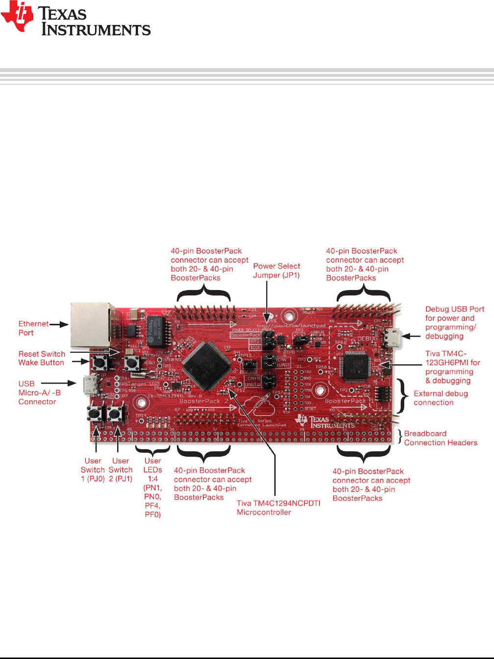
The Tiva™ C Series TM4C1294 Connected LaunchPad Evaluation Board (EK-TM4C1294XL) is a low-cost
evaluation platform for ARM® Cortex™-M4F-based microcontrollers. The Connected LaunchPad design
highlights the TM4C1294NCPDT microcontroller with its on-chip 10/100 Ethernet MAC and PHY, USB 2.0,
hibernation module, motion control pulse-width modulation and a multitude of simultaneous serial
connectivity. The Connected LaunchPad also features two user switches, four user LEDs, dedicated reset
and wake switches, a breadboard expansion option and two independent BoosterPack XL expansion
connectors. The pre-programmed quickstart application on the Connected LaunchPad also enables
remote monitoring and control of the evaluation board from an internet browser anywhere in the world.
The web interface is provided by 3rd party, Exosite. Each Connected LaunchPad is enabled on the
Exosite platform allowing users to create and customize their own Internet-of-Things applications.
Figure 1-1 shows a photo of the Connected LaunchPad with key features highlighted.
Figure 1-1. Tiva C Series Connected LaunchPad Evaluation Board

www.ti.com
Kit Contents
5
SPMU365C–March 2014–Revised October 2016
Submit Documentation Feedback Copyright © 2014–2016, Texas Instruments Incorporated
Board Overview
1.1 Kit Contents
The Connected LaunchPad Evaluation Kit contains the following items:
• Tiva™ C Series TM4C1294 Evaluation Board (EK-TM4C1294XL)
• Retractable Ethernet cable
• USB Micro-B plug to USB-A plug cable
•README First document
1.2 Using the Connected LaunchPad
The recommended steps for using the Connected LaunchPad Evaluation Kit are:
1. Follow the README First document included in the kit. The README First helps you get the
Connected LaunchPad up and running in minutes. Within just a few minutes you can be controlling and
monitoring the Connected LaunchPad through the internet using Exosite and the pre-programmed
quickstart application.
2. Experiment with BoosterPacks. This evaluation kit conforms to the latest revision of the BoosterPack
pinout standard. It has two independent BoosterPack connections to enable a multitude of expansion
opportunities.
3. Take the first step towards developing your own applications. The Connected LaunchPad is
supported by TivaWare for C Series. After installing TivaWare, look in the installation directory for
examples\boards\ek-tm4c1294xl. You can find pre-configured example applications for this board as
well as for this board with selected BoosterPacks. Alternately, use Energīa for a wiring framework-
based cross-platform, fast-prototyping environment that works with this and other TI LaunchPads. See
Chapter 3 of this document for more details about software development. TivaWare can be
downloaded from the TI website at http://www.ti.com/tool/sw-tm4c. Energīa can be found at
http://energia.nu.
4. Customize and integrate the hardware to suit your end application. This evaluation kit can be
used as a reference for building your own custom circuits based on Tiva C microcontrollers or as a
foundation for expansion with your custom BoosterPack or other circuit. This manual can serve as a
starting point for this endeavor.
5. Get Trained. You can also download hours of written and video training materials on this and related
LaunchPads. Visit the Tiva C Series LaunchPad Workshop Wiki for more information.
6. More Resources. See the TI MCU LaunchPad web page for more information and available
BoosterPacks. (http://www.ti.com/tiva-c-launchpad)
1.3 Features
Your Connected LaunchPad includes the following features:
• Tiva TM4C1294NCPDTI microcontroller
• Ethernet connectivity with fully integrated 10/100 Ethernet MAC and PHY Motion Control PWM
• USB 2.0 Micro A/B connector
• 4 user LEDs
• 2 user buttons
• 1 independent hibernate wake switch
• 1 independent microcontroller reset switch
• Jumper for selecting power source:
– ICDI USB
– USB Device
– BoosterPack
• Preloaded Internet-of-Things Exosite quickstart application
• I/O brought to board edge for breadboard expansion
• Two independent BoosterPack XL standard connectors featuring stackable headers to maximize
expansion through BoosterPack ecosystem

BoosterPacks
www.ti.com
6SPMU365C–March 2014–Revised October 2016
Submit Documentation Feedback
Copyright © 2014–2016, Texas Instruments Incorporated
Board Overview
– For a complete list of BoosterPacks, see the TI MCU LaunchPad web page:
http://www.ti.com/launchpad
1.4 BoosterPacks
The Connected LaunchPad provides an easy and inexpensive way to develop applications with the
TM4C1294NCPDTI microcontroller. BoosterPacks are add-on boards that follow a pin-out standard
created by Texas Instruments. The TI and third-party ecosystem of BoosterPacks greatly expands the
peripherals and potential applications that you can easily explore with the Connected LaunchPad.
You can also build your own BoosterPack by following the design guidelines on TI’s website. Texas
Instruments even helps you promote your BoosterPack to other members of the community. TI offers a
variety of avenues for you to reach potential customers with your solutions.
1.5 Energīa
Energīa is an open-source electronics prototyping platform started in January of 2012 with the goal of
bringing the Wiring and Arduino framework to the TI LaunchPad community. Energīa includes an
integrated development environment (IDE) that is based on Processing.
Together with Energīa, LaunchPads can be used to develop interactive objects, taking inputs from a
variety of switches or sensors, and controlling a variety of lights, motors, and other physical outputs.
LaunchPad projects can be stand-alone (only run on the target board, i.e. your LaunchPad), or they can
communicate with software running on your computer (Host PC). Energīa projects are highly portable
between supported LaunchPad platforms. Projects written for your Connected LaunchPad can be run on
other LaunchPads with little or no modifications.
More information is available at http://energia.nu.
1.6 Specifications
Table 1-1 summarizes the specifications for the Connected LaunchPad.
Table 1-1. EK-TM4C1294XL Specifications
Parameter Value
Board Supply Voltage
4.75 VDC to 5.25 VDC from one of the following sources:
• Debug USB U22 (ICDI) USB Micro-B cable connected to PC or other compatible
power source.
• Target USB (U7) USB Micro-B cable connected to PC or other compatible power
source.
• BoosterPack 1 (X8-4)
• BoosterPack 2 (X6-4)
• Breadboard expansion header (X11-2 or X11-97).
See schematic symbol JP1 for power input selection.
Dimensions 4.9 in x 2.2 in x .425 in (12.45 cm x 5.59 cm x 10.8 mm) (L x W x H)
Break-out Power Output
• 5 VDC to BoosterPacks, current limited by TPS2052B. Nominal rating 1 Amp.
Board input power supply limitations may also apply.
• 3.3 VDC to BoosterPacks, limited by output of TPS73733 LDO. This 3.3-V plane is
shared with on-board components. Total output power limit of TPS73733 is 1
Amp.
RoHS Status Compliant
7
SPMU365C–March 2014–Revised October 2016
Submit Documentation Feedback Copyright © 2014–2016, Texas Instruments Incorporated
Hardware Description
Chapter 2
SPMU365C–March 2014–Revised October 2016
Hardware Description
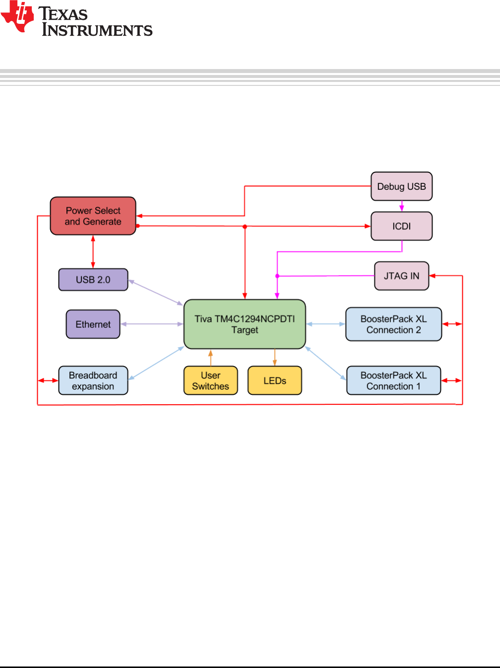
The Connected LaunchPad includes a TM4C1294NCPDTI microcontroller with an integrated 10/100
Ethernet MAC and PHY. This advanced ARM® Cortex™ M4F MCU has a wide range of peripherals that
are made available to users via the on-board accessories and the BoosterPack connectors. This chapter
explains how those peripherals operate and interface to the microcontroller.
Figure 2-1 provides a high-level block diagram of the Connected LaunchPad.
Figure 2-1. Tiva Connected LaunchPad Evaluation Board Block Diagram
2.1 Functional Description
2.1.1 Microcontroller
The TM4C1294NCPDTI is a 32-bit ARM Cortex-M4F based microcontroller with 1024-kB Flash memory,
256-kB SRAM, 6-kB EEPROM, and 120 MHz operation; integrated 10/100 Ethernet MAC and PHY;
integrated USB 2.0 connectivity with external high-speed USB 3.0 PHY capability; a hibernation module, a
multitude of serial connectivity and motion control PWM; as well as a wide range of other peripherals. See
the TM4C1294NCPDTI microcontroller data sheet for more complete details.
Most of the microcontroller’s signals are routed to 0.1-in (2.54-mm) pitch headers or through-hole solder
pads. An internal multiplexor allows different peripheral functions to be assigned to each of these GPIO
pads. When adding external circuitry, consider the additional load on the evaluation board power rails.
The TM4C1294NCPDTI microcontroller is factory-programmed with a quickstart demo program. The
quickstart program resides in on-chip Flash memory and runs each time power is applied, unless the
quickstart application has been replaced with a user program. The quickstart application automatically
connects to http://ti.exosite.com when an internet connection is provided through the RJ45 Ethernet jack
on the evaluation board.

Functional Description
www.ti.com
8SPMU365C–March 2014–Revised October 2016
Submit Documentation Feedback
Copyright © 2014–2016, Texas Instruments Incorporated
Hardware Description
2.1.2 Ethernet Connectivity
The Connected LaunchPad is designed to connect directly to an Ethernet network using RJ45 style
connectors. The microcontroller contains a fully integrated Ethernet MAC and PHY. This integration
creates a simple, elegant and cost-saving Ethernet circuit design. Example code is available for both the
uIP and LwIP TCP/IP protocol stacks. The embedded Ethernet on this device can be programmed to act
as an HTTP server, client or both. The design and integration of the circuit and microcontroller also enable
users to synchronize events over the network using the IEEE1588 precision time protocol.
When configured for Ethernet operation, it is recommended that the user configure LED D3 and D4 to be
controlled by the Ethernet MAC to indicate connection and transmit/receive status.
2.1.3 USB Connectivity
The Connected LaunchPad is designed to be USB 2.0 ready. A TPS2052B load switch is connected to
and controlled by the microcontroller USB peripheral, which manages power to the USB micro A/B
connector when functioning in a USB host. When functioning as a USB device, the entire Connected
LaunchPad can be powered directly from the USB micro A/B connector. Use JP1 to select the desired
power source.
USB 2.0 functionality is provided and supported directly out of the box with the target USB micro A/B
connector. High-speed USB 3.0 functionality can be enabled by adding an external USB PHY. The USB
external PHY control and data signals are provided on the breadboard expansion header X11.
2.1.4 Motion Control
The Connected LaunchPad includes the Tiva C Series Motion Control PWM technology, featuring a PWM
module capable of generating eight PWM outputs. The PWM module provides a great deal of flexibility
and can generate simple PWM signals – for example, those required by a simple charge pump – as well
as paired PWM signals with dead-band delays, such as those required by a half-H bridge driver. Three
generator blocks can also generate the full six channels of gate controls required by a 3-phase inverter
bridge.
A quadrature encoder interface (QEI) is also available to provide motion control feedback.
See the BoosterPacks and Headers section of this document for details about the availability of these
signals on the BoosterPack interfaces.
2.1.5 User Switches and LED's
Two user switches are provided for input and control of the TM4C1294NCPDTI software. The switches
are connected to GPIO pins PJ0 and PJ1.
A reset switch and a wake switch are also provided. The reset switch initiates a system reset of the
microcontroller whenever it is pressed and released. Pressing the reset switch also asserts the reset
signal to the BoosterPack and Breadboard headers. The wake switch is one way to bring the device out of
hibernate mode.
Four user LEDs are provided on the board. D1 and D2 are connected to GPIOs PN1 and PN0. These
LEDs are dedicated for use by the software application. D3 and D4 are connected to GPIOs PF4 and
PF0, which can be controlled by user’s software or the integrated Ethernet module of the microcontroller.
A power LED is also provided to indicate that 3.3 volt power is present on the board.
www.ti.com
Functional Description
9
SPMU365C–March 2014–Revised October 2016
Submit Documentation Feedback
Copyright © 2014–2016, Texas Instruments Incorporated
Hardware Description
2.1.6 BoosterPacks and Headers
2.1.6.1 BoosterPack 1
The Connected LaunchPad features two fully independent BoosterPack XL connectors. BoosterPack 1, located around the ICDI portion of the
board, is fully compliant with the BoosterPack standard with the single exception of GPIO pin PA6 (X8-16), which does not provide analog
capability. PA6 is located near the bottom of the inner left BoosterPack XL header.
I2C is provided in both the original BoosterPack standard configuration as well as the updated standard location. Use of I2C on the bottom left of
the BoosterPack connections per the updated standard is highly encouraged whenever possible.
Motion control advanced PWM connections are provided on the inner right connector for motion control applications.
Table 2-1 provides a complete listing of the BoosterPack pins and the GPIO alternate functions available on each pin. The TM4C1294NCPDTI
GPIO register GPIOPCTL values are shown for each configuration. The headers in this table are labeled from left to right in ten pin columns. ‘A’
and ‘D’ make up the outer BoosterPack standard pins, ‘B’ and ‘C’ make up the inner BoosterPack XL standard pins.
Table 2-1. BoosterPack 1 GPIO and Signal Muxing
Header Pin Standard
Function GPIO MCU
Pin Analog Digital Function (GPIOPCTL Bit Encoding)
1 2 3 5 6 7 8 11 13 14 15
A1 1 +3.3 volts 3.3V
A1 2 Analog PE4 123 AIN9 U1RI - - - - - - - - - SSI1XDAT0
A1 3 UART RX PC4 25 C1- U7Rx - - - - - - - - - EPI0S7
A1 4 UART TX PC5 24 C1+ U7Tx - - - - RTCCLK - - - - EPI0S6
A1 5 GPIO PC6 23 C0+ U5Rx - - - - - - - - - EPI0S5
A1 6 Analog PE5 124 AIN8 - - - - - - - - - - SSIXDAT1
A1 7 SPI CLK PD3 4 AIN12 - I2C8SDA T1CCP1 - - - - - - - SSI2CLk
A1 8 GPIO PC7 22 C0- U5Tx - - - - - - - - - EPI0S4
A1 9 I2C SCL PB2 91 - - I2C0SCL T5CCP0 - - - - - - USB0STP EPI0S27
A1 10 I2C SDA PB3 92 - - I2C0SDA T5CCP1 - - - - - - USB0CLK EPI0S28
B1 1 +5 volts 5V
B1 2 ground GND
B1 3 Analog PE0 15 AIN3 U1RTS - - - - - - - - - -
B1 4 Analog PE1 14 AIN2 U1DSR - - - - - - - - - -
B1 5 Analog PE2 13 AIN1 U1DCD - - - - - - - - - -
B1 6 Analog PE3 12 AIN0 U1DTR - - - - - - - - - -
B1 7 Analog PD7 128 AIN4 U2CTS - T4CCP1 USB0PFLT - - NMI - - - SSI2XDAT2
B1 8 Analog PA6 40 - U2Rx I2C6SCL T3CCP0 USB0EPEN - - - - SSI0XDAT2 - EPI0S8
B1 9 A out PM4 74 TMPR3 U0CTS - T4CCP0 - - - - - - - -
B1 10 A out PM5 73 TMPR2 U0DCD - T4CCP1 - - - - - - - -

Functional Description
www.ti.com
10 SPMU365C–March 2014–Revised October 2016
Submit Documentation Feedback
Copyright © 2014–2016, Texas Instruments Incorporated
Hardware Description
Table 2-1. BoosterPack 1 GPIO and Signal Muxing (continued)
Header Pin Standard
Function GPIO MCU
Pin Analog Digital Function (GPIOPCTL Bit Encoding)
1 2 3 5 6 7 8 11 13 14 15
C1 1 PWM PF1 43 - - - - EN0LED2 M0PWM1 - - - - SSI3XDAT0 TRD1
C1 2 PWM PF2 44 - - - - - M0PWM2 - - - - SSI3Fss TRD0
C1 3 PWM PF3 45 - - - - - M0PWM3 - - - - SSI3Clk TRCLK
C1 4 PWM PG0 49 - - I2C1SCL - EN0PPS M0PWM4 - - - - - EPI0S11
C1 5 Capture PL4 85 - - - T0CCP0 - - - - - - USB0D4 EPI0S26
C1 6 Capture PL5 86 - - - T0CCP1 - - - - - - USB0D5 EPI0S33
C1 7 GPIO PL0 81 - - I2C2SDA - - M0FAULT3 - - - - USB0D0 EPI0S16
C1 8 GPIO PL1 82 - - I2C2SCL - - PhA0 - - - - USB0D1 EPI0S17
C1 9 GPIO PL2 83 - - - - C0o PhB0 - - - - USB0D2 EPI0S18
C1 10 GPIO PL3 84 - - - - C1o IDX0 - - - - USB0D3 EPI0S19
D1 1 ground GND
D1 2 PWM PM3 75 - - - T3CCP1 - - - - - - - EPI0S12
D1 3 GPIO PH2 31 - U0DCD - - - - - - - - - EPI0S2
D1 4 GPIO PH3 32 - U0DSR - - - - - - - - - EPI0S3
D1 5 reset RESET
D1 6 SPI MOSI PD1 2 AIN14 - I2C7SDA T0CCP1 C1o - - - - - - SSI2XDAT0
D1 7 SPI MISO PD0 1 AIN15 - I2C7SCL T0CCP0 C0o - - - - - - SSI2XDAT1
D1 8 GPIO PN2 109 - U1DCD U2RTS - - - - - - - - EPI0S29
D1 9 GPIO PN3 110 - U1DSR U2CTS - - - - - - - - EPI0S30
D1 10 GPIO PP2 103 - U0DTR - - - - - - - - USB0NXT EPI0S29

Functional Description
www.ti.com
12 SPMU365C–March 2014–Revised October 2016
Submit Documentation Feedback
Copyright © 2014–2016, Texas Instruments Incorporated
Hardware Description
2.1.6.2 BoosterPack 2
The second BoosterPack XL interface is located near the middle of the board. This interface is fully compliant with the BoosterPack standard, and
adds features not covered by the BoosterPack standard that enable operation with additional BoosterPacks.
An additional analog signal is provided on the outer left header (X6-9). This signal can be used to monitor the touch panel on the popular Kentec
EB-LM4F120-L35 BoosterPack.
Using the jumpers JP4 and JP5, Controller Area Network (CAN) digital receive and transmit signals can be optionally routed to the BoosterPack 2
interface. The location of these signals is consistent with the CAN interface on the Tiva C Series TM4C123G LaunchPad and the Stellaris
LM4F120 LaunchPad. In the default configuration, UART0 is used for the ICDI virtual UART and CAN is not present on the BoosterPack headers.
In this configuration, the ROM serial bootloader can be used over the ICDI virtual UART. When the jumpers are configured for CAN on the
BoosterPack, then UART2 must be used for the ICDI virtual UART.
To comply with both the original and the new BoosterPack standard, I2C is provided on both sides of the BoosterPack connection. Use of I2C on
the bottom left of the BoosterPack connection is highly encouraged where possible, to be in compliance with the new BoosterPack standard. To
provide I2C capability on the right side of the connector, per the original standard, two zero-ohm resistors (R19 and R20) are used to combine the
SPI and I2C signals. These signals are not shared with any other pins on the LaunchPad and therefore removal of these zero-ohm resistors
should not be required. Software should be certain that unused GPIO signals are configured as inputs.
Table 2-2 provides a complete listing of the BoosterPack pins and the GPIO alternate functions available at each pin. The TM4C1294NCPDT
GPIO register GPIOPCTL values are shown for each configuration. The headers in this table are labeled from left to right in ten pin columns. ‘A’
and ‘D’ make up the outer BoosterPack standard pins, ‘B’ and ‘C’ make up the inner BoosterPack XL standard pins.
Table 2-2. BoosterPack 2 GPIO and Signal Muxing
Header Pin Standard
Function GPIO MCU
Pin Analog Digital Function (FPIOPCTL Bit Encoding)
1 2 3 5 6 7 8 11 13 14 15
A2 1 3.3V
A2 2 Analog PD2 3 AIN13 - I2C8SCL T1CCP0 C2o - - - - - - SSI2Fss
A2 3 UART RX PP0 118 C2+ U6Rx - - - - - - - - - SSI3XDAT2
A2 4 UART TX PP1 119 C2- U6Tx - - - - - - - - - SSI3XDAT3
A2 5 GPIO
(See JP4)
PD4 125 AIN7 U2Rx - T3CCP0 - - - - - - - SSI1XDAT2
PA0 33 - U0Rx I2C9SCL T0CCP0 - - CANORx - - - - -
A2 6 Analog
(See JP5)
PD5 126 AIN6 U2Tx - T3CCP1 - - - - - - - SSI1XDAT3
PA1 34 - U0Tx I2C9SDA T0CCP1 - - CAN0Tx - - - - -
A2 7 SPI CLK PQ0 5 - - - - - - - - - - SSI3Clk EPI0S20
A2 8 GPIO PP4 105 - U3RTS U0DSR - - - - - - - USB0D7 -
A2 9 I2C SCL PN5 112 - U1RI U3CTS I2C2SCL - - - - - - - EPIO0S35
A2 10 I2C SDA PN4 111 - U1DTR U3RTS I2C2SDA - - - - - - - EPIO0S34
B2 1 5V
B2 2 GND
B2 3 Analog PB4 121 AIN10 U0CTS I2C5SCL - - - - - - - - SSI1Fss

www.ti.com
Functional Description
13
SPMU365C–March 2014–Revised October 2016
Submit Documentation Feedback
Copyright © 2014–2016, Texas Instruments Incorporated
Hardware Description
Table 2-2. BoosterPack 2 GPIO and Signal Muxing (continued)
Header Pin Standard
Function GPIO MCU
Pin Analog Digital Function (FPIOPCTL Bit Encoding)
1 2 3 5 6 7 8 11 13 14 15
B2 4 Analog PB5 120 AIN11 U0RTS I2C5SDA - - - - - - - - SSI1Clk
B2 5 Analog PK0 18 AIN16 U4Rx - - - - - - - - - EPI0S0
B2 6 Analog PK1 19 AIN17 U4Tx - - - - - - - - - EPI0S1
B2 7 Analog PK2 20 AIN18 U4RTS - - - - - - - - - EPI0S2
B2 8 Analog PK3 21 AIN19 u4CTS - - - - - - - - - EPI0S3
B2 9 A out PA4 37 - U3Rx I2C7SCL T2CCP0 - - - - - - - SSI0XDAT0
B2 10 A out PA5 38 - U3Tx I2C7SDA T2CCP1 - - - - - - - SSI0XDAT1
C2 1 PWM PG1 50 - - I2C1SDA - - M0PWM5 - - - - - EPI0S10
C2 2 PWM PK4 63 - - I2C3SCL - EN0LED0 M0PWM6 - - - - - EPI0S32
C2 3 PWM PK5 62 - - I2C3SDA - EN0LED2 M0PWM7 - - - - - EPI0S31
C2 4 PWM PM0 78 - - - T2CCP0 - - - - - - - EPI0S15
C2 5 Capture PM1 77 - - - T2CCP1 - - - - - - - EPI0S14
C2 6 Capture PM2 76 - - - T3CCP0 - - - - - - - EPI0S13
C2 7 GPIO PH0 29 - U0RTS - - - - - - - - - EPI0S0
C2 8 GPIO PH1 30 - U0CTS - - - - - - - - - EPI0S1
C2 9 GPIO PK6 61 - - I2C4SCL - EN0LED1 M0FAULT1 - - - - - EPI0S25
C2 10 GPIO PK7 60 - U0RI I2C4SDA - RTCCLK M0FAULT2 - - - - - EPI0S24
D2 1 GND
D2 2 PWM PM7 71 TMPR0 U0RI - T5CCP1 - - - - - - - -
D2 3 GPIO PP5 106 - U3CTS I2C2SDL - - - - - - - USB0D6 -
D2 4 GPIO PA7 41 - U2Tx I2C6SDA T3CCP1 USB0PFLT - - - USB0EPEN SSI0XDAT3 - EPI0S9
D2 5 RESET
D2 6 SPI MOSI PQ2 11 - - - - - - - - - - SSI3XDAT0 EPI0S22
I2C PA3 36 - U4Tx I2C8SDA T1CCP1 - - - - - - - SSI0Fss
D2 7 SPI MISO PQ3 27 - - - - - - - - - - SSI3XDAT1 EPI0S23
I2C PA2 35 - U4Rx I2C8SCL T1CCP0 - - - - - - - SSI0Clk
D2 8 GPIO PP3 104 - U1CTS U0DCD - - - - - - - USB0DIR EPI0S30
D2 9 GPIO PQ1 6 - - - - - - - - - - SSI3Fss EPI0S21
D2 10 GPIO PM6 72 TMPR1 U0DSR - T5CCP0 - - - - - - - -


www.ti.com
Functional Description
15
SPMU365C–March 2014–Revised October 2016
Submit Documentation Feedback Copyright © 2014–2016, Texas Instruments Incorporated
Hardware Description
2.1.6.3 Breadboard Connection
The breadboard adapter section of the board is a set of 98 holes on a 0.1 inch grid. Properly combined
with a pair of right angle headers, the entire Connected LaunchPad can be plugged directly into a
standard 300 mil (0.3 inch) wide solder-less breadboard. The right angle headers and breadboard are not
provided with this kit. Suggested part numbers are Samtec TSW-149-09-L-S-RE and TSW-149-08-L-S-RA
right angle pin headers and Twin industries TW-E40-1020 solder-less breadboard. Samtec TSW-149-09-
F-S-RE and TSW-149-09-F-S-RA may be substituted.
A detailed explanation of how to install the headers is available on the TI LaunchPad Wiki or at
http://users.ece.utexas.edu/~valvano/EE345L/Labs/Fall2011/LM3S1968soldering.pdf.
Nearly all microcontroller signals are made available at the breadboard adapter holes (X11). These signals
are grouped by function where possible. For example, all EPI signals are grouped on one side of the
connector. Many of the analog signals are grouped near VREF, and UART, SSI and I2C signals are
grouped by peripheral to make expansion and customization simpler.
Table 2-3 and Table 2-4 show the GPIO pin and signal muxing for the X11 breadboard adapter pads.

Functional Description
www.ti.com
16 SPMU365C–March 2014–Revised October 2016
Submit Documentation Feedback
Copyright © 2014–2016, Texas Instruments Incorporated
Hardware Description
Table 2-3. X11 Breadboard Adapter Odd-Numbered Pad GPIO and Signal Muxing
Pin Port MCU
PIN Analog Digital Function (GPIOPCTL Bit Encoding)
1 2 3 5 6 7 8 11 13 14 15
1 3V3
3 GND
5 PB4 121 AIN10 U0CTS I2C5SCL - - - - - - - - SSI1Fss
7 PB5 120 AIN11 U0RTS I2C5SDA - - - - - - - - SSI1Clk
9 PH0 29 - U0RTS - - - - - - - - - EPI0S0
11 PH1 30 - U0CTS - - - - - - - - - EPI0S1
13 PH2 31 - U0DCD - - - - - - - - - EPI0S2
15 PH3 32 - U0DSR - - - - - - - - - EPI0S3
17 PC7 22 C0- U5Tx - - - - - - - - - EPI0S4
19 PC6 23 C0+ U5Rx - - - - - - - - - EPI0S5
21 PC5 24 C1+ U7Tx - - - - RTCCLK - - - - EPI0S6
23 PC4 25 C1- U7Rx - - - - - - - - - EPI0S7
25 PA6 40 - U2Rx I2C6SCL T3CCP0 USB0EPEN - - - - SSI0XDAT2 - EPI0S8
27 PA7 41 - U2Tx I2C6SDA T3CCP1 USB0PFLT - - - USB0EPEN SSI0XDAT3 - EPI0S9
29 PG1 50 - - I2C1SDA - - M0PWM5 - - - - - EPI0S10
31 PG0 49 - - I2C1SCL - EN0PPS M0PWM4 - - - - - EPI0S11
33 PM3 75 - - - T3CCP1 - - - - - - - EPI0S12
35 GND
37 PM2 76 - - - T3CCP0 - - - - - - - EPI0S13
39 PM1 77 - - - T2CCP1 - - - - - - - EPI0S14
41 PM0 78 - - - T2CCP0 - - - - - - - EPI0S15
43 PL0 81 - - I2C2SDA - - M0FAULT3 - - - - USB0D0 EPI0S16
45 PL1 82 - - I2C2SCL - - PhA0 - - - - USB0D1 EPI0S17
47 PL2 83 - - - - C0o PhB0 - - - - USB0D2 EPI0S18
49 PL3 84 - - - - C1o IDX0 - - - - USB0D3 EPI0S19
51 PQ0 5 - - - - - - - - - - SSI3Clk EPI0S20
53 PQ1 6 - - - - - - - - - - SSI3Fss EPI0S21
55 PQ2 11 - - - - - - - - - - SSI3XDAT0 EPI0S22
57 PQ3 27 - - - - - - - - - - SSI3XDAT1 EPI0S23
59 PK7 60 - U0RI I2C4SDA - - - - - - EPI0S24
61 GND
63 PK6 61 - - I2C4SCL - EN0LED1 M0FAULT1 - - - - - EPI0S25
65 PL4 85 - - - T0CCP0 - - - - - - USB0D4 EPI0S26
www.ti.com
Functional Description
17
SPMU365C–March 2014–Revised October 2016
Submit Documentation Feedback
Copyright © 2014–2016, Texas Instruments Incorporated
Hardware Description
Table 2-3. X11 Breadboard Adapter Odd-Numbered Pad GPIO and Signal Muxing (continued)
Pin Port MCU
PIN Analog Digital Function (GPIOPCTL Bit Encoding)
1 2 3 5 6 7 8 11 13 14 15
67 PB2 91 - - I2C0SCL T5CCP0 - - - - - - USB0STP EPI0S27
69 PB3 92 - - I2C0SDA T5CCP1 - - - - - - USB0CLK EPI0S28
71 PP2 103 - U0DTR - - - - - - - - USB0NXT EPI0S29
73 PP3 104 - U1CTS U0DCD - - - RTCCLK - - - USB0DIR EPI0S30
75 PK5 62 - - I2C3SDA - EN0LED2 M0PWM7 - - - - - EPI0S31
77 PK4 63 - - I2C3SCL - EN0LED0 M0PWM6 - - - - - EPI0S32
79 PL5 86 - - - T0CCP1 - - - - - - USB0D5 EPI0S33
81 PN4 111 - U1DTR U3RTS I2C2SDA - - - - - - - EPI0S34
83 PN5 112 - U1RI U3CTS I2C2SCL - - - - - - - EPI0S35
85 PN0 107 - U1RTS - - - - - - - - - -
87 PN1 108 - U1CTS - - - - - - - - - -
89 PN2 109 - U1DCD U2RTS - - - - - - - - EPI0S29
91 PN3 110 - U1DSR U2CTS - - - - - - - - EPI0S30
93 PQ4 102 - U1Rx - - - - - DIVSCLK - - - -
95 WAKE
97 5V
Table 2-4. X11 Breadboard Adapter Even-Numbered Pad GPIO and Signal Muxing
Pin Port MCU
PIN Analog Digital Function (GPIOPCTL Bit Encoding)
1 2 3 5 6 7 8 11 13 14 15
2 5V
4 GND
6 PA2 35 - U4Rx I2C8SCL T1CCP0 - - - - - - - SSI0Clk
8 PA3 36 - U4Tx I2C8SDA T1CCP1 - - - - - - - SSI0Fss
10 PA4 37 - U3Rx I2C7SCL T2CCP0 - - - - - - - SSI0XDAT0
12 PA5 38 - U3Tx I2C7SDA T2CCP1 - - - - - - - SSI0XDAT1
14 PE0 15 AIN3 U1RTS - - - - - - - - - -
16 PE1 14 AIN2 U1DSR - - - - - - - - - -
18 PE2 13 AIN1 U1DCD - - - - - - - - - -
20 PE3 12 AIN0 U1DTR - - - - - - - - - -
22 PE4 123 AIN9 U1RI - - - - - - - - - SSI1XDAT0
24 PE5 124 AIN8 - - - - - - - - - - SSI1XDAT1

Functional Description
www.ti.com
18 SPMU365C–March 2014–Revised October 2016
Submit Documentation Feedback
Copyright © 2014–2016, Texas Instruments Incorporated
Hardware Description
Table 2-4. X11 Breadboard Adapter Even-Numbered Pad GPIO and Signal Muxing (continued)
Pin Port MCU
PIN Analog Digital Function (GPIOPCTL Bit Encoding)
1 2 3 5 6 7 8 11 13 14 15
26 PK0 18 AIN16 U4Rx - - - - - - - - - EPI0S0
28 PK1 19 AIN17 U4Tx - - - - - - - - - EPI0S1
30 PK2 20 AIN18 U4RTS - - - - - - - - - EPI0S2
32 PK3 21 AIN19 U4CTS - - - - - - - - - EPI0S3
34 VREF
36 GND
38 PD5 126 AIN6 U2Tx - T3CCP1 - - - - - - - SSI1XDAT3
40 PD4 125 AIN7 U2Rx - T3CCP0 - - - - - - - SSI1XDAT2
42 PD7 128 AIN4 U2CTS - T4CCP1 USB0PFLT - - NMI - - - SSI2XDAT2
44 PD6 127 AIN5 U2RTS - T4CCP0 USB0EPEN - - - - - - SSI2XDAT3
46 PD3 4 AIN12 - I2C8SDA T1CCP1 - - - - - - - SSI2Clk
48 PD1 2 AIN14 - I2C7SDA T0CCP1 C1o - - - - - - SSI2XDAT0
50 PD0 1 AIN15 - I2C7SCL T0CCP0 C0o - - - - - - SSI2XDAT1
52 PD2 3 AIN13 - I2C8SCL T1CCP0 C2o - - - - - - SSI2Fss
54 PP0 118 C2+ U6Rx - - - - - - - - - SSI3XDAT2
56 PP1 119 C2- U6Tx - - - - - - - - - SSI3XDAT3
58 PB0 95 USB0ID U1Rx I2C5SCL T4CCP0 - - CAN1Rx - - - - -
60 PB1 96 USB0VBUS U1Tx I2C5SDA T4CCP1 - - CAN1Tx - - - - -
62 GND
64 PF4 46 - - - - EN0LED1 M0FAULT0 - - - - SSI3XDAT2 TRD3
66 PF0 42 - - - - EN0LED0 M0PWM0 - - - - SSI3XDAT1 TRD2
68 PF1 43 - - - - EN0LED2 M0PWM1 - - - - SSI3XDAT0 TRD1
70 PF2 44 - - - - - M0PWM2 - - - - SSI3Fss TRD0
72 PF3 45 - - - - - M0PWM3 - - - - SSI3Clk TRCLK
74 PA0 33 - U0Rx I2C9SCL T0CCP0 - - CAN0Rx - - - - -
76 PA1 34 - U0Tx I2C9SDA T0CCP1 - - CAN0Tx - - - - -
78 PP4 105 - U3RTS U0DSR - - - - - - - USB0D7 -
80 PP5 106 - U3CTS I2C2SCL - - - - - - - USB0D6 -
82 PJ0 116 - U3Rx - - - - - - - - -
84 PJ1 117 - U3Tx - - - - - - - - - -
86 PM7 71 TMPR0 U0RI - T5CCP1 - - - - - - - -
88 PM6 72 TMPR1 U0DSR - T5CCP0 - - - - - - - -
90 PM5 73 TMPR2 U0DCD - T4CCP1 - - - - - - - -
www.ti.com
Functional Description
19
SPMU365C–March 2014–Revised October 2016
Submit Documentation Feedback
Copyright © 2014–2016, Texas Instruments Incorporated
Hardware Description
Table 2-4. X11 Breadboard Adapter Even-Numbered Pad GPIO and Signal Muxing (continued)
Pin Port MCU
PIN Analog Digital Function (GPIOPCTL Bit Encoding)
1 2 3 5 6 7 8 11 13 14 15
92 PM4 74 TMPR3 U0CTS - T4CCP0 - - - - - - - -
94 RESET
96 GND
98 3V3
Power Management
www.ti.com
20 SPMU365C–March 2014–Revised October 2016
Submit Documentation Feedback
Copyright © 2014–2016, Texas Instruments Incorporated
Hardware Description
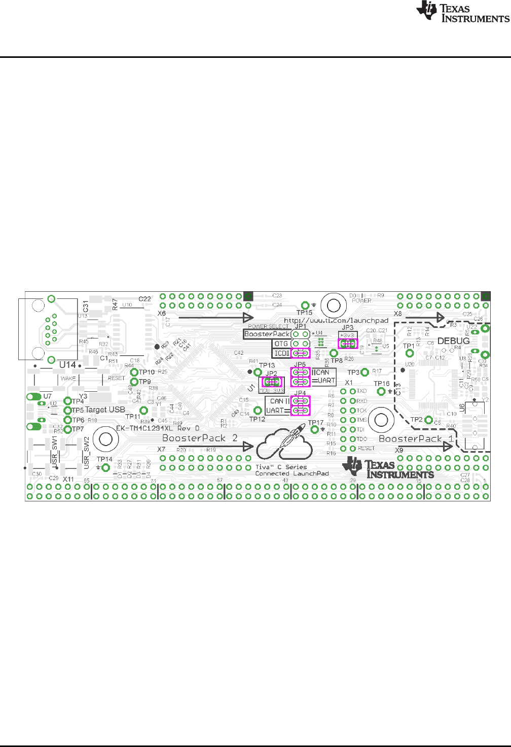
2.1.6.4 Other Headers and Jumpers
JP1 is provided to select the power input source for the Connected LaunchPad. The top position is for
BoosterPack power; this position also disconnects both USB voltages from the board’s primary 5-volt
input. In the top position, the TPS2052B does not limit current so additional care should be exercised. The
middle position draws power from the USB connector on the left side of the board near the Ethernet jack.
The bottom position is the default, in which power is drawn from the ICDI (Debug) USB connection.
JP2 separates the MCU 3.3-volt power domain from the rest of the 3.3-volt power on the board allowing
an ammeter to be used to obtain more accurate measurements of microcontroller power consumption.
JP3 isolates the output of the TPS73733 LDO from the board’s 3.3-V power domain.
JP4 and JP5 are used to configure CAN signals to the BoosterPack 2 interface. In the default horizontal
configuration, CAN is not present on the BoosterPack. UART2 goes to the BoosterPack and UART 0 goes
to the ICDI virtual serial port to provide ROM serial bootloader capability. In the vertical CAN-enabled
configuration, UART2 goes to the ICDI virtual serial port and CAN signals are available on the
BoosterPack. The ROM serial bootloader is not available to the ICDI virtual serial port while the jumpers
are in the CAN position.
Figure 2-2 shows the default configuration and relative location of the jumpers on the board.
Figure 2-2. Default Jumper Locations
2.2 Power Management
2.2.1 Power Supplies
The Connected LaunchPad can be powered from three different input options:
• On-board ICDI USB cable (Debug, Default)
• Target USB cable
• BoosterPack or Breadboard adapter connection
The JP1 power-select jumper is used to select one of the power sources.
In addition, the JP3 power jumper can be used to isolate the 3.3-volt output of the TPS73733 from the
board’s 3.3-volt rail.
A TPS2052B load switch is used to regulate and control power to the Target USB connector when the
microcontroller is acting in USB host mode. This load switch also limits current to the BoosterPack and
Breadboard adapter headers when the JP1 jumper is in the ICDI position.

www.ti.com
Power Management
21
SPMU365C–March 2014–Revised October 2016
Submit Documentation Feedback Copyright © 2014–2016, Texas Instruments Incorporated
Hardware Description
2.2.2 Low Power Modes
The Connected LaunchPad demonstrates several low power microcontroller modes. In run mode, the
microcontroller can be clocked from several sources such as the internal precision oscillator or an external
crystal oscillator. Either of these sources can then optionally drive an internal PLL to increase the effective
frequency of the system up to 120 MHz. In this way, the run mode clock speed can be used to manage
run mode current consumption.
The microcontroller also provides sleep and deep sleep modes and internal voltage adjustments to the
flash and SRAM to further refine power consumption when the processor is not in use but peripherals
must remain active. Each peripheral can be individually clock gated in these modes so that current
consumption by unused peripherals is minimized. A wide variety of conditions from internal and external
sources can trigger a return to run mode.
The lowest power setting of the microcontroller is hibernation, which requires a small amount of supporting
external circuitry available on the Connected LaunchPad. The Connected LaunchPad can achieve
microcontroller current consumption modes under 2 micro-Amps using hibernate VDD3ON mode.
Hibernation with VDD3ON mode is not supported on this board. The Connected LaunchPad can be woken
from hibernate by several triggers including the dedicated wake button, the reset button, an internal RTC
timer and a subset of the device GPIO pins. The hibernation module provides a small area of internal
SRAM that can preserve data through a hibernate cycle.
2.2.3 Clocking
The Connected LaunchPad uses a 25 MHz crystal (Y1) to drive the main TM4C1294NCPDTI internal
clock circuit. Most software examples use the internal PLL to multiply this clock to higher frequencies up to
120 MHz for core and peripheral timing. The 25-MHz crystal is required when using the integrated
Ethernet MAC and PHY.
The Hibernation module is clocked from an external 32.768-KHz crystal (Y3).
2.2.4 Reset
The RESET signal to the TM4C1294NCPDTI microcontroller connects to the RESET switch, BoosterPack
connectors, Breadboard adapter and to the ICDI circuit for a debugger-controller reset.
External reset is asserted (active low) under the following conditions:
• Power-on reset (filtered by and R-C network)
• RESET switch is held down.
• By the ICDI circuit when instructed by the debugger (this capability is optional, and may not be
supported by all debuggers)
• By an external circuit attached to the BoosterPack or Breadboard connectors.
2.3 Debug Interface
2.3.1 In-Circuit Debug Interface (ICDI)
The Connected LaunchPad comes with an on-board ICDI. The ICDI allows for the programming and
debugging of the TM4C1294NCPDTI using LM Flash Programmer and/or any of the supported tool
chains. Note that ICDI only supports JTAG debugging at this time. It is possible to use other JTAG
emulators instead of the on board ICDI, by connecting to U6. When the ICDI detects an external debug
adapter connection on the JTAG connector U6 and disables the ICDI outputs to allow the external debug
adapter to drive the debug circuit. For more information, see Section 2.3.2.
Debug out of the ICDI is possible by removing resistors R6, R7, R8, R10, R11, R15, R16 and R40 from
the Connected LaunchPad and use the ICDI to drive JTAG signals out on U6 for the purpose of
programming or debugging other boards. To restore the connection to the on-board TM4C1294NCPDTI
microcontroller, install jumpers from the odd to even pins of X1 or re-install the resistors. Removal of R40
disables the detection of an attached external debugger. R40 must be installed to use an external debug
adapter to program or debug the Connected LaunchPad.

Debug Interface
www.ti.com
22 SPMU365C–March 2014–Revised October 2016
Submit Documentation Feedback
Copyright © 2014–2016, Texas Instruments Incorporated
Hardware Description
2.3.2 External Debugger
The connector U6 is provided for the attachment of an external debug adapter such as the IAR J-Link or
Keil ULINK. This connector follows the ARM standard 10-pin JTAG pinout. This interface can use either
JTAG or SWD if supported by the external debug adapter.
2.3.3 Virtual COM Port
When plugged into a USB host, the ICDI enumerates as both a debugger and a virtual COM port. JP4 and
JP5 control the selection of which UART from the TM4C1294NCPDTI is connected to the virtual COM
port. In the default configuration, UART0 maps to the virtual COM port of the ICDI. In the CAN jumper
configuration, UART2 maps to the virtual COM port of the ICDI.

23
SPMU365C–March 2014–Revised October 2016
Submit Documentation Feedback Copyright © 2014–2016, Texas Instruments Incorporated
Software Development
Chapter 3
SPMU365C–March 2014–Revised October 2016
Software Development
This chapter provides general information on software development as well as instructions for flash
memory programming.
3.1 Software Description
The TivaWare software provides drivers for all of the peripheral devices supplied in the design. The Tiva C
Series Peripheral Driver Library is used to operate the on-chip peripherals as part of TivaWare.
TivaWare includes a set of example applications that use the TivaWare Peripheral Driver Library. These
applications demonstrate the capabilities of the TM4C1294NCPDTI microcontroller, as well as provide a
starting point for the development of the final application for use on the Connected LaunchPad evaluation
board. Example applications are also provided for the Connected LaunchPad when paired with selected
BoosterPacks.
3.2 Source Code
The complete source code including the source code installation instructions are provided at
http://www.ti.com/tool/sw-tm4c. The source code and binary files are installed in the TivaWare software
tree.
3.3 Tool Options
The source code installation includes directories containing projects, makefiles, and binaries for the
following tool-chains:
• Keil ARM RealView®Microcontroller Development System
• IAR Embedded Workbench for ARM
• Sourcery Codebench
• Generic GNU C Compiler
• Texas Instruments' Code Composer Studio™ IDE
Download evaluation versions of these tools from the Tools & Software section of www.ti.com/tiva. Due to
code size restrictions, the evaluation tools may not build all example programs. A full license is necessary
to re-build or debug all examples.
For detailed information on using the tools, see the documentation included in the tool chain installation or
visit the website of the tools supplier.

Programming the Connected LaunchPad
www.ti.com
24 SPMU365C–March 2014–Revised October 2016
Submit Documentation Feedback
Copyright © 2014–2016, Texas Instruments Incorporated
Software Development
3.4 Programming the Connected LaunchPad
The Connected LaunchPad software package includes pre-built binaries for each of the example
applications. If you installed the TivaWare™ software to the default installation path of
C:\ti\TivaWare_C_Series_<version>, you can find the example applications in C:\ti\TivaWare_C_Series-
<version>\examples\boards\ek-tm4c129xl. The on-board ICDI is used with the LM Flash Programmer tool
to program applications on the Connected LaunchPad.
Follow these steps to program example applications into the Connected LaunchPad evaulation board
using the ICDI:
1. Install LM Flash Programmer on a PC running Microsoft Windows.
2. Place JP1 into the ICDI position on the Connected LaunchPad.
3. Connect the USB-A cable plug in to an available USB port on the PC and plug the Micro-B plug to the
Debug USB port (U22) on the Connected LaunchPad.
4. Verify that LED D0 at the top of the board is illuminated.
5. Install Windows ICDI and Virtual COM Port drivers if prompted. Installation instructions can be found at
http://www.ti.com/lit/pdf/spmu287.
6. Run the LM Flash Programmer application on the PC.
7. In the Configuration tap, use the Quick Set control to select “TM4C1294XL LaunchPad”.
8. Move to the Program tab and click the Browse button. Navigate to the example applications directory
(the default location is C:\ti\TivaWare_C_Series_<version>\examples\boards\ek-tm4c1294xl\)
9. Each example application has its own directory. Navigate to the example directory that you want to
load and then into the sub-directory for one of the supported tool chains which contains the binary
(*.bin) file. Select the binary file and click Open.
10. Set the Erase Method to Erase Necessary Pages, check the Verify After Program box, and check
Reset MCU After Program. The example program starts execution once the verify process is complete.

25
SPMU365C–March 2014–Revised October 2016
Submit Documentation Feedback Copyright © 2014–2016, Texas Instruments Incorporated
References, PCB Layout, and Bill of Materials
Chapter 4
SPMU365C–March 2014–Revised October 2016
References, PCB Layout, and Bill of Materials
4.1 References
In addition to this document the following references are available for download at www.ti.com.
• TivaWare for C Series (http://www.ti.com/tool/sw-tm4c)
• TivaWare Peripheral Driver Library Users' Guide (literature number SPMU298)
• EK-TM4C1294XL Getting Started Guide (literature number SPMZ858)
• LM Flash Programmer Tool (http://www.ti.com/lmflashprogrammer)
• TPS73733 Low-Dropout Regulator with Reverse Current Protection
(http://www.ti.com/product/tps79733)
• Texas Instruments Code Composer Studio website (http://www.ti.com/ccs)
• Tiva C Series TM4C1294NCPDT Microcontroller Data Sheet (http://www.ti.com/lit/gpn/tm4c1294ncpdt)
• Build Your Own BoosterPack information regarding the BoosterPack standard (http://www.ti.com/byob)
• ICDI Driver Installation Guide (literature number SPMU287)
Additional Support:
• Keil RealView MDK-ARM (http://www.keil.com/arm/mdk.asp)
• IAR Embedded Workbench for ARM (http://iar.com/ewarm/)
• Sourcery CodeBench development tools (http://www.mentor.com/embedded-software/sourcery-
tools/sourcery-codebench/overview)
• Exosite (http://ti.exosite.com)
Component Locations
www.ti.com
26 SPMU365C–March 2014–Revised October 2016
Submit Documentation Feedback
Copyright © 2014–2016, Texas Instruments Incorporated
References, PCB Layout, and Bill of Materials
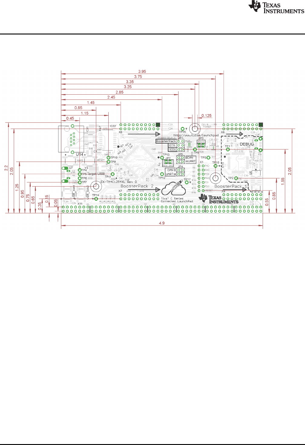
4.2 Component Locations
Figure 4-1 is a dimensioned drawing of the Connected LaunchPad. This figure shows the location of
selected features of the board as well as the component locations.
Figure 4-1. Connected LaunchPad Dimensions and Component Locations

www.ti.com
Bill of Materials
27
SPMU365C–March 2014–Revised October 2016
Submit Documentation Feedback
Copyright © 2014–2016, Texas Instruments Incorporated
References, PCB Layout, and Bill of Materials
4.3 Bill of Materials
Table 4-1 is the Connected LaunchPad bill of materials list.
Table 4-1. Connected LaunchPad Bill of Materials
Item Ref Qty Description Mfg Part Number
1 C1 1 Capacitor, 1000pF, 2kV,
20%, X7R, 1210 Kemet C1210C102MGRACTU
2
C3, C4, C5, C10, C11, C12,
C13, C16, C17, C18, C19,
C21, C22, C23, C24, C25,
C26, C27, C28, C29, C30,
C40, C41, C42, C43, C46
26 Capacitor, 0.1uF 16V,
10%,0402 X7R Taiyo Yuden EMK105B7104KV-F
3 C31 1 Capacitor, 4700pF, 2kV,
10%,X7R, 1812 AVX 1812GC472KAT1A
4 C32, C33 2 Capacitor, 3300pF, 50V,
10%, X7R, 0603 TDK C1608X7R1H332K
5 C6, C14 2 Capacitor, 1uF , X5R, 10V,
Low ESR, 0402 Johanson
Dielectrics Inc 100R07X105KV4T
6 C7, C15, C20 3 Capacitor, 2.2uF, 16V,
10%, 0603, X5R Murata GRM188R61C225KE15D
7C8, C9, C44,
C45, C47, C48 6Capacitor, 12pF, 50V,
5%, 0402, COG Murata GRM1555C1H120JZ01D
8 D0, D1, D2, D3, D4 5 Green LED 0603 Everlight 19-217/G7C-AL1M2B/3T
9J1, J2, J3,
J4, J5, J6, J7 7Jumper, 0.100, Gold,
Black, Open
3M 969102-0000-DA
Kobiconn 151-8000-E
10 JP1 1 Header, 2x3, 0.100, T-Hole,
Vertical Unshrouded,
0.230 Mate, gold FCI 67996-206HLF
11 JP2, JP3 2 Header, 1x2, 0.100, T-Hole,
Vertical Unshrouded, 0.220
Mate
3M 961102-6404-AR
FCI 68001-102HLF
Anyone 1x2-head
12 JP4, JP5 2 Header, 2x2, 0.100, T-Hole,
Vertical Unshrouded, 0.230
Mate
FCI 67997-104HLF
4UCON 00998
13 R1, R2, R3, R4,
R5, R29, R35, R44 8Resistor, 10k ohm, 1/10W,
5%, 0402 Thick Film Yageo RC0402FR-0710KL
14 R17, R26, R36 3 100k 5% 0402 resistor smd Rohm MCR01MRTJ104
15 R18, R51 2 Resistor 0402 100 ohm 5% Rohm MCR1MRTJ101
16 R23, R21, R22, R24 4 Resistor 49.9 ohm 0402. 1 % Rohm MCR01MRTF49R9
17 R25 1 Resistor 4.87k 1% 0402 smd Rohm MCR01MRTF4871
18 R28 1 Resistor, 5.6k ohm,
1/10W, 5%, 0402 Panasonic ERJ-2GEJ562X
19 R32, R43, R45, R46 4 resistor 75 ohm 0402 5% Rohm MCR01MRTJ750
20 R34, R52 2 Resistor, 1M OH,
1/10W, 5% 0603 SMD Panasonic ERJ-3GEYJ105V
21 R38 1 Resistor, 51 ohm,
1/10W, 5%, 0402 Panasonic ERJ-2GEJ510X

Bill of Materials
www.ti.com
28 SPMU365C–March 2014–Revised October 2016
Submit Documentation Feedback
Copyright © 2014–2016, Texas Instruments Incorporated
References, PCB Layout, and Bill of Materials
Table 4-1. Connected LaunchPad Bill of Materials (continued)
Item Ref Qty Description Mfg Part Number
22 R42 1 Resistor, 1M Ohm,
1/10W, 5%, 0402 Rohm MCR01MRTF1004
23 R47 1 RES 1M OHM 5% 1206 TF Panasonic ERJ-8GEYJ105V
24 R49, R50 2 Resistor, 2.0k ohm,
1/10W, 5%, 0402 Panasonic ERJ-3GEYJ202V
25 R6, R7, R8, R10, R11,
R15, R16, R19, R20, R39,
R40, R41 12 Resistor, 0 ohm,
1/10W, 5%, 0402 Panasonic ERJ-2GE0R00X
26 R9, R27, R30, R31, R33 5 Resistor, 330 ohm,
1/10W, 5%, 0402 Yageo RC0402FR-07330RL
27 RESET, USR_SW1,
USR_SW2, WAKE 4Switch, Tact 6mm SMT,
160gf Omron B3S-1000
28 U1 1 Tiva, MCU TM4C1294NCPDT
128 QFP with Ethernet MAC
+ PHY
Texas Instruments TM4C1294NCPDT
Texas Instruments XM4C1294NCPDT
29 U10 1 Transformer, ethernet, 1 to 1.
SOIC 16 Pulse Electronics HX1198FNL
30 U13 1 Diode, 8 chan, +/-15KV, ESD
Protection Array, SO-8 Semtech SLVU2.8-4.TBT
31 U14 1 Connector, RJ45 NO MAG,
shielded THRU HOLE TE Connectivity 1-406541-5
32 U2, U3 2 IC 4CH ESD SOLUTION
W/CLAMP 6SON Texas Instruments TPD4S012DRYR
33 U20 1 Stellaris TIVA MCU
TM4C123GH6PMI Texas Instruments TM4C123GH6PMI
34 U22 1 USB Micro B receptacle
right angle with guides FCI 10118194-0001LF
35 U4 1 Fault protected power switch,
dual channel, 8-SON Texas Instruments TPS2052BDRBR
36 U5 1 3.3V LDO TI TPS73733DRV
fixed out 5V in Texas Instruments TPS73733DRV
37 U6 1 Header 2x5, 0.050, SM,
Vertical Shrouded
Samtec SHF-105-01-S-D-SM
Don Connex
Electronics C44-10BSA1-G
38 U7 1 USB Micro AB receptacle.
Right angle with through
guides Hirose ZX62D-AB-5P8
39 X6, X7, X8, X9 4 Header, 2x10, T-Hole Vertical
unshrouded stacking
Samtec SSW-110-23-S-D
Major League
Electronics SSHQ-110-D-08-F-LF
40 Y1 1 Crystal 25 MHz 3.2 x 2.5 mm NDK nx3225ga-25.000m-std-crg-2
41 Y2 1 Crystal 16 MHz 3.2 x 2.5 mm
4 pin NDK NX3225GA-16.000M-STD-CRG-2
42 Y3 1 Crystal, 32.768 KHz Radial
Can Citizen Finetech
Miyota CMR200T-32.768KDZY-UT

www.ti.com
Bill of Materials
29
SPMU365C–March 2014–Revised October 2016
Submit Documentation Feedback Copyright © 2014–2016, Texas Instruments Incorporated
References, PCB Layout, and Bill of Materials
Table 4-1. Connected LaunchPad Bill of Materials (continued)
Item Ref Qty Description Mfg Part Number
PCB Do Not Populate List (Shown for information only)
43 C2 1 Capacitor, 0.1uF 16V,
10%, 0402 X7R Taiyo Yuden EMK105B7104KV-F
44 H1, H4, H6 3
Screw, #4 x 0.625" Pan
Head, Sheet Metal,
Phillips/Slotted
(for fan)
McMaster 90077A112
45 R12, R13, R14 3 Resistor, 5.6k ohm,
1/10W, 5%, 0402 Panasonic ERJ-2GEJ562X
46 R48 1 Resistor 0402 1% 52.3k Rohm TRR01MZPF5232
47
TP1, TP2, TP3, TP4, TP5,
TP6, TP7, TP8, TP9,
TP10, TP11, TP12, TP13,
TP14, TP15, TP16, TP17
17 Terminal, Test Point Miniature
Loop, Red, T-Hole Keystone 5000
48 X1 1 Header, 2x7, 0.100, T-Hole,
Vertical, Unshrouded, 0.230
Mate FCI 67997-114HLF
49 X11A 1 Valvano style bread board
connect. Right Angle
extended, 1 x 49 0.100 pitch. Samtec TSW-149-09-F-S-RE
50 X11B 1 valvano style breadboard
header. Samtec TSW-149-08-F-S-RA

30 SPMU365C–March 2014–Revised October 2016
Submit Documentation Feedback
Copyright © 2014–2016, Texas Instruments Incorporated
Schematic
Chapter 5
SPMU365C–March 2014–Revised October 2016
Schematic
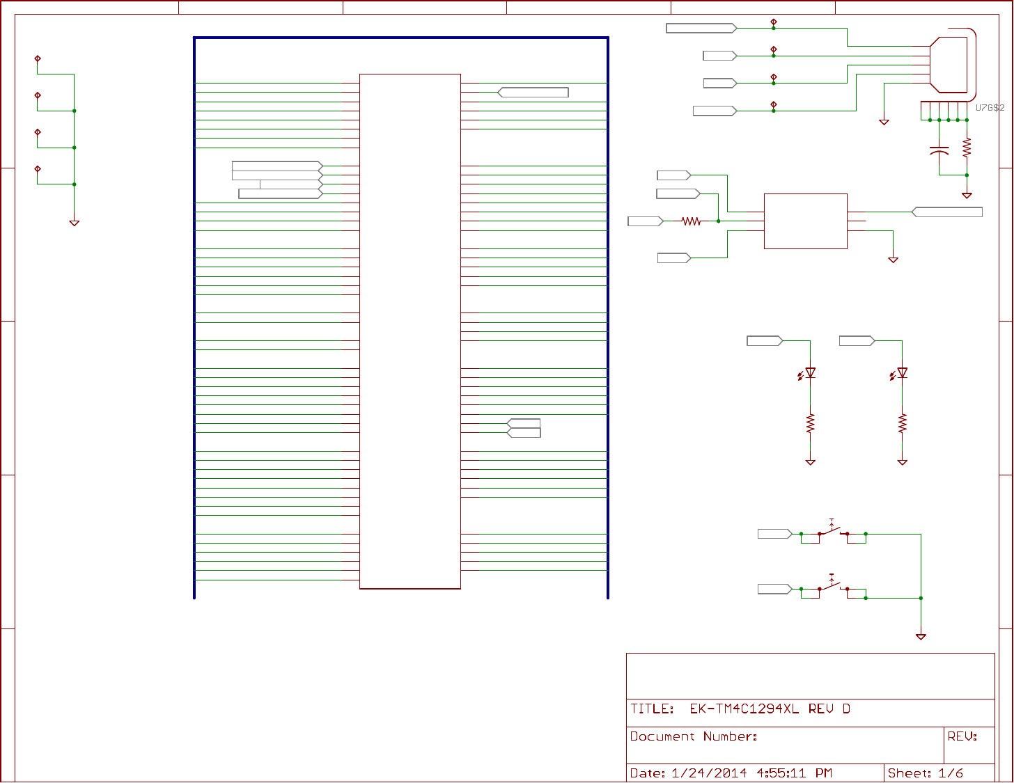
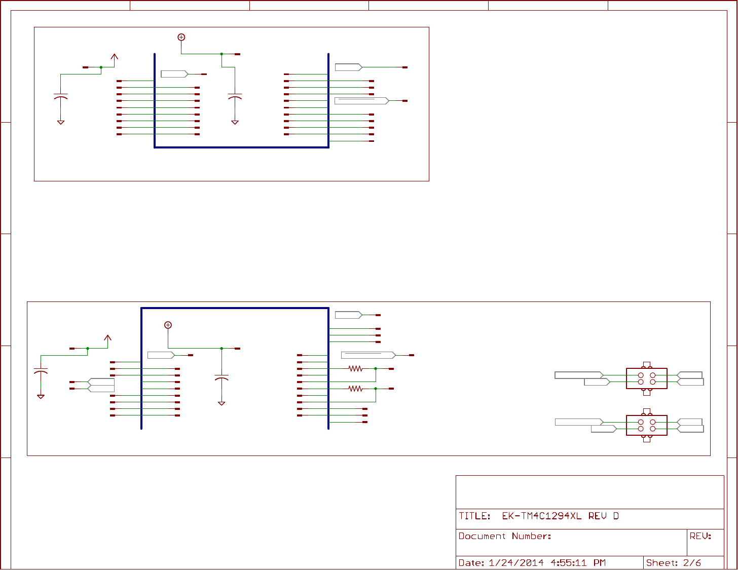
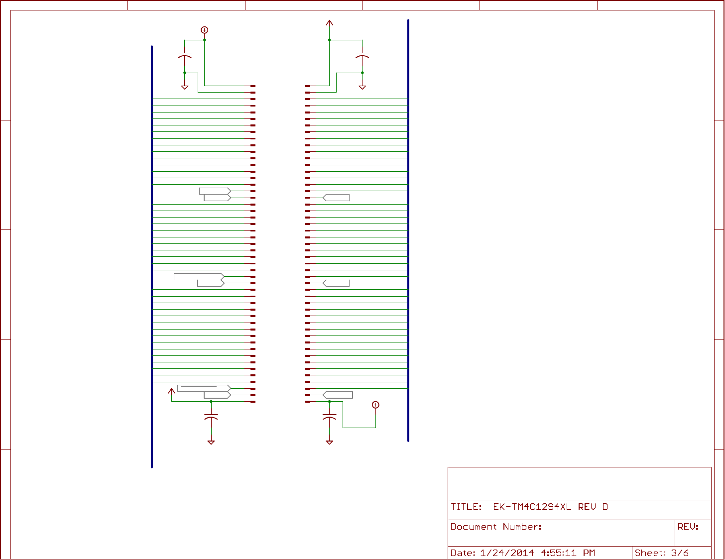
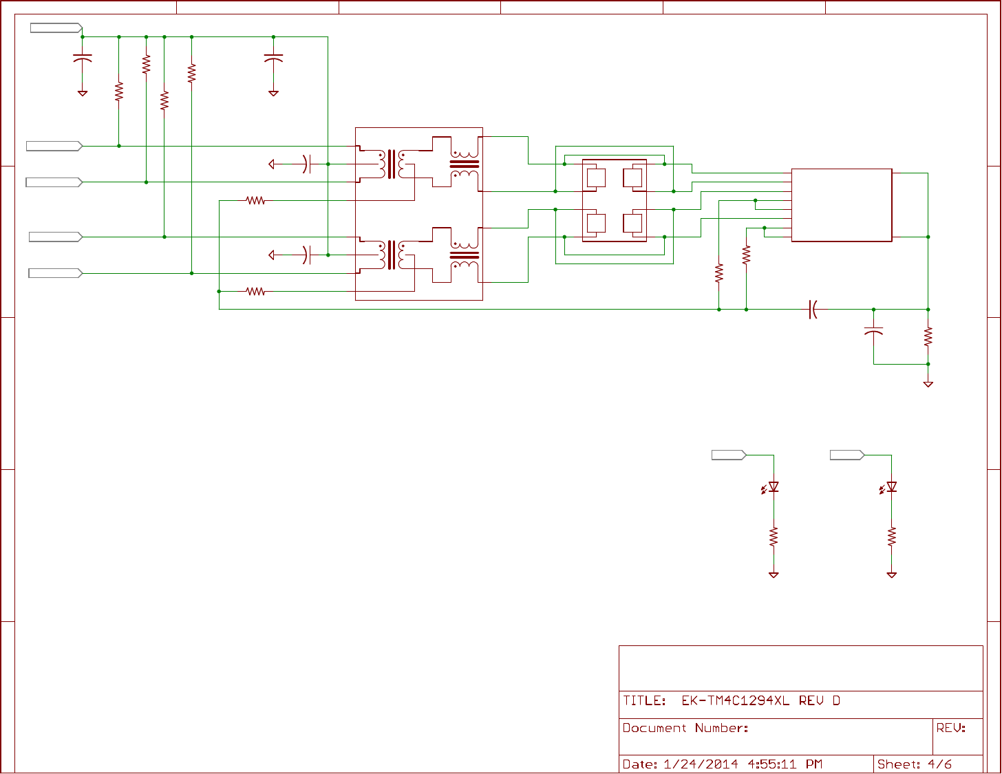
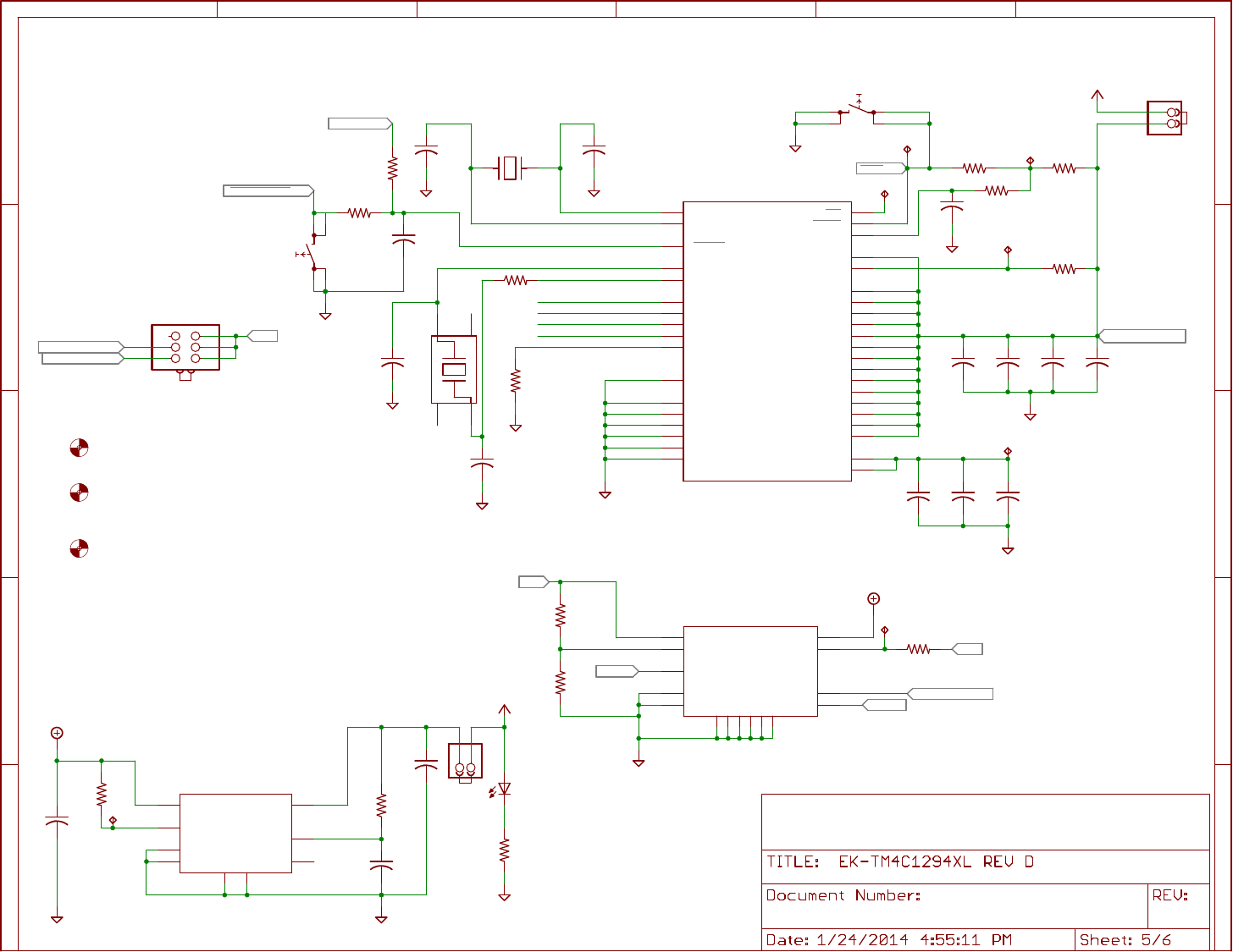
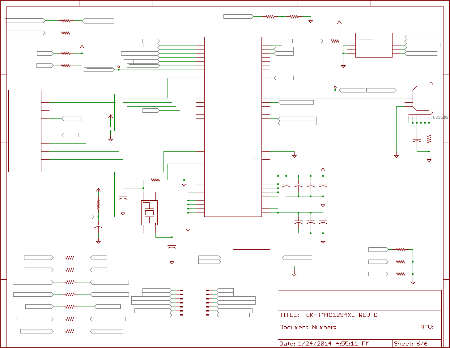
This section contains the complete schematics for the Tiva C Series TM4C1294 Connected LaunchPad.
• Microcontroller, USB, Buttons, and LED's
• BoosterPack connectors
• Breadboard connector
• Ethernet and Ethernet LED's
• Power
• In-Circuit Debug Interface
GND
330
GND
GND
SWITCH_TACTILE
SWITCH_TACTILE
GND
330
GND
TPD4S012_DRY_6
GND
100
GND
1M
3300pF
TP4
TP5
TP6
TP7
D1
R33
USR_SW1
USR_SW2
D2
R27
D+
1
D-
2
GND 4
ID
3N.C. 5
VBUS 6
U2
R18
DM
P2
DP
P3
GND
P5 ID
P4
VBUS
P1
TP14
TP15
TP16
TP17
PA0
P$33
PA1
P$34
PA2
P$35
PA3
P$36
PA4
P$37
PA5
P$38
PA6
P$40
PA7
P$41
PB0 P$95
PB1 P$96
PB2 P$91
PB3 P$92
PB4 P$121
PB5 P$120
PC0
P$100
PC1
P$99
PC2
P$98
PC3
P$97
PC4
P$25
PC5
P$24
PC6
P$23
PC7
P$22
PD0 P$1
PD1 P$2
PD2 P$3
PD3 P$4
PD4 P$125
PD5 P$126
PD6 P$127
PD7 P$128
PE0
P$15
PE1
P$14
PE2
P$13
PE3
P$12
PE4
P$123
PE5
P$124
PF0 P$42
PF1 P$43
PF2 P$44
PF3 P$45
PF4 P$46
PG0
P$49
PG1
P$50 PH0 P$29
PH1 P$30
PH2 P$31
PH3 P$32
PJ0
P$116
PJ1
P$117
PK0
P$18
PK1
P$19
PK2
P$20
PK3
P$21
PK4
P$63
PK5
P$62
PK6
P$61
PK7
P$60
PL0 P$81
PL1 P$82
PL2 P$83
PL3 P$84
PL4 P$85
PL5 P$86
PL6 P$94
PL7 P$93
PM0
P$78
PM1
P$77
PM2
P$76
PM3
P$75
PM4
P$74
PM5
P$73
PM6
P$72
PM7
P$71
PN0 P$107
PN1 P$108
PN2 P$109
PN3 P$110
PN4 P$111
PN5 P$112
PP0
P$118
PP1
P$119
PP2
P$103
PP3
P$104
PP4
P$105
PP5
P$106
PQ0 P$5
PQ1 P$6
PQ2 P$11
PQ3 P$27
PQ4 P$102
R52
C32
GPIO
PA0
PA1
PA2
PA3
PA5
PA6
PA7
PA4
PB0
PB0/3.2C
TARGET_VBUS/3.2C
TARGET_VBUS/3.2C
TARGET_VBUS/3.2C
PB2
PB3
PB4
PB5
PC4
PC5
PC6
PC7
PD0
PD1
PD2
PD3
PD4
PD5
PD6
PD7
PF0
PF1
PF2
PF3
PF4
PE0
PE1
PE2
PE3
PE4
PE5
PG0
PG1
PH0
PH1
PH2
PH3PJ0
PJ0/3.2D
PJ1
PJ1/3.2D
PK0
PK1
PK2
PK3
PK4
PK5
PK6
PK7
PL0
PL1
PL2
PL3
PL4
PL5
USBD_P
USBD_P
USBD_P
USBD_N
USBD_N
USBD_N
PM0
PM1
PM2
PM3
PM4
PM5
PM6
PM7
PP0
PP1
PP2
PP3
PP4
PP5
PN0
PN0/3.4D
PN1
PN1/3.4D
PN2
PN3
PN4
PN5
PQ0
PQ1
PQ2
PQ3
PQ4
TARGET_TCK/SWCLK/6.1A
TARGET_TMS/SWDIO/6.1A
TARGET_TDI/6.1E
TARGET_TDO/SWO/6.1E TARGET_ID
TARGET_ID
A
B
C
D
E
A
B
C
D
E
1 2 3 4 5 6
U7G$1
U1G$1
TM4C1294NCPDT
See PF0 and PF4 for additional LED's used for
Ethernet or user application
NOTE: TPD4S012 all protection circuits are identical.
Connections chosen for simple routing.
convienence test points for ground
TSW-110-02-S-D
TSW-110-02-S-D
TSW-110-02-S-D
TSW-110-02-S-D
0
0
+3V3
+3V3
+5V
+5V
0.1uF 0.1uF
0.1uF
0.1uF
GNDGND
GND
GND
X6-1 X6-2
X6-3
X6-4
X6-5 X6-6
X6-7 X6-8
X6-9 X6-10
X6-11 X6-12
X6-13 X6-14
X6-15 X6-16
X6-17 X6-18
X6-19 X6-20
X7-1
X7-2
X7-3
X7-4
X7-5
X7-6
X7-7
X7-8
X7-9
X7-10
X7-11
X7-12
X7-13
X7-14
X7-15
X7-16X7-17
X7-18X7-19
X7-20
X8-1
X8-2
X8-3
X8-4
X8-5 X8-6
X8-7 X8-8
X8-9 X8-10
X8-11 X8-12
X8-13 X8-14
X8-15 X8-16
X8-17 X8-18
X8-19 X8-20
X9-1
X9-2
X9-3 X9-4
X9-5 X9-6
X9-7 X9-8
X9-9 X9-10
X9-11
X9-12X9-13
X9-14X9-15
X9-16X9-17
X9-18X9-19
X9-20
R19
R20
JP4
1 2
3 4
JP5
1 2
3 4
C23 C24
C25
C26
PB2
PB3
PL0
PP2
PH2
GND/1.6B
GND/1.6B
GND/1.6B
GND/1.6B
TARGET_RESET/3.2D
TARGET_RESET/3.2D
PA0/3.2C
BP2_A2.5BP2_A2.5
TARGET_RXD/6.1D
TARGET_TXD/6.1D PA1/3.2C
BP2_A2.6
BP2_A2.6
PE4
PE5
PC5
PC4
PM3
PM4
PM5
PL4
PD5/1.4B
PC6
PD3
PC7
PE0
PE1
PE2
PE3
PD4/1.4B
PD7
PF1
PF2
PF3
PG0
PL5
PL1
PL2
PL3
PH3
PD1
PD0
PN2
PN3
PD2
PP0
PP1
PQ0
PP4
PN5
PN4
PB4
PB5
PK0
PK1
PK2
PK3
PA4
PA5
PG1
PK4
PK5
PM0
PM1
PM2
PH0
PH1
PK6
PK7
PM7
PA7
PA3
PA2
PQ3
PQ2
PP3
PQ1
PM6
PP5
PA6
BoosterPack 2 Interface
BoosterPack 1 Interface
A
B
C
D
E
A
B
C
D
E
1 2 3 4 5 6
JP4 and JP5 CAN and ICDI UART Selection:
Populate Jumpers from 1-2 and 3-4 for Default Mode
This enables ROM UART boot loader. UART 0 to ICDI
Populate from 1-3 and 2-4 for controller area network
on the boosterpack. UART2 is then availabe to ICDI.
R19 and R20 can be populated to enable I2C on
Right side of BP2 interface. This is for legacy
support and the Sensor Hub BoosterPack.
I2C and SSI are available on the corresponding
BoosterPack 1 interface pins without modification to
the board.
PA6 and PA7 are also used by the onboard radio.
Configure the radio to tri-state these GPIO before
using them on the boosterpack interface.
TSW-149-02-S-D
+3V3
+3V3
+5V
+5V
0.1uF0.1uF
0.1uF 0.1uF
GNDGND
GNDGND
X11-1X11-2
X11-3X11-4
X11-5X11-6
X11-7X11-8
X11-9X11-10
X11-11X11-12
X11-13X11-14
X11-15X11-16
X11-17X11-18
X11-19X11-20
X11-21X11-22
X11-23X11-24
X11-25X11-26
X11-27X11-28
X11-29X11-30
X11-31X11-32
X11-33X11-34
X11-35X11-36
X11-37X11-38
X11-39X11-40
X11-41X11-42
X11-43X11-44
X11-45X11-46
X11-47X11-48
X11-49X11-50
X11-51X11-52
X11-53X11-54
X11-55X11-56
X11-57X11-58
X11-59X11-60
X11-61X11-62
X11-63X11-64
X11-65X11-66
X11-67X11-68
X11-69X11-70
X11-71X11-72
X11-73X11-74
X11-75X11-76
X11-77X11-78
X11-79X11-80
X11-81X11-82
X11-83X11-84
X11-85X11-86
X11-87X11-88
X11-89X11-90
X11-91X11-92
X11-93X11-94
X11-95X11-96
X11-97X11-98
C27C28
C29 C30
VREF+/5.5B
TARGET_RESET/2.4D
GND/2.3C
GND/4.1A
GND/2.3C
GND/4.1AGND/2.3C
PB4
PB5
PH0
PH1
PH2
PH3
PC7
PC6
PC5
PC4
PA6
PA7
PG1
PM3
PM2
PM1
PM0
PL0
PL2
PL3
PQ0
PQ1
PK7
PK6
PL4
PB2
PB3
PP2
PP3
PK5
PK4
PL5
PN4
PN5
PG0
PL1
PQ2
PQ3
PN0
PN1
PN2
PN3
PQ4
WAKE/5.5A
PA2
PA3
PA4
PA5
PE0
PE1
PE2
PE3
PE4
PE5
PK0
PK1
PK2
PK3
PD5
PD4
PD7
PD6
PD3
PD1
PD0
PD2
PP0
PP1
PB0
TARGET_VBUS/1.6B
PF4
PF0
PF1
PF2
PF3
PA0
PA1
PP4
PP5
PJ0
PJ1
PM7
PM6
PM5
PM4
A
B
C
D
E
A
B
C
D
E
1 2 3 4 5 6
NOTE: PB0 and PB1 are used in some
configurations with 5V signals especially in USB
Host or OTG mode. Be aware the 5V may be
present on these pins depending on system jumper
configuration
These pins are only 5V tolerant when configured for
USB mode applications.
This is the breadboard connection header.
Samtec TSW-149-08-F-S-RA and TSW-149-09-F-S-RE
can be used together to create a breadboard
connector
see the Users Manual for more information.
49.9
49.9
49.4
49.9
330
GND
330
GND
0.1uF0.1uF
GNDGND
0.1uF0.1uF
75
75
GNDGND
75
75
GND
4700pF
1M
1000pF
R21
R22
R23
R24
D4
R30
D3
R31
C16C17
C18C22
P$1
P$1
P$2
P$2
P$3
P$3
P$6
P$6
P$7
P$7
P$8
P$8
P$9 P$9
P$10
P$10
P$11 P$11
P$14 P$14
P$15
P$15
P$16 P$16
P$1
1
P$2
2
P$3
3
P$4
4P$5 5
P$6 6
P$7 7
P$8 8
R32
R43
CHASSIS 9
CHASSIS 10
RX+
3
RX-
6
TERM1A
4
TERM1B
5
TERM2A
7
TERM2B
8
TX+
1
TX-
2
R45
R46
C31
R47
C1
EN0RXI_N/5.3B
EN0RXI_P/5.3B
EN0TXO_N/5.3B
EN0TXO_P/5.3B
PF4/3.2C PF0/3.2C
MCU_3V3/5.2A
A
B
C
D
E
A
B
C
D
E
1 2 3 4 5 6
U10
U13
U14
For Ethernet example Applications:
LED4 is default configured as Ethernet Link OK
LED3 is default configured as Ethernet TX/RX activity
User may re-configure these pins / LED's for any
application usage.
Place pull up resistors and C16-C17 near TM4C MCU.
Place C18 and C22 near pin 2 and pin 7 of U$10
U10 May be populated with either HX1188FNL or HX1198FNL.
HX1198FNL preferred for best Ethernet performance.
+3V3
+5V
GND
0.1uF
2.2uF
0.1uF
GND
330
GND
100k
4.87k 1%
GND
GND 0.1uF 1.0uF 2.2uF
0.1uF 0.1uF 0.1uF 0.1uF
GND
0
0
GND
1M
SWITCH_TACTILE
12pF
12pF
10k
0.1uF
12pF 12pF
SWITCH_TACTILE
GND
MOUNT-HOLE3.2
MOUNT-HOLE3.2
GND
GND
GND
GND GND
TPS2052B_DRB_8
+5V
10k
100k
GND
51
0.1uF
GND
+3V3
100k
TPS73733_DRV_6
OMIT
2k
MOUNT-HOLE3.2
100
CRYATL_32K_SMD
C19
C20
C21
D0
R9
R17
TP3
R25
C4 C14 C15
C40 C41 C42 C43
TP9
TP10
TP11
TP12
R39
TP13
R41
R42
RESET
C44
C45
NC2 P$2
NC4
P$4
OSC0
P$1
OSC1 P$3
R44
C46
C47 C48
WAKE
H4
H6
*EN1
3
*EN2
4
*OC1 8
*OC2 5
EPAD
9GND
1
IN
2OUT1 7
OUT2 6
VIA
V
VIA
V_2
VIA
V_3
VIA
V_4
VIA
V_5
VIA
V_6
U4
JP1
1 2
3 4
5 6
JP2
1
2
JP3
1
2
R35
R36
TP8
R38
C3
R26
EN
4
EPAD
7GND
3
IN
6
NC 5
NR/FB 2
OUT 1
VIA
V
VIA
V_2
U5
R48
R49
H1
R51
HIB P$65
RESET
P$70
WAKE P$64
EN0RXIN
P$53
EN0RXIP
P$54
EN0TXON
P$56
EN0TXOP
P$57
GND
P$17
GND
P$48
GND
P$55
GND
P$58
GND
P$80
GND
P$114
GNDA
P$10
OSC0
P$88
OSC1
P$89
RBIAS
P$59
VBAT P$68
VDD P$7
VDD P$16
VDD P$26
VDD P$28
VDD P$39
VDD P$47
VDD P$51
VDD P$52
VDD P$69
VDD P$79
VDD P$90
VDD P$101
VDD P$113
VDD P$122
VDDA P$8
VDDC P$87
VDDC P$115
VREFA+ P$9
XOSC0
P$66
XOSC1
P$67
P$1 P$1
P$2
P$2
Y3
TARGET_VBUS/3.2C
TARGET_VBUS/3.2C
DEBUG_VBUS/6.4A
EN0RXI_N
EN0RXI_P
EN0TXO_N
EN0TXO_P
RBIAS
WAKE/3.3D
MCU_3V3/6.2A
MCU_3V3/4.1A
VBUS
VBUS
VBUS
PQ4/3.4D
PD6/3.2B
TARGET_RESET/3.2D
A
B
C
D
E
A
B
C
D
E
1 2 3 4 5 6
Y1
25Mhz
U1G$2
Power Control Jumper:
1) To power from Debug install jumper on pins 5 - 6
2) To power from Target USB install jumper on pins 3 - 4
3) To power from BoosterPack 5V install jumper on pins 1 - 2
This is also the off position if BoosterPack does not
supply power
When powered from BoosterPack TPS2052B does not
provide current limit protection.
When powered by BoosterPack, USB host mode does not
supply power to connected devices
Primary 3.3V regulator
Disconnect JP3 to power device from 3V3 BoosterPack
JP2 can be used to measure MCU current
consumption with a multi-meter.
TPS2052B provides current limit for main 5V power.
Also provides power switching for USB host/OTG modes
For Host/OTG:
PD6 configured as USB0EPEN peripheral function.
PQ4 configure as individual pin interrupt. Indicates
power fault on the USB bus. USB0PFLT peipheral pin
not available due to pin mux and use on BoosterPacks.
USB Host mode does not supply power to devices
when powered from a BoosterPack
For Applications that do not use USB:
Configure PD6 as input with internal pull-down
enabled. Turns off power to TARGET_VBUS
R38 and C3 Used to meet
VBAT rise time requirements
R41 may be removed and precision
reference applied to TP13
OMIT
TSW-107-02-S-D
OMIT
+3V3
10k
0.1uF
OMIT 0.1uF 1.0uF
12pF
12pF
0.1uF 0.1uF 0.1uF 0.1uF
+3V3
+3V3
2.2uF
5.6k
OMIT
5.6k
OMIT
5.6k
OMIT
10k
10k
10k
10k
+3V3
0
0
0
0
0
0
0
GND
GND
GND
GND
GND
GND
GND
GND
GND
GND
GND
GND
0
+3V3
TPD4S012_DRY_6
5.6k 10k
GND
2k
GND
1M
3300pF
GND
TRST 9
GND 3
NC 5
RESET 10
RTCK 7
TCK 4
TDI 8
TDO 6
TMS 2
VTREF 1
U21
X1-1X1-2
X1-3X1-4
X1-5X1-6
X1-7X1-8
X1-9X1-10
X1-11X1-12
X1-13X1-14
R3
C2
C5 C6
C8
C9
C10 C11 C12 C13
NC2 P$2
NC4
P$4
OSC0
P$1
OSC1 P$3
C7
R12
R13
R14
R1
R2
R4
R5
TP2
TP1
R6
R7
R8
R10
R11
R15
R16
EXTDBG
P3
RESET P10
GND
P5
GND1
P9 P$7
P7
TCK P4
TDI P8
TDO P6
TMS P2
VTARGET
P1
R40
HIB P$33
RESET
P$38 WAKE P$32
GND0
P$12
GND1
P$27
GND2
P$39
GND3
P$55
GNDA
P$3
GNDX
P$35
OSC0
P$40 OSC1
P$41
PA0
P$17
PA1
P$18
PA2
P$19
PA3
P$20
PA4
P$21
PA5
P$22
PA6
P$23
PA7
P$24
PB0 P$45
PB1 P$46
PB2 P$47
PB3 P$48
PB4 P$58
PB5 P$57
PB6 P$1
PB7 P$4
PC0/TCK
P$52
PC1/TMS
P$51
PC2/TDI
P$50
PC3/TDO
P$49
PC4
P$16
PC5
P$15
PC6
P$14
PC7
P$13
PD0 P$61
PD1 P$62
PD2 P$63
PD3 P$64
PD4 P$43
PD5 P$44
PD6 P$53
PD7 P$10
PE0
P$9
PE1
P$8
PE2
P$7
PE3
P$6
PE4
P$59
PE5
P$60
PF0 P$28
PF1 P$29
PF2 P$30
PF3 P$31
PF4 P$5
VBAT P$37
VDD0 P$11
VDD1 P$26
VDD2 P$42
VDD3 P$54
VDDA P$2
VDDC0 P$25
VDDC1 P$56
XOSC0
P$34
XOSC1
P$36
DM
P2
DP
P3
GND
P5 ID
P4
VBUS
P1
D+
1
D-
2
GND 4
ID
3N.C. 5
VBUS 6
U3
R28 R29
R50
R34
C33
ICDI_TDI
ICDI_TMS
ICDI_TMS
ICDI_TCK
ICDI_TCK
ICDI_TDO
ICDI_TDO
ICDI_RESET
ICDI_RESET
VCP_RXD
VCP_RXD
VCP_RXD
VCP_TXD
VCP_TXD
VCP_TXD
DEBUG_PC1/TMS/SWDIO
DEBUG_PC1/TMS/SWDIO
DEBUG_PC1/TMS/SWDIO
DEBUG_PC1/TMS/SWDIO
DEBUG_PC1/TMS/SWDIO
DEBUG_PC3/TDO/SWO
DEBUG_PC3/TDO/SWO
DEBUG_PC3/TDO/SWO
DEBUG_PC3/TDO/SWO
DEBUG_PC3/TDO/SWO
DEBUG_PC2/TDI
DEBUG_PC2/TDI DEBUG_PC2/TDI
DEBUG_PC2/TDI
DEBUG_RESET_OUT
DEBUG_RESET_OUT
DEBUG_RESET_OUT
DEBUG_RESET_OUT
EXTERNAL_DEBUG
EXTERNAL_DEBUG
ICDI_VDDC
VERSION_1
VERSION_1
VERSION_2
VERSION_2
VERSION_0
VERSION_0
DEBUG_ACTIVEDEBUG_ACTIVE
ICDI_USBD_N
ICDI_USBD_N
ICDI_USBD_P
ICDI_USBD_PTARGET_TXD/2.5D
TARGET_TXD/2.5D
TARGET_RXD/2.5D
TARGET_RXD/2.5D
TARGET_TCK/SWCLK/1.2A
TARGET_TCK/SWCLK/1.2A
TARGET_TCK/SWCLK/1.2A
TARGET_TMS/SWDIO/1.2B
TARGET_TMS/SWDIO/1.2B
TARGET_TMS/SWDIO/1.2B
TARGET_TDI/1.2B TARGET_TDI/1.2B
TARGET_TDO/SWO/1.2B
TARGET_TDO/SWO/1.2B
TARGET_RESET/5.2A
TARGET_RESET/5.2A
DEBUG_VBUS/5.1B
DEBUG_VBUS/5.1B
DEBUG_VBUS/5.1B
DEBUG_PC0/TCK/SWCLK
DEBUG_PC0/TCK/SWCLK
DEBUG_PC0/TCK/SWCLK
DEBUG_PC0/TCK/SWCLK
DEBUG_PC0/TCK/SWCLK
MCU_3V3/5.6B
A
B
C
D
E
A
B
C
D
E
1 2 3 4 5 6
Y2
16M
U6
JTAG_ARM_10PIN
U20
TM4C123GH6PMI
TM4C123xH6PMI
U22G$1
PE4 ETM_ENn Leave Open
use GPIO Internal weak pullup.
PE5 LS_PRESENTn Leave Open
use GPIO internal weak pullup
VERSION RESISTOR TABLE:
*use internal GPIO weak pullups.
ALL OMITTED: Legacy mode. (Stellaris ICDI)
ALL POPULATED: Everything enabled
Version 0 populated: UART CTS/RTS and Analog inputs
JTAG PULL-UPS
Jumpers to bridge from ICDI to Target portion of LaunchPad
EXTERNAL_DEBUG pull low to use external debugger
to debug the target. Causes ICDI chip to tri-state the JTAG lines
Use this for JTAG IN from external debugger. See X1
jumpers for information about debug out to an
external target.
R40 must be removed for debug out.
R40 must be instaled for debug in.
X1 omitted by default
To debug out from ICDI to off board MCU remove
0 ohm jumper resistors. To go back from debug
out to debugging the target MCU install X1 and
place jumpers on all pins.

www.ti.com
Revision History
31
SPMU365C–March 2014–Revised October 2016
Submit Documentation Feedback Copyright © 2014–2016, Texas Instruments Incorporated
Revision History
Revision History
Changes from B Revision (May 2015) to C Revision ...................................................................................................... Page
• GLOBAL: Updated/Changed all instances of "UART4" to "UART2"................................................................ 4
STANDARD TERMS FOR EVALUATION MODULES
1. Delivery: TI delivers TI evaluation boards, kits, or modules, including any accompanying demonstration software, components, and/or
documentation which may be provided together or separately (collectively, an “EVM” or “EVMs”) to the User (“User”) in accordance
with the terms set forth herein. User's acceptance of the EVM is expressly subject to the following terms.
1.1 EVMs are intended solely for product or software developers for use in a research and development setting to facilitate feasibility
evaluation, experimentation, or scientific analysis of TI semiconductors products. EVMs have no direct function and are not
finished products. EVMs shall not be directly or indirectly assembled as a part or subassembly in any finished product. For
clarification, any software or software tools provided with the EVM (“Software”) shall not be subject to the terms and conditions
set forth herein but rather shall be subject to the applicable terms that accompany such Software
1.2 EVMs are not intended for consumer or household use. EVMs may not be sold, sublicensed, leased, rented, loaned, assigned,
or otherwise distributed for commercial purposes by Users, in whole or in part, or used in any finished product or production
system.
2Limited Warranty and Related Remedies/Disclaimers:
2.1 These terms do not apply to Software. The warranty, if any, for Software is covered in the applicable Software License
Agreement.
2.2 TI warrants that the TI EVM will conform to TI's published specifications for ninety (90) days after the date TI delivers such EVM
to User. Notwithstanding the foregoing, TI shall not be liable for a nonconforming EVM if (a) the nonconformity was caused by
neglect, misuse or mistreatment by an entity other than TI, including improper installation or testing, or for any EVMs that have
been altered or modified in any way by an entity other than TI, (b) the nonconformity resulted from User's design, specifications
or instructions for such EVMs or improper system design, or (c) User has not paid on time. Testing and other quality control
techniques are used to the extent TI deems necessary. TI does not test all parameters of each EVM.
User's claims against TI under this Section 2 are void if User fails to notify TI of any apparent defects in the EVMs within ten (10)
business days after delivery, or of any hidden defects with ten (10) business days after the defect has been detected.
2.3 TI's sole liability shall be at its option to repair or replace EVMs that fail to conform to the warranty set forth above, or credit
User's account for such EVM. TI's liability under this warranty shall be limited to EVMs that are returned during the warranty
period to the address designated by TI and that are determined by TI not to conform to such warranty. If TI elects to repair or
replace such EVM, TI shall have a reasonable time to repair such EVM or provide replacements. Repaired EVMs shall be
warranted for the remainder of the original warranty period. Replaced EVMs shall be warranted for a new full ninety (90) day
warranty period.
3Regulatory Notices:
3.1 United States
3.1.1 Notice applicable to EVMs not FCC-Approved:
FCC NOTICE: This kit is designed to allow product developers to evaluate electronic components, circuitry, or software
associated with the kit to determine whether to incorporate such items in a finished product and software developers to write
software applications for use with the end product. This kit is not a finished product and when assembled may not be resold or
otherwise marketed unless all required FCC equipment authorizations are first obtained. Operation is subject to the condition
that this product not cause harmful interference to licensed radio stations and that this product accept harmful interference.
Unless the assembled kit is designed to operate under part 15, part 18 or part 95 of this chapter, the operator of the kit must
operate under the authority of an FCC license holder or must secure an experimental authorization under part 5 of this chapter.
3.1.2 For EVMs annotated as FCC – FEDERAL COMMUNICATIONS COMMISSION Part 15 Compliant:
CAUTION
This device complies with part 15 of the FCC Rules. Operation is subject to the following two conditions: (1) This device may not
cause harmful interference, and (2) this device must accept any interference received, including interference that may cause
undesired operation.
Changes or modifications not expressly approved by the party responsible for compliance could void the user's authority to
operate the equipment.
FCC Interference Statement for Class A EVM devices
NOTE: This equipment has been tested and found to comply with the limits for a Class A digital device, pursuant to part 15 of
the FCC Rules. These limits are designed to provide reasonable protection against harmful interference when the equipment is
operated in a commercial environment. This equipment generates, uses, and can radiate radio frequency energy and, if not
installed and used in accordance with the instruction manual, may cause harmful interference to radio communications.
Operation of this equipment in a residential area is likely to cause harmful interference in which case the user will be required to
correct the interference at his own expense.
FCC Interference Statement for Class B EVM devices
NOTE: This equipment has been tested and found to comply with the limits for a Class B digital device, pursuant to part 15 of
the FCC Rules. These limits are designed to provide reasonable protection against harmful interference in a residential
installation. This equipment generates, uses and can radiate radio frequency energy and, if not installed and used in accordance
with the instructions, may cause harmful interference to radio communications. However, there is no guarantee that interference
will not occur in a particular installation. If this equipment does cause harmful interference to radio or television reception, which
can be determined by turning the equipment off and on, the user is encouraged to try to correct the interference by one or more
of the following measures:
•Reorient or relocate the receiving antenna.
•Increase the separation between the equipment and receiver.
•Connect the equipment into an outlet on a circuit different from that to which the receiver is connected.
•Consult the dealer or an experienced radio/TV technician for help.
3.2 Canada
3.2.1 For EVMs issued with an Industry Canada Certificate of Conformance to RSS-210 or RSS-247
Concerning EVMs Including Radio Transmitters:
This device complies with Industry Canada license-exempt RSSs. Operation is subject to the following two conditions:
(1) this device may not cause interference, and (2) this device must accept any interference, including interference that may
cause undesired operation of the device.
Concernant les EVMs avec appareils radio:
Le présent appareil est conforme aux CNR d'Industrie Canada applicables aux appareils radio exempts de licence. L'exploitation
est autorisée aux deux conditions suivantes: (1) l'appareil ne doit pas produire de brouillage, et (2) l'utilisateur de l'appareil doit
accepter tout brouillage radioélectrique subi, même si le brouillage est susceptible d'en compromettre le fonctionnement.
Concerning EVMs Including Detachable Antennas:
Under Industry Canada regulations, this radio transmitter may only operate using an antenna of a type and maximum (or lesser)
gain approved for the transmitter by Industry Canada. To reduce potential radio interference to other users, the antenna type
and its gain should be so chosen that the equivalent isotropically radiated power (e.i.r.p.) is not more than that necessary for
successful communication. This radio transmitter has been approved by Industry Canada to operate with the antenna types
listed in the user guide with the maximum permissible gain and required antenna impedance for each antenna type indicated.
Antenna types not included in this list, having a gain greater than the maximum gain indicated for that type, are strictly prohibited
for use with this device.
Concernant les EVMs avec antennes détachables
Conformément à la réglementation d'Industrie Canada, le présent émetteur radio peut fonctionner avec une antenne d'un type et
d'un gain maximal (ou inférieur) approuvé pour l'émetteur par Industrie Canada. Dans le but de réduire les risques de brouillage
radioélectrique à l'intention des autres utilisateurs, il faut choisir le type d'antenne et son gain de sorte que la puissance isotrope
rayonnée équivalente (p.i.r.e.) ne dépasse pas l'intensité nécessaire à l'établissement d'une communication satisfaisante. Le
présent émetteur radio a été approuvé par Industrie Canada pour fonctionner avec les types d'antenne énumérés dans le
manuel d’usage et ayant un gain admissible maximal et l'impédance requise pour chaque type d'antenne. Les types d'antenne
non inclus dans cette liste, ou dont le gain est supérieur au gain maximal indiqué, sont strictement interdits pour l'exploitation de
l'émetteur
3.3 Japan
3.3.1 Notice for EVMs delivered in Japan: Please see http://www.tij.co.jp/lsds/ti_ja/general/eStore/notice_01.page 日本国内に
輸入される評価用キット、ボードについては、次のところをご覧ください。
http://www.tij.co.jp/lsds/ti_ja/general/eStore/notice_01.page
3.3.2 Notice for Users of EVMs Considered “Radio Frequency Products” in Japan: EVMs entering Japan may not be certified
by TI as conforming to Technical Regulations of Radio Law of Japan.
If User uses EVMs in Japan, not certified to Technical Regulations of Radio Law of Japan, User is required to follow the
instructions set forth by Radio Law of Japan, which includes, but is not limited to, the instructions below with respect to EVMs
(which for the avoidance of doubt are stated strictly for convenience and should be verified by User):
1. Use EVMs in a shielded room or any other test facility as defined in the notification #173 issued by Ministry of Internal
Affairs and Communications on March 28, 2006, based on Sub-section 1.1 of Article 6 of the Ministry’s Rule for
Enforcement of Radio Law of Japan,
2. Use EVMs only after User obtains the license of Test Radio Station as provided in Radio Law of Japan with respect to
EVMs, or
3. Use of EVMs only after User obtains the Technical Regulations Conformity Certification as provided in Radio Law of Japan
with respect to EVMs. Also, do not transfer EVMs, unless User gives the same notice above to the transferee. Please note
that if User does not follow the instructions above, User will be subject to penalties of Radio Law of Japan.
【無線電波を送信する製品の開発キットをお使いになる際の注意事項】 開発キットの中には技術基準適合証明を受けて
いないものがあります。 技術適合証明を受けていないもののご使用に際しては、電波法遵守のため、以下のいずれかの
措置を取っていただく必要がありますのでご注意ください。
1. 電波法施行規則第6条第1項第1号に基づく平成18年3月28日総務省告示第173号で定められた電波暗室等の試験設備でご使用
いただく。
2. 実験局の免許を取得後ご使用いただく。
3. 技術基準適合証明を取得後ご使用いただく。
なお、本製品は、上記の「ご使用にあたっての注意」を譲渡先、移転先に通知しない限り、譲渡、移転できないものとします。
上記を遵守頂けない場合は、電波法の罰則が適用される可能性があることをご留意ください。 日本テキサス・イ
ンスツルメンツ株式会社
東京都新宿区西新宿6丁目24番1号
西新宿三井ビル
3.3.3 Notice for EVMs for Power Line Communication: Please see http://www.tij.co.jp/lsds/ti_ja/general/eStore/notice_02.page
電力線搬送波通信についての開発キットをお使いになる際の注意事項については、次のところをご覧ください。http:/
/www.tij.co.jp/lsds/ti_ja/general/eStore/notice_02.page
3.4 European Union
3.4.1 For EVMs subject to EU Directive 2014/30/EU (Electromagnetic Compatibility Directive):
This is a class A product intended for use in environments other than domestic environments that are connected to a
low-voltage power-supply network that supplies buildings used for domestic purposes. In a domestic environment this
product may cause radio interference in which case the user may be required to take adequate measures.
4EVM Use Restrictions and Warnings:
4.1 EVMS ARE NOT FOR USE IN FUNCTIONAL SAFETY AND/OR SAFETY CRITICAL EVALUATIONS, INCLUDING BUT NOT
LIMITED TO EVALUATIONS OF LIFE SUPPORT APPLICATIONS.
4.2 User must read and apply the user guide and other available documentation provided by TI regarding the EVM prior to handling
or using the EVM, including without limitation any warning or restriction notices. The notices contain important safety information
related to, for example, temperatures and voltages.
4.3 Safety-Related Warnings and Restrictions:
4.3.1 User shall operate the EVM within TI’s recommended specifications and environmental considerations stated in the user
guide, other available documentation provided by TI, and any other applicable requirements and employ reasonable and
customary safeguards. Exceeding the specified performance ratings and specifications (including but not limited to input
and output voltage, current, power, and environmental ranges) for the EVM may cause personal injury or death, or
property damage. If there are questions concerning performance ratings and specifications, User should contact a TI
field representative prior to connecting interface electronics including input power and intended loads. Any loads applied
outside of the specified output range may also result in unintended and/or inaccurate operation and/or possible
permanent damage to the EVM and/or interface electronics. Please consult the EVM user guide prior to connecting any
load to the EVM output. If there is uncertainty as to the load specification, please contact a TI field representative.
During normal operation, even with the inputs and outputs kept within the specified allowable ranges, some circuit
components may have elevated case temperatures. These components include but are not limited to linear regulators,
switching transistors, pass transistors, current sense resistors, and heat sinks, which can be identified using the
information in the associated documentation. When working with the EVM, please be aware that the EVM may become
very warm.
4.3.2 EVMs are intended solely for use by technically qualified, professional electronics experts who are familiar with the
dangers and application risks associated with handling electrical mechanical components, systems, and subsystems.
User assumes all responsibility and liability for proper and safe handling and use of the EVM by User or its employees,
affiliates, contractors or designees. User assumes all responsibility and liability to ensure that any interfaces (electronic
and/or mechanical) between the EVM and any human body are designed with suitable isolation and means to safely
limit accessible leakage currents to minimize the risk of electrical shock hazard. User assumes all responsibility and
liability for any improper or unsafe handling or use of the EVM by User or its employees, affiliates, contractors or
designees.
4.4 User assumes all responsibility and liability to determine whether the EVM is subject to any applicable international, federal,
state, or local laws and regulations related to User’s handling and use of the EVM and, if applicable, User assumes all
responsibility and liability for compliance in all respects with such laws and regulations. User assumes all responsibility and
liability for proper disposal and recycling of the EVM consistent with all applicable international, federal, state, and local
requirements.
5. Accuracy of Information: To the extent TI provides information on the availability and function of EVMs, TI attempts to be as accurate
as possible. However, TI does not warrant the accuracy of EVM descriptions, EVM availability or other information on its websites as
accurate, complete, reliable, current, or error-free.
6. Disclaimers:
6.1 EXCEPT AS SET FORTH ABOVE, EVMS AND ANY MATERIALS PROVIDED WITH THE EVM (INCLUDING, BUT NOT
LIMITED TO, REFERENCE DESIGNS AND THE DESIGN OF THE EVM ITSELF) ARE PROVIDED "AS IS" AND "WITH ALL
FAULTS." TI DISCLAIMS ALL OTHER WARRANTIES, EXPRESS OR IMPLIED, REGARDING SUCH ITEMS, INCLUDING BUT
NOT LIMITED TO ANY EPIDEMIC FAILURE WARRANTY OR IMPLIED WARRANTIES OF MERCHANTABILITY OR FITNESS
FOR A PARTICULAR PURPOSE OR NON-INFRINGEMENT OF ANY THIRD PARTY PATENTS, COPYRIGHTS, TRADE
SECRETS OR OTHER INTELLECTUAL PROPERTY RIGHTS.
6.2 EXCEPT FOR THE LIMITED RIGHT TO USE THE EVM SET FORTH HEREIN, NOTHING IN THESE TERMS SHALL BE
CONSTRUED AS GRANTING OR CONFERRING ANY RIGHTS BY LICENSE, PATENT, OR ANY OTHER INDUSTRIAL OR
INTELLECTUAL PROPERTY RIGHT OF TI, ITS SUPPLIERS/LICENSORS OR ANY OTHER THIRD PARTY, TO USE THE
EVM IN ANY FINISHED END-USER OR READY-TO-USE FINAL PRODUCT, OR FOR ANY INVENTION, DISCOVERY OR
IMPROVEMENT, REGARDLESS OF WHEN MADE, CONCEIVED OR ACQUIRED.
7. USER'S INDEMNITY OBLIGATIONS AND REPRESENTATIONS. USER WILL DEFEND, INDEMNIFY AND HOLD TI, ITS
LICENSORS AND THEIR REPRESENTATIVES HARMLESS FROM AND AGAINST ANY AND ALL CLAIMS, DAMAGES, LOSSES,
EXPENSES, COSTS AND LIABILITIES (COLLECTIVELY, "CLAIMS") ARISING OUT OF OR IN CONNECTION WITH ANY
HANDLING OR USE OF THE EVM THAT IS NOT IN ACCORDANCE WITH THESE TERMS. THIS OBLIGATION SHALL APPLY
WHETHER CLAIMS ARISE UNDER STATUTE, REGULATION, OR THE LAW OF TORT, CONTRACT OR ANY OTHER LEGAL
THEORY, AND EVEN IF THE EVM FAILS TO PERFORM AS DESCRIBED OR EXPECTED.
8. Limitations on Damages and Liability:
8.1 General Limitations. IN NO EVENT SHALL TI BE LIABLE FOR ANY SPECIAL, COLLATERAL, INDIRECT, PUNITIVE,
INCIDENTAL, CONSEQUENTIAL, OR EXEMPLARY DAMAGES IN CONNECTION WITH OR ARISING OUT OF THESE
TERMS OR THE USE OF THE EVMS , REGARDLESS OF WHETHER TI HAS BEEN ADVISED OF THE POSSIBILITY OF
SUCH DAMAGES. EXCLUDED DAMAGES INCLUDE, BUT ARE NOT LIMITED TO, COST OF REMOVAL OR
REINSTALLATION, ANCILLARY COSTS TO THE PROCUREMENT OF SUBSTITUTE GOODS OR SERVICES, RETESTING,
OUTSIDE COMPUTER TIME, LABOR COSTS, LOSS OF GOODWILL, LOSS OF PROFITS, LOSS OF SAVINGS, LOSS OF
USE, LOSS OF DATA, OR BUSINESS INTERRUPTION. NO CLAIM, SUIT OR ACTION SHALL BE BROUGHT AGAINST TI
MORE THAN TWELVE (12) MONTHS AFTER THE EVENT THAT GAVE RISE TO THE CAUSE OF ACTION HAS
OCCURRED.
8.2 Specific Limitations. IN NO EVENT SHALL TI'S AGGREGATE LIABILITY FROM ANY USE OF AN EVM PROVIDED
HEREUNDER, INCLUDING FROM ANY WARRANTY, INDEMITY OR OTHER OBLIGATION ARISING OUT OF OR IN
CONNECTION WITH THESE TERMS, , EXCEED THE TOTAL AMOUNT PAID TO TI BY USER FOR THE PARTICULAR
EVM(S) AT ISSUE DURING THE PRIOR TWELVE (12) MONTHS WITH RESPECT TO WHICH LOSSES OR DAMAGES ARE
CLAIMED. THE EXISTENCE OF MORE THAN ONE CLAIM SHALL NOT ENLARGE OR EXTEND THIS LIMIT.
9. Return Policy. Except as otherwise provided, TI does not offer any refunds, returns, or exchanges. Furthermore, no return of EVM(s)
will be accepted if the package has been opened and no return of the EVM(s) will be accepted if they are damaged or otherwise not in
a resalable condition. If User feels it has been incorrectly charged for the EVM(s) it ordered or that delivery violates the applicable
order, User should contact TI. All refunds will be made in full within thirty (30) working days from the return of the components(s),
excluding any postage or packaging costs.
10. Governing Law: These terms and conditions shall be governed by and interpreted in accordance with the laws of the State of Texas,
without reference to conflict-of-laws principles. User agrees that non-exclusive jurisdiction for any dispute arising out of or relating to
these terms and conditions lies within courts located in the State of Texas and consents to venue in Dallas County, Texas.
Notwithstanding the foregoing, any judgment may be enforced in any United States or foreign court, and TI may seek injunctive relief
in any United States or foreign court.
Mailing Address: Texas Instruments, Post Office Box 655303, Dallas, Texas 75265
Copyright © 2017, Texas Instruments Incorporated

IMPORTANT NOTICE FOR TI DESIGN INFORMATION AND RESOURCES
Texas Instruments Incorporated (‘TI”) technical, application or other design advice, services or information, including, but not limited to,
reference designs and materials relating to evaluation modules, (collectively, “TI Resources”) are intended to assist designers who are
developing applications that incorporate TI products; by downloading, accessing or using any particular TI Resource in any way, you
(individually or, if you are acting on behalf of a company, your company) agree to use it solely for this purpose and subject to the terms of
this Notice.
TI’s provision of TI Resources does not expand or otherwise alter TI’s applicable published warranties or warranty disclaimers for TI
products, and no additional obligations or liabilities arise from TI providing such TI Resources. TI reserves the right to make corrections,
enhancements, improvements and other changes to its TI Resources.
You understand and agree that you remain responsible for using your independent analysis, evaluation and judgment in designing your
applications and that you have full and exclusive responsibility to assure the safety of your applications and compliance of your applications
(and of all TI products used in or for your applications) with all applicable regulations, laws and other applicable requirements. You
represent that, with respect to your applications, you have all the necessary expertise to create and implement safeguards that (1)
anticipate dangerous consequences of failures, (2) monitor failures and their consequences, and (3) lessen the likelihood of failures that
might cause harm and take appropriate actions. You agree that prior to using or distributing any applications that include TI products, you
will thoroughly test such applications and the functionality of such TI products as used in such applications. TI has not conducted any
testing other than that specifically described in the published documentation for a particular TI Resource.
You are authorized to use, copy and modify any individual TI Resource only in connection with the development of applications that include
the TI product(s) identified in such TI Resource. NO OTHER LICENSE, EXPRESS OR IMPLIED, BY ESTOPPEL OR OTHERWISE TO
ANY OTHER TI INTELLECTUAL PROPERTY RIGHT, AND NO LICENSE TO ANY TECHNOLOGY OR INTELLECTUAL PROPERTY
RIGHT OF TI OR ANY THIRD PARTY IS GRANTED HEREIN, including but not limited to any patent right, copyright, mask work right, or
other intellectual property right relating to any combination, machine, or process in which TI products or services are used. Information
regarding or referencing third-party products or services does not constitute a license to use such products or services, or a warranty or
endorsement thereof. Use of TI Resources may require a license from a third party under the patents or other intellectual property of the
third party, or a license from TI under the patents or other intellectual property of TI.
TI RESOURCES ARE PROVIDED “AS IS” AND WITH ALL FAULTS. TI DISCLAIMS ALL OTHER WARRANTIES OR
REPRESENTATIONS, EXPRESS OR IMPLIED, REGARDING TI RESOURCES OR USE THEREOF, INCLUDING BUT NOT LIMITED TO
ACCURACY OR COMPLETENESS, TITLE, ANY EPIDEMIC FAILURE WARRANTY AND ANY IMPLIED WARRANTIES OF
MERCHANTABILITY, FITNESS FOR A PARTICULAR PURPOSE, AND NON-INFRINGEMENT OF ANY THIRD PARTY INTELLECTUAL
PROPERTY RIGHTS.
TI SHALL NOT BE LIABLE FOR AND SHALL NOT DEFEND OR INDEMNIFY YOU AGAINST ANY CLAIM, INCLUDING BUT NOT
LIMITED TO ANY INFRINGEMENT CLAIM THAT RELATES TO OR IS BASED ON ANY COMBINATION OF PRODUCTS EVEN IF
DESCRIBED IN TI RESOURCES OR OTHERWISE. IN NO EVENT SHALL TI BE LIABLE FOR ANY ACTUAL, DIRECT, SPECIAL,
COLLATERAL, INDIRECT, PUNITIVE, INCIDENTAL, CONSEQUENTIAL OR EXEMPLARY DAMAGES IN CONNECTION WITH OR
ARISING OUT OF TI RESOURCES OR USE THEREOF, AND REGARDLESS OF WHETHER TI HAS BEEN ADVISED OF THE
POSSIBILITY OF SUCH DAMAGES.
You agree to fully indemnify TI and its representatives against any damages, costs, losses, and/or liabilities arising out of your non-
compliance with the terms and provisions of this Notice.
This Notice applies to TI Resources. Additional terms apply to the use and purchase of certain types of materials, TI products and services.
These include; without limitation, TI’s standard terms for semiconductor products http://www.ti.com/sc/docs/stdterms.htm), evaluation
modules, and samples (http://www.ti.com/sc/docs/sampterms.htm).
Mailing Address: Texas Instruments, Post Office Box 655303, Dallas, Texas 75265
Copyright © 2017, Texas Instruments Incorporated
