TMP421, TMP422, TMP423 Datasheet. Www.s Manuals.com. Ti
User Manual: Marking of electronic components, SMD Codes DA, DA*, DA**, DA***, DA-, DA-***, DA5, DAA, DAA**, DAB, DAB**, DACI, DAD**, DADI, DAE**, DAEI, DAF**, DAFI, DAG**, DAH**, DAI**, DAJ**, DAL, DALC, DAP, DAP6, DAP8A, DAQ, DAR, DAU, DAU**, DAV**, Da. Datasheets 2SD1664, AP131-15W, BAR43SFILM, BCW67A, BD49E27G, BD49K27G, BZX384-C11, DALC208SC6, DAP006, DMN5L06DMK, MAX6314US38D2-T, MMBZ4708-V, NCP1203D60R2 (analog), NCP1400ASN19T1, NCP1400ASN25T1, NCP1400ASN27T1, NCP1400ASN30T1, NCP1400ASN33T1, NCP1400ASN50T1, NCP140
Open the PDF directly: View PDF ![]() .
.
Page Count: 31
- FEATURES
- APPLICATIONS
- DESCRIPTION
- ABSOLUTE MAXIMUM RATINGS
- ELECTRICAL CHARACTERISTICS
- TMP421 PIN CONFIGURATION
- TMP422 PIN CONFIGURATION
- TMP423 PIN CONFIGURATION
- TYPICAL CHARACTERISTICS
- APPLICATION INFORMATION
- SERIES RESISTANCE CANCELLATION
- DIFFERENTIAL INPUT CAPACITANCE
- TEMPERATURE MEASUREMENT DATA
- REGISTER INFORMATION
- POINTER REGISTER
- TEMPERATURE REGISTERS
- STATUS REGISTER
- CONFIGURATION REGISTER 1
- CONFIGURATION REGISTER 2
- CONVERSION RATE REGISTER
- ONE-SHOT CONVERSION
- n-FACTOR CORRECTION REGISTER
- SOFTWARE RESET
- GENERAL CALL RESET
- IDENTIFICATION REGISTERS
- BUS OVERVIEW
- SERIAL INTERFACE
- SERIAL BUS ADDRESS
- Two-Wire Interface Slave Device Addresses
- READ/WRITE OPERATIONS
- TIMING DIAGRAMS
- HIGH-SPEED MODE
- TIMEOUT FUNCTION
- SHUTDOWN MODE (SD)
- SENSOR FAULT
- UNDERVOLTAGE LOCKOUT
- FILTERING
- REMOTE SENSING
- MEASUREMENT ACCURACY AND THERMAL CONSIDERATIONS
- LAYOUT CONSIDERATIONS
1
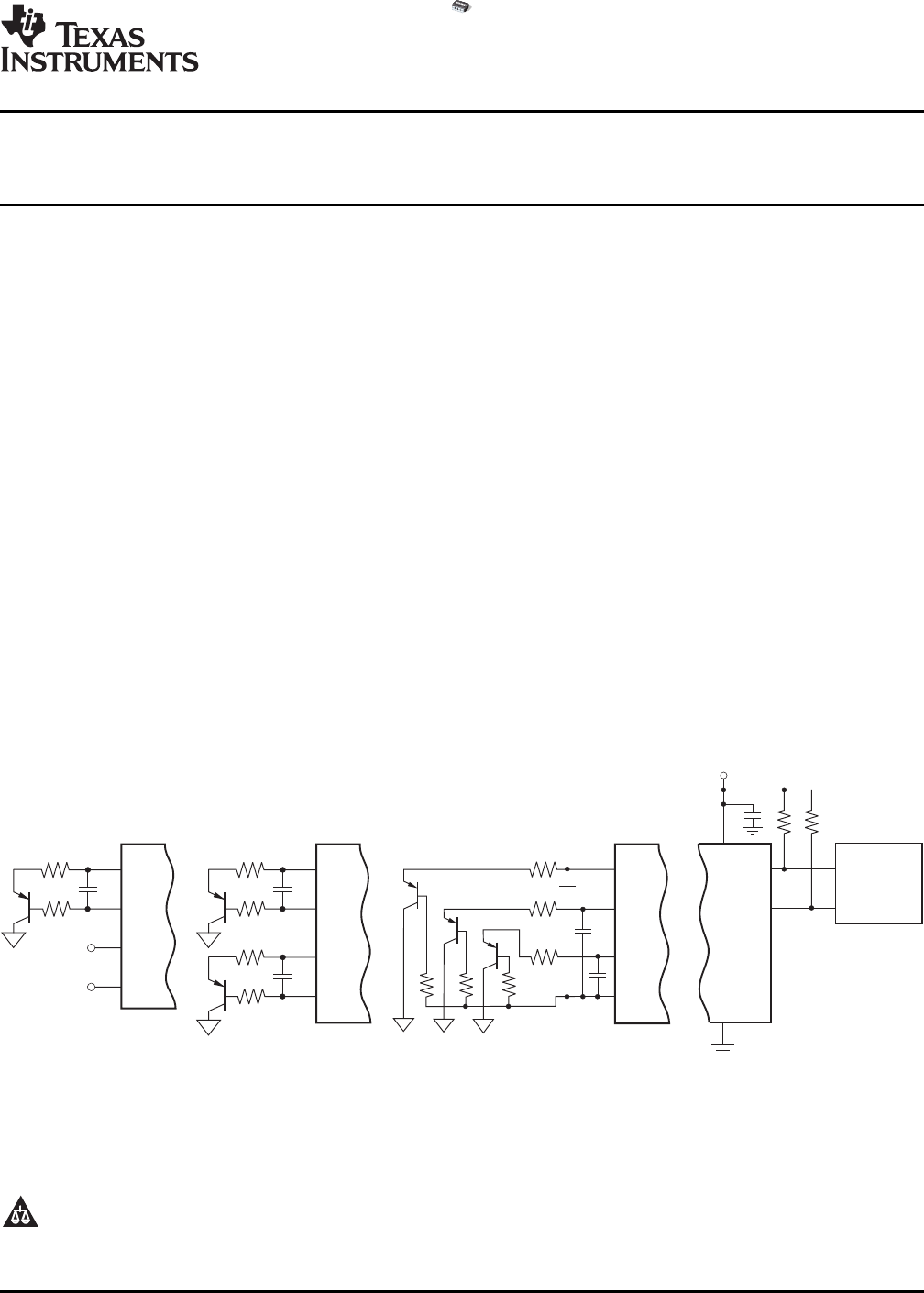
FEATURES DESCRIPTION
APPLICATIONS
+5V
SCL
GND
SDA
V+
SMBus
Controller
8
5
7
6
TMP421
DXP
DXN
A1
A0
1
2
3
4
1ChannelLocal
1ChannelRemote
TMP422
DX1
DX2
DX3
DX4
1
2
3
4
1ChannelLocal
2ChannelsRemote
TMP423
DXP1
DXP2
DXP3
DXN
1
2
3
4
1ChannelLocal
3ChannelsRemote
TMP421
TMP422
TMP423www.ti.com
SBOS398B – JULY 2007 – REVISED MARCH 2008
± 1 °C Remote and Local TEMPERATURE SENSORin SOT23-8
234
•SOT23-8 PACKAGE
The TMP421, TMP422, and TMP423 are remotetemperature sensor monitors with a built-in local•± 1 °C REMOTE DIODE SENSOR (MAX)
temperature sensor. The remote temperature sensor•± 1.5 °C LOCAL TEMPERATURE SENSOR (MAX)
diode-connected transistors are typically low-cost,•SERIES RESISTANCE CANCELLATION
NPN- or PNP-type transistors or diodes that are an•n-FACTOR CORRECTION integral part of microcontrollers, microprocessors, orFPGAs.•TWO-WIRE/ SMBus™ SERIAL INTERFACE
Remote accuracy is ± 1 °C for multiple IC•MULTIPLE INTERFACE ADDRESSES
manufacturers, with no calibration needed. The•DIODE FAULT DETECTION
two-wire serial interface accepts SMBus write byte,•RoHS COMPLIANT AND NO Sb/Br
read byte, send byte, and receive byte commands toconfigure the device.
The TMP421, TMP422, and TMP423 include series•PROCESSOR/FPGA TEMPERATURE
resistance cancellation, programmable non-idealityMONITORING
factor, wide remote temperature measurement range•LCD/ DLP
®
/LCOS PROJECTORS
(up to +150 °C), and diode fault detection.•SERVERS
The TMP421, TMP422, and TMP423 are all available•CENTRAL OFFICE TELECOM EQUIPMENT
in a SOT23-8 package.•STORAGE AREA NETWORKS (SAN)
1
Please be aware that an important notice concerning availability, standard warranty, and use in critical applications ofTexas Instruments semiconductor products and disclaimers thereto appears at the end of this data sheet.
2DLP is a registered trademark of Texas Instruments.
3SMBus is a trademark of Intel Corporation.
4All other trademarks are the property of their respective owners.
PRODUCTION DATA information is current as of publication date.
Copyright © 2007 – 2008, Texas Instruments IncorporatedProducts conform to specifications per the terms of the TexasInstruments standard warranty. Production processing does notnecessarily include testing of all parameters.
www.ti.com
ABSOLUTE MAXIMUM RATINGS
(1)
TMP421
TMP422
TMP423
SBOS398B – JULY 2007 – REVISED MARCH 2008
This integrated circuit can be damaged by ESD. Texas Instruments recommends that all integrated circuits be handled withappropriate precautions. Failure to observe proper handling and installation procedures can cause damage.
ESD damage can range from subtle performance degradation to complete device failure. Precision integrated circuits may be moresusceptible to damage because very small parametric changes could cause the device not to meet its published specifications.
PACKAGE INFORMATION
(1)
TWO-WIRE PACKAGE PACKAGEPRODUCT DESCRIPTION ADDRESS PACKAGE-LEAD DESIGNATOR MARKING
Single ChannelTMP421 Remote Junction 100 11xx SOT23-8 DCN DACITemperature Sensor
Dual ChannelTMP422 Remote Junction 100 11xx SOT23-8 DCN DADITemperature Sensor
TMP423A Triple Channel 100 1100 SOT23-8 DCN DAEIRemote JunctionTMP423B 100 1101 SOT23-8 DCN DAFITemperature Sensor
(1) For the most current package and ordering information see the Package Option Addendum at the end of this document, or see the TIweb site at www.ti.com .
Over operating free-air temperature range, unless otherwise noted.
TMP421, TMP422, TMP423 UNIT
Power Supply, V
S
+7 V
Pins 1, 2, 3, and 4 only – 0.5 to V
S
+ 0.5 VInput Voltage
Pins 6 and 7 only – 0.5 to 7 V
Input Current 10 mA
Operating Temperature Range – 55 to +127 °C
Storage Temperature Range – 60 to +130 °C
Junction Temperature (T
J
max) +150 °C
Human Body Model (HBM) 3000 V
ESD Rating Charged Device Model (CDM) 1000 V
Machine Model (MM) 200 V
(1) Stresses above these ratings may cause permanent damage. Exposure to absolute maximum conditions for extended periods maydegrade device reliability. These are stress ratings only, and functional operation of the device at these or any other conditions beyondthose specified is not implied.
2Submit Documentation Feedback Copyright © 2007 – 2008, Texas Instruments Incorporated
Product Folder Link(s): TMP421 TMP422 TMP423

www.ti.com
ELECTRICAL CHARACTERISTICS
TMP421
TMP422
TMP423
SBOS398B – JULY 2007 – REVISED MARCH 2008
At T
A
= – 40 °C to +125 °C and V
S
= 2.7V to 5.5V, unless otherwise noted.
TMP421, TMP422, TMP423
PARAMETER CONDITIONS MIN TYP MAX UNIT
TEMPERATURE ERROR
Local Temperature Sensor TE
LOCAL
T
A
= – 40 °C to +125 °C ± 1.25 ± 2.5 °C
T
A
= +15 °C to +85 °C, V
S
= 3.3V ± 0.25 ± 1.5 °C
Remote Temperature Sensor
(1)
TE
REMOTE
T
A
= +15 °C to +85 °C, T
D
= – 40 °C to +150 °C, V
S
= 3.3V ± 0.25 ± 1 °C
T
A
= – 40 °C to +100 °C, T
D
= – 40 °C to +150 °C, V
S
= 3.3V ± 1 ± 3 °C
T
A
= – 40 °C to +125 °C, T
D
= – 40 °C to +150 °C ± 3 ± 5 °C
vs Supply (Local/Remote) V
S
= 2.7V to 5.5V ± 0.2 ± 0.5 °C/V
TEMPERATURE MEASUREMENT
Conversion Time (per channel) 100 115 130 ms
Resolution
Local Temperature Sensor (programmable) 12 Bits
Remote Temperature Sensor 12 Bits
Remote Sensor Source Currents
High Series Resistance 3k ΩMax 120 µA
Medium High 60 µA
Medium Low 12 µA
Low 6 µA
Remote Transistor Ideality Factor ηTMP421/22/23 Optimized Ideality Factor 1.008
SMBus INTERFACE
Logic Input High Voltage (SCL, SDA) V
IH
2.1 V
Logic Input Low Voltage (SCL, SDA) V
IL
0.8 V
Hysteresis 500 mV
SMBus Output Low Sink Current 6 mA
SDA Output Low Voltage V
OL
I
OUT
= 6mA 0.15 0.4 V
Logic Input Current 0 ≤V
IN
≤6V – 1 +1 µA
SMBus Input Capacitance (SCL, SDA) 3 pF
SMBus Clock Frequency 3.4 MHz
SMBus Timeout 25 30 35 ms
SCL Falling Edge to SDA Valid Time 1 µs
DIGITAL INPUTS
Input Capacitance 3 pF
Input Logic Levels
Input High Voltage V
IH
0.7(V+) (V+)+0.5 V
Input Low Voltage V
IL
– 0.5 0.3(V+) V
Leakage Input Current I
IN
0V ≤V
IN
≤V
S
1µA
POWER SUPPLY
Specified Voltage Range V
S
2.7 5.5 V
Quiescent Current I
Q
0.0625 Conversions per Second 32 38 µA
Eight Conversions per Second 400 525 µA
Serial Bus Inactive, Shutdown Mode 3 10 µA
Serial Bus Active, f
S
= 400kHz, Shutdown Mode 90 µA
Serial Bus Active, f
S
= 3.4MHz, Shutdown Mode 350 µA
Undervoltage Lockout UVLO 2.3 2.4 2.6 V
Power-On Reset Threshold POR 1.6 2.3 V
TEMPERATURE RANGE
Specified Range – 40 +125 °C
Storage Range – 60 +130 °C
Thermal Resistance, SOT23 θ
JA
100 °C/W
(1) Tested with less than 5 Ωeffective series resistance and 100pF differential input capacitance.
Copyright © 2007 – 2008, Texas Instruments Incorporated Submit Documentation Feedback 3
Product Folder Link(s): TMP421 TMP422 TMP423
www.ti.com
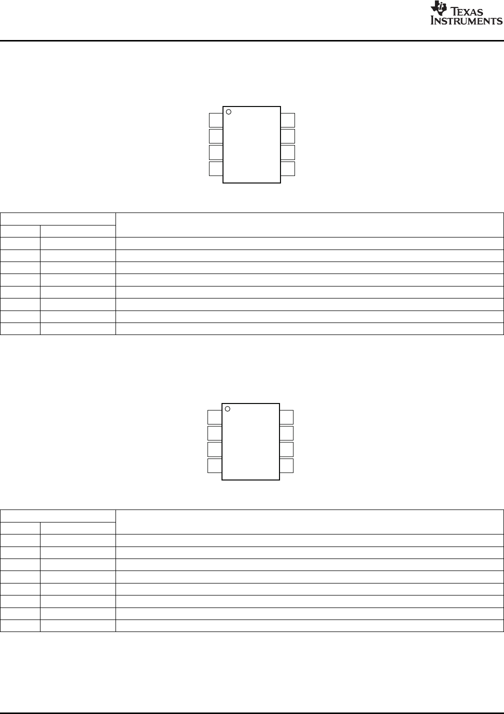
TMP421 PIN CONFIGURATION
1
2
3
4
8
7
6
5
V+
SCL
GND
DXP
DXN
A1
A0
SDA
TMP421
TMP422 PIN CONFIGURATION
1
2
3
4
8
7
6
5
V+
SCL
GND
DX1
DX2
DX3
DX4
SDA
TMP422
TMP421
TMP422
TMP423
SBOS398B – JULY 2007 – REVISED MARCH 2008
DCN PACKAGE
SOT23-8
(TOP VIEW)
TMP421 PIN ASSIGNMENTS
TMP421
NO. NAME DESCRIPTION
1 DXP Positive connection to remote temperature sensor.
2 DXN Negative connection to remote temperature sensor.
3 A1 Address pin
4 A0 Address pin
5 GND Ground
6 SDA Serial data line for SMBus, open-drain; requires pull-up resistor to V+.
7 SCL Serial clock line for SMBus, open-drain; requires pull-up resistor to V+.
8 V+ Positive supply voltage (2.7V to 5.5V)
DCN PACKAGE
SOT23-8
(TOP VIEW)
TMP422 PIN ASSIGNMENTS
TMP422
NO. NAME DESCRIPTION
1 DX1 Channel 1 remote temperature sensor connection pin. Also sets the TMP422 address; see Table 10 .
2 DX2 Channel 1 remote temperature sensor connection pin. Also sets the TMP422 address; see Table 10 .
3 DX3 Channel 2 remote temperature sensor connection pin. Also sets the TMP422 address; see Table 10 .
4 DX4 Channel 2 remote temperature sensor connection pin. Also sets the TMP422 address; see Table 10 .
5 GND Ground
6 SDA Serial data line for SMBus, open-drain; requires pull-up resistor to V+.
7 SCL Serial clock line for SMBus, open-drain; requires pull-up resistor to V+.
8 V+ Positive supply voltage (2.7V to 5.5V)
4Submit Documentation Feedback Copyright © 2007 – 2008, Texas Instruments Incorporated
Product Folder Link(s): TMP421 TMP422 TMP423

www.ti.com
TMP423 PIN CONFIGURATION
1
2
3
4
8
7
6
5
V+
SCL
GND
DXP1
DXP2
DXP3
DXN
SDA
TMP423
TMP421
TMP422
TMP423
SBOS398B – JULY 2007 – REVISED MARCH 2008
DCN PACKAGE
SOT23-8
(TOP VIEW)
TMP423 PIN ASSIGNMENTS
TMP423
NO. NAME DESCRIPTION
1 DXP1 Channel 1 positive connection to remote temperature sensor.
2 DXP2 Channel 2 positive connection to remote temperature sensor.
3 DXP3 Channel 3 positive connection to remote temperature sensor.
4 DXN Common negative connection to remote temperature sensors, Channel 1, Channel 2, Channel 3.
5 GND Ground
6 SDA Serial data line for SMBus, open-drain; requires pull-up resistor to V+.
7 SCL Serial clock line for SMBus, open-drain; requires pull-up resistor to V+.
8 V+ Positive supply voltage (2.7V to 5.5V)
Copyright © 2007 – 2008, Texas Instruments Incorporated Submit Documentation Feedback 5
Product Folder Link(s): TMP421 TMP422 TMP423
www.ti.com
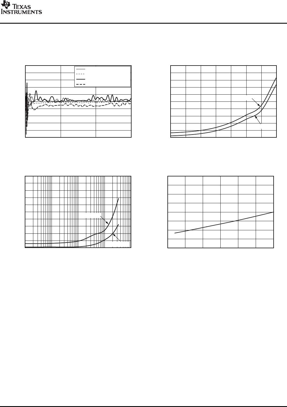
TYPICAL CHARACTERISTICS
3
2
1
0
-1
-2
-3
AmbientTemperature,T ( C)°
A
-50 -25 1251007550250
RemoteTemperatureError( C)°
V =3.3V
S
T =+25 C
REMOTE °
30TypicalUnitsShown
h=1.008
LocalTemperatureError( )
°C
AmbientTemperature,T (
A°C)
3
2
1
0
-1
-2
-3
-50 125-25 0 25 50 75 100
50UnitsShown
V =3.3V
S
60
40
20
0
-20
-40
-60
LeakageResistance(M )W
0 5 10 15 20 25 30
RemoteT
emperatureError( C)°
R GND-
R V-S
RemoteTemperatureError( )
°C
RW( )
S
2.0
1.5
1.0
0.5
0
-0.5
-1.0
-1.5
-2.0
0 3500500 1000 1500 2000 2500 3000
V =2.7V
S
V =5.5V
S
3
2
1
0
-1
-2
-3
Capacitance(nF)
0 0.5 1.0 1.5 2.0 2.5 3.0
RemoteTemperatureError( C)°
RemoteTemperatureError( )
°C
R (W)
S
2.0
1.5
1.0
0.5
0
-0.5
-1.0
-1.5
-2.0
0 3500500 1000 1500 2000 2500 3000
V =2.7V
S
V =5.5V
S
TMP421
TMP422
TMP423
SBOS398B – JULY 2007 – REVISED MARCH 2008
At T
A
= +25 °C and V
S
= +5.0V, unless otherwise noted.
REMOTE TEMPERATURE ERROR LOCAL TEMPERATURE ERRORvs TEMPERATURE vs TEMPERATURE
Figure 1. Figure 2.
REMOTE TEMPERATURE ERROR REMOTE TEMPERATURE ERROR vs SERIES RESISTANCEvs LEAKAGE RESISTANCE (Diode-Connected Transistor, 2N3906 PNP)
Figure 3. Figure 4.
REMOTE TEMPERATURE ERROR vs SERIES RESISTANCE REMOTE TEMPERATURE ERROR(GND Collector-Connected Transistor, 2N3906 PNP) vs DIFFERENTIAL CAPACITANCE
Figure 5. Figure 6.
6Submit Documentation Feedback Copyright © 2007 – 2008, Texas Instruments Incorporated
Product Folder Link(s): TMP421 TMP422 TMP423
www.ti.com
500
450
400
350
300
250
200
150
100
50
0
ConversionRate(conversions/sec)
0.0625 0.125 0.25 0.5 1 2 4 8
I (mA)
Q
V =2.7V
S
V =5.5V
S
25
20
15
10
5
0
-5
-10
-15
-20
-25
Frequency(MHz)
0 5 10 15
TemperatureError( C)°
Local100mV Noise
PP
Remote100mV Noise
PP
Local250mV Noise
PP
Remote250mV Noise
PP
500
450
400
350
300
250
200
150
100
50
0
SCLCLockFrequency(Hz)
1k 10k 100k 1M 10M
I( A)m
Q
V =3.3V
S
V =5.5V
S
I ( )
QmA
V (
SV)
8
7
6
5
4
3
2
1
0
4.53.0 3.5 4.0 5.55.02.5
TMP421
TMP422
TMP423
SBOS398B – JULY 2007 – REVISED MARCH 2008
TYPICAL CHARACTERISTICS (continued)
At T
A
= +25 °C and V
S
= +5.0V, unless otherwise noted.
TEMPERATURE ERROR QUIESCENT CURRENTvs POWER-SUPPLY NOISE FREQUENCY vs CONVERSION RATE
Figure 7. Figure 8.
SHUTDOWN QUIESCENT CURRENT SHUTDOWN QUIESCENT CURRENTvs SCL CLOCK FREQUENCY vs SUPPLY VOLTAGE
Figure 9. Figure 10.
Copyright © 2007 – 2008, Texas Instruments Incorporated Submit Documentation Feedback 7
Product Folder Link(s): TMP421 TMP422 TMP423
www.ti.com
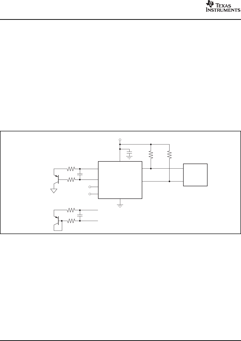
APPLICATION INFORMATION
0.1 Fm10kW
(typ)
10kW
(typ)
TMP421
DXP
DXN
V+
8
7
6
5
2
1
RS
(2)
RS
(2) CDIFF
(3)
CDIFF
(3)
RS
(2)
RS
(2)
GND
SCL
SDA
+5V
SMBus
Controller
Diode-connectedconfiguration :
(1)
SeriesResistance
Transistor-connectedconfiguration :
(1)
A1
A0
4
3
TMP421
TMP422
TMP423
SBOS398B – JULY 2007 – REVISED MARCH 2008
The TMP421 (two-channel), TMP422 (three-channel), The TMP422 requires transistors connected betweenand TMP423 (four-channel) are digital temperature DX1 and DX2 and between DX3 and DX4. Unusedsensors that combine a local die temperature channels on the TMP422 must be connected to GND.measurement channel and one, two, or three remote The TMP423 requires a transistor connected to eachjunction temperature measurement channels in a positive channel (DXP1, DXP2, and DXP3), with thesingle SOT23-8 package. These devices are base of each channel tied to the common negative,two-wire- and SMBus interface-compatible and are DXN. For an unused channel, the TMP423 DXP pinspecified over a temperature range of – 40 °C to can be left open or tied to GND.+125 °C. The TMP421/22/23 each contain multiple
The TMP421/22/23 SCL and SDA interface pins eachregisters for holding configuration information and
require pull-up resistors as part of the communicationtemperature measurement results.
bus. A 0.1 µF power-supply bypass capacitor isFor proper remote temperature sensing operation, the recommended for local bypassing. Figure 11 shows aTMP421 requires only a transistor connected typical configuration for the TMP421; Figure 12between DXP and DXN pins. If the remote channel is illustrates a typical application for the TMP422.not utilized, DXP can be left open or tied to GND. Figure 13 illustrates a typical application for theTMP423.
(1) Diode-connected configuration provides better settling time. Transistor-connected configuration provides better series resistance
cancellation.
(2) R
S
(optional) should be < 1.5k Ωin most applications. Selection of R
S
depends on application; see the Filtering section.
(3) C
DIFF
(optional) should be < 1000pF in most applications. Selection of C
DIFF
depends on application; see the Filtering section and
Figure 6 ,Remote Temperature Error vs Differential Capacitance.
Figure 11. TMP421 Basic Connections
8Submit Documentation Feedback Copyright © 2007 – 2008, Texas Instruments Incorporated
Product Folder Link(s): TMP421 TMP422 TMP423
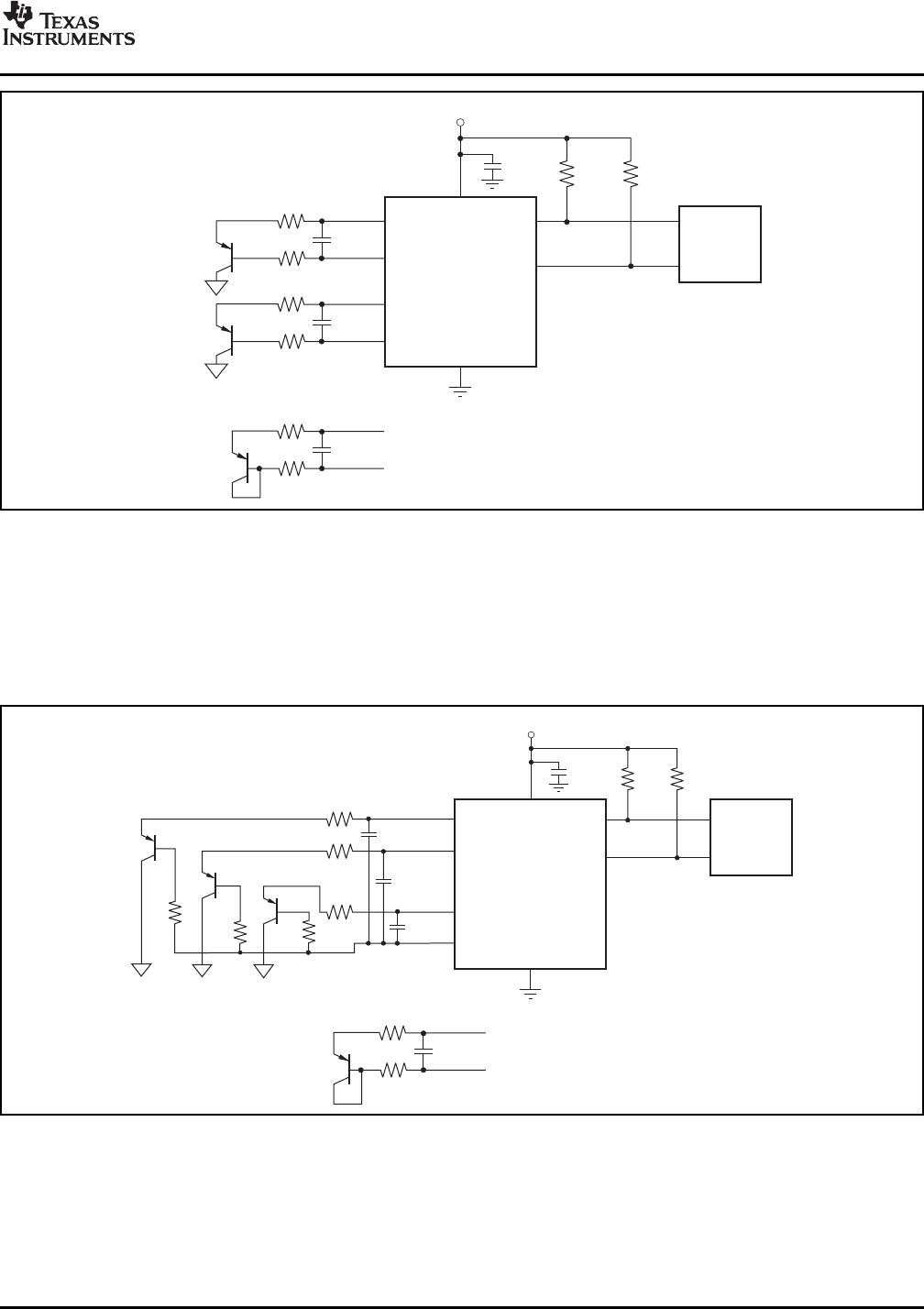
www.ti.com
TMP422
DX1(4)
DX2(4)
5
2
1
RS
(2)
RS
(2) CDIFF
(3)
CDIFF
(3)
RS
(2)
RS
(2)
GND
Diode-connectedconfiguration :
(1)
SeriesResistance
Transistor-connectedconfiguration :
(1)
DX3(4)
DX4(4)
4
3
RS
(2)
RS
(2) CDIFF
(3)
0.1 Fm10kW
(typ)
10kW
(typ)
V+
8
7
6
SCL
SDA
+5V
SMBus
Controller
DXP1
DXN1
DXP2
DXN2
+5V
TMP423
DXP1
DXP2
DXP3
DXP
DXN
DXN
SCL
GND
SDA
V+
2
3
4
7
1
6
8
RS
(2)
RS
(2)
RS
(2)
RS
(2) RS
(2) RS
(2) CDIFF
(3)
CDIFF
(3)
CDIFF
(3)
Transistor-connectedconfiguration :
(1)
CDIFF
(3)
RS
(2)
RS
(2)
Diode-connectedconfiguration :
(1)
5
0.1 Fm10kW
(typ)
10kW
(typ)
SMBus
Controller
SeriesResistance
TMP421
TMP422
TMP423
SBOS398B – JULY 2007 – REVISED MARCH 2008
(1) Diode-connected configuration provides better settling time. Transistor-connected configuration provides better series resistance
cancellation.
(2) R
S
(optional) should be < 1.5k Ωin most applications. Selection of R
S
depends on application; see the Filtering section.
(3) C
DIFF
(optional) should be < 1000pF in most applications. Selection of C
DIFF
depends on application; see the Filtering section and
Figure 6 ,Remote Temperature Error vs Differential Capacitance.
(4) TMP422 SMBus slave address is 1001 100 when connected as shown.
Figure 12. TMP422 Basic Connections
(1) Diode-connected configuration provides better settling time. Transistor-connected configuration provides better series resistance
cancellation.
(2) R
S
(optional) should be < 1.5k Ωin most applications. Selection of R
S
depends on application; see the Filtering section.
(3) C
DIFF
(optional) should be < 1000pF in most applications. Selection of C
DIFF
depends on application; see the Filtering section and
Figure 6 ,Remote Temperature Error vs Differential Capacitance.
Figure 13. TMP423 Basic Connections
Copyright © 2007 – 2008, Texas Instruments Incorporated Submit Documentation Feedback 9
Product Folder Link(s): TMP421 TMP422 TMP423

www.ti.com
SERIES RESISTANCE CANCELLATION
DIFFERENTIAL INPUT CAPACITANCE
TEMPERATURE MEASUREMENT DATA
TMP421
TMP422
TMP423
SBOS398B – JULY 2007 – REVISED MARCH 2008
from low to high. The change in measurement rangeand data format from standard binary to extendedSeries resistance in an application circuit that typically
binary occurs at the next temperature conversion. Forresults from printed circuit board (PCB) trace
data captured in the extended temperature rangeresistance and remote line length is automatically
configuration, an offset of 64 (40h) is added to thecancelled by the TMP421/22/23, preventing what
standard binary value, as shown in the Extendedwould otherwise result in a temperature offset. A total
Binary column of Table 1 . This configuration allowsof up to 3k Ωof series line resistance is cancelled by
measurement of temperatures as low as – 64 °C, andthe TMP421/22/23, eliminating the need for additional
as high as +191 °C; however, mostcharacterization and temperature offset correction.
temperature-sensing diodes only measure with theSee the two Remote Temperature Error vs Series
range of – 55 °C to +150 °C. Additionally, theResistance typical characteristic curves (Figure 4 and
TMP421/22/23 are rated only for ambientFigure 5 ) for details on the effects of series resistance
temperatures ranging from – 40 °C to +125 °C.and power-supply voltage on sensed remote
Parameters in the Absolute Maximum Ratings tabletemperature error.
must be observed.
Table 1. Temperature Data Format (Local andRemote Temperature High Bytes)The TMP421/22/23 tolerate differential inputcapacitance of up to 1000pF with minimal change in
LOCAL/REMOTE TEMPERATURE REGISTERHIGH BYTE VALUE (1 °C RESOLUTION)temperature error. The effect of capacitance on
STANDARD BINARY
(1)
EXTENDED BINARY
(2)sensed remote temperature error is illustrated in
TEMPFigure 6 ,Remote Temperature Error vs Differential (°C) BINARY HEX BINARY HEX
Capacitance.
– 64 1100 0000 C0 0000 0000 00
– 50 1100 1110 CE 0000 1110 0E
– 25 1110 0111 E7 0010 0111 27
0 0000 0000 00 0100 0000 40Temperature measurement data may be taken over
1 0000 0001 01 0100 0001 41an operating range of – 40 °C to +127 °C for both localand remote locations.
5 0000 0101 05 0100 0101 45
10 0000 1010 0A 0100 1010 4AHowever, measurements from – 55 °C to +150 °C can
25 0001 1001 19 0101 1001 59be made both locally and remotely by reconfiguring
50 0011 0010 32 0111 0010 72the TMP421/22/23 for the extended temperature
75 0100 1011 4B 1000 1011 8Brange, as described below.
100 0110 0100 64 1010 0100 A4Temperature data that result from conversions within
125 0111 1101 7D 1011 1101 BDthe default measurement range are represented in
127 0111 1111 7F 1011 1111 BFbinary form, as shown in Table 1 , Standard Binary
150 0111 1111 7F 1101 0110 D6column. Note that although the device is rated to only
175 0111 1111 7F 1110 1111 EFmeasure temperatures down to – 55 °C, it may readtemperatures below this level. However, any
191 0111 1111 7F 1111 1111 FF
temperature below – 64 °C results in a data value of– 64 (C0h). Likewise, temperatures above +127 °C
(1) Resolution is 1 °C/count. Negative numbers are represented inresult in a value of 127 (7Fh). The device can be set
two's complement format.to measure over an extended temperature range by
(2) Resolution is 1 °C/count. All values are unsigned with a – 64 °Cchanging bit 2 (RANGE) of Configuration Register 1 offset.
10 Submit Documentation Feedback Copyright © 2007 – 2008, Texas Instruments Incorporated
Product Folder Link(s): TMP421 TMP422 TMP423
www.ti.com
Standard Decimal to Binary Temperature Data
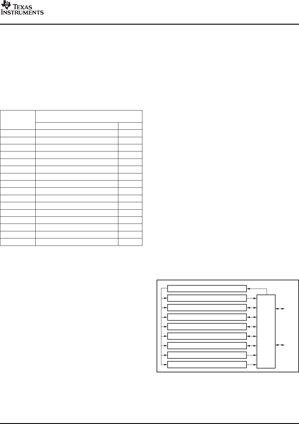
REGISTER INFORMATION
POINTER REGISTER
Standard Binary to Decimal Temperature Data
One-ShotStartRegister
ConfigurationRegisters
StatusRegister
IdentificationRegisters
N-FactorCorrectionRegisters
ConversionRateRegister
LocalandRemoteTemperatureRegisters
SDA
SCL
PointerRegister
I/O
Control
Interface
SoftwareReset
TMP421
TMP422
TMP423
SBOS398B – JULY 2007 – REVISED MARCH 2008
Both local and remote temperature data use two
Calculation Examplebytes for data storage. The high byte stores thetemperature with 1 °C resolution. The second or low
For positive temperatures (for example, +20 °C):byte stores the decimal fraction value of the
(+20 °C)/(+1 °C/count) = 20 →14h →0001 0100temperature and allows a higher measurement
Convert the number to binary code with 8-bit,resolution, as shown in Table 2 . The measurement
right-justified format, and MSB = '0' to denote aresolution for the both the local and remote channels
positive sign.is 0.0625 °C, and is not adjustable.
+20 °C is stored as 0001 0100 →14h.Table 2. Decimal Fraction Temperature Data
For negative temperatures (for example, – 20 °C):Format (Local and Remote Temperature Low
(| – 20|)/(+1 °C/count) = 20 →14h →0001 0100Bytes)
Generate the two's complement of a negativeTEMPERATURE REGISTER LOW BYTE VALUE(0.0625 °C RESOLUTION)
number by complementing the absolute valueTEMP
(°C) STANDARD AND EXTENDED BINARY HEX
binary number and adding 1.
0 0000 0000 00
– 20 °C is stored as 1110 1100 →ECh.0.0625 0001 0000 10
0.1250 0010 0000 20
0.1875 0011 0000 30
The TMP421/22/23 contain multiple registers for0.2500 0100 0000 40
holding configuration information, temperature0.3125 0101 0000 50
measurement results, and status information. These0.3750 0110 0000 60
registers are described in Figure 14 and Table 3 .0.4375 0111 0000 70
0.5000 1000 0000 80
0.5625 1001 0000 90
Figure 14 shows the internal register structure of the0.6250 1010 0000 A0
TMP421/22/23. The 8-bit Pointer Register is used to0.6875 1011 0000 B0
address a given data register. The Pointer Register0.7500 1100 0000 C0
identifies which of the data registers should respondto a read or write command on the two-wire bus. This0.8125 1101 0000 D0
register is set with every write command. A write0.8750 1110 0000 E0
command must be issued to set the proper value in0.9385 1111 0000 F0
the Pointer Register before executing a read(1) Resolution is 0.0625 °C/count. All possible values are shown.
command. Table 3 describes the pointer address ofthe TMP421/22/23 registers. The power-on reset(POR) value of the Pointer Register is 00h (0000Calculation Example
0000b).High byte conversion (for example, 0111 0011):
Convert the right-justified binary high byte tohexadecimal.
From hexadecimal, multiply the first number by16
0
= 1 and the second number by 16
1
= 16.
The sum equals the decimal equivalent.
0111 0011b →73h →(3 ×16
0
) + (7 ×16
1
) = 115
Low byte conversion (for example, 0111 0000):
To convert the left-justified binary low-byte todecimal, use bits 7 through 4 and ignore bits 3through 0 because they do not affect the value ofthe number.
0111b →(0 ×1/2)
1
+ (1 ×1/2)
2
+ (1 ×1/2)
3
+ (1 ×1/2)
4
= 0.4375
Figure 14. Internal Register StructureNote that the final numerical result is the sum of thehigh byte and low byte. In negative temperatures, theunsigned low byte adds to the negative high byte toresult in a value less than the high byte (for instance,– 15 + 0.75 = – 14.25, not – 15.75).
Copyright © 2007 – 2008, Texas Instruments Incorporated Submit Documentation Feedback 11
Product Folder Link(s): TMP421 TMP422 TMP423

www.ti.com
TEMPERATURE REGISTERS
TMP421
TMP422
TMP423
SBOS398B – JULY 2007 – REVISED MARCH 2008
Table 3. Register Map
BIT DESCRIPTIONPOINTER
(HEX) POR (HEX) 7 6 5 4 3 2 1 0 REGISTER DESCRIPTION
00 00 LT11 LT10 LT9 LT8 LT7 LT6 LT5 LT4 Local Temperature (High Byte)
(1)
Remote Temperature 101 00 RT11 RT10 RT9 RT8 RT7 RT6 RT5 RT4
(High Byte)
(1)
Remote Temperature 202 00 RT11 RT10 RT9 RT8 RT7 RT6 RT5 RT4
(High Byte)
(1) (2) (3)
Remote Temperature 303 00 RT11 RT10 RT9 RT8 RT7 RT6 RT5 RT4
(High Byte)
(1) (3)
08 BUSY 0 0 0 0 0 0 0 Status Register
09 00 0 SD 0 0 0 RANGE 0 0 Configuration Register 1
1C/3C
(2)
/0A 0 REN3
(3)
REN2
(2) (3)
REN LEN RC 0 0 Configuration Register 27C
(3)
0B 07 0 0 0 0 0 R2 R1 R0 Conversion Rate Register
0F X X X X X X X X One-Shot Start
(4)
10 00 LT3 LT2 LT1 LT0 0 0 PVLD 0 Local Temperature (Low Byte)
11 00 RT3 RT2 RT1 RT0 0 0 PVLD OPEN Remote Temperature 1 (Low Byte)
Remote Temperature 212 00 RT3 RT2 RT1 RT0 0 0 PVLD OPEN
(Low Byte)
(2) (3)
13 00 RT3 RT2 RT1 RT0 0 0 PLVD OPEN Remote Temperature 3 (Low Byte)
(3)
21 00 NC7 NC6 NC5 NC4 NC3 NC2 NC1 NC0 N Correction 1
22 00 NC7 NC6 NC5 NC4 NC3 NC2 NC1 NC0 N Correction 2
(2) (3)
23 00 NC7 NC6 NC5 NC4 NC3 NC2 NC1 NC0 N Correction 3
(3)
FC X X X X X X X X Software Reset
(5)
FE 55 0 1 0 1 0 1 0 1 Manufacturer ID
0 0 1 0 0 0 0 1 TMP421 Device ID
FF 21 0 0 1 0 0 0 1 0 TMP422 Device ID
0 0 1 0 0 0 1 1 TMP423 Device ID
(1) Compatible with Two-Byte Read; see Figure 19 .(2) TMP422.
(3) TMP423.
(4) X = undefined. Writing any value to this register initiates a one-shot start; see the One-Shot Conversion section.(5) X = undefined. Writing any value to this register initiates a software reset; see the Software Reset section.
The TMP421/22/23 contain circuitry to assure that alow byte register read command returns data from thesame ADC conversion as the immediately precedingThe TMP421/22/23 have multiple 8-bit registers that
high byte read command. This assurance remainshold temperature measurement results. The local
valid only until another register is read. For properchannel and each of the remote channels have a high
operation, the high byte of a temperature registerbyte register that contains the most significant bits
should be read first. The low byte register should be(MSBs) of the temperature analog-to-digital converter
read in the next read command. The low byte register(ADC) result and a low byte register that contains the
may be left unread if the LSBs are not needed.least significant bits (LSBs) of the temperature ADC
Alternatively, the temperature registers may be readresult. The local channel high byte address is 00h;
as a 16-bit register by using a single two-byte readthe local channel low byte address is 10h. The
command from address 00h for the local channelremote channel high byte is at address 01h; the
result, or from address 01h for the remote channelremote channel low byte address is 11h. For the
result (02h for the second remote channel result, andTMP422, the second remote channel high byte
03h for the third remote channel). The high byte isaddress is 02h; the second remote channel low byte
output first, followed by the low byte. Both bytes ofis 12h. The TMP 423 uses the same local and remote
this read operation are from the same ADCaddress as the TMP421 and TMP422, with the third
conversion. The power-on reset value of allremote channel high byte of 03h; the third remote
temperature registers is 00h.channel low byte is 13h. These registers areread-only and are updated by the ADC each time atemperature measurement is completed.
12 Submit Documentation Feedback Copyright © 2007 – 2008, Texas Instruments Incorporated
Product Folder Link(s): TMP421 TMP422 TMP423

www.ti.com
STATUS REGISTER
CONFIGURATION REGISTER 1
CONFIGURATION REGISTER 2
TMP421
TMP422
TMP423
SBOS398B – JULY 2007 – REVISED MARCH 2008
The temperature range is set by configuring theRANGE bit (bit 2) of the Configuration Register.The Status Register reports the state of the
Setting this bit low configures the TMP421/22/23 fortemperature ADCs. Table 4 summarizes the Status
the standard measurement range ( – 40 °C to +127 °C);Register bits. The Status Register is read-only, and is
temperature conversions will be stored in theread by accessing pointer address 08h.
standard binary format. Setting bit 2 high configuresthe TMP421/22/23 for the extended measurementThe BUSY bit = '1' if the ADC is making a conversion;
range ( – 55 °C to +150 °C); temperature conversionsit is set to '0' if the ADC is not converting.
will be stored in the extended binary format (seeTable 1 ).
The remaining bits of the Configuration Register areConfiguration Register 1 (pointer address 09h) sets
reserved and must always be set to '0'. The power-onthe temperature range and controls the shutdown
reset value for this register is 00h.mode. The Configuration Register is set by writing topointer address 09h and read by reading from pointeraddress 09h. Table 5 summarizes the bits ofConfiguration Register 1.
Configuration Register 2 (pointer address 0Ah)controls which temperature measurement channelsThe shutdown (SD) bit (bit 6) enables or disables the
are enabled and whether the external channels havetemperature measurement circuitry. If SD = '0', the
the resistance correction feature enabled or not.TMP421/22/23 convert continuously at the rate set in
Table 6 summarizes the bits of Configurationthe conversion rate register. When SD is set to '1',
Register 2.the TMP421/22/23 stop converting when the currentconversion sequence is complete and enter ashutdown mode. When SD is set to '0' again, theTMP421/22/23 resume continuous conversions.When SD = '1', a single conversion can be started bywriting to the One-Shot Register. See the One-ShotConversion section for more information.
Table 4. Status Register Format
STATUS REGISTER (Read = 08h, Write = NA)
BIT # D7 D6 D5 D4 D3 D2 D1 D0
BIT NAME BUSY 0000000
POR VALUE 0
(1)
0000000
(1) FOR TMP421/TMP423: The BUSY changes to '1' almost immediately (< 100 µs) following power-up, as the TMP421/TMP423 begin thefirst temperature conversion. It is high whenever the TMP421/TMP423 convert a temperature reading.FOR TMP422: The BUSY bit changes to '1' approximately 1ms following power-up. It is high whenever the TMP422 converts atemperature reading.
Table 5. Configuration Register 1 Bit Descriptions
CONFIGURATION REGISTER 1 (Read/Write = 09h, POR = 00h)
POWER-ON RESETBIT NAME FUNCTION VALUE
7 Reserved — 0
0 = Run6 SD 01 = Shut Down
5, 4, 3 Reserved — 0
0 = – 55 °C to +127 °C2 Temperature Range 01 = – 55 °C to +150 °C
1, 0 Reserved — 0
Copyright © 2007 – 2008, Texas Instruments Incorporated Submit Documentation Feedback 13
Product Folder Link(s): TMP421 TMP422 TMP423

www.ti.com
CONVERSION RATE REGISTER
TMP421
TMP422
TMP423
SBOS398B – JULY 2007 – REVISED MARCH 2008
The RC bit (bit 2) enables the resistance correction For the TMP423 only, the REN3 bit (bit 6) enablesfeature for the external temperature channels. If RC = the third external measurement channel. If REN3 ='1', series resistance correction is enabled; if RC = '0', '1', the third external channel is enabled; if REN3 =resistance correction is disabled. Resistance '0', the third external channel is disabled.correction should be enabled for most applications.
The temperature measurement sequence is: localHowever, disabling the resistance correction may
channel, external channel 1, external channel 2,yield slightly improved temperature measurement
external channel 3, shutdown, and delay (to setnoise performance, and reduce conversion time by
conversion rate, if necessary). The sequence startsabout 50%, which could lower power consumption
over with the local channel. If any of the channels arewhen conversion rates of two per second or less are
disabled, they are bypassed in the sequence.selected.
The LEN bit (bit 3) enables the local temperaturemeasurement channel. If LEN = '1', the local channel
The Conversion Rate Register (pointer address 0Bh)is enabled; if LEN = '0', the local channel is disabled.
controls the rate at which temperature conversionsThe REN bit (bit 4) enables external temperature
are performed. This register adjusts the idle timemeasurement for channel 1. If REN = '1', the first
between conversions but not the conversion timingexternal channel is enabled; if REN = '0', the external
itself, thereby allowing the TMP421/22/23 powerchannel is disabled.
dissipation to be balanced with the temperatureregister update rate. Table 7 describes theFor the TMP422 and TMP423 only, the REN2 bit (bit
conversion rate options and corresponding current5) enables the second external measurement
consumption. A one-shot command can be usedchannel. If REN2 = '1', the second external channel is
during the idle time between conversions toenabled; if REN2 = '0', the second external channel is
immediately start temperature conversions on alldisabled.
enabled channels.
Table 6. Configuration Register 2 Bit Descriptions
CONFIGURATION REGISTER 2 (Read/Write = 0Ah, POR = 1Ch for TMP421; 3Ch for TMP422; 7Ch for TMP423)
POWER-ON RESETBIT NAME FUNCTION VALUE
7 Reserved — 0
0 = External Channel 3 Disabled 1 (TMP423)6 REN3
1 = External Channel 3 Enabled 0 (TMP421, TMP422)
0 = External Channel 2 Disabled 1 (TMP422, TMP423)5 REN2
1 = External Channel 2 Enabled 0 (TMP421)
0 = External Channel 1 Disabled4 REN 11 = External Channel 1 Enabled
0 = Local Channel Disabled3 LEN 11 = Local Channel Enabled
0 = Resistance Correction Disabled2 RC 11 = Resistance Correction Enabled
1, 0 Reserved — 0
14 Submit Documentation Feedback Copyright © 2007 – 2008, Texas Instruments Incorporated
Product Folder Link(s): TMP421 TMP422 TMP423

www.ti.com
ONE-SHOT CONVERSION
VBE2*VBE1 +nkT
qlnǒI2
I1Ǔ
(1)
neff +1.008 300
ǒ300 *NADJUSTǓ
(2)
NADJUST +300 *ǒ300 1.008
neff Ǔ
(3)
n-FACTOR CORRECTION REGISTER
TMP421
TMP422
TMP423
SBOS398B – JULY 2007 – REVISED MARCH 2008
Table 7. Conversion Rate Register
CONVERSION RATE REGISTER (Read/Write = 0Bh, POR = 07h)
AVERAGE I
Q
(TYP) ( µA)
R7 R6 R5 R4 R3 R2 R1 R0 CONVERSIONS/SEC V
S
= 2.7V V
S
= 5.5V
0 0 0 0 0 0 0 0 0.0625 11 32
0 0 0 0 0 0 0 1 0.125 17 38
0 0 0 0 0 0 1 0 0.25 28 49
0 0 0 0 0 0 1 1 0.5 47 69
0 0 0 0 0 1 0 0 1 80 103
0 0 0 0 0 1 0 1 2 128 155
00000110 4
(1)
190 220
00000111 8
(2)
373 413
(1) Conversion rate shown is for only one or two enabled measurement channels. When three channels are enabled, the conversion rate is2 and 2/3 conversions-per-second. When four channels are enabled, the conversion rate is 2 per second.(2) Conversion rate shown is for only one enabled measurement channel. When two channels are enabled, the conversion rate is 4conversions-per-second. When three channels are enabled, the conversion rate is 2 and 2/3 conversions-per-second. When fourchannels are enabled, the conversion rate is 2 conversions-per-second.
When the TMP421/22/23 are in shutdown mode
The value nin Equation 1 is a characteristic of the(SD = 1 in the Configuration Register 1), a single
particular transistor used for the remote channel. Theconversion is started on all enabled channels by
power-on reset value for the TMP421/22/23 is n=writing any value to the One-Shot Start Register,
1.008. The value in the n-Factor Correction Registerpointer address 0Fh. This write operation starts one
may be used to adjust the effective n-factor accordingconversion; the TMP421/22/23 return to shutdown
to Equation 2 and Equation 3 .mode when that conversion completes. The value ofthe data sent in the write command is irrelevant andis not stored by the TMP421/22/23. When theTMP421/22/23 are in shutdown mode, the conversionsequence currently in process must be completedbefore a one-shot command can be issued. One-shotcommands issued during a conversion are ignored.
The n-correction value must be stored intwo's-complement format, yielding an effective datarange from – 128 to +127. The n-correction value maybe written to and read from pointer address 21h. TheThe TMP421/22/23 allow for a different n-factor value
n-correction value for the second remote channelto be used for converting remote channel
(TMP422 and TMP423) may be written and read frommeasurements to temperature. The remote channel
pointer address 22h. The n-correction value for theuses sequential current excitation to extract a
third remote channel (TMP423 only) may be writtendifferential V
BE
voltage measurement to determine
to and read from pointer address 23h. The registerthe temperature of the remote transistor. Equation 1
power-on reset value is 00h, thus having no effectdescribes this voltage and temperature.
unless the register is written to.
Copyright © 2007 – 2008, Texas Instruments Incorporated Submit Documentation Feedback 15
Product Folder Link(s): TMP421 TMP422 TMP423

www.ti.com
SOFTWARE RESET
BUS OVERVIEW
GENERAL CALL RESET
SERIAL INTERFACE
IDENTIFICATION REGISTERS
TMP421
TMP422
TMP423
SBOS398B – JULY 2007 – REVISED MARCH 2008
address FEh. The device ID is obtained by readingfrom pointer address FFh. The TMP421/22/23 eachThe TMP421/22/23 may be reset by writing any value
return 55h for the manufacturer code. The TMP421to the Software Reset Register (pointer address
returns 21h for the device ID; the TMP422 returnsFCh). This action restores the power-on reset state to
22h for the device ID; and the TMP423 returns 23hall of the TMP421/22/23 registers as well as aborts
for the device ID. These registers are read-only.any conversion in process. The TMP421/22/23 alsosupport reset via the two-wire general call address(0000 0000). The General Call Reset section containsmore information.
The TMP421/22/23 are SMBus interface-compatible.In SMBus protocol, the device that initiates theTable 8. n-Factor Range
transfer is called a master, and the devices controlledby the master are slaves. The bus must be controlledN
ADJUST
by a master device that generates the serial clockBINARY HEX DECIMAL n
(SCL), controls the bus access, and generates the0111 1111 7F 127 1.747977
START and STOP conditions.0000 1010 0A 10 1.042759
To address a specific device, a START condition is0000 1000 08 8 1.035616
initiated. START is indicated by pulling the data line0000 0110 06 6 1.028571
(SDA) from a high-to-low logic level while SCL is0000 0100 04 4 1.021622
high. All slaves on the bus shift in the slave address0000 0010 02 2 1.014765
byte, with the last bit indicating whether a read or0000 0001 01 1 1.011371
write operation is intended. During the ninth clock0000 0000 00 0 1.008
pulse, the slave being addressed responds to the1111 1111 FF – 1 1.004651
master by generating an Acknowledge and pulling1111 1110 FE – 2 1.001325
SDA low.1111 1100 FC – 4 0.994737
Data transfer is then initiated and sent over eight1111 1010 FA – 6 0.988235
clock pulses followed by an Acknowledge bit. During1111 1000 F8 – 8 0.981818
data transfer SDA must remain stable while SCL is1111 0110 F6 – 10 0.975484
high, because any change in SDA while SCL is high1000 0000 80 – 128 0.706542
is interpreted as a control signal.
Once all data have been transferred, the mastergenerates a STOP condition. STOP is indicated bypulling SDA from low to high, while SCL is high.The TMP421/22/23 support reset via the two-wireGeneral Call address 00h (0000 0000b). TheTMP421/22/23 acknowledge the General Calladdress and respond to the second byte. If the
The TMP421/22/23 operate only as a slave device onsecond byte is 06h (0000 0110b), the TMP421/22/23
either the two-wire bus or the SMBus. Connections toexecute a software reset. This software reset restores
either bus are made via the open-drain I/O lines, SDAthe power-on reset state to all TMP421/22/23
and SCL. The SDA and SCL pins feature integratedregisters, and aborts any conversion in progress. The
spike suppression filters and Schmitt triggers toTMP421/22/23 take no action in response to other
minimize the effects of input spikes and bus noise.values in the second byte.
The TMP421/22/23 support the transmission protocolfor fast (1kHz to 400kHz) and high-speed (1kHz to3.4MHz) modes. All data bytes are transmitted MSBfirst.The TMP421/22/23 allow for the two-wire buscontroller to query the device for manufacturer anddevice IDs to enable software identification of thedevice at the particular two-wire bus address. Themanufacturer ID is obtained by reading from pointer
16 Submit Documentation Feedback Copyright © 2007 – 2008, Texas Instruments Incorporated
Product Folder Link(s): TMP421 TMP422 TMP423
www.ti.com
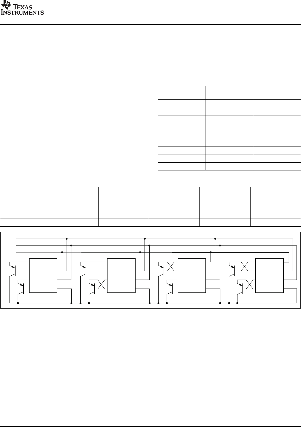
SERIAL BUS ADDRESS
Two-Wire Interface Slave Device Addresses
DX1
DX2
DX3
DX4
SCL
SDA
V+
Q0
Address=1001100 Address=1001101 Address=1001110 Address=1001111
Q1
Q2
Q3
Q4
Q5
V+
SCL
SDA
GND Q7
DX1
DX2
DX3
DX4
V+
SCL
SDA
GND
DX1
DX2
DX3
DX4
V+
SCL
SDA
GND
DX1
DX2
DX3
DX4
V+
SCL
SDA
GND
Q6
TMP421
TMP422
TMP423
SBOS398B – JULY 2007 – REVISED MARCH 2008
DXN connection should be left unconnected. Thepolarity of the transistor for external channel 2 (pins 3To communicate with the TMP421/22/23, the master
and 4) sets the least significant bit of the slavemust first address slave devices via a slave address
address. The polarity of the transistor for externalbyte. The slave address byte consists of seven
channel 1 (pins 1 and 2) sets the next leastaddress bits, and a direction bit indicating the intent
significant bit of the slave address.of executing a read or write operation.
Table 9. TMP421 Slave Address Options
TWO-WIRE SLAVEThe TMP421 supports nine slave device addresses
ADDRESS A1 A0and the TMP422 supports four slave device
0011 100 Float 0addresses. The TMP423 has one of two
0011 101 Float 1factory-preset slave addresses.
0011 110 0 FloatThe slave device address for the TMP421 is set by
0011 111 1 Floatthe A1 and A0 pins according to Table 9 .
0101 010 Float Float
The slave device address for the TMP422 is set by
1001 100 0 0the connections between the external transistors and
1001 101 0 1the TMP422 according to Figure 15 and Table 10 . If
1001 110 1 0one of the channels is unused, the respective DXP
1001 111 1 1connection should be connected to GND, and the
Table 10. TMP422 Slave Address Options
TWO-WIRE SLAVE ADDRESS DX1 DX2 DX3 DX4
1001 100 DXP1 DXN1 DXP2 DXN2
1001 101 DXP1 DXN1 DXN2 DXP2
1001 110 DXN1 DXP1 DXP2 DXN2
1001 111 DXN1 DXP1 DXN2 DXP2
Figure 15. TMP422 Connections for Device Address Setup
Copyright © 2007 – 2008, Texas Instruments Incorporated Submit Documentation Feedback 17
Product Folder Link(s): TMP421 TMP422 TMP423

www.ti.com
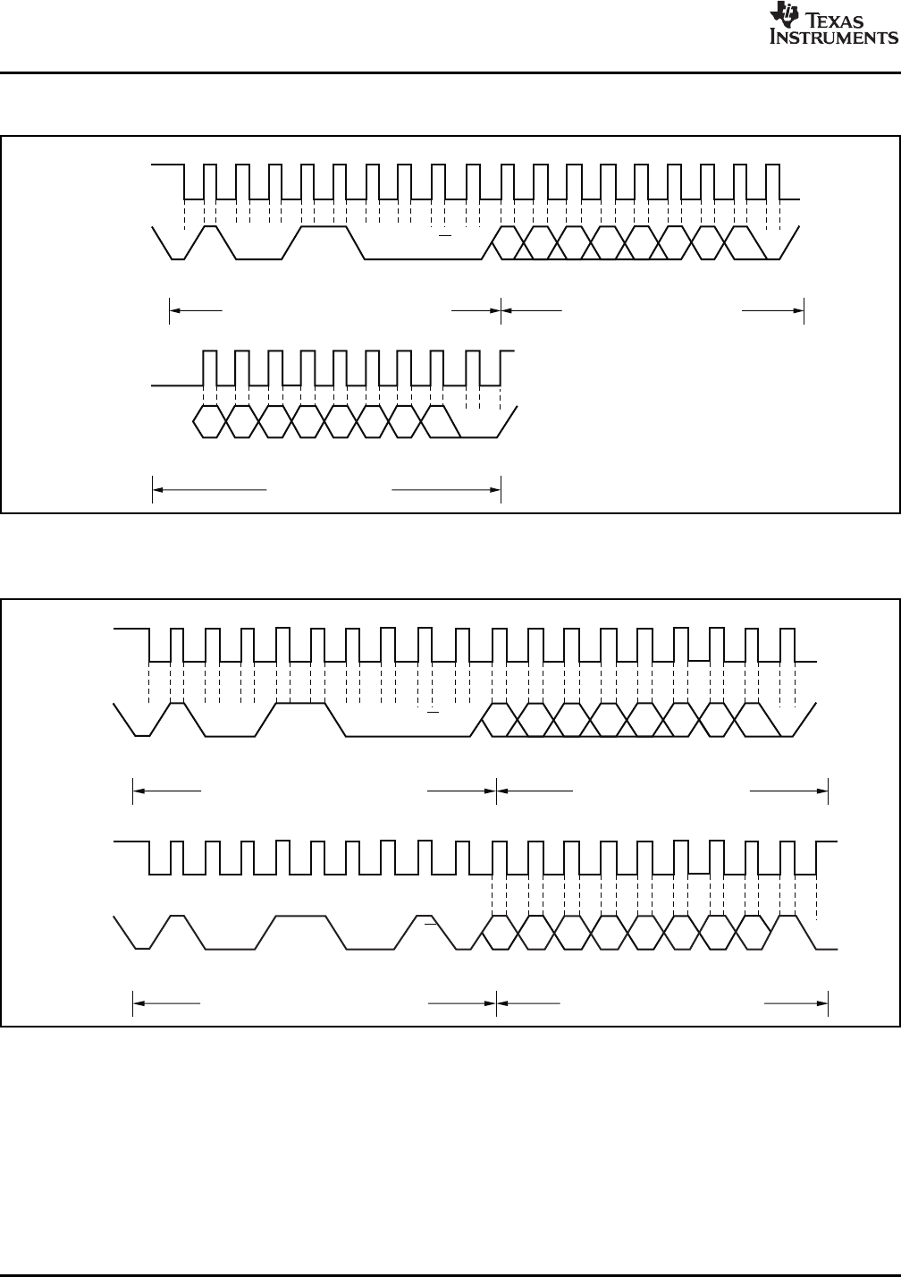
READ/WRITE OPERATIONS
TMP421
TMP422
TMP423
SBOS398B – JULY 2007 – REVISED MARCH 2008
The TMP422 checks the polarity of the externaltransistor at power-on, or after software reset, by
Accessing a particular register on the TMP421/22/23forcing current to pin 1 while connecting pin 2 to
is accomplished by writing the appropriate value toapproximately 0.6V. If the voltage on pin 1 does not
the Pointer Register. The value for the Pointerpull up to near the V+ of the TMP422, pin 1 functions
Register is the first byte transferred after the slaveas DXP for channel 1, and the second LSB of the
address byte with the R/ W bit low. Every writeslave address is '0'. If the voltage on pin 1 does pull
operation to the TMP421/22/23 requires a value forup to near V+, the TMP422 forces current to pin 2
the Pointer Register (see Figure 17 ).while connecting pin 1 to 0.6V. If the voltage on pin 2does not pull up to near V+, the TMP422 uses pin 2
When reading from the TMP421/22/23, the last valuefor DXP of channel 1, and sets the second LSB of the
stored in the Pointer Register by a write operation isslave address to '1'. If both pins are shorted to GND
used to determine which register is read by a reador if both pins are open, the TMP422 uses pin 1 as
operation. To change which register is read for a readDXP and sets the address bit to '0'. This process is
operation, a new value must be written to the Pointerthen repeated for channel 2 (pins 3 and 4).
Register. This transaction is accomplished by issuinga slave address byte with the R/ W bit low, followedIf the TMP422 is to be used with transistors that are
by the Pointer Register byte; no additional data arelocated on another IC (such as a CPU, DSP, or
required. The master can then generate a STARTgraphics processor), it is recommended to use pin 1
condition and send the slave address byte with theor pin 3 as DXP to ensure correct address detection.
R/ W bit high to initiate the read command. SeeIf the other IC has a lower supply voltage or is not
Figure 19 for details of this sequence. If repeatedpowered when the TMP422 tries to detect the slave
reads from the same register are desired, it is notaddress, a protection diode may turn on during the
necessary to continually send the Pointer Registerdetection process and the TMP422 may incorrectly
bytes, because the TMP421/22/23 retain the Pointerchoose the DXP pin and corresponding slave
Register value until it is changed by the next writeaddress. Using pin 1 and/or pin 3 for transistors that
operation. Note that register bytes are sent MSB first,are on other ICs ensures correct operation
followed by the LSB.independent of supply sequencing or levels.
Read operations should be terminated by issuing aThe TMP423 has a factory-preset slave address. The
Not-Acknowledge command at the end of the lastTMP423A slave address is 1001100b, and the
byte to be read. For a single-byte operation, theTMP423B slave address is 1001101b. The
master should leave the SDA line high during theconfiguration of the DXP and DXN channels are
Acknowledge time of the first byte that is read fromindependent of the address. Unused DXP channels
the slave. For a two-byte read operation, the mastercan be left open or tied to GND.
must pull SDA low during the Acknowledge time ofthe first byte read, and should leave SDA high duringthe Acknowledge time of the second byte read fromthe slave.
18 Submit Documentation Feedback Copyright © 2007 – 2008, Texas Instruments Incorporated
Product Folder Link(s): TMP421 TMP422 TMP423
www.ti.com
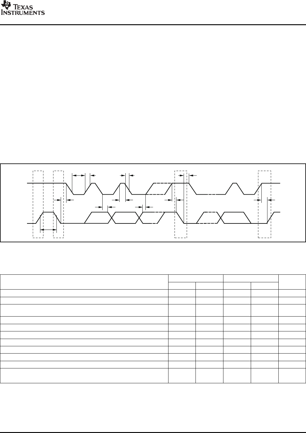
TIMING DIAGRAMS
SCL
SDA
t(LOW) tRtFt(HDSTA)
t(HDSTA)
t(HDDAT)
t(BUF)
t(SUDAT)
t(HIGH) t(SUSTA) t(SUSTO)
P S S P
TMP421
TMP422
TMP423
SBOS398B – JULY 2007 – REVISED MARCH 2008
Data Transfer: The number of data bytes transferredbetween a START and a STOP condition is notThe TMP421/22/23 are two-wire and
limited and is determined by the master device. TheSMBus-compatible. Figure 16 to Figure 19 describe
receiver acknowledges data transfer.the timing for various operations on theTMP421/22/23. Parameters for Figure 16 are defined Acknowledge: Each receiving device, whenin Table 11 . Bus definitions are: addressed, is obliged to generate an Acknowledgebit. A device that acknowledges must pull down theBus Idle: Both SDA and SCL lines remain high.
SDA line during the Acknowledge clock pulse in sucha way that the SDA line is stable low during the highStart Data Transfer: A change in the state of the
period of the Acknowledge clock pulse. Setup andSDA line, from high to low, while the SCL line is high,
hold times must be taken into account. On a masterdefines a START condition. Each data transfer
receive, data transfer termination can be signaled byinitiates with a START condition. Denoted as Sin
the master generating a Not-Acknowledge on the lastFigure 16 .
byte that has been transmitted by the slave.Stop Data Transfer: A change in the state of theSDA line from low to high while the SCL line is highdefines a STOP condition. Each data transferterminates with a repeated START or STOPcondition. Denoted as Pin Figure 16 .
Figure 16. Two-Wire Timing Diagram
Table 11. Timing Characteristics for Figure 16
FAST MODE HIGH-SPEED MODE
PARAMETER MIN MAX MIN MAX UNIT
SCL Operating Frequency f
(SCL)
0.001 0.4 0.001 3.4 MHz
Bus Free Time Between STOP and START Condition t
(BUF)
600 160 ns
Hold time after repeated START condition. After this period, the first clock
t
(HDSTA)
100 100 nsis generated.
Repeated START Condition Setup Time t
(SUSTA)
100 100 ns
STOP Condition Setup Time t
(SUSTO)
100 100 ns
Data Hold Time t
(HDDAT)
0
(1)
0
(2)
ns
Data Setup Time t
(SUDAT)
100 10 ns
SCL Clock LOW Period t
(LOW)
1300 160 ns
SCL Clock HIGH Period t
(HIGH)
600 60 ns
Clock/Data Fall Time t
F
300 160 ns
Clock/Data Rise Time t
R
300 160
nsfor SCL ≤100kHz t
R
1000
(1) For cases with fall time of SCL less than 20ns and/or the rise or fall time of SDA less than 20ns, the hold time should be greater than20ns.
(2) For cases with a fall time of SCL less than 10ns and/or the rise or fall time of SDA less than 10ns, the hold time should be greater than10ns.
Copyright © 2007 – 2008, Texas Instruments Incorporated Submit Documentation Feedback 19
Product Folder Link(s): TMP421 TMP422 TMP423
www.ti.com
Frame1Two-WireSlaveAddressByte Frame2PointerRegisterByte
1
StartBy
Master
ACKBy
TMP421/22/23
ACKBy
TMP421/22/23
1 9 1
Frame3DataByte1
ACKBy
TMP421/22/23
1
D7
SDA
(Continued)
SCL
(Continued)
D6 D5 D4 D3 D2 D1 D0
9
9
SDA
SCL
0 0 1 1 0 0(1) R/WP7 P6 P5 P4 P3 P2 P1 P0
¼
¼
StopBy
Master
Frame1Two-WireSlaveAddressByte Frame2PointerRegisterByte
1
StartBy
Master
ACKBy
TMP421/22/23
ACKBy
TMP421/22/23
Frame3Two-WireSlaveAddressByte Frame4DataByte1ReadRegister
StartBy
Master
ACKBy
TMP421/22/23
NACKBy
Master(2)
From
TMP421/22/23
1 9 1 9
1 9 1 9
SDA
SCL
0 0 1 R/WP7 P6 P5 P4 P3 P2 P1 P0 ¼
¼
¼
¼
SDA
(Continued)
SCL
(Continued)
1 0 0 1
1 0 0(1)
1 0 0(1) R/WD7 D6 D5 D4 D3 D2 D1 D0
TMP421
TMP422
TMP423
SBOS398B – JULY 2007 – REVISED MARCH 2008
(1) Slave address 1001100 shown.
Figure 17. Two-Wire Timing Diagram for Write Word Format
(1) Slave address 1001100 shown.
(2) Master should leave SDA high to terminate a single-byte read operation.
Figure 18. Two-Wire Timing Diagram for Single-Byte Read Format
20 Submit Documentation Feedback Copyright © 2007 – 2008, Texas Instruments Incorporated
Product Folder Link(s): TMP421 TMP422 TMP423
www.ti.com
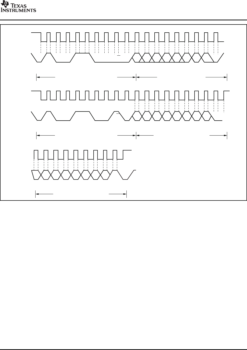
Frame1Two-WireSlaveAddressByte Frame2PointerRegisterByte
1
StartBy
Master
ACKBy
TMP421/22/23
ACKBy
TMP421/22/23
Frame3Two-WireSlaveAddressByte Frame4DataByte1ReadRegister
StartBy
Master
ACKBy
TMP421/22/23
ACKBy
Master
From
TMP421/22/23
1 9 1 9
1 9 1 9
SDA
SCL
0 0 1 R/WP7 P6 P5 P4 P3 P2 P1 P0 ¼
¼
¼
¼
SDA
(Continued)
SCL
(Continued)
SDA
(Continued)
SCL
(Continued)
1 0 0 1
1 0 0(1)
1 0 0(1) R/WD7 D6 D5 D4 D3 D2 D1 D0
Frame5DataByte2ReadRegister
StopBy
Master
NACKBy
Master(2)
From
TMP421/22/23
19
D7 D6 D5 D4 D3 D2 D1 D0
HIGH-SPEED MODE TIMEOUT FUNCTION
TMP421
TMP422
TMP423
SBOS398B – JULY 2007 – REVISED MARCH 2008
(1) Slave address 1001100 shown.
(2) Master should leave SDA high to terminate a two-byte read operation.
Figure 19. Two-Wire Timing Diagram for Two-Byte Read Format
In order for the two-wire bus to operate at frequencies The TMP421/22/23 reset the serial interface if eitherabove 400kHz, the master device must issue a SCL or SDA are held low for 30ms (typical) betweenHigh-Speed mode (Hs-mode) master code (0000 a START and STOP condition. If the TMP421/22/231xxx) as the first byte after a START condition to are holding the bus low, the device releases the busswitch the bus to high-speed operation. The and waits for a START condition. To avoid activatingTMP421/22/23 do not acknowledge this byte, but the timeout function, it is necessary to maintain aswitch the input filters on SDA and SCL and the communication speed of at least 1kHz for the SCLoutput filter on SDA to operate in Hs-mode, allowing operating frequency.transfers at up to 3.4MHz. After the Hs-mode mastercode has been issued, the master transmits atwo-wire slave address to initiate a data transferoperation. The bus continues to operate in Hs-modeuntil a STOP condition occurs on the bus. Uponreceiving the STOP condition, the TMP421/22/23switch the input and output filters back to fast modeoperation.
Copyright © 2007 – 2008, Texas Instruments Incorporated Submit Documentation Feedback 21
Product Folder Link(s): TMP421 TMP422 TMP423

www.ti.com
SHUTDOWN MODE (SD)
SENSOR FAULT
REMOTE SENSING
UNDERVOLTAGE LOCKOUT
TERR +ǒn*1.008
1.008 Ǔ ǒ273.15 )Tǒ°CǓǓ
(4)FILTERING
TMP421
TMP422
TMP423
SBOS398B – JULY 2007 – REVISED MARCH 2008
DX4 (TMP422), to minimize the effects of noise.However, a bypass capacitor placed differentiallyThe TMP421/22/23 Shutdown Mode allows the user
across the inputs of the remote temperature sensor isto save maximum power by shutting down all device
recommended to make the application more robustcircuitry other than the serial interface, reducing
against unwanted coupled signals. The value of thiscurrent consumption to typically less than 3 µA; see
capacitor should be between 100pF and 1nF. SomeFigure 10 ,Shutdown Quiescent Current vs Supply
applications attain better overall accuracy withVoltage. Shutdown Mode is enabled when the SD bit
additional series resistance; however, this increased(bit 6) of Configuration Register 1 is high; the device
accuracy is application-specific. When seriesshuts down once the current conversion is completed.
resistance is added, the total value should not beWhen SD is low, the device maintains a continuous
greater than 3k Ω. If filtering is needed, suggestedconversion state.
component values are 100pF and 50 Ωon each input;exact values are application-specific.
The TMP421 can sense a fault at the DXP inputresulting from incorrect diode connection. The
The TMP421/22/23 are designed to be used withTMP421/22/23 can all sense an open circuit.
either discrete transistors or substrate transistors builtShort-circuit conditions return a value of – 64 °C. The
into processor chips and ASICs. Either NPN or PNPdetection circuitry consists of a voltage comparator
transistors can be used, as long as the base-emitterthat trips when the voltage at DXP exceeds
junction is used as the remote temperature sense.(V+) – 0.6V (typical). The comparator output is
NPN transistors must be diode-connected. PNPcontinuously checked during a conversion. If a fault is
transistors can either be transistor- ordetected, the OPEN bit (bit 0) in the temperature
diode-connected (see Figure 11 ,Figure 12 , andresult register is set to '1' and the rest of the register
Figure 13 ).bits should be ignored.
Errors in remote temperature sensor readings areWhen not using the remote sensor with the TMP421,
typically the consequence of the ideality factor andthe DXP and DXN inputs must be connected together
current excitation used by the TMP421/22/23 versusto prevent meaningless fault warnings. When not
the manufacturer-specified operating current for ausing a remote sensor with the TMP422, the DX pins
given transistor. Some manufacturers specify ashould be connected (refer to Table 10 ) such that
high-level and low-level current for theDXP connections are grounded and DXN connections
temperature-sensing substrate transistors. Theare left open (unconnected). Unused TMP423 DXP
TMP421/22/23 use 6 µA for I
LOW
and 120 µA for I
HIGH
.pins can be left open or connected to GND.
The ideality factor ( n) is a measured characteristic ofa remote temperature sensor diode as compared toan ideal diode. The TMP421/22/23 allow for differentThe TMP421/22/23 sense when the power-supply
n-factor values; see the N-Factor Correction Registervoltage has reached a minimum voltage level for the
section.ADC to function. The detection circuitry consists of a
The ideality factor for the TMP421/22/23 is trimmedvoltage comparator that enables the ADC after the
to be 1.008. For transistors that have an idealitypower supply (V+) exceeds 2.45V (typical). The
factor that does not match the TMP421/22/23,comparator output is continuously checked during a
Equation 4 can be used to calculate the temperatureconversion. The TMP421/22/23 do not perform a
error. Note that for the equation to be used correctly,temperature conversion if the power supply is not
actual temperature ( °C) must be converted to kelvinsvalid. The PVLD bit (bit 1, see Table 3 ) of the
(K).individual Local/Remote Temperature Register is setto '1' and the temperature result may be incorrect.
Where:Remote junction temperature sensors are usually
n = ideality factor of remote temperature sensorimplemented in a noisy environment. Noise is most
T( °C) = actual temperatureoften created by fast digital signals, and it can corruptmeasurements. The TMP421/22/23 have a built-in
T
ERR
= error in TMP421/22/23 because n ≠1.00865kHz filter on the inputs of DXP and DXN
Degree delta is the same for °C and K(TMP421/TMP423), or on the inputs of DX1 through
22 Submit Documentation Feedback Copyright © 2007 – 2008, Texas Instruments Incorporated
Product Folder Link(s): TMP421 TMP422 TMP423

www.ti.com
TERR +ǒ1.004 *1.008
1.008 Ǔ ǒ273.15 )100°CǓ
TERR +1.48°C
(5)
LAYOUT CONSIDERATIONS
MEASUREMENT ACCURACY AND THERMAL
TMP421
TMP422
TMP423
SBOS398B – JULY 2007 – REVISED MARCH 2008
For n= 1.004 and T( °C) = 100 °C: power dissipated as a result of exciting the remotetemperature sensor is negligible because of the smallcurrents used. For a 5.5V supply and maximumconversion rate of eight conversions per second, theTMP421/22/23 dissipate 2.3mW (PD
IQ
= 5.5V ×415 µA). A θ
JA
of 100 °C/W causes the junctiontemperature to rise approximately +0.23 °C above theIf a discrete transistor is used as the remote
ambient.temperature sensor with the TMP421/22/23, the bestaccuracy can be achieved by selecting the transistoraccording to the following criteria:
Remote temperature sensing on the TMP421/22/231. Base-emitter voltage > 0.25V at 6 µA, at the
measures very small voltages using very lowhighest sensed temperature.
currents; therefore, noise at the IC inputs must be2. Base-emitter voltage < 0.95V at 120 µA, at the
minimized. Most applications using thelowest sensed temperature.
TMP421/22/23 will have high digital content, with3. Base resistance < 100 Ω.
several clocks and logic level transitions creating a4. Tight control of V
BE
characteristics indicated by
noisy environment. Layout should adhere to thesmall variations in h
FE
(that is, 50 to 150).
following guidelines:
1. Place the TMP421/22/23 as close to the remoteBased on these criteria, two recommended
junction sensor as possible.small-signal transistors are the 2N3904 (NPN) or2N3906 (PNP).
2. Route the DXP and DXN traces next to eachother and shield them from adjacent signalsthrough the use of ground guard traces; seeCONSIDERATIONS Figure 20 . If a multilayer PCB is used, bury thesetraces between ground or V
DD
planes to shieldThe temperature measurement accuracy of the
them from extrinsic noise sources. 5 milTMP421/22/23 depends on the remote and/or local
(0.127mm) PCB traces are recommended.temperature sensor being at the same temperature
3. Minimize additional thermocouple junctionsas the system point being monitored. Clearly, if the
caused by copper-to-solder connections. If thesetemperature sensor is not in good thermal contact
junctions are used, make the same number andwith the part of the system being monitored, then
approximate locations of copper-to-solderthere will be a delay in the response of the sensor to
connections in both the DXP and DXNa temperature change in the system. For remote
connections to cancel any thermocouple effects.temperature-sensing applications using a substratetransistor (or a small, SOT23 transistor) placed close 4. Use a 0.1 µF local bypass capacitor directlyto the device being monitored, this delay is usually between the V+ and GND of the TMP421/22/23;not a concern. see Figure 21 . Minimize filter capacitancebetween DXP and DXN to 1000pF or less forThe local temperature sensor inside the
optimum measurement performance. ThisTMP421/22/23 monitors the ambient air around the
capacitance includes any cable capacitancedevice. The thermal time constant for the
between the remote temperature sensor and theTMP421/22/23 is approximately two seconds. This
TMP421/22/23.constant implies that if the ambient air changes
5. If the connection between the remotequickly by 100 °C, it would take the TMP421/22/23
temperature sensor and the TMP421/22/23 isabout 10 seconds (that is, five thermal time
less than 8 in (20.32 cm) long, use a twisted-wireconstants) to settle to within 1 °C of the final value. In
pair connection. Beyond 8 in, use a twisted,most applications, the TMP421/22/23 package is in
shielded pair with the shield grounded as close toelectrical, and therefore thermal, contact with the
the TMP421/22/23 as possible. Leave the remoteprinted circuit board (PCB), as well as subjected to
sensor connection end of the shield wire open toforced airflow. The accuracy of the measured
avoid ground loops and 60Hz pickup.temperature directly depends on how accurately thePCB and forced airflow temperatures represent the 6. Thoroughly clean and remove all flux residue intemperature that the TMP421/22/23 is measuring. and around the pins of the TMP421/22/23 toAdditionally, the internal power dissipation of the avoid temperature offset readings as a result ofTMP421/22/23 can cause the temperature to rise leakage paths between DXP or DXN and GND,above the ambient or PCB temperature. The internal or between DXP or DXN and V+.
Copyright © 2007 – 2008, Texas Instruments Incorporated Submit Documentation Feedback 23
Product Folder Link(s): TMP421 TMP422 TMP423
www.ti.com
V+
DXP
DXN
GND
GroundorV+layer
onbottomand/or
top,ifpossible.
1
2
3
4
8
7
6
5
TMP421
0.1mFCapacitor
V+
GND
PCBVia
DXP
DXN
A1
A0
1
2
3
4
8
7
6
5
TMP422
0.1mFCapacitor
V+
GND
PCBVia
DX1
DX2
DX3
DX4
1
2
3
4
8
7
6
5
TMP423
0.1mFCapacitor
V+
GND
PCBVia
DXP1
DXP2
DXP3
DXN
TMP421
TMP422
TMP423
SBOS398B – JULY 2007 – REVISED MARCH 2008
NOTE: Use minimum 5 mil (0.127mm) traces with 5 mil spacing.
Figure 20. Suggested PCB Layer Cross-Section
Figure 21. Suggested Bypass Capacitor Placement and Trace Shielding
24 Submit Documentation Feedback Copyright © 2007 – 2008, Texas Instruments Incorporated
Product Folder Link(s): TMP421 TMP422 TMP423

PACKAGING INFORMATION
Orderable Device Status (1) Package
Type Package
Drawing Pins Package
Qty Eco Plan (2) Lead/Ball Finish MSL Peak Temp (3)
TMP421AIDCNR ACTIVE SOT-23 DCN 8 3000 Green (RoHS &
no Sb/Br) CU NIPDAU Level-2-260C-1 YEAR
TMP421AIDCNRG4 ACTIVE SOT-23 DCN 8 3000 Green (RoHS &
no Sb/Br) CU NIPDAU Level-2-260C-1 YEAR
TMP421AIDCNT ACTIVE SOT-23 DCN 8 250 Green (RoHS &
no Sb/Br) CU NIPDAU Level-2-260C-1 YEAR
TMP421AIDCNTG4 ACTIVE SOT-23 DCN 8 250 Green (RoHS &
no Sb/Br) CU NIPDAU Level-2-260C-1 YEAR
TMP422AIDCNR ACTIVE SOT-23 DCN 8 3000 Green (RoHS &
no Sb/Br) CU NIPDAU Level-2-260C-1 YEAR
TMP422AIDCNRG4 ACTIVE SOT-23 DCN 8 3000 Green (RoHS &
no Sb/Br) CU NIPDAU Level-2-260C-1 YEAR
TMP422AIDCNT ACTIVE SOT-23 DCN 8 250 Green (RoHS &
no Sb/Br) CU NIPDAU Level-2-260C-1 YEAR
TMP422AIDCNTG4 ACTIVE SOT-23 DCN 8 250 Green (RoHS &
no Sb/Br) CU NIPDAU Level-2-260C-1 YEAR
TMP423AIDCNR ACTIVE SOT-23 DCN 8 3000 Green (RoHS &
no Sb/Br) CU NIPDAU Level-2-260C-1 YEAR
TMP423AIDCNT ACTIVE SOT-23 DCN 8 250 Green (RoHS &
no Sb/Br) CU NIPDAU Level-2-260C-1 YEAR
TMP423BIDCNR ACTIVE SOT-23 DCN 8 3000 Green (RoHS &
no Sb/Br) CU NIPDAU Level-2-260C-1 YEAR
TMP423BIDCNT ACTIVE SOT-23 DCN 8 250 Green (RoHS &
no Sb/Br) CU NIPDAU Level-2-260C-1 YEAR
(1) The marketing status values are defined as follows:
ACTIVE: Product device recommended for new designs.
LIFEBUY: TI has announced that the device will be discontinued, and a lifetime-buy period is in effect.
NRND: Not recommended for new designs. Device is in production to support existing customers, but TI does not recommend using this part in
a new design.
PREVIEW: Device has been announced but is not in production. Samples may or may not be available.
OBSOLETE: TI has discontinued the production of the device.
(2) Eco Plan - The planned eco-friendly classification: Pb-Free (RoHS), Pb-Free (RoHS Exempt), or Green (RoHS & no Sb/Br) - please check
http://www.ti.com/productcontent for the latest availability information and additional product content details.
TBD: The Pb-Free/Green conversion plan has not been defined.
Pb-Free (RoHS): TI's terms "Lead-Free" or "Pb-Free" mean semiconductor products that are compatible with the current RoHS requirements
for all 6 substances, including the requirement that lead not exceed 0.1% by weight in homogeneous materials. Where designed to be soldered
at high temperatures, TI Pb-Free products are suitable for use in specified lead-free processes.
Pb-Free (RoHS Exempt): This component has a RoHS exemption for either 1) lead-based flip-chip solder bumps used between the die and
package, or 2) lead-based die adhesive used between the die and leadframe. The component is otherwise considered Pb-Free (RoHS
compatible) as defined above.
Green (RoHS & no Sb/Br): TI defines "Green" to mean Pb-Free (RoHS compatible), and free of Bromine (Br) and Antimony (Sb) based flame
retardants (Br or Sb do not exceed 0.1% by weight in homogeneous material)
(3) MSL, Peak Temp. -- The Moisture Sensitivity Level rating according to the JEDEC industry standard classifications, and peak solder
temperature.
Important Information and Disclaimer:The information provided on this page represents TI's knowledge and belief as of the date that it is
provided. TI bases its knowledge and belief on information provided by third parties, and makes no representation or warranty as to the
accuracy of such information. Efforts are underway to better integrate information from third parties. TI has taken and continues to take
reasonable steps to provide representative and accurate information but may not have conducted destructive testing or chemical analysis on
incoming materials and chemicals. TI and TI suppliers consider certain information to be proprietary, and thus CAS numbers and other limited
information may not be available for release.
PACKAGE OPTION ADDENDUM
www.ti.com 27-Mar-2008
Addendum-Page 1

In no event shall TI's liability arising out of such information exceed the total purchase price of the TI part(s) at issue in this document sold by TI
to Customer on an annual basis.
PACKAGE OPTION ADDENDUM
www.ti.com 27-Mar-2008
Addendum-Page 2
TAPE AND REEL INFORMATION
*All dimensions are nominal
Device Package
Type Package
Drawing Pins SPQ Reel
Diameter
(mm)
Reel
Width
W1 (mm)
A0 (mm) B0 (mm) K0 (mm) P1
(mm) W
(mm) Pin1
Quadrant
TMP421AIDCNR SOT-23 DCN 8 3000 179.0 8.4 3.2 3.2 1.4 4.0 8.0 Q1
TMP421AIDCNT SOT-23 DCN 8 250 179.0 8.4 3.2 3.2 1.4 4.0 8.0 Q1
TMP422AIDCNR SOT-23 DCN 8 3000 179.0 8.4 3.2 3.2 1.4 4.0 8.0 Q1
TMP422AIDCNT SOT-23 DCN 8 250 179.0 8.4 3.2 3.2 1.4 4.0 8.0 Q1
TMP423AIDCNR SOT-23 DCN 8 3000 179.0 8.4 3.2 3.2 1.4 4.0 8.0 Q1
TMP423AIDCNT SOT-23 DCN 8 250 179.0 8.4 3.2 3.2 1.4 4.0 8.0 Q1
TMP423BIDCNR SOT-23 DCN 8 3000 179.0 8.4 3.2 3.2 1.4 4.0 8.0 Q1
TMP423BIDCNT SOT-23 DCN 8 250 179.0 8.4 3.2 3.2 1.4 4.0 8.0 Q1
PACKAGE MATERIALS INFORMATION
www.ti.com 13-May-2008
Pack Materials-Page 1
*All dimensions are nominal
Device Package Type Package Drawing Pins SPQ Length (mm) Width (mm) Height (mm)
TMP421AIDCNR SOT-23 DCN 8 3000 195.0 200.0 45.0
TMP421AIDCNT SOT-23 DCN 8 250 195.0 200.0 45.0
TMP422AIDCNR SOT-23 DCN 8 3000 195.0 200.0 45.0
TMP422AIDCNT SOT-23 DCN 8 250 195.0 200.0 45.0
TMP423AIDCNR SOT-23 DCN 8 3000 195.0 200.0 45.0
TMP423AIDCNT SOT-23 DCN 8 250 195.0 200.0 45.0
TMP423BIDCNR SOT-23 DCN 8 3000 195.0 200.0 45.0
TMP423BIDCNT SOT-23 DCN 8 250 195.0 200.0 45.0
PACKAGE MATERIALS INFORMATION
www.ti.com 13-May-2008
Pack Materials-Page 2

IMPORTANT NOTICE
Texas Instruments Incorporated and its subsidiaries (TI) reserve the right to make corrections, modifications, enhancements, improvements,and other changes to its products and services at any time and to discontinue any product or service without notice. Customers shouldobtain the latest relevant information before placing orders and should verify that such information is current and complete. All products aresold subject to TI’s terms and conditions of sale supplied at the time of order acknowledgment.
TI warrants performance of its hardware products to the specifications applicable at the time of sale in accordance with TI’s standardwarranty. Testing and other quality control techniques are used to the extent TI deems necessary to support this warranty. Except wheremandated by government requirements, testing of all parameters of each product is not necessarily performed.
TI assumes no liability for applications assistance or customer product design. Customers are responsible for their products andapplications using TI components. To minimize the risks associated with customer products and applications, customers should provideadequate design and operating safeguards.
TI does not warrant or represent that any license, either express or implied, is granted under any TI patent right, copyright, mask work right,or other TI intellectual property right relating to any combination, machine, or process in which TI products or services are used. Informationpublished by TI regarding third-party products or services does not constitute a license from TI to use such products or services or awarranty or endorsement thereof. Use of such information may require a license from a third party under the patents or other intellectualproperty of the third party, or a license from TI under the patents or other intellectual property of TI.
Reproduction of TI information in TI data books or data sheets is permissible only if reproduction is without alteration and is accompaniedby all associated warranties, conditions, limitations, and notices. Reproduction of this information with alteration is an unfair and deceptivebusiness practice. TI is not responsible or liable for such altered documentation. Information of third parties may be subject to additionalrestrictions.
Resale of TI products or services with statements different from or beyond the parameters stated by TI for that product or service voids allexpress and any implied warranties for the associated TI product or service and is an unfair and deceptive business practice. TI is notresponsible or liable for any such statements.
TI products are not authorized for use in safety-critical applications (such as life support) where a failure of the TI product would reasonablybe expected to cause severe personal injury or death, unless officers of the parties have executed an agreement specifically governingsuch use. Buyers represent that they have all necessary expertise in the safety and regulatory ramifications of their applications, andacknowledge and agree that they are solely responsible for all legal, regulatory and safety-related requirements concerning their productsand any use of TI products in such safety-critical applications, notwithstanding any applications-related information or support that may beprovided by TI. Further, Buyers must fully indemnify TI and its representatives against any damages arising out of the use of TI products insuch safety-critical applications.
TI products are neither designed nor intended for use in military/aerospace applications or environments unless the TI products arespecifically designated by TI as military-grade or "enhanced plastic." Only products designated by TI as military-grade meet militaryspecifications. Buyers acknowledge and agree that any such use of TI products which TI has not designated as military-grade is solely atthe Buyer's risk, and that they are solely responsible for compliance with all legal and regulatory requirements in connection with such use.
TI products are neither designed nor intended for use in automotive applications or environments unless the specific TI products aredesignated by TI as compliant with ISO/TS 16949 requirements. Buyers acknowledge and agree that, if they use any non-designatedproducts in automotive applications, TI will not be responsible for any failure to meet such requirements.
Following are URLs where you can obtain information on other Texas Instruments products and application solutions:
Products ApplicationsAmplifiers amplifier.ti.com Audio www.ti.com/audioData Converters dataconverter.ti.com Automotive www.ti.com/automotiveDSP dsp.ti.com Broadband www.ti.com/broadbandClocks and Timers www.ti.com/clocks Digital Control www.ti.com/digitalcontrolInterface interface.ti.com Medical www.ti.com/medicalLogic logic.ti.com Military www.ti.com/militaryPower Mgmt power.ti.com Optical Networking www.ti.com/opticalnetworkMicrocontrollers microcontroller.ti.com Security www.ti.com/securityRFID www.ti-rfid.com Telephony www.ti.com/telephonyRF/IF and ZigBee® Solutions www.ti.com/lprf Video & Imaging www.ti.com/videoWireless www.ti.com/wireless
Mailing Address: Texas Instruments, Post Office Box 655303, Dallas, Texas 75265Copyright © 2008, Texas Instruments Incorporated