TPS51640A, TPS59640, TPS59641 Datasheet. Www.s Manuals.com. Ti
User Manual: Datasheets TPS51640A.
Open the PDF directly: View PDF ![]() .
.
Page Count: 55
- FEATURES
- APPLICATIONS
- DESCRIPTION
- SIMPLIFIED APPLICATION
- ABSOLUTE MAXIMUM RATINGS
- THERMAL INFORMATION
- RECOMMENDED OPERATING CONDITIONS
- ELECTRICAL CHARACTERISTICS
- DEVICE INFORMATION
- TYPICAL CHARACTERISTICS3-Phase Configuration, 94-A CPU
- TYPICAL CHARACTERISTICS2-Phase Configuration, 53-A CPU
- TYPICAL CHARACTERISTICS 1-Phase Configuration, 33-A GPU
- TYPICAL CHARACTERISTICS (TPS59641 ONLY)
- APPLICATION INFORMATION
- DETAILED DESCRIPTION
- Functional Overview
- User Selections
- PWM Operation
- Current Sensing
- Setting the Load-line (DROOP)
- Load Transients
- Overshoot Reduction (OSR)
- Undershoot Reduction (USR)
- AutoBalance™ Current Sharing
- Dynamic VID and Power-State Changes
- Gate Driver
- Input Under Voltage Protection (5V and 3.3V)
- Power Good (CPGOOD and GPGOOD)
- Output Under Voltage Protection
- Overcurrent Protection
- Overvoltage Protection
- Over Temperature Protection
- Current Monitor, IMON
- Setting the Maximum Processor Current (ICC(max))
- Internal Driver Bypass Mode
- DESIGN STEPS
- PCB LAYOUT GUIDELINE
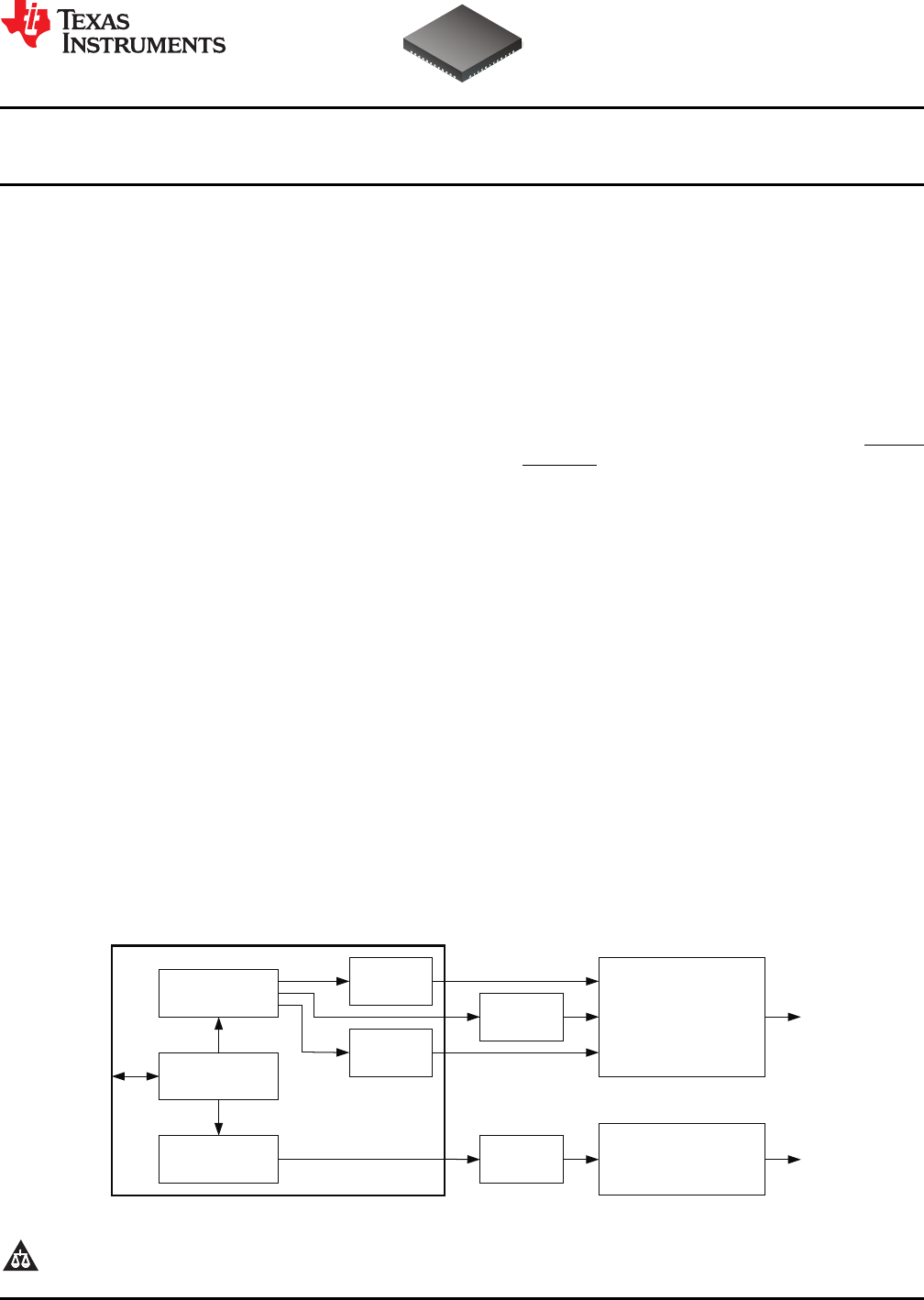
TPS51640
VCC_CPU
VCC_GFX
Processor
3-phase CPU
Controller
IMVP-7
SVID Interface
1-phase GPU
Controller
TPS51601
FET Driver CPU Power Stage
TPS51601
FET Driver
Internal
FET Driver
Internal
FET Driver
GPU Power Stage
UDG-11062
TPS51640A, TPS59640, TPS59641
www.ti.com
SLUSAQ2 –JANUARY 2012
Dual-Channel (3-Phase CPU/1-Phase GPU) SVID, D-CAP+™Step-Down Controller for
IMVP-7 V
CORE
with Two Integrated Drivers
1FEATURES DESCRIPTION
2•Intel IMVP-7 Serial VID (SVID) Compliant The TPS51640A, TPS59640 and TPS59641 are
•Supports CPU and GPU Outputs dual-channel, fully SVID compliant IMVP-7 step-down
•CPU Channel 1, 2, or 3 Phase controllers with two integrated gate drivers. Advanced
control features such as D-CAP™+ architecture with
•Single-Phase GPU Channel overlapping pulse support (undershoot reduction,
•Full IMVP-7 Mobile Feature Set Including USR) and overshoot reduction (OSR) provide fast
Digital Current Monitor transient response, lowest output capacitance and
•8-Bit DAC with 0.250-V to 1.52-V Output Range high efficiency. All of these controllers also support
single-phase operation for light loads. The full
•Optimized Efficiency at Light and Heavy Loads compliment of IMVP-7 I/O is integrated into the
•VCORE Overshoot Reduction (OSR) controllers including dual PGOOD signals, ALERT
•VCORE Undershoot Reduction (USR) and VR_HOT. Adjustable control of VCORE slew rate
and voltage positioning round out the IMVP-7
•Accurate, Adjustable Voltage Positioning features. In addition, the controllers'CPU channel
•8 Independent Frequency Selections per includes two high-current FET gate drivers to drive
Channel (CPU/GPU) high-side and low-side N-channel FETs with
•Patent Pending AutoBalance™Phase exceptionally high speed and low switching loss. The
Balancing TPS51601 or TPS51601A driver is used for the third
phase of the CPU and the GPU channel.
•Selectable 8-Level Current Limit
•3-V to 28-V Conversion Voltage Range The BOOT voltage (VBOOT) on the TPS51640A and
TPS59640 is 0 V. The TPS59641 is specifically
•Two Integrated Fast FET Drivers w/Integrated designed for a VBOOT level of 1.1 V.
Boost FET
These controllers are packaged in a space saving,
•Internal Driver Bypass Mode for Use with thermally enhanced 48-pin QFN. The TPS51640A is
DrMOS Devices rated to operate from –10°C to 105°C. The
•Small 6 ×6 , 48-Pin, QFN, PowerPAD™TPS59640 and TPS59641 are rated to operate
Package from –40°C to 105°C.
APPLICATIONS
•IMVP-7 VCORE Applications for Adapter,
Battery, NVDC or 3 V/5 V/12 V rails
SIMPLIFIED APPLICATION
1
Please be aware that an important notice concerning availability, standard warranty, and use in critical applications of Texas
Instruments semiconductor products and disclaimers thereto appears at the end of this data sheet.
2D-CAP+, PowerPAD, D-CAP are trademarks of Texas Instruments.
PRODUCTION DATA information is current as of publication date. Copyright ©2012, Texas Instruments Incorporated
Products conform to specifications per the terms of the Texas
Instruments standard warranty. Production processing does not
necessarily include testing of all parameters.
TPS51640A, TPS59640, TPS59641
SLUSAQ2 –JANUARY 2012
www.ti.com
These devices have limited built-in ESD protection. The leads should be shorted together or the device placed in conductive foam
during storage or handling to prevent electrostatic damage to the MOS gates.
ORDERING INFORMATION(1)(2)
VBOOT ORDERABLE TRANSPORT MINIMUM
TAPACKAGE PINS ECO PLAN
(V) NUMBER MEDIA QUANTITY
TPS51640ARSLT 250
–10°C to 105°C 0 TPS51640ARSLR 2500
TPS59640RSLT 250 Green (RoHS and
Plastic Quad Flat 0 48 Tape-and-reel
Pack (QFN) no Sb/Br)
TPS59640RSLR 2500
–40°C to 105°CTPS59641RSLT(3) 250
1.1 TPS59641RSLTR(3) 2500
(1) For the most current package and ordering information see the Package Option Addendum at the end of this document, or see the TI
web site at www.ti.com.
(2) Package drawings, thermal data, and symbolization are available at www.ti.com/packaging.
(3) Product preview. Not currently available.
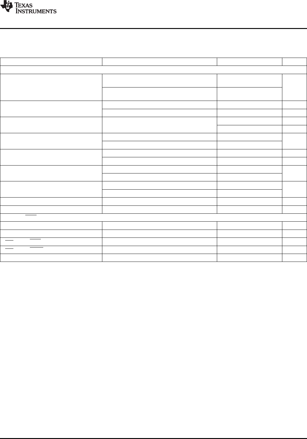
ABSOLUTE MAXIMUM RATINGS(1)(2)
over operating free-air temperature range (unless otherwise noted)
MIN TYP MAX UNIT
VBAT –0.3 32
CSW1, CSW2 –6.0 32 V
CDH1 to CSW1; CDH2 to CSW2; CBST1 to CSW1; CBST2 to CSW2 –0.3 6.0
CTHERM, CCOMP, CF-IMAX, GF-IMAX, GCOMP, GTHERM, –0.3 6.0
Input voltage V5DRV, V5
V
COCP-I, CCSP1, CCSP2, CCSP3, CCSN1, CCSN2, CCSN3, CVFB,
CGFB, V3R3, VR_ON, VCLK, VDIO, SLEWA, GGFB, GVFB, GCSN, –0.3 3.6
GCSP, GOCP-I,
PGND –0.3 0.3
VREF –0.3 1.8
Output voltage CPGOOD, ALERT, VR_HOT, GPGOOD, CIMON, GIMON –0.3 3.6 V
CPWM3, CSKIP, GPWM, GSKIP, CDL1, CDL2 –0.3 6.0
(HBM) QSS 009-105 (JESD22-A114A) 1.5 kV
Electrotatic discharge (CDM) QSS 009-147 (JESD22-C101B.01) 500 V
Operating junction temperature, TJ-40 125 °C
Storage temperature, Tstg -55 150 °C
(1) Stresses beyond those listed under absolute maximum ratings may cause permanent damage to the device. These are stress ratings
only and functional operation of the device at these or any other conditions beyond those indicated under recommended operating
conditions is not implied. Exposure to absolute-maximum-rated conditions for extended periods may affect device reliability.
(2) All voltage values are with respect to the network ground terminal unless otherwise noted.
2Submit Documentation Feedback Copyright ©2012, Texas Instruments Incorporated
TPS51640A, TPS59640, TPS59641
www.ti.com
SLUSAQ2 –JANUARY 2012
THERMAL INFORMATION
TPS51640A
TPS59640
TPS59641
THERMAL METRIC(1) UNITS
RSL
48 PINS
θJA Junction-to-ambient thermal resistance 31.7
θJCtop Junction-to-case (top) thermal resistance 19.8
θJB Junction-to-board thermal resistance 7.1 °C/W
ψJT Junction-to-top characterization parameter 0.3
ψJB Junction-to-board characterization parameter 7.1
θJCbot Junction-to-case (bottom) thermal resistance 2.1
(1) For more information about traditional and new thermal metrics, see the IC Package Thermal Metrics application report, SPRA953.
RECOMMENDED OPERATING CONDITIONS
MIN TYP MAX UNIT
VBAT –0.1 28
CSW1, CSW2 –3.0 30
CDH1 to CSW1; CDH2 to CSW2; CBST1 to CSW1; CBST2 to –0.1 5.5
CSW2
V5DRV, V5 4.5 5.5
V3R3 3.1 3.5
Input voltage CCOMP, GCOMP –0.1 2.5 V
CTHERM, GTHERM 0.1 3.6
CF-IMAX, GF-IMAX, COCP-I, GOCP-I 0.1 1.7
CCSP1, CCSP2, CCSP3, CCSN1, CCSN2, CCSN3, CVFB, CGFB, –0.1 1.7
GGFB, GVFB, GCSN, GCSP,
VR_ON, VCLK, VDIO, SLEWA, –0.1 3.5
PGND –0.1 0.1
VREF –0.1 1.72
CIMON, GIMON –0.1 VVREF
Output voltage V
CPGOOD, ALERT, VR_HOT, GPGOOD, –0.1 VV3R3
CPWM3, CSKIP, GPWM, GSKIP, CDL1, CDL2, –0.1 VV5
TPS51460A –10 105
Operating free air temperature, TA°C
TPS59640,TPS59641 –40 105
Copyright ©2012, Texas Instruments Incorporated Submit Documentation Feedback 3
TPS51640A, TPS59640, TPS59641
SLUSAQ2 –JANUARY 2012
www.ti.com
ELECTRICAL CHARACTERISTICS
over recommended free-air temperature range, VV5 = VV5DRV = 5.0 V; VV3R3 = 3.3 V; VxGFB = VPGND = VGND, VxVFB = VCORE
(Unless otherwise noted)
PARAMETER TEST CONDITIONS MIN TYP MAX UNIT
SUPPLY: CURRENTS, UVLO AND POWER-ON RESET
IV5+ IV5DRV , VVDAC <VxVFB <(VVDAC + 100 mV),
V5 supply current CPU: 3-phase
IV5-4 6.0 9.0 mA
active GPU: 1-phase active VR_ON = ‘HI’
IV5+ IV5DRV, VVDAC <VxVFB <(VVDAC + 100 mV),
V5 supply current CPU: 2-phase
IV5-3 5.5 mA
active GPU: 1-phase active VR_ON = ‘HI’, VCCSP3=3.3 V
V5 supply current CPU: 1-phase IV5+ IV5DRV, VVDAC <VxVFB <(VVDAC + 100 mV),
IV5-2 4.9 mA
active GPU: 1-phase active VR_ON = ‘HI’, VCCSP3 = VCCSP2= 3.3 V
IV5+ IV5DRV, VVDAC <VxVFB <(VVDAC + 100 mV),
V5 supply current CPU: 3-phase
IV5-PS3 VR_ON = ‘HI’, SetPS = PS3 5.1 mA
active GPU: 1-phase active (Note: 3-phase CPU goes to 1-phase in PS3)
IV5STBY V5DRV standby current VR_ON = ‘LO’, IV5 + IV5DRV 10 20 µA
VUVLOH V5 UVLO 'OK'Threshold Ramp up, VR_ON=’HI’, 4.25 4.4 4.5 V
VUVLOL V5 UVLO fault threshold Ramp down, VR_ON = ’HI’, 3.95 4.2 4.3 V
IV3R3 V3R3 supply current SVID bus idle, VR_ON = ‘HI’0.5 1.0 mA
IV3R3SBY V3R3 standby current VR_ON = ‘LO’10 µA
V3UVLOH V3R3 UVLO 'OK'threshold Ramp up, VR_ON=’HI’, 2.5 2.9 3.0 V
V3UVLOL V3R3 UVLO fault threshold Ramp down, VR_ON = ’HI’, 2.4 2.7 2.8 V
REFERENCES: DAC, VREF, VBOOT AND DRVL DISCHARGE FOR BOTH CPU AND GPU
TPS59640 0 V
TPS51640A
VBOOT Boot voltage
TPS59641 1.1
VVIDSTP VID step size 5 mV
0.25 ≤VxVFB ≤0.995V, TPS51640A –5 5
IxPU_CORE = 0 A, 0°C≤TA≤85°C
VDAC1 xVFB tolerance no load active 0.25 ≤VxVFB ≤0.995V, TPS59640
IxPU_CORE = 0 A, –6 8.3
TPS59641
–40°C≤TA≤105°CmV
1.000V ≤VxVFB ≤1.520 V, TPS51640A –0.5% 0.5%
IxPU_CORE = 0 A, 0°C≤TA≤85°C
VDAC4 xVFB tolerance above 1 V VID 1.000V ≤VxVFB ≤1.520 V, TPS59640
IxPU_CORE = 0 A, –0.65% 1.0%
TPS59641
–40°C≤TA≤105°C
VVREF VREF Output 4.5 V ≤VV5 ≤5.5 V, IVREF= 0 A 1.70 V
VVREFSRC VREF output source 0 µA≤IVREF ≤500 µA–4–0.1 mV
VVREFSNK VREF output sink –500 µA≤IVREF ≤0µA 0.1 4 mV
VDLDQ DRVL discharge threshold Soft-stop transistor turns on at this point. 200 300 mV
VOLTAGE SENSE: xVFB AND xGFB FOR BOTH CPU AND GPU
IxVFB xVFB input bias current VxVFB=2 V, VxGFB=0 V 20 40 µA
IxGFB xGFB input bias current VxVFB=2 V, VxGFB=0 V -40 -20 µA
AGAINGND xGFB/GND gain 1 V/V
CURRENT MONITOR
VCiMONLK Zero level current output Σ∆CS = 0 mV, AIMON = 12 ×(1+1.27) 35 mV
VCIMONLO Low level current output Σ∆CS = 15.6 mV, AIMON = 12 ×(1+1.27) 425 mV
VCIMONMID Mid level current output Σ∆CS = 31.1 mV, AIMON = 12 ×(1+1.27) 850 mV
VCIMONHI High level current output Σ∆CS = 62.3 mV, AIMON = 12 ×(1+1.27) 1700 mV
ZERO-CROSSING
Inductor zero crossing threshold
VZx 0 mV
voltage
4Submit Documentation Feedback Copyright ©2012, Texas Instruments Incorporated
TPS51640A, TPS59640, TPS59641
www.ti.com
SLUSAQ2 –JANUARY 2012
ELECTRICAL CHARACTERISTICS (continued)
over recommended free-air temperature range, VV5 = VV5DRV = 5.0 V; VV3R3 = 3.3 V; VxGFB = VPGND = VGND, VxVFB = VCORE
(Unless otherwise noted)
PARAMETER TEST CONDITIONS MIN TYP MAX UNIT
CURRENT SENSE: OVERCURRENT, ZERO CROSSING, VOLTAGE POSITIONING AND PHASE BALANCING
TPS51640A 5.1 7.0 9.7
RxOCP-I = 20 kΩTPS59640 4.6 7.0 9.7
TPS59641
TPS51640A 8.1 10.0 12.6
RxOCP-I = 24 kΩTPS59640 7.6 10.0 13.1
TPS59641
TPS51640A 12.1 14.0 16.7
RxOCP-I = 30 kΩTPS59640 11.6 14.0 17.2
TPS59641
TPS51640A 17.1 19.0 21.7
RxOCP-I = 39 kΩTPS59640 16.6 19.0 22.2
TPS59641
OCP voltage (valley current
VOCPP mV
limit) TPS51640A 23.1 25.0 27.9
RxOCP-I = 56 kΩTPS59640 22.6 25.0 28.4
TPS59641
TPS51640A 29.7 32.0 35.0
RxOCP-I = 75 kΩTPS59640 29.2 32.0 35.5
TPS59641
TPS51640A 37.9 40.0 43.3
RxOCP-I = 100 kΩTPS59640 37.4 40.0 43.8
TPS59641
TPS51640A 46.8 49.0 52.6
RxOCP-I = 150 kΩTPS59640 46.2 49.0 53.1
TPS59641
VIMAX_MIN = 133 mV, value of xIMAX, 20 A
VIMAX = VREF ×IMAX / 255
VIMAX IMAX values both channels
VIMAX_MAX = 653mV, value of xIMAX 98 A
ICS CS pin input bias current CSPx and CSNx –1.0 0.2 1.0 µA
xVFB input bias current,
IxVFBDQ End of soft-stop, xVFB = 100mV 90 125 180 µA
discharge
TPS51640A 486 497 518
Droop amplifier
GM-DROOP xVFB = 1 V µS
TPS59640
transconductance 480 497 518
TPS59641
(VCSP1 –VCSN1) = (VCSP2 –VCSN2) =
IBAL_TOL Internal current share tolerance –3% +3%
(VCSP3 –VCSN3) = VOCPP_MIN
ACSINT Internal current sense gain Gain from CSPx –CSNx to PWM comparator 11.65 12.00 12.30 V/V
Copyright ©2012, Texas Instruments Incorporated Submit Documentation Feedback 5
TPS51640A, TPS59640, TPS59641
SLUSAQ2 –JANUARY 2012
www.ti.com
ELECTRICAL CHARACTERISTICS (continued)
over recommended free-air temperature range, VV5 = VV5DRV = 5.0 V; VV3R3 = 3.3 V; VxGFB = VPGND = VGND, VxVFB = VCORE
(Unless otherwise noted)
PARAMETER TEST CONDITIONS MIN TYP MAX UNIT
TIMERS: SLEW RATE, ISLEW, ADDR, ON-TIME AND I/O TIMING
VBOOT >0 V, SLEWRATE = 12 mV/µs, no faults,
tSTARTUP1 Start-up time time from VR_ON until the controller responds to 5 ms
SVID commands
SLEWRATE = 12mV/µs, VR_ON goes ‘HI’,
SLSTRTSTP xVFB slew soft-start / soft-stop 1.25 1.50 1.75 mV/µs
VR_ON goes ‘LO = ‘Soft-stop’
VSLEWA ≤0.30V (Also disables SVID CLK timer) 10.0 12.0 14.5
VSLEWA = 0.4 V 3.5 4.0 5.0
VSLEWA = 0.6 V 7.5 8.5 9.5
0.75 V ≤VSLEWA ≤0.85 V 10.0 12.0 14.5
SLSET Slew rate setting VSLEWA = 1.0 V 16 mV/µs
VSLEWA = 1.2 V 20
VSLEWA = 1.4 V 23
VSLEWA = 1.6 V 26
VSLEWA ≥2.50 V 26
Time from xVFB out of +220 mV VDAC boundary
tPGDDGLTO xPGOOD deglitch time 5 100 µs
to xPGOOD low.
Time from xVFB out of –315 mV VDAC boundary
tPGDDGLTU xPGOOD deglitch time 150 500 µs
to xPGOOD low.
TPS51640A 270 327 375
RCF=20 kΩ, VBAT=12 V, VDAC=1.1 V TPS59640
(250 kHz) 265 327 380
TPS59641
TPS51640A 225 272 320
RCF=24 kΩ, VBAT=12 V, VDAC=1.1 V TPS59640
(300 kHz) 220 272 325
TPS59641
TPS51640A 185 235 280
RCF=30 kΩ, VBAT=12 V, VDAC=1.1 V TPS59640
(350 kHz) 180 235 285
TPS59641
TPS51640A 160 207 252
tTON_CPU CPU on-time RCF=39 kΩ, VBAT=12 V, VDAC=1.1 V ns
TPS59640
(400 kHz) 155 207 262
TPS59641
TPS51640A 140 185 231
RCF=56 kΩ, VBAT=12 V, VDAC=1.1 V TPS59640
(450 kHz) 134 185 241
TPS59641
TPS51640A 120 167 212
RCF=75 kΩ, VBAT=12 V, VDAC=1.1 V TPS59640
(500 kHz) 115 167 217
TPS59641
RCF=100 kΩ, VBAT=12 V, VDAC=1.1 V (550 kHz) 109 152 198
RCF=150 kΩ, VBAT=12 V, VDAC=1.1 V (600 kHz) 105 140 177
6Submit Documentation Feedback Copyright ©2012, Texas Instruments Incorporated
TPS51640A, TPS59640, TPS59641
www.ti.com
SLUSAQ2 –JANUARY 2012
ELECTRICAL CHARACTERISTICS (continued)
over recommended free-air temperature range, VV5 = VV5DRV = 5.0 V; VV3R3 = 3.3 V; VxGFB = VPGND = VGND, VxVFB = VCORE
(Unless otherwise noted)
PARAMETER TEST CONDITIONS MIN TYP MAX UNIT
TIMERS: SLEW RATE, ISLEW, ADDR, ON-TIME AND I/O TIMING (Continued)
TPS51640A 315 347 388
RGF=20 kΩ, VBAT=12 V, VDAC=1.1 V TPS59640
(275 kHz) 310 347 393
TPS59641
TPS51640A 251 287 330
RGF=24 kΩ, VBAT=12 V, VDAC=1.1V TPS59640
(330 kHz) 246 287 335
TPS59641
TPS51640A 215 245 287
RGF=30 kΩ, VBAT=12 V, VDAC=1.1 V TPS59640
(385 kHz) 210 245 292 ns
TPS59641
tTON_GPU GPU on-time TPS51640A 180 216 252
RGF=39 kΩ,VBAT=12 V, VDAC=1.1 V TPS59640
(440 kHz) 175 216 257
TPS59641
TPS51640A 160 190 223
RGF=56 kΩ, VBAT=12 V, VDAC=1.1 V TPS59640
(495 kHz) 155 190 228
TPS59641
RGF=75 kΩ, VBAT=12 V, VDAC=1.1 V (550 kHz) 145 171 210
RGF=100 kΩ, VBAT=12 V, VDAC=1.1 V (605 kHz) 120 156 205
RGF=150 kΩ, VBAT=12 V, VDAC=1.1 V (660 kHz) 100 150 201
tMIN Controller minimum off time Fixed value 150 200 ns
ACK of SetVID-x command to start of voltage
tVCCVID VID change to xVFB change(1) 2µs
ramp
tVRONPGD VR_ON low to xPGOOD low 20 50 100 ns
tPGDVCC xPGOOD low to xVFB change(1) 100 ns
tVRTDGLT VR_HOT# deglitch time 0.2 0.7 ms
RSFTSTP Soft-stop transistor resistance Connect to CVFB, GVFB 550 770 1100 Ω
PROTECTION: OVP, UVP PGOOD, VR_HOT, ‘FAULTS OFF’AND INTERNAL THERMAL SHUTDOWN
Fixed OVP voltage threshold
VOVPH VCSN1 or VGCSN >VOVPH for 1 µs, DRVL →ON 1.68 1.72 1.77 V
voltage
Measured at the xVFB pin wrt/VID code,
VPGDH xPGOOD high threshold 190 220 245 mV
device latches OFF
Measured at the xVFB pin wrt/VID code,
VPGDL xPGOOD low threshold –348 –315 –280 mV
device latches OFF
bit0 of xTHERM register = high 757 783 808
bit1 of xTHERM register also is high 651 680 707
bit2 of xTHERM register also is high 611 638 663
bit3 of xTHERM register also is high 570 598 623
bit4 of xTHERM register also is high 531 559 583
IMVP-7 thermal bit voltage
VTHERM mV
bit5 of xTHERM register also is high 496 523 548
definition
bit6 of xTHERM register also is high, 461 488 513
ALERT goes low
bit7 of XTHERM register also is high, 428 455 481
VR_HOT goes low
CDLx goes low, CDHx goes low 373 410 425
ITHRM THERM current Leakage current –5 5 µA
Internal controller thermal
THINT Latch off controller 155 °C
Shutdown(1)
Controller thermal SD
THHYS Cooling required before converter can be reset 20 °C
hysteresis(1)
(1) Specified by design. Not production tested.
Copyright ©2012, Texas Instruments Incorporated Submit Documentation Feedback 7
TPS51640A, TPS59640, TPS59641
SLUSAQ2 –JANUARY 2012
www.ti.com
ELECTRICAL CHARACTERISTICS (continued)
over recommended free-air temperature range, VV5 = VV5DRV = 5.0 V; VV3R3 = 3.3 V; VxGFB = VPGND = VGND, VxVFB = VCORE
(Unless otherwise noted)
PARAMETER TEST CONDITIONS MIN TYP MAX UNIT
LOGIC (VCLK, VDIO, ALERT, VR_HOT, VR_ON) INTERFACE PINS: I/O VOLTAGE AND CURRENT
VDIO, ALERT, VR_HOT, pull-down resistance at
RRSVIDL Open drain pull down resistance 4 8 13 Ω
0.31 V
RRPGDL Open drain pull down resistance xPGOOD pull-down resistance at 0.31 V 36 50
VR_HOT, xPGOOD, Hi-Z leakage,
IVRTTLK Open drain leakage current -2 0.2 2 µA
apply 3.3-V in off state
VIL Input logic low 0.45 V
VCLK, VDIO
VIH Input logic high 0.65 V
VHYST Hysteresis voltage(1) 0.05 V
VVR_ONL VR_ON logic low 0.3 V
VVR_ONH VR_ON logic high 0.8 V
IVR_ONH I/O 3.3 V leakage Leakage current , VVR_ON = 1.1 V 10 25.0 µA
OVERSHOOT AND UNDERSHOOT REDUCTION (OSR/USR) THRESHOLD SETTING
RxSKIP = 20 kΩ106
RxSKIP = 24 kΩ156
RxSKIP = 30 kΩ207
RxSKIP = 39 kΩ257
VOSR OSR voltage set mV
RxSKIP = 56 kΩ308
RxSKIP = 75 kΩ409
RxSKIP = 100 kΩ510
RxSKIP = 150 kΩ610
RxSKIP = 20 kΩ40
RxSKIP = 24 kΩ60
RxSKIP = 30 kΩ75
RxSKIP = 39 kΩ115
VUSR USR voltage set mV
RxSKIP = 56 kΩ153
RxSKIP = 75 kΩ190
RxSKIP = 100 kΩ230
RxSKIP ≥150 kΩ= OFF –
VOSR_OFF OSR OFF setting VxSKIP at start up 100 300 mV
VOSRHYS OSR/USR voltage hysteresis(2) All settings 20%
(2) Specified by design. Not production tested.
8Submit Documentation Feedback Copyright ©2012, Texas Instruments Incorporated
TPS51640A, TPS59640, TPS59641
www.ti.com
SLUSAQ2 –JANUARY 2012
ELECTRICAL CHARACTERISTICS (continued)
over recommended free-air temperature range, VV5 = VV5DRV = 5.0 V; VV3R3 = 3.3 V; VxGFB = VPGND = VGND, VxVFB = VCORE
(Unless otherwise noted)
PARAMETER TEST CONDITIONS MIN TYP MAX UNIT
DRIVERS: HIGH-SIDE, LOW-SIDE, CROSS CONDUCTION PREVENTION AND BOOST RECTIFIER
(VCBSTx –VCSWx) = 5 V, ‘HI’state, 1.2 2.5
(VVBST –VVDRVH) = 0.25 V
RDRVH DRVH ON resistance Ω
(VCBSTx –VCSWx) = 5 V, ‘LO’state, 0.8 2.5
(VDRVH –VLL) = 0.25 V
VCDHx = 2.5 V, (VCBSTx –VCSWx) = 5 V, Source 2.2 A
IDRVH DRVH sink/source current(3)
VCDHx = 2.5 V, (VCBSTx –VCSWx) = 5 V, Sink 2.2 A
15 40 ns
tDRVH DRVH transition time CDHx 10% to 90% or 90% to 10%, CCDHx = 3 nF 15 40 ns
‘HI’State, (VV5DRV –VVDRVL) = 0.25 V 0.9 2
RDRVL DRVL ON resistance Ω
‘LO’State, (VVDRVL –VPGND)= 0.2 V 0.4 1
VCDLx = 2.5 V, Source 2.7 A
IDRVL DRVL sink/source current(3)
VCDLx = 2.5 V, Sink 6 A
VCDLx 90% to 10%, CCDLx = 3 nF 15 40
tDRVL DRVL transition time ns
VCDLx 10% to 90%, CCDLx = 3 nF 15 40
VCSWx falls to 1 V to VCDLx rises to 1 V 13 25
tNONOVLP Driver non overlap time ns
CDLx falls to 1 V to CDHx rises to 1 V 13 25
RDS(on) BST on-resistance (VV5DRV –VVBST), IF= 5 mA 5 10 20 Ω
IBSTLK BST switch leakage current VVBST = 34 V, VCSWx=28 V 0.1 1 µA
PWM and SKIP OUTPUT: I/O Voltage and Current
VPWML xPWMy output low level 0.7 V
VPWMH xPWMy output high level 4.2 V
VSKIPL SKIP output low level 0.7 V
VSKIPH xSKIP output high level 4.2 V
VPW(leak) xPWM leakage Tri-state, V = 5 V 0.1 µA
(3) Specified by design. Not production tested.
Copyright ©2012, Texas Instruments Incorporated Submit Documentation Feedback 9
1
2
3
4
5
6
7
8
9
10
11
12
13
14
15
16
17
18
19
20
21
22
23
24
36
35
34
33
32
31
30
29
28
27
26
25
48
47
46
45
44
43
42
41
40
39
38
37
CTHERM
COCP-I
CIMON
CCSP1
CCSN1
CCSN2
CCSP2
CCSP3
CCSN3
CVFB
CCOMP
CGFB
CF-IMAX
VREF
V3R3
VR_ON
CPGOOD
VCLK
ALERT
VDIO
VR_HOT
SLEWA
GPGOOD
GF-IMAX
CPWM3
CSKIP
GPWM
GSKIP
GTHERM
GOCP-I
GIMON
GCSP
GCSN
GCOMP
GVFB
GGFB
V5
CDH1
CBST1
CSW1
CDL1
V5DRV
PGND
CDL2
CSW2
CBST2
CDH2
VBAT
TPS51640A
TPS59640
TPS59641
TPS51640A, TPS59640, TPS59641
SLUSAQ2 –JANUARY 2012
www.ti.com
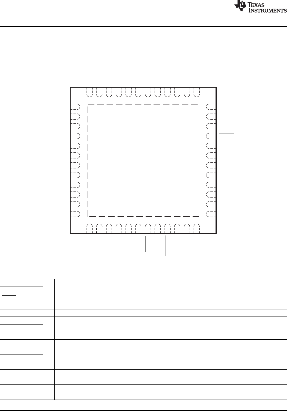
DEVICE INFORMATION
RSL PACKAGE
48 PINS
(TOP VIEW)
PIN FUNCTIONS
PIN I/O DESCRIPTION
NAME NO.
ALERT 19 O SVID interrupt line, open drain. Route between VCLK and VDIO to prevent cross-talk.
CBST1 46 I Top N-channel FET bootstrap voltage input for CPU phase 1.
CBST2 39 I Top N-channel bootstrap voltage input for CPU phase 2.
CCSN1 5 Negative current sense inputs for the CPU converter. Connect to the most negative node of current sense
CCSN2 6 I resistor or inductor DCR sense network. CCSN1 has a secondary OVP comparator.
CCSN3 9
CCOMP 10 O Output of GM error amplifier for the CPU converter. A resistor to VREF sets the droop gain.
CCSP1 4 Positive current sense inputs for the CPU converter. Connect to the most positive node of current sense resistor
CCSP2 7 I or inductor DCR sense network. Tie CCSP3, 2 or 1 (in that order) to V3R3 to disable the phase. Tie CCSP1 to
V3R3 to run the GPU converter only.
CCSP3 8
CDH1 47 O Top N-channel FET gate drive output for CPU phase 1.
CDH2 38 O Top N-channel FET gate drive output for CPU phase 2.
CDL1 44 O Synchronous N-channel FET gate drive output for CPU phase 1.
CDL2 41 O Synchronous N-channel FET gate drive output for CPU phase 2.
10 Submit Documentation Feedback Copyright ©2012, Texas Instruments Incorporated
TPS51640A, TPS59640, TPS59641
www.ti.com
SLUSAQ2 –JANUARY 2012
PIN I/O DESCRIPTION
NAME NO.
Voltage divider to VREF. A resistor to GND sets the operating frequency of the CPU converter. The voltage level
CF-IMAX 13 I sets the maximum operating current of the CPU converter. The IMAX value is an 8-bit A/D where VIMAX = VREF ×
IMAX / 255. Both are latched at start-up.
Voltage sense return tied for the CPU converter. Tie to GND with a 10-Ωresistor to close feedback when the
CGFB 12 I microprocessor is not in the socket.
Analog current monitor output for the CPU converter. VCIMON =ΣVCS ×ACS ×(1 + RCIMON/RCOCP). Connect a
CIMON 3 O 220-nF capacitor to GND for stability.
Resistor to GND (RCOCP) selects 1 of 8 OCP levels (per phase, latched at start-up) of the CPU converter. Also,
COCP-I 2 I voltage divider to CIMON. Resistor ratio sets the IMON gain (see CIMON pin description).
CPGOOD 17 O IMVP-7_PWRGD output for the CPU converter. Open-drain.
CSW1 45 I/O Top N-channel FET gate drive return for CPU phase 1.
CSW2 40 I/O Top N-channel FET gate drive return for CPU phase 2.
CPWM3 36 O PWM control for the external driver, 5V logic level.
Skip mode control of the external driver for the CPU converter. A logic HI = FCCM, LO = SKIP. R to GND selects
CSKIP 35 O 1 of 8 OSR/USR levels. 0.1 V <VCSKIP <0.3 V at start-up turns OSR off.
Thermal sensor connection for the CPU converter. A resistor connected to VREF forms a divider with an NTC
CTHERM 1 I/O thermistor connected to GND.
Voltage sense line tied directly to VCORE of the CPU converter. Tie to VCORE with a 10-Ωresistor to close
CVFB 11 I feedback when µP is not in the socket. The soft-stop transistor is on this pin
Negative current sense input for the GPU converter. Connect to the most negative node of current sense resistor
GCSN 28 I or inductor DCR sense network. GCSN has a secondary OVP comparator and includes the soft-stop pull-down
transistor.
Positive current sense input for the GPU converter. Connect to the most positive node of current sense resistor
GCSP 29 I or inductor DCR sense network. Tie to V3R3 to disable the GPU converter.
GCOMP 27 O Output of gMerror amplifier for the GPU converter. A resistor to VREF sets the droop gain.
Voltage sense return tied for the GPU converter. Tie to GND with a 10-Ωresistor to close feedback when the
GGFB 25 I microprocessor is not in the socket.
24 I Voltage divider to VREF. R to GND sets the operating frequency of the GPU converter. The voltage level sets
GF-IMAX the maximum operating current of the GPU converter. The IMAX value is an 8-bit A/D where VIMAX = VREF ×
IMAX / 255. Both are latched at start-up.
30 O Analog current monitor output for the GPU converter. VGIMON = VISENSE ×(1 + RGIMON/RGOCP). Connect a
GIMON 220-nF capacitor to GND for stability.
31 I Voltage divider to GIMON. Resistor ratio sets the IMON gain (see GIMON pin). Resistor to GND (RGOCP) selects
GOCP-I 1 of 8 OCP levels (per phase, latched at start-up) of the GPU converter.
GPGOOD 23 O IMVP-7_PWRGD output for the GPU converter. Open-drain.
GPWM 34 O PWM control for the external driver, 5-V logic level.
33 O Skip mode control of the external driver for the GPU converter, 5-V logic level. Logic HI = FCCM, LO = SKIP. R
GSKIP to GND selects 1 of 8 OSR/USR levels. 0.1 V <VGSKIP<0.3 V at start-up turns OSR off.
32 I/O Thermal sensor input for the GPU converter. A resistor connected to VREF forms a divider with an NTC
GTHERM thermistor connected to GND.
26 I Voltage sense line tied directly to VGFX of the GPU converter. Tie to VGFX with a 10-Ωresistor to close feedback
GVFB when the microprocessor is not in the socket. The soft-stop transistor is on this pin
PGND 42 –Synchronous N-channel FET gate drive return.
22 I The voltage at start-up sets 1 of 7 slew rates for both converters. The SLOW rate is SLEWRATE/4. Soft-start
SLEWA and soft-stop rates are SLEWRATE/8. This value is latched at start-up. Tie to GND to disable SCLK timer.
48 I 5-V power input for analog circuits; connect through resistor to 5-V plane and bypass to GND with ≥1µF ceramic
V5 capacitor
43 I Power input for the gate drivers; connected with an external resistor to V5F; decouple with a ≥2.2 µF ceramic
V5DRV capacitor.
V3R3 15 I 3.3-V power input; bypass to GND with ≥1µF ceramic cap.
37 I Provides VBAT information to the on-time circuits for both converters. A 10-kΩseries resistor protects the
VBAT adjacent pins from inadvertent shorts due to solder bridges or mis-probing during test.
VCLK 18 I SVID clock. 1-V logic level.
VDIO 20 I/O SVID digital I/O line. 1-V logic level.
VREF 14 O 1.7-V, 500-µA reference. Bypass to GND with a 0.22-µF ceramic capacitor.
Copyright ©2012, Texas Instruments Incorporated Submit Documentation Feedback 11

TPS51640A, TPS59640, TPS59641
SLUSAQ2 –JANUARY 2012
www.ti.com
PIN I/O DESCRIPTION
NAME NO.
VR_ON 16 I IMVP-7 VR enable; 1V I/O level; 100-ns de-bounce. Regulator enters controlled soft-stop when brought low.
21 O IMVP-7 thermal flag open drain output –active low. Typically pulled up to 1-V logic level through 56 Ω. Fall time
VR_HOT <100 ns. 1-ms de-glitch using consecutive 1-ms samples.
PAD GND –Thermal pad and analog circuit reference; tie to a quiet area in the system ground plane with multiple vias.
12 Submit Documentation Feedback Copyright ©2012, Texas Instruments Incorporated
0.80
0.85
0.90
0.95
1.00
1.05
Output Voltage (V)
VIN = 9 V
VIN = 20 V
Nominal
Specified Maximum
Specified Minimum
VVID = 1.05 V
0 10 20 90 100
Output Current (A)
30 40 50 70 8060
0.500
0.525
0.575
0.600
0.625
0.675
0.700
0 2 4 18 20
Output Current (A)
Output Voltage (V)
6 8 10 14 1612
VIN = 9 V
VIN = 20 V
Nominal
Specified Maximum
Specified Minimum
VVID = 0.6 V
0.550
0.650
65
75
80
85
90
Efficiency (%)
VVID = 0.6 V
70 VIN = 9 V
VIN = 20 V
0 2 4 18 20
Output Current (A)
6 8 10 14 1612
65
75
80
85
90
95
Efficiency (%)
VVID = 1.05 V
70 VIN = 9 V
VIN = 20 V
0 10 20 90 100
Output Current (A)
30 40 50 70 8060
0
100
150
200
350
400
Frequency (Hz)
50
0 10 20 90 100
Output Current (A)
30 40 50 70 8060
RCF = 24 kW
PS0, VVID = 1.05 V, VIN = 9 V
PS0, VVID = 1.05 V, VIN = 20 V
PS1, VVID = 1.05 V, VIN = 20 V
PS1, VVID = 1.05 V, VIN = 9 V
250
300
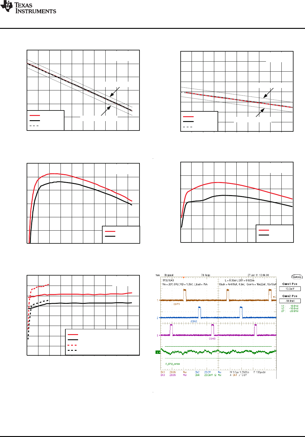
TPS51640A, TPS59640, TPS59641
www.ti.com
SLUSAQ2 –JANUARY 2012
TYPICAL CHARACTERISTICS
3-Phase Configuration, 94-A CPU
Figure 1. Output Voltage vs. Load Current in PS0 Figure 2. Output Voltage vs. Load Current in PS1
Figure 3. Efficiency vs. Load Current in PS0 Figure 4. Efficiency vs. Load Current in PS1
Figure 5. Frequency vs Load-Current (PS0 and PS1) Figure 6. Switching Ripple in PS0, VIN = 20 V
Copyright ©2012, Texas Instruments Incorporated Submit Documentation Feedback 13
TPS51640A, TPS59640, TPS59641
SLUSAQ2 –JANUARY 2012
www.ti.com
TYPICAL CHARACTERISTICS
3-Phase Configuration, 94-A CPU (continued)
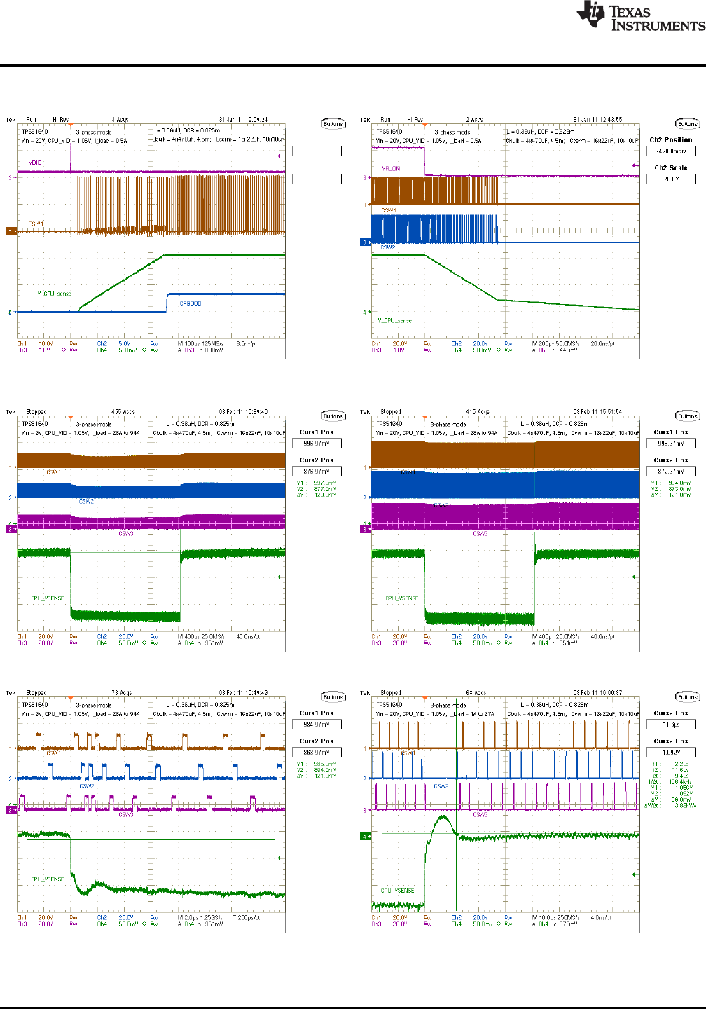
Figure 7. Start-Up and PGOOD Figure 8. Soft-Stop
(TPS51640A and TPS59640 Only)
Figure 9. Load Transient, VIN = 9 V, Load step = 66 A Figure 10. Load Transient, VIN = 20 V, Load step = 66 A
Figure 11. Load Insertion, VIN = 9 V, Load step = 66 A Figure 12. Load Release, VIN = 20 V, Load step = 66 A
14 Submit Documentation Feedback Copyright ©2012, Texas Instruments Incorporated
100 1000 10000 100000 1000000
−50
−40
−30
−20
−10
0
10
20
30
40
50
−225
−180
−135
−90
−45
0
45
90
135
180
225
Frequency (Hz)
Magnitude (dB)
Phase (°)
Gain
Phase
3−Phase CPU
VOUT = 1.05 V
IOUT ~ 20 A
0.0005
0.001
0.0015
0.002
0.0025
0.003
0.0035
0.004
0.0045
-80
-60
-40
-20
0
20
40
60
80
100 1 k 10 k 100 k 1 M
Frequency (Hz)
ZOUTMagnitude (W)
ZOUTPhase (°)
Magnitude
Target
Phase
CPU
3-Phase
TPS51640A, TPS59640, TPS59641
www.ti.com
SLUSAQ2 –JANUARY 2012
TYPICAL CHARACTERISTICS
3-Phase Configuration, 94-A CPU (continued)
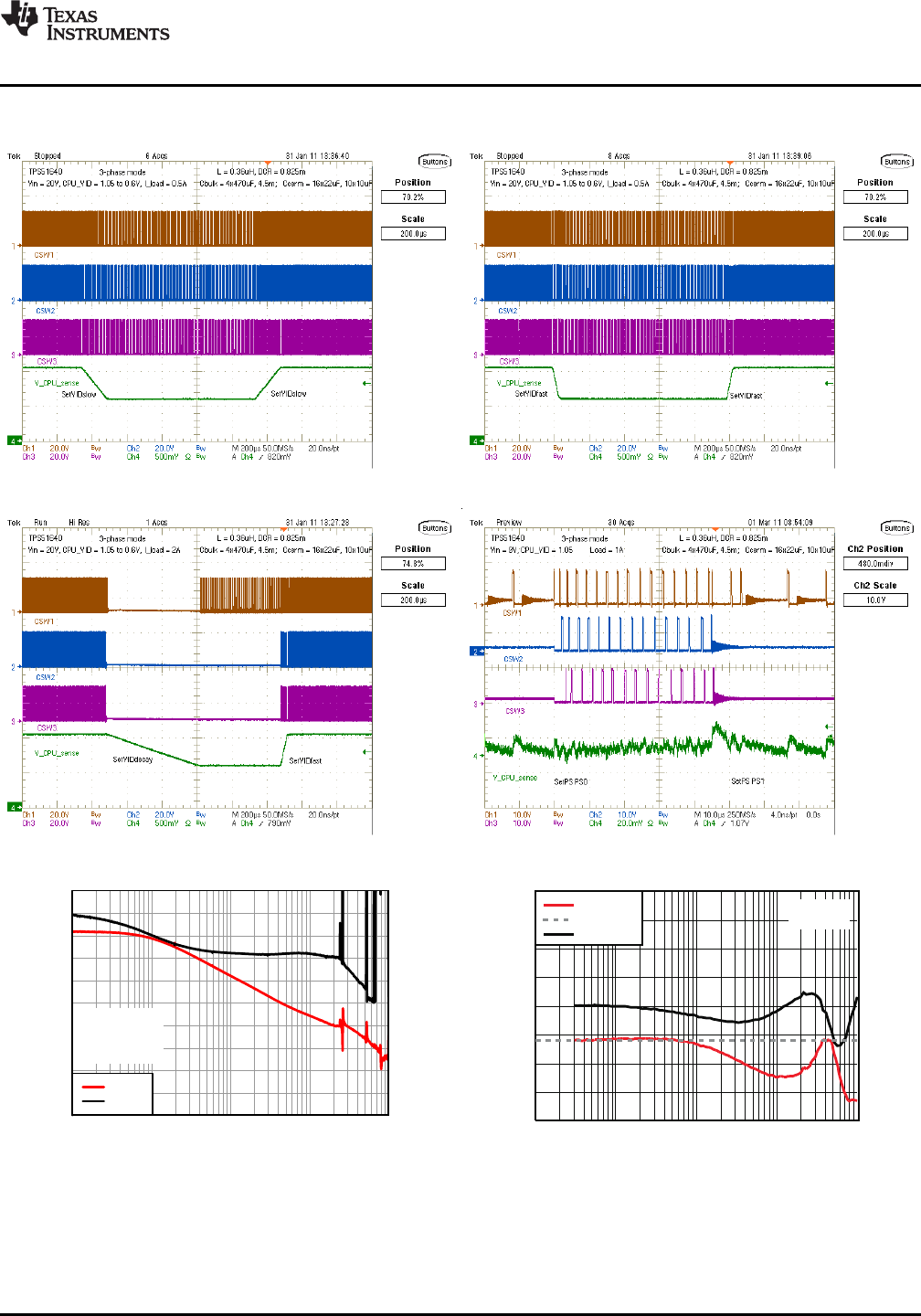
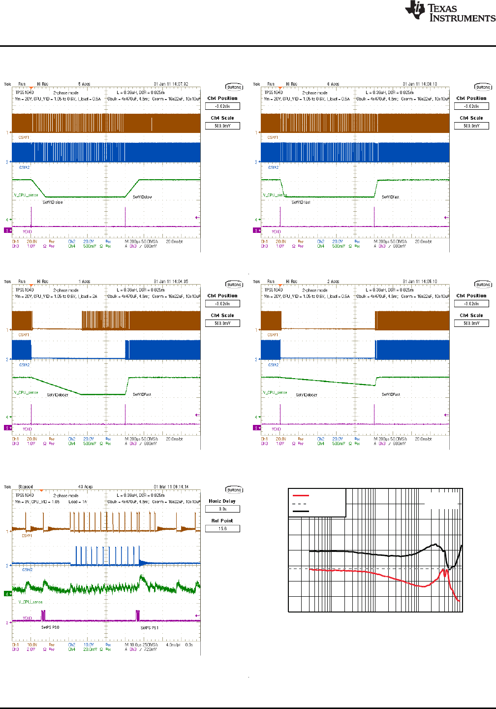
Figure 13. Dynamic VID: SetVID-Slow/SetVID-Slow Figure 14. Dynamic VID: SetVID-Fast/SetVID-Fast
Figure 15. SetVID-Decay/SetVID-Fast Figure 16. PS Change PS0 to PS1 Toggle
Figure 17. CPU Bode Plot Figure 18. Output Impedance
Copyright ©2012, Texas Instruments Incorporated Submit Documentation Feedback 15
0.80
0.85
0.90
0.95
1.00
1.05
1.10
Output Voltage (V)
0 10 20
Output Current (A)
30 40 50 60
VVID = 1.05 V
VIN = 9 V
VIN = 20 V
Nominal
Specified Maximum
Specified Minimum
65
75
80
85
90
95
Efficiency (%)
70
0 5 10 50 55
Output Current (A)
15 20 25 40 4535
VIN = 9 V
VIN = 20 V
VVID = 1.05 V
30
TPS51640A, TPS59640, TPS59641
SLUSAQ2 –JANUARY 2012
www.ti.com
TYPICAL CHARACTERISTICS
2-Phase Configuration, 53-A CPU
Figure 19. Output Voltage Vs. Load Current in PS0 Figure 20. Efficiency Vs. Load Current in PS0
Figure 21. Switching Ripple in PS0 (Persistence), Figure 22. Switching Ripple in PS0 (Persistence),
VIN = 9 V VIN = 20 V
Figure 23. Switching Ripple in PS0, VIN = 9 V Figure 24. Switching Ripple in PS0, VIN = 20 V
16 Submit Documentation Feedback Copyright ©2012, Texas Instruments Incorporated
TPS51640A, TPS59640, TPS59641
www.ti.com
SLUSAQ2 –JANUARY 2012
TYPICAL CHARACTERISTICS
2-Phase Configuration, 53-A CPU (continued)
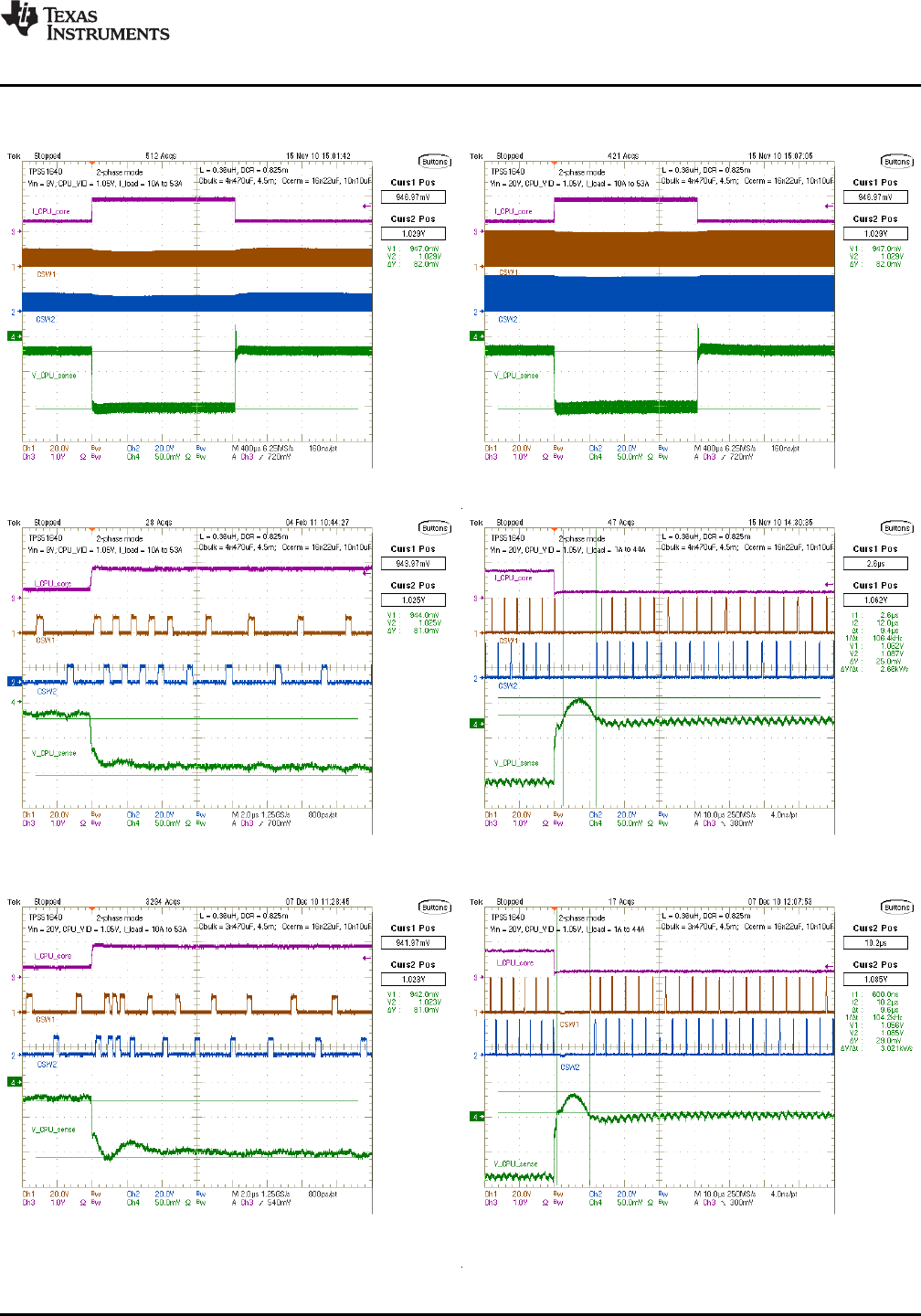
Figure 25. Load Transient, VIN = 9 V, Load Step = 43 A Figure 26. Load Transient, VIN = 20 V, Load Step = 43 A
Figure 27. Load Insertion, VIN = 9 V, Load Step = 43 A, Figure 28. Load Release, VIN = 20 V, Load Step = 43 A,
OSR/USR Setting 150 kΩ) OSR/USR Setting 150 kΩ)
Figure 29. Load Insertion, VIN = 9 V, Load Step = 43 A, Figure 30. Load Release,VIN = 20 V, Load Step = 43 A,
OSR/USR Setting 39 kΩ(Reduced Output Capacitance) OSR/USR Setting 39 kΩ(Reduced Output Capacitance)
Copyright ©2012, Texas Instruments Incorporated Submit Documentation Feedback 17
0.0005
0.001
0.0015
0.002
0.0025
0.003
0.0035
0.004
0.0045
-80
-60
-40
-20
0
20
40
60
80
100 1 k 10 k 100 k 1 M
Frequency (Hz)
ZOUTMagnitude (W)
ZOUTPhase (°)
Magnitude
Target
Phase
CPU
2-Phase
TPS51640A, TPS59640, TPS59641
SLUSAQ2 –JANUARY 2012
www.ti.com
TYPICAL CHARACTERISTICS
2-Phase Configuration, 53-A CPU (continued)
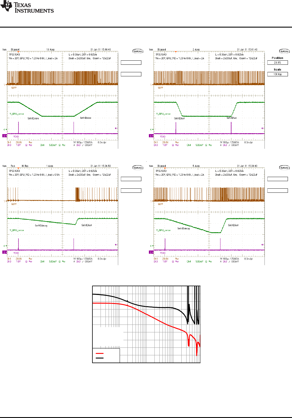
Figure 31. Dynamic VID: SetVID-Slow/SetVID-Slow Figure 32. Dynamic VID: SetVID-Fast/SetVID-Fast
Figure 33. Dynamic VID: SetVID-Decay/SetVID-Fast, Figure 34. Dynamic VID: SetVID-Decay/SetVID-Fast,
ILOAD = 2 A ILOAD = 0.5 A
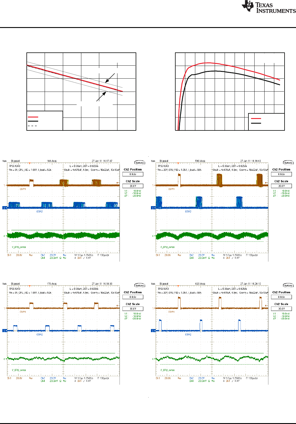
Figure 35. PS Change PS0 to PS1 Toggle Figure 36. Output Impedance
18 Submit Documentation Feedback Copyright ©2012, Texas Instruments Incorporated
1.050
1.100
1.125
1.150
1.175
1.200
1.250
Output Voltage (V)
0 5 10
Output Current (A)
20 25 30 35
VVID = 1.23 V
VIN = 9 V
VIN = 20 V
Nominal
Specified Maximum
Specified Minimum
15
1.225
1.075
0.500
0.525
0.575
0.600
0.625
0 2 4 18 20
Output Current (A)
Output Voltage (V)
6 8 10 14 1612
0.550
0.650
VIN = 9 V
VIN = 20 V
Nominal
Specified Maximum
Specified Minimum
VVID = 0.6 V
75
80
85
90
95
Efficiency (%)
70
VIN = 9 V
VIN = 20 V
VVID = 1.23 V
0 5 10
Output Current (A)
20 25 30 3515
55
70
75
85
90
95
Efficiency (%)
60
0 2 4 18 20
Output Current (A)
6 8 10 14 1612
VIN = 9 V
VIN = 20 V
VVID = 0.6 V
80
65
0
100
150
200
350
400
Frequency (Hz)
50
0 5 10
Output Current (A)
3515 25 3020
250
300
RGF = 30 kW
PS0, VVID = 1.23 V, VIN = 9 V
PS0, VVID = 1.23 V, VIN = 20 V
PS1, VVID = 0.06 V, VIN = 20 V
PS1, VVID = 0.06 V, VIN = 9 V
TPS51640A, TPS59640, TPS59641
www.ti.com
SLUSAQ2 –JANUARY 2012
TYPICAL CHARACTERISTICS
1-Phase Configuration, 33-A GPU
Figure 37. Output Voltage Vs. Load Current in PS0 Figure 38. Output Voltage Vs. Load Current in PS1
Figure 39. Efficiency Vs. Load Current in PS0 Figure 40. Efficiency Vs. Load Current in PS1
Figure 41. Frequency Vs. Load Current Figure 42. Switching Ripple in PS0
Copyright ©2012, Texas Instruments Incorporated Submit Documentation Feedback 19
TPS51640A, TPS59640, TPS59641
SLUSAQ2 –JANUARY 2012
www.ti.com
TYPICAL CHARACTERISTICS
1-Phase Configuration, 33-A GPU (continued)
Figure 43. Start-Up and PGOOD Figure 44. Soft-Stop
(TPS51640A and TPS59640 Only)
Figure 45. Load Transient, VIN = 9 V, Load Step = 20 A Figure 46. Load Transient, VIN = 20 V, Load Step = 20 A
Figure 47. Load Insertion, VIN = 9V, Load Step = 20 A Figure 48. Load Release, VIN = 20 V, Load Step = 20 A
20 Submit Documentation Feedback Copyright ©2012, Texas Instruments Incorporated
100 1000 10000 100000 1000000
−50
−40
−30
−20
−10
0
10
20
30
40
50
−225
−180
−135
−90
−45
0
45
90
135
180
225
Frequency (Hz)
Magnitude (dB)
Phase (°)
Gain
Phase
GPU
VOUT = 1.05 V
IOUT ~ 10 A
TPS51640A, TPS59640, TPS59641
www.ti.com
SLUSAQ2 –JANUARY 2012
TYPICAL CHARACTERISTICS
1-Phase Configuration, 33-A GPU (continued)
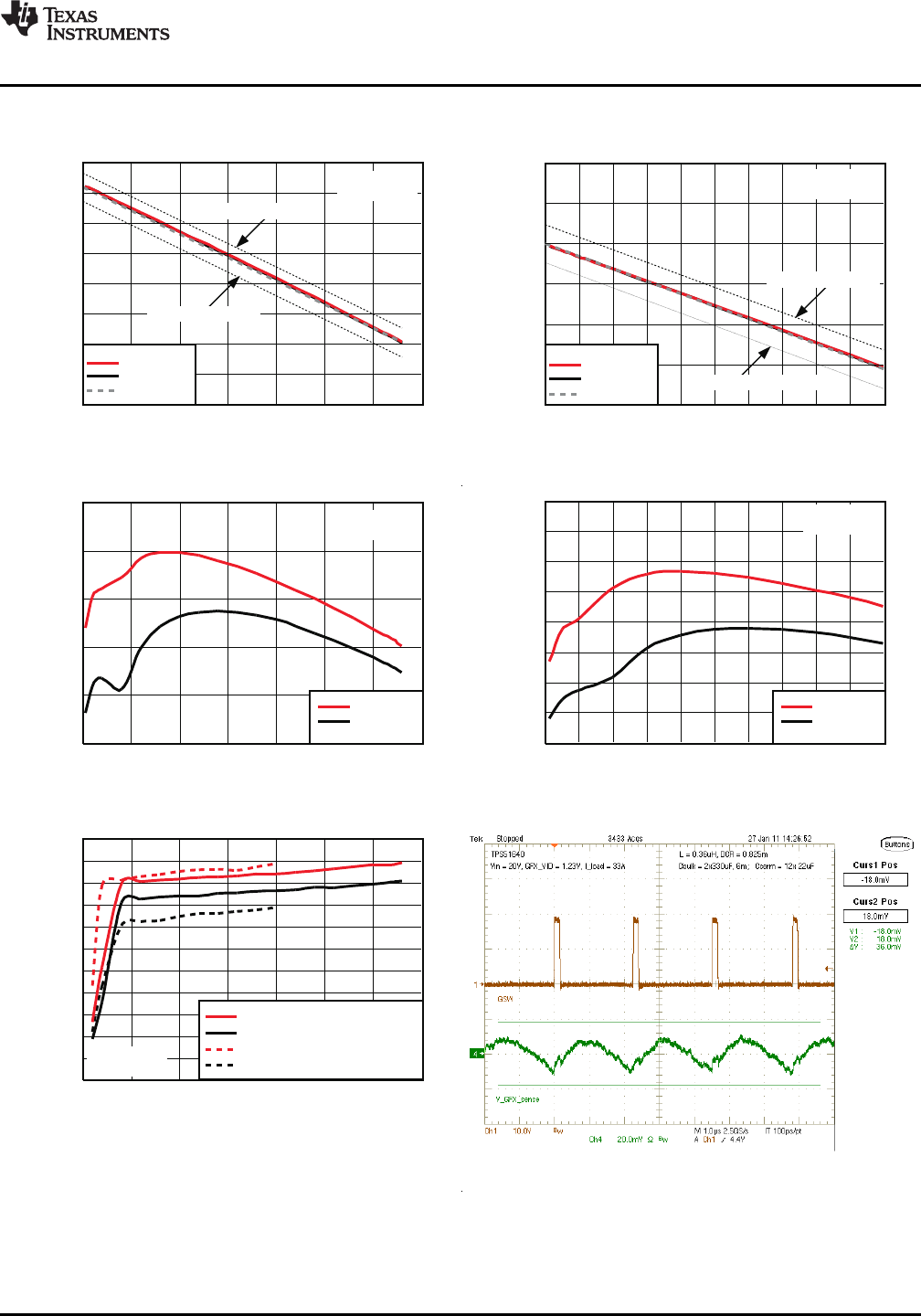
Figure 49. Dynamic VID: SetVID-Slow/SetVID-Slow Figure 50. Dynamic VID: SetVID-Fast/SetVID-Fast
Figure 51. Dynamic VID: SetVID-Decay/SetVID-Fast, Figure 52. Dynamic VID: SetVID-Decay/SetVID-Fast,
ILOAD = 0.5 A ILOAD = 2 A
Figure 53. Bode Plot
Copyright ©2012, Texas Instruments Incorporated Submit Documentation Feedback 21
11CVFB
12CGFB
4CCSP1
5CCSN1
6CCSP2
7CCSN2
14VREF
16VR_ON
17CPGOOD
18VCLK
19ALERT
20VDIO
21VR_HOT
23GPGOOD
22
SLEWA
3
CIMON
30
GIMON
1
CTHERM
32
GTHERM
2
COCP-I
31
GOCP-I
13
CF-IMAX
24
GF-IMAX
26
GVFB
25
GGFB
29
GCSP
28
GCSN
27
GCOM P
+
+
DAC0
+
+
Acs
Acs
8CCSP3
9CCSN3
+Acs
?
Current
Sharing
Circuitry
Gm
A
10
CCOMP
Ramp
Comparator
SVID
Interface
DAC0
and
DAC1
OSR/USR
Phase
Manager
CPWM1
CPWM2
CPWM3
+
+
On-Time
1
On-Time
2
On-Time
3
CF-IMAX
ISHARE
CLK
CLK1
CLK2
CLK3
CPU
Logic Protection
and Status Circuitry
GPU
Logic Protection
and Status Circuitry
COCP
CPx
CVD
ISUM
IS1
IS2
IS3
+
+Gm
AGVD
DAC1
+Acs
+
+
CLK
Smart
Driver
Smart
Driver
Error
Amplifier
Integrator
Error
Amplifier
Integrator
On-Time
GOCP
GPx
GVD
1GFx
Ramp
Comparator
43 V5DRV
46 CBST1
47 CDH1
42 PGND
39 CBST2
38 CDH2
45 CSW1
44 CDL1
40 CSW2
41 CDL2
36 CPWM3
35 CSKIP
33 GSKIP
34 GPWM
VBAT
GF-IMAX
DAC0
DAC1
IS3
IS2
IS1
+
+
+
Pad
GND
15
V3R3
48
V5
GPWM
USR
OSR
UDG-11271
TPS51640A, TPS59640, TPS59641
SLUSAQ2 –JANUARY 2012
www.ti.com
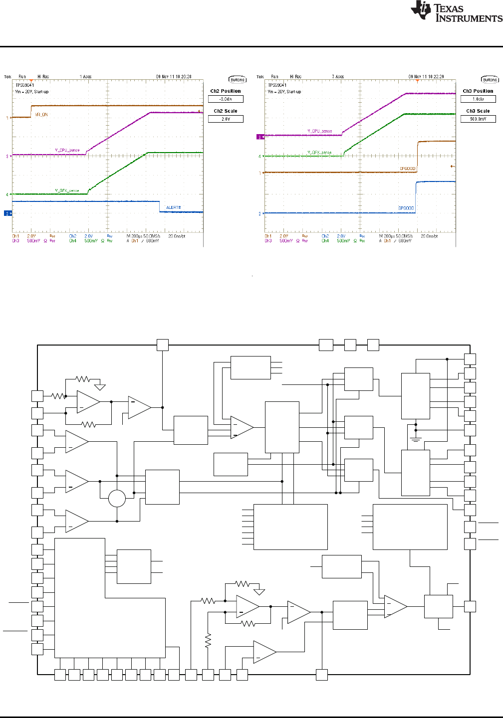
TYPICAL CHARACTERISTICS (TPS59641 ONLY)
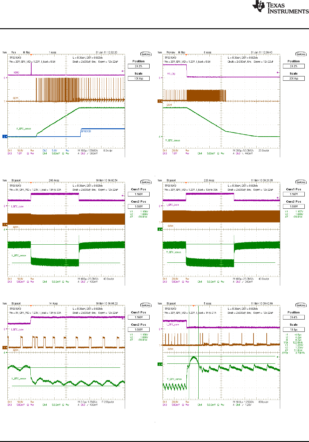
Figure 54. Startup to VBOOT Voltage and ALERT Figure 55. Startup to VBOOT Voltage and CPGOOD,
GPGOOD
FUNCTIONAL BLOCK DIAGRAM
22 Submit Documentation Feedback Copyright ©2012, Texas Instruments Incorporated
CPU_VSNS
CCSP3
CCSP2
CCSN1
CCSP1
COCP-I
GFX_VSNS
GSCP
GIMON
V5
GIMON
VREF
GPGOOD
VDIO
ALERT
CPGOOD
VR_ON
GPWM
VCLK
VREF
VREF
COCP-I
VBAT
CSKIP
SVID:ALERT
SVID:CLK
VIN
CCSP2
CCSN
1
3R3V
VREF
VR_HOT
VCLK
VREF
CPU_GSNS
VREF
CCSN2
CCSN3
GSKIP
CIMON
VDIO
CPWM3
CIMON
VREF
SVID:DATA
VIN
CCSN2
CCSP1
GFX_GSNS
GSCN
GOCP-I
V5DRV
+
ALERT
V5DRV
V5
I_TDC = 21.5A
I_TDC = 52A
GOCP- I
VREF
VREF
To CPU SVID
Loadline = 1.9mohm
Frequency setting= 300kHz
I_cc_max = 33A
I_CC_max = 94A
I_DYN_max = 66A
2
1
VCC_CORE
VREF
VCCIO VCCIO
GFX: GT2
CPU: QC
Min. Over Current Limit= 112A
2
1
Loadline = 3.9mohm
Frequency setting= 385kHz
I_DYNAMIC= 20.2A
Note:
VR_HOT, CPGOOD and GPGOOD are open drain outputs
.
If used, they would need pull
-up resistors
.
Min. Over Current Limit= 37A
TPS51640A, TPS59640, TPS59641
www.ti.com
SLUSAQ2 –JANUARY 2012
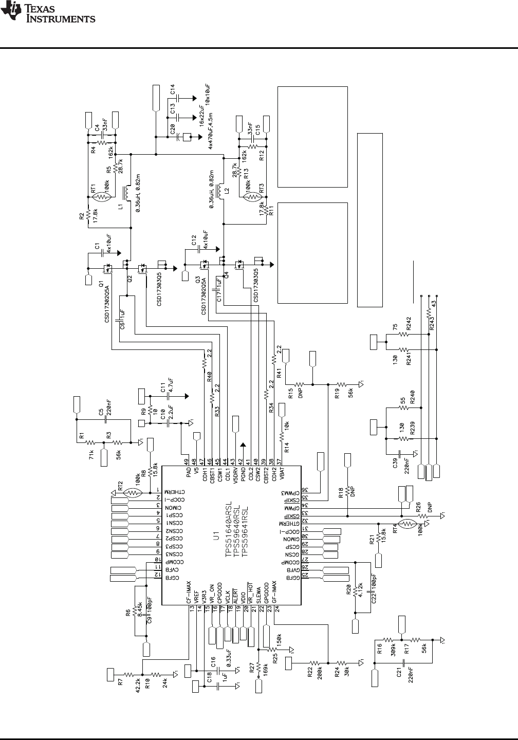
APPLICATION INFORMATION
Figure 56. Application for 3-Phase CPU, 1-Phase GPU with Inductor DCR Current Sense (Controller with
2 internal drivers, 1st and 2nd Phase CPU Power)
Copyright ©2012, Texas Instruments Incorporated Submit Documentation Feedback 23
GSKIP
GPWM V5
GCSN
VIN
+
GCSP
21 VGFX_CORE
CSKIP
CPWM3 V5
VCC_CORE
GCSN
VIN
21
GCSP
+
TPS51640A, TPS59640, TPS59641
SLUSAQ2 –JANUARY 2012
www.ti.com
Figure 57. Application for 3-Phase CPU, 1-Phase GPU with Inductor DCR Current Sense continued
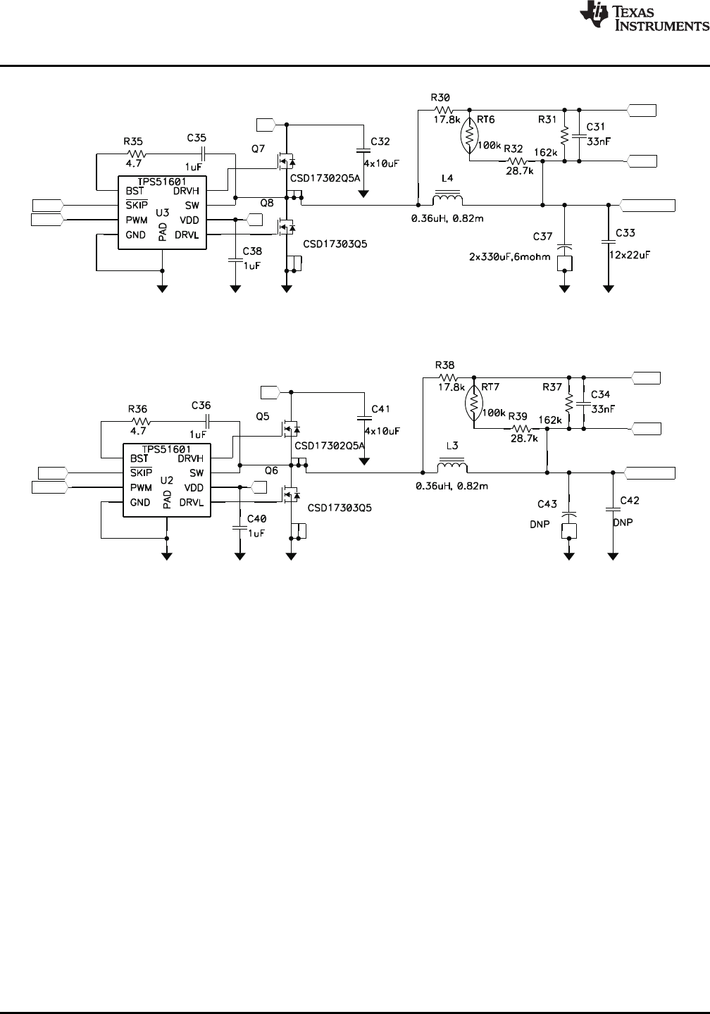
(External driver, 3rd Phase CPU Power)
Figure 58. Application for 3-Phase CPU, 1-Phase GPU with Inductor DCR Current Sense continued
(External driver, GPU Power)
24 Submit Documentation Feedback Copyright ©2012, Texas Instruments Incorporated
CPU_VSNS
C CSP2
CC SN1
C CSP1
COCP-I
V5
VREF
VDIO
ALERT
CPGOOD
VR_ON
VCLK
VREF
COCP-I
VBAT
SVID:ALERT
SVID:CLK
VIN
CCSP2
CCSN1
3R3V
VREF
VR_HOT
VCLK
VREF
3R3V
CPU_GSNS
VREF
CC SN2
3R3V
C IMO N
VDIO
CIMON
VREF
SVID:DATA
VIN
CCSN
2
CCSP1
V5DRV
+
ALERT
V5DRV
V5
I_TDC = 36A
To CPU SVID
Loadline = 1.9mohm
Frequency setting = 300kHz
I_CC_max = 53A
I_DYN_max = 43A
2
1
VCC_CORE
VREF
VCCIO VCCIO
CPU: SV
Note:
VR_HOT and CPGOOD are open drain outputs
.
If used, they would need pull
-up resistors.
Min. Over Current Limit = 65A
2
1
GFX: External. GPU Not used
Note:
R19 = 39k (OSR/USR)
if 3x470uF bulk is used
TPS51640A, TPS59640, TPS59641
www.ti.com
SLUSAQ2 –JANUARY 2012
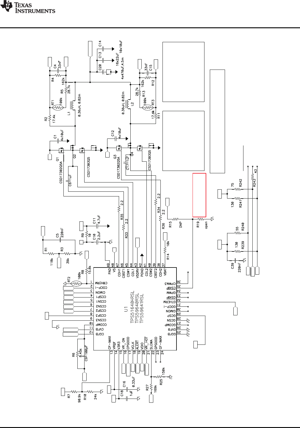
Figure 59. Application for Inductor DCR Current Sense Application Diagram for 2-Phase CPU and GPU
Disabled
Copyright ©2012, Texas Instruments Incorporated Submit Documentation Feedback 25
TPS51640A, TPS59640, TPS59641
SLUSAQ2 –JANUARY 2012
www.ti.com
Table 1. Key External Component Recommendations
FUNCTION MANUFACTURER COMPONENT NUMBER
High-side MOSFET Texas Instruments CSD17302Q5A
Low-side MOSFET Texas Instruments CSD17303Q5
Powerblock MOSFET Texas Instruments CSD87350Q5D
Panasonic ETQP4LR36AFC
MPCH1040LR36,
NEC-Tokin MPCG1040LR36
Inductors FDUE1040J-H-R36,
TOKO FCUL1040xxR36
ALPS GLMDR3601A
Panasonic EEFLXOD471R4
Bulk Output Capacitors Sanyo 2TPLF470M4E
KEMET T528Z477M2R5AT
Murata GRM21BR60J106KE19L
Murata GRM21BR60J226ME39L
Ceramic Output Capacitors Panasonic ECJ2FB0J106K
Panasonic ECJ2FB0J226K
NCP15WF104F03RC,
Murata NCP18WF104F03RC
NTC Thermistors
Panasonic ERTJ1VS104F, ERTJ0ES104F
Vishay WSK0612L7500FEA
Sense Resistors Stackpole CSSK0612FTL750
DETAILED DESCRIPTION
Functional Overview
The TPS51640A, TPS59640, and TPS59641 are a DCAP+™mode adaptive on-time controllers.
The output voltage is set using a DAC that outputs a reference in accordance with the 8-bit VID code defined in
Intel IMVP-7 PWM Specification document. In adaptive on-time converters, the controller varies the on-time as a
function of input and output voltage to maintain a nearly constant frequency during steady-state conditions. In
conventional voltage-mode constant on-time converters, each cycle begins when the output voltage crosses to a
fixed reference level. However, in these devices, the cycle begins when the current feedback reaches an error
voltage level which corresponds to the amplified difference between the DAC voltage and the feedback output
voltage. In the case of two-phase or three-phase operation, the current feedback from all the phases is summed
up at the output of the internal current-sense amplifiers.
This approach has two advantages:
•The amplifier DC gain sets an accurate linear load-line; this is required for CPU core applications.
•The error voltage input to the PWM comparator is filtered to improve the noise performance.
In addition, the difference of the DAC-to-output voltage and the current feedback goes through an integrator to
give a more or less linear load-line even at light loads where the inductor current is in discontinuous conduction
mode (DCM).
In a steady-state condition, the phases of the TPS51640A, TPS59640, and TPS59641 switch 180°
phase-displacement for two-phase mode and 120°phase-displacement for three-phase mode. The phase
displacement is maintained both by the architecture (which does not allow both high-side gate drives to be on in
any condition except transients) and the current ripple (which forces the pulses to be spaced equally). The
controller forces current sharing adjusting the on-time of each phase. Current balancing requires no user
intervention, compensation, or extra components.
26 Submit Documentation Feedback Copyright ©2012, Texas Instruments Incorporated
TPS51640A, TPS59640, TPS59641
www.ti.com
SLUSAQ2 –JANUARY 2012
User Selections
After the 5-V and the 3.3-V power are applied to the controller, the controller must be enabled by the VR_ON
signal going high to the VCCIO logic level. At this time, the following information is latched and cannot be
changed anytime during operation. The ELECTRICAL CHARACTERISTICS table defines the values of each of
the selections.
•Operating Frequency. The resistor from CF-IMAX pin to GND sets the frequency of the CPU channel. The
resistor from GF-IMAX to GND sets the frequency of the GPU channel. See the ELECTRICAL
CHARACTERISTICS table for the resistor settings corresponding to each frequency selection. It is to be
noted that the operating frequency is a quasi-fixed frequency in the sense that the ON time is fixed based on
the input voltage (at the VBAT pin) and output voltage (set by VID). The OFF time varies based on various
factors such as load and power-stage components.
•Maximum Current Limit (ICC(max)) Information. The ICC(max) information of the CPU, which can be set by the
voltage on the CF-IMAX pin. The ICC(max) information of the GPU channel, which can be set by the voltage on
the GF-IMAX pin.
•Overcurrent Protection (OCP) Level. The resistor from COCP-I to GND sets the OCP level of the CPU
channel. The resistor from GOCP-I to GND sets the OCP level of the GPU channel.
•Current Monitor (IMON) Gain and Voltage. The resistor from CIMON to COCP-I sets the CIMON gain and
the CIMON voltage for the CPU channel. The resistor from GIMON to GOCP-I sets the GIMON gain and the
GIMON voltage for the GPU channel.
•Overshoot Reduction (OSR) and Undershoot Reduction (USR) Levels. The resistor from the CSKIP pin
to GND sets the OSR and USR for the CPU channel. The resistor from the GSKIP pin to GND sets the OSR
and USR level for GPU channel. The OSR can be disabled for CPU and/or GPU by setting a voltage of
approximately 200 mV on the corresponding xSKIP pin. This is accomplished by connecting a resistor from
VREF to the xSKIP pin.
•Slew Rate. The SetVID-Fast slew rate is set by the voltage on the SLEWA pin. The rate is the same for both
the CPU and GPU channels. The SetVID-Slow is ¼of the SetVID-Fast rate.
Table 2. Key Selections Summary(1)
SELECTION FREQUENCY OCP OSR / USR
RESISTANCE (kΩ)
Least overshoot,
20 Lowest Lowest least undershoot
24
30
39 Rising Rising Rising
56
75
100
Maximum overshoot,
150 Highest Highest maximum undershoot
(1) See ELECTRICAL CHARACTERISTICS table for complete settings and values.
Table 3. Active Channels and Phases
CCSP1 CCSN1 CCSP2 CCSN2 CCSP3 CCSN3 GCSP CGSN
3CS CS CS CS CS CS n/a n/a
2CS CS CS CS 3.3 V GND n/a n/a
CPU
(Active Phases) 1CS CS 3.3 V GND GND GND n/a n/a
OFF 3.3 V GND GND GND GND GND n/a n/a
1n/a n/a n/a n/a n/a n/a CS CS
GPU
(Active Phases) OFF n/a n/a n/a n/a n/a n/a 3.3 V GND
Copyright ©2012, Texas Instruments Incorporated Submit Documentation Feedback 27
SW_CLK
VCOMP
Phase 1
Phase 2
Phase 3
ISUM
VCORE
Time
UDG-11031
TPS51640A, TPS59640, TPS59641
SLUSAQ2 –JANUARY 2012
www.ti.com
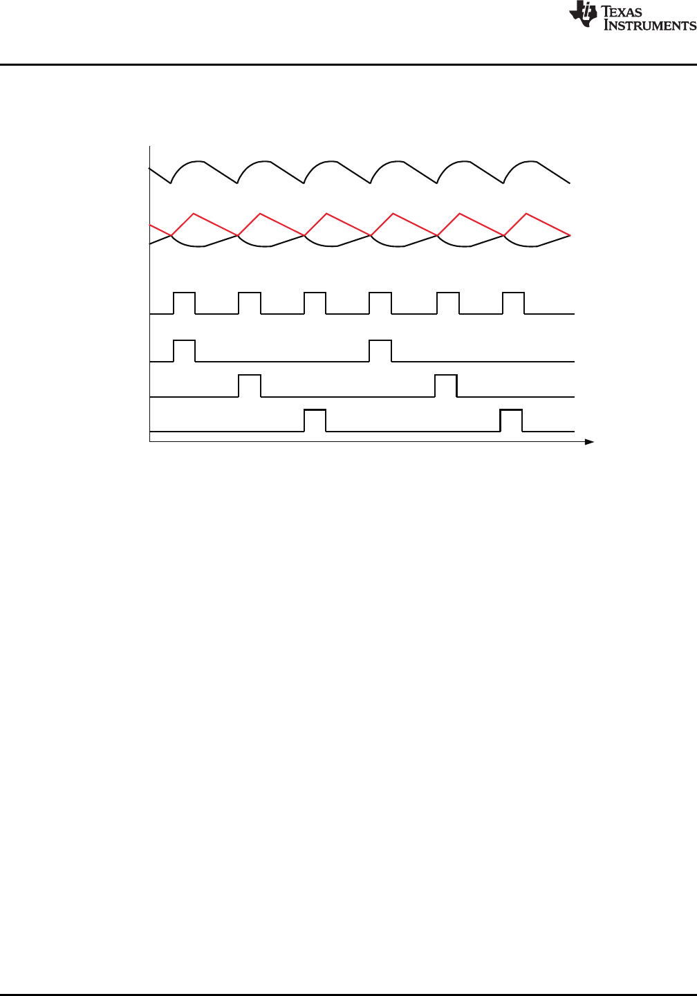
PWM Operation
Referring to the FUNCTIONAL BLOCK DIAGRAM and Figure 60, in continuous conduction mode, the converter
operates as shown in Figure 60.
Figure 60. D-CAP+ Mode Basic Waveforms
Starting with the condition that the hig-side FETs are off and the low-side FETs are on, the summed current
feedback (ISUM) is higher than the error amplifier output (VCOMP). ISUM falls until it reaches the VCOMP level, which
contains a component of the output ripple voltage. The PWM comparator senses where the two waveform values
cross and triggers the on-time generator. This generates the internal SW_CLK. Each SW_CLK corresponds to
one switching ON pulse for one phase.
During single-phase operation, every SW_CLK generates a switching pulse on the same phase. Also, ISUM
voltage corresponds to just a single-phase inductor current.
During multi-phase operation, the SW_CLK is distributed to each of the phases in a cycle. Using the summed
inductor current and then cyclically distributing the ON-pulses to each phase automatically yields the required
interleaving of 360/N, where N is the number of phases.
Current Sensing
The TPS51640A, TPS59640 and TPS59641 provide independent channels of current feedback for every phase.
This increases the system accuracy and reduces the dependence of circuit performance on layout compared to
an externally summed architecture. The current sensing topology can be Inductor DCR Sensing, which yields the
best efficiency, or Resistor Current Sensing, which provides the most accuracy across wide temperature range.
DCR sensing can be optimized by using a NTC thermistor to reduce the variation of current sense with
temperature.
The pins CCSP1, CCSN1, CCSP2, CCSN2 and CCSP3, CCSN3 are used for the three phases of the CPU
channel. The pins GCSP and GCSN are used for the single-phase GPU channel.
28 Submit Documentation Feedback Copyright ©2012, Texas Instruments Incorporated
VDROOP
VVID
VDROOP = RLL x ICC
Slope of Loadline RLL
ICC
UDG-11032
( )´ ´
= ´ = ´
CS CC
CS eff
DROOP LL CC
DROOP M
R A I
V R I R G
TPS51640A, TPS59640, TPS59641
www.ti.com
SLUSAQ2 –JANUARY 2012
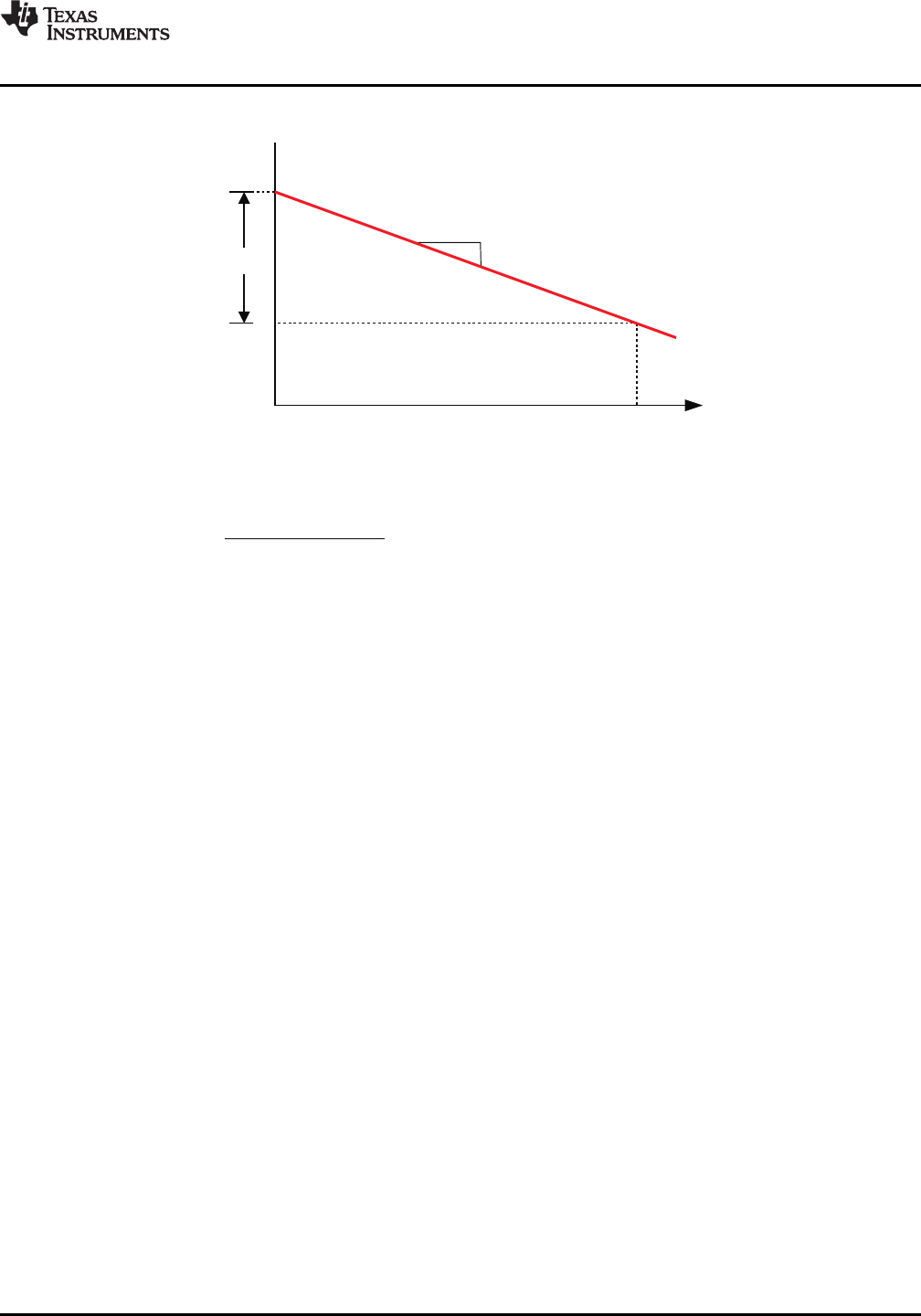
Setting the Load-line (DROOP)
Figure 61. Load Line
where
•ACS is the gain of the current sense amplifier
•RCS(eff) is the effective current sense resistance, whether a sense resistor or inductor DCR is used
•ICC is the load current
•RDROOP is the value of resistor from the DROOP pin to VREF
•GMis the gain of the droop amplifier (1)
Load Transients
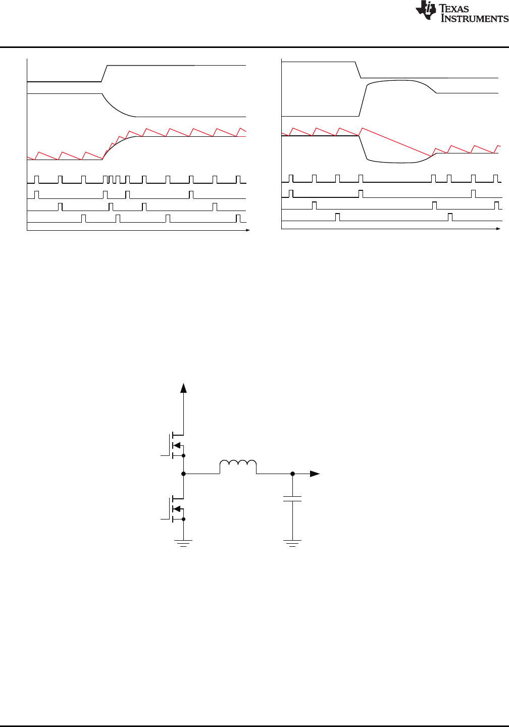
When there is a sudden load increase, the output voltage immediately drops. This is reflected as a rising voltage
on the COMP pin. This forces the PWM pulses to come in sooner and more frequent which causes the inductor
current to rapidly increase. As the inductor current reaches the new load current, a steady-state operating
condition is reached and the PWM switching resumes the steady-state frequency.
When there is a sudden load release, the output voltage rises. This is reflected as a falling voltage on the COMP
pin. This delays the PWM pulses until the inductor current reaches the new load current level. At that point,
switching resumes and steady-state switching continues.
For simplicity, neither Figure 62, nor Figure 63 show the ripple on the Output VCORE nor the COMP waveform.
Copyright ©2012, Texas Instruments Incorporated Submit Documentation Feedback 29
LOAD
VCORE
ISUM
COMP
SW_CLK
Phase 1
Phase 2
Phase 3
UDG-11034
LOAD
VCORE
ISUM
COMP
SW_CLK
Phase 1
Phase 2
Phase 3
Time
UDG-11033
UDG-11035
+ 10.8 V –
12 V
L
– 1.2 V +
1.2 V
C
TPS51640A, TPS59640, TPS59641
SLUSAQ2 –JANUARY 2012
www.ti.com
Figure 62. Operating Waveforms During Load Figure 63. needs a title
Transient
Overshoot Reduction (OSR)
In low duty-cycle synchronous buck converters, an overshoot condition results from the output inductor having a
too little voltage (VCORE) with which to respond to a transient load release.
In Figure 64, a single phase converter is shown for simplicity. In an ideal converter, with typical input voltage of
12 V and 1.2-V output, the inductor has 10.8 V (12 V –1.2 V) to respond to a transient load increase, but only
1.2 V with which to respond once the load releases.
Figure 64. Synchronous Converter
When the overshoot reduction feature is enabled, the output voltage increases beyond a value that corresponds
to a voltage difference between the ISUM voltage and the COMP voltage, exceeding the specified OSR voltage
specified in the ELECTRICAL CHARACTERISTICS. At that instant, the low-side drivers are turned OFF. When
the low-side driver is turned OFF, the energy in the inductor is partially dissipated by the body diodes. As the
overshoot reduces, the low-side drivers are turned ON again.
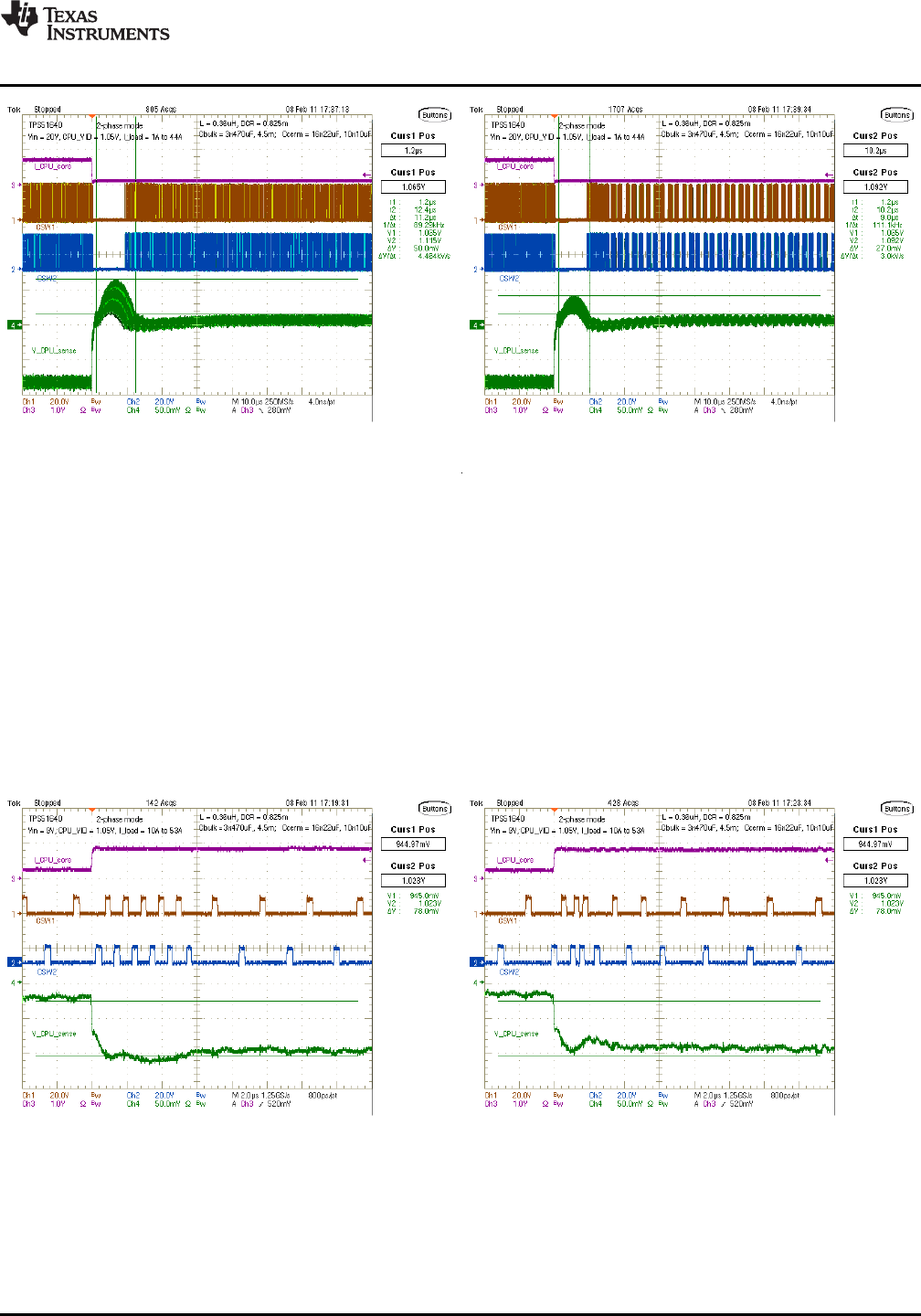
Figure 65 shows the overshoot without OSR. Figure 66 shows the overshoot with OSR. The overshoot reduces
by approximately 23 mV. This shows that reduced output capacitance can be used while continuing to meet the
specification. Note the low-side driver turning OFF briefly during the overshoot.
30 Submit Documentation Feedback Copyright ©2012, Texas Instruments Incorporated
TPS51640A, TPS59640, TPS59641
www.ti.com
SLUSAQ2 –JANUARY 2012
Figure 65. 43-A Load Transient Release Without Figure 66. 43-A Load Transient Release With OSR
OSR Enabled. Enabled
Undershoot Reduction (USR)
When the transient load increase becomes quite large, it becomes difficult to meet the energy demanded by the
load especially at lower input voltages. Then it is necessary to quickly increase the energy tin the inductors
during the transient load increase. This is achieved in these devices by enabling pulse overlapping. In order to
maintain the interleaving of the multi-phase configuration and yet be able to have pulse-overlapping during
load-insertion, the undershoot reduction (USR) mode is entered only when necessary. This mode is entered
when the difference between COMP voltage and ISUM voltage exceeds the USR voltage level specified in the
ELECTRICAL CHARACTERISTICS table.
Figure 67 shows the performance with undershoot reduction. Figure 68 shows the performance without
undershoot reduction and that it is possible to eliminate undershoot by enabling the undershoot reduction. This
allows reduced output capacitance to be used and still meet the specification.
When the transient condition is over, the interleaving of the phases is resumed. For Figure 67, note the
overlapping pulses for Phase 1 and Phase 2 with USR enabled.
Figure 67. Performance for a 43-A Load Transient Figure 68. Performance for a 43-A Load Transient
Release Without USR Enabled Release With USR Enabled
A single-phase GPU operates in a similar way, but instead of pulse-overlap in multi-phase CPU, there is pulse
stretching to provide the needs of the transient load increase when USR is enabled.
Copyright ©2012, Texas Instruments Incorporated Submit Documentation Feedback 31
+
37VBAT
4CCSP1
5CCSN1 Current
Amplifier
5ms
Filter
IAVG
+
VDAC RT(on)
CT(on)
PWM1
+
K x (I1-IAVG)
+
7CCSP2
6CCSN2 Current
Amplifier
5ms
Filter
IAVG
+
VDAC
RT(on)
CT(on)
PWM2
+
K x (I2-IAVG)
Averaging
Circuit IAVG
+
8CCSP3
9CCSN3 Current
Amplifier
5ms
Filter
IAVG
+
VDAC
RT(on)
CT(on)
PWM3
+
K x (I3-IAVG)
UDG-11036
TPS51640A, TPS59640, TPS59641
SLUSAQ2 –JANUARY 2012
www.ti.com
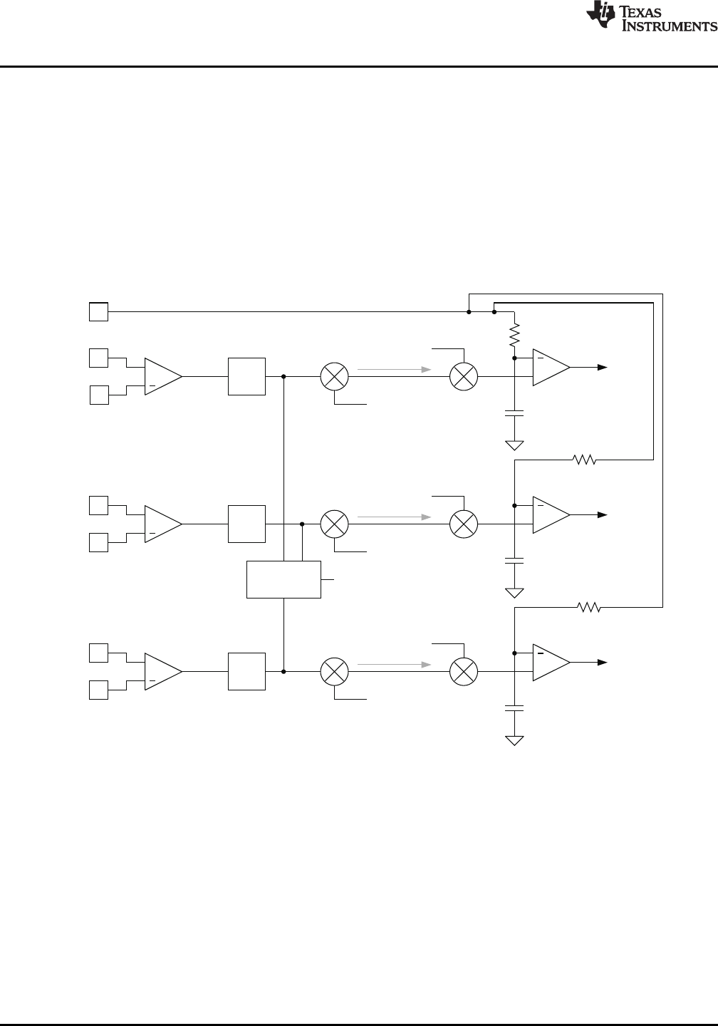
AutoBalance™Current Sharing
The basic mechanism for current sharing is to sense the average phase current, then adjust the pulse width of
each phase to equalize the current in each phase. (See Figure 69.)
The PWM comparator (not shown) starts a pulse when the feedback voltage meets the reference. The VBAT
voltage charges Ct(ON) through Rt(ON). The pulse is terminated when the voltage at Ct(ON) matches the t(ON)
reference, normally the DAC voltage (VDAC).
The circuit operates in the following fashion, using Figure 69 as the block diagram. First assume that the 5-µs
averaged value of I1 = I2 = I3. In this case, the PWM modulator terminates at VDAC, and the normal pulse width
is delivered to the system. If instead, I1 >IAVG, then an offset is subtracted from VDAC, and the pulse width for
Phase 1 is shortened, reducing the current in Phase 1 to compensate. If I1 <IAVG, then a longer pulse is
produced, again compensating on a pulse-by-pulse basis.
Figure 69. Schematic Representation of AutoBalance Current Sharing
Dynamic VID and Power-State Changes
In IMVP-7, there are 3 basic types of VID changes:
•SetVID-Fast
•SetVID-Slow
•SetVID-Decay
SetVID-Fast change and a SetVID-Slow change automatically puts the power state in PS0. A SetVID-Decay
change automatically puts the power state in PS2.
32 Submit Documentation Feedback Copyright ©2012, Texas Instruments Incorporated
TPS51640A, TPS59640, TPS59641
www.ti.com
SLUSAQ2 –JANUARY 2012
The CPU operates in the maximum phase mode when it is in PS0. This means when the CPU channel of the
controller is configured as 3-phase, all 3 phases are active in PS0. When configured in 2-phase mode, the two
phases are active in PS0. But in PS1, PS2 and PS3, the operation is in single-phase mode. Additionally, the
CPU channel in PS0 mode operates in forced continuous conduction mode (FCCM). But in PS1, PS2 and PS3,
the CPU channel operates in diode emulation (DE) mode for additional power savings and higher efficiency.
The single-phase GPU section always operates in diode emulation (DE) mode in all PS states.
The slew rate for a SetVID-Fast is the slew rate set at the SLEWA pin. This slew rate is defined in the
ELECTRICAL CHARACTERISTICS table. The SetVID-Slow is ¼of the SetVID-Fast slew rate. On a
SetVID-Decay the output voltage decays by the rate of the load current or 1/8 of the slew rate whichever is
slower.
Additionally, on a SetVID-Fast change for a VID-up transition, the gain of the gMamplifier is increased to speed
up the response of the output voltage to meet the Intel timing requirement. So, it is possible to observe an
overshoot at the output voltage on a VID-up transition. This overshoot is allowed by the Intel specification.
XXX Table 4. VID (continued)
Table 4. VID 0 0 1 0 0 0 0 0 20 0.405
VID VID VID VID VID VID VID VID 0 0 1 0 0 0 0 1 21 0.410
HEX VDAC
76543210 0 0 1 0 0 0 1 0 22 0.415
0 0 0 0 0 0 0 0 00 0.000 0 0 1 0 0 0 1 1 23 0.420
0 0 0 0 0 0 0 1 01 0.250 0 0 1 0 0 1 0 0 24 0.425
0 0 0 0 0 0 1 0 02 0.255 0 0 1 0 0 1 0 1 25 0.430
0 0 0 0 0 0 1 1 03 0.260 0 0 1 0 0 1 1 0 26 0.435
0 0 0 0 0 1 0 0 04 0.265 0 0 1 0 0 1 1 1 27 0.440
0 0 0 0 0 1 0 1 05 0.270 0 0 1 0 1 0 0 0 28 0.445
0 0 0 0 0 1 1 0 06 0.275 0 0 1 0 1 0 0 1 29 0.450
0 0 0 0 0 1 1 1 07 0.280 0 0 1 0 1 0 1 0 2A 0.455
0 0 0 0 1 0 0 0 08 0.285 0 0 1 0 1 0 1 1 2B 0.460
0 0 0 0 1 0 0 1 09 0.290 0 0 1 0 1 1 0 0 2C 0.465
0 0 0 0 1 0 1 0 0A 0.295 0 0 1 0 1 1 0 1 2D 0.470
0 0 0 0 1 0 1 1 0B 0.300 0 0 1 0 1 1 1 0 2E 0.475
0 0 0 0 1 1 0 0 0C 0.305 0 0 1 0 1 1 1 1 2F 0.480
0 0 0 0 1 1 0 1 0D 0.310 0 0 1 1 0 0 0 0 30 0.485
0 0 0 0 1 1 1 0 0E 0.315 0 0 1 1 0 0 0 1 31 0.490
0 0 0 0 1 1 1 1 0F 0.320 0 0 1 1 0 0 1 0 32 0.495
0 0 0 1 0 0 0 0 10 0.325 0 0 1 1 0 0 1 1 33 0.500
0 0 0 1 0 0 0 1 11 0.330 0 0 1 1 0 1 0 0 34 0.505
0 0 0 1 0 0 1 0 12 0.335 0 0 1 1 0 1 0 1 35 0.510
0 0 0 1 0 0 1 1 13 0.340 0 0 1 1 0 1 1 0 36 0.515
0 0 0 1 0 1 0 0 14 0.345 0 0 1 1 0 1 1 1 37 0.520
0 0 0 1 0 1 0 1 15 0.350 0 0 1 1 1 0 0 0 38 0.525
0 0 0 1 0 1 1 0 16 0.355 0 0 1 1 1 0 0 1 39 0.530
0 0 0 1 0 1 1 1 17 0.360 0 0 1 1 1 0 1 0 3A 0.535
0 0 0 1 1 0 0 0 18 0.365 0 0 1 1 1 0 1 1 3B 0.540
0 0 0 1 1 0 0 1 19 0.370 0 0 1 1 1 1 0 0 3C 0.545
0 0 0 1 1 0 1 0 1A 0.375 0 0 1 1 1 1 0 1 3D 0.550
0 0 0 1 1 0 1 1 1B 0.380 0 0 1 1 1 1 1 0 3E 0.555
0 0 0 1 1 1 0 0 1C 0.385 0 0 1 1 1 1 1 1 3F 0.560
0 0 0 1 1 1 0 1 1D 0.390 0 1 0 0 0 0 0 0 40 0.565
0 0 0 1 1 1 1 0 1E 0.395 0 1 0 0 0 0 0 1 41 0.570
0 0 0 1 1 1 1 1 1F 0.400 0 1 0 0 0 0 1 0 42 0.575
Copyright ©2012, Texas Instruments Incorporated Submit Documentation Feedback 33

TPS51640A, TPS59640, TPS59641
SLUSAQ2 –JANUARY 2012
www.ti.com
Table 4. VID (continued) Table 4. VID (continued)
0 1 0 0 0 0 1 1 43 0.580 0 1 1 1 0 0 1 1 73 0.820
0 1 0 0 0 1 0 0 44 0.585 0 1 1 1 0 1 0 0 74 0.825
0 1 0 0 0 1 0 1 45 0.590 0 1 1 1 0 1 0 1 75 0.830
0 1 0 0 0 1 1 0 46 0.595 0 1 1 1 0 1 1 0 76 0.835
0 1 0 0 0 1 1 1 47 0.600 0 1 1 1 0 1 1 1 77 0.840
0 1 0 0 1 0 0 0 48 0.605 0 1 1 1 1 0 0 0 78 0.845
0 1 0 0 1 0 0 1 49 0.610 0 1 1 1 1 0 0 1 79 0.850
0 1 0 0 1 0 1 0 4A 0.615 0 1 1 1 1 0 1 0 7A 0.855
0 1 0 0 1 0 1 1 4B 0.620 0 1 1 1 1 0 1 1 7B 0.860
0 1 0 0 1 1 0 0 4C 0.625 0 1 1 1 1 1 0 0 7C 0.865
0 1 0 0 1 1 0 1 4D 0.630 0 1 1 1 1 1 0 1 7D 0.870
0 1 0 0 1 1 1 0 4E 0.635 0 1 1 1 1 1 1 0 7E 0.875
0 1 0 0 1 1 1 1 4F 0.640 0 1 1 1 1 1 1 1 7F 0.880
0 1 0 1 0 0 0 0 50 0.645 1 0 0 0 0 0 0 0 80 0.885
0 1 0 1 0 0 0 1 51 0.650 1 0 0 0 0 0 0 1 81 0.890
0 1 0 1 0 0 1 0 52 0.655 1 0 0 0 0 0 1 0 82 0.895
0 1 0 1 0 0 1 1 53 0.660 1 0 0 0 0 0 1 1 83 0.900
0 1 0 1 0 1 0 0 54 0.665 1 0 0 0 0 1 0 0 84 0.905
0 1 0 1 0 1 0 1 55 0.670 1 0 0 0 0 1 0 1 85 0.910
0 1 0 1 0 1 1 0 56 0.675 1 0 0 0 0 1 1 0 86 0.915
0 1 0 1 0 1 1 1 57 0.680 1 0 0 0 0 1 1 1 87 0.920
0 1 0 1 1 0 0 0 58 0.685 1 0 0 0 1 0 0 0 88 0.925
0 1 0 1 1 0 0 1 59 0.690 1 0 0 0 1 0 0 1 89 0.930
0 1 0 1 1 0 1 0 5A 0.695 1 0 0 0 1 0 1 0 8A 0.935
0 1 0 1 1 0 1 1 5B 0.700 1 0 0 0 1 0 1 1 8B 0.940
0 1 0 1 1 1 0 0 5C 0.705 1 0 0 0 1 1 0 0 8C 0.945
0 1 0 1 1 1 0 1 5D 0.710 1 0 0 0 1 1 0 1 8D 0.950
0 1 0 1 1 1 1 0 5E 0.715 1 0 0 0 1 1 1 0 8E 0.955
0 1 0 1 1 1 1 1 5F 0.720 1 0 0 0 1 1 1 1 8F 0.960
0 1 1 0 0 0 0 0 60 0.725 1 0 0 1 0 0 0 0 90 0.965
0 1 1 0 0 0 0 1 61 0.730 1 0 0 1 0 0 0 1 91 0.970
0 1 1 0 0 0 1 0 62 0.735 1 0 0 1 0 0 1 0 92 0.975
0 1 1 0 0 0 1 1 63 0.740 1 0 0 1 0 0 1 1 93 0.980
0 1 1 0 0 1 0 0 64 0.745 1 0 0 1 0 1 0 0 94 0.985
0 1 1 0 0 1 0 1 65 0.750 1 0 0 1 0 1 0 1 95 0.990
0 1 1 0 0 1 1 0 66 0.755 1 0 0 1 0 1 1 0 96 0.995
0 1 1 0 0 1 1 1 67 0.760 1 0 0 1 0 1 1 1 97 1.000
0 1 1 0 1 0 0 0 68 0.765 1 0 0 1 1 0 0 0 98 1.005
0 1 1 0 1 0 0 1 69 0.770 1 0 0 1 1 0 0 1 99 1.010
0 1 1 0 1 0 1 0 6A 0.775 1 0 0 1 1 0 1 0 9A 1.015
0 1 1 0 1 0 1 1 6B 0.780 1 0 0 1 1 0 1 1 9B 1.020
0 1 1 0 1 1 0 0 6C 0.785 1 0 0 1 1 1 0 0 9C 1.025
0 1 1 0 1 1 0 1 6D 0.790 1 0 0 1 1 1 0 1 9D 1.030
0 1 1 0 1 1 1 0 6E 0.795 1 0 0 1 1 1 1 0 9E 1.035
0 1 1 0 1 1 1 1 6F 0.800 1 0 0 1 1 1 1 1 9F 1.040
0 1 1 1 0 0 0 0 70 0.805 1 0 1 0 0 0 0 0 A0 1.045
0 1 1 1 0 0 0 1 71 0.810 1 0 1 0 0 0 0 1 A1 1.050
0 1 1 1 0 0 1 0 72 0.815 1 0 1 0 0 0 1 0 A2 1.055
34 Submit Documentation Feedback Copyright ©2012, Texas Instruments Incorporated

TPS51640A, TPS59640, TPS59641
www.ti.com
SLUSAQ2 –JANUARY 2012
Table 4. VID (continued) Table 4. VID (continued)
1 0 1 0 0 0 1 1 A3 1.060 1 1 0 1 0 0 1 1 D3 1.300
1 0 1 0 0 1 0 0 A4 1.065 1 1 0 1 0 1 0 0 D4 1.305
1 0 1 0 0 1 0 1 A5 1.070 1 1 0 1 0 1 0 1 D5 1.310
1 0 1 0 0 1 1 0 A6 1.075 1 1 0 1 0 1 1 0 D6 1.315
1 0 1 0 0 1 1 1 A7 1.080 1 1 0 1 0 1 1 1 D7 1.320
1 0 1 0 1 0 0 0 A8 1.085 1 1 0 1 1 0 0 0 D8 1.325
1 0 1 0 1 0 0 1 A9 1.090 1 1 0 1 1 0 0 1 D9 1.330
1 0 1 0 1 0 1 0 AA 1.095 1 1 0 1 1 0 1 0 DA 1.335
1 0 1 0 1 0 1 1 AB 1.100 1 1 0 1 1 0 1 1 DB 1.340
1 0 1 0 1 1 0 0 AC 1.105 1 1 0 1 1 1 0 0 DC 1.345
1 0 1 0 1 1 0 1 AD 1.110 1 1 0 1 1 1 0 1 DD 1.350
1 0 1 0 1 1 1 0 AE 1.115 1 1 0 1 1 1 1 0 DE 1.355
1 0 1 0 1 1 1 1 AF 1.120 1 1 0 1 1 1 1 1 DF 1.360
1 0 1 1 0 0 0 0 B0 1.125 1 1 1 0 0 0 0 0 E0 1.365
1 0 1 1 0 0 0 1 B1 1.130 1 1 1 0 0 0 0 1 E1 1.370
1 0 1 1 0 0 1 0 B2 1.135 1 1 1 0 0 0 1 0 E2 1.375
1 0 1 1 0 0 1 1 B3 1.140 1 1 1 0 0 0 1 1 E3 1.380
1 0 1 1 0 1 0 0 B4 1.145 1 1 1 0 0 1 0 0 E4 1.385
1 0 1 1 0 1 0 1 B5 1.150 1 1 1 0 0 1 0 1 E5 1.390
1 0 1 1 0 1 1 0 B6 1.155 1 1 1 0 0 1 1 0 E6 1.395
1 0 1 1 0 1 1 1 B7 1.160 1 1 1 0 0 1 1 1 E7 1.400
1 0 1 1 1 0 0 0 B8 1.165 1 1 1 0 1 0 0 0 E8 1.405
1 0 1 1 1 0 0 1 B9 1.170 1 1 1 0 1 0 0 1 E9 1.410
1 0 1 1 1 0 1 0 BA 1.175 1 1 1 0 1 0 1 0 EA 1.415
1 0 1 1 1 0 1 1 BB 1.180 1 1 1 0 1 0 1 1 EB 1.420
1 0 1 1 1 1 0 0 BC 1.185 1 1 1 0 1 1 0 0 EC 1.425
1 0 1 1 1 1 0 1 BD 1.190 1 1 1 0 1 1 0 1 ED 1.430
1 0 1 1 1 1 1 0 BE 1.195 1 1 1 0 1 1 1 0 EE 1.435
1 0 1 1 1 1 1 1 BF 1.200 1 1 1 0 1 1 1 1 EF 1.440
1 0 0 0 0 0 0 C0 1.205 1 1 1 1 0 0 0 0 F0 1.445
1 1 0 0 0 0 0 1 C1 1.210 1 1 1 1 0 0 0 1 F1 1.450
1 1 0 0 0 0 1 0 C2 1.215 1 1 1 1 0 0 1 0 F2 1.455
1 1 0 0 0 0 1 1 C3 1.220 1 1 1 1 0 0 1 1 F3 1.460
1 1 0 0 0 1 0 0 C4 1.225 1 1 1 1 0 1 0 0 F4 1.465
1 1 0 0 0 1 0 1 C5 1.230 1 1 1 1 0 1 0 1 F5 1.470
1 1 0 0 0 1 1 0 C6 1.235 1 1 1 1 0 1 1 0 F6 1.475
1 1 0 0 0 1 1 1 C7 1.240 1 1 1 1 0 1 1 1 F7 1.480
1 1 0 0 1 0 0 0 C8 1.245 1 1 1 1 1 0 0 0 F8 1.485
1 1 0 0 1 0 0 1 C9 1.250 1 1 1 1 1 0 0 1 F9 1.490
1 1 0 0 1 0 1 0 CA 1.255 1 1 1 1 1 0 1 0 FA 1.495
1 1 0 0 1 0 1 1 CB 1.260 1 1 1 1 1 0 1 1 FB 1.500
1 1 0 0 1 1 0 0 CC 1.265 1 1 1 1 1 1 0 0 FC 1.505
1 1 0 0 1 1 0 1 CD 1.270 1 1 1 1 1 1 0 1 FD 1.510
1 1 0 0 1 1 1 0 CE 1.275 1 1 1 1 1 1 1 0 FE 1.515
1 1 0 0 1 1 1 1 CF 1.280 1 1 1 1 1 1 1 1 FF 1.520
1 1 0 1 0 0 0 0 D0 1.285
1 1 0 1 0 0 0 1 D1 1.290
1 1 0 1 0 0 1 0 D2 1.295
Copyright ©2012, Texas Instruments Incorporated Submit Documentation Feedback 35

TPS51640A, TPS59640, TPS59641
SLUSAQ2 –JANUARY 2012
www.ti.com
Gate Driver
The TPS51640A, TPS59640, and TPS59641 incorporate two internal strong, high-performance gate drives with
adaptive cross-conduction protection. These drivers are for two phases in the CPU channel. The third phase of
the CPU and the single-phase GPU channel require external drivers.
The internal driver in these devices uses the state of the CDLx and CSWx pins to be sure the high-side or
low-side FET is OFF before turning the other ON. Fast logic and high drive currents (up to 8-A typical) quickly
charge and discharge FET gates to minimize dead-time to increase efficiency. The high-side gate driver also
includes an integrated boost FET instead of merely a diode to increase the effective drive voltage for higher
efficiency. A zero-crossing detection logic, which detects the switch-node voltage before turning OFF the low-side
FET, is used to minimize losses during DCM operation.
Input Under Voltage Protection (5V and 3.3V)
The TPS51640A, TPS59640, and TPS59641 continuously monitor the voltage on the V5DRV, V5 and V3R3 pin
to be sure the value is high enough to bias the device properly and provide sufficient gate drive potential to
maintain high efficiency. The converter starts with approximately 4.4-V and has a nominal 200 mV of hysteresis.
The input (VBAT) does not have a UVLO function, so the circuit operates with power inputs as low as
approximately 3 x VCORE.
Power Good (CPGOOD and GPGOOD)
These devices have two open-drain power good pins that follow the requirements for IMVP-7. CPGOOD is used
for the CPU channel output voltage and GPGOOD is used for the GPU channel output voltage. Both of these
signals are active high. The upper and the lower limits for the output voltage for xPGOOD active are:
•Upper: VDAC +220 mV
•Lower : VDAC –315 mV
xPGOOD goes inactive (low) as soon as the VR_ON pin is pulled low or an undervoltage condition on V5 or
V3R3 is detected. The xPGOOD signals are masked during DAC transitions to prevent false triggering during
voltage slewing.
Output Under Voltage Protection
Output undervoltage protection works in conjunction with the current protection described below. If VCORE drops
below the low PGOOD threshold, then the drivers are turned OFF until VR_ON is cycled.
Overcurrent Protection
The TPS51640A, TPS59640, and TPS59641 use a valley current limiting scheme, so the ripple current must be
considered. The DC current value at OCP is the OCP limit value plus half of the ripple current. Current limiting
occurs on a phase-by-phase and pulse-by-pulse basis. If the voltage between xCSPx and xCSNx is above the
OCP value, the converter delays the next ON pulse until it drops below the OCP limit. For inductor current
sensing circuits, the voltage between xCSPx and xCSNx is the inductor DCR value multiplied by the resistor
divider which is part of the NTC compensation network. As a result, a wide range of OCP values can be obtained
by changing the resistor divider value. In general, use the highest OCP setting possible with the least attenuation
in the resistor divider to provide as much signal to the device as possible. This provides the best performance for
all parameters related to current feedback.
In OCP mode, the voltage drops until the UVP limit is reached. Then, the converter sets the xPGOOD to inactive,
and the drivers are turned OFF. The converter remains in this state until the device is reset by the VR_ON.
Overvoltage Protection
An OVP condition is detected when VCORE is more than 220 mV greater than VDAC. In this case, the converter
sets xPGOOD inactive, and turns ON the drive for the Low-side FET. The converter remains in this state until the
device is reset by cycling VR_ON. However, because of the dynamic nature of IMVP-7 systems, the +220 mV
OVP threshold is blanked much of the time. In order to provide protection to the processor 100% of the time,
there is a second OVP level fixed at 1.7 V which is always active. If the fixed OVP condition is detected, the
PGOOD are forced inactive and the low-side FETs are tuned ON. The converter remains in this state until
VR_ON is cycled.
36 Submit Documentation Feedback Copyright ©2012, Texas Instruments Incorporated
æ ö
= ´ + ´
ç ÷
è ø å
CIMON
CIMON CS CCSn
COCP
R
V A 1 V
R
æ ö
= ´ + ´
ç ÷
è ø
GIMON
GIMON CS GCS
GOCP
R
V A 1 V
R
TPS51640A, TPS59640, TPS59641
www.ti.com
SLUSAQ2 –JANUARY 2012
Over Temperature Protection
Two types of thermal protection are provided in these devices:
•VR_HOT
•Thermal Shutdown
VR_HOT
The VR_HOT signal is an Intel-defined open-drain signal that is used to protect the VCORE power chain. To use
VR_HOT, place an NTC thermistor at the hottest area of the CPU channel and connect it from CTHERM pin to
GND. Similarly for GPU channel, place the NTC thermistor at the hottest area and connect it from GTHERM to
GND. Also, connect a resistor from VREF to GTHERM and CTHERM. As the temperature increases, the
xTHERM voltage drops below the THERM threshold, VR_HOT is activated. A small capacitor may be connected
to the xTHERM pins for high frequency noise filtering.
lists the thermal zone register bits based on the xTHERM pin voltage.
Table 5. Thermal Zone Register Bits
OUTPUT IS VR_HOT xTHERM THRESHOLD VOLTAGE FOR THE TEMPERATURE
SVID ALERT ASSERTED
SHUTDOWN ASSERTED ZONE REGISTER BITS TO BE ASSERTED.
b7 b6 b5 b4 b3 b2 b1 b0
410 mV 455 mV 458 mV 523 mV 559 mV 598 mV 638 mV 680 mV 783 mV
Thermal Shutdown
When the xTHERM pin voltage continues to drop even after VR_HOT is asserted, the drivers turn OFF and the
output is shutdown. These devices also have an internal temperature sensor. When the temperature reaches a
nominal 155°C, the device shuts down until the temperature cools approximately 20°C. Then, the circuit can be
re-started by cycling VR_ON.
Current Monitor, IMON
The TPS51640A, TPS59640, and TPS59641 includes a current monitor (IMON) function each for CPU channel
and GPU channel. The current monitor puts out an analog voltage proportional to the output current on the
xIMON pins.
The current monitor function is tied with the OCP selection resistors. The RCOCP and RGOCP are resistors to GND
from COCP-I and GOCP-I respectively to select the OCP levels. RCIMON is the resistor from CIMON to COCP-I to
set the CIMON gain. Similarly, RGIMON is the resistor from GIMON to GOCP-I to set the GIMON gain.
The calculation for the CIMON voltage is shown in Equation 2. The calculation for the GIMON voltages is shown
in Equation 3.
(2)
where
•ACS is given in the ELECTRICAL CHARACTERISTICS table
• Σ VCCS is the sum of the DC voltages at the inputs to the CPU channel current sense amplifiers
•VGCS is the DC voltage at the GPU channel current sense amplifier (3)
For the current monitor function to be stable, connect a 220-nF capacitor from CIMON and GIMON to GND.
Copyright ©2012, Texas Instruments Incorporated Submit Documentation Feedback 37

( ) æ ö
= ´ ç ÷
+
è ø
CF
CC max CPU CF CIMAX
R
I 255 R R
( ) æ ö
= ´ ç ÷
+
è ø
GF
CC max GPU GF GIMAX
R
I 255 R R
TPS51640A, TPS59640, TPS59641
SLUSAQ2 –JANUARY 2012
www.ti.com
Setting the Maximum Processor Current (ICC(max))
The TPS51640 controller allows the user to set the maximum processor current with the multi-function pins
CF-IMAX and GF-IMAX. The voltage on the CF-IMAX and GF-IMAX at start-up sets the maximum processor
current (ICC(max)) for CPU and GPU respectively.
The RCF and RGF are resistors to GND from CF-IMAX and GF-IMAX respectively to select the frequency setting.
RCIMAX is the resistor from VREF to CF-IMAX and RGIMAX is the resistor from VREF to GF-IMAX.
Equation 4 describes the setting the ICC(max) for the CPU channel and Equation 5 describes the setting the
ICC(max) for the GPU channel.
(4)
(5)
Internal Driver Bypass Mode
The controller can be configured to operate in internal driver bypass mode for use with DrMOS type devices and
driver-integrated PowerBlock devices. Consider the following items when designing for operation in this mode.
•Tie CSW2, CSW1 to V5DRV.
•CDL1 becomes the PWM input to the Phase 1 DrMOS device (or external driver)
•CDL2 becomes the PWM input to the Phase 2 DrMOS device (or external driver)
•CSKIP pin becomes the input to the SKIP/FCCM pin of the DrMOS device (or external driver)
•The Phase-2 and Phase-3 DrMOS device (or the external driver) must be configured in FCCM mode.
38 Submit Documentation Feedback Copyright ©2012, Texas Instruments Incorporated
-= ´ =
P P
94 A
I 0.3 9.4 A
3
TPS51640A, TPS59640, TPS59641
www.ti.com
SLUSAQ2 –JANUARY 2012
DESIGN STEPS
The design procedure using the TPS51640A, TPS59640, and TPS59641 is very simple . An excel-based
component value calculation tool is available. Contact your local TI representative to get a copy of the
spreadsheet.
The procedure is explained here below with the following design example:
CPU VCORE SPECIFICATIONS GFX VCORE SPECIFICATIONS
No. of phases 3 1
Input Voltage Range 9 V to 20 V 9 V to 20 V
VHFM 0.9 V 1.23 V
ICC(max) 94 A 33 A
IDYN-MAX 66 A 20 A
ICC-TDC 52 21.5
Load-line 1.9 mV/A 3.9 mV/A
Fast Slew Rate (minimum) 10 mV/µs 10 mV/µs
Step One: Select Switching Frequency.
The CPU channel switching frequency is selected by a resistor from CF-IMAX to GND (RCF) and GPU channel
switching frequency is selected by a resistor from GF-IMAX to GND (RGF). The frequency is an approximate
frequency and is expected to vary based on load and input voltage.
CPU CHANNEL FREQUENCY GPU CHANNEL FREQUENCY
SELECTION RESISTANCE (kΩ)(kHz) (kHz)
20 250 275
24 300 330
30 350 385
39 400 440
56 450 495
75 500 550
100 550 605
150 600 660
For this design, the switching frequency for CPU channel is chosen to be 300 kHz and GPU channel is chosen to
be 385 kHz. Therefore,
RCF = 24 kΩand RGF = 30 kΩ
Step Two: Set ICC(max)
The ICC(max) is set by the voltage on CF-IMAX for CPU channel and GF-IMAX for GPU channel. This is set by the
resistors from VREF to CF-IMAX (RCMAX) and from VREF to GF-IMAX (RGMAX)
From Equation 4 and Equation 5,
RCMAX = 42.2 kΩand RGMAX = 200 kΩ.
Step Three: Set the Slew Rate
The slew rate is set by the voltage setting on SLEWA pin. For a minimum 10 mV/ms slew rate, the voltage on the
SLEWA pin must be: 0.8 V. This is set by a resistor divider on SLEWA pin from VREF. The low-side resistor is
chosen to be 150 kΩand the high-side resistor is calculated as 169 kΩ.
Step Four: Determine inductor value and choose inductor.
Smaller values of inductor have better transient performance but higher ripple and lower efficiency. Higher values
have the opposite characteristics. It is common practice to limit the ripple current to 20% to 40% of the maximum
current per phase. In this case, we use 30%:
(6)
Copyright ©2012, Texas Instruments Incorporated Submit Documentation Feedback 39
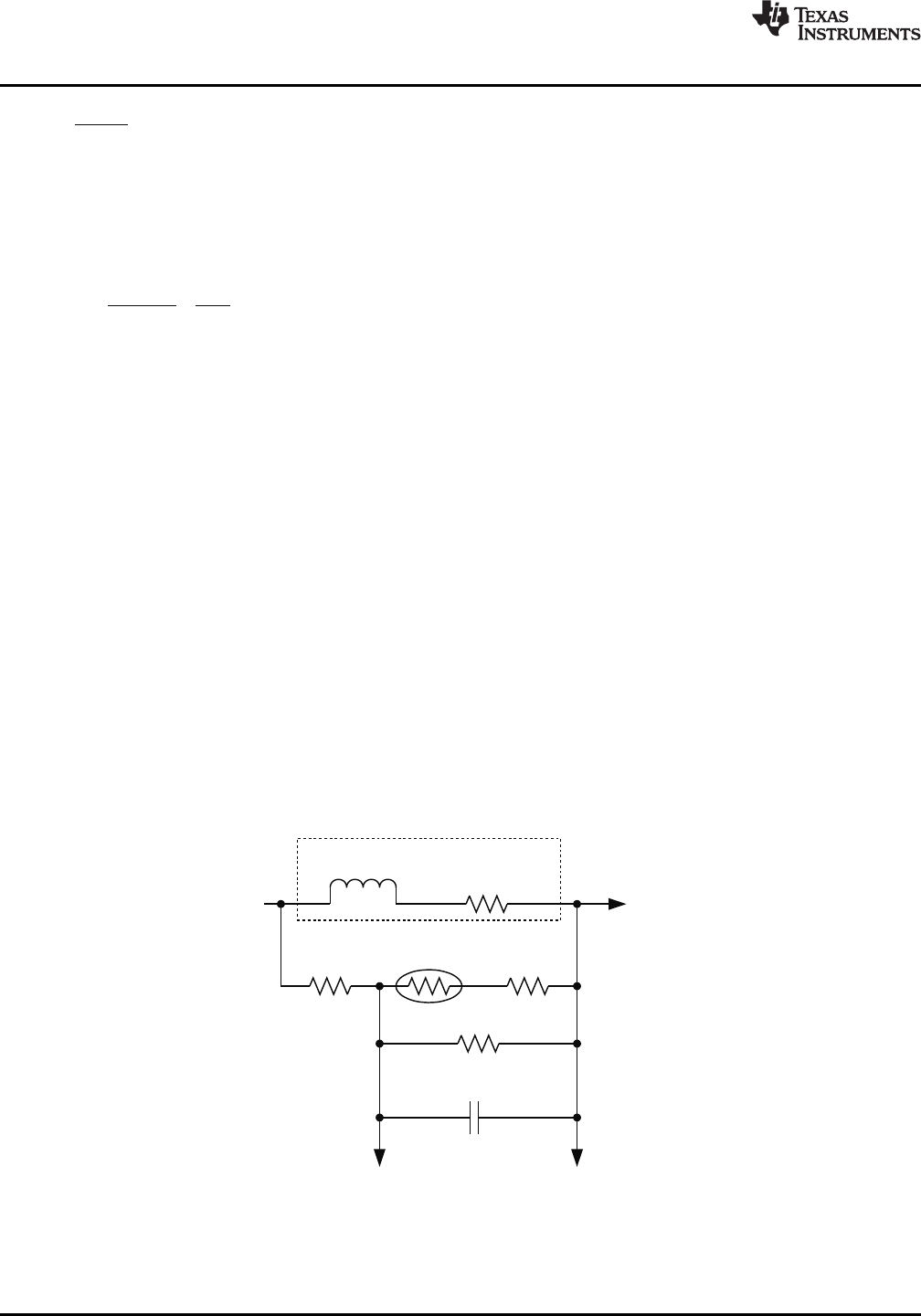
-
´
=
P P
V dT
LI
( ) -
æ ö
ç ÷
= + ´ =
ç ÷
è ø
CC max P P
SAT
PHASE
II
I 1.2 43.2 A
N 2
I
UDG-11039
CSN
LRDCR
RNTC
RPAR
CSENSE
RSERIES
RSEQU
CSP
TPS51640A, TPS59640, TPS59641
SLUSAQ2 –JANUARY 2012
www.ti.com
(7)
In this equation,
V=VIN-MAX –VHFM = 19. 1V; dT = VHFM /(FxVIN-MAX) = 150 ns; Ipp = 9.4A. So, calculating, L = 0.304 µH.
An inductance value of 0.36 µH is chosen as this is a commonly used inductor for VCORE application. The
inductor must not saturate during peak loading conditions.
(8)
The factor of 1.2 allows for current sensing and current limiting tolerances; the factor of 1.25 is the Intel 25%
momentary OCP requirement.
The chosen inductor should have the following characteristics:
•An inductance to current curve ratio equal to 1 (or as close possible). Inductor DCR sensing is based on the
idea L/DCR is approximately a constant through the current range of interest.
•Either high saturation or soft saturation.
•Low DCR for improved efficiency, but at least 0.7 mΩfor proper signal levels.
•DCR tolerance as low as possible for load-line accuracy.
For this application, a 0.36-µH, 0.825-mΩinductor is chosen. Because the per phase current for GPU is same as
CPU, the same inductor for GPU channel is chosen.
Step Five: Determine current sensing method.
The TPS51640A, TPS59640, and TPS59641 support both resistor sensing and inductor DCR sensing. Inductor
DCR sensing is chosen. For resistor sensing, substitute the resistor value (0.75 mΩrecommended for a 3-phase
94-A application) for RCS in the subsequent equations and skip Step Four.
Step Six: Design the thermal compensation network and selection of OCP.
In most designs, NTC thermistors are used to compensate thermal variations in the resistance of the inductor
winding. This winding is generally copper, and so has a resistance coefficient of 3900 PPM/°C. NTC thermistors,
on the other hand, have very non-linear characteristics and need two or three resistors to linearize them over the
range of interest. The typical DCR circuit is shown in Figure 70.
Figure 70. Typical DCR Sensing Circuit
In this circuit, the voltage across the CSENSE exactly equals the voltage across RDCR when Equation 9 is true.
40 Submit Documentation Feedback Copyright ©2012, Texas Instruments Incorporated

= ´
SENSE EQ
DCR
LC R
R
=+
P _N
EQ
SEQU P _N
R
RR R
( )
´ +
=+ +
PAR NTC SERIES
P _N
PAR NTC SERIES
R R R
RR R R
( ) = ´ +
P _N
DCR
CS eff SEQU P _ N
R
R R R R
( )´W ´
= = = W
´ W ´
CS
CS eff
GDROOP
LL M
R A 0.66m 12
R 4.12k
R G 3.9m 0.497mS
( )´W ´
= = = W
´ W ´
CS
CS eff
CDROOP
LL M
R A 0.66m 12
R 8.45k
R G 1.9m 0.497mS
TPS51640A, TPS59640, TPS59641
www.ti.com
SLUSAQ2 –JANUARY 2012
where
•REQ is the series/parallel combination of RSEQU, RNTC, RSERIES and RPAR (9)
(10)
(11)
CSENSE should be a capacitor type which is stable over temperature. Use X7R or better dielectric (C0G
preferred).
Since calculating these values by hand is difficult, TI has a spreadsheet using the Excel Solver function available
to calculate them. Contact a local TI representative to get a copy of the spreadsheet.
In this design, the following values are input to the spreadsheet:
•L = 0.36 µH
•RDCR = 0.825 mΩ
•Load Line, RIMVP = -1.9 mΩ
•Minimum overcurrent limit = 112 A
•Thermistor R25 = 100 kΩand "B" value = 4250 kΩ
The spreadsheet then calculates the OCP (overcurrent protection) setting and the values of RSEQU, RSERIES,
RPAR, and CSENSE. In this case, the OCP setting is the resistor value selection of 56 kΩfrom COCP-I to GND and
GOCP-I to GND. The nearest standard component values are:
•RSEQU = 17.8 kΩ;
•RSERIES = 28.7 kΩ;
•RPAR = 162 kΩ
•CSENSE =33 nF
Note the effective divider ratio for the inductor DCR. The effective current sense resistance (RCS(eff)) is shown in
Equation 12.
where
•RP_N is the series/parallel combination of RNTC, RSERIES and RPAR. (12)
(13)
RCS(eff) is 0.66 mΩ.
Step Seven: Set current monitor (IMON) setting resistor.
After the OCP selection resistor is selected in Step 6, the IMON is set by the resistor from CIMON to COCP-I
(RCIMON) and GIMON to GOCP-I (RGIMON). Based on Equation 2 and Equation 3,
RCIMON = 71.5 kΩand RGIMON = 309 kΩ
Step Eight: Set the load line.
The load-line for CPU channel is set by the resistor, RCDROOP from CCOMP to VREF. The load-line for GPU
channel is set by the resistor, RGDROOP from the GCOMP pin to VREF. Using the Equation 1, the droop setting
resistors are calculated in Equation 14 and Equation 15.
(14)
Copyright ©2012, Texas Instruments Incorporated Submit Documentation Feedback 41

( )´W ´
= = = W
´ W ´
CS
CS eff
GDROOP
LL M
R A 0.66m 12
R 4.12k
R G 3.9m 0.497mS
TPS51640A, TPS59640, TPS59641
SLUSAQ2 –JANUARY 2012
www.ti.com
(15)
Step Nine: Programming the CTHERM and GTHERM pins.
The CTHERM and GTHERM pins should be set so that the resistor divider voltage would be greater than 458
mV at normal operation. For VR_HOT to be asserted, the xTHERM pin voltage should fall below 458 mV. The
NTC resistor from xTHERM to GND is chosen as 100 kΩwith a B of 4250K. With this, for a VR_HOT assertion
temperature of 105°C, the resistor from xTHERM to VREF can be calculated as 15.4 kΩ.
Step Ten: Determine the output capacitor configuration.
For the output capacitor, the Intel Power Delivery guideline gives the output capacitor recommendations. Using
these devices, it is possible to meet the load transient with lower capacitance by using the OSR and USR
feature. Eight settings are available and this selection has to be tuned based on transient measurement.
42 Submit Documentation Feedback Copyright ©2012, Texas Instruments Incorporated
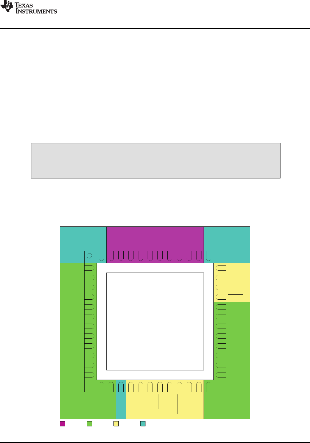
GND
1
2
3
4
5
6
7
8
9
10
11
12
13
20
19
18
17
16
14VREF
V3R3
VCLK
VDIO
ALERT
VR_HOT
CTHERM
GTHERM
CIMON
GIMON
CGFB
CVFB
GPGOOD
CPGOOD
15
24
30
29
28
27
26
25
21
22
23
GGFB
GVFB
COCP-I
CF-IMAX
CCOMP
VBAT
CCSN3
CCSP3
CCSN2
V5
CSKIP
GPWM
GSKIP
GOCP-I
VR_ON
CPWM3
31
40
39
38
37
36
35
34
33
32
44
43
42
41
48
47
46
45
SLEWA
CCSP2
CCSN1
CCSP1
GCOMP
GCSP
GCSN
CDH2
CBST2
CSW2
CDL2
V5DRV
PGND
CDL1
CSW1
CBST1
CDH1
GF-IMAX
Drivers Analog Digital Power
TPS51640A, TPS59640, TPS59641
www.ti.com
SLUSAQ2 –JANUARY 2012
PCB LAYOUT GUIDELINE
SCHEMATIC REVIEW
Because the voltage and current feedback signals are fully differential it is a good idea to double check their
polarity.
1. CCSP1/CCSN1
2. CCSP2/CCSN2
3. CCSP2/CCSN2
4. GCSP/GCSN
5. VCCSENSE to CVFB/VSSSENSE to CGFB (for CPU)
6. VCCGTSENSE to GVFB/VSSGTSENSE to GGFB (for GPU)
Also, note the order of the current sense inputs on Pin 4 to Pin 9 as the second phase has a reverse order.
CAUTION
Separate noisy driver interface lines from sensitive analog interface lines: (This is the
MOST CRITICAL LAYOUT RULE)
The TPS51640A, TPS59640, and TPS59641 make this as easy as possible. The pin-out arrangement for
TPS51640A is shown in Figure 71. The driver outputs clearly separated from the sensitive analog and digital
circuitry. The driver has a separate PGND and this should be directly connected to the decoupling capacitor that
connects from V5DRV to PGND. The thermal pad of the package is the analog ground for these devices and
should NOT be connected directly to PGND (Pin 42).
Figure 71. TPS51640A Pin-out Arranged by Pin Function
Copyright ©2012, Texas Instruments Incorporated Submit Documentation Feedback 43
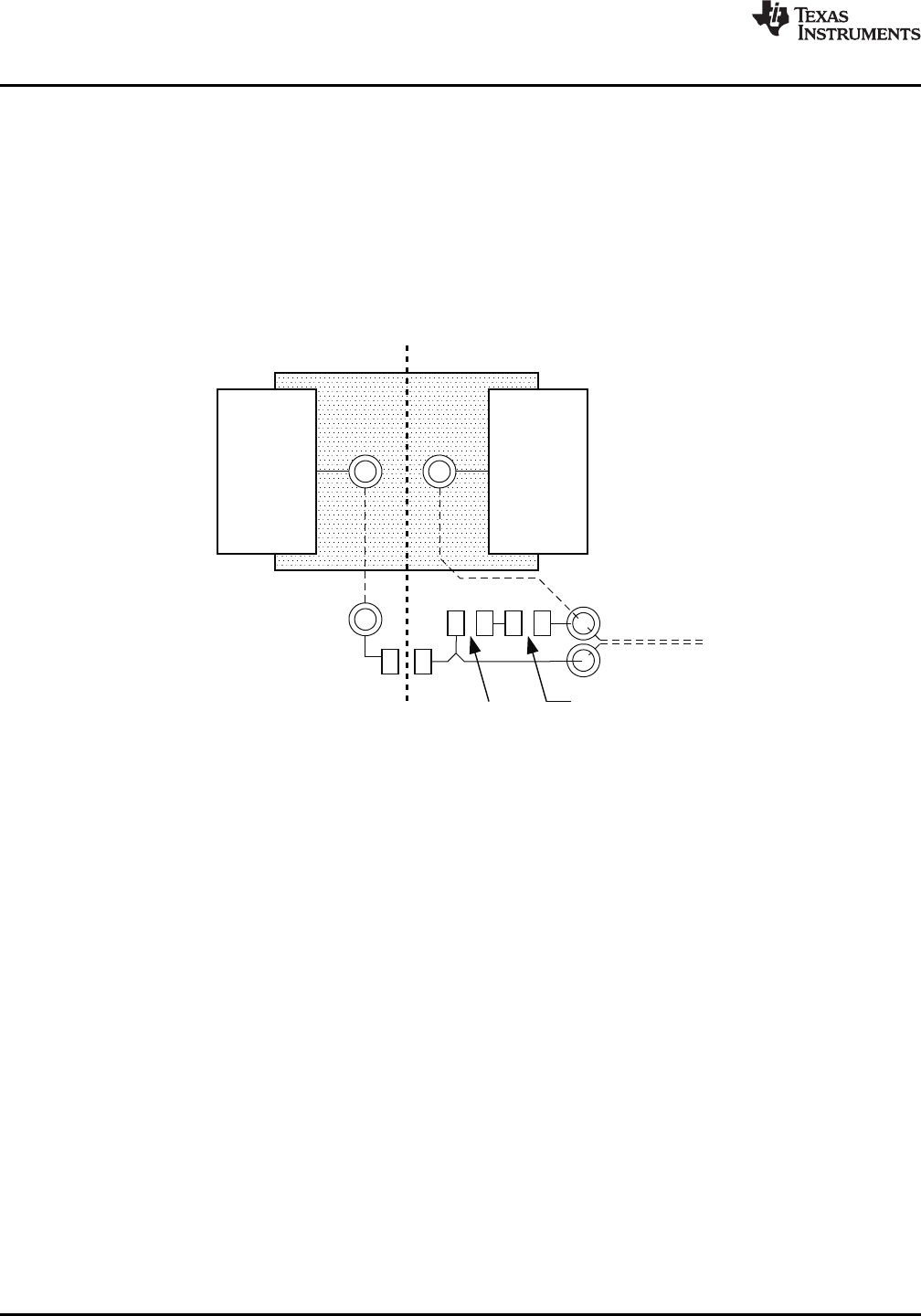
UDG-11038
VCORE
LLx
Noisy Quiet
Inductor
Outline
RSEQ
Thermistor RSERIES
CSNx
CSPx
TPS51640A, TPS59640, TPS59641
SLUSAQ2 –JANUARY 2012
www.ti.com
Given the physical layout of most systems, the current feedback (xCSPx, xCSNx) may have to pass near the
power chain. Clean current feedback is required for good load-line, current sharing, and current limiting
performance of these devices, so please take the following precautions:
•Make a Kelvin connection to the pads of the resistor or inductor used for current sensing. See Figure 72 for a
layout example.
•Run the current feedback signals as a differential pair to the device.
•Run the lines in a quiet layer. Isolate them from noisy signals by a voltage or ground plane.
•Put the compensation capacitor for DCR sensing (CSENSE) as close to the CS pins as possible.
•Place any noise filtering capacitors directly underneath these devices and connect to the CS pins with the
shortest trace length possible.
Figure 72. Make Kelvin Connections to the Inductor for DCR Sensing
44 Submit Documentation Feedback Copyright ©2012, Texas Instruments Incorporated
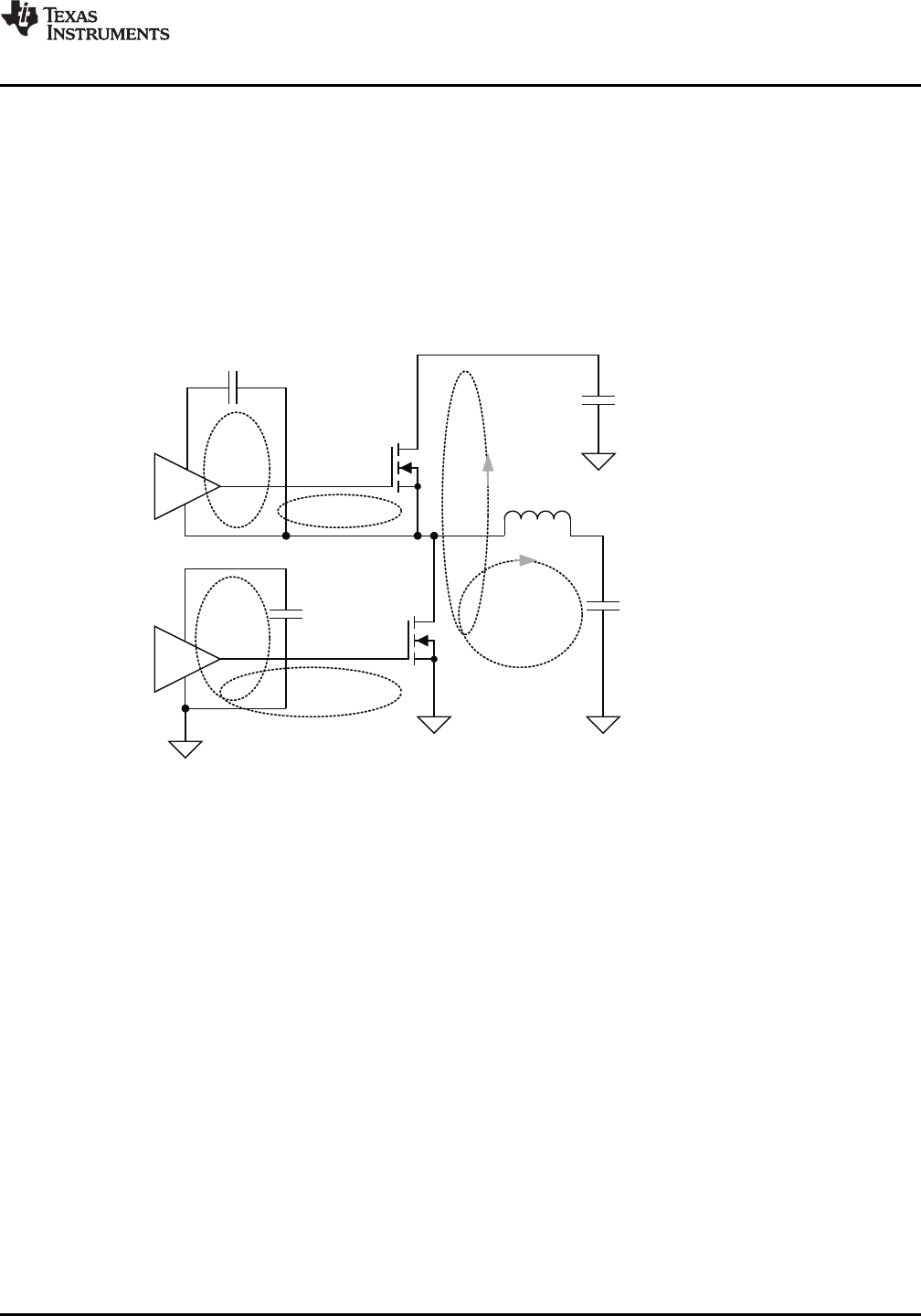
UDG-11040
CB
4b
CIN
L
COUT
4a
DRVH
Q1
1
2
3b
3a
DRVL
Q2
CD
LL
PGND
VCORE
VBAT
TPS51640A, TPS59640, TPS59641
www.ti.com
SLUSAQ2 –JANUARY 2012
Minimize High-Current Loops
Figure 73 shows the primary current loops in each phase, numbered in order of importance.
The most important loop to minimize the area of is Loop 1, the path from the input capacitor through the high and
low side FETs, and back to the capacitor through ground.
Loop 2 is from the inductor through the output capacitor, ground and Q2. The layout of the low side gate drive
(Loops 3a and 3b) is important. The guidelines for gate drive layout are:
•Make the low-side gate drive as short as possible (1 inch or less preferred).
•Make the DRVL width to length ratio of 1:10, wider (1:5) if possible.
•If changing layers is necessary, use at least two vias.
Figure 73. Major Current Loops to Minimize
Power Chain Symmetry
The TPS51640A, TPS59640, and TPS59641 do not require special care in the layout of the power chain
components. This is because independent isolated current feedback is provided. If it is possible to lay out the
phases in a symmetrical manner, then please do so. The rule is: the current feedback from each phase needs to
be clean of noise and have the same effective current sense resistance.
Place analog components as close to the device as possible.
Place components close to the device in the following order.
1. CS pin noise filtering components
2. xCOMP pin compensation components
3. Decoupling capacitors for VREF, V3R3, V5
4. xTHERM filter capacitor
5. xIMON capacitor, resistors
6. xF-IMAX resistors
Copyright ©2012, Texas Instruments Incorporated Submit Documentation Feedback 45

TPS51640A, TPS59640, TPS59641
SLUSAQ2 –JANUARY 2012
www.ti.com
Grounding Recommendations
These devices have separate analog and power grounds, and a thermal pad. The normal procedure for
connecting these is:
•The thermal pad is the analog ground.
•DO NOT connect the thermal pad to Pin 42 directly as Pin 42 is the PGND which is the Gate driver
Ground.
•Pin 42 (PGND) must be connected directly to the gate driver decoupling capacitor ground terminal.
•Tie the thermal pad (analog ground pin) to a ground island with at least 4 small vias or one large via.
•All the analog components can connect to this analog ground island.
•The analog ground can be connected to any quiet spot on the system ground. A quiet area is defined as a
area where no power supply switching currents are likely to flow. This applies to both the VCORE regulator and
other regulators. Use a single point connection from analog ground to the system ground
•Make sure the low-side FET source connection and the decoupling capacitors have plenty of vias.
Decoupling Recommendations
•Decouple V5IN to PGND with at least a 2.2 µF ceramic capacitor.
•Decouple V5 and V3R3 with 1 µF to AGND with leads as short as possible,
•VREF to AGND with 0.33 µF, with short leads also
Conductor Widths
•Follow Intel guidelines with respect to the voltage feedback and logic interface connection requirements.
•Maximize the widths of power, ground and drive signal connections.
•For conductors in the power path, be sure there is adequate trace width for the amount of current flowing
through the traces.
•Make sure there are sufficient vias for connections between layers. A good guideline is to use a minimum of 1
via per ampere of current.
46 Submit Documentation Feedback Copyright ©2012, Texas Instruments Incorporated
PACKAGE OPTION ADDENDUM
www.ti.com 13-Jun-2012
Addendum-Page 1
PACKAGING INFORMATION
Orderable Device Status (1) Package Type Package
Drawing Pins Package Qty Eco Plan (2) Lead/
Ball Finish MSL Peak Temp (3) Samples
(Requires Login)
TPS51640ARSLR ACTIVE VQFN RSL 48 2500 Green (RoHS
& no Sb/Br)
CU NIPDAUAGLevel-2-260C-1 YEAR
TPS51640ARSLT ACTIVE VQFN RSL 48 250 Green (RoHS
& no Sb/Br)
CU NIPDAUAGLevel-2-260C-1 YEAR
TPS59640RSLR ACTIVE VQFN RSL 48 2500 Green (RoHS
& no Sb/Br)
CU NIPDAUAGLevel-2-260C-1 YEAR
TPS59640RSLT ACTIVE VQFN RSL 48 250 Green (RoHS
& no Sb/Br)
CU NIPDAUAGLevel-2-260C-1 YEAR
TPS59641RSLR ACTIVE VQFN RSL 48 2500 Green (RoHS
& no Sb/Br)
CU NIPDAUAGLevel-2-260C-1 YEAR
TPS59641RSLT ACTIVE VQFN RSL 48 250 Green (RoHS
& no Sb/Br)
CU NIPDAUAGLevel-2-260C-1 YEAR
(1) The marketing status values are defined as follows:
ACTIVE: Product device recommended for new designs.
LIFEBUY: TI has announced that the device will be discontinued, and a lifetime-buy period is in effect.
NRND: Not recommended for new designs. Device is in production to support existing customers, but TI does not recommend using this part in a new design.
PREVIEW: Device has been announced but is not in production. Samples may or may not be available.
OBSOLETE: TI has discontinued the production of the device.
(2) Eco Plan - The planned eco-friendly classification: Pb-Free (RoHS), Pb-Free (RoHS Exempt), or Green (RoHS & no Sb/Br) - please check http://www.ti.com/productcontent for the latest availability
information and additional product content details.
TBD: The Pb-Free/Green conversion plan has not been defined.
Pb-Free (RoHS): TI's terms "Lead-Free" or "Pb-Free" mean semiconductor products that are compatible with the current RoHS requirements for all 6 substances, including the requirement that
lead not exceed 0.1% by weight in homogeneous materials. Where designed to be soldered at high temperatures, TI Pb-Free products are suitable for use in specified lead-free processes.
Pb-Free (RoHS Exempt): This component has a RoHS exemption for either 1) lead-based flip-chip solder bumps used between the die and package, or 2) lead-based die adhesive used between
the die and leadframe. The component is otherwise considered Pb-Free (RoHS compatible) as defined above.
Green (RoHS & no Sb/Br): TI defines "Green" to mean Pb-Free (RoHS compatible), and free of Bromine (Br) and Antimony (Sb) based flame retardants (Br or Sb do not exceed 0.1% by weight
in homogeneous material)
(3) MSL, Peak Temp. -- The Moisture Sensitivity Level rating according to the JEDEC industry standard classifications, and peak solder temperature.
Important Information and Disclaimer:The information provided on this page represents TI's knowledge and belief as of the date that it is provided. TI bases its knowledge and belief on information
provided by third parties, and makes no representation or warranty as to the accuracy of such information. Efforts are underway to better integrate information from third parties. TI has taken and
continues to take reasonable steps to provide representative and accurate information but may not have conducted destructive testing or chemical analysis on incoming materials and chemicals.
TI and TI suppliers consider certain information to be proprietary, and thus CAS numbers and other limited information may not be available for release.
PACKAGE OPTION ADDENDUM
www.ti.com 13-Jun-2012
Addendum-Page 2
In no event shall TI's liability arising out of such information exceed the total purchase price of the TI part(s) at issue in this document sold by TI to Customer on an annual basis.
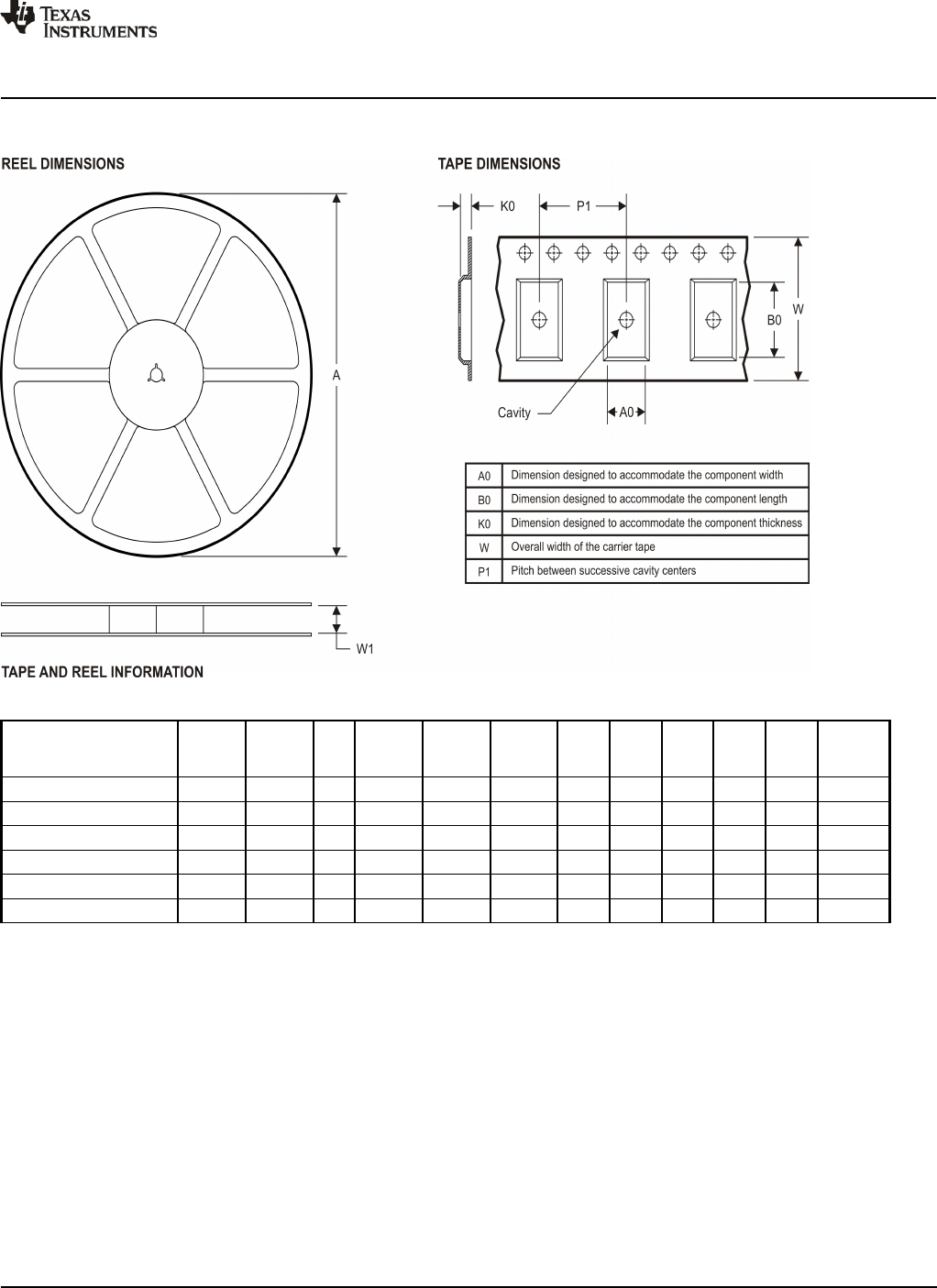
TAPE AND REEL INFORMATION
*All dimensions are nominal
Device Package
Type Package
Drawing Pins SPQ Reel
Diameter
(mm)
Reel
Width
W1 (mm)
A0
(mm) B0
(mm) K0
(mm) P1
(mm) W
(mm) Pin1
Quadrant
TPS51640ARSLR VQFN RSL 48 2500 330.0 16.4 6.3 6.3 1.5 12.0 16.0 Q2
TPS51640ARSLT VQFN RSL 48 250 180.0 16.4 6.3 6.3 1.5 12.0 16.0 Q2
TPS59640RSLR VQFN RSL 48 2500 330.0 16.4 6.3 6.3 1.5 12.0 16.0 Q2
TPS59640RSLT VQFN RSL 48 250 180.0 16.4 6.3 6.3 1.5 12.0 16.0 Q2
TPS59641RSLR VQFN RSL 48 2500 330.0 16.4 6.3 6.3 1.5 12.0 16.0 Q2
TPS59641RSLT VQFN RSL 48 250 180.0 16.4 6.3 6.3 1.5 12.0 16.0 Q2
PACKAGE MATERIALS INFORMATION
www.ti.com 14-Jul-2012
Pack Materials-Page 1
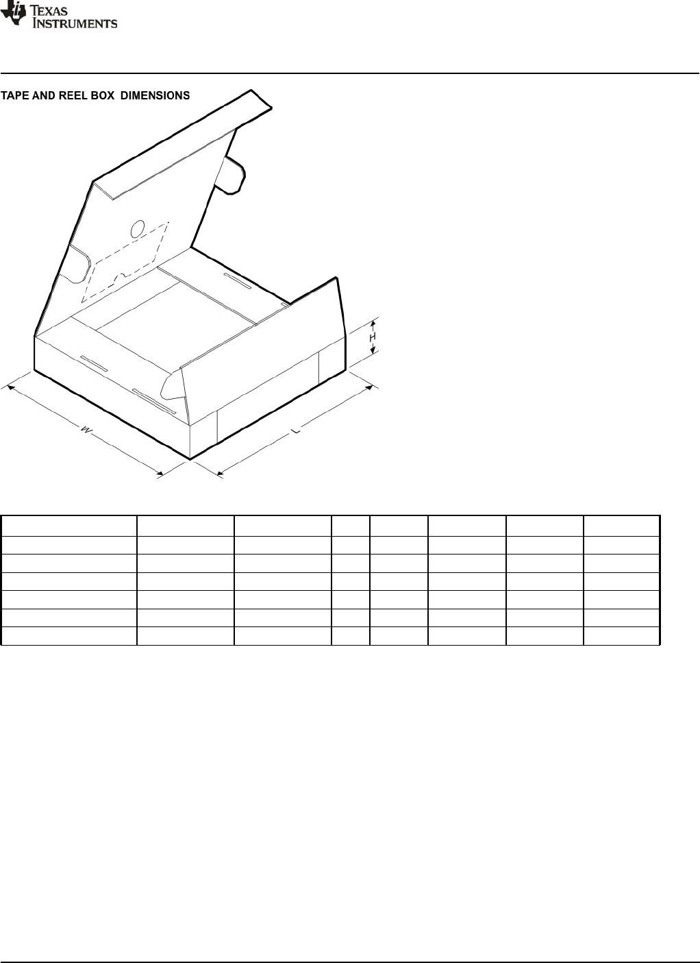
*All dimensions are nominal
Device Package Type Package Drawing Pins SPQ Length (mm) Width (mm) Height (mm)
TPS51640ARSLR VQFN RSL 48 2500 367.0 367.0 38.0
TPS51640ARSLT VQFN RSL 48 250 210.0 185.0 35.0
TPS59640RSLR VQFN RSL 48 2500 367.0 367.0 38.0
TPS59640RSLT VQFN RSL 48 250 210.0 185.0 35.0
TPS59641RSLR VQFN RSL 48 2500 367.0 367.0 38.0
TPS59641RSLT VQFN RSL 48 250 210.0 185.0 35.0
PACKAGE MATERIALS INFORMATION
www.ti.com 14-Jul-2012
Pack Materials-Page 2

IMPORTANT NOTICE
Texas Instruments Incorporated and its subsidiaries (TI) reserve the right to make corrections, enhancements, improvements and other
changes to its semiconductor products and services per JESD46C and to discontinue any product or service per JESD48B. Buyers should
obtain the latest relevant information before placing orders and should verify that such information is current and complete. All
semiconductor products (also referred to herein as “components”) are sold subject to TI’s terms and conditions of sale supplied at the time
of order acknowledgment.
TI warrants performance of its components to the specifications applicable at the time of sale, in accordance with the warranty in TI’s terms
and conditions of sale of semiconductor products. Testing and other quality control techniques are used to the extent TI deems necessary
to support this warranty. Except where mandated by applicable law, testing of all parameters of each component is not necessarily
performed.
TI assumes no liability for applications assistance or the design of Buyers’ products. Buyers are responsible for their products and
applications using TI components. To minimize the risks associated with Buyers’ products and applications, Buyers should provide
adequate design and operating safeguards.
TI does not warrant or represent that any license, either express or implied, is granted under any patent right, copyright, mask work right, or
other intellectual property right relating to any combination, machine, or process in which TI components or services are used. Information
published by TI regarding third-party products or services does not constitute a license to use such products or services or a warranty or
endorsement thereof. Use of such information may require a license from a third party under the patents or other intellectual property of the
third party, or a license from TI under the patents or other intellectual property of TI.
Reproduction of significant portions of TI information in TI data books or data sheets is permissible only if reproduction is without alteration
and is accompanied by all associated warranties, conditions, limitations, and notices. TI is not responsible or liable for such altered
documentation. Information of third parties may be subject to additional restrictions.
Resale of TI components or services with statements different from or beyond the parameters stated by TI for that component or service
voids all express and any implied warranties for the associated TI component or service and is an unfair and deceptive business practice.
TI is not responsible or liable for any such statements.
Buyer acknowledges and agrees that it is solely responsible for compliance with all legal, regulatory and safety-related requirements
concerning its products, and any use of TI components in its applications, notwithstanding any applications-related information or support
that may be provided by TI. Buyer represents and agrees that it has all the necessary expertise to create and implement safeguards which
anticipate dangerous consequences of failures, monitor failures and their consequences, lessen the likelihood of failures that might cause
harm and take appropriate remedial actions. Buyer will fully indemnify TI and its representatives against any damages arising out of the use
of any TI components in safety-critical applications.
In some cases, TI components may be promoted specifically to facilitate safety-related applications. With such components, TI’s goal is to
help enable customers to design and create their own end-product solutions that meet applicable functional safety standards and
requirements. Nonetheless, such components are subject to these terms.
No TI components are authorized for use in FDA Class III (or similar life-critical medical equipment) unless authorized officers of the parties
have executed a special agreement specifically governing such use.
Only those TI components which TI has specifically designated as military grade or “enhanced plastic” are designed and intended for use in
military/aerospace applications or environments. Buyer acknowledges and agrees that any military or aerospace use of TI components
which have not been so designated is solely at the Buyer's risk, and that Buyer is solely responsible for compliance with all legal and
regulatory requirements in connection with such use.
TI has specifically designated certain components which meet ISO/TS16949 requirements, mainly for automotive use. Components which
have not been so designated are neither designed nor intended for automotive use; and TI will not be responsible for any failure of such
components to meet such requirements.
Products Applications
Audio www.ti.com/audio Automotive and Transportation www.ti.com/automotive
Amplifiers amplifier.ti.com Communications and Telecom www.ti.com/communications
Data Converters dataconverter.ti.com Computers and Peripherals www.ti.com/computers
DLP® Products www.dlp.com Consumer Electronics www.ti.com/consumer-apps
DSP dsp.ti.com Energy and Lighting www.ti.com/energy
Clocks and Timers www.ti.com/clocks Industrial www.ti.com/industrial
Interface interface.ti.com Medical www.ti.com/medical
Logic logic.ti.com Security www.ti.com/security
Power Mgmt power.ti.com Space, Avionics and Defense www.ti.com/space-avionics-defense
Microcontrollers microcontroller.ti.com Video and Imaging www.ti.com/video
RFID www.ti-rfid.com
OMAP Mobile Processors www.ti.com/omap TI E2E Community e2e.ti.com
Wireless Connectivity www.ti.com/wirelessconnectivity
Mailing Address: Texas Instruments, Post Office Box 655303, Dallas, Texas 75265
Copyright © 2012, Texas Instruments Incorporated