Vivado Design Suite: AXI Reference Guide (UG1037) Ug1037
ug1037-vivado-axi-reference-guide
User Manual:
Open the PDF directly: View PDF ![]() .
.
Page Count: 175 [warning: Documents this large are best viewed by clicking the View PDF Link!]
- Vivado Design Suite: AXI Reference Guide
- Revision History
- Table of Contents
- Ch. 1: Introducing AXI for Vivado
- Ch. 2: AXI Support in Xilinx Tools and IP
- Ch. 3: Samples of Vivado AXI IP and Xilinx Processors
- Overview
- AXI Infrastructure IP Cores
- Xilinx AXI SmartConnect and AXI Interconnect IP
- AXI SmartConnect IP
- AXI4-Stream Interconnect Core IP
- AXI Virtual FIFO Controller
- The AXI4-Stream interconnect can also perform local FIFO buffering, clock conversion, and width conversion to adapt the interface of the stream endpoints to the data path of the virtual FIFO controller and the AXI memory controller
- DataMover
- AXI4 DMA
- Simulating IP
- Using Debug and IP
- Zynq UltraScale+ MPSoC Processor Device
- Zynq-7000 All Programmable SoC Processor IP
- MicroBlaze Processor
- Ch. 4: AXI Feature Adoption in Xilinx Devices
- Ch. 5: Migrating to Xilinx AXI Protocols
- Ch. 6: AXI System Optimization: Tips and Hints
- Introduction
- AXI System Optimization
- AXI4-based Vivado Multi-Ported Memory Controller: AXI4 System Optimization Example
- Common Pitfalls Leading to AXI Systems of Poor Quality Results
- Optimizing AXI on Zynq-7000 AP SoC Processors
- Ch. 7: AXI4-Stream IP Interoperability: Tips and Hints
- Appx. A: AXI Adoption Summary
- Appx. B: AXI Terminology
- Appx. C: Additional Resources and Legal Notices

Vivado AXI Reference
[optional]
UG1037 (v4.0) July 15, 2017 [optional]
Vivado Design
Suite
AXI Reference Guide
UG1037 (v4.0) July 15, 2017

Vivado AXI Reference Guide www.xilinx.com 2
UG1037 (v4.0) July 15, 2017
Revision History
The following table shows the revision history for this document.
Date Version Revision
07/15/2017 4.0 Updated to match the new Vivado “Look and Feel”.
Updated all IP to reflect current features.
Added Zynq UltraScale+ MPSoC Processor Device in Chapter 3.
Added AXI SmartConnect IP in Chapter 3, and mention of SmartConnect IP
capabilities throughout the document.
Added AXI Verification IP in Chapter 3.
Added AXI4-Stream Verification IP in Chapter 3.
Added Zynq-7000 AP SoC Verification IP in Chapter 3.
06/24/2015 3.0 Added Quick Take Videos.
Updated the AXI IP Catalog Figure 2-1.
Updated the IP Project Settings Packaging tab in Figure 2-6.
Changed Features and Limitations in AXI Infrastructure IP Cores.
Updated Vivado Lab Tools to Vivado Lab Edition throughout the document.
Added XAPP1231 document reference to additional resources.
Added direct links to destinations.
11/20/2014 2.1 Corrected AWCACHE and ARCACHE for AXI4-Lite to “Signal not present” in
Appendix A, Write Data Channel Signals and Appendix A, Read Data Channel Signals.
11/19/2014 2.0 Changed:
IP Interoperability. Using Vivado AXI IP in RTL Projects.
Using the Create and Package IP Wizard for AXI IP.
Using Vivado IP Integrator to Assemble AXI IP.
Adding AXI IP to the IP Catalog Using Vivado IP Packager.
Using AXI IP in System Generator for DSP.
Added:
Adding AXI Interfaces Using High Level Synthesis.
AXI Virtual FIFO Controller. DataMover
Simulating IP. Using Debug and IP.
Performance Monitor IP. AXI BFM.
Bus Functional Models.
Choosing a Programmable Logic Interface.
Zynq-7000 All Programmable SoC Processor IP.
MicroBlaze Processor.
Added: Migrating to AXI for IP Cores.
Migrating to AXI for IP Cores.
Migrating HDL Designs to use DSP IP with AXI4-Stream.
Migrating IP Using the Vivado Create and Package Wizard.
High End Verification Solutions.
Added Optimizing AXI on Zynq-7000 AP SoC Processors.
04/02/2014 1.0 Initial release of Vivado AXI Reference Guide.

Vivado AXI Reference Guide www.xilinx.com 3
UG1037 (v4.0) July 15, 2017
Table of Contents
Chapter 1: Introducing AXI for Vivado
Overview . . . . . . . . . . . . . . . . . . . . . . . . . . . . . . . . . . . . . . . . . . . . . . . . . . . . . . . . . . . . . . . . . . . . . . . . 5
What is AXI? . . . . . . . . . . . . . . . . . . . . . . . . . . . . . . . . . . . . . . . . . . . . . . . . . . . . . . . . . . . . . . . . . . . . . . 5
Summary of AXI4 Benefits. . . . . . . . . . . . . . . . . . . . . . . . . . . . . . . . . . . . . . . . . . . . . . . . . . . . . . . . . . . 6
How AXI Works . . . . . . . . . . . . . . . . . . . . . . . . . . . . . . . . . . . . . . . . . . . . . . . . . . . . . . . . . . . . . . . . . . . 6
IP Interoperability . . . . . . . . . . . . . . . . . . . . . . . . . . . . . . . . . . . . . . . . . . . . . . . . . . . . . . . . . . . . . . . . 10
Quick Take Videos . . . . . . . . . . . . . . . . . . . . . . . . . . . . . . . . . . . . . . . . . . . . . . . . . . . . . . . . . . . . . . . . 11
Chapter 2: AXI Support in Xilinx Tools and IP
Introduction . . . . . . . . . . . . . . . . . . . . . . . . . . . . . . . . . . . . . . . . . . . . . . . . . . . . . . . . . . . . . . . . . . . . . 12
Using Vivado AXI IP in RTL Projects . . . . . . . . . . . . . . . . . . . . . . . . . . . . . . . . . . . . . . . . . . . . . . . . . . 12
Using the Create and Package IP Wizard for AXI IP . . . . . . . . . . . . . . . . . . . . . . . . . . . . . . . . . . . . . . 14
Adding AXI IP to the IP Catalog Using Vivado IP Packager . . . . . . . . . . . . . . . . . . . . . . . . . . . . . . . . 19
Using Vivado IP Integrator to Assemble AXI IP . . . . . . . . . . . . . . . . . . . . . . . . . . . . . . . . . . . . . . . . . 21
Using AXI IP in System Generator for DSP . . . . . . . . . . . . . . . . . . . . . . . . . . . . . . . . . . . . . . . . . . . . . 22
Adding AXI Interfaces Using High Level Synthesis . . . . . . . . . . . . . . . . . . . . . . . . . . . . . . . . . . . . . . . 25
Chapter 3: Samples of Vivado AXI IP and Xilinx Processors
Overview . . . . . . . . . . . . . . . . . . . . . . . . . . . . . . . . . . . . . . . . . . . . . . . . . . . . . . . . . . . . . . . . . . . . . . . 30
AXI Infrastructure IP Cores . . . . . . . . . . . . . . . . . . . . . . . . . . . . . . . . . . . . . . . . . . . . . . . . . . . . . . . . . 30
AXI4 DMA . . . . . . . . . . . . . . . . . . . . . . . . . . . . . . . . . . . . . . . . . . . . . . . . . . . . . . . . . . . . . . . . . . . . . . . 49
Simulating IP. . . . . . . . . . . . . . . . . . . . . . . . . . . . . . . . . . . . . . . . . . . . . . . . . . . . . . . . . . . . . . . . . . . . . 55
Using Debug and IP . . . . . . . . . . . . . . . . . . . . . . . . . . . . . . . . . . . . . . . . . . . . . . . . . . . . . . . . . . . . . . . 56
Zynq UltraScale+ MPSoC Processor Device . . . . . . . . . . . . . . . . . . . . . . . . . . . . . . . . . . . . . . . . . . . . 67
Zynq-7000 All Programmable SoC Processor IP . . . . . . . . . . . . . . . . . . . . . . . . . . . . . . . . . . . . . . . . . 68
MicroBlaze Processor. . . . . . . . . . . . . . . . . . . . . . . . . . . . . . . . . . . . . . . . . . . . . . . . . . . . . . . . . . . . . . 72
Chapter 4: AXI Feature Adoption in Xilinx Devices
Introduction . . . . . . . . . . . . . . . . . . . . . . . . . . . . . . . . . . . . . . . . . . . . . . . . . . . . . . . . . . . . . . . . . . . . . 80
Memory-Mapped IP Feature Adoption and Support . . . . . . . . . . . . . . . . . . . . . . . . . . . . . . . . . . . . 80
AXI4-Stream Adoption and Support . . . . . . . . . . . . . . . . . . . . . . . . . . . . . . . . . . . . . . . . . . . . . . . . . . 82
DSP and Wireless IP: AXI Feature Adoption. . . . . . . . . . . . . . . . . . . . . . . . . . . . . . . . . . . . . . . . . . . . 94
Video IP: AXI Feature Adoption . . . . . . . . . . . . . . . . . . . . . . . . . . . . . . . . . . . . . . . . . . . . . . . . . . . . . 95

Vivado AXI Reference Guide www.xilinx.com 4
UG1037 (v4.0) July 15, 2017
Chapter 5: Migrating to Xilinx AXI Protocols
Introduction . . . . . . . . . . . . . . . . . . . . . . . . . . . . . . . . . . . . . . . . . . . . . . . . . . . . . . . . . . . . . . . . . . . . 110
Migrating to AXI for IP Cores. . . . . . . . . . . . . . . . . . . . . . . . . . . . . . . . . . . . . . . . . . . . . . . . . . . . . . . 110
Migrating IP Using the Vivado Create and Package Wizard . . . . . . . . . . . . . . . . . . . . . . . . . . . . . . 111
Using System Generator for DSP for Migrating IP . . . . . . . . . . . . . . . . . . . . . . . . . . . . . . . . . . . . . . 111
Migrating a Fast Simplex Link to AXI4-Stream . . . . . . . . . . . . . . . . . . . . . . . . . . . . . . . . . . . . . . . . . 112
Migrating HDL Designs to use DSP IP with AXI4-Stream . . . . . . . . . . . . . . . . . . . . . . . . . . . . . . . . . 114
High End Verification Solutions. . . . . . . . . . . . . . . . . . . . . . . . . . . . . . . . . . . . . . . . . . . . . . . . . . . . . 117
Chapter 6: AXI System Optimization: Tips and Hints
Introduction . . . . . . . . . . . . . . . . . . . . . . . . . . . . . . . . . . . . . . . . . . . . . . . . . . . . . . . . . . . . . . . . . . . . 118
AXI System Optimization. . . . . . . . . . . . . . . . . . . . . . . . . . . . . . . . . . . . . . . . . . . . . . . . . . . . . . . . . . 122
AXI4-based Vivado Multi-Ported Memory Controller: AXI4 System Optimization Example . . . . 126
Common Pitfalls Leading to AXI Systems of Poor Quality Results . . . . . . . . . . . . . . . . . . . . . . . . . 142
Optimizing AXI on Zynq-7000 AP SoC Processors . . . . . . . . . . . . . . . . . . . . . . . . . . . . . . . . . . . . . . 145
Chapter 7: AXI4-Stream IP Interoperability: Tips and Hints
Introduction . . . . . . . . . . . . . . . . . . . . . . . . . . . . . . . . . . . . . . . . . . . . . . . . . . . . . . . . . . . . . . . . . . . . 148
Key Considerations . . . . . . . . . . . . . . . . . . . . . . . . . . . . . . . . . . . . . . . . . . . . . . . . . . . . . . . . . . . . . . 148
Domain Usage Guidelines and Conventions . . . . . . . . . . . . . . . . . . . . . . . . . . . . . . . . . . . . . . . . . . 151
Domain-Specific Data Interpretation and Interoperability Guidelines . . . . . . . . . . . . . . . . . . . . . 155
Appendix A: AXI Adoption Summary
Introduction . . . . . . . . . . . . . . . . . . . . . . . . . . . . . . . . . . . . . . . . . . . . . . . . . . . . . . . . . . . . . . . . . . . . 162
Global Signals . . . . . . . . . . . . . . . . . . . . . . . . . . . . . . . . . . . . . . . . . . . . . . . . . . . . . . . . . . . . . . . . . . . 162
AXI4 and AXI4-Lite Signals. . . . . . . . . . . . . . . . . . . . . . . . . . . . . . . . . . . . . . . . . . . . . . . . . . . . . . . . . 163
AXI4-Stream Signal Summary . . . . . . . . . . . . . . . . . . . . . . . . . . . . . . . . . . . . . . . . . . . . . . . . . . . . . . 167
Appendix B: AXI Terminology
Terminology . . . . . . . . . . . . . . . . . . . . . . . . . . . . . . . . . . . . . . . . . . . . . . . . . . . . . . . . . . . . . . . . . . . . 168
Appendix C: Additional Resources and Legal Notices
Xilinx Resources . . . . . . . . . . . . . . . . . . . . . . . . . . . . . . . . . . . . . . . . . . . . . . . . . . . . . . . . . . . . . . . . . 172
Solution Centers. . . . . . . . . . . . . . . . . . . . . . . . . . . . . . . . . . . . . . . . . . . . . . . . . . . . . . . . . . . . . . . . . 172
Documentation Navigator and Design Hubs . . . . . . . . . . . . . . . . . . . . . . . . . . . . . . . . . . . . . . . . . . 172
Third-Party Documentation . . . . . . . . . . . . . . . . . . . . . . . . . . . . . . . . . . . . . . . . . . . . . . . . . . . . . . . 173
Xilinx Documentation . . . . . . . . . . . . . . . . . . . . . . . . . . . . . . . . . . . . . . . . . . . . . . . . . . . . . . . . . . . . 173
Vivado Design Suite Video Tutorials. . . . . . . . . . . . . . . . . . . . . . . . . . . . . . . . . . . . . . . . . . . . . . . . . 175
Please Read: Important Legal Notices . . . . . . . . . . . . . . . . . . . . . . . . . . . . . . . . . . . . . . . . . . . . . . . 175

Vivado AXI Reference Guide www.xilinx.com 5
UG1037 (v4.0) July 15, 2017
Chapter 1
Introducing AXI for Vivado
Overview
Xilinx adopted the Advanced eXtensible Interface (AXI) protocol for Intellectual Property
(IP) cores beginning with the Xilinx® Spartan®-6 and Virtex®-6 devices. Xilinx continues
the use of the AXI protocol for IP targeting the UltraScale™ architecture, 7 series, and
Zynq®-7000 All Programmable (AP) SoC devices.
This document is intended to: Introduce key concepts of the AXI protocol.
• Give an overview of what Xilinx tools you can use to create AXI-based IP.
• Explain what features of AXI that have been adopted by Xilinx.
• Provide guidance on how to migrate your existing design to AXI.
Note: This document is not intended to replace the advanced micro controller bus architecture
(AMBA®) ARM® AXI4 specifications. Before beginning an AXI design, you need to download, read,
and understand the AMBA AXI and ACE Protocol Specification, along with the AMBA4 AXI4-Stream
Protocol. You might need to fill out a brief registration before downloading the documents. See the
AMBA website [Ref 1].
Note: The ACE portion of the AMBA specification is generally not used, except in special cases such
as the connection between a MicroBlaze™ processor and its associated system cache block.
What is AXI?
AXI is part of ARM AMBA, a family of micro controller buses first introduced in 1996. The
first version of AXI was first included in AMBA 3.0, released in 2003. AMBA 4.0, released in
2010, includes the second major version of AXI, AXI4.
There are three types of AXI4 interfaces:
•AXI4: For high-performance memory-mapped requirements.
•AXI4-Lite: For simple, low-throughput memory-mapped communication (for example,
to and from control and status registers).
•AXI4-Stream: For high-speed streaming data.

Vivado AXI Reference Guide www.xilinx.com 6
UG1037 (v4.0) July 15, 2017
Chapter 1: Introducing AXI for Vivado
Xilinx introduced these interfaces in the ISE® Design Suite, release 12.3. Xilinx continues to
use and support AXI and AXI4 interfaces in the Vivado® Design Suite.
Summary of AXI4 Benefits
AXI4 is widely adopted in Xilinx product offerings, providing benefits to Productivity,
Flexibility, and Availability:
•Productivity: By standardizing on the AXI interface, developers need to learn only a
single protocol for IP.
•Flexibility: Providing the right protocol for the application:
°AXI4 is for memory-mapped interfaces and allows high throughput bursts of up to
256 data transfer cycles with just a single address phase.
°AXI4-Lite is a light-weight, single transaction memory-mapped interface. It has a
small logic footprint and is a simple interface to work with both in design and
usage.
°AXI4-Stream removes the requirement for an address phase altogether and allows
unlimited data burst size. AXI4-Stream interfaces and transfers do not have address
phases and are therefore not considered to be memory-mapped.
•Availability: By moving to an industry-standard, you have access not only to the
Vivado IP Catalog, but also to a worldwide community of ARM partners.
°Many IP providers support the AXI protocol.
°A robust collection of third-party AXI tool vendors is available that provide many
verification, system development, and performance characterization tools. As you
begin developing higher performance AXI-based systems, the availability of these
tools is essential.
How AXI Works
This section provides a brief overview of how the AXI interface works. Consult the AMBA AXI
specifications [Ref 1] for the complete details on AXI operation.
The AXI specifications describe an interface between a single AXI master and AXI slave,
representing IP cores that exchange information with each other. Multiple memory-mapped
AXI masters and slaves can be connected together using AXI infrastructure IP blocks. The
Xilinx AXI Interconnect IP and the newer AXI SmartConnect IP contain a configurable
number of AXI-compliant master and slave interfaces, and can be used to route transactions
between one or more AXI masters and slaves.
Vivado AXI Reference Guide www.xilinx.com 7
UG1037 (v4.0) July 15, 2017
Chapter 1: Introducing AXI for Vivado
The AXI Interconnect is architected using a traditional, monolithic crossbar approach;
described in AXI Infrastructure IP Cores in Chapter 3. The newer SmartConnect IP, which was
production released in 2017.1, contains a more scalable and flexible Network-on-Chip
(NoC) architecture and is described in Xilinx AXI SmartConnect and AXI Interconnect IP in
Chapter 3.
Both AXI4 and AXI4-Lite interfaces consist of five different channels:
• Read Address Channel
• Write Address Channel
• Read Data Channel
• Write Data Channel
• Write Response Channel
Data can move in both directions between the master and slave simultaneously, and data
transfer sizes can vary. The limit in AXI4 is a burst transaction of up to 256 data transfers.
AXI4-Lite allows only one data transfer per transaction.
The following figure shows how an AXI4 read transaction uses the read address and read
data channels.
X-Ref Target - Figure 1-1
Figure 1-2 shows how a write transaction uses the write address, write data, and write
response channels.
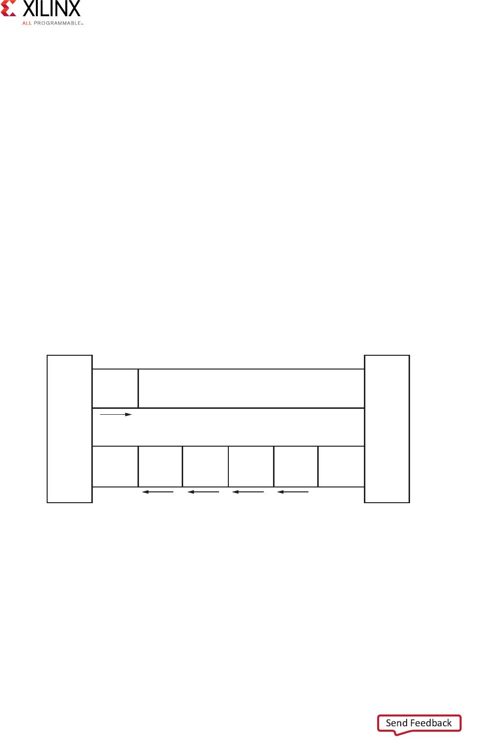
Figure 1-1: Channel Architecture of Reads
Master
interface
Read address channel
Address
and
control
Read data channel
Read
data
Read
data
Read
data
Read
data
Slave
interface
X12076

Vivado AXI Reference Guide www.xilinx.com 8
UG1037 (v4.0) July 15, 2017
Chapter 1: Introducing AXI for Vivado
X-Ref Target - Figure 1-2
As shown in the preceding figures, AXI4:
• Provides separate data and address connections for reads and writes, which allows
simultaneous, bidirectional data transfer.
• Requires a single address and then bursts up to 256 words of data.
The AXI4 protocol describes options that allow AXI4-compliant systems to achieve very
high data throughput. Some of these features, in addition to bursting, are: data upsizing
and downsizing, multiple outstanding addresses, and out-of-order transaction processing.
At a hardware level, AXI4 allows systems to be built with a different clock for each AXI
master-slave pair. In addition, the AXI4 protocol allows the insertion of register slices (often
called pipeline stages) to aid in timing closure.
AXI4-Lite is similar to AXI4 with some exceptions: The most notable exception is that
bursting is not supported. The AXI4-Lite chapter of the ARM AMBA AXI Protocol
Specification [Ref 1] describes the AXI4-Lite protocol in more detail.
The AXI4-Stream protocol defines a single channel for transmission of streaming data. The
AXI4-Stream channel models the write data channel of AXI4. Unlike AXI4, AXI4-Stream
interfaces can burst an unlimited amount of data. There are additional, optional capabilities
described in the AMBA4 AXI4-Stream Protocol Specification [Ref 1]. The specification
describes how you can split, merge, interleave, upsize, and downsize AXI4-Stream
compliant interfaces.
IMPORTANT: Unlike AXI4, you cannot reorder AXI4-Stream transfers.
Figure 1-2: Channel Architecture of Writes
Master
interface
Write address channel
Address
and
control
Write data channel
Write
data
Write
data
Write
data
Write
data
Write
response
Write response channel
Slave
interface
X12077

Vivado AXI Reference Guide www.xilinx.com 9
UG1037 (v4.0) July 15, 2017
Chapter 1: Introducing AXI for Vivado
•Memory-Mapped Protocols: In memory-mapped protocols (AXI3, AXI4, and
AXI4-Lite), all transactions involve the concept of transferring a target address within a
system memory space and data.
Memory-mapped systems often provide a more homogeneous way to view the system,
because the IP operates around a defined memory map.
AXI3-based IP can be integrated into AXI4-based systems for interoperability, however
most Xilinx IP natively adopt AXI4 which contains protocol enhancements compared to
AXI3.
Note: The processing system block in the Zynq-7000 AP SoC devices use AXI3 memory-mapped
interfaces. AXI3 is a subset of AXI4 and Xilinx tools automatically insert the necessary adaptation
logic to translate between AXI3 and AXI4.
•AXI4-Stream Protocol: Use the AXI4-Stream protocol for applications that typically
focus on a data-centric and data-flow paradigm where the concept of an address is not
present or not required. Each AXI4-Stream acts as a single unidirectional channel with a
handshaking data flow.
At this lower level of operation (compared to the memory-mapped protocol types), the
mechanism to move data between IP is defined and efficient, but there is no unifying
address context between IP. The AXI4-Stream IP can be better optimized for
performance in data flow applications, but also tends to be more specialized around a
given application space.
•Infrastructure IP: An infrastructure IP is a building block used to help assemble
systems. Infrastructure IP tends to be a generic IP that moves or transforms data
around the system using general-purpose AXI4 interfaces and does not interpret data.
Examples of infrastructure IP are:
°AXI Register slices (for pipelining)
°AXI FIFOs (for buffering/clock conversion)
°AXI Interconnect IP and AXI SmartConnect IP (for connecting memory-mapped IP
together)
°AXI Direct Memory Access (DMA) engines (for memory-mapped to stream
conversion)
°AXI Performance Monitors and Protocol Checkers (for analysis and debug)
°AXI Verification IP (for simulation-based verification and performance analysis)
These IP are useful for connecting IP together into a system, but are not generally
endpoints for data.
Vivado AXI Reference Guide www.xilinx.com 10
UG1037 (v4.0) July 15, 2017
Chapter 1: Introducing AXI for Vivado
Combining AXI4-Stream and Memory-Mapped Protocols
A common approach is to build systems that combine AXI4-Stream and AXI
memory-mapped IP together. Often a DMA engine can be used to move streams in and out
of memory.
For example, a processor can work with DMA engines to decode packets or implement a
protocol stack on top of the streaming data to build more complex systems where data
moves between different application spaces or different IP.
IP Interoperability
The AXI specification provides a framework that defines protocols for moving data between
IP using a defined signaling standard. This standard ensures that IP can exchange data with
each other and that data can be moved across a system.
AXI IP interoperability affects:
• The IP application space
• How the IP interprets data
• Which AXI interface protocol is used (AXI4, AXI4-Lite, or AXI4-Stream)
The AXI protocol defines how data is exchanged, transferred, and transformed. The AXI
protocol also ensures an efficient, flexible, and predictable means for transferring data.
Data Interpretation
IMPORTANT: The AXI protocol does not specify or enforce the interpretation of data; therefore, you
need to understand the data contents, and the different IP must have a compatible interpretation of the
data.
For IP such as a general purpose processor with an AXI4 memory-mapped interface, there
is a great degree of flexibility in how to program a processor to format and interpret data as
required by the Endpoint IP.
IP Compatibility
For more application-specific IP, like an Ethernet MAC (EMAC) or a Video Display IP using
AXI4-Stream, the compatibility of the IP is more limited to their respective application
spaces. For example, directly connecting an Ethernet MAC to the Video Display IP is not
feasible.

Vivado AXI Reference Guide www.xilinx.com 11
UG1037 (v4.0) July 15, 2017
Chapter 1: Introducing AXI for Vivado
Note: Even though two IP, such as EMAC and Video Streaming, can theoretically exchange data with
each other, they would not function together because the two IP interpret bit fields and data packets
in a completely different manner.
AXI4-Stream IP Interoperability
Chapter 7, “AXI4-Stream IP Interoperability: Tips and Hints,” provides an overview of the
main elements and steps for building an AXI4-Stream system with interoperable IP. These
key elements include understanding the AXI protocol, learning domain specific usage
guidelines, using AXI infrastructure IP as system building blocks, and validating the final
result. You can be most effective if you follow these steps:
1. Review the AXI4 documents:
°AMBA4 AXI4-Stream Protocol Specification [Ref 1]
°LogiCORE IP AXI Interconnect IP Product Guide (PG059) [Ref 12]
°LogicCORE IP AXI SmartConnect Product Guide (PG247) [Ref 23]
°Chapter 7, “AXI4-Stream IP Interoperability: Tips and Hints.”
°LogicCore IP AXI4-Stream Interconnect Product Guide (PG085) [Ref 14]
2. Understand IP domains:
°Review data types and layered protocols in Chapter 7, “AXI4-Stream IP
Interoperability: Tips and Hints.”
°Review the list of AXI IP available at: the Xilinx IP Center website [Ref 3].
°Understand the domain-level guidelines described in Domain Usage Guidelines and
Conventions in Chapter 7.
3. Use the following steps when creating your system:
a. Configure IP to share compatible data types and protocols.
b. Use Infrastructure IP or converters where necessary.
c. Validate the system.
Quick Take Videos
The following quick take videos provide more information about using the AXI protocol
with the Vivado Design Suite and other Xilinx development tools:
VIDEOS:
Vivado Design Suite QuickTake Video: Targeting Zynq Devices Using Vivado IP Integrator
Vivado Design Suite QuickTake Video: Designing with Vivado IP Integrator
Vivado Design Suite QuickTake Video: Targeting Zynq Devices Using Vivado IP Integrator

Vivado AXI Reference Guide www.xilinx.com 12
UG1037 (v4.0) July 15, 2017
Chapter 2
AXI Support in Xilinx Tools and IP
Introduction
This chapter describes how you can use Xilinx® tools to deploy individual pieces of AXI IP
or to build systems of interconnected Xilinx AXI IP (using the Vivado® IP integrator in the
Vivado® Design Suite.
Using Vivado AXI IP in RTL Projects
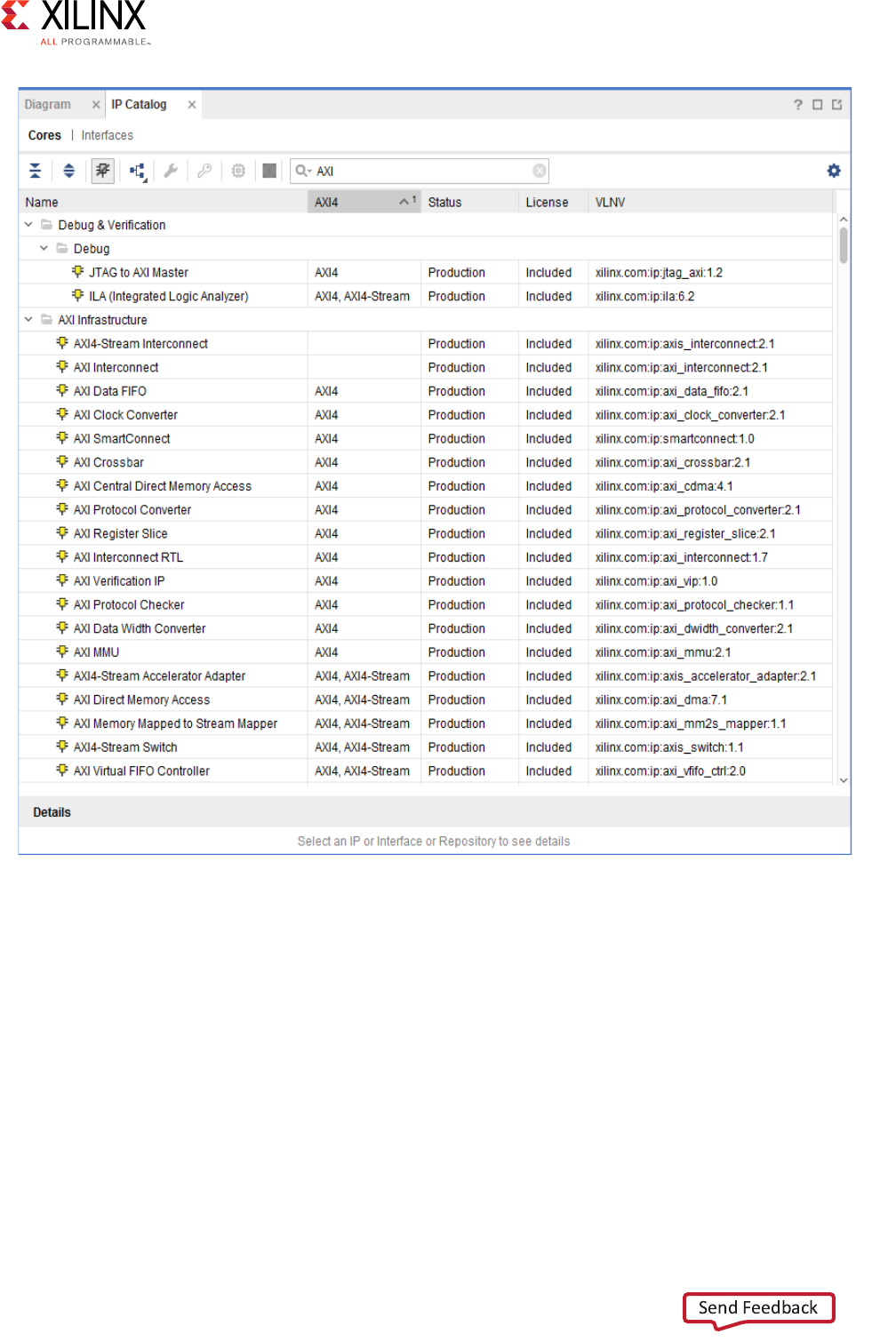
In the Vivado Integrated Development Environment (IDE), you can access Xilinx IP with an
AXI4 interface directly from the Vivado IP Catalog and instantiate that IP directly into an
register transfer logic (RTL) design (Figure 2-1).
Vivado AXI Reference Guide www.xilinx.com 13
UG1037 (v4.0) July 15, 2017
Chapter 2: AXI Support in Xilinx Tools and IP
In the IP catalog, the AXI4 column shows IP with AXI4 interfaces that are supported and
displays the which interfaces are supported by the IP interface: AXI4 (memory-mapped),
AXI4-Stream, or none.
Xilinx IP are designed to support AXI where applicable. For more information about using IP
from the Vivado IP catalog in an RTL flow, see the Vivado Design Suite User Guide: Designing
with IP (UG896) [Ref 30].
X-Ref Target - Figure 2-1
Figure 2-1: IP Catalog in Xilinx Tools
Vivado AXI Reference Guide www.xilinx.com 14
UG1037 (v4.0) July 15, 2017
Chapter 2: AXI Support in Xilinx Tools and IP
Using the Create and Package IP Wizard for AXI IP
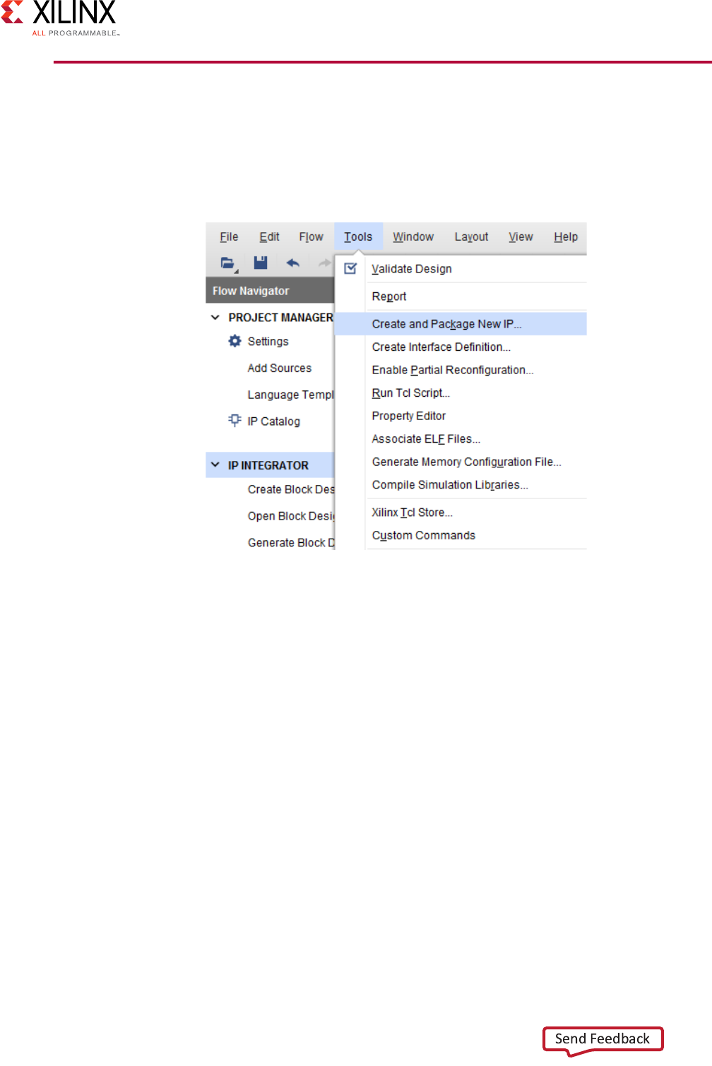
The Vivado IDE provides a Create and Package IP wizard that takes you through all the
required steps and settings for AXI IP. To create and package new IP:
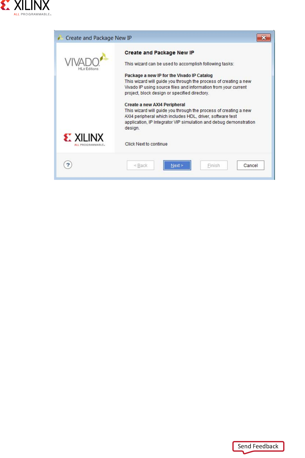
1. From the Tools menu, select Create and Package IP, as shown in the following figure.
The Create And Package IP wizard opens, as shown in Figure 2-3.
X-Ref Target - Figure 2-2
Figure 2-2: Create and Package IP Option
Vivado AXI Reference Guide www.xilinx.com 15
UG1037 (v4.0) July 15, 2017
Chapter 2: AXI Support in Xilinx Tools and IP
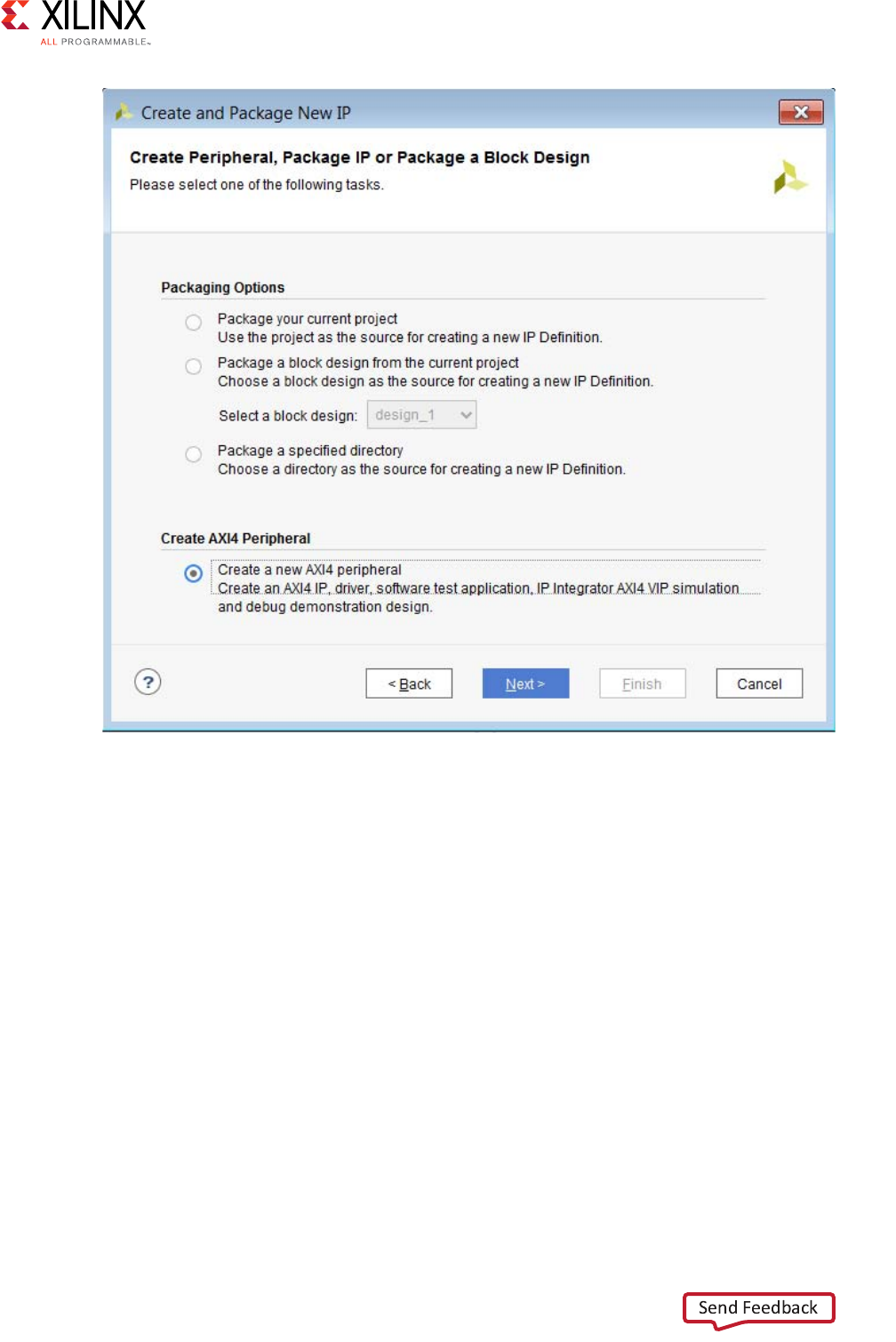
2. Select Create a new AXI4 Peripheral, to create a template AXI4 peripheral that includes
HDL, drivers, a test application, and a BFM example template.
3. Click Next.
The Choose Create Peripheral or Package IP page opens, as shown in Figure 2-4.
X-Ref Target - Figure 2-3
Figure 2-3: Create and Package IP Dialog Box
Vivado AXI Reference Guide www.xilinx.com 16
UG1037 (v4.0) July 15, 2017
Chapter 2: AXI Support in Xilinx Tools and IP
4. Click Next.
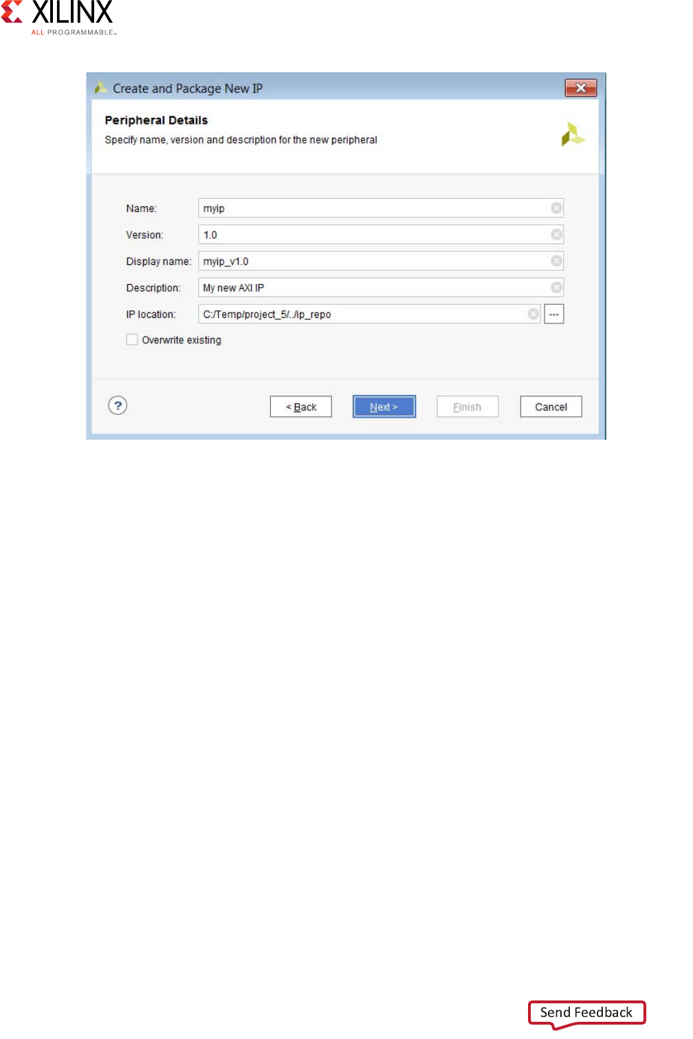
The Peripheral Details page opens.
5. Enter the IP details in the Peripheral Details page, as shown in Figure 2-5.
X-Ref Target - Figure 2-4
Figure 2-4: Choose Create or Package IP Dialog Box
Vivado AXI Reference Guide www.xilinx.com 17
UG1037 (v4.0) July 15, 2017
Chapter 2: AXI Support in Xilinx Tools and IP
The Display Name you provide shows in the Vivado IP catalog.
You can have different names in the Name and Display Name fields; any change in
Name reflects automatically in the Display Name, which is concatenated with the
Version field.
6. Click Next.
7. Select the IP location where you want the IP to be located.
The Vivado IP tool adds the location automatically to the IP repository list.
8. Click Next.
X-Ref Target - Figure 2-5
Figure 2-5: IP Details

Vivado AXI Reference Guide www.xilinx.com 18
UG1037 (v4.0) July 15, 2017
Chapter 2: AXI Support in Xilinx Tools and IP
9. Add interfaces to your IP based on the functionality and the required AXI type, as shown
in the following figure.
10. To include interrupts to be available in your IP, check the Enable Interrupt Support
check box.
The IP that this example shows would support edge or level interrupt (generated locally
on the counter), which can be extended to input ports by user and IRQ output.
The data width and the number of registers vary, based on the AXI4 selection type.
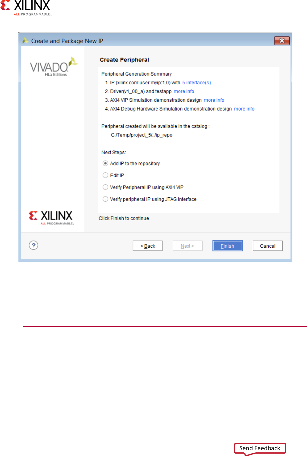
11. Click Next and review your selections.
The final page of the wizard lists the details of your IP, as shown in Figure 2-7.
X-Ref Target - Figure 2-6
Figure 2-6: Create and Package New IP
Vivado AXI Reference Guide www.xilinx.com 19
UG1037 (v4.0) July 15, 2017
Chapter 2: AXI Support in Xilinx Tools and IP
After you generate the IP, additional options are available.
See the Vivado Design Suite User Guide: Creating and Packaging Custom IP (UG1118)
[Ref 30] for more information regarding creating and packaging AXI IP.
Adding AXI IP to the IP Catalog Using Vivado IP
Packager
The Vivado IP packager tool, shown in Figure 2-8, lets you prepare a design for use in the
Vivado IP catalog. You can then instantiate this IP into a design in the Vivado Design Suite
using the Vivado IP integrator.
X-Ref Target - Figure 2-7
Figure 2-7: Create Peripheral Summary Page

Vivado AXI Reference Guide www.xilinx.com 20
UG1037 (v4.0) July 15, 2017
Chapter 2: AXI Support in Xilinx Tools and IP
When you use the Vivado Design Suite IP packaging flow for IP development, you have a
more consistent user experience, better tool integration, and greater facilitation for reuse of
the IP design in the Vivado IDE. The IP packager is AXI-aware, and can auto-recognize AXI
signals. See Appendix A, AXI Adoption Summary, for a summary of the Xilinx AXI adoption
per signal.
X-Ref Target - Figure 2-8
Figure 2-8: Vivado IP Packager Tool
Vivado AXI Reference Guide www.xilinx.com 21
UG1037 (v4.0) July 15, 2017
Chapter 2: AXI Support in Xilinx Tools and IP
See the following documents for more information:
•Vivado Design Suite User Guide: Designing IP Subsystems Using IP Integrator (UG994)
[Ref 38]
•Vivado Design Suite User Guide: Creating and Packaging Custom IP (UG1118) [Ref 41]
Using Vivado IP Integrator to Assemble AXI IP
The Vivado IP integrator feature lets you create complex system designs by instantiating
and interconnecting IP from the Vivado IP Catalog on a design block. You can create
designs interactively through the IP integrator GUI or programmatically through a Tcl
programming interface.
The Vivado IP integrator interprets AXI4 and AXI4-Stream interfaces, allowing you to
construct designs at the interface level (for enhanced productivity). See the following
figure.
X-Ref Target - Figure 2-9
Figure 2-9: Vivado IP Integrator Diagram and AXI Interface Level Connections

Vivado AXI Reference Guide www.xilinx.com 22
UG1037 (v4.0) July 15, 2017
Chapter 2: AXI Support in Xilinx Tools and IP
An interface is a grouping of signals that share a common function. An AXI4 master
interface, for example, contains a large number of individual signals which are required to
be wired correctly to make a connection.
If each signal in an interface is presented separately, the IP symbol is visually very complex
and requires more effort to connect. By grouping these signals into a single AXI interface,
a single Tcl command or GUI connection can be made using a higher level of abstraction.
The Vivado IP integrator contains design rule checks (DRCs) and automation facilities that
are aware of each specific AXI interfaces to help ensure that the required signals are
connected and configured properly. IP integrator offers design assistance as you develop
your design.
For more information about the Vivado IP integrator, see Vivado Design Suite User Guide:
Designing IP Subsystems Using IP Integrator (UG994) [Ref 38].
Using AXI IP in System Generator for DSP
System Generator for DSP® is a design tool that lets you use of the MathWorks
model-based Simulink® product design environment for FPGA design. Designs are
captured in a DSP-friendly Simulink modeling environment using an optimized
Xilinx-specific blockset.
System Generator supports the following:
• AXI4-Lite and AXI4-Stream interfaces which move data in and out of the DSP design
created with System Generator. By using AXI4-Lite and AXI4-Stream for data transfer, it
is easier to integrate a DSP design into a broader system using the Vivado Design Suite.
• Libraries of IP that users connect together using their AXI4-Stream interfaces. The DSP
designs created using System Generator can be created using AXI4-Stream based DSP
blocks.
For more information on using this tool to create AXI-based IP, see Vivado Design Suite User
Guide: Model-Based DSP Design using System Generator (UG897) [Ref 31]. Also, see the
System Generator for DSP website [Ref 49].
Vivado AXI Reference Guide www.xilinx.com 23
UG1037 (v4.0) July 15, 2017
Chapter 2: AXI Support in Xilinx Tools and IP
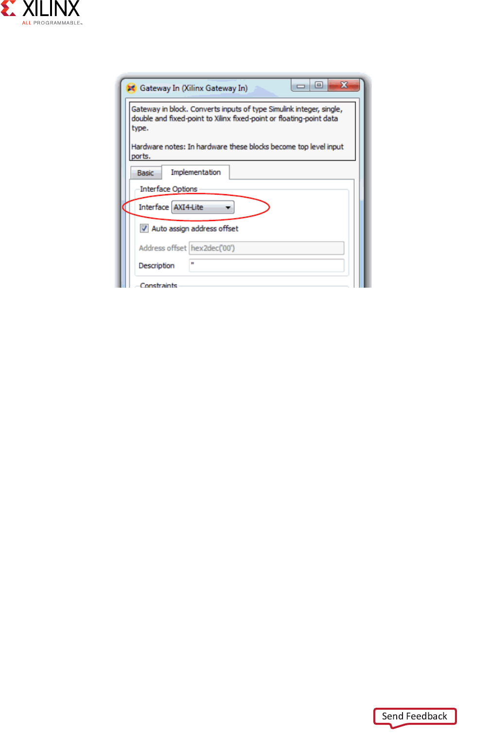
The following figure shows how to specify an AXI4-Lite interface on a Gateway In block.
Port Name Truncation
System Generator shortens the AXI4-Stream signal names to improve readability on the
block; this is cosmetic and the complete AXI4-Stream name is used in the netlist.
The name truncation is turned on by default; uncheck the Display shortened port names
option in the block parameter dialog box to see the full name.
Port Groupings
System Generator groups together and color-codes blocks of AXI4-Stream channel signals.
In the example illustrated in the following figure, the top-most input port, data_tready,
and the top two output ports, data_tvalid and data_tdata belong in the same
AXI4-Stream channel, as well as phase_tready, phase_tvalid, and phase_tdata.
X-Ref Target - Figure 2-10
Figure 2-10: Specifying an AXI4-Lite Interface in System Generator for DSP

Vivado AXI Reference Guide www.xilinx.com 24
UG1037 (v4.0) July 15, 2017
Chapter 2: AXI Support in Xilinx Tools and IP
System Generator gives signals that are not part of any AXI4-Stream channels the same
background color as the block; the arsetn signal, shown in the following figure, is an
example.
Breaking Out Multichannel TDATA
The tdata signal in an AXI4-Stream can contain multiple channels of data. In System
Generator, the individual channels for tdata are broken out; for example, in the complex
multiplier shown in the following figure, the tdata for the dout port contains both the
imaginary and the real number components.
X-Ref Target - Figure 2-12
Note: Breaking out of multichannel tdata does not add additional logic to the design. The data is
correctly byte-aligned also.
X-Ref Target - Figure 2-11
Figure 2-11: Block Signal Groupings
Figure 2-12: Multi-Channel TDATA

Vivado AXI Reference Guide www.xilinx.com 25
UG1037 (v4.0) July 15, 2017
Chapter 2: AXI Support in Xilinx Tools and IP
Adding AXI Interfaces Using High Level Synthesis
The Vivado High Level Synthesis (HLS) tool transforms a C, C++, SystemC, or OpenCL
design specification into a Register Transfer Level (RTL) implementation that you synthesize
in turn into an FPGA device.
Vivado HLS supports adding AXI interfaces you can transfer information into and out of a
design synthesized from the C, C++, SystemC, or OpenCL description. This feature
combines the ability to implement algorithms using a higher level of abstraction with the
plug-and-play benefits of the AXI protocol to integrate that design into a system with ease.
You can integrate Vivado HLS designs with AXI interfaces through Vivado IP integrator, or
instantiate directly into RTL designs.
C-based designs perform I/O operations in zero time, through formal function arguments.
In an RTL design, you perform I/O operations through a port in the design interface, that
typically operate using a specific I/O protocol.
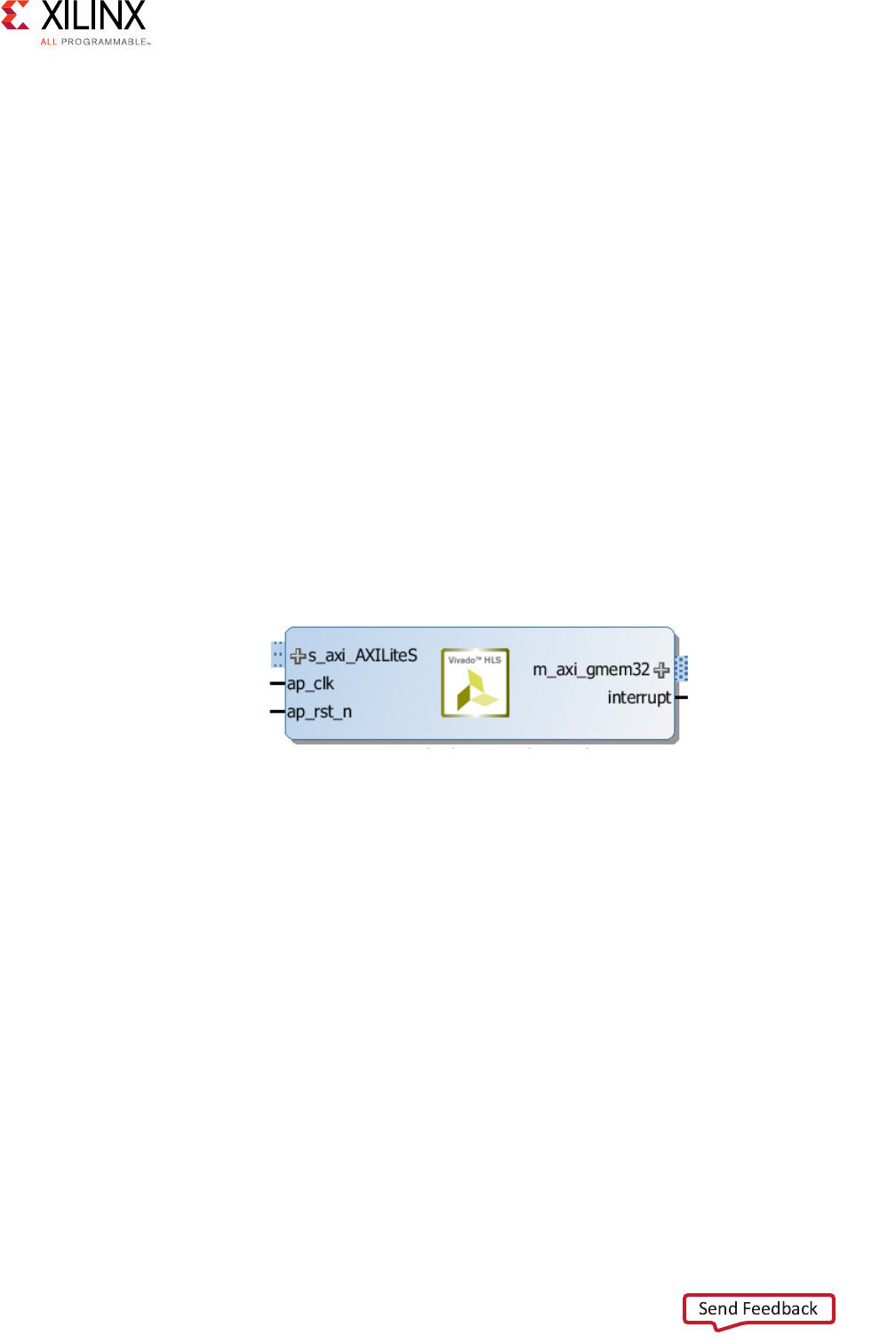
Vivado HLS supports the automatic synthesis of function arguments into the following AXI4
interfaces:
•AXI4-Stream (axis)
• AXI4-Lite slave (s_axilite)
• AXI4 master (m_axi)
The following subsections provide a brief description of the Vivado HLS AXI functionality.
For more information, see the Vivado Design Suite User Guide: High-Level Synthesis (UG902)
[Ref 32].
HLS AXI4-Stream Interface
You can apply an AXI4-Stream interface (axis mode) to any input argument and any array
or pointer output argument. Because the AXI4-Stream interface transfers data in a
sequential streaming manner it cannot be used with arguments which are both read and
written.
You can use an AXI4-Stream in your design: with or without side-channels.
•With side-channels: Using AXI4-Stream interface with side-channels provides
additional functionality, allowing the optional side-channels which are part of the
AXI4-Stream standard, to be used directly in the C code.
•Without side-channels: Use the AXI4-Stream when the data type does not contain any
AXI4 side-channel elements.
Vivado AXI Reference Guide www.xilinx.com 26
UG1037 (v4.0) July 15, 2017
Chapter 2: AXI Support in Xilinx Tools and IP
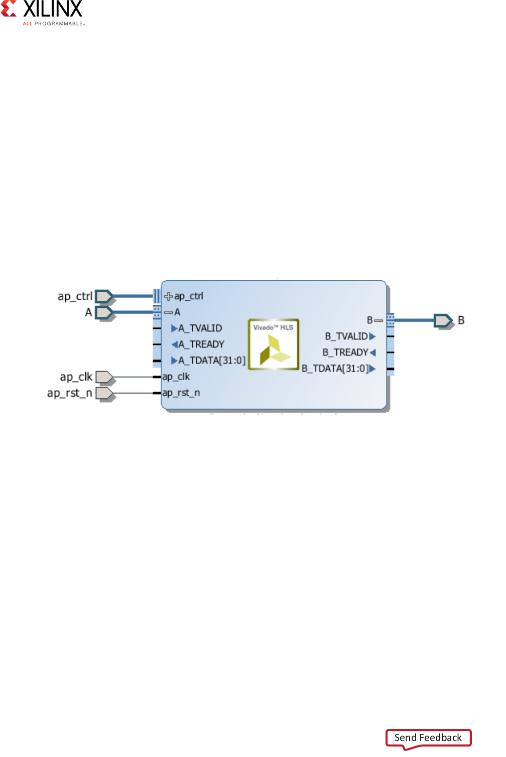
The following example shows a design where the data type is a standard C int type. In this
example, both interfaces are implemented using AXI4-Stream:
void example(int A[50], int B[50]) {
//Set the HLS native interface types
#pragma HLS INTERFACE axis port=A
#pragma HLS INTERFACE axis port=B
int i;
for(i = 0; i < 50; i++){
B[i] = A[i] + 5;
}
}
After you synthesize the code in the previous example, HLS implements both arguments
with a data port and the standard AXI4-Stream TVALID and TREADY protocol ports, as
shown in the following figure.
HLS AXI4-Lite Interface
An AXI4-Lite slave interface is typically used to allow a design to be controlled by some
form of CPU or microcontroller. The Vivado HLS features of the AXI4-Lite slave interface,
(s_axilite mode) are:
• Grouping multiple ports into the same AXI4-Lite slave interface.
• Outputting C function and header files for use with the code running on a processor
when you export the design to the Vivado IP catalog.
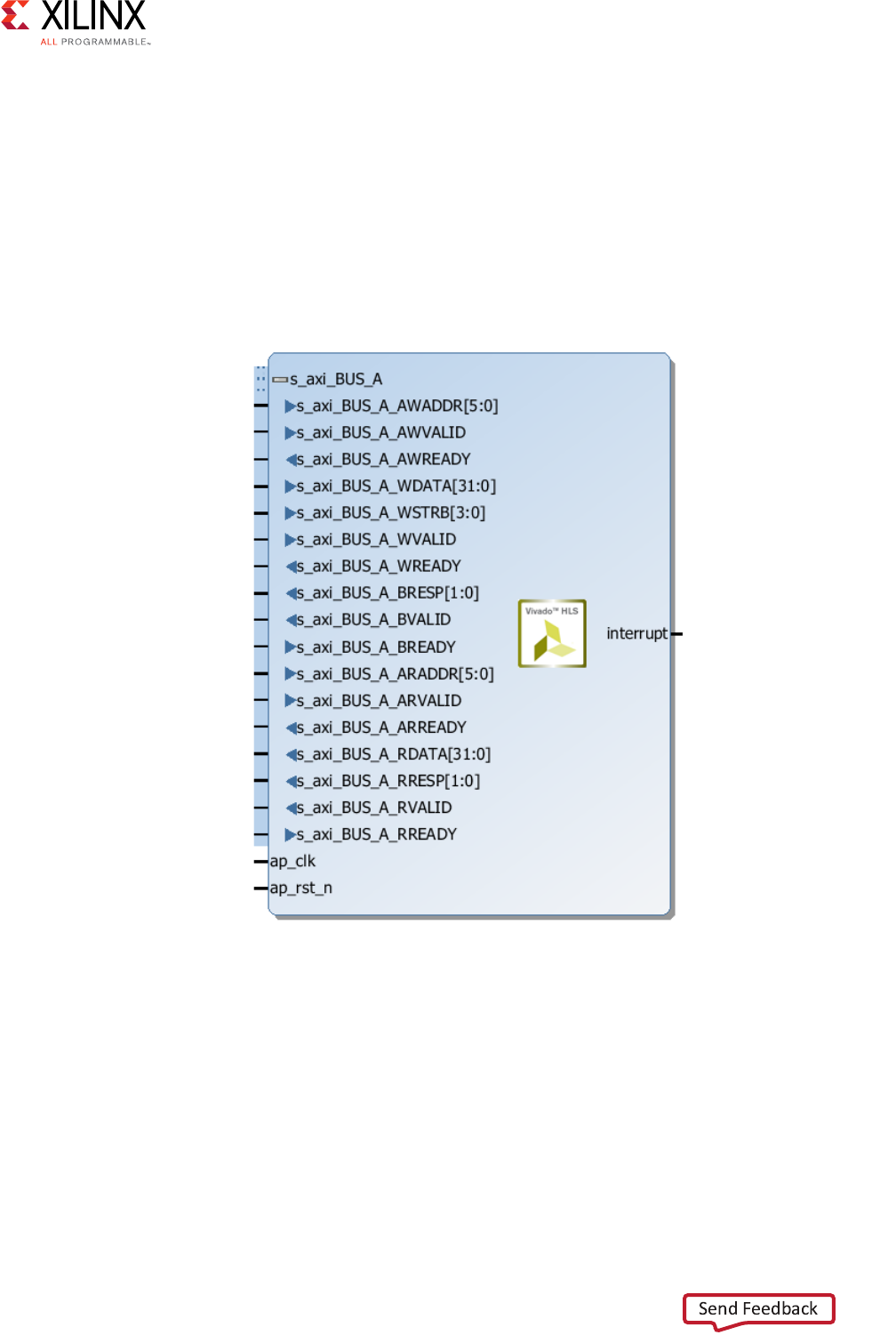
The following code example shows an implementation of multiple arguments, including the
function return, as AXI4-Lite slave interfaces in bundle=BUS_A. Because each interface
uses the same name for the bundle option, the HLS tool groups each of the ports into the
same AXI4-Lite interface:
void example(char *a, char *b, char *c)
{
#pragma HLS INTERFACE s_axilite port=return bundle=BUS_A
X-Ref Target - Figure 2-13
Figure 2-13: HLS AXI4-Stream Interfaces without Side-Channels
Vivado AXI Reference Guide www.xilinx.com 27
UG1037 (v4.0) July 15, 2017
Chapter 2: AXI Support in Xilinx Tools and IP
#pragma HLS INTERFACE s_axilite port=a bundle=BUS_A
#pragma HLS INTERFACE s_axilite port=b bundle=BUS_A
#pragma HLS INTERFACE s_axilite port=c bundle=BUS_A
*c += *a + *b;
}
After synthesizing the previous example code, HLS implements the ports, with the AXI4-Lite
slave port expanded, as shown in the following figure. The interrupt port is created by
including the function return in the AXI4-Lite slave interface. The block-level protocol port,
ap_done, drives the interrupt, which indicates when the function has completed operation.
[
HLS AXI4 Master Interface
You can implement the HLS AXI4 master interface (m_axi mode) on any array or
pointer/reference arguments. The interface is used two modes: individual data transfers,
burst-mode data transfers using the C memcpy function.
X-Ref Target - Figure 2-14
Figure 2-14: HLS AXI4-Lite Slave Interfaces with Grouped RTL Ports

Vivado AXI Reference Guide www.xilinx.com 28
UG1037 (v4.0) July 15, 2017
Chapter 2: AXI Support in Xilinx Tools and IP
Individual Data Transfers
Individual data transfers are those with the characteristics shown in the following code
examples, where a data is read or written to the top-level function argument. The following
code snippets show examples:
Example 1:
void bus (int *d) {
static int acc = 0;
acc += *d;
*d = acc;
}
Example 2:
void bus (int *d) {
static int acc = 0;
int i;
for (i=0;i<4;i++) {
acc += d[i];
d[i] = acc;
}
}
In both cases, the data transfers over the AXI4 master interface as simple read or write
operations: one address, one data values at a time.
Burst-Mode Transfers
Burst-mode transfers data using a single base address, which is followed by multiple
sequential data samples, and is capable of higher data throughput. Burst-mode is possible
only when you use the C memcpy function to read data into, or data out of, the top-level
function for synthesis.
Vivado AXI Reference Guide www.xilinx.com 29
UG1037 (v4.0) July 15, 2017
Chapter 2: AXI Support in Xilinx Tools and IP
The following example shows a copy of a burst-mode AXI4 master interface transfer. The
top-level function, argument a, is specified as the AXI4 master interface:
void example(volatile int *a){
#pragma HLS INTERFACE m_axi depth=50 port=a
#pragma HLS INTERFACE s_axilite port=return bundle=AXILiteS
//Port a is assigned to an AXI4-master interface
int i;
int buff[50];
// memcpy creates a burst access to memory
memcpy(buff,(const int*)a,50*sizeof(int));
for(i=0; i < 50; i++){
buff[i] = buff[i] + 100;
}
memcpy((int *)a,buff,50*sizeof(int));
}
When you synthesize a design with the previous example, it results in an interface as shown
in the following figure (the AXI interfaces are shown collapsed):
X-Ref Target - Figure 2-15
Figure 2-15: HLS AXI Master Interface

Vivado AXI Reference Guide www.xilinx.com 30
UG1037 (v4.0) July 15, 2017
Chapter 3
Samples of Vivado AXI IP and Xilinx
Processors
Overview
Xilinx offers a suite of AXI Infrastructure IP that serve as system building blocks. These IP
provide the ability to move data, operate on data, and measure, test, and debug AXI
transactions. For a more complete list of AXI IP, see the Xilinx® IP Center website [Ref 3].
The following IP descriptions are samples of the common, available AXI IP developed by
Xilinx, and a brief description of the Xilinx processors: Zynq® MPSoC UltraScale+™
processor, the Zynq-7000 All Programmable SoC processor, and the MicroBlaze™ processor,
which include AXI IP.
AXI Infrastructure IP Cores
The AXI Infrastructure is a collection of the following IP cores:
•AXI Crossbar: Connects one or more similar AXI memory-mapped masters to one or
more similar memory-mapped slaves.
•AXI Data Width Converter: Connects one AXI memory-mapped master to one AXI
memory-mapped slave having a wider or narrower data path.
•AXI Clock Converter: Connects one AXI memory-mapped master to one AXI
memory-mapped slave operating in a different clock domain.
•AXI Protocol Converter: Connects one AXI4, AXI3 or AXI4-Lite master to one AXI slave
of a different AXI memory-mapped protocol.
•AXI Data FIFO: Connects one AXI memory-mapped master to one AXI
memory-mapped slave through a set of FIFO buffers.
•AXI Register Slice: Connects one AXI memory-mapped master to one AXI
memory-mapped slave through a set of pipeline registers, typically to break a critical
timing path.
•AXI MMU: Provides address range decoding services for AXI Interconnect.
Vivado AXI Reference Guide www.xilinx.com 31
UG1037 (v4.0) July 15, 2017
Chapter 3: Samples of Vivado AXI IP and Xilinx Processors
AXI Interconnect is available as a standalone IP in the Xilinx IP catalog for use in an RTL
design. The standalone AXI Interconnect has a reduced feature set, mainly suitable for
connecting multiple AXI4 masters to a single AXI4 slave. See the LogiCORE IP AXI
Interconnect IP Product Guide (PG059) [Ref 5] for more information.
The IP integrator provides the user a choice to select between the AXI Interconnect and the
new AXI SmartConnect if the endpoints being connected are AXI4 memory-mapped
endpoints.
The IP integrator tool provides enhanced features, greater ease of use, and automation
services. See the following documents for more information:
°Vivado Design Suite User Guide: Designing IP Subsystems Using IP Integrator
(UG994) [Ref 38]
°Vivado Design Suite Tutorial: Designing IP Subsystems Using IP Integrator (UG995)
[Ref 39]
Xilinx AXI SmartConnect and AXI Interconnect IP
The Xilinx LogiCORE IP AXI Interconnect and LogiCORE IP AXI SmartConnect cores both
connect one or more AXI memory-mapped master devices to one or more
memory-mapped slave devices; however, the SmartConnect is more tightly integrated into
the Vivado design environment to automatically configure and adapt to connected AXI
master and slave IP with minimal user intervention. The AXI Interconnect can be used in all
memory-mapped designs. There are certain cases for high bandwidth application where
using a SmartConnect provides better optimization. The AXI SmartConnect IP delivers the
maximum system throughput at low latency by synthesizing a low area custom interconnect
that is optimized for important interfaces.
The AXI Interconnect core IP (axi_interconnect) connects one or more AXI
memory-mapped master devices to one or more memory-mapped slave devices.
The AXI interfaces conform to the AMBA® AXI4 specification from ARM®, including the
AXI4-Lite control register interface subset.
IMPORTANT: The AXI Interconnect and the AXI SmartConnect core IP are intended for
memory-mapped transfers only; AXI4-Stream transfers are not applicable, but instead can use the
AXI4-Stream Interconnect core IP (axis_interconnect). IP with AXI4-Stream interfaces are
generally connected to one another, to DMA IP, or to the AXI4-Stream Interconnect IP.
RECOMMENDED: For new medium to high performance designs, the AXI SmartConnect IP is
recommended as it offers better upward scaling in area and timing. For low performance (AXI4-Lite) or
small to medium complexity designs, AXI Interconnect may be more area efficient.

Vivado AXI Reference Guide www.xilinx.com 32
UG1037 (v4.0) July 15, 2017
Chapter 3: Samples of Vivado AXI IP and Xilinx Processors
The following section is extracted from the LogiCORE IP AXI Interconnect IP Product Guide
(PG059) [Ref 12]. See the AXI SmartConnect IP section for more in that IP.
AXI Interconnect Core Features
The AXI Interconnect IP contains the following features:
• AXI protocol compliant (AXI3, AXI4, and AXI4-Lite), which includes:
°Burst lengths up to 256 for incremental (INCR) bursts
°Converts AXI4 bursts >16 beats when targeting AXI3 slave devices by splitting
transactions.
°Propagates USER signals on each channel, if any; independent USER signal width per
channel (optional)
°Propagates Quality of Service (QoS) signals, if any; not used by the AXI Interconnect
core (optional)
• Interface data widths:
°AXI4: 32, 64, 128, 256, 512, or 1024 bits.
°AXI4-Lite: 32 bits and 64 bits
• Address width: Up to 64-bits
• ID width: Up to 32 bits
• Support for Read-only and Write-only masters and slaves, resulting in reduced resource
utilization.
Note: When used in a standalone mode, the AXI Interconnect core connects multiple masters to one
slave, which is typically a memory controller.
• Built-in data-width conversion:
°Each master and slave connection can independently use data widths of 32, 64, 128,
256, 512, or 1024 bits wide:
- The internal crossbar can be configured to have a native data-width of 32, 64,
128, 256, 512, or 1024 bits.
- Data-width conversion is performed for each master and slave connection that
does not match the crossbar native data-width.
°When converting to a wider interface (upsizing), data is packed (merged) optionally,
when permitted by address channel control signals (CACHE modifiable bit is
asserted).
°When converting to a narrower interface (downsizing), burst transactions can be
split into multiple transactions if the maximum burst length would otherwise be
exceeded.
• Built-in clock-rate conversion:
°Each master and slave connection can use independent clock rates.

Vivado AXI Reference Guide www.xilinx.com 33
UG1037 (v4.0) July 15, 2017
Chapter 3: Samples of Vivado AXI IP and Xilinx Processors
°Synchronous integer-ratio (N:1 and 1:N) conversion to the internal crossbar native
clock-rate.
°Asynchronous clock conversion (uses more storage and incurs more latency than
synchronous conversion).
°The AXI Interconnect core exports reset signals re-synchronized to the clock input
associated with each SI and MI slot.
• Built-in AXI4-Lite protocol conversion:
°The AXI Interconnect core can connect to any mixture of AXI4 and AXI4-Lite masters
and slaves.
°The AXI Interconnect core saves transaction IDs and restores them during response
transfers, when connected to an AXI4-Lite slave.
- AXI4-Lite slaves do not need to sample or store IDs.
°The AXI Interconnect core detects illegal AXI4-Lite transactions from AXI4 masters,
such as any transaction that accesses more than one word.
It generates a protocol-compliant error response to the master, and does not
propagate the illegal transaction to the AXI4-Lite slave.
• Built-in AXI3 protocol conversion:
°The AXI Interconnect core splits burst transactions of more than 16 beats from AXI4
masters into multiple transactions of no more than 16 beats when connected to an
AXI3 slave.
• Optional register-slice pipelining:
°Available on each AXI channel connecting to each master and each slave.
°Facilitates timing closure by trading-off frequency versus latency.
°One latency cycle per register-slice, with no loss in data throughput under all AXI
handshaking conditions.
• Optional data path FIFO buffering:
°Available on write and read data paths connecting to each master and each slave.
°32-deep LUT-RAM based.
°512-deep block RAM based.
°Option to delay assertion of:
-AWVALID until the complete burst is stored in the W-channel FIFO
-ARVALID until the R-channel FIFO has enough vacancy to store the entire burst
length
• Selectable Interconnect Architecture:
°Shared-Address, Multiple-Data (SAMD) crossbar (Performance Optimized):
- Parallel crossbar pathways for write data and read data channels.

Vivado AXI Reference Guide www.xilinx.com 34
UG1037 (v4.0) July 15, 2017
Chapter 3: Samples of Vivado AXI IP and Xilinx Processors
When more than one write or read data source has data to send to different
destinations, data transfers can occur independently and concurrently, provided AXI
ordering rules are met.
°Shared Access Shared Data (SASD) mode (Area optimized):
- Shared write data, shared read data, and single shared address pathways.
- Issues one outstanding transaction at a time.
- Minimizes resource utilization.
• Supports multiple outstanding transactions:
°Supports masters with multiple reordering depth (ID threads).
°Supports up to 16-bit wide ID signals (system-wide).
°Supports write response re-ordering, read data re-ordering, and read data
interleaving.
°Configurable write and read transaction acceptance limits for each connected
master.
°Configurable write and read transaction issuing limits for each connected slave.
• “Single-Slave per ID” method of cyclic dependency (deadlock) avoidance:
°For each ID thread issued by a connected master, the master can have outstanding
transactions to only one slave for writes and one slave for reads, at any time.
• Fixed priority and round-robin arbitration:
°16 configurable levels of static priority.
°Round-robin arbitration is used among all connected masters configured with the
lowest priority setting (priority 0), when no higher priority master is requesting.
°Any SI slot that has reached its acceptance limit, or is targeting an MI slot that has
reached its issuing limit, or is trying to access an MI slot in a manner that risks
deadlock, is temporarily disqualified from arbitration, so that other SI slots can be
granted arbitration.
• Supports TrustZone security for each connected slave as a whole:
- If configured as a secure slave, only secure AXI accesses are permitted
- Any non-secure accesses are blocked and the AXI Interconnect core returns a
DECERR response to the master
• Support for read-only and write-only masters and slaves, resulting in reduced resource
utilization.

Vivado AXI Reference Guide www.xilinx.com 35
UG1037 (v4.0) July 15, 2017
Chapter 3: Samples of Vivado AXI IP and Xilinx Processors
AXI Interconnect Core Limitations
These limitations apply to the AXI Interconnect core and all applicable infrastructure cores:
• The AXI Interconnect core does not support discontinued AXI3 features:
°Atomic locked transactions. This feature was retracted by AXI4 protocol. A locked
transaction is changed to a non-locked transaction and propagated by the MI.
°Write interleaving. This feature was retracted by AXI4 protocol. AXI3 master devices
must be configured as if connected to a slave with a write interleaving depth of
one.
• AXI4 Quality of Service (QoS) signals do not influence arbitration priority in AXI
Crossbar. QoS signals are propagated from SI to MI.
• AXI Interconnect and the Vivado IDE do not support the use of AXI AWREGION and
ARREGION signals.
• Interconnect cores do not support low-power mode or propagate the AXI C-channel
signals.
• AXI Interconnect cores do not time out if the destination of any AXI channel transfer
stalls indefinitely. All connected AXI slaves must respond to all received transactions, as
required by AXI protocol.
• AXI Interconnect (including AXI Crossbar and AXI MMU cores) provides no address
remapping.
• AXI Interconnect sub-cores do not include conversion or bridging to non-AXI
protocols, such as APB.
• AXI Interconnect cores do not have clock-enable (aclken) inputs. Consequently, the
use of aclken is not supported among memory-mapped AXI interfaces in Xilinx
systems.
Note: The aclken signal is supported for Xilinx AXI4-Stream interfaces.
The following subsection describes the use models for the AXI Interconnect core.
AXI Interconnect Core Use Models
The AXI Interconnect IP core connects one or more AXI memory-mapped master devices to
one or more memory-mapped slave devices. The following subsections describe the
possible use cases:
•Conversion Only
•N-to-1 Interconnect
•1-to-N Interconnect
•N-to-M Interconnect (Sparse Crossbar Mode)
Vivado AXI Reference Guide www.xilinx.com 36
UG1037 (v4.0) July 15, 2017
Chapter 3: Samples of Vivado AXI IP and Xilinx Processors
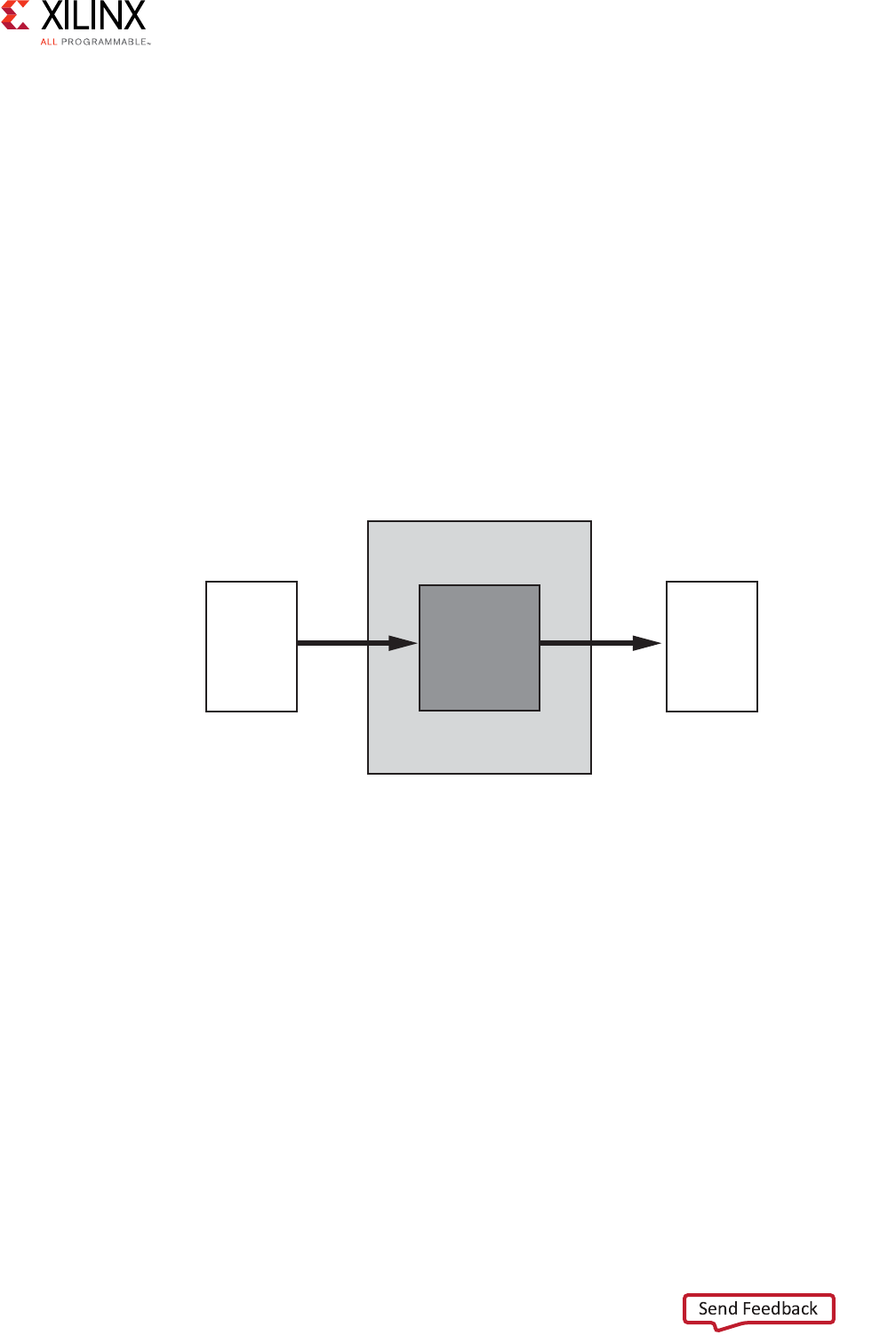
Conversion Only
The AXI Interconnect core can perform various conversion and pipelining functions when
connecting one master device to one slave device. These are:
• Data width conversion
• Clock rate conversion
• AXI4-Lite slave adaptation
• AXI-3 slave adaptation
• Pipelining, such as a register slice or data channel FIFO
In these cases, the AXI Interconnect core contains no arbitration, decoding, or routing logic.
There could be incurred latency, depending on the conversion being performed.
The following figure shows the one-to-one or conversion use case.
N-to-1 Interconnect
A common degenerate configuration of AXI Interconnect core is when multiple master
devices arbitrate for access to a single slave device, typically a memory controller. In these
cases, address decoding logic might be unnecessary and omitted from the AXI Interconnect
core (unless address range validation is needed).
Conversion functions, such as data width and clock rate conversion, can also be performed
in this configuration. The following figure shows the N-to-1 AXI interconnection use case.
X-Ref Target - Figure 3-1
Figure 3-1: 1-to-1 Conversion AXI Interconnect Use Case
Master 0 Slave 0
Interconnect
Conversion
and/or
Pipelining

Vivado AXI Reference Guide www.xilinx.com 37
UG1037 (v4.0) July 15, 2017
Chapter 3: Samples of Vivado AXI IP and Xilinx Processors
.
1-to-N Interconnect
Another degenerative configuration of the AXI Interconnect core is when a single master
device, typically a processor, accesses multiple memory-mapped slave peripherals. In these
cases, arbitration (in the address and write data paths) is not performed. The following
figure shows the 1 to N Interconnect use case.
N-to-M Interconnect (Sparse Crossbar Mode)
The N-to-M use case of the AXI Interconnect features a Shared-Address Multiple-Data
(SAMD) topology, consisting of sparse data crossbar connectivity, with single-threaded
write and read address arbitration, as shown in Figure 3-4.
X-Ref Target - Figure 3-2
Figure 3-2: N-to-1 AXI Interconnect
X-Ref Target - Figure 3-3
Figure 3-3: 1-to-N AXI Interconnect Use Case
X12050
Master 0
Master 1
Slave 0
Interconnect
Arbiter
Master 0
Slave 0
Slave 1
Interconnect
Decoder/Router

Vivado AXI Reference Guide www.xilinx.com 38
UG1037 (v4.0) July 15, 2017
Chapter 3: Samples of Vivado AXI IP and Xilinx Processors
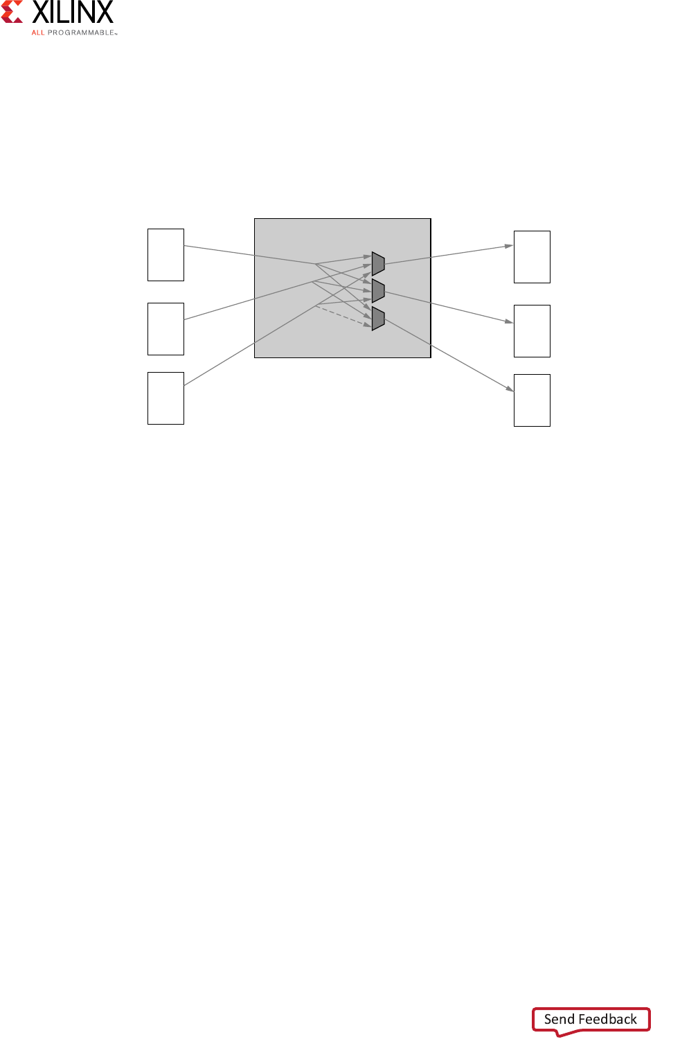
The following figure shows the sparse crossbar write and read data pathways.
X-Ref Target - Figure 3-4
Figure 3-4: Shared Write and Read Address Arbitrations
Master 0
Master 1
Master 2
Slave 0
Slave 1
Slave 2
Interconnect
AW
AR
AW
AR
AW
AR
AW
AR
AW
AR
AW
AR
Write
Transaction
Arbiter
Read
Transaction
Arbiter
Router
Router
X-Ref Target - Figure 3-5
Figure 3-5: Sparse Crossbar Write and Read Pathways
Interconnect
Master 0
Master 1
Master 2
Slave 0
Slave 1
Slave 2
W
R
W
R
W
R
W
R
W
R
W
R
Write Data Crossbar
Read Data Crossbar

Vivado AXI Reference Guide www.xilinx.com 39
UG1037 (v4.0) July 15, 2017
Chapter 3: Samples of Vivado AXI IP and Xilinx Processors
Parallel write and read data pathways connect each SI slot (attached to AXI masters on the
left) to all the MI slots (attached to AXI slaves on the right) that it can access, according to
the configured sparse connectivity map.
When more than one source has data to send to different destinations, data transfers can
occur independently and concurrently, provided AXI ordering rules are met.
The write address channels among all SI slots (if > 1) feed into a central address arbiter,
which grants access to one SI slot at a time, as is also the case for the read address channels.
The winner of each arbitration cycle transfers its address information to the targeted MI slot
and pushes an entry into the appropriate command queue(s) that enable various data
pathways to route data to the proper destination while enforcing AXI ordering rules.
Cascading AXI Interconnect Cores Together
You can connect the slave interface of one AXI Interconnect core module to the master
interface of another AXI Interconnect core with no intervening logic. Cascading multiple AXI
Interconnects allow systems to be partitioned and potentially better optimized.
AXI SmartConnect IP
The following information is extracted from the LogicCORE IP AXI SmartConnect Product
Guide (PG247) [Ref 23].
Feature Summary
• Up to 16 Slave Interfaces (SI) and up to 16 Master Interfaces (MI) per instance.
• Instances of SmartConnect can be cascaded to interconnect a larger number of
masters/slaves or for organizing the interconnect topology.
• AXI Protocol compliant. Each SI and MI of SmartConnect can be connected to a master
or slave IP interface of type AXI3, AXI4 or AXI4-Lite.
• Transactions between interfaces of different protocol types are automatically converted
by SmartConnect.
• Burst transactions are automatically split, as needed, to remain AXI compliant.
• Interface Data Widths (bits):
°AXI4 and AXI3: 32,64,128,256, 512 or 1024.
°AXI4-Lite: 32 or 64-bit.
• Transactions between interfaces of different data widths are automatically converted by
SmartConnect.
• Supports multiple clock domains (the IP provides one clock pin per domain).
• Transactions between interfaces in different clock domains are automatically converted
by SmartConnect.

Vivado AXI Reference Guide www.xilinx.com 40
UG1037 (v4.0) July 15, 2017
Chapter 3: Samples of Vivado AXI IP and Xilinx Processors
°Address width: Up to 64 bits:
°SmartConnect decodes up to 256 total address range segments.
• User defined signals up to 512 bits wide per channel.
°User signals on any AXI channel are propagated regardless of internal transaction
conversions.
• ID width: Up to 32 bits
°Automatic re-mapping/compression of wide input ID signals.
• Support for Read-only and Write-only masters and slaves, resulting in reduced resource
utilization.
• Supports multiple outstanding transactions:
°Supports connected masters with multiple reordering depth (ID threads).
°Supports write response re-ordering, Read data re-ordering, and Read Data
interleaving.
°Multi-threaded traffic (propagation of ID signals) is supported regardless of internal
transaction conversions, including data width conversion and transaction splitting.
°Optional single ordering mode (per SI and MI). Stores ID values internally instead of
propagating to the slave, resulting in reduced resource utilization.
• “Single-Slave per ID” method of cyclic dependency (deadlock) avoidance.
°For each ID thread issued by a connected master, the SmartConnect allows one or
more outstanding transactions to only one slave device for Writes and one slave
device for Reads, at a time.
°Multiple parallel pathways along all AXI channels when connected to multiple
masters and multiple slaves:
°Each AXI channel has independent destination-side arbitration. Transfers from two
or more source endpoints to separate destination endpoints can occur concurrently,
for any AXI channel.
°Round-robin arbitration for each of the AW, AR, R and B channels. (W-channel
transfers follow the same order as AW-channel arbitration, per AXI protocol rules.)
• Supports back-to-back transfers (100% duty cycle) on any AXI channel:
°Single data-beat transactions can traverse the SmartConnect at the same
bandwidth as multi-beat bursts.
• Supports TrustZone security for each connected slave:
°If configured as a secure address segment, only secure AXI accesses are permitted
according to the AXI arprot or awprot signal.
°Any non-secure accesses are blocked and the AXI SmartConnect core returns a
decerr response to the connected master.

Vivado AXI Reference Guide www.xilinx.com 41
UG1037 (v4.0) July 15, 2017
Chapter 3: Samples of Vivado AXI IP and Xilinx Processors
• Internally resynchronized reset:
°One aresetn input per IP.
AXI SmartConnect Core Limitations
These limitations apply to the AXI SmartConnect core:
• SmartConnect unconditionally packs all multi-beat bursts to fill the interface
data-width.
• SmartConnect SI interfaces accept “narrow” bursts, in which the arsize or awsize
signal indicates data units which are smaller than the interface data-width. But such
bursts are always propagated through the SmartConnect and its MI interfaces fully
packed. The “modifiable bit” of the AXI arcache or awcache signal does not prevent
packing.
• SmartConnect converts all WRAP type bursts into INCR type. SmartConnect SI
interfaces accept all protocol-compliant WRAP bursts, beginning at any target address.
But such bursts are always converted to a single INCR burst beginning at the “wrap
address”. This may increase response latency of unaligned read wrap bursts.
• SmartConnect does not support FIXED type bursts. Any FIXED burst transaction
received at the SmartConnect SI is blocked and a DECERR response is returned to the
master.
• SmartConnect does not propagate original ID values from endpoint masters. IDs
received at an SI interface are re-mapped to a smaller (or equal) number of bits for
more resource-efficient management of multi-threaded traffic.
• SmartConnect appends ID bits to differentiate among multiple masters, when
propagating transactions to the MI. Values of master identification bits are assigned by
IP Integrator and cannot be controlled or predicted by the user.
• The AXI SmartConnect core does not support discontinued AXI3 features:
°Atomic locked transactions. This feature was retracted by AXI4 protocol. A locked
transaction is changed to a non-locked transaction and propagated by the MI.
°Write interleaving. This feature was retracted by AXI4 protocol. AXI3 master
devices must be configured as if connected to a slave with a Write interleaving
depth of one.
• All arbitration on all AXI channels is round-robin. SmartConnect does not support fixed
priority arbitration.
• AXI4 Quality of Service (arqos and awqos) signals do not influence arbitration
priority. QoS signals are propagated from SI to MI.
• SmartConnect neither propagates nor generates the AXI4 arregion or awregion
signal.

Vivado AXI Reference Guide www.xilinx.com 42
UG1037 (v4.0) July 15, 2017
Chapter 3: Samples of Vivado AXI IP and Xilinx Processors
• SmartConnect does not support independent reset domains. If any master or slave
device connected to SmartConnect is reset, then all connected devices must be reset
concurrently.
• AXI SmartConnect core does not support low-power mode or propagate the AXI C
channel signals.
• AXI SmartConnect cores does not time out if the destination of any AXI channel
transfer stalls indefinitely. All connected AXI slaves must respond to all received
transactions, as required by AXI protocol.
• AXI SmartConnect provides no address remapping. AXI SmartConnect core does not
include conversion or bridging to non-AXI protocols, such as APB.
AXI4-Stream Interconnect Core IP
The AXI4-Stream Interconnect core IP (axis_interconnect) connects one or more
AXI4-Stream master devices to one or more stream slave devices. The AXI interfaces
conform to the ARM®AMBA® AXI4-Stream Product Guide (PG035) [Ref 9].
Note: The AXI4-Steam Interconnect core IP is intended for AXI4-Stream transfers only; AXI
memory-mapped transfers are not applicable.
The AXI4-Stream Interconnect IP is available in IP integrator and as standalone IP:
•The Infrastructure version for IP integrator has enhanced features, greater ease of use,
and automation services. See the AXI4-Stream Infrastructure IP Suite: Product Guide for
Vivado Design Suite (PG035) [Ref 9] for more information.
• AXI4-Stream Interconnect is also available standalone directly from the IP catalog for
use in an RTL design. See the AXI4-Stream Interconnect IP Product Guide (PG085)
[Ref 14] for more information. The following information is extracted from the AXI-4
Stream Product Guide.
AXI4-Stream Interconnect Core Features
The AXI4-Stream Interconnect IP contains the following features:
• AXI4-Stream compliant:
°Supports all AXI4-Stream defined signals: TVALID, TREADY, TDATA, TSTRB, TKEEP,
TLAST, TID, TDEST, and TUSERl
-TDATA, TSTRB, TKEEP, TLAST, TID, TDEST, and TUSER are optional
- Programmable TDATA, TID, TDEST, and TUSER widths (TSTRB and TKEEP width
is TDATA width/8).
°Per port ACLK/ARESETn inputs (supports clock domain crossing).
°Per port ACLKEN inputs (optional).

Vivado AXI Reference Guide www.xilinx.com 43
UG1037 (v4.0) July 15, 2017
Chapter 3: Samples of Vivado AXI IP and Xilinx Processors
•Core switch:
°1-16 masters.
°1-16 slaves.
°Full slave-side arbitrated crossbar switch.
°Slave input to master output routing based on TDEST value decoding and
comparison against base and high value range settings.
°Round-Robin and Priority arbitration.
- Arbitration suppress capability to prevent head-of-line blocking.
- Native switch data width 8, 16, 24, 32, 48, ... 4096 bits (any byte width up to 512
bytes).
- Arbitration tuning parameters to arbitrate on TLAST boundaries, after a set
number of transfers, and/or after a certain number of idle clock cycles.
°Optional pipeline stages after internal TDEST decoder and arbiter functional blocks.
°Programmable connectivity map to specify full or sparse crossbar connectivity.
• Built-in data width conversion:
°Each master and slave connection can independently use data widths of 8, 16, 24,
32, 48, ... 4096 bits (any byte width up to 512 bytes).
• Built-in clock-rate conversion:
°Each master and slave connection can use independent clock rates.
°Synchronous integer-ratio (N:1 and 1:N) conversion to the internal crossbar native
clock rate.
°Asynchronous clock conversion (uses more storage and incurs more latency than
synchronous conversion).
• Optional register-slice pipelining:
°Available on each AXI4-Stream channel connecting to each master and slave device.
°Facilitates timing closure by trading-off frequency versus latency.
°One latency cycle per register-slice, with no loss in data throughput in the register
slice under all AXI4-Stream handshake conditions.
• Optional data path FIFO buffering:
°Available on data paths connecting to each master and each slave.
°16, 32, 64, 128, through 32768 deep (16-deep and 32-deep are LUT-RAM based;
otherwise are block RAM based).
°Normal and Packet FIFO modes (Packet FIFO mode is also known as
store-and-forward in which a packet is stored and only released downstream after a
TLAST packet boundary is detected.)
Vivado AXI Reference Guide www.xilinx.com 44
UG1037 (v4.0) July 15, 2017
Chapter 3: Samples of Vivado AXI IP and Xilinx Processors
°FIFO data count outputs to report FIFO occupancy.
• Additional error flags to detect conditions such as TDEST decode error, sparse TKEEP
removal, and packer error.
AXI4-Stream Interconnect Core Diagram
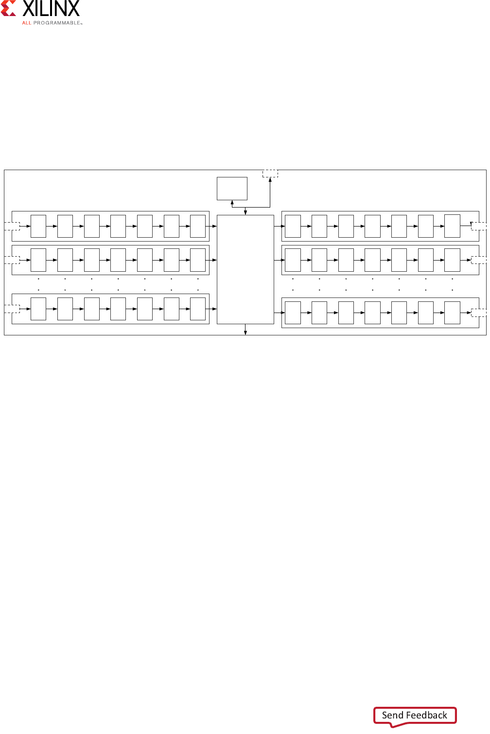
The following figure illustrates a top-level AXI4-Stream Interconnect architecture.
The AXI4-Stream Interconnect core consists of the SI, the MI, and the functional units that
include the AXI channel pathways between them.
• The SI accepts transaction requests from connected master devices.
• The MI issues transactions to slave devices.
• At the center is the switch that arbitrates and routes traffic between the various devices
connected to the SI and MI.
The AXI4-Stream Interconnect core also includes other functional units located between the
switch and each of the SI and MI interfaces that optionally perform various conversion and
storage functions. The switch effectively splits the AXI4-Stream Interconnect core down the
middle between the SI-related functional units (SI hemisphere) and the MI-related units
(MI hemisphere). This architecture is similar to that of the AXI Interconnect.
AXI4-Stream Interconnect Core Use Models
The AXI4-Stream Interconnect IP core connects one or more AXI4-Stream master devices to
one or more AXI4-Stream slave devices. The following subsections describe the possible use
cases:
• Streaming data routing and switching
• Stream multiplexing and de-multiplexing
X-Ref Target - Figure 3-6
Figure 3-6: Top-Level AXI4-Stream Interconnect Architecture
!8)33WITCH
3) -)
3) -)
3) -)
3) -)
3) -)
3) -)
!)
&IXED0RIORITY
2OUND2OBIN
!RBITER
$%#%22
!8)3
2EGISTER
3LICE
!8)3
5PSIZER
!8)3
#LOCK
#ONV
!8)3
$OWN
SIZER
!8)3
&)&/
!)
3)
!8)3)NTERCONNECT
!8)3
&)&/
!8)3
5PSIZER
!8)3
#LOCK
#ONV
!8)3
$OWN
SIZER
!8)3
0ACKER -)
!8)3
3UBSET
#ONV
!8)3
0ACKER
!8)3
5PSIZER
!8)3
#LOCK
#ONV
!8)3
$OWN
SIZER
!8)3
&)&/
3)
!8)3
3UBSET
#ONV
!8)3
0ACKER
!8)3
5PSIZER
!8)3
#LOCK
#ONV
!8)3
$OWN
SIZER
!8)3
&)&/
3)
!8)3
3UBSET
#ONV
!8)3
0ACKER
!8)3
3UBSET
#ONV
!8)3
&)&/
!8)3
5PSIZER
!8)3
#LOCK
#ONV
!8)3
$OWN
SIZER
!8)3
0ACKER -)
!8)3
&)&/
!8)3
5PSIZER
!8)3
#LOCK
#ONV
!8)3
$OWN
SIZER
!8)3
0ACKER -)
!8)3
2EGISTER
3LICE
!8)3
2EGISTER
3LICE
!8)3
2EGISTER
3LICE
!8)3
3UBSET
#ONV
!8)3
3UBSET
#ONV
!8)3
2EGISTER
3LICE
!8)3
2EGISTER
3LICE
Vivado AXI Reference Guide www.xilinx.com 45
UG1037 (v4.0) July 15, 2017
Chapter 3: Samples of Vivado AXI IP and Xilinx Processors
Streaming Data Routing and Switching (Crossbar Mode)
The AXI4-Stream Interconnect can implement a full N x M crossbar switch as shown in the
following figure. It supports slave side arbitration capable of parallel data traffic between N
masters and M slaves. Decoders and arbiters serve to route transactions between masters
and slaves.
Stream Multiplexing and De-multiplexing
You can configure the AXI4-Stream Interconnect in an Nx1 configuration to multiplex
streams together and then configured as 1xM to de-multiplex streams. Use multiplexing
and de-multiplexing to create multi-channel streams where a smaller number of wires can
carry shared traffic from multiple masters or slaves.
For example, in the following figure, AXI4-Stream interconnects are used with the AXI
virtual FIFO controller to multiplex and demultiplex multiple streams from multiple
endpoint masters and slaves together. For more information, see the LogicCORE IP AXI
Virtual FIFO Controller Product Guide (PG038) [Ref 11].
X-Ref Target - Figure 3-7
Figure 3-7: N x M Crossbar Switch (Crossbar Mode)
8
)NTERCONNECT
-ASTER
-ASTER
-ASTER
3LAVE
3LAVE
3LAVE
!8)3TREAM3WITCH
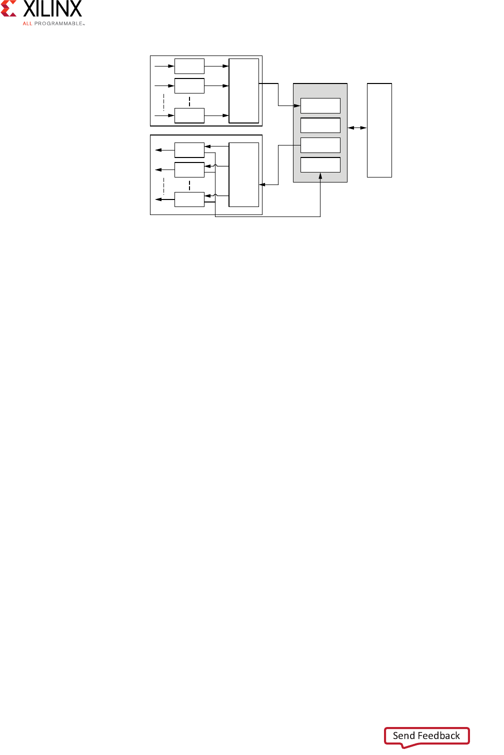
Vivado AXI Reference Guide www.xilinx.com 46
UG1037 (v4.0) July 15, 2017
Chapter 3: Samples of Vivado AXI IP and Xilinx Processors
X-Ref Target - Figure 3-8
AXI Virtual FIFO Controller
The Xilinx LogiCORE™ IP AXI Virtual FIFO Controller core (VFIFO) is a high performance
core that implements multiple AXI4-Stream FIFOs. The memory storage for data contained
in the FIFOs comes from an attached AXI4 slave memory controller. The VFIFO core
manages multiple sets of read and write address pointers to emulate the behavior of
multiple independent FIFOs.
See the LogiCORE IP AXI Virtual FIFO Controller Product Guide (PG038) [Ref 11] for more
information.
An AXI4 slave memory controller with external memory can provide large depths of external
SRAM or DDR memory. VFIFO is useful in applications using PCIe, DSP, video, or Ethernet
that require FIFOs that are deeper than can be otherwise constructed from an on-chip block
RAM memory, distributed RAM memory, or external chips.
The virtual FIFO controller can send and receive multiplexed streams to implement up to 8
logical AXI4-Stream FIFOs.
It can be used in conjunction with the AXI4-Stream Interconnect Core IP to route the data
to each endpoint IP as shown in Figure 3-9.
Figure 3-8: IAXI4-Stream Interconnects with AXI Virtual FIFO Controller
!8)3&)&/
!8)3&)&/
!8)3&)&/
!8)3&)&/
!8)3&)&/
!8)3&)&/
!8)33WITCH
.
!8)33WITCH
.
6IRTUAL&)&/#TRL
!8)-)'
$$2#TRL
3--#ONTROLLER
--3#ONTROLLER
$$2!DDR-GMT
--3722
!RBITER
!8)3TREAM3LAVE
3--
!8)3TREAM-ASTER
--3
!8)--
-ASTER
8
AXIS?INTERCONNECT
AXIS?INTERCONNECT
Vivado AXI Reference Guide www.xilinx.com 47
UG1037 (v4.0) July 15, 2017
Chapter 3: Samples of Vivado AXI IP and Xilinx Processors
The AXI4-Stream interconnect can also perform local FIFO buffering, clock conversion, and
width conversion to adapt the interface of the stream endpoints to the data path of the
virtual FIFO controller and the AXI memory controller
DataMover
The AXI DataMover is a key AXI infrastructure IP that enables high throughput transfer of
data between the AXI4 memory-mapped and AXI4-Stream domains. It provides Memory
Map-to-Stream (MM2S) and Stream-to-Memory-Map (S2MM) functions that operate
independently. The DataMover IP has the following features:
• AXI4 Compliant
• Primary AXI4 data width support of 32, 64,128, 256, 512, and 1,024 bits
• Primary AXI4-Stream data width support of 8, 16, 32, 64, 128, 256, 512 and 1,024 bits
• Parameterized Memory Map Burst Lengths of 2, 4, 8, 16, 32, 64, 128, and 256 data beats
• Optional Unaligned Address access; Up to 64 bit address support
• Optional General Purpose Store-And-Forward in both Memory Map to Stream (MM2S)
and Stream to Memory Map (S2MM)
• Optional Indeterminate Bytes to Transfer (BTT) mode in S2MM
• Supports synchronous/asynchronous clocking for Command/Status interface
See the LogiCORE IP AXI DataMover Product Guide (PG022) [Ref 7] for more information.
X-Ref Target - Figure 3-9
Figure 3-9: AXI4-Stream with Virtual FIFO Controller
!8)3&)&/
!8)3&)&/
!8)3&)&/
!8)3&)&/
!8)3&)&/
!8)3&)&/
!8)33WITCH
.
!8)33WITCH
.
6IRTUAL&)&/#TRL
!8)-)'
$$2#TRL
3--#ONTROLLER
--3#ONTROLLER
$$2!DDR-GMT
--3722
!RBITER
!8)3TREAM3LAVE
3--
!8)3TREAM-ASTER
--3
!8)--
-ASTER
AXIS?INTERCONNECT
AXIS?INTERCONNECT
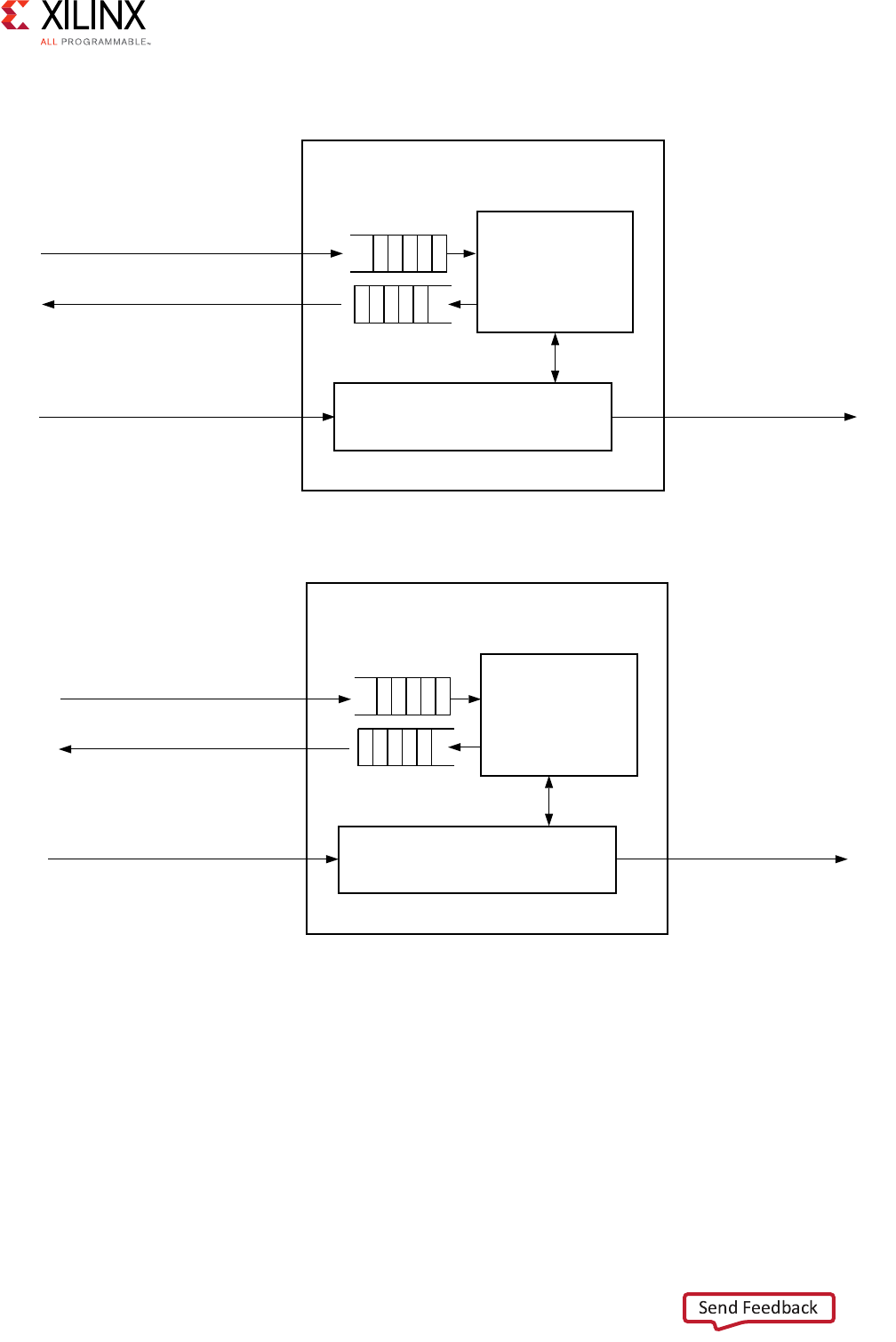
Vivado AXI Reference Guide www.xilinx.com 48
UG1037 (v4.0) July 15, 2017
Chapter 3: Samples of Vivado AXI IP and Xilinx Processors
The following figures show block diagrams of the AXI DataMover core.
There are two sub-blocks:
•MM2S: This block handles transactions from the AXI memory map to AXI4-Stream
domain. It has its dedicated AXI4-Stream compliant command and status queues, reset
block and error signals. Based on command inputs, the MM2S block issues a read
request on the AXI memory-map interface.
°Optionally, you can store read data inside the MM2S block.
X-Ref Target - Figure 3-10
Figure 3-10: DataMover MM2S Read Path
Read Engine
Cmd/Sts Logic
AXI4 Master (Read) AXI4-Stream Master
AXI4-Stream Master (Status)
AXI4-Stream Slave (Command)
MM2S (Read path)
X14017
X-Ref Target - Figure 3-11
Figure 3-11: DataMover S2MM Write Path
600:ULWHSDWK
:ULWH(QJLQH
$;,0HPRU\0DS0DVWHU:ULWH
$;,6WUHDP6ODYH&RPPDQG
$;,6WUHDP0DVWHU6WDWXV
$;,6WUHDP6ODYH
&PG6WV/RJLF
;

Vivado AXI Reference Guide www.xilinx.com 49
UG1037 (v4.0) July 15, 2017
Chapter 3: Samples of Vivado AXI IP and Xilinx Processors
°Optionally, data path interfaces (AXI4 read and AXI4-Stream master) can be made
asynchronous to command and status interfaces (AXI4-Stream command and
AXI4-Stream status).
•S2MM: This block handles transactions from the AXI4-Stream to AXI memory map
domain. It has its dedicated AXI4-Stream compliant command and status queues, reset
block and error signals. Based on command inputs and input data from the AXI4-
Stream interface, the S2MM block issues a write request on the AXI memory map
interface.
°Optionally, you can store input stream data inside a S2MM block.
°Optionally, you can make data path interfaces (AXI4 read and AXI4-Stream master)
asynchronous to command and status interfaces (AXI4-Stream command and
AXI4-Stream status).
AXI4 DMA
The AXI DMA engine provides high performance direct memory access between system
memory and AXI4-Stream type target peripherals. The AXI DMA provides Scatter Gather
(SG) capabilities, allowing the CPU to offload transfer control and execution to hardware
automation.
See the AXI DMA LogiCORE IP Product Guide (PG021) [Ref 29] for more information.
The AXI DMA as well as the SG engines are built around the AXI DataMover helper core
(shared sub-block) that is the fundamental bridging element between AXI4-Stream and
AXI4 memory-mapped buses.
AXI4 DMA provides independent operation between the Transmit channel Memory-Map to
Slave (MM2S) and the Receive channel Slave to Memory Map (S2MM), and provides optional
independent AXI4-Stream interfaces for offloading packet metadata. An AXI control stream
for MM2S provides user application data from the SG descriptors to be transmitted from AXI
DMA.
Similarly, an AXI status stream for S2MM provides user application data from a source IP like
AXI4 Ethernet to be received and stored in SG descriptors associated with the receive
packet. In an AXI Ethernet application, the AXI4 control stream and AXI4 status stream
provide the necessary functionality for performing checksum offloading.
AXI DMA provides optional SG descriptor queuing, allowing fetching and queuing of up to
four descriptors internally. This allows for very high bandwidth data transfer on the primary
data buses.
Vivado AXI Reference Guide www.xilinx.com 50
UG1037 (v4.0) July 15, 2017
Chapter 3: Samples of Vivado AXI IP and Xilinx Processors
AXI DMA Interfaces
The Xilinx implementation for DMA makes extensive use of the AXI4 capabilities. The
following table summarizes the eight AXI4 interfaces used in the AXI DMA function.
Table 3-1: AXI DMA Interfaces
Interface AXI Type Data
Width Description
Control AXI4-Lite slave 32 An AXI4-Lite slave used to access the AXI DMA
internal registers. This is generally used by the System
Processor to control and monitor the AXI DMA
operations.
Scatter Gather AXI4 master 32 An AXI4 memory-mapped master used by the AXI4
DMA to Read DMA transfer descriptors from system
memory and write updated descriptor information
back to system memory when the associated transfer
operation is complete.
Data MM Read AXI4 Read
master
32, 64,
128, 256,
512, 1024
Transfers payload data for operations moving data
from the memory-mapped side of the DMA to the
Main Stream output side.
Data MM Write AXI4 Write
master
32, 64,
128, 256,
512, 1024
Transfers payload data for operations moving data
from the Data Stream In interface of the DMA to the
memory-mapped side of the DMA.
Data Stream Out AXI4-Stream
master
32, 64,
128, 256,
512, 1024
Transfers data read by the Data MM Read interface to
the target receiver IP using the AXI4-Stream protocol.
Data Stream In AXI4-Stream
slave
32, 64,
128, 256,
512, 1024
Received data from the source IP using the
AXI4-Stream protocol. Transferred the received data
to the Memory-Map system using the Data MM Write
Interface.
Control Stream Out AXI4-Stream
master
32 The Control stream Out is used to transfer control
information embedded in the TX transfer descriptors
to the target IP.
Status Stream In AXI4-Stream
slave
32 The Status Stream In receives RX transfer information
from the source IP and updates the data in the
associated transfer descriptor and written back to the
System Memory using the Scatter Gather interface
during a descriptor update.

Vivado AXI Reference Guide www.xilinx.com 51
UG1037 (v4.0) July 15, 2017
Chapter 3: Samples of Vivado AXI IP and Xilinx Processors
Central DMA
Xilinx provides a Central DMA core for AXI interfaces. The following block diagram shows a
typical embedded system architecture incorporating the AXI (AXI4 and AXI4-Lite) Central
DMA. See the AXI Central Direct Memory Access LogiCORE IP Product Guide (PG034) [Ref 8]
for more information.
The AXI4 Central DMA performs data transfers from one memory-mapped space to another
memory-mapped space using high speed, AXI4, bursting protocol under the control of the
system microprocessor.
AXI Central DMA Summary
The AXI Central DMA provides simple transfer mode operations. The Central DMA does the
following:
• Performs the transfer
• Generates an interrupt when the transfer is complete
• Waits for the microprocessor to program and start the next transfer
X-Ref Target - Figure 3-12
Figure 3-12: Typical Use Case for AXI Central DMA
AXI CDMA
CPU
(AXI
MicroBlaze)
AXI4 MMap
Interconnect
(AXI4-Lite)
AXI
BRAM
AXI
DDRx
Registers
Scatter
Gather
Engine
AXI4
AXI4
AXI4 Read
AXI4 Write
AXI4-Lite
AXI4
AXI Intc
AXI4-Lite
AXI4-Lite
AXI4 MMap
Interconnect
(AXI4)
DP
DC
IC
AXI4
AXI4
Interrupt
Interrupts In
Interrupt Out
(To AXI Intc)
AXI4-Stream
AXI4-Stream
DataMover
X12037

Vivado AXI Reference Guide www.xilinx.com 52
UG1037 (v4.0) July 15, 2017
Chapter 3: Samples of Vivado AXI IP and Xilinx Processors
The AXI Central DMA includes an optional data realignment function for 32- and 64-bit bus
widths. This feature allows addressing independence between the transfer source and
destination addresses.
AXI Central DMA Scatter Gather Feature
The AXI Central DMA has an optional Scatter Gather (SG) feature.
SG enables the system CPU to offload transfer control to high-speed hardware automation
that is part of the Scatter Gather engine of the Central DMA. The SG function fetches and
executes pre-formatted transfer commands (buffer descriptors) from system memory as
fast as the system allows with minimal required CPU interaction. The architecture of the
Central DMA separates the SG AXI4 bus interface from the AXI4 data transfer interface so
that buffer descriptor fetching and updating can occur in parallel with ongoing data
transfers, which provides a significant performance enhancement.
DMA transfer progress is coordinated with the system CPU using a programmable and
flexible interrupt generation approach built into the Central DMA.
AXI Centralized DMA lets you switch between using Simple Mode transfers and SG-assisted
transfers using the programmable register set.
The AXI Central DMA is built around the AXI DataMover, which is the fundamental bridging
element between AXI4-Stream and AXI4 memory-mapped buses. In the case of AXI
Centralized DMA, the output stream of the DataMover is internally looped back to the input
stream. The SG feature is based on the Xilinx SG helper core used for all Scatter Gather
enhanced AXI DMA products.
Central DMA Configurable Features
The AXI4 Centralized DMA lets you trade-off the feature set implemented with the device
resource utilization budget. The following features are parameterizable at device
implementation time:
• Use DataMover Lite for the main data transport (Data Realignment Engine (DRE) and SG
mode are not supported with this data transport mechanism).
• Include or omit the Scatter Gather function.
• Include or omit the DRE function (available for 32- and 64-bit data transfer bus widths
only).
• Specify the main data transfer bus width (32, 64, 128, 256, 512, and 1024 bits).
• Specify the maximum allowed AXI4 burst length for the DataMover to use during data
transfers.
Vivado AXI Reference Guide www.xilinx.com 53
UG1037 (v4.0) July 15, 2017
Chapter 3: Samples of Vivado AXI IP and Xilinx Processors
Video DMA
The AXI4 protocol Video DMA (VDMA) provides a high bandwidth solution for Video
applications. It is a similar implementation to the Ethernet DMA solution.
The following figure shows a top-level AXI4 VDMA block diagram.
X-Ref Target - Figure 3-13
Figure 3-13: AXI VDMA High-Level Block Diagram
AXI VDMA
S2MM DMA Controller
MM2S DMA Controller
AXI DataMover
AXI Lite Slave Interface
MM2S_IntrOut
S2MM_IntrOut
Reset
Module
Register Module
MM2S_DMACR
MM2S_DMASR
MM2S_CURDESC
S2MM_DMACR
S2MM_DMASR
S2MM_CURDESC
Reserved
SG Engine
(Interrupt Coalescing )
AXI Memory Map Read (MM2S)
AXI Memory Map Write (S2MM)
AXI MM2S
Stream
AXI S2MM
Stream
AXI Lite
AXI Memory Map SG Read
MM2S
Gen-Lock
MM2S
FSync
S2MM
Gen-Lock
S2MM
FSync
MM2S_TAILDESC
Reserved
S2MM_TAILDESC
Reserved
MM2S Frame Size
MM2S Stride
MM2S Strt Addr 0
MM2S Strt Addr N
:
MM2S Frame Size
MM2S Stride
MM2S Strt Addr 0
MM2S Strt Addr N
:
MM2S Frame Size
MM2S Stride
MM2S Strt Addr 0
MM2S Strt Addr N
:
MM2S Frame Size
MM2S Stride
MM2S Strt Addr 0
MM2S Strt Addr N
:
axi_resetn
m_axis_mm2s_aresetn
s_axis_s2mm_aresetn
Line
Buffer
Line
Buffer
MM2S Line
Bufffer Status
S2MM Line
Bufffer Status
Down
Sizer
Up
Sizer
Reserved
x12054
Vivado AXI Reference Guide www.xilinx.com 54
UG1037 (v4.0) July 15, 2017
Chapter 3: Samples of Vivado AXI IP and Xilinx Processors
The following figure illustrates a typical system architecture for the AXI VDMA.
AXI VDMA Summary
The AXI VDMA engine provides high performance direct memory access between system
memory and AXI4-Stream type target peripherals. The AXI VDMA provides Scatter Gather
(SG) capabilities also, which allows the CPU to offload transfer control and execution to
hardware automation. The AXI VDMA and the SG engines are built around the AXI
DataMover helper core which is the fundamental bridging element between AXI4-Stream
and AXI4 memory-mapped buses.
AXI VDMA provides the following:
• Circular frame buffer access for up to 32 frame buffers and provides the tools to
transfer portions of video frames or full video frames.
• The ability to park on a frame, allowing the same video frame data to be transferred
repeatedly.
• Independent frame synchronization and an independent AXI clock, allowing each
channel to operate on a different frame rate and different pixel rate. To maintain
synchronization between two independently functioning AXI VDMA channels, there is
an optional Gen-Lock synchronization feature. Gen-Lock provides a method of
synchronizing AXI VDMA slaves automatically to one or more AXI VDMA masters so the
slave does not operate in the same video frame buffer space as the master.
X-Ref Target - Figure 3-14
Figure 3-14: Typical Use Case for AXI VDMA and Video IP
&IGURE4OPXREF
!8))NTERCONNECT
!8)$$2X
#05
!8)
-ICRO"LAZE
!8)"2!-
6IDEO
4IMING
#ONTROLLER
6IDEO)0
!8)
!8)
!8))NTC
)NTERRUPT
)NTERRUPTS)N
!8)--AP
)NTERCONNECT
!8),ITE
!8),ITE$0
$#
)#
!8)
!8)
2EGISTERS
3CATTER
'ATHER
%NGINE
$ATA-OVER
--3
#ONTROLLER
--3
'EN,OCK
3--
#ONTROLLER
3--
'EN,OCK
6IDEO)0
'EN,OCK
)NTERRUPT/UT
4O!8))NTC
!8)6$-!
--3&3YNC
6IDEO
4IMING
#ONTROLLER
3--&SYNC
!8),ITE
!8)7RITE !8)3TREAM
!8)3TREAM
!8)2EAD
!8)2EAD
6IDEO/UT
6IDEO)N
8

Vivado AXI Reference Guide www.xilinx.com 55
UG1037 (v4.0) July 15, 2017
Chapter 3: Samples of Vivado AXI IP and Xilinx Processors
In this mode, the slave channel skips or repeats a frame automatically. You can configure
either channel to be a Gen-Lock slave or a Gen-Lock master.
For video data transfer, the AXI4-Stream ports can be configured from 8 bits up to 1024 bits
wide in multiples of 8. For configurations where the AXI4-Stream port is narrower than the
associated AXI4 memory-mapped port, the AXI VDMA upsizes or downsizes the data
providing full bus width burst on the memory-map side. It also supports an asynchronous
mode of operation where all clocks are treated asynchronously.
VDMA AXI4 Interfaces
Simulating IP
You can use the Vivado Lab Edition to test and verify the IP capabilities when attached to a
Xilinx board with a JTAG connection.
See the following documents for more information:
•Vivado Design Suite Tutorial: Programming and Debugging (UG936) [Ref 28]
•Vivado Design Suite User Guide: Programming and Debugging (UG908) [Ref 34]
Table 3-2: AXI VDMA Interfaces
Interface AXI Type Data Width Description
Control AXI4-Lite slave 32 Accesses the AXI VDMA internal registers. This
is generally used by the System Processor to
control and monitor the AXI VDMA operations.
Scatter Gather AXI4 master 32 An AXI4 memory-mapped master that is used
by the AXI VDMA to read DMA transfer
descriptors from System Memory. Fetched
Scatter Gather descriptors set up internal
video transfer parameters for video transfers.
Data MM Read AXI4 Read master 32, 64,
128, 256, 512,
1024
Transfers payload data for operations moving
data from the memory-mapped side of the
DMA to the Main Stream output side.
Data MM Write AXI4 Write master 32, 64,
128, 256, 512,
1024
Transfers payload data for operations moving
data from the Data Stream In interface of the
DMA to the memory-mapped side of the DMA.
Data Stream Out AXI4-Stream master 8,16, 32,
64, 128, 256,
512, 1024
Transfers data read by the Data MM Read
interface to the target receiver IP using the
AXI4-Stream protocol.
Data Stream In AXI4-Stream slave 8, 16, 32,
64, 128, 256,
512, 1024
Receives data from the source IP using the
AXI4-Stream protocol. The data received is
then transferred to the Memory Map system
using the Data MM Write Interface.
Vivado AXI Reference Guide www.xilinx.com 56
UG1037 (v4.0) July 15, 2017
Chapter 3: Samples of Vivado AXI IP and Xilinx Processors
Also, simulating customized IP lets you see if you are achieving the results you expect. See
the following for more information about simulation options:
•Vivado Design Suite User Guide: Logic Simulation (UG900) [Ref 32]
•This link to “Simulating IP” in the Vivado Design Suite User Guide: Designing with IP
(UG896) [Ref 30]
The following section describes the IP that assist with debugging customized Vivado IP.
Using Debug and IP
The Vivado Lab Edition are debugging tools that are available in the Vivado Design Suite.
The features that are included in the Vivado Lab Edition include:
• Vivado logic analyzer (see ILA)
• Vivado serial I/O analyzer (see VIO)
• IBERT serial analyzer (see IBERT)
• JTAG to AXI (see JTAG-to-AXI)
Also, see Ease of Use and Debug Optimization Guidelines in Chapter 6.
ILA
The integrated logic analyzer (ILA) also called Vivado logic analyzer, lets you perform
in-system debugging of post-implemented designs on an FPGA. Use this feature when you
need to monitor signals in a design. You can also use this feature to trigger on hardware
events and capture data at system speeds. You can instantiate the ILA core in your RTL code
or insert the core, post-synthesis, in the Vivado design flow. See the Integrated Logic
Analyzer LogiCORE IP Product Guide (PG172) [Ref 22], for more information.
VIO
The virtual input/output (VIO) debug feature, also called the Vivado serial I/O analyzer can
both monitor and drive internal FPGA signals in real time. In the absence of physical access
to the target hardware, you can use this debug feature to drive and monitor signals that are
present on the real hardware.
IMPORTANT: This debug core must be instantiated in the RTL code; consequently, you need to know
what nets to drive.
The IP Catalog lists this core under the Debug category. See the Virtual Input/Output
LogiCORE IP Product Guide (PG159) [Ref 21] for more information.

Vivado AXI Reference Guide www.xilinx.com 57
UG1037 (v4.0) July 15, 2017
Chapter 3: Samples of Vivado AXI IP and Xilinx Processors
IBERT
The integrated bit error ratio tester (IBERT) serial analyzer enables in-system serial I/O
validation and debug. This allows you to measure and optimize your high-speed serial I/O
links in your FPGA-based system.
RECOMMENDED: Use the IBERT Serial Analyzer when you are interested in addressing a range of
in-system debug and validation problems from simple clocking and connectivity issues to complex
margin analysis and channel optimization issues. Use the Vivado IBERT serial analyzer design when
you are interested in measuring the quality of a signal after a receiver equalization is applied to the
received signal. This ensures that you are measuring at the optimal point in the TX-to-RX channel and
thereby real and accurate data.
You can access this design by selecting configuring, and generating the IBERT core from the
IP catalog and selecting the Open Example Design feature of this core.
See details on the IP in the following documents:
°IBERT for 7 Series GTX Transceivers LogiCORE IP Product Guide (PG132) [Ref 17]
°IBERT for 7 Series GTP Transceivers LogiCORE IP Product Guide (PG133) [Ref 18]
°IBERT for 7 Series GTH Transceivers LogiCORE IP Product Guide (PG152) [Ref 20]
JTAG-to-AXI
The JTAG-to-AXI debug feature generates AXI transactions that interact with various AXI4
and AXI4-Lite slave cores in a system that is running in hardware.
IMPORTANT: Use this core to generate AXI transactions and debug and to drive AXI signals internal to
an FPGA at run time. You can use this core in IP designs without processors as well. The IP Catalog lists
the core under the Debug category.
See Vivado Design Suite Tutorial: Programming and Debugging (UG936) [Ref 36], for a
demonstration of JTAG-to-AXI debug.

Vivado AXI Reference Guide www.xilinx.com 58
UG1037 (v4.0) July 15, 2017
Chapter 3: Samples of Vivado AXI IP and Xilinx Processors
Performance Monitor IP
The LogiCORE™ IP AXI Performance Monitor measures major performance metrics for the
AMBA AXI system. The Performance Monitor measures bus latency of a specific
master/slave (AXI4/AXI3/AXI4-Stream/AXI4-Lite) in a system, the amount of memory traffic
for specific durations, and other performance metrics. This core can also be used for
real-time profiling for software applications. See the LogiCORE IP AXI Performance Monitor
Product Guide (PG037) [Ref 10] for more information.
The AXI Performance Monitor (APM) supports three modes for analyzing system behavior
on AXI interfaces:
•Advanced: Advanced mode supports two major functions on
AXI4/AXI3/AXI4-Stream/AXI4-Lite interfaces.
°Event Logging: The APM logs the specified AXI monitor slots' events (configured by
the user) and external system events coming in to the streaming FIFO. This data can
be used by the system processor or external host application to reconstruct the AXI
transaction for analyzing system behavior/performance.
°Event Counting: The APM supports monitoring AXI slots for counting events
associated with AXI interface transaction and external events. The included event
counters can be set, read by the software, and used to analyze and enhance the
system performance. The core also has a global clock counter for real-time profiling
for software applications.
•Profile: Profile mode provides the event counting functionality of the APM with less
user configuration to analyze system behavior on AXI4/AXI3/AXI4-Lite interfaces. It
provides event counting for fixed metrics on each slot. The number of counters per slot
and the metric for each counter are pre-defined. Profile mode does not support the
AXI4-Stream interface and external event metrics.
•Trace: Trace mode provides event logging functionality of the APM with less user
configuration than Advanced mode. All the flags are enabled or disabled through the
Vivado GUI options when generating the core and cannot be modified after core
generation. Trace mode does not support the AXI4-Stream interface.
The top-level block diagram of the AXI Performance Monitor in advanced mode is shown in
Figure 3-15.
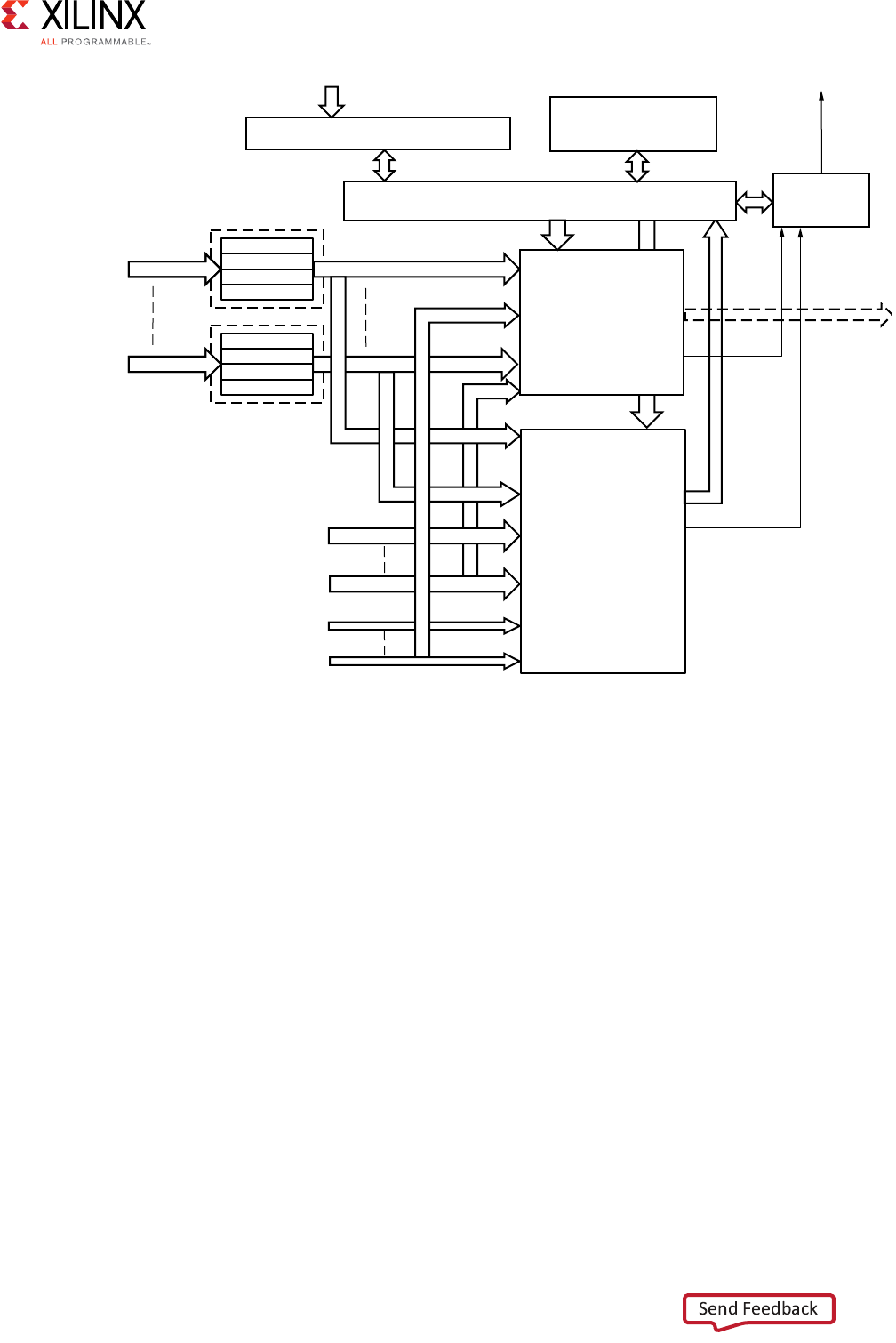
Vivado AXI Reference Guide www.xilinx.com 59
UG1037 (v4.0) July 15, 2017
Chapter 3: Samples of Vivado AXI IP and Xilinx Processors
Protocol Checkers
The AXI Protocol Checker and AXI4-Stream Protocol Checker IP monitor AXI and
AXI4-Stream interfaces. When attached to an interface, the cores actively check for protocol
violations and provide an indication of which violation occurred.
The AXI and AXI4-Stream Protocol Checkers:
• Are useful to add to a system to monitor for protocol violations that could lead to
incorrect behavior.
• Can be used for simulation and hardware-based debug.
See the following product guides for more information:
•AXI Protocol Checker LogiCORE IP Product Guide for Vivado Design Suite (PG101)
[Ref 15]
•AXI4-Stream Protocol Checker LogiCORE IP Product Guide for Vivado Design Suite
(PG145) [Ref 19]
X-Ref Target - Figure 3-15
Figure 3-15: Block Diagram of AXI Performance Monitor
-ONITOR3LOTS
!8)!8)
!8)3TREAM
!8),ITE
%VENT,OG
2EGISTERS
!8),ITE)NTERFACE
)NTERRUPT
%VENT#OUNT
!8)3TREAM
%XTERNAL%VENTS
%XTERNAL4RIGGERS
AFTERCLOCKCROSSING
'LOBAL#LOCK
#OUNTER
8
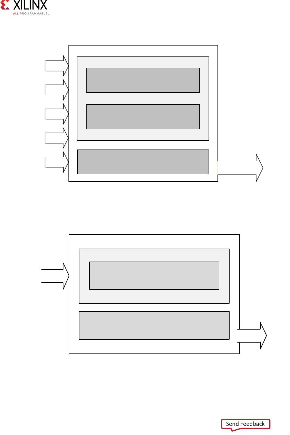
Vivado AXI Reference Guide www.xilinx.com 60
UG1037 (v4.0) July 15, 2017
Chapter 3: Samples of Vivado AXI IP and Xilinx Processors
The following figure is a block diagram of the AXI Protocol Checker.
The following figure is the block diagram of the AXI4-Stream Protocol Checker.
The error vector identifies the specific protocol violation to the console. The simulation
report provides simulation messages in the log file.
X-Ref Target - Figure 3-16
Figure 3-16: AXI Protocol Checker Block Diagram
X-Ref Target - Figure 3-17
Figure 3-17: AXI4-Stream Protocol Checker
AW
W
axi_protocol_checker
core
B
AR
RSimulation
Reporter Error Vector
AXI4/AXI3
Checker
AXI4-Lite
Checker
X13125
axis_protocol_checker
core
Simulation
Reporter
AXI Stream
Checker
T
Error Vector
X13174
Vivado AXI Reference Guide www.xilinx.com 61
UG1037 (v4.0) July 15, 2017
Chapter 3: Samples of Vivado AXI IP and Xilinx Processors
AXI Verification IP
The Xilinx AXI Verification IP (VIP) core has been developed to support the simulation of
customer designed AXI-based IP. The AXI VIP core supports three versions of the AXI
protocol (AXI3, AXI4, and AXI4-Lite). The AXI VIP is unencrypted SystemVerilog source that
contains a SystemVerilog class library and synthesizable RTL. The embedded RTL interface is
controlled by the AXI VIP through a virtual interface. AXI transactions are constructed in the
verification environment of the customer and passed to the AXI driver class. The driver class
then manages the timing and drives the content on the interface.
The following sections list the features and use cases for the AXI VIP IP. See the AXI Verification
LogiCORE IP Product Guide (PG267) [Ref 24] for a full description of the IP.
IMPORTANT: The AXI Verification IP is written in SystemVerilog and uses randomization. Not all
third-party simulators support SystemVerilog and randomization. Check Vivado Design Suite User
Guide: Release Notes, Installation, and Licensing (UG973) [Ref 29] for information about
third-party compatibility to the AXI VIP.
Features
• Supports all protocol data widths, address widths, transfer types, and responses
• Transaction-level protocol checking (burst type, length, size, lock type, and cache type)
•ARM
®-based protocol transaction level checker for tools that support assertion
property
• Behavioral SystemVerilog Syntax
• SystemVerilog class-based API
• Synthesizes to nets and constant tie-offs
Uses
The AXI Verification IP (VIP) core is used in the following manner:
• Generating master AXI commands and write payload
• Generating slave AXI read payload and write responses
• Checking protocol compliance of AXI transactions
The AXI VIP can be configured in three different modes:
• AXI master VIP
• AXI slave VIP
• AXI pass-through VIP
Vivado AXI Reference Guide www.xilinx.com 62
UG1037 (v4.0) July 15, 2017
Chapter 3: Samples of Vivado AXI IP and Xilinx Processors
The following figure shows the AXI master VIP which generates AXI commands and write
payload and sends it to the AXI system.
The following figure shows the AXI slave VIP which responds to the AXI commands and
generates read payload and write responses.
The following figure shows the AXI pass-through VIP which protocol checks all AXI
transactions that pass through it. The IP can be configured to behave in the following
modes:
• Monitor only
•Master
•Slave
The AXI protocol checker does not exist in the synthesized netlist.
IMPORTANT: When using the Vivado® simulator, the AXI Protocol Checker IP [Ref 3] is used in place of
the ARM AMBA Assertions.
X-Ref Target - Figure 3-18
Figure 3-18: AXI Master VIP
X-Ref Target - Figure 3-19
Figure 3-19: AXI Slave VIP
X-Ref Target - Figure 3-20
Figure 3-20: AXI Pass-Through VIP
SystemVerilog Interface AXI Protocol Checker M_AXI
X18492-121316
SystemVerilog Interface AXI Protocol Checker
S_AXI
X18493-121316
SystemVerilog Interface AXI Protocol Checker M_AXIS_AXI
X18494-121316

Vivado AXI Reference Guide www.xilinx.com 63
UG1037 (v4.0) July 15, 2017
Chapter 3: Samples of Vivado AXI IP and Xilinx Processors
AXI4-Stream Verification IP
The AXI4-Stream Verification IP (VIP) core supports the simulation of customer designed
AXI-based IP. The AXI4-Stream VIP core supports the AXI4-Stream protocol The
AXI4-Stream VIP is unencrypted SystemVerilog source that includes a SystemVerilog class
library and synthesizable RTL.
The embedded RTL interface is controlled by the AXI4-Stream VIP through a virtual
interface. AXI4-Stream transactions are constructed in the customer's verification
environment and passed to the AXI4-Stream driver class. The driver class then manages the
timing and driving the content on the interface.
The following sections briefly describe the IP. See the AXI4-Stream Verification IP LogiCORE
IP Product Guide (PG277) [Ref 25] for more information.
Features
• Supports the following widths:
°Data widths up to 512 bytes
°ID widths up to 32 bits
°DEST widths up to 32 bits
• ARM-based transaction-level protocol checking for tools that support assertion
property
• Behavioral SystemVerilog Syntax
• SystemVerilog class-based API
The AXI4-Stream Verification IP (VIP) core is used in the following manner:
• Generating master AXI4-Stream commands and write payload
• Generating slave AXI4-Stream read payload and write responses
• Checking protocol compliance of AXI4-Stream transactions
Overview
The AXI4-Stream VIP can be configured in three different modes:
• AXI4-Stream master VIP
• AXI4-Stream slave VIP
• AXI4-Stream pass-through VIP
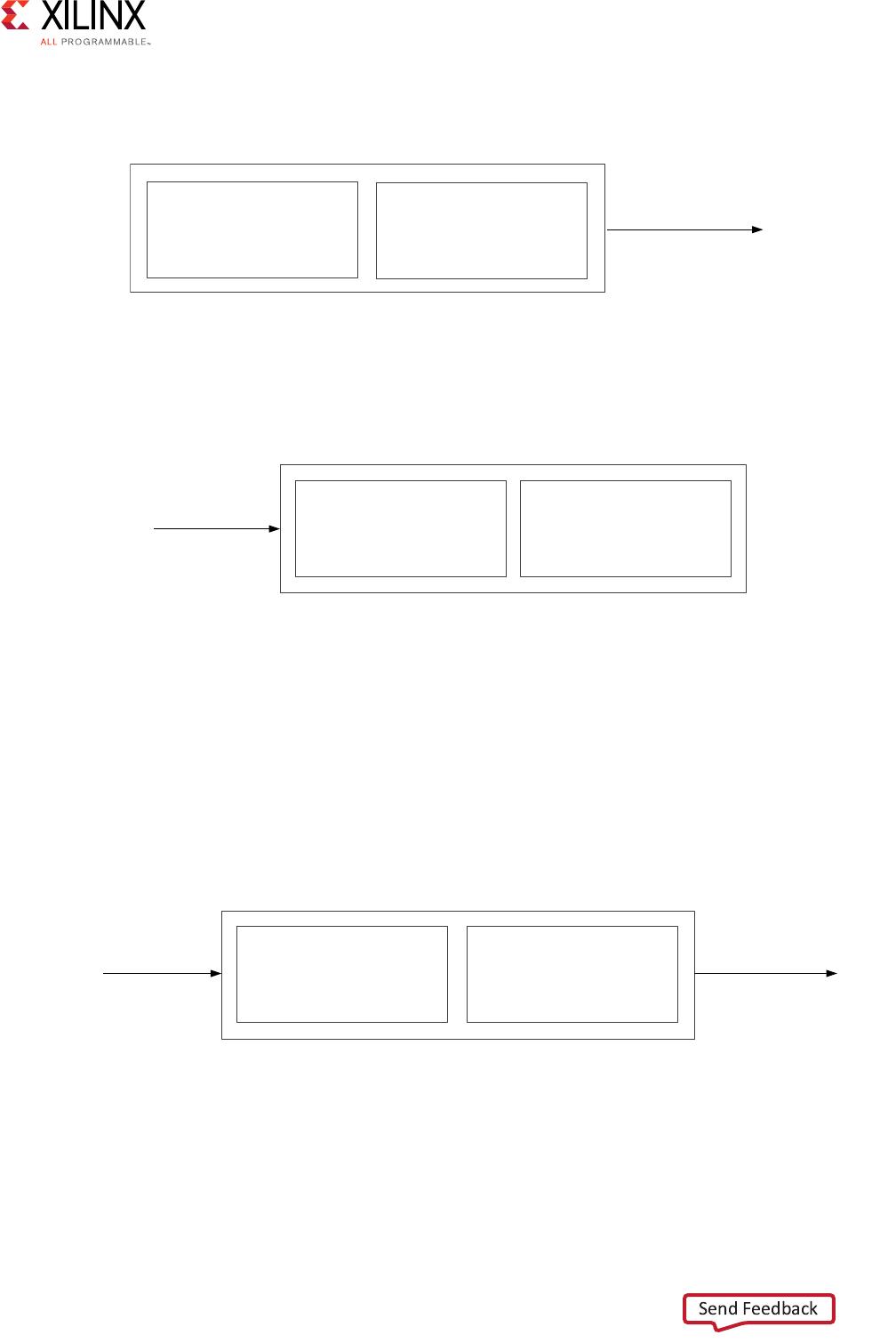
Vivado AXI Reference Guide www.xilinx.com 64
UG1037 (v4.0) July 15, 2017
Chapter 3: Samples of Vivado AXI IP and Xilinx Processors
The following figure shows the AXI4-Stream master VIP that generates AXI4-Stream
payloads and sends it to the AXI4-Stream system.
The following figure shows the AXI4-Stream slave VIP that responds to the AXI4-Stream and
generates a Ready signal.
The following figure shows the AXI4-Stream pass-through VIP that protocol checks all
AXI4-Stream transactions that pass through it. The IP can be configured to behave in the
following modes:
• Monitor only
•Master
•Slave
X-Ref Target - Figure 3-21
Figure 3-21: AXI4-Stream Master VIP
SystemVerilog Interface M_AXI4STREAM
AXI4-Stream Protocol Checker
X18774-030617
X-Ref Target - Figure 3-22
Figure 3-22: AXI4-Stream Slave VIP
SystemVerilog Interface
S_AXI4STREAM AXI4-Stream Protocol Checker
X18775-030617
X-Ref Target - Figure 3-23
Figure 3-23: AXI4-Stream Pass-Through VIP
SystemVerilog Interface M_AXI4STREAMS_AXI4STREAM AXI4-Stream Protocol Checker
X18776-030617
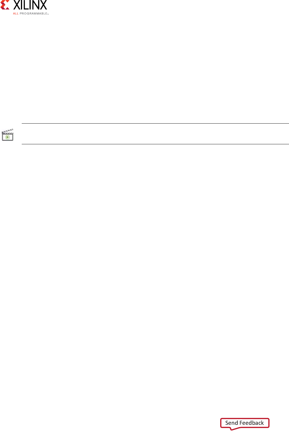
Vivado AXI Reference Guide www.xilinx.com 65
UG1037 (v4.0) July 15, 2017
Chapter 3: Samples of Vivado AXI IP and Xilinx Processors
Zynq-7000 AP SoC Verification IP
When designing Zynq®-7000 All Programmable SoC processor-based applications, a
processing_system7 Verification IP (VIP) is available. This VIP enables functional
verification of the processor logic (PL) by mimicking the processor system (PS) and PL
interfaces in PS logic. This VIP provides a package of encrypted Verilog modules. VIP
operation is controlled by using a sequence of Verilog tasks contained in a Verilog-syntax
file. See the Zynq-7000 All Programmable SoC Verification IP (DS940) [Ref 5] for more
information.
Also, the following Vivado QuickTake Video is available to help you understand how to use
the Zynq-7000 processor VIP.
VIDEO: Vivado Design Suite QuickTake Video: How to Use the Zynq-7000 Verification IP to
Verify and Debug using Simulation
Features
• Pin compatible and Verilog-based simulation model.
• Supports all AXI interfaces.
•AXI 3.0 compliant.
• 32/64–bit Data-width for AXI_HP, 32-bit for AXI_GP, and 64-bit for AXI_ACP.
• Sparse memory model (for DDR) and a RAM model (for OCM).
• System Verilog task-based API.
• Delivered in Vivado® Design Suite.
• Blocking and non-blocking interrupt support.
• ID width support as per the Zynq-7000 specification.
• Support for FIXED, INCR, and WRAP transaction types.
• Support for all Zynq-7000 supported burst lengths and burst sizes.
• Protocol checking, provided by the AXI VIP models.
• Read/Write request capabilities.
• System Address Decode for OCM/DDR transactions.
Additional Features
• System Address Decode for Register Map Read transactions (only default value of the
registers can be read).
• Support for static remap for AXI_GP0 and AXI_GP1.
• Configurable latency for Read/Write responses.
• First-level arbitration scheme based on the priority indicated by the AXI QoS signals.

Vivado AXI Reference Guide www.xilinx.com 66
UG1037 (v4.0) July 15, 2017
Chapter 3: Samples of Vivado AXI IP and Xilinx Processors
• Data path connectivity between any AXI master in PL and the PS memories and register
map.
• Parameters to enable and configure AXI Master and Slave ports.
• APIs to set the traffic profile and latencies for different AXI Master and Slave ports.
• Support for FPGA logic clock generation.
• Soft Reset Control for the PL.
• API support to pre-load the memories, read/wait for the interrupts from PL, and checks
for certain data pattern to be updated at certain memory location.
• All unused interface signals that output to the PL are tied to a valid value.
• Semantic checks on all other unused interface signals.
Limitations
The following features are not yet supported by Zynq-7000 APSoC VIP:
• Exclusive Access transfers are not supported on any of the slave ports.
• Read/Write data interleaving is not supported.
• Write access to the Register Map is not supported.
• Support for in-order transactions only.
MicroBlaze Debug Module
The MicroBlaze™ Debug Module (MDM):
• Enables JTAG-based debugging of one or more MicroBlaze processors.
•Instantiates one BSCAN primitive, or allows an external BSCAN to be used. In devices
that contain more than one BSCAN primitive, MDM uses the USER2 BSCAN by default.
• Includes a UART with a configurable slave bus interface which can be configured for an
AXI4-Lite interconnect. The UART TX and RX signals are transmitted over the FPGA JTAG
port to and from the Xilinx® Microprocessor Debug (XMD) tool. The UART behaves in a
manner similar to the LogiCORE™ IP AXI (UART) Lite core.
• Provides a configurable AXI4 master port for direct access to memory from JTAG. This
allows fast program download, as well as transparent memory access when the
connected MicroBlaze processors are executing.
•Allows software to control debug and observe debug status through the AXI4-Lite slave
interface. This is particularly useful for software performance measurements and
analysis, using the MicroBlaze extended debug functionality for performance
monitoring.
• Includes a cross-trigger capability, which enables routing of trigger events between
connected MicroBlaze processors, as well as an external interface compatible with the
Zynq®-7000 Processing System.
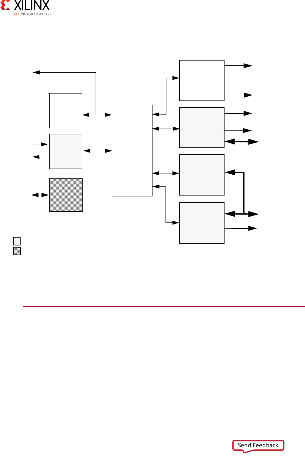
Vivado AXI Reference Guide www.xilinx.com 67
UG1037 (v4.0) July 15, 2017
Chapter 3: Samples of Vivado AXI IP and Xilinx Processors
The block diagram of the MicroBlaze Debug Module is shown in the following figure.
For more information, see the MicroBlaze Debug Module (MDM) Product Guide (PG115)
[Ref 16].
Zynq UltraScale+ MPSoC Processor Device
This information is summarized from the Zynq UltraScale+ MPSoC Technical Reference
Manual (UG1085) [Ref 40].
The Zynq® UtlraScale+™ processor device interfaces to the cache-coherent interconnect
(CCI) only to support the AXI coherency extension (ACE). ACE is an extension to the AXI
protocol and provides the following enhancements:
• Support for hardware cache coherency.
• Barrier transactions that ensure transaction ordering.
X-Ref Target - Figure 3-24
Figure 3-24: MicroBlaze Debug Module (MDM) Block Diagram
MDM
XILINX
BSCAN
MDM
Control/
Status
MicroBlaze
Debug
Control
UART
Control
MicroBlaze
Trace Core
Interface
MBDEBUG_0
MBDEBUG_31
...
S_AXI
Interrupt
XMTC
External
BSCAN
Debug
Register
Access
JTAG
Memory
Access
M_AXI
LMB_0
...
LMB_31
Optional Features
Legacy Support
Cross
Trigger
Trig In
Trig Out
Vivado AXI Reference Guide www.xilinx.com 68
UG1037 (v4.0) July 15, 2017
Chapter 3: Samples of Vivado AXI IP and Xilinx Processors
System-level coherency enables the sharing of memory by system components without the
software requirement to perform software cache maintenance to maintain coherency
between caches. Regions of memory are coherent if writes to the same memory location by
two components are observable in the same order by all components.
The ACE coherency protocol ensures that all masters observe the correct data value at any
given address location by enforcing that only one copy exists whenever a store occurs to
the location. After each store to a location, other masters can obtain a new copy of the data
for their own local cache, allowing multiple copies to exist. See the ARM® AMBA® AXI and
ACE protocol specification for a detailed overview.
PS-PL AXI Interfaces
The following table lists the AXI Interfaces in the Zynq UltraScale+ Processing System (PS)
and Processor Logic (PL).
Zynq-7000 All Programmable SoC Processor IP
This information is summarized from the Zynq-7000 AP SoC Technical Reference Manual (UG585)
[Ref 32] to provide a quick reference to the AXI and Zynq-7000 connectivity features.
Choosing a Programmable Logic Interface
This section discusses various options to connecting Programmable Logic (PL) to the
Processing System (PS). The main emphasis is on data movement tasks such as direct
memory access (DMA).
Table 3-3: PS-PL AXI Interfaces
Interface Name Abbrevi-
ation Type Master
Data
Width
Master ID Width Usage Description
S_AXI_HP{0:3}_FPD HP{0:3} AXI4 PL 128/64/32 6 Non-coherent paths from PL
to FPD main switch and DDR.
S_AXI_HPM0_LPD PL_LPD AXI4 PL 128/64/32 6 Non-coherent path from PL to
IOP in LPD.
S_AXI_ACE_FPD
ACE ACE PL 128 6
Two-way coherent path
between memory in PL and
CCI.
S_AXI_ACP_FPD ACP AXI4 PL 128 5 I/O coherent with CCI. With L2
cache allocation.
S_AXI_HPC{0, 1}_FPD HPC{0, 1} AXI4 PL 128 6 I/O coherent with CCI. No L2
cache allocation.
M_AXI_HPM{0, 1}_FPD HPM{0, 1} AXI4 PS 128/64/32 16 FPD masters to PL slaves.
M_AXI_HPM0_LPD LPD_PL AXI4 PS 128/64/32 16 LPD masters to PL slaves.

Vivado AXI Reference Guide www.xilinx.com 69
UG1037 (v4.0) July 15, 2017
Chapter 3: Samples of Vivado AXI IP and Xilinx Processors
PL Interface Comparison Summary
The following table presents a qualitative overview of data transfer use cases. The estimated
throughput column reflects suggested maximum throughput in a single direction
(read/write).
Cortex-A9 CPU Using General Purpose Masters
The least intrusive method from a software perspective is to use the Cortex-A9 to move
data between the PS and PL. Data flow is directly moved by a CPU, removing the need to
handle events from a separate DMA. Access to the PL is provided through the two
M_AXI_GP master ports, which each have a memory address range to originate PL AXI
transactions. The PL design is also simplified because as little as a single AXI slave can be
implemented to service the CPU requests.
Drawbacks of using a CPU to move data is that a sophisticated CPU is spending cycles
performing simple data movement instead of complex control and computation tasks, and
the limited throughput available. Transfer rates less than 25 MB/s are reasonable with this
method.
See the Zynq-7000 AP SoC Technical Reference Manual (UG585) [Ref 26] for more
information.
Table 3-4: Data Movement Method Comparison Summary
Method Benefits Drawbacks Suggested Uses Estimated
Throughput
CPU Programmed
I/O
•Simple Software
• Least PL Resources
• Simple PL Slaves
• Lowest Throughput • Control Functions <25 MB/s
PS DMAC • Least PL Resources
• Medium Throughput
• Multiple Channels
• Simple PL Slaves
•Somewhat complex
DMA programming
• Limited PL
Resource DMAs
600 MB/s
PL AXI_HP DMA • Highest Throughput
• Multiple Interfaces
• Command/Data FIFOs
• OCM/DDR access only
•More complex PL
Master design
• High Performance
DMA for large
datasets
1,200 MB/s
(per interface)
PL AXI_ACP DMA • Highest Throughput
•Lowest Latency
• Optional Cache
Coherency
• Large burst might
cause cache thrashing
•Shares CPU
Interconnect
bandwidth
•More complex PL
Master design
• High Performance
DMA for smaller,
coherent datasets
•Medium
granularity CPU
offload
1,200 MB/s
PL AXI_GP DMA • Medium Throughput • More complex PL
Master design
•PL to PS Control
Functions
•PS I/O Peripheral
Access
600 MB/s

Vivado AXI Reference Guide www.xilinx.com 70
UG1037 (v4.0) July 15, 2017
Chapter 3: Samples of Vivado AXI IP and Xilinx Processors
PS DMA Controller (DMAC) Using General Purpose Masters
The PS DMA controller (DMAC) provides a flexible DMA engine that can provide moderate
levels of throughput with little PL logic resource usage. The DMAC resides in the PS and
must be programmed through the DMA instructions residing in memory, typically prepared
by a CPU. With support for up to eight channels, multiple DMA fabric cores can potentially
be served in the single DMAC. However, the flexible programmable model might increase
software complexity relative to CPU transfer or specialized PL DMA.
The DMAC interface to the PL is through the general purpose AXI master interfaces, whose
32-bit width along with the centralized DMA nature (a read and write transaction for each
movement) of the DMAC to limit the DMAC from highest throughput. A peripheral request
interface also allows PL slaves to provide status to the DMAC on buffer state, to prevent
transactions involving a stalled PL peripheral from unnecessarily also stalling interconnect
and DMAC bandwidth.
From the Zynq-7000 AP SoC Technical Reference Manual (UG585) [Ref 26], see this link to
the “DMA Controller” chapter for more information on the DMAC controller, and this link to
the “Interconnect” chapter for more information on the M_AXI_GP interfaces.
PL DMA Using AXI High-Performance (HP) Interface
The high-performance (S_AXI_HP) PL interfaces provide high-bandwidth PL slave
interfaces to OCM and DDR memories. The AXI_HP ports are unable to access any other
slaves.
With four, 64-bit wide interfaces, the AXI_HP provide the greatest aggregate interface
bandwidth. The multiple interfaces also save PL resources by reducing the need to a PL AXI
interconnect. Each AXI_HP contains control and data FIFOs to provide buffering of
transactions for larger sets of bursts, making it ideal for workloads such as video frame
buffering in DDR. This additional logic and arbitration does result in higher minimum
latency than other interfaces.
The user IP logic residing in the PL generally consists of a low-speed control interface and
higher performance burst interface. If control flow is orchestrated by the Cortex-A9 CPU,
the general purpose M_AXI_GP port can be used for tasks such as configuring the memory
addresses the user IP should access and transaction status.
Transaction status can also be conveyed using PL to PS interrupts. Higher performance
devices connected to AXI_HP should be able to issue multiple outstanding transactions to
take advantage of the AXI_HP FIFOs.
The PL design complexity of multiple AXI interfaces along with the associated PL utilization
are the primary drawbacks of implementing a DMA engine in the PL for both S_AXI_HP
and S_AXI_ACP interfaces.
See this link to the “Interconnect” chapter of the Zynq-7000 AP SoC Technical Reference
Manual (UG585) [Ref 32] for more information on the AXI_HP interface.

Vivado AXI Reference Guide www.xilinx.com 71
UG1037 (v4.0) July 15, 2017
Chapter 3: Samples of Vivado AXI IP and Xilinx Processors
PL DMA Using AXI ACP
The AXI ACP interface (S_AXI_ACP) provides a similar user IP topology as is in the high
performance S_AXI_HP interfaces. Also 64 bits wide, the ACP also provides highest
throughput capability for a single AXI interface.
The ACP differs from the HP performance ports due to its connectivity inside of the PS. The
ACP connects to the snoop control unit (SCU) which is also connected to the CPU L1 and the
L2 cache. This connectivity allows ACP transactions to interact with the cache subsystems,
potentially decreasing total latency for data to be consumed by a CPU. These optionally
cache-coherent operations can prevent the need to invalidate and flush cache lines. The
ACP also has the lowest memory latency to memory of the PL interfaces. The connectivity of
the ACP is similar to that of the CPUs.
The drawbacks from using the ACP besides those shared with the S_AXI_HP interfaces also
stem from the locality to the cache and CPUs:
• Memory accesses through the ACP use the same interconnect paths as the APU,
potentially decreasing CPU performance.
• Large, coherent ACP transfers can cause thrashing of the cache.
Consequently, ACP coherent transfers are best suited for less than the largest data-sets. The
ACP low-latency access allows opportunity for algorithm acceleration of medium
granularity.
For more information on S_ACI_ACP, see this link to the “Application Processing Unit”
chapter of the Zynq-7000 AP SoC Technical Reference Manual (UG585) [Ref 26].
PL DMA Using General Purpose AXI Slave (GP)
While the general purpose AXI Slave (S_AXI_GP) has reasonably low latency to OCM and
DDR, its narrow 32-bit interface limits its utility as a DMA interface. The two S_AXI_GP
interfaces are more likely to be used for lower-performance control access to the PS
memories, registers and peripherals.
More information on the S_AXI_GP interfaces can be found in at this link in the
“Interconnect” chapter of the Zynq-7000 AP SoC Technical Reference Manual (UG585)
[Ref 26].
Memory Management Unit (MMU)
AXI behavior of the Arm CPU is controlled by the MMU and cache settings, which is detailed
in the “Memory Management Unit” chapter of the Zynq-7000 AP SoC Technical Reference
Manual (UG585) [Ref 26].
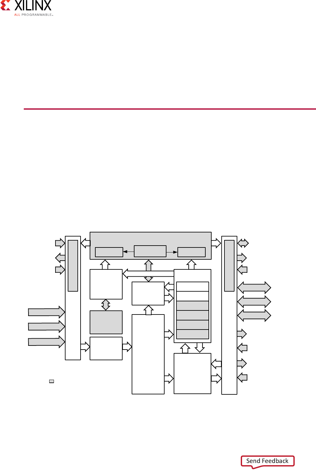
Vivado AXI Reference Guide www.xilinx.com 72
UG1037 (v4.0) July 15, 2017
Chapter 3: Samples of Vivado AXI IP and Xilinx Processors
The MMU in the ARM architecture involves both memory protection and address
translation. The MMU works closely with the L1 and L2 memory systems in the process of
translating virtual addresses to physical addresses. It also controls accesses to and from the
external memory. MMU is responsible for checking of virtual address and ASID (address
space identifier).
See the “Memory Management Unit” section in the Zynq-7000 AP SoC Technical Reference
Manual (UG585) [Ref 32] for more information.
MicroBlaze Processor
This section contains an overview of the MicroBlaze™ processor features.
Overview
The MicroBlaze embedded processor soft core is a reduced instruction set computer (RISC)
optimized for implementation in Xilinx Field Programmable Gate Arrays (FPGAs). The
following figure shows a functional block diagram of the MicroBlaze core.
X-Ref Target - Figure 3-25
Figure 3-25: MicroBlaze Core Block Diagram
Instruction-side
Bus interface
Bus
IF
I-Cache
M_AXI_IC
IXCL_M
IXCLS
M_AXI_IP
IPLB
ILMB
Memory Management Unit (MMU)
ITLB UTLB DTLB
Bus
IF
D-Cache
Program
Counter
Branch
Target
Cache
Instruction
Buffer Instruction
Decode
Special
Purpose
Registers
ALU
Shift
Barrel Shift
Multiplier
Divider
FPU
Register File
32 x 32b
M_AXI_DC
DXCL_M
DXCL_S
M_AXI_DP
DPLB
DLMB
M0_AXIS..
M15_AXIS
S0_AXIS..
S15_AXIS
MFSL 0..15 or
DWFSL 0..15
SFSL 0..15 or
DRFSL 0..15
Data-side
Bus interface
Optional MicroBlaze feature
;

Vivado AXI Reference Guide www.xilinx.com 73
UG1037 (v4.0) July 15, 2017
Chapter 3: Samples of Vivado AXI IP and Xilinx Processors
MicroBlaze Features
The MicroBlaze soft core processor is highly configurable, allowing you to select a specific
set of features required by your design.
The fixed feature set of the processor includes:
• Thirty-two 32-bit general purpose registers
• 32-bit instruction word with three operands and two addressing modes
•32-bit address bus
• Single issue pipeline
In addition to these fixed features, the MicroBlaze processor is parameterized to allow
selective enabling of additional functionality. The following section provides an overview of
the MicroBlaze configurable features by versions.
Configurable MicroBlaze Feature Overview
• Processor pipeline depth of 3/5
• Local Memory Bus (LMB) data side interface
• Local Memory Bus (LMB) instruction side interface
• Hardware barrel shifter
• Hardware divider
• Hardware debug logic
• Stream link interfaces (0-15 AXI)
• Machine status set and clear instructions
• 4 or 8-word cache line
• Hardware exception support
• Pattern compare instructions
• Floating point unit (FPU)
• Disable hardware multiplier(1)
• Hardware debug readable ESR and EAR (Yes)
• Processor Version Register (PVR)
• Area or speed optimized
• Hardware multiplier 64-bit result
• LUT cache memory
• Floating point conversion and square root instructions
1. Used for saving DSP48E primitives.

Vivado AXI Reference Guide www.xilinx.com 74
UG1037 (v4.0) July 15, 2017
Chapter 3: Samples of Vivado AXI IP and Xilinx Processors
• Memory Management Unit (MMU)
• Extended stream instructions
• Use Cache Interface for All I-Cache Memory Accesses
• Use Cache Interface for All D-Cache Memory Accesses
• Use Write-back Caching Policy for D-Cache
• Branch Target Cache (BTC)
• Streams for I-Cache
• Victim handling for I-Cache
• Victim handling for D-Cache
• AXI4 (M_AXI_DP) data side interface
• AXI4 (M_AXI_IP) instruction side interface
• AXI4 (M_AXI_DC) protocol for D-Cache
• AXI4 (M_AXI_IC) protocol for I-Cache
• AXI4 protocol for stream accesses
• Fault tolerant features
• Tool selectable endianness
• Force distributed RAM for cache tags
• Configurable cache data widths
• Count Leading Zeros instruction
• Memory Barrier instruction (Yes)
• Stack overflow and underflow detection
• Allow stream instructions in user mode
• Lockstep support
• Configurable use of FPGA primitives
• Low-latency interrupt mode
• Swap instructions
• Sleep mode and sleep instruction (Yes)
• Relocatable base vectors
•ACE (M_ACE_DC) protocol for D-Cache
•ACE (M_ACE_IC) protocol for I-Cache
• Extended debug: performance monitoring, program trace, non-intrusive profiling
• Reset mode: enter sleep or debug halt at reset
• Extended debug: external program trace
Vivado AXI Reference Guide www.xilinx.com 75
UG1037 (v4.0) July 15, 2017
Chapter 3: Samples of Vivado AXI IP and Xilinx Processors
MicroBlaze Memory Architecture
MicroBlaze is implemented with a Harvard memory architecture; instruction and data
accesses are done in separate address spaces. Each address space has a 32-bit range (that
is, handles up to 4 GB of instructions and data memory respectively). MicroBlaze has limited
support for 64-bit addressing using special extended address access registers. The
instruction and data memory ranges can be made to overlap by mapping them both to the
same physical memory. The latter is useful for debugging.
Both instruction and data interfaces of MicroBlaze are default 32 bits wide and use big
Endian or little Endian, bit-reversed format, depending on the parameter C_ENDIANNESS.
MicroBlaze supports word, halfword, and byte accesses to data memory.
Data accesses must be aligned (word accesses must be on word boundaries, halfword on
halfword boundaries), unless the processor is configured to support unaligned exceptions.
All instruction accesses must be word aligned.
MicroBlaze pre-fetches instructions to improve performance, using the instruction
pre-fetch buffer and (if enabled) instruction cache streams. To avoid attempts to pre-fetch
instructions beyond the end of physical memory, which may cause an instruction bus error
or a processor stall, instructions must not be located too close to the end of physical
memory. The instruction pre-fetch buffer requires 16 bytes margin, and using instruction
cache streams adds two additional cache lines (32 or 64 bytes).
MicroBlaze does not separate data accesses to I/O and memory (it uses memory mapped
I/O). The processor has up to three interfaces for memory accesses:
• Local Memory Bus (LMB)
• AXI4 for peripheral access
• AXI4 or AXI Coherency Extension (ACE) for cache access
IMPORTANT: The LMB memory address range must not overlap with AXI4 ranges.
The C_ENDIANNESS parameter is automatically set to little endian when using AXI4, but can
be overridden by the user.
MicroBlaze Hardware AXI Exceptions
The following hardware exceptions can be encountered when using AXI protocol with
MicroBlaze:
•Stream Exception: An AXI4-Stream exception is caused by executing a get or getd
instruction with the e bit set to 1 when there is a control bit mismatch.
•Instruction Bus Exception: The instruction bus exception is caused by errors when
reading data from memory.

Vivado AXI Reference Guide www.xilinx.com 76
UG1037 (v4.0) July 15, 2017
Chapter 3: Samples of Vivado AXI IP and Xilinx Processors
¨Instruction peripheral AXI4 interface (M_AXI_IP) exception is caused by an error
response on M_AXI_IP_RRESP.
¨Instruction cache AXI4 interface (M_AXI_IC) is caused by an error response on
M_AXI_IC_RRESP. The exception can only occur when C_ICACHE_ALWAYS_USED
is set to 1 and the cache is turned off, or if the MMU Inhibit Caching bit is set for the
address. In all other cases the response is ignored.
¨Instructions side local memory (ILMB) can only cause instruction bus exception
when either an uncorrectable error occurs in the LMB memory, as indicated by the
IUE signal, or C_ECC_USE_CE_EXCEPTION is set to 1 and a correctable error
occurs in he LMB memory, as indicated by the ICE signal.
•Illegal Opcode Exception: The illegal opcode exception is caused by an instruction
with an invalid major opcode (bits 0 through 5 of instruction).
°Bits 6 through 31 of the instruction are not checked.
°Optional processor instructions are detected as illegal if not enabled. If the optional
feature C_OPCODE_0x0_ILLEGAL is enabled, an illegal opcode exception is also
caused if the instruction is equal to 0x00000000.
•Data Bus Exception: A data bus exception is caused by errors when reading data from
memory or writing data to memory.
°The data peripheral AXI4 interface (M_AXI_DP) exception is caused by an error
response on M_AXI_DP_RRESP or M_AXI_DP_BRESP.
°The data cache AXI4 interface (M_AXI_DC) exception is caused by:
- An error response on M_AXI_DC_RRESP or M_AXI_DC_BRESP,
-OKAY response on M_AXI_DC_RRESP in case of an exclusive access using LWX.
The exception can only occur when C_DCACHE_ALWAYS_USED is set to 1 and the cache
is turned off, when an exclusive access using LWX or SWX is performed, or if the MMU
Inhibit Caching bit is set for the address. In all other cases the response is
ignored.
Using MicroBlaze AXI Instruction Cache
MicroBlaze can be used with an optional instruction cache for improved performance when
executing code that resides outside the LMB address range. The M_AXI_IC instruction lets
you cache over an AXI4 interface.
For every instruction fetched, the instruction cache detects if the instruction address
belongs to the cacheable segment.
• If the address is non-cacheable, the cache controller ignores the instruction and lets
the M_AXI_IP or LMB complete the request.

Vivado AXI Reference Guide www.xilinx.com 77
UG1037 (v4.0) July 15, 2017
Chapter 3: Samples of Vivado AXI IP and Xilinx Processors
• If the address is cacheable, a lookup is performed on the tag memory to check if the
requested address is currently cached. The lookup is successful if the word and line
valid bits are set, and the tag address matches the instruction address tag segment.
• On a cache miss, the cache controller requests the new instruction over the instruction
AXI4 interface (M_AXI_IC), and waits for the memory controller to return the
associated cache line.
•C_ICACHE_DATA_WIDTH determines the bus data width, either 32 bits, an entire cache
line (128 bits or 256 bits), or 512 bits.
• When C_FAULT_TOLERANT is set to 1, a cache miss also occurs if a parity error is
detected in a tag or instruction Block RAM.
• The instruction cache issues burst accesses for the AXI4 interface when 32-bit data
width is used, otherwise single accesses are used.
Using MicroBlaze AXI Data Cache
MicroBlaze can be used with an optional data cache for improved performance. The cached
memory range must not include addresses in the LMB address range. The data cache has a
caching over AXI4 interface (M_AXI_DC) feature.
The caching policy used by the MicroBlaze data cache, write-back or write-through, is
determined by the parameter C_DCACHE_USE_WRITEBACK. When this parameter is set, a
write-back protocol is implemented, otherwise write-through is implemented. However,
when configured with an MMU (C_USE_MMU > 1, C_AREA_OPTIMIZED =0,
C_DCACHE_USE_WRITEBACK = 1), the caching policy in virtual mode is determined by the W
storage attribute in the TLB entry, whereas write-back is used in real mode.
With the write-back protocol, a store to an address within the cacheable range always
updates the cached data.
• If the target address word is not in the cache (that is, the access is a cache miss), and
the location in the cache contains data that has not yet been written to memory (the
cache location is dirty), the old data is written over the data AXI4 interface (M_AXI_DC)
to external memory before updating the cache with the new data. If only a single word
needs to be written, a single word write is used, otherwise a burst write is used.
• For byte or halfword stores, in case of a cache miss, the address is first requested over
the data AXI4 interface, while a word store only updates the cache.
With the write-through protocol, a store to an address within the cacheable range
generates an equivalent byte, halfword, or word write over the data AXI4 interface to
external memory. The write also updates the cached data if the target address word is in the
cache (that is, the write is a cache hit). A write cache-miss does not load the associated
cache line into the cache.
When cache is enabled a load from an address within the cacheable range triggers a check
to determine if the requested data is currently cached.
Vivado AXI Reference Guide www.xilinx.com 78
UG1037 (v4.0) July 15, 2017
Chapter 3: Samples of Vivado AXI IP and Xilinx Processors
• On a cache hit, the requested data is retrieved from the cache.
• On a cache miss, the address is requested over the data AXI4 interface using a burst
read, and the processor pipeline stalls until the cache line associated to the requested
address is returned from the external memory controller.
• The parameter C_DCACHE_DATA_WIDTH determines the bus data width, either 32 bits, an
entire cache line (128 bits or 256 bits), or 512 bits.
• When C_FAULT_TOLERANT is set to 1 and write-through protocol is used, a cache miss
also occurs if a parity error is detected in the tag or data Block RAM.
IMPORTANT: The DCE bit in the MSR controls whether or not the cache is enabled. When disabling
caches the user must ensure that all the prior writes within the cacheable range have been completed
in external memory before reading back over M_AXI_DP. This can be done by writing to a semaphore
immediately before turning off caches, and then in a loop poll until it has been written. The contents of
the cache are preserved when the cache is disabled.
The following table summarizes the access types of accesses issued by the data cache AXI4
interface.
Using Victim Cache
The victim cache is enabled by setting the parameter C_DCACHE_VICTIMS to 2, 4 or 8. This
defines the number of cache lines that can be stored in the victim cache. Whenever a
complete cache line is evicted from the cache, it is saved in the victim cache.
By saving the most recent lines they can be fetched much faster, should the processor
request them, thereby improving performance. If the victim cache is not used, all evicted
cache lines must be read from memory again when they are needed.
Table 3-5: Data Cache Interface Accesses
Policy State Direction Access Type
Write-through Cache
Enabled
Read Burst for 32-bit interface non-exclusive access and exclusive access
with ACE enabled, single access otherwise.
Write Single access.
Cache
Disabled
Read Burst for 32-bit interface exclusive access with ACE enabled, single ac-
cess otherwise.
Write Single access.
Write-back Cache
Enabled
Read Burst for 32-bit interface, single access otherwise.
Write Burst for 32-bit interface cache lines with more than one valid word, a
single access otherwise.
Cache
Disabled
Read Burst for 32-bit interface non-exclusive access, discarding all but the
desired data, a single access otherwise.
Write Single access.

Vivado AXI Reference Guide www.xilinx.com 79
UG1037 (v4.0) July 15, 2017
Chapter 3: Samples of Vivado AXI IP and Xilinx Processors
With the AXI4 interface, C_DCACHE_DATA_WIDTH determines the amount of data transferred
from/to the victim cache each clock cycle, either 32 bits or an entire cache line.
Note: To be able to use the victim cache, write-back must be enabled and area optimization must
not be enabled.
MicroBlaze Stream Link Interfaces
MicroBlaze can be configured with up to 16 AXI4-Stream interfaces, each consisting of one
input and one output port. The channels are dedicated uni-directional point-to-point data
streaming interfaces.
The interfaces on MicroBlaze are 32 bits wide. A separate bit indicates whether the
sent/received word is of control or data type.
•The get instruction in the MicroBlaze ISA transfers information from a port to a
general purpose register.
•The put instruction transfers data in the opposite direction.
• Both instructions are available as follows: blocking data, non-blocking data, blocking
control, and non-blocking control. For a detailed description of the get and put
instructions, see this link to the “MicroBlaze Instruction Set Architecture” chapter in the
MicroBlaze Processor Reference Guide (UG984) [Ref 37].

Vivado AXI Reference Guide www.xilinx.com 80
UG1037 (v4.0) July 15, 2017
Chapter 4
AXI Feature Adoption in Xilinx Devices
Introduction
This chapter describes specific features from the AXI standard features used in Xilinx® IP to
familiarize you as an IP designer with various AXI-related design and integration choices.
Memory-Mapped IP Feature Adoption and Support
Xilinx has implemented and is supporting a rich feature set from AXI4 and AXI4-Lite to
facilitate interoperability among memory-mapped IP from Xilinx developers, individual
users, and third-party partners.
The following table lists the key aspects of Xilinx AXI4 and AXI4-Lite adoption, and the level
to which Xilinx IP has support for, and implemented features of the AXI4 specification.
Table 4-1: Xilinx AXI4 and AXI4-Lite Feature Adoption and Support
AXI Feature Xilinx IP Support
READY/VALID
Handshake
Full forward and reverse direction flow control of AXI protocol-defined
READY/VALID handshake.
Transfer Length AXI4 memory-mapped burst lengths of:
· 1 to 256 beats for incrementing bursts
· 1 to 16 beats for wrap bursts
Fixed bursts should not be used with Xilinx IP.
Conversions of FIXED bursts through AXI Interconnect infrastructure could have
sub-optimal performance.
Transfer Size / Data
Width
IP can be defined with native data widths of 32, 64, 128, 256, 512, and 1024 bits wide.
For AXI4-Lite, the supported data width is 32 or 64 bits only, but 32-bits is
recommended to minimize resource utilization.
The use of AXI4 narrow bursts is supported but is not recommended. Use of narrow
bursts can decrease system performance and increase system size.
Where Xilinx IP of different widths need to communicate with each other, the AXI
Interconnect provides data width conversion features.
Read/Write only The use of read/write, read-only, or write-only interfaces.
Many IP, including the AXI Interconnect, perform logic optimizations when an interface
is configured to be Read-only or Write-only.

Vivado AXI Reference Guide www.xilinx.com 81
UG1037 (v4.0) July 15, 2017
Chapter 4: AXI Feature Adoption in Xilinx Devices
AXI3 versus. AXI4 Designed to support AXI4 natively. Where AXI3 interoperability is required, the AXI
Interconnect contains the necessary conversion logic to allow AXI3 and AXI4 devices to
connect.
AXI3 write interleaving is not supported and should not be used with Xilinx IP.
Note: The AXI3 write Interleaving feature was removed from the AXI4
specification.
Lock / Exclusive Access No support for locked transfers.
Xilinx infrastructure IP can pass exclusive access transactions across a system, but Xilinx
IP does not support the exclusive access feature. All exclusive access requests result in
“OK” responses.
Protection/Cache Bits Infrastructure IP passes protection and cache bits across a system, but Endpoint IP
generally do not contain support for dynamic protection or cache bits.
· Protections bits should be constant at 000 signifying a constantly secure transaction
type.
· Cache bits should generally be constant at 0011 signifying a bufferable and
modifiable transaction.
This provides greater flexibility in the infrastructure IP to transport and modify
transactions passing through the system for greater performance.
Quality of Service
(QoS) Bits
Infrastructure IP passes QoS bits across a system.
Endpoint IP generally ignores the QoS bits.
REGION Bits Design of Endpoint slave IP to rely on REGION bits is discouraged because the
computation of REGION bits and their mapping to address decoder ranges can be
difficult to predict and maintain, especially across cascaded crossbars. The AXI
interconnect generates REGION bits based upon the Base/High address decoder ranges
defined in the address map for the AXI interconnect.
Xilinx infrastructure IP, such as register slices, pass REGION bits across a system.
However, AXI Master Endpoint IP do not generate REGION bits, which impacts
point-to-point connections to slaves that rely on REGION bits.
User Bits Infrastructure IP passes user bits across a system, except across width converters, but
Endpoint IP generally ignores user bits.
The use of user bits is discouraged in general purpose IP due to interoperability
concerns, and because width conversion does not propagate user bits.
Reset Xilinx IP generally deasserts all VALID and READY outputs within eight cycles of reset,
and have a reset pulse width requirement of 16 cycles or greater.
Holding AXI ARESETN asserted for 16 cycles of the slowest AXI clock is generally a
sufficient reset pulse width for Xilinx IP.
DSP IP has a requirement of 2 cycles for ARESETN on the AXI4-Stream interface.
Some IP such as SmartConnect have support for optional reset inputs. These IP can be
configured to only be reset with FPGA configuration and omit their reset input port to
reduce logic resources and reset net congestion. IP without a reset input must still start
up with READY/VALID deasserted until they are ready to accept their first AXI
transaction.
Low Power Interface Not Supported. The optional AXI low power interfaces, CSYSREQ, CSYSACK, and
CACTIVE are not present on IP interfaces.
Table 4-1: Xilinx AXI4 and AXI4-Lite Feature Adoption and Support (Cont’d)
AXI Feature Xilinx IP Support
Vivado AXI Reference Guide www.xilinx.com 82
UG1037 (v4.0) July 15, 2017
Chapter 4: AXI Feature Adoption in Xilinx Devices
AXI4-Stream Adoption and Support
To facilitate interoperability, Xilinx IP adopts a consistent set of AXI4-Stream protocol usage
guidelines. This section provides an overview of the adoption of AXI4-Stream signals,
numerical data type representation, and AXI4-Stream protocol usage across DSP, Wireless,
and Video IP. For more information on how to construct systems by configuring your
AXI4-Stream-based IP designs for interoperability, see AXI4-Stream Infrastructure IP Suite:
Product Guide for Vivado Design Suite (PG085) [Ref 14].
AXI4-Stream Signals
The following lists the AXI4-Stream signals, status, and notes on usage. The AXI4-Stream
signals use the following parameters to define the signal widths:
•n = Data bus width in bytes.
•i = TID width. Recommended maximum is 8-bits.
•d = TDEST width. Recommended maximum is 4-bits.
•u = TUSER width. Recommended number of bits is an integer multiple of the width of
the interface in bytes.
Numerical Data in an AXI4-Stream
An AXI4-Stream channel is a method of transferring data from a master to a slave.
IMPORTANT: To enable interoperability, both the master and slave must use the same, correct
interpretation of those bits.
In Xilinx IP, streaming interfaces are frequently used to transfer numerical data representing
sampled physical quantities (for example: video pixel data, audio data, and signal
processing data). Interoperability support requires a consistent interpretation of numerical
data.
IMPORTANT: Numerical data streams in Xilinx IP are defined in terms of logical and physical views.
This is especially important to understand in DSP applications where information can be transferred
essentially as data structures.
• The logical view describes the application-specific organization of the data.
• The physical view describes how the logical view is mapped to bits and the underlying
AXI4-Stream signals.

Vivado AXI Reference Guide www.xilinx.com 83
UG1037 (v4.0) July 15, 2017
Chapter 4: AXI Feature Adoption in Xilinx Devices
Simple vectors of values represent numerical data at the logical level. Individual values can
be real or complex quantities depending on the application. Similarly the number of
elements in the vector are application-specific.
At the physical level, the logical view is mapped to physical wires of the interface. Logical
values are represented physically by a fundamental base unit of bit width N, where N is
application-specific.
In general:
•N bits are interpreted as a fixed point quantity, but floating point quantities are also
permitted.
• Real values are represented using a single base unit.
• Complex values are represented as a pair of base units signifying the real component
followed by the imaginary component.
To aid interoperability, all logical values within a stream are represented using base units of
identical bit width.
Before mapping to the AXI4-Stream signal, TDATA, the N bits of each base unit are rounded
up to a whole number of bytes. As examples:
•A base unit with N=12 is packed into 16 bits of TDATA.
•A base unit with N=20 is packed into 24 bits of TDATA.
The AXI4-Stream protocol requires that TDATA ports of the IP have a width in multiples of
8. It is a specification violation to define an AXI4-Stream IP with a TDATA port width that is
not a multiple of 8, therefore, it is a requirement to round up TDATA widths to byte
multiples. This simplifies interfacing with memory-orientated systems, and also allows the
use of AXI infrastructure IP, such as the AXI Interconnect, to perform upsizing and
downsizing.
By convention, the additional packing bits are ignored at the input to a slave; they therefore
use no additional resources and are removed by the backend tools. To simplify diagnostics,
masters drive the unused bits in a representative manner, as follows:
• Unsigned quantities are zero-extended (the unused bits are zero).
• Signed quantities are sign-extended (the unused bits are copies of the sign bit).
The width of TDATA can allow multiple base units to be transferred in parallel in the same
cycle. For example, if the base unit is packed into 16 bits and TDATA signal width was 64
bits, four base units could be transferred in parallel, corresponding to four scalar values or
two complex values. Base units forming the logical vector are mapped first spatially (across
TDATA) and then temporally (across consecutive transfers of TDATA).
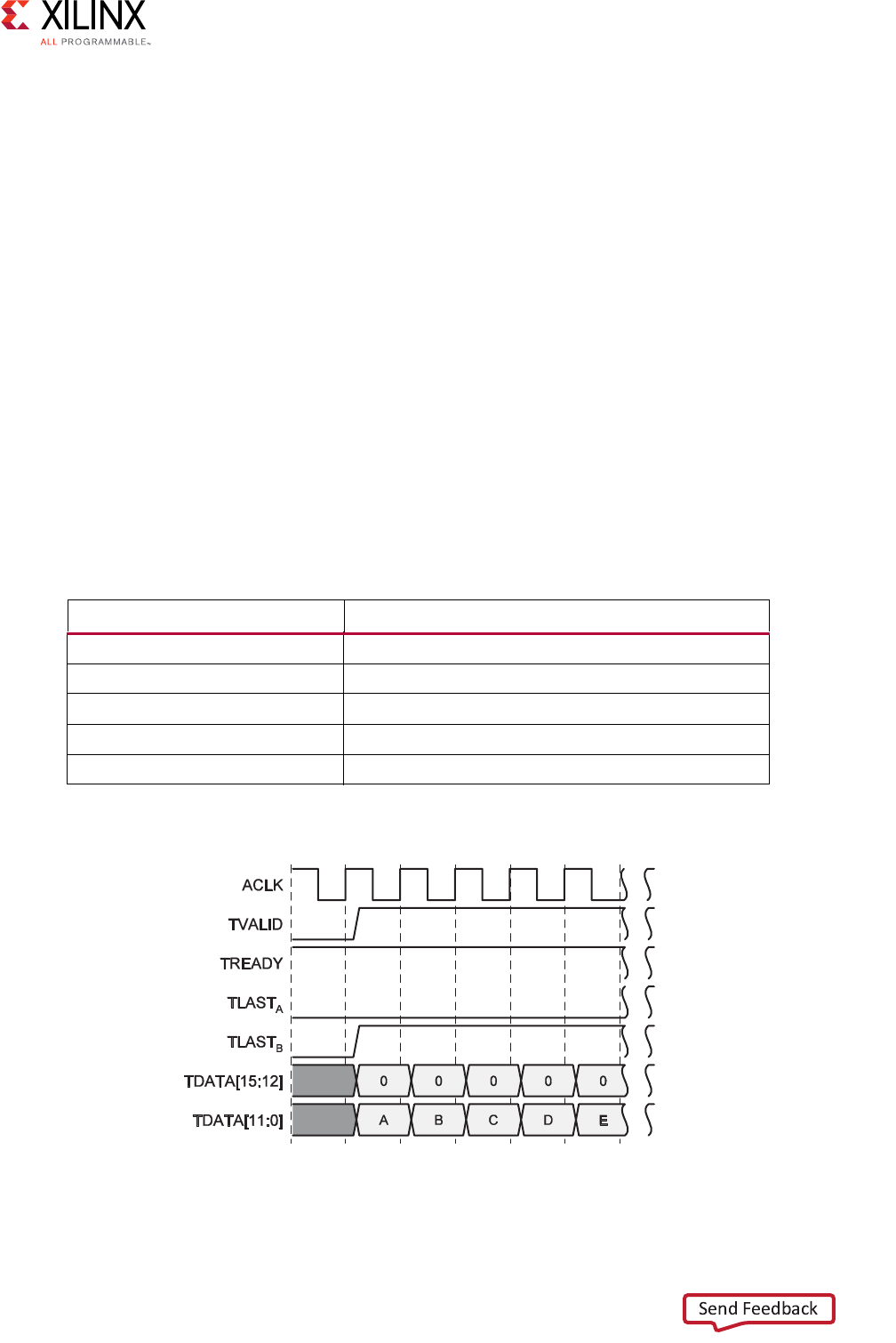
Vivado AXI Reference Guide www.xilinx.com 84
UG1037 (v4.0) July 15, 2017
Chapter 4: AXI Feature Adoption in Xilinx Devices
Deciding whether multiple sub-fields of data (that are not byte multiples) should be
concatenated together before or after alignment to byte boundaries is generally
determined by considering how atomic is the information. Atomic information is data that
can be interpreted on its own whereas non-atomic information is incomplete for the
purpose of interpreting the data.
For example, atomic data can consist of all the bits of information in a floating point
number. However, the exponent bits in the floating point number alone would not be
atomic.
When packing information into TDATA, generally non-atomic bits of data are concatenated
together (regardless of bit width) until they form atomic units. The atomic units are then
aligned to byte boundaries using pad bits where necessary.
Real Scalar Data Example
A stream of scalar values can use two equally valid uses of the optional TLAST signal. This
is illustrated in the following example. Consider a numerical stream with characteristics of
the following values:
This would be represented as an AXI4-Stream, as shown in the following figure.
Table 4-2: Numerical Stream and Value
Numerical Stream Value
Logical type Unsigned Real
Logical vector length 1 (for example, scalar value)
Physical base unit 12-bit fixed point
Physical base unit packed width 16 bits
Physical TDATA width 16 bits
X-Ref Target - Figure 4-1
Figure 4-1: Real Scalar (Unsigned) Data Example in an AXI4-Stream
X12056

Vivado AXI Reference Guide www.xilinx.com 85
UG1037 (v4.0) July 15, 2017
Chapter 4: AXI Feature Adoption in Xilinx Devices
Scalar values can be considered as not packetized at all, in which case TLAST can
legitimately be driven active-Low (TLASTA). Because TLAST is optional, it could be removed
entirely from the channel also.
Alternatively, scalar values can also be considered as vectors of unity length, in which case
TLAST should be driven active-High (TLASTB). Because the value type is unsigned, the
unused packing bits are driven 0 (zero extended).
Similarly, for signed data the unused packing bits are driven with the sign bits
(sign-extended), as shown in the following figure.
Complex Scalar Data Example
Consider a numerical stream with the following characteristics:
X-Ref Target - Figure 4-2
Figure 4-2: Alternative (Sign-Extended) Scalar Value Example
Table 4-3: Numerical Stream and Characteristic
Numerical Stream Characteristic
Logical type Signed Complex
Logical vector length 1 (for example: scalar)
Physical base unit 12 bit fixed point
Physical base unit packed width 16 bits
Physical TDATA width 16 bits
X12057
TDATA[15] ... TDATA[12]
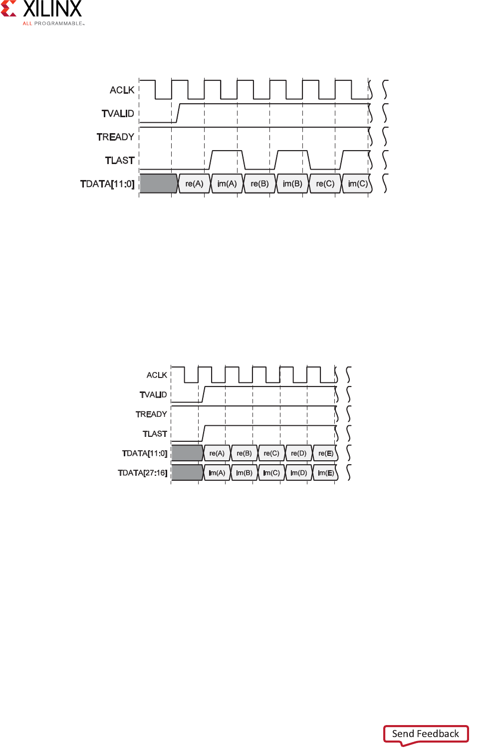
Vivado AXI Reference Guide www.xilinx.com 86
UG1037 (v4.0) July 15, 2017
Chapter 4: AXI Feature Adoption in Xilinx Devices
This would be represented as an AXI4-Stream, as shown in the following figure:
X-Ref Target - Figure 4-3
Where re(X) and im(X) represent the real and imaginary components of X respectively.
Note: For simplicity, sign extension into TDATA[15:12] is not illustrated here. A complex value is
transferred every two clock cycles.
The same data can be similarly represented on a channel with a TDATA signal width of 32
bits, A wider bus allows a complex value to be transferred every clock cycle, as shown in the
following figure.
The two representations in the preceding figures of the same data (serial and parallel) show
that data representation can be tailored to specific system requirements.
For example, a:
• High throughput processing engine such as a Fast Fourier Transform (FFT) might favor
the parallel form
• MAC-based Finite Impulse Response (FIR) might favor the serial form, thus enabling
Time Division Multiplexing (TDM) data path sharing
Figure 4-3: Complex Scalar Data Example in AXI4-Stream
X-Ref Target - Figure 4-4
Figure 4-4: Complex Scalar Example with 32-Bit TDATA Signal
X12058
X12059
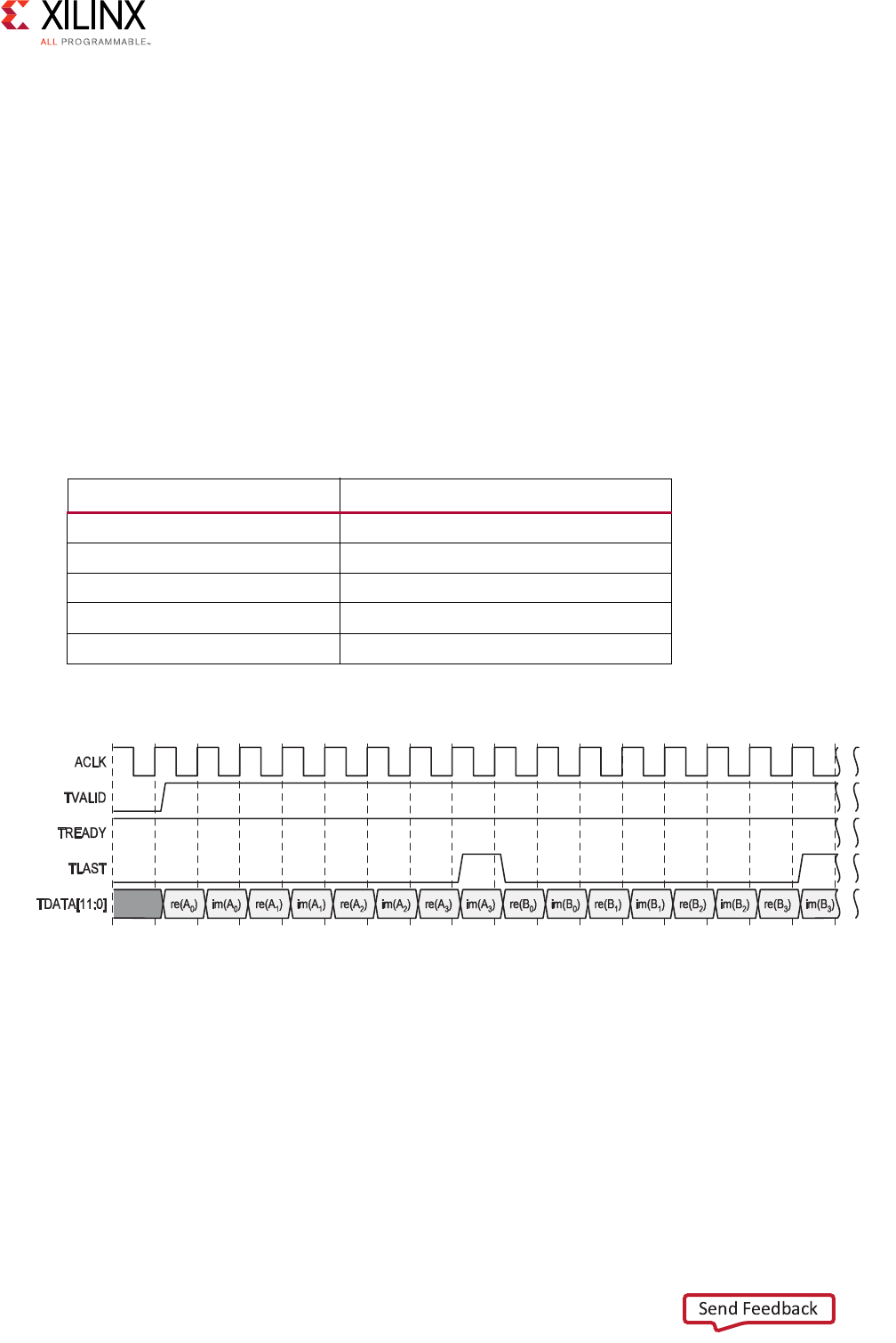
Vivado AXI Reference Guide www.xilinx.com 87
UG1037 (v4.0) July 15, 2017
Chapter 4: AXI Feature Adoption in Xilinx Devices
To enable interoperability of sub-systems with differing representation, you need a
conversion mechanism. This representation was chosen to enable simple conversions using
a standard AXI infrastructure IP:
• Use an AXI4-Stream-based upsizer to convert the serial form to the parallel form.
• Use an AXI4-Stream-based downsizer to convert the parallel form to the serial form.
You can implement an AXI4-Stream-based upsizer or downsizer by using the width
conversion feature of the AXI4-Stream Interconnect. For more information see the
AXI4-Stream Interconnect page [Ref 4].
Vector Data Example
Consider the example of a numerical stream with the following characteristics:
The following figure shows the AXI4-Stream representation of that numerical stream:
Table 4-4: Numerical Stream and Characteristic
Numerical Stream Characteristics
Logical type Signed Complex
Logical vector length 4
Physical base unit 12 bit fixed point
Physical base unit packed width 16 bits
Physical TDATA width 16 bits
X-Ref Target - Figure 4-5
Figure 4-5: Numerical Stream Example
X12060

Vivado AXI Reference Guide www.xilinx.com 88
UG1037 (v4.0) July 15, 2017
Chapter 4: AXI Feature Adoption in Xilinx Devices
As for the scalar case, the same data can be represented on a channel with TDATA width of
32 bits, as shown in the following figure.
The degree of parallelism can be increased further for a channel with TDATA width of 64
bits, as shown in the following figure.
X-Ref Target - Figure 4-6
Figure 4-6: AXI4-Stream Scalar Example
X12061
X-Ref Target - Figure 4-7
Figure 4-7: TDATA Example with 64-Bits
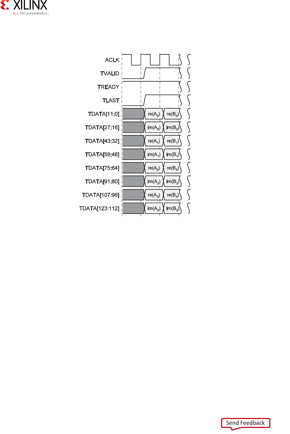
Vivado AXI Reference Guide www.xilinx.com 89
UG1037 (v4.0) July 15, 2017
Chapter 4: AXI Feature Adoption in Xilinx Devices
Full parallelism can be achieved with TDATA width of 128 bits, as shown in the following
figure.
As shown in the preceding figures, for the scalar data there are multiple representations
that you can customize to the application.
Similarly, AXI4-Stream upsizers and downsizers can be used for conversion.
Scalar values can be considered as not packetized at all, in which case TLAST can
legitimately be driven active-Low (TLASTA). Because TLAST is optional, it could be removed
entirely from the channel also.
Alternatively, scalar values can also be considered as vectors of unity length, in which case
TLAST should be driven active-High (TLASTB). Because the value type is unsigned, the
unused packing bits are driven 0 (zero extended).
Similarly, for signed data the unused packing bits are driven with the sign bits
(sign-extended), Packets and NULL Bytes
The AXI4-Stream protocol lets you specify packet boundaries using the optional TLAST
signal.
In many situations this is sufficient; however, by definition, the TLAST signal indicates the
size of the data at the end of the packet, while many IP require packet size at the beginning.
X-Ref Target - Figure 4-8
Figure 4-8: 128 Bit TDATA Example
X12063

Vivado AXI Reference Guide www.xilinx.com 90
UG1037 (v4.0) July 15, 2017
Chapter 4: AXI Feature Adoption in Xilinx Devices
In such situations, where packet size is specified at the beginning, the IP typically requires
an alternative mechanism to provide that packet-size information. Streaming slave channels
can therefore be divided into three categories:
• Slaves that do not require the interpretation of packet boundaries.
There are slave channels that do not have any concept of packet boundaries, or when
the size of packets do not affect the processing operation performed by the core.
Frequently, IP of this type provides a pass-through mechanism to allow TLAST to
propagate from input to output with equal latency to the data.
• Slaves that require the TLAST signal to identify packet boundaries.
These slaves channels are inherently packet-orientated, and can use TLAST as a packet
size indicator. For example, a Cyclic Redundancy Check (CRC) core can calculate the CRC
while data is being transferred, and upon detecting the TLAST signal, can verify that the
CRC is correct.
• Slaves that do not require TLAST to identify packet boundaries.
Some slave channels have an internal expectation of what size packets are required. For
example, an FFT input packet size is always the same as the transform size. In these
cases, TLAST would represent redundant information and also potentially introduce
ambiguity into packet sizing (for example: what should an N-point FFT do when
presented with an N-1 sample input packet.)
To prevent this ambiguity, many Xilinx IP cores are designed to ignore TLAST on slave
channels, and to use the explicit packet sizing information available to them.
In these situations the core uses the required number of AXI transfers it is expecting
regardless of TLAST. This typically greatly aides interoperability as the master and slave
are not required to agree on when TLAST must be asserted.
For example, consider an FIR followed by an N-point FFT. The FIR is a stream-based core
and cannot natively generate a stream with TLAST asserted every N transfers.
If the FFT is designed to ignore the incoming TLAST this is not an issue, and the system
functions as expected. However, if the FFT did require TLAST, an intermediate
“re-framing” core would be required to introduce the required signalling.
• For Packetized Data, TKEEP might be necessary to signal packet remainders.
When the TDATA width is greater than the atomic size (minimum data granularity) of the
stream, a remainder is possible because there might not be enough data bytes to fill an
entire data beat. The only supported use of deasserted TKEEP for Xilinx endpoint IP is
for packet remainder signaling. Deasserted TKEEP bits (which is called “Null Bytes” in
the AXI4-Stream Protocol Specification [Ref 1]) are only present in a data beat with
TLAST asserted.

Vivado AXI Reference Guide www.xilinx.com 91
UG1037 (v4.0) July 15, 2017
Chapter 4: AXI Feature Adoption in Xilinx Devices
For non-packetized continuous streams or packetized streams where the data width is
the same size or smaller than the atomic size of data, there is no need for TKEEP. This
generally follows the “Continuous Aligned Stream” model described in the AXI4-Stream
protocol.
The AXI4-Stream protocol describes the usage for TKEEP to encode trailing null bytes to
preserve packet lengths after size conversion, especially after upsizing an odd length
packet. This usage of TKEEP essentially encodes the remainder bytes after the end of a
packet which is an artifact of upsizing a packet beyond the atomic size of the data.
Xilinx AXI master IP do not generate any packets that have trailing transfers with all
TKEEP bits deasserted. Xilinx AXI masters with a TKEEP output port must drive them
correctly at all times. This implies driving all TKEEP bits high when TLAST is deasserted
and using TKEEP to signal the remainder when TLAST is asserted.
Xilinx infrastructure IP passes through TKEEP values and attempts to process them in a
protocol-compliant manner.
This guideline maximizes compatibility and throughput because Xilinx IP does not
originate packets containing trailing transfers with all TKEEP bits deasserted. Any
deasserted TKEEP bits must be associated with TLAST = 1 in the same data beat to
signal the byte location of the last data byte in the packet.
Xilinx AXI slave IP are generally not designed to be tolerant of receiving packets that
have trailing transfers with all TKEEP bits deasserted. Slave IP that have TKEEP inputs
can be designed to internally only sample TKEEP with TLAST is asserted to determine
the packet remainder bytes. In general if Xilinx IP are used in the system with other IP
designed for “Continuous Aligned Streams” as described in the AXI4-Stream Protocol
Specification [Ref 1], trailing transfers with all TKEEP bits deasserted not occur.
All streams entering into a system of Xilinx IP must be fully packed upon entry in the
system (no leading or intermediate null bytes) in which case arbitrary size conversion
will only introduce TKEEP for packet remainder encoding and will not result in data
beats where all TKEEP bits are deasserted.
Sideband Signals
• The AXI4-Stream interface protocol allows passing sideband signals using the TUSER
bus.
From an interoperability perspective, using TUSER on an AXI4-Stream channel is an
issue because both Master and Slave must now not only have the same interpretation of
TDATA and TUSER.
Generally, Xilinx IP uses the TUSER field only to augment the TDATA field with
information that could prove useful, but ultimately can be ignored. Ignoring TUSER
could result in some loss of information, but the TDATA field still has some meaning.

Vivado AXI Reference Guide www.xilinx.com 92
UG1037 (v4.0) July 15, 2017
Chapter 4: AXI Feature Adoption in Xilinx Devices
An FFT core implementation can use a TUSER output to indicate block exponents to
apply to the TDATA bus. If TUSER is ignored, the exponent scaling factor is lost, but
TDATA still contains unscaled transform data.
Events
• An event signal is a single wire interface used by a core to indicate that some specific
condition exists (for example: an input parameter is invalid, a buffer is empty or nearly
full, or the core is waiting on some additional information).
Events are asserted while the condition is present, and are deasserted once the
condition passes, and exhibit no latching behavior. Depending on the core and how it is
used in a system, an asserted event might indicate an error, a warning, or information.
Event signals can be viewed as AXI4-Stream channels with an VALID signal only, without
any optional signals. Event signals can also be considered out-of-band information and
treated like generic flags, interrupts, or status signals.
Events can be used in many different ways:
°Ignored: Unless explicitly stated otherwise, a system can ignore all event
conditions.
In general, a core continues to operate while an event is asserted, although
potentially in some degraded manner.
°As Interrupts or GPIOs: An event signal might be connected to a processor using a
suitable interrupt controller or general purpose I/O controller. System software is
then free to respond to events as necessary.
°As Simulation Diagnostic: Events can be useful during hardware simulation. They
can indicate interoperability issues between masters and slaves, or indicate
misinterpretation of how subsystems interact.
°As Hardware Diagnostic: Similarly, events can be useful during hardware
diagnostic. You can route events signals to diagnostic LED or test points, or connect
them to the Vivado Lab Edition
As a system moves from development through integration to release, confidence in its
operation is gained; as confidence increases, the need for events diminishes.
During development simulations, events can be actively monitored to ensure a system is
operating as expected. During hardware integration, events might be monitored only if
unexpected behavior occurs, while in a fully-tested system, it might be reasonable to
ignore events.
Note: Events signals are asserted when the core detects the condition described by the event;
depending on internal core latency and buffering, this could be an indeterminate time after the
inputs that caused the event are presented to the core.

Vivado AXI Reference Guide www.xilinx.com 93
UG1037 (v4.0) July 15, 2017
Chapter 4: AXI Feature Adoption in Xilinx Devices
TLAST Events
• Some slave channels do not require a TLAST signal to indicate packet boundaries. In
such cases, the core has a pair of events to indicate any discrepancy between the
presented TLAST and the internal concept of packet boundaries:
°Missing TLAST: TLAST is not asserted when expected by the core.
°Unexpected TLAST: TLAST is asserted when not expected by the core.
Depending on the system design these events might or might not indicate potential
problems.
Consider an FFT core used as a coprocessor to a CPU where data is streamed to the core
using a packet-orientated DMA engine.
The DMA engine can be configured to send a contiguous region of memory of a given
length to the FFT core, and to correctly assert TLAST at the end of the packet. The
system software can elect to use this coprocessor in a number of ways:
°Single Transforms: The simplest mode of operation is for the FFT core and the
DMA engine to operate in a lockstep manner. If the FFT core is configured to
perform an N point transform, then the DMA engine should be configured to
provide packets of N complex samples.
If a software or hardware bug is introduced that breaks this relationship, the FFT core
detects TLAST mismatches and asserts the appropriate event. In this case that is
indicating error conditions.
°Grouped Transforms: Typically, for each packet transferred by the DMA engine, a
descriptor is required containing start address, length, and flags; generating
descriptors and sending them to the engine requires effort from the host CPU. If
the size of transform is short and the number of transforms is high, the overhead of
descriptor management might begin to overcome the advantage of offloading
processing to the FFT core.
One solution is for the CPU to group transforms into a single DMA operation.
If the FFT core is configured for 32-point transforms, the CPU could group 64
individual transforms into a single DMA operation. The DMA engine generates a
single 2048 sample packet containing data for the 64 transforms; however, as the
DMA engine is only sending a single packet, only the data for the last transform has
a correctly placed TLAST. The FFT core then reports 63 individual ‘missing TLAST’
events for the grouped operation. In this case the events are entirely expected and
do not indicate an error condition.
In the example case, the ‘unexpected TLAST’ event should not assert during
normal operation. At no point should a DMA transfer occur where TLAST does not
align with the end of an FFT transform.

Vivado AXI Reference Guide www.xilinx.com 94
UG1037 (v4.0) July 15, 2017
Chapter 4: AXI Feature Adoption in Xilinx Devices
However, as for the described single transform example case, a software or hardware
error could result in this event being asserted. If the transform size is incorrectly
changed in the middle of the grouped packet, an error occurs.
°Streaming Transforms: For large transforms it might be difficult to arrange to hold
the entire input packet in a single contiguous region of memory.
In such cases it might be necessary to send data to the FFT core using multiple
smaller DMA transfers, each completing with a TLAST signal.
Depending on how the CPU manages DMA transfers, it is possible that the TLAST
signal never aligns correctly with the internal concept of packet boundaries within
the FFT core.
The FFT core would therefore assert both ‘missing TLAST’ and ‘unexpected
TLAST’ events as appropriate while the data is transferring. In this example case,
both events are entirely expected, and do not indicate an error condition.
DSP and Wireless IP: AXI Feature Adoption
An individual AXI4-Stream slave channel can be categorized as either a blocking or a
non-blocking channel.
A slave channel is blocking when some operation of the core is inhibited until a transaction
occurs on that channel.
For example, consider an FFT core that features two slave channels; a data channel and a
control channel. The data channel transfers input data, and the control channel transfers
control packets indicating how the input data should be processed (like transform size).
The control channel can be designed to be either blocking or non-blocking:
• A blocking case performs a transform only when both a control packet and a data
packet are presented to the core.
• A non-blocking case performs a transform with just a data packet, with the core reusing
previous control information.
Vivado AXI Reference Guide www.xilinx.com 95
UG1037 (v4.0) July 15, 2017
Chapter 4: AXI Feature Adoption in Xilinx Devices
There are numerous trade-offs related to the use of blocking versus non-blocking
interfaces. The following table lists the trade-offs:
Generally, the simplicity of using blocking channels outweighs the penalties.
Note: The distinction between blocking and non-blocking behavior is a characteristic of how a core
uses data and control presented to it; it does not necessarily have a direct influence on how a core
drives READY on its slave channels. For example, a core might feature internal buffers on slave
channels, in which case READY is asserted while the buffer has free space.
Note: In many cases, DSP and Wireless IP have base units that do not usually fall on the 8-bit (Byte)
boundaries. See Numerical Data in an AXI4-Stream for information on how to handle data that does
not fall on byte boundaries.
Video IP: AXI Feature Adoption
For comprehensive information about Video IP Protocol, see the Video IP Protocol and
Design Guide (UG934) [Ref 27].
See Partial Reconfiguration of a Hardware Accelerator with Vivado Design Suite (XAPP1231)
[Ref 47] for a design example using Partial Reconfiguration, and AXI Interconnects to display
graphics in a variety of modes.
In the video domain, there are established signals that are used in many standards to
transmit data across video communication channels. These signals include video data and
synchronization for proper communication and flow control.
Table 4-5: Blocking Versus Non-Blocking Interfaces
Feature Blocking Non-blocking
Synchronization Automatic
Core operates on transactions; for example,
one control packet and one input data
packet produces one output data packet.
Not automatic
System designer must ensure that
control information arrives at the core
before the data to which it applies.
Signaling
Overhead
Small
Control information must be transferred
even if it does not change.
Minimized
Control information need be transferred
only if it changes.
Connectivity Simple
Data flows through a system of blocking
cores as and when required; automatic
synchronization ensures that control and
data remain in step.
Complex
System designer must manage the flow
of data and control flow though a system
of non-blocking cores.
Resource
Overhead
Small
Cores typically require small additional
buffers and state machines to provide
blocking behavior.
None
Cores typically require no additional
resources to provide non-blocking
behavior.

Vivado AXI Reference Guide www.xilinx.com 96
UG1037 (v4.0) July 15, 2017
Chapter 4: AXI Feature Adoption in Xilinx Devices
Typically, video signals are propagated using several processing cores and frame buffers
along which video resolution, frame rate, and formatting (such as interlaced to
de-interlaced) can change.
Processing cores can:
• Process a single stream (the Xilinx Image Statistics core)
• Process and generate a single stream (most Xilinx Image Processing cores)
• Process multiple streams to generate a single stream (the Xilinx On Screen Display
(OSD) core)
• Process multiple streams to generate multiple streams (the Xilinx Motion Adaptive
Noise Reduction (MANR) core)
Video data enters the system through the input interface and exits the system through a
similar interface, which is, in many cases, connected to a monitor for display of the
processed video sequence. In a complex video system, the IP cores provide a register
interface that is used for setup and control by a central managing microprocessor. This type
of system is supported by Xilinx design tools such as the Vivado IDE embedded tools using
the Zynq®-7000 AP SoC processor or MicroBlaze™ processor.
Xilinx Video IP cores are used in a variety of video and imaging applications and a wide
range of markets, from Industrial, Scientific, and Medical (ISM), automotive and customer
electronics to professional broadcast markets. The interface and protocol addresses the
needs of multiple application domains.
IP using the AXI4-Stream Video Protocol provides a simple, versatile, high-performance
point-to-point communication interface between video IP cores that is easy for video
designers to use.
Using the industry standard AXI interface allows video cores to connect to embedded
processors and infrastructure IP.
Based upon a well-defined, standard interface and protocol, video and system designers
can leverage advanced Xilinx tools to connect video IP and to build video systems.
The following subsections provide the requirements, standards, recommendations, and
guidelines for Xilinx Video IP design to adapt AXI4-Stream interfaces, and harmonize
AXI4-Stream based Video IP development with AXI4-Stream based DSP IP, infrastructure IP,
and tools development.
The subsections also provide the details for defining AXI4-Stream based Video IP
interfaces, and describes the signals and protocols for transmitting video using the
AXI4-Stream interface, its applicability to a wide range of video systems, and usage
guidelines for interoperability.
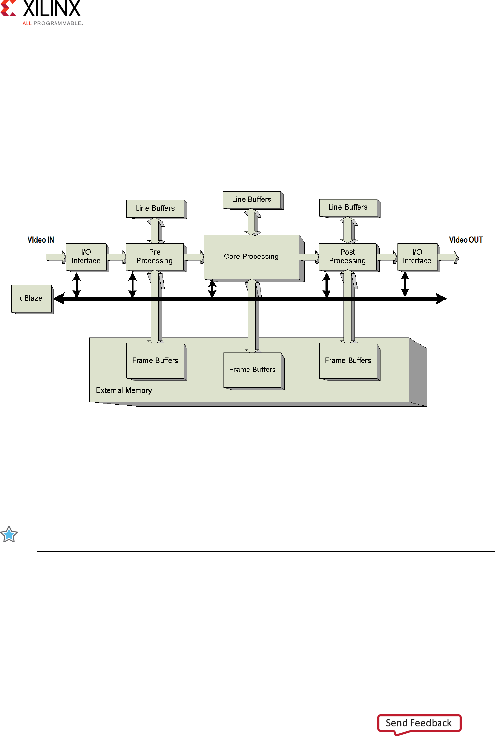
Vivado AXI Reference Guide www.xilinx.com 97
UG1037 (v4.0) July 15, 2017
Chapter 4: AXI Feature Adoption in Xilinx Devices
This subsection also defines the:
• Set of AXI4-Stream signals used for video data exchange between IP cores
• Protocol of transmitting video frames using the AXI4-Stream interface
• List of supported data, such as RGB, 420 YCC, and the mapping of data to the TDATA
bus (see Table 4-9).
Video systems follow the general pipelined processing chain, shown in the following figure.
IP Using AXI4-Stream Video Protocol
For comprehensive information about the AXI4-Stream Video IP, see AXI4-Stream Video IP
and System Design Guide (PG934) [Ref 27].
IMPORTANT: AXI4-Stream only carries active video data, throttled by both the master and slave
interfaces.
Note: Blank periods, audio, and ancillary data packets are not transferred using the AXI4-Stream
Video Protocol.
Signal Interfaces
Master and Slave interfaces have mandatory signal names.
X-Ref Target - Figure 4-9
Figure 4-9: Typical Video Processing System
Vivado AXI Reference Guide www.xilinx.com 98
UG1037 (v4.0) July 15, 2017
Chapter 4: AXI Feature Adoption in Xilinx Devices
Input Slave Side Connectors
The following table lists the mandatory interface signal names and functions for the input
(slave) side connectors.
To avoid naming collisions, append the signal prefix s_ should be appended to sk_, for IP
with multiple AXI4-Stream input interfaces, where k is the index of the respective input
AXI4-Stream. The AXI4-Stream Signal Name column lists the mandatory, top-level IP port
names. For IP with multiple AXI4-Stream input interfaces, append the s_axis_video
signal with the index of the respective input AXI4-Stream
Output Master Side Signals
The following table lists the mandatory interface signal names and functions for the output
(master) side signals.
Similarly, for IP with multiple AXI4-Stream output interfaces, append the
m_axis_video_signal with the index of the respective output AXI4-Stream, shown in
Table 4-7.
The Video Specific Name column recommends short, descriptive signal names referring to
AXI4-Stream ports, to be used in HDL code, timing diagrams, and test benches.
Table 4-6: AXI4-Stream Video Protocol Input (Slave) Interface Signals
Function Width Direction AXI4-Stream
Signal Name
Video Specific
Name
Video Data Any number of bytes IN s_axis_video_tdata DATA
Valid 1 IN s_axis_video_tvalid VALID
Ready 1 OUT s_axis_video_tready READY
Start Of Frame 1 IN s_axis_video_tuser SOF
End Of Line 1 IN s_axis_video_tlast EOL
Table 4-7: AXI4-Stream Video Protocol Output (Master) Interface Signals
Function Width Direction AXI4-Stream Signal Name Video Specific
Name
Video Data Any number of bytes OUT m_axis_video_tdata DATA
Valid 1 OUT m_axis_video_tvalid VALID
Ready 1 IN m_axis_video_tready READY
Start Of Frame 1 OUT m_axis_video_tuser SOF
End Of Line 1 OUT m_axis_video_tlast EOL

Vivado AXI Reference Guide www.xilinx.com 99
UG1037 (v4.0) July 15, 2017
Chapter 4: AXI Feature Adoption in Xilinx Devices
Clocking and ACLK
Each IP using the AXI4-Stream Video Protocol must reference a clock source.
Directly-connected master and slave interfaces must be clocked by the same clock source.
Any clock available to the IP can be used as the referenced clock source for an AXI interface.
The AXI protocol requires each component interface to use a single clock input signal,
ACLK.
IMPORTANT: The ACLK signal is a mandatory pin on the IP core interface.
The ACLK pin name can be either appended or prefixed to designate clock functionality,
such as m0_axis_aclk, or aclk_out for IP with multiple AXI4 interfaces using different
clocks.
Interface input signals are sampled on the rising edge of ACLK. Output signal changes must
occur after the rising edge of ACLK.
On Video IP interfaces, the ACLK pin is not part of the AXI4-Stream component interface;
ACLK signals associated with AXI4-Stream component interfaces are provided to Video IP
using one or multiple core clock signals. The clock signals can be shared by multiple
AXI4-Stream interfaces and signal processing circuitry within the IP.
Signals in each component interface must be synchronous to one of the core clock signals,
which are inputs to Video IP cores, but not directly part of the AXI4-Stream Video Protocol
interface.
For example, if a core uses a single processing ACLK signal, to which all operations within
the core are synchronous, the master and slave AXI4-Stream video interfaces should use
this clock signal as their clock reference.
A Video IP core can contain multiple AXI4-Stream interfaces and multiple clocks. Also, for
system integration tools, the IP must contain metadata tags identifying clock domain
associations.
TDATA Structure
TDATA bits are represented using the (N-1 downto 0) or [N-1:0] bit numbering convention.
The components of implicit subfields of DATA are packed together tightly; for example, a
DW=10 bit RGB data packed together to 30 bits. If necessary, the packed data word can be
zero padded with most significant bit (MSB) so the width of the resulting word is an integer
multiple of 8.
Vivado AXI Reference Guide www.xilinx.com 100
UG1037 (v4.0) July 15, 2017
Chapter 4: AXI Feature Adoption in Xilinx Devices
Clock Enable, ACLKEN
IMPORTANT: The ACLKEN signal, associated with ACLK, is an optional, recommended pin on the IP
core interface.
For IP with multiple AXI4-Stream interfaces using different clocks, the name of the ACLKEN
pin can be appended to designate clock association, such as ACLKEN_m0, or ACLKEN_in.
Note: When ACLKEN (clock enable) pins are used (toggled) in conjunction with a common clock
source driving the master and slave sides of an AXI4-Stream interface, the ACLKEN pins associated
with the master and slave component interfaces must also be driven by the same signal to prevent
transaction errors.
Note: When two cores connect using AXI4-Stream interfaces, where only the master or the slave
interface has an ACLKEN port, which is not permanently tied high, the two interfaces must be
connected using the AXI4 FIFO core to avoid data corruption. See the AXI4-Stream Infrastructure IP
Suite: Product Guide for Vivado Design Suite (PG085) [Ref 26] for more information.
Reset Requirements, ARESETn
Video IP cores must have two reset source types:
• Reset pins provided in conjunction with the corresponding clocks (hardware reset)
• The software reset option provided by the processor interface
IMPORTANT: An active-Low reset pin, ARESETn, associated with ACLK, is required on the IP core
interface. For IP with multiple AXI4-Stream interfaces using different clocks, each clock domain can
have corresponding reset signals. The name of the ARESETn pin can be appended to designate clock
association, such as ARESETn_m0.
The ARESETn signal takes precedence over ACLKEN. IP with optional ACLKEN inputs that
must reset when ARESETn is deasserted regardless of the state of the associated ACLKEN
input.
Note: When a system with multiple-clocks and corresponding reset signals are being reset, the reset
generator has to ensure all reset signals are asserted/deasserted long enough that all interfaces and
clock-domains in all IP cores are correctly re-initialized.
TKEEP and TSTRB
IMPORTANT: TKEEP and TSROBE are not used in IP using AXI4-Stream Video Protocol. When
connecting to IP requiring TKEEP or TSTRB assignments, use the default values of TKEEP=1 and
TSTRB=1.
RECOMMENDED: AXI4-Stream compliant Video IP should only use the “Continuous Aligned Stream”
mode of AXI4-Stream, and use packed data format and TDATA padded to integer (N) multiples of 8 bits
(see Data Format).
Vivado AXI Reference Guide www.xilinx.com 101
UG1037 (v4.0) July 15, 2017
Chapter 4: AXI Feature Adoption in Xilinx Devices
• For most video formats, all data bytes are always valid, when DATA is qualified by
VALID.
• For 420 encoded YCbCr / YUV data, only every second video line contains valid Chroma
data. For the remaining lines, Luma is zero-padded.
TID
Video IP use designated AXI4-Stream interfaces to transfer video and data streams.
IMPORTANT: TID is not used in IP using AXI4-Stream Video Protocol.
Video IP does not forward a slave TID, or generate a TID, instead, the unconnected TID
signal defaults to 0.
TDEST
IMPORTANT: The TDEST signal is not used in IP using AXI4-Stream Video Protocol.
Video IP does not forward a slave TDEST, or generate a TDEST, instead, the unconnected
TDEST signal defaults to 0.
TUSER
TUSER bit 0, labeled Start of Frame (see Start of Frame Signal - SOF) is the only AXI4-Stream
signal used for video. Other TUSER signal bits are not propagated by video cores.
Signaling Protocol
This section describes how you can use the interface signals and basic protocols of the
AXI4-Stream specification to construct streaming interfaces to meet the needs of various
video system applications. Generic AXI protocol signals are referenced using signal names
reflecting their video specific function.
Channel Structure
The interface contains a set of handshake signals, VALID and READY, and a set of
information-carrying signals, DATA, EOL, and SOF, that are conditioned by the handshake
signals.
AXI4-Stream interface signals must operate in the same clock domain; however, the master
and slave side can operate in different clock domains. In this case, proper clock-domain
crossing logic must be employed when connecting the interfaces.
In the IP integrator, the AXI4-Stream Interconnect IP can be used to simplify connecting
AXI4-Stream interfaces in different clock domains.
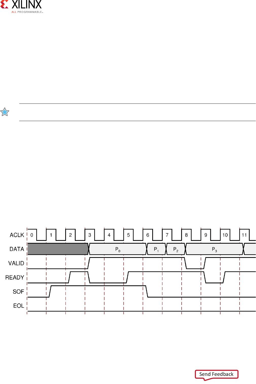
Vivado AXI Reference Guide www.xilinx.com 102
UG1037 (v4.0) July 15, 2017
Chapter 4: AXI Feature Adoption in Xilinx Devices
Note: In this protocol specification, for the sake of simplicity, both master and slave AXI4-Stream
interfaces are assumed to operate in the same clock domain, synchronous to ACLK, with ACLKEN=1,
and ARESETn=1.
For any given channel, signals propagate from the source (master) to the destination (slave)
with the exception of the READY signal.
Any other information-carrying or control signals that need to propagate in the opposite
direction must be part of a separate interface, READY is not used as a mechanism to transfer
opposite direction information from a slave to a master.
READY/VALID Handshake
IMPORTANT: A valid transfer occurs when READY, VALID, ACLKEN, and ARESETn signals are high
at the rising edge of ACLK. During valid transfers, DATA only carries active video data.
Note: Blank periods, audio, and ancillary data packets are not transferred in IP using the
AXI4-Stream Video Protocol.
Guidelines on Driving VALID
After VALID is asserted, no other signals in the same channel (except READY) can change
value until the transfer completes (the cycle after READY is asserted). After it is asserted,
VALID can only be de-asserted after a transfer has completed (READY is sampled high).
Transfers cannot be retracted or aborted. In any cycle following a transfer (handshake
completion), VALID can either be de-asserted or remain asserted to initiate a new transfer.
The following figure shows an example of a READY/VALID handshake at the start of a new
frame.
X-Ref Target - Figure 4-10
Figure 4-10: Example of Ready/Valid Handshake at Start of New Frame

Vivado AXI Reference Guide www.xilinx.com 103
UG1037 (v4.0) July 15, 2017
Chapter 4: AXI Feature Adoption in Xilinx Devices
Driving READY Guidelines
The READY signal can be asserted before, during, or after the cycle in which VALID is
asserted. The assertion of READY might be dependent upon the value of VALID. The READY
slave output cannot be generated combinatorially from the VALID slave input.
A slave that can immediately accept data qualified by VALID must pre-assert its READY
signal until data is received. Alternatively, READY can be registered and driven in the cycle
following the VALID assertion. The default design convention is as follows:
•A slave must drive READY independently.
or
• Pre-assert READY to minimize latency.
Interfacing to AXI4-Stream With No READY Signal
Although READY is a required signal for IP using the AXI4-Stream Video Protocol, the
AXI4-Stream allows READY to be omitted.
In the case that the downstream IP is always ready to receive data, the AXI4-Stream slave
interface READY signal has a defaults value of 1. However, the upstream IP AXI4-Stream
master interface not having a READY could limit interoperability with Video IP that generate
READY. It is possible to connect an AXI4-Stream master with only forward flow control
(VALID only) to an AXI4-Stream slave with full flow control, such as Video IP (READY and
VALID). This generally requires knowledge of the data rates and the use of an AXI4-Stream
FIFO block, to provide elasticity to handle backpressure from READY deassertion.
An example is a Video Input (master) connected to a Video Frame Buffer (slave) that writes
to memory. The video camera produces video data that comes in from a unidirectional link
such as a DVI cable. The data produced by the camera cannot be back-throttled which is
analogous to having VALID handshake only.
The Frame Buffer might have to arbitrate with other devices, such as a processor, for
memory access. This could require the memory controller to temporarily become
unavailable by deasserting READY while waiting for memory access.
After the controller grants access to the Frame Buffer write interface, it asserts READY and
takes data. In this example, having an AXI FIFO between the Video Input IP and the Frame
Buffer IP would allow the two to connect to each other. If the FIFO depth is selected
correctly by analyzing the memory arbitration process, no data is lost to FIFO overflow.
Start of Frame Signal - SOF
The Start-Of-Frame (SOF) signal, physically transmitted over the AXI4-Stream TUSER0
signal, marks the first pixel of a video field or frame.
Vivado AXI Reference Guide www.xilinx.com 104
UG1037 (v4.0) July 15, 2017
Chapter 4: AXI Feature Adoption in Xilinx Devices
The SOF pulse is 1 valid transfer wide, and must coincide with the first pixel of the field or
frame. SOF (TUSER0) is defined on a data beat, and is associated technically with the least
significant byte of the beat, if between AXI4-Stream infrastructure cores TDATA and TUSER
are byte-aligned, or go through width conversions.
The SOF does the following:
• Serves as a field or frame synchronization signal, which allows downstream cores to
re-initialize, and detect the first pixel of a field or frame
• Can be asserted an arbitrary number of ACLK cycles before the first pixel value is
presented on DATA, as long as a VALID is not asserted
Parameterization and/or configuration registers define the dimensions of the video field or
frames that video IP can process. Starting from a known state, based on these configuration
settings the IP can predict when the beginning of the next frame is expected.
The SOF that is detected before expected (early), or the SOF that is not present when it is
expected (late), signals error conditions indicative of either upstream communication errors
or incorrect core configuration. It is recommended that Video IP flag both error conditions
with dedicated flags in the core ERROR register.
RECOMMENDED: Recommended flag names are sk_SOF_EARLY and sk_SOF_LATE, where k
is the index of the AXI4-Stream slave interface. Also, it is recommended that these flags can
trigger interrupts, so embedded application developers can quickly identify faulty interfaces
or incorrectly parameterized cores in a video system.
Also, to minimize the impact of sustained error conditions it is recommended, but not
mandated, that:
• When the SOF_EARLY condition is detected, if possible, the IP immediately start
processing the new frame. All pixels pertaining to the previous frame should be
processed, the last sample of the previous frame should be qualified with the EOL
signal, and processing of the new frame should commence.
• When the SOF_LATE condition is detected, the IP should drop (accept on the input,
but not propagate to the output) subsequent pixels until the SOF signal arrives.
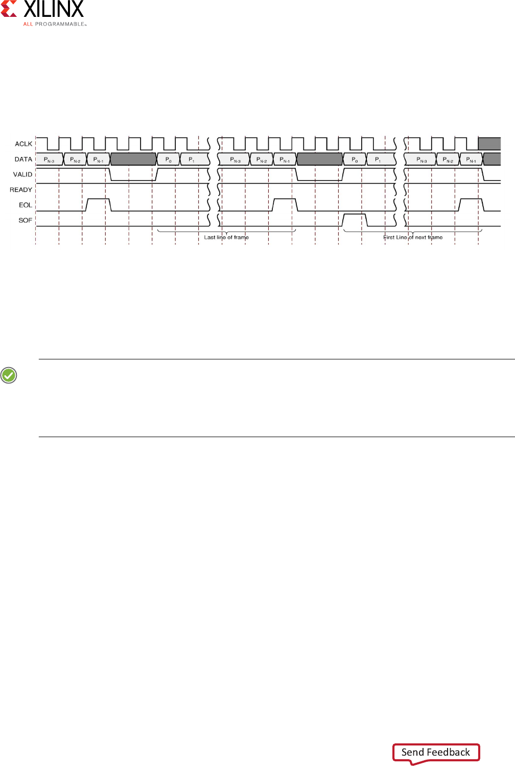
Vivado AXI Reference Guide www.xilinx.com 105
UG1037 (v4.0) July 15, 2017
Chapter 4: AXI Feature Adoption in Xilinx Devices
End Of Line Signal - EOL
The End-Of-Line (EOL) signal, physically transmitted over the AXI4-Stream TLAST signal,
marks the last pixel of a line. The EOL pulse is 1 valid transfer wide, and must coincide with
the last pixel of a scan-line, shown in the following figure.
Parameterization and/or configuration registers define the dimensions of video frames that
video IP should process. Starting from a known state, based on these configuration settings
the IP can predict when the last pixel of each scanline is expected. The EOL detected before
expected (early), or EOL not present when expected (late), signals error conditions
indicative of either upstream communication errors or incorrect core configuration.
RECOMMENDED: It is recommended that video IP flags both error conditions with dedicated flags in
the core ERROR register. Recommended flag names are sk_EOL_EARLY and sk_EOL_LATE, where k is the
index of the AXI4-Stream slave interface.It is recommended that these flags can trigger interrupts, so
embedded application developers can quickly identify faulty interfaces or incorrectly parameterized
cores in a video system.
Also, to minimize the impact of sustained error conditions it is recommended, but not
mandated, that:
• When the EOL_EARLY condition is detected, if possible, the IP should immediately
start processing the new line. All pixels pertaining to the previous frame should be
flushed out, the line should be qualified with the EOL signal, and processing of the new
line should commence.
• When the EOL_LATE condition is detected, the IP must generate its output EOL signal
according to the programmed/parameterized line-length, and drop (accept on the
input, but not propagate to the output) subsequent pixels until the EOL signal arrives.
X-Ref Target - Figure 4-11
Figure 4-11: Use of EOL and SOF Signals
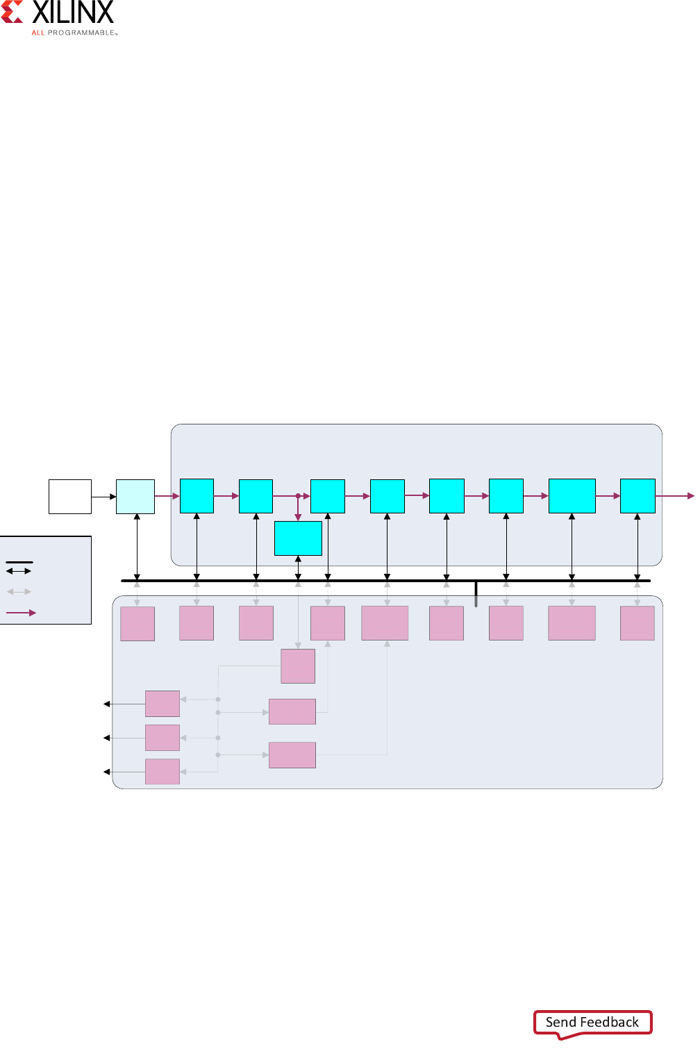
Vivado AXI Reference Guide www.xilinx.com 106
UG1037 (v4.0) July 15, 2017
Chapter 4: AXI Feature Adoption in Xilinx Devices
Real Time Requirements
The AXI4-Stream interface protocol does not impose any rules on real-time requirements.
Video IP should not impose strict cycle-to-cycle real-time requirements on data transfers,
other than to meet and not break the fundamental AXI handshake rules at the AXI4-Stream
interface. The IP must meet the constraint on the clock signal to which the interface is
synchronous.
Data Format
To transport video data, the DATA vector encodes logical channel subsets of physical DATA
signals. Various AXI4-Stream interfaces between the modules can facilitate transferring
video using different precision (for example; 8, 10, 12, or 16 bits per color channel), and/or
different formats (for example RGB or YUV 420).
A specific example of a typical image pre-processing system is illustrated in the following
figure, which consists of a number of Xilinx IP cores connected using AXI4-Stream to
implement an imaging sensor processing pipeline.
AXI4-Stream channels in Figure 4-12 are annotated to reflect the transferred video format.
The DATA signal must not have any explicit subfields defined, either as separate ports or
with special signal suffixes.
X-Ref Target - Figure 4-12
Figure 4-12: Image Processing Pipeline
Legend
Sensor
Image
Statistics
(Stats)
CFA CCM γCSCDPC
AG
AF
Color
Correction
Matrix
RGB
to
YCrCb
Color Filter
Array
Interpolation
AXI4-S
Input
Interface
Sensor Gain
Lens Focus
EnhanceNoise
Noise
Reduction
Gamma
Correction
CRS
Chroma
Resampler
Edge
Enhancement
YCC
444
DPC
driver
CCM
driver
Gamma
driver
Enhance
driver
MicroBlaze
Stats
driver
CFA
driver
Noise
driver
AE
Sensor
Exposure
Control
Defective
Pixel
Correction
Y
444
Y
444
RGB
444
RGB
444
RGB
444
YCC
444
YCC
444
IIF
driver
AXI4-S
IIF
CRS
driver
CSC
driver
AXI4- Lite
AXI4- Stream
Virtual
Connection
(Software)
AXI4-Lite
YCC
422
AWB
Global
Contrast
AG
AF
DP
C
driver
CC
M
d
riv
e
r
G
amma
d
river
E
n
ha
n
ce
driver
M
i
c
r
o
Bl
a
z
e
S
tat
s
d
riv
e
r
C
F
A
driver
Noise
d
river
AE
IIF
d
r
i
v
e
r
C
R
S
d
riv
e
r
CSC
d
riv
e
r
A
W
B
G
lobal
C
ontrast
Vivado AXI Reference Guide www.xilinx.com 107
UG1037 (v4.0) July 15, 2017
Chapter 4: AXI Feature Adoption in Xilinx Devices
For example, cores with DATA_Y and DATA_C signals are not permitted. Format information
is embedded in the IP-XACT representation of IP as metadata tags attached to AXI4-Stream
ports.
AXI4-Stream Specific Parameterization
The following table lists the parameters specific to IP using the AXI4-Stream Video Protocol.
The paragraphs immediately following the table provide further description.
The C_tk_AXIS_TDATA_WIDTH parameter determines the width of the variable-width
DATA interface signal on AXI4-Stream interface t, where interface type t can have the
values [m,s] designating a master or slave interface, while optional integer k specifies the
interface ID. Typically, C_tk_AXIS_TDATA_WIDTH is a function of the component data width,
the number of pixels/samples per data beat, and the number of components the actual
video format is using.
The recommended parameter names for component data width is C_tk_DATA_WIDTH.
Supported component widths are 8, 10, 12, and 16 bits. The optional format parameter
C_tk_VIDEO_FORMAT can assist the IP in determining the number of color or components
present on DATA using a HDL function. Video IP is typically very specific on the formats
expected on the input interfaces, and could already have the number of color or component
channels hard coded in the IP. However, when the C_tk_VIDEO_FORMAT parameter, set by
a default value on the master interface, is propagated in HDL designs to slave interfaces, the
IP source code can perform DRC by means of assertions to ensure that AXI4-Stream video
interfaces are driven by video encoded in the expected format.
The C_tk_MAX_SAMPLES_PER_CLOCK parameter specifies the maximum number of
samples/pixels being transferred in parallel on TDATA. See Encoding for more information.
Encoding
The DATA bits are represented using the [N-1:0] bit numbering convention (N-1 through 0).
The components of implicit subfields of DATA should be packed tightly together; for
example, a DW=10 bit RGB data packed together to 30 bits. If necessary, the packed data
word should be zero padded with most significant bits (MSBs) so the width of the resulting
word is an integer that is a multiple of eight as shown in the following figure.
Table 4-8: IP using AXI4-Stream Video Protocol Parameters
Parameter Name Parameter Function
C_tk_DATA_WIDTH Width of color/component data.
C_tk_VIDEO_FORMAT Video format code (see following description).
C_tk_AXIS_TDATA_WIDTH Width of the DATA interface signal.
C_tk_MAX_SAMPLES_PER_CLOCK Maximum number of samples/pixels per data beat.
Vivado AXI Reference Guide www.xilinx.com 108
UG1037 (v4.0) July 15, 2017
Chapter 4: AXI Feature Adoption in Xilinx Devices
The following table provides detailed representation of different formats, with
DW = C_DATA_WIDTH and VF = C_VIDEO_FORMAT. It lists the detailed representation of
video data formats, with DW = C_DATA_WIDTH and VF = C_VIDEO_FORMAT.
Encoding Multiple Pixels
When multiple samples/pixels are carried by AXI4-Stream, pack the pixels from least
significant bit (LSB) to most significant bit (MSB). For example, the least significant pixel
corresponds to the left-most pixel in a scanline, or to the pixel captured earliest in time.
For example, if 4 samples/pixels are sent per data beat, the first sample sits in the least
significant, the 4th sample sits in the most significant bit positions.
When multiple pixels or samples are transferred using the video protocol over AXI4-Stream,
color components pertinent to the individual pixels are arranged according to Table 4-10,
presenting examples for transferring two pixels for video modes 0, 1, 2, 3, 12. Pixel data is
packed continuously without any padding between pixels.
X-Ref Target - Figure 4-13
Figure 4-13: Video Data Padding for TDATA
816243240
Component GComponent BComponent R
bit 0
Table 4-9: Video Format Codes and Data Representation for C_tk_MAX_SAMPLES_PER_CLOCK =1
VF Code Video Format [4DW-1: 3DW] [3DW-1: 2DW] [2DW-1: DW] [DW-1:0]
0YUV 4:2:2 V/U, Cr/CbY
1 YUV 4:4:4 V, Cr U, Cb Y
2RGB R B G
3YUV 4:2:0 V/U, Cr/CbY
4 YUVA 4:2:2 a V/U, Cr/Cb Y
5 YUVA 4:4:4 a V, Cr U, Cb Y
6RGBAa R B G
7 YUVA 4:2:0 α, V/U, Cr/Cb Y
8 YUVD 4:2:2 D V/U, Cr/Cb Y
9 YUVD 4:4:4 D V, Cr U, Cb Y
10 RGBD D R B G
11 YUV 4:2:0 D V/U, Cr/Cb Y
12 Mono/Sensor Y, RGB, CMY
13 Custom2 2 Components – No DRC
14 Custom3 3 Components – No DRC
15 Custom4 4 Components – No DRC
Vivado AXI Reference Guide www.xilinx.com 109
UG1037 (v4.0) July 15, 2017
Chapter 4: AXI Feature Adoption in Xilinx Devices
When N*DW is not an integer multiple of 8, video data is zero padded on the MSBs, as
presented in the following figure.
Dynamic TDATA Configuration
For applications where video IP can dynamically change color-component width, video
format, or the number of pixels/samples per data beat, pixels and components should
remain at the static locations determined by the generic parameters for instantiation.
Actual data on the TDATA vector should be LSB aligned; for example, if only one pixel is
transmitted over an interface supporting at most two pixels per data beat, the sample/pixel
should be aligned to the LSB position. Similarly, if only 8 bits are transmitted over an
interface generated for 10 bit data, the active bits should be LSB aligned and MSB padded,
shown in the following figure.
X-Ref Target - Figure 4-14
Figure 4-14: Video Data Padding for TDATA for Multiple Pixels
5664 48 8162432
Component GComponent B
bit 0
Component R
40
Component GComponent B
Component R
Table 4-10: Video Format Codes and Data Representation
VF
Code
Video
Format
[6DW-1:
5DW]
[5DW-1:
4DW] [4DW-1: 3DW] [3DW-1:
2DW] [2DW-1: DW] [DW-1:0]
0YUV 4:2:2 V1/U1, Cr1/Cb1 Y1 V0/U0, Cr0/Cb0 Y0
1YUV 4:4:4 V1, Cr1 U1, Cb1 Y1 V0, Cr0 U0, Cb0 Y0
2RGB R1 B1 G1 R0 B0 G0
3YUV 4:2:0 V1/U1, Cr1/Cb1 Y1 V0/U0, Cr0/Cb0 Y0
12 Bayer
Sensor RGB1, CMY1 RBGB0, CMY0
X-Ref Target - Figure 4-15
Figure 4-15: TDATA Padding for Dynamic AXI4- Configuration
5664 48 8bit 0
162432
Component GComponent B
Component R
40

Vivado AXI Reference Guide www.xilinx.com 110
UG1037 (v4.0) July 15, 2017
Chapter 5
Migrating to Xilinx AXI Protocols
Introduction
Migrating an existing core is a process of mapping the I/O signal of your core to
corresponding AXI protocol signals. In some cases, additional logic might be needed.
Migrating to AXI for IP Cores
Xilinx provides the following guidance for migrating IP.
See Memory-Mapped IP Feature Adoption and Support as well as the ARM AMBA AXI
Protocol v2.0 Specification specification [Ref 1] available from the ARM website. New IP
should be designed to the AXI protocol.
IP that was created using the Create and Import Peripheral (CIP) Wizard in a previous
version of Xilinx tools (before AXI was supported) can be migrated by rerunning the CIP
Wizard in the ISE® Design Suite to create AXI-based template designs.
IP that needs to remain unchanged can be used in the Xilinx tools using the AXI to PLB
bridge.
Larger pieces of Xilinx IP (often called Connectivity or Foundation IP): This class of IP has
migration instructions in the respective documentation. This class of IP includes: PCIe®,
Memory Core, and Serial Rapid I/O.
DSP IP: General guidelines on converting this broad class of IP is covered in this link to the
“Migrating Designs to Vivado IDE” chapter of the Vivado Design Suite User Guide:
Model-Based DSP Design Using System Generator (UG897) [Ref 31].
EDK IP: Converting EDK IP is a manual process, described in the ISE to Vivado Migration
Guide (UG911) [Ref 35].
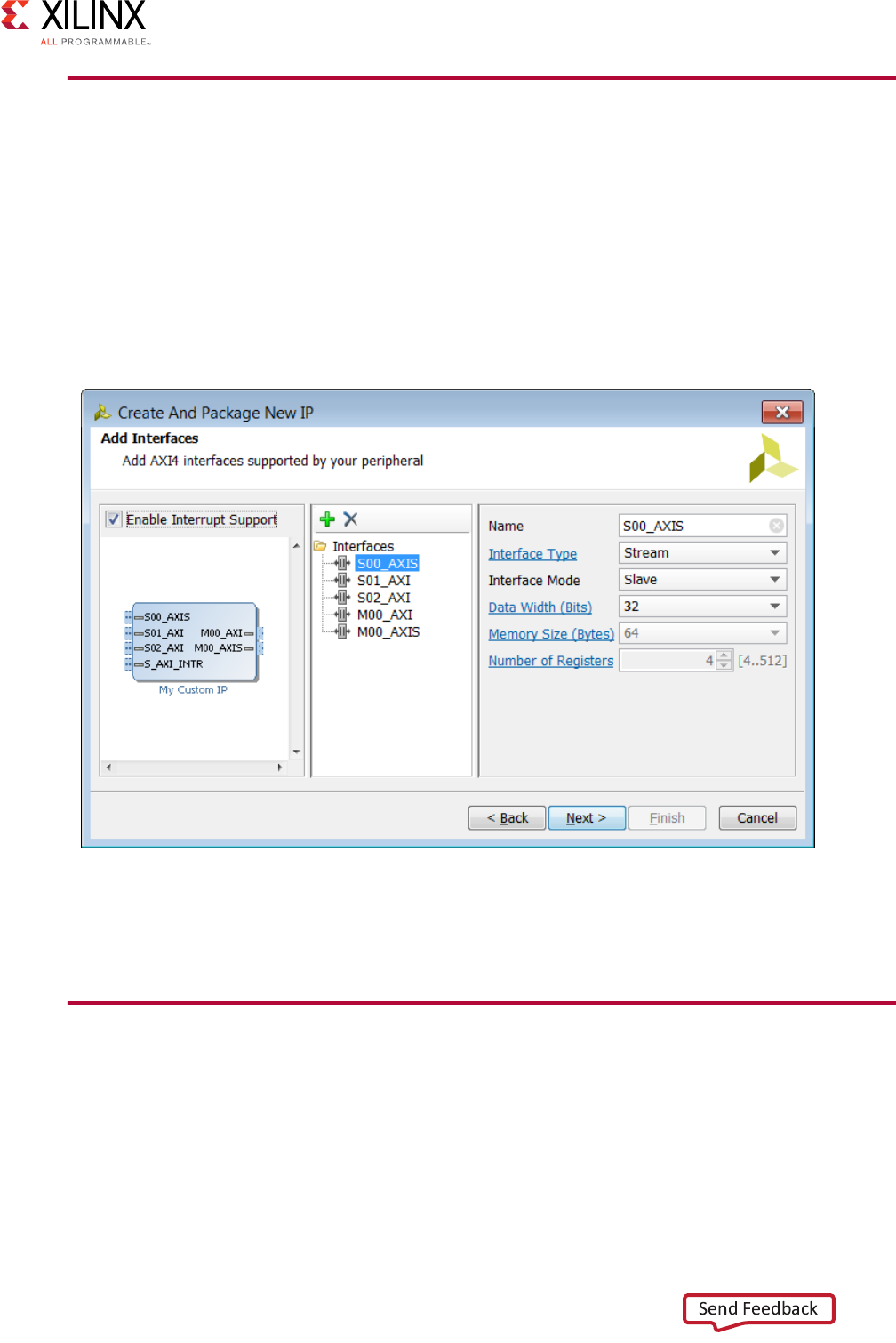
Vivado AXI Reference Guide www.xilinx.com 111
UG1037 (v4.0) July 15, 2017
Chapter 5: Migrating to Xilinx AXI Protocols
Migrating IP Using the Vivado Create and Package
Wizard
The Vivado IDE contains a tool (see the following figure) to help you create a new AXI IP. The
tool lets you specify AXI interface characteristics and then the tool creates and packages a
working example AXI IP. This template IP implements some simple demonstration
functionality and can be created with an example test bench to exercise the IP using the AXI
Verification IP (VIP) modes. This gives you a starting point from which to design you own
custom AXI IP.
For more information about creating AXI IP using this wizard, see the Vivado Design Suite
User Guide: Creating and Packaging Custom IP (UG1118) [Ref 33].
Using System Generator for DSP for Migrating IP
System Generator for DSP has an Upgrade Model feature that can assist you in migrating
designs previously created in ISE System Generator to designs that are compatible with the
Vivado Integrated Design Environment (IDE) and include AXI4 interfaces.
See this link to the “Migrating Designs to Vivado IDE” chapter in the Vivado Design Suite
User Guide: Model-Based DSP (UG897) [Ref 31] for more information.
X-Ref Target - Figure 5-1
Figure 5-1: Create and Package IP Wizard: AXI Interfaces
Vivado AXI Reference Guide www.xilinx.com 112
UG1037 (v4.0) July 15, 2017
Chapter 5: Migrating to Xilinx AXI Protocols
Migrating a Fast Simplex Link to AXI4-Stream
When converting a Fast Simplex Link (FSL) peripheral to an AXI4-Stream peripheral there
are several considerations. You must migrate the:
• Slave FSL port to an AXI4-Stream slave interface
• Master FSL port to an AXI4-Stream master interface
The following tables list the master-FSL and slave-FSL to AXI4-Stream signals conversion
mappings.
Master FSL to AXI4-Stream Signal Mapping
The following table shows the AXI4-Stream signal mapping.
Slave FSL to AXI4-Stream Signal Mapping
The following table shows the FSL to AXI4-Stream signal mapping.
Table 5-1: AXI4-Stream Signal Mapping
Signal Direction AXI Signal Direction
FSL_M_Clk Out M_AXIS_<Port_Name>ACLK In
FSL_M_Write Out M_AXIS_<Port_Name>TVALID Out
FSL_M_Full In M_AXIS_<Port_Name>TREADY In
FSL_M_Data Out M_AXIS_<Port_Name>TDATA Out
FSL_M_Control Out M_AXIS_<Port_Name>TLAST Out
Table 5-2: FSO to AXI-4 Stream Signal Mapping
Signal Direction AXI Signal Direction
FSL_S_Clk Out S_AXIS_<Port_Name>ACLK In
FSL_S_Exists In S_AXIS_<Port_Name>TVALID In
FSL_S_Read Out S_AXIS_<Port_Name>TREADY Out
FSL_S_Data In S_AXIS_<Port_Name>TDATA In
FSL_S_Control In S_AXIS_<Port_Name>TLAST In

Vivado AXI Reference Guide www.xilinx.com 113
UG1037 (v4.0) July 15, 2017
Chapter 5: Migrating to Xilinx AXI Protocols
Differences in Throttling
There are fundamental differences in throttling between FSL and AXI4-Stream, as follows:
•The M_AXIS_TVALID signal cannot be deasserted after being asserted unless a
transfer is completed with M_AXIS_TREADY. However, an M_AXIS_TREADY can be
asserted and deasserted whenever the AXI4-Stream slave requires assertion and
deassertion.
• For FSL, the signals FSL_Full and FSL_Exists are the status of the interface; for
example, if the slave is full or if the master has valid data
• An FSL-master can have a pre-determined expectation prior to writing to FSL to check if
the FSL-Slave can accept the transfer based on the FSL slave having a current state of
FSL_Full
• An AXI4-Stream master cannot use the status of S_AXIS_TREADY unless a transfer is
started.
The MicroBlaze™ processor has an FSL test instruction that checks the current status of the
FSL interface. For this instruction to function on the AXI4-Stream, MicroBlaze has an
additional 32-bit Data Flip-Flop (DFF) for each AXI4-Stream master interface to act as an
output holding register.
When MicroBlaze executes a put fsl instruction, it writes to this DFF. The AXI4-Stream
logic inside MicroBlaze moves the value out from the DFF to the external AXI4-Stream slave
device as soon as the AXI4-Stream allows. Instead of checking the AXI4-Stream
TREADY/TVALID signals, the FSL test instruction checks if the DFF contains valid data
instead because the S_AXIS_TREADY signal cannot be directly used for this purpose.
The additional 32-bit DFFs ensure that all current FSL instructions to work seamlessly on
AXI4-Stream. There is no change needed in the software when converting from FSL to AXI4
stream.
For backward compatibility, the MicroBlaze processor supports keeping the FSL interfaces
while the normal memory-mapped AXI interfaces are configured for AXI4.
This is accomplished by having a separate, independent MicroBlaze configuration
parameter (C_STREAM_INTERCONNECT) to determine if the stream interface should be
AXI4-Stream or FSL.
Vivado AXI Reference Guide www.xilinx.com 114
UG1037 (v4.0) July 15, 2017
Chapter 5: Migrating to Xilinx AXI Protocols
Migrating HDL Designs to use DSP IP with
AXI4-Stream
Adopting an AXI4-stream interface on a DSP IP should not change the functional, or signal
processing behavior of the DSP function such as a filter or a FFT transform. However, the
sequence in which data is presented to a DSP IP could significantly change the functional
output from that DSP IP. For example, one sample shift in a time division multiplexed input
data stream will provide incorrect results for all output time division multiplexed data.
To facilitate the migration of an HDL design to use DSP IP with an AXI4-Stream interface, the
following subsections provide the general items to consider:
•DSP IP-Specific Migration Instructions
•Demonstration Test Bench
•Latency Changes
•Mapping Previously Assigned Ports to An AXI4-Stream Video Protocol
DSP IP-Specific Migration Instructions
This section provides an overview with IP specific migration details available in each
respective data sheet. Before starting the migration of a specific piece of IP, review the
“AXI4-Stream Considerations” and “Migrating from earlier versions” in the individual IP Data
Sheets or Product Guides.
The following figure shows an example.
X-Ref Target - Figure 5-2
Figure 5-2: Example IP Data Sheet
Vivado AXI Reference Guide www.xilinx.com 115
UG1037 (v4.0) July 15, 2017
Chapter 5: Migrating to Xilinx AXI Protocols
Demonstration Test Bench
To assist with core migration, the Vivado Video IP generate an example test bench in the
demo_tb directory under the Vivado IP project directory. The test bench instantiates the
generated core and demonstrates a simple example of how the DSP IP works with the
AXI4-stream interface. This is a simple VHDL test bench that exercises the core.
The demonstration test bench source code is one VHDL file,
demo_tb/tb_<component_name>.vhd, in the Vivado IP output directory.
The source code is comprehensively commented. The demonstration test bench drives the
input signals of the core to demonstrate the features and modes of operation of the core
with the AXI4-Stream interface. For more information on how to use the generated test
bench see the “Demonstration Test bench” section in the individual IP data sheet.
The following figure shows the demo_tb directory structure.
Upgrading IP
Upgrade IP to the latest version by using one of the following:
•The Upgrade IP option in the right-click menu of the selected IP
•The Report IP Status command
See more information see this link to the “Upgrading IP” section in the Vivado Design Suite
User Guide: Designing with IP (UG896) [Ref 30].
Note: The upgrade mechanism alone does not create a core compatible with the latest version but
does provide a core that has equivalent parameter selection as the previous version of the core. The
core instantiation in the design must be updated to use the AXI4-Stream interface. The upgrade
mechanism also creates a backup of the old XCO file. The generated output is contained in the /tmp
directory of the CORE Generator project.
X-Ref Target - Figure 5-3
Figure 5-3: demo_tb Directory Structure

Vivado AXI Reference Guide www.xilinx.com 116
UG1037 (v4.0) July 15, 2017
Chapter 5: Migrating to Xilinx AXI Protocols
Latency Changes
With DSP IP that support the AXI4-Stream interface, each individual AXI4-Stream slave
channel can be categorized as either a blocking or a non-blocking channel. A slave channel
is blocking when some operation of the core is inhibited until a transaction occurs on that
channel. In general, the latency of the DSP IP AXI4-Stream interface is static for
non-blocking and variable for blocking mode. To reduce errors while migrating your design,
pay attention to the “Latency Changes” and “Instructions for Minimum Change Migration”
sections of the IP data sheet.
Mapping Previously Assigned Ports to An AXI4-Stream Video
Protocol
The individual DSP IP datasheets provide a table about the changes to port naming,
additional or deprecated ports, and polarity changes from previous version to the latest
version of the core. Noteworthy changes are:
•Resets: The DSP IP AXI4-stream interface aresetn reset signal is active-Low and must
be asserted for a minimum length of two clock cycles. The aresetn reset signal always
takes priority over the aclken clock enable signal. Therefore your IP instantiation reset
input must change from an active-High “SCLR” signal with a minimum length of one
clock cycle, to a active-Low reset input with a minimum of two clock cycles.
•Input and Output TDATA port structure: The AXI specification calls for data to be
consolidated onto a single TDATA input stream. For ease of visualization you can view
the TDATA structure from the IP symbol and implementation details tab in the IP GUI.
For ease of IP instantiation the demonstration example testbench also shows how to
connect and functionally split signals from the TDATA structure. The demonstration
testbench assigns TDATA fields to aliases for easy waveform viewing during simulation.
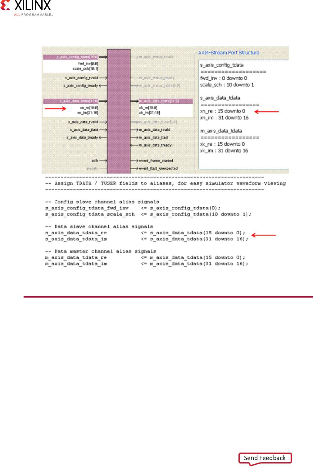
Vivado AXI Reference Guide www.xilinx.com 117
UG1037 (v4.0) July 15, 2017
Chapter 5: Migrating to Xilinx AXI Protocols
The following figure shows the TDATA port structure.
High End Verification Solutions
Many third-party companies (such as Cadence Design Systems, ARM, Mentor Graphics, and
Synopsys) have tools whose function is to allow system-level verification and performance
tuning for system-level design. When designing large AXI-based systems, if the highest
possible verification and performance are required, it is recommended that third-party
tools be used.
X-Ref Target - Figure 5-4
Figure 5-4: TDATA Port Structure

Vivado AXI Reference Guide www.xilinx.com 118
UG1037 (v4.0) July 15, 2017
Chapter 6
AXI System Optimization: Tips and Hints
Introduction
AXI-based Xilinx® IP, third-party IP, and user IP present a wide range of configuration
options and design choices that let you tune a system for size, Fmax, throughput, latency,
ease of use, and ease of debug. IP design decisions and system architecture also impact the
area and performance of the system.
Given that AXI-based systems must span a wide solution space from small Spartan® and
Artix® class designs to very large, high performance Virtex®, Kintex®, Zynq®-7000 AP SoC
and Zynq UltraScale+™ MPSoC processor designs, there is a large configuration space for
AXI IP and systems.
This chapter provides information and presents concepts that help you optimize your IP
designs and system configurations. In some cases, optimization for one attribute might
conflict with another requiring you to balance competing tradeoffs. For example, improving
timing through the use of additional pipelining negatively impacts area.
Table 6-1 and Table 6-2 illustrate the impact of different AXI Interconnect, AXI
SmartConnect, and IP features, configuration parameters, and optimization options across
various criteria. The impact on each criterion is qualitatively described using a positive to
negative scale of Best (++), Better (+), Neutral (0), Worse (-), and Worst (--). When creating
an architecture, optimizing, or diagnosing systems, use these tables to help with designing
the IP or system to maximize the attributes required by the application while minimizing
negative trade-offs.
You need to be familiar with the AXI infrastructure IP, or AXI SmartConnect IP, and general
Vivado embedded tool usage to better understand the optimization suggestions and
strategies described in this chapter.

Chapter 6: AXI System Optimization: Tips and Hints
Vivado AXI Reference Guide www.xilinx.com 119
UG1037 (v4.0) July 15, 2017
Table 6-1: AXI Interconnect Optimization/Feature Impact
Feature Configuration
Size/Area
Timing/Fmax
Throughput
Latency
Ease of Use/Flexibility
Ease of Debug
Notes
Clock Domain Conversion
(Optional, Default = OFF
Synch Clock Conversion - + 0 - + 0 Synch clock conversions require complex multi-cycle timespecs
(core level UCF is automatically generated by AXI Interconnect
and AXI SmartConnect).
Async Clock Conversion -- + 0 -- ++ 0 Asynchronous clock conversion includes a 32-bit deep FIFO or
is merged into BRAM FIFO logic. Synchronized conversion is
generally preferred over asynchronous conversion.
Width Conversion
(Optional, Default = OFF)
Downsizer -- -- -- - + 0 For AXI Interconnect, size converters do not support
multi-threading. They will stall when IDs change until
transactions on previous IDs are complete.
Upsizer -- - - - + 0
Endpoint Slave Protocol
Conversion from AXI4,
(Optional, Default = OFF)
AXI4-Lite 0 0 -- 0 + ++ For AXI Interconnect, the AXI3 converter does not support
multi-threading when splitting is enabled. It will stall when IDs
change until transactions on previous IDs are completed. AXI3
converter also requires logic to handle splitting of long AXI4
bursts to AXI3 bursts of maximum length of 16. This logic adds
size and latency.
AXI3 - - - - 0 0
Connectivity Mode
Shared Access Shared Data++ 0 -- 0 + ++
Crossbar - Sparse (Default) 0 + + 0 0 0
Crossbar - Fully Connected -- - + 0 0 0
ID Threading
Single Thread + + 0 0 + + Applies when a master declares that it does not use IDs or
interconnect is explicitly placed into Single Thread mode. Note
that configuration setting such as Shared Address Shared Data
mode (SASD), size conversion, or protocol conversion, might
automatically cause Single Thread mode to be used.
Multiple Thread Support 0 0 + 0 0 - As more threads are used and there is a greater potential for read
reordering or read interleaving, the more difficult it is to debug.
Issuance/Acceptance
1 (Default) + + - 0 + +
2, 4, 8, 16, 32 - 0 + - 0 -
Legend: “++” = Best; “+” = Better, “0” = Neutral, “-“=Worse, “--“ = Worst

Chapter 6: AXI System Optimization: Tips and Hints
Vivado AXI Reference Guide www.xilinx.com 120
UG1037 (v4.0) July 15, 2017
Datapath Width
32 (Default) + + - 0 0 0
64, 128, 256, 512, 1024 -- - ++ 0 0 0
Register Slice
(Optional, Default = OFF)
Type 7 (Light Weight) - ++ - - + 0 AXI Interconnect has added a “Type 8” register slice that
automatically selects the register slice type based upon
interconnect configuration. Type 8 is recommended and should
be overridden only when warranted. SmartConnect also offers
multiple internal pipelining options.
Type 1 (Fully Registered) -- ++ 0 - + 0
Type 8 (Automatic) - ++ 0 - + 0
Floorplanning
(Optional, Default = OFF)
Floorplan IP Blocks And/Or
Submodules
0 + 0 0 -- 0
Datapath FIFOs
(Optional, Default = OFF)
SRL - 0 + - 0 0 SRL FIFO is 32 deep. FIFO depths are more configurable in
SmartConnect.
BRAM -- 0 ++ - 0 0 BRAM FIFO is 512 deep. Use of additional BRAM FIFO option,
to delay AWVALID/ARVALID until FIFO occupancy permits
interrupted burst transfers, can further improve throughput at the
expense of increased latency.
Arbitration Priority
(Optional, Default = Round
Robin)
Fixed Priority Over Round
Robin
000+ - 0 Each master can be assigned a higher fixed priority that
supersedes masters at the default priority level of 0. Masters set
to the default priority of 0 share Round Robin priority.
SmartConnect does not currently support arbitration priority
options.
AXI System Debug Wizard
(Optional, Default = OFF)
ON - - 0 0 0 ++
AXI Hardware Protocol
Checker
(Optional, Default = OFF)
ON - - 0 0 0 ++
Table 6-1: AXI Interconnect Optimization/Feature Impact (Cont’d)
Feature Configuration
Size/Area
Timing/Fmax
Throughput
Latency
Ease of Use/Flexibility
Ease of Debug
Notes
Legend: “++” = Best; “+” = Better, “0” = Neutral, “-“=Worse, “--“ = Worst
Chapter 6: AXI System Optimization: Tips and Hints
Vivado AXI Reference Guide www.xilinx.com 121
UG1037 (v4.0) July 15, 2017
Table 6-2: AXI Endpoint IP Optimization/Feature Impact
Feature Configuration
Size/Area
Timing/Fmax
Throughput
Latency
Ease of Use/Flexibility
Ease of Debug
Notes
IP Protocol
AXI4-Lite ++ 0 - 0 + ++ AXI Interconnect i s natively AXI4-based. Use of AXI3 protocol not recommended
for new designs.
AXI4 0 0 0 0 0 0
Narrow Burst
Support
ON (Default) -- - - - 0 0
Narrow burst is assumed to be ON unless the AXI master IP specifically designates
this as OFF. Xilinx AXI master IP generally do not use narrow burst and designate
themselves as OFF.
OFF
(Recommended) 0 0 0 0 0 0
Threading
Uses No Thread or
Issues Only a
Single Thread
+ + 0 0 + +
Using a single thread while intermixing transactions destined to multiple different
AXI slave endpoints could trigger stalling by the deadlock avoidance logic in the AXI
Interconnect.
Issues Multiple
Threads0 0 + 0 0 -
Ability to Pipeline
Transactions
1 + + - 0 + +
New transactions pipelined behind high numbers of pipelined transactions might
experience high latency, but throughput might be improved. Head of line blocking
can be caused by excessively pipelined transactions.
> 1 up to 32- 0 + 0 0 0
Datapath Width
32++-000
Native data path width should be minimized while meeting performance
requirements of application. The caveat is that support for a wider native width that
minimizes size conversion in a system could be more beneficial.
64, 128, 256, 512,
1024 -- - ++ 0 0 0
AXI4 Burst Length
Short (1-4) 00-+00
Head of line blocking can be caused by long bursts. Transactions pipelined behind
long bursts might experience high latency, but throughput might be improved.
Long (up to 256) 00++-- 00
Legend: “++” = Best; “+” = Better, “0” = Neutral, “-“ = Worse, “--“ = Worst
Vivado AXI Reference Guide www.xilinx.com 122
UG1037 (v4.0) July 15, 2017
Chapter 6: AXI System Optimization: Tips and Hints
AXI System Optimization
In general, system optimization follows the guidelines in the following subsections.
Size/Area Optimization Guidelines
When considering your AXI IP or system design, use the following size and area guidelines:
1. Minimize the clock domain conversions by reducing the logic associated with clock
domain conversion. Use as few clocks as possible and, if clock conversion is necessary,
attempt to keep the clocks to synchronous integer ratios.
2. Shared Address Shared Data (SASD) configurations of the AXI Interconnect, especially for
AXI4-Lite networks. Analyze the connectivity and bandwidth requirements of the system.
An SASD set of connected data configuration consumes even less logic because a single
data path is shared by all devices and only one transaction is outstanding at a time.
3. Reduce use of multi-threading in AXI memory-mapped IP including reduced values of
issuance or acceptance. Reducing use of threads and transaction pipelining simplifies
the transaction handling logic of the AXI Interconnect, but throughput could be
impacted.
4. Avoid using AXI3 or AXI4 narrow bursts. Narrow bursts are defined in the AXI protocol
but are generally not used by master IP. When a master IP specifically designates that
they do not issue narrow bursts, some slaves (such as memory controllers) can detect
that they will therefore never receive a narrow burst transaction and can omit narrow
burst support logic.
IMPORTANT: Minimize protocol conversions and use AXI4-Lite where possible. Protocol conversion to
AXI3 slaves utilizes logic. The AXI4-Lite protocol requires less logic to support, especially when all
devices on an AXI Interconnect are AXI4-Lite type. Using AXI4-Lite protocols and grouping AXI4-Lite IP
into a separate subsystem can reduce logic.
5. Where appropriate, segment interconnects into smaller, less complex subsystems where
each subsystem can be optimized as described in the previous steps. This requires
analysis of the protocol types, bandwidth, and master/slave connectivity. Grouping IP
into subsystems that minimize connectivity requirements and minimize the number of
conversion operations can reduce logic.
6. Reduce data path width and minimize size and width conversions. Design systems to the
minimum required data path width while also minimizing width conversions.
CAUTION! Be careful to not inadvertently mismatch the AXI Interconnect/AXI SmartConnect core data
width or core clock with the width and clock of all the attached endpoints; this can result in an excessive

Vivado AXI Reference Guide www.xilinx.com 123
UG1037 (v4.0) July 15, 2017
Chapter 6: AXI System Optimization: Tips and Hints
number of conversions. If possible, handle width conversion inside the user IP instead of using a
general-purpose memory-mapped AXI width converter.
A protocol-compliant AXI memory-mapped width converter block is complex due to
issues like address calculation, multi-thread support, transaction splitting, unaligned
bursts, and arbitrary burst length.
If width conversion can be performed more efficiently in the user IP or in the application
domain before reaching the AXI interconnect, the overall area is reduced.
Timing and Fmax Optimization Guidelines
1. Turn on register slices or pipelines where appropriate. Register slices act as AXI pipeline
stages to break combinatorial timing paths across the register slice. AXI
Interconnect/AXI SmartConnect provides an optional register slice at the boundary of
each attached endpoint. Different register slice types and the granularity to set them on
individual AXI channels provides fine grain control of register slices placement.
2. Large and complex IP blocks such as processors, DDR3 memory controllers, and PCIe
bridges are good candidates for having register slices enabled. The register slice breaks
timing paths and allows more freedom for Place and Route (PAR) tools to move a large
IP block away from the congestion of the interconnect core and other IP logic.
a. Overuse of register slices, especially in relatively full designs, can become
counter-productive to timing by increasing the area and therefore the congestion for
PAR tools.
b. As required by the AXI specification, user IP must avoid combinatorial paths
between inputs and outputs of the same AXI interface. This AXI protocol rule helps
improve overall system timing.
3. Reduce data path width and minimize size/width conversions.
4. Where appropriate, segment interconnects into smaller or less complex subsystems
where timing critical IP can be isolated away from non-critical IP. For example, a group
of low bandwidth IP can be placed on a slower clock, smaller data width AXI
Interconnect to free up logic and congestion from the higher performance IP running at
higher clock rates and wider data paths.
5. Separate IP using register slices then floorplan the IP blocks (this is an advanced
strategy). After placing register slices to provide timing isolation, IP blocks can be
floorplanned further away from the interconnect core to reduce congestion around that
block core.
Throughput and Bandwidth Optimization Guidelines
1. Increase clock frequencies using timing optimizations described in “Timing and Fmax
Optimization Guidelines,” in the previous section. Increasing clock frequency, such as

Vivado AXI Reference Guide www.xilinx.com 124
UG1037 (v4.0) July 15, 2017
Chapter 6: AXI System Optimization: Tips and Hints
through the use of register slices to break long combinatorial paths can improve overall
bandwidth.
2. Increase data path widths. Wider data paths carry more information per clock cycle.
3. Turn on data path FIFO buffers. Buffers can provide elasticity to hide temporary stalls or
backpressure in the data flow. Use of the additional block RAM FIFO option, to delay
AWVALID/ARVALID until FIFO occupancy permits interrupted burst transfers, can
further improve throughput at the expense of increased latency.
4. Segment interconnects to group high performance IP together and place lower
performance IP in a separate interconnect. Isolating high performance IP into a smaller
subsystem permits greater flexibility to optimize that subsystem for higher throughput.
5. Increase transaction burst length. Longer bursts reduce the potential for stall cycles
caused by address arbitration and control logic overhead.
Longer bursts also signal to the AXI slave the intent to move a large amount of
contiguous data so that slaves, such as memory controllers, can better optimize their
response, and Reduce the relative amount of AXI address channel bandwidth.
This reduces address channel congestion around the shared address arbiter logic in the
AXI Interconnect.
6. Increase transaction pipelining including issuance and acceptance. Pipelining
transactions allows arbiters and control logic in the slaves to work ahead on the next
transaction while completing a previous transaction. This helps to reduce stalling due to
arbitration/control cycles between back to back transactions.
7. Exploit parallelism of Sparse Crossbar AXI Interconnect. In Sparse Crossbar Mode, the
AXI Interconnect supports parallel data flow when multiple masters transfer data to
multiple independent slaves.
8. Avoid issuing read/write address requests until the IP ensures it can provide data while
inserting minimal idle cycles in the data stream. Otherwise when a read or write data
transfer is in progress, stalling the data phase of the transaction could prevent the AXI
Interconnect from servicing other read or write data transfers. If the master or slave
stalls, it could be blocking other devices, limiting system throughput.
For higher throughput, design IP to request reads or writes when they are ready to be
serviced with minimal stall cycles. The use of buffering might be beneficial. The worst
case is a very slow AXI master requesting write bursts. When the slow master is granted
arbitration, it will block other writes to the same slave until it completes its slow write
transaction; this can take many clock cycles to transfer each beat of data.
The use of data path FIFOs (with delayed AWVALID/ARVALID feature) in the AXI
Interconnect can help mitigate the system throughput impact of slow masters.

Vivado AXI Reference Guide www.xilinx.com 125
UG1037 (v4.0) July 15, 2017
Chapter 6: AXI System Optimization: Tips and Hints
Latency Optimization Guidelines
1. Minimize clock and width conversions. Clock and width conversion require logic that
adds additional cycles of latency.
2. Avoid using AXI3/AXI4 narrow bursts. Some AXI slave devices such as memory
controllers must use logic to internally convert narrow bursts to full width bursts. This
packing logic adds latency. If all masters connected to a given slave can designate that
they do not perform narrow bursts, the narrow burst logic in the slaves can be disabled,
thereby reducing area and latency.
3. Increase arbitration priority of latency sensitive masters. If some masters are more
latency sensitive than others, increasing the priority of the latency sensitive master helps
its requests to be serviced more quickly.
4. Reduce transaction burst lengths to prevent prolonged head of line blocking. Long
bursts lengths can tie up data paths for longer periods of time while latency sensitive
masters have to wait. Reducing burst length provides more frequent arbitration cycles
where a latency sensitive master can gain access.
5. Increase clock frequency while trying not to using register slices. This reduces the
absolute latency time. If register slices are not added, the number of clock cycles of
latency does not change, only the period of each clock cycle.
6. Control Issuance/Acceptance of pipelined transactions from competing IP that are not
latency sensitive. Head of line blocking can be introduced by high numbers of pipelined
transactions. By limiting issuance/acceptance, the number of pipelined transactions is
limited so that there are fewer potential transactions pipelined ahead of a latency
sensitive transaction.
7. Arrange system address map and address access patterns to exploit row/bank
management features of AXI DDRx (MIG) memory controllers.
Accessing address locations of open banks and rows (pages) of memory reduces DRAM
memory access time.
8. Exploit parallelism of crossbar AXI Interconnect/AXI SmartConnect or segment
interconnects to reduce congestion and shorten path from latency critical master to
slave. They can be segmented, grouped, and optimized to arrange the latency sensitive
masters closest to the slaves they wish to access.

Vivado AXI Reference Guide www.xilinx.com 126
UG1037 (v4.0) July 15, 2017
Chapter 6: AXI System Optimization: Tips and Hints
Ease of Use and Debug Optimization Guidelines
1. Greater ease of use is accomplished by leaving each IP in its native, most convenient
clock, width, and protocol, and using the per-port configurability of the Interconnect to
adapt to the IP.
2. Using full crossbar connectivity provides more flexibility to change active transaction
source and destinations, whereas sparse connectivity limits the flexibility of which
masters can communicate with which slaves.
TIP: An even simpler solution is to use the Shared Address Shared Data (SASD) mode of the AXI
Interconnect.
SASD mode permits only a single read or write transaction to execute at a time with no
overlapping or pipelining of transactions. The SASD mode of the AXI Interconnect stalls
transactions so only a single one at a time can progress. This eases the debug and
understanding of transaction sequences.
3. The AXI4-Lite protocol is much simpler than the AXI3 or AXI4 protocol. If AXI4-Lite is
sufficient for an IP, using it simplifies the design.
4. Reducing the use of threading and transaction pipelining makes the system easier to
debug and analyze using the AXI debug monitor. Threading and pipelining make it more
difficult to correlate activity on each of the AXI channels with a logical transaction. High
levels of threading and pipelining also might be more likely to expose functional bugs in
user IP.
5. Enabling the AXI debug monitor permits full waveform capture and triggering in
hardware. This enables hardware runtime viewing/triggering of some or all AXI signals.
This can be used to help diagnose functional or performance issues in hardware.
6. AXI hardware protocol checkers also help detect and more quickly isolate the source of
protocol violations due to functional errors.
AXI4-based Vivado Multi-Ported Memory
Controller: AXI4 System Optimization Example
AXI4 Vivado MPMC Overview
You can create an AXI4-based Multi-Ported Memory Controller (AXI MPMC) using a
combination of an AXI Interconnect and an AXI memory controller core. This permits
multiple AXI4 masters to share a common physical memory.
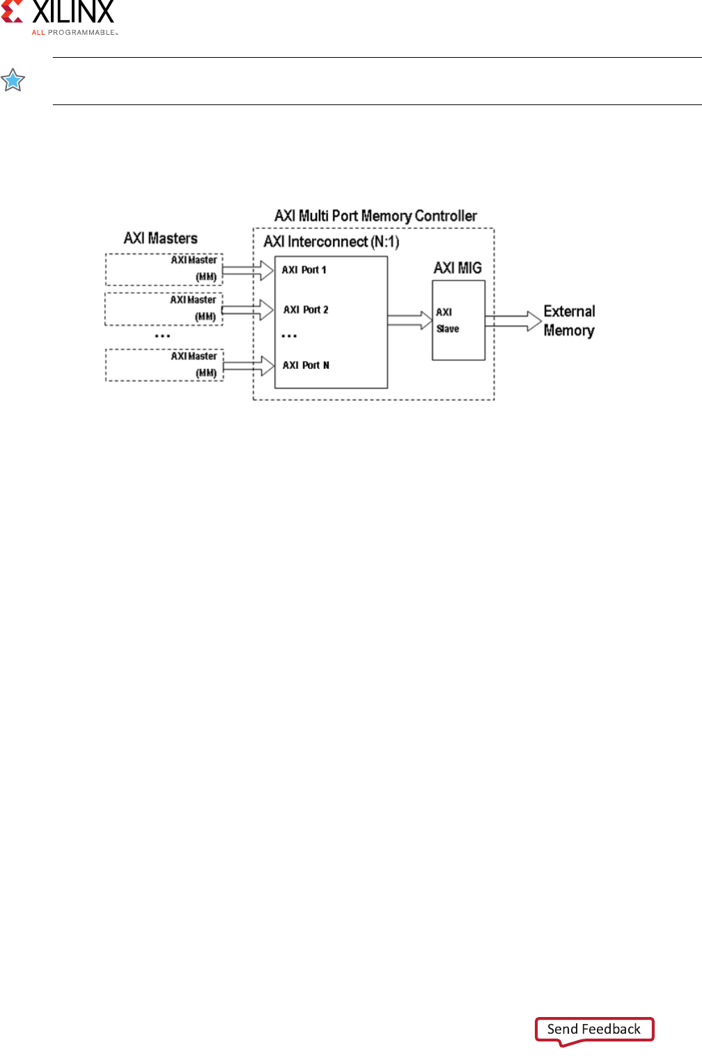
Vivado AXI Reference Guide www.xilinx.com 127
UG1037 (v4.0) July 15, 2017
Chapter 6: AXI System Optimization: Tips and Hints
IMPORTANT: This section provides system optimization examples using AXI Interconnect IP, but the
same techniques apply to the SmartConnect IP too.
The Interconnect can be configured in an N Master to 1 Slave mode with AXI MIG as the
slave connected to the AXI Interconnect as shown in the following figure.
IP Configuration decisions across AXI masters, the AXI Interconnect, and AXI MIG can
greatly affect the characteristics of the system, such as size, Fmax, throughput, and latency.
By using the general optimization information described previously, the AXI MPMC can be
tuned for a balance of size and performance. This section works through an example of
applying system optimization techniques to tune the AXI MPMC.
For information on how to create an AXI MPMC design using the Vivado® Integrated
Design Environment (IDE) IP integrator, see the 7 Series FPGAs AXI Multi-Ported Memory
Controller Using the Vivado IP Integrator Tool (XAPP1164) [Ref 45].
For an example of an AXI MPMC used in a high performance system, see Designing
High-Performance Video Systems with the AXI Interconnect, (XAPP740) [Ref 44].
Initial Memory Controller Configuration
Assume the AXI MPMC is used for the purpose of transferring multiple data streams to and
from a common physical memory. The first step is configuring the memory controller to
meet the bandwidth requirements of the system.
The AXI MIG supports physical memory widths of 8, 16, 32, 64, and 128 bits wide with a
memory clock rate of 300 to 400 MHz for a -1 speed grade Virtex®-6 device (check MIG
documentation for other clock and width limitations). This equates with a 600 to 800 MHz
data rate on the physical data lanes.
Assume that four AXI masters are required, each consuming up to 100 MBytes/sec of
bandwidth for reads and 100 MBytes/sec of bandwidth for writes with a native 32 bit x 48
MHz AXI4 interface.
X-Ref Target - Figure 6-1
Figure 6-1: AXI4 MPMC Block Diagram
Vivado AXI Reference Guide www.xilinx.com 128
UG1037 (v4.0) July 15, 2017
Chapter 6: AXI System Optimization: Tips and Hints
This implies 4x2x100 MBytes/sec = 800 MBytes/sec of total bandwidth is required.
For the memory controller configuration options, the following table can be derived:
The two smallest memory configurations that would meet the bandwidth requirements of
the system are using a 16-bit DDR3 running 300 to 400 MHz memory clock rate, providing
1200 to 1600 Mbytes/sec of theoretical bandwidth (67% to 50% memory utilization at 800
Mbytes/sec).
In theory an 8-bit DDR3 running at 400 MHz meets the bandwidth also, but given overhead
(lost clock cycles) for refresh, write-leveling, read-write bus turnaround time, and row/bank
address changes, some more efficiency margin is required.
With AXI MIG, the AXI slave interface data width is natively equal to four times the physical
memory data width and the AXI slave clock is ½ the memory clock frequency, so a 16-bit
DDR3 @ 300 to 400 MHz directly corresponds to an AXI slave interface that is natively
64-bits wide at 150 to 200 MHz.
Initial AXI Interconnect Configuration
To be able to consume all the bandwidth from the memory controller, the AXI Interconnect
core must be have at least the same bandwidth as the memory controller. Given the
recommendation to avoid width and clock conversion that impact size and timing, the
interconnect core and slave side port should be configured as 64-bits at 150 to 200 MHz to
match the native AXI interface of the memory controller.
To configure the master side of the AXI Interconnect, note that the AXI master is natively 32
bits at 48 MHz. This requires a 32- to 64-bit size conversion for each master.
In addition, the 48 MHz AXI clock on each AXI master would result in an asynchronous clock
conversion if the interconnect is running at 200 MHz.
Table 6-3: Memory Controller Configuration Options
Physical DDR3
Data Width
(Bits)
Memory Clock
(MHz)
Data Rate
(MHz)
Max theoretical
Bandwidth
(MBytes/sec)
8 300 600 600
8 400 800 800
16 300 600 1200
16 400 800 1600
32 300 600 2400
32 400 800 3200
64 300 600 4800
64 400 800 6400
128 300 600 9600
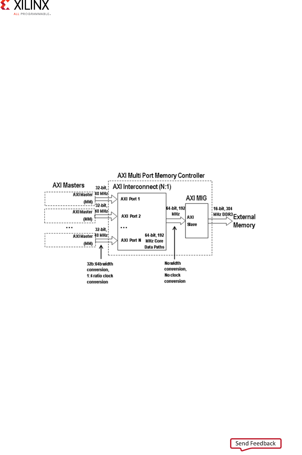
Vivado AXI Reference Guide www.xilinx.com 129
UG1037 (v4.0) July 15, 2017
Chapter 6: AXI System Optimization: Tips and Hints
Clock Conversion Recommendation
The recommendation for clock conversion is to use synchronous ratios over asynchronous
ratios to reduce logic.
Instead of a 200 MHz Interconnect clock, the system can be configured to attempt to
remove asynchronous clock conversions by employing a:
• 48 MHz AXI master clock
• 48 x 4 = 192 MHz AXI Interconnect clock
• 192 x 2 = 384 MHz memory clock
Note: The 48, 192, and 384 MHz clocks should be driven by the same Mixed Mode Clock
Manager (MMCM) block to be phase aligned.
The following figure shows an example of the AXI Interconnect master side configuration.
AXI4 Master Configuration
The use of AXI4 transactions by the AXI4 master impacts the performance that can be
obtained from the memory controller and system. Because this system requires significant
bandwidth from the memory controller, maximizing the burst length of AXI4 transactions to
256 beats helps improve overall data bandwidth.
X-Ref Target - Figure 6-2
Figure 6-2: AXI Interconnect Master Side Configuration Block Diagram

Vivado AXI Reference Guide www.xilinx.com 130
UG1037 (v4.0) July 15, 2017
Chapter 6: AXI System Optimization: Tips and Hints
Maximize Burst Length
Longer bursts reduce address arbitration/control cycles and help keep the memory
controller in the same row, bank, and read/write direction longer. Long bursts would
normally impact latency, but assuming this application is not very latency sensitive and that
data path FIFOs are enabled for elasticity, the use of long bursts should not result in head
of line blocking/stalling.
No Narrow Burst Transactions
The AXI4 master should not issue any narrow burst transactions. Narrow bursts are defined
in the AXI specification as transactions where the size of the AXI transaction is more narrow
than the native data width of the interface. Such bursts are less efficient in terms of bus
utilization and require extra logic in the memory controller to handle repacking of any
narrow bursts into full width bursts.
In this example:
• Size AXI transactions issued by the masters to 32-bit (AxSIZE = 0x2).
• Enable the modifiable bit on AXI transactions (AxCACHE[3]=1) to ensure that any
downstream upsizer can fully pack data up to wider widths. This allows costly narrow
burst support logic to be removed from the memory controller.
In the IP integrator, this is designated by the C_SUPPORTS_NARROW parameter that then
allows the IP integrator to automatically configure AXI MIG to omit narrow burst support
logic. From the context of the CORE Generator™ tool, you must manually configure AXI MIG
to omit narrow burst support logic.
Pipeline Transactions
Design the AXI4 master to pipeline transactions so it can issue new address requests while
servicing the data transfers for previous transactions. Pipelining transactions helps overlap
address and control cycles with data transfer cycles to improve data path efficiency and
throughput. However, new address requests should not be made until it is ensured that the
master can supply sufficient write data or has sufficient ability to accept read data to
complete a full burst with minimal stalling. A master that issues an address request and
excessively stalls the data transfer phase of its requested transaction could cause
backpressure that could eventually stall or slow the whole system.
Single Thread Transactions
Design the AXI4 master so that it operates using only a single thread for all transactions
(declared using the C_SUPPORTS_THREADS=0 parameter). By not using multiple threads,
the logic in the AXI4 master can be simplified because it can be designed to rely upon write
responses and read data being returned in order. The use of a single thread also benefits
the AXI Interconnect performance because the upsizer is active in this example system.
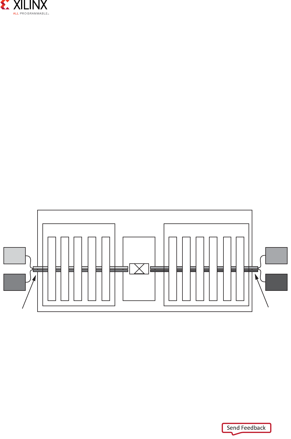
Vivado AXI Reference Guide www.xilinx.com 131
UG1037 (v4.0) July 15, 2017
Chapter 6: AXI System Optimization: Tips and Hints
Upsizers in the AXI Interconnect stall when changing ID threads so using a single thread
avoids stalling of transactions passing through the upsizer. Ensure that the AXI4 master
declares itself not to use threads so that AXI Interconnect can be configured to omit its
multi-thread support logic which reduces area and improves timing. Using a single thread
also makes debug easier because AXI transactions observed in the lab tool monitor are
easier to decode and correlate across a system.
Refining the AXI Interconnect Configuration
After a first pass to establish the basic configuration of AXI MIG, AXI Interconnect, and the
AXI4 master of the user, the user can then perform a second pass at refining the AXI system
configuration.
Independently Configure Converter Banks
When fine tuning the configuration of the AXI Interconnect, it is useful to understand the
AXI Interconnect converter bank block. The converter bank handles size, clock, and protocol
conversion in addition to register slice and data path FIFO features.
The converter bank can be independently configured at each endpoint of the AXI
Interconnect, as shown in the following figure.
Notice that from the perspective of the attached AXI master, shown in the previous figure,
the data path FIFOs are positioned after the upsizer and the clock converter so that the FIFO
interfaces to the interconnect core at its higher native width and clock.
Because the AXI masters are at a relatively lower bandwidth than the memory controller
(1/2 width, ¼ clock frequency), turning on data path FIFOs allows the interconnect to buffer
X-Ref Target - Figure 6-3
Figure 6-3: AXI Interconnect: Crossbar Block Diagram
AXI Interconnect
Slave
Interface
Master
Interface
SI Hemisphere MI Hemisphere
Crossbar
Master 0 Slave 0
Slave 1
Master 1
Register Slices
Register Slices
Up-sizers
Up-sizers
Clock Converters
Down-sizers
Data FIFOs
Clock Converters
Down-sizers
Protocol Converters
Data FIFOs
X12047

Vivado AXI Reference Guide www.xilinx.com 132
UG1037 (v4.0) July 15, 2017
Chapter 6: AXI System Optimization: Tips and Hints
up the wider width transactions to and from the memory controller and service each of the
AXI masters at their slower rates on the other side of the FIFOs.
Datapath FIFOs reduce stalling of the memory controller due to the slower data rate AXI
masters. The AXI Interconnect offers data path FIFOs in options of 32 deep or 512 deep
FIFOs. Because the AXI4 master is generating long bursts up to 256 beats in length,
configure the FIFOs as 512 deep to fit an entire burst.
The data path FIFOs have an optional feature, called Packet Mode, to delay
AWVALID/ARVALID until FIFO occupancy permits interrupted burst transfers downstream.
The Packet Mode feature:
• Causes write address requests to be withheld from the crossbar until the write data
path FIFO has buffered all the data for the transaction.
• Causes read address requests to be withheld from the crossbar until the read data path
FIFO has sufficient vacancy to store the entire transaction.
• Ensures that the crossbar does not see a transaction request until the data path FIFO
can guarantee that it can source/sink the entire transaction at the full bandwidth of the
crossbar without introducing stall cycles in the data transfer.
• Is especially useful in situations similar to the example design, shown in Figure 6-2,
where the master has a relatively lower bandwidth than the slave (memory controller).
Timing Considerations
For timing, the AXI Interconnect should be configured to enable register slices at the
interface to the memory controller. Because the AXI interface memory controller operates
at the highest width and clock frequency in the system, it is likely a critical path unless a
register slice is turned on.
A Type 8 register slice can be enabled on all five channels at the AXI interface of the
memory controller to allow the AXI Interconnect to optimize the kind of register slice best
suited to each AXI channel.
Note: A register slice at the AXI master interface is not required. This is because the AXI master and
the upsizer are both clocked by the slower 48 MHz side of the clock converter.
Also, the clock converter acts as a register slice because it provides timing isolation
between 48 MHz and 192 MHz clock domains.
Setting Issuance and Acceptance Values to 2 or Higher
Issuance and acceptance values at each port of the AXI Interconnect can be optimized to
support transaction pipelining and to limit the pipelining so that head-of-line blocking is
reduced. The default issuance assigned to an AXI masters is 1, unless configured or
designated otherwise. An issuance of 1 minimizes logic but does not permit transaction
pipelining. Set the issuance to a value of 2 or higher.

Vivado AXI Reference Guide www.xilinx.com 133
UG1037 (v4.0) July 15, 2017
Chapter 6: AXI System Optimization: Tips and Hints
Because the target system seeks to maximize throughput, you can calculate the maximum
number of outstanding transaction possible without overflowing the data path FIFOs. The
data path FIFOs are 64 bits wide x 512 deep as described above. That is equivalent storage
to 32 bits wide x 1024 deep.
If the AXI4 master is generating AXI transactions of maximum length 256, then up to four
transactions fit into the data path FIFOs.
The AXI Interconnect supports issuance and acceptance values of 1,2,4,8,16, and 32.
Reasonable values of issuance for each AXI master would therefore be 2 or 4.
• Given that there are 4 masters, an issuance of 2 means that memory controller would
need an acceptance of 8 to fully pipeline 2 transactions from each master.
• Given that transactions are all long bursts, pipelining more than 8 transactions at the
memory controller becomes excessive. An issuance setting of 4 at the masters is too
high because it would require the slave to consume up to 16 transactions to utilize.
• Given that master issuance of 4 might be excessive while an issuance of 1 prevents
transaction pipelining, a setting of 2 is reasonable.
Adding a Processor to the AXI MPMC System
Adding a processor to the example AXI MPMC system complicates the optimization of the
system because processors tend to be very latency sensitive with respect to their
performance. If the processor must also share the memory controller to run complex
software such an operating system or protocol stack, you must take more care to balance
the low latency requirements of the processor with the high throughput requirements of the
other AXI masters.
Processor traffic could interfere with other devices resulting in reduced throughput from
other masters. This is due to random memory accesses that disrupt the row/bank access
patterns of the other devices and because the processor can generate a number of small
length transactions. Small length transactions corresponding to 4- or 8-word cache lines
can consume several memory clock cycles for row/bank access time, read/write turn
around, and so forth. Therefore, the actual data bandwidth transferred by the processor
might be small, but because they can disrupt the otherwise linear, long burst access
patterns of the memory controller, their traffic actually displaces a much larger amount of
the theoretical system bandwidth.
For example, 10 Mbytes/sec of delivered data bandwidth to the processor, might actually
displace the equivalent of 100 MBytes/sec of the theoretical bandwidth of the memory
controller. Optimizations to improve processor performance could force a trade-off in
system throughput, further eroding the bandwidth available to other masters.
Considerations When Adding a Processor
If you need to add a processor to the system, you must consider:

Vivado AXI Reference Guide www.xilinx.com 134
UG1037 (v4.0) July 15, 2017
Chapter 6: AXI System Optimization: Tips and Hints
• If the memory width or clock should be increased to provide more available margin.
• Whether to reduce the burst length of the other AXI masters to reduce the time that a
processor waits for a burst transaction to complete.
• If the highest arbitration priority can be granted to the processor to minimize its
latency.
• If the issuance/acceptance values for other devices might be reduced to limit head of
line blocking due to pipelined transactions.
• If the system clocking can be altered to favor the memory path of the processor having
no clock conversion or only synchronous clock conversion.
Note: The MicroBlaze™ processor can support a native 128-bit and 256-bit and 512-bit wide AXI
interface. This is an example of application domain size conversion that is more efficient that
generic AXI width conversion. This MicroBlaze wide cache configuration is ideal for connecting
to an equally wide memory controller to remove the latency impact of size conversion.
The optimizations described to improve processor performance are often the opposite step
for maximizing system throughput.
Therefore, either more margin is needed by using a larger memory controller or you must
carefully optimize your software (to minimize cache misses) and be more willing to
experiment with the system to find the right balance between latency and throughput.
Additional Potential Optimizations for AXI MPMC
The previous AXI MPMC optimization information steps through an example of working
through the design optimization process, while attempting to balance tradeoffs between
various design criteria.
The following subsections describe further optimizations ideas than might be applicable.
These optimizations might or might not be suitable for a given AXI MPMC design and could
require experimentation to see if the technique is useful in a given situation.
Vivado AXI Reference Guide www.xilinx.com 135
UG1037 (v4.0) July 15, 2017
Chapter 6: AXI System Optimization: Tips and Hints
AXI Interconnect: Shared Address Shared Data Mode
If there is enough extra unused bandwidth, the AXI Interconnect can be configured in
Shared Address Shared Data (SASD) mode.
In this mode, the AXI Interconnect core is simplified to operate on only a single read or a
single write at a time and even shares read and write addresses over the same wires.
This mode removes support for pipelined transactions and prevents simultaneous read and
writes, but significantly reduces logic. Given that long bursts are used, the penalty of stall
cycles between transactions and lack of simultaneous read and write data flow might be
acceptable within the bandwidth requirements of the system. SASD also makes system
debug and waveform analysis of AXI transactions substantially easier. SASD is also generally
more lenient about functional bugs and protocol violations from endpoint IP.
Separate IP Groups into Separate AXI Interconnect Subsystems
If an AXI MPMC design has many masters, and the design has difficulty meeting timing, one
possible strategy is to group two or more IP into a separate N x1 AXI Interconnect that then
feeds the main AXI Interconnect. This breaks a wide fan-in Interconnect into multiple
smaller fan-in Interconnects. Each smaller Interconnect is easier to route and meet timing,
and also provides a greater range of options for the location of register slices, FIFOs, size,
clock, and width converters.
For example, when two AXI Interconnects connect directly to each other, a set of
back-to-back register slices can be enabled using one register slice from each adjacent
interconnect. This can be used to span longer routing distances in large AXI MPMC systems.
In some cases using multiple AXI Interconnects can even reduce overall system size.
When an AXI MPMC requires a large number of upsizers, especially with large steps like 32-
to 128-bits, separating the masters into subgroups using smaller width AXI Interconnects
can reduce the number of upsizers which consume area and impact timing.
Debug and Analysis: Using AXI Debug Monitor and AXI Hardware Protocol
Checkers
The Vivado AXI lab tool debug monitor is a feature that provides waveform capture and
triggering of AXI interface signals in hardware. The AXI debug monitor can be used to help
debug functional issues in hardware or to help diagnose performance issues.
IMPORTANT: Analyze Complex System Activity.
You can place multiple AXI debug monitors around the system and cross-trigger between
each of them to analyze more complex system level activity. The AXI Hardware Protocol
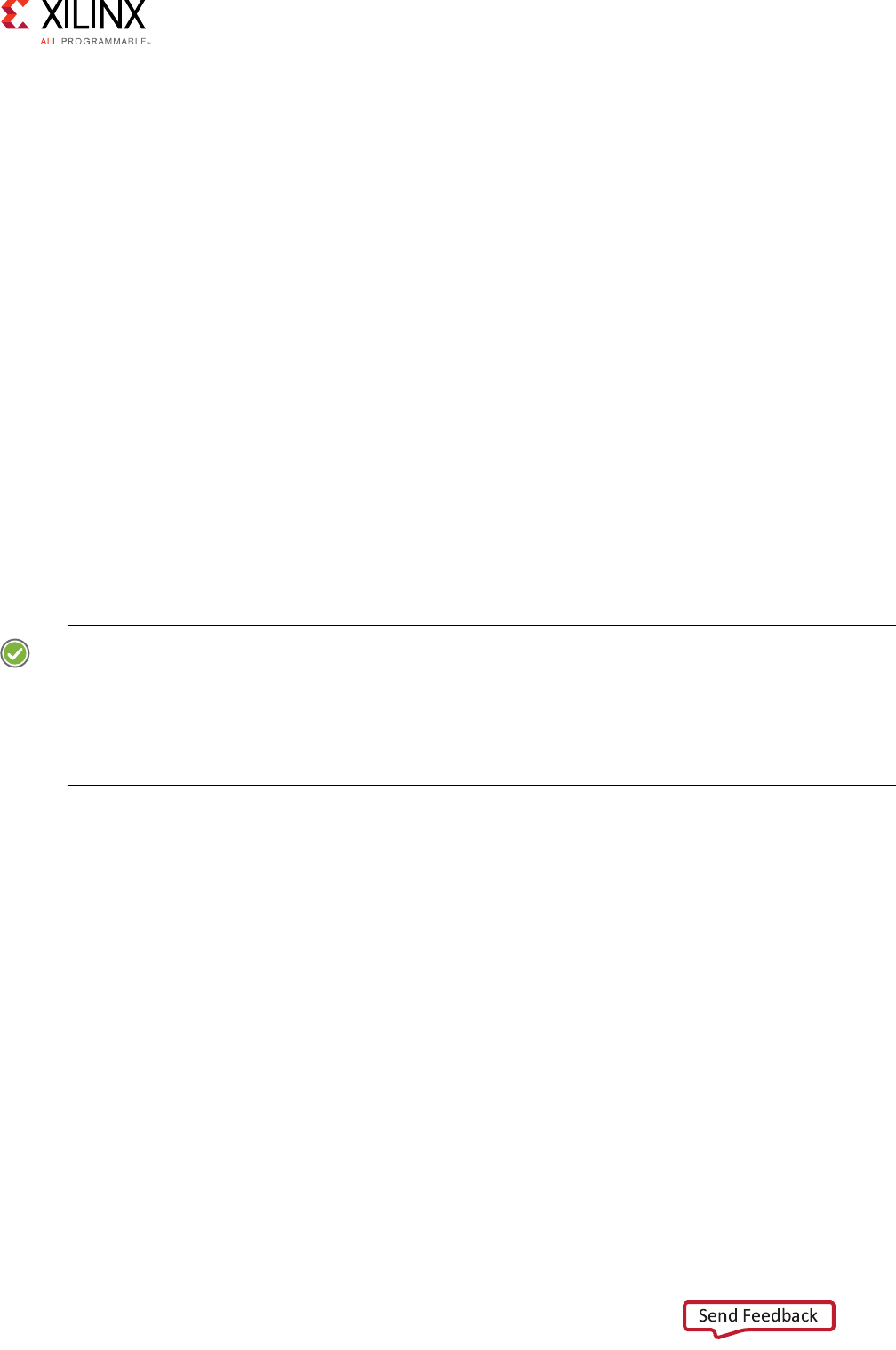
Vivado AXI Reference Guide www.xilinx.com 136
UG1037 (v4.0) July 15, 2017
Chapter 6: AXI System Optimization: Tips and Hints
Checker feature is available that can trigger the AXI debug monitor when some types of AXI
protocol violations occur.
The AXI Hardware Protocol Checker can more quickly isolate the source of protocol
violations. For more information, see the LogiCORE IP AXI Protocol Checker: Product Guide
for Vivado Design Suite (PG101) [Ref 15].
Floorplanning
AXI IP connected to the AXI Interconnect can be floorplanned to improve placer results and
reduce routing congestion. To make floorplanning easier in large FPGAs, enable extra
register slices to provide a more distinct flip flop-based boundary at the AXI IP interface.
Note: After any significant changes to the AXI Interconnect configuration, floorplan locations might
need to be rechecked and updated as necessary. Otherwise subsequent changes to the AXI
Interconnect, such as turning on data path FIFOs, can change the footprint and necessary placement
of the AXI Interconnect.
AXI Verification IP
The Vivado IP integrator supports instantiation of AXI Verification IP (AXI VIP) and AXI
Protocol Monitors for use in simulation to exercise and test AXI IP.
RECOMMENDED: Xilinx recommends that you use AXI Verification IP for verification of user IP under
development. Given the potential complexity of understanding AXI transactions, especially across
pipelined transactions and multi-threaded traffic, it can be extremely difficult to debug subtle
functional errors or isolate the root cause of protocol violations solely in hardware. The simulation
domain is usually a far less expensive method for verifying and debugging new AXI IP before use in
complex systems.
See the LogiCORE IP AXI Verification IP Core Product Guide for Vivado Design Suite (PG267)
[Ref 26] for more information.
More Simple but Wider Interconnect and Memory Controller
Another potential strategy for an AXI MPMC system is to oversize the width of the memory
controller and AXI Interconnect core, such as by doubling the memory width to double the
theoretical system bandwidth. By adding extra potential system throughput, the
configuration of the rest of the system is much more simple.
For example, a system initially requiring a 16-bit DDR3 at 400 MHz with the AXI
Interconnect core configured as 64-bits at 200 MHz could be reconfigured with a 32-bit
DDR3 at 300 MHz and an AXI Interconnect configured as 128 bits at 150 MHz.
The extra bandwidth from doubling the physical memory width can be used to allow greater
system simplifications, including:

Vivado AXI Reference Guide www.xilinx.com 137
UG1037 (v4.0) July 15, 2017
Chapter 6: AXI System Optimization: Tips and Hints
• Reducing AXI clocks from 200 MHz to 150 MHz to improve timing:
°Reductions in clock frequency could permit register slices to be turned off
°Reductions in clock frequency could permit use of a slower speed grade FPGA
device
• Allowing the crossbar to be reconfigured into SASD (this disables transaction
pipelining and multi-threading support):
°Simplifies system debug
°Provides room for future system bandwidth expansion (you can later increase clock
frequencies, enable crossbar, and so forth.)
• Allowing masters to use shorter burst lengths:
°Reduces latency or reduces system FIFO/buffering requirements
Note: Increasing memory controller and AXI Interconnect data width could introduce new size
conversion requirements and board-level requirements into the system that might offset these AXI
system simplifications so analysis and experimentation is required to determine if this approach is an
overall improvement for the given application.
Cascading Interconnects
In some situations where the AXI Interconnect is a large Nx1 configuration with upsizing,
width conversion, with enabled data path FIFOs, it might be beneficial to deploy multiple
cascaded interconnects instead of a single large Interconnect. This is often the case in high
performance systems that contain high bandwidth memory controllers shared by multiple
lower bandwidth masters.
For example, consider an AXI MPMC with 8 masters each with 32 bit at 100 MHz interfaces
connected to a memory controller with a 256 bit interface at 200 MHz as shown in the
following figure. Assume that each master requires 70% of the available bandwidth of the
interface:
32 x 100 x 0.7 = 2240 mbits/sec. Equation 6-1
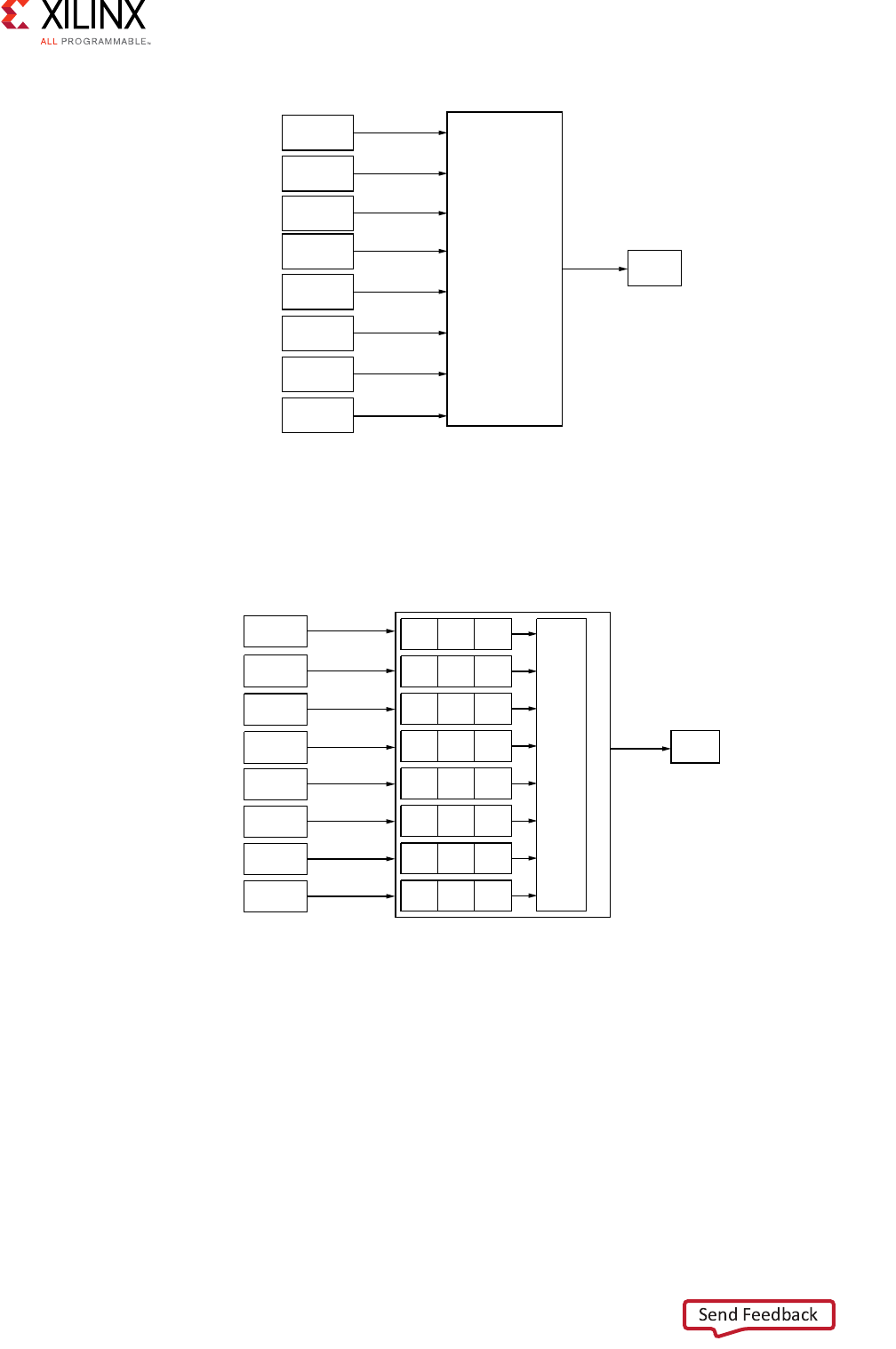
Vivado AXI Reference Guide www.xilinx.com 138
UG1037 (v4.0) July 15, 2017
Chapter 6: AXI System Optimization: Tips and Hints
For highest performance, the interconnect would enable 32 to 256 bit upsizing, 100 MHz to
200 MHz clock conversion, and Packet Mode data path FIFOs as shown in the following
figure.
The order of the sub-modules in the interconnect is:
Upsizer followed by Clock Converter followed by FIFO
This ordering is also shown in Figure 6-3 as the architecture of the AXI Interconnect.
Note: The clock converter and FIFO are located after the upsizer, therefore each block essentially
contains a 256 bits wide internal data path for read and write channels.
X-Ref Target - Figure 6-4
Figure 6-4: AXI MPMC with 8 Masters
X-Ref Target - Figure 6-5
Figure 6-5: Enabled Upsizing
!8)
-!34%2
!8)-)'
!8))NTERCONNECT
!8)
3,!6%
!8)
3LAVE
!8)-ASTER
--
!8)
3,!6%
!8)
3,!6%
!8)-ASTER
--
!8)-ASTER
--
!8)-ASTER
--
!8)-ASTER
--
!8)-ASTER
--
!8)-ASTER
--
!8)-ASTER
--
BIT
-(Z
BIT
-(Z
!8)
3,!6%
!8)
3,!6%
!8)
3,!6%
!8)
3,!6%
!8)
3,!6%
BIT
-(Z
BIT
-(Z
BIT
-(Z
BIT
-(Z
BIT
-(Z
BIT
-(Z
BIT
-(Z
X13117
!8)-)'
!8))NTERCONNECT
!8)
3LAVE
!8)-ASTER
--
BIT
-(Z
BIT
-(Z
5PSIZE #LOCK
#ONV &)&/
#ROSSBAR
!8)-ASTER
--
BIT
-(Z
!8)-ASTER
--
BIT
-(Z
!8)-ASTER
--
BIT
-(Z
!8)-ASTER
--
BIT
-(Z
!8)-ASTER
--
BIT
-(Z
!8)-ASTER
--
BIT
-(Z
!8)-ASTER
--
BIT
-(Z
5PSIZE #LOCK
#ONV &)&/
5PSIZE #LOCK
#ONV &)&/
5PSIZE #LOCK
#ONV &)&/
5PSIZE #LOCK
#ONV &)&/
5PSIZE #LOCK
#ONV &)&/
5PSIZE #LOCK
#ONV &)&/
5PSIZE #LOCK
#ONV &)&/
8
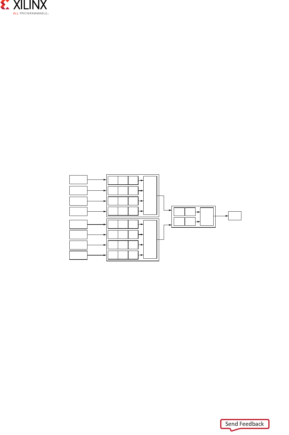
Vivado AXI Reference Guide www.xilinx.com 139
UG1037 (v4.0) July 15, 2017
Chapter 6: AXI System Optimization: Tips and Hints
As a rough estimate, assume this that each sub-module uses two FFs and two LUTs per data
path bit. The approximate size of the data path logic used by the converter blocks is
estimated with the following equation:
Size (LUTs and FF) = <number of ports> x <number of sub-modules> x <data width in bits>x < number
of LUTs and FFs per bit> Equation 6-2
or
8 ports x 3 sub-modules x 256 bits datapath x 2 channels for read/write * 2 LUTs and FFs per bit
= 24576 LUTs and 24576 FFs. Equation 6-3
It can also be assumed that generally the size of the datapaths dominates as the percentage
of the total size of the interconnect relative to the size of the control path logic.
An alternative implementation of the design to explore is to use two levels of cascaded
Interconnects to partition the design into multiple smaller, more gradually scaled
Interconnect building blocks as shown in the following figure.
The scaling, shown in Figure 6-6, is 4x1 Interconnect + 4x1 Interconnect followed by a 2x1
Interconnect that uses three smaller Interconnect blocks instead of one large block.
This is likely a more optimal design than a 2x1 Interconnect + 2x1 Interconnect + 2x1
Interconnect + 2x1 Interconnect design followed by 4x1 Interconnect because it uses five
blocks and therefore, is more likely to lead to optimal partitioning than the one shown in
Figure 6-5.
Using the partitioning shown in the following figure, the next step is to find the best size
and width for the intermediate interface between the cascaded interconnects.
X-Ref Target - Figure 6-6
Figure 6-6: 4x1 Interconnect and 2x1 Interconnect
BIT
-(Z
BIT
-(Z
!8)-)'
!8)
3LAVE
BIT
-(Z
!8))NTERCONNECT
&)&/
#ROSSBAR
&)&/
5PSIZE
5PSIZE
!8))NTERCONNECT
!8)-ASTER
--
BIT
-(Z
5PSIZE #LOCK
#ONV &)&/
#ROSSBAR
#ROSSBAR
!8)-ASTER
--
BIT
-(Z
!8)-ASTER
--
BIT
-(Z
!8)-ASTER
--
BIT
-(Z
!8)-ASTER
--
BIT
-(Z
!8)-ASTER
--
BIT
-(Z
!8)-ASTER
--
BIT
-(Z
!8)-ASTER
--
BIT
-(Z
5PSIZE #LOCK
#ONV &)&/
5PSIZE #LOCK
#ONV &)&/
5PSIZE #LOCK
#ONV &)&/
5PSIZE #LOCK
#ONV &)&/
5PSIZE #LOCK
#ONV &)&/
5PSIZE #LOCK
#ONV &)&/
5PSIZE #LOCK
#ONV &)&/
8
Vivado AXI Reference Guide www.xilinx.com 140
UG1037 (v4.0) July 15, 2017
Chapter 6: AXI System Optimization: Tips and Hints
The options are:
• Width can be 32, 64, 128, or 256 bits wide.
• Clock frequency is either 100 or 200 MHz (to avoid the use of asynchronous clock
converters).
The choice of intermediate signal width and clock frequency determine where width
converters and clock converters are placed in the system and what their data path sizes are.
IMPORTANT: Assume that Packet Mode data path FIFOs are required in all Interconnects because that
is needed to ensure there are no bottlenecks in the data flow toward the memory controller.
Each 4x1 Interconnect aggregates traffic from four masters each requiring 70% of the
bandwidth of the 32 bits x 100 MHz interface for a total maximum throughput requirement
of
4x32x100x0.7 = 8960 mbits/sec.
By looking at the maximum throughput of the connections as detailed the following table,
some options can be eliminated because the given intermediate interface configuration
cannot support this aggregate throughput requirement.
.
X-Ref Target - Figure 6-7
Figure 6-7: Partitioning for Best Size and Width
!8))NTERCONNECT
!8)-ASTER
--
BIT
-(Z
5PSIZE #LOCK
#ONV &)&/
#ROSSBAR
!8)-ASTER
--
BIT
-(Z
!8)-ASTER
--
BIT
-(Z
!8)-ASTER
--
BIT
-(Z
5PSIZE #LOCK
#ONV &)&/
5PSIZE #LOCK
#ONV &)&/
5PSIZE #LOCK
#ONV &)&/
8
BIT
-(Z
Table 6-4: Maximum Connection Throughput
Width (Bits) Clock Domain
(MHz)
Raw Throughput
(mbits/sec)
Capable of 8960
mbits/sec
32 100 3200 No
32 200 6400 No
64 100 6400 No
64 200 12800 Yes
128 100 12800 Yes
128 200 25600 Yes
256 100 25600 Yes
256 200 51200 Yes
Vivado AXI Reference Guide www.xilinx.com 141
UG1037 (v4.0) July 15, 2017
Chapter 6: AXI System Optimization: Tips and Hints
Table 6-5 shows the results of using Equation 6-2 for estimating the size of the interconnect
sub-module data paths, for each intermediate interface option that offers sufficient
throughput.
Therefore, if the intermediate interface is configured as 64 bits x 200 MHz, the data path
area for the cascaded scaled Interconnects is estimated at 10240 LUTs/FFs compared to
24576 LUTs/FFs used by the original single Interconnect design.
TIP: Cascading Interconnects reduces area and potentially improves timing through reduced routing
congestion, but there is a trade-off in higher system complexity and higher latency.
The following figure shows the optimized system configuration.
Using this approach of estimating the size of scaled Interconnects and removing unfeasible
options, you can narrow down the choices to experiment with cascaded Interconnects to
further reduce area.
IMPORTANT: Verify any estimates through implementation of the complete system to validate the
improvement.
Table 6-5: Interconnect Size by Width and Clock Domain
Width (Bits) Clock Domain (MHz) Size Estimate
64 200 10240
128 100 14336
128 200 16384
256 100 20480
256 200 26624
X-Ref Target - Figure 6-8
Figure 6-8: Optimized System Configuration
BIT
-(Z
BIT
-(Z
!8)-)'
!8)
3LAVE
BIT
-(Z
!8))NTERCONNECT
&)&/
#ROSSBAR
&)&/
5PSIZE
5PSIZE
!8))NTERCONNECT
!8)-ASTER
--
BIT
-(Z
5PSIZE #LOCK
#ONV &)&/
#ROSSBAR
#ROSSBAR
!8)-ASTER
--
BIT
-(Z
!8)-ASTER
--
BIT
-(Z
!8)-ASTER
--
BIT
-(Z
!8)-ASTER
--
BIT
-(Z
!8)-ASTER
--
BIT
-(Z
!8)-ASTER
--
BIT
-(Z
!8)-ASTER
--
BIT
-(Z
5PSIZE #LOCK
#ONV &)&/
5PSIZE #LOCK
#ONV &)&/
5PSIZE #LOCK
#ONV &)&/
5PSIZE #LOCK
#ONV &)&/
5PSIZE #LOCK
#ONV &)&/
5PSIZE #LOCK
#ONV &)&/
5PSIZE #LOCK
#ONV &)&/
X
Vivado AXI Reference Guide www.xilinx.com 142
UG1037 (v4.0) July 15, 2017
Chapter 6: AXI System Optimization: Tips and Hints
Common Pitfalls Leading to AXI Systems of Poor
Quality Results
This section describes common pitfalls designers might encounter leading to the design of
AXI systems that are of a larger than expected area, have poor performance, or have poor
timing.
Oversizing a Memory Controller
AXI Virtex-6 MIG supports DDR3 physical memories in 8, 16, 32, 64, and 128 bit widths,
which translates into a 4 times wider native AXI data width of 32, 64, 128, 256, and 512 bits
wide.
If a system contains only a 32-bit microprocessor and associated AXI4-Lite peripherals, then
connecting it to a 64-bit physical DDR3 memory is wasteful of logic and would actually
degrade performance.
Such an AXI MIG would have very large area for the physical interface logic and the 256 bit
data paths inside the AXI MIG. Also, the native 256-bit AXI interface would have to be
upsized from the 32-bit AXI interface of the processor adding further area and latency.
IMPORTANT: Size the AXI MIG to meet the bandwidth needs of the system while minimizing
unnecessary size conversions.
This situation can be common when using fixed evaluation boards, like the ML605, that
contain a 64-bit DDR3 DIMM. You might be working from a reference design containing an
AXI MIG configured for a full, 64-bit DDR3 DIMM that is oversized for a simple MicroBlaze™
processor application.
Incorrect Core Data Width or Core Clock for AXI Interconnect
Incorrectly setting the core data width or connecting the wrong core clock to the AXI
Interconnect can severely impact the system.
For example, consider a system with five masters and five slaves connected to AXI
Interconnect. Assume that each master and slave is 64-bits wide at 100 MHz.
If the AXI Interconnect is also configured to be 64-bits wide at 100 MHz, then no clock or
width converters are used. However, if the interconnect core data width is accidently
configured to be 32-bits wide at 75 MHz, then the same system would then need to incur a
64:32 bit downsizer for each master, a 32:64 bit upsizer for each slave and asynchronous
clock converters at every master and slave. The extra cost of 10 size converters and 10
asynchronous clock converter results in poor timing, very large area, and very high latencies
in the system.
Vivado AXI Reference Guide www.xilinx.com 143
UG1037 (v4.0) July 15, 2017
Chapter 6: AXI System Optimization: Tips and Hints
Additionally, the throughput in the system is greatly constrained because wide 64-bit AXI
traffic from the masters and slaves are funneled through a much more narrow and slower
32-bit data path in the AXI Interconnect. This would result in stall cycles between every data
beat the masters and slaves are trying to transfer.
TIP: Watch For Wrong Clock and Interconnect Data Widths.
Because the Vivado IP integrator handles width and clock conversion configurations
automatically, connecting the wrong interconnect clock or setting the wrong interconnect
data width causes the IP Integrator to automatically activate all the necessary conversions
to make the system function. The result is a system that might appear to function and
completes all AXI transactions, but the system bandwidth, area, latency, and timing could be
very undesirable.
Overuse of Register Slices
In general, register slices are useful for helping to close timing in a system. However,
excessive use of register slices can be counterproductive.
For example, enabling all register slices on all AXI interfaces in a large system might
increase the area of a system leading to routing congestion and longer map, place, and
route times while not improving timing.
TIP: Incrementally Add Register Slices.
The recommended approach is to incrementally add register slices when timing fails
starting at the interfaces with highest clock frequencies and data widths. Register slices
might also be needed for large crossbar interconnects or at AXI interfaces where size
conversion is performed. If large numbers of register slices are required to meet timing in
a large system, floorplanning might be needed to help guide the place and route tools.
TIP: Do Not Place Register Slices on AXI4-Lite IP.
Generally, Xilinx recommends that you do not place register slices on AXI4-Lite IPs.
The recommended approach is to segment AXI4-Lite IP onto a separate SASD AXI
Interconnect and clock this AXI Interconnect and its attached AXI4-Lite IP at a slower
common clock frequency to better meet timing.
If timing improvement is needed on an AXI4-Lite Interconnect, first enable the special
internal register slice rank inside the SASD Interconnect; then add register slices only on
specific channels of AXI4-Lite IP that fail timing.
TIP: Watch For Wrong Register Slice Types.
Vivado AXI Reference Guide www.xilinx.com 144
UG1037 (v4.0) July 15, 2017
Chapter 6: AXI System Optimization: Tips and Hints
Also, using the wrong type of register slice can lead to undesirable effects.
For example, type 1 register slices support back-to-back data beats without inserting stalls
while type 7 register slices use less area, but insert a stall after every data transfer.
• The type 7 register slice is ideal for AXI4-Lite interfaces or for AW, AR, and B channels
of an AXI interface where back-to-back transfers do not occur or occur infrequently.
• The type 1 register slice is designed for R and W channels where burst transactions
occur.
• For convenience, a type 8 register slice option is provided which automatically switches
between type 1 and type 7 based on the AXI Interconnect configuration. Type 8 is
recommended and should only be overridden when specifically warranted.
Skipping Simulation-Based Verification of New IP
AXI4 provides a rich protocol that can:
• Scale into more complex systems
• Support sophisticated protocol features such as multi-threading and transaction
pipelining
• Manage transaction ordering and completion rules to manage traffic among multiple
AXI masters and slaves in a system.
The richness of the AXI protocol and the possible concurrency of data transfer in a crossbar,
make hardware-only based debug and verification of new AXI IP much more challenging.
RECOMMENDED: Verify new IP in simulation using AXI VIP available for the Vivado IP integrator.
Simulation-based verification results in far shorter debug cycle time, easier identification
and isolation of functional problems, and greater variation of AXI traffic than hardware-only
based verification.
Hardware-only based AXI IP verification requires full synthesis and Place and Route (PAR)
time per debug cycle, and the visibility of signals from an AXI debug monitor is more limited
than in a simulation domain. The potential complexity of AXI4 traffic even in a relatively
typical system makes hardware-only verification very expensive.
However, if you must rely on hardware-only AXI IP verification, Xilinx recommends that the
AXI Interconnect be configured as simply as possible.
For example, use SASD (which limits issuance/acceptance to 1), and minimize the use of
converter bank functions (size conversion, clock conversion, data path FIFOs, and so forth).
Register slices can also be enabled for hardware-only verification because register slices
acts as a filter for traffic patterns that can insulate the system from some protocol
violations.
Vivado AXI Reference Guide www.xilinx.com 145
UG1037 (v4.0) July 15, 2017
Chapter 6: AXI System Optimization: Tips and Hints
Enable AXI debug monitors and hardware protocol checkers at strategic points in the
system when performing hardware-only verification.
Non-contiguous Mapping of Slave Devices in Cascaded
Interconnect Scenarios
Instances of AXI Interconnect can be cascaded, allowing masters attached to an upstream
interconnect to send transactions to slaves on one or more downstream interconnects.
Cascading lets you optimize the flow of data the system by attaching peripherals with
similar system characteristics to specific interconnect instances.
When AXI interconnect instances are cascaded, an upstream interconnect must perform
enough address decoding to route transactions from the master to the correct downstream
interconnect.
IMPORTANT: If the downstream interconnect attaches to a large number of endpoint peripherals,
address decoding could consume a large number of logic resources in the upstream interconnect and
affect the system quality.
In 2014.1 and later releases, address automation services in the Vivado IP integrator can
optimize the amount of decoding logic required in cascaded AXI interconnect scenarios.
If the slave devices attached to the downstream interconnect are mapped contiguously, IP
integrator configures the upstream AXI interconnect with an optimized address decoding
range.
Consider the scenario in which a downstream interconnect has four attached AXI slaves,
each with 4KB register ranges that are mapped contiguously into the system address map
starting at address 0x40000000. The address automation within the IP integrator
configures the upstream interconnect with one address decoding range covering
0x40000000-0x40003fff, as opposed to configuring the upstream interconnect with
separate address decode ranges for each slave.
Note: This optimization requires the slave devices be mapped contiguously into an aggregate
memory region with a size that is a power of 2.
RECOMMENDED: When possible, use contiguous mappings of slave devices to benefit from the
automatic address decode optimization available in IP integrator.
Optimizing AXI on Zynq-7000 AP SoC Processors
See the LogicCore IP Processing System 7: Product Guide for Vivado Design Suite (PG082)
[Ref 13] for more information.

Vivado AXI Reference Guide www.xilinx.com 146
UG1037 (v4.0) July 15, 2017
Chapter 6: AXI System Optimization: Tips and Hints
When optimizing AXI for the Zynq®-7000 All Programmable SoC processor, the following
optimization tips are recommended.
• The processing system 7 IP Block IDWIDTH is able to compress the M_GP AXI IDWIDTH
using the static remap setting; potentially saving PL logic.
• For designs with multiple PL masters, consider using the multiple provided PS, PL, and
AXI interfaces to reduce PL Logic utilization.
• PL masters accessing PS peripherals using non-secure accesses (ARPROT[1] =1
and/or AWPROT[1]=1) generate a decode error by default.
• For higher throughput to the PS, PL masters should mark transactions as modifiable
and bufferable ARCACHE/AWCACHE[1:0]=b11.
Considerations for High Performance AXI Interface Modules
This section summarizes the most important considerations when using the high
performance AXI interface module from a software or user perspective.
• For general purpose AXI transfers, use the general purpose PS AXI ports and not these
ports. These ports are optimized for high throughput applications, but have various
limitations.
• The QoS PL inputs can be controlled from physical programmable logic signals or
statically configured in APB registers. The signals allow QoS values to be changed on a
per-command basis. The register control is static for all commands.
•The AxCACHE[1] must be set for upsizing to occur. If this bit is not set, expansion
always occurs.
• If the PL design demands a continuous read data flow after the first data beat has been
read, the design must first allow the read data FIFO to fill with the complete transaction
data before popping the first data beat out. The FIFO level is exported to the PL for this
purpose. This behavior might be useful if the PL master is not able to be throttled by
RVALID after the first data exits the read FIFO.
• Wait states can be inserted if write commands are not asserted at least one cycle ahead
of the corresponding first write data beat in 32-bit AXI channel slave interface mode.
• PL masters handle read data interleaving. If you do not want the PL masters to handle
read data interleaving, then the PL masters must be set to not issue multi-threaded
read commands to both the OCM and DDR from the same port by using the same ARID
value for all outstanding read requests.
• The relationship of write FIFO occupancy to the write data ready to accept signal
(WREADY) varies as follows:
°In 64-bit AXI mode, FIFO not full (SAXIHP0WCOUNT << 128) always implies WREADY=1.
°In 32-bit AXI mode, there is a dependency between the write address (AWVALID) and the
write data (WVALID).
- If the write address is presented at least one cycle before the first beat of any
given write data burst, then the FIFO not full (SAXIHP0WCOUNT << 128)
implies WREADY=1.

Vivado AXI Reference Guide www.xilinx.com 147
UG1037 (v4.0) July 15, 2017
Chapter 6: AXI System Optimization: Tips and Hints
-If not, then WREADY is deasserted until the write address is produced. The
reason for this back pressure is that in 32-bit mode, expansion/upsizing is
performed on the data into the write data FIFO.
• Write response (BVALID) latency is dependent on many factors, such as DDR latency,
DDR transaction reordering, and other conflicting traffic (including higher-priority
transactions).
°Write commands and data are sent the entire path to the slave (DDR or OCM) and
the response is issued by the slave to return to the high performance AXI interface.
°Transactions issued after reception of the write response are guaranteed to be
committed later than the responded write transaction at the slave.
Note: By default, PS peripherals are set to secure TrustZone mode. This means that any
non-secure accesses indicated with AxPROT[1]=1 receive a DECERR response.
• The MMU and the MMU translation tables control the AXI behavior from the CPU to the
PL. For example, to generate multiple outstanding AXI transactions on the PL, the M_GP
address range cannot be set as strongly-ordered. Similar memory attributes control the
generation of bursts to the PL through the M_GP interfaces.
Memory Management Unit (MMU) in Chapter 3 provides a summary of MMU
information. See the “Memory Management Unit” section in the Zynq-7000 AP SoC
Technical Reference Manual (UG585) [Ref 32] for more information regarding optimizing
PS performance.

Vivado AXI Reference Guide www.xilinx.com 148
UG1037 (v4.0) July 15, 2017
Chapter 7
AXI4-Stream IP Interoperability: Tips and Hints
Introduction
The AXI specification provides a framework that defines protocols for moving data between
IP using a defined signaling standard. This standard ensures that IP can exchange data with
each other and that data move across a system. The AXI protocol does not specify or
enforce the interpretation of data; therefore, the data contents must be understood, and
the different IP must have a compatible interpretation of the data.
This chapter provides information and presents concepts that help you construct systems
by configuring your IP designs to be interoperable. Interoperability in the context of this
document is defined as the ability to design two or more components in a system to
exchange information and to use that information without extra design effort.
This chapter also describes areas where converters or additional effort are required to
achieve IP interoperability.
Generally, components can achieve interoperability with other components using either or
both of the following approaches:
• By adhering to published interface standards
• By making use of a “broker” of services (bridge) that can convert the interface of one
component to the interface of another product.
Key Considerations
The key considerations for achieving IP Interoperability are:
•Understand the IP Domain: The interfaces used by the IP for exchanging information and
the data type representation that is used for the transferred information can be classified
by IP domain. Xilinx® IP generally follows a common set of guidelines to describe data
contents and interface signaling within a given domain.
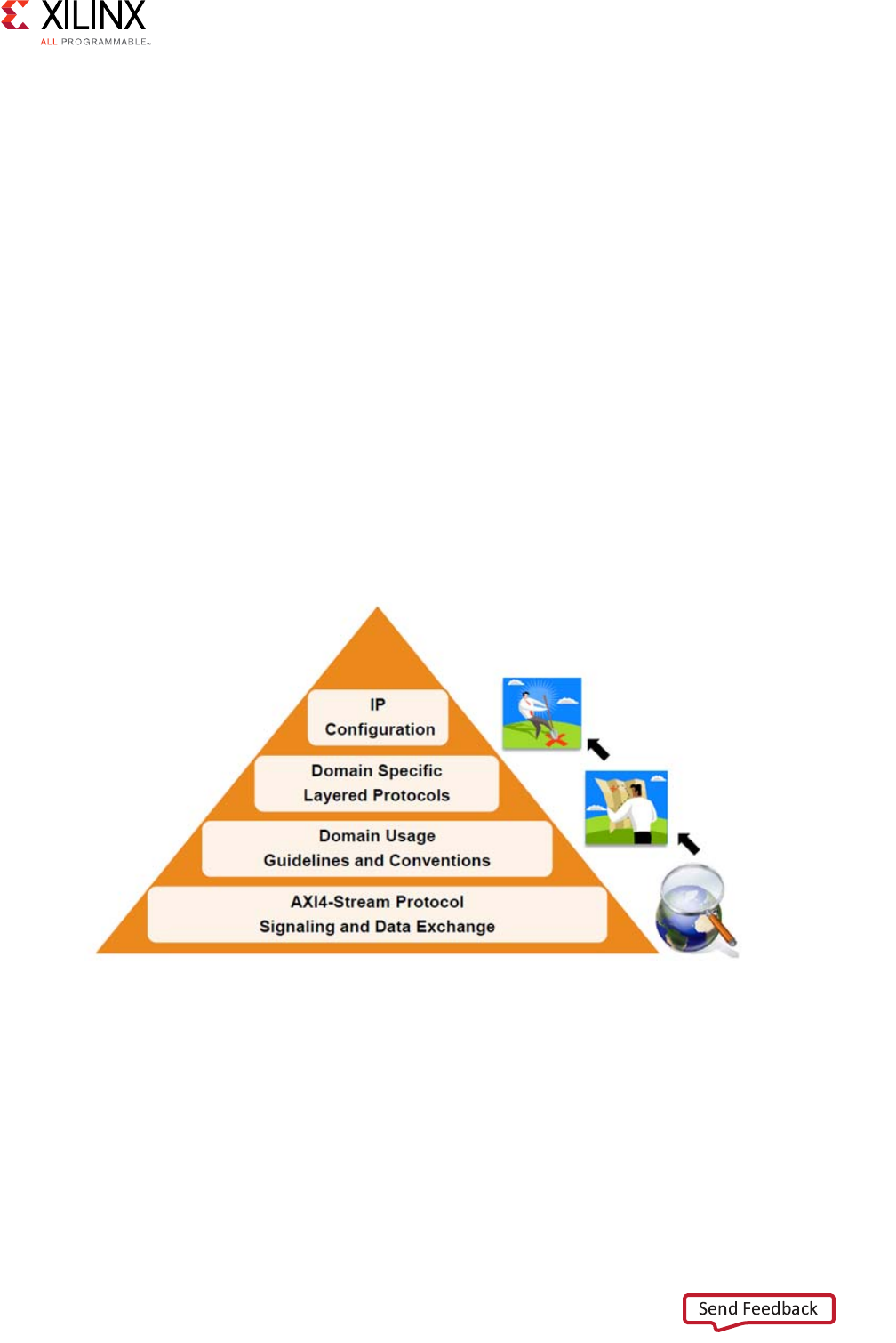
Vivado AXI Reference Guide www.xilinx.com 149
UG1037 (v4.0) July 15, 2017
Chapter 7: AXI4-Stream IP Interoperability: Tips and Hints
This chapter focuses on the following main domains:
°DSP/Wireless
°Video
°Communications
°AXI Infrastructure IP domains
•Follow the Published Standard for the IP Domain: Chapter 4, AXI Feature Adoption in Xilinx
Devices, provides an overview of the adoption of AXI4-Stream by Xilinx IP. This chapter
further describes the various AXI4-Stream interface conventions and guidelines for IP
configuration and use.
•Validate the Data: Understanding the IP domain and following the published standard
lets you focus your effort on the key elements to achieve IP interoperability; however, it is
imperative that you confirm that the IP operates as expected in the system using
simulation or hardware testing.
The following figure illustrates how you need to approach the design and
development
process from IP selection to IP configuration for implementing systems with a high degree of IP
interoperability.
Begin the design process by understanding the AXI4-Stream protocol because it is the basis
for data exchange. You can then move to higher levels of refinement by understanding the
domain-level AXI4-Stream usage conventions, domain-level data organization and
interpretation of data, and finally focus on the exact configuration settings and functions of
each IP in the system. In this process, you narrow the solution space for each IP in the
system.
Figure 7-1: Process Tier for Understanding IP Interoperability
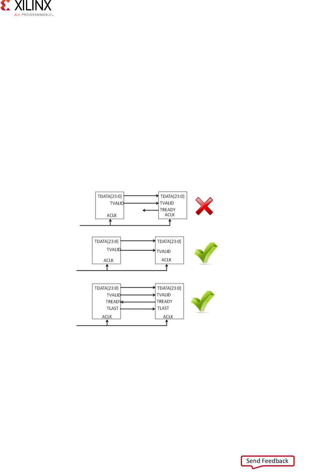
Vivado AXI Reference Guide www.xilinx.com 150
UG1037 (v4.0) July 15, 2017
Chapter 7: AXI4-Stream IP Interoperability: Tips and Hints
AXI4-Stream Protocol
Review and use the AXI4-Stream signaling and data exchange interface protocol as described
in Chapter 4, AXI Feature Adoption in Xilinx Devices. AXI4-Stream is an interface-level
protocol for IP to exchange raw data. Building on top of the signaling protocol, the various IP
application domains can then establish common data types to enable IP to use exchanged
data. AXI4-Stream defines optional signals with default tie-off rules and byte-aligned data
widths with width conversion formulas. Some of the key IP interoperability considerations to
focus on at the AXI4-Stream signaling levels are:
• Use of optional signals between two IP being connected to each other, as shown in the
following figure.
• Data width of the connected interfaces.
• Burst length (such as the size of the data frame, block, or packet).
• Data representation (Layered Protocols).
Figure 7-2: Establish AXI4-Stream Signaling-Level Data Exchange Compatibility
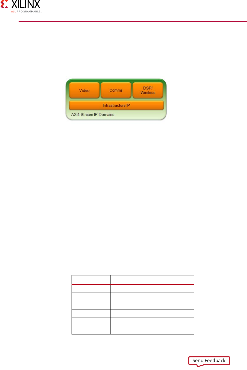
Vivado AXI Reference Guide www.xilinx.com 151
UG1037 (v4.0) July 15, 2017
Chapter 7: AXI4-Stream IP Interoperability: Tips and Hints
Domain Usage Guidelines and
Conventions
Each IP application domain recommends common guidelines for usage of optional
AXI4-Stream signals to facilitate IP interoperability. The four major IP application domains
are shown in the following figure.
Video IP
AXI4-Stream IP in this domain carries framed video and image pixel data, and exchanges
only pixel data and video line and frame markers. Other signals associated with physical
interfaces such as: hsync, vsync, active_video, blanking, or other ancillary data signals; are
not carried over AXI4-Stream.
AXI4-Stream video IP supports backpressure and elasticity in data flow around the
TVALID/TREADY handshake.
Pixel data retains the relative location in the datastream; however, video pixel timing
relative to hsync or vsync at a physical display is not preserved.
AXI4-Stream video IP uses layered protocols to encode a variety of video formats and
resolutions. For more details on video IP adoption of AXI4-Stream, see IP Using
AXI4-Stream Video Protocol in Chapter 4.
The following table summarizes video IP domain AXI4-Stream signaling usage and
guidelines.
Figure 7-3: AXI4-Stream IP
Domains
Table 7-1: Video IP Domain AXI4-Stream Signaling Usage
Signal Endpoint
ACLK Used and Supported
ACLKEN Limited Support
ARESTEN Used and Supported
TVALID Used and Supported
TREADY Used and Supported
TDATA Used and Supported
Vivado AXI Reference Guide www.xilinx.com 152
UG1037 (v4.0) July 15, 2017
Chapter 7: AXI4-Stream IP Interoperability: Tips and Hints
DSP/Wireless IP
AXI4-Stream IP in the DSP and Wireless IP application domain operates on numerical
streaming data paths. IP in this domain exchange data in either blocking (with backpressure)
or non-blocking (continuous) modes.
You can organize data in either Time Division Multiplexing (TDM) or parallel paths, and use
optional AXI4-Stream interfaces to perform configuration, control, and status reporting.
IP with multiple AXI4-Stream interfaces must account for IP core-specific synchronization
rules between configuration and data channels (for example: a configuration packet must
precede each data packet for block-based processing in some wireless IPs). See DSP and
Wireless IP: AXI Feature Adoption in Chapter 4.
The following table summarizes DSP and Wireless IP AXI4-Stream signaling usage and
guidelines.
TID Not Supported
TDEST Not Supported
TKEEP Not Supported
TSTRB Not Supported
TUSER Used and Supported
TLAST Used and Supported
Table 7-2: DSP/Wireless IP Domain AXI4-Stream Signaling Usage
Signal Endpoint
ACLK Used and Supported
ACLKEN Limited Support
ARESTEN Used and Supported
TVALID Used and Supported
TREADY Used and Supported
TDATA Used and Supported
TID Not Supported
TDEST Not Supported
TKEEP Not Supported
TSTRB Not Supported
TUSER Used and Supported
TLAST Used and Supported
Table 7-1: Video IP Domain AXI4-Stream Signaling Usage (Cont’d)
Signal Endpoint
Vivado AXI Reference Guide www.xilinx.com 153
UG1037 (v4.0) July 15, 2017
Chapter 7: AXI4-Stream IP Interoperability: Tips and Hints
Communications IP
AXI4-Stream IP in the communications application domain refers to Endpoint IP that
implement high-speed communications protocols using transceivers or I/Os. Depending on
the relationship with transceivers or I/Os that cannot accept backpressure, these AXI4-Stream
interfaces can have limited
handshaking
options (for example no support for the T
READY
signal with some IP that are closely tied to the physical interface).
AXI4-Stream communications IP are tightly coupled to the underlying protocol (such as PCIe,
Ethernet, and SRIO) with explicit data formats and handshaking rules that limit IP
interoperability across protocols.
AXI4-Stream communications IP are usually connected to custom logic in a user design, AXI
infrastructure IP, or other protocol-specific IP (for example: Ethernet IP using AXI Ethernet
DMA or PCIe bridging IP to other protocols).
More details on Communications IP are available at the Xilinx IP Center website [Ref 3].
The following table summarizes communications IP AXI4-Stream signaling usage and
guidelines.
AXI Infrastructure IP
AXI4-Stream infrastructure IP refers to IP that generally exchanges or moves data within a
system without using the contents of data or being tied to a specific data interpretation.
Typically AXI4-Stream infrastructure IP are used as system building blocks or as test and debug
IP. Common use models for infrastructure IP include width conversion, data switching and
routing, buffering, pipelining, and DMA.
Table 7-3: Communications IP Domain AXI4-Stream Signaling Usage
Signal Endpoint
ACLK Used and Supported
ACLKEN Not Supported
ARESTEN Used and Supported
TVALID Used and Supported
TREADY Optionally Supported
TDATA Used and Supported
TID Not Supported
TDEST Not Supported
TKEEP Optionally Supported
TSTRB Not Supported
TUSER Optionally Supported
TLAST Used and Supported
Vivado AXI Reference Guide www.xilinx.com 154
UG1037 (v4.0) July 15, 2017
Chapter 7: AXI4-Stream IP Interoperability: Tips and Hints
AXI infrastructure IP is required to support a wide range of optional and flexible signal
interface
configurations
to meet the signaling needs of IP from all domains. This also helps to
exchange data between mismatched AXI4-Stream master and slave signaling interfaces. More
details are available on the AXI4-Stream Interconnect IP website [Ref 4].
For information about DMA IP that implement AXI4-Stream to AXI4 Memory-Mapped) data
transfer, see Chapter 3, Samples of Vivado AXI IP and Xilinx Processors.
The following table describes the main sub-categories of AXI4-Stream infrastructure IP and their
useful characteristics. Table 7-5 lists the infrastructure IP domain AXI4-Stream signaling usage.
Table 7-4: AXI4-Stream Infrastructure IP Sub-Categories
Type Key Characteristics Examples Interoperability Considerations
Pass-through °Used for buffering,
pipelining, or moving
data.
°Does not change
contents of data.
°Register Slice
°FIFO
°Clock Converter
°Crossbar Switch
°Does not change contents or organization of
data.
°Generally compatible with all AXI4-Stream IP.
Modifier °Potential to change
contents
or
organization
of data.
°Width converter
°Bus
Rip/Concatenation
°
(Split/Combine)
°MUX/DeMUX
°Subset Converter
°Packer
°Performs specific algorithmic operations on
data.
°Compatible with most AXI4-Stream IP with
proper usage.
Stream
Endpoint
°Entry/Exit Point for a
stream subsystem or
processing pipeline.
°Usually the logical
data source or
terminus in a chain of
IPs.
°DMA (general
purpose)
°(MicroBlaze™
processor stream
ports)
°AXI4-Lite to
AXI4-Stream
bridge
°Virtual FIFO
Controller
° Usually the first or last IP in a processing
pipeline
°Compatible with most AXI4-Stream IP with
proper usage
°Might have limited support for TUSER, TID,
and TDEST
Monitor °Attaches to an AXI
interface for
observation only.
°Does not alter
the contents of data.
°AXI Debug
Monitor
°AXI HW Protocol
Checker
°Performance
Monitor
°Observes but does not alter data.
°Taps an AXI4-Stream connection for
viewing
.
°Generally compatible with all AXI4-Stream IP.
Vivado AXI Reference Guide www.xilinx.com 155
UG1037 (v4.0) July 15, 2017
Chapter 7: AXI4-Stream IP Interoperability: Tips and Hints
Domain-Specific Data Interpretation and
Interoperability Guidelines
Domain-specific
protocols can be layered on top of the
AXI4-Stream
signaling layer so that IP
can interpret and use the data that has been exchanged. This section summarizes key
domain-specific layered protocol usage information and presents guidelines to help users
focus on key concepts when constructing IP and systems to be inter-operable.
Video IP Layered Protocols
Video IP use layered protocols to represent the video format and resolution. Video IP must be
configured to use the same video format and resolution to transfer information, such as
industry recognized YUV/YUVA, RGB/RGBA video formats and 1920x1080P60 resolutions.
Where necessary, format conversion IP such as color space converters can be used to convert
the video between IP blocks in a system.
Table 7-5: Infrastructure IP Domain AXI4-Stream Signaling Usage
Signal Pass- Through Modifier Endpoint Monitor
ACLK Used and Supported Used and Supported Used and Supported Used and Supported
ACLKEN Used and Supported Used and Supported Not Supported Not Supported
ARESTEN Used and Supported Used and Supported Used and Supported Used and Supported
TVALID Used and Supported Used and Supported Used and Supported Used and Supported
TREADY Used and Supported Used and Supported Used and Supported Used and Supported
TDATA Used and Supported Used and Supported Used and Supported Used and Supported
TID Used and Supported Used and Supported Not Supported Used and Supported
TDEST Used and Supported Used and Supported Limited Support Used and Supported
TKEEP Used and Supported Used and Supported Limited Support Used and Supported
TSTRB Used and Supported Used and Supported Limited Support Used and Supported
TUSER Used and Supported Used and Supported Limited Support Used and Supported
TLAST Used and Supported Used and Supported Used and Supported Used and Supported

Vivado AXI Reference Guide www.xilinx.com 156
UG1037 (v4.0) July 15, 2017
Chapter 7: AXI4-Stream IP Interoperability: Tips and Hints
Video IP also has common conventions for packing the data bits for the color components
(such as red, green, and blue
components)
into TDATA.
AXI4-Stream
signals such as TLAST
and
TUSER
encode line and frame boundaries for a given video resolution.
Video IP also contain optional AXI4-Lite interface that can change the layered protocol
during runtime, typically under microprocessor control.
See Video IP: AXI Feature Adoption in Chapter 4 for details on the encoding of video layered
protocols. The following table and Table 7-7 summarize some of the key characteristics,
interoperability considerations, and guidelines for layered protocols used in the Video IP
domain.
Table 7-6: Video IP Layered Protocol Summary
Type Key Characteristics Examples Interoperability Considerations
Video Format
• Video IP support industry
standard formats
•RGB
• YUV 4:2.2
• Use conversion IP video formats.
Pixels Encoding
(Components)
•Pixels (TDATA beats)
consist of 1 to 4
components.
• Each component is 8, 10,
12, or 16 bits wide.
• Components are
concatenated and
0-padded up to an overall
byte width.
• 24-bit wide TDATA
carrying RGB
(3x8-bit
components).
• 6-bit wide TDATA
carrying
YUV 4:2:2
(8-bit alternating
V/U +8-bit Y
components).
• The relative placement order of the
components in the
TDATA
beat is
fixed.
• When the width of components
mismatch, rules apply on how to
scale the data.
Video
Resolution /
Framing
•AXI4-Stream TLAST/
TUSER signaling is used to
mark end-of-line and
frame boundaries
• Only active video pixel data
is transferred
•
TUSER[0]
marks the
start of a frame
•
TLAST
marks end of
line.
•Examples:
• 1024x768 would
have 1024
TDATA
beats per TLAST.
• 768
TLAST
beats per
TUSER[0].
•TLAST and TUSER must be
preserved and placed at correct
intervals relative to pixels.
• Some video IP are capable of
recovering from corrupted or
incomplete frame data and
re-locking to the framing signals.
• Connected Video IP must have the
same frame resolution or rescaling
IP. is required.

Vivado AXI Reference Guide www.xilinx.com 157
UG1037 (v4.0) July 15, 2017
Chapter 7: AXI4-Stream IP Interoperability: Tips and Hints
DSP/Wireless IP Layered Protocols
DSP/Wireless IP use layered protocols to represent numerical information and structures to
perform processing such as filtering, arithmetic operations. DSP/ Wireless IP usually have a
flow through architecture with input and output stream interfaces to take in data, perform
operation on the data, and send out the data.
Data flow is usually optional between blocking (with backpressure using TREADY) and
non-blocking (continuous data flow without TREADY).
Table 7-7: Video IP Interoperability, Considerations, and Guidelines
Guideline Description Rule to Achieve
Interoperability User Effort/Notes
Data Type 1-4 components per pixel,
8,10,12,16 bit per component
Converter cores
provided.
All cores configurable
to support 8,10,12,16
bit data.
Seamless if video format and
resolution match; Standard adapters
provided to change formats and
resolution.
Data Burst Video standards with up to 8k
pixels per line (burst) supported
All cores configurable
to support standard
burst sizes.
Ensure that connected IP use the same
settings.
AXI4-Stream
Optional
Signals
Optional: ACLKEN, ARESETN,
Else Fixed set (TUSER[0],
TLAST, TREADY, TVALID,
TDATA)
AXI-FIFO needed to
bridge between
different ACLK or
ACLKEN domains.
Standard adapter might be needed
(AXI4-Stream FIFO or AXI4-Stream
Interconnect)
AXI4-Stream
TUSER Signals
Only the
TUSER
0
signal used
consistently across all video
cores
TUSER0 is required and
is used to signal frame
boundaries.
Special considerations might be
needed for IP that can generate or
recover from partial frames (for
example, handling when cable is
removed and reconnected)
Number of
Channels and
AXI4-Lite
Dependency
Generally single AXI4-Stream
through IP, but some cores have
multiple inputs/output streams;
Most IP have an optional
AXI4-Lite control interface.
For cores with multiple
input/output streams
or when AXI4-Lite is
used, read the
datasheet to
understand data
relationships.
Core can permit format/resolution to
be
changed
using
AXI4-Lite requiring
care to coordinate any runtime
changes across system.

Vivado AXI Reference Guide www.xilinx.com 158
UG1037 (v4.0) July 15, 2017
Chapter 7: AXI4-Stream IP Interoperability: Tips and Hints
DSP/Wireless IP also support data organized into TDM or parallel paths to operate on
numeric data structures such as arrays. The streams can also carry optional sideband status
signals to supplement the numeric data with core-specific information. DSP/Wireless IP
also often contain control AXI4-Stream interfaces for optional runtime control and status
such as the ability to change filter coefficients at runtime using a secondary AXI4-Stream
interface.
See DSP and Wireless IP: AXI Feature Adoption for details of encoding DSP/Wireless layered
protocols. The following table and Table 7-9 summarizes some of the key characteristics,
interoperability considerations, and guidelines for layered protocols used in the DSP/Wireless
IP domain.
Table 7-8: DSP/Wireless IP Layered Protocol Summary
Key
Characteristi Description Examples Interoperability Considerations
Number of
Data
Tra n s f e r s p er
Invocation
• Sample-Based Processing:
IP data processing is
applied independently to
every single AXI4-Stream
transfer.
• Block-Based Processing: IP
data processing is applied
to a “block” “packet” of
AXI4-Stream transfers.
•Sample: complex
multiplier operates on
a data sample at a time.
•Block: FFT of a given
point size.
Block based IP must have same notion
of block size to inter-operate.
Number of
Data
Tra n s f e r s p er
Invocation
• Single-Channel: 1 logical
stream of data.
• Multi-Channel: data being
processed
in
parallel (could
be a single AXI4-Stream
interface with parallel data
concatenated together on
T DATA ).
• FIR compiler can be
configured to operate
single or multiple
parallel data lanes.
Multi-channel mode
allows DSP resources
to be shared across
multiple data paths.
Data must be concatenated together or
split out to change number of parallel
data streams.
Data type
representati
on of TDATA
• Unit: single datum
• Array: multiple data
• Structure: tuples or special
data structures for
control/status interfaces
• FIR compiler can
operate on unit data or
array of data when
configured for single
or multiple data paths,
respectively.
• Control/status
AXI4-Stream interfaces
usually require
structured data such as
FFT configuration
• IP must have same notion of data
type representation to interoperate.
•
Structured
TDATA
is often used in
control/status interfaces and need
custom logic or programmable IP
(like a microprocessor) to generate.
Vivado AXI Reference Guide www.xilinx.com 159
UG1037 (v4.0) July 15, 2017
Chapter 7: AXI4-Stream IP Interoperability: Tips and Hints
Use of
TUSER
signal for
sideband
data
None: No TUSER signal used
Pass-through: TUSER signal is
passed from an input
interface to an output
interface IP Specific: TUSER
conveys IP-specific sideband
data.
• Complex Multiplier can
work without TUSER or
can Pass-through
TUSER.
• DDS compiler can
include TUSER in its
output interface with
IP-specific
TDM
channel markers.
• IP-specific TUSER often requires
custom logic to decode.
•TUSER Pass-through mode is useful
for transmitting user information
through a core to match latency with
the data.
Use of
TLAST
signal
None: No TLAST signal used.
Pass-thru: TLAST signal is
passed from an input
interface to an output
interface.
Block end marker: TLAST
indicates the last transfer in a
block.
IP-specific TLAST used to
mark an IP specific location in
the data transfers
• Divider Generator can
work without TLAST or
can Pass-through
TLAST.
• FFT uses TLAST for
block end marker
•IP must have same notion of TLAST
when used as block end marker.
•TLAST Pass-through mode is useful
for transmitting user information
through a core with latency matched
to that of the data.
• IP specific TLAST often requires
custom logic to decode TLAST.
Table 7-8: DSP/Wireless IP Layered Protocol Summary (Cont’d)
Key
Characteristi Description Examples Interoperability Considerations
Table 7-9: DSP/Wireless Interoperability Guidelines
Guideline Description Rule to Achieve
Interoperability User Effort/Notes
Data Type Scalars, arrays, and structures with
data type elements for fixed and
floating point number
representation.
Adhere to defined data
types and conventions.
For example real versus
integer, common binary
point and data size.
Must understand data
types/structures and ensure
consistency; adapters might be
needed
Data Burst Sample or block processing; IP
processing applied to a single
transfer or a block of transfers
Use of (optional) TLAST
to delimit blocks,
packets, or frames.
Must align block sizes to match
data structure size, adapters
might be needed.
AXI4-Stream
Optional Signals
Optional: ACLKEN, TREADY
TLAST, TUSER.
Fixed: TDATA, TVALID
Adhere to DSP/Wireless
IP specific guidelines in
DSP and Wireless IP: AXI
Feature Adoption in
Chapter 4.
Optional signals must be used
consistently or adapters are
needed.
AXI4-Stream
TUSER Signals
No use, Pass-through, or IP
specific use of TUSER. TUSER is
generally optional.
For higher
interoperability, avoid
use of IP specific TUSER.
TUSER signals must be used
consistently. Custom logic
might be needed to handle
IP-specific TUSER.
Data Type Scalars, arrays, and structures with
data type elements for fixed and
floating point number
representation.
Adhere to defined data
types and conventions.
For example real versus
integer, common binary
point and data size.
Must understand data
types/structures and ensure
consistency; adapters might be
needed
Vivado AXI Reference Guide www.xilinx.com 160
UG1037 (v4.0) July 15, 2017
Chapter 7: AXI4-Stream IP Interoperability: Tips and Hints
Communications IP Layered Protocols
IP in this domain use layered protocols to represent communications protocols, typically
networking
packets. Packets can be fixed or variable sized depending on the protocol (such as
Ethernet and PCIe). IP are usually closely tied to the physical layer interface or logical level
interface with transmit and receive AXI4-Stream interfaces, sideband TUSER signals for
control/status, and some offer additional AXI4-Lite and AXI4 memory-mapped interfaces.
Because of the specific relationship to a communications protocol standard, IP in this domain
are often used with custom logic, infrastructure IP, other IP of the same protocol type.
The following table summarizes some of the key guidelines for layered protocols used in the
Communicatons IP domain.
AXI Infrastructure IP Layered Protocols
IP in this domain often do not use specific layered protocols but are configurable to
Pass-through data or to generate/receive data using a processor or DMA engine.
The key elements for
interoperability
is to use the
AXI4-Stream
protocol following the
recommendations in Signaling Protocol in Chapter 3.
Table 7-10: Communications IP Layered Protocol Interoperability Guidelines
Guideline Description Rule to Achieve User Effort/Notes
Data Type Packetized data, with and
without headers/footers.
Matched to protocols like
Ethernet, PCIe, or SRIO.
Remove header and footer to
access raw packet data or transfer
data to memory-mapped space
(for example) using a DMA
engine.
Must understand data types and
ensure packet data is delivered in
the correct order.
Adapters might be needed.
Data Burst Variable size:
Minimum can be a single
cycle of data.
Maximum depends upon
the parent protocol
All cores configurable to support
standard burst sizes, up to a
defined limit for a given protocol
Care must be taken to ensure
that
legal-sized packets are
transferred between cores.
Adapters might be needed to
break apart too-large packets.
AXI4-Stream
Optional
Signals
TREADY, TKEEP,
TDATA,TUSER, TLAST.
In some cases, ACLKEN,
TDEST, TID.
Use adapters for infrastructure IP.
TDEST/TID can be used for data
interleaving.
Adapters might be required.
AXI4-Stream
TUSER
Signals
Variety of uses and sizes.
Common uses: packet
discontinue, framing
signals, packet details
Avoid using TUSER. Set
control/status information in
AXI4-Lite register space if possible
Migrate TUSER signals to
dedicated AXI4-Lite or AXI4-Stream
sideband bus. Adapter might be
required.
Number of
Channels
and
AXI4-Lite
Dependency
Generally single
AXI4-Stream in each
direction, through IP.
SRIO can have up to 8
streams in each direction.
For cores with multiple input/
output streams, read the datasheet
to understand data relationships.
Cores must have an appropriate
port to which to connect.
Refer to the individual datasheet for
each core.

Vivado AXI Reference Guide www.xilinx.com 161
UG1037 (v4.0) July 15, 2017
Chapter 7: AXI4-Stream IP Interoperability: Tips and Hints
AXI Infrastructure IP is designed to be broadly compatible with IP from different domains
because it has highly configurable interfaces, and generally does not use the contents of the
data. The following table summarizes some of the key characteristics and interoperability
considerations for the AXI Infrastructure IP domain.
Table 7-11: AXI Infrastructure IP Interoperability Guidelines
Guideline Description Rule to Achieve User Effort/Notes
AXI4-Stream
Optional Signals
Use
• Endpoint type IP generally
limit support for TID,
TDEST
(unless
multi-channel IP), TSTRB,
TUSER.
• Endpoint IP using TLAST
should be aware of burst
size.
•
TKEEP
only for packet
remainders.
•
Use
“Continuous” or
“Continuous Aligned
Streams”.
• Low for Pass-through and
Monitor IP types.
• Generally low when using core
signals TDATA, TVALID,
TREADY, TLAST, TKEEP
(remainders).
• Medium to high with more
complex systems using TID,
TDEST, TSTRB, or TUSER.
Layered Protocols • Pass-through and Monitor
IP types do not alter data.
• Modifiers can transform
data.
• Endpoints can synthesize or
receive layered protocols
with proper configuration.
• Minimize use of TID,
TDEST,
TSTRB
,
and
TUSER.
• Consider how modifiers
change the data structures
used by layered protocols.
• Endpoints require the user
to properly program them
to generate data contents
matching the layered
protocol.
• Low for Pass-through and
Monitor IP types.
• Medium when using
modifiers that can alter the
data encodings
algorithmically.
• Medium to High for endpoint
IPs that must be configured
and programmed properly to
match the requirements of
layered protocols.
Other
Interoperability
Factors
•There are
Interdependencies, such as
Endpoint IP often have
additional AXI4-Lite control
interfaces.
Pay attention to real time
system impact when using
infrastructure IP, such as FIFOs
might increase latency.
• Low for Monitor types.
•Low to Medium for
Pass-through and Modifier
types that could affect real
time behavior.
• Medium to high for endpoint
types which could have
control ports.
Interfacing to IP in
other Domains
• Pass-through and Monitor
types designed to work
with all domains.
• Modifier IP can work in
video or DSP domains, but
need users to validate data
structure integrity.
• Endpoint IP have limited
ability to interface to other
domains and might need
domain specific endpoint
IP (example AXI Video
DMA, PCIe DMA, and so
forth).
• Care must be taken to
configure and program
Endpoints to match the
layered protocol
requirements of other IP
domains.
• Low for Pass-through and
Monitor IP types.
• Medium when using
modifiers that can alter data
structures.
Medium to High for using
endpoints that have to
synthesize or receive layered
protocols.
Vivado AXI Reference Guide www.xilinx.com 162
UG1037 (v4.0) July 15, 2017
Appendix A
AXI Adoption Summary
Introduction
This appendix provides a summary of protocol signals adopted by Xilinx® in the AXI4 and
AXI-Lite, and AXI4-Stream interface protocol IP. Consult the AXI specifications (available at
www.amba.com) for complete descriptions of each of these signals.
Global Signals
TableA-1: Global AXI Signals
Signal AXI4 AXI4-Lite
ACLK Clock source.
ARESETN Global reset source, active-Low. This signal is not present on the interface when a reset
source (of either polarity) is taken from another signal available to the IP. Xilinx IP
generally must deassert TVALID and TREADY outputs within 8 cycles of reset assertion,
and generally require a reset pulse-width of 16 or more clock cycles of the slowest
clock.
Some Xilinx IP might document that they can accept ARESETN asserted for fewer than
16 cycles. For example, DSP IP require ARESETN asserted for a minimum of 2 cycles on
the AXI4-Stream interfaces.
Vivado AXI Reference Guide www.xilinx.com 163
UG1037 (v4.0) July 15, 2017
Appendix A: AXI Adoption Summary
AXI4 and AXI4-Lite Signals
AXI4 and AXI4-Lite Write Address Channel Signals
Note: A read-only master or slave interface omits the entire write address channel.
Table A-2: Write Address Channel Signals
Signal AXI4 AXI4-Lite
AWID Fully supported.
Masters need only output the set of ID bits that it varies
(if any) to indicate re-orderable transaction threads.
Single-threaded master interfaces can omit this signal.
Masters do not need to output the constant portion
that comprises the Master ID, as this is appended by
the AXI Interconnect.
Signal not present.
AWADDR Fully supported.
Widths up to 64 bits.
High-order bits outside the native address range of a slave are ignored (trimmed), by an
endpoint slave, which could result in address aliasing within the slave.
AWLEN Fully supported.
Support bursts:
• Up to 256 beats for incrementing (INCR).
• 16 beats for WRAP.
Signal not present.
AWSIZE Transfer width 8 to 1024 bits supported.
Use of narrow bursts where AWSIZE is less than the
native data width is not recommended.
Signal not present.
AWBURST INCR and WRAP fully supported.
FIXED bursts are not recommended. Conversions of
FIXED bursts through AXI Interconnect infrastructure
may have sub-optimal performance.
Signal not present
AWLOCK Exclusive access support not implemented in endpoint
Xilinx IP.
Infrastructure IP will pass exclusive access bit across a
system.
Signal not present.
AWCACH 0011 value recommended.
Xilinx IP generally ignores (as slaves) or generates (as
masters) transactions as Normal, Non-cacheable,
Modifiable, and Bufferable.
Infrastructure IP will pass Cache bits across a system.
Signal not present
AWPROT 000 value recommended.
Xilinx IP generally ignores (as slaves) or generates transactions (as masters)
with Normal, Secure, and Data attributes.
Infrastructure IP passes Protection bits across a system.
AWQOS Not implemented in Xilinx Endpoint IP.
Infrastructure IP passes QoS bit across a system.
Signal not present
Vivado AXI Reference Guide www.xilinx.com 164
UG1037 (v4.0) July 15, 2017
Appendix A: AXI Adoption Summary
AXI4 and AXI4-Lite Write Data Channel Signals
Note: A read-only master or slave interface omits the entire Write Data Channel.
AXI4 and AXI4-Lite Write Response Channel Signals
The following table lists the Write Response Channel signals.
Note: A read-only master or slave interface omits the entire write response channel.
AWREGION Can be implemented in Xilinx Endpoint slave IP.
Not present on master IP.
Generated by AXI Interconnect using corresponding
address decoder range settings.
Signal not present
AWUSER Generally, not implemented in Xilinx endpoint IP.
Infrastructure IP passes USER bits across a system.
Signal not present.
AWVALID Fully supported.
AWREADY Fully supported.
Table A-2: Write Address Channel Signals (Cont’d)
Signal AXI4 AXI4-Lite
TableA-3: Write Data Channel Signals
Signal AXI4 AXI4-Lite
WDATA Native width 32 to 1024 bits supported. 32-bit width supported.
64-bit AXI4-Lite native data width is not
currently supported
WSTRB Fully supported. Slaves interface can elect to ignore
WSTRB (assume all bytes valid).
WLAST Fully supported. Signal not present.
WUSER Generally, not implemented in Xilinx endpoint IP.
Infrastructure IP will pass USER bits across a system.
Signal not present.
WVALID Fully supported.
WREADY Fully supported.
Table A-4: Write Response Channel Signals
Signal AXI4 AXI4-Lite
BID Fully supported.
See AWID for more information.
Signal not present.
BRESP Fully supported. EXOKAY value not supported by
specification.
BUSER Generally, not implemented in Xilinx endpoint IP.
Infrastructure IP will pass USER bits across a system.
Signal not present.
Vivado AXI Reference Guide www.xilinx.com 165
UG1037 (v4.0) July 15, 2017
Appendix A: AXI Adoption Summary
AXI4 and AXI4-Lite Read Address Channel Signals
Note: A write-only master or slave interface omits the entire read address channel.
BVALID Fully supported.
BREADY Fully supported.
Table A-4: Write Response Channel Signals (Cont’d)
Signal AXI4 AXI4-Lite
Table A-5: Write Address Channel Signals
Signal AXI4 AXI4-Lite
ARID Fully supported.
Masters need only output the set of ID bits that it varies (if any) to indicate
re-orderable transaction threads. Single-threaded master interfaces can omit
this signal. Masters do not need to output the constant portion that comprises
the “Master ID”, as this is appended by the AXI Interconnect.
Signal not present.
ARADDR Fully supported.
Widths up to 64 bits. High-order bits outside the native address range of a slave are ignored
(trimmed) by an endpoint slave, which could result in address aliasing within the slave.
ARLEN Fully supported.
Support bursts:
• Up to 256 beats for incrementing (INCR).
• 16 beats for WRAP.
Signal not present
ARSIZE Transfer width 8 to 1024 bits supported.
Use of narrow bursts where ARSIZE is less than the native data width is not
recommended.
Signal not present.
ARBURST INCR and WRAP fully supported.
FIXED bursts are not recommended. Conversions of FIXED bursts through
AXI Interconnect infrastructure may have sub-optimal performance.
Signal not present.
ARLOCK Exclusive access support not implemented in Endpoint Xilinx IP.
Infrastructure IP passes exclusive access bit across a system.
Signal not present.
ARCACHE 0011 value recommended.
Xilinx IP generally ignores (as slaves) or generates (as masters) transactions
with
Normal, Non-cacheable, Modifiable, and Bufferable.
Infrastructure IP will pass Cache bits across a system.
Signal not present.
ARPROT Xilinx IP generally ignore (as slaves) or generate transactions (as masters) with Normal, Secure, and
Data attributes.
Infrastructure IP passes Protection bits across a system.
000 value recommended.
ARQOS Not implemented in Xilinx Endpoint IP.
Infrastructure IP passes QoS bit across a system
Signal not present.
Vivado AXI Reference Guide www.xilinx.com 166
UG1037 (v4.0) July 15, 2017
Appendix A: AXI Adoption Summary
AXI4 and AXI4-Lite Read Data Channel Signals
The following table lists the Read Data Channel signals.
Note: A read-only Master or slave interface omits the entire read data channel.
ARREGION Can be implemented in Xilinx Endpoint Slave IP.
Not present on master IP.
Generated by AXI Interconnect using corresponding address decoder range
settings.
Signal not present.
ARUSER Generally, not implemented in Xilinx Endpoint IP.
Infrastructure IP passes User bits across a system.
Signal not present.
ARVALID Fully supported.
ARREADY Fully supported.
Table A-5: Write Address Channel Signals (Cont’d)
Signal AXI4 AXI4-Lite
Table A-6: Read Data Channel Signals
Signal AXI4 AXI4-Lite
RID Fully supported.
See ARID for more information.
Signal not present.
RDATA Native width 32 to 1024 bits supported. 32-bit width supported.
64-bit AXI4-Lite native data width is not
supported.
RRESP Fully supported. EXOKAY value not supported by
specification.
RLAST Fully supported. Signal not present.
RUSER Generally, not implemented in Xilinx Endpoint IP.
Infrastructure IP will pass User bits across a system.
Signal not present.
RVALID Fully supported.
RREADY Fully supported.
Vivado AXI Reference Guide www.xilinx.com 167
UG1037 (v4.0) July 15, 2017
Appendix A: AXI Adoption Summary
AXI4-Stream Signal Summary
The following table lists the AXI4-Stream signal summary.
TableA-7: AXI4-Stream Signal Summary
Signal Optional Default
(All Bits) Description
TVALID No N/A No change.
TREADY Yes 1 No change
TDATA Yes 0 No change. Xilinx AXI IP convention:
8 through 4096 bit widths are used by Xilinx AXI IP
(establishes a testing limit).
TSTRB Yes Same as
TKEEP
else 1
No change. Generally, the usage of TSTRB is to encode
Sparse Streams. TSTRB should not be used only to encode
packet remainders.
TKEEP Yes 1 In Xilinx IP, there is only a limited use of Null Bytes to
encode the remainders bytes at the end of packetized
streams.
TKEEP is not used in Xilinx endpoint IP for signaling leading
or intermediate null bytes in the middle of a stream.
TLAST Yes 0 Indicates the last data beat of a packet.
Omission of TLAST implies a continuous, non-packetized
stream.
TID Yes 0 No change.
Xilinx AXI IP convention:
Only 1-32 bit widths are used by Xilinx AXI IP (establishes a
testing limit).
TDEST Yes 0 No change
Xilinx AXI IP convention:
Only 1-32 bit widths are used by Xilinx AXI IP (establishes a
testing limit).
TUSER Yes 0 No change
Xilinx AXI IP convention:
Only 1-4096 bit widths are used by Xilinx AXI IP (establishes
a testing limit).
Vivado AXI Reference Guide www.xilinx.com 168
UG1037 (v4.0) July 15, 2017
Appendix B
AXI Terminology
Terminology
The following table lists the AXI terminology.
Table B-1: AXI Terminology
Term Type Description Usage
AXI Generic The generic term for all implemented
AXI protocol interfaces.
General
description.
AXI4 Memory-mapped
block transfers
Addressed interface bursts up to 256
data beats.
Embedded and
memory cores.
Examples: MIG,
block Ram, PCIe
Bridge, FIFO.
AXI4-Lite Control Register
Subset
32-bit data, memory-mapped,
lightweight, single data beat transfers
only.
Management
registers.
Examples:
Interrupt
Controller,
UART Lite, IIC
Bus Interface.
AXI4-Stream Streaming Data
Subset
Unidirectional links modeled after a
single write channel.
Unlimited burst length.
Used in DSP,
Video, and
communication
applications.
Interface
AXI4
AXI4-Lite
AXI4-Stream
Collection of one or more channels
that expose an IP core function,
connecting a master to a slave.
Each IP can have multiple interfaces.
All.
Channel
AXI4
AXI4-Lite
AXI4-Stream
Independent collection of AXI signals
associated with a VALID signal.
All.
Bus Generic Multiple-bit signal
(Not an interface or a channel).
All.
Vivado AXI Reference Guide www.xilinx.com 169
UG1037 (v4.0) July 15, 2017
Appendix Appendix B: AXI Terminology
Transaction
AXI4-Stream
Complete communication operation
across a channel, composed of one or
more transfers. A complete action.
Used in DSP,
Video, and
communication
applications.
AXI4
AXI4-Lite
Complete collection of related read or
write communication operations
across address, data, and response
channels, composed of one or more
transfers. A complete read or write
request.
Embedded and
memory cores.
Management
registers.
Transfer
AXI4
AXI4-Lite
AXI4-Stream
Single clock cycle where information is
communicated, qualified by a VALID
hand-shake. Data beat
All
Burst
AXI4
AXI4-Lite
AXI4-Stream
Transaction that consists of more than
one transfer.
All
master
AXI4
AXI4-Lite
AXI4-Stream
An IP or device (or one of multiple
interfaces on an IP) that generates AXI
transactions out from the IP onto the
wires connecting to a slave IP.
All
slave
AXI4
AXI4-Lite
AXI4-Stream
An IP or device (or one of multiple
interfaces on an IP) that receives and
responds to AXI transactions coming in
to the IP from the wires connecting to
a master IP.
All
master interface
(generic)
AXI4
AXI4-Lite
AXI4-Stream
An interface of an IP or module that
generates out-bound AXI transactions
and thus is the initiator (source) of an
AXI transfer.
All
slave interface
(generic)
AXI4
AXI4-Lite
AXI4-Stream
An interface of an IP or module that
receives in-bound AXI transactions and
becomes the target (destination) of an
AXI transfer.
All
SI AXI4
AXI4-Lite
AXI Interconnect Slave Interface:
• For the IP integrator embedded flow,
Vectored AXI slave interface
receiving in-bound AXI transactions
from all connected master devices.
• For the Vivado IP flow, one of
multiple slave interfaces connecting
to one master device.
IP integrator
Table B-1: AXI Terminology (Cont’d)
Term Type Description Usage

Vivado AXI Reference Guide www.xilinx.com 170
UG1037 (v4.0) July 15, 2017
Appendix Appendix B: AXI Terminology
MI AXI4
AXI4-Lite
AXI Interconnect Master Interface:
• For the IP integrator embedded flow,
Vectored AXI master interface
generating out-bound AXI
transactions to all connected slave
devices.
• For the Vivado IP flow, one master
interface connecting to one slave
device.
IP integrator
SI slot AXI4
AXI4-Lite
Slave Interface Slot: A slice of the slave
Interface vector signals of the
Interconnect that connect to a single
master IP.
IP integrator
MI slot AXI4
AXI4-Lite
Master Interface Slot: A slice of the
Master Interface vector signals of the
Interconnect that connect to a single
Master Interface slave IP.
IP integrator
SI-side AXI4
AXI4-Lite
Refers to a module interface closer to
the SI side of the Interconnect.
All
MI-side AXI4
AXI4-Lite
Refers to a module interface closer to
the MI side of the Interconnect.
All
upsizer
AXI4
AXI4-Lite
AXI4-Stream
Data width conversion function in
which the data path width gets wider
when moving in the direction from the
slave interface toward the master
interface (regardless of write or read
direction).
All
downsizer
AXI4
AXI4-Lite
AXI4-Stream
Data width conversion function in
which the data path width gets
narrower when moving in the direction
from the slave interface toward the
master interface (regardless of write or
read direction).
All
SAMD Topology Shared-Address, Multiple-Data:
Configuration of AXI Interconnect
where data transfers can occur
independently and concurrently
between different master and slave
devices.
All
SASD Topology Shared-Address, Shared-Data:
Configuration of AXI Interconnect
where a single read and write pathway
is implemented.
All
Shared-Access Topology Configuration of AXI Interconnect
based on SASD topology where only
one transaction is issued at a time to
minimize resources.
EDK, Embedded
Table B-1: AXI Terminology (Cont’d)
Term Type Description Usage

Vivado AXI Reference Guide www.xilinx.com 171
UG1037 (v4.0) July 15, 2017
Appendix Appendix B: AXI Terminology
Crossbar Topology Configuration of AXI Interconnect
based on SAMD topology where data
pathways are implemented according
to sparse connectivity between master
and slave devices.
All
Crossbar Structural Module at the center of the AXI
Interconnect that routes address, data
and response channel transfers
between various SI slots and MI slots.
All
Table B-1: AXI Terminology (Cont’d)
Term Type Description Usage

Vivado AXI Reference Guide www.xilinx.com 172
UG1037 (v4.0) July 15, 2017
Appendix C
Additional Resources and Legal Notices
Xilinx Resources
For support resources such as Answers, Documentation, Downloads, and Forums, see Xilinx
Support Page.
Solution Centers
See the Xilinx Solution Centers for support on devices, software tools, and intellectual
property at all stages of the design cycle. Topics include design assistance, advisories, and
troubleshooting tips.
Documentation Navigator and Design Hubs
Xilinx Documentation Navigator provides access to Xilinx documents, videos, and support
resources, which you can filter and search to find information. To open the Xilinx
Documentation Navigator (DocNav):
• From the Vivado IDE, select Help > Documentation and Tutorials.
• On Windows, select Start > All Programs > Xilinx Design Tools > DocNav.
• At the Linux command prompt, enter docnav.
Xilinx Design Hubs provide links to documentation organized by design tasks and other
topics, which you can use to learn key concepts and address frequently asked questions. To
access the Design Hubs:
• In the Xilinx Documentation Navigator, click the Design Hubs View tab.
• On the Xilinx website, see the Design Hubs page.
Note: For more information on Documentation Navigator, see the Documentation Navigator page
on the Xilinx website.

Vivado AXI Reference Guide www.xilinx.com 173
UG1037 (v4.0) July 15, 2017
Appendix C: Additional Resources and Legal Notices
Third-Party Documentation
Additional reference documentation:
1. Instructions on how to download the ARM® AMBA® AXI specifications are at
http://www.amba.com. See the:
°AMBA AXI and ACE Protocol Specification (AXI3, AXI4, and AXI4-Lite Sections)
°AMBA4 AXI4-Stream Protocol Specification
2. Cadence AXI UVC
Xilinx Documentation
3. Xilinx IP Center
4. AXI4-Stream Interconnect page
5. Zynq-7000 All Programmable SoC Verification IP Data Sheet (DS940)
6. LogiCORE IP AXI DMA Product Guide (PG021)
7. LogiCORE IP AXI DataMover Product Guide (PG022)
8. LogiCORE IP AXI Central Direct Memory Access Product Guide (PG034)
9. AXI-4 Stream Interconnect IP Product Guide for Vivado Design Suite (PG035)
10. LogicCORE IP AXI Performance Monitor Product Guide (PG037)
11. LogiCORE IP AXI Virtual FIFO Controller Product Guide (PG038)
12. LogiCORE IP AXI Interconnect IP Product Guide (PG059)
13. LogicCore IP Processing System 7: Product Guide for Vivado Design Suite (PG082)
14. AXI4-Stream Infrastructure IP Suite: Product Guide for Vivado Design Suite (PG085)
15. LogiCORE IP AXI Protocol Checker: Product Guide for Vivado Design Suite (PG101)
16. MicroBlaze Debug Module (MDM) Product Guide (PG115)
17. LogiCORE IP IBERT for 7 Series GTX Transceivers (PG132)
18. LogiCORE IP IBERT for 7 Series GTP Transceivers (PG133)
19. LogiCORE IP AXI4-Stream Protocol Checker: Product Guide for Vivado Design Suite
(PG145)
20. LogiCORE IP IBERT for 7 Series GTH Transceivers (PG152)
21. LogiCORE IP Virtual Input/Output Product Guide (PG159)

Vivado AXI Reference Guide www.xilinx.com 174
UG1037 (v4.0) July 15, 2017
Appendix C: Additional Resources and Legal Notices
22. LogiCORE IP Integrated Logic Analyzer Product Guide (PG172)
23. LogicCORE IP AXI SmartConnect Product Guide (PG247)
24. LogiCORE IP Product Guide: AXI Verification (PG267)
25. LogiCORE IP Product Guide: AXI4-Stream Verification IP (PG277)
26. Zynq-7000 All Programmable SoC Technical Reference Manual (UG585)
27. AXI-4 Stream Video IP and System Design Guide (UG934)
28. Vivado Design Suite Tutorial: Programming and Debugging (UG936)
29. Vivado Design Suite User Guide: Release Notes, Installation, and Licensing (UG973)
30. Vivado Design Suite User Guide: Designing with IP (UG896)
31. Vivado Design Suite User Guide: Model-Based DSP Design Using System Generator (UG897)
32. Vivado Design Suite User Guide: Logic Simulation (UG900)
33. Vivado Design Suite User Guide: High-Level Synthesis (UG902)
34. Vivado Design Suite User Guide: Programming and Debugging (UG908)
35. ISE to Vivado Design Suite Migration Guide (UG911)
36. Vivado Design Suite Tutorial: Programming and Debugging (UG936)
37. MicroBlaze Processor Reference Guide (UG984)
38. Vivado Design Suite User Guide: Designing IP Subsystems Using IP Integrator (UG994)
39. Vivado Design Suite Tutorial: Designing IP Subsystems Using IP Integrator (UG995)
40. Zynq UltraScale+ MPSoC Technical Reference Manual (UG1085)
41. Vivado Design Suite User Guide: Creating and Packaging Custom IP (UG1118)
Xilinx White Papers and Application Notes
42. White Paper: Maximize System Performance Using Xilinx Based AXI4 Interconnects
(WP417)
43. AXI Multi-Ported Memory Controller Application Note (XAPP739)
44. Designing High-Performance Video Systems with the AXI Interconnect (XAPP740)
45. 7 Series FPGAs AXI Multi-Port Memory Controller Using the Vivado IP Integrator Tool
(XAPP1164)
46. Methods for Integrating AXI4-based IP Using Vivado IP Integrator (XAPP1204)
47. Partial Reconfiguration of a Hardware Accelerator with Vivado Design Suite (XAPP1231)
48. Vivado Design Suite Documentation

Vivado AXI Reference Guide www.xilinx.com 175
UG1037 (v4.0) July 15, 2017
Appendix C: Additional Resources and Legal Notices
General Xilinx References
49. Xilinx System Generator for DSP Page
Vivado Design Suite Video Tutorials
50. Vivado Design Suite QuickTake Video: Targeting Zynq Devices Using Vivado IP Integrator
51. Vivado Design Suite QuickTake Video: Designing with Vivado IP Integrator
52. Vivado Design Suite QuickTake Video: Targeting Zynq Devices Using Vivado IP Integrator
53. Vivado Design Suite QuickTake Video: How to Use the Zynq-7000 Verification IP to Verify
and Debug using Simulation
54. Vivado Design Suite QuickTake Video Tutorials
Please Read: Important Legal Notices
The information disclosed to you hereunder (the “Materials”) is provided solely for the selection and use of Xilinx products. To the
maximum extent permitted by applicable law: (1) Materials are made available "AS IS" and with all faults, Xilinx hereby DISCLAIMS
ALL WARRANTIES AND CONDITIONS, EXPRESS, IMPLIED, OR STATUTORY, INCLUDING BUT NOT LIMITED TO WARRANTIES OF
MERCHANTABILITY, NON-INFRINGEMENT, OR FITNESS FOR ANY PARTICULAR PURPOSE; and (2) Xilinx shall not be liable (whether
in contract or tort, including negligence, or under any other theory of liability) for any loss or damage of any kind or nature related
to, arising under, or in connection with, the Materials (including your use of the Materials), including for any direct, indirect, special,
incidental, or consequential loss or damage (including loss of data, profits, goodwill, or any type of loss or damage suffered as a
result of any action brought by a third party) even if such damage or loss was reasonably foreseeable or Xilinx had been advised
of the possibility of the same. Xilinx assumes no obligation to correct any errors contained in the Materials or to notify you of
updates to the Materials or to product specifications. You may not reproduce, modify, distribute, or publicly display the Materials
without prior written consent. Certain products are subject to the terms and conditions of Xilinx’s limited warranty, please refer to
Xilinx’s Terms of Sale which can be viewed at https://www.xilinx.com/legal.htm#tos; IP cores may be subject to warranty and
support terms contained in a license issued to you by Xilinx. Xilinx products are not designed or intended to be fail-safe or for use
in any application requiring fail-safe performance; you assume sole risk and liability for use of Xilinx products in such critical
applications, please refer to Xilinx’s Terms of Sale which can be viewed at https://www.xilinx.com/legal.htm#tos.
AUTOMOTIVE APPLICATIONS DISCLAIMER
AUTOMOTIVE PRODUCTS (IDENTIFIED AS “XA” IN THE PART NUMBER) ARE NOT WARRANTED FOR USE IN THE DEPLOYMENT OF
AIRBAGS OR FOR USE IN APPLICATIONS THAT AFFECT CONTROL OF A VEHICLE (“SAFETY APPLICATION”) UNLESS THERE IS A
SAFETY CONCEPT OR REDUNDANCY FEATURE CONSISTENT WITH THE ISO 26262 AUTOMOTIVE SAFETY STANDARD (“SAFETY
DESIGN”). CUSTOMER SHALL, PRIOR TO USING OR DISTRIBUTING ANY SYSTEMS THAT INCORPORATE PRODUCTS, THOROUGHLY
TEST SUCH SYSTEMS FOR SAFETY PURPOSES. USE OF PRODUCTS IN A SAFETY APPLICATION WITHOUT A SAFETY DESIGN IS FULLY
AT THE RISK OF CUSTOMER, SUBJECT ONLY TO APPLICABLE LAWS AND REGULATIONS GOVERNING LIMITATIONS ON PRODUCT
LIABILITY.
© Copyright 2012-2017 Xilinx, Inc. Xilinx, the Xilinx logo, Artix, ISE, Kintex, Spartan, Virtex, Vivado, Zynq, UltraScale, and other
designated brands included herein are trademarks of Xilinx in the United States and other countries. All other trademarks are the
property of their respective owners. Simulink is a registered trademark of The MathWorks, Inc. AMBA, AMBA Designer, ARM,
ARM1176JZ-S, CoreSight, Cortex, PrimeCell, and MPCore are trademarks of ARM in the EU and other countries. All other
trademarks are the property of their respective owners.
