UP6305 Datasheet. Www.s Manuals.com. Rp00 Upi
User Manual: Datasheets uP6305, uP6305AFA9, uP6305AQDD, uP6305ASU8.
Open the PDF directly: View PDF ![]() .
.
Page Count: 18
uP6305
1uPI Semiconductor Corp., http://www.upi-semi.com
Rev. P00, File Name: uP6305-DS-P0002
Preliminary
2.5V to 5.5V Input Voltage Range
Adjustable Output from 0.6V to VIN
Guaranteed 2.0A Output Current
Accurate Reference: 0.6V (+/- +/-
+/- +/-
+/- 1.5%)
Up to 95% Conversion Efficiency
Low Quiescent Current
Integrated Low RDS(ON) Upper and Lower
MOSFET Switches: 85mΩΩ
ΩΩ
Ω and 75mΩΩ
ΩΩ
Ω
Current Mode PWM Operation
Fixed Frequency: 1MHz
100% Maximum Duty Cycle for Lowest Dropout
Internal Soft-Start
No Schottky Diode Required
Over-Voltage and Under-Voltage Protection
Over-Temperature and Over-Current Protection
WQFN3x3-16L, WLCSP1.5x1.5-9B or PSOP-8L
Packages
RoHS Compliant and 100% Lead (Pb)-Free
rebmuNredrOepyTegakcaPkrameR
DDQA5036PuL61-3x3NFQW
9AFA5036PuB9-5.1x5.1PSCLW
8USA5036PuL8-POSP
1MHz, 2.0A, High-Eefficiency
Synchronous-Rectified Buck Converter
The uP6305 is a high efficiency synchronous-rectified buck
converter with internal power switches. Fixed 1MHz PWM
operation allows possible smallest output ripple and
external component size. With high conversion efficiency
and small package, the uP6305 is ideally suitable for
portable devices and USB/PCIE-based interface cards
where PCB area is especially concerned.
With internal low RDS(ON) switches, the uP6305 is capable
of delivering 2.0A output current over a wide input voltage
range from 2.5V to 5.5V. The output voltage is adjustable
from 0.6V to VIN by a voltage divider. Other features include
internal soft-start, chip enable, overvoltage, under-voltage,
over-temperature and over-current protections. The uP6305
is available in a space-saving WQFN3x3-16L,
WLCSP1.5x1.5-9B or PSOP-8L packages.
Battery-Powered Portable Devices
MP3 Players
Digital Still Cameras
Wireless and DSL Modems
Personal Information Appliances
802.11 WLAN Power Supplies
FPGA/ASIC Power Supplies
Dynamically Adjustable Power Supply for
CDMA/WCSMA Power Amplifiers
USB-Based xDSL Modems and Other Network
Interface Cards
Point-of-Load Regulation
General Description
A
pplications
Ordering Information
Features
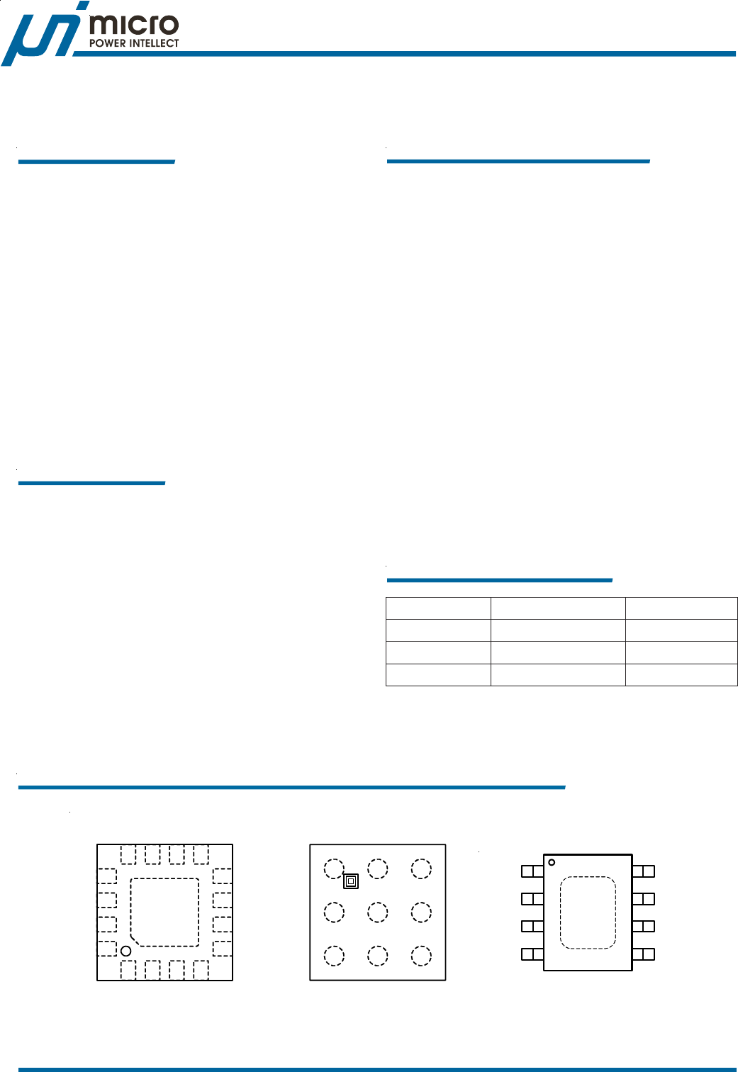
LX
FB
POK
PGNDNC
EN
AGND
GND
1
2
3
45
6
7
8
PSOP - 8
VIN
PGND
AGND
FB
VIN
NC
VCC
PGND
EN
PGND
LX
POK
PGND
NC
VIN
VIN
LX
LX
123
A
GND
WLCSP1.5x1.5-9B
GNDFB
NC LX LX
EN VIN VIN
B
C
1
2
3
4
8
7
6
5
12
11
10
9
13
15
15
16
WQFN3x3-16L
Note: uPI products are compatible with the current IPC/
JEDEC J-STD-020 requirement. They are halogen-free,
RoHS compliant and 100% matte tin (Sn) plating that are
suitable for use in SnPb or Pb-free soldering processes.
Pin Configuration
uP6305
2uPI Semiconductor Corp., http://www.upi-semi.com
Rev. P00, File Name: uP6305-DS-P0002
Preliminary
emaNniPnoitcnuFniP
DNGP .dnuorGrewoP .nrutersroticapactupnidnatuptuoehtottcennoC
BF .tupnIkcabdeeF hguorhttuptuorehctiwsehtsesnesBF.reifilpmarorreehtfotupnignitrevniehtsinipsihT
.krowtenredividrotsiserlanretxena
DNGA .dnuorGlangiS .nipsihtotstenenopmoclangisllamsllafonruterehttcennoC
CN .detcennoCyllanretnItoN
NE elbanEpihC .retrevnocehtnwodstuhswolcigoL.)hgiHevitcA(
CCV .ylppuSsaiB htiwretlifssapwolaivrewoptupniottcennoC.yrtiucriclanretniehtrofrewopseilppuS
.PAFB5036PurofNIVotdetcennocyllanretnisinipsihT.DNGAotgnilpuoced
NIV .tupnIylppuSrewoP lanretniehtsrewopdnaegatlovtuptuoehtottnerrucseilppustahtegatlovtupnI
.roticapaccimarecR7XroR5XFu01muminimahtiwegatlovtupniehtssapyB.tiucriclortnoc
XL .tuptuOsehctiwSlanretnI .rotcudnituptuoehtotsnipesehttcennoC
KOP )ylnODDQA5036Pu(noitacidnIKOrewoP ondnadnetratstfosretfaecnadepmihgihtessinipsihT.
.sruccotluaf
desopxE
daP
.dnuorGrewoP enalpdnuorgotsaivelpitlumhtiwBCPotderedlosllewebdluohsdapdesopxeehT
.ecnamrofreplamrehtlamitporof
Functional Pin Descriptio
n
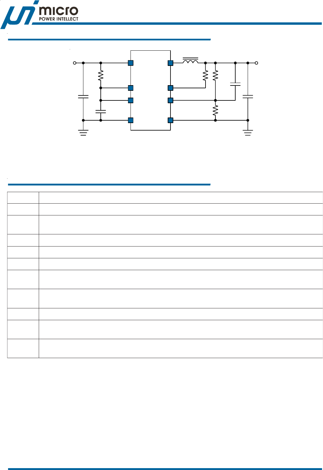
VIN LX
AGND
EN
PGND
VOUT
VIN
FB
VCC
R1
R2
uP6305AQDD
R3
C3
POK
Option
Typical Application Circuit
uP6305
3uPI Semiconductor Corp., http://www.upi-semi.com
Rev. P00, File Name: uP6305-DS-P0002
Preliminary
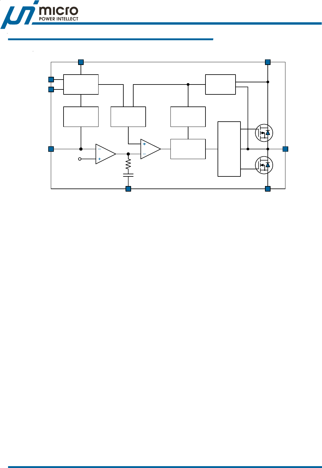
Functional Block Diagram
Control Logic Driver
Current
Sense
Current Limit
Detector
Over/Under
Voltage
Protection
Slope
Comp.
OSC &
Shutdown
Control
0.6V
VREF
VIN
LX
FB
EN
VCC
AGND PGND
POK
uP6305
4uPI Semiconductor Corp., http://www.upi-semi.com
Rev. P00, File Name: uP6305-DS-P0002
Preliminary
The uP6305 is a high efficiency synchronous-rectified buck
converter with internal power switches. Fixed 1.0MHz PWM
operation allows possible smallest output ripple and
external component size. With high conversion efficiency
and small package, the uP6305 is ideally suitable for
portable devices and USB/PCIE-based interface cards
where PCB area is especially concerned.
With internal low RDS(ON) switches, the uP6305 is capable
of delivering 2.0A output current over a wide input voltage
range from 2.5V to 5.5V. The output voltage is adjustable
from 0.6V to VIN by a voltage divider. Other features include
internal soft-start, chip enable, overvoltage, under-voltage,
over-temperature and over-current protections. The uP6305
is available in a space-saving WQFN3x3-16L,
WLCSP1.5x1.5-9B or PSOP-8L packages.
Input Supply Voltages, VIN & VCC
The uP6305 features seperate power supply and ground
pins for power stages and control circuit, isolating the
control circuit from noise associated with the power
MOSFET switching.
The VIN pins provide current to the power stage. The supply
voltage range is from 2.5V to 5.5V. The uP6305 draws
pulsed current with sharp edges from VIN each time the
upper switch turns on, resulting in voltage ripples and spikes
at supply input. A minimum 10uF ceramic capacitor with
shortest PCB trace is highly recommended for bypassing
the supply input.
The VCC pin provides currents for the internal control circuit.
A power on reset (POR) continuously monitors the input
supply voltage. The POR level is typically 2.3V at VCC rising.
Use low pass filter R3 and C3 as shown in the Typical
Application Circuit to filter the input noise associated with
the power switching.
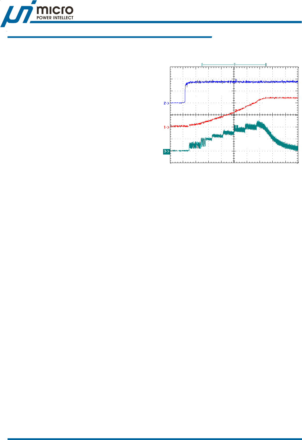
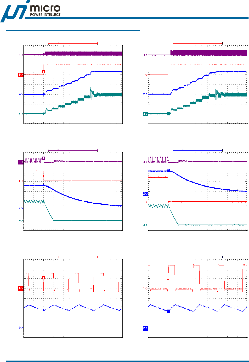
Chip Enable/Disable and Soft Start
The uP6305 features an EN pin for enable/disable control
of the output voltage. Pulling the EN pin lower than 0.4V
shuts down the uP6305 and reduces its quiescent current
lower than 1uA. In the shutdown mode, both upper and
lower switches are turned off.
Pulling EN pin higher than 1.5V enables the uP6305 and
initiates the softstart cycle once the VCC POR is granted.
The inductor current is limited to fractions of its rated value
during the softstart cycle. Figure 1 illustrates the softstart
behavior of the uP6305. The inductor current ramps up
stairwisely with 250mA increments and 60us duration each
step. Note that the output capacitor is large to illustrate
the whole softstart behavior. The output voltage may ramp
up to its target level in 2 or 3 steps in real applications
where output capacitor is about 22uF.
VOUT
(0.5V/Div)
ILX
(500mA/Div)
EN
(2V/Div)
Time (100us/Div)
Figure 1. Softstart of uP6305.
The uP6305 asserts end of soft start and set the current
limit to its normal level when the soft start duration expires.
After soft start end, the POK pin is set high impedance if
no fault occurs.
PWM Operation
The uP6305 adopts slope-compensated, current mode
PWM control capable of achieving 100% duty cycle. During
normal operation, the uP6305 operates at PWM mode to
regulate output voltage by transferring the power to the
output voltage cycle by cycle at a constant 1.0MHz
frequency. The uP6305 turns on the upper switch at each
rising edge of the internal oscillator allowing the inductor
current to ramp up linearly. The switch remains on until
either the current-limit is tripped or the PWM comparator
turns off the switch for regulating output voltage. The upper
switch current is sensed, slope compensated and
compared with the error amplifier output COMP to determine
the adequate duty cycle. The VOUT pin senses output
feedback voltage from an external resistive divider.
When the load current increases, it causes a slight
decrease in the feedback voltage relative to the 0.6V
reference, which in turn, causes the error amplifier output
voltage to increase until the average inductor current
matches the new load current.
Low Dropout Mode
The uP6305 increases duty cycle to maintain output voltage
within its regulation as the supply input drops gradually in
the battery-powered applications. The uP6305 operates with
100% duty cycle and enters low dropout mode as the supply
input approaches the output voltage. This maximizes the
battery life.
Functional Description

uP6305
5uPI Semiconductor Corp., http://www.upi-semi.com
Rev. P00, File Name: uP6305-DS-P0002
Preliminary
Output Voltage Setting and Feedback Network
The output voltage can be set from VREF to VIN by a voltage
divider as:
REFOUT V
1R
2R1R
V×
+
=
The internal VREF is 0.6V with 1.5% accuracy. In real
applications, a 22pF feedforward ceramic capacitor is
recommended in parallel with R2 for better transient
response.
Current Limit Function
The uP6305 continuously monitors the inductor current for
current limit by sensing the voltage drop across the upper
switch when it turns on. When the inductor current is higher
than current limit threshold (3.0A typical), the current limit
function activates and forces the upper switch turning off to
limit inductor current cycle by cycle. If the load continuously
demands more current than what uP6305 could provide,
uP6305 can not regulate the output voltage. Eventually
under voltage protection will be triggered and shuts down
the uP6305 if VOUT is too low.
Functional Description
Undervoltage Protection
Undervoltage Protection is triggered if the FB voltage is
lower than 0.15V and shuts down uP6305. The undervoltage
protection is latch-off type and can only be reset by POR
of VCC or toggling the EN pin.
Overvoltage Protection
Overvoltage protection (OVP) is triggered if the FB voltage
is higher than 0.8V and forces the uP6305 to continuous
PWM mode that allows the inductor current to be negative.
The voltage control loop will continuously turn on the lower
switch to sink charges from the output capacitor to lower
the output voltage. The lower switch turns off only the sinking
current is higher than it current limit level, typical 2.0A.
The uP6305 resumes normal operation if the OVP is
removed.
Over Temperature Protection (OTP)
The OTP is triggered and shuts down the uP6305 if the
junction temperature is higher than 150OC. The OTP is a
non-latch type protection. The uP6305 automatically
initiates another soft start cycle if the junction temperature
drops below 130OC.
uP6305
6uPI Semiconductor Corp., http://www.upi-semi.com
Rev. P00, File Name: uP6305-DS-P0002
Preliminary
retemaraPlobmySsnoitidnoCtseTniMpyTxaMstinU
tnerruCylppuS
egnaRegatloVylppuSV
NI
V
NI
V=
CC
5.2--5.5V
tuokcoLegatloVrednUV
OLVU
V
CC
V,gnisiR
NE
V=
CC
----5.2 V
V
CC
V,gnillaF
NE
V=
CC
2.2----
tnerruCtnecseiuQI
Q
V
BF
I,V8.0=
TUO
Am0=--4.3--Am
tnerruCnwodtuhSI
NDHS
V
NE
V0=--10.01Au
ecnerefeR
egatloVecnerefeRV
BF
I
TUO
Am0=95.006.016.0V
ycaruccAegatloVtuptuO ∆V
TUO
I
TUO
Am0=5.1---5.1+%
noitalugeReniLegatloVtuptuO ∆V
TUO
V
NI
V5.5otV5.2=--40.04.0V/%
noitalugeRdaoLegatloVtuptuO ∆V
TUO
I
TUO
A2~A0=--5.0--A/%
Supply Input Voltage, VIN, VCC(Note 1) --------------------------------------------------------------------------------------------- -0.3V to +6V
LX Pin Voltage
DC -------------------------------------------------------------------------------------------------------------------- -0.3V to +(VIN +0.3V)
<50ns -------------------------------------------------------------------------------------------------------------------- -5V to +(VIN +5V)
Other Pins --------------------------------------------------------------------------------------------------------------------------- -0.3V to (VCC + 0.3V
Storage Temperature Range ---------------------------------------------------------------------------------------------------- -65OC to +150OC
Junction Temperature ------------------------------------------------------------------------------------------------------------------------------------ 150OC
Lead Temperature (Soldering, 10 sec) ------------------------------------------------------------------------------------------------------------ 260OC
ESD Rating (Note 2)
HBM (Human Body Mode) --------------------------------------------------------------------------------------------------------------------- 2kV
MM (Machine Mode) ----------------------------------------------------------------------------------------------------------------------------- 200V
Operating Junction Temperature Range (Note 4) ------------------------------------------------------------------------ -40OC to +125OC
Operating Ambient Temperature Range -------------------------------------------------------------------------------------- -40OC to +85OC
Supply Input Voltage, VIN -------------------------------------------------------------------------------------------------------- +2.5V to +5.5V
(VCC = VIN = 5V, TA = 25OC, unless otherwise specified)
A
bsolute Maximum Ratin
g
Thermal Informatio
n
Recommended Operation Conditions
Electrical Characteristics
Package Thermal Resistance (Note 3)
WQFN3x3-16L θJA ------------------------------------------------------------------------------------------------------------------------- 68°C/W
WQFN3x3-16L θJC ----------------------------------------------------------------------------------------------------------------------- 6°C/W
WLCSP1.5x1.5-9B θJA ----------------------------------------------------------------------------------------------------------------- 160°C/W
PSOP-8L θJA ------------------------------------------------------------------------------------------------------------------------- 50°C/W
PSOP-8L θJC ----------------------------------------------------------------------------------------------------------------------- 5°C/W
Power Dissipation, PD @ TA = 25°C
DFN3x3 -16 ----------------------------------------------------------------------------------------------------------------------------------------- 1.47W
WLCSP1.5x1.5-9B ------------------------------------------------------------------------------------------------------------------------------ 0.625W
PSOP-8L ----------------------------------------------------------------------------------------------------------------------------------------- 2.0W
uP6305
7uPI Semiconductor Corp., http://www.upi-semi.com
Rev. P00, File Name: uP6305-DS-P0002
Preliminary
Note 1. Stresses listed as the above “Absolute Maximum Ratings” may cause permanent damage to the device.
These are for stress ratings. Functional operation of the device at these or any other conditions beyond those
indicated in the operational sections of the specifications is not implied. Exposure to absolute maximum
rating conditions for extended periods may remain possibility to affect device reliability.
Note 2. Devices are ESD sensitive. Handling precaution recommended.
Note 3. θJA is measured in the natural convection at TA = 25°C on a low effective thermal conductivity test board of
JEDEC 51-3 thermal measurement standard.
Note 4. The device is not guaranteed to function outside its operating conditions.
retemaraPlobmySsnoitidnoCtseTniMpyTxaMstinU
rotallicsO
egnaRycneuqerFgnihctiwSf
CSO
8.00.12.1zHM
elcyCytuDmumixaMCDV
NI
V=
TUO
V;
BF
V55.0=001----%
sehctiwSrewoP
R
)NO(SD
hctiwSreppUfoR
TEF_P
V
NI
I,V6.3=
XL
Am001=--58--mΩ
R
)NO(SD
hctiwSrewoLfoR
TEF_N
V
NI
I,V6.3=
XL
Am001-=--57--mΩ
tupnIcigoL
dlohserhTwoLcigoLNEV
LI
V
NI
nwodtuhS,V5.5otV5.2=----4.0V
dlohserhThgiHcigoLNEV
HI
V
NI
elbanE,V5.5otV5.2=5.1----V
tuptuOKOrewoP
tnerruCegakaeLhgiHcigoLI
KOP
V
KOP
V=
CC
V5=----1Au
egatloVwoLcigoLV
KOP
I
KOP
Am1=----2.0V
noitcetorP
noitcetorPegatloVrednUBF ∆
PVU_BF
gnillaFBF--52--V%
FER
noitcetorPegatloVrevOBF ∆
PVO_BF
gnisiRBF----031V%
FER
erutarepmeTnowdtuhSlamrehTT
NDHS
ngisedyb--051--
O
C
siseretsyHnwodtuhSlamrehT ∆T
NDHS
ngisedyb--02--
O
C
Electrical Characteristics
uP6305
8uPI Semiconductor Corp., http://www.upi-semi.com
Rev. P00, File Name: uP6305-DS-P0002
Preliminary
LX
(2V/Div)
ILX
(500mA/Div)
LX
(2V/Div)
ILX
(500mA/Div)
EN
(2V/Div)
IOUT
(1A/Div)
VOUT
(500mV/Div)
LX (10V/Div)
EN
(5V/Div)
IOUT
(1A/Div) VOUT
(500mV/Div)
LX (10V/Div)
EN
(5V/Div)
IOUT
(1A/Div)
VOUT
(500mV/Div)
LX (10V/Div)
EN
(5V/Div)
IOUT
(1A/Div)
VOUT
(500mV/Div)
LX (10V/Div)
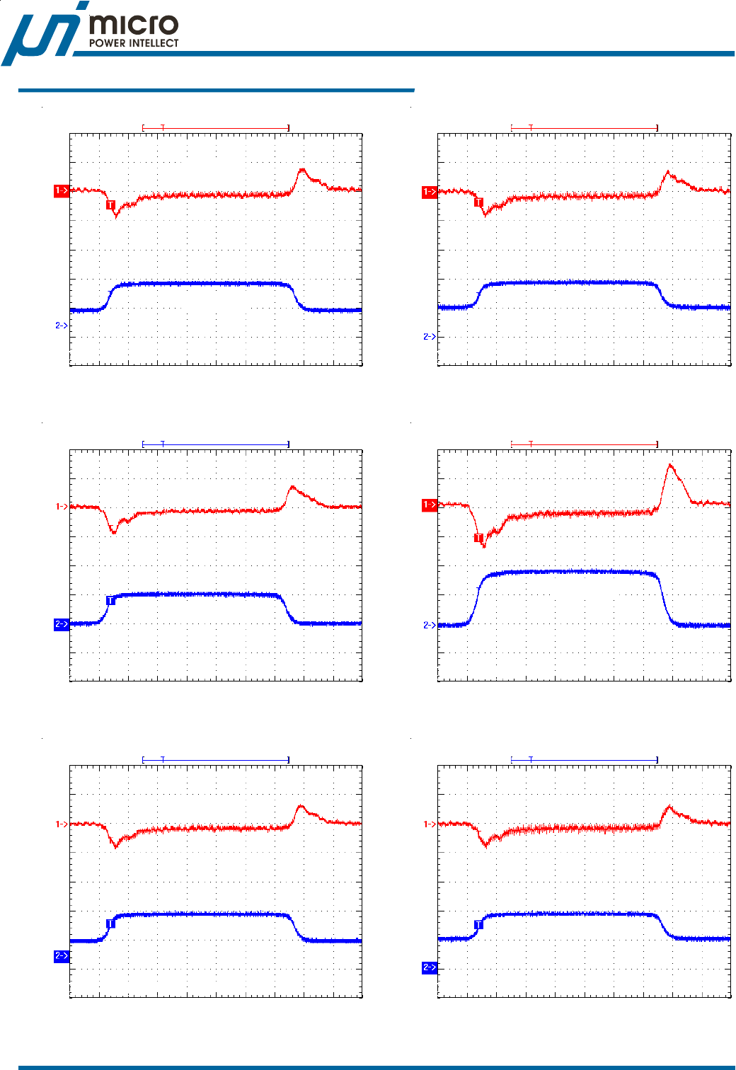
Typical Operation Characteristics
Switching
400ns/Div
VIN = 3.3V, VOUT = 1.2V, IOUT = 1A
Switching
400ns/Div
VIN = 5V, VOUT = 1.2V, IOUT = 1A
Turn On Waveforms
100us/Div
VIN = 3.3V, VOUT = 1.2V, RLOAD = 0.6Ω
Turn On Waveforms
100us/Div
VIN = 5V, VOUT = 1.2V, RLOAD = 0.6Ω
Turn Off Waveforms
4us/Div
VIN = 3.3V, VOUT = 1.2V, RLOAD = 0.6Ω
Turn Off Waveforms
4us/Div
VIN = 5V, VOUT = 1.2V, RLOAD = 0.6Ω
uP6305
9uPI Semiconductor Corp., http://www.upi-semi.com
Rev. P00, File Name: uP6305-DS-P0002
Preliminary
VOUT
(50mV/Div)
IOUT (1A/Div)
VOUT
(50mV/Div)
IOUT (1A/Div)
VOUT
(10mV/Div)
IOUT (1A/Div)
VOUT
(10mV/Div)
IOUT (1A/Div)
VOUT
(10mV/Div)
IOUT
(500mA/Div)
VOUT
(10mV/Div)
IOUT
(500mA/Div)
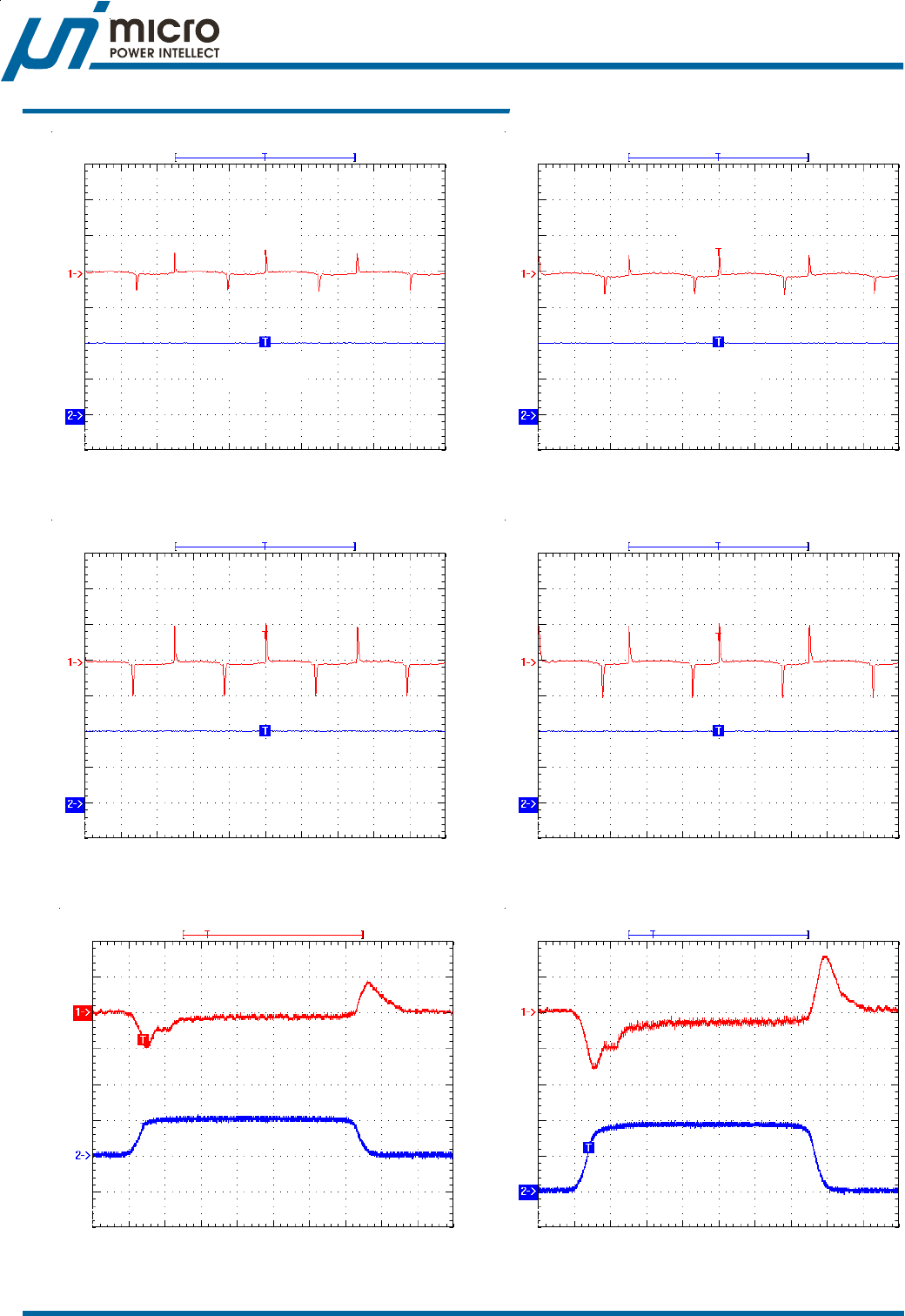
Typical Operation Characteristics
Load Transient Response
20us/Div
IOUT = 0A to 1A, VIN = 3.3V, VOUT = 1.2V
Steady State Waveforms
400ns/Div
VIN = 3.3V, VOUT = 1.2V, IOUT = 2A
Steady State Waveforms
400ns/Div
VIN = 5V, VOUT = 1.2V, IOUT = 2A
Load Transient Response
20us/Div
IOUT = 0A to 2A, VIN = 3.3V, VOUT = 1.2V
Steady State Waveforms
400ns/Div
VIN = 3.3V, VOUT = 1.2V, IOUT = 1A
Steady State Waveforms
400ns/Div
VIN = 5V, VOUT = 1.2V, IOUT = 1A
uP6305
10uPI Semiconductor Corp., http://www.upi-semi.com
Rev. P00, File Name: uP6305-DS-P0002
Preliminary
VOUT
(50mV/Div)
IOUT (1A/Div)
VOUT
(50mV/Div)
IOUT (1A/Div)
VOUT
(50mV/Div)
IOUT (1A/Div)
VOUT
(50mV/Div)
IOUT (1A/Div)
VOUT
(50mV/Div)
IOUT (1A/Div)
VOUT
(50mV/Div)
IOUT (1A/Div)
Load Transient Response
20us/Div
IOUT = 0.5A to 1.5A, VIN = 3.3V, VOUT = 1.2V
Load Transient Response
20us/Div
IOUT = 1A to 2A, VIN = 3.3V, VOUT = 1.2V
Typical Operation Characteristics
Load Transient Response
20us/Div
IOUT = 0A to 1A, VIN = 5V, VOUT = 1.2V
Load Transient Response
20us/Div
IOUT = 0A to 2A, VIN = 5V, VOUT = 1.2V
Load Transient Response
20us/Div
IOUT = 0.5 to 1.5A, VIN = 5V, VOUT = 1.2V
Load Transient Response
20us/Div
IOUT = 1A to 2A, VIN = 5V, VOUT = 1.2V
uP6305
11uPI Semiconductor Corp., http://www.upi-semi.com
Rev. P00, File Name: uP6305-DS-P0002
Preliminary
0.580
0.585
0.590
0.595
0.600
0.605
0.610
0.615
0.620
2.5 3.0 3.5 4.0 4.5 5.0 5.5
0.8
0.9
1.0
1.1
1.2
1.3
2.5 3.0 3.5 4.0 4.5 5.0 5.5
0
1
2
3
4
5
2.5 3.0 3.5 4.0 4.5 5.0 5.5
0.8
1.0
1.2
1.4
1.6
1.8
2.5 3.0 3.5 4.0 4.5 5.0 5.5
Enable
Disable
10
20
30
40
50
60
70
80
90
100
1 10 100 1000 10000
10
20
30
40
50
60
70
80
90
100
1 10 100 1000 10000
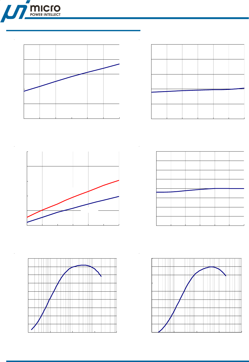
Typical Operation Characteristics
FREQ vs. VIN
Input Voltage (V)
FREQ (MHz)
Quiescent Current vs. VIN
Input Voltage (V)
Quiescent Current (mA)
Enable/Disable Threshold Voltage vs. VIN
Input Voltage (V)
Enable/Disable Threshold Voltage (V)
FB vs. VIN
Input Voltage (V)
FB (V)
Efficiency vs. Output Current
Output Current (mA)
VIN = 3.3V, VOUT = 1.2V, L = 3.3uH, CIN = COUT = 22uF
Efficiency (%)
Efficiency vs. Output Current
Output Current (mA)
VIN = 5V, VOUT = 1.2V, L = 3.3uH, CIN = COUT = 22uF
Efficiency (%)
uP6305
12uPI Semiconductor Corp., http://www.upi-semi.com
Rev. P00, File Name: uP6305-DS-P0002
Preliminary
0
1
2
3
4
5
6
-40 -20 0 20 40 60 80 100 120 140
1.15
1.16
1.17
1.18
1.19
1.20
1.21
1.22
-40 -20 0 20 40 60 80 100 120 140
600
700
800
900
1000
1100
1200
-40 -20 0 20 40 60 80 100 120 140
1.4
1.6
1.8
2.0
2.2
2.4
2.6
2.8
3.0
3.2
2.5 3.0 3.5 4.0 4.5 5.0 5.5
OCP
Input Voltage (V)
VIN = 3.3V, VOUT = 1.2V, CIN = COUT = 22uF
Output Current (A)
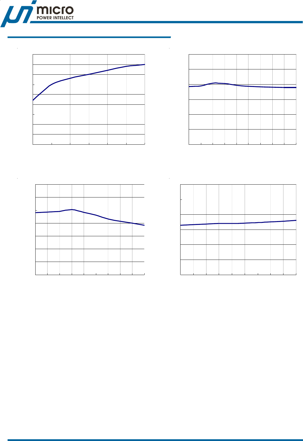
Typical Operation Characteristics
VOUT vs. Temperature
Temperature (OC)
VIN = 5V, VOUT = 1.2V, L = 3.3uH, CIN = COUT = 22uF, No Load
Output Voltage (V)
Input Current vs. Temperature
Temperature (OC)
VIN = 5V, VOUT = 1.2V, L = 3.3uH, CIN = COUT = 22uF, No Load
Input Current (mA)
FREQ vs. Temperature
Temperature (OC)
VIN = 5V, VOUT = 1.2V, L = 3.3uH, CIN = COUT = 22uF, No Load
FREQ (kHz)
uP6305
13uPI Semiconductor Corp., http://www.upi-semi.com
Rev. P00, File Name: uP6305-DS-P0002
Preliminary
capacitance over temperature, they also become resistive
at high frequencies. This reduces their ability to filter out
high frequency noise.
The capacitor with low ESR (equivalent series resistance)
provides the small drop voltage to stabilize the input voltage
during the transient loading. For input capacitor selection,
the ceramic capacitors larger than 1uF is recommend. The
capacitor must conform to the RMS current requirement.
The maximum RMS ripple current is calculated as:
IN
OUTINOUT
)MAX(OUT)RMS(IN V
)VV(V
II
−×
×=
This formula has a maximum at VIN = 2xVOUT, where IIN(RMS)
= IOUT(MAX)/2. This simple worst-case condition is commonly
used for design because even significant deviations do not
offer much relief. Note that the capacitor manufacturer’s
ripple current ratings are often based on 2000 hours of life.
This makes it advisable to further derate the capacitor, or
choose a capacitor rated at a higher temperature than
required. Always consult the manufacturer if there is any
question.
Output Capacitor Selection
The uP6305 is specifically design to operate with minimum
10uF X5R or X7R ceramic capacitor. The value can be
increased to improve load/line transient performance. Y5V
dielectrics, aside from losing most of their capacitance over
temperature, they also become resistive at high
frequencies. This reduces their ability to filter out high
frequency noise.
The ESR of the output capacitor determines the output
ripple voltage and the initial voltage drop following a high
slew rate load transient edge. The output ripple voltage
can be calculated as:
)
Cf8
1
ESR(IV
OUTOSC
COUT ××
+×∆=∆
where fOSC = operating frequency, COUT = output capacitance
and ∆IC = ∆IL = ripple current in the inductor.
The ceramic capacitor with low ESR value provides the low
output ripple and low size profile. Connect a 22uF ceramic
capacitor at output terminal for good performance and place
the input and output capacitors as close as possible to the
device.
Using Ceramic Capacitors
Higher value, lower cost ceramic capacitors are now
available in smaller case sizes. Their high ripple current,
high voltage rating and low ESR make them ideal for
switching regulator applications. Because the uP6305
Output Inductor Selection
Output inductor selection is usually based the
considerations of inductance, rated current value, size
requirements and DC resistance (DCR).
The inductance is chosen based on the desired ripple
current. Large value inductors result in lower ripple currents
and small value inductors result in higher ripple currents.
Higher VIN or VOUT also increases the ripple current as shown
in the equation below. A reasonable starting point for setting
ripple current is ∆IL = 600mA (30% of 2A).
)
V
V
1(V
Lf
1
I
IN
OUT
OUT
OUTOSC
L−××
×
=∆
For most applications, the value of the inductor will fall in
the range of 1uH to 10uH.
Maximum current ratings of the inductor are generally
specified in two methods: permissible DC current and
saturation current. Permissible DC current is the allowable
DC current that causes 40OC temperature raise. The
saturation current is the allowable current that causes 10%
inductance loss. Make sure that the inductor will not
saturate over the operation conditions including temperature
range, input voltage range, and maximum output current. If
possible, choose an inductor with rated current higher than
3A so that it will not saturate even under current limit
condition.
The size requirements refer to the area and height
requirement for a particular design. For better efficiency,
choose a low DC resistance inductor. DCR is usually
inversely proportional to size.
Different core materials and shapes will change the size/
current and price/current relationship of an inductor. Toroid
or shielded pot cores in ferrite or permalloy materials are
small and don’t radiate much energy, but generally cost
more than powdered iron core inductors with similar electrical
characteristics. The choice of which style inductor to use
often depends on the price vs. size requirements and any
radiated field/EMI requirements.
Input Capacitor Selection
The uP6305 draws pulsed current with sharp edges from
the input capacitor resulting in ripple and noise at the input
supply voltage. A minimum 10uF X5R or X7R ceramic
capacitor is highly recommended to filter the pulsed current.
The input capacitor should be placed as near the device as
possible to avoid the stray inductance along the connection
trace. Y5V dielectrics, aside from losing most of their
A
pplication Information

uP6305
14uPI Semiconductor Corp., http://www.upi-semi.com
Rev. P00, File Name: uP6305-DS-P0002
Preliminary
control loop does not depend on the output capacitor’s ESR
for stable operation, ceramic capacitors can be used to
achieve very low output ripple and small circuit size.
However, care must be taken when these capacitors are
used at the input and the output. When a ceramic capacitor
is used at the input and the power is supplied by a wall
adapter through long wires, a load step at the output can
induce ringing at the input, VIN. At best, this ringing can
couple to the output and be mistaken as loop instability. At
worst, a sudden inrush of current through the long wires
can potentially cause a voltage spike at VIN, large enough
to damage the part.
When choosing the input and output ceramic capacitors,
choose the X5R or X7R dielectric formulations. These
dielectrics have the best temperature and voltage
characteristics of all the ceramics for a given value and
size.
Thermal Considerations
In most applications the uP6305 does not dissipate much
heat due to its high efficiency. However, overtemperature
protection is implemented in case of applications where
the uP6305 is operating at high ambient temperature. If
the junction temperature reaches approximately 150OC, the
OTP turns both power switches and let the LX node become
high impedance. The uP6305 restores to normal operation
if the junction temperature drops to 130OC.
It is helpful to analysis the power dissipation of uP6305 for
avoding the uP6305 from exceeding the maximum junction
temperature. In typical applications, the conduction loss
dominates the total power loss in uP6305. The conduction
loss has its maximum at high duty-ratio, low input voltage,
and high ambient temperatures.
Consider the uP6305 in dropout mode operation at an input
voltage of 2.5V, a load current of 1.5A and an ambient
temperature of 75OC. The on-resistance of the upper swith
is about 100mΩ at this condition. Therefore the power
dissipation PD is:
mW225RIP )ON(DS
2
OUTD =×=
This results in 50 x 0.225 = 12OC temperature raise at
junction. The juction temperature is 82OC and is lower
than it maximum rating 125OC.
Checking Transient Response
The regulator loop response can be checked by looking at
the load transient response. Switching regulators take
several cycles to respond to a step in load current. When
a load step occurs, VOUT immediately shifts by an amount
equal to (∆IOUT x ESR), where ESR is the effective series
resistance of COUT. ∆IOUT also begins to discharge or charge
A
pplication Information
COUT, which generates a feedback error signal. The regulator
loop then acts to return VOUT to its steady state value.
During this recovery time VOUT can be monitored for
overshoot or ringing that would indicate a stability problem.
PCB Layout Considerations
High switching frequencies and relatively large peak
currents make the PCB layout a very important part of
switching mode power supply design. Good design
minimizes excessive EMI on the feedback paths and voltage
gradients in the ground plane, both of which can result in
instability or regulation errors. Follow the PCB layout
guidelines for optimal performance of uP6305.
1. For the main current paths, keep their traces short,
direct and wide.
2. Put the input/output capacitors as close as possible to
the device pins.
3. LX node is with high frequency voltage swing and should
be kept small area. Keep analog components away from
LX node to prevent stray capacitive noise pick-up.
4. Connect feedback network behind the output capacitors.
Place the feedback components near the uP6305 and
keep the loop area small. .
5. A ground plane is preferred, but if not available, keep
the signal and power grounds sepregated with small
signal components returning to the GND pin at one point.
They should not share the high current path of CIN or
COUT.
6. Flood all unused areas on all layers with copper.
Flooding with copper will reduce the temperature rise
of power components. These copper areas should be
connected to VIN or GND.
uP6305
15uPI Semiconductor Corp., http://www.upi-semi.com
Rev. P00, File Name: uP6305-DS-P0002
Preliminary
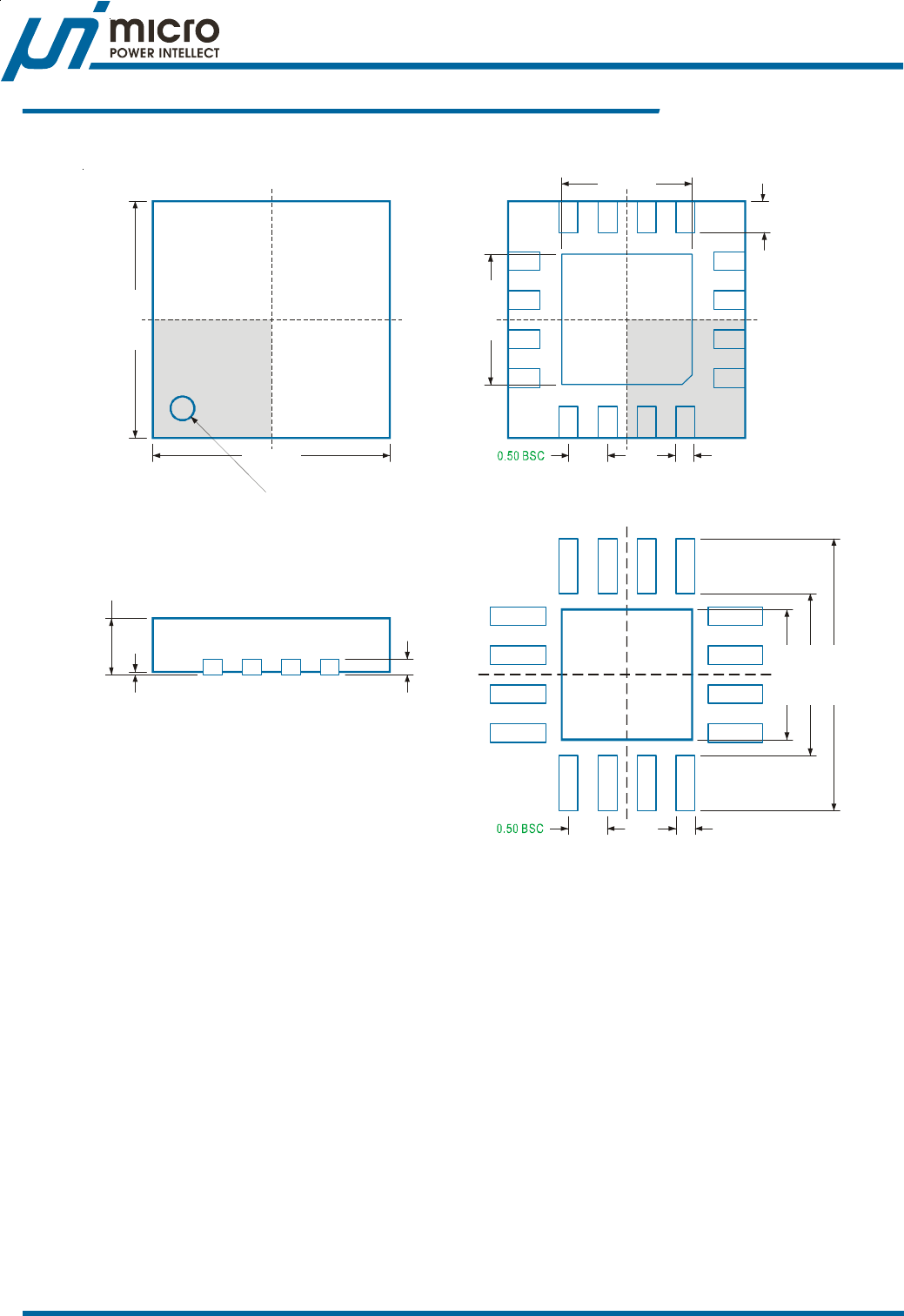
Package Informatio
n
Note
1.Package Outline Unit Description:
BSC: Basic. Represents theoretical exact dimension or dimension target
MIN: Minimum dimension specified.
MAX: Maximum dimension specified.
REF: Reference. Represents dimension for reference use only. This value is not a device specification.
TYP. Typical. Provided as a general value. This value is not a device specification.
2.Dimensions in Millimeters.
3.Drawing not to scale.
4.These dimensions no not include mold flash or protrusions. Mold flash or protrusions shell not exceed 0.15mm.
WQFN3x3-16L Package
2.90 - 3.10
Pin 1 mark Bottom View - Exposed Pad
1.45 -1.80
1.45-1.80
0.18 - 0.30
1.45 - 1.80 0.35 - 0.45
2.05 - 2.15
3.45 - 3.55
2.90 - 3.10
0.00 - 0.05
0.80 MAX
0.20 BSC
Recommended Solder Pad Pitch and Dimensions
0.18 - 0.30
uP6305
16uPI Semiconductor Corp., http://www.upi-semi.com
Rev. P00, File Name: uP6305-DS-P0002
Preliminary
0.21 - 0.27
Recommended Solder Pad Layout
0.50 BSC
0.50 - 0.70
1.40 - 1.50
1.40 - 1.50
0.05 - 0.13 0.30 - 0.34R
0.50 BSC
0.50 BSC
0.25 - 0.28R
0.50 BSC
CB A
1
2
3
BUMP A1 Center
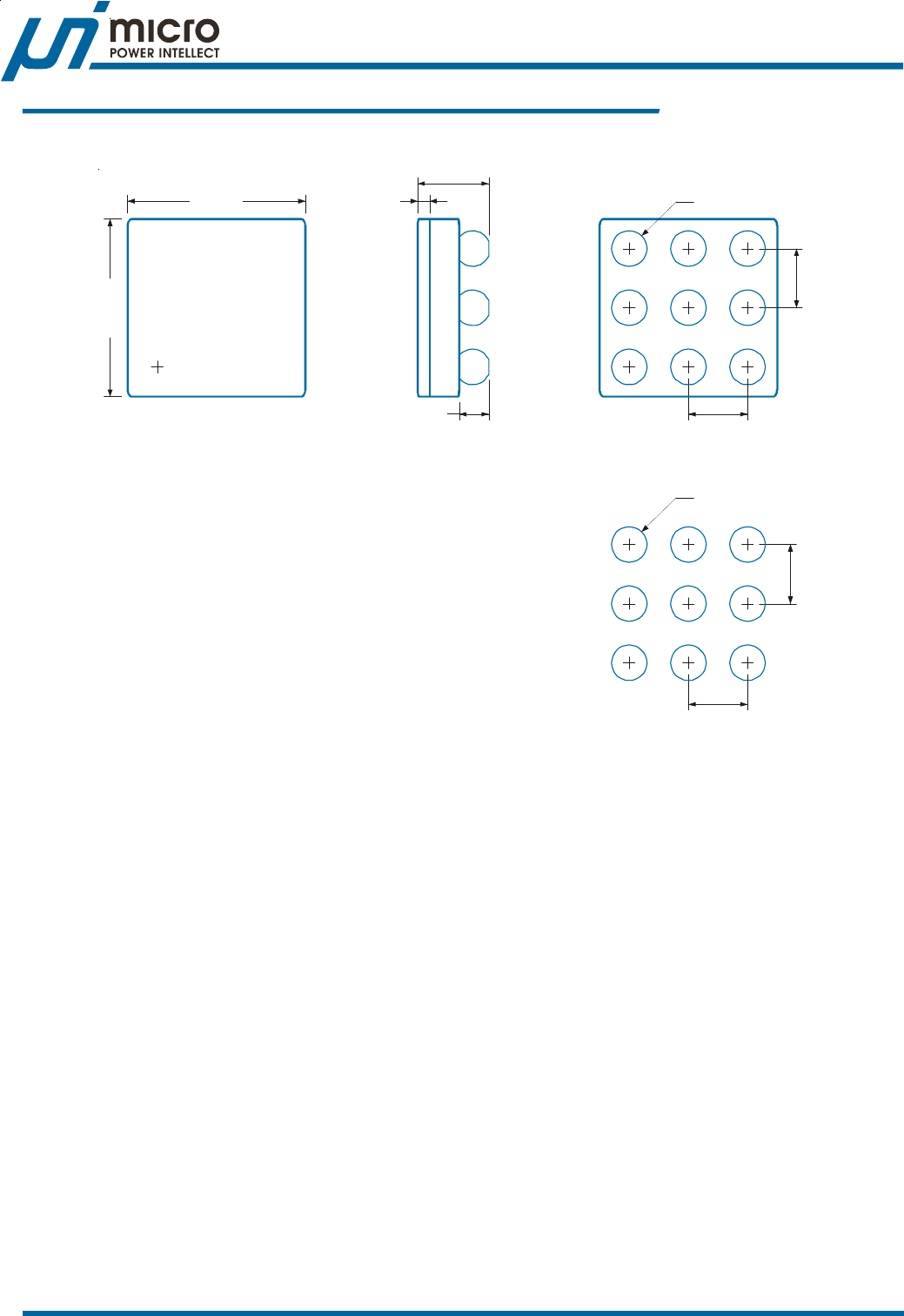
Package Informatio
n
Note
1.Package Outline Unit Description:
BSC: Basic. Represents theoretical exact dimension or dimension target
MIN: Minimum dimension specified.
MAX: Maximum dimension specified.
REF: Reference. Represents dimension for reference use only. This value is not a device specification.
TYP. Typical. Provided as a general value. This value is not a device specification.
2.Dimensions in Millimeters.
3.Drawing not to scale.
4.These dimensions no not include mold flash or protrusions. Mold flash or protrusions shell not exceed 0.15mm.
WLCSP1.5x1.5-9B Package
uP6305
17uPI Semiconductor Corp., http://www.upi-semi.com
Rev. P00, File Name: uP6305-DS-P0002
Preliminary
0.32 - 0.52
4.80 - 5.00
5.80 - 6.20
0.18 - 0.25
0.40 - 0.90
7.00 10
±
0.
1.50 10
±
0.
0.70 10
±
0. 1.27 10
±
0.
1.27 BSC
3.80 - 4.00
5.50 10
±
0.
4.00 10
±0.
Recommended Solder Pad Layout
1.80 - 2.30
1.80 - 2.30
2.20
±
100.
2.20 10
±
0.
3.81 BSC
0.05 - 0.25
1.75 MAX
1.45 - 1.60
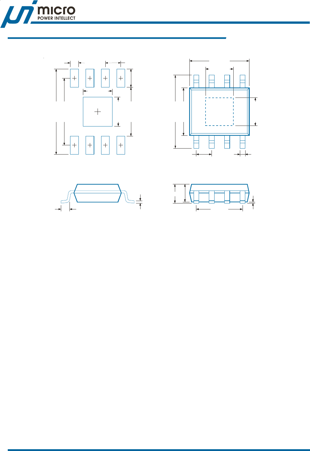
Package Informatio
n
PSOP-8L Package
Note
1.Package Outline Unit Description:
BSC: Basic. Represents theoretical exact dimension or dimension target
MIN: Minimum dimension specified.
MAX: Maximum dimension specified.
REF: Reference. Represents dimension for reference use only. This value is not a device specification.
TYP. Typical. Provided as a general value. This value is not a device specification.
2.Dimensions in Millimeters.
3.Drawing not to scale.
4.These dimensions no not include mold flash or protrusions. Mold flash or protrusions shell not exceed 0.15mm.