Verilog HDL: A Guide To Digital Design And Synthesis, 2nd Ed. Hdl Synthesis Second Edition Samir Palnitkar
User Manual:
Open the PDF directly: View PDF ![]() .
.
Page Count: 442 [warning: Documents this large are best viewed by clicking the View PDF Link!]

Verilog HDL: A Guide to Digital Design and Synthesis, Second Edition
By Samir Palnitkar
Publisher: Prentice Hall PTR
Pub Date: February 21, 2003
ISBN: 0-13-044911-3
Pages: 496
Written for both experienced and new users, this book gives you broad coverage of
Verilog HDL. The book stresses the practical design and verification perspective
ofVerilog rather than emphasizing only the language aspects. The informationpresented
is fully compliant with the IEEE 1364-2001 Verilog HDL standard.
• Describes state-of-the-art verification methodologies
• Provides full coverage of gate, dataflow (RTL), behavioral and switch modeling
• Introduces you to the Programming Language Interface (PLI)
• Describes logic synthesis methodologies
• Explains timing and delay simulation
• Discusses user-defined primitives
• Offers many practical modeling tips
Includes over 300 illustrations, examples, and exercises, and a Verilog resource
list.Learning objectives and summaries are provided for each chapter.

2
Verilog HDL: A Guide to Digital Design and Synthesis, Second Edition
By Samir Palnitkar
Publisher: Prentice Hall PTR
Pub Date: February 21, 2003
ISBN: 0-13-044911-3
Pages: 496
3
Copyright
2003 Sun Microsystems, Inc. 2550 Garcia Avenue, Mountain View, California 94043-
1100 U.S.A.
All rights reserved. This product or document is protected by copyright and distributed
under licenses restricting its use, copying, distribution and decompilation. No part of this
product or document may be reproduced in any form by any means without prior written
authorization of Sun and its licensors, if any.
Portions of this product may be derived from the UNIX system and from the Berkeley 4.3
BSD system, licensed from the University of California. Third-party software, including
font technology in this product, is protected by copyright and licensed from Sun's
Suppliers.
RESTRICTED RIGHTS LEGEND: Use, duplication, or disclosure by the government is
subject to restrictions as set forth in subparagraph (c)(1)(ii) of the Rights in Technical
Data and Computer Software clause at DFARS 252.227-7013 and FAR 52.227-19.
The product described in this manual may be protected by one or more U.S. patents,
foreign patents, or pending applications.
TRADEMARKS
Sun, Sun Microsystems, the Sun logo, and Solaris are trademarks or registered
trademarks of Sun Microsystems, Inc. in the United States and may be protected as
trademarks in other countries. UNIX is a registered trademark in the United States and
other countries, exclusively licensed through X/Open Company, Ltd. OPEN LOOK is a
registered trademark of Novell, Inc. PostScript and Display PostScript are trademarks of
Adobe Systems, Inc. Verilog is a registered trademark of Cadence Design Systems, Inc.
Verilog-XL is a trademark of Cadence Design Systems, Inc. VCS is a trademark of
Viewlogic Systems, Inc. Magellan is a registered trademark of Systems Science, Inc.
VirSim is a trademark of Simulation Technologies, Inc. Signalscan is a trademark of
Design Acceleration, Inc. All other product, service, or company names mentioned herein
are claimed as trademarks and trade names by their respective companies.

4
All SPARC trademarks, including the SCD Compliant Logo, are trademarks or registered
trademarks of SPARC International, Inc. in the United States and may be protected as
trademarks in other countries. SPARCcenter, SPARCcluster, SPARCompiler,
SPARCdesign, SPARC811, SPARCengine, SPARCprinter, SPARCserver,
SPARCstation, SPARCstorage, SPARCworks, microSPARC, microSPARC-II, and
UltraSPARC are licensed exclusively to Sun Microsystems, Inc. Products bearing
SPARC trademarks are based upon an architecture developed by Sun Microsystems, Inc.
The OPEN LOOK and Sun Graphical User Interfaces were developed by Sun
Microsystems, Inc. for its users and licensees. Sun acknowledges the pioneering efforts
of Xerox in researching and developing the concept of visual or graphical user interfaces
for the computer industry. Sun holds a non-exclusive license from Xerox to the Xerox
Graphical User Interface, which license also covers Sun's licensees who implement
OPEN LOOK GUI's and otherwise comply with Sun's written license agreements.
X Window System is a trademark of X Consortium, Inc.
The publisher offers discounts on this book when ordered in bulk quantities. For more
information, contact: Corporate Sales Department, Prentice Hall PTR, One Lake Street,
Upper Saddle River, NJ 07458. Phone: 800-382-3419; FAX: 201- 236-7141. E-mail:
corpsales@prenhall.com.
Production supervisor: Wil Mara
Cover designer: Nina Scuderi
Cover design director: Jerry Votta
Manufacturing manager: Alexis R. Heydt-Long
Acquisitions editor: Gregory G. Doench
Printed in the United States of America
10 9 8 7 6 5 4 3 2 1
SunSoft Press
A Prentice Hall Title

5
Dedication
To Anu, Aditya, and Sahil,
Thank you for everything.
To our families,
Thank you for your constant encouragement and support.
― Samir
6
About the Author
Samir Palnitkar is currently the President of Jambo Systems, Inc., a leading ASIC design
and verification services company which specializes in high-end designs for
microprocessor, networking, and communications applications. Mr. Palnitkar is a serial
entrepreneur. He was the founder of Integrated Intellectual Property, Inc., an ASIC
company that was acquired by Lattice Semiconductor, Inc. Later he founded Obongo,
Inc., an e-commerce software firm that was acquired by AOL Time Warner, Inc.
Mr. Palnitkar holds a Bachelor of Technology in Electrical Engineering from Indian
Institute of Technology, Kanpur, a Master's in Electrical Engineering from University of
Washington, Seattle, and an MBA degree from San Jose State University, San Jose, CA.
Mr. Palnitkar is a recognized authority on Verilog HDL, modeling, verification, logic
synthesis, and EDA-based methodologies in digital design. He has worked extensively
with design and verification on various successful microprocessor, ASIC, and system
projects. He was the lead developer of the Verilog framework for the shared memory,
cache coherent, multiprocessor architecture, popularly known as the UltraSPARCTM
Port Architecture, defined for Sun's next generation UltraSPARC-based desktop systems.
Besides the UltraSPARC CPU, he has worked on a number of diverse design and
verification projects at leading companies including Cisco, Philips, Mitsubishi, Motorola,
National, Advanced Micro Devices, and Standard Microsystems.
Mr. Palnitkar was also a leading member of the group that first experimented with cycle-
based simulation technology on joint projects with simulator companies. He has
extensive experience with a variety of EDA tools such as Verilog-NC, Synopsys VCS,
Specman, Vera, System Verilog, Synopsys, SystemC, Verplex, and Design Data
Management Systems.
Mr. Palnitkar is the author of three US patents, one for a novel method to analyze finite
state machines, a second for work on cycle-based simulation technology and a
third(pending approval) for a unique e-commerce tool. He has also published several
technical papers. In his spare time, Mr. Palnitkar likes to play cricket, read books, and
travel the world.
7
Foreword
From a modest beginning in early 1984 at Gateway Design Automation, the Verilog
hardware description language has become an industry standard as a result of extensive
use in the design of integrated circuit chips and digital systems. Verilog came into being
as a proprietary language supported by a simulation environment that was the first to
support mixed-level design representations comprising switches, gates, RTL, and higher
levels of abstractions of digital circuits. The simulation environment provided a powerful
and uniform method to express digital designs as well as tests that were meant to verify
such designs.
There were three key factors that drove the acceptance and dominance of Verilog in the
marketplace. First, the introduction of the Programming Language Interface (PLI)
permitted users of Verilog to literally extend and customize the simulation environment.
Since then, users have exploited the PLI and their success at adapting Verilog to their
environment has been a real winner for Verilog. The second key factor which drove
Verilog's dominance came from Gateways paying close attention to the needs of the
ASIC foundries and enhancing Verilog in close partnership with Motorola, National, and
UTMC in the 1987-1989 time-frame. The realization that the vast majority of logic
simulation was being done by designers of ASIC chips drove this effort. With ASIC
foundries blessing the use of Verilog and even adopting it as their internal sign-off
simulator, the industry acceptance of Verilog was driven even further. The third and final
key factor behind the success of Verilog was the introduction of Verilog-based synthesis
technology by Synopsys in 1987. Gateway licensed its proprietary Verilog language to
Synopsys for this purpose. The combination of the simulation and synthesis technologies
served to make Verilog the language of choice for the hardware designers.
The arrival of the VHDL (VHSIC Hardware Description Language), along with the
powerful alignment of the remaining EDA vendors driving VHDL as an IEEE standard,
led to the placement of Verilog in the public domain. Verilog was inducted as the IEEE
1364 standard in 1995. Since 1995, many enhancements were made to Verilog HDL
based on requests from Verilog users. These changes were incorporated into the latest
IEEE 1364-2001 Verilog standard. Today, Verilog has become the language of choice for
digital design and is the basis for synthesis, verification, and place and route
technologies.
Samir's book is an excellent guide to the user of the Verilog language. Not only does it
explain the language constructs with a rich variety of examples, it also goes into details o
f
the usage of the PLI and the application of synthesis technology. The topics in the book
are arranged logically and flow very smoothly. This book is written from a very practical
design perspective rather than with a focus simply on the syntax aspects of the language.
This second edition of Samir's book is unique in two ways. Firstly, it incorporates all

8
enhancements described in IEEE 1364-2001 standard. This ensures that the readers of the
book are working with the latest information on Verilog. Secondly, a new chapter has
been added on advanced verification techniques that are now an integral part of Verilog-
based methodologies. Knowledge of these techniques is critical to Verilog users who
design and verify multi-million gate systems.
I can still remember the challenges of teaching Verilog and its associated design and
verification methodologies to users. By using Samir's book, beginning users of Verilog
will become productive sooner, and experienced Verilog users will get the latest in a
convenient reference book that can refresh their understanding of Verilog. This book is a
must for any Verilog user.
Prabhu Goel
Former President of Gateway Design Automation
9
Preface
During my earliest experience with Verilog HDL, I was looking for a book that could
give me a "jump start" on using Verilog HDL. I wanted to learn basic digital design
paradigms and the necessary Verilog HDL constructs that would help me build small
digital circuits, using Verilog and run simulations. After I had gained some experience
with building basic Verilog models, I wanted to learn to use Verilog HDL to build larger
designs. At that time, I was searching for a book that broadly discussed advanced
Verilog-based digital design concepts and real digital design methodologies. Finally,
when I had gained enough experience with digital design and verification of real IC
chips, though manuals of Verilog-based products were available, from time to time, I felt
the need for a Verilog HDL book that would act as a handy reference. A desire to fill this
need led to the publication of the first edition of this book.
It has been more than six years since the publication of the first edition. Many changes
have occurred during these years. These years have added to the depth and richness of my
design and verification experience through the diverse variety of ASIC and
microprocessor projects that I have successfully completed in this duration. I have also
seen state-of-the-art verification methodologies and tools evolve to a high level of
maturity. The IEEE 1364-2001 standard for Verilog HDL has been approved. The
purpose of this second edition is to incorporate the IEEE 1364-2001 additions and
introduce to Verilog users the latest advances in verification. I hope to make this edition a
richer learning experience for the reader.
This book emphasizes breadth rather than depth. The book imparts to the reader a
working knowledge of a broad variety of Verilog-based topics, thus giving the reader a
global understanding of Verilog HDL-based design. The book leaves the in-depth
coverage of each topic to the Verilog HDL language reference manual and the reference
manuals of the individual Verilog-based products.
This book should be classified not only as a Verilog HDL book but, more generally, as a
digital design book. It is important to realize that Verilog HDL is only a tool used in
digital design. It is the means to an end?the digital IC chip. Therefore, this book stresses
the practical design perspective more than the mere language aspects of Verilog HDL.
With HDL-
b
ased digital design having become a necessity, no digital designer can afford
to ignore HDLs.

10
Who Should Use This Book
The book is intended primarily for beginners and intermediate-level Verilog users.
However, for advanced Verilog users, the broad coverage of topics makes it an excellent
reference book to be used in conjunction with the manuals and training materials of
Verilog-based products.
The book presents a logical progression of Verilog HDL-based topics. It starts with the
basics, such as HDL-
b
ased design methodologies, and then gradually builds on the basics
to eventually reach advanced topics, such as PLI or logic synthesis. Thus, the book is
useful to Verilog users with varying levels of expertise as explained below.
• Students in logic design courses at universities
• Part 1 of this book is ideal for a foundation semester course in Verilog HDL-
based logic design. Students are exposed to hierarchical modeling concepts, basic
Verilog constructs and modeling techniques, and the necessary knowledge to
write small models and run simulations.
• New Verilog users in the industry
• Companies are moving to Verilog HDL- based design. Part 1 of this book is a
perfect jump start for designers who want to orient their skills toward HDL-based
design.
• Users with basic Verilog knowledge who need to understand advanced concepts
• Part 2 of this book discusses advanced concepts, such as UDPs, timing
simulation, PLI, and logic synthesis, which are necessary for graduation from
small Verilog models to larger designs.
• Verilog experts
• All Verilog topics are covered, from the basics modeling constructs to advanced
topics like PLIs, logic synthesis, and advanced verification techniques. For
Verilog experts, this book is a handy reference to be used along with the IEEE
Standard Verilog Hardware Description Language reference manual.
The material in the book sometimes leans toward an Application Specific Integrated
Circuit (ASIC) design methodology. However, the concepts explained in the book are
general enough to be applicable to the design of FPGAs, PALs, buses, boards, and
11
systems. The book uses Medium Scale Integration (MSI) logic examples to simplify
discussion. The same concepts apply to VLSI designs.

12
How This Book Is Organized
This book is organized into three parts.
Part 1, Basic Verilog Topics, covers all information that a new user needs to build small
Verilog models and run simulations. Note that in Part 1, gate-level modeling is addressed
before behavioral modeling. I have chosen to do so because I think that it is easier for a
new user to see a 1-1 correspondence between gate-level circuits and equivalent Verilog
descriptions. Once gate-level modeling is understood, a new user can move to higher
levels of abstraction, such as data flow modeling and behavioral modeling, without losing
sight of the fact that Verilog HDL is a language for digital design and is not a
programming language. Thus, a new user starts off with the idea that Verilog is a
language for digital design. New users who start with behavioral modeling often tend to
write Verilog the way they write their C programs. They sometimes lose sight of the fact
that they are trying to represent hardware circuits by using Verilog. Part 1 contains nine
chapters.
Part 2, Advanced Verilog Topics, contains the advanced concepts a Verilog user needs to
know to graduate from small Verilog models to larger designs. Advanced topics such as
timing simulation, switch-level modeling, UDPs, PLI, logic synthesis, and advanced
verification techniques are covered. Part 2 contains six chapters.
Part 3, Appendices, contains information useful as a reference. Useful information, such
as strength-level modeling, list of PLI routines, formal syntax definition, Verilog tidbits,
and large Verilog examples is included. Part 3 contains six appendices.
13
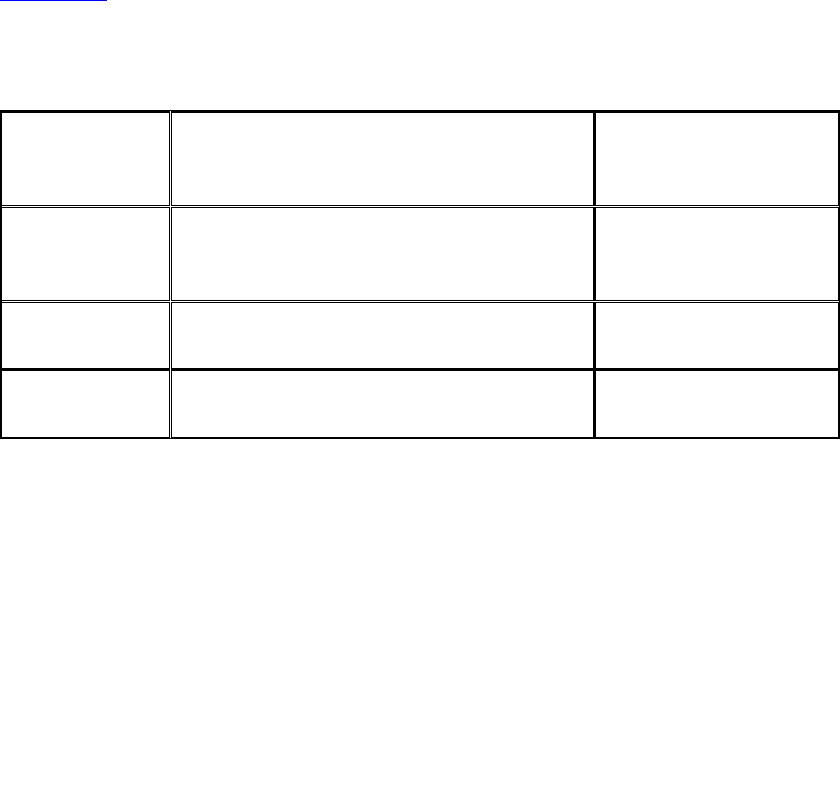
Conventions Used in This Book
Table PR-1 describes the type changes and symbols used in this book.
Table PR-1. Typographic Conventions
Typeface or
Symbol
Description
Examples
AaBbCc123
Keywords, system tasks and compiler
directives that are a part of Verilog HDL
and, nand, $display,
`define
AaBbCc123
Emphasis
cell characterization,
instantiation
AaBbCc123
Names of signals, modules, ports, etc.
fulladd4, D_FF, out
A few other conventions need to be clarified.
• In the book, use of Verilog and Verilog HDL refers to the "Verilog Hardware
Description Language." Any reference to a Verilog-
b
ased simulator is specifically
mentioned, using words such as Verilog simulator or trademarks such as Verilog-
XL or VCS.
• The word designer is used frequently in the book to emphasize the digital design
perspective. However, it is a general term used to refer to a Verilog HDL user or a
verification engineer.
14
Acknowledgments
The first edition of this book was written with the help of a great many people who
contributed their energies to this project. Following were the primary contributors to my
creation: John Sanguinetti, Stuart Sutherland, Clifford Cummings, Robert Emberley,
Ashutosh Mauskar, Jack McKeown, Dr. Arun Somani, Dr. Michael Ciletti, Larry Ke,
Sunil Sabat, Cheng-I Huang, Maqsoodul Mannan, Ashok Mehta, Dick Herlein, Rita
Glover, Ming-Hwa Wang, Subramanian Ganesan, Sandeep Aggarwal, Albert Lau, Samir
Sanghani, Kiran Buch, Anshuman Saha, Bill Fuchs, Babu Chilukuri, Ramana
Kalapatapu, Karin Ellison and Rachel Borden. I would like to start by thanking all those
people once again.
For this second edition, I give special thanks to the following people who helped me with
the review process and provided valuable feedback:
Anders Nordstrom
Stefen Boyd
Clifford Cummings
Harry Foster
Yatin Trivedi
Rajeev Madhavan
John Sanguinetti
Dr. Arun Somani
Michael McNamara
Berend Ozceri
Shrenik Mehta
Mike Meredith
ASIC Consultant
Boyd Technology
Sunburst Design
Verplex Systems
Magma Design Automation
Magma Design Automation
Forte Design Systems
Iowa State University
Verisity Design
Cisco Systems
Sun Microsystems
Forte Design Systems

15
I also appreciate the help of the following individuals:
Richard Jones and John Williamson of Simucad Inc., for providing the free Verilog
simulator SILOS 2001 to be packaged with the book.
Greg Doench of Prentice Hall and Myrna Rivera of Sun Microsystems for providing help
in the publishing process.
Some of the material in this second edition of the book was inspired by conversations,
email, and suggestions from colleagues in the industry. I have credited these sources
where known, but if I have overlooked anyone, please accept my apologies.
Samir Palnitkar
Silicon Valley, California

16
Part 1: Basic Verilog Topics
1 Overview of Digital Design with Verilog HDL
Evolution of CAD, emergence of HDLs, typical HDL-based design flow, why Verilog
HDL?, trends in HDLs.
2 Hierarchical Modeling Concepts
Top-down and bottom-up design methodology, differences between modules and
module instances, parts of a simulation, design block, stimulus block.
3 Basic Concepts
Lexical conventions, data types, system tasks, compiler directives.
4 Modules and Ports
Module definition, port declaration, connecting ports, hierarchical name referencing.
5 Gate-Level Modeling
Modeling using basic Verilog gate primitives, description of and/or and buf/not type
gates, rise, fall and turn-off delays, min, max, and typical delays.
6 Dataflow Modeling
Continuous assignments, delay specification, expressions, operators, operands, operator
types.
7 Behavioral Modeling
Structured procedures, initial and always, blocking and nonblocking statements, delay
control, generate statement, event control, conditional statements, multiway branching,
loops, sequential and parallel blocks.
8 Tasks and Functions
Differences between tasks and functions, declaration, invocation, automatic tasks and
functions.
9 Useful Modeling Techniques
Procedural continuous assignments, overriding parameters, conditional compilation and
execution, useful system tasks.

17
Chapter 1. Overview of Digital Design
with Verilog HDL
• Section 1.1. Evolution of Computer-Aided Digital Design
• Section 1.2. Emergence of HDLs
• Section 1.3. Typical Design Flow
• Section 1.4. Importance of HDLs
• Section 1.5. Popularity of Verilog HDL
• Section 1.6. Trends in HDLs
18
1.1 Evolution of Computer-Aided Digital Design
Digital circuit design has evolved rapidly over the last 25 years. The earliest digital
circuits were designed with vacuum tubes and transistors. Integrated circuits were then
invented where logic gates were placed on a single chip. The first integrated circuit (IC)
chips were SSI (Small Scale Integration) chips where the gate count was very small. As
technologies became sophisticated, designers were able to place circuits with hundreds of
gates on a chip. These chips were called MSI (Medium Scale Integration) chips. With the
advent of LSI (Large Scale Integration), designers could put thousands of gates on a
single chip. At this point, design processes started getting very complicated, and
designers felt the need to automate these processes. Electronic Design Automation (EDA)
techniques began to evolve. Chip designers began to use circuit and logic simulation
techniques to verify the functionality of building blocks of the order of about 100
transistors. The circuits were still tested on the breadboard, and the layout was done on
paper or by hand on a graphic computer terminal.
[1] The earlier edition of the book used the term CAD tools. Technically, the term
Computer-Aided Design (CAD) tools refers to back-end tools that perform functions
related to place and route, and layout of the chip . The term Computer-Aided Engineering
(CAE) tools refers to tools that are used for front-end processes such HDL simulation,
logic synthesis, and timing analysis. Designers used the terms CAD and CAE
interchangeably. Today, the term Electronic Design Automation is used for both CAD
and CAE. For the sake of simplicity, in this book, we will refer to all design tools as EDA
tools.
With the advent of VLSI (Very Large Scale Integration) technology, designers could
design single chips with more than 100,000 transistors. Because of the complexity of
these circuits, it was not possible to verify these circuits on a breadboard. Computer-
aided techniques became critical for verification and design of VLSI digital circuits.
Computer programs to do automatic placement and routing of circuit layouts also became
popular. The designers were now building gate-level digital circuits manually on graphic
terminals. They would build small building blocks and then derive higher-level blocks
from them. This process would continue until they had built the top-level block. Logic
simulators came into existence to verify the functionality of these circuits before they
were fabricated on chip.
As designs got larger and more complex, logic simulation assumed an important role in
the design process. Designers could iron out functional bugs in the architecture before the
chip was designed further.
19
1.2 Emergence of HDLs
For a long time, programming languages such as FORTRAN, Pascal, and C were being
used to describe computer programs that were sequential in nature. Similarly, in the
digital design field, designers felt the need for a standard language to describe digital
circuits. Thus, Hardware Description Languages (HDLs) came into existence. HDLs
allowed the designers to model the concurrency of processes found in hardware elements.
Hardware description languages such as Verilog HDL and VHDL became popular.
Verilog HDL originated in 1983 at Gateway Design Automation. Later, VHDL was
developed under contract from DARPA. Both Verilog and VHDL simulators to simulate
large digital circuits quickly gained acceptance from designers.
Even though HDLs were popular for logic verification, designers had to manually
translate the HDL-based design into a schematic circuit with interconnections between
gates. The advent of logic synthesis in the late 1980s changed the design methodology
radically. Digital circuits could be described at a register transfer level (RTL) by use of
an HDL. Thus, the designer had to specify how the data flows between registers and how
the design processes the data. The details of gates and their interconnections to
implement the circuit were automatically extracted by logic synthesis tools from the RTL
description.
Thus, logic synthesis pushed the HDLs into the forefront of digital design. Designers no
longer had to manually place gates to build digital circuits. They could describe complex
circuits at an abstract level in terms of functionality and data flow by designing those
circuits in HDLs. Logic synthesis tools would implement the specified functionality in
terms of gates and gate interconnections.
HDLs also began to be used for system-level design. HDLs were used for simulation of
system boards, interconnect buses, FPGAs (Field Programmable Gate Arrays), and PALs
(Programmable Array Logic). A common approach is to design each IC chip, using an
HDL, and then verify system functionality via simulation.
Today, Verilog HDL is an accepted IEEE standard. In 1995, the original standard IEEE
1364-1995 was approved. IEEE 1364-2001 is the latest Verilog HDL standard that made
significant improvements to the original standard.
20
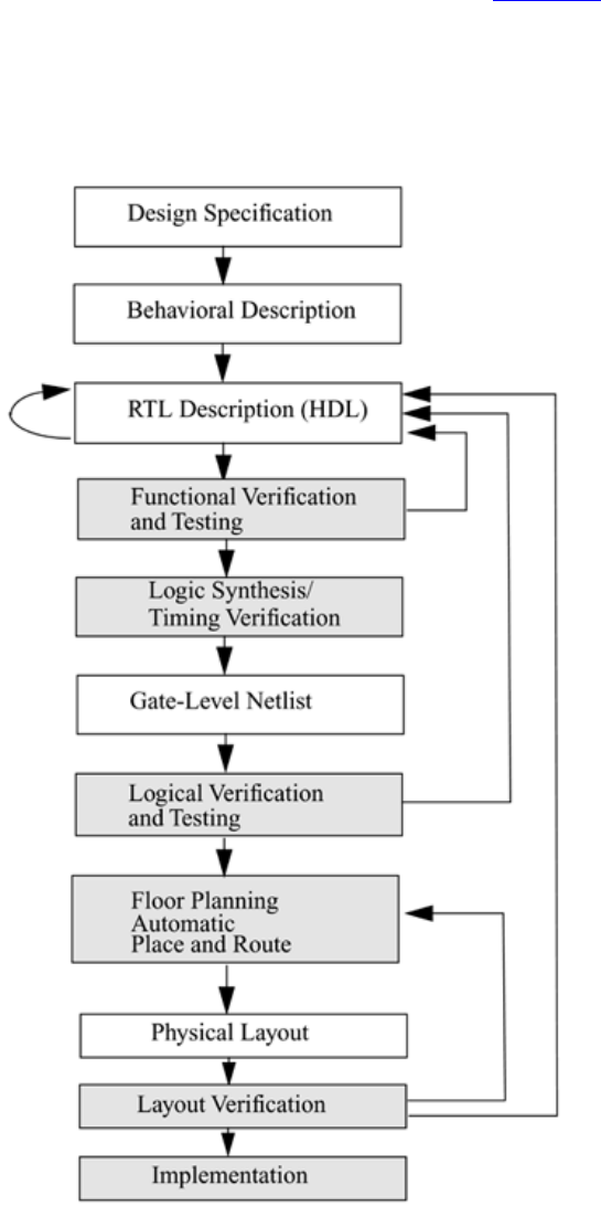
1.3 Typical Design Flow
A typical design flow for designing VLSI IC circuits is shown in Figure 1-1. Unshaded
blocks show the level of design representation; shaded blocks show processes in the
design flow.
Figure 1-1. Typical Design Flow

21
The design flow shown in Figure 1-1 is typically used by designers who use HDLs. In
any design, specifications are written first. Specifications describe abstractly the
functionality, interface, and overall architecture of the digital circuit to be designed. At
this point, the architects do not need to think about how they will implement this circuit.
A behavioral description is then created to analyze the design in terms of functionality,
performance, compliance to standards, and other high-level issues. Behavioral
descriptions are often written with HDLs.[2]
[2] New EDA tools have emerged to simulate behavioral descriptions of circuits. These
tools combine the powerful concepts from HDLs and object oriented languages such as
C++. These tools can be used instead of writing behavioral descriptions in Verilog HDL.
The behavioral description is manually converted to an RTL description in an HDL. The
designer has to describe the data flow that will implement the desired digital circuit.
From this point onward, the design process is done with the assistance of EDA tools.
Logic synthesis tools convert the RTL description to a gate-level netlist. A gate-level
netlist is a description of the circuit in terms of gates and connections between them.
Logic synthesis tools ensure that the gate-level netlist meets timing, area, and power
specifications. The gate-level netlist is input to an Automatic Place and Route tool, which
creates a layout. The layout is verified and then fabricated on a chip.
Thus, most digital design activity is concentrated on manually optimizing the RTL
description of the circuit. After the RTL description is frozen, EDA tools are available to
assist the designer in further processes. Designing at the RTL level has shrunk the design
cycle times from years to a few months. It is also possible to do many design iterations in
a short period of time.
Behavioral synthesis tools have begun to emerge recently. These tools can create RTL
descriptions from a behavioral or algorithmic description of the circuit. As these tools
mature, digital circuit design will become similar to high-level computer programming.
Designers will simply implement the algorithm in an HDL at a very abstract level. EDA
tools will help the designer convert the behavioral description to a final IC chip.
It is important to note that, although EDA tools are available to automate the processes
and cut design cycle times, the designer is still the person who controls how the tool will
perform. EDA tools are also susceptible to the "GIGO : Garbage In Garbage Out"
phenomenon. If used improperly, EDA tools will lead to inefficient designs. Thus, the
designer still needs to understand the nuances of design methodologies, using EDA tools
to obtain an optimized design.

22
1.4 Importance of HDLs
HDLs have many advantages compared to traditional schematic-based design.
• Designs can be described at a very abstract level by use of HDLs. Designers can
write their RTL description without choosing a specific fabrication technology.
Logic synthesis tools can automatically convert the design to any fabrication
technology. If a new technology emerges, designers do not need to redesign their
circuit. They simply input the RTL description to the logic synthesis tool and
create a new gate-level netlist, using the new fabrication technology. The logic
synthesis tool will optimize the circuit in area and timing for the new technology.
• By describing designs in HDLs, functional verification of the design can be done
early in the design cycle. Since designers work at the RTL level, they can
optimize and modify the RTL description until it meets the desired functionality.
Most design bugs are eliminated at this point. This cuts down design cycle time
significantly because the probability of hitting a functional bug at a later time in
the gate-level netlist or physical layout is minimized.
• Designing with HDLs is analogous to computer programming. A textual
description with comments is an easier way to develop and debug circuits. This
also provides a concise representation of the design, compared to gate-level
schematics. Gate-level schematics are almost incomprehensible for very complex
designs.
HDL-based design is here to stay. With rapidly increasing complexities of digital circuits
and increasingly sophisticated EDA tools, HDLs are now the dominant method for large
digital designs. No digital circuit designer can afford to ignore HDL-based design.
[3] New tools and languages focused on verification have emerged in the past few years.
These languages are better suited for functional verification. However, for logic design,
HDLs continue as the preferred choice.
23
1.5 Popularity of Verilog HDL
Verilog HDL has evolved as a standard hardware description language. Verilog HDL
offers many useful features
• Verilog HDL is a general-purpose hardware description language that is easy to
learn and easy to use. It is similar in syntax to the C programming language.
Designers with C programming experience will find it easy to learn Verilog HDL.
• Verilog HDL allows different levels of abstraction to be mixed in the same model.
Thus, a designer can define a hardware model in terms of switches, gates, RTL, or
behavioral code. Also, a designer needs to learn only one language for stimulus
and hierarchical design.
• Most popular logic synthesis tools support Verilog HDL. This makes it the
language of choice for designers.
• All fabrication vendors provide Verilog HDL libraries for postlogic synthesis
simulation. Thus, designing a chip in Verilog HDL allows the widest choice of
vendors.
• The Programming Language Interface (PLI) is a powerful feature that allows the
user to write custom C code to interact with the internal data structures of Verilog.
Designers can customize a Verilog HDL simulator to their needs with the PLI.
24
1.6 Trends in HDLs
The speed and complexity of digital circuits have increased rapidly. Designers have
responded by designing at higher levels of abstraction. Designers have to think only in
terms of functionality. EDA tools take care of the implementation details. With designer
assistance, EDA tools have become sophisticated enough to achieve a close-to-optimum
implementation.
The most popular trend currently is to design in HDL at an RTL level, because logic
synthesis tools can create gate-level netlists from RTL level design. Behavioral synthesis
allowed engineers to design directly in terms of algorithms and the behavior of the
circuit, and then use EDA tools to do the translation and optimization in each phase of the
design. However, behavioral synthesis did not gain widespread acceptance. Today, RTL
design continues to be very popular. Verilog HDL is also being constantly enhanced to
meet the needs of new verification methodologies.
Formal verification and assertion checking techniques have emerged. Formal verification
applies formal mathematical techniques to verify the correctness of Verilog HDL
descriptions and to establish equivalency between RTL and gate-level netlists. However,
the need to describe a design in Verilog HDL will not go away. Assertion checkers allow
checking to be embedded in the RTL code. This is a convenient way to do checking in
the most important parts of a design.
New verification languages have also gained rapid acceptance. These languages combine
the parallelism and hardware constructs from HDLs with the object oriented nature of
C++. These languages also provide support for automatic stimulus creation, checking,
and coverage. However, these languages do not replace Verilog HDL. They simply boost
the productivity of the verification process. Verilog HDL is still needed to describe the
design.
For very high-speed and timing-critical circuits like microprocessors, the gate-level
netlist provided by logic synthesis tools is not optimal. In such cases, designers often mix
gate-level description directly into the RTL description to achieve optimum results. This
practice is opposite to the high-level design paradigm, yet it is frequently used for high-
speed designs because designers need to squeeze the last bit of timing out of circuits, and
EDA tools sometimes prove to be insufficient to achieve the desired results.
25
Another technique that is used for system-level design is a mixed bottom-up
methodology where the designers use either existing Verilog HDL modules, basic
building blocks, or vendor-supplied core blocks to quickly bring up their system
simulation. This is done to reduce development costs and compress design schedules. For
example, consider a system that has a CPU, graphics chip, I/O chip, and a system bus.
The CPU designers would build the next-generation CPU themselves at an RTL level, but
they would use behavioral models for the graphics chip and the I/O chip and would buy a
vendor-supplied model for the system bus. Thus, the system-level simulation for the CPU
could be up and running very quickly and long before the RTL descriptions for the
graphics chip and the I/O chip are completed.

26
Chapter 2. Hierarchical Modeling
Concepts
Before we discuss the details of the Verilog language, we must first understand basic
hierarchical modeling concepts in digital design. The designer must use a "good" design
methodology to do efficient Verilog HDL-based design. In this chapter, we discuss
typical design methodologies and illustrate how these concepts are translated to Verilog.
A digital simulation is made up of various components. We talk about the components
and their interconnections.
Learning Objectives
• Understand top-down and bottom-up design methodologies for digital design.
• Explain differences between modules and module instances in Verilog.
• Describe four levels of abstraction?behavioral, data flow, gate level, and switch
level?to represent the same module.
• Describe components required for the simulation of a digital design. Define a
stimulus block and a design block. Explain two methods of applying stimulus.
27
2.1 Design Methodologies
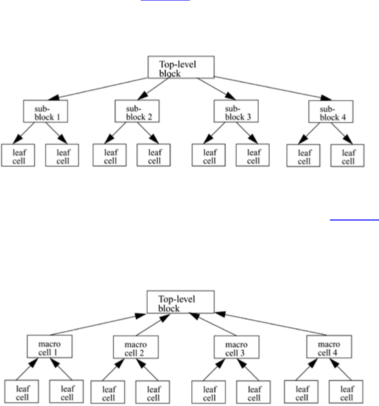
There are two basic types of digital design methodologies: a top-down design
methodology and a bottom-up design methodology. In a top-down design methodology,
we define the top-level block and identify the sub-blocks necessary to build the top-level
block. We further subdivide the sub-blocks until we come to leaf cells, which are the
cells that cannot further be divided. Figure 2-1 shows the top-down design process.
Figure 2-1. Top-down Design Methodology
In a bottom-up design methodology, we first identify the building blocks that are
available to us. We build bigger cells, using these building blocks. These cells are then
used for higher-level blocks until we build the top-level block in the design. Figure 2-2
shows the bottom-up design process.
Figure 2-2. Bottom-up Design Methodology
Typically, a combination of top-down and bottom-up flows is used. Design architects
define the specifications of the top-level block. Logic designers decide how the design
should be structured by breaking up the functionality into blocks and sub-blocks. At the
same time, circuit designers are designing optimized circuits for leaf-level cells. They
build higher-level cells by using these leaf cells. The flow meets at an intermediate point
where the switch-level circuit designers have created a library of leaf cells by using

28
switches, and the logic level designers have designed from top-down until all modules are
defined in terms of leaf cells.
To illustrate these hierarchical modeling concepts, let us consider the design of a negative
edge-triggered 4-bit ripple carry counter described in Section 2.2, 4-bit Ripple Carry
Counter.
2.2 4-bit Ripple Carry Counter
The ripple carry counter shown in Figure 2-3 is made up of negative edge-triggered
toggle flipflops (T_FF). Each of the T_FFs can be made up from negative edge-triggered
D-flipflops (D_FF) and inverters (assuming q_bar output is not available on the D_FF),
as shown in Figure 2-4.
Figure 2-3. Ripple Carry Counter
Figure 2-4. T-flipflop
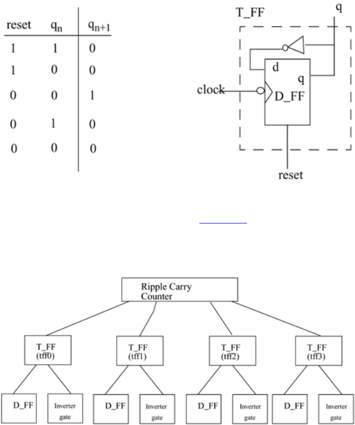
29
Thus, the ripple carry counter is built in a hierarchical fashion by using building blocks.
The diagram for the design hierarchy is shown in Figure 2-5.
Figure 2-5. Design Hierarchy
In a top-down design methodology, we first have to specify the functionality of the ripple
carry counter, which is the top-level block. Then, we implement the counter with T_FFs.
We build the T_FFs from the D_FF and an additional inverter gate. Thus, we break
bigger blocks into smaller building sub-blocks until we decide that we cannot break up
the blocks any further. A bottom-up methodology flows in the opposite direction. We
combine small building blocks and build bigger blocks; e.g., we could build D_FF from
and and or gates, or we could build a custom D_FF from transistors. Thus, the bottom-up
flow meets the top-down flow at the level of the D_FF.

30
2.3 Modules
We now relate these hierarchical modeling concepts to Verilog. Verilog provides the
concept of a module. A module is the basic building block in Verilog. A module can be
an element or a collection of lower-level design blocks. Typically, elements are grouped
into modules to provide common functionality that is used at many places in the design.
A module provides the necessary functionality to the higher-level block through its port
interface (inputs and outputs), but hides the internal implementation. This allows the
designer to modify module internals without affecting the rest of the design.
In Figure 2-5, ripple carry counter, T_FF, D_FF are examples of modules. In Verilog, a
module is declared by the keyword module. A corresponding keyword endmodule must
appear at the end of the module definition. Each module must have a module_name,
which is the identifier for the module, and a module_terminal_list, which describes the
input and output terminals of the module.
module <module_name> (<module_terminal_list>);
...
<module internals>
...
...
endmodule
Specifically, the T-flipflop could be defined as a module as follows:
module T_FF (q, clock, reset);
.
.
<functionality of T-flipflop>
.
.
endmodule
Verilog is both a behavioral and a structural language. Internals of each module can be
defined at four levels of abstraction, depending on the needs of the design. The module
behaves identically with the external environment irrespective of the level of abstraction
at which the module is described. The internals of the module are hidden from the
environment. Thus, the level of abstraction to describe a module can be changed without
any change in the environment. These levels will be studied in detail in separate chapters
later in the book. The levels are defined below.
31
• Behavioral or algorithmic level
• This is the highest level of abstraction provided by Verilog HDL. A module can
be implemented in terms of the desired design algorithm without concern for the
hardware implementation details. Designing at this level is very similar to C
programming.
• Dataflow level
• At this level, the module is designed by specifying the data flow. The designer is
aware of how data flows between hardware registers and how the data is
processed in the design.
• Gate level
• The module is implemented in terms of logic gates and interconnections between
these gates. Design at this level is similar to describing a design in terms of a
gate-level logic diagram.
• Switch level
• This is the lowest level of abstraction provided by Verilog. A module can be
implemented in terms of switches, storage nodes, and the interconnections
between them. Design at this level requires knowledge of switch-level
implementation details.
Verilog allows the designer to mix and match all four levels of abstractions in a design.
In the digital design community, the term register transfer level (RTL) is frequently used
for a Verilog description that uses a combination of behavioral and dataflow constructs
and is acceptable to logic synthesis tools.
If a design contains four modules, Verilog allows each of the modules to be written at a
different level of abstraction. As the design matures, most modules are replaced with
gate-level implementations.
Normally, the higher the level of abstraction, the more flexible and technology-
independent the design. As one goes lower toward switch-level design, the design
becomes technology-dependent and inflexible. A small modification can cause a
significant number of changes in the design. Consider the analogy with C programming
and assembly language programming. It is easier to program in a higher-level language
such as C. The program can be easily ported to any machine. However, if you design at
the assembly level, the program is specific for that machine and cannot be easily ported
to another machine.

32
2.4 Instances
A module provides a template from which you can create actual objects. When a module
is invoked, Verilog creates a unique object from the template. Each object has its own
name, variables, parameters, and I/O interface. The process of creating objects from a
module template is called instantiation, and the objects are called instances. In Example
2-1, the top-level block creates four instances from the T-flipflop (T_FF) template. Each
T_FF instantiates a D_FF and an inverter gate. Each instance must be given a unique
name. Note that // is used to denote single-line comments.
Example 2-1 Module Instantiation
// Define the top-level module called ripple carry
// counter. It instantiates 4 T-flipflops. Interconnections are
// shown in Section 2.2, 4-bit Ripple Carry Counter.
module ripple_carry_counter(q, clk, reset);
output [3:0] q; //I/O signals and vector declarations
//will be explained later.
input clk, reset; //I/O signals will be explained later.
//Four instances of the module T_FF are created. Each has a unique
//name.Each instance is passed a set of signals. Notice, that
//each instance is a copy of the module T_FF.
T_FF tff0(q[0],clk, reset);
T_FF tff1(q[1],q[0], reset);
T_FF tff2(q[2],q[1], reset);
T_FF tff3(q[3],q[2], reset);
endmodule
// Define the module T_FF. It instantiates a D-flipflop. We assumed
// that module D-flipflop is defined elsewhere in the design. Refer
// to Figure 2-4 for interconnections.
module T_FF(q, clk, reset);
//Declarations to be explained later
output q;
input clk, reset;
wire d;
D_FF dff0(q, d, clk, reset); // Instantiate D_FF. Call it dff0.
not n1(d, q); // not gate is a Verilog primitive. Explained later.
endmodule
In Verilog, it is illegal to nest modules. One module definition cannot contain another
module definition within the module and endmodule statements. Instead, a module
definition can incorporate copies of other modules by instantiating them. It is important

33
not to confuse module definitions and instances of a module. Module definitions simply
specify how the module will work, its internals, and its interface. Modules must be
instantiated for use in the design.
Example 2-2 shows an illegal module nesting where the module T_FF is defined inside
the module definition of the ripple carry counter.
Example 2-2 Illegal Module Nesting
// Define the top-level module called ripple carry counter.
// It is illegal to define the module T_FF inside this module.
module ripple_carry_counter(q, clk, reset);
output [3:0] q;
input clk, reset;
module T_FF(q, clock, reset);// ILLEGAL MODULE NESTING
...
<module T_FF internals>
...
endmodule // END OF ILLEGAL MODULE NESTING
endmodule
2.5 Components of a Simulation
Once a design block is completed, it must be tested. The functionality of the design block
can be tested by applying stimulus and checking results. We call such a block the
stimulus block. It is good practice to keep the stimulus and design blocks separate. The
stimulus block can be written in Verilog. A separate language is not required to describe
stimulus. The stimulus block is also commonly called a test bench. Different test benches
can be used to thoroughly test the design block.
Two styles of stimulus application are possible. In the first style, the stimulus block
instantiates the design block and directly drives the signals in the design block. In Figure
2-6, the stimulus block becomes the top-level block. It manipulates signals clk and reset,
and it checks and displays output signal q.
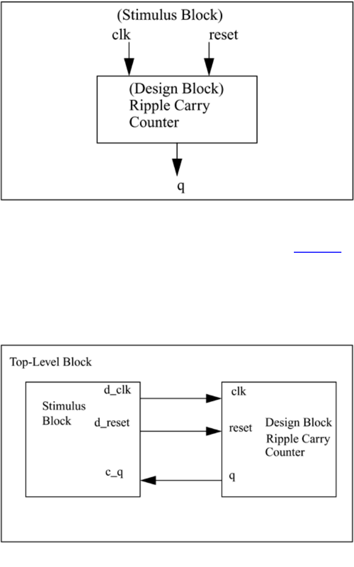
34
Figure 2-6. Stimulus Block Instantiates Design Block
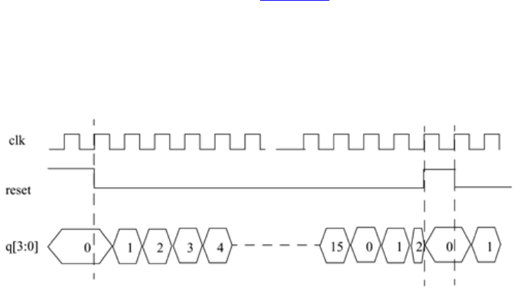
The second style of applying stimulus is to instantiate both the stimulus and design
blocks in a top-level dummy module. The stimulus block interacts with the design block
only through the interface. This style of applying stimulus is shown in Figure 2-7. The
stimulus module drives the signals d_clk and d_reset, which are connected to the signals
clk and reset in the design block. It also checks and displays signal c_q, which is
connected to the signal q in the design block. The function of top-level block is simply to
instantiate the design and stimulus blocks.
Figure 2-7. Stimulus and Design Blocks Instantiated in a Dummy Top-Level Module
Either stimulus style can be used effectively.

35
2.6 Example
To illustrate the concepts discussed in the previous sections, let us build the complete
simulation of a ripple carry counter. We will define the design block and the stimulus
block. We will apply stimulus to the design block and monitor the outputs. As we
develop the Verilog models, you do not need to understand the exact syntax of each
construct at this stage. At this point, you should simply try to understand the design
p
rocess. We discuss the syntax in much greater detail in the later chapters.
2.6.1 Design Block
We use a top-down design methodology. First, we write the Verilog description of the
top-level design block (Example 2-3), which is the ripple carry counter (see Section 2.2,
4-bit Ripple Carry Counter).
Example 2-3 Ripple Carry Counter Top Block
module ripple_carry_counter(q, clk, reset);
output [3:0] q;
input clk, reset;
//4 instances of the module T_FF are created.
T_FF tff0(q[0],clk, reset);
T_FF tff1(q[1],q[0], reset);
T_FF tff2(q[2],q[1], reset);
T_FF tff3(q[3],q[2], reset);
endmodule
In the above module, four instances of the module T_FF (T-flipflop) are used. Therefore,
we must now define (Example 2-4) the internals of the module T_FF, which was shown
in Figure 2-4.
Example 2-4 Flipflop T_FF
module T_FF(q, clk, reset);
output q;
input clk, reset;
wire d;
D_FF dff0(q, d, clk, reset);
not n1(d, q); // not is a Verilog-provided primitive. case sensitive
endmodule
Since T_FF instantiates D_FF, we must now define (Example 2-5) the internals of
36
module D_FF. We assume asynchronous reset for the D_FFF.
Example 2-5 Flipflop D_F
// module D_FF with synchronous reset
module D_FF(q, d, clk, reset);
output q;
input d, clk, reset;
reg q;
// Lots of new constructs. Ignore the functionality of the
// constructs.
// Concentrate on how the design block is built in a top-down fashion.
always @(posedge reset or negedge clk)
if (reset)
q <= 1'b0;
else
q <= d;
endmodule
All modules have been defined down to the lowest-level leaf cells in the design
methodology. The design block is now complete.
2.6.2 Stimulus Block
We must now write the stimulus block to check if the ripple carry counter design is
functioning correctly. In this case, we must control the signals clk and reset so that the
regular function of the ripple carry counter and the asynchronous reset mechanism are
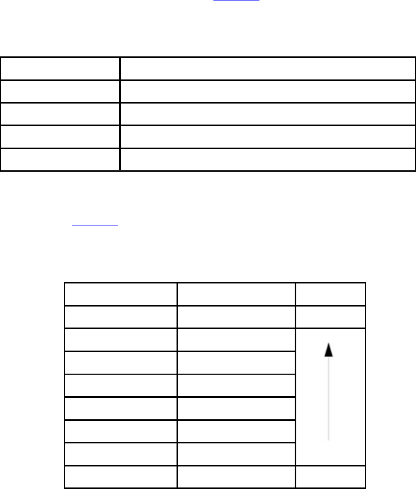
both tested. We use the waveforms shown in Figure 2-8 to test the design. Waveforms for
clk, reset, and 4-
b
it output q are shown. The cycle time for clk is 10 units; the reset signal
stays up from time 0 to 15 and then goes up again from time 195 to 205. Output q counts
from 0 to 15.
Figure 2-8. Stimulus and Output Waveforms

37
We are now ready to write the stimulus block (see Example 2-6) that will create the
above waveforms. We will use the stimulus style shown in Figure 2-6. Do not worry
about the Verilog syntax at this point. Simply concentrate on how the design block is
instantiated in the stimulus block.
Example 2-6 Stimulus Block
module stimulus;
reg clk;
reg reset;
wire[3:0] q;
// instantiate the design block
ripple_carry_counter r1(q, clk, reset);
// Control the clk signal that drives the design block. Cycle time = 10
initial
clk = 1'b0; //set clk to 0
always
#5 clk = ~clk; //toggle clk every 5 time units
// Control the reset signal that drives the design block
// reset is asserted from 0 to 20 and from 200 to 220.
initial
begin
reset = 1'b1;
#15 reset = 1'b0;
#180 reset = 1'b1;
#10 reset = 1'b0;
#20 $finish; //terminate the simulation
end
// Monitor the outputs
initial
$monitor($time, " Output q = %d", q);
endmodule
Once the stimulus block is completed, we are ready to run the simulation and verify the
functional correctness of the design block. The output obtained when stimulus and design
blocks are simulated is shown in Example 2-7.
Example 2-7 Output of the Simulation
0 Output q = 0
20 Output q = 1
30 Output q = 2
40 Output q = 3
50 Output q = 4
60 Output q = 5
70 Output q = 6
80 Output q = 7
38
90 Output q = 8
100 Output q = 9
110 Output q = 10
120 Output q = 11
130 Output q = 12
140 Output q = 13
150 Output q = 14
160 Output q = 15
170 Output q = 0
180 Output q = 1
190 Output q = 2
195 Output q = 0
210 Output q = 1
220 Output q = 2
39
2.7 Summary
In this chapter we discussed the following concepts.
• Two kinds of design methodologies are used for digital design: top-down and
bottom-up. A combination of these two methodologies is used in today's digital
designs. As designs become very complex, it is important to follow these
structured approaches to manage the design process.
• Modules are the basic building blocks in Verilog. Modules are used in a design by
instantiation. An instance of a module has a unique identity and is different from
other instances of the same module. Each instance has an independent copy of the
internals of the module. It is important to understand the difference between
modules and instances.
• There are two distinct components in a simulation: a design block and a stimulus
block. A stimulus block is used to test the design block. The stimulus block is
usually the top-level block. There are two different styles of applying stimulus to
a design block.
• The example of the ripple carry counter explains the step-by-step process of
building all the blocks required in a simulation.
This chapter is intended to give an understanding of the design process and how Verilog
fits into the design process. The details of Verilog syntax are not important at this stage
and will be dealt with in later chapters.
40
2.8 Exercises
1: An interconnect switch (IS) contains the following components, a shared
memory (MEM), a system controller (SC) and a data crossbar (Xbar).
a. Define the modules MEM, SC, and Xbar, using the module/endmodule
keywords. You do not need to define the internals. Assume that the
modules have no terminal lists.
b. Define the module IS, using the module/endmodule keywords.
Instantiate the modules MEM, SC, Xbar and call the instances mem1,
sc1, and xbar1, respectively. You do not need to define the internals.
Assume that the module IS has no terminals.
c. Define a stimulus block (Top), using the module/endmodule keywords.
Instantiate the design block IS and call the instance is1. This is the final
step in building the simulation environment.
2: A 4-bit ripple carry adder (Ripple_Add) contains four 1-bit full adders (FA).
a. Define the module FA. Do not define the internals or the terminal list.
b. Define the module Ripple_Add. Do not define the internals or the
terminal list. Instantiate four full adders of the type FA in the module
Ripple_Add and call them fa0, fa1, fa2, and fa3.
41
Chapter 3. Basic Concepts
In this chapter, we discuss the basic constructs and conventions in Verilog. These
conventions and constructs are used throughout the later chapters. These conventions
provide the necessary framework for Verilog HDL. Data types in Verilog model actual
data storage and switch elements in hardware very closely. This chapter may seem dry,
but understanding these concepts is a necessary foundation for the successive chapters.
Learning Objectives
• Understand lexical conventions for operators, comments, whitespace, numbers,
strings, and identifiers.
• Define the logic value set and data types such as nets, registers, vectors, numbers,
simulation time, arrays, parameters, memories, and strings.
• Identify useful system tasks for displaying and monitoring information, and for
stopping and finishing the simulation.
• Learn basic compiler directives to define macros and include files.
3.1 Lexical Conventions
The basic lexical conventions used by Verilog HDL are similar to those in the C
programming language. Verilog contains a stream of tokens. Tokens can be comments,
delimiters, numbers, strings, identifiers, and keywords. Verilog HDL is a case-sensitive
language. All keywords are in lowercase.
3.1.1 Whitespace
Blank spaces (\b) , tabs (\t) and newlines (\n) comprise the whitespace. Whitespace is
ignored by Verilog except when it separates tokens. Whitespace is not ignored in strings.
42
3.1.2 Comments
Comments can be inserted in the code for readability and documentation. There are two
ways to write comments. A one-line comment starts with "//". Verilog skips from that
point to the end of line. A multiple-line comment starts with "/*" and ends with "*/".
Multiple-line comments cannot be nested. However, one-line comments can be
embedded in multiple-line comments.
a = b && c; // This is a one-line comment
/* This is a multiple line
comment */
/* This is /* an illegal */ comment */
/* This is //a legal comment */
3.1.3 Operators
Operators are of three types: unary, binary, and ternary. Unary operators precede the
operand. Binary operators appear between two operands. Ternary operators have two
separate operators that separate three operands.
a = ~ b; // ~ is a unary operator. b is the operand
a = b && c; // && is a binary operator. b and c are operands
a = b ? c : d; // ?: is a ternary operator. b, c and d are operands
3.1.4 Number Specification
There are two types of number specification in Verilog: sized and unsized.
Sized numbers
Sized numbers are represented as <size> '<base format> <number>.
<size> is written only in decimal and specifies the number of bits in the number. Legal
base formats are decimal ('d or 'D), hexadecimal ('h or 'H), binary ('b or 'B) and octal ('o
or 'O). The number is specified as consecutive digits from 0, 1, 2, 3, 4, 5, 6, 7, 8, 9, a, b,
c, d, e, f. Only a subset of these digits is legal for a particular base. Uppercase letters are
legal for number specification.
4'b1111 // This is a 4-bit binary number
12'habc // This is a 12-bit hexadecimal number
16'd255 // This is a 16-bit decimal number.
43
Unsized numbers
Numbers that are specified without a <base format> specification are decimal numbers
b
y default. Numbers that are written without a <size> specification have a default number
of bits that is simulator- and machine-specific (must be at least 32).
23456 // This is a 32-bit decimal number by default
'hc3 // This is a 32-bit hexadecimal number
'o21 // This is a 32-bit octal number
X or Z values
Verilog has two symbols for unknown and high impedance values. These values are very
important for modeling real circuits. An unknown value is denoted by an x. A high
impedance value is denoted by z.
12'h13x // This is a 12-bit hex number; 4 least significant bits
unknown
6'hx // This is a 6-bit hex number
32'bz // This is a 32-bit high impedance number
An x or z sets four bits for a number in the hexadecimal base, three bits for a number in
the octal base, and one bit for a number in the binary base. If the most significant bit of a
number is 0, x, or z, the number is automatically extended to fill the most significant bits,
respectively, with 0, x, or z. This makes it easy to assign x or z to whole vector. If the
most significant digit is 1, then it is also zero extended.
Negative numbers
Negative numbers can be specified by putting a minus sign before the size for a constant
number. Size constants are always positive. It is illegal to have a minus sign between
<base format> and <number>. An optional signed specifier can be added for signed
arithmetic.
-6'd3 // 8-bit negative number stored as 2's complement of 3
-6'sd3 // Used for performing signed integer math
4'd-2 // Illegal specification
Underscore characters and question marks
An underscore character "_" is allowed anywhere in a number except the first character.
Underscore characters are allowed only to improve readability of numbers and are
ignored by Verilog.

44
A question mark "?" is the Verilog HDL alternative for z in the context of numbers. The ?
is used to enhance readability in the casex and casez statements discussed in Chapter 7,
where the high impedance value is a don't care condition. (Note that ? has a different
meaning in the context of user-defined primitives, which are discussed in Chapter 12,
User-Defined Primitives.)
12'b1111_0000_1010 // Use of underline characters for readability
4'b10?? // Equivalent of a 4'b10zz
3.1.5 Strings
A string is a sequence of characters that are enclosed by double quotes. The restriction on
a string is that it must be contained on a single line, that is, without a carriage return. It
cannot be on multiple lines. Strings are treated as a sequence of one-byte ASCII values.
"Hello Verilog World" // is a string
"a / b" // is a string
3.1.6 Identifiers and Keywords
Keywords are special identifiers reserved to define the language constructs. Keywords
are in lowercase. A list of all keywords in Verilog is contained in Appendix C, List of
Keywords, System Tasks, and Compiler Directives.
Identifiers are names given to objects so that they can be referenced in the design.
Identifiers are made up of alphanumeric characters, the underscore ( _ ), or the dollar sign
( $ ). Identifiers are case sensitive. Identifiers start with an alphabetic character or an
underscore. They cannot start with a digit or a $ sign (The $ sign as the first character is
reserved for system tasks, which are explained later in the book).
reg value; // reg is a keyword; value is an identifier
input clk; // input is a keyword, clk is an identifier
3.1.7 Escaped Identifiers
Escaped identifiers begin with the backslash ( \ ) character and end with whitespace
(space, tab, or newline). All characters between backslash and whitespace are processed
literally. Any printable ASCII character can be included in escaped identifiers. Neither
the backslash nor the terminating whitespace is considered to be a part of the identifier.
\a+b-c
\**my_name**
45
3.2 Data Types
This section discusses the data types used in Verilog.
3.2.1 Value Set
Verilog supports four values and eight strengths to model the functionality of real
hardware. The four value levels are listed in Table 3-1.
Table 3-1. Value Levels
Value Level Condition in Hardware Circuits
0 Logic zero, false condition
1 Logic one, true condition
x Unknown logic value
z High impedance, floating state
In addition to logic values, strength levels are often used to resolve conflicts between
drivers of different strengths in digital circuits. Value levels 0 and 1 can have the strength
levels listed in Table 3-2.
Table 3-2. Strength Levels
Strength Level Type Degree
supply Driving strongest
strong Driving
pull riving
large Storage
weak Driving
medium Storage
small Storage
highz High Impedance weakest
46
If two signals of unequal strengths are driven on a wire, the stronger signal prevails. For
example, if two signals of strength strong1 and weak0 contend, the result is resolved as a
strong1. If two signals of equal strengths are driven on a wire, the result is unknown. If
two signals of strength strong1 and strong0 conflict, the result is an x. Strength levels are
particularly useful for accurate modeling of signal contention, MOS devices, dynamic
MOS, and other low-level devices. Only trireg nets can have storage strengths large,
medium, and small. Detailed information about strength modeling is provided in
Appendix A, Strength Modeling and Advanced Net Definitions.
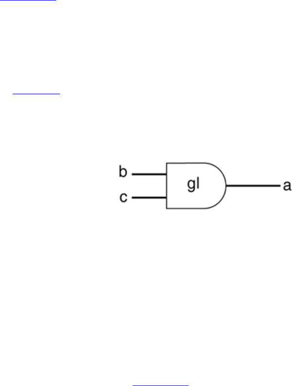
3.2.2 Nets
Nets represent connections between hardware elements. Just as in real circuits, nets have
values continuously driven on them by the outputs of devices that they are connected to.
In Figure 3-1 net a is connected to the output of and gate g1. Net a will continuously
assume the value computed at the output of gate g1, which is b & c.
Figure 3-1. Example of Nets
Nets are declared primarily with the keyword wire. Nets are one-bit values by default
unless they are declared explicitly as vectors. The terms wire and net are often used
interchangeably. The default value of a net is z (except the trireg net, which defaults to x
). Nets get the output value of their drivers. If a net has no driver, it gets the value z.
wire a; // Declare net a for the above circuit
wire b,c; // Declare two wires b,c for the above circuit
wire d = 1'b0; // Net d is fixed to logic value 0 at declaration.
Note that net is not a keyword but represents a class of data types such as wire, wand,
wor, tri, triand, trior, trireg, etc. The wire declaration is used most frequently. Other net
declarations are discussed in Appendix A, Strength Modeling and Advanced Net
Definitions.
3.2.3 Registers
Registers represent data storage elements. Registers retain value until another value is
placed onto them. Do not confuse the term registers in Verilog with hardware registers
built from edge-triggered flipflops in real circuits. In Verilog, the term register merely

47
means a variable that can hold a value. Unlike a net, a register does not need a driver.
Verilog registers do not need a clock as hardware registers do. Values of registers can be
changed anytime in a simulation by assigning a new value to the register.
Register data types are commonly declared by the keyword reg. The default value for a
reg data type is x. An example of how registers are used is shown Example 3-1.
Example 3-1 Example of Register
reg reset; // declare a variable reset that can hold its value
initial // this construct will be discussed later
begin
reset = 1'b1; //initialize reset to 1 to reset the digital circuit.
#100 reset = 1'b0; // after 100 time units reset is deasserted.
end
Registers can also be declared as signed variables. Such registers can be used for signed
arithmetic. Example 3-2 shows the declaration of a signed register.
Example 3-2 Signed Register Declaration
reg signed [63:0] m; // 64 bit signed value
integer i; // 32 bit signed value
3.2.4 Vectors
Nets or reg data types can be declared as vectors (multiple bit widths). If bit width is not
specified, the default is scalar (1-bit).
wire a; // scalar net variable, default
wire [7:0] bus; // 8-bit bus
wire [31:0] busA,busB,busC; // 3 buses of 32-bit width.
reg clock; // scalar register, default
reg [0:40] virtual_addr; // Vector register, virtual address 41 bits
wide
Vectors can be declared at [high# : low#] or [low# : high#], but the left number in the
squared brackets is always the most significant bit of the vector. In the example shown
above, bit 0 is the most significant bit of vector virtual_addr.
48
Vector Part Select
For the vector declarations shown above, it is possible to address bits or parts of vectors.
busA[7] // bit # 7 of vector busA
bus[2:0] // Three least significant bits of vector bus,
// using bus[0:2] is illegal because the significant bit should
// always be on the left of a range specification
virtual_addr[0:1] // Two most significant bits of vector virtual_addr
Variable Vector Part Select
Another ability provided in Verilog HDl is to have variable part selects of a vector. This
allows part selects to be put in for loops to select various parts of the vector. There are
two special part-select operators:
[<starting_bit>+:width] - part-select increments from starting bit
[<starting_bit>-:width] - part-select decrements from starting bit
The starting bit of the part select can be varied, but the width has to be constant. The
following example shows the use of variable vector part select:
reg [255:0] data1; //Little endian notation
reg [0:255] data2; //Big endian notation
reg [7:0] byte;
//Using a variable part select, one can choose parts
byte = data1[31-:8]; //starting bit = 31, width =8 => data[31:24]
byte = data1[24+:8]; //starting bit = 24, width =8 => data[31:24]
byte = data2[31-:8]; //starting bit = 31, width =8 => data[24:31]
byte = data2[24+:8]; //starting bit = 24, width =8 => data[24:31]
//The starting bit can also be a variable. The width has
//to be constant. Therefore, one can use the variable part select
//in a loop to select all bytes of the vector.
for (j=0; j<=31; j=j+1)
byte = data1[(j*8)+:8]; //Sequence is [7:0], [15:8]... [255:248]
//Can initialize a part of the vector
data1[(byteNum*8)+:8] = 8'b0; //If byteNum = 1, clear 8 bits [15:8]
49
3.2.5 Integer , Real, and Time Register Data Types
Integer, real, and time register data types are supported in Verilog.
Integer
An integer is a general purpose register data type used for manipulating quantities.
Integers are declared by the keyword integer. Although it is possible to use reg as a
general-purpose variable, it is more convenient to declare an integer variable for purposes
such as counting. The default width for an integer is the host-machine word size, which is
implementation-specific but is at least 32 bits. Registers declared as data type reg store
values as unsigned quantities, whereas integers store values as signed quantities.
integer counter; // general purpose variable used as a counter.
initial
counter = -1; // A negative one is stored in the counter
Real
Real number constants and real register data types are declared with the keyword real.
They can be specified in decimal notation (e.g., 3.14) or in scientific notation (e.g., 3e6,
which is 3 x 10⁶ ). Real numbers cannot have a range declaration, and their default value
is 0. When a real value is assigned to an integer, the real number is rounded off to the
nearest integer.
real delta; // Define a real variable called delta
initial
begin
delta = 4e10; // delta is assigned in scientific notation
delta = 2.13; // delta is assigned a value 2.13
end
integer i; // Define an integer i
initial
i = delta; // i gets the value 2 (rounded value of 2.13)
Time
Verilog simulation is done with respect to simulation time. A special time register data
type is used in Verilog to store simulation time. A time variable is declared with the
keyword time. The width for time register data types is implementation-specific but is at
least 64 bits.The system function $time is invoked to get the current simulation time.
time save_sim_time; // Define a time variable save_sim_time
initial
save_sim_time = $time; // Save the current simulation time

50
Simulation time is measured in terms of simulation seconds. The unit is denoted by s, the
same as real time. However, the relationship between real time in the digital circuit and
simulation time is left to the user. This is discussed in detail in Section 9.4, Time Scales.
3.2.6 Arrays
Arrays are allowed in Verilog for reg, integer, time, real, realtime and vector register data
types. Multi-dimensional arrays can also be declared with any number of dimensions.
Arrays of nets can also be used to connect ports of generated instances. Each element of
the array can be used in the same fashion as a scalar or vector net. Arrays are accessed by
<array_name>[<subscript>]. For multi-dimensional arrays, indexes need to be provided
for each dimension.
integer count[0:7]; // An array of 8 count variables
reg bool[31:0]; // Array of 32 one-bit boolean register variables
time chk_point[1:100]; // Array of 100 time checkpoint variables
reg [4:0] port_id[0:7]; // Array of 8 port_ids; each port_id is 5 bits
wide
integer matrix[4:0][0:255]; // Two dimensional array of integers
reg [63:0] array_4d [15:0][7:0][7:0][255:0]; //Four dimensional array
wire [7:0] w_array2 [5:0]; // Declare an array of 8 bit vector wire
wire w_array1[7:0][5:0]; // Declare an array of single bit wires
It is important not to confuse arrays with net or register vectors. A vector is a single
element that is n-bits wide. On the other hand, arrays are multiple elements that are 1-bit
or n-bits wide.
Examples of assignments to elements of arrays discussed above are shown below:
count[5] = 0; // Reset 5th element of array of count variables
chk_point[100] = 0; // Reset 100th time check point value
port_id[3] = 0; // Reset 3rd element (a 5-bit value) of port_id array.
matrix[1][0] = 33559; // Set value of element indexed by [1][0] to
33559
array_4d[0][0][0][0][15:0] = 0; //Clear bits 15:0 of the register
//accessed by indices [0][0][0][0]
port_id = 0; // Illegal syntax - Attempt to write the entire array

51
matrix [1] = 0; // Illegal syntax - Attempt to write [1][0]..[1][255]
3.2.7 Memories
In digital simulation, one often needs to model register files, RAMs, and ROMs.
Memories are modeled in Verilog simply as a one-dimensional array of registers. Each
element of the array is known as an element or word and is addressed by a single array
index. Each word can be one or more bits. It is important to differentiate between n 1-bit
registers and one n-bit register. A particular word in memory is obtained by using the
address as a memory array subscript.
reg mem1bit[0:1023]; // Memory mem1bit with 1K 1-bit words
reg [7:0] membyte[0:1023]; // Memory membyte with 1K 8-bit words(bytes)
membyte[511] // Fetches 1 byte word whose address is 511.
3.2.8 Parameters
Verilog allows constants to be defined in a module by the keyword parameter. Parameters
cannot be used as variables. Parameter values for each module instance can be overridden
individually at compile time. This allows the module instances to be customized. This
aspect is discussed later. Parameter types and sizes can also be defined.
parameter port_id = 5; // Defines a constant port_id
parameter cache_line_width = 256; // Constant defines width of cache
line
parameter signed [15:0] WIDTH; // Fixed sign and range for parameter
// WIDTH
Module definitions may be written in terms of parameters. Hardcoded numbers should be
avoided. Parameters values can be changed at module instantiation or by using the
defparam statement, which is discussed in detail in Chapter 9, Useful Modeling
Techniques. Thus, the use of parameters makes the module definition flexible. Module
behavior can be altered simply by changing the value of a parameter.
Verilog HDL local parameters (defined using keyword localparam -) are identical to
parameters except that they cannot be directly modified with the defparam statement or
by the ordered or named parameter value assignment. The localparam keyword is used to
define parameters when their values should not be changed. For example, the state
encoding for a state machine can be defined using localparam. The state encoding cannot
be changed. This provides protection against inadvertent parameter redefinition.
localparam state1 = 4'b0001,
state2 = 4'b0010,
state3 = 4'b0100,
state4 = 4'b1000;
52
3.2.9 Strings
Strings can be stored in reg. The width of the register variables must be large enough to
hold the string. Each character in the string takes up 8 bits (1 byte). If the width of the
register is greater than the size of the string, Verilog fills bits to the left of the string with
zeros. If the register width is smaller than the string width, Verilog truncates the leftmost
bits of the string. It is always safe to declare a string that is slightly wider than necessary.
reg [8*18:1] string_value; // Declare a variable that is 18 bytes wide
initial
string_value = "Hello Verilog World"; // String can be stored
// in variable
Special characters serve a special purpose in displaying strings, such as newline, tabs, and
displaying argument values. Special characters can be displayed in strings only when
they are preceded by escape characters, as shown in Table 3-3.
Table 3-3. Special Characters
Escaped Characters Character Displayed
\n newline
\t tab
%% %
\\ \
\" "
\ooo Character written in 1?3 octal digits
53
3.3 System Tasks and Compiler Directives
In this section, we introduce two special concepts used in Verilog: system tasks and
compiler directives.
3.3.1 System Tasks
Verilog provides standard system tasks for certain routine operations. All system tasks
appear in the form $<keyword>. Operations such as displaying on the screen, monitoring
values of nets, stopping, and finishing are done by system tasks. We will discuss only the
most useful system tasks. Other tasks are listed in Verilog manuals provided by your
simulator vendor or in the IEEE Standard Verilog Hardware Description Language
specification.
Displaying information
$display is the main system task for displaying values of variables or strings or
expressions. This is one of the most useful tasks in Verilog.
Usage: $display(p1, p2, p3,....., pn);
p1, p2, p3,..., pn can be quoted strings or variables or expressions. The format of $display
is very similar to printf in C. A $display inserts a newline at the end of the string by
default. A $display without any arguments produces a newline.
Strings can be formatted using the specifications listed in Table 3-4. For more detailed
specifications, see IEEE Standard Verilog Hardware Description Language specification.
Table 3-4. String Format Specifications
Format Display
%d or %D Display variable in decimal
%b or %B Display variable in binary
%s or %S Display string
%h or %H Display variable in hex
54
%c or %C Display ASCII character
%m or %M Display hierarchical name (no argument required)
%v or %V Display strength
%o or %O Display variable in octal
%t or %T Display in current time format
%e or %E Display real number in scientific format (e.g., 3e10)
%f or %F Display real number in decimal format (e.g., 2.13)
%g or %G Display real number in scientific or decimal, whichever is shorter
Example 3-3 shows some examples of the $display task. If variables contain x or z
values, they are printed in the displayed string as "x" or "z".
Example 3-3 $display Task
//Display the string in quotes
$display("Hello Verilog World");
-- Hello Verilog World
//Display value of current simulation time 230
$display($time);
-- 230
//Display value of 41-bit virtual address 1fe0000001c at time 200
reg [0:40] virtual_addr;
$display("At time %d virtual address is %h", $time, virtual_addr);
-- At time 200 virtual address is 1fe0000001c
//Display value of port_id 5 in binary
reg [4:0] port_id;
$display("ID of the port is %b", port_id);
-- ID of the port is 00101
//Display x characters
//Display value of 4-bit bus 10xx (signal contention) in binary
reg [3:0] bus;
$display("Bus value is %b", bus);
-- Bus value is 10xx
//Display the hierarchical name of instance p1 instantiated under
//the highest-level module called top. No argument is required. This
//is a useful feature)
$display("This string is displayed from %m level of hierarchy");
-- This string is displayed from top.p1 level of hierarchy

55
Special characters are discussed in Section 3.2.9, Strings. Examples of displaying special
characters in strings as discussed are shown in Example 3-4.
Example 3-4 Special Characters
//Display special characters, newline and %
$display("This is a \n multiline string with a %% sign");
-- This is a
-- multiline string with a % sign
//Display other special characters
Monitoring information
Verilog provides a mechanism to monitor a signal when its value changes. This facility is
provided by the $monitor task.
Usage: $monitor(p1,p2,p3,....,pn);
The parameters p1, p2, ... , pn can be variables, signal names, or quoted strings. A format
similar to the $display task is used in the $monitor task. $monitor continuously monitors
the values of the variables or signals specified in the parameter list and displays all
parameters in the list whenever the value of any one variable or signal changes. Unlike
$display, $monitor needs to be invoked only once.
Only one monitoring list can be active at a time. If there is more than one $monitor
statement in your simulation, the last $monitor statement will be the active statement.
The earlier $monitor statements will be overridden.
Two tasks are used to switch monitoring on and off.
Usage:
$monitoron;
$monitoroff;
The $monitoron tasks enables monitoring, and the $monitoroff task disables monitoring
during a simulation. Monitoring is turned on by default at the beginning of the simulation
and can be controlled during the simulation with the $monitoron and $monitoroff tasks.
Examples of monitoring statements are given in Example 3-5. Note the use of $time in
the $monitor statement.

56
Example 3-5 Monitor Statement
//Monitor time and value of the signals clock and reset
//Clock toggles every 5 time units and reset goes down at 10 time units
initial
begin
$monitor($time,
" Value of signals clock = %b reset = %b", clock,reset);
end
Partial output of the monitor statement:
-- 0 Value of signals clock = 0 reset = 1
-- 5 Value of signals clock = 1 reset = 1
-- 10 Value of signals clock = 0 reset = 0
Stopping and finishing in a simulation
The task $stop is provided to stop during a simulation.
Usage: $stop;
The $stop task puts the simulation in an interactive mode. The designer can then debug
the design from the interactive mode. The $stop task is used whenever the designer wants
to suspend the simulation and examine the values of signals in the design.
The $finish task terminates the simulation.
Usage: $finish;
Examples of $stop and $finish are shown in Example 3-6.
Example 3-6 Stop and Finish Tasks
// Stop at time 100 in the simulation and examine the results
// Finish the simulation at time 1000.
initial // to be explained later. time = 0
begin
clock = 0;
reset = 1;
#100 $stop; // This will suspend the simulation at time = 100
#900 $finish; // This will terminate the simulation at time = 1000
end

57
3.3.2 Compiler Directives
Compiler directives are provided in Verilog. All compiler directives are defined by using
the `<keyword> construct. We deal with the two most useful compiler directives.
`define
The `define directive is used to define text macros in Verilog (see Example 3-7). The
Verilog compiler substitutes the text of the macro wherever it encounters a
`<macro_name>. This is similar to the #define construct in C. The defined constants or
text macros are used in the Verilog code by preceding them with a ` (back tick).
Example 3-7 `define Directive
//define a text macro that defines default word size
//Used as 'WORD_SIZE in the code
'define WORD_SIZE 32
//define an alias. A $stop will be substituted wherever 'S appears
'define S $stop;
//define a frequently used text string
'define WORD_REG reg [31:0]
// you can then define a 32-bit register as 'WORD_REG reg32;
`include
The `include directive allows you to include entire contents of a Verilog source file in
another Verilog file during compilation. This works similarly to the #include in the C
programming language. This directive is typically used to include header files, which
typically contain global or commonly used definitions (see Example 3-8).
Example 3-8 `include Directive
// Include the file header.v, which contains declarations in the
// main verilog file design.v.
'include header.v
...
...
<Verilog code in file design.v>
...
...
Two other directives, `ifdef and `timescale, are used frequently. They are discussed in
Chapter 9, Useful Modeling Techniques.
58
3.4 Summary
We discussed the basic concepts of Verilog in this chapter. These concepts lay the
foundation for the material discussed in the further chapters.
• Verilog is similar in syntax to the C programming language . Hardware designers
with previous C programming experience will find Verilog easy to learn.
• Lexical conventions for operators, comments, whitespace, numbers, strings, and
identifiers were discussed.
• Various data types are available in Verilog. There are four logic values, each with
different strength levels. Available data types include nets, registers, vectors,
numbers, simulation time, arrays, memories, parameters, and strings. Data types
represent actual hardware elements very closely.
• Verilog provides useful system tasks to do functions like displaying, monitoring,
suspending, and finishing a simulation.
• Compiler directive `define is used to define text macros, and `include is used to
include other Verilog files.
59
3.5 Exercises
1: Practice writing the following numbers:
a. Decimal number 123 as a sized 8-bit number in binary. Use _ for
readability.
b. A 16-bit hexadecimal unknown number with all x's.
c. A 4-bit negative 2 in decimal . Write the 2's complement form for this
number.
d. An unsized hex number 1234.
2: Are the following legal strings? If not, write the correct strings.
a. "This is a string displaying the % sign"
b. "out = in1 + in2"
c. "Please ring a bell \007"
d. "This is a backslash \ character\n"
3: Are these legal identifiers?
a. system1
b. 1reg
c. $latch
d. exec$
4: Declare the following variables in Verilog:
60
a. An 8-bit vector net called a_in.
b. A 32-bit storage register called address. Bit 31 must be the most
significant bit. Set the value of the register to a 32-bit decimal number
equal to 3.
c. An integer called count.
d. A time variable called snap_shot.
e. An array called delays. Array contains 20 elements of the type integer.
f. A memory MEM containing 256 words of 64 bits each.
g. A parameter cache_size equal to 512.
5: What would be the output/effect of the following statements?
a. latch = 4'd12;
$display("The current value of latch = %b\n", latch);
b. in_reg = 3'd2;
$monitor($time, " In register value = %b\n", in_reg[2:0]);
c. `define MEM_SIZE 1024
$display("The maximum memory size is %h", 'MEM_SIZE);
61
Chapter 4. Modules and Ports
In the previous chapters, we acquired an understanding of the fundamental hierarchical
modeling concepts, basic conventions, and Verilog constructs. In this chapter, we take a
closer look at modules and ports from the Verilog language point of view.
Learning Objectives
• Identify the components of a Verilog module definition, such as module names,
port lists, parameters, variable declarations, dataflow statements, behavioral
statements, instantiation of other modules, and tasks or functions.
• Understand how to define the port list for a module and declare it in Verilog.
• Describe the port connection rules in a module instantiation.
• Understand how to connect ports to external signals, by ordered list, and by name.
• Explain hierarchical name referencing of Verilog identifiers.
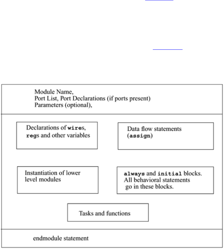
62
4.1 Modules
We discussed how a module is a basic building block in Chapter 2, Hierarchical
Modeling Concepts. We ignored the internals of modules and concentrated on how
modules are defined and instantiated. In this section, we analyze the internals of the
module in greater detail.
A module in Verilog consists of distinct parts, as shown in Figure 4-1.
Figure 4-1. Components of a Verilog Module
A module definition always begins with the keyword module. The module name, port
list, port declarations, and optional parameters must come first in a module definition.
Port list and port declarations are present only if the module has any ports to interact with
the external environment.The five components within a module are: variable declarations,
dataflow statements, instantiation of lower modules, behavioral blocks, and tasks or
functions. These components can be in any order and at any place in the module
definition. The endmodule statement must always come last in a module definition. All
components except module, module name, and endmodule are optional and can be mixed
and matched as per design needs. Verilog allows multiple modules to be defined in a
single file. The modules can be defined in any order in the file.
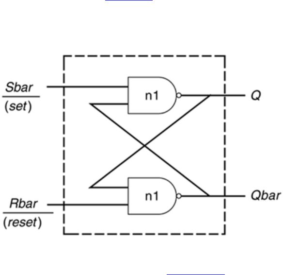
63
To understand the components of a module shown above, let us consider a simple
example of an SR latch, as shown in Figure 4-2.
Figure 4-2. SR Latch
The SR latch has S and R as the input ports and Q and Qbar as the output ports. The SR
latch and its stimulus can be modeled as shown in Example 4-1.
Example 4-1 Components of SR Latch
// This example illustrates the different components of a module
// Module name and port list
// SR_latch module
module SR_latch(Q, Qbar, Sbar, Rbar);
//Port declarations
output Q, Qbar;
input Sbar, Rbar;
// Instantiate lower-level modules
// In this case, instantiate Verilog primitive nand gates
// Note, how the wires are connected in a cross-coupled fashion.
nand n1(Q, Sbar, Qbar);
nand n2(Qbar, Rbar, Q);
// endmodule statement
endmodule
// Module name and port list
// Stimulus module
module Top;
// Declarations of wire, reg, and other variables

64
wire q, qbar;
reg set, reset;
// Instantiate lower-level modules
// In this case, instantiate SR_latch
// Feed inverted set and reset signals to the SR latch
SR_latch m1(q, qbar, ~set, ~reset);
// Behavioral block, initial
initial
begin
$monitor($time, " set = %b, reset= %b, q= %b\n",set,reset,q);
set = 0; reset = 0;
#5 reset = 1;
#5 reset = 0;
#5 set = 1;
end
// endmodule statement
endmodule
Notice the following characteristics about the modules defined above:
• In the SR latch definition above , notice that all components described in Figure
4-1 need not be present in a module. We do not find variable declarations,
dataflow (assign) statements, or behavioral blocks (always or initial).
• However, the stimulus block for the SR latch contains module name, wire, reg,
and variable declarations, instantiation of lower level modules, behavioral block
(initial), and endmodule statement but does not contain port list, port declarations,
and data flow (assign) statements.
• Thus, all parts except module, module name, and endmodule are optional and can
be mixed and matched as per design needs.
4.2 Ports
Ports provide the interface by which a module can communicate with its environment.
For example, the input/output pins of an IC chip are its ports. The environment can
interact with the module only through its ports. The internals of the module are not
visible to the environment. This provides a very powerful flexibility to the designer. The
internals of the module can be changed without affecting the environment as long as the
interface is not modified. Ports are also referred to as terminals.
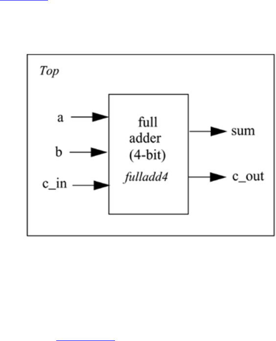
65
4.2.1 List of Ports
A module definition contains an optional list of ports. If the module does not exchange
any signals with the environment, there are no ports in the list. Consider a 4-bit full adder
that is instantiated inside a top-level module Top. The diagram for the input/output ports
is shown in Figure 4-3.
Figure 4-3. I/O Ports for Top and Full Adder
Notice that in the above figure, the module Top is a top-level module. The module
fulladd4 is instantiated below Top. The module fulladd4 takes input on ports a, b, and
c_in and produces an output on ports sum and c_out. Thus, module fulladd4 performs an
addition for its environment. The module Top is a top-level module in the simulation and
does not need to pass signals to or receive signals from the environment. Thus, it does not
have a list of ports. The module names and port lists for both module declarations in
Verilog are as shown in Example 4-2.
Example 4-2 List of Ports
module fulladd4(sum, c_out, a, b, c_in); //Module with a list of ports
module Top; // No list of ports, top-level module in simulation
4.2.2 Port Declaration
All ports in the list of ports must be declared in the module. Ports can be declared as
follows:

66
Verilog Keyword Type of Port
input Input port
output Output port
inout Bidirectional port
Each port in the port list is defined as input, output, or inout, based on the direction of the
port signal. Thus, for the example of the fulladd4 in Example 4-2, the port declarations
will be as shown in Example 4-3.
Example 4-3 Port Declarations
module fulladd4(sum, c_out, a, b, c_in);
//Begin port declarations section
output[3:0] sum;
output c_cout;
input [3:0] a, b;
input c_in;
//End port declarations section
...
<module internals>
...
endmodule
Note that all port declarations are implicitly declared as wire in Verilog. Thus, if a port is
intended to be a wire, it is sufficient to declare it as output, input, or inout. Input or inout
ports are normally declared as wires. However, if output ports hold their value, they must
be declared as reg. For example, in the definition of DFF, in Example 2-5, we wanted the
output q to retain its value until the next clock edge. The port declarations for DFF will
look as shown in Example 4-4.
Example 4-4 Port Declarations for DFF
module DFF(q, d, clk, reset);
output q;
reg q; // Output port q holds value; therefore it is declared as reg.
input d, clk, reset;
...
...
endmodule
Ports of the type input and inout cannot be declared as reg because reg variables store
values and input ports should not store values but simply reflect the changes in the
external signals they are connected to.
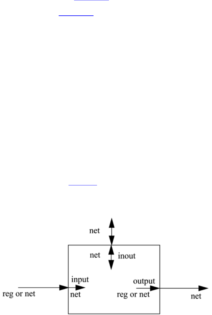
67
Note that the module fulladd4 in Example 4-3 can be declared using an ANSI C style
syntax to specify the ports of that module. Each declared port provides the complete
information about the port. Example 4-5 shows this alternate syntax. This syntax avoids
the duplication of naming the ports in both the module definition statement and the
module port list definitions. If a port is declared but no data type is specified, then, under
specific circumstances, the signal will default to a wire data type.
Example 4-5 ANSI C Style Port Declaration Syntax
module fulladd4(output reg [3:0] sum,
output reg c_out,
input [3:0] a, b, //wire by default
input c_in); //wire by default
...
<module internals>
...
endmodule
4.2.3 Port Connection Rules
One can visualize a port as consisting of two units, one unit that is internal to the module
and another that is external to the module. The internal and external units are connected.
There are rules governing port connections when modules are instantiated within other
modules. The Verilog simulator complains if any port connection rules are violated.
These rules are summarized in Figure 4-4.
Figure 4-4. Port Connection Rules

68
Inputs
Internally, input ports must always be of the type net. Externally, the inputs can be
connected to a variable which is a reg or a net.
Outputs
Internally, outputs ports can be of the type reg or net. Externally, outputs must always be
connected to a net. They cannot be connected to a reg.
Inouts
Internally, inout ports must always be of the type net. Externally, inout ports must always
be connected to a net.
Width matching
It is legal to connect internal and external items of different sizes when making inter-
module port connections. However, a warning is typically issued that the widths do not
match.
Unconnected ports
Verilog allows ports to remain unconnected. For example, certain output ports might be
simply for debugging, and you might not be interested in connecting them to the external
signals. You can let a port remain unconnected by instantiating a module as shown
below.
fulladd4 fa0(SUM, , A, B, C_IN); // Output port c_out is unconnected
Example of illegal port connection
To illustrate port connection rules, assume that the module fulladd4 in Example 4-3 is
instantiated in the stimulus block Top. Example 4-6 shows an illegal port connection.
Example 4-6 Illegal Port Connection
module Top;
//Declare connection variables
reg [3:0]A,B;
reg C_IN;
reg [3:0] SUM;

69
wire C_OUT;
//Instantiate fulladd4, call it fa0
fulladd4 fa0(SUM, C_OUT, A, B, C_IN);
//Illegal connection because output port sum in module fulladd4
//is connected to a register variable SUM in module Top.
.
.
<stimulus>
.
.
endmodule
This problem is rectified if the variable SUM is declared as a net (wire).
4.2.4 Connecting Ports to External Signals
There are two methods of making connections between signals specified in the module
instantiation and the ports in a module definition. These two methods cannot be mixed.
These methods are discussed in the following sections.
Connecting by ordered list
Connecting by ordered list is the most intuitive method for most beginners. The signals to
be connected must appear in the module instantiation in the same order as the ports in the
port list in the module definition. Once again, consider the module fulladd4 defined in
Example 4-3. To connect signals in module Top by ordered list, the Verilog code is
shown in Example 4-7. Notice that the external signals SUM, C_OUT, A, B, and C_IN
appear in exactly the same order as the ports sum, c_out, a, b, and c_in in module
definition of fulladd4.
Example 4-7 Connection by Ordered List
module Top;
//Declare connection variables
reg [3:0]A,B;
reg C_IN;
wire [3:0] SUM;
wire C_OUT;
//Instantiate fulladd4, call it fa_ordered.
//Signals are connected to ports in order (by position)
fulladd4 fa_ordered(SUM, C_OUT, A, B, C_IN);
...
<stimulus>
...
endmodule

70
module fulladd4(sum, c_out, a, b, c_in);
output[3:0] sum;
output c_cout;
input [3:0] a, b;
input c_in;
...
<module internals>
...
endmodule
Connecting ports by name
For large designs where modules have, say, 50 ports, remembering the order of the ports
in the module definition is impractical and error-prone. Verilog provides the capability to
connect external signals to ports by the port names, rather than by position. We could
connect the ports by name in Example 4-7 above by instantiating the module fulladd4, as
follows. Note that you can specify the port connections in any order as long as the port
name in the module definition correctly matches the external signal.
// Instantiate module fa_byname and connect signals to ports by name
fulladd4 fa_byname(.c_out(C_OUT), .sum(SUM), .b(B), .c_in(C_IN),
.a(A),);
Note that only those ports that are to be connected to external signals must be specified in
port connection by name. Unconnected ports can be dropped. For example, if the port
c_out were to be kept unconnected, the instantiation of fulladd4 would look as follows.
The port c_out is simply dropped from the port list.
// Instantiate module fa_byname and connect signals to ports by name
fulladd4 fa_byname(.sum(SUM), .b(B), .c_in(C_IN), .a(A),);
Another advantage of connecting ports by name is that as long as the port name is not
changed, the order of ports in the port list of a module can be rearranged without
changing the port connections in module instantiations.
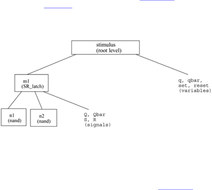
71
4.3 Hierarchical Names
We described earlier how Verilog supports a hierarchical design methodology. Every
module instance, signal, or variable is defined with an identifier. A particular identifier
has a unique place in the design hierarchy. Hierarchical name referencing allows us to
denote every identifier in the design hierarchy with a unique name. A hierarchical name
is a list of identifiers separated by dots (".") for each level of hierarchy. Thus, any
identifier can be addressed from any place in the design by simply specifying the
complete hierarchical name of that identifier.
The top-level module is called the root module because it is not instantiated anywhere. It
is the starting point. To assign a unique name to an identifier, start from the top-level
module and trace the path along the design hierarchy to the desired identifier. To clarify
this process, let us consider the simulation of SR latch in Example 4-1. The design
hierarchy is shown in Figure 4-5.
Figure 4-5. Design Hierarchy for SR Latch Simulation
For this simulation, stimulus is the top-level module. Since the top-level module is not
instantiated anywhere, it is called the root module. The identifiers defined in this module
are q, qbar, set, and reset. The root module instantiates m1, which is a module of type
SR_latch. The module m1 instantiates nand gates n1 and n2. Q, Qbar, S, and R are port
signals in instance m1. Hierarchical name referencing assigns a unique name to each
identifier. To assign hierarchical names, use the module name for root module and
instance names for all module instances below the root module. Example 4-8 shows
hierarchical names for all identifiers in the above simulation. Notice that there is a dot (.)
for each level of hierarchy from the root module to the desired identifier.

72
Example 4-8 Hierarchical Names
stimulus stimulus.q
stimulus.qbar stimulus.set
stimulus.reset stimulus.m1
stimulus.m1.Q stimulus.m1.Qbar
stimulus.m1.S stimulus.m1.R
stimulus.n1 stimulus.n2
Each identifier in the design is uniquely specified by its hierarchical path name. To
display the level of hierarchy, use the special character %m in the $display task. See
Table 3-4, String Format Specifications, for details.

73
4.4 Summary
In this chapter, we discussed the following aspects of Verilog:
• Module definitions contain various components. Keywords module and
endmodule are mandatory. Other components?port list, port declarations, variable
and signal declarations, dataflow statements, behavioral blocks, lower-level
module instantiations, and tasks or functions?are optional and can be added as
needed.
• Ports provide the module with a means to communicate with other modules or its
environment. A module can have a port list. Ports in the port list must be declared
as input, output, or inout. When instantiating a module, port connection rules are
enforced by the Verilog simulator. An ANSI C style embeds the port declarations
in the module definition statement.
• Ports can be connected by name or by ordered list.
• Each identifier in the design has a unique hierarchical name. Hierarchical names
allow us to address any identifier in the design from any other level of hierarchy
in the design.
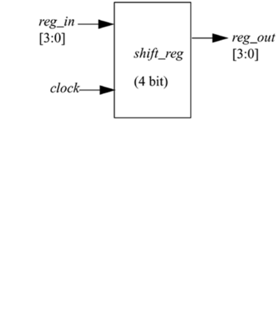
74
4.5 Exercises
1: What are the basic components of a module? Which components are
mandatory?
2:
Does a module that does not interact with its environment have any I/O ports?
Does it have a port list in the module definition?
3: A 4-bit parallel shift register has I/O pins as shown in the figure below. Write
the module definition for this module shift_reg. Include the list of ports and port
declarations. You do not need to show the internals.
4: Declare a top-level module stimulus. Define REG_IN (4 bit) and CLK (1 bit) as
reg register variables and REG_OUT (4 bit) as wire. Instantiate the module
shift_reg and call it sr1. Connect the ports by ordered list.
5: Connect the ports in Step 4 by name.
6:
Write the hierarchical names for variables REG_IN, CLK, and REG_OUT.
7: Write the hierarchical name for the instance sr1. Write the hierarchical names
for its ports clock and reg_in.

75
Chapter 5. Gate-Level Modeling
In the earlier chapters, we laid the foundations of Verilog design by discussing design
methodologies, basic conventions and constructs, modules and port interfaces. In this
chapter, we get into modeling actual hardware circuits in Verilog.
We discussed the four levels of abstraction used to describe hardware. In this chapter, we
discuss a design at a low level of abstraction?gate level. Most digital design is now done
at gate level or higher levels of abstraction. At gate level, the circuit is described in terms
of gates (e.g., and, nand). Hardware design at this level is intuitive for a user with a basic
knowledge of digital logic design because it is possible to see a one-to-one
correspondence between the logic circuit diagram and the Verilog description. Hence, in
this book, we chose to start with gate-level modeling and move to higher levels of
abstraction in the succeeding chapters.
Actually, the lowest level of abstraction is switch- (transistor-) level modeling. However,
with designs getting very complex, very few hardware designers work at switch level.
Therefore, we will defer switch-level modeling to Chapter 11, Switch-Level Modeling, in
Part 2 of this book.
Learning Objectives
• Identify logic gate primitives provided in Verilog.
• Understand instantiation of gates, gate symbols, and truth tables for and/or and
buf/not type gates.
• Understand how to construct a Verilog description from the logic diagram of the
circuit.
• Describe rise, fall, and turn-off delays in the gate-level design.
• Explain min, max, and typ delays in the gate-level design.
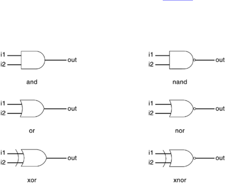
76
5.1 Gate Types
A logic circuit can be designed by use of logic gates. Verilog supports basic logic gates
as predefined primitives. These primitives are instantiated like modules except that they
are predefined in Verilog and do not need a module definition. All logic circuits can be
designed by using basic gates. There are two classes of basic gates: and/or gates and
buf/not gates.
5.1.1 And/Or Gates
And/or gates have one scalar output and multiple scalar inputs. The first terminal in the
list of gate terminals is an output and the other terminals are inputs. The output of a gate
is evaluated as soon as one of the inputs changes. The and/or gates available in Verilog
are shown below.
and or xor
nand nor xnor
The corresponding logic symbols for these gates are shown in Figure 5-1. We consider
gates with two inputs. The output terminal is denoted by out. Input terminals are denoted
by i1 and i2.
Figure 5-1. Basic Gates

77
These gates are instantiated to build logic circuits in Verilog. Examples of gate
instantiations are shown below. In Example 5-1, for all instances, OUT is connected to
the output out, and IN1 and IN2 are connected to the two inputs i1 and i2 of the gate
primitives. Note that the instance name does not need to be specified for primitives. This
lets the designer instantiate hundreds of gates without giving them a name.
More than two inputs can be specified in a gate instantiation. Gates with more than two
inputs are instantiated by simply adding more input ports in the gate instantiation (see
Example 5-1). Verilog automatically instantiates the appropriate gate.
Example 5-1 Gate Instantiation of And/Or Gates
wire OUT, IN1, IN2;
// basic gate instantiations.
and a1(OUT, IN1, IN2);
nand na1(OUT, IN1, IN2);
or or1(OUT, IN1, IN2);
nor nor1(OUT, IN1, IN2);
xor x1(OUT, IN1, IN2);
xnor nx1(OUT, IN1, IN2);
// More than two inputs; 3 input nand gate
nand na1_3inp(OUT, IN1, IN2, IN3);
// gate instantiation without instance name
and (OUT, IN1, IN2); // legal gate instantiation
The truth tables for these gates define how outputs for the gates are computed from the
inputs. Truth tables are defined assuming two inputs. The truth tables for these gates are
shown in Table 5-1. Outputs of gates with more than two inputs are computed by
applying the truth table iteratively.
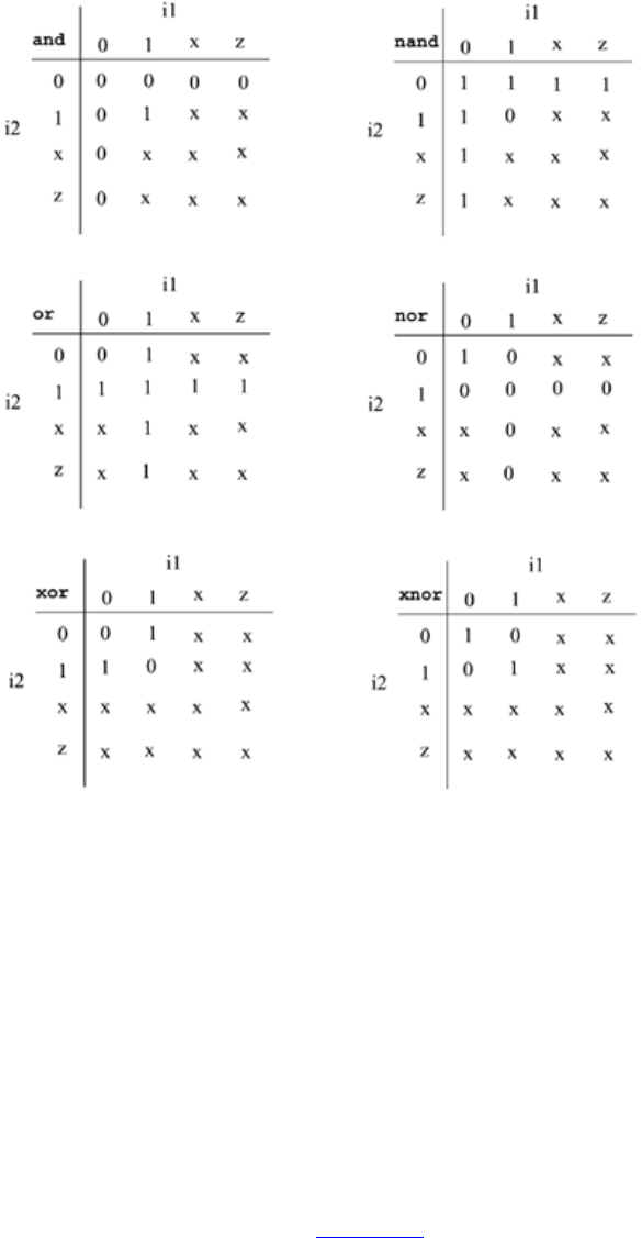
78
Table 5-1. Truth Tables for And/Or
Gates
5.1.2 Buf/Not Gates
Buf/not gates have one scalar input and one or more scalar outputs. The last terminal in
the port list is connected to the input. Other terminals are connected to the outputs. We
will discuss gates that have one input and one output.
Two basic buf/not gate primitives are provided in Verilog.
buf not
The symbols for these logic gates are shown in Figure 5-2.
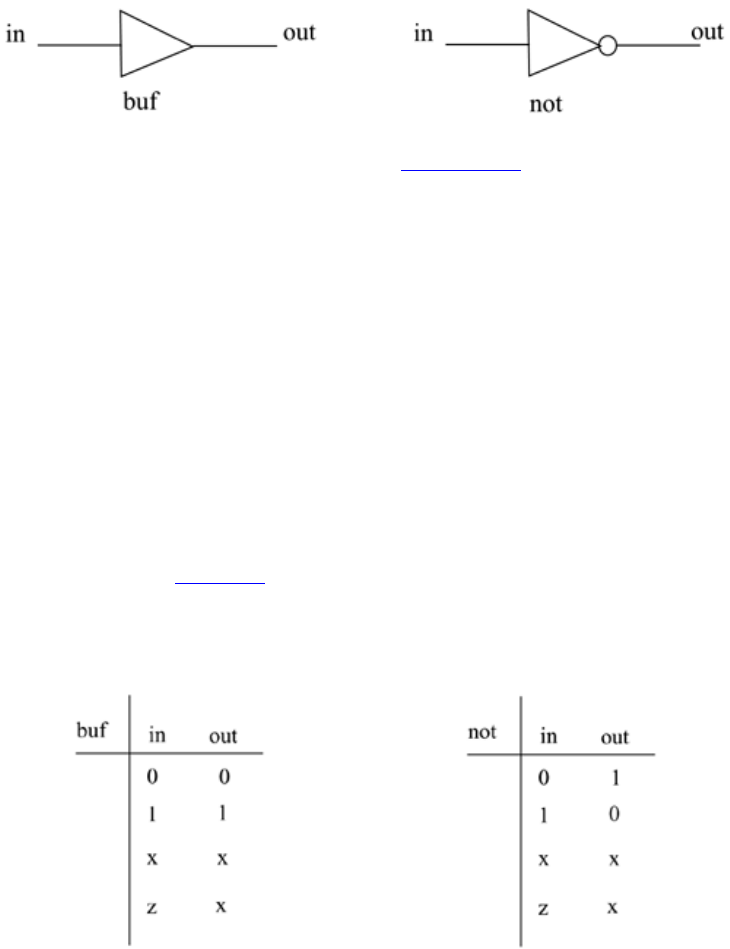
79
Figure 5-2. Buf and Not Gates
These gates are instantiated in Verilog as shown Example 5-2. Notice that these gates can
have multiple outputs but exactly one input, which is the last terminal in the port list.
Example 5-2 Gate Instantiations of Buf/Not Gates
// basic gate instantiations.
buf b1(OUT1, IN);
not n1(OUT1, IN);
// More than two outputs
buf b1_2out(OUT1, OUT2, IN);
// gate instantiation without instance name
not (OUT1, IN); // legal gate instantiation
The truth tables for these gates are very simple. Truth tables for gates with one input and
one output are shown in Table 5-2.
Table 5-2. Truth Tables for Buf/Not Gates
Bufif/notif
Gates with an additional control signal on buf and not gates are also available.
bufif1 notif1
bufif0 notif0
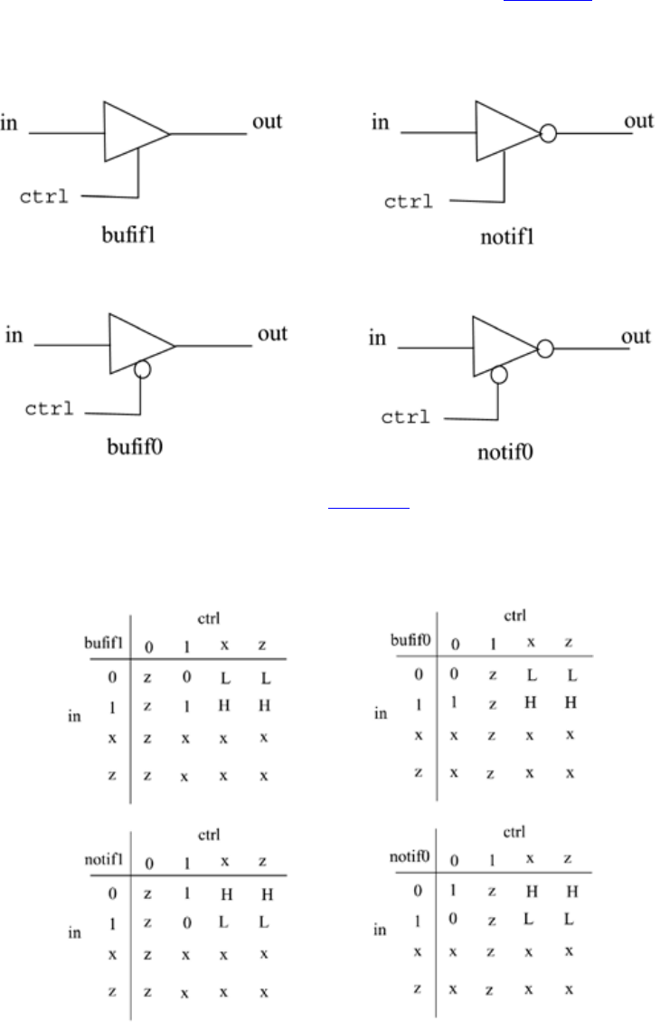
80
These gates propagate only if their control signal is asserted. They propagate z if their
control signal is deasserted. Symbols for bufif/notif are shown in Figure 5-3.
Figure 5-3. Gates Bufif and Notif
The truth tables for these gates are shown in Table 5-3.
Table 5-3. Truth Tables for Bufif/Notif Gates
These gates are used when a signal is to be driven only when the control signal is
asserted. Such a situation is applicable when multiple drivers drive the signal.

81
These drivers are designed to drive the signal on mutually exclusive control signals.
Example 5-3 shows examples of instantiation of bufif and notif gates.
Example 5-3 Gate Instantiations of Bufif/Notif Gates
//Instantiation of bufif gates.
bufif1 b1 (out, in, ctrl);
bufif0 b0 (out, in, ctrl);
//Instantiation of notif gates
notif1 n1 (out, in, ctrl);
notif0 n0 (out, in, ctrl);
5.1.3 Array of Instances
There are many situations when repetitive instances are required. These instances differ
from each other only by the index of the vector to which they are connected. To simplify
specification of such instances, Verilog HDL allows an array of primitive instances to be
defined.[1] Example 5-4 shows an example of an array of instances.
[1] Refer to the IEEE Standard Verilog Hardware Description Language document for
detailed information on the use of an array of instances.
Example 5-4 Simple Array of Primitive Instances
wire [7:0] OUT, IN1, IN2;
// basic gate instantiations.
nand n_gate[7:0](OUT, IN1, IN2);
// This is equivalent to the following 8 instantiations
nand n_gate0(OUT[0], IN1[0], IN2[0]);
nand n_gate1(OUT[1], IN1[1], IN2[1]);
nand n_gate2(OUT[2], IN1[2], IN2[2]);
nand n_gate3(OUT[3], IN1[3], IN2[3]);
nand n_gate4(OUT[4], IN1[4], IN2[4]);
nand n_gate5(OUT[5], IN1[5], IN2[5]);
nand n_gate6(OUT[6], IN1[6], IN2[6]);
nand n_gate7(OUT[7], IN1[7], IN2[7]);
5.1.4 Examples
Having understood the various types of gates available in Verilog, we will discuss a real
example that illustrates design of gate-level digital circuits.
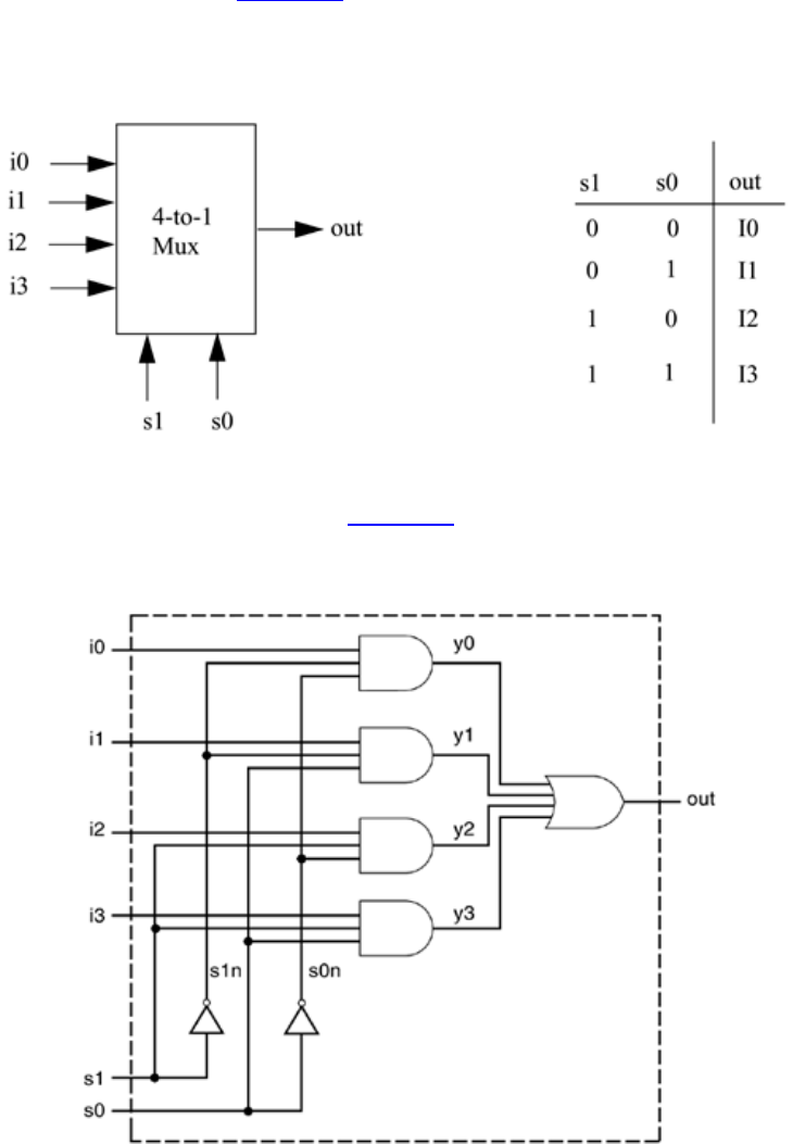
82
Gate-level multiplexer
We will design a 4-to-1 multiplexer with 2 select signals. Multiplexers serve a useful
purpose in logic design. They can connect two or more sources to a single destination.
They can also be used to implement boolean functions. We will assume for this example
that signals s1 and s0 do not get the value x or z. The I/O diagram and the truth table for
the multiplexer are shown in Figure 5-4. The I/O diagram will be useful in setting up the
port list for the multiplexer.
Figure 5-4. 4-to-1 Multiplexer
We will implement the logic for the multiplexer using basic logic gates. The logic
diagram for the multiplexer is shown in Figure 5-5.
Figure 5-5. Logic Diagram for Multiplexer

83
The logic diagram has a one-to-one correspondence with the Verilog description. The
Verilog description for the multiplexer is shown in Example 5-5. Two intermediate nets,
s0n and s1n, are created; they are complements of input signals s1 and s0. Internal nets
y0, y1, y2, y3 are also required. Note that instance names are not specified for primitive
gates, not, and, and or. Instance names are optional for Verilog primitives but are
mandatory for instances of user-defined modules.
Example 5-5 Verilog Description of Multiplexer
// Module 4-to-1 multiplexer. Port list is taken exactly from
// the I/O diagram.
module mux4_to_1 (out, i0, i1, i2, i3, s1, s0);
// Port declarations from the I/O diagram
output out;
input i0, i1, i2, i3;
input s1, s0;
// Internal wire declarations
wire s1n, s0n;
wire y0, y1, y2, y3;
// Gate instantiations
// Create s1n and s0n signals.
not (s1n, s1);
not (s0n, s0);
// 3-input and gates instantiated
and (y0, i0, s1n, s0n);
and (y1, i1, s1n, s0);
and (y2, i2, s1, s0n);
and (y3, i3, s1, s0);
// 4-input or gate instantiated
or (out, y0, y1, y2, y3);
endmodule
This multiplexer can be tested with the stimulus shown in Example 5-6. The stimulus
checks that each combination of select signals connects the appropriate input to the
output. The signal OUTPUT is displayed one time unit after it changes. System task
$monitor could also be used to display the signals when they change values.
Example 5-6 Stimulus for Multiplexer
// Define the stimulus module (no ports)
module stimulus;
// Declare variables to be connected
// to inputs
reg IN0, IN1, IN2, IN3;

84
reg S1, S0;
// Declare output wire
wire OUTPUT;
// Instantiate the multiplexer
mux4_to_1 mymux(OUTPUT, IN0, IN1, IN2, IN3, S1, S0);
// Stimulate the inputs
// Define the stimulus module (no ports)
initial
begin
// set input lines
IN0 = 1; IN1 = 0; IN2 = 1; IN3 = 0;
#1 $display("IN0= %b, IN1= %b, IN2= %b, IN3= %b\n",IN0,IN1,IN2,IN3);
// choose IN0
S1 = 0; S0 = 0;
#1 $display("S1 = %b, S0 = %b, OUTPUT = %b \n", S1, S0, OUTPUT);
// choose IN1
S1 = 0; S0 = 1;
#1 $display("S1 = %b, S0 = %b, OUTPUT = %b \n", S1, S0, OUTPUT);
// choose IN2
S1 = 1; S0 = 0;
#1 $display("S1 = %b, S0 = %b, OUTPUT = %b \n", S1, S0, OUTPUT);
// choose IN3
S1 = 1; S0 = 1;
#1 $display("S1 = %b, S0 = %b, OUTPUT = %b \n", S1, S0, OUTPUT);
end
endmodule
The output of the simulation is shown below. Each combination of the select signals is
tested.
IN0= 1, IN1= 0, IN2= 1, IN3= 0
S1 = 0, S0 = 0, OUTPUT = 1
S1 = 0, S0 = 1, OUTPUT = 0
S1 = 1, S0 = 0, OUTPUT = 1
S1 = 1, S0 = 1, OUTPUT = 0
4-bit Ripple Carry Full Adder
In this example, we design a 4-bit full adder whose port list was defined in Section 4.2.1,
List of Ports. We use primitive logic gates, and we apply stimulus to the 4-bit full adder
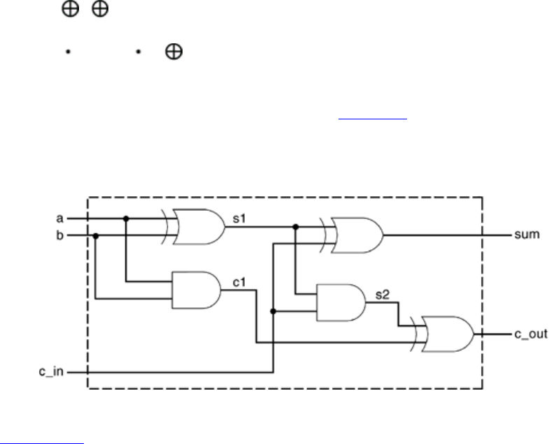
85
to check functionality . For the sake of simplicity, we will implement a ripple carry adder.
The basic building block is a 1-bit full adder. The mathematical equations for a 1-bit full
adder are shown below.
sum = (a b cin)
cout = (a b) + cin (a b)
The logic diagram for a 1-bit full adder is shown in Figure 5-6.
Figure 5-6. 1-bit Full Adder
This logic diagram for the 1-bit full adder is converted to a Verilog description, shown in
Example 5-7.
Example 5-7 Verilog Description for 1-bit Full Adder
// Define a 1-bit full adder
module fulladd(sum, c_out, a, b, c_in);
// I/O port declarations
output sum, c_out;
input a, b, c_in;
// Internal nets
wire s1, c1, c2;
// Instantiate logic gate primitives
xor (s1, a, b);
and (c1, a, b);
xor (sum, s1, c_in);
and (c2, s1, c_in);
xor (c_out, c2, c1);
endmodule
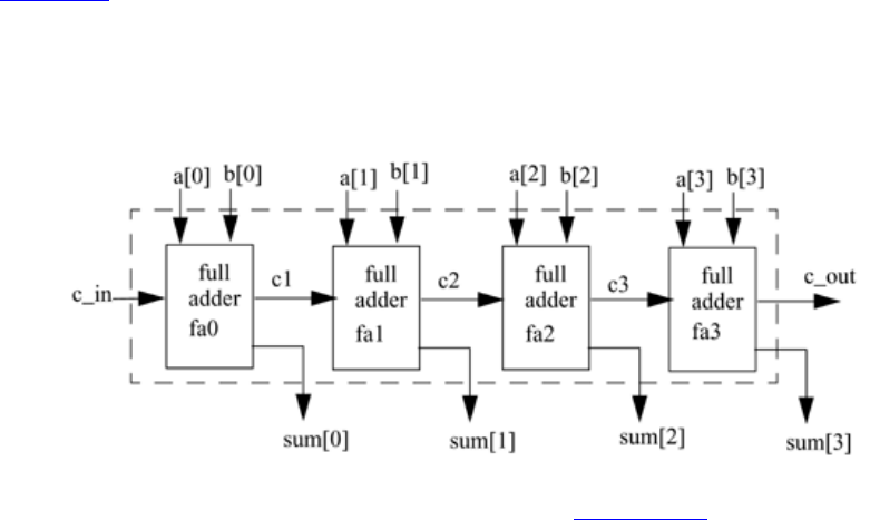
86
A 4-bit ripple carry full adder can be constructed from four 1-bit full adders, as shown in
Figure 5-7. Notice that fa0, fa1, fa2, and fa3 are instances of the module fulladd (1-bit
full adder).
Figure 5-7. 4-bit Ripple Carry Full Adder
This structure can be translated to Verilog as shown in Example 5-8. Note that the port
names used in a 1-bit full adder and a 4-bit full adder are the same but they represent
different elements. The element sum in a 1-bit adder is a scalar quantity and the element
sum in the 4-bit full adder is a 4-bit vector quantity. Verilog keeps names local to a
module. Names are not visible outside the module unless hierarchical name referencing is
used. Also note that instance names must be specified when defined modules are
instantiated, but when instantiating Verilog primitives, the instance names are optional.
Example 5-8 Verilog Description for 4-bit Ripple Carry Full Adder
// Define a 4-bit full adder
module fulladd4(sum, c_out, a, b, c_in);
// I/O port declarations
output [3:0] sum;
output c_out;
input[3:0] a, b;
input c_in;
// Internal nets
wire c1, c2, c3;
// Instantiate four 1-bit full adders.
fulladd fa0(sum[0], c1, a[0], b[0], c_in);
fulladd fa1(sum[1], c2, a[1], b[1], c1);
fulladd fa2(sum[2], c3, a[2], b[2], c2);
fulladd fa3(sum[3], c_out, a[3], b[3], c3);
endmodule

87
Finally, the design must be checked by applying stimulus, as shown in Example 5-9. The
module stimulus stimulates the 4-bit full adder by applying a few input combinations and
monitors the results.
Example 5-9 Stimulus for 4-bit Ripple Carry Full Adder
// Define the stimulus (top level module)
module stimulus;
// Set up variables
reg [3:0] A, B;
reg C_IN;
wire [3:0] SUM;
wire C_OUT;
// Instantiate the 4-bit full adder. call it FA1_4
fulladd4 FA1_4(SUM, C_OUT, A, B, C_IN);
// Set up the monitoring for the signal values
initial
begin
$monitor($time," A= %b, B=%b, C_IN= %b, --- C_OUT= %b, SUM= %b\n",
A, B, C_IN, C_OUT, SUM);
end
// Stimulate inputs
initial
begin
A = 4'd0; B = 4'd0; C_IN = 1'b0;
#5 A = 4'd3; B = 4'd4;
#5 A = 4'd2; B = 4'd5;
#5 A = 4'd9; B = 4'd9;
#5 A = 4'd10; B = 4'd15;
#5 A = 4'd10; B = 4'd5; C_IN = 1'b1;
end
endmodule
The output of the simulation is shown below.
0 A= 0000, B=0000, C_IN= 0, --- C_OUT= 0, SUM= 0000
5 A= 0011, B=0100, C_IN= 0, --- C_OUT= 0, SUM= 0111
10 A= 0010, B=0101, C_IN= 0, --- C_OUT= 0, SUM= 0111
15 A= 1001, B=1001, C_IN= 0, --- C_OUT= 1, SUM= 0010
20 A= 1010, B=1111, C_IN= 0, --- C_OUT= 1, SUM= 1001
25 A= 1010, B=0101, C_IN= 1,, C_OUT= 1, SUM= 0000
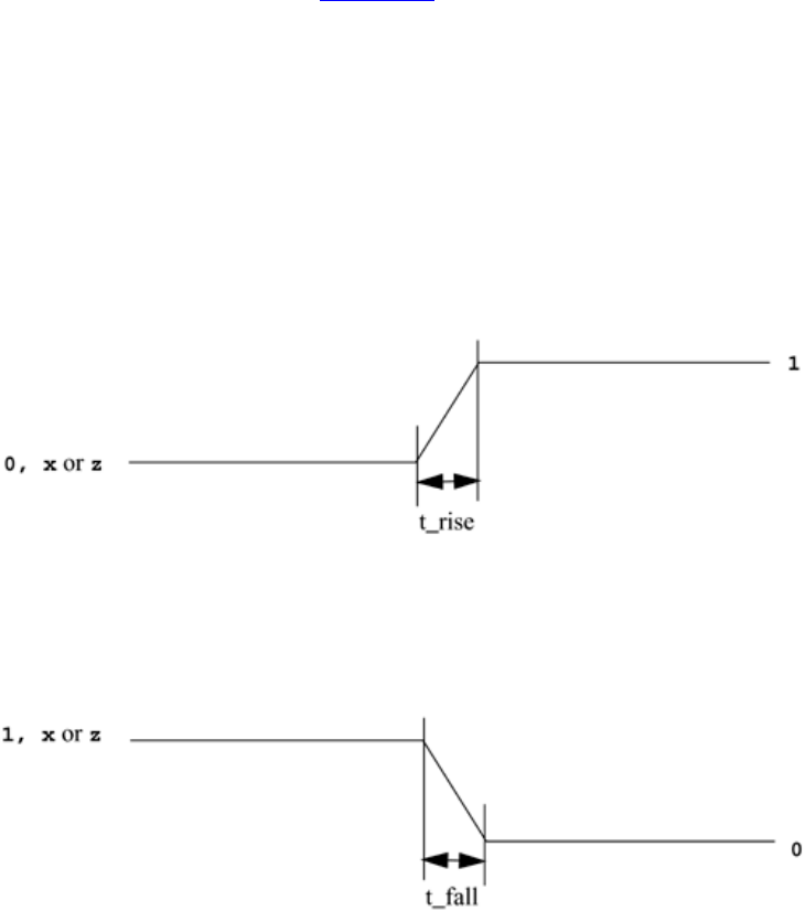
88
5.2 Gate Delays
Until now, we described circuits without any delays (i.e., zero delay). In real circuits,
logic gates have delays associated with them. Gate delays allow the Verilog user to
specify delays through the logic circuits. Pin-to-pin delays can also be specified in
Verilog. They are discussed in Chapter 10, Timing and Delays.
5.2.1 Rise, Fall, and Turn-off Delays
There are three types of delays from the inputs to the output of a primitive gate.
Rise delay
The rise delay is associated with a gate output transition to a 1 from another value.
Fall delay
The fall delay is associated with a gate output transition to a 0 from another value.
Turn-off delay
The turn-off delay is associated with a gate output transition to the high impedance value
(z) from another value.

89
If the value changes to x, the minimum of the three delays is considered.
Three types of delay specifications are allowed. If only one delay is specified, this value
is used for all transitions. If two delays are specified, they refer to the rise and fall delay
values. The turn-off delay is the minimum of the two delays. If all three delays are
specified, they refer to rise, fall, and turn-off delay values. If no delays are specified, the
default value is zero. Examples of delay specification are shown in Example 5-10.
Example 5-10 Types of Delay Specification
// Delay of delay_time for all transitions
and #(delay_time) a1(out, i1, i2);
// Rise and Fall Delay Specification.
and #(rise_val, fall_val) a2(out, i1, i2);
// Rise, Fall, and Turn-off Delay Specification
bufif0 #(rise_val, fall_val, turnoff_val) b1 (out, in, control);
Examples of delay specification are shown below.
and #(5) a1(out, i1, i2); //Delay of 5 for all transitions
and #(4,6) a2(out, i1, i2); // Rise = 4, Fall = 6
bufif0 #(3,4,5) b1 (out, in, control); // Rise = 3, Fall = 4, Turn-off
= 5
5.2.2 Min/Typ/Max Values
Verilog provides an additional level of control for each type of delay mentioned above.
For each type of delay?rise, fall, and turn-off?three values, min, typ, and max, can be
specified. Any one value can be chosen at the start of the simulation. Min/typ/max values
are used to model devices whose delays vary within a minimum and maximum range
because of the IC fabrication process variations.
Min value
The min value is the minimum delay value that the designer expects the gate to have.
Typ val
The typ value is the typical delay value that the designer expects the gate to have.
Max value

90
The max value is the maximum delay value that the designer expects the gate to have.
Min, typ, or max values can be chosen at Verilog run time. Method of choosing a
min/typ/max value may vary for different simulators or operating systems. (For Verilog-
XL , the values are chosen by specifying options +maxdelays, +typdelays, and
+mindelays at run time. If no option is specified, the typical delay value is the default).
This allows the designers the flexibility of building three delay values for each transition
into their design. The designer can experiment with delay values without modifying the
design.
Examples of min, typ, and max value specification for Verilog-XL are shown in Example
5-11.
Example 5-11 Min, Max, and Typical Delay Values
// One delay
// if +mindelays, delay= 4
// if +typdelays, delay= 5
// if +maxdelays, delay= 6
and #(4:5:6) a1(out, i1, i2);
// Two delays
// if +mindelays, rise= 3, fall= 5, turn-off = min(3,5)
// if +typdelays, rise= 4, fall= 6, turn-off = min(4,6)
// if +maxdelays, rise= 5, fall= 7, turn-off = min(5,7)
and #(3:4:5, 5:6:7) a2(out, i1, i2);
// Three delays
// if +mindelays, rise= 2 fall= 3 turn-off = 4
// if +typdelays, rise= 3 fall= 4 turn-off = 5
// if +maxdelays, rise= 4 fall= 5 turn-off = 6
and #(2:3:4, 3:4:5, 4:5:6) a3(out, i1,i2);
Examples of invoking the Verilog-XL simulator with the command-line options are
shown below. Assume that the module with delays is declared in the file test.v.
//invoke simulation with maximum delay
> verilog test.v +maxdelays
//invoke simulation with minimum delay
> verilog test.v +mindelays
//invoke simulation with typical delay
> verilog test.v +typdelays
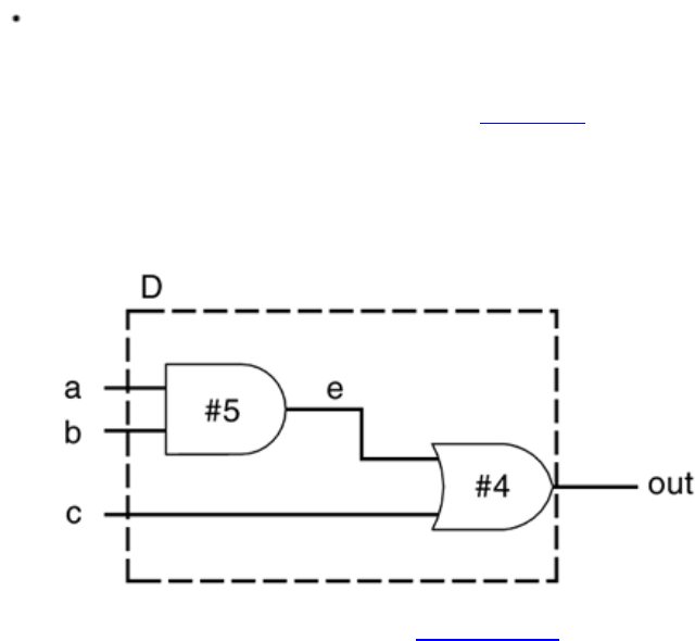
91
5.2.3 Delay Example
Let us consider a simple example to illustrate the use of gate delays to model timing in
the logic circuits. A simple module called D implements the following logic equations:
out = (a b) + c
The gate-level implementation is shown in Module D (Figure 5-8). The module contains
two gates with delays of 5 and 4 time units.
Figure 5-8. Module D
The module D is defined in Verilog as shown in Example 5-12.
Example 5-12 Verilog Definition for Module D with Delay
// Define a simple combination module called D
module D (out, a, b, c);
// I/O port declarations
output out;
input a,b,c;
// Internal nets
wire e;
// Instantiate primitive gates to build the circuit
and #(5) a1(e, a, b); //Delay of 5 on gate a1
or #(4) o1(out, e,c); //Delay of 4 on gate o1
endmodule

92
This module is tested by the stimulus file shown in Example 5-13.
Example 5-13 Stimulus for Module D with Delay
// Stimulus (top-level module)
module stimulus;
// Declare variables
reg A, B, C;
wire OUT;
// Instantiate the module D
D d1( OUT, A, B, C);
// Stimulate the inputs. Finish the simulation at 40 time units.
initial
begin
A= 1'b0; B= 1'b0; C= 1'b0;
#10 A= 1'b1; B= 1'b1; C= 1'b1;
#10 A= 1'b1; B= 1'b0; C= 1'b0;
#20 $finish;
end
endmodule
The waveforms from the simulation are shown in Figure 5-9 to illustrate the effect of
specifying delays on gates. The waveforms are not drawn to scale. However, simulation
time at each transition is specified below the transition.
1. The outputs E and OUT are initially unknown.
2. At time 10, after A, B, and C all transition to 1, OUT transitions to 1 after a delay
of 4 time units and E changes value to 1 after 5 time units.
3. At time 20, B and C transition to 0. E changes value to 0 after 5 time units, and
OUT transitions to 0, 4 time units after E changes.
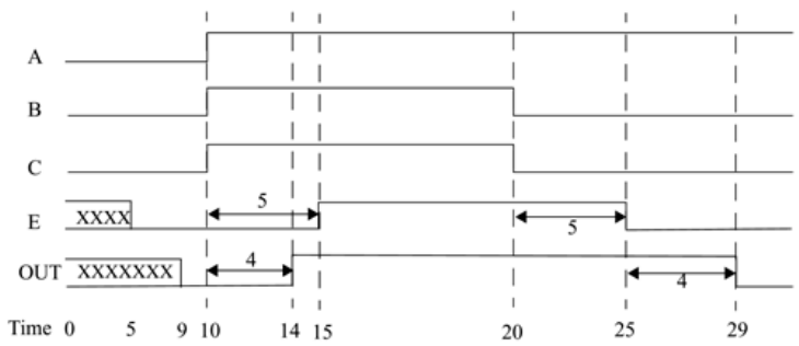
93
Figure 5-9. Waveforms for Delay Simulation
It is a useful exercise to understand how the timing for each transition in the above
waveform corresponds to the gate delays shown in Module D.

94
5.3 Summary
In this chapter, we discussed how to model gate-level logic in Verilog. We also discussed
different aspects of gate-level design.
• The basic types of gates are and, or, xor, buf, and not. Each gate has a logic
symbol, truth table, and a corresponding Verilog primitive. Primitives are
instantiated like modules except that they are predefined in Verilog. The output of
a gate is evaluated as soon as one of its inputs changes.
• Arrays of built-in primitive instances and user-defined modules can be defined in
Verilog.
• For gate-level design, start with the logic diagram, write the Verilog description
for the logic by using gate primitives, provide stimulus, and look at the output.
Two design examples, a 4-to-1 multiplexer and a 4-bit full adder, were discussed.
Each step of the design process was explained.
• Three types of delays are associated with gates: rise, fall, and turn-off. Verilog
allows specification of one, two, or three delays for each gate. Values of rise, fall,
and turn-off delays are computed by Verilog, based on the one, two, or three
delays specified.
• For each type of delay, a minimum, typical, and maximum value can be specified.
The user can choose which value to apply at simulation time. This provides the
flexibility to experiment with three delay values without changing the Verilog
code.
• The effect of propagation delay on waveforms was explained by the simple, two-
gate logic example. For each gate with a delay of t, the output changes t time units
after any of the inputs change.
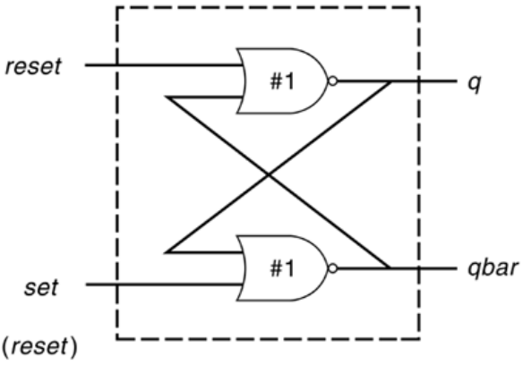
95
5.4 Exercises
1: Create your own 2-input Verilog gates called my-or, my-and and my-not from
2-input nand gates. Check the functionality of these gates with a stimulus
module.
2: A 2-input xor gate can be built from my_and, my_or and my_not gates.
Construct an xor module in Verilog that realizes the logic function, z = xy' +
x'y. Inputs are x and y, and z is the output. Write a stimulus module that
exercises all four combinations of x and y inputs.
3: The 1-bit full adder described in the chapter can be expressed in a sum of
products form.
sum = a.b.c_in + a'.b.c_in' + a'.b'.c_in + a.b'.c_in'
c_out = a.b + b.c_in + a.c_in
Assuming a, b, c_in are the inputs and sum and c_out are the outputs, design a
logic circuit to implement the 1-bit full adder, using only and, not, and or gates.
Write the Verilog description for the circuit. You may use up to 4-input Verilog
primitive and and or gates. Write the stimulus for the full adder and check the
functionality for all input combinations.
4: The logic diagram for an RS latch with delay is shown below.
Write the Verilog description for the RS latch. Include delays of 1 unit when
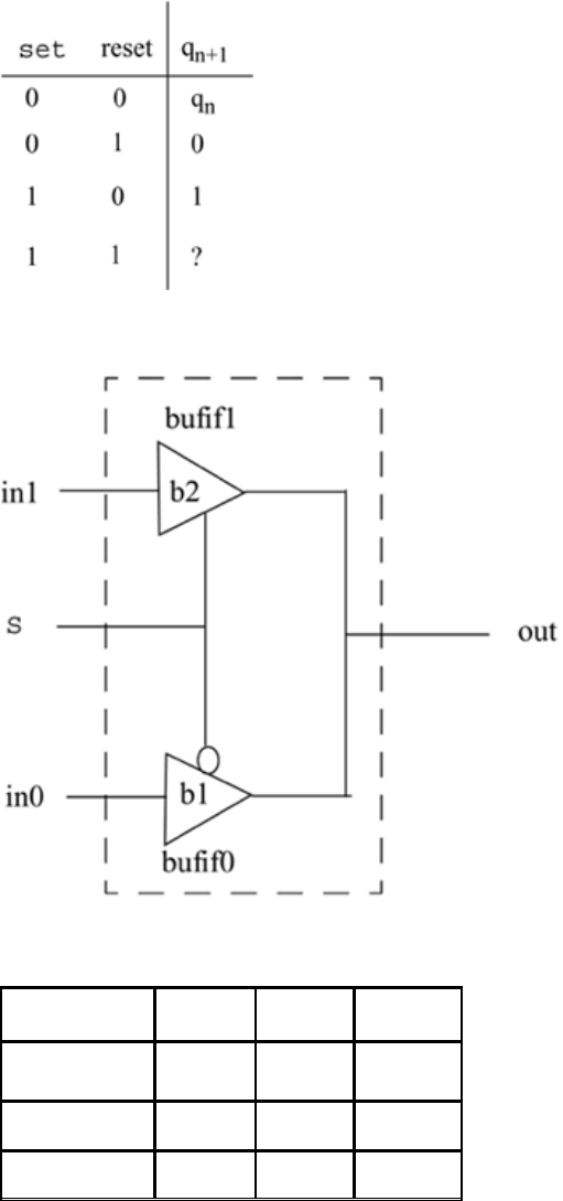
96
instantiating the nor gates. Write the stimulus module for the RS latch, using the
following table, and verify the outputs.
5: Design a 2-to-1 multiplexer using bufif0 and bufif1 gates as shown below.
The delay specification for gates b1 and b2 are as follows:
Min Typ Max
Rise 1 2 3
Fall 3 4 5
Turnoff 5 6 7
Apply stimulus and test the output values.
97
Chapter 6. Dataflow Modeling
For small circuits, the gate-level modeling approach works very well because the number
of gates is limited and the designer can instantiate and connect every gate individually.
Also, gate-level modeling is very intuitive to a designer with a basic knowledge of digital
logic design. However, in complex designs the number of gates is very large. Thus,
designers can design more effectively if they concentrate on implementing the function at
a level of abstraction higher than gate level. Dataflow modeling provides a powerful way
to implement a design. Verilog allows a circuit to be designed in terms of the data flow
between registers and how a design processes data rather than instantiation of individual
gates. Later in this chapter, the benefits of dataflow modeling will become more apparent.
With gate densities on chips increasing rapidly, dataflow modeling has assumed great
importance. No longer can companies devote engineering resources to handcrafting entire
designs with gates. Currently, automated tools are used to create a gate-level circuit from
a dataflow design description. This process is called logic synthesis. Dataflow modeling
has become a popular design approach as logic synthesis tools have become
sophisticated. This approach allows the designer to concentrate on optimizing the circuit
in terms of data flow. For maximum flexibility in the design process, designers typically
use a Verilog description style that combines the concepts of gate-level, data flow, and
behavioral design. In the digital design community, the term RTL (Register Transfer
Level) design is commonly used for a combination of dataflow modeling and behavioral
modeling.
Learning Objectives
• Describe the continuous assignment (assign) statement, restrictions on the assign
statement, and the implicit continuous assignment statement.
• Explain assignment delay, implicit assignment delay, and net declaration delay for
continuous assignment statements.
• Define expressions, operators, and operands.
•
• List operator types for all possible operations?arithmetic, logical, relational,
equality, bitwise, reduction, shift, concatenation, and conditional.
• Use dataflow constructs to model practical digital circuits in Verilog.

98
6.1 Continuous Assignments
A continuous assignment is the most basic statement in dataflow modeling, used to drive
a value onto a net. This assignment replaces gates in the description of the circuit and
describes the circuit at a higher level of abstraction. The assignment statement starts with
the keyword assign. The syntax of an assign statement is as follows.
continuous_assign ::= assign [ drive_strength ] [ delay3 ]
list_of_net_assignments ;
list_of_net_assignments ::= net_assignment { , net_assignment }
net_assignment ::= net_lvalue = expression
Notice that drive strength is optional and can be specified in terms of strength levels
discussed in Section 3.2.1, Value Set. We will not discuss drive strength specification in
this chapter. The default value for drive strength is strong1 and strong0. The delay value
is also optional and can be used to specify delay on the assign statement. This is like
specifying delays for gates. Delay specification is discussed in this chapter. Continuous
assignments have the following characteristics:
1. The left hand side of an assignment must always be a scalar or vector net or a
concatenation of scalar and vector nets. It cannot be a scalar or vector register.
Concatenations are discussed in Section 6.4.8, Concatenation Operator.
2. Continuous assignments are always active. The assignment expression is
evaluated as soon as one of the right-hand-side operands changes and the value is
assigned to the left-hand-side net.
3. The operands on the right-hand side can be registers or nets or function calls.
Registers or nets can be scalars or vectors.
4. Delay values can be specified for assignments in terms of time units. Delay values
are used to control the time when a net is assigned the evaluated value. This
feature is similar to specifying delays for gates. It is very useful in modeling
timing behavior in real circuits.
Examples of continuous assignments are shown below. Operators such as &, ^, |, {, } and
+ used in the examples are explained in Section 6.4, Operator Types. At this point,
concentrate on how the assign statements are specified.
99
Example 6-1 Examples of Continuous Assignment
// Continuous assign. out is a net. i1 and i2 are nets.
assign out = i1 & i2;
// Continuous assign for vector nets. addr is a 16-bit vector net
// addr1 and addr2 are 16-bit vector registers.
assign addr[15:0] = addr1_bits[15:0] ^ addr2_bits[15:0];
// Concatenation. Left-hand side is a concatenation of a scalar
// net and a vector net.
assign {c_out, sum[3:0]} = a[3:0] + b[3:0] + c_in;
We now discuss a shorthand method of placing a continuous assignment on a net.
6.1.1 Implicit Continuous Assignment
Instead of declaring a net and then writing a continuous assignment on the net, Verilog
provides a shortcut by which a continuous assignment can be placed on a net when it is
declared. There can be only one implicit declaration assignment per net because a net is
declared only once.
In the example below, an implicit continuous assignment is contrasted with a regular
continuous assignment.
//Regular continuous assignment
wire out;
assign out = in1 & in2;
//Same effect is achieved by an implicit continuous assignment
wire out = in1 & in2;
6.1.2 Implicit Net Declaration
If a signal name is used to the left of the continuous assignment, an implicit net
declaration will be inferred for that signal name. If the net is connected to a module port,
the width of the inferred net is equal to the width of the module port.
// Continuous assign. out is a net.
wire i1, i2;
assign out = i1 & i2; //Note that out was not declared as a wire
//but an implicit wire declaration for out
//is done by the simulator

100
6.2 Delays
Delay values control the time between the change in a right-hand-side operand and when
the new value is assigned to the left-hand side. Three ways of specifying delays in
continuous assignment statements are regular assignment delay, implicit continuous
assignment delay, and net declaration delay.
6.2.1 Regular Assignment Delay
The first method is to assign a delay value in a continuous assignment statement. The
delay value is specified after the keyword assign. Any change in values of in1 or in2 will
result in a delay of 10 time units before recomputation of the expression in1 & in2, and
the result will be assigned to out. If in1 or in2 changes value again before 10 time units
when the result propagates to out, the values of in1 and in2 at the time of recomputation
are considered. This property is called inertial delay. An input pulse that is shorter than
the delay of the assignment statement does not propagate to the output.
assign #10 out = in1 & in2; // Delay in a continuous assign
The waveform in Figure 6-1 is generated by simulating the above assign statement. It
shows the delay on signal out. Note the following change:
1. When signals in1 and in2 go high at time 20, out goes to a high 10 time units later
(time = 30).
2. When in1 goes low at 60, out changes to low at 70.
3. However, in1 changes to high at 80, but it goes down to low before 10 time units
have elapsed.
4. Hence, at the time of recomputation, 10 units after time 80, in1 is 0. Thus, out
gets the value 0. A pulse of width less than the specified assignment delay is not
propagated to the output.
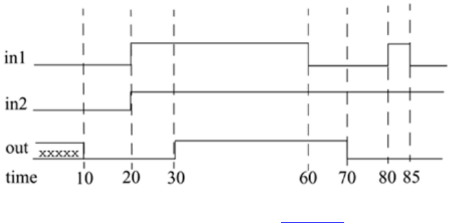
101
Figure 6-1. Delays
Inertial delays also apply to gate delays, discussed in Chapter 5, Gate-Level Modeling.
6.2.2 Implicit Continuous Assignment Delay
An equivalent method is to use an implicit continuous assignment to specify both a delay
and an assignment on the net.
//implicit continuous assignment delay
wire #10 out = in1 & in2;
//same as
wire out;
assign #10 out = in1 & in2;
The declaration above has the same effect as defining a wire out and declaring a
continuous assignment on out.
6.2.3 Net Declaration Delay
A delay can be specified on a net when it is declared without putting a continuous
assignment on the net. If a delay is specified on a net out, then any value change applied
to the net out is delayed accordingly. Net declaration delays can also be used in gate-level
modeling.
//Net Delays
wire # 10 out;
assign out = in1 & in2;
//The above statement has the same effect as the following.
wire out;
assign #10 out = in1 & in2;
Having discussed continuous assignments and delays, let us take a closer look at
expressions, operators, and operands that are used inside continuous assignments.

102
6.3 Expressions, Operators, and Operands
Dataflow modeling describes the design in terms of expressions instead of primitive
gates. Expressions, operators, and operands form the basis of dataflow modeling.
6.3.1 Expressions
Expressions are constructs that combine operators and operands to produce a result.
// Examples of expressions. Combines operands and operators
a ^ b
addr1[20:17] + addr2[20:17]
in1 | in2
6.3.2 Operands
Operands can be any one of the data types defined in Section 3.2, Data Types. Some
constructs will take only certain types of operands. Operands can be constants, integers,
real numbers, nets, registers, times, bit-select (one bit of vector net or a vector register),
part-select (selected bits of the vector net or register vector), and memories or function
calls (functions are discussed later).
integer count, final_count;
final_count = count + 1;//count is an integer operand
real a, b, c;
c = a - b; //a and b are real operands
reg [15:0] reg1, reg2;
reg [3:0] reg_out;
reg_out = reg1[3:0] ^ reg2[3:0];//reg1[3:0] and reg2[3:0] are
//part-select register operands
reg ret_value;
ret_value = calculate_parity(A, B);//calculate_parity is a
//function type operand
6.3.3 Operators
Operators act on the operands to produce desired results. Verilog provides various types
of operators. Operator types are discussed in detail in Section 6.4, Operator Types.
d1 && d2 // && is an operator on operands d1 and d2
!a[0] // ! is an operator on operand a[0]
B >> 1 // >> is an operator on operands B and 1

103
6.4 Operator Types
Verilog provides many different operator types. Operators can be arithmetic, logical,
relational, equality, bitwise, reduction, shift, concatenation, or conditional. Some of these
operators are similar to the operators used in the C programming language. Each operator
type is denoted by a symbol. Table 6-1 shows the complete listing of operator symbols
classified by category.
Table 6-1. Operator Types and Symbols
Operator Type Operator Symbol Operation Performed Number of Operands
Arithmetic
*
/
+
-
%
**
multiply
divide
add
subtract
modulus
power (exponent)
two
two
two
two
two
two
Logical
!
&&
||
logical negation
logical and
logical or
one
two
two
Relational
>
<
>=
<=
greater than
less than
greater than or equal
less than or equal
two
two
two
two
Equality
==
!=
===
!==
equality
inequality
case equality
case inequality
two
two
two
two

104
Bitwise
~
&
|
^
^~ or ~^
bitwise negation
bitwise and
bitwise or
bitwise xor
bitwise xnor
one
two
two
two
two
Reduction
&
~&
|
~|
^
^~ or ~^
reduction and
reduction nand
reduction or
reduction nor
reduction xor
reduction xnor
one
one
one
one
one
one
Shift
>>
<<
>>>
<<<
Right shift
Left shift
Arithmetic right shift
Arithmetic left shift
Two
Two
Two
Two
Concatenation { } Concatenation Any number
Replication { { } } Replication Any number
Conditional ?: Conditional Three
Let us now discuss each operator type in detail.
6.4.1 Arithmetic Operators
There are two types of arithmetic operators: binary and unary.
Binary operators
Binary arithmetic operators are multiply (*), divide (/), add (+), subtract (-), power (**),
and modulus (%). Binary operators take two operands.
105
A = 4'b0011; B = 4'b0100; // A and B are register vectors
D = 6; E = 4; F=2// D and E are integers
A * B // Multiply A and B. Evaluates to 4'b1100
D / E // Divide D by E. Evaluates to 1. Truncates any fractional part.
A + B // Add A and B. Evaluates to 4'b0111
B - A // Subtract A from B. Evaluates to 4'b0001
F = E ** F; //E to the power F, yields 16
If any operand bit has a value x, then the result of the entire expression is x. This seems
intuitive because if an operand value is not known precisely, the result should be an
unknown.
in1 = 4'b101x;
in2 = 4'b1010;
sum = in1 + in2; // sum will be evaluated to the value 4'bx
Modulus operators produce the remainder from the division of two numbers. They
operate similarly to the modulus operator in the C programming language.
13 % 3 // Evaluates to 1
16 % 4 // Evaluates to 0
-7 % 2 // Evaluates to -1, takes sign of the first operand
7 % -2 // Evaluates to +1, takes sign of the first operand
Unary operators
The operators + and - can also work as unary operators. They are used to specify the
positive or negative sign of the operand. Unary + or ? operators have higher precedence
than the binary + or ? operators.
-4 // Negative 4
+5 // Positive 5
Negative numbers are represented as 2's complement internally in Verilog. It is advisable
to use negative numbers only of the type integer or real in expressions. Designers should
avoid negative numbers of the type <sss> '<base> <nnn> in expressions because they are
converted to unsigned 2's complement numbers and hence yield unexpected results.
//Advisable to use integer or real numbers
-10 / 5// Evaluates to -2
//Do not use numbers of type <sss> '<base> <nnn>
-'d10 / 5// Is equivalent (2's complement of 10)/5 = (232 - 10)/5
// where 32 is the default machine word width.
// This evaluates to an incorrect and unexpected result
106
6.4.2 Logical Operators
Logical operators are logical-and (&&), logical-or (||) and logical-not (!). Operators &&
and || are binary operators. Operator ! is a unary operator. Logical operators follow these
conditions:
1. Logical operators always evaluate to a 1-bit value, 0 (false), 1 (true), or x
(ambiguous).
2. If an operand is not equal to zero, it is equivalent to a logical 1 (true condition). If
it is 01equal to zero, it is equivalent to a logical 0 (false condition). If any operand
bit is x or z, it is equivalent to x (ambiguous condition) and is normally treated by
simulators as a false condition.
3. Logical operators take variables or expressions as operands.
Use of parentheses to group logical operations is highly recommended to improve
readability. Also, the user does not have to remember the precedence of operators.
// Logical operations
A = 3; B = 0;
A && B // Evaluates to 0. Equivalent to (logical-1 && logical-0)
A || B // Evaluates to 1. Equivalent to (logical-1 || logical-0)
!A// Evaluates to 0. Equivalent to not(logical-1)
!B// Evaluates to 1. Equivalent to not(logical-0)
// Unknowns
A = 2'b0x; B = 2'b10;
A && B // Evaluates to x. Equivalent to (x && logical 1)
// Expressions
(a == 2) && (b == 3) // Evaluates to 1 if both a == 2 and b == 3 are
true.
// Evaluates to 0 if either is false.
6.4.3 Relational Operators
Relational operators are greater-than (>), less-than (<), greater-than-or-equal-to (>=), and
less-than-or-equal-to (<=). If relational operators are used in an expression, the
expression returns a logical value of 1 if the expression is true and 0 if the expression is
false. If there are any unknown or z bits in the operands, the expression takes a value x.
These operators function exactly as the corresponding operators in the C programming
language.
107
// A = 4, B = 3
// X = 4'b1010, Y = 4'b1101, Z = 4'b1xxx
A <= B // Evaluates to a logical 0
A > B // Evaluates to a logical 1
Y >= X // Evaluates to a logical 1
Y < Z // Evaluates to an x
6.4.4 Equality Operators
Equality operators are logical equality (==), logical inequality (!=), case equality (===),
and case inequality (!==). When used in an expression, equality operators return logical
value 1 if true, 0 if false. These operators compare the two operands bit by bit, with zero
filling if the operands are of unequal length. Table 6-2 lists the operators.
Table 6-2. Equality Operators
Expression Description Possible Logical
Value
a == b a equal to b, result unknown if x or z in a or b 0, 1, x
a != b a not equal to b, result unknown if x or z in a or
b 0, 1, x
a === b a equal to b, including x and z 0, 1
a !== b a not equal to b, including x and z 0, 1
It is important to note the difference between the logical equality operators (==, !=) and
case equality operators (===, !==). The logical equality operators (==, !=) will yield an x
if either operand has x or z in its bits. However, the case equality operators ( ===, !== )
compare both operands bit by bit and compare all bits, including x and z. The result is 1 i
f
the operands match exactly, including x and z bits. The result is 0 if the operands do not
match exactly. Case equality operators never result in an x.
// A = 4, B = 3
// X = 4'b1010, Y = 4'b1101
// Z = 4'b1xxz, M = 4'b1xxz, N = 4'b1xxx
A == B // Results in logical 0
X != Y // Results in logical 1
X == Z // Results in x
Z === M // Results in logical 1 (all bits match, including x and z)
Z === N // Results in logical 0 (least significant bit does not match)
M !== N // Results in logical 1
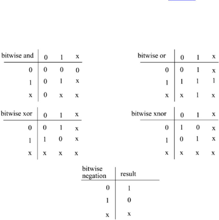
108
6.4.5 Bitwise Operators
Bitwise operators are negation (~), and(&), or (|), xor (^), xnor (^~, ~^). Bitwise operators
perform a bit-by-bit operation on two operands. They take each bit in one operand and
perform the operation with the corresponding bit in the other operand. If one operand is
shorter than the other, it will be bit-extended with zeros to match the length of the longer
operand. Logic tables for the bit-by-bit computation are shown in Table 6-3. A z is
treated as an x in a bitwise operation. The exception is the unary negation operator (~),
which takes only one operand and operates on the bits of the single operand.
Table 6-3. Truth Tables for Bitwise Operators
Examples of bitwise operators are shown below.
// X = 4'b1010, Y = 4'b1101
// Z = 4'b10x1
~X // Negation. Result is 4'b0101
X & Y // Bitwise and. Result is 4'b1000
X | Y // Bitwise or. Result is 4'b1111
X ^ Y // Bitwise xor. Result is 4'b0111
X ^~ Y // Bitwise xnor. Result is 4'b1000
X & Z // Result is 4'b10x0

109
It is important to distinguish bitwise operators ~, &, and | from logical operators !, &&, ||.
Logical operators always yield a logical value 0, 1, x, whereas bitwise operators yield a
bit-by-bit value. Logical operators perform a logical operation, not a bit-by-bit operation.
// X = 4'b1010, Y = 4'b0000
X | Y // bitwise operation. Result is 4'b1010
X || Y // logical operation. Equivalent to 1 || 0. Result is 1.
6.4.6 Reduction Operators
Reduction operators are and (&), nand (~&), or (|), nor (~|), xor (^), and xnor (~^, ^~).
Reduction operators take only one operand. Reduction operators perform a bitwise
operation on a single vector operand and yield a 1-bit result. The logic tables for the
operators are the same as shown in Section 6.4.5, Bitwise Operators. The difference is
that bitwise operations are on bits from two different operands, whereas reduction
operations are on the bits of the same operand. Reduction operators work bit by bit from
right to left. Reduction nand, reduction nor, and reduction xnor are computed by inverting
the result of the reduction and, reduction or, and reduction xor, respectively.
// X = 4'b1010
&X //Equivalent to 1 & 0 & 1 & 0. Results in 1'b0
|X//Equivalent to 1 | 0 | 1 | 0. Results in 1'b1
^X//Equivalent to 1 ^ 0 ^ 1 ^ 0. Results in 1'b0
//A reduction xor or xnor can be used for even or odd parity
//generation of a vector.
The use of a similar set of symbols for logical (!, &&, ||), bitwise (~, &, |, ^), and
reduction operators (&, |, ^) is somewhat confusing initially. The difference lies in the
number of operands each operator takes and also the value of results computed.
6.4.7 Shift Operators
Shift operators are right shift ( >>), left shift (<<), arithmetic right shift (>>>), and
arithmetic left shift (<<<). Regular shift operators shift a vector operand to the right or
the left by a specified number of bits. The operands are the vector and the number of bits
to shift. When the bits are shifted, the vacant bit positions are filled with zeros. Shift
operations do not wrap around. Arithmetic shift operators use the context of the
expression to determine the value with which to fill the vacated bits.
// X = 4'b1100
Y = X >> 1; //Y is 4'b0110. Shift right 1 bit. 0 filled in MSB
position.
110
Y = X << 1; //Y is 4'b1000. Shift left 1 bit. 0 filled in LSB position.
Y = X << 2; //Y is 4'b0000. Shift left 2 bits.
integer a, b, c; //Signed data types
a = 0;
b = -10; // 00111...10110 binary
c = a + (b >>> 3); //Results in -2 decimal, due to arithmetic shift
Shift operators are useful because they allow the designer to model shift operations, shift-
and-add algorithms for multiplication, and other useful operations.
6.4.8 Concatenation Operator
The concatenation operator ( {, } ) provides a mechanism to append multiple operands.
The operands must be sized. Unsized operands are not allowed because the size of each
operand must be known for computation of the size of the result.
Concatenations are expressed as operands within braces, with commas separating the
operands. Operands can be scalar nets or registers, vector nets or registers, bit-select,
part-select, or sized constants.
// A = 1'b1, B = 2'b00, C = 2'b10, D = 3'b110
Y = {B , C} // Result Y is 4'b0010
Y = {A , B , C , D , 3'b001} // Result Y is 11'b10010110001
Y = {A , B[0], C[1]} // Result Y is 3'b101
6.4.9 Replication Operator
Repetitive concatenation of the same number can be expressed by using a replication
constant. A replication constant specifies how many times to replicate the number inside
the brackets ( { } ).
reg A;
reg [1:0] B, C;
reg [2:0] D;
A = 1'b1; B = 2'b00; C = 2'b10; D = 3'b110;
Y = { 4{A} } // Result Y is 4'b1111
Y = { 4{A} , 2{B} } // Result Y is 8'b11110000
Y = { 4{A} , 2{B} , C } // Result Y is 8'b1111000010
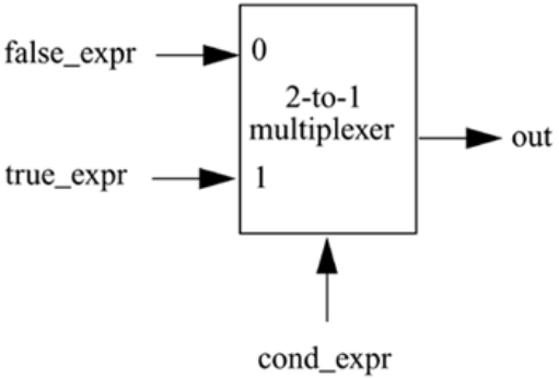
111
6.4.10 Conditional Operator
The conditional operator(?:) takes three operands.
Usage: condition_expr ? true_expr : false_expr ;
The condition expression (condition_expr) is first evaluated. If the result is true (logical
1), then the true_expr is evaluated. If the result is false (logical 0), then the false_expr is
evaluated. If the result is x (ambiguous), then both true_expr and false_expr are evaluated
and their results are compared, bit by bit, to return for each bit position an x if the bits are
different and the value of the bits if they are the same.
The action of a conditional operator is similar to a multiplexer. Alternately, it can be
compared to the if-else expression.
Conditional operators are frequently used in dataflow modeling to model conditional
assignments. The conditional expression acts as a switching control.
//model functionality of a tristate buffer
assign addr_bus = drive_enable ? addr_out : 36'bz;
//model functionality of a 2-to-1 mux
assign out = control ? in1 : in0;
Conditional operations can be nested. Each true_expr or false_expr can itself be a
conditional operation. In the example that follows, convince yourself that (A==3) and
control are the two select signals of 4-to-1 multiplexer with n, m, y, x as the inputs and
out as the output signal.
assign out = (A == 3) ? ( control ? x : y ): ( control ? m : n) ;
112
6.4.11 Operator Precedence
Having discussed the operators, it is now important to discuss operator precedence. If no
parentheses are used to separate parts of expressions, Verilog enforces the following
precedence. Operators listed in Table 6-4 are in order from highest precedence to lowest
precedence. It is recommended that parentheses be used to separate expressions except in
case of unary operators or when there is no ambiguity.
Table 6-4. Operator Precedence
Operators Operator Symbols Precedence
Unary + - ! ~ Highest precedence
Multiply, Divide, Modulus * / %
Add, Subtract + -
Shift << >>
Relational < <= > >=
Equality == != === !==
Reduction
&, ~&
^ ^~
|, ~|
Logical
&&
||
Conditional ?: Lowest precedence

113
6.5 Examples
A design can be represented in terms of gates, data flow, or a behavioral description. In
this section, we consider the 4-to-1 multiplexer and 4-bit full adder described in Section
5.1.4, Examples. Previously, these designs were directly translated from the logic
diagram into a gate-level Verilog description. Here, we describe the same designs in
terms of data flow. We also discuss two additional examples: a 4-bit full adder using
carry lookahead and a 4-bit counter using negative edge-triggered D-flipflops.
6.5.1 4-to-1 Multiplexer
Gate-level modeling of a 4-to-1 multiplexer is discussed in Section 5.1.4, Examples. The
logic diagram for the multiplexer is given in Figure 5-5 and the gate-level Verilog
description is shown in Example 5-5. We describe the multiplexer, using dataflow
statements. Compare it with the gate-level description. We show two methods to model
the multiplexer by using dataflow statements.
Method 1: logic equation
We can use assignment statements instead of gates to model the logic equations of the
multiplexer (see Example 6-2). Notice that everything is same as the gate-level Verilog
description except that computation of out is done by specifying one logic equation by
using operators instead of individual gate instantiations. I/O ports remain the same. This
is important so that the interface with the environment does not change. Only the
internals of the module change. Notice how concise the description is compared to the
gate-level description.
Example 6-2 4-to-1 Multiplexer, Using Logic Equations
// Module 4-to-1 multiplexer using data flow. logic equation
// Compare to gate-level model
module mux4_to_1 (out, i0, i1, i2, i3, s1, s0);
// Port declarations from the I/O diagram
output out;
input i0, i1, i2, i3;
input s1, s0;
//Logic equation for out
assign out = (~s1 & ~s0 & i0)|
(~s1 & s0 & i1) |
(s1 & ~s0 & i2) |
(s1 & s0 & i3) ;
endmodule

114
Method 2: conditional operator
There is a more concise way to specify the 4-to-1 multiplexers. In Section 6.4.10,
Conditional Operator, we described how a conditional statement corresponds to a
multiplexer operation. We will use this operator to write a 4-to-1 multiplexer. Convince
yourself that this description (Example 6-3) correctly models a multiplexer.
Example 6-3 4-to-1 Multiplexer, Using Conditional Operators
// Module 4-to-1 multiplexer using data flow. Conditional operator.
// Compare to gate-level model
module multiplexer4_to_1 (out, i0, i1, i2, i3, s1, s0);
// Port declarations from the I/O diagram
output out;
input i0, i1, i2, i3;
input s1, s0;
// Use nested conditional operator
assign out = s1 ? ( s0 ? i3 : i2) : (s0 ? i1 : i0) ;
endmodule
In the simulation of the multiplexer, the gate-level module in Example 5-5 on page 72
can be substituted with the dataflow multiplexer modules described above. The stimulus
module will not change. The simulation results will be identical. By encapsulating
functionality inside a module, we can replace the gate-level module with a dataflow
module without affecting the other modules in the simulation. This is a very powerful
feature of Verilog.
6.5.2 4-bit Full Adder
The 4-bit full adder in Section 5.1.4, Examples, was designed by using gates; the logic
diagram is shown in Figure 5-7 and Figure 5-6. In this section, we write the dataflow
description for the 4-bit adder. Compare it with the gate-level description in Figure 5-7.
In gates, we had to first describe a 1-bit full adder. Then we built a 4-bit full ripple carry
adder. We again illustrate two methods to describe a 4-bit full adder by means of
dataflow statements.
Method 1: dataflow operators
A concise description of the adder (Example 6-4) is defined with the + and { } operators.

115
Example 6-4 4-bit Full Adder, Using Dataflow Operators
// Define a 4-bit full adder by using dataflow statements.
module fulladd4(sum, c_out, a, b, c_in);
// I/O port declarations
output [3:0] sum;
output c_out;
input[3:0] a, b;
input c_in;
// Specify the function of a full adder
assign {c_out, sum} = a + b + c_in;
endmodule
If we substitute the gate-level 4-bit full adder with the dataflow 4-bit full adder, the rest
of the modules will not change. The simulation results will be identical.
Method 2: full adder with carry lookahead
In ripple carry adders, the carry must propagate through the gate levels before the sum is
available at the output terminals. An n-
b
it ripple carry adder will have 2n gate levels. The
propagation time can be a limiting factor on the speed of the circuit. One of the most
popular methods to reduce delay is to use a carry lookahead mechanism. Logic equations
for implementing the carry lookahead mechanism can be found in any logic design book.
The propagation delay is reduced to four gate levels, irrespective of the number of bits in
the adder. The Verilog description for a carry lookahead adder is shown in Example 6-5.
This module can be substituted in place of the full adder modules described before
without changing any other component of the simulation. The simulation results will be
unchanged.
Example 6-5 4-bit Full Adder with Carry Lookahead
module fulladd4(sum, c_out, a, b, c_in);
// Inputs and outputs
output [3:0] sum;
output c_out;
input [3:0] a,b;
input c_in;
// Internal wires
wire p0,g0, p1,g1, p2,g2, p3,g3;
wire c4, c3, c2, c1;
// compute the p for each stage
assign p0 = a[0] ^ b[0],
p1 = a[1] ^ b[1],

116
p2 = a[2] ^ b[2],
p3 = a[3] ^ b[3];
// compute the g for each stage
assign g0 = a[0] & b[0],
g1 = a[1] & b[1],
g2 = a[2] & b[2],
g3 = a[3] & b[3];
// compute the carry for each stage
// Note that c_in is equivalent c0 in the arithmetic equation for
// carry lookahead computation
assign c1 = g0 | (p0 & c_in),
c2 = g1 | (p1 & g0) | (p1 & p0 & c_in),
c3 = g2 | (p2 & g1) | (p2 & p1 & g0) | (p2 & p1 & p0 & c_in),
c4 = g3 | (p3 & g2) | (p3 & p2 & g1) | (p3 & p2 & p1 & g0) |
(p3 & p2 & p1 & p0 & c_in);
// Compute Sum
assign sum[0] = p0 ^ c_in,
sum[1] = p1 ^ c1,
sum[2] = p2 ^ c2,
sum[3] = p3 ^ c3;
// Assign carry output
assign c_out = c4;
endmodule
6.5.3 Ripple Counter
We now discuss an additional example that was not discussed in the gate-level modeling
chapter. We design a 4-bit ripple counter by using negative edge-triggered flipflops. This
example was discussed at a very abstract level in Chapter 2, Hierarchical Modeling
Concepts. We design it using Verilog dataflow statements and test it with a stimulus
module. The diagrams for the 4-bit ripple carry counter modules are shown below.
Figure 6-2 shows the counter being built with four T-flipflops.
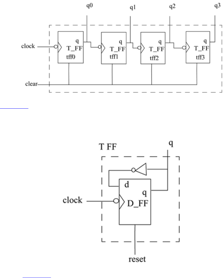
117
Figure 6-2. 4-bit Ripple Carry Counter
Figure 6-3 shows that the T-flipflop is built with one D-flipflop and an inverter gate.
Figure 6-3. T-flipflop
Finally, Figure 6-4 shows the D-flipflop constructed from basic logic gates.
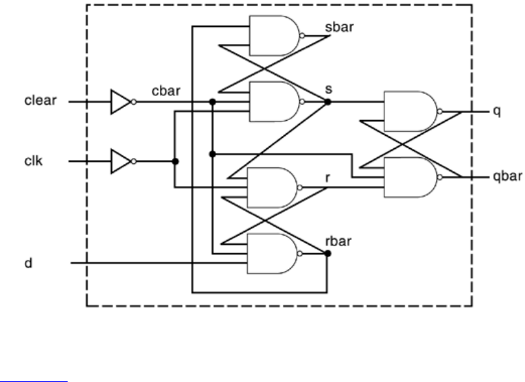
118
Figure 6-4. Negative Edge-Triggered D-flipflop with Clear
Given the above diagrams, we write the corresponding Verilog, using dataflow
statements in a top-down fashion. First we design the module counter. The code is shown
in Figure 6-6. The code contains instantiation of four T_FF modules.
Example 6-6 Verilog Code for Ripple Counter
// Ripple counter
module counter(Q , clock, clear);
// I/O ports
output [3:0] Q;
input clock, clear;
// Instantiate the T flipflops
T_FF tff0(Q[0], clock, clear);
T_FF tff1(Q[1], Q[0], clear);
T_FF tff2(Q[2], Q[1], clear);
T_FF tff3(Q[3], Q[2], clear);
endmodule
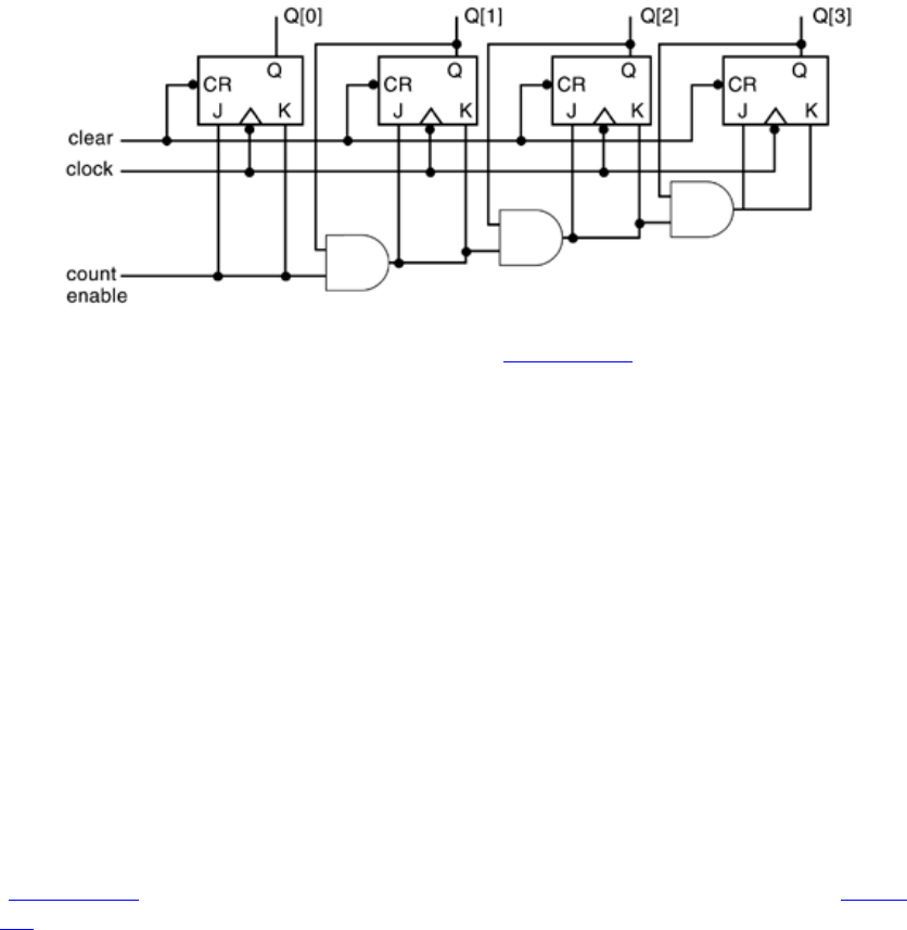
119
Figure 6-6. 4-bit Synchronous Counter with clear and count_enable
Next, we write the Verilog description for T_FF (Example 6-7). Notice that instead of the
not gate, a dataflow operator ~ negates the signal q, which is fed back.
Example 6-7 Verilog Code for T-flipflop
// Edge-triggered T-flipflop. Toggles every clock
// cycle.
module T_FF(q, clk, clear);
// I/O ports
output q;
input clk, clear;
// Instantiate the edge-triggered DFF
// Complement of output q is fed back.
// Notice qbar not needed. Unconnected port.
edge_dff ff1(q, ,~q, clk, clear);
endmodule
Finally, we define the lowest level module D_FF (edge_dff ), using dataflow statements
(Example 6-8). The dataflow statements correspond to the logic diagram shown in Figure
6-4. The nets in the logic diagram correspond exactly to the declared nets.
Example 6-8 Verilog Code for Edge-Triggered D-flipflop
// Edge-triggered D flipflop
module edge_dff(q, qbar, d, clk, clear);
// Inputs and outputs
output q,qbar;
input d, clk, clear;
// Internal variables
wire s, sbar, r, rbar,cbar;
// dataflow statements
//Create a complement of signal clear

120
assign cbar = ~clear;
// Input latches; A latch is level sensitive. An edge-sensitive
// flip-flop is implemented by using 3 SR latches.
assign sbar = ~(rbar & s),
s = ~(sbar & cbar & ~clk),
r = ~(rbar & ~clk & s),
rbar = ~(r & cbar & d);
// Output latch
assign q = ~(s & qbar),
qbar = ~(q & r & cbar);
endmodule
The design block is now ready. Now we must instantiate the design block inside the
stimulus block to test the design. The stimulus block is shown in Example 6-9. The clock
has a time period of 20 with a 50% duty cycle.
Example 6-9 Stimulus Module for Ripple Counter
// Top level stimulus module
module stimulus;
// Declare variables for stimulating input
reg CLOCK, CLEAR;
wire [3:0] Q;
initial
$monitor($time, " Count Q = %b Clear= %b", Q[3:0],CLEAR);
// Instantiate the design block counter
counter c1(Q, CLOCK, CLEAR);
// Stimulate the Clear Signal
initial
begin
CLEAR = 1'b1;
#34 CLEAR = 1'b0;
#200 CLEAR = 1'b1;
#50 CLEAR = 1'b0;
end
// Set up the clock to toggle every 10 time units
initial
begin
CLOCK = 1'b0;
forever #10 CLOCK = ~CLOCK;
end
// Finish the simulation at time 400
initial
begin
#400 $finish;
end
endmodule

121
The output of the simulation is shown below. Note that the clear signal resets the count to
zero.
0 Count Q = 0000 Clear= 1
34 Count Q = 0000 Clear= 0
40 Count Q = 0001 Clear= 0
60 Count Q = 0010 Clear= 0
80 Count Q = 0011 Clear= 0
100 Count Q = 0100 Clear= 0
120 Count Q = 0101 Clear= 0
140 Count Q = 0110 Clear= 0
160 Count Q = 0111 Clear= 0
180 Count Q = 1000 Clear= 0
200 Count Q = 1001 Clear= 0
220 Count Q = 1010 Clear= 0
234 Count Q = 0000 Clear= 1
284 Count Q = 0000 Clear= 0
300 Count Q = 0001 Clear= 0
320 Count Q = 0010 Clear= 0
340 Count Q = 0011 Clear= 0
360 Count Q = 0100 Clear= 0
380 Count Q = 0101 Clear= 0

122
6.6 Summary
• Continuous assignment is one of the main constructs used in dataflow modeling.
A continuous assignment is always active and the assignment expression is
evaluated as soon as one of the right-hand-side variables changes. The left-hand
side of a continuous assignment must be a net. Any logic function can be realized
with continuous assignments.
• Delay values control the time between the change in a right-hand-side variable
and when the new value is assigned to the left-hand side. Delays on a net can be
defined in the assign statement, implicit continuous assignment, or net
declaration.
• Assignment statements contain expressions, operators, and operands.
• The operator types are arithmetic, logical, relational, equality, bitwise, reduction,
shift, concatenation, replication, and conditional. Unary operators require one
operand, binary operators require two operands, and ternary require three
operands. The concatenation operator can take any number of operands.
• The conditional operator behaves like a multiplexer in hardware or like the if-
then-else statement in programming languages.
• Dataflow description of a circuit is more concise than a gate-level description.
The 4-to-1 multiplexer and the 4-bit full adder discussed in the gate-level
modeling chapter can also be designed by use of dataflow statements. Two
dataflow implementations for both circuits were discussed. A 4-bit ripple counter
using negative edge-triggered D-flipflops was designed.

123
6.7 Exercises
1: A full subtractor has three 1-bit inputs x, y, and z (previous borrow) and two 1-
bit outputs D (difference) and B (borrow). The logic equations for D and B are
as follows:
D = x'.y'.z + x'.y.z' + x.y'.z' + x.y.z
B = x'.y + x'.z +y.z
Write the full Verilog description for the full subtractor module, including I/O
ports (Remember that + in logic equations corresponds to a logical or operator
(||) in dataflow). Instantiate the subtractor inside a stimulus block and test all
eight possible combinations of x, y, and z given in the following truth table.
x y z B D
0 0 0 0 0
0 0 1 1 1
0 1 0 1 1
0 1 1 1 0
1 0 0 0 1
1 0 1 0 0
1 1 0 0 0
1 1 1 1 1
2: A magnitude comparator checks if one number is greater than or equal to or less
than another number. A 4-bit magnitude comparator takes two 4-bit numbers, A
and B, as input. We write the bits in A and B as follows. The leftmost bit is the
most significant bit.
A = A(3) A(2) A(1) A(0)
B = B(3) B(2) B(1) B(0)
The magnitude can be compared by comparing the numbers bit by bit, starting
with the most significant bit. If any bit mismatches, the number with bit 0 is the

124
lower number. To realize this functionality in logic equations, let us define an
intermediate variable. Notice that the function below is an xnor function.
x(i) = A(i).B(i) + A(i)'.B(i)'
The three outputs of the magnitude comparator are A_gt_B, A_lt_B, A_eq_B.
They are defined with the following logic equations:
A_gt_B = A(3).B(3)' + x(3).A(2).B(2)' + x(3).x(2).A(1).B(1)' +
x(3).x(2).x(1).A(0).B(0)'
A_lt_B = A(3)'.B(3) + x(3).A(2)'.B(2) + x(3).x(2).A(1)'.B(1) +
x(3).x(2).x(1).A(0)'.B(0)
A_eq_B = x(3).x(2).x(1).x(0)
Write the Verilog description of the module magnitude_comparator. Instantiate
the magnitude comparator inside the stimulus module and try out a few
combinations of A and B.
3: A synchronous counter can be designed by using master-slave JK flipflops.
Design a 4-bit synchronous counter. Circuit diagrams for the synchronous
counter and the JK flipflop are given below. The clear signal is active low. Data
gets latched on the positive edge of clock, and the output of the flipflop appears
on the negative edge of clock. Counting is disabled when count_enable signal is
low. Write the dataflow description for the synchronous counter. Write a
stimulus file that exercises clear and count_enable. Display the output count
Q[3:0].
Figure 6-5. Master-Slave JK-flipflop
125
Chapter 7. Behavioral Modeling
With the increasing complexity of digital design, it has become vitally important to make
wise design decisions early in a project. Designers need to be able to evaluate the trade-
offs of various architectures and algorithms before they decide on the optimum
architecture and algorithm to implement in hardware. Thus, architectural evaluation takes
place at an algorithmic level where the designers do not necessarily think in terms of
logic gates or data flow but in terms of the algorithm they wish to implement in
hardware. They are more concerned about the behavior of the algorithm and its
performance. Only after the high-level architecture and algorithm are finalized, do
designers start focusing on building the digital circuit to implement the algorithm.
Verilog provides designers the ability to describe design functionality in an algorithmic
manner. In other words, the designer describes the behavior of the circuit. Thus,
behavioral modeling represents the circuit at a very high level of abstraction. Design at
this level resembles C programming more than it resembles digital circuit design.
Behavioral Verilog constructs are similar to C language constructs in many ways. Verilog
is rich in behavioral constructs that provide the designer with a great amount of
flexibility.
Learning Objectives
• Explain the significance of structured procedures always and initial in behavioral
modeling.
• Define blocking and nonblocking procedural assignments.
• Understand delay-based timing control mechanism in behavioral modeling. Use
regular delays, intra-assignment delays, and zero delays.
• Describe event-based timing control mechanism in behavioral modeling. Use
regular event control, named event control, and event OR control.
• Use level-sensitive timing control mechanism in behavioral modeling.
• Explain conditional statements using if and else.
• Describe multiway branching, using case, casex, and casez statements.
• Understand looping statements such as while, for, repeat, and forever.
126
• Define sequential and parallel blocks.
• Understand naming of blocks and disabling of named blocks.
• Use behavioral modeling statements in practical examples.

127
7.1 Structured Procedures
There are two structured procedure statements in Verilog: always and initial. These
statements are the two most basic statements in behavioral modeling. All other behavioral
statements can appear only inside these structured procedure statements.
Verilog is a concurrent programming language unlike the C programming language,
which is sequential in nature. Activity flows in Verilog run in parallel rather than in
sequence. Each always and initial statement represents a separate activity flow in Verilog.
Each activity flow starts at simulation time 0. The statements always and initial cannot be
nested. The fundamental difference between the two statements is explained in the
following sections.
7.1.1 initial Statement
All statements inside an initial statement constitute an initial block. An initial block starts
at time 0, executes exactly once during a simulation, and then does not execute again. If
there are multiple initial blocks, each block starts to execute concurrently at time 0. Each
block finishes execution independently of other blocks. Multiple behavioral statements
must be grouped, typically using the keywords begin and end. If there is only one
behavioral statement, grouping is not necessary. This is similar to the begin-end blocks in
Pascal programming language or the { } grouping in the C programming language.
Example 7-1 illustrates the use of the initial statement.
Example 7-1 initial Statement
module stimulus;
reg x,y, a,b, m;
initial
m = 1'b0; //single statement; does not need to be grouped
initial
begin
#5 a = 1'b1; //multiple statements; need to be grouped
#25 b = 1'b0;
end
initial
begin
#10 x = 1'b0;
#25 y = 1'b1;
end
initial

128
#50 $finish;
endmodule
In the above example, the three initial statements start to execute in parallel at time 0. If a
delay #<delay> is seen before a statement, the statement is executed <delay> time units
after the current simulation time. Thus, the execution sequence of the statements inside
the initial blocks will be as follows.
time statement executed
0 m = 1'b0;
5 a = 1'b1;
10 x = 1'b0;
30 b = 1'b0;
35 y = 1'b1;
50 $finish;
The initial blocks are typically used for initialization, monitoring, waveforms and other
processes that must be executed only once during the entire simulation run. The
following subsections discussion how to initialize values using alternate shorthand
syntax. The use of such shorthand syntax has the same effect as an initial block combined
with a variable declaration.
Combined Variable Declaration and Initialization
Variables can be initialized when they are declared. Example 7-2 shows such a
declaration.
Example 7-2 Initial Value Assignment
//The clock variable is defined first
reg clock;
//The value of clock is set to 0
initial clock = 0;
//Instead of the above method, clock variable
//can be initialized at the time of declaration
//This is allowed only for variables declared
//at module level.
reg clock = 0;
Combined Port/Data Declaration and Initialization
The combined port/data declaration can also be combined with an initialization. Example
7-3 shows such a declaration.

129
Example 7-3 Combined Port/Data Declaration and Variable Initialization
module adder (sum, co, a, b, ci);
output reg [7:0] sum = 0; //Initialize 8 bit output sum
output reg co = 0; //Initialize 1 bit output co
input [7:0] a, b;
input ci;
--
--
endmodule
Combined ANSI C Style Port Declaration and Initialization
ANSI C style port declaration can also be combined with an initialization. Example 7-4
shows such a declaration.
Example 7-4 Combined ANSI C Port Declaration and Variable Initialization
module adder (output reg [7:0] sum = 0, //Initialize 8 bit output
output reg co = 0, //Initialize 1 bit output co
input [7:0] a, b,
input ci
);
--
--
endmodule
7.1.2 always Statement
All behavioral statements inside an always statement constitute an always block. The
always statement starts at time 0 and executes the statements in the always block
continuously in a looping fashion. This statement is used to model a block of activity that
is repeated continuously in a digital circuit. An example is a clock generator module that
toggles the clock signal every half cycle. In real circuits, the clock generator is active
from time 0 to as long as the circuit is powered on. Example 7-5 illustrates one method to
model a clock generator in Verilog.
Example 7-5 always Statement
module clock_gen (output reg clock);
//Initialize clock at time zero
initial
clock = 1'b0;
//Toggle clock every half-cycle (time period = 20)
always
#10 clock = ~clock;

130
initial
#1000 $finish;
endmodule
In Example 7-5, the always statement starts at time 0 and executes the statement clock =
~clock every 10 time units. Notice that the initialization of clock has to be done inside a
separate initial statement. If we put the initialization of clock inside the always block,
clock will be initialized every time the always is entered. Also, the simulation must be
halted inside an initial statement. If there is no $stop or $finish statement to halt the
simulation, the clock generator will run forever.
C programmers might draw an analogy between the always block and an infinite loop.
But hardware designers tend to view it as a continuously repeated activity in a digital
circuit starting from power on. The activity is stopped only by power off ($finish) or by
an interrupt ($stop).

131
7.2 Procedural Assignments
Procedural assignments update values of reg, integer, real, or time variables. The value
placed on a variable will remain unchanged until another procedural assignment updates
the variable with a different value. These are unlike continuous assignments discussed in
Chapter 6, Dataflow Modeling, where one assignment statement can cause the value of
the right-hand-side expression to be continuously placed onto the left-hand-side net. The
syntax for the simplest form of procedural assignment is shown below.
assignment ::= variable_lvalue = [ delay_or_event_control ]
expression
The left-hand side of a procedural assignment <lvalue> can be one of the following:
• A reg, integer, real, or time register variable or a memory element
• A bit select of these variables (e.g., addr[0])
• A part select of these variables (e.g., addr[31:16])
• A concatenation of any of the above
The right-hand side can be any expression that evaluates to a value. In behavioral
modeling, all operators listed in Table 6-1 on page 96 can be used in behavioral
expressions.
There are two types of procedural assignment statements: blocking and nonblocking.
7.2.1 Blocking Assignments
Blocking assignment statements are executed in the order they are specified in a
sequential block. A blocking assignment will not block execution of statements that
follow in a parallel block. Both parallel and sequential blocks are discussed in Section
7.7, Sequential and Parallel Blocks. The = operator is used to specify blocking
assignments.
Example 7-6 Blocking Statements
reg x, y, z;
reg [15:0] reg_a, reg_b;
integer count;

132
//All behavioral statements must be inside an initial or always block
initial
begin
x = 0; y = 1; z = 1; //Scalar assignments
count = 0; //Assignment to integer variables
reg_a = 16'b0; reg_b = reg_a; //initialize vectors
#15 reg_a[2] = 1'b1; //Bit select assignment with delay
#10 reg_b[15:13] = {x, y, z} //Assign result of concatenation
to
// part select of a vector
count = count + 1; //Assignment to an integer (increment)
end
In Example 7-6, the statement y = 1 is executed only after x = 0 is executed. The
behavior in a particular block is sequential in a begin-end block if blocking statements are
used, because the statements can execute only in sequence. The statement count = count
+ 1 is executed last. The simulation times at which the statements are executed are as
follows:
• All statements x = 0 through reg_b = reg_a are executed at time 0
• Statement reg_a[2] = 0 at time = 15
• Statement reg_b[15:13] = {x, y, z} at time = 25
• Statement count = count + 1 at time = 25
• Since there is a delay of 15 and 10 in the preceding statements, count = count + 1
will be executed at time = 25 units
Note that for procedural assignments to registers, if the right-hand side has more
b
its than
the register variable, the right-hand side is truncated to match the width of the register
variable. The least significant bits are selected and the most significant bits are discarded.
If the right-hand side has fewer bits, zeros are filled in the most significant bits of the
register variable.
7.2.2 Nonblocking Assignments
Nonblocking assignments allow scheduling of assignments without blocking execution o
f
the statements that follow in a sequential block. A <= operator is used to specify
nonblocking assignments. Note that this operator has the same symbol as a relational
operator, less_than_equal_to. The operator <= is interpreted as a relational operator in an
expression and as an assignment operator in the context of a nonblocking assignment. To
illustrate the behavior of nonblocking statements and its difference from blocking

133
statements, let us consider Example 7-7, where we convert some blocking assignments to
nonblocking assignments, and observe the behavior.
Example 7-7 Nonblocking Assignments
reg x, y, z;
reg [15:0] reg_a, reg_b;
integer count;
//All behavioral statements must be inside an initial or always block
initial
begin
x = 0; y = 1; z = 1; //Scalar assignments
count = 0; //Assignment to integer variables
reg_a = 16'b0; reg_b = reg_a; //Initialize vectors
reg_a[2] <= #15 1'b1; //Bit select assignment with delay
reg_b[15:13] <= #10 {x, y, z}; //Assign result of concatenation
//to part select of a vector
count <= count + 1; //Assignment to an integer (increment)
end
In this example, the statements x = 0 through reg_b = reg_a are executed sequentially at
time 0. Then the three nonblocking assignments are processed at the same simulation
time.
1. reg_a[2] = 0 is scheduled to execute after 15 units (i.e., time = 15)
2. reg_b[15:13] = {x, y, z} is scheduled to execute after 10 time units (i.e.,
time = 10)
3. count = count + 1 is scheduled to be executed without any delay (i.e., time = 0)
Thus, the simulator schedules a nonblocking assignment statement to execute and
continues to the next statement in the block without waiting for the nonblocking
statement to complete execution. Typically, nonblocking assignment statements are
executed last in the time step in which they are scheduled, that is, after all the blocking
assignments in that time step are executed.
In the example above, we mixed blocking and nonblocking assignments to illustrate their
behavior. However, it is recommended that blocking and nonblocking assignments not be
mixed in the same always block.
Application of nonblocking assignments
Having described the behavior of nonblocking assignments, it is important to understand
why they are used in digital design. They are used as a method to model several

134
concurrent data transfers that take place after a common event. Consider the following
example where three concurrent data transfers take place at the positive edge of clock.
always @(posedge clock)
begin
reg1 <= #1 in1;
reg2 <= @(negedge clock) in2 ^ in3;
reg3 <= #1 reg1; //The old value of reg1
end
At each positive edge of clock, the following sequence takes place for the nonblocking
assignments.
1. A read operation is performed on each right-hand-side variable, in1, in2, in3, and
reg1, at the positive edge of clock. The right-hand-side expressions are evaluated,
and the results are stored internally in the simulator.
2. The write operations to the left-hand-side variables are scheduled to be executed
at the time specified by the intra-assignment delay in each assignment, that is,
schedule "write" to reg1 after 1 time unit, to reg2 at the next negative edge of
clock, and to reg3 after 1 time unit.
3. The write operations are executed at the scheduled time steps. The order in which
the write operations are executed is not important because the internally stored
right-hand-side expression values are used to assign to the left-hand-side values.
For example, note that reg3 is assigned the old value of reg1 that was stored after
the read operation, even if the write operation wrote a new value to reg1 before
the write operation to reg3 was executed.
Thus, the final values of reg1, reg2, and reg3 are not dependent on the order in which the
assignments are processed.
To understand the read and write operations further, consider Example 7-8, which is
intended to swap the values of registers a and b at each positive edge of clock, using two
concurrent always blocks.
Example 7-8 Nonblocking Statements to Eliminate Race Conditions
//Illustration 1: Two concurrent always blocks with blocking
//statements
always @(posedge clock)
a = b;
always @(posedge clock)
b = a;

135
//Illustration 2: Two concurrent always blocks with nonblocking
//statements
always @(posedge clock)
a <= b;
always @(posedge clock)
b <= a;
In Example 7-8, in Illustration 1, there is a race condition when blocking statements are
used. Either a = b would be executed before b = a, or vice versa, depending on the
simulator implementation. Thus, values of registers a and b will not be swapped. Instead,
both registers will get the same value (previous value of a or b), based on the Verilog
simulator implementation.
However, nonblocking statements used in Illustration 2 eliminate the race condition. At
the positive edge of clock, the values of all right-hand-side variables are "read," and the
right-hand-side expressions are evaluated and stored in temporary variables. During the
write operation, the values stored in the temporary variables are assigned to the left-hand-
side variables. Separating the read and write operations ensures that the values of
registers a and b are swapped correctly, regardless of the order in which the write
operations are performed. Example 7-9 shows how nonblocking assignments shown in
Illustration 2 could be emulated using blocking assignments.
Example 7-9 Implementing Nonblocking Assignments using Blocking Assignments
//Emulate the behavior of nonblocking assignments by
//using temporary variables and blocking assignments
always @(posedge clock)
begin
//Read operation
//store values of right-hand-side expressions in temporary variables
temp_a = a;
temp_b = b;
//Write operation
//Assign values of temporary variables to left-hand-side variables
a = temp_b;
b = temp_a;
end
For digital design, use of nonblocking assignments in place of blocking assignments is
highly recommended in places where concurrent data transfers take place after a common
event. In such cases, blocking assignments can potentially cause race conditions because
the final result depends on the order in which the assignments are evaluated. Nonblocking
assignments can be used effectively to model concurrent data transfers because the final
result is not dependent on the order in which the assignments are evaluated. Typical
applications of nonblocking assignments include pipeline modeling and modeling of
several mutually exclusive data transfers. On the downside, nonblocking assignments can
potentially cause a degradation in the simulator performance and increase in memory
usage.

136
7.3 Timing Controls
Various behavioral timing control constructs are available in Verilog. In Verilog, if there
are no timing control statements, the simulation time does not advance. Timing controls
provide a way to specify the simulation time at which procedural statements will execute.
There are three methods of timing control: delay-based timing control, event-based
timing control, and level-sensitive timing control.
7.3.1 Delay-Based Timing Control
Delay-
b
ased timing control in an expression specifies the time duration between when the
statement is encountered and when it is executed. We used delay-based timing control
statements when writing few modules in the preceding chapters but did not explain them
in detail. In this section, we will discuss delay-based timing control statements. Delays
are specified by the symbol #. Syntax for the delay-based timing control statement is
shown below.
delay3 ::= # delay_value | # ( delay_value [ , delay_value [ ,
delay_value ] ] )
delay2 ::= # delay_value | # ( delay_value [ , delay_value ] )
delay_value ::=
unsigned_number
| parameter_identifier
| specparam_identifier
| mintypmax_expression
Delay-based timing control can be specified by a number, identifier, or a
mintypmax_expression. There are three types of delay control for procedural
assignments: regular delay control, intra-assignment delay control, and zero delay
control.
Regular delay control
Regular delay control is used when a non-zero delay is specified to the left of a
procedural assignment. Usage of regular delay control is shown in Example 7-10.
Example 7-10 Regular Delay Control
//define parameters
parameter latency = 20;
parameter delta = 2;
//define register variables
reg x, y, z, p, q;
initial
begin

137
x = 0; // no delay control
#10 y = 1; // delay control with a number. Delay execution of
// y = 1 by 10 units
#latency z = 0; // Delay control with identifier. Delay of 20
units
#(latency + delta) p = 1; // Delay control with expression
#y x = x + 1; // Delay control with identifier. Take value of
y.
#(4:5:6) q = 0; // Minimum, typical and maximum delay values.
//Discussed in gate-level modeling chapter.
end
In Example 7-10, the execution of a procedural assignment is delayed by the number
specified by the delay control. For begin-end groups, delay is always relative to time
when the statement is encountered. Thus, y =1 is executed 10 units after it is encountered
in the activity flow.
Intra-assignment delay control
Instead of specifying delay control to the left of the assignment, it is possible to assign a
delay to the right of the assignment operator. Such delay specification alters the flow of
activity in a different manner. Example 7-11 shows the contrast between intra-assignment
delays and regular delays.
Example 7-11 Intra-assignment Delays
//define register variables
reg x, y, z;
//intra assignment delays
initial
begin
x = 0; z = 0;
y = #5 x + z; //Take value of x and z at the time=0, evaluate
//x + z and then wait 5 time units to assign value
//to y.
end
//Equivalent method with temporary variables and regular delay control
initial
begin
x = 0; z = 0;
temp_xz = x + z;
#5 y = temp_xz; //Take value of x + z at the current time and
//store it in a temporary variable. Even though x and
z
//might change between 0 and 5,

138
//the value assigned to y at time 5 is unaffected.
end
Note the difference between intra-assignment delays and regular delays. Regular delays
defer the execution of the entire assignment. Intra-assignment delays compute the right-
hand-side expression at the current time and defer the assignment of the computed value
to the left-hand-side variable. Intra-assignment delays are like using regular delays with a
temporary variable to store the current value of a right-hand-side expression.
Zero delay control
Procedural statements in different always-initial blocks may be evaluated at the same
simulation time. The order of execution of these statements in different always-initial
blocks is nondeterministic. Zero delay control is a method to ensure that a statement is
executed last, after all other statements in that simulation time are executed. This is used
to eliminate race conditions. However, if there are multiple zero delay statements, the
order between them is nondeterministic. Example 7-12 illustrates zero delay control.
Example 7-12 Zero Delay Control
initial
begin
x = 0;
y = 0;
end
initial
begin
#0 x = 1; //zero delay control
#0 y = 1;
end
In Example 7-12, four statements?x = 0, y = 0, x = 1, y = 1?are to be executed at
simulation time 0. However, since x = 1 and y = 1 have #0, they will be executed last.
Thus, at the end of time 0, x will have value 1 and y will have value 1. The order in
which x = 1 and y = 1 are executed is not deterministic.
The above example was used as an illustration. However, using #0 is not a recommended
practice.
7.3.2 Event-Based Timing Control
An event is the change in the value on a register or a net. Events can be utilized to trigger
execution of a statement or a block of statements. There are four types of event-based

139
timing control: regular event control, named event control, event OR control, and level-
sensitive timing control.
Regular event control
The @ symbol is used to specify an event control. Statements can be executed on
changes in signal value or at a positive or negative transition of the signal value. The
keyword posedge is used for a positive transition, as shown in Example 7-13.
Example 7-13 Regular Event Control
@(clock) q = d; //q = d is executed whenever signal clock changes value
@(posedge clock) q = d; //q = d is executed whenever signal clock does
//a positive transition ( 0 to 1,x or z,
// x to 1, z to 1 )
@(negedge clock) q = d; //q = d is executed whenever signal clock does
//a negative transition ( 1 to 0,x or z,
//x to 0, z to 0)
q = @(posedge clock) d; //d is evaluated immediately and assigned
//to q at the positive edge of clock
Named event control
Verilog provides the capability to declare an event and then trigger and recognize the
occurrence of that event (see Example 7-14). The event does not hold any data. A named
event is declared by the keyword event. An event is triggered by the symbol ->. The
triggering of the event is recognized by the symbol @.
Example 7-14 Named Event Control
//This is an example of a data buffer storing data after the
//last packet of data has arrived.
event received_data; //Define an event called received_data
always @(posedge clock) //check at each positive clock edge
begin
if(last_data_packet) //If this is the last data packet
->received_data; //trigger the event received_data
end
always @(received_data) //Await triggering of event received_data
//When event is triggered, store all four
//packets of received data in data buffer
//use concatenation operator { }
data_buf = {data_pkt[0], data_pkt[1], data_pkt[2],
data_pkt[3]};

140
Event OR Control
Sometimes a transition on any one of multiple signals or events can trigger the execution
of a statement or a block of statements. This is expressed as an OR of events or signals.
The list of events or signals expressed as an OR is also known as a sensitivity list. The
keyword or is used to specify multiple triggers, as shown in Example 7-15.
Example 7-15 Event OR Control (Sensitivity List)
//A level-sensitive latch with asynchronous reset
always @( reset or clock or d)
//Wait for reset or clock or d to
change
begin
if (reset) //if reset signal is high, set q to 0.
q = 1'b0;
else if(clock) //if clock is high, latch input
q = d;
end
Sensitivity lists can also be specified using the "," (comma) operator instead of the or
operator. Example 7-16 shows how the above example can be rewritten using the comma
operator. Comma operators can also be applied to sensitivity lists that have edge-sensitive
triggers.
Example 7-16 Sensitivity List with Comma Operator
//A level-sensitive latch with asynchronous reset
always @( reset, clock, d)
//Wait for reset or clock or d to
change
begin
if (reset) //if reset signal is high, set q to 0.
q = 1'b0;
else if(clock) //if clock is high, latch input
q = d;
end
//A positive edge triggered D flipflop with asynchronous falling
//reset can be modeled as shown below
always @(posedge clk, negedge reset) //Note use of comma operator
if(!reset)
q <=0;
else
q <=d;
When the number of input variables to a combination logic block are very large,
sensitivity lists can become very cumbersome to write. Moreover, if an input variable is

141
missed from the sensitivity list, the block will not behave like a combinational logic
block. To solve this problem, Verilog HDL contains two special symbols: @* and @(*).
Both symbols exhibit identical behavior. These special symbols are sensitive to a change
on any signal that may be read by the statement group that follows this symbol.[1]
Example 7-17 shows an example of this special symbol for combinational logic
sensitivity lists.
[1] See IEEE Standard Verilog Hardware Description Language document for details and
restrictions on the @* and @(*) symbols.
Example 7-17 Use of @* Operator
//Combination logic block using the or operator
//Cumbersome to write and it is easy to miss one input to the block
always @(a or b or c or d or e or f or g or h or p or m)
begin
out1 = a ? b+c : d+e;
out2 = f ? g+h : p+m;
end
//Instead of the above method, use @(*) symbol
//Alternately, the @* symbol can be used
//All input variables are automatically included in the
//sensitivity list.
always @(*)
begin
out1 = a ? b+c : d+e;
out2 = f ? g+h : p+m;
end
7.3.3 Level-Sensitive Timing Control
Event control discussed earlier waited for the change of a signal value or the triggering of
an event. The symbol @ provided edge-sensitive control. Verilog also allows level-
sensitive timing control, that is, the ability to wait for a certain condition to be true before
a statement or a block of statements is executed. The keyword wait is used for level-
sensitive constructs.
always
wait (count_enable) #20 count = count + 1;
In the above example, the value of count_enable is monitored continuously. If
count_enable is 0, the statement is not entered. If it is logical 1, the statement count =
count + 1 is executed after 20 time units. If count_enable stays at 1, count will be
incremented every 20 time units.

142
7.4 Conditional Statements
Conditional statements are used for making decisions based upon certain conditions.
These conditions are used to decide whether or not a statement should be executed.
Keywords if and else are used for conditional statements. There are three types of
conditional statements. Usage of conditional statements is shown below. For formal
syntax, see Appendix D, Formal Syntax Definition.
//Type 1 conditional statement. No else statement.
//Statement executes or does not execute.
if (<expression>) true_statement ;
//Type 2 conditional statement. One else statement
//Either true_statement or false_statement is evaluated
if (<expression>) true_statement ; else false_statement ;
//Type 3 conditional statement. Nested if-else-if.
//Choice of multiple statements. Only one is executed.
if (<expression1>) true_statement1 ;
else if (<expression2>) true_statement2 ;
else if (<expression3>) true_statement3 ;
else default_statement ;
The <expression> is evaluated. If it is true (1 or a non-zero value), the true_statement is
executed. However, if it is false (zero) or ambiguous (x), the false_statement is executed.
The <expression> can contain any operators mentioned in Table 6-1 on page 96. Each
true_statement or false_statement can be a single statement or a block of multiple
statements. A block must be grouped, typically by using keywords begin and end. A
single statement need not be grouped.
Example 7-18 Conditional Statement Examples
//Type 1 statements
if(!lock) buffer = data;
if(enable) out = in;
//Type 2 statements
if (number_queued < MAX_Q_DEPTH)
begin
data_queue = data;
number_queued = number_queued + 1;
end
else
$display("Queue Full. Try again");
//Type 3 statements
//Execute statements based on ALU control signal.
if (alu_control == 0)
y = x + z;

143
else if(alu_control == 1)
y = x - z;
else if(alu_control == 2)
y = x * z;
else
$display("Invalid ALU control signal");

144
7.5 Multiway Branching
In type 3 conditional statement in Section 7.4, Conditional Statements, there were many
alternatives, from which one was chosen. The nested if-else-if can become unwieldy if
there are too many alternatives. A shortcut to achieve the same result is to use the case
statement.
7.5.1 case Statement
The keywords case, endcase, and default are used in the case statement..
case (expression)
alternative1: statement1;
alternative2: statement2;
alternative3: statement3;
...
...
default: default_statement;
endcase
Each of statement1, statement2 , default_statement can be a single statement or a block
of multiple statements. A block of multiple statements must be grouped by keywords
begin and end. The expression is compared to the alternatives in the order they are
written. For the first alternative that matches, the corresponding statement or block is
executed. If none of the alternatives matches, the default_statement is executed. The
default_statement is optional. Placing of multiple default statements in one case statement
is not allowed. The case statements can be nested. The following Verilog code
implements the type 3 conditional statement in Example 7-18.
//Execute statements based on the ALU control signal
reg [1:0] alu_control;
...
...
case (alu_control)
2'd0 : y = x + z;
2'd1 : y = x - z;
2'd2 : y = x * z;
default : $display("Invalid ALU control signal");
endcase
The case statement can also act like a many-to-one multiplexer. To understand this, let us
model the 4-to-1 multiplexer in Section 6.5, Examples, on page 106, using case
statements. The I/O ports are unchanged. Notice that an 8-to-1 or 16-to-1 multiplexer can
also be easily implemented by case statements.

145
Example 7-19 4-to-1 Multiplexer with Case Statement
module mux4_to_1 (out, i0, i1, i2, i3, s1, s0);
// Port declarations from the I/O diagram
output out;
input i0, i1, i2, i3;
input s1, s0;
reg out;
always @(s1 or s0 or i0 or i1 or i2 or i3)
case ({s1, s0}) //Switch based on concatenation of control signals
2'd0 : out = i0;
2'd1 : out = i1;
2'd2 : out = i2;
2'd3 : out = i3;
default: $display("Invalid control signals");
endcase
endmodule
The case statement compares 0, 1, x, and z values in the expression and the alternative bit
for bit. If the expression and the alternative are of unequal bit width, they are zero filled
to match the bit width of the widest of the expression and the alternative. In Example 7-
20, we will define a 1-to-4 demultiplexer for which outputs are completely specified, that
is, definitive results are provided even for x and z values on the select signal.
Example 7-20 Case Statement with x and z
module demultiplexer1_to_4 (out0, out1, out2, out3, in, s1, s0);
// Port declarations from the I/O diagram
output out0, out1, out2, out3;
reg out0, out1, out2, out3;
input in;
input s1, s0;
always @(s1 or s0 or in)
case ({s1, s0}) //Switch based on control signals
2'b00 : begin out0 = in; out1 = 1'bz; out2 = 1'bz; out3 =
1'bz; end
2'b01 : begin out0 = 1'bz; out1 = in; out2 = 1'bz; out3 =
1'bz; end
2'b10 : begin out0 = 1'bz; out1 = 1'bz; out2 = in; out3 =
1'bz; end
2'b11 : begin out0 = 1'bz; out1 = 1'bz; out2 = 1'bz; out3 =
in; end
//Account for unknown signals on select. If any select signal is x
//then outputs are x. If any select signal is z, outputs are z.
//If one is x and the other is z, x gets higher priority.
2'bx0, 2'bx1, 2'bxz, 2'bxx, 2'b0x, 2'b1x, 2'bzx :

146
begin
out0 = 1'bx; out1 = 1'bx; out2 = 1'bx; out3 = 1'bx;
end
2'bz0, 2'bz1, 2'bzz, 2'b0z, 2'b1z :
begin
out0 = 1'bz; out1 = 1'bz; out2 = 1'bz; out3 = 1'bz;
end
default: $display("Unspecified control signals");
endcase
endmodule
In the demultiplexer shown above, multiple input signal combinations such as 2'bz0,
2'bz1, 2,bzz, 2'b0z, and 2'b1z that cause the same block to be executed are put together
with a comma (,) symbol.
7.5.2 casex, casez Keywords
There are two variations of the case statement. They are denoted by keywords, casex and
casez.
• casez treats all z values in the case alternatives or the case expression as don't
cares. All bit positions with z can also represented by ? in that position.
• casex treats all x and z values in the case item or the case expression as don't
cares.
The use of casex and casez allows comparison of only non-x or -z positions in the case
expression and the case alternatives. Example 7-21 illustrates the decoding of state bits in
a finite state machine using a casex statement. The use of casez is similar. Only one bit is
considered to determine the next state and the other bits are ignored.
Example 7-21 casex Use
reg [3:0] encoding;
integer state;
casex (encoding) //logic value x represents a don't care bit.
4'b1xxx : next_state = 3;
4'bx1xx : next_state = 2;
4'bxx1x : next_state = 1;
4'bxxx1 : next_state = 0;
default : next_state = 0;
endcase
Thus, an input encoding = 4'b10xz would cause next_state = 3 to be executed.

147
7.6 Loops
There are four types of looping statements in Verilog: while, for, repeat, and forever. The
syntax of these loops is very similar to the syntax of loops in the C programming
language. All looping statements can appear only inside an initial or always block. Loops
may contain delay expressions.
7.6.1 While Loop
The keyword while is used to specify this loop. The while loop executes until the while-
expression is not true. If the loop is entered when the while-expression is not true, the
loop is not executed at all. Each expression can contain the operators in Table 6-1 on
page 96. Any logical expression can be specified with these operators. If multiple
statements are to be executed in the loop, they must be grouped typically using keywords
begin and end. Example 7-22 illustrates the use of the while loop.
Example 7-22 While Loop
//Illustration 1: Increment count from 0 to 127. Exit at count 128.
//Display the count variable.
integer count;
initial
begin
count = 0;
while (count < 128) //Execute loop till count is 127.
//exit at count 128
begin
$display("Count = %d", count);
count = count + 1;
end
end
//Illustration 2: Find the first bit with a value 1 in flag (vector
variable)
'define TRUE 1'b1';
'define FALSE 1'b0;
reg [15:0] flag;
integer i; //integer to keep count
reg continue;
initial
begin
flag = 16'b 0010_0000_0000_0000;
i = 0;
continue = 'TRUE;

148
while((i < 16) && continue ) //Multiple conditions using operators.
begin
if (flag[i])
begin
$display("Encountered a TRUE bit at element number %d", i);
continue = 'FALSE;
end
i = i + 1;
end
end
7.6.2 For Loop
The keyword for is used to specify this loop. The for loop contains three parts:
• An initial condition
• A check to see if the terminating condition is true
• A procedural assignment to change value of the control variable
The counter described in Example 7-22 can be coded as a for loop (Example 7-23). The
initialization condition and the incrementing procedural assignment are included in the
for loop and do not need to be specified separately. Thus, the for loop provides a more
compact loop structure than the while loop. Note, however, that the while loop is more
general-purpose than the for loop. The for loop cannot be used in place of the while loop
in all situations.
Example 7-23 For Loop
integer count;
initial
for ( count=0; count < 128; count = count + 1)
$display("Count = %d", count);
for loops can also be used to initialize an array or memory, as shown below.
//Initialize array elements
'define MAX_STATES 32
integer state [0: 'MAX_STATES-1]; //Integer array state with elements
0:31
integer i;
initial
begin
for(i = 0; i < 32; i = i + 2) //initialize all even locations with 0
state[i] = 0;

149
for(i = 1; i < 32; i = i + 2) //initialize all odd locations with 1
state[i] = 1;
end
for loops are generally used when there is a fixed beginning and end to the loop. If the
loop is simply looping on a certain condition, it is better to use the while loop.
7.6.3 Repeat Loop
The keyword repeat is used for this loop. The repeat construct executes the loop a fixed
number of times. A repeat construct cannot be used to loop on a general logical
expression. A while loop is used for that purpose. A repeat construct must contain a
number, which can be a constant, a variable or a signal value. However, if the number is
a variable or signal value, it is evaluated only when the loop starts and not during the loop
execution.
The counter in Example 7-22 can be expressed with the repeat loop, as shown in
Illustration 1 in Example 7-24. Illustration 2 shows how to model a data buffer that
latches data at the positive edge of clock for the next eight cycles after it receives a data
start signal.
Example 7-24 Repeat Loop
//Illustration 1 : increment and display count from 0 to 127
integer count;
initial
begin
count = 0;
repeat(128)
begin
$display("Count = %d", count);
count = count + 1;
end
end
//Illustration 2 : Data buffer module example
//After it receives a data_start signal.
//Reads data for next 8 cycles.
module data_buffer(data_start, data, clock);
parameter cycles = 8;
input data_start;
input [15:0] data;
input clock;
reg [15:0] buffer [0:7];
integer i;

150
always @(posedge clock)
begin
if(data_start) //data start signal is true
begin
i = 0;
repeat(cycles) //Store data at the posedge of next 8 clock
//cycles
begin
@(posedge clock) buffer[i] = data; //waits till next
// posedge to latch data
i = i + 1;
end
end
end
endmodule
7.6.4 Forever loop
The keyword forever is used to express this loop. The loop does not contain any
expression and executes forever until the $finish task is encountered. The loop is
equivalent to a while loop with an expression that always evaluates to true, e.g., while
(1). A forever loop can be exited by use of the disable statement.
A forever loop is typically used in conjunction with timing control constructs. If timing
control constructs are not used, the Verilog simulator would execute this statement
infinitely without advancing simulation time and the rest of the design would never be
executed. Example 7-25 explains the use of the forever statement.
Example 7-25 Forever Loop
//Example 1: Clock generation
//Use forever loop instead of always block
reg clock;
initial
begin
clock = 1'b0;
forever #10 clock = ~clock; //Clock with period of 20 units
end
//Example 2: Synchronize two register values at every positive edge of
//clock
reg clock;
reg x, y;
initial
forever @(posedge clock) x = y;

151
7.7 Sequential and Parallel Blocks
Block statements are used to group multiple statements to act together as one. In previous
examples, we used keywords begin and end to group multiple statements. Thus, we used
sequential blocks where the statements in the block execute one after another. In this
section we discuss the block types: sequential blocks and parallel blocks. We also discuss
three special features of blocks: named blocks, disabling named blocks, and nested
blocks.
7.7.1 Block Types
There are two types of blocks: sequential blocks and parallel blocks.
Sequential blocks
The keywords begin and end are used to group statements into sequential blocks.
Sequential blocks have the following characteristics:
• The statements in a sequential block are processed in the order they are specified.
A statement is executed only after its preceding statement completes execution
(except for nonblocking assignments with intra-assignment timing control).
• If delay or event control is specified, it is relative to the simulation time when the
previous statement in the block completed execution.
We have used numerous examples of sequential blocks in this book. Two more examples
of sequential blocks are given in Example 7-26. Statements in the sequential block
execute in order. In Illustration 1, the final values are x = 0, y= 1, z = 1, w = 2 at
simulation time 0. In Illustration 2, the final values are the same except that the
simulation time is 35 at the end of the block.
Example 7-26 Sequential Blocks
//Illustration 1: Sequential block without delay
reg x, y;
reg [1:0] z, w;
initial
begin
x = 1'b0;
y = 1'b1;
z = {x, y};
w = {y, x};

152
end
//Illustration 2: Sequential blocks with delay.
reg x, y;
reg [1:0] z, w;
initial
begin
x = 1'b0; //completes at simulation time 0
#5 y = 1'b1; //completes at simulation time 5
#10 z = {x, y}; //completes at simulation time 15
#20 w = {y, x}; //completes at simulation time 35
end
Parallel blocks
Parallel blocks, specified by keywords fork and join, provide interesting simulation
features. Parallel blocks have the following characteristics:
• Statements in a parallel block are executed concurrently.
• Ordering of statements is controlled by the delay or event control assigned to each
statement.
• If delay or event control is specified, it is relative to the time the block was
entered.
Notice the fundamental difference between sequential and parallel blocks. All statements
in a parallel block start at the time when the block was entered. Thus, the order in which
the statements are written in the block is not important.
Let us consider the sequential block with delay in Example 7-26 and convert it to a
parallel block. The converted Verilog code is shown in Example 7-27. The result of
simulation remains the same except that all statements start in parallel at time 0. Hence,
the block finishes at time 20 instead of time 35.
Example 7-27 Parallel Blocks
//Example 1: Parallel blocks with delay.
reg x, y;
reg [1:0] z, w;
initial
fork
x = 1'b0; //completes at simulation time 0
#5 y = 1'b1; //completes at simulation time 5
#10 z = {x, y}; //completes at simulation time 10
#20 w = {y, x}; //completes at simulation time 20
join

153
Parallel blocks provide a mechanism to execute statements in parallel. However, it is
important to be careful with parallel blocks because of implicit race conditions that might
arise if two statements that affect the same variable complete at the same time. Shown
below is the parallel version of Illustration 1 from Example 7-26. Race conditions have
been deliberately introduced in this example. All statements start at simulation time 0.
The order in which the statements will execute is not known. Variables z and w will get
values 1 and 2 if x = 1'b0 and y = 1'b1 execute first. Variables z and w will get values
2'bxx and 2'bxx if x = 1'b0 and y = 1'b1 execute last. Thus, the result of z and w is
nondeterministic and dependent on the simulator implementation. In simulation time, all
statements in the fork-join block are executed at once. However, in reality, CPUs running
simulations can execute only one statement at a time. Different simulators execute
statements in different order. Thus, the race condition is a limitation of today's
simulators, not of the fork-join block.
//Parallel blocks with deliberate race condition
reg x, y;
reg [1:0] z, w;
initial
fork
x = 1'b0;
y = 1'b1;
z = {x, y};
w = {y, x};
join
The keyword fork can be viewed as splitting a single flow into independent flows. The
keyword join can be seen as joining the independent flows back into a single flow.
Independent flows operate concurrently.
7.7.2 Special Features of Blocks
We discuss three special features available with block statements: nested blocks, named
blocks, and disabling of named blocks.
Nested blocks
Blocks can be nested. Sequential and parallel blocks can be mixed, as shown in Example
7-28.
Example 7-28 Nested Blocks
//Nested blocks
initial
begin
x = 1'b0;

154
fork
#5 y = 1'b1;
#10 z = {x, y};
join
#20 w = {y, x};
end
Named blocks
Blocks can be given names.
• Local variables can be declared for the named block.
• Named blocks are a part of the design hierarchy. Variables in a named block can
be accessed by using hierarchical name referencing.
• Named blocks can be disabled, i.e., their execution can be stopped.
Example 7-29 shows naming of blocks and hierarchical naming of blocks.
Example 7-29 Named Blocks
//Named blocks
module top;
initial
begin: block1 //sequential block named block1
integer i; //integer i is static and local to block1
// can be accessed by hierarchical name, top.block1.i
...
...
end
initial
fork: block2 //parallel block named block2
reg i; // register i is static and local to block2
// can be accessed by hierarchical name, top.block2.i
...
...
join
Disabling named blocks
The keyword disable provides a way to terminate the execution of a named block. disable
can be used to get out of loops, handle error conditions, or control execution of pieces of
code, based on a control signal. Disabling a block causes the execution control to be
passed to the statement immediately succeeding the block. For C programmers, this is
very similar to the break statement used to exit a loop. The difference is that a break

155
statement can break the current loop only, whereas the keyword disable allows disabling
of any named block in the design.
Consider the illustration in Example 7-22 on page 142, which looks for the first true bit in
the flag. The while loop can be recoded, using the disable statement as shown in Example
7-30. The disable statement terminates the while loop as soon as a true bit is seen.
Example 7-30 Disabling Named Blocks
//Illustration: Find the first bit with a value 1 in flag (vector
//variable)
reg [15:0] flag;
integer i; //integer to keep count
initial
begin
flag = 16'b 0010_0000_0000_0000;
i = 0;
begin: block1 //The main block inside while is named block1
while(i < 16)
begin
if (flag[i])
begin
$display("Encountered a TRUE bit at element number %d", i);
disable block1; //disable block1 because you found true bit.
end
i = i + 1;
end
end
end
156
7.8 Generate Blocks
Generate statements allow Verilog code to be generated dynamically at elaboration time
before the simulation begins. This facilitates the creation of parametrized models.
Generate statements are particularly convenient when the same operation or module
instance is repeated for multiple bits of a vector, or when certain Verilog code is
conditionally included based on parameter definitions.
Generate statements allow control over the declaration of variables, functions, and tasks,
as well as control over instantiations. All generate instantiations are coded with a module
scope and require the keywords generate - endgenerate.
Generated instantiations can be one or more of the following types:
• Modules
• User defined primitives
• Verilog gate primitives
• Continuous assignments
• initial and always blocks
Generated declarations and instantiations can be conditionally instantiated into a design.
Generated variable declarations and instantiations can be multiply instantiated into a
design. Generated instances have unique identifier names and can be referenced
hierarchically. To support interconnection between structural elements and/or procedural
blocks, generate statements permit the following Verilog data types to be declared within
the generate scope:
• net, reg
• integer, real, time, realtime
• event
Generated data types have unique identifier names and can be referenced hierarchically.
157
Parameter redefinition using ordered or named assignment or a defparam statement can
be declared with the generate scope. However, a defparam statement within a generate
scope is allowed to modify the value of a parameter only in the same generate scope or
within the hierarchy instantiated within the generate scope.
Task and function declarations are permitted within the generate scope but not within a
generate loop. Generated tasks and functions have unique identifier names and can be
referenced hierarchically.
Some module declarations and module items are not permitted in a generate statement.
They include:
• parameters, local parameters
• input, output, inout declarations
• specify blocks
Connections to generated module instances are handled in the same way as with normal
module instances.
There are three methods to create generate statements:
• Generate loop
• Generate conditional
• Generate case
The following sections explain these methods in detail:
7.8.1 Generate Loop
A generate loop permits one or more of the following to be instantiated multiple times
using a for loop:
• Variable declarations
• Modules
• User defined primitives, Gate primitives

158
• Continuous assignments
• initial and always blocks
Example 7-31 shows a simple example of how to generate a bit-wise xor of two N-bit
buses. Note that this implementation can be done in a simpler fashion by using vector
nets instead of bits. However, we choose this example to illustrate the use of generate
loop.
Example 7-31 Bit-wise Xor of Two N-bit Buses
// This module generates a bit-wise xor of two N-bit buses
module bitwise_xor (out, i0, i1);
// Parameter Declaration. This can be redefined
parameter N = 32; // 32-bit bus by default
// Port declarations
output [N-1:0] out;
input [N-1:0] i0, i1;
// Declare a temporary loop variable. This variable is used only
// in the evaluation of generate blocks. This variable does not
// exist during the simulation of a Verilog design
genvar j;
//Generate the bit-wise Xor with a single loop
generate for (j=0; j<N; j=j+1) begin: xor_loop
xor g1 (out[j], i0[j], i1[j]);
end //end of the for loop inside the generate block
endgenerate //end of the generate block
// As an alternate style,
// the xor gates could be replaced by always blocks.
// reg [N-1:0] out;
//generate for (j=0; j<N; j=j+1) begin: bit
// always @(i0[j] or i1[j]) out[j] = i0[j] ^ i1[j];
//end
//endgenerate
endmodule
Some interesting observations for Example 7-31 are listed below.
• Prior to the beginning of the simulation, the simulator elaborates (unrolls) the
code in the generate blocks to create a flat representation without the generate
blocks. The unrolled code is then simulated. Thus, generate blocks are simply a
convenient way of replacing multiple repetitive Verilog statements with a single
statement inside a loop.

159
• genvar is a keyword used to declare variables that are used only in the evaluation
of generate block. Genvars do not exist during simulation of the design.
• The value of a genvar can be defined only by a generate loop.
• Generate loops can be nested. However, two generate loops using the same
genvar as an index variable cannot be nested.
• The name xor_loop assigned to the generate loop is used for hierarchical name
referencing of the variables inside the generate loop. Therefore, the relative
hierarchical names of the xor gates will be xor_loop[0].g1, xor_loop[1].g1, .......,
xor_loop[31].g1.
Generate loops are fairly flexible. Various Verilog constructs can be used inside the
generate loops. It is important to imagine, the Verilog description after the generate loop
is unrolled. That gives a clearer picture of the behavior of generate loops. Example 7-32
shows a generated ripple adder with the net declaration inside the generate loop.
Example 7-32 Generated Ripple Adder
// This module generates a gate level ripple adder
module ripple_adder(co, sum, a0, a1, ci);
// Parameter Declaration. This can be redefined
parameter N = 4; // 4-bit bus by default
// Port declarations
output [N-1:0] sum;
output co;
input [N-1:0] a0, a1;
input ci;
//Local wire declaration
wire [N-1:0] carry;
//Assign 0th bit of carry equal to carry input
assign carry[0] = ci;
// Declare a temporary loop variable. This variable is used only
// in the evaluation of generate blocks. This variable does not
// exist during the simulation of a Verilog design because the
// generate loops are unrolled before simulation.
genvar i;
//Generate the bit-wise Xor with a single loop
generate for (i=0; i<N; i=i+1) begin: r_loop
wire t1, t2, t3;
xor g1 (t1, a0[i], a1[i]);
xor g2 (sum[i], t1, carry[i]);
and g3 (t2, a0[i], a1[i]);

160
and g4 (t3, t1, carry[i]);
or g5 (carry[i+1], t2, t3);
end //end of the for loop inside the generate block
endgenerate //end of the generate block
// For the above generate loop, the following relative hierarchical
// instance names are generated
// xor : r_loop[0].g1, r_loop[1].g1, r_loop[2].g1, r_loop[3].g1
r_loop[0].g2, r_loop[1].g2, r_loop[2].g2, r_loop[3].g2
// and : r_loop[0].g3, r_loop[1].g3, r_loop[2].g3, r_loop[3].g3
r_loop[0].g4, r_loop[1].g4, r_loop[2].g4, r_loop[3].g4
// or : r_loop[0].g5, r_loop[1].g5, r_loop[2].g5, r_loop[3].g5
// Generated instances are connected with the following
// generated nets
// Nets: r_loop[0].t1, r_loop[0].t2, r_loop[0].t3
// r_loop[1].t1, r_loop[1].t2, r_loop[1].t3
// r_loop[2].t1, r_loop[2].t2, r_loop[2].t3
// r_loop[3].t1, r_loop[3].t2, r_loop[3].t3
assign co = carry[N];
endmodule
7.8.2 Generate Conditional
A generate conditional is like an if-else-if generate construct that permits the following
Verilog constructs to be conditionally instantiated into another module based on an
expression that is deterministic at the time the design is elaborated:
• Modules
• User defined primitives, Gate primitives
• Continuous assignments
• initial and always blocks
Example 7-33 shows the implementation of a parametrized multiplier. If either a0_width
or a1_width parameters are less than 8 bits, a carry-look-ahead (CLA) multiplier is
instantiated. If both a0_width or a1_width parameters are greater than or equal to 8 bits, a
tree multiplier is instantiated.
Example 7-33 Parametrized Multiplier using Generate Conditional
// This module implements a parametrized multiplier
module multiplier (product, a0, a1);
// Parameter Declaration. This can be redefined

161
parameter a0_width = 8; // 8-bit bus by default
parameter a1_width = 8; // 8-bit bus by default
// Local Parameter declaration.
// This parameter cannot be modified with defparam or
// with module instance # statement.
localparam product_width = a0_width + a1_width;
// Port declarations
output [product_width -1:0] product;
input [a0_width-1:0] a0;
input [a1_width-1:0] a1;
// Instantiate the type of multiplier conditionally.
// Depending on the value of the a0_width and a1_width
// parameters at the time of instantiation, the appropriate
// multiplier will be instantiated.
generate
if (a0_width <8) || (a1_width < 8)
cla_multiplier #(a0_width, a1_width) m0 (product, a0, a1);
else
tree_multiplier #(a0_width, a1_width) m0 (product, a0, a1);
endgenerate //end of the generate block
endmodule
7.8.3 Generate Case
A generate case permits the following Verilog constructs to be conditionally instantiated
into another module based on a select-one-of-many case construct that is deterministic at
the time the design is elaborated:
• Modules
• User defined primitives, Gate primitives
• Continuous assignments
• initial and always blocks
Example 7-34 shows the implementation of an N-bit adder using a generate case block.
Example 7-34 Generate Case Example
// This module generates an N-bit adder
module adder(co, sum, a0, a1, ci);
// Parameter Declaration. This can be redefined
parameter N = 4; // 4-bit bus by default
162
// Port declarations
output [N-1:0] sum;
output co;
input [N-1:0] a0, a1;
input ci;
// Instantiate the appropriate adder based on the width of the bus.
// This is based on parameter N that can be redefined at
// instantiation time.
generate
case (N)
//Special cases for 1 and 2 bit adders
1: adder_1bit adder1(c0, sum, a0, a1, ci); //1-bit implementation
2: adder_2bit adder2(c0, sum, a0, a1, ci); //2-bit implementation
// Default is N-bit carry look ahead adder
default: adder_cla #(N) adder3(c0, sum, a0, a1, ci);
endcase
endgenerate //end of the generate block
endmodule

163
7.9 Examples
In order to illustrate the use of behavioral constructs discussed earlier in this chapter, we
consider three examples in this section. The first two, 4-to-1 multiplexer and 4-bit
counter, are taken from Section 6.5, Examples. Earlier, these circuits were designed by
using dataflow statements. We will model these circuits with behavioral statements. The
third example is a new example. We will design a traffic signal controller, using
behavioral constructs, and simulate it.
7.9.1 4-to-1 Multiplexer
We can define a 4-to-1 multiplexer with the behavioral case statement. This multiplexer
was defined, in Section 6.5.1, 4-to-1 Multiplexer, by dataflow statements. It is described
in Example 7-35 by behavioral constructs. The behavioral multiplexer can be substituted
for the dataflow multiplexer; the simulation results will be identical.
Example 7-35 Behavioral 4-to-1 Multiplexer
// 4-to-1 multiplexer. Port list is taken exactly from
// the I/O diagram.
module mux4_to_1 (out, i0, i1, i2, i3, s1, s0);
// Port declarations from the I/O diagram
output out;
input i0, i1, i2, i3;
input s1, s0;
//output declared as register
reg out;
//recompute the signal out if any input signal changes.
//All input signals that cause a recomputation of out to
//occur must go into the always @(...) sensitivity list.
always @(s1 or s0 or i0 or i1 or i2 or i3)
begin
case ({s1, s0})
2'b00: out = i0;
2'b01: out = i1;
2'b10: out = i2;
2'b11: out = i3;
default: out = 1'bx;
endcase
end
endmodule

164
7.9.2 4-bit Counter
In Section 6.5.3, Ripple Counter, we designed a 4-bit ripple carry counter. We will now
design the 4-bit counter by using behavioral statements. At dataflow or gate level, the
counter might be designed in hardware as ripple carry, synchronous counter, etc. But, at a
behavioral level, we work at a very high level of abstraction and do not care about the
underlying hardware implementation. We will design only functionality. The counter can
be designed by using behavioral constructs, as shown in Example 7-36. Notice how
concise the behavioral counter description is compared to its dataflow counterpart. If we
substitute the counter in place of the dataflow counter, the simulation results will be
exactly the same, assuming that there are no x and z values on the inputs.
Example 7-36 Behavioral 4-bit Counter Description
//4-bit Binary counter
module counter(Q , clock, clear);
// I/O ports
output [3:0] Q;
input clock, clear;
//output defined as register
reg [3:0] Q;
always @( posedge clear or negedge clock)
begin
if (clear)
Q <= 4'd0; //Nonblocking assignments are recommended
//for creating sequential logic such as flipflops
else
Q <= Q + 1;// Modulo 16 is not necessary because Q is a
// 4-bit value and wraps around.
end
endmodule
7.9.3 Traffic Signal Controller
This example is fresh and has not been discussed before in the book. We will design a
traffic signal controller, using a finite state machine approach.
Specification
Consider a controller for traffic at the intersection of a main highway and a country road.
165
The following specifications must be considered:
• The traffic signal for the main highway gets highest priority because cars are
continuously present on the main highway. Thus, the main highway signal
remains green by default.
• Occasionally, cars from the country road arrive at the traffic signal. The traffic
signal for the country road must turn green only long enough to let the cars on the
country road go.
• As soon as there are no cars on the country road, the country road traffic signal
turns yellow and then red and the traffic signal on the main highway turns green
again.
• There is a sensor to detect cars waiting on the country road. The sensor sends a
signal X as input to the controller. X = 1 if there are cars on the country road;
otherwise, X= 0.
• There are delays on transitions from S1 to S2, from S2 to S3, and from S4 to S0.
The delays must be controllable.
The state machine diagram and the state definitions for the traffic signal controller are
shown in Figure 7-1.
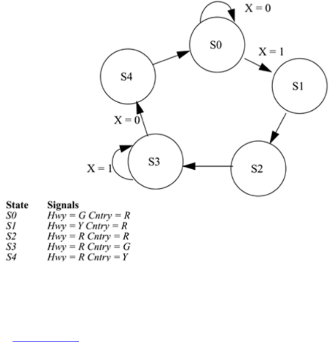
166
Figure 7-1. FSM for Traffic Signal Controller
Verilog description
The traffic signal controller module can be designed with behavioral Verilog constructs,
as shown in Example 7-37.
Example 7-37 Traffic Signal Controller
`define TRUE 1'b1
`define FALSE 1'b0
//Delays
`define Y2RDELAY 3 //Yellow to red delay
`define R2GDELAY 2 //Red to green delay
module sig_control
(hwy, cntry, X, clock, clear);
//I/O ports
output [1:0] hwy, cntry;
//2-bit output for 3 states of signal
//GREEN, YELLOW, RED;
reg [1:0] hwy, cntry;
//declared output signals are registers
input X;
//if TRUE, indicates that there is car on
//the country road, otherwise FALSE
167
input clock, clear;
parameter RED = 2'd0,
YELLOW = 2'd1,
GREEN = 2'd2;
//State definition HWY CNTRY
parameter S0 = 3'd0, //GREEN RED
S1 = 3'd1, //YELLOW RED
S2 = 3'd2, //RED RED
S3 = 3'd3, //RED GREEN
S4 = 3'd4; //RED YELLOW
//Internal state variables
reg [2:0] state;
reg [2:0] next_state;
//state changes only at positive edge of clock
always @(posedge clock)
if (clear)
state <= S0; //Controller starts in S0 state
else
state <= next_state; //State change
//Compute values of main signal and country signal
always @(state)
begin
hwy = GREEN; //Default Light Assignment for Highway light
cntry = RED; //Default Light Assignment for Country light
case(state)
S0: ; // No change, use default
S1: hwy = YELLOW;
S2: hwy = RED;
S3: begin
hwy = RED;
cntry = GREEN;
end
S4: begin
hwy = RED;
cntry = `YELLOW;
end
endcase
end
//State machine using case statements
always @(state or X)
begin
case (state)
S0: if(X)
next_state = S1;
else
next_state = S0;
S1: begin //delay some positive edges of clock
repeat(`Y2RDELAY) @(posedge clock) ;

168
next_state = S2;
end
S2: begin //delay some positive edges of clock
repeat(`R2GDELAY) @(posedge clock);
next_state = S3;
end
S3: if(X)
next_state = S3;
else
next_state = S4;
S4: begin //delay some positive edges of clock
repeat(`Y2RDELAY) @(posedge clock) ;
next_state = S0;
end
default: next_state = S0;
endcase
end
endmodule
Stimulus
Stimulus can be applied to check if the traffic signal transitions correctly when cars arrive
on the country road. The stimulus file in Example 7-38 instantiates the traffic signal
controller and checks all possible states of the controller.
Example 7-38 Stimulus for Traffic Signal Controller
//Stimulus Module
module stimulus;
wire [1:0] MAIN_SIG, CNTRY_SIG;
reg CAR_ON_CNTRY_RD;
//if TRUE, indicates that there is car on
//the country road
reg CLOCK, CLEAR;
//Instantiate signal controller
sig_control SC(MAIN_SIG, CNTRY_SIG, CAR_ON_CNTRY_RD, CLOCK, CLEAR);
//Set up monitor
initial
$monitor($time, " Main Sig = %b Country Sig = %b Car_on_cntry = %b",
MAIN_SIG, CNTRY_SIG, CAR_ON_CNTRY_RD);
//Set up clock
initial
begin
CLOCK = `FALSE;
forever #5 CLOCK = ~CLOCK;
end
//control clear signal
initial
169
begin
CLEAR = `TRUE;
repeat (5) @(negedge CLOCK);
CLEAR = `FALSE;
end
//apply stimulus
initial
begin
CAR_ON_CNTRY_RD = `FALSE;
repeat(20)@(negedge CLOCK); CAR_ON_CNTRY_RD = `TRUE;
repeat(10)@(negedge CLOCK); CAR_ON_CNTRY_RD = `FALSE;
repeat(20)@(negedge CLOCK); CAR_ON_CNTRY_RD = `TRUE;
repeat(10)@(negedge CLOCK); CAR_ON_CNTRY_RD = `FALSE;
repeat(20)@(negedge CLOCK); CAR_ON_CNTRY_RD = `TRUE;
repeat(10)@(negedge CLOCK); CAR_ON_CNTRY_RD = `FALSE;
repeat(10)@(negedge CLOCK); $stop;
end
endmodule
Note that we designed only the behavior of the controller without worrying about how it
will be implemented in hardware.
170
7.10 Summary
We discussed digital circuit design with behavioral Verilog constructs.
• A behavioral description expresses a digital circuit in terms of the algorithms it
implements. A behavioral description does not necessarily include the hardware
implementation details. Behavioral modeling is used in the initial stages of a
design process to evaluate various design-related trade-offs. Behavioral modeling
is similar to C programming in many ways.
• Structured procedures initial and always form the basis of behavioral modeling.
All other behavioral statements can appear only inside initial or always blocks.
An initial block executes once; an always block executes continuously until
simulation ends.
• Procedural assignments are used in behavioral modeling to assign values to
register variables. Blocking assignments must complete before the succeeding
statement can execute. Nonblocking assignments schedule assignments to be
executed and continue processing to the succeeding statement.
• Delay-based timing control, event-based timing control, and level-sensitive timing
control are three ways to control timing and execution order of statements in
Verilog. Regular delay, zero delay, and intra-assignment delay are three types of
delay-based timing control. Regular event, named event, and event OR are three
types of event-based timing control. The wait statement is used to model level-
sensitive timing control.
• Conditional statements are modeled in behavioral Verilog with if and else
statements. If there are multiple branches, use of case statements is recommended.
casex and casez are special cases of the case statement.
• Keywords while, for, repeat, and forever are used for four types of looping
statements in Verilog.
• Sequential and parallel are two types of blocks. Sequential blocks are specified by
keywords begin and end . Parallel blocks are expressed by keywords fork and
join. Blocks can be nested and named. If a block is named, the execution of the
block can be disabled from anywhere in the design. Named blocks can be
referenced by hierarchical names.
• Generate statements allow Verilog code to be generated dynamically at
elaboration time before the simulation begins. This facilitates the creation of
parametrized models. Generate statements are particularly convenient when the
same operation or module instance is repeated for multiple bits of a vector, or

171
when certain Verilog code is conditionally included based on parameter
definitions. Generate loop, generate conditional, and generate case are the three
types of generate statements.
172
7.11 Exercises
1: Declare a register called oscillate. Initialize it to 0 and make it toggle every 30
time units. Do not use always statement (Hint: Use the forever loop).
2: Design a clock with time period = 40 and a duty cycle of 25% by using the
always and initial statements. The value of clock at time = 0 should be
initialized to 0.
3: Given below is an initial block with blocking procedural assignments. At what
simulation time is each statement executed? What are the intermediate and
final values of a, b, c, d?
initial
begin
a = 1'b0;
b = #10 1'b1;
c = #5 1'b0;
d = #20 {a, b, c};
end
4: Repeat exercise 3 if nonblocking procedural assignments were used.
5: What is the order of execution of statements in the following Verilog code? Is
there any ambiguity in the order of execution? What are the final values of a,
b, c, d?
initial
begin
a = 1'b0;
#0 c = b;
end
initial
begin
b = 1'b1;
#0 d = a;
end
6: What is the final value of d in the following example? (Hint: See intra-
assignment delays.)
initial
begin
b = 1'b1; c = 1'b0;
#10 b = 1'b0;
initial

173
begin
d = #25 (b | c);
end
7: Design a negative edge-triggered D-flipflop (D_FF) with synchronous clear,
active high (D_FF clears only at a negative edge of clock when clear is high).
Use behavioral statements only. (Hint: Output q of D_FF must be declared as
reg). Design a clock with a period of 10 units and test the D_FF.
8: Design the D-flipflop in exercise 7 with asynchronous clear (D_FF clears
whenever clear goes high. It does not wait for next negative edge). Test the
D_FF.
9: Using the wait statement, design a level-sensitive latch that takes clock and d
as inputs and q as output. q = d whenever clock = 1.
10: Design the 4-to-1 multiplexer in Example 7-19 by using if and else statements.
The port interface must remain the same.
11: Design the traffic signal controller discussed in this chapter by using if and
else statements.
12: Using a case statement, design an 8-function ALU that takes 4-bit inputs a and
b and a 3-bit input signal select, and gives a 5-bit output out. The ALU
implements the following functions based on a 3-bit input signal select. Ignore
any overflow or underflow bits.
Select Signal Function
3'b000 out = a
3'b001 out = a + b
3'b010 out = a - b
3'b011 out = a / b
3'b100 out = a % b (remainder)
3'b101 out = a << 1
3'b110 out = a >> 1
3'b111 out = (a > b) (magnitude compare)
13: Using a while loop, design a clock generator. Initial value of clock is 0. Time
period for the clock is 10.

174
14: Using the for loop, initialize locations 0 to 1023 of a 4-bit register array
cache_var to 0.
15: Using a forever statement, design a clock with time period = 10 and duty cycle
= 40%. Initial value of clock is 0.
16: Using the repeat loop, delay the statement a = a + 1 by 20 positive edges of
clock.
17: Below is a block with nested sequential and parallel blocks. When does the
block finish and what is the order of execution of events? At what simulation
times does each statement finish execution?
initial
begin
x = 1'b0;
#5 y = 1'b1;
fork
#20 a = x;
#15 b = y;
join
#40 x = 1'b1;
fork
#10 p = x;
begin
#10 a = y;
#30 b = x;
end
#5 m = y;
join
end
18: Design an 8-bit counter by using a forever loop, named block, and disabling of
named block. The counter starts counting at count = 5 and finishes at count =
67. The count is incremented at positive edge of clock. The clock has a time
period of 10. The counter counts through the loop only once and then is
disabled. (Hint: Use the disable statement.)

175
Chapter 8. Tasks and Functions
A designer is frequently required to implement the same functionality at many places in a
behavioral design. This means that the commonly used parts should be abstracted into
routines and the r outines must be invoked instead of repeating the code. Most
programming languages provide procedures or subroutines to accomplish this. Verilog
provides tasks and functions to break up large behavioral designs into smaller pieces.
Tasks and functions allow the designer to abstract Verilog code that is used at many
places in the design.
Tasks have input, output, and inout arguments; functions have input arguments. Thus,
values can be passed into and out from tasks and functions. Considering the analogy of
FORTRAN, tasks are similar to SUBROUTINE and functions are similar to
FUNCTION.
Tasks and functions are included in the design hierarchy. Like named blocks, tasks or
functions can be addressed by means of hierarchical names.
Learning Objectives
• Describe the differences between tasks and functions.
• Identify the conditions required for tasks to be defined. Understand task
declaration and invocation.
• Explain the conditions necessary for functions to be defined. Understand function
declaration and invocation.

176
8.1 Differences between Tasks and Functions
Tasks and functions serve different purposes in Verilog. We discuss tasks and functions
in greater detail in the following sections. However, first it is important to understand
differences between tasks and functions, as outlined in Table 8-1.
Table 8-1. Tasks and Functions
Functions Tasks
A function can enable another function
but not another task.
A task can enable other tasks and functions.
Functions always execute in 0
simulation time.
Tasks may execute in non-zero simulation
time.
Functions must not contain any delay,
event, or timing control statements.
Tasks may contain delay, event, or timing
control statements.
Functions must have at least one input
argument. They can have more than one
input.
Tasks may have zero or more arguments of
type input, output, or inout.
unctions always return a single value.
They cannot have output or inout
arguments.
Tasks do not return with a value, but can
pass multiple values through output and
inout arguments.
Both tasks and functions must be defined in a module and are local to the module. Tasks
are used for common Verilog code that contains delays, timing, event constructs, or
multiple output arguments. Functions are used when common Verilog code is purely
combinational, executes in zero simulation time, and provides exactly one output.
Functions are typically used for conversions and commonly used calculations.
Tasks can have input, output, and inout arguments; functions can have input arguments.
In addition, they can have local variables, registers, time variables, integers, real, or
events. Tasks or functions cannot have wires. Tasks and functions contain behavioral
statements only. Tasks and functions do not contain always or initial statements but are
called from always blocks, initial blocks, or other tasks and functions.
177
8.2 Tasks
Tasks are declared with the keywords task and endtask. Tasks must be used if any one of
the following conditions is true for the procedure:
• There are delay, timing, or event control constructs in the procedure.
• The procedure has zero or more than one output arguments.
• The procedure has no input arguments.
8.2.1 Task Declaration and Invocation
Task declaration and task invocation syntax are as follows.
Example 8-1 Syntax for Tasks
task_declaration ::=
task [ automatic ] task_identifier ;
{ task_item_declaration }
statement
endtask
| task [ automatic ] task_identifier ( task_port_list ) ;
{ block_item_declaration }
statement
endtask
task_item_declaration ::=
block_item_declaration
| { attribute_instance } tf_input_declaration ;
| { attribute_instance } tf_output_declaration ;
| { attribute_instance } tf_inout_declaration ;
task_port_list ::= task_port_item { , task_port_item }
task_port_item ::=
{ attribute_instance } tf_input_declaration
| { attribute_instance } tf_output_declaration
| { attribute_instance } tf_inout_declaration
tf_input_declaration ::=
input [ reg ] [ signed ] [ range ] list_of_port_identifiers
| input [ task_port_type ] list_of_port_identifiers
tf_output_declaration ::=
output [ reg ] [ signed ] [ range ]
list_of_port_identifiers
| output [ task_port_type ] list_of_port_identifiers
tf_inout_declaration ::=
inout [ reg ] [ signed ] [ range ] list_of_port_identifiers
| inout [ task_port_type ] list_of_port_identifiers
task_port_type ::=
time | real | realtime | integer

178
I/O declarations use keywords input, output, or inout, based on the type of argument
declared. Input and inout arguments are passed into the task. Input arguments are
processed in the task statements. Output and inout argument values are passed back to the
variables in the task invocation statement when the task is completed. Tasks can invoke
other tasks or functions.
Although the keywords input, inout, and output used for I/O arguments in a task are the
same as the keywords used to declare ports in modules, there is a difference. Ports are
used to connect external signals to the module. I/O arguments in a task are used to pass
values to and from the task.
8.2.2 Task Examples
We discuss two examples of tasks. The first example illustrates the use of input and
output arguments in tasks. The second example models an asymmetric sequence
generator that generates an asymmetric sequence on the clock signal.
Use of input and output arguments
Example 8-2 illustrates the use of input and output arguments in tasks. Consider a task
called bitwise_oper, which computes the bitwise and, bitwise or, and bitwise ex-or of two
16-bit numbers. The two 16-bit numbers a and b are inputs and the three outputs are 16-
bit numbers ab_and, ab_or, ab_xor. A parameter delay is also used in the task.
Example 8-2 Input and Output Arguments in Tasks
//Define a module called operation that contains the task bitwise_oper
module operation;
...
...
parameter delay = 10;
reg [15:0] A, B;
reg [15:0] AB_AND, AB_OR, AB_XOR;
always @(A or B) //whenever A or B changes in value
begin
//invoke the task bitwise_oper. provide 2 input arguments A, B
//Expect 3 output arguments AB_AND, AB_OR, AB_XOR
//The arguments must be specified in the same order as they
//appear in the task declaration.
bitwise_oper(AB_AND, AB_OR, AB_XOR, A, B);
end
...
...
//define task bitwise_oper
task bitwise_oper;

179
output [15:0] ab_and, ab_or, ab_xor; //outputs from the task
input [15:0] a, b; //inputs to the task
begin
#delay ab_and = a & b;
ab_or = a | b;
ab_xor = a ^ b;
end
endtask
...
endmodule
In the above task, the input values passed to the task are A and B. Hence, when the task is
entered, a = A and b = B. The three output values are computed after a delay. This delay
is specified by the parameter delay, which is 10 units for this example. When the task is
completed, the output values are passed back to the calling output arguments. Therefore,
AB_AND = ab_and, AB_OR = ab_or, and AB_XOR = ab_xor when the task is
completed.
Another method of declaring arguments for tasks is the ANSI C style. Example 8-3
shows the bitwise_oper task defined with an ANSI C style argument declaration.
Example 8-3 Task Definition using ANSI C Style Argument Declaration
//define task bitwise_oper
task bitwise_oper (output [15:0] ab_and, ab_or, ab_xor,
input [15:0] a, b);
begin
#delay ab_and = a & b;
ab_or = a | b;
ab_xor = a ^ b;
end
endtask
Asymmetric Sequence Generator
Tasks can directly operate on reg variables defined in the module. Example 8-4 directly
operates on the reg variable clock to continuously produce an asymmetric sequence. The
clock is initialized with an initialization sequence.
Example 8-4 Direct Operation on reg Variables
//Define a module that contains the task asymmetric_sequence
module sequence;
...
reg clock;
...
initial
init_sequence; //Invoke the task init_sequence
...

180
always
begin
asymmetric_sequence; //Invoke the task asymmetric_sequence
end
...
...
//Initialization sequence
task init_sequence;
begin
clock = 1'b0;
end
endtask
//define task to generate asymmetric sequence
//operate directly on the clock defined in the module.
task asymmetric_sequence;
begin
#12 clock = 1'b0;
#5 clock = 1'b1;
#3 clock = 1'b0;
#10 clock = 1'b1;
end
endtask
...
...
endmodule
8.2.3 Automatic (Re-entrant) Tasks
Tasks are normally static in nature. All declared items are statically allocated and they are
shared across all uses of the task executing concurrently. Therefore, if a task is called
concurrently from two places in the code, these task calls will operate on the same task
variables. It is highly likely that the results of such an operation will be incorrect.
To avoid this problem, a keyword automatic is added in front of the task keyword to
make the tasks re-entrant. Such tasks are called automatic tasks. All items declared inside
automatic tasks are allocated dynamically for each invocation. Each task call operates in
an independent space. Thus, the task calls operate on independent copies of the task
variables. This results in correct operation. It is recommended that automatic tasks be
used if there is a chance that a task might be called concurrently from two locations in the
code.
Example 8-5 shows how an automatic task is defined and used.
Example 8-5 Re-entrant (Automatic) Tasks
// Module that contains an automatic (re-entrant) task
// Only a small portion of the module that contains the task definition
// is shown in this example. There are two clocks.

181
// clk2 runs at twice the frequency of clk and is synchronous
// with clk.
module top;
reg [15:0] cd_xor, ef_xor; //variables in module top
reg [15:0] c, d, e, f; //variables in module top
-
task automatic bitwise_xor;
output [15:0] ab_xor; //output from the task
input [15:0] a, b; //inputs to the task
begin
#delay ab_and = a & b;
ab_or = a | b;
ab_xor = a ^ b;
end
endtask
...
-
// These two always blocks will call the bitwise_xor task
// concurrently at each positive edge of clk. However, since
// the task is re-entrant, these concurrent calls will work correctly.
always @(posedge clk)
bitwise_xor(ef_xor, e, f);
-
always @(posedge clk2) // twice the frequency as the previous block
bitwise_xor(cd_xor, c, d);
-
-
endmodule
182
8.3 Functions
Functions are declared with the keywords function and endfunction. Functions are used if
all of the following conditions are true for the procedure:
• There are no delay, timing, or event control constructs in the procedure.
• The procedure returns a single value.
• There is at least one input argument.
• There are no output or inout arguments.
• There are no nonblocking assignments.
8.3.1 Function Declaration and Invocation
The syntax for functions is follows:
Example 8-6 Syntax for Functions
function_declaration ::=
function [ automatic ] [ signed ] [ range_or_type ]
function_identifier ;
function_item_declaration { function_item_declaration }
function_statement
endfunction
| function [ automatic ] [ signed ] [ range_or_type ]
function_identifier (function_port_list ) ;
block_item_declaration { block_item_declaration }
function_statement
endfunction
function_item_declaration ::=
block_item_declaration
| tf_input_declaration ;
function_port_list ::= { attribute_instance } tf_input_declaration {,
{ attribute_instance } tf_input_declaration }
range_or_type ::= range | integer | real | realtime | time
There are some peculiarities of functions. When a function is declared, a register with
name function_identifer is declared implicitly inside Verilog. The output of a function is
passed back by setting the value of the register function_identifer appropriately. The
function is invoked by specifying function name and input arguments. At the end of
function execution, the return value is placed where the function was invoked. The
optional range_or_type specifies the width of the internal register. If no range or type is

183
specified, the default bit width is 1. Functions are very similar to FUNCTION in
FORTRAN.
Notice that at least one input argument must be defined for a function. There are no
output arguments for functions because the implicit register function_identifer contains
the output value. Also, functions cannot invoke other tasks. They can invoke only other
functions.
8.3.2 Function Examples
We will discuss two examples. The first example models a parity calculator that returns a
1-bit value. The second example models a 32-bit left/right shift register that returns a 32-
bit shifted value.
Parity calculation
Let us discuss a function that calculates the parity of a 32-bit address and returns the
value. We assume even parity. Example 8-7 shows the definition and invocation of the
function calc_parity.
Example 8-7 Parity Calculation
//Define a module that contains the function calc_parity
module parity;
...
reg [31:0] addr;
reg parity;
//Compute new parity whenever address value changes
always @(addr)
begin
parity = calc_parity(addr); //First invocation of calc_parity
$display("Parity calculated = %b", calc_parity(addr) );
//Second invocation of calc_parity
end
...
...
//define the parity calculation function
function calc_parity;
input [31:0] address;
begin
//set the output value appropriately. Use the implicit
//internal register calc_parity.
calc_parity = ^address; //Return the xor of all address bits.
end
endfunction
...
...
endmodule

184
Note that in the first invocation of calc_parity, the returned value was used to set the reg
parity. In the second invocation, the value returned was directly used inside the $display
task. Thus, the returned value is placed wherever the function was invoked.
Another method of declaring arguments for functions is the ANSI C style. Example 8-8
shows the calc_parity function defined with an ANSI C style argument declaration.
Example 8-8 Function Definition using ANSI C Style Argument Declaration
//define the parity calculation function using ANSI C Style arguments
function calc_parity (input [31:0] address);
begin
//set the output value appropriately. Use the implicit
//internal register calc_parity.
calc_parity = ^address; //Return the xor of all address bits.
end
endfunction
Left/right shifter
To illustrate how a range for the output value of a function can be specified, let us
consider a function that shifts a 32-bit value to the left or right by one bit, based on a
control signal. Example 8-9 shows the implementation of the left/right shifter.
Example 8-9 Left/Right Shifter
//Define a module that contains the function shift
module shifter;
...
//Left/right shifter
`define LEFT_SHIFT 1'b0
`define RIGHT_SHIFT 1'b1
reg [31:0] addr, left_addr, right_addr;
reg control;
//Compute the right- and left-shifted values whenever
//a new address value appears
always @(addr)
begin
//call the function defined below to do left and right shift.
left_addr = shift(addr, `LEFT_SHIFT);
right_addr = shift(addr, `RIGHT_SHIFT);
end
...
...
//define shift function. The output is a 32-bit value.
function [31:0] shift;
input [31:0] address;
input control;
begin
//set the output value appropriately based on a control signal.

185
shift = (control == `LEFT_SHIFT) ?(address << 1) : (address >>
1);
end
endfunction
...
...
endmodule
8.3.3 Automatic (Recursive) Functions
Functions are normally used non-recursively . If a function is called concurrently from
two locations, the results are non-deterministic because both calls operate on the same
variable space.
However, the keyword automatic can be used to declare a recursive (automatic) function
where all function declarations are allocated dynamically for each recursive calls. Each
call to an automatic function operates in an independent variable space.Automatic
function items cannot be accessed by hierarchical references. Automatic functions can be
invoked through the use of their hierarchical name.
Example 8-10 shows how an automatic function is defined to compute a factorial.
Example 8-10 Recursive (Automatic) Functions
//Define a factorial with a recursive function
module top;
...
// Define the function
function automatic integer factorial;
input [31:0] oper;
integer i;
begin
if (operand >= 2)
factorial = factorial (oper -1) * oper; //recursive call
else
factorial = 1 ;
end
endfunction
// Call the function
integer result;
initial
begin
result = factorial(4); // Call the factorial of 7
$display("Factorial of 4 is %0d", result); //Displays 24
end
...
...
endmodule

186
8.3.4 Constant Functions
A constant function[1] is a regular Verilog HDL function, but with certain restrictions.
These functions can be used to reference complex values and can be used instead of
constants.
[1] See IEEE Standard Verilog Hardware Description Language document for details on
constant function restrictions.
Example 8-11 shows how a constant function can be used to compute the width of the
address bus in a module.
Example 8-11 Constant Functions
//Define a RAM model
module ram (...);
parameter RAM_DEPTH = 256;
input [clogb2(RAM_DEPTH)-1:0] addr_bus; //width of bus computed
//by calling constant
//function defined below
//Result of clogb2 = 8
//input [7:0] addr_bus;
--
--
//Constant function
function integer clogb2(input integer depth);
begin
for(clogb2=0; depth >0; clogb2=clogb2+1)
depth = depth >> 1;
end
endfunction
--
--
endmodule
8.3.5 Signed Functions
Signed functions allow signed operations to be performed on the function return values.
Example 8-12 shows an example of a signed function.
Example 8-12 Signed Functions
module top;
--
//Signed function declaration
//Returns a 64 bit signed value
function signed [63:0] compute_signed(input [63:0] vector);

187
--
--
endfunction
--
//Call to the signed function from the higher module
if(compute_signed(vector) < -3)
begin
--
end
--
endmodule
188
8.4 Summary
In this chapter, we discussed tasks and functions used in behavior Verilog modeling.
• Tasks and functions are used to define common Verilog functionality that is used
at many places in the design. Tasks and functions help to make a module
definition more readable by breaking it up into manageable subunits. Tasks and
functions serve the same purpose in Verilog as subroutines do in C.
• Tasks can take any number of input, inout, or output arguments. Delay, event, or
timing control constructs are permitted in tasks. Tasks can enable other tasks or
functions.
• Re-entrant tasks defined with the keyword automatic allow each task call to
operate in an independent space. Therefore, re-entrant tasks work correctly even
with concurrent tasks calls.
• Functions are used when exactly one return value is required and at least one
input argument is specified. Delay, event, or timing control constructs are not
permitted in functions. Functions can invoke other functions but cannot invoke
other tasks.
• A register with name as the function name is declared implicitly when a function
is declared. The return value of the function is passed back in this register.
• Recursive functions defined with the keyword automatic allow each function call
to operate in an independent space. Therefore, recursive or concurrent calls to
such functions will work correctly.
• Tasks and functions are included in a design hierarchy and can be addressed by
hierarchical name referencing.
189
8.5 Exercises
1: Define a function to calculate the factorial of a 4-bit number. The output is a 32-
bit value. Invoke the function by using stimulus and check results.
2: Define a function to multiply two 4-bit numbers a and b. The output is an 8-bit
value. Invoke the function by using stimulus and check results.
3: Define a function to design an 8-function ALU that takes two 4-bit numbers a
and b and computes a 5-bit result out based on a 3-bit select signal. Ignore
overflow or underflow bits.
Select Signal Function Output
3'b000 a
3'b001 a + b
3'b010 a - b
3'b011 a / b
3'b100 a % 1 (remainder)
3'b101 a << 1
3'b110 a >> 1
3'b111 (a > b) (magnitude compare)
4: Define a task to compute the factorial of a 4-bit number. The output is a 32-bit
value. The result is assigned to the output after a delay of 10 time units.
5: Define a task to compute even parity of a 16-bit number. The result is a 1-bit
value that is assigned to the output after three positive edges of clock. (Hint:
Use a repeat loop in the task.)
6: Using named events, tasks, and functions, design the traffic signal controller in
Traffic Signal Controller on page 160.

190
Chapter 9. Useful Modeling Techniques
We learned the basic features of Verilog in the preceding chapters. In this chapter. we
will discuss additional features that enhance the Verilog language, making it powerful
and flexible for modeling and analyzing a design.
Learning Objectives
• Describe procedural continuous assignment statements assign, deassign, force,
and release. Explain their significance in modeling and debugging.
• Understand how to override parameters by using the defparam statement at the
time of module instantiation.
• Explain conditional compilation and execution of parts of the Verilog description.
• Identify system tasks for file output, displaying hierarchy, strobing, random
number generation, memory initialization, and value change dump.

191
9.1 Procedural Continuous Assignments
We studied procedural assignments in Section 7.2, Procedural Assignments. Procedural
assignments assign a value to a register. The value stays in the register until another
p
rocedural assignment puts another value in that register. Procedural continuous
assignments behave differently. They are procedural statements which allow values of
expressions to be driven continuously onto registers or nets for limited periods of time.
Procedural continuous assignments override existing assignments to a register or net.
They provide an useful extension to the regular procedural assignment statement.
9.1.1 assign and deassign
The keywords assign and deassign are used to express the first type of procedural
continuous assignment. The left-hand side of procedural continuous assignments can be
only be a register or a concatenation of registers. It cannot be a part or bit select of a net
or an array of registers. Procedural continuous assignments override the effect of regular
p
rocedural assignments. Procedural continuous assignments are normally used for
controlled periods of time.
A simple example is the negative edge-triggered D-flipflop with asynchronous reset that
we modeled in Example 6-8. In Example 9-1, we now model the same D_FF, using
assign and deassign statements.
Example 9-1 D-Flipflop with Procedural Continuous Assignments
// Negative edge-triggered D-flipflop with asynchronous reset
module edge_dff(q, qbar, d, clk, reset);
// Inputs and outputs
output q,qbar;
input d, clk, reset;
reg q, qbar; //declare q and qbar are registers
always @(negedge clk) //assign value of q & qbar at active edge of
clock.
begin
q = d;
qbar = ~d;
end
always @(reset) //Override the regular assignments to q and qbar
//whenever reset goes high. Use of procedural
continuous
//assignments.
if(reset)
begin //if reset is high, override regular assignments to q

192
with
//the new values, using procedural continuous
assignment.
assign q = 1'b0;
assign qbar = 1'b1;
end
else
begin //If reset goes low, remove the overriding values by
//deassigning the registers. After this the regular
//assignments q = d and qbar = ~d will be able to
change
//the registers on the next negative edge of clock.
deassign q;
deassign qbar;
end
endmodule
In Example 9-1, we overrode the assignment on q and qbar and assigned new values to
them when the reset signal went high. The register variables retain the continuously
assigned value after the deassign until they are changed by a future procedural
assignment. The assign and deassign constructs are now considered to be a bad coding
style and it is recommended that alternative styles be used in Verilog HDL code.
9.1.2 force and release
Keywords force and release are used to express the second form of the procedural
continuous assignments. They can be used to override assignments on both registers and
nets. force and release statements are typically used in the interactive debugging process,
where certain registers or nets are forced to a value and the effect on other registers and
nets is noted. It is recommended that force and release statements not be used inside
design blocks. They should appear only in stimulus or as debug statements.
force and release on registers
A force on a register overrides any procedural assignments or procedural continuous
assignments on the register until the register is released. The register variables will
continue to store the forced value after being released, but can then be changed by a
future procedural assignment. To override the values of q and qbar in Example 9-1 for a
limited period of time, we could do the following:
module stimulus;
...
...
//instantiate the d-flipflop
edge_dff dff(Q, Qbar, D, CLK, RESET);
...
...

193
initial
begin
//these statements force value of 1 on dff.q between time 50 and
//100, regardless of the actual output of the edge_dff.
#50 force dff.q = 1'b1; //force value of q to 1 at time 50.
#50 release dff.q; //release the value of q at time 100.
end
...
...
endmodule
force and release on nets
force on nets overrides any continuous assignments until the net is released. The net will
immediately return to its normal driven value when it is released. A net can be forced to
an expression or a value.
module top;
...
...
assign out = a & b & c; //continuous assignment on net out
...
initial
#50 force out = a | b & c;
#50 release out;
end
...
...
endmodule
In the example above, a new expression is forced on the net from time 50 to time 100.
From time 50 to time 100, when the force statement is active, the expression a | b & c will
be re-evaluated and assigned to out whenever values of signals a or b or c change. Thus,
the force statement behaves like a continuous assignment except that it is active for only
a limited period of time.

194
9.2 Overriding Parameters
Parameters can be defined in a module definition, as was discussed earlier in Section
3.2.8, Parameters. However, during compilation of Verilog modules, parameter values
can be altered separately for each module instance. This allows us to pass a distinct set of
parameter values to each module during compilation regardless of predefined parameter
values.
There are two ways to override parameter values: through the defparam statement or
through module instance parameter value assignment.
9.2.1 defparam Statement
Parameter values can be changed in any module instance in the design with the keyword
defparam. The hierarchical name of the module instance can be used to override
parameter values. Consider Example 9-2, which uses defparam to override the parameter
values in module instances.
Example 9-2 Defparam Statement
//Define a module hello_world
module hello_world;
parameter id_num = 0; //define a module identification number = 0
initial //display the module identification number
$display("Displaying hello_world id number = %d", id_num);
endmodule
//define top-level module
module top;
//change parameter values in the instantiated modules
//Use defparam statement
defparam w1.id_num = 1, w2.id_num = 2;
//instantiate two hello_world modules
hello_world w1();
hello_world w2();
endmodule
In Example 9-2, the module hello_world was defined with a default id_num = 0.
However, when the module instances w1 and w2 of the type hello_world are created,
their id_num values are modified with the defparam statement. If we simulate the above
design, we would get the following output:

195
Displaying hello_world id number = 1
Displaying hello_world id number = 2
Multiple defparam statements can appear in a module. Any parameter can be overridden
with the defparam statement. The defparam construct is now considered to be a bad
coding style and it is recommended that alternative styles be used in Verilog HDL code.
Note that the module hello_world can also be defined using an ANSI C style parameter
declaration. Figure 9-3 shows the ANSI C style parameter declaration for the module
hello_world.
Example 9-3 ANSI C Style Parameter Declaration
//Define a module hello_world
module hello_world #(parameter id_num = 0) ;//ANSI C Style Parameter
initial //display the module identification number
$display("Displaying hello_world id number = %d", id_num);
endmodule
9.2.2 Module_Instance Parameter Values
Parameter values can be overridden when a module is instantiated. To illustrate this, we
will use Example 9-2 and modify it a bit. The new parameter values are passed during
module instantiation. The top-level module can pass parameters to the instances w1 and
w2, as shown below. Notice that defparam is not needed. The simulation output will be
identical to the output obtained with the defparam statement.
//define top-level module
module top;
//instantiate two hello_world modules; pass new parameter values
//Parameter value assignment by ordered list
hello_world #(1) w1; //pass value 1 to module w1
//Parameter value assignment by name
hello_world #(.id_num(2)) w2; //pass value 2 to id_num parameter
//for module w2
endmodule
If multiple parameters are defined in the module, during module instantiation, they can be
overridden by specifying the new values in the same order as the parameter declarations
in the module. If an overriding value is not specified, the default parameter declaration
values are taken. Alternately, one can override specific values by naming the parameters

196
and the corresponding values. This is called parameter value assignment by name.
Consider Example 9-4.
Example 9-4 Module Instance Parameter Values
//define module with delays
module bus_master;
parameter delay1 = 2;
parameter delay2 = 3;
parameter delay3 = 7;
...
<module internals>
...
endmodule
//top-level module; instantiates two bus_master modules
module top;
//Instantiate the modules with new delay values
//Parameter value assignment by ordered list
bus_master #(4, 5, 6) b1(); //b1: delay1 = 4, delay2 = 5, delay3 = 6
bus_master #(9, 4) b2(); //b2: delay1 = 9, delay2 = 4, delay3 =
7(default)
//Parameter value assignment by name
bus_master #(.delay2(4), delay3(7)) b3(); //b2: delay2 = 4, delay3 = 7
//delay1=2 (default)
// It is recommended to use the parameter value assignment by name
// This minimizes the chance of error and parameters can be added
// or deleted without worrying about the order.
endmodule
Module-instance parameter value assignment is a very useful method used to override
parameter values and to customize module instances.

197
9.3 Conditional Compilation and Execution
A portion of Verilog might be suitable for one environment but not for another. The
designer does not wish to create two versions of Verilog design for the two environments.
Instead, the designer can specify that the particular portion of the code be compiled only
if a certain flag is set. This is called conditional compilation.
A designer might also want to execute certain parts of the Verilog design only when a
flag is set at run time. This is called conditional execution.
9.3.1 Conditional Compilation
Conditional compilation can be accomplished by using compiler directives `ifdef, `ifndef,
`else, `elsif, and `endif. Example 9-5 contains Verilog source code to be compiled
conditionally.
Example 9-5 Conditional Compilation
//Conditional Compilation
//Example 1
'ifdef TEST //compile module test only if text macro TEST is defined
module test;
...
...
endmodule
'else //compile the module stimulus as default
module stimulus;
...
...
endmodule
'endif //completion of 'ifdef directive
//Example 2
module top;
bus_master b1(); //instantiate module unconditionally
'ifdef ADD_B2
bus_master b2(); //b2 is instantiated conditionally if text macro
//ADD_B2 is defined
'elsif ADD_B3
bus_master b3(); //b3 is instantiated conditionally if text macro
//ADD_B3 is defined
'else
bus_master b4(); //b4 is instantiate by default
'endif
'ifndef IGNORE_B5

198
bus_master b5(); //b5 is instantiated conditionally if text macro
//IGNORE_B5 is not defined
'endif
endmodule
The `ifdef and `ifndef directives can appear anywhere in the design. A designer can
conditionally compile statements, modules, blocks, declarations, and other compiler
directives. The `else directive is optional. A maximum of one `else directive can
accompany an `ifdef or `ifndef. Any number of `elsif directives can accompany an `ifdef
or `ifndef. An `ifdef or `ifndef is always closed by a corresponding `endif.
The conditional compile flag can be set by using the `define statement inside the Verilog
file. In the example above, we could define the flags by defining text macros TEST and
ADD_B2 at compile time by using the `define statement. The Verilog compiler simply
skips the portion if the conditional compile flag is not set. A Boolean expression, such as
TEST && ADD_B2, is not allowed with the `ifdef statement.
9.3.2 Conditional Execution
Conditional execution flags allow the designer to control statement execution flow at run
time. All statements are compiled but executed conditionally. Conditional execution flags
can be used only for behavioral statements. The system task keyword $test$plusargs is
used for conditional execution.
Consider Example 9-6, which illustrates conditional execution with $test$plusargs.
Example 9-6 Conditional Execution with $test$plusargs
//Conditional execution
module test;
...
...
initial
begin
if($test$plusargs("DISPLAY_VAR"))
$display("Display = %b ", {a,b,c} ); //display only if flag is
set
else
//Conditional execution
$display("No Display"); //otherwise no display
end
endmodule
The variables are displayed only if the flag DISPLAY_VAR is set at run time. Flags can
be set at run time by specifying the option +DISPLAY_VAR at run time.

199
Conditional execution can be further controlled by using the system task keyword
$value$plusargs. This system task allows testing for arguments to an invocation option.
$value$plusargs returns a 0 if a matching invocation was not found and non-zero if a
matching option was found. Example 9-7 shows an example of $value$plusargs.
Example 9-7 Conditional Execution with $value$plusargs
//Conditional execution with $value$plusargs
module test;
reg [8*128-1:0] test_string;
integer clk_period;
...
...
initial
begin
if($value$plusargs("testname=%s", test_string))
$readmemh(test_string, vectors); //Read test vectors
else
//otherwise display error message
$display("Test name option not specified");
if($value$plusargs("clk_t=%d", clk_period))
forever #(clk_period/2) clk = ~clk; //Set up clock
else
//otherwise display error message
$display("Clock period option name not specified");
end
//For example, to invoke the above options invoke simulator with
//+testname=test1.vec +clk_t=10
//Test name = "test1.vec" and clk_period = 10
endmodule

200
9.4 Time Scales
Often, in a single simulation, delay values in one module need to be defined by using
certain time unit, e.g., 1 s, and delay values in another module need to be defined by
using a different time unit, e.g. 100 ns. Verilog HDL allows the reference time unit for
modules to be specified with the `timescale compiler directive.
Usage: `timescale <reference_time_unit> / <time_precision>
The <reference_time_unit> specifies the unit of measurement for times and delays. The
<time_precision> specifies the precision to which the delays are rounded off during
simulation. Only 1, 10, and 100 are valid integers for specifying time unit and time
precision. Consider the two modules, dummy1 and dummy2, in Example 9-8.
Example 9-8 Time Scales
//Define a time scale for the module dummy1
//Reference time unit is 100 nanoseconds and precision is 1 ns
`timescale 100 ns / 1 ns
module dummy1;
reg toggle;
//initialize toggle
initial
toggle = 1'b0;
//Flip the toggle register every 5 time units
//In this module 5 time units = 500 ns = .5 µs
always #5
begin
toggle = ~toggle;
$display("%d , In %m toggle = %b ", $time, toggle);
end
endmodule
//Define a time scale for the module dummy2
//Reference time unit is 1 microsecond and precision is 10 ns
`timescale 1 us / 10 ns
module dummy2;
reg toggle;
//initialize toggle
initial
201
toggle = 1'b0;
//Flip the toggle register every 5 time units
//In this module 5 time units = 5 µs = 5000 ns
always #5
begin
toggle = ~toggle;
$display("%d , In %m toggle = %b ", $time, toggle);
end
endmodule
The two modules dummy1 and dummy2 are identical in all respects, except that the time
unit for dummy1 is 100 ns and the time unit for dummy2 is 1 s. Thus the $display
statement in dummy1 will be executed 10 times for each $display executed in dummy2.
The $time task reports the simulation time in terms of the reference time unit for the
module in which it is invoked. The first few $display statements are shown in the
simulation output below to illustrate the effect of the `timescale directive.
5 , In dummy1 toggle = 1
10 , In dummy1 toggle = 0
15 , In dummy1 toggle = 1
20 , In dummy1 toggle = 0
25 , In dummy1 toggle = 1
30 , In dummy1 toggle = 0
35 , In dummy1 toggle = 1
40 , In dummy1 toggle = 0
45 , In dummy1 toggle = 1
--> 5 , In dummy2 toggle = 1
50 , In dummy1 toggle = 0
55 , In dummy1 toggle = 1
Notice that the $display statement in dummy2 executes once for every ten $display
statements in dummy1.

202
9.5 Useful System Tasks
In this section, we discuss the system tasks that are useful for a variety of purposes in
Verilog. We discuss system tasks [1] for file output, displaying hierarchy, strobing,
random number generation, memory initialization, and value change dump.
[1] Other system tasks such as $signed and $unsigned used for sign conversion are not
discussed in this book. For details, please refer to the "IEEE Standard Verilog Hardware
Description Language" document.
9.5.1 File Output
Output from Verilog normally goes to the standard output and the file verilog.log. It is
possible to redirect the output of Verilog to a chosen file.
Opening a file
A file can be opened with the system task $fopen.
Usage: $fopen("<name_of_file>"); [2]
[2] The "IEEE Standard Verilog Hardware Description Language" document provides
additional capabilities for $fopen. The $fopen syntax mentioned in this book is adequate
for most purposes. However, if you need additional capabilities, please refer to the "IEEE
Standard Verilog Hardware Description Language" document.
Usage: <file_handle> = $fopen("<name_of_file>");
The task $fopen returns a 32-bit value called a multichannel descriptor.[3] Only one bit is
set in a multichannel descriptor. The standard output has a multichannel descriptor with
the least significant bit (bit 0) set. Standard output is also called channel 0. The standard
output is always open. Each successive call to $fopen opens a new channel and returns a
32-bit descriptor with bit 1 set, bit 2 set, and so on, up to bit 30 set. Bit 31 is reserved.
The channel number corresponds to the individual bit set in the multichannel descriptor.
Example 9-9 illustrates the use of file descriptors.
[3] The "IEEE Standard Verilog Hardware Description Language" document provides a
method for opening up to 230 files by using a single-channel file descriptor. Please refer
to it for details.

203
Example 9-9 File Descriptors
//Multichannel descriptor
integer handle1, handle2, handle3; //integers are 32-bit values
//standard output is open; descriptor = 32'h0000_0001 (bit 0 set)
initial
begin
handle1 = $fopen("file1.out"); //handle1 = 32'h0000_0002 (bit 1 set)
handle2 = $fopen("file2.out"); //handle2 = 32'h0000_0004 (bit 2 set)
handle3 = $fopen("file3.out"); //handle3 = 32'h0000_0008 (bit 3 set)
end
The advantage of multichannel descriptors is that it is possible to selectively write to
multiple files at the same time. This is explained below in greater detail.
Writing to files
The system tasks $fdisplay, $fmonitor, $fwrite, and $fstrobe are used to write to files.[4]
Note that these tasks are similar in syntax to regular system tasks $display, $monitor, etc.,
but they provide the additional capability of writing to files.
[4] The "IEEE Standard Verilog Hardware Description Language" document provides
many additional capabilities for file output. The file output system tasks mentioned in this
b
ook are adequate for most digital designers. However, if you need additional capabilities
for file output, please refer to the IEEE Standard Verilog Hardware Description
Language document.
Systems tasks for reading files are also provided by the IEEE Standard Verilog Hardware
Description Language. These system tasks include $fgetc, $ungetc, $fgetc, $fscanf,
$sscanf, $fread, $ftell, $fseek, $rewind, and $fflush. However, most digital designers do
not need these capabilities frequently. Therefore, they are not covered in this book. If you
need to use the file reading capabilities, please refer to the "IEEE Standard Verilog
Hardware Description Language" document.
We will consider only $fdisplay and $fmonitor tasks.
Usage: $fdisplay(<file_descriptor>, p1, p2 ..., pn);
$fmonitor(<file_descriptor>, p1, p2,..., pn);
p1, p2, , pn can be variables, signal names, or quoted strings.A file_descriptor is a
multichannel descriptor that can be a file handle or a bitwise combination of file handles.

204
Verilog will write the output to all files that have a 1 associated with them in the file
descriptor. We will use the file descriptors defined in Example 9-9 to illustrate the use of
the $fdisplay and $fmonitor tasks.
//All handles defined in Example 9-9
//Writing to files
integer desc1, desc2, desc3; //three file descriptors
initial
begin
desc1 = handle1 | 1; //bitwise or; desc1 = 32'h0000_0003
$fdisplay(desc1, "Display 1");//write to files file1.out & stdout
desc2 = handle2 | handle1; //desc2 = 32'h0000_0006
$fdisplay(desc2, "Display 2");//write to files file1.out &
file2.out
desc3 = handle3 ; //desc3 = 32'h0000_0008
$fdisplay(desc3, "Display 3");//write to file file3.out only
end
Closing files
Files can be closed with the system task $fclose.
Usage: $fclose(<file_handle>);
//Closing Files
$fclose(handle1);
A file cannot be written to once it is closed. The corresponding bit in the multichannel
descriptor is set to 0. The next $fopen call can reuse the bit.
9.5.2 Displaying Hierarchy
Hierarchy at any level can be displayed by means of the %m option in any of the display
tasks, $display, $write task, $monitor, or $strobe task, as discussed briefly in Section 4.3,
Hierarchical Names. This is a very useful option. For example, when multiple instances
of a module execute the same Verilog code, the %m option will distinguish from which
module instance the output is coming. No argument is needed for the %m option in the
display tasks. See Example 9-10.
Example 9-10 Displaying Hierarchy
//Displaying hierarchy information
module M;
...
initial
$display("Displaying in %m");
endmodule
//instantiate module M

205
module top;
...
M m1();
M m2();
//Displaying hierarchy information
M m3();
endmodule
The output from the simulation will look like the following:
Displaying in top.m1
Displaying in top.m2
Displaying in top.m3
This feature can display full hierarchical names, including module instances, tasks,
functions, and named blocks.
9.5.3 Strobing
Strobing is done with the system task keyword $strobe. This task is very similar to the
$display task except for a slight difference. If many other statements are executed in the
same time unit as the $display task, the order in which the statements and the $display
task are executed is nondeterministic. If $strobe is used, it is always executed after all
other assignment statements in the same time unit have executed. Thus, $strobe provides
a synchronization mechanism to ensure that data is displayed only after all other
assignment statements, which change the data in that time step, have executed. See
Example 9-11.
Example 9-11 Strobing
//Strobing
always @(posedge clock)
begin
a = b;
c = d;
end
always @(posedge clock)
$strobe("Displaying a = %b, c = %b", a, c); // display values at
posedge
In Example 9-11, the values at positive edge of clock will be displayed only after
statements a = b and c = d execute. If $display was used, $display might execute before
statements a = b and c = d, thus displaying different values.

206
9.5.4 Random Number Generation
Random number generation capabilities are required for generating a random set of test
vectors. Random testing is important because it often catches hidden bugs in the design.
Random vector generation is also used in performance analysis of chip architectures. The
system task $random is used for generating a random number.
Usage:
$random;
$random(<seed>);
The value of <seed> is optional and is used to ensure the same random number sequence
each time the test is run. The <seed> parameter can either be a reg, integer, or time
variable. The task $random returns a 32-bit signed integer. All bits, bit-selects, or part-
selects of the 32-bit random number can be used (see Example 9-12).
Example 9-12 Random Number Generation
//Generate random numbers and apply them to a simple ROM
module test;
integer r_seed;
reg [31:0] addr;//input to ROM
wire [31:0] data;//output from ROM
...
...
ROM rom1(data, addr);
initial
r_seed = 2; //arbitrarily define the seed as 2.
always @(posedge clock)
addr = $random(r_seed); //generates random numbers
...
<check output of ROM against expected results>
...
...
endmodule
The random number generator is able to generate signed integers. Therefore, depending
on the way the $random task is used, it can generate positive or negative integers.
Example 9-13 shows an example of such generation.

207
Example 9-13 Generation of Positive and Negative Numbers by $random Task
reg [23:0] rand1, rand2;
rand1 = $random % 60; //Generates a random number between -59 and 59
rand2 = {$random} % 60; //Addition of concatenation operator to
//$random generates a positive value between
//0 and 59.
Note that the algorithm used by $random is standardized. Therefore, the same simulation
test run on different simulators will generate consistent random patterns for the same seed
value.
9.5.5 Initializing Memory from File
We discussed how to declare memories in Section 3.2.7, Memories. Verilog provides a
very useful system task to initialize memories from a data file. Two tasks are provided to
read numbers in binary or hexadecimal format. Keywords $readmemb and $readmemh
are used to initialize memories.
Usage: $readmemb("<file_name>", <memory_name>);
$readmemb("<file_name>", <memory_name>, <start_addr>);
$readmemb("<file_name>", <memory_name>,
<start_addr>,<finish_addr>);
Identical syntax for $readmemh.
The <file_name> and <memory_name> are mandatory; <start_addr> and <finish_addr>
are optional. Defaults are start index of memory array for <start_addr> and end of the
data file or memory for <finish_addr>. Example 9-14 illustrates how memory is
initialized.
Example 9-14 Initializing Memory
module test;
reg [7:0] memory[0:7]; //declare an 8-byte memory
integer i;
initial
begin
//read memory file init.dat. address locations given in memory
$readmemb("init.dat", memory);
module test;
//display contents of initialized memory
for(i=0; i < 8; i = i + 1)
$display("Memory [%0d] = %b", i, memory[i]);

208
end
endmodule
The file init.dat contains the initialization data. Addresses are specified in the data file
with @<address>. Addresses are specified as hexadecimal numbers. Data is separated by
whitespaces. Data can contain x or z. Uninitialized locations default to x. A sample file,
init.dat, is shown below.
@002
11111111 01010101
00000000 10101010
@006
1111zzzz 00001111
When the test module is simulated, we will get the following output:
Memory [0] = xxxxxxxx
Memory [1] = xxxxxxxx
Memory [2] = 11111111
Memory [3] = 01010101
Memory [4] = 00000000
Memory [5] = 10101010
Memory [6] = 1111zzzz
Memory [7] = 00001111
9.5.6 Value Change Dump File
A value change dump (VCD) is an ASCII file that contains information about simulation
time, scope and signal definitions, and signal value changes in the simulation run. All
signals or a selected set of signals in a design can be written to a VCD file during
simulation. Postprocessing tools can take the VCD file as input and visually display
hierarchical information, signal values, and signal waveforms. Many postprocessing tools
as well as tools integrated into the simulator are now commercially available. For
simulation of large designs, designers dump selected signals to a VCD file and use a
postprocessing tool to debug, analyze, and verify the simulation output. The use of VCD
file in the debug process is shown in Figure 9-1.
209
Figure 9-1. Debugging and Analysis of Simulation with VCD File
System tasks are provided for selecting module instances or module instance signals to
dump ($dumpvars), name of VCD file ($dumpfile), starting and stopping the dump
process ($dumpon, $dumpoff), and generating checkpoints ($dumpall). The uses of each
task are shown in Example 9-15.
Example 9-15 VCD File System Tasks
//specify name of VCD file. Otherwise,default name is
//assigned by the simulator.
initial
$dumpfile("myfile.dmp"); //Simulation info dumped to myfile.dmp
//Dump signals in a module
initial
$dumpvars; //no arguments, dump all signals in the design
initial
$dumpvars(1, top); //dump variables in module instance top.
//Number 1 indicates levels of hierarchy. Dump one
//hierarchy level below top, i.e., dump variables in
top,
//but not signals in modules instantiated by top.
initial
$dumpvars(2, top.m1);//dump up to 2 levels of hierarchy below
top.m1
initial
$dumpvars(0, top.m1);//Number 0 means dump the entire hierarchy
// below top.m1
//Start and stop dump process
initial
begin
$dumpon; //start the dump process.
#100000 $dumpoff; //stop the dump process after 100,000 time units
end
//Create a checkpoint. Dump current value of all VCD variables

210
initial
$dumpall;
The $dumpfile and $dumpvars tasks are normally specified at the beginning of the
simulation. The $dumpon, $dumpoff, and $dumpall control the dump process during the
simulation.[5]
[5] Please refer to "IEEE Standard Verilog Hardware Description Language" document
for details on additional tasks such as $dumpports, $dumpportsoff, $dumpportson,
$dumpportsall, $dumpportslimit, and $dumpportsflush.
Postprocessing tools with graphical displays are commercially available and are now an
important part of the simulation and debug process. For large simulation runs, it is very
difficult for the designer to analyze the output from $display or $monitor statements. It is
more intuitive to analyze results from graphical waveforms. Formats other than VCD
have also emerged, but VCD still remains the popular dump format for Verilog
simulators.
However, it is important to note that VCD files can become very large (hundreds of
megabytes for large designs). It is important to selectively dump only those signals that
need to be examined.
211
9.6 Summary
In this chapter, we discussed the following aspects of Verilog:
• Procedural continuous assignments can be used to override the assignments on
registers and nets. assign and deassign can override assignments on registers.
force and release can override assignments on registers and nets. assign and
deassign are used in the actual design. force and release are used for debugging.
• Parameters defined in a module can be overridden with the defparam statement or
by passing a new value during module instantiation. During module instantiation,
parameter values can be assigned by ordered list or by name. It is recommended
to use parameter assignment by name.
• Compilation of parts of the design can be made conditional by using the 'ifdef,
'ifndef, 'elsif, 'else, and 'endif directives. Compilation flags are defined at compile
time by using the `define statement.
•
• Execution is made conditional in Verilog simulators by means of the
$test$plusargs system task. The execution flags are defined at run time by
+<flag_name>.
• Up to 30 files can be opened for writing in Verilog. Each file is assigned a bit in
the multichannel descriptor. The multichannel descriptor concept can be used to
write to multiple files. The IEEE Standard Verilog Hardware Description
Language document describes more advanced ways of doing file I/O.
• Hierarchy can be displayed with the %m option in any display statement.
• Strobing is a way to display values at a certain time or event after all other
statements in that time unit have executed.
• Random numbers can be generated with the system task $random. They are used
for random test vector generation. $random task can generate both positive and
negative numbers.
• Memory can be initialized from a data file. The data file contains addresses and
data. Addresses can also be specified in memory initialization tasks.
Value Change Dump is a popular format used by many designers for debugging with
postprocessing tools. Verilog allows all or selected module variables to be dumped to the
VCD file. Various system tasks are available for this purpose.
212
9.7 Exercises
1: Using assign and deassign statements, design a positive edge-triggered D-
flipflop with asynchronous clear (q=0) and preset (q=1).
2: Using primitive gates, design a 1-bit full adder FA. Instantiate the full adder
inside a stimulus module. Force the sum output to a & b & c_in for the time
between 15 and 35 units.
3: A 1-bit full adder FA is defined with gates and with delay parameters as shown
below.
// Define a 1-bit full adder
module fulladd(sum, c_out, a, b, c_in);
parameter d_sum = 0, d_cout = 0;
// I/O port declarations
output sum, c_out;
input a, b, c_in;
// Internal nets
wire s1, c1, c2;
// Instantiate logic gate primitives
xor (s1, a, b);
and (c1, a, b);
xor #(d_sum) (sum, s1, c_in); //delay on output sum is d_sum
and (c2, s1, c_in);
or #(d_cout) (c_out, c2, c1); //delay on output c_out is d_cout
endmodule
Define a 4-bit full adder fulladd4 as shown in Example 5-8 on page 77, but pass
the following parameter values to the instances, using the two methods
discussed in the book:
Instance Delay Values
fa0
fa1
fa2
fa3
d_sum=1, d_cout=1
d_sum=2, d_cout=2
d_sum=3, d_cout=3
d_sum=4, d_cout=4

213
a. Build the fulladd4 module with defparam statements to change instance
parameter values. Simulate the 4-bit full adder using the stimulus shown
in Example 5-9 on page 77. Explain the effect of the full adder delays on
the times when outputs of the adder appear. (Use delays of 20 instead of
5 used in this stimulus.)
b. Build the fulladd4 with delay values passed to instances fa0, fa1, fa2,
and fa3 during instantiation. Resimulate the 4-bit adder, using the
stimulus above. Check if the results are identical.
4: Create a design that uses the full adder example above. Use a conditional
compilation (`ifdef). Compile the fulladd4 with defparam statements if the text
macro DPARAM is defined by the `define statement; otherwise, compile the
fulladd4 with module instance parameter values.
5: Identify the files to which the following display statements will write:
//File output with multi-channel descriptor
module test;
integer handle1,handle2,handle3; //file handles
//open files
initial
begin
handle1 = $fopen("f1.out");
handle2 = $fopen("f2.out");
handle3 = $fopen("f3.out");
end
//Display statements to files
initial
begin
//File output with multi-channel descriptor
#5;
$fdisplay(4, "Display Statement # 1");
$fdisplay(15, "Display Statement # 2");
$fdisplay(6, "Display Statement # 3");
$fdisplay(10, "Display Statement # 4");
$fdisplay(0, "Display Statement # 5");
end
endmodule
6: What will be the output of the $display statement shown below?
module top;
A a1();
endmodule
module A;
214
B b1();
endmodule
module B;
initial
$display("I am inside instance %m");
endmodule
7: Consider the 4-bit full adder in Example 6-4 on page 108. Write a stimulus file
to do random testing of the full adder. Use a random number generator to
generate a 32-bit random number. Pick bits 3:0 and apply them to input a; pick
bits 7:4 and apply them to input b. Use bit 8 and apply it to c_in. Apply 20
random test vectors and observe the output.
8: Use the 8-byte memory initialization example in Example 9-14 on page 205.
Modify the file to read data in hexadecimal. Write a new data file with the
following addresses and data values. Unspecified locations are not initialized.
Location Address Data
1
2
4
5
6
33
66
z0
0z
01
9: Write an initial block that controls the VCD file. The initial block must do the
following:
• Set myfile.dmp as the output VCD file.
• Dump all variables two levels deep in module instance top.a1.b1.c1.
• Stop dumping to VCD at time 200.
• Start dumping to VCD at time 400.
• Stop dumping to VCD at time 500.
• Create a checkpoint. Dump the current value of all VCD variables to the
dumpfile.

215
Part 2: Advanced Verilog
Topics
10 Timing and Delays
Distributed, lumped and pin-to-pin delays, specify blocks, parallel and full connection,
timing checks, delay back-annotation.
11 Switch-Level Modeling
MOS and CMOS switches, bidirectional switches, modeling of power and ground,
resistive switches, delay specification on switches.
12 User-Defined Primitives
Parts of UDP, UDP rules, combinational UDPs, sequential UDPs, shorthand symbols.
13 Programming Language Interface
Introduction to PLI, uses of PLI, linking and invocation of PLI tasks, conceptual
representation of design, PLI access and utility routines.
14 Logic Synthesis with Verilog HDL
Introduction to logic synthesis, impact of logic synthesis, Verilog HDL constructs and
operators for logic synthesis, synthesis design flow, verification of synthesized circuits,
modeling tips, design partitioning.
15 Advanced Verification Techniques
Introduction to a simple verification flow, architectural modeling, test
vectors/testbenches, simulation acceleration, emulation, analysis/coverage, assertion
checking, formal verification, semi-formal verification, equivalence checking.
216
Chapter 10. Timing and Delays
Functional verification of hardware is used to verify functionality of the designed circuit.
However, blocks in real hardware have delays associated with the logic elements and
paths in them. Therefore, we must also check whether the circuit meets the timing
requirements, given the delay specifications for the blocks. Checking timing requirements
has become increasingly important as circuits have become smaller and faster. One of the
ways to check timing is to do a timing simulation that accounts for the delays associated
with the block during the simulation.
Techniques other than timing simulation to verify timing have also emerged in design
automation industry. The most popular technique is static timing verification. Designers
first do a pure functional verification and then verify timing separately with a static
timing verification tool. The main advantage of static verification is that it can verify
timing in orders of magnitude more quickly than timing simulation. Static timing
verification is a separate field of study and is not discussed in this book.
In this chapter, we discuss in detail how timing and delays are controlled and specified in
Verilog modules. Thus, by using timing simulation, the designer can verify both
functionality and timing of the circuit with Verilog.
Learning Objectives
• Identify types of delay models, distributed, lumped, and pin-to-pin (path) delays
used in Verilog simulation.
• Understand how to set path delays in a simulation by using specify blocks.
• Explain parallel connection and full connection between input and output pins.
•
• Understand how to define parameters inside specify blocks by using specparam
statements.
• Describe state-dependent path delays.
• Explain rise, fall, and turn-off delays. Understand how to set min, max, and typ
values.
• Define system tasks for timing checks $setup, $hold, and $width.
• Understand delay back-annotation.
217
10.1 Types of Delay Models
There are three types of delay models used in Verilog: distributed, lumped, and pin-to-pin
(path) delays.
10.1.1 Distributed Delay
Distributed delays are specified on a per element basis. Delay values are assigned to
individual elements in the circuit. An example of distributed delays in module M is
shown in Figure 10-1.
Figure 10-1. Distributed Delay
Distributed delays can be modeled by assigning delay values to individual gates or by
using delay values in individual assign statements. When inputs of any gate change, the
output of the gate changes after the delay value specified. Example 10-1 shows how
distributed delays are specified in gates and dataflow description.
Example 10-1 Distributed Delays
//Distributed delays in gate-level modules
module M (out, a, b, c, d);
output out;
input a, b, c, d;
wire e, f;
//Delay is distributed to each gate.
and #5 a1(e, a, b);
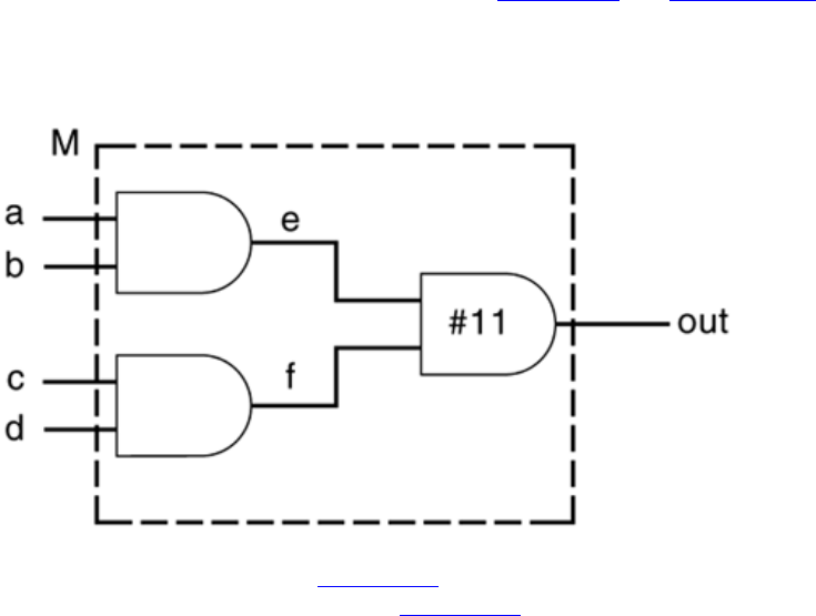
218
and #7 a2(f, c, d);
and #4 a3(out, e, f);
endmodule
//Distributed delays in data flow definition of a module
module M (out, a, b, c, d);
output out;
input a, b, c, d;
wire e, f;
//Distributed delay in each expression
assign #5 e = a & b;
assign #7 f = c & d;
assign #4 out = e & f;
endmodule
Distributed delays provide detailed delay modeling. Delays in each element of the circuit
are specified.
10.1.2 Lumped Delay
Lumped delays are specified on a per module basis. They can be specified as a single
delay on the output gate of the module. The cumulative delay of all paths is lumped at
one location. The example of a lumped delay is shown in Figure 10-2 and Example 10-2.
Figure 10-2. Lumped Delay
The above example is a modification of Figure 10-1. In this example, we computed the
maximum delay from any input to the output of Figure 10-1, which is 7 + 4 = 11 units.
The entire delay is lumped into the output gate. After a delay, primary output changes
after any input to the module M changes.

219
Example 10-2 Lumped Delay
//Lumped Delay Model
module M (out, a, b, c, d);
output out;
input a, b, c, d;
wire e, f;
and a1(e, a, b);
and a2(f, c, d);
and #11 a3(out, e, f);//delay only on the output gate
endmodule
Lumped delays models are easy to model compared with distributed delays.
10.1.3 Pin-to-Pin Delays
Another method of delay specification for a module is pin-to-pin timing. Delays are
assigned individually to paths from each input to each output. Thus, delays can be
separately specified for each input/output path. In Figure 10-3, we take the example in
Figure 10-1 and compute the pin-to-pin delays for each input/output path.
Figure 10-3. Pin-to-Pin Delay

220
Pin-to-pin delays for standard parts can be directly obtained from data books. Pin-to-pin
delays for modules of a digital circuit are obtained by circuit characterization, using a
low-level simulator like SPICE.
Although pin-to-pin delays are very detailed, for large circuits they are easier to model
than distributed delays because the designer writing delay models needs to know only the
I/O pins of the module rather than the internals of the module. The internals of the
module may be designed by using gates, data flow, behavioral statements, or mixed
design, but the pin-to-pin delay specification remains the same. Pin-to-pin delays are also
known as path delays. We will use the term "path delays" in the succeeding sections.
We covered distributed and lumped delays in Section 5.2, Gate Delays, and in Section
6.2, Delays. In the following section, we study path delays in detail.

221
10.2 Path Delay Modeling
In this section, we discuss various aspects of path delay modeling. In this section, the
terms pin and port are used interchangeably.
10.2.1 Specify Blocks
A delay between a source (input or inout) pin and a destination (output or inout) pin of a
module is called a module path delay. Path delays are assigned in Verilog within the
keywords specify and endspecify. The statements within these keywords constitute a
specify block.
Specify blocks contain statements to do the following:
• Assign pin-to-pin timing delays across module paths
• Set up timing checks in the circuits
• Define specparam constants
For the example in Figure 10-3, we can write the module M with pin-to-pin delays, using
specify blocks as follows:
Example 10-3 Pin-to-Pin Delay
//Pin-to-pin delays
module M (out, a, b, c, d);
output out;
input a, b, c, d;
wire e, f;
//Specify block with path delay statements
specify
(a => out) = 9;
(b => out) = 9;
(c => out) = 11;
(d => out) = 11;
endspecify
//gate instantiations
and a1(e, a, b);
and a2(f, c, d);
and a3(out, e, f);
endmodule

222
The specify block is a separate block in the module and does not appear under any other
block, such as initial or always. The meaning of the statements within specify blocks
needs to be clarified. In the following subsection, we analyze the statements that are used
inside specify blocks.
10.2.2 Inside Specify Blocks
In this section, we describe the statements that can be used inside specify blocks.
Parallel connection
As discussed earlier, every path delay statement has a source field and a destination field.
In the path delay statements in Example 10-3, a, b, c, and d are in the position of the
source field and out is the destination field.
A parallel connection is specified by the symbol => and is used as shown below.
Usage: ( <source_field> => <destination_field>) = <delay_value>;
In a parallel connection, each bit in source field connects to its corresponding bit in the
destination field. If the source and the destination fields are vectors, they must have the
same number of bits; otherwise, there is a mismatch. Thus, a parallel connection specifies
delays from each bit in source to each bit in destination.
Figure 10-4 shows how bits between the source field and destination field are connected
in a parallel connection. Example 10-4 shows the Verilog description for a parallel
connection.
Example 10-4 Parallel Connection
//bit-to-bit connection. both a and out are single-bit
(a => out) = 9;
//vector connection. both a and out are 4-bit vectors a[3:0], out[3:0]
//a is source field, out is destination field.
(a => out) = 9;
//the above statement is shorthand notation
//for four bit-to-bit connection statements
(a[0] => out[0]) = 9;
(a[1] => out[1]) = 9;
(a[2] => out[2]) = 9;
(a[3] => out[3]) = 9;

223
//illegal connection. a[4:0] is a 5-bit vector, out[3:0] is 4-bit.
//Mismatch between bit width of source and destination fields
(a => out) = 9; //bit width does not match.
Figure 10-4. Parallel Connection
Full connection
A full connection is specified by the symbol *> and is used as shown below.
Usage: ( <source_field> *> <destination_field>) = <delay_value>;
In a full connection, each bit in the source field connects to every bit in the destination
field. If the source and the destination are vectors, then they need not have the same
number of bits. A full connection describes the delay between each bit of the source and
every bit in the destination, as illustrated in Figure 10-5.
Figure 10-5. Full Connection
Delays for module M were described in Example 10-3, using a parallel connection.
Example 10-5 shows how delays are specified by using a full connection.
Example 10-5 Full Connection
//Full Connection
module M (out, a, b, c, d);
output out;
input a, b, c, d;

224
wire e, f;
//full connection
specify
(a,b *> out) = 9;
(c,d *> out) = 11;
endspecify
and a1(e, a, b);
and a2(f, c, d);
and a3(out, e, f);
endmodule
The full connection is particularly useful for specifying a delay between each bit of an
input vector and every bit in the output vector when bit width of the vectors is large. The
following example shows how the full connection sometimes specifies delays very
concisely.
//a[31:0] is a 32-bit vector and out[15:0] is a 16-bit vector
//Delay of 9 between each bit of a and every bit of out
specify
( a *> out) = 9; // you would need 32 X 16 = 352 parallel connection
// statements to accomplish the same result! Why?
endspecify
Edge-Sensitive Paths
An edge-sensitive path construct is used to model the timing of input to output delays,
which occurs only when a specified edge occurs at the source signal.
//In this example, at the positive edge of clock, a module path
//extends from clock signal to out signal using a rise delay of 10
//and a fall delay of 8. The data path is from in to out, and the
//in signal is not inverted as it propagates to the out signal.
(posedge clock => (out +: in)) = (10 : 8);
specparam statements
Special parameters can be declared for use inside a specify block. They are declared by
the keyword specparam. Instead of using hardcoded delay numbers to specify pin-to-pin
delays, it is common to define specify parameters by using specparam and then to use
those parameters inside the specify block. The specparam values are often used to store
values for nonsimulation tools, such as delay calculators, synthesis tools, and layout
estimators. A sample specify block with specparam statements is shown in Example 10-6.

225
Example 10-6 Specparam
//Specify parameters using specparam statement
specify
//define parameters inside the specify block
specparam d_to_q = 9;
specparam clk_to_q = 11;
(d => q) = d_to_q;
(clk => q) = clk_to_q;
endspecify
Note that specify parameters are used only inside their own specify block. They are not
general-purpose parameters that are declared by the keyword parameter. Specify
parameters are provided for convenience in assigning delays. It is recommended that all
pin-to-pin delay values be expressed in terms of specify parameters instead of hardcoded
numbers. Thus, if timing specifications of the circuit change, the user has to change only
the values of specify parameters.
Conditional path delays
Based on the states of input signals to a circuit, the pin-to-pin delays might change.
Verilog allows path delays to be assigned conditionally, based on the value of the signals
in the circuit. A conditional path delay is expressed with the if conditional statement. The
operands can be scalar or vector module input or inout ports or their bit-selects or part-
selects, locally defined registers or nets or their bit-selects or part-selects, or compile time
constants (constant numbers and specify block parameters). The conditional expression
can contain any logical, bitwise, reduction, concatenation, or conditional operator shown
in Table 6-1 on page 96. The else construct cannot be used. Conditional path delays are
also known as state dependent path delays(SDPD).
Example 10-7 Conditional Path Delays
//Conditional Path Delays
module M (out, a, b, c, d);
output out;
input a, b, c, d;
wire e, f;
//specify block with conditional pin-to-pin timing
specify
//different pin-to-pin timing based on state of signal a.
if (a) (a => out) = 9;
if (~a) (a => out) = 10;
//Conditional expression contains two signals b , c.
//If b & c is true, delay = 9,
//Conditional Path Delays

226
if (b & c) (b => out) = 9;
if (~(b & c)) (b => out) = 13;
//Use concatenation operator.
//Use Full connection
if ({c,d} == 2'b01)
(c,d *> out) = 11;
if ({c,d} != 2'b01)
(c,d *> out) = 13;
endspecify
and a1(e, a, b);
and a2(f, c, d);
and a3(out, e, f);
endmodule
Rise, fall, and turn-off delays
Pin-to-pin timing can also be expressed in more detail by specifying rise, fall, and turn-
off delay values (see Example 10-8). One, two, three, six, or twelve delay values can be
specified for any path. Four, five, seven, eight, nine, ten, or eleven delay value
specification is illegal. The order in which delays are specified must be strictly followed.
Rise, fall, and turn-off delay specification for gates was discussed in Section 5.2.1, Rise,
Fall, and Turn-off Delays. We discuss it in this section in the context of pin-to-pin timing
specification.
Example 10-8 Path Delays Specified by Rise, Fall and Turn-off Values
//Specify one delay only. Used for all transitions.
specparam t_delay = 11;
(clk => q) = t_delay;
//Specify two delays, rise and fall
//Rise used for transitions 0->1, 0->z, z->1
//Fall used for transitions 1->0, 1->z, z->0
specparam t_rise = 9, t_fall = 13;
(clk => q) = (t_rise, t_fall);
//Specify three delays, rise, fall, and turn-off
//Rise used for transitions 0->1, z->1
//Fall used for transitions 1->0, z->0
//Turn-off used for transitions 0->z, 1->z
specparam t_rise = 9, t_fall = 13, t_turnoff = 11;
(clk => q) = (t_rise, t_fall, t_turnoff);
//specify six delays.
//Delays are specified in order
//for transitions 0->1, 1->0, 0->z, z->1, 1->z, z->0. Order
//must be followed strictly.
specparam t_01 = 9, t_10 = 13, t_0z = 11;
specparam t_z1 = 9, t_1z = 11, t_z0 = 13;
(clk => q) = (t_01, t_10, t_0z, t_z1, t_1z, t_z0);

227
//specify twelve delays.
//Delays are specified in order
//for transitions 0->1, 1->0, 0->z, z->1, 1->z, z->0
// 0->x, x->1, 1->x, x->0, x->z, z->x.
//Order must be followed strictly.
specparam t_01 = 9, t_10 = 13, t_0z = 11;
specparam t_z1 = 9, t_1z = 11, t_z0 = 13;
specparam t_0x = 4, t_x1 = 13, t_1x = 5;
specparam t_x0 = 9, t_xz = 11, t_zx = 7;
(clk => q) = (t_01, t_10, t_0z, t_z1, t_1z, t_z0,
t_0x, t_x1, t_1x, t_x0, t_xz, t_zx );
Min, max, and typical delays
Min, max, and typical delay values were discussed earlier for gates in Section 5.2.2,
Min/Typ/Max Values. Min, max, and typical values can also be specified for pin-to-pin
delays. Any delay value shown in Example 10-8 can be expressed in min, max, typical
delay form. Consider the case of the three-delay specification, shown in Example 10-9.
Each delay is expressed in min:typ:max form.
Example 10-9 Path Delays with Min, Max, and Typical Values
//Specify three delays, rise, fall, and turn-off
//Each delay has a min:typ:max value
specparam t_rise = 8:9:10, t_fall = 12:13:14, t_turnoff = 10:11:12;
(clk => q) = (t_rise, t_fall, t_turnoff);
As discussed earlier, min, typical, and max values can be typically invoked with the
runtime option +mindelays, +typdelays, or +maxdelays on the Verilog command line.
Default is the typical delay value. Invocation may vary with individual simulators.
Handling x transitions
Verilog uses the pessimistic method to compute delays for transitions to the x state. The
pessimistic approach dictates that if x transition delays are not explicitly specified,
• Transitions from x to a known state should take the maximum possible time
• Transition from a known state to x should take the minimum possible time
A path delay specification with six delays borrowed from Example 10-8 is shown below.
//Six delays specified .
//for transitions 0->1, 1->0, 0->z, z->1, 1->z, z->0.

228
specparam t_01 = 9, t_10 = 13, t_0z = 11;
specparam t_z1 = 9, t_1z = 11, t_z0 = 13;
(clk => q) = (t_01, t_10, t_0z, t_z1, t_1z, t_z0);
The computation for transitions to x for the above delay specification is shown in the
table below.
Transition Delay Value
0->x
1->x
z->x
x->0
x->1
x->z
min(t_01, t_0z) = 9
min(t_10, t_1z) = 11
min(t_z0, t_z1) = 9
max(t_10, t_z0) = 13
max(t_01, t_z1) = 9
max(t_1z, t_0z) = 11
229
10.3 Timing Checks
In the earlier sections of this chapter, we discussed how to specify path delays. The
purpose of specifying path delays is to simulate the timing of the actual digital circuit
with greater accuracy than gate delays. In this section, we describe how to set up timing
checks to see if any timing constraints are violated during simulation. Timing verification
is particularly important for timing critical, high-speed sequential circuits such as
microprocessors.
System tasks are provided to do timing checks in Verilog. There are many timing check
system tasks available in Verilog. We will discuss the three most common timing
checks[1] tasks: $setup, $hold, and $width. All timing checks must be inside the specify
blocks only. Optional notifier arguments used in these timing check system tasks are
omitted to simplify the discussion.
[1] The IEEE Standard Verilog Hardware Description Language document provides
additional constraint checks, $removal, $recrem, $timeskew, $fullskew. Please refer to it
for details. Negative input timing constraints can also be specified.
10.3.1 $setup and $hold Checks
$setup and $hold tasks are used to check the setup and hold constraints for a sequential
element in the design. In a sequential element such as an edge-triggered flip-flop, the
setup time is the minimum time the data must arrive before the active clock edge. The
hold time is the minimum time the data cannot change after the active clock edge. Setup
and hold times are shown in Figure 10-6.
Figure 10-6. Setup and Hold Times
230
$setup task
Setup checks can be specified with the system task $setup.
Usage: $setup(data_event, reference_event, limit);
data_event
Signal that is monitored for violations
reference_event Signal that establishes a reference for monitoring the
data_event signal
limit Minimum time required for setup of data event
Violation is reported if (Treference_event - Tdata_event) < limit.
An example of a setup check is shown below.
//Setup check is set.
//clock is the reference
//data is being checked for violations
//Violation reported if Tposedge_clk - Tdata < 3
specify
$setup(data, posedge clock, 3);
endspecify
$hold task
Hold checks can be specified with the system task $hold.
Usage: $hold (reference_event, data_event, limit);
reference_event
Signal that establishes a reference for monitoring the
data_event signal
data_event Signal that is monitored for violation
limit Minimum time required for hold of data event
Violation is reported if ( Tdata_event - Treference_event ) < limit.
An example of a hold check is shown below.
//Hold check is set.
//clock is the reference
//data is being checked for violations
231
//Violation reported if Tdata - Tposedge_clk < 5
specify
$hold(posedge clear, data, 5);
endspecify
10.3.2 $width Check
Sometimes it is necessary to check the width of a pulse.
The system task $width is used to check that the width of a pulse meets the minimum
width requirement.
Usage: $width(reference_event, limit);
reference_event
Edge-triggered event (edge transition of a signal)
limit Minimum width of the pulse
The data_event is not specified explicitly for $width but is derived as the next opposite
edge of the reference_event signal. Thus, the $width task checks the time between the
transition of a signal value to the next opposite transition in the signal value.
Violation is reported if ( Tdata_event - Treference_event ) < limit.
//width check is set.
//posedge of clear is the reference_event
//the next negedge of clear is the data_event
//Violation reported if Tdata - Tclk < 6
specify
$width(posedge clock, 6);
endspecify

232
10.4 Delay Back-Annotation
Delay back-annotation is an important and vast topic in timing simulation. An entire boo
k
could be devoted to that subject. However, in this section, we introduce the designer to
the concept of back-annotation of delays in a simulation. Detailed coverage of this topic
is outside the scope of this book. For details, refer to the IEEE Standard Verilog
Hardware Description Language document.
The various steps in the flow that use delay back-annotation are as follows:
1. The designer writes the RTL description and then performs functional simulation.
2. The RTL description is converted to a gate-level netlist by a logic synthesis tool.
3. The designer obtains pre-layout estimates of delays in the chip by using a delay
calculator and information about the IC fabrication process. Then, the designer
does timing simulation or static timing verification of the gate-level netlist, using
these preliminary values to check that the gate-level netlist meets timing
constraints.
4. The gate-level netlist is then converted to layout by a place and route tool. The
post-layout delay values are computed from the resistance (R) and capacitance
(C) information in the layout. The R and C information is extracted from factors
such as geometry and IC fabrication process.
5. The post-layout delay values are back-annotated to modify the delay estimates for
the gate-level netlist. Timing simulation or static timing verification is run again
on the gate-level netlist to check if timing constraints are still satisfied.
6. If design changes are required to meet the timing constraints, the designer has to
go back to the RTL level, optimize the design for timing, and then repeat Step 2
through Step 5.
Figure 10-7 shows the flow of delay back annotation.
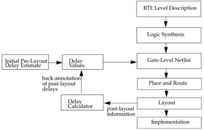
233
Figure 10-7. Delay Back-Annotation
A standard format called the Standard Delay Format (SDF) is popularly used for back-
annotation. Details of delay back-annotation are outside the scope of this book and can be
obtained from the IEEE Standard Verilog Hardware Description Language document.
234
10.5 Summary
In this chapter, we discussed the following aspects of Verilog:
• There are three types of delay models: lumped, distributed, and path delays.
Distributed delays are more accurate than lumped delays but difficult to model for
large designs. Lumped delays are relatively simpler to model.
• Path delays, also known as pin-to-pin delays, specify delays from input or inout
pins to output or inout pins. Path delays provide the most accuracy for modeling
delays within a module.
• Specify blocks are the basic blocks for expressing path delay information. In
modules, specify blocks appear separately from initial or always blocks.
• Parallel connection and full connection are two methods to describe path delays.
• Parameters can be defined inside the specify blocks by specparam statements.
• Path delays can be conditional or dependent on the values of signals in the circuit.
They are known as State Dependent Path Delays (SDPD).
• Rise, fall, and turn-off delays can be described in a path delay. Min, max, and
typical values can also be specified. Transitions to x are handled by the
pessimistic method.
• Setup, hold, and width are timing checks that check timing integrity of the digital
circuit. Other timing checks are also available but are not discussed in the book.
• Delay back-annotation is used to resimulate the digital design with path delays
extracted from layout information. This process is used repeatedly to obtain a
final circuit that meets all timing requirements.
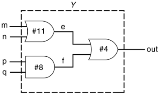
235
10.6 Exercises
1: What type of delay model is used in the following circuit? Write the Verilog
description for the module Y.
2: Use the largest delay in the module to convert the circuit to a lumped delay
model. Using a lumped delay model, write the Verilog description for the
module Y.
3: Compute the delays along each path from input to output for the circuit in
Exercise 1. Write the Verilog description, using the path delay model. Use
specify blocks.
4: Consider the negative edge-triggered with the asynchronous reset D-flipflop
shown in the figure below. Write the Verilog description for the module D_FF.
Show only the I/O ports and path delay specification. Describe path delays,
using parallel connection.
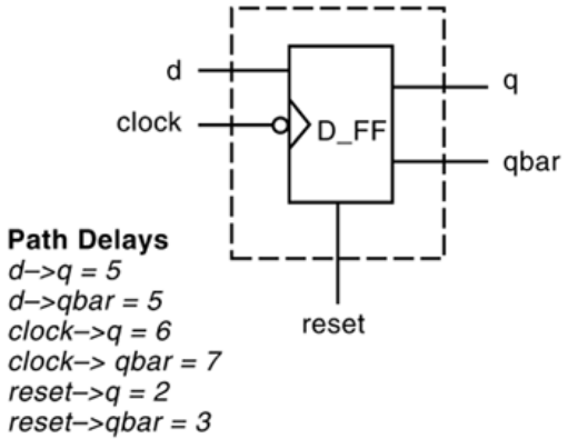
236
5: Modify the D-flipflop in Exercise 4 if all path delays are 5 units. Describe the
path delays, using full connections to q and qbar.
6: Assume that a six-delay specification is to be specified for all path delays. All
path delays are equal. In the specify block, define parameters t_01 = 4, t_10 = 5,
t_0z = 7, t_z1 = 2, t_1z = 3, t_z0 = 8. Use the D-flipflop in Exercise 4 and write
the six-delay specification for all paths, using full connections.
7: In Exercise 4, modify the delay specification for the D-flipflop if the delays are
dependent on the value of d as follows:
clock -> q = 5 for d = 1'b0, clock -> q= 6 otherwise
clock -> qbar = 4 for d = 1'b0, clock ->qbar = 7 otherwise
All other delays are 5 units.
8: For the D-flipflop in Exercise 7, add timing checks for the D-flipflop in the
specify block as follows:
The minimum setup time for d with respect to clock is 8.
The minimum hold time for d with respect to clock is 4.
The reset signal is active high. The minimum width of a reset pulse is 42.
9:
Describe delay back-annotation. Draw the flow diagram for delay back-
annotation.

237
Chapter 11. Switch-Level Modeling
In Part 1 of this book, we explained digital design and simulation at a higher level of
abstraction such as gates, data flow, and behavior. However, in rare cases designers will
choose to design the leaf-level modules, using transistors. Verilog provides the ability to
design at a MOS-transistor level. Design at this level is becoming rare with the increasing
complexity of circuits (millions of transistors) and with the availability of sophisticated
CAD tools. Verilog HDL currently provides only digital design capability with logic
values 0 1, x, z, and the drive strengths associated with them. There is no analog
capability. Thus, in Verilog HDL, transistors are also known switches that either conduct
or are open. In this chapter, we discuss the basic principles of switch-level modeling. For
most designers, it is adequate to know only the basics. Detailed information on signal
strengths and advanced net definitions is provided in Appendix A, Strength Modeling and
Advanced Net Definitions. Refer to the IEEE Standard Verilog Hardware Description
Language document for complete details on switch-level modeling.
Learning Objectives
• Describe basic MOS switches nmos, pmos, and cmos.
• Understand modeling of bidirectional pass switches, power, and ground.
• Identify resistive MOS switches.
• Explain the method to specify delays on basic MOS switches and bidirectional
pass switches.
• Build basic switch-level circuits in Verilog, using available switches.
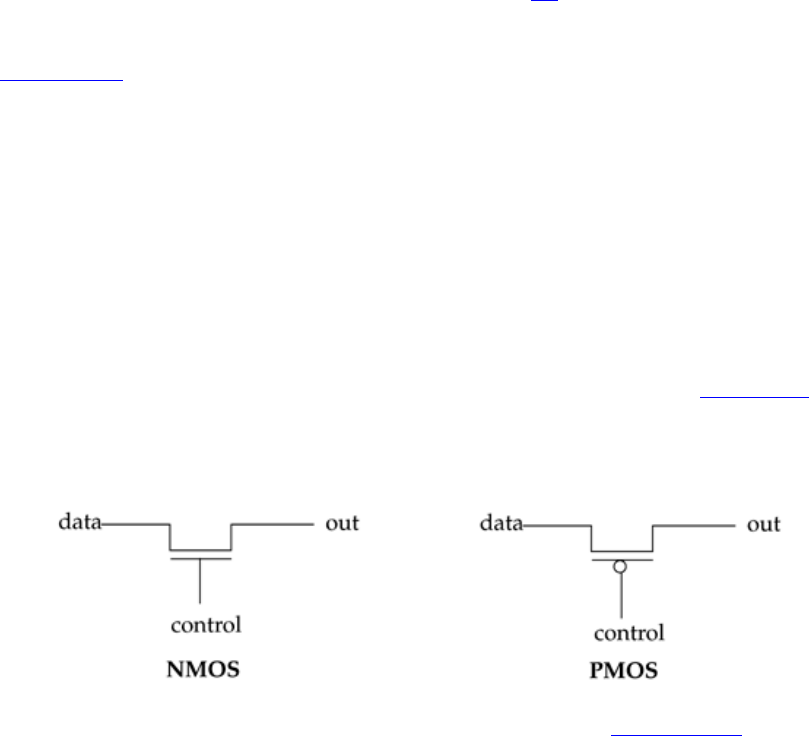
238
11.1 Switch-Modeling Elements
Verilog provides various constructs to model switch-level circuits. Digital circuits at
MOS-transistor level are described using these elements.[1]
[1] Array of instances can be defined for switches. Array of instances is described in
Section 5.1.3, Array of Instances.
11.1.1 MOS Switches
Two types of MOS switches can be defined with the keywords nmos and pmos.
//MOS switch keywords
nmos pmos
Keyword nmos is used to model NMOS transistors; keyword pmos is used to model
PMOS transistors. The symbols for nmos and pmos switches are shown in Figure 11-1.
Figure 11-1. NMOS and PMOS Switches
In Verilog, nmos and pmos switches are instantiated as shown in Example 11-1.
Example 11-1 Instantiation of NMOS and PMOS Switches
nmos n1(out, data, control); //instantiate a nmos switch
pmos p1(out, data, control); //instantiate a pmos switch
Since switches are Verilog primitives, like logic gates, the name of the instance is
optional. Therefore, it is acceptable to instantiate a switch without assigning an instance
name.
nmos (out, data, control); //instantiate an nmos switch; no instance
name
pmos (out, data, control); //instantiate a pmos switch; no instance
name
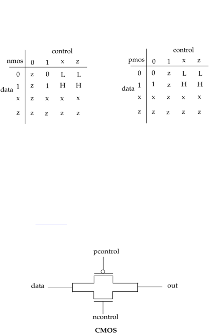
239
The value of the out signal is determined from the values of data and control signals.
Logic tables for out are shown in Table 11-1. Some combinations of data and control
signals cause the gates to output to either a 1 or 0, or to an z value without a preference
for either value. The symbol L stands for 0 or z; H stands for 1 or z.
Table 11-1. Logic Tables for NMOS and PMOS
Thus, the nmos switch conducts when its control signal is 1. If the control signal is 0, the
output assumes a high impedance value. Similarly, a pmos switch conducts if the control
signal is 0.
11.1.2 CMOS Switches
CMOS switches are declared with the keyword cmos.
A cmos device can be modeled with a nmos and a pmos device. The symbol for a cmos
switch is shown in Figure 11-2.
Figure 11-2. CMOS Switch

240
A cmos switch is instantiated as shown in Example 11-2.
Example 11-2 Instantiation of CMOS Switch
cmos c1(out, data, ncontrol, pcontrol);//instantiate cmos gate.
or
cmos (out, data, ncontrol, pcontrol); //no instance name given.
The ncontrol and pcontrol are normally complements of each other. When the ncontrol
signal is 1 and pcontrol signal is 0, the switch conducts. If ncontrol signal is 0 and
pcontrol is 1, the output of the switch is high impedance value. The cmos gate is
essentially a combination of two gates: one nmos and one pmos. Thus the cmos
instantiation shown above is equivalent to the following:
nmos (out, data, ncontrol); //instantiate a nmos switch
pmos (out, data, pcontrol); //instantiate a pmos switch
Since a cmos switch is derived from nmos and pmos switches, it is possible to derive the
output value from Table 11-1, given values of data, ncontrol, and pcontrol signals.
11.1.3 Bidirectional Switches
NMOS, PMOS and CMOS gates conduct from drain to source. It is important to have
devices that conduct in both directions. In such cases, signals on either side of the device
can be the driver signal. Bidirectional switches are provided for this purpose. Three
keywords are used to define bidirectional switches: tran, tranif0, and tranif1.
tran tranif0 tranif1
Symbols for these switches are shown in Figure 11-3 below.
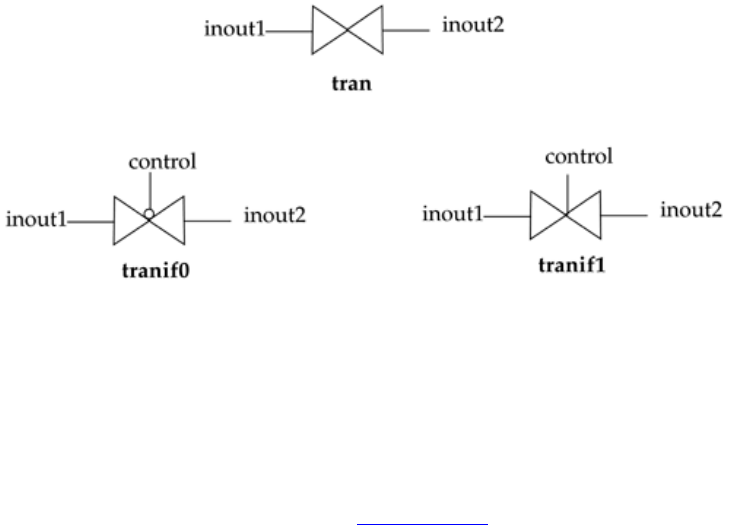
241
Figure 11-3. Bidirectional Switches
The tran switch acts as a buffer between the two signals inout1 and inout2. Either inout1
or inout2 can be the driver signal. The tranif0 switch connects the two signals inout1 and
inout2 only if the control signal is logical 0. If the control signal is a logical 1, the
nondriver signal gets a high impedance value z. The driver signal retains value from its
driver. The tranif1 switch conducts if the control signal is a logical 1.
These switches are instantiated as shown in Example 11-3.
Example 11-3 Instantiation of Bidirectional Switches
tran t1(inout1, inout2); //instance name t1 is optional
tranif0 (inout1, inout2, control); //instance name is not specified
tranif1 (inout1, inout2, control); //instance name is not specified
Bidirectional switches are typically used to provide isolation between buses or signals.
11.1.4 Power and Ground
The power (Vdd, logic 1) and Ground (Vss, logic 0) sources are needed when transistor-
level circuits are designed. Power and ground sources are defined with keywords supply1
and supply0.
Sources of type supply1 are equivalent to Vdd in circuits and place a logical 1 on a net.
Sources of the type supply0 are equivalent to ground or Vss and place a logical 0 on a
net. Both supply1 and supply0 place logical 1 and 0 continuously on nets throughout the
simulation.
Sources supply1 and supply0 are shown below.
242
supply1 vdd;
supply0 gnd;
assign a = vdd; //Connect a to vdd
assign b = gnd; //Connect b to gnd
11.1.5 Resistive Switches
MOS, CMOS, and bidirectional switches discussed before can be modeled as
corresponding resistive devices. Resistive switches have higher source-to-drain
impedance than regular switches and reduce the strength of signals passing through them.
Resistive switches are declared with keywords that have an "r" prefixed to the
corresponding keyword for the regular switch. Resistive switches have the same syntax
as regular switches.
rnmos rpmos //resistive nmos and pmos switches
rcmos //resistive cmos switch
rtran rtranif0 rtranif1 //resistive bidirectional switches.
There are two main differences between regular switches and resistive switches: their
source-to-drain impedances and the way they pass signal strengths. Refer to Appendix A,
Strength Modeling and Advanced Net Definitions, for strength levels in Verilog.
• Resistive devices have a high source-to-drain impedance. Regular switches have a
low source-to-drain impedance.
• Resistive switches reduce signal strengths when signals pass through them. The
changes are shown below. Regular switches retain strength levels of signals from
input to output. The exception is that if the input is of strength supply, the output
is of strong strength. Table 11-2 shows the strength reduction due to resistive
switches.
Table 11-2. Strength Reduction by Resistive Switches
Input Strength Output Strength
supply pull
strong pull
pull weak
weak medium
243
medium small
small small
high high
11.1.6 Delay Specification on Switches
MOS and CMOS switches
Delays can be specified for signals that pass through these switch-level elements. Delays
are optional and appear immediately after the keyword for the switch. Delay specification
is similar to that discussed in Section 5.2.1, Rise, Fall, and Turn-off Delays. Zero, one,
two, or three delays can be specified for switches according to Table 11-3.
Table 11-3. Delay Specification on MOS and CMOS Switches
Switch Element Delay Specification Examples
pmos, nmos, rpmos,
rnmos
Zero (no delay)
One (same delay on all transitions)
Two (rise, fall)
Three (rise, fall, turnoff)
pmos p1(out, data, control);
pmos #(1) p1(out, data,
control);
nmos #(1, 2) p2(out, data,
control);
nmos #(1, 3, 2) p2(out,
data, control);
cmos, rcmos Zero, one, two, or three delays
(same as above)
cmos #(5) c2(out, data,
nctrl, pctrl);
cmos #(1,2) c1(out, data,
nctrl, pctrl);
Bidirectional pass switches
Delay specification is interpreted slightly differently for bidirectional pass switches.
These switches do not delay signals passing through them. Instead, they have turn-on and
turn-off delays while switching. Zero, one, or two delays can be specified for
bidirectional switches, as shown in Table 11-4.
244
Table 11-4. Delay Specification for Bidirectional Switches
Switch Element Delay Specification Examples
tran, rtran No delay specification
allowed
tranif1, rtranif1 tranif0,
rtranif0
Zero (no delay)
One (both turn-on and
turn-off)
Two (turn-on, turn-off)
rtranif0 rt1(inout1, inout2,
control);
tranif0 #(3) T(inout1, inout2,
control);
tranif1 #(1,2) t1(inout1, inout2,
control);
Specify blocks
Pin-to-pin delays and timing checks can also be specified for modules designed using
switches. Pin-to-pin timing is described, using specify blocks. Pin-to-pin delay
specification is discussed in detail in Chapter 10, Timing and Delays, and is identical for
switch-level modules.
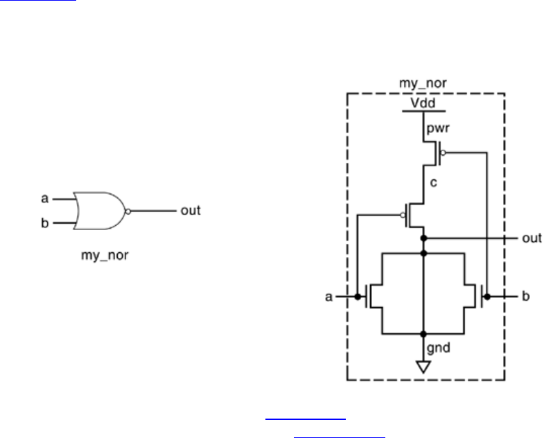
245
11.2 Examples
In this section, we discuss how to build practical digital circuits, using switch-level
constructs.
11.2.1 CMOS Nor Gate
Though Verilog has a nor gate primitive, let us design our own nor gate,using CMOS
switches. The gate and the switch-level circuit diagram for the nor gate are shown in
Figure 11-4.
Figure 11-4. Gate and Switch Diagram for Nor Gate
Using the switch primitives discussed in Section 11.1, Switch-Modeling Elements, the
Verilog description of the circuit is shown in Example 11-4 below.
Example 11-4 Switch-Level Verilog for Nor Gate
//Define our own nor gate, my_nor
module my_nor(out, a, b);
output out;
input a, b;
//internal wires
wire c;
246
//set up power and ground lines
supply1 pwr; //pwr is connected to Vdd (power supply)
supply0 gnd ; //gnd is connected to Vss(ground)
//instantiate pmos switches
pmos (c, pwr, b);
pmos (out, c, a);
//instantiate nmos switches
nmos (out, gnd, a);
nmos (out, gnd, b);
endmodule
We can now test our nor gate, using the stimulus shown below.
//stimulus to test the gate
module stimulus;
reg A, B;
wire OUT;
//instantiate the my_nor module
my_nor n1(OUT, A, B);
//Apply stimulus
initial
begin
//test all possible combinations
A = 1'b0; B = 1'b0;
#5 A = 1'b0; B = 1'b1;
#5 A = 1'b1; B = 1'b0;
#5 A = 1'b1; B = 1'b1;
end
//check results
initial
$monitor($time, " OUT = %b, A = %b, B = %b", OUT, A, B);
endmodule
The output of the simulation is shown below.
0 OUT = 1, A = 0, B = 0
5 OUT = 0, A = 0, B = 1
10 OUT = 0, A = 1, B = 0
15 OUT = 0, A = 1, B = 1
Thus we designed our own nor gate. If designers need to customize certain library blocks,
they use switch-level modeling.
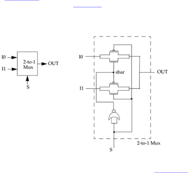
247
11.2.2 2-to-1 Multiplexer
A 2-to-1 multiplexer can be defined with CMOS switches. We will use the my_nor gate
declared in Section 11.2.1, CMOS Nor Gate to implement the not function. The circuit
diagram for the multiplexer is shown in Figure 11-5 below.
Figure 11-5. 2-to-1 Multiplexer, Using Switches
The 2-to-1 multiplexer passes the input I0 to output OUT if S = 0 and passes I1 to OUT i
f
S = 1. The switch-level description for the 2-to-1 multiplexer is shown in Example 11-4.
Example 11-5 Switch-Level Verilog Description of 2-to-1 Multiplexer
//Define a 2-to-1 multiplexer using switches
module my_mux (out, s, i0, i1);
output out;
input s, i0, i1;
//internal wire
wire sbar; //complement of s
//create the complement of s; use my_nor defined previously.
my_nor nt(sbar, s, s); //equivalent to a not gate
//instantiate cmos switches
cmos (out, i0, sbar, s);
cmos (out, i1, s, sbar);
endmodule
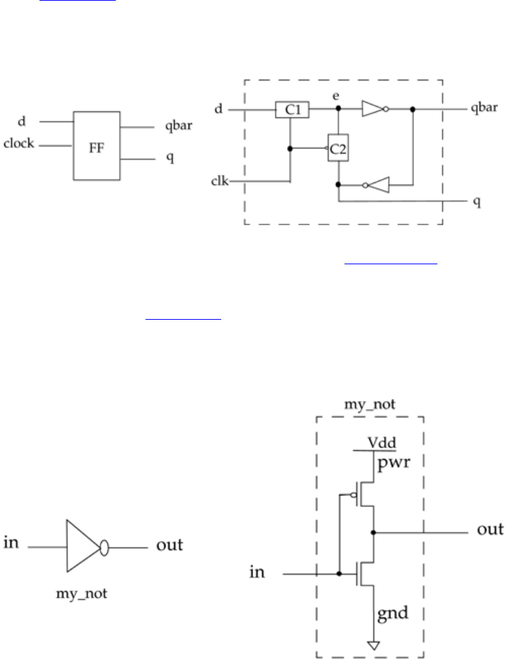
248
The 2-to-1 multiplexer can be tested with a small stimulus. The stimulus is left as an
exercise to the reader.
11.2.3 Simple CMOS Latch
We designed combinatorial elements in the previous examples. Let us now define a
memory element which can store a value. The diagram for a level-sensitive CMOS latch
is shown in Figure 11-6.
Figure 11-6. CMOS flipflop
The switches C1 and C2 are CMOS switches, discussed in Section 11.1.2, CMOS
Switches. Switch C1 is closed if clk = 1, and switch C2 is closed if clk = 0. Complement
of the clk is fed to the ncontrol input of C2. The CMOS inverters can be defined by using
MOS switches, as shown in Figure 11-7.
Figure 11-7. CMOS Inverter

249
We are now ready to write the Verilog description for the CMOS latch. First, we need to
design our own inverter my_not by using switches. We can write the Verilog module
description for the CMOS inverter from the switch-level circuit diagram in Figure 11-7.
The Verilog description of the inverter is shown below.
Example 11-6 CMOS Inverter
//Define an inverter using MOS switches
module my_not(out, in);
output out;
input in;
//declare power and ground
supply1 pwr;
supply0 gnd;
//instantiate nmos and pmos switches
pmos (out, pwr, in);
nmos (out, gnd, in);
endmodule
Now, the CMOS latch can be defined using the CMOS switches and my_not inverters.
The Verilog description for the CMOS latch is shown in Example 11-6.
Example 11-7 CMOS Flipflop
//Define a CMOS latch
module cff ( q, qbar, d, clk);
output q, qbar;
input d, clk;
//internal nets
wire e;
wire nclk; //complement of clock
//instantiate the inverter
my_not nt(nclk, clk);
//instantiate CMOS switches
cmos (e, d, clk, nclk); //switch C1 closed i.e. e = d, when clk = 1.
cmos (e, q, nclk, clk); //switch C2 closed i.e. e = q, when clk = 0.
//instantiate the inverters
my_not nt1(qbar, e);
my_not nt2(q, qbar);
endmodule

250
We will leave it as an exercise to the reader to write a small stimulus module and
simulate the design to verify the load and store properties of the latch.

251
11.3 Summary
We discussed the following aspects of Verilog in this chapter:
• Switch-level modeling is at a very low level of design abstraction. Designers use
switch modeling in rare cases when they need to customize a leaf cell. Verilog
design at this level is becoming less popular with increasing complexity of
circuits.
• MOS, CMOS, bidirectional switches, and supply1 and supply0 sources can be
used to design any switch-level circuit. CMOS switches are a combination of
MOS switches.
• Delays can be optionally specified for switch elements. Delays are interpreted
differently for bidirectional devices.
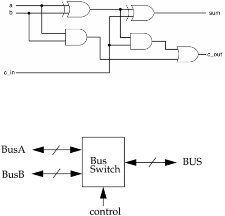
252
11.4 Exercises
1: Draw the circuit diagram for an xor gate, using nmos and pmos switches. Write
the Verilog description for the circuit. Apply stimulus and test the design.
2: Draw the circuit diagram for and and or gates, using nmos and pmos switches.
Write the Verilog description for the circuits. Apply stimulus and test the
design.
3: Design the 1-bit full-adder shown below using the xor, and, and or gates built in
Exercise 1 and Exercise 2 above. Apply stimulus and test the design.
4: Design a 4-bit bidirectional bus switch that has two buses, BusA and BusB, on
one side and a single bus, BUS, on the other side. A 1-bit control signal is used
for switching. BusA and BUS are connected if control = 1. BusB and BUS are
connected if control = 0. (Hint: Use the switches tranif0 and tranif1.) Apply
stimulus and test the design.
5: Instantiate switches with the following delay specifications. Use your own
input/output port names.
a. A pmos switch with rise = 2 and fall = 3.
253
b. An nmos switch with rise = 4, fall = 6, turn-off = 5
c. A cmos switch with delay = 6
d. A tranif1 switch with turn-on = 5, turn-off = 6
e. A tranif0 with delay = 3.
254
Chapter 12. User-Defined Primitives
Verilog provides a standard set of primitives, such as and, nand, or, nor, and not, as a part
of the language. These are also commonly known as built-in primitives. However,
designers occasionally like to use their own custom-built primitives when developing a
design. Verilog provides the ability to define User-Defined Primitives (UDP). These
primitives are self-contained and do not instantiate other modules or primitives. UDPs are
instantiated exactly like gate-level primitives.
There are two types of UDPs: combinational and sequential.
• Combinational UDPs are defined where the output is solely determined by a
logical combination of the inputs. A good example is a 4-to-1 multiplexer.
• Sequential UDPs take the value of the current inputs and the current output to
determine the value of the next output. The value of the output is also the internal
state of the UDP. Good examples of sequential UDPs are latches and flipflops.
Learning Objectives
• Understand UDP definition rules and parts of a UDP definition.
• Define sequential and combinational UDPs.
• Explain instantiation of UDPs.
• Identify UDP shorthand symbols for more conciseness and better readability.
• Describe the guidelines for UDP design.

255
12.1 UDP basics
In this section, we describe parts of a UDP definition and rules for UDPs.
12.1.1 Parts of UDP Definition
Figure 12-1 shows the distinct parts of a basic UDP definition in pseudo syntax form. For
details, see the formal syntax definition described in Appendix , Formal Syntax
Definition.
Figure 12-1 Parts of UDP Definition
//UDP name and terminal list
primitive <udp_name> (
<output_terminal_name>(only one allowed)
<input_terminal_names> );
//Terminal declarations
output <output_terminal_name>;
input <input_terminal_names>;
reg <output_terminal_name>;(optional; only for sequential
UDP)
// UDP initialization (optional; only for sequential UDP
initial <output_terminal_name> = <value>;
//UDP state table
table
<table entries>
endtable
//End of UDP definition
endprimitive
A UDP definition starts with the keyword primitive. The primitive name, output terminal,
and input terminals are specified. Terminals are declared as output or input in the
terminal declarations section. For a sequential UDP, the output terminal is declared as a
reg. For sequential UDPs, there is an optional initial statement that initializes the output
terminal of the UDP. The UDP state table is most important part of the UDP. It begins
with the keyword table and ends with the keyword endtable. The table defines how the
output will be computed from the inputs and current state. The table is modeled as a
lookup table. and the table entries resemble entries in a logic truth table. Primitive
definition is completed with the keyword endprimitive.

256
12.1.2 UDP Rules
UDP definitions follow certain rules:
1. UDPs can take only scalar input terminals (1 bit). Multiple input terminals are
permitted.
2. UDPs can have only one scalar output terminal (1 bit). The output terminal must
always appear first in the terminal list. Multiple output terminals are not allowed.
3. In the declarations section, the output terminal is declared with the keyword
output. Since sequential UDPs store state, the output terminal must also be
declared as a reg.
4. The inputs are declared with the keyword input.
5. The state in a sequential UDP can be initialized with an initial statement. This
statement is optional. A 1-bit value is assigned to the output, which is declared as
reg.
6. The state table entries can contain values 0, 1, or x. UDPs do not handle z values.
z values passed to a UDP are treated as x values.
7. UDPs are defined at the same level as modules. UDPs cannot be defined inside
modules. They can be instantiated only inside modules. UDPs are instantiated
exactly like gate primitives.
8. UDPs do not support inout ports.
Both combinational and sequential UDPs must follow the above rules. In the following
sections, we will discuss the details of combinational and sequential UDPs.

257
12.2 Combinational UDPs
Combinational UDPs take the inputs and produce the output value by looking up the
corresponding entry in the state table.
12.2.1 Combinational UDP Definition
The state table is the most important part of the UDP definition. The best way to explain
a state table is to take the example of an and gate modeled as a UDP. Instead of using the
and gate provided by Verilog, let us define our own and gate primitive and call it
udp_and.
Example 12-1 Primitive udp_and
//Primitive name and terminal list
primitive udp_and(out, a, b);
//Declarations
output out; //must not be declared as reg for combinational UDP
input a, b; //declarations for inputs.
//State table definition; starts with keyword table
table
//The following comment is for readability only
//Input entries of the state table must be in the
//same order as the input terminal list.
// a b : out;
0 0 : 0;
0 1 : 0;
1 0 : 0;
1 1 : 1;
endtable //end state table definition
endprimitive //end of udp_and definition
Compare parts of udp_and defined above with the parts discussed in Figure 12-1. The
missing parts are that the output is not declared as reg and the initial statement is absent.
Note that these missing parts are used only for sequential UDPs, which are discussed
later in the chapter.
ANSI C style declarations for UDPs are also supported. This style allows the declarations
of a primitive port to be combined with the port list. Example 12-2 shows an example of
an ANSI C style UDP declaration.

258
Example 12-2 ANSI C Style UDP Declaration
//Primitive name and terminal list
primitive udp_and(output out,
input a,
input b);
--
--
endprimitive //end of udp_and definition
12.2.2 State Table Entries
In order to understand how state table entries are specified, let us take a closer look at the
state table for udp_and. Each entry in the state table in a combinational UDP has the
following pseudosyntax:
<input1> <input2> ..... <inputN> : <output>;
Note the following points about state table entries:
1. The <input#> values in a state table entry must appear in the same order as they
appear in the input terminal list. It is important to keep this in mind while
designing UDPs, because designers frequently make mistakes in the input order
and get incorrect results.
2. Inputs and output are separated by a ":".
3. A state table entry ends with a ";".
4. All possible combinations of inputs, where the output produces a known value,
must be explicitly specified. Otherwise, if a certain combination occurs and the
corresponding entry is not in the table, the output is x. Use of default x output is
frequently used in commercial models. Note that the table for udp_and does not
handle the case when a or b is x.
In the Verilog and gate, if a = x and b = 0, the result should be 0, but udp_and will give
an x as output because the corresponding entry was not found in the state table, that is,
the state table was incompletely specified. To understand how to completely specify all
possible combinations in a UDP, let us define our own or gate udp_or, which completely
specifies all possible cases. The UDP definition for udp_or is shown in Example 12-3.
Example 12-3 Primitive udp_or
primitive udp_or(out, a, b);
output out;

259
input a, b;
table
// a b : out;
0 0 : 0;
0 1 : 1;
1 0 : 1;
1 1 : 1;
x 1 : 1;
1 x : 1;
endtable
endprimitive
N
otice that the above example covers all possible combinations of a and b where the
output is not x. The value z is not allowed in a UDP. The z values on inputs are treated as
x values.
12.2.3 Shorthand Notation for Don't Cares
In the above example, whenever one input is 1, the result of the OR operation is 1,
regardless of the value of the other input. The ? symbol is used for a don't care condition.
A ? symbol is automatically expanded to 0, 1, or x. The or gate described above can be
rewritten with the ? symbol.
primitive udp_or(out, a, b);
output out;
input a, b;
table
// a b : out;
0 0 : 0;
1 ? : 1; //? expanded to 0, 1, x
? 1 : 1; //? expanded to 0, 1, x
0 x : x;
x 0 : x;
endtable
endprimitive
12.2.4 Instantiating UDP Primitives
Having discussed how to define combinational UDPs, let us take a look at how UDPs are
instantiated. UDPs are instantiated exactly like Verilog gate primitives. Let us design a 1-
bit full adder with the udp_and and udp_or primitives defined earlier. The 1-
b
it full adder
code shown in Example 12-4 is identical to Example 5-7 on page 75 except that the
standard Verilog primitives and and or primitives are replaced with udp_and and upd_or
260
primitives.
Example 12-4 Instantiation of udp Primitives
// Define a 1-bit full adder
module fulladd(sum, c_out, a, b, c_in);
// I/O port declarations
output sum, c_out;
input a, b, c_in;
// Internal nets
wire s1, c1, c2;
// Instantiate logic gate primitives
xor (s1, a, b);//use Verilog primitive
udp_and (c1, a, b); //use UDP
xor (sum, s1, c_in); //use Verilog primitive
udp_and (c2, s1, c_in); //use UDP
udp_or (c_out, c2, c1);//use UDP
endmodule
12.2.5 Example of a Combinational UDP
We discussed two small examples of combinational UDPs: udp_and and udp_or. Let us
design a bigger combinational UDP, a 4-to-1 multiplexer. A 4-to-1 multiplexer was
designed with gates in Section 5.1.4, Examples. In this section, we describe the
multiplexer as a UDP. Note that the multiplexer is ideal because it has only one output
terminal. The block diagram and truth table for the multiplexer are shown in Figure 12-2.
Figure 12-2. 4-to-1 Multiplexer with UDP

261
The multiplexer has six inputs and one output. The Verilog UDP description for the
multiplexer is shown in Example 12-5.
Example 12-5 Verilog Description of 4-to-1 Multiplexer with UDP
// 4-to-1 multiplexer. Define it as a primitive
primitive mux4_to_1 ( output out,
input i0, i1, i2, i3, s1, s0);
table
// i0 i1 i2 i3, s1 s0 : out
1 ? ? ? 0 0 : 1 ;
0 ? ? ? 0 0 : 0 ;
? 1 ? ? 0 1 : 1 ;
? 0 ? ? 0 1 : 0 ;
? ? 1 ? 1 0 : 1 ;
? ? 0 ? 1 0 : 0 ;
? ? ? 1 1 1 : 1 ;
? ? ? 0 1 1 : 0 ;
? ? ? ? x ? : x ;
? ? ? ? ? x : x ;
endtable
endprimitive
It is important to note that the state table becomes large very quickly as the number of
inputs increases. Memory requirements to simulate UDPs increase exponentially with the
number of inputs to the UDP. However, UDPs offer a convenient feature to implement an
arbitrary function whose truth table is known, without extracting actual logic and by
using logic gates to implement the circuit.
The stimulus shown in Example 12-6 is applied to test the multiplexer.
Example 12-6 Stimulus for 4-to-1 Multiplexer with UDP
// Define the stimulus module (no ports)
module stimulus;
// Declare variables to be connected
// to inputs
reg IN0, IN1, IN2, IN3;
reg S1, S0;
// Declare output wire
wire OUTPUT;
// Instantiate the multiplexer
mux4_to_1 mymux(OUTPUT, IN0, IN1, IN2, IN3, S1, S0);
262
// Stimulate the inputs
initial
begin
// set input lines
IN0 = 1; IN1 = 0; IN2 = 1; IN3 = 0;
#1 $display("IN0= %b, IN1= %b, IN2= %b, IN3= %b\n",IN0,IN1,IN2,IN3);
// choose IN0
S1 = 0; S0 = 0;
#1 $display("S1 = %b, S0 = %b, OUTPUT = %b \n", S1, S0, OUTPUT);
// choose IN1
S1 = 0; S0 = 1;
#1 $display("S1 = %b, S0 = %b, OUTPUT = %b \n", S1, S0, OUTPUT);
// choose IN2
S1 = 1; S0 = 0;
#1 $display("S1 = %b, S0 = %b, OUTPUT = %b \n", S1, S0, OUTPUT);
// choose IN3
S1 = 1; S0 = 1;
#1 $display("S1 = %b, S0 = %b, OUTPUT = %b \n", S1, S0, OUTPUT);
end
endmodule
The output of the simulation is shown below.
IN0= 1, IN1= 0, IN2= 1, IN3= 0
S1 = 0, S0 = 0, OUTPUT = 1
S1 = 0, S0 = 1, OUTPUT = 0
S1 = 1, S0 = 0, OUTPUT = 1
S1 = 1, S0 = 1, OUTPUT = 0

263
12.3 Sequential UDPs
Sequential UDPs differ from combinational UDPs in their definition and behavior.
Sequential UDPs have the following differences:
• The output of a sequential UDP is always declared as a reg.
• An initial statement can be used to initialize output of sequential UDPs.
• The format of a state table entry is slightly different.
• <input1> <input2> ..... <inputN> : <current_state> :
<next_state>;
• There are three sections in a state table entry: inputs, current state, and next state.
The three sections are separated by a colon (:) symbol.
• The input specification of state table entries can be in terms of input levels or
edge transitions.
• The current state is the current value of the output register.
• The next state is computed based on inputs and the current state. The next state
becomes the new value of the output register.
• All possible combinations of inputs must be specified to avoid unknown output
values.
If a sequential UDP is sensitive to input levels, it is called a level-sensitive sequential
UDP. If a sequential UDP is sensitive to edge transitions on inputs, it is called an edge-
sensitive sequential UDP.
12.3.1 Level-Sensitive Sequential UDPs
Level-sensitive UDPs change state based on input levels. Latches are the most common
example of level-sensitive UDPs. A simple latch with clear is shown in Figure 12-3.
264
Figure 12-3. Level-Sensitive Latch with clear
In the level-sensitive latch shown above, if the clear input is 1, the output q is always 0. I
f
clear is 0, q = d when clock = 1. If clock = 0, q retains its value. The latch can be
described as a UDP as shown in Example 12-7. Note that the dash "-" symbol is used to
denote no change in the state of the latch.
Example 12-7 Verilog Description of Level-Sensitive UDP
//Define level-sensitive latch by using UDP.
primitive latch(q, d, clock, clear);
//declarations
output q;
reg q; //q declared as reg to create internal storage
input d, clock, clear;
//sequential UDP initialization
//only one initial statement allowed
initial
q = 0; //initialize output to value 0
//state table
table
//d clock clear : q : q+ ;
? ? 1 : ? : 0 ; //clear condition;
//q+ is the new output value
1 1 0 : ? : 1 ; //latch q = data = 1
0 1 0 : ? : 0 ; //latch q = data = 0
? 0 0 : ? : - ; //retain original state if clock = 0
endtable
endprimitive
265
Sequential UDPs can include the reg declaration in the port list using an ANSI C style
UDP declaration. They can also initialize the value of the output in the port declaration.
Example 12-8 shows an example of an ANSI C style declaration for sequential UDPs.
Example 12-8 ANSI C Style Port Declaration for Sequential UDP
//Define level-sensitive latch by using UDP.
primitive latch(output reg q = 0,
input d, clock, clear);
--
--
--
endprimitive
12.3.2 Edge-Sensitive Sequential UDPs
Edge-sensitive sequential UDPs change state based on edge transitions and/or input
levels. Edge-triggered flipflops are the most common example of edge-sensitive
sequential UDPs. Consider the negative edge-triggered D-flipflop with clear shown in
Figure 12-4.
Figure 12-4. Edge-Sensitive D-flipflop with clear
In the edge-sensitive flipflop shown above, if clear =1, the output q is always 0. If clear =
0, the D-flipflop functions normally. On the negative edge of clock, i.e., transition from 1
to 0, q gets the value of d. If clock transitions to an unknown state or on a positive edge
of clock, do not change the value of q. Also, if d changes when clock is steady, hold
value of q.
The Verilog UDP description for the D-flipflop is shown in Example 12-9.

266
Example 12-9 Negative Edge-Triggered D-flipflop with clear
//Define an edge-sensitive sequential UDP;
primitive edge_dff(output reg q = 0,
input d, clock, clear);
table
// d clock clear : q : q+ ;
? ? 1 : ? : 0 ; //output = 0 if clear = 1
? ? (10): ? : - ; //ignore negative transition of clear
1 (10) 0 : ? : 1 ; //latch data on negative transition of
0 (10) 0 : ? : 0 ; //clock
? (1x) 0 : ? : - ; //hold q if clock transitions to
unknown
//state
? (0?) 0 : ? : - ; //ignore positive transitions of clock
? (x1) 0 : ? : - ; //ignore positive transitions of clock
(??) ? 0 : ? : - ; //ignore any change in d when clock
//is steady
endtable
endprimitive
In Example 12-9, edge transitions are explained as follows:
• (10) denotes a negative edge transition from logic 1 to logic 0.
• (1x) denotes a transition from logic 1 to unknown x state.
• (0?) denotes a transition from 0 to 0, 1, or x. Potential positive-edge transition.
• (??) denotes any transition in signal value 0,1, or x to 0, 1, or x.
It is important to completely specify the UDP by covering all possible combinations of
transitions and levels in the state table for which the outputs have a known value.
Otherwise, some combinations may result in an unknown value. Only one edge
specification is allowed per table entry. More than one edge specification in a single table
entry, as shown below, is illegal in Verilog.
table
...
(01) (10) 0 : ? : 1 ; //illegal; two edge transitions in an
entry
...
endtable

267
12.3.3 Example of a Sequential UDP
We discussed small examples of sequential UDPs. Let now describe a slightly bigger
example, a 4-bit binary ripple counter. A 4-bit binary ripple counter was designed with T-
flipflops in Section 6.5.3, Ripple Counter. The T-flipflops were built with negative edge-
triggered D-flipflops. Instead, let us define the T-flipflop directly as a UDP primitive.
The UDP definition for the T-flipflop is shown in Example 12-10.
Example 12-10 T-Flipflop with UDP
// Edge-triggered T-flipflop
primitive T_FF(output reg q,
input clk, clear);
//no initialization of q; TFF will be initialized with clear signal
table
// clk clear : q : q+ ;
//asynchronous clear condition
? 1 : ? : 0 ;
//ignore negative edge of clear
? (10) : ? : - ;
//toggle flipflop at negative edge of clk
(10) 0 : 1 : 0 ;
(10) 0 : 0 : 1 ;
//ignore positive edge of clk
(0?) 0 : ? : - ;
endtable
endprimitive
To build the ripple counter with T-flipflops, four T-flipflops are instantiated in the ripple
counter, as shown in Example 12-11.
Example 12-11 Instantiation of T_FF UDP in Ripple Counter
// Ripple counter
module counter(Q , clock, clear);
// I/O ports
output [3:0] Q;
input clock, clear;
// Instantiate the T flipflops
// Instance names are optional
T_FF tff0(Q[0], clock, clear);
T_FF tff1(Q[1], Q[0], clear);
T_FF tff2(Q[2], Q[1], clear);

268
T_FF tff3(Q[3], Q[2], clear);
endmodule
If stimulus shown in Example 6-9 on page 113 is applied to the counter, identical
simulation output will be obtained.
269
12.4 UDP Table Shorthand Symbols
Shorthand symbols for levels and edge transitions are provided so UDP tables can be
written in a concise manner. We already discussed the symbols ? and -. A summary of all
shorthand symbols and their meaning is shown in Table 12-1.
Table 12-1. UDP Table Shorthand Symbols
Shorthand
Symbols Meaning Explanation
? 0, 1, x Cannot be specified in an output field
b 0, 1 Cannot be specified in an output field
- No change in state
value
Can be specified only in output field of a
sequential UDP
r (01) Rising edge of signal
f (10) Falling edge of signal
p (01), (0x) or (x1) Potential rising edge of signal
n (10), (1x) or (x0) Potential falling edge of signal
* (??) Any value change in signal
Using the shorthand symbols, we can rewrite the table entries in Example 12-9 on page
263 as follows.
table
// d clock clear : q : q+ ;
? ? 1 : ? : 0 ; //output = 0 if clear = 1
? ? f : ? : - ; //ignore negative transition of clear
1 f 0 : ? : 1 ; //latch data on negative transition of
0 f 0 : ? : 0 ; //clock
? (1x) 0 : ? : - ; //hold q if clock transitions to unknown
//state
? p 0 : ? : - ; //ignore positive transitions of clock
* ? 0 : ? : - ; //ignore any change in d when
//clock is steady
endtable
Note that the use of shorthand symbols makes the entries more readable and more
concise.
270
12.5 Guidelines for UDP Design
When designing a functional block, it is important to decide whether to model it as a
module or as a user-defined primitive. Here are some guidelines used to make that
decision.
• UDPs model functionality only. They do not model timing or process technology
(such as CMOS, TTL, ECL). The primary purpose of a UDP is to define in a
simple and concise form the functional portion of a block. A module is always
used to model a complete block that has timing and process technology.
• A block can modeled as a UDP only if it has exactly one output terminal. If the
block to be designed has more than one output, it has to be modeled as a module.
• The limit on the maximum number of inputs of a UDP is specific to the Verilog
simulator being used. However, Verilog simulators are required to allow a
minimum of 9 inputs for sequential UDPs and 10 for combinational UDPs.
• A UDP is typically implemented as a lookup table in memory. As the number of
inputs increases, the number of table entries grows exponentially. Thus, the
memory requirement for a UDP grows exponentially in relation to the number of
inputs. It is not advisable to design a block with a large number of inputs as a
UDP.
• UDPs are not always the appropriate method to design a block. Sometimes it is
easier to design blocks as a module. For example, it is not advisable to design an
8-to-1 multiplexer as a UDP because of the large number of table entries. Instead,
the data flow or behavioral representation would be much simpler. It is important
to consider complexity trade-offs to decide whether to use UDP to represent a
block.
There are also some guidelines for writing the UDP state table.
• The UDP state table should be specified as completely as possible. All possible
input combinations for which the output is known should be covered. If a certain
combination of inputs is not specified, the default output value for that
combination will be x. This feature is used frequently in commercial libraries to
reduce the number of table entries.
• Shorthand symbols should be used to combine table entries wherever possible.
Shorthand symbols make the UDP description more concise. However, the
Verilog simulator may internally expand the table entries. Thus, there is no
memory requirement reduction by using shorthand symbols.
271
• Level-sensitive entries take precedence over edge sensitive entries. If edge-
sensitive and level-sensitive entries clash on the same inputs, the output is
determined by the level-sensitive entry because it has precedence over the edge-
sensitive entry.
272
12.6 Summary
We discussed the following aspects of Verilog in this chapter:
• User-defined primitives (UDP) are used to define custom Verilog primitives by
the use of lookup tables. UDPs offer a convenient way to design certain functional
blocks.
• UDPs can have only one output terminal. UDPs are defined at the same level as
modules. UDPs are instantiated exactly like gate primitives. A state table is the
most important component of UDP specification.
• UDPs can be combinational or sequential. Sequential UDPs can be edge- or level-
sensitive.
• Combinational UDPs are used to describe combinational circuits where the output
is purely a logical combination of the inputs.
• Sequential UDPs are used to define blocks with timing controls. Blocks such as
latches or flipflops can be described with sequential UDPs. Sequential UDPs are
modeled like state machines. There is a present state and a next state. The next
state is also the output of the UDP. Edge- and level-sensitive descriptions can be
mixed.
• Shorthand symbols are provided to make UDP state table entries more concise.
Shorthand notation should be used wherever possible.
• It is important to decide whether a functional block should be described as a UDP
or as a module. Memory requirements and complexity trade-offs must be
considered.
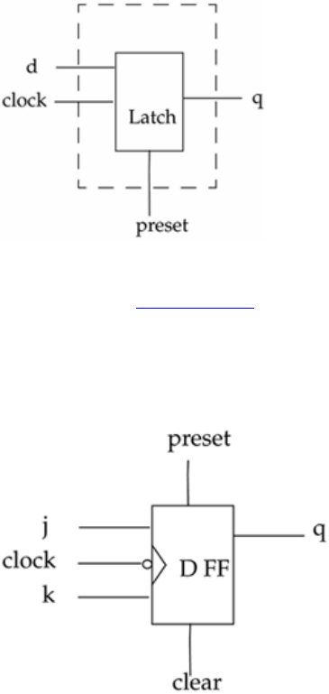
273
12.7 Exercises
1: Design a 2-to-1 multiplexer by using UDP. The select signal is s, inputs are i0,
i1, and the output is out. If the select signal s = x, the output out is always 0. If s
= 0, then out = i0. If s = 1, then out = i1.
2: Write the truth table for the boolean function Y = (A & B) | (C ^ D). Define a
UDP that implements this boolean function. Assume that the inputs will never
take the value x.
3: Define a level-sensitive latch with a preset signal. Inputs are d, clock, and
preset. Output is q. If clock = 0, then q = d. If clock = 1 or x, then q is
unchanged. If preset = 1, then q = 1. If preset = 0, then q is decided by clock
and d signals. If preset = x, then q = x.
4: Define a positive edge-triggered D-flipflop with clear as a UDP. Signal clear is
active low. Use Example 12-9 on page 263 as a guideline. Use shorthand
notation wherever possible.
5: Define a negative edge-triggered JK flipflop, jk_ff with asynchronous preset
and clear as a UDP. q = 1 when preset = 1 and q = 0 when clear = 1.
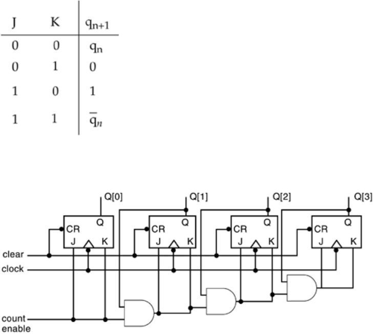
274
The table for a JK flipflop is shown below.
6: Design the 4-bit synchronous counter shown below. Use the UDP jk_ff that was
defined above.

275
Chapter 13. Programming Language
Interface
Verilog provides the set of standard system tasks and functions defined in Appendix C,
List of Keywords, System Tasks, and Compiler Directives. However, designers
frequently need to customize the capability of the Verilog language by defining their own
system tasks and functions. To do this, the designers need to interact with the internal
representation of the design and the simulation environment in the Verilog simulator. The
Programming Language Interface (PLI) provides a set of interface routines to read
internal data representation, write to internal data representation, and extract information
about the simulation environment. User-defined system tasks and functions can be
created with this predefined set of PLI interface routines.
Verilog Programming Language Interface is a very broad area of study. Thus, only the
basics of Verilog PLI are covered in this chapter. Designers should consult the IEEE
Standard Verilog Hardware Description Language document for complete details of the
PLI.
There are three generations of the Verilog PLI.
1. Task/Function (tf_) routines make up the first generation PLI. These routines are
primarily used for operations involving user-defined task/function arguments,
utility functions, callback mechanism, and writing data to output devices.
2. Access (acc_) routines make up the second-generation PLI. These routines are
provide object-oriented access directly into a Verilog HDL structural description.
These routines can be used to access and modify a wide variety of objects in the
Verilog HDL description.
3. Verilog Procedural Interface (vpi_) routines make up the third-generation PLI.
These routines are a superset of the functionality of acc_ and tf_ routines.
For the sake of simplicity, we will discuss only acc_ and tf_ routines in this chapter.
Learning Objectives
• Explain how PLI routines are used in a Verilog simulation.
• Describe the uses of the PLI.
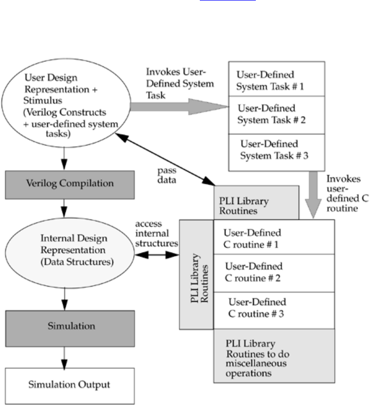
276
• Define user-defined system tasks and functions and user-defined C routines.
• Understand linking and invocation of user-defined system tasks.
• Explain how the PLI is represented conceptually inside a Verilog simulator.
• Identify and describe how to use the two classes of PLI library routines: access
routines and utility routines.
• Learn to create user-defined system tasks and functions and use them in
simulation.
The first step is to understand how PLI tasks fit into the Verilog simulation. A sample
simulation flow using PLI routines is shown in Figure 13-1.
Figure 13-1. PLI Interface

277
A designer describes the design and stimulus by using standard Verilog constructs and
system tasks. In addition, user-defined system tasks can also be invoked in the design and
stimulus. The design and stimulus are compiled and converted to an internal design
representation. The internal design representation is typically in the Verilog simulator
proprietary format and is incomprehensible to the designer. The internal representation is
then used to run the actual simulation and produce output.
Each of the user-defined system tasks is linked to a user-defined C routine. The C
routines are described by means of a standard library of PLI interface routines, which can
access the internal design representation, and the standard C routines available with the C
compiler. The standard PLI library is provided with the Verilog simulator. A list of PLI
library routines is provided in Appendix B, List of PLI Routines. The PLI interface
allows the user to do the following:
• Read internal data structures
• Modify internal data structures
• Access simulation environment
Without the PLI interface, the designer would have to understand the format of the
internal design representation to access it. PLI provides a layer of abstraction that allows
access to internal data structures through an interface that is uniform for all simulators.
The user-defined system tasks will work even if the internal design representation format
of the Verilog simulator is changed or if a new Verilog simulator is used.
278
13.1 Uses of PLI
PLI provides a powerful capability to extend the Verilog language by allowing users to
define their own utilities to access the internal design representation. PLI has various
applications.
• PLI can be used to define additional system tasks and functions. Typical examples
are monitoring tasks, stimulus tasks, debugging tasks, and complex operations
that cannot be implemented with standard Verilog constructs.
• Application software like translators and delay calculators can be written with
PLI.
• PLI can be used to extract design information such as hierarchy, connectivity,
fanout, and number of logic elements of a certain type.
• PLI can be used to write special-purpose or customized output display routines.
Waveform viewers can use this file to generate waveforms, logic connectivity,
source level browsers, and hierarchy information.
• Routines that provide stimulus to the simulation can be written with PLI. The
stimulus could be automatically generated or translated from some other form of
stimulus.
• General Verilog-
b
ased application software can be written with PLI routines. This
software will work with all Verilog simulators because of the uniform access
provided by the PLI interface.
279
13.2 Linking and Invocation of PLI Tasks
Designers can write their own user-defined system tasks by using PLI library routines.
However, the Verilog simulator must know about the existence of the user-defined
system task and its corresponding user-defined C function. This is done by linking the
user-defined system task into the Verilog simulator.
To understand the process, let us consider the example of a simple system task
$hello_verilog. When invoked, the task simply prints out a message "Hello Verilog
World". First, the C routine that implements the task must be defined with PLI library
routines. The C routine hello_verilog in the file hello_verilog.c is shown below.
#include "veriuser.h" /*include the file provided in release dir */
int hello_verilog()
{
io_printf("Hello Verilog World\n");
}
The hello_verilog routine is fairly straightforward. The io_printf is a PLI library routine
that works exactly like printf.
The following sections show the steps involved in defining and using the new
$hello_verilog system task.
13.2.1 Linking PLI Tasks
Whenever the task $hello_verilog is invoked in the Verilog code, the C routine
hello_verilog must be executed. The simulator needs to be aware that a new system task
called $hello_verilog exists and is linked to the C routine hello_verilog. This process is
called linking the PLI routines into the Verilog simulator. Different simulators provide
different mechanisms to link PLI routines. Also, though the exact mechanics of the
linking process might be different for simulators, the fundamentals of the linking process
remain the same. For details, refer to the latest reference manuals available with your
simulator.
At the end of the linking step, a special binary executable containing the new
$hello_verilog system task is created. For example, instead of the usual simulator binary
executable, a new binary executable hverilog is produced. To simulate, run hverilog
instead of your usual simulator executable file.
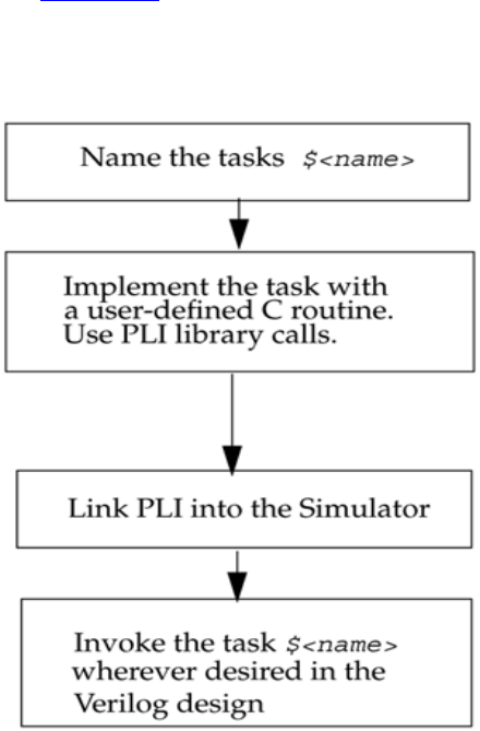
280
13.2.2 Invoking PLI Tasks
Once the user-defined task has been linked into the Verilog simulator, it can be invoked
like any Verilog system task by the keyword $hello_verilog. A Verilog module hello_top,
which calls the task $hello_verilog, is defined in file hello.v as shown below.
module hello_top;
initial
$hello_verilog; //Invoke the user-defined task $hello_verilog
endmodule
Output of the simulation is as follows:
Hello Verilog World
13.2.3 General Flow of PLI Task Addition and Invocation
We discussed a simple example to illustrate how a user-defined system task is named,
implemented in terms of a user-defined C routine, linked into the simulator, and invoked
in the Verilog code. More complex PLI tasks discussed in the following sections will
follow the same process. Figure 13-2 summarizes the general process of adding and
invoking a user-defined system task.
Figure 13-2. General Flow of PLI Task Addition and Invocation
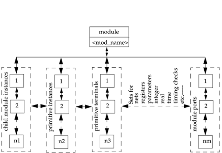
281
13.3 Internal Data Representation
Before we understand how to use PLI library routines, it is first necessary to describe
how a design is viewed internally in the simulator. Each module is viewed as a collection
of object types. Object types are elements defined in Verilog, such as:
• Module instances, module ports, module pin-to-pin paths, and intermodule paths
• Top-level modules
• Primitive instances, primitive terminals
• Nets, registers, parameters, specparams
• Integer, time, and real variables
• Timing checks
• Named events
Each object type has a corresponding set that identifies all objects of that type in the
module. Sets of all object types are interconnected.
A conceptual internal representation of a module is shown in Figure 13-3.
Figure 13-3. Conceptual Internal Representation a Module
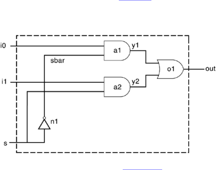
282
Each set contains all elements of that object type in the module. All sets are
interconnected. The connections between the sets are bidirectional. The entire internal
representation can be traversed by using PLI library routines to obtain information about
the module. PLI library routines are discussed later in the chapter.
To illustrate the internal data representation, consider the example of a simple 2-to-1
multiplexer whose gate level circuit is shown in Figure 13-4.
Figure 13-4. 2-to-1 Multiplexer
The Verilog description of the circuit is shown in Example 13-1.
Example 13-1 Verilog Description of 2-to-1 Multiplexer
module mux2_to_1(out, i0, i1, s);
output out; //output port
input i0, i1; //input ports
input s;
wire sbar, y1, y2; //internal nets
//Gate Instantiations
not n1(sbar, s);
and a1(y1, i0, sbar);
and a2(y2, i1, s);
or o1(out, y1, y2);
endmodule
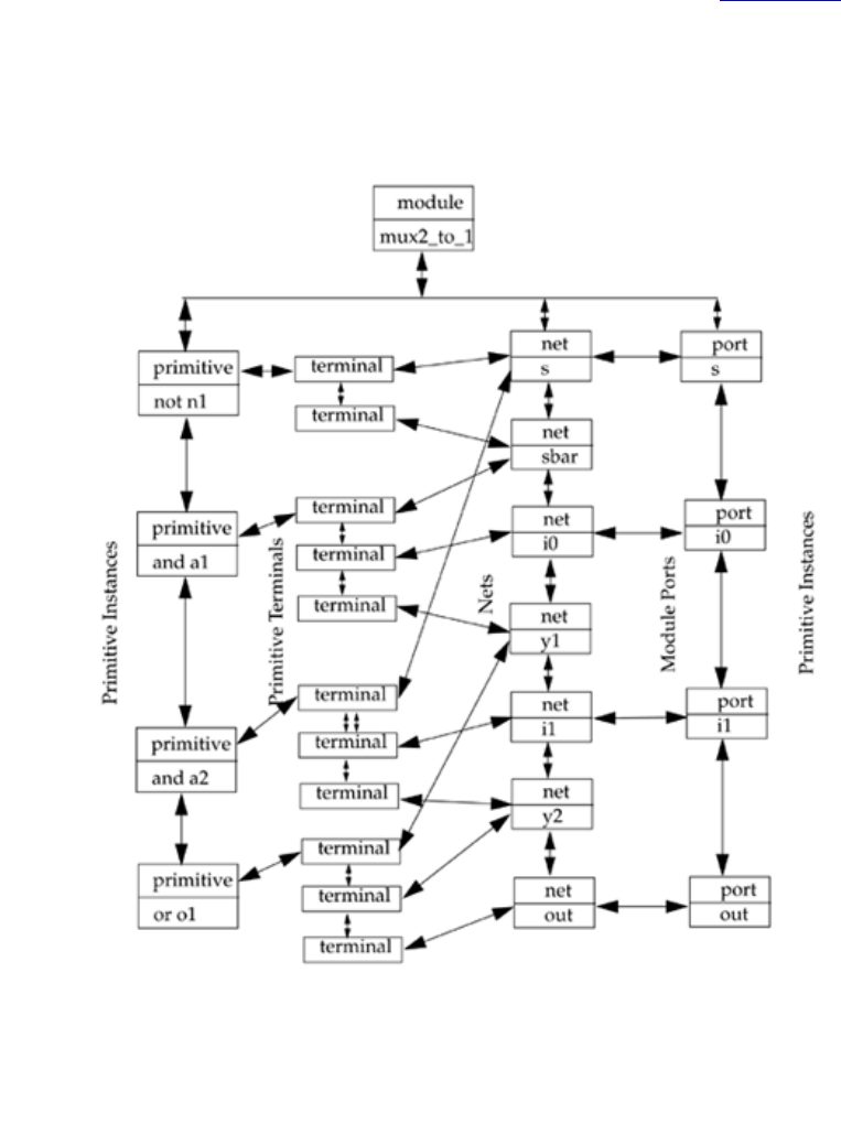
283
The internal data representation for the 2-to-1 multiplexer is shown in Figure 13-5. Sets
are shown for primitive instances, primitive instance terminals, module ports, and nets.
Other object types are not present in this module.
Figure 13-5. Internal Data Representation of 2-to-1 Multiplexer
The example shown above does not contain register, integers, module instances, and
other object types. If they are present in a module definition, they are also represented in
terms of sets. This description is a conceptual view of the internal structures. The exact
implementation of data structures is simulator dependent.
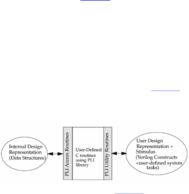
284
13.4 PLI Library Routines
PLI library routines provide a standard interface to the internal data representation of the
design. The user-defined C routines for user-defined system tasks are written by using
PLI library routines. In the example in Section 13.2, Linking and Invocation of PLI
Tasks, $hello_verilog is the user-defined system task, hello_verilog is the user-defined C
routine, and io_printf is a PLI library routine.
There are two broad classes of PLI library routines: access routines and utility routines.
(Note that vpi_ routines are a superset of access and utility routines and are not discussed
in this book.)
Access routines provide access to information about the internal data representation; they
allow the user C routine to traverse the data structure and extract information about the
design. Utility routines are mainly used for passing data across the Verilog/Programming
Language Boundary and for miscellaneous housekeeping functions. Figure 13-6 shows
the role of access and utility routines in PLI.
Figure 13-6. Role of Access and Utility Routines
A complete list of PLI library routines is provided in Appendix B, List of PLI Routines.
The function and usage of each routine are also specified.
13.4.1 Access Routines
Access routines are also popularly called acc routines. Access routines can do the
following:
• Read information about a particular object from the internal data representation
• Write information about a particular object into the internal data representation
285
We will discuss only reading of information from the design. Information about
modifying internal design representation can be found in the Programming Language
Interface (PLI) Manual. However, reading of information is adequate for most practical
purposes.
Access routines can read information about objects in the design. Objects can be one of
the following types:
• Module instances, module ports, module pin-to-pin paths, and intermodule paths
• Top-level modules
• Primitive instances, primitive terminals
• Nets, registers, parameters, specparams
• Integer, time, and real variables
• Timing checks
• Named events
Mechanics of access routines
Some observations about access routines are listed below.
• Access routines always start with the prefix acc_.
• A user-defined C routine that uses access routines must first initialize the
environment by calling the routine acc_initialize(). When exiting, the user-defined
C routine must call acc_close().
• If access routines are being used in a file, the header file acc_user.h must also be
included. All access routine data types and constants are predefined in the file
acc_user.h.
• #include "acc_user.h"
• Access routines use the concept of a handle to access an object. Handles are
predefined data types that point to specific objects in the design. Any information
about the object can be obtained once the object handle is obtained. This is similar
to the concept of file handles for accessing files in C programs. An object handle
identifier is declared with the keyword handle.
handle top_handle;

286
Types of access routines
We discuss six types of access routines.
• Handle routines. They return handles to objects in the design. The name of handle
routines always starts with the prefix acc_handle_.
• Next routines. They return the handle to the next object in the set of a given object
type in a design. Next routines always start with the prefix acc_next_ and accept
reference objects as arguments.
• Value Change Link (VCL) routines. They allow the user system task to add and
delete objects from the list of objects that are monitored for value changes. VCL
routines always begin with the prefix acc_vcl_ and do not return a value.
• Fetch routines. They can extract a variety of information about objects.
Information such as full hierarchical path name, relative name, and other
attributes can be obtained. Fetch routines always start with the prefix acc_fetch_.
• Utility access routines. They perform miscellaneous operations related to access
routines. For example, acc_initialize() and acc_close() are utility routines.
• Modify routines. They can modify internal data structures. We do not discuss
them in this book. Refer to the IEEE Standard Verilog Hardware Description
Language document for details about modify routines.
A complete list of access routines and their usage is provided in Appendix B, List of PLI
Routines.
Examples of access routines
We will discuss two examples that illustrate the use of access routines. The first example
is a user-defined system task to find names of all ports in a module and count the number
of ports. The second example is a user-defined system task that monitors the changes in
values of nets.
Example 1: Get Module Port List
Let us write a user-defined system task $get_ports to find complete hierarchical names of
input, output, and inout ports in a module and to count the number of input, output, and

287
inout ports. The user-defined system task will be invoked in Verilog as
$get_ports("<hierarchical_module_name>"). The user-defined C routine get_ports, which
implements the task $get_ports, is described in file get_ports.c. The file get_ports.c is
shown in Example 13-3.
Example 13-2 PLI Routine to get Module Port List
#include "acc_user.h"
int get_ports()
{
handle mod, port;
int input_ctr = 0;
int output_ctr = 0;
int inout_ctr = 0;
acc_initialize();
mod = acc_handle_tfarg(1); /* get a handle to the module instance
first argument in the system task
argument
list */
port = acc_handle_port(mod, 0); /* get the first port of the module
*/
while( port != null ) /* loop for all ports */
{
if (acc_fetch_direction(port) == accInput) /* Input port */
{
io_printf("Input Port %s \n", acc_fetch_fullname(port));
/* full hierarchical name
*/
input_ctr++;
}
else if (acc_fetch_direction(port) == accOutput) /* Output port */
{
io_printf("Output Port %s \n", acc_fetch_fullname(port));
output_ctr++;
}
else if (acc_fetch_direction(port) == accInout) /* Inout port */
{
io_printf("Inout Port %s \n", acc_fetch_fullname(port));
inout_ctr++;
}
port = acc_next_port(mod, port); /* go to the next port */
}
io_printf("Input Ports = %d Output Ports = %d, Inout ports = %d\n\n",
input_ctr, output_ctr, inout_ctr);
acc_close();
}

288
Notice that handle, fetch, next, and utility access routines are used to write the user C
routine.
Link the new task into the Verilog simulator as described in Section 13.2.1, Linking PLI
Tasks. To check the newly defined task, we will use it to find out the port list of the
module mux2_to_1 described in Example 13-1. A top-level module that instantiates the
2-to-1 multiplexer and invokes the $get_ports task is shown below.
module top;
wire OUT;
reg I0, I1, S;
mux2_to_1 my_mux(OUT, I0, I1, S); /*Instantiate the 2-to-1 mux*/
initial
begin
$get_ports("top.my_mux"); /*invoke task $get_ports to get port list*/
end
endmodule
Invocation of $get_ports causes the user C routine $get_ports to be executed. The output
of the simulation is shown below.
Output Port top.my_mux.out
Input Port top.my_mux.i0
Input Port top.my_mux.i1
Input Port top.my_mux.s
Input Ports = 3 Output Ports = 1, Inout ports = 0
Example 2: Monitor Nets for Value Changes
This example highlights the use of Value Change Link (VCL) routines. Instead of using
the $monitor task provided with the Verilog simulator, let us define our own task to
monitor specific nets in the design for value changes. The task
$my_monitor("<net_name>"); is to be invoked to add a <net_name> to the monitoring
list.
The user-defined C routine my_monitor, which implements the user-defined system task,
is shown in Example 13-3.
289
Example 13-3 PLI Routine to Monitor Nets for Value Changes
#include "acc_user.h"
char convert_to_char();
int display_net();
int my_monitor()
{
handle net;
char *netname ; /*pointer to store names of nets*/
char *malloc();
acc_initialize(); /*initialize environment*/
net = acc_handle_tfarg(1); /*get a handle to the net to be
monitored*/
/*Find hierarchical name of net and store it*/
netname = malloc(strlen(acc_fetch_fullname(net)));
strcpy(netname, acc_fetch_fullname(net));
/* Call the VCL routine to add a signal to the monitoring list*/
/* Pass four arguments to acc_vcl_add task*/
/* 1st : handle to the monitored object (net)
2nd : Consumer C routine to call when the object value changes
(display_net)
3rd : String to be passed to consumer C routine (netname)
4th : Predefined VCL flags: vcl_verilog_logic for logic monitoring
vcl_verilog_strength for strength monitoring
*/
acc_vcl_add(net, display_net, netname, vcl_verilog_logic);
acc_close();
}
Notice that the net is added to the monitoring list with the routine acc_vcl_add. A
consumer routine display_net is an argument to acc_vcl_add. Whenever the value of the
net changes, the acc_vcl_add calls the consumer routine display_net and passes a pointer
to a data structure of the type p_vc_record. A consumer routine is a C routine that
performs an action determined by the user whenever acc_vcl_add calls it. The
p_vc_record is predefined in the acc_user.h file, as shown below.
typedef struct t_vc_record{
int vc_reason; /*reason for value change*/
int vc_hightime; /*Higher 32 bits of 64-bit simulation time*/
int vc_lowtime; /*Lower 32 bits of 64-bit simulation time*/
char *user_data; /*String passed in 3rd argument of acc_vcl_add*/
union { /*New value of the monitored signal*/
unsigned char logic_value;
double real_value;
handle vector_handle;
s_strengths strengths_s;
} out_value;
} *p_vc_record;

290
The consumer routine display_net simply displays the time of change, name of net, and
new value of the net. The consumer routine is written as shown in Example 13-4.
Another routine, convert_to_char, is defined to convert the logic value constants to an
ASCII character.
Example 13-4 Consumer Routine for VCL Example
/*Consumer routine. Called whenever any monitored net changes*/
display_net(vc_record)
p_vc_record vc_record; /*Structure p_vc_record predefined in
acc_user.h*/
{
/*Print time, name, and new value of the changed net */
io_printf("%d New value of net %s is %c \n",
vc_record->vc_lowtime,
vc_record->user_data,
convert_to_char(vc_record->out_value.logic_value));
}
/*Miscellaneous routine to convert predefined character constant to
ASCII character*/
char convert_to_char(logic_val)
char logic_val;
{
char temp;
switch(logic_val)
{
/*vcl0, vcl1, vclX and vclZ are predefined in acc_user.h*/
case vcl0: temp='0';
break;
case vcl1: temp='1';
break;
case vclX: temp='X';
break;
case vclZ: temp='Z';
break;
}
return(temp);
}
Link the new task into the Verilog simulator as described in Section 13.2.1, Linking PLI
Tasks. To check the newly defined task, we will use it to monitor nets sbar and y1 when
stimulus is applied to module mux2_to_1 described in Example 13-1 on page 281. A top-
level module that instantiates the 2-to-1 multiplexer, applies stimulus, and invokes the
$my_monitor task is shown below.
module top;
wire OUT;
reg I0, I1, S;
mux2_to_1 my_mux(OUT, I0, I1, S); //Instantiate the module mux2_to_1
291
initial //Add nets to the monitoring list
begin
$my_monitor("top.my_mux.sbar");
$my_monitor("top.my_mux.y1");
end
initial //Apply Stimulus
begin
I0=1'b0; I1=1'b1; S = 1'b0;
#5 I0=1'b1; I1=1'b1; S = 1'b1;
#5 I0=1'b0; I1=1'b1; S = 1'bx;
#5 I0=1'b1; I1=1'b1; S = 1'b1;
end
endmodule
The output of the simulation is shown below.
0 New value of net top.my_mux.y1 is 0
0 New value of net top.my_mux.sbar is 1
5 New value of net top.my_mux.y1 is 1
5 New value of net top.my_mux.sbar is 0
5 New value of net top.my_mux.y1 is 0
10 New value of net top.my_mux.sbar is X
15 New value of net top.my_mux.y1 is X
15 New value of net top.my_mux.sbar is 0
15 New value of net top.my_mux.y1 is 0
13.4.2 Utility Routines
Utility routines are miscellaneous PLI routines that pass data in both directions across the
Verilog/user C routine boundary. Utility routines are also popularly called "tf" routines.
Mechanics of utility routines
Some observations about utility routines are listed below.
• Utility routines always start with the prefix tf_.
• If utility routines are being used in a file, the header file veriuser.h must be
included. All utility routine data types and constants are predefined in veriuser.h.
#include "veriuser.h"

292
Types of utility routines
Utility routines are available for the following purposes:
• Get information about the Verilog system task invocation
• Get argument list information
• Get values of arguments
• Pass back new values of arguments to calling system task
• Monitor changes in values of arguments
• Get information about simulation time and scheduled events
•
• Perform housekeeping tasks, such as saving work areas, and storing pointers to
tasks
• Do long arithmetic
• Display messages
• Halt, terminate, save, and restore simulation
A list of utility routines, their function, and usage is provided in Appendix B.
Example of utility routines
Until now we encountered only one utility routine, io_printf(). Now we will look at a few
more utility routines that allow passing of data between the Verilog design and the user-
defined C routines.
Verilog provides the system tasks $stop and $finish that suspend and terminate the
simulation. Let us define our own system task, $my_stop_finish, which does both
stopping and finishing based on the arguments passed to it. The complete specifications
for the user-defined system task $my_stop_finish are shown in Table 13-1.
293
Table 13-1. Specifications for $my_stop_finish
1st
Argument 2nd
Argument Action
0 none Stop simulation. Display simulation time and message.
1 none Finish simulation. Display simulation time and message.
0 any value
Stop simulation. Display simulation time, module
instance from which stop was called, and message.
1 any value
Finish simulation. Display simulation time, module
instance from which stop was called, and message.
The source code for the user-defined C routine my_stop_finish is shown in Example 13-
5.
Example 13-5 User C Routine my_stop_finish, Using Utility Routines
#include "veriuser.h"
int my_stop_finish()
{
if(tf_nump() == 1) /* if 1 argument is passed to the my_stop_finish
task, display only simulation time and
message*/
{
if(tf_getp(1) == 0) /* get value of argument. If the argument
is 0, then stop the simulation*/
{
io_printf("Mymessage: Simulation stopped at time %d\n",
tf_gettime());
tf_dostop(); /*stop the simulation*/
}
else if(tf_getp(1) == 1) /* if the argument is 0 then terminate
the simulation*/
{
io_printf("Mymessage: Simulation finished at time %d\n",
tf_gettime());
tf_dofinish(); /*terminate the simulation*/
}
else
/* Pass warning message */
tf_warning("Bad arguments to \$my_stop_finish at time %d\n",
tf_gettime());
}
else if(tf_nump() == 2) /* if 1 argument is passed to the
my_stop_finish
task, then print module instance from which the
task was called, time and message */

294
{
if(tf_getp(1) == 0) /* if the argument is 0 then stop
the simulation*/
{
io_printf
("Mymessage: Simulation stopped at time %d in instance %s \n",
tf_gettime(), tf_mipname());
tf_dostop(); /*stop the simulation*/
}
else if(tf_getp(1) == 1) /* if the argument is 0 then terminate
the simulation*/
{
io_printf
("Mymessage: Simulation finished at time %d in instance %s \n",
tf_gettime(), tf_mipname());
tf_dofinish(); /*terminate the simulation*/
}
else
/* Pass warning message */
tf_warning("Bad arguments to \$my_stop_finish at time %d\n",
tf_gettime());
}
}
Link the new task into the Verilog simulator as described in Section 13.2.1, Linking PLI
Tasks. To check the newly defined task $my_stop_finish, a stimulus in which
$my_stop_finish is called with all possible combinations of arguments is applied to the
module mux2_to_1 described in Example 13-1 on page 281. A top-level module that
instantiates the 2-to-1 multiplexer, applies stimulus, and invokes the $my_stop_finish
task is shown below.
module top;
wire OUT;
reg I0, I1, S;
mux2_to_1 my_mux(OUT, I0, I1, S); //Instantiate the module mux2_to_1
initial //Apply Stimulus
begin
I0=1'b0; I1=1'b1; S = 1'b0;
$my_stop_finish(0); //Stop simulation. Don't print module instance
name
#5 I0=1'b1; I1=1'b1; S = 1'b1;
$my_stop_finish(0,1); //Stop simulation. Print module instance name
#5 I0=1'b0; I1=1'b1; S = 1'bx;
$my_stop_finish(2,1); //Pass bad argument 2 to the task
#5 I0=1'b1; I1=1'b1; S = 1'b1;
$my_stop_finish(1,1); //Terminate simulation. Print module instance
//name
end
endmodule
295
The output of the simulation with a Verilog simulator is shown below.
Mymessage: Simulation stopped at time 0
Type ? for help
C1 > .
Mymessage: Simulation stopped at time 5 in instance top
C1 > .
"my_stop_finish.v", 14: warning! Bad arguments to $my_stop_finish at
time 10
Mymessage: Simulation finished at time 15 in instance top
296
13.5 Summary
In this chapter, we described the Programming Language Interface (PLI) for Verilog. The
following aspects were discussed:
• PLI Interface provides a set of C interface routines to read, write, and extract
information about the internal data structures of the design. Designers can write
their own system tasks to do various useful functions.
• PLI Interface can be used for monitors, debuggers, translators, delay calculators,
automatic stimulus generators, dump file generators, and other useful utilities.
• A user-defined system task is implemented with a corresponding user-defined C
routine. The C routine uses PLI library calls.
• The process of informing the simulator that a new user-defined system task is
attached to a corresponding user C routine is called linking. Different simulators
handle the linking process differently.
• User-defined system tasks are invoked like standard Verilog system tasks, e.g.,
$hello_verilog(); . The corresponding user C routine hello_verilog is executed
whenever the task is invoked.
• A design is represented internally in a Verilog simulator as a big data structure
with sets for objects. PLI library routines allow access to the internal data
structures.
• Access (acc) routines and utility (tf) routines are two types of PLI library routines.
• Utility routines represent the first generation of Verilog PLI. Utility routines are
used to pass data back and forth across the boundary of user C routines and the
original Verilog design. Utility routines start with the prefix tf_. Utility routines
do not interact with object handles.
• Access routines represent the second generation of Verilog PLI. Access routines
can read and write information about a particular object from/to the design.
Access routines start with the prefix acc_. Access routines are used primarily
across the boundary of user C routines and internal data representation. Access
routines interact with object handles.
• Value change link (VCL) is a special category of access routines that allow
monitoring of objects in a design. A consumer routine is executed whenever the
monitored object value changes.
• Verilog Procedural Interface (VPI) routines represent the third generation of

297
Verilog PLI. VPI routines provide a superset of the functionality of acc_ and tf_
routines. VPI routines are not covered in this book.
Programming Language Interface is a very broad area of study. Thus, only the basics of
Verilog PLI are covered in this chapter. Designers should consult the IEEE Standard
Verilog Hardware Description Language document for details of PLI.

298
13.6 Exercises
Refer to Appendix B, List of PLI Routines and IEEE Standard Verilog Hardware
Description Language document, for a list of PLI access and utility routines, their
function, and usage. You will need to use some PLI library calls that were not discussed
in this chapter.
1: Write a user-defined system task, $get_in_ports, that gets full hierarchical
names of only the input ports of a module instance. Hierarchical module
instance name is the input to the task (Hint: Use the C routine in Example 13-2
as a reference). Link the task into the Verilog simulator. Find the input ports of
the 1-bit full adder defined in Example 5-7 on page 75.
2: Write a user-defined system task, $count_and_gates, which counts the number
of and gate primitives in a module instance. Hierarchical module instance name
is the input to the task. Use this task to count the number of and gates in the 4-
to-1 multiplexer in Example 5-5.
3: Create a user-defined system task, $monitor_mod_output, that finds out all the
output signals of a module instance and adds them to a monitoring list. The line
"Output signal has changed" should appear whenever any output signal of the
module changes value. (Hint: Use VCL routines.) Use the 2-to-1 multiplexer in
Example 13-1. Add output signals to the monitoring list by using
$monitor_mod_output. Check results by applying stimulus.

299
Chapter 14. Logic Synthesis with Verilog
HDL
Advances in logic synthesis have pushed HDLs into the forefront of digital design
technology. Logic synthesis tools have cut design cycle times significantly. Designers
can design at a high level of abstraction and thus reduce design time. In this chapter, we
discuss logic synthesis with Verilog HDL. Synopsys synthesis products were used for the
examples in this chapter, and results for individual examples may vary with synthesis
tools. However, the concepts discussed in this chapter are general enough to be applied to
any logic synthesis tool.[1] This chapter is intended to give the reader a basic
understanding of the mechanics and issues involved in logic synthesis. It is not intended
to be comprehensive material on logic synthesis. Detailed knowledge of logic synthesis
can be obtained from reference manuals, logic synthesis books, and by attending training
classes.
[1] Many EDA vendors now offer logic synthesis tools. Please see the reference
documentation provided with your logic synthesis tool for details on how to synthesize
RTL to gates. There may be minor variations from the material presented in this chapter.
Learning Objectives
• Define logic synthesis and explain the benefits of logic synthesis.
• Identify Verilog HDL constructs and operators accepted in logic synthesis.
Understand how the logic synthesis tool interprets these constructs.
• Explain a typical design flow, using logic synthesis. Describe the components in
the logic synthesis-based design flow.
• Describe verification of the gate-level netlist produced by logic synthesis.
• Understand techniques for writing efficient RTL descriptions.
• Describe partitioning techniques to help logic synthesis provide the optimal gate-
level netlist.
• Design combinational and sequential circuits, using logic synthesis.
300
14.1 What Is Logic Synthesis?
Simply speaking, logic synthesis is the process of converting a high-level description of
the design into an optimized gate-level representation, given a standard cell library and
certain design constraints. A standard cell library can have simple cells, such as basic
logic gates like and, or, and nor, or macro cells, such as adders, muxes, and special flip-
flops. A standard cell library is also known as the technology library. It is discussed in
detail later in this chapter.
Logic synthesis always existed even in the days of schematic gate-level design, but it was
always done inside the designer's mind. The designer would first understand the
architectural description. Then he would consider design constraints such as timing, area,
testability, and power. The designer would partition the design into high-level blocks,
draw them on a piece of paper or a computer terminal, and describe the functionality of
the circuit. This was the high-level description. Finally, each block would be
implemented on a hand-drawn schematic, using the cells available in the standard cell
library. The last step was the most complex process in the design flow and required
several time-consuming design iterations before an optimized gate-level representation
that met all design constraints was obtained. Thus, the designer's mind was used as the
logic synthesis tool, as illustrated in Figure 14-1.
Figure 14-1. Designer's Mind as the Logic Synthesis Tool
301
The advent of computer-aided logic synthesis tools has automated the process of
converting the high-level description to logic gates. Instead of trying to perform logic
synthesis in their minds, designers can now concentrate on the architectural trade-offs,
high-level description of the design, accurate design constraints, and optimization of cells
in the standard cell library. These are fed to the computer-aided logic synthesis tool,
which performs several iterations internally and generates the optimized gate-level
description. Also, instead of drawing the high-level description on a screen or a piece of
paper, designers describe the high-level design in terms of HDLs. Verilog HDL has
become one of the popular HDLs for the writing of high-level descriptions. Figure 14-2
illustrates the process.
Figure 14-2. Basic Computer-Aided Logic Synthesis Process

302
Automated logic synthesis has significantly reduced time for conversion from high-level
design representation to gates. This has allowed designers to spend more time on
designing at a higher level of representation, because less time is required for converting
the design to gates.
303
14.2 Impact of Logic Synthesis
Logic synthesis has revolutionized the digital design industry by significantly improving
productivity and by reducing design cycle time. Before the days of automated logic
synthesis, when designs were converted to gates manually, the design process had the
following limitations:
• For large designs, manual conversion was prone to human error. A small gate
missed somewhere could mean redesign of entire blocks.
• The designer could never be sure that the design constraints were going to be met
until the gate-level implementation was completed and tested.
• A significant portion of the design cycle was dominated by the time taken to
convert a high-level design into gates.
• If the gate-level design did not meet requirements, the turnaround time for
redesign of blocks was very high.
• What-if scenarios were hard to verify. For example, the designer designed a block
in gates that could run at a cycle time of 20 ns. If the designer wanted to find out
whether the circuit could be optimized to run faster at 15 ns, the entire block had
to be redesigned. Thus, redesign was needed to verify what-if scenarios.
• Each designer would implement design blocks differently. There was little
consistency in design styles. For large designs, this could mean that smaller
blocks were optimized, but the overall design was not optimal.
• If a bug was found in the final, gate-level design, this would sometimes require
redesign of thousands of gates.
• Timing, area, and power dissipation in library cells are fabrication-technology
specific. Thus if the company changed the IC fabrication vendor after the gate-
level design was complete, this would mean redesign of the entire circuit and a
possible change in design methodology.
• Design reuse was not possible. Designs were technology-specific, hard to port,
and very difficult to reuse.
Automated logic synthesis tools addressed these problems as follows:
• High-level design is less prone to human error because designs are described at a
higher level of abstraction.
304
• High-level design is done without significant concern about design constraints.
Logic synthesis will convert a high-level design to a gate-level netlist and ensure
that all constraints have been met. If not, the designer goes back, modifies the
high-level design and repeats the process until a gate-level netlist that satisfies
timing, area, and power constraints is obtained.
• Conversion from high-level design to gates is fast. With this improvement, design
cycle times are shortened considerably. What took months before can now be
done in hours or days.
• Turnaround time for redesign of blocks is shorter because changes are required
only at the register-transfer level; then, the design is simply resynthesized to
obtain the gate-level netlist.
•
• What-if scenarios are easy to verify. The high-level description does not change.
The designer has merely to change the timing constraint from 20 ns to 15 ns and
resynthesize the design to get the new gate-level netlist that is optimized to
achieve a cycle time of 15 ns.
• Logic synthesis tools optimize the design as a whole. This removes the problem
with varied designer styles for the different blocks in the design and suboptimal
designs.
• If a bug is found in the gate-level design, the designer goes back and changes the
high-level description to eliminate the bug. Then, the high-level description is
again read into the logic synthesis tool to automatically generate a new gate-level
description.
• Logic synthesis tools allow technology-independent design. A high-level
description may be written without the IC fabrication technology in mind. Logic
synthesis tools convert the design to gates, using cells in the standard cell library
provided by an IC fabrication vendor. If the technology changes or the IC
fabrication vendor changes, designers simply use logic synthesis to retarget the
design to gates, using the standard cell library for the new technology.
• Design reuse is possible for technology-independent descriptions. For example, if
the functionality of the I/O block in a microprocessor does not change, the RTL
description of the I/O block can be reused in the design of derivative
microprocessors. If the technology changes, the synthesis tool simply maps to the
desired technology.
305
14.3 Verilog HDL Synthesis
For the purpose of logic synthesis, designs are currently written in an HDL at a register
transfer level (RTL). The term RTL is used for an HDL description style that utilizes a
combination of data flow and behavioral constructs. Logic synthesis tools take the
register transfer-level HDL description and convert it to an optimized gate-level netlist.
Verilog and VHDL are the two most popular HDLs used to describe the functionality at
the RTL level. In this chapter, we discuss RTL-based logic synthesis with Verilog HDL.
Behavioral synthesis tools that convert a behavioral description into an RTL description
are slowly evolving, but RTL-based synthesis is currently the most popular design
method. Thus, we will address only RTL-based synthesis in this chapter.
14.3.1 Verilog Constructs
Not all constructs can be used when writing a description for a logic synthesis tool. In
general, any construct that is used to define a cycle-by-cycle RTL description is
acceptable to the logic synthesis tool. A list of constructs that are typically accepted by
logic synthesis tools is given in Table 14-1. The capabilities of individual logic synthesis
tools may vary. The constructs that are typically acceptable to logic synthesis tools are
also shown.
Table 14-1. Verilog HDL Constructs for Logic Synthesis
Construct
Type Keyword or Description Notes
ports input, inout, output
parameters parameter
module
definition module
signals and
variables wire, reg, tri Vectors are allowed
instantiation module instances,
primitive gate instances
E.g., mymux m1(out, i0, i1, s); E.g., nand
(out, a, b);
functions and
tasks function, task Timing constructs ignored
procedural always, if, then, else, case,
casex, casez initial is not supported
306
procedural
blocks
begin, end, named blocks,
disable Disabling of named blocks allowed
data flow assign Delay information is ignored
loops for, while, forever, while and forever loops must contain
@(posedge clk) or @(negedge clk)
Remember that we are providing a cycle-by-cycle RTL description of the circuit. Hence,
there are restrictions on the way these constructs are used for the logic synthesis tool. For
example, the while and forever loops must be broken by a @ (posedge clock) or @
(negedge clock) statement to enforce cycle-by-cycle behavior and to prevent
combinational feedback. Another restriction is that logic synthesis ignores all timing
delays specified by #<delay> construct. Therefore, pre- and post-synthesis Verilog
simulation results may not match. The designer must use a description style that
eliminates these mismatches. Also, the initial construct is not supported by logic
synthesis tools. Instead, the designer must use a reset mechanism to initialize the signals
in the circuit.
It is recommended that all signal widths and variable widths be explicitly specified.
Defining unsized variables can result in large, gate-level netlists because synthesis tools
can infer unnecessary logic based on the variable definition.
14.3.2 Verilog Operators
Almost all operators in Verilog are allowed for logic synthesis. Table 14-2 is a list of the
operators allowed. Only operators such as === and !== that are related to x and z are not
allowed, because equality with x and z does not have much meaning in logic synthesis.
While writing expressions, it is recommended that you use parentheses to group logic the
way you want it to appear. If you rely on operator precedence, logic synthesis tools might
produce an undesirable logic structure.
Table 14-2. Verilog HDL Operators for Logic Synthesis
Operator Type Operator Symbol Operation Performed
Arithmetic
*
/
+
-
%
multiply
divide
add
subtract
modulus

307
+
-
unary plus
unary minus
Logical
!
&&
||
logical negation
logical and
logical or
Relational
>
<
>=
<=
greater than
less than
greater than or equal
less than or equal
Equality
==
!=
equality
inequality
Bit-wise
~
&
|
^
^~ or ~^
bitwise negation
bitwise and
bitwise or
bitwise ex-or
bitwise ex-nor
Reduction
&
~&
|
~|
^
^~ or ~^
reduction and
reduction nand
reduction or
reduction nor
reduction ex-or
reduction ex-nor
Shift
>>
<<
>>>
right shift
left shift
arithmetic right shift
308
<<< arithmetic left shift
Concatenation { } concatenation
Conditional ?: conditional
14.3.3 Interpretation of a Few Verilog Constructs
Having described the basic Verilog constructs, let us try to understand how logic
synthesis tools frequently interpret these constructs and translate them to logic gates.
The assign statement
The assign construct is the most fundamental construct used to describe combinational
logic at an RTL level. Given below is a logic expression that uses the assign statement.
assign out = (a & b) | c;
This will frequently translate to the following gate-level representation:
If a, b, c, and out are 2-bit vectors [1:0], then the above assign statement will frequently
translate to two identical circuits for each bit.
If arithmetic operators are used, each arithmetic operator is implemented in terms of
arithmetic hardware blocks available to the logic synthesis tool. A 1-bit full adder is
309
implemented below.
assign {c_out, sum} = a + b + c_in;
Assuming that the 1-bit full adder is available internally in the logic synthesis tool, the
above assign statement is often interpreted by logic synthesis tools as follows:
If a multiple-
b
it adder is synthesized, the synthesis tool will perform optimization and the
designer might get a result that looks different from the above figure.
If a conditional operator ? is used, a multiplexer circuit is inferred.
assign out = (s) ? i1 : i0;
It frequently translates to the gate-level representation shown in Figure 14-3.
Figure 14-3. Multiplexer Description

310
The if-else statement
Single if-else statements translate to multiplexers where the control signal is the signal or
variable in the if clause.
if(s)
out = i1;
else
out = i0;
The above statement will frequently translate to the gate-level description shown in
Figure 14-3. In general, multiple if-else-if statements do not synthesize to large
multiplexers.
The case statement
The case statement also can used to infer multiplexers. The above multiplexer would
have been inferred from the following description that uses case statements:
case (s)
1'b0 : out = i0;
1'b1 : out = i1;
endcase
Large case statements may be used to infer large multiplexers.
for loops
The for loops can be used to build cascaded combinational logic. For example, the
following for loop builds an 8-bit full adder:
c = c_in;
for(i=0; i <=7; i = i + 1)
{c, sum[i]} = a[i] + b[i] + c; // builds an 8-bit ripple adder
c_out = c;
The always statement
The always statement can be used to infer sequential and combinational logic. For
sequential logic, the always statement must be controlled by the change in the value of a
clock signal clk.
always @(posedge clk)
q <= d;
311
This is inferred as a positive edge-triggered D-flipflop with d as input, q as output, and
clk as the clocking signal.
Similarly, the following Verilog description creates a level-sensitive latch:
always @(clk or d)
if (clk)
q <= d;
For combinational logic, the always statement must be triggered by a signal other than
the clk, reset, or preset. For example, the following block will be interpreted as a 1-bit
full adder:
always @(a or b or c_in)
{c_out, sum} = a + b + c_in;
The function statement
Functions synthesize to combinational blocks with one output variable. The output might
be scalar or vector. A 4-bit full adder is implemented as a function in the Verilog
description below. The most significant bit of the function is used for the carry bit.
function [4:0] fulladd;
input [3:0] a, b;
input c_in;
begin
fulladd = a + b + c_in; //bit 4 of fulladd for carry, bits[3:0] for
sum.
end
endfunction
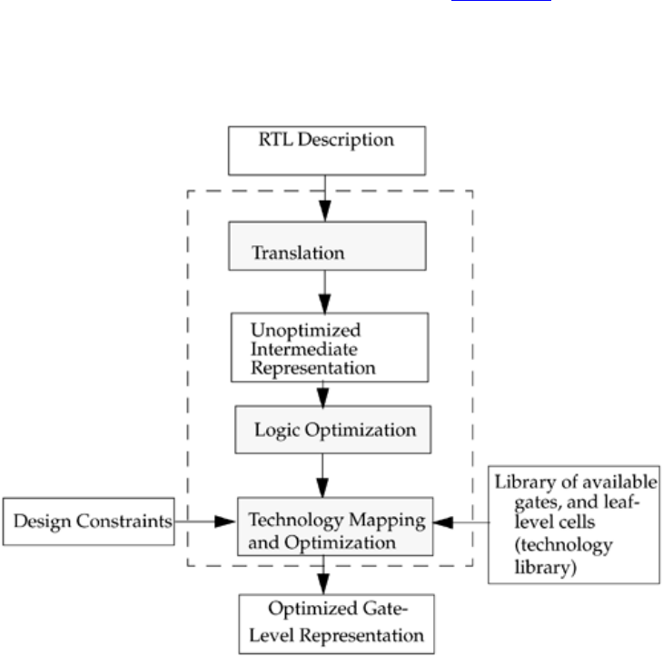
312
14.4 Synthesis Design Flow
Having understood how basic Verilog constructs are interpreted by the logic synthesis
tool, let us now discuss the synthesis design flow from an RTL description to an
optimized gate-level description.
14.4.1 RTL to Gates
To fully utilize the benefits of logic synthesis, the designer must first understand the flow
from the high-level RTL description to a gate-level netlist. Figure 14-4 explains that
flow.
Figure 14-4. Logic Synthesis Flow from RTL to Gates
Let us discuss each component of the flow in detail.

313
RTL description
The designer describes the design at a high level by using RTL constructs. The designer
spends time in functional verification to ensure that the RTL description functions
correctly. After the functionality is verified, the RTL description is input to the logic
synthesis tool.
Translation
The RTL description is converted by the logic synthesis tool to an unoptimized,
intermediate, internal representation. This process is called translation. Translation is
relatively simple and uses techniques similar to those discussed in Section 14.3.3,
Interpretation of a Few Verilog Constructs. The translator understands the basic
primitives and operators in the Verilog RTL description. Design constraints such as area,
timing, and power are not considered in the translation process. At this point, the logic
synthesis tool does a simple allocation of internal resources.
Unoptimized intermediate representation
The translation process yields an unoptimized intermediate representation of the design.
The design is represented internally by the logic synthesis tool in terms of internal data
structures. The unoptimized intermediate representation is incomprehensible to the user.
Logic optimization
The logic is now optimized to remove redundant logic. Various technology independent
boolean logic optimization techniques are used. This process is called logic optimization.
It is a very important step in logic synthesis, and it yields an optimized internal
representation of the design.
Technology mapping and optimization
Until this step, the design description is independent of a specific target technology. In
this step, the synthesis tool takes the internal representation and implements the
representation in gates, using the cells provided in the technology library. In other words,
the design is mapped to the desired target technology.
Suppose you want to get your IC chip fabricated at ABC Inc. ABC Inc. has 0.65 micron
CMOS technology, which it calls abc_100 technology. Then, abc_100 becomes the target
technology. You must therefore implement your internal design representation in gates,
using the cells provided in abc_100 technology library. This is called technology
314
mapping. Also, the implementation should satisfy such design constraints as timing, area,
and power. Some local optimizations are done to achieve the best results for the target
technology. This is called technology optimization or technology-dependent
optimization.
Technology library
The technology library contains library cells provided by ABC Inc. The term standard
cell library used earlier in the chapter and the term technology library are identical and
are used interchangeably.
To build a technology library, ABC Inc. decides the range of functionality to provide in
its library cells. As discussed earlier, library cells can be basic logic gates or macro cells
such as adders, ALUs, multiplexers, and special flip-flops. The library cells are the basic
building blocks that ABC Inc. will use for IC fabrication. Physical layout of library cells
is done first. Then, the area of each cell is computed from the cell layout. Next, modeling
techniques are used to estimate the timing and power characteristics of each library cell.
This process is called cell characterization.
Finally, each cell is described in a format that is understood by the synthesis tool. The
cell description contains information about the following:
• Functionality of the cell
• Area of the cell layout
• Timing information about the cell
• Power information about the cell
A collection of these cells is called the technology library. The synthesis tool uses these
cells to implement the design. The quality of results from synthesis tools will typically be
dominated by the cells available in the technology library. If the choice of cells in the
technology library is limited, the synthesis tool cannot do much in terms of optimization
for timing, area, and power.
Design constraints
Design constraints typically include the following:
• Timing? The circuit must meet certain timing requirements. An internal static
timing analyzer checks timing.
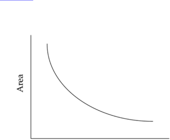
315
• Area? The area of the final layout must not exceed a limit.
• Power? The power dissipation in the circuit must not exceed a threshold.
In general, there is an inverse relationship between area and timing constraints. For a
given technology library, to optimize timing (faster circuits), the design has to be
parallelized, which typically means that larger circuits have to be built. To build smaller
circuits, designers must generally compromise on circuit speed. The inverse relationship
is shown in Figure 14-5.
Figure 14-5. Area vs. Timing Trade-off
On top of design constraints, operating environment factors, such as input and output
delays, drive strengths, and loads, will affect the optimization for the target technology.
Operating environment factors must be input to the logic synthesis tool to ensure that
circuits are optimized for the required operating environment.
Optimized gate-level description
After the technology mapping is complete, an optimized gate-level netlist described in
terms of target technology components is produced. If this netlist meets the required
constraints, it is handed to ABC Inc. for final layout. Otherwise, the designer modifies the
RTL or reconstrains the design to achieve the desired results. This process is iterated until
the netlist meets the required constraints. ABC Inc. will do the layout, do timing checks
to ensure that the circuit meets required timing after layout, and then fabricate the IC chip
for you.
316
There are three points to note about the synthesis flow.
1. For very high speed circuits like microprocessors, vendor technology libraries
may yield nonoptimal results. Instead, design groups obtain information about the
fabrication process used by the vendor, for example, 0.65 micron CMOS process,
and build their own technology library components. Cell characterization is done
by the designers. Discussion about building technology libraries and cell
characterization is beyond the scope of this book.
2. Translation, logic optimization, and technology mapping are done internally in the
logic synthesis tool and are not visible to the designer. The technology library is
given to the designer. Once the technology is chosen, the designer can control
only the input RTL description and design constraint specification. Thus, writing
efficient RTL descriptions, specifying design constraints accurately, evaluating
design trade-offs, and having a good technology library are very important to
produce optimal digital circuits when using logic synthesis.
3. For submicron designs, interconnect delays are becoming a dominating factor in
the overall delay. Therefore, as geometries shrink, in order to accurately model
interconnect delays, synthesis tools will need to have a tighter link to layout, right
at the RTL level. Timing analyzers built into synthesis tools will have to account
for interconnect delays in the total delay calculation.
14.4.2 An Example of RTL-to-Gates
Let us discuss synthesis of a 4-bit magnitude comparator to understand each step in the
synthesis flow. Steps of the synthesis flow such as translation, logic optimization, and
technology mapping are not visible to us as designers. Therefore, we will concentrate on
the components that are visible to the designer, such as the RTL description, technology
library, design constraints, and the final, optimized, gate-level description.
Design specification
A magnitude comparator checks if one number is greater than, equal to, or less than
another number. Design a 4-bit magnitude comparator IC chip that has the following
specifications:
• The name of the design is magnitude_comparator
• Inputs A and B are 4-bit inputs. No x or z values will appear on A and B inputs
• Output A_gt_B is true if A is greater than B
• Output A_lt_B is true if A is less than B

317
• Output A_eq_B is true if A is equal to B
• The magnitude comparator circuit must be as fast as possible. Area can be
compromised for speed.
RTL description
The RTL description that describes the magnitude comparator is shown in Example 14-1.
This is a technology-independent description. The designer does not have to worry about
the target technology at this point.
Example 14-1 RTL for Magnitude Comparator
//Module magnitude comparator
module magnitude_comparator(A_gt_B, A_lt_B, A_eq_B, A, B);
//Comparison output
output A_gt_B, A_lt_B, A_eq_B;
//4-bits numbers input
input [3:0] A, B;
assign A_gt_B = (A > B); //A greater than B
assign A_lt_B = (A < B); //A less than B
assign A_eq_B = (A == B); //A equal to B
endmodule
Notice that the RTL description is very concise.
Technology library
We decide to use the 0.65 micron CMOS process called abc_100 used by ABC Inc. to
make our IC chip. ABC Inc. supplies a technology library for synthesis. The library
contains the following library cells. The library cells are defined in a format understood
by the synthesis tool.
//Library cells for abc_100 technology
VNAND//2-input nand gate
VAND//2-input and gate
VNOR//2-input nor gate
VOR//2-input or gate
VNOT//not gate
VBUF//buffer
NDFF//Negative edge triggered D flip-flop
PDFF//Positive edge triggered D flip-flop

318
Functionality, timing, area, and power dissipation information of each library cell are
specified in the technology library.
Design constraints
According to the specification, the design should be as fast as possible for the target
technology, abc_100. There are no area constraints. Thus, there is only one design
constraint.
• Optimize the final circuit for fastest timing
Logic synthesis
The RTL description of the magnitude comparator is read by the logic synthesis tool. The
design constraints and technology library for abc_100 are provided to the logic synthesis
tool. The logic synthesis tool performs the necessary optimizations and produces a gate-
level description optimized for abc_100 technology.
Final, Optimized, Gate-Level Description
The logic synthesis tool produces a final, gate-level description. The schematic for the
gate-level circuit is shown in Figure 14-6.
319
Figure 14-6. Gate-Level Schematic for the Magnitude Comparator
The gate-level Verilog description produced by the logic synthesis tool for the circuit is
shown below. Ports are connected by name.
Example 14-2 Gate-Level Description for the Magnitude Comparator
module magnitude_comparator ( A_gt_B, A_lt_B, A_eq_B, A, B );
input [3:0] A;
input [3:0] B;
output A_gt_B, A_lt_B, A_eq_B;
wire n60, n61, n62, n50, n63, n51, n64, n52, n65, n40, n53,
n41, n54, n42, n55, n43, n56, n44, n57, n45, n58, n46,
n59, n47, n48, n49, n38, n39;
VAND U7 ( .in0(n48), .in1(n49), .out(n38) );
VAND U8 ( .in0(n51), .in1(n52), .out(n50) );

320
VAND U9 ( .in0(n54), .in1(n55), .out(n53) );
VNOT U30 ( .in(A[2]), .out(n62) );
VNOT U31 ( .in(A[1]), .out(n59) );
VNOT U32 ( .in(A[0]), .out(n60) );
VNAND U20 ( .in0(B[2]), .in1(n62), .out(n45) );
VNAND U21 ( .in0(n61), .in1(n45), .out(n63) );
VNAND U22 ( .in0(n63), .in1(n42), .out(n41) );
VAND U10 ( .in0(n55), .in1(n52), .out(n47) );
VOR U23 ( .in0(n60), .in1(B[0]), .out(n57) );
VAND U11 ( .in0(n56), .in1(n57), .out(n49) );
VNAND U24 ( .in0(n57), .in1(n52), .out(n54) );
VAND U12 ( .in0(n40), .in1(n42), .out(n48) );
VNAND U25 ( .in0(n53), .in1(n44), .out(n64) );
VOR U13 ( .in0(n58), .in1(B[3]), .out(n42) );
VOR U26 ( .in0(n62), .in1(B[2]), .out(n46) );
VNAND U14 ( .in0(B[3]), .in1(n58), .out(n40) );
VNAND U27 ( .in0(n64), .in1(n46), .out(n65) );
VNAND U15 ( .in0(B[1]), .in1(n59), .out(n55) );
VNAND U28 ( .in0(n65), .in1(n40), .out(n43) );
VOR U16 ( .in0(n59), .in1(B[1]), .out(n52) );
VNOT U29 ( .in(A[3]), .out(n58) );
VNAND U17 ( .in0(B[0]), .in1(n60), .out(n56) );
VNAND U18 ( .in0(n56), .in1(n55), .out(n51) );
VNAND U19 ( .in0(n50), .in1(n44), .out(n61) );
VAND U2 ( .in0(n38), .in1(n39), .out(A_eq_B) );
VNAND U3 ( .in0(n40), .in1(n41), .out(A_lt_B) );
VNAND U4 ( .in0(n42), .in1(n43), .out(A_gt_B) );
VAND U5 ( .in0(n45), .in1(n46), .out(n44) );
VAND U6 ( .in0(n47), .in1(n44), .out(n39) );
endmodule
If the designer decides to use another technology, say, xyz_100 from XYZ Inc., because
it is a better technology, the RTL description and design constraints do not change. Only
the technology library changes. Thus, to map to a new technology, a logic synthesis tool
simply reads the unchanged RTL description, unchanged design constraints, and new
technology library and creates a new, optimized, gate-level netlist.
Note that if automated logic synthesis were not available, choosing a new technology
would require the designer to redesign and reoptimize by hand the gate-level netlist in
Example 14-2.
IC Fabrication
The gate-level netlist is verified for functionality and timing and then submitted to ABC
Inc. ABC Inc. does the chip layout, checks that the post-layout circuit meets timing
requirements, and then fabricates the IC chip, using abc_100 technology.

321
14.5 Verification of Gate-Level Netlist
The optimized gate-level netlist produced by the logic synthesis tool must be verified for
functionality. Also, the synthesis tool may not always be able to meet both timing and
area requirements if they are too stringent. Thus, a separate timing verification can be
done on the gate-level netlist.
14.5.1 Functional Verification
Identical stimulus is run with the original RTL and synthesized gate-level descriptions of
the design. The output is compared to find any mismatches. For the magnitude
comparator, a sample stimulus file is shown below.
Example 14-3 Stimulus for Magnitude Comparator
module stimulus;
reg [3:0] A, B;
wire A_GT_B, A_LT_B, A_EQ_B;
//Instantiate the magnitude comparator
magnitude_comparator MC(A_GT_B, A_LT_B, A_EQ_B, A, B);
initial
$monitor($time," A = %b, B = %b, A_GT_B = %b, A_LT_B = %b, A_EQ_B =
%b",
A, B, A_GT_B, A_LT_B, A_EQ_B);
//stimulate the magnitude comparator.
initial
begin
A = 4'b1010; B = 4'b1001;
# 10 A = 4'b1110; B = 4'b1111;
# 10 A = 4'b0000; B = 4'b0000;
# 10 A = 4'b1000; B = 4'b1100;
# 10 A = 4'b0110; B = 4'b1110;
# 10 A = 4'b1110; B = 4'b1110;
end
endmodule
The same stimulus is applied to both the RTL description in Example 14-1 and the
synthesized gate-level description in Example 14-2, and the simulation output is
compared for mismatches. However, there is an additional consideration. The gate-level
description is in terms of library cells VAND, VNAND, etc. Verilog simulators do not
understand the meaning of these cells. Thus, to simulate the gate-level description, a
simulation library, abc_100.v, must be provided by ABC Inc. The simulation library must

322
describe cells VAND, VNAND, etc., in terms of Verilog HDL primitives and, nand, etc.
For example, the VAND cell will be defined in the simulation library as shown in
Example 14-4.
Example 14-4 Simulation Library
//Simulation Library abc_100.v. Extremely simple. No timing checks.
module VAND (out, in0, in1);
input in0;
input in1;
output out;
//timing information, rise/fall and min:typ:max
specify
(in0 => out) = (0.260604:0.513000:0.955206,
0.255524:0.503000:0.936586);
(in1 => out) = (0.260604:0.513000:0.955206,
0.255524:0.503000:0.936586);
endspecify
//instantiate a Verilog HDL primitive
and (out, in0, in1);
endmodule
...
//All library cells will have corresponding module definitions
//in terms of Verilog primitives.
...
Stimulus is applied to the RTL description and the gate-level description. A typical
invocation with a Verilog simulator is shown below.
//Apply stimulus to RTL description
> verilog stimulus.v mag_compare.v
//Apply stimulus to gate-level description.
//Include simulation library "abc_100.v" using the -v option
> verilog stimulus.v mag_compare.gv -v abc_100.v
The simulation output must be identical for the two simulations. In our case, the output is
identical. For the example of the magnitude comparator, the output is shown in Example
14-5.
Example 14-5 Output from Simulation of Magnitude Comparator
0 A = 1010, B = 1001, A_GT_B = 1, A_LT_B = 0, A_EQ_B = 0
10 A = 1110, B = 1111, A_GT_B = 0, A_LT_B = 1, A_EQ_B = 0
20 A = 0000, B = 0000, A_GT_B = 0, A_LT_B = 0, A_EQ_B = 1
30 A = 1000, B = 1100, A_GT_B = 0, A_LT_B = 1, A_EQ_B = 0
40 A = 0110, B = 1110, A_GT_B = 0, A_LT_B = 1, A_EQ_B = 0
50 A = 1110, B = 1110, A_GT_B = 0, A_LT_B = 0, A_EQ_B = 1

323
If the output is not identical, the designer needs to check for any potential bugs and rerun
the whole flow until all bugs are eliminated.
Comparing simulation output of an RTL and a gate-level netlist is only a part of the
functional verification process. Various techniques are used to ensure that the gate-level
netlist produced by logic synthesis is functionally correct. One technique is to write a
high-level architectural description in C++. The output obtained by executing the high-
level architectural description is compared against the simulation output of the RTL or
the gate-level description. Another technique called equivalence checking is also
frequently used. It is discussed in greater detail in Section 15.3.2, Equivalence Checking,
in this book.
Timing verification
The gate-level netlist is typically checked for timing by use of timing simulation or by a
static timing verifier. If any timing constraints are violated, the designer must either
redesign part of the RTL or make trade-offs in design constraints for logic synthesis. The
entire flow is iterated until timing requirements are met. Details of static timing verifiers
are beyond the scope of this book. Timing simulation is discussed in Chapter 10, Timing
and Delays.

324
14.6 Modeling Tips for Logic Synthesis
The Verilog RTL design style used by the designer affects the final gate-level netlist
produced by logic synthesis. Logic synthesis can produce efficient or inefficient gate-
level netlists, based on the style of RTL descriptions. Hence, the designer must be aware
of techniques used to write efficient circuit descriptions. In this section, we provide tips
about modeling trade-offs, for the designer to write efficient, synthesizable Verilog
descriptions.
14.6.1 Verilog Coding Style[2]
[2] Verilog coding style suggestions may vary slightly based on your logic synthesis tool.
However, the suggestions included in this chapter are applicable to most cases. The IEEE
Standard Verilog Hardware Description Language document also adds a new language
construct called attribute. Attributes such as full_case, parallel_case, state_variable, and
optimize can be included in the Verilog HDL specification of the design. These attributes
are used by synthesis tools to guide the synthesis process.
The style of the Verilog description greatly affects the final design. For logic synthesis, it
is important to consider actual hardware implementation issues. The RTL specification
should be as close to the desired structure as possible without sacrificing the benefits of a
high level of abstraction. There is a trade-off between level of design abstraction and
control over the structure of the logic synthesis output. Designing at a very high level of
abstraction can cause logic with undesirable structure to be generated by the synthesis
tool. Designing at a very low level (e.g., hand instantiation of each cell) causes the
designer to lose the benefits of high-level design and technology independence. Also, a
"good" style will vary among logic synthesis tools. However, many principles are
common across logic synthesis tools. Listed below are some guidelines that the designer
should consider while designing at the RTL level.
Use meaningful names for signals and variables
Names of signals and variables should be meaningful so that the code becomes self-
commented and readable.
Avoid mixing positive and negative edge-triggered flipflops
Mixing positive and negative edge-triggered flipflops may introduce inverters and buffers
into the clock tree. This is often undesirable because clock skews are introduced in the
circuit.

325
Use basic building blocks vs. use continuous assign statements
Trade-offs exist between using basic building blocks versus using continuous assign
statements in the RTL description. Continuous assign statements are a very concise way
of representing the functionality and they generally do a good job of generating random
logic. However, the final logic structure is not necessarily symmetrical. Instantiation of
basic building blocks creates symmetric designs, and the logic synthesis tool is able to
optimize smaller modules more effectively. However, instantiation of building blocks is
not a concise way to describe the design; it inhibits retargeting to alternate technologies,
and generally there is a degradation in simulator performance.
Assume that a 2-to-1, 8-
b
it multiplexer is defined as a module mux2_1L8 in the design. I
f
a 32-bit multiplexer is needed, it can be built by instantiating 8-bit multiplexers rather
than by using the assign statement.
//Style 1: 32-bit mux using assign statement
module mux2_1L32(out, a, b, select);
output [31:0] out;
input [31:0] a, b;
wire select;
assign out = select ? a : b;
endmodule
//Style 2: 32-bit multiplexer using basic building blocks
//If 8-bit muxes are defined earlier in the design, instantiating
//these muxes is more efficient for
//synthesis. Fewer gates, faster design.
//Less efficient for simulation
module mux2_1L32(out, a, b, select);
output [31:0] out;
input [31:0] a, b;
wire select;
mux2_1L8 m0(out[7:0], a[7:0], b[7:0], select); //bits 7 through 0
mux2_1L8 m1(out[15:7], a[15:7], b[ 15:7], select); //bits 15 through 7
mux2_1L8 m2(out[23:16], a[23:16], b[23:16], select); //bits 23 through
16
mux2_1L8 m3(out[31:24], a[31:24], b[31:24], select); //bits 31 through
24
endmodule
Instantiate multiplexers vs. Use if-else or case statements
We discussed in Section 14.3.3, Interpretation of a Few Verilog Constructs, that if-else
and case statements are frequently synthesized to multiplexers in hardware. If a
structured implementation is needed, it is better to implement a block directly by using
326
multiplexers, because if-else or case statements can cause undesired random logic to be
generated by the synthesis tool. Instantiating a multiplexer gives better control and faster
synthesis, but it has the disadvantage of technology dependence and a longer RTL
description. On the other hand, if-else and case statements can represent multiplexers
very concisely and are used to create technology-independent RTL descriptions.
Use parentheses to optimize logic structure
The designer can control the final structure of logic by using parentheses to group logic.
Using parentheses also improves readability of the Verilog description.
//translates to 3 adders in series
out = a + b + c + d;
//translates to 2 adders in parallel with one final adder to sum
results
out = (a + b) + (c + d) ;
Use arithmetic operators *, /, and % vs. Design building blocks
Multiply, divide, and modulo operators are very expensive to implement in terms of logic
and area. However, these arithmetic operators can be used to implement the desired
functionality concisely and in a technology-independent manner. On the other hand,
designing custom blocks to do multiplication, division, or modulo operation can take a
longer time, and the RTL description becomes more technology-dependent.
Be careful with multiple assignments to the same variable
Multiple assignments to the same variable can cause undesired logic to be generated. The
previous assignment might be ignored, and only the last assignment would be used.
//two assignments to the same variable
always @(posedge clk)
if(load1) q <= a1;
always @(posedge clk)
if(load2) q <= a2;
The synthesis tool infers two flipflops with the outputs anded together to produce the q
output. The designer needs to be careful about such situations.
Define if-else or case statements explicitly
Branches for all possible conditions must be specified in the if-else or case statements.

327
Otherwise, level-sensitive latches may be inferred instead of multiplexers. Refer to
Section 14.3.3, Interpretation of a Few Verilog Constructs, for the discussion on latch
inference.
//latch is inferred; incomplete specification.
//whenever control = 1, out = a which implies a latch behavior.
//no branch for control = 0
always @(control or a)
if (control)
out <= a;
//multiplexer is inferred. complete specification for all values of
//control
always @(control or a or b)
if (control)
out = a;
else
out = b;
Similarly, for case statements, all possible branches, including the default statement, must
be specified.
14.6.2 Design Partitioning
Design partitioning is another important factor for efficient logic synthesis. The way the
designer partitions the design can greatly affect the output of the logic synthesis tool.
Various partitioning techniques can be used.
Horizontal partitioning
Use bit slices to give the logic synthesis tool a smaller block to optimize. This is called
horizontal partitioning. It reduces complexity of the problem and produces more optimal
results for each block. For example, instead of directly designing a 16-bit ALU, design a
4-bit ALU and build the 16-bit ALU with four 4-bit ALUs. Thus, the logic synthesis tool
has to optimize only the 4-bit ALU, which is a smaller problem than optimizing the 16-
bit ALU. The partitioning of the ALU is shown in Figure 14-7.
328
Figure 14-7. Horizontal Partitioning of 16-bit ALU
The downside of horizontal partitioning is that global minima can often be different local
minima. Thus, by use of bit slices, each block is optimized individually, but there may be
some global redundancies that the synthesis tool may not be able to eliminate.
Vertical Partitioning
Vertical partitioning implies that the functionality of a block is divided into smaller
submodules. This is different from horizontal partitioning. In horizontal partitioning, all
b
locks do the same function. In vertical partitioning, each block does a different function.
Assume that the 4-bit ALU described earlier is a four-function ALU with functions add,
subtract, shift right, and shift left. Each block is distinct in function. This is vertical
partitioning. Vertical partitioning of the 4-bit ALU is shown in Figure 14-8.
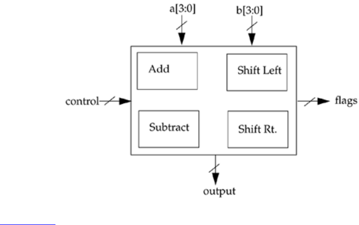
329
Figure 14-8. Vertical Partitioning of 4-bit ALU
Figure 14-8 shows vertical partitioning of the 4-bit ALU. For logic synthesis, it is
important to create a hierarchy by partitioning a large block into separate functional sub-
blocks. A design is best synthesized if levels of hierarchy are created and smaller blocks
are synthesized individually. Creating modules that contain a lot of functionality can
cause logic synthesis to produce suboptimal designs. Instead, divide the functionality into
smaller modules and instantiate those modules.
Parallelizing design structure
In this technique, we use more resources to produce faster designs. We convert sequential
operations into parallel operations by using more logic. A good example is the carry
lookahead full adder.
Contrast the carry lookahead adder with a ripple carry adder. A ripple carry adder is serial
in nature. A 4-bit ripple carry adder requires 9 gate delays to generate all sum and carry
bits. On the other hand, assuming that up to 5-input and and or gates are available, a carry
lookahead adder generates the sum and carry bits in 4 gate delays. Thus, we use more
logic gates to build a carry lookahead unit, which is faster compared to an n-bit ripple
carry adder.
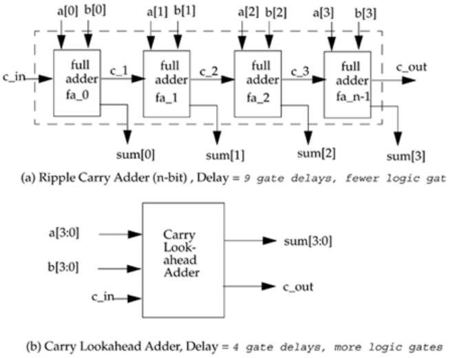
330
Figure 14-9. Parallelizing the Operation of an Adder
14.6.3 Design Constraint Specification
Design constraints are as important as efficient HDL descriptions in producing optimal
designs. Accurate specification of timing, area, power, and environmental parameters
such as input drive strengths, output loads, input arrival times, etc., are crucial to produce
a gate-level netlist that is optimal. A deviation from the correct constraints or omission of
a constraint can lead to nonoptimal designs. Careful attention must be given to specifying
design constraints.

331
14.7 Example of Sequential Circuit Synthesis
In Section 14.4.2, An Example of RTL-to-Gates, we synthesized a combinational circuit.
Let us now consider an example of sequential circuit synthesis. Specifically, we will
design finite state machines.
14.7.1 Design Specification
A simple digital circuit is to be designed for the coin acceptor of an electronic newspaper
vending machine.
• Assume that the newspaper cost 15 cents. (Wow! Who gives that kind of a price
any more? Well, let us assume that it is a special student edition!!)
• The coin acceptor takes only nickels and dimes.
• Exact change must be provided. The acceptor does not return extra money.
• Valid combinations including order of coins are one nickel and one dime, three
nickels, or one dime and one nickel. Two dimes are valid, but the acceptor does
not return money.
This digital circuit can be designed by using the finite state machine approach.
14.7.2 Circuit Requirements
We must set some requirements for the digital circuit.
• When each coin is inserted, a 2-bit signal coin[1:0] is sent to the digital circuit.
The signal is asserted at the next negative edge of a global clock signal and stays
up for exactly 1 clock cycle.
• The output of the digital circuit is a single bit. Each time the total amount inserted
is 15 cents or more, an output signal newspaper goes high for exactly one clock
cycle and the vending machine door is released.
• A reset signal can be used to reset the finite state machine. We assume
synchronous reset.
332
14.7.3 Finite State Machine (FSM)
We can represent the functionality of the digital circuit with a finite state machine.
• input: 2-bit, coin[1:0]?no coin x0= 2'b00, nickel x5 = 2'b01, dime x10 = 2'b10.
• output: 1-bit, newspaper?release door when newspaper = 1'b1
• states: 4 states?s0 = 0 cents; s5 = 5 cents; s10 = 10 cents; s15 = 15 cents
The bubble diagram for the finite state machine is shown in Figure 14-10. Each arc in the
FSM is labeled with a label <input>/<output> where input is 2-bit and output is 1-
b
it. For
example, x5/0 means transition to the state pointed to by the arc, when input is x5
(2'b01), and set the output to 0.
Figure 14-10. Finite State Machine for Newspaper Vending Machine
14.7.4 Verilog Description
The Verilog RTL description for the finite state machine is shown in Example 14-6.
Example 14-6 RTL Description for Newspaper Vending Machine FSM
//Design the newspaper vending machine coin acceptor
//using a FSM approach
module vend( coin, clock, reset, newspaper);
//Input output port declarations
333
input [1:0] coin;
input clock;
input reset;
output newspaper;
wire newspaper;
//internal FSM state declarations
wire [1:0] NEXT_STATE;
reg [1:0] PRES_STATE;
//state encodings
parameter s0 = 2'b00;
parameter s5 = 2'b01;
parameter s10 = 2'b10;
parameter s15 = 2'b11;
//Combinational logic
function [2:0] fsm;
input [1:0] fsm_coin;
input [1:0] fsm_PRES_STATE;
reg fsm_newspaper;
reg [1:0] fsm_NEXT_STATE;
begin
case (fsm_PRES_STATE)
s0: //state = s0
begin
if (fsm_coin == 2'b10)
begin
fsm_newspaper = 1'b0;
fsm_NEXT_STATE = s10;
end
else if (fsm_coin == 2'b01)
begin
fsm_newspaper = 1'b0;
fsm_NEXT_STATE = s5;
end
else
begin
fsm_newspaper = 1'b0;
fsm_NEXT_STATE = s0;
end
end
s5: //state = s5
begin
if (fsm_coin == 2'b10)
begin
fsm_newspaper = 1'b0;
fsm_NEXT_STATE = s15;
end
else if (fsm_coin == 2'b01)
begin
fsm_newspaper = 1'b0;
fsm_NEXT_STATE = s10;
end

334
else
begin
fsm_newspaper = 1'b0;
fsm_NEXT_STATE = s5;
end
s10: //state = s10
begin
if (fsm_coin == 2'b10)
begin
fsm_newspaper = 1'b0;
fsm_NEXT_STATE = s15;
end
else if (fsm_coin == 2'b01)
begin
fsm_newspaper = 1'b0;
fsm_NEXT_STATE = s15;
end
else
begin
fsm_newspaper = 1'b0;
fsm_NEXT_STATE = s10;
end
end
s15: //state = s15
begin
fsm_newspaper = 1'b1;
fsm_NEXT_STATE = s0;
end
endcase
fsm = {fsm_newspaper, fsm_NEXT_STATE};
end
endfunction
//Reevaluate combinational logic each time a coin
//is put or the present state changes
assign {newspaper, NEXT_STATE} = fsm(coin, PRES_STATE);
//clock the state flip-flops.
//use synchronous reset
always @(posedge clock)
begin
if (reset == 1'b1)
PRES_STATE <= s0;
else
PRES_STATE <= NEXT_STATE;
end
endmodule
14.7.5 Technology Library
We defined abc_100 technology in Section 14.4.1, RTL to Gates. We will use abc_100 as
the target technology library. abc_100 contains the following library cells:
//Library cells for abc_100 technology

335
VNAND//2-input nand gate
VAND//2-input and gate
VNOR//2-input nor gate
VOR//2-input or gate
VNOT//not gate
VBUF//buffer
NDFF//Negative edge triggered D flip-flop
PDFF//Positive edge triggered D flip-flop
14.7.6 Design Constraints
Timing critical is the only design constraint we used in this design. Typically, design
constraints are more elaborate.
14.7.7 Logic Synthesis
We synthesize the RTL description by using the specified design constraints and
technology library and obtain the optimized gate-level netlist.
14.7.8 Optimized Gate-Level Netlist
We use logic synthesis to map the RTL description to the abc_100 technology. The
optimized gate-level netlist produced is shown in Example 14-7.
Example 14-7 Optimized Gate-Level Netlist for Newspaper Vending Machine FSM
module vend ( coin, clock, reset, newspaper );
input [1:0] coin;
input clock, reset;
output newspaper;
wire \PRES_STATE[1] , n289, n300, n301, n302, \PRES_STATE243[1] ,
n303, n304, \PRES_STATE[0] , n290, n291, n292, n293, n294,
n295, n296, n297, n298, n299, \PRES_STATE243[0] ;
PDFF \PRES_STATE_reg[1] ( .clk(clock), .d(\PRES_STATE243[1] ),
.clrbar( 1'b1), .prebar(1'b1), .q(\PRES_STATE[1] )
);
PDFF \PRES_STATE_reg[0] ( .clk(clock), .d(\PRES_STATE243[0] ),
.clrbar( 1'b1), .prebar(1'b1), .q(\PRES_STATE[0] )
);
VOR U119 ( .in0(n292), .in1(n295), .out(n302) );
VAND U118 ( .in0(\PRES_STATE[0] ), .in1(\PRES_STATE[1] ),
.out(newspaper));
VNAND U117 ( .in0(n300), .in1(n301), .out(n291) );
VNOR U116 ( .in0(n298), .in1(coin[0]), .out(n299) );
VNOR U115 ( .in0(reset), .in1(newspaper), .out(n289) );
VNOT U128 ( .in(\PRES_STATE[1] ), .out(n298) );
VAND U114 ( .in0(n297), .in1(n298), .out(n296) );
VNOT U127 ( .in(\PRES_STATE[0] ), .out(n295) );
VAND U113 ( .in0(n295), .in1(n292), .out(n294) );
VNOT U126 ( .in(coin[1]), .out(n293) );
VNAND U112 ( .in0(coin[0]), .in1(n293), .out(n292) );
VNAND U125 ( .in0(n294), .in1(n303), .out(n300) );
336
VNOR U111 ( .in0(n291), .in1(reset), .out(\PRES_STATE243[0] ) );
VNAND U124 ( .in0(\PRES_STATE[0] ), .in1(n304), .out(n301) );
VAND U110 ( .in0(n289), .in1(n290), .out(\PRES_STATE243[1] ) );
VNAND U123 ( .in0(n292), .in1(n298), .out(n304) );
VNAND U122 ( .in0(n299), .in1(coin[1]), .out(n303) );
VNAND U121 ( .in0(n296), .in1(n302), .out(n290) );
VOR U120 ( .in0(n293), .in1(coin[0]), .out(n297) );
endmodule
The schematic diagram for the gate-level netlist is shown in Figure 14-11.
Figure 14-11. Gate-Level Schematic for the Vending Machine

337
14.7.9 Verification
Stimulus is applied to the original RTL description to test all possible combinations of
coins. The same stimulus is applied to test the optimized gate-level netlist. Stimulus
applied to both the RTL and gate-level netlist is shown in Example 14-8.
Example 14-8 Stimulus for Newspaper Vending Machine FSM
module stimulus;
reg clock;
reg [1:0] coin;
reg reset;
wire newspaper;
//instantiate the vending state machine
vend vendY (coin, clock, reset, newspaper);
//Display the output
initial
begin
$display("\t\tTime Reset Newspaper\n");
$monitor("%d %d %d", $time, reset, newspaper);
end
//Apply stimulus to the vending machine
initial
begin
clock = 0;
coin = 0;
reset = 1;
#50 reset = 0;
@(negedge clock); //wait until negative edge of clock
//Put 3 nickels to get newspaper
#80 coin = 1; #40 coin = 0;
#80 coin = 1; #40 coin = 0;
#80 coin = 1; #40 coin = 0;
//Put one nickel and then one dime to get newspaper
#180 coin = 1; #40 coin = 0;
#80 coin = 2; #40 coin = 0;
//Put two dimes; machine does not return a nickel to get newspaper
#180 coin = 2; #40 coin = 0;
#80 coin = 2; #40 coin = 0;
//Put one dime and then one nickel to get newspaper
#180 coin = 2; #40 coin = 0;
#80 coin = 1; #40 coin = 0;
#80 $finish;
end

338
//setup clock; cycle time = 40 units
always
begin
#20 clock = ~clock;
end
endmodule
The output from the simulation of RTL and the gate-level netlist is compared. In our
case, Example 14-9, the output is identical. Thus, the gate-level netlist is verified.
Example 14-9 Output of Newspaper Vending Machine FSM
Time Reset Newspaper
0 1 x
20 1 0
50 0 0
420 0 1
460 0 0
780 0 1
820 0 0
1100 0 1
1140 0 0
1460 0 1
1500 0 0
The gate-level netlist is sent to ABC Inc., which does the layout, checks that the layout
meets the timing requirements, and then fabricates the IC chip.
14.8 Summary
In this chapter, we discussed the following aspects of logic synthesis with Verilog HDL:
• Logic synthesis is the process of converting a high-level description of the design
into an optimized, gate-level representation, using the cells in the technology
library.
• Computer-aided logic synthesis tools have greatly reduced the design cycle time
and have improved productivity. They allow designers to write technology-
independent, high-level descriptions and produce technology-dependent,
optimized, gate-level netlists. Both combinational and sequential RTL
descriptions can be synthesized.
• Logic synthesis tools accept high-level descriptions at the register transfer level
(RTL). Thus, not all Verilog constructs are acceptable to a logic synthesis tool.
We discussed the acceptable Verilog constructs and operators and their
339
interpretation in terms of digital circuit elements.
• A logic synthesis tool accepts an RTL description, design constraints, and
technology library and produces an optimized gate-level netlist. Translation, logic
optimization, and technology mapping are the internal processes in a logic
synthesis tool and are normally invisible to the user.
• Functional verification of the optimized gate-level netlist is done by applying the
same stimulus to the RTL description and the gate-level netlist and comparing the
output. Timing is verified with timing simulation or static timing verification.
• Proper Verilog coding techniques must be used to write efficient RTL
descriptions, and various design trade-offs must be evaluated. Guidelines for
writing efficient RTL descriptions were discussed.
• Design partitioning is an important technique used to break the design into
smaller blocks. Smaller blocks reduce the complexity of optimization for the logic
synthesis tool.
• Accurate specification of design constraints is an important part of logic
synthesis.
High-level synthesis tools allow the designer to write designs at an algorithmic level.
However, high-level synthesis is still an emerging design paradigm, and RTL remains the
popular high-level description method for logic synthesis tools.

340
14.9 Exercises
1: A 4-bit full adder with carry lookahead was defined in Example 6-5 on page
109, using an RTL description. Synthesize the full adder, using a technology
library available to you. Optimize for fastest timing. Apply identical stimulus to
the RTL and the gate-level netlist and compare the output.
2: A 1-bit full subtractor has three inputs x, y, and z (previous borrow) and two
outputs D(difference) and B(borrow). The logic equations for D and B are as
follows:
D = x'y'z + x'yz' + xy'z' + xyz
B = x'y + x'z +yz
Write the Verilog RTL description for the full subtractor. Synthesize the full
subtractor, using any technology library available to you. Optimize for fastest
timing. Apply identical stimulus to the RTL and the gate-level netlist and
compare the output.
3: Design a 3-to-8 decoder, using a Verilog RTL description. A 3-bit input a[2:0]
is provided to the decoder. The output of the decoder is out[7:0]. The output bit
indexed by a[2:0] gets the value 1, the other bits are 0. Synthesize the decoder,
using any technology library available to you. Optimize for smallest area.
Apply identical stimulus to the RTL and the gate-level netlist and compare the
outputs.
4: Write the Verilog RTL description for a 4-bit binary counter with synchronous
reset that is active high. (Hint: Use always loop with the @(posedge clock)
statement.) Synthesize the counter, using any technology library available to
you. Optimize for smallest area. Apply identical stimulus to the RTL and the
gate-level netlist and compare the outputs.
5: Using a synchronous finite state machine approach, design a circuit that takes a
single bit stream as an input at the pin in. An output pin match is asserted high
each time a pattern 10101 is detected. A reset pin initializes the circuit
synchronously. Input pin clk is used to clock the circuit. Synthesize the circuit,
using any technology library available to you. Optimize for fastest timing.
Apply identical stimulus to the RTL and the gate-level netlist and compare the
outputs.
341
Chapter 15. Advanced Verification
Techniques
Verilog HDL was traditionally used both as a simulation modeling language and as a
hardware description language. Verilog HDL was heavily used in verification and
simulation for testbenches, test environments, simulation models, and architectural
models. This approach worked well for smaller designs and simpler test environments.
As the average gate count for designs began to approach or exceed one million,
verification soon became the main bottleneck in the design process. Design teams started
spending 50-70% of their time in verifying designs rather than creating new ones.
Designers quickly realized that to verify complex designs, they needed to use tools that
contained enhanced verification capabilities. They needed tools that could automate some
of the tedious processes. Moreover, it was important to find bugs the very first time to
avoid expensive chip re-spins.
To address these needs, a variety of verification methodologies and tools has emerged
over the past few years. The latest addition to verification methodology is assertion-
b
ased
verification. However, Verilog HDL remains the focal point in the design process. These
new developments enhance the productivity of verifying Verilog HDL-based designs.
This chapter gives the reader a basic understanding of these verification concepts that
complement Verilog HDL.
Learning Objectives
• Define the components of a traditional verification flow.
• Understand architectural modeling concepts.
• Explain the use of high-level verification languages (HVLs).
• Describe different techniques for effective simulation.
• Explain the methods for analysis of simulation results.
• Describe coverage techniques.
342
• Understand assertion checking techniques.
• Understand formal verification techniques.
• Describe semi-formal verification techniques.
• Define equivalence checking.
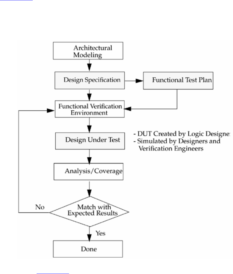
343
15.1 Traditional Verification Flow
A traditional verification flow consisting of certain standard components is illustrated in
Figure 15-1. This flow addresses only the verification perspective. It assumes that logic
design is done separately.
Figure 15-1. Traditional Verification Flow
As shown in Figure 15-1, the traditional verification flow consists of the following steps:
1. The chip architect first needs to create a design specification. In order to create a
good specification, an analysis of architectural trade-offs has to be performed so
that the best possible architecture can be chosen. This is usually done by
simulating architectural models of the design. At the end of this step, the design
specification is complete.
344
2. When the specification is ready, a functional test plan is created based on the
design specification. This test plan forms the fundamental framework of the
functional verification environment. Based on the test plan, test vectors are
applied to the design-under-test (DUT), which is written in Verilog HDL.
Functional test environments are needed to apply these test vectors. There are
many tools available for generating and apply test vectors. These tools also allow
the efficient creation of test environments.
3. The DUT is then simulated using traditional software simulators. (The DUT is
normally created by logic designers. Verification engineers simulate the DUT.)
4. The output is then analyzed and checked against the expected results. This can be
done manually using waveform viewers and debugging tools. Alternately,
analysis can be automated by the test environment checking the output of the
DUT or by parsing the log files using a language like PERL. In addition, coverage
results are analyzed to ensure that the tests have exercised the design thoroughly
and that the verification goals are met. If the output matches the expected results
and the coverage goals are met, then the verification is complete.
5. Optionally, additional steps can be taken to decrease the risk of a future design re-
spin. These steps include Hardware Acceleration, Hardware Emulation and
Assertion based Verification.
Earlier, each step in the traditional verification flow was accomplished with Verilog
HDL. Though Verilog HDL remains the dominant method for creating the DUT, many
advances have occurred in the other steps of the verification flow. The following sections
describe these advances in detail.
15.1.1 Architectural Modeling
This stage includes design exploration by the architects. The initial model typically does
not capture exact design behavior, except to the extent required for the initial design
decisions. For example, a fundamental algorithm like an MPEG decoder might be
implemented, but the processor to memory bandwidth is not specified. The architect tries
out several different variations of the model and make some fundamental decisions about
the system. These decisions may include number of processors, algorithms implemented
in hardware, memory architecture, and so on. These trade-offs will affect the eventual
implementation of the target design.
Architectural models are often written using C and C++. Though C++ has the advantage
of object oriented constructs, it does not implement concepts such as parallelism and
timing that were found in HDLs. Thus, creators of architectural models have to
implement these concepts in their models. This is very cumbersome, resulting in long
development times for architectural models.
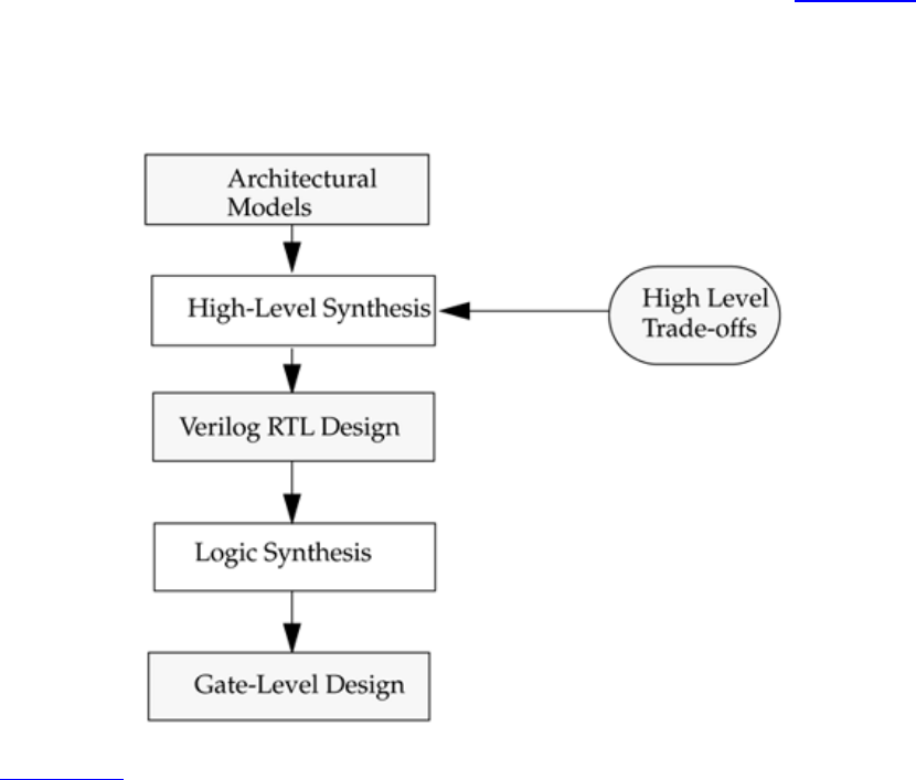
345
To solve this problem, architectural modeling languages were invented. These languages
have both the object oriented constructs found in C++ as well as parallelism and timing
constructs found in HDLs. Thus, they are well-suited for high-level architectural models.
A likely advancement in the future is the design of chips at the architectural modeling
level rather than at the RTL level. High-level synthesis tools will convert architectural
models to Verilog RTL design implementations based on the trade-off inputs. These RTL
designs can then go through the standard ASIC design and verification flow. Figure 15-2
shows an example of such a flow.
Figure 15-2. Architectural Modeling
Appendix E, Verilog Tidbits, contains further information on popular architectural
modeling languages.
15.1.2 Functional Verification Environment
The functional verification of a chip can be divided into three phases.
• Block level verification: Block level verification is usually done by the block
designer using Verilog for both design and verification. A number of simple test
cases are executed to ensure that the block functions well enough for chip
integration.

346
• Full ChipVerification: The goal of full chip verification is to ensure that all the
features of the full chip described in the functional test plan are covered.
• Extended Verification: The objective of the extended verification is to find all
corner case bugs in the design. This phase of verification is lengthy since the set
of tests is not predetermined and it may continue past tape-out.
During the functional verification phase, a combination of directed and random
simulation is used. Directed tests are written by the verification engineers to test a
specific behavior of the design. They may use random data, but the sequence of events
are predetermined. Random sequences of legal input transactions are used towards the
end of functional verifcation and during the extended verification phases in order to
simulate corner cases which the designer may have missed.
As Verilog HDL became popular, designers[1] started using Verilog HDL to both the
DUT and its surrounding functional verification environment. In a typical HDL-based
verification environment,
[1] In this chapter, the words "designer" and "verification engineer" have been used
interchangeably. This is because logic designers perform block level verification and are
often involved in the full chip verification process.
• The testbench consisted of HDL procedures that wrote data to the DUT or read
data from it.
• The tests, which called the testbench procedures in sequence to apply manually
selected input stimuli to the DUT and checked the results, were directed only
towards specific features of the design as described in the functional test plan.
However, as design sizes exceeded million gates, this approach became less effective
because
• The tests became harder and more time consuming to write because of decreasing
controllability of the design.
• Verifying correct behavior became difficult due to decreasing observability into
internal design states.
• The tests became difficult to read and maintain.
• There were too many corner cases for the available labor.
• Multiple environments became difficult to create and maintain because they used
little shared code.
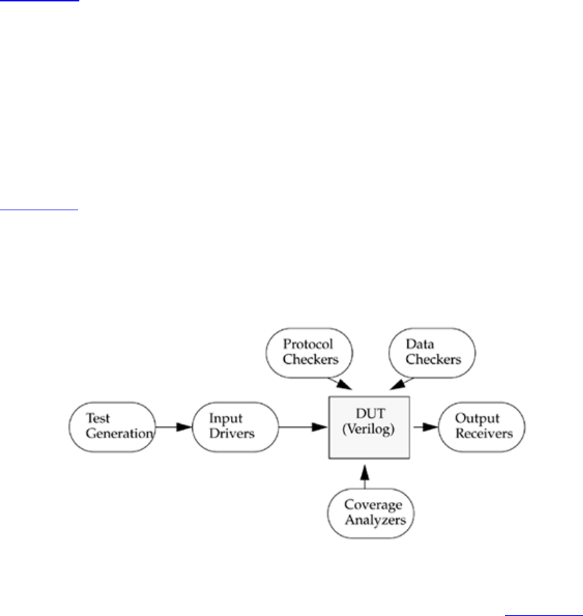
347
To make the test environment more reusable and readable, verification engineers needed
to write the tests and the test environment code in an object oriented programming
language. High-Level Verification Languages (HVLs) were created to address this need.
Appendix E, Verilog Tidbits, contains further information on popular HVLs.
HVLs are powerful because they combine the object oriented approach of C++ with the
parallelism and timing constructs in HDLs and are thus best suited for verification. HVLs
also help in the automatic generation of test stimuli and provide an integrated
environment for functional verification, including input drivers, output drivers, data
checking, protocol checking, and coverage. Thus, HVLs maximize productivity for
creating and maintaining verification environments.
Figure 15-3 shows the various components of a typical functional verification
environment. HVLs greatly improve the designer's ability to create and maintain each test
component. Note that Verilog HDL is still the primary method of creating a DUT.
Figure 15-3. Components of a Functional Verification Environment
In an HVL-based methodology, the verification components are simulated in the HVL
simulator and the DUT is simulated with a Verilog simulator. The HVL simulator and the
Verilog simulator interact with each other to produce the simulation results. Figure 15-4
shows an example of such an interaction. The HVL simulator and Verilog simulator are
run as two separate processes and communicate through the Verilog PLI interface. The
HVL simulator is primarily responsible for all verification components, including test
generation, input driver, output receiver, data checker, protocol checker, and coverage
analyzer. The Verilog simulator is responsible for simulating the DUT.
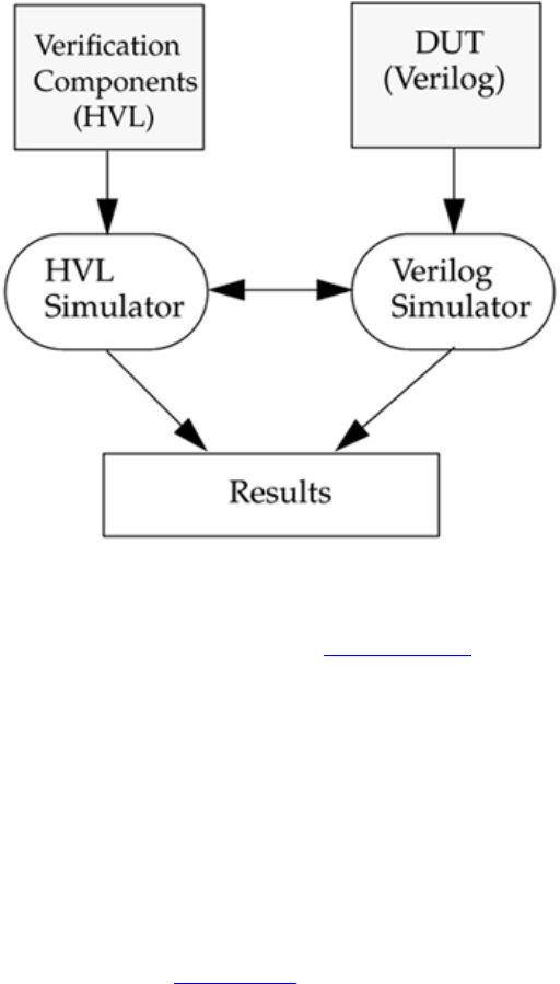
348
Figure 15-4. Interaction between HVL and Verilog Simulators
The future trend in HVLs is to apply acceleration techniques to HVL simulators to
greatly speed up the simulations. These acceleration techniques are similar to those used
for Verilog HDL simulators and are discussed in Section 15.1.3, Simulation.
15.1.3 Simulation
There are three ways to simulate a design: software simulation, hardware acceleration,
and hardware emulation.
Software Simulation
Software simulators were typically used to run Verilog HDL-based designs. Software
simulators run on a generic computer or server. They load the Verilog HDL code and
simulate the behavior in software. Appendix E, Verilog Tidbits, contains further
information on popular software simulators.
However, when designs started exceeding one million gates, software simulations began
to consume large amounts of time and became a bottleneck in the verification process.
Thus, various techniques emerged to accelerate these simulations. Two techniques,
hardware acceleration and emulation, were invented.
349
Hardware Acceleration
Hardware acceleration is used to speed up existing simulations and to run long sequences
of random transactions during functional and extended verification phases.
In this technique, the Verilog HDL-based design is mapped onto a reconfigurable
hardware box. The design is then run on the hardware box to produce simulation results.
Hardware acceleration[2] can often accelerate simulations by two to three orders of
magnitude.
[2] Also know as "Simulation Acceleration."
Hardware accelerators can be FPGA-based or processor-based. The simulation is divided
between the software simulator, which simulates all Verilog HDL code that is not
synthesizable, and the hardware accelerator, which simulates everything that is
synthesizable.
Figure 15-5 shows the verification methodology with a hardware accelerator.
Figure 15-5. Hardware Acceleration

350
Verification components may be simulated using a Verilog simulator or an HVL
simulator. The simulator and the hardware accelerator interact with each other to produce
results.
Hardware accelerators can cut simulation times from a matter of days to a few hours.
Therefore, they can greatly shorten the verification timeline. However, they are expensive
and need significant set-up time. Another drawback is that they usually require long
compilation times, which means that they are most useful only for long regression
simulations. As a result, smaller designs still employ software simulation as the
simulation technique of choice.
Appendix E, Verilog Tidbits, contains further information on popular hardware
accelerators.
Hardware Emulation
Hardware emulation[3] is used to verify the design in a real life environment with real
system software running on the system. HW emulation is used during the extended
verification phase since the design must be pretty stable.
[3] Also know as "In-Circuit Emulation."
One of the major benefits of hardware emulation is that hardware software integration
can start before the actual hardware is available, thus saving time in the schedule. By
running real-life software, conditions that are very difficult to set up in a simulation
environment can be tested.
When the design is complete, software engineers often want to run their software on the
design before the design is realized on a chip. Here are a few examples of what the
designer of a chip might want to do before a chip is sent for fabrication:
1. Designers of a microprocessor want to try booting the UNIX operating system.
2. Designers of an MPEG decoder want to have live frames decoded and shown on a
screen.
3. Designers of a graphics chip want actual frame renderings to show up on the
screen in real time.
Running live systems with the design is an important verification step that reduces the
p
ossibility of bugs and a design re-spin. However, software simulators and hardware
351
accelerators cannot be used for this purpose because they are too slow and do not have
the necessary hooks to run a live system. For example, to boot UNIX with a software
simulation of a design may take many years. Hardware emulation can boot UNIX in a
few hours.
Figure 15-6 shows the setup of a typical emulation system. Emulation is done so that the
software application runs exactly as it would on the real chip in a real circuit. The
software application is oblivious to the fact that it is running on an emulator rather than
the actual chip.
Figure 15-6. Hardware Emulation
Hardware emulators typically run at megahertz speeds. However, they are very expensive
and require significant setup time. As a result, smaller designs still employ software
simulation as the simulation technique of choice.
Appendix E, Verilog Tidbits, contains further information on popular hardware
emulators.
352
15.1.4 Analysis
An important step in the traditional verification flow is to analyze the design to check the
following items:
1. Was the data received equal to the expected data?
2. Was the data received correctly according to the interface protocol?
To analyze the correctness of the data value and data protocol, various methods are used.
1. Waveform Viewers are used to see the dump files. The designer visually goes
through the dump files from various tests and ensures that the data value and the
data protocol are both correct.
2. Log Files contain traces of the simulation run. The designer visually looks at the
log files from various tests and determines the correctness of the data value and
the data protocol based on the simulation messages.
These methods are extremely tedious and time-consuming. Every time a test is run, the
designers has to manually look through the dump files and log files. This method breaks
down when a large number of simulation runs needs to be analyzed. Therefore, it is
advisable to make your test environment self-checking. Two components are required for
building a self-checking test environment:
1. Data Checker
2. Protocol Checker
Data checkers compare each value output from the simulation and check the value on-
the-fly against the expected output. If there is a mismatch, the simulation can be stopped
immediately to display an error message. If there are no error messages, the simulation is
deemed to complete successfully. Scoreboards are often used to implement data checkers.
Scoreboards are often used to indicate the completion transactions and verify that data is
received on the corrected interface. Scoreboards also ensure that data is not lost in the
DUT, even if the protocol is followed, and that the data received is correct.
Protocol checkers check on-the-fly whether the data protocol is followed at each input
and output interface. If there is a violation of protocol, the simulation can be stopped
immediately to display an error message. If there are no error messages, the simulation is
deemed to complete successfully.
A self-checking methodology allows the designer to run thousands of tests without
having to analyze each test for correctness. If there is a failure, the designer can probe
further into the dump files and the log files to determine the cause of the error.

353
15.1.5 Coverage
Coverage helps the designer determine when verification is complete. Various methods
have been developed and used to quantify the verification progress. There are two types
of coverage: structural and functional.
Structural Coverage
Structural coverage deals with the structure of the Verilog HDL code and tells when key
portions of that structure have been covered. There are three main types of structural
coverage:
1. Code coverage: The basic assumption of code coverage is that unexercised code
potentially bears bugs. However, code coverage checks how well RTL code was
exercised rather than design functionality. Code coverage does not tell whether
the verification is complete. It simply tells that verification is not complete until
100% code coverage is achieved. Therefore, code coverage is useful but it is not a
complete metric.
2. Toggle coverage: This is one of the oldest coverage measurements. It was
historically used for manufacturing tests. Toggle coverage monitors the bits of
logic that have toggled during simulation. If a bit does not toggle from 0 to 1, or
from 1 to 0, it has not been adequately verified.
Toggle coverage does not ensure completeness. It cannot assure that a specific bit
toggle sequence that represents high-level functionality has occurred. Toggle
coverage does not shorten the verification process. It may even prolong the
verification process as engineers try to toggle a bit, which cannot toggle according
to the specification. Toggle coverage is very low-level coverage and it is
cumbersome to relate a specific bit to a high-level test plan item.
3. Branch coverage: Branch coverage checks if all possible branches in a control
flow are taken. This coverage metric is necessary but not sufficient.
Functional Coverage
Functional coverage perceives the design from a system point of view. Functional
coverage ensures that all possible legal values of input stimuli are exercised in all
possible combinations at all possible times. Moreover, functional coverage also provides
finite state machine coverage, including states and state transitions.
Functional coverage can be enhanced with implementation coverage by inserting
coverage points or assertions in the RTL code. For example, it enhances the functional
coverage metric by determining if all transactions have been tested while receiving an
interrupt or when one of the internal FIFOs is full.
Appendix E, Verilog Tidbits, contains further information on popular coverage tools.

354
15.2 Assertion Checking
The traditional verification flow discussed in the previous section is a black box
approach, i.e., verification relies only on the knowledge of the input and output behavior
of the system.
Many other verification methodologies have evolved over the past few years to
complement the traditional verification flow discussed in the previous section. In this
section and the following sections, we explain some of these new verification
methodologies that use the white box verification approach, i.e., knowledge of the
internal structure of the design is needed for verification.
Assertion checking is a form of white box verification. It requires knowledge of internal
structures of the design. The main purpose of assertion checkers is to improve
observability.
Assertions are statements about a design's intended behavior. There are two types of
assertions:
• Temporal assertions ? they describe the timing relationship between signals.
• Static assertions ? they describe a property of a signal that is always true or false.
Assertions may be used in the RTL code to describe the intended behavior of a piece of
Verilog HDL code. The following are examples of such behavior:
• An FSM state register should always be one-hot.
• The full and empty flags of a FIFO should never be asserted at the same time.
Assertions can also be used to describe the behavior of the internal or external interface
of a chip. For example, the acknowledge signal should always be asserted within five
cycles of the request signal. Assertions may be verified in simulation or by using formal
methods.
Assertions do not contribute to the element being designed; they are usually treated as
comments for logic synthesis. Their sole purpose is to ensure consistency between the
designer's intention and the design that is created. Figure 15-7 shows the interfaces at
which assertions could be placed in a FIFO-based design.
355
Figure 15-7. Assertion Checks
Assertion checks can be used with the traditional verification flow described in Section
15.1, Traditional Verification Flow. Assertion checks are placed by the designer at
critical points in the design. During simulation, if there is a failure at that point, the
designer is notified.
Assertion-based verification (ABV) has the following advantages:
1. ABV improves observability. It isolates the problem close to the source.
2. ABV improves verification efficiency. It reduces the number of engineers
involved in the debugging process. Engineers notified when there are bugs are
having to look through waveforms and log files for hours to find bugs. Thus, the
debug process is greatly simplified.
Appendix E, Verilog Tidbits, contains further information on popular assertion-checking
tools.

356
15.3 Formal Verification
A well-known white-box approach is formal verification, in which mathematical
techniques are used to prove an assertion or a property of the design. The property to be
proven may be related to the chip's overall functional specification, or it may represent
internal design behavior. Detailed knowledge of the behavior of design structures is often
required to specify useful properties that are worth proving. Thus, one can prove the
correctness of a design without doing simulations. Another application of formal
verification is to prove that the architectural specifications of a design are sound before
starting with the RTL implementation.
A formal verification tool proves a design property by exploring all possible ways to
manipulate a design. All input changes must conform to the constraints for legal
behavior. Assertions on interfaces act as constraints to the formal tool to constrain what is
legal behavior on the inputs. Attempts are then made to prove the assertions in the RTL
code to be true or false. If the constraints on the inputs are too loose, then the formal
verification tool can generate counter-examples that rely on illegal input sequences that
would not occur in the design. If the constraints are too tight, then the tool will not
explore all possible behavior and will wrongly report the design as "proven."
Figure 15-8 shows the verification flow with a formal verification tool. In the best case,
the tool either proves a particular assertion absolutely or provides a counter-example to
show the circumstances under which the assertion[4] is not met.
[4] Assertions are not used simply to increase observability. In formal verification, they
are used as constraints. The formal verification tool explores the state space such that it
proves the assertion absolutely or produces a counter-example. Thus, assertions also
increase controllability, i.e., they control how the formal verification tool explores the
state space to prove a property.
357
Figure 15-8. Formal Verification Flow
Since formal verification tools explore a design exhaustively, they can run only on
designs that are limited in size. Typically, beyond 10,000 gates, absolute formal proofs
become too hard and the tool blows up in terms of computation time and memory usage.
The limitations on formal verification tools are not based on number of lines. They are
based on the complexity of the assertions being proven and the design structure. The
limitation lies in the number of cycles the algorithm can reach from the seed state(Formal
verifications tools often use reset as the seed state).
To circumvent the problems of formal verification, semi-formal techniques are used.
15.3.1 Semi-formal Verification
Semi-formal verification combines the traditional verification flow using test vectors with
the power and thoroughness of formal verification. Semi-formal techniques have the
following components:
1. Semi-formal methods supplement, but do not replace, simulation with test
vectors.
2. Embedded assertion checks define the properties targeted by formal methods.
3. Embedded assertion checks define the input constraints.
4. Semi-formal methods explore a limited state space exhaustively from the states
358
reached by simulation, thus maximizing the effect of simulation. The exploration
is limited to a certain point around the state reached by simulation.
During a Verilog simulation, seed states are captured to serve as starting points for formal
methods. Then formal methods start from the seed states and try to prove the assertions
completely or describe stimulus sequences that will violate these assertions. The semi-
formal tool proves properties exhaustively in a limited exploration space starting from
these seed states, thus quickly identifying many corner-cases that would have been
detected only by extensive simulation test suites. Figure 15-9 shows the verification flow
with a semi-formal tool.
Figure 15-9. Semi-formal Verification Flow
Formal and semi-formal verification methods have recently received a lot of attention
because of the increasing complexity of designs. Appendix E, Verilog Tidbits, contains
further information on popular tools that employ formal and semi-formal verification
methods.
359
15.3.2 Equivalence Checking
After logic synthesis and place and route tools create gate level netlist and physical
implementations of the RTL design, it is necessary to check whether these
implementations match the functionality of the original RTL design. One methodology is
to re-run all the test vectors used for RTL verification, with the gate level netlist and the
physical implementation. However, this methodology is extremely time consuming and
tedious.
Equivalence checking solves this problem. Equivalence checking is one application of
formal verification. It ensures that the gate level or the physical netlist has the same
functionality as the Verilog RTL that was simulated. Equivalence checkers build a logical
model of both the RTL and gate level representations of the design and mathematically
prove that they are functionally equivalent. Thus, functional verification can focus
entirely on RTL and there is little need for gate level simulation.
Figure 15-10 shows the equivalence checking flow.
Figure 15-10. Equivalence Checking
Appendix E, Verilog Tidbits, contains further information on popular equivalence
checking tools.
360
15.4 Summary
• A traditional verification flow contains a test-vector-based approach. An
architectural model is developed to analyze design trade-offs. Once the design is
finalized, it is verified using test vectors and simulation. Then the results are
analyzed and coverage is measured. If the analysis meets the verification goals,
the design is deemed verified.
• Architectural modeling is used by architects for design exploration. The initial
model of the design typically does not capture exact design behavior, except to
the extent required for the initial design decisions. Architectural modeling
languages are suitable for building architectural models.
• Functional verification environments often contain test generators, input drivers,
output receivers, data checkers, protocol checkers and coverage analyzers. High
level verification languages (HVLs) can be used to effectively create and maintain
these environments.
• Software simulators are the most popular tools for simulating Verilog HDL
designs. Hardware accelerators are used to accelerate simulation by a few orders
of magnitude. Hardware emulators run in the megahertz range and are used to run
software applications as if they were running on the real chip.
• Waveforms and log files are the most common methods to analyze the output
from a simulation. For effectively analysis, it is important to build automatic data
checker and protocol checker modules. If there is a violation of data value or
protocol, the simulation is stopped immediately and an error message is
displayed. A self-checking methodology allows the designer to run thousands of
tests without having to analyze each test for correctness.
• Toggle coverage, code coverage, and branch coverage are three types of structural
coverage techniques. Functional coverage perceives the design from a system
point of view. Functional coverage also provides finite state machine coverage,
including states and state transitions. A combination of functional coverage and
other coverage techniques is recommended.
• Assertion checking is a form of white-box verification. It requires knowledge of
the internal structures of the design. Assertion checking improves observability
and verification efficiency. Assertion checks are placed by the designer at critical
points in the design. If there is a failure at that point, the designer is notified.
• Formal verification is a white-
b
ox approach in which mathematical techniques are
used to exhaustively prove an assertion or a property of the design. Semi-formal
verification combines the traditional verification flow using test vectors with the

361
power and thoroughness of formal verification. Equivalence checking is an
application of formal verificaton that examines the RTL representation of the
design and checks to see if it matches the gate level and physical implementations
of the design.

362
Part 3: Appendices
A Strength Modeling and Advanced Net Definitions
Strength levels, signal contention, advanced net definitions.
B List of PLI Routines
A list of all access (acc) and utility (tf) PLI routines.
C List of Keywords, System Tasks, and Compiler Directives
A list of keywords, system tasks, and compiler directives in Verilog HDL.
D Formal Syntax Definition
Formal syntax definition of the Verilog Hardware Description Language.
E Verilog Tidbits
Origins of Verilog HDL, interpreted, compiled and native simulators, event-driven and
oblivious simulation, cycle simulation, fault simulation, Verilog newsgroup, Verilog
simulators, and Verilog-related Web sites.
F Verilog Examples
Synthesizable model of a FIFO, behavioral model of a 256K X 16 DRAM.

363
Appendix A. Strength Modeling and
Advanced Net Definitions
• Section A.1. Strength Levels
• Section A.2. Signal Contention
• Section A.3. Advanced Net Types
364
A.1 Strength Levels
Verilog allows signals to have logic values and strength values. Logic values are 0, 1, x,
and z. Logic strength values are used to resolve combinations of multiple signals and to
represent behavior of actual hardware elements as accurately as possible. Several logic
strengths are available. Table A-1 shows the strength levels for signals. Driving strengths
are used for signal values that are driven on a net. Storage strengths are used to model
charge storage in trireg type nets, which are discussed later in this appendix.
Table A-1. Strength Levels
Strength Level Abbreviation Degree Strength Type
supply1 Su1 strongest 1 driving
strong1 St1 driving
pull1 Pu1 driving
large1 La1 storage
weak1 We1 driving
medium1 e1 storage
small1 Sm1
storage
highz1 HiZ1 weakest1 high impedance
highz HiZ0 weakest0 high impedance
small0 Sm0 storage
medium0 Me0 storage
weak0 We0 driving
large0 La0 storage
pull0 Pu0 driving
strong0 St0
driving
supply0 Su0 strongest0 driving
365
A.2 Signal Contention
Logic strength values can be used to resolve signal contention on nets that have multiple
drivers.There are many rules applicable to resolution of contention. However, two cases
of interest that are most commonly used are described below.
A.2.1 Multiple Signals with Same Value and Different Strength
If two signals with same known value and different strength drive the same net, the signal
with the higher strength wins.
In the example shown, supply strength is greater than pull. Hence, Su1 wins.
A.2.2 Multiple Signals with Opposite Value and Same Strength
When two signals with opposite value and same strength combine, the resulting value is
x.
366
A.3 Advanced Net Types
We discussed resolution of signal contention by using strength levels. There are other
methods to resolve contention without using strength levels. Verilog provides advanced
net declarations to model logic contention.
A.3.1 tri
The keywords wire and tri have identical syntax and function. However, separate names
are provided to indicate the purpose of the net. Keyword wire denotes nets with single
drivers, and tri is denotes nets that have multiple drivers. A multiplexer, as defined
below, uses the tri declaration.
module mux(out, a, b, control);
output out;
input a, b, control;
tri out;
wire a, b, control;
bufif0 b1(out, a, control); //drives a when control = 0; z otherwise
bufif1 b2(out, b, control); //drives b when control = 1; z otherwise
endmodule
The net is driven by b1 and b2 in a complementary manner. When b1 drives a, b2 is
tristated; when b2 drives b, b1 is tristated. Thus, there is no logic contention. If there is
contention on a tri net, it is resolved by using strength levels. If there are two signals of
opposite values and same strength, the resulting value of the tri net is x.
A.3.2 trireg
Keyword trireg is used to model nets having capacitance that stores values. The default
strength for trireg nets is medium. Nets of type trireg are in one of two states:
• Driven state? At least one driver drives a 0, 1, or x value on the net. The value is
continuously stored in the trireg net. It takes the strength of the driver.
• Capacitive state? All drivers on the net have high impedance (z) value. The net
holds the last driven value. The strength is small, medium, or large (default is
medium).
trireg (large) out;
wire a, control;
367
bufif1 (out, a, control); // net out gets value of a when control = 1;
//when control = 0, out retains last value of
a
//instead of going to z. strength is large.
A.3.3 tri0 and tri1
Keywords tri0 and tri1 are used to model resistive pulldown and pullup devices. A tri0
net has a value 0 if nothing is driving the net. Similarly, tri1 net has a value 1 if nothing is
driving the net. The default strength is pull.
tri0 out;
wire a, control;
bufif1 (out, a, control); //net out gets the value of a when control =
1;
//when control = 0, out gets the value 0
instead
//of z. If out were declared as tri1, the
//default value of out would be 1 instead of
0.
A.3.4 supply0 and supply1
Keyword supply1 is used to model a power supply. Keyword supply0 is used to model
ground. Nets declared as supply1 or supply0 have constant logic value and a strength
level supply (strongest strength level).
supply1 vcc; //all nets connected to vcc are connected to power
supply
supply0 gnd; //all nets connected to gnd are connected to ground
A.3.5 wor, wand, trior, and triand
When there is logic contention, if we simply use a tri net, we will get an x. This could be
indicative of a design problem. However, sometimes the designer needs to resolve the
final logic value when there are multiple drivers on the net, without using strength levels.
Keywords wor, wand, trior, and triand are used to resolve such conflicts. Net wand
perform the and operation on multiple driver logic values. If any value is 0, the value of
the net wand is 0. Net wor performs the or operation on multiple driver values. If any
value is 1, the net wor is 1. Nets triand and trior have the same syntax and function as the
nets wor and wand. The example below explains the function.

368
wand out1;
wor out2;
buf (out1, 1'b0);
buf (out1, 1'b1); //out1 is a wand net; gets the final value 1'b0
buf (out2, 1'b0);
buf (out2, 1'b1); //out2 is a wor net; gets the final value 1'b1

369
Appendix B. List of PLI Routines
A list of PLI acc_ and tf_ routines is provided. VPI routines are not listed.[1] Names, the
argument list, and a brief description of the routine are shown for each PLI routine. For
details regarding the use of each PLI routine, refer to the IEEE Standard Verilog
Hardware Description Language document.
[1] See the "IEEE Standard Verilog Hardware Description Language" document for
details on VPI routines.
370
B.1 Conventions
Conventions to be used for arguments are shown below.
Convention Meaning
char *format Pass formatted string
char * Pass name of object as a string
underlined arguments Arguments are optional
* Pointer to the data type
......... More arguments of the same type
B.2 Access Routines
Access routines are classified into five categories: handle, next, value change link, fetch,
and modify routines.
B.2.1 Handle Routines
Handle routines return handles to objects in the design. The names of handle routines
always starts with the prefix acc_handle_. See Table B-1.
Table B-1. Handle Routines
Return
Type Name Argument List Description
handle acc_handle_by_name (char *name, handle
scope)
Object from name
relative to scope.

371
handle acc_handle_condition (handle object)
Conditional
expression for
module path or
timing check
handle.
handle acc_handle_conn (handle terminal);
Get net connected
to a primitive,
module path, or
timing check
terminal.
handle acc_handle_datapath (handle modpath);
Get the handle to
data path for an
edge-sensitive
module path.
handle acc_handle_hiconn (handle port);
Get hierarchically
higher net
connection to a
module port.
handle acc_handle_interactive_scope ( );
Get the handle to
the current
simulation
interactive scope.
handle acc_handle_loconn (handle port);
Get hierarchically
lower net
connection to a
module port.
handle acc_handle_modpath
(handle module, char
*src, char *dest); or
(handle module, handle
src, handle dest);
Get the handle to
module path whose
source and
destination are
specified. Module
path can be
specified by names
or handles.
handle
acc_handle_notifier
(handle tchk);
Get notifier register
associated with a
particular timing
check.

372
handle acc_handle_object (char *name);
Get the handle for
any object, given
its full or relative
hierarchical path
name.
handle acc_handle_parent (handle object);
Get the handle for
own primitive or
containing module
or an object.
handle acc_handle_path (handle outport, handle
inport);
Get the handle to
path from output
port of a module to
input port of
another module.
handle acc_handle_pathin (handle modpath);
Get the handle for
first net connected
to the input of a
module path.
handle acc_handle_pathout (handle modpath);
Get the handle for
first net connected
to the output of a
module path.
handle acc_handle_port (handle module, int
port#);
Get the handle for
module port. Port#
is the position from
the left in the
module definition
(starting with 0).
handle acc_handle_scope (handle object);
Get the handle to
the scope
containing an
object.
handle acc_handle_simulated_net (handle
collapsed_net_handle);
Get the handle to
the net associated
with a collapsed
net.
handle acc_handle_tchk
(handle module, int
tchk_type, char
*netname1, int edge1,
........);
Get the handle for a
specified timing
check of a module
or cell.

373
handle acc_handle_tchkarg1 (handle tchk);
Get net connected
to the first
argument of a
timing check.
handle acc_handle_tchkarg2 (handle tchk);
Get net connected
to the second
argument of a
timing check.
handle acc_handle_terminal (handle primitive, int
terminal#);
Get the handle for a
primitive terminal.
Terminal# is the
position in the
argument list.
handle acc_handle_tfarg (int arg#);
Get the handle to
argument arg# of
calling system task
or function that
invokes the PLI
routine.
handle acc_handle_tfinst ( );
Get the handle to
the current user
defined system task
or function.
B.2.2 Next Routines
Next routines return the handle to the next object in the linked list of a given object type
in a design. Next routines always start with the prefix acc_next_ and accept reference
objects as arguments. Reference objects are shown with a prefix current_. See Table B-2.
Table B-2. Next Routines
Return
Type Name Argument List Description
handle acc_next
(int obj_type_array[],
handle module, handle
current_object);
Get next object of a
certain type within a
scope. Object types such
as accNet or accRegister
are defined in
obj_type_array.

374
handle acc_next_bit (handle vector, handle
current_bit);
Get next bit in a vector
port or array.
handle acc_next_cell (handle module, handle
current_cell);
Get next cell instance in
a module. Cells are
defined in a library.
handle acc_next_cell_load (handle net, handle
current_cell_load);
Get next cell load on a
net.
handle acc_next_child (handle module, handle
current_child);
Get next module instance
appearing in this module
handle acc_next_driver (handle net, handle
current_driver_terminal);
Get next primitive
terminal driver that
drives the net.
handle acc_next_hiconn (handle port, handle
current_net);
Get next higher net
connection.
handle acc_next_input (handle path_or_tchk,
handle current_terminal);
Get next input terminal
of a specified module
path or timing check.
handle acc_next_load (handle net, handle
current_load);
Get next primitive
terminal driven by a net
independent of hierarchy.
handle acc_next_loconn (handle port, handle
current_net);
Get next lower net
connection to a module
port.
handle acc_next_modpath (handle module, handle
path);
Get next path within a
module.
handle acc_next_net (handle module, handle
current_net);
Get the next net in a
module.
handle acc_next output (handle path, handle
current_terminal);
Get next output terminal
of a module path or data
path.
handle acc_next_parameter
(handle module, handle
current_parameter);
Get next parameter in a
module.
handle acc_next_port (handle module, handle
current_port);
Get the next port in a
module port list.
handle acc_next_portout (handle module, handle
current_port);
Get next output or inout
port of a module.
handle acc_next_primitive (handle module, handle
current_primitive);
Get next primitive in a
module.
375
handle acc_next_scope (handle scope, handle
current_scope);
Get next hierarchy scope
within a certain scope.
handle acc_next_specparam
(handle module, handle
current_specparam);
Get next specparam
declared in a module.
handle acc_next_tchk (handle module, handle
current_tchk);
Get next timing check in
a module.
handle acc_next_terminal (handle primitive, handle
current_terminal);
Get next terminal of a
primitive.
handle acc_next_topmod (handle current_topmod); Get next top level
module in the design.
B.2.3 Value Change Link (VCL) Routines
VCL routines allow the user system task to add and delete objects from the list of objects
that are monitored for value changes. VCL routines always begin with the prefix
acc_vcl_ and do not return a value. See Table B-3.
Table B-3. Value Change Link Routines
Return
Type Name Argument List Description
void acc_vcl_add
(handle object, int
(*consumer_routine) (), char
*user_data, int VCL_flags);
Tell the Verilog simulator to
call the consumer routine with
value change information
whenever the value of an
object changes.
void acc_vcl_delete
(handle object, int
(*consumer_routine) (), char
*user_data, int VCL_flags);
Tell the Verilog simulator to
stop calling the consumer
routine when the value of an
object changes.
B.2.4 Fetch Routines
Fetch routines can extract a variety of information about objects. Information such as full
hierarchical path name, relative name, and other attributes can be obtained. Fetch routines
always start with the prefix acc_fetch_. See Table B-4.

376
Table B-4. Fetch Routines
Return
Type Name Argument List Description
int acc_fetch_argc ( );
Get the number of
invocation command-line
arguments.
char ** acc_fetch_argv ( );
Get the array of
invocation command-line
arguments.
double acc_fetch_attribute
(handle object, char
*attribute, double
default);
Get the attribute of a
parameter or specparam.
char * acc_fetch_defname (handle object);
Get the defining name of
a module or a primitive
instance.
int acc_fetch_delay_mode (handle module); Get delay mode of a
module instance.
bool acc_fetch_delays
(handle object, double
*rise, double *fall,
double *turnoff);
(handle object, double
*d1, *d2, *d3, *d4 *d5,
*d6);
Get typical delay values
for primitives, module
paths, timing checks, or
module input ports.
int acc_fetch_direction (handle object);
Get the direction of a port
or terminal, i.e., input,
output, or inout.
int acc_fetch_edge (handle
path_or_tchk_term);
Get the edge specifier
type of a path input or
output terminal or a
timing check input
terminal.
char * acc_fetch_fullname (handle object);
Get the full hierarchical
name of any name object
or module path.
int acc_fetch_fulltype (handle object);
Get the type of the object.
Return a predefined
integer constant that tells
type.

377
int acc_fetch_index (handle
port_or_terminal);
Get the index for a port
or terminal for gate,
switch, UDP instance,
module, etc. Zero
returned for the first
terminal.
void acc_fetch_location (p_location loc_p,
handle object);
Get the location of an
object in a Verilog source
file. p_location is a
predefined data structure
that has file name and
line number in the file.
char * acc_fetch_name (handle object);
Get instance of object or
module path within a
module.
int acc_fetch_paramtype (handle parameter);
Get the data type of
parameter, integer, string,
real, etc.
double acc_fetch_paramval (handle parameter);
Get value of parameter or
specparam. Must cast
return values to integer,
string, or double.
int acc_fetch_polarity (handle path); Get polarity of a path.
int acc_fetch_precision ( ); Get the simulation time
precision.
bool acc_fetch_pulsere
(handle path, double
*r1, double *e1,double
*r2, double *e2.........)
Get pulse control values
for module paths based
on reject values and
e_values for transitions.
int acc_fetch_range (handle vector, int
*msb, int *lsb);
Get the most significant
bit and least significant
bit range values of a
vector.
int acc_fetch_size (handle object); Get number of bits in a
net, register, or port.
double acc_fetch_tfarg (int arg#);
Get value of system task
or function argument
indexed by arg#.

378
int acc_fetch_tfarg_int (int arg#);
Get integer value of
system task or function
argument indexed by
arg#.
char * acc_fetch_tfarg_str (int arg#);
Get string value of
system task or function
argument indexed by
arg#.
void acc_fetch_timescale_info
(handle object,
p_timescale_info
timescale_p);
Get the time scale
information for an object.
p_timescale_info is a
pointer to a predefined
time scale data structure.
int acc_fetch_type (handle object);
Get the type of object.
Return a predefined
integer constant such as
accIntegerVar,
accModule, etc.
char * acc_fetch_type_str (handle object);
Get the type of object in
string format. Return a
string of type
accIntegerVar,
accParameter, etc.
char * acc_fetch_value (handle object, char
*format);
Get the logic or strength
value of a net, register, or
variable in the specified
format.
B.2.5 Utility Access Routines
Utility access routines perform miscellaneous operations related to access routines. See
Table B-5.
Table B-5. Utility Access Routines
Return
Type Name Argument List Description
void acc_close ( );
Free internal memory used
by access routines and reset
all configuration
parameters to default
values.

379
handle
* acc_collect
(handle
*next_routine,
handle ref_object,
int *count);
Collect all objects related
to a particular reference
object by successive calls
to an acc_next routine.
Return an array of handles.
bool acc_compare_handles (handle object1,
handle object2);
Return true if both handles
refer to the same object.
void acc_configure (int config_param,
char *config_value);
Set parameters that control
the operation of various
access routines.
int acc_count
(handle
*next_routine,
handle ref_object);
Count the number of
objects in a reference
object such as a module.
The objects are counted by
successive calls to the
acc_next routine
void acc_free (handle
*object_handles);
Free memory allocated by
acc_collect for storing
object handles.
void acc_initialize ( );
Reset all access routine
configuration parameters.
Call when entering a user-
defined PLI routine.
bool acc_object_in_typelist (handle object, int
object_types[]);
Match the object type or
property against an array of
listed types or properties.
bool acc_object_of_type (handle object, int
object_type);
Match the object type or
property against a specific
type or property.
int acc_product_type ( ); Get the type of software
product being used.
char * acc_product_version ( ); Get the version of software
product being used.
int acc_release_object (handle object);
Deallocate memory
associated with an input or
output terminal path.
void acc_reset_buffer ( ); Reset the string buffer.
handle acc_set_interactive_scope ( ); Set the interactive scope of
a software implementation.
380
void acc_set_scope (handle module, char
*module_name);
Set the scope for searching
for objects in a design
hierarchy.
char * acc_version ( ); Get the version of access
routines being used.
B.2.6 Modify Routines
Modify routines can modify internal data structures. See Table B-6.
Table B-6. Modify Routines
Return
Type Name Argument List Description
void acc_append_delays
(handle object,
double rise, double
fall, double z); or
(handle object,
double d1, ..., double
d6); or
(handle object,
double limit); or
(handle object
double delay[]);
Add delays to existing delay
values for primitives, module
paths, timing checks, or module
input ports. Can specify
rise/fall/turn-off or 6 delay or
timing check or min:typ:max
format.
bool acc_append_pulsere
(handle path, double
r1, ...., double r12,
double e1, ..., double
e12);
Add to the existing pulse control
values of a module path.

381
void acc_replace_delays
(handle object,
double rise, double
fall, double z); or
(handle object,
double d1, ..., double
d6); or
(handle object,
double limit); or
(handle object
double delay[]);
Replace delay values for
primitives, module paths, timing
checks, or module input ports.
Can specify rise/fall/turn-off or 6
delay or timing check or
min:typ:max format.
bool acc_replace_pulsere
(handle path, double
r1, ...., double r12,
double e1, ..., double
e12);
Set pulse control values of a
module path as a percentage of
path delays.
void acc_set_pulsere (handle path, double
reject, double e);
Set pulse control percentages for
a module path.
void acc_set_value
(handle object,
p_setval_value
value_P,
p_setval_delay
delay_P);
Set value for a register or a
sequential UDP.
382
B.3 Utility (tf_) Routines
Utility (tf_) routines are used to pass data in both directions across the Verilog/user C
routine boundary. All the tf_ routines assume that operations are being performed on
current instances. Each tf_ routine has a tf_i counterpart in which the instance pointer
where the operations take place has to be passed as an additional argument at the end of
the argument list. See Table B-7 through B-16.
B.3.1 Get Calling Task/Function Information
Table B-7. Get Calling Task/Function Information
Return
Type Name Argument
List Description
char * tf_getinstance ( );
Get the pointer to the current instance of the
simulation task or function that called the
user's PLI application program.
char * tf_mipname ( );
Get the Verilog hierarchical path name of the
simulation module containing the call to the
user's PI application program.
char * tf_ispname ( )
Get the Verilog hierarchical path name of the
scope containing the call to the user's PLI
application program.
B.3.2 Get Argument List Information
Table B-8. Get Argument List Information
Return
Type Name Argument List Description
int tf_nump ( );
Get the number of
parameters in the argument
list.
int tf_typep (int param_index#);
Get the type of a particular
parameter in the argument
list.

383
int tf_sizep (int param_index#);
Get the length of a parameter
in bits.
t_tfexprinfo
* tf_expinfo (int param_index#, struct
t_tfexprinfo *exprinfo_p);
Get information about a
parameter expression.
t_tfexprinfo
* tf_nodeinfo (int param_index#, struct
t_tfexprinfo *exprinfo_p);
Get information about a node
value parameter.
B.3.3 Get Parameter Values
Table B-9. Get Parameter Values
Return
Type Name Argument List Description
int tf_getp (int param_index#); Get the value of parameter in
integer form.
double tf_getrealp (int param_index#);
Get the value of a parameter in
double-precision floating-point
form.
int tf_getlongp
(int *aof_highvalue, int
para_index#);
Get parameter value in long 64-
bit integer form.
char * tf_strgetp (int param_index#, char
format_character);
Get parameter value as a
formatted character string.
char * tf_getcstringp (int param_index#); Get parameter value as a C
character string.
void tf_evaluatep (int param_index#); Evaluate a parameter expression
and get the result.
B.3.4 Put Parameter Value
Table B-10. Put Parameter Values
Return
Type Name Argument List Description
void tf_putp (int param_index#, int
value);
Pass back an integer value to
the calling task or function.

384
void tf_putrealp (int param_index#, double
value;
Pass back a double-precision
floating-point value to the
calling task or function.
void tf_putlongp (int param_index#, int
lowvalue, int highvalue);
Pass back a double-precision
64-bit integer value to the
calling task or function.
void tf_propagatep (int param_index#); Propagate a node parameter
value.
int tf_strdelputp
(int param_index#, int
bitlength, char format_char,
int delay, int delaytype,
char *value_p);
Pass back a value and
schedule an event on the
parameter. The value is
expressed as a formatted
character string, and the
delay, as an integer value.
int tf_strrealdelputp
(int param_index#, int
bitlength, char format_char,
int delay, double delaytype,
char *value_p);
Pass back a string value with
an attached real delay.
int tf_strlongdelputp
(int param_index#, int
bitlength, char format_char,
int lowdelay,int highdelay,
int delaytype, char
*value_p);
Pass back a string value with
an attached long delay.
B.3.5 Monitor Parameter Value Changes
Table B-11. Monitor Parameter Value Changes
Return
Type Name Argument List Description
void tf_asynchon ( ); Enable a user PLI routine to be called
whenever a parameter changes value.
void tf_asynchoff ( ); Disable asynchronous calling.
void tf_synchronize ( );
Synchronize parameter value changes
to the end of the current simulation time
slot.
void tf_rosynchronize ( );
Synchronize parameter value changes
and suppress new event generation
during current simulation time slot.

385
int
tf_getpchange
(int
param_index#);
Get the number of the parameter that
changed value.
int tf_copypvc_flag
(int
param_index#); Copy a parameter value change flag.
int tf_movepvc_flag
(int
param_index#); Save a parameter value change flag.
int tf_testpvc_flag
(int
param_index#); Test a parameter value change flag.
B.3.6 Synchronize Tasks
Table B-12. Synchronize Tasks
Return
Type Name Argument List Description
int tf_gettime ( ); Get current simulation
time in integer form.
tf_getrealtime
int tf_getlongtime (int *aof_hightime); Get current simulation
time in long integer form.
char * tf_strgettime ( ); Get current simulation
time as a character string.
int tf_getnextlongtime
(int *aof_lowtime, int
*aof_hightime);
Get time of the next
scheduled simulation
event.
int tf_setdelay (int delay);
Cause user task to be
reactivated at a future
simulation time expressed
as an integer value delay.
int tf_setlongdelay (int lowdelay, int
highdelay);
Cause user task to be
reactivated after a long
integer value delay.
int tf_setrealdelay (double delay, char
*instance);
Activate the misctf
application at a particular
simulation time.

386
void tf_scale_longdelay
(char *instance, int
lowdelay, int hidelay, int
*aof_lowtime, int
*aof_hightime );
Convert a 64-bit integer
delay to internal
simulation time units.
void tf_scale_realdelay
(char *instance, double
delay, double
*aof_realdelay);
Convert a double-precision
floating-point delay to
internal simulation time
units.
void tf_unscale_longdelay
(char *instance, int
lowdelay, int hidelay, int
*aof_lowtime, int
*aof_hightime );
Convert a delay from
internal simulation time
units to the time scale of a
particular module.
void tf_unscale_realdelay
(char *instance, double
delay, double
*aof_realdelay);
Convert a delay from
internal simulation time
units to the time scale of a
particular module.
void tf_clearalldelays ( ); Clear all reactivation
delays.
int tf_strdelputp
(int param_index#, int
bitlength, char
format_char, int delay, int
delaytype, char *value_p);
Pass back a value and
schedule an event on the
parameter. The value is
expressed as a formatted
character string and the
delay as an integer value.
int tf_strrealdelputp
(int param_index#, int
bitlength, char
format_char, int delay,
double delaytype, char
*value_p);
Pass back a string value
with an attached real
delay.
int tf_strlongdelputp
(int param_index#, int
bitlength, char
format_char, int
lowdelay,int highdelay,
int delaytype, char
*value_p);
Pass back a string value
with an attached long
delay.

387
B.3.7 Long Arithmetic
Table B-13. Long Arithmetic
Return
Type Name Argument List Description
void tf_add_long
(int *aof_low1, int
*aof_high1, int low2, int
high2);
Add two 64-bit long
values.
void tf_subtract_long
(int *aof_low1, int
*aof_high1, int low2, int
high2);
Subtract one long value
from another.
void tf_multiply_long
(int *aof_low1, int
*aof_high1, int low2, int
high2);
Multiply two long
values.
void tf_divide_long
(int *aof_low1, int
*aof_high1, int low2, int
high2);
Divide one long value by
another.
int tf_compare_long
(int low1, int high1, int low2,
int high2);
Compare two long
values.
char * tf_longtime_tostr (int lowtime, int hightime); Convert a long value to a
character string.
void tf_real_to_long
(double real, int *aof_low, int
*aof_high);
Convert a real number to
a 64-bit integer.
void tf_long_to_real
(int low, int high, double
*aof_real);
Convert a long integer to
a real number.
B.3.8 Display Messages
Table B-14. Display Messages
Return
Type Name Argument List Description
void io_printf
(char *format,
arg1,......);
Write messages to the standard
output and log file.
void io_mcdprintf
(char *format,
arg1,......);
Write messages to multiple-channel
descriptor files.

388
void tf_error (char *format,
arg1,......); Print error message.
void tf_warning
(char *format,
arg1,......); Print warning message.
void tf_message
(int level, char facility,
char code, char
*message, arg1, ....);
Print error and warning messages,
using the Verilog simulator's
standard error handling facility.
void tf_text (char *format, arg1,
.....);
Store error message information in
a buffer. Displayed when
tf_message is called.
B.3.9 Miscellaneous Utility Routines
Table B-15. Miscellaneous Utility Routines
Return
Type Name Argument List Description
void tf_dostop ( ); Halt the simulation and put the
system in interactive mode.
void tf_dofinish ( ); Terminate the simulation.
char * mc_scanplus_args (char *startarg);
Get command line plus (+)
options entered by the user in
interactive mode.
void tf_write_save
(char *blockptr, int
blocklength);
Write PLI application data to a
save file.
int tf_read_restart
(char *blockptr, int
block_length);
Get a block of data from a
previously written save file.
void tf_read_restore
(char *blockptr, int
blocklength); Retrieve data from a save file.
void tf_dumpflush ( ); Dump parameter value changes
to a system dump file.
char * tf_dumpfilename ( ); Get name of system dump file.

389
B.3.10 Housekeeping Tasks
Table B-16. Housekeeping Tasks
Return
Type Name Argument List Description
void tf_setworkarea
(char
*workarea);
Save a pointer to the work area of a PLI
application task/function instance.
char * tf_getworkarea ( ); Retrieve pointer to a work area.
void tf_setroutine
(char (*routine)
() );
Store pointer to a PLI application
task/function.
char * tf_getroutine ( ); Retrieve pointer to a PLI application
task/function.
void tf_settflist (char *tflist);
Store pointer to a PLI application
task/function instance.
char * tf_gettflist ( ); Retrieve pointer to a PLI application
task/function instance.

390
Appendix C. List of Keywords, System
Tasks, and Compiler Directives
• Section C.1. Keywords
• Section C.2. System Tasks and Functions
• Section C.3. Compiler Directives
391
C.1 Keywords
Keywords are predefined, nonescaped identifiers that define the language constructs. An
escaped identifier is never treated as a keyword. All keywords are defined in lowercase.
[1] From IEEE Std. 1364-2001. Copyright 2001 IEEE. All rights reserved.
The list is sorted in alphabetical order.
always ifnone rnmos
and incdir rpmos
assign include rtran
automatic initial rtranif0
begin inout rtranif1
buf input scalared
bufif0 instance showcancelled
bufif1 integer signed
case join small
casex large specify
casez liblist specparam
cell library strong0
cmos localparam strong1
config macromodule supply0
deassign medium supply1
default module table
defparam nand task
design negedge time
disable nmos tran
edge nor tranif0
else noshowcancelled tranif1
392
end not tri
endcase notif0 tri0
endconfig notif1 tri1
endfunction or triand
endgenerate output trior
endmodule parameter trireg
endprimitive pmos unsigned
endspecify posedge use
endtable primitive vectored
endtask pull0 wait
event pull1 wand
for pulldown weak0
force pullup weak1
forever pulsestyle_onevent while
fork pulsestyle_ondetect wire
function rcmos wor
generate real xnor
genvar realtime xor
highz0 reg
highz1 release
if repeat
C.2 System Tasks and Functions
The following is a list of keywords frequently used by Verilog simulators for names of
system tasks and functions. Not all system tasks and functions are explained in this book.
For details, refer to the IEEE Standard Verilog Hardware Description Language
document. This list is sorted in alphabetical order.
$bitstoreal $countdrivers $display $fclose
$fdisplay $fmonitor $fopen $fstrobe

393
$fwrite $finish $getpattern $history
$incsave $input $itor $key
$list $log $monitor $monitoroff
$monitoron $nokey
C.3 Compiler Directives
The following is a list of keywords frequently used by Verilog simulators for specifying
compiler directives. Only the most frequently used directives are discussed in the book.
For details, refer to the IEEE Standard Verilog Hardware Description Language
document. This list is sorted in alphabetical order.
'accelerate 'autoexpand_vectornets 'celldefine
'default_nettype 'define 'define
'else 'elsif 'endcelldefine
'endif 'endprotect 'endprotected
'expand_vectornets 'ifdef 'ifndef
'include 'noaccelerate
'noexpand_vectornets
'noremove_gatenames 'nounconnected_drive 'protect
'protected 'remove_gatenames 'remove_netnames
'resetall 'timescale 'unconnected_drive

394
Appendix D. Formal Syntax Definition
This appendix contains the formal definition[1] of the Verilog-2001 standard in Backus-
Naur Form (BNF). The formal definition contains a description of every possible usage
of Verilog HDL. Therefore, it is very useful if there is a doubt on the usage of certain
Verilog HDL syntax.
[1] From IEEE Std. 1364-2001. Copyright 2001 IEEE. All rights reserved.
Though the BNF may be hard to understand initially, the following summary may help
the reader better understand the formal syntax definition:
1. Bold text represents literal words themselves (these are called terminals).
Example: module.
2. Non-bold text (possibly with underscores) represents syntactic categories (these
are called non terminals). Example: port_identifier.
3. Syntactic categories are defined using the form: syntactic_category ::= definition
4. [ ] square brackets (non-bold) surround optional items.
5. { } curly brackets (non-bold) surrounds items that can repeat zero or more times.
6. | vertical line (non-bold) separates alternatives.
395
D.1 Source Text
D.1.1 Library Source Text
library_text ::= { library_descriptions }
library_descriptions ::=
library_declaration
| include_statement
| config_declaration
library_declaration ::=
library library_identifier file_path_spec [ { , file_path_spec } ]
[ -incdir file_path_spec [ { , file_path_spec } ] ;
file_path_spec ::= file_path
include_statement ::= include <file_path_spec> ;
D.1.2 Configuration Source Text
config_declaration ::=
config config_identifier ;
design_statement
{config_rule_statement}
endconfig
design_statement ::= design { [library_identifier.]cell_identifier } ;
config_rule_statement ::=
default_clause liblist_clause
| inst_clause liblist_clause
| inst_clause use_clause
| cell_clause liblist_clause
| cell_clause use_clause
default_clause ::= default
inst_clause ::= instance inst_name
inst_name ::= topmodule_identifier{.instance_identifier}
cell_clause ::= cell [ library_identifier.]cell_identifier
liblist_clause ::= liblist [{library_identifier}]
use_clause ::= use [library_identifier.]cell_identifier[:config]
D.1.3 Module and Primitive Source Text
source_text ::= { description }
description ::=
module_declaration
| udp_declaration
module_declaration ::=
{ attribute_instance } module_keyword module_identifier [
396
module_parameter_port_list
]
[ list_of_ports ] ; { module_item }
endmodule
| { attribute_instance } module_keyword module_identifier [
module_parameter_port_list
]
[ list_of_port_declarations ] ; { non_port_module_item }
endmodule
module_keyword ::= module | macromodule
D.1.4 Module Parameters and Ports
module_parameter_port_list ::= # ( parameter_declaration { , parameter_declaration } )
list_of_ports ::= ( port { , port } )
list_of_port_declarations ::=
( port_declaration { , port_declaration } )
|( )
port ::=
[ port_expression ]
|. port_identifier ( [ port_expression ] )
port_expression ::=
port_reference
|{ port_reference { , port_reference } }
port_reference ::=
port_identifier
|port_identifier [ constant_expression ]
|port_identifier [ range_expression ]
port_declaration ::=
{attribute_instance} inout_declaration
|{attribute_instance} input_declaration
|{attribute_instance} output_declaration
D.1.5 Module Items
module_item ::=
module_or_generate_item
| port_declaration ;
| { attribute_instance } generated_instantiation
| { attribute_instance } local_parameter_declaration
| { attribute_instance } parameter_declaration
| { attribute_instance } specify_block
| { attribute_instance } specparam_declaration
397
module_or_generate_item ::=
{ attribute_instance } module_or_generate_item_declaration
| { attribute_instance } parameter_override
| { attribute_instance } continuous_assign
| { attribute_instance } gate_instantiation
| { attribute_instance } udp_instantiation
| { attribute_instance } module_instantiation
| { attribute_instance } initial_construct
| { attribute_instance } always_construct
module_or_generate_item_declaration ::=
net_declaration
| reg_declaration
| integer_declaration
| real_declaration
| time_declaration
| realtime_declaration
| event_declaration
| genvar_declaration
| task_declaration
| function_declaration
non_port_module_item ::=
{ attribute_instance } generated_instantiation
| { attribute_instance } local_parameter_declaration
| { attribute_instance } module_or_generate_item
| { attribute_instance } parameter_declaration
| { attribute_instance } specify_block
| { attribute_instance } specparam_declaration
parameter_override ::= defparam list_of_param_assignments ;
D.2 Declarations
D.2.1 Declaration Types
Module parameter declarations
local_parameter_declaration ::=
localparam [ signed ] [ range ] list_of_param_assignments ;
| localparam integer list_of_param_assignments ;
| localparam real list_of_param_assignments ;
| localparam realtime list_of_param_assignments ;
| localparam time list_of_param_assignments ;
parameter_declaration ::=
398
parameter [ signed ] [ range ] list_of_param_assignments ;
| parameter integer list_of_param_assignments ;
| parameter real list_of_param_assignments ;
| parameter realtime list_of_param_assignments ;
| parameter time list_of_param_assignments ;
specparam_declaration ::= specparam [ range ] list_of_specparam_assignments ;
Port declarations
inout_declaration ::= inout [ net_type ] [ signed ] [ range ]
list_of_port_identifiers
input_declaration ::= input [ net_type ] [ signed ] [ range ]
list_of_port_identifiers
output_declaration ::=
output [ net_type ] [ signed ] [ range ]
list_of_port_identifiers
| output [ reg ] [ signed ] [ range ]
list_of_port_identifiers
| output reg [ signed ] [ range ]
list_of_variable_port_identifiers
| output [ output_variable_type ]
list_of_port_identifiers
| output output_variable_type
list_of_variable_port_identifiers
Type declarations
event_declaration ::= event list_of_event_identifiers ;
genvar_declaration ::= genvar list_of_genvar_identifiers ;
integer_declaration ::= integer list_of_variable_identifiers ;
net_declaration ::=
net_type [ signed ]
[ delay3 ] list_of_net_identifiers ;
| net_type [ drive_strength ] [ signed ]
[ delay3 ] list_of_net_decl_assignments ;
| net_type [ vectored | scalared ] [ signed ]
range [ delay3 ] list_of_net_identifiers ;
| net_type [ drive_strength ] [ vectored | scalared ] [ signed ]
range [ delay3 ] list_of_net_decl_assignments ;
| trireg [ charge_strength ] [ signed ]
[ delay3 ] list_of_net_identifiers ;
| trireg [ drive_strength ] [ signed ]
[ delay3 ] list_of_net_decl_assignments ;
| trireg [ charge_strength ] [ vectored | scalared ] [ signed ]
range [ delay3 ] list_of_net_identifiers ;
| trireg [ drive_strength ] [ vectored | scalared ] [ signed ]
range [ delay3 ] list_of_net_decl_assignments ;
399
real_declaration ::= real list_of_real_identifiers ;
realtime_declaration ::= realtime list_of_real_identifiers ;
reg_declaration ::= reg [ signed ] [ range ]
list_of_variable_identifiers ;
time_declaration ::= time list_of_variable_identifiers ;
D.2.2 Declaration Data Types
Net and variable types
net_type ::=
supply0 | supply1
| tri | triand | trior | tri0 | tri1
| wire | wand | wor
output_variable_type ::= integer | time
real_type ::=
real_identifier [ = constant_expression ]
| real_identifier dimension { dimension }
variable_type ::=
variable_identifier [ = constant_expression ]
| variable_identifier dimension { dimension }
Strengths
drive_strength ::=
( strength0 , strength1 )
| ( strength1 , strength0 )
| ( strength0 , highz1 )
| ( strength1 , highz0 )
| ( highz0 , strength1 )
| ( highz1 , strength0 )
strength0 ::= supply0 | strong0 | pull0 | weak0
strength1 ::= supply1 | strong1 | pull1 | weak1
charge_strength ::= ( small ) | ( medium ) | ( large )
Delays
delay3 ::= # delay_value | # ( delay_value [ , delay_value [ , delay_value ] ] )
delay2 ::= # delay_value | # ( delay_value [ , delay_value ] )
delay_value ::=
unsigned_number
| parameter_identifier
| specparam_identifier
| mintypmax_expression
400
D.2.3 Declaration Lists
list_of_event_identifiers ::= event_identifier [ dimension { dimension }]
{ , event_identifier [ dimension { dimension }] }
list_of_genvar_identifiers ::= genvar_identifier { , genvar_identifier }
list_of_net_decl_assignments ::= net_decl_assignment { , net_decl_assignment }
list_of_net_identifiers ::= net_identifier [ dimension { dimension }]
{ , net_identifier [ dimension { dimension }] }
list_of_param_assignments ::= param_assignment { , param_assignment }
list_of_port_identifiers ::= port_identifier { , port_identifier }
list_of_real_identifiers ::= real_type { , real_type }
list_of_specparam_assignments ::= specparam_assignment { , specparam_assignment }
list_of_variable_identifiers ::= variable_type { , variable_type }
list_of_variable_port_identifiers ::= port_identifier [ = constant_expression ]
{ , port_identifier [ = constant_expression ] }
D.2.4 Declaration Assignments
net_decl_assignment ::= net_identifier = expression
param_assignment ::= parameter_identifier = constant_expression
specparam_assignment ::=
specparam_identifier = constant_mintypmax_expression
| pulse_control_specparam
pulse_control_specparam ::=
PATHPULSE$ = ( reject_limit_value [ , error_limit_value ] ) ;
| PATHPULSE$specify_input_terminal_descriptor$specify_output_terminal_descripto
r
= ( reject_limit_value [ , error_limit_value ] ) ;
error_limit_value ::= limit_value
reject_limit_value ::= limit_value
limit_value ::= constant_mintypmax_expression
D.2.5 Declaration Ranges
dimension ::= [ dimension_constant_expression : dimension_constant_expression ]
range ::= [ msb_constant_expression : lsb_constant_expression ]
D.2.6 Function Declarations
function_declaration ::=
function [ automatic ] [ signed ] [ range_or_type ] function_identifier ;
function_item_declaration { function_item_declaration }
function_statement
endfunction
| function [ automatic ] [ signed ] [ range_or_type ] function_identifier (
function_port_list ) ;
block_item_declaration { block_item_declaration }
401
function_statement
endfunction
function_item_declaration ::=
block_item_declaration
| tf_input_declaration ;
function_port_list ::= { attribute_instance } tf_input_declaration { , { attribute_instance }
tf_input_declaration }
range_or_type ::= range | integer | real | realtime | time
D.2.7 Task Declarations
task_declaration ::=
task [ automatic ] task_identifier ;
{ task_item_declaration }
statement
endtask
| task [ automatic ] task_identifier ( task_port_list ) ;
{ block_item_declaration }
statement
endtask
task_item_declaration ::=
block_item_declaration
| { attribute_instance } tf_input_declaration ;
| { attribute_instance } tf_output_declaration ;
| { attribute_instance } tf_inout_declaration ;
task_port_list ::= task_port_item { , task_port_item }
task_port_item ::=
{ attribute_instance } tf_input_declaration
| { attribute_instance } tf_output_declaration
| { attribute_instance } tf_inout_declaration
tf_input_declaration ::=
input [ reg ] [ signed ] [ range ] list_of_port_identifiers
| input [ task_port_type ] list_of_port_identifiers
tf_output_declaration ::=
output [ reg ] [ signed ] [ range ] list_of_port_identifiers
| output [ task_port_type ] list_of_port_identifiers
tf_inout_declaration ::=
inout [ reg ] [ signed ] [ range ] list_of_port_identifiers
| inout [ task_port_type ] list_of_port_identifiers
task_port_type ::=
time | real | realtime | integer

402
D.2.8 Block Item Declarations
block_item_declaration ::=
{ attribute_instance } block_reg_declaration
| { attribute_instance } event_declaration
| { attribute_instance } integer_declaration
| { attribute_instance } local_parameter_declaration
| { attribute_instance } parameter_declaration
| { attribute_instance } real_declaration
| { attribute_instance } realtime_declaration
| { attribute_instance } time_declaration
block_reg_declaration ::= reg [ signed ] [ range ]
list_of_block_variable_identifiers ;
list_of_block_variable_identifiers ::=
block_variable_type { , block_variable_type }
block_variable_type ::=
variable_identifier
| variable_identifier dimension { dimension }
403
D.3 Primitive Instances
D.3.1 Primitive Instantiation and Instances
gate_instantiation ::=
cmos_switchtype [delay3]
cmos_switch_instance { , cmos_switch_instance } ;
| enable_gatetype [drive_strength] [delay3]
enable_gate_instance { , enable_gate_instance } ;
| mos_switchtype [delay3]
mos_switch_instance { , mos_switch_instance } ;
| n_input_gatetype [drive_strength] [delay2]
n_input_gate_instance { , n_input_gate_instance } ;
| n_output_gatetype [drive_strength] [delay2]
n_output_gate_instance { , n_output_gate_instance } ;
| pass_en_switchtype [delay2]
pass_enable_switch_instance { , pass_enable_switch_instance } ;
| pass_switchtype
pass_switch_instance { , pass_switch_instance } ;
| pulldown [pulldown_strength]
pull_gate_instance { , pull_gate_instance } ;
| pullup [pullup_strength]
pull_gate_instance { , pull_gate_instance } ;
cmos_switch_instance ::= [ name_of_gate_instance ] ( output_terminal , input_terminal ,
ncontrol_terminal , pcontrol_terminal )
enable_gate_instance ::= [ name_of_gate_instance ] ( output_terminal , input_terminal ,
enable_terminal )
mos_switch_instance ::= [ name_of_gate_instance ] ( output_terminal , input_terminal ,
enable_terminal )
n_input_gate_instance ::= [ name_of_gate_instance ] ( output_terminal , input_terminal {
,
input_terminal } )
n_output_gate_instance ::= [ name_of_gate_instance ] ( output_terminal { ,
output_terminal }
, input_terminal )
pass_switch_instance ::= [ name_of_gate_instance ] ( inout_terminal , inout_terminal )
pass_enable_switch_instance ::= [ name_of_gate_instance ] ( inout_terminal ,
inout_terminal
, enable_terminal )
pull_gate_instance ::= [ name_of_gate_instance ] ( output_terminal )
name_of_gate_instance ::= gate_instance_identifier [ range ]

404
D.3.2 Primitive Strengths
pulldown_strength ::=
( strength0 , strength1 )
| ( strength1 , strength0 )
| ( strength0 )
pullup_strength ::=
( strength0 , strength1 )
| ( strength1 , strength0 )
| ( strength1 )
D.3.3 Primitive Terminals
enable_terminal ::= expression
inout_terminal ::= net_lvalue
input_terminal ::= expression
ncontrol_terminal ::= expression
output_terminal ::= net_lvalue
pcontrol_terminal ::= expression
D.3.4 Primitive Gate and Switch Types
cmos_switchtype ::= cmos | rcmos
enable_gatetype ::= bufif0 | bufif1 | notif0 | notif1
mos_switchtype ::= nmos | pmos | rnmos | rpmos
n_input_gatetype ::= and | nand | or | nor | xor | xnor
n_output_gatetype ::= buf | not
pass_en_switchtype ::= tranif0 | tranif1 | rtranif1 | rtranif0
pass_switchtype ::= tran | rtran
D.4 Module and Generated Instantiation
D.4.1 Module Instantiation
module_instantiation ::=
module_identifier [ parameter_value_assignment ]
module_instance { , module_instance } ;
parameter_value_assignment ::= # ( list_of_parameter_assignments )
list_of_parameter_assignments ::=
ordered_parameter_assignment { , ordered_parameter_assignment } |
named_parameter_assignment { , named_parameter_assignment }
ordered_parameter_assignment ::= expression
405
named_parameter_assignment ::= . parameter_identifier ( [ expression ] )
module_instance ::= name_of_instance ( [ list_of_port_connections ] )
name_of_instance ::= module_instance_identifier [ range ]
list_of_port_connections ::=
ordered_port_connection { , ordered_port_connection }
| named_port_connection { , named_port_connection }
ordered_port_connection ::= { attribute_instance } [ expression ]
named_port_connection ::= { attribute_instance } .port_identifier ( [ expression ] )
D.4.2 Generated Instantiation
generated_instantiation ::= generate { generate_item } endgenerate
generate_item_or_null ::= generate_item | ;
generate_item ::=
generate_conditional_statement
| generate_case_statement
| generate_loop_statement
| generate_block
| module_or_generate_item
generate_conditional_statement ::=
if ( constant_expression ) generate_item_or_null [ else generate_item_or_null ]
generate_case_statement ::= case ( constant_expression )
genvar_case_item { genvar_case_item } endcase
genvar_case_item ::= constant_expression { , constant_expression } :
generate_item_or_null | default [ : ] generate_item_or_null
generate_loop_statement ::= for ( genvar_assignment ; constant_expression ;
genvar_assignment )
begin : generate_block_identifier { generate_item } end
genvar_assignment ::= genvar_identifier = constant_expression
generate_block ::= begin [ : generate_block_identifier ] { generate_item } end
D.5 UDP Declaration and Instantiation
D.5.1 UDP Declaration
udp_declaration ::=
{ attribute_instance } primitive udp_identifier ( udp_port_list ) ;
udp_port_declaration { udp_port_declaration }
udp_body
endprimitive
| { attribute_instance } primitive udp_identifier ( udp_declaration_port_list ) ;
udp_body
endprimitive
406
D.5.2 UDP Ports
udp_port_list ::= output_port_identifier , input_port_identifier { , input_port_identifier }
udp_declaration_port_list ::=
udp_output_declaration , udp_input_declaration { , udp_input_declaration }
udp_port_declaration ::=
udp_output_declaration ;
| udp_input_declaration ;
| udp_reg_declaration ;
udp_output_declaration ::=
{ attribute_instance } output port_identifier
| { attribute_instance } output reg port_identifier [ = constant_expression ]
udp_input_declaration ::= { attribute_instance } input list_of_port_identifiers
udp_reg_declaration ::= { attribute_instance } reg variable_identifier
D.5.3 UDP Body
udp_body ::= combinational_body | sequential_body
combinational_body ::= table combinational_entry { combinational_entry } endtable
combinational_entry ::= level_input_list : output_symbol ;
sequential_body ::= [ udp_initial_statement ] table sequential_entry { sequential_entry }
endtable
udp_initial_statement ::= initial output_port_identifier = init_val ;
init_val ::= 1'b0 | 1'b1 | 1'bx | 1'bX | 1'B0 | 1'B1 | 1'Bx | 1'BX | 1 | 0
sequential_entry ::= seq_input_list : current_state : next_state ;
seq_input_list ::= level_input_list | edge_input_list
level_input_list ::= level_symbol { level_symbol }
edge_input_list ::= { level_symbol } edge_indicator { level_symbol }
edge_indicator ::= ( level_symbol level_symbol ) | edge_symbol
current_state ::= level_symbol
next_state ::= output_symbol | -
output_symbol ::= 0 | 1 | x | X
level_symbol ::= 0 | 1 | x | X | ? | b | B
edge_symbol ::= r | R | f | F | p | P | n | N | *
D.5.4 UDP Instantiation
udp_instantiation ::= udp_identifier [ drive_strength ] [ delay2 ]
udp_instance { , udp_instance } ;
udp_instance ::= [ name_of_udp_instance ] ( output_terminal , input_terminal
{ , input_terminal } )
name_of_udp_instance ::= udp_instance_identifier [ range ]
407
D.6 Behavioral Statements
D.6.1 Continuous Assignment Statements
continuous_assign ::= assign [ drive_strength ] [ delay3 ] list_of_net_assignments ;
list_of_net_assignments ::= net_assignment { , net_assignment }
net_assignment ::= net_lvalue = expression
D.6.2 Procedural Blocks and Assignments
initial_construct ::= initial statement
always_construct ::= always statement
blocking_assignment ::= variable_lvalue = [ delay_or_event_control ] expression
nonblocking_assignment ::= variable_lvalue <= [ delay_or_event_control ] expression
procedural_continuous_assignments ::=
assign variable_assignment
| deassign variable_lvalue
| force variable_assignment
| force net_assignment
| release variable_lvalue
| release net_lvalue
function_blocking_assignment ::= variable_lvalue = expression
function_statement_or_null ::=
function_statement
| { attribute_instance } ;
D.6.3 Parallel and Sequential Blocks
function_seq_block ::= begin [ : block_identifier
{ block_item_declaration } ] { function_statement } end
variable_assignment ::= variable_lvalue = expression
par_block ::= fork [ : block_identifier
{ block_item_declaration } ] { statement } join
seq_block ::= begin [ : block_identifier
{ block_item_declaration } ] { statement } end
D.6.4 Statements
statement ::=
{ attribute_instance } blocking_assignment ;
| { attribute_instance } case_statement
| { attribute_instance } conditional_statement
| { attribute_instance } disable_statement
| { attribute_instance } event_trigger
| { attribute_instance } loop_statement
408
| { attribute_instance } nonblocking_assignment ;
| { attribute_instance } par_block
| { attribute_instance } procedural_continuous_assignments ;
| { attribute_instance } procedural_timing_control_statement
| { attribute_instance } seq_block
| { attribute_instance } system_task_enable
| { attribute_instance } task_enable
| { attribute_instance } wait_statement
statement_or_null ::=
statement
| { attribute_instance } ;
function_statement ::=
{ attribute_instance } function_blocking_assignment ;
| { attribute_instance } function_case_statement
| { attribute_instance } function_conditional_statement
| { attribute_instance } function_loop_statement
| { attribute_instance } function_seq_block
| { attribute_instance } disable_statement
| { attribute_instance } system_task_enable
D.6.5 Timing Control Statements
delay_control ::=
# delay_value
| # ( mintypmax_expression )
delay_or_event_control ::=
delay_control
| event_control
| repeat ( expression ) event_control
disable_statement ::=
disable hierarchical_task_identifier ;
| disable hierarchical_block_identifier ;
event_control ::=
@ event_identifier
| @ ( event_expression )
| @*
| @ (*)
event_trigger ::=
-> hierarchical_event_identifier ;
event_expression ::=
expression
| hierarchical_identifier
| posedge expression
| negedge expression
| event_expression or event_expression
| event_expression , event_expression
procedural_timing_control_statement ::=
409
delay_or_event_control statement_or_null
wait_statement ::=
wait ( expression ) statement_or_null
D.6.6 Conditional Statements
conditional_statement ::=
if ( expression )
statement_or_null [ else statement_or_null ]
| if_else_if_statement
if_else_if_statement ::=
if ( expression ) statement_or_null
{ else if ( expression ) statement_or_null }
[ else statement_or_null ]
function_conditional_statement ::=
if ( expression ) function_statement_or_null
[ else function_statement_or_null ]
| function_if_else_if_statement
function_if_else_if_statement ::=
if ( expression ) function_statement_or_null
{ else if ( expression ) function_statement_or_null }
[ else function_statement_or_null ]
D.6.7 Case Statements
case_statement ::=
case ( expression )
case_item { case_item } endcase
| casez ( expression )
case_item { case_item } endcase
| casex ( expression )
case_item { case_item } endcase
case_item ::=
expression { , expression } : statement_or_null
| default [ : ] statement_or_null
function_case_statement ::=
case ( expression )
function_case_item { function_case_item } endcase
| casez ( expression )
function_case_item { function_case_item } endcase
| casex ( expression )
function_case_item { function_case_item } endcase
function_case_item ::=
expression { , expression } : function_statement_or_null
| default [ : ] function_statement_or_null
410
D.6.8 Looping Statements
function_loop_statement ::=
forever function_statement
| repeat ( expression ) function_statement
| while ( expression ) function_statement
| for ( variable_assignment ; expression ; variable_assignment )
function_statement
loop_statement ::=
forever statement
| repeat ( expression ) statement
| while ( expression ) statement
| for ( variable_assignment ; expression ; variable_assignment )
statement
D.6.9 Task Enable Statements
system_task_enable ::= system_task_identifier [ ( expression { , expression } ) ] ;
task_enable ::= hierarchical_task_identifier [ ( expression { , expression } ) ] ;
D.7 Specify Section
D.7.1 Specify Block Declaration
specify_block ::= specify { specify_item } endspecify
specify_item ::=
specparam_declaration
|pulsestyle_declaration
|showcancelled_declaration
|path_declaration
|system_timing_check
pulsestyle_declaration ::=
pulsestyle_onevent list_of_path_outputs ;
| pulsestyle_ondetect list_of_path_outputs ;
showcancelled_declaration ::=
showcancelled list_of_path_outputs ;
| noshowcancelled list_of_path_outputs ;
411
D.7.2 Specify Path Declarations
p
ath_declaration ::=
simple_path_declaration ;
| edge_sensitive_path_declaration ;
| state_dependent_path_declaration ;
simple_path_declaration ::=
parallel_path_description = path_delay_value
| full_path_description = path_delay_value
p
arallel_path_description ::=
( specify_input_terminal_descriptor [ polarity_operator ] =>
specify_output_terminal_descriptor )
full_path_description ::=
( list_of_path_inputs [ polarity_operator ] *> list_of_path_outputs )
list_of_path_inputs ::=
specify_input_terminal_descriptor { , specify_input_terminal_descriptor }
list_of_path_outputs ::=
specify_output_terminal_descriptor { , specify_output_terminal_descriptor }
D.7.3 Specify Block Terminals
specify_input_terminal_descriptor ::=
input_identifier
| input_identifier [ constant_expression ]
| input_identifier [ range_expression ]
specify_output_terminal_descriptor ::=
output_identifier
| output_identifier [ constant_expression ]
| output_identifier [ range_expression ]
input_identifier ::= input_port_identifier | inout_port_identifier
output_identifier ::= output_port_identifier | inout_port_identifier
D.7.4 Specify Path Delays
p
ath_delay_value ::=
list_of_path_delay_expressions
| ( list_of_path_delay_expressions )
list_of_path_delay_expressions ::=
t_path_delay_expression
| trise_path_delay_expression , tfall_path_delay_expression
| trise_path_delay_expression , tfall_path_delay_expression , tz_path_delay_expression
| t01_path_delay_expression , t10_path_delay_expression , t0z_path_delay_expression
,
tz1_path_delay_expression , t1z_path_delay_expression , tz0_path_delay_expression
| t01_path_delay_expression , t10_path_delay_expression , t0z_path_delay_expression
412
,
tz1_path_delay_expression , t1z_path_delay_expression , tz0_path_delay_expression
t0x_path_delay_expression , tx1_path_delay_expression , t1x_path_delay_expression
,
tx0_path_delay_expression , txz_path_delay_expression , tzx_path_delay_expression
t_path_delay_expression ::= path_delay_expression
trise_path_delay_expression ::= path_delay_expression
tfall_path_delay_expression ::= path_delay_expression
tz_path_delay_expression ::= path_delay_expression
t01_path_delay_expression ::= path_delay_expression
t10_path_delay_expression ::= path_delay_expression
t0z_path_delay_expression ::= path_delay_expression
tz1_path_delay_expression ::= path_delay_expression
t1z_path_delay_expression ::= path_delay_expression
tz0_path_delay_expression ::= path_delay_expression
t0x_path_delay_expression ::= path_delay_expression
tx1_path_delay_expression ::= path_delay_expression
t1x_path_delay_expression ::= path_delay_expression
tx0_path_delay_expression ::= path_delay_expression
txz_path_delay_expression ::= path_delay_expression
tzx_path_delay_expression ::= path_delay_expression
path_delay_expression ::= constant_mintypmax_expression
edge_sensitive_path_declaration ::=
parallel_edge_sensitive_path_description = path_delay_value
| full_edge_sensitive_path_description = path_delay_value
parallel_edge_sensitive_path_description ::=
( [ edge_identifier ] specify_input_terminal_descriptor =>
specify_output_terminal_descriptor [ polarity_operator ] : data_source_expression
)
full_edge_sensitive_path_description ::=
( [ edge_identifier ] list_of_path_inputs *>
list_of_path_outputs [ polarity_operator ] : data_source_expression )
data_source_expression ::= expression
edge_identifier ::= posedge | negedge
state_dependent_path_declaration ::=
if ( module_path_expression ) simple_path_declaration
| if ( module_path_expression ) edge_sensitive_path_declaration
| ifnone simple_path_declaration
polarity_operator ::= + | -
D.7.5 System Timing Checks
System timing check commands
system_timing_check ::=
$setup_timing_check
| $hold _timing_check
413
| $setuphold_timing_check
| $recovery_timing_check
| $removal_timing_check
| $recrem_timing_check
| $skew_timing_check
| $timeskew_timing_check
| $fullskew_timing_check
| $period_timing_check
| $width_timing_check
| $nochange_timing_check
$setup_timing_check ::=
$setup ( data_event , reference_event , timing_check_limit [ , [ notify_reg ] ] ) ;
$hold _timing_check ::=
$hold ( reference_event , data_event , timing_check_limit [ , [ notify_reg ] ] ) ;
$setuphold_timing_check ::=
$setuphold ( reference_event , data_event , timing_check_limit , timing_check_limit
[ , [ notify_reg ] [ , [ stamptime_condition ] [ , [ checktime_condition ]
[ , [ delayed_reference ] [ , [ delayed_data ] ] ] ] ] ] ) ;
$recovery_timing_check ::=
$recovery ( reference_event , data_event , timing_check_limit [ , [ notify_reg ] ] ) ;
$removal_timing_check ::=
$removal ( reference_event , data_event , timing_check_limit [ , [ notify_reg ] ] ) ;
$recrem_timing_check ::=
$recrem ( reference_event , data_event , timing_check_limit , timing_check_limit
[ , [ notify_reg ] [ , [ stamptime_condition ] [ , [ checktime_condition ]
[ , [ delayed_reference ] [ , [ delayed_data ] ] ] ] ] ] ) ;
$skew_timing_check ::=
$skew ( reference_event , data_event , timing_check_limit [ , [ notify_reg ] ] ) ;
$timeskew_timing_check ::=
$timeskew ( reference_event , data_event , timing_check_limit
[ , [ notify_reg ] [ , [ event_based_flag ] [ , [ remain_active_flag ] ] ] ] ) ;
$fullskew_timing_check ::=
$fullskew ( reference_event , data_event , timing_check_limit , timing_check_limit
[ , [ notify_reg ] [ , [ event_based_flag ] [ , [ remain_active_flag ] ] ] ] ) ;
$period_timing_check ::=
$period ( controlled_reference_event , timing_check_limit [ , [ notify_reg ] ] ) ;
$width_timing_check ::=
$width ( controlled_reference_event , timing_check_limit ,
threshold [ , [ notify_reg ] ] ) ;
$nochange_timing_check ::=
$nochange ( reference_event , data_event , start_edge_offset ,
end_edge_offset [ , [ notify_reg ] ] ) ;
414
System timing check command arguments
checktime_condition ::= mintypmax_expression
controlled_reference_event ::= controlled_timing_check_event
data_event ::= timing_check_event
delayed_data ::=
terminal_identifier
| terminal_identifier [ constant_mintypmax_expression ]
delayed_reference ::=
terminal_identifier
| terminal_identifier [ constant_mintypmax_expression ]
end_edge_offset ::= mintypmax_expression
event_based_flag ::= constant_expression
notify_reg ::= variable_identifier
reference_event ::= timing_check_event
remain_active_flag ::= constant_mintypmax_expression
stamptime_condition ::= mintypmax_expression
start_edge_offset ::= mintypmax_expression
threshold ::=constant_expression
timing_check_limit ::= expression
System timing check event definitions
timing_check_event ::=
[timing_check_event_control] specify_terminal_descriptor [ &&&
timing_check_condition ]
controlled_timing_check_event ::=
timing_check_event_control specify_terminal_descriptor [ &&&
timing_check_condition ]
timing_check_event_control ::=
posedge
| negedge
| edge_control_specifier
specify_terminal_descriptor ::=
specify_input_terminal_descriptor
| specify_output_terminal_descriptor
edge_control_specifier ::= edge [ edge_descriptor [ , edge_descriptor ] ]
edge_descriptor ::=
01
| 10
| z_or_x zero_or_one
| zero_or_one z_or_x
zero_or_one ::= 0 | 1
z_or_x ::= x | X | z | Z
timing_check_condition ::=
scalar_timing_check_condition
| ( scalar_timing_check_condition )

415
scalar_timing_check_condition ::=
expression
| ~ expression
| expression == scalar_constant
| expression === scalar_constant
| expression != scalar_constant
| expression !== scalar_constant
scalar_constant ::=
1'b0 | 1'b1 | 1'B0 | 1'B1 | 'b0 | 'b1 | 'B0 | 'B1 | 1 | 0
D.8 Expressions
D.8.1 Concatenations
concatenation ::= { expression { , expression } }
constant_concatenation ::= { constant_expression { , constant_expression } }
constant_multiple_concatenation ::= { constant_expression constant_concatenation }
module_path_concatenation ::= { module_path_expression { , module_path_expression }
}
module_path_multiple_concatenation ::= { constant_expression
module_path_concatenation
}
multiple_concatenation ::= { constant_expression concatenation }
net_concatenation ::= { net_concatenation_value { , net_concatenation_value } }
net_concatenation_value ::=
hierarchical_net_identifier
| hierarchical_net_identifier [ expression ] { [ expression ] }
| hierarchical_net_identifier [ expression ] { [ expression ] } [ range_expression ]
| hierarchical_net_identifier [ range_expression ]
| net_concatenation
variable_concatenation ::= { variable_concatenation_value { ,
variable_concatenation_value
} }
variable_concatenation_value ::=
hierarchical_variable_identifier
| hierarchical_variable_identifier [ expression ] { [ expression ] }
| hierarchical_variable_identifier [ expression ] { [ expression ] } [ range_expression ]
| hierarchical_variable_identifier [ range_expression ]
| variable_concatenation
416
D.8.2 Function calls
constant_function_call ::= function_identifier { attribute_instance }
( constant_expression { , constant_expression } )
function_call ::= hierarchical_function_identifier{ attribute_instance }
( expression { , expression } )
genvar_function_call ::= genvar_function_identifier { attribute_instance }
( constant_expression { , constant_expression } )
system_function_call ::= system_function_identifier
[ ( expression { , expression } ) ]
D.8.3 Expressions
base_expression ::= expression
conditional_expression ::= expression1 ? { attribute_instance } expression2 : expression3
constant_base_expression ::= constant_expression
constant_expression ::=
constant_primary
| unary_operator { attribute_instance } constant_primary
| constant_expression binary_operator { attribute_instance } constant_expression
| constant_expression ? { attribute_instance } constant_expression :
constant_expression
| string
constant_mintypmax_expression ::=
constant_expression
| constant_expression : constant_expression : constant_expression
constant_range_expression ::=
constant_expression
| msb_constant_expression : lsb_constant_expression
| constant_base_expression +: width_constant_expression
| constant_base_expression -: width_constant_expression
dimension_constant_expression ::= constant_expression
expression1 ::= expression
expression2 ::= expression
expression3 ::= expression
expression ::=
primary
| unary_operator { attribute_instance } primary
| expression binary_operator { attribute_instance } expression
| conditional_expression
| string
lsb_constant_expression ::= constant_expression
mintypmax_expression ::=
expression
| expression : expression : expression
module_path_conditional_expression ::= module_path_expression ? { attribute_instance
417
}
module_path_expression : module_path_expression
module_path_expression ::=
module_path_primary
| unary_module_path_operator { attribute_instance } module_path_primary
| module_path_expression binary_module_path_operator { attribute_instance }
module_path_expression
| module_path_conditional_expression
module_path_mintypmax_expression ::=
module_path_expression
| module_path_expression : module_path_expression : module_path_expression
msb_constant_expression ::= constant_expression
range_expression ::=
expression
| msb_constant_expression : lsb_constant_expression
| base_expression +: width_constant_expression
| base_expression -: width_constant_expression
width_constant_expression ::= constant_expression
D.8.4 Primaries
constant_primary ::=
constant_concatenation
| constant_function_call
| ( constant_mintypmax_expression )
| constant_multiple_concatenation
| genvar_identifier
| number
| parameter_identifier
| specparam_identifier
module_path_primary ::=
number
| identifier
| module_path_concatenation
| module_path_multiple_concatenation
| function_call
| system_function_call
| constant_function_call
| ( module_path_mintypmax_expression )
primary ::=
number
| hierarchical_identifier
| hierarchical_identifier [ expression ] { [ expression ] }
| hierarchical_identifier [ expression ] { [ expression ] } [ range_expression ]
| hierarchical_identifier [ range_expression ]
| concatenation

418
| multiple_concatenation
| function_call
| system_function_call
| constant_function_call
| ( mintypmax_expression )
D.8.5 Expression Left-Side Values
net_lvalue ::=
hierarchical_net_identifier
| hierarchical_net_identifier [ constant_expression ] { [ constant_expression ] }
| hierarchical_net_identifier [ constant_expression ] { [ constant_expression ] } [
constant_range_expression ]
| hierarchical_net_identifier [ constant_range_expression ]
| net_concatenation
variable_lvalue ::=
hierarchical_variable_identifier
| hierarchical_variable_identifier [ expression ] { [ expression ] }
| hierarchical_variable_identifier [ expression ] { [ expression ] } [ range_expression ]
| hierarchical_variable_identifier [ range_expression ]
| variable_concatenation
D.8.6 Operators
unary_operator ::=
+ | - | ! | ~ | & | ~& | | | ~| | ^ | ~^ | ^~
binary_operator ::=
+ | - | * | / | % | == | != | === | !== | && | || | **
| < | <= | > | >= | & | | | ^ | ^~ | ~^ | >> | << | >>> | <<<
unary_module_path_operator ::=
! | ~ | & | ~& | | | ~| | ^ | ~^ | ^~
binary_module_path_operator ::=
== | != | && | || | & | | | ^ | ^~ | ~^
D.8.7 Numbers
number ::=
decimal_number
| octal_number
| binary_number
| hex_number
| real_number
real_number[1] ::=
unsigned_number . unsigned_number
| unsigned_number [ . unsigned_number ] exp [ sign ] unsigned_number
exp ::= e | E

419
decimal_number ::=
unsigned_number
| [ size ] decimal_base unsigned_number
| [ size ] decimal_base x_digit { _ }
| [ size ] decimal_base z_digit { _ }
binary_number ::= [ size ] binary_base binary_value
octal_number ::= [ size ] octal_base octal_value
hex_number ::= [ size ] hex_base hex_value
sign ::= + | -
size ::= non_zero_unsigned_number
non_zero_unsigned_number[1] ::= non_zero_decimal_digit { _ | decimal_digit}
unsigned_number[1] ::= decimal_digit { _ | decimal_digit }
binary_value[1] ::= binary_digit { _ | binary_digit }
octal_value[1] ::= octal_digit { _ | octal_digit }
hex_value[1] ::= hex_digit { _ | hex_digit }
decimal_base[1] ::= '[s|S]d | '[s|S]D
binary_base[1] ::= '[s|S]b | '[s|S]B
octal_base[1] ::= '[s|S]o | '[s|S]O
hex_base[1] ::= '[s|S]h | '[s|S]H
non_zero_decimal_digit ::= 1 | 2 | 3 | 4 | 5 | 6 | 7 | 8 | 9
decimal_digit ::= 0 | 1 | 2 | 3 | 4 | 5 | 6 | 7 | 8 | 9
binary_digit ::= x_digit | z_digit | 0 | 1
octal_digit ::= x_digit | z_digit | 0 | 1 | 2 | 3 | 4 | 5 | 6 | 7
hex_digit ::=
x_digit | z_digit | 0 | 1 | 2 | 3 | 4 | 5 | 6 | 7 | 8 | 9
| a | b | c | d | e | f | A | B | C | D | E | F
x_digit ::= x | X
z_digit ::= z | Z | ?
D.8.8 Strings
string ::= " { Any_ASCII_Characters_except_new_line } "
D.9 General
D.9.1 Attributes
attribute_instance ::= (* attr_spec { , attr_spec } *)
attr_spec ::=
attr_name = constant_expression
| attr_name
attr_name ::= identifier

420
D.9.2 Comments
comment ::=
one_line_comment
| block_comment
one_line_comment ::= // comment_text \n
block_comment ::= /* comment_text */
comment_text ::= { Any_ASCII_character }
D.9.3 Identifiers
arrayed_identifier ::=
simple_arrayed_identifier
| escaped_arrayed_identifier
block_identifier ::= identifier
cell_identifier ::= identifier
config_identifier ::= identifier
escaped_arrayed_identifier ::= escaped_identifier [ range ]
escaped_hierarchical_identifier[4] ::=
escaped_hierarchical_branch
{ .simple_hierarchical_branch | .escaped_hierarchical_branch }
escaped_identifier ::= \ {Any_ASCII_character_except_white_space} white_space
event_identifier ::= identifier
function_identifier ::= identifier
gate_instance_identifier ::= arrayed_identifier
generate_block_identifier ::= identifier
genvar_function_identifier ::= identifier /* Hierarchy disallowed */
genvar_identifier ::= identifier
hierarchical_block_identifier ::= hierarchical_identifier
hierarchical_event_identifier ::= hierarchical_identifier
hierarchical_function_identifier ::= hierarchical_identifier
hierarchical_identifier ::=
simple_hierarchical_identifier
| escaped_hierarchical_identifier
hierarchical_net_identifier ::= hierarchical_identifier
hierarchical_variable_identifier ::= hierarchical_identifier
hierarchical_task_identifier ::= hierarchical_identifier
identifier ::=
simple_identifier
| escaped_identifier
inout_port_identifier ::= identifier
input_port_identifier ::= identifier
instance_identifier ::= identifier
library_identifier ::= identifier
memory_identifier ::= identifier
module_identifier ::= identifier

421
module_instance_identifier ::= arrayed_identifier
net_identifier ::= identifier
output_port_identifier ::= identifier
parameter_identifier ::= identifier
port_identifier ::= identifier
real_identifier ::= identifier
simple_arrayed_identifier ::= simple_identifier [ range ]
simple_hierarchical_identifier[3] ::=
simple_hierarchical_branch [ .escaped_identifier ]
simple_identifier[2] ::= [ a-zA-Z_ ] { [ a-zA-Z0-9_$ ] }
specparam_identifier ::= identifier
system_function_identifier[5] ::= $[ a-zA-Z0-9_$ ]{ [ a-zA-Z0-9_$ ] }
system_task_identifier[2] ::= $[ a-zA-Z0-9_$ ]{ [ a-zA-Z0-9_$ ] }
task_identifier ::= identifier
terminal_identifier ::= identifier
text_macro_identifier ::= simple_identifier
topmodule_identifier ::= identifier
udp_identifier ::= identifier
udp_instance_identifier ::= arrayed_identifier
variable_identifier ::= identifier
D.9.4 Identifier Branches
simple_hierarchical_branch[3] ::=
simple_identifier [ [ unsigned_number ] ]
[ { .simple_identifier [ [ unsigned_number ] ] } ]
escaped_hierarchical_branch[4] ::=
escaped_identifier [ [ unsigned_number ] ]
[ { .escaped_identifier [ [ unsigned_number ] ] } ]
D.9.5 Whitespace
white_space ::= space | tab | newline | eof[6]
422
Endnotes
1. Embedded spaces are illegal.
2. A simple_identifier and arrayed_reference shall start with an alpha or underscore
(_) character, shall have at least one character, and shall not have any spaces.
3. The period (.) in simple_hierarchical_identifier and simple_hierarchical_branch
shall not be preceded or followed by white_space.
4. The period in escaped_hierarchical_identifier and escaped_hierarchical_branch
shall be preceded by white_space, but shall not be followed by white_space.
5. The $ character in a system_function_identifier or system_task_identifier shall
not be followed by white_space. A system_function_identifier or
system_task_identifier shall not be escaped.
6. End of file.

423
Appendix E. Verilog Tidbits
Answers to common Verilog questions are provided in this appendix.
Origins of Verilog HDL
Verilog HDL originated around 1983 at Gateway Design Automation, which was then
located in Acton, Massachusetts. The language that most influenced Verilog HDL was
HILO-2, which was developed at Brunel University in England under contract to produce
a test generation system for the British Ministry of Defense. HILO-2 successfully
combined the gate and register transfer levels of abstraction and supported verification
simulation, timing analysis, fault simulation, and test generation.
Gateway Design Automation was privately held at that time and was headed by Dr.
Prabhu Goel, the inventor of the PODEM test generation algorithm. Verilog HDL was
introduced into the EDA market in 1985 as a simulator product. Verilog HDL was
designed by Phil Moorby, who was later to become the Chief Designer for Verilog-XL
and the first Corporate Fellow at Cadence Design Systems. Gateway Design Automation
grew rapidly with the success of Verilog-XL and was finally acquired by Cadence Design
Systems, San Jose, CA, in 1989.
Verilog HDL was opened to the public by Cadence Design Systems in 1990. Open
Verilog Internation(OVI) was formed to standardize and promote Verilog HDL and
related design automation products.
In 1992, the Board of Directors of OVI began an effort to establish Verilog HDL as an
IEEE standard. In 1993, the first IEEE Working Group was formed and, after 18 months
of focused efforts, Verilog became the IEEE Standard 1364-1995.
After the standardization process was complete, the 1364 Working Group started looking
for feedback from 1364 users worldwide so that the standard could be enhanced and
modified accordingly. This led to a five-year effort to create a much better Verilog
standard IEEE 1364-2001.
424
Interpreted, Compiled, Native Compiled Simulators
Verilog simulators come in three flavors, based on the way they perform the simulation.
Interpreted simulators read in the Verilog HDL design, create data structures in memory,
and run the simulation interpretively. A compile is performed each time the simulation is
run, but the compile is usually very fast. An example of an interpreted simulator is
Cadence Verilog-XL simulator.
Compiled code simulators read in the Verilog HDL design and convert it to equivalent C
code (or some other programming language). The C code is then compiled by a standard
C compiler to get the binary executable. The binary is executed to run the simulation.
Compile time is usually long for compiled code simulators, but, in general, the execution
speed is faster compared to interpreted simulators. An example of compiled code
simulator is Synopsys VCS simulator.
Native compiled code simulators read in the Verilog HDL design and convert it directly
to binary code for a specific machine platform. The compilation is optimized and tuned
separately for each machine platform. Of course, that means that a native compiled code
simulator for a Sun workstation will not run on an HP workstation, and vice versa.
Because of fine tuning, native compiled code simulators can yield significant
performance benefits. An example of a native compiled code simulator is Cadence
Verilog-NC simulator.
Event-Driven Simulation, Oblivious Simulation
Verilog simulators typically use an event-driven or an oblivious simulation algorithm. An
event-driven algorithm processes elements in the design only when signals at the inputs
of these elements change. Intelligent scheduling is required to process elements.
Oblivious algorithms process all elements in the design, irrespective of changes in
signals. Little or no scheduling is required to process elements.

425
Cycle-Based Simulation
Cycle-based simulation is useful for synchronous designs where operations happen only
at active clock edges. Cycle simulators work on a cycle-by-cycle basis. Timing
information between two clock edges is lost. Significant performance advantages can be
obtained by using cycle simulation.
Fault Simulation
Fault simulation is used to deliberately insert stuck-at or bridging faults in the reference
circuit. Then, a test pattern is applied and the outputs of the faulty circuit and the
reference circuit are compared. The fault is said to be detected if the outputs mismatch. A
set of test patterns is developed for testing the circuit.
General Verilog Web sites
The following sites provide interesting information related to Verilog HDL.
1. Verilog — http://www.verilog.com
2. Cadence — http://www.cadence.com/
3. EE Times — http://www.eetimes.com
4. Synopsys — http://www.synopsys.com/
5. DVCon (Conference for HDL and HVL Users) — http://www.dvcon.org
6. Verification Guild — http://www.janick.bergeron.com/guild/default.htm
7. Deep Chip — http://www.deepchip.com

426
Architectural Modeling Tools
1. For details on System C, see
http://www.systemc.org
High-Level Verification Languages
1. Information on e is available at http://www.verisity.com
2. Information on Vera is available at http://www.open-vera.com
3. Information on SuperLog is available at http://www.synopsys.com
4. Information on SystemVerilog is available at http://www.accellera.org
Simulation Tools
1. Information on Verilog-XL and Verilog-NC is available at
http://www.cadence.com
2. Information on VCS is available at http://www.synopsys.com
Hardware Acceleration Tools
Information on hardware acceleration tools is available at the Web sites of the following
companies:
1. http://www.cadence.com
2. http://www.aptix.com

427
3. http://www.mentorg.com
4. http://www.axiscorp.com
5. http://www.tharas.com
In-Circuit Emulation Tools
Information on in-circuit emulation tools is available at the Web sites of the following
companies.
1. http://www.cadence.com
2. http://www.mentorg.com
Coverage Tools
Information on coverage tools is available at the Web sites of the following companies:
1. http://www.verisity.com
2. http://www.synopsys.com
Assertion Checking Tools
Information on assertion checking tools is available at the Web sites of the following
companies:
1. Information on e is available at http://www.verisity.com
2. Information on Vera is available at http://www.open-vera.com
3. Information on SystemVerilog is available at http://www.accellera.org

428
4. http://www.0-in.com
5. http://www.verplex.com
6. Information on Open Verification Library is available at http://www.accellera.org
Equivalence Checking Tools
1. Information on equivalence checking tools is available at http://www.verplex.com
2. Information on equivalence checking tools is available at
http://www.synopsys.com
Formal Verification Tools
Information on formal verification tools is available at the Web sites of the following
companies:
1. http://www.verplex.com
2. http://www.realintent.com
3. http://www.synopsys.com
4. http://www.athdl.com
5. http://www.0-in.com
Appendix F. Verilog Examples
This appendix contains the source code for two examples.
• The first example is a synthesizable model of a FIFO implementation.
• The second example is a behavioral model of a 256K x 16 DRAM.
These examples are provided to give the reader a flavor of real-life Verilog HDL usage.
The reader is encouraged to look through the source code to understand coding style and
the usage of Verilog HDL constructs.

429
F.1 Synthesizable FIFO Model
This example describes a synthesizable implementation of a FIFO. The FIFO depth and
FIFO width in bits can be modified by simply changing the value of two parameters,
`FWIDTH and `FDEPTH. For this example, the FIFO depth is 4 and the FIFO width is
32 bits. The input/output ports of the FIFO are shown in Figure F-1.
Figure F-1. FIFO Input/Output Ports
Input ports
All ports with a suffix "N" are low-asserted.
Clk — Clock signal
RstN — Reset signal
Data_In — 32-bit data into the FIFO
FInN — Write into FIFO signal
FClrN — Clear signal to FIFO
FOutN — Read from FIFO signal
Output ports
F_Data — 32-bit output data from FIFO
F_FullN — Signal indicating that FIFO is full
F_EmptyN — Signal indicating that FIFO is empty
F_LastN — Signal indicating that FIFO has space for one data value
F_SLastN — Signal indicating that FIFO has space for two data values
F_FirstN — Signal indicating that there is only one data value in FIFO

430
The Verilog HDL code for the FIFO implementation is shown in Example F-1.
Example F-1 Synthesizable FIFO Model
////////////////////////////////////////////////////////////////////
// FileName: "Fifo.v"
// Author : Venkata Ramana Kalapatapu
// Company : Sand Microelectronics Inc.
// (now a part of Synopsys, Inc.),
// Profile : Sand develops Simulation Models, Synthesizable Cores and
// Performance Analysis Tools for Processors, buses and
// memory products. Sand's products include models for
// industry-standard components and custom-developed models
// for specific simulation environments.
//
////////////////////////////////////////////////////////////////////
`define FWIDTH 32 // Width of the FIFO.
`define FDEPTH 4 // Depth of the FIFO.
`define FCWIDTH 2 // Counter Width of the FIFO 2 to
power
// FCWIDTH = FDEPTH.
module FIFO( Clk,
RstN,
Data_In,
FClrN,
FInN,
FOutN,
F_Data,
F_FullN,
F_LastN,
F_SLastN,
F_FirstN,
F_EmptyN
);
input Clk; // CLK signal.
input RstN; // Low Asserted Reset signal.
input [(`FWIDTH-1):0] Data_In; // Data into FIFO.
input FInN; // Write into FIFO Signal.
input FClrN; // Clear signal to FIFO.
input FOutN; // Read from FIFO signal.
output [(`FWIDTH-1):0] F_Data; // FIFO data out.
output F_FullN; // FIFO full indicating signal.
output F_EmptyN; // FIFO empty indicating signal.
output F_LastN; // FIFO Last but one signal.
output F_SLastN; // FIFO SLast but one signal.
output F_FirstN; // Signal indicating only one
// word in FIFO.
431
reg F_FullN;
reg F_EmptyN;
reg F_LastN;
reg F_SLastN;
reg F_FirstN;
reg [`FCWIDTH:0] fcounter; //counter indicates num of data in
FIFO
reg [(`FCWIDTH-1):0] rd_ptr; // Current read pointer.
reg [(`FCWIDTH-1):0] wr_ptr; // Current write pointer.
wire [(`FWIDTH-1):0] FIFODataOut; // Data out from FIFO MemBlk
wire [(`FWIDTH-1):0] FIFODataIn; // Data into FIFO MemBlk
wire ReadN = FOutN;
wire WriteN = FInN;
assign F_Data = FIFODataOut;
assign FIFODataIn = Data_In;
FIFO_MEM_BLK memblk(.clk(Clk),
.writeN(WriteN),
.rd_addr(rd_ptr),
.wr_addr(wr_ptr),
.data_in(FIFODataIn),
.data_out(FIFODataOut)
);
// Control circuitry for FIFO. If reset or clr signal is asserted,
// all the counters are set to 0. If write only the write counter
// is incremented else if read only read counter is incremented
// else if both, read and write counters are incremented.
// fcounter indicates the num of items in the FIFO. Write only
// increments the fcounter, read only decrements the counter, and
// read && write doesn't change the counter value.
always @(posedge Clk or negedge RstN)
begin
if(!RstN) begin
fcounter <= 0;
rd_ptr <= 0;
wr_ptr <= 0;
end
else begin
if(!FClrN ) begin
fcounter <= 0;
rd_ptr <= 0;
wr_ptr <= 0;
end
else begin
if(!WriteN && F_FullN)
wr_ptr <= wr_ptr + 1;
432
if(!ReadN && F_EmptyN)
rd_ptr <= rd_ptr + 1;
if(!WriteN && ReadN && F_FullN)
fcounter <= fcounter + 1;
else if(WriteN && !ReadN && F_EmptyN)
fcounter <= fcounter - 1;
end
end
end
// All the FIFO status signals depends on the value of fcounter.
// If the fcounter is equal to fdepth, indicates FIFO is full.
// If the fcounter is equal to zero, indicates the FIFO is empty.
// F_EmptyN signal indicates FIFO Empty Status. By default it is
// asserted, indicating the FIFO is empty. After the First Data is
// put into the FIFO the signal is deasserted.
always @(posedge Clk or negedge RstN)
begin
if(!RstN)
F_EmptyN <= 1'b0;
else begin
if(FClrN==1'b1) begin
if(F_EmptyN==1'b0 && WriteN==1'b0)
F_EmptyN <= 1'b1;
else if(F_FirstN==1'b0 && ReadN==1'b0 && WriteN==1'b1)
F_EmptyN <= 1'b0;
end
else
F_EmptyN <= 1'b0;
end
end
// F_FirstN signal indicates that there is only one datum sitting
// in the FIFO. When the FIFO is empty and a write to FIFO occurs,
// this signal gets asserted.
always @(posedge Clk or negedge RstN)
begin
if(!RstN)
F_FirstN <= 1'b1;
else begin
if(FClrN==1'b1) begin
433
if((F_EmptyN==1'b0 && WriteN==1'b0) ||
(fcounter==2 && ReadN==1'b0 && WriteN==1'b1))
F_FirstN <= 1'b0;
else if (F_FirstN==1'b0 && (WriteN ^ ReadN))
F_FirstN <= 1'b1;
end
else begin
F_FirstN <= 1'b1;
end
end
end
// F_SLastN indicates that there is space for only two data words
//in the FIFO.
always @(posedge Clk or negedge RstN)
begin
if(!RstN)
F_SLastN <= 1'b1;
else begin
if(FClrN==1'b1) begin
if( (F_LastN==1'b0 && ReadN==1'b0 && WriteN==1'b1) ||
(fcounter == (`FDEPTH-3) && WriteN==1'b0 &&
ReadN==1'b1))
F_SLastN <= 1'b0;
else if(F_SLastN==1'b0 && (ReadN ^ WriteN) )
F_SLastN <= 1'b1;
end
else
F_SLastN <= 1'b1;
end
end
// F_LastN indicates that there is one space for only one data
// word in the FIFO.
always @(posedge Clk or negedge RstN)
begin
if(!RstN)
F_LastN <= 1'b1;
else begin
434
if(FClrN==1'b1) begin
if ((F_FullN==1'b0 && ReadN==1'b0) ||
(fcounter == (`FDEPTH-2) && WriteN==1'b0 &&
ReadN==1'b1))
F_LastN <= 1'b0;
else if(F_LastN==1'b0 && (ReadN ^ WriteN) )
F_LastN <= 1'b1;
end
else
F_LastN <= 1'b1;
end
end
// F_FullN indicates that the FIFO is full.
always @(posedge Clk or negedge RstN)
begin
if(!RstN)
F_FullN <= 1'b1;
else begin
if(FClrN==1'b1) begin
if (F_LastN==1'b0 && WriteN==1'b0 && ReadN==1'b1)
F_FullN <= 1'b0;
else if(F_FullN==1'b0 && ReadN==1'b0)
F_FullN <= 1'b1;
end
else
F_FullN <= 1'b1;
end
end
endmodule
///////////////////////////////////////////////////////////////////
//
//
// Configurable memory block for fifo. The width of the mem
// block is configured via FWIDTH. All the data into fifo is done
// synchronous to block.
//
// Author : Venkata Ramana Kalapatapu
//
///////////////////////////////////////////////////////////////////

435
module FIFO_MEM_BLK( clk,
writeN,
wr_addr,
rd_addr,
data_in,
data_out
);
input clk; // input clk.
input writeN; // Write Signal to put data into fifo.
input [(`FCWIDTH-1):0] wr_addr; // Write Address.
input [(`FCWIDTH-1):0] rd_addr; // Read Address.
input [(`FWIDTH-1):0] data_in; // DataIn in to Memory Block
output [(`FWIDTH-1):0] data_out; // Data Out from the Memory
// Block(FIFO)
wire [(`FWIDTH-1):0] data_out;
reg [(`FWIDTH-1):0] FIFO[0:(`FDEPTH-1)];
assign data_out = FIFO[rd_addr];
always @(posedge clk)
begin
if(writeN==1'b0)
FIFO[wr_addr] <= data_in;
end
endmodule
F.2 Behavioral DRAM Model
This example describes a behavioral implementation of a 256K x 16 DRAM. The DRAM
has 256K 16-bit memory locations. The input/output ports of the DRAM are shown in
Figure F-2.
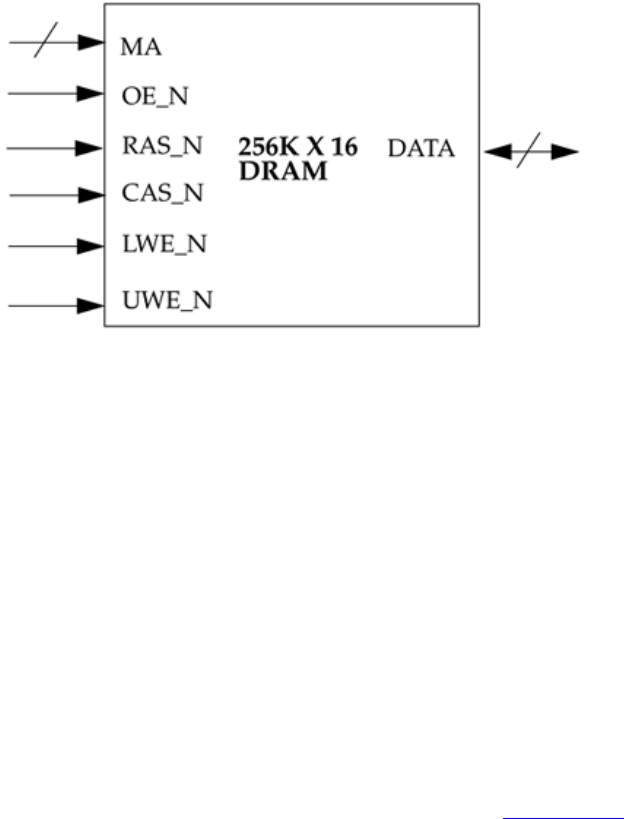
436
Figure F-2. DRAM Input/Output Ports
Input ports
All ports with a suffix "N" are low-asserted.
MA — 10-bit memory address
OE_N — Output enable for reading data
RAS_N — Row address strobe for asserting row address
CAS_N — Column address strobe for asserting column address
LWE_N — Lower write enable to write lower 8 bits of DATA into memory
UWE_N — Upper write enable to write upper 8 bits of DATA into memory
Inout ports
DATA — 16-bit data as input or output. Write input if LWE_N
or UWE_N is asserted. Read output if OE_N is asserted.
The Verilog HDL code for the DRAM implementation is shown in Example F-2.
Example F-2 Behavioral DRAM Model
////////////////////////////////////////////////////////////////////
// FileName: "dram.v" - functional model of a 256K x 16 DRAM
// Author : Venkata Ramana Kalapatapu
// Company : Sand Microelectronics Inc.(now a part of Synopsys, Inc.)
// Profile : Sand develops Simulation Models, Synthesizable Cores, and
// Performance Analysis Tools for Processors, buses and
// memory products. Sand's products include models for
// industry-standard components and custom-developed
// models for specific simulation environments.
//
////////////////////////////////////////////////////////////////////
437
module DRAM( DATA,
MA,
RAS_N,
CAS_N,
LWE_N,
UWE_N,
OE_N);
inout [15:0] DATA;
input [9:0] MA;
input RAS_N;
input CAS_N;
input LWE_N;
input UWE_N;
input OE_N;
reg [15:0] memblk [0:262143]; // Memory Block. 256K x 16.
reg [9:0] rowadd; // RowAddress Upper 10 bits of MA.
reg [7:0] coladd; // ColAddress Lower 8 bits of MA.
reg [15:0] rd_data; // Read Data.
reg [15:0] temp_reg;
reg hidden_ref;
reg last_lwe;
reg last_uwe;
reg cas_bef_ras_ref;
reg end_cas_bef_ras_ref;
reg last_cas;
reg read;
reg rmw;
reg output_disable_check;
integer page_mode;
assign #5 DATA=(OE_N===1'b0 && CAS_N===1'b0) ? rd_data : 16'bz;
parameter infile = "ini_file"; // Input file for preloading the
Dram.
initial
begin
$readmemh(infile, memblk);
end
always @(RAS_N)
begin
if(RAS_N == 1'b0 ) begin
if(CAS_N == 1'b1 ) begin
rowadd = MA;
end
else
hidden_ref = 1'b1;
end
else
hidden_ref = 1'b0;
end
438
always @(CAS_N)
#1 last_cas = CAS_N;
always @(CAS_N or LWE_N or UWE_N)
begin
if(RAS_N===1'b0 && CAS_N===1'b0 ) begin
if(last_cas==1'b1)
coladd = MA[7:0];
if(LWE_N!==1'b0 && UWE_N!==1'b0) begin // Read Cycle.
rd_data = memblk[{rowadd, coladd}];
$display("READ : address = %b, Data = %b",
{rowadd,coladd}, rd_data );
end
else if(LWE_N===1'b0 && UWE_N===1'b0) begin
// Write Cycle both
bytes.
memblk[{rowadd,coladd}] = DATA;
$display("WRITE: address = %b, Data = %b",
{rowadd,coladd}, DATA );
end
else if(LWE_N===1'b0 && UWE_N===1'b1) begin
// Lower Byte Write
Cycle.
temp_reg = memblk[{rowadd, coladd}];
temp_reg[7:0] = DATA[7:0];
memblk[{rowadd,coladd}] = temp_reg;
end
else if(LWE_N===1'b1 && UWE_N===1'b0) begin
// Upper Byte Write
Cycle.
temp_reg = memblk[{rowadd, coladd}];
temp_reg[15:8] = DATA[15:8];
memblk[{rowadd,coladd}] = temp_reg;
end
end
end
// Refresh.
always @(CAS_N or RAS_N)
begin
if(CAS_N==1'b0 && last_cas===1'b1 && RAS_N===1'b1) begin
cas_bef_ras_ref = 1'b1;
end
if(CAS_N===1'b1 && RAS_N===1'b1 && cas_bef_ras_ref==1'b1) begin
end_cas_bef_ras_ref = 1'b1;

439
cas_bef_ras_ref = 1'b0;
end
if( (CAS_N===1'b0 && RAS_N===1'b0) && end_cas_bef_ras_ref==1'b1
)
end_cas_bef_ras_ref = 1'b0;
end
endmodule

440
Bibliography
• Manuals
• Books
• Quick Reference Guides
Manuals
IEEE 1364-2001 Standard, IEEE Standard Verilog Hardware Description Language,
2001 (http://www.ieee.org).
Accellera Standard, System Verilog 3.0: Accellera's Extensions to Verilog, 2002.
(http://www.accellera.org).
Books
E. Sternheim, Rajvir Singh, Rajeev Madhavan, Yatin Trivedi, Digital Design and
Synthesis with Verilog HDL, Automata Publishing Company, 1993. ISBN 0-9627488-2-
X.
Donald Thomas and Phil Moorby, The Verilog Hardware Description Language, Fourth
Edition, Kluwer Academic Publishers, 1998. ISBN 0-7923-8166-1.
Stuart Sutherland, Verilog 2001?A Guide to the New Features of the Verilog Hardware
Description Language, Kluwer Academic Publishers, 2002. ISBN 0-7923-7568-8.
Stuart Sutherland, The Verilog Pli Handbook: A User's Guide and Comprehensive
Reference on the Verilog Programming Language Interface, Second Edition, Kluwer
Academic Publishers, 2002. ISBN: 0-7923-7658-7.
Douglas Smith, HDL Chip Design : A Practical Guide for Designing, Synthesizing and
Simulating ASICs and FPGAs Using VHDL or Verilog, Doone Publications, TX, 1996.
ISBN: 0-9651934-3-8.
Ben Cohen, Real Chip Design and Verification Using Verilog and VHDL, VhdlCohen
Publishing, 2001. ISBN 0-9705394-2-8.

441
J. Bhasker, Verilog HDL Synthesis: A Practical Primer, Star Galaxy Publishing, 1998.
ISBN 0-9650391-5-3.
J. Bhasker, A Verilog HDL Primer, Star Galaxy Publishing, 1999. ISBN 0-9650391-7-X.
James M. Lee, Verilog Quickstart, Kluwer Academic Publishers, 1997. ISBN 0-7923992-
7-7.
Bob Zeidman, Verilog Designer's Library, Prentice Hall, 1999. ISBN 0-1308115-4-8.
Michael D. Ciletti, Modeling, Synthesis, and Rapid Prototyping with the Verilog HDL,
Prentice Hall, 1999. ISBN 0-1397-7398-3.
Janick Bergeron, Writing Testbenches: Functional Verification of HDL Models, Kluwer
Academic Publishers, 2000. ISBN 0-7923-7766-4.
Lionel Bening and Harry Foster, Principles of Verifiable RTL Design, Second Edition,
Kluwer Academic Publishers, 2001. ISBN: 0-7923-7368-5.
Quick Reference Guides
Stuart Sutherland, Verilog HDL Quick Reference Guide, Sutherland Consulting, OR,
2001. ISBN: 1-930368-03-8.
Rajeev Madhavan, Verilog HDL Reference Guide, Automata Publishing Company, CA,
1993. ISBN 0-9627488-4-6.
Stuart Sutherland, Verilog PLI Quick Reference Guide, Sutherland Consulting, OR,
2001. ISBN: 1-930368-02-X.

442
About the CD-ROM
• Using the CD-ROM
• Technical Support
Using the CD-ROM
The CD that accompanies this book contains a demonstration version of the SILOS 2001
Verilog HDL Toolbox for Microsoft Windows (98/98SE/ME/NT/2000/XP). To run it,
please follow these instructions?
1. Insert CD into CD-ROM drive.
2. Run D:\SETUP.EXE (where D: is the letter of your CD drive).
3. Copy D:\VERILOG_BOOK_EXAMPLES directory to hard drive and make the
folder writable.
4. See D:\README.TXT for further instructions.
If you are a Unix user, please do the following?
1. Go to http://authors.phptr.com/palnitkar/.
2. Binary.
3. Get file VERILOG_BOOK_EXAMPLES.tar.
4. Get file README.txt.
5. Tar xvf VERILOG_BOOK_EXAMPLES.tar.
6. See README.txt for details.
Technical Support
Prentice Hall does not offer technical support for the material on the CD-ROM. If you
have any problems with the Verilog simulator, please visit http://www.simucad.com/. If
the CD is physically damaged, you may ontain a replacement copy by sending an email
to disc_exchange@prenhall.com.
