Zynq UltraScale+ MPSoC Product Tables And Selection Guide Ultrascale Plus
User Manual:
Open the PDF directly: View PDF ![]() .
.
Page Count: 16
© Copyright 2016–2017 Xilinx
.
© Copyright 2016–2017 Xilinx
.
Page 2
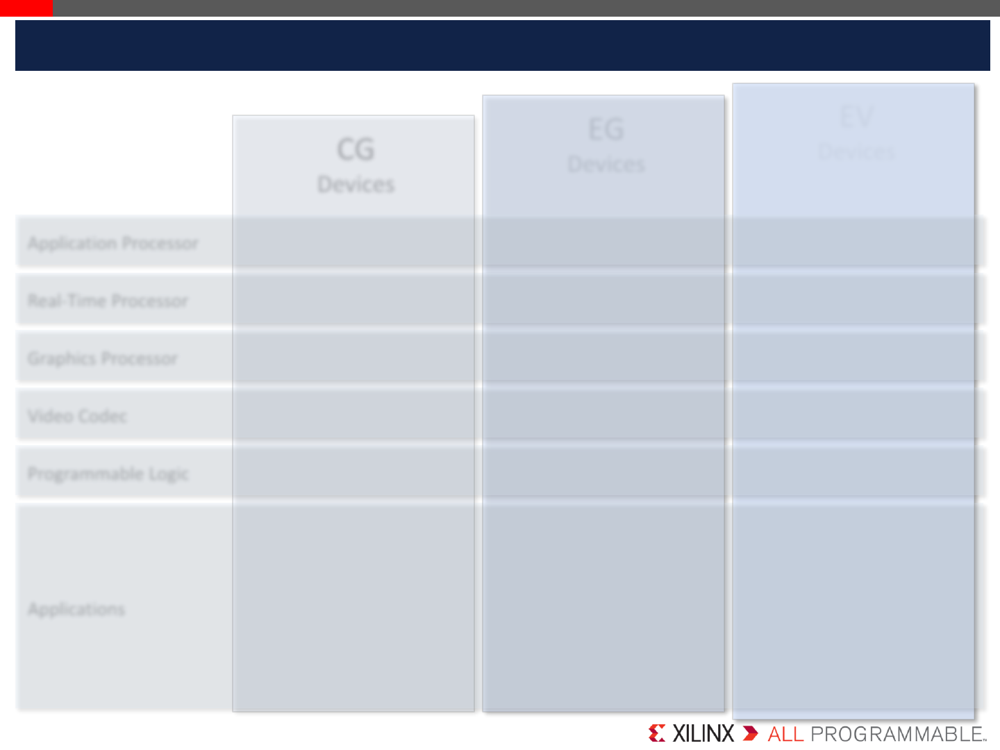
CG
Devices
EG
Devices
EV
Devices
Application Processor
Zynq® UltraScale+™ MPSoCs
Dual-core ARM® Cortex™-A53
MPCore™ up to 1.3GHz
Real-Time Processor
Graphics Processor
Video Codec
Programmable Logic
Dual-core ARM Cortex-R5
MPCore up to 533MHz
103K–600K System Logic Cells
Applications
Quad-core ARM Cortex-A53
MPCore up to 1.5GHz
Dual-core ARM Cortex-R5
MPCore up to 600MHz
103K–1143K System Logic Cells
Mali™-400 MP2
Quad-core ARM Cortex-A53
MPCore up to 1.5GHz
Dual-core ARM Cortex-R5
MPCore up to 600MHz
192K–504K System Logic Cells
Mali™-400 MP2
H.264 / H.265
•Situational Awareness
•Surveillance/Reconnaissance
•Smart Vision
•Image Manipulation
•Graphic Overlay
•Human Machine Interface
•Automotive ADAS
•Video Processing
•Interactive Display
•Flight Navigation
•Missile & Munitions
•Military Construction
•Secure Solutions
•Networking
•Cloud Computing Security
•Data Center
•Machine Vision
•Medical Endoscopy
•Sensor Processing & Fusion
•Motor Control
•Low-cost Ultrasound
•Traffic Engineering
© Copyright 2016–2017 Xilinx
.
Page 3
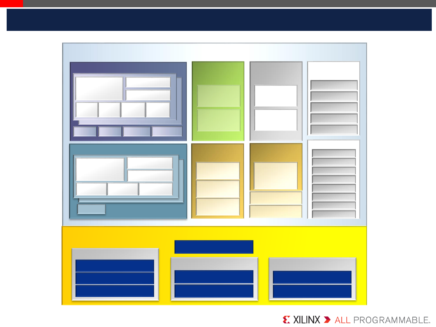
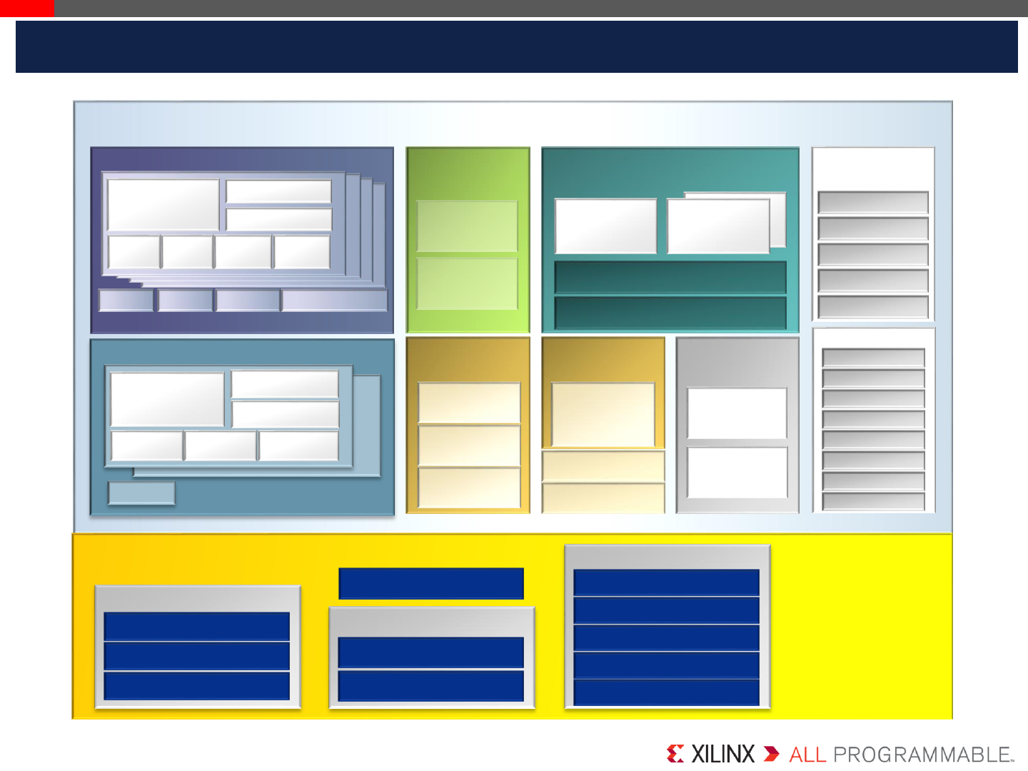
Zynq® UltraScale+™ MPSoCs: CG Block Diagram
Processing System
Programmable Logic
Memory
Platform
Management Unit
Configuration and
Security Unit
System
Management
Power
Management
Application Processing Unit
2
1
ARM®
Cortex™-A53
NEON™
32KB
I-Cache
w/Parity
Floating Point Unit
32KB
D-Cache
w/ECC
Memory
Management
Unit
Embedded
Trace
Macrocell
GIC-400 SCU 1MB L2 w/ECC
CCI/SMMU
Config AES
Decryption,
Authentication,
Secure Boot
Voltage/Temp
Monitor
High-Speed
Connectivity
DisplayPort v1.2a
USB 3.0
SATA 3.1
PCIe® 1.0 / 2.0
PS-GTR
General Connectivity
DDR4/3/3L,
LPDDR4/3
32/64-Bit w/ ECC
256KB OCM
with ECC
Real-Time Processing Unit
2
1
ARM
Cortex™-R5
Vector Floating
Point Unit
128KB
TCM w/ECC
32KB I-Cache
w/ECC
32KB D-Cache
w/ECC
GIC
Memory Protection
Unit
Functional
Safety TrustZone
GigE
CAN
UART
SPI
Quad SPI NOR
NAND
SD/eMMC
USB 2.0
System
Functions
Timers,
WDT, Resets,
Clocking & Debug
Multichannel DMA
Storage & Signal Processing
Block RAM
UltraRAM
DSP
General-Purpose I/O
High-Performance HP I/O
High-Density HD I/O
High-Speed Connectivity
GTH
PCIe Gen4
System Monitor
© Copyright 2016–2017 Xilinx
.
Page 4
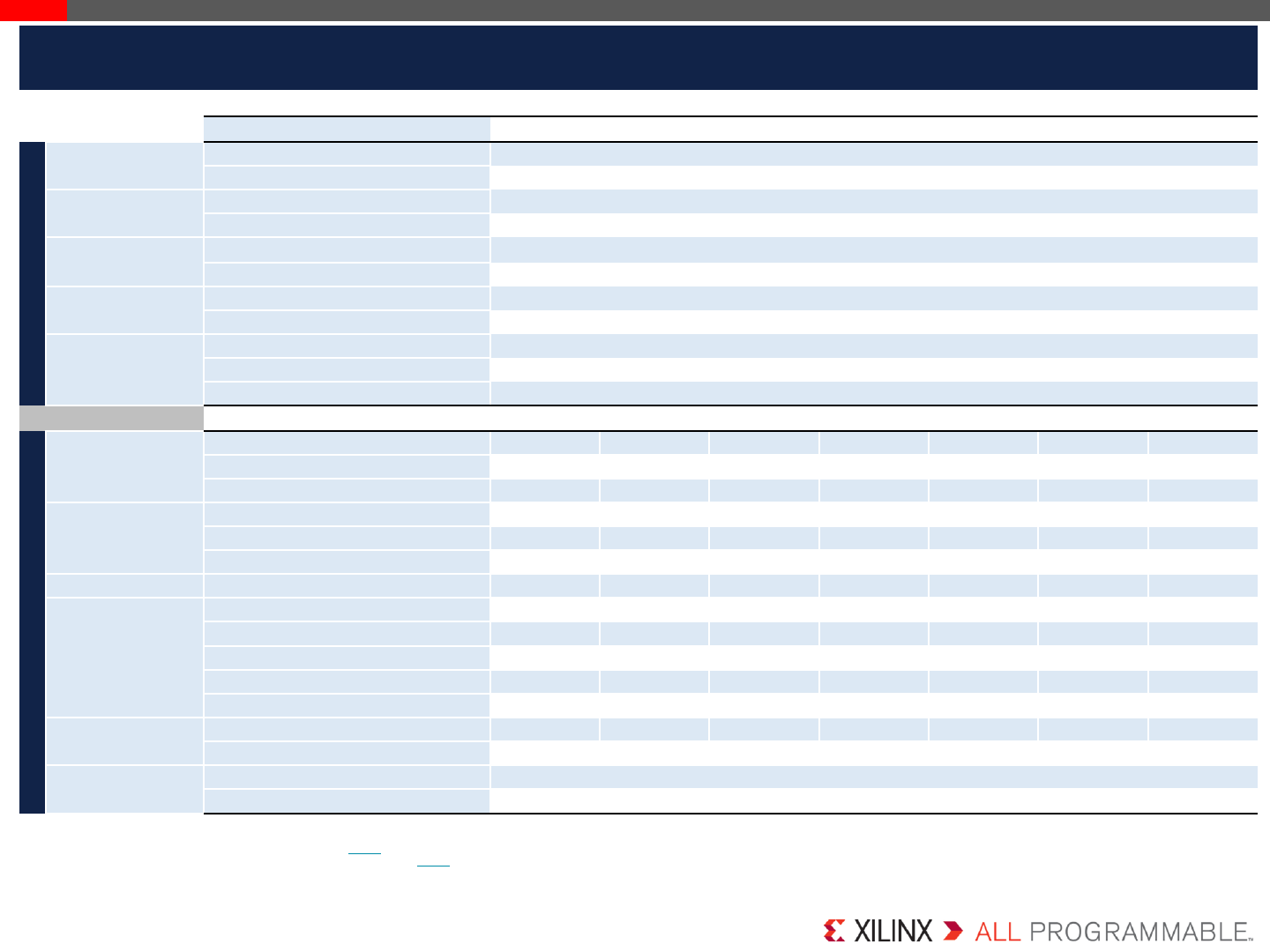
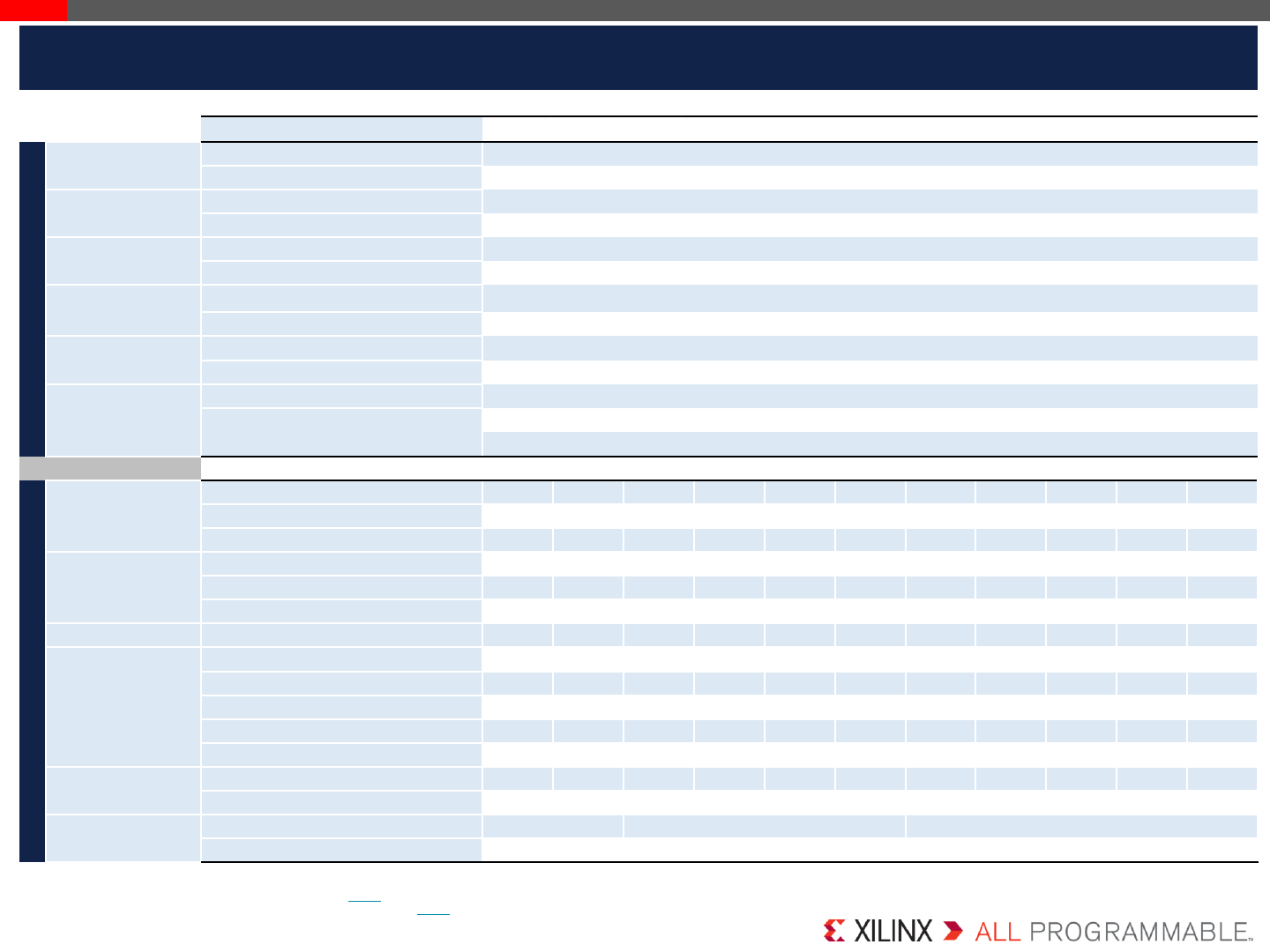
Zynq® UltraScale+™ MPSoCs: CG Devices
Device Name
(1)
ZU2CG ZU3CG ZU4CG ZU5CG ZU6CG ZU7CG ZU9CG
Processing System (PS)
Application
Processor Unit
Processor Core
Dual-core ARM® Cortex™-A53 MPCore™ up to 1.3GHz
Memory w/ECC
L1 Cache 32KB I / D per core, L2 Cache 1MB, on-chip Memory 256KB
Real
-Time
Processor Unit
Processor Core
Dual-core ARM Cortex-R5 MPCore up to 533MHz
Memory w/ECC
L1 Cache 32KB I / D per core, Tightly Coupled Memory 128KB per core
External
Memory Dynamic
Memory Interface
x32/x64: DDR4, LPDDR4, DDR3, DDR3L, LPDDR3 with ECC
Static
Memory Interfaces
NAND, 2x Quad-SPI
Connectivity
High-
Speed Connectivity
PCIe® Gen2 x4, 2x USB3.0, SATA 3.1, DisplayPort, 4x Tri-mode Gigabit Ethernet
General Connectivity
2xUSB 2.0, 2x SD/SDIO, 2x UART, 2x CAN 2.0B, 2x I2C, 2x SPI, 4x 32b GPIO
Integrated Block
Functionality
Power Management
Full / Low / PL / Battery Power Domains
Security
RSA, AES, and SHA
AMS -
System Monitor
10-bit, 1MSPS –Temperature and Voltage Monitor
PS to PL
Interface 12 x 32/64/128b AXI Ports
Programmable Logic (PL)
Programmable
Functionality
System Logic Cells (
K)
103 154 192 256 469 504 600
CLB Flip-Flops
(K)
94 141 176 234 429 461 548
CLB LUTs (K)
47 71 88 117 215 230 274
Memory
Max. Distributed
RAM (Mb)
1.2 1.8 2.6 3.5 6.9 6.2 8.8
Total Block
RAM (Mb)
5.3 7.6 4.5 5.1 25.1 11.0 32.1
UltraRAM (Mb)
- - 13.5 18.0 - 27.0 -
Clocking
Clock
Management Tiles (CMTs)
3344484
Integrated
IP
DSP Slices
240 360 728 1,248 1,973 1,728 2,520
PCI Express® Gen
3x16 / Gen4x8
- - 2 2 - 2 -
150G Interlaken
-------
100G Ethernet MAC/PCS
w/RS-
FEC
-------
AMS - System
Monitor
1111111
Transceivers
GTH 16.3Gb/s Transceivers
- - 16 16 24 24 24
GTY 32.75Gb/s Transceivers
-------
Speed Grades
Extended
(2)
-1 -2 -2L
Industrial
-1 -1L -2
Notes:
1. For full part number details, see the Ordering Information section in DS891, Zynq UltraScale+ MPSoC Overview.
2.-2LE (Tj = 0°C to 110°C). For more details, see the Ordering Information section in DS891, Zynq UltraScale+ MPSoC Overview.
© Copyright 2016–2017 Xilinx
.
Page 5
Processing System
Programmable Logic
Memory
Platform
Management Unit
Configuration and
Security Unit
System
Management
Power
Management
System
Functions
Application Processing Unit
3
2
1
ARM®
Cortex™-A53
NEON™
32KB
I-Cache
w/Parity
Floating Point Unit
32KB
D-Cache
w/ECC
Memory
Management
Unit
Embedded
Trace
Macrocell
4
GIC-400 SCU 1MB L2 w/ECC
CCI/SMMU
Config AES
Decryption,
Authentication,
Secure Boot
Voltage/Temp
Monitor
Timers,
WDT, Resets,
Clocking & Debug
High-Speed
Connectivity
DisplayPort v1.2a
USB 3.0
SATA 3.1
PCIe® 1.0 / 2.0
PS-GTR
General Connectivity
DDR4/3/3L,
LPDDR4/3
32/64-Bit w/ECC
256KB OCM
with ECC
Real-Time Processing Unit
2
1
ARM
Cortex™-R5
Vector Floating
Point Unit
128KB
TCM w/ECC
32KB I-Cache
w/ECC
32KB D-Cache
w/ECC
GIC
Memory Protection
Unit
Graphics Processing Unit
ARM Mali™-400 MP2
Memory Management Unit
64KB L2 Cache
Geometry
Processor
Pixel
Processor
Pixel
Processor 12
Functional
Safety TrustZone
GigE
CAN
UART
SPI
Quad SPI NOR
NAND
SD/eMMC
USB 2.0
Multichannel DMA
High-Speed Connectivity
GTH
100G EMAC
GTY
PCIe Gen4
Interlaken
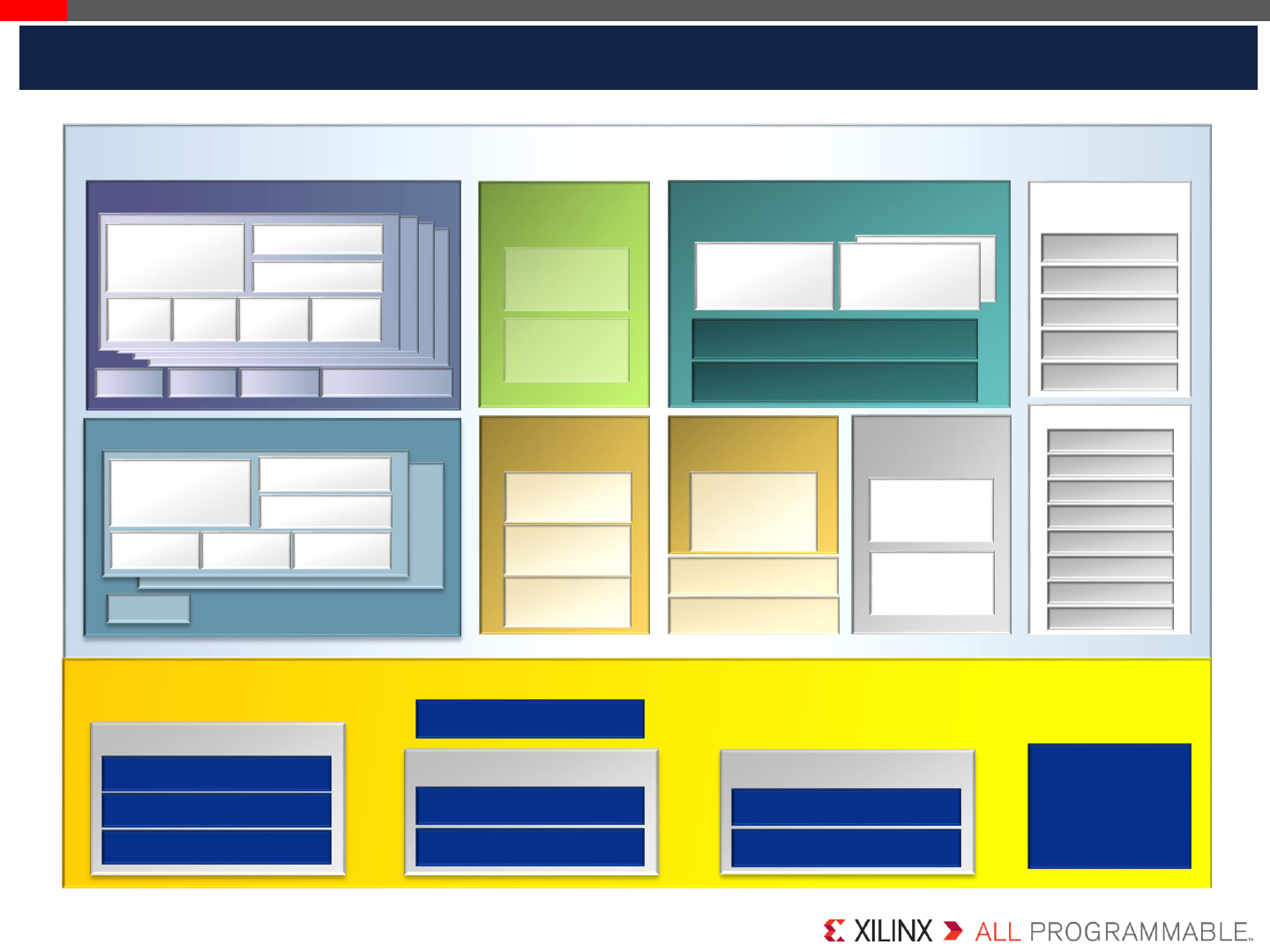
Zynq® UltraScale+™ MPSoCs: EG Block Diagram
Storage & Signal Processing
Block RAM
UltraRAM
DSP
General-Purpose I/O
High-Performance HP I/O
High-Density HD I/O
System Monitor
© Copyright 2016–2017 Xilinx
.
Page 6
Zynq® UltraScale+™ MPSoCs: EG Devices
Notes:
1. For full part number details, see the Ordering Information section in DS891, Zynq UltraScale+ MPSoC Overview.
2.-2LE (Tj = 0°C to 110°C). For more details, see the Ordering Information section in DS891, Zynq UltraScale+ MPSoC Overview.
Device Name
(1)
ZU2EG
ZU3EG
ZU4EG
ZU5EG
ZU6EG
ZU7EG
ZU9EG
ZU11EG
ZU15EG
ZU17EG
ZU19EG
Processing System (PS)
Application
Processor Unit
Processor Core
Quad-core ARM® Cortex™-A53 MPCore™ up to 1.5GHz
Memory w/ECC
L1 Cache 32KB I / D per core, L2 Cache 1MB, on-chip Memory 256KB
Real
-Time
Processor Unit
Processor Core
Dual-core ARM Cortex-R5 MPCore™ up to 600MHz
Memory w/ECC
L1 Cache 32KB I / D per core, Tightly Coupled Memory 128KB per core
Graphic & Video
Acceleration
Graphics Processing
Unit
Mali™-400 MP2 up to 667MHz
Memory
L2 Cache 64KB
External
Memory Dynamic
Memory Interface
x32/x64: DDR4, LPDDR4, DDR3, DDR3L, LPDDR3 with ECC
Static
Memory Interfaces
NAND, 2x Quad-SPI
Connectivity
High-
Speed Connectivity
PCIe® Gen2 x4, 2x USB3.0, SATA 3.1, DisplayPort, 4x Tri-mode Gigabit Ethernet
General Connectivity
2xUSB 2.0, 2x SD/SDIO, 2x UART, 2x CAN 2.0B, 2x I2C, 2x SPI, 4x 32b GPIO
Integrated Block
Functionality
Power Management
Full / Low / PL / Battery Power Domains
Security
AMS -
System Monitor
RSA, AES, and SHA
10-bit, 1MSPS –Temperature and Voltage Monitor
PS to PL
Interface 12 x 32/64/128b AXI Ports
Programmable Logic (PL)
Programmable
Functionality
System Logic Cells (
K)
103 154 192 256 469 504 600 653 747 926 1,143
CLB Flip-Flops
(K)
94 141 176 234 429 461 548 597 682 847 1,045
CLB LUTs (K)
47 71 88 117 215 230 274 299 341 423 523
Memory
Max. Distributed
RAM (Mb)
1.2 1.8 2.6 3.5 6.9 6.2 8.8 9.1 11.3 8.0 9.8
Total Block
RAM (Mb)
5.3 7.6 4.5 5.1 25.1 11.0 32.1 21.1 26.2 28.0 34.6
UltraRAM (Mb)
- - 13.5 18.0 - 27.0 - 22.5 31.5 28.7 36.0
Clocking
Clock
Management Tiles (CMTs)
3 3 4 4 4 8 4 8 4 11 11
Integrated
IP
DSP Slices
240 360 728 1,248 1,973 1,728 2,520 2,928 3,528 1,590 1,968
PCI Express® Gen
3x16 / Gen4x8
- - 2 2 - 2 - 4 - 4 5
150G Interlaken
- - - - - - - 1 - 2 4
100G Ethernet MAC/PCS
w/RS-
FEC
- - - - - - - 2 - 2 4
AMS - System
Monitor
1 1 1 1 1 1 1 1 1 1 1
Transceivers
GTH 16.3Gb/s Transceivers
- - 16 16 24 24 24 32 24 44 44
GTY 32.75Gb/s Transceivers
- - - - - - - 16 -28 28
Speed Grades
Extended
(2)
-1 -2 -2L -1 -2 -2L -3 -1 -2 -2L -3
Industrial
-1 -1L -2
© Copyright 2016–2017 Xilinx
.
Page 7
Processing System
Programmable Logic
Memory
Platform
Management Unit
Configuration and
Security Unit
System
Management
Power
Management
System
Functions
Application Processing Unit
3
2
1
ARM®
Cortex™-A53
NEON™
32KB
I-Cache
w/Parity
Floating Point Unit
32KB
D-Cache
w/ECC
Memory
Management
Unit
Embedded
Trace
Macrocell
4
GIC-400 SCU 1MB L2 w/ECC
CCI/SMMU
Config AES
Decryption,
Authentication,
Secure Boot
Voltage/Temp
Monitor
Timers,
WDT, Resets,
Clocking & Debug
High-Speed
Connectivity
DisplayPort v1.2a
USB 3.0
SATA 3.1
PCIe® 1.0 / 2.0
PS-GTR
General Connectivity
DDR4/3/3L,
LPDDR4/3
32/64 bit w/ECC
256KB OCM
with ECC
Real-Time Processing Unit
2
1
ARM
Cortex™-R5
Vector Floating
Point Unit
128KB
TCM w/ECC
32KB I-Cache
w/ECC
32KB D-Cache
w/ECC
GIC
Memory Protection
Unit
Graphics Processing Unit
ARM Mali™-400 MP2
Memory Management Unit
64KB L2 Cache
Geometry
Processor
Pixel
Processor
Pixel
Processor 12
Functional
Safety TrustZone
GigE
CAN
UART
SPI
Quad SPI NOR
NAND
SD/eMMC
USB 2.0
Multichannel DMA
Video Codec
H.265/H.264
Zynq® UltraScale+™ MPSoCs: EV Block Diagram
Storage & Signal Processing
Block RAM
UltraRAM
DSP
General-Purpose I/O
High-Performance HP I/O
High-Density HD I/O
High-Speed Connectivity
GTH
PCIe Gen4
System Monitor

© Copyright 2016–2017 Xilinx
.
Page 8
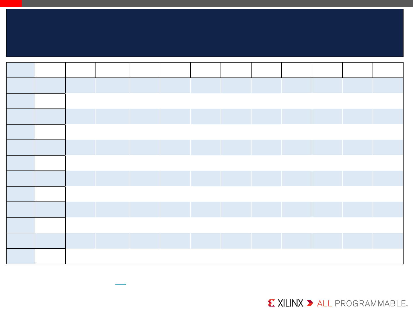
Zynq® UltraScale+™ MPSoCs: EV Devices
Notes:
1. For full part number details, see the Ordering Information section in DS891, Zynq UltraScale+ MPSoC Overview.
2.-2LE (Tj = 0°C to 110°C). For more details, see the Ordering Information section in DS891, Zynq UltraScale+ MPSoC Overview.
Device Name
(1)
ZU4EV ZU5EV ZU7EV
Processing System (PS)
Application
Processor Unit
Processor Core
Quad-core ARM® Cortex™-A53 MPCore™ up to 1.5GHz
Memory w/ECC
L1 Cache 32KB I / D per core, L2 Cache 1MB, on-chip Memory 256KB
Real
-Time
Processor Unit
Processor Core
Dual-core ARM Cortex-R5 MPCore™ up to 600MHz
Memory w/ECC
L1 Cache 32KB I / D per core, Tightly Coupled Memory 128KB per core
Graphic & Video
Acceleration
Graphics Processing
Unit
Mali™-400 MP2 up to 667MHz
Memory
L2 Cache 64KB
External
Memory Dynamic
Memory Interface
x32/x64: DDR4, LPDDR4, DDR3, DDR3L, LPDDR3 with ECC
Static
Memory Interfaces
NAND, 2x Quad-SPI
Connectivity
High-
Speed Connectivity
PCIe® Gen2 x4, 2x USB3.0, SATA 3.1, DisplayPort, 4x Tri-mode Gigabit Ethernet
General Connectivity
2xUSB 2.0, 2x SD/SDIO, 2x UART, 2x CAN 2.0B, 2x I2C, 2x SPI, 4x 32b GPIO
Integrated Block
Functionality
Power Management
Full / Low / PL / Battery Power Domains
Security
AMS -
System Monitor
RSA, AES, and SHA
10-bit, 1MSPS –Temperature and Voltage Monitor
PS to PL
Interface 12 x 32/64/128b AXI Ports
Programmable Logic (PL)
Programmable
Functionality
System Logic Cells (
K)
192 256 504
CLB Flip-Flops
(K)
176 234 461
CLB LUTs (K)
88 117 230
Memory
Max. Distributed
RAM (Mb)
2.6 3.5 6.2
Total Block
RAM (Mb)
4.5 5.1 11.0
UltraRAM (Mb)
13.5 18.0 27.0
Clocking
Clock
Management Tiles (CMTs)
4 4 8
Integrated
IP
DSP Slices
728 1,248 1,728
Video Codec Unit
(VCU)
1 1 1
PCI Express® Gen
3x16 / Gen4x8
2 2 2
150G Interlaken
- - -
100G Ethernet MAC/PCS
w/RS-
FEC
- - -
AMS - System
Monitor
1 1 1
Transceivers
GTH 16.3Gb/s Transceivers
16 16 24
GTY 32.75Gb/s Transceivers
- - -
Speed Grades
Extended
(2)
-1 -2 -2L -3
Industrial
-1 -1L -2
© Copyright 2016–2017 Xilinx
.
Notes:
1. PS I/O is a combination of PS MIO and PS DDRIO.
2. Packages with the same last letter and number sequence, e.g., A484, are footprint compatible with all other UltraScale devices with the same sequence.
3. For full part number details, see the Ordering Information section in DS891, Zynq UltraScale+ MPSoC Overview.
4. These packages are only offered in 0.8mm ballpitch. All other packages are offered in 1.0mm ball pitch.
5. GTH transceivers in the C784 package support data rates up to 12.5Gb/s.
Zynq® UltraScale+™ MPSoCs
PS I/Os
(1), 3.3V High-Density (HD) I/O, 1.8V High-Performance (HP) I/Os
PS
-GTR 6Gb/s, GTH 16.3Gb/s, GTY 32.75Gb/s
Pkg
Footprint(2,3)
Dimensions
(mm) ZU2 ZU3 ZU4 ZU5 ZU6 ZU7 ZU9 ZU11 ZU15 ZU17 ZU19
A484
(4) 19x19 170, 24, 58
4, 0, 0
170, 24, 58
4, 0, 0
A625
(4) 21x21
170, 24, 156
4, 0, 0
170, 24, 156
4, 0, 0
C784
(4,5) 23x23
214, 96, 156
4, 0, 0
214, 96, 156
4, 0, 0
214, 96, 156
4, 4, 0
214, 96, 156
4, 4, 0
B900
31x31
214, 48, 156
4, 16, 0
214, 48, 156
4, 16, 0
214, 48, 156
4, 16, 0
C900
31x31
214, 48, 156
4, 16, 0
214, 48, 156
4, 16, 0
214, 48, 156
4, 16, 0
B1156
35x35
214, 120, 208
4, 24, 0
214, 120, 208
4, 24, 0
214, 120, 208
4, 24, 0
C1156
35x35
214, 48, 312
4, 20, 0
214, 48, 312
4, 20, 0
B1517
40x40
214, 72, 416
4, 16, 0
214, 72, 572
4, 16, 0
214, 72, 572
4, 16, 0
F1517
40x40
214, 48, 416
4, 24, 0
214, 48, 416
4, 32, 0
C1760
42.5x42.5
214, 96, 416
4, 32, 16
214, 96, 416
4, 32, 16
214, 96, 416
4, 32, 16
D1760
42.5x42.5
214
, 48
, 260
4, 44, 28
214, 48, 260
4, 44, 28
E1924
45x45
214
, 96
, 572
4, 44, 0
214, 96, 572
4, 44, 0
Page 9
Important: Verify all data in this document with the device data sheets found at www.xilinx.com
© Copyright 2016–2017 Xilinx
.
Page 10
Zynq® UltraScale+™
Pkg mm CG Devices EG Devices EV Devices
ZU2CG
ZU3CG
ZU4CG
ZU5CG
ZU6CG
ZU7CG
ZU9CG
ZU2EG
ZU3EG
ZU4EG
ZU5EG
ZU6EG
ZU7EG
ZU9EG
ZU11EG
ZU15EG
ZU17EG
ZU19EG
ZU4EV
ZU5EV
ZU7EV
A484 19 X X X X
A625 21 X X X X
C784 23 X X X X X X X X X
B900 31 X X xX X X X X X
C900 31 XXx X X
B1156 35 XXx X X
C1156 35 x x X X
B1517 40 X X X
F1517 40 x x X X
C1760 42.5 X X X
D1760 42.5 X X
E1924 45 X X
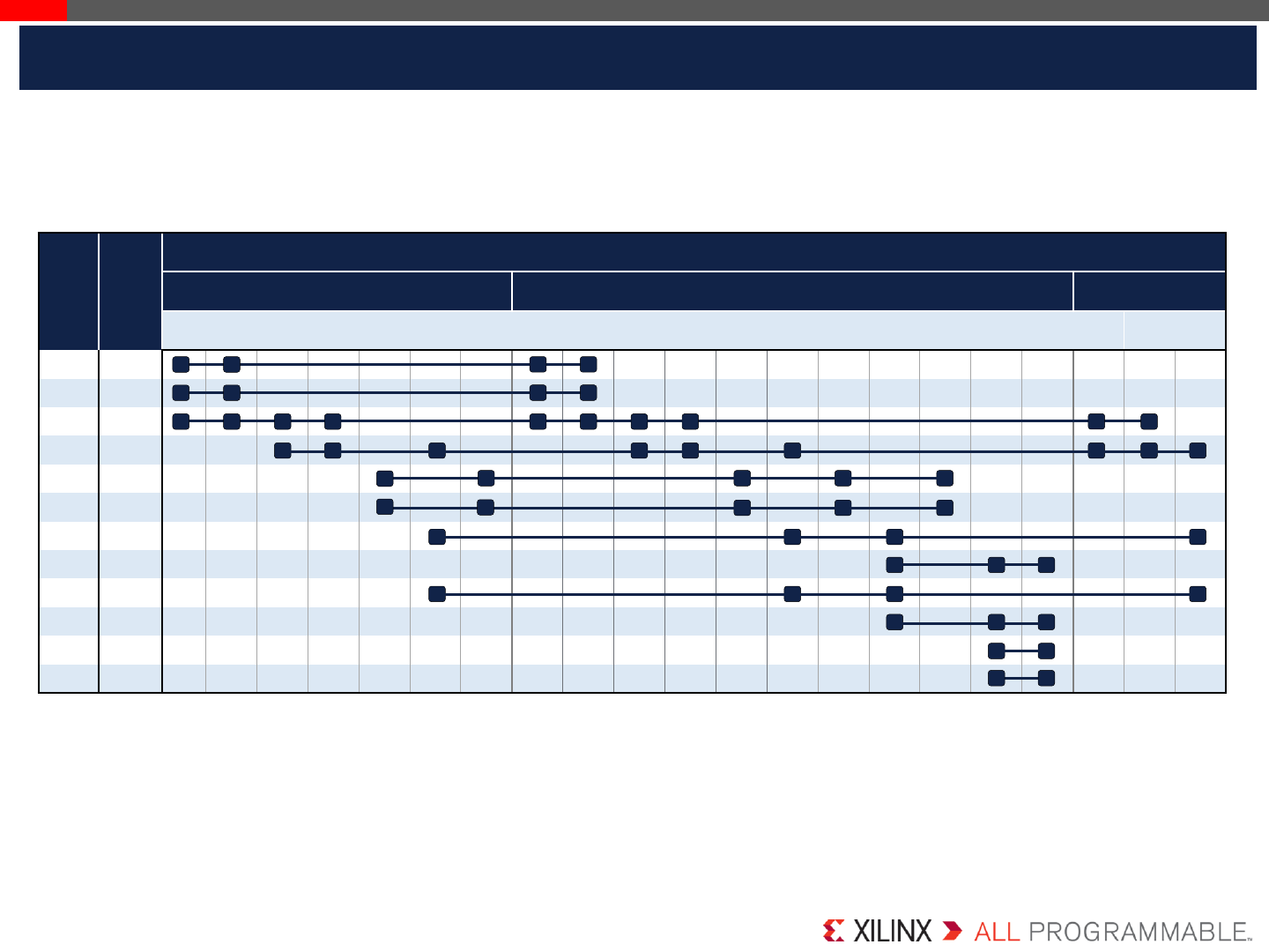
Zynq® UltraScale+™ MPSoC Device Migration Table
The Zynq UltraScale+ family provides footprint compatibility to enable users to migrate designs from one device to
another. Any two packages with the same footprint identifier code (last letter and number sequence) are footprint
compatible.
© Copyright 2016–2017 Xilinx
.
Page 11
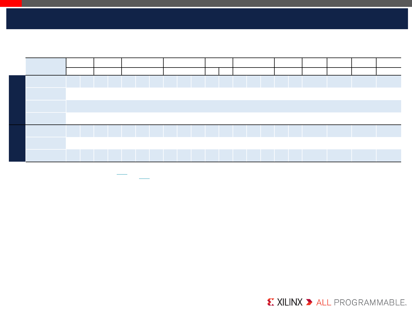
Zynq® UltraScale+™ MPSoC Speed Grades
Notes:
1. For full part number details, see the Ordering Information section in DS891, Zynq UltraScale+ MPSoC Overview.
2.-2LE (Tj = 0°C to 110°C). For more details, see the Ordering Information section in DS891, Zynq UltraScale+ MPSoC Overview.
:: available
–:: not offered
Device Name(1)
Speed Grade ZU2 ZU3 ZU4 ZU5 ZU6 ZU7 ZU9 ZU11 ZU15 ZU17 ZU19
CG
EG
CG
EG
CG
EG
EV
CG
EG
EV
CG
EG
CG
EG
EV
CG
EG
EG EG EG EG
Extended(2)
-1
-2
-2L
-3 ––––– – –– –
Industrial
-1
-1L
-2
© Copyright 2016–2017 Xilinx
.
Page 12
Zynq® UltraScale+™ MPSoC Ordering Information
E = Extended (Tj = 0°C to +100°C)
I = Industrial (Tj = –40°C to +100°C)
Note: -L2E (Tj = 0°C to +110°C). Refer to DS891, Zynq UltraScale+ MPSoC Overview for additional information.
Important: Verify all data in this document with the device data sheets found at www.xilinx.com
Xilinx
Commercial
Zynq
UltraScale +
F: Lid
B: Lidless
Value
Index
F: Flip-chip
w/ 1.0mm
Ball Pitch
S: Flip-chip
w/ 0.8mm
Ball Pitch
V: RoHS 6/6 Package
Designator
Speed Grade
-1: Slowest
-L1: Low Power
-2: Mid
-L2: Low Power
-3: Fastest
Footprint
Temperature
Grade
(E, I)
Package
Pin Count
XC ZU # -1 F F V A #E
Processor
System
Identifier
C: Dual APU
E: Quad APU
Dual RPU
Single GPU
E
Engine Type
G: General Purpose
V: Video
G
Dual RPU
© Copyright 2016–2017 Xilinx
.
Page 13
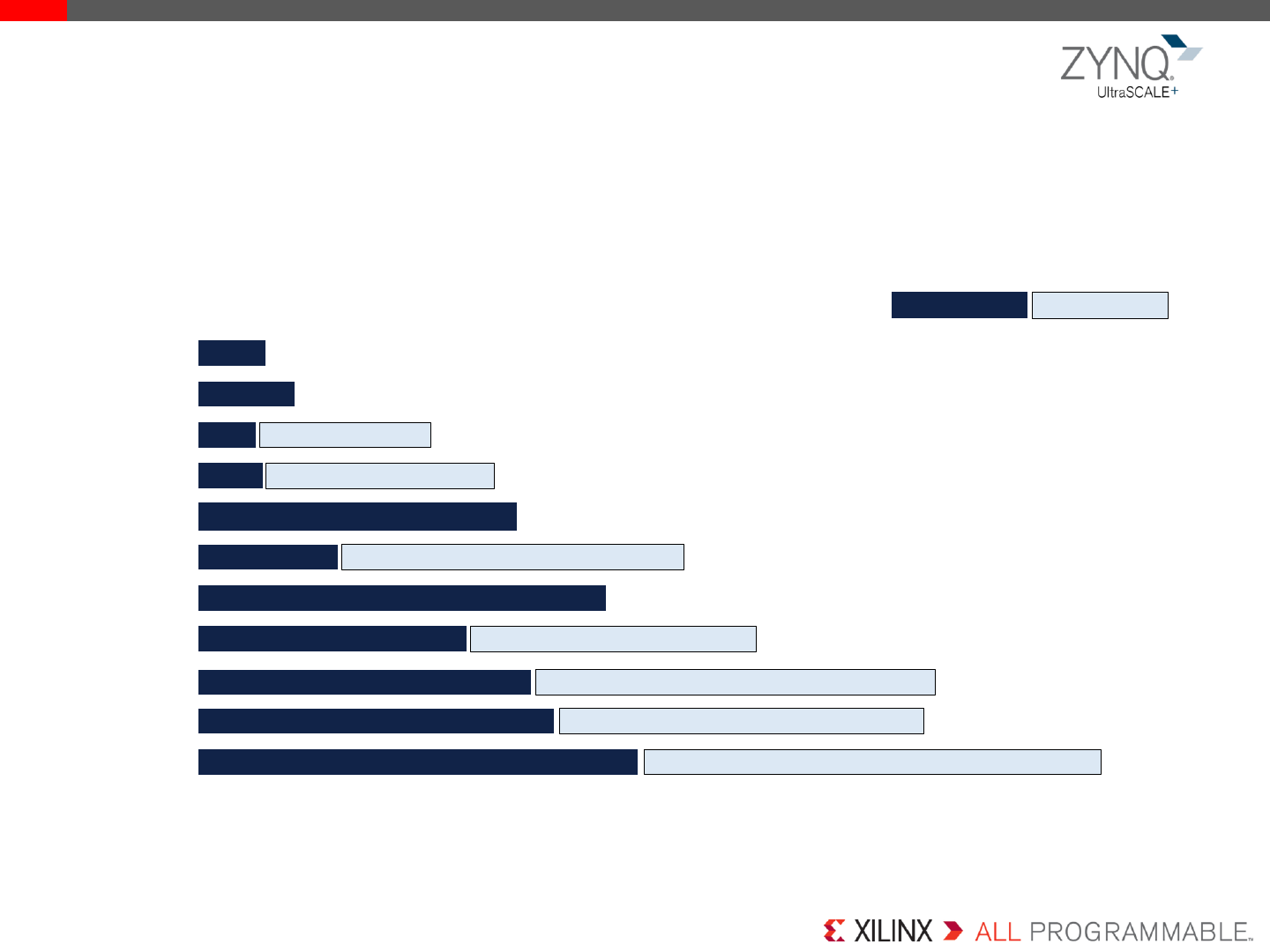
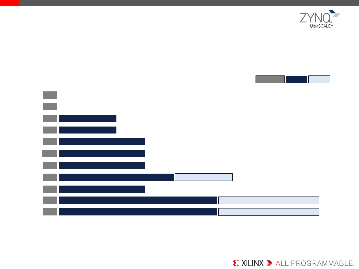
Memory
Zynq® UltraScale+™ MPSoCs include block RAM and UltraRAM (high density, dual-port, synchronous memory
block), which increase performance, device utilization, and power efficiency. These new features are designed to
provide highly efficient solutions for applications that require heterogeneous processing.
Important: Verify all data in this document with the device data sheets found at www.xilinx.com
5.3
ZU2
ZU19 34.6 36.0
ZU17 28.728.0
26.2
ZU15 31.5
ZU11 21.1 22.5
ZU9 32.1
ZU3 7.6
Total Memory (Mb) Block RAM UltraRAM
ZU6 25.1
11.0
ZU7 27.0
ZU4 4.5 13.5
ZU5 5.1 18.0
© Copyright 2016–2017 Xilinx
.
Page 14
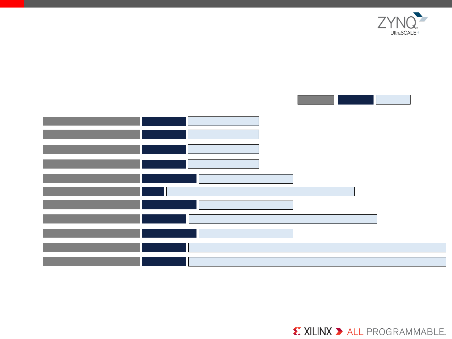
Transceiver Count and Bandwidth
UltraScale™ architecture serial transceivers include the proven on-chip circuits required to provide optimal signal
integrity in real world environments, at data rates up to 6.0Gb/s (PS-GTR), 16.3Gb/s (GTH), and 32.75Gb/s (GTY).
Important: Verify all data in this document with the device data sheets found at www.xilinx.com
Total Transceiver Count and Bandwidth GTH GTY
PS-GTR = 6.0Gb/s
GTH = 16.3Gb/s
GTY = 32.75Gb/s
4
ZU2
ZU3 4
PS-GTR
ZU4 416
ZU5 164
ZU6 244
16
ZU11 324
ZU17 28444
ZU9 244
ZU19 42844
24.0Gb/s
24.0Gb/s
224Gb/s
224Gb/s
ZU7 244415.2Gb/s
415.2Gb/s
415.2Gb/s
24
ZU15 4415.2Gb/s
1069.6Gb/s
1658.2Gb/s
1658.2Gb/s
© Copyright 2016–2017 Xilinx
.
I/O Count
Page 15
Important: Verify all data in this document with the device data sheets found at www.xilinx.com
I/O Counts
ZU5
ZU6
ZU4
ZU9
ZU3
ZU2
The I/Os are classified as PS I/O, high-density (HD) I/O, and high-performance (HP) I/O. The PS I/Os are composed
of multi-use I/O (MIO) and DDR I/O, which support 1.8V to 3.3V standards. The HD I/Os are reduced-feature I/Os,
providing voltage support from 1.2V to 3.3V. The HP I/Os are optimized for highest performance operation, from
1.0V to 1.8V.
416
ZU11
572
ZU19 96214
57296214
ZU17
96214
214
214
214
214
214
214
208
ZU15 214 120
208
120
208
120
ZU7 416
214 48
96 156
96 156
96 156
96 156
HD I/O HP I/O
PS I/O
Notes:
1. The PS I/O count is composed of 78 I/Os, which are used to communicate to external components, referred to as multi-use I/O (MIO) and an additional 136 I/Os, which are used to
communicate to DDRs, referred to as DDR I/O.

© Copyright 2016–2017 Xilinx
.
References
Page 16
Important: Verify all data in this document with the device data sheets found at www.xilinx.com
DS890,UltraScale™ Architecture and Product Overview
DS891, Zynq® UltraScale+™ MPSoC Overview
DS925, Zynq UltraScale+ MPSoC Data Sheet: DC and AC Switching Characteristics
UG1075, Zynq UltraScale+ MPSoC Packaging and Pinouts
UG1085, Zynq UltraScale+ MPSoC Technical Reference Manual
UG1087, Zynq UltraScale+ MPSoC Register Reference
UG1137, Zynq UltraScale+ MPSoC: Software Developers Guide
UG1169, Zynq UltraScale+ MPSoC QEMU: User Guide
UG1186, Zynq UltraScale+ MPSoC OpenAMP: Getting Started Guide
UG571,UltraScale Architecture SelectIO™ Resources User Guide
UG572,UltraScale Architecture Clocking Resources User Guide
UG573,UltraScale Architecture Memory Resources User Guide
UG574,UltraScale Architecture Configurable Logic Block User Guide
UG576, UltraScale Architecture GTH Transceivers User Guide
UG578, UltraScale Architecture GTY Transceivers User Guide
UG579, UltraScale Architecture DSP Slice User Guide
UG580, UltraScale Architecture System Monitor User Guide
UG583,UltraScale Architecture PCB and Pin Planning User Guide
PG150, LogiCORE™ IP UltraScale Architecture-Based FPGAs Memory Interface Solutions
PG182, UltraScale FPGAs Transceivers Wizard Product Guide XMP104 (v2.3)
