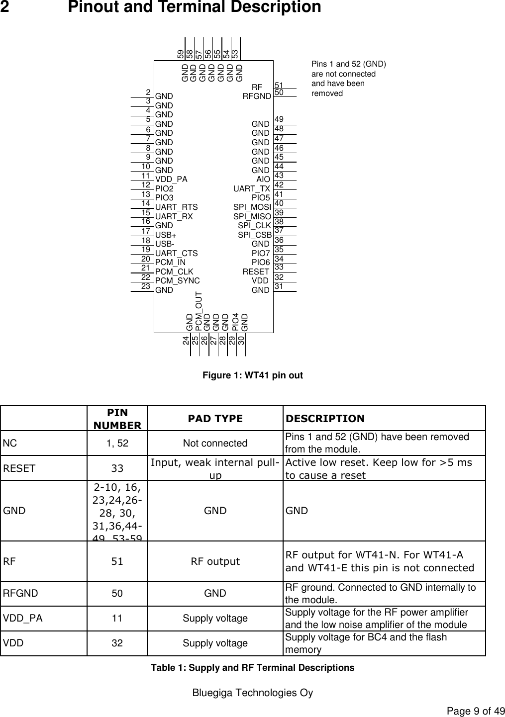
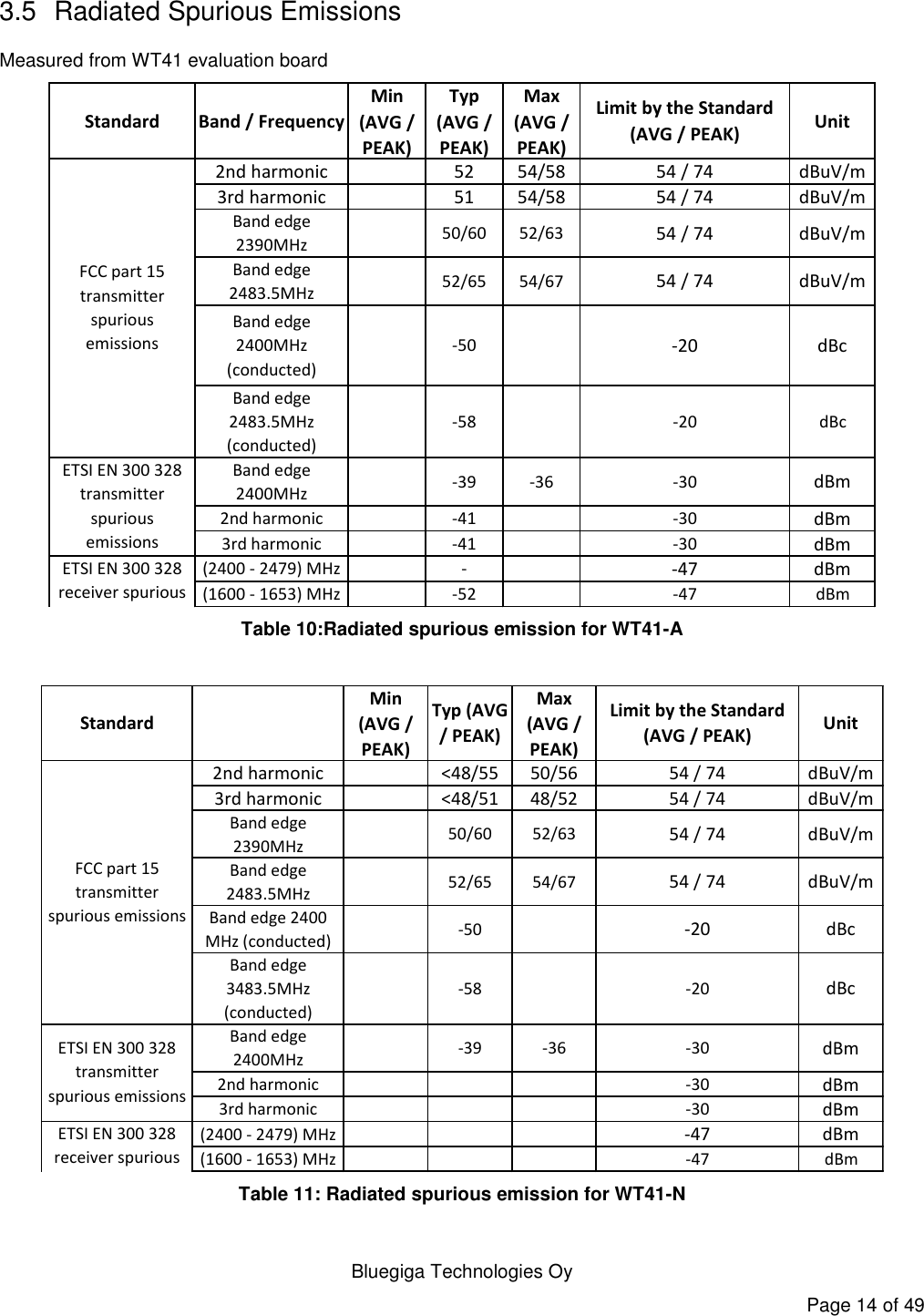
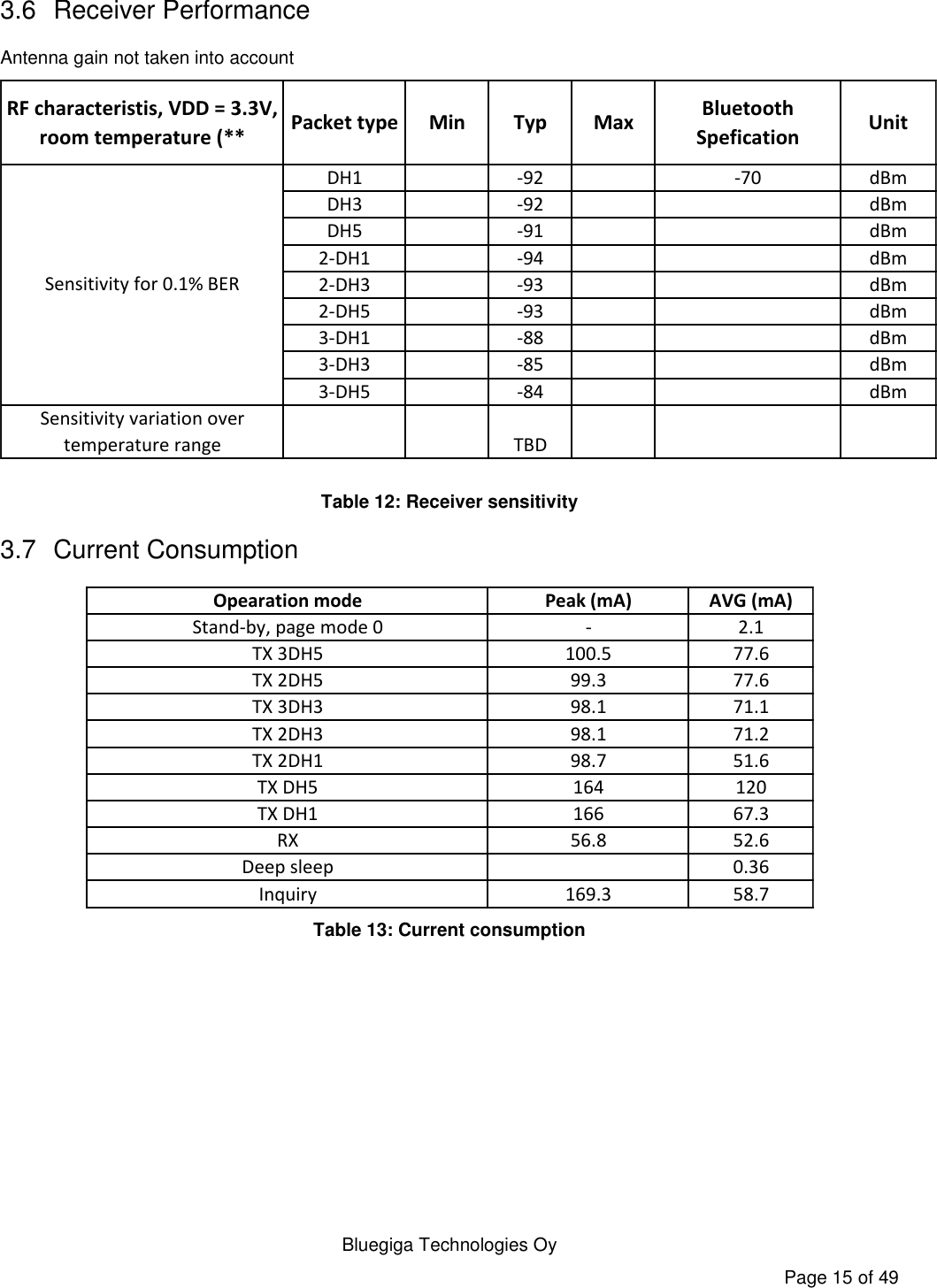
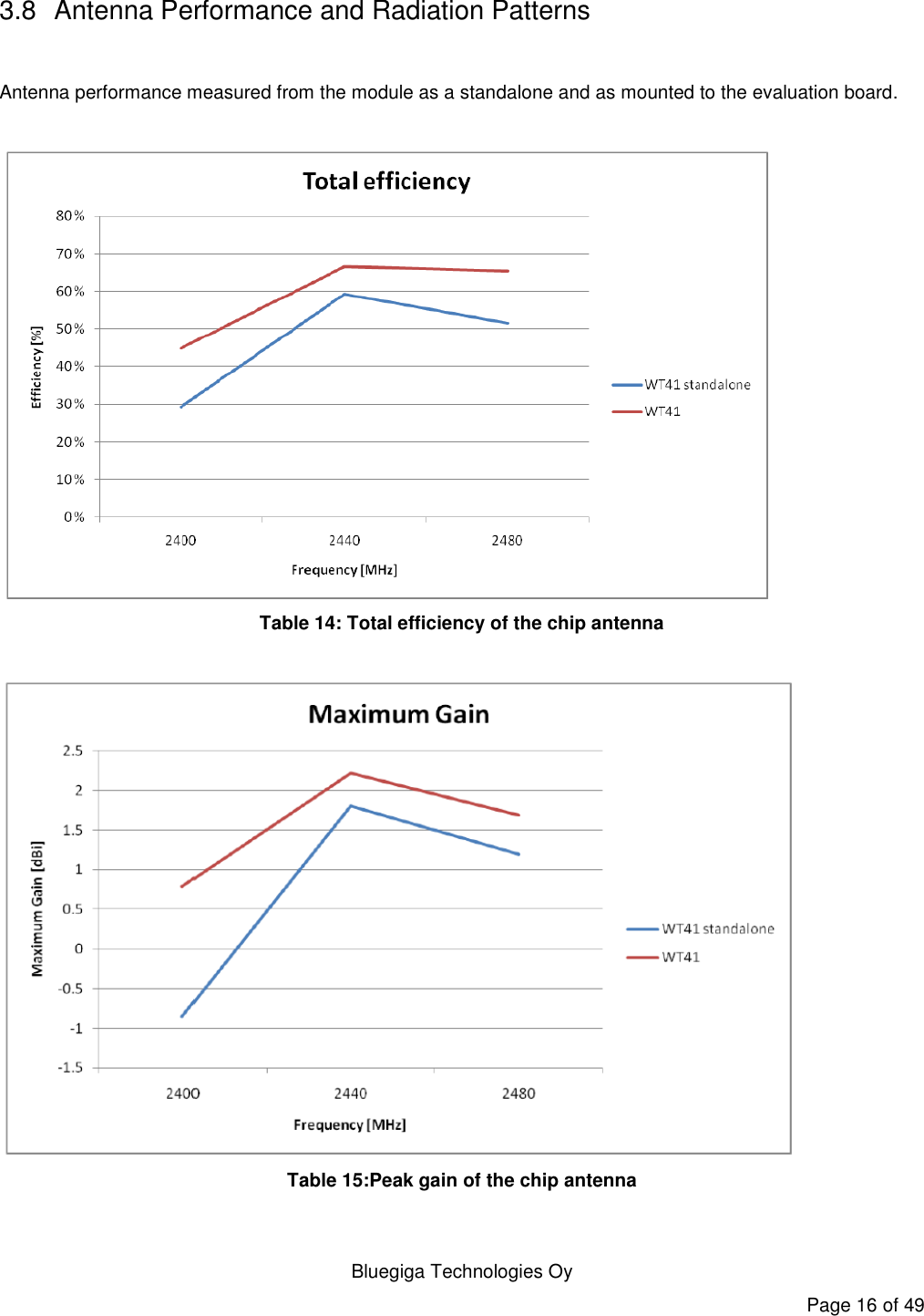
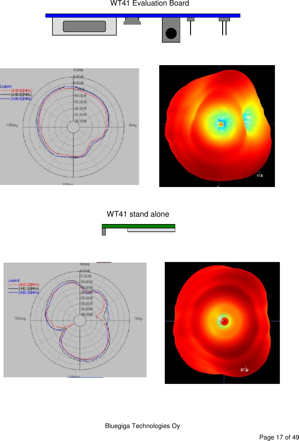
Druck ADTSTOUCH-01 ADTS Touch User Manual Bluetooth
Druck Ltd ADTS Touch Bluetooth
UserManual.wiki
>
Druck
>
ADTSTOUCH-01 User Manual
>
User Manual Bluetooth
Contents
1.
Users Manual
2.
User Manual Bluetooth
User Manual Bluetooth
Navigation menu
Upload a User Manual
Namespaces
Wiki Guide
HTML
PDF
Info
Views
User Manual
Discussion / Help
Navigation
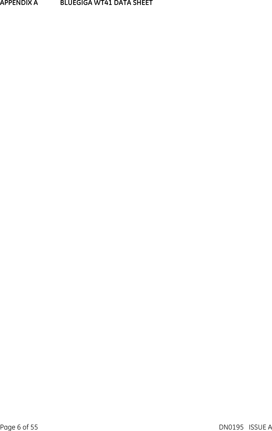

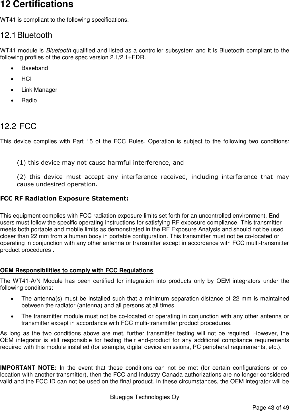
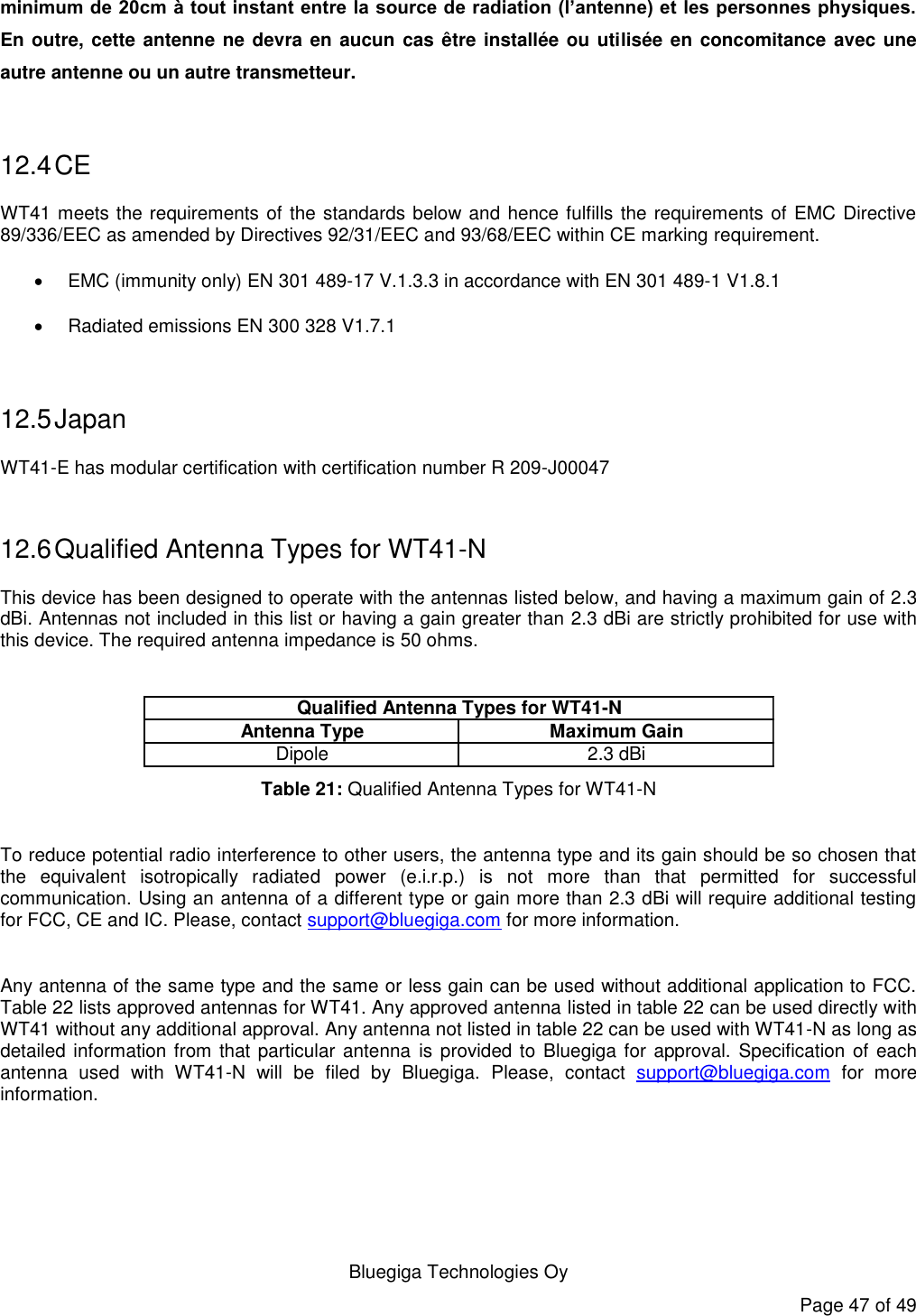
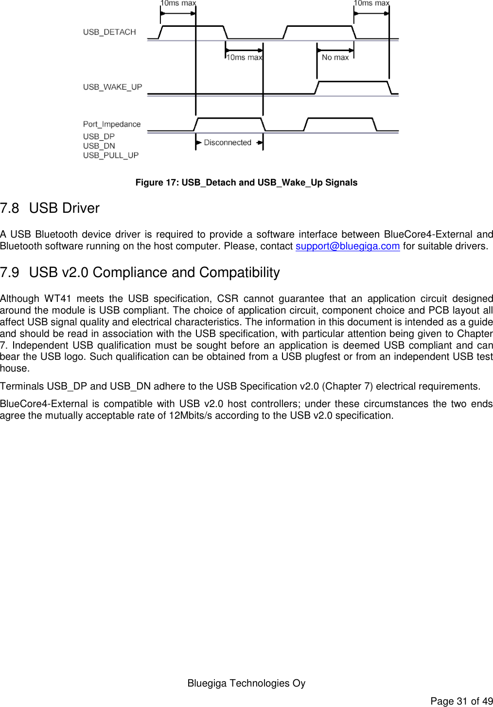
![Bluegiga Technologies Oy Page 10 of 49 PIO PORTPIN NUMBERPAD TYPE DESCRIPTIONPIO[2] 12Bi-directional, programmamble strength internal pull-down/pull-upProgrammamble input/output linePIO[3] 13Bi-directional, programmamble strength internal pull-down/pull-upProgrammamble input/output linePIO[4] 29Bi-directional, programmamble strength internal pull-down/pull-upProgrammamble input/output linePIO[5] 41Bi-directional, programmamble strength internal pull-down/pull-upProgrammamble input/output linePIO[6] 34Bi-directional, programmamble strength internal pull-down/pull-upProgrammamble input/output linePIO[7] 35Bi-directional, programmamble strength internal pull-down/pull-upProgrammamble input/output lineAIO[1] 43 Bi-directionalProgrammamble analog input/output line Table 2: GPIO Terminal Descriptions SPI INTERFACEPIN NUMBERPAD TYPE DESCRIPTIONPCM_OUT 25CMOS output, tri-state, weak internal pull-downSynchronous data outputPCM_IN 20CMOS input, weak internal pull-downSynchronous data inputPCM_SYNC 22Bi-directional, weak internal pull-downSynchronous data syncPCM_CLK 21Bi-directional, weak internal pull-downSynchronous data clock Table 3: PCM Terminal Descriptions UART InterfacesPIN NUMBERPAD TYPE DESCRIPTIONUART_TX 42CMOS output, tri-state, with weak internal pull-upUART data output, active highUART_RTS# 14CMOS output, tri-state, with weak internal pull-upUART request to send, active lowUART_RX 15CMOS input, tri-state, with weak internal pull-downUART data input, active highUART_CTS# 19CMOS input, tri-state, with weak internal pull-downUART clear to send, active low Table 4: UART Terminal Descriptions](https://usermanual.wiki/Druck/ADTSTOUCH-01.User-Manual-Bluetooth/User-Guide-2522022-Page-16.png)
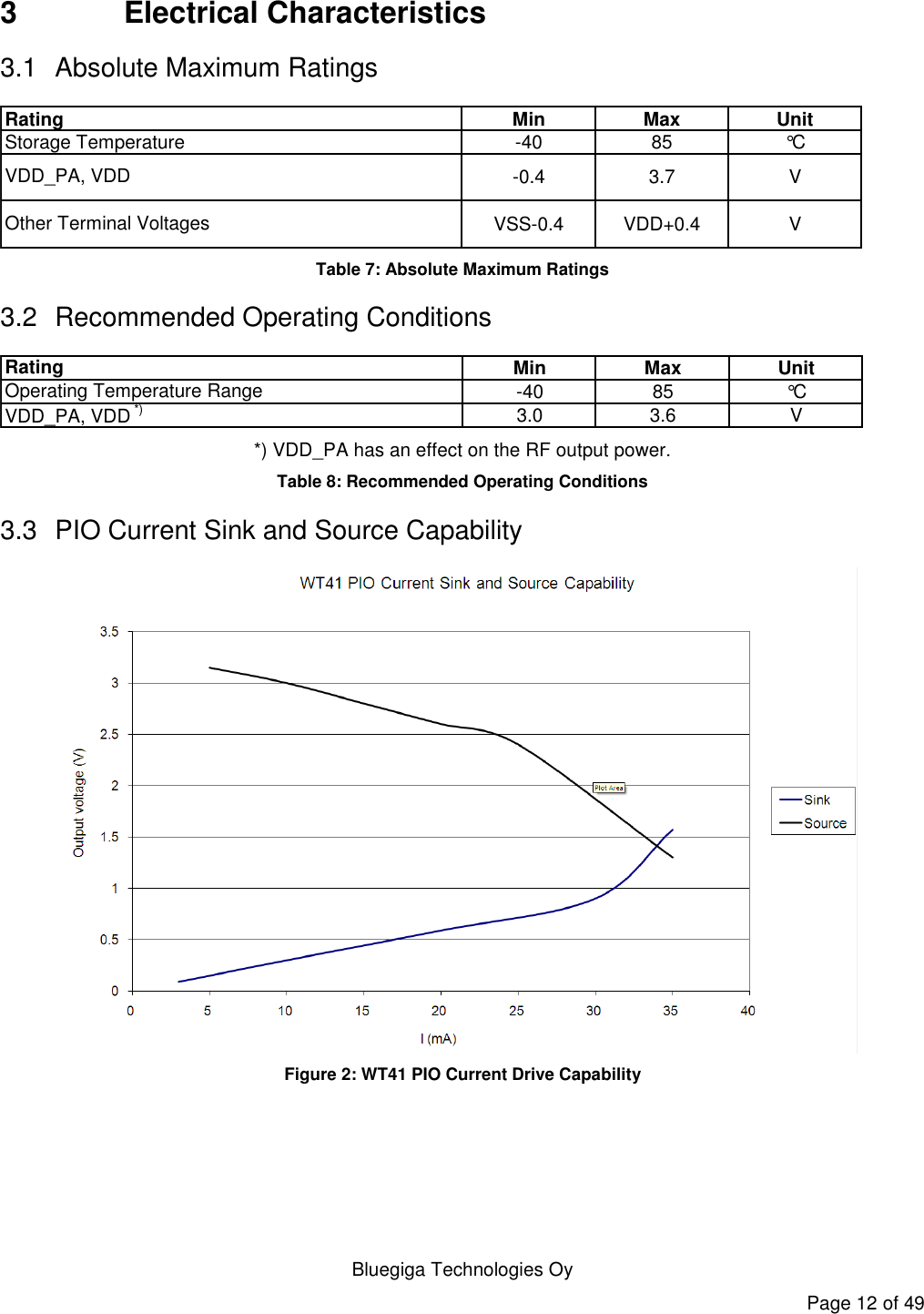
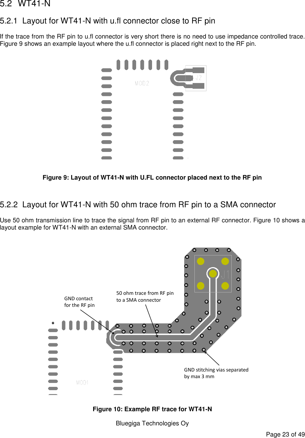
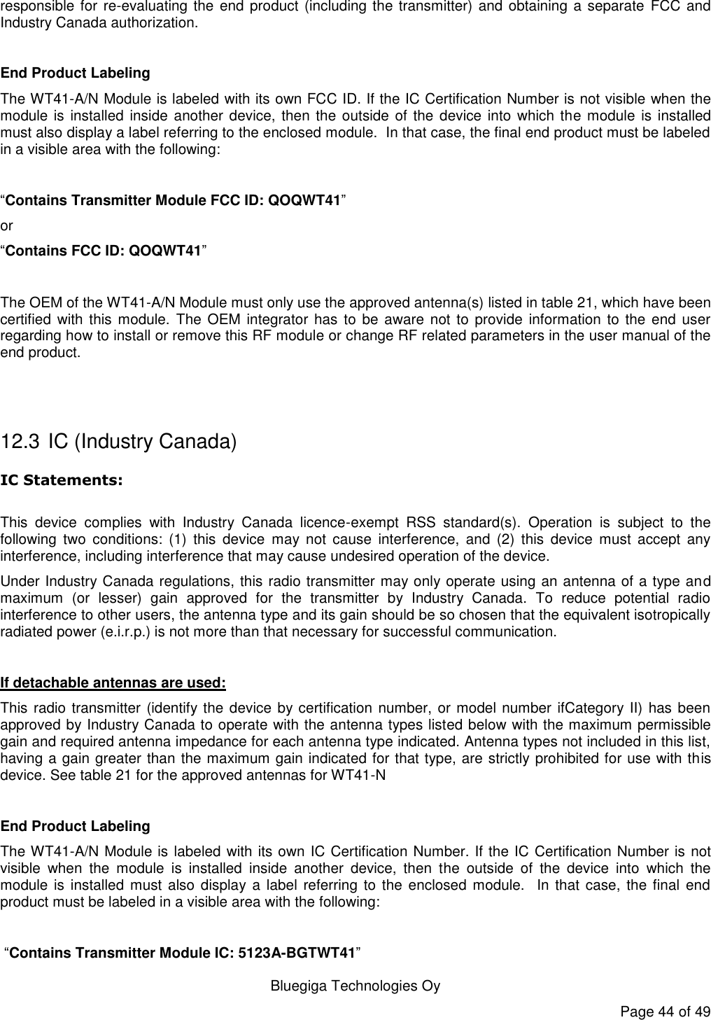
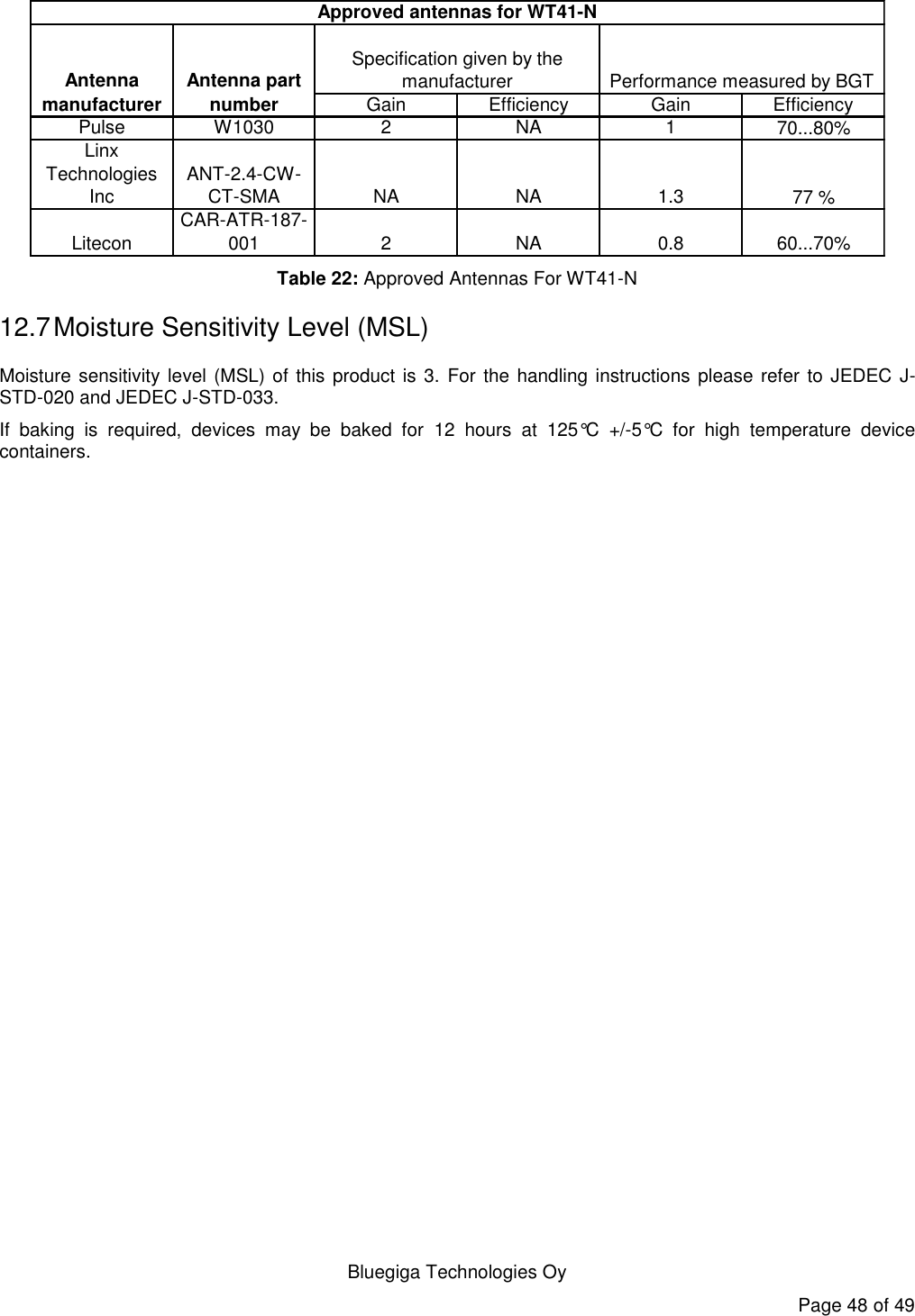
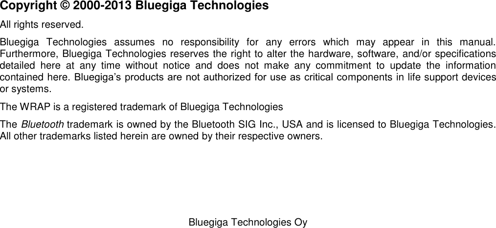
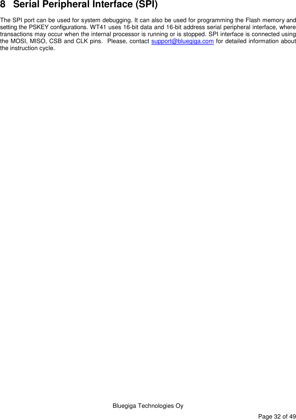
![Bluegiga Technologies Oy Page 27 of 49 6.1 UART Bypass Figure 13: UART Bypass Architecture 6.2 UART Configuration While Reset is Active The UART interface for WT41 while the chip is being held in reset is tristate. This will allow the user to daisy chain devices onto the physical UART bus. The constraint on this method is that any devices connected to this bus must tristate when WT41 reset is de-asserted and the firmware begins to run. 6.3 UART Bypass Mode Alternatively, for devices that do not tristate the UART bus, the UART bypass mode on BlueCore4-External can be used. The default state of BlueCore4-External after reset is de-asserted; this is for the host UART bus to be connected to the BlueCore4-External UART, thereby allowing communication to BlueCore4-External via the UART. All UART bypass mode connections are implemented using CMOS technology and have signalling levels of 0V and VDD. In order to apply the UART bypass mode, a BCCMD command will be issued to BlueCore4-External. Upon this issue, it will switch the bypass to PIO[7:4] as Figure 13 indicates. Once the bypass mode has been invoked, WT41 will enter the Deep Sleep state indefinitely. In order to re-establish communication with WT41, the chip must be reset so that the default configuration takes effect. It is important for the host to ensure a clean Bluetooth disconnection of any active links before the bypass mode is invoked. Therefore, it is not possible to have active Bluetooth links while operating the bypass mode. The current consumption for a device in UART bypass mode is equal to the values quoted for a device in standby mode.](https://usermanual.wiki/Druck/ADTSTOUCH-01.User-Manual-Bluetooth/User-Guide-2522022-Page-33.png)
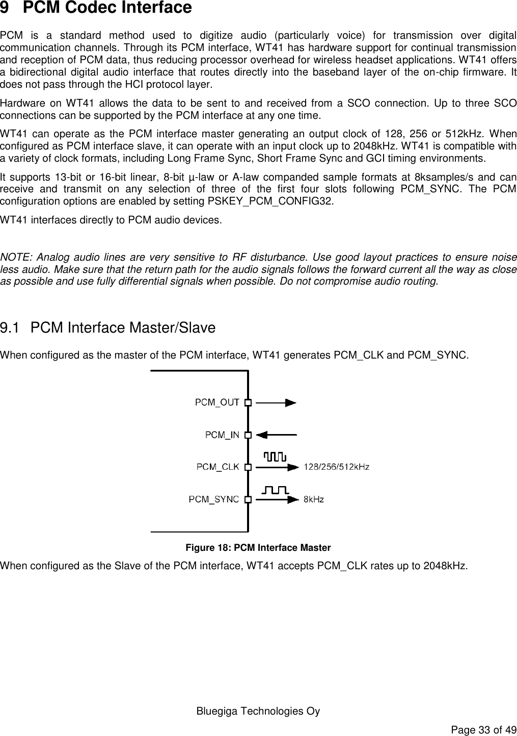
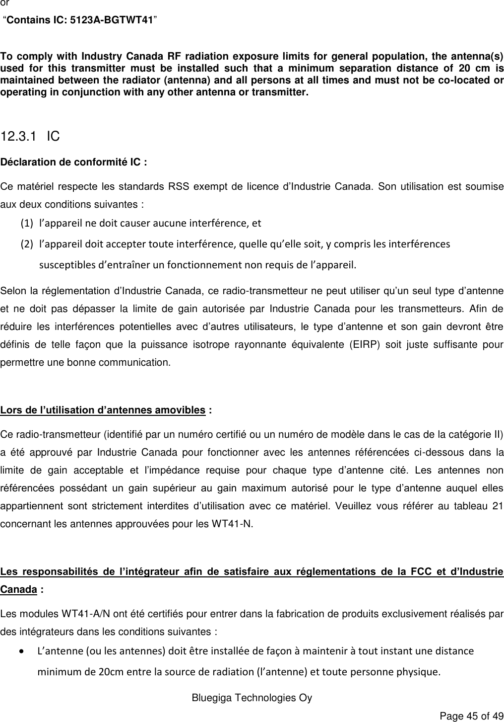
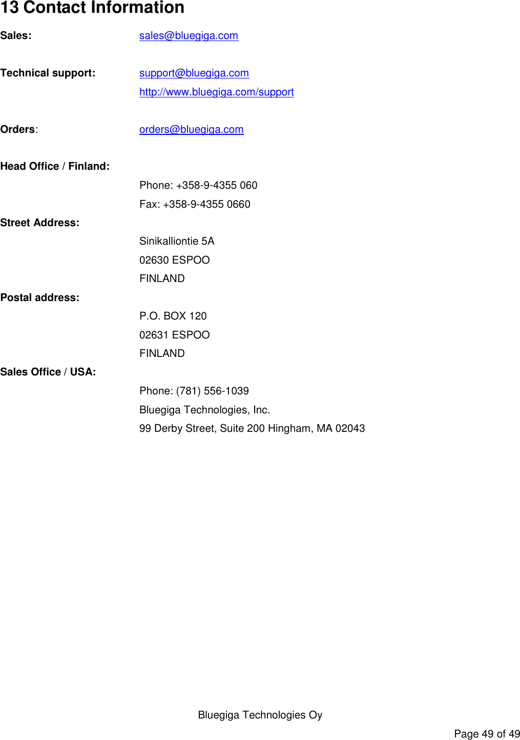
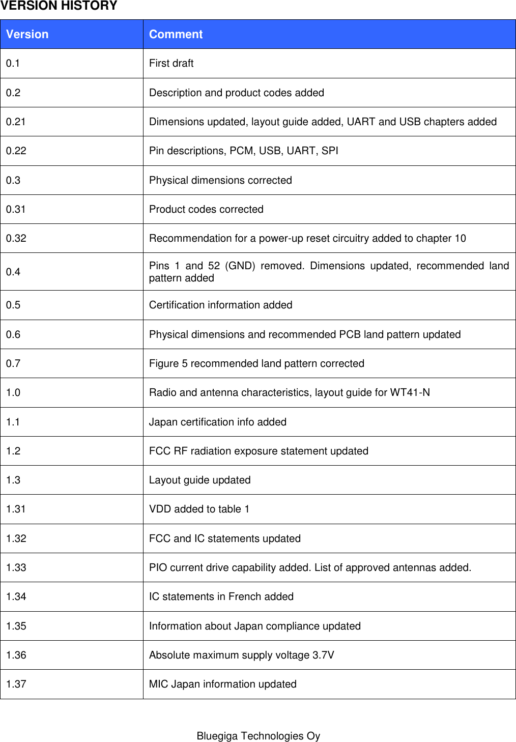
![Bluegiga Technologies Oy Page 39 of 49 Name Bit position Description-0 Set to 0SLAVE MODE EN 10 selects Master mode with internal generation of PCM_CLK and PCM_SYNC. 1 selects Slave mode requiring externally generated PCM_CLK and PCM_SYNC. This should be set to 1 if 48M_PCM_CLK_GEN_EN (bit 11) is set.SHORT SYNC EN 20 selects long frame sync (rising edge indicates start of frame), 1 selects short frame sync (falling edge indicates start of frame).- 3 Set to 0SIGN EXTENDED EN 40 selects padding of 8 or 13-bit voice sample into a 16- bit slot by inserting extra LSBs, 1 selects sign extension. When padding is selected with 3-bit voice sample, the 3 padding bits are the audio gain setting; with 8-bit samples the 8 padding bits are zeroes.LSB FIRST EN 5 0 transmits and receives voice samples MSB first, 1 uses LSB first.TX TRISTATE EN 60 drives PCM_OUT continuously, 1 tri-states PCM_OUT immediately after the falling edge of PCM_CLK in the last bit of an active slot, assuming the next slot is not active.TX TRISTATE RISING EDGE EN70 tristates PCM_OUT immediately after the falling edge of PCM_CLK in the last bit of an active slot, assuming the next slot is also not active. 1 tristates PCM_OUT after the rising edge of PCM_CLK.SYNC SUPPRESS EN80 enables PCM_SYNC output when master, 1 suppresses PCM_SYNC whilst keeping PCM_CLK running. Some CODECS utilize this to enter a low power state.GCI MODE EN 9 1 enables GCI mode.MUTE EN 10 1 forces PCM_OUT to 0.48M PCM CLK GEN EN110 sets PCM_CLK and PCM_SYNC generation via DDS from internal 4 MHz clock, as for BlueCore4-External. 1 sets PCM_CLK and PCM_SYNC generation via DDS from internal 48 MHz clock.LONG LENGTH SYNC EN120 sets PCM_SYNC length to 8 PCM_CLK cycles and 1 sets length to 16 PCM_CLK cycles. Only applies for long frame sync and with 48M_PCM_CLK_GEN_EN set to 1.-[20:16] Set to 0b00000.MASTER CLK RATE [22:21]Selects 128 (0b01), 256 (0b00), 512 (0b10) kHz PCM_CLK frequency when master and 48M_PCM_CLK_GEN_EN (bit 11) is low.ACTIVE SLOT [26:23] Default is 0001. Ignored by firmawareSAMPLE_FORMAT [28:27] Selects between 13 (0b00), 16 (0b01), 8 (0b10) bit sample with 16 cycle slot duration 8 (0b11) bit sample 8 cycle slot duration. Table 18: PSKEY_PCM_CONFIG32 description Name Bit position DescriptionCNT LIMIT [12:0] Sets PCM_CLK counter limitCNT RATE [23:16] Sets PCM_CLK count rate.SYNC LIMIT [31:24] Sets PCM_SYNC division relative to PCM_CLK. Table 19: PSKEY_PCM_LOW_JITTER_CONFIG Description](https://usermanual.wiki/Druck/ADTSTOUCH-01.User-Manual-Bluetooth/User-Guide-2522022-Page-45.png)
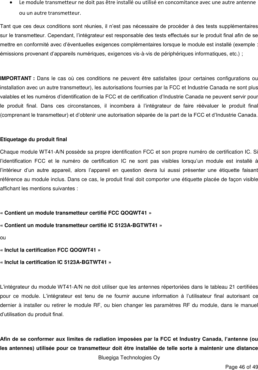
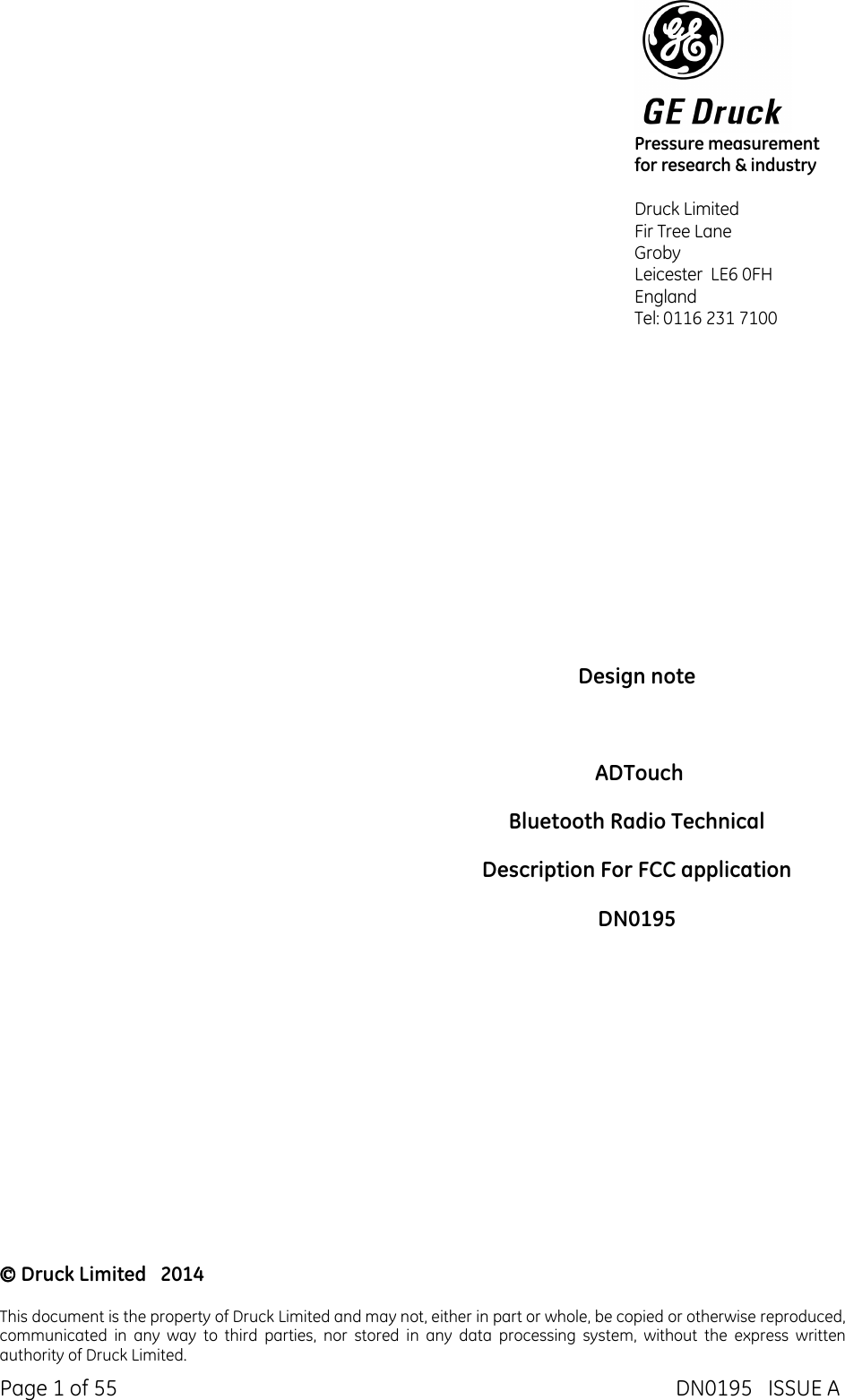
![Bluegiga Technologies Oy Page 40 of 49 10 I/O Parallel Ports Six lines of programmable bidirectional input/outputs (I/O) are provided. All the PIO lines are power from VDD. PIO lines can be configured through software to have either weak or strong pull-ups or pull-downs. All PIO lines are configured as inputs with weak pull-downs at reset. Any of the PIO lines can be configured as interrupt request lines or as wake-up lines from sleep modes. WT41 has a general purpose analogue interface pin AIO[1]. This is used to access internal circuitry and control signals. It may be configured to provide additional functionality. Auxiliary functions available via AIO[1] include an 8-bit ADC and an 8-bit DAC. Typically the ADC is used for battery voltage measurement. Signals selectable at this pin include the band gap reference voltage and a variety of clock signals: 48, 24, 16, 8MHz and the XTAL clock frequency. When used with analogue signals, the voltage range is constrained by the analogue supply voltage internally to the module (1.8V). When configured to drive out digital level signals (e.g., clocks), the output voltage level is determined by VDD. 10.1 PIO Defaults Bluegiga cannot guarantee that these terminal functions remain the same. Refer to the software release note for the implementation of these PIO lines, as they are firmware build-specific.](https://usermanual.wiki/Druck/ADTSTOUCH-01.User-Manual-Bluetooth/User-Guide-2522022-Page-46.png)
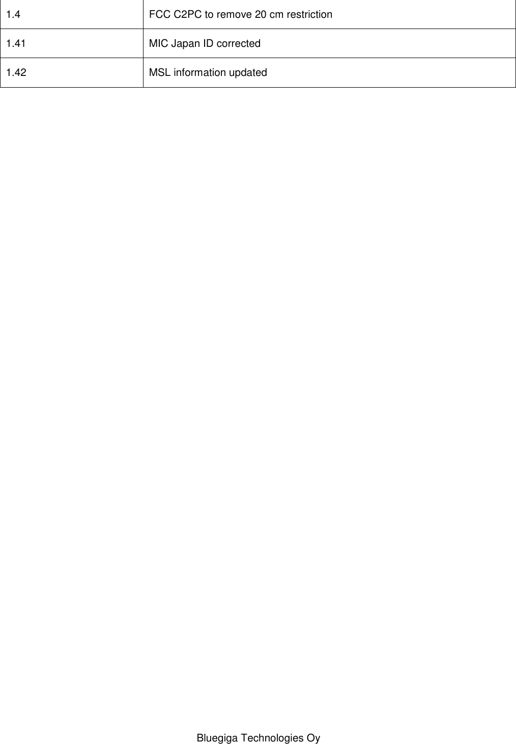
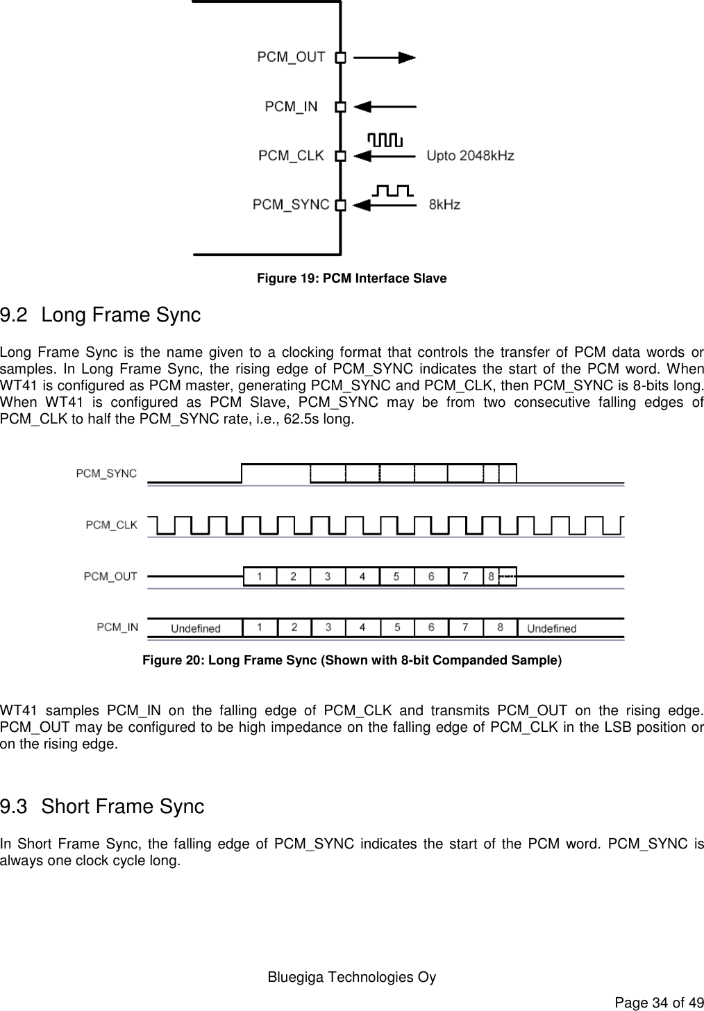
![Bluegiga Technologies Oy Page 42 of 49 11.1 Pin States on Reset PIN NAME STATEPIO[7:2] Input with weak pull-downPCM_OUT Tri-staed with weak pull-downPCM_IN Input with weak pull-downPCM_SYNC Input with weak pull-downPCM_CLK Input with weak pull-downUART_TX Output tristated with weak pull-upUART_RX Input with weak pull-downUART_RTS Output tristated with weak pull-upUART_CTS Input with weak pull-downUSB+ Input with weak pull-downUSB- Input with weak pull-downSPI_CSB Input with weak pull-downSPI_CLK Input with weak pull-downSPI_MOSI Input with weak pull-downSPI_MISO Output tristated with weak pull-downAIO[1] Output, driving low Table 20: Pin States on Reset](https://usermanual.wiki/Druck/ADTSTOUCH-01.User-Manual-Bluetooth/User-Guide-2522022-Page-48.png)