EA Technology UTP2A UltraTEV Plus2 User Manual WL18xx Module Hardware Integration Guide
EA Technology Limited UltraTEV Plus2 WL18xx Module Hardware Integration Guide
Contents
- 1. User manual
- 2. Users manual
- 3. User Manual
User Manual

WL18xx Module Hardware Integration Guide
User's Guide
Literature Number: SWRU437
September 2015

Contents
1 Introduction......................................................................................................................... 4
2 Module Variant Table............................................................................................................ 5
2.1 WL18xx WLAN Antenna Configuration................................................................................ 6
3 Critical Connections............................................................................................................. 7
4 Power Supply ...................................................................................................................... 7
4.1 Power Up/Shutdown Sequence ........................................................................................ 7
4.2 Power Sequencing ....................................................................................................... 8
5 Clocks ................................................................................................................................ 9
5.1 Slow Clock ................................................................................................................ 9
5.2 Fast Clock................................................................................................................. 9
6 Current Consumption ........................................................................................................... 9
6.1 Performance Parameters - Typical .................................................................................... 9
7 Antenna ............................................................................................................................ 10
8 Ground Connections........................................................................................................... 11
9 Layout............................................................................................................................... 11
10 Hardware Troubleshoot....................................................................................................... 11
10.1 System Requirements.................................................................................................. 11
10.2 Power Rails.............................................................................................................. 12
10.3 Critcal Supplies ......................................................................................................... 12
10.4 Sense on Reset......................................................................................................... 12
10.5 WLAN .................................................................................................................... 13
10.6 BT and BLE ............................................................................................................. 15
10.7 Reserved Pins........................................................................................................... 16
10.8 Debug .................................................................................................................... 16
11 WiFi_Zigbee Coex............................................................................................................... 17
12 References ........................................................................................................................ 18
2Table of Contents SWRU437–September 2015
Submit Documentation Feedback
Copyright © 2015, Texas Instruments Incorporated

www.ti.com
List of Figures
1 SISO........................................................................................................................... 6
2 MIMO .......................................................................................................................... 6
3 IO Connection Operational Mode.......................................................................................... 7
4 Power Sequencing........................................................................................................... 8
5 Antenna Matching Network in PI Configuration ........................................................................ 10
6 RNR Configuration ......................................................................................................... 11
7 WLAN_IRQ Signal on System Wake Up................................................................................ 14
8 HOST HCI UART Interface ............................................................................................... 15
9 Bootup Sequence Complete.............................................................................................. 15
10 HOST PCM Interface ...................................................................................................... 16
11 WLAN ZigBee Coexistence ............................................................................................... 17
12 Zigbee_LS................................................................................................................... 17
13 Zigbee_RNR ................................................................................................................ 18
List of Tables
1 WL18XXMODGB (2.4 GHz only module variants) ...................................................................... 5
2 WL18X7MODGI (2.4 GHz and 5 GHz modules) ........................................................................ 5
3 Supply Lines.................................................................................................................. 7
4 Recommended Current Requirement..................................................................................... 9
5 Approved Antenna Types and Maximum Gain Values................................................................ 10
6 Critical Supplies ............................................................................................................ 12
7 SDIO Interface Lines....................................................................................................... 13
8 HCI UART Interface Lines ................................................................................................ 15
9 PCM Interface Lines ....................................................................................................... 16
10 Debug/RS232 Interface Lines ............................................................................................ 16
11 WLAN ZigBee Coex Lines ................................................................................................ 17
3
SWRU437–September 2015 List of Figures
Submit Documentation Feedback Copyright © 2015, Texas Instruments Incorporated

User's Guide
SWRU437–September 2015
WL18xx Module Hardware Integration Guide
1 Introduction
This document provides the necessary BT/BLE and WLAN hardware operation information to aid in
system design. This is a review of the integration process of TI's WL18XX Module into final product PCB.
When designing your own system around the TI module, it is recommended to step through the guidelines
outlined below.
•WL18xxMOD product page [1]
NOTE: You can check your TI module WL18XXMOD design to PCB integration with the
WL18XXMOD series of easy-to-follow excel Checklist.
WiLink is a trademark of Texas Instruments.
Bluetooth is a registered trademark of Bluetooth SIG, Inc. and is licensed to Texas Instruments.
Windows is a registered trademark of Microsoft Corporation in the United States and other countries.
All other trademarks are the property of their respective owners.
4WL18xx Module Hardware Integration Guide SWRU437–September 2015
Submit Documentation Feedback
Copyright © 2015, Texas Instruments Incorporated
www.ti.com
Module Variant Table
2 Module Variant Table
Table 1. WL18XXMODGB (2.4 GHz only module variants)
WLAN
Reduced integration interfaces Compared to the 2.4-GHz WLAN 2.4-GHz WLAN
Device Main 1835 Module SISO MIMO 2.4-GHz MRC Bluetooth
WL1835MOD • Full version (all of the integration checklist must be ✓ ✓ ✓ ✓
applied)
WL1831MOD • Only the main RF antenna, ANT1 is used and the ✓ ✓
second one should be left N.C.
WL1805MOD • For BT IP removal. BT EN line must be connected to ✓ ✓ ✓
VSS. BT HCI, PCM and logger lines should be left N.C.
WL1801MOD • Only the main RF antenna, ANT1, is used and the ✓
second one should be left N.C.
• For BT IP removal. BT EN line must be connected to
VSS. BT HCI, PCM and logger lines should be left N.C.
Table 2. WL18X7MODGI (2.4 GHz and 5 GHz modules)
Redundant
Capabilities
Compared to the
Main 1837 WLAN WLAN WLAN WLAN
Device Module 2.4-GHz SISO (1) 2.4-GHz MIMO (2) 2.4-GHz MRC (3) Bluetooth 5-GHz SISO
WL1837MOD • Full version (all ✓✓✓✓✓
of the integration
checklist must be
applied)
WL1807MOD • For BT IP ✓ ✓ ✓ ✓
removal: BT EN
line must be
connected to
VSS. BT HCI,
PCM and logger
lines should be
left N.C.
(1) Single input, single output (SISO)
(2) Multiple input, multiple output (MIMO)
(3) Maximum ratio combining (MRC)
NOTE: Customers working with WL1837MOD/WL1807MOD modules that require only the single
antenna solution (2.4 Ghz WLAN SISO/ BT/ 5 GHz single antenna), while reusing the
original certification, can do so by making sure that no RF comes out of the second antenna
port (2.4 MIMO only / 5 Ghz diversity). To do this, use the following requirements:
• Leave the second module RF port open ( pin number 18 = N.C.)
• In the WL1837MOD INI [4], make sure that only 1 antenna is selected for 2.4 GHz by
setting parameter NumberOfAssembledAnt2_4 = 1;
5
SWRU437–September 2015 WL18xx Module Hardware Integration Guide
Submit Documentation Feedback Copyright © 2015, Texas Instruments Incorporated
Module Variant Table
www.ti.com
2.1 WL18xx WLAN Antenna Configuration
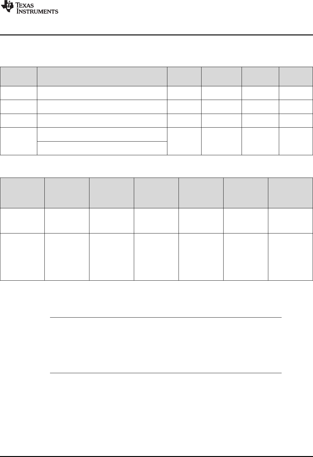
2.1.1 Single-Input Single-Output (SISO)
SISO is an acronym for single-input and single-output system. SISO technology use of only one antenna
both in the transmitter and receiver side.
Figure 1. SISO
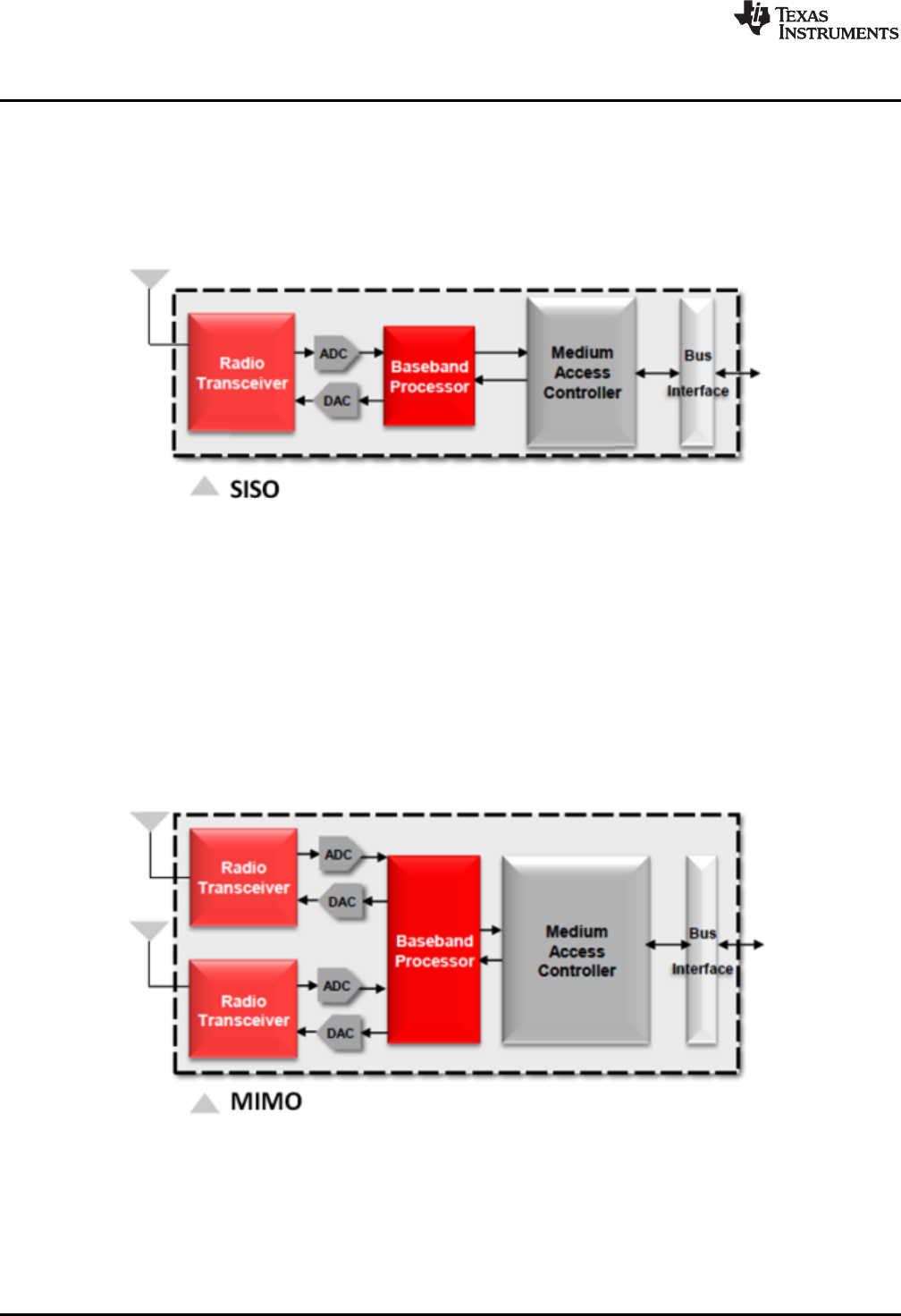
2.1.2 Multiple-Input Multiple-Output (MIMO) \ Maximum Ratio Combining (MRC)
MIMO is an acronym for multiple input multiple output. This technology can multiply the throughput
capacity by delivering multiple data streams over multiple antennas.
MRC is an acronym for maximum ration combining, This technology enables diversity of the reception
signal, done by combining the signal received in each antenna with the proper gain factor according to its
quality.
Figure 2. MIMO
6WL18xx Module Hardware Integration Guide SWRU437–September 2015
Submit Documentation Feedback
Copyright © 2015, Texas Instruments Incorporated
www.ti.com
Critical Connections
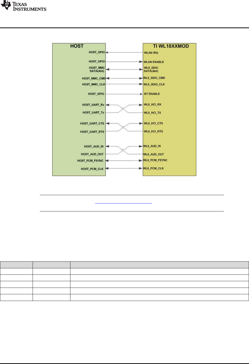
3 Critical Connections
Figure 3. IO Connection Operational Mode
NOTE: The reference is built using AM335 processor integration. For some of the other processors,
the RTS/CTS, TX/RX lines can be routed directly.
4 Power Supply
4.1 Power Up/Shutdown Sequence
Make sure the power up and shutdown sequence is kept at all times.
Table 3. Supply Lines
Pin No Name Description
40 WL_EN WLAN enable line from system
41 BT_EN Bluetooth enable line from system
36 SCLK Slow clock is running at 32 kHz
46,47 VBAT VBAT is high and stable at approximately 3.3 V
38 VIO VIO is high and stable at approximately 1.8 V
7
SWRU437–September 2015 WL18xx Module Hardware Integration Guide
Submit Documentation Feedback Copyright © 2015, Texas Instruments Incorporated
VBAT
VIO
SCLK (32 KHz)
WL and BT EN
>10 µs
1
t≥60 µst
2
3
>10 µs 4
5 5
Power Supply
www.ti.com
4.1.1 Power Up
To power up, do the following:
1. Ensure slow clock, VIO, and VBAT are stable.
2. Assert BT_EN or WL_EN high.
Internal DC2DCs, LDOs, and clocks start to ramp and stabilize.
4.1.2 Shutdown
Shutdown
1. Ensure the supplies to the device (VBAT, VIO, and slow clock) are stable and available.
2. De-assert BT_EN and WL_EN.
3. De-assert the supplies to the chip (VBAT and VIO)
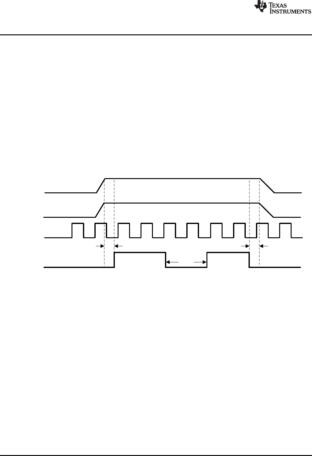
4.2 Power Sequencing
The most crucial points during integration of the WL18xx Module is that proper power-up and power-down
sequences must be followed in order to avoid damage to the device.
(1) On system level, either VBAT and VIO can come up first.
(2) VBAT supplies, VIO supplies, and slow clock (SCLK) msut be enabled before EN is asserted and at all times
when EN is active.
(3) Keep a 60-µs delay between two consecutive device enables. The device is assumed to be in a shutdown
state during that period; all enables to the device are low for that minimum duration.
(4) Deassert the enable line at least 10 µs before the VBAT or VIO can be lowered. (The order in which supplies
are turned off after EN shutdown in immaterial).
(5) The SCLK I/O cell is a fail safe; the clock can be supplied before the VBAT and VIO supplies.
Figure 4. Power Sequencing
8WL18xx Module Hardware Integration Guide SWRU437–September 2015
Submit Documentation Feedback
Copyright © 2015, Texas Instruments Incorporated
www.ti.com
Clocks
5 Clocks
5.1 Slow Clock
• The slow clock must be a free-running 32.768 KHz digital square wave
• The slow clock should be connected to pin 36 of the module
• Verify that the voltage range is between 0 V-1.8 V
5.2 Fast Clock
The WL18xxMOD uses a dedicated on-board 26 MHz fast clock TCXO.
6 Current Consumption
The power supplies for Vbat and VIO must handle the maximum current loads incurred by the WL18xx.
Please verify that your power supply can handle the maximum loads listed in Table 4 for each subsystem.
Table 4. Recommended Current Requirement
Parameter Power Supply Required Current Typical Values Units
WLAN SISO or MIMO 2.4 GHz, 5 GHz VBAT (1) 1 A
SISO/MRC, Bluetooth
WLAN SISO and BT VBAT (1) 750 mA
VIO VIO (2) 200 mA
(1) VBAT current is based on calibration current as well as maximum TX currents from all IPs
(2) VIO current requirement takes into account slow clock supply and LS, which are powered with the same supply from the WL8
side.
6.1 Performance Parameters - Typical
• System design power scheme must comply with both peak and average TX bursts
• WLAN maximum VBAT current draw of 725 mA with MIMO continues burst configuration
• Peak current VBAT can hit 850 mA during device calibration (1)
(1) • At wakeup, the WiLink™ 8 module performs the entire calibration sequence at the center of the
2.4-GHz band.
• Once a link is established, calibration is performed periodically (every 5 minutes) on the specific
tuned channel.
• The maximum VBAT value is based on peak calibration consumption with a 30% margin.
For more information on WiLink8 current consumption and Max VBAT / VIO, see the WL18xxmod device-
specific data sheet (http://www.ti.com/lsds/ti/wireless_connectivity/wilink/products.page).
9
SWRU437–September 2015 WL18xx Module Hardware Integration Guide
Submit Documentation Feedback Copyright © 2015, Texas Instruments Incorporated
Antenna
www.ti.com
7 Antenna
This device is intended only for OEM integrators under the following conditions:
• The antenna must be installed so that 20 cm is maintained between the antenna and users.
• The transmitter module cannot be co-located with any other transmitter or antenna.
• The radio transmitter can operate only using an antenna of a type and maximum (or lesser) gain
approved by TI. Table 5 lists the antennas approved by TI for use with the radio transmitter along with
maximum allowable gain values. Antenna types not included in the list or having a gain greater than
the maximum indicated are strictly prohibited for use with this transmitter.
Table 5. Approved Antenna Types and Maximum Gain Values
Antenna Type Brand 2.4 GHz 4.9 to 5.9 GHz (1) Unit
PCB Ethertronics –0.600 4.50
Dipole LSR 2.00 2.00
PCB Laird 2.00 4.00 dBi
Chip Pulse 3.20 4.20
PIFA LSR 2.00 3.00
Chip TDK 2.27 3.96
(1) Range is approximate.
NOTE: If these conditions cannot be met (for example, with certain laptop configurations or co-
location with another transmitter), the FCC/IC authorization will not be considered valid and
the FCC ID/IC ID cannot be used on the final product. In these circumstances, the OEM
integrator is responsible for reevaluating the end product (including the transmitter) and
obtaining a separate FCC/IC authorization.
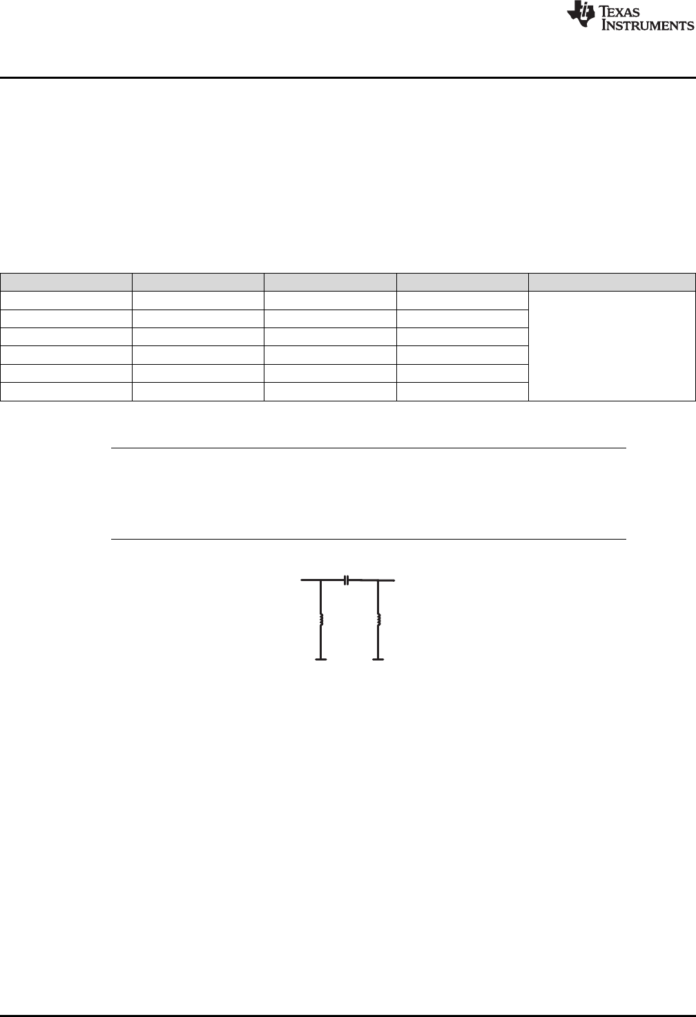
• It is suggested to place a Pi matching network place holder before the antenna on board
Figure 5. Antenna Matching Network in PI Configuration
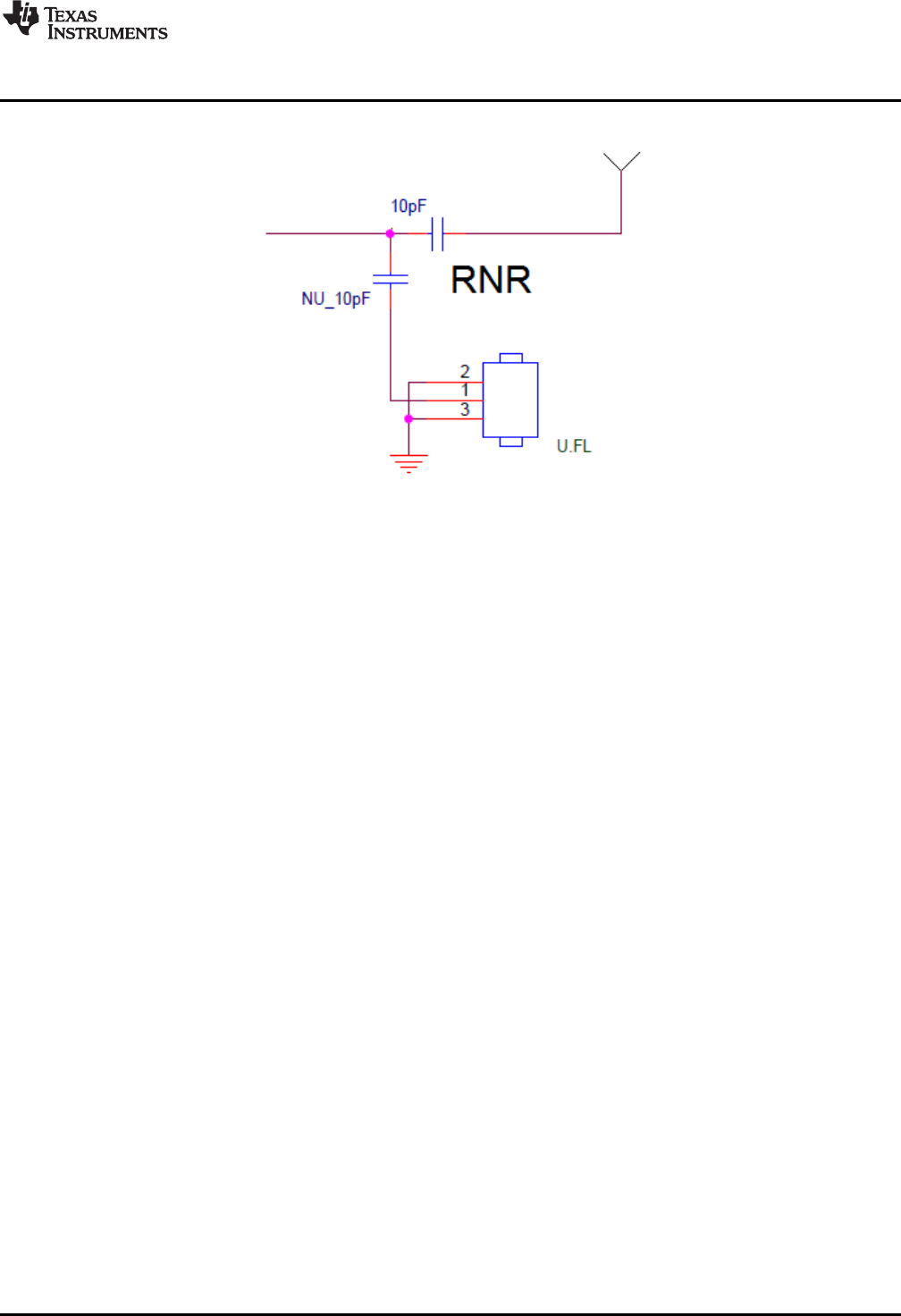
• It is strongly advised to have a debug miniature connector on the PCB
• Switching between the antenna and the debug connector should be done in RNR configuration to
avoid stubs
10 WL18xx Module Hardware Integration Guide SWRU437–September 2015
Submit Documentation Feedback
Copyright © 2015, Texas Instruments Incorporated
www.ti.com
Ground Connections
Figure 6. RNR Configuration
• Antenna should be placed away from the rest of the circuit
– Avoid digital and analog routing in the area, metal enclosure.
• MIMO antenna spacing
– Distance between the two antennas is advised to be greater than half of the wavelength (62.5 mm
at 2.4 GHz)
8 Ground Connections
All the ground pins of the module must be connected to ground on the main PCB.
9 Layout
For more information, see the WL1837 User's Guide [5].
10 Hardware Troubleshoot
This section is intended to cover the basic hardware troubleshoot that you may come across bringing up
the WL18xxMOD on the final board; the device has several interfaces and sequences that must be kept in
order to operate the device in properly.
10.1 System Requirements
For basic integration, the process requires the following components:
• Wireless Tool Package located at TI.COM
• Minimum requirements: PC running Pentium II
• Operating systems: Windows®2000, Windows XP, Windows 7
• Serial communication port (RS-232) or USB port with UART-to-USB adapter (to enable the RS232
interface on the WiLink 8.0 IC)
• Access to WL_UART_DBG pin
• Access to BT_UART_DBG
• Access to RS232 Tx , RS232 Rx Pins
– HCI UART Pins
• Oscilloscope
• Multimeter
11
SWRU437–September 2015 WL18xx Module Hardware Integration Guide
Submit Documentation Feedback Copyright © 2015, Texas Instruments Incorporated
Hardware Troubleshoot
www.ti.com
Debug and calibration tools for WLAN and Bluetooth®require four UART ports. The most efficient way to
drive these ports to the PC is to use a UART-to-USB converter (not included in the wireless tools
package). TI recommends using the WL18XXCOM82SDMMC SDMMC-to-COM8 adapter with the TI
WL1837MODCOM8I module or the WL1835MODCOM8B module on the COM8 board.
NOTE: Multiple UART-to-COM8 adapters are available on the market, such as the FTDI Chip
development modules.
10.2 Power Rails
There are two power rails that must feed into the WL18xx system:
• VBAT - Main power supply source (typically 3.3 V - 3.6 V)
– VBAT should be connected to pin 46 and 47 of the module
• VIO - Voltage reference from host (1.8 V)
– VIO should be connected to pin 38 of the module
– Can be used for Level shifter supply and slow clock OSC supply
10.3 Critcal Supplies
Make sure all of the critical supplies are in the range of the following expected values:
Table 6. Critical Supplies
Pin No Name Description Frequency [Hz] Amplitude [V] Current [mA]
– DC_IN Depends on the system
36 Slow Clock External 32 kHz slow clock 32K 1.8 –
46,47 VBAT DC supply range for all modes – 3.3-3.6 1000
38 VIO I/O ring power supply voltage – 1.8 200
1. VBAT and VIO amplitude and current are maximum values.
10.4 Sense on Reset
Wilink8 has several wake-up options that are entered through sense on reset by three IO's of the device:
IRQ_WL, UART_DBG_BT, AUD_OUT_BT.
Once BT or WLAN enable bit is set to high, the device checks the state of the lines and wakes up in that
specific mode.
There are only two modes or configurations that are supported by the device, all of the rest are prohibited
and the user must verify that there is no option on the system level to enter the prohibited modes.
The supported modes are:
• Operational mode:
– IRQ_WL = 0, UART_DBG_BT = 1, AUD_OUT_BT = 0
Operational mode is set by default using internal pull of WL18xx (90K typical).
• Debug mode:
WLAN RS232 debug interface and Jtag interface are muxed out to the WL18XX IO's by default,
nevertheless, this mode is only for debug a 10K resistor pull up place holder on the IRQ line should
be placed. It can be applied only in case the debug mode is required:
– IRQ_WL = 1, UART_DBG_BT = 1, AUD_OUT_BT = 0
12 WL18xx Module Hardware Integration Guide SWRU437–September 2015
Submit Documentation Feedback
Copyright © 2015, Texas Instruments Incorporated
www.ti.com
Hardware Troubleshoot
NOTE: In order to avoid an undefined state of the device, be extremely careful when level-
shifting those three I/Os to ensure that only those one of the two supported
configurations of the device are applied.
For further details, see Level Shifting WL18xx I/Os (SWRA448).
10.5 WLAN
10.5.1 WLAN Host Interface (SDIO)
The SDIO is the host interface for WLAN. The interface between the host and the WL18xx module uses
an SDIO interface and supports a maximum clock rate of 52 MHz.
The device SDIO also supports the following features of the SDIO V3 specification:
• 4-bit data bus
• Synchronous and asynchronous in-band interrupt
• Default and high-speed (HS, 52 MHz) timing
• Sleep and wake commands
• The WLAN subsystem is controlled via an SDIO interface. The WLAN acts as a slave with the
processor as host. The host should generate the SDIO clock and read/write from the WLAN interface.
• Verify that the SDIO bus pins are connected to the host. These pins include:
Table 7. SDIO Interface Lines
Pin
Number Name Type Description
6 SDIO_CMD I/O SDIO command line. This is a bidirectional line. The host sends commands and the WLAN
responds to these commands.
8 SDIO_CLK I SDIO clock input line. This line is generated by the host.
10 SDIO_D0 I/O SDIO data 0 line. This is the primary data line used in both 1-bit and 4-bit SDIO mode. This
is a bidirectional line.
11 SDIO_D1 I/O SDIO data 1 line. This is one of four data lines. This line is used only in 4-bit mode. This is a
bidirectional line.
12 SDIO_D2 I/O SDIO data 2 line. This is one of four data lines. This line is used only in 4-bit mode. This is a
bidirectional line.
13 SDIO_D3 I/O SDIO data 3 line. This is one of four data lines. This line is used only in 4- bit mode. This is a
bidirectional line.
14 WLAN_IRQ O Generates interrupt from the WLAN chip toward the HOST. It is used to signal the HOST on
many events like received data from the WLAN media is ready at the firmware (WLAN Chip)
queue, the last Tx frame that was transmitted, all kind of asynchronous messages (evens),
and so on.
40 WLAN_EN I WLAN enable signal, should be "1" in order enable the WLAN operation, once the WLAN
enable signal is "0" the WLAN part of the chip is reset in a way that the firmware has to be
loaded again after enabling the WLAN.
• Host must provide PU using a 10-K resistor for all non-CLK SDIO signals.
• In order to follow the wakeup/shutdown requirements, the WL_EN (pin number 40) should be
connected to host GPIO. Must be pulled high for WLAN operation. This GPIO should have internal
pull-up allowing the WL18xx pin to remain high on host suspend. In order to enable WOW feature, a
pull up on the line is required during HOST shutdown.
• IRQ_WL should be connected to host GPIO. This GPIO should be able to wake the host from
suspend, therefore it's better to always connect the pin (number 14) to the always on domain of the
Host. The IRQ_WL pin serves as interrupt generation from WL18xx to the host.
13
SWRU437–September 2015 WL18xx Module Hardware Integration Guide
Submit Documentation Feedback Copyright © 2015, Texas Instruments Incorporated
Hardware Troubleshoot
www.ti.com
NOTE: It is recommended to connect the SDIO directly to the 1.8 V SDIO interface on the host side.
In case Level Shifter is inevitable, see Level Shifting WL18xx I/Os Application Report
(SWRA448).
10.5.2 WLAN IRQ Operation (SDIO Out-of-Band Interrupt)
The WLAN IRQ is an out-of-band interrupt request line that is not defined by the SDIO standard
specification. Therefore, a good understanding on how it works is required in order to work with the WL8xx
solution.
The WLAN_IRQ line operates as follows:
• The default state of the WLAN_IRQ prior to device enable is internal 100K pulldown (in case of a
debug mode there is external 10K pull up)
• After the enable line is applied high, the WL_IRQ is changed to drive logic '0'.
• During firmware initialization, the WLAN_IRQ is configured by the SDIO module.
– The WLAN firmware creates an interrupt-to-host request, indicated by a 0-to-1 transition on the
WLAN_IRQ line (the host must be configured as active high or rising-edge detect).
– After the host is available, depending on the interrupt priority and other host tasks, it masks the
firmware interrupt. The WLAN_IRQ line returns to 0 (a 1-to-0 transition on the WLAN_IRQ line).
– The host reads the internal register status to determine the interrupt sources. The register is
cleared after the read.
– The host processes all the interrupts read from this register in sequence.
– The host unmasks the firmware interrupts.
• The host is ready to receive another interrupt from the WLAN device.
Figure 7. WLAN_IRQ Signal on System Wake Up
For more details on the Wake on Wlan feature, see [3].
14 WL18xx Module Hardware Integration Guide SWRU437–September 2015
Submit Documentation Feedback
Copyright © 2015, Texas Instruments Incorporated
www.ti.com
Hardware Troubleshoot
10.6 BT and BLE
10.6.1 Bluetooth UART HCI Interface
• The Bluetooth subsystem is controlled via an HCI 4-wire UART interface (H4).
• Verify that the HCI interface is connected as shown in Figure 8. Note that a TX pin always routes to a
RX pin, and a RTS pin always routes to a CTS pin.
Figure 8. HOST HCI UART Interface
Table 8. HCI UART Interface Lines
Pin
Number Name Type Description
41 BT_EN I Bluetooth Enable
50 BT_HCI_RTS O Bluetooth HCI UART request to send output
51 BT_HCI_CTS I Bluetooth HCI UART clear to send input
52 BT_HCI_TX O Bluetooth HCI UART transmit output
53 BT_HCI_RX I Bluetooth HCI UART receive input
• FUNC1_BT should be NC.
• FUNC2_BT should be NC.
NOTE: In the AM335x integration reference, the RTS and CTS lines are crossed, as shown. For
some of the other processors, the RTS/CTS lines must be connected directly.
• In case of host processor I/O is at 3.3 V, use a standard 245 level shifter and not a direction sensing
one. For more information, see Level Shifting WL18xx I/Os (SWRA448).
• Once BT EN is asserted to high the BT FW stored in ROM start to execute, during this time the RTS is
driven high to prevent HCI transaction and not to interfere with device boot, once the FW finish the
boot process RTS line goes low after approximately 100 mS.
If logger is configured at this point, WL18xx should print boot up message.
Figure 9. Bootup Sequence Complete
15
SWRU437–September 2015 WL18xx Module Hardware Integration Guide
Submit Documentation Feedback Copyright © 2015, Texas Instruments Incorporated
Hardware Troubleshoot
www.ti.com
• Connect HCI Tester and Set Baud Rate - 115200, Data Bits - 8, Stop bits -1, Parity - none, Flow
Control - HW. On this port, send basic HCI commands (BD Address) to verify connectivity.
• In case UART lines are not operating, make sure that the CTS line is set to 0 on the PC side - the
signal on the WL18xx Rx input line that comes from the PC (on the port Probe).
For every packet on Rx, there should be a response on the Tx line from WL18xx.
10.6.2 BT PCM
There are two lines that can be bidirectional (CLK/FSYNC) to support master and slave configuration and
two directional pins: AUD_OUT (output) and AUD_IN (input).
All four lines should be connected to the HOST PCM interface.
Figure 10. HOST PCM Interface
In case the PCM interface is not used, leave not connected (N.C.).
Table 9. PCM Interface Lines
Pin Number Name Type Description
56 BT_AUD_IN I Bluetooth PCM data output
57 BT_AUD_OUT O Bluetooth PCM data output
58 BT_AUD_FSYNC I/O Bluetooth PCM frame sync input or output
60 BT_AUD_CLK I/O Bluetooth PCM clock input or output
10.7 Reserved Pins
• Reserved 1, 2, 3, can be used for Audio sync otherwise, leave N.C.
• GPIO 9, 10, and 12 can be used for ZigBee coexistence
– GPIO11 can be used for Audio sync, otherwise, leave N.C.
10.8 Debug
Table 10. Debug/RS232 Interface Lines
Pin Number Name Type Description
26 WLAN RS232 RX I WLAN debug interface
27 WLAN RS232 TX O WLAN debug interface
42 WL_UART_DBG O WLAN FW logger
43 BT_UART_DBG O BT FW logger
For bring up and evaluation of the module, the following should be connected:
• Pin out GPIO1 and GPIO2 for WLAN RS232 interface to enable RTTT tool for controlling RF test in the
absence of a host.
• There is a need to pull up WL_IRQ (10k pull up) at power-on to enable this RS232 UART interface.
• WLAN logger must have at least a TP to allow Wi-Fi Firmware logs to be captured by gLogger.
Requires a 1.8 V LVCMOS to USB cable for capture.
16 WL18xx Module Hardware Integration Guide SWRU437–September 2015
Submit Documentation Feedback
Copyright © 2015, Texas Instruments Incorporated
www.ti.com
WiFi_Zigbee Coex
• BT logger must have at least a TP to allow Bluetooth Firmware logs to be captured by gLogger.
Requires a 1.8 V LVCMOS to USB cable for capture.
• WLAN RS232 lines - Check transmission on Rx/Tx line, for every packet on Rx should be a response
in Tx.
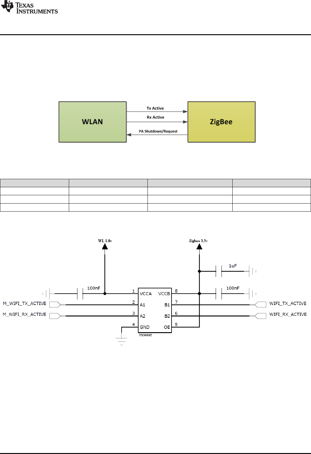
11 WiFi_Zigbee Coex
• For Zigbee/WiFi Coexistence, the following should be connected:
Figure 11. WLAN ZigBee Coexistence
Table 11. WLAN ZigBee Coex Lines
Signal Name WL18xxMOD IO (1.8 Bv) CC2530 Zigbee IO (3.3 V) Direction
Tx Active GPIO12 (Pin 5) P1_7 (Pin 37) From WLAN
Rx Active GPIO10 (Pin 4) P0_0 (Pin 19) From WLAN
PA SHUTDOWN/REQUEST GPIO9 (Pin 3) P1_6 (Pin 38) To WLAN
• For signals level shifting between WL18XXMOD and CC2530, TI recommends the TXS0102
Bidirectional Voltage-Level Translator.
Figure 12. Zigbee_LS
17
SWRU437–September 2015 WL18xx Module Hardware Integration Guide
Submit Documentation Feedback Copyright © 2015, Texas Instruments Incorporated
References
www.ti.com
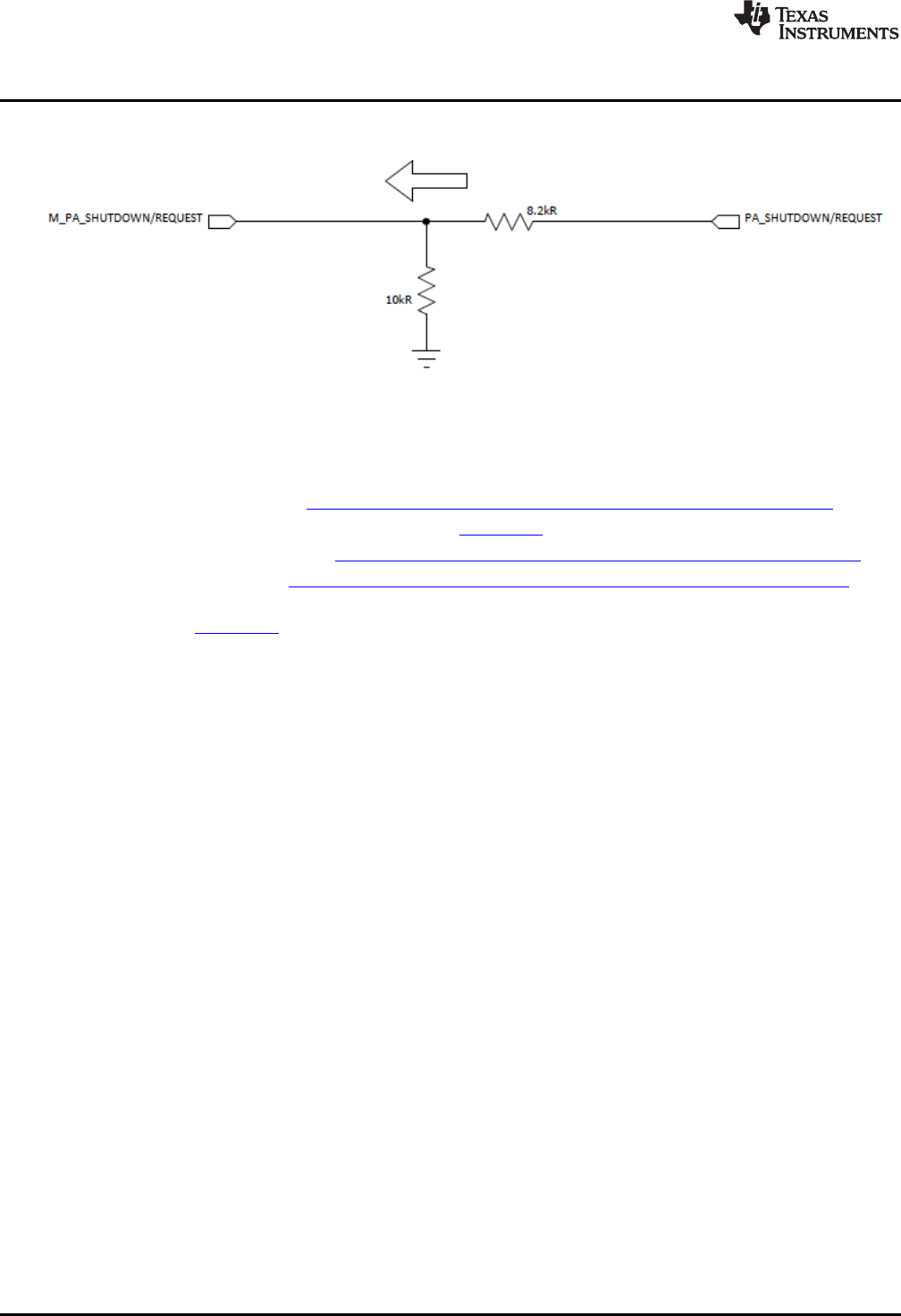
• For the TX disable, one of the options is to use resistor divider or use single bit Level Shifter.
Figure 13. Zigbee_RNR
12 References
1. WL18xxMOD product page: http://www.ti.com/lsds/ti/wireless_connectivity/wilink/products.page
2. Level Shifting WL18xx I/Os Application Report (SWRA448)
3. WL18xx Adding WoWLAN wiki: http://processors.wiki.ti.com/index.php/WL18xx_Adding_WoWLAN
4. .INI/wlconf Overview wiki: http://processors.wiki.ti.com/index.php/.INI/wlconf_Overview#.INI_Files
5. WL1837MODCOM8I WLAN MIMO and Bluetooth® Module Evaluation Board for TI Sitara™ Platform
User's Guide (SWRU382)
18 WL18xx Module Hardware Integration Guide SWRU437–September 2015
Submit Documentation Feedback
Copyright © 2015, Texas Instruments Incorporated

IMPORTANT NOTICE
Texas Instruments Incorporated and its subsidiaries (TI) reserve the right to make corrections, enhancements, improvements and other
changes to its semiconductor products and services per JESD46, latest issue, and to discontinue any product or service per JESD48, latest
issue. Buyers should obtain the latest relevant information before placing orders and should verify that such information is current and
complete. All semiconductor products (also referred to herein as “components”) are sold subject to TI’s terms and conditions of sale
supplied at the time of order acknowledgment.
TI warrants performance of its components to the specifications applicable at the time of sale, in accordance with the warranty in TI’s terms
and conditions of sale of semiconductor products. Testing and other quality control techniques are used to the extent TI deems necessary
to support this warranty. Except where mandated by applicable law, testing of all parameters of each component is not necessarily
performed.
TI assumes no liability for applications assistance or the design of Buyers’ products. Buyers are responsible for their products and
applications using TI components. To minimize the risks associated with Buyers’ products and applications, Buyers should provide
adequate design and operating safeguards.
TI does not warrant or represent that any license, either express or implied, is granted under any patent right, copyright, mask work right, or
other intellectual property right relating to any combination, machine, or process in which TI components or services are used. Information
published by TI regarding third-party products or services does not constitute a license to use such products or services or a warranty or
endorsement thereof. Use of such information may require a license from a third party under the patents or other intellectual property of the
third party, or a license from TI under the patents or other intellectual property of TI.
Reproduction of significant portions of TI information in TI data books or data sheets is permissible only if reproduction is without alteration
and is accompanied by all associated warranties, conditions, limitations, and notices. TI is not responsible or liable for such altered
documentation. Information of third parties may be subject to additional restrictions.
Resale of TI components or services with statements different from or beyond the parameters stated by TI for that component or service
voids all express and any implied warranties for the associated TI component or service and is an unfair and deceptive business practice.
TI is not responsible or liable for any such statements.
Buyer acknowledges and agrees that it is solely responsible for compliance with all legal, regulatory and safety-related requirements
concerning its products, and any use of TI components in its applications, notwithstanding any applications-related information or support
that may be provided by TI. Buyer represents and agrees that it has all the necessary expertise to create and implement safeguards which
anticipate dangerous consequences of failures, monitor failures and their consequences, lessen the likelihood of failures that might cause
harm and take appropriate remedial actions. Buyer will fully indemnify TI and its representatives against any damages arising out of the use
of any TI components in safety-critical applications.
In some cases, TI components may be promoted specifically to facilitate safety-related applications. With such components, TI’s goal is to
help enable customers to design and create their own end-product solutions that meet applicable functional safety standards and
requirements. Nonetheless, such components are subject to these terms.
No TI components are authorized for use in FDA Class III (or similar life-critical medical equipment) unless authorized officers of the parties
have executed a special agreement specifically governing such use.
Only those TI components which TI has specifically designated as military grade or “enhanced plastic” are designed and intended for use in
military/aerospace applications or environments. Buyer acknowledges and agrees that any military or aerospace use of TI components
which have not been so designated is solely at the Buyer's risk, and that Buyer is solely responsible for compliance with all legal and
regulatory requirements in connection with such use.
TI has specifically designated certain components as meeting ISO/TS16949 requirements, mainly for automotive use. In any case of use of
non-designated products, TI will not be responsible for any failure to meet ISO/TS16949.
Products Applications
Audio www.ti.com/audio Automotive and Transportation www.ti.com/automotive
Amplifiers amplifier.ti.com Communications and Telecom www.ti.com/communications
Data Converters dataconverter.ti.com Computers and Peripherals www.ti.com/computers
DLP® Products www.dlp.com Consumer Electronics www.ti.com/consumer-apps
DSP dsp.ti.com Energy and Lighting www.ti.com/energy
Clocks and Timers www.ti.com/clocks Industrial www.ti.com/industrial
Interface interface.ti.com Medical www.ti.com/medical
Logic logic.ti.com Security www.ti.com/security
Power Mgmt power.ti.com Space, Avionics and Defense www.ti.com/space-avionics-defense
Microcontrollers microcontroller.ti.com Video and Imaging www.ti.com/video
RFID www.ti-rfid.com
OMAP Applications Processors www.ti.com/omap TI E2E Community e2e.ti.com
Wireless Connectivity www.ti.com/wirelessconnectivity
Mailing Address: Texas Instruments, Post Office Box 655303, Dallas, Texas 75265
Copyright © 2015, Texas Instruments Incorporated