EDAN INSTRUMENTS V1102EDAN SMQV1102EDAN WIFI Module User Manual User Mannal Rev0
EDAN INSTRUMENTS, INC. SMQV1102EDAN WIFI Module User Mannal Rev0
UserManual.wiki
>
EDAN INSTRUMENTS
>
V1102EDAN User Manual
User Mannal-Rev0
Navigation menu
Upload a User Manual
Namespaces
Wiki Guide
HTML
PDF
Info
Views
User Manual
Discussion / Help
Navigation
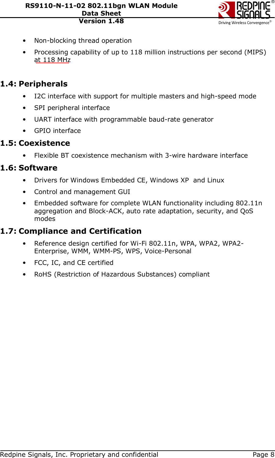
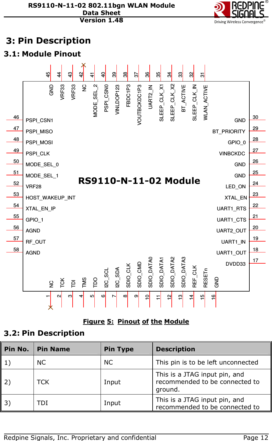
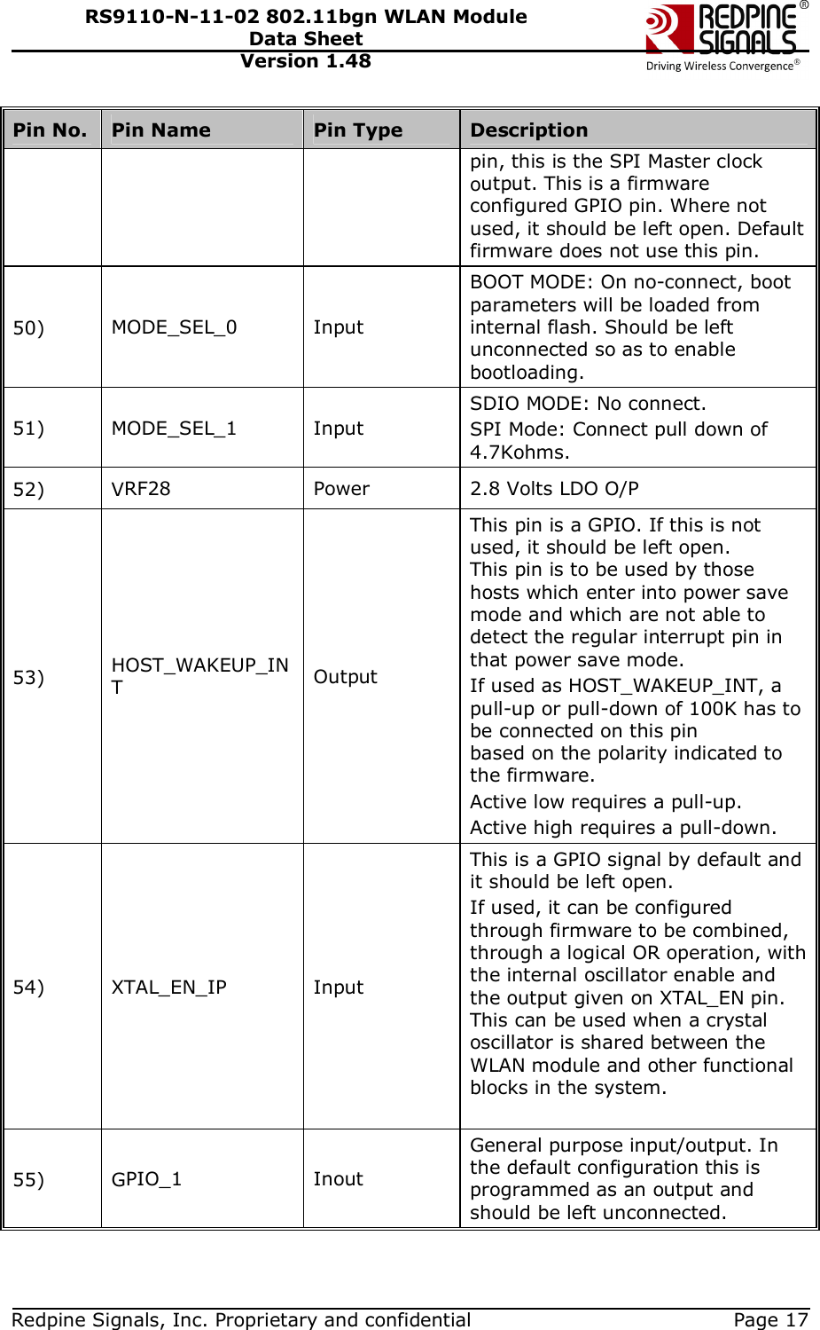
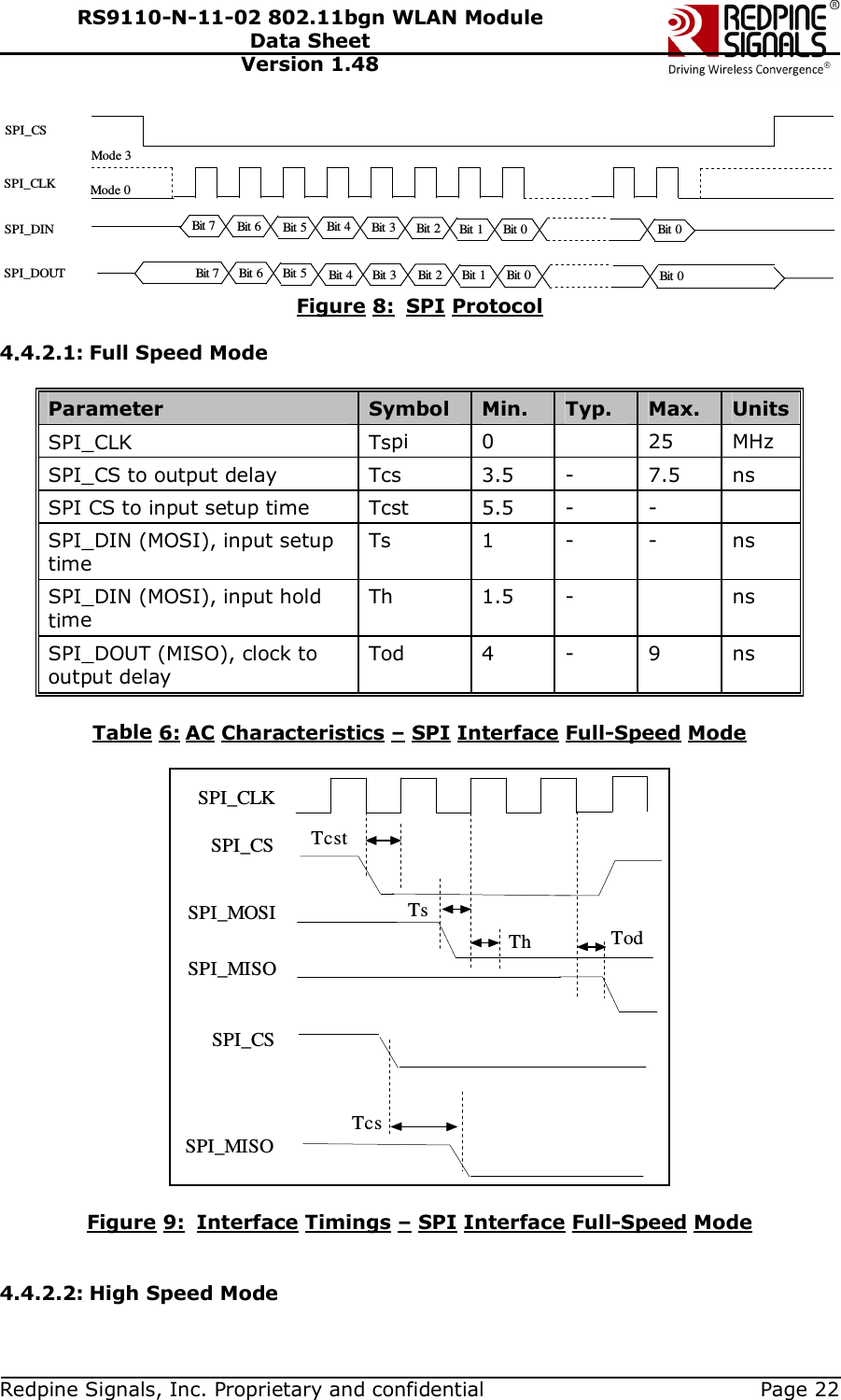
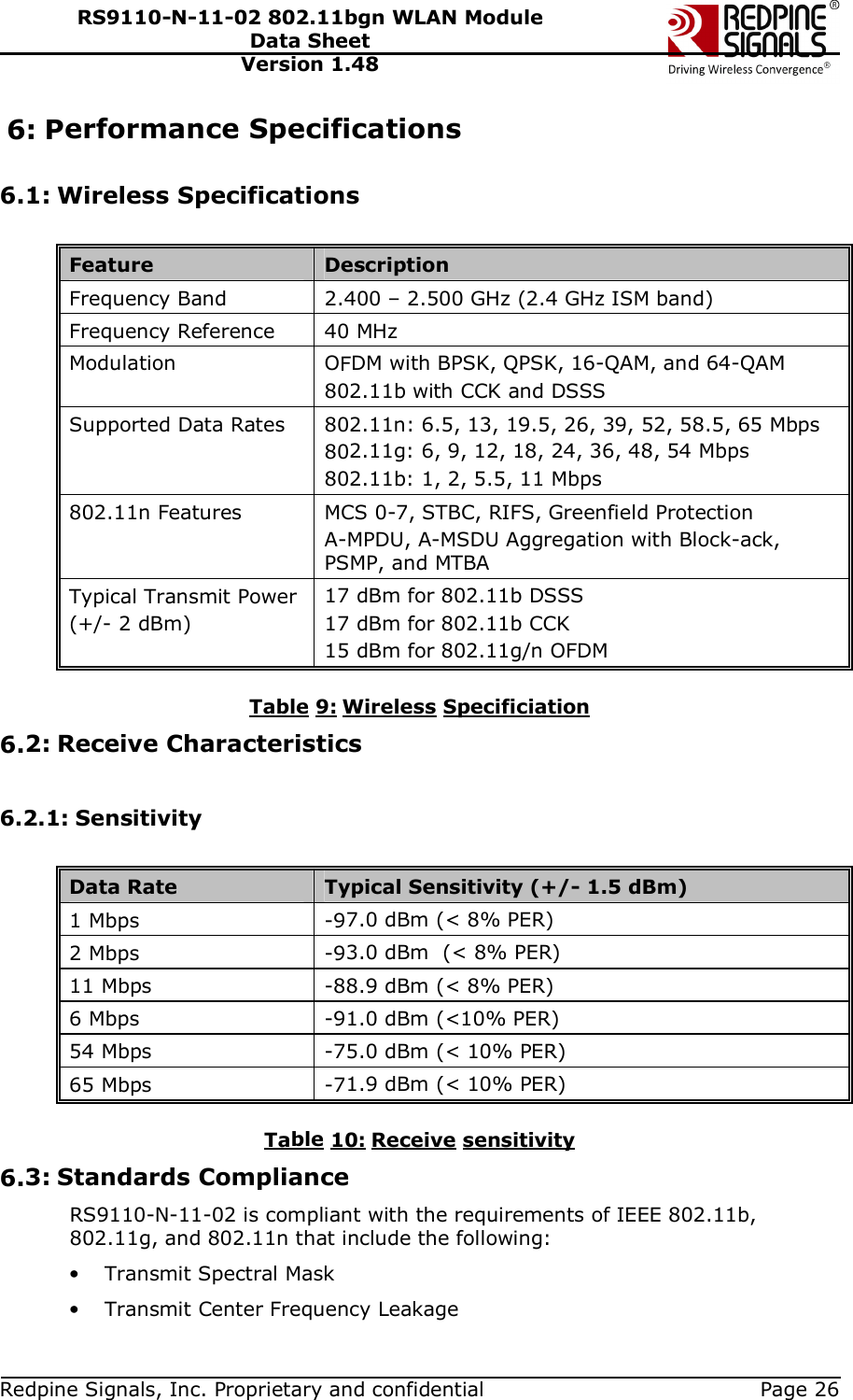
![Redpine Signals, Inc. Proprietary and confidential Page 13 RS9110-N-11-02 802.11bgn WLAN Module Data Sheet Version 1.48 Pin No. Pin Name Pin Type Description ground. 4) TMS Input This is a JTAG input pin, and recommended to be connected to ground. 5) TDO Output This is a JTAG output pin, and recommended to be left open. 6) I2C_SCL Inout I2C Bus Clock. By default, and unless firmware is modified, this line is programmed as an output and should be left open. 7) I2C_SDA Inout I2C Bus Data. By default, and unless firmware is modified, this line is programmed as an output and should be left open. 8) SDIO_CLK/SPI_CLK Input SDIO/SPI interface clock input 9) SDIO_CMD/SPI_CS Input SDIO 4-bit: Command/Response SDIO 1-bit: Command SDIO-SPI: SPI_CS SPI: SPI_CS 10) SDIO_DATA0/MOSI Inout SDIO 4-bit: Data [0] SDIO 1-bit: Data line SDIO-SPI: SPI_DIN (MOSI) SPI: SPI_DIN 11) SDIO_DATA1/MISO Inout SDIO 4-bit: Data [1]/Interrupt SDIO 1-bit: Interrupt SDIO-SPI: Reserved SPI: SPI_DOUT 12) SDIO_DATA2/SPI_INTR Inout SDIO 4-bit: Data [2]/Read wait SDIO 1-bit: Read wait SDIO-SPI: SPI_DOUT SPI: SPI_INT2 13) SDIO_DATA3 Inout SDIO 4-bit: Data [3] SDIO 1-bit: Reserved SDIO-SPI: SPI_INT SPI: Reserved 14) REF_CLK Input Reference Clock source: 40MHz. 2 SPI_INT is used to raise an interrupt, level triggered active_high, upon events in the chip pertaining to SPI host interface.](https://usermanual.wiki/EDAN-INSTRUMENTS/V1102EDAN/User-Guide-2592833-Page-13.png)