EDAN INSTRUMENTS V1102EDAN SMQV1102EDAN WIFI Module User Manual User Mannal Rev0
EDAN INSTRUMENTS, INC. SMQV1102EDAN WIFI Module User Mannal Rev0
User Mannal-Rev0

Redpine Signals, Inc. Proprietary and Confidential
RS9110-N-11-02 802.11bgn WLAN Module
Data Sheet
V
Ve
er
rs
si
io
on
n
1
1.
.4
48
8
September 2011
Redpine Signals, Inc
.
2107 N. First Street, #680
San Jose, CA 95131.
Tel: (408) 748-3385
Fax: (408) 705-2019
Email: info@redpinesignals.com
Website: www.redpinesignals.com
Redpine Signals, Inc. Proprietary and confidential Page 2
RS9110
-
N
-
11
-
02
802.11bgn
WLAN
Module
Data Sheet
Version
1.48
Overview
The RS9110-N-11-02 module is a
complete IEEE 802.11bgn Wi-Fi client
device with an integrated MAC,
Baseband processor, and RF transceiver
with power amplifier. Based on the
Redpine Signals RS9110-LI MAC/BBP
chip, the module provides a complete
end-to-end solution for low-power
WLAN applications. It includes a multi-
threaded processor and a rich set of
peripheral interfaces. It can connect to
a host processor through SDIO and SPI
interfaces.
Applications:
• VOIP handsets
• Interactive remote control devices
• Industrial automation and telemetry
• MP3 music and MP4 video players
• Digital cameras and camcorders
Device Features:
• Conforms to IEEE 802.11b/g/e/i
standards, single-stream 802.11 n
• 802.11n MAC features for high user
throughput
• 802.11n Space Time Block Code
(STBC) support for extended range
and higher throughput
• Host interface through SDIO and SPI
• Bluetooth coexistence
• Integrated multi-threaded processor
• TCP checksum offloading
• Rich set of peripherals – UART, SPI,
I2C, GPIO, and timers
• 2.4 GHz, 802.11n RF transceiver with
high performance power amplifier
• Complete WLAN software along with
host driver for various operating
systems such as Windows XP, Linux,
Windows CE
• Single supply 3.1 to 3.6 V operation
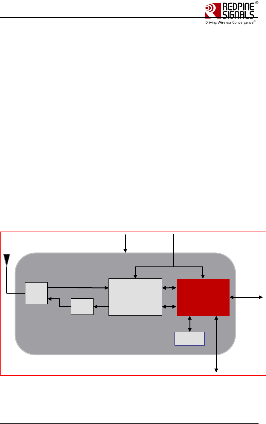
RS9110-N-11-02 System Block Diagram
RS9110-N-11-02
RF Transceiver
+
PA
Balun
EEPROM
T/R
Switch Host
Interface
3.3V
Peripheral
I/O
Frequency Reference
RS9110-LI

Redpine Signals, Inc. Proprietary and confidential Page 3
RS9110
-
N
-
11
-
02
802.11bgn
WLAN
Module
Data Sheet
Version
1.48
Table of Contents
1: Detailed Feature List ............................................................ 7
1.1: Host Interfaces...................................................................... 7
1.2: WLAN .................................................................................... 7
1.2.1: MAC .............................................................................................. 7
1.2.2: Baseband Processing.................................................................... 7
1.2.3: RF Transceiver.............................................................................. 7
1.3: Multi-Threaded Processor ...................................................... 7
1.4: Peripherals............................................................................ 8
1.5: Coexistence........................................................................... 8
1.6: Software ............................................................................... 8
1.7: Compliance and Certification.................................................. 8
2: Package Description ............................................................. 9
2.1: Top View ............................................................................... 9
2.2: Bottom View.......................................................................... 9
2.3: Package Dimensions ............................................................ 10
2.4: Recommended Reflow Profile............................................... 11
2.5: Baking Instructions ............................................................. 11
3: Pin Description ................................................................... 12
3.1: Module Pinout...................................................................... 12
3.2: Pin Description .................................................................... 12
4: Electrical Characteristics .................................................... 19
4.1: Absolute Maximum Ratings.................................................. 19
4.2: Recommended Operating Conditions .................................... 19
4.3: DC Characteristics – Digital I/O Signals ............................... 19
4.4: AC Characteristics – Digital I/O Signals................................ 20
4.4.1: SDIO Interface ........................................................................... 20
4.4.1.1: Full Speed Mode.................................................................... 20
4.4.1.2: High Speed Mode .................................................................. 21
4.4.2: SPI Interface .............................................................................. 21
4.4.2.1: Full Speed Mode.................................................................... 22
4.4.2.2: High Speed Mode .................................................................. 22
4.4.3: Reset Timing............................................................................... 23
4.4.4: JTAG Interface............................................................................ 24
5: Module Power Consumption ............................................... 25
6: Performance Specifications ................................................ 26
6.1: Wireless Specifications ........................................................ 26
6.2: Receive Characteristics........................................................ 26
6.2.1: Sensitivity................................................................................... 26
6.3: Standards Compliance ......................................................... 26
7: Software Details................................................................. 28
7.1: Architecture ........................................................................ 28
7.2: Details................................................................................. 28
7.2.1: 802.1x Supplicant....................................................................... 29
7.2.2: Configuration Utility ................................................................... 29

Redpine Signals, Inc. Proprietary and confidential Page 4
RS9110
-
N
-
11
-
02
802.11bgn
WLAN
Module
Data Sheet
Version
1.48
7.2.3: WLAN Driver ............................................................................... 29
7.2.4: HAL- Hardware Abstraction Layer............................................... 29
7.2.5: Upper MAC.................................................................................. 29
7.2.6: Lower MAC.................................................................................. 30
7.3: OS Support .......................................................................... 30
8: Ordering Information ......................................................... 31
8.1: Contact Information ............................................................ 31
8.2: Device Ordering Information................................................ 31
8.2.1: Device Packaging........................................................................ 31
8.3: Collateral............................................................................. 32

Redpine Signals, Inc. Proprietary and confidential Page 5
RS9110
-
N
-
11
-
02
802.
11bgn
WLAN
Module
Data Sheet
Version
1.48
Table of Figures
Figure 1: Top View of the Module ................................................................. 9
Figure 2: Bottom View of the Module ........................................................... 9
Figure 3: Package and Pad dimensions ...................................................... 10
Figure 4: Reflow Profile.............................................................................. 11
Figure 5: Pinout of the Module ................................................................... 12
Figure 6: Interface Timings – SDIO Interface Full-Speed Mode.................. 20
Figure 7: Interface Timings – SDIO Interface High-speed Mode ................ 21
Figure 8: SPI Protocol ................................................................................ 22
Figure 9: Interface Timings – SPI Interface Full-Speed Mode .................... 22
Figure 10: Interface Timings – SPI Interface High-Speed Mode................. 23
Figure 11: Reset Pin Timing Diagram ......................................................... 24
Figure 12: Interface Timings – JTAG Interface........................................... 24
Figure 13: RS9110-N-11-02 Software Architecture .................................... 28

Redpine Signals, Inc. Proprietary and confidential Page 6
RS9110
-
N
-
11
-
02
802.11bgn
WLAN
Module
Data Sheet
Version
1.48
List of Tables
Table 1: Absolute Maximum Ratings........................................................... 19
Table 2: Recommended Operating Conditions ............................................ 19
Table 3: Input/Output DC Characteristics .................................................. 20
Table 4: AC Characteristics – SDIO Interface Full-Speed Mode .................. 20
Table 5: AC Characteristics – SDIO Interface High-Speed Mode................. 21
Table 6: AC Characteristics – SPI Interface Full-Speed Mode ..................... 22
Table 7: AC Characteristics – SPI Interface High-Speed Mode.................... 23
Table 8: AC Characteristics – JTAG Interface ............................................. 24
Table 9: Wireless Specificiation.................................................................. 26
Table 10: Receive sensitivity ...................................................................... 26

Redpine Signals, Inc. Proprietary and confidential Page 7
RS9110
-
N
-
11
-
02
802.11bgn
WLAN
Module
Data Sheet
Version 1.48
1: Detailed Feature List
1.1: Host Interfaces
• SDIO
• Version 2.0-compatible
• Supports SD-SPI, 1-bit, and 4-bit SDIO modes
• Operation up to a maximum clock speed of 50 MHz
• SPI Interface
• Operation up to a maximum clock speed of 80 MHz
1.2: WLAN
1.2.1: MAC
• Conforms to IEEE 802.11b/g/n/e/i standards for MAC1
• Dynamic selection of fragment threshold, data rate, and antenna
depending on the channel statistics
• Hardware accelerators for WEP 64/128-bit and AES
• WPA, WPA2, WPA2-Enterprise, Voice Personal, WPS (PIN/PBC),
• WMM and WMM-PS support
• AMPDU and AMSDU aggregation for high performance
• Firmware downloaded from host based on application
1.2.2: Baseband Processing
• Supports DSSS (1, 2 Mbps) and CCK (5.5, 11 Mbps) modes
• Supports all OFDM data rates (6, 9, 12, 18, 24, 36, 48, and 54 Mbps)
• Supports IEEE 802.11n single-stream modes with data rates up to 65
Mbps
• Supports long, short, and HT preamble modes
• High-performance multipath compensation in OFDM, DSSS, and CCK
modes
1.2.3: RF Transceiver
• Highly integrated 2.4 GHz transceiver with direct conversion architecture
• Receiver with 38 dB RF selectable gain range and 60 dB baseband variable
gain range
• Power amplifier with 17 dBm maximum output power
• Integrated LNA, BPF, and T/R switch
1.3: Multi-Threaded Processor
• RISC-based pipelined architecture
1 Compliance to inter-operability specifications based on the standards

Redpine Signals, Inc. Proprietary and confidential Page 8
RS9110
-
N
-
11
-
02
802.11bgn
WLAN
Module
Data Sheet
Version
1.48
• Non-blocking thread operation
• Processing capability of up to 118 million instructions per second (MIPS)
at 118 MHz
1.4: Peripherals
• I2C interface with support for multiple masters and high-speed mode
• SPI peripheral interface
• UART interface with programmable baud-rate generator
• GPIO interface
1.5: Coexistence
• Flexible BT coexistence mechanism with 3-wire hardware interface
1.6: Software
• Drivers for Windows Embedded CE, Windows XP and Linux
• Control and management GUI
• Embedded software for complete WLAN functionality including 802.11n
aggregation and Block-ACK, auto rate adaptation, security, and QoS
modes
1.7: Compliance and Certification
• Reference design certified for Wi-Fi 802.11n, WPA, WPA2, WPA2-
Enterprise, WMM, WMM-PS, WPS, Voice-Personal
• FCC, IC, and CE certified
• RoHS (Restriction of Hazardous Substances) compliant
Redpine Signals, Inc. Proprietary and confidential Page 9
RS9110
-
N
-
11
-
02
802.11bgn
WLAN
Module
Data Sheet
Version
1.48
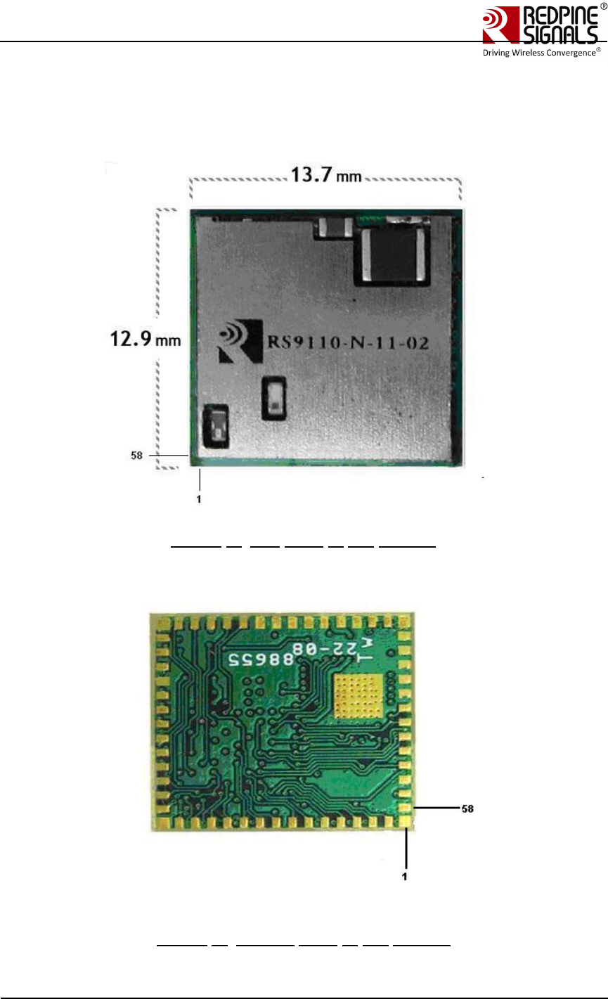
2: Package Description
2.1: Top View
Figure 1: Top View of the Module
2.2: Bottom View
Figure 2: Bottom View of the Module
Redpine Signals, Inc. Proprietary and confidential Page 10
RS9110
-
N
-
11
-
02
802.11bgn
WLAN
Module
Data Sheet
Version
1.48
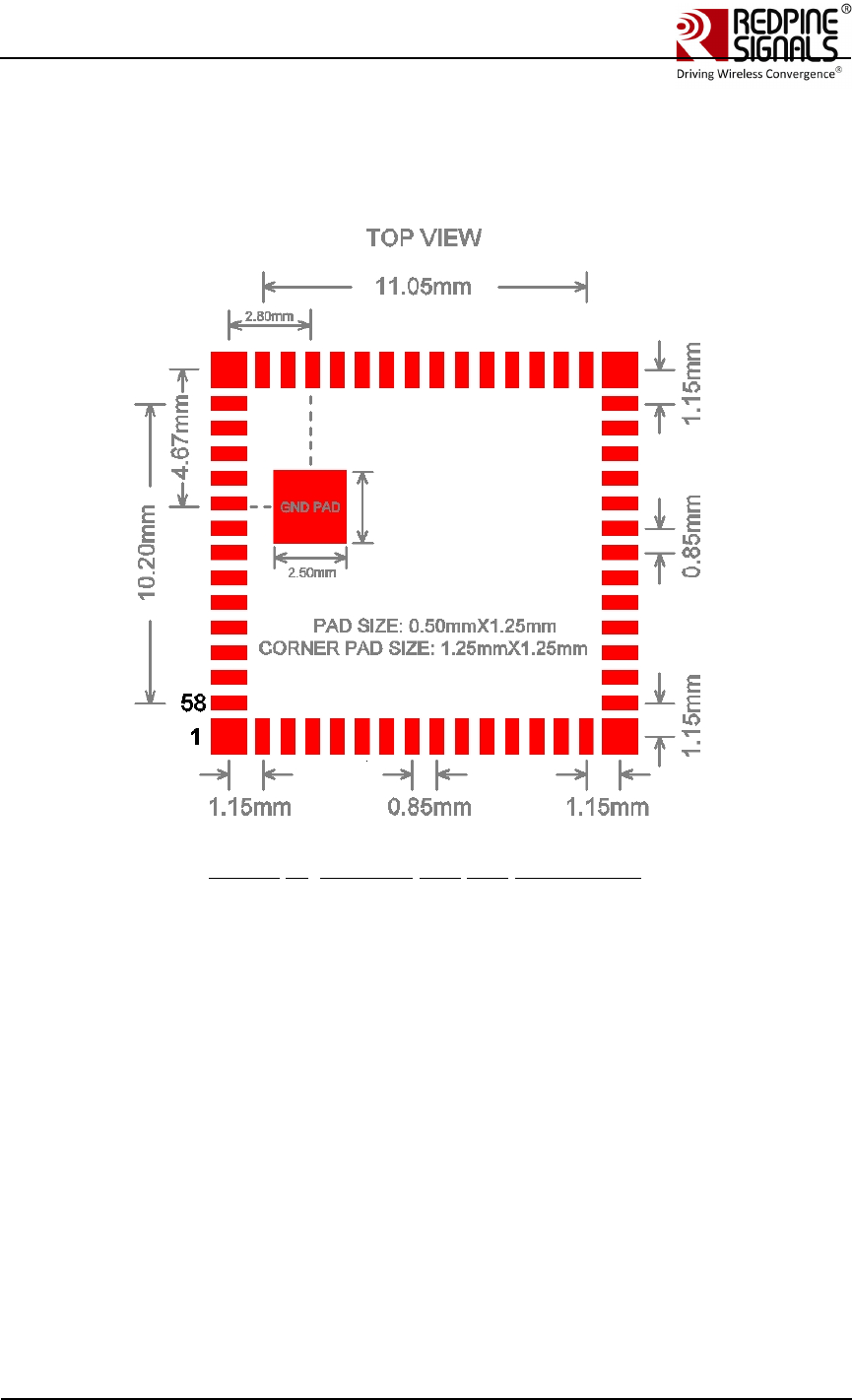
2.3: Package Dimensions
The module measures 13.7 x 12.9 x 1.7 mm.
Figure 3: Package and Pad dimensions
Redpine Signals, Inc. Proprietary and confidential Page 11
RS9110
-
N
-
11
-
02
802.11bgn
WLAN
Module
Data Sheet
Version
1.48
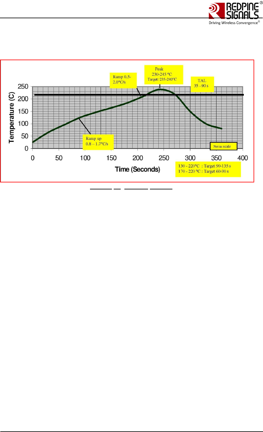
2.4: Recommended Reflow Profile
Figure 4: Reflow Profile
Note: The profile shown is based on SAC 305 solder (3% silver, 0.5%
copper). We recommend the ALPHA OM-338 lead-free solder paste. This
profile is provided mainly for guidance. The total dwell time depends on the
thermal mass of the assembled board and the sensitivity of the components
on it.
2.5: Baking Instructions
The RS9110-N-11-02 package is moisture sensitive and devices must be
handled appropriately. After the devices are removed from their vacuum
sealed packs, they should be taken through reflow for board assembly within
168 hours at room conditions, or stored at under 10% relative humidity. If
these conditions are not met, the devices must be baked before reflow. The
recommended baking time is nine hours at 125° C.
Redpine Signals, Inc. Proprietary and confidential Page 12
RS9110
-
N
-
11
-
02
802.11bgn
WLAN
Module
Data Sheet
Version
1.48
3: Pin Description
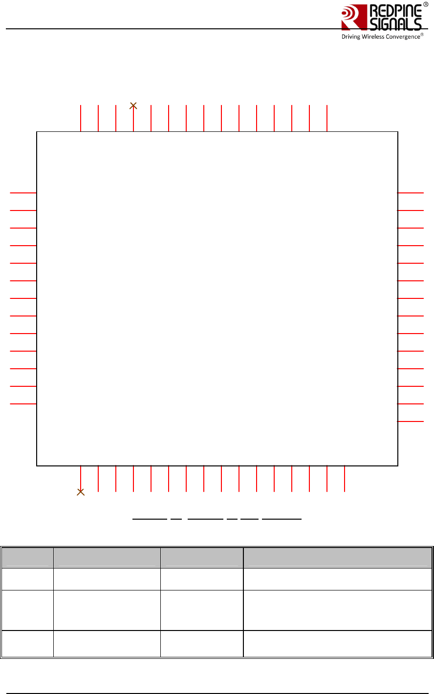
3.1: Module Pinout
AGND
56
RF_OUT
57
AGND
58
GND 25
NC
1
DVDD33 17
PSPI_CSN0 40
LED_ON 24
MODE_SEL_1
51
VRF28
52
XTAL_EN 23
REF_CLK
14
PSPI_CSN1
46
SLEEP_CLK_X1 35
SLEEP_CLK_X2 34
I2C_SCL
6
I2C_SDA
7
GND 30
GND 26
RESETn
15
MODE_SEL_2 41
WLAN_ACTIVE 31
BT_PRIORITY 29
SLEEP_CLK_IN 32
HOST_WAKEUP_INT
53
NC 42
VRF33 43
VRF33 44
SDIO_DATA3
13
SDIO_DATA2
12
SDIO_DATA1
11
SDIO_DATA0
10
SDIO_CMD
9
SDIO_CLK
8
GPIO_1
55
GND
16
VINBCKDC 27
VINLDOP123 39
FBDC1P3 38
VOUTBCKDC1P3 37
UART2_IN 36
UART1_RTS 22
UART1_CTS 21
UART1_OUT 18
UART1_IN 19
TCK
2
TDI
3
TMS
4
TDO
5
XTAL_EN_IP
54
GPIO_0 28
BT_ACTIVE 33
UART2_OUT 20
PSPI_MISO
47
GND 45
MODE_SEL_0
50
PSPI_CLK
49
PSPI_MOSI
48
RS9110-N-11-02 Module
Figure 5: Pinout of the Module
3.2: Pin Description
Pin No. Pin Name Pin Type Description
1) NC NC This pin is to be left unconnected
2) TCK Input
This is a JTAG input pin, and
recommended to be connected to
ground.
3) TDI Input This is a JTAG input pin, and
recommended to be connected to

Redpine Signals, Inc. Proprietary and confidential Page 13
RS9110
-
N
-
11
-
02
802.11bgn
WLAN
Module
Data Sheet
Version
1.48
Pin No. Pin Name Pin Type Description
ground.
4) TMS Input
This is a JTAG input pin, and
recommended to be connected to
ground.
5) TDO Output This is a JTAG output pin, and
recommended to be left open.
6) I2C_SCL Inout
I2C Bus Clock. By default, and
unless firmware is modified, this
line is programmed as an output
and should be left open.
7) I2C_SDA Inout
I2C Bus Data. By default, and
unless firmware is modified, this
line is programmed as an output
and should be left open.
8) SDIO_CLK/SPI_CL
K Input SDIO/SPI interface clock input
9) SDIO_CMD/SPI_CS
Input
SDIO 4-bit: Command/Response
SDIO 1-bit: Command
SDIO-SPI: SPI_CS
SPI: SPI_CS
10) SDIO_DATA0/MOS
I Inout
SDIO 4-bit: Data [0]
SDIO 1-bit: Data line
SDIO-SPI: SPI_DIN (MOSI)
SPI: SPI_DIN
11) SDIO_DATA1/MIS
O Inout
SDIO 4-bit: Data [1]/Interrupt
SDIO 1-bit: Interrupt
SDIO-SPI: Reserved
SPI: SPI_DOUT
12) SDIO_DATA2/SPI_
INTR Inout
SDIO 4-bit: Data [2]/Read wait
SDIO 1-bit: Read wait
SDIO-SPI: SPI_DOUT
SPI: SPI_INT2
13) SDIO_DATA3 Inout
SDIO 4-bit: Data [3]
SDIO 1-bit: Reserved
SDIO-SPI: SPI_INT
SPI: Reserved
14) REF_CLK Input Reference Clock source: 40MHz.
2 SPI_INT is used to raise an interrupt, level triggered active_high, upon events in
the chip pertaining to SPI host interface.

Redpine Signals, Inc. Proprietary and confidential Page 14
RS9110
-
N
-
11
-
02
802.11bgn
WLAN
Module
Data Sheet
Version
1.48
Pin No. Pin Name Pin Type Description
15) RESET_n Input
Power-on reset. Active low, and
required to be active for at least 20
ms
16) GND Ground Ground
17) DVDD33 Power 3.3 Volts Input to the I/O Rail
18) UART1_OUT Inout
UART Port1 output. This is a
firmware configured GPIO pin.
Where not used, it should be left
open. The default firmware does
not use this pin.
19) UART1_IN Inout
UART Port1 input. This is a
firmware configured GPIO pin.
Where not used, it should be left
open. The default firmware does
not use this pin.
20) UART2_OUT Inout
UART Port2 output. This is a
firmware configured GPIO pin.
Where not used, it should be left
open. The default firmware does
not use this pin.
21) UART1_CTS Inout
UART Port1 CTS. This is a firmware
configured GPIO pin. Where not
used, it should be left open. The
default firmware does not use this
pin.
22) UART1_RTS Inout
UART Port1 RTS. This is a firmware
configured GPIO pin. Where not
used, it should be left open. The
default firmware does not use this
pin.
23) XTAL_EN Output
This signal controls an external
reference clock oscillator for power-
save purposes.
1 – Enable
0 – Disable
24) LED_ON Inout
LED Control signal. Indicates
activity on WLAN – the device pulls
this line low when the module is
activated. To be connected to the
Cathode of an LED with a
recommended series resistor of 820
ohms to VDD.
25) GND Ground Ground

Redpine Signals, Inc. Proprietary and confidential Page 15
RS9110
-
N
-
11
-
02
802.11bgn
WLAN
Module
Data Sheet
Version
1.48
Pin No. Pin Name Pin Type Description
26) GND Ground Ground
27) VINBCKDC Power 3.3 Volts input to the
PMU
28) GPIO_0 Inout
General purpose input/output. In
the default configuration this is
programmed as an output and
should be left unconnected.
29) BT_PRIORITY Input
Indicates through ‘logic high’ that
BT is transmitting high priority
traffic. This is a firmware configured
GPIO pin. Where not used, it should
be left open.
30) GND Ground Ground
31) WLAN_ACTIVE Output
When configured for BT
coexistence, this is an output and
indicates with logic high that WLAN
activity is in progress. When low,
BT device has the opportunity to
transmit. This is a firmware
configured GPIO pin. Where not
used, it should be left open.
32) SLEEP_CLK_IN Input
Sleep clock input is NC for default
firmware.
An external 32KHz signal is fed to
this pin if the external 32KHz input
mode is selected. Please refer to
notes on Sleep Clock Input for more
details.
33) BT_ACTIVE Input
This signal may be used by an
external Bluetooth device to
indicate its activity or impending
activity. This signal is not used in
the default BT coexistence
firmware. This is a firmware
configured GPIO pin. Where not
used, it should be left open.
34) SLEEP_CLK_X2 Input
32KHz crystal connection
The pin should be left open except
as describe in mode (iii) as
described in note below for Sleep
Clock Input.
35) SLEEP_CLK_X1 Input 32KHz crystal connection

Redpine Signals, Inc. Proprietary and confidential Page 16
RS9110
-
N
-
11
-
02
802.11bgn
WLAN
Module
Data Sheet
Version
1.48
Pin No. Pin Name Pin Type Description
The pin should be left grounded
except as describe in mode (iii) as
described in note below for Sleep
Clock Input.
36) UART2_IN Inout
UART-2 input. This is a firmware
configured GPIO pin. Where not
used, it should be left open.
37) VOUTBCKDC1P3 Power
Internal DC-DC convertor output. A
Schottky diode is to be placed on
this line for protection.
38) FBDC1P3 Power
Feedback for the DC-DC Converter
Input to the LDO’s. This has to be
connected to FBDC1P3.
39) VINLDOP123 Power Input to the LDO’s. Connect this to
FBDC1P3.
40) NC No-connect This pin is to be left unconnected
41) NC No-connect This pin is to be left unconnected
42) NC No-connect This pin is to be left unconnected
43) VRF33 Power 3.3 Volts input to the RF transceiver
44) VRF33 Power 3.3 Volts input to the RF transceiver
45) GND Ground Ground
46) PSPI_CSN1 Output
When enabled as a SPI interface
pin, this is the chip-select output
from SPI Master. This is a firmware
configured GPIO pin. Where not
used, it should be left open. Default
firmware does not use this pin
47) PSPI_MISO Input
When enabled as a SPI interface
pin, this is the SPI Master data
input. This is a firmware configured
GPIO pin. Where not used, it should
be left open. Default firmware does
not use this pin.
48) PSPI_MOSI Output
When enabled as a SPI interface
pin, this is the SPI Master data
output. This is a firmware
configured GPIO pin. Where not
used, it should be left open. Default
firmware does not use this pin.
49) PSPI_CLK Output When enabled as a SPI interface

Redpine Signals, Inc. Proprietary and confidential Page 17
RS9110
-
N
-
11
-
02
802.11bgn
WLAN
Module
Data Sheet
Version
1.48
Pin No. Pin Name Pin Type Description
pin, this is the SPI Master clock
output. This is a firmware
configured GPIO pin. Where not
used, it should be left open. Default
firmware does not use this pin.
50) MODE_SEL_0 Input
BOOT MODE: On no-connect, boot
parameters will be loaded from
internal flash. Should be left
unconnected so as to enable
bootloading.
51) MODE_SEL_1 Input
SDIO MODE: No connect.
SPI Mode: Connect pull down of
4.7Kohms.
52) VRF28 Power 2.8 Volts LDO O/P
53) HOST_WAKEUP_IN
T Output
This pin is a GPIO. If this is not
used, it should be left open.
This pin is to be used by those
hosts which enter into power save
mode and which are not able to
detect the regular interrupt pin in
that power save mode.
If used as HOST_WAKEUP_INT, a
pull-up or pull-down of 100K has to
be connected on this pin
based on the polarity indicated to
the firmware.
Active low requires a pull-up.
Active high requires a pull-down.
54) XTAL_EN_IP Input
This is a GPIO signal by default and
it should be left open.
If used, it can be configured
through firmware to be combined,
through a logical OR operation, with
the internal oscillator enable and
the output given on XTAL_EN pin.
This can be used when a crystal
oscillator is shared between the
WLAN module and other functional
blocks in the system.
55) GPIO_1 Inout
General purpose input/output. In
the default configuration this is
programmed as an output and
should be left unconnected.

Redpine Signals, Inc. Proprietary and confidential Page 18
RS91
10
-
N
-
11
-
02
802.11bgn
WLAN
Module
Data Sheet
Version
1.48
Pin No. Pin Name Pin Type Description
56) GND Ground Ground
57) RF_OUT Rfin/Rfout Antenna Port-50 ohms Impedance
58) GND Ground Ground
Notes:
• Some interfaces are not used in the default configuration or mode of
operation. These include the I2C, GPIO, and UART interfaces. These may
be used in custom applications with appropriate firmware. These are all
fundamentally Inout signals and may be configured either as input or
output.
• JTAG functionality is not included in default firmware.
• The Bluetooth coexistence interface (BT_PRIORITY, WLAN_ACTIVE,
BT_ACTIVE) are also general purpose I/O signals and may be
reprogrammed to be inputs or outputs as needed. Please refer to BT
coexistence application note for more details.
• Sleep clock input:
This should be a 32 kHz clock and is used in power-save modes, if
chosen. During the low power sleep state, the module's wake-up
timer uses the sleep clock - which can have one of three sources
i) an internal 32 kHz oscillator
This is the recommended mode of operation.
ii) a 32 kHz clock fed into this pin,
iii) a 32 kHz crystal connected to pins SLEEP_CLK_X2 and
SLEEP_CLK_X1.
NOTE: The recommended mode of operation is i).
This is a firmware configured GPIO pin and where not used, should be
left open.
By default, an internal 32KHz oscillator is used.
• Please refer to the Module Integration Guide document for reference
schematics and the list of recommended part numbers.
• Please contact Redpine for application notes or for customization of a
solution.
Redpine Signals, Inc. Proprietary and confidential Page 19
RS9110
-
N
-
11
-
02
802.11bgn
WLAN
Module
Data Sheet
Version
1.48
4: Electrical Characteristics
4.1: Absolute Maximum Ratings
Absolute maximum ratings in the table given below are the values beyond
which the device could be damaged. Functional operation at these conditions
or beyond these conditions is not guaranteed.
Parameter Symbol Value Units
Input Supply voltage Vin 3.6 V
Supply voltage for I/O Rail DVDD33
3.6 V
Supply Voltage for the RF VRF33 3.6 V
RF Input Level RFIN 10 dBm
Storage temperature Tstore -65 to
150
°C
Electrostatic discharge tolerance (HBM) ESDHBM 2000 V
Electrostatic discharge tolerance (MM) ESDMM 200 V
Electrostatic discharge tolerance (CDM) ESDCDM 500 V
Table 1: Absolute Maximum Ratings
4.2: Recommended Operating Conditions
Parameter Symbol
Min. Typ. Max. Units
Input Supply voltage VIN 3.1 3.3 3.6 V
Supply voltage for I/O Rail DVDD33
3.1 3.3 3.6 V
Supply Voltage for the RF VRF33 3.1 3.3 3.6 V
Ambient temperature Ta -40 25 85 °C
Table 2: Recommended Operating Conditions
Relative Humidity: 5 to 95%, non-condensing
4.3: DC Characteristics – Digital I/O Signals
Parameter Min. Typ. Max. Units
Input high voltage 2 - 3.6 V
Redpine Signals, Inc. Proprietary and confidential Page 20
RS9110
-
N
-
11
-
02
802.1
1bgn
WLAN
Module
Data Sheet
Version
1.48
Parameter Min. Typ. Max. Units
Input low voltage -0.3 - 0.8 V
Output low voltage - - 0.4 V
Output high voltage 2.4 - - V
Input leakage current (at 3.3V or 0V) - - ±10 µA
Tristate output leakage current (at 3.3V
or 0V)
- - ±10 µA
Table 3: Input/Output DC Characteristics
4.4: AC Characteristics – Digital I/O Signals
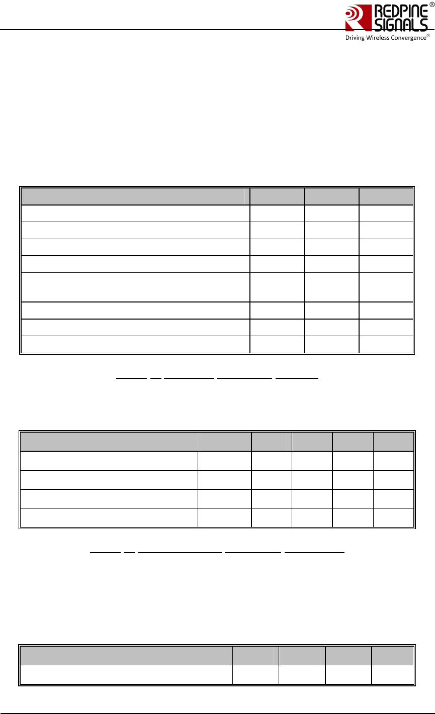
4.4.1: SDIO Interface
4.4.1.1: Full Speed Mode
Parameter Symbol
Min. Typ. Max. Units
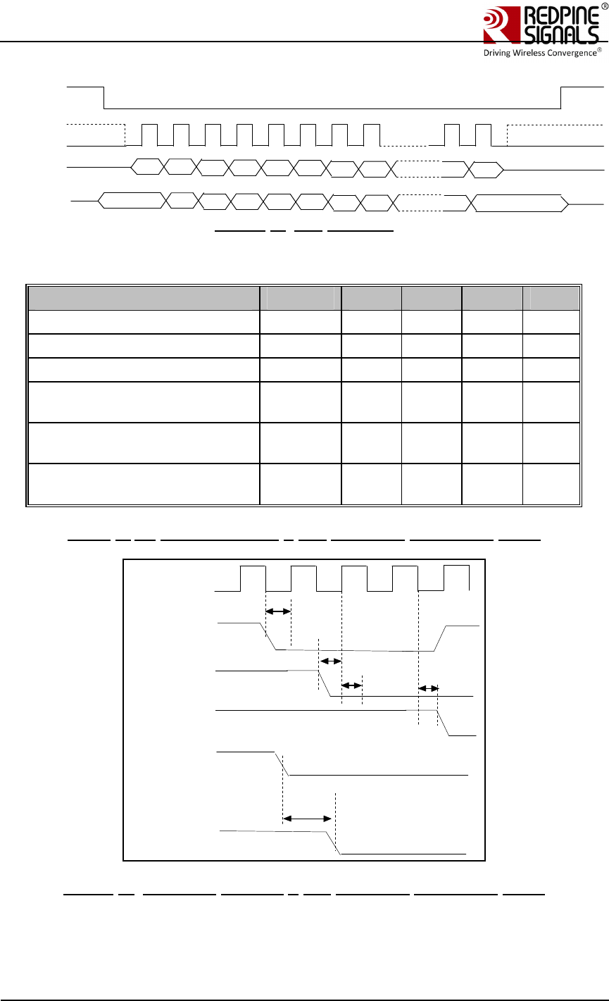
SDIO_CLK Tsdio 0 25 MHz
SDIO_DATA, input setup time Ts 5 - - ns
SDIO_DATA, input hold time Th 2 - - ns
SDIO_DATA, clock to output
delay
Tod 5 - 11 ns
Table 4: AC Characteristics – SDIO Interface Full-Speed Mode
SDIO_DATA
Tod
SDIO_DATA
SDIO_CLK
Th
Ts
Figure 6: Interface Timings – SDIO Interface Full-Speed Mode
Redpine Signals, Inc. Proprietary and confidential Page 21
RS9110
-
N
-
11
-
02
802.11bgn
WLAN
Module
Data Sheet
Version
1.48
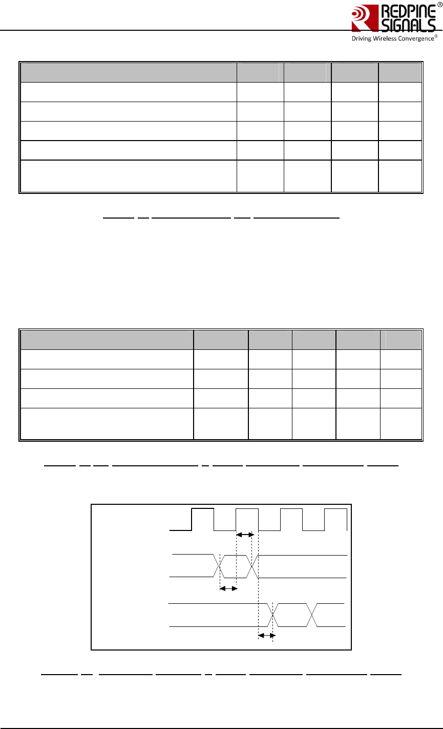
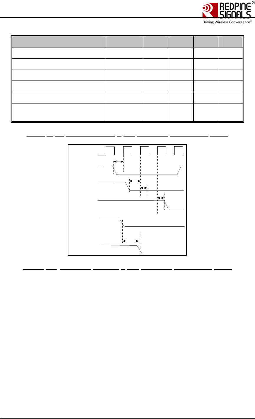
4.4.1.2: High Speed Mode
Parameter Symbol
Min. Typ. Max. Units
SDIO_CLK Tsdio 25 - 50 MHz
SDIO_DATA, input setup time Ts 5 - - ns
SDIO_DATA, input hold time Th 2 - - ns
SDIO_DATA, clock to output
delay
Tod 5.5 - 12.5 ns
Table 5: AC Characteristics – SDIO Interface High-Speed Mode
SDIO_CLK
SDIO_DATA
SDIO_DATA
Tod
Th
Ts
Figure 7: Interface Timings – SDIO Interface High-speed Mode
4.4.2: SPI Interface
The SPI Interface is a full duplex serial host interface, which supports 8-bit and 32-
bit data granularity. It also supports gated mode of SPI clock and both the low and
the high frequency modes. Incase of low frequency host, the data is driven on the
falling edge and sampled on the rising edge and hence, it should be ensured that a
valid data is present on the bus at the immediate rising edge after the SPI chip select
is driven low. For high frequency transmission the data is driven as well as sampled
on rising edge.
This interface has the interrupt pin along with the regular signals clock, chip select,
data in and data out. Device interrupts the host processor regarding the packet
pending event through this interrupt pin. This is an active high signal, and this will
get cleared only after clearing the source of the interrupt, i.e. reading the pending
packet from device. This will be generally connected to a GPIO pin of host platform
and GPIO has to be configured for detecting interrupt on level high, and interrupt
from this GPIO has to be mapped to driver ISR.
The SPI Slave supports mode 0 (SPI_POL=0, SPI_PHA=0) and mode 3 (SPI_POL=1,
SPI_PHA=1).
Redpine Signals, Inc. Proprietary and confidential Page 22
RS9110
-
N
-
11
-
02
802.11bgn
WLAN
Module
Data Sheet
Version
1.48
Bit 7 Bit 6 Bit 5 Bit 4 Bit 3 Bit 2 Bit 1 Bit 0
SPI_CS
SPI_CLK
SPI_DIN
SPI_DOUT Bit 7 Bit 6 Bit 5 Bit 4 Bit 3 Bit 2 Bit 1 Bit 0
Bit 0
Bit 0
Mode 0
Mode 3
Figure 8: SPI Protocol
4.4.2.1: Full Speed Mode
Parameter Symbol Min. Typ. Max. Units
SPI_CLK Tspi 0 25 MHz
SPI_CS to output delay Tcs 3.5 - 7.5 ns
SPI CS to input setup time Tcst 5.5 - -
SPI_DIN (MOSI), input setup
time
Ts 1 - - ns
SPI_DIN (MOSI), input hold
time
Th 1.5 - ns
SPI_DOUT (MISO), clock to
output delay
Tod 4 - 9 ns
Table 6: AC Characteristics – SPI Interface Full-Speed Mode
SPI_CLK
SPI_CS
SPI_MOSI
SPI_MISO
Tcst
Tod
Ts
Th
Tcs
SPI_CS
SPI_MISO
Figure 9: Interface Timings – SPI Interface Full-Speed Mode
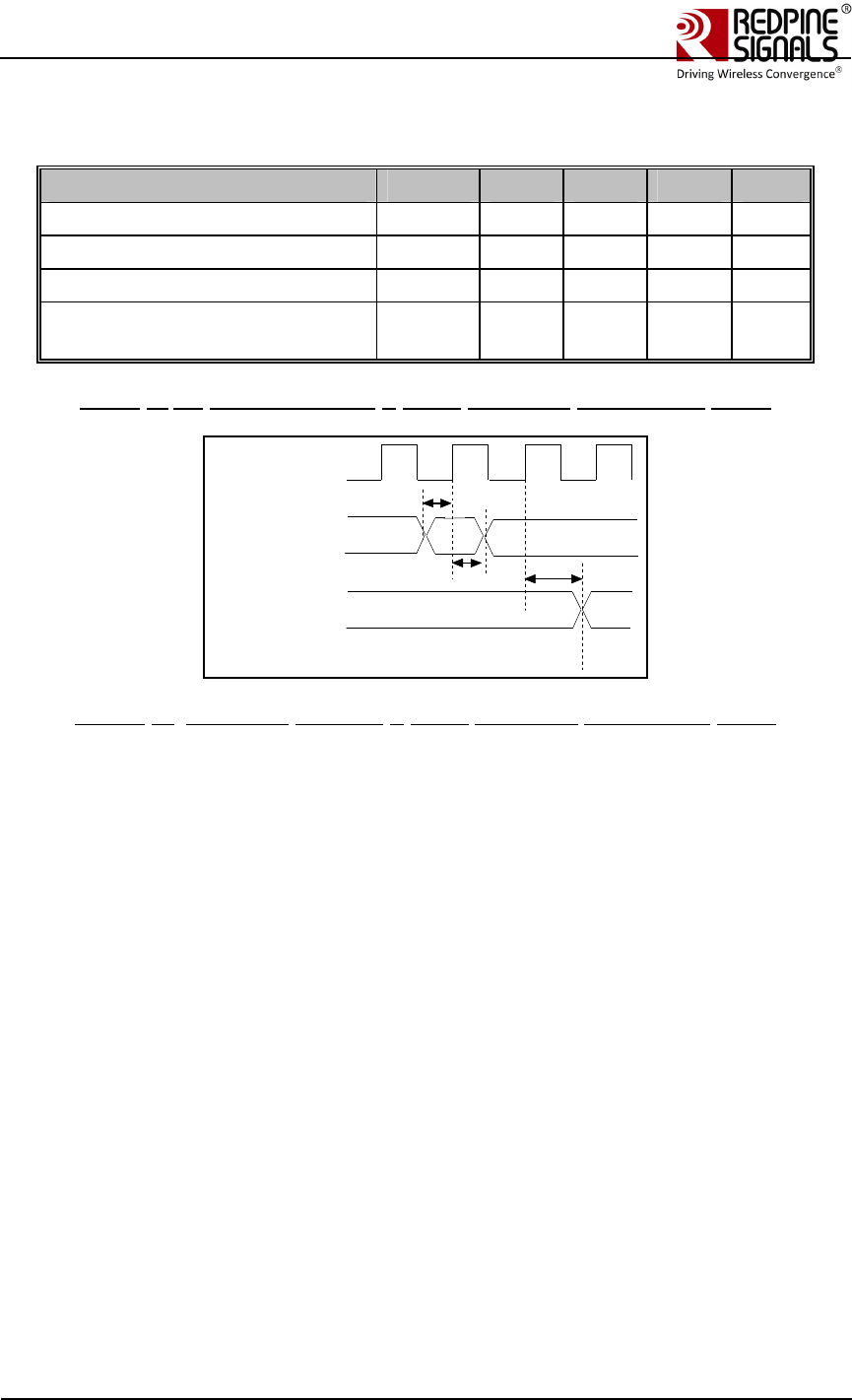
4.4.2.2: High Speed Mode
Redpine Signals, Inc. Proprietary and confidential Page 23
RS9110
-
N
-
11
-
02
802.11bgn
WLAN
Module
Data Sheet
Version
1.48
Parameter Symbol Min. Typ. Max. Units
SPI_CLK Tspi 25 - 75 MHz
SPI_CS to output delay Tcs 3.5 - 7.5 ns
SPI CS to input setup time Tcst 5.5 - -
SPI_MOSI, input setup time Ts 1 - ns
SPI_MOSI, input hold time Th 1.5 - ns
SPI_MISO, clock to output
delay
Tod 4 - 9.5 ns
Table 7: AC Characteristics – SPI Interface High-Speed Mode
SPI_CLK
SPI_CS
SPI_MOSI
SPI_MISO
Ts
Tod
Th
Tcst
Tcs
SPI_CS
SPI_MISO
Figure 10: Interface Timings – SPI Interface High-Speed Mode
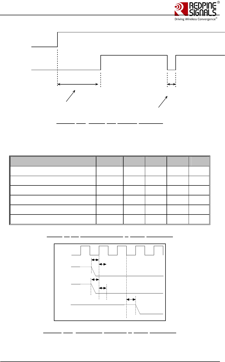
4.4.3: Reset Timing
Following diagram shows the timing requirement for reset_n input in two
scenarios. If external power supply (instead of 2.8V coming out of the
module) is used for reference clock crystal oscillator, it has to be taken
care that oscillator output is stable before releasing reset. When using
2.8V coming out of module as power supply for reference clock crystal
oscillator, maximum oscillator stabilization time after feeding power has
to be 10ms.
A. Powerup
B. Giving hard reset without power reset
Redpine Signals, Inc. Proprietary and confidential Page 24
RS9110
-
N
-
11
-
02
802.11bgn
WLAN
Module
Data Sheet
Version
1.48
20msec
1msec
reset_n
3.3V input
supply
AB
Figure 11: Reset Pin Timing Diagram
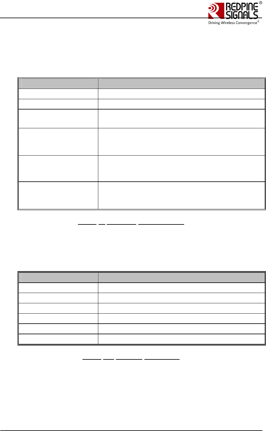
4.4.4: JTAG Interface
Parameter Symbol
Min. Typ. Max. Units
TCK Tjtag 0 5 MHz
TDI, setup time Tstdi 5 - - ns
TDI, hold time Thtdi 5 - - ns
TMS, setup time Tstms 5 - - ns
TMS, hold time Thtms 5 - - ns
TDO, clock to output valid Totdo 0 - 14 ns
Table 8: AC Characteristics – JTAG Interface
Tstdi
Tstms
Totdo
Thtdi
Thtms
TCK
TDI
TMS
TDO
Figure 12: Interface Timings – JTAG Interface

Redpine Signals, Inc. Proprietary and confidential Page 25
RS9110
-
N
-
11
-
02
802.11bgn
WLAN
Module
Data Sheet
Version
1.48
5: Module Power Consumption
The following is the typical power consumption data for the RS9110-N-
11-02 802.11b/g/n module. A single point 3.3V supply is used. Transmit
power at antenna is 15dBm.
Mode Conditions Module
Current
Standard Operational Modes – 2.4 GHz
Data Transfer –
Transmit TCP
1Mbps throughput 19 mA
Data Transfer –
Transmit TCP
2Mbps throughput 30 mA
Data Transfer –
Transmit TCP
22 Mbps throughput
200 mA
Data Transfer –
Receive TCP
1Mbps throughput 17 mA
Data Transfer –
Receive TCP
2Mbps throughput 24 mA
Data Transfer –
Receive TCP
22 Mbps throughput
149 mA
Listen Receive mode, with no active packet
reception in progress
110 mA
Standby Remaining connected to the Access Point,
in Power-Save mode, with DTIM=3, beacon
interval of 200 ms
1.10 mA
Sleep Not connected to an AP; ready to connect
upon driver command. The module can
transition to any active mode in less than
2.5 ms.
0.52 mA
Note:
1. The current numbers mentioned include the current drawn by the crystal
oscillator.
2. Applications where wireless LAN module is inactive for extended periods of time
an external power switch can be integrated. This may be used to obtain idle current
of less than 5 uAmp which would be the leakage current of the power switch.
Redpine Signals, Inc. Proprietary and confidential Page 26
RS9110
-
N
-
11
-
02
802.11bgn
WLAN
Module
Data Sheet
Version
1.48
6: Performance Specifications
6.1: Wireless Specifications
Feature Description
Frequency Band 2.400 – 2.500 GHz (2.4 GHz ISM band)
Frequency Reference 40 MHz
Modulation OFDM with BPSK, QPSK, 16-QAM, and 64-QAM
802.11b with CCK and DSSS
Supported Data Rates 802.11n: 6.5, 13, 19.5, 26, 39, 52, 58.5, 65 Mbps
802.11g: 6, 9, 12, 18, 24, 36, 48, 54 Mbps
802.11b: 1, 2, 5.5, 11 Mbps
802.11n Features MCS 0-7, STBC, RIFS, Greenfield Protection
A-MPDU, A-MSDU Aggregation with Block-ack,
PSMP, and MTBA
Typical Transmit Power
(+/- 2 dBm)
17 dBm for 802.11b DSSS
17 dBm for 802.11b CCK
15 dBm for 802.11g/n OFDM
Table 9: Wireless Specificiation
6.2: Receive Characteristics
6.2.1: Sensitivity
Data Rate Typical Sensitivity (+/- 1.5 dBm)
1 Mbps -97.0 dBm (< 8% PER)
2 Mbps -93.0 dBm (< 8% PER)
11 Mbps -88.9 dBm (< 8% PER)
6 Mbps -91.0 dBm (<10% PER)
54 Mbps -75.0 dBm (< 10% PER)
65 Mbps -71.9 dBm (< 10% PER)
Table 10: Receive sensitivity
6.3: Standards Compliance
RS9110-N-11-02 is compliant with the requirements of IEEE 802.11b,
802.11g, and 802.11n that include the following:
• Transmit Spectral Mask
• Transmit Center Frequency Leakage

Redpine Signals, Inc. Proprietary and confidential Page 27
RS9110
-
N
-
11
-
02
802.11bgn
WLAN
Module
Data Sheet
Version
1.48
• Transmit Center Frequency Tolerance
• Symbol Clock Frequency Tolerance
• Transmit Constellation error
• Receiver Adjacent Channel Interference Rejection
• Receiver Non-adjacent Channel Rejection
• Receiver Minimum Input Level
• Receiver Maximum Input Level
Redpine Signals, Inc. Proprietary and confidential Page 28
RS9110
-
N
-
11
-
02
802.11bgn
WLAN
Module
Data Sheet
Version
1.48
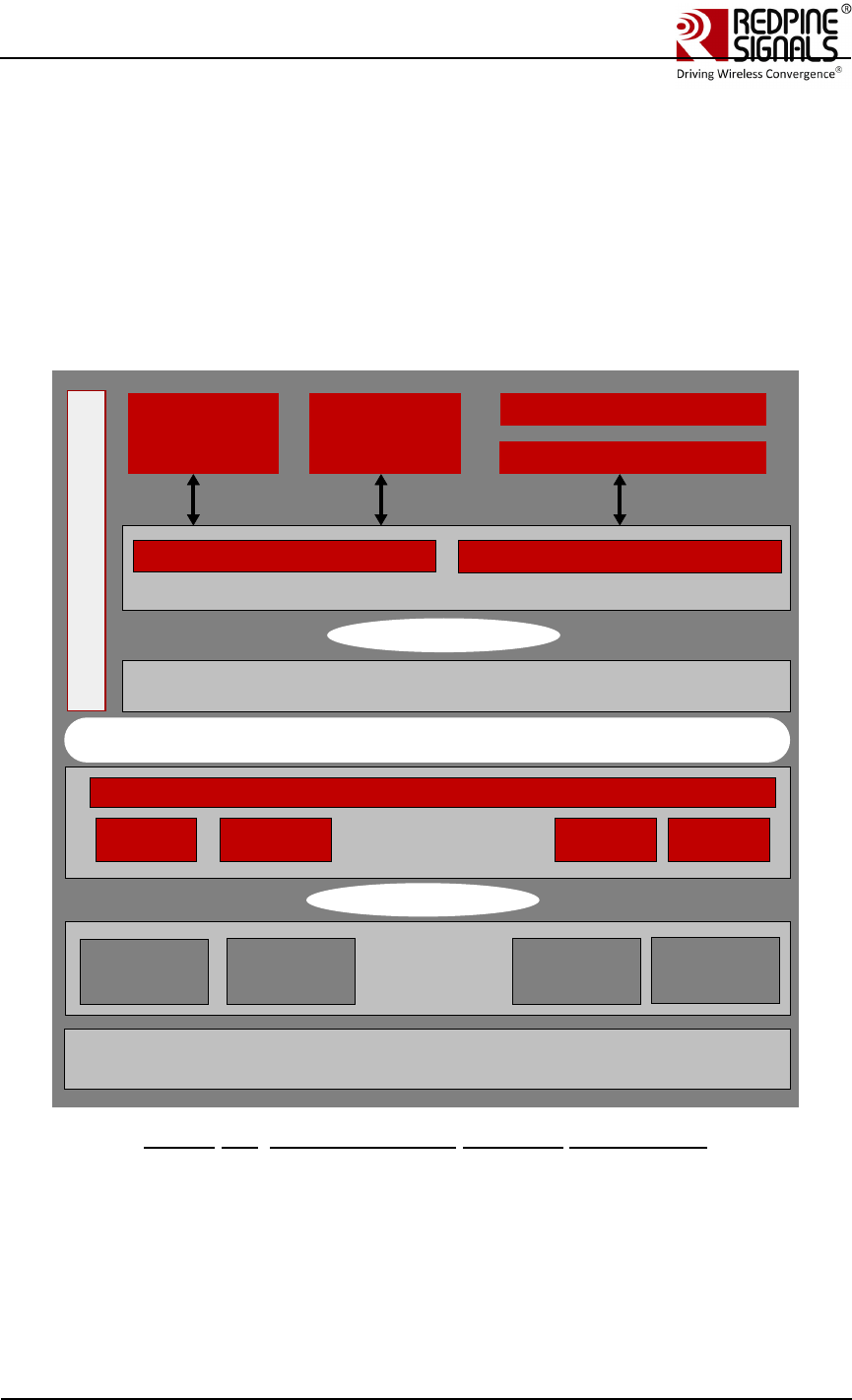
7: Software Details
The RS9110-N-11-02 provides a zero-host-load system architecture by
implementing most of the 802.11 MAC functions in its internal multi-threaded
ThreadArch™ processor. The driver consumes less than 5 MIPS from the host
processor, giving the freedom to the host processor to run its own
applications.
7.1: Architecture
The following diagram depicts the software architecture of the solution.
O
P
E
R
A
T
I
N
G
S
Y
S
T
E
M
BBP/RF
Lower MAC
Upper MAC
Host Interface Module
IPSec Power
Save WMM Roaming
Encryption/
Decryption Auto Rate
MPDU/MSDU
Aggregation
802.11 MAC
Management
HAL
Hardware Interface - SDIO/SPI
WLAN Host Driver
SME Network Interface
802.1X
Supplicant
WLAN
Configuration
Utility TCP/IP Stack
Network Applications
HAL Interface
Packet Interface
Management
Interface
Data
Interface
Figure 13: RS9110-N-11-02 Software Architecture
7.2: Details
This section provides an overview of the functionality of each of the key
modules in the WLAN system.

Redpine Signals, Inc. Proprietary and confidential Page 29
RS9110
-
N
-
11
-
02
802.11bgn
WLAN
Module
Data Sheet
Version
1.48
7.2.1: 802.1x Supplicant
• WPA/WPA2-Personal mode functionality
• WPA/WPA2-EAP exchanges for entreprise mode
• Key negotiation and management – WEP, TKIP, and CCMP
• Pre-authentication and PMKSA caching for roaming
7.2.2: Configuration Utility
• It is a user-mode application to manage the wireless network connection
• SSID selection
• Channel and rate selection
• Key management
• Configuration of 802.11 parameters
7.2.3: WLAN Driver
• Consumes < 5 MIPS from host processor
• Initialization module
• Baseband and RF programming
• Firmware downloading
• TCP/IP Network Interface Layer
• Transmission of TCP/IP packets
• Indicating received TCP/IP packets
• 802.11 Station Management Module
• Interaction with HAL layer – SDIO and SPI
• Power-save modes
o Sleep
o Standby
7.2.4: HAL- Hardware Abstraction Layer
• HAL layer changes depending on the host interface used
• SPI Interface – SPI host controller driver
• SDIO Interface – SDIO host controller and bus drivers
7.2.5: Upper MAC
• Non-time critical 802.11 MAC functions
• Classification of the packets
• Block-Acknowledgement negotiation
• Power save features
• Transfer of packets from host to LMAC and vice versa

Redpine Signals, Inc. Proprietary and confidential Page 30
RS9110
-
N
-
11
-
02
802.11bgn
WLAN
Module
Data Sheet
Version
1.48
• RNG – Random Number Generation
7.2.6: Lower MAC
• Time-critical 802.11 MAC functionality
• 802.11 frame formatting
• 802.3 frame to 802.11 conversion and vice-versa
• Beacon processing
• Backoff algorithm
• WEP 64 and 128 bit, WPA/WPA2 encryption and decryption
• Auto rate algorithm
• A-MPDU and A-MSDU aggregation
• Re-transmission
• Fragmentation and reassembly
7.3: OS Support
The Lite-Fi™ family devices including RS9110-N-11-02 support the device
drivers and wireless configuration utilities for the following operating systems:
• Windows CE® 5.0 and 6.0
• Linux – 2.6.xx kernel
• Windows XP®

Redpine Signals, Inc. Proprietary and confidential Page 31
RS9110
-
N
-
11
-
02
802.11bgn
WLAN
Module
Data Sheet
Version
1.48
8: Ordering Information
8.1: Contact Information
For additional information, please contact Sales at Redpine Signals, Inc.
Redpine Signals, Inc.
2107 North First Street, Suite 680,
San Jose, CA 95131 USA
Phone: +1 408 748 3385
E-mail: sales@redpinesignals.com
Website: http://www.redpinesignals.com/
8.2: Device Ordering Information
The following table lists the part numbers to be used for ordering
modules or evaluation boards (EVB). The ‘xx’ in the part numbers
indicate a version number – 01, 02, etc., - identifying the version of the
custom firmware that is included with the module or EVB. Redpine can
create and provide customized firmware based on user requirements.
Device Number Description Packaging Qualification
RS9110-N-11-02-0 Standard Part Tray Industrial
RS9110-N-11-02-1 Standard Part Tape and
reel
Industrial
RS9110-N-11-02-xx-0 Part with custom
firmware
Tray Industrial
RS9110-N-11-02-xx-1 Part with custom
firmware
Tape and
reel
Industrial
RS9110-N-11-02-EVB Evaluation board
for standard part
Board
RS9110-N-11-02-xx-EVB Evaluation board
for part with
custom firmware
Board
8.2.1: Device Packaging
• 136 RS9110-N-11-02 modules per tray
• Each tray has 17 rows and 8 columns
• Tray dimensions 14cm x 32.5cm x 0.8cm (L X W X H)
• The device packaging is MSL-3 compliant

Redpine Signals, Inc. Proprietary and confidential Page 32
RS9110
-
N
-
11
-
02
802.11bgn
WLAN
Module
Data Sheet
Version
1.48
8.3: Collateral
The following documentation and software are available along with the
RS9110-N-11-02 module.
• Module Evaluation Board (EVB) with SDIO host interface
• Device driver and configuration software for Windows XP, Windows CE, or
Linux3
• Test mode software
• EVB User Guide
• Software Installation Guide
• Wi-Fi Evaluation Procedure Manual
• Module Integration Guide
3 Please contact Redpine for details of operating systems and processor platforms
supported, and for software porting and customization services
FCC Caution
§ 15.19 Labelling requirements.
This device complies with part 15 of the FCC Rules. Operation is subject to the following two
conditions: (1) This device may not cause harmful interference, and (2) this device must accept
any interference received, including interference that may cause undesired operation.
§ 15.21 Information to user.
Any Changes or modifications not expressly approved by the party responsible for compliance
could void the user's authority to operate the equipment.
§ 15.105 Information to the user.
Note: This equipment has been tested and found to comply with the limits for a Class B digital
device, pursuant to part 15 of the FCC Rules. These limits are designed to provide reasonable
protection against harmful interference in a residential installation. This equipment generates uses
and can radiate radio frequency energy and, if not installed and used in accordance with the
instructions, may cause harmful interference to radio communications. However, there is no
guarantee that interference will not occur in a particular installation. If this equipment does cause
harmful interference to radio or television reception, which can be determined by turning the
equipment off and on, the user is encouraged to try to correct the interference by one or more of
the following measures:
-Reorient or relocate the receiving antenna.
-Increase the separation between the equipment and receiver.
-Connect the equipment into an outlet on a circuit different from that to which the receiver is
connected.
-Consult the dealer or an experienced radio/TV technician for help.
Module use requirements
If the FCC ID is not visible when the module is installed inside another device, the OEM
integrator shall apply a label in a visible area on his product with the following statement:
Contains Transmitter Module FCC ID: SMQV1102EDAN