EMCEE Broadcast TTU500FA UHF LPTV Transmitter User Manual TTU1000FA Mnl Cover Pg 1
EMCEE Broadcast Products UHF LPTV Transmitter TTU1000FA Mnl Cover Pg 1
Contents
- 1. TTU500FA Users Manual
- 2. RF Commmunications Model 2000 Modulator Manual
TTU500FA Users Manual

Broadcast Products
P.O. Box 68, White Haven, PA 18661 Phone: (570) 443-9575 FAX: (570) 443-9257
MDS MMDS ITFS LPTV
North America South America Europe Asia Australia Africa
Since 1960
6) USERS MANUAL
TTU500FA
SOLID STATE LDMOS
500W UHF TRANSMITTER

TTU500FA
SOLID STATE LDMOS
500W UHF TRANSMITTER
05/01

IMPORTANT
Transient Overvoltage Protection
Transient overvoltage of micro- and nano-seconds durations present on AC lines
are a continuous threat to all solid-state circuitry. The resulting costs of
equipment repairs and system downtime make preventative protection the best
insurance against these sudden surges. Types of protection range from isolation
transformers and uninterruptible power supplies to the more cost effective AC
power line protectors. As transients are most often caused by lightning induction
and switching surges, AC power line protectors are the most practical solution.
An effective AC power line protector is one capable of dissipating impulse
energy at a low enough voltage to ensure the safety of the electronic compo-
nents it is protecting. The protection unit should be across the AC line at all
times even during periods of total blackout. It should also reset immediately and
automatically to be 100% ready for repeated transients.

TABLE OF CONTENTS
I. THE TTU500FA TRANSMITTER
1.1 Introduction
1.2 Specifications
1.3 Installation
1.4 Operation
1.5 Warrant
y
and Parts Orderin
g
II. CIRCUIT DESCRIPTION
2.1 Modulator
2.2 EMEX1 2 Watt UHF Exciter
2.3 500 Watt UHF Power Amplifier
2.4 Output Section
2.5 Control/Meterin
g
Panel
III. MAINTENANCE
3.1 Periodic Maintenance Schedule
3.2 Recommended Test E
q
uipment
3.3 Troubleshootin
g
3.4 Ali
g
nment
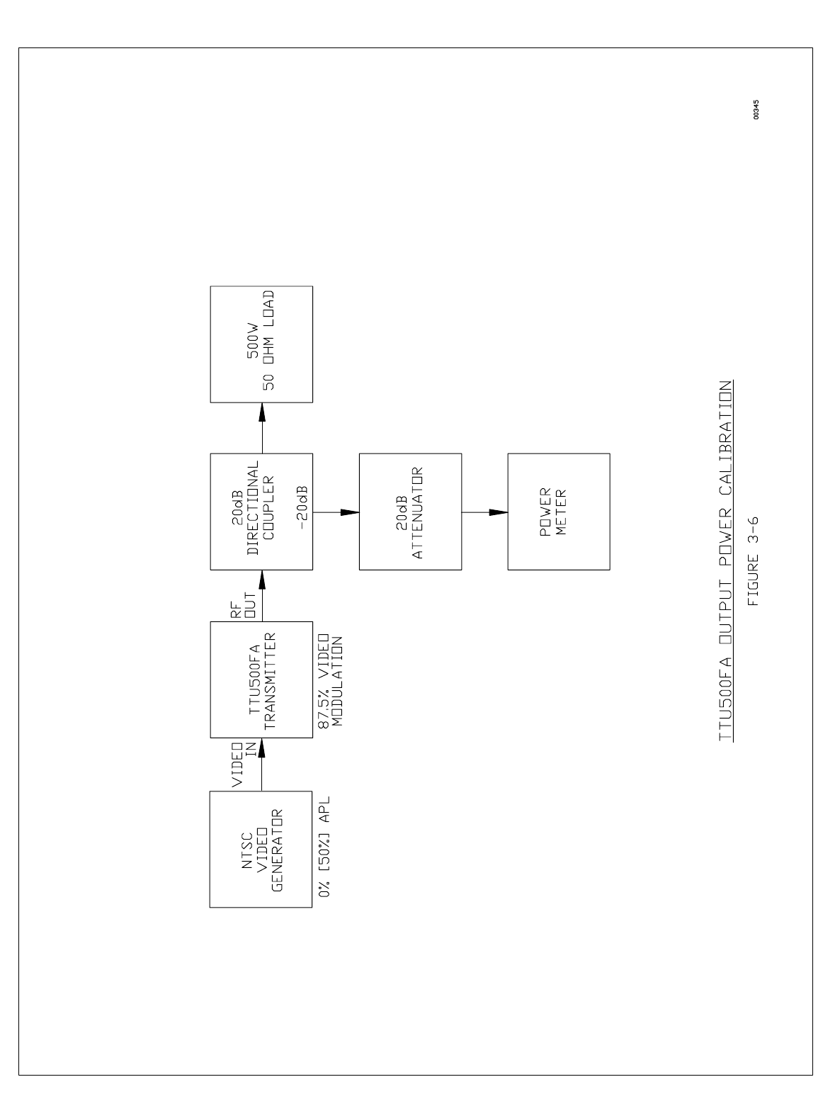
3.5 Output Power Calibration
3.6 Linearit
y
Corrector Ad
j
ustment
3.7 Remote Monitor Si
g
nal Levels
3.8 Spare Modules and Components
3.9 S
y
nthesizer Pro
g
rammin
g
IV. DATA PAK
V. SCHEMATIC DIAGRAMS

i
SECTION I
THE TTU500FA TRANSMITTER
1.1 INTRODUCTION ....................................................... 1 1
1.2 SPECIFICATIONS ..................................................... 1 1
1.3 INSTALLATION ........................................................ 1 3
1.4 OPERATION ........................................................... 1 4
1.5 WARRANTY AND PARTS ORDERING ................................... 1 5

1 1
SECTION I
THE TTU500FA TRANSMITTER
1.1 INTRODUCTION:
The EMCEE TTU500FA LPTV Transmitter is a remarkably compact design rated to provide
500 watts peak visual and 25 watts average aural power on any FCC specified channel extending
from 470 to 806MHz. The TTU500FA is completely solid-state supplying maximum performance
and reliability through the liberal utilization of Laterally Diffused Metal Oxide Semiconductors
(LDMOS). Comprised of a modulator, an EMEX1 2 Watt UHF Exciter, one 500 Watt UHF Amplifier
drawer, an Output Section for filtering and power measurement, and panels for power distribution
and metering/control, the TTU500FA is easy to service and maintain with RF alignment practically
nonexistent. A number of controls and indicators, furnished on the transmitter’s Control/Metering
panel and the EMEX1 Exciter front panel, provide convenient operation while displaying the results
of the transmitter's diagnostic circuitry.
The TTU500FA is designed for the express purpose of broadcasting as authorized by the U.S.
Federal Communications Commission under Part 74, Subpart G, of the FCC Rules and Regulations.
1.2 SPECIFICATIONS:
Visual:
Output Power 500 watts peak
Emission 5M75C3F visual
Color Transmission NTSC, PAL, or SECAM
Output Frequency 470-806MHz
(FCC - Ch.14-69)
(CCIR - Ch.21-62)
Frequency Stability Visual Carrier ±500Hz
Output Power Stability ±0.5dB
Spurious Products 60dB below peak sync
Harmonics 60dB below peak sync
In-band Intermodulation (IM3)52dB below peak sync
Differential Gain ±5%
Differential Phase ±3

1 2
Low Frequency Linearity 5%
Frequency Response ±0.5dB
Sideband Response Better than FCC 73.687(a)(1)
Envelope Delay Better than FCC 73.687(a)(3)
Output Impedance/Connector 50 ohms / 7/8" EIA flange
Video Signal to Noise 55dB
Video Input Level 1 volt peak-to-peak nominal
Video Input Impedance 75 ohms unbalanced
Aural:
Output Power 25 watts average
Emissions 250KF3E
Frequency Stability ±200Hz re. visual
Audio Input Level 0dBm nominal
Audio Input Impedance 600 ohms balanced
Audio Distortion <1%
FM Noise < 55dB
General/Mechanical:
Ambient Temperature 30 C to +50 C
Power Requirements 230Vac ± 15%, 1 phase, 50/60Hz, 4kW
Power Consumption: 2kW w/black picture
Power Factor 0.9
Mechanical Dimensions 48"H x 22"W x 31"D
Weight 300 lb.

1 3
1.3 INSTALLATION:
Except where otherwise noted, the connectors mentioned in the following instructions are located
on the rear of the transmitter.
1. After unpacking the transmitter, a thorough inspection should be conducted to reveal any
damage which may have occurred during shipment. If damage is found, immediately notify
the shipping agency and advise EMCEE Broadcast Products Customer Service or its field
representative. Also check to see that any connectors, cables or miscellaneous equipment,
which may have been ordered separately, are included.
2. Place the transmitter in a clean, weatherproof environment providing adequate ventilation
for the exhaust fans at the rear of the transmitter drawers. It is important to maintain the
transmitter's ambient temperature within the 30 C and +50 C limits. Cooler ambient
temperatures will provide increased reliability.
3. Place the transmitter in its permanent location near a single-phase receptacle that supplies
230Vac at 50/60Hz. The ac source should have a minimum power capacity of 4kW.
IMPORTANT
Do not apply ac power to the transmitter at this time since its RF output must be
properly loaded before being placed in operation.
4. Set all circuit breakers, including the customer's incoming ac line breaker, to the OFF
position. Ac breakers can be found on the transmitter’s AC Distribution Panel, at the rear of
the amplifier and Exciter drawers, and on the front AC Power panel. Place an appropriate
power line protector (surge suppressor) across the ac line that supplies the transmitter.
5. Connect the baseband video and audio cables (customer supplied) to the transmitter's VIDEO
and AUDIO connectors located on the upper panel at the rear of the transmitter cabinet.
6. Connect the transmitting antenna cable (or a 1kW, 50 ohm dummy load) to the 7/8" EIA
flange connector marked RF OUTPUT located through the center rear of the cabinet’s top
cover.
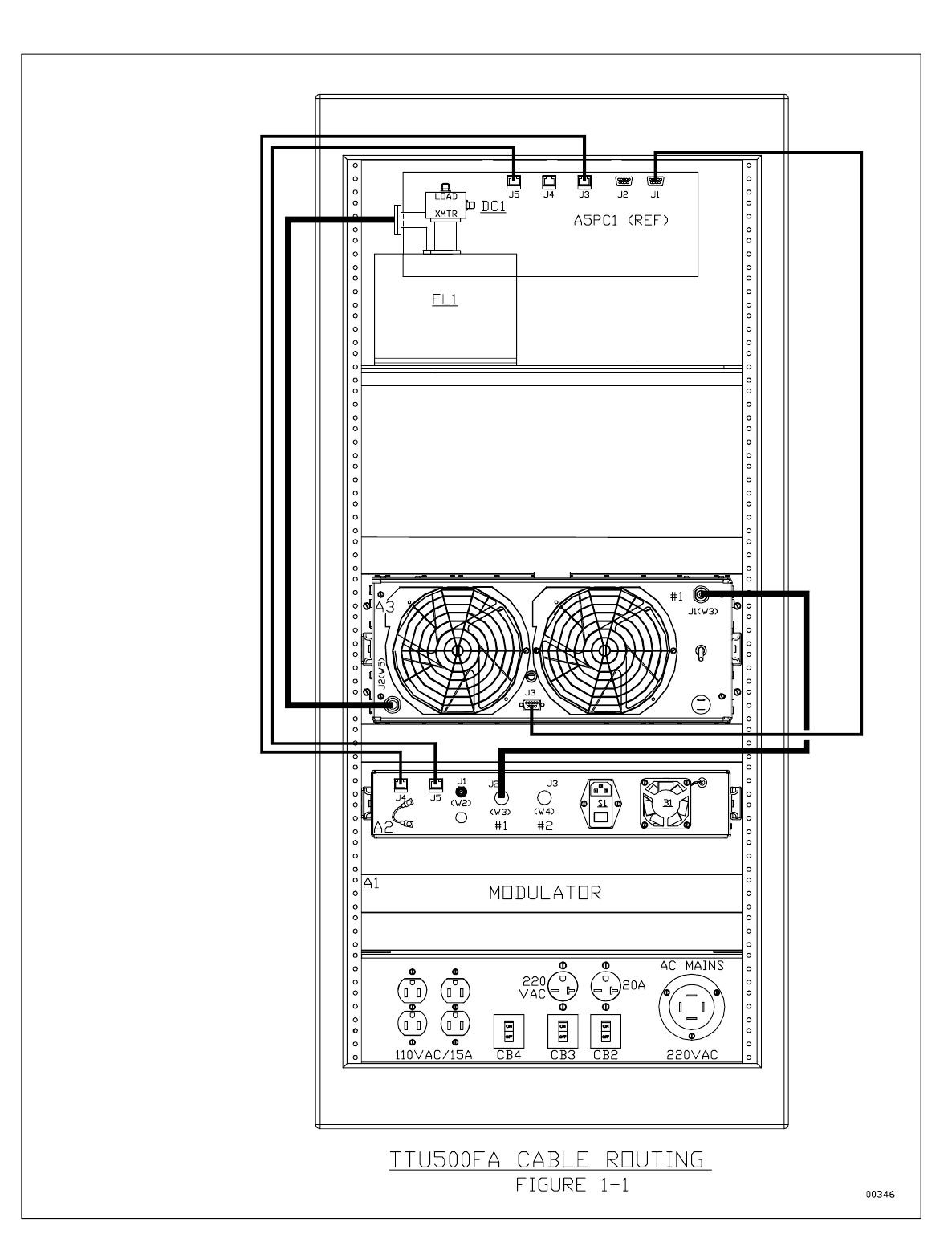
7. Verify that the power cords of the Modulator (110V/15A), Exciter (110/15A) and 500W Power
Amplifier drawer (220V/20A) are plugged into the receptacles at the bottom of the transmitter
cabinet. Also check to see that any ancillary equipment included in the cabinet (i.e. Video
Detect Switch, Stereo Generator, etc.) are connected to the appropriate ac sockets.
8. Check to see that all RF cables and wire harnesses are properly connected and secure.
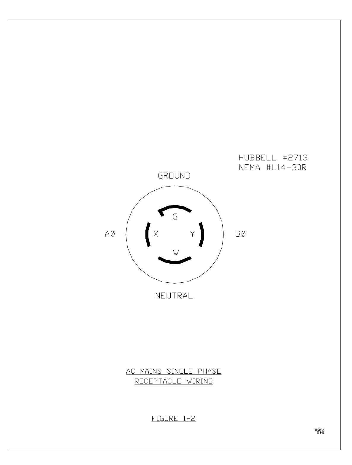
9. Using the 4-prong, twist-lock, female plug supplied with the transmitter, fabricate an ac power
cord (Figure 1 1) and plug it into the transmitter's AC MAINS connector at the bottom rear
of the transmitter cabinet. Open the incoming ac mains wall breaker and connect the other
end of the power cord into an appropriate 220Vac electrical outlet.

1 4
1.4 OPERATION:
Assuming the installation instructions of Section 1.3 have been completed and the transmitter is
receiving baseband video and audio signals, proceed with the following steps to place the transmitter
in operation. Except where otherwise noted, the controls, switches, and indicators mentioned in
these steps are located on the front of the transmitter.
1. Open the AC POWER circuit breaker located on the bottom front panel of the transmitter and
close the incoming ac mains breaker. Insure that the EMEX1 Exciter OPERATE/STANDBY
switch is in the off/out (STNDBY) position and the AGC/MANUAL button is in the off/out
(MANUAL) position. Place the transmitter’s Control/Metering panel FWD/REFL meter switch
to the FWD/out position.
2. Place the three AC Distribution Panel breakers (CB2, CB3, CB4), located at the lower rear
of the cabinet, to the on position. Also switch the Exciter and amplifier drawer rear panel
breakers to on.
3. Move the AC POWER circuit breaker located on the bottom front panel of the transmitter to
the ON position.
4. If applicable, place the Modulator's power switch to ON and verify that it is providing 87.5%
video modulation. If necessary, adjust the Modulator for the proper video depth of
modulation as described in its instruction manual. Also check to see that the audio peaks are
not overmodulating the aural carrier.
5. Verify the following transmitter responses:
a. The fans at the rear of each drawer should be operating.
b. The Exciter’s green LED indicators should react as follows:
SYNTHESIZER LOCK – on
IF STATUS – on
AMPLIFIER STATUS – on
LINEARITY CORRECTOR – on
AGC ACTIVE – off
SWEEP MODE – off
OPERATE/STANDBY – off
VSWR RESET – off
AGC voltmeter – 1 segment lit at approximate center
RF POWER meter – 0%
c. The green LED indicators on the transmitter’s Control/Metering panel should respond
as follows:
AMPLIFIER TEMP – off
AMPLIFIER – on
POWER SUPPLY – off
RF POWER meter – 0%
FWD – on
REFL – off

1 5
6. Turn the Exciter's OUTPUT LEVEL ADJUST two or three turns counterclockwise and press
the OPERATE/STANDBY switch in to place the transmitter in OPERATE. Then verify the
following responses of the transmitter:
a. The Exciter’s OPERATE/STANDBY switch indicator is now lit green.
b. The POWER SUPPLY Control/Metering panel indicator is now lit green.
c. The status of all other indicators previously mentioned is the same.
7. Check to see that the Control/Metering panel’s meter switch is in the FWD/out position and
then slowly turn the Exciter’s OUTPUT LEVEL ADJUST clockwise until a 100% indication
appears on the Control/Metering panel’s RF POWER meter. The Exciter’s RF POWER
meter should also be displaying a 100% indication.
8. After 10 minutes of operation press the Exciter’s AGC/MANUAL switch in to engage the
transmitter’s output automatic gain control. If necessary and with a small tuning tool, slowly
turn the AGC LEVEL ADJUST to bring the transmitter’s RF POWER meter reading back to
100%.
9. Place the Control/Metering panel's meter switch to REFLD and verify that the RF POWER
meter indicates no more than 10% returned power. If the reflected power is more than 10%,
shut down the transmitter and check the VSWR of the transmitting antenna and its associated
cable.
10. Place the Control/Metering panel's meter switch to FWD for constant monitoring of the
transmitter's final output power.
The transmitter is now in operation. Check its coverage area for clean, sharp television reception.
If the reception or picture quality is unsatisfactory, examine the amount of power delivered to the
transmitting antenna (see Section 3.5) and, if necessary, examine the antenna orientation and
antenna transmission line VSWR to insure maximum radiation in the proper direction.
1.5 WARRANTY AND PARTS ORDERING:
Warranty – EMCEE warrants its equipment to be free from defects in material and workmanship for
a period of one year after delivery to the customer. Equipment or components returned as defective
(prepaid) will be, at our option, repaired or replaced at no charge as long as the equipment or
component part in question has not been improperly used or damaged by external causes
(e.g., water, ac line transients or lightning). Semiconductors are excepted from this warranty and
shall be warranted for a period of not more than ninety (90) days from date of shipment. Equipment
or component parts sold or used by EMCEE, but manufactured by others, shall carry the same
warranty as extended to EMCEE by the original manufacturer.
Equipment Returns – If the customer desires to return a unit, drawer, or module to EMCEE for
repair, follow the procedure described below:
1. Contact EMCEE Customer Service Department by phone or fax for a Return Authorization
Number.

1 6
2. Provide Customer Service with the following information:
Equipment model and serial numbers.
Date of purchase.
Unit input and output frequencies.
Part number (PN) and Schematic Diagram designator if a module is being sent.
Detailed information concerning the nature of the malfunction.
The customer shall designate the mode of shipping desired (e.g., Air Freight, UPS, Fed Ex, etc.).
EMCEE will not be responsible for damage to the material while in transit. Therefore, it is of utmost
importance that the customer insure the returned item is properly packed.
Parts Ordering – If the customer desires to purchase parts or modules, utilize the following
procedure:
1. Contact EMCEE Customer Service by phone or fax indicating the customer's purchase order
number. If the purchase order number is provided by phone, written confirmation of the order
is required.
2. Also provide:
The equipment model and serial number.
The unit input and output frequencies.
The quantity, description, vendor, number, and designation of the parts needed as found in
the Parts Lists subsection of this manual.
If a module is required, give the part number (PN) and Schematic Diagram designator
(e.g., 30404029).
Designate the mode of shipping desired (e.g., Air Freight, UPS, Fed Ex, etc.).
Shipping and billing addresses.
Spare and Replacement Parts – The Spare Modules and Components section of this manual
provides a detailed listing of the modules and some discrete components contained within the
transmitter. The listing contains those modules or components considered to be essential
bench-stock items and should be available to the technician at all times. The Schematic or
Interconnection Diagram is the governing document of this manual. Should there be a discrepancy
between a modules or components list and a diagram, the diagram takes precedence. Such a
discrepancy is possible since manufacturing changes cannot always be incorporated immediately
into the instruction manual.
Component Referencing – A transmitter may consist of a modulator or receiver, a number of
modules and components mounted in drawers, and components or modules mounted to panels or
directly to the cabinet. Components mounted in a module which is included in a drawer take the
drawer number and the module number in addition to a component number. Thus the reference
designator A2A1Q1 means transistor Q1 in module A1 of drawer A2. Components mounted in a
drawer take only the drawer number and a component number (e.g., A2M1 designates meter M1 of
drawer A2). Components mounted directly to a panel take only the panel number and a component
number. Components and modules mounted directly to the cabinet take only a component or
module number.

1 7
For EMERGENCY technical assistance, EMCEE offers a toll free, 24-hour, 7-day-a-week
customer service hot line: 1-800-233-6193.

ii
SECTION II
CIRCUIT DESCRIPTION
2.1 MODULATOR ......................................................... 2 1
2.1a Video Detector Switch ............................................... 2 1
2.2 EMEX1 2 WATT UHF EXCITER ......................................... 2 1
2.2a Linearity Corrector .................................................. 2 2
2.2b IF/Converter ....................................................... 2 3
2.2c UHF Synthesizer ................................................... 2 6
2.2d Reference Oscillator ................................................. 2 7
2.2e UHF Bandpass Filter ................................................ 2 7
2.2f 2 Watt UHF Amplifier ................................................ 2 7
2.2g Metering Coupler ................................................... 2 9
2.2h Metering Detector................................................... 2 9
2.2i Control/Interface Board .............................................. 2 9
2.2j Display/Monitor Board .............................................. 2 20
2.2k 28V/15V/5V Power Supply ........................................... 2 24
2.3 500 WATT UHF POWER AMPLIFIER DRAWER ......................... 2 24
2.3a Power Splitter..................................................... 2 25
2.3b 300W UHF Power Amplifier .......................................... 2 25
2.3c Power Combiner................................................... 2 27
2.3d Amplifier Status Interface ............................................ 2 27
2.3e Power Supply/Thermal Interface ....................................... 2 27
2.3f 32V Power Supply ................................................. 2 28
2.4 OUTPUT SECTION ................................................... 2 29
2.4a UHF Bandpass Filter ............................................... 2 29
2.4b Directional Coupler ................................................. 2 29
2.4c Metering Detector.................................................. 2 29
2.5 CONTROL/METERING PANEL ......................................... 2 30
2.5a Control/Monitor Board .............................................. 2 30

2 1
SECTION II
CIRCUIT DESCRIPTION
2.1 MODULATOR:
EMCEE EM1 / Scientific Atlanta 6340 / RF Comm. 2000 A1
IF OUT 8dBm peak visual typical
The modulator processes baseband video and audio signals to provide a composite IF output
composed of a visual carrier at 45.75MHz with 5M75C3F modulation, and an aural carrier at
41.25MHz with 250KF3E modulation. Any of these modulators can be used to drive the EMEX1
2 Watt Exciter drawer (A2). The optional video sense circuit provides an indication of whether the
modulator is receiving a baseband video signal. The output of the video sense is either a logic
high ( +5Vdc) with video present or a logic low ( 0Vdc) when video is not present. This logic
signal is used by the Exciter Control/Interface Board (A2PC1) to place the transmitter in standby
if the video signal is lost.
2.1a Video Detector Switch:
Burst VDS A9
For those modulators which do not contain a video sense alarm, the Burst Electronics Video
Detector Switch (Model VDS) will be installed in the transmitter cabinet. The VDS detects the
presence of composite video connected to its A INPUT directly from the VIDEO connector mounted
on the Video/Audio/Remote Panel (A8J2). If a loss of video is detected, then the unit switches to
the B INPUT, lights its red LED and energizes an internal TALLY relay. Through this relay, a
ground is sent to the Exciter Control/Interface circuit via the transmitter’s Control/Monitor board
(A5PC1) placing the transmitter in a nonradiating condition.
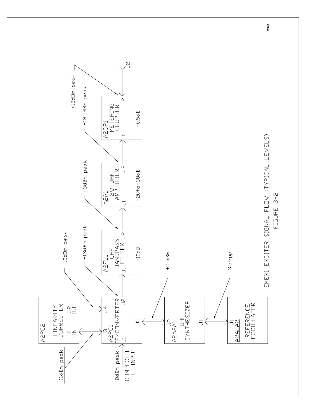
2.2 EMEX1 2 WATT UHF EXCITER:
Interconnection Diagram 40404001/Rev 55 A2
Composite IF IN (J1) 8dBm peak visual
21dBm average aural
RF OUT (J2 & J3) +18dBm typical peak visual
+5dBm typical average aural
The EMEX1 Exciter drawer converts the composite IF signal from the modulator to the desired
UHF frequency while amplifying this RF signal to the appropriate output level. The Exciter supplies
approximately 200mW of peak visual power to drive the 500W UHF Power Amplifier drawer (A3).
Power control, automatic gain control (AGC) and heterodyne conversion are performed by the
IF/Converter module (PC1). Utilizing the composite IF signal, the Linearity Corrector furnishes
performance improvements for the transmitter’s ICPM, differential phase and gain, sync amplitude

2 2
and intermodulation. The UHF Synthesizer supplies a programmable LO to the IF/Converter mixer
where the LO and IF signals are combined to create the desired UHF frequency. The UHF signal
from the Converter module is then passed through the UHF Bandpass Filter (FL1) to remove the
unwanted LO and sum products from the conversion process while passing and amplifying the
desired difference signals. The signal is then amplified approximately 25dB by the 2 Watt UHF
amplifier (A1) and passed through the Metering Coupler (CP1). Here, a forward RF sample is
provided for use by the Metering Detector (A3) while the main signal is passed to the output of the
drawer.
Metering and control functions are provided by the Metering Detector, the Display/Monitor board
(PC3) and the Control/Interface Board (PC4). The Display/Monitor Board has several status and
diagnostic LED indicators which are presented on the Exciter’s front panel. The Control/Interface
board provides for various controls and logic circuits for proper operation of the transmitter. Dc
power for the Exciter is supplied by a small, efficient multioutput switching power supply PS1 which
furnishes ±28, ±15 and ±5 volts.
2.2a Linearity Corrector:
Schematic Diagram 40404011/Rev 55 A2PC2
IF IN (J1) 11dBm typical
IF OUT (J2) 12dBm typical
Gain with S1 ENABLE/DISABLE (J1-J2) 0 to 2dB typical
Current Draw 610mA @ +15Vdc
The Linearity Corrector is a six-stage, unity gain circuit which compensates for nonlinear distortions
generated in the transmitter's Class AB 500 Watt Power Amplifier drawer. When properly adjusted,
it provides correction to the transmitter’s output signal for sync amplitude, differential gain,
differential phase, ICPM and intermodulation. Corrector amplifiers U1 through U8 are all
monolithic amplifier stages providing approximately 12dB of gain per device. A phase correction
network is centered around amplifiers U2 through U5 while the circuitry surrounding U7 and U8
corrects for differential gain and sync compression. When properly adjusted, the phase and gain
correction networks will collectively reduce intermodulation distortion.
Input amplifier U1 is biased through resistor R1 and inductor L1 which acts as an RF choke.
Capacitor C2 is utilized as a B+ bypass with coupling capacitors C1 and C3 advancing the input
signal to the matching T-attenuator made up of resistors R2, R3 and R4. At hybrid splitter DC1,
the IF carrier is divided into two equal amplitude signals which are 90 out of phase. At the
splitter’s 90 port, a negative phase-shift network composed of inductor L3 and capacitors C15
through C18 adds another 22.5 shift to the signal ( 112.5 total) before amplification by U3.
Conversely, connected to the 0 port of the splitter is a positive phase-shift network comprised of
inductor L2 and capacitors C4 throughC7. Here the 0 signal is shifted in the positive direction by
22.5 resulting in a 135 total difference between the two signals. In order to keep the amplitude
of each signal similar, the circuits surrounding amplifiers U2 through U5 are essentially identical
with the same biasing, bypassing and coupling described for U1. Transformers T3 and T4 on the
negative shift side of the circuit are 2:1 step-up types identical to T1 and T2, but necessary to
efficiently drive gain expansion diodes CR1 and CR2. Through adjustment of slope potentiometers
R15 and R25 and threshold (cut-in) pots R21 and R30, the amplitude of the negative shifted signal
can be varied to add to or subtract from the positive shifted signal at in-phase combiner CP1.
When adjusted properly, this circuit can then correct the differential phase, intermodulation and
ICPM distortions created by the transmitter’s power amplifier. At the output of combiner CP1 the

2 3
IF signal passes through a matching pi-attenuator comprised of resistors R35, R36 and R37 before
amplification by U6, U7 and U8. Transformers T5 and T6 again double the signal voltage to
properly drive the gain expansion diodes CR3 and CR4 which compensate for differential gain and
sync compression created in the 500 Watt Power Amplifier (A3).
The variable gain expansion networks, which provide linearity correction, are centered around dual
diodes CR1 through CR4, slope potentiometers R15, R25, R41, R57, unity gain dc amplifiers U9,
U10, U11, threshold potentiometers R21, R30, R47, R55 and ENABLE/BYPASS switch S1. The
threshold (cut-in) potentiometers determine the point on the IF waveform where the correction, or
gain expansion, will occur and the slope potentiometers dictate the amount of correction/expansion
to be used at that breakpoint. With S1 in the ENABLE position, the four diode pairs form nonlinear
circuits where each diode is reverse biased and the amount of reverse bias dictates the point at
which the diode turns on during the positive and negative cycles of the visual IF carrier envelope.
Each diode is biased using voltages established by the threshold potentiometers in conjunction with
dc amplifiers U9, U10, U11 and U12. L4 through L6 and L9 through L12 isolate the IF signal from
the diode threshold biasing circuitry. When the positive and negative peaks of the visual signal
envelope are sufficient to forward bias a diode pair, the pair turns on placing the resistance of its
respective slope potentiometer in parallel with the series arm of its L-pad (R14, R24, R40, R50).
As a result, the attenuation of the visual IF carrier is reduced during this period causing the
waveform to stretch. Slope control R41 is typically used to correct differential gain while R57
primarily adjusts sync amplitude.
With S1 in the BYPASS position, ground is applied to FET switches Q1 and Q2 placing each diode
pair in hard reverse bias preventing conduction throughout the positive and negative cycles of the
IF carrier envelope. Due to the high reverse resistance provided, each diode network essentially
represents a resistive L-pad (R14/R16, R24/R31, R40/R42, R50/R58) with the IF signal attenuated
by a fixed amount in each location. As a result, no linearity correction is provided.
2.2b IF/Converter:
Schematic Diagram 40404021/Rev 53 A2PC1
IF INPUT (J1) 0dBm to 30dBm peak visual
CORRECTOR LOOP Out (J3) 11dBm peak visual typical
CORRECTOR LOOP In (J4) 12dBm peak visual typical
RF OUT 10 to 18dBm
LO INPUT (J5) +13dBm minimum
Current Draw 42mA @ +15V
31mA @ 15V
185mA @ +5V
The IF/Converter performs three tasks in this transmitter. With the first AGC loop it furnishes level
control for the incoming signal from the modulator, upconverts the IF signal to the desired UHF
channel and then controls the transmitter’s output power through a second gain control loop.
The modulator’s IF input, provided at J1, is amplified or attenuated by variable gain amplifier U1.
This integrated circuit, controlled by the output of integrator U4 via switch S1, (U1) can produce
wide variations in gain ranging from +30dB to 10dB. At the output of U1 is coupling capacitor C3
and 2:1 step-down transformer T1 required for proper impedance matching between U1 and in-
phase splitter CP1. At the output of CP1, two equal amplitude IF signals are delivered for differing
applications. The signal at pin CP1-3 is used to provide a reference for the input AGC loop, while

2 4
the second signal at pin CP1-4 is fed to the Linearity Corrector (PC2) connected to output J3. Both
signals pass through attenuators (3dB and 7dB respectively) which are connected to identical
monolithic amplifiers, U7 and U8. These devices, offering approximately 14dB of signal gain, are
furnished bias through resistors R15/R22 and RF chokes L1/L2. The output of amplifier U8 is
connected, through coupling capacitor C19, to a variable PIN attenuator composed of diodes CR7
and CR8. This diode array forms a pi-attenuator operated by buffer U9 whose input (pin 5) is
supplied control voltage from the Exciter’s front panel OUTPUT LEVEL ADJUST. With maximum
voltage from U9 (+15V) the attenuator will exhibit minimum attenuation of approximately 2dB.
With minimum voltage the attenuator can provide more than 50dB of loss to the signal. This
attenuator is utilized as the main power control and standby mechanism for the transmitter.
At the output pin 3 of U7 is the second IF signal required by the input AGC circuit as a power
reference representing the incoming modulator signal level. This signal is passed through coupling
capacitor C16 to integrated circuit U6, an RMS detector. At pin 7, U6 outputs the video component
of the IF visual carrier while C11 rolls off the aural energy contained in the signal. The amplitude
of the video is then doubled using op-amp U5A and then sent to peak detector CR3 via pins 1 and
2 of jumper JP1. (Pins 2 and 3 of JP1 are utilized for average digital power detection only.)
Capacitor C9 and resistor R10 filter the peak video component from diode CR3 and this dc voltage
is sent to unity gain buffer U5B. The dc level at the output of U5B (pin 7), which is now
proportional to the peak power of the visual signal entering the IF/Converter, will be approximately
+3V when the modulator level into the Converter board is at the midpoint of its input AGC window
(15dBm peak). This potential then appears at pin 6 of integrator U4B where it is compared to the
voltage on pin 5 ( +3V) generated by divider R7/R8. When the values of each voltage at pins 5
and 6 are equal, the output of U4B at pin 7 will be zero, holding variable gain amplifier U1 at the
center of its gain extremes (+10dB) via pins 8 and 1 of electronic switch S1. (The gain of U1 can
also be set to its center by applying a low to the INPUT AGC CONTROL line which is connected
to pin 6 (IN) of switch S1. This low, supplied by the OPERATE/SWEEP switch PC4S1 on the
Control/Interface board, will disconnect the input AGC voltage at S1-8 from S1-1 and connect the
ground at S1-2, 3 to S1-1 effectively placing a zero voltage on pin 1 of U1.) If the input level from
the modulator at J1 increases, the outputs of U7, U6, U5A and U5B will also increase forcing pin 7
of U4B negative and proportionally reducing the gain of U1. Conversely, if the input from the
modulator were to be reduced, the output of U4B would swing positive causing U1 to increase its
gain compensating for the signal reduction. Under normal transmitter operating conditions, the
signal provided at the CORRECTOR LOOP output (J3) will be approximately 11dBm peak visual.
However, if the IF signal is significantly reduced ( 25dBm) or removed completely, the potential
at the output of U4B will exceed +2.5V causing the level at input pin 2 of U4A to exceed the
reference (2.5V) provided at pin 3 through divider R5/R6. This action would drive output pin 1 of
U4A to zero, turning off the IF STATUS light (PC3DS5) on the Exciter’s front panel and placing a
low on the LEVEL ADJUST line attached to pin 5 of U9 increasing the attenuation of the associated
PIN diode circuit to maximum ( 50dB).
After proceeding through the Linearity Corrector, the IF signal is fed to CORRECTOR LOOP input
J4 at an approximate level of 12dBm. Here the signal is furnished a 50 ohm match using
pi-attenuator R30/R31/R32. Hybrid amplifier U1, biased through resistor R33 and RF choke L3,
provides 14dB of gain and delivers the signal to in-phase 2-way splitter CP2 via coupling capacitor
C29. At output pins 3 and 4 of CP2 are two equal amplitude IF signals used, respectively, to drive
the output AGC loop (U13 through U18) and to be mixed to the wanted UHF channel after passing
through the output control attenuator. Made up of PIN diodes CR9/CR10 and controlled by U18,
this attenuator is capable of 2dB to 50dB of attenuation and ultimately sets the output power of the
transmitter. From the output control attenuator the IF signal is transferred to mixer MX1 through
coupling capacitor C51 and pins 1 and 2 of jumper JP3. (Connecting pins 2 and 3 of JP3 brings
the IF signal to test point TP1.) In MX1 the IF is then upconverted to the desired UHF signal as
a result of combining with the local oscillator frequency presented at LO INPUT J5. At the output
of the mixer (pin 4) resistors R67/R68/R69 provide 5dB of attenuation and the appropriate

2 5
impedance match for amplifier U20 via capacitor C52. U20 supplies 13dB of amplification for the
UHF frequencies with resistor R70 and choke L5 furnishing the necessary power to the hybrid.
From output pin 2 of U20, the amplified signal is brought to the OUTput connector J5 where it will
be fed to the subsequent UHF Bandpass Filter (A2FL1) and eventually to the transmitter’s output.
The second IF signal, present at pin 3 of splitter CP2, functions as the signal level reference for
the output AGC loop. Matching attenuator R34/R35/R36 provides the proper impedance for the
signal brought to pin 1 of 14dB hybrid amplifier U13. Bias is supplied to U13 through resistor R37
and choke L4 with capacitor C31 acting as an RF bypass. Capacitors C32 and C33 in conjunction
with resistor R38 provide coupling and matching from the output of amplifier U13 to the input of
RMS detector U14. As with detector U6 of the input AGC loop, U14 separates the video program
from the IF visual carrier while attenuating the aural components through C35. The demodulated
video signal, found at pin 7 of U14, is amplified by U15A and passed through detector CR4 via
jumper JP2 pins 1 and 2. (Pins 2 and 3 of JP2 are utilized for average digital power detection
only.) The resulting peak of the video signal is transformed into an average dc voltage using filter
CR36/R42 which is then buffered with unity gain amplifier U15B. At the output of divider R43/R45,
the positive detected voltage created by the IF signal at CORRECTOR LOOP J4 meets the
negative POWER REFERENCE voltage supplied to connector J6-8 from the transmitter’s output
power Metering Detector (A7A1) through inverting amplifier U16B. When their associated circuits
are correctly adjusted, these two voltages will be opposite but equal in value, theoretically yielding
0 volts at the output of adder circuit U16A, operational amplifier U17A and integrator U17B. With
the front panel AGC/MANUAL switch PC3S2 depressed (in), this voltage is then sent through pins
8 and 1 of switch S2 and divider R56/R61 to amplifier U18A which controls the attenuation value
of PIN diodes CR9/CR10 and, subsequently, the output power of the transmitter. (With 0V at the
output of switch S1, PIN attenuator CR9/CR10 provides approximately 3dB of signal reduction.
With +15V from S1, the PIN attenuator will furnish almost no resistance and with 15V, diodes
CR9/CR10 will supply about 6dB of signal loss.) If, for some reason the transmitter’s output power
were to drop, the positive voltage at J6-8 would be reduced, making the output of U16B less
negative. The more positive voltage at pin 3 of U16 will force its output positive while the outputs
of U17A and U17B go negative and positive, respectively. The change in level, sent to U18 via
switch S2, forces pin 1 of U18A high reducing the attenuation provided by PIN diodes CR9/CR10.
This reduction in attenuation will be proportional to the power decrease seen at the transmitter’s
output, thereby bringing the transmitter’s power back to its appropriate operating level. In the case
where the transmitter’s output increases above its rated power, the exact opposite happens. The
POWER REFERENCE voltage at J6-8 will increase taking the U16A input negative. The output
from U17A will go positive forcing U17B to send a negative voltage to U18 via switch S2. The
negative voltage from U18A will cause PIN diode attenuator CR9/CR10 to increase resistance,
decreasing the transmitter’s signal level to its proper value.
To defeat the output AGC, the front panel AGC/MANUAL switch must be released (out), placing
a ground on the OUTPUT AGC CONTROL line at pin 10 of J6. This low, applied to pin 6 of switch
S2, causes the incoming AGC voltage at pin 8 of S2 to be removed from pin 1 and connected to
the ground at pins 2, 3. The 0V potential sent to U18A will fix PIN diodes CR9/10 at 3dB, the
center of their attenuation range. Amplifier U18B, which also follows the output of S2 at its input
pin 5, acts as a unity gain buffer forwarding the output AGC voltage to the Exciter’s front panel
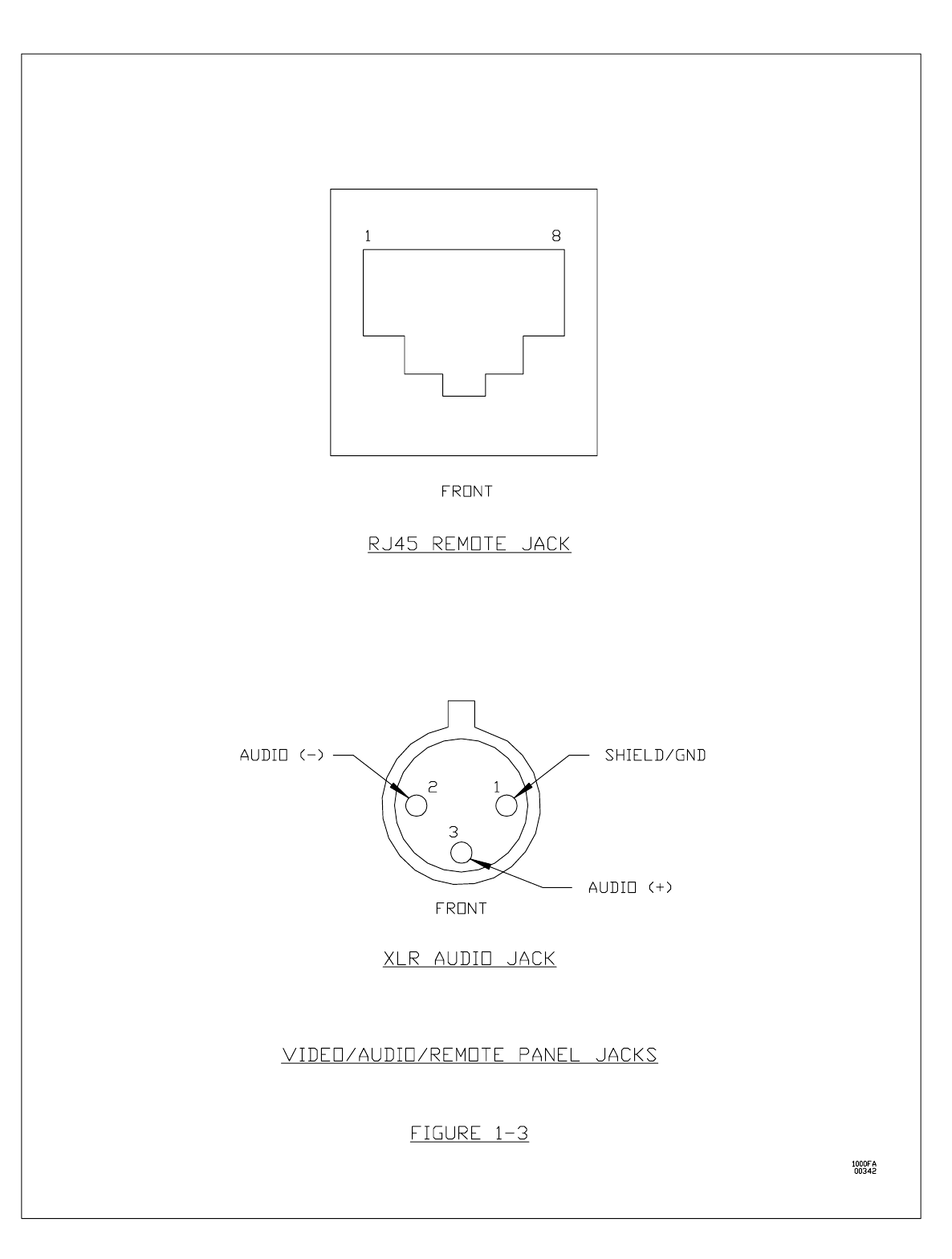
AGC meter (A2PC3DS12) and to the RJ45 REMOTE plug (A8J1) on the VIDEO/AUDIO/REMOTE
rear panel.

2 6
2.2c UHF Synthesizer:
Schematic Diagram 30367094/Rev B A2A2A1
LO OUT (J2) +15dBm minimum
Frequency Stability 0.3ppm / 30 C to +70 C
10MHz REF. IN (J1) 3.5V P/P square wave
SYNTH LOCK (Pin J4-A) logic high - unlocked / logic low - locked
Current Draw 15mA @ +28V
120mA @ +15V
36mA @ +5V
The UHF Synthesizer is a phase-lock loop circuit that uses 10MHz as a reference to develop a
manually programmable CW signal for the Mixer in the IF/Converter module (A2PC1MX1). The
frequency of the synthesizer output signal (or LO) is calculated as the sum of the visual IF carrier
from the modulator and the visual carrier of the transmitter’s UHF output channel. The LO
frequency is programmed by the setting of switches S1 through S4 which are accessible via access
holes on the Synthesizer’s module (A2A1) cover. The switch settings for each UHF channel and
the resulting LO frequencies are provided in Table 3 1 of Section 3.9.
A 10MHz signal from Reference Oscillator A2A2 is brought to the Synthesizer module through
connector J1 (10MHz IN). At the connector, the two sections of divider chip U4 perform a binary
divide-by-5 count creating a 400kHz signal at the OSCin pin 27 of synthesizer chip U1. At the
same time, the output of voltage controlled G1 (RF OUT), amplified by U5 and available as the
transmitter’s LO at J2 (OUT), is also amplified by U6 and fed to a ÷64/÷65 prescaler, U2. The U2
prescaling factor is ultimately selected by programming switches S1 through S4 which set the MOD
CONTROL line at pin 9 of U1 to either high or low. When a high is seen at pin 6 (MC) of prescaler
U2, the chip will divide the VCO output by 64. With a low at U2-6 the prescaler will divide the VCO
output by 65. After prescaling, the signal is sent to pin 1 of U1 (Fin) from U2-4 (OUT) and, with the
aid of the A and N counters within U1, the prescaled signal is also divided down to 50kHz using a
divide-by-ratio selected through the switch settings of S1 through S4. This 50kHz, derived from
voltage controlled oscillator G1, is sent to a phase detector for comparison with the 50kHz taken
from the high stability 10MHz reference. At the U1 phase detector outputs 0/V and 0/R (pins 7 & 8),
loop filter U3 integrates the incoming correction pulses and sends them to VCO G1 as a dc control
voltage after suppression filter C14/C15/C24/R5/R13. If the frequency generated by VCO G1 is
lower than the frequency selected by programming switches S1-S4, a pulse train will appear at
pin 5 of U3 forcing the control voltage at pin 7 higher, thereby raising the frequency of the
oscillator. If the VCO output is higher than the frequency selected by the programming switches,
then pulses will appear at U3 pin 6 pushing the control voltage lower at U3-7 to reduce the
frequency from G1. The corrected frequency is then passed through matching attenuator R7/8/9
and amplified by U5 for delivery to the IF/Converter mixer. (For NTSC System M operation, A0
and A1, pins 21 and 23 on U1, are grounded. For PAL System B/G and D/K operation, A0 and A1
are made high by opening the traces at pins 21 and 23 thereby adding the characteristic 150kHz
to the LO.
When the synthesizer is locked to its programmed frequency, pin LD of chip U1 provides a high
which saturates Darlington pair Q1 after capacitor C28 changes through resistor R16. This time
delay is created to ensure that the synthesizer has successfully locked before supplying a low to
the SYNTH LOCK line. During an unlocked condition, the LD pin switches low discharging C28
through diode CR1 and reverse biasing Q1. A high (+5V) is now present on the SYNTH LOCK line
indicating an unlocked condition.

2 7
2.2d Reference Oscillator:
Schematic Diagram 10368037/Rev B A2A2A2
10MHz REF. OUT (J1, J2) 3.5V P/P square wave
Frequency Stability 0.3ppm / 30 C to +60 C
Current Draw 15mA @ +5V
The Reference Oscillator provides a high stability 10MHz signal which provides accuracy and long-
term frequency stability for the UHF Synthesizer (A2A2A1). This reference module is centered
around a 10MHz temperature-compensated crystal oscillator (G1) using 5V as power. The output
from G1 is buffered by two exclusive-OR gates used as inverters. The output signal from each
gate is a 10MHz low-level square wave with a frequency stability of 0.3 parts per million (ppm).
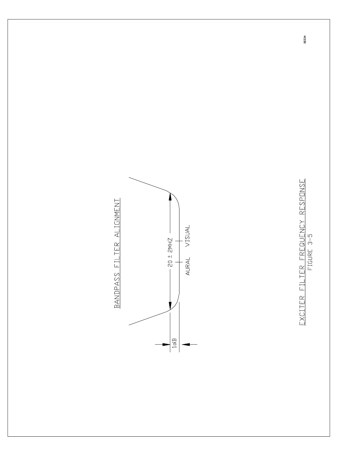
2.2e UHF Bandpass Filter:
Schematic Diagram 20404015/Rev 51 A2FL1
INPUT (J1) 10 to 18dBm
OUTPUT (J2) 0 to 8dBm
Bandwidth (J1-J2) 8MHz to 15MHz @ 1dB
Gain (J1-J2) 10dB
Current Draw 50mA @ +5V
The UHF Bandpass Filter is a six-section comb-line design joined with a single-stage amplifier to
provide 10dB of total module gain. The first three sections of the filter, composed of variable
capacitors C1/C2/C3 and their associated tuned stubs, are terminated at the input of U1, a 14dB
amplifier. Variable capacitors C1/C2/C3 and C4/C5/C6 electrically lengthen or shorten their
connected stubs to pass the chosen UHF channel with the appropriate coupling provided by
spacing between the stubs. For extra stub length at lower frequencies, capacitors C7/C8/C9/C10/
C11/C12 are added to operate at channels below 560MHz. The bias for U1 is obtained from the
5 volt power supply via R1 and RF choke FB1 (ferrite bead) with bypassing furnished by capacitors
C15/C16/C17. Loading wires W1/W2/W3/W4 set the input and output impedance of each three-
section filter segment, dictating the overall bandwidth and loss of the circuits. FL1 is tuned to
select the desired UHF mixer products from the lower sideband, or difference signal, found at the
RF OUTPUT of the IF/Converter (A2PC1).
2.2f 2W UHF Amplifier:
Schematic Diagram 30404029/Rev 54 A2A1
INPUT (J1) 0 to 8dBm peak visual
OUTPUT (J2) +22dBm peak visual
Gain (J1-J2) 20dB to 38dB manual set
Frequency Response (J1-2) ±1dB/470-806MHz
Current Draw 500mA @ +28V
210mA @ +15V

2 8
The 2W UHF Amplifier is a variable gain, class A module that provides amplification to the
selected UHF channel. The amplifier is a three-stage, class A, microstrip design capable of 38dB
gain and 2 watts peak visual output. The first stage is centered around broadband monolithic
amplifier U1 rated for 10dB of gain. U1 is provided bias from 9 volt regulator U2 through filter FB1
and parallel resistors R1/R2. Input and output signal coupling is supplied by capacitors C1/C2 with
B+ bypass furnished by C3 through C6 and C16/C17. At the output of amplifier U1 is 90 hybrid
coupler HY1 configured as a variable gain control using PIN diodes CR1/CR2 and the GAIN
ADJUST voltage applied to E3. As the E3 GAIN ADJUST voltage is increased (using the
AMPLIFIER GAIN ADJUST A2PC4R7 on the Control/Interface board), PIN diodes CR1/CR2 begin
to conduct, creating a low impedance at the 0 and 90 ports of the hybrid. Due to mismatch
generated at these two ports, the resulting reflected power is added in phase at the hybrid’s ISO
port affording lower attenuation for the through signal. Conversely, as the GAIN ADJUST voltage
decreases, the PIN diodes conduct less generating a higher impedance at the 0 and 90 ports
making 47 ohm resistors R5/R6 electrically more apparent as power absorbing loads. With less
power reflected back into the hybrid, less power will appear at the ISO port making for increased
attenuation of the through signal. Variable gain adjust HY1 is capable of 3dB to 18dB of
attenuation.
From HY1 the UHF signal is coupled into field-effect transistor Q1 via capacitor C9 and an input
matching circuit made up of capacitor C10 and a tuned microstrip network. Biased from 9V
regulator U2 through resistors R11/R12, Q1 furnishes 12dB of signal amplification and with a drain
current of approximately 140mA. Capacitors C12/C13/C14/C15 supply RF bypassing for the bias
voltage with C11/C18 acting as signal coupling capacitors positioned at the input and output of 3dB
matching attenuator R13/R14/R15. At the input of 8 pin DIP power FET Q2 is a microstrip network
with matching capacitors C19/C20/C24 and variable capacitor C35. Connected directly to the
28 volt supply, Q2 is powered through a current regulator circuit centered on transistor Q5 and
drain resistors R20 through R23. This circuit continuously maintains the drain voltage and current
of Q2 over a wide variation of load and temperature. The required collector voltage and current
of this device is established by potentiometer R19, which controls the conduction of regulator Q5,
ultimately setting the 500mA drain current of Q2. At the output the amplified signal proceeds
through another matching network made up of capacitors C31/C32 and various microstrip tuning
elements. Coupling capacitor C33 passes the signal from Q2 to output connector J2.
Within the 2W UHF Amplifier module, fault circuits monitor the status of RF devices U1, Q1 and
Q2. Centered on transistors Q3/Q4/Q5, these fault circuits detect the presence of an open RF
device within the module and send a signal to the Exciter’s front panel AMPLIFIER STATUS
indicator. Under normal operation, transistors Q3/Q4/Q5 are forward biased generating approx-
imately 8.5 volts at collector resistors R4/R9/R26 pushing diodes CR3/CR4/CR5 into reverse bias.
With CR3/CR4/CR5 not conducting, the voltage at pin 5 of comparator U3 will be approximately
7.5 volts as dictated by resistive divider R27/R28. When compared to the 5.7 volt level provided
by divider R28/R30 at pin 6, the higher voltage at pin 5 will force U3 high, lighting the AMPLIFIER
STATUS LED (A2PC3DS1) to indicate the amplifier is operating properly. Due to the low created
on its collector resistor (R4/R9/R26), one of the back biased diodes would begin to conduct taking
U3-5 lower than the reference voltage at pin 6. This action would immediately create a low at the
output of U3 (pin 7) extinguishing the front panel AMPLIFIER STATUS light indicating the amplifier
module should be repaired or replaced.

2 9
2.2g Metering Coupler:
Schematic Diagram N/A A2CP1
Insertion Loss (J1-J2) <0.5dB
Forward Coupling (J1-J3) 30dB ± 1dB
The Metering Coupler is a three-port device designed to provide a forward RF sample to the
Metering Detector (A2A3) with minimal loss to the Exciter’s output signal. The RF signal is applied
to the coupler's input port (J1) and exits the coupler with a maximum of 0.5dB of loss at J2. A
10dB sample of the forward power is provided at J3 and connected to the FWD PWR SAMPLE
port of the Metering Detector. A dc signal, proportional to the Exciter’s output power, is then sent
to the front panel RF POWER meter via the Control/Interface (A2PC4) and Display/Monitor
(A2PC3) circuits.
2.2h Metering Detector:
Schematic Diagram 30400038/Rev 53 A2A3
The Metering Detector contains two identical circuits for monitoring forward and reflected output
power while providing dc voltages proportional to those signal levels. However, in the case of the
EMEX1 Exciter, only the forward power detection circuit is utilized. A sample of the output signal
from the Metering Coupler (A2CP1) is supplied to the Visual port FWD PWR Sample input (J1) of
the detector. This signal is passed through resistive attenuator R1/R2/R3 and coupling capacitor
C1 to integrated circuit U1, an RMS detector. At pin 7, U1 outputs the video component of the
UHF visual carrier while C3 rolls off the aural energy contained in the signal. The amplitude of the
video is then doubled using op-amp U2 and sent to peak detector CR1 via pins 1 and 2 of jumper
JP1. (Pins 2 and 3 of JP1 are utilized for average digital power detection only.) Capacitor C4 and
resistor R7 filter the peak video component from diode CR1 and this dc voltage is sent to unity gain
buffer U2. The dc level at the output of U2 (pin 7), which is now proportional to the peak power of
the visual signal entering the Metering Detector, will be approximately +3V. This voltage will be
delivered to the Display/Monitor RF POWER meter (A2PC3DS9) after processing on the Control/
Interface board (A2PC4).
2.2i Control/Interface Board:
Schematic Diagram 40404036/Rev 53 A2PC4
Current Draw 12mA @ +15V
4mA @ 15V
112mA @ +5V
The Control/Interface board, positioned in the right rear corner of the drawer, is the control center
for the EMEX1 Exciter. All local and remote monitoring signals, control voltages, interlock circuits,
external AGC loops and power supply voltages are routed to their proper destination through this
circuit board. Each multipin connector on the Control/Interface is dedicated to an individual module
or PC board as described below.

210
IF/Converter Module Interface (PC1J6)
Jack – Pin # Function
J8 – 1 GND: Ground to PC1J8-1
J8 – 2 15V: From J3-3 to PC1J8-2
J8 – 3 +15V: From J3-5 to PC1J8-3
J8 – 4 +5V: From J3-4 to PC1J8-4
J8 – 5 INPUT AGC CONTROL: With S1 in OPERATE, U3C sends a high to PC1S1
permitting the input AGC voltage to control variable gain amplifier PC1U1. With
S1 in the sweep position U3C provides a low to PC1S1 fixing the gain of PC1U1
at 10dB. A low is also sent to U4C which provides a low to set the attenuation
of output PIN diodes PC1CR9/CR10. To eliminate output power surges from the
Exciter when S1 is switched from SWEEP to OPERATE, one-shot multivibrator
U10B sends a temporary low to U3D causing U2A and U8A to go low. The low
is forwarded via J10-21, PC3J1-21, LEVEL ADJUST PC3R16, PC3J1-23,
J10-23, J8-7, and PC1-7 causing PC1U9 to set IF input attenuator PC1CR7/CR8
to maximum attenuation. After 1 second, ramp-up circuit CR1, R26, R27, C17
slowly discharges bringing the Exciter/transmitter output back to normal.
J8 – 6 IF STATUS: With the presence of an IF signal at the input of PC1, a high is
provided from PC1U4A to U4B, lighting IF STATUS LED PC3DS5 via R19,
J10-24, PC3J1-24, and PC3Q5. If the IF input is removed, PC1U4 will then
provide a low to U4B extinguishing the IF STATUS LED PC3DS5 while forcing
U3D and U2A low. The resulting low from U8A will force IF input attenuator
PC1CR7/CR8 to maximum attenuation until the IF signal is returned (see
description under J8-5).
J8 – 7 LEVEL ADJUST: The Level Adjust voltage controls the output power of the
Exciter (and, therefore, the transmitter) by controlling the attenuation provided
to the IF input signal by attenuator PC1CR7/CR8 through buffer PC1U9. This
voltage originates from U8A and is varied by front panel LEVEL ADJUST
PC3R16 via J10-21, PC3-21, PC3-23, J10-23 and J8-7.
J8 – 8 POWER REFERENCE: This voltage is provided to PC1J6-8 as the reference
for the output AGC loop controlling attenuators PC1CR9/CR10 which act as the
Exciter/transmitter output power adjust. The voltage originates in either the
Exciter Metering Detector A3 via J9-5, buffer U5A and jumper JP1-1 & 2 or from
a detector external to the Exciter. In the TTU500FA, the FWD PWR voltage is
generated in the transmitter’s Output Section detector A7A1J3-5, enters at J5-7
to buffer U7A and jumper J1-2 & 3. In both instances the PWR REF voltage is
sent to AGC ADJUST PC3R15 via J10-19, PC3J1-19, PC3J1-17, J10-17 to J8-8.
J8 – 9 OUTPUT AGC VOLTS: From PC1J6-9, this ±15V signal is transformed to a 0
to +15V level and sent to J5-4 and J10-25. The voltage at J10-25 is used to
drive the front panel AGC meter PC3DS12 via PC3J1-25. The voltages at J5-4
are for remote monitoring at the Exciter’s rear panel. In the TTU500FA, these
voltages are passed to the Control/Meter Panel Monitor/Control Board A5PC1J5
and looped to connector A5PC1J4. From here they are sent to open REMOTE
connector A8J1 on the transmitter’s rear Video/Audio/Remote Panel.

IF/Converter Module Interface (PC1J6)
Jack – Pin # Function
211
J8 – 10 OUTPUT AGC CONTROL: This voltage is applied to switch PC1S2 which
determines if the IF output AGC is active (high) or fixed (low). With the
OPERATE/SWEEP switch S1 in the SWEEP position, the ground at U3C will
cause the output U4C-8 to go low, switching PC1S2 to place a ground on
PC1U18. This low forces PIN diodes PC1CR9/CR10 to stabilize at the center of
their attenuation range ( 3dB). Releasing the front panel AGC/MANUAL switch
PC3S2 will deactivate the output AGC by supplying a ground to J10-9 via
PC3J1-9. The low at U4A-2 will cause the outputs of U4D and U4C to go low,
again inhibiting the AGC. In the TTU500FA, a power supply or transistor failure
occurring in the 500W Power Amplifier drawer (A3) will furnish a low at J4-1 from
A5PC1J3-1. The low at U4A-1 will drive the outputs of U4D and U4C toward
ground with the same affect. If the operator wishes to remotely deactivate the
transmitter’s output AGC, a ground can be applied to pin 7 of REMOTE jack
A8J1 on the Video/Audio/Remote Panel at the rear of the transmitter cabinet.
This ground will be fed to U4D-12 from A5PC1J5-6 to J5-6 and to U4D, pushing
U4C-8 low. Whether the output of AND gate U4C is at a logic high or low, that
signal is also sent to pin 18 of J10 through resistor R23 and on to front panel
AGC ACTIVE LED P3DS6. If the voltage is high, transistor PC3Q6 will be
forward biased causing the LED to turn on, indicating the output AGC is active.
If the voltage at PC3J1-18 is low, PC3Q6 will not conduct and PC3DS6 will not
illuminate indicating an inactive output AGC.
2W UHF Amplifier Module Interface (A1J3)
Jack – Pin # Function
J6 – 1 +28V: From J3-6 to A1J3-1
J6 – 2 +15V: From J3-5 to A1J3-2
J6 – 3 STATUS: This high or low voltage originates from A1J3 pin 3 to indicate the
status of the transistors within the 2W UHF Amplifier module. A high indicates
that the devices are operating properly creating highs from U3A and U3B while
lighting AMPLIFIER STATUS LED PC3DS1 via R8, J10-26 and PC3J1-26. If a
transistor fails within A1, the STATUS line will go low sending the outputs U3A-3,
U3B-6 and U2B-6 low. A low will emanate from U8A and pass through J10-21,
PC3J1-21, LEVEL ADJUST PC3R16, PC3J1-23, J10-23, J8-7, PC1J6-7 and
PC1U9-5, increasing the IF attenuation of PIN diodes PC1CR7/CR8 and signif-
icantly reducing the output power of the Exciter and, therefore, the transmitter.
The low at the output of U3A will also extinguish the front panel AMPLIFIER
STATUS LED PC3DS1 via J26 and PC3J1-26.
J6 – 4 GAIN ADJUST VOLTAGE: This 0 to 12V potential is delivered to A1J3-4 to
control the gain of the 2W Amplifier module through manipulation of hybrid
attenuator A1HY1/CR-1/CR2. The voltage is delivered by variable voltage regu-
lator U12 with AMPLIFIER GAIN ADJUST potentiometer R7 controlling its out-
put. The voltage to R7 is supplied by 5V regulator U11 fed from the 15V
supply.
J6 – 9 GND: Ground to A1J3-9

212
UHF Synthesizer Module Interface (A2A1J3/J4, A2A2J2)
Jack – Pin # Function
J2 – 1 GND: Ground to A2A1J3-D
J2 – 2 GND: Ground to A2A2J2-B
J2 – 3 +5V: From J3-4 to A2A1J3-C
J2 – 4 +5V: From J3-4 to A2A2J2-A
J2 – 5 +15V: From J3-5 to A2A1J3-A
J2 – 6 +28V: From J3-6 to A2A1J3-B
J2 – 8 LOCK STATUS: This voltage is brought in from A2A1J3-A as an operational
indicator for the Synthesizer. A low (synthesizer locked) at the base of Q1 will
forward bias this transistor, placing a high at the inputs of AND gate U1A-1 & 2
forcing its output pin 3 high. Assuming the outputs of AND gates U1B and
U2A/B/C/D are high, the LEVEL ADJUST OUT voltage at J10-21 will be kept
high with the Exciter’s (and transmitter’s) output power unaffected. A high, indi-
cating an unlocked synthesizer, will back bias transistor Q1 forcing lows from
AND gates U1A/B, U2A/B/C/D and amplifier U8A. The low is forwarded via
J10-21, PC3J1-21, LEVEL ADJUST PC3R16, PC3J1-23, J10-23, J8-7, and
PC1-7 causing buffer PC1U9 to set IF input attenuator PC1CR7/CR8 to maxi-
mum attenuation. This action reduces the output power of the Exciter approxi-
mately 50dB to insure that no off frequency signals are transmitted.
UHF Bandpass Filter Module Interface (FL1J3)
Jack – Pin # Function
J1 – A +5V: From J3-4 to FL1J3-A
J1 – B GND: Ground to FL1J3-B
Linearity Corrector Module Interface (PC2J3)
Jack – Pin # Function
J7 – 1 GND: Ground to PC2J3-1
J7 – 3 LINEARITY CORRECTOR ACTIVE: With switch PC2S1 in the ENABLE posi-
tion, +15V is divided down to +5V and presented to input pins 9 and 10 of U1C
via PC2R64, PC2J3-3, J7-3 and R36. The high at U1C-8 is then forwarded to
J10-16, PC3J1-16, PC3Q3 used to turn on front panel LINEARITY
CORRECTOR light PC3DS3.
J7 – 4 +15V: From J3-5 to PC2J3-4

213
Power Supply Module Interface (PS1TB2)
Jack – Pin # Function
J3 – 1 GND: Ground from TB1-4
J3 – 2 GND: Ground from TB1-4
J3 – 3 15V: From PS1TB2-1 and distributed to circuits and interface jacks on PC4
J3 – 4 +5V: From PS1TB2-9 and distributed to circuits and interface jacks on PC4
J3 – 5 +15V: From PS1TB2-4 and distributed to circuits and interface jacks on PC4
J3 – 6 +28V: From PS1TB2-6 and distributed to interface jacks on PC4
Metering Detector Module Interface (A3J3)
Jack – Pin # Function
J9 – 1 REFL PWR: Metering voltage proportional to the reflected power found at the
output of the Exciter is provided from A3J3-1, buffered by U5B and amplified by
U6B according to the setting of REFL PWR METER ADJ potentiometer R33.
This voltage is sent to J10-14 but is not utilized in this application. When the
Exciter is not driving higher power amplifiers, pins 1 and 2 of jumper JP2 are
closed sending the metering voltage to pin 6 of U6A, the VSWR overload refer-
ence amplifier. When the Exciter is driving higher power amplifiers, JP2 pins
2 & 3 are connected, bringing reflected metering voltage in at J5-3 from the
detector (A7A1) monitoring the output of the transmitter. With high reflected
output power, the voltage at U6A-3 will exceed the reference at pin 2, a level
determined by VSWR OVLD REF potentiometer R12 which is typically set for
25% reflected power. Output pin U6A-1 will turn positive causing output pins
5 & 6 of flip-flop U9A to change states. As U9A-5 goes negative, gate U2D will
output a low on pin 11 sending U2A-3 and U8A-1 low. The low at J10-21
proceeds to PC3J1-21, LEVEL ADJUST PC3R16, PC3J1-23, J10-23, 8-7 and
PC1-7, causing buffer PC1U9 to set IF input attenuator PC1CR7/CR8 at maxi-
mum attenuation. This action reduces the output power of the Exciter and trans-
mitter approximately 50dB to insure that no amplifier damage occurs due to
excessive output VSWR. Concurrently, the high generated at U9A-6 is used to
light VSWR OVERLOAD indicator PC3DS8 via J10-11, PC3J1-11 and transistor
PC3Q8.
J9 – 3 +5V: To A3J3-3 from J3-4
J9 – 4 GND: Ground to A3J3-4
J9 – 5 FWD PWR: Voltage proportional to the forward output power of the Exciter is
provided from A3J3-5 to buffer U5A and amplifier U7B whose gain is controlled
by FWD PWR METER ADJ potentiometer R42. R42 is adjusted so that U7B
provides enough voltage to register a 100% reading on the front panel RF
POWER meter PC3DS9/10/11 when the Exciter is providing its rated output
power. This voltage is supplied to the meter through J10-15, PC3J1-15, squaring
circuit PC3U2 and amplifier PC3U1.

214
Remote Control/Monitor Interface (A5PC1J5)
Jack – Pin # Function
J5 – 1 REMOTE/OP/STBY: In the TTU500FA, this pin is connected to the Video/Audio/
Remote panel plug A8J1-5 via A5PC1J4-5 and A5PC1J5-1. Normally this input
is left open allowing the high to remain at pin 13 of U1D. If the operator wishes
to place the Exciter and/or transmitter in standby from a remote location, a
ground is applied to J5-1 forcing the output pin 11of U1D to go low, causing
succeeding AND gates U1B through U2A to send a low to the input of U8A-3.
The low is forwarded via J10-21, PC3J1-21, LEVEL ADJUST PC3R16,
PC3J1-23, J10-23, J8-7, and PC1-7 causing buffer PC1U9 to set IF input attenu-
ator PC1CR7/CR8 to maximum attenuation. The Exciter (or transmitter) is now
in standby and prevented from radiating a signal.
J5 – 3 REFL PWR IN: This voltage is proportional to the reflected power found at the
output of the transmitter that the Exciter might be driving. When driving higher
power amplifiers, JP2 pins 2 & 3 are connected, bringing reflected metering
voltage in from the detector (A7A1) monitoring the output of the transmitter. The
voltage travels from A7A1P3-1 to A5PC1J6-1 where it is buffered by A5PC1U4A
and sent to PC1J5-7 and the Exciter REMOTE plug J5. With high reflected
output power, the voltage at U6A-3 will exceed the reference at pin 2, a level
determined by VSWR OVLD REF potentiometer R12, which is typically set for
a reflected power 25% of the transmitter’s forward rating. Output pin U6A-1 will
turn positive causing output pins 5 & 6 of flip-flop U9A to change polarity. As
U9A-5 goes negative, gate U2D will output a low on pin 11 sending U2A-3 and
U8A-1 low. The low at J10-2 proceeds to PC3J1-21, LEVEL ADJUST PC3R16,
PC3J1-23, J10-23, J8-7 and PC1-7, causing buffer PC1U9 to set IF input attenu-
ator PC1CR7/CR8 at maximum attenuation. This action reduces the output
power of the Exciter and transmitter approximately 50dB to insure that no
amplifier damage occurs due to excessive output VSWR. Concurrently, the high
generated at U9A-6 is used to light VSWR OVERLOAD indicator PC3DS8 via
J10-11, PC3J1-11 and transistor PC3Q8.
J5 – 4 AGC VOLT: This AGC voltage, originating from IF/Converter buffer PC1U18B
and pin 9 of PC1J6, is amplified by U8B before proceeding to J5-4. In the
TTU500FA, the voltage is provided for monitoring at A8J1-2 of the Video/Audio/
Remote rear panel REMOTE plug via A5PC1J4-2 and A5PC1J5-4.
J5 – 5 REMOTE VSWR RESET: A momentary ground is normally applied to this pin
to bring the unit out of standby due to a VSWR overload caused by excessive
returned power at the output of the Exciter (J9-1) or transmitter (J5-3). In the
TTU500FA transmitter, this ground can be applied to pin 6 of J1 on the Video/
Audio/Remote panel (A8) at the transmitter’s rear. The ground will proceed to
A5PC1J4-6, A5PC1J5-5 and then to J5-5. (A momentary ground is also pro-
vided by Exciter front panel VSWR RESET switch PC3S3.) The transition from
high to low on pin 4 of flip-flop U9A will reset pins 5 & 6 to their original Q (high)
and Q NOT (low) states, removing the low from U2D-13 and the high from
VSWR OVERLOAD LED control transistor PC3Q8, respectively. Front panel
LED PC3DS8 will then turn off and IF input attenuator PC1CR7/CR8 will be
returned to normal operating levels.

Remote Control/Monitor Interface (A5PC1J5)
Jack – Pin # Function
215
J5 – 6 REMOTE AGC ON/OFF: By applying a ground, this pin can be used to deacti-
vate the output AGC voltage that controls IF/Converter PIN diode attenuator
PC1CR9/CR10. In the TTU500FA, the same result is achieved by placing a
ground on pin 7 of jack A8J1 on the rear Video/Audio/Remote panel. This low
will be passed on to A5PC1J4-7, looped through A5PC1J5-6 and sent to J5-6.
The low now found at U4D-12 will force U4D-8 and J8-10 low forcing PIN diodes
PC1CR9/CR10 to stabilize at the center of their attenuation range ( 3dB).
Whether the output of AND gate U4C is at a logic high or low, that signal is also
sent to pin 18 of J10 through resistor R23 and on to front panel AGC ACTIVE
LED P3DS6. If the voltage is high, transistor PC3Q6 will be forward biased
causing the LED to turn on, indicating the output AGC is active. If the voltage
at PC3J1-18 is low, PC3Q6 will not conduct and PC3DS6 will not illuminate
indicating an inactive output AGC.
J5 – 7 FWD PWR IN: The incoming voltage at this pin is proportional to the forward
output power of the transmitter and is forwarded to pin 3 of buffer U7A from
Metering Detector A7A1J3-5 via A5PC1J6-5, buffer amplifier A5PC1U4A and
A5PC1J5-7. When this voltage is available, the Exciter is driving higher power
equipment and pins 1 & 3 of jumper JP1 are closed sending the metering voltage
from U7A to the front panel AGC ADJUST amplifier PC3U1 through J10-19 and
PC3J1-19. From AGC ADJUST PC3R15, this PWR REFERENCE signal
reaches PC1J6-8 of the IF/Converter by PC3J1-17, J10-17 and J8-8. This
voltage acts as the reference for the IF/Converter’s output AGC loop by
controlling variable attenuator PC1CR9/CR10 and compensating for any power
variations occurring at the transmitter’s output. If for some reason the transmit-
ter’s output power were to drop, the positive voltage at J8-8 would be reduced.
The change in level reduces the attenuation provided by PIN diodes PC1CR9/
CR10 in proportion to the power decrease seen at the transmitter’s output,
thereby bringing the transmitter’s power back to its appropriate operating level.
In the case where the transmitter’s output increases above its rated output, the
PWR REFERENCE voltage at J8-8 will increase causing attenuator PC1CR9/
CR10 to increase resistance, decreasing the transmitter’s output signal level to
its proper value.
J5 – 8 GND: Ground provided to the operator’s remote equipment from the Exciter or
to the TTU500FA Video/Audio/Remote rear panel jack A8J1-8 via A5PC1J4-8
and A5PC1J5-8.
Transmitter Control/Monitor Interface (A5PC1J3)
Jack – Pin # Function
J4 – 1 AMP STATUS IN: In the TTU500FA, a power supply failure, overtemperature
condition or transistor failure occurring in the 500W UHF Power Amplifier drawer
(A3) will furnish a low to this pin from A5PC1J3-1. The resulting lows at U4A-3,
U4D-11 and U4C-8 are sent through J8-10 to IF/Converter switch PC1S2 which
determines if the IF output AGC is active (high) or fixed (low). With a low at
PC1S2-6, pins 1 & 2, 3 are closed placing a ground on PC1U18-3. This low
forces PIN diodes PC1CR9/CR10 to stabilize at the center of their attenuation

Transmitter Control/Monitor Interface (A5PC1J3)
Jack – Pin # Function
216
range ( 3dB). At the same time, the low output of AND gate U4C is passed to
pin J10-18 through resistor R23 and on to front panel AGC ACTIVE LED control
transistor PC3Q6. Since the voltage at PC3J1-18 is low, PC3Q6 will not conduct
and PC3DS6 will turn off indicating an inactive output AGC. If the voltage was
high, transistor PC3Q6 would forward bias causing the LED to turn on, indicating
the output AGC was active.
J4 – 3 AMP BIAS CONTROL: This voltage is generated by AND gate U2C and
forwarded to switching FETs A5PC1Q1/Q2 which activate or deactivate the
power supplies (A3PS1/PS2) contained within the 500W UHF Power Amplifier
drawer A3. Power Supply activation requires that UHF Synthesizer A2 be locked
(J2-8 high) producing a high at U1A-3, that the OPERATE/STANDBY lines be
open (J5-1 and J10-7 high) creating a high at U1D-11 and that the VIDEO
SENSE line (J4-5) provides a high to U2C-10. Under these conditions the high
furnished at U2C-8 will activate amplifier drawer A3. If any of the above
conditions change creating a logic low at J2-8, J5-1, J10-7 (OPERATE/
STANDBY switch PC3S1) or J4-5, then the 500W UHF Power Amplifier drawer
will be shut down.
J4 – 5 VIDEO SENSE: A high/low indication for the presence or absence of video pro-
gramming is delivered to this input from the Video Detector Switch (VDS) TALLY
jack. With video present at INPUT A9-A, an open is sent from A9J1-NO to J4-5
via A5PC1J8-1 and A5PC1J3-5 placing a high on U2C-10. If a loss of video
occurs, a ground appears at A9J1-NO forcing U2C low at pins 10 & 6 which
deactivates power supplies A3PS1/PS2 in the 500W UHF Power Amplifier
drawer.
J4 – 8 GND: Ground to A5PC1J3-8
Display/Monitor Interface (PC3J1)
Jack – Pin # Function
J10 – 1 +5V: From J3-4 to PC3J1-1
J10 – 2 GND: Ground to PC3J1-2
J10 – 3 15V: From J3-3 to PC3J1-3
J10 – 5 +15V: From J3-5 to PC3J1-5
J10 – 7 OPERATE/STANDBY: An open or ground is brought in on this pin from the front
panel OPERATE/STANDBY switch PC3S1 via PC3J1-7 to place the Exciter/
transmitter in operate (switch in) or standby (switch out) while illuminating or
extinguishing OPERATE indicator PC3DS7. If the incoming logic level is high
and assuming all other gates are high, pin U1D-11 will remain at 5V keeping the
AMP BIAS CONTROL (J4-3) level high to activate the 500W UHF Power
Amplifier drawer. Simultaneously, the output of U8A and voltage at J10-21
remain normal through LEVEL ADJUST PC3R16, PC3J1-23, J10-23, J8-7, and
PC1-7 causing buffer PC1U9 to set IF input attenuator PC1CR7/CR8 at its
appropriate value. If OPERATE/STANDBY switch PC3S1 supplies a ground to

Display/Monitor Interface (PC3J1)
Jack – Pin # Function
217
J10-7, gate U1D will go low at pin 11 forcing logic lows at the outputs of U1B
through U2A. The resulting low at J4-3 will shut down power supplies A3PS1/
PS2 causing the 500W UHF Power Amplifier to become inactive. Op-Amp U8A
will also go negative supplying a low at J10-21, PC3J1-21, LEVEL ADJUST
PC3R16, PC3J1-23, J10-23, J8-7 and PC1-7, causing buffer PC1U9 to set IF
input attenuator PC1CR7/CR8 to maximum attenuation. The Exciter and
transmitter are now in standby and prevented from radiating a signal.
J10 – 9 AGC/MANUAL: An open or ground will appear here depending on the position
of the front panel AGC/MANUAL switch PC3S2 which determines if the
IF/Converter (PC1) output AGC is active (in/high) or fixed (out/low). Releasing
the front panel AGC/MANUAL switch will supply a ground to U4A-2 causing the
outputs of U4D and U4C to go low, switching PC1S2 to place a ground on
PC1U18. This low forces PIN diodes PC1CR9/CR10 to stabilize at the center of
their attenuation range ( 3dB) thereby inhibiting the AGC while extinguishing the
front panel AGC ACTIVE LED PC3DS6 via J10-18, PC3J1-18 and PC3Q6. With
the AGC/MANUAL switch pressed in, a high will appear at J10-9 and, assuming
all other inputs to U4C, U4D and U4A are high, the high at J8-10 will release
switch PC1S2, remove the ground from PC1U18 and release diodes PC1CR9/
CR10 to respond to the normal output AGC voltages while AGC ACTIVE lamp
PC3DS6 turns on.
J10 – 11 VSWR LED: If high reflected power at the output of the Exciter or transmitter
initiates a VSWR overload, pin 6 of flip-flop U9A will shift high causing VSWR
OVERLOAD LED PC3DS8 to illuminate via J10-11, PC3J1-11 and PC3Q8.
Under normal operation U9A-6 and the associated VSWR LED line will be low
keeping VSWR OVERLOAD LED PC3DS8 off.
J10 – 13 VSWR RESET: This input is connected to the front panel VSWR RESET
momentary switch PC3S3. In the event of a VSWR overload, pressing this
switch provides a ground to reset pin 4 of flip-flop U9A which changes the states
of pins 5 & 6 to their normal Q/high and Q NOT/low outputs. As a consequence,
the high activating LED PC3DS8 is removed turning off the front panel VSWR
OVERLOAD indicator and the low at U2D-13 switches high sending U2A-3 and
U8A-1 in the same direction after ramp-up circuit R26/R27/CR1/C17 charges.
The high at J10-21 proceeds to PC3J1-21, LEVEL ADJUST PC3R16, PC3J1-23,
J10-23, J8-7 and PC1-7 causing buffer PC1U9 to release IF input attenuator
PC1CR7/CR8 to normal attenuation. This action brings the Exciter and trans-
mitter out of standby by slowly increasing the unit’s output power to normal.
J10 – 14 REFLECTED POWER: No connection
J10 – 15 FORWARD POWER: From Metering Detector A3J3-5 via J9-5, a voltage pro-
portional to the forward output power of the Exciter is provided to buffer U5A and
amplifier U7B whose gain is controlled by FWD PWR METER ADJ potentiome-
ter R42. R42 is adjusted for U7B to provide enough voltage for a 100% reading
on the front panel RF POWER meter PC3DS9/10/11 when the Exciter is pro-
viding its proper output power. This voltage is supplied to the meter through
J10-15, PC3J1-15, squaring circuit PC3U2 and amplifier PC3U1.

Display/Monitor Interface (PC3J1)
Jack – Pin # Function
218
J10 – 16 LINEARITY CORRECTOR ACTIVE LED: With Linearity Corrector switch
PC2S1 in the ENABLE position, the corrector circuits active with +15V divided
down to +5V and presented to input pins 9 & 10 of U1C via PC2R64, PC2J3-3,
J7-3 and R36. The resulting high at U1C-8 is forwarded to J10-16, PC3J1-16
and PC3Q3 used to turn on front panel LINEARITY CORRECTOR light PC3DS3.
J10 – 17 PWR REFERENCE IN: This voltage, proportional to the monitored output
power, originates from either the Exciter (A3J3-5) or transmitter (A7A1J3-5)
Metering Detector and is buffered by U5A or U7A, respectively. The voltage
connected to JP1 is forwarded to the front panel AGC ADJUST PC3R15 through
J10-19, PC3J1-19, amplifier PC3U1, PC3J1-17 to J10-17. This PWR
REFERENCE signal reaches PC1J6-8 of the IF/Converter through J8-8 and acts
as the reference for the IF/Converter’s output AGC loop by controlling variable
attenuator PC1CR9/CR10 and compensating for any power variations occurring
at the Exciter’s/transmitter’s output. If for some reason the Exciter’s/transmitter’s
output power were to drop, the positive voltage at J8-8 would be reduced. The
change in level reduces the attenuation provided by PIN diodes PC1CR9/CR10
in proportion to the power decrease, thereby bringing the output power back to
its appropriate operating level. In the case where the Exciter’s/transmitter’s
output increases above its rated output, the PWR REFERENCE voltage at J8-8
will increase causing attenuator PC1CR9/CR10 to increase resistance,
decreasing the output signal level to its proper value.
J10 – 18 AGC MANUAL LED: This output line connected to U4C-8 via R23 controls front
panel AGC ACTIVE LED PC3DS6 through PC3J1-18 and switching transistor
PC3Q6. The AGC ACTIVE indicator will be lit when concurrent highs are pro-
vided from the OPERATE/SWEEP switch S1 (OPERATE position), from the
AMP STATUS IN line at J4-1, from the front panel AGC/MANUAL switch PC3S2
(AGC position) input at J10-9 and from the REMOTE AGC ON/OFF line at J5-6
forcing the output of U4C high.
J10 – 19 PWR REFERENCE OUT: This voltage, proportional to the monitored output
power, originates from either the Exciter (A3J3-5) or transmitter (A7A1J3-5)
Metering Detector and is buffered by U5A or U7A, respectively. The voltage
connected to JP1-2 is forwarded to the front panel AGC ADJUST PC3R15
through J10-19, PC3J1-19, amplifier PC3U1, PC3J1-17 to J10-17. The signal
reaches PC1J6-8 of the IF/Converter through J8-8 and acts as the reference for
the IF/Converter’s output AGC loop by controlling variable attenuator PC1CR9/
CR10 and compensating for any power variations occurring at the Exciter’s/
transmitter’s output. If for some reason the Exciter’s/transmitter’s output power
were to drop, the positive voltage at J8-8 would be reduced. The change in level
reduces the attenuation provided by PIN diodes PC1CR9/CR10 in proportion to
the power decrease seen at the Exciter’s/transmitter’s output, thereby bringing
the power back to its appropriate operating level. In the case where the trans-
mitter’s output increases above its rated power, the PWR REFERENCE voltage
at J8-8 will increase causing attenuator PC1CR9/CR10 to increase resistance,
decreasing the Exciter’s/transmitter’s output signal level to its proper value.

Display/Monitor Interface (PC3J1)
Jack – Pin # Function
219
J10 – 20 SWEEP LED: This output controls the operation of the front panel SWEEP
MODE LED PC3DS4. With the OPERATE/SWEEP switch in the SWEEP (low)
position, U3C supplies a low to R23, J10-20, PC3J1-20 and transistor PC3Q4
which is forward biased to turn on PC3DS4. Placing switch S1 in the OPERATE
position will generate a high causing the SWEEP MODE indicator to go out.
J10 – 21 LEVEL ADJ OUT: Assuming the outputs of AND gates U1A/U1B/U1D/U2C/U2B/
U2D/U2A are high, amplifier U8A provides a reference of approximately 14V at
this output which is fed to the front panel LEVEL ADJUST potentiometer
PC3R16. This pot facilitates manual adjustment of IF/Converter variable attenu-
ator PC1CR7/CR8 and, therefore, manual control of the Exciter’s/transmitter’s
output power. If one of the above mentioned AND gates shifts low due to a fault
signal or command from:
J8-6 IF STATUS
S1 OPERATE/SWEEP
J6-3 2W AMPL STATUS
J2-8 LOCK STATUS
J9-1 REFL PWR
J5-1 REMOTE OP/STBY
J4-5 VIDEO SENSE
J10-7 OPERATE/STANDBY
then a low will emanate from U8A and pass through J10-21, PC3J1-21, LEVEL
ADJUST PC3R16, PC3J1-23, J10-23, J8-7, PC1J6-7 and PC1U9-5, increasing
the IF attenuation of PIN diodes PC1CR7/CR8 and significantly reducing the
output power of the Exciter/transmitter effectively placing the unit in standby.
J10 – 22 SYNTH LOCK LED: This output controls the activation and deactivation of the
front panel SYNTHESIZER LOCK light PC3DS2. The voltage originates at
A2A1J3-A as an operational indicator for the Synthesizer. A low (synthesizer
locked) from J2-8 to the base of Q1 will forward bias this transistor, placing a
high at the inputs of AND gate U1A-1 & 2 forcing its output pin 3 high. This high
is passed through R5, J10-22, PC3J1-22 forward biasing PC3Q2 causing
PC3DS2 to light. If Synthesizer A2A1 unlocks, a high will be sent to J2-8 which
ultimately shuts off the SYNTHESIZER LOCK indicator PC3DS2.
J10 – 23 LEVEL ADJ IN: This voltage is developed in amplifier U8A and sent through
LEVEL ADJUST PC3R16 and passed from this input (J10-23) to J8-7 as a
control level for variable attenuator PC1CR7/CR8 in the IF/Converter (see
J10-21 above).
J10 – 24 IF STATUS IN: This signal is taken from the output of U4B via resistor R19 for
control of IF STATUS LED PC3DS5. With the presence of an IF signal at the
input of PC1, a high is provided from PC1U4A to U4B, lighting IF STATUS LED
PC3DS5 via R19, J10-24, PC3J1-24, and PC3Q5. If the IF input is removed,
PC1U14 will then provide a low to U4B extinguishing the IF STATUS LED
PC3DS5 while forcing U3D and U2A low.

Display/Monitor Interface (PC3J1)
Jack – Pin # Function
220
J10 – 25 OUTPUT AGC VOLT: This voltage is used to drive the front panel AGC meter
PC3DS12. From PC1J6-9 a ±15V signal is transformed to a 0 to +15V level by
U8B and sent to J5-4 and J10-25. The voltage at J10-25 is used to drive the
front panel AGC meter via PC3J1-25 and LED bar graph driver PC3U3.
J10 – 26 AMPLIFIER STATUS LED: This high or low voltage originates from A1J3-3 to
indicate the status of the transistors within the 2W UHF Amplifier module. A high
at J6-3 and U3A-3 indicates that the devices are operating properly while lighting
AMPLIFIER STATUS LED PC3DS1 via R8, J10-26, PC3J1-26 and PC3Q1. A
low at the output of U3A indicating a device failure within the amplifier will
extinguish the front panel AMPLIFIER STATUS LED PC3DS1 via the same path.
2.2j Display/Monitor Board:
Schematic Diagram 30404041/Rev 52 A2PC3
Current Draw 33mA @ +15V
7mA @ 15V
300mA typ./360mA max. @ +5V
The Display/Monitor board is positioned behind the front panel of the drawer and contains the
indicator lights, adjustments and switches necessary to operate and maintain the EMEX1 Exciter.
Control/Interface Board Interface (PC4J10)
Jack – Pin # Function
J1 – 1 +5V: From PC4J10-1
J1 – 2 GND: From PC4J10-2
J1 – 3 15V: From PC4J10-3
J1 – 5 +15V: From PC4J10-5
J1 – 7 OPERATE/STANDBY: An open or ground is provided at this pin to PC4J10-7
from OPERATE/STANDBY switch S1 placing the Exciter/transmitter in an active
(switch in ) or inactive (switch out) mode. With S1 in, transistor Q7 will conduct
causing OPERATE LED DS7 to illuminate while sending a high to AND gate
PC4U1D. If its associated gates PC4U1B through PC4U2A are also high, 500W
Power Amplifier A3 will activate via PC4J4-3 (AMP BIAS CONTROL) due to the
high from PC4U2C-8. Simultaneously, the voltage at PC3J10-21 will remain
normal through LEVEL ADJUST R16, holding IF input attenuator PC1CR7/CR8
at its previously set value for proper Exciter/transmitter output power. With S1
released, a ground at PC4U1D-12 will force logic lows at the outputs of the
succeeding AND gates resulting with a low at PC3J4-3 making the 500W UHF
Power Amplifier inactive. The negative at PC3J10-21 through LEVEL ADJUST

Control/Interface Board Interface (PC4J10)
Jack – Pin # Function
221
R16 causes IF input attenuator PC1CR7/CR8 to provide maximum attenuation.
The Exciter and transmitter are now in standby with OPERATE LED DS7
extinguished.
J1 – 9 AGC/MANUAL: An open or ground will appear here depending on the position
of the front panel AGC/MANUAL switch S2 which determines the IF/Converter
(PC1) output AGC is active (switch in) or fixed (switch out). Releasing the front
panel AGC/MANUAL switch will supply a ground to PC4U4A-2 causing the
outputs of PC4U4D/U4C to go low. This low forces IF PIN diodes PC1CR9/
CR10 to stabilize at the center of their attenuation range ( 3dB) thereby
inhibiting the output AGC while extinguishing front panel AGC ACTIVE LED DS6
via PC4J10-18, J1-18 and Q6. With the AGC/MANUAL switch pressed in, a high
will appear at PC4J10-9 and, assuming all other inputs to U4C, U4D and U4A
are high, the high at PC4J8-10 will release switch PC1S2, remove the ground
from PC1U18 and release diodes PC1CR9/CR10 to respond to the normal output
AGC voltages while AGC ACTIVE lamp DS6 turns on.
J1 – 11 VSWR LED: Illumination and deactivation of VSWR OVERLOAD LED DS9 is
controlled by the voltage at the base of transistor Q8 delivered from flip-flop
PC4U9A-6 via PC4J10-11. Under normal operation PC4U9A-6 is low keeping
Q8 back biased and DS8 off. With a VSWR overload, PC4U9A-6 changes state
for causing Q8 to conduct and DS8 to light.
J1 – 13 VSWR RESET: S3 is a momentary switch which sends a ground to reset pin 4
of VSWR overload flip-flop PC4U9A changing the states of pins 5 & 6 to their
normal Q/high and Q NOT/low outputs. As a consequence, the high activating
VSWR OVERLOAD light DS8 is removed turning off the front panel indicator.
A high now appears at PC4U2D-13 sending PC4U2A-3 and PC4U8A-1 in the
same direction after ramp-up circuit PC4R26/R27/CR1/CR17 charges. The
positive voltage at PC4J10-21 proceeds to LEVEL ADJUST R16 finally causing
buffer PC1U9 to release IF input attenuator PC1CR7/CR8 to normal attenuation.
This action brings the Exciter and transmitter out of standby by slowly increasing
the unit’s output power to normal.
J1 – 14 REFL PWR: No connection
J1 – 15 FWD PWR: A voltage proportional to the forward output power of the Exciter is
provided from Metering Detector A3J3-5 via PC4J9-5, PC4U5A and amplifier
PC4U7B whose gain is controlled by FWD PWR METER ADJ PC4R42. This
potentiometer is adjusted for PC4U7B to provide enough voltage for a 100%
reading on the front panel RF POWER meter DS9/10/11 when the Exciter is
providing its proper output power. This voltage is supplied to the meter through
PC4J10-15, squaring circuit U2, amplifier PC3U1 and LED Bar Graph Drivers
U4/U5/U6.
J1 – 16 LIN CORR ACTIVE: With Linearity corrector switch PC2S1 in the ENABLE
position +5V is presented to input pins 9 & 10 of PC4U1C via PC4J7-3. The
resulting high at PC4U1C-8 is forwarded to PC4J10-16, J1-16 and Q3 used to
turn on front panel LINEARITY CORRECTOR light DS3.

Control/Interface Board Interface (PC4J10)
Jack – Pin # Function
222
J1 – 17 PWR REF OUT: This voltage, proportional to the monitored output power,
originates from the front panel AGC ADJUST R15 and reaches PC1J6-8 of the
IF/Converter through PC4J10-17 and PC4J8-8. This signal acts as the power
reference for the IF/Converter’s output AGC loop by controlling variable
attenuator PC1CR9/CR10 and compensating for any power variations occurring
at the Exciter’s/transmitter’s output. If for some reason the Exciter’s/transmitter’s
output power were to drop, the positive voltage at PC4J8-8 would drop reducing
the attenuation provided by PIN diodes PC1CR9/CR10 in proportion to the power
decrease, thereby bringing the output power back to its appropriate operating
level. In the case where the Exciter’s/transmitter’s output increases above its
rated output, the PWR REFERENCE voltage at PC4J8-8 will increase causing
attenuator PC1CR9/CR10 to increase signal resistance, decreasing the output
level to its proper value.
J1 – 18 AGC/MANUAL LED: AGC ACTIVE LED DS6 will light when a high is present at
this input forward biasing transistor Q6 which is connected to PC4U4C-8 via R23.
Indicator DS6 will be lit only when concurrent highs are provided from the
OPERATE/SWEEP switch PC4S1 (OPERATE position), from the AMP STATUS
IN line at PC4J4-1, from the front panel AGC/MANUAL switch S2 (AGC position)
at PC4J10-9 and from the REMOTE AGC ON/OFF line at PC4J5-6, forcing the
output of PC4U4C high.
J1 – 19 PWR REF IN: This voltage, proportional to the monitored output power,
originates from either the Exciter (A3J3-5) or transmitter (A7A1J3-5) Metering
Detector and is buffered by PC4U5A or PC4U7A, respectively. The voltage is
forwarded to the front panel AGC ADJUST R15 through PC4JP1 and PC4J10-19
to variable gain amplifier U1. The amplitude of the voltage is controlled by R15
and reaches the IF/Converter through PCJ10-17 and PCJ8-8. The voltage acts
as the reference for the IF/Converter’s output AGC loop by controlling variable
attenuator PC1CR9/CR10 and automatically compensating for any power
variations occurring at the Exciter’s/transmitter’s output. If for some reason the
Exciter’s/transmitter’s output power were to drop, the positive voltage at PC4J8-8
would be reduced cutting the attenuation provided by PIN diodes PC1CR9/CR10
in proportion to the power decrease seen at the Exciter’s/transmitter’s output,
thereby bringing the power back to its appropriate operating level. In the case
where the transmitter’s output increases above its rated power, the PWR
REFERENCE voltage at PC4J8-8 will increase causing attenuator PC1CR9/
CR10 to add signal resistance, decreasing the Exciter’s/transmitter’s output level
to its proper value.
J1 – 20 SWEEP MODE LED: This input controls the operation of the front panel
SWEEP MODE LED DS4. With the OPERATE/SWEEP switch PC4S1 in the
SWEEP (low) position, PC4U3C supplies a low to PC4J10-20 and control
transistor Q4 which is forward biased to turn DS4. Placing switch PC4S1 in the
OPERATE position will generate a high causing the SWEEP MODE indicator to
go out.

Control/Interface Board Interface (PC4J10)
Jack – Pin # Function
223
J1 – 21 LEVEL ADJUST IN: Assuming the outputs of AND gates PC4U1A/U1B/U1D/
U2C/U2B/U2D/U2A are high, amplifier PC4U8A provides a reference of approxi-
mately 14V at this input which is fed to front panel LEVEL ADJUST potentiome-
ter R16. This potentiometer enables manual adjustment of IF/Converter variable
attenuator PC1CR7/CR8 and, therefore, manual control of the Exciter’s/
transmitter’s output power. If one of the above mentioned AND gates shifts low
due to a fault signal or command from:
J8-6 IF STATUS
S1 OPERATE/SWEEP
J6-3 2W AMPL STATUS
J2-8 LOCK STATUS
J9-1 REFL PWR
J5-1 REMOTE OP/STBY
J4-5 VIDEO SENSE
J10-7 OPERATE/STANDBY
then a negative voltage will emanate from PC4U8A and pass through
PC4J10-21, LEVEL ADJUST R16, J1-23, PC4J10-23, PC4J8-7, PC1J6-7 and
PC1U9-5, increasing the IF attenuation of PIN diodes PC1CR7/CR8 and
significantly reducing the output power of the Exciter/transmitter, placing the unit
in standby.
J1 – 22 SYNTH LOCK LED: This input controls the activation and deactivation of the
front panel SYNTHESIZER LOCK light DS2. The voltage originates at
A2A1J3-A as an operational indicator for the Synthesizer. A low (synthesizer
locked) from PC4J2-8 to the base of PC4Q1 will place a high at the inputs of
AND gate PC4U1A-1 & 2 forcing its output high. This high is passed through
PC4R5 and PC4J10-22 forward biasing Q2 causing DS2 to light. If Synthesizer
A2A1 unlocks, a high will be sent to PC4J2-8 which ultimately shuts off the
SYNTHESIZER LOCK indicator DS2.
J1 – 23 LEVEL ADJUST OUT: This voltage is developed in amplifier PC4U8A and sent
through LEVEL ADJUST R16 and passed from this output (J1-23) to PC4J8-7
as a control level for variable attenuator PC1CR7/CR8 in the IF/Converter (see
J1-21 above).
J1 – 24 IF STATUS LED: This signal is taken from the output of PC4U4B via resistor
PC4R19 to control IF STATUS LED DS5. With the presence of an IF signal at
the input of PC1, a high is provided from PC1U4A to PC4U4B, lighting IF
STATUS indicator DS5 via PC4R19, PC4J10-24 and control transistor Q5. If the
IF input is removed from PC1J1, PC1U4 will then provide a low to PC4U4B
extinguishing the IF STATUS LED DS5 while forcing U3D and U2A low.
J1 – 25 OUTPUT AGC VOLTAGE: This voltage drives the front panel AGC meter
DS12. From PC1J6-9, a ±15V signal is transformed to a 0 to +15V level by
PC4U8B and sent to PC4J10-25 and is used to drive the front panel AGC meter
employing LED Bar Graph Driver U3.

Control/Interface Board Interface (PC4J10)
Jack – Pin # Function
224
J1 – 26 AMPL STATUS LED: A high or low voltage at this pin originates from A1J3-3
to signal the status of the transistors within the 2W UHF Amplifier module. A
high at PC4J6-3 and PC4U3A-3 indicates that the amplifier devices are
operating properly while lighting AMPLIFIER STATUS LED DS1 via PC4R8,
PC4J10-26 and Q1. A low at the output of PC4U3A indicating a device failure
within the 2W Amplifier will extinguish the front panel AMPLIFIER STATUS
indicator DS1 via the same path.
2.2k 28V/15V/5V Power Supply:
Integrated Power Design SRW-65-4006-28 A2PS1
Input: TB1-L/N/G 85-264Vac / 47-63Hz / 128W
Outputs: TB2-1 15V @ 2A Max.
TB2-4 +15V @ 2A Max.
TB2-6 +28V @ 1A Max.
TB2-9 & 10 +5V @ 5A Max.
PS1 is a very compact, multioutput switching power supply capable of providing 65 watts of
maximum total output. It features a universal input with output overvoltage and overcurrent
protection. This supply powers all of the modules and PC boards within the Exciter drawer and is
not adjustable or field repairable. If found defective, PS1 must be returned to EMCEE for repair
or replacement.
2.3 500W UHF POWER AMPLIFIER DRAWER:
Interconnection Diagram 30394008/Rev 54 A3
Frequency Response 470-806MHz
RF In (J1) +18dBm peak visual
RF OUT (J2) +58dBm peak visual
Gain (J1-J2) 40dB +1/ 2dB
The TTU500FA transmitter is made up of one 500W Power Amplifier drawer (A3) containing two
300W Power Amplifier assemblies mounted on 14 by 16 inch fabricated high density heat sink
material. Both heat sink assemblies amplify an equal portion of the divided signal from Splitter
CP1 and provide approximately 300 watts of peak visual power at their outputs. Each assembly,
powered by dedicated, redundant 32V power supplies (PS1/PS2), includes two driver stages
composed of dual parallel LDMOS transistors and a final stage built with four parallel high power
LDMOS devices. The first driver (Q1/Q3) is a Class A amplifier capable of 4 watts of peak visual
power and 18dB of gain. The second amplifier (Q5/Q6) is a Class AB driver delivering 14dB of
gain and a 40 watt peak capability. The final stage, providing 14dB of gain, is composed of four
120 watt devices (Q7/Q8/Q9/Q10) designed in a parallel push-pull configuration. The outputs of
the two 300 Watt Amplifier assemblies are summed in Combiner CP2 before exiting the drawer
at RF OUTput J2. The drawer’s monitoring circuits used to detect amplifier and power supply faults

225
are contained on the Amplifier Status Interface board (PC1). Monitoring the operating temperature
of each 300 Watt Amplifier and the corresponding power supply control is furnished by the Power
Supply/Thermal Interface board PC2.
2.3a Power Splitter:
Schematic Diagram 10394220/Rev 51 A3CP1
Insertion Loss (J1-J2 & J3) 3.25dB
Frequency 470-806MHz
The Power Splitter is a Wilkinson design which divides the UHF signal from the Exciter drawer into
two signals of equal magnitude with 0 phase difference. These in-phase signals are used to
individually drive the two parallel 300 Watt UHF Power Amplifier assemblies (A1, A2).
2.3b 300W UHF Power Amplifier:
Schematic Diagram 40394135/Rev 56 A3A1, A3A2
Frequency Response 470-806MHz
RF IN (J1) +18dBm peak visual
RF OUT (J2) +58dBm peak visual
Gain (J1-J2) 40dB +1/ 2dB
Current Draw 22A @ 32V typical
Each 300W UHF Amplifier heat sink assembly consists of a 4 watt input driver stage, a 40 watt
intermediate driver stage and a 300 watt final amplifier, collectively providing approximately 40dB
of signal gain. To insure redundant operation, all amplifier stages utilize parallel transistors. The
input driver stage is built around LDMOS devices Q1/Q3, designed to supply 18dB of gain as
Class A amplifiers. Transistors Q2/Q4 furnish the appropriate bias and current regulation for the
RF devices with potentiometers R6/R7 set to supply 500mA of drain current to each. Capacitors
C3/C4/C5/C6 in conjunction with C50/C53 provide the proper input match for Q1/Q3. Coupling
capacitors C1/C2 bring in out-of-phase, equal amplitude signals from 90 hybrid coupler CP1 which
splits the input signal entering the amplifier at connector J1. Attenuator AT1 is selected to insure
that the gains of both 300W Amplifiers are matched within 0.5dB across the band of operation. At
the outputs of Q1/Q3 capacitors C15/C16/C17/C18/C19/C20 are part of microstrip matching
networks that couple the amplified signals into 90 hybrid combiner CP2. For maintenance and
troubleshooting purposes, SMA connector J3 is installed at the output of CP2 and connected via
jumper cable to the input of the intermediate driver amplifier.
The incoming signal at connector J4 is again split into equal amplitude, out-of-phase signals by
hybrid coupler CP3 and sent through two input matching networks composed of tuned microstrip
lines and capacitors C21 through C32. RF LDMOS transistors Q5/Q6 form a 40 watt class AB
amplifier featuring 14dB of gain. Both transistors receive drain current directly from the 32V supply
via 0.1 ohm bias resistors R130(A)/R121(D). To effectively measure the current through these
resistors, and therefore through each transistor, dc amplifiers U12/U11 monitor the voltage across
bias resistors R130/R121 producing a voltage at test points TP5/TP6. Each voltage will be
proportional to the drain current of the associated transistor using a ratio of 1V/100mA. Regulated
gate bias for each device is delivered from variable voltage regulator U13 which, through

226
adjustment of R142, generates 10V gate bias to potentiometers R19/R23, each being set for
300mA drain consumption. At the drains of transistors Q5/Q6 microstrip elements in conjunction
with capacitors C37 to C42 and C47 to C52 form output matching structures to efficiently transfer
the amplified signals to hybrid coupler CP4. After in-phase combining, the signal is delivered to
SMA connector J2 which, in conjunction with J4, can be used for tuning and troubleshooting this
particular amplifier stage.
Jumper cable W2 transfers the signal from the intermediate driver to connector J1 of the final stage
where it is divided into equal amplitude components by an in-phase Wilkinson splitter terminated
with resistor R1. The resulting signals are passed to 90 hybrid couplers HY1/HY2 where they are
redivided and distributed to input baluns Z1/Z2/Z3/Z4 which transform the unbalanced signals into
the balanced form required by push-pull transistors Q7/Q8/Q9/Q10. After each balun, a series of
parallel capacitors form the input match for each transistor (e.g., C1/C2/C123/C7/C8/C9 for Q7)
with gate bias delivered from variable voltage regulators U7/U8/U9/U10. Using potentiometers R9/
R37/R55/R83, these regulators are set up to provide 10V to transistor bias adjustments R7/R25/
R30/R35/R53/R71/R76/R81, all calibrated to insure that both drains of each transistor conduct
500mA of idle current. Drain current for each side of transistors Q7 through Q10 is provided
directly from the amplifier’s 32V power supply via .05 ohm power resistors R13/R41/R59/R87 and
RF chokes L1/L2/L3/L4/L5/L6/L7/L8. Since only one drain bias resistor is employed for each
transistor, the transistor’s total current is monitored using dc amplifiers U1/U2/U3/U4 across each
bias resistor. At test points TP1/TP2/TP3/TP4, U1 through U4 will generate voltages proportional
to the total drain current of each transistor at a rate of 1V/1A. On the output side of each transistor
is a balanced matching structure composed of tuned lines and parallel capacitors (e.g., C10/C11/
C12/C127/C19/C20 for Q7) terminated in coaxial balun transformers Z5/Z6/Z7/Z8. The amplified
signals from Z5/Z6 are then combined in hybrid coupler HY3, as the signals from Z7/Z8 are
summed in coupler HY4. The two signals now formed in HY3 and HY4 are joined in the Wilkinson
combiner identified by termination resistor R139 at the amplifier’s output. From here the fully
amplified signal exits the 300 Watt Power Amplifier through connector J2.
For the purposes of troubleshooting and alignment, each parallel final amplifier centered on
transistors Q7/Q8/Q9/Q10 can be isolated by utilizing the SMA connectors provided at the input
and output of each circuit. For example, test point connections J3/J7 can be arranged as input and
output connectors for amplifier circuit Q7 by moving coupling capacitors C131/C21 to connect
J3/J7 directly to baluns Z1/Z5 while leaving the connections to hybrid couplers HY1/HY3 open.
The same can be done for amplifier circuit Q8 with C132-J4/C43-J8, for Q9 with C133-J5/C75-J9
and Q10 with C134-J6/C92-J10. To monitor the performance of transistors Q7 through Q10,
transistor fault circuits made up of comparators U6/U5 have been installed to monitor the ISOlation
ports of output hybrid combiners HY3/HY4. During normal transistor operation, the power entering
HY3/HY4 will be relatively balanced, causing very little power to be developed at the ISO port of
each combiner. However, if a transistor fails, the power imbalance at the input of the correspond-
ing hybrid will cause a significant power increase at its ISOlation port. After passing through
attenuator AT1/AT2, this excess power will be detected by diode CR1/CR2, filtered and delivered
as a dc voltage to comparator U6/U5. Under this circumstance, the voltage at pin 5 of U6/U5 will
exceed the reference at pin 6 supplied by potentiometer R103/R114 causing the comparator output
at pin 7 to go high. Normally, when transistors Q7 through Q10 are operating properly, this voltage
will be low. In either case, these amplifier STATUS voltages are sent to the Amplifier Status
Interface board (A3PC1) where they are ORed and forwarded to the transmitter’s Control/Monitor
board (A5PC1).

227
2.3c Power Combiner:
Schematic Diagram 10394221/Rev 51 A3CP2
Insertion Loss (J1-J2 & J3) 3.25dB
Frequency 470-806MHz
The Power Combiner is a standard Wilkinson circuit that combines the two amplified signals from
the 300 Watt Power Amplifier assemblies (A1, A2). The recombined signal is then brought to the
drawer’s output connector and applied to the UHF Bandpass Filter (A7FL1) located in the
transmitter Output Section.
2.3d Amplifier Status Interface:
Schematic Diagram 20394216/Rev 53 A3PC1
The Amplifier Status Interface board monitors two critical areas in the 500 Watt Power Amplifier
drawer: the 32V Power Supply outputs and the 300W Amplifier operational status. The Status
board receives power from the two 32V Power Supplies (PS1/PS2) within the amplifier drawer
through inputs J1-1 & 2 and diodes CR1/CR2. Voltage divider resistors R4/R5 provide a 14V
reference at pins U1A-3/U1B-5 which, assuming both power supplies are operating properly, are
compared to the 16V inputs present at U1A-2/U1B-6 via dividers R2/R3 and R1/R6. In this
situation, output pins U1-1 & 7 are negative forcing U2B-7 positive and forward biasing Q1A. The
ground appearing at J1-3 is relayed to the Control/Monitor board (A5PC1) illuminating the POWER
SUPPLY LED on the transmitter’s Control/Metering panel via A3J3-6 and A5PC1J1-6/A5PC1J2-6.
If either one of the power supply outputs drops below 28V, U1A-1/U1B-7 will turn positive, creating
a negative at the base of Q1A through U2B, shutting off the Control/Metering POWER SUPPLY
indicator. Concurrently, a low will be sent to the IF/Converter Output AGC Control (PC1J6-10)
from the Control/Metering panel, disabling the circuit so that the transmitter can continue to operate
at a lower power.
The second function of this board is to monitor the operation of each 300 Watt Power Amplifier
assembly. When operating properly, low voltages are forwarded from the amplifier transistor
output monitor circuits at A1TB1-4/A2TB1-4 to J1-5/J1-6. Comparator U2A will supply a low at
pin 1 keeping control transistor Q1B reverse biased, FAULT OUT line J1-4 high and Control/
Metering AMPLIFIER indicator (A5PC1DS1) lit. If a transistor in one of the 300W Amplifier’s
happens to fail, a high will be generated at either A1TB1-4 or A2TB1-4 and at J1-5 or J1-6, pushing
the output of U2A high and biasing transistor Q1B into conduction. The short created at J1-4 will
extinguish the AMPLIFIER indicator located on the transmitter’s Control/Metering panel. As before,
a low will be sent to the IF/Converter Output AGC Control line (PC1J6-10) from the Control/
Metering panel, disabling the AGC circuit so that the transmitter will continue to operate at reduced
power.
2.3e Power Supply/Thermal Interface:
Schematic Diagram 30400055/Rev 52 A3PC2
The purpose of the Power Supply/Thermal Interface board is to monitor the thermostats (A1S1/
A2S1) on each 300 Watt Amplifier assembly and activate the associated power supply if the

228
amplifier’s operating temperature is correct. Normally the thermostats will present a ground to
J1-5/J1-7 while Control/Monitor transistors A5PC1Q1/Q2 provide open/ENABLE signals to J1-4/
J1-8 due to the high sent on the Exciter’s AMP BIAS CONTROL line (A5PC1J3-3). NAND gates
U1/U2 will supply highs to transistors Q2/Q5, reverse biasing transistors Q3/Q6 which then supply
highs to U1-10/U1-4/U1-5/U2-10. With high ENABLE signals at J1-4/J1-5 and low THERMAL
STATUS signals at J1-5/J1-7, outputs U1-8/U1-6/U2-8 are now low, cutting off control transistors
Q7/Q8/Q9. The opens presented to PS1J3-7/PS2J3-7 by Q7 and Q9 will activate both power
supplies turning on the two 300W Amplifiers (A1/A2) and, therefore, the 500 Watt Power Amplifier
drawer. Concurrently, the open presented by Q6 will keep the respective Control/Metering
AMPLIFIER TEMP indicator inactive via J1-6, J3-4, A5PC1J1-4 or J2-4 and A5PC1Q9 or Q10.
If an overtemperature condition arises on one of the 300W Amplifier assemblies causing the
attendant 175 F thermostat to open, a high will occur at either J1-5 or J1-7. Assuming the thermal
problem resides in AMPL 1, pin 11 of gate U1 will now go low, reverse biasing Q2 and forward
biasing Q3. The resulting high at U1-8 will cause Q7 to conduct, providing a ground at J1-3 which
will shut down the 32V Supply (PS1) powering AMPL 1 (A1). To avoid cycling the affected
amplifier back on as it cools, capacitor C3 charges with the appearance of a high at the collector
of Q2 placing a permanent ground latch on the base of Q2 through forward biased Q1. (This
thermal overload latch can only be removed by opening the transmitter’s front panel AC POWER
circuit breaker CB1). At the same time, the low at the collector of Q3 has forced U1-6 high causing
transistor Q8 to place a ground at J1-6. This low TEMP STATUS signal is sent to A3J3-4 and
A5PC1J1-4 turning on the AMPLIFIER TEMPERATURE indicator (A5PC1DS10) using A5PC1Q9.
Also, the low now appearing at A5PC1U1D-12 will produce a low at A5PC1J3-1 which is eventually
seen at the IF/Converter Output AGC Control (PC1J6-10), disabling the AGC circuit so that the
transmitter can operate at a reduced power commensurate with an inactive 300 Watt Power
Amplifier.
2.3f 32V Power Supply:
Vicor PM1-02-520PFC A3PS1, A3PS2
Output +32V @ 31 Amps
Power Factor .99 @ 800W
Efficiency 80%
The 32V Power Supply is a single output, high efficiency, 1000 watt switching supply featuring
power factor correction and a volumetrically pleasing package. Each supply is connected directly
to its allocated 300W UHF Power Amplifier assembly and is activated/deactivated through the use
of open/short logic levels provided by the Power Supply/Thermal Interface board. These logic
levels are connected to J3-7, the GSD (General Shut Down) input of each supply.
The 32V Power Supply is not field repairable. If defective, it should be returned to EMCEE for
repair or replacement.

229
2.4 OUTPUT SECTION:
Interconnection Diagram 40400003/Rev 52 A7
The Output Section of the TTU500FA Transmitter is located at the top of the transmitter cabinet
behind the Control/Metering Panel (A5). This assembly constitutes the transmitter’s RF output and
contains the Bandpass Filter (FL1), Directional Coupler (DC1) and the Metering Detector (A1).
2.4a UHF Bandpass Filter:
Schematic Diagram N/A A7FL1
Frequency Response 6MHz @ 1dB
Insertion Loss (J1-J2) 0.5dB
Rejection 25dB @ 4.5MHz FV/+4.5MHz FA
The UHF Bandpass Filter is a highly selective, low loss coaxial cavity design composed of six
tuned sections, four utilized for band selection and two employed for band rejection. The two band
rejection cavities, physically located at each end of the filter, provide 25dB bandstop notches
positioned on the 4.5MHz visual and aural out-of-band products generated through common
amplification of the television signal. This filter also aids significantly in the attenuation of channel
related harmonics. Unless a network analyzer and knowledgeable technician/engineer are
available, it is recommended that this filter be returned to the factory for repair and/or
retuning.
2.4b Directional Coupler:
Schematic Diagram N/A A7DC1
Frequency Range 460-890MHz
Insertion Loss (J1-J2) 0.25dB
FWD Coupling (J1-J3) 46dB ± 1dB
REFLD Coupling (J1-J4) 46dB ± 1dB
The Directional Coupler is a high power, four-port circuit connected directly to the output of the
UHF Bandpass Filter (FL1) using 7/8" EIA flange assemblies for input and output connections (J1,
J2). The forward (FWD, J3) and reflected (REFLD, J4) coupled ports are made up of “N”
connectors which deliver RF samples of the transmitter’s output to the Metering Detector (A1). DC
signals, proportional to the transmitter’s forward and reflected output power, are then sent to the
Control/Monitor board (A5PC1) to drive the RF POWER meter on the Control/Metering panel.
2.4c Metering Detector:
Schematic Diagram 30400038/Rev 53 A7A1
The Metering Detector contains two identical circuits for monitoring the transmitter’s forward and
reflected output power while providing dc voltages proportional to those signal levels. Each output

230
sample from the Directional Coupler (DC1) is supplied to the FORWARD SAMPLE input (J1) and
the REFLECTED SAMPLE input (J2) of the detector. The signals are passed through resistive
attenuators R1/R2/R3, R9/R10/R11 and coupling capacitors C1, C7 to RMS detectors U1, U3. At
pin 7, U1 and U3 output the video component of the incoming UHF visual carriers while C3 and
C9 roll off the aural energy contained in each signal. The amplitude of the video is then doubled
using op-amps U2 and U4 and sent to peak detectors CR1/CR2 via pins 1 and 2 of jumpers JP1
and JP2. (Pins 2 and 3 of JP1 and JP2 are utilized for average digital power detection only.)
Capacitors C4/C10 and resistors R7/R15 filter the peak video component from diodes CR1/CR2
and each dc voltage is sent to unity gain buffers U2/U4. The dc levels at pin 7 of U2 and U4 are
now proportional to the peak forward or reflected power of the respective visual signals entering
the Metering Detector. These voltages will be delivered to the Control/Monitor board (A5PC1) to
provide FWD and REFL readings on the RF POWER meter mounted on the Control/Metering
panel (A5).
2.5 CONTROL/METERING PANEL:
Interconnection Diagram 40400003/Rev 52 A5
The Control/Metering panel displays various fault indicators and output power metering for the
TTU500FA Transmitter. The panel is located at the top front of the transmitter cabinet and
includes the Control/Monitor board (PC1) and a ±5V/±15V Power Supply (PS1), both mounted on
the rear of the panel.
2.5a Control/Monitor Board:
Schematic Diagram 40400045/Rev 55 A5PC1
The Control/Monitor board, mounted on the rear side of the Control/Metering panel (A5) is the
control center for the TTU500FA Transmitter. All local and remote monitoring signals, control
voltages and interlock circuits are routed to their proper destination through this circuit board. Also,
the transmitter’s forward and reflected output power metering is controlled and displayed on this
board. Each multipin connector on the Control/Monitor is dedicated to an individual drawer or
assembly as described below.
500W Power Amplifier Interface (A3J3)
Jack – Pin # Function
J1 – 5 PWR AMPLIFIER FAULT: This voltage is brought in from the Amplifier Status
Interface board located in the 500 Watt Amplifier drawer A3 through A3PC1J1-4
and A3J3-5, indicating that one of the 300W Amplifier (A3A1/A3A2) assemblies
has had an output transistor failure. Under normal operation this voltage will be
high forcing a high from U1A-3 which forward biases Q5, lighting AMPLIFIER
STATUS indicator DS1. In case of a transistor failure in drawer A3, this line will
go low driving U1A-3 low to turn off indicator DS1, but also causing AND gates
U1C, U2D and U1D to send a low to J3-1, the AMP STATUS output. This low
signal is forwarded to the Exciter drawer at A2J4-1 and on to the IF/Converter
Output AGC Control line (PC1J6-10) disabling the IF output AGC circuit so that
the transmitter continues to operate at reduced power.

500W Power Amplifier Interface (A3J3)
Jack – Pin # Function
231
J1 – 7 +5V: From PS1J2-2
J1 – 6 POWER SUPPLY OK: This input is the status monitor line for the two 32V
Power Supplies (A3PS1/A3PS2) contained in amplifier drawer A3. This line
originates from the Amplifier Status Interface board at A3PC1J1-3 and is low
when both power supplies are operating normally, forward biasing transistor Q3
which supplies a high collector to U1B-4 & 5. The high output on U1B-6 will
make control transistor Q6 conduct turning on AMPLIFIER POWER SUPPLY
light DS2. If one of the power supply outputs drops below 28 volts, this line will
shift high shutting off power supply indicator DS2. Concurrently, a low will be
sent via U1C-8, U2D-11, U1D-11 and J3-1 to the Exciter’s Control/Interface
board at A2PC4J4-1. From here the signal finds the IF/Converter Output AGC
Control at PC1J6-10 from A2PC4J8-10, disabling the AGC so that the transmitter
can continue to operate at a lower power.
J1 – 4 THERMAL STATUS: This control signal is generated on the Power Supply/
Thermal Interface board (A3PC2) which monitors the thermostats fastened to
each 300W Amplifier heat sink (A3A1/A3A2) located in the 500W Power
Amplifier drawer. The circuit provides an open/high under normal amplifier
operating temperatures while supplying a short/low during overtemperature situ-
ations. With an open connected to base resistor R44, transistor Q9 is cutoff
extinguishing AMPLIFIER TEMPERATURE LED DS10. If one of the 300W heat
sinks becomes too hot ( 175 F), opening its associated thermostat, the Thermal
Interface board will develop a short at R44 turning on Q9 and indicator DS10 as
notification that an overtemperature situation has occurred. Aside from the
appropriate power supply being deactivated, the low at R44 will shift the output
of gate U1D presenting a low at J3-1, the AMP STATUS output. As stated
previously, this signal is sent to the IF/Converter Output AGC Control via
A2PC4J4-1, A2PC4J8-10 and A2PC1J6-10 to disable the AGC circuit so that the
transmitter operates at a reduced power commensurate with an inactive
300 Watt Power Amplifier.
J1 – 2 PS1 ENABLE: This output, sent to the Power Supply/Thermal Interface board
(A3PC2), is the control signal necessary to activate or deactivate 32V Power
Supply A3PS1. Control transistor Q1A provides an open (PS1 on) or short (PS1
off) as dictated by op-amp U3 which receives its instructions directly from the
Exciter’s AMP BIAS CONTROL appearing at J3-3 from A2J4-3. Power supply
activation requires a high at U3-2 which will appear when the Exciter’s UHF
Synthesizer A2A2 is locked (A2PC4U1A high), when the OPERATE/STANDBY
switch is in OPERATE (A2PC4U1D-11 high) and when the VIDEO SENSE line
is high (A2PC4U2C high) indicating video present at the modulator. The PS1
ENABLE open/high provided by Q1A will be seen at the Power Supply/Thermal
Interface board input A3PC2J1-4 turning on power supply A3PS1 assuming an
overtemperature condition has not occurred as indicated by a high (open
thermostat) at A3PC2J1-5.

500W Power Amplifier Interface (A3J3)
Jack – Pin # Function
232
J1 – 3 PS2 ENABLE: This output, sent to the Power Supply/Thermal Interface board
(A3PC2), is the control signal necessary to activate or deactivate 32V Power
Supply A3PS2. Control transistor Q1B provides an open (PS2 on) or short (PS2
off) as dictated by op-amp U3 which receives its instructions directly from the
Exciter’s AMP BIAS CONTROL appearing at J3-3 from A2J4-3. Power supply
activation requires a high at U3-2 which will appear when the Exciter’s UHF
Synthesizer A2A2 is locked (A2PC4U1A high), when the OPERATE/STANDBY
switch is in OPERATE (A2PC4U1D-11 high) and when the VIDEO SENSE line
is high (A2PC4U2C high) indicating video present at the modulator. The PS2
ENABLE open/high provided by Q1B will be seen at the Power Supply/Thermal
Interface board input A3PC2J1-8 turning on power supply A3PS2 assuming an
overtemperature condition has not occurred as indicated by a high (open thermo-
stat) at A3PC2J1-8.
J1 – 1 GND: From J7-4
Video Detector Switch Interface (A9J1)
Jack – Pin # Function
J8 – 1 VIDEO SENSE: A high or low indication for the presence or absence of video
programming is delivered to this input from the Video Detector Switch (VDS)
TALLY jack. With video present at INPUT A9-A of the VDS, an open is sent
from A9J1-NO to J8-1 and is looped to J3-5 placing a high on the Exciter’s
Control/Interface gate A2PC4U2C-10. If a loss of video occurs, a ground
appears at A9J1-NO forcing A2PC4U2C low at pins 10 & 8. This low appears at
AMP BIAS CONTROL input J3-3 from A2PC4J4-3 deactivating power supplies
A3PS1/PS2 in the 500W UHF Power Amplifier drawer A3.
J8 – 4 GND: From A9J1-COM
Exciter Interface (A2J4)
Jack – Pin # Function
J3 – 1 AMP STATUS: A power supply failure (U1B or U2B low), an overtemperature
condition (U1D low) or an output transistor failure (U1A or U2A low) occurring in
the 500W UHF Power Amplifier (A3) will result in a low at this pin. The resulting
lows at A2PC4U4A-3/U4D-11/U4C-8 are sent through A2PC4J8-10 to
IF/Converter switch A2PC1S2 which determines if the IF output AGC is active
(high) or fixed (low). With a low at A2PC1S2-6, pins 1 & 2, 3 are closed placing
a ground on A2PC1U18-3. This low forces PIN diodes PC1CR9/CR10 to
stabilize at the center of their attenuation range ( 3dB). At the same time, the
low output of AND gate A2PC4U4C is passed to pin A2PC4J10-18 and on to
Exciter front panel AGC ACTIVE LED control transistor A2PC3Q6. Since the
low will not allow A2PC3Q6 to conduct, A2PC3DS6 will turn off indicating an
inactive output AGC. If the voltage was high, transistor A2PC3Q6 would forward
bias causing the LED to turn on, indicating the output AGC is active.

Exciter Interface (A2J4)
Jack – Pin # Function
233
J3 – 5 VIDEO SENSE: A high or low indication for the presence or absence of video
programming is delivered to this output from the Video Detector Switch (VDS)
TALLY jack via J8-1. With video present at INPUT A9-A of the VDS, an open
is sent from A9J1-NO to J8-1 and is looped to J3-5 placing a high on the
Exciter’s Control/Interface input A2PC4J4-5 and gate A2PC4U2C-10. If a loss
of video occurs, a ground appears at A9J1-NO forcing A2PC4U2C low at pins
10 & 8. This low appears at AMP BIAS CONTROL input J3-3 from A2PC4J4-3
deactivating power supplies A3PS1/PS2 in the 500W UHF Power Amplifier.
J3 – 3 AMP BIAS CONTROL: This control voltage is generated on the Exciter’s
Control/Interface board (A2PC4) and forwarded to this input pin from
A2PC4J4-3. Its purpose is to activate or deactivate the power supplies (A3PS1/
PS2) contained within the 500W UHF Power Amplifier drawer A3. Power supply
activation requires a high at U3-2 which will appear when the Exciter’s UHF
Synthesizer A2A2 is locked (A2PC4U1A high), when the OPERATE/STANDBY
switch A2PC3S1 is in OPERATE (A2PC4U1D-11 high) and when the VIDEO
SENSE line A9J1-NO is high (A2PC4U2C high) indicating video present at the
modulator. The resulting low output at U3-1 will back bias switching transistors
Q1A/B and Q2A/B providing an open/high to the Power Supply/Thermal
Interface board A3PC2 turning on power supplies A3PS1/PS2 in the 500W
Power Amplifier drawer. If any of the above conditions change creating a logic
low at J3-3, then the 500W UHF Power Amplifier will be shut down.
J3 – 8 GND: From A2J4-8
Audio/Video/Remote Panel Interface (A8J1)
Jack – Pin # Function
J4 – 1 REFLECTED POWER: This voltage, proportional to the reflected power seen
at the output of the transmitter, is provided for monitoring at REMOTE plug
A8J1-1 on the rear Video/Audio/Remote panel. The voltage is taken from output
pin 7 of meter adjust amplifier U5B which is primarily used to drive the RF
POWER meter DS5/DS6/DS7 mounted on the Control/Metering front panel via
FWD/REFL switch S1. The gain of U5B is controlled by the setting of poten-
tiometer R32 and receives its reflected power voltage from Metering Detector
output A7A1J3-1 via REFLECTED POWER INPUT J6-1. With S1 in the REFL
position, the information supplied by U5B is fed from S1-2 & 1 to four quadrant
multiplier U10 which squares the voltage so that the bar graph will respond as a
power meter rather than a volt meter. The signal is then amplified by U6A
before distribution to bar graph drivers U7/U8/U9. With the TTU500FA trans-
mitter operating at its rated power and REFLECTED POWER LED DS9 lit, REFL
METER ADJUST R32, accessible through the Control/Metering panel, is
adjusted for a 100% indication on the RF POWER meter with a simulated open
at the transmitter’s output (total output power returned).
J4 – 3 FWD POWER: This voltage, presented at the Video/Audio/Remote panel
REMOTE plug A8J1-3 for monitoring, is proportional to forward power produced
at the transmitter’s output. The voltage is generated at meter adjust op-amp
U5A-1 which receives its input from Metering Detector A7A1-5 through

Audio/Video/Remote Panel Interface (A8J1)
Jack – Pin # Function
234
FORWARD POWER INPUT J6-5. The output voltage of U5A is also used to
provide a reading on the Control/Metering RF POWER bar graph meter through
the FWD/REFL front panel switch S1. For further explanation see J5-7 below.
J4 – 2 AGC VOLTAGE: This is the same voltage that drives the AGC meter
(A2PC3DS12) located on the front panel of the Exciter drawer. This potential,
a representation of the IF/Converter output AGC voltage, is taken from Control/
Interface amplifier A2PC4U8B and made available for monitoring at REMOTE
jack A8J1-2 via A2PC4J5-4 and J5-4.
J4 – 6 REMOTE VSWR RESET: This input control originates at REMOTE jack A8J1-6,
loops through J5-5 to the Exciter Control/Interface input A2PC4J5-5 and on to
VSWR overload flip-flop reset pin A2PC4U9A-4. A momentary ground would
normally be applied to this line bringing the transmitter out of standby due to a
VSWR overload created by excessive returned power at the output of the unit.
(A momentary ground is also provided by Exciter front panel VSWR RESET
switch A2PC3S3.) The transition from high to low on pin 4 of flip-flop
A2PC4U9A will reset pins 5 & 6 to their original Q (high) and Q NOT (low) states,
removing the low from A2PC4U2D-13 and the high from VSWR OVERLOAD
LED control transistor A2PC3Q8, respectively. Exciter front panel LED
A2PC3DS8 will then turn off and IF input attenuator A2PC1CR7/CR8 will be
returned to normal operating levels.
J4 – 7 REMOTE AGC ON/OFF: This input control begins at REMOTE jack A8J1-7
and, by applying a ground, this pin can be used to deactivate the voltage that
controls IF/Converter output AGC attenuator A2PC1CR9/CR10. From J4-7, this
ground will be looped through J5-6 and sent to A2PC4J5-6. The low now found
at A2PC4U4D-12 will force A2PC4U4C-8 and A2PC4J8-10 low driving the
IF/Converter PIN diodes A2PC1CR9/CR10 to stabilize at the center of their
attenuation range ( 3dB). With the output of A2PC4U4C at a logic low, that sig-
nal is also sent to pin A2PC4J10-18 and on to front panel AGC ACTIVE LED
A2PC3DS6. Since the voltage at A2PC3J1-18 is low, A2PC3Q6 will not conduct
and A2PC3DS6 will not illuminate indicating an inactive output AGC.
J4 – 5 REMOTE OP/STBY: This pin is connected to the Video/Audio/Remote panel
plug A8J1-5 which is normally left open allowing the high to remain at J5-1,
A2PC4J5-1 and A2PC4U1D-13 keeping the transmitter in operation. If the oper-
ator wishes to place the Exciter and transmitter in standby from a remote
location, a ground is applied to this line forcing output A2PC4U1D-11 to go low,
causing succeeding AND gates A2PC4U1B through A2PC4U2A to send a low to
the input of A2PC4U8A-3 and output A2PC4J4-3. The low forwarded to
A2PC4J10-21 will eventually enter the IF/Converter at A2PC1-7 via A2PC4J8-7
causing buffer A2PC1U9 to set IF attenuator A2PC1CR7/CR8 to maximum
attenuation preventing the Exciter from radiating a signal. Concurrently, the low
at A2PC4J4-3 will appear at J3-3 forcing U3 to shut down the 500W Power
Amplifier drawer power supplies (A3PS1/PS2). The transmitter is now in standby
prevented from radiating a signal.
J4 – 8 GND: From J7-4

235
Exciter Remote Interface (A2J5)
Jack – Pin # Function
J5 – 1 REMOTE OP/STBY: This control pin is looped through J4-5 and connected to
pin 5 of REMOTE plug A8J1 to remotely control the operate/standby function of
the transmitter. See the function description of J4-5 above for further
information.
J5 – 3 REFLECTED POWER: This voltage, brought into the Control/Monitor board
from Metering Detector A7A1J3-1 via J6-1 and buffered by U4B, is proportional
to any reflected power present at the transmitter’s output. Sent from J5-3 to
A2PC4J5-3, this voltage is monitored by comparator A2PC4U6A for an exces-
sive returned power indication at pin 3 which could exceed the reference at pin 2,
a level determined by VSWR OVLD REF potentiometer A2PC4R12 (25% of the
transmitter’s forward rating). With high VSWR, output pin A2PC4U6A-1 will turn
positive causing output pins 5 & 6 of flip-flop A2PC4U9A to change polarity. As
A2PC4U9A-5 goes negative, gate A2PC4U2D will output a low on pin 11 sending
A2PC4U2A-3 and A2PC4U8A-1 low. The low at A2PC4J10-2 proceeds to
A2PC3J1-21, LEVEL ADJUST A2PC3R16, A2PC3J1-23, A2PC4J10-23,
A2PC4J8-7 and A2PC1-7, causing buffer A2PC1U9 to set IF input attenuator
A2PC1CR7/CR8 at maximum attenuation. This action reduces the output power
of the Exciter and transmitter approximately 50B to insure that no amplifier
damage occurs due to excessive output VSWR. Concurrently, the high
generated at A2PC4U9A-6 is used to light VSWR OVERLOAD indicator
A2PC3DS8 via A2PC4J10-11, A2PC3J1-11 and transistor A2PC3Q8.
J5 – 4 AGC VOLTAGE: This is the same voltage that drives the AGC meter
(A2PC3DS12) located on the front panel of the Exciter drawer. This voltage is
a representation of the IF/Converter output AGC voltage taken from Control/
Interface amplifier A2PC4U8B and made available for monitoring at REMOTE
jack A8J1-2 via A2PC4J5-4, J5-4 and J4-2.
J5 – 6 REMOTE AGC ON/OFF: This control begins at REMOTE jack A8J1-7 and, by
applying a ground to this pin, the voltage that controls IF/Converter output AGC
attenuator A2PC1CR9/CR10 will be deactivated. This ground will be looped
through J5-6 from J4-7 and sent to A2PC4J5-6. The low now found at gate
A2PC4U4D-12 will shift A2PC4U4C-8 and A2PC4J8-10 low, forcing IF/Converter
PIN diodes A2PC1CR9/CR10 to stabilize at the center of their attenuation range
(3dB). With the output of A2PC4U4C at a logic low, that signal is also sent to
pin A2PC4J10-18 and on to front panel AGC ACTIVE LED A2PC3DS6. Since
the voltage at A2PC3J1-18 is low, A2PC3Q6 will not conduct and A2PC3DS6 will
not illuminate indicating an inactive output AGC.
J5 – 5 REMOTE VSWR RESET: This control originates at REMOTE jack A8J1-6,
loops through from J4-6 to the Exciter Control/Interface input A2PC4J5-5 and on
to VSWR overload flip-flop reset pin A2PC4U9A-4. A momentary ground would
normally be applied to this line to bring the transmitter out of standby due to a
VSWR overload created by excessive returned power at the output of the unit.
(A momentary ground is also provided by Exciter front panel VSWR RESET
switch A2PC3S3). The transition from high to low on pin 4 of flip-flop
A2PC4U9A will reset pins 5 & 6 to their original Q (high) and Q NOT (low) states,
removing the low from A2PC4U2D-13 and the high from VSWR OVERLOAD
LED control transistor A2PC3Q8, respectively. Exciter front panel LED

Exciter Remote Interface (A2J5)
Jack – Pin # Function
236
A2PC3DS8 will then turn off and IF input attenuator A2PC1CR7/CR8 will be
returned to normal operating levels.
J5 – 7 FWD POWER: The outgoing voltage at this pin from buffer U4A is proportional
to the forward output power of the transmitter according to the voltage supplied
by Metering Detector A7A1J3-5 via FORWARD POWER INPUT J6-5. This
metering information is then forwarded through A2PC4J5-7 to pin 3 of buffer
A2PC4U7A. When the Exciter is driving higher power equipment, as in the
TTU500FA, pins 1 & 3 of jumper A2PC4JP1 are closed sending the metering
voltage from A2PC4U7A to the front panel AGC ADJUST amplifier A2PC3U1
through A2PC4J10-19 and A2PC3J1-19. From AGC ADJUST PC3R15, this
PWR REFERENCE signal reaches A2PC1J6-8 of the IF/Converter by
A2PC3J1-17, A2PC4J10-17 and A2PC4J8-8. This voltage now acts as the
reference for the IF/Converter’s output AGC loop by controlling variable
attenuator A2PC1CR9/CR10 and compensating for any power variations occur-
ring at the transmitter’s output. At the same time, the voltage at J6-5 is supplied
to FORWARD POWER meter adjust amplifier U5A, the gain of which is dictated
by the setting of potentiometer R31. Connected to front panel FWD/REFL meter
switch at S1-3, the output of U5A is essentially utilized to deflect the RF POWER
bar graph meter DS5/DS6/DS7 when S1 is in the FWD position. The information
supplied by U5A is fed from S1-3 & 1 to four quadrant multiplier U10 which
squares the voltage so that the bar graph will respond as a power meter rather
than a volt meter. The signal is then amplified by U6A before distribution to bar
graph drivers U7/U8/U9. With the TTU500FA transmitter operating at its rated
power and FORWARD POWER LED DS8 lit, FWD METER ADJUST R31,
accessible through the Control/Metering panel, is adjusted for a 100% indication
on the RF POWER meter.
J5 – 8 GND: From A2J5-8
Power Supply Interface (PS1J2)
Jack – Pin # Function
J7 – 1 +5V: From PS1J2-3
J7 – 2 15V: From PS1J2-6
J7 – 3 +15V: From PS1J2-1
J7 – 4 GND: From PS1J2-5
Metering Detector Interface (PS1J2)
Jack – Pin # Function
J6 – 5 FORWARD POWER INPUT: This input voltage is proportional to the power
being produced at the RF OUTput of the transmitter (A7DC1J2) and is supplied
by the Metering Detector’s FWD PWR connection A7A1J3-5. The signal is then
supplied to buffer amplifier U4A and FORWARD POWER meter adjust amplifier

Metering Detector Interface (PS1J2)
Jack – Pin # Function
237
U5A. The voltage provided at U4A to J5-7 will act as the reference for the
IF/Converter’s output AGC loop by controlling variable attenuator A2PC1CR9/
CR10 and compensating for any power variations occurring at the transmitter’s
output. At the same time, the voltage from amplifier U5A, its gain dictated by
the setting of potentiometer R31, is connected to front panel FWD/REFL meter
switch at S1-3 and is utilized to deflect the RF POWER bar graph meter DS5/
DS6/DS7 when S1 is in the FWD position. The information supplied by U5A is
fed from S1-3 & 1 to four quadrant multiplier U10 which squares the voltage in
order that the bar graph responds as a power meter rather than a volt meter.
The signal is then amplified by U6A before distribution to bar graph drivers U7/
U8/U9. With the TTU500FA transmitter operating at its rated power and
FORWARD POWER LED DS8 lit (S1-4 & 6 closed) FWD METER ADJUST R31,
accessible through the Control/Metering panel, is adjusted for a 100% indication
on the RF POWER meter.
J6 – 4 GND: From J7-4
J6 – 3 +5V: From J7-1
J6 – 1 REFLECTED POWER INPUT: This voltage, brought in from Metering Detector
A7A1J3-1, is proportional to any reflected power present at the transmitter’s
output. The signal buffered by U4B is sent from J5-3 to A2PC4J5-3, to be moni-
tored by VSWR overload comparator A2PC4U6A on the Exciter’s Control/
Interface board. If the comparator reference (A2PC4R12) is exceeded due to
excessive reflected power at the transmitter’s output, the power from the Exciter
and transmitter will be reduced by approximately 50dB to insure that no damage
occurs to the final amplifier (A3). Concurrently, VSWR OVERLOAD indicator
A2PC3DS8 on the Exciter’s front panel will light. The voltage at J6-1 is also
connected to the REFLECTED POWER meter adjust amplifier input U5B-5. The
output at U5B is primarily used to drive the RF POWER meter DS5/DS6/DS7 via
FWD/REFL switch S1, both mounted on the Control/Metering front panel. With
S1 in the REFL position, the information supplied by U5B is fed from S1-2 & 1
to four quadrant multiplier U10 which squares the incoming voltage so that the
bar graph will respond as a power meter rather than a volt meter. The signal is
then amplified by U6A before distribution to bar graph drivers U7/U8/U9. With
the TTU500FA transmitter operating at its rated power and REFLECTED
POWER LED DS9 illuminated (S1-5 & 4 closed), REFL METER ADJUST R32,
accessible through the Control/Metering panel, is adjusted for a 100% indication
on the RF POWER meter with a simulated open at the transmitter’s output (total
output power returned).

iii
SECTION III
MAINTENANCE
3.1 PERIODIC MAINTENANCE SCHEDULE ................................. 3 1
3.2 RECOMMENDED TEST EQUIPMENT ................................... 3 1
3.3 TROUBLESHOOTING .................................................. 3 2
3.3a Control/Metering Panel Indicators ....................................... 3 2
3.3b EMEX1 Exciter Drawer Indicators ....................................... 3 3
3.3c Troubleshooting Chart ............................................... 3 5
3.4 ALIGNMENT ........................................................... 3 7
3.4a Exciter UHF Bandpass Filter .......................................... 3 7
3.5 OUTPUT POWER CALIBRATION ....................................... 3 7
3.5a Forward Power ..................................................... 3 8
3.5b Reflected Power (Optional) ............................................ 3 9
3.6 LINEARITY CORRECTOR ADJUSTMENT ............................... 3 9
3.7 REMOTE MONITOR SIGNAL LEVELS .................................. 3 11
3.8 SPARE MODULES AND COMPONENTS .................................S 1
3.9 SYNTHESIZER PROGRAMMING

3 1
SECTION III
MAINTENANCE
3.1 PERIODIC MAINTENANCE SCHEDULE:
OPERATION RECOMMENDATION
ALIGNMENT Upon installation and at one-year intervals
thereafter (Section 3.4).
OUTPUT POWER CALIBRATION Same as above (Section 3.5).
FANS Inspect as often as possible (at least monthly)
and clean when necessary. No lubrication
needed.
3.2 RECOMMENDED TEST EQUIPMENT:
EQUIPMENT MANUFACTURER MODEL #
Digital Multimeter HEWLETT PACKARD E2378A
Oscilloscope TEKTRONIX 2232
VHF Sweep Generator WAVETEK 2001
50 Ohm RF Detector TELONIC BERKELEY 8553
20dB/30dB Attenuator NARDA 766-20/30
30dB Directional Coupler NARDA 3001-30
50 Ohm, 500W Dummy Load NARDA 785-30
Power Meter HEWLETT PACKARD 435B
Frequency Counter HEWLETT PACKARD 5386A
Spectrum Analyzer HEWLETT PACKARD 8594E
NTSC Video Generator TEKTRONIX TSG100

3 2
3.3 TROUBLESHOOTING:
If the visual and/or aural output signals from the transmitter appear distorted, noisy or nonexistent,
consider the following procedure as a troubleshooting aid. This procedure assumes the transmitter
wiring as well as the cabling and connectors are trouble free. It also assumes the modulator is
receiving baseband video and audio signals while providing the required visual and aural IF
carriers at appropriate levels of 8dBm peak and 21dBm average, respectively. The general
problem area will be indicated by simply checking the front panel diagnostic lights as well as the
transmitter and Exciter RF POWER meters. The diagnostic indicators are located on the front
panel of the EMEX1 Exciter and on the Control/Metering panel at the top front of the transmitter
cabinet.
3.3a Control/Metering Panel Indicators:
1. Under normal operation the following indicators will be lit green:
AMPLIFIER
POWER SUPPLY
RF POWER meter = 100% with FWD green/<10% with REFL green
2. In standby operation the AMPLIFIER indicator will be lit green.
3. If the POWER SUPPLY indicator fails to illuminate with the transmitter in OPERATE, it is
signaling that one of the 32V power supplies in the 500W Power Amplifier drawer indicated
(A3PS1 or PS2 / see Figure 3 1) has failed and needs to be replaced. Until that time, the
IF/Converter’s output AGC circuit is deactivated allowing the transmitter to operate at
reduced power.
4. If the AMPLIFIER light goes out with the transmitter providing power, it indicates that one
of the output transistors in the 500W Power Amplifier drawer has failed. If a qualified
technician is available, the defective transistor can be replaced; otherwise, replace the
affected 300W Power Amplifier assembly (A3A1, A3A2) or 500W Power Amplifier drawer
(A3). In the interim, the fault indication has deactivated the IF/Converter’s output AGC
control so that the transmitter can operate at lower power.
5. If the AMPLIFIER TEMP indicator lights yellow, this is a sign that one of the 300W Amplifier
Assemblies in the 500W Amplifier drawer is operating at a temperature high enough to
cause transistor damage. This fault usually occurs due to high ambient temperature at the
transmission site, amplifier drawer cooling fan failure or lack of maintenance allowing for
fouled fans and blocked front panel air vents.
6. Assuming that the transmitter had previously been operating at its appropriate power and
none of the indicators discussed above are showing a fault, if the FWD RF POWER meter
is now reading less than 100% with the Exciter RF POWER meter indicating 100% (AGC
off) or more (AGC on), a loss of gain has occurred somewhere in the system after the
Exciter’s output. Check first for faulty cables or a detuned/defective output UHF Bandpass
Filter (A7FL1). Next, check the gain of the 500W Power Amplifier drawer. Neither the
Splitter (A3CP1), Combiner (A3CP2) nor driver amplifier transistors contained in the 500W
Power Amplifier are monitored and, if faulty, will cause loss of gain. Identify the problem
component and replace the affected drawer, amplifier assembly, module or component as
soon as possible. If it is necessary to operate the transmitter before repairs are effected,
be sure to defeat the output AGC by releasing (out) the Exciter’s AGC/MANUAL button.

3 3
7. If the REFL RF POWER meter registers more than 10% returned power, all the components
in the RF system (i.e., transmission line, antenna, jumpers) after the transmitter’s output
should be checked thoroughly for higher than normal VSWR. The offending component
should be repaired or replaced. If the output VSWR seen by the transmitter creates more
than 25% returned power, then the VSWR overload protection circuit will place the unit in
standby.
3.3b EMEX1 Exciter Drawer Indicators:
1. Under normal “on the air” operating conditions the Exciter’s green LED indicators should
appear as follows:
SYNTHESIZER LOCK on
IF STATUS on
AMPLIFIER STATUS on
LINEARITY CORRECTOR on
AGC ACTIVE on
SWEEP MODE off
OPERATE/STANDBY on
VSWR RESET off
AGC voltmeter 1 segment lit at approximate center
RF POWER meter 100%
2. An extinguished SYNTHESIZER LOCK light indicates that the UHF Synthesizer (A2A2) is
defective and should be replaced. Under this condition the transmitter is placed in
permanent standby until the problem is resolved.
3. The IF STATUS indicator provides verification that an IF signal of appropriate amplitude
and frequency is present at the Exciter’s input. Loss of IF input from the modulator will
cause this LED to shut off.
4. The AMPLIFIER STATUS indicator monitors the operation of the 2 Watt UHF Amplifier
module (A2A1) within the Exciter drawer. With the amplifier operating normally, the
indicator will be lit green. However, if one of the transistors within the module fails, this LED
will extinguish.
5. The LINEARITY CORRECTOR LED, when lit, indicates that the corrector is active. This
function is manually controlled by the ENABLE/BYPASS switch (A2PC2S1) mounted on the
corrector PC board. This indicator will turn off when the corrector switch is placed in
BYPASS.
6. The AGC ACTIVE light will be lit when the front panel AGC/MANUAL switch (A2PC3S2) is
pressed in engaging the transmitter’s output automatic gain control. With the front panel
switch placed in MANUAL (released/out), the AGC is disengaged and the LED will go out.
7. The SWEEP MODE LED will typically be turned off and is only active when the OPERATE/
SWEEP switch (A2PC4S1) on the Control/Interface board is placed in the SWEEP position.
This position deactivates both input and output AGC circuits so that low level sweep
measurements can be made.

3 4
8. The OPERATE/STANDBY indicator will illuminate with the associated front panel switch in
the OPERATE (depressed/in) position. The status of this indicator is fully dependent on the
position of the OPERATE/STANDBY switch (A2PC3S1) and will stay lit even if the trans-
mitter is forced into standby through some other means.
9. The VSWR RESET light will always be inactive until high reflected power appears at the
transmitter’s output causing a VSWR overload to occur. This indicator can be extinguished
by depressing the front panel momentary VSWR RESET switch, but only after the cause
of the high returned power has been cleared.
10. The AGC bar graph meter provides a gross indication of the output AGC voltage activity.
Normally, one of the two segments at the center of the meter will be lit suggesting that the
AGC system has been properly calibrated and that the transmitter is operating correctly.
With the AGC/MANUAL switch (A2PC3S2) in the AGC (in) position and a loss of gain in the
transmitter, the AGC circuit will see the reduction in output power and attempt to
compensate by increasing its voltage, thereby, adding more gain to the system. This action
will move the AGC meter indication toward the + or right side of the meter. If, for some
reason, the gain should increase in the transmitter amplifier chain, the AGC circuit will react
by decreasing its voltage, reducing system gain while, again, holding the transmitter’s output
constant. In this situation, the AGC meter bar indication will move toward the or left side
of the display.
11. The RF POWER meter (A2PC3DS9/10/11) provides an indication of the signal level
generated at the output of the Exciter. When driving higher power equipment (e.g.,
TTU500FA), this meter is calibrated for a 100% reading when the driven equipment is
operating at its rated power (100%).

3 5
3.3c TTU500FA Troubleshooting Chart:
The following chart is meant as an aid for uncovering faults that have developed in this transmitter.
During normal operation, all indicator LEDs are green, except the AMPLIFIER and VSWR OVLD
LEDs which are yellow and red, respectively, but are normally extinguished (in conjunction with the
SWEEP MODE light). This chart lists the LEDs that are indicating a fault by not appearing in their
normal state. If a problem develops with the transmitter, note the state of each indicator and
compare this to the chart below.
TTU500FA TROUBLESHOOTING CHART
PROBLEM INDICATORS CAUSE SOLUTION
NO OUTPUT
POWER ALL EXCITER DRAWER
INDICATORS UNLIT Exciter Power Supply
faulty Check 28V/15V/5V Power
Supply. Replace if
necessary.
SYNTH LOCK UNLIT
POWER SUPPLY UNLIT
RF POWER METER 0%
Defective Synthesizer Check synthesizer for
correct output level and
frequency. Replace if
necessary.
OPERATE UNLIT
POWER SUPPLY UNLIT
RF POWER METER 0%
Operate/Standby
switch in Standby Place switch (in) to
Operate.
Ground on A8J1-5 of
Remote plug Ensure transmitter has
not been placed in
standby through remote
system.
No video at input of
modulator Check video program
input and VDS tally.
VSWR RESET RED
RF POWER METER 0% VSWR overload Clear VSWR problem
and press Reset button.
IF STATUS UNLIT
RF POWER METER 0% No IF input from
modulator Fix cables or replace
modulator.
AMPLIFIER STATUS UNLIT
RF POWER METER 0% 2 Watt Amplifier faulty Replace module.
LOW OUTPUT
POWER AMPLIFIER TEMP YELLOW
POWER SUPPLY UNLIT
RF POWER <100%
High 300W Amplifier
temperature Insure site ambient
temperature is controlled.
Check fans for proper
operation and adequate
space to ventilate drawer.

TTU500FA TROUBLESHOOTING CHART
PROBLEM INDICATORS CAUSE SOLUTION
3 6
LOW OUTPUT
POWER AMPLIFIER UNLIT
RF POWER <100% Output transistor failure
in 300W Amplifier of
500W drawer indicated
Replace failed 500W
Amplifier drawer, 300W
Amplifier Assembly or
transistor.
POWER SUPPLY UNLIT
RF POWER <100% 32V Power Supply
failure in 500W drawer
indicated
Replace failed 500W
Amplifier drawer or 32V
power supply.
LOW OUTPUT
POWER OR
DISTORTED
OUTPUT
No Fault indicated Output Power
Calibration is incorrect See Section 3.5.
Modulator malfunction Replace modulator.
High loss in one of the
modules Test each module for
correct gain/loss. See
Signal Flow Diagram
(Fig 3 2) for gains/
losses.
Precorrector improperly
adjusted or not active See Section 3.6.
NO VISUAL
OUTPUT
(AURAL OK)
No Fault indicated Modulator failure Replace modulator.
Bad cable Check rear panel visual
loop-thru cable.
NO AURAL
OUTPUT
(VISUAL OK)
No Fault indicated Modulator failure Replace modulator.
Bad cable Check rear panel aural
loop-thru cable.

3 7
3.4 ALIGNMENT:
3.4a Exciter UHF Bandpass Filter:
1. With the transmitter operating normally, place the OPERATE/STANDBY switch to
STANDBY. Carefully pull out the Exciter drawer and remove its top cover. Leave the
Power Adjust control as it would be for normal operation and place the Control/Interface
board OPERATE/SWEEP switch (A2PC4S1) to the SWEEP position. (The front panel
SWEEP MODE light will turn on.)
2. Remove the modulator cable attached to the Exciter’s IF INput connector (J1). Also,
remove the RF cables attached to RF OUT connector (J3). Set up the test equipment as
shown in Figure 3 4. Set the VHF generator sweep width from 35 to 55MHz and use
45.75MHz and 41.25MHz markers if available.
3. Remove the four screws securing the UHF Bandpass Filter (A2FL1) to the Exciter chassis
and place the OPERATE/STANDBY switch to OPERATE. Adjust variable capacitors C1
through C6, accessible through the holes on the front side of filter assembly, to obtain the
frequency response shown in Figure 3 5. A small tuning tool is required for this procedure.
4. If the transmitter's channel is being changed to one that is more than 40MHz from the
factory preset, connect a spectrum analyzer to the 20dB attenuator in Figure 3 4 and find
the transmitter’s synthesizer/local oscillator (LO) frequency and the sweep signal appearing
on the low side of the LO. Tune the spectrum analyzer to the UHF Synthesizer's new
frequency as shown in Table 3 1, UHF Synthesizer Programming Chart. Program the
synthesizer for the new channel and look for the LO carrier on the analyzer. Tune the
analyzer 44MHz (36MHz for PAL B/G) below the LO frequency and tune capacitors C1
through C6 of the Bandpass Filter for maximum amplitude and bandwidth of the sweep
generator signal on the spectrum analyzer. Replace the analyzer with the diode detector
and oscilloscope, and adjust the Bandpass Filter for the response of Figure 3 5. In order
to obtain the appropriate bandwidth and loss characteristics (10dB minimum gain), it may
be necessary to open the filter and adjust the position of wire loading probes W1 through
W4. If possible, this procedure should be done using a network analyzer (or reasonable
substitute) to view input and output return loss, both of which should be less than 18dB.
IMPORTANT: If the transmitter’s output channel has been changed, the UHF
Bandpass Filter (A7FL1) at the unit’s output must be removed or replaced.
5. Once the filter is appropriately tuned, reattach the filter to the Exciter chassis, move the
Control/Interface OPERATE/SWEEP switch to the OPERATE position (SWEEP MODE LED
off), replace the cover on the Exciter drawer and remove the test equipment.
6. Recable the Exciter exactly as it was cabled when delivered and place the transmitter back
in operation according to Section 1.4 of this manual.
3.5 OUTPUT POWER CALIBRATION:
To ensure proper operation, the transmitter’s output power level and RF POWER meter calibration
should be checked once every year. With the meter switch in the FWD position, the RF POWER

3 8
meter has been factory calibrated for 100% with the transmitter providing 500 watts peak visual
and 25 watts average aural. The following calibration procedures assume that the composite signal
from the transmitter has the aural carrier 13dB down from the peak visual with the visual carrier
having 87.5% video modulation and 0% (sync only) average picture level (APL). The power levels
stated in the steps below are those expected at the output of the transmitter. Therefore, when
measuring these power levels using the equipment shown in Figure 3 6, be sure to take into
account the attenuation factor provided by the 20dB directional coupler and the 20dB attenuator.
Power levels at 50% APL (5 Step/Ramp/50% Flat Field) are included in brackets following the
power level at 0% APL.
3.5a Forward Power:
1. Assuming the transmitter is in operation, place the Exciter’s OPERATE/STANDBY switch
to STANDBY and set up the test equipment shown in Figure 3 6.
2. Using sync only video, verify that the modulator is providing 87.5% video modulation with
the aural carrier 13dB below the visual carrier. Release the Exciter AGC/MANUAL switch
to the MANUAL position and the transmitter RF POWER meter switch to FWD. Place the
Exciter OPERATE/STANDBY switch to OPERATE.
3. Wait for the transmitter to come up to power and, using a small tuning tool, rotate the
OUTPUT LEVEL ADJUST for an external power meter reading of 323W [195W]. Notice
that 500 watts of peak visual power at 0% [50%] APL plus 25 watts of average aural power
at 13dB down equals 323W [195W] power on the external average power meter.
4. To check and adjust visual to aural ratio, replace the power meter in Figure 3 6 with a
spectrum analyzer. Set the modulator’s aural carrier level adjustment for the desired visual/
aural ratio. Remove the spectrum analyzer, return the power meter to the transmitter output
and recheck power. Set the OUTPUT LEVEL ADJUST again for an external power meter
reading of 323W [195W].
5. With the external power meter reading correctly, place the Control/Metering panel meter
switch to FWD and check the transmitter's RF POWER meter for a 100% indication. If this
reading is not obtained, adjust FORWARD POWER potentiometer A5PC1R32, located
behind the Control/Metering panel (A5) and accessible through the METER ADJUST hole
marked FWD, for the correct indication.
6. Activate the transmitter’s output gain control by pushing in the Exciter AGC/MANUAL button
and recheck the power indication on the external meter for 323 watts [195W]. If the meter
reading is not correct, slowly turn the AGC LEVEL ADJUST (small tuning tool required) to
correct the transmitter output power. The output AGC circuit has a very long time constant
which requires the operator to wait for the transmitter power to settle after each small
movement of the AGC LEVEL ADJUST.

3 9
3.5b Reflected Power:
(OPTIONAL)
7. Carefully pull out the Exciter drawer and remove its top cover. On the Control/Interface
board find VSWR OVLD REF potentiometer A2PC4R12 and turn it fully counterclockwise
to disable the VSWR overload detection circuit. Place the Control/Metering panel RF
POWER meter switch to REFL.
8. Place the Exciter’s OPERATE/STANDBY switch to STANDBY and the AGC/MANUAL
switch to MANUAL. Switch the INCIDENT (J3) and REFLD (J4) coupling port cables on the
Output Section Metering Coupler (A7DC1). J2 (REFLD) of the Metering Detector (A7A1)
should now be connected to J3 (INCIDENT) of the Metering Coupler. This simulates an
open circuit at the transmitter's RF OUTput delivering maximum returned power to the
reflected power detector.
9. Place the OPERATE/STANDBY switch to OPERATE and wait until the external power
meter reading of 323 watts [195W] is reached. Check the front panel RF POWER meter
for a 100% reading. If the meter is incorrect, adjust it using REFLECTED POWER
potentiometer A5PC1R32 accessible through the METER ADJUST hole marked REFL on
the Control/Metering panel (A5).
10. Using the Exciter’s OUTPUT LEVEL ADJUST, decrease the transmitter's power to 25% as
seen on the RF POWER meter. This power level is used for setting the trip point of the
VSWR overload detection circuit. Return to the Exciter’s Control/Interface board and
slowly adjust VSWR OVLD REF potentiometer A2PC4R12 clockwise until the Exciter’s
VSWR RESET indicator illuminates red.
11. Check the VSWR OVLD trip point by pressing the momentary VSWR RESET switch on the
Exciter front panel which will reactivate the transmitter. As the transmitter power rises to
25%, the VSWR overload circuit should again trip. If it does not, carefully rotate the VSWR
OVLD REF adjust further clockwise and repeat this step to recheck the trip point.
12. Place the OPERATE/STANDBY switch to STANDBY and return the metering cables to their
original coupler ports (DC1J3/J4). Remove all test equipment from the transmitter, replace
the top cover on the Exciter and push the drawer back into the rack.
13. After properly loading the transmitter, place the unit in operation by pressing the OPERATE/
STANDBY switch in and resetting the OUTPUT LEVEL ADJUST for a 100% indication on
the RF POWER bar graph meter. Reactivate the transmitter’s output AGC as explained in
step #6 above.
3.6 LINEARITY CORRECTOR ADJUSTMENT:
Adjustment of the transmitter linearity is accomplished using eight potentiometers on the Exciter
Linearity Corrector board (A2PC2). Since the Linearity Corrector can produce unwanted distortion
if adjusted incorrectly, this circuit should not be realigned unless absolutely necessary. The test
equipment which should be available for readjustment of the precorrector is a spectrum analyzer
which provides demodulated video for measurement of sync and intermodulation and/or a video
measurement set with television demodulator for sync, differential gain, differential phase and
ICPM measurements. Acquire as much of this test equipment as possible since the precorrection
accuracy will depend on equipment versatility. It is assumed that all the transmitter's circuits are

310
operating properly and its frequency response is correct (Section 3.4a), allowing the unit to operate
with maximum efficiency.
1. Place the transmitter in standby and connect the test equipment available for monitoring
intermodulation, sync amplitude and differential gain and phase.
2. Remove the top cover of the Exciter drawer and insure that the Linearity Corrector
BYPASS/ENABLE switch (A2PC2S1) is in the ENABLE position causing the front panel
LINEARITY CORRECTOR light to illuminate.
3. Place the transmitter in operation with the system providing its rated output power. After
demodulating video, find the distortion that needs the most correction and slowly adjust the
potentiometers shown on the table below dedicated to that type of distortion. Those
adjustments designated as CUT IN are used to position the correction on a specific part of
the waveform being modified. Those adjustments specified as SLOPE increase and
decrease the amount of correction applied. Remember that the corrector was factory
calibrated and should need very little readjustment. Also, be aware that, while manipulating
the corrector, the transmitter’s output must be carefully monitored since changes in linearity
can significantly alter the unit’s output power.
ADJUSTMENT CORRECTION FUNCTION
R21 Diff. Phase Cut In
R15 Diff. Phase Slope
R30 Diff. Phase Cut In
R25 Diff. Phase Slope
R47 Diff. Gain Cut In
R41 Diff. Gain Slope
R55 Sync Cut In
R57 Sync Slope
4. After the adjustments in step #3 are completed, modulate the visual signal with a modulated
ramp waveform and place the transmitter signal on a spectrum analyzer (100kHz resolution
bandwidth) to view in-band intermodulation distortion. Carefully readjust R21 and R15 to
null the IM3 distortion products.
5. Check and, if necessary, readjust the transmitter's output power using the Exciter’s Control/
Interface AMPLIFIER GAIN ADJUST (A2PC4R7).
6. Repeat steps #3 and #4 to find the appropriate trade-off between differential phase,
differential gain, sync amplitude and intermodulation distortion.
7. Place the transmitter in standby, remove the test equipment, reinstall the top cover on the
Exciter and slide the drawer back into the cabinet. Properly load the transmitter’s output
and place it back on the air.

311
3.7 REMOTE MONITOR SIGNAL LEVELS:
This table lists the signals necessary for control and monitoring of the transmitter provided on the
REMOTE connector (A8J1) located on the rear Video/Audio/Remote panel.
NAME PIN I/O TTL TYPICAL LEVEL
REFL POWER 1 O <+1V
AGC VOLTAGE 2 O <+7.5V
FWD POWER 3 O +3V
OPERATE/STANDBY 5 I X Open/Gnd
VSWR RESET 6 I X Gnd
AGC ON/OFF 7 I X Open/Gnd
GND 8 I/O Gnd
S 1
3.8 SPARE MODULES AND COMPONENTS:
The following contains the description, vendor, part number, and designator of each module found
in the TTU500FA Transmitter which EMCEE considers to be essential bench-stock items. One
each of these items should be available to the technician at all times.
TTU500FA
INTERCONNECTION DIAGRAM 40400003
DESCRIPTION VENDOR/PART # DESIGNATOR
Fans 10" / 560CFM / 220Vac EMCEE/4C829 B1, B2
Control/Monitor Board EMCEE/30400047-2 A5PC1
500W UHF POWER AMPLIFIER
INTERCONNECTION DIAGRAM 30394008
DESCRIPTION VENDOR/PART # DESIGNATOR
Fans 6" / 230CFM / 220Vac COMAIR/031844 A3B1, A3B2
300W UHF Power Amplifier Assy. EMCEE/40394177-2 A3A1, A3A2
32V Power Supply VICOR/PM1-02-520PFC A3PS1, A3PS2

S 2
EMEX1 UHF EXCITER
INTERCONNECTION DIAGRAM 40404001
DESCRIPTION VENDOR/PART # DESIGNATOR
Linearity Corrector EMCEE/20404013-1 A2PC2
IF/Converter EMCEE/20404023-1 A2PC1
2 Watt UHF Amplifier EMCEE/40404059-1 A2A1
UHF Synthesizer EMCEE/60367103-1 A2A2A1
Reference Oscillator EMCEE/60368055-1 A2A2A2
Metering Detector EMCEE/40400053-1 A2A3
28V/15V/5V Power Supply IPD/SWR-65-4006-28 A2PS1
Control/Interface Board EMCEE/30404038-1 A2PC4
Display/Monitor Board EMCEE/30404043-1 A2PC3
Fan 2.5" / 20CFM / 24Vac NMB/2410ML-05W-B30-P00 A2B1
Table 3 1
Page 1 of 2
3.9 SYNTHESIZER PROGRAMMING:
UHF SYNTHESIZER PROGRAMMING CHART (NTSC)
Channel Visual Frequency
(MHz) LO Freq
(MHz) S4 S3 S2 S1
14 471.25 517 0 A 1 9
15 477.25 523 0 A 3 7
16 483.25 529 0 A 5 5
17 489.25 535 0 A 7 3
18 495.25 541 0 A 9 1
19 501.25 547 0 A A F
20 507.25 553 0 A C D
21 513.25 559 0 A E B
22 519.25 565 0 B 0 9
23 525.25 571 0 B 2 7
24 531.25 577 0 B 4 5
25 537.25 583 0 B 6 3
26 543.25 589 0 B 8 1
27 549.25 595 0 B 9 F
28 555.25 601 0 B B D
29 561.25 607 0 B D B
30 567.25 613 0 B F 9
31 573.25 619 0 C 1 7
32 579.25 625 0 C 3 5
33 585.25 631 0 C 5 3
34 591.25 637 0 C 7 1
35 597.25 643 0 C 8 F
36 603.25 649 0 C A D
37 609.25 655 0 C C B
38 615.25 661 0 C E 9
39 621.25 667 0 D 0 7
40 627.25 673 0 D 2 5
41 633.25 679 0 D 4 3
42 639.25 685 0 D 6 1
UHF SYNTHESIZER PROGRAMMING CHART (NTSC)
Channel Visual Frequency
(MHz) LO Freq
(MHz) S4 S3 S2 S1
Table 3 1
Page 2 of 2
43 645.25 691 0 D 7 F
44 651.25 697 0 D 9 D
45 657.25 703 0 D B B
46 663.25 709 0 D D 9
47 669.25 715 0 D F 7
48 675.25 721 0 E 1 5
49 681.25 727 0 E 3 3
50 687.25 733 0 E 5 1
51 693.25 739 0 E 6 F
52 699.25 745 0 E 8 D
53 705.25 751 0 E A B
54 711.25 757 0 E C 9
55 717.25 763 0 E E 7
56 723.25 769 0 F 0 5
57 729.25 775 0 F 2 3
58 735.25 781 0 F 4 1
59 741.25 787 0 F 5 F
60 747.25 793 0 F 7 D
61 753.25 799 0 F 9 B
62 759.25 805 0 F B 9
63 765.25 811 0 F D 7
64 771.25 817 0 F F 5
65 777.25 823 1 0 1 3
66 783.25 829 1 0 3 1
67 789.25 835 1 0 4 F
68 795.25 841 1 0 6 D
69 801.25 847 1 0 8 B
For PAL operation the grounds to Pins 21 and 23 of U1 (MC145152) must be removed.
Table 3 1
Page 1 of 2
UHF SYNTHESIZER PROGRAMMING CHART (PAL)
Channel Visual Frequency
(MHz) LO Freq
(MHz) S4 S3 S2 S1
21 471.25 510.15 0 9 F 6
22 479.25 518.15 0 A 1 E
23 487.25 526.15 0 A 4 6
24 495.25 534.15 0 A 6 E
25 503.25 542.15 0 A 9 6
26 511.25 550.15 0 A B E
27 519.25 558.15 0 A E 6
28 527.25 566.15 0 B 0 E
29 535.25 574.15 0 B 3 6
30 543.25 582.15 0 B 5 E
31 551.25 590.15 0 B 8 6
32 559.25 598.15 0 B A E
33 567.25 606.15 0 B D 6
34 575.25 614.15 0 B F E
35 583.25 622.15 0 C 2 6
36 591.25 630.15 0 C 4 E
37 599.25 638.15 0 C 7 6
38 607.25 646.15 0 C 9 E
39 615.25 654.15 0 C C 6
40 623.25 662.15 0 C E E
41 631.25 670.15 0 D 1 6
42 639.25 678.15 0 D 3 E
43 647.25 686.15 0 D 6 6
44 655.25 694.15 0 D 8 E
45 663.25 702.15 0 D B 6
46 671.25 710.15 0 D D E
47 679.25 718.15 0 E 0 6
48 687.25 726.15 0 E 2 E
49 695.25 734.15 0 E 5 6
UHF SYNTHESIZER PROGRAMMING CHART (PAL)
Channel Visual Frequency
(MHz) LO Freq
(MHz) S4 S3 S2 S1
For PAL operation the grounds to Pins 21 and 23 of U1 (MC145152) must be removed.
Table 3 1
Page 2 of 2
50 703.25 742.15 0 E 7 E
51 711.25 750.15 0 E A 6
52 719.25 758.15 0 E C E
53 727.25 766.15 0 E F 6
54 735.25 774.15 0 F 1 E
55 743.25 782.15 0 F 4 6
56 751.25 790.15 0 F 6 E
57 759.25 798.15 0 F 9 6
58 767.25 806.15 0 F B E
59 775.25 814.15 0 F E 6
60 783.25 822.15 1 0 0 E
61 791.25 830.15 1 0 3 6
62 799.25 838.15 1 0 5 E
63 807.25 846.15 1 0 8 6
64 815.25 854.15 1 0 A E
65 823.25 862.15 1 0 D 6
66 831.25 870.15 1 0 F E
67 839.25 878.15 1 1 2 6
68 847.25 886.15 1 1 4 E