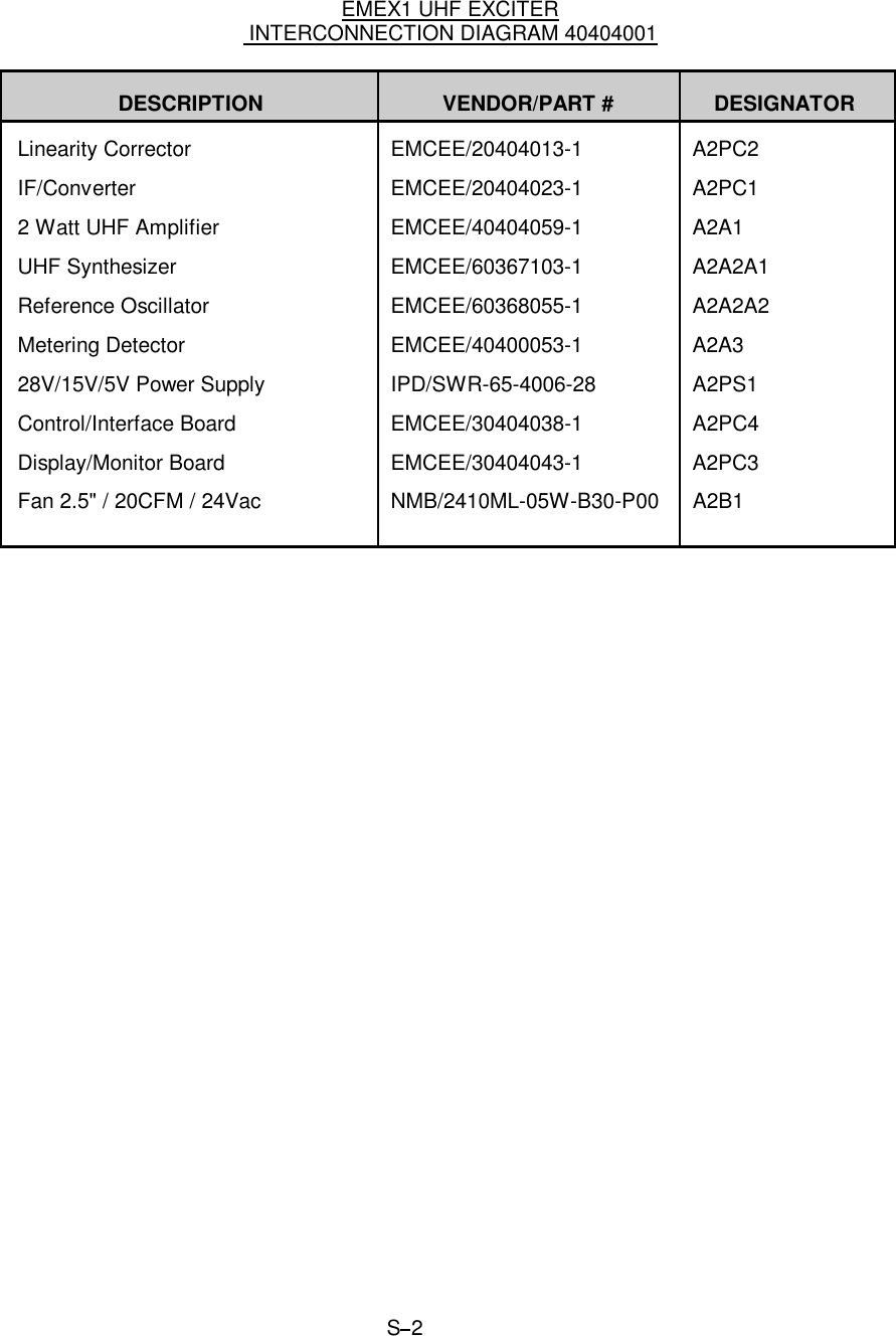
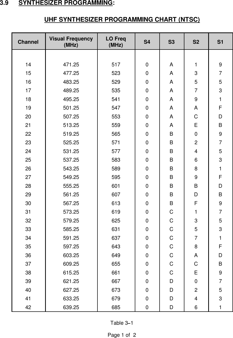
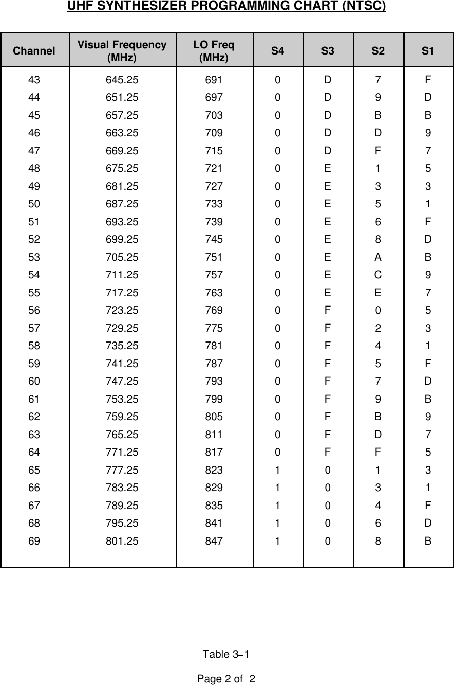
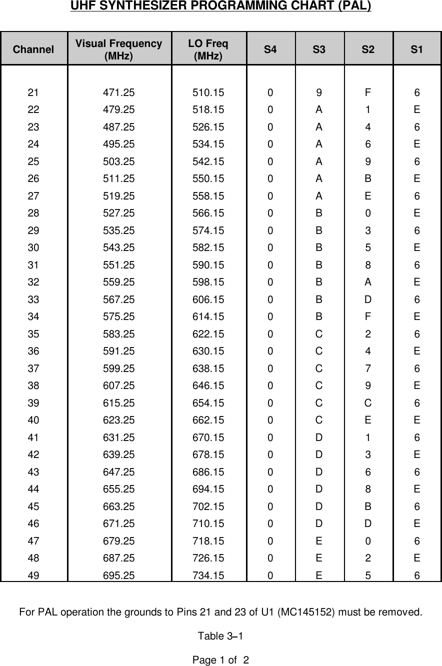
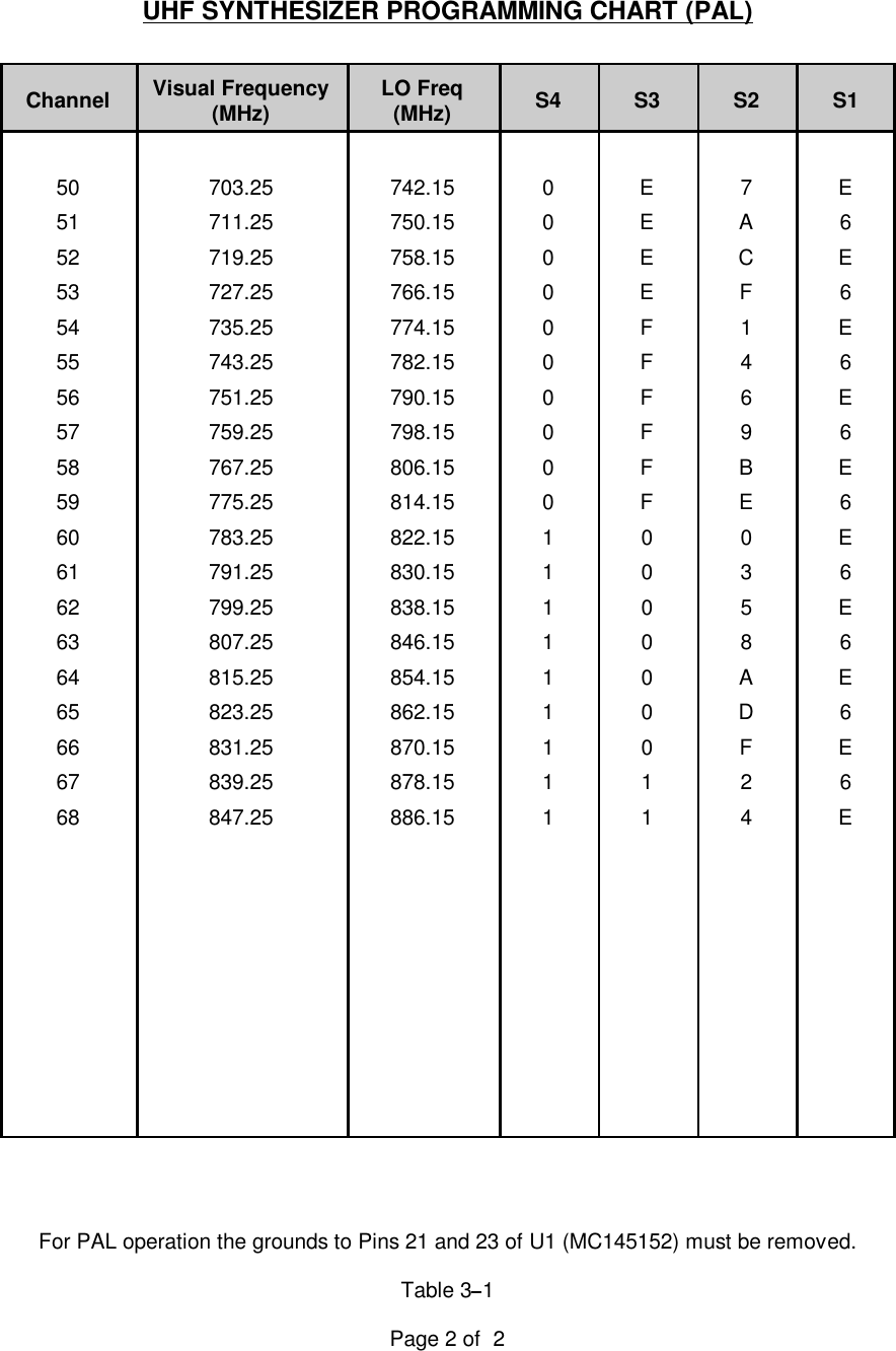
EMCEE Broadcast TTU500FA UHF LPTV Transmitter User Manual TTU1000FA Mnl Cover Pg 1

EMCEE Broadcast Products UHF LPTV Transmitter TTU1000FA Mnl Cover Pg 1
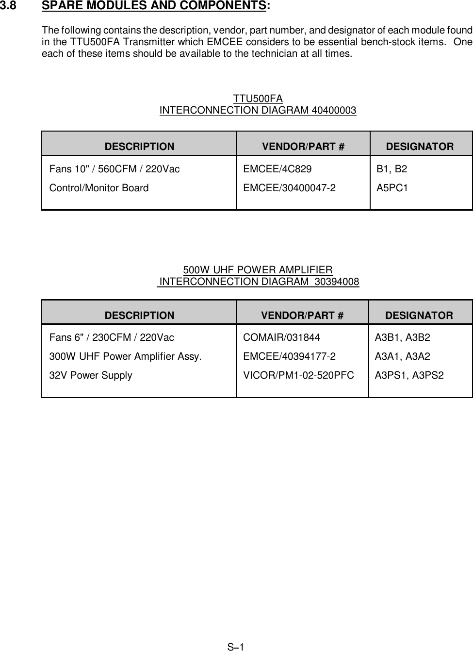
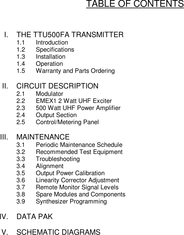
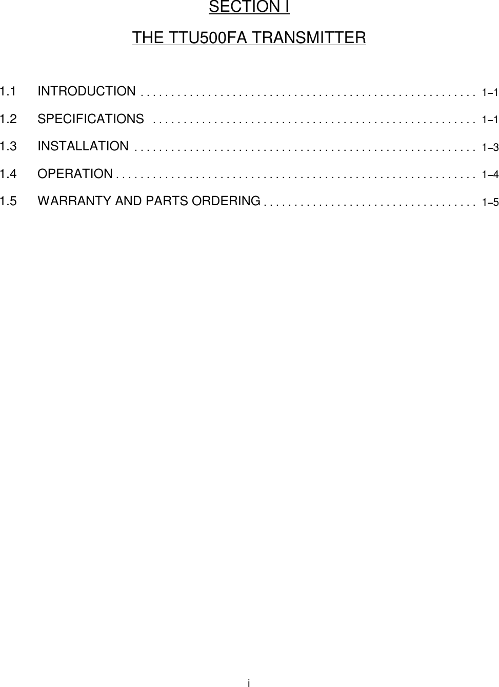
Contents

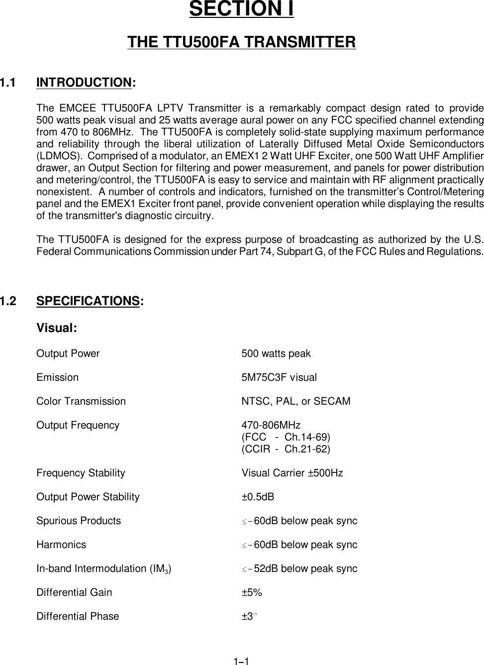
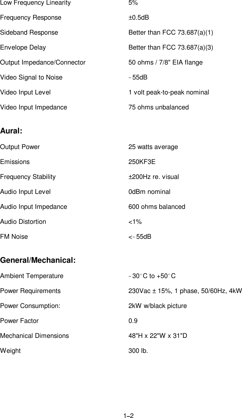
TTU500FA Users Manual
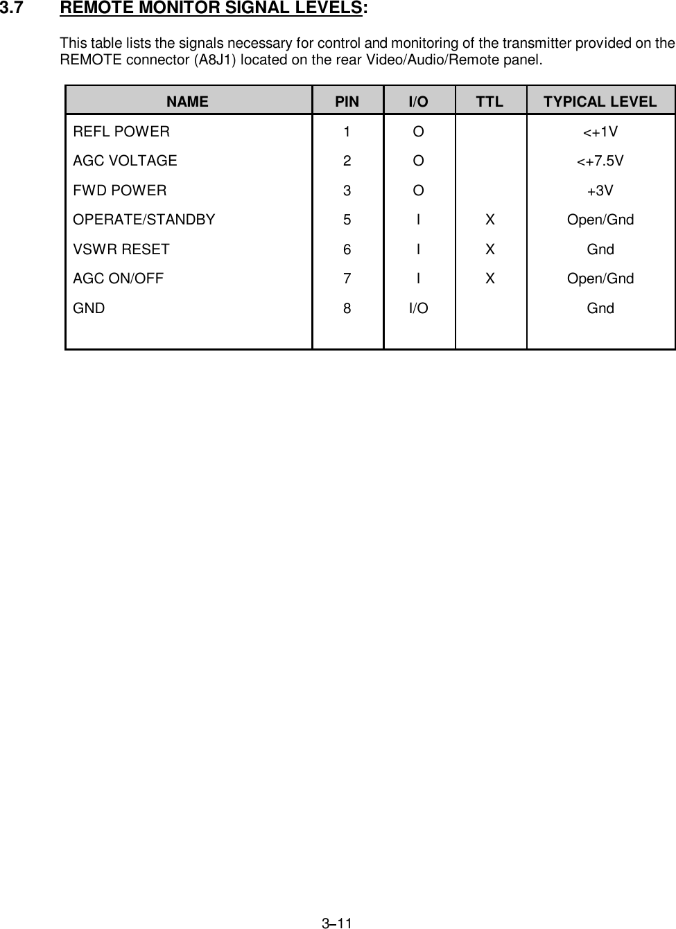
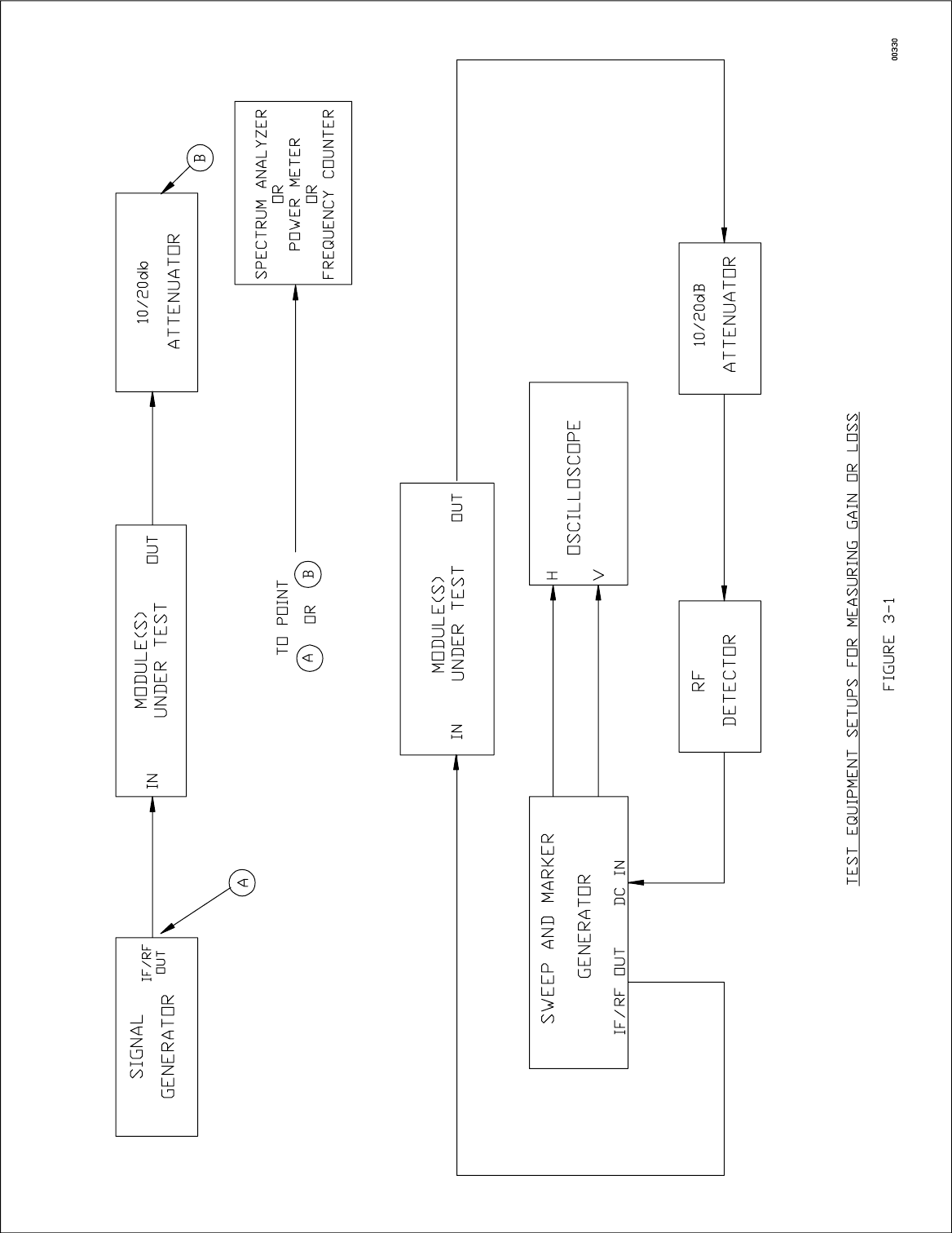
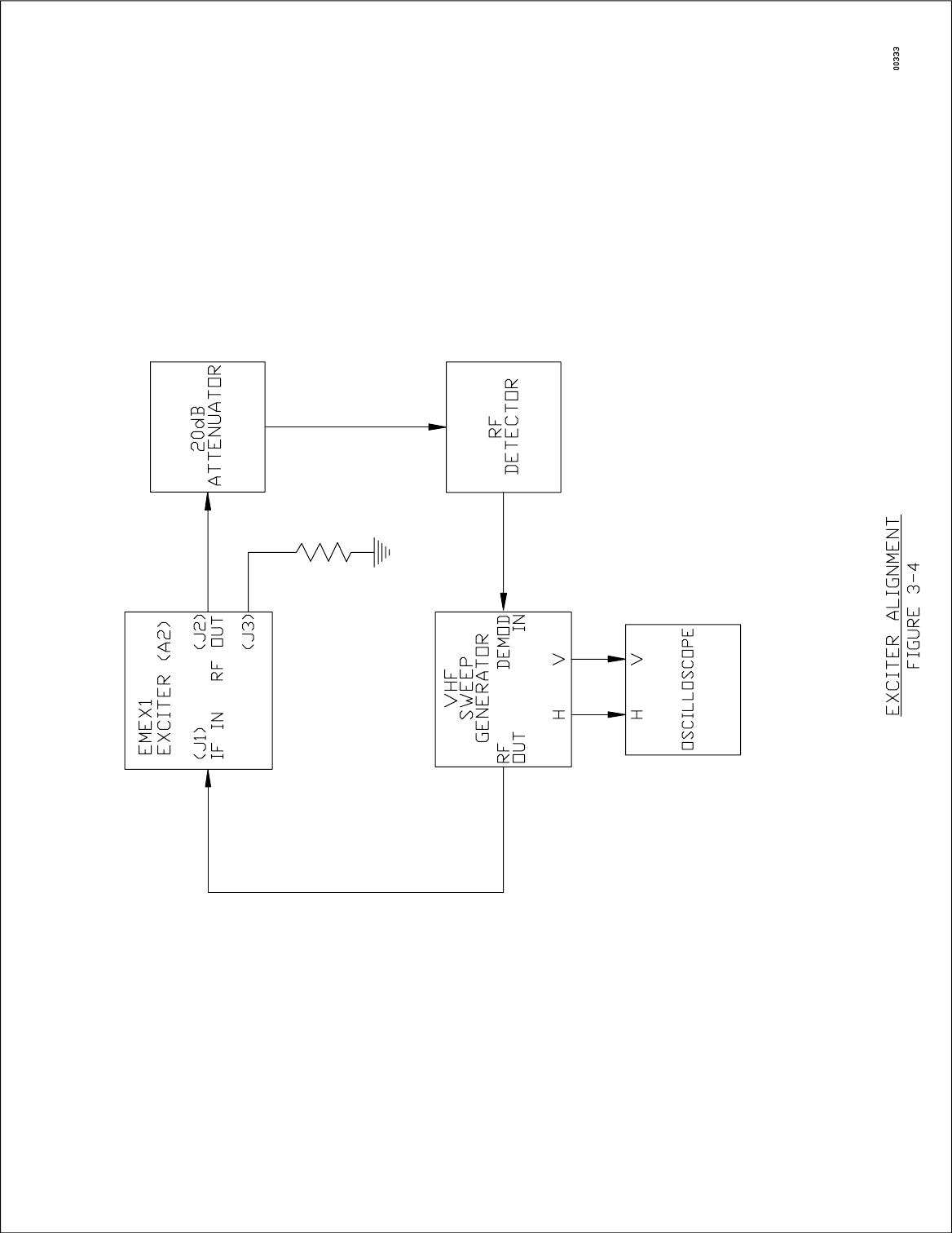
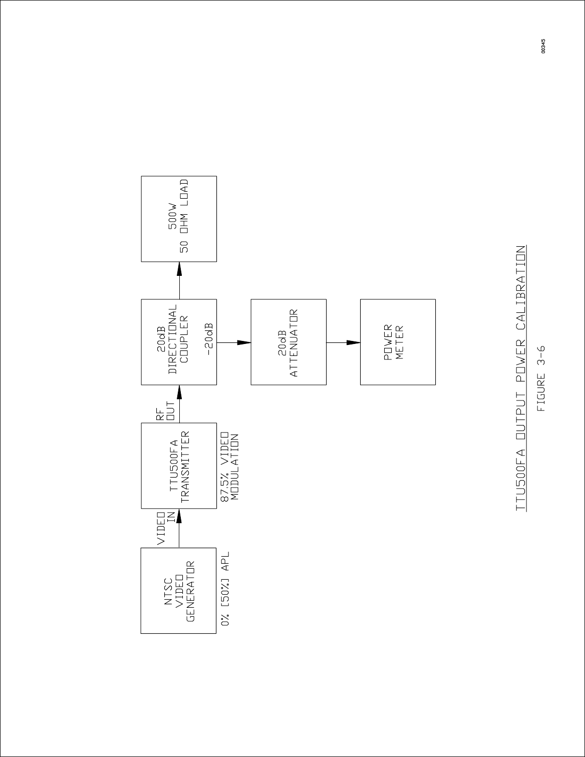
Broadcast ProductsP.O. Box 68, White Haven, PA 18661     Phone: (570) 443-9575    FAX:  (570) 443-9257MDS     MMDS     ITFS     LPTVNorth America   South America   Europe   Asia   Australia   AfricaSince 19606)  USERS MANUALTTU500FASOLID STATE LDMOS500W UHF TRANSMITTER
TTU500FASOLID STATE LDMOS500W UHF TRANSMITTER05/01
IMPORTANTTransient Overvoltage ProtectionTransient overvoltage of micro- and nano-seconds durations present on AC linesare a continuous threat to all solid-state circuitry.  The resulting costs ofequipment repairs and system downtime make preventative protection the bestinsurance against these sudden surges.  Types of protection range from isolationtransformers and uninterruptible power supplies to the more cost effective ACpower line protectors.  As transients are most often caused by lightning inductionand switching surges, AC power line protectors are the most practical solution.An effective AC power line protector is one capable of dissipating impulseenergy at a low enough voltage to ensure the safety of the electronic compo-nents it is protecting.  The protection unit should be across the AC line at alltimes even during periods of total blackout.  It should also reset immediately andautomatically to be 100% ready for repeated transients.
TABLE OF CONTENTSI. THE TTU500FA TRANSMITTER1.1 Introduction1.2 Specifications1.3 Installation1.4 Operation1.5 Warranty and Parts OrderingII. CIRCUIT DESCRIPTION2.1 Modulator2.2 EMEX1 2 Watt UHF Exciter2.3 500 Watt UHF Power Amplifier2.4 Output Section2.5 Control/Metering PanelIII. MAINTENANCE3.1 Periodic Maintenance Schedule3.2 Recommended Test Equipment3.3 Troubleshooting3.4 Alignment3.5 Output Power Calibration3.6 Linearity Corrector Adjustment3.7 Remote Monitor Signal Levels3.8 Spare Modules and Components3.9 Synthesizer ProgrammingIV. DATA PAKV. SCHEMATIC DIAGRAMS
iSECTION ITHE TTU500FA TRANSMITTER1.1 INTRODUCTION ....................................................... 1 11.2 SPECIFICATIONS ..................................................... 1 11.3 INSTALLATION ........................................................ 1 31.4 OPERATION ........................................................... 1 41.5 WARRANTY AND PARTS ORDERING ................................... 1 5
1 1SECTION ITHE TTU500FA TRANSMITTER1.1 INTRODUCTION:The EMCEE TTU500FA LPTV Transmitter is a remarkably compact design rated to provide500 watts peak visual and 25 watts average aural power on any FCC specified channel extendingfrom 470 to 806MHz.  The TTU500FA is completely solid-state supplying maximum performanceand reliability through the liberal utilization of Laterally Diffused Metal Oxide Semiconductors(LDMOS).  Comprised of a modulator, an EMEX1 2 Watt UHF Exciter, one 500 Watt UHF Amplifierdrawer, an Output Section for filtering and power measurement, and panels for power distributionand metering/control, the TTU500FA is easy to service and maintain with RF alignment practicallynonexistent.  A number of controls and indicators, furnished on the transmitter’s Control/Meteringpanel and the EMEX1 Exciter front panel, provide convenient operation while displaying the resultsof the transmitter's diagnostic circuitry.The TTU500FA is designed for the express purpose of broadcasting as authorized by the U.S.Federal Communications Commission under Part 74, Subpart G, of the FCC Rules and Regulations.1.2 SPECIFICATIONS:Visual:Output Power 500 watts peakEmission 5M75C3F visualColor Transmission NTSC, PAL, or SECAMOutput Frequency 470-806MHz(FCC -  Ch.14-69)(CCIR -  Ch.21-62)Frequency Stability Visual Carrier ±500HzOutput Power Stability ±0.5dBSpurious Products 60dB below peak syncHarmonics 60dB below peak syncIn-band Intermodulation (IM3)52dB below peak syncDifferential Gain ±5%Differential Phase ±3
1 2Low Frequency Linearity 5%Frequency Response ±0.5dBSideband Response Better than FCC 73.687(a)(1)Envelope Delay Better than FCC 73.687(a)(3)Output Impedance/Connector 50 ohms / 7/8" EIA flangeVideo Signal to Noise 55dBVideo Input Level 1 volt peak-to-peak nominalVideo Input Impedance 75 ohms unbalancedAural:Output Power 25 watts averageEmissions 250KF3EFrequency Stability ±200Hz re. visualAudio Input Level 0dBm nominalAudio Input Impedance 600 ohms balancedAudio Distortion <1%FM Noise < 55dBGeneral/Mechanical:Ambient Temperature 30 C to +50 CPower Requirements 230Vac ± 15%, 1 phase, 50/60Hz, 4kWPower Consumption: 2kW w/black picturePower Factor 0.9Mechanical Dimensions 48"H x 22"W x 31"DWeight 300 lb.
1 31.3 INSTALLATION:Except where otherwise noted, the connectors mentioned in the following instructions are locatedon the rear of the transmitter. 1. After unpacking the transmitter, a thorough inspection should be conducted to reveal anydamage which may have occurred during shipment.  If damage is found, immediately notifythe shipping agency and advise EMCEE Broadcast Products Customer Service or its fieldrepresentative.  Also check to see that any connectors, cables or miscellaneous equipment,which may have been ordered separately, are included. 2. Place the transmitter in a clean, weatherproof environment providing adequate ventilationfor the exhaust fans at the rear of the transmitter drawers.  It is important to maintain thetransmitter's ambient temperature within the  30 C and +50 C limits.  Cooler ambienttemperatures will provide increased reliability. 3. Place the transmitter in its permanent location near a single-phase receptacle that supplies230Vac at 50/60Hz.  The ac source should have a minimum power capacity of 4kW.IMPORTANTDo not apply ac power to the transmitter at this time since its RF output must beproperly loaded before being placed in operation. 4. Set all circuit breakers, including the customer's incoming ac line breaker, to the OFFposition.  Ac breakers can be found on the transmitter’s AC Distribution Panel, at the rear ofthe amplifier and Exciter drawers, and on the front AC Power panel.  Place an appropriatepower line protector (surge suppressor) across the ac line that supplies the transmitter. 5. Connect the baseband video and audio cables (customer supplied) to the transmitter's VIDEOand AUDIO connectors located on the upper panel at the rear of the transmitter cabinet. 6. Connect the transmitting antenna cable (or a 1kW, 50 ohm dummy load) to the 7/8" EIAflange connector marked RF OUTPUT located through the center rear of the cabinet’s topcover. 7. Verify that the power cords of the Modulator (110V/15A), Exciter (110/15A) and 500W PowerAmplifier drawer (220V/20A) are plugged into the receptacles at the bottom of the transmittercabinet.  Also check to see that any ancillary equipment included in the cabinet (i.e. VideoDetect Switch, Stereo Generator, etc.) are connected to the appropriate ac sockets. 8. Check to see that all RF cables and wire harnesses are properly connected and secure. 9. Using the 4-prong, twist-lock, female plug supplied with the transmitter, fabricate an ac powercord (Figure 1 1) and plug it into the transmitter's AC MAINS connector at the bottom rearof the transmitter cabinet.  Open the incoming ac mains wall breaker and connect the otherend of the power cord into an appropriate 220Vac electrical outlet.
1 41.4 OPERATION:Assuming the installation instructions of Section 1.3 have been completed and the transmitter isreceiving baseband video and audio signals, proceed with the following steps to place the transmitterin operation.  Except where otherwise noted, the controls, switches, and indicators mentioned inthese steps are located on the front of the transmitter. 1. Open the AC POWER circuit breaker located on the bottom front panel of the transmitter andclose the incoming ac mains breaker.  Insure that the EMEX1 Exciter OPERATE/STANDBYswitch is in the off/out (STNDBY) position and the AGC/MANUAL button is in the off/out(MANUAL) position.  Place the transmitter’s Control/Metering panel FWD/REFL meter switchto the FWD/out position. 2. Place the three AC Distribution Panel breakers (CB2, CB3, CB4), located at the lower rearof the cabinet, to the on position.  Also switch the Exciter and amplifier drawer rear panelbreakers to on. 3. Move the AC POWER circuit breaker located on the bottom front panel of the transmitter tothe ON position. 4. If applicable, place the Modulator's power switch to ON and verify that it is providing 87.5%video modulation.  If necessary, adjust the Modulator for the proper video depth ofmodulation as described in its instruction manual.  Also check to see that the audio peaks arenot overmodulating the aural carrier. 5. Verify the following transmitter responses:a. The fans at the rear of each drawer should be operating.b. The Exciter’s green LED indicators should react as follows:SYNTHESIZER LOCK – onIF STATUS – onAMPLIFIER STATUS – onLINEARITY CORRECTOR – onAGC ACTIVE – offSWEEP MODE – offOPERATE/STANDBY – offVSWR RESET – offAGC voltmeter – 1 segment lit at approximate centerRF POWER meter – 0%c. The green LED indicators on the transmitter’s Control/Metering panel should respondas follows:AMPLIFIER TEMP – offAMPLIFIER – onPOWER SUPPLY – offRF POWER meter – 0%FWD – onREFL – off
1 5 6. Turn the Exciter's OUTPUT LEVEL ADJUST two or three turns counterclockwise and pressthe OPERATE/STANDBY switch in to place the transmitter in OPERATE.  Then verify thefollowing responses of the transmitter:a. The Exciter’s OPERATE/STANDBY switch indicator is now lit green.b. The POWER SUPPLY Control/Metering panel indicator is now lit green.c. The status of all other indicators previously mentioned is the same. 7. Check to see that the Control/Metering panel’s meter switch is in the FWD/out position andthen slowly turn the Exciter’s OUTPUT LEVEL ADJUST clockwise until a 100% indicationappears on the Control/Metering panel’s RF POWER meter.  The Exciter’s RF POWERmeter should also be displaying a 100% indication. 8. After 10 minutes of operation press the Exciter’s AGC/MANUAL switch in to engage thetransmitter’s output automatic gain control.  If necessary and with a small tuning tool, slowlyturn the AGC LEVEL ADJUST to bring the transmitter’s RF POWER meter reading back to100%. 9. Place the Control/Metering panel's meter switch to REFLD and verify that the RF POWERmeter indicates no more than 10% returned power.  If the reflected power is more than 10%,shut down the transmitter and check the VSWR of the transmitting antenna and its associatedcable.10. Place the Control/Metering panel's meter switch to FWD for constant monitoring of thetransmitter's final output power.The transmitter is now in operation.  Check its coverage area for clean, sharp television reception.If the reception or picture quality is unsatisfactory, examine the amount of power delivered to thetransmitting antenna (see Section 3.5) and, if necessary, examine the antenna orientation andantenna transmission line VSWR to insure maximum radiation in the proper direction.1.5 WARRANTY AND PARTS ORDERING:Warranty – EMCEE warrants its equipment to be free from defects in material and workmanship fora period of one year after delivery to the customer.  Equipment or components returned as defective(prepaid) will be, at our option, repaired or replaced at no charge as long as the equipment orcomponent part in question has not been improperly used or damaged by external causes(e.g., water, ac line transients or lightning).  Semiconductors are excepted from this warranty andshall be warranted for a period of not more than ninety (90) days from date of shipment.  Equipmentor component parts sold or used by EMCEE, but manufactured by others, shall carry the samewarranty as extended to EMCEE by the original manufacturer.Equipment Returns – If the customer desires to return a unit, drawer, or module to EMCEE forrepair, follow the procedure described below: 1. Contact EMCEE Customer Service Department by phone or fax for a Return AuthorizationNumber.
1 6 2. Provide Customer Service with the following information:Equipment model and serial numbers.Date of purchase.Unit input and output frequencies.Part number (PN) and Schematic Diagram designator if a module is being sent.Detailed information concerning the nature of the malfunction.The customer shall designate the mode of shipping desired (e.g., Air Freight, UPS, Fed Ex, etc.).EMCEE will not be responsible for damage to the material while in transit.  Therefore, it is of utmostimportance that the customer insure the returned item is properly packed.Parts Ordering – If the customer desires to purchase parts or modules, utilize the followingprocedure: 1. Contact EMCEE Customer Service by phone or fax indicating the customer's purchase ordernumber.  If the purchase order number is provided by phone, written confirmation of the orderis required. 2. Also provide:The equipment model and serial number.The unit input and output frequencies.The quantity, description, vendor, number, and designation of the parts needed as found inthe Parts Lists subsection of this manual.If a module is required, give the part number (PN) and Schematic Diagram designator(e.g., 30404029).Designate the mode of shipping desired (e.g., Air Freight, UPS, Fed Ex, etc.).Shipping and billing addresses.Spare and Replacement Parts – The Spare Modules and Components section of this manualprovides a detailed listing of the modules and some discrete components contained within thetransmitter.  The listing contains those modules or components considered to be essentialbench-stock items and should be available to the technician at all times.  The Schematic orInterconnection Diagram is the governing document of this manual.  Should there be a discrepancybetween a modules or components list and a diagram, the diagram takes precedence.  Such adiscrepancy is possible since manufacturing changes cannot always be incorporated immediatelyinto the instruction manual.Component Referencing – A transmitter may consist of a modulator or receiver, a number ofmodules and components mounted in drawers, and components or modules mounted to panels ordirectly to the cabinet.  Components mounted in a module which is included in a drawer take thedrawer number and the module number in addition to a component number.  Thus the referencedesignator A2A1Q1 means transistor Q1 in module A1 of drawer A2.  Components mounted in adrawer take only the drawer number and a component number (e.g., A2M1 designates meter M1 ofdrawer A2).  Components mounted directly to a panel take only the panel number and a componentnumber.  Components and modules mounted directly to the cabinet take only a component ormodule number.
1 7For EMERGENCY technical assistance, EMCEE offers a toll free, 24-hour, 7-day-a-weekcustomer service hot line:  1-800-233-6193.
iiSECTION IICIRCUIT DESCRIPTION2.1 MODULATOR ......................................................... 2 12.1a Video Detector Switch ............................................... 2 12.2 EMEX1 2 WATT UHF EXCITER ......................................... 2 12.2a Linearity Corrector .................................................. 2 22.2b IF/Converter ....................................................... 2 32.2c UHF Synthesizer ................................................... 2 62.2d Reference Oscillator ................................................. 2 72.2e UHF Bandpass Filter ................................................ 2 72.2f 2 Watt UHF Amplifier ................................................ 2 72.2g Metering Coupler ................................................... 2 92.2h Metering Detector................................................... 2 92.2i Control/Interface Board .............................................. 2 92.2j Display/Monitor Board .............................................. 2 202.2k 28V/15V/5V Power Supply ........................................... 2 242.3 500 WATT UHF POWER AMPLIFIER DRAWER ......................... 2 242.3a Power Splitter..................................................... 2 252.3b 300W UHF Power Amplifier .......................................... 2 252.3c Power Combiner................................................... 2 272.3d Amplifier Status Interface ............................................ 2 272.3e Power Supply/Thermal Interface ....................................... 2 272.3f 32V Power Supply ................................................. 2 282.4 OUTPUT SECTION ................................................... 2 292.4a UHF Bandpass Filter ............................................... 2 292.4b Directional Coupler ................................................. 2 292.4c Metering Detector.................................................. 2 292.5 CONTROL/METERING PANEL ......................................... 2 302.5a Control/Monitor Board .............................................. 2 30
2 1SECTION IICIRCUIT DESCRIPTION2.1 MODULATOR:EMCEE EM1 / Scientific Atlanta 6340 / RF Comm. 2000     A1IF OUT 8dBm peak visual typicalThe modulator processes baseband video and audio signals to provide a composite IF outputcomposed of a visual carrier at 45.75MHz with 5M75C3F modulation, and an aural carrier at41.25MHz with 250KF3E modulation.  Any of these modulators can be used to drive the EMEX12 Watt Exciter drawer (A2).  The optional video sense circuit provides an indication of whether themodulator is receiving a baseband video signal.  The output of the video sense is either a logichigh ( +5Vdc) with video present or a logic low ( 0Vdc) when video is not present.  This logicsignal is used by the Exciter Control/Interface Board (A2PC1) to place the transmitter in standbyif the video signal is lost.2.1a Video Detector Switch:Burst VDS     A9For those modulators which do not contain a video sense alarm, the Burst Electronics VideoDetector Switch (Model VDS) will be installed in the transmitter cabinet.  The VDS detects thepresence of composite video connected to its A INPUT directly from the VIDEO connector mountedon the Video/Audio/Remote Panel (A8J2).  If a loss of video is detected, then the unit switches tothe B INPUT, lights its red LED and energizes an internal TALLY relay.  Through this relay, aground is sent to the Exciter Control/Interface circuit via the transmitter’s Control/Monitor board(A5PC1) placing the transmitter in a nonradiating condition.2.2 EMEX1 2 WATT UHF EXCITER:Interconnection Diagram 40404001/Rev 55     A2Composite IF IN (J1) 8dBm peak visual21dBm average auralRF OUT (J2 & J3) +18dBm typical peak visual+5dBm typical average auralThe EMEX1 Exciter drawer converts the composite IF signal from the modulator to the desiredUHF frequency while amplifying this RF signal to the appropriate output level.  The Exciter suppliesapproximately 200mW of peak visual power to drive the 500W UHF Power Amplifier drawer (A3).Power control, automatic gain control (AGC) and heterodyne conversion are performed by theIF/Converter module (PC1).  Utilizing the composite IF signal, the Linearity Corrector furnishesperformance improvements for the transmitter’s ICPM, differential phase and gain, sync amplitude
2 2and intermodulation.  The UHF Synthesizer supplies a programmable LO to the IF/Converter mixerwhere the LO and IF signals are combined to create the desired UHF frequency.  The UHF signalfrom the Converter module is then passed through the UHF Bandpass Filter (FL1) to remove theunwanted LO and sum products from the conversion process while passing and amplifying thedesired difference signals.  The signal is then amplified approximately 25dB by the 2 Watt UHFamplifier (A1) and passed through the Metering Coupler (CP1).  Here, a forward RF sample isprovided for use by the Metering Detector (A3) while the main signal is passed to the output of thedrawer.Metering and control functions are provided by the Metering Detector, the Display/Monitor board(PC3) and the Control/Interface Board (PC4).  The Display/Monitor Board has several status anddiagnostic LED indicators which are presented on the Exciter’s front panel.  The Control/Interfaceboard provides for various controls and logic circuits for proper operation of the transmitter.  Dcpower for the Exciter is supplied by a small, efficient multioutput switching power supply PS1 whichfurnishes ±28, ±15 and ±5 volts.2.2a Linearity Corrector:Schematic Diagram 40404011/Rev 55     A2PC2IF IN (J1) 11dBm typicalIF OUT (J2) 12dBm typicalGain with S1 ENABLE/DISABLE (J1-J2) 0 to  2dB typicalCurrent Draw 610mA @ +15VdcThe Linearity Corrector is a six-stage, unity gain circuit which compensates for nonlinear distortionsgenerated in the transmitter's Class AB 500 Watt Power Amplifier drawer.  When properly adjusted,it provides correction to the transmitter’s output signal for sync amplitude, differential gain,differential phase, ICPM and intermodulation.  Corrector amplifiers U1 through U8 are allmonolithic amplifier stages providing approximately 12dB of gain per device.  A phase correctionnetwork is centered around amplifiers U2 through U5 while the circuitry surrounding U7 and U8corrects for differential gain and sync compression.  When properly adjusted, the phase and gaincorrection networks will collectively reduce intermodulation distortion.Input amplifier U1 is biased through resistor R1 and inductor L1 which acts as an RF choke.Capacitor C2 is utilized as a B+ bypass with coupling capacitors C1 and C3 advancing the inputsignal to the matching T-attenuator made up of resistors R2, R3 and R4.  At hybrid splitter DC1,the IF carrier is divided into two equal amplitude signals which are 90  out of phase.  At thesplitter’s  90  port, a negative phase-shift network composed of inductor L3 and capacitors C15through C18 adds another  22.5  shift to the signal ( 112.5  total) before amplification by U3.Conversely, connected to the 0  port of the splitter is a positive phase-shift network comprised ofinductor L2 and capacitors C4 throughC7.  Here the 0  signal is shifted in the positive direction by22.5  resulting in a 135  total difference between the two signals.  In order to keep the amplitudeof each signal similar, the circuits surrounding amplifiers U2 through U5 are essentially identicalwith the same biasing, bypassing and coupling described for U1.  Transformers T3 and T4 on thenegative shift side of the circuit are 2:1 step-up types identical to T1 and T2, but necessary toefficiently drive gain expansion diodes CR1 and CR2.  Through adjustment of slope potentiometersR15 and R25 and threshold (cut-in) pots R21 and R30, the amplitude of the negative shifted signalcan be varied to add to or subtract from the positive shifted signal at in-phase combiner CP1.When adjusted properly, this circuit can then correct the differential phase, intermodulation andICPM distortions created by the transmitter’s power amplifier.  At the output of combiner CP1 the
2 3IF signal passes through a matching pi-attenuator comprised of resistors R35, R36 and R37 beforeamplification by U6, U7 and U8.  Transformers T5 and T6 again double the signal voltage toproperly drive the gain expansion diodes CR3 and CR4 which compensate for differential gain andsync compression created in the 500 Watt Power Amplifier (A3).The variable gain expansion networks, which provide linearity correction, are centered around dualdiodes CR1 through CR4, slope potentiometers R15, R25, R41, R57, unity gain dc amplifiers U9,U10, U11, threshold potentiometers R21, R30, R47, R55 and ENABLE/BYPASS switch S1.  Thethreshold (cut-in) potentiometers determine the point on the IF waveform where the correction, orgain expansion, will occur and the slope potentiometers dictate the amount of correction/expansionto be used at that breakpoint.  With S1 in the ENABLE position, the four diode pairs form nonlinearcircuits where each diode is reverse biased and the amount of reverse bias dictates the point atwhich the diode turns on during the positive and negative cycles of the visual IF carrier envelope.Each diode is biased using voltages established by the threshold potentiometers in conjunction withdc amplifiers U9, U10, U11 and U12.  L4 through L6 and L9 through L12 isolate the IF signal fromthe diode threshold biasing circuitry.  When the positive and negative peaks of the visual signalenvelope are sufficient to forward bias a diode pair, the pair turns on placing the resistance of itsrespective slope potentiometer in parallel with the series arm of its L-pad (R14, R24, R40, R50).As a result, the attenuation of the visual IF carrier is reduced during this period causing thewaveform to stretch.  Slope control R41 is typically used to correct differential gain while R57primarily adjusts sync amplitude.With S1 in the BYPASS position, ground is applied to FET switches Q1 and Q2 placing each diodepair in hard reverse bias preventing conduction throughout the positive and negative cycles of theIF carrier envelope.  Due to the high reverse resistance provided, each diode network essentiallyrepresents a resistive L-pad (R14/R16, R24/R31, R40/R42, R50/R58) with the IF signal attenuatedby a fixed amount in each location.  As a result, no linearity correction is provided.2.2b IF/Converter:Schematic Diagram 40404021/Rev 53     A2PC1IF INPUT (J1) 0dBm to  30dBm peak visualCORRECTOR LOOP Out (J3) 11dBm peak visual typicalCORRECTOR LOOP In (J4) 12dBm peak visual typicalRF OUT 10 to  18dBmLO INPUT (J5) +13dBm minimumCurrent Draw 42mA @ +15V31mA @  15V185mA @ +5VThe IF/Converter performs three tasks in this transmitter.  With the first AGC loop it furnishes levelcontrol for the incoming signal from the modulator, upconverts the IF signal to the desired UHFchannel and then controls the transmitter’s output power through a second gain control loop.The modulator’s IF input, provided at J1, is amplified or attenuated by variable gain amplifier U1.This integrated circuit, controlled by the output of integrator U4 via switch S1, (U1) can producewide variations in gain ranging from +30dB to  10dB.  At the output of U1 is coupling capacitor C3and 2:1 step-down transformer T1 required for proper impedance matching between U1 and in-phase splitter CP1.  At the output of CP1, two equal amplitude IF signals are delivered for differingapplications.  The signal at pin CP1-3 is used to provide a reference for the input AGC loop, while
2 4the second signal at pin CP1-4 is fed to the Linearity Corrector (PC2) connected to output J3.  Bothsignals pass through attenuators (3dB and 7dB respectively) which are connected to identicalmonolithic amplifiers, U7 and U8.  These devices, offering approximately 14dB of signal gain, arefurnished bias through resistors R15/R22 and RF chokes L1/L2.  The output of amplifier U8 isconnected, through coupling capacitor C19, to a variable PIN attenuator composed of diodes CR7and CR8.  This diode array forms a pi-attenuator operated by buffer U9 whose input (pin 5) issupplied control voltage from the Exciter’s front panel OUTPUT LEVEL ADJUST.  With maximumvoltage from U9 (+15V) the attenuator will exhibit minimum attenuation of approximately 2dB.With minimum voltage the attenuator can provide more than 50dB of loss to the signal.  Thisattenuator is utilized as the main power control and standby mechanism for the transmitter.At the output pin 3 of U7 is the second IF signal required by the input AGC circuit as a powerreference representing the incoming modulator signal level.  This signal is passed through couplingcapacitor C16 to integrated circuit U6, an RMS detector.  At pin 7, U6 outputs the video componentof the IF visual carrier while C11 rolls off the aural energy contained in the signal.  The amplitudeof the video is then doubled using op-amp U5A and then sent to peak detector CR3 via pins 1 and2 of jumper JP1.  (Pins 2 and 3 of JP1 are utilized for average digital power detection only.)Capacitor C9 and resistor R10 filter the peak video component from diode CR3 and this dc voltageis sent to unity gain buffer U5B.  The dc level at the output of U5B (pin 7), which is nowproportional to the peak power of the visual signal entering the IF/Converter, will be approximately+3V when the modulator level into the Converter board is at the midpoint of its input AGC window(15dBm peak).  This potential then appears at pin 6 of integrator U4B where it is compared to thevoltage on pin 5 ( +3V) generated by divider R7/R8.  When the values of each voltage at pins 5and 6 are equal, the output of U4B at pin 7 will be zero, holding variable gain amplifier U1 at thecenter of its gain extremes (+10dB) via pins 8 and 1 of electronic switch S1.  (The gain of U1 canalso be set to its center by applying a low to the INPUT AGC CONTROL line which is connectedto pin 6 (IN) of switch S1.  This low, supplied by the OPERATE/SWEEP switch PC4S1 on theControl/Interface board, will disconnect the input AGC voltage at S1-8 from S1-1 and connect theground at S1-2, 3 to S1-1 effectively placing a zero voltage on pin 1 of U1.)  If the input level fromthe modulator at J1 increases, the outputs of U7, U6, U5A and U5B will also increase forcing pin 7of U4B negative and proportionally reducing the gain of U1.  Conversely, if the input from themodulator were to be reduced, the output of U4B would swing positive causing U1 to increase itsgain compensating for the signal reduction.  Under normal transmitter operating conditions, thesignal provided at the CORRECTOR LOOP output (J3) will be approximately  11dBm peak visual.However, if the IF signal is significantly reduced ( 25dBm) or removed completely, the potentialat the output of U4B will exceed +2.5V causing the level at input pin 2 of U4A to exceed thereference (2.5V) provided at pin 3 through divider R5/R6.  This action would drive output pin 1 ofU4A to zero, turning off the IF STATUS light (PC3DS5) on the Exciter’s front panel and placing alow on the LEVEL ADJUST line attached to pin 5 of U9 increasing the attenuation of the associatedPIN diode circuit to maximum ( 50dB).After proceeding through the Linearity Corrector, the IF signal is fed to CORRECTOR LOOP inputJ4 at an approximate level of  12dBm.  Here the signal is furnished a 50 ohm match usingpi-attenuator R30/R31/R32.  Hybrid amplifier U1, biased through resistor R33 and RF choke L3,provides 14dB of gain and delivers the signal to in-phase 2-way splitter CP2 via coupling capacitorC29.  At output pins 3 and 4 of CP2 are two equal amplitude IF signals used, respectively, to drivethe output AGC loop (U13 through U18) and to be mixed to the wanted UHF channel after passingthrough the output control attenuator.  Made up of PIN diodes CR9/CR10 and controlled by U18,this attenuator is capable of 2dB to 50dB of attenuation and ultimately sets the output power of thetransmitter.  From the output control attenuator the IF signal is transferred to mixer MX1 throughcoupling capacitor C51 and pins 1 and 2 of jumper JP3.  (Connecting pins 2 and 3 of JP3 bringsthe IF signal to test point TP1.)  In MX1 the IF is then upconverted to the desired UHF signal asa result of combining with the local oscillator frequency presented at LO INPUT J5.  At the outputof the mixer (pin 4) resistors R67/R68/R69 provide 5dB of attenuation and the appropriate
2 5impedance match for amplifier U20 via capacitor C52.  U20 supplies 13dB of amplification for theUHF frequencies with resistor R70 and choke L5 furnishing the necessary power to the hybrid.From output pin 2 of U20, the amplified signal is brought to the OUTput connector J5 where it willbe fed to the subsequent UHF Bandpass Filter (A2FL1) and eventually to the transmitter’s output.The second IF signal, present at pin 3 of splitter CP2, functions as the signal level reference forthe output AGC loop.  Matching attenuator R34/R35/R36 provides the proper impedance for thesignal brought to pin 1 of 14dB hybrid amplifier U13.  Bias is supplied to U13 through resistor R37and choke L4 with capacitor C31 acting as an RF bypass.  Capacitors C32 and C33 in conjunctionwith resistor R38 provide coupling and matching from the output of amplifier U13 to the input ofRMS detector U14.  As with detector U6 of the input AGC loop, U14 separates the video programfrom the IF visual carrier while attenuating the aural components through C35.  The demodulatedvideo signal, found at pin 7 of U14, is amplified by U15A and passed through detector CR4 viajumper JP2 pins 1 and 2.  (Pins 2 and 3 of JP2 are utilized for average digital power detectiononly.)  The resulting peak of the video signal is transformed into an average dc voltage using filterCR36/R42 which is then buffered with unity gain amplifier U15B.  At the output of divider R43/R45,the positive detected voltage created by the IF signal at CORRECTOR LOOP J4 meets thenegative POWER REFERENCE voltage supplied to connector J6-8 from the transmitter’s outputpower Metering Detector (A7A1) through inverting amplifier U16B.  When their associated circuitsare correctly adjusted, these two voltages will be opposite but equal in value, theoretically yielding0 volts at the output of adder circuit U16A, operational amplifier U17A and integrator U17B.  Withthe front panel AGC/MANUAL switch PC3S2 depressed (in), this voltage is then sent through pins8 and 1 of switch S2 and divider R56/R61 to amplifier U18A which controls the attenuation valueof PIN diodes CR9/CR10 and, subsequently, the output power of the transmitter.  (With 0V at theoutput of switch S1, PIN attenuator CR9/CR10 provides approximately 3dB of signal reduction.With +15V from S1, the PIN attenuator will furnish almost no resistance and with  15V, diodesCR9/CR10 will supply about 6dB of signal loss.)  If, for some reason the transmitter’s output powerwere to drop, the positive voltage at J6-8 would be reduced, making the output of U16B lessnegative.  The more positive voltage at pin 3 of U16 will force its output positive while the outputsof U17A and U17B go negative and positive, respectively.  The change in level, sent to U18 viaswitch S2, forces pin 1 of U18A high reducing the attenuation provided by PIN diodes CR9/CR10.This reduction in attenuation will be proportional to the power decrease seen at the transmitter’soutput, thereby bringing the transmitter’s power back to its appropriate operating level.  In the casewhere the transmitter’s output increases above its rated power, the exact opposite happens.  ThePOWER REFERENCE voltage at J6-8 will increase taking the U16A input negative.  The outputfrom U17A will go positive forcing U17B to send a negative voltage to U18 via switch S2.  Thenegative voltage from U18A will cause PIN diode attenuator CR9/CR10 to increase resistance,decreasing the transmitter’s signal level to its proper value.To defeat the output AGC, the front panel AGC/MANUAL switch must be released (out), placinga ground on the OUTPUT AGC CONTROL line at pin 10 of J6.  This low, applied to pin 6 of switchS2, causes the incoming AGC voltage at pin 8 of S2 to be removed from pin 1 and connected tothe ground at pins 2, 3.  The 0V potential sent to U18A will fix PIN diodes CR9/10 at  3dB, thecenter of their attenuation range.  Amplifier U18B, which also follows the output of S2 at its inputpin 5, acts as a unity gain buffer forwarding the output AGC voltage to the Exciter’s front panelAGC meter (A2PC3DS12) and to the RJ45 REMOTE plug (A8J1) on the VIDEO/AUDIO/REMOTErear panel.
2 62.2c UHF Synthesizer:Schematic Diagram 30367094/Rev B     A2A2A1LO OUT (J2) +15dBm minimumFrequency Stability 0.3ppm /  30 C to +70 C10MHz REF. IN (J1) 3.5V P/P square waveSYNTH LOCK (Pin J4-A) logic high - unlocked / logic low - lockedCurrent Draw 15mA @ +28V120mA @ +15V36mA @ +5VThe UHF Synthesizer is a phase-lock loop circuit that uses 10MHz as a reference to develop amanually programmable CW signal for the Mixer in the IF/Converter module (A2PC1MX1).  Thefrequency of the synthesizer output signal (or LO) is calculated as the sum of the visual IF carrierfrom the modulator and the visual carrier of the transmitter’s UHF output channel.  The LOfrequency is programmed by the setting of switches S1 through S4 which are accessible via accessholes on the Synthesizer’s module (A2A1) cover.  The switch settings for each UHF channel andthe resulting LO frequencies are provided in Table 3 1 of Section 3.9.A 10MHz signal from Reference Oscillator A2A2 is brought to the Synthesizer module throughconnector J1 (10MHz IN).  At the connector, the two sections of divider chip U4 perform a binarydivide-by-5 count creating a 400kHz signal at the OSCin pin 27 of synthesizer chip U1.  At thesame time, the output of voltage controlled G1 (RF OUT), amplified by U5 and available as thetransmitter’s LO at J2 (OUT), is also amplified by U6 and fed to a ÷64/÷65 prescaler, U2.  The U2prescaling factor is ultimately selected by programming switches S1 through S4 which set the MODCONTROL line at pin 9 of U1 to either high or low.  When a high is seen at pin 6 (MC) of prescalerU2, the chip will divide the VCO output by 64.  With a low at U2-6 the prescaler will divide the VCOoutput by 65.  After prescaling, the signal is sent to pin 1 of U1 (Fin) from U2-4 (OUT) and, with theaid of the A and N counters within U1, the prescaled signal is also divided down to 50kHz using adivide-by-ratio selected through the switch settings of S1 through S4.  This 50kHz, derived fromvoltage controlled oscillator G1, is sent to a phase detector for comparison with the 50kHz takenfrom the high stability 10MHz reference.  At the U1 phase detector outputs 0/V and 0/R (pins 7 & 8),loop filter U3 integrates the incoming correction pulses and sends them to VCO G1 as a dc controlvoltage after suppression filter C14/C15/C24/R5/R13.  If the frequency generated by VCO G1 islower than the frequency selected by programming switches S1-S4, a pulse train will appear atpin 5 of U3 forcing the control voltage at pin 7 higher, thereby raising the frequency of theoscillator.  If the VCO output is higher than the frequency selected by the programming switches,then pulses will appear at U3 pin 6 pushing the control voltage lower at U3-7 to reduce thefrequency from G1.  The corrected frequency is then passed through matching attenuator R7/8/9and amplified by U5 for delivery to the IF/Converter mixer.  (For NTSC System M operation, A0and A1, pins 21 and 23 on U1, are grounded.  For PAL System B/G and D/K operation, A0 and A1are made high by opening the traces at pins 21 and 23 thereby adding the characteristic 150kHzto the LO.When the synthesizer is locked to its programmed frequency, pin LD of chip U1 provides a highwhich saturates Darlington pair Q1 after capacitor C28 changes through resistor R16.  This timedelay is created to ensure that the synthesizer has successfully locked before supplying a low tothe SYNTH LOCK line.  During an unlocked condition, the LD pin switches low discharging C28through diode CR1 and reverse biasing Q1.  A high (+5V) is now present on the SYNTH LOCK lineindicating an unlocked condition.
2 72.2d Reference Oscillator:Schematic Diagram 10368037/Rev B     A2A2A210MHz REF. OUT (J1, J2) 3.5V P/P square waveFrequency Stability 0.3ppm /  30 C to +60 CCurrent Draw 15mA @ +5VThe Reference Oscillator provides a high stability 10MHz signal which provides accuracy and long-term frequency stability for the UHF Synthesizer (A2A2A1).  This reference module is centeredaround a 10MHz temperature-compensated crystal oscillator (G1) using 5V as power.  The outputfrom G1 is buffered by two exclusive-OR gates used as inverters.  The output signal from eachgate is a 10MHz low-level square wave with a frequency stability of 0.3 parts per million (ppm).2.2e UHF Bandpass Filter:Schematic Diagram 20404015/Rev 51     A2FL1INPUT (J1) 10 to  18dBmOUTPUT (J2) 0 to  8dBmBandwidth (J1-J2) 8MHz to 15MHz @ 1dBGain (J1-J2) 10dBCurrent Draw 50mA @ +5VThe UHF Bandpass Filter is a six-section comb-line design joined with a single-stage amplifier toprovide 10dB of total module gain.  The first three sections of the filter, composed of variablecapacitors C1/C2/C3 and their associated tuned stubs, are terminated at the input of U1, a 14dBamplifier.  Variable capacitors C1/C2/C3 and C4/C5/C6 electrically lengthen or shorten theirconnected stubs to pass the chosen UHF channel with the appropriate coupling provided byspacing between the stubs.  For extra stub length at lower frequencies, capacitors C7/C8/C9/C10/C11/C12 are added to operate at channels below 560MHz.  The bias for U1 is obtained from the5 volt power supply via R1 and RF choke FB1 (ferrite bead) with bypassing furnished by capacitorsC15/C16/C17.  Loading wires W1/W2/W3/W4 set the input and output impedance of each three-section filter segment, dictating the overall bandwidth and loss of the circuits.  FL1 is tuned toselect the desired UHF mixer products from the lower sideband, or difference signal, found at theRF OUTPUT of the IF/Converter (A2PC1).2.2f 2W UHF Amplifier:Schematic Diagram 30404029/Rev 54     A2A1INPUT (J1) 0 to  8dBm peak visualOUTPUT (J2) +22dBm peak visualGain (J1-J2) 20dB to 38dB manual setFrequency Response (J1-2) ±1dB/470-806MHzCurrent Draw 500mA @ +28V210mA @ +15V
2 8The 2W UHF Amplifier is a variable gain, class A module that provides amplification to theselected UHF channel.  The amplifier is a three-stage, class A, microstrip design capable of 38dBgain and 2 watts peak visual output.  The first stage is centered around broadband monolithicamplifier U1 rated for 10dB of gain.  U1 is provided bias from 9 volt regulator U2 through filter FB1and parallel resistors R1/R2.  Input and output signal coupling is supplied by capacitors C1/C2 withB+ bypass furnished by C3 through C6 and C16/C17.  At the output of amplifier U1 is 90  hybridcoupler HY1 configured as a variable gain control using PIN diodes CR1/CR2 and the GAINADJUST voltage applied to E3.  As the E3 GAIN ADJUST voltage is increased (using theAMPLIFIER GAIN ADJUST A2PC4R7 on the Control/Interface board), PIN diodes CR1/CR2 beginto conduct, creating a low impedance at the 0  and 90  ports of the hybrid.  Due to mismatchgenerated at these two ports, the resulting reflected power is added in phase at the hybrid’s ISOport affording lower attenuation for the through signal.  Conversely, as the GAIN ADJUST voltagedecreases, the PIN diodes conduct less generating a higher impedance at the 0  and 90  portsmaking 47 ohm resistors R5/R6 electrically more apparent as power absorbing loads.  With lesspower reflected back into the hybrid, less power will appear at the ISO port making for increasedattenuation of the through signal.  Variable gain adjust HY1 is capable of 3dB to 18dB ofattenuation.From HY1 the UHF signal is coupled into field-effect transistor Q1 via capacitor C9 and an inputmatching circuit made up of capacitor C10 and a tuned microstrip network.  Biased from 9Vregulator U2 through resistors R11/R12, Q1 furnishes 12dB of signal amplification and with a draincurrent of approximately 140mA.  Capacitors C12/C13/C14/C15 supply RF bypassing for the biasvoltage with C11/C18 acting as signal coupling capacitors positioned at the input and output of 3dBmatching attenuator R13/R14/R15.  At the input of 8 pin DIP power FET Q2 is a microstrip networkwith matching capacitors C19/C20/C24 and variable capacitor C35.  Connected directly to the28 volt supply, Q2 is powered through a current regulator circuit centered on transistor Q5 anddrain resistors R20 through R23.  This circuit continuously maintains the drain voltage and currentof Q2 over a wide variation of load and temperature.  The required collector voltage and currentof this device is established by potentiometer R19, which controls the conduction of regulator Q5,ultimately setting the 500mA drain current of Q2.  At the output the amplified signal proceedsthrough another matching network made up of capacitors C31/C32 and various microstrip tuningelements.  Coupling capacitor C33 passes the signal from Q2 to output connector J2.Within the 2W UHF Amplifier module, fault circuits monitor the status of RF devices U1, Q1 andQ2.  Centered on transistors Q3/Q4/Q5, these fault circuits detect the presence of an open RFdevice within the module and send a signal to the Exciter’s front panel AMPLIFIER STATUSindicator.  Under normal operation, transistors Q3/Q4/Q5 are forward biased generating approx-imately 8.5 volts at collector resistors R4/R9/R26 pushing diodes CR3/CR4/CR5 into reverse bias.With CR3/CR4/CR5 not conducting, the voltage at pin 5 of comparator U3 will be approximately7.5 volts as dictated by resistive divider R27/R28.  When compared to the 5.7 volt level providedby divider R28/R30 at pin 6, the higher voltage at pin 5 will force U3 high, lighting the AMPLIFIERSTATUS LED (A2PC3DS1) to indicate the amplifier is operating properly.  Due to the low createdon its collector resistor (R4/R9/R26), one of the back biased diodes would begin to conduct takingU3-5 lower than the reference voltage at pin 6.  This action would immediately create a low at theoutput of U3 (pin 7) extinguishing the front panel AMPLIFIER STATUS light indicating the amplifiermodule should be repaired or replaced.
2 92.2g Metering Coupler:Schematic Diagram N/A     A2CP1Insertion Loss (J1-J2) <0.5dBForward Coupling (J1-J3) 30dB ± 1dBThe Metering Coupler is a three-port device designed to provide a forward RF sample to theMetering Detector (A2A3) with minimal loss to the Exciter’s output signal.  The RF signal is appliedto the coupler's input port (J1) and exits the coupler with a maximum of 0.5dB of loss at J2.  A10dB sample of the forward power is provided at J3 and connected to the FWD PWR SAMPLEport of the Metering Detector.  A dc signal, proportional to the Exciter’s output power, is then sentto the front panel RF POWER meter via the Control/Interface (A2PC4) and Display/Monitor(A2PC3) circuits.2.2h Metering Detector:Schematic Diagram 30400038/Rev 53     A2A3The Metering Detector contains two identical circuits for monitoring forward and reflected outputpower while providing dc voltages proportional to those signal levels.  However, in the case of theEMEX1 Exciter, only the forward power detection circuit is utilized.  A sample of the output signalfrom the Metering Coupler (A2CP1) is supplied to the Visual port FWD PWR Sample input (J1) ofthe detector.  This signal is passed through resistive attenuator R1/R2/R3 and coupling capacitorC1 to integrated circuit U1, an RMS detector.  At pin 7, U1 outputs the video component of theUHF visual carrier while C3 rolls off the aural energy contained in the signal.  The amplitude of thevideo is then doubled using op-amp U2 and sent to peak detector CR1 via pins 1 and 2 of jumperJP1.  (Pins 2 and 3 of JP1 are utilized for average digital power detection only.)  Capacitor C4 andresistor R7 filter the peak video component from diode CR1 and this dc voltage is sent to unity gainbuffer U2.  The dc level at the output of U2 (pin 7), which is now proportional to the peak power ofthe visual signal entering the Metering Detector, will be approximately +3V.  This voltage will bedelivered to the Display/Monitor RF POWER meter (A2PC3DS9) after processing on the Control/Interface board (A2PC4).2.2i Control/Interface Board:Schematic Diagram 40404036/Rev 53     A2PC4Current Draw 12mA @ +15V4mA @  15V112mA @ +5VThe Control/Interface board, positioned in the right rear corner of the drawer, is the control centerfor the EMEX1 Exciter.  All local and remote monitoring signals, control voltages, interlock circuits,external AGC loops and power supply voltages are routed to their proper destination through thiscircuit board.  Each multipin connector on the Control/Interface is dedicated to an individual moduleor PC board as described below.
210IF/Converter Module Interface (PC1J6)Jack – Pin # FunctionJ8 – 1 GND:  Ground to PC1J8-1J8 – 2 15V:  From J3-3 to PC1J8-2J8 – 3 +15V:  From J3-5 to PC1J8-3J8 – 4 +5V:  From J3-4 to PC1J8-4J8 – 5 INPUT AGC CONTROL:  With S1 in OPERATE, U3C sends a high to PC1S1permitting the input AGC voltage to control variable gain amplifier PC1U1.  WithS1 in the sweep position U3C provides a low to PC1S1 fixing the gain of PC1U1at 10dB.  A low is also sent to U4C which provides a low to set the attenuationof output PIN diodes PC1CR9/CR10.  To eliminate output power surges from theExciter when S1 is switched from SWEEP to OPERATE, one-shot multivibratorU10B sends a temporary low to U3D causing U2A and U8A to go low.  The lowis forwarded via J10-21, PC3J1-21, LEVEL ADJUST PC3R16, PC3J1-23,J10-23, J8-7, and PC1-7 causing PC1U9 to set IF input attenuator PC1CR7/CR8to maximum attenuation.  After 1 second, ramp-up circuit CR1, R26, R27, C17slowly discharges bringing the Exciter/transmitter output back to normal.J8 – 6 IF STATUS:  With the presence of an IF signal at the input of PC1, a high isprovided from PC1U4A to U4B, lighting IF STATUS LED PC3DS5 via R19,J10-24, PC3J1-24, and PC3Q5.  If the IF input is removed, PC1U4 will thenprovide a low to U4B extinguishing the IF STATUS LED PC3DS5 while forcingU3D and U2A low.  The resulting low from U8A will force IF input attenuatorPC1CR7/CR8 to maximum attenuation until the IF signal is returned (seedescription under J8-5).J8 – 7 LEVEL ADJUST:  The Level Adjust voltage controls the output power of theExciter (and, therefore, the transmitter) by controlling the attenuation providedto the IF input signal by attenuator PC1CR7/CR8 through buffer PC1U9.  Thisvoltage originates from U8A and is varied by front panel LEVEL ADJUSTPC3R16 via J10-21, PC3-21, PC3-23, J10-23 and J8-7.J8 – 8 POWER REFERENCE:  This voltage is provided to PC1J6-8 as the referencefor the output AGC loop controlling attenuators PC1CR9/CR10 which act as theExciter/transmitter output power adjust.  The voltage originates in either theExciter Metering Detector A3 via J9-5, buffer U5A and jumper JP1-1 & 2 or froma detector external to the Exciter.  In the TTU500FA, the FWD PWR voltage isgenerated in the transmitter’s Output Section detector A7A1J3-5, enters at J5-7to buffer U7A and jumper J1-2 & 3.  In both instances the PWR REF voltage issent to AGC ADJUST PC3R15 via J10-19, PC3J1-19, PC3J1-17, J10-17 to J8-8.J8 – 9 OUTPUT AGC VOLTS:  From PC1J6-9, this ±15V signal is transformed to a 0to +15V level and sent to J5-4 and J10-25.  The voltage at J10-25 is used todrive the front panel AGC meter PC3DS12 via PC3J1-25.  The voltages at J5-4are for remote monitoring at the Exciter’s rear panel.  In the TTU500FA, thesevoltages are passed to the Control/Meter Panel Monitor/Control Board A5PC1J5and looped to connector A5PC1J4.  From here they are sent to open REMOTEconnector A8J1 on the transmitter’s rear Video/Audio/Remote Panel.
IF/Converter Module Interface (PC1J6)Jack – Pin # Function211J8 – 10 OUTPUT AGC  CONTROL:  This voltage is applied  to switch PC1S2 whichdetermines if the IF output AGC is active (high) or fixed (low).  With theOPERATE/SWEEP switch S1 in the SWEEP position, the ground at U3C willcause the output U4C-8 to go low, switching PC1S2 to place a ground onPC1U18.  This low forces PIN diodes PC1CR9/CR10 to stabilize at the center oftheir attenuation range ( 3dB).  Releasing the front panel AGC/MANUAL switchPC3S2 will deactivate the output AGC by supplying a ground to J10-9 viaPC3J1-9.  The low at U4A-2 will cause the outputs of U4D and U4C to go low,again inhibiting the AGC.  In the TTU500FA, a power supply or transistor failureoccurring in the 500W Power Amplifier drawer (A3) will furnish a low at J4-1 fromA5PC1J3-1.  The low at U4A-1 will drive the outputs of U4D and U4C towardground with the same affect.  If the operator wishes to remotely deactivate thetransmitter’s output AGC, a ground can be applied to pin 7 of REMOTE jackA8J1 on the Video/Audio/Remote Panel at the rear of the transmitter cabinet.This ground will be fed to U4D-12 from A5PC1J5-6 to J5-6 and to U4D, pushingU4C-8 low.  Whether the output of AND gate U4C is at a logic high or low, thatsignal is also sent to pin 18 of J10 through resistor R23 and on to front panelAGC ACTIVE LED P3DS6.  If the voltage is high, transistor PC3Q6 will beforward biased causing the LED to turn on, indicating the output AGC is active.If the voltage at PC3J1-18 is low, PC3Q6 will not conduct and PC3DS6 will notilluminate indicating an inactive output AGC.2W UHF Amplifier Module Interface (A1J3)Jack – Pin # FunctionJ6 – 1 +28V:  From J3-6 to A1J3-1J6 – 2 +15V:  From J3-5 to A1J3-2J6 – 3 STATUS:  This high or low voltage originates from A1J3 pin 3 to indicate thestatus of the transistors within the 2W UHF Amplifier module.  A high indicatesthat the devices are operating properly creating highs from U3A and U3B whilelighting AMPLIFIER STATUS LED PC3DS1 via R8, J10-26 and PC3J1-26.  If atransistor fails within A1, the STATUS line will go low sending the outputs U3A-3,U3B-6 and U2B-6 low.  A low will emanate from U8A and pass through J10-21,PC3J1-21, LEVEL ADJUST PC3R16, PC3J1-23, J10-23, J8-7, PC1J6-7 andPC1U9-5, increasing the IF attenuation of PIN diodes PC1CR7/CR8 and signif-icantly reducing the output power of the Exciter and, therefore, the transmitter.The low at the output of U3A will also extinguish the front panel AMPLIFIERSTATUS LED PC3DS1 via J26 and PC3J1-26.J6 – 4 GAIN ADJUST VOLTAGE:  This 0 to 12V potential is delivered to A1J3-4 tocontrol the gain of the 2W Amplifier module through manipulation of hybridattenuator A1HY1/CR-1/CR2.  The voltage is delivered by variable voltage regu-lator U12 with AMPLIFIER GAIN ADJUST potentiometer R7 controlling its out-put.  The voltage to R7 is supplied by  5V regulator U11 fed from the  15Vsupply.J6 – 9 GND:  Ground to A1J3-9
212UHF Synthesizer Module Interface (A2A1J3/J4, A2A2J2)Jack – Pin # FunctionJ2 – 1 GND:  Ground to A2A1J3-DJ2 – 2 GND:  Ground to A2A2J2-BJ2 – 3 +5V:  From J3-4 to A2A1J3-CJ2 – 4 +5V:  From J3-4 to A2A2J2-AJ2 – 5 +15V:  From J3-5 to A2A1J3-AJ2 – 6 +28V:  From J3-6 to A2A1J3-BJ2 – 8 LOCK STATUS:  This voltage is brought in from A2A1J3-A as an operationalindicator for the Synthesizer.  A low (synthesizer locked) at the base of Q1 willforward bias this transistor, placing a high at the inputs of AND gate U1A-1 & 2forcing its output pin 3 high.  Assuming the outputs of AND gates U1B andU2A/B/C/D are high, the LEVEL ADJUST OUT voltage at J10-21 will be kepthigh with the Exciter’s (and transmitter’s) output power unaffected.  A high, indi-cating an unlocked synthesizer, will back bias transistor Q1 forcing lows fromAND gates U1A/B, U2A/B/C/D and amplifier U8A.  The low is forwarded viaJ10-21, PC3J1-21, LEVEL ADJUST PC3R16, PC3J1-23, J10-23, J8-7, andPC1-7 causing buffer PC1U9 to set IF input attenuator PC1CR7/CR8 to maxi-mum attenuation.  This action reduces the output power of the Exciter approxi-mately 50dB to insure that no off frequency signals are transmitted.UHF Bandpass Filter Module Interface (FL1J3)Jack – Pin # FunctionJ1 – A +5V:  From J3-4 to FL1J3-AJ1 – B GND:  Ground to FL1J3-BLinearity Corrector Module Interface (PC2J3)Jack – Pin # FunctionJ7 – 1 GND:  Ground to PC2J3-1J7 – 3 LINEARITY CORRECTOR ACTIVE:  With switch PC2S1 in the ENABLE posi-tion, +15V is divided down to +5V and presented to input pins 9 and 10 of U1Cvia PC2R64, PC2J3-3, J7-3 and R36.  The high at U1C-8 is then forwarded toJ10-16, PC3J1-16, PC3Q3 used to turn on front panel LINEARITYCORRECTOR light PC3DS3.J7 – 4 +15V:  From J3-5 to PC2J3-4
213Power Supply Module Interface (PS1TB2)Jack – Pin # FunctionJ3 – 1 GND:  Ground from TB1-4J3 – 2 GND:  Ground from TB1-4J3 – 3 15V:  From PS1TB2-1 and distributed to circuits and interface jacks on PC4J3 – 4 +5V:  From PS1TB2-9 and distributed to circuits and interface jacks on PC4J3 – 5 +15V:  From PS1TB2-4 and distributed to circuits and interface jacks on PC4J3 – 6 +28V:  From PS1TB2-6 and distributed to interface jacks on PC4Metering Detector Module Interface (A3J3)Jack – Pin # FunctionJ9 – 1 REFL PWR:  Metering voltage proportional to the reflected power found at theoutput of the Exciter is provided from A3J3-1, buffered by U5B and amplified byU6B according to the setting of REFL PWR METER ADJ potentiometer R33.This voltage is sent to J10-14 but is not utilized in this application.  When theExciter is not driving higher power amplifiers, pins 1 and 2 of jumper JP2 areclosed sending the metering voltage to pin 6 of U6A, the VSWR overload refer-ence amplifier.  When the Exciter is driving higher power amplifiers, JP2 pins2 & 3 are connected, bringing reflected metering voltage in at J5-3 from thedetector (A7A1) monitoring the output of the transmitter.  With high reflectedoutput power, the voltage at U6A-3 will exceed the reference at pin 2, a leveldetermined by VSWR OVLD REF potentiometer R12 which is typically set for25% reflected power.  Output pin U6A-1 will turn positive causing output pins5 & 6 of flip-flop U9A to change states.  As U9A-5 goes negative, gate U2D willoutput a low on pin 11 sending U2A-3 and U8A-1 low.  The low at J10-21proceeds to PC3J1-21, LEVEL ADJUST PC3R16, PC3J1-23, J10-23, 8-7 andPC1-7, causing buffer PC1U9 to set IF input attenuator PC1CR7/CR8 at maxi-mum attenuation.  This action reduces the output power of the Exciter and trans-mitter approximately 50dB to insure that no amplifier damage occurs due toexcessive output VSWR.  Concurrently, the high generated at U9A-6 is used tolight VSWR OVERLOAD indicator PC3DS8 via J10-11, PC3J1-11 and transistorPC3Q8.J9 – 3 +5V:  To A3J3-3 from J3-4J9 – 4 GND:  Ground to A3J3-4J9 – 5 FWD PWR:  Voltage proportional to the forward output power of the Exciter isprovided from A3J3-5 to buffer U5A and amplifier U7B whose gain is controlledby FWD PWR METER ADJ potentiometer R42.  R42 is adjusted so that U7Bprovides enough voltage to register a 100% reading on the front panel RFPOWER meter PC3DS9/10/11 when the Exciter is providing its rated outputpower.  This voltage is supplied to the meter through J10-15, PC3J1-15, squaringcircuit PC3U2 and amplifier PC3U1.
214Remote Control/Monitor Interface (A5PC1J5)Jack – Pin # FunctionJ5 – 1 REMOTE/OP/STBY:  In the TTU500FA, this pin is connected to the Video/Audio/Remote panel plug A8J1-5 via A5PC1J4-5 and A5PC1J5-1.  Normally this inputis left open allowing the high to remain at pin 13 of U1D.  If the operator wishesto place the Exciter and/or transmitter in standby from a remote location, aground is applied to J5-1 forcing the output pin 11of U1D to go low, causingsucceeding AND gates U1B through U2A to send a low to the input of U8A-3.The low is forwarded via J10-21, PC3J1-21, LEVEL ADJUST PC3R16,PC3J1-23, J10-23, J8-7, and PC1-7 causing buffer PC1U9 to set IF input attenu-ator PC1CR7/CR8 to maximum attenuation.  The Exciter (or transmitter) is nowin standby and prevented from radiating a signal.J5 – 3 REFL PWR IN:  This voltage is proportional to the reflected power found at theoutput of the transmitter that the Exciter might be driving.  When driving higherpower amplifiers, JP2 pins 2 & 3 are connected, bringing reflected meteringvoltage in from the detector (A7A1) monitoring the output of the transmitter.  Thevoltage travels from A7A1P3-1 to A5PC1J6-1 where it is buffered by A5PC1U4Aand sent to PC1J5-7 and the Exciter REMOTE plug J5.  With high reflectedoutput power, the voltage at U6A-3 will exceed the reference at pin 2, a leveldetermined by VSWR OVLD REF potentiometer R12, which is typically set fora reflected power 25% of the transmitter’s forward rating.  Output pin U6A-1 willturn positive causing output pins 5 & 6 of flip-flop U9A to change polarity.  AsU9A-5 goes negative, gate U2D will output a low on pin 11 sending U2A-3 andU8A-1 low.  The low at J10-2 proceeds to PC3J1-21, LEVEL ADJUST PC3R16,PC3J1-23, J10-23, J8-7 and PC1-7, causing buffer PC1U9 to set IF input attenu-ator PC1CR7/CR8 at maximum attenuation.  This action reduces the outputpower of the Exciter and transmitter approximately 50dB to insure that noamplifier damage occurs due to excessive output VSWR.  Concurrently, the highgenerated at U9A-6 is used to light VSWR OVERLOAD indicator PC3DS8 viaJ10-11, PC3J1-11 and transistor PC3Q8.J5 – 4 AGC VOLT:  This AGC voltage, originating from IF/Converter buffer PC1U18Band pin 9 of PC1J6, is amplified by U8B before proceeding to J5-4.  In theTTU500FA, the voltage is provided for monitoring at A8J1-2 of the Video/Audio/Remote rear panel REMOTE plug via A5PC1J4-2 and A5PC1J5-4.J5 – 5 REMOTE VSWR RESET:  A momentary ground is normally applied to this pinto bring the unit out of standby due to a VSWR overload caused by excessivereturned power at the output of the Exciter (J9-1) or transmitter (J5-3).  In theTTU500FA transmitter, this ground can be applied to pin 6 of J1 on the Video/Audio/Remote panel (A8) at the transmitter’s rear.  The ground will proceed toA5PC1J4-6, A5PC1J5-5 and then to J5-5.  (A momentary ground is also pro-vided by Exciter front panel VSWR RESET switch PC3S3.)  The transition fromhigh to low on pin 4 of flip-flop U9A will reset pins 5 & 6 to their original Q (high)and Q NOT (low) states, removing the low from U2D-13 and the high fromVSWR OVERLOAD LED control transistor PC3Q8, respectively.  Front panelLED PC3DS8 will then turn off and IF input attenuator PC1CR7/CR8 will bereturned to normal operating levels.
Remote Control/Monitor Interface (A5PC1J5)Jack – Pin # Function215J5 – 6 REMOTE AGC ON/OFF:  By applying a ground, this pin can be used to deacti-vate the output AGC voltage that controls IF/Converter PIN diode attenuatorPC1CR9/CR10.  In the TTU500FA, the same result is achieved by placing aground on pin 7 of jack A8J1 on the rear Video/Audio/Remote panel.  This lowwill be passed on to A5PC1J4-7, looped through A5PC1J5-6 and sent to J5-6.The low now found at U4D-12 will force U4D-8 and J8-10 low forcing PIN diodesPC1CR9/CR10 to stabilize at the center of their attenuation range ( 3dB).Whether the output of AND gate U4C is at a logic high or low, that signal is alsosent to pin 18 of J10 through resistor R23 and on to front panel AGC ACTIVELED P3DS6.  If the voltage is high, transistor PC3Q6 will be forward biasedcausing the LED to turn on, indicating the output AGC is active.  If the voltageat PC3J1-18 is low, PC3Q6 will not conduct and PC3DS6 will not illuminateindicating an inactive output AGC.J5 – 7 FWD PWR IN:  The incoming voltage at this pin is proportional to the forwardoutput power of the transmitter and is forwarded to pin 3 of buffer U7A fromMetering Detector A7A1J3-5 via A5PC1J6-5, buffer amplifier A5PC1U4A andA5PC1J5-7.  When this voltage is available, the Exciter is driving higher powerequipment and pins 1 & 3 of jumper JP1 are closed sending the metering voltagefrom U7A to the front panel AGC ADJUST amplifier PC3U1 through J10-19 andPC3J1-19.  From AGC ADJUST PC3R15, this PWR REFERENCE signalreaches PC1J6-8 of the IF/Converter by PC3J1-17, J10-17 and J8-8.  Thisvoltage acts as the reference for the IF/Converter’s output AGC loop bycontrolling variable attenuator PC1CR9/CR10 and compensating for any powervariations occurring at the transmitter’s output.  If for some reason the transmit-ter’s output power were to drop, the positive voltage at J8-8 would be reduced.The change in level reduces the attenuation provided by PIN diodes PC1CR9/CR10 in proportion to the power decrease seen at the transmitter’s output,thereby bringing the transmitter’s power back to its appropriate operating level.In the case where the transmitter’s output increases above its rated output, thePWR REFERENCE voltage at J8-8 will increase causing attenuator PC1CR9/CR10 to increase resistance, decreasing the transmitter’s output signal level toits proper value.J5 – 8 GND:  Ground provided to the operator’s remote equipment from the Exciter orto the TTU500FA Video/Audio/Remote rear panel jack A8J1-8 via A5PC1J4-8and A5PC1J5-8.Transmitter Control/Monitor Interface (A5PC1J3)Jack – Pin # FunctionJ4 – 1 AMP STATUS IN:  In the TTU500FA, a power supply failure, overtemperaturecondition or transistor failure occurring in the 500W UHF Power Amplifier drawer(A3) will furnish a low to this pin from A5PC1J3-1.  The resulting lows at U4A-3,U4D-11 and U4C-8 are sent through J8-10 to IF/Converter switch PC1S2 whichdetermines if the IF output AGC is active (high) or fixed (low).  With a low atPC1S2-6, pins 1 & 2, 3 are closed placing a ground on PC1U18-3.  This lowforces PIN diodes PC1CR9/CR10 to stabilize at the center of their attenuation
Transmitter Control/Monitor Interface (A5PC1J3)Jack – Pin # Function216range ( 3dB).  At the same time, the low output of AND gate U4C is passed topin J10-18 through resistor R23 and on to front panel AGC ACTIVE LED controltransistor PC3Q6.  Since the voltage at PC3J1-18 is low, PC3Q6 will not conductand PC3DS6 will turn off indicating an inactive output AGC.  If the voltage washigh, transistor PC3Q6 would forward bias causing the LED to turn on, indicatingthe output AGC was active.J4 – 3 AMP  BIAS  CONTROL:  This voltage is generated by AND gate U2C andforwarded to switching FETs A5PC1Q1/Q2 which activate or deactivate thepower supplies (A3PS1/PS2) contained within the 500W UHF Power Amplifierdrawer A3.  Power Supply activation requires that UHF Synthesizer A2 be locked(J2-8 high) producing a high at U1A-3, that the OPERATE/STANDBY lines beopen (J5-1 and J10-7 high) creating a high at U1D-11 and that the VIDEOSENSE line (J4-5) provides a high to U2C-10.  Under these conditions the highfurnished at U2C-8 will activate amplifier drawer A3.  If any of the aboveconditions change creating a logic low at J2-8, J5-1, J10-7 (OPERATE/STANDBY switch PC3S1) or J4-5, then the 500W UHF Power Amplifier drawerwill be shut down.J4 – 5 VIDEO SENSE:  A high/low indication for the presence or absence of video pro-gramming is delivered to this input from the Video Detector Switch (VDS) TALLYjack.  With video present at INPUT A9-A, an open is sent from A9J1-NO to J4-5via A5PC1J8-1 and A5PC1J3-5 placing a high on U2C-10.  If a loss of videooccurs, a ground appears at A9J1-NO forcing U2C low at pins 10 & 6 whichdeactivates power supplies A3PS1/PS2 in the 500W UHF Power Amplifierdrawer.J4 – 8 GND:  Ground to A5PC1J3-8Display/Monitor Interface (PC3J1)Jack – Pin # FunctionJ10 – 1 +5V:  From J3-4 to PC3J1-1J10 – 2 GND:  Ground to PC3J1-2J10 – 3 15V:  From J3-3 to PC3J1-3J10 – 5 +15V:  From J3-5 to PC3J1-5J10 – 7 OPERATE/STANDBY:  An open or ground is brought in on this pin from the frontpanel OPERATE/STANDBY switch PC3S1 via PC3J1-7 to place the Exciter/transmitter in operate (switch in) or standby (switch out) while illuminating orextinguishing OPERATE indicator PC3DS7.  If the incoming logic level is highand assuming all other gates are high, pin U1D-11 will remain at 5V keeping theAMP BIAS CONTROL (J4-3) level high to activate the 500W UHF PowerAmplifier drawer.  Simultaneously, the output of U8A and voltage at J10-21remain normal through LEVEL ADJUST PC3R16, PC3J1-23, J10-23, J8-7, andPC1-7 causing buffer PC1U9 to set IF input attenuator PC1CR7/CR8 at itsappropriate value.  If OPERATE/STANDBY switch PC3S1 supplies a ground to
Display/Monitor Interface (PC3J1)Jack – Pin # Function217J10-7, gate U1D will go low at pin 11 forcing logic lows at the outputs of U1Bthrough U2A.  The resulting low at J4-3 will shut down power supplies A3PS1/PS2 causing the 500W UHF Power Amplifier to become inactive.  Op-Amp U8Awill also go negative supplying a low at J10-21, PC3J1-21, LEVEL ADJUSTPC3R16, PC3J1-23, J10-23, J8-7 and PC1-7, causing buffer PC1U9 to set IFinput attenuator PC1CR7/CR8 to maximum attenuation.  The Exciter andtransmitter are now in standby and prevented from radiating a signal.J10 – 9 AGC/MANUAL:  An open or ground will appear here depending on the positionof the front panel AGC/MANUAL switch PC3S2 which determines if theIF/Converter (PC1) output AGC is active (in/high) or fixed (out/low).  Releasingthe front panel AGC/MANUAL switch will supply a ground to U4A-2 causing theoutputs of U4D and U4C to go low, switching PC1S2 to place a ground onPC1U18.  This low forces PIN diodes PC1CR9/CR10 to stabilize at the center oftheir attenuation range ( 3dB) thereby inhibiting the AGC while extinguishing thefront panel AGC ACTIVE LED PC3DS6 via J10-18, PC3J1-18 and PC3Q6.  Withthe AGC/MANUAL switch pressed in, a high will appear at J10-9 and, assumingall other inputs to U4C, U4D and U4A are high, the high at J8-10 will releaseswitch PC1S2, remove the ground from PC1U18 and release diodes PC1CR9/CR10 to respond to the normal output AGC voltages while AGC ACTIVE lampPC3DS6 turns on.J10 – 11 VSWR LED:  If high reflected power at the output of the Exciter or transmitterinitiates a VSWR overload, pin 6 of flip-flop U9A will shift high causing VSWROVERLOAD LED PC3DS8 to illuminate via J10-11, PC3J1-11 and PC3Q8.Under normal operation U9A-6 and the associated VSWR LED line will be lowkeeping VSWR OVERLOAD LED PC3DS8 off.J10 – 13 VSWR  RESET:  This input is connected to the front panel VSWR RESETmomentary switch PC3S3.  In the event of a VSWR overload, pressing thisswitch provides a ground to reset pin 4 of flip-flop U9A which changes the statesof pins 5 & 6 to their normal Q/high and Q NOT/low outputs.  As a consequence,the high activating LED PC3DS8 is removed turning off the front panel VSWROVERLOAD indicator and the low at U2D-13 switches high sending U2A-3 andU8A-1 in the same direction after ramp-up circuit R26/R27/CR1/C17 charges.The high at J10-21 proceeds to PC3J1-21, LEVEL ADJUST PC3R16, PC3J1-23,J10-23, J8-7 and PC1-7 causing buffer PC1U9 to release IF input attenuatorPC1CR7/CR8 to normal attenuation.  This action brings the Exciter and trans-mitter out of standby by slowly increasing the unit’s output power to normal.J10 – 14 REFLECTED POWER:  No connectionJ10 – 15 FORWARD POWER:  From Metering Detector A3J3-5 via J9-5, a voltage pro-portional to the forward output power of the Exciter is provided to buffer U5A andamplifier U7B whose gain is controlled by FWD PWR METER ADJ potentiome-ter R42.  R42 is adjusted for U7B to provide enough voltage for a 100% readingon the front panel RF POWER meter PC3DS9/10/11 when the Exciter is pro-viding its proper output power.  This voltage is supplied to the meter throughJ10-15, PC3J1-15, squaring circuit PC3U2 and amplifier PC3U1.
Display/Monitor Interface (PC3J1)Jack – Pin # Function218J10 – 16 LINEARITY  CORRECTOR  ACTIVE  LED:  With Linearity Corrector switchPC2S1 in the ENABLE position, the corrector circuits active with +15V divideddown to +5V and presented to input pins 9 & 10 of U1C via PC2R64, PC2J3-3,J7-3 and R36.  The resulting high at U1C-8 is forwarded to J10-16, PC3J1-16and PC3Q3 used to turn on front panel LINEARITY CORRECTOR light PC3DS3.J10 – 17 PWR  REFERENCE  IN:  This voltage, proportional to the monitored outputpower, originates from either the Exciter (A3J3-5) or transmitter (A7A1J3-5)Metering Detector and is buffered by U5A or U7A, respectively.  The voltageconnected to JP1 is forwarded to the front panel AGC ADJUST PC3R15 throughJ10-19, PC3J1-19, amplifier PC3U1, PC3J1-17 to J10-17.  This PWRREFERENCE signal reaches PC1J6-8 of the IF/Converter through J8-8 and actsas the reference for the IF/Converter’s output AGC loop by controlling variableattenuator PC1CR9/CR10 and compensating for any power variations occurringat the Exciter’s/transmitter’s output.  If for some reason the Exciter’s/transmitter’soutput power were to drop, the positive voltage at J8-8 would be reduced.  Thechange in level reduces the attenuation provided by PIN diodes PC1CR9/CR10in proportion to the power decrease, thereby bringing the output power back toits appropriate operating level.  In the case where the Exciter’s/transmitter’soutput increases above its rated output, the PWR REFERENCE voltage at J8-8will increase causing attenuator PC1CR9/CR10 to increase resistance,decreasing the output signal level to its proper value.J10 – 18 AGC MANUAL LED:  This output line connected to U4C-8 via R23 controls frontpanel AGC ACTIVE LED PC3DS6 through PC3J1-18 and switching transistorPC3Q6.  The AGC ACTIVE indicator will be lit when concurrent highs are pro-vided from the OPERATE/SWEEP switch S1 (OPERATE position), from theAMP STATUS IN line at J4-1, from the front panel AGC/MANUAL switch PC3S2(AGC position) input at J10-9 and from the REMOTE AGC ON/OFF line at J5-6forcing the output of U4C high.J10 – 19 PWR REFERENCE OUT:  This voltage, proportional to the monitored outputpower, originates from either the Exciter (A3J3-5) or transmitter (A7A1J3-5)Metering Detector and is buffered by U5A or U7A, respectively.  The voltageconnected to JP1-2 is forwarded to the front panel AGC ADJUST PC3R15through J10-19, PC3J1-19, amplifier PC3U1, PC3J1-17 to J10-17.  The signalreaches PC1J6-8 of the IF/Converter through J8-8 and acts as the reference forthe IF/Converter’s output AGC loop by controlling variable attenuator PC1CR9/CR10 and compensating for any power variations occurring at the Exciter’s/transmitter’s output.  If for some reason the Exciter’s/transmitter’s output powerwere to drop, the positive voltage at J8-8 would be reduced.  The change in levelreduces the attenuation provided by PIN diodes PC1CR9/CR10 in proportion tothe power decrease seen at the Exciter’s/transmitter’s output, thereby bringingthe power back to its appropriate operating level.  In the case where the trans-mitter’s output increases above its rated power, the PWR REFERENCE voltageat J8-8 will increase causing attenuator PC1CR9/CR10 to increase resistance,decreasing the Exciter’s/transmitter’s output signal level to its proper value.
Display/Monitor Interface (PC3J1)Jack – Pin # Function219J10 – 20 SWEEP LED:  This output controls the operation of the front panel SWEEPMODE LED PC3DS4.  With the OPERATE/SWEEP switch in the SWEEP (low)position, U3C supplies a low to R23, J10-20, PC3J1-20 and transistor PC3Q4which is forward biased to turn on PC3DS4.  Placing switch S1 in the OPERATEposition will generate a high causing the SWEEP MODE indicator to go out.J10 – 21 LEVEL ADJ OUT:  Assuming the outputs of AND gates U1A/U1B/U1D/U2C/U2B/U2D/U2A are high, amplifier U8A provides a reference of approximately 14V atthis output which is fed to the front panel LEVEL ADJUST potentiometerPC3R16.  This pot facilitates manual adjustment of IF/Converter variable attenu-ator PC1CR7/CR8 and, therefore, manual control of the Exciter’s/transmitter’soutput power.  If one of the above mentioned AND gates shifts low due to a faultsignal or command from:J8-6 IF STATUSS1 OPERATE/SWEEPJ6-3 2W AMPL STATUSJ2-8 LOCK STATUSJ9-1 REFL PWRJ5-1 REMOTE OP/STBYJ4-5 VIDEO SENSEJ10-7 OPERATE/STANDBYthen a low will emanate from U8A and pass through J10-21, PC3J1-21, LEVELADJUST PC3R16, PC3J1-23, J10-23, J8-7, PC1J6-7 and PC1U9-5, increasingthe IF attenuation of PIN diodes PC1CR7/CR8 and significantly reducing theoutput power of the Exciter/transmitter effectively placing the unit in standby.J10 – 22 SYNTH LOCK LED:  This output controls the activation and deactivation of thefront panel SYNTHESIZER LOCK light PC3DS2.  The voltage originates atA2A1J3-A as an operational indicator for the Synthesizer.  A low (synthesizerlocked) from J2-8 to the base of Q1 will forward bias this transistor, placing ahigh at the inputs of AND gate U1A-1 & 2 forcing its output pin 3 high.  This highis passed through R5, J10-22, PC3J1-22 forward biasing PC3Q2 causingPC3DS2 to light.  If Synthesizer A2A1 unlocks, a high will be sent to J2-8 whichultimately shuts off the SYNTHESIZER LOCK indicator PC3DS2.J10 – 23 LEVEL ADJ IN:  This voltage is developed in amplifier U8A and sent throughLEVEL ADJUST PC3R16 and passed from this input (J10-23) to J8-7 as acontrol level for variable attenuator PC1CR7/CR8 in the IF/Converter (seeJ10-21 above).J10 – 24 IF STATUS IN:  This signal is taken from the output of U4B via resistor R19 forcontrol of IF STATUS LED PC3DS5.  With the presence of an IF signal at theinput of PC1, a high is provided from PC1U4A to U4B, lighting IF STATUS LEDPC3DS5 via R19, J10-24, PC3J1-24, and PC3Q5.  If the IF input is removed,PC1U14 will then provide a low to U4B extinguishing the IF STATUS LEDPC3DS5 while forcing U3D and U2A low.
Display/Monitor Interface (PC3J1)Jack – Pin # Function220J10 – 25 OUTPUT AGC  VOLT:  This voltage is used to drive the front panel AGC meterPC3DS12.  From PC1J6-9 a ±15V signal is transformed to a 0 to +15V level byU8B and sent to J5-4 and J10-25.  The voltage at J10-25 is used to drive thefront panel AGC meter via PC3J1-25 and LED bar graph driver PC3U3.J10 – 26 AMPLIFIER STATUS LED:  This high or low voltage originates from A1J3-3 toindicate the status of the transistors within the 2W UHF Amplifier module.  A highat J6-3 and U3A-3 indicates that the devices are operating properly while lightingAMPLIFIER STATUS LED PC3DS1 via R8, J10-26, PC3J1-26 and PC3Q1.  Alow at the output of U3A indicating a device failure within the amplifier willextinguish the front panel AMPLIFIER STATUS LED PC3DS1 via the same path.2.2j Display/Monitor Board:Schematic Diagram 30404041/Rev 52     A2PC3Current Draw 33mA @ +15V7mA @  15V300mA typ./360mA max. @ +5VThe Display/Monitor board is positioned behind the front panel of the drawer and contains theindicator lights, adjustments and switches necessary to operate and maintain the EMEX1 Exciter.Control/Interface Board Interface (PC4J10)Jack – Pin # FunctionJ1 – 1 +5V:  From PC4J10-1J1 – 2 GND:  From PC4J10-2J1 – 3 15V:  From PC4J10-3J1 – 5 +15V:  From PC4J10-5J1 – 7 OPERATE/STANDBY:  An open or ground is provided at this pin to PC4J10-7from OPERATE/STANDBY switch S1 placing the Exciter/transmitter in an active(switch in ) or inactive (switch out) mode.  With S1 in, transistor Q7 will conductcausing OPERATE LED DS7 to illuminate while sending a high to AND gatePC4U1D.  If its associated gates PC4U1B through PC4U2A are also high, 500WPower Amplifier A3 will activate via PC4J4-3 (AMP BIAS CONTROL) due to thehigh from PC4U2C-8.  Simultaneously, the voltage at PC3J10-21 will remainnormal through LEVEL ADJUST R16, holding IF input attenuator PC1CR7/CR8at its previously set value for proper Exciter/transmitter output power.  With S1released, a ground at PC4U1D-12 will force logic lows at the outputs of thesucceeding AND gates resulting with a low at PC3J4-3 making the 500W UHFPower Amplifier inactive.  The negative at PC3J10-21 through LEVEL ADJUST
Control/Interface Board Interface (PC4J10)Jack – Pin # Function221R16 causes IF input attenuator PC1CR7/CR8 to provide maximum attenuation.The Exciter and transmitter are now in standby with OPERATE LED DS7extinguished.J1 – 9 AGC/MANUAL:  An open or ground will appear here depending on the positionof the front panel AGC/MANUAL switch S2 which determines the IF/Converter(PC1) output AGC is active (switch in) or fixed (switch out).  Releasing the frontpanel AGC/MANUAL switch will supply a ground to PC4U4A-2 causing theoutputs of PC4U4D/U4C to go low.  This low forces IF PIN diodes PC1CR9/CR10 to stabilize at the center of their attenuation range ( 3dB) therebyinhibiting the output AGC while extinguishing front panel AGC ACTIVE LED DS6via PC4J10-18, J1-18 and Q6.  With the AGC/MANUAL switch pressed in, a highwill appear at PC4J10-9 and, assuming all other inputs to U4C, U4D and U4Aare high, the high at PC4J8-10 will release switch PC1S2, remove the groundfrom PC1U18 and release diodes PC1CR9/CR10 to respond to the normal outputAGC voltages while AGC ACTIVE lamp DS6 turns on.J1 – 11 VSWR LED:  Illumination and deactivation of VSWR OVERLOAD LED DS9 iscontrolled by the voltage at the base of transistor Q8 delivered from flip-flopPC4U9A-6 via PC4J10-11.  Under normal operation PC4U9A-6 is low keepingQ8 back biased and DS8 off.  With a VSWR overload, PC4U9A-6 changes statefor causing Q8 to conduct and DS8 to light.J1 – 13 VSWR RESET:  S3 is a momentary switch which sends a ground to reset pin 4of VSWR overload flip-flop PC4U9A changing the states of pins 5 & 6 to theirnormal Q/high and Q NOT/low outputs.  As a consequence, the high activatingVSWR OVERLOAD light DS8 is removed turning off the front panel indicator.A high now appears at PC4U2D-13 sending PC4U2A-3 and PC4U8A-1 in thesame direction after ramp-up circuit PC4R26/R27/CR1/CR17 charges.  Thepositive voltage at PC4J10-21 proceeds to LEVEL ADJUST R16 finally causingbuffer PC1U9 to release IF input attenuator PC1CR7/CR8 to normal attenuation.This action brings the Exciter and transmitter out of standby by slowly increasingthe unit’s output power to normal.J1 – 14 REFL PWR:  No connectionJ1 – 15 FWD PWR:  A voltage proportional to the forward output power of the Exciter isprovided from Metering Detector A3J3-5 via PC4J9-5, PC4U5A and amplifierPC4U7B whose gain is controlled by FWD PWR METER ADJ PC4R42.  Thispotentiometer is adjusted for PC4U7B to provide enough voltage for a 100%reading on the front panel RF POWER meter DS9/10/11 when the Exciter isproviding its proper output power.  This voltage is supplied to the meter throughPC4J10-15, squaring circuit U2, amplifier PC3U1 and LED Bar Graph DriversU4/U5/U6.J1 – 16 LIN CORR ACTIVE:  With Linearity corrector switch PC2S1 in the ENABLEposition +5V is presented to input pins 9 & 10 of PC4U1C via PC4J7-3.  Theresulting high at PC4U1C-8 is forwarded to PC4J10-16, J1-16 and Q3 used toturn on front panel LINEARITY CORRECTOR light DS3.
Control/Interface Board Interface (PC4J10)Jack – Pin # Function222J1 – 17 PWR REF OUT:  This voltage, proportional to the monitored output power,originates from the front panel AGC ADJUST R15 and reaches PC1J6-8 of theIF/Converter through PC4J10-17 and PC4J8-8.  This signal acts as the powerreference for the IF/Converter’s output AGC loop by controlling variableattenuator PC1CR9/CR10 and compensating for any power variations occurringat the Exciter’s/transmitter’s output.  If for some reason the Exciter’s/transmitter’soutput power were to drop, the positive voltage at PC4J8-8 would drop reducingthe attenuation provided by PIN diodes PC1CR9/CR10 in proportion to the powerdecrease, thereby bringing the output power back to its appropriate operatinglevel.  In the case where the Exciter’s/transmitter’s output increases above itsrated output, the PWR REFERENCE voltage at PC4J8-8 will increase causingattenuator PC1CR9/CR10 to increase signal resistance, decreasing the outputlevel to its proper value.J1 – 18 AGC/MANUAL LED:  AGC ACTIVE LED DS6 will light when a high is present atthis input forward biasing transistor Q6 which is connected to PC4U4C-8 via R23.Indicator DS6 will be lit only when concurrent highs are provided from theOPERATE/SWEEP switch PC4S1 (OPERATE position), from the AMP STATUSIN line at PC4J4-1, from the front panel AGC/MANUAL switch S2 (AGC position)at PC4J10-9 and from the REMOTE AGC ON/OFF line at PC4J5-6, forcing theoutput of PC4U4C high.J1 – 19 PWR  REF  IN:  This voltage, proportional to the monitored output power,originates from either the Exciter (A3J3-5) or transmitter (A7A1J3-5) MeteringDetector and is buffered by PC4U5A or PC4U7A, respectively.  The voltage isforwarded to the front panel AGC ADJUST R15 through PC4JP1 and PC4J10-19to variable gain amplifier U1.  The amplitude of the voltage is controlled by R15and reaches the IF/Converter through PCJ10-17 and PCJ8-8.  The voltage actsas the reference for the IF/Converter’s output AGC loop by controlling variableattenuator PC1CR9/CR10 and automatically compensating for any powervariations occurring at the Exciter’s/transmitter’s output.  If for some reason theExciter’s/transmitter’s output power were to drop, the positive voltage at PC4J8-8would be reduced cutting the attenuation provided by PIN diodes PC1CR9/CR10in proportion to the power decrease seen at the Exciter’s/transmitter’s output,thereby bringing the power back to its appropriate operating level.  In the casewhere the transmitter’s output increases above its rated power, the PWRREFERENCE voltage at PC4J8-8 will increase causing attenuator PC1CR9/CR10 to add signal resistance, decreasing the Exciter’s/transmitter’s output levelto its proper value.J1 – 20 SWEEP  MODE  LED:  This input controls the operation of the front panelSWEEP MODE LED DS4.  With the OPERATE/SWEEP switch PC4S1 in theSWEEP (low) position, PC4U3C supplies a low to PC4J10-20 and controltransistor Q4 which is forward biased to turn DS4.  Placing switch PC4S1 in theOPERATE position will generate a high causing the SWEEP MODE indicator togo out.
Control/Interface Board Interface (PC4J10)Jack – Pin # Function223J1 – 21 LEVEL ADJUST IN:  Assuming the outputs of AND gates PC4U1A/U1B/U1D/U2C/U2B/U2D/U2A are high, amplifier PC4U8A provides a reference of approxi-mately 14V at this input which is fed to front panel LEVEL ADJUST potentiome-ter R16.  This potentiometer enables manual adjustment of IF/Converter variableattenuator PC1CR7/CR8 and, therefore, manual control of the Exciter’s/transmitter’s output power.  If one of the above mentioned AND gates shifts lowdue to a fault signal or command from:J8-6 IF STATUSS1 OPERATE/SWEEPJ6-3 2W AMPL STATUSJ2-8 LOCK STATUSJ9-1 REFL PWRJ5-1 REMOTE OP/STBYJ4-5 VIDEO SENSEJ10-7 OPERATE/STANDBYthen a negative voltage will emanate from PC4U8A and pass throughPC4J10-21, LEVEL ADJUST R16, J1-23, PC4J10-23, PC4J8-7, PC1J6-7 andPC1U9-5, increasing the IF attenuation of PIN diodes PC1CR7/CR8 andsignificantly reducing the output power of the Exciter/transmitter, placing the unitin standby.J1 – 22 SYNTH LOCK LED:  This input controls the activation and deactivation of thefront panel SYNTHESIZER LOCK light DS2.  The voltage originates atA2A1J3-A as an operational indicator for the Synthesizer.  A low (synthesizerlocked) from PC4J2-8 to the base of PC4Q1 will place a high at the inputs ofAND gate PC4U1A-1 & 2 forcing its output high.  This high is passed throughPC4R5 and PC4J10-22 forward biasing Q2 causing DS2 to light.  If SynthesizerA2A1 unlocks, a high will be sent to PC4J2-8 which ultimately shuts off theSYNTHESIZER LOCK indicator DS2.J1 – 23 LEVEL ADJUST OUT:  This voltage is developed in amplifier PC4U8A and sentthrough LEVEL ADJUST R16 and passed from this output (J1-23) to PC4J8-7as a control level for variable attenuator PC1CR7/CR8 in the IF/Converter (seeJ1-21 above).J1 – 24 IF STATUS LED:  This signal is taken from the output of PC4U4B via resistorPC4R19 to control IF STATUS LED DS5.  With the presence of an IF signal atthe input of PC1, a high is provided from PC1U4A to PC4U4B, lighting IFSTATUS indicator DS5 via PC4R19, PC4J10-24 and control transistor Q5.  If theIF input is removed from PC1J1, PC1U4 will then provide a low to PC4U4Bextinguishing the IF STATUS LED DS5 while forcing U3D and U2A low.J1 – 25 OUTPUT  AGC  VOLTAGE:  This voltage drives the front panel AGC meterDS12.  From PC1J6-9, a ±15V signal is transformed to a 0 to +15V level byPC4U8B and sent to PC4J10-25 and is used to drive the front panel AGC meteremploying LED Bar Graph Driver U3.
Control/Interface Board Interface (PC4J10)Jack – Pin # Function224J1 – 26 AMPL STATUS LED:  A high or low voltage at this pin originates from A1J3-3to signal the status of the transistors within the 2W UHF Amplifier module.  Ahigh at PC4J6-3 and PC4U3A-3 indicates that the amplifier devices areoperating properly while lighting AMPLIFIER STATUS LED DS1 via PC4R8,PC4J10-26 and Q1.  A low at the output of PC4U3A indicating a device failurewithin the 2W Amplifier will extinguish the front panel AMPLIFIER STATUSindicator DS1 via the same path.2.2k 28V/15V/5V Power Supply:Integrated Power Design SRW-65-4006-28     A2PS1Input: TB1-L/N/G 85-264Vac / 47-63Hz / 128WOutputs: TB2-1 15V @ 2A Max.TB2-4 +15V @ 2A Max.TB2-6 +28V @ 1A Max.TB2-9 & 10 +5V @ 5A Max.PS1 is a very compact, multioutput switching power supply capable of providing 65 watts ofmaximum total output.  It features a universal input with output overvoltage and overcurrentprotection.  This supply powers all of the modules and PC boards within the Exciter drawer and isnot adjustable or field repairable.  If found defective, PS1 must be returned to EMCEE for repairor replacement.2.3 500W UHF POWER AMPLIFIER DRAWER:Interconnection Diagram 30394008/Rev 54     A3Frequency Response 470-806MHzRF In (J1) +18dBm peak visualRF OUT (J2) +58dBm peak visualGain (J1-J2) 40dB +1/ 2dBThe TTU500FA transmitter is made up of one 500W Power Amplifier drawer (A3) containing two300W Power Amplifier assemblies mounted on 14 by 16 inch fabricated high density heat sinkmaterial.  Both heat sink assemblies amplify an equal portion of the divided signal from SplitterCP1 and provide approximately 300 watts of peak visual power at their outputs.  Each assembly,powered by dedicated, redundant 32V power supplies (PS1/PS2), includes two driver stagescomposed of dual parallel LDMOS transistors and a final stage built with four parallel high powerLDMOS devices.  The first driver (Q1/Q3) is a Class A amplifier capable of 4 watts of peak visualpower and 18dB of gain.  The second amplifier (Q5/Q6) is a Class AB driver delivering 14dB ofgain and a 40 watt peak capability.  The final stage, providing 14dB of gain, is composed of four120 watt devices (Q7/Q8/Q9/Q10) designed in a parallel push-pull configuration.  The outputs ofthe two 300 Watt Amplifier assemblies are summed in Combiner CP2 before exiting the drawerat RF OUTput J2.  The drawer’s monitoring circuits used to detect amplifier and power supply faults
225are contained on the Amplifier Status Interface board (PC1).  Monitoring the operating temperatureof each 300 Watt Amplifier and the corresponding power supply control is furnished by the PowerSupply/Thermal Interface board PC2.2.3a Power Splitter:Schematic Diagram 10394220/Rev 51     A3CP1Insertion Loss (J1-J2 & J3) 3.25dBFrequency 470-806MHzThe Power Splitter is a Wilkinson design which divides the UHF signal from the Exciter drawer intotwo signals of equal magnitude with 0  phase difference.  These in-phase signals are used toindividually drive the two parallel 300 Watt UHF Power Amplifier assemblies (A1, A2).2.3b 300W UHF Power Amplifier:Schematic Diagram 40394135/Rev 56     A3A1, A3A2Frequency Response 470-806MHzRF IN (J1) +18dBm peak visualRF OUT (J2) +58dBm peak visualGain (J1-J2) 40dB +1/ 2dBCurrent Draw 22A @ 32V typicalEach 300W UHF Amplifier heat sink assembly consists of a 4 watt input driver stage, a 40 wattintermediate driver stage and a 300 watt final amplifier, collectively providing approximately 40dBof signal gain.  To insure redundant operation, all amplifier stages utilize parallel transistors.  Theinput driver stage is built around LDMOS devices Q1/Q3, designed to supply 18dB of gain asClass A amplifiers.  Transistors Q2/Q4 furnish the appropriate bias and current regulation for theRF devices with potentiometers R6/R7 set to supply 500mA of drain current to each.  CapacitorsC3/C4/C5/C6 in conjunction with C50/C53 provide the proper input match for Q1/Q3.  Couplingcapacitors C1/C2 bring in out-of-phase, equal amplitude signals from 90  hybrid coupler CP1 whichsplits the input signal entering the amplifier at connector J1.  Attenuator AT1 is selected to insurethat the gains of both 300W Amplifiers are matched within 0.5dB across the band of operation.  Atthe outputs of Q1/Q3 capacitors C15/C16/C17/C18/C19/C20 are part of microstrip matchingnetworks that couple the amplified signals into 90  hybrid combiner CP2.  For maintenance andtroubleshooting purposes, SMA connector J3 is installed at the output of CP2 and connected viajumper cable to the input of the intermediate driver amplifier.The incoming signal at connector J4 is again split into equal amplitude, out-of-phase signals byhybrid coupler CP3 and sent through two input matching networks composed of tuned microstriplines and capacitors C21 through C32.  RF LDMOS transistors Q5/Q6 form a 40 watt class ABamplifier featuring 14dB of gain.  Both transistors receive drain current directly from the 32V supplyvia 0.1 ohm bias resistors R130(A)/R121(D).  To effectively measure the current through theseresistors, and therefore through each transistor, dc amplifiers U12/U11 monitor the voltage acrossbias resistors R130/R121 producing a voltage at test points TP5/TP6.  Each voltage will beproportional to the drain current of the associated transistor using a ratio of 1V/100mA.  Regulatedgate bias for each device is delivered from variable voltage regulator U13 which, through
226adjustment of R142, generates 10V gate bias to potentiometers R19/R23, each being set for300mA drain consumption.  At the drains of transistors Q5/Q6 microstrip elements in conjunctionwith capacitors C37 to C42 and C47 to C52 form output matching structures to efficiently transferthe amplified signals to hybrid coupler CP4.  After in-phase combining, the signal is delivered toSMA connector J2 which, in conjunction with J4, can be used for tuning and troubleshooting thisparticular amplifier stage.Jumper cable W2 transfers the signal from the intermediate driver to connector J1 of the final stagewhere it is divided into equal amplitude components by an in-phase Wilkinson splitter terminatedwith resistor R1.  The resulting signals are passed to 90  hybrid couplers HY1/HY2 where they areredivided and distributed to input baluns Z1/Z2/Z3/Z4 which transform the unbalanced signals intothe balanced form required by push-pull transistors Q7/Q8/Q9/Q10.  After each balun, a series ofparallel capacitors form the input match for each transistor (e.g., C1/C2/C123/C7/C8/C9 for Q7)with gate bias delivered from variable voltage regulators U7/U8/U9/U10.  Using potentiometers R9/R37/R55/R83, these regulators are set up to provide 10V to transistor bias adjustments R7/R25/R30/R35/R53/R71/R76/R81, all calibrated to insure that both drains of each transistor conduct500mA of idle current.  Drain current for each side of transistors Q7 through Q10 is provideddirectly from the amplifier’s 32V power supply via .05 ohm power resistors R13/R41/R59/R87 andRF chokes L1/L2/L3/L4/L5/L6/L7/L8.  Since only one drain bias resistor is employed for eachtransistor, the transistor’s total current is monitored using dc amplifiers U1/U2/U3/U4 across eachbias resistor.  At test points TP1/TP2/TP3/TP4, U1 through U4 will generate voltages proportionalto the total drain current of each transistor at a rate of 1V/1A.  On the output side of each transistoris a balanced matching structure composed of tuned lines and parallel capacitors (e.g., C10/C11/C12/C127/C19/C20 for Q7) terminated in coaxial balun transformers Z5/Z6/Z7/Z8.  The amplifiedsignals from Z5/Z6 are then combined in hybrid coupler HY3, as the signals from Z7/Z8 aresummed in coupler HY4.  The two signals now formed in HY3 and HY4 are joined in the Wilkinsoncombiner identified by termination resistor R139 at the amplifier’s output.  From here the fullyamplified signal exits the 300 Watt Power Amplifier through connector J2.For the purposes of troubleshooting and alignment, each parallel final amplifier centered ontransistors Q7/Q8/Q9/Q10 can be isolated by utilizing the SMA connectors provided at the inputand output of each circuit.  For example, test point connections J3/J7 can be arranged as input andoutput connectors for amplifier circuit Q7 by moving coupling capacitors C131/C21 to connectJ3/J7 directly to baluns Z1/Z5 while leaving the connections to hybrid couplers HY1/HY3 open.The same can be done for amplifier circuit Q8 with C132-J4/C43-J8, for Q9 with C133-J5/C75-J9and Q10 with C134-J6/C92-J10.  To monitor the performance of transistors Q7 through Q10,transistor fault circuits made up of comparators U6/U5 have been installed to monitor the ISOlationports of output hybrid combiners HY3/HY4.  During normal transistor operation, the power enteringHY3/HY4 will be relatively balanced, causing very little power to be developed at the ISO port ofeach combiner.  However, if a transistor fails, the power imbalance at the input of the correspond-ing hybrid will cause a significant power increase at its ISOlation port.  After passing throughattenuator AT1/AT2, this excess power will be detected by diode CR1/CR2, filtered and deliveredas a dc voltage to comparator U6/U5.  Under this circumstance, the voltage at pin 5 of U6/U5 willexceed the reference at pin 6 supplied by potentiometer R103/R114 causing the comparator outputat pin 7 to go high.  Normally, when transistors Q7 through Q10 are operating properly, this voltagewill be low.  In either case, these amplifier STATUS voltages are sent to the Amplifier StatusInterface board (A3PC1) where they are ORed and forwarded to the transmitter’s Control/Monitorboard (A5PC1).
2272.3c Power Combiner:Schematic Diagram 10394221/Rev 51     A3CP2Insertion Loss (J1-J2 & J3) 3.25dBFrequency 470-806MHzThe Power Combiner is a standard Wilkinson circuit that combines the two amplified signals fromthe 300 Watt Power Amplifier assemblies (A1, A2).  The recombined signal is then brought to thedrawer’s output connector and applied to the UHF Bandpass Filter (A7FL1) located in thetransmitter Output Section.2.3d Amplifier Status Interface:Schematic Diagram 20394216/Rev 53     A3PC1The Amplifier Status Interface board monitors two critical areas in the 500 Watt Power Amplifierdrawer:  the 32V Power Supply outputs and the 300W Amplifier operational status.  The Statusboard receives power from the two 32V Power Supplies (PS1/PS2) within the amplifier drawerthrough inputs J1-1 & 2 and diodes CR1/CR2.  Voltage divider resistors R4/R5 provide a 14Vreference at pins U1A-3/U1B-5 which, assuming both power supplies are operating properly, arecompared to the 16V inputs present at U1A-2/U1B-6 via dividers R2/R3 and R1/R6.  In thissituation, output pins U1-1 & 7 are negative forcing U2B-7 positive and forward biasing Q1A.  Theground appearing at J1-3 is relayed to the Control/Monitor board (A5PC1) illuminating the POWERSUPPLY LED on the transmitter’s Control/Metering panel via A3J3-6 and A5PC1J1-6/A5PC1J2-6.If either one of the power supply outputs drops below 28V, U1A-1/U1B-7 will turn positive, creatinga negative at the base of Q1A through U2B, shutting off the Control/Metering POWER SUPPLYindicator.  Concurrently, a low will be sent to the IF/Converter Output AGC Control (PC1J6-10)from the Control/Metering panel, disabling the circuit so that the transmitter can continue to operateat a lower power.The second function of this board is to monitor the operation of each 300 Watt Power Amplifierassembly.  When operating properly, low voltages are forwarded from the amplifier transistoroutput monitor circuits at A1TB1-4/A2TB1-4 to J1-5/J1-6.  Comparator U2A will supply a low atpin 1 keeping control transistor Q1B reverse biased, FAULT OUT line J1-4 high and Control/Metering AMPLIFIER indicator (A5PC1DS1) lit.  If a transistor in one of the 300W Amplifier’shappens to fail, a high will be generated at either A1TB1-4 or A2TB1-4 and at J1-5 or J1-6, pushingthe output of U2A high and biasing transistor Q1B into conduction.  The short created at J1-4 willextinguish the AMPLIFIER indicator located on the transmitter’s Control/Metering panel.  As before,a low will be sent to the IF/Converter Output AGC Control line (PC1J6-10) from the Control/Metering panel, disabling the AGC circuit so that the transmitter will continue to operate at reducedpower.2.3e Power Supply/Thermal Interface:Schematic Diagram 30400055/Rev 52     A3PC2The purpose of the Power Supply/Thermal Interface board is to monitor the thermostats (A1S1/A2S1) on each 300 Watt Amplifier assembly and activate the associated power supply if the
228amplifier’s operating temperature is correct.  Normally the thermostats will present a ground toJ1-5/J1-7 while Control/Monitor transistors A5PC1Q1/Q2 provide open/ENABLE signals to J1-4/J1-8 due to the high sent on the Exciter’s AMP BIAS CONTROL line (A5PC1J3-3).  NAND gatesU1/U2 will supply highs to transistors Q2/Q5, reverse biasing transistors Q3/Q6 which then supplyhighs to U1-10/U1-4/U1-5/U2-10.  With high ENABLE signals at J1-4/J1-5 and low THERMALSTATUS signals at J1-5/J1-7, outputs U1-8/U1-6/U2-8 are now low, cutting off control transistorsQ7/Q8/Q9.  The opens presented to PS1J3-7/PS2J3-7 by Q7 and Q9 will activate both powersupplies turning on the two 300W Amplifiers (A1/A2) and, therefore, the 500 Watt Power Amplifierdrawer.  Concurrently, the open presented by Q6 will keep the respective Control/MeteringAMPLIFIER TEMP indicator inactive via J1-6, J3-4, A5PC1J1-4 or J2-4 and A5PC1Q9 or Q10.If an overtemperature condition arises on one of the 300W Amplifier assemblies causing theattendant 175 F thermostat to open, a high will occur at either J1-5 or J1-7.  Assuming the thermalproblem resides in AMPL 1, pin 11 of gate U1 will now go low, reverse biasing Q2 and forwardbiasing Q3.  The resulting high at U1-8 will cause Q7 to conduct, providing a ground at J1-3 whichwill shut down the 32V Supply (PS1) powering AMPL 1 (A1).  To avoid cycling the affectedamplifier back on as it cools, capacitor C3 charges with the appearance of a high at the collectorof Q2 placing a permanent ground latch on the base of Q2 through forward biased Q1.  (Thisthermal overload latch can only be removed by opening the transmitter’s front panel AC POWERcircuit breaker CB1).  At the same time, the low at the collector of Q3 has forced U1-6 high causingtransistor Q8 to place a ground at J1-6.  This low TEMP STATUS signal is sent to A3J3-4 andA5PC1J1-4 turning on the AMPLIFIER TEMPERATURE indicator (A5PC1DS10) using A5PC1Q9.Also, the low now appearing at A5PC1U1D-12 will produce a low at A5PC1J3-1 which is eventuallyseen at the IF/Converter Output AGC Control (PC1J6-10), disabling the AGC circuit so that thetransmitter can operate at a reduced power commensurate with an inactive 300 Watt PowerAmplifier.2.3f 32V Power Supply:Vicor PM1-02-520PFC     A3PS1, A3PS2Output +32V @ 31 AmpsPower Factor .99 @ 800WEfficiency 80%The 32V Power Supply is a single output, high efficiency, 1000 watt switching supply featuringpower factor correction and a volumetrically pleasing package.  Each supply is connected directlyto its allocated 300W UHF Power Amplifier assembly and is activated/deactivated through the useof open/short logic levels provided by the Power Supply/Thermal Interface board.  These logiclevels are connected to J3-7, the GSD (General Shut Down) input of each supply.The 32V Power Supply is not field repairable.  If defective, it should be returned to EMCEE forrepair or replacement.
2292.4 OUTPUT SECTION:Interconnection Diagram 40400003/Rev 52     A7The Output Section of the TTU500FA Transmitter is located at the top of the transmitter cabinetbehind the Control/Metering Panel (A5).  This assembly constitutes the transmitter’s RF output andcontains the Bandpass Filter (FL1), Directional Coupler (DC1) and the Metering Detector (A1).2.4a UHF Bandpass Filter:Schematic Diagram N/A     A7FL1Frequency Response 6MHz @ 1dBInsertion Loss (J1-J2) 0.5dBRejection 25dB @  4.5MHz FV/+4.5MHz FAThe UHF Bandpass Filter is a highly selective, low loss coaxial cavity design composed of sixtuned sections, four utilized for band selection and two employed for band rejection.  The two bandrejection cavities, physically located at each end of the filter, provide 25dB bandstop notchespositioned on the 4.5MHz visual and aural out-of-band products generated through commonamplification of the television signal.  This filter also aids significantly in the attenuation of channelrelated harmonics.  Unless a network analyzer and knowledgeable technician/engineer areavailable, it is recommended that this filter be returned to the factory for repair and/orretuning.2.4b Directional Coupler:Schematic Diagram N/A     A7DC1Frequency Range 460-890MHzInsertion Loss (J1-J2) 0.25dBFWD Coupling (J1-J3) 46dB ± 1dBREFLD Coupling (J1-J4) 46dB ± 1dBThe Directional Coupler is a high power, four-port circuit connected directly to the output of theUHF Bandpass Filter (FL1) using 7/8" EIA flange assemblies for input and output connections (J1,J2).  The forward (FWD, J3) and reflected (REFLD, J4) coupled ports are made up of “N”connectors which deliver RF samples of the transmitter’s output to the Metering Detector (A1).  DCsignals, proportional to the transmitter’s forward and reflected output power, are then sent to theControl/Monitor board (A5PC1) to drive the RF POWER meter on the Control/Metering panel.2.4c Metering Detector:Schematic Diagram 30400038/Rev 53     A7A1The Metering Detector contains two identical circuits for monitoring the transmitter’s forward andreflected output power while providing dc voltages proportional to those signal levels.  Each output
230sample from the Directional Coupler (DC1) is supplied to the FORWARD SAMPLE input (J1) andthe REFLECTED SAMPLE input (J2) of the detector.  The signals are passed through resistiveattenuators R1/R2/R3, R9/R10/R11 and coupling capacitors C1, C7 to RMS detectors U1, U3.  Atpin 7, U1 and U3 output the video component of the incoming UHF visual carriers while C3 andC9 roll off the aural energy contained in each signal.  The amplitude of the video is then doubledusing op-amps U2 and U4 and sent to peak detectors CR1/CR2 via pins 1 and 2 of jumpers JP1and JP2.  (Pins 2 and 3 of JP1 and JP2 are utilized for average digital power detection only.)Capacitors C4/C10 and resistors R7/R15 filter the peak video component from diodes CR1/CR2and each dc voltage is sent to unity gain buffers U2/U4.  The dc levels at pin 7 of U2 and U4 arenow proportional to the peak forward or reflected power of the respective visual signals enteringthe Metering Detector.  These voltages will be delivered to the Control/Monitor board (A5PC1) toprovide FWD and REFL readings on the RF POWER meter mounted on the Control/Meteringpanel (A5).2.5 CONTROL/METERING PANEL:Interconnection Diagram 40400003/Rev 52     A5The Control/Metering panel displays various fault indicators and output power metering for theTTU500FA Transmitter.  The panel is located at the top front of the transmitter cabinet andincludes the Control/Monitor board (PC1) and a ±5V/±15V Power Supply (PS1), both mounted onthe rear of the panel.2.5a Control/Monitor Board:Schematic Diagram 40400045/Rev 55     A5PC1The Control/Monitor board, mounted on the rear side of the Control/Metering panel (A5) is thecontrol center for the TTU500FA Transmitter.  All local and remote monitoring signals, controlvoltages and interlock circuits are routed to their proper destination through this circuit board.  Also,the transmitter’s forward and reflected output power metering is controlled and displayed on thisboard.  Each multipin connector on the Control/Monitor is dedicated to an individual drawer orassembly as described below.500W Power Amplifier Interface (A3J3)Jack – Pin # FunctionJ1 – 5 PWR AMPLIFIER FAULT:  This voltage is brought in from the Amplifier StatusInterface board located in the 500 Watt Amplifier drawer A3 through A3PC1J1-4and A3J3-5, indicating that one of the 300W Amplifier (A3A1/A3A2) assemblieshas had an output transistor failure.  Under normal operation this voltage will behigh forcing a high from U1A-3 which forward biases Q5, lighting AMPLIFIERSTATUS indicator DS1.  In case of a transistor failure in drawer A3, this line willgo low driving U1A-3 low to turn off indicator DS1, but also causing AND gatesU1C, U2D and U1D to send a low to J3-1, the AMP STATUS output.  This lowsignal is forwarded to the Exciter drawer at A2J4-1 and on to the IF/ConverterOutput AGC Control line (PC1J6-10) disabling the IF output AGC circuit so thatthe transmitter continues to operate at reduced power.
500W Power Amplifier Interface (A3J3)Jack – Pin # Function231J1 – 7 +5V:  From PS1J2-2J1 – 6 POWER SUPPLY OK:  This input is the status monitor line for the two 32VPower Supplies (A3PS1/A3PS2) contained in amplifier drawer A3.  This lineoriginates from the Amplifier Status Interface board at A3PC1J1-3 and is lowwhen both power supplies are operating normally, forward biasing transistor Q3which supplies a high collector to U1B-4 & 5.  The high output on U1B-6 willmake control transistor Q6 conduct turning on AMPLIFIER POWER SUPPLYlight DS2.  If one of the power supply outputs drops below 28 volts, this line willshift high shutting off power supply indicator DS2.  Concurrently, a low will besent via U1C-8, U2D-11, U1D-11 and J3-1 to the Exciter’s Control/Interfaceboard at A2PC4J4-1.  From here the signal finds the IF/Converter Output AGCControl at PC1J6-10 from A2PC4J8-10, disabling the AGC so that the transmittercan continue to operate at a lower power.J1 – 4 THERMAL STATUS:  This control signal is generated on the Power Supply/Thermal Interface board (A3PC2) which monitors the thermostats fastened toeach 300W Amplifier heat sink (A3A1/A3A2) located in the 500W PowerAmplifier drawer.  The circuit provides an open/high under normal amplifieroperating temperatures while supplying a short/low during overtemperature situ-ations.  With an open connected to base resistor R44, transistor Q9 is cutoffextinguishing AMPLIFIER TEMPERATURE LED DS10.  If one of the 300W heatsinks becomes too hot ( 175 F), opening its associated thermostat, the ThermalInterface board will develop a short at R44 turning on Q9 and indicator DS10 asnotification that an overtemperature situation has occurred.  Aside from theappropriate power supply being deactivated, the low at R44 will shift the outputof gate U1D presenting a low at J3-1, the AMP STATUS output.  As statedpreviously, this signal is sent to the IF/Converter Output AGC Control viaA2PC4J4-1, A2PC4J8-10 and A2PC1J6-10 to disable the AGC circuit so that thetransmitter operates at a reduced power commensurate with an inactive300 Watt Power Amplifier.J1 – 2 PS1 ENABLE:  This output, sent to the Power Supply/Thermal Interface board(A3PC2), is the control signal necessary to activate or deactivate 32V PowerSupply A3PS1.  Control transistor Q1A provides an open (PS1 on) or short (PS1off) as dictated by op-amp U3 which receives its instructions directly from theExciter’s AMP BIAS CONTROL appearing at J3-3 from A2J4-3.  Power supplyactivation requires a high at U3-2 which will appear when the Exciter’s UHFSynthesizer A2A2 is locked (A2PC4U1A high), when the OPERATE/STANDBYswitch is in OPERATE (A2PC4U1D-11 high) and when the VIDEO SENSE lineis high (A2PC4U2C high) indicating video present at the modulator.  The PS1ENABLE open/high provided by Q1A will be seen at the Power Supply/ThermalInterface board input A3PC2J1-4 turning on power supply A3PS1 assuming anovertemperature condition has not occurred as indicated by a high (openthermostat) at A3PC2J1-5.
500W Power Amplifier Interface (A3J3)Jack – Pin # Function232J1 – 3 PS2 ENABLE:  This output, sent to the Power Supply/Thermal Interface board(A3PC2), is the control signal necessary to activate or deactivate 32V PowerSupply A3PS2.  Control transistor Q1B provides an open (PS2 on) or short (PS2off) as dictated by op-amp U3 which receives its instructions directly from theExciter’s AMP BIAS CONTROL appearing at J3-3 from A2J4-3.  Power supplyactivation requires a high at U3-2 which will appear when the Exciter’s UHFSynthesizer A2A2 is locked (A2PC4U1A high), when the OPERATE/STANDBYswitch is in OPERATE (A2PC4U1D-11 high) and when the VIDEO SENSE lineis high (A2PC4U2C high) indicating video present at the modulator.  The PS2ENABLE open/high provided by Q1B will be seen at the Power Supply/ThermalInterface board input A3PC2J1-8 turning on power supply A3PS2 assuming anovertemperature condition has not occurred as indicated by a high (open thermo-stat) at A3PC2J1-8.J1 – 1 GND:  From J7-4Video Detector Switch Interface (A9J1)Jack – Pin # FunctionJ8 – 1 VIDEO SENSE:  A high or low indication for the presence or absence of videoprogramming is delivered to this input from the Video Detector Switch (VDS)TALLY jack.  With video present at INPUT A9-A of the VDS, an open is sentfrom A9J1-NO to J8-1 and is looped to J3-5 placing a high on the Exciter’sControl/Interface gate A2PC4U2C-10.  If a loss of video occurs, a groundappears at A9J1-NO forcing A2PC4U2C low at pins 10 & 8.  This low appears atAMP BIAS CONTROL input J3-3 from A2PC4J4-3 deactivating power suppliesA3PS1/PS2 in the 500W UHF Power Amplifier drawer A3.J8 – 4 GND:  From A9J1-COMExciter Interface (A2J4)Jack – Pin # FunctionJ3 – 1 AMP STATUS:  A power supply failure (U1B or U2B low), an overtemperaturecondition (U1D low) or an output transistor failure (U1A or U2A low) occurring inthe 500W UHF Power Amplifier (A3) will result in a low at this pin.  The resultinglows at A2PC4U4A-3/U4D-11/U4C-8 are sent through A2PC4J8-10 toIF/Converter switch A2PC1S2 which determines if the IF output AGC is active(high) or fixed (low).  With a low at A2PC1S2-6, pins 1 & 2, 3 are closed placinga ground on A2PC1U18-3.  This low forces PIN diodes PC1CR9/CR10 tostabilize at the center of their attenuation range ( 3dB).  At the same time, thelow output of AND gate A2PC4U4C is passed to pin A2PC4J10-18 and on toExciter front panel AGC ACTIVE LED control transistor A2PC3Q6.  Since thelow will not allow A2PC3Q6 to conduct, A2PC3DS6 will turn off indicating aninactive output AGC.  If the voltage was high, transistor A2PC3Q6 would forwardbias causing the LED to turn on, indicating the output AGC is active.
Exciter Interface (A2J4)Jack – Pin # Function233J3 – 5 VIDEO SENSE:  A high or low indication for the presence or absence of videoprogramming is delivered to this output from the Video Detector Switch (VDS)TALLY jack via J8-1.  With video present at INPUT A9-A of the VDS, an openis sent from A9J1-NO to J8-1 and is looped to J3-5 placing a high on theExciter’s Control/Interface input A2PC4J4-5 and gate A2PC4U2C-10.  If a lossof video occurs, a ground appears at A9J1-NO forcing A2PC4U2C low at pins10 & 8.  This low appears at AMP BIAS CONTROL input J3-3 from A2PC4J4-3deactivating power supplies A3PS1/PS2 in the 500W UHF Power Amplifier.J3 – 3 AMP  BIAS  CONTROL:  This control voltage is generated on the Exciter’sControl/Interface  board (A2PC4) and forwarded to this input pin fromA2PC4J4-3.  Its purpose is to activate or deactivate the power supplies (A3PS1/PS2) contained within the 500W UHF Power Amplifier drawer A3.  Power supplyactivation requires a high at U3-2 which will appear when the Exciter’s UHFSynthesizer A2A2 is locked (A2PC4U1A high), when the OPERATE/STANDBYswitch A2PC3S1 is in OPERATE (A2PC4U1D-11 high) and when the VIDEOSENSE line A9J1-NO is high (A2PC4U2C high) indicating video present at themodulator.  The resulting low output at U3-1 will back bias switching transistorsQ1A/B and Q2A/B providing an open/high to the Power Supply/ThermalInterface board A3PC2 turning on power supplies A3PS1/PS2 in the 500WPower Amplifier drawer.  If any of the above conditions change creating a logiclow at J3-3, then the 500W UHF Power Amplifier will be shut down.J3 – 8 GND:  From A2J4-8Audio/Video/Remote Panel Interface (A8J1)Jack – Pin # FunctionJ4 – 1 REFLECTED POWER:  This voltage, proportional to the reflected power seenat the output of the transmitter, is provided for monitoring at REMOTE plugA8J1-1 on the rear Video/Audio/Remote panel.  The voltage is taken from outputpin 7 of meter adjust amplifier U5B which is primarily used to drive the RFPOWER meter DS5/DS6/DS7 mounted on the Control/Metering front panel viaFWD/REFL switch S1.  The gain of U5B is controlled by the setting of poten-tiometer R32 and receives its reflected power voltage from Metering Detectoroutput A7A1J3-1 via REFLECTED POWER INPUT J6-1.  With S1 in the REFLposition, the information supplied by U5B is fed from S1-2 & 1 to four quadrantmultiplier U10 which squares the voltage so that the bar graph will respond as apower meter rather than a volt meter.  The signal is then amplified by U6Abefore distribution to bar graph drivers U7/U8/U9.  With the TTU500FA trans-mitter operating at its rated power and REFLECTED POWER LED DS9 lit, REFLMETER ADJUST R32, accessible through the Control/Metering panel, isadjusted for a 100% indication on the RF POWER meter with a simulated openat the transmitter’s output (total output power returned).J4 – 3 FWD  POWER:  This voltage, presented at the Video/Audio/Remote panelREMOTE plug A8J1-3 for monitoring, is proportional to forward power producedat the transmitter’s output.  The voltage is generated at meter adjust op-ampU5A-1 which receives its input from Metering Detector A7A1-5 through
Audio/Video/Remote Panel Interface (A8J1)Jack – Pin # Function234FORWARD POWER INPUT J6-5.  The output voltage of U5A is also used toprovide a reading on the Control/Metering RF POWER bar graph meter throughthe FWD/REFL front panel switch S1.  For further explanation see J5-7 below.J4 – 2 AGC  VOLTAGE:  This is the same voltage that drives the AGC meter(A2PC3DS12) located on the front panel of the Exciter drawer.  This potential,a representation of the IF/Converter output AGC voltage, is taken from Control/Interface amplifier A2PC4U8B and made available for monitoring at REMOTEjack A8J1-2 via A2PC4J5-4 and J5-4.J4 – 6 REMOTE VSWR RESET:  This input control originates at REMOTE jack A8J1-6,loops through J5-5 to the Exciter Control/Interface input A2PC4J5-5 and on toVSWR overload flip-flop reset pin A2PC4U9A-4.  A momentary ground wouldnormally be applied to this line bringing the transmitter out of standby due to aVSWR overload created by excessive returned power at the output of the unit.(A momentary ground is also provided by Exciter front panel VSWR RESETswitch A2PC3S3.)  The transition from high to low on pin 4 of flip-flopA2PC4U9A will reset pins 5 & 6 to their original Q (high) and Q NOT (low) states,removing the low from A2PC4U2D-13 and the high from VSWR OVERLOADLED control transistor A2PC3Q8, respectively.  Exciter front panel LEDA2PC3DS8 will then turn off and IF input attenuator A2PC1CR7/CR8 will bereturned to normal operating levels.J4 – 7 REMOTE AGC ON/OFF:  This input control begins at REMOTE jack A8J1-7and, by applying a ground, this pin can be used to deactivate the voltage thatcontrols IF/Converter output AGC attenuator A2PC1CR9/CR10.  From J4-7, thisground will be looped through J5-6 and sent to A2PC4J5-6.  The low now foundat A2PC4U4D-12 will force A2PC4U4C-8 and A2PC4J8-10 low driving theIF/Converter PIN diodes A2PC1CR9/CR10 to stabilize at the center of theirattenuation range ( 3dB).  With the output of A2PC4U4C at a logic low, that sig-nal is also sent to pin A2PC4J10-18 and on to front panel AGC ACTIVE LEDA2PC3DS6.  Since the voltage at A2PC3J1-18 is low, A2PC3Q6 will not conductand A2PC3DS6 will not illuminate indicating an inactive output AGC.J4 – 5 REMOTE OP/STBY:  This pin is connected to the Video/Audio/Remote panelplug A8J1-5 which is normally left open allowing the high to remain at J5-1,A2PC4J5-1 and A2PC4U1D-13 keeping the transmitter in operation.  If the oper-ator wishes to place the Exciter and transmitter in standby from a remotelocation, a ground is applied to this line forcing output A2PC4U1D-11 to go low,causing succeeding AND gates A2PC4U1B through A2PC4U2A to send a low tothe input of A2PC4U8A-3 and output A2PC4J4-3.  The low forwarded toA2PC4J10-21 will eventually enter the IF/Converter at A2PC1-7 via A2PC4J8-7causing buffer A2PC1U9 to set IF attenuator A2PC1CR7/CR8 to maximumattenuation preventing the Exciter from radiating a signal.  Concurrently, the lowat A2PC4J4-3 will appear at J3-3 forcing U3 to shut down the 500W PowerAmplifier drawer power supplies (A3PS1/PS2).  The transmitter is now in standbyprevented from radiating a signal.J4 – 8 GND:  From J7-4
235Exciter Remote Interface (A2J5)Jack – Pin # FunctionJ5 – 1 REMOTE OP/STBY:  This control pin is looped through J4-5 and connected topin 5 of REMOTE plug A8J1 to remotely control the operate/standby function ofthe transmitter.  See the function description of J4-5 above for furtherinformation.J5 – 3 REFLECTED POWER:  This voltage, brought into the Control/Monitor boardfrom Metering Detector A7A1J3-1 via J6-1 and buffered by U4B, is proportionalto any reflected power present at the transmitter’s output.  Sent from J5-3 toA2PC4J5-3, this voltage is monitored by comparator A2PC4U6A for an exces-sive returned power indication at pin 3 which could exceed the reference at pin 2,a level determined by VSWR OVLD REF potentiometer A2PC4R12 (25% of thetransmitter’s forward rating).  With high VSWR, output pin A2PC4U6A-1 will turnpositive causing output pins 5 & 6 of flip-flop A2PC4U9A to change polarity.  AsA2PC4U9A-5 goes negative, gate A2PC4U2D will output a low on pin 11 sendingA2PC4U2A-3 and A2PC4U8A-1 low.  The low at A2PC4J10-2 proceeds toA2PC3J1-21, LEVEL ADJUST A2PC3R16, A2PC3J1-23, A2PC4J10-23,A2PC4J8-7 and A2PC1-7, causing buffer A2PC1U9 to set IF input attenuatorA2PC1CR7/CR8 at maximum attenuation.  This action reduces the output powerof the Exciter and transmitter approximately 50B to insure that no amplifierdamage occurs due to excessive output VSWR.  Concurrently, the highgenerated at A2PC4U9A-6 is used to light VSWR OVERLOAD indicatorA2PC3DS8 via A2PC4J10-11, A2PC3J1-11 and transistor A2PC3Q8.J5 – 4 AGC  VOLTAGE:  This is the same voltage that drives the AGC meter(A2PC3DS12) located on the front panel of the Exciter drawer.  This voltage isa representation of the IF/Converter output AGC voltage taken from Control/Interface amplifier A2PC4U8B and made available for monitoring at REMOTEjack A8J1-2 via A2PC4J5-4, J5-4 and J4-2.J5 – 6 REMOTE AGC ON/OFF:  This control begins at REMOTE jack A8J1-7 and, byapplying a ground to this pin, the voltage that controls IF/Converter output AGCattenuator A2PC1CR9/CR10 will be deactivated.  This ground will be loopedthrough J5-6 from J4-7 and sent to A2PC4J5-6.  The low now found at gateA2PC4U4D-12 will shift A2PC4U4C-8 and A2PC4J8-10 low, forcing IF/ConverterPIN diodes A2PC1CR9/CR10 to stabilize at the center of their attenuation range(3dB).  With the output of A2PC4U4C at a logic low, that signal is also sent topin A2PC4J10-18 and on to front panel AGC ACTIVE LED A2PC3DS6.  Sincethe voltage at A2PC3J1-18 is low, A2PC3Q6 will not conduct and A2PC3DS6 willnot illuminate indicating an inactive output AGC.J5 – 5 REMOTE VSWR RESET:  This control originates at REMOTE jack A8J1-6,loops through from J4-6 to the Exciter Control/Interface input A2PC4J5-5 and onto VSWR overload flip-flop reset pin A2PC4U9A-4.  A momentary ground wouldnormally be applied to this line to bring the transmitter out of standby due to aVSWR overload created by excessive returned power at the output of the unit.(A momentary ground is also provided by Exciter front panel VSWR RESETswitch A2PC3S3).  The transition from high to low on pin 4 of flip-flopA2PC4U9A will reset pins 5 & 6 to their original Q (high) and Q NOT (low) states,removing the low from A2PC4U2D-13 and the high from VSWR OVERLOADLED control transistor A2PC3Q8, respectively.  Exciter front panel LED
Exciter Remote Interface (A2J5)Jack – Pin # Function236A2PC3DS8 will then turn off and IF input attenuator A2PC1CR7/CR8 will bereturned to normal operating levels.J5 – 7 FWD POWER:  The outgoing voltage at this pin from buffer U4A is proportionalto the forward output power of the transmitter according to the voltage suppliedby Metering Detector A7A1J3-5 via FORWARD POWER INPUT J6-5.  Thismetering information is then forwarded through A2PC4J5-7 to pin 3 of bufferA2PC4U7A.  When the Exciter is driving higher power equipment, as in theTTU500FA, pins 1 & 3 of jumper A2PC4JP1 are closed sending the meteringvoltage from A2PC4U7A to the front panel AGC ADJUST amplifier A2PC3U1through A2PC4J10-19 and A2PC3J1-19.  From AGC ADJUST PC3R15, thisPWR REFERENCE signal reaches A2PC1J6-8 of the IF/Converter byA2PC3J1-17, A2PC4J10-17 and A2PC4J8-8.  This voltage now acts as thereference for the IF/Converter’s output AGC loop by controlling variableattenuator A2PC1CR9/CR10 and compensating for any power variations occur-ring at the transmitter’s output.  At the same time, the voltage at J6-5 is suppliedto FORWARD POWER meter adjust amplifier U5A, the gain of which is dictatedby the setting of potentiometer R31.  Connected to front panel FWD/REFL meterswitch at S1-3, the output of U5A is essentially utilized to deflect the RF POWERbar graph meter DS5/DS6/DS7 when S1 is in the FWD position.  The informationsupplied by U5A is fed from S1-3 & 1 to four quadrant multiplier U10 whichsquares the voltage so that the bar graph will respond as a power meter ratherthan a volt meter.  The signal is then amplified by U6A before distribution to bargraph drivers U7/U8/U9.  With the TTU500FA transmitter operating at its ratedpower and FORWARD POWER LED DS8 lit, FWD METER ADJUST R31,accessible through the Control/Metering panel, is adjusted for a 100% indicationon the RF POWER meter.J5 – 8 GND:  From A2J5-8Power Supply Interface (PS1J2)Jack – Pin # FunctionJ7 – 1 +5V:  From PS1J2-3J7 – 2 15V:  From PS1J2-6J7 – 3 +15V:  From PS1J2-1J7 – 4 GND:  From PS1J2-5Metering Detector Interface (PS1J2)Jack – Pin # FunctionJ6 – 5 FORWARD POWER INPUT:  This input voltage is proportional to the powerbeing produced at the RF OUTput of the transmitter (A7DC1J2) and is suppliedby the Metering Detector’s FWD PWR connection A7A1J3-5.  The signal is thensupplied to buffer amplifier U4A and FORWARD POWER meter adjust amplifier
Metering Detector Interface (PS1J2)Jack – Pin # Function237U5A.  The voltage provided at U4A to J5-7 will act as the reference for theIF/Converter’s output AGC loop by controlling variable attenuator A2PC1CR9/CR10 and compensating for any power variations occurring at the transmitter’soutput.  At the same time, the voltage from amplifier U5A, its gain dictated bythe setting of potentiometer R31, is connected to front panel FWD/REFL meterswitch at S1-3 and is utilized to deflect the RF POWER bar graph meter DS5/DS6/DS7 when S1 is in the FWD position.  The information supplied by U5A isfed from S1-3 & 1 to four quadrant multiplier U10 which squares the voltage inorder that the bar graph responds as a power meter rather than a volt meter.The signal is then amplified by U6A before distribution to bar graph drivers U7/U8/U9.  With the TTU500FA transmitter operating at its rated power andFORWARD POWER LED DS8 lit (S1-4 & 6 closed) FWD METER ADJUST R31,accessible through the Control/Metering panel, is adjusted for a 100% indicationon the RF POWER meter.J6 – 4 GND:  From J7-4J6 – 3 +5V:  From J7-1J6 – 1 REFLECTED POWER INPUT:  This voltage, brought in from Metering DetectorA7A1J3-1, is proportional to any reflected power present at the transmitter’soutput.  The signal buffered by U4B is sent from J5-3 to A2PC4J5-3, to be moni-tored by VSWR overload comparator A2PC4U6A on the Exciter’s Control/Interface board.  If the comparator reference (A2PC4R12) is exceeded due toexcessive reflected power at the transmitter’s output, the power from the Exciterand transmitter will be reduced by approximately 50dB to insure that no damageoccurs to the final amplifier (A3).  Concurrently, VSWR OVERLOAD indicatorA2PC3DS8 on the Exciter’s front panel will light.  The voltage at J6-1 is alsoconnected to the REFLECTED POWER meter adjust amplifier input U5B-5.  Theoutput at U5B is primarily used to drive the RF POWER meter DS5/DS6/DS7 viaFWD/REFL switch S1, both mounted on the Control/Metering front panel.  WithS1 in the REFL position, the information supplied by U5B is fed from S1-2 & 1to four quadrant multiplier U10 which squares the incoming voltage so that thebar graph will respond as a power meter rather than a volt meter.  The signal isthen amplified by U6A before distribution to bar graph drivers U7/U8/U9.  Withthe TTU500FA transmitter operating at its rated power and REFLECTEDPOWER LED DS9 illuminated (S1-5 & 4 closed), REFL METER ADJUST R32,accessible through the Control/Metering panel, is adjusted for a 100% indicationon the RF POWER meter with a simulated open at the transmitter’s output (totaloutput power returned).
iiiSECTION IIIMAINTENANCE3.1 PERIODIC MAINTENANCE SCHEDULE ................................. 3 13.2 RECOMMENDED TEST EQUIPMENT ................................... 3 13.3 TROUBLESHOOTING .................................................. 3 23.3a Control/Metering Panel Indicators ....................................... 3 23.3b EMEX1 Exciter Drawer Indicators ....................................... 3 33.3c Troubleshooting Chart ............................................... 3 53.4 ALIGNMENT ........................................................... 3 73.4a Exciter UHF Bandpass Filter .......................................... 3 73.5 OUTPUT POWER CALIBRATION ....................................... 3 73.5a Forward Power ..................................................... 3 83.5b Reflected Power (Optional) ............................................ 3 93.6 LINEARITY CORRECTOR ADJUSTMENT ............................... 3 93.7 REMOTE MONITOR SIGNAL LEVELS .................................. 3 113.8 SPARE MODULES AND COMPONENTS .................................S 13.9 SYNTHESIZER PROGRAMMING
3 1SECTION IIIMAINTENANCE3.1 PERIODIC MAINTENANCE SCHEDULE:OPERATION RECOMMENDATIONALIGNMENT Upon installation and at one-year intervalsthereafter (Section 3.4).OUTPUT POWER CALIBRATION Same as above (Section 3.5).FANS Inspect as often as possible (at least monthly)and clean when necessary.  No lubricationneeded.3.2 RECOMMENDED TEST EQUIPMENT:EQUIPMENT MANUFACTURER MODEL #Digital Multimeter HEWLETT PACKARD E2378AOscilloscope TEKTRONIX 2232VHF Sweep Generator WAVETEK 200150 Ohm RF Detector TELONIC BERKELEY 855320dB/30dB Attenuator NARDA 766-20/3030dB Directional Coupler NARDA 3001-3050 Ohm, 500W Dummy Load NARDA 785-30Power Meter HEWLETT PACKARD 435BFrequency Counter HEWLETT PACKARD 5386ASpectrum Analyzer HEWLETT PACKARD 8594ENTSC Video Generator TEKTRONIX TSG100
3 23.3 TROUBLESHOOTING:If the visual and/or aural output signals from the transmitter appear distorted, noisy or nonexistent,consider the following procedure as a troubleshooting aid.  This procedure assumes the transmitterwiring as well as the cabling and connectors are trouble free.  It also assumes the modulator isreceiving baseband video and audio signals while providing the required visual and aural IFcarriers at appropriate levels of  8dBm peak and  21dBm average, respectively.  The generalproblem area will be indicated by simply checking the front panel diagnostic lights as well as thetransmitter and Exciter RF POWER meters.  The diagnostic indicators are located on the frontpanel of the EMEX1 Exciter and on the Control/Metering panel at the top front of the transmittercabinet.3.3a Control/Metering Panel Indicators: 1. Under normal operation the following indicators will be lit green:AMPLIFIERPOWER SUPPLYRF POWER meter = 100% with FWD green/<10% with REFL green 2. In standby operation the AMPLIFIER indicator will be lit green. 3. If the POWER SUPPLY indicator fails to illuminate with the transmitter in OPERATE, it issignaling that one of the 32V power supplies in the 500W Power Amplifier drawer indicated(A3PS1 or PS2 / see Figure 3 1) has failed and needs to be replaced.  Until that time, theIF/Converter’s output AGC circuit is deactivated allowing the transmitter to operate atreduced power. 4. If the AMPLIFIER light goes out with the transmitter providing power, it indicates that oneof the output transistors in the 500W Power Amplifier drawer has failed.  If a qualifiedtechnician is available, the defective transistor can be replaced; otherwise, replace theaffected 300W Power Amplifier assembly (A3A1, A3A2) or 500W Power Amplifier drawer(A3).  In the interim, the fault indication has deactivated the IF/Converter’s output AGCcontrol so that the transmitter can operate at lower power. 5. If the AMPLIFIER TEMP indicator lights yellow, this is a sign that one of the 300W AmplifierAssemblies in the 500W Amplifier drawer is operating at a temperature high enough tocause transistor damage.  This fault usually occurs due to high ambient temperature at thetransmission site, amplifier drawer cooling fan failure or lack of maintenance allowing forfouled fans and blocked front panel air vents. 6. Assuming that the transmitter had previously been operating at its appropriate power andnone of the indicators discussed above are showing a fault, if the FWD RF POWER meteris now reading less than 100% with the Exciter RF POWER meter indicating 100% (AGCoff) or more (AGC on), a loss of gain has occurred somewhere in the system after theExciter’s output.  Check first for faulty cables or a detuned/defective output UHF BandpassFilter (A7FL1).  Next, check the gain of the 500W Power Amplifier drawer.  Neither theSplitter (A3CP1), Combiner (A3CP2) nor driver amplifier transistors contained in the 500WPower Amplifier are monitored and, if faulty, will cause loss of gain.  Identify the problemcomponent and replace the affected drawer, amplifier assembly, module or component assoon as possible.  If it is necessary to operate the transmitter before repairs are effected,be sure to defeat the output AGC by releasing (out) the Exciter’s AGC/MANUAL button.
3 3 7. If the REFL RF POWER meter registers more than 10% returned power, all the componentsin the RF system (i.e., transmission line, antenna, jumpers) after the transmitter’s outputshould be checked thoroughly for higher than normal VSWR.  The offending componentshould be repaired or replaced.  If the output VSWR seen by the transmitter creates morethan 25% returned power, then the VSWR overload protection circuit will place the unit instandby.3.3b EMEX1 Exciter Drawer Indicators: 1. Under normal “on the air” operating conditions the Exciter’s green LED indicators shouldappear as follows:SYNTHESIZER LOCK onIF STATUS onAMPLIFIER STATUS onLINEARITY CORRECTOR onAGC ACTIVE onSWEEP MODE offOPERATE/STANDBY onVSWR RESET offAGC voltmeter 1 segment lit at approximate centerRF POWER meter 100% 2. An extinguished SYNTHESIZER LOCK light indicates that the UHF Synthesizer (A2A2) isdefective and should be replaced.  Under this condition the transmitter is placed inpermanent standby until the problem is resolved. 3. The IF STATUS indicator provides verification that an IF signal of appropriate amplitudeand frequency is present at the Exciter’s input.  Loss of IF input from the modulator willcause this LED to shut off. 4. The AMPLIFIER STATUS indicator monitors the operation of the 2 Watt UHF Amplifiermodule (A2A1) within the Exciter drawer.  With the amplifier operating normally, theindicator will be lit green.  However, if one of the transistors within the module fails, this LEDwill extinguish. 5. The LINEARITY CORRECTOR LED, when lit, indicates that the corrector is active.  Thisfunction is manually controlled by the ENABLE/BYPASS switch (A2PC2S1) mounted on thecorrector PC board.  This indicator will turn off when the corrector switch is placed inBYPASS. 6. The AGC ACTIVE light will be lit when the front panel AGC/MANUAL switch (A2PC3S2) ispressed in engaging the transmitter’s output automatic gain control.  With the front panelswitch placed in MANUAL (released/out), the AGC is disengaged and the LED will go out. 7. The SWEEP MODE LED will typically be turned off and is only active when the OPERATE/SWEEP switch (A2PC4S1) on the Control/Interface board is placed in the SWEEP position.This position deactivates both input and output AGC circuits so that low level sweepmeasurements can be made.
3 4 8. The OPERATE/STANDBY indicator will illuminate with the associated front panel switch inthe OPERATE (depressed/in) position.  The status of this indicator is fully dependent on theposition of the OPERATE/STANDBY switch (A2PC3S1) and will stay lit even if the trans-mitter is forced into standby through some other means. 9. The VSWR RESET light will always be inactive until high reflected power appears at thetransmitter’s output causing a VSWR overload to occur.  This indicator can be extinguishedby depressing the front panel momentary VSWR RESET switch, but only after the causeof the high returned power has been cleared.10. The AGC bar graph meter provides a gross indication of the output AGC voltage activity.Normally, one of the two segments at the center of the meter will be lit suggesting that theAGC system has been properly calibrated and that the transmitter is operating correctly.With the AGC/MANUAL switch (A2PC3S2) in the AGC (in) position and a loss of gain in thetransmitter, the AGC circuit will see the reduction in output power and attempt tocompensate by increasing its voltage, thereby, adding more gain to the system.  This actionwill move the AGC meter indication toward the + or right side of the meter.  If, for somereason, the gain should increase in the transmitter amplifier chain, the AGC circuit will reactby decreasing its voltage, reducing system gain while, again, holding the transmitter’s outputconstant.  In this situation, the AGC meter bar indication will move toward the   or left sideof the display.11. The RF POWER meter (A2PC3DS9/10/11) provides an indication of the signal levelgenerated at the output of the Exciter.  When driving higher power equipment (e.g.,TTU500FA), this meter is calibrated for a 100% reading when the driven equipment isoperating at its rated power (100%).
3 53.3c TTU500FA Troubleshooting Chart:The following chart is meant as an aid for uncovering faults that have developed in this transmitter.During normal operation, all indicator LEDs are green, except the AMPLIFIER and VSWR OVLDLEDs which are yellow and red, respectively, but are normally extinguished (in conjunction with theSWEEP MODE light).  This chart lists the LEDs that are indicating a fault by not appearing in theirnormal state.  If a problem develops with the transmitter, note the state of each indicator andcompare this to the chart below.TTU500FA TROUBLESHOOTING CHARTPROBLEM INDICATORS CAUSE SOLUTIONNO OUTPUTPOWER ALL EXCITER DRAWERINDICATORS UNLIT Exciter Power Supplyfaulty Check 28V/15V/5V PowerSupply.  Replace ifnecessary.SYNTH LOCK UNLITPOWER SUPPLY UNLITRF POWER METER 0%Defective Synthesizer Check synthesizer forcorrect output level andfrequency.  Replace ifnecessary.OPERATE UNLITPOWER SUPPLY UNLITRF POWER METER 0%Operate/Standbyswitch in Standby Place switch (in) toOperate.Ground on A8J1-5 ofRemote plug Ensure transmitter hasnot been placed instandby through remotesystem.No video at input ofmodulator Check video programinput and VDS tally.VSWR RESET REDRF POWER METER 0% VSWR overload Clear VSWR problemand press Reset button.IF STATUS UNLITRF POWER METER 0% No IF input frommodulator Fix cables or replacemodulator.AMPLIFIER STATUS UNLITRF POWER METER 0% 2 Watt Amplifier faulty Replace module.LOW OUTPUTPOWER AMPLIFIER TEMP YELLOWPOWER SUPPLY UNLITRF POWER <100%High 300W Amplifiertemperature Insure site ambienttemperature is controlled. Check fans for properoperation and adequatespace to ventilate drawer.
TTU500FA TROUBLESHOOTING CHARTPROBLEM INDICATORS CAUSE SOLUTION3 6LOW OUTPUTPOWER AMPLIFIER UNLITRF POWER <100% Output transistor failurein 300W Amplifier of500W drawer indicatedReplace failed 500WAmplifier drawer, 300WAmplifier Assembly ortransistor.POWER SUPPLY UNLITRF POWER <100% 32V Power Supplyfailure in 500W drawerindicatedReplace failed 500WAmplifier drawer or 32Vpower supply.LOW OUTPUTPOWER ORDISTORTEDOUTPUTNo Fault indicated Output PowerCalibration is incorrect See Section 3.5.Modulator malfunction Replace modulator.High loss in one of themodules Test each module forcorrect gain/loss.  SeeSignal Flow Diagram(Fig 3 2) for gains/losses.Precorrector improperlyadjusted or not active See Section 3.6.NO VISUALOUTPUT(AURAL OK)No Fault indicated Modulator failure Replace modulator.Bad cable Check rear panel visualloop-thru cable.NO AURALOUTPUT(VISUAL OK)No Fault indicated Modulator failure Replace modulator.Bad cable Check rear panel auralloop-thru cable.
3 73.4 ALIGNMENT:3.4a Exciter UHF Bandpass Filter: 1. With the transmitter operating normally, place the OPERATE/STANDBY switch toSTANDBY.  Carefully pull out the Exciter drawer and remove its top cover.  Leave thePower Adjust control as it would be for normal operation and place the Control/Interfaceboard OPERATE/SWEEP switch (A2PC4S1) to the SWEEP position.  (The front panelSWEEP MODE light will turn on.) 2. Remove the modulator cable attached to the Exciter’s IF INput connector (J1).  Also,remove the RF cables attached to RF OUT connector (J3).  Set up the test equipment asshown in Figure 3 4.  Set the VHF generator sweep width from 35 to 55MHz and use45.75MHz and 41.25MHz markers if available. 3. Remove the four screws securing the UHF Bandpass Filter (A2FL1) to the Exciter chassisand place the OPERATE/STANDBY switch to OPERATE.  Adjust variable capacitors C1through C6, accessible through the holes on the front side of filter assembly, to obtain thefrequency response shown in Figure 3 5.  A small tuning tool is required for this procedure. 4. If the transmitter's channel is being changed to one that is more than 40MHz from thefactory preset, connect a spectrum analyzer to the 20dB attenuator in Figure 3 4 and findthe transmitter’s synthesizer/local oscillator (LO) frequency and the sweep signal appearingon the low side of the LO.  Tune the spectrum analyzer to the UHF Synthesizer's newfrequency as shown in Table 3 1, UHF Synthesizer Programming Chart.  Program thesynthesizer for the new channel and look for the LO carrier on the analyzer.  Tune theanalyzer 44MHz (36MHz for PAL B/G) below the LO frequency and tune capacitors C1through C6 of the Bandpass Filter for maximum amplitude and bandwidth of the sweepgenerator signal on the spectrum analyzer.  Replace the analyzer with the diode detectorand oscilloscope, and adjust the Bandpass Filter for the response of Figure 3 5.  In orderto obtain the appropriate bandwidth and loss characteristics (10dB minimum gain), it maybe necessary to open the filter and adjust the position of wire loading probes W1 throughW4.  If possible, this procedure should be done using a network analyzer (or reasonablesubstitute) to view input and output return loss, both of which should be less than 18dB.IMPORTANT:  If the transmitter’s output channel has been changed, the UHFBandpass Filter (A7FL1) at the unit’s output must be removed or replaced. 5. Once the filter is appropriately tuned, reattach the filter to the Exciter chassis, move theControl/Interface OPERATE/SWEEP switch to the OPERATE position (SWEEP MODE LEDoff), replace the cover on the Exciter drawer and remove the test equipment. 6. Recable the Exciter exactly as it was cabled when delivered and place the transmitter backin operation according to Section 1.4 of this manual.3.5 OUTPUT POWER CALIBRATION:To ensure proper operation, the transmitter’s output power level and RF POWER meter calibrationshould be checked once every year.  With the meter switch in the FWD position, the RF POWER
3 8meter has been factory calibrated for 100% with the transmitter providing 500 watts peak visualand 25 watts average aural.  The following calibration procedures assume that the composite signalfrom the transmitter has the aural carrier 13dB down from the peak visual with the visual carrierhaving 87.5% video modulation and 0% (sync only) average picture level (APL).  The power levelsstated in the steps below are those expected at the output of the transmitter.  Therefore, whenmeasuring these power levels using the equipment shown in Figure 3 6, be sure to take intoaccount the attenuation factor provided by the 20dB directional coupler and the 20dB attenuator.Power levels at 50% APL (5 Step/Ramp/50% Flat Field) are included in brackets following thepower level at 0% APL.3.5a Forward Power: 1. Assuming the transmitter is in operation, place the Exciter’s OPERATE/STANDBY switchto STANDBY and set up the test equipment shown in Figure 3 6. 2. Using sync only video, verify that the modulator is providing 87.5% video modulation withthe aural carrier 13dB below the visual carrier.  Release the Exciter AGC/MANUAL switchto the MANUAL position and the transmitter RF POWER meter switch to FWD.  Place theExciter OPERATE/STANDBY switch to OPERATE. 3. Wait for the transmitter to come up to power and, using a small tuning tool, rotate theOUTPUT LEVEL ADJUST for an external power meter reading of 323W [195W].  Noticethat 500 watts of peak visual power at 0% [50%] APL plus 25 watts of average aural powerat 13dB down equals 323W [195W] power on the external average power meter. 4. To check and adjust visual to aural ratio, replace the power meter in Figure 3 6 with aspectrum analyzer.  Set the modulator’s aural carrier level adjustment for the desired visual/aural ratio.  Remove the spectrum analyzer, return the power meter to the transmitter outputand recheck power.  Set the OUTPUT LEVEL ADJUST again for an external power meterreading of 323W [195W]. 5. With the external power meter reading correctly, place the Control/Metering panel meterswitch to FWD and check the transmitter's RF POWER meter for a 100% indication.  If thisreading is not obtained, adjust FORWARD POWER potentiometer A5PC1R32, locatedbehind the Control/Metering panel (A5) and accessible through the METER ADJUST holemarked FWD, for the correct indication. 6. Activate the transmitter’s output gain control by pushing in the Exciter AGC/MANUAL buttonand recheck the power indication on the external meter for 323 watts [195W].  If the meterreading is not correct, slowly turn the AGC LEVEL ADJUST (small tuning tool required) tocorrect the transmitter output power.  The output AGC circuit has a very long time constantwhich requires the operator to wait for the transmitter power to settle after each smallmovement of the AGC LEVEL ADJUST.
3 93.5b Reflected Power:(OPTIONAL) 7. Carefully pull out the Exciter drawer and remove its top cover.  On the Control/Interfaceboard find VSWR OVLD REF potentiometer A2PC4R12 and turn it fully counterclockwiseto disable the VSWR overload detection circuit.  Place the Control/Metering panel RFPOWER meter switch to REFL. 8. Place the Exciter’s OPERATE/STANDBY switch to STANDBY and the AGC/MANUALswitch to MANUAL.  Switch the INCIDENT (J3) and REFLD (J4) coupling port cables on theOutput Section Metering Coupler (A7DC1).  J2 (REFLD) of the Metering Detector (A7A1)should now be connected to J3 (INCIDENT) of the Metering Coupler.  This simulates anopen circuit at the transmitter's RF OUTput delivering maximum returned power to thereflected power detector. 9. Place the OPERATE/STANDBY switch to OPERATE and wait until the external powermeter reading of 323 watts [195W] is reached.  Check the front panel RF POWER meterfor a 100% reading.  If the meter is incorrect, adjust it using REFLECTED POWERpotentiometer A5PC1R32 accessible through the METER ADJUST hole marked REFL onthe Control/Metering panel (A5).10. Using the Exciter’s OUTPUT LEVEL ADJUST, decrease the transmitter's power to 25% asseen on the RF POWER meter.  This power level is used for setting the trip point of theVSWR overload detection circuit.  Return to the Exciter’s Control/Interface board andslowly adjust VSWR OVLD REF potentiometer A2PC4R12 clockwise until the Exciter’sVSWR RESET indicator illuminates red.11. Check the VSWR OVLD trip point by pressing the momentary VSWR RESET switch on theExciter front panel which will reactivate the transmitter.  As the transmitter power rises to25%, the VSWR overload circuit should again trip.  If it does not, carefully rotate the VSWROVLD REF adjust further clockwise and repeat this step to recheck the trip point.12. Place the OPERATE/STANDBY switch to STANDBY and return the metering cables to theiroriginal coupler ports (DC1J3/J4).  Remove all test equipment from the transmitter, replacethe top cover on the Exciter and push the drawer back into the rack.13. After properly loading the transmitter, place the unit in operation by pressing the OPERATE/STANDBY switch in and resetting the OUTPUT LEVEL ADJUST for a 100% indication onthe RF POWER bar graph meter.  Reactivate the transmitter’s output AGC as explained instep #6 above.3.6 LINEARITY CORRECTOR ADJUSTMENT:Adjustment of the transmitter linearity is accomplished using eight potentiometers on the ExciterLinearity Corrector board (A2PC2).  Since the Linearity Corrector can produce unwanted distortionif adjusted incorrectly, this circuit should not be realigned unless absolutely necessary.  The testequipment which should be available for readjustment of the precorrector is a spectrum analyzerwhich provides demodulated video for measurement of sync and intermodulation and/or a videomeasurement set with television demodulator for sync, differential gain, differential phase andICPM measurements.  Acquire as much of this test equipment as possible since the precorrectionaccuracy will depend on equipment versatility.  It is assumed that all the transmitter's circuits are
310operating properly and its frequency response is correct (Section 3.4a), allowing the unit to operatewith maximum efficiency. 1. Place the transmitter in standby and connect the test equipment available for monitoringintermodulation, sync amplitude and differential gain and phase. 2. Remove the top cover of the Exciter drawer and insure that the Linearity CorrectorBYPASS/ENABLE switch (A2PC2S1) is in the ENABLE position causing the front panelLINEARITY CORRECTOR light to illuminate. 3. Place the transmitter in operation with the system providing its rated output power.  Afterdemodulating video, find the distortion that needs the most correction and slowly adjust thepotentiometers shown on the table below dedicated to that type of distortion.  Thoseadjustments designated as CUT IN are used to position the correction on a specific part ofthe waveform being modified.  Those adjustments specified as SLOPE increase anddecrease the amount of correction applied.  Remember that the corrector was factorycalibrated and should need very little readjustment.  Also, be aware that, while manipulatingthe corrector, the transmitter’s output must be carefully monitored since changes in linearitycan significantly alter the unit’s output power.ADJUSTMENT CORRECTION FUNCTIONR21 Diff. Phase Cut InR15 Diff. Phase SlopeR30 Diff. Phase Cut InR25 Diff. Phase SlopeR47 Diff. Gain Cut InR41 Diff. Gain SlopeR55 Sync Cut InR57 Sync Slope 4. After the adjustments in step #3 are completed, modulate the visual signal with a modulatedramp waveform and place the transmitter signal on a spectrum analyzer (100kHz resolutionbandwidth) to view in-band intermodulation distortion.  Carefully readjust R21 and R15 tonull the IM3 distortion products. 5. Check and, if necessary, readjust the transmitter's output power using the Exciter’s Control/Interface AMPLIFIER GAIN ADJUST (A2PC4R7). 6. Repeat steps #3 and #4 to find the appropriate trade-off between differential phase,differential gain, sync amplitude and intermodulation distortion. 7. Place the transmitter in standby, remove the test equipment, reinstall the top cover on theExciter and slide the drawer back into the cabinet.  Properly load the transmitter’s outputand place it back on the air.
3113.7 REMOTE MONITOR SIGNAL LEVELS:This table lists the signals necessary for control and monitoring of the transmitter provided on theREMOTE connector (A8J1) located on the rear Video/Audio/Remote panel.NAME PIN I/O TTL TYPICAL LEVELREFL POWER 1 O <+1VAGC VOLTAGE 2 O <+7.5VFWD POWER 3 O +3VOPERATE/STANDBY 5 I X Open/GndVSWR RESET 6 I X GndAGC ON/OFF 7 I X Open/GndGND 8 I/O Gnd
S 13.8 SPARE MODULES AND COMPONENTS:The following contains the description, vendor, part number, and designator of each module foundin the TTU500FA Transmitter which EMCEE considers to be essential bench-stock items.  Oneeach of these items should be available to the technician at all times.TTU500FAINTERCONNECTION DIAGRAM 40400003DESCRIPTION VENDOR/PART # DESIGNATORFans 10" / 560CFM / 220Vac EMCEE/4C829 B1, B2Control/Monitor Board EMCEE/30400047-2 A5PC1500W UHF POWER AMPLIFIER INTERCONNECTION DIAGRAM  30394008DESCRIPTION VENDOR/PART # DESIGNATORFans 6" / 230CFM / 220Vac COMAIR/031844 A3B1, A3B2300W UHF Power Amplifier Assy. EMCEE/40394177-2 A3A1, A3A232V Power Supply VICOR/PM1-02-520PFC A3PS1, A3PS2
S 2EMEX1 UHF EXCITER INTERCONNECTION DIAGRAM 40404001DESCRIPTION VENDOR/PART # DESIGNATORLinearity Corrector EMCEE/20404013-1 A2PC2IF/Converter EMCEE/20404023-1 A2PC12 Watt UHF Amplifier EMCEE/40404059-1 A2A1UHF Synthesizer EMCEE/60367103-1 A2A2A1Reference Oscillator EMCEE/60368055-1 A2A2A2Metering Detector EMCEE/40400053-1 A2A328V/15V/5V Power Supply IPD/SWR-65-4006-28 A2PS1Control/Interface Board EMCEE/30404038-1 A2PC4Display/Monitor Board EMCEE/30404043-1 A2PC3Fan 2.5" / 20CFM / 24Vac NMB/2410ML-05W-B30-P00 A2B1
Table 3 1Page 1 of  23.9 SYNTHESIZER PROGRAMMING:UHF SYNTHESIZER PROGRAMMING CHART (NTSC)Channel Visual Frequency(MHz) LO Freq(MHz) S4 S3 S2 S114 471.25 517 0 A 1 915 477.25 523 0 A 3 716 483.25 529 0 A 5 517 489.25 535 0 A 7 318 495.25 541 0 A 9 119 501.25 547 0 A A F20 507.25 553 0 A C D21 513.25 559 0 A E B22 519.25 565 0 B 0 923 525.25 571 0 B 2 724 531.25 577 0 B 4 525 537.25 583 0 B 6 326 543.25 589 0 B 8 127 549.25 595 0 B 9 F28 555.25 601 0 B B D29 561.25 607 0 B D B30 567.25 613 0 B F 931 573.25 619 0 C 1 732 579.25 625 0 C 3 533 585.25 631 0 C 5 334 591.25 637 0 C 7 135 597.25 643 0 C 8 F36 603.25 649 0 C A D37 609.25 655 0 C C B38 615.25 661 0 C E 939 621.25 667 0 D 0 740 627.25 673 0 D 2 541 633.25 679 0 D 4 342 639.25 685 0 D 6 1
UHF SYNTHESIZER PROGRAMMING CHART (NTSC)Channel Visual Frequency(MHz) LO Freq(MHz) S4 S3 S2 S1Table 3 1Page 2 of  243 645.25 691 0 D 7 F44 651.25 697 0 D 9 D45 657.25 703 0 D B B46 663.25 709 0 D D 947 669.25 715 0 D F 748 675.25 721 0 E 1 549 681.25 727 0 E 3 350 687.25 733 0 E 5 151 693.25 739 0 E 6 F52 699.25 745 0 E 8 D53 705.25 751 0 E A B54 711.25 757 0 E C 955 717.25 763 0 E E 756 723.25 769 0 F 0 557 729.25 775 0 F 2 358 735.25 781 0 F 4 159 741.25 787 0 F 5 F60 747.25 793 0 F 7 D61 753.25 799 0 F 9 B62 759.25 805 0 F B 963 765.25 811 0 F D 764 771.25 817 0 F F 565 777.25 823 1 0 1 366 783.25 829 1 0 3 167 789.25 835 1 0 4 F68 795.25 841 1 0 6 D69 801.25 847 1 0 8 B
For PAL operation the grounds to Pins 21 and 23 of U1 (MC145152) must be removed.Table 3 1Page 1 of  2UHF SYNTHESIZER PROGRAMMING CHART (PAL)Channel Visual Frequency(MHz) LO Freq(MHz) S4 S3 S2 S121 471.25 510.15 0 9 F 622 479.25 518.15 0 A 1 E23 487.25 526.15 0 A 4 624 495.25 534.15 0 A 6 E25 503.25 542.15 0 A 9 626 511.25 550.15 0 A B E27 519.25 558.15 0 A E 628 527.25 566.15 0 B 0 E29 535.25 574.15 0 B 3 630 543.25 582.15 0 B 5 E31 551.25 590.15 0 B 8 632 559.25 598.15 0 B A E33 567.25 606.15 0 B D 634 575.25 614.15 0 B F E35 583.25 622.15 0 C 2 636 591.25 630.15 0 C 4 E37 599.25 638.15 0 C 7 638 607.25 646.15 0 C 9 E39 615.25 654.15 0 C C 640 623.25 662.15 0 C E E41 631.25 670.15 0 D 1 642 639.25 678.15 0 D 3 E43 647.25 686.15 0 D 6 644 655.25 694.15 0 D 8 E45 663.25 702.15 0 D B 646 671.25 710.15 0 D D E47 679.25 718.15 0 E 0 648 687.25 726.15 0 E 2 E49 695.25 734.15 0 E 5 6
UHF SYNTHESIZER PROGRAMMING CHART (PAL)Channel Visual Frequency(MHz) LO Freq(MHz) S4 S3 S2 S1For PAL operation the grounds to Pins 21 and 23 of U1 (MC145152) must be removed.Table 3 1Page 2 of  250 703.25 742.15 0 E 7 E51 711.25 750.15 0 E A 652 719.25 758.15 0 E C E53 727.25 766.15 0 E F 654 735.25 774.15 0 F 1 E55 743.25 782.15 0 F 4 656 751.25 790.15 0 F 6 E57 759.25 798.15 0 F 9 658 767.25 806.15 0 F B E59 775.25 814.15 0 F E 660 783.25 822.15 1 0 0 E61 791.25 830.15 1 0 3 662 799.25 838.15 1 0 5 E63 807.25 846.15 1 0 8 664 815.25 854.15 1 0 A E65 823.25 862.15 1 0 D 666 831.25 870.15 1 0 F E67 839.25 878.15 1 1 2 668 847.25 886.15 1 1 4 E

Navigation menu