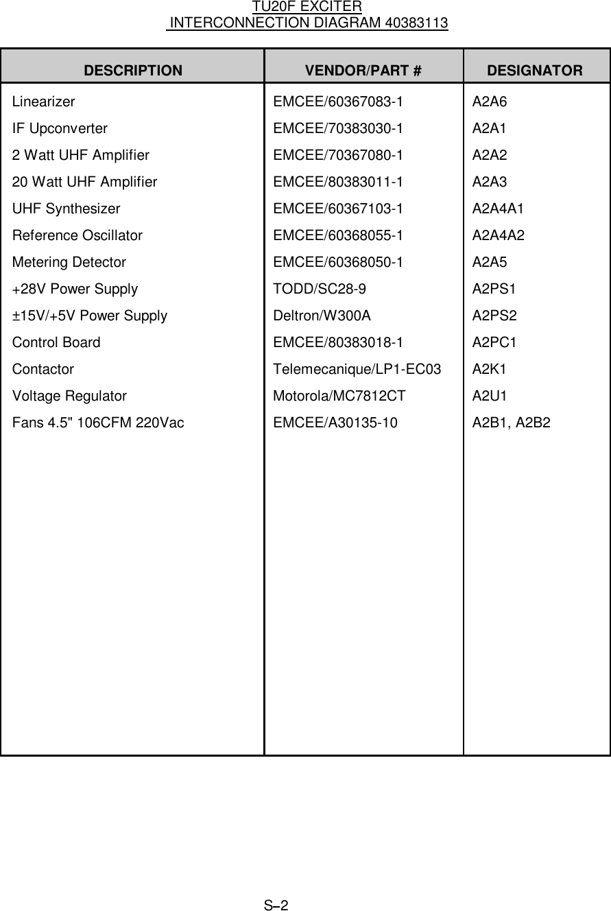
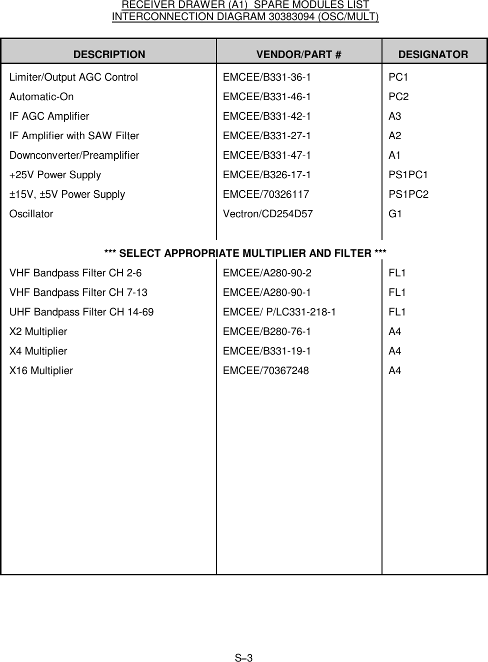
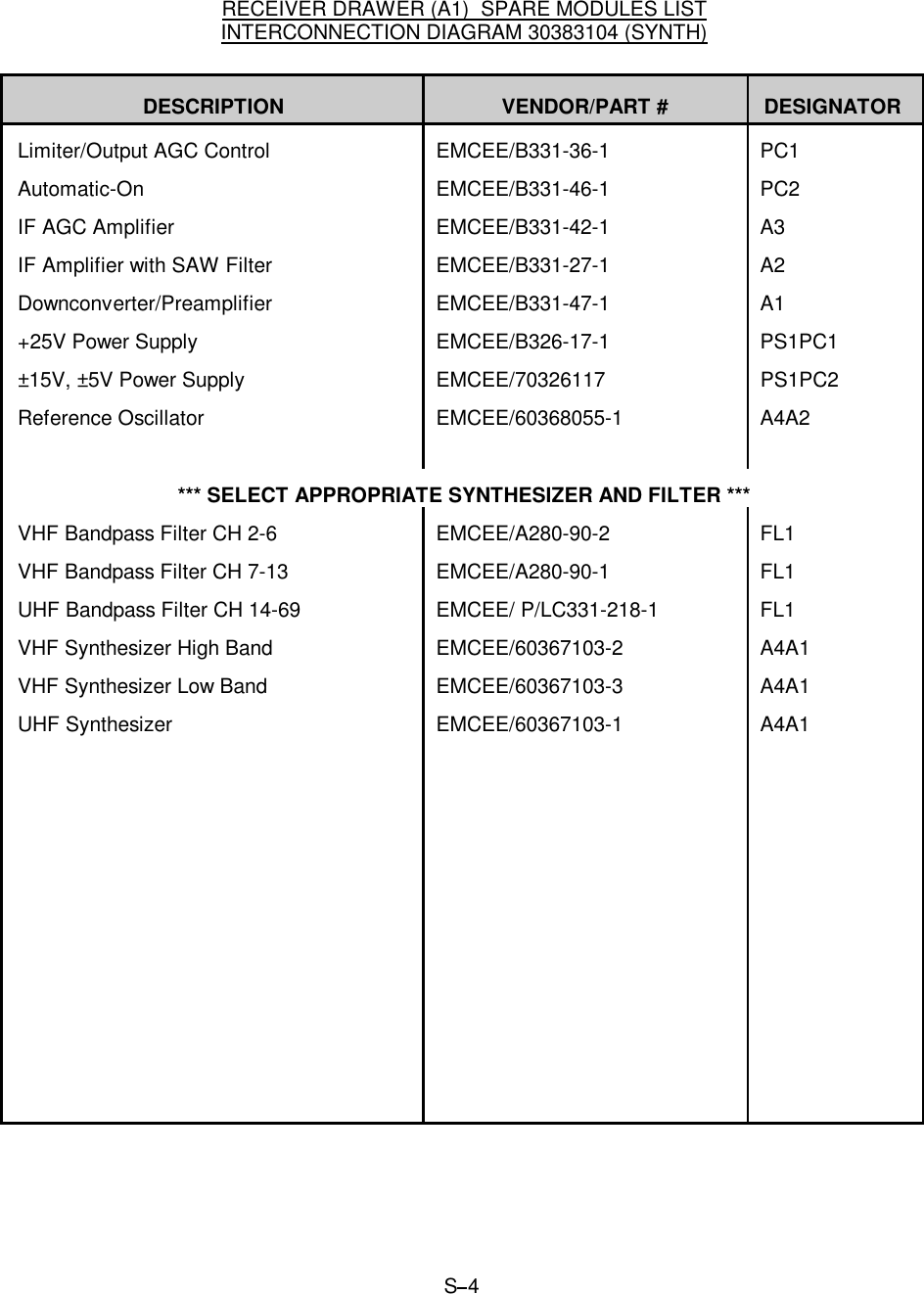
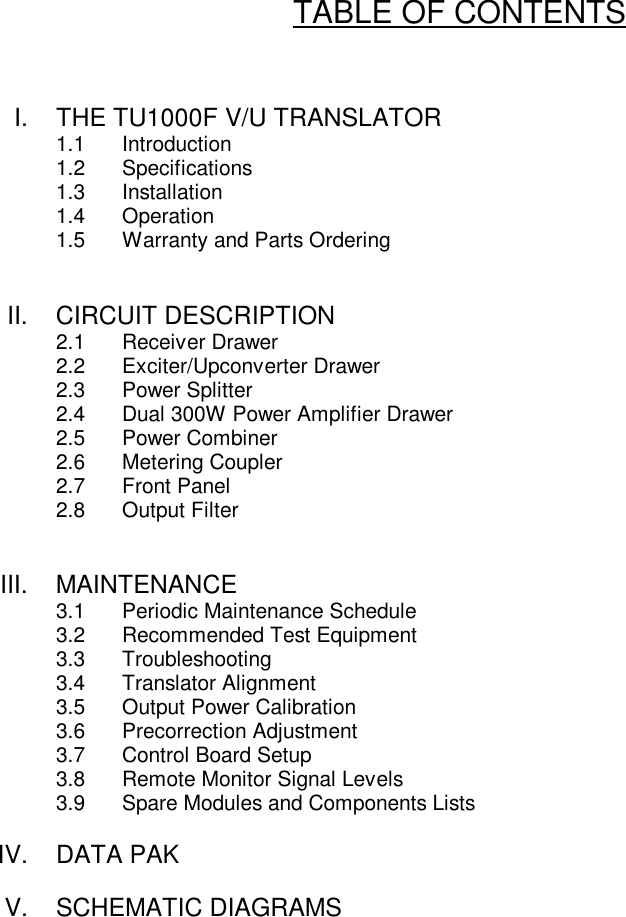
EMCEE Broadcast TU1000F UHF LPTV Translator User Manual TTU1000F Mnl Cover Pg 1
EMCEE Broadcast Products UHF LPTV Translator TTU1000F Mnl Cover Pg 1
UserManual.wiki
>
EMCEE Broadcast
>
TU1000F User Manual
TU1000F Manual
Navigation menu
Upload a User Manual
Namespaces
Wiki Guide
HTML
PDF
Info
Views
User Manual
Discussion / Help
Navigation


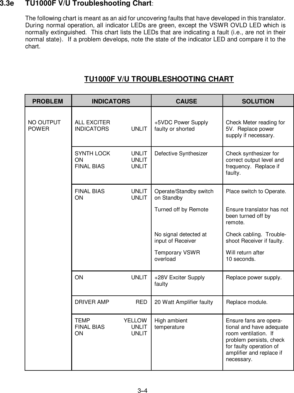
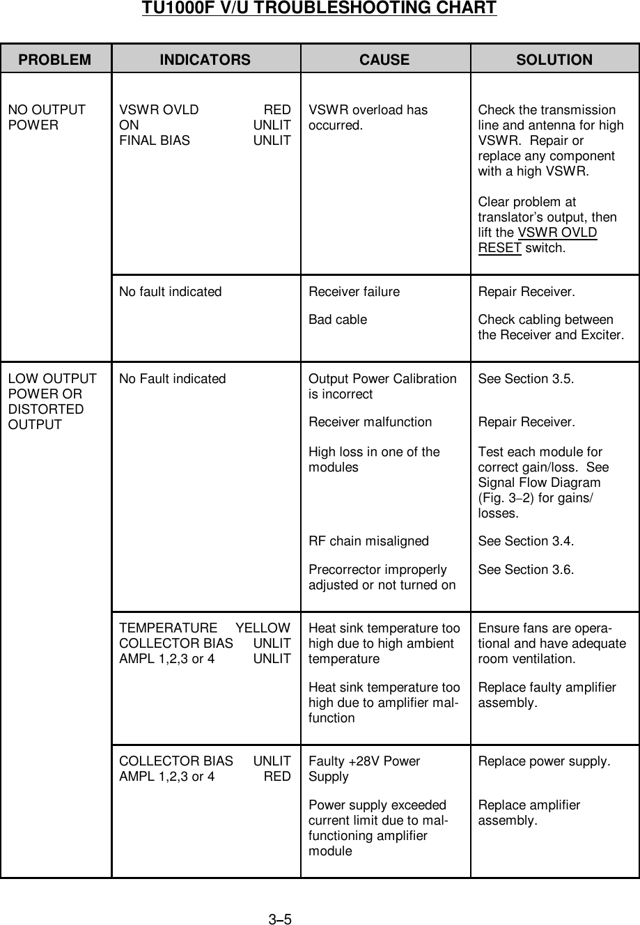
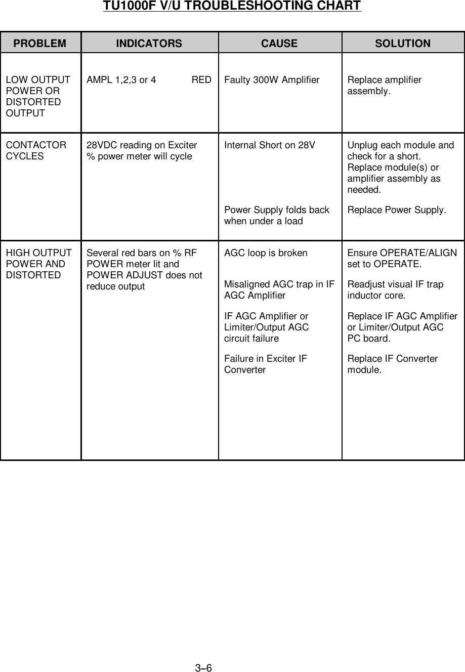
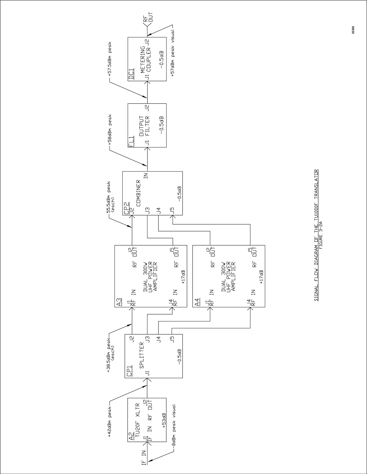
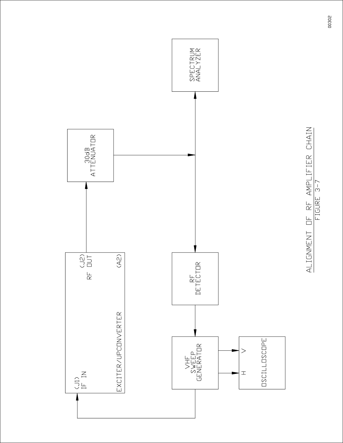
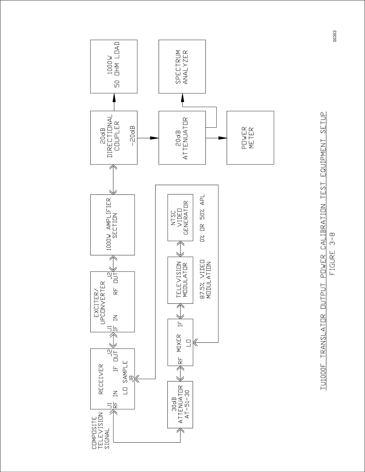
![313 3. To set the output power, adjust the Exciter’s POWER ADJUST control for an external powermeter reading of 645W [430W]. Note that 1000W peak visual at 0% [50%] APL plus50 watts average aural for a 13:1 peak visual to average aural ratio equals 645W [430W]. 4. To check or adjust visual to aural ratio, replace the power meter in Figure 3 8 with aspectrum analyzer. Adjust the aural carrier level on the modulator for the desired ratio.Remove the spectrum analyzer and return the power meter to the setup to reset the outputpower. Set the POWER ADJUST again for an external power meter reading of 595W[380W] visual plus the average aural carrier level for the set ratio. Modulators are presetby EMCEE test department. 5. With the external power meter reading correctly, place the Front Panel (A5) meter switchto FWD and check the translator's % RF Power meter for a 100% indication. If this readingis not obtained, adjust potentiometer R9 of the Metering Detector located behind the FrontPanel (A5) and accessible through the METER ADJUST hole marked FWD.3.5b Reflected Power (Optional): 6. Through the METER ADJUST access hole marked VSWR OVLD, adjust potentiometer R30of the Metering Detector fully clockwise to disable the VSWR overload detection circuit.Place the % RF POWER meter switch to REFL. 7. Place the Exciter’s OPERATE/STANDBY switch to STANDBY and the OPERATE/ALIGNswitch to ALIGN. Disconnect and reverse the FWD (J3) and REFLD (J4) coupling portcables on the Metering Coupler (DC1). J3 (REFLD) of the Metering Detector (A5A7) shouldnow be connected to J3 (FWD) of the Metering Coupler (DC1). This simulates an opencircuit at the translator's RF OUTput (J2) delivering maximum returned power to thereflected power detector. Insert a 1dB step attenuator between the Receiver and theExciter’s IF INput connector and set the attenuator for 10dB of attenuation. 8. Place the OPERATE/STANDBY switch to OPERATE. Remove attenuation from the stepattenuator until an external power meter reading of 645W [430W] is reached. Check thefront panel % RF POWER meter for a 100% [70%] reading. If the meter is incorrect, adjustit using potentiometer R27 of the Metering Detector found behind the METER ADJUST holemarked REFL. 9. Decrease the translator's power to 10% using the step attenuator (an external power meterreading of 64.5W [43W]). This power level is used for setting the trip point of the VSWRoverload detection circuit. Adjust R30 of the Metering Detector, found through the METERADJUST access hole marked VSWR OVLD, slowly counterclockwise until the front panelVSWR OVLD indicator illuminates red and the translator’s output power drops to zero.10. Check the VSWR OVLD trip point by adding an additional 1dB of attenuation in the stepattenuator. Press the momentary VSWR RESET switch to reactivate the translator andremove an additional 1or 2dB of attenuation from the step attenuator. The VSWR OVLDcircuit should again trip. If it does not, repeat this section beginning at step #6.11. Place the Exciter’s OPERATE/STANDBY switch to STANDBY. Return the metering cablesto their original coupler ports. Place the OPERATE/ALIGN switch to OPERATE, removethe test equipment, properly load the translator output and place the OPERATE/STANDBYswitch to OPERATE.](https://usermanual.wiki/EMCEE-Broadcast/TU1000F/User-Guide-96654-Page-58.png)