EULUM DESIGN EUCSB3 Casambi BLE Module User Manual
EULUM DESIGN, LLC Casambi BLE Module
User Manual
EULUM DESIGN LLC 6131 • Kellers Church Road • Pipersville • PA • 18947 • USA
EULUM DESIGN LTD Unit 4 • Zone D •Chelmsford Road Ind. Est • Dunmow • CM6 1XG • UK
www.eulum.com
info@eulum.com UK: +4 4 (0) 1371 23 8523
USA: +1 215 622 2652
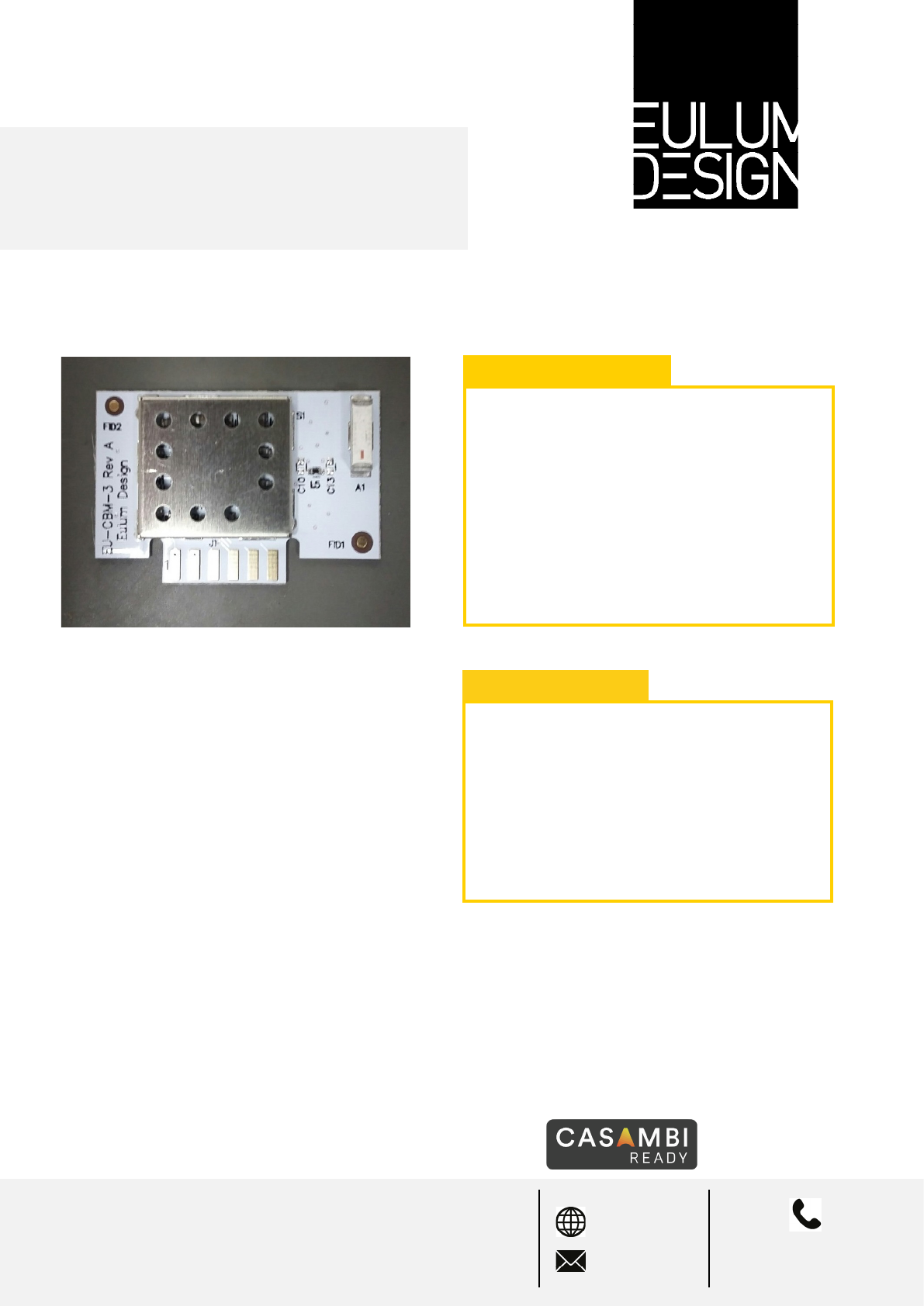
RFM-CSB-3
Features of the Module include:
The RFM-CSB-3 module
The BLE mesh Network
• Wireless Bluetooth 4.0 Mesh Network
• Free Casambi lighting control app
• Four programmable control lines
• Easy integration with card-edge SMT
connector interface
• FCC & CE certified
The Bluetooth 4.0 mesh network operates
without the need for additional controllers
or gateway units. The 200ft (60m) open air
functioning distance enables a wide range
of lighting arrangements while the exclusive
Casambi-Bluetooth connection prevents the
lighting system from interfering with other
Bluetooth networks.
The RFM-CSB-3 is a class 2 Bluetooth 4.0
module for integration into lighting fixtures,
LED drivers or other lighting controls. The
module contains a powerful 32 bit ARM®
CortexTM microcontroller and 2.4GHz
transceiver with on-board antenna. Four logic
level control signals are available on the 6-pin
card edge connector. The module operates
exclusively through the Casambi app (free on
IOS and Android).
EULUM DESIGN LLC 6131 • Kellers Church Road • Pipersville • PA • 18947 • USA
EULUM DESIGN LTD Unit 4 • Zone D •Chelmsford Road Ind. Est • Dunmow • CM6 1XG • UK
www.eulum.com
info@eulum.com UK: +4 4 (0) 1371 23 8523
USA: +1 215 622 2652
RFM-CSB-3
TABLE OF CONTENTS
Operation
Peripheral Blocks
Block Diagram
Zero Cross Detection
Specifications
Dimensions
Regulatory Statements
1
2
3
4
5
6
7
3
3
4
6
7
10
11
EULUM DESIGN LLC 6131 • Kellers Church Road • Pipersville • PA • 18947 • USA
EULUM DESIGN LTD Unit 4 • Zone D •Chelmsford Road Ind. Est • Dunmow • CM6 1XG • UK
www.eulum.com
info@eulum.com UK: +4 4 (0) 1371 23 8523
USA: +1 215 622 2652
RFM-CSB-3
OPERATION
The RFM-CSB-3 is an embedded wireless module intended to operate in conjunction with
the Casambi Lighting control app. Four configurable I/O lines interface to the host device for
control of up to 4 independent lighting channels.
A highly integrate SOC (system on chip) contains a 32 bit ARM® CortexTM microcontrol-
ler, 2.4GHz transceiver and several peripheral blocks. These blocks include PWM, SPI, I2C,
UART and GPIO (i.e. pushbutton, relay control). These can be configured in Casambi Admin
webpages and taken into use without a need to re-program the module.
The default factory configuration for the I/O is four PWM outputs @ 1.2kHz
1.
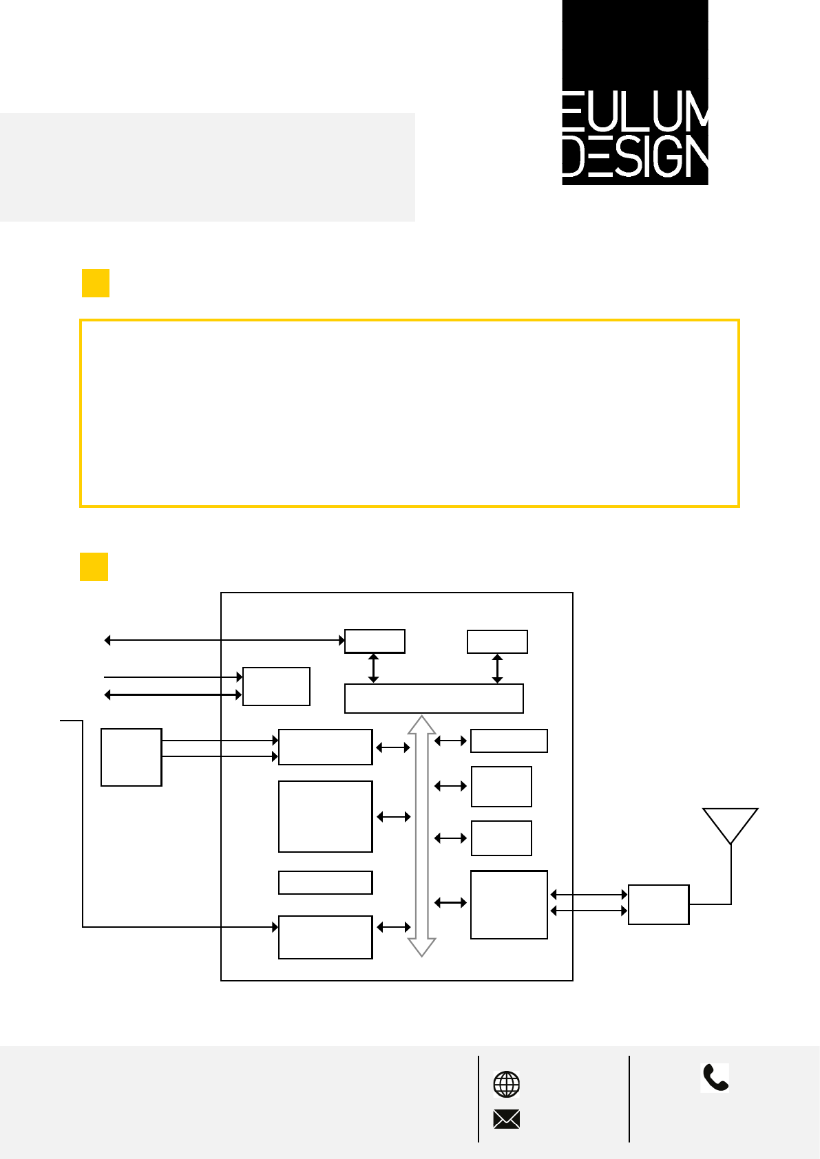
BLOCK DIAGRAM
2.
GPIO RAM
SW-DP AHB Multi-Layer
CLOCK TIMER
CPU
M4
ARM CORTEX
ADC
POWER
DC/DC
RADIO
SPI
UART
BALUN
32MHZ
XTAL
x1
x2
VCC (3.0-3.3V)
ANT1
ANT2
IO (P0.04-PO.10)
SWCLK
SWIO
Chip Antenna
SOC

EULUM DESIGN LLC 6131 • Kellers Church Road • Pipersville • PA • 18947 • USA
EULUM DESIGN LTD Unit 4 • Zone D •Chelmsford Road Ind. Est • Dunmow • CM6 1XG • UK
www.eulum.com
info@eulum.com UK: +4 4 (0) 1371 23 8523
USA: +1 215 622 2652
RFM-CSB-3
3. PERIPHERAL BLOCKS
a. PWM
Any GPIO pin can be configured to output a PWM signal. Up to 4 PWM channels can be used
simultaneously. PWM frequency can be determined freely up to 40 kHz. By default the PWM
frequency is the same for all PWM channels. The maximum resolution is 400-1600 steps and
it depends on the PWM frequency. The PWM signal is logic level (max. VCC) and it has driving
capacity from 0,5 mA (standard) up to 15 mA (high-drive).
b. SPI
RFM-CSB-3 supports a 3-wire (SCK, MISO, MOSI) bidirectional SPI bus with fast data
transfers to and from multiple slaves. RFM-CSB-2 acts as a master and it provides a simple
CPU interface which includes a TXD register for sending data and an RXD register for
receiving data. These registers are double buffered to enable some degree of uninterrupted
data flow in and out of the SPI master.
Each of the slave devices requires an individual chip select signal which can be connected to
any available GPIO pin. The SPI master does not implement support for chip select directly.
Therefore the correct slave must be selected independently of the SPI master.
The GPIOs used for each SPI interface line can be chosen from any GPIO on the module and
are independently configurable. This enables great flexibility in module pinout and enables
efficient use of printed circuit board space and signal routing.
The SPI peripheral supports SPI modes 0, 1, 2, and 3.

EULUM DESIGN LLC 6131 • Kellers Church Road • Pipersville • PA • 18947 • USA
EULUM DESIGN LTD Unit 4 • Zone D •Chelmsford Road Ind. Est • Dunmow • CM6 1XG • UK
www.eulum.com
info@eulum.com UK: +4 4 (0) 1371 23 8523
USA: +1 215 622 2652
RFM-CSB-3
c. I2C
This two-wire interface uses clock (SCL) and bidirectional data (SDA). The protocol makes it
possible to interconnect up to 128 individually addressable devices. The interface is capable
of clock stretching and data rates of 100 kbps and 400 kbps are supported.
The GPIOs used for each Two-Wire Interface line can be chosen from any GPIO on the module
and are independently configurable.
d. UART
The Universal Asynchronous Receiver/Transmitter offers fast, full-duplex, asynchronous serial
communication with built-in flow control (CTS, RTS) support in HW up to 1 Mbps baud. Parity
checking and generation for the 9th data bit are supported.
The GPIOs used for each UART interface line can be chosen from any GPIO on the module and
are independently configurable.
e. GPIO
Each of the four I/O can also be configured for alternate input/output functions. Casambi
supported functions include:
• Pushbutton input • Relay control output • Zero Detect Input • Fixed “idle” state output
The I/O can be further tailored using options such as:
• Input/output polarity • Output drive strength • Internal pull-up and pull-down resistors
EULUM DESIGN LLC 6131 • Kellers Church Road • Pipersville • PA • 18947 • USA
EULUM DESIGN LTD Unit 4 • Zone D •Chelmsford Road Ind. Est • Dunmow • CM6 1XG • UK
www.eulum.com
info@eulum.com UK: +4 4 (0) 1371 23 8523
USA: +1 215 622 2652
RFM-CSB-3
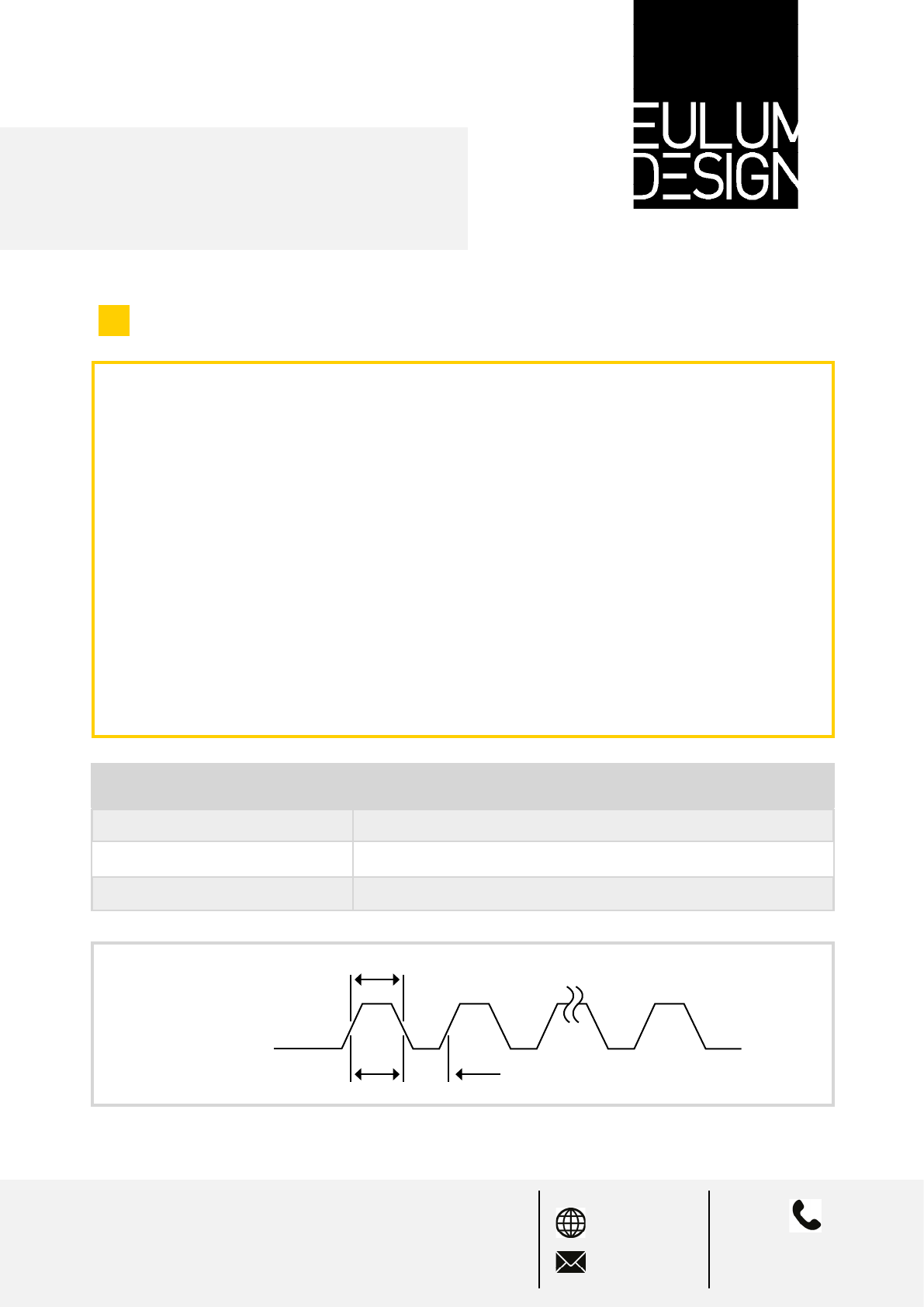
The RFM-CSB-3 can be configured to detect the zero crossing point of an AC signal. This is
necessary to take advantage of Casambi’s “Smart Switching” feature. This looks for a pattern
of on-off cycles (quickly switching AC source on & off) in order to implement specific modes or
settings.
For proper Smart Switch operation, local VCC of the module must be kept alive during loss of
AC for 1.5 seconds. A 1200uf cap on VCC is typically recommended.
It is the responsibility of the host system designer to create the zero detection circuit and it’s
output needs to be compatible with logic level inputs of the RFM- CSB-1 (see specifications
section). ZD polarity and phase are adjustable in the Casambi admin webpages.
If Smart switching is not required, it is suggested to configure the ZD input for online/
offline detection. This allows the module to notify the network when it goes offline. This
reduces network bandwidth as it will not be repeatedly polling for a device that is no longer
responding. Local VCC must be kept alive for at least 500ms to support this feature.
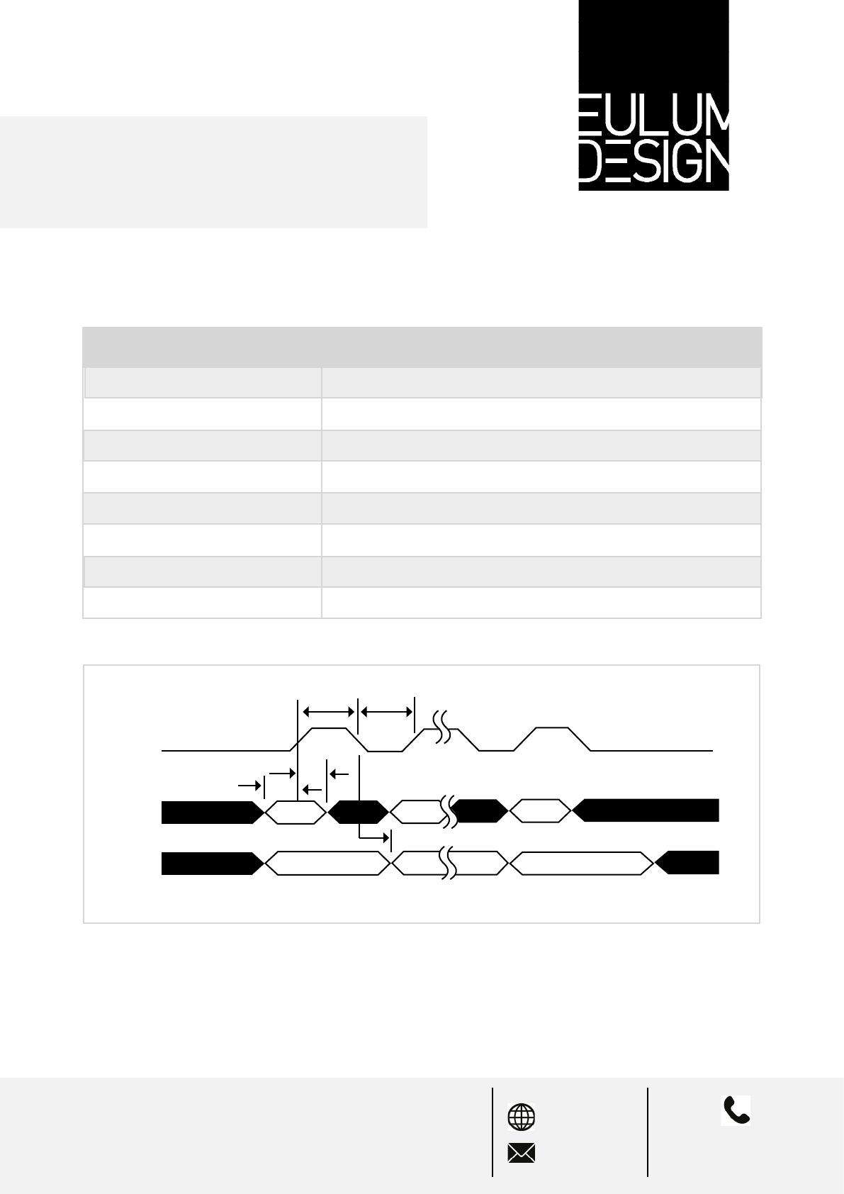
ZERO DETECT CHARACTERISTICS MIN TYPICAL MAX UNITS
Hz
ms
ms
20
20
60
1
1
ZERO DETECT FREQUENCY, FMAINS
ZERO DETECT HIGH TIME, TZD_H
ZERO DETECT LOW TIME, TZD_L
4. ZERO CROSS DETECTION (ZD)
Zero Detect
tZD_LtZD_H
1/f MAINS
EULUM DESIGN LLC 6131 • Kellers Church Road • Pipersville • PA • 18947 • USA
EULUM DESIGN LTD Unit 4 • Zone D •Chelmsford Road Ind. Est • Dunmow • CM6 1XG • UK
www.eulum.com
info@eulum.com UK: +4 4 (0) 1371 23 8523
USA: +1 215 622 2652
RFM-CSB-3
MAXIMUM RATINGS UNITS
V
V
°C
MAX
Vcc + 0.3
+125
MIN
-0.3SUPPLY VOLTAGE, Vcc
I/O PIN VOLTAGE
STORAGE TEMPERATURE
SPECIFICATIONS
OPERATING TEMPERATURE -25 +70
+3.6
-0.3
-40
°C
V
mA
15
+2.5SUPPLY VOLTAGE, Vcc
SUPPLY CURRENT, Icc
TX/RX ACTIVE
IDLE 1.5
+3.0
POWER SUPPLY SPECIFICATIONS MIN TYPICAL MAX UNITS
+3.3
21
2mA
MHz
2400
OPERATING FREQUENCIES,
fop, 1MHZ Channel Spacing
PLL PROGRAMMING RESOLUTION,
PLLres
FREQUENCY DEVIATION, fBLE
ON-AIR DATA RATE, bpsFSK 250
RADIO SPECIFICATIONS MIN TYPICAL MAX UNITS
2000
MAXIMUM OUTPUT POWER, PRF
2483
MHz
kHz
kbps
dBm
±275±250±225
4
1
5.
SENSITIVITY, PSENS -89 -93 dBm
EULUM DESIGN LLC 6131 • Kellers Church Road • Pipersville • PA • 18947 • USA
EULUM DESIGN LTD Unit 4 • Zone D •Chelmsford Road Ind. Est • Dunmow • CM6 1XG • UK
www.eulum.com
info@eulum.com UK: +4 4 (0) 1371 23 8523
USA: +1 215 622 2652
RFM-CSB-3
V
0.7 Vcc
INPUT HIGH VOLTAGE, VLH
INPUT LOW VOLTAGE, VIL
OUTPUT HIGH VOLTAGE, VOH
OUTPUT LOW VOLTAGE, VOL 0
GPIO SPECIFICATIONS MIN TYPICAL MAX UNITS
0.3Vcc
SOURCE CURRENT, IGPIO_IN
V
V
V
mA
PULL-UP RESISTANCE, RPU
PULL DOWN RESISTANCE, RPU 11 16
kΩ
kΩ
161311
SINK CURRENT, IGPIO_OUT mA
15
14
Vcc
0.3Vcc
Vcc
13
2
2
Vcc-0.3
0
*Total source/ sink current of all GPIO pins combined is 15mA. If required source/ sink current for any GPIO pin
exceeds 0.5mA, that GPIO pin must be configured for high-drive.
kHzPWM FREQUENCY, fPWM
PWM RESOLUTION @ fPWM 10kHZ
PWM RESOLUTION @ fPWM 20kHZ
PWM RESOLUTION @ fPWM 40kHZ
PWM SPECIFICATIONS UNITSMAX
40
1600
400
800
steps
steps
steps
MIN TYPICAL
EULUM DESIGN LLC 6131 • Kellers Church Road • Pipersville • PA • 18947 • USA
EULUM DESIGN LTD Unit 4 • Zone D •Chelmsford Road Ind. Est • Dunmow • CM6 1XG • UK
www.eulum.com
info@eulum.com UK: +4 4 (0) 1371 23 8523
USA: +1 215 622 2652
RFM-CSB-3
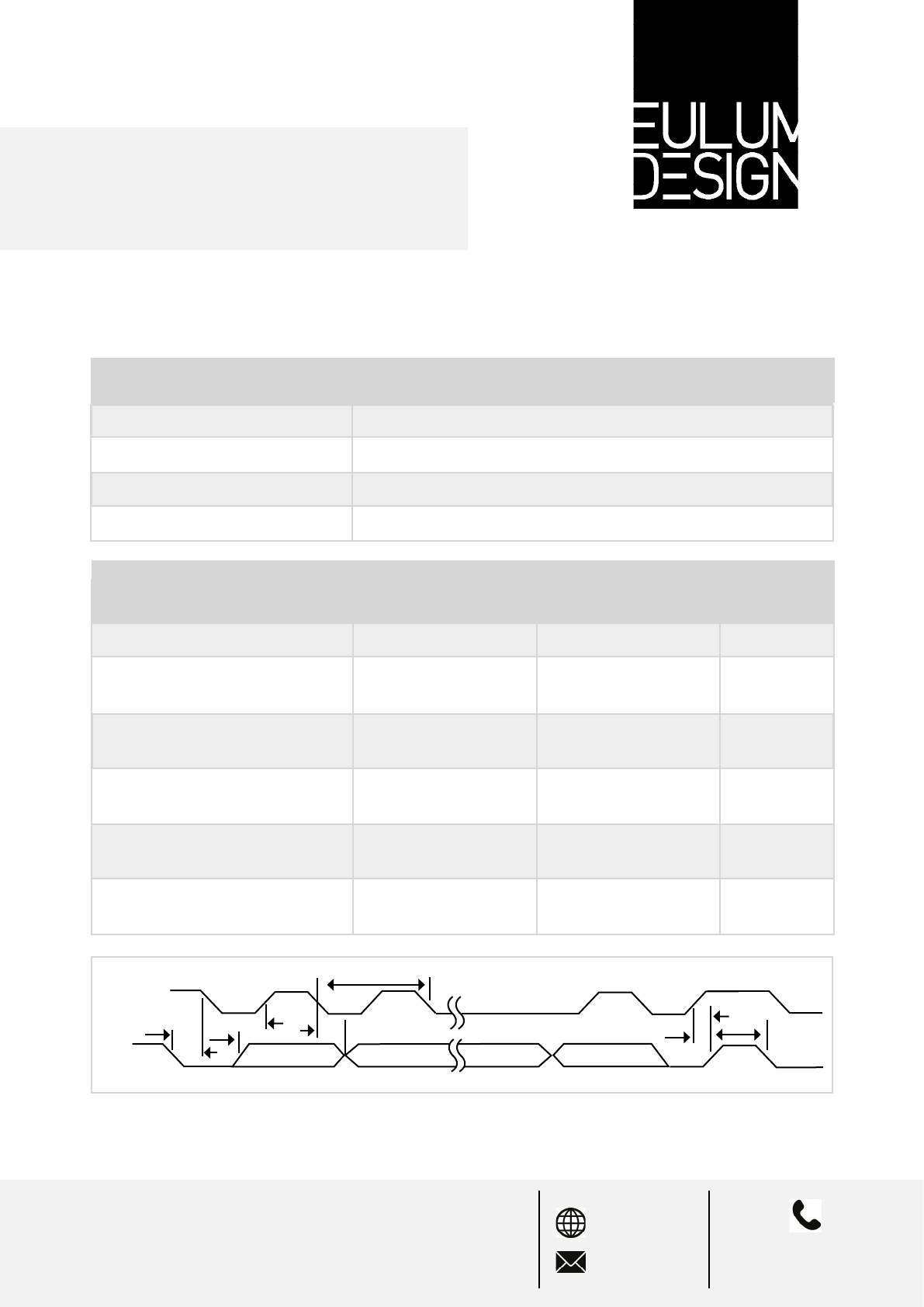
MBPS0.125
BIT RATES FOR SPI, fSPI
DATA TO SCK SETUP, tDC
SCK TO DATA HOLD, tDH
SCK TO DATA VALID, tCD
SPI TIMING PARAMETERS MIN TYPICAL MAX UNITS
SCK HIGH TIME, tCH
ns
SCK FREQUENCY, fSCK
SCK RISE AND FALL TIME, tR, tF
MHZ0.125
SCK LOW TIME, tCL
8
10
10
60
40
40
ns
ns
ns
ns
ns
80
8
100
tCH tCL
SCK
MISO
MOSI
SPI Timing Diagram, One Byte Transmission, SPI Mode 0
tDH
tDC
tCD
EULUM DESIGN LLC 6131 • Kellers Church Road • Pipersville • PA • 18947 • USA
EULUM DESIGN LTD Unit 4 • Zone D •Chelmsford Road Ind. Est • Dunmow • CM6 1XG • UK
www.eulum.com
info@eulum.com UK: +4 4 (0) 1371 23 8523
USA: +1 215 622 2652
RFM-CSB-3
uARUN CURRENT @ MAX BAUD RATE
RUN CURRENT @ 115200 bps
RUN CURRENT @ 1200 bps
BAUD RATE FOR UART
UART SPECIFICATIONS UNITSMAX
1000
uA
uA
kbps
MIN TYPICAL
1.2
230
220
210
SCL CLOCK FREQUENCY, fSCL
Hold time for START and repeated
START condition, tHD_STA
I2C TIMING PARAMETERS
MIN MAX UNITS
ns
ns
ns
ns
ns
Data setup time before positive
edge on SCL, tSU_DAT
Data hold time after negative edge
on SCL, tHD_DAT
Setup time from SCL goes high to
STOP condition, tSU_STO
Bus free time between STOP and
START conditions, tBUF
STANDARD FAST
MIN MAX
kHz400100
5200
300
300
5200
4700 1300
1300
300
300
1300
1/fSCL
SCL
tSU_DAT
SDA
tHD_SDA tSU_STO tBUF
I2C Timing Diagram
EULUM DESIGN LLC 6131 • Kellers Church Road • Pipersville • PA • 18947 • USA
EULUM DESIGN LTD Unit 4 • Zone D •Chelmsford Road Ind. Est • Dunmow • CM6 1XG • UK
www.eulum.com
info@eulum.com UK: +4 4 (0) 1371 23 8523
USA: +1 215 622 2652
RFM-CSB-3
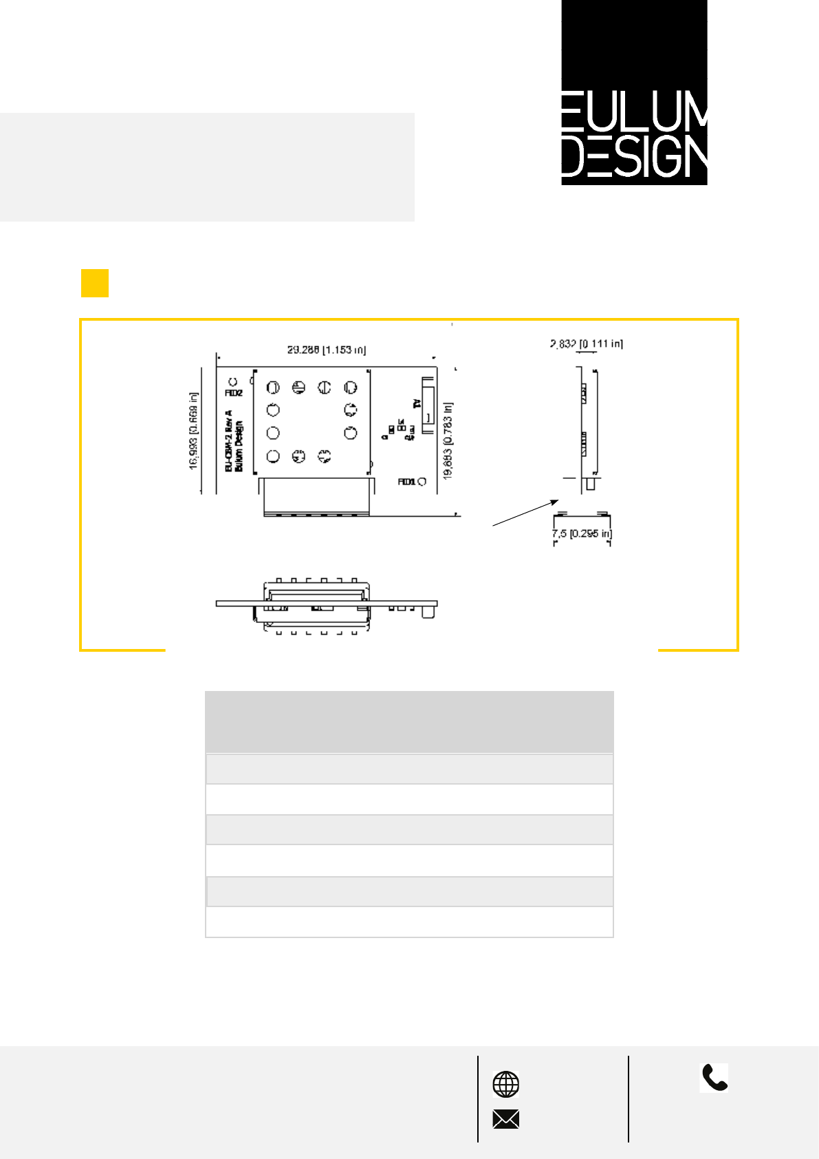
DIMENSIONS
PIN LABEL DESCRIPTION
1
2
3
4
5
6
VCC
GND
P0.05
P0.06
P0.09
P0.10
POWER
GROUND
PWM1*
PWM2*
PWM3*
PWM4*
*Factory Default. GPIO can be configured for alternate input/ output
functionality. Please contact Eulum Design for more information.
PINOUT
6.
Mating Connector: AVX
p/n 009159006551906

EULUM DESIGN LLC 6131 • Kellers Church Road • Pipersville • PA • 18947 • USA
EULUM DESIGN LTD Unit 4 • Zone D •Chelmsford Road Ind. Est • Dunmow • CM6 1XG • UK
www.eulum.com
info@eulum.com UK: +4 4 (0) 1371 23 8523
USA: +1 215 622 2652
RFM-CSB-3
REGULATORY STATEMENTS7.
FCC Statement
Changes or modifications not expressly approved by the
party responsible for compliance could void the user’s
authority to operate the equipment.
This device complies with Part 15 of the FCC Rules.
Operation is subject to the following two conditions:
(1) this device may not cause harmful interference, and
(2) this device must accept any interference received,
including interference that may cause undesired operation.
Note:
This equipment has been tested and found to comply with the limits for a Class B digital
device, pursuant to Part 15 of the FCC Rules. These limits are designed to provide
reasonable protection against harmful interference in a residential installation. This
equipment generates, uses, and can radiate radio frequency energy, and if not installed
and used in accordance with the instructions, may cause harmful interference to radio
communications. However, there is no guarantee that interference will not occur in a
particular installation. If this equipment does cause harmful interference to radio or
television reception, which can be determined by turning the equipment off and on, the user
is encouraged to try to correct the interference by one or more of the following measures:
● Reorient or relocate the receiving antenna.
● Increase the separation between the equipment and receiver.
● Connect the equipment into an outlet on a circuit different from that to which the receiver
is connected.
● Consult the dealer or an experienced radio/TV technician for help.

EULUM DESIGN LLC 6131 • Kellers Church Road • Pipersville • PA • 18947 • USA
EULUM DESIGN LTD Unit 4 • Zone D •Chelmsford Road Ind. Est • Dunmow • CM6 1XG • UK
www.eulum.com
info@eulum.com UK: +4 4 (0) 1371 23 8523
USA: +1 215 622 2652
RFM-CSB-3
1.Radiation Exposure Statement
This equipment complies with FCC radiation exposure limits
set forth for an uncontrolled environment. This equipment
should be installed and operated with a minimum distance of
20cm between the radiator & your body. This transmitter must
not be co-located or operating in conjunction with any other
antenna or transmitter.
FCC Important Notes
2. OEM Integrated Instructions
This device is intended only for OEM integrators under the following conditions:
● The antenna and transmitter must not be co-located with any other transmitter or antenna.
The module shall be only used with the integral antenna(s) that has been originally tested and
certified with this module.
● As long as the two (2) conditions above are met, further transmitter testing will not be
required. However, the OEM integrator is still responsible for testing their end-product for any
additional compliance requirements with this module installed (for example, digital device
emission, PC peripheral requirements, etc.)
● In the event that these conditions cannot be met (for example certain laptop configuration
or co-location with another transmitter), then the FCC authorization for this module in
combination with the host equipment is no longer considered valid and the FCC ID of the
module cannot be used on the final product. In these and circumstance, the OEM integrator
will be responsible for re-evaluating. The end product (including the transmitter) and obtaining
a separate FCC authorization.
● The module is limited to installation in mobile or fixed applications.
● The seperate approval is required for all other operating configurations, including portable
configurations with respect to Part 2.1093 and different antenna configurations.
● The OEM is still responsible for verifying compliance with FCC Part 15, subpart B limits for
unintentional radiators through an accredited test facility.

EULUM DESIGN LLC 6131 • Kellers Church Road • Pipersville • PA • 18947 • USA
EULUM DESIGN LTD Unit 4 • Zone D •Chelmsford Road Ind. Est • Dunmow • CM6 1XG • UK
www.eulum.com
info@eulum.com UK: +4 4 (0) 1371 23 8523
USA: +1 215 622 2652
RFM-CSB-3
3. End Product Labelling
The final end product must be labeled in a visible area with the following:
RFM-CSB-3: “Contains FCC ID: 2AJML- EUCSBM”
Any similar wording that expresses the same meaning may be used.
The FCC Statement below should also be included on the label. When not possible, the FCC
Statement should be included in the User Manual of the host device.
“This device complies with part 15 of the FCC rules. Operation is subject to the following two
conditions:
(1) This device may not cause harmful interference.
(2) This device must accept any interference received, including interference that may cause
undesired operation.”
4. Information regarding the end user manual
The OEM integrator has to be aware not to provide information to the end user regarding how
to install or remove this RF module in the user’s manual of the end product which integrates
this module. The end user manual shall include all required regulatory information/warning as
show in this manual.
CE Regulatory
This device is tested and compliant against the following standards. OEM integrators should
consult with qualified test house to verify all regulatory requirements have been met for their
complete device.
● EN 62479:2010
● EN60950-1:2006+A11.2009+A1:2010+A12:2011+A2:2013
● ETSI EN 201-489-1 V2.2.0(2017-03)
● ESTI EN 301 489-17 V3.2.0(2017-03)
● ESTI EN 300 328 V2.1.1(2016-11)