Ehong Technology ES101 BLE Module User Manual Datasheet
ShangHai Ehong Technology Co.,Ltd. BLE Module Datasheet
User Manual
Ehong ® Professional Bluetooth Solutions Provider page 1 of 14
Ehong Technology Co.,Ltd
•
Bluetooth® Radio
-
-
Fully embedded Bluetooth® V4.2 single mode
ARM® Cortex-M0 @ 32-bit
•
Support Profiles
- BLE (Master and slave)
- The generic attribute profile (GATT)
•
User Interface
- Send AT command over UART
- Firmware upgrade over the air (OTA)
- Transmit data: 1Mbps transmission speed
- I2C ,SPI interface ( Master )
- Watchdog and RTC
- 2 PWM modules
•
General
I/O
-
14 general purpose I/Os
-
2 analog I/Os
(10bit ADC)
• Power dissipation
-
Standby power consumption of less than 1uA
in hibernation mode (wakeable)
•
FCC/RED/IC/RoHs and Bluetooth® qualified
•
Single voltage supply: 1.8-- 3.6V typical
•
Small form factor: 7.0 x 7.0x 1.0mm
•
Operating temperature range: -40 °C to 105 °C
Sept 17, 2018
EH-ES101
Low Energy SIP Module Data Sheet
EH-2018090-DS Rev1.1

EH-ES101
Ehong ® Professional Bluetooth Solutions Provider page 2 of 14
VERSION HISTORY
Version
Comment
V1.1
Change the Pin GPIO to DIO in the schematic diagram
Confidential and Proprietary – Ehong Technology Co.,Ltd
NO PUBLIC DISCLOSURE PERMITTED: Please report postings of this document on public servers
or websites to: DCC@ehlink.com.cn
Restricted Distribution: Not to be distributed to anyone who is not an employee of either Ehong
Technology Co.,Ltd or its affiliated companies without the express approval of Ehong Configuration
Management.
Not to be used, copied, reproduced, or modified in whole or in part, nor its contents revealed in any
manner to others without the express written permission of Ehong Technology Co.,Ltd.
This Bluetooth trademark is owned by the Bluetooth SIG Inc., USA and is licensed to Ehong
Technologies. All other trademarks listed herein are owned by their respective owners.
© 2016 Ehong Technology Co.,Ltd. All rights reserved.

EH-ES101
Ehong ® Professional Bluetooth Solutions Provider page 3 of 14
1. Contents
1. Description ......................................................................................................................................................... 4
2. Applications ....................................................................................................................................................... 4
3. EH-ES101 Product numbering ...................................................................................................................... 4
4. Pinout and Terminal Description .................................................................................................................. 5
4.1. Pin Configuration ......................................................................................................................................... 5
5. Physical Interfaces ........................................................................................................................................... 7
5.1. GPIO .............................................................................................................................................................. 7
5.2. ADC ............................................................................................................................................................... 7
5.3. PWM .............................................................................................................................................................. 8
5.4. UART ............................................................................................................................................................. 8
5.5. I2C Master .................................................................................................................................................... 8
5.6. SPI Master .................................................................................................................................................... 8
6. Electrical Characteristics ............................................................................................................................... 8
6.1. Recommended Operation Conditions ...................................................................................................... 8
6.2. Absolute Maximum Rating ......................................................................................................................... 9
6.3. Input/Output Terminal Characteristics ...................................................................................................... 9
6.4. Power Consumption .................................................................................................................................... 9
7. Reference Design ........................................................................................................................................... 10
8. Layout and Soldering Considerations ...................................................................................................... 11
8.1. EH-ES101 external view ........................................................................................................................... 11
8.2. PCB package outline drawing .................................................................................................................. 11
9. Tape and reel information ............................................................................................................................ 12
9.1. Tapa orientation ......................................................................................................................................... 12
9.2. Tape dimensions ....................................................................................................................................... 12
9.3. Reel information ......................................................................................................................................... 13
10. The tray information ...................................................................................................................................... 13
11. Soldering Recommendations ...................................................................................................................... 14
12. Contact Information ....................................................................................................................................... 14

EH-ES101
Ehong ® Professional Bluetooth Solutions Provider page 4 of 14
1. Description
EH-ES101 series is a powerful, highly flexible, ultra-low power Bluetooth smart SIP module
base on BlueNRG-1 SoC from ST. Embedded 2.4GHz transceiver; the EH-ES101module
provides a complete RF solution allowing faster time-to-market with reduced development
costs.
The module offers all Bluetooth® low energy features: radio, stack, profiles and application
space for customer application, so no external control processor is needed. The module also
provides flexible hardware interfaces to connect sensors, simple user interfaces or even
displays directly to the module.
The module is small in size and support the module of selecting the external antenna to facilitate
the flexible development of the product.The module can be powered directly with a standard 3V
coin cell batteries or pair of AAA batteries. In lowest power sleep mode it consumes only less
1uA and will wake up in few hundred microseconds.
After buying Bluetooth® module, we provide free technical support APP of iOS system or APP
Android system.
2. Applications
Sports and fitness
Healthcare
Home entertainment
Office and mobile accessories
Automotive
Commercial
Watches
Human interface devices
3. EH-ES101 Product numbering
EH-ES101
A. EH ------------- Company Name(Ehong)
B. ES101 ------------ Module Name
EH-ES101
Ehong ® Professional Bluetooth Solutions Provider page 5 of 14
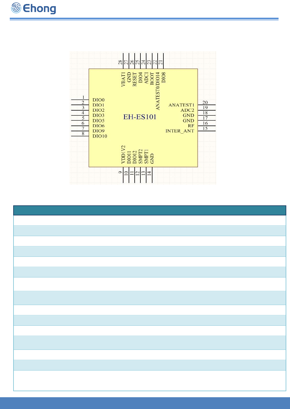
4. Pinout and Terminal Description
4.1. Pin Configuration
Figure 1: Pinout of EH-ES101
Symbol
Pin
PAD Type
Description
DIO0
1
General purpose digit I/O
See IO function map
DIO1
2
General purpose digit I/O
See IO function map
DIO2
3
General purpose digit I/O
See IO function map
DIO3
4
General purpose digit I/O
See IO function map
DIO5
5
General purpose digit I/O
See IO function map
DIO6
6
General purpose digit I/O
See IO function map
DIO9
7
General purpose digit I/O
See IO function map, also
work as SWDCLK
DIO10
8
General purpose digit I/O
See IO function map, also
work as SWDIO
VDD1V2
9
1.2V digit core output
Connect a capacitor
DIO11
10
General purpose digit I/O
See IO function map
DIO12
11
General purpose digit I/O
See IO function map
SMPT2
12
SMPS output to external filter / VCC input
Connect to VCC or an
inductor
SMPT1
13
SMPS output to external filter
GND
14
Powered ground

EH-ES101
Ehong ® Professional Bluetooth Solutions Provider page 6 of 14
RF
16
Use an internal antenna or connect to an
external antenna.
GND
17
Powered ground
GND
18
Powered ground
ADC2
19
ADC input 2
ANATEST1
20
Antenna test pin1
Used for indicate RF’s TX/RX
event, also can user for
extern antenna switch
DIO8
21
General purpose digit I/O
See IO function map
DIO14/TEST0
22
General purpose digit I/O / Analog
output
See IO function map
DIO7/BOOT
23
General purpose digit BOOT pin
See IO function map, used
for BOOT pin(vcc) for jump to
bootloader when power on
ADC1
24
ADC input 1
DIO4
25
General purpose digit I/O
See IO function map
RESET
26
System reset pin
Active low level
GND
27
Powered ground
VBAT1
28
Powered VCC
1.8-3.6V
Table 1:PIN Terminal Description
Pin namea
GPIO mode”000”
Mode serial1”001”
Mode serial0”100”
Mode serial2”101”
Type
Signal
Type
Signal
Type
Signal
Type
Signal
IO0
I/O
GPIO 0
I
UART_CTS
I/O
SPI_CLK
-
-
IO1
I/O
GPIO 1
O
UART_RTS
I/O
SPI_CS1
I
PDM_DAT
A
IO2
I/O
GPIO 2
O
PWM0
O
SPI_OUT
O
PDM_CLK
IO3
I/O
GPIO 3
O
PWM1
I
SPI_IN
O
-
IO4
I/O
GPIO 4
I
UART_RXD
I/O
I2C2_CLK
O
PWM0
IO5
I/O
GPIO 5
O
UART_TXD
I/O
I2C2_DAT
O
PWM1
IO6
I/O
GPIO 6
O
UART_RTS
I/O
I2C2_CLK
I
PDM_DAT
A
IO7
-
-
I
UART_CTS
I/O
I2C2_DAT
O
PDM_CLK
IO8
I/O
GPIO 8
O
UART_TXD
I/O
SPI_CLK
I
PDM_DAT
A
IO9
I/O
GPIO 9
I
SWCLK
I
SPI_IN
-
-
IO10
I/O
GPIO 10
I
SWDIO
O
SPI_OUT
-
-
IO11
I/O
GPIO 11
I
UART_RXD
I/O
SPI_CS1
-
-
IO12
OD
GPIO 12b
I
-
I/O
I2C2_DAT
-
-
IO14
I/O
GPIO 14
I/O
I2C1_CLK
I/O
SPI_CLK
O
-
Table 2:IO function MAP
EH-ES101
Ehong ® Professional Bluetooth Solutions Provider page 7 of 14
5. Physical Interfaces
5.1. GPIO
14 IOs are provided. Every IO can program for other function.
All theGP IOs are in high impedance under reset. All the IOs are in high impedance
in low power modes (sleep and standby). If pre-programmed as wake up sources,
pins IO9, IO10 and IO11 are in input pull up.
All the GIOs can programed for an interrupt source. Edge detection or level
detection, and falling/rising or both.
GIO0~GIO8 and GIO14 can program input pull down.
GIO9~GIO11 can program input pull up.
GIO12 can only be General Purpose Input pins (not output).
When power for 3.3V, internal Pull resister is:
Name
Description Name
Min
Type
Max
Unit
RPD
Pull-down Value
53
84
144
KΩ
RPU
Pull-up Value
57
81
122
Table 3:Internal Pull for 3.3V
When power for 1.8V, internal Pull resister is:
Name
Description Name
Min
Type
Max
Unit
Digital input and output when 1.8V supply
RPD
Pull-down Value
117
202
363
KΩ
RPU
Pull-up Value
135
211
334
Table 4:Internal Pull for 1.8V
Note: A. GIO7 can work as BOOT pin. when power on, if GIO7 is high level, CPU will jump to bootloader
mode, and this time can update the firmware by UART.
B. GIO9 and DIO10 can work as SWDCLK and SWDIO. If need debug or download also can use Jlink
OB or ST-LINK.
The IOs programmed to be wake up sources need an external drive according to the selected level
sensitivity. If the wake up level is high level, a pull down drive should be used. If the wake up level is low
level, a pull up drive should be used. If no external drive is applied, IO9, IO10 and IO11 are only sensitive
to low level as they have an internal pull up (activated by default). IO12 do not have an internal pull and
therefore require an external drive.
5.2. ADC
2 ADCs are provided.
Main features are: . e pins ADC1 and ADC2.
Internal temperature and battery level conversion.
EH-ES101
Ehong ® Professional Bluetooth Solutions Provider page 8 of 14
5.3. PWM
2 PWMs can be driven by internal PWM module.
5.4. UART
This is a standard UART interface for communicating with other serial devices. The
UART interface provides a simple mechanism for communicating with other serial
devices using the TTL protocol.
When using low-power mode, TXD needs to pull up resistance, and the reference value
is 4.7k.
Main features are:
Programmable baud rate can reach up to 921600bps.
me of 5, 6, 7 or 8 bits of data.
-parity bit generation and detection.
5.5. I2C Master
The module can act as an I2C master when configured by software.
Main features are: e and up to 100 Kb/s in standard mode.
multi-master system with bus arbitration.
5.6. SPI Master
The module can act as an SPI master (mode 0) when configured by software.
Main features are:
6. Electrical Characteristics
6.1. Recommended Operation Conditions
Operating Condition
Min
Typical
Max
Unit
Operating Temperature Range
-30
--
+80
°C
Battery (VDD_BAT) operation
1.8
3.3
+3.6
V
2402
-2
2480
ADC Input range
0
-
+1.2
V
Frequency Range MHz

EH-ES101
Ehong ® Professional Bluetooth Solutions Provider page 9 of 14
Table 5: Recommended Operation Conditions
Table 6: Absolute Maximum Rating
*In the absence of damage, the maximum 10% of product life is allowed for short term operation, but
the output regulation and other specifications will not be guaranteed in excess of 4.2V.*
6.2. Absolute Maximum Rating
*Short-term operation up to a maximum of 10% of product lifetime is permissible without damage, but output
regulation and other specifications are not guaranteed in excess of 4.2V.
6.3. Input/Output Terminal Characteristics
Input Voltage Levels
Min
Typical
Max
Unit
VIL input logic level low
-0.4
-
0.4
V
VIH input logic level high
0.7 x VDD
-
VDD + 0.4
V
Tr/Tf
-
-
25
ns
Output Voltage Levels
Min
Typical
Max
Unit
VOL output logic level low, lOL = 4.0mA
-
-
0.4
V
VOH output logic level high, lOH = -4.0mA
0.75 x VDD
-
--
V
Tr/Tf
-
-
5
ns
Table 7: Digital I/O Characteristics
Condition
Class
Max Rating
Human Body Model Contact Discharge per JEDEC EIA/JESD22-
A114
2
2000V (all pins)
Machine Model Contact Discharge per JEDEC EIA/JESD22-A115
200V
200V (all pins)
Charged Device Model Contact Discharge per JEDEC
EIA/JESD22-C101
III
500V (all pins)
Table 8: ESD Protection
6.4. Power Consumption
Current consumption is measured using a battery.
(1)When the DC-DC converter is activated, the power consumption is as follows:
Rating
Min
Max
Unit
Storage Temperature
-40
+85
°C
Battery (VBAT) operation*
1.8
3.6
V
I/O supply voltage
-0.4
+3.6
V
Other Terminal Voltages except RF
Vss-0.4
VBAT+0.4
V
EH-ES101
Ehong ® Professional Bluetooth Solutions Provider page 10 of 14
Table 9: Current Consumption
(2)The power consumption is as follows when the DC-DC converter is not used:
7. Reference Design
Pattern
describe
Total typical current
at 3.3V (average)
Standby
All functions are shut down. GPIO
preprogramming is required to wake up.
<700nA
Sleep
32kHz on and 24KB RAM retain
<2.1uA
Model at full speed
Open all functions
2.5mA-3.6mA
RF TX active
VDD=3.3V
~8.3mA peak
RF RX active
VDD=3.3V
~7.7mA peak
pattern
Discribe
Total typical current
at 3.3V (average)
Standby
All functions are shut down. GPIO
preprogramming is required to wake up.
<700nA
Sleep
32kHz on and 24KB RAM retain
<2.1uA
Model at full speed
Open all functions
2.5mA-3.6mA
RF TX active
VDD=3.3V
~15.3mA peak
RF RX active
VDD=3.3V
~14.5mA peak
EH-ES101
Figure 4:EH-ES101 package information (TOP
VIEW) E hong ® Professional Bluetooth Solutions Provider
page 11 of 14
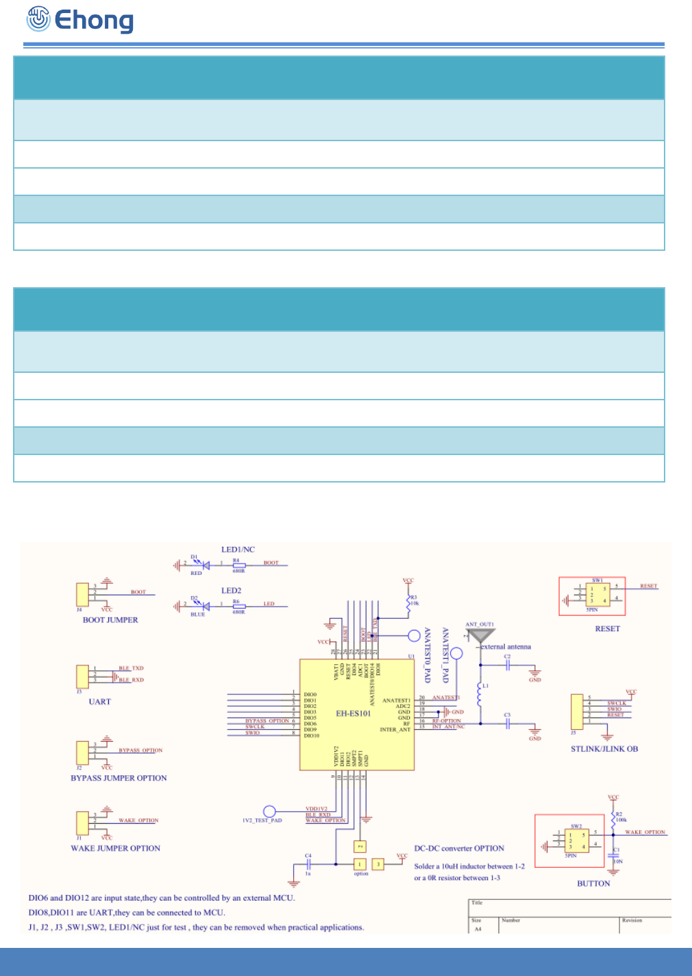
Figure 2: Reference Design important
Note: A. DC-DC transverter select;
(1) When the DC-DC converter is not used, a 0 - o resistor is welded to the welding plate 1-3,
otherwise it cannot work;
(2) When the dc-dc converter is activated, a 10uH inductance is welded to the welding disc
1-2.This method can reduce peak power consumption, and the peak current can be
reduced by about 45%.
B. Pin23 BOOT pin can’t connect to VCC, or else will always goto boot mode;
C. Pin9 VDD1V2 need connect a test pad.
8. Layout and Soldering Considerations
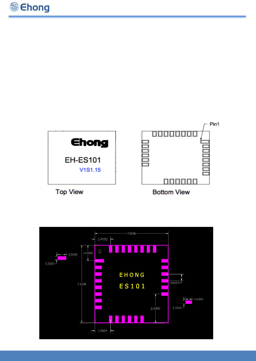
8.1. EH-ES101 external view
Figure 3: EH-ES101 External view
8.2. PCB package outline drawing
EH-ES101
Ehong ® Professional Bluetooth Solutions Provider page 12 of 14
9. Tape and reel information
EH-ES101 modules are supplied on the tape and reels.
For tape and reel packing and labeling, see IC packing and labeling specification.
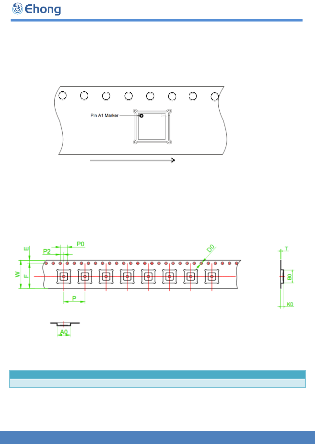
9.1. Tapa orientation
Figure 5 shows the EH-ES101 module LGA packing tape orientation.
User Direction of Feed
Figure 5: EH-ES101 module tape orientation
9.2. Tape dimensions
Figure 6 shows and Table10 lists the dimensions of the tape for the EH-ES101 module.
Figure 6 :EH-ES101 tape dimensions
ITEM
W
A0
B0
K0
P
F
E
D0
P0
P2
T
DIM(mm)
16.0
7.3
7.3
1.5
12
7.5
1.75
1.5
4
2.0
0.3
Table 10: EH-ES101 module tape dimensions
EH-ES101
Ehong ® Professional Bluetooth Solutions Provider page 13 of 14
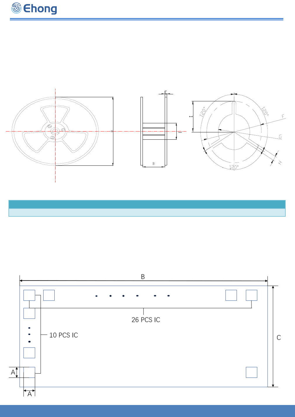
9.3. Reel information
Figure 7 :EH-ES101 reel dimensions
Item
A
B
D
E
F
G
H
I
Unit:mm
330
16.4
100
2.0
21.5
13.2
2.6
10.75
Table 11: EH-ES101 module reel dimensions
10. The tray information
Figure 8 is the size of EH-ES101 pallet, and the number of chips in the tray is 26*10=260PCS.

EH-ES101
Ehong ® Professional Bluetooth Solutions Provider page 14 of 14
Figure 8: EH-ES101 pallet size.
11. Soldering Recommendations
EH-ES101 is compatible with industrial standard reflow profile for Pb-free solders. The
reflow profile used is dependent on the thermal mass of the entire populated PCB, heat
transfer efficiency of the oven and particular type of solder paste used. Consult the
datasheet of particular solder paste for profile configurations.
SMT stencil making requirements
If Bluetooth module PIN pitch ≥ 0.25mm and other component PIN pitch ≥ 0.25mm,so you
choose SMT stencil thickness 0.15mm.
If Bluetooth module PIN pitch ≥ 0.25mm and other component PIN pitch ≤ 0.25mm,so you
choose SMT Ladder stencil Bluetooth module thickness 0.15mm other component
thickness 0.13mm.
Solder pad open via ratio Length 1:1.2, width 1:1.
12. Contact Information
Sales: sales@ehlink.com.cn
Technical support: support@ehlink.com.cn
Website: http://www.ehonglink.com
Tel: 021-61263536
Fax: 021-61263536
Address: Suite501,No.3 building,No.439 Jinglian road,Minhang district,Shanghai,China
FCC Statement
Any Changes or modifications not expressly approved by the party responsible for compliance could void the user’s authority to
operate the equipment.
This device complies with part 15 of the FCC Rules. Operation is subject to the following two conditions: (1) This device may
not cause harmful interference, and
(2) This device must accept any interference received, including interference that may cause undesired operation.
FCC Radiation Exposure Statement:
This equipment complies with FCC radiation exposure limits set forth for an uncontrolled
environment .This equipment should be installed and operated with minimum distance 20cm between the radiator& your body.
FCC Label Instructions:
The outside of final products that contains this module device must display a label referring to the enclosed module. This exterior
label can use wording such as: “Contains Transmitter Module
FCC ID: 2ACCRES101”,or “Contains FCC ID: 2ACCRES101”, Any similar wording that expresses the same meaning may be
used