Ehong Technology MB05 Bluetooth Module User Manual
ShangHai Ehong Technology Co.,Ltd. Bluetooth Module Users Manual
Contents
- 1. Users Manual
- 2. User Manual
Users Manual
EH
-
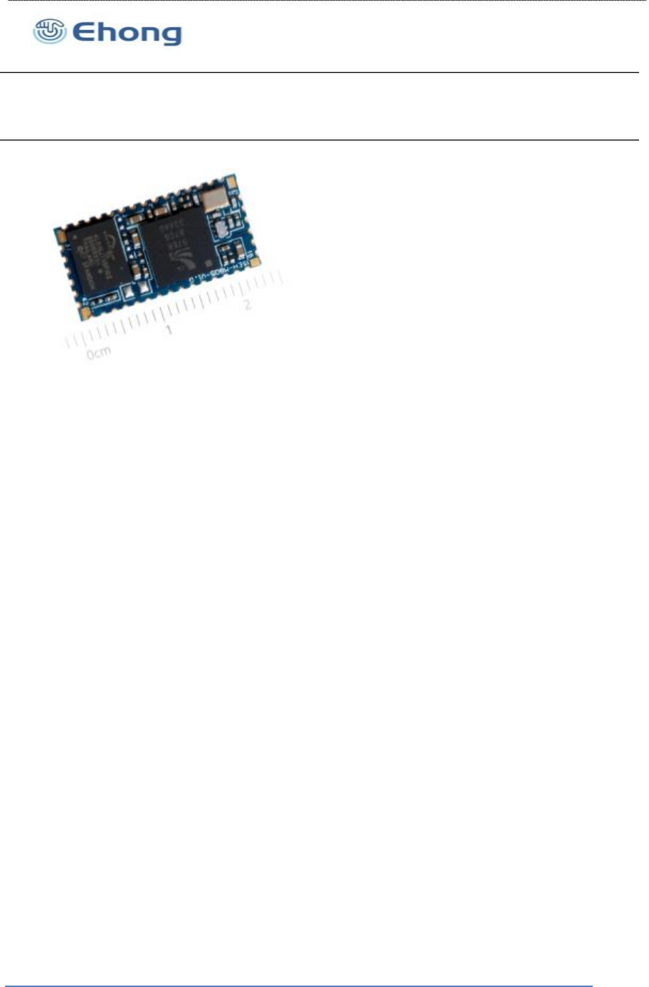
MB05
Bluetooth® technology
audio
module
FCCID:2ACCRMB05
• Bluetooth radio
-
-
-
-
-
Fully embedded Bluetooth® v
3.0 +EDR
Class2 module
128-bit encryption security
Range up to 15m
Multipoint capability(7 transmit data devices
connected at the same time)
• Support profiles
-
-
-
SPP (Master and slave)
iAP (ipod accessory protocol)
HFP ,A2DP,AVRCP,HID(Salve)
EH
-
MB05
• User interface
-
Send AT command over UART
- Firmware upgrade over USB
-
With SPP service active: 560kbps tr
ansmission
speed (UART)
-
PCM interface (I2S,SPDIF)
- I2C interface(Master )
• Audio codec
-
-
-
16bit internal stereo codec :95dB SNR for DAC
64MIPS Kalimba DSP coprocessor
Support Apt-X ,AAC, Apt-XLL,SBC codec
• General I/O
-
-
11 general purpose I/Os
2 analogue I/O
• FCC and Bluetooth® qualified
• Single voltage supply: 3.3V typical
• Small form factor: 23.24 x 11.93 x 2.2mm
• Operating temperature range: -40 °C to 85 °C
• The operation distance >20cm
Version 2.0
July 21 2014
Shanghai Ehong Technologies Inc

Bluetooth Audio Module
1. Contents
1.
2.
3.
4.
Description
.............................................................................................................................
................................... 4
Application................................................................................................................................................................. 4
EH-MB05 Product numbering ............................................................................................................................. 4
Electrical Characteristic ........................................................................................................................................ 5
4.1.
Recommend operation conditions
.............................
.................................................................................... 5
Absolute Maximum Rating
.............................................................................................................................. 5
Power consumptions ........................................................................................................................................ 6
Input/output Terminal Characteristics ........................................................................................................... 6
4.2.
4.3.
4.4.
4.4.1.
4.4.2.
4.4.3.
4.4.4.
Digital Terminals
.............................................................................................................................
........... 6
USB .............................................................................................................................................................. 7
Internal CODEC Analogue to Digital Converter ................................................................................. 7
Internal CODEC Digital to Analogue Converter ................................................................................. 8
5.
6.
Pinout and Terminal Description
..........................................................................
.............................................. 9
5.1.
Pin assignment
.............................................................................................................................
..................... 9
Physical Interfaces
...................
.............................................................................................................................
11
6.1.
Power Supply
.............................................................................................................
...................................... 11
Reset .................................................................................................................................................................. 12
PIO ...................................................................................................................................................................... 12
AIO
...................................................................................................................................................................... 12
UART.................................................................................................................................................................. 13
I2C Master ........................................................................................................................................................ 13
6.2.
6.3.
6.4.
6.5.
6.6.
6.6.1.
Apple iOS CP reference design
...............................................................
............................................ 14
6.7.
Digital Audio Interfaces
.............................................................................................................................
..... 15
6.7.1
6.7.2
PCM
............................
.............................................................................................................................
.. 16
Digital Audio Interface (I S) .................................................................................................................. 16
2
6.7.3
IEC 60958 Interface (SPDIF)
............................................................................................................... 19
6.8
Microphone input
.............................................................
................................................................................ 20
Analog Output stage
....................................................................................................................................... 21
USB .................................................................................................................................................................... 21
6.9
6.10
7.
8.
EH
-
MB05 Reference Design
.........................................................
...................................................................... 23
Mechanical and PCB Footprint Characteristics.......................................................................................... 24
Shanghai Ehong Technologies Inc

Bluetooth Audio Module
RF Layout Guidelines .......................................................................................................................................... 24
9.
9.1
Feed Line and Antenna
.............................................................................................................................
..... 25
Matching network in free space ................................................................................................................... 26
9.2
10.
11.
Reflow Profile
.............................................................................................................................
........................
27
Contact Information ......................................................................................................................................... 28
2. Table of Tables
T
ABLE
1: R
ECOMMENDED
O
PERATING
C
ONDITIONS
..............................
................................................................. 5
TABLE 2: ABSOLUTE MAXIMUM RATING RECOMMENDED OPERATING CONDITIONS ................................................ 5
TABLE 3: POWER CONSUMPTIONS .......................................................................................................................... 6
TABLE 4: DIGITAL TERMINAL .................................................................................................................................. 7
TABLE 5: USB TERMINAL ....................................................................................................................................... 7
TABLE 6: ANALOGUE TO DIGITAL CONVERTER ....................................................................................................... 8
TABLE 7: DIGITAL TO ANALOGUE CONVERTER ....................................................................................................... 8
T
ABLE
8
:
PIN T
ERMINAL
D
ESCRIPTION
......................................
......................................................................... 11
T
ABLE
9: P
IN
S
TATUS ON
R
ESET
.......................................................................................................................... 12
TABLE 10: POSSIBLE UART SETTINGS ................................................................................................................ 13
TABLE 11:ALTERNATIVE FUNCTIONS OF THE DIGITAL AUDIO BUS INTERFACE ON THE PCM INTERFACE .............. 16
TABLE 12 : DIGITAL AUDIO INTERFACE SLAVE TIMING .......................................................................................... 17
TABLE 13 : DIGITAL AUDIO INTERFACE MASTER TIMING ....................................................................................... 18
TABLE 14: USB INTERFACE COMPONENT VALUES ............................................................................................... 22
3. Table of Figures
F
IGURE
1
:
P
I NOUT OF
EH
-
MB05................................................................
......................................................... 9
FIGURE 2: POW ER SUPPLY PCB DESIGN .......................................................................................................... 11
F
IGURE
3
:
C
O NNECTION
T
O
H
OST DEVICE
................
........................................................................................ 13
FIGURE 4 : EXAMPLE EEPROM CONNECTION WITH I2C INTERFACE .................................................................... 14
FIGURE 5 : APPLE CO-PROCESSOR 2.0C ............................................................................................................. 14
FIGURE 6 : APPLE CO-PROCESSOR 2.0B ............................................................................................................. 15
FIGURE 7 : AUDIO INTERFACE .............................................................................................................................. 15
FIGURE 8 : DIGITAL AUDIO INTERFACE MODES ..................................................................................................... 17
FIGURE 9 : DIGITAL AUDIO INTERFACE SLAVE TIMING .......................................................................................... 18
FIGURE 10 : DIGITAL AUDIO INTERFACE MASTER TIMING ..................................................................................... 18
FIGURE 11: EXAMPLE CIRCUIT FOR SPDIF INTERFACE (CO-AXIAL ) ..................................................................... 19
FIGURE 12: EXAMPLE CIRCUIT FOR SPDIF INTERFACE (OPTICAL) ....................................................................... 20
FIGURE 13: MICROPHONE BIASING (SINGLE CHANNEL SHOWN) ........................................................................... 20
FIGURE 14: SPEAKER OUTPUT ............................................................................................................................. 21
FIGURE 15: USB CONNECTIONS .......................................................................................................................... 22
FIGURE 16: REFERENCE DESIGN ......................................................................................................................... 23
FIGURE 17: RECOMMENDED PCB MOUNTING PATTERN (UNIT: MM, DEVIATION:0.02MM)TOP VIEW ................... 24
FIGURE 18: CLEARANCE AREA OF ANTENNA ......................................................................................................... 25
FIGURE 19: ANTENNA REFERENCE DESIGN .......................................................................................................... 26
FIGURE 20: PI MATCH NETWORK EXAMPLE ........................................................................................................... 26
FIGURE 21: RECOMMENDED REFLOW PROFILE ................................................................................................... 27
Shanghai Ehong Technologies Inc

Bluetooth Audio Module
1. Description
The EH-MB05 is an easy to use Bluetooth module, compliant with Bluetooth v3.0+EDR. The
module provides complete RF platform in a small form factor.
The EH-MB05 enables electronic devices with wireless connectivity, not requiring any RF
experience or expertise for integration into the final product. The EH-MB05 module, being a
certified solution, optimizes the time to market of the final application.
The module is designed for maximum performance in a minimal space including fast speed
UART and 11general purpose I/O lines, 1 analogueI/O lines, several serial interface options, and
up to 600 kbps transmission speed with SPP service active, 200 kbps with iAP service active.
The module is , the impedance of the feed line between the RF port and the
antenna shall be 50Ω.Embedded Bluetooth AT command firmware is a friendly interface,
Supportdifferent Bluetooth profiles, such as SPP, A2DP, AVRCP, HFP, HID, iAP and etc. iAP
over Bluetooth using apple’s authentication coprocessor.
Customers using the Apple authentication IC must register as developers, to become an
Apple certified MFI member. License fees may apply, for additional information visit:
http://developer.apple.com/programs/which-program/index.html.
Certified MFI developers developing electronic accessories that connect to an iPod®,
® ®
iPhone , and iPad can gain access to technical documentation, hardware components,
technical support and certification logos.
Customized firmware for peripheral device interaction, power optimization, security, and other
proprietary features may be supported and can be ordered pre-loaded and configured.
2. Application
•
Sports and fitness
• Home entertainment
• Service diagnostics
• Office and mobile accessories
• Commercial
• Multimedia speaker
• Automotive
• Human interface devices
3. EH-MB05 Product numbering
EH
-
MB05X
Company Name(Ehong)
A. EH -------------
B. MB05 ------------ Module Name
Shanghai Ehong Technologies Inc
Bluetooth Audio Module
4. Electrical Characteristic
4.1. Recommend operation conditions
Operating Condition Min Typical Max Unit
Storage Temperature -40 -- +105 °C
°C
V
Operating Temperature Range
PIO Voltage
-40
+1.7
+1.42
+2.7
2400
-- +85
+3.6
+3.3
+1.5
+3.3
2441
AIO Voltage +1.57
+3.6
V
VDD Voltage V
RF frequency 24800 MHz
Table 1: Recommended Operating Conditions
4.2. Absolute Maximum Rating
Rating Min
-40
Max
+125
+85
Unit
°C
°C
V
Storage Temperature
Operating Temperature
PIO Voltage
-40
-0.4
-0.4
-0.4
-0.4
+3.6
+1.57
+3.6
+3.6
AIO Voltage V
VDD Voltage V
USB_DP/USB_DN Voltage V
VDD+0.
4
Other Terminal Voltages except RF -0.4 V
Table 2: Absolute Maximum Rating Recommended Operating Co
nditions
Shanghai Ehong Technologies Inc
Bluetooth Audio Module
4.3. Power consumptions
Operating Condition Min Typical Max Unit
Standby, without deep sleep 2.1
0.11
-
-
-
-
3.1
0.7
40
mA
mA
mA
Standby, with deep sleep
Inquiry window time
Connected (Deep sleep
disable, sniff enable )
Connected (Deep sleep on,
(b)
(a)
- 3.3 - mA
sniff enable)
(a)
- 0.4
20
- mA
mA
Connected with data transfer 18 22
Connected with audio
streaming (A2DP) 35 40 mA
Table 3: Power consumptions
Note :
Power consumption depends on the firmware used. Typical values are shown in the table.
(a)
Sniff mode
-----
In Sniff mode, the duty cycle of the slave
’
s activity in t
he piconet may be reduced. If a
slave is in active mode on an ACL logical transport, it shall listen in every ACL slot to the master traffic,
unless that link is being treated as a scatter net link or is absent due to hold mode. With sniff mode, the
time slots when a slave is listening are reduced, so the master shall only transmit to a slave in specified
time slots. The sniff anchor points are spaced regularly with an interval of Tsniff.
(b)
Radio on(Inquiry )
----
Search time is 22 seconds
4.4. Input/output Terminal Characteristics
4.4.1.Digital Terminals
Supply Voltage Levels
Input Voltage Levels
Min Typ Max Unit
VIL input logic level low -0.3 - +0.25xVDD
VDD+0.3
V
V
VIH input logic level high 0.625VDD -
Output Voltage Levels
VOL output logic level low, lOL = 4.0mA
VOH output logic level high, lOH = -4.0mA
Input and Tri-state Current
Ii input leakage current at Vin=VDD or 0V
- -
-
0.125
VDD
V
V
0.75xVDD
-100
-100
0
0
100
100
nA
nA
Ioz tri-state output leakage current at Vo=VDD
or 0V
With strong pull-up -100
10
-40
40
-10 uA
μA
With strong pull-down 100
Shanghai Ehong Technologies Inc

Bluetooth Audio Module
mV
rms
Input full scale at maximum gain (differential)
Input full scale at minimum gain (differential)
-
-
4 -
- mV
rms
800
3dB Bandwidth -
-
20
6
-
-
kHz
kΩ
%
Microphone mode input impedance
THD+N (microphone input) @ 30mv rms input 0.04
Table 6: Analogue to Digital Converter
4.4.4.Internal CODEC Digital to Analogue Converter
Parameter Conditions Min Typ Max
16
Unit
Bits
Resolution - -
-
Output Sample Rate, Fsample
fin=1kHz
8 48 kHz
Fsample
8kHz - 95
95
95
95
95
95
95
-
-
-
-
-
-
-
B/W=20Hz->20kHz 11.025kHz
16kHz
-
Signal to Noise
Ratio, SNR
A-Weighted -
THD+N<0.01%
0dBFS signal
Load = 100kΩ
22.050kHz
32kHz
-
-
dB
44.1kHz
48kHz
-
-
Digital Gain Digital Gain Resolution = 1/32 dB
Analogue Gain Resolution = 3dB
-24
0
21.5
-21
dB
dB
Analogue Gain -
mV
rms
Output voltage full swing (differential)
Allowed Load
- 750 -
Resistive 16
-
-
-
-
OC
500
0.01
Ω
pF
%
Capacitive
THD+N 100kΩ load
THD+N 16Ω load
-
-
-
- 0.1
-
%
SNR (Load=16Ω, 0dBFS input relative to digital
silence) 95 dB
Table 7: Digital to Analogue Converter
Shanghai Ehong T
echnologies Inc
Bluetooth Audio Module
5. Pinout and Terminal Description
5.1. Pin assignment
Figure 1:
Pinout of EH
-
MB05
Pin Symbol I/O Type Description
1 GND Ground Ground
Active LOW RESETB, input debounced
so must be low for >5ms to cause a
RESETB
CMOS input with weak
internal pull-up
2 RESETB
Input with weak internal pull- Serial Peripheral interface clock for
3
4
5
SPI_CLK
SPI_MISO
SPI_MOSI
down programming only
CMOS output, tri-state, with
weak internal pull
-down
Serial Peripheral Interface output for
programming only
CMOS input, with weak
internal pull-down
Serial Peripheral Interface input for
programming only
Chip select for Synchronous Serial
Interface for programming only, active
low
Input with weak internal pull-
up
6
7
8
SPI_CSB
LED0 Open drain output LED Driver
Bi-directional with
programmable strength
PIO3 Programmable input/output line
internal pull-up/down
CMOS output, tri-state, with
weak internal pull
-down
9 PCM_OUT Synchronous Data Output
10
11
MIC_RP
MIC_RN
Analogue
Analogue
Microphone input positive, right
Microphone input negative, right
Shanghai Ehong Technologies Inc
Bluetooth Audio Module
Bi-directional with
12
13
PIO0
PIO1
programmable strength
internal pull-up/down
Programmable input/output line
Bi-directional with
programmable strength
internal pull-up/down
Programmable input/output line
CMOS Input, with weak
internal pull-down
14
15
16
PCM_IN
GND
Synchronous Data Input
Ground
Ground
Bi-directional with weak
internal pull-down
PCM_SYNC Synchronous Data Sync
17
18
19
RF_GND
RF_IN
RF Ground
RF
RF ground
RF Transceiver input/output line
RF ground
RF_GND RF Ground
Bi-directional with weak
internal pull-down
20 PCM_CLK Synchronous Data Clock
21
22
23
24
25
26
27
28
AIO0 Bi-directional
Ground
Analogue programmable input/output line
Ground
GND
MIC_LP
MIC_LN
SPK_LN
SPK_LP
SPK_RN
SPK_RP
Analogue
Analogue
Analogue
Analogue
Analogue
Analogue
Microphone input positive, left
Microphone input negative, right
Speaker output negative, left
Speaker output positive, left
Speaker output negative, right
Speaker output positive, right
Bi-directional with
29 PIO13 programmable strength
internal pull-up/down
Programmable input/output line
30
31
VDD 3V3 power input 3V3 power input
USB data plus with selectable internal
1.5K pull up resistor
USB_DP Bi-directional
32
33
USB_DN
GND
Bi-directional
Ground
USB data minus
Ground
Bi-directional with
34 PIO9 programmable strength Programmable input/output line
internal pull-up/down
Bi-directional with
35
36
PIO14
PIO4
programmable strength
internal pull-up/down
Programmable input/output line
Programmable input/output line
Bi-directional with
Shanghai Ehong Technologies Inc
Bluetooth Audio Module
programmable strength
internal pull-up/down
37
38
GND Ground Ground
Bi-directional CMOS output,
tri-state, with weak internal
pull-up
UART_TX UART data output
CMOS input with weak
internal pull-down
39
40
UART_RX
PIO8
UART data input
Bi-directional with
programmable strength Programmable input/output line
internal pull-up/down
Bi-directional with
41
42
PIO7
PIO6
programmable strength
internal pull-up/down
Programmable input/output line
Programmable input/output line
Bi-directional with
programmable strength
internal pull-up/down
Table 8:
PIN Terminal Description
6. Physical Interfaces
6.1. Power Supply
-
-
-
-
The module DC3.3V power input.
Power supply pin connection capacitor to chip and pin as far as possible close
Capacitor decouples power to the chip
Capacitor prevents noise coupling back to power plane.
.
Figure 2:
Power Supply PCB Design
Shanghai Ehong Technologies Inc

Bluetooth Audio Module
6.2. Reset
The module may be reset from several sources: RESETB pin, power-on reset, a UART break
character or via software configured watchdog timer.
The RESETB pin is an active low RESETB and is internally filtered using the internal low
frequency clock oscillator. A RESETB will be performed between 1.5 and 4.0ms following
RESETB being active. It is recommended that RESETB be applied for a period greater than
5ms.
At RESETB the digital I/O pins are set to inputs for bi-directional pins and outputs are tri-state.
The pull-down state is shown below.
Pin Name / Group
USB_DP
Pin Status on RESETB
N/a
N/a
PD
PU
PD
PD
PU
PD
PU
PD
PD
PD
PD
PD
USB_DN
UART_RX
UART_TX
SPI_MOSI
SPI_CLK
SPI_CSB
SPI_MISO
RESETB
PIOs
PCM_IN
PCM_CLK
PCM_SYNC
PCM_OUT
Table 9: Pin Status on R
eset
6.3. PIO
EH-MB05 has a total of 11 digital programmable I/O terminals. They are powered from VDD
(3.3V). Their functions depend on firmware running on the device. PIO lines can be configured
through software to have either weak or strong pull-ups or pull-downs.
Note:
All PIO lines are configured as inputs with weak pull-downs at reset.
Any of the PIO lines can be configured as interrupt request lines or as wake-up lines from sleep
modes.
6.4. AIO
EH-MB05 has 2 analogue I/O terminals. Their functions depend on software. Typically ADC
functions can be configured to battery voltage measurement. They can also be used as a digital
PIO.
Shanghai Ehong Technologies Inc
Bl
uetooth Audio Module
6.5. UART
This is a standard UART interface for communicating with other serial devices. The
UART interface provides a simple mechanism for communicating with other serial
devices using the RS232 protocol.
The UART CTS and RTS signals can be used to implement RS232 hardware flow
control where both are active low indicators.
Parameter Possible Values
1200 baud (≤2%Error)
9600 baud (≤1%Error)
3M baud (≤1%Error)
RTS/CTS or None
None, Odd or Even
1 or 2
Minimum
Maximum
Baud Rate
Flow Control
Parity
Number of Stop Bits
Bits per Byte 8
Table 10: Possible UART Settings
Figure 3:
Connection To Host device
6.6. I2C Master
PIO6, PIO7 and PIO8 can be used to form a master I C interface. The interface is formed using
2
software to drive these lines. It is suited only to relatively slow functions such as driving a LCD,
keyboard scanner or EEPROM. In the case, PIO lines need to be pulled up through 2.2KΩ
resistors.
Shanghai Ehon
g Technologies Inc
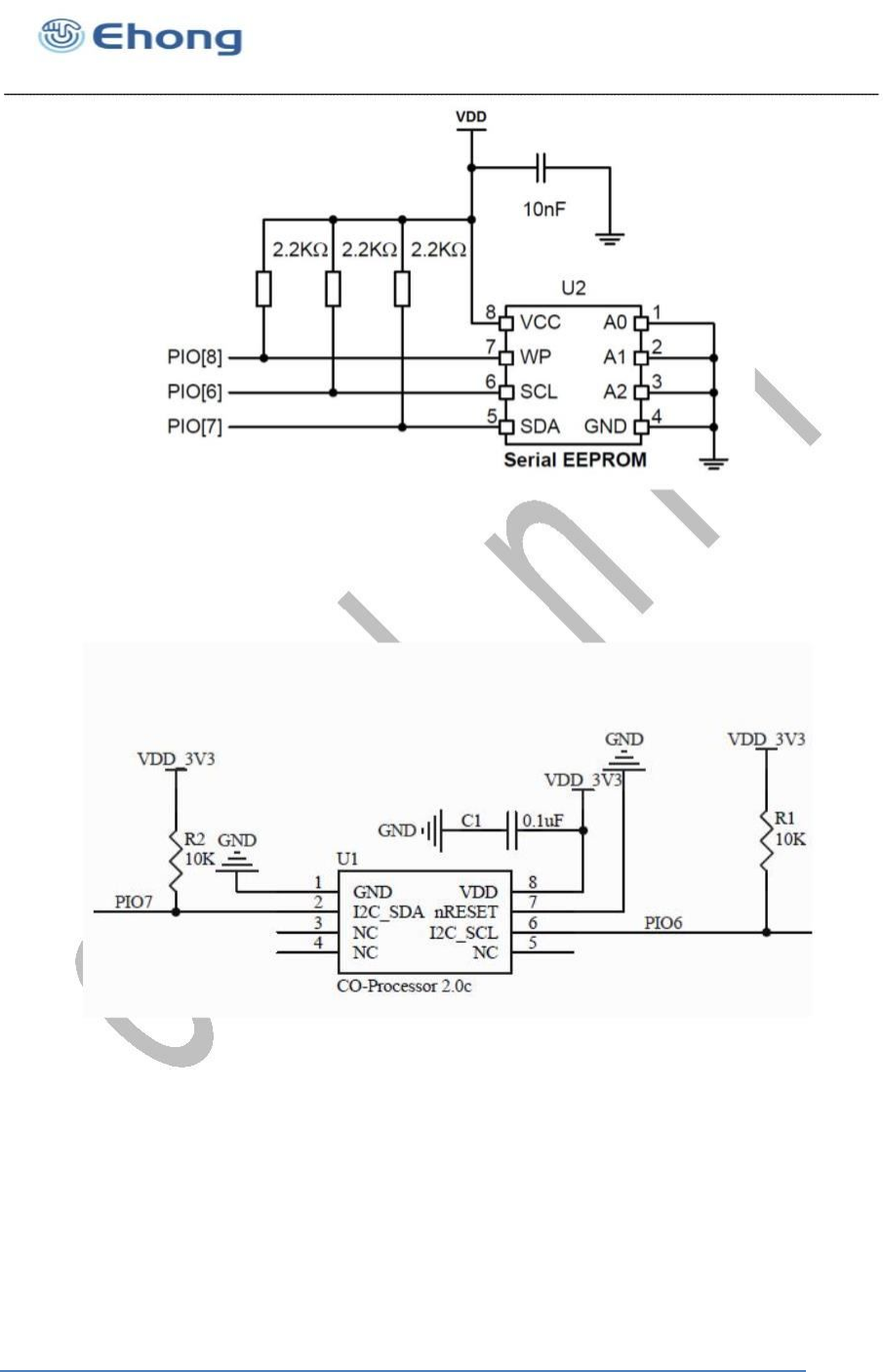
Bluetooth Audio Module
Figure 4 : Example EEPROM Connection with I
2
C Interface
6.6.1.Apple iOS CP reference design
The figures below give an indicative overview of what the hardware concept looks like. A
specific MFI co-processor layout is available for licensed MFI developers from the MFI program.
Figure 5 : Apple Co
-
processor 2.0C
Shanghai Ehong Technologies Inc
Bluetooth Audio Module
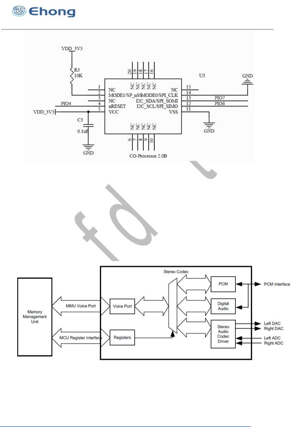
Figure 6 : Apple Co
-
processor 2.0B
6.7. Digital Audio Interfaces
The audio interface circuit consists of:
■ Stereo audio codec
■ Dual audio inputs and outputs
■ A configurable PCM, I²S or SPDIF interface
Figure 2 outlines the functional blocks of the interface. The codec supports stereo playback and
recording of audio signals at multiple sample rates with a resolution of 16-bit. The ADC and
the DAC of the codec each contain 2 independent channels. Any ADC or DAC channel can be
run at its own independent sample rate.
Figure 7 : Audio Interface
The interface for the digital audio bus shares the same pins as the PCM codec interface
described in Table 11, which means each of the audio buses are mutually exclusive in their
usage. Table 11 lists these alternative functions.
Shanghai Ehong Technologies Inc

Bluetooth
Audio Module
PCM Interface
PCM_OUT
SPDIF Interface
SPDIF_OUT
I²S Interface
SD_OUT
PCM_IN
SPDIF_IN
SD_IN
WS
PCM_SYNC
PCM_CLK
-
-
SCK
Table 11: Alternative Functions of the Digital Audio Bus Interface on the PCM Interf
ace
The audio input circuitry consists of a dual audio input that can be configured to be either
single-ended or fully differential and programmed for either microphone or line input. It has an
analogue and digital programmable gain stage for optimization of different microphones.
The audio output circuitry consists of a dual differential class A
-
B output stage.
6.7.1 PCM
The audio pulse code modulation (PCM) interface supports continuous transmission and
reception of PCM encoded audio
data over Bluetooth.
Hardware on EH
-
MB05 allows the data to be sent to and received from a SCO connection. Up
to three SCO connections can be supported by the PCM interface at any one time.
EH-MB05 can operate as the PCM interface master generating PCM_SYNC and PCM_CLK or
as a PCM interface slave accepting externally generated PCM_SYNC and PCM_CLK.
EH-MB05 is compatible with a variety of clock formats, including Long Frame Sync, Short
Frame Sync and GCI timing environments.
It supports 13-bit or 16-bit linear, 8-bit u-law or A-law companded sample formats and can
receive and transmit on any selection of three of the first four slots following PCM_SYNC.
EH-MB05 interfaces directly to PCM audio devices including the following:
■ Qualcomm MSM 3000 series and MSM 5000 series CDMA baseband devices
■
OKI MSM7705 four channel A
-
law and μ
-
law CODEC
■
Motorola MC145481 8
-
bit A
-
law and μ
-
law CODEC
■ Motorola MC145483 13-bit linear CODEC
■ STW 5093 and 5094 14-bit linear CODECs(8)
■
EH
-
MB05 is also compatible with the Motorola SSI interface
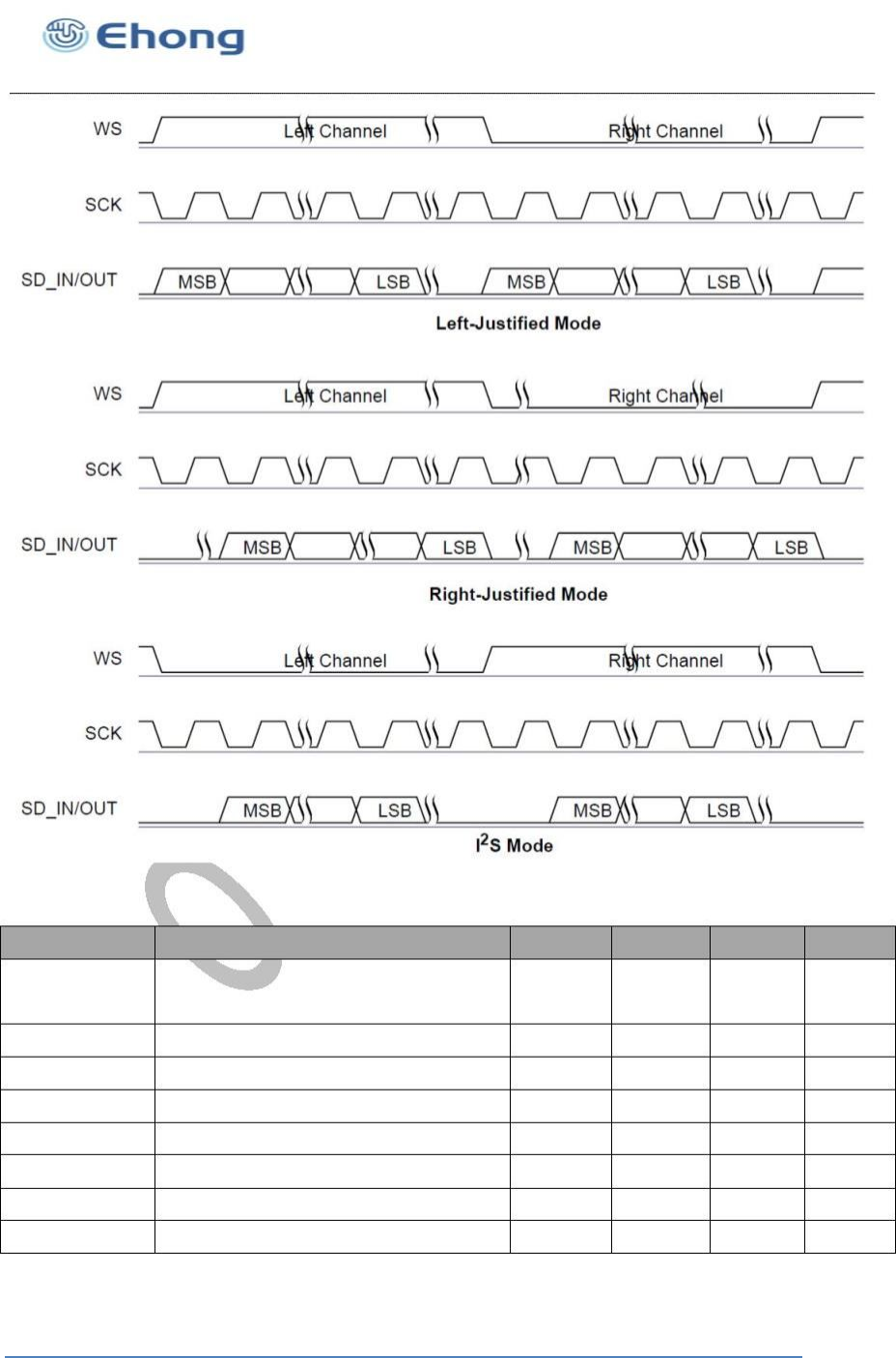
6.7.2 Digital Audio Interface (I
2
S)
The digital audio interface supports the industry standard formats for I2S, left
-
justified or right
-
justified. The interface shares the same pi
ns of the PCM interface as Table 11.
The I2S interface can be enabled by using AT+ commands. The module is an I2S slave device
with the default firmware. Contact with EHong for special firmware when use the module as an
I2S master. The I2S suppo
rt following formats:
Shanghai Ehong Technologies Inc
Bluetooth Audio Module
Figure 8 : Digital Audio Interface Modes
Symbol
Parameter
Min
-
Typical
M
ax
Unit
MHz
kHz
ns
-
SCK Frequency
-
-
-
-
-
-
-
-
-
6.2
-
WS Frequency
-
96
-
t
ch
tcl
SCK high time
80
80
-
SCK low time
-
ns
t
opd
tssu
tsh
tisu
tih
SCK to SD_OUT delay
WS to SCK set up time
WS to SCK hold time
SD_IN to SCK set-up time
SD_IN to SCK hold time
20
-
ns
20
20
20
20
ns
-
ns
-
ns
-
ns
Table 12 : Digital Audio Interface Slave Timing
Shanghai Ehong Technologies Inc
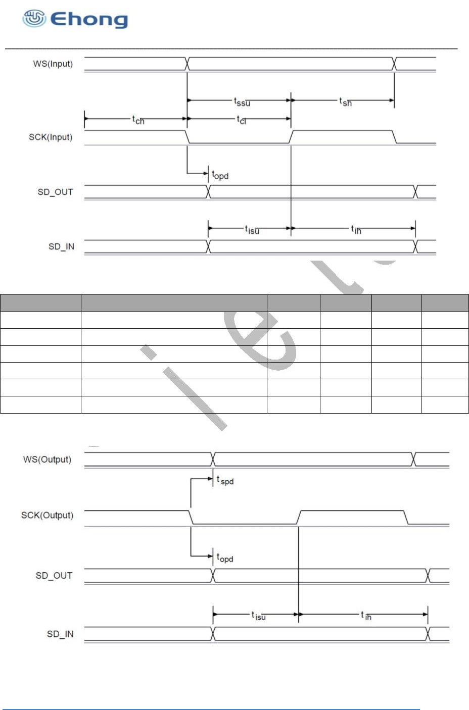
Bluetooth Audio Module
Figure
9 : Digital Audio Interface Slave Timing
Symbol
Parameter
Min
Typical
Max
6.2
96
20
20
-
Unit
MHz
kHz
ns
-
SCK Frequency
-
-
-
-
-
-
-
-
-
WS Frequency
t
opd
tspd
tisu
tih
SCK to SD_OUT delay
SCK to WS delay
-
-
ns
SD_IN to SCK set
-
up time
SD_IN to SCK hold time
20
10
ns
-
ns
Table 13 : Digital Audio Interface Master Timing
Figure 10 : Digital Audio Interface Master Timing
Shanghai Ehong Technologies Inc
Bluetooth Audio Module
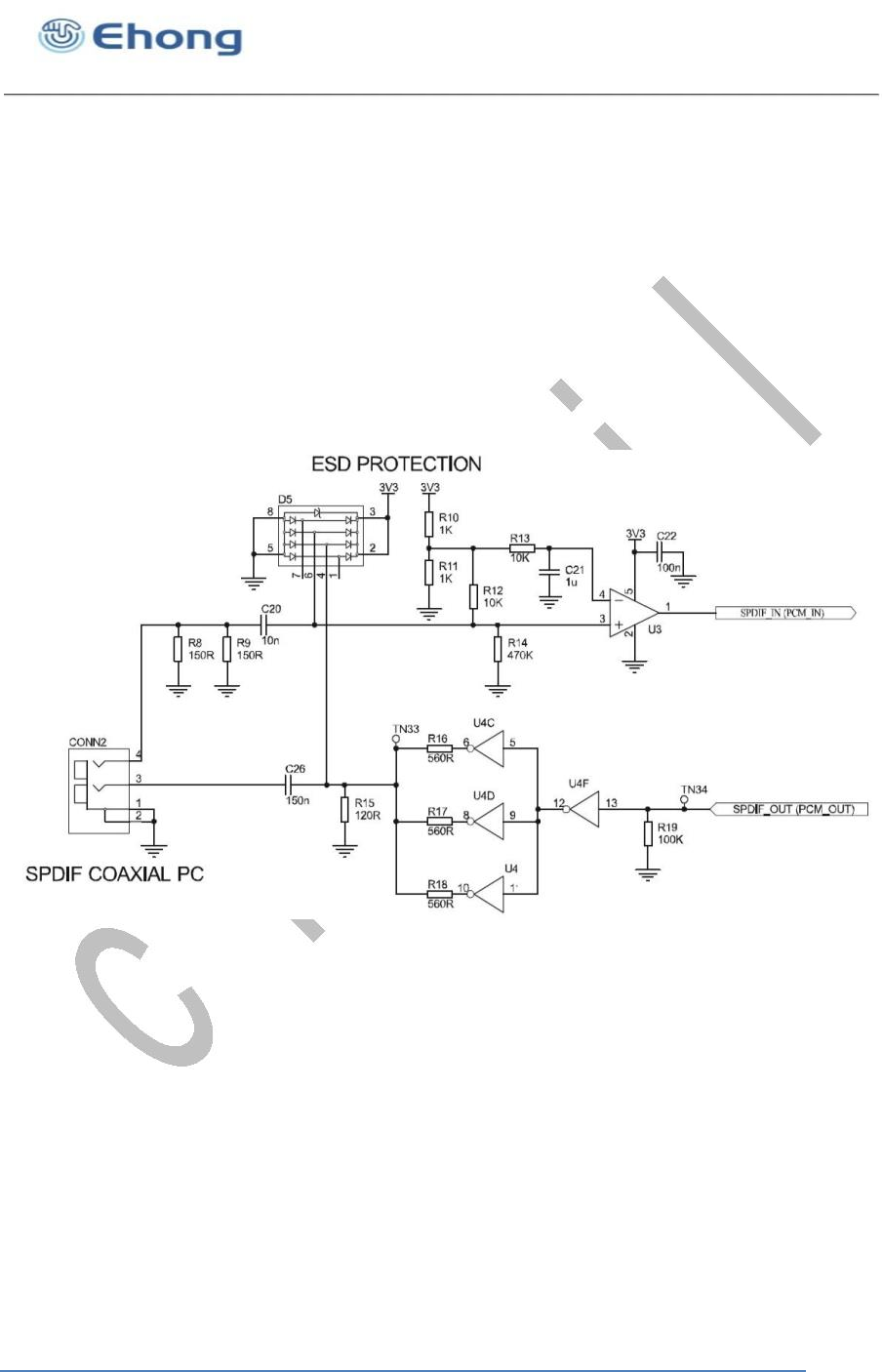
6.7.3 IEC 60958 Interface (SPDIF)
Through AT+ command to switch if SPDIF is used.The IEC 60958 interface is a digital audio
interface that uses bi-phase coding to minimise the DC content of the transmitted signal and
allows the receiver to decode the clock information from the transmitted signal. The IEC 60958
specification is based on the 2 industry standards:
■
■
AES/EBU
Sony and Philips interface specification SPDIF
The interface is compatible with IEC 60958
-
1, IEC 609
58
-
3 and IEC 60958
-
4.
The SPDIF interface signals are SPDIF_IN and SPDIF_OUT and are shared on the PCM
interface pins. The input and output stages of the SPDIF pins can interface to:
■
A
75Ω
coaxial cable with an RCA connector, see Figure 11.
■
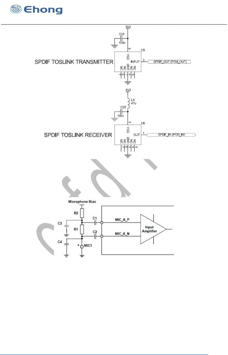
An optical link that uses Toslink optical components, see Figure 12.
Figure 11: Example Circuit for SPDIF Interface (Co
-
Axial)
Shanghai Ehong Technologies Inc
Bluetooth Audio Module
Figure 12: Example Circuit for SPDIF Interface (Optical)
6.8 Microphone input
Figure 13: Microphone Biasing (Single Channel
Shown)
The audio input is intended for use in the range from 1μA @ 94dB SPL to about 10μA @ 9
4dB
SPL. With biasing resistors R1 and R2 equal to 1kΩ, this requires microphones with sensitivity
between about –40dBV and –60dBV. The microphone for each channel should be biased as
shown in Figure 14.
Shanghai Ehong Technologies Inc
Bluetooth Audio Module
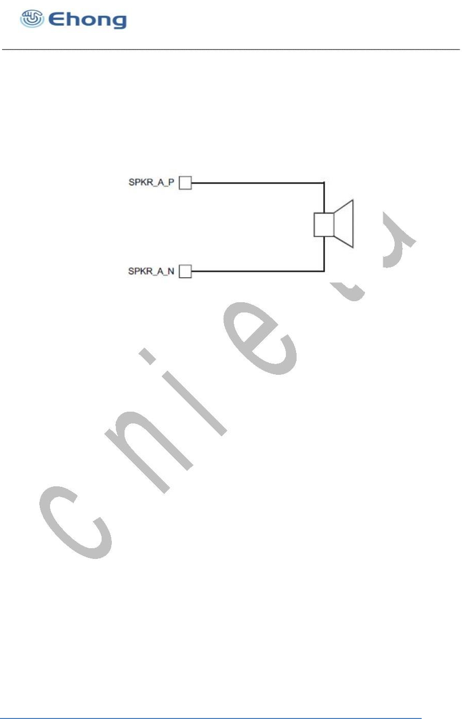
6.9 Analog Output stage
The output stage digital circuitry converts the signal from 16
-
bit per sample, linear PCM of
variable sampling frequency to a 2Mbits/s 5-bit multi-bit bit stream, which is fed into the analogue
output circuitry.
The output stage circuit is comprised a DAC with gain setting and class AB amplifier. The output
is available as a differential signal between SPKR_LN and SPKR_LP for the right channel, as
Figure 14 shows, and between SPKL_RN and SPKL_RP for the left channel.
Figure 15: Speaker output
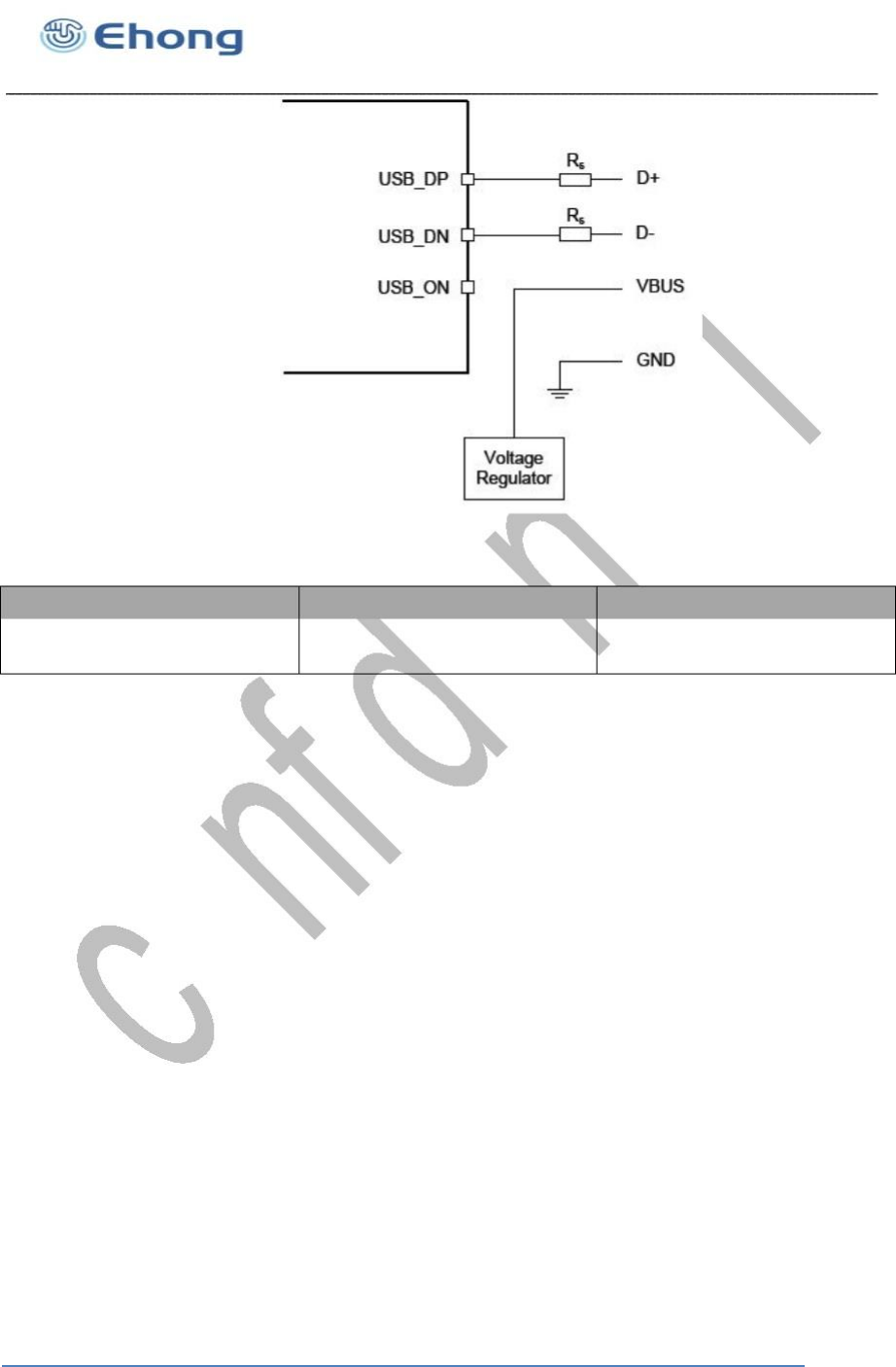
6.10 USB
This is a full speed (12M bits/s) USB interface for communicating with other compatible digital
devices. The module acts as a USB peripheral, responding to request from a master host
controller, such as a PC.
The USB interface is capable of driving a USB cable directly. No external USB transceiver is
required. The device operates as a USB peripheral, responding to requests from a master host
controller such as a PC. Both the OHCI and the UHCI standards are supported. The set of USB
endpoints implemented can behave as specified in the USB section of the Bluetooth
specification v2.1+EDR or alternatively can appear as a set of endpoints appropriate to USB
audio devices such as speakers.
The module has an internal USB pull
-
up resistor. This pulls the USB_DP pin weakly high when
module is ready to enumerate. It signals to the USB master that it is a full speed (12Mbit/s) USB
device.
Shanghai Ehong Technologies Inc
Bluetooth Audio Module
Figure 16: USB Connections
Identifier
Value
Function
Impedance matching to USB
cable
R
s
27Ω Nominal
Table 14: USB Interface Component Values
Note:
USB_ON is only used when the firmware need an input to detect if USB is connected and the USB
function shall be enabled. In such case it is shared with the module PIO terminals. If detection is not
needed (firmware already runs with USB, such as USB DFU or USB CDC), USB_ON is not needed.
Shanghai Ehong Technologies Inc
Bluetooth A
udio Module
7. EH
-
MB05 Reference Design
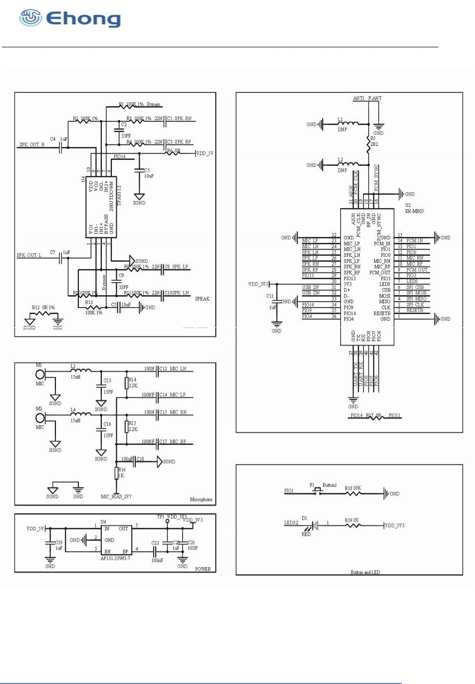
Figure 17: Reference Design
Shanghai Ehong Technologies Inc
Bluetooth Audio Module
8. Mechanical and PCB Footprint Characteristics
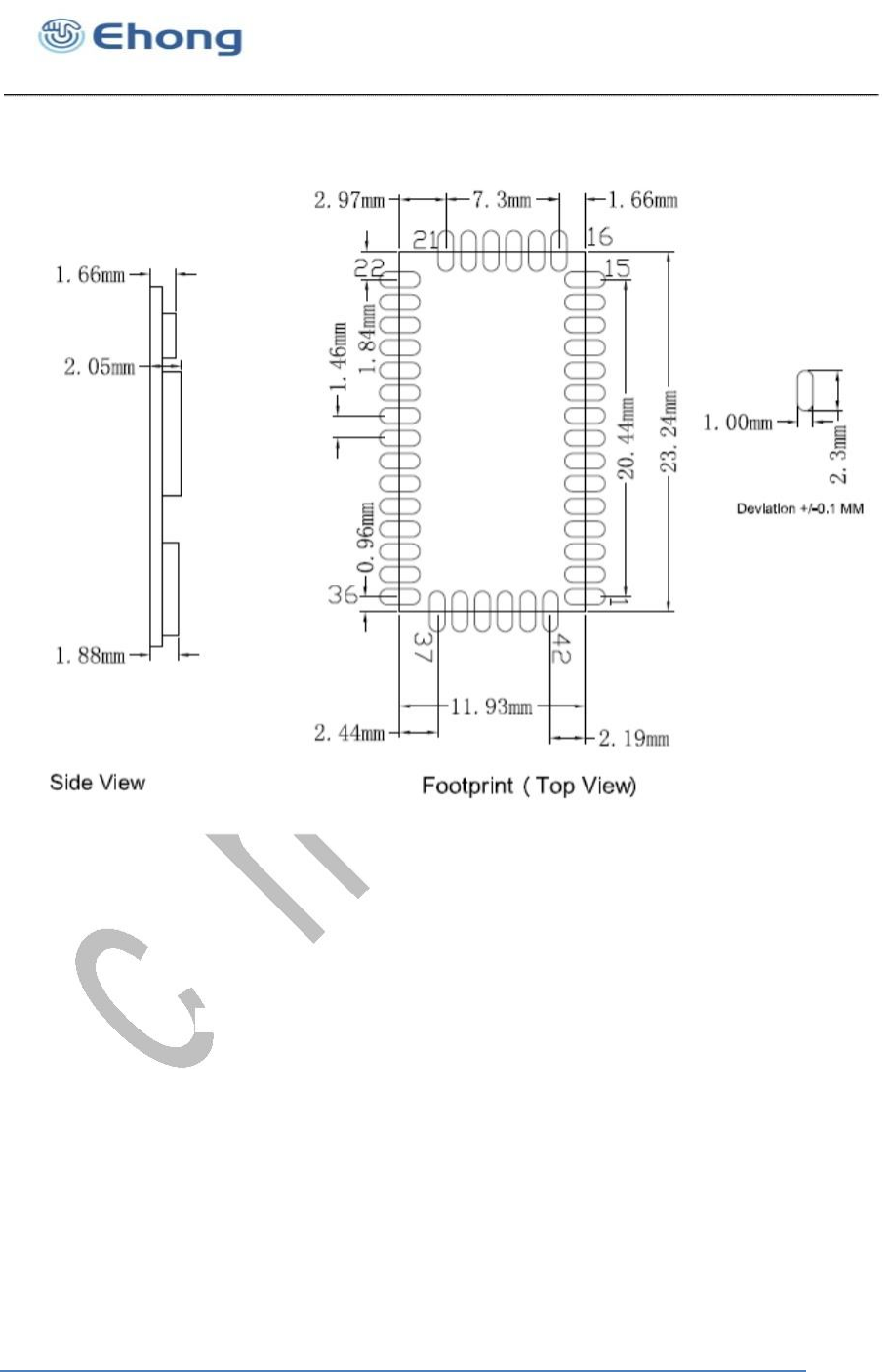
Figure 18: Recommended PCB Mounting Pattern (Unit: mm, Deviation:0.02mm)TOP View
9. RF Layout Guidelines
EH
-
MB05 has an on
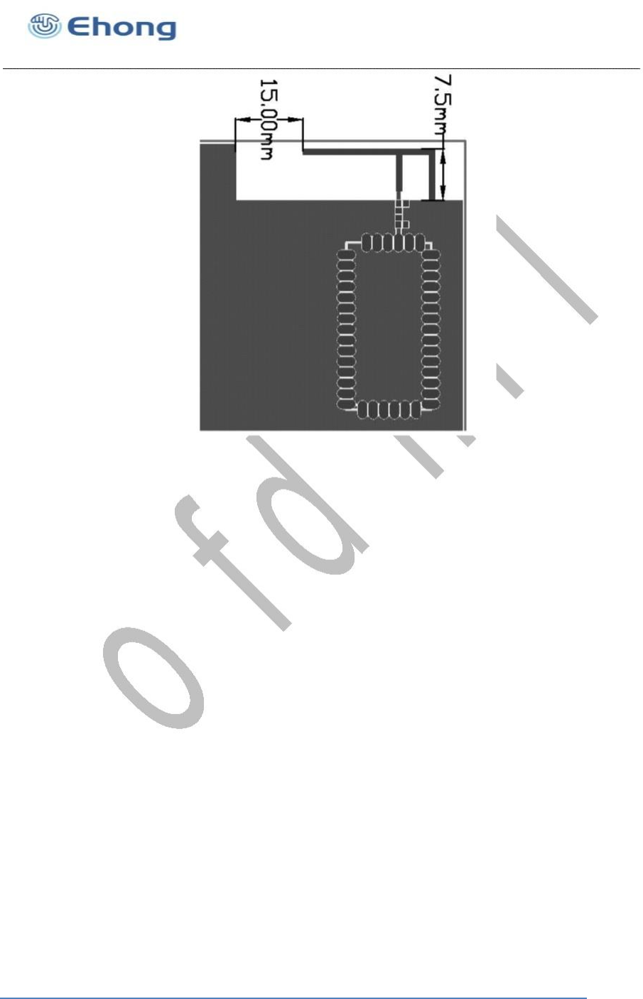
-
board PCB antenna. PCB design to ensure enough clearance area of
antenna, area length is 1.6 times of antenna length, area width is 4 times of antenna width, the
bigger the better if the space allows. The specific size as shown figure below.
Shanghai Ehong Technologies Inc
Bluetooth Audio Module
Figure 19: Clearance area of antenna
9.1
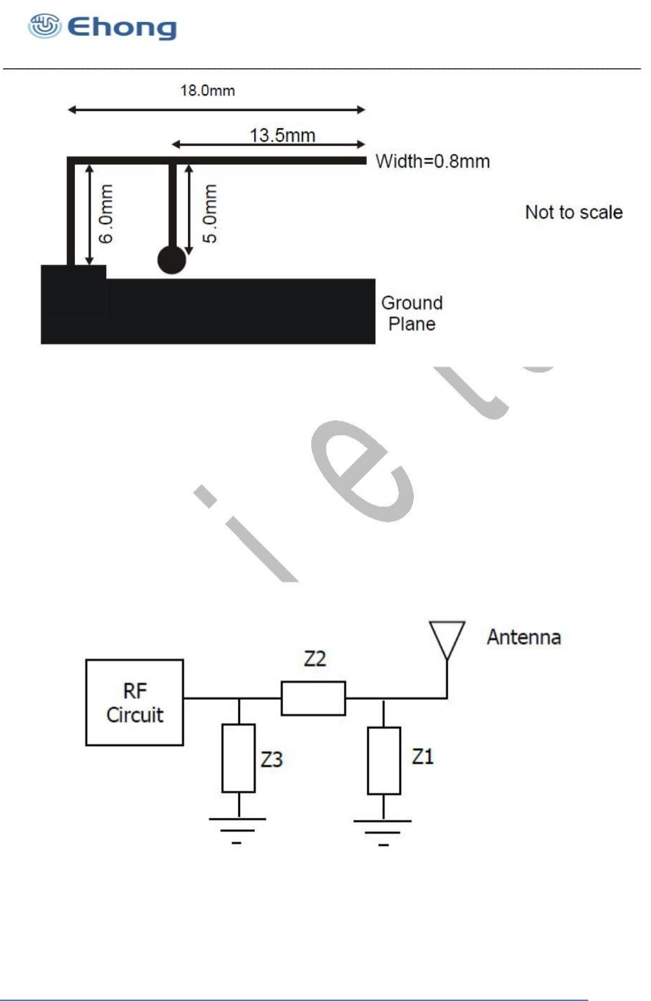
Feed Line and Antenna
The impedance of the feed line between the RF port and the antenna shall be 50Ω.
A good ground di
rectly under the feed line is always needed for impedance control.
Route the feed line as curve lines when needed, avoid 90 or even less degree angles style.
The width of the feed line, the distance of the feed line to the ground plane are keys to the
impedance. Ask your PCB supplier to control the impedance of the feed line.
For the antenna,
When PCB antenna is used, matching networks shall be used to optimize the antenna’s
signal strength.
Use as many vias as possible to connect the ground
planes nearby the antenna.
Shanghai Ehong Technologies Inc
Bluetooth Audio Module
Figure 20: Antenna reference design
9.2
Matching network in free sp
ace
The specs of a Fractus standard antenna are measured in their evaluation board (in free space),
which is an ideal case. In a real design, components nearby the antenna, semiconductors,
LCD’s, batteries, covers, connectors, etc affect the antenna performance. This is the reason
why it is highly recommended to place 0402 pads for a PI matching network as close as
possible to the antenna feeding point. Do it in the ground plane area, not in the clearance area.
This is a degree of freedom to tune the antenna once the design is finished and taking into
account all elements of the system (batteries, displays, covers, etc).
Figure 21: PI match network example
Shanghai Ehong Technologies Inc
Bluetooth Audio Module
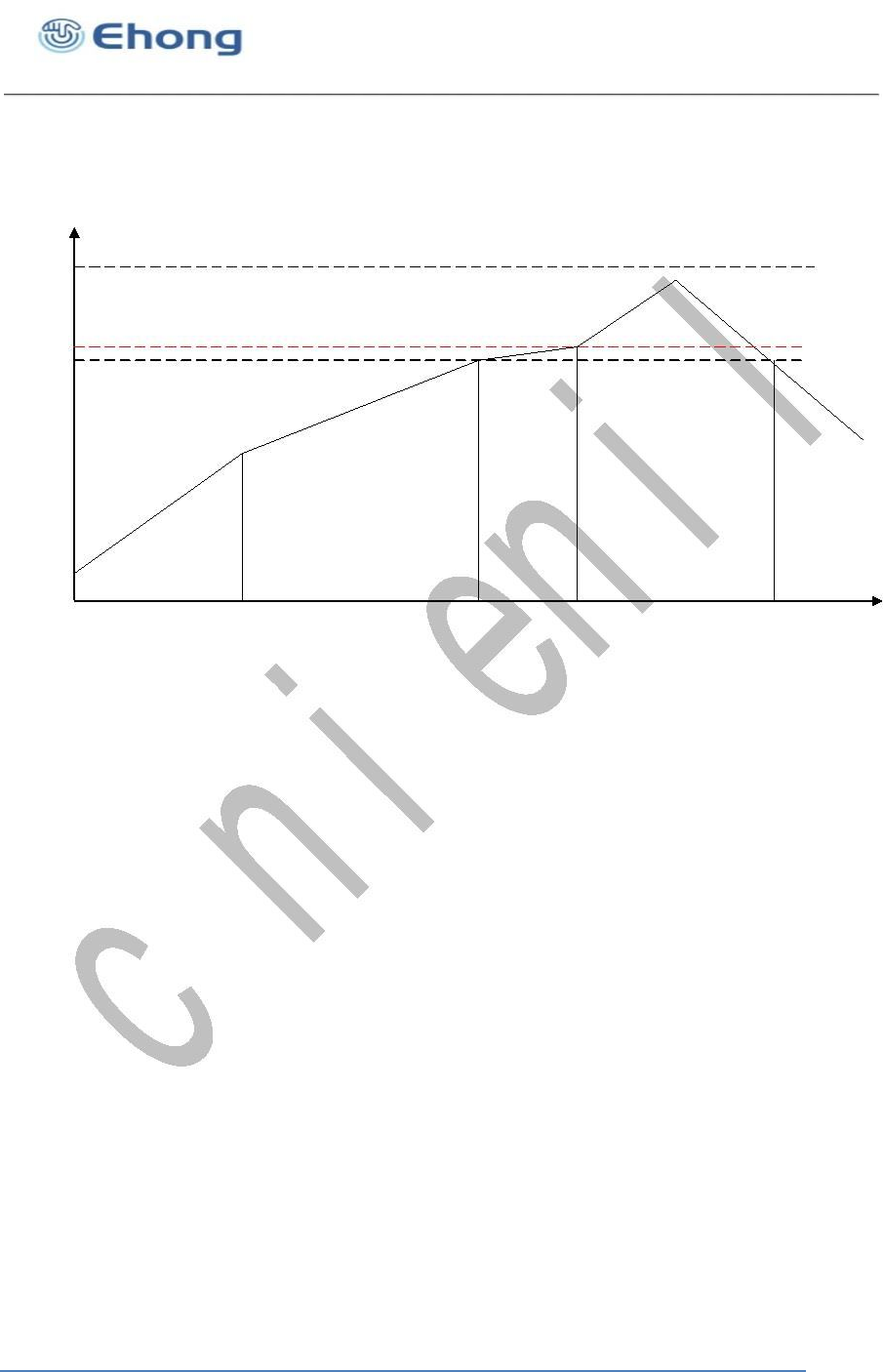
10. Reflow Profile
The soldering profile depends on various parameters necessitating a set up for each application.
The data here is given only for guidance on solder refl
ow.
℃
250
217
210
A
B
C
D
E
25
0 1 2 3 4 5 6 min
Figure 22: Recommended Reflow Profile
Pre
-
heat zone (A)
—
This zone raises the temperature at a controlled rate,
typically 0.5
–
2
C/s. The purpose of this zone is to preheat the PCB board and components to 120 ~ 150 C.
This stage is required to distribute the heat uniformly to the PCB board and completely remove
solvent to reduce the heat shock to components.
Equilibrium Zone 1 (
B)
—
In this stage the flux becomes soft and uniformly encapsulates
solder particles and spread over PCB board, preventing them from being re-oxidized. Also with
elevation of temperature and liquefaction of flux, each activator and rosin get activated and start
eliminating oxide film formed on the surface of each solder particle and PCB board. The
temperature is recommended to be 150to 210for 60 to 120 second for this zone.
Equilibrium Zone 2 (c) (optional)
—
In
order to resolve the upright component issue, it is
recommended to keep the temperature in 210 – 217 for about 20 to 30 second.
Reflow Zone (D)
—
The profile in the figure is designed for Sn/Ag3.0/Cu0.5. It can be a
reference for other lead-free solder. The peak temperature should be high enough to achieve
good wetting but not so high as to cause component discoloration or damage. Excessive
soldering time can lead to intermetallic growth which can result in a brittle joint. The
recommended peak temperature (Tp) is 230 ~ 250 C. The soldering time should be 30 to 90
second when the temperature is above 217 C.
Cooling Zone (E)
—
The cooling ate should be fast, to keep t
he solder grains small which will
give a longerlasting joint. Typical cooling rate should be 4 C.
Shanghai Ehong Technologies Inc

Bluetooth Audio Module
11. Contact Information
Sales: sales@ehlink.com.cn
Technical support: support@ehlink.com.cn
Phone: +86 21 64769993
Fax: +86 21 64765833
Street address: Rom1505, Blk 1st ,No.833 South Hong mei Rd ,Ming hang district shanghai
Note: FCC RF exposure requirements
1. Radiated transmit power must be equal to or lower than that specified in the FCC Grant of
Equipment Authorization for FCC ID:2ACCRMB05.
2. To comply with FCC regulations limiting both maximum RF output power and human
exposure to RF radiation, maximum antenna gain (including cable loss) must not exceed: .
Bluetooth <4.0 dBi
3. This device complies with part 15 of the FCC Rules. Operation is subject to the following two
conditions:
(1) This device may not cause harmful interference, and (2) this device must accept any
interference received,including interference that may cause undesired operation.
4.The host end product must include a user manual that clearly defines operating requirements
and conditions that must be observed to ensure compliance with current FCC RF exposure
guidelines.
Ehong Technology Co., Ltd

Bluetooth Audio Module
For portable devices, in addition to the conditions described above, a separate approval is
required to satisfy the SAR requirements of FCC Part 2.1093
If the device is used for other equipment that separate approval is required for all other
operating configurations, including portable configurations with respect to 2.1093 and different
antenna configurations.
For thi
s device, OEM integrators must be provided with labeling instructions of finished
products.Please refer to KDB784748 D01 v07, section 8. Page 6/7 last two paragraphs:
A certified modular has the option to use a permanently affixed label, or an electr
onic label. For
a permanently affixed label, the module must be labelled with an FCC ID - Section 2.926 (see
2.2 Certification (labelling requirements) above). The OEM manual must provide clear
instructions explaining to the OEM the labelling requirements,options and OEM user manual
instructions that are required (see next paragraph).
For a host using a certified modular with a standard fixed label, if (1) the module’s FCC ID is not
visible when installed in the host, or (2) if the host is marketed so that end users do not have
straight forward commonly used methods for access to remove the module so that the FCC ID
of the module is visible; then an additional permanent label referring to the enclosed
module:“Contains Transmitter Module FCC ID: 2ACCRMB05” or “Contains FCC ID:
2ACCRMB05” must be used. The host OEM user manual must also contain clear instructions
on how end users can find and/or access the module and the FCC ID.
The final host / module combination may also need to be e
valuated against the FCC Part 15B
criteria for unintentional radiators in order to be properly authorized for operation as a Part 15
digital device.
The users manual or instruction manual for an intentional or unintentional radiator shall caution
the user that changes or modifications not expressly approved by the party responsible for
compliance could void the user's authority to operate the equipment. In cases where the manual
is provided only in a form other than paper, such as on a computer disk or over the Internet, the
information required by this section may be included in the manual in that alternative form,
provided the user can reasonably be expected to have the capability to access information in
that form.
This device complies
with part 15 of the FCC Rules. Operation is subject to the following two
conditions: (1) This device may not cause harmful interference, and (2) this device must accept
any interference received, including interference that may cause undesired operati
on.
This equipment has been tested and found to comply with the limits for a Class B digital device,
pursuant to part 15 of the FCC Rules. These limits are designed to provide reasonable
protection against harmful interference in a residential installation. This equipment generates,
uses and can radiate radio frequency energy and, if not installed and used in accordance with
the instructions, may cause harmful interference to radio communications. However, there is no
guarantee that interference will not occur in a particular installation. If this equipment does
cause harmful interference to radio or television reception, which can be determined by turning
the equipment off and on, the user is encouraged to try to correct the interference by one or
more of the following measures:
Ehong Technology Co., Ltd

Bluetooth Audio Module
—Reorient or relocate the receiving antenna.
—Increase the separation between the equipment and receiver.
—Connect the equipment into an outlet on a circuit different from that to which the receiver is
connected.
—Consult the dealer or an experienced radio/TV technician for help.
In accordance with FCC Part 15C, this module is listed as a Limited Modular Transmitter device.
Therefore, the final host product must be submitted to [ShangHai Ehong Technology Co.,Ltd.] for confirmation
that the installation of the module into the host is in compliance with the regulations of FCC and IC Canada.
Specifically, if an antenna other than the model documented in the Filing is used, a Class 2 Permissive Change
must be filed with the FCC. Changes or modifications not expressly approved by the manufacturer could
void the user’s authority to operate the equipment.
Ehong Technology Co., Ltd