Ehong Technology MB05 Bluetooth Module User Manual EH MB05 Datasheet V2 0x
ShangHai Ehong Technology Co.,Ltd. Bluetooth Module EH MB05 Datasheet V2 0x
Contents
- 1. Users Manual
- 2. User Manual
User Manual
Ehong
T
FCC ID
T
echnology C
o
:2ACCRM
B
o
., Ltd
B
05
Blu
e
e
tooth
®
•
Blu
-
F
-
C
-
1
2
-
R
-
M
c
o
•
Su
p
-
S
-
i
A
-
H
•
Us
e
-
S
-
F
-
W
s
p
-
P
-
I
2
•
Au
d
-
1
6
-
6
4
-
S
•
Ge
n
-
1
-
2
-
•
-
•
-
•
2
-
•
t
o
-
•
®
Techn
o
etooth rad
i
ully embed
d
C
lass2 mod
u
2
8-bit encr
y
R
ange up to
M
ultipoint c
a
o
nnected a
t
p
port profil
e
PP (Master
A
P (ipod ac
c
FP ,A2DP,
A
e
r interface
S
end
A
T co
m
irmware up
g
W
ith SPP se
r
p
eed (UAR
T
CM interfa
c
2
C interfac
e
d
io codec
6
bit internal
4
MIPS Kali
m
upport Apt-
X
n
eral
I/O
1 general p
u
analogue I
/
FCC and
Single v
o
Small fo
r
.2mm
Operatin
o
85 °C
The op
e
E
H
o
logy
A
i
o
d
ed Bluetoo
t
u
le
y
ption securi
t
15m
a
pability(7 t
r
t
the same
e
s
and slave)
c
essory prot
o
A
VRCP,HID
m
mand ove
r
g
rade over
U
r
vice active
:
T
)
c
e (I2S,SPD
e
(Master )
stereo cod
e
m
ba DSP c
o
X
,AAC, Ap
t
u
rpose I/Os
/
O
Bluetoot
h
o
ltage su
p
r
m factor:
g temper
a
e
ration di
s
V
J
H
-MB0
5
A
udio
M
o
t
h® v3.0+E
D
ty
r
ansmit dat
a
time)
o
col)
(Salve)
r UART
U
SB
:
560kbps t
r
IF)
e
c :95dB S
N
o
processor
t
-XLL,SBC
c
h
® qualifi
e
p
ply: 3.3V
23.24 x 1
1
a
ture ran
g
s
tance >2
0
V
ersion 2.0
J
uly 21 201
4
5
o
dule
D
R
a
devices
ansmission
N
R for DAC
c
odec
e
d
typical
1
.93 x
g
e: -40 °C
0
cm
4

E
hon
g
T
1.
C
1.
De
s
2.
Ap
p
3.
EH
-
4.
Ele
c
4.1.
4.2.
4.3.
4.4.
4.4
.
4.5.
4.5
.
4.5
.
5.
Pin
5.1.
6.
Ph
y
6.1.
6.2.
6.3.
6.4.
6.5.
6.6.
6.6
.
6.7.
6.7
.
6.7
.
6.7
.
6.8.
6.9.
6.10.
7.
EH
-
8.
Me
c
9.
RF
9.1.
T
echnolo
gy
C
o
C
onte
s
cription .....
p
lication .....
-
MB05 Prod
c
trical Cha
r
Recomme
n
A
bsolute
M
Power con
s
Input/outp
u
.
1.
Digital
USB ...........
.
1.
Intern
a
.
2.
Intern
a
out and Te
r
Pin assign
m
y
sical Interf
a
Power Sup
p
Reset .........
PIO ............
AIO ............
UART ........
I2C Maste
r
.
1.
A
pple
i
Digital Aud
i
.
1.
PCM ..
.
2.
Digital
.
3.
IEC 6
0
Microphon
e
A
nalog Ou
t
USB .......
-
MB05 Refe
r
c
hanical an
d
La
y
out Gui
d
Feed Line
a
o
., Ltd
nts
.....................
.
.....................
.
uct numbe
r
r
acteristic ...
.
n
d operation
M
aximum Ra
t
s
umptions ...
.
u
t Terminal
C
Terminals ...
.
.....................
.
a
l CODEC A
n
a
l CODEC D
i
r
minal Desc
m
ent .............
.
a
ces ............
.
p
l
y
................
.
.....................
.
.....................
.
.....................
.
.....................
.
r
.....................
.
i
OS CP refe
r
i
o Interface
s
.....................
.
Audio Interf
a
0
958 Interfa
c
e
input ..........
.
t
put stage ....
.
.....................
.
r
ence Desi
g
d
PCB Foot
d
elines .......
.
a
nd Antenn
a
.
....................
.
.
....................
.
r
in
g
..............
.
.
....................
.
condition
s
...
t
in
g
................
.
.....................
C
haracteristi
c
.
....................
.
.
.....................
n
alogue to
D
i
gital to Anal
ription ........
.
.
.....................
.
....................
.
.
.....................
.
.....................
.
.....................
.
.....................
.
.....................
.
.....................
r
ence desig
n
.....................
.
....................
.
a
ce (I2S) .....
.
c
e (SPDIF) ..
.
.
.....................
.
.....................
.
.....................
g
n .................
.
print Chara
c
.
....................
.
a
.....................
.
.....................
.
.....................
.
.....................
.
.....................
.....................
.....................
.....................
c
s ..................
.
.....................
.....................
D
igital Conve
ogue Conve
.
.....................
.....................
.
.....................
.....................
.....................
.....................
.....................
.....................
.....................
n
....................
.....................
.
.....................
.
.....................
.
.....................
.....................
.....................
.....................
.
.....................
c
teristics ....
.
.....................
.....................
.....................
.
.....................
.
.....................
.
.....................
.
.....................
.
.....................
.
.....................
.
.....................
.
.....................
.
.....................
.
rte
r
...............
.
rte
r
..............
.
.....................
.
.....................
.
.....................
.
.....................
.
.....................
.
.....................
.
.....................
.
.....................
.
.....................
.
.....................
.
.....................
.
.....................
.
.....................
.
.....................
.
.....................
.
.....................
.
.....................
.
.....................
.
.....................
.
.....................
.
.....................
.
B
.
....................
.
.
....................
.
.
....................
.
.
....................
.
.
.....................
.
.....................
.
.....................
.
.....................
.
....................
.
.
.....................
.
....................
.
.
....................
.
.
....................
.
.
.....................
.
....................
.
.
.....................
.
.....................
.
.....................
.
.....................
.
.....................
.
.....................
.
....................
.
.
.....................
.
....................
.
.
....................
.
.
....................
.
.
.....................
.
.....................
.
.....................
.
....................
.
.
....................
.
.
....................
.
.
.....................
B
luetooth Au
d
.
.....................
.
.....................
.
.....................
.
.....................
.....................
.....................
.....................
.....................
.
.....................
.....................
.
.....................
.
.....................
.
.....................
.....................
.
.....................
.....................
.....................
.....................
.....................
.....................
.....................
.
.....................
.....................
.
.....................
.
.....................
.
.....................
.....................
.....................
.....................
.
.....................
.
.....................
.
.....................
.....................
d
io Module
....................
4
....................
4
....................
4
....................
5
....................
5
....................
5
....................
5
....................
6
....................
6
....................
6
....................
7
....................
8
....................
9
....................
9
.................. 1
1
.................. 1
1
.................. 1
2
.................. 1
2
.................. 1
2
.................. 1
3
.................. 1
3
.................. 1
4
.................. 1
5
.................. 1
6
.................. 1
6
.................. 1
9
.................. 2
0
.................. 2
0
.................. 2
1
.................. 2
2
.................. 2
3
.................. 2
3
.................. 2
4
4
4
4
5
5
5
5
6
6
6
7
8
9
9
1
1
2
2
2
3
3
4
5
6
6
9
0
0
1
2
3
3
4

E
hon
g
T
9.2.
10.
R
2.
T
T
ABLE
1
:
T
ABLE
2
:
T
ABLE
3
:
T
ABLE
4
:
T
ABLE
5
:
T
ABLE
6
:
T
ABLE
7
:
T
ABLE
8
:
T
ABLE
9
:
T
ABLE
1
0
T
ABLE
1
1
T
ABLE
1
2
T
ABLE
1
3
T
ABLE
1
4
3.
T
F
IGURE
1
F
IGURE
2
F
IGURE
3
F
IGURE
4
F
IGURE
5
F
IGURE
6
F
IGURE
7
F
IGURE
8
F
IGURE
9
F
IGURE
1
F
IGURE
1
F
IGURE
1
F
IGURE
1
F
IGURE
1
F
IGURE
1
F
IGURE
1
F
IGURE
1
F
IGURE
1
F
IGURE
1
F
IGURE
2
F
IGURE
2
T
echnolo
gy
C
o
Matching n
R
eflow Profi
l
T
able
:
R
ECOMMEN
D
:
A
BSOLUTE
M
:
P
OWER CO
N
:
D
IGITAL
T
E
R
:
USB
T
ERMI
N
:
A
NALOGUE
T
:
D
IGITAL TO
A
:
PIN
T
ERMI
N
:
P
IN
S
TATUS
0
:
P
OSSIBLE
U
1
:
A
LTERNAT
I
2
:
D
IGITAL
A
U
3
:
D
IGITAL
A
U
4
:
USB
I
NTE
R
T
able
1
:
P
INOUT
O
2
:
P
OWER
S
3
:
C
ONNECTI
O
4
:
E
XAMPLE
E
5
:
A
PPLE
C
O
-
6
:
A
PPLE
C
O
-
7
:
A
UDIO
I
NT
E
8
:
D
IGITAL
A
U
9
:
D
IGITAL
A
U
1
0:
D
IGITAL
A
1
1:
E
XAMPLE
1
2:
E
XAMPLE
1
3:
M
ICROPH
1
4:
S
PEAKER
1
5:
USB
C
O
N
1
6:
R
EFEREN
1
7:
R
ECOMM
E
1
8:
C
LEARAN
1
9:
A
NTENN
A
2
0:
PI
MATCH
2
1:
R
ECOMM
E
o
., Ltd
etwork in fr
e
l
e
..................
.
of Ta
D
ED
O
PERAT
I
M
AXIMUM
R
A
T
N
SUMPTIONS
.
.
R
MINAL
..........
.
N
AL
...............
.
T
O
D
IGITAL
C
A
NALOGUE
C
N
AL
D
ESCRIP
T
ON
R
ESET
...
.
U
ART
S
ETTI
N
I
VE
F
UNCTIO
N
U
DIO
I
NTERF
A
U
DIO
I
NTERF
A
R
FACE
C
OMP
O
of Fi
g
O
F
EH-MB05
.
S
UPPLY
PCB
O
N
T
O
H
OST
D
E
EPROM
C
O
-
PROCESSOR
-
PROCESSOR
E
RFACE
.........
.
U
DIO
I
NTERFA
C
U
DIO
I
NTERFA
C
A
UDIO
I
NTERF
A
C
IRCUIT FO
R
C
IRCUIT FO
R
ONE
B
IASING
OUTPUT
.......
.
N
NECTIONS
...
.
CE
D
ESIGN
..
.
E
NDED
PCB
M
CE AREA OF
A
A
REFERENCE
NETWORK E
X
E
NDED
R
EFL
O
e
e space
.......
.
....................
.
bles
I
NG
C
ONDITI
O
T
ING
R
ECOM
M
.
....................
.
.
....................
.
.
....................
.
ONVERTER
...
.
ONVERTER
...
.
T
ION
..............
.
.
....................
.
N
GS
..............
.
N
S OF THE
D
I
G
A
CE
S
LAVE
T
I
A
CE
M
ASTER
T
O
NENT
V
ALU
E
g
ures
.
....................
.
D
ESIGN
.......
.
D
EVICE
.........
.
O
NNECTION W
2.0C
............
.
2.0B
............
.
.
....................
.
C
E
M
ODES
...
.
C
E
S
LAVE
T
I
M
A
CE
M
ASTER
R
SPDIF
I
NTE
R
SPDIF
I
NTE
(S
INGLE
C
H
A
.
....................
.
.
....................
.
.
....................
.
M
OUNTING
P
A
A
NTENNA
......
.
DESIGN
........
.
X
AMPLE
........
.
O
W
P
ROFILE
.
.
.....................
.
.....................
O
NS
................
M
ENDED
O
PE
R
.
.....................
.
.....................
.
.....................
.
.....................
.
.....................
.
.....................
.
.....................
.
.....................
G
ITAL
A
UDIO
B
MING
.............
T
IMING
..........
E
S
..................
.
.....................
.
.....................
.
.....................
ITH
I2C
I
NTE
R
.
.....................
.
.....................
.
.....................
.
.....................
M
ING
..............
T
IMING
........
RFACE
(C
O
-
A
RFACE
(O
PTI
C
A
NNEL
S
HOW
N
.
.....................
.
.....................
.
.....................
A
TTERN
(U
NI
T
.
.....................
.
.....................
.
.....................
.
.....................
.....................
.
.....................
.
.....................
.
R
ATING
C
ON
D
.....................
.
.....................
.
.....................
.
.....................
.
.....................
.
.....................
.
.....................
.
.....................
.
B
US
I
NTERFA
C
.....................
.
.....................
.
.....................
.
.....................
.
.....................
.
.....................
.
R
FACE
...........
.
.....................
.
.....................
.
.....................
.
.....................
.
.....................
.
.....................
.
A
XIAL
)
...........
.
C
AL
)
.............
.
N
)
.................
.
.....................
.
.....................
.
.....................
.
T
:
MM
,
D
EVIA
T
.....................
.
.....................
.
.....................
.
.....................
.
B
.
.....................
.
....................
.
.
....................
.
D
ITIONS
.........
.
.
....................
.
.
....................
.
.
....................
.
.
....................
.
.
....................
.
.
....................
.
.
....................
.
.
....................
.
C
E ON THE
P
C
.
....................
.
.
....................
.
.
....................
.
.
....................
.
.
....................
.
.
....................
.
.
....................
.
.
....................
.
.
....................
.
.
....................
.
.
....................
.
.
....................
.
.
....................
.
.
....................
.
.
....................
.
.
....................
.
.
....................
.
.
....................
.
.
....................
.
T
ION
:0.02
MM
)
.
....................
.
.
....................
.
.
....................
.
.
....................
.
B
luetooth Au
d
.....................
.
.....................
.
.....................
.
.....................
.
.....................
.
.....................
.
.....................
.
.....................
.
.....................
.
.....................
.
.....................
.
.....................
C
M
I
NTERFA
C
.
.....................
.
.....................
.
.....................
.
.....................
.
.....................
.
.....................
.
.....................
.
.....................
.
.....................
.
.....................
.
.....................
.
.....................
.
.....................
.
.....................
.
.....................
.
.....................
.
.....................
.
.....................
.
.....................
)
TOP
V
IEW
...
.
.....................
.
.....................
.
.....................
.
.....................
d
io Module
.................. 2
5
.................. 2
6
....................
5
....................
5
....................
6
....................
6
....................
7
....................
7
....................
8
.................. 1
1
.................. 1
2
.................. 1
3
C
E
............... 1
6
.................. 1
8
.................. 1
8
.................. 2
1
....................
9
.................. 1
1
.................. 1
3
.................. 1
4
.................. 1
4
.................. 1
5
.................. 1
5
.................. 1
7
.................. 1
8
.................. 1
9
.................. 1
9
.................. 2
0
.................. 2
0
.................. 2
1
.................. 2
1
.................. 2
2
.................. 2
3
.................. 2
4
.................. 2
5
.................. 2
5
.................. 2
6
5
6
5
5
6
6
7
7
8
1
2
3
6
8
8
1
9
1
3
4
4
5
5
7
8
9
9
0
0
1
1
2
3
4
5
5
6

E
hon
g
T
1. D
e
The E
H
modul
e
The E
H
experi
e
certifie
d
The m
o
UART
a
up to 6
0
The m
o
antenn
a
Support
over Bl
u
Custo
m
Apple
c
http://d
e
Certifie
d
iPhone
®
technic
Custo
m
proprie
t
2. A
p
•
Hom
•
Serv
i
•
Offic
e
•
Com
•
Mul
t
•
A
uto
m
•
Hum
3. E
H
E
H
A. E
H
B. M
T
echnolo
gy
C
o
e
scripti
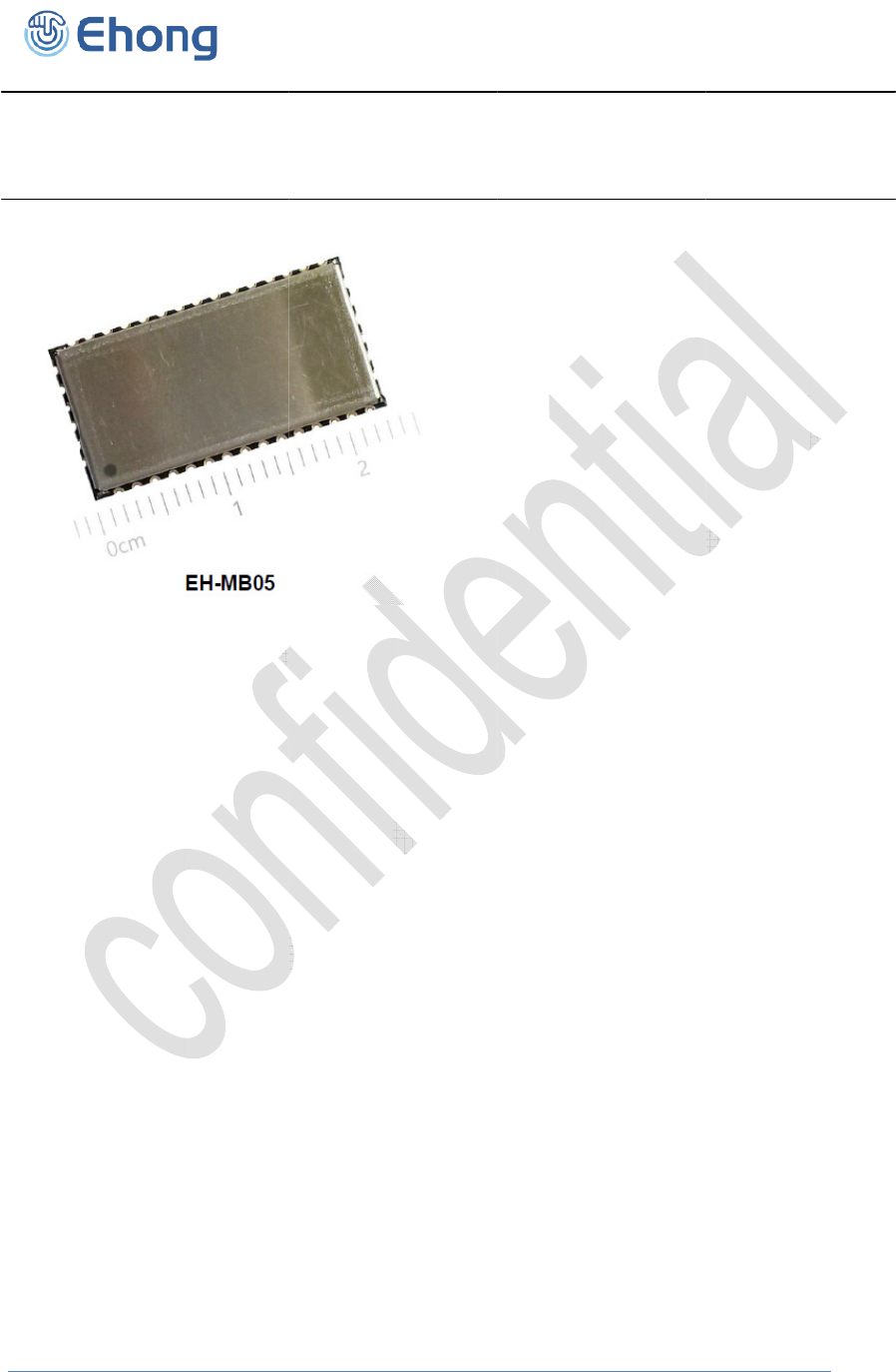
o
H
-MB05 is
a
e
provides
c
H
-MB05 en
a
e
nce or exp
e
d
solution,
o
o
dule is des
a
nd 11gen
e
0
0 kbps tra
n
o
dule is ext
e
a
shall be
5
differen
t
Blu
u
etooth usi
n
m
ers using t
h
c
ertified MF
e
veloper.a
p
d
MFI deve
®
, and iPa
d
al support
a
m
ized firmw
a
t
ary feature
p
plicati
o
e entertain
m
i
ce diagno
s
e
and mob
i
mercial
t
imedia spe
a
m
otive
an interfac
e
H
-MB05
P
H
-M
B
H
-------
-
B05 ------
-
o
., Ltd
o
n
a
n easy to
u
c
omplete R
F
a
bles electr
o
e
rtise for in
t
o
ptimizes th
igned for
m
e
ral purpos
e
n
smission
s
e
rnal anten
5
0.Embed
d
etooth prof
i
n
g apple’s
a
h
e Apple a
u
I member.
L
p
ple.com/pr
o
lopers dev
e
d
® can gai
n
a
nd certific
a
a
re for peri
p
s may be s
u
o
n
m
ent
s
tics
i
le accesso
a
ke
r
e
devices
P
roduc
t
B
05
X
-
----- Co
m
-
----- Mo
d
u
se Blueto
o
F
platform i
o
nic device
s
t
egration in
t
e time to
m
m
aximum p
e
e
I/O lines,
1
s
peed with
S
na, the im
p
d
ed Blueto
o
i
les, such a
a
uthenticati
u
thenticati
o
L
icense fee
s
o
grams/wh
e
loping ele
c
n
access to
a
tion logos.
p
heral devi
c
u
pported a
n
ries
t
numb
e
X
m
pany Na
m
d
ule Nam
e
o
th module,
n a small f
o
s
with wirel
e
t
o the final
p
m
arket of th
e
e
rformance
i
1
analogue I
/
S
PP servic
e
p
edance of
t
o
th AT com
m
s SPP, A2
D
on coproc
e
o
n IC must r
s
may appl
y
ich-progra
m
c
tronic acc
e
technical d
o
c
e interacti
o
n
d can be o
e
ring
m
e(Ehong
)
e
compliant
w
o
rm factor.
e
ss connec
t
p
roduct. Th
e
final appli
c
i
n a minim
a
/
O lines, sev
e
e
active, 20
t
he feed lin
e
m
and firm
w
D
P, AVRC
P
e
ssor.
egister as
d
y
, for additi
o
m
/index.ht
m
e
ssories tha
o
cumentati
o
o
n, power o
rdered pre
-
)
B
w
ith Blueto
o
t
ivity, not re
e EH-MB0
5
c
ation.
a
l space inc
l
e
ral serial i
n
0 kbps with
e
between
t
w
are is a fri
e
P
, HFP, HI
D
d
evelopers,
o
nal inform
a
m
l.
t connect t
o
o
n, hardwa
r
ptimization
,
loaded and
B
luetooth Au
d
o
th v3.0+E
D
quiring an
y
5
module, b
l
uding fast
s
n
terface op
t
h
iAP servic
e
t
he RF port
e
ndly interfa
D
, iAP and
e
to become
a
tion visit:
o
an iPod®,
r
e compon
e
,
security, a
configure
d
d
io Module
D
R. The
y
RF
eing a
s
peed
t
ions, and
e
active.
and the
ce,
e
tc. iAP
an
e
nts,
nd other
d
.
E
hon
g
T
4. El
e
4.1.
Ope
Stor
a
Ope
r
PIO
V
A
IO
V
VDD
RF f
r
4.2.
4.3.
Rati
Stor
a
Ope
r
PIO
V
A
IO
V
VDD
USB
_
Oth
e
Ope
Stan
d
Stan
d
Inqui
Con
n
disa
b
Con
n
sniff(
a
Con
n
Con
n
stre
a
T
echnolo
gy
C
o
e
ctrical
Recom
m
rating Co
n
a
ge Tempe
r
r
ating Tem
p
V
oltage
V
oltage
Voltage
r
equency
Absolut
e
Table
Power
c
ng
a
ge Tempe
r
ating Tem
p
V
oltage
V
oltage
Voltage
_
DP/USB_
e
r Terminal
V
rating Co
n
d
by, withou
t
d
by, with d
e
ry window
t
n
ected (De
b
le, sniff(a)
e
n
ected (De
e
a
) enable)
n
ected with
n
ected with
a
ming (A2D
o
., Ltd
Charac
t
m
end op
e
n
dition
r
ature
p
erature R
a
Tab
e
Maxim
2: Absolut
e
c
onsum
p
rature
p
erature
DN Voltag
e
V
oltages e
x
n
dition
t
deep slee
p
e
ep sleep
t
ime (b)
ep sleep
e
nable )
e
p sleep on
data trans
f
audio
P)
t
eristic
e
ration
c
a
nge
le 1: Reco
m
um Rati
n
e
Maximum
p
tions
e
x
cept RF
Mi
n
p
2.1
0.1
1
-
-
,
-
f
e
r
18
c
onditio
n
m
mended O
p
n
g
Ratin
g
Rec
o
n
Ty
p
1
3
0
2
3
n
s
Min
-40
-40
+1.7
+1.42
+2.7
2400
p
eratin
g
Co
o
mmended
p
ical
-
-
-
3
.3
0
.4
2
0
3
5
B
Typic
a
--
--
+3.3
+1.5
+3.3
2441
nditions
Operatin
g
C
Min
-40
-40
-0.4
-0.4
-0.4
-0.4
-0.4
Max
3.1
0.7
40
-
-
22
40
B
luetooth Au
d
a
l Ma
x
+10
5
+8
5
+3.
6
+1.
5
+3.
6
248
0
C
onditions
Ma
x
+12
5
+8
5
+3.
6
+1.
5
+3.
6
+3.
6
VDD
+
4
d
io Module
x
Uni
t
5
°C
5
°C
6
V
5
7 V
6
V
0
0 MH
z
x
Uni
t
5
°C
5
°C
6
V
5
7 V
6
V
6
V
+
0. V
Unit
mA
mA
mA
mA
mA
mA
mA
t
z
t
E
hon
g
T
Note :
Power
c
(a)
Sniff
m
slave is
unless t
h
time slo
t
time slo
t
(b)
Radio
4.4.
4.4.1.
Supp
l
Input
V
VIL inp
u
VIH inp
Outpu
VOL ou
t
VOH ou
Input
a
Ii input
Ioz tri-s
t
or 0V
With s
t
With s
t
With
w
With
w
CI Inp
u
Resis
t
Rpuw w
e
Rpdw w
e
Rpus st
r
Rpds st
r
4.5.
USB
T
Input
T
T
echnolo
gy
C
o
c
onsumption
m
ode ----- In
in active mo
h
at link is b
e
t
s when a sl
a
t
s. The sniff
a
on(Inquiry )
-
Input/o
u
Digital T
e
l
y Voltag
e
V
oltage Le
v
u
t logic lev
e
ut logic lev
e
t Voltage
L
t
put logic l
e
tput logic l
e
a
nd Tri-sta
leakage c
u
t
ate output
t
rong pull-u
t
rong pull-d
o
w
eak pull-u
p
w
eak pull-d
o
u
t Capacita
n
t
ive Streng
e
ak pull-up
e
ak pull-do
w
r
ong pull-u
p
r
ong pull-d
o
USB
T
erminal
s
T
hreshold
o
., Ltd
depends on
Sniff mode,
t
de on an A
C
e
ing treated
a
a
ve is listeni
n
a
nchor poin
t
-
---Search ti
m
u
tput Te
r
e
rminals
e
Levels
v
els
e
l low
e
l high
L
evels
e
vel low, lOL
e
vel high, l
O
te Current
u
rrent at Vin
=
leakage cu
p
o
wn
p
o
wn
n
ce
th
strength a
t
w
n strengt
h
p
strength
a
o
wn strengt
s
the firmwar
e
t
he duty cyc
l
C
L logical tra
a
s a scatter
n
n
g are redu
c
t
s are space
d
m
e is 22 sec
o
r
minal C
h
= 4.0mA
O
H = -4.0m
A
=
VDD or 0
V
rrent at Vo
=
t
VDD-0.2V
h
at 0.2V
a
t VDD-0.2
V
h at 0.2V
Tabl
e
used. Typi
c
l
e of the sla
v
nsport, it sh
a
n
et link or is
c
ed, so the
m
d
regularly
w
o
nds
h
aracter
i
0.
6
0.
7
V
=
VDD
V
e 4: Di
g
ital
T
Table 3: P
o
c
al values a
r
v
e’s activity i
n
a
ll listen in e
v
absent due
t
m
aster shall
o
w
ith an interv
i
stics
Min
-0.3
6
25VDD
-
7
5xVDD
-100
-100
-100
10
-5
-0.2
1.0
500k
500k
10k
10k
T
erminal
Min
o
wer consu
m
B
r
e shown in
t
n
the picone
t
v
ery ACL sl
o
t
o hold mod
e
o
nly transmit
al o
f
Tsniff.
Typ
-
-
-
-
0
0
-40
40
-1.0
+1.0
-
-
-
-
-
Typical
m
ptions
B
luetooth Au
d
t
he table.
t
may be re
d
o
t to the mas
e
. With sniff
m
to a slave i
n
Max
+0.25xVD
D
VDD+0.
3
0.125
VDD
100
100
-10
100
-0.2
5.0
5.0
2M
2M
50k
50k
Max
d
io Module
d
uced. If a
ter traffic,
m
ode, the
n
specified
Unit
D
V
3
V
V
V
nA
nA
uA
A
A
A
pF
Uni
t
t
E
hon
g
T
VIL in
p
VIH in
p
Input
GND
<
CI Inp
u
Outp
u
VOL o
u
VOH o
u
(a)
Int
e
4.5.1.
Pa
r
Resol
u
Input
S
Signal
Ratio,
Digital
A
nalo
g
Input
f
Input
f
3dB B
Micro
p
THD+
T
echnolo
gy
C
o
p
ut logic lev
e
p
ut logic lev
Leakage
C
<
VIN < VD
u
t capacita
n
u
t Voltage
L
t
put logic l
e
ut
put logic l
e
e
rnal USB
Internal
C
r
ameter
u
tion
S
ample Ra
t
to Noise
SNR
Gain
g
ue Gain
f
ull scale at
f
ull scale at
andwidth
p
hone mod
e
N
(microph
o
o
., Ltd
e
l low
el high
C
urrent
D(a)
n
ce
L
evels to
C
e
vel low
e
vel high
pull-up di
s
C
ODEC A
n
t
e, Fsample
fin=1kHz
B/W=20
H
A-Weigh
t
THD+N
<
150mV
V
Digital G
a
A
nalogu
e
maximum
g
minimum
g
e
input imp
e
o
ne input)
@
C
orrectly T
e
Ta
b
s
able
n
alogue t
o
Conditi
o
H
z->20kHz
t
ed
<
1%
V
pk-pk
a
in Resolu
t
e
Gain Res
o
g
ain (differ
e
g
ain (differe
e
dance
@
30mv rm
Table 6: An
e
rminated
b
le 5: USB
T
o
Digital
C
o
ns
Fsampl
e
8kHz
11.025k
H
16kH
z
22.050k
H
32kH
z
44.1kH
t
ion = 1/32
d
o
lution = 3
d
e
ntial)
ntial)
s input
alo
g
ue to
D
-
0.7VDD
-1
2.5
USB Cabl
e
0.0
2.8
T
erminal
C
onverter
Mi
n
-
8
e
-
H
z -
z
-
H
z -
z
-
z -
d
B -2
4
d
B -3
-
-
-
-
D
i
g
ital Conv
e
B
-
-
1
-
e
-
-
n
Typ
-
-
82
81
80
79
79
78
4
-
-
4
800
20
6
0.04
e
rter
B
luetooth Au
d
0.3VD
-
5
10.0
0.2
VDD
Max
16
44.1
-
-
-
-
-
-
21.5
42
-
-
-
-
d
io Module
D
V
V
A
pF
V
V
Unit
Bits
kHz
dB
dB
dB
mV
rms
mV
rms
kHz
k
%
E
hon
g
T
4.5.2.
Pa
r
Resol
u
Output
Signal
Ratio,
S
Digital
A
nalo
g
Output
A
llowe
d
THD+
N
THD+
N
SNR (
L
silenc
e
T
echnolo
gy
C
o
Internal
C
r
ameter
u
tion
Sample R
a
to Noise
S
NR
Gain
g
ue Gain
voltage ful
l
d
Load
N
100k lo
a
N
16 load
L
oad=16,
e
)
o
., Ltd
C
ODEC Di
g
a
te, Fsample
fin=1kH
z
B/W=20
A-Weig
h
THD+N
<
0dBFS
s
Load =
1
Digital
G
A
nalog
u
l
swing (dif
f
a
d
0dBFS inp
u
g
ital to A
n
Condit
i
z
Hz->20kH
z
h
ted
<
0.01%
s
ignal
1
00k
G
ain Resol
u
u
e Gain Re
s
f
erential)
u
t relative t
o
Table 7: Di
g
n
alogue C
i
ons
z
Fsampl
8kH
z
11.025
k
16kH
z
22.050
k
32kH
z
44.1k
H
48kH
z
u
tion = 1/32
s
olution = 3
Resistiv
e
Capaciti
v
o
digital
g
ital to Anal
onverte
r
Mi
-
8
e
z
-
k
Hz -
z -
k
Hz -
z -
H
z -
z -
dB -2
4
dB 0
-
e
1
6
v
e -
-
-
-
o
g
ue Conv
e
B
n Typ
-
-
95
95
95
95
95
95
95
4
-
-
750
6
-
-
-
-
95
e
rter
B
luetooth Au
d
Max
16
48
-
-
-
-
-
-
21.5
-21
-
OC
500
0.01
0.1
-
d
io Module
Unit
Bits
kHz
dB
dB
dB
mV
rms
pF
%
%
dB
E
hon
g
T
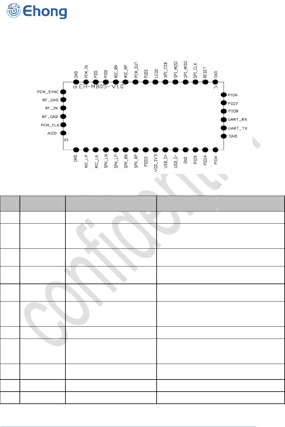
5. Pi
n
5.1.
Pin
1
2
3
4
5
6
7
8
9
10
11
T
echnolo
gy
C
o
n
out an
d
Pin assi
Symbol
GND
RESET
B
SPI_CL
K
SPI_MIS
O
SPI_MO
S
SPI_CS
B
LED0
PIO3
PCM_OU
T
MIC_RP
MIC_RN
o
., Ltd
d
Termi
n
gnment
l
Groun
d
B
CMO
S
intern
a
K
Input
w
down
O
CMO
S
weak i
S
I CMO
S
intern
a
B
Input
w
up
Open
d
Bi-dir
e
progr
a
intern
a
T
CMO
S
weak i
A
nalo
g
A
nalo
g
n
al Des
c
Figure
I/O Ty
p
d
S
input with
a
l pull-up
w
ith weak i
n
S
output, tri
-
nternal pull
S
input, with
a
l pull-dow
n
w
ith weak i
n
d
rain outpu
ctional wit
h
mmable st
r
a
l pull-up/d
o
S
output, tri
-
nternal pull
g
ue
g
ue
c
ription
1: Pinout
o
p
e
weak
n
ternal pull-
-
state, with
-down
weak
n
n
ternal pull-
t
h
r
ength
o
wn
-
state, with
-down
o
f EH-MB0
5
Ground
A
ctive L
O
so must
RESET
B
Serial P
e
program
Serial P
e
program
Serial P
e
program
Chip sel
e
Interfac
e
low
LED Dri
v
Progra
m
Synchro
n
Microph
o
Microph
o
B
5
Des
c
O
W RESE
T
be low for
>
B
e
ripheral in
t
ming only
e
ripheral In
t
ming only
e
ripheral In
t
ming only
e
ct for Syn
c
e
for progra
m
v
e
r
m
mable inp
u
n
ous Data
O
o
ne input p
o
o
ne input n
e
B
luetooth Au
d
c
ription
T
B, input d
e
>
5ms to ca
u
t
erface clo
c
t
erface out
p
t
erface inp
u
c
hronous S
e
m
ming onl
y
u
t/output lin
e
O
utput
o
sitive, righ
e
gative, rig
h
d
io Module
e
bounced
u
se a
c
k for
p
ut for
u
t for
e
rial
y
, active
e
t
h
t

E
hon
g
T
12
13
14
15
16
17
18
19
20
21
22
23
24
25
26
27
28
29
30
31
32
33
34
35
T
echnolo
gy
C
o
PIO0
PIO1
PCM_IN
GND
PCM_SY
N
RF_GN
D
RF_IN
RF_GN
D
PCM_CL
K
AIO0
GND
MIC_LP
MIC_LN
SPK_LN
SPK_LP
SPK_R
N
SPK_R
P
PIO13
VDD
USB_D
P
USB_D
N
GND
PIO9
PIO14
o
., Ltd
Bi-dir
e
progr
a
intern
a
Bi-dir
e
progr
a
intern
a
CMO
S
intern
a
Groun
d
N
C Bi-dir
e
intern
a
D
RF Gr
o
RF
D
RF Gr
o
K
Bi-dir
e
intern
a
Bi-dir
e
Groun
d
Analo
g
A
nalo
g
A
nalo
g
A
nalo
g
N
A
nalo
g
P
Analo
g
Bi-dir
e
progr
a
intern
a
3V3 p
o
P
Bi-dir
e
N
Bi-dir
e
Groun
d
Bi-dir
e
progr
a
intern
a
Bi-dir
e
progr
a
intern
a
ctional wit
h
mmable st
r
a
l pull-up/d
o
ctional wit
h
mmable st
r
a
l pull-up/d
o
S
Input, wit
h
a
l pull-dow
n
d
ctional wit
h
a
l pull-dow
n
o
und
o
und
ctional wit
h
a
l pull-dow
n
ctional
d
g
ue
g
ue
g
ue
g
ue
g
ue
g
ue
ctional wit
h
mmable st
r
a
l pull-up/d
o
o
wer input
ctional
ctional
d
ctional wit
h
mmable st
r
a
l pull-up/d
o
ctional wit
h
mmable st
r
a
l pull-up/d
o
h
r
ength
o
wn
h
r
ength
o
wn
h
weak
n
h
weak
n
h
weak
n
h
r
ength
o
wn
h
r
ength
o
wn
h
r
ength
o
wn
Progra
m
Progra
m
Synchro
n
Ground
Synchro
n
RF grou
n
RF Tran
s
RF grou
n
Synchro
n
A
nalogu
e
Ground
Microph
o
Microph
o
Speaker
Speaker
Speaker
Speaker
Progra
m
3V3 po
w
USB dat
a
1.5K pul
l
USB dat
a
Ground
Progra
m
Progra
m
B
m
mable inp
u
m
mable inp
u
n
ous Data
I
n
ous Data
S
n
d
s
ceiver inp
u
n
d
n
ous Data
C
e
program
m
o
ne input p
o
o
ne input n
e
output ne
g
output pos
output ne
g
output pos
m
mable inp
u
w
er input
a
plus with
l
up resisto
r
a
minus
m
mable inp
u
m
mable inp
u
B
luetooth Au
d
u
t/output lin
e
u
t/output lin
e
I
nput
S
ync
u
t/output lin
C
lock
m
able input
/
o
sitive, left
e
gative, rig
h
g
ative, left
itive, left
g
ative, right
itive, right
u
t/output lin
e
selectable
r
u
t/output lin
e
u
t/output lin
e
d
io Module
e
e
e
/
output line
h
t
e
internal
e
e
E
hon
g
T
36
37
38
39
40
41
42
6. P
h
6.1.
-
Th
e
-
Po
w
-
Ca
p
-
Ca
p
T
echnolo
gy
C
o
PIO4
GND
UART_T
X
UART_R
X
PIO8
PIO7
PIO6
h
ysical I
n
Power
S
e
module D
C
w
er supply
p
p
acitor dec
o
p
acito
r
pre
v
o
., Ltd
Bi-dir
e
progr
a
intern
a
Groun
d
X
Bi-dir
e
tri-stat
e
pull-u
p
X
CMO
S
intern
a
Bi-dir
e
progr
a
intern
a
Bi-dir
e
progr
a
intern
a
Bi-dir
e
progr
a
intern
a
n
terfac
e
S
upply
C
3.3V pow
e
p
in connec
t
o
uples pow
e
v
ents noise
.
ctional wit
h
mmable st
r
a
l pull-up/d
o
d
ctional CM
O
e
, with we
a
p
S
input with
a
l pull-dow
n
ctional wit
h
mmable st
r
a
l pull-up/d
o
ctional wit
h
mmable st
r
a
l pull-up/d
o
ctional wit
h
mmable st
r
a
l pull-up/d
o
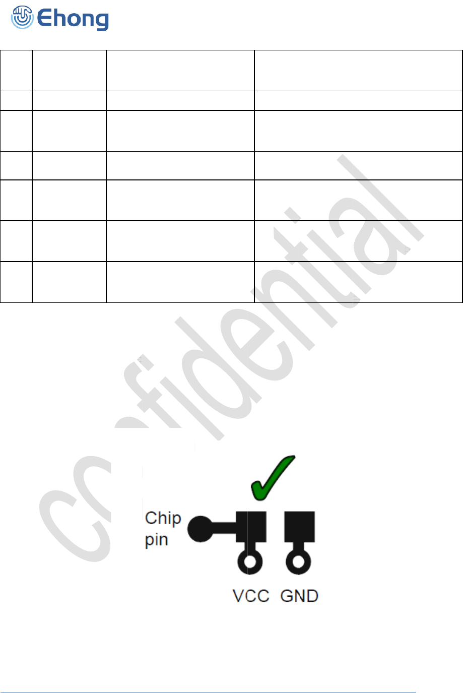
Table 8:
P
e
s
e
r input.
t
ion capacit
o
e
r to the ch
coupling b
a
Figure 2:
h
r
ength
o
wn
O
S output,
a
k internal
weak
n
h
r
ength
o
wn
h
r
ength
o
wn
h
r
ength
o
wn
P
IN Termin
a
o
r to chip a
ip
a
ck to pow
e
Power Sup
p
Progra
m
Ground
UART d
a
UART d
a
Progra
m
Progra
m
Progra
m
a
l Descripti
o
nd pin as f
a
e
r plane.
p
l
y
PCB De
s
B
m
mable inp
u
a
ta output
a
ta input
m
mable inp
u
m
mable inp
u
m
mable inp
u
o
n
a
r as possi
b
s
i
g
n
B
luetooth Au
d
u
t/output lin
e
u
t/output lin
e
u
t/output lin
e
u
t/output lin
e
b
le close
d
io Module
e
e
e
e

E
hon
g
T
6.2.
The m
o
charac
t
The R
E
freque
n
RESE
T
5ms.
A
t RES
The pu
l
6.3.
EH-MB
(3.3V).
throug
h
Note:
A
ll PIO
A
ny of
t
modes.
6.4.
EH-MB
functio
n
PIO.
T
echnolo
gy
C
o
Reset
o
dule may
b
t
er or via s
o
E
SETB pin i
n
cy clock o
s
T
B being ac
t
ETB the di
g
l
l-down sta
t
Pin
N
P
P
PIO
05 has a t
o
Their funct
i
h
software t
o
lines are c
o
t
he PIO lin
e
AIO
05 has 2 a
n
n
s can be c
o
o
., Ltd
b
e reset fr
o
o
ftware con
f
s an active
s
cillator. A
R
t
ive. It is re
c
g
ital I/O pin
t
e is shown
N
ame / G
r
USB_DP
USB_DN
UART_RX
UART_TX
SPI_MOSI
SPI_CLK
SPI_CSB
SPI_MISO
RESETB
PIOs
PCM_IN
PCM_CLK
P
CM_SYN
C
P
CM_OUT
o
tal of 11 di
g
i
ons depen
d
o
have eith
e
o
nfigured a
s
e
s can be c
o
n
alogue I/
O
o
nfigured t
o
o
m several
f
igured wat
c
low RESE
T
R
ESETB wi
c
ommende
d
s are set t
o
below.
r
oup
C
Table
9
g
ital progra
m
d
on firmw
a
e
r weak or
s
s
inputs wi
t
o
nfigured a
O
terminals.
o
battery v
o
sources:
R
c
hdog time
r
T
B and is i
n
ll be perfor
m
d
that RES
E
o
inputs for
b
9
: Pin Statu
m
mable I/
O
a
re running
s
trong pull-
h weak pul
l
s interrupt
r
Their funct
i
o
ltage mea
s
R
ESETB pi
n
r
.
n
ternally filt
e
m
ed betwe
e
E
TB be ap
p
b
i-direction
a
Pi
n
s on Reset
O
terminals.
on the dev
i
ups or pull
-
l
-downs at
r
r
equest lin
e
i
ons depen
d
s
urement.
T
B
n
, powe
r
-o
n
e
red using
t
e
n 1.5 and
4
p
lied for a
p
a
l pins and
n
Status o
n
N/
a
N/
a
PD
PU
PD
PD
PU
PD
PU
PD
PD
PD
PD
PD
They are
p
i
ce. PIO lin
e
-
downs.
r
eset.
e
s or as wa
k
d
on softw
a
T
hey can al
s
B
luetooth Au
d
n
reset, a
U
t
he internal
4
.0ms follo
w
p
eriod great
outputs ar
e
n
RESET
B
a
a
p
owered fro
m
e
s can be
c
k
e-up lines
a
re. Typical
l
s
o be used
d
io Module
U
ART brea
k
low
w
ing
e
r than
e
tri-state.
B
m
VDD
c
onfigured
from sleep
l
y ADC
as a digital
k
E
hon
g
T
6.5.
This is
UART
device
s
The U
A
control
6.6.
PIO6,
P
softwa
r
keyboa
resisto
r
T
echnolo
gy
C
o
UART
a standar
d
interface
p
s
using th
e
A
RT CTS
a
where bo
t
I2C Mas
t
P
IO7 and P
r
e to drive t
h
rd scanner
r
s.
Baud Rat
e
Nu
o
., Ltd
d
UART in
p
rovides a
e
RS232 p
a
nd RTS
s
t
h are acti
v
t
e
r
IO8 can be
h
ese lines.
or EEPR
O
Paramet
e
Flow Con
t
Parity
mber of St
o
Bits per B
y
terface fo
r
simple m
e
rotocol.
s
ignals ca
n
v
e low indi
Table 10:
Figure 3:
C
used to fo
r
It is suited
O
M. In the
er
Minimu
Maxim
u
t
rol
o
p Bits
y
te
r
communi
c
e
chanism f
o
n
be used
t
cators.
Possible U
C
onnection
T
r
m a mast
e
only to rel
a
case, PI
O
m
u
m
c
ating wit
h
o
r commu
n
t
o implem
e
ART Settin
g
T
o Host de
v
e
r I2C interf
a
a
tively slow
O
lines nee
d
B
h
other ser
i
n
icating w
i
e
nt RS232
g
s
v
ice
a
ce. The in
t
functions
s
d
to be pul
Possibl
1200 bau
d
9600 bau
d
3M baud
(
RTS/CT
S
None, O
d
1
o
B
luetooth Au
d
i
al device
s
i
th other s
e
hardware
t
erface is f
o
s
uch as dri
v
led up thr
o
e Values
d
(2%Erro
r
d
(1%Erro
r
(
1%Error)
S
or None
d
d or Even
o
r 2
8
d
io Module
s
. The
e
rial
flow
o
rmed usin
g
v
ing a LCD
o
ugh 2.2K
Ω
r
)
r
)
g
,
Ω
E
hon
g
T
6.6.1.
The fig
u
specifi
c
T
echnolo
gy
C
o
Apple iO
S
u
res below
c
MFI co-pr
o
o
., Ltd
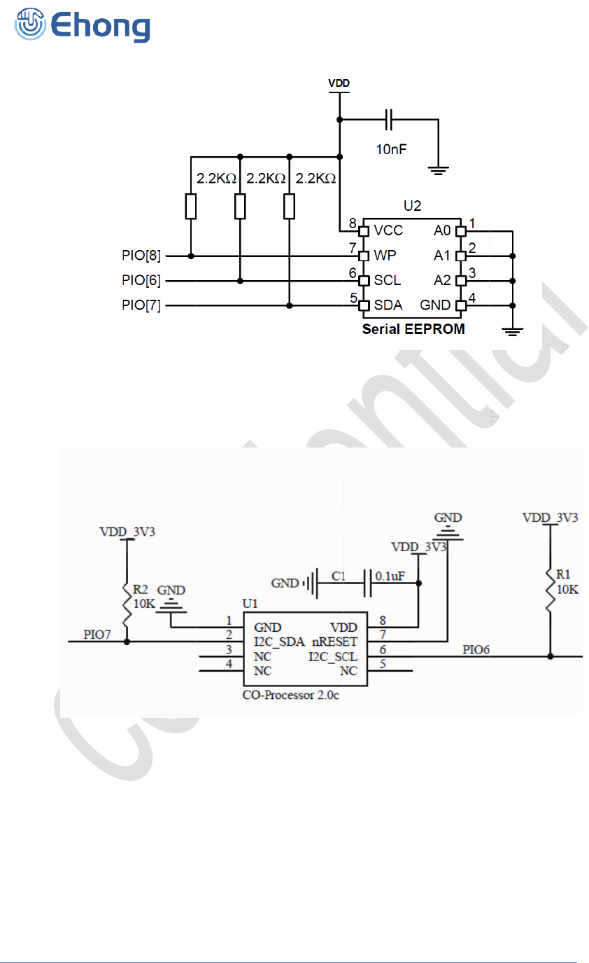
Figure 4:
E
S
CP refe
r
give an ind
o
cessor lay
o
E
xample E
E
r
ence des
i
icative ove
r
o
ut is avail
a
Figure 5:
E
PROM Con
i
gn
r
view of wh
a
a
ble for lice
Apple Co-p
nection wit
h
a
t the hard
w
nsed MFI
d
rocessor 2.
0
B
h
I2C Interf
a
w
are conc
e
d
evelopers
f
0
C
B
luetooth Au
d
a
ce
e
pt looks lik
e
f
rom the M
F
d
io Module
e
. A
F
I program.
E
hon
g
T
6.7.
The a
u
Figur
e
recor
d
the D
A
run at
The i
n
descr
i
usag
e
T
echnolo
gy
C
o
Digital
A
u
dio interfa
Stereo au
Dual audi
o
A configu
r
e
2 outlines t
h
d
ing of audi
o
A
C of the c
o
its own ind
n
terface for
i
bed in Tab
l
e
. Table 11
l
o
., Ltd
A
udio In
t
ce circuit c
o
dio codec
o
inputs an
d
r
able PCM,
h
e function
a
o
signals at
o
dec each
c
ependent
s
the digital
a
l
e 11, whic
h
l
ists these
a
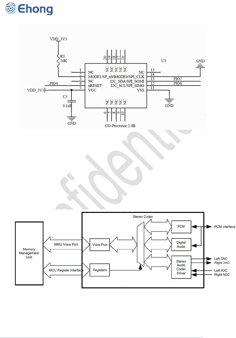
Figure 6:
t
erfaces
o
nsists of:
d
outputs
I²S or SP
D
a
l blocks of
multiple s
a
c
ontain 2 in
s
ample rate
Fi
g
u
a
udio bus s
h
h
means ea
a
lternative
f
Apple Co-p
D
IF interfac
e
the interfac
a
mple rates
dependent
.
re 7: Audio
h
a
r
es the s
a
ch of the a
u
f
unctions.
rocessor 2.
0
e
e. The cod
e
with a res
o
channels.
A
Interface
a
me pins a
s
u
dio buses
B
0
B
e
c supports
o
lution of 1
6
A
ny ADC o
r
s
the PCM
c
are mutuall
B
luetooth Au
d
stereo pla
y
6
-bit. The
AD
r
DAC chan
c
odec inter
f
y exclusiv
e
d
io Module
y
back and
D
C and
nel can be
f
ace
e
in their

E
hon
g
T
PC
M
PC
M
PC
M
PC
M
PC
M
T
a
The au
d
single-
e
analog
u
The au
d
6.7.1.
The au
d
recepti
o
Hardw
a
to thre
e
EH-MB
as a P
C
EH-MB
Frame
It supp
o
receive
EH-MB
Qual
c
OKI
M
Moto
r
Moto
r
STW
EH-
M
6.7.2.
The di
g
j
ustifie
d
The I2
S
with th
e
I2S ma
s
T
echnolo
gy
C
o
M
Interface
M
_OUT
M
_IN
M
_SYNC
M
_CLK
a
ble 11: Alt
e
d
io input ci
r
e
nded or fu
u
e and digi
t
d
io output
c
PCM
d
io pulse c
o
o
n of PCM
e
a
re on EH-
M
e
SCO con
n
05 can op
e
C
M interfac
e
05 is comp
Sync and
G
o
rts 13-bit
o
and trans
m
05 interfac
e
c
omm MS
M
M
SM7705 f
o
r
ola MC14
5
r
ola MC14
5
5093 and
5
M
B05 is als
o
Digital A
u
g
ital audio i
n
d
. The inter
f
S
interface
c
e
default fir
m
s
ter. The I
2
o
., Ltd
e
rnative Fu
n
r
cuitry con
s
lly different
t
al progra
m
c
ircuitry co
n
o
de modul
a
e
ncoded a
u
M
B05 allow
n
ections ca
n
e
rate as the
e
slave ac
c
atible with
a
G
CI timing
e
o
r 16-bit lin
e
m
it on any
s
e
s directly
t
M
3000 seri
e
o
ur chann
e
5
481 8-bit
A
5
483 13-bit
5
094 14-bit
o
compatibl
u
dio Inter
f
n
terface su
p
f
ace share
s
c
an be ena
m
ware. Co
n
2
S support
f
SPDIF
SPDIF
_
SPDIF
_
-
-
n
ctions of t
h
s
ists of a d
u
ial and pro
g
m
mable gai
n
n
sists of a
d
a
tion (PCM
)
u
dio data o
v
s the data
t
n
be suppo
PCM inter
f
c
epting ext
e
a
variety of
e
nvironme
n
e
ar, 8-bit u
-
s
election of
t
o PCM au
d
e
s and MS
M
e
l A-law an
d
A
-law and
linear CO
D
linear CO
D
e with the
M
f
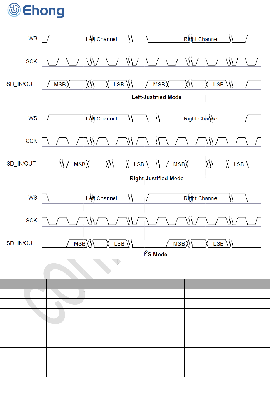
ace (I2S)
p
ports the i
s
the same
bled by usi
n
n
tact with
E
f
ollowing f
o
Interface
_
OUT
_
IN
h
e Di
g
ital A
u
al audio in
p
g
rammed f
o
n
stage for
o
d
ual differe
n
)
interface
s
v
er Blueto
o
t
o be sent t
o
rted by the
f
ace maste
e
rnally gen
e
clock form
a
n
ts.
-
law or A-la
w
three of th
e
d
io devices
M
5000 ser
i
d
-law CO
D
-law COD
E
D
EC
D
ECs(8)
M
otorola S
S
ndustry st
a
pins of the
n
g AT+ co
m
E
Hong for s
p
o
rmats:
udio Bus In
p
ut that ca
n
o
r either mi
c
o
ptimizatio
n
n
tial class
A
s
upports c
o
o
th.
o
and recei
PCM inter
f
r generatin
g
e
rated PC
M
a
ts, includi
n
w
compan
d
e
first four
s
including t
h
i
es CDMA
b
D
EC
E
C
S
I interface
a
ndard for
m
PCM interf
a
m
mands. T
h
p
ecial firm
w
B
I²S Interf
a
SD_OUT
SD_IN
WS
SCK
terface on
t
n
be config
u
c
rophone
o
n
of differe
n
A
-B output
s
o
ntinuous tr
a
ved from a
f
ace at any
g
PCM_SY
M
_SYNC an
n
g Long Fr
a
d
ed sample
s
lots followi
h
e followin
g
b
aseband
d
m
ats for I2S,
a
ce as Ta
b
h
e module
i
w
are when
u
B
luetooth Au
d
a
ce
t
he PCM Int
e
u
red to be
e
o
r line input
.
n
t micropho
s
tage.
a
nsmission
SCO conn
one time.
NC and P
C
d PCM_CL
a
me Sync,
formats a
n
ng PCM_S
g
:
d
evices
left-
j
ustifie
b
le 11.
i
s an I2S sl
u
se the mo
d
io Module
e
rface
e
ither
.
It has an
nes.
and
ection. Up
C
M_CLK or
K.
Short
n
d can
YNC.
d or right-
a
ve device
dule as an
E
hon
g
T
Sy
m
-
-
t
c
t
t
o
t
s
t
s
t
i
t
T
echnolo
gy
C
o
m
bol
-
S
-
W
c
h
S
t
cl
S
o
pd
S
s
su
W
s
h
W
su
S
t
ih
S
o
., Ltd
F
S
CK Frequ
W
S Frequ
e
S
CK high ti
S
CK low ti
m
S
CK to SD
_
W
S to SC
K
W
S to SC
K
S
D_IN to S
S
D_IN to S
F
i
g
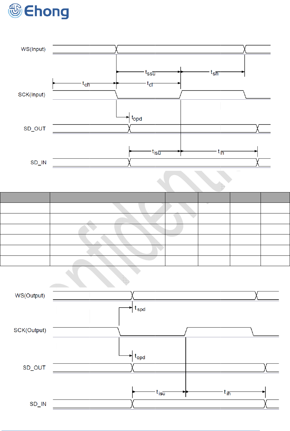
ure 8: Di
g
Paramet
e
ency
e
ncy
me
m
e
_
OUT del
a
K
set up ti
m
K
hold time
CK set-up
CK hold ti
m
g
ital Audio
e
r
a
y
m
e
time
m
e
Interface M
o
Min
-
-
80
80
-
20
20
20
20
B
o
des
Typic
-
-
-
-
-
-
-
-
-
B
luetooth Au
d
al Max
6.2
96
-
-
20
-
-
-
-
d
io Module
Unit
MHz
kHz
ns
ns
ns
ns
ns
ns
ns
E
hon
g
T
Sy
m
-
-
t
o
t
s
t
i
t
T
echnolo
gy
C
o
m
bol
-
S
-
W
o
pd
S
s
pd
S
su
S
t
ih
S
o
., Ltd
T
a
Fi
gu
S
CK Frequ
W
S Frequ
e
S
CK to SD
_
S
CK to W
S
S
D_IN to S
S
D_IN to S
Tabl
a
ble 12 : Digi
t
u
re 9: Di
g
it
a
Paramet
e
ency
e
ncy
_
OUT del
a
S
delay
CK set-up
CK hold ti
m
e 13: Di
g
ita
t
al Audio Int
e
a
l Audio Int
e
e
r
a
y
time
m
e
l Audio Int
e
e
rface Slave
T
e
rface Slav
e
Min
-
-
-
-
20
10
e
rface Mast
e
B
T
iming
e
Timin
g
Typic
-
-
-
-
-
-
e
r Timin
g
B
luetooth Au
d
al Max
6.2
96
20
20
-
-
d
io Module
Unit
MHz
kHz
ns
ns
ns
ns
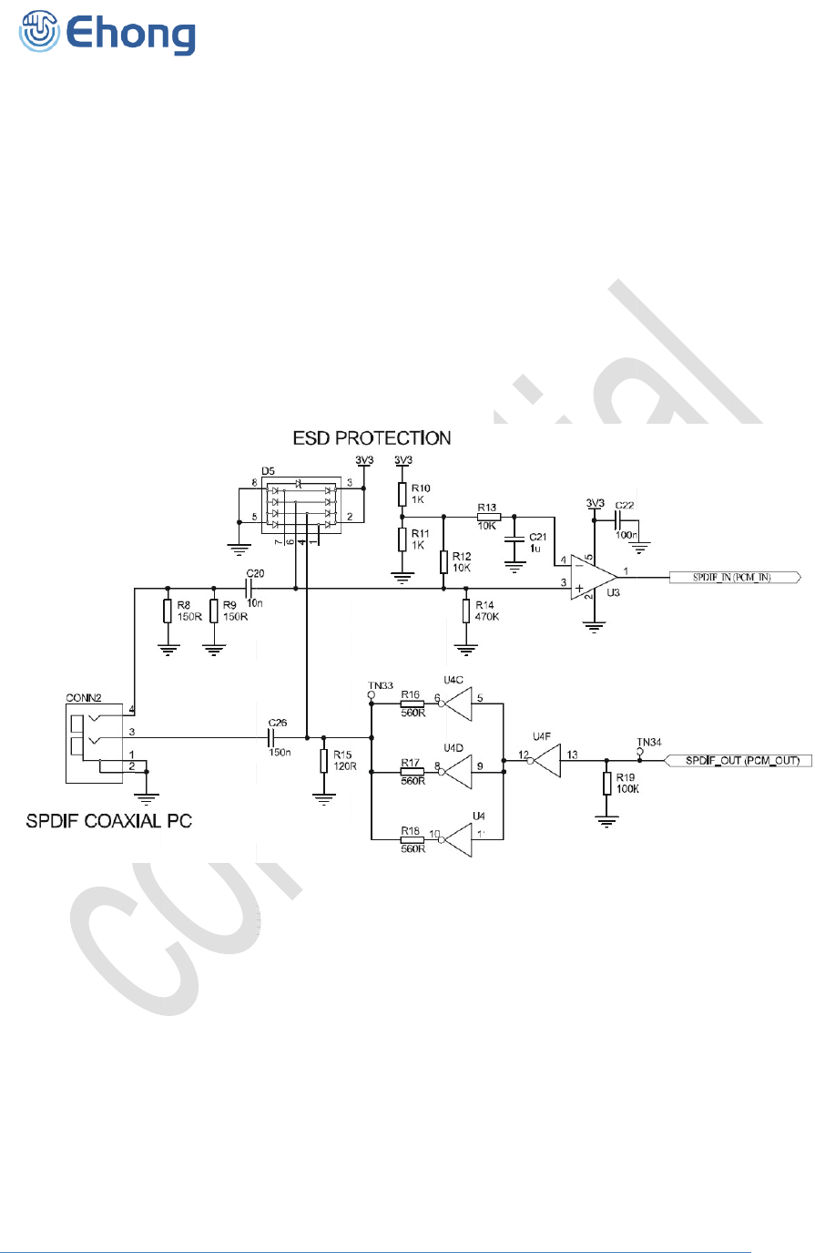
E
hon
g
T
6.7.3.
Throu
interf
a
allow
s
speci
f
The i
n
The S
interf
a
T
echnolo
gy
C
o
IEC 6095
8
gh
A
T+ co
m
a
ce that us
e
s
the
receiv
e
f
ication is b
a
A
ES/EBU
Sony and
n
terface is
c
PDIF interf
a
a
ce pins. T
h
A 75 co
a
An optica
l
o
., Ltd
Fi
g
u
r
8
Interfac
e
m
mand to s
e
s bi-phase
e
r
to
decod
e
a
sed on th
e
Philips int
e
c
ompatible
w
a
ce signal
s
h
e input an
d
a
xial cable
w
l
link that u
s
Figure 11
r
e 10: Di
g
it
a
e
(SPDIF)
witch if SP
D
coding to
m
e
the clock
i
n
e
2 industry
e
rface speci
w
ith IEC 60
s
are SPDI
F
d
output sta
w
ith an RC
A
s
es Toslink
: Example
C
a
l Audio Int
e
D
IF is used
m
inimise th
e
n
formation
f
standards:
fication SP
D
958-1, IEC
F
_IN and S
P
ges of the
S
A
connecto
optical co
m
C
ircuit for
S
e
rface Mast
e
.The IEC 6
0
e
DC conte
n
f
rom the
tra
n
D
IF
60958-3 a
n
P
DIF_OUT
a
S
PDIF pins
r, see Figu
r
m
ponents, s
e
S
PDIF Interf
a
B
e
r Timin
g
0
958 interf
a
n
t of the
tra
n
smitted si
g
n
d IEC 609
5
a
nd are sh
a
can interfa
c
r
e 11.
e
e Figure 1
a
ce
(
Co-
A
xi
a
B
luetooth Au
d
a
ce is a dig
i
nsmitted si
g
g
nal.
The IE
5
8-4.
ar
ed on the
c
e to:
2.
a
l
)
d
io Module
i
tal audio
g
nal
and
C 60958
PCM
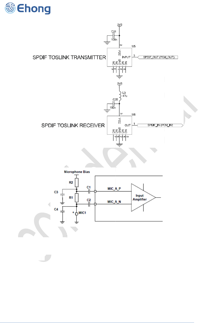
E
hon
g
T
6.8.
The au
d
SPL.
W
betwee
shown
6.9.
The ou
t
variabl
e
output
c
The ou
t
is avail
a
Figure
1
T
echnolo
gy
C
o
Microp
h
d
io input is
W
ith biasing
n about –4
0
in Figure 1
4
Analog
t
put stage
d
e
sampling
f
c
ircuitry.
t
put stage
c
a
ble as a di
1
4 shows,
a
o
., Ltd
Figure 1
2
h
one inp
u
Figure 1
3
intended f
o
resistors R
0
dBV and
–
4
.
Output
s
d
igital circui
t
f
requency t
c
ircuit is co
m
fferential si
g
a
nd betwe
e
2
: Example
u
t
3
: Microph
o
o
r use in th
e
1 and R2 e
q
–
60dBV. Th
s
tage
t
ry convert
s
o a 2Mbits/
s
m
prised a
D
g
nal betwe
e
n SPKL_R
N
Circuit for
S
o
ne Biasin
g
e
range fro
m
q
ual to 1k
e microph
o
s
the signal
s
5-bit mult
i
D
AC with ga
e
n SPKR
_L
N
and SPK
L
S
PDIF Inter
f
(
Sin
g
le Ch
a
m
1A @ 9
4
, this requi
r
o
ne for eac
h
from 16-bi
t
i
-bit bit stre
a
in setting a
n
L
N and SP
K
L
_RP for th
e
B
f
ace
(
Optic
a
a
nnel Show
n
4
dB SPL to
r
es microp
h
h
channel s
h
t
per sampl
e
a
m, which i
s
n
d class
AB
K
R_LP for t
h
e
left chan
n
B
luetooth Au
d
a
l
)
n)
about 10
A
h
ones with
s
h
ould be bi
a
e
, linear P
C
s
fed into t
h
B
amplifier.
h
e right ch
a
n
el.
d
io Module
A
@ 94dB
s
ensitivity
a
sed as
C
M of
h
e analogu
e
The output
a
nnel, as
e
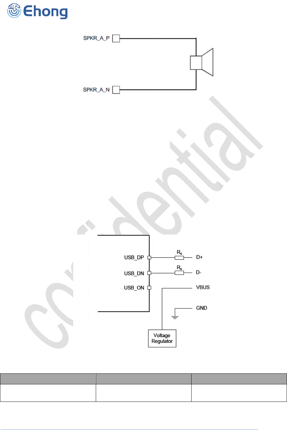
E
hon
g
T
6.10.
This is
device
s
controll
The U
S
require
d
controll
endpoi
n
specifi
c
audio d
The m
o
modul
e
device.
T
echnolo
gy
C
o
USB
a full spee
d
s
. The mo
d
er, such as
S
B interfac
e
d
. The devi
c
er such as
n
ts implem
e
c
ation v2.1
+
evices suc
h
o
dule has a
e
is ready t
o
Identif
i
Rs
o
., Ltd
d
(12M bit
s
d
ule acts
a
a PC.
e
is capable
c
e operate
s
a PC. Both
e
nted can
b
+
EDR or alt
e
h
as speak
e
n internal
U
o
enumerat
e
i
e
r
Ta
Fi
g
u
r
s
/s) USB in
a
s a USB
p
of driving
a
s
as a USB
the OHCI
a
b
ehave as s
e
rnatively
c
e
rs.
U
SB pull-u
p
e
. It signals
Fi
g
ure
ble 14: US
B
r
e 15: Spea
k
terface for
p
eripheral,
a
USB cabl
e
peripheral,
a
nd the UH
pecified in
t
c
an appear
a
p
resistor.
T
to the US
B
16: USB C
o
Value
27 Nomi
B
Interface
C
k
er output
communic
a
respondin
g
e
directly.
N
respondin
g
CI standar
d
t
he USB s
e
a
s a set of
e
T
his pulls th
B
master th
a
o
nnections
nal
C
omponent
V
B
a
ting with
o
g
to reque
s
N
o external
g
to reques
t
d
s are supp
e
ction of th
e
e
ndpoints
a
e USB_DP
a
t it is a full
Impeda
V
alues
B
luetooth Au
d
o
ther comp
a
s
t from a
m
USB trans
c
t
s from a m
orted. The
e
Bluetooth
a
ppropriate
pin weakl
y
speed (12
M
Functio
n
nce matchi
cable
d
io Module
a
tible digita
m
aster hos
t
c
eiver is
aster host
set of USB
to USB
y
high whe
n
M
bit/s) US
B
n
ng to USB
l
t
n
B
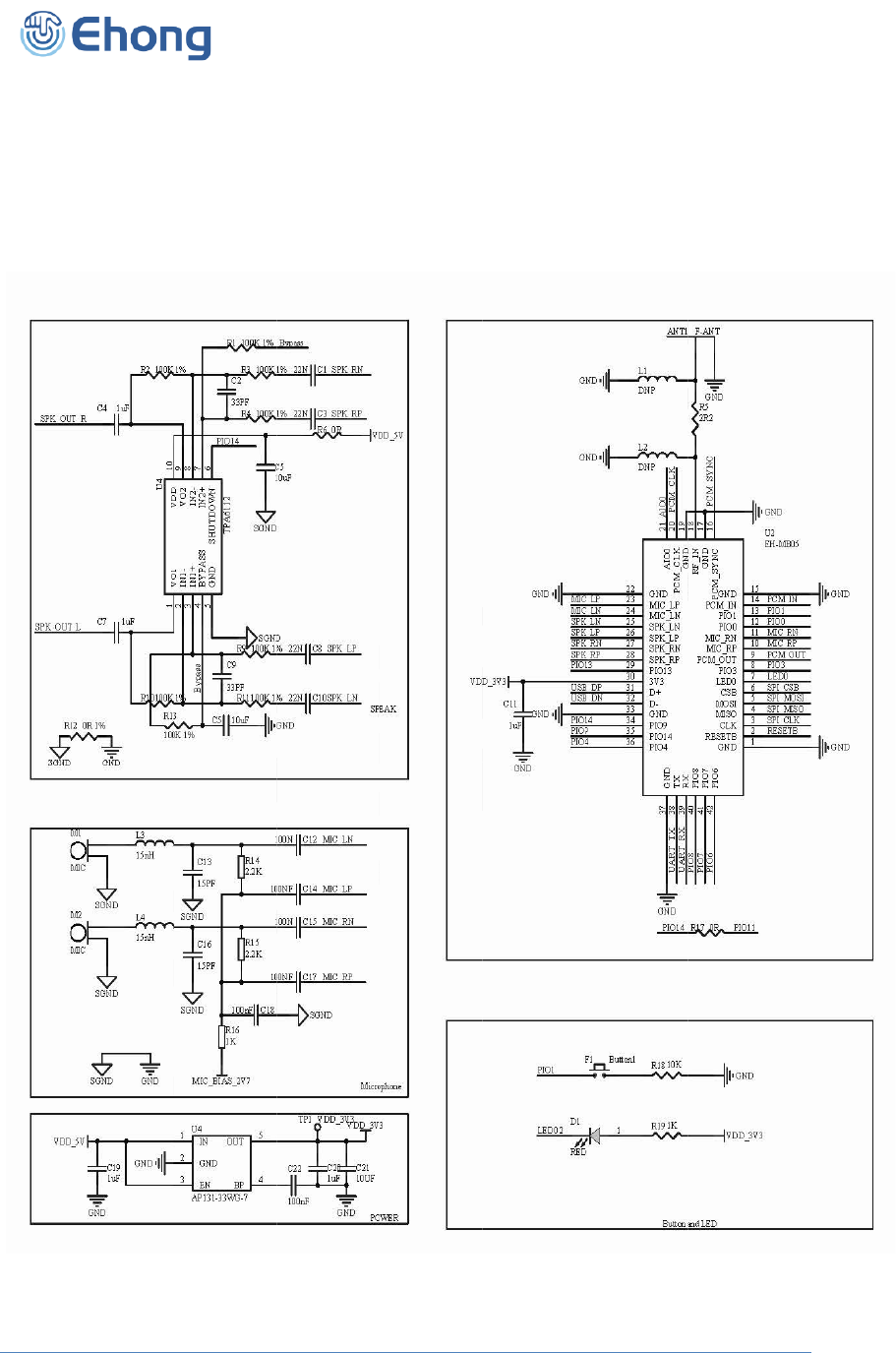
E
hon
g
T
Note:
USB_O
N
function
needed
7. E
H
T
echnolo
gy
C
o
N
is only us
e
shall be en
a
(firmware al
r
H
-MB05
R
o
., Ltd
e
d when the
f
a
bled. In suc
r
eady runs
w
R
eferen
f
irmware ne
e
h case it is
s
w
ith USB, su
c
ce Desi
Fi
g
ure
e
d an input t
o
s
hared with t
h
c
h as USB
D
gn
17: Refere
n
o
detect if U
S
h
e module
P
D
FU or USB
n
ce Desi
g
n
B
S
B is conne
c
P
IO terminal
s
CDC), USB
_
B
luetooth Au
d
c
ted and the
s
. If detectio
n
_
ON is not n
e
d
io Module
USB
n
is not
e
eded.
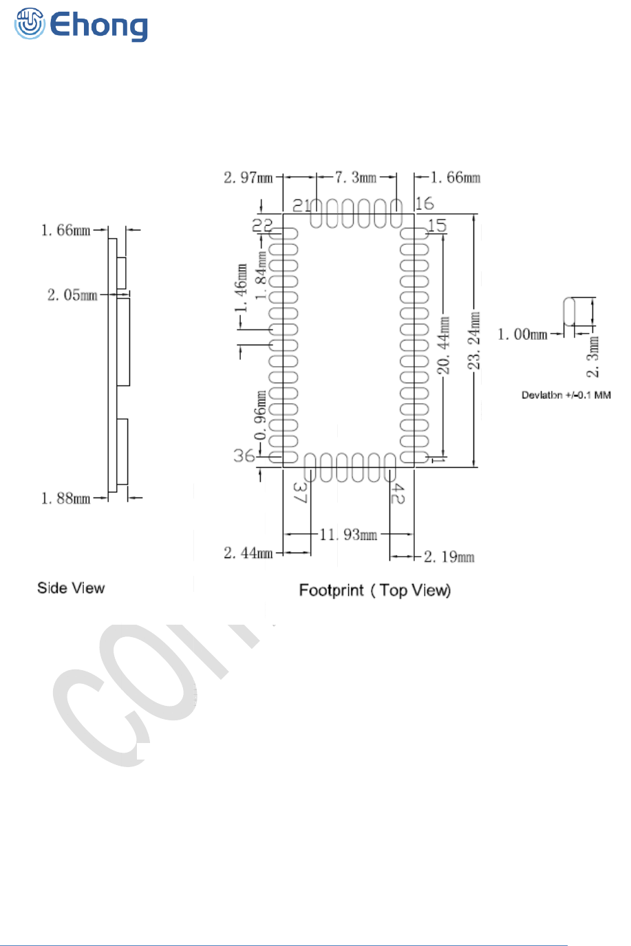
E
hon
g
T
8. M
e
Fi
g
9. R
F
EH-MB
antenn
a
bigger
t
T
echnolo
gy
C
o
e
chanic
a
g
ure 18: Re
c
F
Layou
t
05 has an
o
a
, area len
g
t
he better if
o
., Ltd
a
l and
P
c
ommende
d
t
Guidel
o
n-board P
C
g
th is 1.6 ti
m
the space
a
P
CB Foo
d
PCB Mou
n
ines
C
B antenn
a
m
es of ante
a
llows. Th
e
tprint C
n
tin
g
Patter
n
a
. PCB des
i
nna length,
e
specific si
z
haracte
n
(
Unit: mm
i
gn to ensu
r
area width
z
e as show
B
ristics
, Deviation:
r
e enough
c
is 4 times
o
n figure bel
B
luetooth Au
d
0.02mm
)
T
O
c
learance a
o
f antenna
ow.
d
io Module
O
P View
rea of
width, the
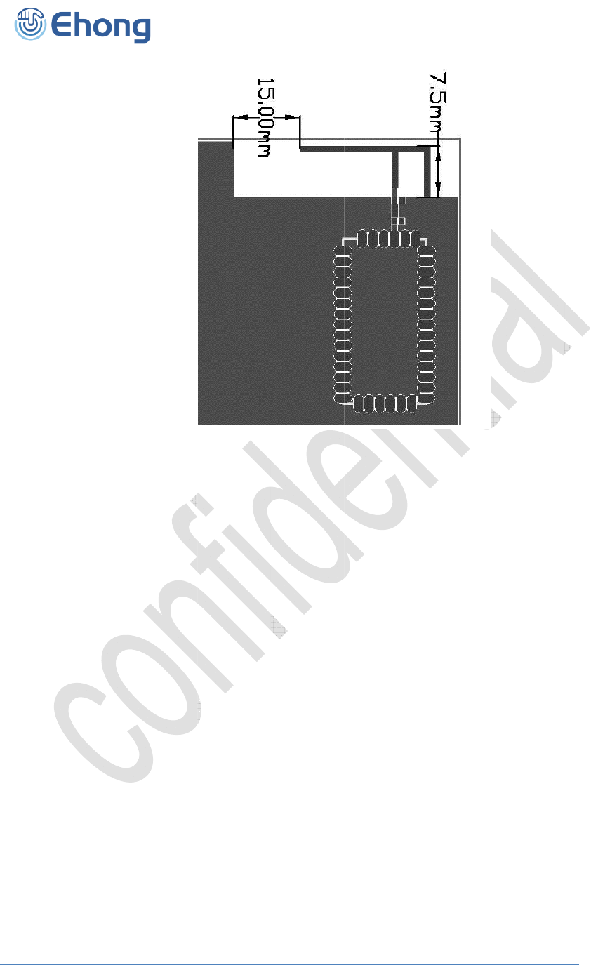
E
hon
g
T
9.1.
The im
p
A
g
Ro
Th
e
im
p
For the
W
h
sig
Us
e
T
echnolo
gy
C
o
Feed Li
p
edance of
g
ood groun
d
ute the fee
d
e
width of t
h
p
edance. A
s
antenna,
h
en PCB a
n
nal strengt
h
e
as many
v
o
., Ltd
ne and
A
the feed li
n
d
directly u
n
d
line as cu
h
e feed lin
e
s
k your PC
B
n
tenna is u
s
h
.
v
ias as pos
Figure 19:
A
ntenna
n
e between
n
der the fe
e
rve lines w
h
e
, the dista
n
B
supplier
t
s
ed, matchi
n
sible to co
n
Clearance
a
the RF po
r
e
d line is al
w
h
en neede
d
n
ce of the f
e
t
o control t
h
n
g network
s
n
nect the g
r
a
rea of ante
r
t and the a
n
w
ays need
e
d
, avoid 90
o
e
ed line to t
h
h
e impedan
c
s
shall be u
r
ound plan
e
B
nna
n
tenna sha
l
e
d for impe
d
o
r even les
s
h
e ground
p
c
e of the fe
e
sed to opti
m
e
s nearby t
h
B
luetooth Au
d
l
l be 50.
d
ance cont
r
s
degree a
n
p
lane are k
e
e
d line.
m
ize the an
h
e antenna.
d
io Module
r
ol.
n
gles style.
e
ys to the
tenna’s
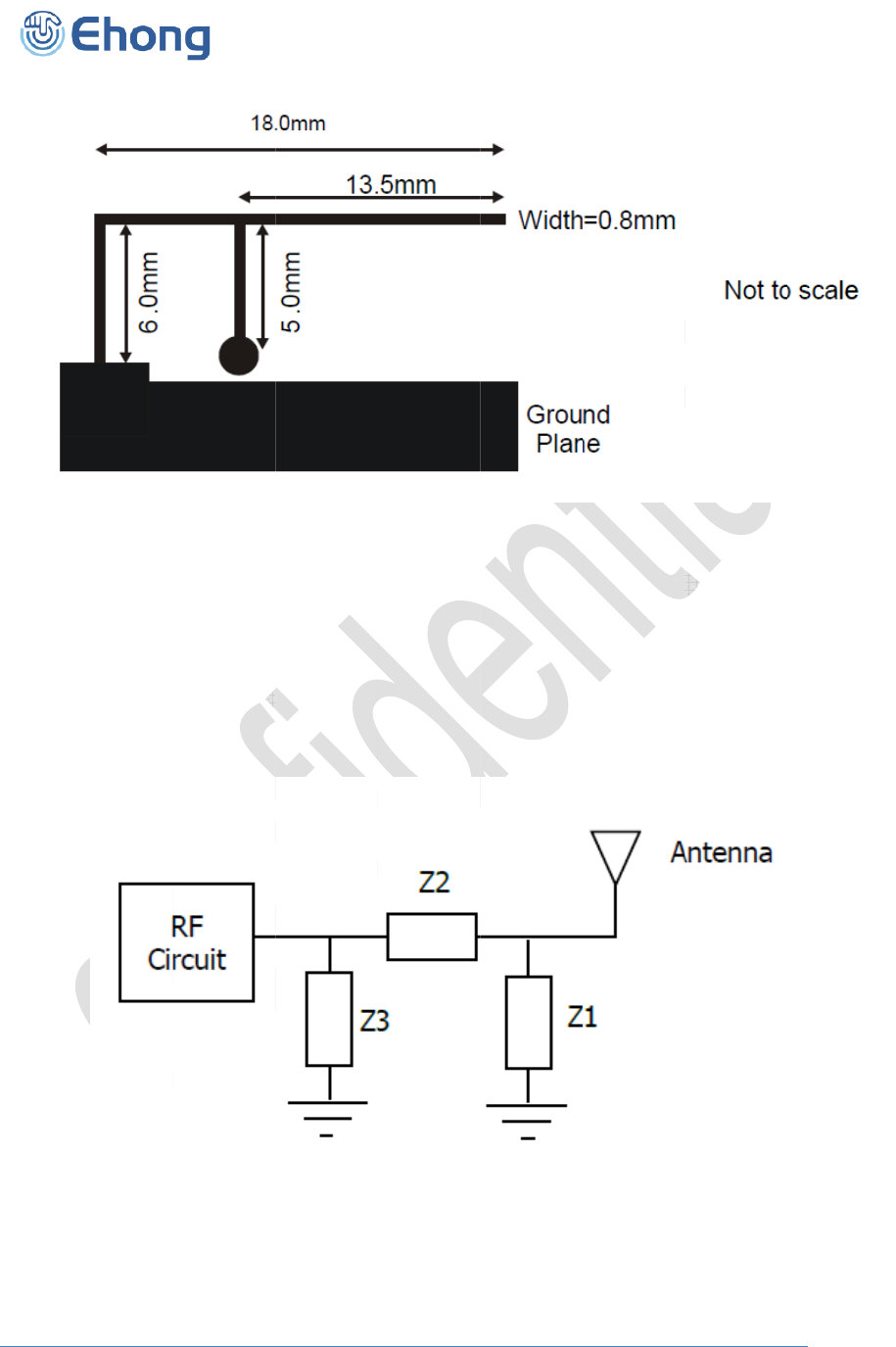
E
hon
g
T
9.2.
The sp
e
which i
s
LCD’s,
why it i
s
possibl
e
This is
a
accoun
T
echnolo
gy
C
o
Matchi
n
e
cs of a Fr
a
s
an ideal c
batteries,
c
s
highly rec
e
to the ant
a
degree o
f
t all eleme
n
o
., Ltd
n
g netw
o
a
ctus stand
ase. In a r
e
c
overs, con
n
ommende
d
enna feedi
n
f
freedom t
o
n
ts of the s
y
Figure 20:
o
rk in fre
ard antenn
a
e
al design,
c
n
ectors, et
c
d
to place 0
4
n
g point. D
o
o
tune the
a
y
stem (batt
e
Figure 21:
Antenna re
f
e space
a
are meas
c
omponent
s
c
affect the
a
4
02 pads f
o
o
it in the g
r
a
ntenna on
c
e
ries, displ
a
PI match n
e
f
erence de
s
ured in the
i
s
nearby th
e
a
ntenna pe
o
r a PI mat
c
r
ound plan
e
c
e the desi
g
a
ys, covers,
e
twork exa
m
B
s
i
g
n
i
r evaluatio
n
e
antenna,
rformance.
c
hing netw
o
e
area, not i
g
n is finishe
etc).
m
ple
B
luetooth Au
d
n
board (in
semicondu
This is the
o
rk as close
n the clear
a
d and takin
d
io Module
free space
)
ctors,
reason
as
a
nce area.
g into
)
,
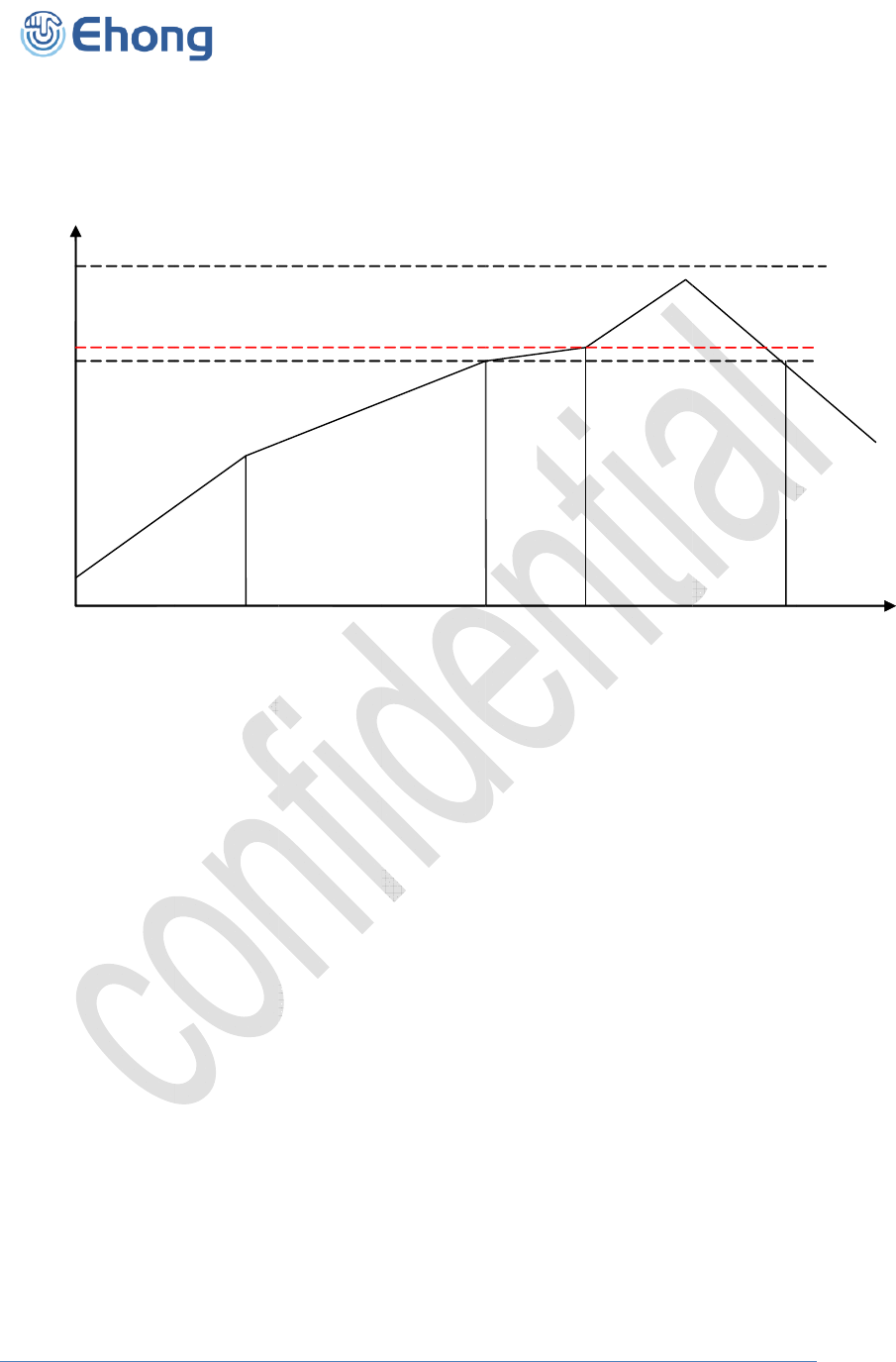
E
hong
T
10.
The sol
The da
t
210
217
℃
250
0
25
Pre-he
a
C/s.
T
This st
a
solvent
Equili
b
solder
p
elevati
o
elimina
t
tempe
r
Equili
b
recom
m
Reflo
w
referen
c
good
w
solderi
n
recom
m
second
Coolin
g
give a l
o
T
echnology C
o
Reflow
dering pro
f
t
a here is g
i
A
a
t zone (
A
T
he purpos
e
a
ge is requ
i
to reduce
t
b
rium Zon
e
p
articles an
o
n of temp
e
t
ing oxide
r
ature is re
b
rium Zon
e
m
ended to
k
w
Zone (D)
c
e for othe
w
etting but
n
g time c
a
m
ended pe
a
when the t
g
Zone (E
)
o
ngerlastin
g
o
., Ltd
Profile
f
ile depend
s
i
ven only f
o
1
F
A
) — This z
e
of this zo
i
red to dist
r
t
he heat sh
o
e
1 (B) —
d spread o
v
e
rature and
film forme
d
commend
e
e
2 (c) (o
p
k
eep the te
m
— The p
r
r lead-free
not so hi
g
a
n lead t
o
a
k tempera
t
emperatur
e
)
— The co
o
g
joint. Ty
p
s
on variou
s
o
r guidance
B
2
F
igure 22:
R
one raises
ne is to pr
e
r
ibute the h
e
o
ck to com
p
In this st
a
v
er PCB b
o
liquefactio
n
d
on the
s
e
d to be 1
5
p
tional) —
m
perature i
n
r
ofile in th
e
solder. Th
e
g
h as to c
a
o
intermeta
t
ure (Tp) is
e
is above
2
o
ling ate s
h
p
ical coolin
s
paramete
r
on solder
r
3
R
ecommend
e
the tempe
r
e
heat the P
C
e
at unifor
m
p
onents.
a
ge the flu
x
o
ard, preve
n
n
of flux, ea
s
urface of
5
0 to 210
In order t
o
n
210 – 21
7
e
figure is
e
peak te
m
a
use com
p
llic growth
230 ~ 25
0
2
17 C.
h
ould be fa
s
g rate sho
r
s necessit
a
r
eflow.
C
4
e
d Reflow
P
r
ature at a
C
B board
a
m
ly to the P
C
x
becomes
n
ting them
ch activato
r
each sold
e
for 60 to 1
2
o
resolve t
h
7
for abou
designed f
o
m
perature s
h
p
onent dis
c
which c
a
0
C. The
s
s
t, to keep
uld be 4
C
B
a
ting a set
u
D
5
P
rofile
controlled
r
a
nd compo
n
C
B board
a
soft and
u
from being
r
and rosin
e
r particle
2
0 second
h
e upright
c
t 20 to 30
s
o
r Sn/Ag3.
h
ould be h
i
c
oloration
o
a
n result i
n
s
oldering ti
m
the solder
C
.
B
luetooth Au
d
u
p for each
5
r
ate, typic
a
n
ents to 12
0
a
nd comple
t
u
niformly e
n
re-oxidize
d
get activat
e
and PCB
for this z
o
c
omponent
s
econd.
0/Cu0.5.
I
i
gh enough
o
r damage.
n
a brittle
m
e should
b
grains sm
a
d
io Module
applicatio
n
6mi
n
E
a
lly 0.5 –
2
0
~ 150 C
t
ely remov
e
n
capsulate
s
d
. Also wit
h
e
d and star
t
board. Th
e
o
ne.
issue, it i
s
I
t can be
a
to achiev
e
Excessiv
e
joint. Th
e
b
e 30 to 9
0
ll which wil
n
.
n
2
.
e
s
h
t
e
s
a
e
e
e
0
l

E
hong
T
11. C
o
Sales:
s
Techni
c
Phone:
Fax: +8
Street
a
Note: F
1. Radi
a
Equi
p
2. To c
o
expo
s
Blue
t
3. This
4. This
con
d
(1) T
h
in
5.The
h
and
c
guid
e
T
echnology C
o
o
ntact Inf
o
s
ales@ehlin
c
al support:
s
+86 21 647
6 21 64765
8
a
ddress: Ro
m
CC RF ex
p
a
ted trans
m
p
ment Auth
o
mply with
s
ure to RF
t
ooth <4.0
d
module m
u
device co
m
d
itions:
h
is device
m
terference
h
ost end pr
o
c
onditions t
h
e
lines.
o
., Ltd
o
rmation
k.com.cn
s
upport@e
h
69993
8
33
m
1505, Blk
p
osure requ
m
it power m
orization fo
FCC regul
a
radiation,
m
d
Bi
u
st not tran
s
m
plies with
p
m
ay not ca
u
received,in
c
o
duct must
h
at must b
e
h
link.com.c
n
1st ,No.833
irements
ust be equ
a
r FCC ID:2
A
a
tions limiti
n
m
aximum a
n
s
mit simult
a
p
art 15 of t
h
u
se harmful
c
luding int
e
include a u
s
e
observed
n
South Hon
g
a
l to or low
e
A
CCRMB0
5
n
g both ma
x
n
tenna gai
n
a
neously wi
t
h
e FCC Rul
e
interferen
c
e
rference th
a
s
er manual
to ensure
c
g
mei Rd ,
M
e
r than that
5
.
x
imum RF
o
n
(including
t
h any othe
r
e
s. Operati
o
c
e, and (2)
t
a
t may cau
s
that clearl
y
c
ompliance
B
M
ing hang di
s
specified i
n
o
utput pow
e
cable loss)
r
antenna
o
o
n is subje
c
t
his device
s
e undesir
e
y
defines o
p
with curren
B
luetooth Au
d
s
trict shang
h
n
the FCC
G
e
r and hum
a
must not e
o
r transmitt
e
c
t to the fol
l
must acce
p
e
d operatio
n
p
erating re
q
t FCC RF
e
d
io Module
h
ai
G
rant of
a
n
xceed: .
e
r.
l
owing two
p
t any
n
.
q
uirements
e
xposure

E
hong
T
For po
r
approv
a
If the d
e
operati
n
antenn
a
For thi
s
produc
t
A certif
i
a perm
a
2.2 Ce
r
instruct
instruct
For a h
o
visible
w
straigh
t
of the
m
modul
e
2ACC
R
on how
The fin
a
criteria
digital
d
The us
e
the us
e
compli
a
is provi
d
inform
a
provid
e
that for
m
This d
e
conditi
o
any int
e
This eq
pursua
n
protecti
uses a
n
the inst
guaran
t
cause
h
T
echnology C
o
r
table devic
e
a
l is requir
e
e
vice is us
e
n
g configur
a
a
configura
t
s
device, O
E
t
s.Please r
e
i
ed modula
r
a
nently affi
x
r
tification (l
a
ions explai
n
ions that a
r
o
st using a
w
hen instal
t
forward c
o
m
odule is vi
s
e
:“Contains
R
MB05” mu
s
end users
a
l host / m
o
for uninten
t
d
evice.
e
rs manual
e
r that chan
g
a
nce could
v
d
ed only in
a
tion requir
e
e
d the user
c
m
.
e
vice compl
i
o
ns: (1) Thi
s
e
rference r
e
uipment h
a
n
t to part 1
5
on against
n
d can radi
a
ructions, m
t
ee that int
e
h
armful int
e
o
., Ltd
e
s, in additi
e
d to satisfy
e
d for other
a
tions, incl
u
t
ions.
E
M integrat
o
e
fer to KDB
7
r
has the o
p
x
ed label, t
h
a
belling req
n
ing to the
O
r
e required
certified m
o
led in the h
o
o
mmonly u
s
s
ible; then
a
Transmitte
r
s
t be used.
can find an
o
dule combi
t
ional radia
t
or instructi
o
g
es or mod
v
oid the us
e
a form oth
e
e
d by this s
e
c
an reason
a
i
es with pa
r
s
device m
a
e
ceived, in
c
a
s been tes
t
5
of the FC
C
harmful int
e
a
te radio fr
e
ay cause h
a
e
rference w
e
rference to
on to the c
o
the SAR r
e
equipment
u
ding porta
b
o
rs must b
e
7
84748 D0
p
tion to use
h
e module
m
uirements)
O
EM the la
(see next p
o
dular with
o
st, or (2) i
f
s
ed method
s
a
n addition
a
r
Module F
C
The host
O
d/or acces
s
nation ma
y
t
ors in orde
o
n manual
f
ifications n
o
e
r's authori
t
e
r than pap
e
e
ction may
a
bly be ex
p
r
t 15 of the
F
a
y not caus
e
c
luding inte
r
t
ed and fou
C
Rules. T
h
e
rference i
n
e
quency en
e
a
rmful inte
r
ill not occu
r
radio or tel
o
nditions 1
e
quirement
s
that separ
a
b
le configu
r
e
provided
w
1 v07, sect
i
a perman
e
m
ust be la
b
above). Th
e
belling req
u
aragraph).
a standard
f
the host i
s
s
for acces
s
a
l permane
C
C ID: 2A
C
O
EM user
m
s
the modul
y
also need
r to be pro
p
f
or an inten
o
t expressl
y
t
y to operat
e
r, such as
be include
d
p
ected to h
a
F
CC Rules
.
e
harmful i
n
r
ference th
a
nd to comp
h
ese limits
a
n
a residen
t
e
rgy and, i
f
r
ference to
r
r
in a partic
u
evision rec
e
through 5
d
s
of FCC P
a
a
te approv
a
r
ations with
w
ith labelin
g
i
on 8. Pag
e
e
ntly affixed
b
elled with
a
e
OEM ma
n
u
irements,
o
fixed label
,
s
marketed
s
s
to remov
e
nt label ref
e
C
CRMB05”
o
m
anual mus
t
e and the
F
to be eval
u
p
erly autho
r
tional or u
n
y
approved
e the equip
on a comp
d
in the ma
n
a
ve the cap
.
Operation
n
terference
,
a
t may cau
s
ly with the
l
a
re design
e
t
ial installati
f
not install
e
r
adio com
m
u
lar install
a
e
ption, whi
c
B
d
escribed a
a
rt 2.1093
a
l is require
d
respect to
g
instructio
n
e
6/7 last tw
o
label, or a
n
a
n FCC ID
-
n
ual must
p
o
ptions and
,
if (1) the
m
s
o that end
e
the modul
e
e
rring to th
e
o
r “Contain
s
t
also cont
a
F
CC ID.
u
ated again
s
r
ized for op
e
n
intentional
by the part
y
ment. In c
a
uter disk o
r
n
ual in that
ability to a
c
is subject
t
,
and (2) th
i
s
e undesire
d
l
imits for a
C
e
d to provid
e
on. This e
q
e
d and use
d
m
unications
.
a
tion. If this
c
h can be
d
B
luetooth Au
d
bove, a se
p
d
for all oth
e
2.1093 an
d
n
s of finish
e
o
paragrap
h
n
electroni
c
-
Section 2.
p
rovide cle
a
OEM user
m
odule’s F
C
users do n
e
so that th
e
enclosed
s
FCC ID:
a
in clear ins
s
t the FCC
e
ration as
a
radiator sh
a
y
responsi
b
a
ses where
r
over the I
n
alternative
c
cess infor
m
t
o the follo
w
i
s device m
d
operation
C
lass B dig
e
reasonab
q
uipment g
e
d
in accord
a
.
However,
equipment
d
etermined
d
io Module
p
arate
e
r
d
different
e
d
h
s:
c
label. Fo
r
926 (see
a
r
manual
C
C ID is not
ot have
e FCC ID
tructions
Part 15B
a
Part 15
a
ll caution
b
le for
the manua
l
n
ternet, the
form,
m
ation in
w
ing two
ust accept
.
ital device,
le
e
nerates,
a
nce with
there is no
does
by turning
l

E
hong
T
the eq
u
more o
f
—Reor
—Incre
—Con
n
connec
—Con
s
T
echnology C
o
u
ipment off
a
f
the followi
ient or relo
c
ase the se
p
n
ect the eq
u
ted.
s
ult the dea
l
o
., Ltd
a
nd on, the
ng measur
e
c
ate the re
c
p
aration be
t
u
ipment int
o
l
er or an ex
user is en
c
e
s:
c
eiving ant
e
t
ween the
e
o
an outlet
o
perienced
r
c
ouraged t
o
e
nna.
e
quipment
a
o
n a circuit
d
r
adio/TV te
c
o
try to corr
e
a
nd receive
r
d
ifferent fr
o
c
hnician fo
r
B
e
ct the inte
r
r
.
o
m that to
w
r
help.
B
luetooth Au
d
r
ference by
w
hich the re
c
d
io Module
one or
c
eiver is