Ehong Technology MC30 Bluetooth Module User Manual Datasheet
ShangHai Ehong Technology Co.,Ltd. Bluetooth Module Datasheet
User Manual
Ehong ® Professional Bluetooth Solutions Provider
Ehong Technology Co.,Ltd
Feb 18 2017
•
Bluetooth® Radio
- Fully embedded Bluetooth® v4.2 single mode
- TX power+1.5dBm, -93dbm RX sensitivity
- 128-bit encryption security
- Range up to 80m
- Integrated chip antenna
- Multipoint capability (2devices at master)
- 32-bit ARM Cortex M0 CPU core
•
Support Profiles
- BLE (Master and slave) the same
- The generic attribute profile (GATT)
- HID Health care, Sports and fitness, Proximity
sensing
- Alerts and timer profiles
- HID (keyboards, remote)
•
User Interface
- UART(CTS/RTS)
- SPI master/Slave interface
- Debug SPI interface for programming(SWD)
- I²C master controller
- Quadrature Decoder (QDEC)
- Real Timer Counter (RTC)
- 4 x LED PWMs
- 10 bit Aux ADC
- 256 KB internal flash
•
General
I/O
- 22 general purpose I/Os
- 5 analogue I/O (10bit ADC)
•
Single voltage supply: 3.3V typical
•
Small form factor: 15.72 x 9.15x 2.2mm
•
Operating temperature range: -25 °C to 75 °C
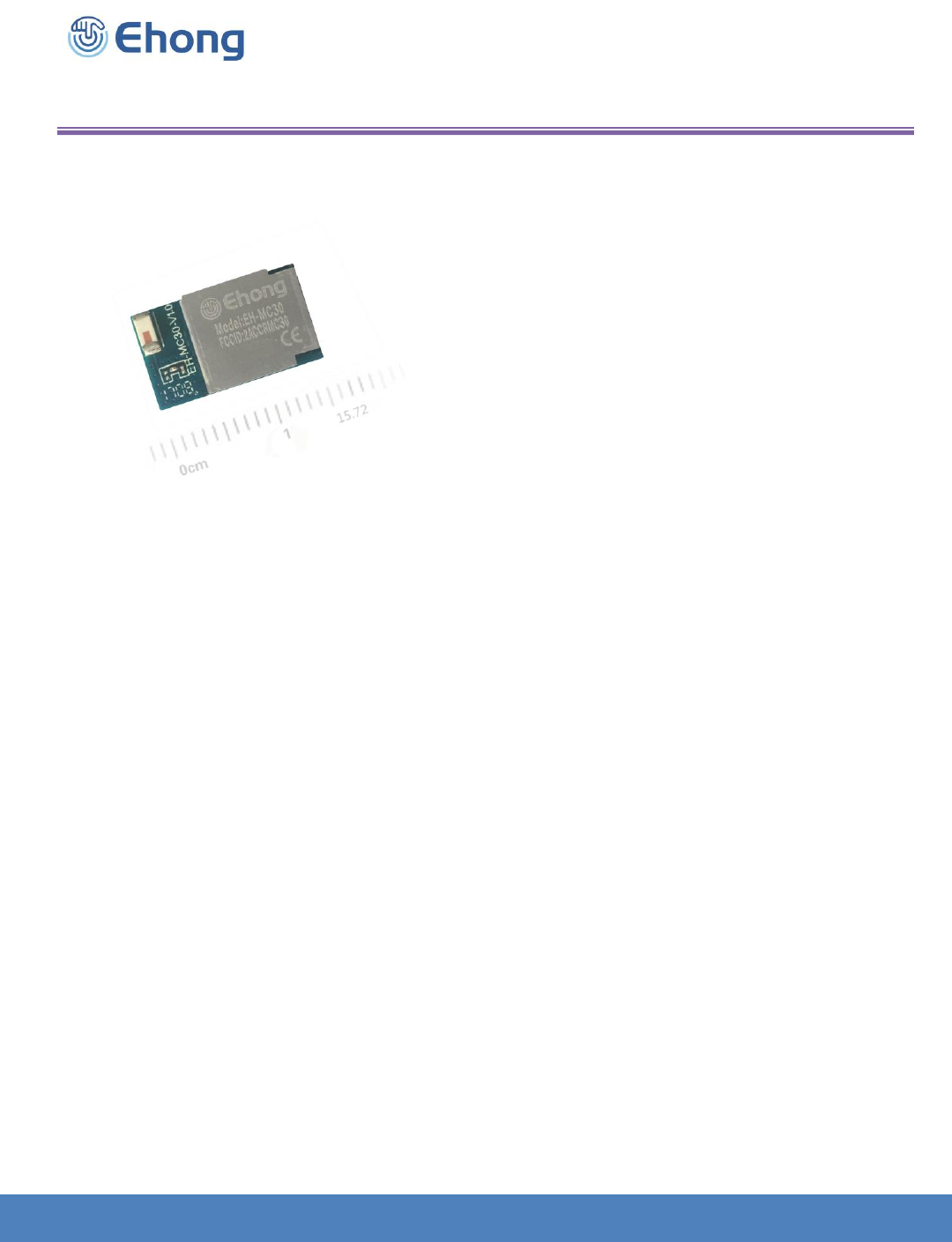
EH-MC30
Low Energy Module Data Sheet
EH-20170218-DS Rev1.1

Ehong ® Professional Bluetooth Solutions Provider page 2 of 18
VERSION HISTORY
Version
Comment
V1.0
Current consumption added
V1.1
Certification information updated.
Confidential and Proprietary – Ehong Technology Co.,Ltd
NO PUBLIC DISCLOSURE PERMITTED: Please report postings of this document on public servers
or websites to: DCC@ehlink.com.cn.
Restricted Distribution: Not to be distributed to anyone who is not an employee of either Ehong
Technology Co.,Ltd or its affiliated companies without the express approval of Ehong Configuration
Management.
Not to be used, copied, reproduced, or modified in whole or in part, nor its contents revealed in any
manner to others without the express written permission of Ehong Technology Co.,Ltd.
This Bluetooth trademark is owned by the Bluetooth SIG Inc., USA and is licensed to Ehong
Technologies. All other trademarks listed herein are owned by their respective owners.
© 2016 Ehong Technology Co.,Ltd All rights reserved.

EH-MC30
Ehong ® Professional Bluetooth Solutions Provider page 3 of 17
1. Contents
1. Description ......................................................................................................................................................... 5
2. Applications ....................................................................................................................................................... 5
3. EH-MC30 Product numbering ........................................................................................................................ 5
4. Electrical Characteristics ............................................................................................................................... 5
4.1 Recommended Operation Conditions .................................................................................................................. 5
4.2 Absolute Maximum Rating .................................................................................................................................. 6
4.4 Power Consumption............................................................................................................................................. 6
5. Pinout and Terminal Description .................................................................................................................. 7
5.1 Pin Configuration ................................................................................................................................................ 7
6. Physical Interfaces ........................................................................................................................................... 8
6.1. Power Supply ............................................................................................................................................... 8
6.2. PIO ................................................................................................................................................................ 9
6.3. AIO ................................................................................................................................................................ 9
6.4. PWMs ........................................................................................................................................................... 9
6.5. UART ............................................................................................................................................................ 9
6.6. I2C Master/ Slave ...................................................................................................................................... 10
6.7. SPI Master/Slave ...................................................................................................................................... 11
6.8. SPI Debug .................................................................................................................................................. 12
7. Reference Design ........................................................................................................................................... 13
8. Layout Guidelines .......................................................................................................................................... 13
9. Mechanical and PCB Footprint Characteristics ...................................................................................... 14
10. EH-MEVK-MC30 ............................................................................................................................................... 14
10.1. EH-MEVK-MC30-PCB........................................................................................................................... 14
10.2. EH-MEVK-MC30-SCH .......................................................................................................................... 15
11. Packing .............................................................................................................................................................. 16
12. Soldering Recommendations ...................................................................................................................... 16
13. Contact Information ....................................................................................................................................... 17

Ehong ® Professional Bluetooth Solutions Provider page 4 of 18
2. Table of Tables
TABLE 1: RECOMMENDED OPERATION CONDITION ...................................................................................................... 5
TABLE 2: ABSOLUTE MAXIMUM RATING........................................................................................................................ 6
TABLE 3: ESD PROTECTION ......................................................................................................................................... 6
TABLE 4: CURRENT CONSUMPTION .............................................................................................................................. 6
TABLE 5: PIN TERMINAL DESCRIPTION ........................................................................................................................ 8
TABLE 6: POSSIBLE UART SETTINGS ........................................................................................................................ 10
3. Table of Figures
FIGURE 1: PINOUT OF EH-MC30 .............................................................................................................................. 7
FIGURE 2: POWER SUPPLY PCB DESIGN ................................................................................................................. 9
FIGURE 3: CONNECTION TO HOST DEVICE .............................................................................................................. 10
FIGURE 4: WTI SPECIFICATIONS .............................................................................................................................. 10
FIGURE 5: SCL/SDA TIMING .................................................................................................................................... 11
FIGURE 6: TWI TIMING PARAMETERS....................................................................................................................... 11
FIGURE 7: SPI SPECIFICATIONS ............................................................................................................................... 11
FIGURE 8: SPI TIMING DIAGRAM, ONE BYTE TRANSMISSION, SPI MODE................................................................. 12
FIGURE 9: SPI TIMING PARAMETERS ....................................................................................................................... 12
FIGURE 10: REFERENCE DESIGN............................................................................................................................. 13
FIGURE 11: CLEARANCE AREA OF ANTENNA ........................................................................................................... 13
FIGURE 12: PHYSICAL DIMENSIONS AND RECOMMENDED FOOTPRINT (UNIT: MM, DEVIATION:0.02MM) .............. 14
FIGURE 13: EH-MEVK-MC30-PCB ....................................................................................................................... 14
FIGURE 14: EH-MEVK-MC30-SCH ....................................................................................................................... 15
FIGURE 15: EH-MC30 PACKAGING(PALLET) .................................................................................................... 16

EH-MC30
Ehong ® Professional Bluetooth Solutions Provider page 5 of 17
1. Description
EH-MC30 Bluetooth® low energy single mode module is a single mode device targeted for low
power sensors and accessories.
The module offers all Bluetooth® low energy features V4.2: radio, stack, profiles and
application space for customer applications, internal integration Cortex-M0 CPU so no external
processor is needed. The module also provides flexible hardware interfaces to connect sensors,
simple user interfaces or even displays directly to the module.
The module can be powered directly with a standard 3.3V coin cell batteries or pair of AAA
batteries. In lowest power sleep mode it consumes only 2.6uA and will wake up in few hundred
microseconds.
After buying Bluetooth® module, we provide free technical support APP of iOS or Android.
2. Applications
HID: keyboards, mice, touchpads, advanced remote controls with voice activation
Sports and fitness sensors: heart rate, runner/cycle speed and cadence
Health sensors: blood pressure, thermometer and glucose meters
Mobile accessories: watches, proximity tags, alert tags and camera controls
Smart home: heating/lighting control
3. EH-MC30 Product numbering
EH-MC30
Module name
Ehong company
4. Electrical Characteristics
4.1 Recommended Operation Conditions
Operating Condition
Min
Typical
Max
Unit
Operating Temperature Range
-25
+25
+75
°C
Battery (VDD_BAT) operation
2.1
+3.0
+3.6
V
I/O Supply Voltage (VDD_PIO)
1.8
+3.0
+3.6
V
AIO input
0
-
+3.6
V
Frequency Range
2402
2480
MHz
Table 1: Recommended Operation Condition
with a standard 3V coin cell batteries or pair of AAA

Ehong ® Professional Bluetooth Solutions Provider page 6 of 18
4.2 Absolute Maximum Rating
Table 2:Absolute Maximum Rating
* Short-term operation up to a maximum of 10% of product lifetime is permissible without damage, but output
regulation and other specifications are not guaranteed in excess of 4.2V.
Condition
Class
Max Rating
Human Body Model Contact Discharge per JEDEC
EIA/JESD22-A114
1C
4000V (all pins)
Charged Device Model Contact Discharge per JEDEC
EIA/JESD22-C101
C1
750V (all pins)
Table 3: ESD Protection
4.4 Power Consumption
The current consumption are measured at the VBAT
Mode
Description
Total typical current
at 3.3V (average)
TX at -
3V using on-chip DC-DC
6.3mA
TX at 0dBm
3V using on-chip DC-DC
10.5mA
3V using on-chip DC-DC
11.8mA
RX mode
3V using on-chip DC-DC
13 mA
Sleep mode
SYSTEM-OFF, no RAM retention
0.6uA
Sleep mode
SYSTEM-OFF, 8KB RAM retention
1.2uA
Sleep mode
SYSTEM-ON, All peripherals in idle mode 2.6uA
Table 4: Current Consumption
Rating
Min
Max
Unit
Storage Temperature
-40
+125
°C
Battery (VBAT) operation*
-0.3
3.9
V
I/O supply voltage
-0.3
+VDD+0.3V
V
Other Terminal Voltages except RF
Vss-0.4
VBAT+0.4
V
1.5dBm
TX at + 1.5dBm
EH-MC30
Ehong ® Professional Bluetooth Solutions Provider page 7 of 17
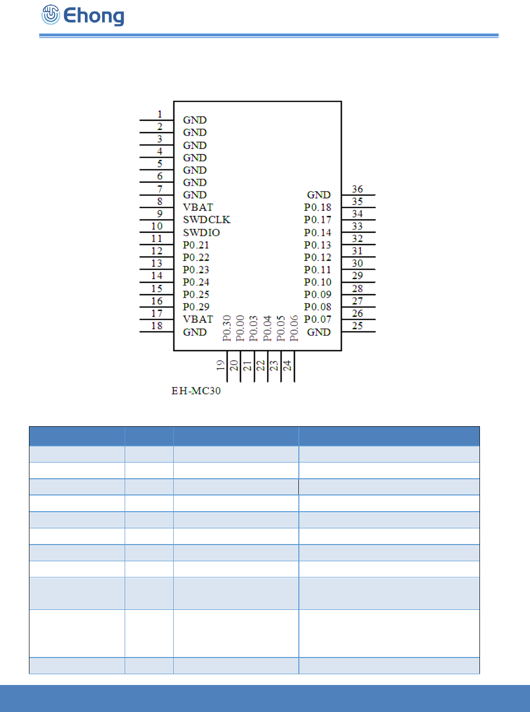
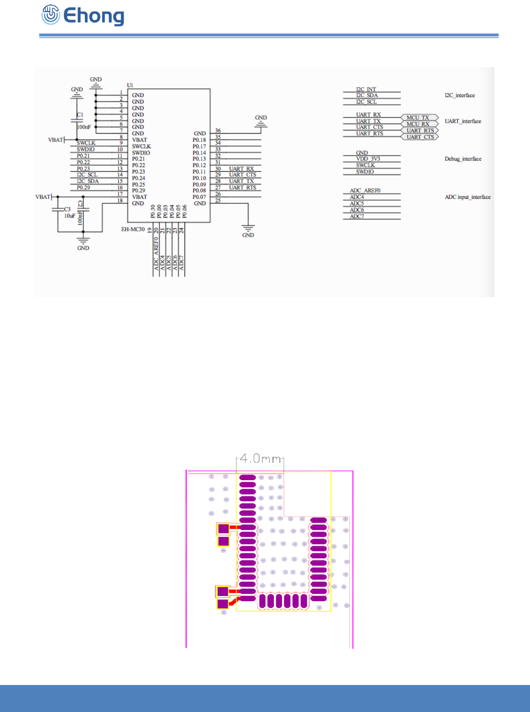
5. Pinout and Terminal Description
5.1 Pin Configuration
Figure 1: Pinout of EH-MC30
Symbol
Pin
PAD Type
Description
GND
1
Ground
Ground
GND
2
Ground
Ground
GND
3
Ground
Ground
GND
4
Ground
Ground
GND
5
Ground
Ground
GND
6
Ground
Ground
GND
7
Ground
Ground
VBAT
8
Power supply
Power supply 3.3V
SWDCLK
9
Digital input
Hardware debug and flash
programming I/O.
SWDIO
10
Digital IO
System reset (active low).
Hardware debug and flash
programming I/O.
P0.21
11
Digital IO
General purpose I/O pin

Ehong ® Professional Bluetooth Solutions Provider page 8 of 18
P0.22
12
Digital IO
General purpose I/O pin
P0.23
13
Digital IO
General purpose I/O pin.
P0.24
14
Digital IO
General purpose I/O pin
P0.25
15
Digital IO
General purpose I/O pin
P0.29
16
Digital IO
General purpose I/O pin
VBAT
17
Power supply
Power supply 3.3V
GND
18
Ground
Ground
P0.30
19
Digital IO
General purpose I/O pin
P0.00
(AREF0)
20
Digital IO
Analog input
General purpose I/O pin
ADC/LPCOMP reference input 0
P0.03
(AIN4)
21
Digital IO
Analog input
General purpose I/O pin
ADC/LPCOMP reference input4
P0.04
(AIN5)
22
Digital IO
Analog input
General purpose I/O pin
ADC/LPCOMP reference input5
P0.05
(AIN6)
23
Digital IO
Analog input
General purpose I/O pin
ADC/LPCOMP reference input6
P0.06
(AIN7)
24
Digital IO
Analog input
General purpose I/O pin
General purpose I/O pin
ADC/LPCOMP reference input7
GND
25
Ground
Ground
P0.07
26
Digital IO
General purpose I/O pin
P0.08
27
Digital IO
General purpose I/O pin
P0.09
28
Digital IO
General purpose I/O pin
P0.10
29
Digital IO
General purpose I/O pin
P0.11
30
Digital IO
General purpose I/O pin
P0.12
31
Digital IO
General purpose I/O pin
P0.13
32
Digital IO
General purpose I/O pin
P0.14
33
Digital IO
General purpose I/O pin
P0.17
34
Digital IO
General purpose I/O pin
P0.18
35
Digital IO
General purpose I/O pin
GND
36
Ground
Ground
Table 5:PIN Terminal Description
Note: The module UARTs and I2C can be mapped any PIOs.
6. Physical Interfaces
6.1. Power Supply
- The module power supply 3v coin cell batteries or DC 3.3v
- Power supply pin connection capacitor to chip and pin as far as possible close
- Capacitor decouples power to the chip
- Capacitor prevents noise coupling back to power plane.
- Support power on reset

EH-MC30
Ehong ® Professional Bluetooth Solutions Provider page 9 of 17
-
Figure 2: Power Supply PCB Design
6.2. PIO
The general purpose I/O is organized as one port with up to 19 I/Os (dependent on package)
enabling access and control of up to 19 pins through one port. Each GPIO can be accessed
individually with the following user configurable features:
Input/output direction
Output drive strength
Internal pull-up and pull-down resistors
Wake-up from high or low level triggers on all pins
Trigger interrupt on all pins
All pins can be used by the PPI task/event system.
The maximum number of pins that can be interfaced through the PPI at the same time is limited
by the number of GPIOTE channels. All pins can be individually configured to carry serial
interface or quadrature demodulator signals.
6.3. AIO
The 10 bit incremental Analog to Digital Converter (ADC) enables sampling of up to 8 external
signals through a front-end multiplexer. The ADC has configurable input, reference presaging,
and sample resolution (8, 9, and 10 bit)
6.4. PWMs
The module has 4 independently configurable PWM instances.
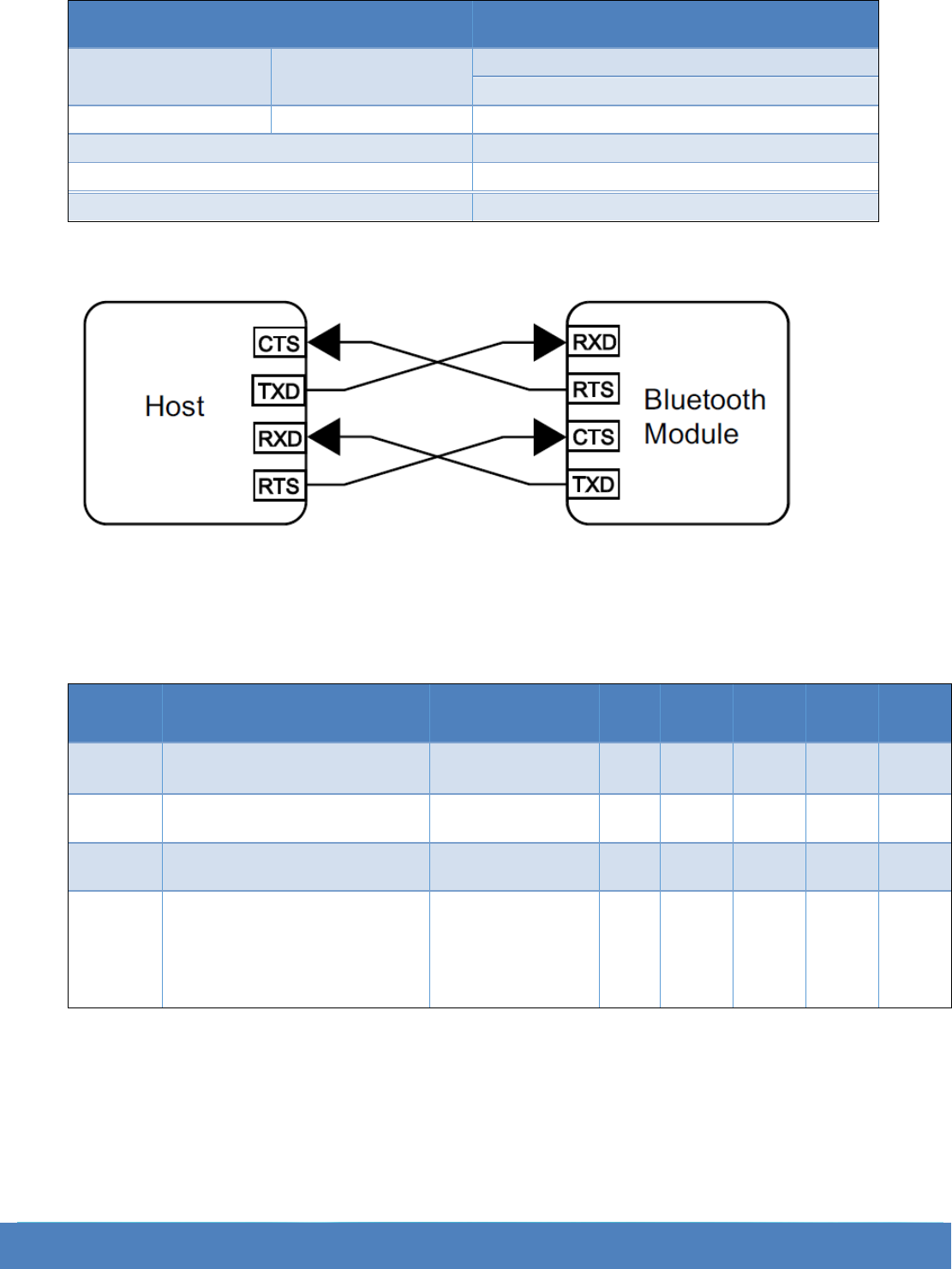
6.5. UART
The module has 1 UART interface. The Universal Asynchronous Receiver/Transmitter offers
fast, full-duplex, asynchronous serial communication with built-in flow control (CTS, RTS)
support in hardware up to 1Mbps baud. Parity checking is supported. The GPIOs used for each
UART interface line can be chosen from any GPIO on the device and are independently
configurable. This enables great flexibility in device pinout and efficient use of board space and
signal routing.
Ehong ® Professional Bluetooth Solutions Provider page 10 of 18
Table 6: Possible UART Settings
Figure 3: Connection To Host device
6.6. I2C Master/ Slave
The module has 1 I²C master/slave general interface for communication with external
peripherals and sensors.
Symbol
Description
Note
Min
Typ.
Max.
Units
Test
Level
I2W100K
Run current for TWI at 100 kbps.
380
μA
1
I2W400K
Run current for TWI at 400 kbps.
400
μA
1
f2W
Bit rates for TWI.
100
400
kbps
N/A
tTWI,START
Time from STARTRX/STARTTX
task is given until start condition.
Low power mode.1
Constant latency
mode.1
3
1
4.4
μs
1
For more information on how to control the sub power modes, see the Series Reference Manual.
Figure 4: WTI specifications
Parameter
Possible Values
Baud Rate
Minimum
1200 baud (≤2%Error)
9600 baud (≤1%Error)
Maximum
2M baud (≤1%Error)
Parity
None, Odd or Even
Number of Stop Bits
1 or 2
Bits per Byte
8
EH-MC30
Ehong ® Professional Bluetooth Solutions Provider page 11 of 17
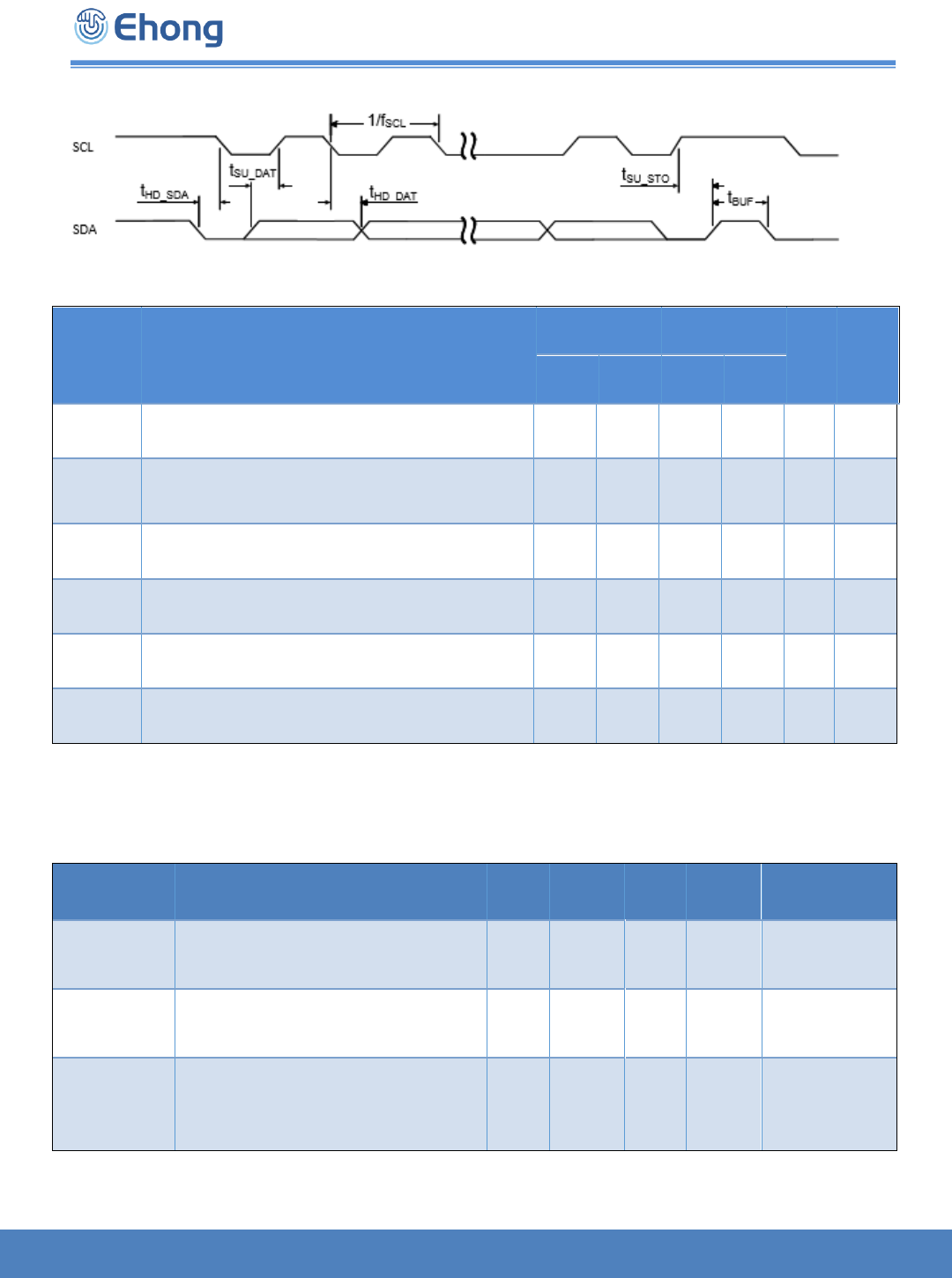
Figure 5: SCL/SDA timing
Symbol
Description
Standard
Fast
Uni
ts
Test
level
Min.
Max.
Min.
Max.
fSCL
SCL clock frequency.
100
400
kHz
1
tHD_STA
Hold time for START and repeated START condition.
5200
1300
ns
1
tSU_DAT
Data setup time before positive edge on SCL
300
300
ns
1
tHD_DAT
Data hold time after negative edge on SCL.
300
300
ns
1
tSU_STO
Setup time from SCL goes high to STOP condition.
5200
1300
ns
1
tBUF
Bus free time between STOP and START conditions.
4700
1300
ns
1
Figure 6: TWI timing parameters
Note: Strong pull is sufficient for I²C on all PIO pads.
6.7. SPI Master/Slave
Symbol
Description
Min.
Typ.
Max.
Units
Test level
IGPIOTE,IN
Run current with 1 or more GPIOTE
active channels in Input mode.
22
μA
1
IGPIOTE,OUT
Run current with 1 or more GPIOTE
active channels in Output mode.
0.1
μA
1
IGPIOTE,IDLE
Run current when all channels are in
Idle mode. PORT event can be
generated with a delay of up to t1V2
0.1
μA
1
Figure 7:SPI specifications
Ehong ® Professional Bluetooth Solutions Provider page 12 of 18
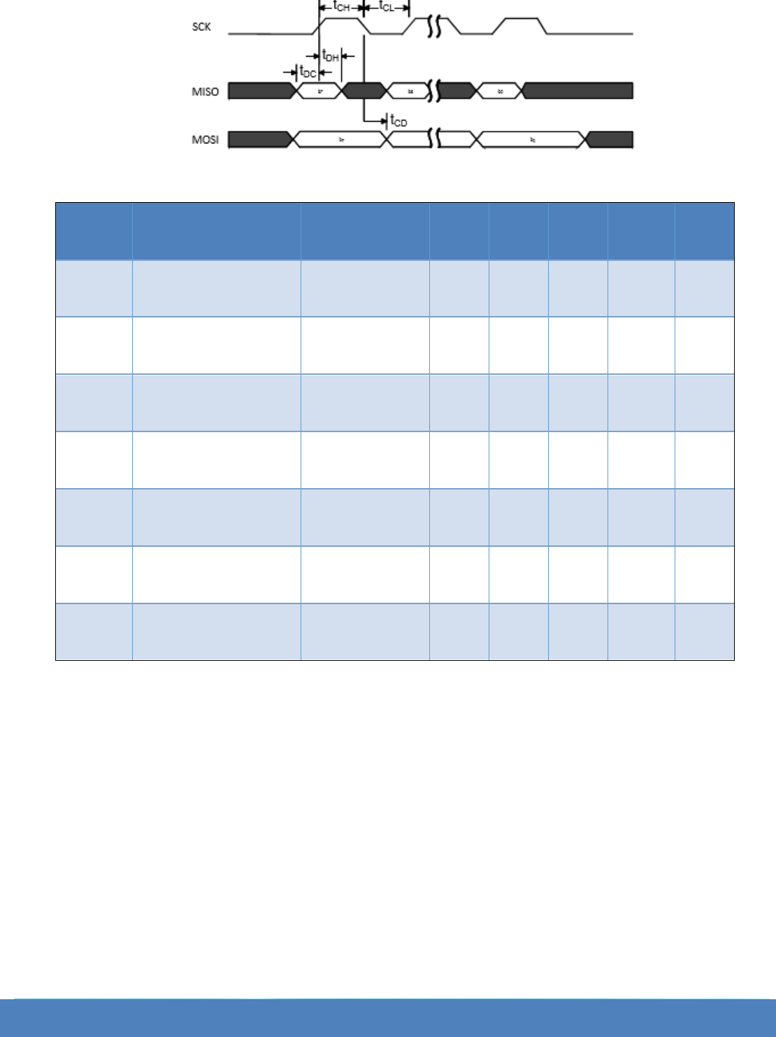
Figure 8:SPI timing diagram, one byte transmission, SPI mode
Symbol
Description
Note
Min.
Typ.
Max.
Units
Test
level
tDC
Data to SCK setup.
10
ns
1
tDH
SCK to data hold.
10
ns
1
tCD
SCK to data valid.
CLOAD = 10 pF
972
ns
1
tCL
SCK low time.
40
ns
1
tCH
SCK high time.
40
ns
1
fSCK
SCK frequency.
0.125
MHz
1
tR,tF
SCK rise and fall time.
ns
1
Figure 9: SPI timing parameters
6.8. SPI Debug
The two pin Serial Wire Debug (SWD) interface provided as a part of the Debug Access Port
(DAP) offers a flexible and powerful mechanism for non-intrusive debugging of program code.
Breakpoints and single stepping are part of this support.
EH-MC30
Ehong ® Professional Bluetooth Solutions Provider page 13 of 17
7. Reference Design
Figure 10: Reference Design
8. Layout Guidelines
For optimal performance of the antenna place the module at the corner of the PCB as shown in
the figure 3. Do not place any metal (traces, components, battery etc.) within the clearance area
of the antenna. Connect all the GND pins directly to a solid GND plane. Place the GND via as
close to the GND pins as possible. Use good layout practices to avoid any excessive noise
coupling to signal lines or supply voltage lines. Avoid placing plastic or any other dielectric
material closer than 6 mm from the antenna. Any dielectric closer than 6 mm from the antenna
will detune the antenna to lower frequencies.
Figure 11: Clearance area of antenna
Ehong ® Professional Bluetooth Solutions Provider page 14 of 18
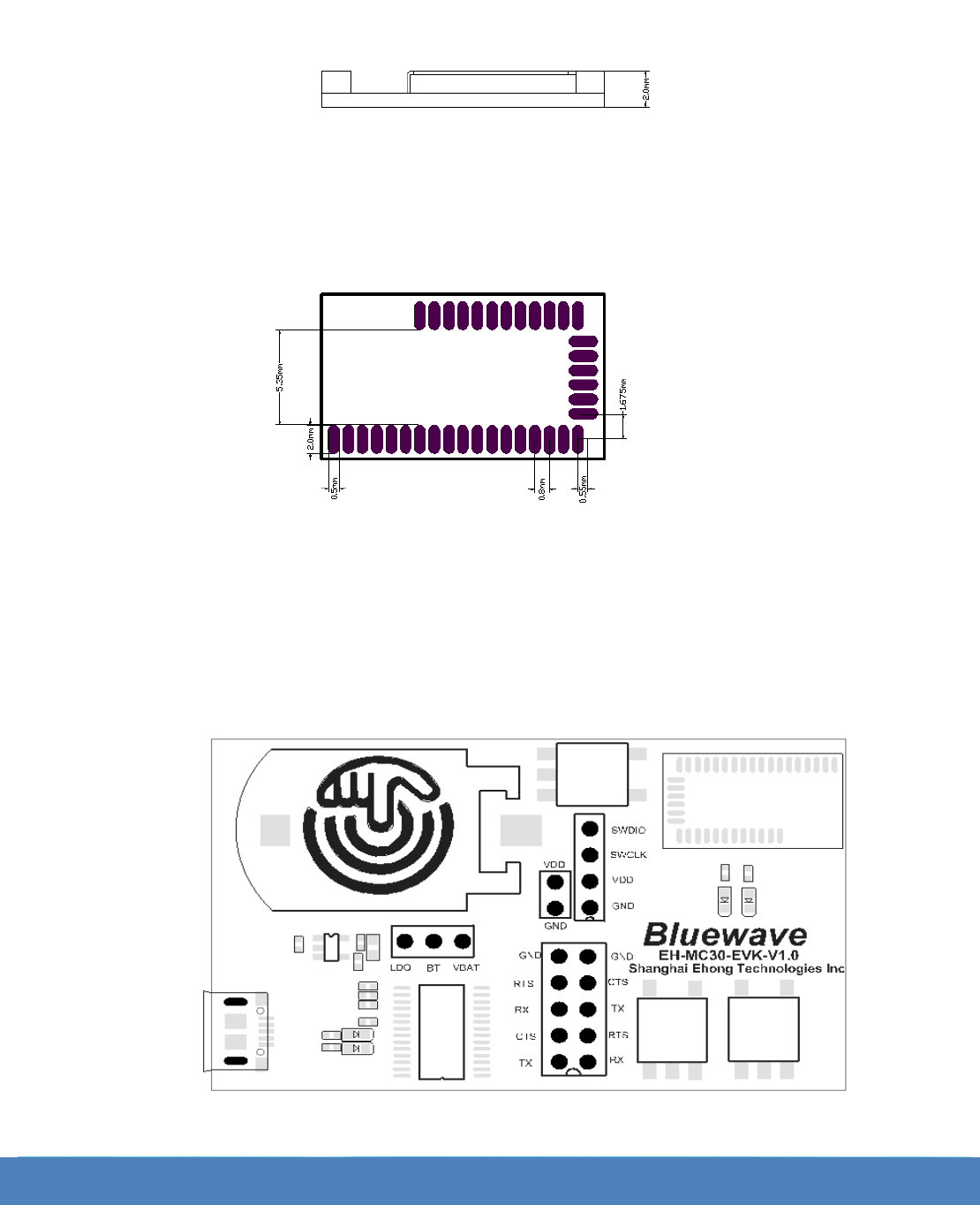
9. Mechanical and PCB Footprint Characteristics
Figure 12:Physical Dimensions and Recommended Footprint (Unit: mm, Deviation:0.02mm)
10. EH-MEVK-MC30
10.1. EH-MEVK-MC30-PCB
Figure 13: EH-MEVK-MC30-PCB
EH-MC30
Ehong ® Professional Bluetooth Solutions Provider page 15 of 17
A. EH-MEVK-MC30 has two power supplies: LDO_3V3 and cell battery.
B. USB RS232 interface, connect to module UART.
C. SWD PIN, Button and LED interface.
D. Any more information, please document of EH-MEVK-MC30 using guide.
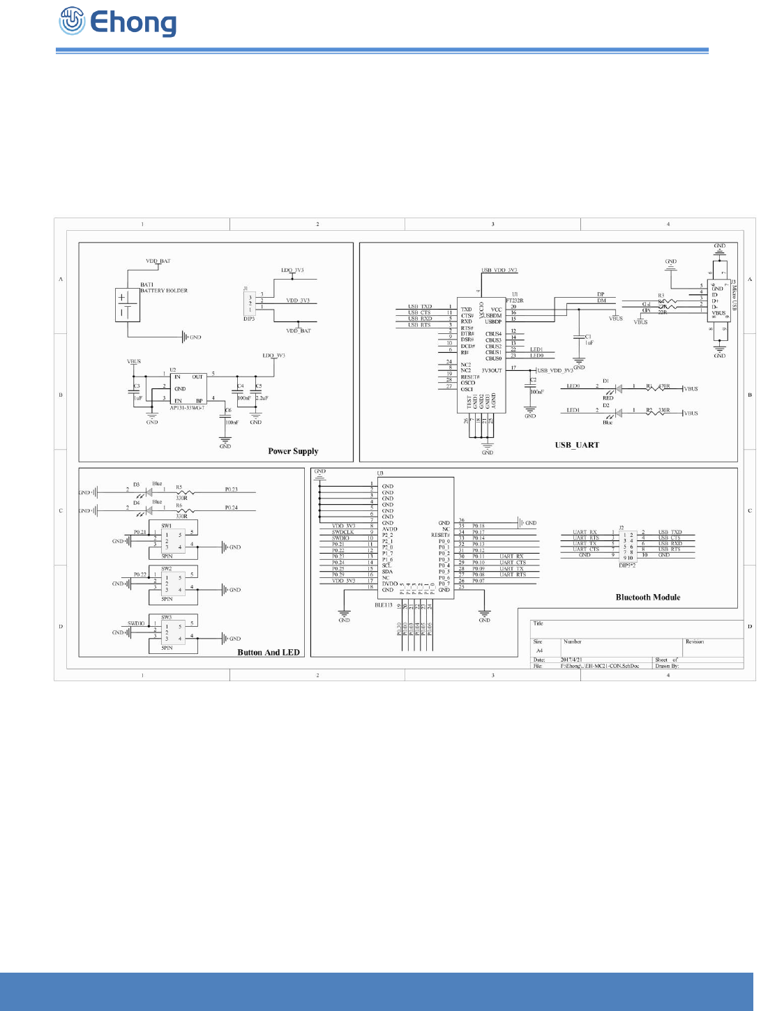
10.2. EH-MEVK-MC30-SCH
Figure 14: EH-MEVK-MC30-SCH
Ehong ® Professional Bluetooth Solutions Provider page 16 of 18
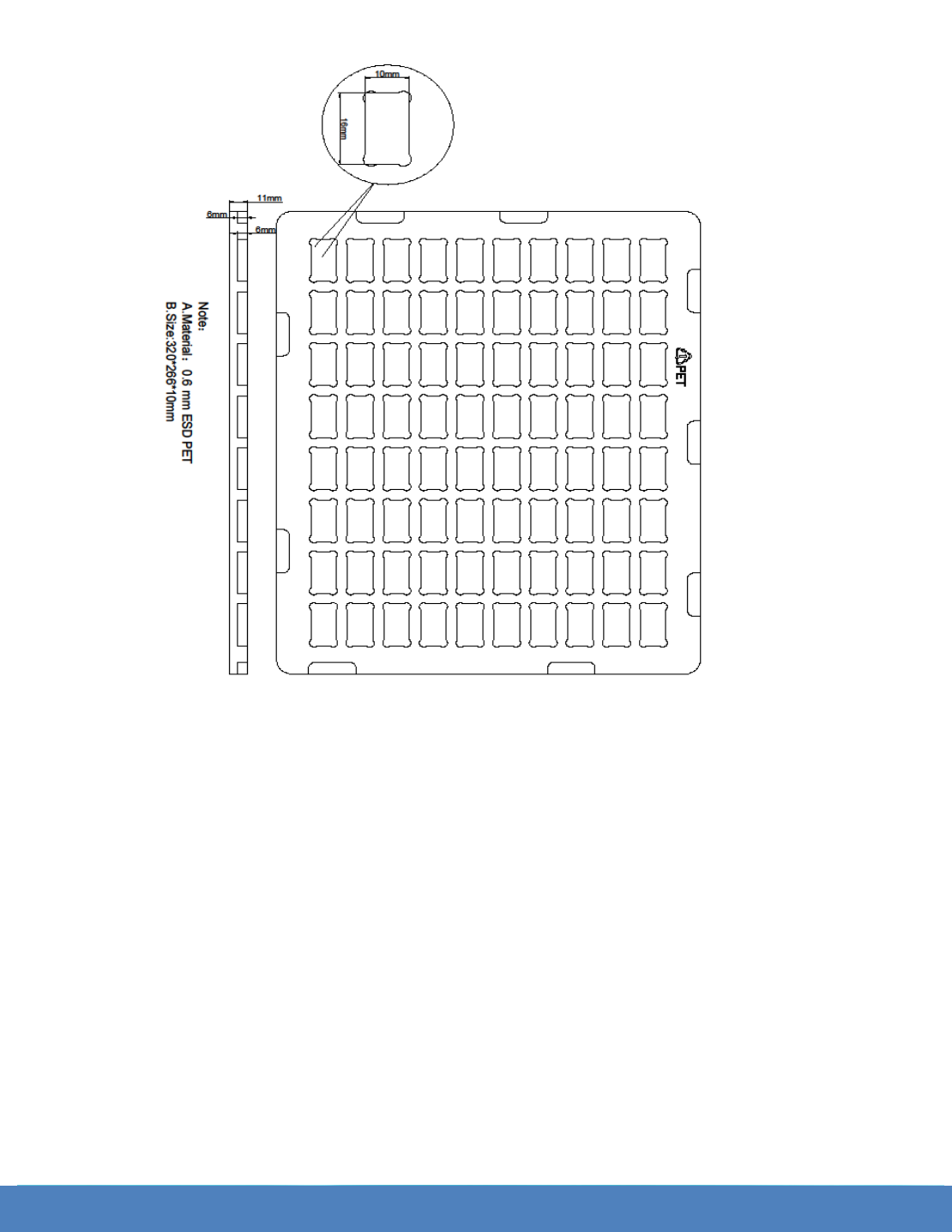
11. Packing
Figure 15: EH-MC30 Packaging(Pallet)
Remark: Packing for the pallet,one packaging quantity is 80 PCS。
12. Soldering Recommendations
EH-MC30 is compatible with industrial standard reflow profile for Pb-free solders. The reflow
profile used is dependent on the thermal mass of the entire populated PCB, heat transfer
efficiency of the oven and particular type of solder paste used. Consult the datasheet of
particular solder paste for profile configurations.
SMT stencil making requirements
If bluetooth module PIN pitch ≥ 0.25mm and other component PIN pitch ≥
0.25mm ,so you choose SMT stencil thickness 1.5mm。
If bluetooth module PIN pitch ≥ 0.25mm and other component PIN pitch ≤
0.25mm ,so you choose SMT Ladder stencil Bluetooth module thickness
1.5mm other component thickness 1.3mm .
Solder pad open via ratio Length 1:1.2, width 1:1.

EH-MC30
Ehong ® Professional Bluetooth Solutions Provider page 17 of 17
13. Contact Information
Sales: sales@ehlink.com.cn
Technical support: support@ehlink.com.cn
Website:http://www.ehlink.com.cn
Phone: +86 21 64769993
Fax: +86 21 64765833
Street address: Rom505, Blk 1st ,No.833 South Hong Mei Rd ,Ming hang district Shanghai
FCC/IC Statements
Integrator is reminded to assure that these installation instructions
will not be made available to the end-user of the final host device.
The final host device, into which this RF Module isintegrated" hasto be labelled
with an auxilliary lable stating the FCC IDofthe RF Module,such as
"This device complies with part 15 of the FCC rules. Operation is subject to the following two
conditions:
(1)this devicemay not cause harmful interference, and
(2)this devicemust accept any interference received, including
interference thatmay cause undesired operation."
approved by the party responsible for compliance could
"Contains FCC ID:2ACCRMC30
the Integrator will be responsible to satisfy SAR/ RF Exposure requirements,
when the module integrated into the host device.
The final host device, into which this RF Module isintegrated" hasto be labelled
with an auxilliary lable stating the IC ofthe RF Module,such as
"Contains transmitter module IC:20625-EHMC30
void the user’s authority to operate the equipment."
"Changes or modifications to this unit not expressly
This device complies with Industry Canada licence-exempt RSS standard(s). Operation is
subject to the following two conditions:
(1) this device may not cause interference, and
(2) this device must accept any interference, including interference that may cause
undesired operation of the device.
Le présent appareil est conforme aux CNR d'Industrie Canada applicables aux appareils
radio exempts de licence. L'exploitation est autorisée aux deux conditions suivantes :
(1) l'appareil ne doit pas produire de brouillage, et
(2) l'utilisateur de l'appareil doit accepter tout brouillage radioélectrique subi, même si le
brouillage est susceptible d'en compromettre le fonctionnement.
(OEM) Integrator has to assure compliance of the entire end-product incl. the integrated RF Module.
For 15 B (§15.107 and if applicable §15.109) compliance, the host manufacturer is required to
show compliance with 15 while the module is installed and operating.
Furthermore the module should be transmitting and the evaluation should confirm that the module's
intentional emissions (15C) are compliant (fundamental / out-of-band). Finally the integrator has
to apply the appropriate equipment authorization (e.g. Verification) for the new host device per
definition in §15.101.
NOTE: This equipment has been tested and found to comply with the limits for a
Class B digital device, pursuant to part 15 of the FCC Rules. These limits are
designed to provide reasonable protection against harmful interference in a
residential installation. This equipment generates uses and can radiate radio
frequency energy and, if not installed and used in accordance with the instructions,
may cause harmful interference to radio communications. However, there is no
guarantee that interference will not occur in a particular installation. If this
equipment does cause harmful interference to radio or television reception, which
can be determined by turning the equipment off and on, the user is encouraged to
try to correct the interference by one or more of the following measures:
- Reorient or relocate the receiving antenna.
- Increase the separation between the equipment and receiver.
-Connect the equipment into an outlet on a circuit different from that to which the
receiver is connected.
-Consult the dealer or an experienced radio/TV technician for help
This transmitter/module must not be collocated or operating in conjunction with
any other antenna or transmitter.
Module statement
The single-modular transmitter is a self-contained, physically delineated, component
for which compliance can be demonstrated independent of the host operating
conditions, and which complies with all eight requirements of § 15.212(a)(1) as
summarized below.
1) The radio elements have the radio frequency circuitry shielded.
2) The module has buffered modulation/data inputs to ensure that the device will
comply with Part 15 requirements with any type of input signal.
3) The module contains power supply regulation on the module.
4) The module contains a permanently attached antenna.
5) The module demonstrates compliance in a stand-alone configuration.
6) The module is labeled with its permanently affixed FCC ID label
7) The module complies with all specific rules applicable to the transmitter, including
all the conditions provided in the integration instructions by the grantee.
8) The module complies with RF exposure requirements.