Elettronika S r l TXUP1000 1000 Watt Analog TV Broadcast Transmitter User Manual APT139B VEGA Rev0 Date100604
Elettronika S.r.l. 1000 Watt Analog TV Broadcast Transmitter APT139B VEGA Rev0 Date100604
Contents
Exciter User Manual Part 3

102
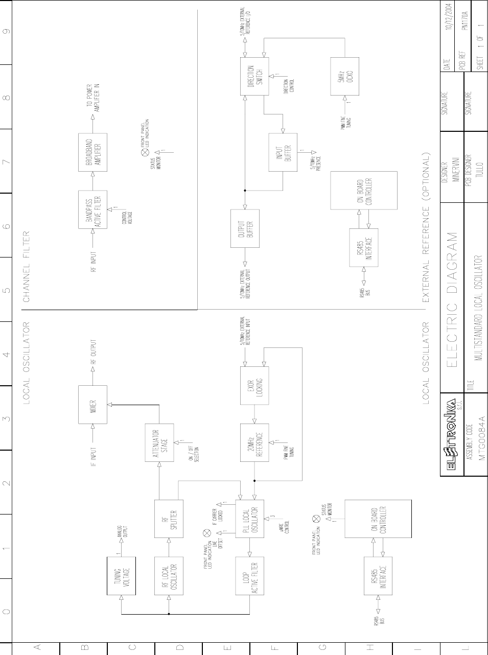
MULT. UHF LOCAL OSCILLATOR MODULE MTG0084AR0
DESCRIPTION
The synthesis system of the local oscillator for the channel conversion is based on a control
technique which allows to obtain the programming of the standard, the channel (split into
the three bands I, III, IV/V) and the line offset (as multiple of the line frequency of the
video signal) via software, with no change to be made.
The module includes an internal VCTCXO reference which can be locked to a more
precise 5/10MHz reference (trough the bus) needed if the field offset is used.
TECHNICAL CHARACTERISTICS
Nominal level +13dBm ±1dB
FM S/N ccir unweight. > 65dB
FM S/N ccir wght. > 60dB
Analog measures VCO control voltage
Carrier frequency synthesis A PLL
Offset Line offset, step ±1/12 line frequency
O.L. carrier characteristics On/Off selection and fine adjust
Frequency reference Internal TCXO externally lockable
External interface Microprocessor with RS485 protocol
Firmware Re-configurable via RS485
103

104
The module contains the following blocks:
1. Local oscillator generated the carrier to be synthesised, it is split into three windows (I-II / III / IV-V
band) to ensure the coverage of all of the TV channels to be implemented for all standards.
2. Radio-frequency splitter splits the signal coming from the local oscillator by means of splitters and
amplifiers, with 10dB attenuation and gain respectively, to ensure the complete isolation of the LO from
the other stages and to minimise the frequency pulling phenomenon.
3. PLL stage synthesises the desired channel by locking the LO to a 20MHz frequency reference by
means of a PLL which can be configured via uWire and provides the locking and line-offset indication
(LED on frontal panel); the choice is made via software.
4. Active ring filter stabilises the system in PLL retro-action and e has to be modified if the operating
band of the module changes (see table attached to the electrical diagram).
5. Conditioning stage of the correction voltage conditions the correction voltage of the PLL ring
providing a conditioned analog voltage for the A/D conversion; the voltage is processed by the
microcontroller of the display board (see MTG0079) to be displayed as VU-METER.
6. Mixer in the UPCONVERTER version of the module, converts to channel the intermediate frequency
coming from the pre-corrector (see MTG0073) using a LEVEL13 mixer (in case the module is only used
as LO, see REPEATER configuration, this stage is not present and the synthesised carrier goes directly to
the output of the module).
7. 20MHz reference the frequency reference to the PLL synthesis of the carrier is generated by an
internal TCXO which fine control of the frequency is internally generated via PWM by the microcontroller
or, alternately, can be locked to a more precise 5/10MHz external reference (see MTG0076).
8. Controller all of the described operations are managed by a microcontroller communicating to the user
interface board (see MTG0079) by RS485 protocol; the local controller stores the status of the module
and a reprogramming of the firmware (possible via RS485 from the display board) does not alter its
contents.
CALIBRATION PROCEDURE
- List of instrument
MEASURE INSTRUMENT
Lock of the carriers and reference
- Spectrum analyser
- Oscilloscope
- Tester
105
The calibration procedure of the module requires a complete structure of display board (see MTG0079)
and extension module (see MTG0095) in order to perform the software selection which will be referred
to later and power the module itself..
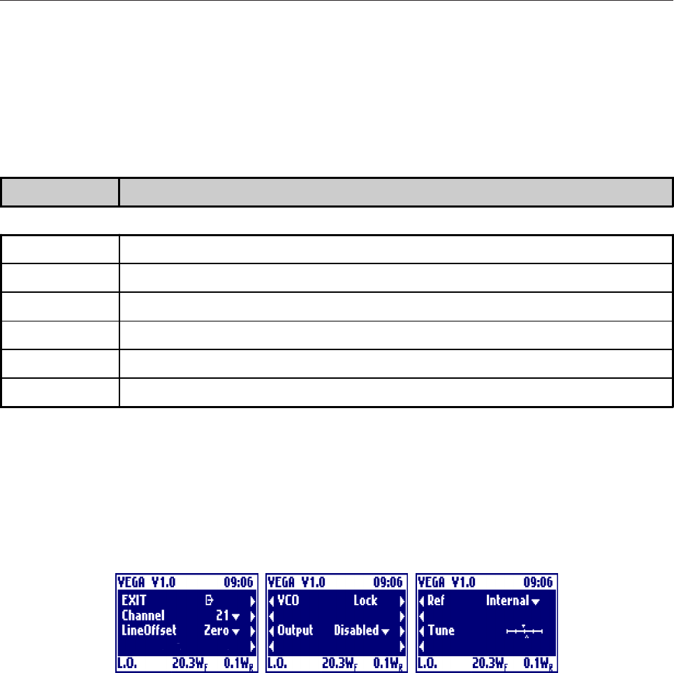
- Menu of the Multistandard UHF Local Oscillator Module
Verification of the local oscillator section connect a spectrum analyser to the monitor of the J4 module
and check the sections therein:
qConfigure the module with Output Enabled, LineOffset Zero, Ref Internal and Channel on the
desired channel, and calibrate C1(C2 and C3) to lock the carrier to the LO frequency of the standard and
channel set (to change the standard refer to the standard changing procedure) and obtain a locking
voltage between 2V and 3V on TP1, checking that VCO is on Lock in the display menu.
Verification of the external reference section connect a spectrum analyser to the monitor of the J4
module and check the sections therein:
qConfigure the module with Ref Internal and check that it is possible to find adjust the synthesised frequency
by acting on Tune.
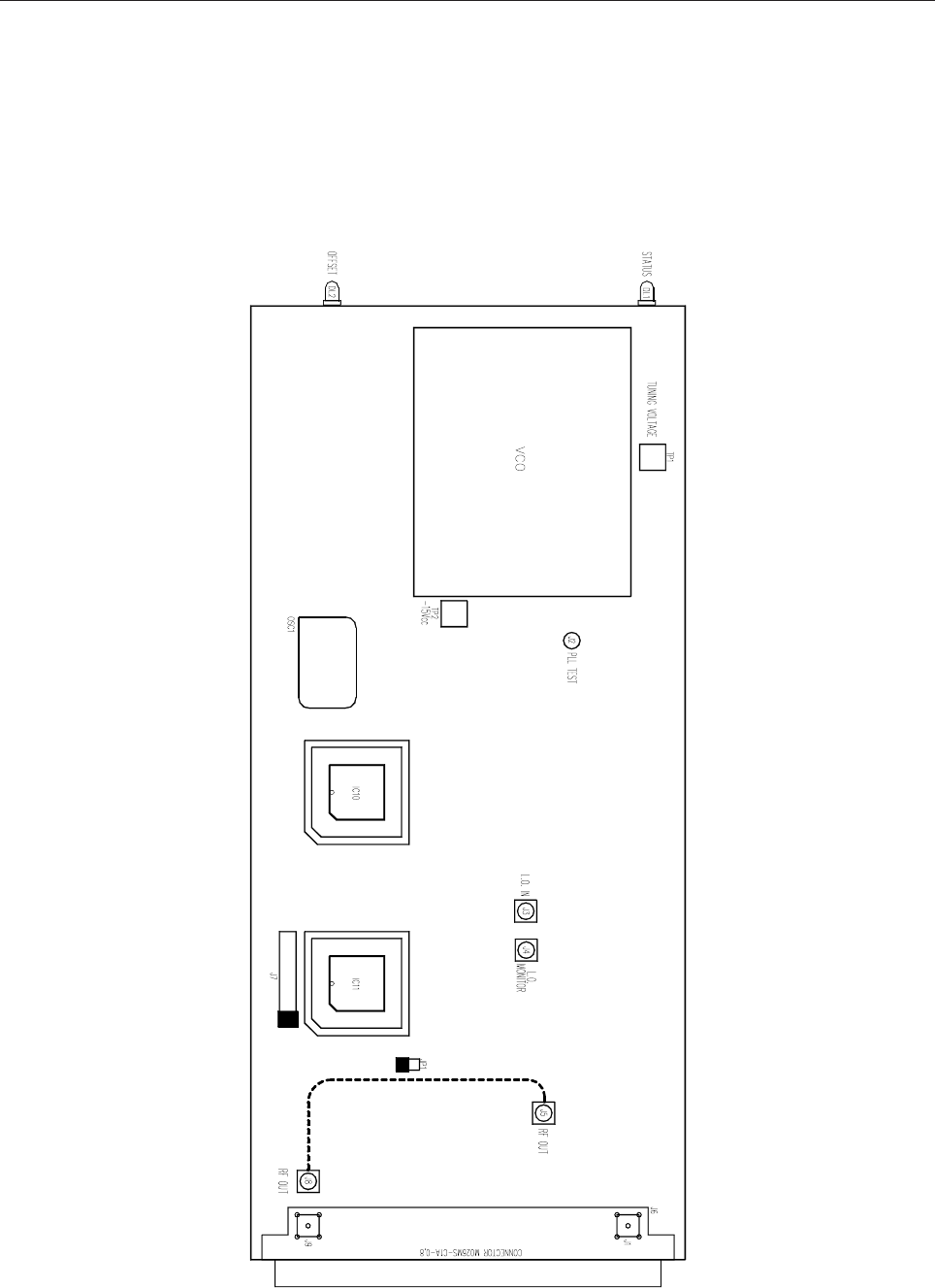
- Description of the adjustment points
COMPONENT DESCRIPTION
C1, C2, C3 Tuning of the local oscillator (SCH0292 - 0309 - 0310)
J3 LO input
J5, J8 RF link (absent in case of LO configuration)
J4 LO monitor (panel)
JP1 Unused
J2 Testpoint for the debug of the PLL
106
Component layout for adjustment points
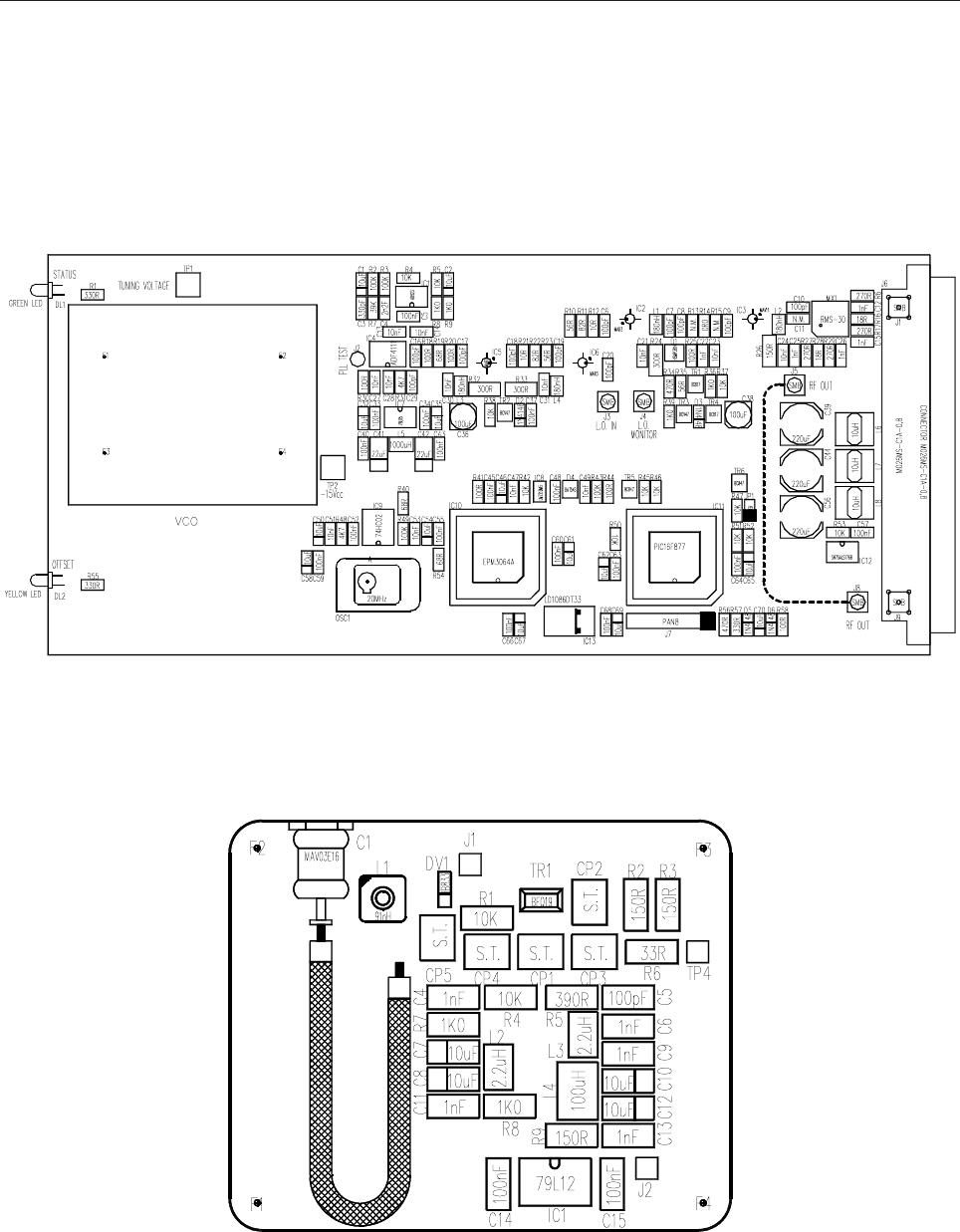
107
Component layout SCH0293AR0
Component layout SCH0292AR0
108
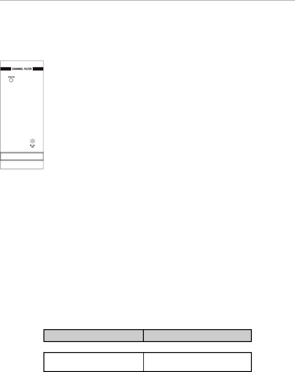
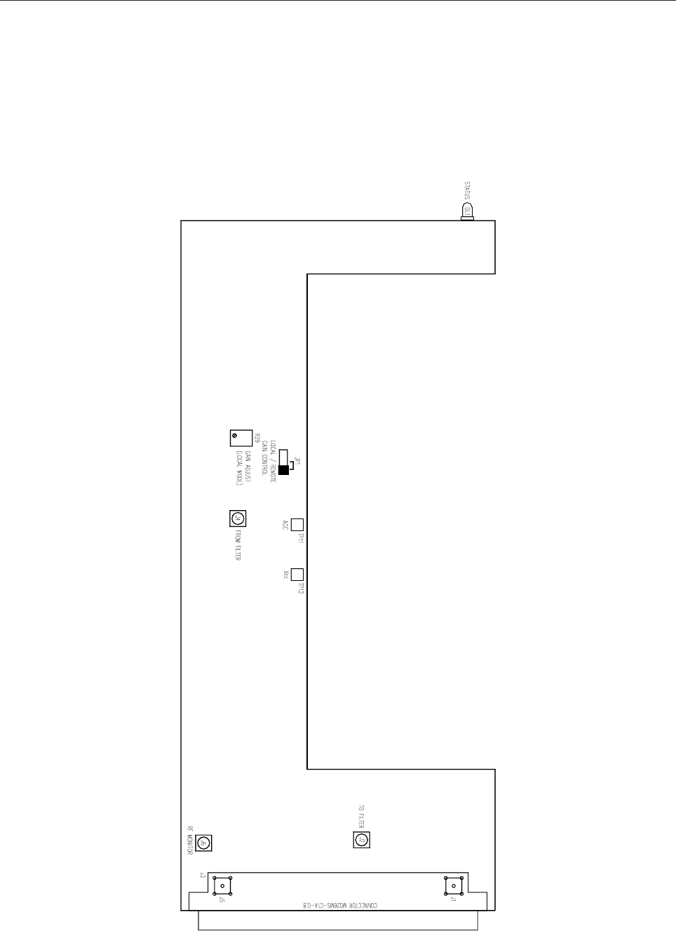
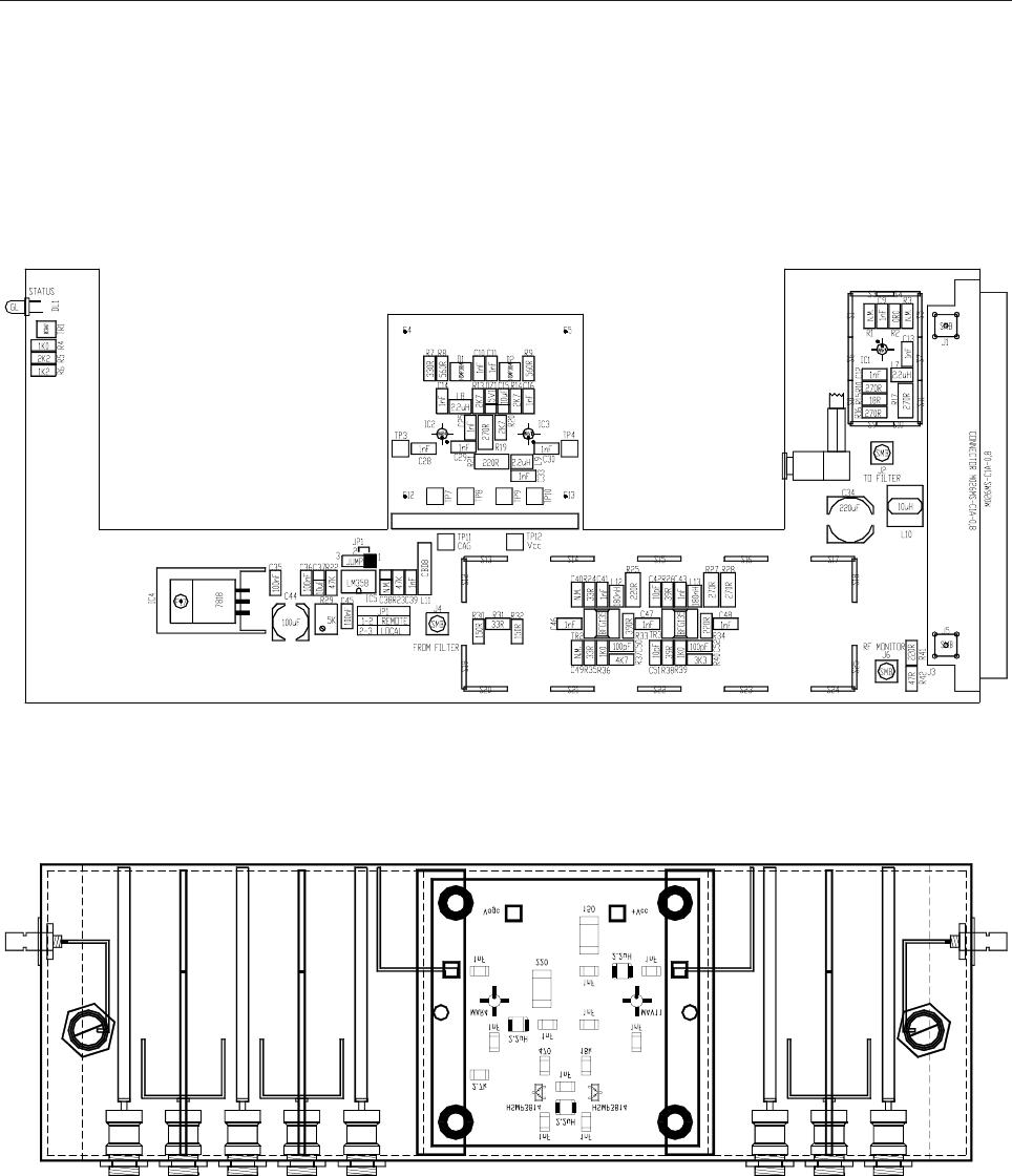
MULT. UHF CHANNEL FILTER MODULE MTG0075AR0
DESCRIPTION
The module filters the signal coming from the conversion mixer removing the local oscillator
and the upper side-band and contains the voltage-controlled gain stage composed by a
pin-diode attenuation cell followed by a wide-band amplification stage used as driver of
the final stage.
TECHNICAL CHARACTERISTICS
Input/output impedance 50W R.O.S.>20dB
Filter type Active 5-cell band-pass
RF-attenuation type 4 PIN-diodes cell
Output amplifier Wide band
Overall gain 25dB (max.)
The module contains the following blocks:
1. Active band-pass filter filters the lower side-band after conversion, it is split into three windows (I-II
/ III / IV-V band) to ensure the coverage of all of the TV channels to be implemented for all standards,
and contains the PIN-diode attenuation cell for the gain control.
2. Wide-band amplifier amplifies the filtered channel in order to obtain the correct driving level for the
RF final stages (see MTF0088-0087-0089).
CALIBRATION PROCEDURE
- List of instruments
MEASURE INSTRUMENT
Calibration of the channel filter - Network analyser
- Spectrum analyser with tracking
109
The calibration procedure of the module requires a complete structure of display board (see MTG0079)
and extension module (see MTG0095) in order to perform the software selection which will be referred
to later and power the module itself.
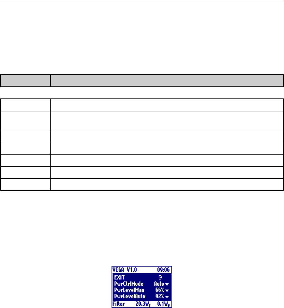
- Menu of the Multistandard UHF Channel Filter Module
Verification of the channel filter connect a network analyser to the channel filter and calibrate its
components to obtain the desired frequency response:
qConfigure the module with PwrCtrlMode Man and verify that it is possible to change the gain of the filter
by acting on PwrLevelMan, setting JP1 Remote.
Verification of the wide-band amplifier section connect a spectrum analyser with tracking between J4
and J5 check that the frequency response of the amplifier is flat within 1dB from 50MHz to 900MHz.
- Description of the adjustment points
COMPONENT DESCRIPTION
C1-C8, C18-19 Channel filter calibration for bands III and IV-V
C17, C20-24,
C26-27, C31-32 Channel filter calibration for band I-II
L1-6 Channel filter calibration for band I-II
J6 RF monitor (panel)
JP1, R29 Local gain control of the filter
J2 Channel filter input
J4 Channel filter output
110
Component layout for adjustment points
111
Component layout SCH0222AR2
Component layout UHF Channel Filter

112
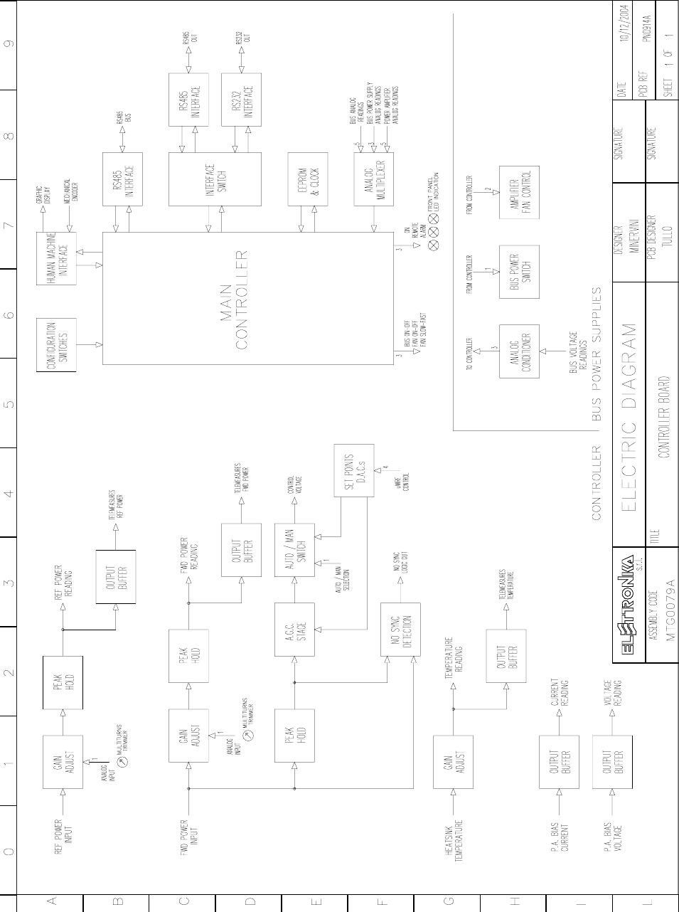
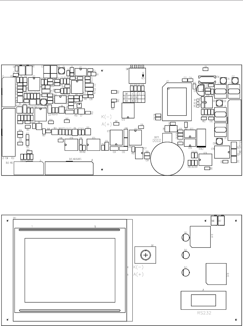
CONTROLLER MODULE MTG0079AR0
SCH0135AR1 DESCRIPTION
The Controller module, located on the right side of the VEGA
TV modulator, is the user interface of the whole modulator. It
gathers the data from all the sections of the modulator, processes
them by means of a 16bit flash micro-controller by Fujitsu and
makes them available to the user both through the local interface,
composed by a display and a knob, and the remote interface
made up by the serial port (either the RS232 on the front or the
RS485 on the back, as selected) or the interface of the
telemeasuring connector.
The acquisition and setting of all the concerned parameters is
made in two different ways. Analog measures reach the board
from the individual modules as voltages, are conditioned on the board and then converted by an internal A/D
converter in the micro.
The remaining parameters are gathered through a 2-wire RS485 interface, which runs on the bus. The display
board acts as master on this 485 bus. Besides it is provided with an RTC and a non-volatile memory on an
internal I2C bus.
- Dip-Switch
The display board is provided with 4 dip-switches. The dip-switches 3 and 4 are used to program the flash
memory of the flash micro-controller by Fujitsu, in detail:
DIP3: On DIP4: Off Boot Programming
DIP3: Off DIP4: On Run or Firmware Programming
The "Boot Programming" configuration is only for BIOS programming purposes.
Once the BIOS has been programmed, the firmware has to be programmed at least once in order to use the
board. The firmware programming and the normal operation of the board are obtained with the same position
of the dip switches.
For more detail on Firmware upgrade please refer to the "Firmware Upgrade" section.
DIP2: On Factory setting
DIP2 is set to ON only during the factory setup of the exciter. This allow to store in the memory all of the
settings made as 'factory defaults'.
Once the test is completed, and while the modulator is used normally, the DIP2 must be kept OFF.

113
- LEDs
The board is provided with three LEDs.
- On (green): it is lit when the exciter is switched on by local or remote control. The LED is blinking till the
power reach his nominal value.
- Remote (yellow): it is lit when the exciter has been set to accept remote commands. To have it accept local
commands again, the local/remote selection menu can be used.
- Alarm (red): shows that an alarm is present.
In case of alarm the red LED lights up and the icon of a bell appears in the upper bar of the display. If the alarm
disappears, the red LED is turned off and the bell starts blinking, in order to show that an anomaly occurred.
To know the details of the anomaly and when it occurred, the history menu can be used. Once this menu is
accessed, the blinking bell icon disappears.
While an alarm is present the exciter switch off the output power. When the alarm disappear, the power is
switched on again. After 5 times the exciter switch off the output power, the exciter goes in LockOut state: the
power remains off till the user reset the LockOut. If the fails are far more that 1 hour than the LockOut counter
is automatically cleaned.
TECHNICAL CHARACTERISTICS
Flash ROM 256kByte
RAM 6kByte
EEPROM 64kBit
Serial interfaces 2xRS485 or 1xRS485 + 1xRS232
Graphic display 128x64pixel blue with white LED back light
Encoder Mechanical with push button
Clock and Calendar Lithium battery backup
Telemeasures Output: FWD, REF, Alarm
Input: Remote OFF
FIRMWARE UPGRADE
Inside the VEGA exciter there are 5 micro-controllers. One of these is the one of the display board (16bit
Fujitsu with 256K Flash) while 4 are in the audio, video, local oscillator and external reference boards
respectively (8bit Microchip with 8K Flash).
It is possible to upgrade all of the micro-controllers of the exciter, but the procedures differ from the display
one and the remaining four.
All upgrades are made by means of the RS232 connector on the front panel of the exciter.
All of the firmware inside the exciter are made up by two parts: the BIOS and the firmware proper. The
former only programs the built-in Flash memory, while all of the operations of the micro are determined by the

114
latter.
l Upgrade of the BIOS of the display board:
While the exciter is off, set the dip-switched of the board on these positions DIP3:ON DIP4:OFF. Run the
Fujitsu Flash MCU programmer application, select the BIOS file to be used, select download and follow the
instructions given by the application.
l
Upgrade of the FIRMWARE of the display board:
A display board provided with the BIOS is needed.
While the exciter is off, set the dip-switched of the board on these positions DIP3:OFF DIP4:ON. Run the
Vega Flash Application, select the upgrade of the display board and the file to be used, select download and
switch the exciter on. The upgrade will start automatically.
l
Upgrade of the boards on the BUS:
A working display board is needed in order to upgrade the boards on the BUS, because the programming of
the modules is made trough the display board.
Warning: while it is possible to program both the BIOS and the firmware of the display board, it is only
possible to change the firmware, and not the BIOS, of the boards on the bus. Since the BIOS is in the same
micro as the firmware, this means that it is not possible to program the micro of a board on the bus on a virgin
micro, which can be done, instead, on the display.
To proceed with the upgrade, while the exciter is on and remote, run the Vega Flash Application, select the
board to be upgraded and the file to be sent, then select download. The upgrade will start automatically.
115
116
Component layout SCH0135AR1 - Bot layer
Component layout SCH0135AR1 - Top layer
117
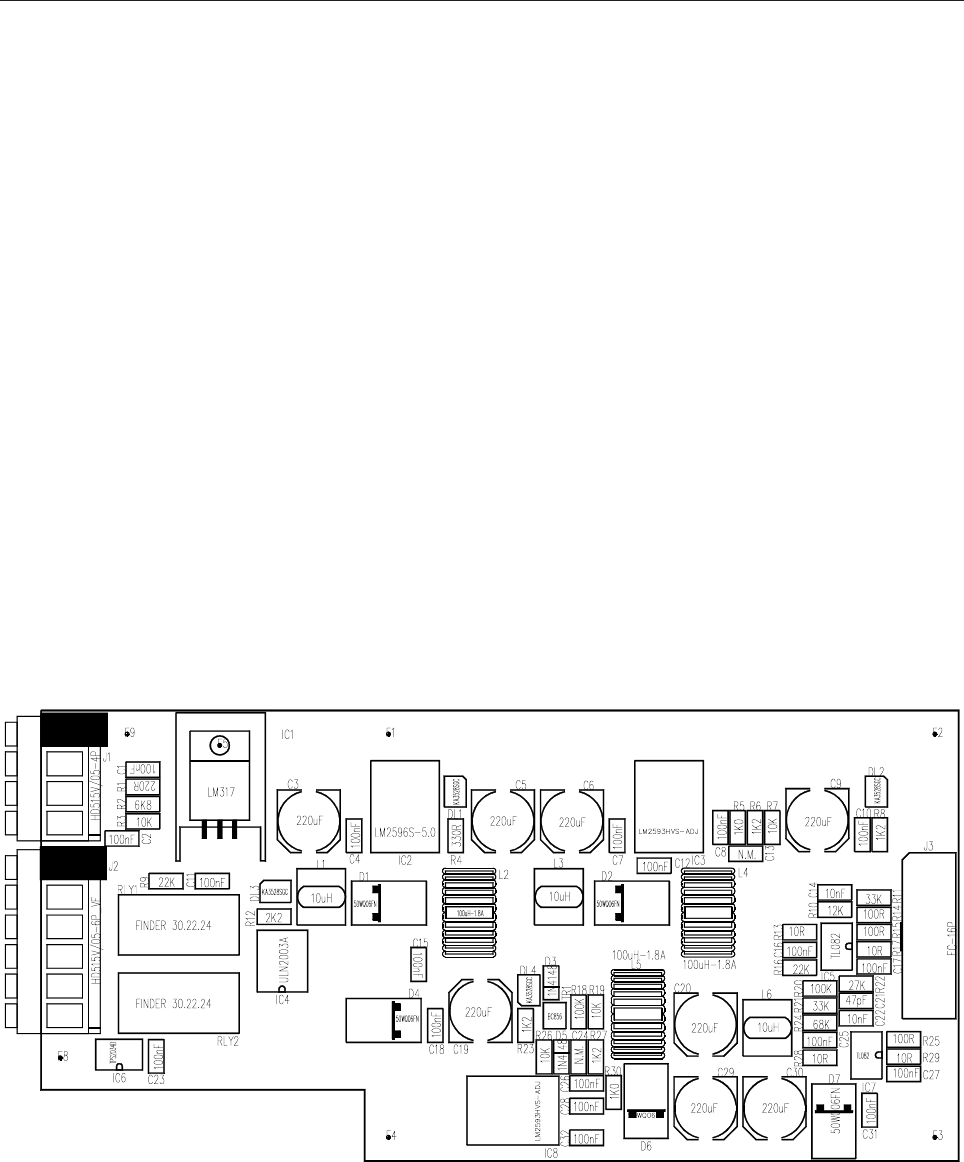
Component layout SCH0231AR1
SCH0231AR1 DESCRIPTION
The power supply accepts a nominal continuous input voltage of 28V and supplies three continuous current
output with voltages of +5V, +15V and -15V. It also provides a voltage of +28V to the system bus. The
power supply voltages towards the system bus are switched by means of relays controlled by the micro-
processor of the control board.
There are switching regulators for the +5V, +15V and -15V voltages.
The power supply board provides the operating voltages to the control board trough multi-wire flat cable. In
this there are also analog voltages to monitor the power supply status. The monitoring of the +5V, +15V and
-15V voltages are conditioned to about 4V nominal.
The board provides the power supply to the system fan. Its on/off status and its speed can be set by the
micro-processor of the control board.
The connections to the system bus and power supply board are made using a fast-lock connector.
118
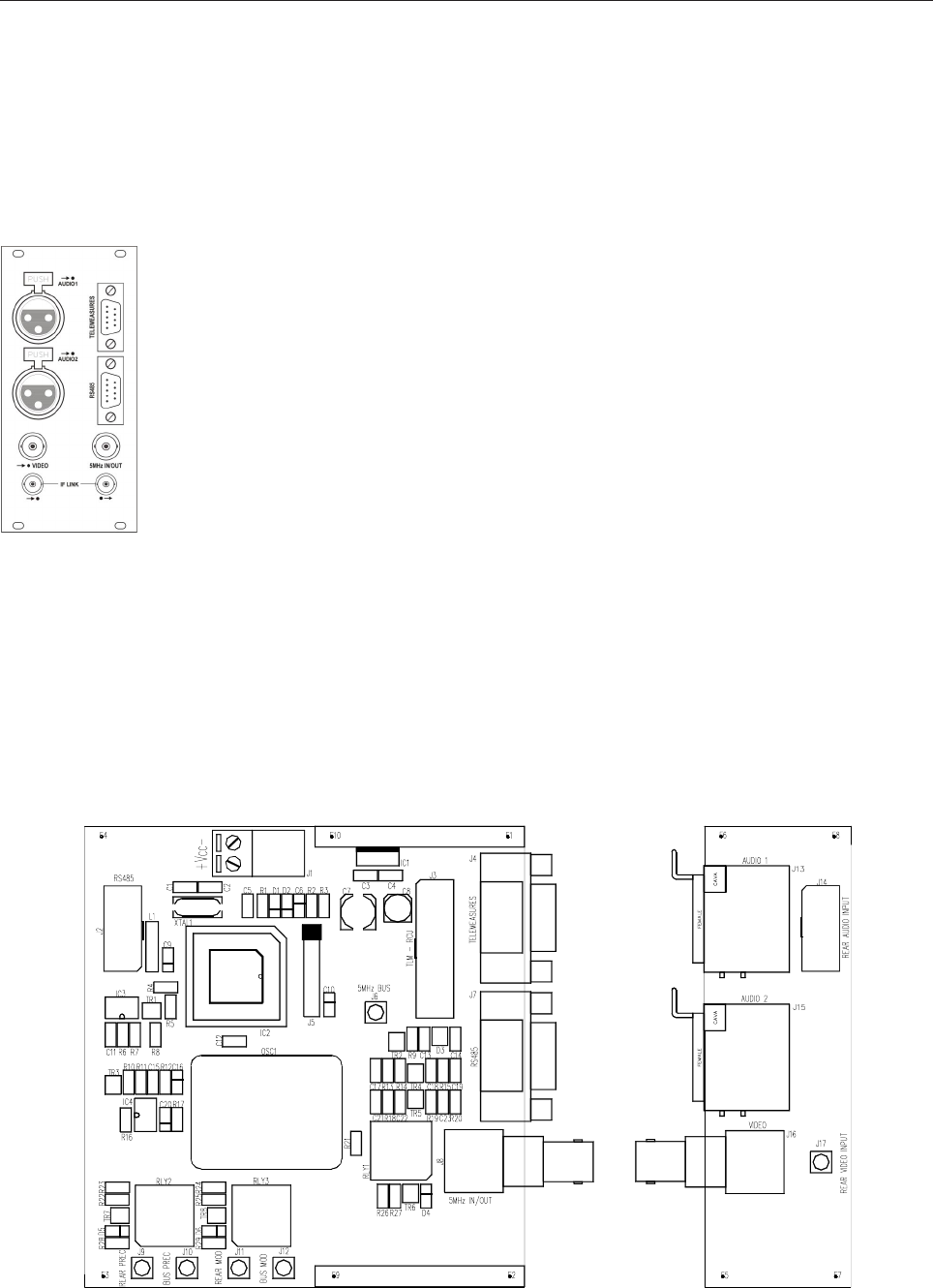
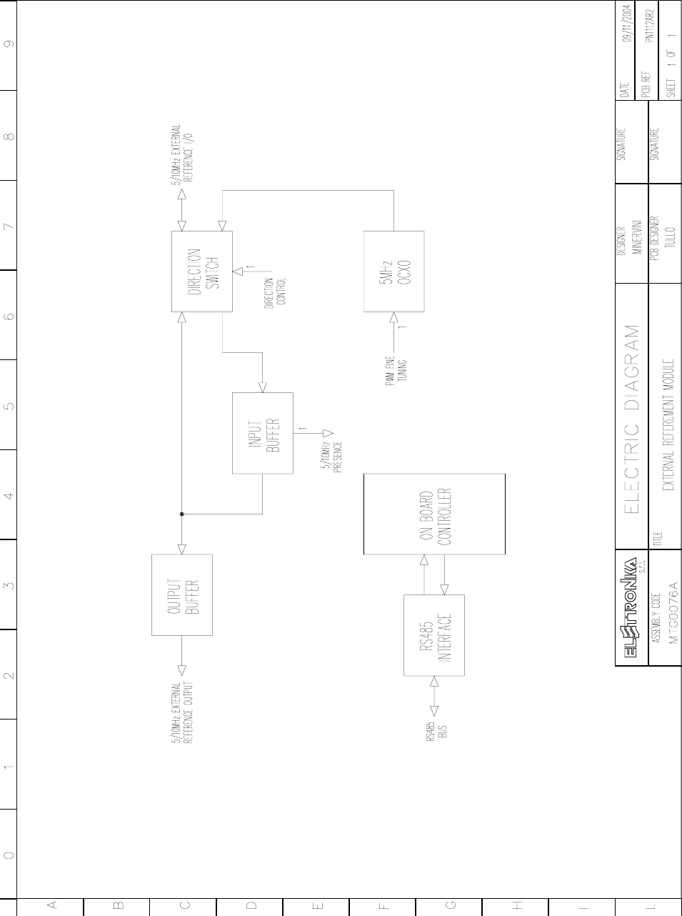
EXTERNAL REFEREMENT MODULE MTG0076AR0
DESCRIPTION
The board contains the 5/10MHz external reference and a series of functions on the back
of the apparatus: the rear audio and video inputs, the telemeasuring connectors and the
RS485, the external reference input (or output) and the IF connection before the linearity
pre-corrector, in order to allow the insertion in the chain of different modulation systems
such as NICAM.
TECHNICAL CHARACTERISTICS
Frequency reference 5-10MHz
Detector presence 0dBm threshold
Connector BNC input-output selectable (sw)
O.C.X.O. Characteristics (optional) 0.05ppm long term stability
O.C.X.O. Tuning frequency ±5ppm fine tunability (sw)
O.C.X.O. Warm up consumption 4.5W 10min @25°C
IF Link OPEN-CLOSED Selection switch (sw)
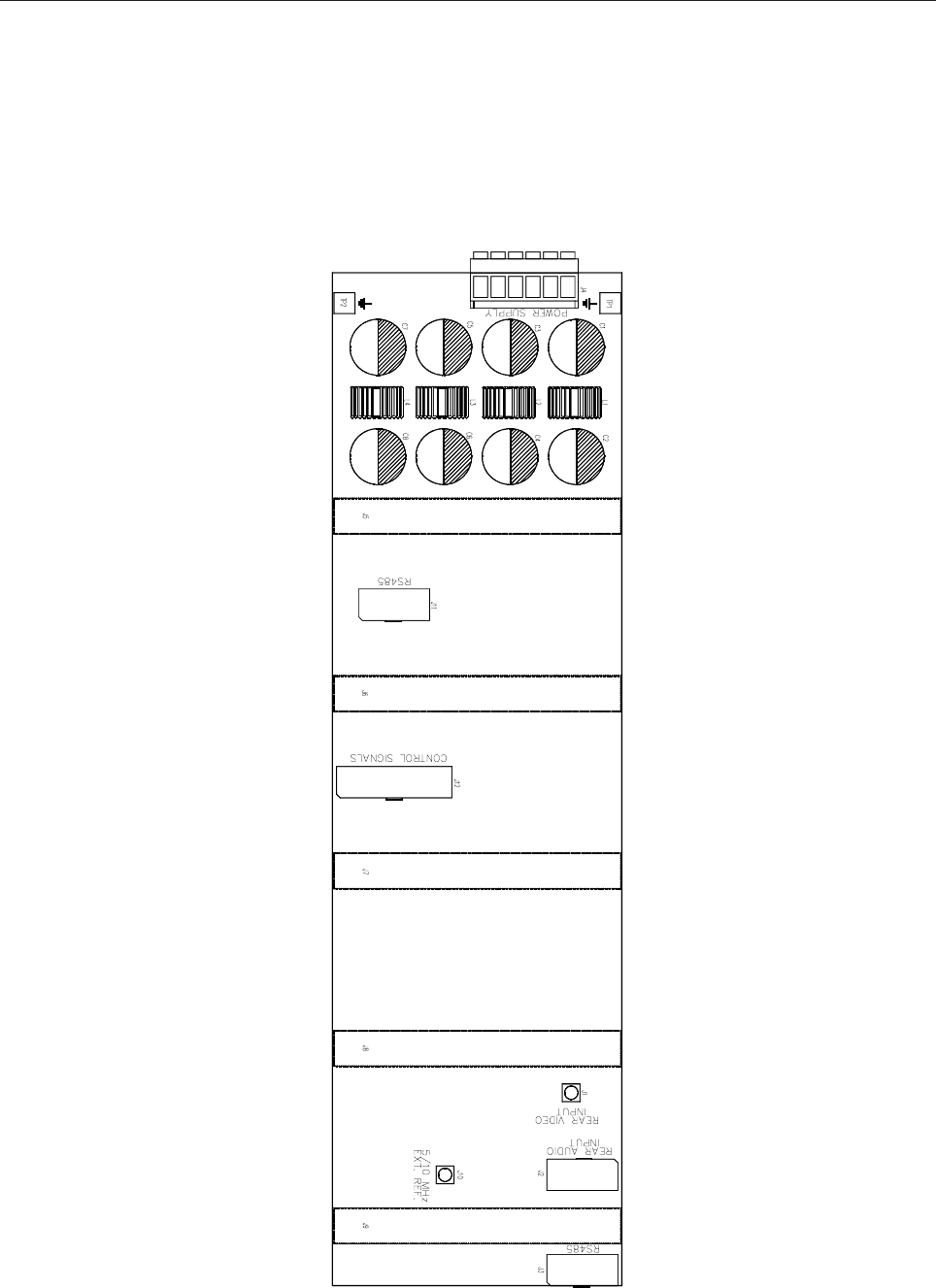
A-V Rear connections Available on exciter arrangement
Telemasures DB9
RS485-RS232 DB9 Selectable (sw)
Component layout SCH0266AR1
119
120
The module contains the following blocks:
1. Input and output buffers de-couple the internal circuitry from the I/O conenctors and detect the
presence of the reference signal.
2. Direction switch allows the configuration of the BNC as either input or output for the 5/10MHz
reference signal.
3. 5MHz O.C.X.O. 5MHz internal reference system (optional), which frequency can be fine-adjusted
via software.
4. Controller all of the described operations are managed by a microcontroller communicating to the user
interface board (see MTG0079) by RS485 protocol; the local controller stores the status of the module
and a reprogramming of the firmware (possible via RS485 from the display board) does not after its
contents.
EXTERNAL PIN OUT CONNECTORS
Telemeasures (DB9) RS485 (DB9)
CALIBRATION PROCEDURE
- List of instrument
PIN N° SIGNAL TYPE IN / OUT FUNCTION
1Analog Output FWD Power
2Analog Output REF Power
3 Analog Output Temperature
4 Analog Input FWD Power
5GND - -
6 Digital Output Free contact with pin7 - Alarm
7 Digital Output Free contact with pin6 - Alarm
8 Digital Input GND= Off - OPEN= On
9 Digital Input N.U.
PIN N° FUNCTION
1N.C.
2RX-
3RX+
4+5V
5GND
6+5V
7TX-
8TX+
9N.C.
MEASURE INSTRUMENT
Frequency referement control - Spectrum analyser
121
The calibration procedure of the module requires a complete structure of display board (see MTG0079)
in order to perform the software selection which will be referred to later and power the module itself..
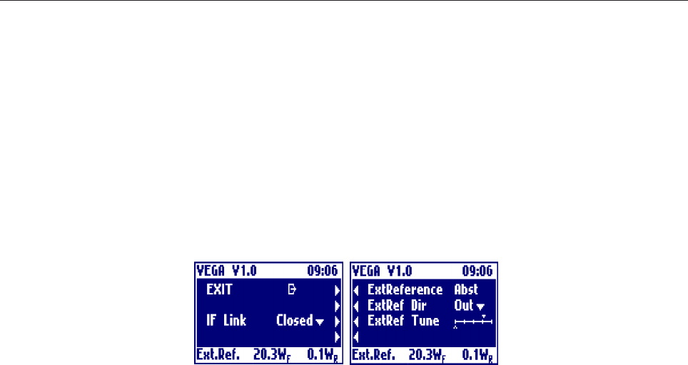
- Menu of the External Referement Module
Verification of the external reference section connect a spectrum analyser to the BNC labelled EXT
REF IN/OUT and check the sections therein:
qConfigure the module with ExtREF Dir Out and check the presence of the 5MHz carrier with
ExtReference set to Pres in the display menu.
qCheck that the 5MHz frequency is fine-adjusted by acting on ExtRef Tune.
Verification of the IF Link section:
qConfigure the module with IF Link open and closed checking the switching of the relays.
122
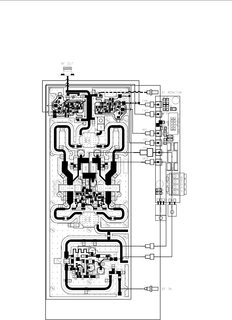
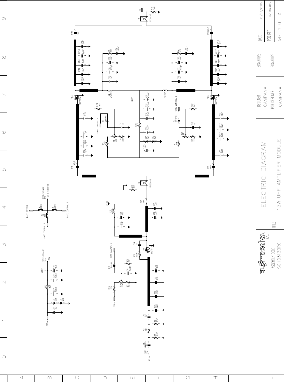
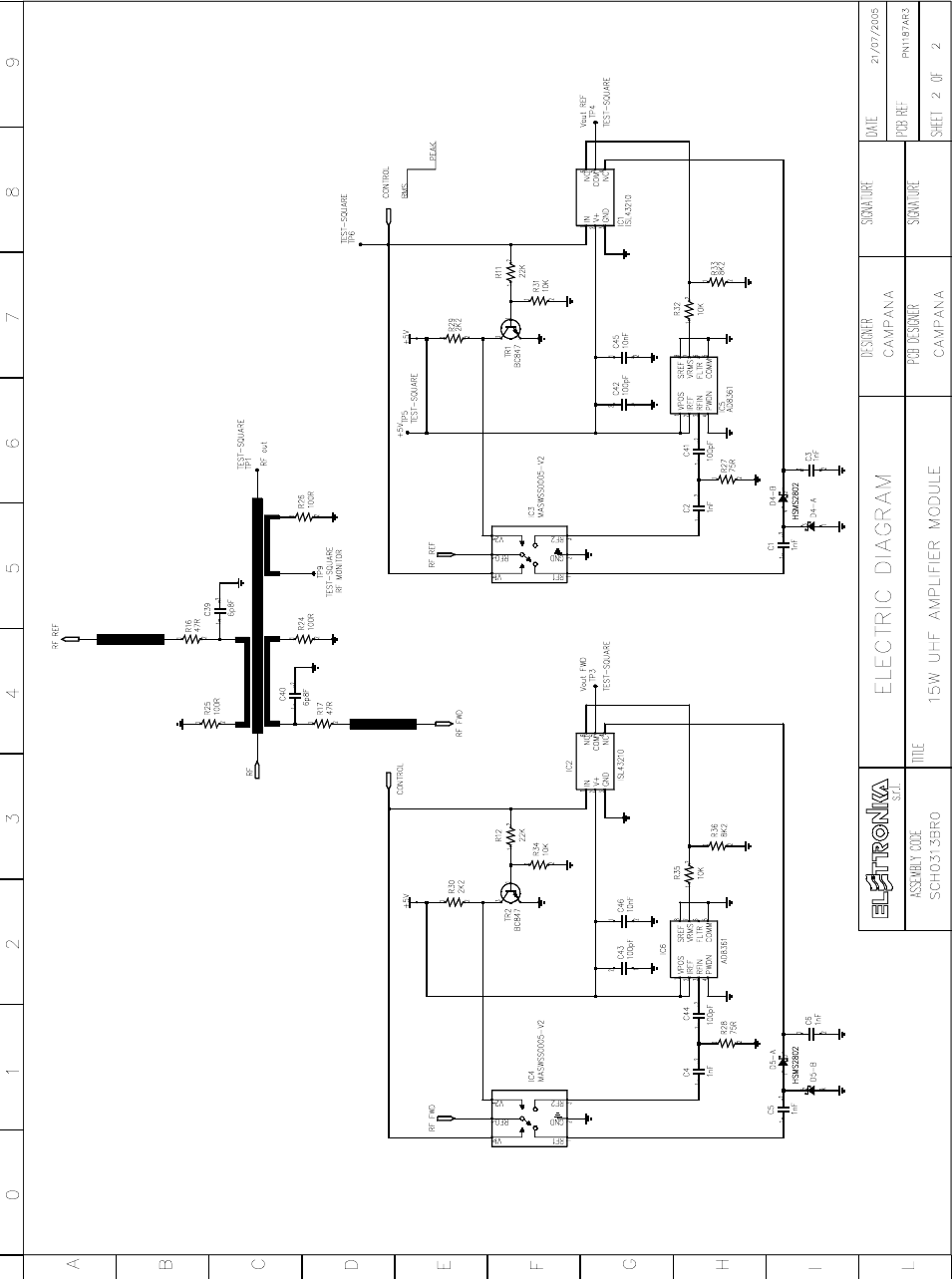
15W UHF AMPLIFIER MODULE MTF0088BR0
Component layout MTF0088BR0
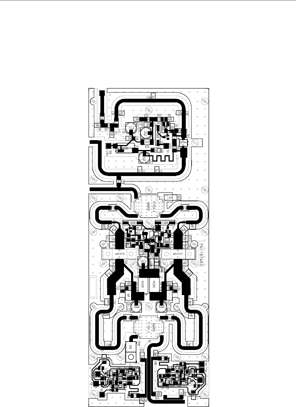
123
Component layout SCH0313BR0 - 15W UHF Amplifier Module
124
125

126
COMPONENT LIST SCH0313BR0
Part Name/Number Description Qty. Comps. Page 1/2
CC 100nF-S 01065C 01065C Y5V 1206 COND 6 C27-29, C32-34
CC 100pF-S 01092 01092 SMD 1206 COND 3 C7-9
CC 10pF-S 01086 01086 SMD 1206 COND 1 C38
CC 1206 N. M. N. M. SMD 1206 COND 1 C37
CC 1nF-S 01096 01096 SMD 1206 COND 7 C10-16
CC 1p2F-S 01081 01081 SMD 1206 COND 1 C17
CC 1uF 100V 01077A CERAMIC COND. 2 C25-26
CC 2p2F-S 01081B 01081B SMD 1206 COND 2 C35-36
CC 470nF 63V-S 01073 POLIESTER COND SMD 1 C31
CC 4p7F-S 01083 01083 SMD 1206 COND 1 C30
CE 10uF50V-S 01779A 01779A ELETTR SMD COND 7 C18-24
CP 10pF-S CHIP CHB 2 CP7, CP9
CP 12pF-S CHIP CHB 2 CP11-12
CP 15pF-S 01121 CHIP CHB 4 CP13-16
CP 1p8F-S 01102A CHIP CHB 4 CP8, CP10, CP19-20
CP 47pF-S 01130 CHIP CHB 2 CP5-6
CP 5p6F-S 01109 CHIP CHB 2 CP2, CP4
CP 6p8F-S CHIP CHB 6 CP1, CP3, CP17-18, CP21-22
D 1N4148-S 03002 03002 SMD DIODE 3 D1-3
DZ 3V9-S 03134 SMD ZENER DIODE 4 DZ1-4
H ANAREN 1F1304-3 05368 HIBRID COUP. ANAREM 2 H1-2
IND CBD8 05072 05072 INDUCTOR 3 L4-6
IND VK200 05013 05013 INDUCTOR 3 L1-3
R 10R-S 00017A 00017A RES 1/4W 5% SMD 1206 2 R4-5
R 18R-S 00020A 00020A RES 1/4W 5% SMD 1206 1 R37
R 1K5-S 00043A 00043A RES 1/4W 5% SMD 1206 2 R22-23
R 22K-S 00057A 00057A RES 1/4W 5% SMD 1206 3 R1-2, R15
R 270R-S 00034A 00034A RES 1/4W5% SMD 1206 2 R6-7
R 330R-S 00035B 00035B RES 1/4W 5% SMD 1206 1 R38
R 39R-S 00024A 00024A RES 1/4W 5% SMD 1206 1 R39
R 3K3-1W-S 00400 RES 1W 5% SMD 2512 2 R20-21
R 47K-S 00061A 00061A RES 1/4W 5% SMD 1206 3 R3, R13-14
R 47R-1W-S 00384 RES 1W 5% SMD 2512 1 R19
R 50R 60W TERM 00432 50 OHM 60W RF TERM 1 R18
RV 50K-S-H/S 00797 00797 SMD VARIABLE RESISTOR 3 R8-10
TR BLF1043-S 03469 LDMOS TRANSISTOR 1 TR3
TR MRF373A-S 04031A LDMOS TRANSISTOR 2 TR4-5
CC 100pF-S 01092C 01092C SMD 0805 COND 4 C41-44
CC 10nF-S 01053A 01053A SMD 0805 COND 2 C45-46
CC 1nF-S 01096A 01096A SMD 0805 COND 6 C1-6
CC 6p8F-S 01084 01084 SMD 1206 COND 2 C39-40
D HSMS2802 03207 03207 SMD DIODE 2 D4-5
IC AD8361 04899 04899 SMD INTEG CIRCUIT 2 IC5-6

127
Part Name/Number Description Qty. Comps. Page 2/2
IC ISL43210-S 04567 SMD INTEG CIRCUIT 2 IC1-2
IC MASWSS0005-V2-S 04568 SMD INTEG CIRCUIT 2 IC3-4
R 100R-S 00029A 00029A RES 1/4W 5% SMD 1206 3 R24-26
R 10K-S 00053C 00053C RES 1/4W 5% SMD 0805 4 R31-32, R34-35
R 22K-S 00057A 00057A RES 1/4W 5% SMD 1206 2 R11-12
R 2K2-S 00045C 00045C RES 1/4W 5% SMD 0805 2 R29-30
R 47R-S 00025A 00025A RES 1/4W 5% SMD 1206 2 R16-17
R 75R-S 00221C 00221C RES 1/4W 5% SMD 0805 2 R27-28
R 8K2-S 00052A 00052A RES 1/4W 5% SMD 1206 2 R33, R36
TR BC847 03456 03456 NPN SMD TRANSISTOR 2 TR1-2
128
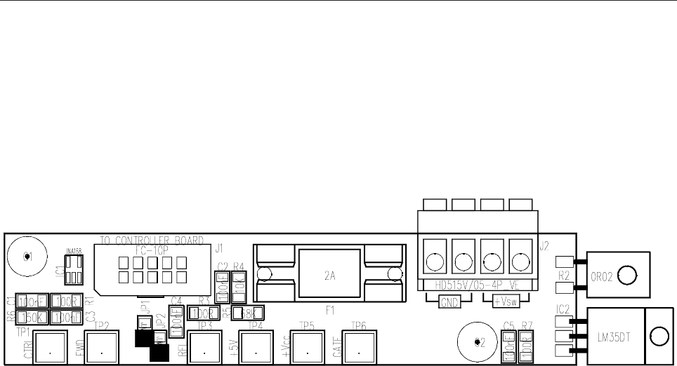
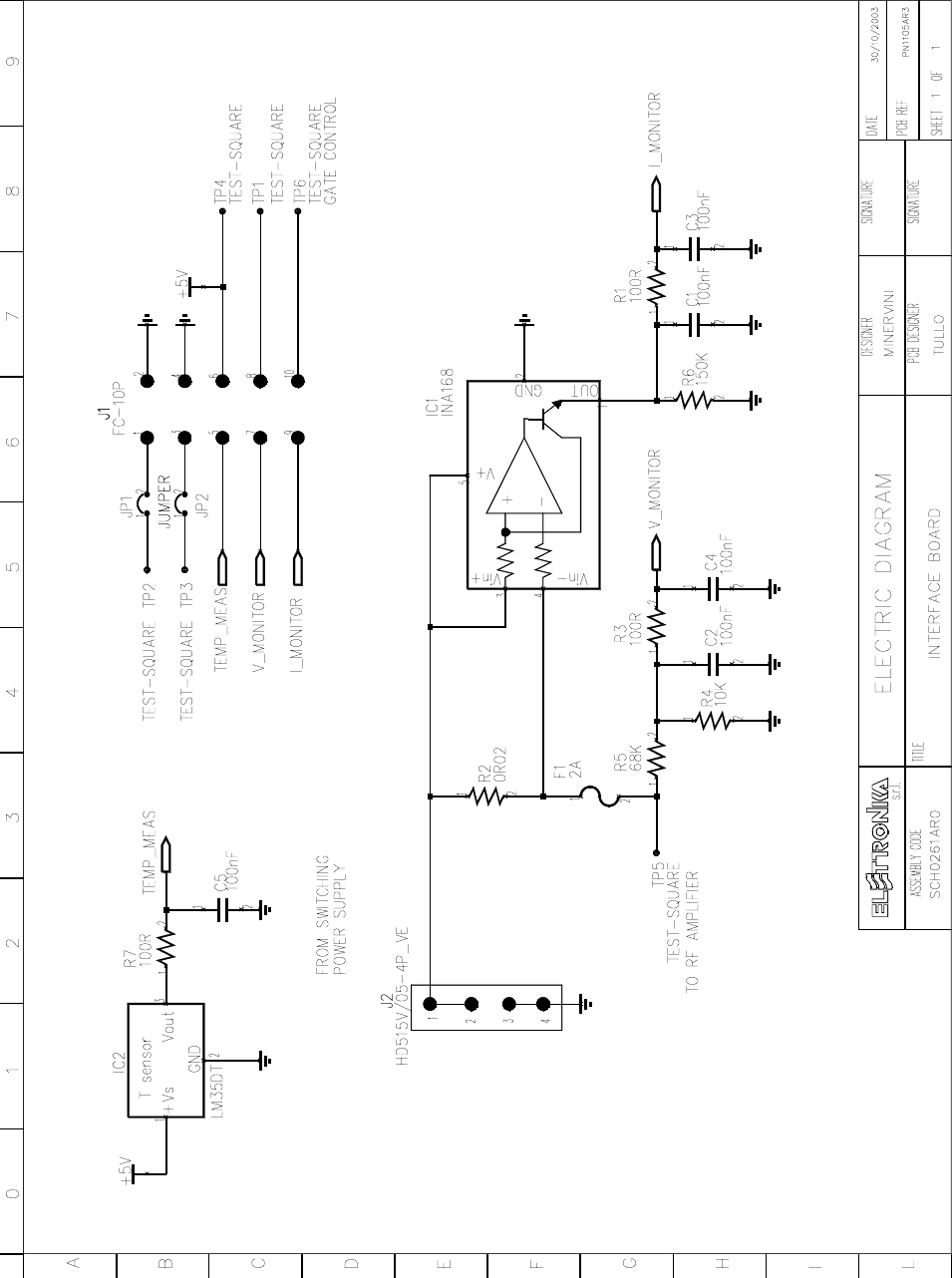
Component layout SCH0261AR0 - Interface Board
COMPONENT LIST SCH0261AR0
Part Name/Number Description Qty. Comps.
CC 100nF-S 01065C 01065C Y5V 1206 COND 5 C1-5
FUSE 2A-PCB 7543 7543 PORTA FUSIBILE + FUSE 5x2 1 F1
IC INA168 04600A SMD INTEG CIRCUIT 1 IC1
IC LM35DT 00664 00664 INTEG CIRCUIT 1 IC2
J CON HD515V/05-4PVE 02881 + 02882 PANDUIT PCB CONN 1 J2
J FC-10P 02697-02699 02697+02699 PCB CONNECTOR POL 1 J1
JU JUMP2 02739-02742 02739+02742 MASCHIO PAN2 2 JP1-2
R 0R02 00356 RES 20W 1% 1 R2
R 100R-1%-S 00029D 00029D RES 1/4W 1% SMD 1206 3 R1, R3, R7
R 10K-1%-S 00053B 00053B RES 1/4W 1% SMD 1206 1 R4
R 150K-S 00067A 00067A RES 1/4W 5% SMD 1206 1 R6
R 68K-1%-S 00063B 00063B RES 1/4W 1% SMD 1206 1 R5
129
130
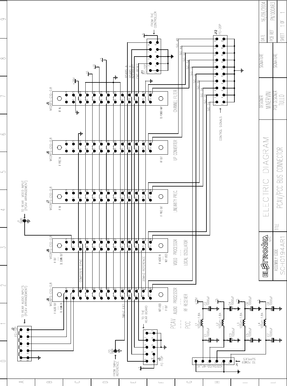
Component layout SCH0194AR1
BUS STRUCTURE SCH0194AR1
131

132
COMPONENT LIST SCH0194AR1
Part Name/Number Description Qty. Comps.
CC 100nF-S 01065C 01065C Y5V 1206 COND 19 C1-2, C4, C7-8, C10-12, C15-18,
C23, C25-28, C31-32
CC 10nF-S 01053B 01053B SMD 1206 COND 2 C14, C22
CC 1206 N. M. N. M. SMD 1206 COND 2 C13, C24
CC 47pF-S 01100 01100 SMD 1206 COND 1 C21
CE 220uF50V LOW ESR 01799A ELETTR SMD COND LOW ESR 8 C3, C5-6, C9, C19-20, C29-30
D 1N4148-S 03002 03002 SMD DIODE 2 D3, D5
D 50WQ06FN 03019A SMD DIODE SCHOTTKY 5,5A 5 D1-2, D4, D6-7
DL KA-3528SGC 03057 03057 GREEN SMD LED DIODE 4 DL1-4
IC LM2593HVS-ADJ 04089 SMD INTEG CIRCUIT 2 IC3, IC8
IC LM2596S-5.0 04580 SMD INTEG CIRCUIT 1 IC2
IC LM317 04340 04340 INTEG CIRCUIT 1 IC1
IC TL082-S 04796A 04796A SMD INTEG CIRCUIT 2 IC5, IC7
IC TPS2034D-S 04088 SMD INTEG CIRCUIT 1 IC6
IC ULN2003A 4870 04870 SMD INTEG CIRCUIT 1 IC4
IND MS85 10uH-S 04948 INDUCTOR 2,7A 3 L1, L3, L6
IND T100uH-1.8A 4958 04958 TOROIDAL-STORAGE CHOKES 3 L2, L4-5
J CON HD515V/05-4PVE 02881 + 02882 PANDUIT PCB CONN 1 J1
J CON HD515V/05-6PVE 02883 + 02884 PANDUIT PCB CONN 1 J2
J FC-16P 02701-02700 02701+02700 PCB CONNECTOR POL 1 J3
R 100K-1%-S 00065B 00065B RES 1/4W 1% SMD 1206 2 R18, R20
R 100R-1%-S 00029D 00029D RES 1/4W 1% SMD 1206 3 R14-15, R25
R 10K-1%-S 00053B 00053B RES 1/4W 1% SMD 1206 4 R3, R7, R19, R26
R 10R-1%-S 00017D 00017D RES 1/4W 1% SMD 1206 4 R13, R17, R28-29
R 12K-1%-S 00054B 00054B RES 1/4W 1% SMD 1206 1 R10
R 1K0-1%-S 00041B 00041B RES 1/4W 1% SMD 1206 2 R5, R30
R 1K2-1%-S 00042A 00042A RES 1/4W 1% SMD 1206 4 R6, R8, R23, R27
R 220R-1%-S 00033C 00033C RES 1/4W 1% SMD 1206 1 R1
R 22K-1%-S 00057B 00057B RES 1/4W 1% SMD 1206 2 R9, R16
R 27K-1%-S 00058B 00058B RES 1/4W 1% SMD 1206 1 R22
R 2K2-1%-S 00045B 00045B RES 1/4W 1% SMD 1206 1 R12
R 330R-1%-S 00035A 00035A RES 1/4W 1% SMD 1206 1 R4
R 33K-1%-S 00059B 00059B RES 1/4W 1% SMD 1206 2 R11, R21
R 68K-1%-S 00063B 00063B RES 1/4W 1% SMD 1206 1 R24
R 6K8-1%-S 00051B 00051B RES 1/4W 1% SMD 1206 1 R2
RL 30.22.24 07569 07569 RELE 2 RLY1-2
TR BC856 03455 03455 PNP SMD TRANSISTOR 1 TR1
133
SP300-27 SWITCHING POWER SUPPLY E0017
MAIN FEATURES
- Universal AC input / Full range
- Built-in active PFC function, PF>0.95
- Protections: Short circuit / Over load / Over voltage / Over temp.
- Forced air cooling by built-in DC fan
- Built-in cooling Fan ON-OFF control
- Fixed switching frequency at 110kHz
MECHANICAL SPECIFICATION
Air flow
direction
215
32.5
50
25
4-M4 L=6mm
150
C
L
PIN N° ASSIGNMENT
1AC/L
2AC/N
3FG
4-5 DC OUTPUT -V
6-7 DC OUTPUT +V
134
TECHNICAL CHARACTERISTICS
MODEL SP300-27 SP300-48
OUTPUT
DC VOLTAGE 27V 48V
RATED CURRENT 11A 6.25A
CURRENT RANGE 0 ~ 11A 0 ~ 6.5A
RATED POWER 297W 300W
RIPPLE & NOISE (max.) Note 2 200mVp-p 240mVp-p
VOLTAGE ADJ. RANGE 26 ~ 32V 41 ~ 56V
VOLTAGE TOLERANCE Note 3 ± 1.0% ± 1.0%
LINE REGULATION ± 0.2% ± 0.2%
LOAD REGULATION ± 0.5% ± 0.5%
SETUP, RISE, HOLD TIME 1500ms, 50ms, 20ms at full load
INPUT
VOLTAGE RANGE 88 ~ 264VAC 124 ~ 370VDC
FREQUENCY RANGE 47 ~ 63Hz
POWER FACTOR PF>0.95/230VAC PF>0.95/115VAC at full load
EFFICIENCY (Typ.) 86% 85%
AC CURRENT 4A/115VAC 2A/230VAC
INRUSH CURRENT (Max.) 18A/115VAC 36A/230VAC
LEAKAGE CURRENT <2mA/240VAC
PROTECTION
OVER LOAD
105 ~ 135% rated output power
Protection type: Hiccup mode, recovers automatically after fault condition is removed
OVER VOLTAGE
33.7 ~ 39.2V 57.6 ~ 67.2V
Protection type: Hiccup mode, recovers automatically after fault condition is removed
FAN CONTROL O.T.P. RTH1 or RTH2 >= 50°C FAN ON, <= 45°C FAN OFF, >= 70°C output shutdown
ENVIRONMENT
WORKING TEMP. -10 ~ +50°C (Refer to output load derating curve)
WORKING HUMIDITY 20 ~ 90% RH non-condensing
STORAGE TEMP., HUMIDITY -20 ~ +85°C, 10 ~ 95% RH
TEMP. COEFFICIENT ± 0.03%/°C (0 ~ 50°C)
VIBRATION 10 ~ 500Hz, 2G 10min./1cycle, period for 60min. each along X, Y, Z axes
SAFETY & EMC
(Note 4)
SAFETY STANDARDS UL1950, TUV EN60950 Approved
WITHSTAND VOLTAGE I/P-O/P:3KVAC I/P-FG:1.5KVAC O/P-FG:0.5KVAC
ISOLATION RESISTANCE I/P-O/P, I/P-FG, O/P-GD:100M Ohms/500VDC
EMI CONDUCTION & RADIATION Compliance to EN55022 (CISPR22) Class B
HARMONIC CURRENT Compliance to EN61000-3-2,-3
EMS IMMUNITY Compliance to EN61000-4-2,3,4,5,6,8,11; ENV50204, Light industry level, criteria A
OTHERS
MTBF 168.7K hrs min. MIL-HDBK-217F (25°C)
DIMENSION 215*115*50mm (L*W*H)
PACKING 1.18kg; 12pcs/14.2kg/0.98CUFT
135
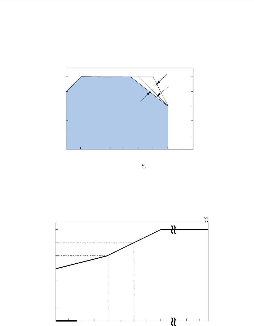
DERATING CURVE
OUTPUT DERATING VS INPUT VOLTAGE
AMBIENT TEMPERATURE ( )
LOAD (%)
20
40
60
80
100
-10 0 10 20 30 40 45 50 (HORIZONTAL)
12~15V
5,7.5V
24~48V
INPUT VOLTAGE (VAC) 60Hz
88 115 135 155 264230
90
100
80
70
60
50
40