Elettronika S r l TXUP10000 10 kW Analog TV Broadcast Transmitter User Manual Nuovo 5
Elettronika S.r.l. 10 kW Analog TV Broadcast Transmitter Nuovo 5
Contents
- 1. User Manual Part 1
- 2. User Manual Part 2
User Manual Part 1

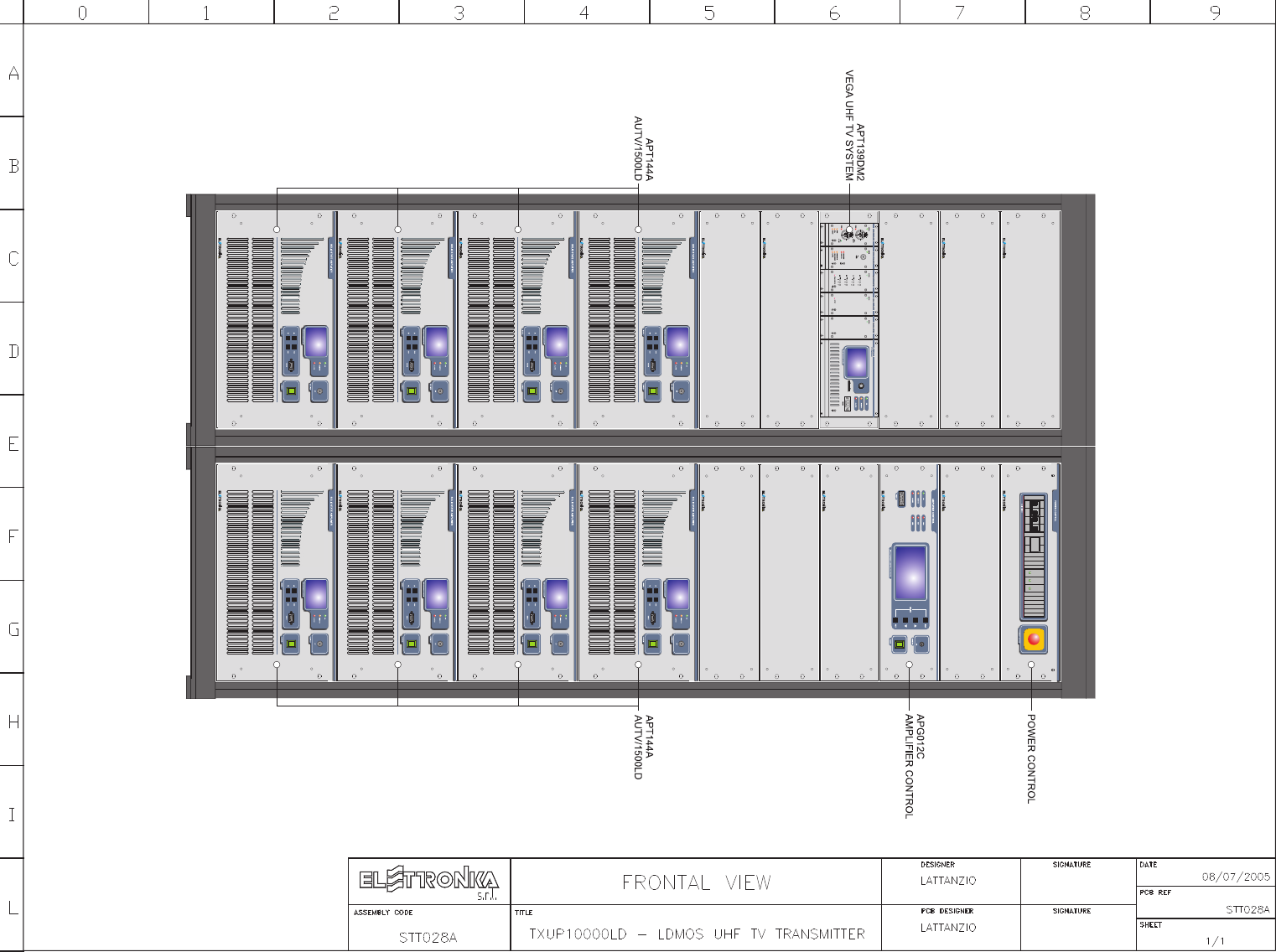
TXUP10000LD
LDMOS - UHF TV Solid State Transmitter
General description
CODE: STT028A TITLE: TXUP10000LD REV: 0 DATE: 08/07/05

SS 96 Km 113
70027 Palo del Colle (Ba) ITALY
Tel. +39 (0)80 626755
Fax +39 (0)80 629262
E-mail: elettronika@elettronika.it
Web site: http://www.elettronika.it
Registration number: IT-17686
Registration number: IT-24436

DESCRIPTION
The TXUP10000LD belongs to the High Power UHF products family of Television Transmitters fully in solid
state technology.
The TXUP10000LD series represents the 10kW TV Transmitters operating in the IV/V Band for Common
amplification process (separate amplification available) of the Vision and Sound carriers. This Transmitters
family has been designed to offer to the customer high performances, high reliability and greater simplicity in
their operation and maintenance procedures.
The Vision and Sound signal processing is provided for all TV Standards and all types of Audio applications
(Mono & Dual sound - NICAM) together with colour systems such as PAL - NTSC - SECAM. Thanks to
the amplitude and phase pre-correction circuit, it is possible to cancel the distortions in the output stage, thus
cutting down the operating costs. The RF transposition in the driver is carried out by a synthesizer with various
possibilities of accuracy and stability as well as precision offset locked by internal or external frequency
reference.
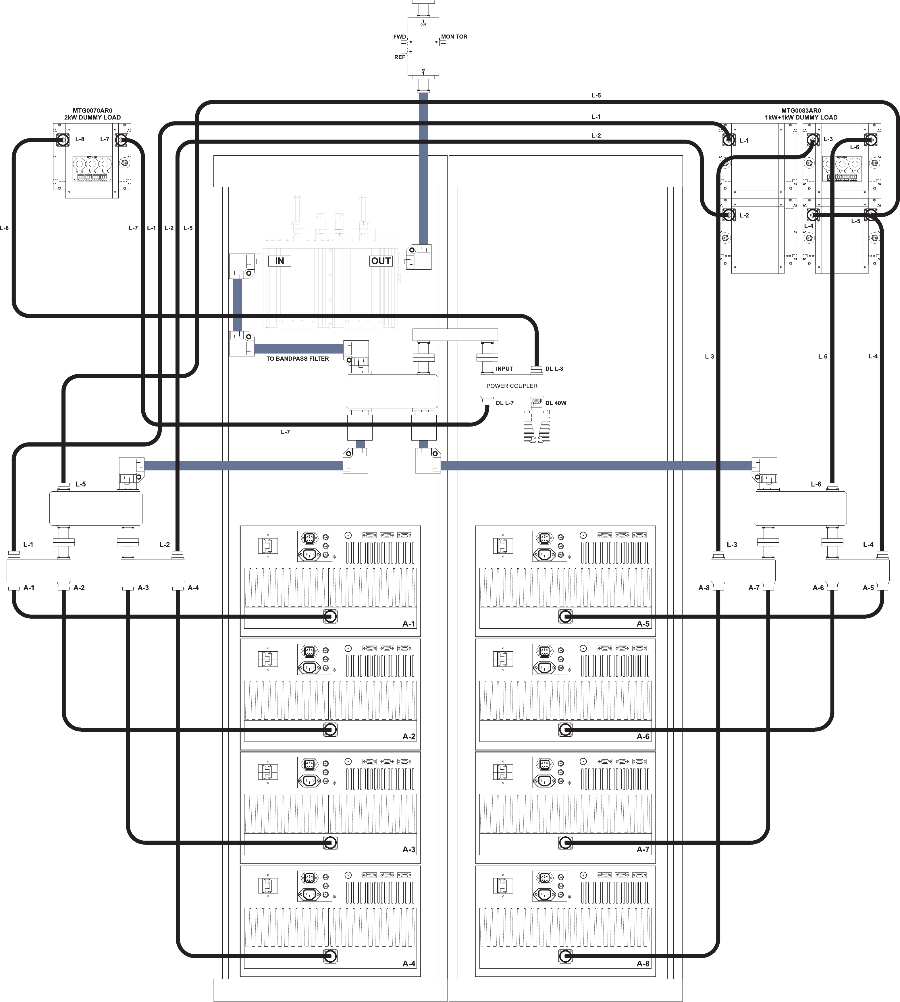
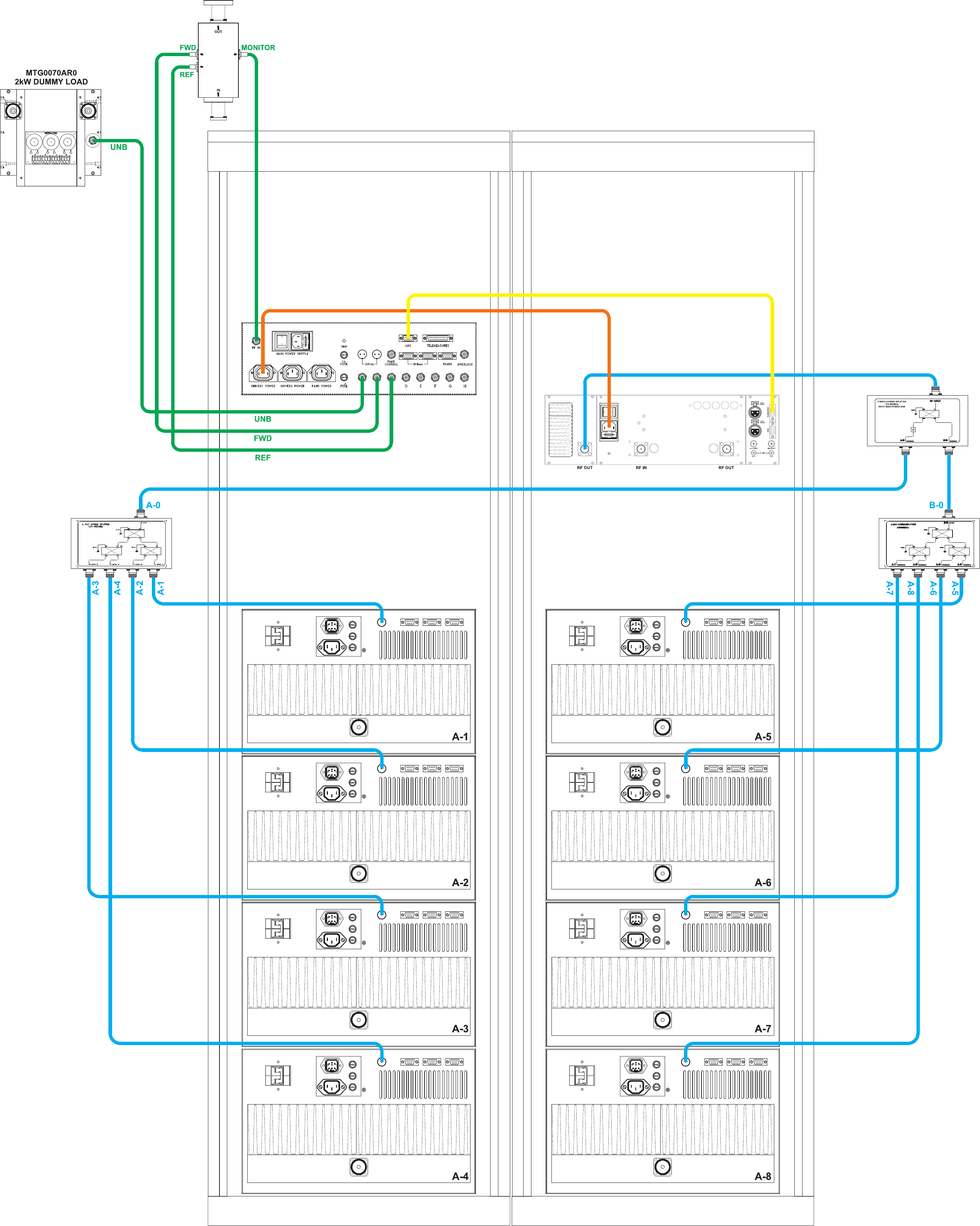
The RF amplifier is made up by eight RF modules installed in a power rack, the modules are dedicated for the
Vision and Sound carriers common amplification. The amplifiers employ solid state LDMOS technology in
order to obtain wide band, reliability, and high efficiency. Each RF module has a built-in switching-mode
power supply unit, self-protected against overcurrents and overvoltages, as well as overtemperature and
VSWR for RF parameters. The cooling system is fully contained into the transmitter. The control unit provides
full management of the transmitter without the presence of the operator, the system includes a central controller
and several peripheral units installed in each RF module and rack. The control device includes a fault finding
system to detect equipment malfunctions and locate the faulty subassembly which needs to be replaced. The
interlock circuit is independent on the software and remains always operational whether computer control is
present or not. The operator interface is made by a high resolution LCD graphic display and a simple keyboard,
the menu is very friendly and easy to use.
The Control Unit can be fully controlled in REMOTE mode via link or via modem in RS232 or other interface.
The equipment design allows the soft degradation (RF power loss) for several transistors faults.
- TECHNICAL SPECIFICATIONS
RF SECTION
Frequenchy range ............................................................................................................................................ 470 - 860MHz
Output power ........................................................................................................................................................ 10kW PEP
Audio / Video power ratio ....................................................................................... 10/1 single sound - 20/1/0.2 dual sound
Out stage technology ............................................................................................................................. Solid State LDMOS
Audio / Video amplification ...................................................................................................................................... Common
Standards ................................................................................................................................................................ G, K, I, M
Audio transmission ...................................................................... FM single sound - Dual sound coding IRT - NICAM 728
Harmonics and suppression emission ..................................................................................... In compliance with CCIR rec.
Intermodulation products from audio and video ..................................................................................................... < = 56dB
Frequency stability ......................................................................................................................... 2,5ppm (option 0,05ppm)

VIDEO SECTION
Video input ............................................................................................................................................. BNC 75Ω connector
Nominal input level .............................................................................................................................................. 1Vpp ±6dB
Return loss ............................................................................................................................................................... > = 30dB
DC Restoration ........................................................................... Clamped to the blanking level without affecting the burst
White limiter ................................................................................. At 90% picture signal without affecting the chrominance
Transmission characteristics
Sideband spewctrum response ....................................................................................................According to the standard
Amplitude frequency response ....................................................................................................According to the standard
Group delay variation without receiver pre-correction and TV demodulator flat ................................................... < = ±35ns
Non linearity distortion (10 to 75% mod.) ................................................................................................................... < = 5%
Differential gain (10 to 75% mod.) ............................................................................................................................... < = 5%
Differential phase (10 to 75% mod.) .............................................................................................................................. < = 5°
Signal to random noise ratio (weighted 0.2 to 5MHz) .............................................................................................. > = 60dB
Blanking level variation ............................................................................................................................................... < = 2%
2T k factor ................................................................................................................................................................... < = 2%
AUDIO SECTION
Nominal input level (±50kHz dev.) ..................................................................................................................... -10 to +8dBm
Input impedance ............................................................................................................................................ 600Ω balanced
Pre-emphasis .................................................................................................................................................................. 50ms
Transmission characteristics
Amplitude frequency response ............................................................................................................ 40 to 15000Hz ±0.5dB
Total harmonic distortion ......................................................................................................................................... < = 0.5%
FM Signal to noise ratio (referred to ±50kHz dev. f = 400Hz) ................................................................. > = 60dB (weighted)
AM Signal to nokise ratio .......................................................................................................... > = 50dB (referred to 100%)
AM Synchronous modulation ................................................................................................... < = 40dB (referred to 100%)
REMOTE CONTROL
Parallel interface ............................................................................................................................. On/Off, Alarms, Interlock
Serial interface ...................................................................................................... RS232 (Full monitoring and management)
GENERAL
Power supply voltage ....................................................................................................... 230VAC, ±10% (other on request)
Frequency ........................................................................................................................................................ 50-60Hz, ±5%
Temperature operating range .................................................................................................................................. 0 to 45°C
Altitude ............................................................................... Up to 2.500 meters (> = 2.500m with additional cooling system)
Power consumption (cooling system included) .............................................................................. < = 24.5kVA (black level)
Power factor ................................................................................................................................................................ > = 0.9
Cooling .................................................................................................................................................................. Forced air
Dimensions ................................................................................................................................................ n. 2 Rack 19”-42U
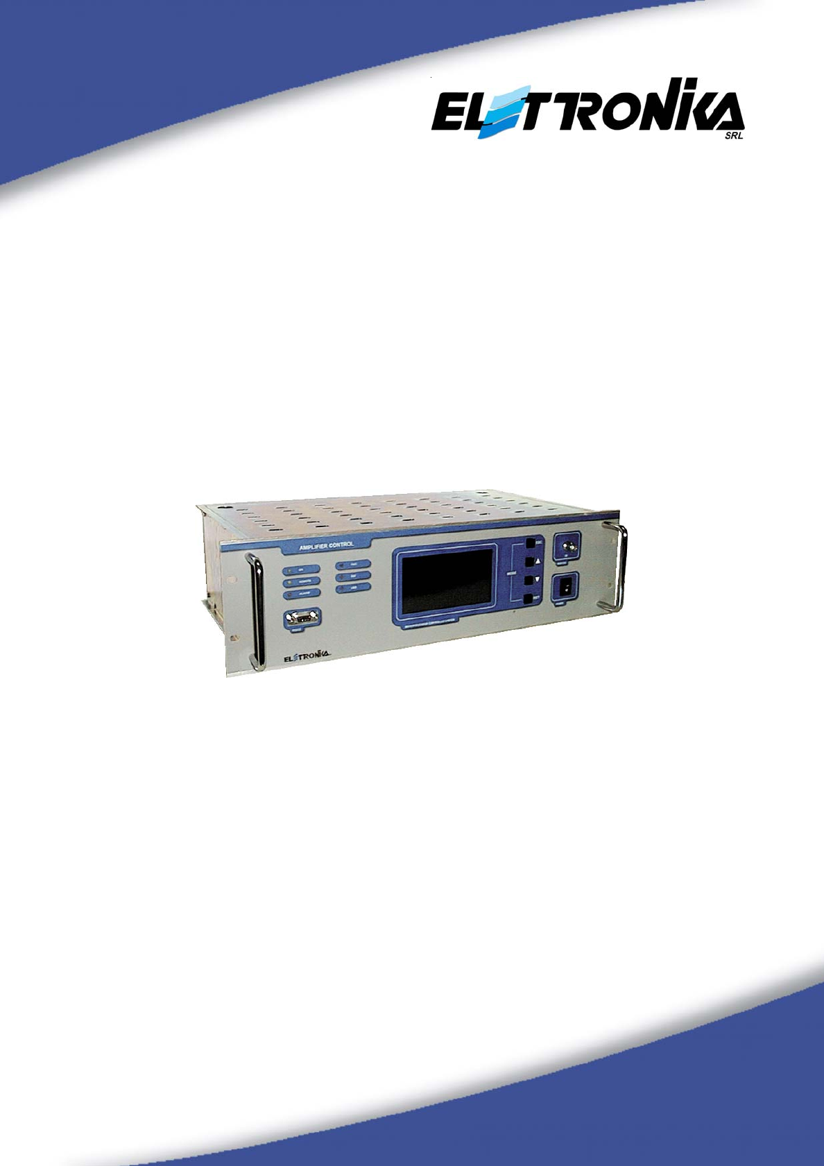
AMPLIFIER CONTROL
User’s manual
2
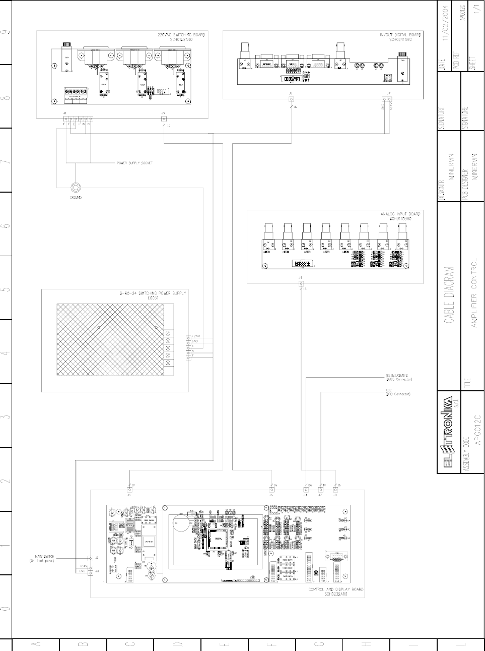
1.1 CONTROL SYSTEM OVERVIEW
The control system is made up by some “Slave” boards, which check locally the amplifier modules, and a
“Master” board to monitor the status of the Slave boards in each module and show on a graphic display all
the checked parameters.
The number of the Slaves changes depending on the output power of the amplifier. The communication
between Master and Slaves is made via RS485 standard. The Master board reads the overall parameters of
the equipment (Forward and Reflected power and Unbalancing), polls (interrogaes in sequence) the local
boards, shows on the display the values requested by the user, indicates alarm conditions, if any, and allows
to change some of the operating parameters of the apparatus. Besides it realizes a serial data interface to an
external system able to analyse the working parameters of the equipment, using the RS232 and RS485
communication protocols.
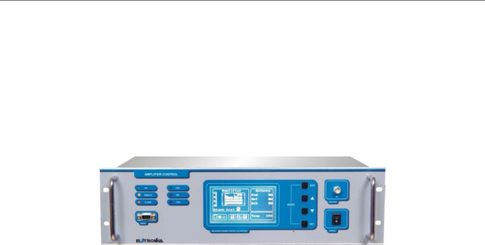
1.2 FUNCTIONS
At start-up, the display of Amplifier Control module shows an informational message concerning the equipment
and its firmware version.
- Main menu
The main menu has: a list of the amplifier modules, the measure of some parameters of the power in antenna,
a window with icons to show the alarm status (Alarm Status Window) and some general information, that is
date, time, temperature inside the module and, for FM equipment, transmission frequency.
The following picture is an exact representation of the main menu screen.
AMPLIFIER CONTROL
3
if the communication with the slave is correct and then
if the communication with the slave is interrupted
ON
if the amplifier module is OFF
OFF
if the amplifier module is ON
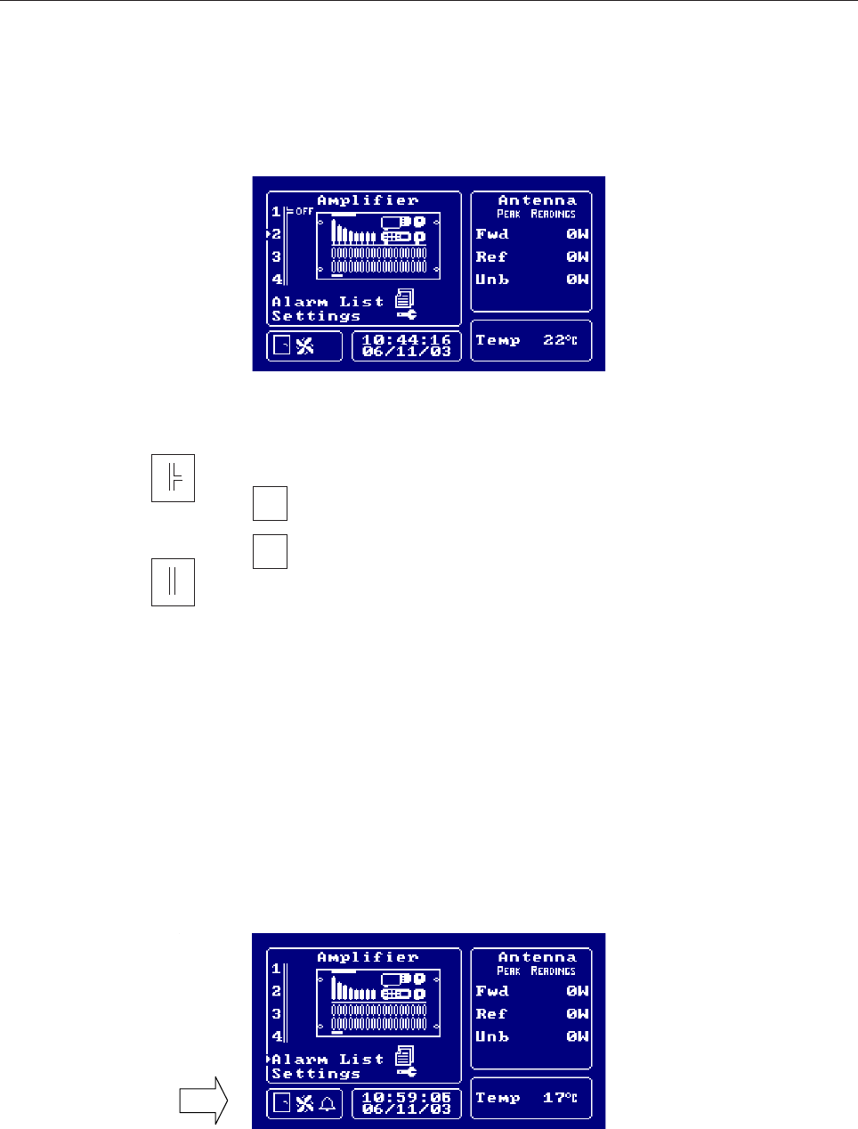
In the Amplifier List, next to each module, the following symbols can be found:
The UP and DOWN arrow keys allow to select one of the slave, the alarm list, or a menu allowing to change
some settings of the control module and the apparatus; the RET key is used to confirm the selection.
In the main and slave menu the Alarm Status Window (which position is indicated by an arrow in the picture
below) is shown: the gate symbol displays the status of the INTERLOCK, in case of alarm this icon blinks
and the buzzer ringgs.
The INTERLOCK signal is a control available to the user to manage an ON/OFF sensor.
When the relevant PIN is grounded, the Master board does not signal any alarm, as soon as the PIN is left
floating, an alarm is detected; the rotating screw symbol shows that the FANS work normally; in case of alarm
this icon blinks and the buzzer rings; the bell symbol appears in case of alarm detected by the control module
or the amplifier. It blinks if the alarm condition is terminated and the alarm itself can be displayed in the Alarm
List.
If one of the parameters of a Slave or any of the ones directly checked by the Master is alarmed, the general
4
Note that no numerical value is shown for amplifiers which are not communicating with the control module.
alarm LED and the alarm icon blink until the Alarm List is checked to see the type of alarm occurred.
Besides, if an alarm for any of the powers of the signals in antenna occurs, the relevant measure in the
Antenna window of the display and the relevant LED on the front panel of the Master module blink until the
measure decreases below the threshold level, determined by the nominal power of the amplifier.
If the slave modules are working and an INTERLOCK or FANS alarm occurs, aside from the indication
explained above, the amplifiers are switched off. This happens immediately after an INTERLOCK alarm, or
about 7 seconds after a FANS alarm is detected.
In case the amplifiers are communicating but switched off, or they are not communicating and the INTERLOCK
alarm contact is open, a WARNING condition occurs: buzzer on and blinking ALARM LED on the front
panel; while if it is the FANS alarm contact to be open, the icon of the alarm appears in the box.
Further to any of these two alarms it is possible to choose whether to turn off the amplifiers or not. In fact,
there is a submenu of the Settings menu which allows to choose whether to turn off the amplifiers connected
to the control module as a consequence of an INTERLOCK and FAN alarm.
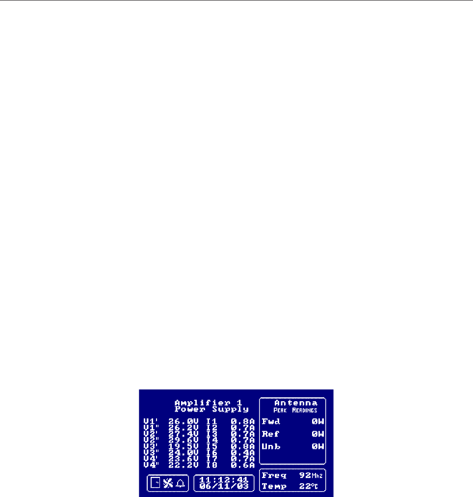
- Slave menu
By selecting one of the slaves, it is possible to see all the parameters of that amplifier module in two pages. The
first one shows voltages and currents Power Supply, the second one shows RF Powers: forward and reflected
power, temperature and, for some amplifiers, unbalancing and input power. The UP and DOWN keys allow
to scroll the local measures of all the slaves, page by page. The ESC key is used to go back to the main menu.
The following pictures show the menu screen of one amplifier.
5
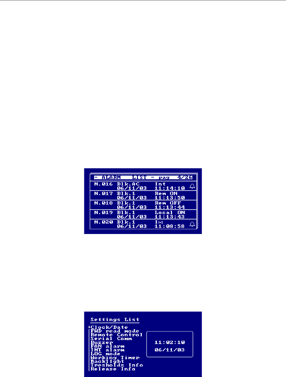
- Alarm List
By selecting the Alarm List, 26 pages listing the latest 130 alarms saved are shown. Each page shows 5
alarms, each contained in a box providing the following information: progressive number of the alarm, starting
with the most recent; number of the module in which the alarm occurred, following the “Blk.” Message (the
indication “AC” means that the alarm occurred in the Amplifier Control module); parameter in alarm, date and
time of the alarm. Next to the parameter showing the alarm type there may be a bell symbol. In case it is not
here, the alarm event has been communicated by an amplifier connected to the control module. These events
are different and on option of the Settings menu allows to choose whether they are displayed or not in the
alarm list.
The saved alarm can be deleted by keeping simultaneously pressed the UP and DOWN keys. The ESC key
is used to go back to the main menu. The picture shows a page of the list, containing both alarms and general
events.
1.3 PROGRAMMING MODE
The Settings menu gives access to programming mode. As shown below, the menu offers a list of settings next
to a window showing the default parameter set, or the one selected previously, when the pointer is moved on
the relevant options.
The menu under the cursor is accessed by pressing the RET key. This is shown by the “Enabled Menu”. Once
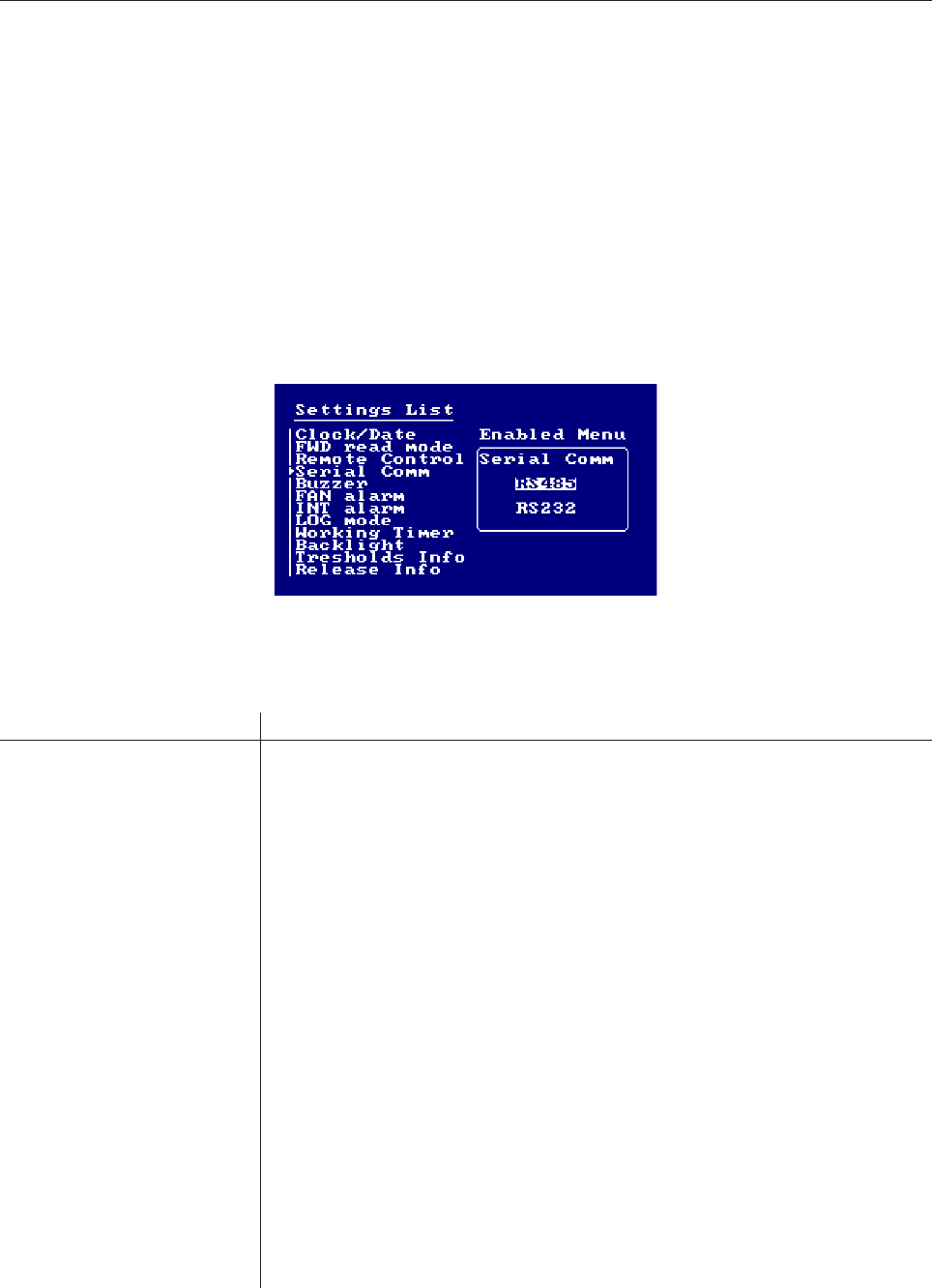
6
Description of the submenus included in Settings.
SUBMENU OPERATION
Update the time and date shown in the main menu box.
Selection of the analogue voltage signal (PEAK or RMS) to convert and
display the Forward power in antenna. A message in the main menu screen
confirms current choice.
It is possible to remotely control the apparatus, thus to monitor the parameters
shown on the display of Amplifier Control module and check the status of the
transmitter.
This is done through RS232 or RS485 standard serial communication, digital
and analog inputs through the DB25 telemetering connector on the rear panel
of the Amplifier Control module.
If the “Local” mode is set in this menu, the control module and the apparatus
can only be controlled locally, and a remote command is ignored. If “Remote”
is set instead, the REMOTE LED on the front panel of the module lights up
after going back to the main screen. From then on, incoming remote commands
from either the serial port or the telemeasuring connector on the rear panel
are handled (Note 1).
Clock / Date
FWD Read Mode
Remote Control
the menu is accessed, it is possible to change the value of the displayed fields or select a function by means of
the arrow keys. The RET key is used to confirm the selection (an acoustic signal should be heard). The ESC
key (or no key pressed for more than 7 seconds) sends back to the setting list. Pressing it again (or pressing
no key for more than 10 seconds) brings back to the main menu.
Every selection made in the Settings menu is stored into the EEPROM until it is changed again, this allows to
remember the settings status after an equipment reset.

7
Serial Comm
Buzzer
FAN Alarm
INT Alarm
LOG Mode
Working Timer
Backlight
Frequency
Thresholds info
Release info
Note 1: to control the apparatus from remote, consider that pins n. 1 and n. 14 of the telemetering connector on the rear panel
of Amplifier Control module are used to receive the ON (pin n. 1) and OFF (pin n. 14) commands, both impulsive and
stationary. The digital level on these contacts is usually high, becoming low when the remote control is active. When a remote
command to turn off the amplifiers is received while the transmitters is ON, the LED ON of the frontal panel blinks.
Selects the remote control via serial port.
RS232 MODE: the RS232 mode allows a direct access to the equipment
via PC and a remote access via modem or switched telephone line.
RS485 MODE: the RS485 mode allows a remote access to the equipment
via modem over switched telephone line or GSM network. It allows the
connection to the Remote Control System, designed to monitor several
apparatuses located at the same site.
Enables / disables the buzzer during normal operation.
Select “OFF” to have the amplifiers turned off further to a FAN alarm; if
“ON” is selected, they will stay on.
Select “OFF” to have the amplifiers turned off further to a INTERLOCK
alarm; if “ON” is selected, they will stay on.
Select “only alarms” to store in the EEPROM and display in the module LOG
only detected alarms; select “all events” to store and display also any event
detected by any amplifier and sent via RS485 to the control module.
Updates the counter of the working time of the transmitter. Once this menu
has been enabled, the counter reset option appears in the window.
If “Switch Off” is selected and no key is pressed for 8 minutes, the back light
of the display is turned off; select “always ON” to have it always on.
This menu only exists in the firmware for Amplifier Control of FM transmitters.
The working frequency can be selected within a range from 88 to 108MHz,
this allows to optimise the display of the Forward power sent to the antenna.
Shows for some seconds the alarms thresholds of the powers sent to the
antenna.
Shows for some seconds information concerning the transmitter and the
firmware version.

8
1.3 POWER CALIBRATION
- FWD Power calibration
Disconnect the antenna and connect a wattmeter to the antenna connector. Give power to the amplifier until
you will read on the wattmeter a value corresponding to the equipment nominal power. Then turn the trimmer
A (see mounting plan BOTTOM - PN1071AR2, it is a variable resistor used to adjust the A analog input
measure) until you read approximately the same FWD power value on the display.
- REF Power calibration
Disconnect the antenna and connect a wattmeter to the antenna connector. Connect the Forward power
monitoring cable to the Reflected power input connector. Give power to the amplifier until you will read on the
wattmeter a value corresponding to 10% of the equipment nominal power. Then turn the trimmer B (see
mounting plan BOTTOM - PN1071AR2, it is a variable resistor used to adjust the B analog input measure)
until you read approximately the same REF power value on the display.
- UNB Calibration
Connect a wattmeter before the dummy load. Give power to the amplifier then turn off one slave module: you
will read an amount of unbalancing power on the wattmeter. Turn the trimmer C (see mounting plan BOTTOM
- PN1071AR2, it is a variable resistor used to adjust the C analog input measure) until you read approximately
the same UNB power value on the display.
1.4 RS232 AND RS485 PIN TABLES
PIN N° SYGNAL TYPE IN/OUT FUNCTION
1- - -
2 Digital Input RX2_485B-
3 Digital Input RX2_485A+
4- - -
5GND - -
6- - -
7 Digital Output TX2_485Z-
8 Digital Output TX2_485Y+
9- - -
PIN N° SYGNAL TYPE IN/OUT FUNCTION
1- - -
2 Digital Output TX232
3 Digital Input RX232
4- - -
5GND - -
6VDC +5V - -
7- - -
8- - -
9- - -
RS232 - DB9 Connector (Front panel) RS485 - DB9 Connector (Rear panel)

9
1.5 TELEMEASURING PINS TABLE
PIN N° SIGNAL TYPE IN / OUT FUNCTION
1 Digital -
REMOTE ON/OFF TTL:
GND = REMOTE ON
+5V = REMOTE OFF
2 Digital Output -
3 Digital Output -
4 Digital Output -
5 Digital Output -
6 Digital Output -
7 Digital Output AGC alarm TTL:
GND = AGC alarm, +5V = no AGC alarm
8 Digital Output -
9GND - -
10 Analog Output -
11 Analog Output -
12 Analog Output -
13 Analog Output -
14 Digital Input
RE MOTE AMP LIFIER ON/OFF TTL:
if REMOTE ON then
GND = AMPLIFIER OFF
+5V = AMPLIFIER ON
15 Digital Output -
16 Digital Output -
17 Digital Output -
18 Digital Output -
19 Digital Output AGC alarm TTL:
GND = AGC alarm, +5V = no AGC alarm
20 GND - -
21 +5V - -
22 Analog Output FWD Power [0,+ 5V]
23 Analog Output REF Power [0,+ 5V]
24 Analog Output UNB Power [0,+ 5V]
25 Analog Output -
10
1.6 OTHER TABLES
BNC Connectors
AGC Connector
SYGNAL TYPE IN/OUT FUNCTION
A Analog Input FWD Power monitoring
B Analog Input REF Power monitoring
C Analog Input UNB Power monitoring
D- - -
E- - -
F- - -
G- - -
PIN N° SYGNAL TYPE IN/OUT FUNCTION
1GND - -
2 Digital Output AGC alarm TTL:
GND = AGC alarm, +5V = no AGC alarm
3 Digital Output AGC alarm TTL:
GND = AGC alarm, +5V = no AGC alarm
4- - -
5- - -
6- - -
7- - -
8 Analog Output FWD Power (range 0 - +5V)
9 Analog Output FWD Power (range 0 - +5V)
11
BNC SYGNAL TYPE IN/OUT FUNCTION
Contact Digital Input
FANS control Switch or TTL:
closed/GND = no FANS alarm
open/+5V = FANS alarm
Body GND - -
FANS CONTROL Connector
PIN N° SYGNAL TYPE IN/OUT FUNCTION
1---
2 Digital Output TX1_485Z-
3 Digital Output TX1_485Y-
4---
5GND - -
6---
7 Digital Input RX1_485B-
8 Digital Input RX1_485A+
9---
RS485 - DB9 Connector (Amplifiers communication)
PIN N° SYGNAL TYPE IN/OUT FUNCTION
1GND - -
2 VDC +24V - -
24VDC LOAD FAN Connector
12
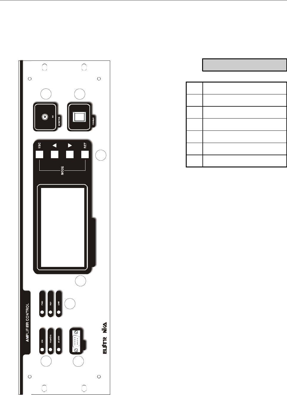
O
MI CR OPR O CESS O R CO NT RO LLED SYS T EM
RS2 32
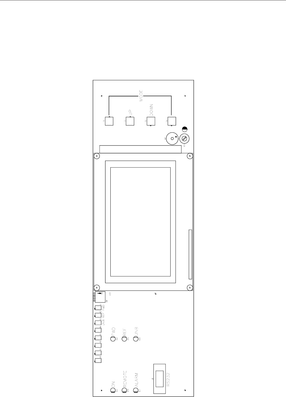
Front panel
1
34
5
6
7
2
DESCRIPTION
1 Status LEDs
2Alarm LEDs
3 RS232 Socket
4 LCD Display
5 Function keys
6 RF Monitor connector
7 ON/OFF Switch
13
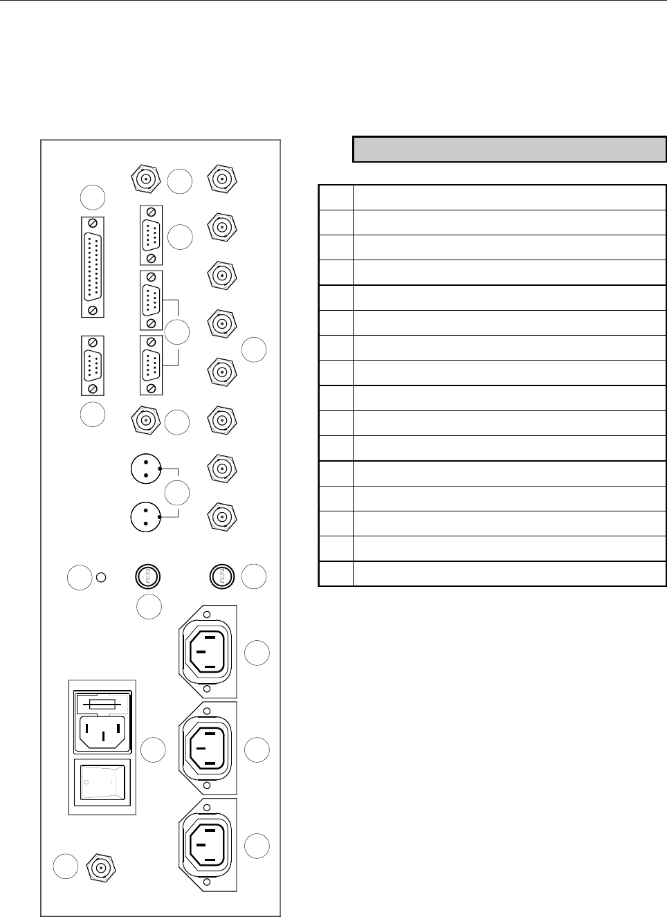
Rear panel
1
2
3 4 5
6
7
816
912 13 14 15
10 11
DESCRIPTION
1 RF Input connector
2 Main Power supply socket with Fuse-Holder by 10A
3 Driver1 Power socket
4 Driver2 Power socket
5 Fans Power socket
6GND
7 Fuse by 1A
8 Fuse by 8A
9 24Vdc Connectors
10 AGC Socket
11 Telemeasures socket
12 Fans Control connector
13 RS485 Socket (Amplifiers Communication)
14 RS485 Socket (Remote Control)
15 Interlock connector
16 Power measurement connector
14
15
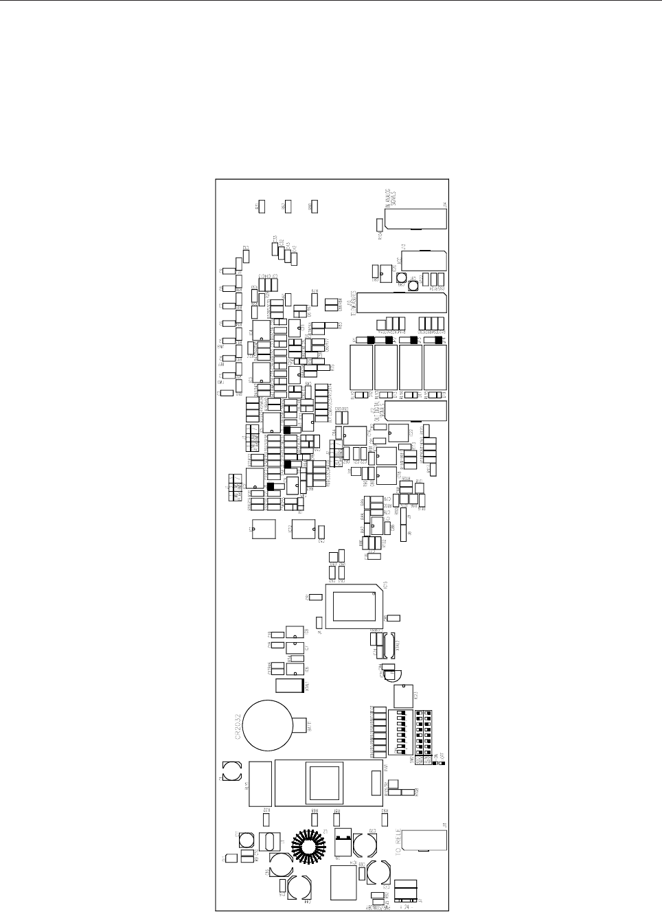
CONTROL AND DISPLAY BOARD SCH0239AR0
SCH0239AR0 Top layer Component layout
16
SCH0239AR0 Bottom layer Component layout

17
SCH0239AR0 COMPONENT LIST
Part Name/Number Description Qty. Comps. Page 1/2
BATT BH001RB 3093_90 03093 03090 BATTERY HOLDER 1 BATT1
BZ AI-155 03705 03705 5VDC BUZZER 1 BZ1
CC 100nF-S 01065C 01065C Y5V 1206 COND 33 C10, C15, C17-19, C22, C25, C28, C38,
C45, C49-52, C55, C62-63, C68-69, C78,
C80-85, C87-88, C90, C92-95
CC 15pF-S 01088 01088 SMD 1206 COND 2 C74-75
CC 1nF-S 01096 01096 SMD 1206 COND 20 C12-14, C31-33, C42-43, C53-54, C56-58,
C60-61, C66, C76-77, C79, C86
CC 1uF100V-S 01760A 01760A Y5V 1206 COND <<50 V>> 8 C21, C23, C37, C64-65, C67, C71-72
CC 220pF-S 01093 01093 SMD 1206 COND 8 C2-9
CC 47pF-S 01100 01100 SMD 1206 COND 8 C20, C30, C35-36, C40-41, C48, C59
CE 10uF16V-S 01626B TANT. ELETTR SMD CO 8 C24, C26-27, C29, C34, C39, C46-47
CE 1uF50V-S 01763A 01763A ELETTR SMD COND 2 C89, C91
CE 220uF50V LOW ESR 1799A ELETTR SMD COND LOW ESR 4 C16, C44, C70, C73
CE 47uF35V-S 01790A 01790A ELETTR SMD COND 1 C11
CE 47uF50V-S 01791C 01791C ELETTR SMD COND 1 C1
D 1N4148-S 03002 03002 SMD DIODE 4 D12-13, D17, D19
D 50WQ06FN 03019A SMD DIODE SCHOTTKY 5,5A 1 D9
D BAS85-S 03024 SMD DIODE SCHOTTKY 8 D1-8
D BAT54S 03199 SMD SCHOTTKY DIODE A-K T 6 D10-11, D14-16, D18
DIS WG240128B 03083 240/128 DOT MATRIX LCD 1 LCD1
DL KA-3528SGC 03057 03057 GREEN SMD LED DIODE 1 DL1
DL LEDG3 03053 03053 GREEN LED DIODE 3mm 1 DL3
DL LEDR3 03058 03058 RED LED DIODE 3mm 4 DL2, DL4, DL6-7
DL LEDY3 03051 03051 YELLOW LED DIODE 3mm 1 DL5
IC 24LC64 04815 04815 SMD INTEG CIRCUIT 1 IC7
IC 74HC00-S 4762A 4762A SMD INTEG CIRCUIT 1 IC19
IC 82B715-S 04734A 04734A SMD INTEG CIRCUIT 1 IC17
IC CD4053BC-S 04710A 04710A SMD INTEG CIRCUIT 1 IC12
IC LM2596S-5.0 04580 SMD INTEG CIRCUIT 1 IC14
IC LM75-S 00668 00668 SMD INTEG CIRCUIT 1 IC8
IC LMC6482-S 04632 SMD INTEG CIRCUIT 1 IC20
IC LMC6484-S 04634 SMD INTEG CIRCUIT 4 IC2-5
IC M41T56 04611 04611 SMD INTEG CIRCUIT 1 IC6
IC MAX232-S 04804B 04804B SMD INTEG CIRCUIT 1 IC16
IC MAX3080-S 04770 04770 SMD INTEG CIRCUIT 1 IC22
IC MAX3080-S N.M. NOT MOUTED SMD INTEG CIRCUIT 1 IC18
IC MAX942CSA-S 04572 SMD INTEG CIRCUIT 4 IC9-11, IC13
IC MB90F543PF 04596 SMD INTEG CIRCUIT 1 IC15
IC MPC100T-450I-TT 04577 SMD INTEG CIRCUIT 1 IC21
IC ULN2003A 4870 04870 SMD INTEG CIRCUIT 2 IC1, IC23
IND MS85 10uH-S 04948 INDUCTOR 2,7A 1 L1
IND T100uH-1.8A 4958 04958 TOROIDAL-STORAGE CHOKES 1 L2

18
Part Name/Number Description Qty. Comps. Page 2/2
INV IN-D43A-5V 03085 DC/AC MODULE 1 INV1
J DB9_F-0° LT 02794 PCB CONNECTOR DB9 LONG T 1 J6
J FC-10P 02697-02699 02697+02699 PCB CONNECTOR POL 2 J11, J13
J FC-16P 02701-02700 02701+02700 PCB CONNECTOR POL 2 J12, J14
J FC-26P 02855-02854 02855+02854 PCB CONNECTOR POL 1 J10
J PAN2 02739 02739 PCB CONNECTOR 1 J4
J PAN2 02739-40-41 02739+02740+02741 PCB CONNECTO 1 J5
J PAN3 02707 02707 PCB CONNECTOR 3 J1-3
J PAN3 NOT MOUNTED NOT MOUNTED PCB CONNECTOR 2 J8-9
J SCREWCONN2 02853 02853 PCB SCREW CONNECTOR 1 J7
JU JUMP3 02707-02742 02707+02742 MASCHIO PAN3 4 JP1-4
R 100R-S 00029A 00029A RES 1/4W 5% SMD 1206 6 R109, R114, R119-121, R123
R 10K-S 00053A 00053A RES 1/4W 5% SMD 1206 37 R22-27, R30, R32-33, R40, R47, R50, R57,
R68, R81-82, R85, R90-101, R105-108,
R116, R118, R122, R124
R 120R-S 00030A 00030A RES 1/4W 5% SMD 1206 2 R112-113
R 1K0-S 00041A 00041A RES 1/4W 5% SMD 1206 5 R46, R54, R87-88, R104
R 1K5-S 00043A 00043A RES 1/4W 5% SMD 1206 2 R110-111
R 22K-S 00057A 00057A RES 1/4W 5% SMD 1206 11 R18, R20-21, R28, R34, R36, R38-39, R41,
R43-44
R 2K2-S 00045A 00045A RES 1/4W 5% SMD 1206 8 R19, R35, R37, R42, R45, R53, R59-60
R 330R-S 00035B 00035B RES 1/4W 5% SMD 1206 2 R89, R103
R 33R-S 00023A 00023A RES 1/4W 5% SMD 1206 2 R86, R102
R 470K-S 00073A 00073A RES 1/4W 5% SMD 1206 8 R48-49, R51-52, R55-56, R58, R65
R 470R-S 00037A 00037A RES 1/4W 5% SMD 1206 30 R10-17, R29, R31, R61-64, R66-67,
R69-80, R83-84
R 4K7-S 00049A 00049A RES 1/4W 5% SMD 1206 1 R117
R 820R-S 00040A 00040A RES 1/4W 5% SMD 1206 1 R9
RL 30.22.24 07569 07569 RELE 5 RLY1-5
RV 10K-S-H 00715 00715 VARIABLE RESISTOR 1 R115
RV 1M-3266X 00815 VARIABLE RESISTOR 8 R1-8
SW SWITCH-4DIP 90° 07531A PCB DIP SWITCH 90° 1 SW1
SW SWITCH-8DIP 07530A PCB DIP SWITCH SMD 1 SW2
T 06086 N 7630 7632 7630 7632 KTI06086 PULSANTE 2 4 T1-4
TR BC848 03457 03457 NPN SMD TRANSISTOR 1 TR1
XTAL 32.768k-S 05146 05146 QUARTZ 1 XTAL1
XTAL 4MHz-S 05101A 05101A QUARTZ 1 XTAL2
19
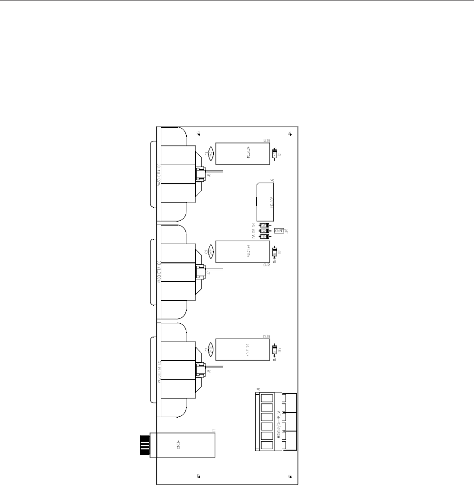
220VAC SWITCHING BOARD SCH0152AR0
SCH0152AR0 Component layout
SCH0152AR0 COMPONENT LIST
Part Name/Number Description Qty. Comps.
CC 2nF2 2kV 01045A 01045A CERAMIC CAPACITOR 3 C1-3
D 1N4148 03001 03001 DIODE 6 D1-6
FUSE OMEGA C1034 FUS00008 FUSE-HOLDER 5x20 D 1 F1
J CON HD515V/05-6PVE 02883 + 02884 PANDUIT PCB CONN 1 J1
J FC-10P 02697-02699 02697+02699 PCB CONNECTOR POL 1 J9
J VASCHETTA IEC 02879 VASCHETTA FEMALE PCB 3 J6-8
JU JUMP2 02739-02742 02739+02742 MALE PAN2 1 JP1
RL 40.31.24 7567C RELE 3 RLY1-3
20
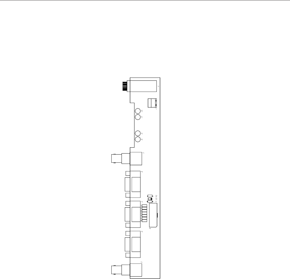
IN/OUT DIGITAL BOARD SCH0241AR0
SCH0241AR0 Component layout
SCH0241AR0 COMPONENT LIST
Part Name/Number Description Qty. Comps.
DZ 5V1 03109 03109 ZENER DIODE 1 DZ1
FUSE OMEGA C1034 FUS00008 PORTA FUSIBILE 5x20 D 1 F1
J BNC-90G-PCB 2034 02034 PCB CONNECTOR 2 J2-3
J DB9-90G 02797 02797 PCB CONNECTOR 3 J4-6
J FC-16P 02701-02700 02701+02700 PCB CONNECTOR POL 1 J1
J SCREWCONN2 02853 02853 PCB SCREW CONNECTOR 1 J7
J TESTP2.5mm 07912 07912 TEST POINT 4 J8-11
R 0R0-S 00001 00001 RES 1/4W 5% SMD 1206 7 R3-9
R 10K 0053 0053 RES 1/4W 5% 1 R1
R 1K0 0041 0041 RES 1/4W 5% 1 R2
21
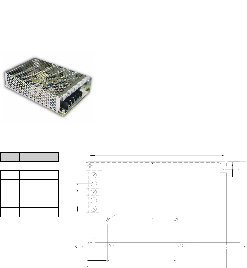
S-60-24 SWITCHING POWER SUPPLY E0031
MAIN FEATURES
- Universal AC input / Full range
- Protections: Short circuit / Over load / Over voltage
- Cooling by free air convection
- 100% full load burn-in test
- Fixed switching frequency at 50kHz
MECHANICAL SPECIFICATION
4.5
65
152.5
97
84.5 7
2-M3
78
24
159
3.5
3.5
5
4
3
2
8.2 9.5
1
PIN N° ASSIGNMENT
1AC/L
2AC/N
3FG
4DC OUTPUT -V
5DC OUTPUT +V

22
TECHNICAL CHARACTERISTICS
MODEL S-60-15 S-60-24
OUTPUT
DC VOLTAGE 15V 24V
RATED CURRENT 4A 2.5A
CURRENT RANGE 0 ~ 4A 0 ~ 2.5A
RATED POWER 60W 60W
RIPPLE & NOISE (max.) Note 2 150mVp-p 150mVp-p
VOLTAGE ADJ. RANGE 13.5 ~ 16.5V 21.6 ~ 26.4V
VOLTAGE TOLERANCE Note 3 ± 1.0% ± 1.0%
LINE REGULATION ± 0.5% ± 0.5%
LOAD REGULATION ± 0.5% ± 0.5%
SETUP, RISE, HOLD TIME 300ms, 50ms, 80ms / 230VAC 800ms, 50ms, 10ms / 115VAC at full load
INPUT
VOLTAGE RANGE 88 ~ 264VAC 120 ~ 370VDC
FREQUENCY RANGE 47 ~ 63Hz
EFFICIENCY (Typ.) 77% 79%
AC CURRENT 24A/115VAC 1A/230VAC
INRUSH CURRENT (Max.) COLD START 30A/115VAC 60A/230VAC
LEAKAGE CURRENT <3.5mA/240VAC
PROTECTION
OVER LOAD
105 ~ 150% rated output power
Protection type: Hiccup mode, recovers automatically after fault condition is removed
OVER VOLTAGE
17.25 ~ 20.25V 27.6 ~ 32.4V
Protection type: Hiccup mode, recovers automatically after fault condition is removed
ENVIRONMENT
WORKING TEMP. -10 ~ +60°C (Refer to output load derating curve)
WORKING HUMIDITY 20 ~ 90% RH non-condensi ng
STORAGE TEMP., HUMIDITY -20 ~ +85°C, 10 ~ 95% RH
TEMP. COEFFICIENT ± 0.03%/°C (0 ~ 50°C)
VIBRATION 10 ~ 500Hz, 2G 10min./1cycle, period for 60min. each along X, Y, Z axes
SAFETY & EMC
(Note 4)
SAFETY STANDARDS UL1012, UL1950, TUV EN60950 Approved
WITHSTAND VOLTAGE I/P-O/P:3KVAC I/P-FG:1.5KVAC O/P-FG:0.5KVAC
ISOLATION RESISTANCE I/P-O/P, I/P-FG, O/P-GD:100M Ohms/500VDC
EMI CONDUCTION & RADIATION Compliance to EN55022 (CISPR22) Class B
HARMONIC CURRENT Compliance to EN61000-3-2,-3
EMS IMMUNITY Compliance to EN61000-4-2,3,4,5,6,8,11; ENV50204, EN55024, Light industry level, criteria A
OTHERS
MTBF 316.2K hrs min. MIL-HDBK-217F (25°C)
DIMENSION 159*97*38mm (L*W*H)
PACKING 0.51kg; 24pcs/13.1kg/0.7CUFT
23
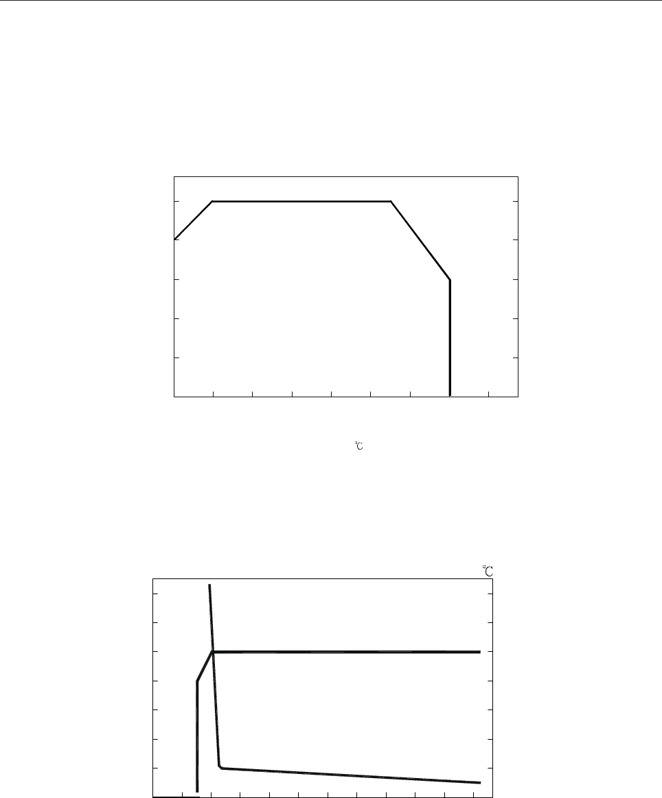
DERATING CURVE
OUTPUT DERATING VS INPUT VOLTAGE
AMBIENT TEMPERATURE ( )
LOAD (%)
-10
-10
0
0
2010 30 40
20
40
80
60
100
60
55
50
45 (HORIZONTAL)
(VERTICAL)
INPUT VOLTAGE (V) 60Hz
60 80 100 120 140 160 180 200 220 240 260
Vo
300
35032
250
28
200
24
150
20
100
16
50
12
8
OUTPUT VOLTAGE (V)
OUTPUT RIPPLE ( m Vp -p )
Ta= 2 5
24
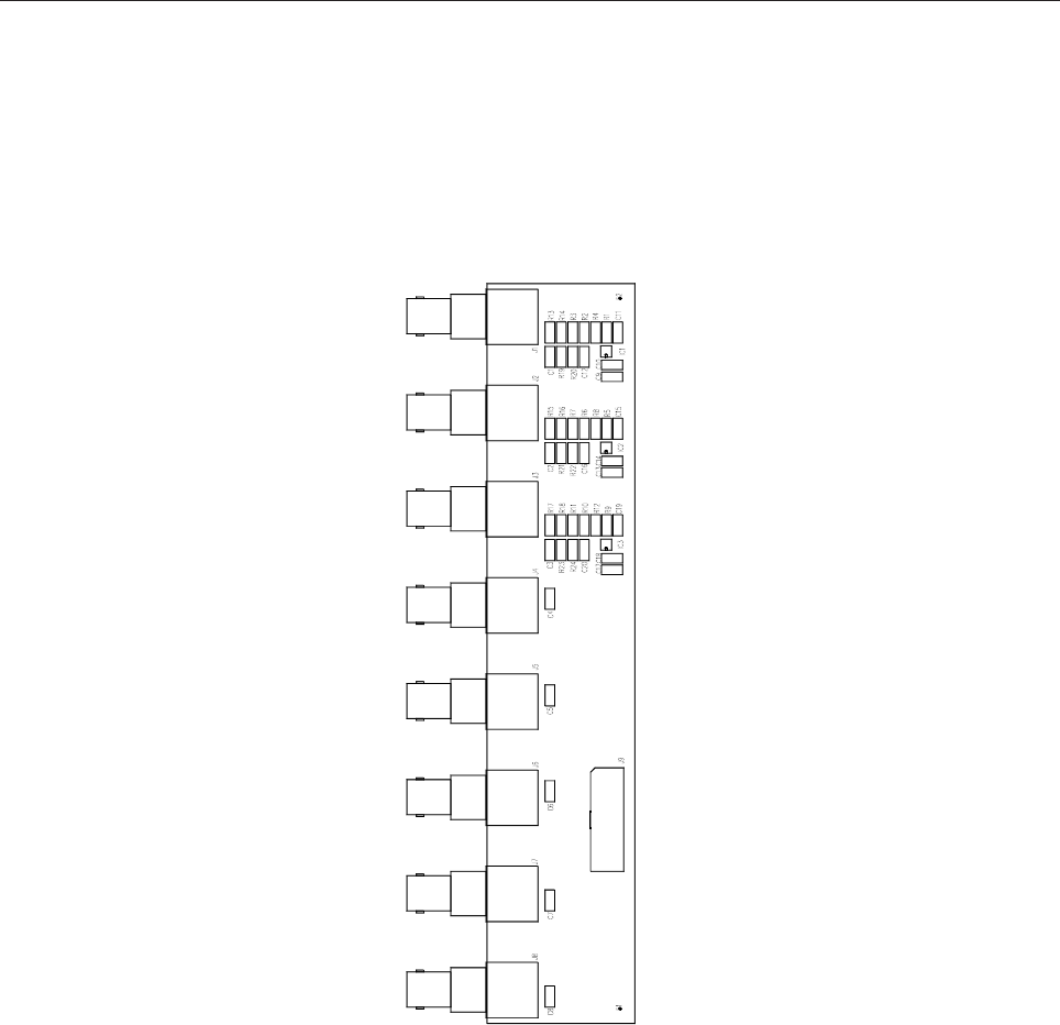
ANALOG INPUT BOARD SCH0110BR0
SCH0110BR0 Component layout
SCH0110BR0 COMPONENT LIST
Part Name/Number Description Qty. Comps.
CC 1206 N. M. N. M. SMD 1206 CAPACITOR 17 C4-20
CC 1nF-S 01096 01096 SMD 1206 CAPACITOR 3 C1-3
J BNC-90G-PCB 2034 02034 PCB CONNECTOR 3 J1-3
J BNC-90G-PCB 2034 N. M. BNC-90G 5 J4-8
J FC-16P 02701-02700 02701+02700 PCB CONNECTOR POL 1 J9
R 0R0-S 00001 00001 RES 1/4W 5% SMD 1206 6 R13, R15, R17, R19, R21, R23
R 1206 N. M. N. M. RES 1/4W 5% SMD 1206 18 R1-12, R14, R16, R18, R20, R22
R24
Z MICRO SOIC 8P N.M. SMD INTEG CIRCUIT NOT MOUNTED 3 IC1-3