Elettronika S r l TXUP10000 10 kW Analog TV Broadcast Transmitter User Manual Nuovo 5
Elettronika S.r.l. 10 kW Analog TV Broadcast Transmitter Nuovo 5
UserManual.wiki
>
Elettronika S r l
>
TXUP10000 User Manual
>
User Manual Part 1
Contents
1.
User Manual Part 1
2.
User Manual Part 2
User Manual Part 1
Navigation menu
Upload a User Manual
Namespaces
Wiki Guide
HTML
PDF
Info
Views
User Manual
Discussion / Help
Navigation

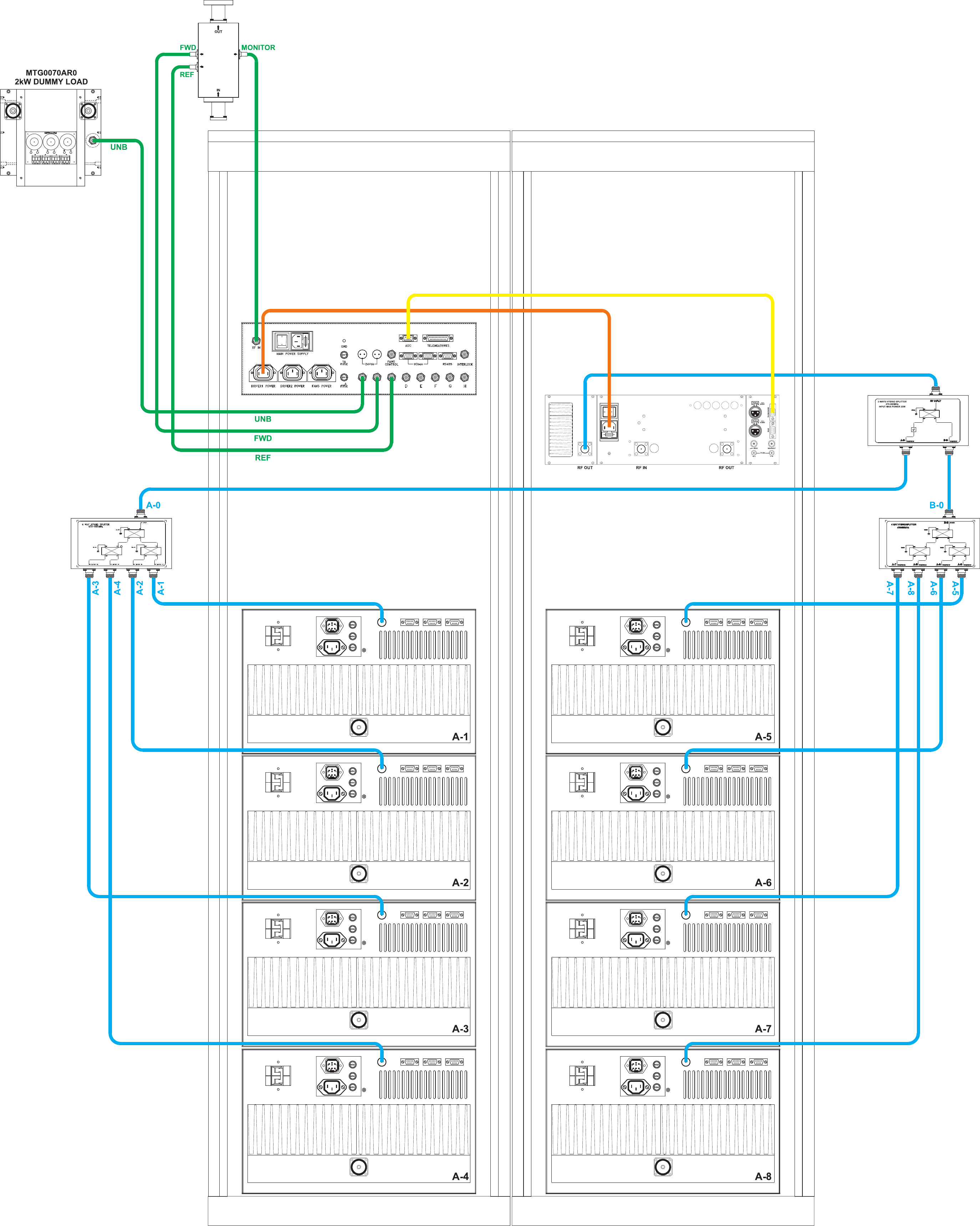
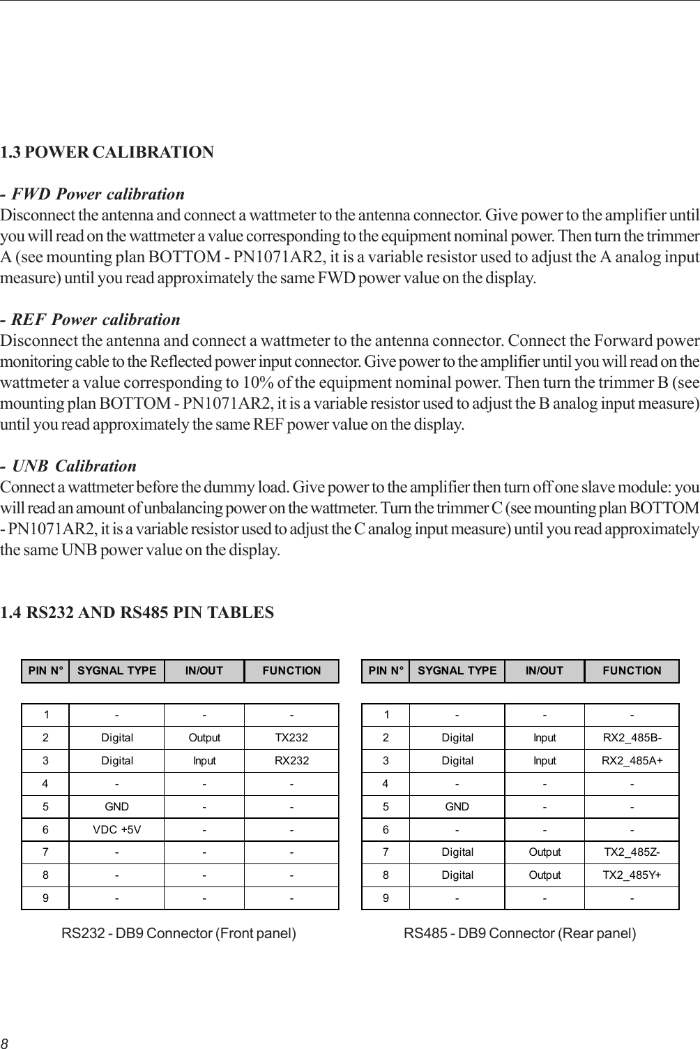
![91.5 TELEMEASURING PINS TABLEPIN N° SIGNAL TYPE IN / OUT FUNCTION1 Digital -REMOTE ON/OFF TTL:GND = REMOTE ON+5V = REMOTE OFF2 Digital Output -3 Digital Output -4 Digital Output -5 Digital Output -6 Digital Output -7 Digital Output AGC alarm TTL:GND = AGC alarm, +5V = no AGC alarm8 Digital Output -9GND - -10 Analog Output -11 Analog Output -12 Analog Output -13 Analog Output -14 Digital InputRE MOTE AMP LIFIER ON/OFF TTL:if REMOTE ON thenGND = AMPLIFIER OFF+5V = AMPLIFIER ON15 Digital Output -16 Digital Output -17 Digital Output -18 Digital Output -19 Digital Output AGC alarm TTL:GND = AGC alarm, +5V = no AGC alarm20 GND - -21 +5V - -22 Analog Output FWD Power [0,+ 5V]23 Analog Output REF Power [0,+ 5V]24 Analog Output UNB Power [0,+ 5V]25 Analog Output -](https://usermanual.wiki/Elettronika-S-r-l/TXUP10000.User-Manual-Part-1/User-Guide-734618-Page-16.png)