Elettronika S r l TXUP10000 10 kW Analog TV Broadcast Transmitter User Manual Nuovo 5
Elettronika S.r.l. 10 kW Analog TV Broadcast Transmitter Nuovo 5
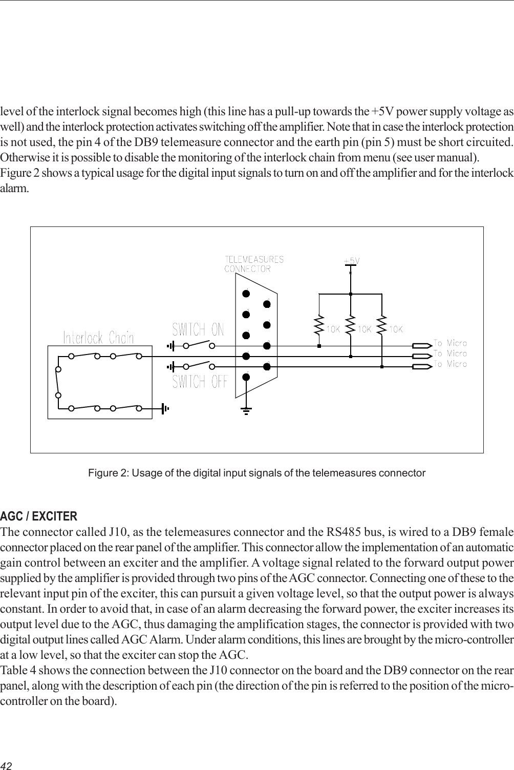
UserManual.wiki
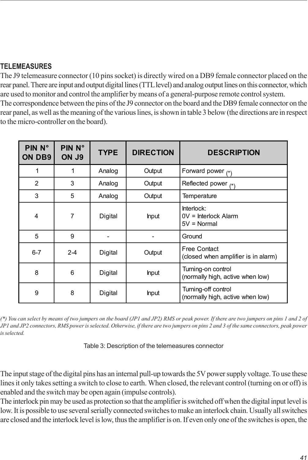
>
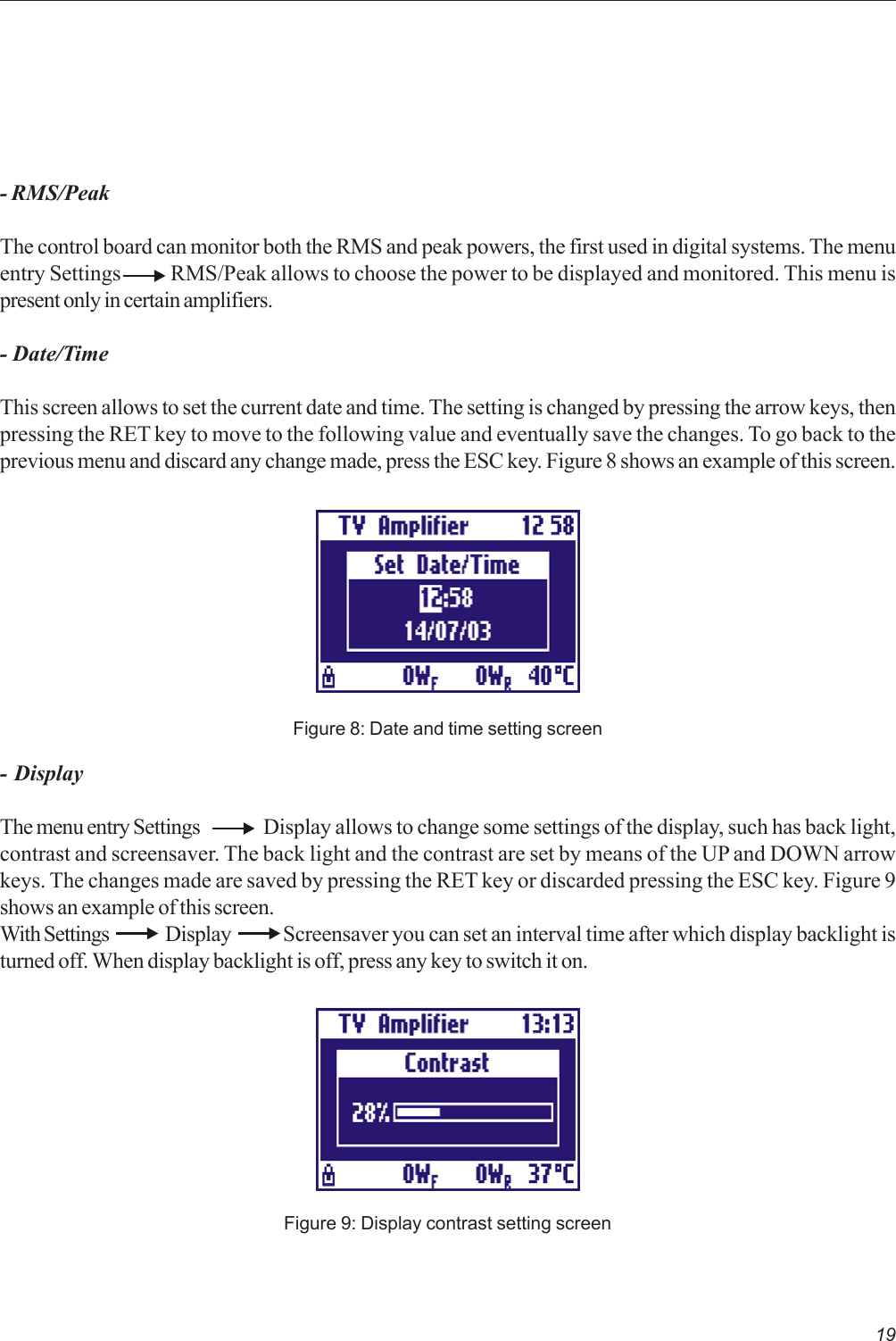
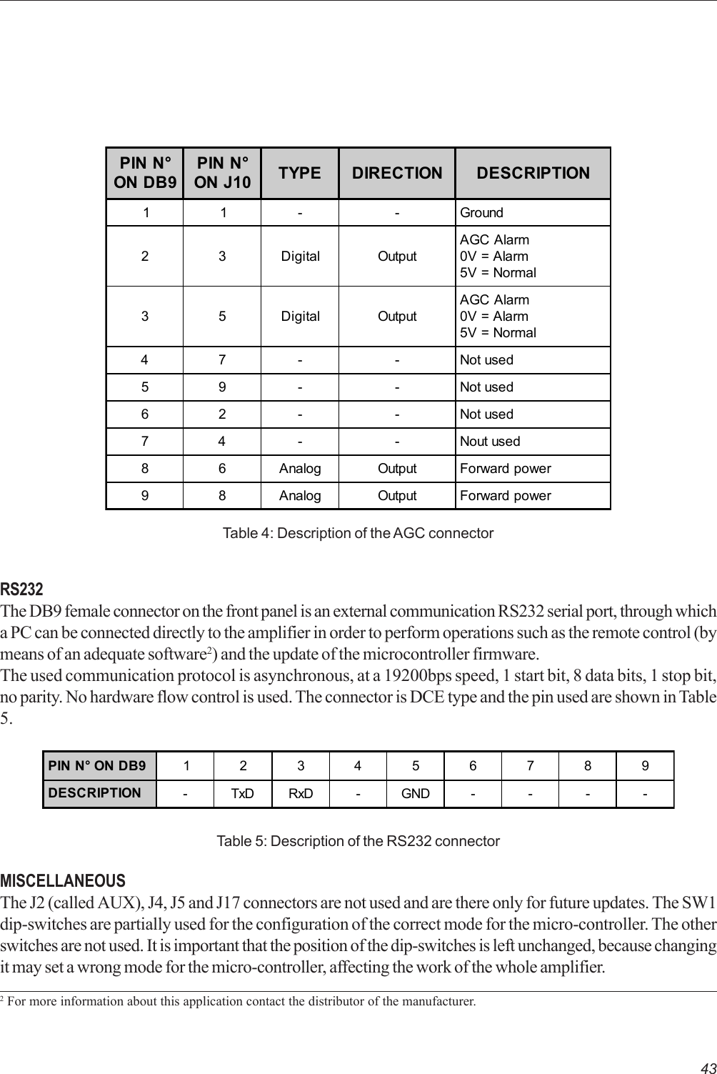
Elettronika S r l
>
TXUP10000 User Manual
>
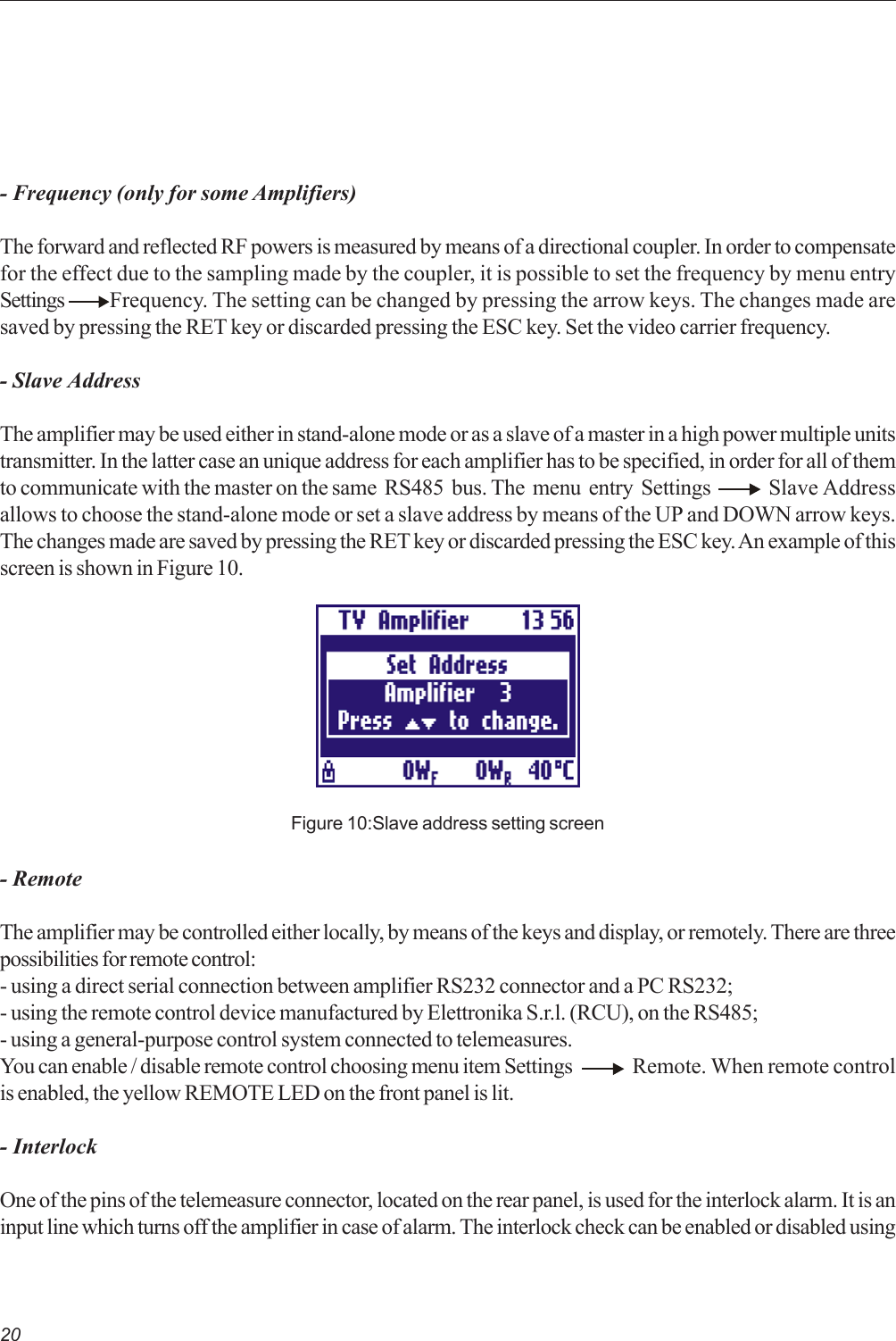
User Manual Part 2
Contents
1.
User Manual Part 1
2.
User Manual Part 2
User Manual Part 2
Navigation menu
Upload a User Manual
Namespaces
Wiki Guide
HTML
PDF
Info
Views
User Manual
Discussion / Help
Navigation