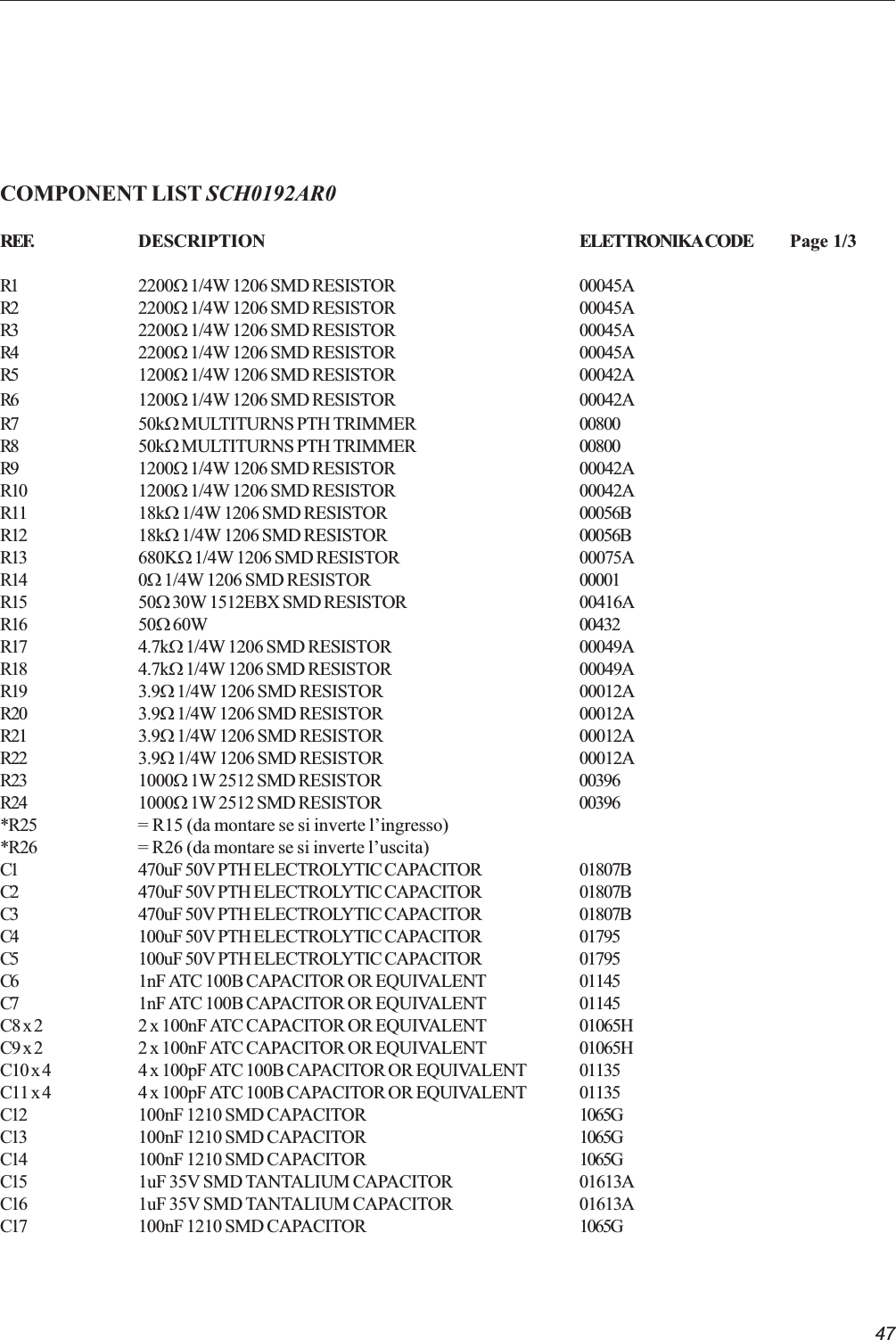
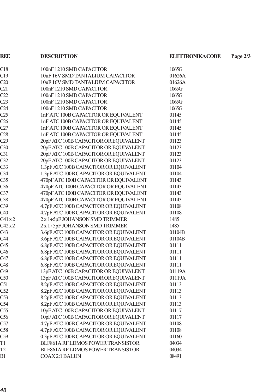
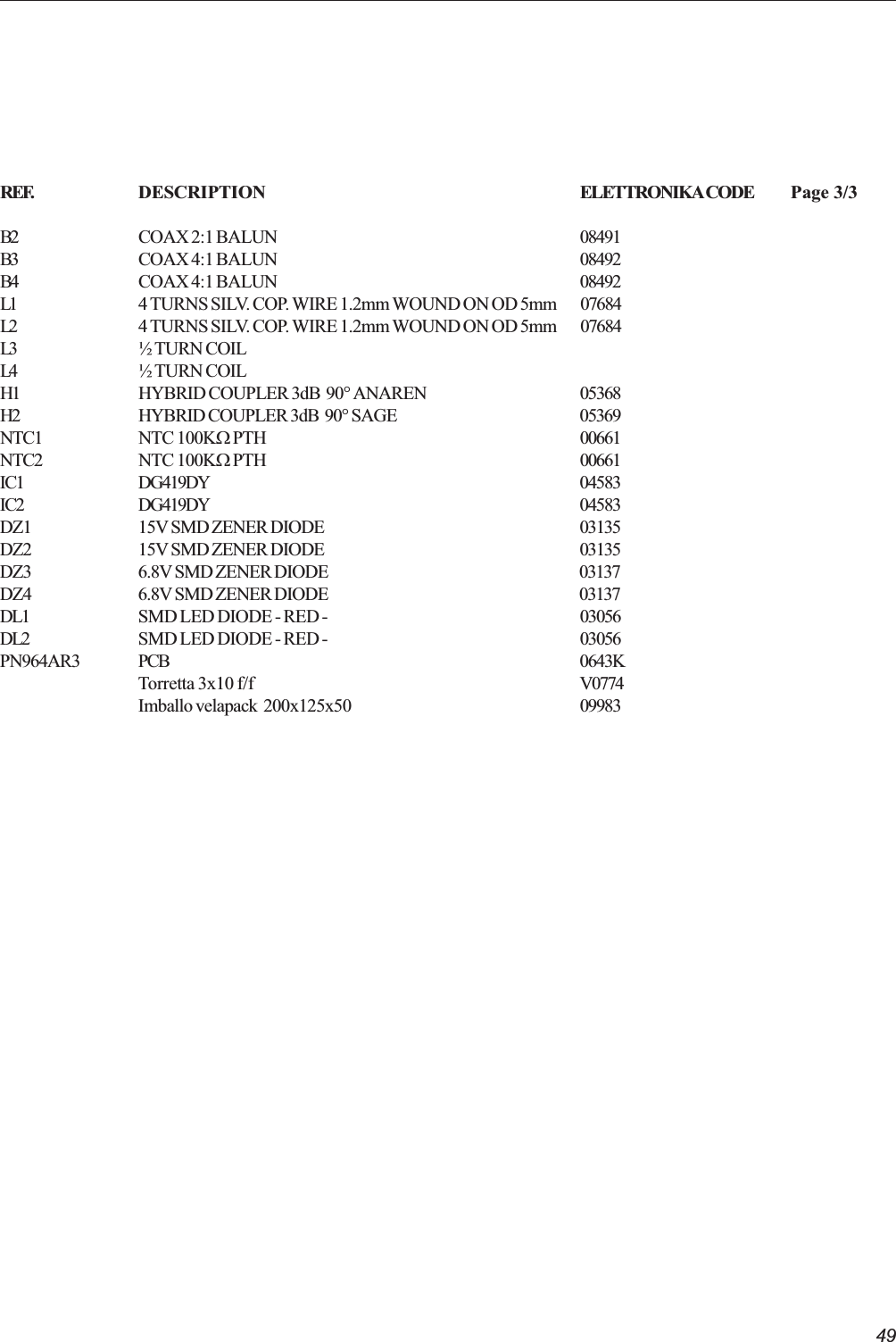
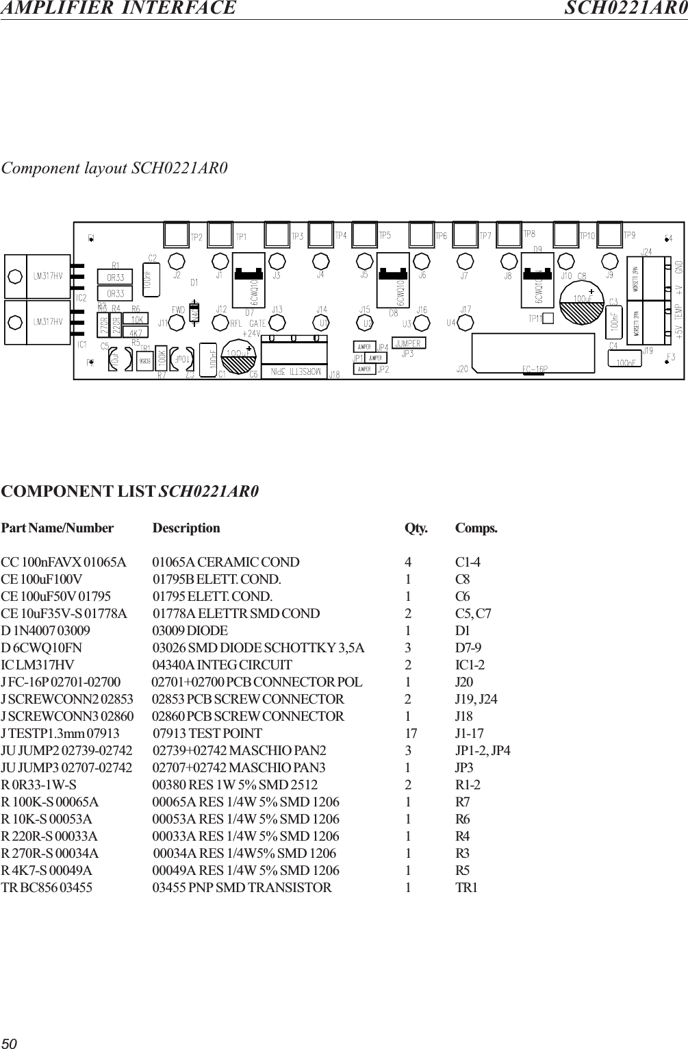
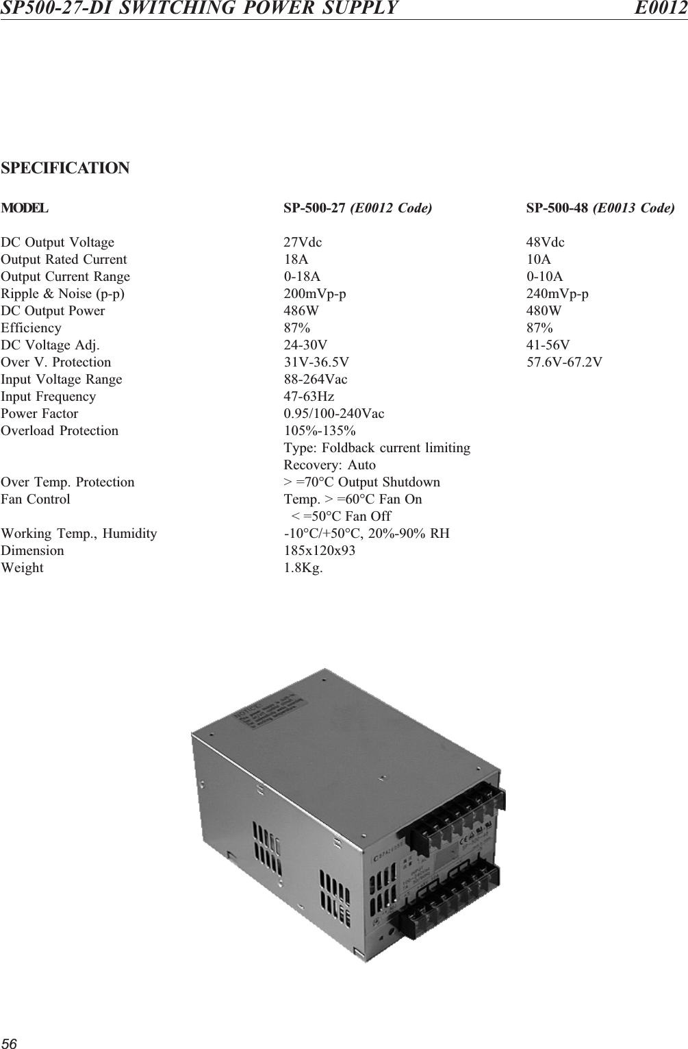
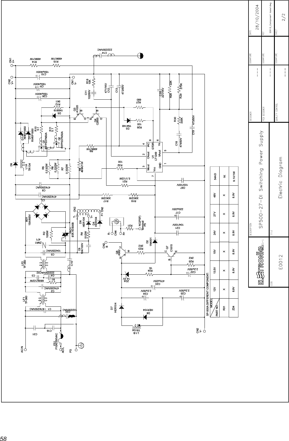
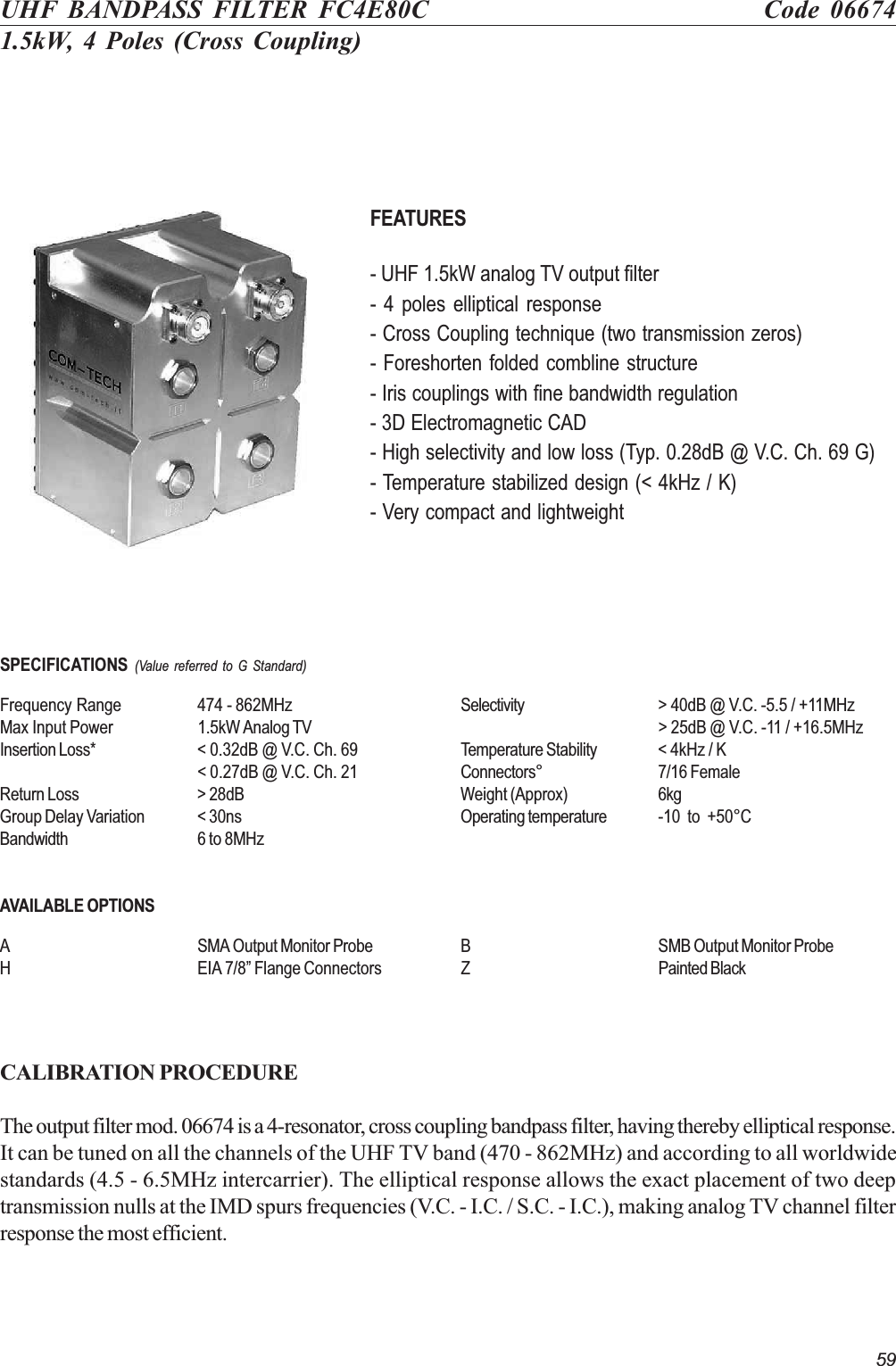
Elettronika S r l TXUP1500 1300 Watt Analog TV Broadcast Transmitter User Manual APT144A AUTV 1500LD Rev0 Date081104
Elettronika S.r.l. 1300 Watt Analog TV Broadcast Transmitter APT144A AUTV 1500LD Rev0 Date081104
Contents
- 1. Exciter user manual Part 1
- 2. Exciter user manual Part 2
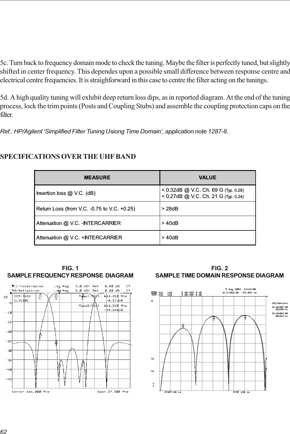
- 3. Exciter user manual Part 3
- 4. Amplifier User manual Part 1
- 5. Amplifier User manual Part 2
Amplifier User manual Part 2