Elettronika S r l TXUP1500 1300 Watt Analog TV Broadcast Transmitter User Manual APT144A AUTV 1500LD Rev0 Date081104
Elettronika S.r.l. 1300 Watt Analog TV Broadcast Transmitter APT144A AUTV 1500LD Rev0 Date081104
Contents
- 1. Exciter user manual Part 1
- 2. Exciter user manual Part 2
- 3. Exciter user manual Part 3
- 4. Amplifier User manual Part 1
- 5. Amplifier User manual Part 2
Amplifier User manual Part 2
33
_______________________________________________________________________________________________
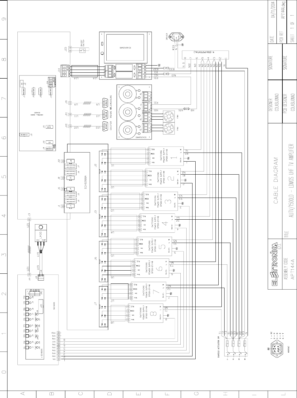
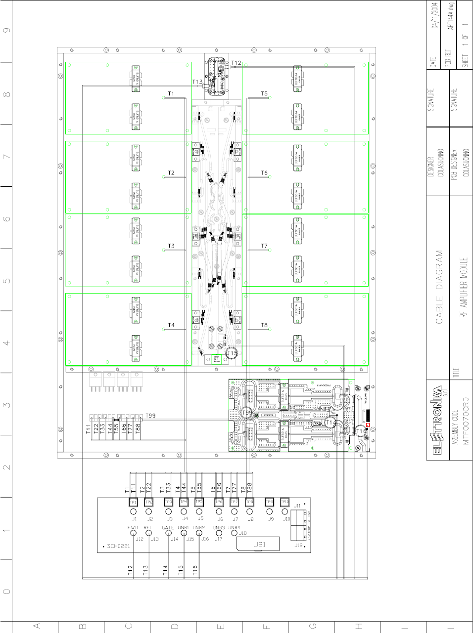
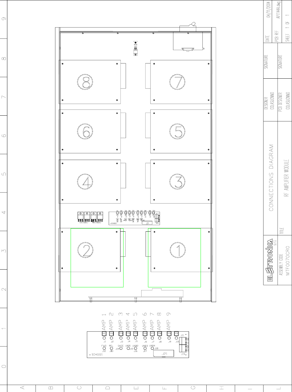
Section 4 - Diagram
Contents:
- Cable diagram
- MTF0070CR0 RF Amplifier module Cable Diagram
- MTF0070CR0 RF Amplifier module Connections Diagram
- MTF0070CR0 Amplifier module - Component list
- SCH0192AR0 (200W UHF LDMOS Amplifier module)
- SCH0223AR1 (Control board and display)
- SCH0221AR1 (Amplifier interface)
- SCH0265AR0 (Mains distribution board)
- SCH0288AR1 (Interface board)
- E0012 (SP500-27-DI Switching power supply)
34
35
36

37
Part Name Code Description Qty
00001 0W 1206 SMD RESISTOR 2
01041D 1nF 1206 2% SMD CAPACITOR 2
00221B 75W 1206 1% SMD RESISTOR 2
03207 HSMS-2802*L31 DIODE 2
SCH0192AR0 200W UHF LDMOS AMPLIFIER MODULE 9
SCH0221AR0 AMPLIFIER INTERFACE 1
SCH0248AR0 8 WAY WILKINSON 1
SCH0249AR0 4 WAY WILKINSON Dx 1
SCH0250AR0 4 WAY WILKINSON Sx 1
SCH0251AR0 2 WAY WILKINSON 1
SCH0252AR0 1500W UHF INPUT COUPLER 1
PN1091A C.S. PN1091AR3 OUTPUT DIRECTIONAL COUPLER 1
02402 7/16 FEMALE CONNECTOR cod. 0142 1
02512 J01151A0531 SMA SOCKET WITHOUT BAT. 1
01400 2499-003-X5U0-102M FEED-THROUGH CAPACITOR 13
01408 5000PF FEED-THROUGH CAPACITOR 2
DET0726 DET0726R2 SIDE x 1500W UHF AMP. MOD. 2
DET0727 DET0727R1 INTERNAL FRONT SIDE x AMP. MOD. 1
DET0728 DET0728R4 INTERNAL SIDE x AMP. MOD. 2
DET0729 DET0729R2 FRONT SIDE x AMP. MOD. 1
DET0730 DET0730R2 REAR SIDE x AMP. MOD. 1
DET0732 DET0732R1 CONNECTIONS SUPPORT BOARD 1
DET0734 DET0734R0 COVER x AMPLIFIER MODULE P. 2634 1
DET0736 DET0736R6 HEATSINK x AMPLIFIER MODULE 1
DET0807 DET0807R3 SCREEN DIR. COUPLER MODULE 1
DET0810 DET0810R0 PART. x DIRECTIONAL COUPLER 1
DET0811 DET0811R1 COVER x DIRECTIONAL COUPLER 1
DET0812 DET0812R1 TEFLON RING x DIRECTIONAL COUPLER 1
DET0819 DET0819R0 SPESS. x INPUT DIR. COUPLER 1
DET0828 DET0828R0 COVER x AMPLIFIER MODULE P. 2644 1
DET0839 DET0839R2 DIRECTIONAL COUPLER 1
08502 RG316 50W CABLE 3,00
08527 HF-85 ENDIFORM CABLE 0,20
03017 MBR3045PT DIODE 4
PN0998A PN998AR1 POWER SUPPLY ADDED PCB 2
Component list MTF0070CR0 Amplifier module

38
This page is intentionally blank

39
Part Name Code Description Qty
05553B KIT MANIGLIE 5-6U cod. 235.013 2
V0962 MORSETTIERA/GIUNZIONE ELECO E806 2
V0760 TAPPI NERI 0 9.5 PLASTICA DP-375 1
SCH0223AR1 CONTROL BOARD AND DISPLAY 1
SCH0265AR0 MAINS DISTRIBUTION BOARD 1
MTF0070CR0 RF AMPLIFIER MODULE 1
09419 C.S. PN419/A SUPPOR. SENSORE TEMPER. 1
PN1114A C.S. PN1114AR1 SCHEDA CABL. VENT. x 1kW III 1
07925 PROTEZIONE IN GOMMA PVC PG 075 1
07515C INTER. AUTOM. 4P*16A 4.5KA 2 mod. GW 90087 1
07524A INTERR. NERI I3910 1
07541 PORTAFUS. 10A PANN. cod. P1820 3
02830 PRESA VDE 10A cod. PX675 A63 1
02893 MORSETTIERA ESTRA. 3VIE MAS. KSC 3 3
02894 MORSETTIERA ESTRA. 3 VIE FEM. KB 3 3
02695 CONNETTORE DB9F x CAVO IU008059 3
02699 CONNETTORE cod. IDS10FSR1 FEMM. 10 VIE 9
02700 CONNETTORE cod. IDS16FSR1 FEM. 16 VIE 1
02228 GE 15145 D/60 NF A VITONE 1
02502 J01150A0041 SMA x RG58/c 1
02876 PRESA VOLANTE ILME 16A PENTAPOLARE 4MT 1
02877 SPINA A PANNELLO ILME 16A 5P 35cm 1
07605A COND. 2uF 2
07605B VENTOLA D2E097-BI56-48 2
07605F GRIGLIA 09485-2-4039 4
01041 1nF COND. CERAMICO 50V 2
00664 SENSORE TERMICO LM 35DT 1
FUS1A FUSIBILI 1A 5x20 RITARDATI ST520210 1
FUS3A FUSIB. 3.15A 5x20 RITAR. ST520231 1
FUS5A FUSIBILI 5A 5x20 RITARDATI ST520250 1
CON0171 CON0171R5 SOST. VENT. 1kW LDM. PH. ZN P.2614 1
CON0178 CON0178R4 POST. 1500W LDMOS UHF ZN 1
DET0516 DET0516R0 SUPPORTO PRESE ZN P.2642 1
DET0772 DET0772R0 BARRETTA FISSAGGIO VENTOLE 2
Z0021 TONDO IN OTTONE x INT. MAGNET. TAV. 635/A 2
Z0081 SUPPORTO GUIDA DIN INT. MAG. 1
Z0673 TAV. 1199 CHIUS. CONT. PROF. 775 ZN P.2366 2
E0012 SP-500-27 DE2 SWITCHING POWER SUPPLY 8
PAN0074 PAN0074AR2 PANN. 6U AMPLIFICATORE LDMOS 1
08503 CABLE RG303 50W TEFLON 1,20
DET0575 DET0575R1 BARRA FISSAGGIO ALIM. SP-500 8
SCH0288AR2 INTERFACE BOARD 1
CON0237 CON0237R2 LAT. SX 1500W UHF MW P.2743 ZN 1
CON0238 CON0238R1 LAT. DX 1500W UHF MW P.2744 ZN 1
DET0996 DET0996R0 BARRA FISS. SCHEDA DISTR. RETE 1
DET0995 DET0995R0 BARRA FISSAGGIO ALIM. SP-500 1
Component list APT144A - AUTV/1500LD

40
This page is intentionally blank
41
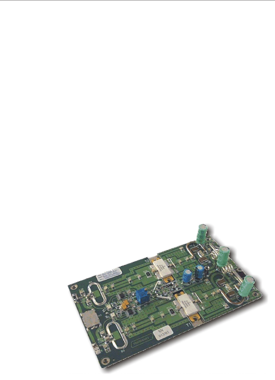
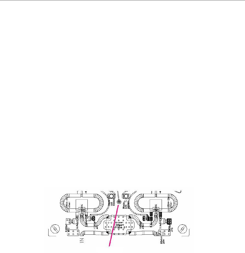
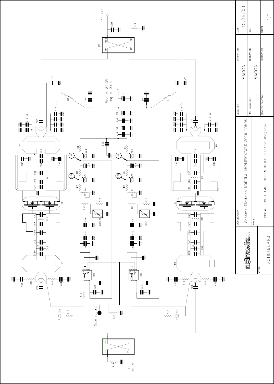
200W UHF LDMOS AMPLIFIER MODULE SCH0192AR0
DESCRIPTION
The RF module is an integrated TV linear amplifier designed for UHF band, this module employs push-pull
LDMOS technology in order to achieve very good efficiency, high linearity and reliability.
LDMOS transistors operate in AB class. It is a wideband amplifier over the full frequency, no adjustment is
required for the channel change. The board includes RF section amplifier, bias circuit, protection circuit and
matching networks. A silver plated copper plate is brazed with PCB in order to obtain low thermal resistance.
Providing a minimum of 200W Pk sync linear power, this module is the perfect amplifier for any broadband
UHF power transmitter.
TECHNICAL CHARACTERISTICS
Output power 300W max
Input power 15W max
Frequency 470 - 860MHz
Gain > 13dB
LDMOS Power supply 32V ±2%
LDMOS Bias current @+32V Vdc 2A
RF Input impedance 50W
RF Output impedance 50W
Input / Output return loss > = 15dB
Drain efficiency 47% @ 250W
Storage temperature range -50° to +150°C
Dimensions (LxWxH) 165x95x29mm
42
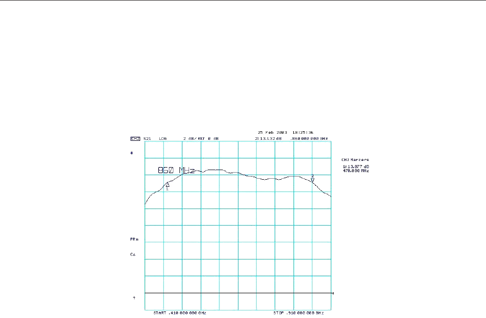
CALIBRATION PROCEDURE
- Technical characteristics
Power supply voltage 32V (± 2%)
Polarisation current 1.0 cold for each device (2A total), ± 0.1A
Gain for low signal Not less than 13dB in the 470-860MHz band (± 1dB)
Compare to the typical curve eclosed
- Adjustment procedure
Polarisation current calibration 32V stabilised power supply
10A amperometer
Gain curve Network analyser
- Adjustment points description
R7-R8 (Trimmers) Adjust the current absorbed in stand-by (1.0A per device)
Middle frequency 660MHz, span 500MHz, 2dB/div., reference to the arrow
- Curve response graphic
43
- Calibration steps
STEP 1. Close the input and the output of the module by connecting them to a 50WW
WW
W dummy load
and connect the spectrum analyser through a directive sample, in order to look for self-oscillation of the
module, if any (anyway the module has been designed so that it would not self-oscillate even if totally de-
coupled, without any input or output load).
STEP 2. Check the voltages of the polarisation circuits without assembling the transistors first:
connect the 32V power supply to the proper turret by means of a fastening screw, then give power and check
data:
- the stabilised voltage on the zener diodes DZ1 and DZ2 is about 15V compared to the ground;
- the stabilised voltage on the zener diodes DZ3 and DZ4 is about 6.8V compared to the ground;
- the voltage on the pads to which the gates of the LDMOS transistors will be soldered (R23 and R24
resistors side) changes from 0V to a maximum value of about 6V when moving the relevant trimmer (R7-R8).
STEP 3. Check the work of the protections.
- Set both trimmers so that there is a value of about 4.5V on the pads of the gates;
- solder some wire to the pad between the two LEDs, next to the serigraphy of the input hybrid H1;
- in order to check the work of the protections aboard, a power of about 4V has to be supplied to the wire,
for example by touching with it the reophore of C23 or C24 which is not connected to ground; the two red
LEDs will immediately light up and the two RF transistors will be switched off at the same time: the polarisation
current (2A) will decrease to 0 and of course the gain curve displayed by the spectrum analyser will decrease;
- after this it is important to restore the position of the two trimmers for the minimum voltage! Then
disconnect the 32V power supply.
STEP 4. Fastening of the LDMOS transistors: after properly cleaning the plate surface, smear a thin
layer of silicone fat on the lower side of the flange of the MOSFETs, fasten them to the heat sink and solder
the gate first, then the drain. Solder the two 13pF (ATC) chip capacitors and above them the two 1-5pF
Solder a wire

44
capacitive trimmers, between the two pair of gates, as shown by the mounting plan.
STEP5. Connect serially a c.c. amperometer to the power supply, with scale starting from more than 5A
(i.e. 10A).
STEP 6. Power the module and check the MOSFET is not absorbing current; this means that the device
is integral and working correctly.
STEP 7. Slowly turn the R7 trimmer until the MOSFET absorbs 1A, always checking that there are no
self-oscillation; under this conditions it is possible to check by means of a digital tester that the voltage on the
gate is about 5.2-5.4V.
STEP 8. Repeat the previous step for the other section of the module, this time turnign R8 and checking
that the indication of the current on the amperometer increases to 2A total (which includes the current of the
other device left on).
STEP 9. Check the response curve of the module by means of the network analyser.
STEP 10. Check the response curve for low signal with centre 660MHz and span 500MHz, 2dB/div.
STEP 11. The curve should be similar to the one enclosed, with a tolerance of ± 0.5dB. To obtain this, act
on the four trimmers C41-C41a and C42-C42a with the proper calibrator, inorder to flatten the curve as
much as possible, especially at the edged of the band which represents the minimum values.
STEP 12. Finally, check that the current in stand-by does not increase by more than 15÷20%, reaching at
worst 2.3÷2.4A when the heat sink is hot and not ventilated.
Note: when mounting-removing the PALLET on the heat sink, tightly fasten the screw of each all N input and output
connectors. These are mounted with a single 3mm screw and if it is not properly fastened it may be detached from the PCB
by a movement of the connector once it has already been soldered to the path.
45
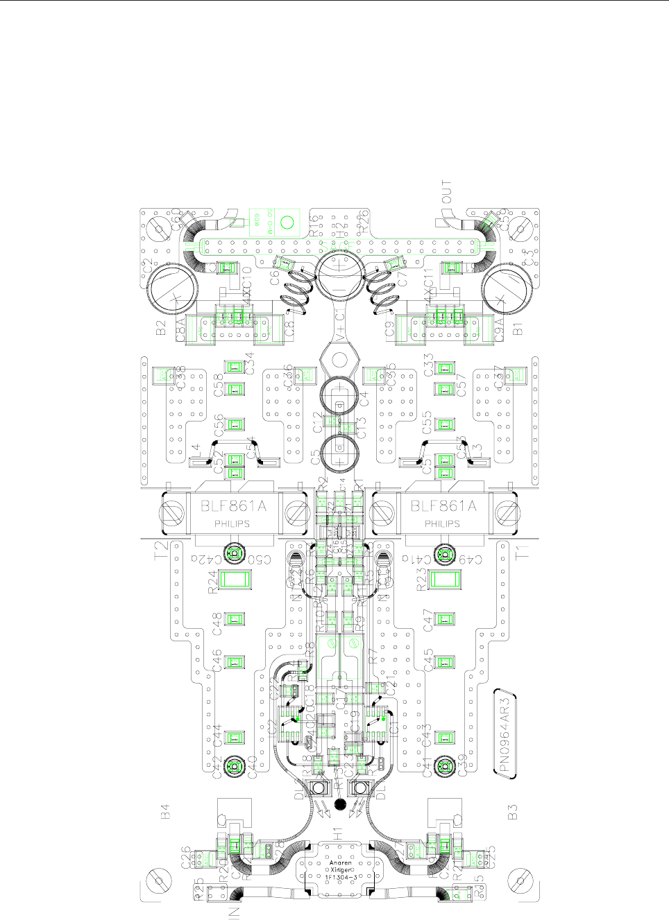
Component layout SCH0192AR0
46

47
COMPONENT LIST SCH0192AR0
REF. DESCRIPTION ELETTRONIKA CODE Page 1/3
R1 2200W 1/4W 1206 SMD RESISTOR 00045A
R2 2200W 1/4W 1206 SMD RESISTOR 00045A
R3 2200W 1/4W 1206 SMD RESISTOR 00045A
R4 2200W 1/4W 1206 SMD RESISTOR 00045A
R5 1200W 1/4W 1206 SMD RESISTOR 00042A
R6 1200W 1/4W 1206 SMD RESISTOR 00042A
R7 50kW MULTITURNS PTH TRIMMER 00800
R8 50kW MULTITURNS PTH TRIMMER 00800
R9 1200W 1/4W 1206 SMD RESISTOR 00042A
R10 1200W 1/4W 1206 SMD RESISTOR 00042A
R11 18kW 1/4W 1206 SMD RESISTOR 00056B
R12 18kW 1/4W 1206 SMD RESISTOR 00056B
R13 680KW 1/4W 1206 SMD RESISTOR 00075A
R14 0W 1/4W 1206 SMD RESISTOR 00001
R15 50W 30W 1512EBX SMD RESISTOR 00416A
R16 50W 60W 00432
R17 4.7kW 1/4W 1206 SMD RESISTOR 00049A
R18 4.7kW 1/4W 1206 SMD RESISTOR 00049A
R19 3.9W 1/4W 1206 SMD RESISTOR 00012A
R20 3.9W 1/4W 1206 SMD RESISTOR 00012A
R21 3.9W 1/4W 1206 SMD RESISTOR 00012A
R22 3.9W 1/4W 1206 SMD RESISTOR 00012A
R23 1000W 1W 2512 SMD RESISTOR 00396
R24 1000W 1W 2512 SMD RESISTOR 00396
*R25 = R15 (da montare se si inverte lingresso)
*R26 = R26 (da montare se si inverte luscita)
C1 470uF 50V PTH ELECTROLYTIC CAPACITOR 01807B
C2 470uF 50V PTH ELECTROLYTIC CAPACITOR 01807B
C3 470uF 50V PTH ELECTROLYTIC CAPACITOR 01807B
C4 100uF 50V PTH ELECTROLYTIC CAPACITOR 01795
C5 100uF 50V PTH ELECTROLYTIC CAPACITOR 01795
C6 1nF ATC 100B CAPACITOR OR EQUIVALENT 01145
C7 1nF ATC 100B CAPACITOR OR EQUIVALENT 01145
C8 x 2 2 x 100nF ATC CAPACITOR OR EQUIVALENT 01065H
C9 x 2 2 x 100nF ATC CAPACITOR OR EQUIVALENT 01065H
C10 x 4 4 x 100pF ATC 100B CAPACITOR OR EQUIVALENT 01135
C11 x 4 4 x 100pF ATC 100B CAPACITOR OR EQUIVALENT 01135
C12 100nF 1210 SMD CAPACITOR 1065G
C13 100nF 1210 SMD CAPACITOR 1065G
C14 100nF 1210 SMD CAPACITOR 1065G
C15 1uF 35V SMD TANTALIUM CAPACITOR 01613A
C16 1uF 35V SMD TANTALIUM CAPACITOR 01613A
C17 100nF 1210 SMD CAPACITOR 1065G

48
REF. DESCRIPTION ELETTRONIKA CODE Page 2/3
C18 100nF 1210 SMD CAPACITOR 1065G
C19 10uF 16V SMD TANTALIUM CAPACITOR 01626A
C20 10uF 16V SMD TANTALIUM CAPACITOR 01626A
C21 100nF 1210 SMD CAPACITOR 1065G
C22 100nF 1210 SMD CAPACITOR 1065G
C23 100nF 1210 SMD CAPACITOR 1065G
C24 100nF 1210 SMD CAPACITOR 1065G
C25 1nF ATC 100B CAPACITOR OR EQUIVALENT 01145
C26 1nF ATC 100B CAPACITOR OR EQUIVALENT 01145
C27 1nF ATC 100B CAPACITOR OR EQUIVALENT 01145
C28 1nF ATC 100B CAPACITOR OR EQUIVALENT 01145
C29 20pF ATC 100B CAPACITOR OR EQUIVALENT 01123
C30 20pF ATC 100B CAPACITOR OR EQUIVALENT 01123
C31 20pF ATC 100B CAPACITOR OR EQUIVALENT 01123
C32 20pF ATC 100B CAPACITOR OR EQUIVALENT 01123
C33 1.3pF ATC 100B CAPACITOR OR EQUIVALENT 01104
C34 1.3pF ATC 100B CAPACITOR OR EQUIVALENT 01104
C35 470pF ATC 100B CAPACITOR OR EQUIVALENT 01143
C36 470pF ATC 100B CAPACITOR OR EQUIVALENT 01143
C37 470pF ATC 100B CAPACITOR OR EQUIVALENT 01143
C38 470pF ATC 100B CAPACITOR OR EQUIVALENT 01143
C39 4.7pF ATC 100B CAPACITOR OR EQUIVALENT 01108
C40 4.7pF ATC 100B CAPACITOR OR EQUIVALENT 01108
C41 x 2 2 x 1¸5pF JOHANSON SMD TRIMMER 1485
C42 x 2 2 x 1¸5pF JOHANSON SMD TRIMMER 1485
C43 3.6pF ATC 100B CAPACITOR OR EQUIVALENT 01104B
C44 3.6pF ATC 100B CAPACITOR OR EQUIVALENT 01104B
C45 6.8pF ATC 100B CAPACITOR OR EQUIVALENT 01111
C46 6.8pF ATC 100B CAPACITOR OR EQUIVALENT 01111
C47 6.8pF ATC 100B CAPACITOR OR EQUIVALENT 01111
C48 6.8pF ATC 100B CAPACITOR OR EQUIVALENT 01111
C49 13pF ATC 100B CAPACITOR OR EQUIVALENT 01119A
C50 13pF ATC 100B CAPACITOR OR EQUIVALENT 01119A
C51 8.2pF ATC 100B CAPACITOR OR EQUIVALENT 01113
C52 8.2pF ATC 100B CAPACITOR OR EQUIVALENT 01113
C53 8.2pF ATC 100B CAPACITOR OR EQUIVALENT 01113
C54 8.2pF ATC 100B CAPACITOR OR EQUIVALENT 01113
C55 10pF ATC 100B CAPACITOR OR EQUIVALENT 01117
C56 10pF ATC 100B CAPACITOR OR EQUIVALENT 01117
C57 4.7pF ATC 100B CAPACITOR OR EQUIVALENT 01108
C58 4.7pF ATC 100B CAPACITOR OR EQUIVALENT 01108
C59 0.3pF ATC 100B CAPACITOR OR EQUIVALENT 01160
T1 BLF861A RF LDMOS POWER TRANSISTOR 04034
T2 BLF861A RF LDMOS POWER TRANSISTOR 04034
B1 COAX 2:1 BALUN 08491

49
REF. DESCRIPTION ELETTRONIKA CODE Page 3/3
B2 COAX 2:1 BALUN 08491
B3 COAX 4:1 BALUN 08492
B4 COAX 4:1 BALUN 08492
L1 4 TURNS SILV. COP. WIRE 1.2mm WOUND ON OD 5mm 07684
L2 4 TURNS SILV. COP. WIRE 1.2mm WOUND ON OD 5mm 07684
L3 ½ TURN COIL
L4 ½ TURN COIL
H1 HYBRID COUPLER 3dB 90° ANAREN 05368
H2 HYBRID COUPLER 3dB 90° SAGE 05369
NTC1 NTC 100KW PTH 00661
NTC2 NTC 100KW PTH 00661
IC1 DG419DY 04583
IC2 DG419DY 04583
DZ1 15V SMD ZENER DIODE 03135
DZ2 15V SMD ZENER DIODE 03135
DZ3 6.8V SMD ZENER DIODE 03137
DZ4 6.8V SMD ZENER DIODE 03137
DL1 SMD LED DIODE - RED - 03056
DL2 SMD LED DIODE - RED - 03056
PN964AR3 PCB 0643K
Torretta 3x10 f/f V0774
Imballo velapack 200x125x50 09983
50
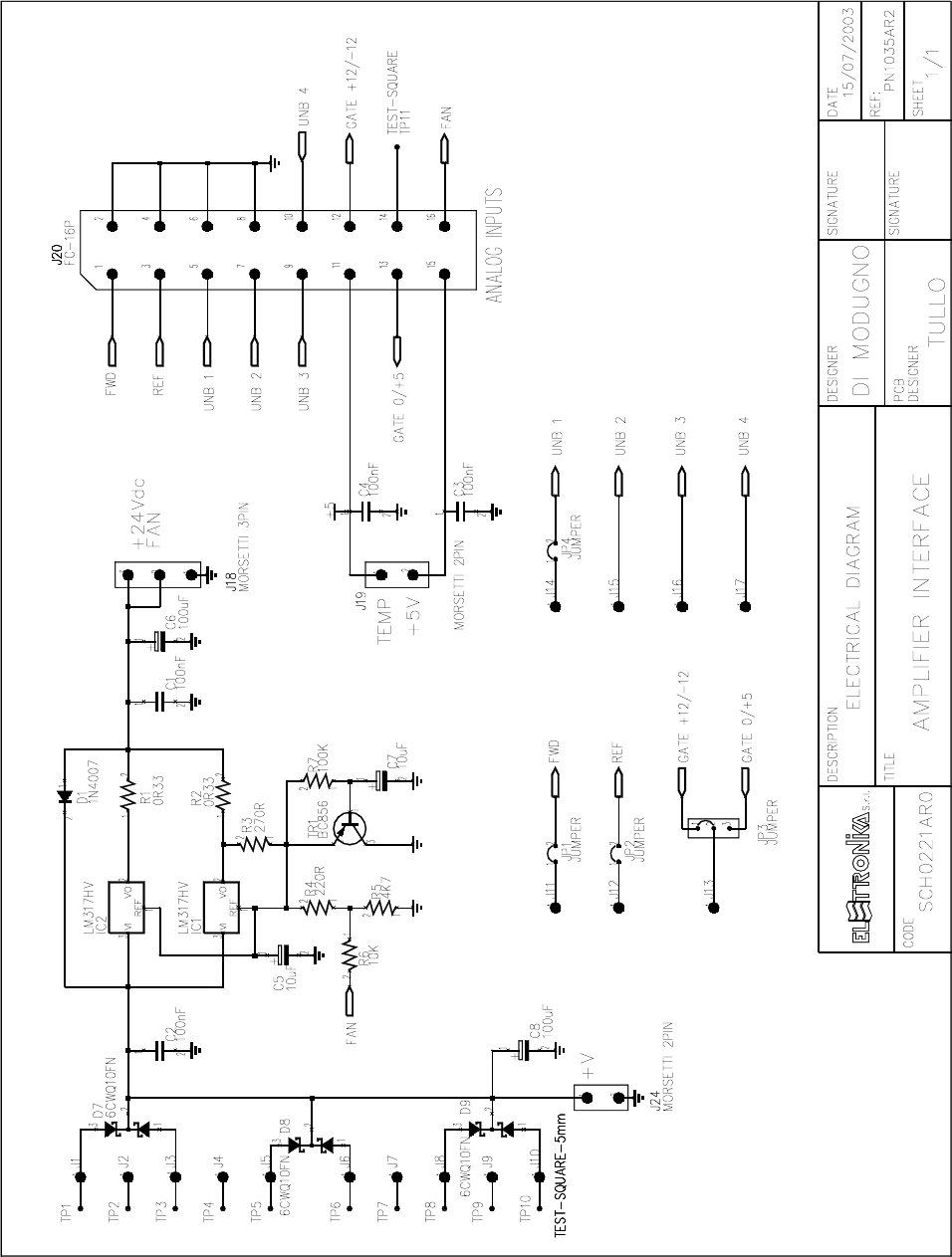
AMPLIFIER INTERFACE SCH0221AR0
Component layout SCH0221AR0
COMPONENT LIST SCH0221AR0
Part Name/Number Description Qty. Comps.
CC 100nFAVX 01065A 01065A CERAMIC COND 4 C1-4
CE 100uF100V 01795B ELETT. COND. 1 C8
CE 100uF50V 01795 01795 ELETT. COND. 1 C6
CE 10uF35V-S 01778A 01778A ELETTR SMD COND 2 C5, C7
D 1N4007 03009 03009 DIODE 1 D1
D 6CWQ10FN 03026 SMD DIODE SCHOTTKY 3,5A 3 D7-9
IC LM317HV 04340A INTEG CIRCUIT 2 IC1-2
J FC-16P 02701-02700 02701+02700 PCB CONNECTOR POL 1 J20
J SCREWCONN2 02853 02853 PCB SCREW CONNECTOR 2 J19, J24
J SCREWCONN3 02860 02860 PCB SCREW CONNECTOR 1 J18
J TESTP1.3mm 07913 07913 TEST POINT 17 J1-17
JU JUMP2 02739-02742 02739+02742 MASCHIO PAN2 3 JP1-2, JP4
JU JUMP3 02707-02742 02707+02742 MASCHIO PAN3 1 JP3
R 0R33-1W-S 00380 RES 1W 5% SMD 2512 2 R1-2
R 100K-S 00065A 00065A RES 1/4W 5% SMD 1206 1 R7
R 10K-S 00053A 00053A RES 1/4W 5% SMD 1206 1 R6
R 220R-S 00033A 00033A RES 1/4W 5% SMD 1206 1 R4
R 270R-S 00034A 00034A RES 1/4W5% SMD 1206 1 R3
R 4K7-S 00049A 00049A RES 1/4W 5% SMD 1206 1 R5
TR BC856 03455 03455 PNP SMD TRANSISTOR 1 TR1
51
52
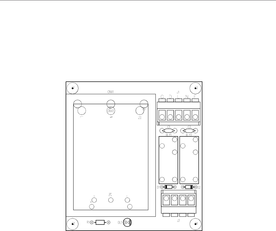
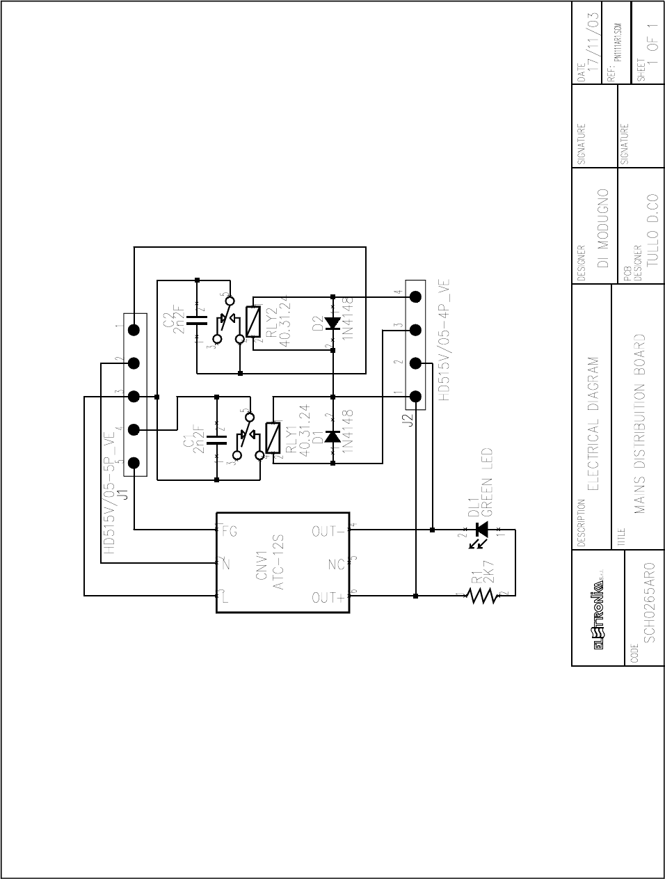
MAINS DISTRIBUTION BOARD SCH0265AR0
Component layout SCH0265AR0
COMPONENT LIST SCH0265AR0
Part Name/Number Description Qty. Comps.
CC 2nF2 2kV 01045A 01045A CERAMIC COND 2 C1-2
CNV AC-DC ATC-12S E0037 AC DC CONVERTER 1 CNV1
D 1N4148 03001 03001 DIODE 2 D1-2
DL LEDG3 03053 03053 GREEN LED DIODE 3mm 1 DL1
J CON HD515V/05-4PVE 02881 + 02882 PANDUIT PCB CONN 1 J2
J CON HD515V/05-5PVE PANDUIT PCB CO 1 J1
R 2K7 0046 0046 RES 1/4W 5% 1 R1
RL 40.31.24 7567C RELE 2 RLY1-2
53
54
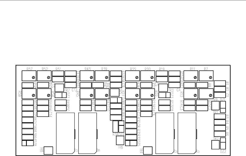
INTERFACE BOARD SCH0288AR1
Component layout SCH0288AR1
COMPONENT LIST SCH0288AR1
Part Name/Number Description Qty. Comps.
CC 1nF-S 01096 01096 SMD 1206 COND 16 C1-16
DZ 5V1-S 03128 03128 SMD ZENER DIODE 8 DZ1-8
J FC-10P 02697-02699 02697+02699 PCB CONNECTOR POL 4 J2-3, J6-7
J FC-10P PCB FEMALE 02706 PCB FEMALE CONNECTOR POL 4 J1, J4-5, J8
R 0R0-S 00001 00001 RES 1/4W 5% SMD 1206 16 R1, R8, R12, R15, R21, R23, R26
R28, R33, R40, R44, R47, R53, R55,
R58, R60
R 10K-S 00053A 00053A RES 1/4W 5% SMD 1206 16 R3-6, R17-18, R31-32, R35-38,
R49-50, R63-64
R 1206 NOT MOUNTED NOT MOUNTED RES 1/4W 5% SMD 12 16 R2, R10, R14, R16, R19, R24, R29,
R30, R34, R42, R46, R48, R51, R56,
R61-62
RV 3266W NOT MOUNT NOT MOUNTED VARIABLE RESISTOR 16 R7, R9, R11, R13, R20, R22, R25,
R27, R39, R41, R43, R45, R52, R54,
R57, R59
TR BC847 03456 03456 NPN SMD TRANSISTOR 8 TR1-8
56
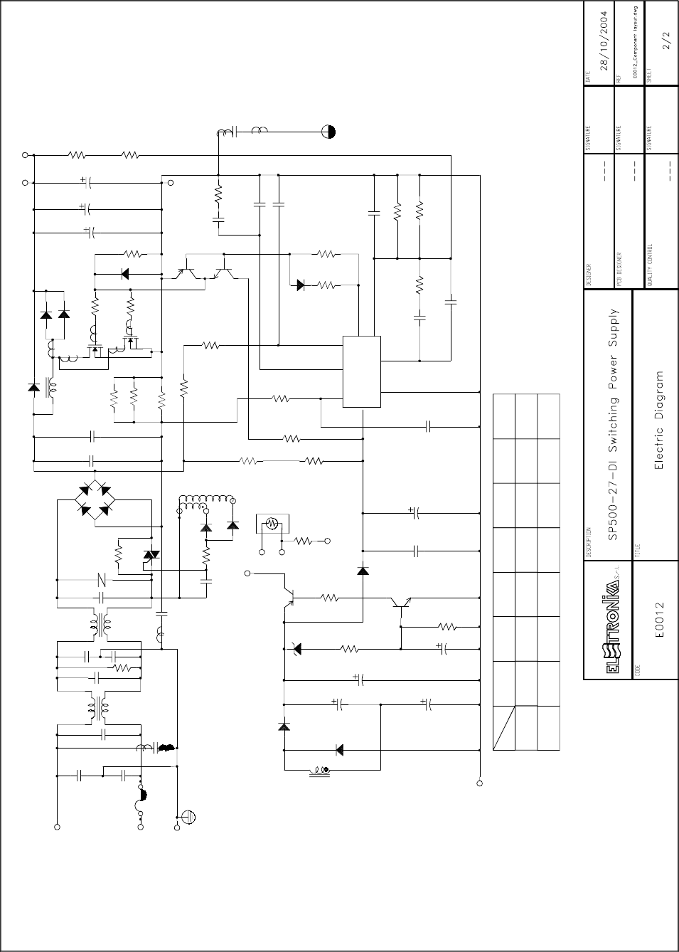
SPECIFICATION
MODEL SP-500-27 (E0012 Code) SP-500-48 (E0013 Code)
DC Output Voltage 27Vdc 48Vdc
Output Rated Current 18A 10A
Output Current Range 0-18A 0-10A
Ripple & Noise (p-p) 200mVp-p 240mVp-p
DC Output Power 486W 480W
Efficiency 87% 87%
DC Voltage Adj. 24-30V 41-56V
Over V. Protection 31V-36.5V 57.6V-67.2V
Input Voltage Range 88-264Vac
Input Frequency 47-63Hz
Power Factor 0.95/100-240Vac
Overload Protection 105%-135%
Type: Foldback current limiting
Recovery: Auto
Over Temp. Protection > =70°C Output Shutdown
Fan Control Temp. > =60°C Fan On
< =50°C Fan Off
Working Temp., Humidity -10°C/+50°C, 20%-90% RH
Dimension 185x120x93
Weight 1.8Kg.
SP500-27-DI SWITCHING POWER SUPPLY E0012
58
X X X
R+
R-
X1K
14.2V
C3
8.9V
R31
FG
AC/N
12V
X
13.5V 15V 24V
P5
Terminal
CN4
X
27V 48V
F+ CN2
54AD
270K
R29
AC/L
CN2
V-
HER104
D8 C32
102/250VAC
8.9V
2.2u/50V
C25 2.2u/50V
C24
470u/25V
C23
8.9V
1K
R24
C15
8.9V
104/100V
C21
1N4001
D2
51/2W
R4
BTA16-600B
TRC1
471
ZNR1
8.9V 8.9V
220u/25V
C17
T+
T- CN2
9.1V/1W
103/100V
C67
5.1/1/2W
R21
499K/1W
R9
330K
R30
1N4148
D3
C
E
B
Q4
C2655
22KR28
221/1KV
C20
472/50V
C13
102/50V
C11
CN1
V-
150u/400V
C26
150u/400V
C9
CN2
V+
499K/1W
R14
CN1
V+
C1 474/250VAC
C16
C2
474/250VAC
680K/1/2/W
R1
2K2
R25
2.2u/50V
C22
C5
104/250VAC
TF-360
LF2
10/5W
R2
30K/2W
R18
474/250VAC
C7
30K/2W
R17
100
R26
1N5819
D5
471/1KV
C12
C14
222/250VAC
499K/1W
R15
R31
PART NO .
SP-500A DIFFERENT COMPONENT:
ZD4
MODEL
HER104
D7
ZD4
FS1
F10A/250VAC
TF-360
LF1
C31
NC(PSF)
B
C
E
Q8
A562
100
R32
HER104
D4
0.22/2W
R6
0.33/2W
R7
15A/600V
BD1
C8
474/250VAC
D9
474/50V
C18
10K
R16
RHRP1650
D1:B
5.1
R10
150u/400V
C10
TR134
L1:B
C4
222/250VACX2
2K2
R23
C
E
BC1815
Q7
CN2
B
104/100V
C6
HER104
D6 499K/1W
R8
0.33/2W
R5
TR134
L1:A
473/50VC19
680
R27
B
C
EA1020
Q3
5.1
R11
5K1
R12
RHRP1650
D1:A
Q1
IRFPS37N50A
15
6
8
423
7
IAC
GTDR
VAo u t Vs
CAoutMout
Vcc
GND
LT1249
U1
Q2
IRFPS37N50A
59
UHF BANDPASS FILTER FC4E80C Code 06674
1.5kW, 4 Poles (Cross Coupling)
FEATURES
- UHF 1.5kW analog TV output filter
- 4 poles elliptical response
- Cross Coupling technique (two transmission zeros)
- Foreshorten folded combline structure
- Iris couplings with fine bandwidth regulation
- 3D Electromagnetic CAD
- High selectivity and low loss (Typ. 0.28dB @ V.C. Ch. 69 G)
- Temperature stabilized design (< 4kHz / K)
- Very compact and lightweight
SPECIFICATIONS (Value referred to G Standard)
Frequency Range 474 - 862MHz Selectivity > 40dB @ V.C. -5.5 / +11MHz
Max Input Power 1.5kW Analog TV > 25dB @ V.C. -11 / +16.5MHz
Insertion Loss* < 0.32dB @ V.C. Ch. 69 Temperature Stability < 4kHz / K
< 0.27dB @ V.C. Ch. 21 Connectors° 7/16 Female
Return Loss > 28dB Weight (Approx) 6kg
Group Delay Variation < 30ns Operating temperature -10 to +50°C
Bandwidth 6 to 8MHz
AVAILABLE OPTIONS
A SMA Output Monitor Probe B SMB Output Monitor Probe
H EIA 7/8 Flange Connectors Z Painted Black
CALIBRATION PROCEDURE
The output filter mod. 06674 is a 4-resonator, cross coupling bandpass filter, having thereby elliptical response.
It can be tuned on all the channels of the UHF TV band (470 - 862MHz) and according to all worldwide
standards (4.5 - 6.5MHz intercarrier). The elliptical response allows the exact placement of two deep
transmission nulls at the IMD spurs frequencies (V.C. - I.C. / S.C. - I.C.), making analog TV channel filter
response the most efficient.

60
Tunings (T1, T2, T3, T4) can be regulated simply by means of a suitable screwdriver.
Couplings (K12, K23, K34) are regulated varying the insertion of the Post Screws, which are located between
the resonators; the insertion of the Post Screws increases the bandwidth, except for K23 which has the
opposite effect of decreasing bandwidth as it is inserted. In order to execute this regulations it is necessary to
loosen every lock nut by means of a pipe wrench n. 19.
The elliptical response characteristics transmission nulls are set by the K14 Post Screw in a similar way as
above.
External loads (KE) are adjusted by means of the two shafts (Coupling Stubs), available removing the protection
caps opposite to each connector. A flat wrench n. 8 is required; the twist friction of these couplings can be set
tightening the relevant clamps with a pipe wrench n. 16.
The regulation is carried out considering that when the marked dots are set towards the resonators coupling
is maximum, otherwise tuning them 90 degrees from the maximum the minimum coupling is achieved.
The symmetry of the response curve is slightly affected by the orientation of the external loads (KE); to get
the best response symmetry, always rotate both dots outwards.
TUNING INSTRUCTIONS
The advised tuning sequence is the following:
1. set the instrument state as follows:
l C.F. = (V.C. + S.C.) / 2
l SPAN = INTERCARRIER * 5 (E.G. 27.5mhZ std. G)
l TRANSMISSION SCALE = 5dB/div.
l REFLECTION SCALE = 5dB/div.
l MKR1 = V.C.
l MKR2 = S.C.
l MKR3 = V.C. - VSB (E.G. V.C. -0.75MHz std. G)
2. Preset the Coupling Posts K12, K23, K34 and K14 at middle value, i.e. at the middle of their stroke.
Preset the external loads KE at middle value, i.e. the marked dots orientated 45 degrees one outward the
other, starting from the highest position.
3. The tuning is based upon the sample diagram attached. The final response must be the same for any channel
and any standard. Center the tunings (T1, T2, T3, T4) on the required channels center frequency, and set
K14 in order to place the response nulls at the required IMD frequencies. Proceed with the external loads KE

61
and bandwidth couplings K12/K34 and K23. Improve the tuning by repeatedly acting as before. The electrical
symmetry implies K12 equal to K34 (same heights) and KE/KE (same rotation angle). Regulate K14 each
pass to set the transmission nulls.
IMPORTANT NOTICE: the most effective tuning for analog TV channels is NOT equiripple, bus has -30dB R.L. at
middle peak and -35dB R.L. at outer peaks.
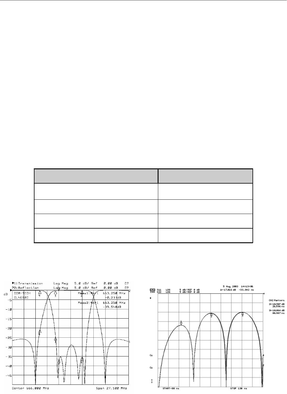
4. A high quality tuning will exhibit deep return loss dips, as in reported diagram. At the end of the tuning
process, lock the trim points (Posts and Coupling Stubs) and assemble the coupling protection caps on the
filter.
TIME DOMAIN TUNING
5. This filter is particularly suitable for time domain tuning. This tuning technique, available with HP/Agilent and
Rohde & Schwarz analyzers, is time saving and gives optimum results. The time domain graph contains all the
information about the parameters to be tuned, the tuning process becomes deterministic and it is not required
to be skilled. A vector network analizer with S-parameter test set is recommended. The following instructions
refers to Agilent HP8753ES unit. Execute a full two-port calibration, and start tuning the filter according the
previous instructions, up tyo step 3. When the filter is roughly tuned in frequency domain, you can toggle
modality.
5a. Turn on the Time Domain mode, taking a look at both S11 and S22 (System / Transform / Bandpass). Set
the time scale from -80 to 130ns, and amplitude scale at 5dB/dib. The displayed trace should be similar to the
example reported. The time domain interpretation is the following:
l the first peak is related to KE/KE
l the first dip is related to T1/T4
l the second peak is related to K12/K34
l the second dip is related to T2/T3
l the third peak is related to K23
5b. Tune repeatedly the filter starting from the outside to the center, which
corresponds to follow the time domain graph starting from left to right. The
resonators shall produce the deepest dips, whereas the couplings shall be
set to the following amplitude values (use markers to measure peak
amplitudes).
IMPORTANT NOTICE: K14 is NOT detectable in time domain, and have to
be continuously set in the frequency domain.
TUNING VALUE
KE/KE -17dB
K12/K34 -10.5dB
K23 -10dB
62
5c. Turn back to frequency domain mode to check the tuning. Maybe the filter is perfectly tuned, but slightly
shifted in center frequency. This dependes upon a possible small difference between response centre and
electrical centre frequencies. It is straighforward in this case to centre the filter acting on the tunings.
5d. A high quality tuning will exhibit deep return loss dips, as in reported diagram. At the end of the tuning
process, lock the trim points (Posts and Coupling Stubs) and assemble the coupling protection caps on the
filter.
Ref.: HP/Agilent Simplified Filter Tuning Usiong Time Domain, application note 1287-8.
SPECIFICATIONS OVER THE UHF BAND
MEASURE VALUE
Insertion loss @ V.C. (dB) < 0.32dB @ V.C. Ch. 69 G (Typ. 0.28)
< 0.27dB @ V.C. Ch. 21 G (Typ. 0.24)
Return Loss (from V.C. -0.75 to V.C. +0.25) > 28dB
Attenuation @ V.C. -INTERCARRIER > 40dB
Attenuation @ V.C. +INTERCARRIER > 40dB
FIG. 1
SAMPLE FREQUENCY RESPONSE DIAGRAM
FIG. 2
SAMPLE TIME DOMAIN RESPONSE DIAGRAM