Elettronika S r l TXUP200 250 Watt Analog TV Broadcast Transmitter User Manual APT134A AUTV 250LD Rev0 Date061103 pmd
Elettronika S.r.l. 250 Watt Analog TV Broadcast Transmitter APT134A AUTV 250LD Rev0 Date061103 pmd
User Manual

AUTV/250LD
LDMOS - UHF TV Solid State Amplifier
CODE APT134A TITLE AUTV/250LD REV 0DATE 06/11/03

SS 96 Km 113
70027 Palo del Colle (Ba) ITALY
Tel. +39 (0)80 626755
Fax +39 (0)80 629262
E-mail: elettronika@elettronika.it
Web site: http://www.elettronika.it
Registration number: IT-17686
Registration number: IT-24436

3
WARNING
The apparatus described in this manual has been designed and manufactured with devices to safe-
guard the users. In any case it is recommended that during any operation of installation, maintenance,
miscellaneous interventions and calibrations requiring the apparatus to be switched on,
THE USER TAKES ALL THE
PRECAUTIONS AGAINST INCIDENTS
It is required to use the proper clothes and protection gloves in order to prevent damages from inci-
dental contacts with high-voltage parts.
The manufacturer declines every responsibility in case the recommendations above are not followed.
IMPORTANT
The component lists attached to the relevant electrical diagrams indicate for each item the reference,
the description and the type normally used.
The Elettronika S.r.l. though reserves the right to use or supply as spare parts components with
equivalent characteristics but of a different type, assuring anyway the optimal work of the apparatus
in accordance with the specifications.
The enclosed monographs are solely owned by Elettronika S.r.l.
The use of anything enclosed in this technical manual without explicit authorization given by Elettronika
S.r.l. will be prosecuted by the law.
The data and technical characteristics of the apparatus described in this manual are not compelling for
the manufacturer.
The Elettronika S.r.l. reserves the right to make, without previous notice, modifications or updates in
order to improve the quality of the product.
The general conditions of supply and sale are described in the contracts.
The delivery time are in accordance with the products and quantities ordered.

4
Summary of warranty
We, ELETTRONIKA S.r.l., SS096 Km 113 Z.I. PALO DEL COLLE (BA) ITALY, warrant to the ORIGINAL PURCHASER of a NEW product, for a
period of one (1) year from the date of purchase by the original purchaser (the “warranty period”) that the new ELETTRONIKA product is free of defects
in materials and workmanship and will meet or exceed all advertised specifications for such a product. This warranty does not extend to any subsequent
purchaser or user, and automatically terminates upon sale or other disposition of our product.
Items excluded from this ELETTRONIKA warranty
We are not responsible for product failure caused by misuse, accident, or neglect. This warranty does not extend to any product on which the serial
number has been defaced, altered, or removed. It does not cover damage to loads or any other products or accessories resulting from ELETTRONIKA
product failure. It does not cover defects or damage caused by use of unauthorized modificstions, accessories, parts, or service.
What we will do
We will remedy any defect, in material or workmanship (except as excluded), in our sole discretion, by repair, replacement, or refund. If a refund is
elected, then you must make the defective or malfunctioning component available to us free and clear of all liens or other encumbrances. The refund will
be equal to the actual purchase price, not including interest, insurance, closing costs, and other finance charges less a reasonable depreciation on the
product from the date of original purchase. Warranty work can only be performed at our authorized service centers or at our factory. Expenses in
remedying the defect will be borne by ELETTRONIKA, including one-way surface freight shipping costs within the United States. (Purchaser must bear
the expense of shipping the product between any foreign country and the port of entry in the United States and all taxes, duties, and other custom’s fee(s)
for such foreign shipments).
How to obtain warranty service
You must notify us of your need for warranty service not later than ninety (90) days after the expiration of the warranty period. We will give you an
authorization to return the product for service. All components must be shipped in a factory pack or equivalent which, if needed, may
Desclaimer of consequential and incidental damages
You are not entitled to recover from us any consequential or incidental damages resulting from any defect in our product. This includes any damage
to another product or products resulting from such a defect.
Warranty alterations
No person has the authority to enlarge, or modify this warranty. The warranty is not extended by the lenght of time for which you are deprived of
the use of the product. Repairs and replacement parts are provided under the terms of this warranty shall carry only the unexpired portion of this
warranty.
Design changes
We reserve the right to change the design of any product from time to time without notice and with no obligation to make corresponding changes in
products previously manufactured.
Legal remedies of purchaser
There is no warranty which extends beyond the terms hereof. This written warranty is given in lieu of any oral or implied warranties not contained
herein. We disclaim all implied warranties, including without limitation any warranties of merchantability or fitness for a particular purpose. No action
to enforce this warranty shall be commenced later than ninety (90) days after expiration of the warranty period.
Warranty for electronic tubes
The warranty applied for electronic tubes is the one given by the manufacturer of the tube. In the event that the product shows anomalies within the
deadline of the validity of the warranty given by the manufacturer of the product itself, the buyer will have to return it to the seller with the needed
documents and the written description of the defect. The seller will ship the broken tube to the manufacturer in order to effect the necessary technical
tests to find out the cause of the anomaly. Meanwhile the buyer of the tube who needs to use, and as such to replace immediately the product, will have
to buy a new one and provide to the relevant payment, further to the issuing by the seller of a regular commercial invoice. After the adequate tests made
by the manufacturer, should the result be positive, that is confirm the defect in manufacturing, the seller will issue a regular credit note in the name of
the buyer and return the amount paid. Should the result be negative, that is detect a negligence in the installation or use by the buyer, he will have no
right against the seller.
Warranty

5
INTRODUCTION
The apparatus described in this manual is the latest of this series, offering high performances, remark-
able reliability and a wide range of characteristics, it all at a competitive cost.
Its is easy to install and use. It only takes to follow the installation procedure as shown in this manual:
after having removed all from the package, you only have to follow step by step the description in the
various sections.
Before starting to use the apparatus, remember to:
read carefully the general safety information contained in this section;
follow the instructions for the installation and set up of the apparatus;
read all the remaining sections of this manual in order to know well the apparatus and learn
how to obtain the best of its characteristics.
CONTENTS OF THE MANUAL
The chapter composing this manual contain all the information concerning the use of the apparatus.
For more information refer to ELETTRONIKA S.r.l.
This manual is made up of different chapters, each made up of various sections.

6
WARNING!
The currents and voltages in this equipment are dangerous!
Personnel must at all times observe safety regulation!
This manual is intended as a general guide for trained and qualified personnel who are aware of the
dangers inherent in handling potentially hazaedous electrical and electronic circuits.
It is not intended to contain a complete statement of all safety precautions which should be observed by
personnel in using this or other electronic equipment.
The installation, operation, maintenance and service of this equipment involves risks both to personnel
and equipment, and must be performed only by qualified personnel exercising due care.
Elettronika S.r.l. shall not be responsible for injury or damage resulting from improper procedures or
from the use of improperly trained or inexperienced personnel performing such tasks.
During installation and operation of this equipment, local building codes and fire protection standards
must be observed.
WARNING!
Always disconnect power before opening covers,
doors, enclosures, gates, panels or shields.
Always use grounding nsticks and short out high
voltage points before servicing. Never make
internal adjustments, perform maintenance or
service when alone or when fatigued.
Do not remove, short-circuit or tamper with interlock switches on access covers, doors, enclosures,
gates, panels or shields.
Keep away from live circuits, know your equipment and don’t take chances.
WARNING!
In case of emergency ensure that power has been disconnected.

7
A - AIRWAY
If unconscious, open airway lift up neck, push
forehead back, clear out mouth if necessary,
observe for breathing.
Treatment of electrical shock
1) If victim is not responsive follow the A, B, C’s of basic life support.
PLACE VICTIM FLAT ON HIS BACK ON A HARD SURFACE
B - BREATHING
If not breathing, begin artificial breathing. Tilt
head, pinch nostrils, make airttght seal, 4 quick
full breaths. Remember mouth to mouth resuscita-
tion must be commenced as soon as possible.
C - CIRCULATION
Check carotid pulse. If pulse
absent, begin artificial circulation.
Approx. 80sec.: 1 rescuer, 15 compressions, 2 quick breaths.
Approx. 60sec.: 2 rescuers, 5 compressions, 1 breath.
NOTE: DO NOT INTERRUPT RHYTHM
OF COMPRESSIONS WHEN SECOND PERSON
IS GIVING BREATH.
Call for medical assistance as soon as possible.

8
2) If victim is responsive:
- keep them warm;
- keep them as quiet as possible;
- loosen their clothing (a reclining position is recommended).
FIRST-AID
Personnel engaged in the installation, operation, maintenance or servicing of this equipment are urged
to become familiar with first-aid theory and practices. The following information is not intended to be
a complete first-aid procedure, it is brief and is only to be used as a reference. It is the duty of all
personnel using the equipment to be prepared to give adequate Emergency First Aid and thereby pre-
vent avoidable loss of life.
TREATMENT OF ELECTRICAL BURNS
1) Extensive burned and broken skin.
- Cover area with clean sheet or cloth (cleansed available cloth article);
- do not break blisters, remove tissure, remove adhered particles of clothing, or apply any salve or
ointment;
- treat victim for shock as required;
- arrange transportation to a hospital as quickly as possible;
- if arms or legs are effected keep them elevated.
NOTE
If medical help will not be available within an hour and the victim is conscious and not vomiting, give
him a weak solution of salt and soda: 1 level teaspoonful of salt and 1/2 level teaspoonful of baking
soda to each quart of water (neither hot or cold).
Allow victim to sip slowly about 4 ounces (half a glass) over a period of 15 minutes.
Discontinue fluid if vomiting occurs (do not give alcohol).
2) Less severe burns - (1st & 2nd degree).
- Apply cool (not ice cold) compresses using the cleansed available cloth article;
- do not break blisters, remove tissue, remove adhered particles of clothing, or apply salve or ointment;
- apply clean dry dressing if necessary;
- treat victim for shock as required;
- arrange transportation to a hospital as qickly as possible;
- if arms or legs are affected keep them elevated.

9
Further to the directives issued by the European Community, 2002/95/CE, 2002/95/CE and 2003/108/
CE, and to the Italian Decree of Law n° 151 dated 25 July 2005, this is to inform the customers of Elettronika
S.r.l. living within the boundaries of the European Community about the following obligations:
1) It is forbidden to trash RAEE products (which includes all broadcasting products which are not expressly
labelled as lead-free) along with normal wastes;
2) Such devices must be brought to proper centres able to perform the adequate processing in order to
recycle their parts where possible and dispose of the raw materials contained therein;
3) For equipment purchased from Elettronika after the 13th of August 2005, the gathering, transport, processing,
recycle and disposal operations are responsibility of Elettronika who will bear all related expenses;
4) For equipment purchased from Elettronika before the 13th of August 2005 , the gathering, transport,
processing, recycle and disposal operations are responsibility of Elettronika, who will bear all related expenses,
only if you are purchasing from us new equipment in substitution of the disposed one;
5) Electric and electronic devices contains lead in soldering, cables, etc. This substance pollutes the environment
and may be accumulated in the organism of plants and mammals. It is dangerous for humans because it may
affect blood, bone marrow, peripheral and central nervous system and kidneys, causing anaemia,
encephalopathies (e.g., convulsions), peripheral neuropathies, cramps of the abdomen and kidney damages.
Besides it affects human reproduction and growth.
These devices also contain mercury. From the environmental point of view, this substance is highly toxic for
aquatic life, and can be accumulated in the organism of fish.
Long-term damages to humans can affect the central nervous system and the kidneys, producing irritability,
emotional instability, tremors, damages to the mind and the memory, language disorders. It may also irritate
and whiten the gums, and its effects may be cumulative. Based on tests on animals, it may affect the human
reproduction or growth.
There is also chrome, which may result in irritation of the eyes and respiration system.
Cadmium is also present. In humans it may damage lungs, due to repeated or prolonged contact with its dust,
and kidneys. It may cause cancer.
6) The symbol below marks the devices which cannot be disposed of along with normal wastes, as stated in
1) and 2) above.
7) The payment of fees is foreseen for the non-allowed disposal of such devices.
Communication N°1 -2002/95/CE - RoHS Directive

10
This page is intentionally blank
11
LDMOS - UHF TV AMPLIFIER
AUTV/250LD
User’s manual

12
This page is intentionally blank

13
Section 1 - Information
Contents:
1.1 Description
1.2 Technical characteristics
14
AUTV/250LD
LDMOS - UHF TV AMPLIFIER
1.1 DESCRIPTION
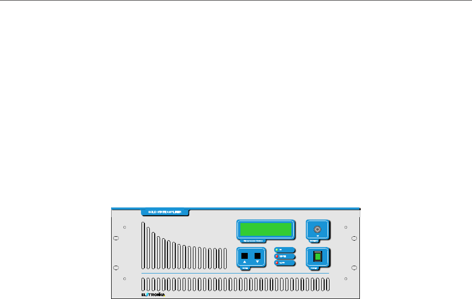
The amplifier AUTV/250LD is an apparatus designed to be used as final power stage or driver for higher-
power amplifiers in the UHF TV band.
It is able to supply a power of 250W (peak sync.) in class AB and is completely realized with LDMOS
technology. The power supply of the apparatus is given by a switching power supply for the RF power
module and a traditional transformer for the control board. The protection board uses all the potential of a
microprocessor to check all the parameters of the amplifier module and the voltage of the power supply.
An output band-pass filter provides for the attenuation of the spurious products. The final result is a compact
apparatus, it is all inside a standard 19”-4U cabinet, with a very good price-to-quality ratio.

15
1.2 TECHNICAL CHARACTERISTICS
RF SECTION
Frequency range 470 - 860MHz
Output power 250W
Gain 13dB +/-1
RF Input impedance 50Ω
RF Output impedance 50Ω
I.M.D. (3 Tones: -8, -10, -16dB) < -54dB (with IF Pre-corrector)
RF Spurious products Better than -60dB
Filter insertion loss < = 0,6dB
RF Input connector N Female
RF Output connector N Female
GENERAL
Power Supply 90-260VAC
Typical power consumption 600VA (Black)
RS232 Socket DB9 Connector
Telemeasuring socket DB9 Connector
Cabinet Rack 19”-4U
Dimensions 421x368x178mm
Weight 25kg
Ambient temperature -5° to +45°C
Humidity 20% - 90%
PROTECTION THR.
FWD Power 300W
REF Power 20W
Temperature 70°C
IDC 14A
VDC Min 5V - Max 34V

16
This page is intentionally blank

17
Section 2 - Installation
Contents:
2.1 Operating environment
2.2 Preliminary operations
2.3 Telemeasuring socket connections
2.4 RS232 / RS485 Socket connections
2.5 Control system
2.6 Preventive maintenance
- Front panel
- Rear panel
18
2.1 OPERATING ENVIRONMENT
You can install the apparatus in a standard component rack or on a suitable surface such as a bench or
desk. In any case, the area should be as clean and well-ventilated as possible. Always allow for at least
2 cm of clearance under the unit for ventilation. If you set the apparatus on a flat surface, install spacers
on the bottom cover plate. If you install the apparatus in a rack, provide adequate clearance above and
below. Do not locate the apparatus directly above a hot piece of equipment.
2.2 PRELIMINARY OPERATIONS
Correct installation of the equipment is important for maximum performance and reliability. Antenna
and earth connections must be installed with the greatest care. The equipment adjustment isn’t need,
because the unit is completely adjusted by our technical staff. This is the installation procedure:
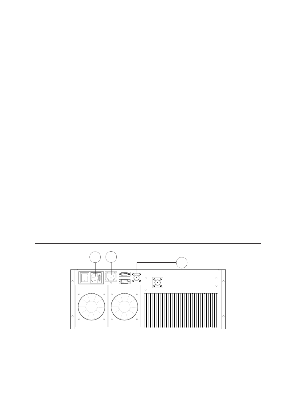
1. connect the power supply cable of the transmitter to the auxiliary socket on the rear panel of the
amplifier;
2. connect the power supply cable of the amplifier to the electric network (90-260VAC);
3. connect the exciter / antenna cable to the RF IN and RF OUT on the rear panel of the amplifier.
WARNING!!!
FOR ELECTRICAL SAFETY REASONS AND IN ORDER TO KEEP THE APPARATUS SAFE,
THE GROUND TERMINAL OF THE APPARATUS MUST BE CONNECTED TO THE EX-
ISTING GROUNDING SYSTEM AND NOT BY USING THE SHIELD OF THE OUTPUT
COAXIAL CABLE.
13
2
RF IN
RF IN
19
Before powering fully the apparatus, check that the output connections of the coaxial cable to the antenna
system are working.
In order to this it is possible to check the indication of the reflected power at low power levels. Only if
the SWR indication on the display is 0, the output power can be slowly increased. At maximum output
power, some watt might be shown as reflected power
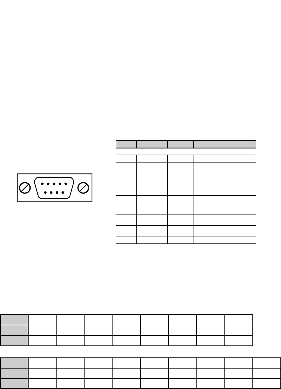
2.3 TELEMEASURING SOCKET CONNECTIONS
DB9 Socket
PIN N° SIGNAL TYPE IN / OUT FUNCTION
1Ground - -
2AnalogOutput
FWD Power
0 to 5V
3 Digital Input Floating: ON - GND: OFF
Valid only in remote (Pin 6= GND)
4 Digital Output 0: Alarm - 1: No alarm
TTL Level
5 - - Not used
6 Digital Input Floating: Local
GND: Remote (Pin 3 Command accepted)
7AnalogOutput
REF Power
0 to 5V
8AnalogOutput
Te mpe r at ur e
0 to 5V
9 - - Not used
2.4 RS232 / RS485 SOCKET CONNECTIONS
The DB9 connector can be used in two modes (RS232 or RS485) depending on the position of the Dip-
Switch.
PIN N° 123456789
RS232 -RXTX+5VGND+5V---
RS485 - RX- RX+ +5V GND +5V TX- TX+ -
SW1 12 34 5 6 78
RS232 Open Open Open Open Closed Closed Closed -
RS485 Closed Closed Closed Closed Open Open Open -

20
2.5 CONTROL SYSTEM
The control system allows the user to monitor the most important measures of the transmitter, voltage
and current of the power supply, temperature of the RF board, forward and reflected power, by using
the two keys placed on the frontal panel. The turn-on key allows to turn on and off the transmitter.
In case one of the monitored measures is in alarm, the transmitter will show this. If the value of the
measure goes back to normal, the control system will turn on the transmitter again.
After 5 cycles of turning on and off the transmitter will be kept switched off until the user turns it off.
Meaning of the LEDs
- LED ON: The LED ON is lit when the turn-on command of the transmitter is inserted.
- LED REMOTE: the LED REMOTE is lit when the remote commands have been enabled by the
telemeasuring connector or when the transmitter is controlled trough the RS232 port.
- LED ALARM: the LED ALARM is lit when the transmitter has been turned off due to a failure.
2.6 PREVENTIVE MAINTENANCE
To ensure maximum performance and minimum repair trouble, we strongly recommend you to follow
the below stated headlines for preventive maintenance:
1. check antenna installation and ground connection at regular intervals;
2. keep your apparatus clean and dry externally: this will ensure continuous functioning of the front
panel controls;
3. if the apparatus has not been used for a long period of time combined with exposure to extreme
environmental conditions, open the unit and make a visual inspection.
Remove salt, water or ice with a moist cloth before turning the apparatus on. Check that the cooling fans
are running freely.
4. for general maintenance and top performance, call an authorized service technical to give the appara-
tus and the complete antenna/earth connection installation a general check each 12-18 months;
5. check at regular intervals that the air intake located on the front panel is free of dust. If there is visible
dust, remove it by means of a soft brush.
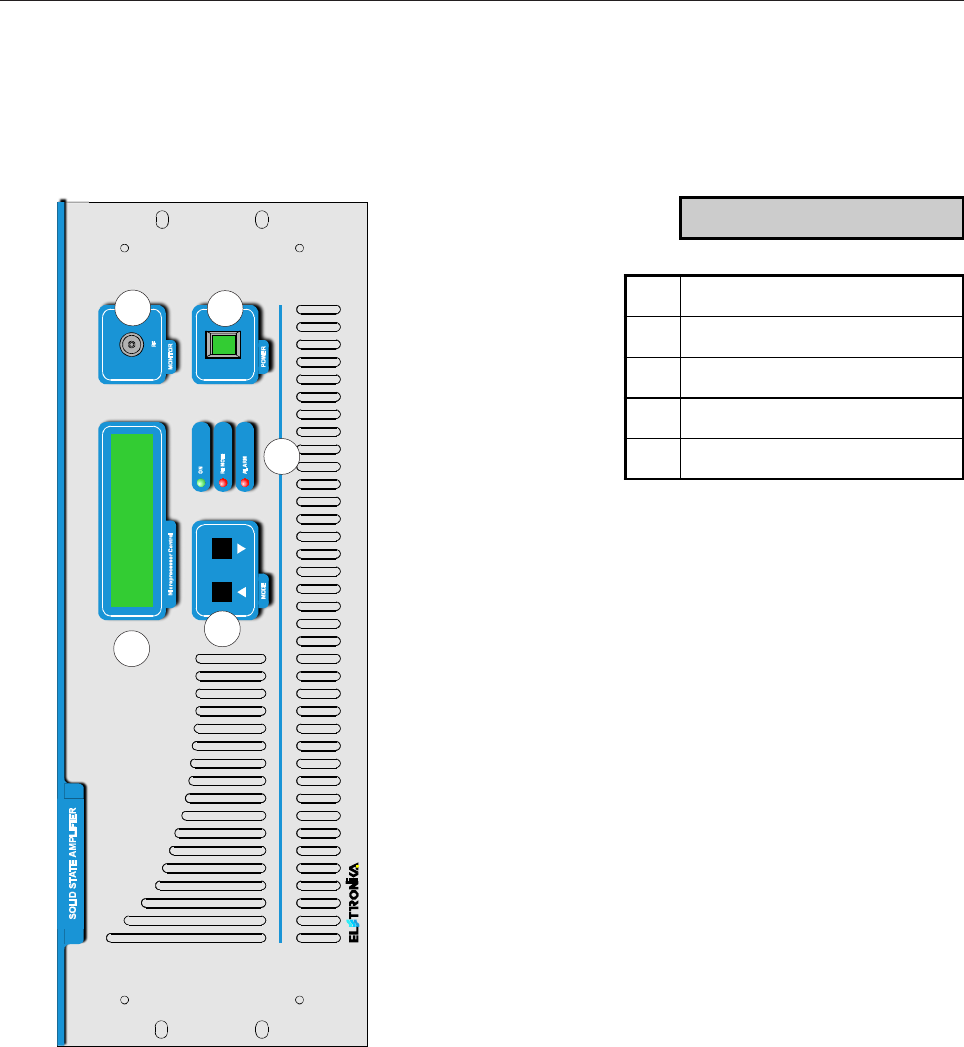
21
Front panel
2
3
4
5
1
DESCRIPTION
1LCD Display
2 RF Monitor connector
3 Function keys
4 Status LEDs
5 Main switch
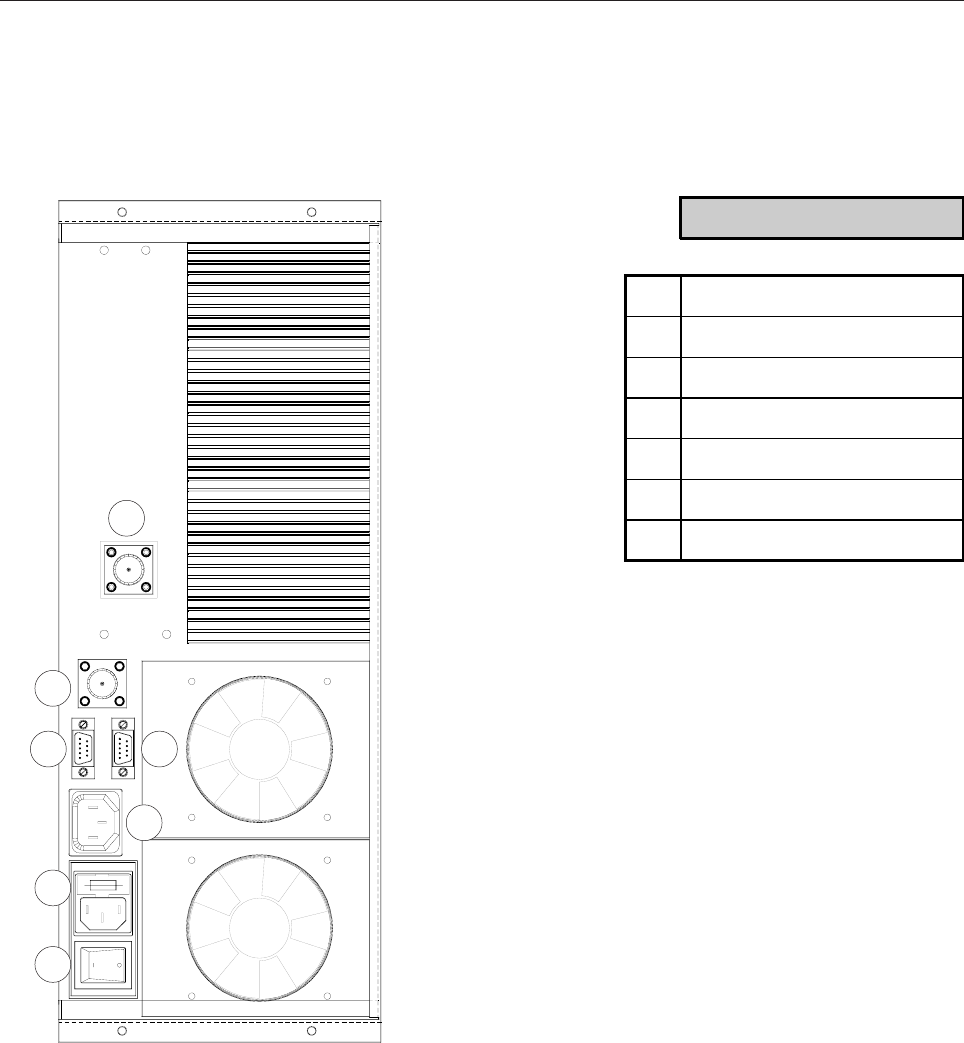
22
GND
15
4
6
7
3
2
DESCRIPTION
1 Power supply socket
2 Auxiliary socket
3 Breaker
4 RS232 Socket
5 Telemeasuring socket
6 RF Output connector
7 RF Input connector
Rear panel

23
_______________________________________________________________________________________________
Section 3 - Diagram
Contents:
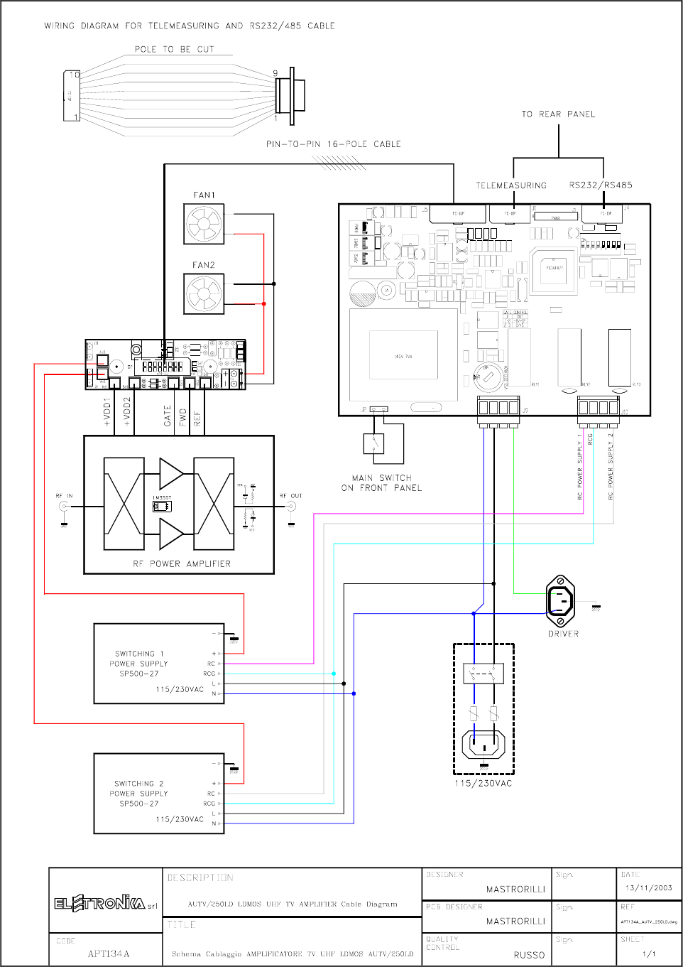
- Cable diagram
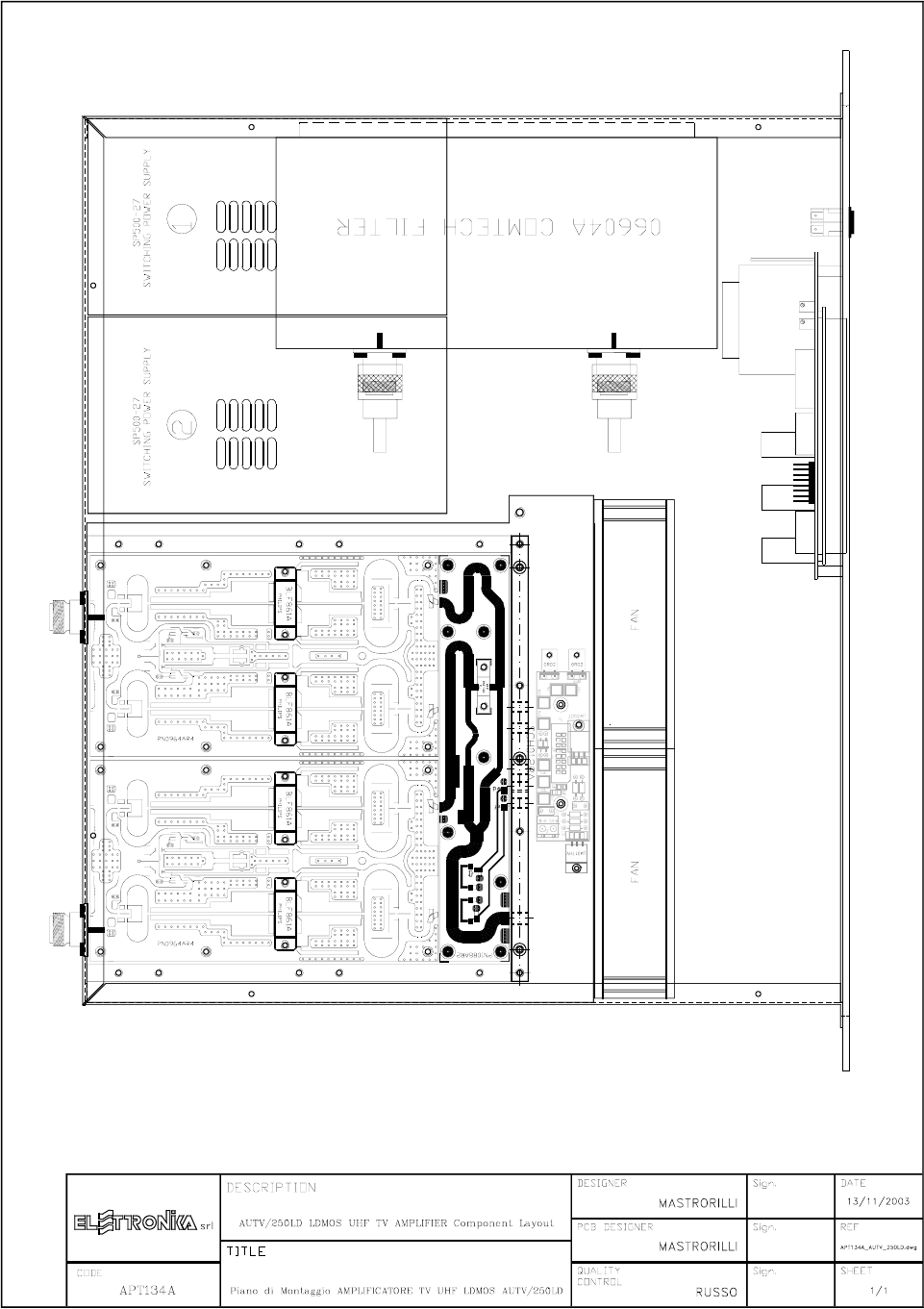
- AUTV/250LD Component layout
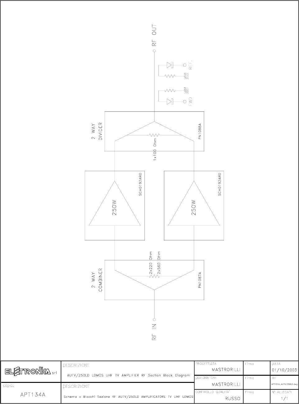
- RF Section Block Diagram
- SCH0192AR0 (250W UHF LDMOS Amplifier module)
- SCH0122BR1 (Control board and display)
- SCH0128AR1 (Amplifier interface)
- E0012 (SP500/27-48 Switching power supply)
- 06604A (UHF TV Output Filter IMD Suppressor)
24
25
26
27
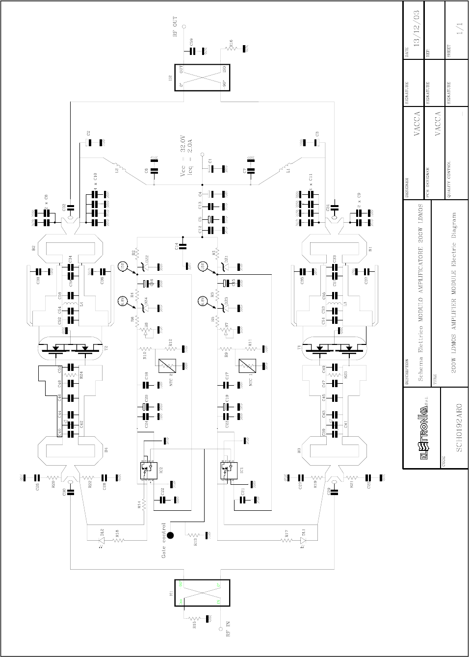
200W UHF LDMOS AMPLIFIER MODULE SCH0192AR0
DESCRIPTION
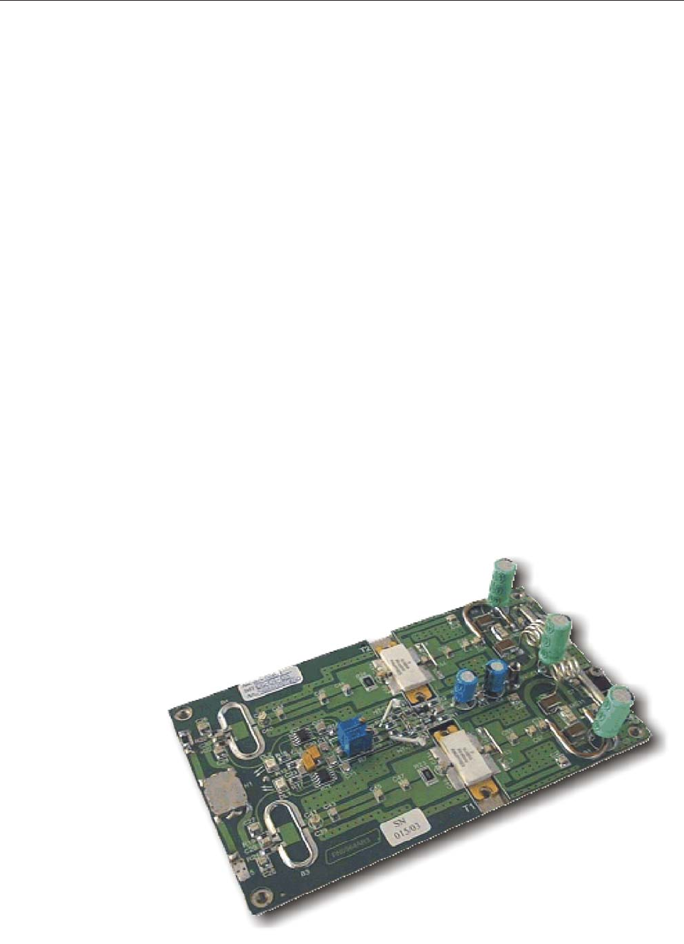
The RF module is an integrated TV linear amplifier designed for UHF band, this module employs push-pull
LDMOS technology in order to achieve very good efficiency, high linearity and reliability.
LDMOS transistors operate in AB class. It is a wideband amplifier over the full frequency, no adjustment is
required for the channel change. The board includes RF section amplifier, bias circuit, protection circuit and
matching networks. A silver plated copper plate is brazed with PCB in order to obtain low thermal resistance.
Providing a minimum of 200W Pk sync linear power, this module is the perfect amplifier for any broadband
UHF power transmitter.
TECHNICAL CHARACTERISTICS
Output power 300W max
Input power 15W max
Frequency 470 - 860MHz
Gain > 13dB
LDMOS Power supply 32V ±2%
LDMOS Bias current @+32V Vdc 2A
RF Input impedance 50Ω
RF Output impedance 50Ω
Input / Output return loss > = 15dB
Drain efficiency 47% @ 250W
Storage temperature range -50° to +150°C
Dimensions (LxWxH) 165x95x29mm
28
CALIBRATION PROCEDURE
- Technical characteristics
Power supply voltage 32V (± 2%)
Polarisation current 1.0 cold for each device (2A total), ± 0.1A
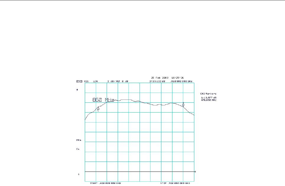
Gain for low signal Not less than 13dB in the 470-860MHz band (± 1dB)
Compare to the typical curve eclosed
- Adjustment procedure
Polarisation current calibration 32V stabilised power supply
10A amperometer
Gain curve Network analyser
- Adjustment points description
R7-R8 (Trimmers) Adjust the current absorbed in stand-by (1.0A per device)
Middle frequency 660MHz, span 500MHz, 2dB/div., reference to the arrow
- Curve response graphic
29
- Calibration steps
STEP 1. Close the input and the output of the module by connecting them to a 50ΩΩ
ΩΩ
Ω dummy load
and connect the spectrum analyser through a directive sample, in order to look for self-oscillation of the
module, if any (anyway the module has been designed so that it would not self-oscillate even if totally de-
coupled, without any input or output load).
STEP 2. Check the voltages of the polarisation circuits without assembling the transistors first:
connect the 32V power supply to the proper turret by means of a fastening screw, then give power and check
data:
- the stabilised voltage on the zener diodes DZ1 and DZ2 is about 15V compared to the ground;
- the stabilised voltage on the zener diodes DZ3 and DZ4 is about 6.8V compared to the ground;
- the voltage on the pads to which the gates of the LDMOS transistors will be soldered (R23 and R24
resistors side) changes from 0V to a maximum value of about 6V when moving the relevant trimmer (R7-R8).
STEP 3. Check the work of the protections.
- Set both trimmers so that there is a value of about 4.5V on the pads of the gates;
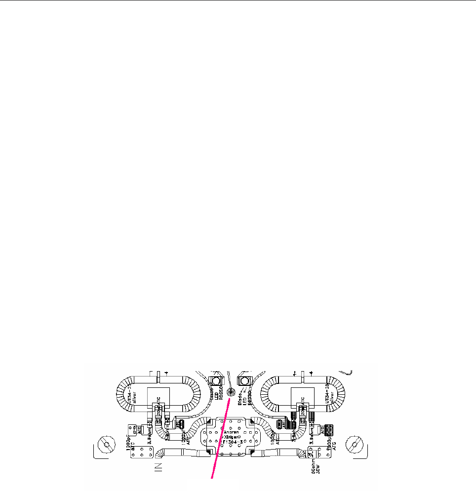
- solder some wire to the pad between the two LEDs, next to the serigraphy of the input hybrid H1;
- in order to check the work of the protections aboard, a power of about 4V has to be supplied to the wire,
for example by touching with it the reophore of C23 or C24 which is not connected to ground; the two red
LEDs will immediately light up and the two RF transistors will be switched off at the same time: the polarisation
current (2A) will decrease to 0 and of course the gain curve displayed by the spectrum analyser will decrease;
- after this it is important to restore the position of the two trimmers for the minimum voltage! Then
disconnect the 32V power supply.
STEP 4. Fastening of the LDMOS transistors: after properly cleaning the plate surface, smear a thin
layer of silicone fat on the lower side of the flange of the MOSFETs, fasten them to the heat sink and solder
the gate first, then the drain. Solder the two 13pF (ATC) chip capacitors and above them the two 1-5pF
Solder a wire

30
capacitive trimmers, between the two pair of gates, as shown by the mounting plan.
STEP 5. Connect serially a c.c. amperometer to the power supply, with scale starting from more than 5A
(i.e. 10A).
STEP 6. Power the module and check the MOSFET is not absorbing current; this means that the device
is integral and working correctly.
STEP 7. Slowly turn the R7 trimmer until the MOSFET absorbs 1A, always checking that there are no
self-oscillation; under this conditions it is possible to check by means of a digital tester that the voltage on the
gate is about 5.2-5.4V.
STEP 8. Repeat the previous step for the other section of the module, this time turnign R8 and checking
that the indication of the current on the amperometer increases to 2A total (which includes the current of the
other device left on).
STEP 9. Check the response curve of the module by means of the network analyser.
STEP 10. Check the response curve for low signal with centre 660MHz and span 500MHz, 2dB/div.
STEP 11. The curve should be similar to the one enclosed, with a tolerance of ± 0.5dB. To obtain this, act
on the four trimmers C41-C41a and C42-C42a with the proper “calibrator”, inorder to flatten the curve as
much as possible, especially at the edged of the band which represents the minimum values.
STEP 12. Finally, check that the current in stand-by does not increase by more than 15÷20%, reaching at
worst 2.3÷2.4A when the heat sink is hot and not ventilated.
Note: when mounting-removing the PALLET on the heat sink, tightly fasten the screw of each all “N” input and output
connectors. These are mounted with a single 3mm screw and if it is not properly fastened it may be detached from the PCB
by a movement of the connector once it has already been soldered to the path.
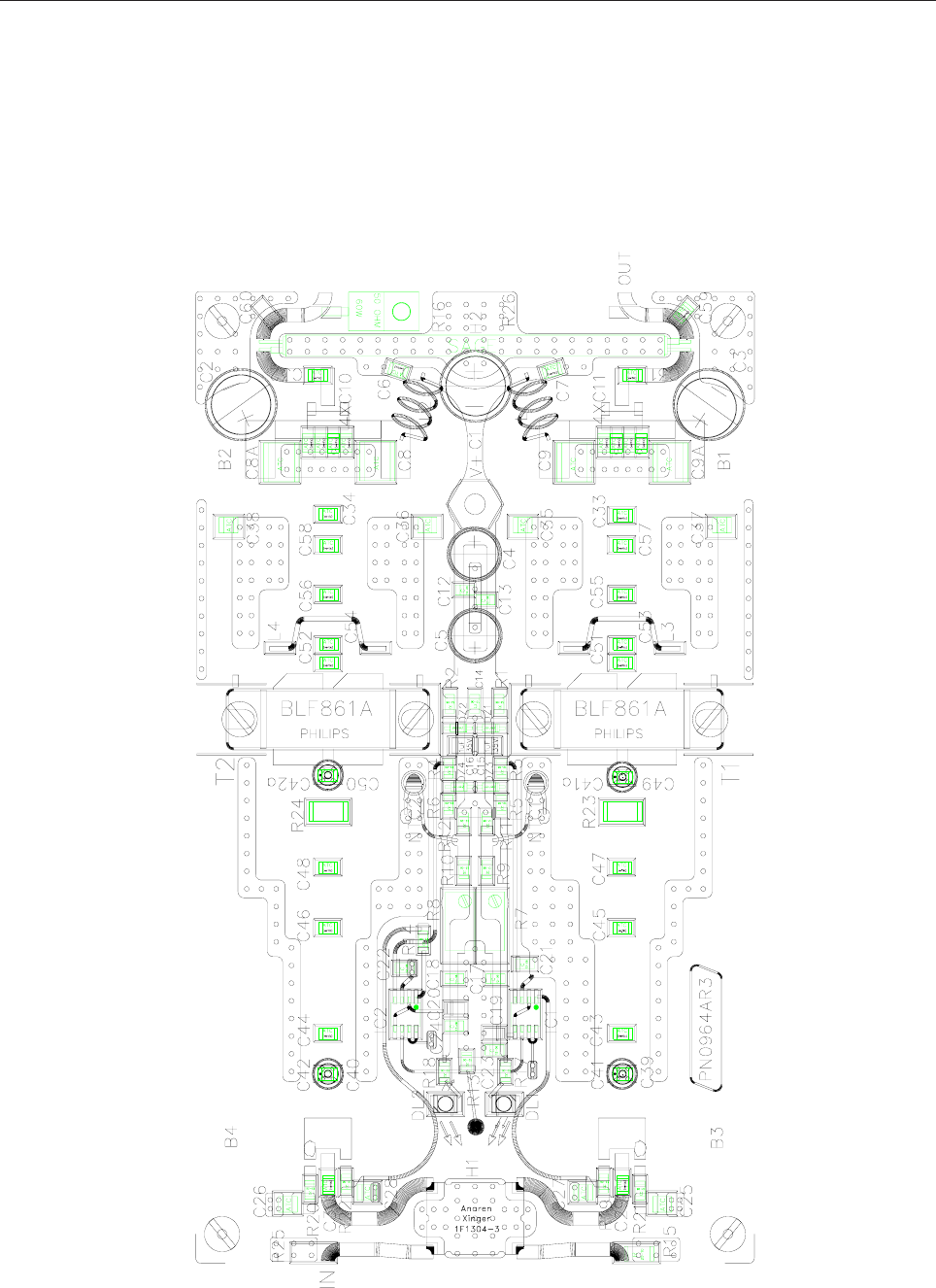
31
Component layout SCH0192AR0
32

33
COMPONENT LIST SCH0192AR0
REF. DESCRIPTION ELETTRONIKA CODE Page 1/3
R1 2200Ω 1/4W 1206 SMD RESISTOR 00045A
R2 2200Ω 1/4W 1206 SMD RESISTOR 00045A
R3 2200Ω 1/4W 1206 SMD RESISTOR 00045A
R4 2200Ω 1/4W 1206 SMD RESISTOR 00045A
R5 1200Ω 1/4W 1206 SMD RESISTOR 00042A
R6 1200Ω 1/4W 1206 SMD RESISTOR 00042A
R7 50kΩ MULTITURNS PTH TRIMMER 00800
R8 50kΩ MULTITURNS PTH TRIMMER 00800
R9 1200Ω 1/4W 1206 SMD RESISTOR 00042A
R10 1200Ω 1/4W 1206 SMD RESISTOR 00042A
R11 18kΩ 1/4W 1206 SMD RESISTOR 00056B
R12 18kΩ 1/4W 1206 SMD RESISTOR 00056B
R13 680KΩ 1/4W 1206 SMD RESISTOR 00075A
R14 0Ω 1/4W 1206 SMD RESISTOR 00001
R15 50Ω 30W 1512EBX SMD RESISTOR 00416A
R16 50Ω 60W 00432
R17 4.7kΩ 1/4W 1206 SMD RESISTOR 00049A
R18 4.7kΩ 1/4W 1206 SMD RESISTOR 00049A
R19 3.9Ω 1/4W 1206 SMD RESISTOR 00012A
R20 3.9Ω 1/4W 1206 SMD RESISTOR 00012A
R21 3.9Ω 1/4W 1206 SMD RESISTOR 00012A
R22 3.9Ω 1/4W 1206 SMD RESISTOR 00012A
R23 1000Ω 1W 2512 SMD RESISTOR 00396
R24 1000Ω 1W 2512 SMD RESISTOR 00396
*R25 = R15 (da montare se si inverte l’ingresso)
*R26 = R26 (da montare se si inverte l’uscita)
C1 470uF 50V PTH ELECTROLYTIC CAPACITOR 01807B
C2 470uF 50V PTH ELECTROLYTIC CAPACITOR 01807B
C3 470uF 50V PTH ELECTROLYTIC CAPACITOR 01807B
C4 100uF 50V PTH ELECTROLYTIC CAPACITOR 01795
C5 100uF 50V PTH ELECTROLYTIC CAPACITOR 01795
C6 1nF ATC 100B CAPACITOR OR EQUIVALENT 01145
C7 1nF ATC 100B CAPACITOR OR EQUIVALENT 01145
C8 x 2 2 x 100nF ATC CAPACITOR OR EQUIVALENT 01065H
C9 x 2 2 x 100nF ATC CAPACITOR OR EQUIVALENT 01065H
C10 x 4 4 x 100pF ATC 100B CAPACITOR OR EQUIVALENT 01135
C11 x 4 4 x 100pF ATC 100B CAPACITOR OR EQUIVALENT 01135
C12 100nF 1210 SMD CAPACITOR 1065G
C13 100nF 1210 SMD CAPACITOR 1065G
C14 100nF 1210 SMD CAPACITOR 1065G
C15 1uF 35V SMD TANTALIUM CAPACITOR 01613A
C16 1uF 35V SMD TANTALIUM CAPACITOR 01613A
C17 100nF 1210 SMD CAPACITOR 1065G

34
REF. DESCRIPTION ELETTRONIKA CODE Page 2/3
C18 100nF 1210 SMD CAPACITOR 1065G
C19 10uF 16V SMD TANTALIUM CAPACITOR 01626A
C20 10uF 16V SMD TANTALIUM CAPACITOR 01626A
C21 100nF 1210 SMD CAPACITOR 1065G
C22 100nF 1210 SMD CAPACITOR 1065G
C23 100nF 1210 SMD CAPACITOR 1065G
C24 100nF 1210 SMD CAPACITOR 1065G
C25 1nF ATC 100B CAPACITOR OR EQUIVALENT 01145
C26 1nF ATC 100B CAPACITOR OR EQUIVALENT 01145
C27 1nF ATC 100B CAPACITOR OR EQUIVALENT 01145
C28 1nF ATC 100B CAPACITOR OR EQUIVALENT 01145
C29 20pF ATC 100B CAPACITOR OR EQUIVALENT 01123
C30 20pF ATC 100B CAPACITOR OR EQUIVALENT 01123
C31 20pF ATC 100B CAPACITOR OR EQUIVALENT 01123
C32 20pF ATC 100B CAPACITOR OR EQUIVALENT 01123
C33 1.3pF ATC 100B CAPACITOR OR EQUIVALENT 01104
C34 1.3pF ATC 100B CAPACITOR OR EQUIVALENT 01104
C35 470pF ATC 100B CAPACITOR OR EQUIVALENT 01143
C36 470pF ATC 100B CAPACITOR OR EQUIVALENT 01143
C37 470pF ATC 100B CAPACITOR OR EQUIVALENT 01143
C38 470pF ATC 100B CAPACITOR OR EQUIVALENT 01143
C39 4.7pF ATC 100B CAPACITOR OR EQUIVALENT 01108
C40 4.7pF ATC 100B CAPACITOR OR EQUIVALENT 01108
C41 x 2 2 x 1÷5pF JOHANSON SMD TRIMMER 1485
C42 x 2 2 x 1÷5pF JOHANSON SMD TRIMMER 1485
C43 3.6pF ATC 100B CAPACITOR OR EQUIVALENT 01104B
C44 3.6pF ATC 100B CAPACITOR OR EQUIVALENT 01104B
C45 6.8pF ATC 100B CAPACITOR OR EQUIVALENT 01111
C46 6.8pF ATC 100B CAPACITOR OR EQUIVALENT 01111
C47 6.8pF ATC 100B CAPACITOR OR EQUIVALENT 01111
C48 6.8pF ATC 100B CAPACITOR OR EQUIVALENT 01111
C49 13pF ATC 100B CAPACITOR OR EQUIVALENT 01119A
C50 13pF ATC 100B CAPACITOR OR EQUIVALENT 01119A
C51 8.2pF ATC 100B CAPACITOR OR EQUIVALENT 01113
C52 8.2pF ATC 100B CAPACITOR OR EQUIVALENT 01113
C53 8.2pF ATC 100B CAPACITOR OR EQUIVALENT 01113
C54 8.2pF ATC 100B CAPACITOR OR EQUIVALENT 01113
C55 10pF ATC 100B CAPACITOR OR EQUIVALENT 01117
C56 10pF ATC 100B CAPACITOR OR EQUIVALENT 01117
C57 4.7pF ATC 100B CAPACITOR OR EQUIVALENT 01108
C58 4.7pF ATC 100B CAPACITOR OR EQUIVALENT 01108
C59 0.3pF ATC 100B CAPACITOR OR EQUIVALENT 01160
T1 BLF861A RF LDMOS POWER TRANSISTOR 04034
T2 BLF861A RF LDMOS POWER TRANSISTOR 04034
B1 COAX 2:1 BALUN 08491

35
REF. DESCRIPTION ELETTRONIKA CODE Page 3/3
B2 COAX 2:1 BALUN 08491
B3 COAX 4:1 BALUN 08492
B4 COAX 4:1 BALUN 08492
L1 4 TURNS SILV. COP. WIRE 1.2mm WOUND ON OD 5mm 07684
L2 4 TURNS SILV. COP. WIRE 1.2mm WOUND ON OD 5mm 07684
L3 ½ TURN COIL
L4 ½ TURN COIL
H1 HYBRID COUPLER 3dB 90° ANAREN 05368
H2 HYBRID COUPLER 3dB 90° SAGE 05369
NTC1 NTC 100KΩ PTH 00661
NTC2 NTC 100KΩ PTH 00661
IC1 DG419DY 04583
IC2 DG419DY 04583
DZ1 15V SMD ZENER DIODE 03135
DZ2 15V SMD ZENER DIODE 03135
DZ3 6.8V SMD ZENER DIODE 03137
DZ4 6.8V SMD ZENER DIODE 03137
DL1 SMD LED DIODE - RED - 03056
DL2 SMD LED DIODE - RED - 03056
PN964AR3 PCB 0643K
Torretta 3x10 f/f V0774
Imballo velapack 200x125x50 09983

36
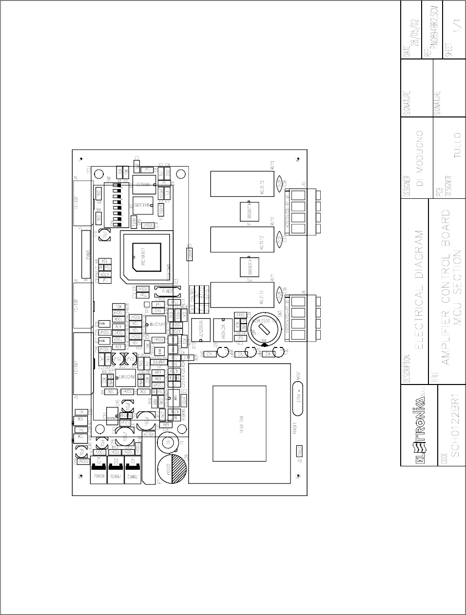
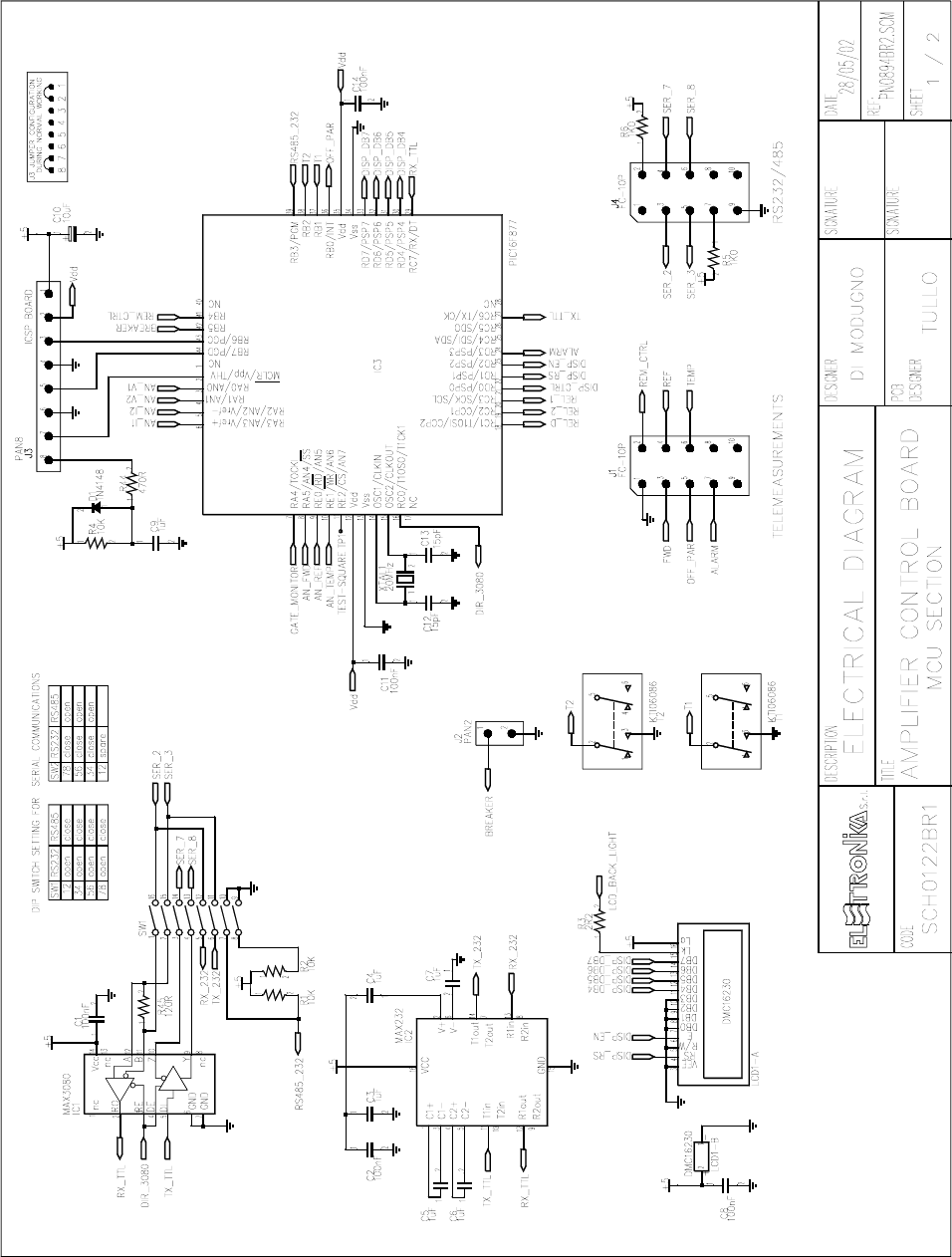
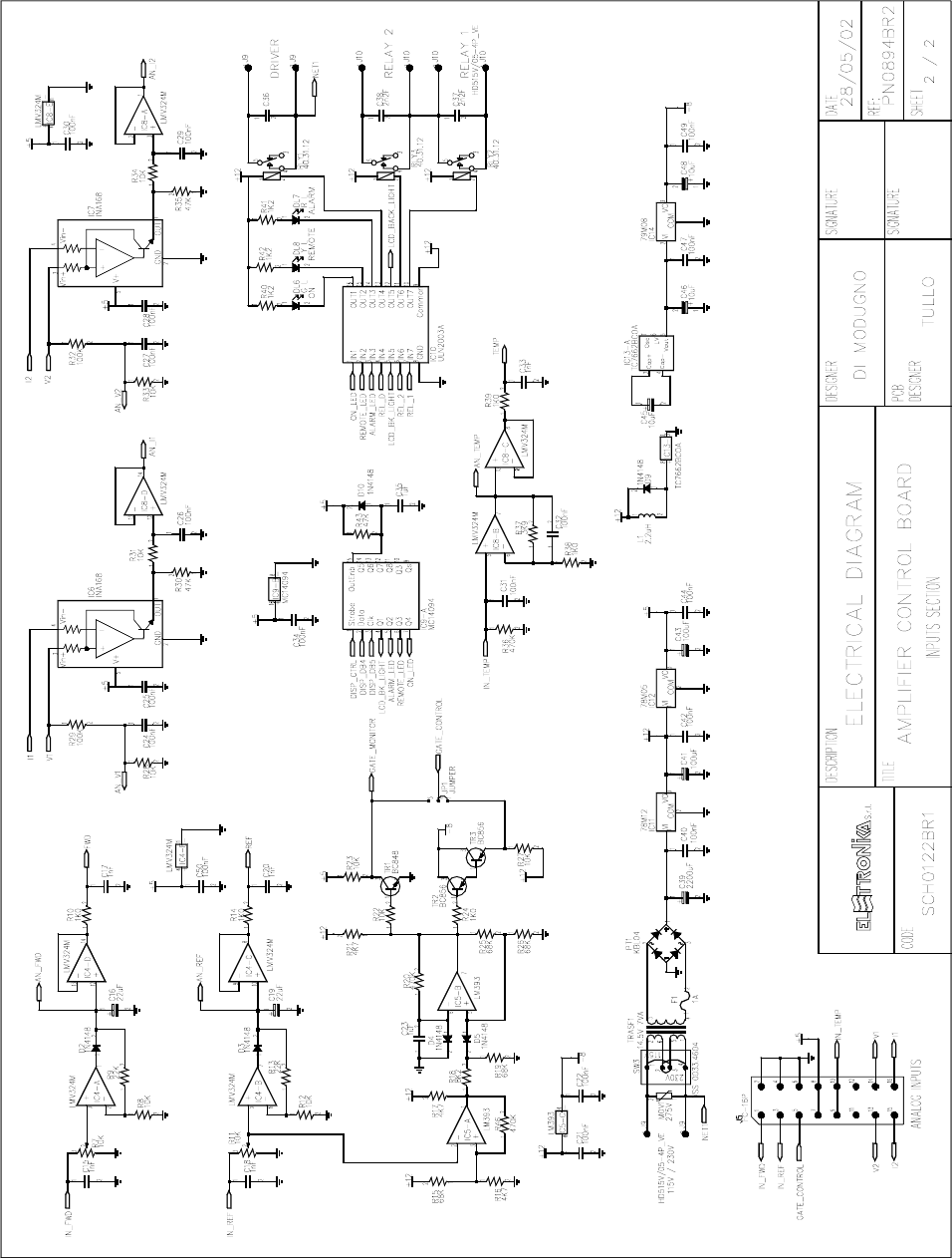
CONTROL BOARD AND DISPLAY SCH0122BR1
DESCRIPTION
The control board performs all the logic and control fucntions of the amplifier. Both the RF and power supply
parameters are continuously monitored in order to guarantee optimal performance in every working environment:
- amplifier supply voltages Vdc;
- amplifier supply currents Idc;
- power module working temperature Temperature;
- amplifier forward RF power FWD Power.
- amplifier reflected RF power REF Power.
The board is based on a flash microcontroller working at a frequency of 20MHz, able to read the parameters,
control the amplifier and communicate with any PC connected through RS232/RS485 line. Besides, the
microcontroller is programmable, thus it is possible to change the internal program by connecting the appropriate
programmer to the J3 connector and this to a computer. The boards contains a 16 characters x 2 lines display
and two keys to change the parameter currently shown. There are also 3 different LEDs. The green LED
indicates when the amplifier module is ON, the red one is lit when an alarm in occur and the yellow one
indicates the remote control of the amplifier.
OPERATING CONTROL
As indicated in the previous section, the boards is able to read in real time all the necessary parameters to
control the amplifier. When the operator turns the amplifier on the display shows the software release number.
After a few seconds the amplifier is switched on and the first parameter shown on the display is the forward
RF power (“FWD Power”).
When a value read is out of the allowed boundaries, the microcontroller activates (after five scans to be
sure) the corresponding alarm indicating this on the first line of the display, and showing on the second line the
physical value. When the alarm is active, the microcontroller switches the amplifier off and restarts the time
counter (3 and 6 seconds). The microcontroller internally stores the number of occurred alarms and if it
reaches 5 the whole equipment is definitively switched off. In this case, if the operator needs to restart the
machine, it is necessary to switch it off and on again (locally o by remote). When the machine is working
normally on the first line shows “TV AMPLIFIER UHF” and the second line shows the parameter with the
format “parameter = xx.x unit”. The two keys on the frontal panel allow to change the currently shown
parameter: the left one goes to the next parameter and the right one goes back (in sequence Vdc, Vac,
Temperature, Idc, FWD, REF). If the amplifier is switched off, the “STAND BY” indication is shown on the
display and the backlight is turned off.
The amplifier can be remotely controlled by serial line (contact ELETTRONIKA for details). It is
configurable as RS232 or RS485.
37
Note: When changing the voltage of the device from 230 to 110VAC, it also takes acting on
the SW3 switch on the display board. Failure to do this may result in damages to the device.
38
39

40
COMPONENT LIST SCH0122BR1
Part Name/Number Description Qty. Comps. Page 1/2
CC 100nF-S 01065C 01065C Y5V 1206 COND 23 C1-2, C8, C11, C14, C21,
C22, C24-32, C34, C40,
C42, C44, C47, C49-50
CC 15pF-S 01088 01088 SMD 1206 COND 2 C12-13
CC 1nF-S 01096 01096 SMD 1206 COND 5 C15, C17-18, C20, C33
CC 1uF100V-S 01760A 01760A Y5V 1206 COND 8 C3-7, C9, C23, C35
CC 2nF2 2kV 01045A 01045A CERAMIC COND 3 C36-38
CE 100uF25V-S 01793B 01793B ELETTR SMD COND 2 C41, C43
CE 10uF35V-S 01778A 01778A ELETTR SMD COND 4 C10, C45-46, C48
CE 2200uF25V 01813 01813 ELETT. COND. 1 C39
CE 22uF16V-S 01780A ELETTR SMD COND 2 C16, C19
D 1N4148-S 03002 03002 SMD DIODE 7 D1-5, D9-10
DB KBL04 03042 03042 BRIDGE DIODE 1 PT1
DIS DMC16230 03072B 03072B DISPLAY 1 LCD1
DL LEDG5 03060 03060 GREEN LED DIODE 5mm 1 DL6
DL LEDR5 03061 03061 RED LED DIODE 5mm 1 DL7
DL LEDY5 03054B 03054B YELLOW LED DIODE 5mm 1 DL8
FUSE 1A MICRO FUSE FUS00007 + FUS00006 PORTA FUSI 1 F1
IC 78M05 04301B 04301B SMD VOLTAGE REGULATOR 1 IC12
IC 78M12 4307B 04307B SMD VOLTAGE REGULATOR 1 IC11
IC 79M08 04304A 04304A SMD VOLTAGE REGULATOR 1 IC14
IC INA168 04600A SMD INTEG CIRCUIT 2 IC6-7
IC LM393-S 04639 04639 SMD INTEG CIRCUIT 1 IC5
IC LMV324M-S 04658B 04658B SMD INTEG CIRCUIT 2 IC4, IC8
IC MAX232-S 04804B 04804B SMD INTEG CIRCUIT 1 IC2
IC MAX3080-S 04770 04770 SMD INTEG CIRCUIT 1 IC1
IC MC14094BD 04718 04718 SMD INTEG CIRCUIT 1 IC9
IC PIC16F877 4869 04869 + 07509C INTEG CIRCUIT 1 IC3
IC TC7662BCOA 04758A 04758A SMD INTEG CIRCUIT 1 IC13
IC ULN2003A 4870 04870 SMD INTEG CIRCUIT 1 IC10
IND 2u2H-S 05020A 05020A INDUCTOR 1 L1
J CON HD515V/05-4PVE 02881 + 02882 PANDUIT PCB CONN 2 J9-10
J FC-10P 02697-02699 02697+02699 PCB CONNECTOR POL 2 J1, J4
J FC-16P 02701-02700 02701+02700 PCB CONNECTOR POL 1 J5
J PAN2 02739-40-41 02739+02740+02741 PCB CONNECTO 1 J2
J PAN8 02716-17-18 02716+02717+02718 PCB CONNECTO 1 J3
JU JUMP3 02707-02742 02707+02742 MASCHIO PAN3 1 JP1
MOV 275V 00951A VARISTORE 1 MOV1
R 100K-1%-S 00065B 00065B RES 1/4W 1% SMD 1206 2 R29, R32
R 10K-1%-S 00053B 00053B RES 1/4W 1% SMD 1206 12 R1-2, R4, R8, R12, R22,
R23, R27-28, R31, R33,
R34
R 120R-S 00030A 00030A RES 1/4W 5% SMD 1206 1 R45

41
Part Name/Number Description Qty. Comps. Page 2/2
R 1K0-1%-S 00041B 00041B RES 1/4W 1% SMD 1206 7 R5-6, R10, R14, R24, R38,
R39
R 1K2-1%-S 00042A 00042A RES 1/4W 1% SMD 1206 3 R40-42
R 22K-1%-S 00057B 00057B RES 1/4W 1% SMD 1206 2 R9, R13
R 2R2-S 00009A RES 1/4W 5% SMD 1206 1 R3
R 3K9-1%-S 00048B 00048B RES 1/4W 1% SMD 1206 1 R37
R 470K-S 00073A 00073A RES 1/4W 5% SMD 1206 3 R20, R36, R46
R 470R-1%-S 00037B 00037B RES 1/4W 1% SMD 1206 1 R44
R 47K-1%-S 00061B 00061B RES 1/4W 1% SMD 1206 3 R30, R35, R43
R 4K7-1%-S 00049B 00049B RES 1/4W 1% SMD 1206 3 R16-17, R21
R 68K-1%-S 00063B 00063B RES 1/4W 1% SMD 1206 4 R15, R19, R25-26
R 8K2-1%-S 00052B 00052B RES 1/4W 1% SMD 1206 1 R18
RL 40.31.12 07567 07567 RELE 3 RLY1-3
RV 10K-3266X 00807 00807 VARIABLE RESISTOR 2 R7, R11
SW SWITCH-8DIP 07530A PCB DIP SWITCH 1 SW1
SW VSS 0033.4604 07519A CAMBIO TENSIONE SERIALE 1 SW3
T 06086 N 7630 7632 7630 7632 KTI06086 PULSANTE 2 2 T1-2
TR BC848 03457 03457 NPN SMD TRANSISTOR 1 TR1
TR BC856 03455 03455 PNP SMD TRANSISTOR 2 TR2-3
TRASF TRASF 14V5 7VA 09597 TRASFORMATORE 110+110 PE 1 TRASF1
XTAL 20MHz-S CXS00001 QUARTZ 1 XTAL1
42
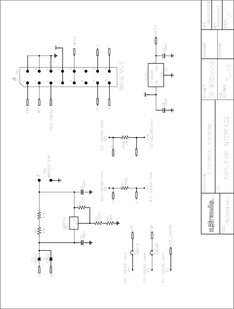
AMPLIFIER INTERFACE SCH0128AR1
DESCRIPTION
The interface board (SCH0128AR1) is used to connect the amplifier stages to the control board
(SCH0122BR0) to allow to the microcontroller the reading of the RF and analogical parameters.
It is simply composed of one temperature sensor, a voltage regulator, some passive componentes and a
10 pin connector J2. This connector has to be connected to the corresponding one of the SCH0122BR0
board.
The LM317HV (IC1) integrated circuit is an adjustable 3-terminal positive voltage regulator used to
make more stable the power supply voltage of the amplifiers fan.
The LM35DT (IC2) integrated circuit is a precision temperature sensor whose output voltage is
proportional to the Celsius (Centigrade) temperature. It does not require any external calibration or
trimming. The package is a plastic TO-220 model and the heat sink is directly connected to the amplifier.
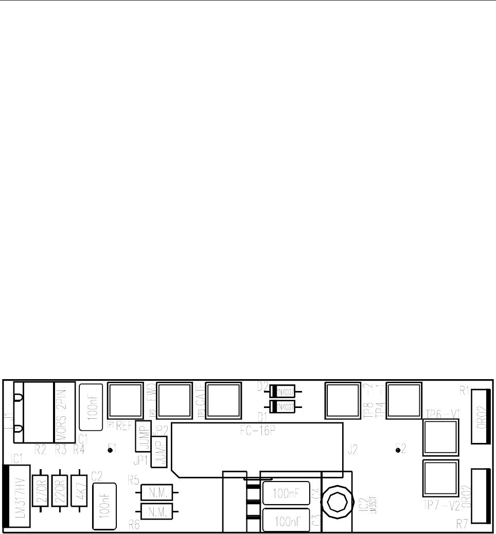
Component layout SCH0128AR1
43

44
COMPONENT LIST SCH0128AR1
Part Name/Number Description Qty. Comps.
CC 100nFAVX 01065A 01065A CERAMIC COND 4 C1-4
D 1N4007 03009 03009 DIODE 2 D1-2
IC LM317HV 04340A INTEG CIRCUIT 1 IC1
IC LM35DT 00664 00664 INTEG CIRCUIT 1 IC2
J FC-16P 02701-02700 02701+02700 PCB CONNECTOR POL 1 J2
J SCREWCONN2 02853 02853 PCB SCREW CONNECTOR 1 J1
JU JUMP2 02739-02742 02739+02742 MASCHIO PAN2 2 JP1-2
R 0R02 RES 20W 1% 2 R1
R7
R 220R 0033 0033 RES 1/4W 5% 1 R3
R 270R 0034 0034 RES 1/4W 5% 1 R2
R 4K7 0049 0049 RES 1/4W 5% 1 R4
R R400m NOT MOUNTED NOT MOUNTED 2 R5-6
45
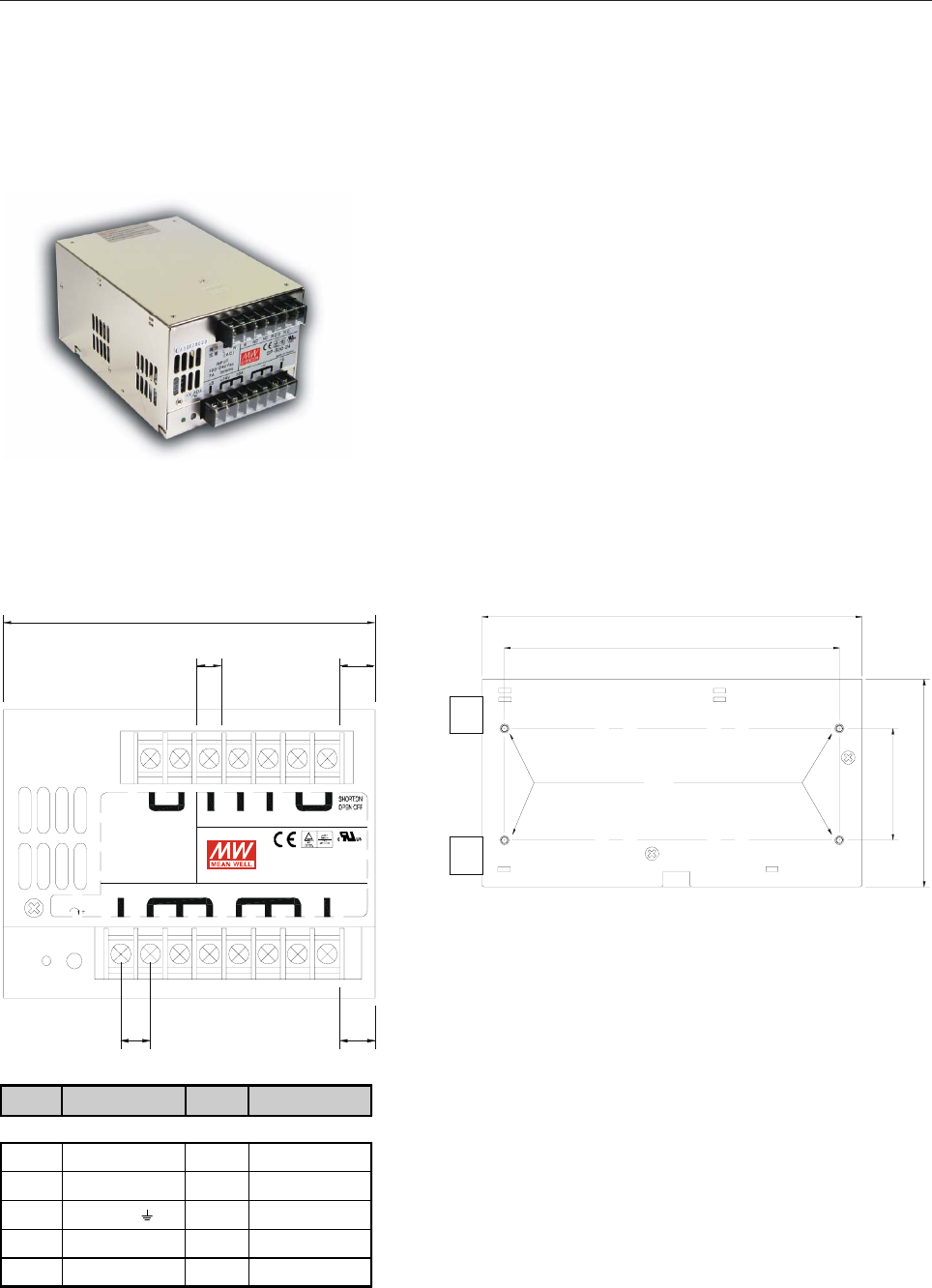
SP500-48 SWITCHING POWER SUPPLY E0013
MAIN FEATURES
- Universal AC input / Full range
- Built-in active PFC function, PF>0.95
- Protections: Short circuit / Over load / Over voltage / Over temp.
- Forced air cooling by built-in DC fan
- Built-in cooling Fan ON-OFF control
- Built-in remote sense function
- Fixed switching frequency at 110kHz
MECHANICAL SPECIFICATION
170
150
50
93
2-M3 L=16mm max.2-M3 L=4mm max.
9.5 11. 5
811 . 5
120
15141312111098
7654321
7A 50/60Hz
100-240VAC
INPUT
(AC )
-S-V+24V 20A+S
+VADJ.
SP-500-24
E183223
LEVEL5
R.C.G.L N FG NC NC R.C.
PIN N° ASSIGNMENT PIN N° ASSIGNMENT
1 AC/L 7 R.C.
2AC/N8 +S
3 FG 9 ~ 11 DC OUTPUT +V
4, 5 NC 12 ~ 14 DC OUTPUT -V
6R.C.G.15 -S
46
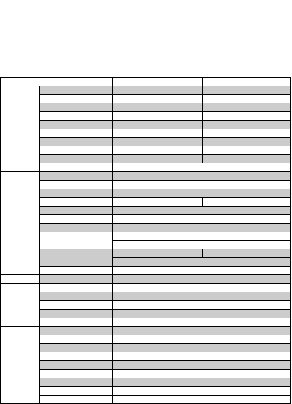
TECHNICAL CHARACTERISTICS
MODEL SP500-27 SP500-48
OUTPUT
DC VOLTAGE 27V 48V
RATED CURRENT 18A 10A
CURRENT RANGE 0 ~ 18A 0 ~ 10A
RATED POWER 486W 480W
RIPPLE & NOISE (max.) Note 2 200mVp-p 300mVp-p
VOLTAGE ADJ. RANGE 24 ~ 30V 41 ~ 56V
VOLTAGE TOLERANCE Note 3 ± 1.0% ± 1.0%
LINE REGULATION ± 0.5% ± 0.5%
LOAD REGULATION ± 0.5% ± 0.5%
SETUP, RISE, HOLD TIME 1500ms, 50ms, 20ms at full load
INPUT
VOLTAGE RANGE 88 ~ 264VAC 124 ~ 370VDC
FREQUENCY RANGE 47 ~ 63Hz
POWER FACTOR PF>0.95/230VAC PF>0.95/115VAC at full load
EFFICIENCY (Typ.) 86.5% 87%
AC CURRENT 7A/115VAC 3.5/230VAC
INRUSH CURRENT (Max.) 18A/115VAC 36A/230VAC
LEAKAGE CURRENT <3.5A/240VAC
PROTECTION
OVER LOAD
105 ~ 135% rated output power
Protection type: Fold back current limiting, recovers automatically after fault condition is removed
OVER VOLTAGE
31 ~ 36.5V 57.6 ~ 67.2V
Protection type: Hiccup mode, recovers automatically after fault condition is removed
FAN CONTROL O.T.P. RTH1 or RTH2 >= 50°C FAN ON, <= 45°C FAN OFF, >= 70°C output shutdown
FUNCTION REMOTE CONTROL RC+/RC-: Short = power on; Open = power off
ENVIRONMENT
WORKING TEMP. -10 ~ +50°C (Refer to output load derating curve)
WORKING HUMIDITY 20 ~ 90% RH non-condensing
STORAGE TEMP., HUMIDITY -20 ~ +85°C, 10 ~ 95% RH
TEMP. COEFFICIENT ± 0.03%/°C (0 ~ 50°C)
VIBRATION 10 ~ 500Hz, 2G 10min./1cycle, period for 60min. each along X, Y, Z axes
SAFETY & EMC
(Note 4)
SAFETY STANDARDS UL1950, TUV EN60950 Approved
WITHSTAND VOLTAGE I/P-O/P:3KVAC I/P-FG:1.5KVAC O/P-FG:0.5KVAC
ISOLATION RESISTANCE I/P-O/P, I/P-FG, O/P-GD:100M Ohms/500VDC
EMI CONDUCTION & RADIATION Compliance to EN55022 (CISPR22) Class B
HARMONIC CURRENT Compliance to EN61000-3-2,-3
EMS IMMUNITY Compliance to EN61000-4-2,3,4,5,6,8,11; ENV50204, Light industry level, criteria A
OTHERS
MTBF 133.4K hrs min. MIL-HDBK-217F (25°C)
DIMENSION 170*120*93mm (L*W*H)
PACKING 1.9kg; 8pcs/15.2kg/1.06CUFT
47
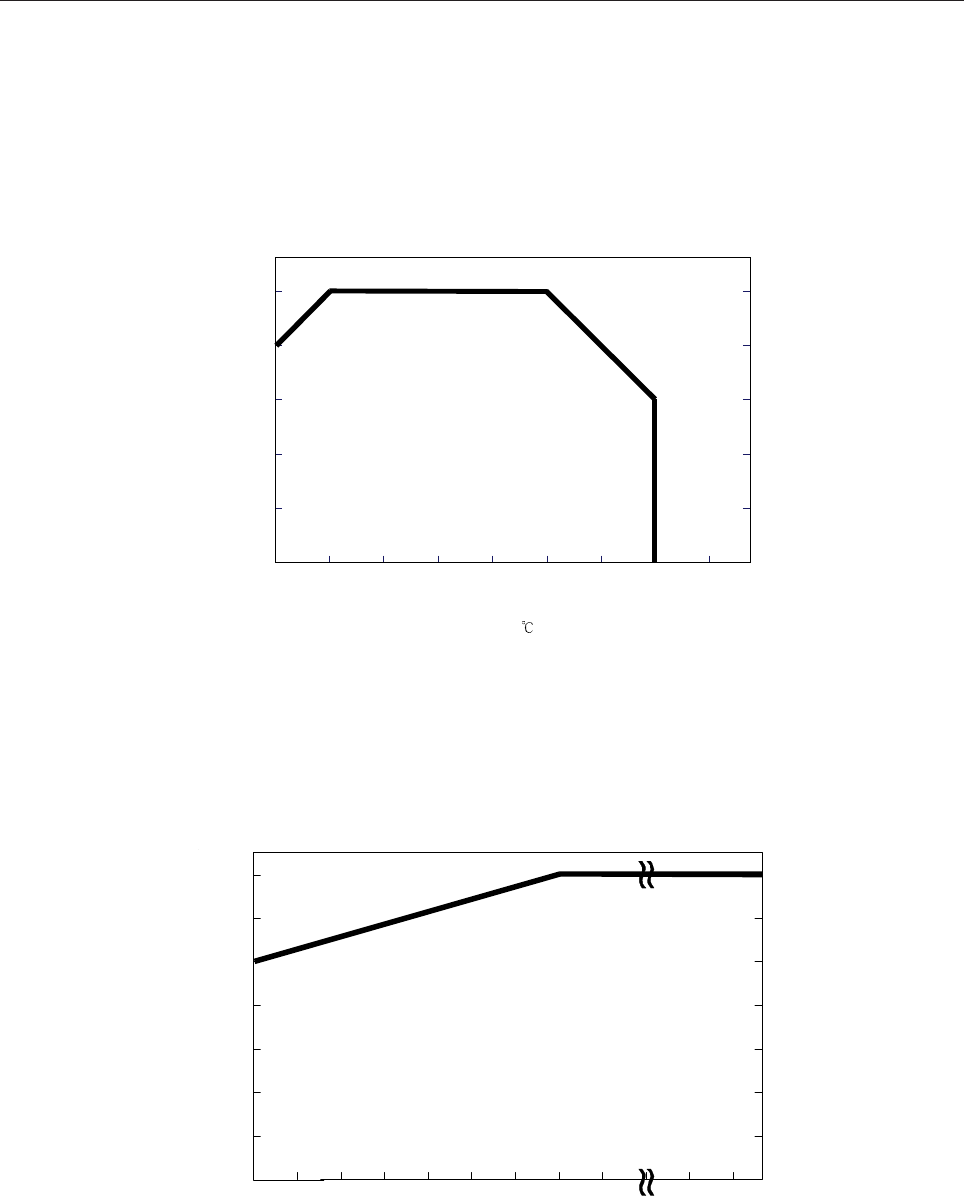
DERATING CURVE
OUTPUT DERATING VS INPUT VOLTAGE
AMBIENT TEMPERATURE ( )
LOAD (%)
-10 0 10 20 30 40 45 50 (HORIZONTAL)
20
40
60
80
100
INPUT VOLTAGE (V) 60Hz
11 588 135 155 230 264
90
100
80
70
60
50
40
LOAD(%)
48
SPECIFICATIONS
Frequency 470 - 860MHz
Connectors N
Insertion loss 0.55dB Typ. @ V.C.
Return loss 26dB
Operating temperature -10° to +50°C
Bandwidth 8MHz
Selectivity @V.C.-5.5/+11 -30dB
Selectivity @V.C.-11/+16.5 -22dB
Weight 1.2kg
3 SECTION BANDPASS FILTER WITH 2 NOTCH ELEMENTS - COMB-LINE STRUCTURE, INDUCTIVE COUPLING
IRISES; CONSTANT BANDWIDTH, VERY EASY TO TUNE - EXACT GENERALIZED CHEBISHEV DESIGN
GIVING MAXIMUM SELECTIVITY AND MINIMUM GROUP DELAY VARIATION.
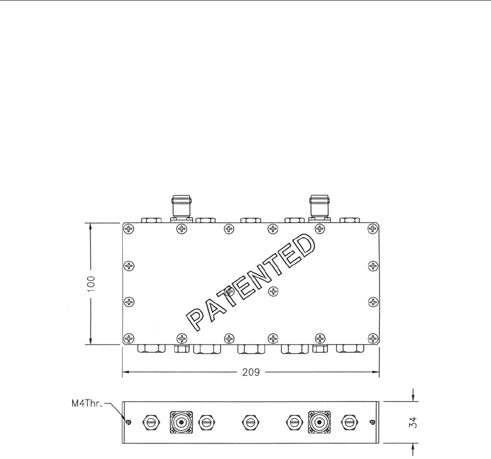
UHF TV OUTPUT FILTER IMD SUPPRESSOR 06604A

49
TECHNICAL DESCRIPTION
The output UHF filter is made up of a resonators bandpass filter and two notches. It can be regulated on all
the channels of UHF TV band (470 - 8690MHz) and according to all world-wide standards (intercarrier 4.5
- 6.5MHz). The bandpass section is composed by the three middle resonators, while the two resonators
apart are the notches. The filter is symmetrical, therefore the choice of lowest and highest notch is indifferent.
The bandwidth and the notch depth are predetermined, so they don’t need any regulation.
The input/output coupling are regulated by means of the two screws which are in position opposed to
every connector. The regulation is carried out with a screwdriver, considering that when the screw
lines are parallel to the longer side of the filter the coupling is maximum, otherwise if orthogonal it is
minimum. The twist friction of the couplings can be set acting on the hexagonal clamps with a no. 12
key.
TUNING INSTRUCTIONS
The advised sequence is the following:
1. Set the instrument state as follows:
- C.F. = (V.C. + S.C.) / 2
- SPAN = INTERCARRIER * 5 (E.G. 27,5MHz std. B/G)
- TRANSMISSION SCALE = 5dB/div.
- REFLECTION SCALE = 5dB/div.
2. Turn the bandpass section on the required channel, and match input and output until a correct response
is achieved. During this step keep the tunings of the two notches well far away from the response. Fit the
curve at the center of the screen, so as to get the same attenuation at the borders. The input/output
couplings can influence the external resonators, therefore it will be necessary to repeatedly fix the
former after the latter in small steps.
3. Tune the two notches to P.V.-INTERCARRIER and P.A.+INTERCARRIER frequencies. This will
vary the response and matchning.
4. Adjust the bandpass external tunings. The lower notch side tuning shall be a little unscrewed, whereas
the upper notch side tuning will have to screwed.
5. Enhance a little the lower notch side coupling (the coupling screw toward the filter lenghth). Improve
the calibration alternatively acting on two sides according to this sequence: regulate the couplings, re-tune
50
notches if it has to be moved and then the bandpass tunings. Execute the sequence in small steps aiming to
improve the matching.
SPECIFICATION OVER THE UHF BAND
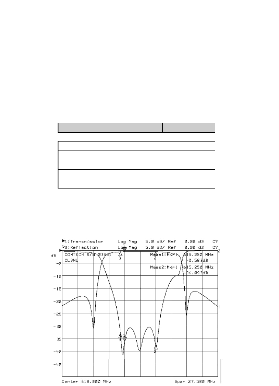
SAMPLE FREQUENCY RESPONSE DIAGRAM
MEASURE VALUE
Insertion loss @ V.C. < 0.65dB (Typ. 0.56)
Return Loss (from V.C.-0.75 to S.C.+0.25) > 26dB
Attenuation @ V.C.-INTERCARRIER > 25
Attenuation @ V.C.+INTERCARRIER > 20
Date D.T.