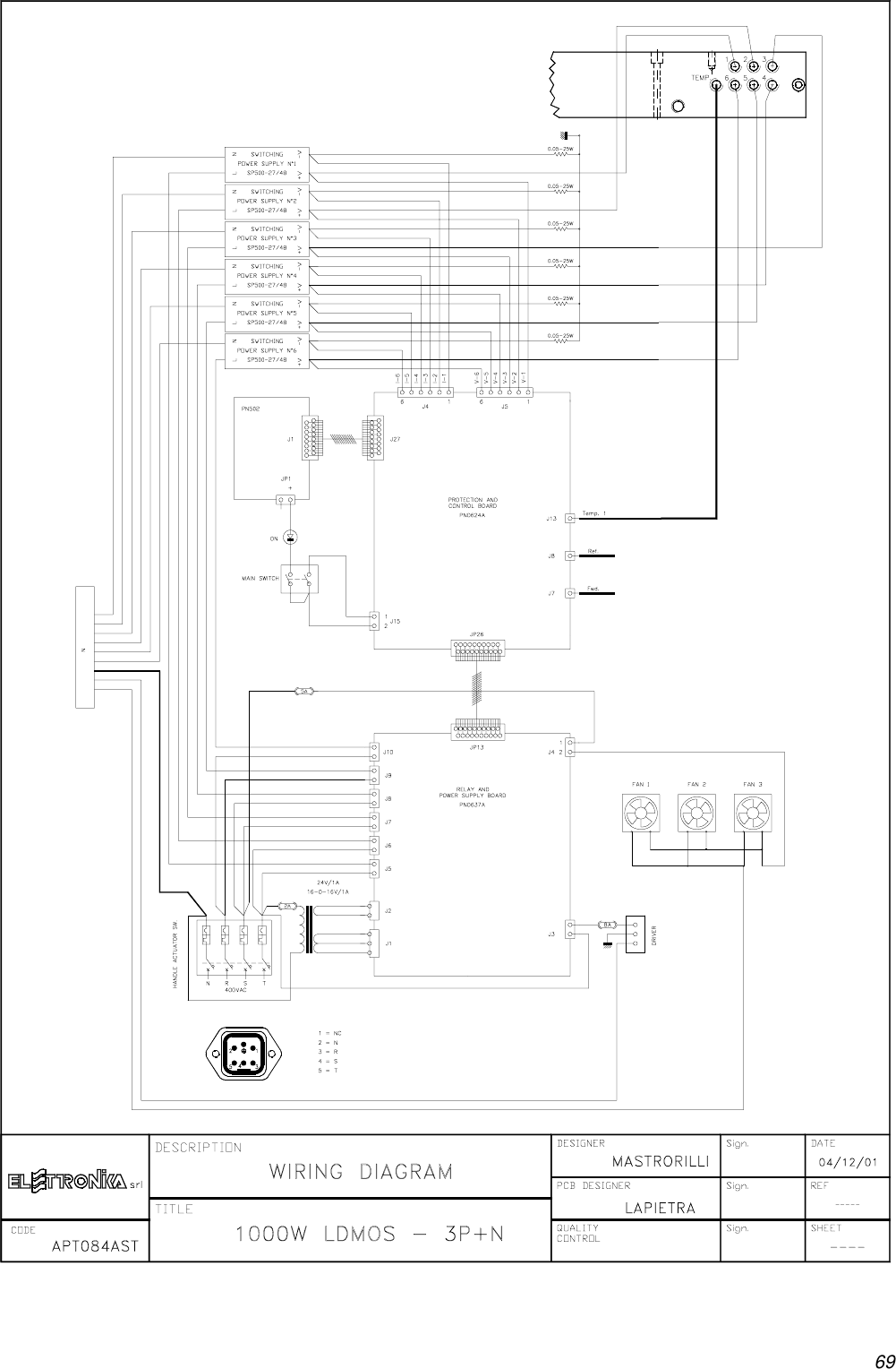
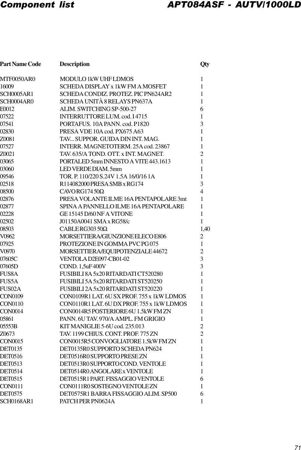
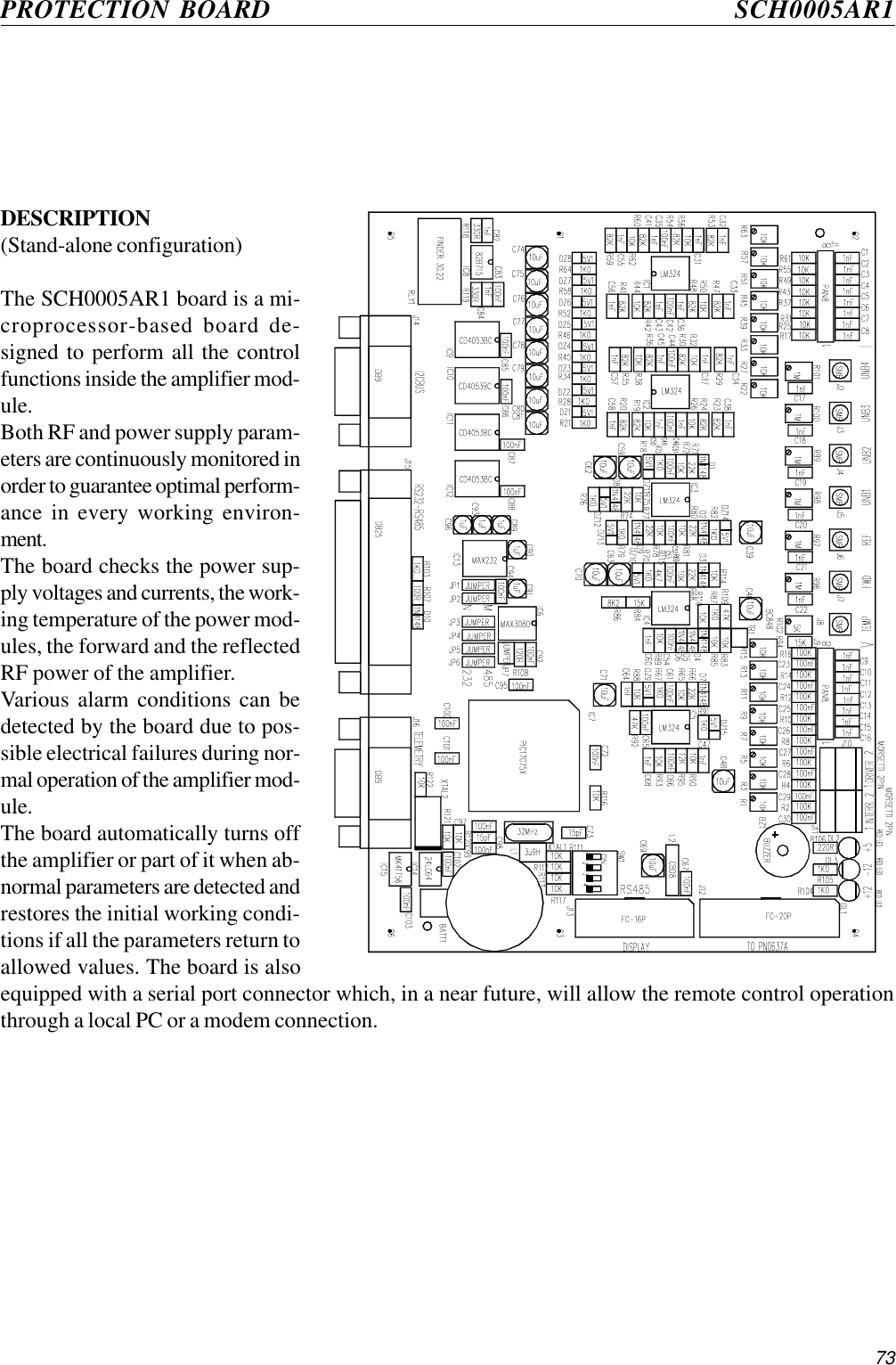
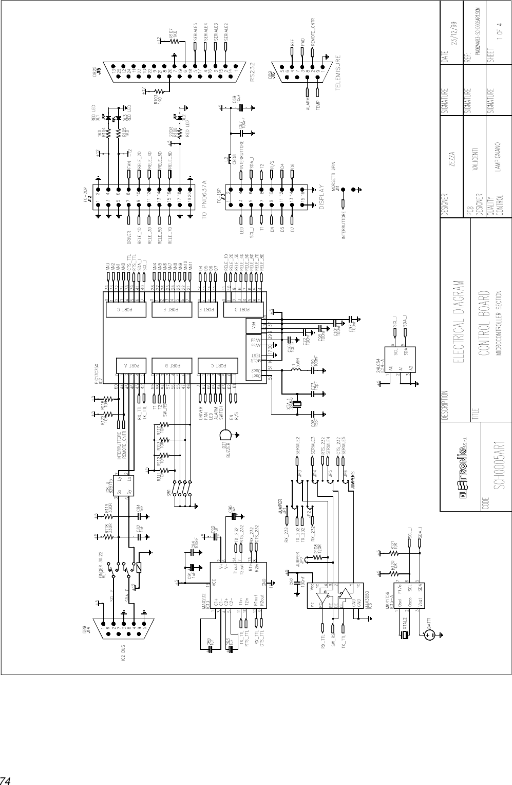
Elettronika S r l TXUP2000 2 kW Analog TV Broadcast transmitter User Manual APT088A AUTV 2000LD Rev0 Date170203 p65
Elettronika S.r.l. 2 kW Analog TV Broadcast transmitter APT088A AUTV 2000LD Rev0 Date170203 p65
Contents
- 1. User Manual Part 1
- 2. User Manual Part 2
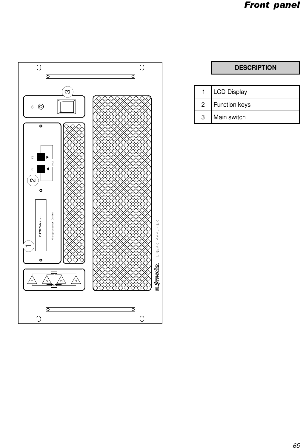
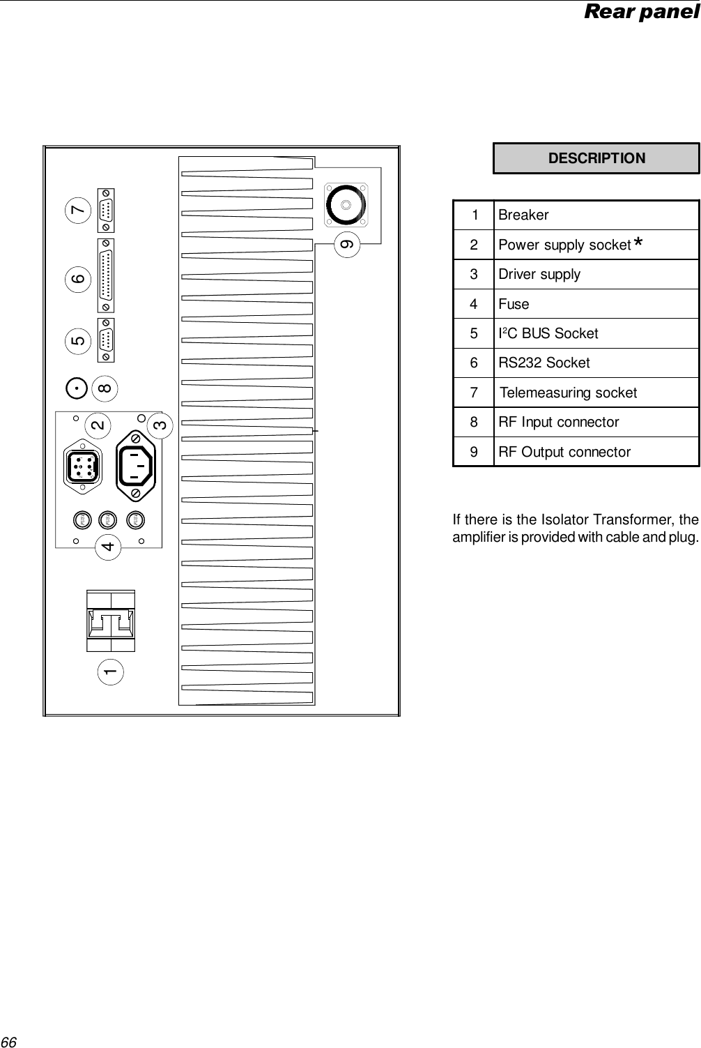
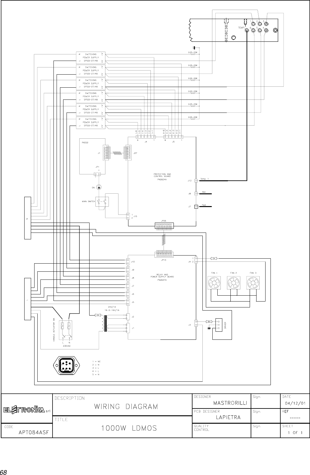
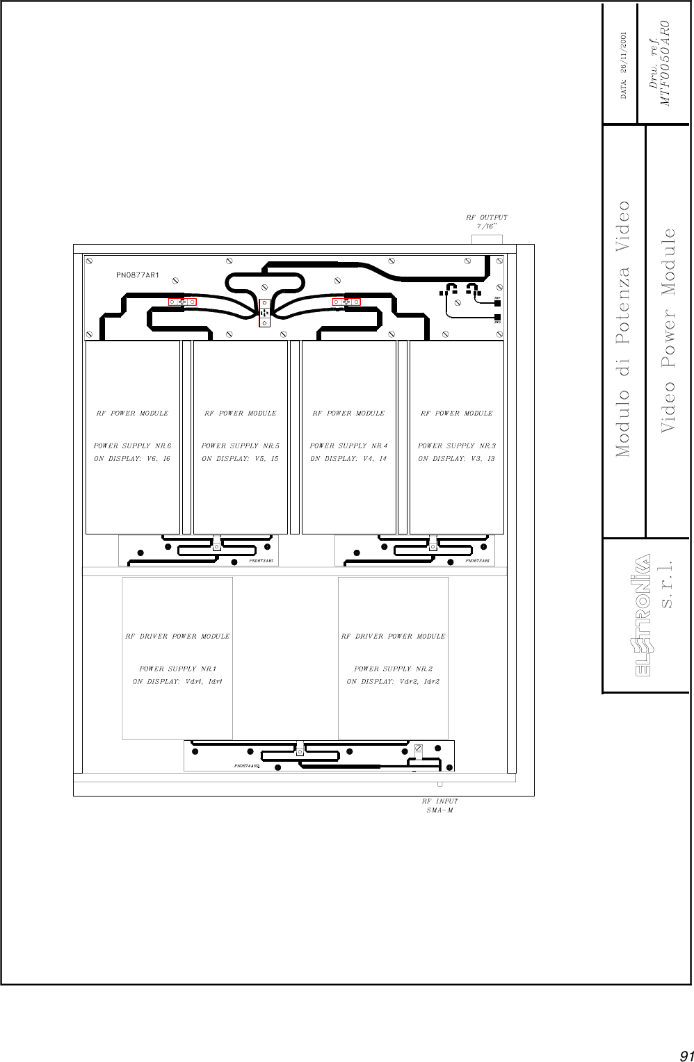
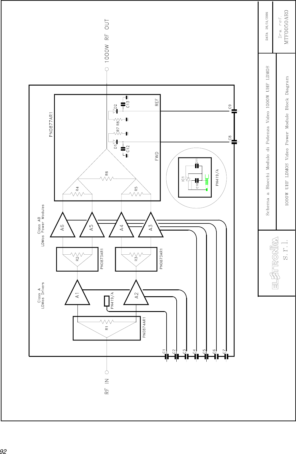
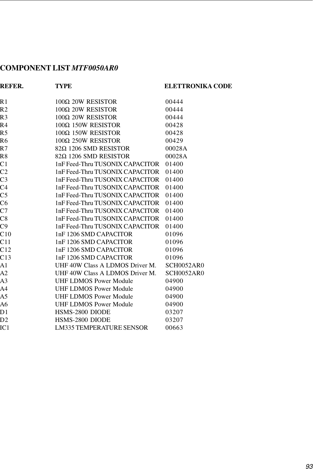
User Manual Part 2
![59_______________________________________________________________________________________________Section 2 - InstallationContents:2.1 Operating environment2.2 Preliminary operations2.3 Telemeasuring socket connections2.4 RS232 and RS485 socket connections2.5 SCH0005AR1 Calibration procedure2.6 Preventive maintenance- Front panel- Rear panel](https://usermanual.wiki/Elettronika-S-r-l/TXUP2000.User-Manual-Part-2/User-Guide-689180-Page-1.png)
![602.1 OPERATING ENVIRONMENTYou can install the apparatus in a standard component rack or on a suitable surface such as a bench ordesk. In any case, the area should be as clean and well-ventilated as possible. Always allow for at least2 cm of clearance under the unit for ventilation. If you set the apparatus on a flat surface, install spacerson the bottom cover plate. If you install the apparatus in a rack, provide adequate clearance above andbelow. Do not locate the apparatus directly above a hot piece of equipment.2.2 PRELIMINARY OPERATIONSCorrect installation of the equipment is important for maximum performance and reliability. Antennaand earth connections must be installed with the greatest care. The equipment adjustment isn’t need,because the unit is completely adjusted by our technical staff. This is the installation procedure:1. connect the power supply cable of the transmitter to the auxiliary socket on the rear panel of theamplifier;2. connect the power supply cable of the amplifier to the electric network (230VAC). If there is the IsolatorTransformer, the amplifier is provided with cable and plug;3. connect the exciter / antenna cable to the RF IN and RF OUT on the rear panel of the amplifier.WARNING!!!FOR ELECTRICAL SAFETY REASONS AND IN ORDER TO KEEP THE APPARATUS SAFE,THE GROUND TERMINAL OF THE APPARATUS MUST BE CONNECTED TO THE EX-ISTING GROUNDING SYSTEM AND NOT BY USING THE SHIELD OF THE OUTPUTCOAXIAL CABLE.1233](https://usermanual.wiki/Elettronika-S-r-l/TXUP2000.User-Manual-Part-2/User-Guide-689180-Page-2.png)
![61When the apparatus is put within a combined system it is directly connected to the input splitting and outputcombining systems.Before fully powering the apparatus, check that the output connections of the coaxial cable to theantenna system are working.In order to this it is possible to check the indication of the reflected power at low power levels. Only ifthe SWR indication on the display is 0, the output power can be slowly increased. At maximum outputpower, some watts might be shown as reflected power.2.3 TELEMEASURING SOCKET CONNECTIONSThe following table summarizes the Telemeasuring pin connections.2.4 RS232 AND RS485 SOCKET CONNECTIONSThe connector DB25 may be configured as RS232 or RS485 socket, depending on the position of thejumpers on the board. In case it is used as RS232 socket, the jumpers JP3, JP4, JP5 and JP6 have to bepositioned towards the serigraphy “RS232”. If the jumpers JP1 and JP2 are placed in “N” position, thefollwing configuration is obtained:DB9 SocketPIN 23567820FUNCTIONS RxD TxD RTS 12V GND 12V 12VN° Pin SYGNAL TYPE IN/OUT FUNCTION1 Ground2 Logical Input 5V= On - 0V= Off3 Analog Output Dir Power4 Analog Output Ref Power5 Analog Output Unbalancing6 Analog Output Temperature7 Analog Output Alarm 5V= On - 0V= Off8N.C.9N.C.](https://usermanual.wiki/Elettronika-S-r-l/TXUP2000.User-Manual-Part-2/User-Guide-689180-Page-3.png)
![62If the jumpers JP1 and JP2 are put in “M” position, the following configuration will be obtained:In order to use the connector as RS485 socket, the jumper JP3, JP4, JP5 and JP6 have to be positionedtowards the serigraphy “RS485”. In this way, the following configuration will be obtained:2.5 SCH0005AR1 CALIBRATION PROCEDUREWARNING: this procedure is very delicate, so be VERY CAREFUL in order to avoid damagingthe equipment !!!First of all turn on the equipment with the correct antenna connection, and then perform the following steps:- Power supply voltages and currents calibrationMeasure with a tester the voltage Vdr1 on the power supply of the first driver transistor without loading thepower supply (this can be done by disconnecting the six supply wires from the RF power modules). Verifythat it is 29V. Then take the calibration load (consisting of five 47Ω/20W resistors connected in parallel) andconnect it between the positive power supply terminal (corresponding to Vdr1) and ground. Turn the trimmerR1 until you read on the display Vdr1 equal to the value measured before with the tester. Then turn thetrimmer R22 until you read on the display Idr1 = 3.1A.Repeat the procedure above for the power supply of the second driver stage: measure with the tester thevoltage Vdr2 and turn the trimmer R3 and R27 until you read on the display the correct values.Measure with a tester the voltage V1 on the power supply of the first final power transistor. Verify that it isPIN 23456720FUNCTIONS TxD RxD RTS CTS 12V GND 12VPIN 23456720FUNCTIONS Rx+ RX- TX- TX+ 12V GND 12V](https://usermanual.wiki/Elettronika-S-r-l/TXUP2000.User-Manual-Part-2/User-Guide-689180-Page-4.png)
![63around 32V. Then take the calibration load and connect it between the positive power supply terminal(corresponding to V1) and ground. Turn the trimmer R5 until you read on the display V1 equal to the valuemeasured before with the tester. Then turn the trimmer R33 until you read on the display Idr1 = 3.4A.Repeat the procedure above for the power supplies of the remaining three power transistors: measure withthe tester the voltages V2-V3-V4 and turn the trimmers R7-R9-R11 until you read on the display the correctvalues measured.To calibrate the remaining currents readings, you have to connect the calibration load to the other three powersupplies (not all together, but one at a time!) and then turn the trimmers R39-R45-R51 until you read on thedisplay I2=I3=I4= 3.4A.- Temperature calibrationMeasure with a tester the voltage of the OUT pin of the integrated temperature sensor mounted on the heatdissipating element. Than perform the operation explained in this example:- voltage measured (for example) = 2.93V- fixed number = 2.73- perform subtraction: 2.93-2.73 = 0.20If you get a result of 0.20, it means that the temperature is 20°C, so you have to turn the trimmer R102 untilyou read TEMP = 20°C.- Forward power calibrationDisconnect the antenna and connect a wattmeter (with a suitable dummy load!) to the antenna connector. Putthe cover on the amplifier module and then give power to the equipment until you read 1000W on thewattmeter. Then turn the trimmer R96 until you read FWD = 1000W (approximately).- Reflected power calibrationTo perform the reflected power calibration just disconnect the REF SMB (J6) and the FWD SMB (J7)connectors from the control board and connect the forward power reading cable to J6 (REF). Give 50W offorward power to the equipment and turn the R97 trimmer until you read on the display REF = 50W.Note: When you have completed this calibration be sure to restore the original connections on thecontrol board!](https://usermanual.wiki/Elettronika-S-r-l/TXUP2000.User-Manual-Part-2/User-Guide-689180-Page-5.png)
![64To ensure the best reliability for the board operations it is advisable that you turn the unused trimmers (thosecorresponding to the unused readings connectors) counterclockwise until they reach the zero position (youwill hear a click).2.6 PREVENTIVE MAINTENANCETo ensure maximum performance and minimum repair trouble, we strongly recommend you to follow thebelow stated headlines for preventive maintenance:1. check antenna installation and ground connection at regular intervals;2. keep your apparatus clean and dry externally: this will ensure continuous functioning of the front panelcontrols;3. if the apparatus has not been used for a long period of time combined with exposure to extreme environ-mental conditions, open the unit and make a visual inspection.Remove salt, water or ice with a moist cloth before turning the apparatus on. Check that the cooling fans arerunning freely.4. for general maintenance and top performance, call an authorized service technician to give the apparatusand the complete antenna/earth connection installation a general check every 12-18 months;5. check at regular intervals that the air intake located on the front panel is free of dust. If there is visible dust,remove it by means of a soft brush.](https://usermanual.wiki/Elettronika-S-r-l/TXUP2000.User-Manual-Part-2/User-Guide-689180-Page-6.png)
![65Front panelDESCRIPTION1 LCD Display2 Function keys3Main switch123](https://usermanual.wiki/Elettronika-S-r-l/TXUP2000.User-Manual-Part-2/User-Guide-689180-Page-7.png)
![66Rear panel1If there is the Isolator Transformer, theamplifier is provided with cable and plug.2345 6 798*DESCRIPTION1 Breaker2 Power supply socket3 Driver supply4Fuse5I2C BUS Socket6 RS232 Socket7 Telemeasuring socket8 RF Input connector9 RF Output connector](https://usermanual.wiki/Elettronika-S-r-l/TXUP2000.User-Manual-Part-2/User-Guide-689180-Page-8.png)
![67_______________________________________________________________________________________________Section 3 - DiagramContents:- Cable diagrams- SCH0005AR1 (Protection board)- SCH0004AR0 (Relay board)- PN502 (Display board)- MTF0050AR0 (1kW LDMOS Power mdoule)- SP500-27/48 (Switching power supply)- 06641 (UHF Band-pass filter)](https://usermanual.wiki/Elettronika-S-r-l/TXUP2000.User-Manual-Part-2/User-Guide-689180-Page-9.png)
![68](https://usermanual.wiki/Elettronika-S-r-l/TXUP2000.User-Manual-Part-2/User-Guide-689180-Page-10.png)
![69](https://usermanual.wiki/Elettronika-S-r-l/TXUP2000.User-Manual-Part-2/User-Guide-689180-Page-11.png)
![70This page is intentionally blank](https://usermanual.wiki/Elettronika-S-r-l/TXUP2000.User-Manual-Part-2/User-Guide-689180-Page-12.png)
![71Part Name Code Description QtyMTF0050AR0 MODULO 1kW UHF LDMOS 116009 SCHEDA DISPLAY x 1kW FM A MOSFET 1SCH0005AR1 SCHEDA CONDIZ. PROTEZ. PIC PN624AR2 1SCH0004AR0 SCHEDA UNITÀ 8 RELAYS PN637A 1E0012 ALIM. SWITCHING SP-500-27 607522 INTERRUTTORE LUM. cod. I 4715 107541 PORTAFUS. 10A PANN. cod. P1820 302830 PRESA VDE 10A cod. PX675 A63 1Z0081 TAV... SUPPOR. GUIDA DIN INT. MAG. 107527 INTERR. MAGNETOTERM. 25A cod. 23867 1Z0021 TAV. 635/A TOND. OTT. x INT. MAGNET. 203065 PORTALED 5mm INNESTO A VITE 443.1613 103060 LED VERDE DIAM. 5mm 109546 TOR. P. 110/220 S.24V 1.5A 16/0/16 1A 102518 R114082000 PRESA SMB x RG174 308500 CAVO RG174 50Ω402876 PRESA VOLANTE ILME 16A PENTAPOLARE 3mt 102877 SPINA A PANNELLO ILME 16A PENTAPOLARE 102228 GE 15145 D/60 NF A VITONE 102502 J01150A0041 SMA x RG58/c 108503 CABLE RG303 50Ω1,40V0962 MORSETTIERA/GIUNZIONE ELECO E806 207925 PROTEZIONE IN GOMMA PVC PG 075 1V0970 MORSETTIERA/EQUIPOTENZIALE 44672 207605C VENTOLA D2E097-CB01-02 307605D COND. 1,5uF 400V 3FUS8A FUSIBILI 8A 5x20 RITARDATI CT520280 1FUS5A FUSIBILI 5A 5x20 RITARDATI ST520250 1FUS02A FUSIBILI 2A 5x20 RITARDATI ST520220 1CON0109 CON0109R1 LAT. 6U SX PROF. 755 x 1kW LDMOS 1CON0110 CON0110R1 LAT. 6U DX PROF. 755 x 1kW LDMOS 1CON0014 CON0014R5 POSTERIORE 6U 1.5kW FM ZN 105861 PANN. 6U TAV. 970/A AMPL. FM GRIGIO 105553B KIT MANIGLIE 5-6U cod. 235.013 2Z0673 TAV. 1199 CHIUS. CONT. PROF. 775 ZN 2CON0015 CON0015R5 CONVOGLIATORE 1.5kW FM ZN 1DET0135 DET0135R0 SUPPORTO SCHEDA PN624 1DET0516 DET0516R0 SUPPORTO PRESE ZN 1DET0513 DET0513R0 SUPPORTO COND. VENTOLE 1DET0514 DET0514R0 ANGOLARE x VENTOLE 1DET0515 DET0515R1 PART. FISSAGGIO VENTOLE 6CON0111 CON0111R0 SOSTEGNO VENTOLE ZN 1DET0575 DET0575R1 BARRA FISSAGGIO ALIM. SP500 6SCH0168AR1 PATCH PER PN0624A 1Component list APT084ASF - AUTV/1000LD](https://usermanual.wiki/Elettronika-S-r-l/TXUP2000.User-Manual-Part-2/User-Guide-689180-Page-13.png)
![72This page is intentionally blank](https://usermanual.wiki/Elettronika-S-r-l/TXUP2000.User-Manual-Part-2/User-Guide-689180-Page-14.png)
![73PROTECTION BOARD SCH0005AR1DESCRIPTION(Stand-alone configuration)The SCH0005AR1 board is a mi-croprocessor-based board de-signed to perform all the controlfunctions inside the amplifier mod-ule.Both RF and power supply param-eters are continuously monitored inorder to guarantee optimal perform-ance in every working environ-ment.The board checks the power sup-ply voltages and currents, the work-ing temperature of the power mod-ules, the forward and the reflectedRF power of the amplifier.Various alarm conditions can bedetected by the board due to pos-sible electrical failures during nor-mal operation of the amplifier mod-ule.The board automatically turns offthe amplifier or part of it when ab-normal parameters are detected andrestores the initial working condi-tions if all the parameters return toallowed values. The board is alsoequipped with a serial port connector which, in a near future, will allow the remote control operationthrough a local PC or a modem connection.](https://usermanual.wiki/Elettronika-S-r-l/TXUP2000.User-Manual-Part-2/User-Guide-689180-Page-15.png)
![74](https://usermanual.wiki/Elettronika-S-r-l/TXUP2000.User-Manual-Part-2/User-Guide-689180-Page-16.png)
![75](https://usermanual.wiki/Elettronika-S-r-l/TXUP2000.User-Manual-Part-2/User-Guide-689180-Page-17.png)
![76](https://usermanual.wiki/Elettronika-S-r-l/TXUP2000.User-Manual-Part-2/User-Guide-689180-Page-18.png)
![77](https://usermanual.wiki/Elettronika-S-r-l/TXUP2000.User-Manual-Part-2/User-Guide-689180-Page-19.png)
![78COMPONENT LIST SCH0005AR1Part Name/Number Description Qty. Comps. Page 1/4BATT BH-001RB 03093 BATTERY HOLDER 1 BATT1BZ AI-155 03705 5VDC BUZZER 1 BZ1CC 100nF-S 01065B Y5V 1206 COND 35 C23-30 C35 C42 C44 C49 C51-54 C61 C65-67 C72 C83 C85-88 C92 C94-95 C97 C99-103CC 15pF-S 01088 SMD 1206 COND 2 C73 C98CC 1nF-S 01096 SMD 1206 COND 44 C1-22 C31-34 C36-38 C41 C43 C45-47 C50 C55-58 C60 C64 C68 C82 C84CE 10uF35V-S 01778A ELETTR SMD COND 17 C39-40 C48 C59 C62-63 C69-71 C74-81CE 1uF50V-S 01763A ELETTR SMD COND 5 C89-91 C93 C96D 1N4148-S 03002 SMD DIODE 9 D1-9DL LEDR3 03058 RED LED DIODE 3mm 3 DL1-3](https://usermanual.wiki/Elettronika-S-r-l/TXUP2000.User-Manual-Part-2/User-Guide-689180-Page-20.png)
![79Part Name/Number Description Qty. Comps. Page 2/4DZ 5V1-S 03128 SMD ZENER DIODE 15 DZ1-15IC 24LC64 04815 SMD INTEG CIRCUIT 1 IC14IC 82B715-S 04734A SMD INTEG CIRCUIT 1 IC8IC CD4053BC-S 04710A SMD INTEG CIRCUIT 4 IC9-12IC LM324M-S 04658A SMD INTEG CIRCUIT 5 IC1-5IC MAX232-S 04804B SMD INTEG CIRCUIT 1 IC13IC MAX3080-S 04770 SMD INTEG CIRCUIT 1 IC6IC MK41T56 04611 SMD INTEG CIRCUIT 1 IC15IC PIC17C75X 04807A SMD INTEG CIRCUIT 1 IC7IND 3u9H-S 05030 INDUCTOR 1 L1IND CBD8 05072 INDUCTOR 1 L2J DB25-90G 02688 PCB CONNECTOR 1 J15J DB9-90G 02797 PCB CONNECTOR 2 J14 J16J FC-16P 02701-02700 PCB CONNECTOR POL 1 J13J FC-20P 02868-02867 PCB CONNECTOR POL 1 J12J PAN8 02716-17-18 PCB CONNECTOR 2 J1 J9J SCREWCONN2 02853 PCB SCREW CONNECTOR 2 J10-11J SMB-PCB 02516 PCB CONNECTOR 7 J2-8JU JUMP2 02739-02742 MASCHIO PAN2 1 JP7JU JUMP3 02707-02742 MASCHIO PAN3 6 JP1-6R 100K-S 00065A RES 1/4W 5% SMD 1206 8 R2 R4 R6 R8 R10 R12 R14 R16R 10K-S 00053A RES 1/4W 5% SMD 1206 38 R17-18 R25-26 R31-32 R37-38 R43-44 R49-50 R55-56 R61-62 R65 R69 R72 R75 R78 R81 R83](https://usermanual.wiki/Elettronika-S-r-l/TXUP2000.User-Manual-Part-2/User-Guide-689180-Page-21.png)
![80Part Name/Number Description Qty. Comps. Page 3/4 R85 R88-90 R93 R110-114 R116-117 R120-122R 120R-S 00030A RES 1/4W 5% SMD 1206 1 R108R 12K-S 00054A RES 1/4W 5% SMD 1206 1 R95R 15K-S 00055A RES 1/4W 5% SMD 1206 2 R84 R94R 1K0-S 00041A RES 1/4W 5% SMD 1206 20 R21 R28 R34 R40 R46 R52 R58 R64 R67 R70 R73 R76 R79 R82 R87 R91 R103-105 R107R 220R-S 00033A RES 1/4W 5% SMD 1206 1 R106R 22K-S 00057A RES 1/4W 5% SMD 1206 6 R66 R68 R71 R74 R77 R80R 330R-S 00035B RES 1/4W 5% SMD 1206 2 R118-119R 47K-S 00061A RES 1/4W 5% SMD 1206 2 R92 R109R 4K7-S 00049A RES 1/4W 5% SMD 1206 1 R115R 82K-S 00064A RES 1/4W 5% SMD 1206 16 R19-20 R23-24 R29-30 R35-36 R41-42 R47-48](https://usermanual.wiki/Elettronika-S-r-l/TXUP2000.User-Manual-Part-2/User-Guide-689180-Page-22.png)
![81Part Name/Number Description Qty. Comps. Page 4/4 R53-54 R59-60R 8K2-S 00052A RES 1/4W 5% SMD 1206 1 R86RL FINDER30.22 07564 RELE 1 RLY1RV 10K-3266W 00810 VARIABLE RESISTOR 16 R1 R3 R5 R7 R9 R11 R13 R15 R22 R27 R33 R39 R45 R51 R57 R63RV 1M-3266W 00811 VARIABLE RESISTOR 6 R96-101RV 5K-3266W 00809 VARIABLE RESISTOR 1 R102SW SWITCH-4DIP 07531 PCB DIP SWITCH 1 SW1TR BC848 03457 NPN SMD TRANSISTOR 1 TR1XTAL 32.768k-S 05146 QUARTZ 1 XTAL2XTAL 32MHz-S 05291 QUARTZ 1 XTAL1](https://usermanual.wiki/Elettronika-S-r-l/TXUP2000.User-Manual-Part-2/User-Guide-689180-Page-23.png)
![82RELÈ BOARD SCH0004AR0Component layout SCH0004AR0Note: solder the two terminals of JP1 connector.](https://usermanual.wiki/Elettronika-S-r-l/TXUP2000.User-Manual-Part-2/User-Guide-689180-Page-24.png)
![83](https://usermanual.wiki/Elettronika-S-r-l/TXUP2000.User-Manual-Part-2/User-Guide-689180-Page-25.png)
![84](https://usermanual.wiki/Elettronika-S-r-l/TXUP2000.User-Manual-Part-2/User-Guide-689180-Page-26.png)
![85COMPONENT LIST SCH0004AR0Part Name/Number Description Qty. Comps. Page 1/2CC 100nF 01065 CERAMIC COND 11 C1-11CC 2nF2 2kV 01045A CERAMIC COND 10 C19-28CE 1000uF63V 01811 ELETT. COND. 3 C16-18CE 10uF63V 01779 ELETT. COND. 4 C12-15D 1N4148 03001 DIODE 11 D1-11DB KBL04 03042 BRIDGE DIODE 2 PT1-2DL LEDR3 03058 RED LED DIODE 3mm 10 DL1-10IC 7805 04315 VOLTAGE REGULATOR 1 IC3IC 7812 04321 VOLTAGE REGULATOR 1 IC1IC 7824 04331 VOLTAGE REGULATOR 1 IC5IC 7912 04322 VOLTAGE REGULATOR 1 IC2J FC-20P 02868-02867 PCB CONNECTOR POL 1 J13J SCREWCONN2 02853 PCB SCREW CONNECTOR 11 J2-12J SCREWCONN3 02860 PCB SCREW CONNECTOR 1 J1JU JUMP2 02739-02742 MASCHIO PAN2 1 JP1R 10K 0053 RES 1/4W 5% 20 R1-2 R6-7 R10-11 R14-15 R18-19 R22-23 R26-27 R30-31 R34-35 R39-40R 1K0 0041 RES 1/4W 5% 10 R4 R8 R12 R16 R20 R24 R28 R32 R36 R38R 4K7 0049 RES 1/4W 5% 10 R3 R5 R9 R13 R17 R21 R25 R29](https://usermanual.wiki/Elettronika-S-r-l/TXUP2000.User-Manual-Part-2/User-Guide-689180-Page-27.png)
![86Part Name/Number Description Qty. Comps. Page 2/2 R33 R37RL 40.31.12 07567 RELE 10 RLY1-10TR BC548 03423 NPN TRANSISTOR 10 TR1 TR3 TR5 TR7 TR9 TR11 TR13 TR15 TR17 TR19TR BD137 03408 NPN TRANSISTOR 10 TR2 TR4 TR6 TR8 TR10 TR12 TR14 TR16 TR18 TR20](https://usermanual.wiki/Elettronika-S-r-l/TXUP2000.User-Manual-Part-2/User-Guide-689180-Page-28.png)
![87Component layout PN502DISPLAY BOARD pn502DESCRIPTIONThe display board, PN502, is used to display the main operating parameters of the amplifier module.The two keys on the right of the LCD display are used to scroll the list of parameters which can bedisplayed. These parameters are:1. Temperature (TEMP)2. Direct Power (FWD PWR)3. Reflected Power (REF PWR)4. Max 6 Power supply voltages (V1...V6)5. Max 6 Power supply currents (I1...I6)6. Max 4 Unbalancing powers (UNB1...UNB4)Depending on the apparatus in which the board is, the parameters 4, 5 and 6 may be less than the oneslisted. The first line of the display shows the type of amplifier or the number of the amplifier module,referring to the whole apparatus, if this is composed by more than one amplifier. It also shows alarmconditions, if any, inside the amplifier module. If the amplifier module is turned off by a protectiondevice, the first line displays “AMPLIFIER OFF”.](https://usermanual.wiki/Elettronika-S-r-l/TXUP2000.User-Manual-Part-2/User-Guide-689180-Page-29.png)
![88](https://usermanual.wiki/Elettronika-S-r-l/TXUP2000.User-Manual-Part-2/User-Guide-689180-Page-30.png)
![89COMPONENT LIST pn502REFER. DESCRIPTION ELETTRONIKA CODER1 10kΩ 1/4W RESISTOR 00053R2 10kΩ 1/4W RESISTOR 00053R3 10Ω 1/2W RESISTOR 00127R4 470Ω 1/4W RESISTOR 00037C1 4.7uF 35V ELECTROL. CAPACITOR 01775Q1-A DISPLAY 03072BPN502 PRINTED CIRCUIT BOARD 09502](https://usermanual.wiki/Elettronika-S-r-l/TXUP2000.User-Manual-Part-2/User-Guide-689180-Page-31.png)
![901kW LDMOS POWER MODULE MTF0050AR0DESCRIPTIONThe 1000W output power PEP ampli-fier module has been realized by cou-pling four 250W Video power modules.A 4-way Wilkinson coupler, completelybalanced by means of power resistors,has been used in output. This way anexcellent de-coupling between the am-plifier is obtained, as well as the possi-bility to work even with only one ac-tive module. The high extension of theIV/V UHF band and the presence ofparasitic capabilities towards ground,along with the resistors, required an ac-curate design of the couple which hasbeen possible thanks to the use of so-phisticated simulation software. Themodule also has two 40W class A driv-ers realized with LDMOS technology,one for each couple of final modules.All the amplification chain is then real-ized LDMOS technology. The high gain of the output stages allows to drive them with class A drivers,thus giving the module high linearity characteristics, which can be especially appreciated in DVB-Tapplications. The module is completed by two directional couplers for the reading of Forward andReflected power. Besides the by-pass capacitors by TUSONIX used on power supply allow an excel-lent de-coupling with RF stages.TECHNICAL CHARACTERISTICSOutput power 1000W Sync. PeakFrequency 470 - 860MHzInput impedance 50ΩInput R.L. 15dB minOutput impedance 50ΩPower Supply 32V Power module and 29V Driver moduleSmall signal gain with 5dB/div. REF 10.7 dBm ATT 20 dB MKR 860.0 MHz 5 dB/ -0.15 dBmP:-->T MARKER 860.0 MHz - 0. 1 5 dBm RBW 1 MHz VBW 300 kHz DL - 24. 30 dBm SWP 50 ms SPAN 500 MHz CENTER 670 MHz 470MHz 860MHz](https://usermanual.wiki/Elettronika-S-r-l/TXUP2000.User-Manual-Part-2/User-Guide-689180-Page-32.png)
![91](https://usermanual.wiki/Elettronika-S-r-l/TXUP2000.User-Manual-Part-2/User-Guide-689180-Page-33.png)
![92](https://usermanual.wiki/Elettronika-S-r-l/TXUP2000.User-Manual-Part-2/User-Guide-689180-Page-34.png)
![93COMPONENT LIST MTF0050AR0REFER. TYPE ELETTRONIKA CODER1 100Ω 20W RESISTOR 00444R2 100Ω 20W RESISTOR 00444R3 100Ω 20W RESISTOR 00444R4 100Ω 150W RESISTOR 00428R5 100Ω 150W RESISTOR 00428R6 100Ω 250W RESISTOR 00429R7 82Ω 1206 SMD RESISTOR 00028AR8 82Ω 1206 SMD RESISTOR 00028AC1 1nF Feed-Thru TUSONIX CAPACITOR 01400C2 1nF Feed-Thru TUSONIX CAPACITOR 01400C3 1nF Feed-Thru TUSONIX CAPACITOR 01400C4 1nF Feed-Thru TUSONIX CAPACITOR 01400C5 1nF Feed-Thru TUSONIX CAPACITOR 01400C6 1nF Feed-Thru TUSONIX CAPACITOR 01400C7 1nF Feed-Thru TUSONIX CAPACITOR 01400C8 1nF Feed-Thru TUSONIX CAPACITOR 01400C9 1nF Feed-Thru TUSONIX CAPACITOR 01400C10 1nF 1206 SMD CAPACITOR 01096C11 1nF 1206 SMD CAPACITOR 01096C12 1nF 1206 SMD CAPACITOR 01096C13 1nF 1206 SMD CAPACITOR 01096A1 UHF 40W Class A LDMOS Driver M. SCH0052AR0A2 UHF 40W Class A LDMOS Driver M. SCH0052AR0A3 UHF LDMOS Power Module 04900A4 UHF LDMOS Power Module 04900A5 UHF LDMOS Power Module 04900A6 UHF LDMOS Power Module 04900D1 HSMS-2800 DIODE 03207D2 HSMS-2800 DIODE 03207IC1 LM335 TEMPERATURE SENSOR 00663](https://usermanual.wiki/Elettronika-S-r-l/TXUP2000.User-Manual-Part-2/User-Guide-689180-Page-35.png)
![94SPECIFICATIONMODEL SP-500-27 SP-500-48DC Output Voltage 27Vdc 48VdcOutput Rated Current 18A 10AOutput Current Range 0-18A 0-10ARipple & Noise (p-p) 200mVp-p 240mVp-pDC Output Power 486W 480WEfficiency 87% 87%DC Voltage Adj. 24-30V 41-56VOver V. Protection 31V-36.5V 57.6V-67.2VInput Voltage Range 88-264VacInput Frequency 47-63HzPower Factor 0.95/100-240VacOverload Protection 105%-135%Type: Foldback current limitingRecovery: AutoOver Temp. Protection > =70°C Output ShutdownFan Control Temp. > =60°C Fan On < =50°C Fan OffWorking Temp., Humidity -10°C/+50°C, 20%-90% RHDimension 185x120x93Weight 1.8Kg.SWITCHING POWER SUPPLY SP500-27/48](https://usermanual.wiki/Elettronika-S-r-l/TXUP2000.User-Manual-Part-2/User-Guide-689180-Page-36.png)
![95](https://usermanual.wiki/Elettronika-S-r-l/TXUP2000.User-Manual-Part-2/User-Guide-689180-Page-37.png)
![96D9202D9202/1KV331/1KV47124V27V48V27/1W22/1W TR130TR131221/1KV D920239/1W TR13215V /500VMODEL222222/50 0V/50 0V12V13.5V222C71,72SP-500B DIFFERENT COMPONENT:PART NO. L51R80,81 D60,6162C25P06QC25P06Q10/1W10/1WTR12915/1W D9202TR127TR1271K/35V1000u/35V1000u/35V1K1K220220/2W/2W270/2W 1000uV-CCN2R86C73,7475R82,83 C80R95R941u/50V1u/50V1K81K510K6K810K 1K5 1u/50V3K3/2W /1/2W/63V 6K8220u1000u/35V/50V470u680/2W/2W1K 2K22K2 20K24K2K2K1u/50V224/100V1K536K /1 00V224104/100VC601N4148D54C55 102/50VC561u/50V1N4148D53R715K1103/50VC571KR73330R72MOC3022U51:21MR69100R56680R57R7475K22KR70C54 103/50VR6724K87654321U553845C58R68 1KR66471/100VC6168KR65C59471/1KVC6568P/50V0.82/2W R64100u/35VC620.22/2WR630.22/2WR62D55HER104R611R15 /1/2WR60 C63222/500V174HER204D75HER204D69222/500VC8722/1/2WR11216 18518V/1WZD515K1R585.1R592SK1358Q52DGS2SK1358Q5151R115PC123U53:AA1020Q5468KR892SC1815Q562K R11122R91 1N4148D64RC5K1 R117R1162KC88103/50VC93105/50VDR005L5247u/50VC861u/50VC855.1V/1WZD5551/2WR110CN51:A2.2/1/2WR109FAN787812RG51C2120Q55100R10633V/1W12V/1W18V/1W12.9V15V/1W18V/1W15V/1WTF403TF402J2,J3TF404910910820J1,J2 J3J1,J2 J333V/1W27V/1WJ3,J4J1,J2TF400TF407J1,J2J3,J4J3,J4J1,J21K2 TF4011K2910C101222/250VAC10mmR87 1.40T51 ZD53ZD52 ZD54C102222/250VACJUMP18V/1W JUMPJUMPJUMP16.1V12.9VJUMPJUMP1K 51K 88K210K6K81K 85.4V5.4V5.4VR84 R50HER104D76560/1/2WR120ZD6047u/50VC8347u/50VC84C92XXX16.1V10.6V10.6V 6K810K1K 21K 1XX221/1KV820 10K200K/1WR52200K/1WR51R49JUMP104/630VC6415/1/2WR54B104/100VC53PC123U52:BCN2PC123U53:BV- T-T+1N4148D522SC2655Q535.1R55327100/2WR539C51100P/2KVV+ C71D60:AHER308D51BDR8013-158D62:AD61:AT51:DBD510-12C52103/2KVD60:BR81D61:BD62:BC73BDBDC72R82R838910L51:A104/100VC79-+LM324U54:CJUM PD70R84R50R881KSVR2JUMPZD52J3J4LE D 1R8710R93TB1:AZD541KR90ZD 53C74C75J2J1ZD60HER203D63104/100VC76R86473/630VC77+VTB1:BTB1:F473/630VC78-V+SRC-820R105104/100VC81820R1046K8R103103/50VC821.5KR1027145231N4148D681N4148D67 -+LM324U54:A15KR1083K9R1001N4148D65-+LM324U54:B1N4148D661KR107CN4:A6113K9R1012.2u/50VC9110R96C92CARTL431SHR1C90PC123U52:AC801KR921KSVR1TB1:HR94R95U51:1MOC3022-SRTRTH25KR+R-](https://usermanual.wiki/Elettronika-S-r-l/TXUP2000.User-Manual-Part-2/User-Guide-689180-Page-38.png)
![97COMPONENT LIST SP-500-27-CSPECIFICATIONS QUANTITY POSITIONCASE 910-D-R3 1CASE 910-T-R3 1 11208PTB1;L;20cm+TUBE/TYPE:B; 1 CASEPIN KS-1 3 +S+V -S-V G-RCMYLAR FILM 910-R1 2BOX PS-300 194x127x103mm 1 1SCREW P 3x6 ISO NI 4 PCBA PCBBSCREW F 5.0x12 TP1 NI 2 FANSCREW F 3x6 TP2 NI 5 CASELABEL UP SP-500-27-R2 1LABEL INDCON UL E010-R2 FAN CONT. 1CARTON PS-300 1CUFT 1 8261x18mm 1 1 TB1327x18mm 1 TB2BOM FOR SP-500-27A ON PCB 1R/C 1/4W 5.1Ω 5% HP=10 T-52mm 2 R10, R11R/C 1/4W 100Ω 5% HP=10 T-52mm 2 R26, R32R/C 1/4W 680Ω 5% HP=10 T-52mm 1 R27R/C 1/4W 1kΩ 5% HP=10 T-52mm 1 R24R/C 1/4W 2.2kΩ 5% HP=10 T-52mm 2 R23, R25R/C 1/4W 5.1kΩ 5% HP=10 T-52mm 1 R12R/C 1/4W 10kΩ 5% HP=10 T-52mm 1 R16R/C 1/4W 270kΩ 5% HP=10 T-52mm 1 R29R/C 1/4W 330kΩ 5% HP=10 T-52mm 1 R30R/C 1/2W 5.1Ω 5% T-52mm 1 R21R/C 1/2W 680kΩ 5% T-52mm 1 R1R/MO 2W 51Ω 5% 1 R4R/MO 2W 30kΩ 5% 2 R17, R18R/M 1/4W 22kΩ 1% T-52mm 1 R28R/M 1W 499kΩ 1% MFR-1WS 4 R14, R15, R8,R9R/NW 2W 0.22Ω 5% 1 R6R/NW 2W 0.33Ω 5% 2 R5, R7R/FS 5W 10Ω 10% T=130°C 1 R2NTC 5kΩ 10% TSC-502 1 RTMOV 0.6W 470V 14 TNR15G471K 1 ZNR1C/Y2 221/250VAC 20% P=7.5 AC 1 C32C/Y2 222/250VAC 20% P=7.5 AC 3 C14, C3, C4C/Y2 472/250VAC 20% P=7.5 AC 1 C16C/X2 104/250VAC 20% P=15 KNB153X 1 C5C/X2 474/250VAC 20% P=22 KNB153X 4 C1, C2, C17, C8C/M 104/63V 10% P=5 1 C21C/M 104/100V 10% P=5 1 C6C/M 474/50V 10% P=5 1 C18](https://usermanual.wiki/Elettronika-S-r-l/TXUP2000.User-Manual-Part-2/User-Guide-689180-Page-39.png)
![98SPECIFICATIONS QUANTITY POSITIONC/C 221/1KV 10% P=5 Y5P 1 C20C/C 471/1KV 10% P=5 Y5P 1 C12C/ML 102/100V 5% P=3 1 C11C/ML 472/100V 5% P=3 1 C13C/ML 103/100V 5% P=3 1 C67C/ML 473/100V 5% P=5 1 C19C/E 150u/400V 85°C 22x30 HP3 3 C10, C26, C9C/E 2.2u/50V 105°C 5x11 KM 3 C22, C24, C25C/E 220u/25V 105°C 8x11.5 KM 1 C17C/E 470u/25V 105°C 10x16 MHA 1 C23RD 15/A/600V GLASS D15XB60 1 BD1RD 1A/50V 1N4001 T-52mm 1 D2RD 3A/600V 1N5406 DO-201 1 D9SFRD HER104 1A/300V T-52mm 4 D4, D6, D7, D8SFRD RHRP1560 15A/600V TO220 1 D1SBD 1N5819 1A/40V T-52mm 1 D5HIGH-SPEED DIODE 1N4148 T-52mm 1 D3ZD 1/2W 8.9V 2% 9B3 T-52mm 1 ZD4BJT 2SA1020 -2A/50V TO92M 1 Q3BJT 2SA562Y -0.5A/-30V TO92 1 Q8BJT 2SC1815GR 0.1A/40V TO92 1 Q7BJT 2SC2655 2A/50V TO92M 1 Q4FET IRFP460 20A/500V TO3P 2 Q1, Q2TRIAC BTA16-600B 16A TO220 1 TRC1CONTROL LT1249CN8 1 U1TR134-R2 Ku130125x2 1 L1LF TF360 ET-28 3.12mH 2 LF1, LF2BEAD CORE BD-001A-M4S RH3.5x3x1.5 5 C14F, D1A, Q1D,Q1G, Q2DBEAD CORE BD-001A-M4S RH3.5x3x1.5 1 Q2GFUSE F10 L 250 5x20 G- U GFE 1 FS1FUSE CLIP 5x20 2 FS1TB DT-4C-B14W(1171)-07 1 TB1WAFER 8822-02 P=2.5 2 CN2, CN3WAFER 8822-04 P=2.5 1 CN4WAFER JS-1120-03N2 UL P=3.96 1 CN1WIRE 07#18 90mm 52Tx2 2 F-FHS YS032W-048 71431W-048 2 HS1, HS3HS YS032W-070B 71431W-070B 1 HS2MHS013-R1 SP-500 1 RTTO220-A 11.4x21.5x5.8 1 RTTO3P-A 17.5x28.5x5.9 1 RTCORE MS-130125 HKH-130 2 L1PCB SP-500A-R9 FR-4 2OZ DS 1 PCBTW 3.0 NI 1 RT](https://usermanual.wiki/Elettronika-S-r-l/TXUP2000.User-Manual-Part-2/User-Guide-689180-Page-40.png)
![99SPECIFICATIONS QUANTITY POSITIONSCREW P 3x8 ISO NI 2 D1, TRC1SCREW P 3x10 ISO NI 3 BD1, Q1, Q2SCREW P 3x6 TP2 ZN 6 HS1, HS2, HS3SCREW P 3x16 TP2 ZN 1 RT10 1M (20mm) 20/100 RTBOM FOR SP-500-27B ON PCB 1R/C 1/4W 1Ω 5% HP=10 T-52mm 1 R61R/C 1/4W 5.1Ω 5% HP=10 T-52mm 2 R55, R59R/C 1/4W 10Ω 5% HP=10 T-52mm 2 R93, R96R/C 1/4W 22Ω 5% HP=10 T-52mm 1 R91R/C 1/4W 51Ω 5% HP=10 T-52mm 1 R115R/C 1/4W 100Ω 5% HP=10 T-52mm 2 R106, R56R/C 1/4W 330Ω 5% HP=10 T-52mm 1 R72R/C 1/4W 680Ω 5% HP=10 T-52mm 1 R57R/C 1/4W 820Ω 5% HP=10 T-52mm 3 R104, R105, R87R/C 1/4W 1kΩ 5% HP=10 T-52mm 5 R107, R66, R73,R88, R90R/C 1/4W 1kΩ 5% HP=10 T-52mm 1 R92R/C 1/4W 1.1kΩ 5% HP=10 T-52mm 1 R84R/C 1/4W 1.5kΩ 5% HP=10 T-52mm 1 R102R/C 1/4W 2kΩ 5% HP=10 T-52mm 3 R111, R116, R95R/C 1/4W 2.2kΩ 5% HP=10 T-52mm 1 R86R/C 1/4W 3.9kΩ 5% HP=10 T-52mm 2 R100, R101R/C 1/4W 5.1kΩ 5% HP=10 T-52mm 3 R117, R58, R71R/C 1/4W 6.8kΩ 5% HP=10 T-52mm 2 R103, R50R/C 1/4W 15kΩ 5% HP=10 T-52mm 1 R108R/C 1/4W 22kΩ 5% HP=10 T-52mm 1 R70R/C 1/4W 24kΩ 5% HP=10 T-52mm 1 R94R/C 1/4W 68kΩ 5% HP=10 T-52mm 2 R65, R89R/C 1/4W 75kΩ 5% HP=10 T-52mm 1 R74R/C 1/4W 1MΩ 5% HP=10 T-52mm 1 R69R/C 1/2W 2.2Ω 5% T-52mm 1 R109R/C 1/2W 15Ω 5% T-52mm 2 R54, R60R/C 1/2W 22Ω 5% T-52mm 1 R112R/C 1/2W 560Ω 5% T-52mm 1 R120R/C 1W 27Ω 5% 2 R80, R81R/C 1W 200kΩ 5% CFR-1WS 2 R51, R52R/MO 2W 51Ω 5% 1 R110R/MO 2W 100Ω 5% 1 R53R/MO 2W 1kΩ 5% 2 R82, R83R/M 1/4W 24kΩ 1% T-52mm 1 R67R/NW 2W 0.22Ω 5% 2 R62, R63R/NW 2W 0.82Ω 5% 1 R64MVR 0.W 1kΩ 10% 6 VP=5x2.5 1 SVR1NTC 5kΩ 10% TSC-502 1 RTH2](https://usermanual.wiki/Elettronika-S-r-l/TXUP2000.User-Manual-Part-2/User-Guide-689180-Page-41.png)
![100SPECIFICATIONS QUANTITY POSITIONJUMP 0.6 P=5 1 SVR2JUMP 0.6 P=10 2 D70, R49JUMP 1.4 P=10 9A 3 J1, J2, J3C/Y2 222/250VAC 20% P=7.5 AC 2 C101, C102C/M 473/630V 10% P=15 2 C77, C78C/M 104/63V 10% P=5 5 C53, C60, C76,C79, C81C/M 104/630V 10% P=15 1 C64C/M 224/63V 10% P=5 1 C80C/C 68P/50V 10% P=5 NPO 1 C65C/C 331/1KV 10% P=5 Y5P 2 C71, C72C/C 471/100V 10% P=5 Y5P 1 C61C/C 471/1KV 10% P=5 Y5P 1 C59C/C 222/500V 20% P=5 Z5U 2 C63, C87C/C 103/100V 20% P=5 Z5U 1 C88C/ML 102/100V 5% P=3 1 C55C/ML 103/100V 5% P=3 3 C54, C57, C82C/MC 105/50V80, -20%P=5 Y5V 1 C93C/C 101/2KV EPOXY 10% P=5 Y5P 1 C51C/C 103/2KV EPOXY 80, -20% P=10 Y5V 1 C52C/E 1u/50V 105°C 5x11 KM 2 C56, C85C/E 2.2u/50V 105°C 5x11 KM 1 C91C/E 47u/50V 105°C 6.3x11 KM 3 C83, C84, C86C/E 100u/35V 105°C 8x11.5 KM 1 C62C/E 470u/50V LL5K 12.5x25 YXG 3 C73, C74, C75SFRD ESAD92-02 20A/200V TO3P 3 D60, D61, D62SFRD HER104 1A/300V T-52mm 2 D55, D76SFRD HER203 2A/200V T-52mm 1 D63SFRD HER204 2A/300V T-52mm 2 D69, D75SFRD HER308 3A/1KV 1 D51HIGH-SPEED DIODE 1N4148 T-52mm 5 D52, D53, D54,D64, D65HIGH-SPEED DIODE 1N4148 T-52mm 3 D66, D67, D68ZD 1/2W 10.6V 2% 11B2 T-52mm 1 ZD60ZD 1W 5.1V 2% 1N4733 T-52mm 1 ZD55ZD 1W 15V 2% 1N4744 T-52mm 1 ZD53ZD 1W 18V 2% 1N4746 T-52mm 3 ZD51, ZD52,ZD54LED A264B/G A264B/G/F14-9 1 LED1BJT 2SA1020 -2A/50V TO92M 1 Q54BJT 2SC1815FGR 0.1A/40V TO92 1 Q56BJT 2SC2120 0.8A/30V TO92 1 Q55BJT 2SC2655 2A/50V TO92M 1 Q53FET 2SK1358 9A/900V TO3P 2 Q51, Q52SHR 431 2.5V 2% MM1431AT 1 SHR1](https://usermanual.wiki/Elettronika-S-r-l/TXUP2000.User-Manual-Part-2/User-Guide-689180-Page-42.png)
![101SPECIFICATIONS QUANTITY POSITIONRG MC7812CT 1.0A/12V TO220 1 RG51PHOTO-TRIAC MOC3022 1 U51PHOTO PC123 TLP721F(04-GR) 2 U52, U53PWM TL3845P TI 1 U55OP LM324 LA6324N 1 U54DR-COIL DR005A 9x12 0.35 498uH 1 L52TR131-R4 Ku130125x2 91.6u SP500-27 1 L51MT TF403-R1 ETD-44 SP-500-27 1 T51BEAD CORE BD-001A-M4S RH3.5x3x1.5 10 D60, D61, D62,Q51, Q52TB DT-4C-B14W(1172)-08 1 TB1WAFER 8822-02 P=2.5 1 CN51I/O WIRE PSP300-CN1-R1 1 CN1I/O WIRE PSP300-CN6-R2 1 CN3I/O WIRE SP500-CN1-R1 1 CN2I/O WIRE SP500-CN2-R3 1 CN4HS YS021W-3 72020-3 h=25m/m 1 HS53HS YS032W-070 71431W-070 2 HS51, HS52CORE MS-130125 HKH-130 2 L51PCB SP-500B-R10 FR4 20Z DS 1 PCBTW 30. NI 1 RTH2SCREW P 3x10 ISO NI 5 D60, D61, D62,Q51, Q52SCREW P 3x6 TP2 ZN 5 HS51, HS52,RTH2SCREW T 3x6 TP2 NI H 1 HS53](https://usermanual.wiki/Elettronika-S-r-l/TXUP2000.User-Manual-Part-2/User-Guide-689180-Page-43.png)
![1021kW UHF TV Output Filter IMD Suppressor Code 06641SPECIFICATIONSFrequency 470 - 860MHzConnectors 7/16”Power handling 1200W CWInsertion loss 0.28dB Typ. @ V.C.Return loss 28dBOperating temperature -10° to +50°CBandwidth 6 to 8MHzSelectivity @V.C.-5.5/+11 -50dBSelectivity @V.C.-11/+16.5 -35dBWeight 8kg4 SECTION BANDPASS FILTER WITH 2 NOTCH ELEMENTS - COMB-LINE STRUCTURE, INDUCTIVE COUPLINGIRISES; CONSTANT BANDWITDH WITH FINE REGULATION, VERY EASY TO TUNE - EXACT GENERALIZEDCHEBISHEV DESIGN GIVING MAXIMUM SELECTIVITY AND MINIMUM GROUP DELAY VARIATION](https://usermanual.wiki/Elettronika-S-r-l/TXUP2000.User-Manual-Part-2/User-Guide-689180-Page-44.png)
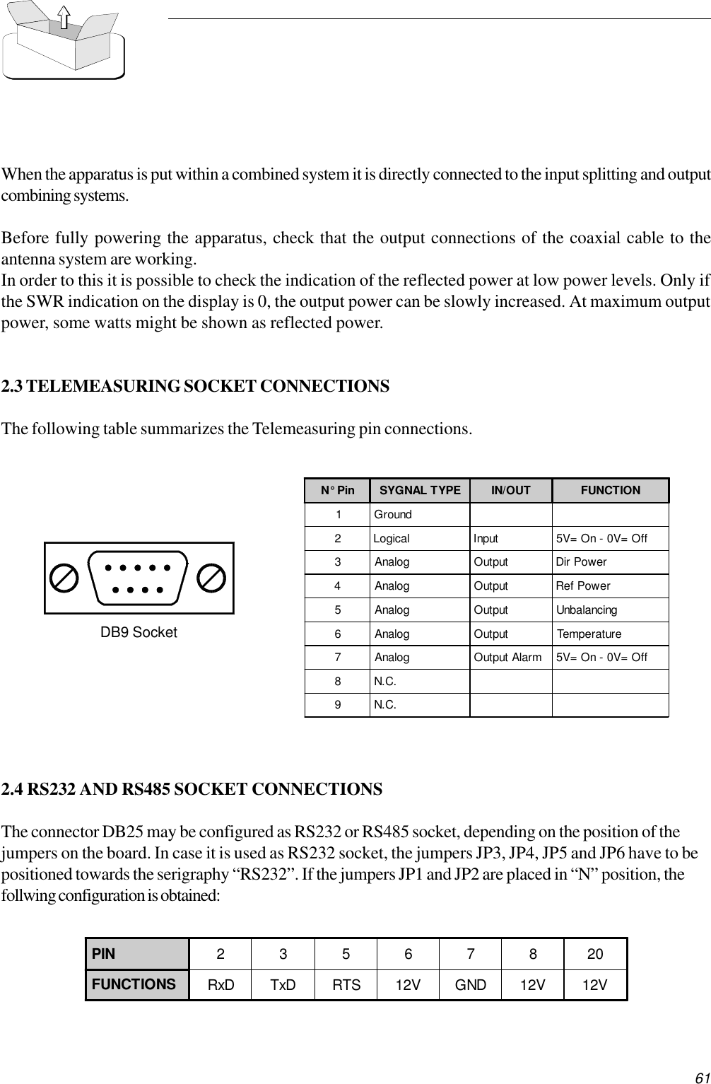
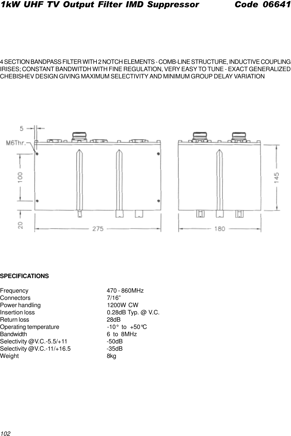
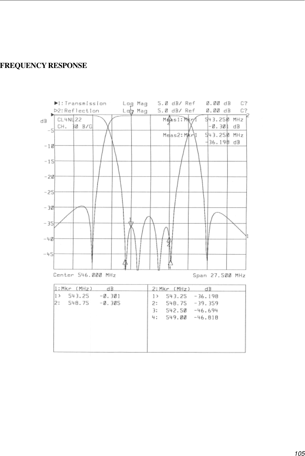
![103TESTING AND CALIBRATION INSTRUCTIONSThe output filter Mod. CL4NL22 is made up by a 4-resonator band-pass section and two “notch”resonators. It can be adjusted on all the channels of the TV UHF band (470 ÷ 860MHz) and on all theworld standards (intercarrier 4.5 - 6.5MHz). The pass-band section is made up by the group of the fourresonators, while the two separate resonator are the notches. The filter is symmetrical, thus there is nodifference between the upper and lower notch.The band width is adjusted by changing the insertion of the lower Post Screws which are placedbetween the band-pass resonators; inserting the post screws it is increased. In order to perform thisadjustment, loose the bolt of each post screws by means of a wrench n° 19. The first and third postscrews have to be adjusted for the same protrusion from the body of the filter, while the middle oneshould usually be adjusted in a slightly different manner in order to obtain an equiripple response.The input and output coupling, which can be reached by removing the protection cups, can be adjustedby means of the two lower Coupling Stubs next to the connectors. The adjustment is made by means of aflat wrench n° 18, taking into consideration that when the maximum coupling is obtained when thecommand cuts are parallel to the longer side of the filter, the minimum when they are orthogonal to it.The response symmetry is determined by the protrusion of the above mantioned stubs; these are set byloosening the relevant lower clamps by means of a tube wrench n° 16. The clamps, once tightened, alsodetermine the friction of the rotatio of the couplings.The suggested calibration sequence os the following:set the measuring instrument on- C.G. = (P.V. + P.A.) / 2- SPAN = INTERCARRIER * 5 (Es. 27,5MHz std. B/G)- RESPONSE = 5dB/div.- ADAPTATION = 10dB/div.Center Frequency[MHz=] Coupling Stub[mm=] Post Screw[mm=]474 2 6570 16 15666 29 17762 38 17858 40 17](https://usermanual.wiki/Elettronika-S-r-l/TXUP2000.User-Manual-Part-2/User-Guide-689180-Page-45.png)
![104• Set the coupling stubs and the post screws according to the indicative protrusion from their edge to the bodyof the filter listed in the table.• Tune the band-pass section on the wanted channel and load input and output correctly to obtain anoptimal response. At this stage the tuning of the two notches have to be kept distant from one another.Adjust the band width to -35dB at the limits of the screen (Es. std. B/G: BW (-35dB) = 27,5MHz). Theinput and output couplings may affect the tuning of the resonators, as such they have to be adjusted insmall steps, one after another. The equiripple response is obtained by adjusting the middle Post Screws.• Tune the two notches bringing them to the frequencies P.V.-INTERCARRIER andP.A.+INTERCARRIER. This will cause a change in the response and the adaptation of the band-pass.Correct the response by acting on the band-pass tuning.• Complete the calibration on both sides in this sequence: adjust the coupling, re-tune the notch in caseit has moved and then the band-pass tuning. If needed, adjust the middle Post Screws to obtain the bestequiripple adaptation. Perform this sequence in little steps trying to obtain the best adaptation.• Check the symmetry of the obtained response, and correct it if needed according to the followingcriterion: if the lower notch is more accentuated than the other one, insert the coupling stubs, otherwise,if the upper one is more accentuated, extract them.• Once the symmetry of the response has been corrected, complete the calibration as explained above.Once the calibration has been completed, put again the protection cups on the coupling regulators.Insertion loss @ P.V. (dB) < -0.40 (typ. -0.32)R.L. (from P.V.-0.75 to P.A.+0.25) (dB) > 28Attenuation @ P.V. -INTERCARRIER (dB) > 40Attenuation @ P.V. +INTERCARRIER (dB) > 40](https://usermanual.wiki/Elettronika-S-r-l/TXUP2000.User-Manual-Part-2/User-Guide-689180-Page-46.png)
![105FREQUENCY RESPONSE](https://usermanual.wiki/Elettronika-S-r-l/TXUP2000.User-Manual-Part-2/User-Guide-689180-Page-47.png)