Elettronika S r l TXUP3500 3.5 kW Analog TV Broadcast Transmitter User Manual APT137BM AUTV 3500LD Rev0 Date090605 p65
Elettronika S.r.l. 3.5 kW Analog TV Broadcast Transmitter APT137BM AUTV 3500LD Rev0 Date090605 p65
Contents
- 1. User Manual Part 1
- 2. User Manual Part 2
- 3. User Manual Part 3
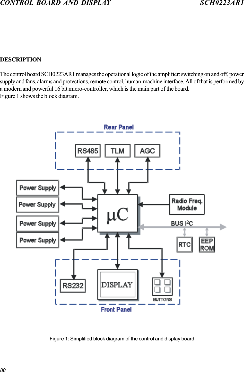
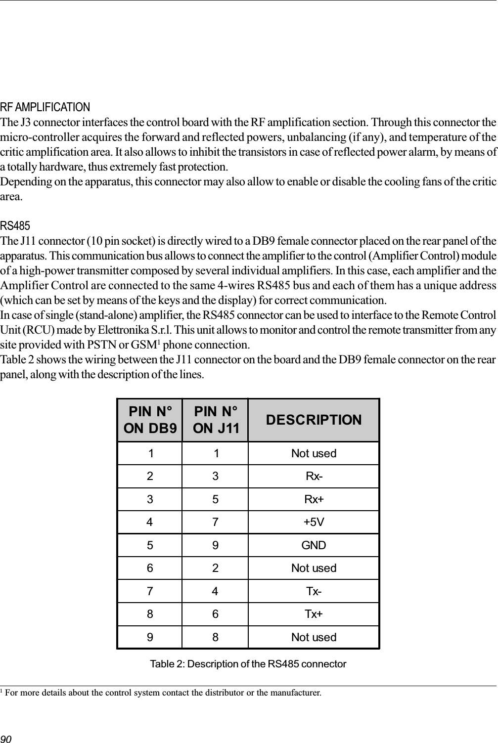
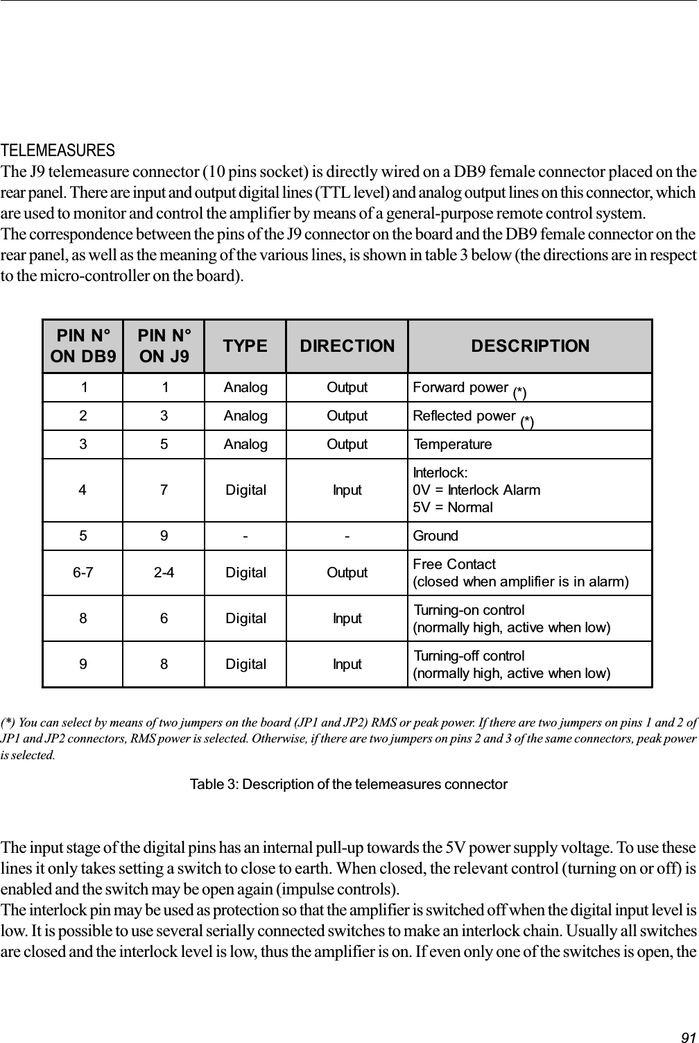
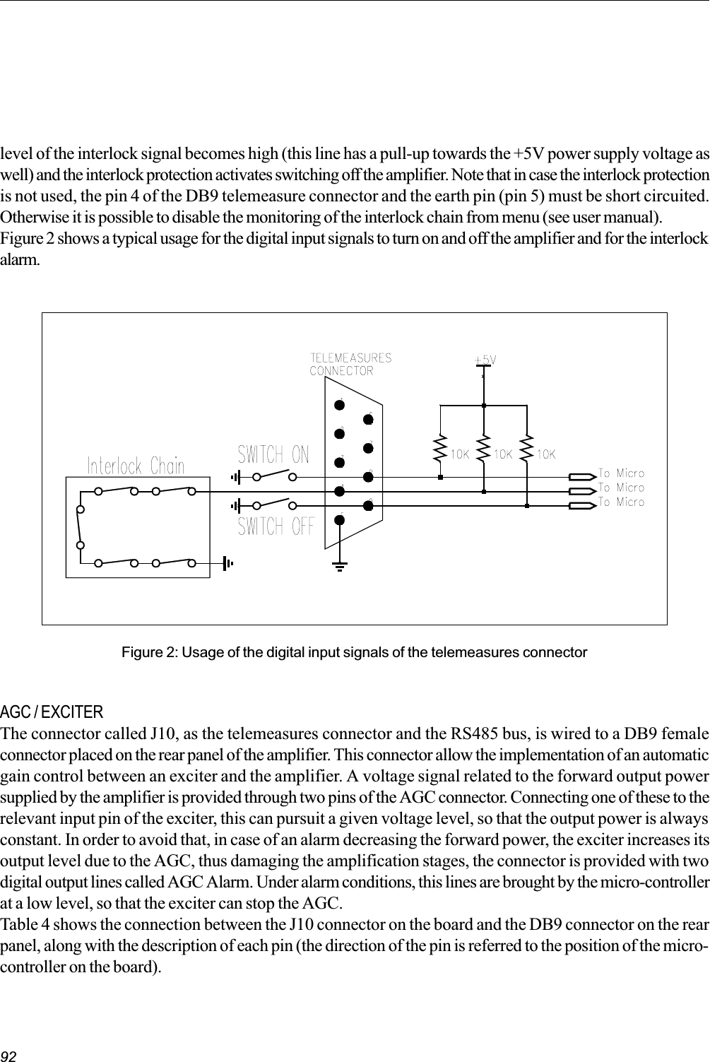
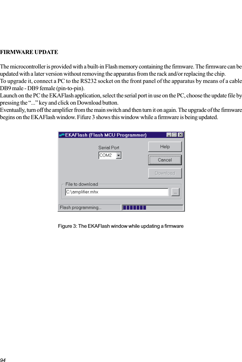
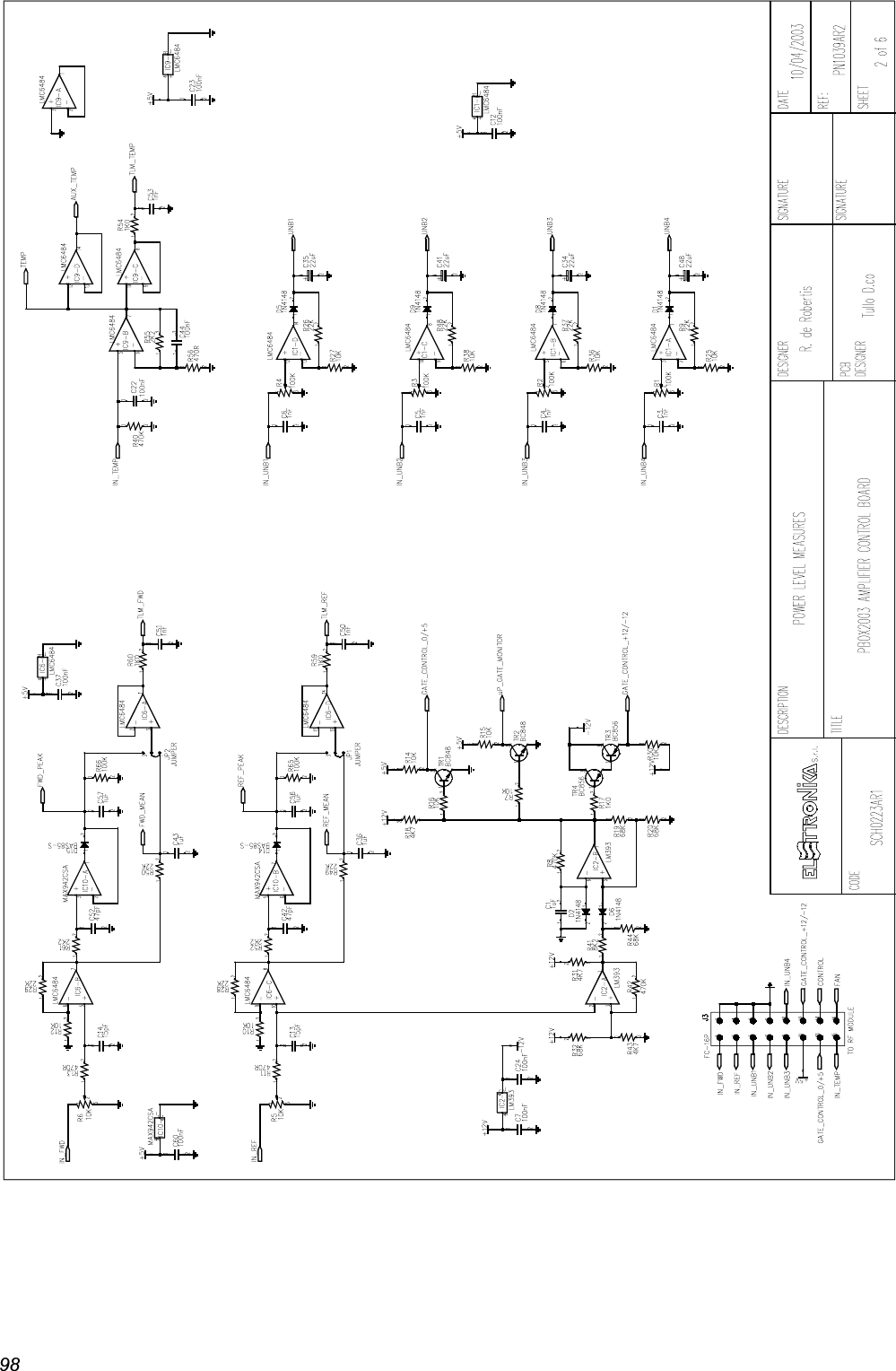
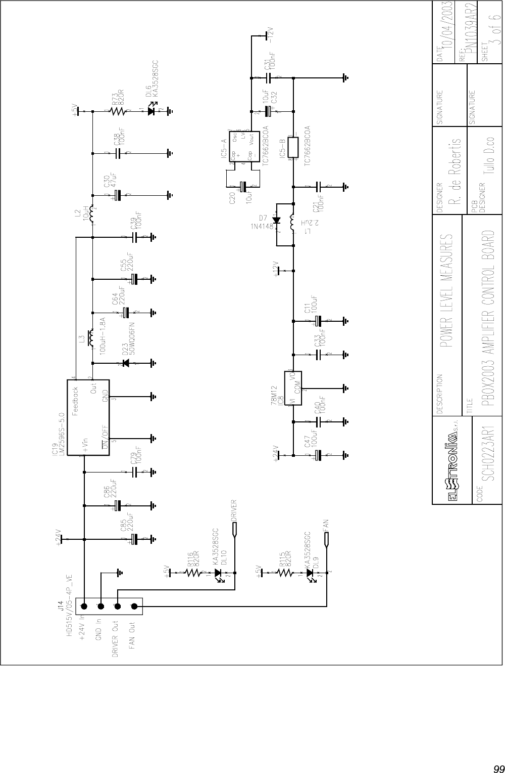
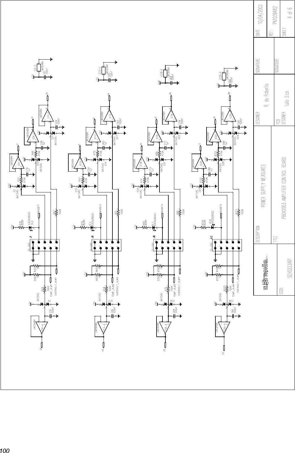
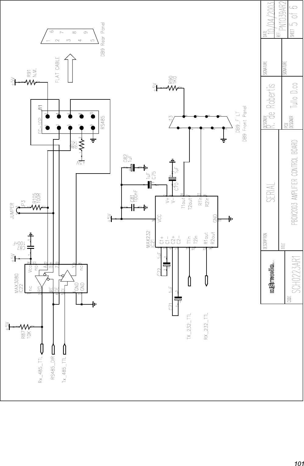
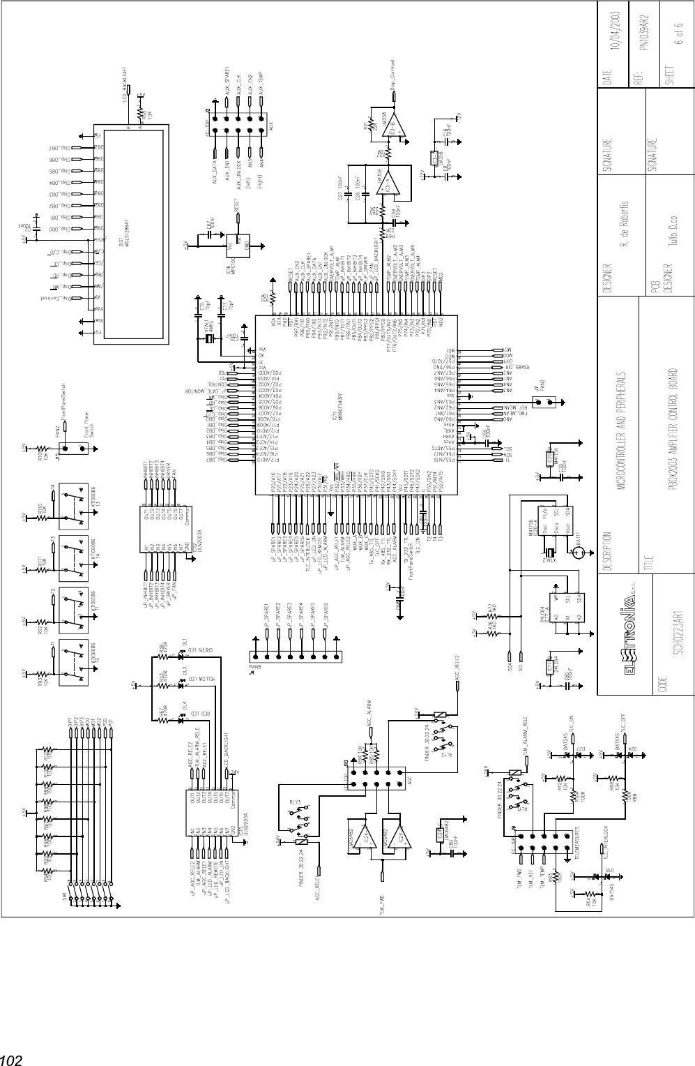
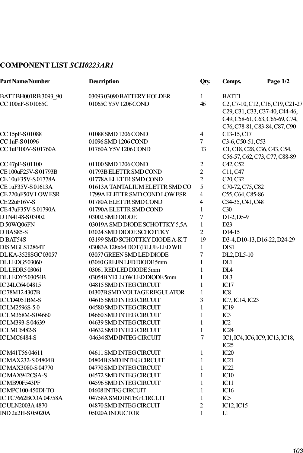
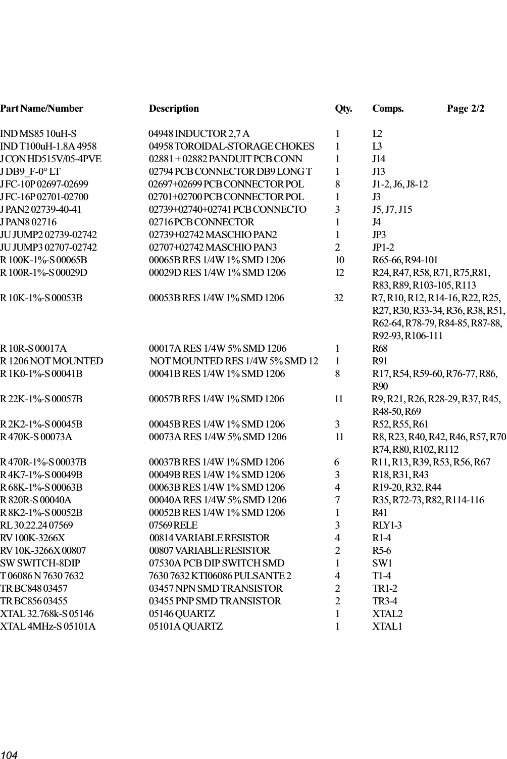
User Manual Part 2