Elettronika S r l TXUP3500 3.5 kW Analog TV Broadcast Transmitter User Manual APT137BM AUTV 3500LD Rev0 Date090605 p65
Elettronika S.r.l. 3.5 kW Analog TV Broadcast Transmitter APT137BM AUTV 3500LD Rev0 Date090605 p65
Contents
- 1. User Manual Part 1
- 2. User Manual Part 2
- 3. User Manual Part 3
User Manual Part 3
105
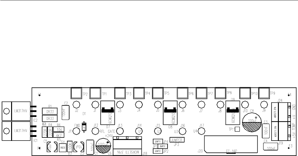
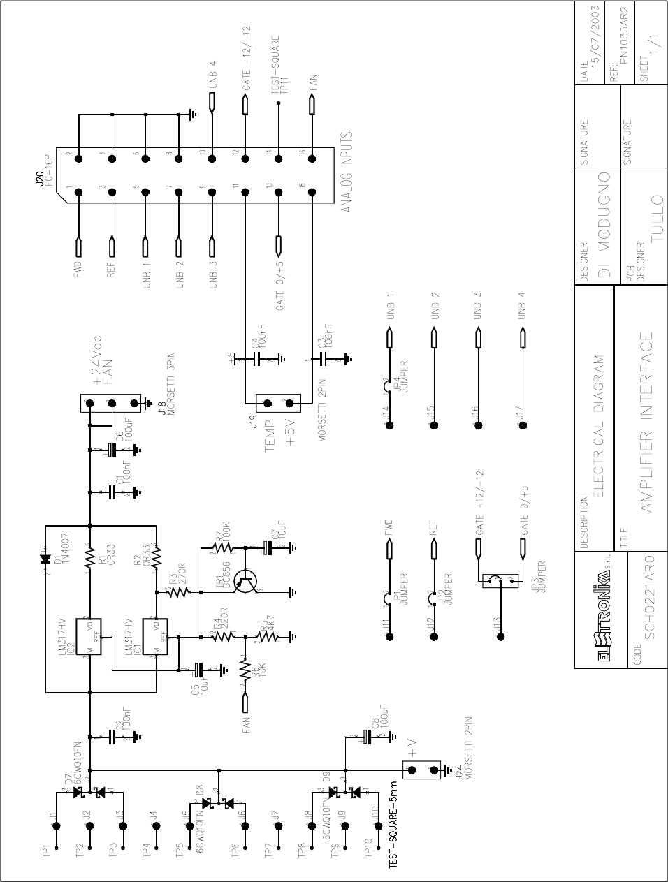
AMPLIFIER INTERFACE SCH0221AR0
Component layout SCH0221AR0
COMPONENT LIST SCH0221AR0
Part Name/Number Description Qty. Comps.
CC 100nFAVX 01065A 01065A CERAMIC COND 4 C1-4
CE 100uF100V 01795B ELETT. COND. 1 C8
CE 100uF50V 01795 01795 ELETT. COND. 1 C6
CE 10uF35V-S 01778A 01778A ELETTR SMD COND 2 C5, C7
D 1N4007 03009 03009 DIODE 1 D1
D 6CWQ10FN 03026 SMD DIODE SCHOTTKY 3,5A 3 D7-9
IC LM317HV 04340A INTEG CIRCUIT 2 IC1-2
J FC-16P 02701-02700 02701+02700 PCB CONNECTOR POL 1 J20
J SCREWCONN2 02853 02853 PCB SCREW CONNECTOR 2 J19, J24
J SCREWCONN3 02860 02860 PCB SCREW CONNECTOR 1 J18
J TESTP1.3mm 07913 07913 TEST POINT 17 J1-17
JU JUMP2 02739-02742 02739+02742 MASCHIO PAN2 3 JP1-2, JP4
JU JUMP3 02707-02742 02707+02742 MASCHIO PAN3 1 JP3
R 0R33-1W-S 00380 RES 1W 5% SMD 2512 2 R1-2
R 100K-S 00065A 00065A RES 1/4W 5% SMD 1206 1 R7
R 10K-S 00053A 00053A RES 1/4W 5% SMD 1206 1 R6
R 220R-S 00033A 00033A RES 1/4W 5% SMD 1206 1 R4
R 270R-S 00034A 00034A RES 1/4W5% SMD 1206 1 R3
R 4K7-S 00049A 00049A RES 1/4W 5% SMD 1206 1 R5
TR BC856 03455 03455 PNP SMD TRANSISTOR 1 TR1
106
107
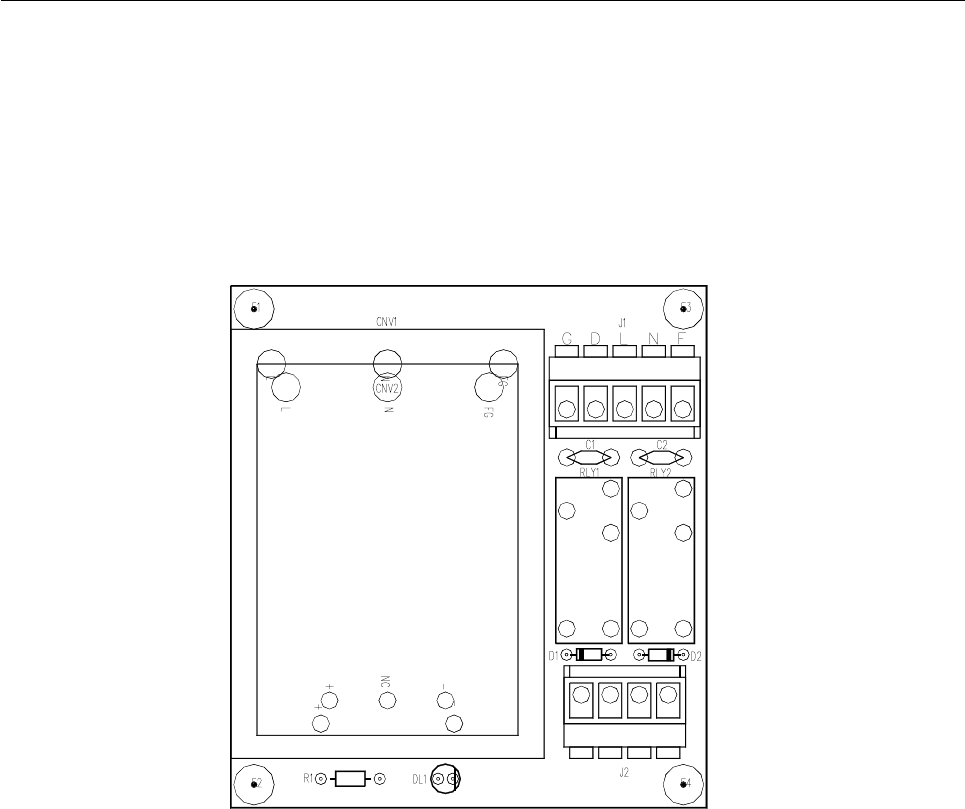
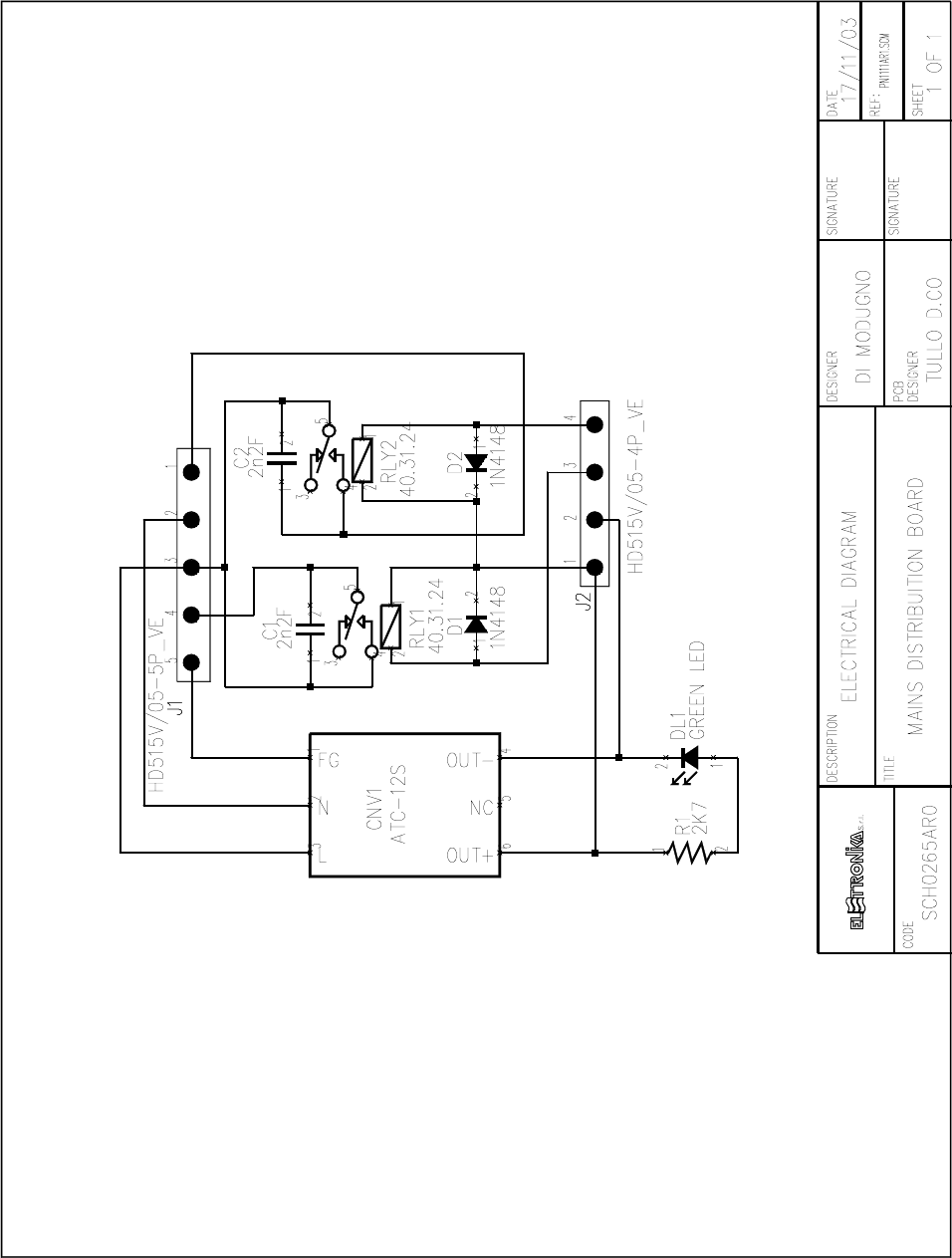
MAINS DISTRIBUTION BOARD SCH0265AR0
Component layout SCH0265AR0
COMPONENT LIST SCH0265AR0
Part Name/Number Description Qty. Comps.
CC 2nF2 2kV 01045A 01045A CERAMIC COND 2 C1-2
CNV AC-DC ATC-12S E0037 AC DC CONVERTER 1 CNV1
D 1N4148 03001 03001 DIODE 2 D1-2
DL LEDG3 03053 03053 GREEN LED DIODE 3mm 1 DL1
J CON HD515V/05-4PVE 02881 + 02882 PANDUIT PCB CONN 1 J2
J CON HD515V/05-5PVE PANDUIT PCB CO 1 J1
R 2K7 0046 0046 RES 1/4W 5% 1 R1
RL 40.31.24 7567C RELE 2 RLY1-2
108
109
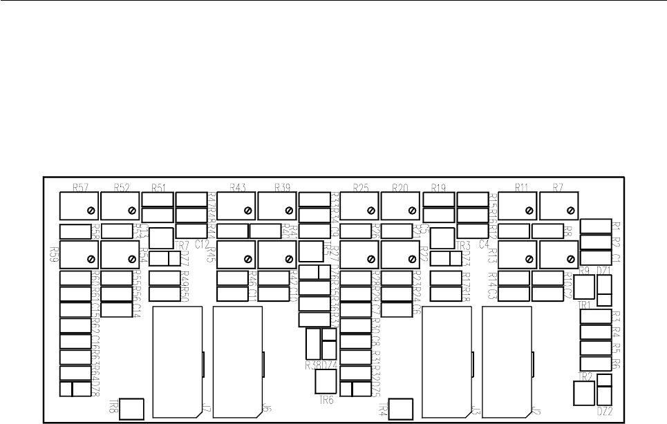
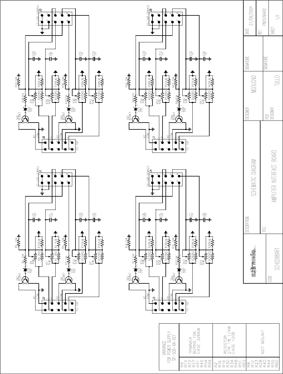
INTERFACE BOARD SCH0288AR1
Component layout SCH0288AR1
COMPONENT LIST SCH0288AR1
Part Name/Number Description Qty. Comps.
CC 1nF-S 01096 01096 SMD 1206 COND 16 C1-16
DZ 5V1-S 03128 03128 SMD ZENER DIODE 8 DZ1-8
J FC-10P 02697-02699 02697+02699 PCB CONNECTOR POL 4 J2-3, J6-7
J FC-10P PCB FEMALE 02706 PCB FEMALE CONNECTOR POL 4 J1, J4-5, J8
R 0R0-S 00001 00001 RES 1/4W 5% SMD 1206 16 R1, R8, R12, R15, R21, R23, R26
R28, R33, R40, R44, R47, R53, R55,
R58, R60
R 10K-S 00053A 00053A RES 1/4W 5% SMD 1206 16 R3-6, R17-18, R31-32, R35-38,
R49-50, R63-64
R 1206 NOT MOUNTED NOT MOUNTED RES 1/4W 5% SMD 12 16 R2, R10, R14, R16, R19, R24, R29,
R30, R34, R42, R46, R48, R51, R56,
R61-62
RV 3266W NOT MOUNT NOT MOUNTED VARIABLE RESISTOR 16 R7, R9, R11, R13, R20, R22, R25,
R27, R39, R41, R43, R45, R52, R54,
R57, R59
TR BC847 03456 03456 NPN SMD TRANSISTOR 8 TR1-8
110
111
SPECIFICATION
MODEL SP-500-27 (E0012 Code) SP-500-48 (E0013 Code)
DC Output Voltage 27Vdc 48Vdc
Output Rated Current 18A 10A
Output Current Range 0-18A 0-10A
Ripple & Noise (p-p) 200mVp-p 240mVp-p
DC Output Power 486W 480W
Efficiency 87% 87%
DC Voltage Adj. 24-30V 41-56V
Over V. Protection 31V-36.5V 57.6V-67.2V
Input Voltage Range 88-264Vac
Input Frequency 47-63Hz
Power Factor 0.95/100-240Vac
Overload Protection 105%-135%
Type: Foldback current limiting
Recovery: Auto
Over Temp. Protection > =70°C Output Shutdown
Fan Control Temp. > =60°C Fan On
< =50°C Fan Off
Working Temp., Humidity -10°C/+50°C, 20%-90% RH
Dimension 185x120x93
Weight 1.8Kg.
SP500-27-DI SWITCHING POWER SUPPLY E0012
112
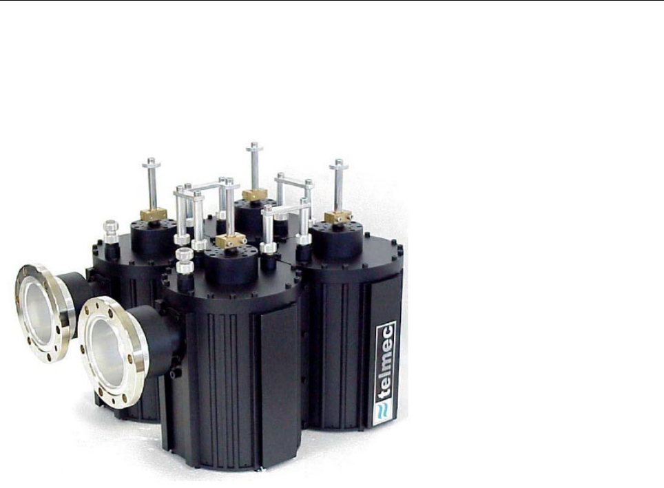
UHF 5/10kW ANALOG TV FILTER Code 06663
Suitable for use in solid state A-AB
class transmitter, in common
amplification, to eliminate out of band
products in all standard frequencies.
Available connectors:
- EIA 1 5/8
- RIGID LINE 1 5/8
- EIA 3 1/8
opposite or parallel position.
TECHNICAL CHARACTERISTICS
Configuration 4 Cavities
Max power output 10kW (cw)
Frequency range 470 - 860MHz
Insertion loss (Video c.) < 0,2dB
Return loss > 30dB
Temperature range -10°C / +50°C
Temperature shift < = 2kHz/K
Weight 20kg
Working position Any
Dimensions 395x380x347mm
113
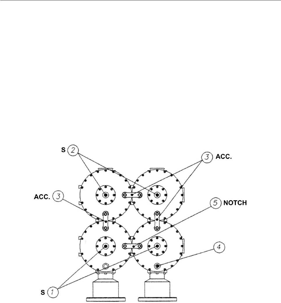
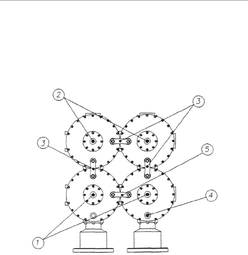
CALIBRATION PROCEDURE
In order to calibrate PBN153/44, a double-track Network Analyser is needed, in order to visualize the
frequency response of the passing and reflected signals.
- Calibration procedure from 470MHz to 666MHz
1. Extract the coupling 5 (Fig. 1) until it stops.
2. Insert the couplings 3, letting about 5mm out.
3. Connect the filter to the Network Analyser marking the input. Select the frequency of the desired channel
centre and set a SPAN of 50MHz.
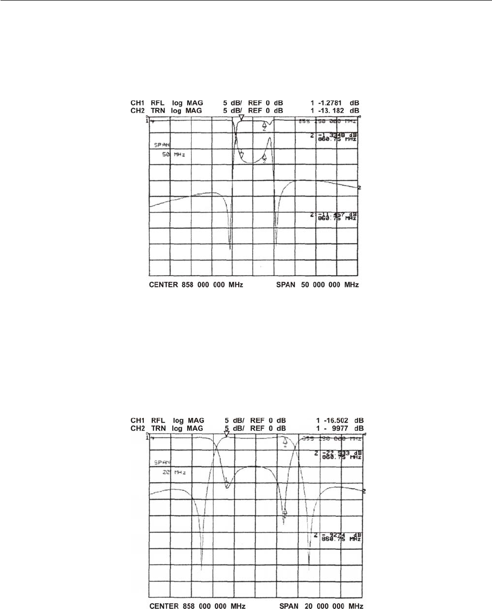
4. Act on the tuning rods 1 and 2 until the curve of the band-pass appears in the centre of the screeen, and
adjust it by means of the couplings 3 to obtain a width of about 10MHz (Fig. 2).
114
Fig. 2
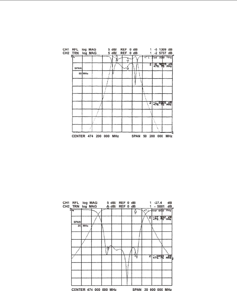
5. Set a SPAN of 20MHz and act alternatively on:
- Interstage coupling 3 (rise and lower);
- IN/OUT couplings 4 (turn);
- Tuning 1 and 2 (rise and lower);
to obtain a bandwidth of 7-8MHz and an adaptation of about 25dB, composed by four peaks (Fig. 3).
Fig. 3
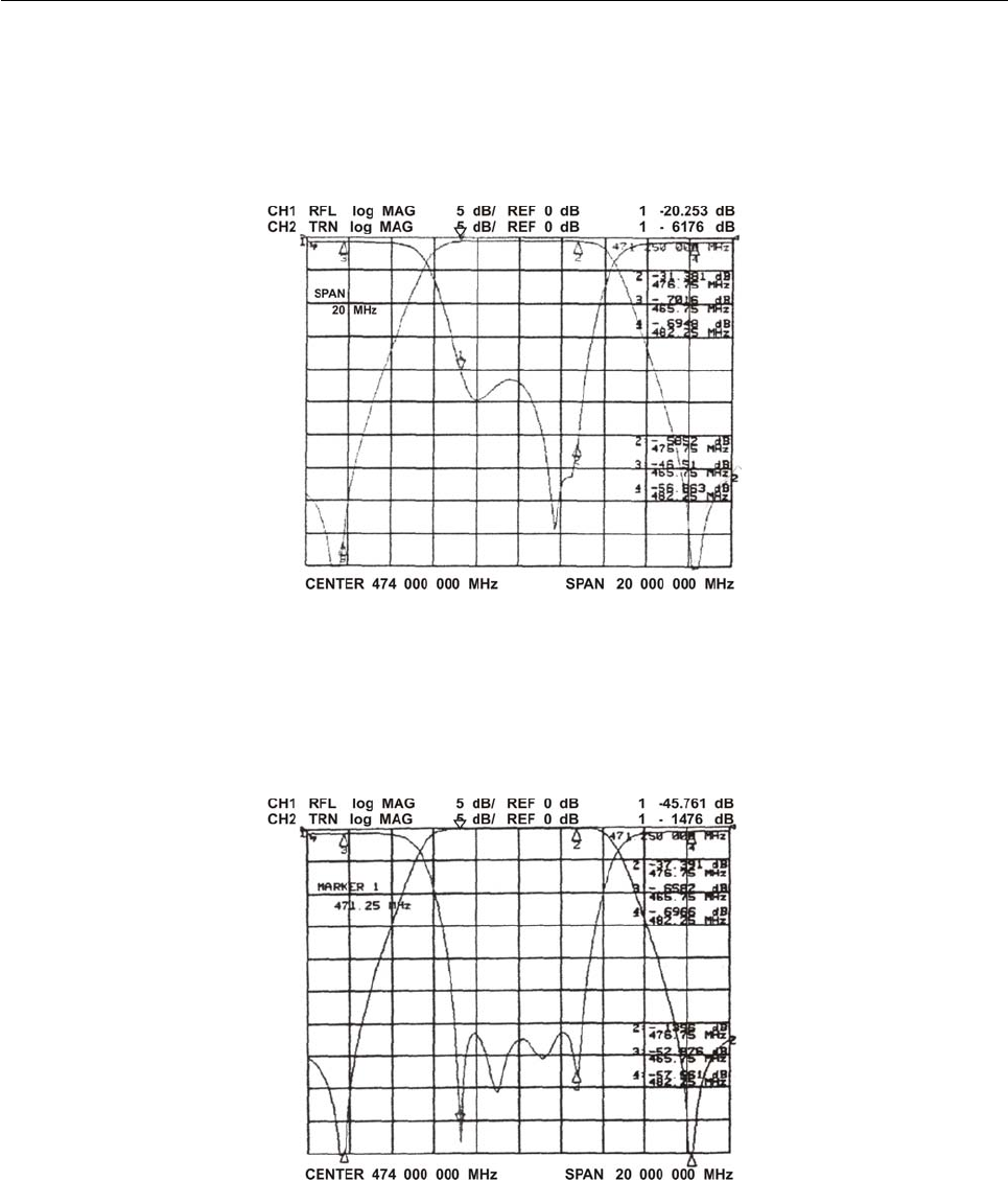
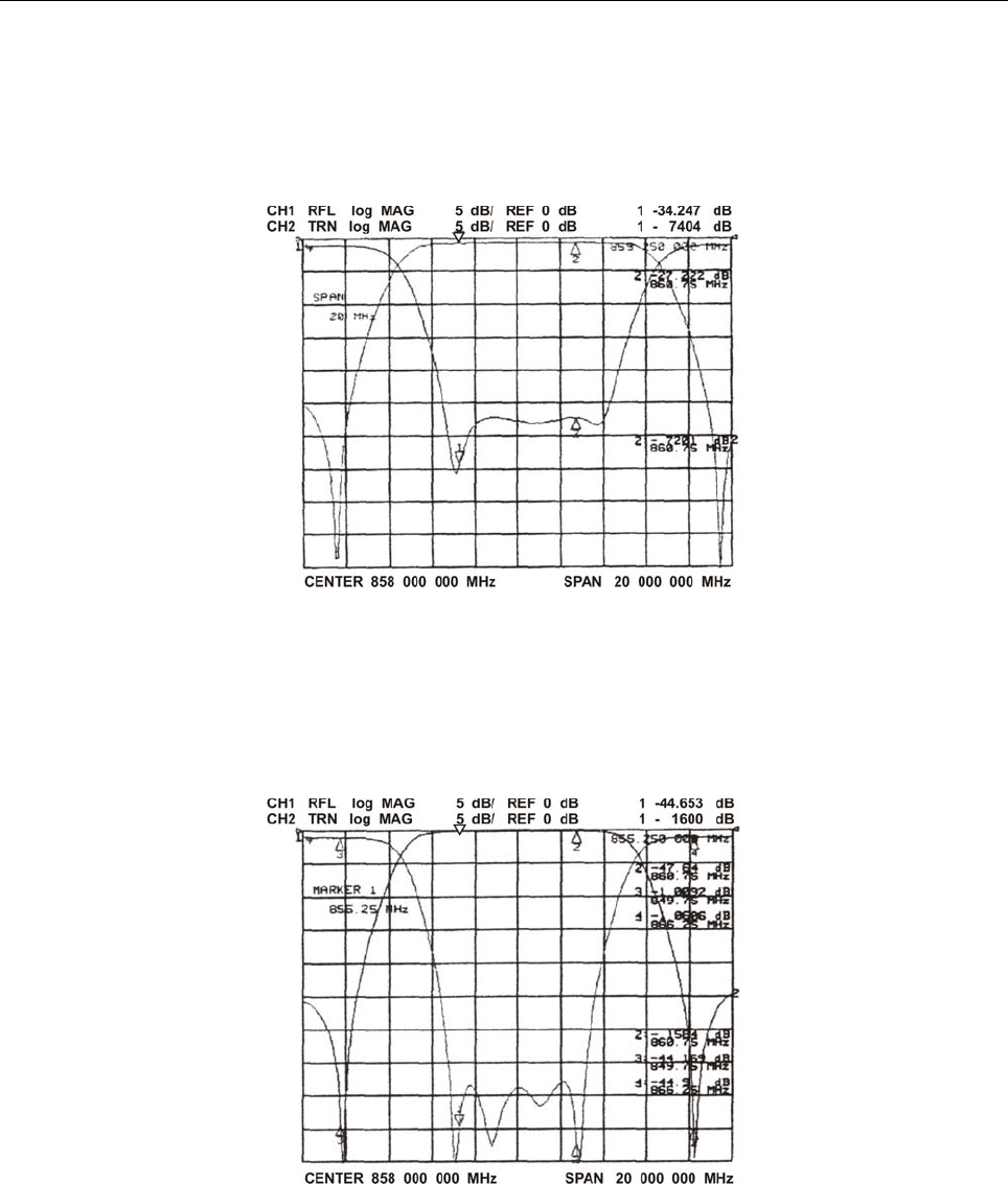
6. Insert the coupling 5 (Fig. 1) to set the position of the notch attenuation on the desired frequencies (Fig. 4)
(5.5MHz and +11MHz or 4-5MHz and +9MHz).
115
Fig. 4
7. The adaptation has moved; it can be adjusted by acting on the filter as per point 6, correcting each time the
attenuation tuning by means of the coupling 5, until a frequency response like that in the example (Fig. 5) is
obtained.
Fig. 5
8. Once the calibration is complete, the machanical movement during the locking stage will have to be
compensator for, because a variation of the adaptation may occur. It only takes to extract slightly the tuning
which is being fastened.
116
- Calibration procedure from 66MHz to 860MHz
1. Extract the coupling 5 (Fig. 1) until it stops.
2. Extract the couplings 3 making sure not to short-circuit them.
3.Connect the filter to the Network Analyser, marking the input. Select the frequency of the desired centre
channel and set a SPAN of 50MHz.
4. Act on the tuning rods 1 and 2 until the curve of the band-pass appears in the centre of the screen and
adjust it by means of the coupling 3 to obtain a width of about 10MHz (Fig. 2). The tuning 2, due to the
elliptical system according to which the filter has been designed, will compose the attenuation of the notch as
well as the curve of the band-pass.
117
Fig. 2
5. Set a SPAN of 20MHz and act alternatively on:
- Interstage couplings 3 (rise and lower);
- IN/OUT couplings 4 (turn);
- Tuning 1 and 2 (rise and lower);
to obtain a bandwidth of 7-8MHz and an adaptation of about 25dB, composed by four peaks (Fig. 3).
Fig. 3
6. Use the coupling 5 (Fig. 1) to set the position of the notch attenuation on the desired frequencies (Fig. 4)
(5.5MHz and +11MHz or 4.5MHz and +9MHz).
118
Fig. 4
7. It is possible to note that, by tuning the notch attenuation as described in point 6 above, the adaptation has
moved. It can be adjusted by acting on the filter as per point 6, correcting each time the tuning of the notch
attenuation by means of the coupling 5, until a frequency response like the one in the example (Fig. 5) is
obtained.
Fig. 5
8. Once the calibration is complete, the mechanical movement during the locking stage will have to be
compensated for, because a variation of the adaptation may occur. It only takes to extract slightly the tuning
which is being fastened.