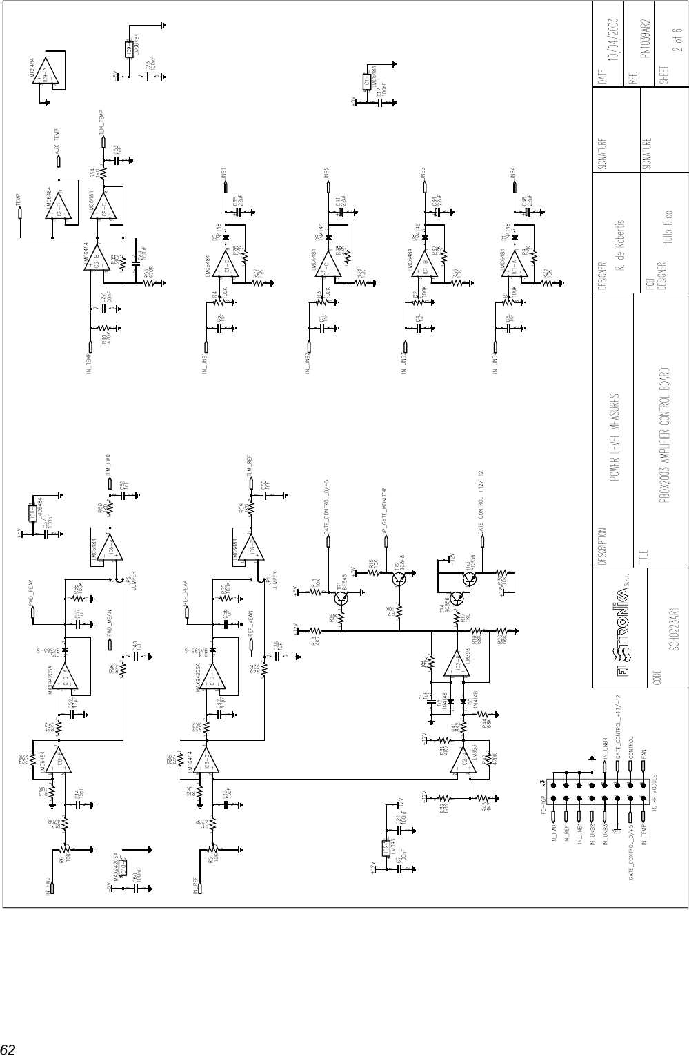
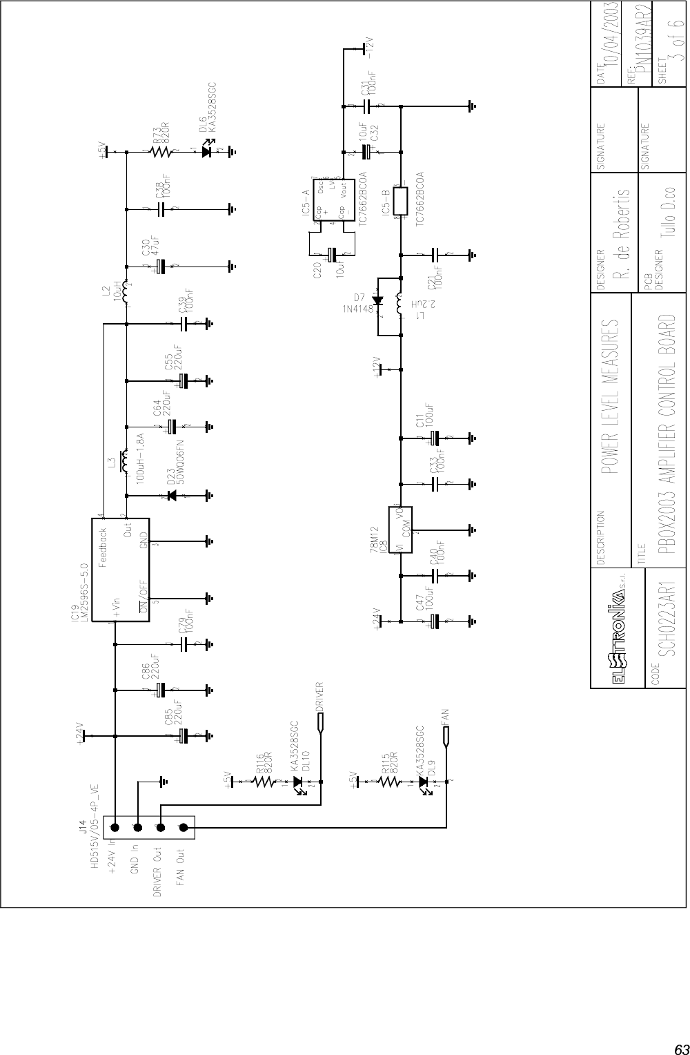
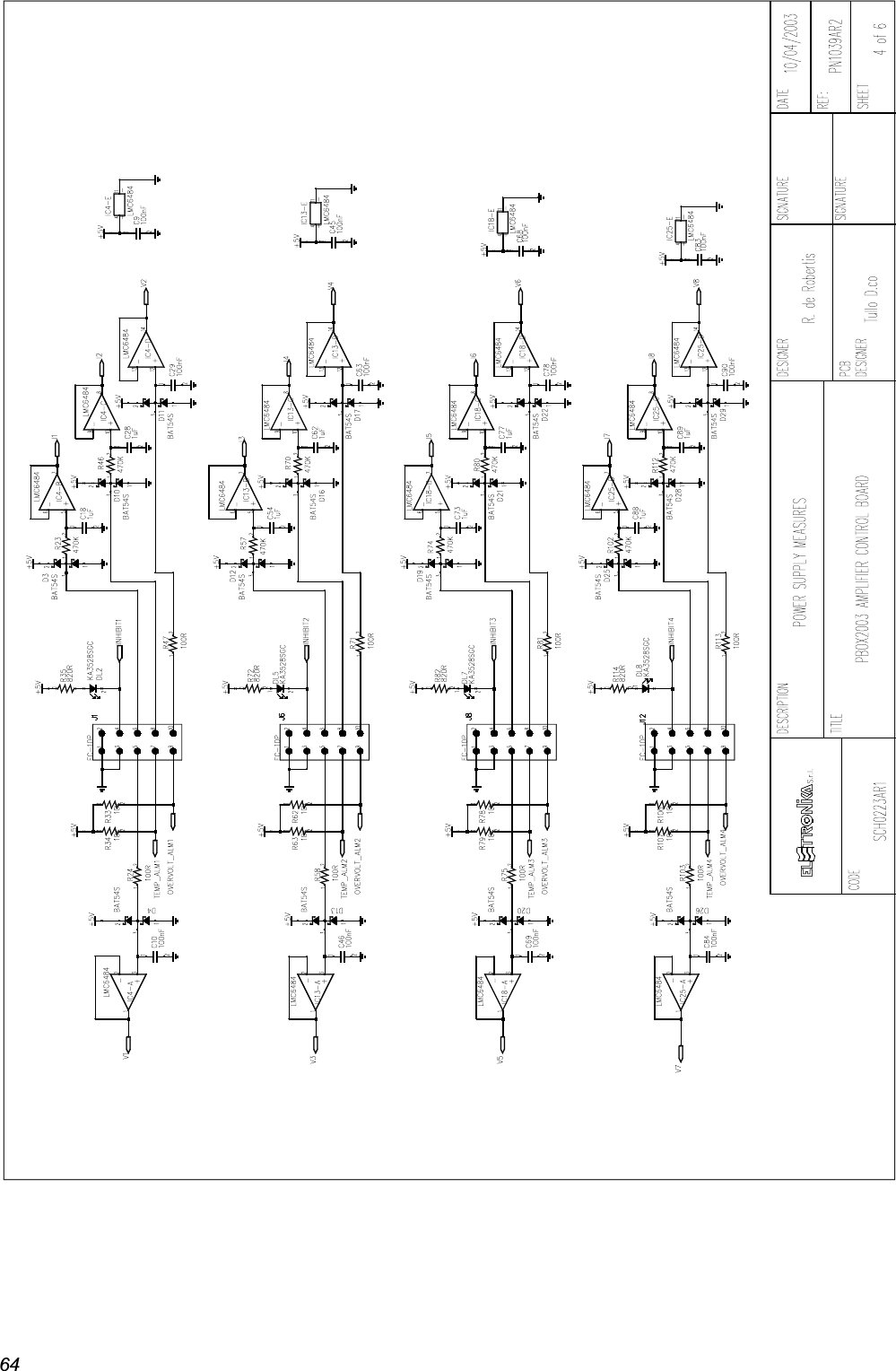
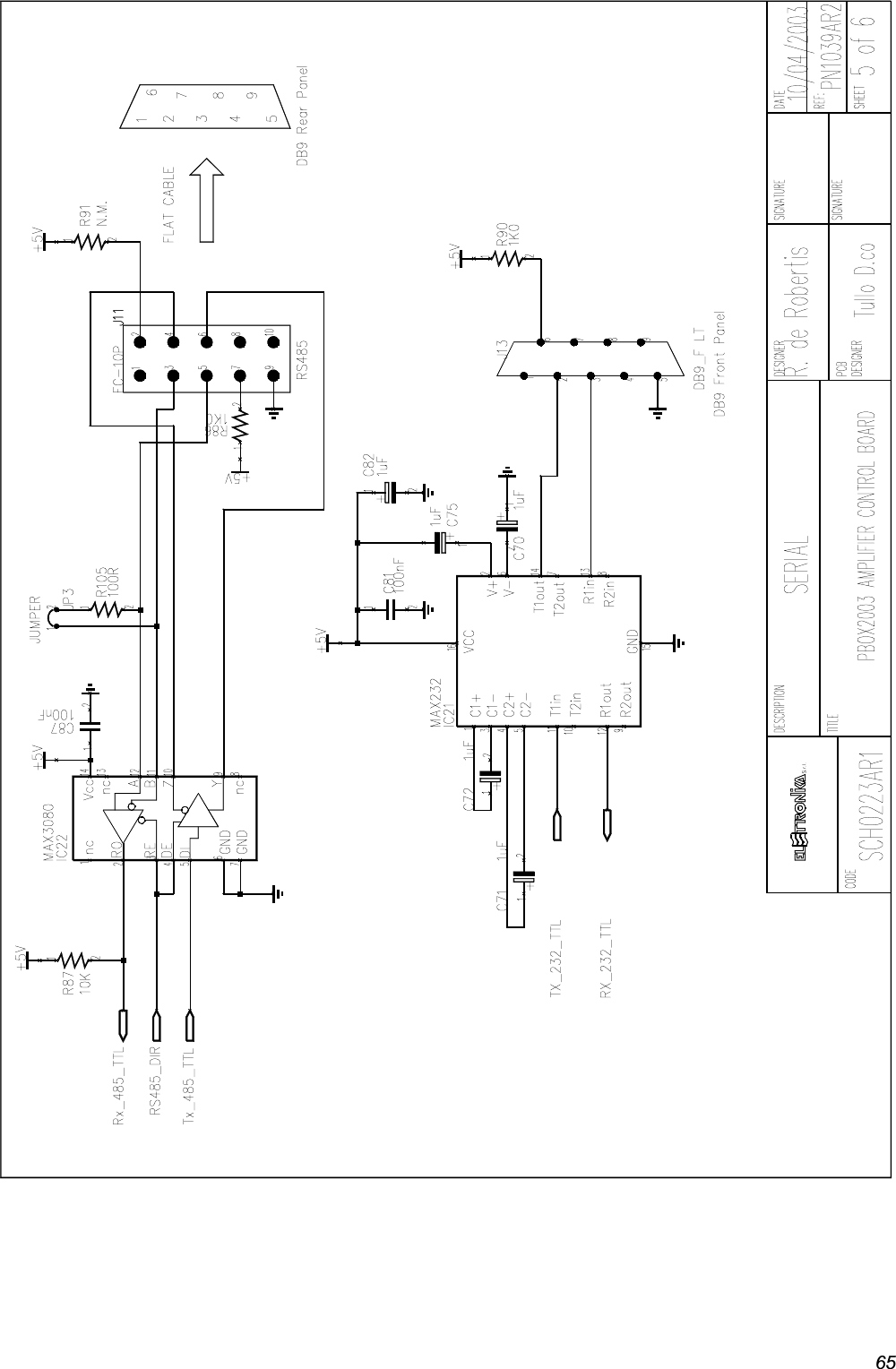
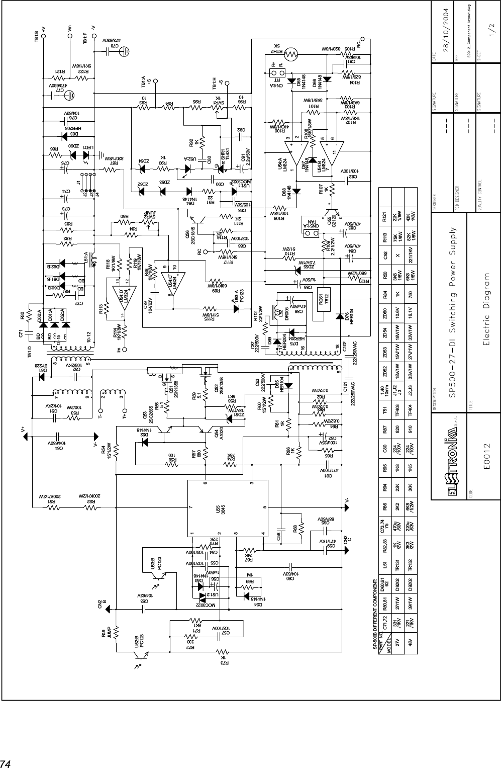
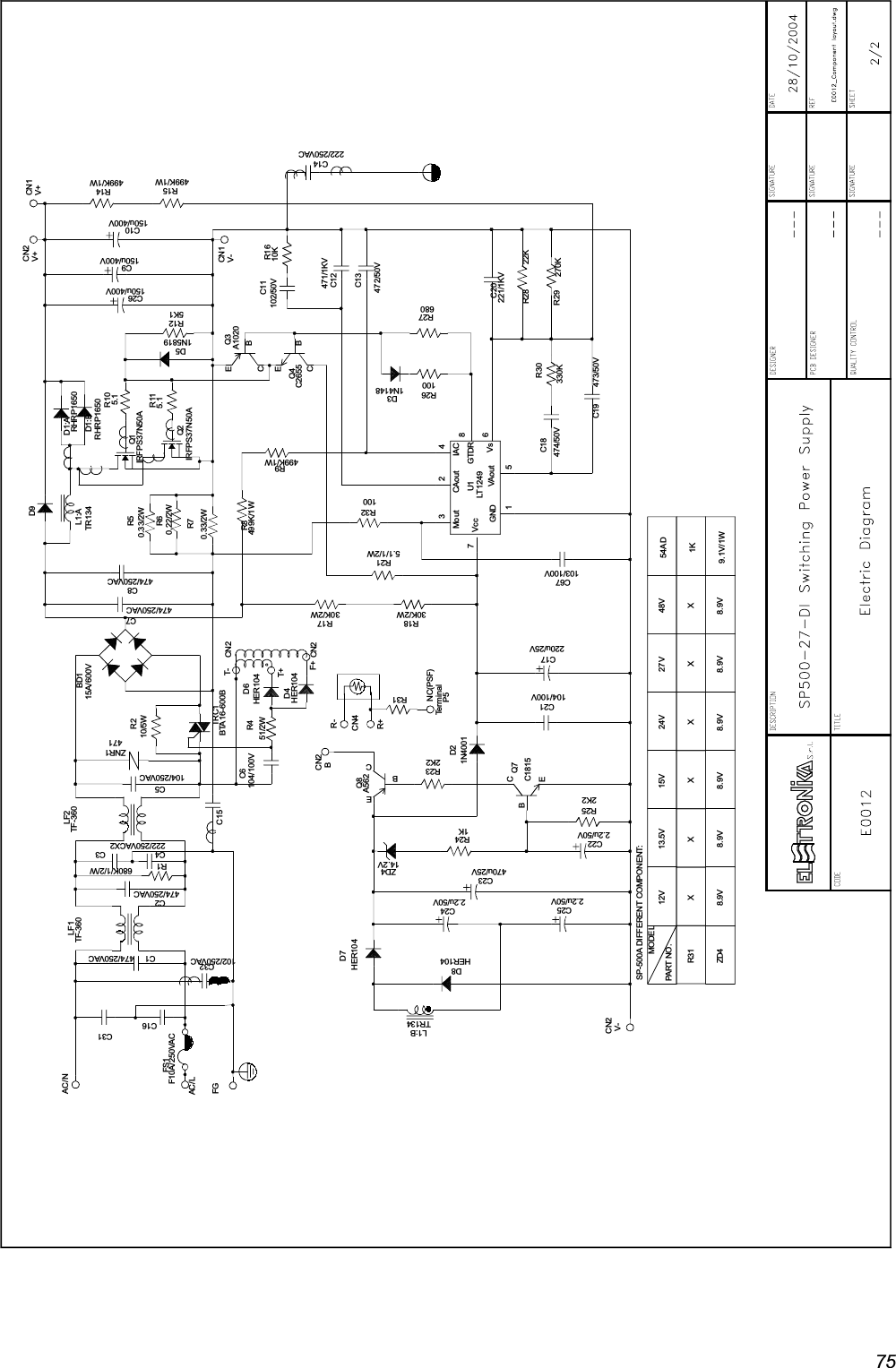
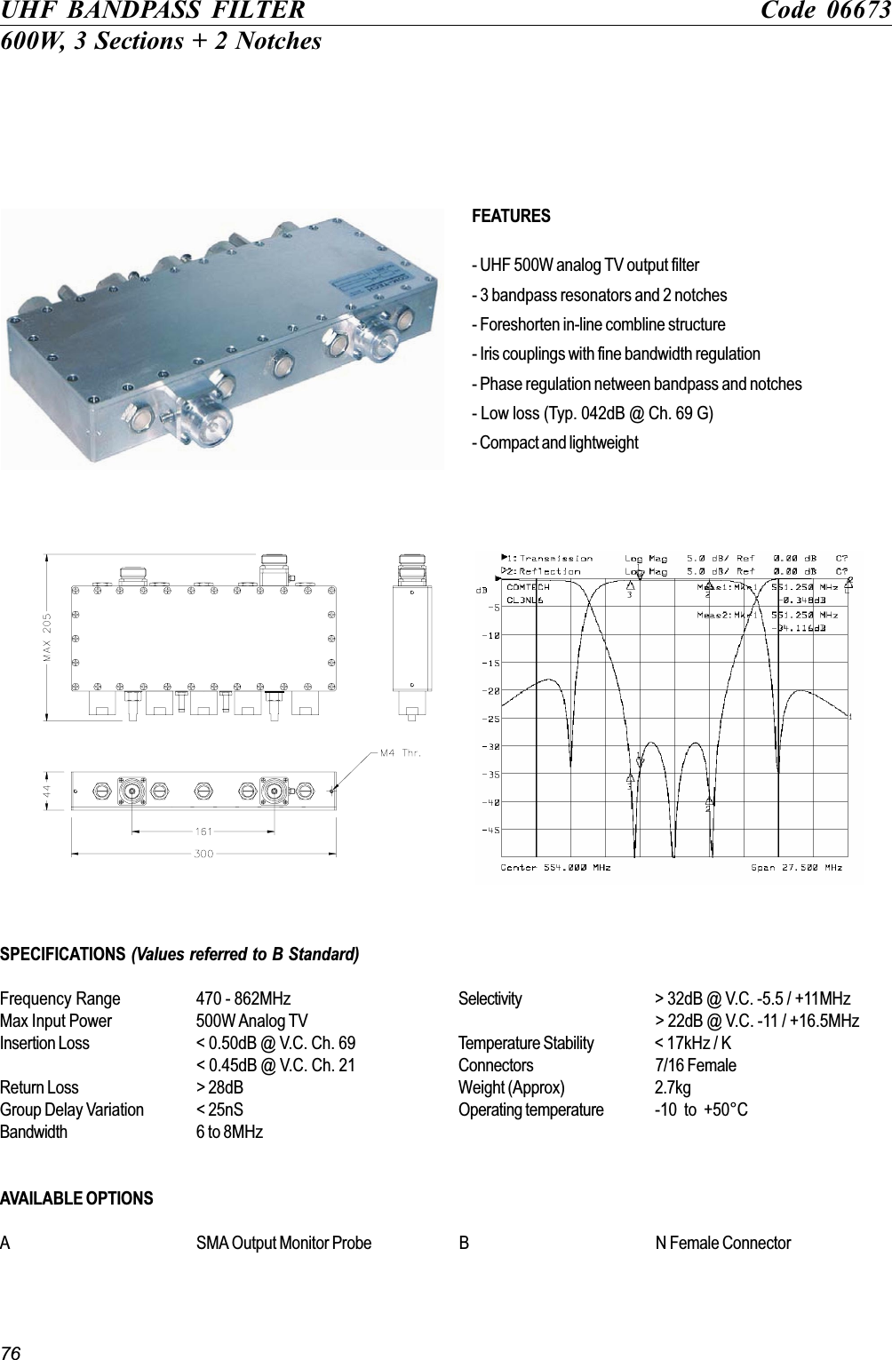
Elettronika S r l TXUP500 500 Watt Analog TV Broadcast Transmitter User Manual APT159B AUTV 500LD Rev0 Date190105 p65
Elettronika S.r.l. 500 Watt Analog TV Broadcast Transmitter APT159B AUTV 500LD Rev0 Date190105 p65
UserManual.wiki
>
Elettronika S r l
>
TXUP500 User Manual
>
Users manual Part 2
Contents
1.
Users manual Part 1
2.
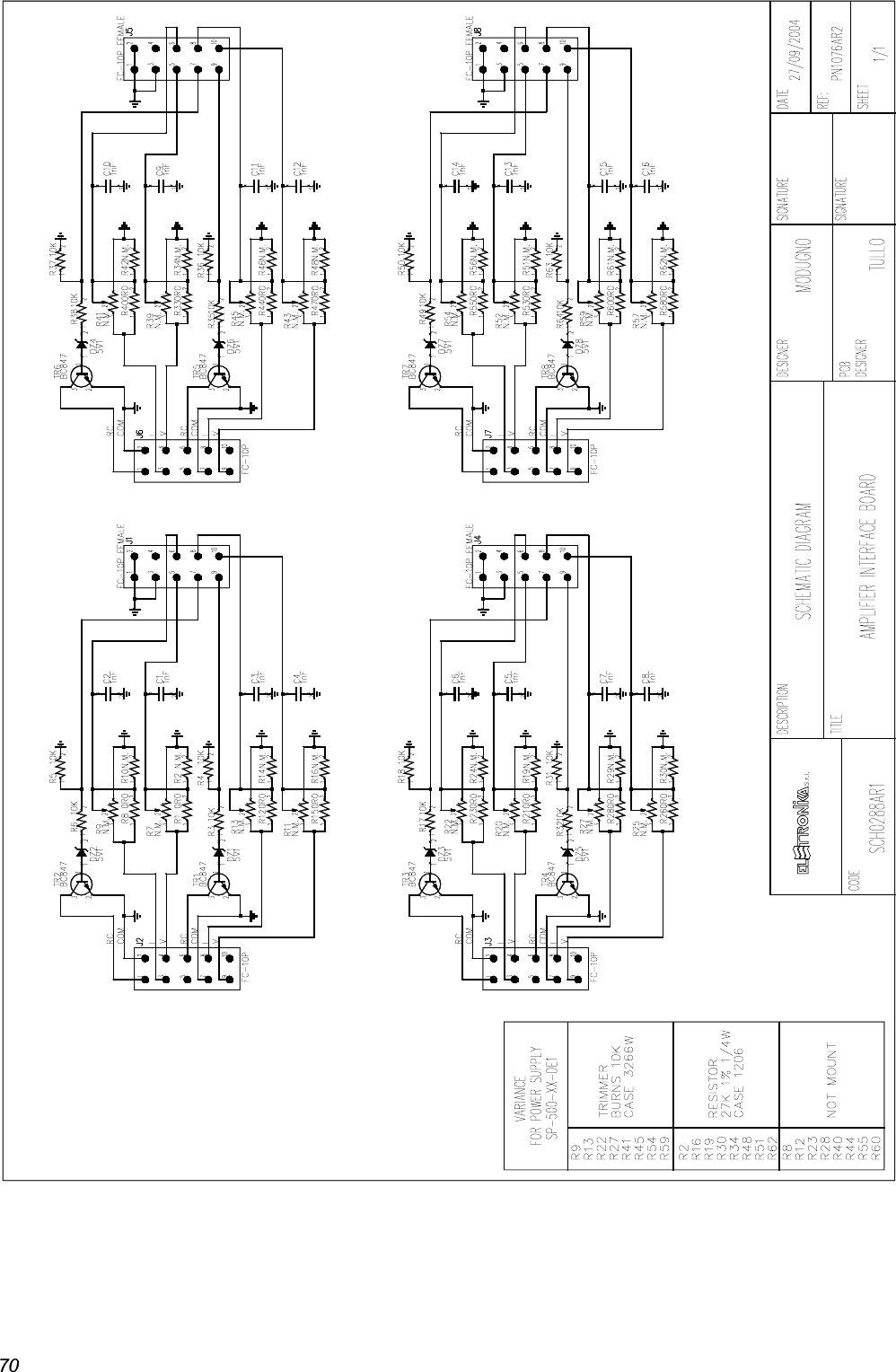
Users manual Part 2
3.
Users manual Exciter part 1
4.
Users manual Exciter Part 2
5.
Users manual Exciter Part 3
Users manual Part 2
Navigation menu
Upload a User Manual
Namespaces
Wiki Guide
HTML
PDF
Info
Views
User Manual
Discussion / Help
Navigation