Elettronika S r l TXUP500 500 Watt Analog TV Broadcast Transmitter User Manual APT159B AUTV 500LD Rev0 Date190105 p65
Elettronika S.r.l. 500 Watt Analog TV Broadcast Transmitter APT159B AUTV 500LD Rev0 Date190105 p65
Contents
Users manual Part 2
33
_______________________________________________________________________________________________
Section 4 - Diagram
Contents:
- Cable diagram
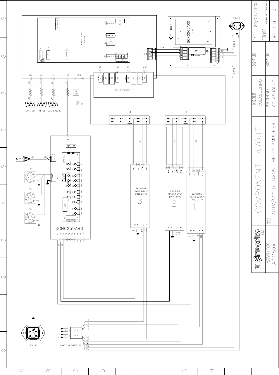
- APT159A AUTV/500LD Power Supply Section
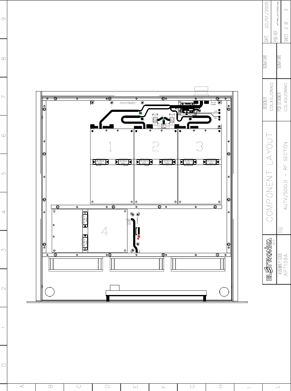
- APT159A AUTV/500LD RF Section
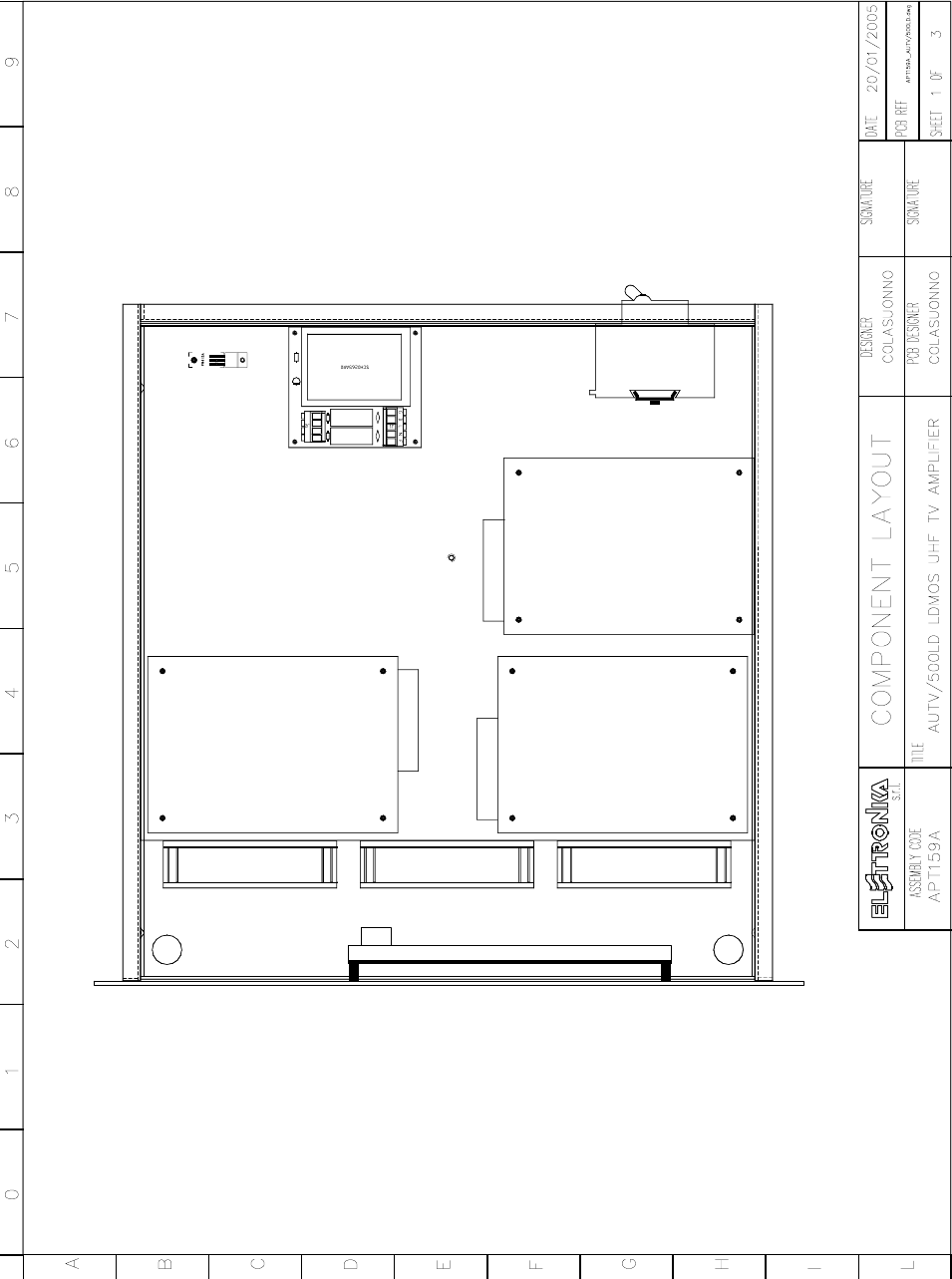
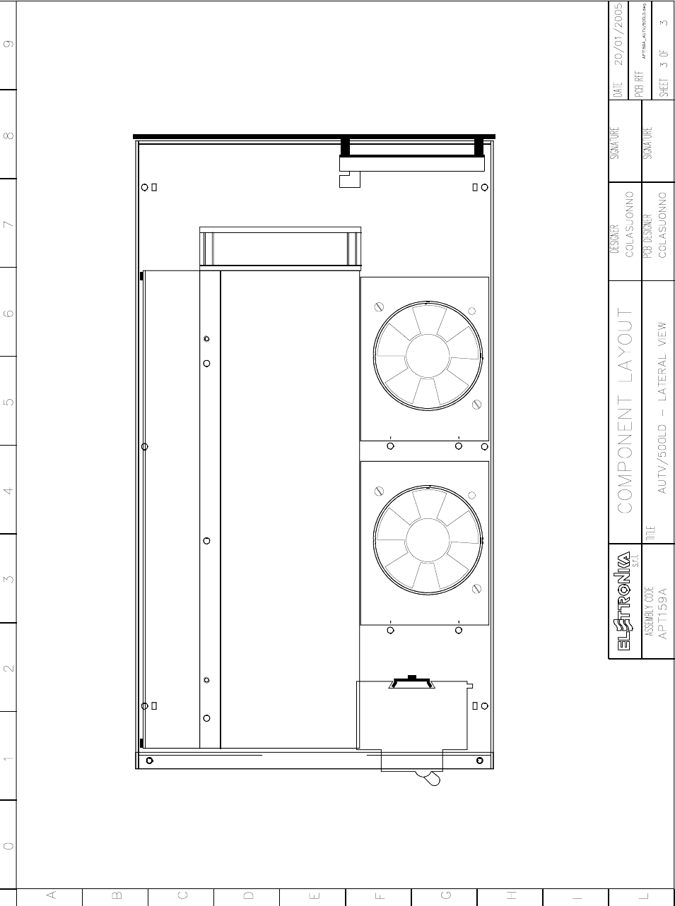
- APT159A AUTV/500LD Lateral View
- MTF0083AR0 Amplifier module - Component list
- SCH0192AR0 (200W UHF LDMOS Amplifier module)
- SCH0259AR0 (RF Amplifier interface)
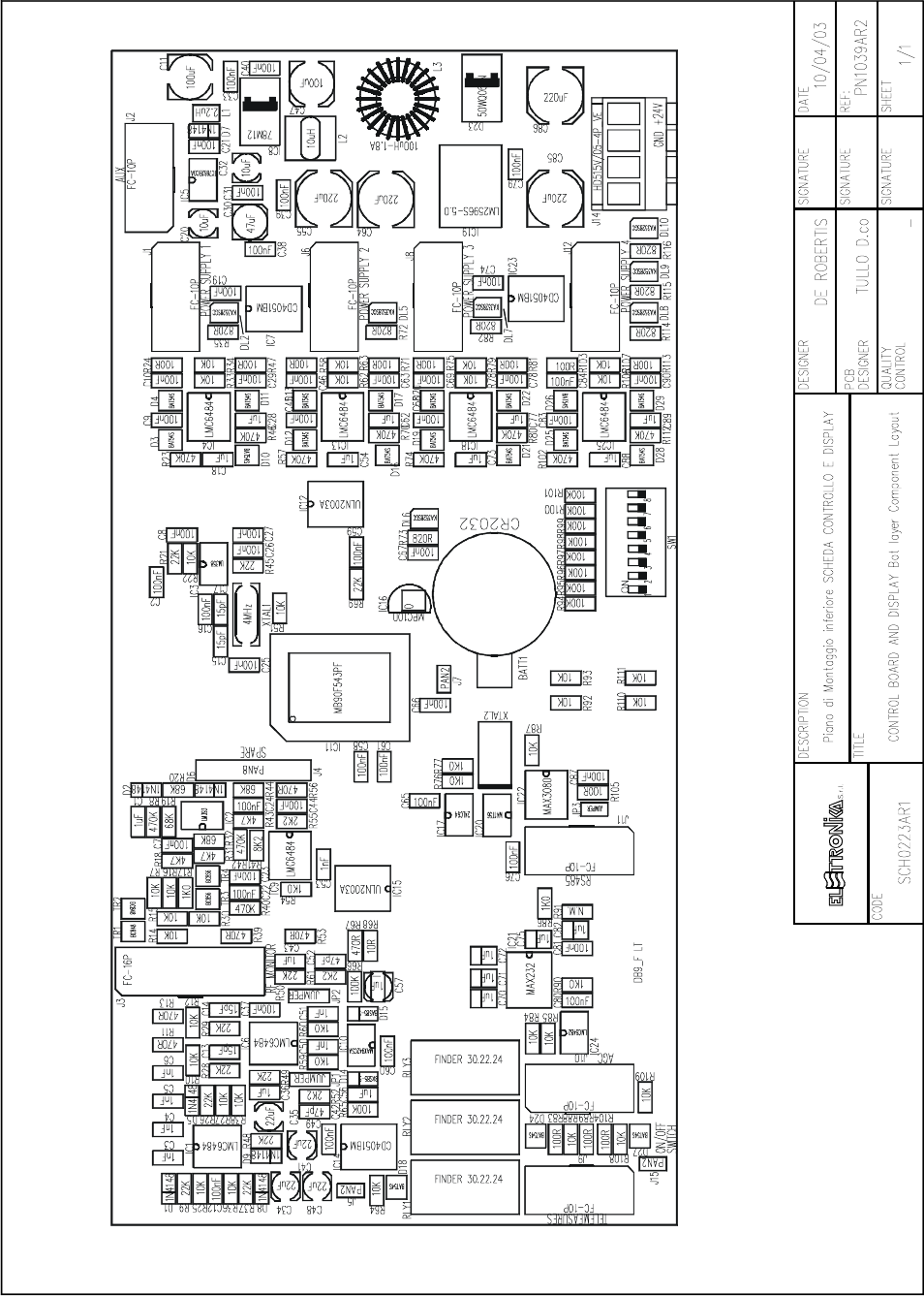
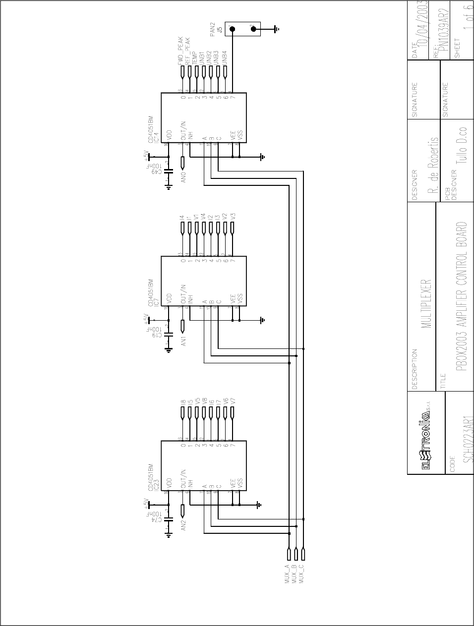
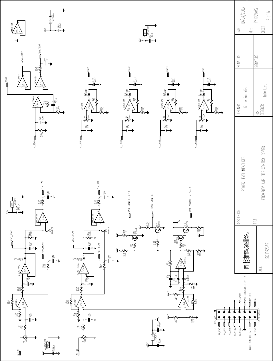
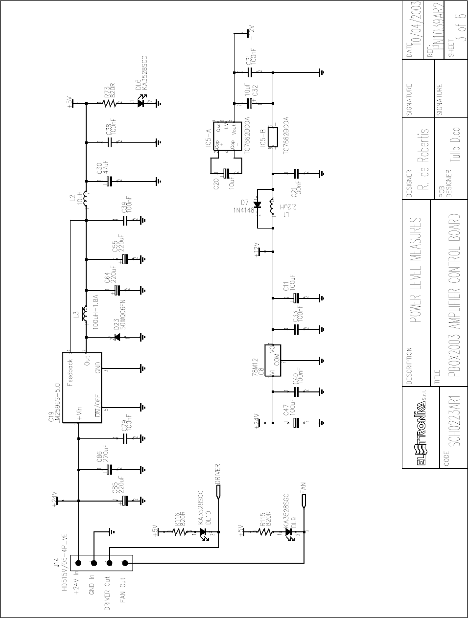
- SCH0223AR1 (Control board and display)
- SCH0288AR0 (Amplifier interface)
- SCH0265AR0 (Mains distribution board)
- E0012 (SP500-27-DI Switching power supply)
34
35
36
37

38
Part Name Code Description Qty
08502 RG 316 50W CABLE 1,30
08521 RG179 BU 75W CABLE 0,27
08527 HF-85 ENDIFORM CABLE 0,25
00028A 82W 1206 SMD RESISTOR 1
01096 1nF CHIP MULT. 2222 863 15102 3
03207 HSMS-2802*TR1 DIODE 3
07904 PASSANTINI TO3 cod. 672.1607 2
07907 MICA x TO22 cod. 542-2822 2
SCH0192AR0 200W LDMOS UHF AMPLIFIER MODULE 4
SCH0295AR0 INTERFACE BOARD 1
PN0998A C.S. PN998AR1 SOMMATORE ALIMENTATORE 1
PN1079A C.S. PN1079AR2 DIVISORE IN 3 VIE 500W UHF 1
PN1078A C.S. PN1078AR4 COMBIN. DUSCITA x 500W UHF 1
PN1083A C.S. PN1083AR2 ACCOPPIATORE INGRESSO 1500W 1
02402 7/16 FEMMINA ANIM. FILET. cod. 0142 1
02512 J01151A0531 PRESA SMA SEN. BAT. 1
01041 1nF COND. CERAMICO 50V 2
01400 C. PAS. 2499-003-X5U0-102M 8
00424 TERMINAZIONE 50W 250W 32-1037-50-5 3
DET0868 DET0868R0 SPESS. ACC. DIR. ING. 1000W UHF 1
DET0842 DET0842R4 DISSIPATORE 700W UHF LDMOS 1
DET0843 DET0843R1 SPOND. LAT. 700W UHF LDMOS 2
DET0844 DET0844 SPOND. ANT. 700W UHF LDMOS 1
DET0845 DET0845R2 SPOND. POST. 700W UHF LDMOS 1
DET0846 DET0846R2 SPOND. CENTR. 700W UHF LDMOS 1
DET0847 DET0847R1 SPESSORE x PN1078A 1
DET0849 DET0849R1 CHIUS. 700W UHF LDMOS P.2670 1
00383 1W SMD RESISTOR 2512 100R 224/0272 6
00403 270W 1W SMD RESISTOR 2512 1% 6
00436 ATTENUATORI 20W PPA 20.6 1
00027A 68W 1206 SMD RESISTOR 2
00041A 1kW 1206 SMD RESISTOR 5% 2
03017 MBR3045PT DIODE 2
07911 MICA IN SIL-PAD x TO3P VA001080 2
07910 PASSANTE x TO220 cod. 672/1606 2
PN1210A C.S. PN1210AR2 ACCOPPIATORE DIREZIONALE 1
DET0805 DET0805R4 PARTICOLARE PRELIEVO MONITORIA 1
DET1059 DET1059R0 ANELLO IN TEFLON x ACCOP. DIREZ. 2
DET0813 DET0813R1 LINEA PART. PRELIEVO MONITORIA 1
DET1058 DET1058R0 CHIUSURA x ACCOP. DIREZIONALE 1
0148 C. PAS. 5000PF 2
Component list MTF0083AR0 Amplifier module

39
Part Name Code Description Qty
05570 GUIDE FOR RACK TAV. 816RB RKG6 560mm ZN 4
05578 RACK 20U RK20 600mm DEPTH 1
APT159A AUTV/500LD LDMOS UHF AMPLIFIER MEANWELL 1
02502 SMA SOCKET FOR RG58/c J01150A0041 1
08504 RG58 50W CABLE 1
CMS6006 1/2 FORM 1mt CABLE 7/16 (M) CONN. BN203391 1
02029 GE35145 D/60 BN (UG909/c FOR RG58) 1
CSS5011 RG58 FROM 1.5mt NM/NM CABLE 1
DET0483 DET0483R0 BAR. PR. 683 REG. PCAV ZN P. 2557 2
DET0631 DET0631R1 ANGOL. FISS. FILTRO FOR 300W CINA 2
PAN0080 PAN0080R0 PANN. FRONT. 1U CON POLICARB. 1
PAN0081 PAN0081R0 PANN. FRONT. 2U CON POLICARB. 2
PAN0082 PAN0082R0 PANN. FRONT. 3U CON POLICARB. 2
06673 500W UHF BANDPASS FILTER mod. CL3NL6 1
Component list APT159B - AUTV/500LD

40
This page is intentionally blank
41
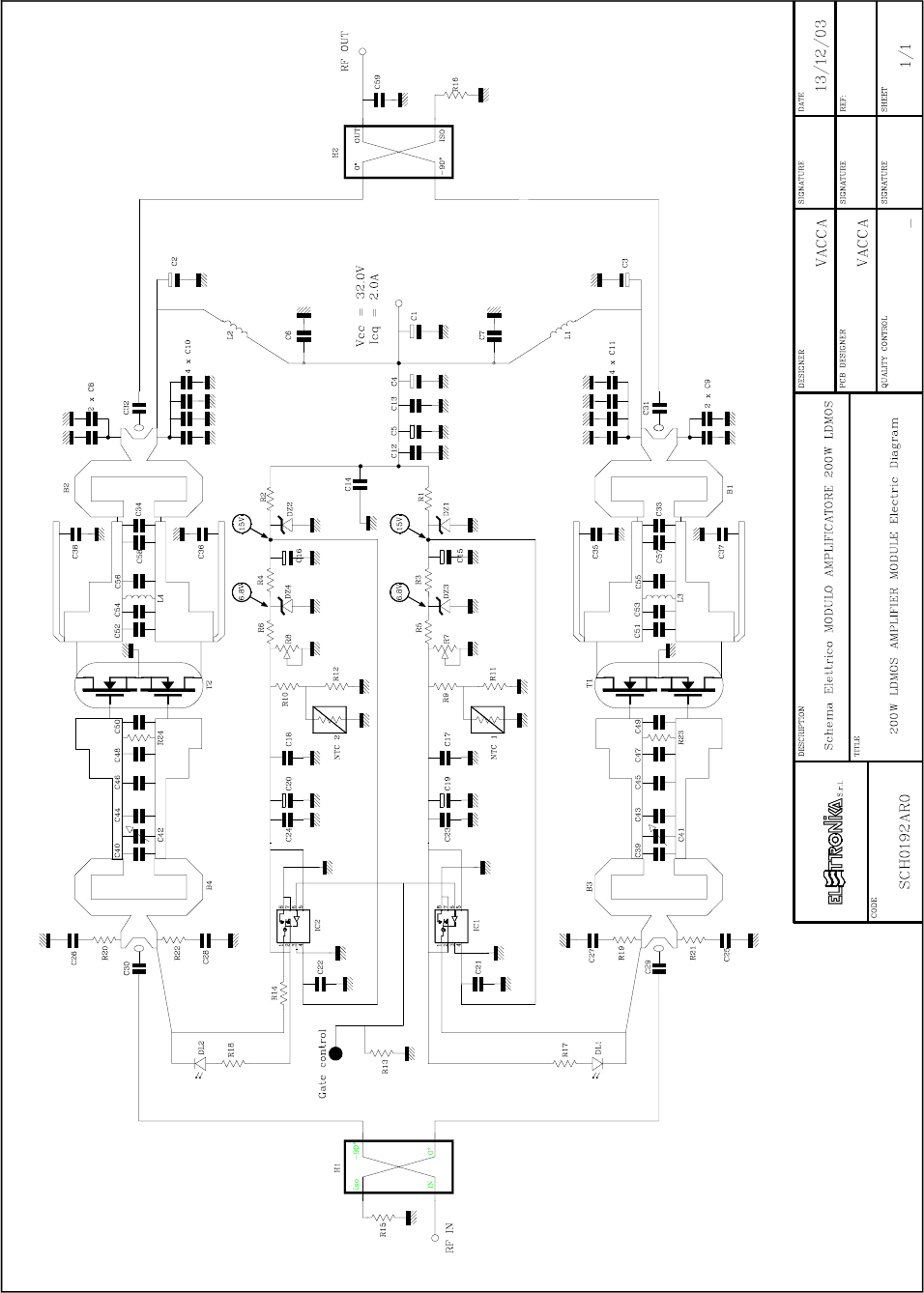
200W UHF LDMOS AMPLIFIER MODULE SCH0192AR0
DESCRIPTION
The RF module is an integrated TV linear amplifier designed for UHF band, this module employs push-pull
LDMOS technology in order to achieve very good efficiency, high linearity and reliability.
LDMOS transistors operate in AB class. It is a wideband amplifier over the full frequency, no adjustment is
required for the channel change. The board includes RF section amplifier, bias circuit, protection circuit and
matching networks. A silver plated copper plate is brazed with PCB in order to obtain low thermal resistance.
Providing a minimum of 200W Pk sync linear power, this module is the perfect amplifier for any broadband
UHF power transmitter.
TECHNICAL CHARACTERISTICS
Output power 300W max
Input power 15W max
Frequency 470 - 860MHz
Gain > 13dB
LDMOS Power supply 32V ±2%
LDMOS Bias current @+32V Vdc 2A
RF Input impedance 50W
RF Output impedance 50W
Input / Output return loss > = 15dB
Drain efficiency 47% @ 250W
Storage temperature range -50° to +150°C
Dimensions (LxWxH) 165x95x29mm
42
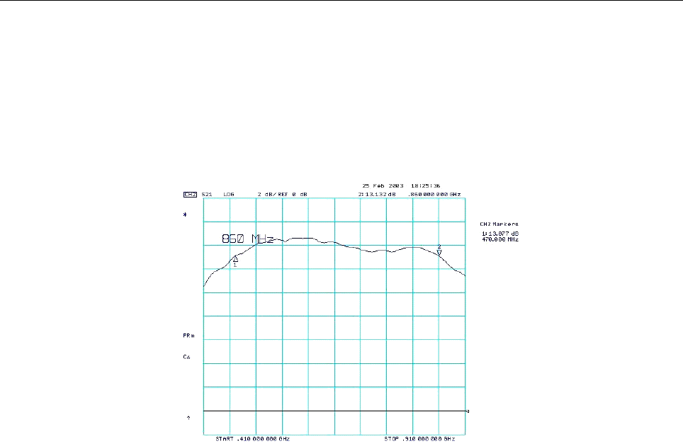
CALIBRATION PROCEDURE
- Technical characteristics
Power supply voltage 32V (± 2%)
Polarisation current 1.0 cold for each device (2A total), ± 0.1A
Gain for low signal Not less than 13dB in the 470-860MHz band (± 1dB)
Compare to the typical curve eclosed
- Adjustment procedure
Polarisation current calibration 32V stabilised power supply
10A amperometer
Gain curve Network analyser
- Adjustment points description
R7-R8 (Trimmers) Adjust the current absorbed in stand-by (1.0A per device)
Middle frequency 660MHz, span 500MHz, 2dB/div., reference to the arrow
- Curve response graphic
43
- Calibration steps
STEP 1. Close the input and the output of the module by connecting them to a 50WW
WW
W dummy load
and connect the spectrum analyser through a directive sample, in order to look for self-oscillation of the
module, if any (anyway the module has been designed so that it would not self-oscillate even if totally de-
coupled, without any input or output load).
STEP 2. Check the voltages of the polarisation circuits without assembling the transistors first:
connect the 32V power supply to the proper turret by means of a fastening screw, then give power and check
data:
- the stabilised voltage on the zener diodes DZ1 and DZ2 is about 15V compared to the ground;
- the stabilised voltage on the zener diodes DZ3 and DZ4 is about 6.8V compared to the ground;
- the voltage on the pads to which the gates of the LDMOS transistors will be soldered (R23 and R24
resistors side) changes from 0V to a maximum value of about 6V when moving the relevant trimmer (R7-R8).
STEP 3. Check the work of the protections.
- Set both trimmers so that there is a value of about 4.5V on the pads of the gates;
- solder some wire to the pad between the two LEDs, next to the serigraphy of the input hybrid H1;
- in order to check the work of the protections aboard, a power of about 4V has to be supplied to the wire,
for example by touching with it the reophore of C23 or C24 which is not connected to ground; the two red
LEDs will immediately light up and the two RF transistors will be switched off at the same time: the polarisation
current (2A) will decrease to 0 and of course the gain curve displayed by the spectrum analyser will decrease;
- after this it is important to restore the position of the two trimmers for the minimum voltage! Then
disconnect the 32V power supply.
STEP 4. Fastening of the LDMOS transistors: after properly cleaning the plate surface, smear a thin
layer of silicone fat on the lower side of the flange of the MOSFETs, fasten them to the heat sink and solder
the gate first, then the drain. Solder the two 13pF (ATC) chip capacitors and above them the two 1-5pF
Solder a wire

44
capacitive trimmers, between the two pair of gates, as shown by the mounting plan.
STEP5. Connect serially a c.c. amperometer to the power supply, with scale starting from more than 5A
(i.e. 10A).
STEP 6. Power the module and check the MOSFET is not absorbing current; this means that the device
is integral and working correctly.
STEP 7. Slowly turn the R7 trimmer until the MOSFET absorbs 1A, always checking that there are no
self-oscillation; under this conditions it is possible to check by means of a digital tester that the voltage on the
gate is about 5.2-5.4V.
STEP 8. Repeat the previous step for the other section of the module, this time turnign R8 and checking
that the indication of the current on the amperometer increases to 2A total (which includes the current of the
other device left on).
STEP 9. Check the response curve of the module by means of the network analyser.
STEP 10. Check the response curve for low signal with centre 660MHz and span 500MHz, 2dB/div.
STEP 11. The curve should be similar to the one enclosed, with a tolerance of ± 0.5dB. To obtain this, act
on the four trimmers C41-C41a and C42-C42a with the proper calibrator, inorder to flatten the curve as
much as possible, especially at the edged of the band which represents the minimum values.
STEP 12. Finally, check that the current in stand-by does not increase by more than 15÷20%, reaching at
worst 2.3÷2.4A when the heat sink is hot and not ventilated.
Note: when mounting-removing the PALLET on the heat sink, tightly fasten the screw of each all N input and output
connectors. These are mounted with a single 3mm screw and if it is not properly fastened it may be detached from the PCB
by a movement of the connector once it has already been soldered to the path.
45
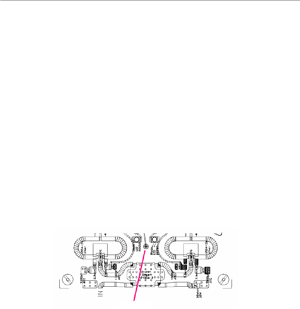
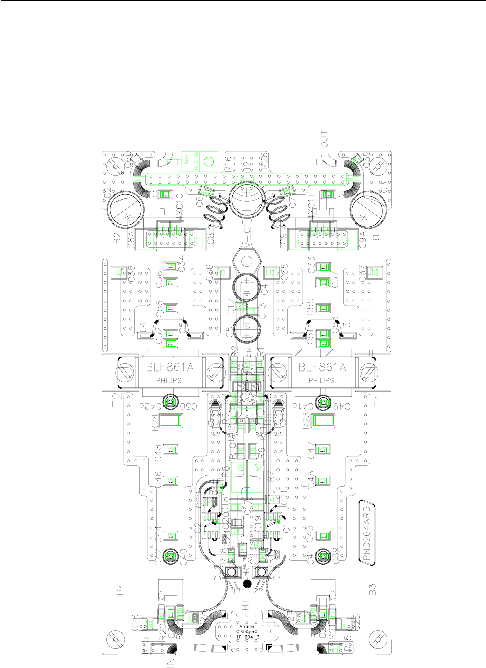
Component layout SCH0192AR0
46

47
COMPONENT LIST SCH0192AR0
REF. DESCRIPTION ELETTRONIKA CODE Page 1/3
R1 2200W 1/4W 1206 SMD RESISTOR 00045A
R2 2200W 1/4W 1206 SMD RESISTOR 00045A
R3 2200W 1/4W 1206 SMD RESISTOR 00045A
R4 2200W 1/4W 1206 SMD RESISTOR 00045A
R5 1200W 1/4W 1206 SMD RESISTOR 00042A
R6 1200W 1/4W 1206 SMD RESISTOR 00042A
R7 50kW MULTITURNS PTH TRIMMER 00800
R8 50kW MULTITURNS PTH TRIMMER 00800
R9 1200W 1/4W 1206 SMD RESISTOR 00042A
R10 1200W 1/4W 1206 SMD RESISTOR 00042A
R11 18kW 1/4W 1206 SMD RESISTOR 00056B
R12 18kW 1/4W 1206 SMD RESISTOR 00056B
R13 680KW 1/4W 1206 SMD RESISTOR 00075A
R14 0W 1/4W 1206 SMD RESISTOR 00001
R15 50W 30W 1512EBX SMD RESISTOR 00416A
R16 50W 60W 00432
R17 4.7kW 1/4W 1206 SMD RESISTOR 00049A
R18 4.7kW 1/4W 1206 SMD RESISTOR 00049A
R19 3.9W 1/4W 1206 SMD RESISTOR 00012A
R20 3.9W 1/4W 1206 SMD RESISTOR 00012A
R21 3.9W 1/4W 1206 SMD RESISTOR 00012A
R22 3.9W 1/4W 1206 SMD RESISTOR 00012A
R23 1000W 1W 2512 SMD RESISTOR 00396
R24 1000W 1W 2512 SMD RESISTOR 00396
*R25 = R15 (da montare se si inverte lingresso)
*R26 = R26 (da montare se si inverte luscita)
C1 470uF 50V PTH ELECTROLYTIC CAPACITOR 01807B
C2 470uF 50V PTH ELECTROLYTIC CAPACITOR 01807B
C3 470uF 50V PTH ELECTROLYTIC CAPACITOR 01807B
C4 100uF 50V PTH ELECTROLYTIC CAPACITOR 01795
C5 100uF 50V PTH ELECTROLYTIC CAPACITOR 01795
C6 1nF ATC 100B CAPACITOR OR EQUIVALENT 01145
C7 1nF ATC 100B CAPACITOR OR EQUIVALENT 01145
C8 x 2 2 x 100nF ATC CAPACITOR OR EQUIVALENT 01065H
C9 x 2 2 x 100nF ATC CAPACITOR OR EQUIVALENT 01065H
C10 x 4 4 x 100pF ATC 100B CAPACITOR OR EQUIVALENT 01135
C11 x 4 4 x 100pF ATC 100B CAPACITOR OR EQUIVALENT 01135
C12 100nF 1210 SMD CAPACITOR 1065G
C13 100nF 1210 SMD CAPACITOR 1065G
C14 100nF 1210 SMD CAPACITOR 1065G
C15 1uF 35V SMD TANTALIUM CAPACITOR 01613A
C16 1uF 35V SMD TANTALIUM CAPACITOR 01613A
C17 100nF 1210 SMD CAPACITOR 1065G

48
REF. DESCRIPTION ELETTRONIKA CODE Page 2/3
C18 100nF 1210 SMD CAPACITOR 1065G
C19 10uF 16V SMD TANTALIUM CAPACITOR 01626A
C20 10uF 16V SMD TANTALIUM CAPACITOR 01626A
C21 100nF 1210 SMD CAPACITOR 1065G
C22 100nF 1210 SMD CAPACITOR 1065G
C23 100nF 1210 SMD CAPACITOR 1065G
C24 100nF 1210 SMD CAPACITOR 1065G
C25 1nF ATC 100B CAPACITOR OR EQUIVALENT 01145
C26 1nF ATC 100B CAPACITOR OR EQUIVALENT 01145
C27 1nF ATC 100B CAPACITOR OR EQUIVALENT 01145
C28 1nF ATC 100B CAPACITOR OR EQUIVALENT 01145
C29 20pF ATC 100B CAPACITOR OR EQUIVALENT 01123
C30 20pF ATC 100B CAPACITOR OR EQUIVALENT 01123
C31 20pF ATC 100B CAPACITOR OR EQUIVALENT 01123
C32 20pF ATC 100B CAPACITOR OR EQUIVALENT 01123
C33 1.3pF ATC 100B CAPACITOR OR EQUIVALENT 01104
C34 1.3pF ATC 100B CAPACITOR OR EQUIVALENT 01104
C35 470pF ATC 100B CAPACITOR OR EQUIVALENT 01143
C36 470pF ATC 100B CAPACITOR OR EQUIVALENT 01143
C37 470pF ATC 100B CAPACITOR OR EQUIVALENT 01143
C38 470pF ATC 100B CAPACITOR OR EQUIVALENT 01143
C39 4.7pF ATC 100B CAPACITOR OR EQUIVALENT 01108
C40 4.7pF ATC 100B CAPACITOR OR EQUIVALENT 01108
C41 x 2 2 x 1¸5pF JOHANSON SMD TRIMMER 1485
C42 x 2 2 x 1¸5pF JOHANSON SMD TRIMMER 1485
C43 3.6pF ATC 100B CAPACITOR OR EQUIVALENT 01104B
C44 3.6pF ATC 100B CAPACITOR OR EQUIVALENT 01104B
C45 6.8pF ATC 100B CAPACITOR OR EQUIVALENT 01111
C46 6.8pF ATC 100B CAPACITOR OR EQUIVALENT 01111
C47 6.8pF ATC 100B CAPACITOR OR EQUIVALENT 01111
C48 6.8pF ATC 100B CAPACITOR OR EQUIVALENT 01111
C49 13pF ATC 100B CAPACITOR OR EQUIVALENT 01119A
C50 13pF ATC 100B CAPACITOR OR EQUIVALENT 01119A
C51 8.2pF ATC 100B CAPACITOR OR EQUIVALENT 01113
C52 8.2pF ATC 100B CAPACITOR OR EQUIVALENT 01113
C53 8.2pF ATC 100B CAPACITOR OR EQUIVALENT 01113
C54 8.2pF ATC 100B CAPACITOR OR EQUIVALENT 01113
C55 10pF ATC 100B CAPACITOR OR EQUIVALENT 01117
C56 10pF ATC 100B CAPACITOR OR EQUIVALENT 01117
C57 4.7pF ATC 100B CAPACITOR OR EQUIVALENT 01108
C58 4.7pF ATC 100B CAPACITOR OR EQUIVALENT 01108
C59 0.3pF ATC 100B CAPACITOR OR EQUIVALENT 01160
T1 BLF861A RF LDMOS POWER TRANSISTOR 04034
T2 BLF861A RF LDMOS POWER TRANSISTOR 04034
B1 COAX 2:1 BALUN 08491

49
REF. DESCRIPTION ELETTRONIKA CODE Page 3/3
B2 COAX 2:1 BALUN 08491
B3 COAX 4:1 BALUN 08492
B4 COAX 4:1 BALUN 08492
L1 4 TURNS SILV. COP. WIRE 1.2mm WOUND ON OD 5mm 07684
L2 4 TURNS SILV. COP. WIRE 1.2mm WOUND ON OD 5mm 07684
L3 ½ TURN COIL
L4 ½ TURN COIL
H1 HYBRID COUPLER 3dB 90° ANAREN 05368
H2 HYBRID COUPLER 3dB 90° SAGE 05369
NTC1 NTC 100KW PTH 00661
NTC2 NTC 100KW PTH 00661
IC1 DG419DY 04583
IC2 DG419DY 04583
DZ1 15V SMD ZENER DIODE 03135
DZ2 15V SMD ZENER DIODE 03135
DZ3 6.8V SMD ZENER DIODE 03137
DZ4 6.8V SMD ZENER DIODE 03137
DL1 SMD LED DIODE - RED - 03056
DL2 SMD LED DIODE - RED - 03056
PN964AR3 PCB 0643K
Torretta 3x10 f/f V0774
Imballo velapack 200x125x50 09983
50
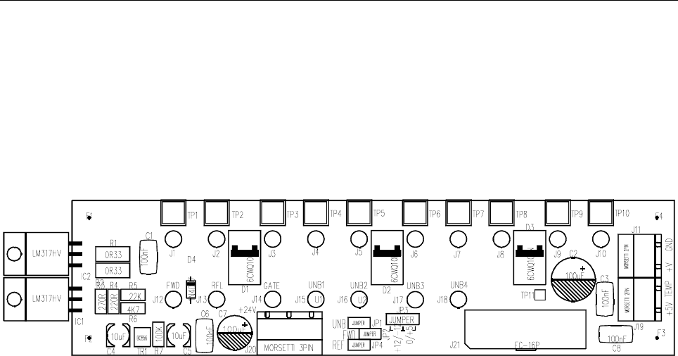
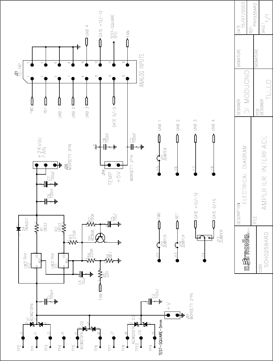
RF AMPLIFIER INTERFACE SCH0259AR0
Component layout SCH0259AR0
COMPONENT LIST SCH0259AR0
Part Name/Number Description Qty. Comps.
CC 100nFAVX 01065A 01065A CERAMIC COND 4 C1, C3, C6, C8
CE 100uF100V 01795B ELETT. COND. 1 C2
CE 100uF50V 01795 01795 ELETT. COND. 1 C7
CE 10uF35V-S 01778A 01778A ELETTR SMD COND 2 C4-5
D 1N4007 03009 03009 DIODE 1 D4
D 6CWQ10FN 03026 SMD DIODE SCHOTTKY 3,5A 3 D1-3
IC LM317HV 04340A INTEG CIRCUIT 2 IC1-2
J FC-16P 02701-02700 02701+02700 PCB CONNECTOR POL 1 J21
J SCREWCONN2 02853 02853 PCB SCREW CONNECTOR 2 J11, J19
J SCREWCONN3 02860 02860 PCB SCREW CONNECTOR 1 J20
J TESTP1.3mm 07913 07913 TEST POINT 17 J1-10, J12-18
JU JUMP2 02739-02742 02739+02742 MASCHIO PAN2 3 JP1-2, JP4
JU JUMP3 02707-02742 02707+02742 MASCHIO PAN3 1 JP3
R 0R33-1W-S 00380 RES 1W 5% SMD 2512 2 R1-2
R 100K-S 00065A 00065A RES 1/4W 5% SMD 1206 1 R7
R 220R-S 00033A 00033A RES 1/4W 5% SMD 1206 1 R4
R 22K-S 00057A 00057A RES 1/4W 5% SMD 1206 1 R5
R 270R-S 00034A 00034A RES 1/4W5% SMD 1206 1 R3
R 4K7-S 00049A 00049A RES 1/4W 5% SMD 1206 1 R6
TR BC856 03455 03455 PNP SMD TRANSISTOR 1 TR1
51
52
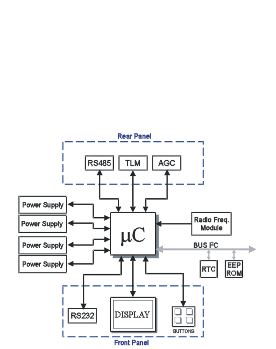
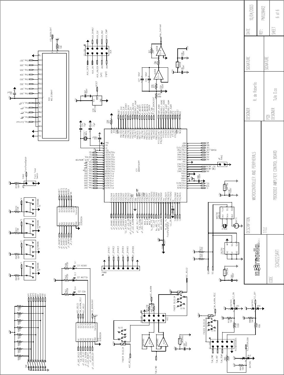
Figure 1: Simplified block diagram of the control and display board
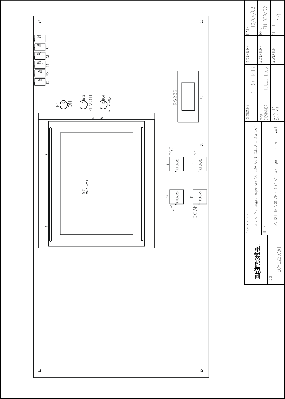
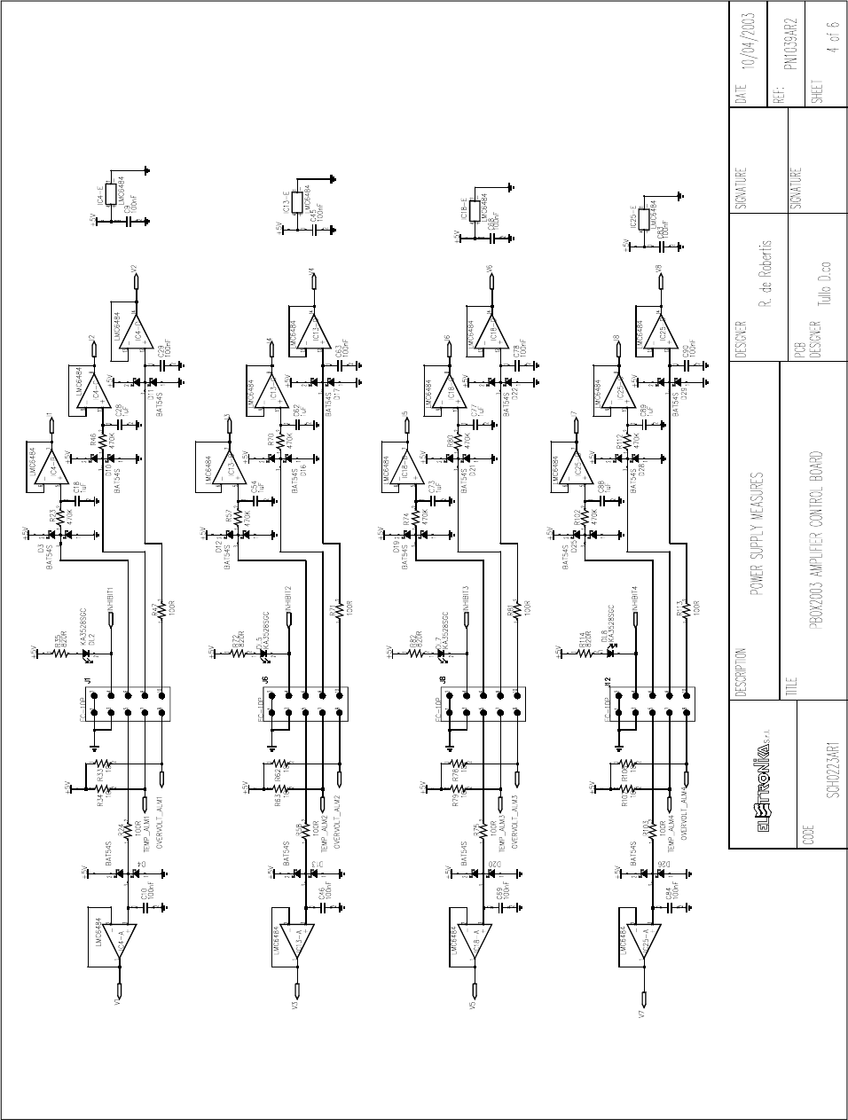
CONTROL BOARD AND DISPLAY SCH0223AR1
DESCRIPTION
The control board SCH0223AR1 manages the operational logic of the amplifier: switching on and off, power
supply and fans, alarms and protections, remote control, human-machine interface. All of that is performed by
a modern and powerful 16 bit micro-controller, which is the main part of the board.
Figure 1 shows the block diagram.
53
It can be seen that the micro-controller is the heart of the control system, to which the various peripherals
(power supply, serial ports, telemeasure socket, AGC port, RF amplifier module, ROM, clock, display and
keys) are interfaced.
- Power Supply
The board is powered with a continuous +24V voltage applied on the J14 connector. From that the +5V
voltage, powering the most of the chips (micro-controller, operational amplifiers, display, etc.) is derived by
means of a switching converter (see IC19). A +12Vdc voltage is obtained from it as well, by means of a linear
conversion provided by the integrated circuit IC8. From this, a -12Vdc voltage is obtained by means of the
integrated circuit IC5. The -12V voltage is used to adjust the contrast of the display.
- Connectors
On the board SCH0223AR1 there are several connectors used as interfaces for the peripherals of the apparatus
and the ports for external communication.
POWER SUPPLY
The connectors J1, J6, J8 e J12 are used to connect the power supply powering the RF modules. The number
of power supply used changes depending on the amplifier, up to eight power supply. They are connected in
the order shown in Table 1 below. Remaining connectors, if any, are left unconnected.
Table 1: Interface connectors for the power supply
Through this connection, each power supply provides the level of voltage and current acquired by the micro-
controller by means of an internal ADC. Besides the connectors allow the control board to turn on or off the
individual power supply (for instance when an alarm occurs).
CONNECTOR POWER SUPPLY N°
J1 1 - 2
J6 3 - 4
J8 5 - 6
J12 7 - 8
54
RF AMPLIFICATION
The J3 connector interfaces the control board with the RF amplification section. Through this connector the
micro-controller acquires the forward and reflected powers, unbalancing (if any), and temperature of the
critic amplification area. It also allows to inhibit the transistors in case of reflected power alarm, by means of
a totally hardware, thus extremely fast protection.
Depending on the apparatus, this connector may also allow to enable or disable the cooling fans of the critic
area.
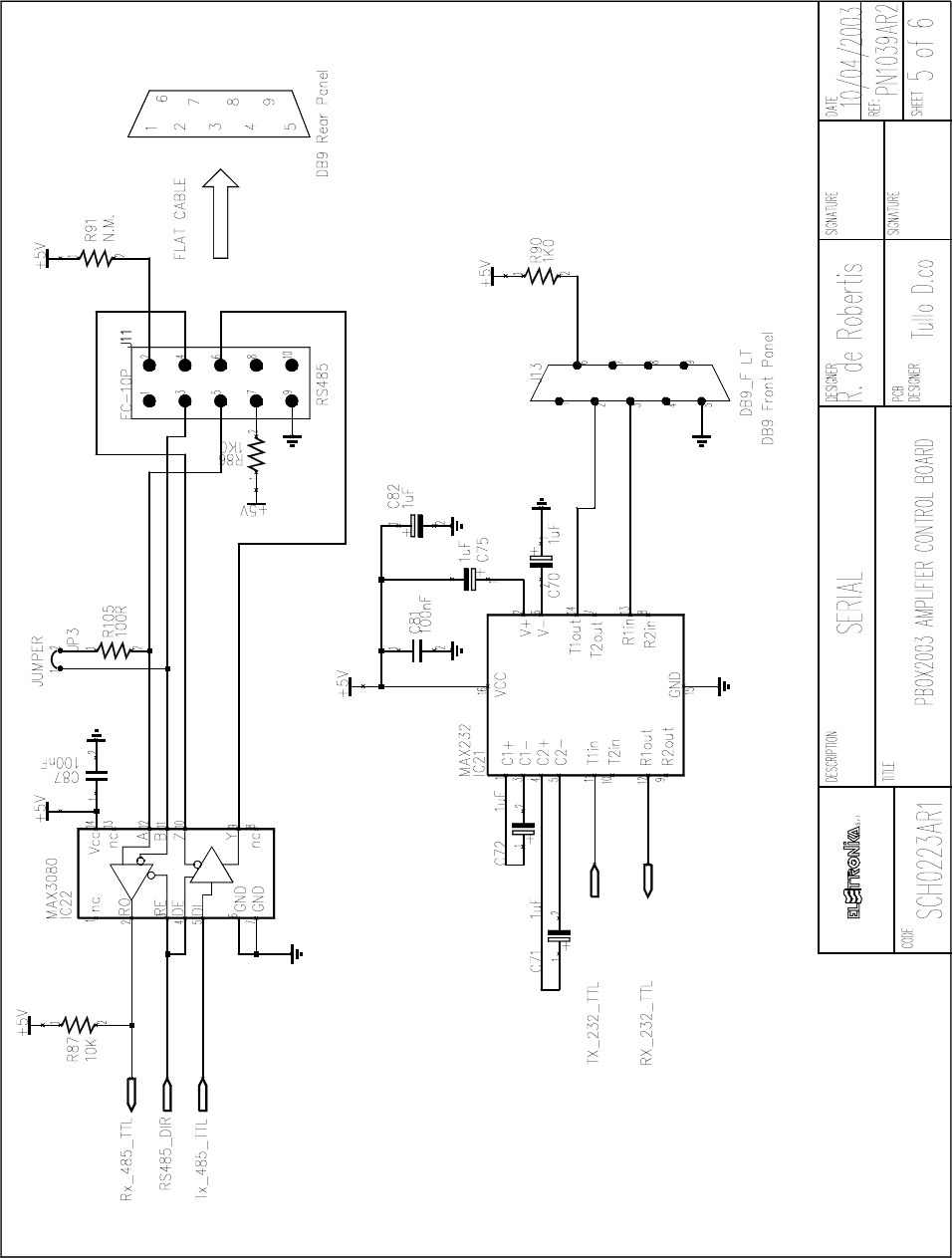
RS485
The J11 connector (10 pin socket) is directly wired to a DB9 female connector placed on the rear panel of the
apparatus. This communication bus allows to connect the amplifier to the control (Amplifier Control) module
of a high-power transmitter composed by several individual amplifiers. In this case, each amplifier and the
Amplifier Control are connected to the same 4-wires RS485 bus and each of them has a unique address
(which can be set by means of the keys and the display) for correct communication.
In case of single (stand-alone) amplifier, the RS485 connector can be used to interface to the Remote Control
Unit (RCU) made by Elettronika S.r.l. This unit allows to monitor and control the remote transmitter from any
site provided with PSTN or GSM1 phone connection.
Table 2 shows the wiring between the J11 connector on the board and the DB9 female connector on the rear
panel, along with the description of the lines.
1 For more details about the control system contact the distributor or the manufacturer.
PIN N°
ON DB9
PIN N°
ON J11 DESCRIPTION
11 Not used
23 Rx-
35 Rx+
47 +5V
59 GND
62 Not used
74 Tx-
86 Tx+
98 Not used
Table 2: Description of the RS485 connector
55
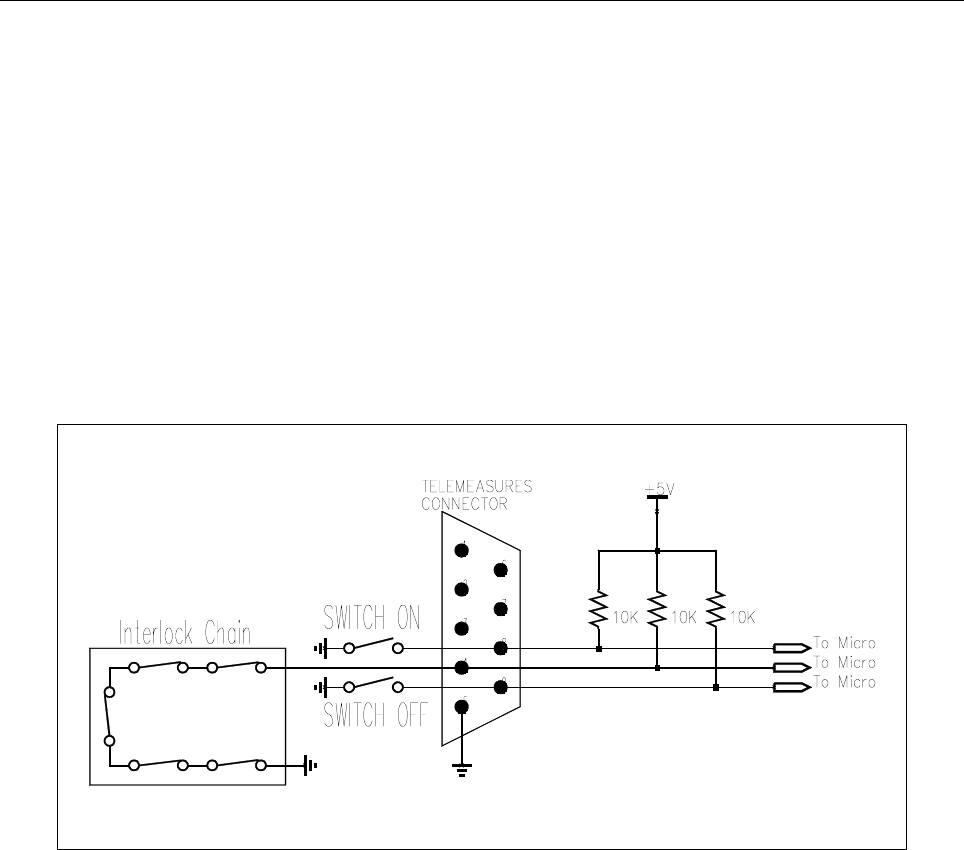
TELEMEASURES
The J9 telemeasure connector (10 pins socket) is directly wired on a DB9 female connector placed on the
rear panel. There are input and output digital lines (TTL level) and analog output lines on this connector, which
are used to monitor and control the amplifier by means of a general-purpose remote control system.
The correspondence between the pins of the J9 connector on the board and the DB9 female connector on the
rear panel, as well as the meaning of the various lines, is shown in table 3 below (the directions are in respect
to the micro-controller on the board).
Table 3: Description of the telemeasures connector
The input stage of the digital pins has an internal pull-up towards the 5V power supply voltage. To use these
lines it only takes setting a switch to close to earth. When closed, the relevant control (turning on or off) is
enabled and the switch may be open again (impulse controls).
The interlock pin may be used as protection so that the amplifier is switched off when the digital input level is
low. It is possible to use several serially connected switches to make an interlock chain. Usually all switches
are closed and the interlock level is low, thus the amplifier is on. If even only one of the switches is open, the
(*)
(*)
(*) You can select by means of two jumpers on the board (JP1 and JP2) RMS or peak power. If there are two jumpers on pins 1 and 2 of
JP1 and JP2 connectors, RMS power is selected. Otherwise, if there are two jumpers on pins 2 and 3 of the same connectors, peak power
is selected.
PIN N°
ON DB9
PIN N°
ON J9 TYPE DIRECTION DESCRIPTION
1 1 Analog Output Forward power
2 3 Analog Output Reflected power
3 5 Analog Output Temperature
4 7 Digital Input
Interlock:
0V = Interlock Alarm
5V = Normal
59 - -Ground
6-7 2-4 Digital Output Free Contact
(closed when amplifier is in alarm)
8 6 Digital Input Turning-on control
(normally high, active when low)
9 8 Digital Input Turning-off control
(normally high, active when low)
56
Figure 2: Usage of the digital input signals of the telemeasures connector
AGC / EXCITER
The connector called J10, as the telemeasures connector and the RS485 bus, is wired to a DB9 female
connector placed on the rear panel of the amplifier. This connector allow the implementation of an automatic
gain control between an exciter and the amplifier. A voltage signal related to the forward output power
supplied by the amplifier is provided through two pins of the AGC connector. Connecting one of these to the
relevant input pin of the exciter, this can pursuit a given voltage level, so that the output power is always
constant. In order to avoid that, in case of an alarm decreasing the forward power, the exciter increases its
output level due to the AGC, thus damaging the amplification stages, the connector is provided with two
digital output lines called AGC Alarm. Under alarm conditions, this lines are brought by the micro-controller
at a low level, so that the exciter can stop the AGC.
Table 4 shows the connection between the J10 connector on the board and the DB9 connector on the rear
panel, along with the description of each pin (the direction of the pin is referred to the position of the micro-
controller on the board).
level of the interlock signal becomes high (this line has a pull-up towards the +5V power supply voltage as
well) and the interlock protection activates switching off the amplifier. Note that in case the interlock protection
is not used, the pin 4 of the DB9 telemeasure connector and the earth pin (pin 5) must be short circuited.
Otherwise it is possible to disable the monitoring of the interlock chain from menu (see user manual).
Figure 2 shows a typical usage for the digital input signals to turn on and off the amplifier and for the interlock
alarm.
57
Table 4: Description of the AGC connector
RS232
The DB9 female connector on the front panel is an external communication RS232 serial port, through which
a PC can be connected directly to the amplifier in order to perform operations such as the remote control (by
means of an adequate software2) and the update of the microcontroller firmware.
The used communication protocol is asynchronous, at a 19200bps speed, 1 start bit, 8 data bits, 1 stop bit,
no parity. No hardware flow control is used. The connector is DCE type and the pin used are shown in Table
5.
PIN N° ON DB9 123456789
DESCRIPTION -TxDRxD-GND----
MISCELLANEOUS
The J2 (called AUX), J4, J5 and J17 connectors are not used and are there only for future updates. The SW1
dip-switches are partially used for the configuration of the correct mode for the micro-controller. The other
switches are not used. It is important that the position of the dip-switches is left unchanged, because changing
it may set a wrong mode for the micro-controller, affecting the work of the whole amplifier.
2 For more information about this application contact the distributor of the manufacturer.
PIN N°
ON DB9
PIN N°
ON J10 TYPE DIRECTION DESCRIPTION
11- -Ground
23DigitalOutput
AGC Alarm
0V = Alarm
5V = Normal
35DigitalOutput
AGC Alarm
0V = Alarm
5V = Normal
47- -Not used
59 - -Not used
62 - -Not used
7 4 - - Nout used
8 6 Analog Output Forward power
9 8 Analog Output Forward power
Table 5: Description of the RS232 connector
58
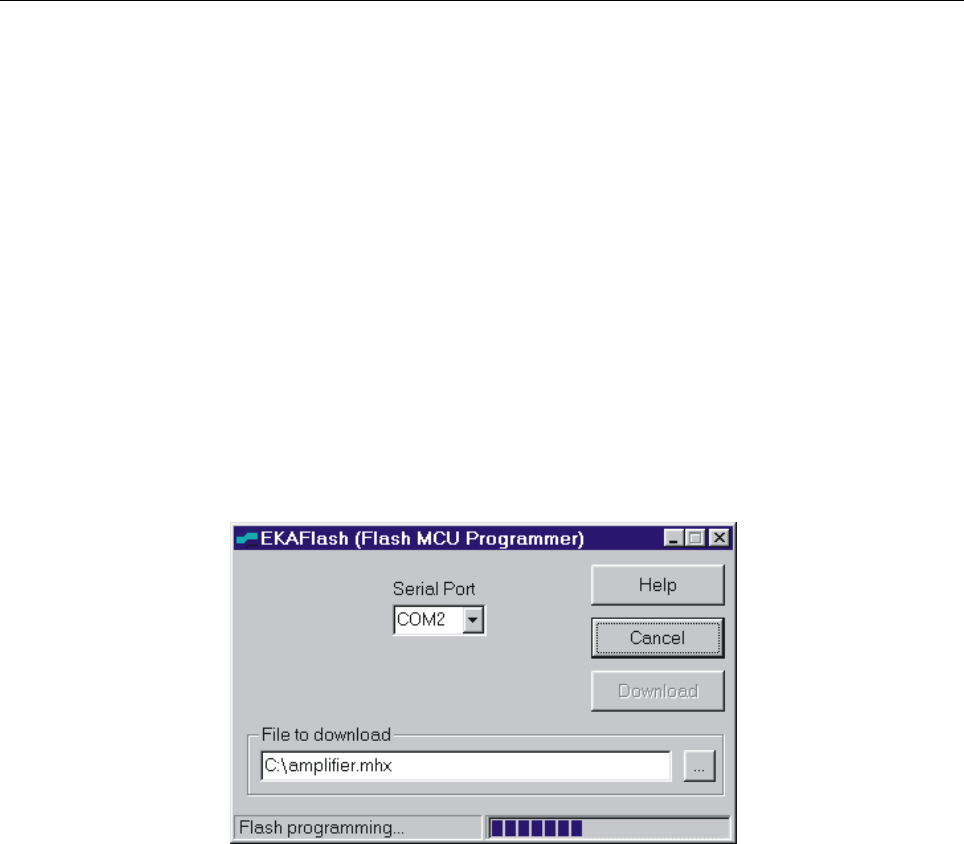
FIRMWARE UPDATE
The microcontroller is provided with a built-in Flash memory containing the firmware. The firmware can be
updated with a later version without removing the apparatus from the rack and/or replacing the chip.
To upgrade it, connect a PC to the RS232 socket on the front panel of the apparatus by means of a cable
DB9 male - DB9 female (pin-to-pin).
Launch on the PC the EKAFlash application, select the serial port in use on the PC, choose the update file by
pressing the ... key and click on Download button.
Eventually, turn off the amplifier from the main switch and then turn it on again. The upgrade of the firmware
begins on the EKAFlash window. Fifure 3 shows this window while a firmware is being updated.
Figure 3: The EKAFlash window while updating a firmware
59
60
61
62
63
64
65
66

67
COMPONENT LIST SCH0223AR1
Part Name/Number Description Qty. Comps. Page 1/2
BATT BH001RB 3093_90 03093 03090 BATTERY HOLDER 1 BATT1
CC 100nF-S 01065C 01065C Y5V 1206 COND 46 C2, C7-10, C12, C16, C19, C21-27
C29, C31, C33, C37-40, C44-46,
C49, C58-61, C63, C65-69, C74,
C76, C78-81, C83-84, C87, C90
CC 15pF-S 01088 01088 SMD 1206 COND 4 C13-15, C17
CC 1nF-S 01096 01096 SMD 1206 COND 7 C3-6, C50-51, C53
CC 1uF100V-S 01760A 01760A Y5V 1206 COND 13 C1, C18, C28, C36, C43, C54,
C56-57, C62, C73, C77, C88-89
CC 47pF-S 01100 01100 SMD 1206 COND 2 C42, C52
CE 100uF25V-S 01793B 01793B ELETTR SMD COND 2 C11, C47
CE 10uF35V-S 01778A 01778A ELETTR SMD COND 2 C20, C32
CE 1uF35V-S 01613A 01613A TANTALIUM ELETTR SMD CO 5 C70-72, C75, C82
CE 220uF50V LOW ESR 1799A ELETTR SMD COND LOW ESR 4 C55, C64, C85-86
CE 22uF16V-S 01780A ELETTR SMD COND 4 C34-35, C41, C48
CE 47uF35V-S 01790A 01790A ELETTR SMD COND 1 C30
D 1N4148-S 03002 03002 SMD DIODE 7 D1-2, D5-9
D 50WQ06FN 03019A SMD DIODE SCHOTTKY 5,5A 1 D23
D BAS85-S 03024 SMD DIODE SCHOTTKY 2 D14-15
D BAT54S 03199 SMD SCHOTTKY DIODE A-K T 19 D3-4, D10-13, D16-22, D24-29
DIS MGLS12864T 03083A 128x64 DOT (BLUE-LED WH 1 DIS1
DL KA-3528SGC 03057 03057 GREEN SMD LED DIODE 7 DL2, DL5-10
DL LEDG5 03060 03060 GREEN LED DIODE 5mm 1 DL1
DL LEDR5 03061 03061 RED LED DIODE 5mm 1 DL4
DL LEDY5 03054B 03054B YELLOW LED DIODE 5mm 1 DL3
IC 24LC64 04815 04815 SMD INTEG CIRCUIT 1 IC17
IC 78M12 4307B 04307B SMD VOLTAGE REGULATOR 1 IC8
IC CD4051BM-S 04615 SMD INTEG CIRCUIT 3 IC7, IC14, IC23
IC LM2596S-5.0 04580 SMD INTEG CIRCUIT 1 IC19
IC LM358M-S 04660 04660 SMD INTEG CIRCUIT 1 IC3
IC LM393-S 04639 04639 SMD INTEG CIRCUIT 1 IC2
IC LMC6482-S 04632 SMD INTEG CIRCUIT 1 IC24
IC LMC6484-S 04634 SMD INTEG CIRCUIT 7 IC1, IC4, IC6, IC9, IC13, IC18,
IC25
IC M41T56 04611 04611 SMD INTEG CIRCUIT 1 IC20
IC MAX232-S 04804B 04804B SMD INTEG CIRCUIT 1 IC21
IC MAX3080-S 04770 04770 SMD INTEG CIRCUIT 1 IC22
IC MAX942CSA-S 04572 SMD INTEG CIRCUIT 1 IC10
IC MB90F543PF 04596 SMD INTEG CIRCUIT 1 IC11
IC MPC100-450DI-TO 04608 INTEG CIRCUIT 1 IC16
IC TC7662BCOA 04758A 04758A SMD INTEG CIRCUIT 1 IC5
IC ULN2003A 4870 04870 SMD INTEG CIRCUIT 2 IC12, IC15
IND 2u2H-S 05020A 05020A INDUCTOR 1 L1

68
Part Name/Number Description Qty. Comps. Page 2/2
IND MS85 10uH-S 04948 INDUCTOR 2,7 A 1 L2
IND T100uH-1.8A 4958 04958 TOROIDAL-STORAGE CHOKES 1 L3
J CON HD515V/05-4PVE 02881 + 02882 PANDUIT PCB CONN 1 J14
J DB9_F-0° LT 02794 PCB CONNECTOR DB9 LONG T 1 J13
J FC-10P 02697-02699 02697+02699 PCB CONNECTOR POL 8 J1-2, J6, J8-12
J FC-16P 02701-02700 02701+02700 PCB CONNECTOR POL 1 J3
J PAN2 02739-40-41 02739+02740+02741 PCB CONNECTO 3 J5, J7, J15
J PAN8 02716 02716 PCB CONNECTOR 1 J4
JU JUMP2 02739-02742 02739+02742 MASCHIO PAN2 1 JP3
JU JUMP3 02707-02742 02707+02742 MASCHIO PAN3 2 JP1-2
R 100K-1%-S 00065B 00065B RES 1/4W 1% SMD 1206 10 R65-66, R94-101
R 100R-1%-S 00029D 00029D RES 1/4W 1% SMD 1206 12 R24, R47, R58, R71, R75,R81,
R83, R89, R103-105, R113
R 10K-1%-S 00053B 00053B RES 1/4W 1% SMD 1206 32 R7, R10, R12, R14-16, R22, R25,
R27, R30, R33-34, R36, R38, R51,
R62-64, R78-79, R84-85, R87-88,
R92-93, R106-111
R 10R-S 00017A 00017A RES 1/4W 5% SMD 1206 1 R68
R 1206 NOT MOUNTED NOT MOUNTED RES 1/4W 5% SMD 12 1 R91
R 1K0-1%-S 00041B 00041B RES 1/4W 1% SMD 1206 8 R17, R54, R59-60, R76-77, R86,
R90
R 22K-1%-S 00057B 00057B RES 1/4W 1% SMD 1206 11 R9, R21, R26, R28-29, R37, R45,
R48-50, R69
R 2K2-1%-S 00045B 00045B RES 1/4W 1% SMD 1206 3 R52, R55, R61
R 470K-S 00073A 00073A RES 1/4W 5% SMD 1206 11 R8, R23, R40, R42, R46, R57, R70
R74, R80, R102, R112
R 470R-1%-S 00037B 00037B RES 1/4W 1% SMD 1206 6 R11, R13, R39, R53, R56, R67
R 4K7-1%-S 00049B 00049B RES 1/4W 1% SMD 1206 3 R18, R31, R43
R 68K-1%-S 00063B 00063B RES 1/4W 1% SMD 1206 4 R19-20, R32, R44
R 820R-S 00040A 00040A RES 1/4W 5% SMD 1206 7 R35, R72-73, R82, R114-116
R 8K2-1%-S 00052B 00052B RES 1/4W 1% SMD 1206 1 R41
RL 30.22.24 07569 07569 RELE 3 RLY1-3
RV 100K-3266X 00814 VARIABLE RESISTOR 4 R1-4
RV 10K-3266X 00807 00807 VARIABLE RESISTOR 2 R5-6
SW SWITCH-8DIP 07530A PCB DIP SWITCH SMD 1 SW1
T 06086 N 7630 7632 7630 7632 KTI06086 PULSANTE 2 4 T1-4
TR BC848 03457 03457 NPN SMD TRANSISTOR 2 TR1-2
TR BC856 03455 03455 PNP SMD TRANSISTOR 2 TR3-4
XTAL 32.768k-S 05146 05146 QUARTZ 1 XTAL2
XTAL 4MHz-S 05101A 05101A QUARTZ 1 XTAL1
69
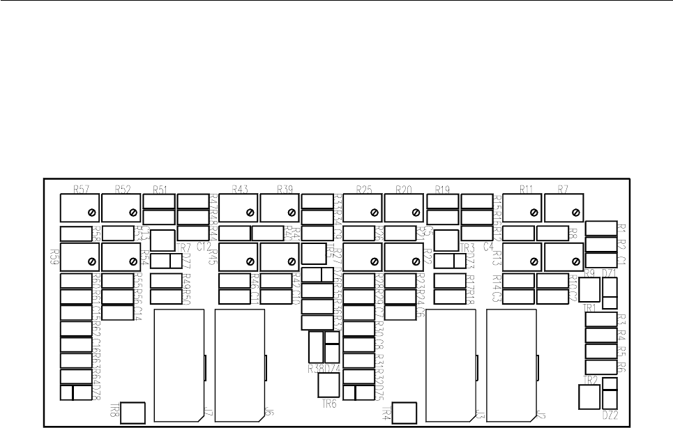
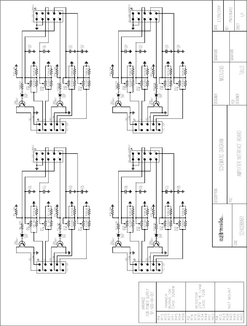
INTERFACE BOARD SCH0288AR1
Component layout SCH0288AR1
COMPONENT LIST SCH0288AR1
Part Name/Number Description Qty. Comps.
CC 1nF-S 01096 01096 SMD 1206 COND 16 C1-16
DZ 5V1-S 03128 03128 SMD ZENER DIODE 8 DZ1-8
J FC-10P 02697-02699 02697+02699 PCB CONNECTOR POL 4 J2-3, J6-7
J FC-10P PCB FEMALE 02706 PCB FEMALE CONNECTOR POL 4 J1, J4-5, J8
R 0R0-S 00001 00001 RES 1/4W 5% SMD 1206 16 R1, R8, R12, R15, R21, R23, R26
R28, R33, R40, R44, R47, R53, R55,
R58, R60
R 10K-S 00053A 00053A RES 1/4W 5% SMD 1206 16 R3-6, R17-18, R31-32, R35-38,
R49-50, R63-64
R 1206 NOT MOUNTED NOT MOUNTED RES 1/4W 5% SMD 12 16 R2, R10, R14, R16, R19, R24, R29,
R30, R34, R42, R46, R48, R51, R56,
R61-62
RV 3266W NOT MOUNT NOT MOUNTED VARIABLE RESISTOR 16 R7, R9, R11, R13, R20, R22, R25,
R27, R39, R41, R43, R45, R52, R54,
R57, R59
TR BC847 03456 03456 NPN SMD TRANSISTOR 8 TR1-8
70
71
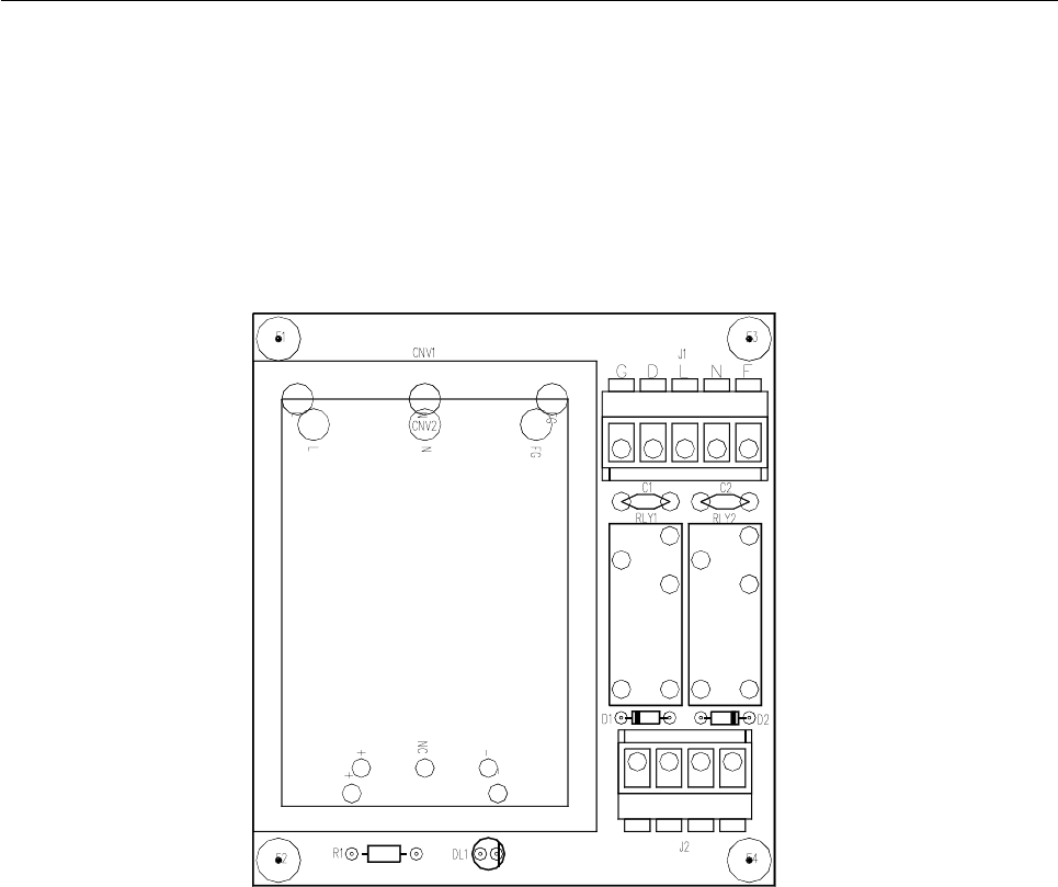
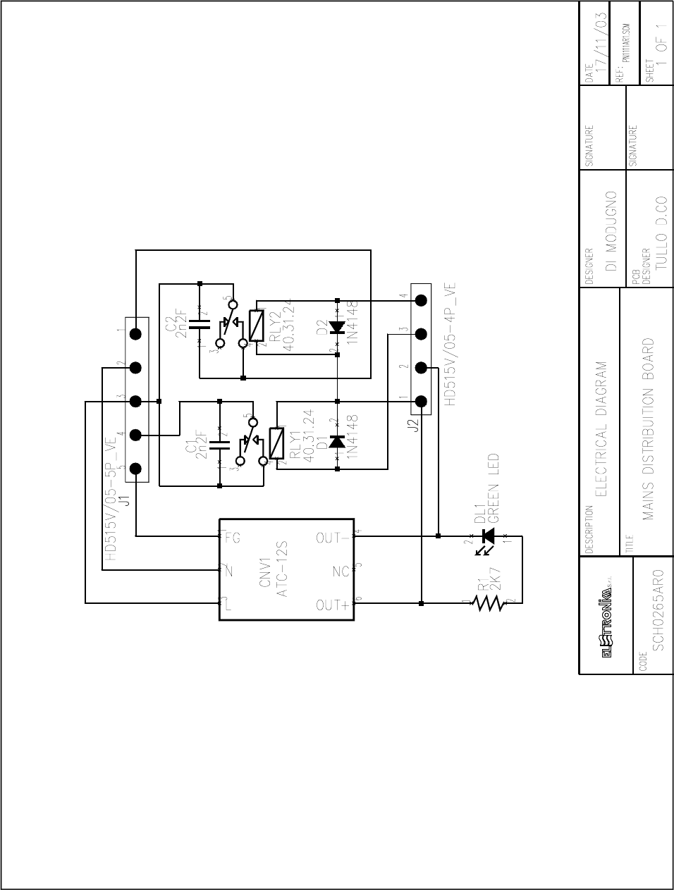
MAINS DISTRIBUTION BOARD SCH0265AR0
Component layout SCH0265AR0
COMPONENT LIST SCH0265AR0
Part Name/Number Description Qty. Comps.
CC 2nF2 2kV 01045A 01045A CERAMIC COND 2 C1-2
CNV AC-DC ATC-12S E0037 AC DC CONVERTER 1 CNV1
D 1N4148 03001 03001 DIODE 2 D1-2
DL LEDG3 03053 03053 GREEN LED DIODE 3mm 1 DL1
J CON HD515V/05-4PVE 02881 + 02882 PANDUIT PCB CONN 1 J2
J CON HD515V/05-5PVE PANDUIT PCB CO 1 J1
R 2K7 0046 0046 RES 1/4W 5% 1 R1
RL 40.31.24 7567C RELE 2 RLY1-2
72
73
SPECIFICATION
MODEL SP-500-27 (E0012 Code) SP-500-48 (E0013 Code)
DC Output Voltage 27Vdc 48Vdc
Output Rated Current 18A 10A
Output Current Range 0-18A 0-10A
Ripple & Noise (p-p) 200mVp-p 240mVp-p
DC Output Power 486W 480W
Efficiency 87% 87%
DC Voltage Adj. 24-30V 41-56V
Over V. Protection 31V-36.5V 57.6V-67.2V
Input Voltage Range 88-264Vac
Input Frequency 47-63Hz
Power Factor 0.95/100-240Vac
Overload Protection 105%-135%
Type: Foldback current limiting
Recovery: Auto
Over Temp. Protection > =70°C Output Shutdown
Fan Control Temp. > =60°C Fan On
< =50°C Fan Off
Working Temp., Humidity -10°C/+50°C, 20%-90% RH
Dimension 185x120x93
Weight 1.8Kg.
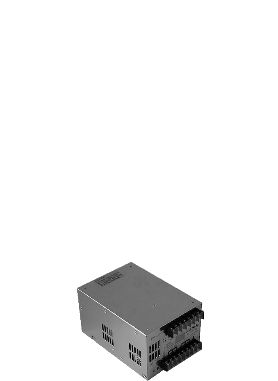
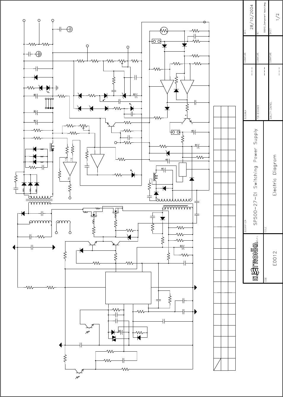
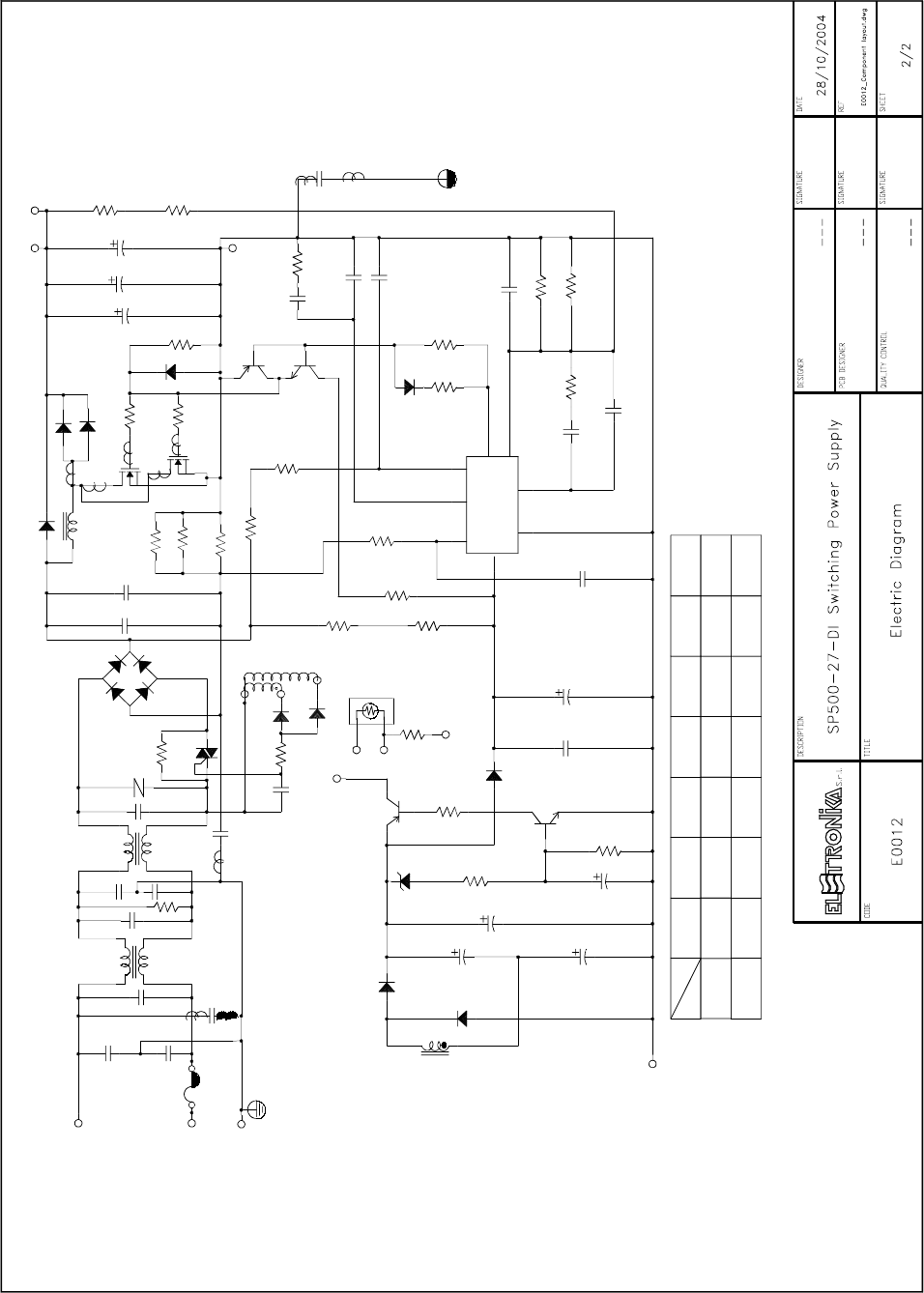
SP500-27-DI SWITCHING POWER SUPPLY E0012
74
CN2
3
9
4
17
8
1
6
2
R-
L51
1K5
1K8
R95
910
820
2
7
518
R84
1K
750
BD
X
7
4
5
3
R121
R+
-V
331
PART NO . D60,61
1K 470u
C73,74
CN2
C58
224
1.40
13-15
BD
BD
J4
J2
-S
+S
Vm
48V
27V
/1KV
/1KV
221
C71,72
R72
330
R71
5K1
R49
JUMP
62
TR132
TR131
D9202
D9202
C60
104/63V
R69
1M
C55 102/100V
D53
1N4148
U53: B
PC123
/2W
/2W
3K3 /63V
R82,83
/50V
220u
75
R68
22K
R70
36K
22K
R94
C61
471/100V
224
/100V
/100V
C80 R87
R61
1R
ZD51
18V/1W
D52
1N4148
V-
C64
104/630V
33V/1W
18V/1W
ZD52
J2,J3
J1,J2
J3
10mm
D55
HER104
5
8
D51
BY228
33V/1W
18V/1W
ZD54
16
D75
HER204
C87
222/500V
Im
10-12
D60:A
3K6
1/8W
R50
6K8
1/8W
ZD55
7.5V/1W
C85
1u/50V
10
9
R88
1K/1/8W
BD R81
22K
1/8W
43K
1/8W
R121
75K
1/8W
R11 3
C83
47u/50V
R109
2.2/1/2W
103/100V
C88
RC
Q56
2SC1815
SVR2
JUMP
C82
103/100V
D68
1N4148
U51:1
MOC3022
D64
1N4148
ZD52
J3
J1
11
R108
15K/ 1/8W
C92
1K
R92
R86
R103
6K8/1/8W
820/1/8W
R104 RT
D65
1N4148
R96
10
R95 R93
10
TB1:A
C77
473/630V
R105 820/1/8W
RC-
RTH2
5K C78
473/630V
TB 1: F
+V
TB 1: B
C57
103/100V
C56
1u/50V
C65
68P/50V
R64
0.82/2W
100u/35V
C62
Q54
A1020
V+
R62
0.22/2W
C63
222/500V
Q52
2SK1358
D
G
S
Q51
2SK1358
C52
103/2KV
D69
HER204
R114
1K/1/8W
C71
R89
68K/1/8W
-
+
U5 4: C
LM324
D60:B
C72
D61:B
82K
1/8W
CN51:A
FAN R111
2K
R116
2K
R84
R50
R83
R82
C90
R107
1K
22
R91
ZD53
C74
R100
4K3/1/8W
ZD60
D63
HER203
R94
D66
1N4148
CN4:A
TB1:H
R122
5K1/1/8W
R120
560/1/2W
MODEL
T+
T-
U52:B
PC123
/1/2W
39/1W
27/1W
R80,81
2K2
6K8
R86
CV-
R66
1K
1N4148
D54
24K
R67
MOC3022
U51:2
C54 103/100V
R57
680
C53
104/63V
BR54
15/ 1/ 2W
R52
200K/1/2W
R51
200K/1/2W
T51
TF404
TF403
27V/1W
15V/1W
ZD53
16.1V
10.6V
ZD60
221/1KV
C92
C102
222/250VAC
C84
47u/50V
D76
HER104
C101
222/250VAC
L52
DR005
C86
47u/50V
R110
51/2W
U53:A
PC123
22/1/2W
R112
R59
5.1
R55
5.1
R119
1K/1/8W
104/63V
C79
R11 3
L51:A
D61:A
D62:A
C51
101/2KV
T51:D
Q55
C2120
R102
1K5/1/8W
C81
104/63V
1N4148
D67 -
+
LM324
U5 4: A
C93
105/50V
C91
2.2u/50V
C80
U52:A ZD54
LED1
R73
1K
C59
471/1KV
R65 R74
75K
R56
100
8
7
6
5
4
3
2
1
U55
3845
0.22/2W
R63
R60
15/1/2W
R58
5K1
R115
51/1/8W
5K1/1/8W
R117
7812
RG51
R53
100/2W
R80
R118
1K/1/8W
D62:B
-
+
LM324
U54:D
R106
100/1/8W
C
A
R
SHR1
TL43 1
R90
1K
R101
3K6/1/8W SVR1
1K
C73
820/1/8W
R87 C75
C76
104/63V
-
+
LM324
U5 4: B
SP-500B DIFFERENT COMPONENT:
Q53
2SC2655
75
X X X
R+
R-
X1K
14.2V
C3
8.9V
R31
FG
AC/N
12V
X
13.5V 15V 24V
P5
Terminal
CN4
X
27V 48V
F+ CN2
54AD
270K
R29
AC/L
CN2
V-
HER104
D8 C32
102/250VAC
8.9V
2.2u/50V
C25 2.2u/50V
C24
470u/25V
C23
8.9V
1K
R24
C15
8.9V
104/100V
C21
1N4001
D2
51/2W
R4
BTA16-600B
TRC1
471
ZNR1
8.9V 8.9V
220u/25V
C17
T+
T- CN2
9.1V/1W
103/100V
C67
5.1/1/2W
R21
499K/1W
R9
330K
R30
1N4148
D3
C
E
B
Q4
C2655
22KR28
221/1KV
C20
472/50V
C13
102/50V
C11
CN1
V-
150u/400V
C26
150u/400V
C9
CN2
V+
499K/1W
R14
CN1
V+
C1 474/250VAC
C16
C2
474/250VAC
680K/1/2/W
R1
2K2
R25
2.2u/50V
C22
C5
104/250VAC
TF-360
LF2
10/5W
R2
30K/2W
R18
474/250VAC
C7
30K/2W
R17
100
R26
1N5819
D5
471/1KV
C12
C14
222/250VAC
499K/1W
R15
R31
PART NO .
SP-500A DIFFERENT COMPONENT:
ZD4
MODEL
HER104
D7
ZD4
FS1
F10A/250VAC
TF-360
LF1
C31
NC(PSF)
B
C
E
Q8
A562
100
R32
HER104
D4
0.22/2W
R6
0.33/2W
R7
15A/600V
BD1
C8
474/250VAC
D9
474/50V
C18
10K
R16
RHRP1650
D1:B
5.1
R10
150u/400V
C10
TR134
L1:B
C4
222/250VACX2
2K2
R23
C
E
BC1815
Q7
CN2
B
104/100V
C6
HER104
D6 499K/1W
R8
0.33/2W
R5
TR134
L1:A
473/50VC19
680
R27
B
C
EA1020
Q3
5.1
R11
5K1
R12
RHRP1650
D1:A
Q1
IRFPS37N50A
15
6
8
423
7
IAC
GTDR
VAo u t Vs
CAoutMout
Vcc
GND
LT1249
U1
Q2
IRFPS37N50A
76
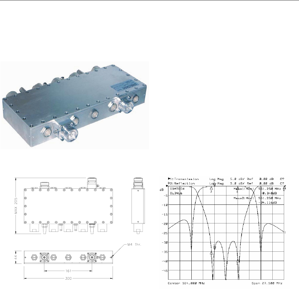
UHF BANDPASS FILTER Code 06673
600W, 3 Sections + 2 Notches
FEATURES
- UHF 500W analog TV output filter
- 3 bandpass resonators and 2 notches
- Foreshorten in-line combline structure
- Iris couplings with fine bandwidth regulation
- Phase regulation netween bandpass and notches
- Low loss (Typ. 042dB @ Ch. 69 G)
- Compact and lightweight
SPECIFICATIONS (Values referred to B Standard)
Frequency Range 470 - 862MHz Selectivity > 32dB @ V.C. -5.5 / +11MHz
Max Input Power 500W Analog TV > 22dB @ V.C. -11 / +16.5MHz
Insertion Loss < 0.50dB @ V.C. Ch. 69 Temperature Stability < 17kHz / K
< 0.45dB @ V.C. Ch. 21 Connectors 7/16 Female
Return Loss > 28dB Weight (Approx) 2.7kg
Group Delay Variation < 25nS Operating temperature -10 to +50°C
Bandwidth 6 to 8MHz
AVAILABLE OPTIONS
A SMA Output Monitor Probe B N Female Connector

77
TECHNICAL DESCRIPTION
The output filter mod. 06673 is made up of a 3 resonators bandpass filter and two notches. It can be tuned on
all the channels of the UHF TV band (470 - 862MHz) and according to all worldwide standards (4.5 -
6.5MHz intercarrier). The bandpass section is composed by the three middle resonators, while the two
resonators apart are the notches. The filter is symmetrical; therefore, the choice of the lowest and the hightest
notch is indifferent.
The bandwidth regulation is accomplished by varying the insertion of the two Post Rods, which are located
between the bandpass resonators; the insertion of the Post Rods increases the bandwidth. In order to execute
this regulation it is necessary to loosen every lock nut by means of a n. 12 pipe key.
The input/output couplings are regulated by means of the two shafts (Coupling Stub) opposite to each connector.
The regulation is carried out with n. 8 flat key, considering that when the operating flattenings are parallel to the
longer side of the filter the coupling is maximum, otherwise if orthogonal the coupling is minimum.
The frequency response symmetry is determined by the insertion of the previously mentioned shafts; these
shafts can be set after loosening the relevant clamps with a pipe wrench n. 16. Once locked, these clamps set
out also the twist friction of the couplings.
TUNING INSTRUCTIONS
The advised tuning sequence is the following:
1. Set the instrument state as follows:
C.F. = (V.C. + S.C.) / 2
SPAN = INTERCARRIER * 5 (E.G. 27,5MHz std. B/G)
TRANSMISSION SCALE = 5dB/div.
REFLECTION SCALE = 5dB/div.
2. Preset the Coupling Stubs and the bandwidth (Posts ), measuring them from the extremity to the filters
body, according to the following table:
C.F.
(MHz)
COUPLING STUBS
(mm)
POSTS (mm)
B, G Standards K, K1 Standards M, N Standards I Standard
474 27 27 16 48 20
666 48 32 28 41 30
85862 22182820

78
3.Tune the bandpass section on the required channel, and match input and output until a correct response is
achieved. During this step, the tunings of the two notches shall be kept well far from the bandpass response.
Regulate the bandwidth at -24dB to the ends of span (E. g. std. G: BW (-24dB) = 27,5MHz). The input/
output couplings may influence the external resonators; therefore, it will be necessary to repeatedly fix the
formers after the latters in small steps. The frequency response must be centered, with the same attenuation
values at both sides of the screen.
4. Tune the two notches to P.V. - INTERCARRIER and P.A. + INTERCARRIER frequencies. This will vary
the response and matching. Adjust the response acting on the bandpass tunings.
5. Improve the calibration alternatively acting on two sides of the filter according to this sequence:
regulate the couplings;
re-tune notches if they have to be moved;
re-tune the bandpass resonatoes.
6. Execute the sequence in small steps aiming to improve the matching. Check the response symmetry, and
correct it if needed according to the following criterion: if the lowest notch is much more emphasized than
the highest one it is necessary to insert the Coupling Stubs, otherwise if the hightest notch is more emphasized
than the lowest one it is necessary to extract the Coupling Stubs.
7. At the end of the tuning process, lock the trim points (Posts and Coupling Stubs) and assemble the coupling
protection caps on the filter.
SPECIFICATION OVER THE UHF BAND
MEASURE VALUE
Insertion Loss @ V.C. < 0.50dB @ V.C. Ch 69 G (Typ. 0.38)
< 0.45dB @ V.C. Ch 21 G (Typ. 0.33)
Return Loss (from V.C.-0.75 to S.C. +0.25) > 28dB
Attenuation @ V.C. - INTERCARRIER > 32dB
Attenuation @ V.C. + INTERCARRIER > 24dB
79
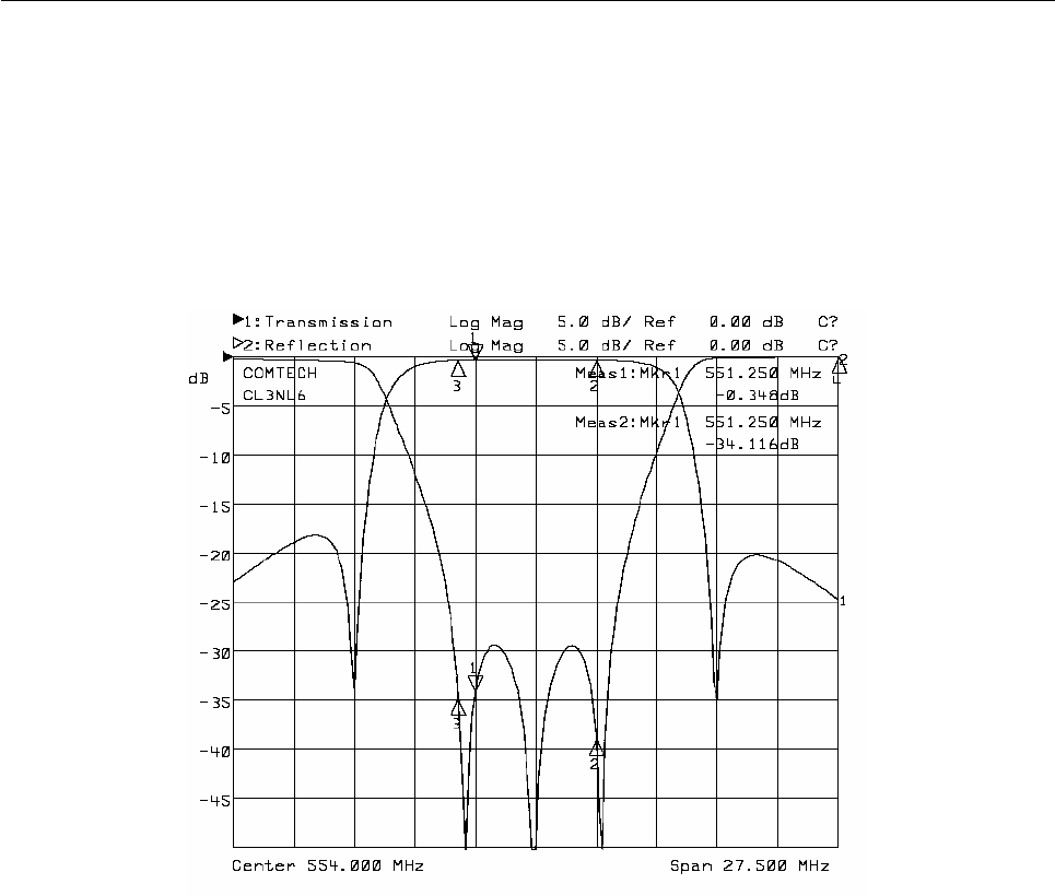
SAMPLE FREQUENCY RESPONSE DIAGRAM