Epson Rtc 4543Sa Users Manual
RTC-4543SB to the manual 0ccda093-d2a9-4363-a229-55f294cb2fe5
2015-01-23
: Epson Epson-Rtc-4543Sa-Users-Manual-250933 epson-rtc-4543sa-users-manual-250933 epson pdf
Open the PDF directly: View PDF ![]() .
.
Page Count: 16
MQ252-03
Application Manual
Real Time Clock Module
RTC-4543SA/SB
Model Product Number
RTC-4543SA Q4145435x000200
RTC-4543SB Q4145436x000200

NOTICE
• The material is subject to change without notice.
• Any part of this material may not be reproduced or duplicated in any form or any means without the
written permission of Seiko Epson.
• The information, applied circuit, program, using way etc., written in this material is just for reference.
Seiko Epson does not assume any liability for the occurrence of infringing any patent or copyright of third
party. This material does not authorize the licence for any patent or intellectual property rights.
• Any product described in this material may contain technology or the subject relating to strategic
products under the control of the Foreign Exchange and Foreign Trade Law of Japan and may require an
export licence from the Ministry of International Trade and industry or other approval from another
government agency.
• The products (except for some product for automotive applications) listed up on this material are designed
to be u
s
ed with ordinary electronic equipment (OA equipment, AV equipment, communications equipment,
measuring instruments etc). Seiko Epson does not assume any liability for the case using the products with
the appoication required high reliability or safety extremely (such as aerospace equipment etc).
When intending to use any our product with automotive application and the other application than
ordinary electronic equipments as above, please contact our sales representatives in advance.
I
n pursuit of "Saving" Technology ,Epson electronic device.
Our Lineup of semiconductors, Liquid crystal displays and quartz devices
assists in creating the products of our customers' dreams.
E
pson IS energy savings.

RTC - 4543 SA/SB
CONTENTS
1. OVERVIEW ........................................................................................................1
2. BLOCK DIAGRAM...........................................................................................1
3. PIN CONNECTIONS.......................................................................................2
4. PIN FUNCTIONS..............................................................................................2
5. ELECTRICAL CHARACTERISTICS .........................................................3
5-1. ABSOLUTE MAXIMUM RATINGS ..........................................................................................3
5-2. OPERATING CONDITION.......................................................................................................3
5-3. FREQUENCY CHARACTERISTICS........................................................................................3
5-4. DC CHARACTERISTICS ........................................................................................................3
5-5. AC CHARACTERISTICS.........................................................................................................4
5-6. TIMING CHARTS.....................................................................................................................5
6. TIMER DATA ORGANIZATION..................................................................6
7. DESCRIPTION OF OPERATION...............................................................7
7-1.DATA READS............................................................................................................................7
7-2. DATA WRITES.........................................................................................................................7
7-3. DATA WRITES (DIVIDER RESET).........................................................................................8
7-4. FOUT OUTPUT AND 1 HZ CARRIES...................................................................................8
8. EXAMPLES OF EXTERNAL CIRCUITS .................................................9
9. EXTERNAL DIMENSIONS.........................................................................10
10. LAYOUT OF PACKAGE MARKINGS ..................................................10
11. REFERENCE DATA...................................................................................11
12. APPLICATION NOTES..............................................................................12
12-1. NOTES ON HANDLING.......................................................................................................12
12-2. NOTES ON PACKAGING ....................................................................................................12

RTC - 4543 SA/SB
Page - 1 MQ - 252 - 03
32-kHz Output Serial RTC Module
RTC - 4543 SA/SB
z Built-in crystal permits operation without requiring adjustment
z Built-in time counters (seconds, minutes, hours) and calendar counters (days, days of the week
months, years)
z Operating voltage range: 2.5 V to 5.5 V
z Supply voltage detection voltage: 1.7 ±0.3 V
z Low current consumption: 1.0 µA/2.0 V (Max.)
z Automatic processing for leap years
z Output selectable between 32.768 kHz/1 Hz
1. Overview
This module is a real-time clock with a serial interface and a built-in crystal oscillator. This module
is also equipped with clock and calendar circuits, an automatic leap year compensation function,
and a supply voltage detection function.
In addition, this module has a 32.768 kHz/1 Hz selectable output function for hardware control that
is independent of the RTC circuit.
This module is available in a compact SOP 14-pin package (RTC-4543SA) and a thin SOP 18-pin
package (RTC-4543SB).
2. Block diagram
OSC
FOUT
I / O
CONTROLLER
SHIFT REGISTER
CLK
DATA
CE
WR
32.768 kHz
DIVIDER
OUTPUT
CONTROLLER
FOE
CONTROL
CIRCUIT
FSEL
VOLTAGE
DETECT
CLOCK AND CALENDAR

RTC - 4543 SA/SB
Page - 2 MQ - 252 - 03
3. Pin Connections
1
78
14
2
3
4
5
6
1
7
14
12
11
10
9
8
13
GND
CLK
WR
FOUT
DATA
CE
DD
V
FOE
N.C
FSEL
N.C
N.C
N.C
N.C
RTC - 4543SA
SOP - 14pin
1
910
18
2
3
4
5
6
1
7
9
8
GND
WR
CE
DD
V
FOE
N.C
FSEL
N.C
N.C
17
16
15
14
13
18
12
10
11
N.C
N.C
N.C
N.C
N.C
CLK
DATA
FOUT
N.C
RTC - 4543SB
SOP - 18pin
4. Pin Functions
Signal Pin No.
SOP-14pin
(SOP-18pin) I/O Function
GND 1
( 9 ) Connects to negative (-) side (ground) of the power supply.
CE
3
( 8 ) Input
Chip enable input pin.
When high,the chip is enabled. When low,the DATA pin goes to
high impedance and the CLK,DATA,and WR pins are not able to
accept input.In addition, when low,the TM bit is cleared.
FSEL 4
( 7 ) Input
Serect the frequency that is output from the FOUT pin.
High : 1 Hz
Low : 32.768 kHz
WR 5
( 6 ) Input
DATA pin input/output switching pin.
High : DATA input (when writing the RTC)
Low : DATA output (when reading the RTC)
FOE 6
( 5 ) Input
When high, the frequency selected by the FSEL pin is output from
the FOUT pin.
When low, the FOUT pin goes to high impedance.
VDD 9
( 14 ) Connects to positive (+) side of the power supply.
CLK 10
( 12 ) Input
Serial clock input pin.
Data is gotten at the rising edge during a write, and data is output
at the rising edge during a read.
DATA 11
( 11 ) Bi-directional Input/outout pin that is used for writing and reading data.
FOUT 14
( 10 ) Output
Outputs the frequency selected by the FSEL pin. 1 Hz output is
synchronized with the internal one-second signal.
This output is not affected by the CE pin.
N.C.
2,7,8,12,13
( 1,2,3,4,13,
15,16,17,18 )
Although these pins are not connected internally,they should
always be left open in order to obtain the most stable oscillation
possible.
* Always connect a passthrough capacitor of at least 0.1 µF as close as possible between VDD and GND.

RTC - 4543 SA/SB
Page - 3 MQ - 252 - 03
5. Electrical Characteristics
5-1. Absolute Maximum Ratings
Item Symbol Conditions Min. Max. Unit
Supply voltage VDD -0.3 7.0 V
Input voltage VI Ta=+25 °C GND-0.3 VDD+0.3 V
Output voltage VO GND-0.3 VDD+0.3 V
Storage temperature TSTG - -55 +125 °C
5-2. Operating Condition
Item Symbol Conditions Min. Max. Unit
Operating supply
voltage VDD - 2.5 5.5 V
Data holding voltage VCLK - 1.4 5.5 V
Operating temperature TOPR No condensation -40 +85
°C
5-3. Frequency Characteristics
Item Symbol Conditions Max. Unit
Frequency tolerance ∆f/fO Ta=+25
°C , VDD=5.0 V 5
± 23 * ×10-6
Frequency temperature
characteristics Top -10to+70 °C +25
°C ref + 10 / - 120 ×10-6
Frequency voltage
characteristics f/V Ta=+25 °C , VDD=2.0 to 5.5 V ± 2 ×10⁻⁶/V
Oscillation start time tSTA Ta=+25 °C , VDD=2.5 V 3 s
Aging fa
Ta=+25 °C , VDD=5 V , first year ± 5 ×10⁻⁶
* Monthly deviation: Approx. 1 min.
5-4. DC Characteristics
Unless specified otherwise: VDD = 5 V ± 10 %, Ta = - 40 to +85 °C
Item Symbol Conditions Min. Typ. Max. Unit
Current consumption(1) IDD1 VDD=5.0 V CE=L , FOE=L 1.5 3.0
µA
Current consumption(2) IDD2 VDD=3.0 V FSEL=H 1.0 2.0
µA
Current consumption(3) IDD3 VDD=2.0 V 0.5 1.0
µA
Current consumption(4) IDD4 VDD=5.0 V CE=L , FOE=H 4.0 10.0
µA
Current consumption(5) IDD5 VDD=3.0 V FSEL=L 2.5 6.5
µA
Current consumption(6) IDD6 VDD=2.0 V No load on the
FOUT pin 1.5 4.0
µA
Input voltage VIH WR,DATA,CE,CLK, 0.8 VDD V
V
IL FOE,FSEL pins 0.2 VDD V
Input off/leak current IOFF WR,CE,CLK,FOE,FSEL pins
VIN = VDD or GND 0.5
µA
V
OH(1) V
DD=5.0 V IOH=-1.0 mA 4.5 V
Output voltage VOH(2) V
DD=3.0 V DATA , FOUT pins 2.0 V
V
OL(1) V
DD=5.0 V IOL= 1.0 mA 0.5 V
V
OL(2) V
DD=3.0 V DATA , FOUT pins 0.8 V
Output load condition
( fanout ) N / CL FOUT pin 2 LSTTL / 30 pF Max.
Output leak current IOZH V
OUT=5.5 V DATA , FOUT pins -1.0 1.0 µA
I
OZL V
OUT=0 V DATA , FOUT pins -1.0 1.0 µA
Supply voltage detection
voltage VDT - 1.4 1.7 2.0 V

RTC - 4543 SA/SB
Page - 4 MQ - 252 - 03
5-5. AC Characteristics
Unless specified otherwise: Ta = - 40 to +85 °C, CL = 50 pF
Item Symbol
VDD=5 V ± 10 % VDD=3 V ± 10 % Unit
Min. Max. Min. Max.
CLK clock cycle tCLK 0.75 7800 1.5 7800
µs
CLK low pulse width tCLKL 0.375 3900 0.75 3900 µs
CLK high pulse width tCLKH 0.375 3900 0.75 3900 µs
CLK setup time tCLKS 25 50 ns
CE setup time tCES 0.375 3900 0.75 3900 µs
CE hold time tCEH 0.375 0.75 µs
CE enable time tCE 0.9 0.9 s
Write data setup time tSD 0.1 0.2
µs
Write data hold time tHD 0.1 0.1
µs
WR setup time tWRS 100 100 ns
WR hold time tWRH 100 100 ns
DATA output delay time tDATD 0.2 0.4
µs
DATA output floating time tDZ 0.1 0.2
µs
Clock input rise time tr1 50 100 ns
Clock input fall time tf1 50 100 ns
FOUT rise time (CL=30 pF) tr2 100 200 ns
FOUT fall time (CL=30 pF) tf2 100 200 ns
Disable time (CL=30 pF) tXZ 100 200 ns
Enable time (CL=30 pF) tZX 100 200 ns
FOUT duty ratio (CL=30 pF) Duty 40 60 40 60 %
Wait time tRCV 0.95 1.9
µs

RTC - 4543 SA/SB
Page - 5 MQ - 252 - 03
5-6. Timing Charts
( 1 ) Data read
WR tWRS
CE
tt f1r1
CLK
tCES tCLK
DATA
tCLKH tCLKL
tDATD
tWRH
tCEH
tDZ
tRCV
tCE
tCLKS
( 2 ) Data write
WR
tWRS
CE
tt f1r1
CLK
tCES tCLK
DATA
tCLKH tCLKL
tWRH
tCEH
tSD tHD
tRCV
tCE
tCLKS
( 3 ) FOUT output
FOUT
t
tr2
10%
90%
50%
tf2 tH
[]
Duty t
t100 %
H
=×
( 4 ) Disable/enable
FOE VIH
FOUT
VIL
tXZ tZX
Disable
High impedance
Enable
RTC - 4543 SA/SB
Page - 6 MQ - 252 - 03
6. Timer Data Organization
• The counter data is BCD code.
• The timer automatically adjusts for different month lengths and for leap year.
• The time is indicated in 24-hour format.
• Writes and reads are both performed on an LSB-first basis.
MSB LSB
Second
( 0 to 59 )
FDT
s40
s20
s10
s8
s4
s2
s1
Minutes
( 0 to 59 )
*
mi40
mi20
mi10
mi8
mi4
mi2
mi1
Hour ( 0 to 23 )
*
*
h20
h10
h8
h4
h2
h1
Day of the week
( 1 to 7 )
*
w4
w2
w1
Day ( 1 to 31 )
*
*
d20
d10
d8
d4
d2
d1
Month ( 1 to 12 )
TM
*
*
mo10
mo8
mo4
mo2
mo1
Year ( 0 to 99 )
y80
y40
y20
y10
y8
y4
y2
y1
* bits: Any data may be written to these bits.
• FDT bit: Supply voltage detection bit
• This bit is set to “1” when voltage of 1.7 ±0.3 V or less is detected between VDD and GND.
• The FDT bit is cleared if all of the digits up to the year digits are read.
• Although this bit can be both read and written, normally set this bit to “0”.
D
etect
i
on
pulse
VDD
Mode
FDT bit
VDET
0.5 s
Read
0.5 s
The supply voltage detection circuit monitors the supply voltage once every 0.5 seconds;
if the supply voltage is lower than the detection voltage value, the FDT bit is set to “1”.
• TM bit: This is a test bit for SEIKO-EPSON’s use. Always set this bit to “0”.
RTC - 4543 SA/SB
Page - 7 MQ - 252 - 03
7. Description of Operation
7-1.Data reads
CLK
WR
DATA FDTs40s20s10s8s4s2s1 y8 y10 y20 y40
CE
y80
152
Sec
253 54 54+n
Output data does not change
Year
1) When the WR pin is low and the CE pin is high, the RTC enters data output mode.
2) At the first rising edge of the CLK signal, the clock and calendar data are loaded into the shift
register and the LSB of the seconds digits is output from the DATA pin.
3) The remaining seconds, minutes, hour, day of the week, day, month, and year data is shifted out,
in sequence and in synchronization with the rising edge of the CLK signal, so that the data is
output from the DATA pin.
The output data is valid until the rising edge of the 52nd clock pulse; even if more than 52 clock
pulses are input, the output data does not change.
4) If data is required in less than 52 clock pulses, that part of the data can be gotten by setting the
CE pin low after the necessary number of clock pulses have been output.
Example: If only the data from “seconds” to “day of the week” is needed:
After 28 clock pulses, set the CE pin low in order to get the data from “seconds” to “day of
the week.”
5) When performing successive data read operations, a wait (tRCV) is necessary after the CE pin
is set low.
6) Note that if an update operation (a one-second carry) occurs during a data read operation,
the data that is read will have an error of -1 second.
7) Complete data read operations within tCE (Max.) = 0.9 seconds, as described earlier.
7-2. Data writes
CLK
WR
DATA 0
s40s20s10s8s4s2s1 y8 y10 y20 y40
CE
y80
152
( FDT )
253 54 54+n
Seconds Year
1) When the WR pin is high and the CE pin is high, the RTC enters data input mode.
2) In this mode, data is input, in succession and in synchronization with the rising edge of the CLK
signal, to the shift register from the DATA pin, starting from the LSB of the seconds digits.
3) The sub-seconds counter is reset between the falling edge of the first clock pulse and the rising
edge of the second clock pulse. In addition, carries to the seconds counter are prohibited at the
falling edge of the first clock pulse.
4) After the last data is input to the shift register at the rising edge of the 52nd clock pulse, the
contents of the shift register are transferred to the timer counter.
5) Note that during a data write operation, 52 bits of data must be input.
• Correct write-access isn't completed when CE terminal turned into low on a state of less
than 52 bits.
• If more than 52 bits of data are input, the 53rd and subsequent bits are ignored.
(The first 52 bits of data are valid.)
6) Once the CE pin is set low, the prohibition on carries to the seconds counter is lifted.
Complete data write operations within tCE (Max.) = 0.9 seconds, as described earlier.
7) If a data read operation is to be performed immediately after a data write operation, a wait (tRCV)
is necessary after the CE pin is set low.
* Malfunction will result if illegal data is written. Therefore, be certain to write legal data.

RTC - 4543 SA/SB
Page - 8 MQ - 252 - 03
7-3. Data writes (Divider Reset)
CLK
WR
DATA s40s20s10s8s4 y8 y10 y20 y40
CE
y80
1522
N Seconds
s1
Divider reset
Pulse
s2
Timer,counter N seconds N seconds0 seconds
Carry stop
Pulse
After the counter is reset, carries to the seconds digit are halted.After the data write operation,
the prohibition on carries to the seconds counter is lifted by setting the CE pin low.
Complete data write operations within tCE (Max.) = 0.9 seconds, as described earlier.
7-4. FOUT output and 1 Hz carries
CLK
WR
CE
1Hz
FOUT
CLK
t
CES
t
1.0 s 0
-7.8 ms
15.6 ms 15.6 ms
During a data write operation, because a reset is applied to the Devider counter (from the 128 Hz
level to the 1 Hz level) after the CE pin goes high during the time between the falling edge of the first
clock cycle and the rising edge of the second clock cycle, the length of the first 1 Hz cycle after the
data write operation is 1.0 s +0 / −7.8ms +tCES+tCLK. Subsequent cycles are output at 1.0-second intervals.
The 1-Hz signal that is output on FOUT is the internal 1-Hz signal with a 15.6-ms shift applied.
RTC - 4543 SA/SB
Page - 9 MQ - 252 - 03
8. Examples of External Circuits
• Example 1. When used as an RTC + clock source
RTC 4543
VDD
CE
GND
0.1 µF
FOUT
FSEL
WR
DATA
CLK
FOE
VDD
VDD
Power supply
Detection circuit
Power supply
Switching circuit
*1
*2
*1: FOUT output frequency setting (High: 1 Hz; low: 32.768 kHz)
*2: Prohibits FOUT output during back up, reducing current consumption.
• Example 2. When used as a clock source (oscillator)
RTC-4543
VDD
CE
GND
0.1 µF
FOUT
FSEL
WR
DATA
CLK
FOE
VDD
VDD
VDD
∗1
RTC - 4543 SA/SB
Page - 10 MQ - 252 - 03
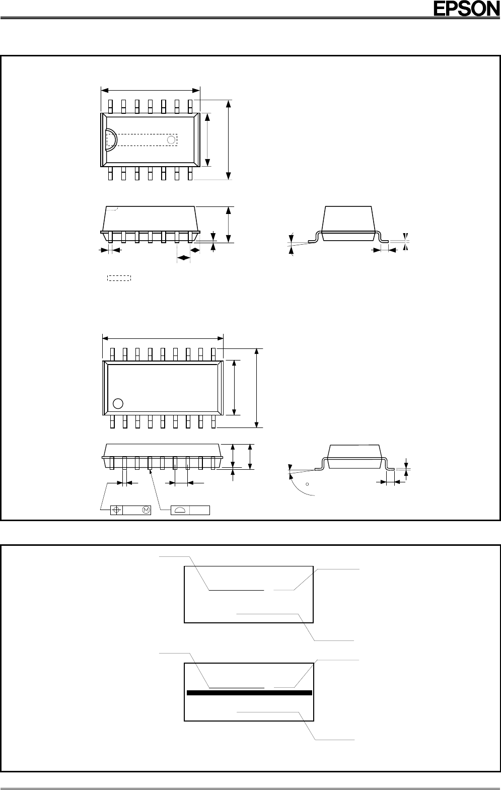
9. External Dimensions
RTC - 4543 SA ( SOP-14pin )
10.1 ± 0.2
5.0 7.4 ± 0.2
1.27 1.2
0.05
Min. 3.2 ± 0.1
0.35 0.6
0.15
0 - 10°
∗ The cylinder of the crystal oscillator can be seen in this area ( front ),
but it has no affect on the performance of the device.
RTC - 4543 SB ( SOP-18pin )
7.8 ± 0.2
5.4
11.4 ± 0.2
1.27 0.4
1.8 2.0
0.12 0.1
Max.
0 Min.
0.15
0.6 ± 0.2
0 - 10
10. Layout of Package Markings
RTC - 4543 SA
( SOP-14pin )
R4543
E 1234A
Model
Manufacturing
Lot
B
Frequency
torerance
RTC - 4543 SB
( SOP-18pin )
R4543
E 1234A
Model
Manufacturing
Lot
B
Frequency
tolerance
Note :
The markings and their positions as pictured above are only approximations.
These illustrations do not define the details of the style, size, and position of the characters marked on the packages.

RTC - 4543 SA/SB
Page - 11 MQ - 252 - 03
11. Reference Data
(1) Example of Frequency-Temperature Characteristics
θT = +25 °C Typ.
α = -0.035
× 10-6/ °C 2 Typ.
Temperature [°C]
-150
-140
-130
-120
-110
-100
-90
-80
-70
-60
-50
-40
-30
-20
-10
0
+10
-50 -40 -30 -20 -10 0 +10 +20 +30 +40 +50 +60 +70 +80 +90+100
Frequency fT
∆
× 10-6
Determining the frequency stability (clock accuracy)
1.The frequency-temperature characteristics can be
approximated by the following equation:
∆fT = α(θT-θX)2
∆fT: Frequency deviation at any given temperature
α( /°C2): Second-order temperature
: Highest temperature(+25 °C±5 °C)
: Any given temperature
θT(°C)
θX(°C)
((-0.035±0.005)×10-6/°C2)
2. In order to determine the clock accuracy, add in the
frequency tolerance and the voltage characteristics.
∆f/f = ∆f/f0 + ∆fT + ∆fv
∆f: Clock accuracy at any given temperature
and voltage (frequency stability)
: Frequency accuracy
∆T
∆v
: Frequency deviation at any given temperature
: Frequency deviation at any given voltage
/f
∆f/f0
f
f
3. Determining the daily error
Daily error =∆f/f × 86400 (seconds)
With error of 11.574 × 10⁻⁶, the error of the clock is
about one second per day.
(2)Example of Frequency-Voltage
Characteristics
Frequency [ ×10-6 ]
-1.0
0.0
+1.0
2345
Conditions
5 V reference Voltage,
Ta=+25 °C
-2.0 Supply voltage (VDD)[V]
(3)Example of Current Consumption-Voltage
Characteristics
Current consumpiton[ µA ]
1.0
2.0
2.0 3.0 4.0 5.0
Conditions
No load, Ta=+25 °C
Supply voltage (VDD) [V]
0.0
Note : This data shows values obtained from a sample lot.
RTC - 4543 SA/SB
Page - 12 MQ - 252 - 03
12. Application notes
12-1. Notes on handling
This module uses a C-MOS IC to realize low power consumption. Carefully note the following cautions when
handling.
(1) Static electricity
While this module has built-in circuitry designed to protect it against electrostatic discharge, the chip
could still be damaged by a large discharge of static electricity. Containers used for packing and
transport should be constructed of conductive materials. In addition, only soldering irons, measurement
circuits, and other such devices which do not leak high voltage should be used with this module, which
should also be grounded when such devices are being used.
(2) Noise
If a signal with excessive external noise is applied to the power supply or input pins, the device may
malfunction or "latch up." In order to ensure stable operation, connect a filter capacitor (preferably
ceramic) of greater that 0.1F as close as possible to the power supply pins (between VDD and GNDs).
Also, avoid placing any device that generates high level of electronic noise near this module.
* Do not connect signal lines to the shaded area in the figure shown in Fig. 1 and, if possible, embed
this area in a GND land.
(3) Voltage levels of input pins
When the input pins are at the mid-level, this will cause increased current consumption and a reduced
noise margin, and can impair the functioning of the device. Therefore, try as much as possible to apply
the voltage level close to VDD or GND.
(4) Handling of unused pins
Since the input impedance of the input pins is extremely high, operating the device with these pins in
the open circuit state can lead to unstable voltage level and malfunctions due to noise. Therefore, pull-
up or pull-down resistors should be provided for all unused input pins.
12-2. Notes on packaging
(1) Soldering heat resistance.
If the temperature within the package exceeds 260, the characteristics of the crystal oscillator will be
degraded and it may be damaged. The reflow conditions within our reflow profile is recommended.
Therefore, always check the mounting temperature and time before mounting this device. Also, check
again if the mounting conditions are later changed.
* See Fig. 2 profile for our evaluation of Soldering heat resistance for reference.
(2) Mounting equipment
While this module can be used with general-purpose mounting equipment, the internal crystal oscillator
may be damaged in some circumstances, depending on the equipment and conditions. Therefore, be
sure to check this. In addition, if the mounting conditions are later changed, the same check should be
performed again.
(3) Ultrasonic cleaning
Depending on the usage conditions, there is a possibility that the crystal oscillator will be damaged by
resonance during ultrasonic cleaning. Since the conditions under which ultrasonic cleaning is carried
out (the type of cleaner, power level, time, state of the inside of the cleaning vessel, etc.) vary widely,
this device is not warranted against damage during ultrasonic cleaning.
(4) Mounting orientation
This device can be damaged if it is mounted in the wrong orientation. Always confirm the orientation of
the device before mounting.
(5) Leakage between pins
Leakage between pins may occur if the power is turned on while the device has condensation or dirt on
it. Make sure the device is dry and clean before supplying power to it.
Fig. 1: Example GND Pattern Fig. 2: Reference profile for our evaluation of Soldering heat resistance.
RTC - 4543 SA ( SOP-14pin )
RTC - 4543 SB ( SOP-18pin )
+1 ∼ +5 °C / s 100 s
Pre-heating area
−1 ∼ −5 °C / s
time [ s ]
Temperature [ °C ]
+170 °C +220
°C
+260 °C Max.
+1 ∼ +5 °C / s
35 s
Stable Melting area

Application Manual
AMERICA
EPSON ELECTRONICS AMERICA, INC.
HEADQUARTER 150 River Oaks Parkway, San Jose, CA 95134, U.S.A.
Phone: (1)800-228-3964 (Toll free) : (1)408-922-0200 (Main) Fax: (1)408-922-0238
http://www.eea.epson.com
Atlanta Office 3010 Royal Blvd. South, Ste. 170, Alpharetta, GA 30005, U.S.A.
Phone: (1)877-332-0020 (Toll free) : (1)770-777-2078 (Main) Fax: (1)770-777-2637
Boston Office 301Edgewater Place, Ste. 120, Wakefield, MA 01880, U.S.A.
Phone: (1)800-922-7667 (Toll free) : (1)781-246-3600 (Main) Fax: (1)781-246-5443
Chicago Office 101 Virginia St., Ste. 290, Crystal Lake, IL 60014, U.S.A.
Phone: (1)800-853-3588 (Toll free) : (1)815-455-7630 (Main) Fax: (1)815-455-7633
El Segundo Office 1960 E. Grand Ave., 2nd Floor, El Segundo, CA 90245, U.S.A.
Phone: (1)800-249-7730 (Toll free) : (1)310-955-5300 (Main) Fax: (1)310-955-5400
EUROPE
EPSON EUROPE ELECTRONICS GmbH
HEADQUARTER Riesstrasse 15, 80992 Munich, Germany
Phone: (49)-(0)89-14005-0 Fax: (49)-(0)89-14005-110 http://www.epson-electronics.de
Düsseldorf Branch Office Altstadtstrasse 176, 51379 Leverkusen, Germany
Phone: (49)-(0)2171-5045-0 Fax: (49)-(0)2171-5045-10
UK & Ireland Branch Office Unit 2.4, Doncastle House, Doncastle Road, Bracknell, Berkshire RG12 8PE, England
Phone: (44)-(0)1344-381700 Fax: (44)-(0)1344-381701
French Branch Office LP 915 Les Conquérants, 1 Avenue de l' Atlantique, Z.A. de Courtaboeuf 2
91976 Les Ulis Cedex, France
Phone: (33)-(0)1-64862350 Fax: (33)-(0)1-64862355
ASIA
EPSON (CHINA) CO., LTD.
23F, Beijing Silver Tower 2# North RD DongSangHuan ChaoYang District, Beijing, China
Phone: (86) 10-6410-6655 Fax: (86) 10-6410-7319 http://www.epson.com.cn
4F, Bldg.,27, No.69, Gui Qing Road, Cao hejing, Shanghai, China
Phone: (86) 21-6485-0835 Fax: (86) 21-6485-0775
EPSON HONG KONG LTD.
20/F., Harbour Centre, 25 Harbour Road, Wanchai, Hong kong
Phone: (852) 2585-4600 Fax: (852) 2827-2152 http://www.epson.com.hk
EPSON ELECTRONIC TECHNOLOGY DEVELOPMENT (SHENZHEN )CO., LTD.
Flat 16A, 16/F, New Times Plaza, No.1 Taizi Road, Shenzhen, China
Phone: (86) 755-6811118 Fax: (86) 755-6677786
EPSON TAIWAN TECHNOLOGY & TRADING LTD.
14F, No.7, Song Ren Road, Taipei 110
Phone: (886) 2-8786-6688 Fax: (886)2-8786-6660 http://www.epson.com.tw
EPSON SINGAPORE PTE. LTD.
No.1, Temasek Avenue #36-00, Millenia Tower, Singapore 039192
Phone: (65) 337-7911 Fax: (65) 334-2716 http://www.epson.com.sg
SEIKO EPSON CORPORATION KOREA Office
50F, KLI 63 Building,60 Yoido-dong, Youngdeungpo-Ku, Seoul, 150-763, Korea
Phone: (82) 2-784-6027 Fax: (82) 2-767-3677 http://www.epson-device.co.kr
Gumi Branch Office 6F, Good Morning Securities Bldg., 56, Songjeong-dong Gumi-City, Gyongsangbuk-Do,
730-090, Korea
Phone: (82) 54-454-6027 Fax: (82) 54-454-6093
ELECTRONIC DEVICE MARKETING DEPARTMENT
Electronic devices information on WWW server
Distributor
http://www.epsondevice.com
