FEIBIT ELECTRONIC TECHNOLOGY FZB561011A ZigBee module User Manual
SHENZHEN FEIBIT ELECTRONIC TECHNOLOGY Co., LTD ZigBee module
Users Manual

FZB5610 ZigBee Module
User Manual
V1.00

1
VERSIONS HISTORY
Versions
Date
Description
Mender
V1.00
Aug.18.2015
First release
Daniel

2
Contents
VERSIONS HISTORY..................................................................................................................... 1
1 Product Introduction...................................................................................................................3
1.1 Product Description........................................................................................................ 3
1.2 Product Figures...............................................................................................................3
1.3 Applications......................................................................................................................4
1.4 Product Features............................................................................................................ 4
2 Electrical Characteristics...........................................................................................................5
2.1 Hardware Specification..................................................................................................5
2.2 Absolute Maximum Ratings.......................................................................................... 5
2.3 Recommended Operating Conditions.........................................................................6
2.4 Recommended Output Power Setting........................................................................ 6
2.5 Power Characteristics.................................................................................................... 7
2.6 Temperature Characteristics.........................................................................................7
2.7 SPI AC Characteristics.................................................................................................. 8
2.8 DC Characteristics..........................................................................................................9
2.9 RF Frequency,Output Levels and Data Rates.........................................................10
3 Terminal Configuration And Functions..................................................................................11
3.1 Pin Assignments........................................................................................................... 11
3.2 Pin Attributes..................................................................................................................11
3.2.1 ZigBee Transmission Module..........................................................................11
3.2.2 ZLL Module........................................................................................................ 12
3.2.3 Curtain Module.................................................................................................. 13
3.2.4 Light Sensor Module.........................................................................................13
3.2.5 Infrared Human Body Sensor Module........................................................... 14
3.2.6 Switch Module................................................................................................... 15
3.2.7 Smart Plug Module........................................................................................... 16
3.2.8 Temperature and Humanity Sensor Module.................................................17
4 Reference Information.............................................................................................................18
4.1 Electrical Schematic Diagram.................................................................................... 18
4.2 Design Considerations................................................................................................ 18
5 IEEE 802.15.4.......................................................................................................................... 19
6 The ZigBee Protocol................................................................................................................19
7 Mechanical Drawings And Installation..................................................................................20
FCC compliance............................................................................................................................. 22
COPYRIGHT STATEMENT..........................................................................................................23
DISCLAIMER.................................................................................................................................. 23
TRADEMARK STATEMENT......................................................................................................... 23
Contact us....................................................................................................................................... 23
3
1 Product Introduction
1.1 Product Description
The FZB5610 ZigBee module is a compact surface-mounted modules specially
designed for IEEE 802.15.4 and ZigBee applications.It enables robust network nodes to
be built with very low total bill-of -material costs.The FZB5610 ZigBee module combines
the excellent performance of a leading RF transceiver with an industry-standard enhanced
8051MCU,in -system programmable flash memory 8-KB RAM,and many other powerful
features.The FZB5610 ZigBee module has 256KB flash memory and various operating
modes,making it highly suited for systems where ultra low power consumption is
required. Short transition times between operating modes further ensure low energy
consumption. Combined with the industry-leading and golden-unit-status ZigBee protocol
stack(Z-Stack )from Texas Instruments,the FZB5610 ZigBee modules provides
arobust and complete ZigBee solution.
Specification of FZB5610 ZigBee module as shown as table 1-1.
Table 1-1 Specification of FZB5610 ZigBee module
Specification
Parameter
Weight
5 g(including antenna)
Dimensions(depth×width×height)
15mm×28mm×2mm
1.2 Product Figures
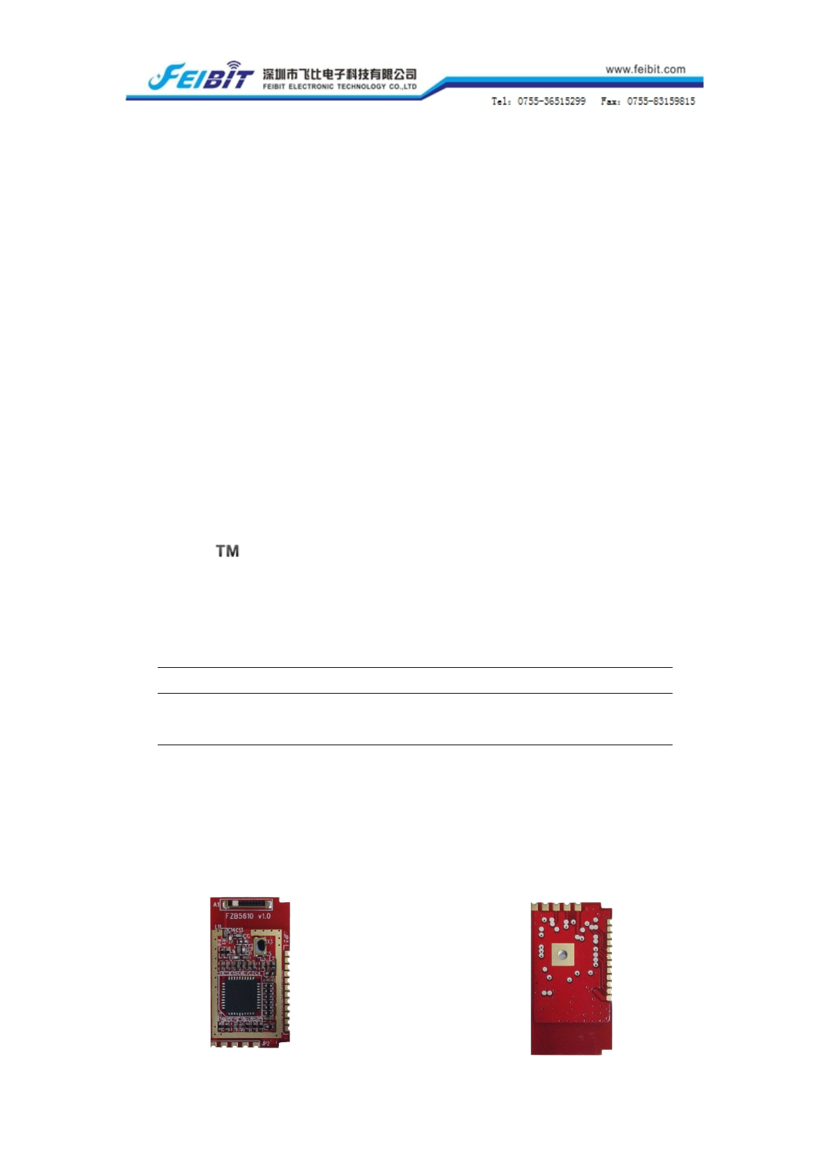
Front side and Back side of FZB5610 ZigBee module as shown as figure 1-1 and
figure 1-2.

4
Figure 1-1 FZB5610 Front Side Figure 1-2 FZB5610 Back Side
1.3 Applications
2.4-GHz IEEE 802.15.4 Systems
RF4CE Remote Control Systems(64-KB Flash and Higher)
ZigBee Systems(255-KB Flash)
Home/Building Automation
Lighting Systems
Industrial Control and Monitoring
Low-Power Wireless Sensor Networks
Consumer Electronics
Health Care
1.4 Product Features
Follow IEEE802.15.4 Standard.
High power consumption of the processor.
Integrate with 2.4G low power consumption of transceiver.
Use UART communication,and support to upgrade software by UART.
Voltage supply 2.0V-3.6V.
Conform to CE authentication.
Conform to ZigBee Standard,support ZLL and ZHA.
Support Ceramic Antenna or I-PEX Antenna(according to the model type)
Hardware compatibility design of the front-end amplifier circuit(according to the model
type)
The circuit outside the antenna should be shield by metal.

5
2 Electrical Characteristics
2.1 Hardware Specification
FZB5610 specification as shown as table 2-1.
Table 2-1 FZB5610 Specification
Performances
Specification
Operating Frequency Band
2405~2480MHz
Transmitted Power
4dBm
Outdoor Accessible Communication Range
200m
Outdoor Accessible Network Range
100m
Receiver Sensitivity
-97dBm
Working Temperature
-40℃ ~ + 125℃
Supply Voltage
+2.0V ~+3.6V(Recommend
Value:+3.3V)
Standby Current
10mA (Non-sleeping)
1mA (PM1)
10µA (PM2)
1µA (PM3)
Operating Current
35mA(TX)
25mA(RX)
Modulation type of RF module
QPSK
Protocol
ZigBee HA/ZigBee Light Link
2.2 Absolute Maximum Ratings
Absolute maximum ratings of FZB5610 as shown as table 2-2.
Table 2-2 FZB5610 absolute maximum ratings
Parameter
Parameter Description
MIN
MAX
UNIT
Ts
Storage temperature range
-40
125
℃
Vi
Input/Output signal voltage in any pin
-0.3
3.9
V
Iin
IO port input power
-
100
mA
VESD
Electrostatic voltage
-2000
2000
V

6
2.3 Recommended Operating Conditions
The recommended operating conditions of FZB5610 as shown as table 2-3.
Table 2-3 FZB5610 recommended operating conditions
Parameter
Parameter Description
Min
Max
UNIT
TA
Operating environment temperature
-40
125
℃
VIH
High-level input voltage
1.85
3.14
V
VIL
Low-level input voltage
-0.3
0.9
V
VOH
High-level output voltage
2.4
3.3
V
VOL
Low-level output voltage
0
0.4
V
Io
Output current
4
mA
2.4 Recommended Output Power Setting
The recommended output power setting of FZB5610 as shown as table 2-4.
Table 2-4 FZB5610 recommended output power setting
TXPOWER Register Setting
Typical Output Power(dBm)
Typical Current Consumption(mA)
0xF5
4
34
0xE5
2
31
0xD5
0.5
29
0xC5
-1
28
0xB5
-2
27
0xA5
-3.5
27
0x95
-4.5
26
0x85
-6.5
26
0x75
-8.5
25
0x65
-10.5
25
0x55
-12.5
25
0x45
-14.5
25
0x35
-16.5
25
0x25
-18.5
24
0x15
-20.5
24
0x05
-22.5
23
0x05 and TXCTRL=0x09
-28.5
23
7
2.5 Power Characteristics
Power characteristics of FZB5610 as shown as table 2-5
Table 2-5 FZB5610 Power Characteristics
Parameter
MIN
TYP
MAX
UNIT
VDD
2.0
3.3
3.6
V
2.6 Temperature Characteristics
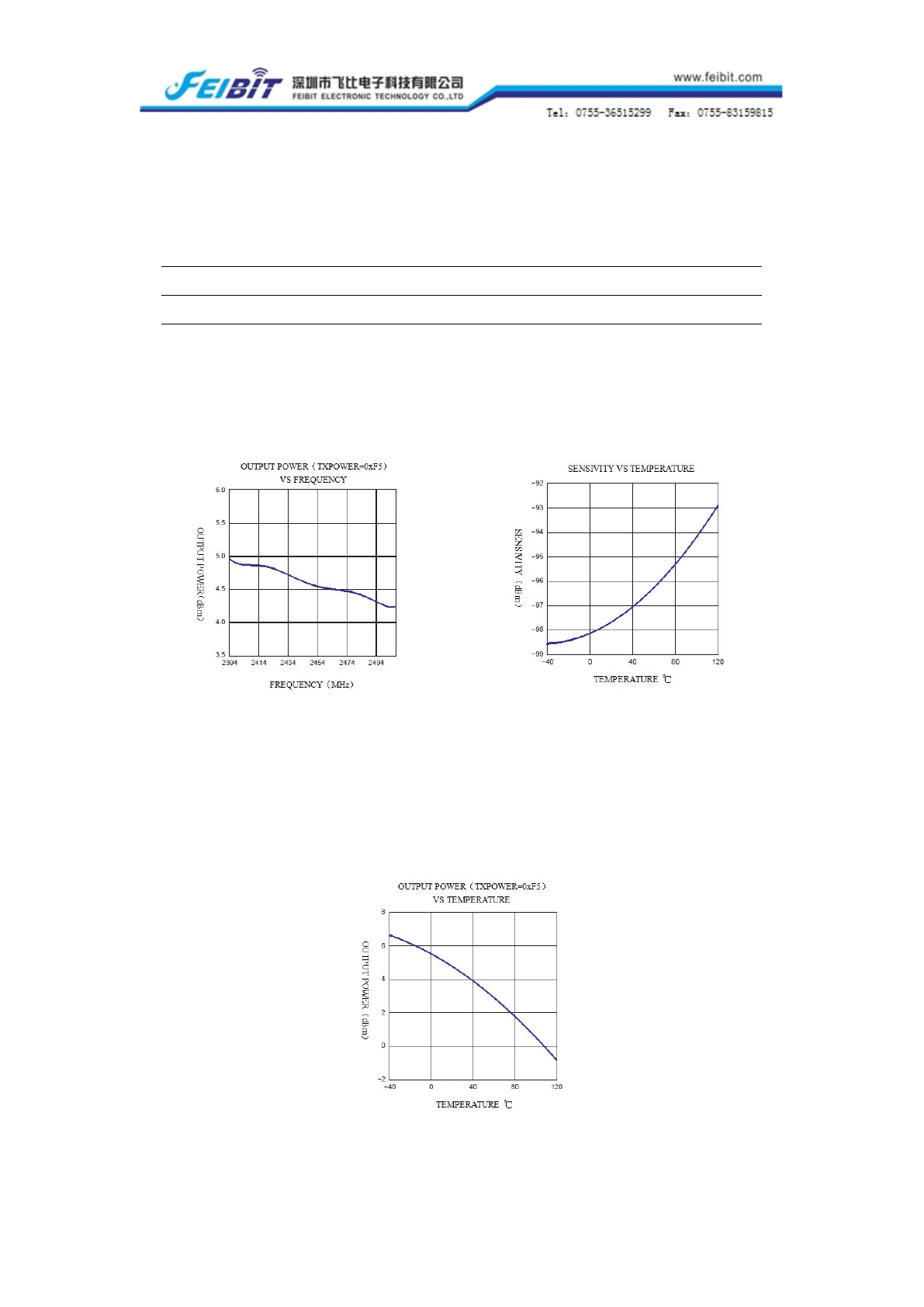
The relationship between output power and frequency as shown as figure 2-1.
Figure 2-1 OUTPUT POWER VS FREQUENCY Figure 2-2 SENSITIVITY VS FREQUENCY
The relationship between sensitivity and temperature as shown as figure 2-2.
The relationship between output power and temperature as shown as figure 2-3.
Figure 2-3 OUTPUT POWER VS TEMPERATURE

8
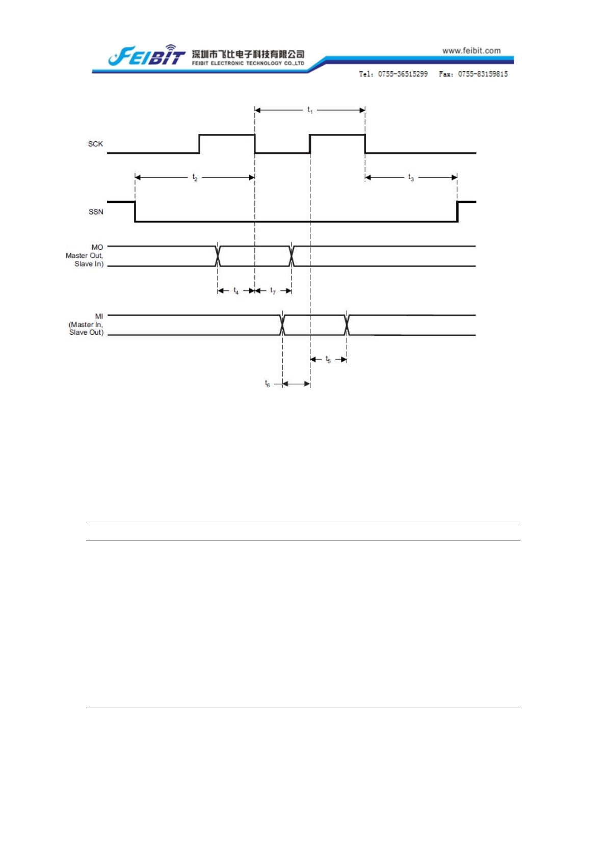
2.7 SPI AC Characteristics
(ref CC2530 datasheet)
TA = –40°C to 125°C, VDD = 2 V to 3.6 V, unless otherwise noted.See table 2-6.
Table 2-6 SPI AC Characteristics
PARAMETER
TEST CONDITIONS
MIN
TYP
MAX
UNIT
t1SCK penod
Master,Rx and Tx
250
ns
SCK duty cycle
Master
50%
t2SSN low to SCK
Master
63
ns
t3SCK to SSN high
Master
63
ns
t4MO early out
Master,load= 10 pF
7
ns
t7MO late out
Master,load 10 = pF
10
ns
t6MI setup
Master
90
ns
t5MI hold
Master
10
ns
t1SCK penod
Stave,Rx and Tx
250
ns
SCK duty cycle
Stave
50%
t2SSN low to SCK
Stave
63
ns
t3SCK to SSN high
Stave
63
ns
t6MO setup
Stave
35
ns
t5MO hold
Stave
10
ns
t5MI late out
Stave,load = 10 pF
95
ns
Operating frequency
Master,Tx only
8
MHz
Master,Rx and Tx
4
Stave,Rx only
8
Stave,Rx and Tx
4
9
Figure 2-4 SPI AC Characteristics
2.8 DC Characteristics
TA = 25°C, VDD = 3 V, unless otherwise noted. See table 2-7.
Table 2-7 DC Characteristics
PARAMETER
TEST CONDITIONS
MIN
TYP
MAX
UNIT
Logic-0 input voltage
0.5
V
Logic-1 input voltage
2.5
V
Logic-0 input current
Input equals 0V
-50
50
nA
Logic-1 input current
Input equals VDD
-50
50
nA
I/O-pin pullup and pull down resistors
20
kΩ
Logic-0 output voltage,4-mA pins
Output load 4 mA
0.5
V
Logic-1 output voltage,4-mA pins
Output load 4 mA
2.4
V
Logic-0 output voltage,20-mA pins
Output load 20 mA
0.5
V
Logic-1 output voltage,20-mA pins
Output load 20 mA
2.4
V

10
2.9 RF Frequency,Output Levels and Data Rates
The following table shows the RF channels as defined by the IEEE 802.15.4 standard.
See table 2-8.
Table 2-8 RF channels
RF channel
Frequency
11
2405MHz
12
2410MHz
13
2415MHz
14
2420MHz
15
2425MHz
16
2430MHz
17
2435MHz
18
2440MHz
19
2445MHz
20
2450MHz
21
2455MHz
22
2460MHz
23
2465MHz
24
2470MHz
25
2475MHz
26
2480MHz
For proprietary solutions (non-IEEE 802.15.4), the RF transceiver can be
programmed in steps of 1 MHz.
The RF transceiver uses direct sequence spread spectrum (DSSS) with 2 Mchip/s
chip rate, giving a raw data rate of 250 kbit/s. The modulation format is Offset–
Quadrature Phase Shift Keying (O-QPSK).The DSSS makes the communication link
robust in noisy environments, which is beneficial when sharing the same frequency band
with other applications.
11
3 Terminal Configuration And Functions
3.1 Pin Assignments
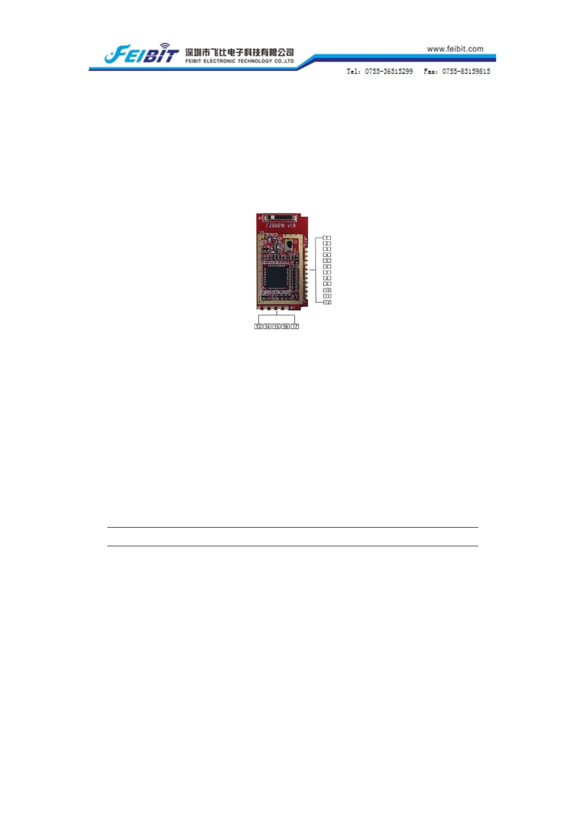
Pin assignments of FZB5610 ZigBee module as shown as Figure 3-1.
Figure 3-1 FZB5610 Module
3.2 Pin Attributes
3.2.1 ZigBee Transmission Module
Use FZB5610 ZigBee module as transmission module,the pin attributes as shown as
table 3-1.
Table 3-1 Pin attributes of ZigBee Transmission Module(Corresponding Type:FZB5610-IR01-HA)
Pin number
Name
I/O
Description
1
VDD
Power(+3.3V)
2
KEY
I
FAC_NEW button
3
Nc.
4
GND.
Ground
5
Nc.
6
Nc.
7
Nc.
8
Status LED
O
State LED
9
Tx
O
Serial ports send Tx
10
Rx
I
Serial ports receive Rx
11
Nc.

12
Pin number
Name
I/O
Description
12
Nc.
13
GND.
Ground
14
RESETn
I
System RESET signal,active low
15
DC
I
DEBUG port,leave unconnected
16
DD
I/O
DEBUG port,leave unconnected
17
VDD
I
Power(+3.3V)
3.2.2 ZLL Module
Use FZB5610 ZigBee module as transmission module,the pin attributes as shown as
table 3-2.
Table 3-2 Pin attributes of ZLL Module(Corresponding Type:FZB5610 -CW02-ZLL(RGB)
/FZB5610-BW01-ZLL(Dimming))
Pin number
Name
I/O
Descriptions
1
VDD
I
Power(+3.3V)
2
B-DRIVE
O
Blue LED PWM control signal
3
G-DRIVE
O
Green LED PWM control signal
4
GND.
I
Ground
5
Nc.
6
Nc.
7
Nc.
8
Nc
9
R-DRIVE
O
Red LED PWM control signal
10
FAC_RESE
T
Factory reset button,press 5 seconds can reset to
factory setting. Active low.
11
Nc
12
IR_IN
Infrared remote control signal
13
GND.
Ground
14
RESETn
I
System RESET signal,active low
15
DC
I
DEBUG port
16
DD
I/O
DEBUG port
17
VDD
I
Power(+3.3V)

13
3.2.3 Curtain Module
Use FZB5610 ZigBee module as curtain module,the pin attributes as shown as table
3-3.
Table 3-3 Pin attribute of ZigBee HA Smart Curtain Module(Corresponding Type:FZB5610-CUR01-HA)
Pin Number
Name
I/O
Descriptions
1
VDD
I
Power(+3.3V)
2
L-DRIVE
O
Control signal-Left
3
R-DRIVE
O
Control signal-Right
4
GND.
I
Ground
5
TSET
I
Test button signal,active low
6
R
I
Button signal,active low
7
STOP
I
Button signal-stop,active low
8
L
I
Button signal-right,active low.
9
Nc.
10
FAC_RESET
I
Factory reset button,press 5 seconds can reset to
factory setting. Active low.
11
Nc.
12
Status
O
Operating Status Indicator,it can connect to LED.H :
ON,L:OFF;If LED keeps on,the model is not in the
ZigBee Network;If LED is off,the model is in the ZigBee
Network.In this case,each time the model sends a
ZigBee data,LED flashes one time.When exiting the
network,LED flashes quickly.It will not flash until LED
keeps on,that means logout succeed
13
GND.
Ground
14
RESETn
I
System RESET signal,active low.
15
DC
I
DEBUG port
16
DD
I/O
DEBUG port
17
VDD
I
Power(+3.3V)
3.2.4 Light Sensor Module
Use FZB5610 ZigBee module as Light Sensor module,the pin attributes as shown as
table 3-4.
Table 3-4 Pin attributes of ZigBee HA Light Sensor Module(Corresponding Type :FZB5610-LGT01-HA)

14
Pin Number
Name
I/O
Description
1
VDD
I
Power Input(+3.3V)
2
SCL
O
Light Sensor reads SCL signal of bus clock
3
DO
O
Relay control signal
4
GND.
I
Ground
5
Nc.
6
DCT
I
Relay control feedback
7
Nc
8
Status
O
Operating Status Indicator,it can connect to
LED.H:ON,L:OFF;If LED keeps on,the model is
not in the ZigBee Network;If LED is off,the model
is in the ZigBee Network.In this case,each time the
model sends a ZigBee data,LED flashes one
time.When exiting the network,LED flashes
quickly.It will not flash until LED keeps on,that
means logout succeed.
9
Nc.
10
FAC_RES
ET
I
Factory reset button,press 5 seconds can reset to
factory setting. Active low.
11
SDA
O
Light Sensor reads signal SDA of data bus
12
Nc.
13
GND.
Ground
14
RESETn
I
System reset signal,active low
15
DC
I
DEBUG port,leave unconnected.
16
DD
I/O
DEBUG port,leave unconnected.
17
VDD
I
Power(+3.3V)
3.2.5 Infrared Human Body Sensor Module
Use FZB5610 ZigBee module as Infrared Human Body Sensor module,the pin
attributes as shown as table 3-5.
Table 3-5 Pin attributes of ZigBee HA Infrared Human Body Sensor Module(Corresponding
Type:FZB5610-BOT01-HA)
Pin number
Name
I/O
Description
1
VDD
I
Power(+3.3V)
2
DIN
I
Infrared Human Body Sensor,active high,H:
Someone,L:No one.When designing,should configure
pull-down resistor.
3
NC.
O
Output ,active low

15
Pin number
Name
I/O
Description
4
GND.
Ground
5
Nc.
O
Output ,active low
6
Nc.
O
Output ,active low
7
Nc
O
Output ,active low
8
Status
O
Operating Status Indicator,it can connect to LED.H :
ON,L:OFF;If LED keeps on,the model is not in the
ZigBee Network;If LED is off,the model is in the ZigBee
Network.In this case,each time the model sends a
ZigBee data,LED flashes one time.When exiting the
network,LED flashes quickly.It will not flash until LED
keeps on,that means logout succeed.
9
Nc.
O
Output ,active low
10
FAC_RESE
T
I
Factory reset button,press 5 seconds can reset to
factory setting. Active low.When designing,should
configure pull-down resistor.
11
Nc.
Output ,active low
12
Nc.
Output ,active low
13
GND.
Ground
14
RESETn
System RESET signal,active low
15
DC
I
DEBUG port,leave unconnected
16
DD
I/O
DEBUG port,leave unconnected
17
VDD
Power(+3.3V)
3.2.6 Switch Module
Use FZB5610 ZigBee module as Switch module,the pin attributes as shown as table
3-6.
Table 3-6 Pin attributes of ZigBee HA Smart Switch Module(Corresponding Type : FZB5610-SC
H01-HA)
Pin Number
Name
I/O
Description
1
VDD
I
Power(+3.3V)
2
DIN1
I
1# Switch input signal
3
DIN2
I
2# Switch input signal
4
GND.
I
Ground
5
DIN1_LED
O
6
DIN2_LED
O
7
DIN3_LED
O
DEMO Board leave unconnected.
8
Status
O
Operating Status Indicator,it can connect to LED.H:

16
Pin Number
Name
I/O
Description
ON,L:OFF;If LED keeps on,the model is not in the
ZigBee Network;If LED is off,the model is in the
ZigBee Network.In this case,each time the model
sends a ZigBee data,LED flashes one time.When
exiting the network,LED flashes quickly.It will not
flash until LED keeps on,that means logout
succeed.
9
DIN4_LED
O
DEMO Board leave unconnected
10
FAC_RESET
I
Factory reset button,press 5 seconds can reset to
factory setting. Active low.
11
DIN3
I
3# Switch input signal,DEMO Board leave
unconnected
12
DIN4
I
4# Switch input signal,DEMO Board leave
unconnected
13
GND.
Ground
14
RESETn
I
System RESET signal,active low.
15
DC
I
DEBUG port,leave unconnected
16
DD
I/O
DEBUG port,leave unconnected
17
VDD
I
Power(+3.3V)
3.2.7 Smart Plug Module
Use FZB5610 ZigBee module as Smart Plug module,the pin attributes as shown as
table 3-7.
Table 3-7 Pin attributes of ZigBee HA socket control module(Corresponding Type :
FZB5610-SKT01-HA)
Pin Number
Name
I/O
Description
1
VDD
I
Power(+3.3V)
2
DIN1
I
1# switch signal input
3
DIN2
I
2# switch signal input
4
GND.
I
Ground
5
DO1.
O
Relay control signal 1
6
DO2.
O
Relay control signal 2
7
DO3
O
Relay control signal 3
8
Status
O
Operating Status Indicator,it can connect to
LED.H:ON,L:OFF;If LED keeps on,the model is

17
Pin Number
Name
I/O
Description
not in the ZigBee Network;If LED is off,the model
is in the ZigBee Network.In this case,each time the
model sends a ZigBee data,LED flashes one
time.When exiting the network,LED flashes
quickly.It will not flash until LED keeps on,that
means logout succeed.
9
DO4.
O
Relay control signal 4
10
FAC_RES
ET
I
Factory reset button,press 5 seconds can reset to
factory setting. Active low.
11
DIN3
I
3# Switch signal input
12
DIN4
I
4# Switch signal input
13
GND.
Ground
14
RESETn
I
System RESET signal,active low
15
DC
I
DEBUG port,leave unconnected
16
DD
I/O
DEBUG port,leave unconnected
17
VDD
I
Power(+3.3V)
3.2.8 Temperature and Humanity Sensor Module
Use FZB5610 ZigBee module as Temperature and Humanity Sensor module,the pin
attributes as shown as table 3-8.
Table 3-8 Pin attributes of ZigBee HA Temperature and Humanity Sensor Module(Corresponding
Type:FZB5610-THM02-HA)
Pin number
Name
I/O
Description
1
VDD
I
Power(+3.3V)
2
FAC_RES
ET
I
Factory reset button,press 5 seconds can reset to
factory setting. Active low.
3
Nc.
4
GND.
I
Ground.
5
Nc.
6
Nc.
7
Nc.
8
Status
O
Operating Status Indicator,it can connect to
LED.H:ON,L:OFF;If LED keeps on,the model is
not in the ZigBee Network;If LED is off,the model
is in the ZigBee Network.In this case,each time the

18
Pin number
Name
I/O
Description
model sends a ZigBee data,LED flashes one
time.When exiting the network,LED flashes
quickly.It will not flash until LED keeps on,that
means logout succeed.
9
Tx
I
Serial port send Tx
10
Rx
O
Serial port receive Rx
11
Nc.
12
Nc.
13
GND.
Ground
14
RESETn
I
System RESET signal,active low
15
DC
I
DEBUG port,leave unconnected
16
DD
I/O
DEBUG port,leave unconnected
17
VDD
I
Power(+3.3V)
4 Reference Information
4.1 Electrical Schematic Diagram
The electrical schematic diagram of FZB5610 ZigBee module,which refers to
FZB5610 schematic diagram.pdf.
4.2 Design Considerations
◆The area below the antenna is unoccupied.
◆The power of the module had better use 5V regulated power ,use a LDO that is
suitable for RF application to supply power.
◆Had better use double-sided board to design.
◆IO port leave unconnected.
◆The width of LED drive’s layout is according to the actual current selection.
◆The default state of output IO port is high-level,suggesting the users to add
1.2KΩ to pull-down resistor.
◆RESET time is more than 200ms.See figure 4-1.

19
Figure 4-1 Reset time more than 200ms
5 IEEE 802.15.4
The IEEE 802.15.4 standard provides a worldwide standard for Personal Area
Networks and short distance wireless networks for low data rate solutions with long
battery life and low complexity.The standard defines a Physical layer(PHY) and a Medium
Access Control layer(MAC).There are two active versions of the standard:IEEE
802.15.4-2003 and IEEE 802.15.4-2006 where the 2003 version is the basis for the
ZigBee protocol.The typical applications are meter reading,home and building
automation,industrial control and monitoring systems,wireless sensor networks,remote
controls and consumer electronics.
The module complies with the IEEE 802.15.4 standard operating in the 2.45GHz
band.It uses direct sequence spread spectrum(DSSS) with 2 Mc/s chip rate giving a raw
data rate of 250kbit/s.16 channels are available in the 2.45GHz band named channel
11-26(channels 0-10 are reserved for use in the 868 and 915 MHz bands).
For more information on the standard,please consult
www.ieee802.org/15/pub/TG4.html.
6 The ZigBee Protocol
The ZigBee Alliance is an association of companies working together to enable
reliable,cost-effective,low-power,wirelessly networked,monitoring and control products
based on an open global standard.The ZigBee Alliance is a rapidly growing,non-profit
industry consortium of leading semiconductor manufactures,technology providers,OEMs
and end-users worldwide Membership is open to all.The ZigBee Alliance,in collaboration
with the IEEE is defining the network,security,and application layers above the IEEE

20
802.15.4 PHY and MAC layers.This cooperation has resulted in an easy-to-use,industry
standard wireless network platform optimised for wireless monitoring and control
applications.
The ZigBee standard defines a Network Layer and an Application Layer on top of
IEEE.802.15.4.The network layer includes routing,security etc.While the application layer
defines binding and other support for application.
The applications are specified in profiles to ensure multi-vendor
interoperability.Current public profile includes:
-Smart Energy-SE(Profile for Smart Meter reading)
-Building Automation-CBA
-Home Automation-HA
-Health Care-HC
-Telecom Services-TA
- Remote Control - RF4CE
Manufacturer specific profiles can also be made.
The current version of the ZigBee standard is 2007.The standard defines two
different stack feature sets:
- ZigBee Feature set
- ZigBee PRO feature set
In order to sell a product containing ZigBee technology, the seller must be a member
(adaptor or higher) of the ZigBee alliance.
For more information about the ZigBee Alliance and the ZigBee standard, please
consult www.zigbee.org.
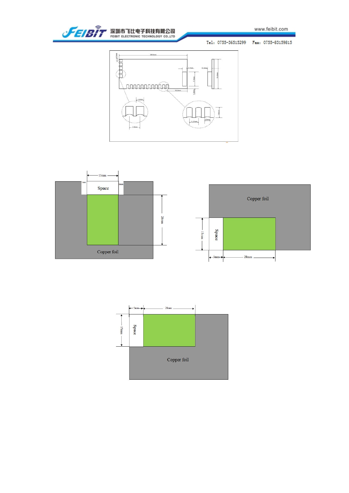
7 Mechanical Drawings And Installation
The mechanical drawings and installation as shown as below.
21
Figure 7-1 Mechanical drawing and installation
Figure 7-2 Installation 1 Figure 7-3 Installation 2
Figure 7-4 Installation 3

22
FCC compliance
This device complies with Part 15 of the FCC Rules.
Part Number
FCC ID
FZB5610
2AE8BFZB561011A
Operation is subject to the following two conditions: (1)this device may not cause
harmful interface,and (2)this device must accept any interface received,including interface
that may cause undesired operation.
Changes or modifications not expressly approved by the party responsible for
compliance could void the user’s authority to operate the equipment.
This device must be installed and used in strict accordance with the manufacturer’s
instructions as described in the user documentation that comes with the product.
The modules have been approved with the following external chip antenna.
Manufacturer
Part Number
WinWave Electronic Co., Ltd.
WAN8010F245M05
Warning for FZB5610:This device complies with FCC RF radiation exposure limits set
forth for an uncontrolled environment.This device and its antenna(s) must not be
co-located or operating in conjunction with any other antenna or transmitter.
The final end product must be labeled in a visible area with the following:Contains
FCC ID: 2AE8BFZB561011A.
This module shall be integrated to the end product with a stable 3.3VDC power to this
module through regulator circuit.
The OEM integrator is responsible for testing their end-product for any additional
compliance requirements required with this module installed (for example, digital device
emission, PC peripheral requirements, etc.).

23
COPYRIGHT STATEMENT
The copyright of the manual is belonged to Shenzhen Feibit Electronic Technology
Co.,Ltd(simply “Feibit Technology”for short),and reserves all rights.Without the written
consent of Feibit Technology,any company or individual can’t copy the part or the whole
content of the manual.
DISCLAIMER
Because of the version upgrading and other reasons,the content of the manual will
update irregular.Unless with the other appointment,the manual will be only used as the
user’s guide,and all the statement,information and suggestion will not constitute any
guarantee.
TRADEMARK STATEMENT
is used as the trademark of Shenzhen Feibit Electronic Technology Co.,Ltd.All other
trademarks and registered trademarks are property of their respective owners.
Contact us
Shenzhen Feibit Electric Technology CO.,Ltd
Address :Room 505, Building A1, Lilang Software Park, No 31. Bulan Road, Nanwan
Street, Longgang District, Shenzhen, China
Tel:0755-36515299
Fax:0755-83159815
E-mail:sales@feibit.com
Website:www.feibit.com