Fairfield BOX-RU Geophysical Data Telemetry System User Manual RU07 Appendix 5
Fairfield Industries Inc Geophysical Data Telemetry System RU07 Appendix 5
Operating Manual

THE BOX - Remote Unit Application for FCC Certification
Radio System: Operating Manual
Appendix 5 Page 0 of 27
Appendix 5
Remote Unit Radio System

THE BOX - Remote Unit Application for FCC Certification
Radio System: Operating Manual
Appendix 5 Page 1 of 27
Appendix 5
Contents
1.0 Overall Description of RU
2.0 RF Module
2.1 Overall Description
2.2 Dallas Temperature Sensor
2.3 Cartesian Loop Linearizer
2.3.1 Operation
2.3.1.1 Instability Detection
2.3.1.2 DC Null
2.3.2 Transmit/Receive Switching
2.4 Receiver
2.5 Power Amplifier (Transmitter)
2.5.1 Overall Description
2.5.2 Sub-Modules
2.5.3 Power amplifier
2.5.4 Transmitter Mask
2.5.5 Electrical Specifications
2.6 Synthesizer
2.6.1 Performance Parameters
3.0 Baseband Module
3.1 Overall Description
3.2 Processor
3.3 Codec
3.4 Memory
3.5 Clock Generation
3.6 Parallel Host Interface
3.7 Temperature Sensing
4.0 RU Power Supply
5.0 RU Signals and Connections
5.1 RF Module
5.1.1 Power Amplifier
5.2 Synthesizer
5.3 Receiver
5.4 Baseband Module
THE BOX - Remote Unit Application for FCC Certification
Radio System: Operating Manual
Appendix 5 Page 2 of 27
1.0 Overall Description of RU
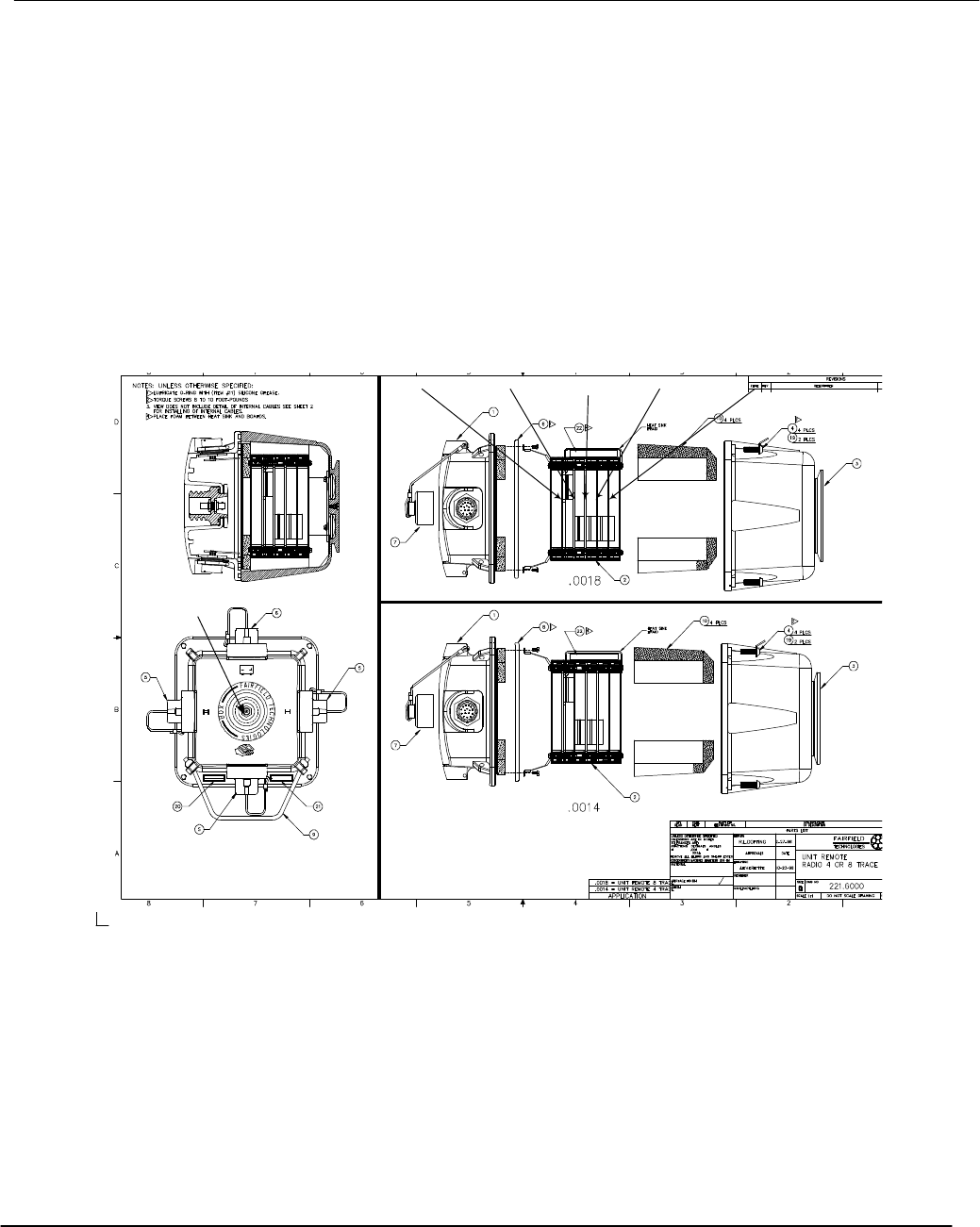
Each remote unit (RU) is mounted on and powered by a Battery power unit.
All RUs are identical, each containing a stack of five interconnected circuit boards, held together by
spacers and secured by shock mountings. As shown in figure 1, the board order (top to bottom) is:
Radio System RF Module
Radio System Baseband Module
Main CPU Module
ADC Module #1
ADC Module #
Remote Unit - Assembly
Figure 1
The radio sub-system, which includes the RF and Baseband boards, is able to
• Transmit data to the CRS using 16QAM transmission at 60 kb/s (up-link) and
• Receive commands from the CRS, which have been transmitted using 10 kb/s QPSK transmission
(down-link).
RF Board Baseband Board CPU Board ADC Board #1 ADC Board #2
Antenna Connector
THE BOX - Remote Unit Application for FCC Certification
Radio System: Operating Manual
Appendix 5 Page 3 of 27
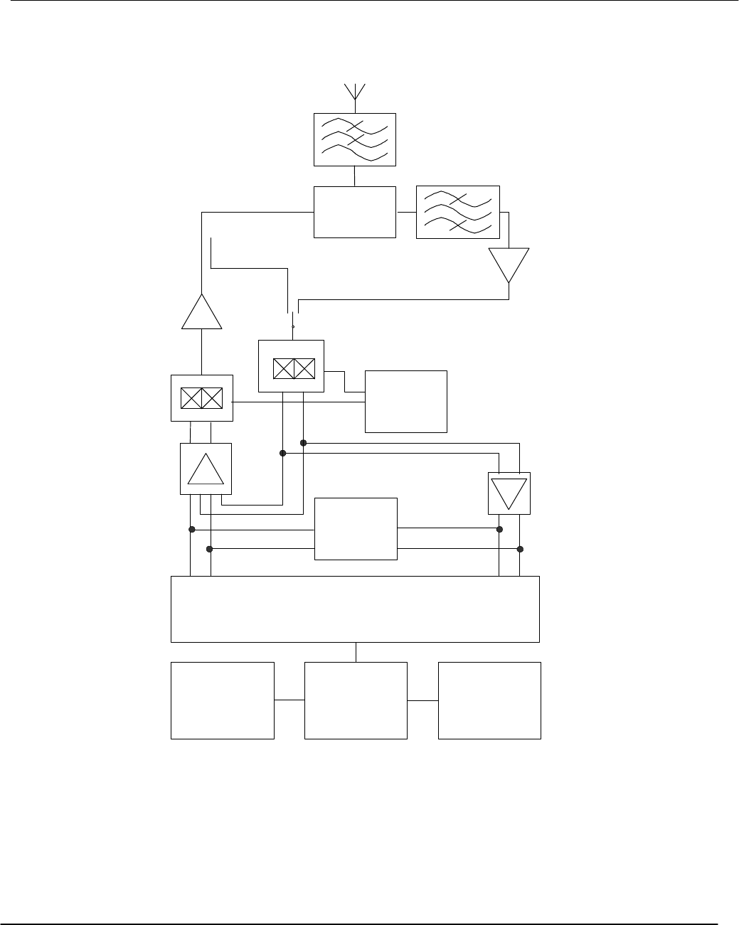
The whole radio sub-system is depicted in block form in figure 2.
Transmit/Receive
Switch
Data I/O Digital Signal
Processor Memory
Sigma-Delta
DAC / ADC
Baseband Interface
Synthesiser
IQ Demodulator
IQ Modulator
Tx Rx
Coupler
Radio Sub-System Block Diagram
Figure 2
THE BOX - Remote Unit Application for FCC Certification
Radio System: Operating Manual
Appendix 5 Page 4 of 27
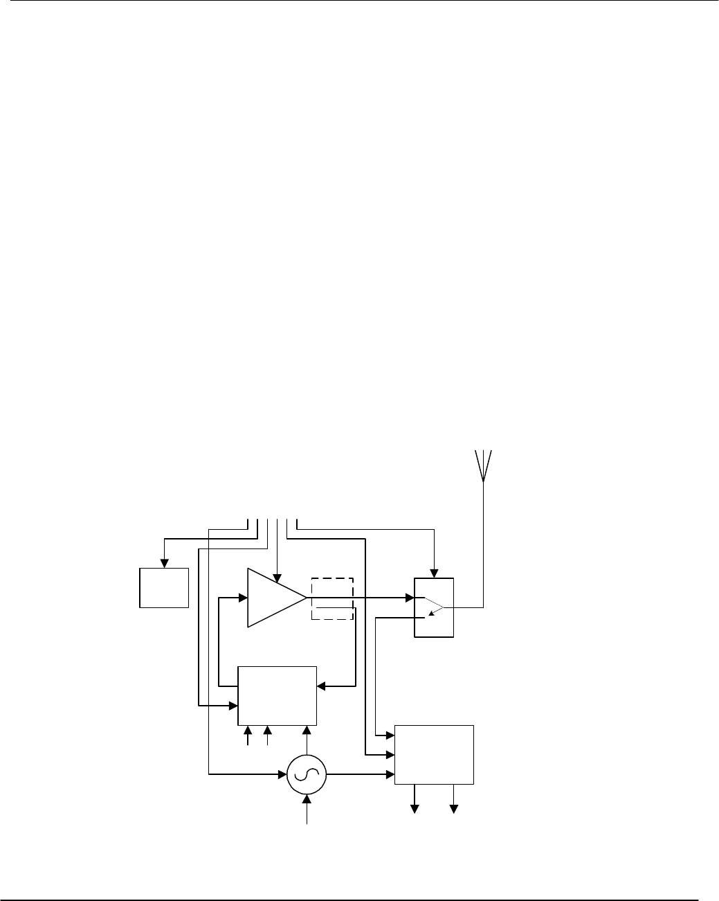
2.0 RF Module
2.1 Overall Description
The RF Module of the RU contains
• the receiver for commands downlinked from the CRS and
• the transmitter for uplinking data from the RU to the CRS.
With reference to figure 3 it can be seen that the RF modle can be split into six discrete sub-modules,
these being:
Cartesian Loop Linearizer
Transmitter/Power Amplifier
Transmit/Receive Switch
Synthesizer
Receiver
Dallas temperature sensor
The RU Receiver is described in 2.4 and the RU Transmitter/Power Amplifier in 2.5.
PA
Cartesian
Loop
Linearizer
Receiver
DALLAS
SENSOR
Baseband Board Control
TX/RX
Switch
20.48 MHz LO I & Q Outputs
Antenna
Synthesizer
I & Q Inputs
Coupler
Remote Unit RF Module Overall Block Diagram
Figure 3:
THE BOX - Remote Unit Application for FCC Certification
Radio System: Operating Manual
Appendix 5 Page 5 of 27
2.2 Dallas Temperature Sensor
The temperature-sensing device (manufactured by Dallas Corporation) is programmed by the
Baseband board and incorporates two important features.
First it provides a temperature measurement system with a one-second acquisition time, the
data being read as an integer byte via a two wire serial (i2c) line.
Second it incorporates 256 bytes of non-volatile memory for storing details unique to the
individual amplifier – such as phase control voltages, phase and image-balance information,
and model details including serial number and revision details.
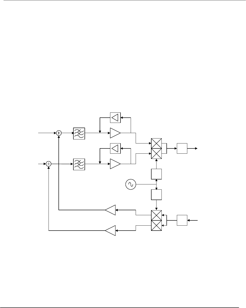
2.3 Cartesian Loop Linearizer
Figure 4 shows a block diagram of the linearizer.
Linearizer – Block Diagram
Figure 4
2.3.1 Operation
A fraction of the transmitted power is fed back from the output via the coupler. Further attenuation is
required to reduce the signal to a level suitable for input to the down-converter, where the signal is
split and down-converted, with two carriers of 90º phase difference yielding the I and Q baseband
signals.
φ
dB
dB
τ
I
Q
Low-Pass Filters
Local Oscillator
Phase
Shifter
Delay Line
RF Feedback
from Coupler
RF Modulation
to PA
Feedback Gain
Sample and Hold
Switchable
Attenuator
Switchable
Attenuator
Up-
Converter
Down-
Converter
THE BOX - Remote Unit Application for FCC Certification
Radio System: Operating Manual
Appendix 5 Page 6 of 27
Feedback gain is provided by low-noise operational amplifiers.
The signal is then subtracted from the modulation input and the forward-path error signal is low-pass
filtered and pre-amplified at baseband.
2.3.1.1 Instability Detection
During operation, the loop may become unstable. Therefore, to monitor loop stability, a circuit is
provided which detects energy in the output spectrum at around 200 kHz above the carrier.
If the loop starts to become unstable, high frequency components appear in the output
spectrum and correspondingly at baseband level.
A high-pass filter is used to isolate these higher frequencies, which are then fed through an amplitude
detector. When the detected amplitude reaches a preset dc detected level, an instability error is
flagged.
2.3.1.2 DC Null
As a result of carrier up/down-converter feed-through during Power Amplifier operation, a steadily-
rising carrier component can be seen on the output spectrum. This may also be seen at baseband as
a dc component superimposed on the I and Q signals. As this is essentially an unwanted tone in the
output spectrum it must be removed.
Removal is achieved by sampling the magnitude of this dc component at the start of transmission,
and removing it from the following thirty seconds of transmission.
2.4 Transmit/Receive Switching
ANAREN
20dB COUPLER
Harmonic
Filter
TX/RX
Received
Signal
Transmit-Receive
Switch
RF_IN
RF_FB
50Ω
Load
Coupler and Transmit/Receive Switching
Figure 5
PIN diodes are used to direct signals from the antenna during Receive and to the antenna during
Transmit.

THE BOX - Remote Unit Application for FCC Certification
Radio System: Operating Manual
Appendix 5 Page 7 of 27
These diodes can be biased either positive or negative by Transistor switch Q4.
The RF path is determined by the PIN diodes’ bias which, in conjunction with matching circuitry,
appears to BOX RF signals as quarter wavelength sections. These sections have the ability to
behave as open circuits or 50Ω line depending on the polarity of the bias voltage.
THE BOX - Remote Unit Application for FCC Certification
Radio System: Operating Manual
Appendix 5 Page 8 of 27
The RF LO is fed into a Wilkinson power divider, giving an approximate 3 dB split.
One half is used directly by the Cartesian loop at –10dBm.
The other is fed through a small gain stage to provide a +10dBm signal for the receiver.
2.4. Receiver
The RU receiver, which is part of the RF board, provides the RF receiver path for the Command
downlink. Demodulation is achieved through ac-coupled direct conversion, which is suitable for
QPSK.
V-Tx
D4
L7 R74
C53/63 C151/152
Q4 Tx /Rx
From Tx
Power
Amplifier C62
Passes Tx Signal to Antenna
when V-Tx is high
Transmission
Path
Transmission
Path
Rx RF
L2
L12
C48
C27
C29 L22
C37 C52 C80 D15
C79
Antenna
Received and
Transmitted Signals
Reception Path
L1
When Tx/Rx is HIGH, Radio Section is in
.TRANSMIT Mode.
When Tx/Rx is LOW, Radio Section is in
.RECEIVE Mode.
Transmit/Receive Switch & RF Paths to and from Antenna
Figure 6
6.5 V
THE BOX - Remote Unit Application for FCC Certification
Radio System: Operating Manual
Appendix 5 Page 9 of 27
Baseband I
to Baseband
Board
Baseband Q
to Baseband
Board
Down
Converter
Low-Noise
Gain Stages
RF_IN
LO Driver
LO to PA
+ +
4
20.48MHz
REF
+10dBm LO
856-936MHz
214-234MHz
Serial Programming
BUS
Active
Filter
Final Gain
Stages
dB
Gain
Switch
High
Low
Receiver Block Diagram
Figure 7
The receiver is capable of operation in two modes: high-gain and low-gain.
• The high-gain setting is employed for maximum sensitivity and introduces an additional 20 dB gain
stage in the receive path.
• The low-gain setting is used for maximum signal handling, introducing a 4 dB pad in the receive
path, preventing saturation when large signals are encountered.
The RF signal received at the antenna is band-pass filtered and passed through the high/low gain
switch.
It is then fed into a Mini-Circuits down-converter (JSIQ-234D1) and mixed with the +10 dBm LO,
resulting in the production of I and Q baseband signals. These I and Q signals are fed into a low
noise op-amp stage, consisting of a CLC428 with a voltage gain of about 10.
The baseband signals are then fed into an active filter chain, with a roll-off from 80 to 140 kHz. The
final stage involves amplitude-balancing, followed once again by a low-noise gain stage. The
baseband I and Q signals are then fed to the baseband Remote Unit board.
THE BOX - Remote Unit Application for FCC Certification
Radio System: Operating Manual
Appendix 5 Page 10 of 27
2.5Power Amplifier (Transmitter)
2.5.1 Overall Description
The RU transmitter, which is shown in block form in figure 8, is part of the RF module.
It provides the data uplink channel for both command and sample data.
The transmitter consists of a Cartesian linearized power amplifier suitable for both 16QAM data
modulation and (if required) linear voice modulation. The RU Transmitter’s chief specifications are
summarised as follows:
Output Power: +27 dBm
RF power control: 58 dB
Supply voltage: 12 V nominal, 10.5 V min, 14.8 V max.
Channel bandwidth: 20 kHz
Data format: Pilot aided 16QAM
2.5.2 Sub-Modules
The RU transmitter contains two sub-modules, the Power Amplifier and the Cartesian Linearizer.
Power Control
Transmitter Control
PA Switch
Switched
Attenuator
Quadrature
Demodulator
Baseband LNA
Phase Shifter
(360°)
Loop
Filter Quadrature
Modulator Switched
Attenuator PA
Driver PA Tx/Rx
Switch Harmonic
Filter Antenna
Tx Enable
Power
Control
LO Up
(214-234 MHz)
I
Q
LO Down
(214-234 MHz)
Directional
Coupler
To Receiver
Power Amplifier
Remote Unit – Radio Transmitter
Figure 8
THE BOX - Remote Unit Application for FCC Certification
Radio System: Operating Manual
Appendix 5 Page 11 of 27
2.5.3 Power Amplifier
The power amplifier sub-module provides most of the RF gain and final output drive for the RU
transmitter. Also included is transmit/receive switching and an output coupler for the Cartesian
linearizer.
This output coupler provides the forward-path gain and the final output drive. Figure 9 shows the
three-stage device line-up employed. High or low gain modes can be selected depending on the
range of output level required.
BFP193 MRF557 D1211UK
12V @ 30mA
20dB Gain 12V @ 100mA
15dB Gain 12V @ 400mA
22dB Gain
Device line-up (high gain setting)
Figure 9
Feedback is employed on the first two stages to reduce the gain from the maximum available. When
the device is switched OFF in the low-gain mode, the feedback on the second stage also provides an
RF forward-path
There is a signal gain of 56 dB in high-gain mode and approximately 23 dB in low-gain mode.
The Semelab D1211 is capable of 40 dBm output and is under-driven to maximize the intermodulation
distortion performance of the PA.
2.5.4 Transmitter Mask
Figure 10 shows the transmit mask in direct mode. All numbers are power relative to the wanted
channel, measured in a 20 kHz bandwidth.
THE BOX - Remote Unit Application for FCC Certification
Radio System: Operating Manual
Appendix 5 Page 12 of 27
Transmitter Mask
Figure 10
2.5.5 Electrical Specifications
Frequency Range: 216 - 220 MHz
Output power: 0.5 W (27 dBm)
Stability: Stable with loads ≤ 3:1 (all angles)
High Gain: 56 dB nom.
High Gain flatness: ±1 dB max.
Low Gain: 22 dB nom
Low Gain flatness ±1 dB max
Power added efficiency: 30% min.
Noise floor: ≤ -90 dBm/Hz at ≥ 2 MHz from carrier
The above powers are measured at the antenna connector.
2.6 Synthesizer
The RU Synthesizer is part of the RF module. It is illustrated in block schematic diagram in figure 11.
This synthesizer serves two main purposes:
• Generation of the local oscillator required for the direct down-conversion receiver.
THE BOX - Remote Unit Application for FCC Certification
Radio System: Operating Manual
Appendix 5 Page 13 of 27
• Generation of the two local oscillators required for the direct up-conversion Cartesian loop
transmitter.
Control of synthesizer frequency is achieved by programming the synthesizer hardware via a serial
bus.
In order to avoid possible interference problems in transmit-mode the voltage-controlled oscillator
(VCO), which forms part of the synthesizer, runs at four times the fundamental operating frequency
Reference
Conditioning Synthesiser
VCO
856-936 MHz
Power Supply
Divide
by
4Buffer
Amplifier
Power
-10 dBm
Output
+10 dBm
Output
REF_OSC
RU Synthesizer – Block Diagram
Figure 11
2.6.1 Performance Parameters
2.6.1.1 Transmit & Receive Frequencies
The operating band is 216 to 220 MHz in 20kHz channels and the synthesizer is able to generate a
216.01 to 219.99 MHz Local Oscillator, programmable in 10kHz steps.
2.6.1.2 Phase Noise
The synthesizer’s frequency-dependent phase noise is illustrated in Figure 12.
2.6.1.3 Lock time
Less than 20 ms.
2.6.1.4 Spurious output
Harmonics < 30 dBc
Non harmonics <70 dBc
THE BOX - Remote Unit Application for FCC Certification
Radio System: Operating Manual
Appendix 5 Page 14 of 27
Synthesizer Phase Noise
Figure 12
3.0 Baseband Module
3.1 Overall Description
The Remote Unit baseband board, which is shown in block form in Figure 13, comprises a single
digital signal processor (DSP) with ancillary memory and peripherals.
This sub-module carries out the following functions:
• Modulation of the uplink 16QAM baseband signal
• Demodulation of the downlink QPSK baseband signal
• Command and data communications with the host processor through the host parallel interface
• RS232 communications for firmware downloads and for use in testing.
• Timer functions to control the duty cycle in sleep and standby modes.
• Power supply management and regulation for baseband and RF board switching.
• Digital I/O associated with control of the RF board and PA module
• Digital I/O signals to/from the host CPU card
• Clock generation for Codec, processor and frequency locked reference
• Local frequency reference pulling
• Analog control signals for the RF module (if required)
THE BOX - Remote Unit Application for FCC Certification
Radio System: Operating Manual
Appendix 5 Page 15 of 27
DSP
TMS320C50
Serial I/F
CODEC
CS4225
Audio Out
I Out
Q Out
I In
Q In
Clock
Generator Freq. Ref
VCTCXO
7.68MHz
20.48MHz
VCXO
FPGA
Address Decode, Device Select, Host I/F
Address
Bus
Host Data
(16 bit)
FLASH 128k
120ns
Data Bus
(16 bit)
RAM
32k 70ns
UARTRS232
Non-Volatile
RAM
256 bytes
Standby
Low power
Programmable
Timer
Power Supply
Conditioning
&
Control
Wake Up
DAC
8 bit serial
(Low power)
Repeater
Switching
2.048MHz
Audio
In
Tx I
Tx Q
Rx I
Rx Q
RP Rx/Tx I
RP Rx/Tx Q
iic
Loop phase
20.48MHz
Digital
I/O
Rf Control
Battery
Voltage
Power
Control
Host
Control
Remote Unit - Baseband Sub-Module
Figure 13
3.2 Processor
The baseband sub-module is designed around a single 40.96 MHz Texas Instruments TMS320C50
digital signal processor which is capable of performing all modulation, demodulation, control and
communication tasks on the RF module.
3.3 Codec
A single Crystal Semiconductor CS4225 Codec device performs most of the analog to digital and
digital to analog conversion. This device also provides channel and anti-aliasing filtering of the
baseband signals.
An additional low current DAC provides phase control of the Cartesian loop transmitter. The complete
analog signal set is:
• I in • Cartesian loop phase control output
• Q in • Frequency reference adjust
• I out
• Q out

THE BOX - Remote Unit Application for FCC Certification
Radio System: Operating Manual
Appendix 5 Page 16 of 27
3.4 Memory
Three types of memory are provided in the baseband module for program and data storage:
• FLASH RWM
• Static RAM
• Non-volatile RAM
3.5 Clock Generation
A clock generator circuit derives the following clock waveforms from the 20.48 MHz frequency
Reference on the board. This Reference is locked to the base-station Master Reference during
receive:
• 7.68 MHz to drive the Codec at the correct sampling rate
• 20.48 MHz DSP clock. This is clocked into the DSP in ×1 mode to give a minimum internal cycle
time of 48.82 ns, corresponding to a basic processor speed of 20.48 MIPS.
• 2.048 MHz - a divided and buffered version of the on-board reference for use by the CPU host
When the RF module is frequency locked (i.e. during receive mode); stability of all clocks is ±0.5 ppm
with respect to the Central Recording System’s Master Reference.
At other times, when the on-board reference is free-running, clock stability is ±3 ppm.
It is the responsibility of the host CPU to ensure the integrity of any data transferred to the radio
system for the purpose of firmware updates before the transfer is made.
3.6 Parallel Host Interface
A parallel bi-directional interface is provided between the Host CPU (Motorola 68336 processor) and
the RF board TMS320C50 processor. This interface is used for passing:
downlink messages from the radio system to the host CPU and
uplink data from the host to the radio.
Additionally the host interface is used for control messaging issued by the host CPU, and for any
subsequent baseband replies.
3.7 Temperature sensing
Thermal monitoring is provided on the radio transmitter, with the baseband module DSP able to read
the PA temperature and ascertain if it is approaching its maximum recommended operating
temperature. Data from this sensor is made available to the host processor over the host parallel
interface.

THE BOX - Remote Unit Application for FCC Certification
Radio System: Operating Manual
Appendix 5 Page 17 of 27
4.0 RU Power Supply
The RU is powered by a power-supply unit (or “battery pack) located beneath and attached to the RU
housing as shown in figure 14.
The unit contains one 12 V --- AH rechargeable lead-acid battery, which may be recharged without
removing it from the unit.
Figure 14
The Power-Supply Unit may be rectangular for land use as or cylindrical for marine use as illustrated
in fires 15 and 16 respectively.
Land Power Unit Marine Power Unit
Figure 15 Figure 16
Annotated Photograph of
RU with Land Battery Box
Assembly Drawing Assembly Drawing

THE BOX - Remote Unit Application for FCC Certification
Radio System: Operating Manual
Appendix 5 Page 18 of 27
5.0 RU Signals and Connections
5.1 RF Module
5.1.1 Power Amplifier
5.1.1.1 External Interfaces
External interfaces to the transmitter sub-module are defined as those signals which leave the radio
system RF board. They therefore include all
• transmitter control signals which originate on the baseband board, and
• all status signals that go to the baseband board.
Table 1 lists the signals that constitute the external interface between the Power Amplifier
(transmitter) and the rest of the Remote Unit (excluding signals internal to the RF module).
Signal Name Direction Type Description
20dB_ATT_B In Digital HCMOS power control: 20dB step
10dB_ATT_A In Digital HCMOS power control: 10dB step
25dB_DOWN In Digital HCMOS power control, down converter:
switches in delay line
25dB_UP In Digital HCMOS power control, up converter:
switches second stage of PA
ANT In/Out RF Antenna connector
50Ω SMA female
BATT In Power Unregulated power supply for PA
DC_NULL In Digital Cartesian loop dc null control
GND In Power Ground
I_DOWN Out Analog Baseband I channel output (to receiver)
Q_DOWN Out Analog Baseband Q channel output (to receiver)
I_UP In Analog Baseband I channel input (from codec)
Q_UP In Analog Baseband Q channel input (from codec)
INSTB Out Digital Transmitter instability detector (to DSP)
PA_ON In Digital Switches PA on
PH_CTL In Analog Cartesian loop phase control
TX_RX In Digital Switches between Tx & Rx mode
SCL In Digital PA temperature sensor Clock
SDA Out Digital PA temperature sensor Serial Data
RU Transmitter - External/Interface Signals
Table 1
THE BOX - Remote Unit Application for FCC Certification
Radio System: Operating Manual
Appendix 5 Page 19 of 27
5.1.1.2 Internal Interfaces
Table 2 lists the internal interface signals between the Cartesian Linear Transmitter and the other sub-
modules on the RF module.
Signal Name Direction Type Description
C10V In Power Power supply for CLT
Regulated from raw battery power
S2V5 In Power Power supply for CLT
RX_RF Out RF Received RF output to Receiver front-end
Frequency range: 214 - 234 MHz
Source impedance: 50Ω nominal
Power: 0 dBm max
RF_FB In RF Coupled RF input from PA directional coupler
RF_MOD Out RF Low level modulated RF output to PA
Rx_D In RF Down converter RF input from Receiver front-end
LO_+10dBm In RF Local oscillator input for down converter
50Ω, +10 dBm nom.
LO_-10dBM In RF Local oscillator input for up converter
50Ω, -10 dBm nominal
RU - Interface Signals between Cartesian Linear Transmitter Sub-Module and
other Radio Board Sub-Modules
Table 2:
5.2 Synthesizer
5.2.1 Interfaces
All interfaces to and from the synthesizer are internal, i.e. between the synthesiser and other sub-
modules within the RF module.
5.2.1.1 Inputs
Signal Name Description
S5V Synthesizer +5 V Power supply
50 mA max
S10V Synthesizer +10 V Power supply
10 mA max
GND Analog ground
S_CLK Synthesizer serial data clock
High impedance CMOS input
Data clocked in on rising edge
S_DATA Synthesizer serial data
High impedance CMOS input
Data entered MSB first
Continued Overleaf
THE BOX - Remote Unit Application for FCC Certification
Radio System: Operating Manual
Appendix 5 Page 20 of 27
S_LE Synthesizer load enable
High impedance CMOS input
When SLE goes high, data stored in synthesizer shift registers is loaded
into the appropriate latch.
REF_OSC 20.48 MHz Reference oscillator input
Synthesizer – Input Signals
Table 3
5.2.1.2 Outputs
Signal Name Description
LO_+10dBm LO output to the down-converter
+9 dBm, ±1 dB, nominal impedance 50Ω
LO_-10dBm LO output to the transmitter up-converter
-8 dBm, ± 2 dB, nominal impedance 50Ω
Synthesizer – Output Signals
Table 4
5.2.1.5 Internal Interfaces
Signal Name Direction Type Description
C10V In Power Power supply for CLT
Regulated from battery power
S2V5 In Power Power supply for CLT
RX_RF Out RF Received RF output to Receiver front-end
Frequency range: 214 - 234 MHz
Source impedance: 50Ω nominal
Power: 0 dBm max
RF_FB In RF Coupled RF input from PA directional coupler
RF_MOD Out RF Low level modulated RF output to PA
Rx_D In RF Down converter RF input from Receiver front-end
LO_+10 dBm In RF Local oscillator input for down converter
50Ω, +10 dBm nominal
LO_-10 dBM In RF Local oscillator input for up converter
50Ω, -10 dBm nominal
Synthesizer – Internal Interfaces
Table 7
5.2.1.6 Digital Control Signals
Signal Direction Connector Type Description
SLE In P2: 15; 16 TTL Synthesizer enable
S_DATA In P2: 17; 18 TTL Synthesizer data
S_CLOCK In P2: 19; 20 TTL Synthesizer clock
PA_ON In P2: 25; 26 HCMOS PA bias switch
Continued overleaf
DC_NULL In P2: 29; 30 HCMOS Transmitter DC Null
LOW = Null; HIGH = normal transmit

THE BOX - Remote Unit Application for FCC Certification
Radio System: Operating Manual
Appendix 5 Page 21 of 27
RX_GAIN In P2: 31; 31 HCMOS RX gain HI/LO switch
CON In P2: 35; 36 HCMOS Cartesian loop
RON In P2: 37; 38 HCMOS Receiver
SON In P2: 39; 40 HCMOS Synthesizer
TX_RX In P2: 42; 43 HCMOS Transmit/Receive
LOW = receive; HIGH = transmit
SCL In P2: 45; 46 HCMOS Dallas chip clock
SDA In P2: 47; 48 HCMOS Dallas chip data
INSTAB In P2: 51; 52 TTL Transmitter unstable
LOW = unstable; HIGH = unstable
20DB_ATTB In P2: 55; 56 HCMOS Power control (see Table 9)
10DB_ATTA In P2: 57; 58 HCMOS Power control (see Table 9)
25DB_UP In P2: 59; 60 HCMOS Power control (see Table 9)
Synthesizer – Digital Control Signals
Table 8
5.3 Receiver
5.3.1 Receiver Inputs, Outputs and Internal Signals
These are shown in Table 9.
Signal Name Direction Type Description
BATT In Power Unregulated power supply for PA
GND In Power Ground
R5V In Power 5V Power supply
200 mA max
A6V5 In Power 6.5V Power supply to front end
20mA max
AGND In Power Analogue ground
RX_RF Out RF Received RF output after Tx-Rx switch to Receiver front-end.
Frequency range: 214 - 234 MHz
LO_+10dBm In RF Local oscillator input for receiver
50Ω, +10dBm nom.
ANT In/Out RF Antenna connector
50Ω SMA female
IRX Out RF Baseband I channel output
Level 2.5 V pp ±0.1 v pp max.
QRX Out RF Baseband Q channel output
Level 2.5 V pp ±0.1 v pp max.
TX_RX In Digital Switches between TX & RX mode
RX_GAIN In HCMOS Set RX gain for either maximum sensitivity or large signal
handling
RON In HOS Receiver Enable - used by FET switches on baseband inputs
Table 9

THE BOX - Remote Unit Application for FCC Certification
Radio System: Operating Manual
Appendix 5 Page 22 of 27
5.4 Baseband Module
5.4.1 External Interfaces
These signals which originate from or go directly to the Baseband module from any part of the RU
(other than the radio RF module) are listed in Table 10.
Signal Name Direction Type Connector Description
HI_D0 -
HI_D15 In/Out Digital H1 pin 1-16 16 bit parallel interface, Host CPU data bus
TTL
HI_C/D In Digital H1 pin 33 Indicates whether host interface contents are
command or data (host to radio direction only)
TTL
See Ref. [8] for levels & timing
HI_WSTRB In Digital H1:37 Buffer read/write
TTL
See Ref. [8] for levels & timing
HI_RFLAG Out Digital H1:35 Read buffer full flag
TTL
See Ref. [8] for levels & timing
HI_WFLAG Out Digital H1:36 Write buffer full flag
TTL
See Ref. [8] for levels & timing
HI_RSTRB In/Out Digital H1:34 Read data strobe
TTL
See Ref. [8] for levels & timing
WKUPH Out Digital H1:39 Wakeup to Host CPU from Radio system
TTL high: wakeup
TTL low: radio card in sleep mode
WKUPR In Digital H1:38 Wakeup from Host CPU to Radio system
TTL high: Wakeup radio system from sleep
HI_RESET In Digital H1:40 Hardware reset from Host
TTL active high
REF Out Digital H1:41 2.048 MHz reference locked to master ref.
Buffering HCMOS
TZERO Out Digital H1:42 T-zero
HCMOS, timing ±20 µs
AUD_IN In Analog TBD Audio input
0 dBm into 600Ω
AUD_OUT Out Analog TBD Audio output
0 dBm into 600Ω
RP_I+ In/Out Analog H6 pin 2 Repeater I channel
Analog differential line driver !5 V
RP_I- In/Out Analog H6 pin 1 Repeater I channel
Analogue Differential line driver !5 V
RP_Q+ In/Out Analog H6 pin 5 Repeater Q channel
Analogue differential line driver !5 V
Continued overleaf

THE BOX - Remote Unit Application for FCC Certification
Radio System: Operating Manual
Appendix 5 Page 23 of 27
RP_Q- In/Out Analog H6 pin 4 Repeater Q channel
Analogue differential line driver !5 V
RP_DIR+ In/Out Digital H6 pin 8 Repeater uplink/downlink select
Digital differential line driver !5 V
RP_DIR- In/Out Digital H6 pin 7 Repeater uplink/downlink select
Digital differential line driver !5 V
RP_MODE In Digital H6 pin 15 Repeater/Normal mode select
HCMOS high: Repeater
HCMOS low: Normal
RP_MS In Digital H6 pin 13 Repeater master/slave select
HCMOS high: master
HCMOS low: slave
RP_WKUP+ In/Out Digital H6 pin 10 Wakeup to repeater slave
RP_WKUP- In/Out H6 pin 9 Wakeup to repeater slave
RP_U1+ In/Out H6 pin 12 Unused
Digital differential line driver ±5 V
RP_U1- In/Out Digital H6 pin 11 Unused
Digital differential line driver ±5 V
RP_GND Out Power H6 pins 14 Ground for repeater link
RP_AGND In Power H6 pin 3 Analogue ground connection
RP_SCRN In Power H6 pin 6 Cable screen connection
PTT In Digital TBD Push-to-talk test connector
TCK In Digital H3 pin 11 JTAG test clock
HCMOS
TDI In Digital H3 pin 3 JTAG test data input
HCMOS
TDO Out Digital H3 pin 7 JTAG test data output
HCMOS
TMS In Digital H3 pin 1 JTAG test mode select
HCMOS
TRST In Digital H3 pin 2 JTAG test reset
HCMOS
EMU0 In/Out Digital H3 pin 13 JTAG emulation pin 0
HCMOS
EMU1 In/Out Digital H3 pin 14 JTAG emulation pin 1
HCMOS
PD Out Digital H3 pin 5 JTAG presence detect
HCMOS
TCK_RET Out Digital H3 pin 9 JTAG test clock return
HCMOS
RXD Out RS232 H4 pin 2 RS232 Receive Data
TXD In RS232 H4 pin 3 RS232 Transmit Data
DTR Out RS232 H4 pin 4 RS232 Data Terminal Ready
DSR Out RS232 H4 pin 6 RS232 Data Set Ready
RTS In RS232 H4 pin 7 RS232 Ready To Send
CTS Out RS232 H4 pin 8 RS232 Clear To Send
BATT In power H1 pin 52,
54, 56, 58, 60 +12V nominal battery power
range 10.8V to 15.6V
1.5 A max

THE BOX - Remote Unit Application for FCC Certification
Radio System: Operating Manual
Appendix 5 Page 24 of 27
GND In power H1 pin 17, 18
31, 32, 43, 44,
49, 51, 53, 55,
57, 59
Battery ground
Baseband Module - External Interface Signals
Table 10
Table 11 lists the signals which constitute the interfaces between the baseband sub-module and the
host CPU card or PA module.
Signal Name Direction Type Connector Description
DGND In Power H1 pin 49 Digital ground
TZERO Out Digital H1 pin 42 Timing pulse for reception of synch.
code
TTL active high
2.048MHz Out Digital H1 pin 41 Reference clock
TTL
HI_D0 -HI_D16 In/Out Digital H1 pin 1- 16 16 bit parallel interface, Host CPU
data bus
TTL
HI_C/D In Digital H1 pin 33 Indicates whether host interface
contents are command or data (host
to radio direction only)
TTL high: command
TTL low: data
HI_RFLAG Out Digital H1 pin 35 Read buffer empty interrupt
TTL active high:
Timing to correspond to C50 interrupt
requirement
HI_WFLAG Out Digital H1 pin 36 Write buffer full interrupt
TTL active high
Timing to correspond to C50 interrupt
requirement
HI_WSTRB In Digital H1 pin 37 Data strobe
TTL
HI_RSTRB In Digital H1 pin 34 Data strobe
TTL
WKUPHOST Out Digital H1 pin 39 Wakeup to Host CPU
TTL high: wakeup
HI_RESET In Digital H1 pin 40 Hardware reset from Host
TTL active high
External interface signals
Table 11
5.4.2 Connectors
Connectors for the Baseband module are defined in Table 12.

THE BOX - Remote Unit Application for FCC Certification
Radio System: Operating Manual
Appendix 5 Page 25 of 27
Connector Name Description
H1 Radio card to Host CPU
60 way Molex 53408-1200
H2 Connector to RF board
60 way Molex 53408-1200
JT11JTAG connector
14-pin header (two 7-pin rows)
Pin-to-pin spacing 0.100 in (X,Y)
Pin width: 0.025 in. square post
Pin length: 0.235 in nominal
RS232 connector
9-way SM Molex
Repeater connector
15-way SM Molex
Audio Connector
Baseband Module Connectors
5.4.3 Internal Interfaces (Radio System)
described in Table 13.
Connector
Source Type RF Description
BB Power
DGND BB Digital ground
GND Power Battery ground
BB Power
PA_ON BB H2 pin 31 Switches power supply to PA (slow)
HCMOS low PA off
SON HCMOS H2 pin 19
RON BB H2 pin 23 Switches power supply to receiver section
BB HCMOS Switches power to the Cartesian loop section
TX_RX HCMOS H2 pin 28 HCMOS high: Tx mode
HCMOS low: Rx mode
BB HCMOS Switches gain in Rx chain
High = Low gain
DC_NULL BB HCMOS H2 pin 32 Causes Cartesian loop to perform DC NULL
HCMOS low: DC null active
HCMOS high: Normal loop operation
25dB_DOWN BB HCMOS H2 pin 34 For operation see
25dB_UP BB HCMOS H2 pin 33 For operation see
Continued overleaf

THE BOX - Remote Unit Application for FCC Certification
Appendix 5 Page 26
20dB_ATTA BB H2 pin 35 For operation see
20dB_ATTB BB H2 pin 36 For operation see
RF HCMOS Cartesian loop instability detector output
HCMOS high: Loop stable
PWR_CNT BB Controls 20dB Tx power control
HCMOS high: 0 dB
S_CLK BB H2 pin 22 Synthesizer serial data bit clock
BB HCMOS Synthesizer serial data
S_LE HCMOS H2 pin 26
PA_EN BB H2 pin 25 PA enable (fast)
HCMOS low: PA not enabled
T_CLK HCMOS H2 pin 42
T_DATA BB H2 pin 41 Temperature sensor data
RF Analog I channel from Rx (to Codec)
AC coupled, 2.8 V p-p signal
RX_Q RF Analog H2 pin 15 Q channel from Rx (to Codec)
AC coupled, 2.8 V p-p signal
TX_I BB Analog H2 pin 3 I channel to transmitter (from Codec)
AC coupled, 2.8 V p-p signal
Input impedance > 10 kΩ
TX_Q BB Analog H2 pin 7 Q channel to transmitter (from Codec)
AC coupled, 2.8 V p-p signal
Input impedance > 10 kΩ
PH_CTL BB Analog H2 pin 20 Cartesian loop phase control
0.5-2.5 V
Remote Unit Radio Internal Interface Signals
Table 13
5.4.4 Bi-Directional Host Interface Signals
These signals are defined in Table 14.
Signal Name Direction Description
HI_C/D H → R Indicates whether interface contents are command or data (host to radio
communications only).
TTL high: Command information
TTL low: Seismic data
HI_RSTRB H → R Read Data Strobe
High indicates that Host CPU it has read data from radio.
HI_WSTRB H → R Write Data strobe
High indicates presence of data on interface
Continued Overleaf

Radio System: Operating Manual
Appendix 5 Page of 27
HI_WFLAG → H for this buffer to be empty before transferring data to the radio baseband
board
TTL low: buffer empty
R →Flag indicating the state of the “to host” buffer. The radio DSP should wait
for this buffer to be empty before transferring data to the host CPU.
TTL low: buffer empty
Host Interface Signals