Fairfield BOX-RU Geophysical Data Telemetry System User Manual RU07 Appendix 5
Fairfield Industries Inc Geophysical Data Telemetry System RU07 Appendix 5
UserManual.wiki
>
Fairfield
>
BOX RU User Manual
Operating Manual
Navigation menu
Upload a User Manual
Namespaces
Wiki Guide
HTML
PDF
Info
Views
User Manual
Discussion / Help
Navigation
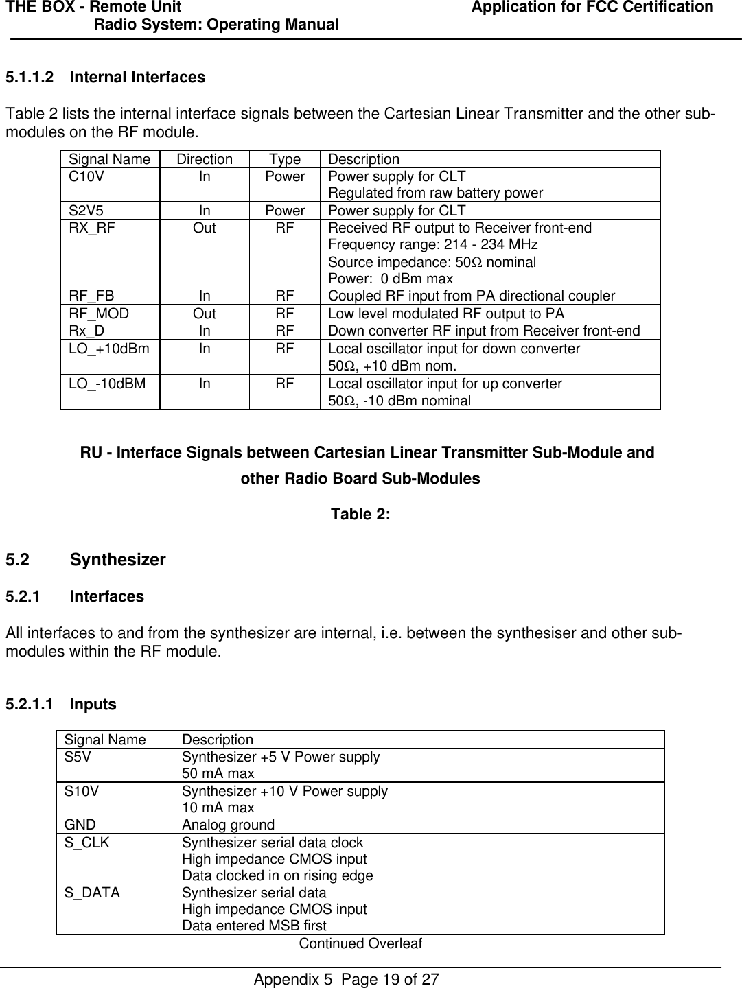
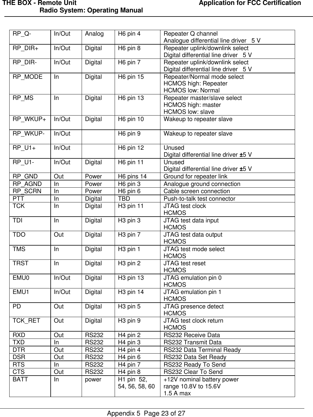
![THE BOX - Remote Unit Application for FCC Certification Radio System: Operating ManualAppendix 5 Page 22 of 275.4 Baseband Module5.4.1 External InterfacesThese signals which originate from or go directly to the Baseband module from any part of the RU(other than the radio RF module) are listed in Table 10.Signal Name Direction Type Connector DescriptionHI_D0 -HI_D15 In/Out Digital H1 pin 1-16 16 bit parallel interface, Host CPU data busTTLHI_C/D In Digital H1 pin 33 Indicates whether host interface contents arecommand or data (host to radio direction only)TTLSee Ref. [8] for levels & timingHI_WSTRB In Digital H1:37 Buffer read/writeTTLSee Ref. [8] for levels & timingHI_RFLAG Out Digital H1:35 Read buffer full flagTTLSee Ref. [8] for levels & timingHI_WFLAG Out Digital H1:36 Write buffer full flagTTLSee Ref. [8] for levels & timingHI_RSTRB In/Out Digital H1:34 Read data strobeTTLSee Ref. [8] for levels & timingWKUPH Out Digital H1:39 Wakeup to Host CPU from Radio systemTTL high: wakeupTTL low: radio card in sleep modeWKUPR In Digital H1:38 Wakeup from Host CPU to Radio systemTTL high: Wakeup radio system from sleepHI_RESET In Digital H1:40 Hardware reset from HostTTL active highREF Out Digital H1:41 2.048 MHz reference locked to master ref.Buffering HCMOSTZERO Out Digital H1:42 T-zeroHCMOS, timing ±20 µsAUD_IN In Analog TBD Audio input0 dBm into 600ΩAUD_OUT Out Analog TBD Audio output0 dBm into 600ΩRP_I+ In/Out Analog H6 pin 2 Repeater I channelAnalog differential line driver !5 VRP_I- In/Out Analog H6 pin 1 Repeater I channelAnalogue Differential line driver !5 VRP_Q+ In/Out Analog H6 pin 5 Repeater Q channelAnalogue differential line driver !5 VContinued overleaf](https://usermanual.wiki/Fairfield/BOX-RU/User-Guide-91400-Page-25.png)