Fender Musical Instruments FMAPR4475 Fender PCB Assembly including the BT Radio Module - PN 7710068000 FMA BT-FTSW-USB / BT Module - FreeWings FW3817-30 User Manual
Fender Musical Instruments Fender PCB Assembly including the BT Radio Module - PN 7710068000 FMA BT-FTSW-USB / BT Module - FreeWings FW3817-30
User Manual
Fender FMA BT-FTSW-USB PCBA (PN 7710068000) Page 1
Manual and Spec, revision 1.0 November 8, 2016
Fender FMA BT-FTSW-USB PCBA (PN 7710068000)
Manual and Spec, revision 1.0
Module Description
The Fender FMA BT-FTSW-USB PCB Assembly is an auxiliary PCB used in the family of Fender Modular
Architecture (FMA) products. The board has a USB port with a micro AB connector, a Fender Footswitch
port with a ¼” phone jack and a wireless module.
Circuit Description/Theory of Operation
There are three main sections of the circuit:
• Bluetooth module (FreeWings FW3817-30), antenna, & audio output circuit
• USB port
• Footswitch port
The USB circuit consists of ESD protection components and a micro AB USB connector. The Footswitch
circuit consists of ESD protection components and a ¼” phone jack connector. Both of these circuits are
unrelated to the Bluetooth section, and are shared on the PCB for mechanical convenience.
The FreeWings module is a complete Bluetooth implementation with analog audio output. An F-style
antenna is connected to the RF output of the module through a test switch and matching network. The
module is powered with a 3.3V DC supply and digital ground. The PCB is dual layer with digital ground
plane sections stitched together on both sides where possible. The analog stereo audio output from the
module is buffered by an op-amp stage before sending back to the host system. The analog audio buffer
circuit has a separate power supply and ground system to isolate it from digital noise.
All Bluetooth functionality is controlled by on-board firmware. But the module may be accessed for test
through the SPI port to a computer interface module (available from FreeWings). A description of
specific commands for Bluetooth is beyond the scope of this document and can be found in
documentation from FreeWings or CSR for the CSR8630 chipset.

Fender FMA BT-FTSW-USB PCBA (PN 7710068000) Page 2
Manual and Spec, revision 1.0 November 8, 2016
FMA Main PCB Interface Header
All control and power signals come from a connection to a motherboard through an 18-pin, 2mm dual
row female header. The pinout for the header is in the table below:
Pin
Signal
Description
1
USB_OTG_DP
USB OTG port data signal
2
USB_OTG_DN
USB OTG port data signal
3
GNDD
Digital GND
4
FTSW_DAT
Footswitch port data signal
5
STATUS_LED
-
CHIP_WAKE
Status GPIO output
6
FTSW_DET
Footswitch port detect
7
PAIR
-
HOST_WAKE
Pair GPIO input
8
USB_OTG_5V
Reserved for future use
9
USB_OTG_ID
USB OTG port ID signal
10
3.3V
3.3V DC Supply
for
digital circuitry and BT module
11
Not used
12
GNDD
Digital GND
13
Not used
14
+5V_ANALOG
5V DC Supply for analog audio circuit
15
GNDA
Audio GND
16
G2V5
2.5V half
-
bias reference for analog audio circuit
17
BTA_L
Analog audio signal output LEFT
18
BTA_R
Analog audio signal output RIGHT
Fender FMA BT-FTSW-USB PCBA (PN 7710068000) Page 3
Manual and Spec, revision 1.0 November 8, 2016
Power Consumption
Operating Voltage
3.3VDC +/
-
9%
Operating Current
50mA
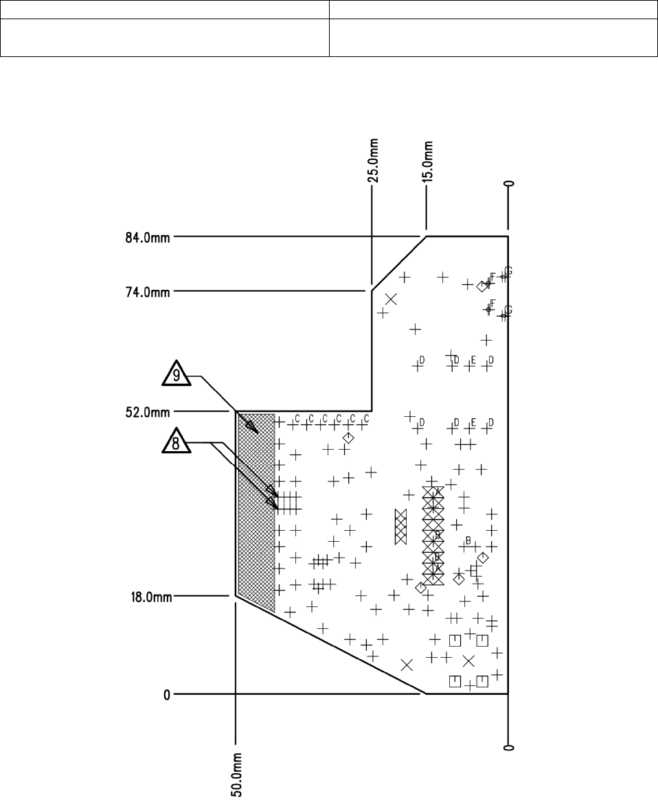
Board Dimensions
Fender FMA BT-FTSW-USB PCBA (PN 7710068000) Page 4
Manual and Spec, revision 1.0 November 8, 2016
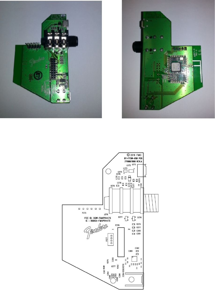
PHOTOS
Top Side PCB Module Bottom Side PCB Module
SILKSCREEN ID LABEL
Fender FMA BT-FTSW-USB PCBA (PN 7710068000) Page 5
Manual and Spec, revision 1.0 November 8, 2016
COMPLIANCE STATEMENTS
FCC Statement:
This device complies with Part 15 of the FCC Rules. Operation is subject to the following two conditions:
(1) This device may not cause harmful interference. (2) This device must accept any interference
received, including interference that may cause undesired operation.
NOTE: This equipment has been tested and found to comply with the limits for a Class B digital device,
pursuant to Part 15 of the FCC Rules. These limits are designed to provide reasonable protection against
harmful interference in a residential installation. This equipment generates uses and can radiate radio
frequency energy and, if not installed and used in accordance with the instructions, may cause harmful
interference to radio communications. However, there is no guarantee that interference will not occur
in a particular installation. If this equipment does cause harmful interference to radio or television
reception, which can be determined by turning the equipment off and on, the user is encouraged to try
to correct the interference by one or more of the following measures:
• Reorient or relocate the receiving antenna.
• Increase the separation between the equipment and receiver.
• Connect the equipment into an outlet on a circuit different from that to which the receiver is
connected.
• Consult the dealer or an experienced radio/TV technician for help.
WARNING: Changes or modifications not expressly approved by the party responsible for compliance
could void the user's authority to operate the equipment.
LABEL OF THE END PRODUCT:
The final end product must be labelled in a visible area with the following:
"Contains FCC ID: XQW-FMAPR4475"
If the size of the end product is smaller than 8x10cm, then additional FCC part 15.19 statement is
required to be available in the users manual: This device complies with Part 15 of the FCC Rules.
Operation is subject to the following two conditions: (1) this device may not cause harmful interference,
and (2) this device must accept any interference received, including interference that may cause
undesired operation.
RF Exposure
This device has been evaluated and shown compliant with the FCC RF Exposure limits under fixed
exposure conditions (antennas are greater than 20cm from a person's body) when installed in certain
specific OEM configurations.
This modular complies with FCC RF radiation exposure limits set forth for an uncontrolled environment.
This transmitter must not be co-located or operating in conjunction with any other antenna or
transmitter. Due to missing shielding the module is strictly limited to integration by the Grantee himself
Fender FMA BT-FTSW-USB PCBA (PN 7710068000) Page 6
Manual and Spec, revision 1.0 November 8, 2016
or his dedicated OEM integrator under control of the Grantee. However, the OEM integrator is still
responsible for testing their end-product for any additional compliance requirements required with this
module installed.
IMPORTANT NOTE:
This device is intended only for OEM integrators under the following conditions:
(1) According to FCC Part 15 Subpart C Section 15.212, the radio elements of the modular transmitter
must have their own shielding. However, due to there is no shielding for this WIFI/BT module, this
module is granted as a Limited Modular Approval.
(2) This module has been designed to operate with PCBA antenna having a maximum gain of 0dBi.
(3) Integration is typically strictly restricted to Grantee himself or dedicated OEM integrators under
control of the Grantee.
The module will be responsible to satisfy SAR/RF Exposure requirements, when the module integrated
into any (portable, mobile, fixed) host device.
This module is intended for OEM integrator only and the OEM integrators and instructed to ensure that
the end user has no manual instructions to remove or install the device. The OEM integrator is still
responsible for the FCC compliance requirement of the end product, which integrates this module.
The module has no shielding and tested stand alone. This module is tested and approved as Limited
modular approval with stand alone configuration, any OEM incorporated this radio module into any
system are require additional testing and evaluation.
The module is only certified with the installed antenna. Any change of the antenna will void the
certification.
IC Notice:
This device complies with Canada Industry licence-exempt RSS standard(s). Operation is subject to the
following two conditions:
(1) this device may not cause interference; and
(2) this device must accept any interference. Including interference that may cause undesired operation
of the device.
Avis d’Industrie Canada
Le présent appareil est conforme aux CNR d'industrie Canada applicables aux appareils radio exem pts
de licence L'exploitation est autorisée aux deux conditions suivantes:
1) I'appareil ne doit pas produire de brouillage; et
2) I'utillsateur de I'appareil doit accepterbrouillage radioélectrique subi meme si le brouillage est
susceptible d'encompromettre le fonctionnement. mauvais fonctionnement de I'appareil.
Fender FMA BT-FTSW-USB PCBA (PN 7710068000) Page 7
Manual and Spec, revision 1.0 November 8, 2016
Radiation Exposure Statement:
This equipment complies with IC radiation exposure limits set forth for an uncontrolled environment.
This equipment should be installed and operated with minimum distance 20cm between the radiator &
your body.
Déclaration d'exposition aux radiations:
Cet équipement est conforme aux limites d'exposition aux rayonnements IC établies pour un
environnement non contrôlé. Cet équipement doit être installé et utilisé avec un minimum de 20 cm de
distance entre la source de rayonnement et votre corps.
This device and its antenna(s) must not be co-located with any other transmitters except in accordance
with IC multi-transmitter product procedures.
Refering to the multi-transmitter policy, multiple-transmitter(s) and module(s) can be operated
simultaneously without reassessment permissive change.
Cet appareil et son antenne (s) ne doit pas être co-localisés ou fonctionnement en association avec une
autre antenne ou transmetteur. This module is intended for OEM integrator.
The OEM integrator is still responsible for the IC compliance requirement of the end product, which
integrates this module.
In the users manual of the end product, the end user has to be informed to keep at least 20cm
separation with the antenna while this end product is installed and operated. The end user has to be
informed that the IC radio-frequency exposure guidelines for an uncontrolled environment can be
satisfied. The end user has to also be informed that any changes or modifications not expressly
approved by the manufacturer could void the user's authority to operate this equipment. Operation is
subject to the following two conditions: (1) this device may not cause harmful interference and (2) this
device must accept any interference received, including interference that may cause undesired
operation.
The final end product must be labeled in a visible area with the following
"Contains TX IC : 8690A-FMAPR4475 ".
This radio transmitter (identify the device by certification number, or model number if Category II) has
been approved by Industry Canada to operate with the antenna types listed below with the maximum
permissible gain and required antenna impedance for each antenna type indicated.
Le présent émetteur radio (identifier le dispositif par son numéro de certification ou son numéro de
modèle s'il fait partie du matériel de catégorie I) a été approuvé par Industrie Canada pour fonctionner
avec les types d'antenne énumérés ci-dessous et ayant un gain admissible maximal et l'impédance
requise pour chaque type d'antenne.
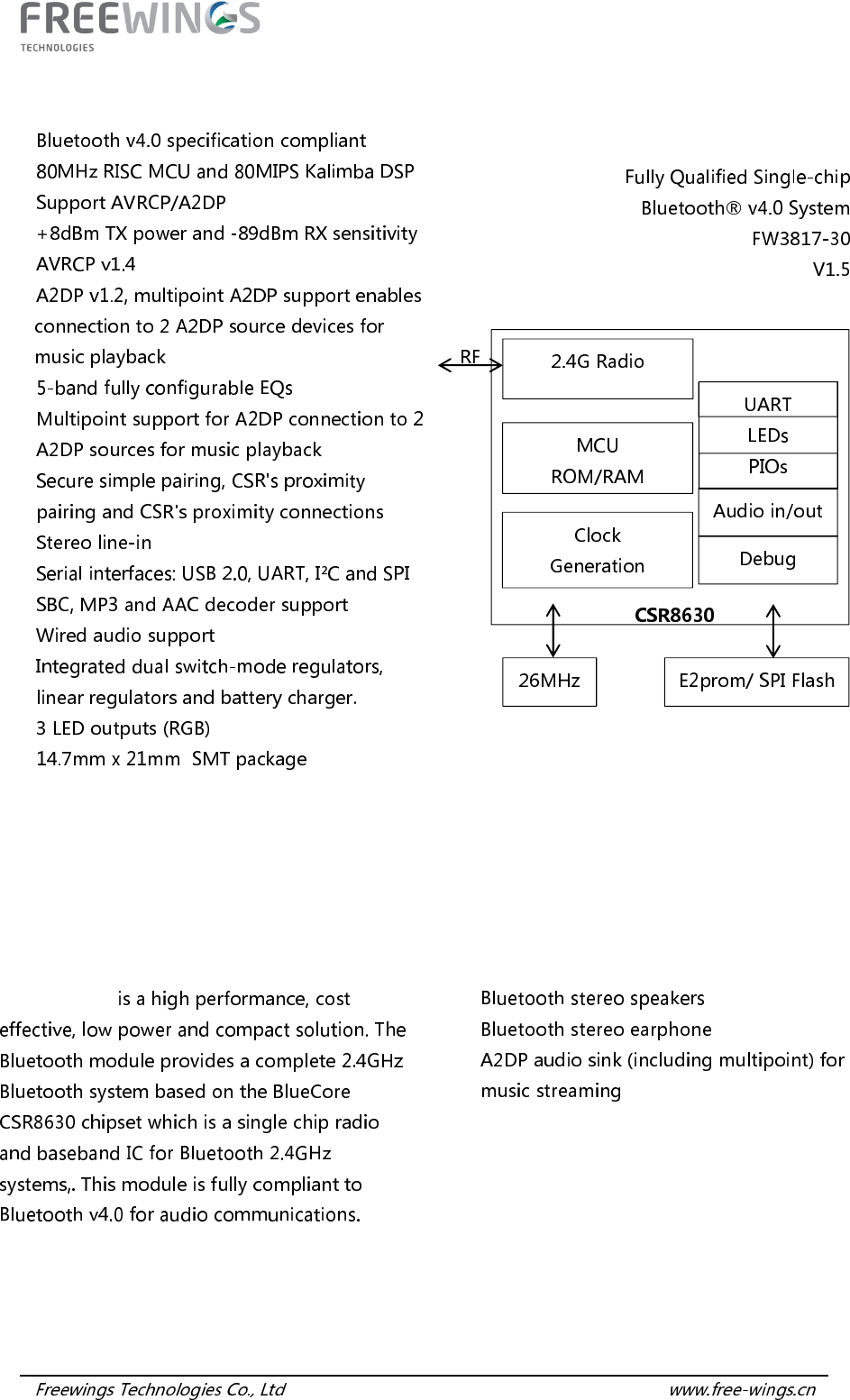
Features
FW3817-30 Bluetooth Module
CSR8630 Audio Solution
General Description
FW3817-30
Applications
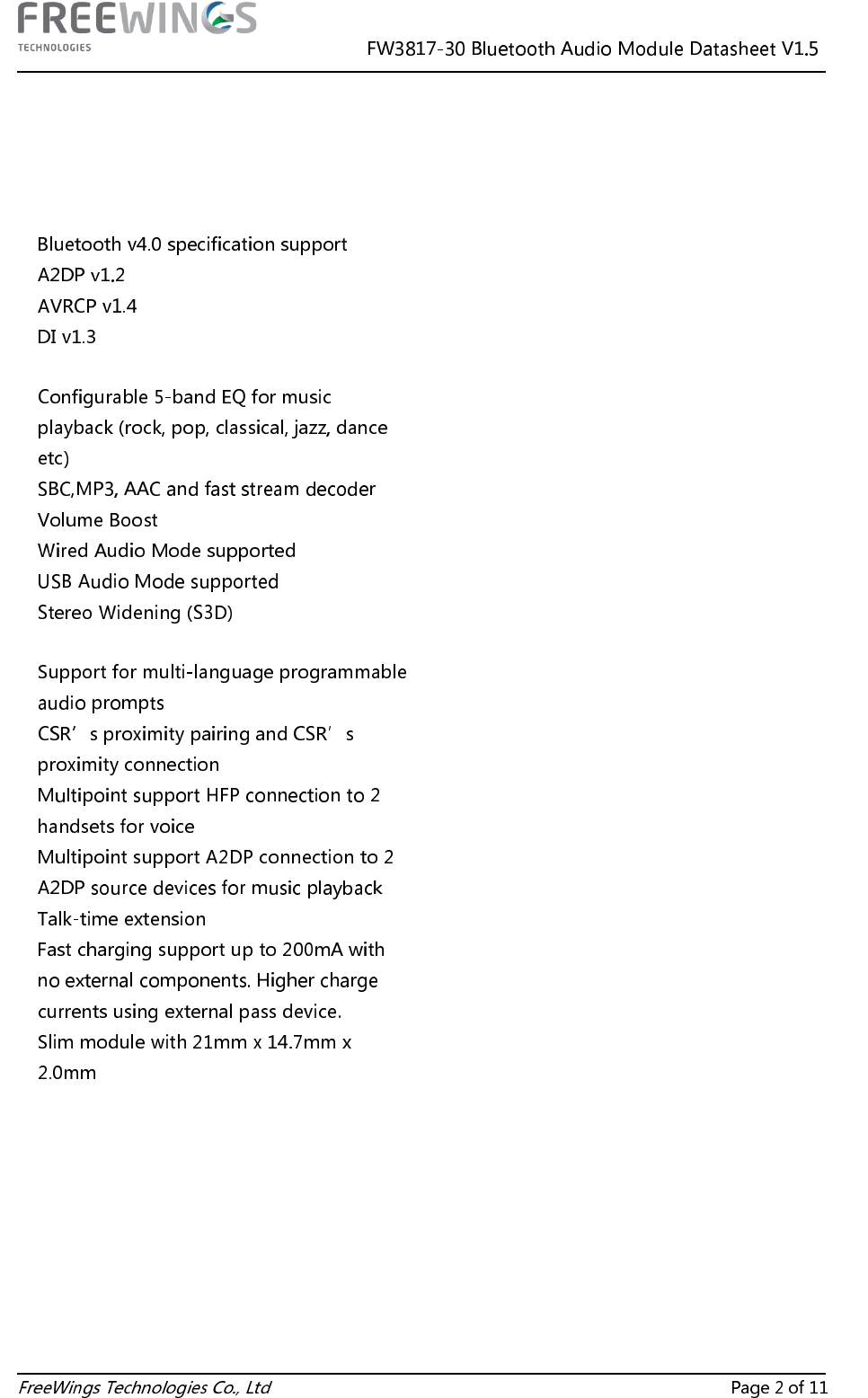
FW3817-30 Details
Features
Bluetooth Profiles
Music Enhancements
Additional Functionality
Contents
1
GENERAL SPECIFICATIONS ................................................................................................................. 4
2
MODULE PACKAGE INFORMATION .................................................................................................. 5
6.1 P
INOUT
D
IAGRAM AND PACKAGE DIMENSIONS
.............................................................................. 5
6.2 M
ODULE
P
IN DESCRIPTIONS
........................................................................................................... 6
3
ELECTRICAL CHARACTERISTICS ..................................................................................................... 7
7.1 R
ESET
............................................................................................................................................. 7
7.2 P
OWER ON AND POWER OFF
............................................................................................................ 7
7.3 I/O .................................................................................................................................................. 7
7.4 B
ATTERY
C
HARGER
....................................................................................................................... 8
7.5 USB ................................................................................................................................................ 8
7.6 A
BSOLUTE
M
AXIMUM
R
ATINGS
..................................................................................................... 8
7.7 R
ECOMMENDED
O
PERATING
C
ONDITIONS
..................................................................................... 8
7.8 P
OWER CONSUMPTION
.................................................................................................................... 8
4
MAIN COMPONENTS LIST ..................................................................................................................... 9
5
RECOMMENDED REFLOW TEMPERATURE PROFILE ............................................................... 10
6
RECORD OF CHANGES ......................................................................................................................... 11
7
IMPORTANT NOTICE ............................................................................................................................ 11

1 General specifications
Model Name FW3817-30
Product Description Bluetooth 4.0 Class2 Module
Bluetooth Standard Bluetooth 4.0
Chipset CSR8630
Dimension 21mm x 14.7mm x 2.0mm
Temperature
Storage Temperature -40 +85
Operating Temperature -20 +70
Electrical Specifications
Supply Voltage 2.80~4.25V
Power Consumption in A2DP slave mode
with no load and playing peak noise 14mA
Modulation GFSK/π/4 DQPSK/8DPSK
Frequency Range 2402 2480MHz
Maximum RF Transmit Power 4dBm
Receive Sensitivity -84dBm
2 Module Package Information
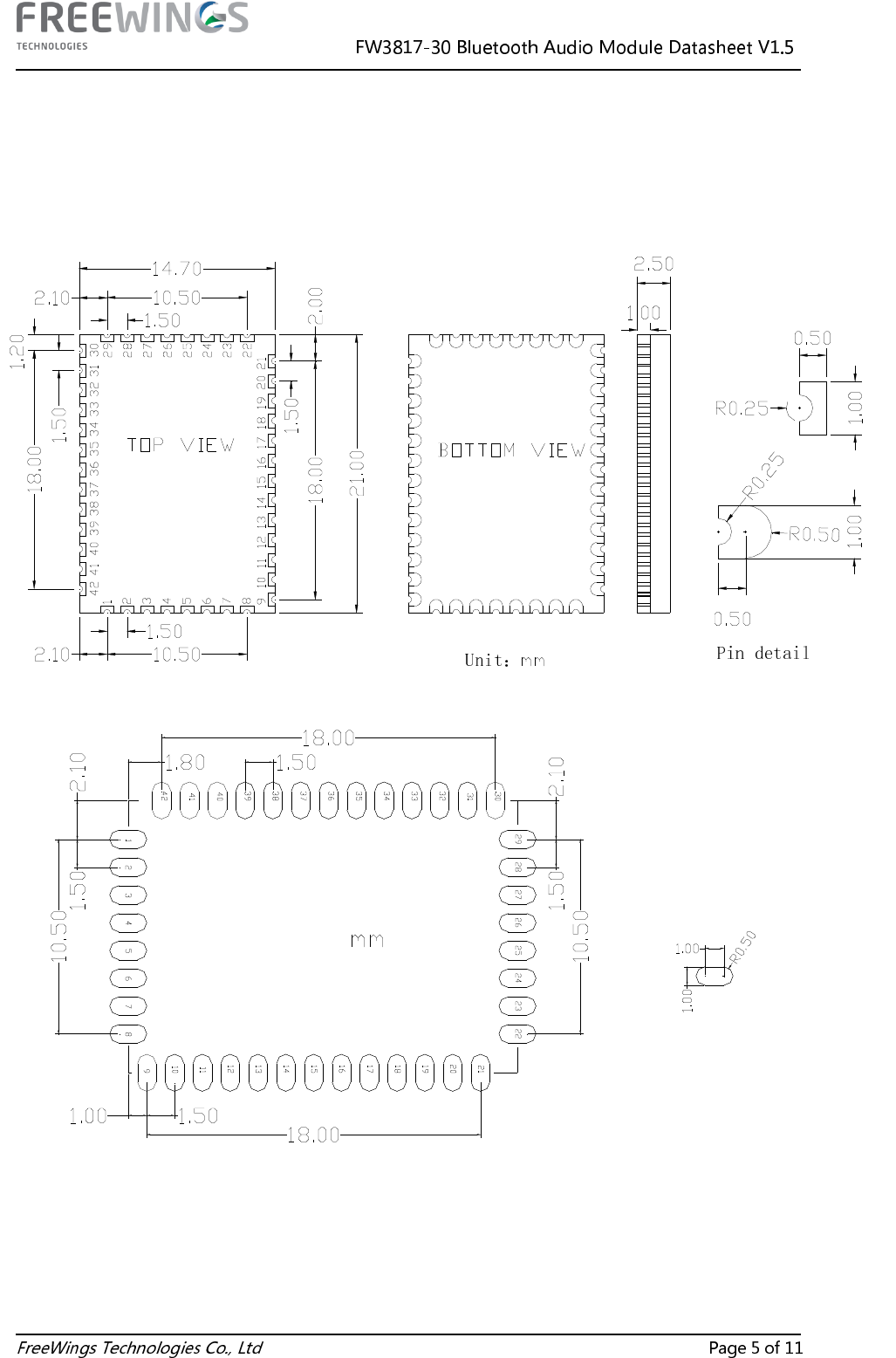
6.1 Pinout Diagram and package dimensions
Mechanical Dimensions
Unit:
Pin detail
Recommended PCB layout footprint
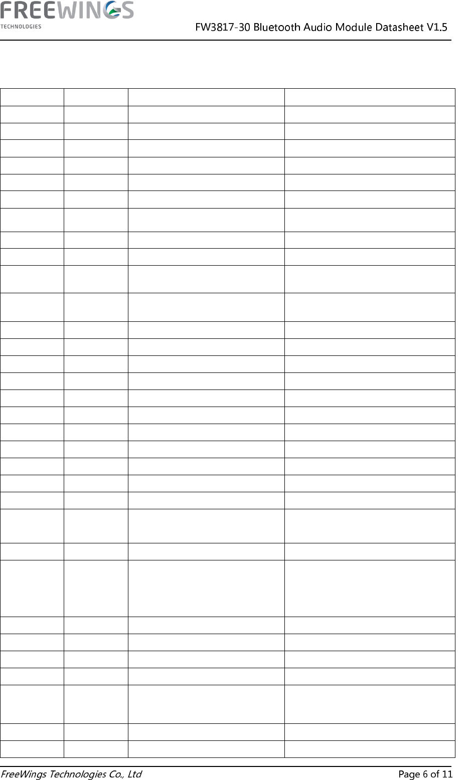
6.2 Module Pin descriptions
Pin No. Pin Name Pin Type Description
1 GND VSS Ground
2 USB_P Bidirectional USB data plus
3 USB_N Bidirectional USB data minus
4 PIO15 Bidirectional with strong pull-up
MFB key input
5 PIO14 Bidirectional with strong pull-up Skip+ key input
6 PIO16 Bidirectional with strong pull-up Volume+ key input
7 PIO9 Bidirectional with strong pull-down
External PA enable output high
8 PIO1 Bidirectional with strong pull-up Volume- key input
9 NC N.C NOT CONNECTED
10
PIO17 Bidirectional with strong pull-down
Skip- key input
11 RSTn Input with strong pull-up Reset if low. Pull low for minimum
5ms to cause a reset.
12 SPI_MOSI Bidirectional with weak pull-down SPI_MOSI for debug only
13 SPI_CLK Bidirectional with weak pull-down SPI_CLK for debug only
14 SPI_CSB Bidirectional with weak pull-down SPI_CSB active low for debug only
15 SPI_MISO Bidirectional with weak pull-down SPI_MISO for debug only
16 LED1 Open drain output LED driver
17 LED0 Open drain output LED driver
18 VREG_EN Power on/off key input Power on/off input key indication
19 VBAT Battery positive terminal Power supply input for 2.8~4.2V
20 VCHG Charger voltage input Internal charger input for charging
21 1V8 1.8V output 1.8V output for keys
22 GND VSS Ground
23 VBAT_SEN
SE Battery Sense Battery charger sense input
24 PIO6 Bidirectional with strong pull-down
Programmable input/output line
25 CHG_EXT Charger external pin
External battery charger control.
External battery charger transistor base
control when using external charger
boost. Otherwise leave unconnected.
26 LED2 Open drain output LED driver
27 NC N.C Not Connected
28 LINE_RP Analog input Line input, positive right
29 LINE_RN Analog input Line input, negative right
30 AIO0 Analog input ADC input used only to test
temperature of battery
31 LINE_LP Analog input Line input, positive left
32 LINE_LN Analog input Line input, negative left

33 SPK_RN Analog output Speaker output negative right
34 SPK_RP Analog output Speaker output positive right
35 SPK_LN Analog output Speaker output negative left
36 SPK_LP Analog output Speaker output positive left
37 GND VSS Ground
38 RF PORT Analog Bluetooth signal input/output port
50Ohm
39 GND VSS Ground
40 NC N.C Not Connected
41 NC N.C Not Connected
42 NC N.C Not Connected
3 Electrical Characteristics
7.1 Reset
FW3817-30 module is reset from several sources.We suggest to use power-on reset,that means to leave the
RSTn pin floating:
RSTn pin pulled low for minimum 5ms
Power-on reset, leaving the RSTn pin floating. It should be that it was 0V voltage at any pin before reset.
USB charger attach reset
Software configured watchdog timer
7.2 Power on and power off
FW3817-30 module is power on from two sources:
VREG_EN pin pulled high for minimum 100ms when VBAT pin is in the status of stable power.
VREG_EN pin pulled high from low when VBAT pin is in the status of stable power.
The wrong timing sequence of VREN_EN and VBAT will lead to error of power on.
FW3817-30 module is power off from two sources:
VREG_EN pin pulled high for minimum 100ms when VBAT pin is in the status of stable power.
VREG_EN pin pulled low from high when VBAT pin is in the status of stable power.
The wrong timing sequence of VREN_EN and VBAT will lead to error of power off.
7.3 I/O
The driver power voltage of all the PIO port is 1.8V inside of the module.

7.4 Battery Charger
FW3817-30 module provides two kinds of battery charger controls.
The internal charger circuit can provide up to 200mA of charger circuit.
The module controls an external pass transistor which can provide 500mA of charger circuit.
7.5 USB
USB_P and USB_N can be used to updating software or USB audio.Both of them request that VCHG pin must
be supplied 5V power.The two data signals do not need any resistance or capacitance.
7.6 Absolute Maximum Ratings
Rating Minimum Maximum Unit
Storage Temperature -40 85
Supply Voltage
VCHG -0.4 5.75 V
LEDs -0.4 4.4 V
VBAT SENSE -0.4 4.4 V
VREG_EN -0.4 4.4 V
VBAT -0.4 4.4 V
7.7 Recommended Operating Conditions
Rating Minimum Typical Maximum Unit
Operating Temperature -20 20 70
Supply Voltage
VCHG 4.75 5.00 5.75 V
LEDs 1.10 3.70 4.30 V
PIO 1.50 1.80 1.90 V
VBAT SENSE 0 3.70 4.25 V
VREN_EN 2.80 3.70 4.25 V
VBAT 2.80 3.70 4.25 V
7.8 Power consumption
Status Current Typical Unit
Power off VBAT 0.1 uA
A2DP slave mode with no load and playing
peak noise VBAT 12 mA
A2DP slave mode with two16ohm speakers and
playing peak noise VBAT 24 mA
Pause in A2DP slave mode connection VBAT 0.5 mA
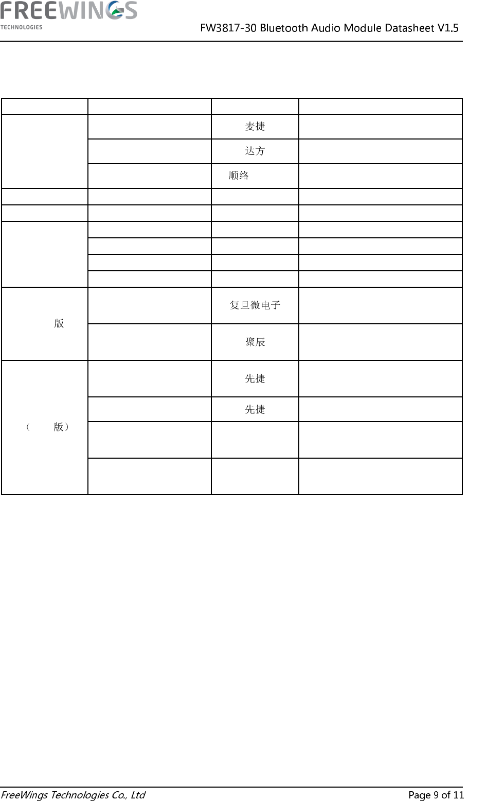
4 Main components list
NO. Description Manufacture Manufacturer P/N
1
Inductor 4.7uH ±20%
0805 MGFL2012C4R7MT-LF
Inductor 4.7uH ±20%
0805 IP20124R7MPS9
Inductor 4.7uH ±20%
0805 Sunlord MSL2012S4R7MHT
2 IC BT BC8630 QFN68 CSR CSR8630B04-IQQF-R
3 Filter WiFi 1608 ACX BF1608-L2R4DAAT/LF
4
Crystal 26M 8.5PF 10PPM
HOSONIC E3SB26.0000F8ES11M
Crystal 26M 8.5PF 10PPM
TXC 7M26000314
Crystal 26M 8.5PF 10PPM
EPSON XIE000021008300
Crystal 26M 9PF 10PPM H.ELE X3S026000B91H-NZ
5(ROM )
IC EEPROM
FM24C128A-TS-T-G
TSSOP-8
FM24C128A-TS-T-G
IC EEPROM
GT24C128A-2ZLI-TR
TSSOP-8
GT24C128A-2ZLI-TR
6 Flash
IC Flash Serial
GD25Q41B 4M-bit SOP-8
Gigadevice
GD25Q41BTIGR
IC Flash Serial MD25D40
4M-bit SOP-8 Gigadevice MD25D40TIGR
IC
1.8V 4M SPI FLASH SOP
-8 150mile
MXIC MX25U4033EM1I-12G
IC
1.8V 4M SPI FLASH SOP
-8 150mile
MXIC KH25U4033EM1I-12G
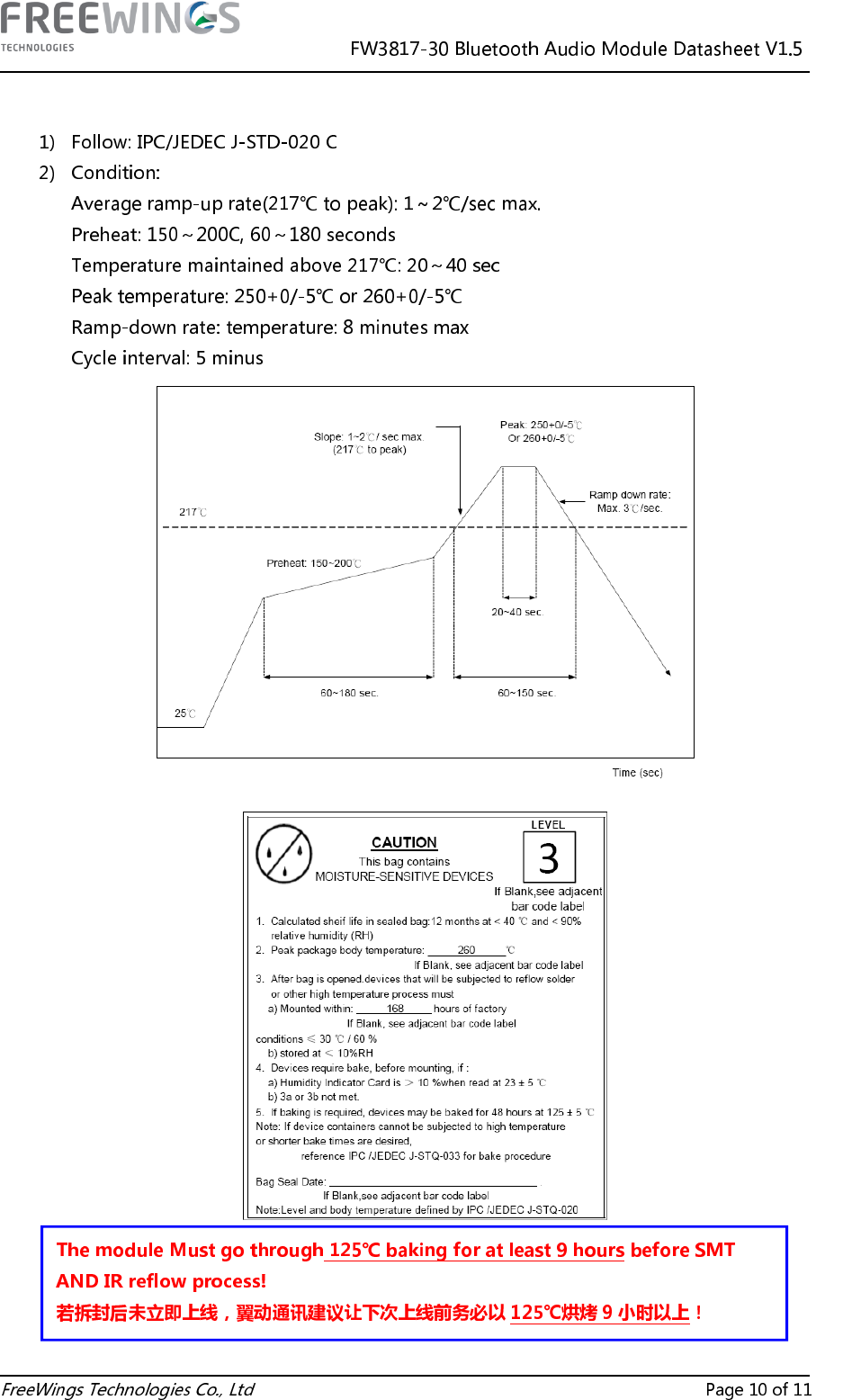
5 Recommended reflow temperature profile

6 Record of Changes
7 Important Notice